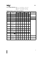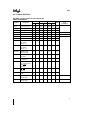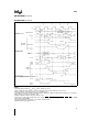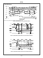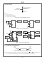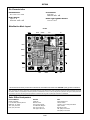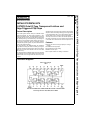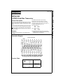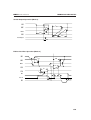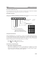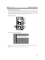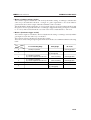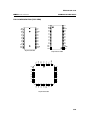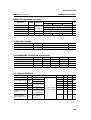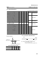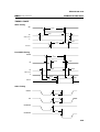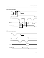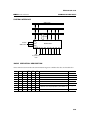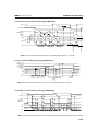
1
KING FHAD UNIVERSITY OF PETROLEUM & MINERALS Collage of Computer Sciences & Engineering Department of Computer Engineering COE305 Microcomputer Systems Design Lab Manual COE305 LAB MANUAL Microcomputer Systems Design by Dr. Abdul Rahim Naseer Mr. Khaled Al-Utaibi Mr. Hazem Selmi Table of Contents Design & Fabrication of an 8086 Microprocessor System Interfacing the Clock Generator to the CPU 2 Designing the Bus System 5 Designing the Memory System 8 Interfacing I/O Ports 12 Testing the 80806 Microcomputer System 15 Interface Experiments Using 8086 Microprocessor Kits & Application Boards Flight 8086 Training Board 21 Conducting Simple I/O Operations Using Flight 86 Training Kit 30 Generating Timing Sequences 37 Analog To Digital & Digital To Analog Conversion 47 Controlling Dc Motors 54 Interfacing A Hyper Terminal To The Flight 86 Kit 59 Mini Project Appendices C O E 3 0 5 L A B 1 Part M A N U A L Design & Fabrication of an 8086 Microprocessor System I n this part of the lab, the students are required to design and fabricate an 8086 based microcomputer system. The lab experiments in this part, consist of designing, assembling and testing of the fabricated system. The design, assembling and testing will be carried out by the students in an incremental manner as indicated below. 1. Connecting and testing clock driver circuit with microprocessor. 2. Connecting and testing address buffers and data bus drivers with microprocessor 3. Connecting and testing memory and I/O decoders 4. Connecting and testing memory devices (EPROMs, RAMs) with the processor 5. Connecting and testing I/O ports. 6. Writing assembly language programs for simple applications. 1 C O E 3 0 5 L A B 1 Experiment M A N U A L Interfacing the Clock Generator to the CPU 1.1 Background The 8086 CPU has 16 data lines and 20 address lines. The CPU uses time multiplexing for the Address, data, and some status lines. The Clock Generator and Driver 8284 is a device capable of providing the CPU with Clock, reset logic, and ready logic. For this it uses a crystal oscillator that must be 3 times the frequency of the CPU (15 MHz Crystal). 1.2 Objective Interfacing the clock generator to the CPU 1.3 Equipment The instructor should group the students (2 or 3 per group) and assign a group head. The group head will take the following equipment on his responsibility as a loan from COE department. From now on, in every experiment there will be more equipment given. The group will keep the equipment and use them through the following experiments. They should return every thing before reporting the grades. Proto board, 8086 CPU, 8284 Clock generator, 15 MHz crystal clock, 1 Reset-Switch, 3 resistors (l00K, 510, 510), 2 C O E 3 0 5 L A B M A N U A L 1 Capacitor (10u), and Oscilloscope 1.4 Procedure 1. Make a short review of the clock generator 8284 (Appendix II) and identify the three major functions that this device can operate. Figure 1.1: Top view of the 8284 clock generator 2. Implement the design shown in Figure 1.2 and check the output signal at CLK, PCLK, and OSC using the oscilloscope. Interface the CLK line to CPU and show your instructor the resulting signals. Figure 1.2:Connecting the crystal to the 8284 3. Implement the RESET circuit shown in Figure 1.3, and make sure that any change from 0 to 1 must have duration of at least 50us. Test the reset signal using the oscilloscope and show the resulting signal to your instructor. 3 C O E 3 0 5 L A B M A N U A L Figure 1.3: Reset Circuit 4. Read pin description of the 8086 microprocessor (Appendix), and determine what should be connected to the following pins (assume minimum mode): a. MN / MX (pin 33) b. HOLD (pin 31) c. TEST (pin 23) d. READY (pin 22) e. RESET (pin 21) f. CLK (pin 19) g. INTR (pin 18) h. NMI (pin 17) 5. Connect VCC and GND pins of the 8086 microprocessor and test the ALE signal (pin 25) using the oscilloscope. Exercises 1.1. What is the relationship between frequencies on the lines CLK, PCLK, and OSC? Do these frequencies match with the description of the 8284? 1.2. Find out the proper values of the needed resistors and capacitors in the RESET circuit such that any change from 0 to 1 must ensure duration of 50us. 1.3. What is the function of the ready signals on the 8284? 4 C O E 3 0 5 L A B 2 Experiment M A N U A L Designing the Bus System 2.1 Background The 8086 CPU has 16 data lines and 20 address lines. The CPU uses time multiplexing for the address, data, and some status lines. The CPU generates the addresses A0-A15 on lines AD0- AD15 and A16-A19 on lines AS16-AS19 during clock T1. This event is indicated by a bus control signal ALE. During T2, T3, and T4 the CPU uses the AD0AD15 to transfer data, i.e. as data bus. Demultiplexing of the AD lines requires latching of the addresses by using some integrated latches (e.g. 74LS373 octal latches). The latched addresses will then be used as address bus during clocks T2, T3, and T4. The 74LS373 octal latch is a simple level-triggered D flip-flops with two control lines: Output Control (OC) and Latch Enable (G). As long as the Latch Enable (G) is high, the outputs of the D flip-flops follow their inputs. When G goes low, the flip-flops latch (save) the input signals. The output control line (OC) can be used to place the eight latches in either a normal logic state (high or low logic levels), or a high-impedance state. 2.2 Objective To provide a demultiplexed data and address buses for the 8086 CPU through the use of the 74LS373 octal latches 2.3 Equipment The prototype-board that already includes an 8086 microprocessor with clock generator, TTL 74LS373 octal latches, and Multimeter 5 C O E 3 0 5 L A B M A N U A L 2.4 Procedure 1. Review the function of the 74LS373 octal latch (Appendix). Identify its input and output lines as well as the control signals available on this chip. 2. Each group discuss and give solutions to the following issues: a. What are the AD and AS lines that must be demultiplexed? b. The number of needed octal latches. c. What should be connected to control lines of the 74LS373 octal latch (i.e. G and OC). 3. Each group present their design of the demultiplexed bus to the lab instructor for validation. The proposed design must be completely defined on a working map, and the same map must be used in the wiring and debugging. The design must show what should be connected to the Latch Enable (G) and Output Control (OC) lines. 4. Once the design is validated, the group can start wiring based on the working map. 5. After completing the wiring, each group must carry out visual and electrical testing of the connections (e.g. using multimeters) as well as doing necessary corrections. 6 C O E 3 0 5 L A B M A N U A L 7 C O E 3 0 5 L A B 3 Experiment M A N U A L Designing the Memory System 3.1 Background The 8086 CPU has addressing capability of 1 Mega Bytes as well as a 16-bit data bus. Basically, EPROM and SRAM memory chips are byte organized. The 8086 CPU requires that the memory be organized as two banks called the even and odd banks. The EPROM memory is to store resident programs that must run when the microprocessor system is powered on. The SRAM memory is used to store application programs that are ready to run as well as to provide some reserved locations for the proper operations of interrupts. The designer must be careful with bank selection especially when dealing with read/write memories. In this case, byte operations with one bank must be done while enabling one of the memory banks and disabling the other. This experiment should expose the student to a number of issues such as: 1. Partitioning of the memory address space, 2. Distinguishing between addressing capability and physical memory, 3. Dealing with partial and exhaustive addressing, arid 4. Studying address decoding techniques 3.2 Objective Designing and implementing a small memory system using SRAM and EPROM memory chips 3.3 Equipment The prototype-board that already includes an 8086 CPU operating in minimum mode with clock generator and a fully demultiplexed data and address buses, 8 C O E 3 0 5 L A B M A N U A L Two 8 Kbytes SRAM memories (6264), and Two 8 Kbytes EPROM memories (2764) 3.4 Procedure In this project, each group will design a memory system consisting of two memory modules. The first is a 16 KByte SRAM starting at address 00000h. The second is a 16 KByte EPROM ending at address FFFFh (Why?). Refer to your text book for more details about memory system design. 1. Each group discuss and answer the following issues: a. What is the number of address lines required to address the two modules? b. How to design the 32 KBytes memory system using partial decoding? c. How to design the same memory system using exhaustive (full) decoding? d. What address lines to be connected to the even and odd banks of the two modules? e. How to distinguish the even and odd banks of the SRAM module? f. Is it necessary to distinguish the even and odd banks of the EPROM module? Why? 2. Design the above memory system by using two 8 KBytes SRAM memories (6264) and two 8 KBytes EPROM memories (2764). Show your design to the lab instructor and implement it after validation. Your design should show, for each memory chip, what should be connected to: a. Address and data pins b. Chip select ( CS ) c. Output Enable ( OE ) d. Write Enable ( WE ) 9 C O E 3 0 5 L A B M A N U A L 3. Implement the decoder shown in Figure 3.1 which takes as input RD , WR and M / IO , and produces memory read ( MEMR ), memory write ( MEMW ), I/O read ( IOR ) and I/O write ( IOW ) signals. 4. After completing the wiring, each group must carry out visual and electrical testing of the connections (e.g. using multimeters) as well as doing necessary corrections. Figure 3.1: Generating the four memory and I/O control bus signals from the 8086's RD, WR and I/O signals. 10 C O E 3 0 5 L A B M A N U A L 11 C O E 3 0 5 L A B 4 Experiment M A N U A L Interfacing I/O Ports 4.1 Background The I/O ports are very essential in any computer system because they enable the user to communicate with the system. In this experiment, we will design and implement a very simple form of I/O ports (switches for input and LEDs for output). The input port should be designed to pass the data on the input switches to the data bus if and only if an input instruction (I/O read cycle) is executed by the CPU. This can be achieved using a tri-state buffer that will be enabled only during I/O read cycles. The output port should be capable of storing the data on the bus when the CPU performs an output instruction (I/O write cycle). In this case, a latch can be used to store the output data and supply it continuously to the LEDs. The latch should be enabled to pass its input to the LEDs only when the CPU is writing to the output port (i.e. I/O write cycle). Just as each memory location has its own (memory) address, each I/O port has its own (port) address. However, since we are using only one input port and one output port, we will not assign any addresses to our I/O port. Thus, I/O instructions can use dummy addresses to access our I/O ports. 4.2 Objective Interfacing simple I/O ports the 8086 microcomputer system 4.3 Equipment Use of a prototype-board that already includes an 8086 CPU operating in minimum mode with clock generator and a fully demultiplexed data and address buses in addition to two 8 Kbytes SRAM memories (6264) and two 8 Kbytes EPROM memories (2764), TTL 74LS245 tri-state buffer, 12 C O E 3 0 5 L A B M A N U A L TTL 74LS373 octal latch, 8 Switches, 8 LEDs, and 8 resisters 4.4 Procedure 1. The lab instructor should explain how to connect the switches and LEDs to the system 2. Each group should draw a complete circuit diagram of the input port using 74LS245 that shows what should be connected to its inputs, outputs and control lines. 3. Each group should draw a complete circuit diagram of the output port using 74LS373 that shows what should be connected to its inputs, outputs and control lines. 4. Confirm your design with the lab instructor then start wiring 13 C O E 3 0 5 L A B M A N U A L 14 C O E 3 0 5 L A B 5 Experiment M A N U A L Testing the 80806 Microcomputer System 5.1 Introduction By this experiment your system should include the following: 1. an 8086 microprocessor, 2. a clock generator with 15MHz crystal, 3. a fully demultiplexed bus system (74LS373 octal latches), 4. a memory system including two SRAM memory chips and two EPROM memory chips each of size 8Kbytes, 5. decoders, and 6. simple I/O ports (switches, LEDs, tri-state buffer, and octal latch) To find if the system is working properly, we will write a simple program (see Figure 5.1) that light LEDs one after another one at a time in a sequence from right to left. MOV AL, 01h L1: MOV CX, 0FFFFh ;load the counter CX with FFFFh L2: OUT 00h, AL LOOP L2 ROL AL, JMP L1 ;set the LSB of register AL ;output AL to port 00h (output port) ;repeat the operation until CX becomes 0 1 ;rotate AL one bit position to the left ;go back to L1 Figure 5.1: Test Program 15 C O E 3 0 5 L A B M A N U A L 5.2 Equipment Use of a prototype-board that already includes an 8086 CPU operating in minimum mode with clock generator and a fully demultiplexed data and address buses in addition to two 8 Kbytes SRAM memories (6264) and two 8 Kbytes EPROM memories (2764), MS-DOS Debugger, EPROM Eraser, EPROM Programmer, Oscilloscope, Logic Probe, and Multimeter 5.3 Procedure 1. Use the MS-DOS debugger to find the machine code of the test program as shown in Figure 5.2. 2. Take out the EPROMs from your system and label them as EVEN BANK and ODD BANK. 3. Place the two chips in the EPROM eraser. 4. Load the machine code of the test program (see Figure 5.3) into the EPROMs using the EPROM programmer (Load even bytes of the machine code into the even back, and the odd bytes into the odd bank). 5. Place the programmed EPROMs back on your prototype-board. 6. Make sure that the EVEN BANK chip is connected to the even byte of the bus (D0-D7) and the ODD BANK chip is connected the odd byte of the bus (D8-D15). 7. Connect your system to the power supply and check output displayed on the LEDs. 16 C O E 3 0 5 L A B M A N U A L C:\> Debug -a 0000:0000 0000:0000 MOV AL, 1 0000:0002 MOV CX, FFFF 0000:0005 OUT 0, AL 0000:0007 LOOP 0005 0000:0009 ROL AL, 0000:000B JMP 0002 1 0000:000D -u 0000:0000 0000:0000 B001 MOV AL, 1 0000:0002 B9FFFF MOV CX, FFFF 0000:0005 E600 OUT 0, AL 0000:0007 E2FC LOOP 0005 0000:0009 D0C0 ROL AL, 0000:000B EBF5 JMP 0002 . . . . . . Relative Address Machine Code 1 Assembly Code Figure 5.2: Finding the machine code Byte # 0 1 2 3 4 5 6 7 8 9 10 11 12 13 Machine Code B0 01 B9 FF FF E6 00 E2 FC D0 C0 EB F5 FF Figure 5.3: Machine code to be loaded into the EPROMs 17 C O E 3 0 5 L A B M A N U A L 5.4 Debugging the System In case that your system is not functioning, you can carry out hardware testing of the microcomputer system through general inspection and hardware debugging as explained in the following steps: Step 1: Visual inspection and testing: 1. Make sure that the VCC and GND you are using are appropriate. Use oscilloscope to measure VCC on your system. 2. Identify the VCC and GND lines on your board and make sure all chips receive them on the right pins. For this you may carry out visual inspection to avoid applying reverse voltage on the chips. 3. Test all VCC and GND on all the chips using the Oscilloscope or a Logic Probe. 4. Check the following signals using the Oscilloscope: a. the Reset circuit at the input of 8086 CPU, b. the CLK input of 8086 CPU, and c. the ALE output of 8086 CPU. 5. Using a multimeter and the map of your design you need to check the following: a. all inter-connections between the address bus lines at output of octal latches and the memories, b. all inter-connections between the CPU and memories data lines, and c. all control connections for Read/Write, chip-select, and all default connections. Step 2: Testing the logic operations of the system. We expect the test program (Figure 5.1) to generate some pattern of chip select on the EPROM memory because the program is stored there. Also this program is supposed to write data to the I/O port, so we expect I/O write cycles on the control of output port. One may consider that the system is working fine if the chip-select pattern and 18 C O E 3 0 5 L A B M A N U A L I/O write cycles are observed in the right order. For this test we have to follow the steps below: 1. Analyze the program and find out the expected chip-select pattern on the EPROM and I/O write cycles. 2. Turn on your microprocessor system, and use the oscilloscope to check memory and I/O read signals (i.e., chip-select of the EPROMs and latch-enable of the I/O port). 3. If you do not see the expected pattern, then there is still a problem with your system. In this case you need to do further investigation of the system: a. Check Reset, CLK, and ALE on the CPU. If an error is found, then correct it and repeat the test. b. Check the ALE signal on the control of the octal latches. c. You may need to use the Logic Analyzer and set the triggering condition to valid EPROM select, and then follow up the timing step-by-step. Following a reset the CPU must generate the bootstrap address. If it does not, then the starting conditions are not OK. You better carefully check Reset, CLK, and ALE on the CPU. If the above address is generated but control is lost, then your address connections and data connections from CPU to memories are likely to contain some errors. You need to check them again and restart the procedure. Exercises 5.1. Write an assembly program that continuously reads one byte from the input port, complement it and sent it to the output port. Test this program on your system. 5.2. Write an assembly program to display an 8-bit counter on the LEDs of your system. 5.3. Write an assembly program to add 2 four-bit numbers and display the result on the LEDs of your system. The two numbers are entered through the 8-DIP switch (i.e. each 4 switches represent one number). 19 C O E 3 0 5 L A B 2 Part M A N U A L Interface Experiments using 8086 Microprocessor Kits & Application Boards I In this part, students will be carrying out interfacing experiments using 8086 microprocessor kits and interfacing boards. These kits need to be interfaced to the PCs for downloading programs. In this part, students will get an opportunity to use professionally designed microprocessor system kits and application boards which would enable them to gain enough knowledge and experience in interfacing external circuits to microprocessors for performing different applications. The lab experiments in this part consist of the following : 1. Studying the microprocessor kit capabilities and interfacing to PC (in order to familiarize with the kit commands for entering, assembling, debugging and running the programs using the kit). 2. Conducting the Interfacing experiments using application boards interfaced to the kits. The interface experiments include configuring and programming the peripheral chips 8253(PIT – Programmable Interval Timer), 8255(PPI – Programmable Peripheral Interface), 8251(PCI – Programmable Communication Interface), 8259(PICPriority Interrupt Controller) for different applications. The application boards provided with the microprocessor kits are designed to teach a wide variety of control experiments. Circuits provided in the application board include: digital switches, temperature sensor, optical speed/position sensor, light sensor, potentiometer, A/D and D/A converter, DC motor, LEDs, bargraph, and heater. 20 C O E 3 0 5 L A B 1 Experiment M A N U A L Flight 8086 Training Board Objective The aim of this lab experiment is to familiarize the students with Flight 8086 training board. Equipment Flight 8086 training board, PC with Flight86 software, download cable. Tasks to be Performed Connecting the 8086 training board to PC (using COM1 port) Study of different commands provided by the training board Program Entry, Execution and Debugging Assembling and disassembling of a program Displaying the contents of registers and memory locations Modifying the registers and memory contents Single-step execution and Breakpoint insertion Downloading & uploading a program file. Running simple programs to perform 1. Arithmetic operations 2. Finding the smallest/largest number from a given list of numbers 3. Searching for a given number in a list of numbers. 21 C O E 3 0 5 L A B M A N U A L 1.1 Background The FLIGHT 86 Trainer System is designed to simplify the teaching of the 8086 CPU and some of its commonly used peripherals. It can be linked to most PCs with a simple serial line, so that code may be assembled and debugged in a supportive software environment before being downloaded into the RAM on the board. The board itself may then be linked to other peripheral devices. A block diagram of this mode of operation is shown in Figure 1.1. Figure 1.1: Block Diagram of the FLIGHT-86 Trainer System Once downloaded, the code may be executed and examined in a system which is accessible to the user. Data may be manipulated on the board and the effects viewed on the PC. The software which handles this two-way transfer is supplied with the board, in the form of a monitor program resident on the board in EPROM, and a disk containing the "host" software for the PC. 1.2 Connecting the Training Board to PC Figure 1.2 shows the FLIGHT-86 Trainer Board layout. The first step is to connect the serial socket (P3) on the training board to COM1 in the PC using RS323 cable. Next, connect the power cable to the power supply connector (P6). Finally, load the program F86GO.BAT on the PC. This should run and report the amount of RAM and EPROM on the FLIGHT-86 board, before returning the prompt as shown in Figure1.3. 1.3 Commands Provided by Flight-86 A ‘-’ prompt on the screen means that the host is ready to accept a command. Table1.1 gives a summary of the commands that will be used during this experiment. 22 C O E 3 0 5 L A B M A N U A L Figure 1.2: Layout of the FLIGHT-86 Training Board Loading FLIGHT86 host program, please wait... FLIGHT86 Controller Board, Host Program Version 2.1 Press ? and Enter for help - waiting for controller board response... ROM found at F000:C000 to F000:FFFF Flight Monitor ROM version 2.0 RAM found at 0000:0000 to 0000:FFFF - Figure 1.3: Starting Message of the FLIGHT-86 Training Board 23 C O E 3 0 5 L A B M A N U A L Table 1.1: Summary of some commands provided by FLIGHT-86 KEY PARAMETER DESCRIPTION Press the Escape button to stop the current command ESC X Resets the training board Q Terminates running of the board software and returns control to the operating system ? [command letter] Help R [register] Allows the user to display or change the content of a register M [W][segment:] address1 [address2] Allows the user to display or change one or more memory locations A [[segment:] address] Allows the user to write 8086 assembly code directly into the training board Z [[V] [segment:] address1 [address2]] G [[segment:] address] Allows the user to execute code that has been downloaded into RAM B ? | R | S [segment:] address Allows the user to Display/Clear/Set break points inside his code S [R][[segment:] address] Allows the user to step through code one instruction at a time : [drive:\path] filename Loads an Extended Intel Hex file from disk into the memory of the training board 1.4 The First Program Assembling a Program (Command A) The assemble command (A [segment:] address) allows you to type in 8086 assembly code, and this code will be assembled and stored into the board memory. The following example shows you how to write a simple program using this command Example 1.1: Using the assemble command, write a program that will add the content of two memory locations (words) and store the result in a third memory location. 1. Start the line assembler at the desired address by entering A 0050:0100 (Note that the origin address for user RAM on the FLIGHT-86 is 0050:0100) 2. The FLIGHT-86 responds by echoing the address 0050:0100 24 C O E 3 0 5 L A B M A N U A L 3. Now enter the assembly code one instruction at a time hitting ENTER after each instruction 4. Each time, the FLIGHT-86 responds by echoing the next address 5. When you are done exit from the line assembler by pressing ESC button The screen will now look like A 0050:0100 0050:0100 DW 0050:0102 DW 0050:0104 DW 0050:0106 MOV 0050:0109 ADD 0050:010D MOV 0050:0111 INT 0050:0113 - 0002 0003 0000 AX,[0100] AX,[0102] [0104], AX 5 Disassembling a Program (Command Z) You can examine what you have entered using the disassemble command. If you type Z 0050:0100 0111, then the content of the memory locations between the addresses 0050:0100 and 0050:0111 will be disassembled as follows: 0050:0100 0050:0102 0050:0104 0050:0106 0050:0109 0050:010D 0050:0111 02 03 00 A1 03 89 CD 00 00 00 01 06 06 05 00 02 04 01 01 ADD ADD ADD MOV ADD MOV INT AL, [BX+SI] AX, [BX+SI] [BX+SI], AL AX,[0100] AX,[0102] [0104], AX 5 The HEX numbers between the addresses and the instructions represent the opcodes of the disassembled instructions. Notice that memory words entered as DW directives have been disassembled as ADD instructions with different parameters. This because the values of these memory words are equivalent to the opcode of the ADD instruction with the shown parameters. Running a Program (Command G) To run the above program enter G 0050:0100 and press the ENTER key. The program will now run, load the word at address 0050:0100 into AX, add the content of the word at address 0050:0102 to the content of AX, store the result into the word at address 0050:0104, and terminate. Note that the instruction INT 5 is responsible for terminating the program. 25 C O E 3 0 5 L A B M A N U A L Displaying/Modifying Memory Locations (Command M) To test the result of the above program enter M W 0050:0104 and press the Enter key. This will display the memory word at address 0050:0104 where the result of the above program is stored. Exit from this command by pressing the ESC key. Lets now change the content of the memory words stored at addresses 0050:0100 and 0050:0102. At the command prompt ‘-’, enter M W 0050:0100 and press the Enter key. The content of the memory word at address 0050:0100 is displayed. To change the content of this memory location, enter a HEX number (say 0005) and press the Enter key. The content of the next memory location is displayed. Enter another HEX number (say 0007) and press the Enter key. When the content of the next memory location is displayed, press the ESC key to go back to the command prompt. These steps are shown below: -M W 0050:0100 0050:0100 0002 0050:0102 0003 0050:0104 0005 - 0005 0007 Now run the program again and test the content of the memory word at address 0050:0104. Breakpoint Insertion (Command B) This command is intended for debugging user code. A breakpoint is an INT 3 instruction inserted at an opcode position. The original opcode at this address is saved. When the code is executed it runs normally, at full speed, until it reaches this location. Then, original opcode is restored and the registers, address and first opcode byte are displayed. The user may set another break point and continue with a G instruction. As an example, enter the command B S 0050:010D and press the Enter key. This will set a breakpoint at address 0050:010D in the previous program (i.e. a breakpoint is set at the instruction MOV [0104], AX). Now, run the program using the command G 0050:0100. Notice that the program terminates and the message “Monitor breakpoint at 0050:010D” is displayed. This means that the execution of the program stopped at location 0050:010D. You can resume the execution of the program using the command G, but let us first modify the content of register AX. At the command prompt ‘-’, enter the command R AX and press the Enter key. This will display the content of AX which is 000D (i.e. 0005+0007). Modify this value by entering 0001 next to 000D and press the Enter key then ESC to go back to the command prompt. Now, continue the execution of the program from address 0050:010D using the command G 0050:010D. Check the content of memory word at address 0050:0104. 26 C O E 3 0 5 L A B M A N U A L The previous steps are shown below: -B S 0050:010D -G 0050:0100 Monitor Breakpoint at 0050:010D -R AX AX 000C 0001 BX 0000 -G 0050:010D User Break at 0050:0111 -M W 0050:0104 0050:0104 0001 0050:0106 00A1 - Single-Step Execution (Command S) This command is provided to allow the user to step through code one instruction at a time for debugging purposes. The display will be the next instruction address and opcode byte with, optionally, registers content. Once the command has started, pressing the Enter key will execute the next instruction. As an example, enter the command S R 0050:0100 and press the Enter key. This will execute the first instruction and terminate with registers content shown on the screen. When you press Enter again, the next instruction is executed. Continue pressing the Enter key until all instructions in the program get executed, or press the ESC key to terminate the command. 1.5 Writing a Program Using Assembler on a PC In the pervious section, we have used the assemble command to write and load simple assembly instructions into the board memory. However, for more sophisticated applications, you need to write and assemble programs on a PC before downloading them into the board memory. For this purpose, you need the following programs: MASM: as the assembler and linker EXE2BIN: to convert from and executable file into a binary file OBJECT86: to convert the binary file into an INTEL HEX file for download to the FLIGHT-86 Example 1.2: Write a program to search for a given number in a list of numbers. You should define the list as a sequence of memory bytes labeled with the letter A. The number to be searched is passed through register DL. When the program terminate, BX should contain the index of the number in the list if the number is in the list. 27 C O E 3 0 5 L A B M A N U A L COMSEG SEGMENT BYTE PUBLIC 'CODE' ASSUME CS:COMSEG, DS:COMSEG, ES:COMSEG, SS:COMSEG ORG 0100h start: MOV AX, CS MOV DS, AX ; Set the data segment L1: MOV BX, 0 CMP JZ BX, L2 8 DL, L2 BX L1 5 4 2 7 6 3 5 1 8 A[BX] ; if the number is found in the list ; then end the search ; else increment BX CMP JZ INC JMP L2: INT A DB DB DB DB DB DB DB DB COMSEG ENDS END start ; ; ; ; Set BX to index of the 1st element in the list if BX exceeds the indices of the list then end the search ; terminate the program Using any text editor on the PC enter the previous code. Notice that the code shown in Bold is required for every program using MASM and can be thought of as a template. Now, save this file as SEARCH.ASM. Using the Assembler, i.e. MASM, assemble and link this file to produce SEARCH.EXE, and using EXE2BIN create the binary code file SEARCH.BIN. Now, using OBJECT86, convert this binary file to the Intel hex format file SEARCH.HEX. Finally load the HEX file into the board memory using the command “:SEARCH.HEX”. Note, you may need to specify the drive and the path of the file if it is not in the same directory as the F86GO software (e.g. :C:\MyProjects\Search.hex). To run this program, first load the required number into DX using the command R DX. Next, run the program using the command G 0050:0100. Finally, use the command RX BX to check result of the search (i.e. the value of BX represents the index of the given number in the list). These steps are shown below. -R DX DX 0000 0003 SP 0500 -G 0050:0100 User Break at 0050:011A -R BX BX 0004 - 28 C O E 3 0 5 L A B M A N U A L Exercises 1.1. Modify the program in Example 1.1 to perform the four basic operations: addition, subtraction, multiplication, and division. The required operation is specified by loading DX with the appropriate value (i.e. 1 for addition, 2 for subtraction, 3 for multiplication, and 4 for division). 1.2. Write a program to find the smallest number from a given list of numbers. Load this program into the FLIGTH-86 and test it. 29 C O E 3 0 5 L A B 2 Experiment M A N U A L Conducting Simple I/O Operations Using Flight 86 Training Kit Objective The aim of this lab experiment is to conduct simple I/O operations, reading state of switches and turning on/off LEDs provided on the Application Board, by programming 8255 PPI chip. Equipment FLIGHT-86 training board, Application Board, PC with Flight86 software, download cable Tasks to be Performed Interfacing the Application Board to the FLIGHT-86 training board. Conducting the following experiments 1. To read the state of a switch (on/off), and to output a signal to turn (on/off) an LED 2. Generate a mod 16 counter and display the output on LEDs. 3. Controlling the operation of the LEDs based on the state of a particular switch. 30 C O E 3 0 5 L A B M A N U A L 2.1 Background The FLIGHT-86 training board ‘talks’ to the Application Board by means of an Input/Output (I/O) device (i.e. 8255 PPI). This device is quite intelligent, and can perform input, output, and handshaking. However, before it will carry out any of these tasks, it must be told what is required of it. For I/O, it consists of three 8-bit ports. These ports can be set up as input or output ports. Telling the PPI device how to perform is known as INITIALISATION. Thus, the first code we run after power up or reset, must be one which initializes the 8255. This little code will be required for every experiment. In this experiment you will learn how to interface the Application Board to the FLIGHT-86 training board, program the 8255 PPI chip, and conduct simple I/O operations. 2.2 The Application Board Figure 2.1 shows the layout of the Application Board that will be used to carryout a number of experiments. This board incorporates a wide array of electronic devices such as digital switches, LED displays, temperature, light, and optical position/speed sensors, a heater, a DC motor, an LED bar-graph, and a potentiometer. A screw terminal is also provided for external analog input. The Application Board has two I/O ports (one for input and one for output) connected to a parallel socket (P1). The Processor output port connects to Port-A on the Application Board, and the state of the output port is always displayed on the 8colored LEDs. This port can be used to control the motor (forward and reverse) and/or the heater. When not in use for these functions, the output port can be used to drive the Digital-to-Analog Converter (D/A). On the other hand, the processor input port connects to Port-B on the Application Board. This port can be used to read the 8-bit DIP switch, or the output of the Analog-to-Digital Converter (A/D), or the output of the D/A comparator, and/or the output of the speed sensing infrared detector. The operation of the devices on the Application Board is controlled by means of the MODE SWITCHES. There are 6 mode switches divided into two groups (SW2 and SW4). Each switch enables/disables a certain device as shown in Table 2.1. 31 C O E 3 0 5 L A B M A N U A L Figure 2.1: Layout of the Application Board Table 2.1: Mode Switches Group Switch 1 Enables either the 8-bit DIP switch or the Analog-to-Digital Converter (ADC) 2 Enables/disables the MOTOR 1 Enables/disables the speed sensor 2 Enables/disables the Digital-to-Analog Converter (DAC) 3 Enables/Disables 4 Enables/Disables the BARGRAPH SW2 SW4 Operation 32 C O E 3 0 5 L A B M A N U A L 2.3 Programming the 8255 PPI Chip The 8255 is a general-purpose parallel I/O interfacing device. It provides 24 I/O lines organized as three 8-bit I/O ports labeled A, B, and C. In addition to these three ports, a third port (Control) is used to program the chip. Each of the ports, A or B, can be programmed as an 8-bit input or output port. Port C can be divided in half, with the topmost or bottommost four bits programmed as inputs or outputs. Individual bits of a particular port cannot be programmed. In the FLIGTH-86 training board, the 8255 PPI chip is interfaced to two parallel port sockets P1 and P2. In each socket, each one the four ports (A, B, C, and Control) has an individual address as shown in Table 2.2. Table 2.2: 8255 port addresses Port Activity allowed Port A Port B Port C Control Read/Write Read/Write Read/Write Write only Actual port address P1 P2 00 01 02 03 04 05 06 07 The 8255 PPI chip can be programmed to operate in three modes: Mode 0 Basic Input/Output Mode 1 Strobed Input/Output Mode 2 Bi-directional bus (not available on FLIGHT-86) There is also a bit set/reset mode that allows individual bits of port C to be set or reset for control purposes. In this experiment, you will learn how to initialize the 8255 PPI chip to operate in Mode 0. To learn about programming the 8255 PPI chip in other modes you can refer to your text book. Mode 0 gives the simplest form of I/O possible, where no ‘handshaking’ is required. Data is simply read from or written to the specified port. Any one of the ports A, B, C (upper half), and C (lower half) can be set individually as input or output ports. This is done by sending a control byte to the Control Port. The 16 possible control words are shown in Table 2.3. Notice that D7, D6, D5, and D2 are fixed for this mode. For example, to set the three ports as output ports, you need to send the control word 80h to the Control port using the following set of instructions: MOV AL, 80H ; load AL with the control word 80H OUT 06H, AL ; send this control word to port 60H ; (i.e. the Control port) 33 C O E 3 0 5 L A B M A N U A L Table 2.3: Control words for Mode 0 A OUT OUT OUT OUT OUT OUT OUT OUT IN IN IN IN IN IN IN IN Ports C (higher) B OUT OUT OUT OUT OUT IN OUT IN IN OUT IN OUT IN IN IN IN OUT OUT OUT OUT OUT IN OUT IN IN OUT IN OUT IN IN IN IN C (lower) OUT IN OUT IN OUT IN OUT IN OUT IN OUT IN OUT IN OUT IN Control Word D7 D6 D5 D4 D3 D2 D1 D0 1 0 0 0 0 0 0 0 1 0 0 0 0 0 0 1 1 0 0 0 0 0 1 0 1 0 0 0 0 0 1 1 1 0 0 0 1 0 0 0 1 0 0 0 1 0 0 1 1 0 0 0 1 0 1 0 1 0 0 0 1 0 1 1 1 0 0 1 0 0 0 0 1 0 0 1 0 0 0 1 1 0 0 1 0 0 1 0 1 0 0 1 0 0 1 1 1 0 0 1 1 0 0 0 1 0 0 1 1 0 0 1 1 0 0 1 1 0 1 0 1 0 0 1 1 0 1 1 2.4 Conducting Simple Experiments Using the Application Board In this section, you will learn how to write simple programs to read the states of the switches and turn on/off the LEDs on the Application Board connected to the FLIGHT-86 training board. These programs will be assembled on the PC, and then downloaded to the training board. In this way, you can keep your programs on the PC, and easily modify them or link them with other programs. Example 2.1: Write a program to read the state of a switch (on/off) and display it on the corresponding LED. 1 2 3 4 5 6 7 8 9 10 11 COMSEG SEGMENT BYTE PUBLIC 'CODE' ASSUME CS:COMSEG, DS:COMSEG, ES:COMSEG, SS:COMSEG ORG 0100h start: MOV AL, 99h; Port A IN, Port B OUT, Port C OUT OUT 06h, AL; output control word to the Control Port L1: IN AL, 00h; read the states of the switches OUT 02h, AL; display the output on the LEDs JMP L1 COMSEG ENDS END start 34 C O E 3 0 5 L A B M A N U A L Lines 4 and 5 in the above code initialize the 8255 PPI chip in Mode 0, such that ports A and C are set as input ports while port B is set as an output port. Then, the program enters a continuous loop that reads the states of the switches into AL and displays them on the LEDs. Reading the states of the switches (line 7) is done through port A (00h), while displaying the output on the LEDs (line 8) is done through port B (02h). Example 2.2: Write a program to generate modulo 16 counter and display the output on the LEDs. 1 2 3 4 5 6 7 8 9 10 11 12 13 14 15 16 17 18 COMSEG SEGMENT BYTE PUBLIC 'CODE' ASSUME CS:COMSEG, DS:COMSEG, ES:COMSEG, SS:COMSEG ORG 0100h start: MOV BL, 16 MOV AL, 99h ; Port A IN, Port B OUT, Port C OUT OUT 06h, AL ; output control word to the Control Port MOV AX, 0 ; initialize the counter to 0 L1: OUT 02h, AL ; display the counter on the LEDs MOV CX, 0FFFh ; delay loop L2: LOOP L2 INC AL ; increment the counter DIV BL ; AH = AL mod 16 MOV AL, AH MOV AH, 0 JMP L1 COMSEG ENDS END start The previous code starts as usual by initializing the 8255 PPI chip (lines 6 and 7). The counter is initialized in line 8. Line 9 displays the counter on the LEDs through port B (02h). Then, the program enters a delay loop (lines 10 to 12) before incrementing the counter in line 13. Since a module 16 counting is required, the counter (i.e. AX) is divided by 16 and the remainder is loaded back into AX (lines 14 to 16). Notice that instruction in line 14 divides AX by 16, leaving the quotient in AL and the remainder in AH. 35 C O E 3 0 5 L A B M A N U A L Exercises 2.1. Write a program to generate the following based on the state of a particular switch Switch 1 : ON OFF Switch 2 : ON OFF 2.2. Generate a mod 8 counter and display it on LEDs Switch off all LEDs Generate a mod 256 counter and display it on LEDs Switch off all LEDs Switch 3 : ON Light LEDs one after another one at a time in a sequence from left to right (from first LED to Last LED). When one LED is on, all other LEDs must be switched off. ( i.e., shifting bit ‘1’ from left to right). Repeat this cycle until the switch 3 is turned OFF Switch 4 : ON Repeat the above from last LED to the first Write a program to add 2 four-bit numbers and display the result on the LEDs. The two numbers are entered through the 8-DIP switch provided on the Application Board (i.e. each 4 switches represent one number). 36 C O E 3 0 5 L A B 3 Experiment M A N U A L Generating Timing Sequences Objective The aim of this lab experiment is to generate timing sequences using software delays and programming 8253 Programmable Interval Timer (PIT) chip. Equipment Flight 8086 training board, the Application Board, PC with Flight86 software, download cable Tasks to be Performed Generate time delays using software delays and 8253 PIT chip. Use generated delays to turn ON/OFF LEDs for specific amounts of time Generate waveforms of different frequencies, and observe them on an oscilloscope/logic analyzer. Interface a simple relay driver circuit to 8255 port and switch ON/OFF a device for a specific amount of time. 37 C O E 3 0 5 L A B M A N U A L 3.1 Background It is often necessary to control how long certain actions last. This can be achieved using software delays, or more accurately by the use of a timer (i.e. 8253 PIT chip). In this experiment, you will learn how to generate time delays using both software delays and 8253 PIT chip. Also, you will learn how to use time delays to control the operation of some devices (e.g. LEDs and Relays), and to generate periodical waveforms of different frequencies. 3.2 Software Delays The easiest way to generate delays is a software delay. If we create a program which loops around itself, and does this for a fixed number of times, for a given processor, running at a given clock rate, this process will almost take the same time each time the program is executed. All we have to do is to write this loop such that it takes 1 second. Then, by calling this loop n times, we generate a delay of n seconds. Notice that the time taken by the loop does not need to be 1 second. For example, a loop that takes 0.25 seconds to execute, can be called 4×n times (i.e. n/0.25) to generate a delay of n seconds. The question now is how to determine the time taken by a loop. This can be answered by the following example. Example 3.1: Calculate the total time taken by the following loop. MOV CX, 8000h; load CX with a fixed value 8000h (32768) L1: DEC CX ; decrement CX, loop if not zero JNZ L1 From the 8086 data sheets, we find that DEC CX requires 2 clock cycles and JNZ requires 16 clock cycles. Thus, the total number of clock cycles required by these two instructions is 18 clock cycles. Since the FLIGHT-86 board is running at 14.7456/3 MHz, 1 clock cycle will take 3/14.7456 microseconds, and 18 clock cycles will take 54/14.7456 microseconds. Thus, the total time taken by the loop is 32768 × (54/14.7456 × 10-6) = 0.12 seconds The previous loop requires 0.12 seconds. Thus, this loop needs to be executed almost 8 times to generate a delay of 1 second. The following example shows how to use this loop inside a program to turn ON/OFF an LED for specific amounts of time. 38 C O E 3 0 5 L A B M A N U A L Example 3.2: Write a program to turn ON an LED for 3 seconds, then turn it OFF for another 3 seconds, and repeat this cycle. COMSEG SEGMENT BYTE PUBLIC 'CODE' ASSUME CS:COMSEG, DS:COMSEG, ES:COMSEG, SS:COMSEG ORG 0100h Start: MOV AL, 99h ; initialize 8255 ports: OUT 06h, AL ; A and C in, B out MOV AL, 01h ; set bit 0 in AL to 1 ON_OFF: OUT 02h, AL ; turn on/off LED 0 MOV DL, 25 ; delay of 25*0.12 = 3 sec CALL Delay XOR AL, 01h ; complement bit 0 in AL JMP ON_OFF Delay L1: L2: PROC MOV DEC JNZ DEC JNZ RET Delay ENDP COMSEG ENDS END Start CX, 8000h CX L2 DL L1 Run the above program on the FLIGHT-86 board and estimate the ON/OFF time of LED 0. What you conclude about the accuracy of the software delays? 3.3 Time Delays Using the 8253 PIT Chip Software delays are the easiest way to generate time-delays, as they do not require any additional hardware. However, software delays are not accurate especially for long delays. Therefore, timers like the 8253 PIT chip are used to generate accurate delays. Figure 3.1 shows the circuit diagram of the 8253 PIT chip. It consists mainly of three identical counters (Counter0 to Counter2) and one Control Word Register. Counting and Control Registers of the 8253 PIC Chip The three counters are 16-bit count down registers, which decrement on the falling edge of their input clocks (CLK0 to CLK2). In the case of the FLIGHT-86, CLK0 to CLK2 are connected to the PCLK clock that is running at 14.7456/6 MHz. Thus, the counters will be decremented every 6/14.7456 microseconds. The three counters are loaded through the low byte of the data bus (D0-D7). Hence, two write cycles are required to load any one of the 16-bit registers. The Control Word register is used to determine the mode, size and type of count for each counter to be used. 39 C O E 3 0 5 L A B M A N U A L Figure 3.1: The 8253 PIT circuit diagram Each one of the previous registers has a unique address, and can be accessed using I/O operations (i.e. IN and OUT). Table 3.1, shows the addresses assigned to four registers in the FLIGHT-86 board. Table 3.1: The 8253 PIT chip register addresses Register Counter 0 Counter 1 Counter 2 Control Word Activity Allowed Read/Write Read/Write Read/Write Write Only Actual Port Address 08h 0Ah 0Ch 0Eh Programming the 8253 PIT Chip Each counter of the 8253 PIT chip can be programmed independent from the other counter by sending a control word to the Control Word Register. Figure 3.2 shows the format of the control word. Bit D0 specifies counting type (i.e. binary or BDC). Bits D3, D2, and D1 specify the counting mode. Bits D5 and D4 specify how the counter is read and loaded. Bits D7 and D6 specify the counter to be programmed (i.e. Counter 0 to Counter 2). There are four options for reading/loading the counter: 1. Latch Counter: allows you to latch the current register count, and then read the counter value ‘on the fly’ 2. Read/Load Least Significant Byte (LSB): only the low byte of the counter can be read or loaded 40 C O E 3 0 5 L A B M A N U A L 3. Read/Load Most Significant Byte (MSB): only the high byte of the counter can be read or loaded 4. Read/Load Least LSB then MSB: allows two bytes to be read from or loaded into the counter such that the LSB comes first. Figure 3.2: Control Word Format of the 8253 PIT Chip As indicated in Figure 3.2, there are six counting modes: Mode 0 - Interrupt on Terminal Count: The output goes low after the mode set operation, and remains low while counting down. When the count decrements to zero, the output goes high and remains high until then next mode is set or a new count is loaded. See Figure 3.3 (a). Mode 1 - Programmable One-shot: not available on FLIGHT-86 Mode 2 - Rate Generator: A divide by N counter. The output is low for one input clock period and then high for N clock periods. This cycle repeats until a new mode is selected. See Figure 3.3 (b). Mode 3 - Square Wave Rate Generator: Similar to Mode 2, except that the output is high for the first half of the count and goes low for the other half. See Figure 3.3 (c). Mode 4 - Software Triggered Strobe: The output goes high once the mode is set, and remains high while the counter is decremented. When the counter decrements to zero, the output goes low for one clock cycle and then goes high again. The output will remain high until a new mode or count is loaded. See Figure 3.3 (d). Mode 5 -Hardware Triggered Strobe: not available on FLIGHT-86. 41 C O E 3 0 5 L A B M A N U A L Figure 3.3: Counting modes of the 8253 PIT chip 42 C O E 3 0 5 L A B M A N U A L In order to program any one of the three counters in a certain mode, you need to do two things. First, send a control word to the Control Word Register. Then, load a proper value into the counter register. These two steps are illustrated in the following example. Example 3.3: Write an assembly code to do the following: (1) Set Counter0 as a 16-bit binary counter operating in Mode0 (2) Load Counter0 with the proper value, such that OUT0 goes high after 0.025 seconds. (1) The required control word is shown below: 0 0 1 1 0 0 0 0 = 30h --- --- ----- | | | |16 bit binary counter | | |Mode 0 | |Read/Load LSB then MSB |Counter 0 (2) Since the counter clock input is connected to PCLK (14.7456/6 MHz), it will be decremented every 6/14.7456 microseconds. Hence, we need to load the counter with the value (0.025 × 14.7456 × 10-6)/6 = 61440 = F000h. The following code will load the required control word (i.e. 30h) into the Control Word Register, and will load Counter0 with F000h. MOV AL, 30h ; load the control word into AL OUT 0Eh, AL ; and send it to the Control Register ; since the 8253 PIT chip is connected to the low byte of ; the data bus, two write cycles are required to load ; F000h into counter0 MOV AL, 00h ; load the low byte of F000h OUT 08h, AL ; into low byte of Counter0 MOV AL, F0h ; load the high byte of F000h OUT 08h, AL ; into high byte of Counter0 Handling the Outputs of Counter0 and Counter1 You may noticed that the outputs of Counter0 and Counter1 (i.e. OUT0 and OUT1) in Figure 3.1 are connected to inputs IR6 and IR7 of the 8259 chip respectively. This allows these two counters to operate in an interrupt driven manner. The 8259 Programmable Interrupt Control (PIC) chip accepts requests from the peripheral chips through inputs IR0 to IR7, and determines which of the incoming requests has the highest priority. Then, it issues the interrupt to the 8086 processor together with the 43 C O E 3 0 5 L A B M A N U A L interrupt pointer to enable the correct Interrupt Service Routine (ISR) to be executed. The 8259 PIC chip can be programmed to perform a number of modes of operation, which may be changed dynamically at any time in the program. Programming the 8253 PIC chip is not covered in this experiment. Instead, you will be given the necessary code to set the chip in a proper mode of operation. When the output of Counter0/Counter1 goes high, it generates a request on IR6/IR7. The 8253 PIC chip handles this request as follows. If maskable interrupts are enabled by the instruction STI, the 8259 will send an interrupt to the 8086 via the INT line. The 8086 acknowledges the interrupt request with an INTA pulse. Upon receipt of the INTA from the 8086, the 8259 freezes the pending interrupts and waits for another INTA pulse. When the 8086 sends the second INTA , the 8259 treats this as a Read pulse and places an 8-bit pointer onto the data bus. The pointers corresponding to requests on IR6 and IR7 are 38 and 39 respectively. The 8086 processor uses the 8-bit pointer to fetch the address (i.e. offset and segment) of the corresponding ISR from the Interrupt Vector Table (IVT). This is done as follows. Suppose that the 8-bit pointer is n, then the 8086 will fetch four bytes starting from the address 0000:n*4. The first two bytes contain the offset of the ISR, while the next two bytes contain the segment of the ISR. Illustrative Example The following example illustrates how to program the 8253 PIT and 8259 PIC chips to generate time delays. Example 3.4: Write a program to turn ON an LED for 3 seconds, then turn it OFF for another 3 seconds, and repeats this cycle. Do not use software delays. 1 2 3 4 5 6 7 8 9 10 11 12 13 14 15 16 17 COMSEG SEGMENT BYTE PUBLIC 'CODE' ASSUME CS:COMSEG, DS:COMSEG, ES:COMSEG, SS:COMSEG ORG 0100h Start: ; set the extra segment to point to the ; base of the Interrupt Vector Table (IVR) XOR AX,AX MOV ES,AX ;store the offset of ISR in the IVT MOV WORD PTR ES:[38*4],OFFSET IR6_ROUTINE ;store the segment of ISR in the IVT MOV WORD PTR ES:[38*4+2],CS ; initialize the 8255 PPI chip: ; A and C input ports, B output port MOV AL, 99h OUT 06h, AL 44 C O E 3 0 5 L A B M A N U A L 18 19 20 21 22 23 24 25 26 ; initialize the 8259 PIC chip MOV AL, 17h OUT 10h, AL MOV AL, 20h OUT 12h, AL MOV AL, 03h OUT 12h, AL MOV AL, 3Fh OUT 12h, AL 27 28 29 30 ; initialize 8253 PIT chip (00110110 = 36h) ; Counter0, load MSB then LSB, mode 3, binary MOV AL, 36h OUT 0Eh, AL 31 32 33 34 35 ; counter loaded with F000h for 25 ms delay MOV AL, 00h OUT 08h, AL ; first load low byte MOV AL, 0F0h OUT 08h, AL ; now load high byte 36 37 STI MOV DL, 120 38 ; start of main program ; enable 8086 maskable interrupts ; count for 120 interrupts (3s) 39 40 41 42 43 44 ; switch off all LEDs MOV DH, 00h MOV AL, DH OUT 02h, AL Again: JMP Again ; wait for interrupt on IR6 ; (Counter0 decrements to 0) 45 46 47 ; Interrupt Service Routine (ISR) for IR6 ; this routine toggles ON/OFF LED 0 every 3 seconds IR6_ROUTINE: 48 49 50 51 52 53 DEC CMP JNZ XOR MOV OUT 54 MOV DL, 120 DL DL,0 Return DH, 01h AL, DH 02h, AL 55 Return:IRET 56 57 COMSEG ENDS END start ; ; ; ; decrement interrupts counter if counter < 120 then exit ISR else toggle LED0 ; count for 120 interrupts (3s) 45 C O E 3 0 5 L A B M A N U A L In the previous program, lines 6 and 7 set the ES segment to 0000h, which is the base address of the IVT. Lines 9 and 12 load the starting address of the ISR (IR6_ROUTINE) into the IVT. This routine will handle any request on IR6. Lines 16 and 17 initialize the 8255 PPI chip. Lines 19 to 26 initialize the 8259 PIC chip. Lines 29 and 20 initialize the 8253 PIT chip. Lines 32 to 35 load the Counter0 with the value F000h. This will generate an interrupt every 25 ms (120 interrupts every 3 seconds). The main routine starts by setting all LEDs off by sending 00h to port B (Lines 40 to 42), and waits for an interrupt on IR6 (Line 43). Upon receipt of the interrupt, the control is transferred to IR6_ROUTINE (Line 47). This routine toggles LED0 every 120 interrupts (i.e. every 3 seconds). Exercises 3.1. Consider the following loop: MOV CX, Y L1: DEC CX JNZ L1 What value of Y makes the loop executes in 0.225 seconds? 3.2. Modify the program in Example 3.2 such that Counter0 is set in Mode 0 3.3. Generate square waveforms with the following frequencies: a. 100 KHz b. 10 KHz c. 1 KHz 3.4. Interface a simple relay driver circuit to 8255 port, and write a program switch ON/OFF a lamp every 10 seconds. 3.5. Write a program to simulate a traffic light controller (home assignment) 3.6. Write a program to simulate a lift controller (home assignment) 46 C O E 3 0 5 L A B 4 Experiment M A N U A L Analog to Digital & Digital to Analog Conversion Objective The aim of this lab experiment is to study the Analog to Digital conversion and Digital to Analog conversion. Equipment Flight 8086 training board, Application board, PC with Flight86 software, download cable. Tasks to be Performed Simulation of a A/D conversion employing successive approximation method using D/A converter Use a D/A converter to perform the following: 1. Sine wave generation (using look up table) 2. Staircase waveform generation 3. Saw-tooth waveform generation Read the DIL switches and output the digital values to the LEDs and DAC. The analog output of the DAC is to be represented by lighting up the bargraph. 47 C O E 3 0 5 L A B M A N U A L 4.1 Background In any computer controlled process it may be required to monitor analog values, i.e. the output of a voltmeter or strain gauge. In order to do this, the analog signal must be first converted into a digital value using an Analog-to-Digital Converter (A/D). On the other hand, Digital-to-Analog Converters (D/A) can be used to convert a digital output from the computer into an analog value. For instance, we could generate a series of tones by changing the digital output values in such a way that the analog signal is represented as a sine wave. 4.2 A/D Conversion The Application Board provides four sources of analog inputs which can be selected using a four position switch (SW3). The analog source can be provided externally (P2in), or from the output of a light dependent resistor (LDR1), or from the temperature sensor (Q1), or from an on board variable voltage (UR6). With the Application Board we can simulate a simple A/D converter that reads the output of a certain analog source (e.g. variable voltage) and converts it into a digital value as shown in Figure 4.1. By means sending values to Port-B, and hence by means of the D/A converter we can generate analog voltages proportional to the digital value we output. If this analog voltage is now compared with the unknown analog voltage, we can gradually adjust the output value to Port-A, until the comparator finds the two analog voltages equal. The digital value output to the D/A converter must be the digital value equivalent of the unknown analog input. The output of the comparator is bit 3 of the input Port-B. A logic 1 means the output on Port-B is too small, a logic 0 means it is too large. Figure 4.1: Simulation of an A/D Converter 48 C O E 3 0 5 L A B M A N U A L Example 4.1: Write a program to simulate a simple A/D converter. Use the variable voltage source (UR6) as your analog source. The program should display one HEX digit (0-F) representing the digital value of the voltage input. Set SW3 to VOLTS (Variable Voltage) Set SW4-2 to DAC (enable D/A converter) Set SW2-2, SW4-1, SW4-3, and SW4-4 OFF 1 2 3 4 5 6 7 8 9 10 11 12 13 14 15 16 17 18 COMSEG SEGMENT BYTE PUBLIC 'CODE' ASSUME CS:COMSEG, DS:COMSEG, ES:COMSEG, SS:COMSEG ORG 0100h Start: MOV AL, 99h ; initialize the 8255 PPI chip OUT 06h, AL ; A input, B output, C input MOV AL, 0 OUT 02h, AL ANAL: MOV BL, 0 SMALL: MOV AL, BL OUT 02h, AL NOP NOP NOP NOP NOP NOP ; turn off all LEDs ; first digital value ; put in AL for output ; output value to D/A ; wait for D/A 19 20 IN AL, 00h AND AL, 08h ; get input Port-B ; keep comparator bit (bit 3) 21 22 23 24 JZ ; ; ; ; LARGE INC BL JMP SMALL if value is large (bit3= 0) then display the digital value else increment the digital value and tray again 25 26 27 28 ; display the digital value as a HEX digit LARGE: MOV AL, BL CALL display_voltage JMP ANAL 29 30 31 32 INCLUDE display_voltage.asm INCLUDE putc.asm COMSEG ENDS END start 49 C O E 3 0 5 L A B M A N U A L The previous code uses two functions, namely display_voltage and putc, to display the digital value corresponding to the input voltage. The first function converts the digital (binary) value of the input voltage into an ASCII character, and calls putc to display it on the screen. The two functions are given in two separate files display_voltage.asm and putc.asm, so that you can include these two files in your code using the INCLUDE directive. 4.3 D/A Conversion The D/A converter on the Application Board produces an analog voltage proportional to the digital input. The digital input is provided by Port-A. The analog output corresponding to 00h is 0.00V, while the analog output corresponding to the digital input FFh (255) is approximately 2.55V. The following example shows you how to generate a SIN wave using the D/A converter. Example 4.2: Using a set of SIN tables for data, output a sine wave in 10 degree steps, observe the analog output (at P2-Out) with an oscilloscope and measure its frequency. The first step is to construct a table containing the values of the SIN function for the following degrees: 0, 10, 20, …, 350 (see Table 4.1). Then, we assign a proper voltage to each value in the SIN table. As you know, the D/A converter can produce 256 different analog voltages (0.00V to 2.55V). Therefore, we can map a range of these voltages to the range of the SIN function (-1 to 1). Let us use the range 0.00V to 2.54V, such that 0.00V corresponds to -1 and 2.54V corresponds to 1. Since 1.27V is the mid point in the range 0.00V to 2.54V, it will be mapped to the mid point of the SIN range which is 0. Other voltage values can be mapped easily to the SIN values as shown in Table 4.1. Finally, we use the digital values corresponding to these analog voltages to generate the SIN wave as shown in the following program. Set SW4-2 to DAC (enable D/A converter) Set SW2-1 to SWITCH Set SW4-1, SW4-3, and SW4-4 OFF 1 2 3 4 5 6 COMSEG SEGMENT BYTE PUBLIC 'CODE' ASSUME CS:COMSEG, DS:COMSEG, ES:COMSEG, SS:COMSEG ORG 0100h Start: MOV AL, 99h ; initialize the 8255 PPI chip OUT 06h, AL ; A input, B output, C input 50 C O E 3 0 5 7 8 L A B M A N U A L MOV AL, 0 ; turn off all LEDs OUT 02h, AL 9 10 L1: MOV SI, OFFSET Table ; 1st element in the table MOV BL, 36 ; number of elements in the table 11 12 L2: LODSB ; load AL from the table OUT 02h, AL; and output the value to D/A 13 14 15 16 17 18 19 20 21 22 23 24 25 26 27 28 29 30 31 32 33 34 35 36 37 38 39 40 41 42 43 44 45 46 47 48 49 50 51 52 53 54 DEC BL JZ L2 JMP L1 ; ; ; ; count down table loop if not zero if zero then return to the start of the table DB 127 DB 149 DB 170 DB 191 DB 209 DB 224 DB 237 DB 246 DB 252 DB 254 DB 252 DB 246 DB 237 DB 224 DB 209 DB 191 DB 170 DB 149 DB 127 DB 105 DB 84 DB 64 DB 45 DB 30 DB 17 DB 8 DB 2 DB 0 DB 2 DB 8 DB 17 DB 30 DB 45 DB 64 DB 84 DB 105 COMSEG ENDS END start ; ; ; ; ; ; ; ; ; ; ; ; ; ; ; ; ; ; ; ; ; ; ; ; ; ; ; ; ; ; ; ; ; ; ; ; 1.27V 1.49V 1.70V 1.91V 2.09V 2.24V 2.37V 2.46V 2.52V 2.54V 1.27V 1.27V 1.27V 1.27V 1.27V 1.27V 1.27V 1.27V 1.27V 1.27V 1.27V 1.27V 1.27V 1.27V 1.27V 1.27V 1.27V 1.27V 1.27V 1.27V 1.27V 1.27V 1.27V 1.27V 1.27V 1.27V Table -> -> -> -> -> -> -> -> -> -> -> -> -> -> -> -> -> -> -> -> -> -> -> -> -> -> -> -> -> -> -> -> -> -> -> -> 51 sin(0) sin(10) sin(20) sin(30) sin(40) sin(50) sin(60) sin(70) sin(80) sin(90) sin(100) sin(110) sin(120) sin(130) sin(140) sin(150) sin(160) sin(170) sin(180) sin(190) sin(200) sin(210) sin(220) sin(230) sin(240) sin(250) sin(260) sin(270) sin(280) sin(290) sin(300) sin(310) sin(320) sin(330) sin(340) sin(350) C O E 3 0 5 L A B M A N U A L This program reads the digital values form Table and output them to Port-A, then the D/A converter converts them to the corresponding analog voltages. Notice that the values in Table can generate only one cycle of the SIN wave. Therefore, the digital values in Table are output continuously to the D/A converter to generate a continuous SIN wave. Table 4.1: SIN Table Degree SIN(Degree) Assigned Voltage Corresponding Digital Value 0 0.000 1.27 127 10 0.174 1.49 149 20 0.342 1.70 170 30 0.500 1.91 191 40 0.643 2.09 209 50 0.766 2.24 224 60 0.866 2.37 237 70 0.940 2.46 246 80 0.985 2.52 252 90 1.000 2.54 254 100 0.985 2.52 252 110 0.940 2.46 246 120 0.866 2.37 237 130 0.766 2.24 224 140 0.643 2.09 209 150 0.500 1.91 191 160 0.342 1.70 170 170 0.174 1.49 149 180 0.000 1.27 127 190 -0.174 1.05 105 200 -0.342 0.84 84 210 -0.500 0.64 64 220 -0.643 0.45 45 230 -0.766 0.30 30 240 -0.866 0.17 17 250 -0.940 0.08 8 260 -0.985 0.02 2 270 -1.000 0.00 0 280 -0.985 0.02 2 290 -0.940 0.08 8 300 -0.866 0.17 17 310 -0.766 0.30 30 320 -0.643 0.45 45 330 -0.500 0.63 64 340 -0.342 0.84 84 350 -0.174 1.05 105 52 C O E 3 0 5 L A B M A N U A L Exercises 6.1. Consider Example 4.1. Describe how you would minimize the number of digital values required to find the unknown voltage. 6.2. How could you vary the frequency of the SIN wave generated in Example4.2? 6.3. Use the D/A converter to perform the following: a. Staircase waveform generation b. Saw-tooth waveform generation 6.4. The bar-graph (U10) is essentially a bank of 10 LEDs. It is driven by U11 (LM3914) which samples a voltage input signal, as the signal exceeds certain preset levels it will output a signal to light one of the LEDs on the bargraph. Hence, as the voltage increases, more LEDs will be turned on. a. Write a program to read the DIL switches and output the digital values to the LEDs and DAC. The analog output of the DAC is to be represented by lighting up the bar-graph. b. Plot a graph of switch digital value against the number of LEDs alight on the bar-graph. 53 C O E 3 0 5 L A B 5 Experiment M A N U A L Controlling DC Motors Objective The aim of this lab experiment is to control a small DC motor. Equipment Flight 8086 training board, Application board, PC with Flight86 software, download cable Tasks to be Performed Running the motor in forward and reverse direction for a specified time Controlling the speed of the motor 54 C O E 3 0 5 L A B M A N U A L 5.1 DC Motor The Application Board contains a small DC motor that can be operated in the forward or reverse direction. The operation of this DC motor is controlled by bits 6 and 7 on Port-A as shown in Table 5.1. Table 5.1: Operation Modes of the DC Motor Bit6 0 0 1 1 Bit7 0 1 0 1 Operation Stop Reverse Direction Forward Direction Stop The following example shows you how to run the DC motor in the forward and reverse direction for a specific time. Example 4.1: Write a program to run the DC motor in the forward direction for 5 seconds, turn it off for 3 seconds, then run it in the revere direction for 5 seconds. Set SW2-1 to SWITCH Set SW2-2 to MOTOR SW4-1, SW4-2, SW4-3, and SW4-4 OFF MOV OUT MOV MOV OUT CALL MOV MOV OUT CALL MOV MOV OUT CALL MOV OUT INT AL, 99h 06h, AL DL, ? AL, 40h 02h, AL Delay DL, ? AL, 00h 02h, AL Delay DL, ? AL, 80h 02h, AL Delay AL, 00h 02h, AL 5 ; ; ; ; initialize the 8255 PPI chip A input, B output, C input load a proper value for 5s delay forward direction ; load a proper value for 3s delay ; stop the motor ; load a proper value for 5s delay ; reverse direction ; stop the motor ; the delay procedure is left as an exercise 55 C O E 3 0 5 L A B M A N U A L 5.3 Controlling the Speed of the DC Motor When the DC motor is ON (forward/reverse), it operates in its maximum speed. However, the speed of the motor can be controlled using pulse width modulation (PWM). PWM is a common technique for speed control. A good analogy is bicycle riding. You peddle (exert energy) and then coast (relax) using your momentum to carry you forward. As you slow down (due to wind resistance, friction, road shape) you peddle to speed up and then coast again. The duty cycle is the ratio of peddling time to the total time (peddle+coast time). A 100% duty cycle means you are peddling all the time, and 50% only half the time. PWM for motor speed control works in a very similar way. Instead of peddling, your motor is given a fixed voltage value (turned on) and starts spinning. The voltage is then removed (turned off) and the motor "coasts". By continuing this voltage on-off duty cycle, motor speed is controlled. The concept of PWM inherently requires timing. The 8253 PIT chip can be used to generate PWM. In the beginning, the motor is turned on and Counter 0 is loaded with the ON duration. When Counter 0 terminates, the motor is turned off and Counter 1 is loaded with the OFF duration. Now, when Counter 1 terminates, the process is repeated from the beginning. Example 4.2: Write a program to control the speed of the DC motor based on the state of Bit0 of the DIP switch. If Bit0 = 0, the motor will run at maximum speed. Otherwise, it will run at 50% of its duty cycle. 1 2 3 4 5 6 7 Set SW2-1 to SWITCH Set SW2-2 to MOTOR SW4-1, SW4-2, SW4-3, and SW4-4 OFF COMSEG SEGMENT BYTE PUBLIC 'CODE' ASSUME CS:COMSEG, DS:COMSEG, ES:COMSEG, SS:COMSEG ORG 0100h Start: ; set the external segment to point to the ; base of the Interrupt Vector Table (IVR) XOR AX,AX MOV ES,AX 8 9 10 11 ;store the offset of ISR in the IVT MOV WORD PTR ES:[38*4],OFFSET IR6_ROUTINE ;store the segment of ISR in the IVT MOV WORD PTR ES:[38*4+2],CS 12 13 14 15 ;store the offset of ISR in the IVT MOV WORD PTR ES:[39*4],OFFSET IR7_ROUTINE ;store the segment of ISR in the IVT MOV WORD PTR ES:[39*4+2],CS 56 C O E 3 0 5 L A B M A N U A L 16 17 18 19 ; initialize the 8255 PPI chip: ; A and C input ports, B output port MOV AL, 99h OUT 06h, AL 20 21 22 23 24 25 26 27 28 ; initialize the 8259 PIC chip MOV AL, 17h OUT 10h, AL MOV AL, 20h OUT 12h, AL MOV AL, 03h OUT 12h, AL MOV AL, 3Fh OUT 12h, AL 29 30 31 32 33 34 35 36 ; initialize 8253 PIT chip (00110000 = 30h) ; Counter0, load MSB then LSB, mode 0, binary MOV AL, 30h OUT 0Eh, AL ; initialize 8253 PIT chip (01110000 = 70h) ; Counter1, load MSB then LSB, mode 0, binary MOV AL, 70h OUT 0Eh, AL 37 38 39 40 41 ; counter0 loaded with FFFFh MOV AL, 0FFh OUT 08h, AL ; first load low byte MOV AL, 0FFh OUT 08h, AL ; now load high byte 42 STI ; enable 8086 maskable interrupts 43 44 45 46 47 ; start of main program MOV AL, 40h ; turn on the motor OUT 02h, AL again: JMP again ; wait for interrupt on IR6/IR7 ; Counter0/Counter1 decrements to 0 48 49 50 51 52 ; ; ; ; ; 53 54 IR6_ROUTINE: IN AL, 00h 55 56 57 58 59 60 61 Interrupt Service Routine (ISR) for IR6 this routine checks Bit0 of the DIP switch If Bit0 = 0 continue running the motor (max speed) If Bit0 = 1 stop the motor (50% duty cycle) the routine also reload Counter 1 TEST JZ MOV OUT ; read DIP switch AL, 01h ; check Bit0 continue ; if Bit0=0 then don't stop the motor AL, 00h ; else stop the motor 02h, AL continue: ; counter1 loaded with FFFFh (50% duty cycle) MOV AL, 0FFh 57 C O E 3 0 5 70 71 72 73 L A B M A N U A L OUT 0Ah, AL MOV AL, 0FFh OUT 0Ah, AL IRET ; first load low byte ; now load high byte 74 75 ; Interrupt Service Routine (ISR) for IR7 ; this routine turn on the motor and reload Counter 0 76 78 79 80 IR7_ROUTINE: MOV AL, 40h OUT 02h, AL ; turn on the motor 81 82 83 84 85 ; counter0 loaded with FFFFh MOV AL, 0FFh OUT 08h, AL ; first load low byte MOV AL, 0FFh OUT 08h, AL ; now load high byte 86 IRET 87 88 COMSEG END ENDS start Exercises 5.1. Modify Example 5.2 to allow the user to control the direction in addition to the speed (Use Bit1 to control the direction). 5.2. Modify Example 5.2 to operate the motor at 4 different, for example 100% duty cycle, 50% duty cycle, 25% duty cycle, and 5 % duty cycle. The speed is selected based on the states of Bit0 and Bit1. 58 C O E 3 0 5 L A B 6 Experiment M A N U A L Interfacing a Hyper Terminal to the Flight 86 Kit Objective The aim of this lab experiment is to interface a Hyper Terminal to 8086 processor by programming the 8251 USART. Equipment Flight 8086 training board, PC with Flight86 software, and Download cable Tasks to be Performed Reading data from the keyboard and displaying it on the Hyper Terminal using RS-232 standard interface and asynchronous serial communication 59 C O E 3 0 5 L A B M A N U A L 6.1 Background The Intel 8251 Universal Synchronous/Asynchronous Receiver/Transmitter (USART), designed for data communication with Intel's microprocessor families. It is used as a peripheral device and is programmed by the CPU to operate using many serial data transmission techniques. The USART accepts data characters from the CPU in parallel format and then converts them into a continuous serial data stream. It accepts serial data streams and converts them into parallel data characters for the CPU. The USART will signal the CPU whenever it can accept a new character for transmission or whenever it has received a character for the CPU. The CPU can read the status of the USART at any time. The status includes data transmission errors and control signals. Although the USART is capable of operating in synchronous and asynchronous modes, it is probable that most work will be carried out in the asynchronous mode. Therefore, asynchronous operation only will be described in this experiment. The 8251 USART chip may operate its transmitter and receiver independently. It may even operate them at different speeds. However, on the FLIGHT-86 board, they both work at the same speed which can be programmed using Counter 2 of the 8253 PIT chip. Registers The 8251 USART chip has four register: 1. The Data Register is used to store recently received data byte or the data byte that is ready to be transmitted. 2. The Mode Register is used to set the operation mode of the 8251 chip. 3. The Control Register is used to send commands to the 8251 chip. 4. The Status Register reflects the current status of 8251 chip. Table 6.1 shows the actual port addresses and allowed activities of these four registers in the FLIGHT-86 board. 60 C O E 3 0 5 L A B M A N U A L Table 6.1: The 8251 Registers Register Data Mode Control Status Activity Allowed Read/Write Write Only Write Only Read Only Actual Port Address 18h 1Ah 1Ah 1Ah Control Words The 8251 USART chip can be programmed using two types of control words: (1) The Mode Instruction, which must follow a reset (internal or external) to specify the general operation of the chip. This control word can be sent through the MODE register according to the format shown in Figure 6.1 (a). The baud rate of the transmitter/receiver depends on the frequency of the input clock of the transmitter/receiver. For example, if the input clock runs at 9600Hz (i.e. 9600 cycles per second), then the 8251 can transmit/receive 9600 bits per second (i.e. 1 bit every clock cycle). The baud rate factor is used to adjust the baud rate by a certain factor (i.e. divide the baud rate by 1, 16 or 64). (2) The Command Instruction, which defines the detailed operation. Command instructions can by sent after a mode instruction using the COMMAND register according to the format shown in Figure 6.1 (b). All command instructions must keep D6 zero. Setting this bit to 1 will reset the USART and make it ready to accept a new mode word. Status Word The CPU can examine the STATUS register at any time to determine the current condition of the 8251. The format of the 8251 status word is given in Table 6.2. Sending Data Provided the transmitter is enabled, as soon as a data byte is written to the DATA register, the 8251 will convert this to a serial form and send it to the serial output pin in the format specified. If the receiving device is not ready the data byte will be held and sent as soon as possible. Sending Data Provided that the receiver is enabled, the 8251 will receive a serial data byte sent to it from another device, and will store it in the DATA register. The CPU can identify if a character has been received (e.g. by checking the STATUS register) and read the data byte form the DATA register. Once the data byte is read the DATA register is flushed. 61 C O E 3 0 5 L A B M A N U A L Figure 6.1: 8251 Control Words Table 6.1: 8251 Status Word 0 1 2 BIT Transmitter Ready Receiver Buffer Full Transmitter Buffer Empty 3 Parity Error 4 Overrun Error 5 Framing Error 6 Synchronous Detect/ Break Detect Data Set Ready 7 Description This bit is set when the transmitter is ready to receive a new character for transmission from the CPU. This bit s set when a character is received on the serial input. This bit is set as soon as the USART completes transmitting a character and a new one has not been loaded in time. It goes low only while a data character is being transmitted by the USART. This bit is set when parity is enabled and a parity error is detected in any received character. This bit is set when the CPU does not read a received character before the next one becomes available. However, the previous character is lost. This bit is set when a valid stop bit (high) is not detected at the end of a received character. Used for synchronous mode only This is a general-purpose input bit that can be read by the CPU as part of the 8251status. 62 C O E 3 0 5 L A B M A N U A L 6.2 Programming the 8251 USART Chip In order to program the 8251 USART chip in asynchronous mode, you need to do the following: 1. Set the receiver/transmitter input clock to the desired baud rate. In the FLIGHT-86, this is done by programming Counter 2 of the 8253 PIT chip. 2. Send asynchronous mode instruction with the desired format. 3. Send a command instruction to enable the transmitter/receiver. Setting up the Baud Rate Since the output of Counter 2 is connected to the input clocks of the transmitter and receiver, Counter 2 can be used to control the speed (baud rate) of transmission/reception. If we program Counter 2 in mode 3 and load it with some number N, then the transmitter/receiver can be operated at 14.7456/(N×6) MHz. In other words, the transmitter/receiver can transmit/receive 14.7456×10⁶/(N×6) bits per second. For instance, to get a baud rate of 9600, we need to load Counter 2 with 14.7456×10⁶/(9600×6) = 256. Sending a Mode Instruction After a system RESET the MODE register must be the first to be set. Because the 8251 may be in an unknown state, it is normal practice to send the byte 00h to the COMMAND register three times. This will guarantee the 8251 COMMAND register is active. Now, the byte value 40h (D6 is 1) is sent to activate the MODE register. The desired asynchronous format may now be set up and sent to the MODE register. Sending a Control Instruction Once the mode has been programmed the 8251 will switch to the COMMAND register. Now, you can send a command instruction according to the format shown in Figure 6.1 (b) to enable the transmitter or the receiver or both. 63 C O E 3 0 5 L A B M A N U A L Example 4.1: Write a program that continuously reads one character from the keyboard and displays it on the Hyper Terminal. 1 2 3 4 4 5 6 7 8 9 10 11 12 13 COMSEG SEGMENT BYTE PUBLIC 'CODE' ASSUME CS:COMSEG, DS:COMSEG, ES:COMSEG, SS:COMSEG ORG 0100H Start: ; send 00h three times to ensure that ; the command register is active MOV AL, 00h CALL Send_Control_Word CALL Send_Control_Word CALL Send_Control_Word ; send 40h to activate the mode register ; (D6=1 internal reset) MOV AL, 40h CALL Send_Control_Word 14 15 16 17 18 19 20 21 22 ; send a mode instruction, namely ; 0100 1101 = 4Dh ; baud factor=1, 8-bit char, no parity, 1 stop bit MOV AL, 4Dh ;mode register 0100 1110 CALL Send_Control_Word ; send a command instruction to enable ; both the transmitter and receiver MOV AL, 37h CALL Send_Control_Word 23 24 25 26 ; initialize 8253 PIT chip (1011 0110 = B6h) ; Counter2, load MSB then LSB, mode 3, binary MOV AL, 0B6h OUT 0Eh, AL 27 28 29 30 31 ; counter loaded with 0100h (baud rate = 9600) MOV AL, 00h OUT 0Ch, AL ; first load low byte MOV AL, 01h OUT 0Ch, AL ; now load high byte 32 33 34 35 36 37 L1: IN AL, 1Ah; read status word TEST AL, 02h; check receiver buffer JZ L1 ; if buffer is empty then try again IN AL, 18h ; else get the character in the buffer OUT 18h, AL ; and output it to the Hyper Terminal JMP L1 ; repeat the process 38 39 40 41 42 43 44 Send_Control_Word: OUT 1Ah, AL ; send the control word MOV CX, 200h ; delay to ensure 8251 catches up Delay: LOOP Delay RET COMSEG ENDS END start 64 C O E 3 0 5 L A B M A N U A L Note that once you run the program of Example 6.1 on the FLIGHT-86, you need to close the F86GO program to allow the Hyper Terminal to communicate with the program through the serial cable. This is because the serial communication port may not be used by more than one application at the same time. Exercises 6.1. Write a program to read a string from the keyboard and display it on the Hyper Terminal in a reverse order. 6.2. Write a program to read a decimal number (between 0 and 255) from the keyboard and display it on the Hyper Terminal as a binary number. 65 C O E 3 0 5 L A B 3 Part M A N U A L Mini Project I In this part, students will be carrying out a mini project of designing an interface board for certain application. This mini project will be carried out in groups. The students will use PCB design tools for entering schematic and generating layout for fabrication of the interface card. The interface board will need to be interfaced to their fabricated processor board. They are required to select an appropriate peripheral chip depending upon the application chosen and design the complete circuit and develop the control software to perform the required task. Some of the mini projects that can be offered to the students are: Interfacing Keyboard (either PC keyboard or Keypad matrix) Interfacing CRT monitor Interfacing LED matrix character Display or LCD display ( to display alphanumeric messages) Interfacing 7-segment LEDs ( to display address and data appearing on the system bus, contents of the internal registers) Traffic Light controller Lift controller Smart Card Reader Stepper motor control ( robotic arm control application) Data Acquisition system ( using A/D and D/A converters) Serial I/O communication between processor kits ( file transfer ) Printer Interface (printers using Centronics parallel Interface) Simple IC tester Voting machine Quiz/JAM key/buzzer and scoreboard control Counting Application (example, to count the number of visitors entering an Exhibition Hall) 66 C O E 3 0 5 L A B M A N U A L Appendices 8086 Microprocessor 8284 Clock Generator TTL Data Sheets 8255 Programmable Peripheral Interface (PPI) 8253 Programmable Interval Timer (PIT) 8259 Programmable Interrupt Controller (PIC) 8251 Universal Synchronous Asynchronous Receiver Transmitter (USART) 67 8086 16-BIT HMOS MICROPROCESSOR 8086/8086-2/8086-1 Y Direct Addressing Capability 1 MByte of Memory Y Architecture Designed for Powerful Assembly Language and Efficient High Level Languages Y 14 Word, by 16-Bit Register Set with Symmetrical Operations Y 24 Operand Addressing Modes Y Bit, Byte, Word, and Block Operations Y 8 and 16-Bit Signed and Unsigned Arithmetic in Binary or Decimal Including Multiply and Divide Y Range of Clock Rates: 5 MHz for 8086, 8 MHz for 8086-2, 10 MHz for 8086-1 Y MULTIBUS System Compatible Interface Y Available in EXPRESS Ð Standard Temperature Range Ð Extended Temperature Range Y Available in 40-Lead Cerdip and Plastic Package (See Packaging Spec. Order Ý231369) The Intel 8086 high performance 16-bit CPU is available in three clock rates: 5, 8 and 10 MHz. The CPU is implemented in N-Channel, depletion load, silicon gate technology (HMOS-III), and packaged in a 40-pin CERDIP or plastic package. The 8086 operates in both single processor and multiple processor configurations to achieve high performance levels. 231455 – 2 40 Lead Figure 2. 8086 Pin Configuration Figure 1. 8086 CPU Block Diagram September 1990 231455 – 1 Order Number: 231455-005 8086 Table 1. Pin Description The following pin function descriptions are for 8086 systems in either minimum or maximum mode. The ‘‘Local Bus’’ in these descriptions is the direct multiplexed bus interface connection to the 8086 (without regard to additional bus buffers). Symbol Pin No. Type Name and Function AD15 –AD0 2–16, 39 I/O ADDRESS DATA BUS: These lines constitute the time multiplexed memory/IO address (T1), and data (T2, T3, TW, T4) bus. A0 is analogous to BHE for the lower byte of the data bus, pins D7 –D0. It is LOW during T1 when a byte is to be transferred on the lower portion of the bus in memory or I/O operations. Eight-bit oriented devices tied to the lower half would normally use A0 to condition chip select functions. (See BHE.) These lines are active HIGH and float to 3-state OFF during interrupt acknowledge and local bus ‘‘hold acknowledge’’. 35–38 O ADDRESS/STATUS: During T1 these are the four most significant address lines for memory operations. During I/O operations these lines are LOW. During memory and I/O operations, status information is available on these lines during T2, T3, TW, T4. The status of the interrupt enable FLAG bit (S5) is updated at the beginning of each CLK cycle. A17/S4 and A16/S3 are encoded as shown. This information indicates which relocation register is presently being used for data accessing. These lines float to 3-state OFF during local bus ‘‘hold acknowledge.’’ A19/S6, A18/S5, A17/S4, A16/S3 BHE/S7 RD 2 34 32 O O A17/S4 A16/S3 0 (LOW) 0 1 (HIGH) 1 S6 is 0 (LOW) 0 1 0 1 Characteristics Alternate Data Stack Code or None Data BUS HIGH ENABLE/STATUS: During T1 the bus high enable signal (BHE) should be used to enable data onto the most significant half of the data bus, pins D15 –D8. Eight-bit oriented devices tied to the upper half of the bus would normally use BHE to condition chip select functions. BHE is LOW during T1 for read, write, and interrupt acknowledge cycles when a byte is to be transferred on the high portion of the bus. The S7 status information is available during T2, T3, and T4. The signal is active LOW, and floats to 3-state OFF in ‘‘hold’’. It is LOW during T1 for the first interrupt acknowledge cycle. BHE A0 Characteristics 0 0 1 1 0 1 0 1 Whole word Upper byte from/to odd address Lower byte from/to even address None READ: Read strobe indicates that the processor is performing a memory or I/O read cycle, depending on the state of the S2 pin. This signal is used to read devices which reside on the 8086 local bus. RD is active LOW during T2, T3 and TW of any read cycle, and is guaranteed to remain HIGH in T2 until the 8086 local bus has floated. This signal floats to 3-state OFF in ‘‘hold acknowledge’’. 8086 Table 1. Pin Description (Continued) Symbol Pin No. Type Name and Function READY 22 I READY: is the acknowledgement from the addressed memory or I/O device that it will complete the data transfer. The READY signal from memory/IO is synchronized by the 8284A Clock Generator to form READY. This signal is active HIGH. The 8086 READY input is not synchronized. Correct operation is not guaranteed if the setup and hold times are not met. INTR 18 I INTERRUPT REQUEST: is a level triggered input which is sampled during the last clock cycle of each instruction to determine if the processor should enter into an interrupt acknowledge operation. A subroutine is vectored to via an interrupt vector lookup table located in system memory. It can be internally masked by software resetting the interrupt enable bit. INTR is internally synchronized. This signal is active HIGH. TEST 23 I TEST: input is examined by the ‘‘Wait’’ instruction. If the TEST input is LOW execution continues, otherwise the processor waits in an ‘‘Idle’’ state. This input is synchronized internally during each clock cycle on the leading edge of CLK. NMI 17 I NON-MASKABLE INTERRUPT: an edge triggered input which causes a type 2 interrupt. A subroutine is vectored to via an interrupt vector lookup table located in system memory. NMI is not maskable internally by software. A transition from LOW to HIGH initiates the interrupt at the end of the current instruction. This input is internally synchronized. RESET 21 I RESET: causes the processor to immediately terminate its present activity. The signal must be active HIGH for at least four clock cycles. It restarts execution, as described in the Instruction Set description, when RESET returns LOW. RESET is internally synchronized. CLK 19 I CLOCK: provides the basic timing for the processor and bus controller. It is asymmetric with a 33% duty cycle to provide optimized internal timing. VCC 40 GND 1, 20 MN/MX VCC: a 5V power supply pin. GROUND 33 I MINIMUM/MAXIMUM: indicates what mode the processor is to operate in. The two modes are discussed in the following sections. The following pin function descriptions are for the 8086/8288 system in maximum mode (i.e., MN/MX e VSS). Only the pin functions which are unique to maximum mode are described; all other pin functions are as described above. S2, S1, S0 26–28 O STATUS: active during T4, T1, and T2 and is returned to the passive state (1, 1, 1) during T3 or during TW when READY is HIGH. This status is used by the 8288 Bus Controller to generate all memory and I/O access control signals. Any change by S2, S1, or S0 during T4 is used to indicate the beginning of a bus cycle, and the return to the passive state in T3 or TW is used to indicate the end of a bus cycle. 3 8086 Table 1. Pin Description (Continued) Symbol Pin No. Type Name and Function S2, S1, S0 (Continued) 26–28 O These signals float to 3-state OFF in ‘‘hold acknowledge’’. These status lines are encoded as shown. RQ/GT0, RQ/GT1 LOCK 4 S2 S1 S0 0 (LOW) 0 0 0 1 (HIGH) 1 1 1 0 0 1 1 0 0 1 1 0 1 0 1 0 1 0 1 Characteristics Interrupt Acknowledge Read I/O Port Write I/O Port Halt Code Access Read Memory Write Memory Passive 30, 31 I/O REQUEST/GRANT: pins are used by other local bus masters to force the processor to release the local bus at the end of the processor’s current bus cycle. Each pin is bidirectional with RQ/GT0 having higher priority than RQ/GT1. RQ/GT pins have internal pull-up resistors and may be left unconnected. The request/grant sequence is as follows (see Page 2-24): 1. A pulse of 1 CLK wide from another local bus master indicates a local bus request (‘‘hold’’) to the 8086 (pulse 1). 2. During a T4 or T1 clock cycle, a pulse 1 CLK wide from the 8086 to the requesting master (pulse 2), indicates that the 8086 has allowed the local bus to float and that it will enter the ‘‘hold acknowledge’’ state at the next CLK. The CPU’s bus interface unit is disconnected logically from the local bus during ‘‘hold acknowledge’’. 3. A pulse 1 CLK wide from the requesting master indicates to the 8086 (pulse 3) that the ‘‘hold’’ request is about to end and that the 8086 can reclaim the local bus at the next CLK. Each master-master exchange of the local bus is a sequence of 3 pulses. There must be one dead CLK cycle after each bus exchange. Pulses are active LOW. If the request is made while the CPU is performing a memory cycle, it will release the local bus during T4 of the cycle when all the following conditions are met: 1. Request occurs on or before T2. 2. Current cycle is not the low byte of a word (on an odd address). 3. Current cycle is not the first acknowledge of an interrupt acknowledge sequence. 4. A locked instruction is not currently executing. If the local bus is idle when the request is made the two possible events will follow: 1. Local bus will be released during the next clock. 2. A memory cycle will start within 3 clocks. Now the four rules for a currently active memory cycle apply with condition number 1 already satisfied. 29 O LOCK: output indicates that other system bus masters are not to gain control of the system bus while LOCK is active LOW. The LOCK signal is activated by the ‘‘LOCK’’ prefix instruction and remains active until the completion of the next instruction. This signal is active LOW, and floats to 3-state OFF in ‘‘hold acknowledge’’. 8086 Table 1. Pin Description (Continued) Symbol Pin No. Type Name and Function QS1, QS0 24, 25 O QUEUE STATUS: The queue status is valid during the CLK cycle after which the queue operation is performed. QS1 and QS0 provide status to allow external tracking of the internal 8086 instruction queue. QS1 0 (LOW) 0 1 (HIGH) 1 QS0 Characteristics 0 1 0 1 No Operation First Byte of Op Code from Queue Empty the Queue Subsequent Byte from Queue The following pin function descriptions are for the 8086 in minimum mode (i.e., MN/MX e VCC). Only the pin functions which are unique to minimum mode are described; all other pin functions are as described above. M/IO 28 O STATUS LINE: logically equivalent to S2 in the maximum mode. It is used to distinguish a memory access from an I/O access. M/IO becomes valid in the T4 preceding a bus cycle and remains valid until the final T4 of the cycle (M e HIGH, IO e LOW). M/IO floats to 3-state OFF in local bus ‘‘hold acknowledge’’. WR 29 O WRITE: indicates that the processor is performing a write memory or write I/O cycle, depending on the state of the M/IO signal. WR is active for T2, T3 and TW of any write cycle. It is active LOW, and floats to 3-state OFF in local bus ‘‘hold acknowledge’’. INTA 24 O INTA: is used as a read strobe for interrupt acknowledge cycles. It is active LOW during T2, T3 and TW of each interrupt acknowledge cycle. ALE 25 O ADDRESS LATCH ENABLE: provided by the processor to latch the address into the 8282/8283 address latch. It is a HIGH pulse active during T1 of any bus cycle. Note that ALE is never floated. DT/R 27 O DATA TRANSMIT/RECEIVE: needed in minimum system that desires to use an 8286/8287 data bus transceiver. It is used to control the direction of data flow through the transceiver. Logically DT/R is equivalent to S1 in the maximum mode, and its timing is the same as for M/IO. (T e HIGH, R e LOW.) This signal floats to 3-state OFF in local bus ‘‘hold acknowledge’’. DEN 26 O DATA ENABLE: provided as an output enable for the 8286/8287 in a minimum system which uses the transceiver. DEN is active LOW during each memory and I/O access and for INTA cycles. For a read or INTA cycle it is active from the middle of T2 until the middle of T4, while for a write cycle it is active from the beginning of T2 until the middle of T4. DEN floats to 3state OFF in local bus ‘‘hold acknowledge’’. 31, 30 I/O HOLD: indicates that another master is requesting a local bus ‘‘hold.’’ To be acknowledged, HOLD must be active HIGH. The processor receiving the ‘‘hold’’ request will issue HLDA (HIGH) as an acknowledgement in the middle of a T4 or Ti clock cycle. Simultaneous with the issuance of HLDA the processor will float the local bus and control lines. After HOLD is detected as being LOW, the processor will LOWer the HLDA, and when the processor needs to run another cycle, it will again drive the local bus and control lines. Hold acknowledge (HLDA) and HOLD have internal pull-up resistors. The same rules as for RQ/GT apply regarding when the local bus will be released. HOLD is not an asynchronous input. External synchronization should be provided if the system cannot otherwise guarantee the setup time. HOLD, HLDA 5 8086 bytes, addressed as 00000(H) to FFFFF(H). The memory is logically divided into code, data, extra data, and stack segments of up to 64K bytes each, with each segment falling on 16-byte boundaries. (See Figure 3a.) FUNCTIONAL DESCRIPTION General Operation The internal functions of the 8086 processor are partitioned logically into two processing units. The first is the Bus Interface Unit (BIU) and the second is the Execution Unit (EU) as shown in the block diagram of Figure 1. These units can interact directly but for the most part perform as separate asynchronous operational processors. The bus interface unit provides the functions related to instruction fetching and queuing, operand fetch and store, and address relocation. This unit also provides the basic bus control. The overlap of instruction pre-fetching provided by this unit serves to increase processor performance through improved bus bandwidth utilization. Up to 6 bytes of the instruction stream can be queued while waiting for decoding and execution. The instruction stream queuing mechanism allows the BIU to keep the memory utilized very efficiently. Whenever there is space for at least 2 bytes in the queue, the BIU will attempt a word fetch memory cycle. This greatly reduces ‘‘dead time’’ on the memory bus. The queue acts as a First-In-First-Out (FIFO) buffer, from which the EU extracts instruction bytes as required. If the queue is empty (following a branch instruction, for example), the first byte into the queue immediately becomes available to the EU. The execution unit receives pre-fetched instructions from the BIU queue and provides un-relocated operand addresses to the BIU. Memory operands are passed through the BIU for processing by the EU, which passes results to the BIU for storage. See the Instruction Set description for further register set and architectural descriptions. MEMORY ORGANIZATION The processor provides a 20-bit address to memory which locates the byte being referenced. The memory is organized as a linear array of up to 1 million Memory Reference Need Segment Register Used All memory references are made relative to base addresses contained in high speed segment registers. The segment types were chosen based on the addressing needs of programs. The segment register to be selected is automatically chosen according to the rules of the following table. All information in one segment type share the same logical attributes (e.g. code or data). By structuring memory into relocatable areas of similar characteristics and by automatically selecting segment registers, programs are shorter, faster, and more structured. Word (16-bit) operands can be located on even or odd address boundaries and are thus not constrained to even boundaries as is the case in many 16-bit computers. For address and data operands, the least significant byte of the word is stored in the lower valued address location and the most significant byte in the next higher address location. The BIU automatically performs the proper number of memory accesses, one if the word operand is on an even byte boundary and two if it is on an odd byte boundary. Except for the performance penalty, this double access is transparent to the software. This performance penalty does not occur for instruction fetches, only word operands. Physically, the memory is organized as a high bank (D15 –D8) and a low bank (D7 –D0) of 512K 8-bit bytes addressed in parallel by the processor’s address lines A19 –A1. Byte data with even addresses is transferred on the D7 –D0 bus lines while odd addressed byte data (A0 HIGH) is transferred on the D15 –D8 bus lines. The processor provides two enable signals, BHE and A0, to selectively allow reading from or writing into either an odd byte location, even byte location, or both. The instruction stream is fetched from memory as words and is addressed internally by the processor to the byte level as necessary. Segment Selection Rule Instructions CODE (CS) Automatic with all instruction prefetch. Stack STACK (SS) All stack pushes and pops. Memory references relative to BP base register except data references. Local Data DATA (DS) Data references when: relative to stack, destination of string operation, or explicitly overridden. External (Global) Data EXTRA (ES) Destination of string operations: explicitly selected using a segment override. 6 8086 address FFFF0H through FFFFFH are reserved for operations including a jump to the initial program loading routine. Following RESET, the CPU will always begin execution at location FFFF0H where the jump must be. Locations 00000H through 003FFH are reserved for interrupt operations. Each of the 256 possible interrupt types has its service routine pointed to by a 4-byte pointer element consisting of a 16-bit segment address and a 16-bit offset address. The pointer elements are assumed to have been stored at the respective places in reserved memory prior to occurrence of interrupts. MINIMUM AND MAXIMUM MODES 231455 – 3 Figure 3a. Memory Organization In referencing word data the BIU requires one or two memory cycles depending on whether or not the starting byte of the word is on an even or odd address, respectively. Consequently, in referencing word operands performance can be optimized by locating data on even address boundaries. This is an especially useful technique for using the stack, since odd address references to the stack may adversely affect the context switching time for interrupt processing or task multiplexing. The requirements for supporting minimum and maximum 8086 systems are sufficiently different that they cannot be done efficiently with 40 uniquely defined pins. Consequently, the 8086 is equipped with a strap pin (MN/MX) which defines the system configuration. The definition of a certain subset of the pins changes dependent on the condition of the strap pin. When MN/MX pin is strapped to GND, the 8086 treats pins 24 through 31 in maximum mode. An 8288 bus controller interprets status information coded into S0, S2, S2 to generate bus timing and control signals compatible with the MULTIBUS architecture. When the MN/MX pin is strapped to VCC, the 8086 generates bus control signals itself on pins 24 through 31, as shown in parentheses in Figure 2. Examples of minimum mode and maximum mode systems are shown in Figure 4. BUS OPERATION The 8086 has a combined address and data bus commonly referred to as a time multiplexed bus. This technique provides the most efficient use of pins on the processor while permitting the use of a standard 40-lead package. This ‘‘local bus’’ can be buffered directly and used throughout the system with address latching provided on memory and I/O modules. In addition, the bus can also be demultiplexed at the processor with a single set of address latches if a standard non-multiplexed bus is desired for the system. 231455 – 4 Figure 3b. Reserved Memory Locations Certain locations in memory are reserved for specific CPU operations (see Figure 3b). Locations from Each processor bus cycle consists of at least four CLK cycles. These are referred to as T1, T2, T3 and T4 (see Figure 5). The address is emitted from the processor during T1 and data transfer occurs on the bus during T3 and T4. T2 is used primarily for changing the direction of the bus during read operations. In the event that a ‘‘NOT READY’’ indication is given by the addressed device, ‘‘Wait’’ states (TW) are inserted between T3 and T4. Each inserted ‘‘Wait’’ state is of the same duration as a CLK cycle. Periods 7 8086 231455 – 5 Figure 4a. Minimum Mode 8086 Typical Configuration 231455 – 6 Figure 4b. Maximum Mode 8086 Typical Configuration 8 8086 can occur between 8086 bus cycles. These are referred to as ‘‘Idle’’ states (Ti) or inactive CLK cycles. The processor uses these cycles for internal housekeeping. During T1 of any bus cycle the ALE (Address Latch Enable) signal is emitted (by either the processor or the 8288 bus controller, depending on the MN/MX strap). At the trailing edge of this pulse, a valid address and certain status information for the cycle may be latched. Status bits S0, S1, and S2 are used, in maximum mode, by the bus controller to identify the type of bus transaction according to the following table: S2 S1 S0 Characteristics 0 (LOW) 0 0 Interrupt Acknowledge 0 0 1 Read I/O 0 1 0 Write I/O 0 1 1 Halt 1 (HIGH) 0 0 Instruction Fetch 1 0 1 Read Data from Memory 1 1 0 Write Data to Memory 1 1 1 Passive (no bus cycle) 231455 – 8 Figure 5. Basic System Timing 9 8086 Status bits S3 through S7 are multiplexed with highorder address bits and the BHE signal, and are therefore valid during T2 through T4. S3 and S4 indicate which segment register (see Instruction Set description) was used for this bus cycle in forming the address, according to the following table: S4 S3 Characteristics 0 (LOW) 0 Alternate Data (extra segment) 0 1 Stack 1 (HIGH) 0 Code or None 1 1 Data NMI asserted prior to the 2nd clock after the end of RESET will not be honored. If NMI is asserted after that point and during the internal reset sequence, the processor may execute one instruction before responding to the interrupt. A hold request active immediately after RESET will be honored before the first instruction fetch. All 3-state outputs float to 3-state OFF during RESET. Status is active in the idle state for the first clock after RESET becomes active and then floats to 3-state OFF. ALE and HLDA are driven low. INTERRUPT OPERATIONS S5 is a reflection of the PSW interrupt enable bit. S6 e 0 and S7 is a spare status bit. I/O ADDRESSING In the 8086, I/O operations can address up to a maximum of 64K I/O byte registers or 32K I/O word registers. The I/O address appears in the same format as the memory address on bus lines A15 –A0. The address lines A19 –A16 are zero in I/O operations. The variable I/O instructions which use register DX as a pointer have full address capability while the direct I/O instructions directly address one or two of the 256 I/O byte locations in page 0 of the I/O address space. I/O ports are addressed in the same manner as memory locations. Even addressed bytes are transferred on the D7 –D0 bus lines and odd addressed bytes on D15 –D8. Care must be taken to assure that each register within an 8-bit peripheral located on the lower portion of the bus be addressed as even. External Interface PROCESSOR RESET AND INITIALIZATION Processor initialization or start up is accomplished with activation (HIGH) of the RESET pin. The 8086 RESET is required to be HIGH for greater than 4 CLK cycles. The 8086 will terminate operations on the high-going edge of RESET and will remain dormant as long as RESET is HIGH. The low-going transition of RESET triggers an internal reset sequence for approximately 10 CLK cycles. After this interval the 8086 operates normally beginning with the instruction in absolute location FFFF0H (see Figure 3b). The details of this operation are specified in the Instruction Set description of the MCS-86 Family User’s Manual. The RESET input is internally synchronized to the processor clock. At initialization the HIGH-to-LOW transition of RESET must occur no sooner than 50 ms after power-up, to allow complete initialization of the 8086. 10 Interrupt operations fall into two classes; software or hardware initiated. The software initiated interrupts and software aspects of hardware interrupts are specified in the Instruction Set description. Hardware interrupts can be classified as non-maskable or maskable. Interrupts result in a transfer of control to a new program location. A 256-element table containing address pointers to the interrupt service program locations resides in absolute locations 0 through 3FFH (see Figure 3b), which are reserved for this purpose. Each element in the table is 4 bytes in size and corresponds to an interrupt ‘‘type’’. An interrupting device supplies an 8-bit type number, during the interrupt acknowledge sequence, which is used to ‘‘vector’’ through the appropriate element to the new interrupt service program location. NON-MASKABLE INTERRUPT (NMI) The processor provides a single non-maskable interrupt pin (NMI) which has higher priority than the maskable interrupt request pin (INTR). A typical use would be to activate a power failure routine. The NMI is edge-triggered on a LOW-to-HIGH transition. The activation of this pin causes a type 2 interrupt. (See Instruction Set description.) NMI is required to have a duration in the HIGH state of greater than two CLK cycles, but is not required to be synchronized to the clock. Any high-going transition of NMI is latched on-chip and will be serviced at the end of the current instruction or between whole moves of a block-type instruction. Worst case response to NMI would be for multiply, divide, and variable shift instructions. There is no specification on the occurrence of the low-going edge; it may occur before, during, or after the servicing of NMI. Another high-going edge triggers another response if it occurs after the start of the NMI procedure. The signal must be free of logical spikes in general and be free of bounces on the low-going edge to avoid triggering extraneous responses. 8086 MASKABLE INTERRUPT (INTR) HALT The 8086 provides a single interrupt request input (INTR) which can be masked internally by software with the resetting of the interrupt enable FLAG status bit. The interrupt request signal is level triggered. It is internally synchronized during each clock cycle on the high-going edge of CLK. To be responded to, INTR must be present (HIGH) during the clock period preceding the end of the current instruction or the end of a whole move for a blocktype instruction. During the interrupt response sequence further interrupts are disabled. The enable bit is reset as part of the response to any interrupt (INTR, NMI, software interrupt or single-step), although the FLAGS register which is automatically pushed onto the stack reflects the state of the processor prior to the interrupt. Until the old FLAGS register is restored the enable bit will be zero unless specifically set by an instruction. When a software ‘‘HALT’’ instruction is executed the processor indicates that it is entering the ‘‘HALT’’ state in one of two ways depending upon which mode is strapped. In minimum mode, the processor issues one ALE with no qualifying bus control signals. In maximum mode, the processor issues appropriate HALT status on S2, S1, and S0; and the 8288 bus controller issues one ALE. The 8086 will not leave the ‘‘HALT’’ state when a local bus ‘‘hold’’ is entered while in ‘‘HALT’’. In this case, the processor reissues the HALT indicator. An interrupt request or RESET will force the 8086 out of the ‘‘HALT’’ state. During the response sequence (Figure 6) the processor executes two successive (back-to-back) interrupt acknowledge cycles. The 8086 emits the LOCK signal from T2 of the first bus cycle until T2 of the second. A local bus ‘‘hold’’ request will not be honored until the end of the second bus cycle. In the second bus cycle a byte is fetched from the external interrupt system (e.g., 8259A PIC) which identifies the source (type) of the interrupt. This byte is multiplied by four and used as a pointer into the interrupt vector lookup table. An INTR signal left HIGH will be continually responded to within the limitations of the enable bit and sample period. The INTERRUPT RETURN instruction includes a FLAGS pop which returns the status of the original interrupt enable bit when it restores the FLAGS. READ/MODIFY/WRITE (SEMAPHORE) OPERATIONS VIA LOCK The LOCK status information is provided by the processor when directly consecutive bus cycles are required during the execution of an instruction. This provides the processor with the capability of performing read/modify/write operations on memory (via the Exchange Register With Memory instruction, for example) without the possibility of another system bus master receiving intervening memory cycles. This is useful in multi-processor system configurations to accomplish ‘‘test and set lock’’ operations. The LOCK signal is activated (forced LOW) in the clock cycle following the one in which the software ‘‘LOCK’’ prefix instruction is decoded by the EU. It is deactivated at the end of the last bus cycle of the instruction following the ‘‘LOCK’’ prefix instruction. While LOCK is active a request on a RQ/ GT pin will be recorded and then honored at the end of the LOCK. 231455 – 9 Figure 6. Interrupt Acknowledge Sequence 11 8086 EXTERNAL SYNCHRONIZATION VIA TEST SYSTEM TIMINGÐMINIMUM SYSTEM As an alternative to the interrupts and general I/O capabilities, the 8086 provides a single softwaretestable input known as the TEST signal. At any time the program may execute a WAIT instruction. If at that time the TEST signal is inactive (HIGH), program execution becomes suspended while the processor waits for TEST to become active. It must remain active for at least 5 CLK cycles. The WAIT instruction is re-executed repeatedly until that time. This activity does not consume bus cycles. The processor remains in an idle state while waiting. All 8086 drivers go to 3-state OFF if bus ‘‘Hold’’ is entered. If interrupts are enabled, they may occur while the processor is waiting. When this occurs the processor fetches the WAIT instruction one extra time, processes the interrupt, and then re-fetches and reexecutes the WAIT instruction upon returning from the interrupt. The read cycle begins in T1 with the assertion of the Address Latch Enable (ALE) signal. The trailing (lowgoing) edge of this signal is used to latch the address information, which is valid on the local bus at this time, into the address latch. The BHE and A0 signals address the low, high, or both bytes. From T1 to T4 the M/IO signal indicates a memory or I/O operation. At T2 the address is removed from the local bus and the bus goes to a high impedance state. The read control signal is also asserted at T2. The read (RD) signal causes the addressed device to enable its data bus drivers to the local bus. Some time later valid data will be available on the bus and the addressed device will drive the READY line HIGH. When the processor returns the read signal to a HIGH level, the addressed device will again 3state its bus drivers. If a transceiver is required to buffer the 8086 local bus, signals DT/R and DEN are provided by the 8086. Basic System Timing A write cycle also begins with the assertion of ALE and the emission of the address. The M/IO signal is again asserted to indicate a memory or I/O write operation. In the T2 immediately following the address emission the processor emits the data to be written into the addressed location. This data remains valid until the middle of T4. During T2, T3, and TW the processor asserts the write control signal. The write (WR) signal becomes active at the beginning of T2 as opposed to the read which is delayed somewhat into T2 to provide time for the bus to float. Typical system configurations for the processor operating in minimum mode and in maximum mode are shown in Figures 4a and 4b, respectively. In minimum mode, the MN/MX pin is strapped to VCC and the processor emits bus control signals in a manner similar to the 8085. In maximum mode, the MN/MX pin is strapped to VSS and the processor emits coded status information which the 8288 bus controller uses to generate MULTIBUS compatible bus control signals. Figure 5 illustrates the signal timing relationships. The BHE and A0 signals are used to select the proper byte(s) of the memory/IO word to be read or written according to the following table: BHE A0 Characteristics 0 0 0 1 1 0 1 1 Whole word Upper byte from/to odd address Lower byte from/to even address None I/O ports are addressed in the same manner as memory location. Even addressed bytes are transferred on the D7 –D0 bus lines and odd addressed bytes on D15 –D8. 231455 – 10 Figure 7. 8086 Register Model 12 The basic difference between the interrupt acknowledge cycle and a read cycle is that the interrupt acknowledge signal (INTA) is asserted in place of the read (RD) signal and the address bus is floated. (See Figure 6.) In the second of two successive INTA cycles, a byte of information is read from bus 8086 lines D7 –D0 as supplied by the inerrupt system logic (i.e., 8259A Priority Interrupt Controller). This byte identifies the source (type) of the interrupt. It is multiplied by four and used as a pointer into an interrupt vector lookup table, as described earlier. BUS TIMINGÐMEDIUM SIZE SYSTEMS For medium size systems the MN/MX pin is connected to VSS and the 8288 Bus Controller is added to the system as well as a latch for latching the system address, and a transceiver to allow for bus loading greater than the 8086 is capable of handling. Signals ALE, DEN, and DT/R are generated by the 8288 instead of the processor in this configuration although their timing remains relatively the same. The 8086 status outputs (S2, S1, and S0) provide type-of-cycle information and become 8288 inputs. This bus cycle information specifies read (code, data, or I/O), write (data or I/O), interrupt acknowledge, or software halt. The 8288 thus issues control signals specifying memory read or write, I/O read or write, or interrupt acknowledge. The 8288 provides two types of write strobes, normal and advanced, to be applied as required. The normal write strobes have data valid at the leading edge of write. The advanced write strobes have the same timing as read strobes, and hence data isn’t valid at the leading edge of write. The transceiver receives the usual DIR and G inputs from the 8288’s DT/R and DEN. The pointer into the interrupt vector table, which is passed during the second INTA cycle, can derive from an 8259A located on either the local bus or the system bus. If the master 8259A Priority Interrupt Controller is positioned on the local bus, a TTL gate is required to disable the transceiver when reading from the master 8259A during the interrupt acknowledge sequence and software ‘‘poll’’. 13 8086 ABSOLUTE MAXIMUM RATINGS* NOTICE: This is a production data sheet. The specifications are subject to change without notice. Ambient Temperature Under Bias ÀÀÀÀÀÀ0§ C to 70§ C Storage Temperature ÀÀÀÀÀÀÀÀÀÀ b 65§ C to a 150§ C Voltage on Any Pin with Respect to GroundÀÀÀÀÀÀÀÀÀÀÀÀÀÀ b 1.0V to a 7V Power DissipationÀÀÀÀÀÀÀÀÀÀÀÀÀÀÀÀÀÀÀÀÀÀÀÀÀÀ2.5W D.C. CHARACTERISTICS Symbol *WARNING: Stressing the device beyond the ‘‘Absolute Maximum Ratings’’ may cause permanent damage. These are stress ratings only. Operation beyond the ‘‘Operating Conditions’’ is not recommended and extended exposure beyond the ‘‘Operating Conditions’’ may affect device reliability. (8086: TA e 0§ C to 70§ C, VCC e 5V g 10%) (8086-1: TA e 0§ C to 70§ C, VCC e 5V g 5%) (8086-2: TA e 0§ C to 70§ C, VCC e 5V g 5%) Parameter Min Max a 0.8 Units Test Conditions V (Note 1) VCC a 0.5 V (Notes 1, 2) 0.45 V IOL e 2.5 mA V IOH e b 400 mA VIL Input Low Voltage b 0.5 VIH Input High Voltage 2.0 VOL Output Low Voltage VOH Output High Voltage ICC Power Supply Current: 8086 8086-1 8086-2 340 360 350 mA TA e 25§ C Input Leakage Current g 10 mA 0V s VIN s VCC (Note 3) ILO Output Leakage Current g 10 mA 0.45V s VOUT s VCC VCL Clock Input Low Voltage b 0.5 a 0.6 V 3.9 VCC a 1.0 V ILI 2.4 VCH Clock Input High Voltage CIN Capacitance of Input Buffer (All input except AD0 –AD15, RQ/GT) 15 pF fc e 1 MHz CIO Capacitance of I/O Buffer (AD0 –AD15, RQ/GT) 15 pF fc e 1 MHz NOTES: 1. VIL tested with MN/MX Pin e 0V. VIH tested with MN/MX Pin e 5V. MN/MX Pin is a Strap Pin. 2. Not applicable to RQ/GT0 and RQ/GT1 (Pins 30 and 31). 3. HOLD and HLDA ILI min e 30 mA, max e 500 mA. 14 8086 A.C. CHARACTERISTICS (8086: TA e 0§ C to 70§ C, VCC e 5V g 10%) (8086-1: TA e 0§ C to 70§ C, VCC e 5V g 5%) (8086-2: TA e 0§ C to 70§ C, VCC e 5V g 5%) MINIMUM COMPLEXITY SYSTEM TIMING REQUIREMENTS Symbol 8086 Parameter Min Max Min Max 500 100 500 125 500 CLK Cycle Period 200 TCLCH CLK Low Time 118 TCHCL CLK High Time 69 TCH1CH2 CLK Rise Time CLK Fall Time TDVCL Data in Setup Time 8086-2 Max TCLCL TCL2CL1 8086-1 Min 53 68 39 10 10 30 10 Test Conditions ns ns 44 10 Units ns 10 ns From 1.0V to 3.5V 10 ns From 3.5V to 1.0V 5 20 ns TCLDX Data in Hold Time 10 10 10 ns TR1VCL RDY Setup Time into 8284A (See Notes 1, 2) 35 35 35 ns TCLR1X RDY Hold Time into 8284A (See Notes 1, 2) 0 0 0 ns TRYHCH READY Setup Time into 8086 118 53 68 ns TCHRYX READY Hold Time into 8086 30 20 20 ns TRYLCL READY Inactive to CLK (See Note 3) b8 b 10 b8 ns THVCH HOLD Setup Time 35 20 20 ns TINVCH INTR, NMI, TEST Setup Time (See Note 2) 30 15 15 ns TILIH Input Rise Time (Except CLK) 20 20 20 ns From 0.8V to 2.0V TIHIL Input Fall Time (Except CLK) 12 12 12 ns From 2.0V to 0.8V 15 8086 A.C. CHARACTERISTICS (Continued) TIMING RESPONSES Symbol Parameter 8086 8086-1 Min Max 110 8086-2 Min Max 10 50 Units Min Max 10 60 TCLAV Address Valid Delay 10 TCLAX Address Hold Time 10 TCLAZ Address Float Delay TLHLL ALE Width TCLLH ALE Active Delay 80 40 50 ns TCHLL ALE Inactive Delay 85 45 55 ns TLLAX Address Hold Time TCLDV Data Valid Delay TCHDX Data Hold Time TWHDX Data Hold Time After WR TCLAX 10 80 TCLCH-20 40 TCLCH-10 TCHCL-10 10 10 10 10 50 10 ns ns TCHCL-10 50 ns ns TCLCH-10 TCHCL-10 110 TCLAX ns 60 ns 10 10 10 ns TCLCH-30 TCLCH-25 TCLCH-30 ns TCVCTV Control Active Delay 1 10 110 10 50 10 70 ns TCHCTV Control Active Delay 2 10 110 10 45 10 60 ns TCVCTX Control Inactive Delay 10 110 10 50 10 70 ns TAZRL Address Float to READ Active 0 TCLRL RD Active Delay 10 165 TCLRH RD Inactive Delay 10 150 TRHAV RD Inactive to Next Address Active TCLHAV HLDA Valid Delay TRLRH 0 TCLCL-45 10 0 10 70 10 60 TCLCL-35 160 10 10 100 ns 10 80 ns 10 *CL e 20–100 pF for all 8086 Outputs (In addition to 8086 selfload) ns TCLCL-40 60 Test Conditions ns 100 ns RD Width 2TCLCL-75 2TCLCL-40 2TCLCL-50 ns TWLWH WR Width 2TCLCL-60 2TCLCL-35 2TCLCL-40 ns TAVAL Address Valid to ALE Low TCLCH-60 TCLCH-35 TCLCH-40 ns TOLOH Output Rise Time 20 20 20 ns From 0.8V to 2.0V TOHOL Output Fall Time 12 12 12 ns From 2.0V to 0.8V NOTES: 1. Signal at 8284A shown for reference only. 2. Setup requirement for asynchronous signal only to guarantee recognition at next CLK. 3. Applies only to T2 state. (8 ns into T3). 16 8086 A.C. TESTING INPUT, OUTPUT WAVEFORM A.C. TESTING LOAD CIRCUIT 231455-11 A.C. Testing: Inputs are driven at 2.4V for a Logic ‘‘1’’ and 0.45V for a Logic ‘‘0’’. Timing measurements are made at 1.5V for both a Logic ‘‘1’’ and ‘‘0’’. 231455 – 12 CL Includes Jig Capacitance WAVEFORMS MINIMUM MODE 231455 – 13 17 8086 WAVEFORMS (Continued) MINIMUM MODE (Continued) 231455 – 14 SOFTWARE HALTÐ RD, WR, INTA e VOH DT/R e INDETERMINATE NOTES: 1. All signals switch between VOH and VOL unless otherwise specified. 2. RDY is sampled near the end of T2, T3, TW to determine if TW machines states are to be inserted. 3. Two INTA cycles run back-to-back. The 8086 LOCAL ADDR/DATA BUS is floating during both INTA cycles. Control signals shown for second INTA cycle. 4. Signals at 8284A are shown for reference only. 5. All timing measurements are made at 1.5V unless otherwise noted. 18 8086 A.C. CHARACTERISTICS MAX MODE SYSTEM (USING 8288 BUS CONTROLLER) TIMING REQUIREMENTS Symbol 8086 Parameter 8086-1 8086-2 Min Max Min Max Min Max 500 100 500 125 500 Units TCLCL CLK Cycle Period 200 TCLCH CLK Low Time 118 53 68 ns TCHCL CLK High Time 69 39 44 ns Test Conditions ns TCH1CH2 CLK Rise Time 10 10 10 ns From 1.0V to 3.5V TCL2CL1 CLK Fall Time 10 10 10 ns From 3.5V to 1.0V TDVCL Data in Setup Time 30 5 20 ns TCLDX Data in Hold Time 10 10 10 ns TR1VCL RDY Setup Time into 8284A (Notes 1, 2) 35 35 35 ns TCLR1X RDY Hold Time into 8284A (Notes 1, 2) 0 0 0 ns TRYHCH READY Setup Time into 8086 118 53 68 ns TCHRYX READY Hold Time into 8086 30 20 20 ns TRYLCL READY Inactive to CLK (Note 4) b8 b 10 b8 ns TINVCH Setup Time for Recognition (INTR, NMI, TEST) (Note 2) 30 15 15 ns TGVCH RQ/GT Setup Time (Note 5) 30 15 15 ns TCHGX RQ Hold Time into 8086 40 20 30 ns TILIH Input Rise Time (Except CLK) 20 20 20 ns From 0.8V to 2.0V TIHIL Input Fall Time (Except CLK) 12 12 12 ns From 2.0V to 0.8V 19 8086 A.C. CHARACTERISTICS (Continued) TIMING RESPONSES Symbol 8086 Parameter 8086-1 8086-2 Units Min Max Min Max Min Max TCLML Command Active Delay (See Note 1) 10 35 10 35 10 35 ns TCLMH Command Inactive Delay (See Note 1) 10 35 10 35 10 35 ns TRYHSH READY Active to Status Passive (See Note 3) 65 ns TCHSV Status Active Delay 10 110 10 45 10 60 ns TCLSH Status Inactive Delay 10 130 10 55 10 70 ns TCLAV Address Valid Delay 10 110 10 50 10 60 TCLAX Address Hold Time 10 TCLAZ Address Float Delay TCLAX 50 ns TSVLH Status Valid to ALE High (See Note 1) 15 15 15 ns TSVMCH Status Valid to MCE High (See Note 1) 15 15 15 ns TCLLH CLK Low to ALE Valid (See Note 1) 15 15 15 ns TCLMCH CLK Low to MCE High (See Note 1) 15 15 15 ns TCHLL ALE Inactive Delay (See Note 1) 15 15 15 ns TCLMCL MCE Inactive Delay (See Note 1) 15 15 15 ns 110 45 10 80 10 40 50 TCLAX Data Valid Delay 10 TCHDX Data Hold Time 10 TCVNV Control Active Delay (See Note 1) 5 45 5 45 5 45 ns TCVNX Control Inactive Delay (See Note 1) 10 45 10 45 10 45 ns TAZRL Address Float to READ Active 0 TCLRL RD Active Delay 10 165 10 70 10 100 ns TCLRH RD Inactive Delay 10 150 10 60 10 80 ns 10 10 ns ns TCLDV 20 110 10 10 60 10 0 Test Conditions ns ns 0 ns CL e 20 – 100 pF for all 8086 Outputs (In addition to 8086 self-load) 8086 A.C. CHARACTERISTICS (Continued) TIMING RESPONSES (Continued) Symbol Parameter 8086 Min TRHAV 8086-1 Max RD Inactive to Next TCLCL-45 Address Active Min 8086-2 Max TCLCL-35 Min Units Max TCLCL-40 Test Conditions ns TCHDTL Direction Control Active Delay (Note 1) 50 50 50 ns TCHDTH Direction Control Inactive Delay (Note 1) 30 30 30 ns CL e 20 – 100 pF for all 8086 Outputs (In addition to 8086 self-load) TCLGL GT Active Delay 0 85 0 38 0 50 ns TCLGH GT Inactive Delay 0 85 0 45 0 50 ns TRLRH RD Width TOLOH Output Rise Time 20 20 20 ns From 0.8V to 2.0V TOHOL Output Fall Time 12 12 12 ns From 2.0V to 0.8V 2TCLCL-75 2TCLCL-40 2TCLCL-50 ns NOTES: 1. Signal at 8284A or 8288 shown for reference only. 2. Setup requirement for asynchronous signal only to guarantee recognition at next CLK. 3. Applies only to T3 and wait states. 4. Applies only to T2 state (8 ns into T3). 21 8086 WAVEFORMS MAXIMUM MODE 231455 – 15 22 8086 WAVEFORMS (Continued) MAXIMUM MODE (Continued) 231455 – 16 NOTES: 1. All signals switch between VOH and VOL unless otherwise specified. 2. RDY is sampled near the end of T2, T3, TW to determine if TW machines states are to be inserted. 3. Cascade address is valid between first and second INTA cycle. 4. Two INTA cycles run back-to-back. The 8086 LOCAL ADDR/DATA BUS is floating during both INTA cycles. Control for pointer address is shown for second INTA cycle. 5. Signals at 8284A or 8288 are shown for reference only. 6. The issuance of the 8288 command and control signals (MRDC, MWTC, AMWC, IORC, IOWC, AIOWC, INTA and DEN) lags the active high 8288 CEN. 7. All timing measurements are made at 1.5V unless otherwise noted. 8. Status inactive in state just prior to T4. 23 8086 WAVEFORMS (Continued) ASYNCHRONOUS SIGNAL RECOGNITION 231455 – 17 NOTE: 1. Setup requirements for asynchronous signals only to guarantee recognition at next CLK. BUS LOCK SIGNAL TIMING (MAXIMUM MODE ONLY) RESET TIMING 231455 – 18 231455 – 19 REQUEST/GRANT SEQUENCE TIMING (MAXIMUM MODE ONLY) 231455 – 20 NOTE: The coprocessor may not drive the buses outside the region shown without risking contention. 24 8086 WAVEFORMS (Continued) HOLD/HOLD ACKNOWLEDGE TIMING (MINIMUM MODE ONLY) 231455 – 21 25 8086 Table 2. Instruction Set Summary Mnemonic and Description Instruction Code DATA TRANSFER MOV e Move: 76543210 Register/Memory to/from Register 100010dw Immediate to Register/Memory 76543210 76543210 1100011w 1 0 1 1 w reg mod 0 0 0 r/m data data if w e 1 data data if w e 1 Memory to Accumulator Accumulator to Memory 1010000w addr-low addr-high 1010001w addr-low addr-high Register/Memory to Segment Register 10001110 mod 0 reg r/m Segment Register to Register/Memory 10001100 mod 0 reg r/m 11111111 mod 1 1 0 r/m Immediate to Register 76543210 mod reg r/m PUSH e Push: Register/Memory Register Segment Register 0 1 0 1 0 reg 0 0 0 reg 1 1 0 POP e Pop: Register/Memory Register Segment Register 10001111 mod 0 0 0 r/m 0 1 0 1 1 reg 0 0 0 reg 1 1 1 XCHG e Exchange: Register/Memory with Register Register with Accumulator 1000011w mod reg r/m 1 0 0 1 0 reg IN e Input from: Fixed Port 1110010w Variable Port 1110110w port OUT e Output to: Fixed Port 1110011w Variable Port 1110111w XLAT e Translate Byte to AL 11010111 port LEA e Load EA to Register 10001101 mod reg r/m LDS e Load Pointer to DS 11000101 mod reg r/m LES e Load Pointer to ES 11000100 mod reg r/m LAHF e Load AH with Flags 10011111 SAHF e Store AH into Flags 10011110 PUSHF e Push Flags 10011100 POPF e Pop Flags 10011101 Mnemonics © Intel, 1978 26 8086 Table 2. Instruction Set Summary (Continued) Mnemonic and Description ARITHMETIC Instruction Code 76543210 76543210 76543210 76543210 data if s: w e 01 ADD e Add: Reg./Memory with Register to Either 000000dw mod reg r/m Immediate to Register/Memory 100000sw mod 0 0 0 r/m data Immediate to Accumulator 0000010w data data if w e 1 ADC e Add with Carry: Reg./Memory with Register to Either 000100dw mod reg r/m Immediate to Register/Memory 100000sw mod 0 1 0 r/m data 0001010w data data if w e 1 1111111w mod 0 0 0 r/m Immediate to Accumulator data if s: w e 01 INC e Increment: Register/Memory Register 0 1 0 0 0 reg AAA e ASCII Adjust for Add 00110111 BAA e Decimal Adjust for Add 00100111 SUB e Subtract: Reg./Memory and Register to Either 001010dw mod reg r/m Immediate from Register/Memory 100000sw mod 1 0 1 r/m data Immediate from Accumulator 0010110w data data if w e 1 data if s w e 01 SSB e Subtract with Borrow Reg./Memory and Register to Either 000110dw mod reg r/m Immediate from Register/Memory 100000sw mod 0 1 1 r/m data 000111w data data if w e 1 1111111w mod 0 0 1 r/m Immediate from Accumulator data if s w e 01 DEC e Decrement: Register/memory Register NEG e Change sign 0 1 0 0 1 reg 1111011w mod 0 1 1 r/m CMP e Compare: Register/Memory and Register 001110dw mod reg r/m Immediate with Register/Memory 100000sw mod 1 1 1 r/m data Immediate with Accumulator 0011110w data data if w e 1 AAS e ASCII Adjust for Subtract 00111111 DAS e Decimal Adjust for Subtract 00101111 MUL e Multiply (Unsigned) 1111011w mod 1 0 0 r/m IMUL e Integer Multiply (Signed) 1111011w mod 1 0 1 r/m AAM e ASCII Adjust for Multiply 11010100 00001010 DIV e Divide (Unsigned) 1111011w mod 1 1 0 r/m IDIV e Integer Divide (Signed) 1111011w mod 1 1 1 r/m AAD e ASCII Adjust for Divide 11010101 00001010 CBW e Convert Byte to Word 10011000 CWD e Convert Word to Double Word 10011001 data if s w e 01 Mnemonics © Intel, 1978 27 8086 Table 2. Instruction Set Summary (Continued) Mnemonic and Description Instruction Code LOGIC 76543210 76543210 NOT e Invert 1111011w mod 0 1 0 r/m SHL/SAL e Shift Logical/Arithmetic Left 110100vw mod 1 0 0 r/m SHR e Shift Logical Right 110100vw mod 1 0 1 r/m SAR e Shift Arithmetic Right 110100vw mod 1 1 1 r/m ROL e Rotate Left 110100vw mod 0 0 0 r/m ROR e Rotate Right 110100vw mod 0 0 1 r/m RCL e Rotate Through Carry Flag Left 110100vw mod 0 1 0 r/m RCR e Rotate Through Carry Right 110100vw mod 0 1 1 r/m 76543210 76543210 data if w e 1 AND e And: Reg./Memory and Register to Either 001000dw mod reg r/m Immediate to Register/Memory 1000000w mod 1 0 0 r/m data Immediate to Accumulator 0010010w data data if w e 1 Register/Memory and Register 1000010w mod reg r/m Immediate Data and Register/Memory 1111011w mod 0 0 0 r/m data Immediate Data and Accumulator 1010100w data data if w e 1 TEST e And Function to Flags, No Result: data if w e 1 OR e Or: Reg./Memory and Register to Either 000010dw mod reg r/m Immediate to Register/Memory 1000000w mod 0 0 1 r/m data data data if w e 1 Immediate to Accumulator 0000110w data if w e 1 XOR e Exclusive or: Reg./Memory and Register to Either 001100dw mod reg r/m Immediate to Register/Memory 1000000w mod 1 1 0 r/m data Immediate to Accumulator 0011010w data data if w e 1 disp-high STRING MANIPULATION REP e Repeat 1111001z MOVS e Move Byte/Word 1010010w CMPS e Compare Byte/Word 1010011w SCAS e Scan Byte/Word 1010111w LODS e Load Byte/Wd to AL/AX 1010110w STOS e Stor Byte/Wd from AL/A 1010101w CONTROL TRANSFER CALL e Call: Direct within Segment 11101000 disp-low Indirect within Segment 11111111 mod 0 1 0 r/m Direct Intersegment 10011010 offset-low offset-high seg-low seg-high Indirect Intersegment Mnemonics © Intel, 1978 28 11111111 mod 0 1 1 r/m data if w e 1 8086 Table 2. Instruction Set Summary (Continued) Mnemonic and Description Instruction Code JMP e Unconditional Jump: 76543210 76543210 76543210 Direct within Segment 11101001 disp-low disp-high Direct within Segment-Short 11101011 disp Indirect within Segment 11111111 mod 1 0 0 r/m Direct Intersegment 11101010 offset-low offset-high seg-low seg-high Indirect Intersegment 11111111 mod 1 0 1 r/m RET e Return from CALL: Within Segment 11000011 Within Seg Adding Immed to SP 11000010 Intersegment 11001011 data-low data-high data-high Intersegment Adding Immediate to SP 11001010 data-low JE/JZ e Jump on Equal/Zero 01110100 disp JL/JNGE e Jump on Less/Not Greater or Equal JLE/JNG e Jump on Less or Equal/ Not Greater 01111100 disp 01111110 disp JB/JNAE e Jump on Below/Not Above 01110010 disp 01110110 disp 01111010 disp JO e Jump on Overflow 01110000 disp JS e Jump on Sign 01111000 disp JNE/JNZ e Jump on Not Equal/Not Zero 01110101 disp JNL/JGE e Jump on Not Less/Greater or Equal JNLE/JG e Jump on Not Less or Equal/ Greater JNB/JAE e Jump on Not Below/Above or Equal JNBE/JA e Jump on Not Below or Equal/Above JNP/JPO e Jump on Not Par/Par Odd 01111101 disp 01111111 disp 01110011 disp 01110111 disp 01111011 disp JNO e Jump on Not Overflow 01110001 disp JNS e Jump on Not Sign 01111001 disp LOOP e Loop CX Times 11100010 disp or Equal JBE/JNA e Jump on Below or Equal/ Not Above JP/JPE e Jump on Parity/Parity Even LOOPZ/LOOPE e Loop While Zero/Equal 11100001 disp LOOPNZ/LOOPNE e Loop While Not Zero/Equal JCXZ e Jump on CX Zero 11100000 disp 11100011 disp Type Specified 11001101 type Type 3 11001100 INTO e Interrupt on Overflow 11001110 IRET e Interrupt Return 11001111 INT e Interrupt 29 8086 Table 2. Instruction Set Summary (Continued) Mnemonic and Description Instruction Code 76543210 76543210 PROCESSOR CONTROL CLC e Clear Carry 11111000 CMC e Complement Carry 11110101 STC e Set Carry 11111001 CLD e Clear Direction 11111100 STD e Set Direction 11111101 CLI e Clear Interrupt 11111010 STI e Set Interrupt 11111011 HLT e Halt 11110100 WAIT e Wait 10011011 ESC e Escape (to External Device) 11011xxx LOCK e Bus Lock Prefix 11110000 NOTES: AL e 8-bit accumulator AX e 16-bit accumulator CX e Count register DS e Data segment ES e Extra segment Above/below refers to unsigned value Greater e more positive; Less e less positive (more negative) signed values if d e 1 then ‘‘to’’ reg; if d e 0 then ‘‘from’’ reg if w e 1 then word instruction; if w e 0 then byte instruction if mod e 11 then r/m is treated as a REG field if mod e 00 then DISP e 0*, disp-low and disp-high are absent if mod e 01 then DISP e disp-low sign-extended to 16 bits, disp-high is absent if mod e 10 then DISP e disp-high; disp-low if r/m e 000 then EA e (BX) a (SI) a DISP if r/m e 001 then EA e (BX) a (DI) a DISP if r/m e 010 then EA e (BP) a (SI) a DISP if r/m e 011 then EA e (BP) a (DI) a DISP if r/m e 100 then EA e (SI) a DISP if r/m e 101 then EA e (DI) a DISP if r/m e 110 then EA e (BP) a DISP* if r/m e 111 then EA e (BX) a DISP DISP follows 2nd byte of instruction (before data if required) *except if mod e 00 and r/m e 110 then EA e disp-high; disp-low. mod x x x r/m if s w e 01 then 16 bits of immediate data form the operand if s w e 11 then an immediate data byte is sign extended to form the 16-bit operand if v e 0 then ‘‘count’’ e 1; if v e 1 then ‘‘count’’ in (CL) e don’t care x z is used for string primitives for comparison with ZF FLAG SEGMENT OVERRIDE PREFIX 0 0 1 reg 1 1 0 REG is assigned according to the following table: 16-Bit (w e 1) 000 001 010 011 100 101 110 111 AX CX DX BX SP BP SI DI 8-Bit (w e 0) 000 001 010 011 100 101 110 111 AL CL DL BL AH CH DH BH Segment 00 ES 01 CS 10 SS 11 DS Instructions which reference the flag register file as a 16-bit object use the symbol FLAGS to represent the file: FLAGS e X:X:X:X:(OF):(DF):(IF):(TF):(SF):(ZF):X:(AF):X:(PF):X:(CF) Mnemonics © Intel, 1978 DATA SHEET REVISION REVIEW The following list represents key differences between this and the -004 data sheet. Please review this summary carefully. 1. The Intel 8086 implementation technology (HMOS) has been changed to (HMOS-III). 2. Delete all ‘‘changes from 1985 Handbook Specification’’ sentences. 30 82C84A CMOS Clock Generator Driver March 1997 Features Description • Generates the System Clock For CMOS or NMOS Microprocessors The Intersil 82C84A is a high performance CMOS Clock Generatordriver which is designed to service the requirements of both CMOS and NMOS microprocessors such as the 80C86, 80C88, 8086 and the 8088. The chip contains a crystal controlled oscillator, a divide-bythree counter and complete “Ready” synchronization and reset logic. • Up to 25MHz Operation • Uses a Parallel Mode Crystal Circuit or External Frequency Source Static CMOS circuit design permits operation with an external frequency source from DC to 25MHz. Crystal controlled operation to 25MHz is guaranteed with the use of a parallel, fundamental mode crystal and two small load capacitors. • Provides Ready Synchronization • Generates System Reset Output From Schmitt Trigger Input • TTL Compatible Inputs/Outputs All inputs (except X1 and RES) are TTL compatible over temperature and voltage ranges. Power consumption is a fraction of that of the equivalent bipolar circuits. This speed-power characteristic of CMOS permits the designer to custom tailor his system design with respect to power and/or speed requirements. • Very Low Power Consumption • Single 5V Power Supply Ordering Information • Operating Temperature Ranges - C82C84A . . . . . . . . . . . . . . . . . . . . . . . . .0oC to +70oC - I82C84A . . . . . . . . . . . . . . . . . . . . . . . . -40oC to +85oC - M82C84A . . . . . . . . . . . . . . . . . . . . . . -55oC to +125oC PART NUMBER TEMP. RANGE PKG. NO. PACKAGE CP82C84A 0oC to +70oC IP82C84A -40oC to +85oC CS82C84A 0oC to +70oC IS82C84A -40oC to +85oC CD82C84A 0oC to +70oC ID82C84A -40oC to +85oC F18.3 MD82C84A/B -55oC to +125oC F18.3 18 Ld PDIP E18.3 20 Ld PLCC N20.35 E18.3 N20.35 18 Ld CERDIP F18.3 8406801VA SMD# MR82C84A/B -55oC to +125oC F18.3 20 Pad CLCC 84068012A SMD# J20.A J20.A Pinouts AEN1 3 16 X2 RDY1 4 15 ASYNC READY 5 14 EFI RDY2 6 13 F/C AEN2 7 12 OSC CLK 8 11 RES GND 9 10 RESET 2 1 20 19 RDY1 4 18 X2 READY 5 17 ASYNC RDY2 6 16 EFI AEN2 7 15 F/C 8 14 NC NC CAUTION: These devices are sensitive to electrostatic discharge; follow proper IC Handling Procedures. http://www.intersil.com or 407-727-9207 | Copyright © Intersil Corporation 1999 4-287 3 X1 X1 9 10 11 12 13 OSC 17 RES 2 CSYNC PCLK VCC VCC RESET 18 GND 1 CLK CSYNC PCLK 82C84A (PLCC, CLCC) TOP VIEW AEN1 82C84A (PDIP, CERDIP) TOP VIEW File Number 2974.1 82C84A Functional Diagram 11 D RES X1 X2 F/C EF1 CSYNC RDY1 AEN1 RDY2 AEN2 ASYNC 16 Q 10 RESET CK 17 XTAL OSCILLATOR 12 OSC 13 ÷3 SYNC ÷2 SYNC 2 PCLK 14 1 4 8 CLK 3 6 CK D Q FF1 7 CK 5 D Q FF2 15 CONTROL PIN LOGICAL 1 LOGICAL 0 F/C External Clock Crystal Drive RES Normal Reset RDY1, RDY2 Bus Ready Bus Not Ready AEN1, AEN2 Address Disabled Address Enable ASYNC 1 Stage Ready Synchronization 2 Stage Ready Synchronization 4-288 READY 82C84A Pin Description SYMBOL NUMBER TYPE DESCRIPTION AEN1, AEN2 3, 7 I ADDRESS ENABLE: AEN is an active LOW signal. AEN serves to qualify its respective Bus Ready Signal (RDY1 or RDY2). AEN1 validates RDY1 while AEN2 validates RDY2. Two AEN signal inputs are useful in system configurations which permit the processor to access two MultiMaster System Busses. In non-Multi-Master configurations, the AEN signal inputs are tied true (LOW). RDY1, RDY2 4, 6 I BUS READY (Transfer Complete). RDY is an active HIGH signal which is an indication from a device located on the system data bus that data has been received, or is available RDY1 is qualified by AEN1 while RDY2 is qualified by AEN2. ASYNC 15 I READY SYNCHRONIZATION SELECT: ASYNC is an input which defines the synchronization mode of the READY logic. When ASYNC is low, two stages of READY synchronization are provided. When ASYNC is left open or HIGH, a single stage of READY synchronization is provided. READY 5 O READY: READY is an active HIGH signal which is the synchronized RDY signal input. READY is cleared after the guaranteed hold time to the processor has been met. X1, X2 17, 16 IO CRYSTAL IN: X1 and X2 are the pins to which a crystal is attached. The crystal frequency is 3 times the desired processor clock frequency, (Note 1). F/C 13 I FREQUENCY/CRYSTAL SELECT: F/C is a strapping option. When strapped LOW. F/C permits the processor’s clock to be generated by the crystal. When F/C is strapped HIGH, CLK is generated for the EFI input, (Note 1). EFI 14 I EXTERNAL FREQUENCY IN: When F/C is strapped HIGH, CLK is generated from the input frequency appearing on this pin. The input signal is a square wave 3 times the frequency of the desired CLK output. CLK 8 O PROCESSOR CLOCK: CLK is the clock output used by the processor and all devices which directly connect to the processor’s local bus. CLK has an output frequency which is 1/3 of the crystal or EFI input frequency and a 1/3 duty cycle. PCLK 2 O PERIPHERAL CLOCK: PCLK is a peripheral clock signal whose output frequency is 1/2 that of CLK and has a 50% duty cycle. OSC 12 O OSCILLATOR OUTPUT: OSC is the output of the internal oscillator circuitry. Its frequency is equal to that of the crystal. RES 11 I RESET IN: RES is an active LOW signal which is used to generate RESET. The 82C84A provides a Schmitt trigger input so that an RC connection can be used to establish the power-up reset of proper duration. RESET 10 O RESET: RESET is an active HIGH signal which is used to reset the 80C86 family processors. Its timing characteristics are determined by RES. CSYNC 1 I CLOCK SYNCHRONIZATION: CSYNC is an active HIGH signal which allows multiple 82C84As to be synchronized to provide clocks that are in phase. When CSYNC is HIGH the internal counters are reset. When CSYNC goes LOW the internal counters are allowed to resume counting. CSYNC needs to be externally synchronized to EFI. When using the internal oscillator CSYNC should be hardwired to ground. GND 9 Ground VCC 18 VCC: The +5V power supply pin. A 0.1µF capacitor between VCC and GND is recommended for decoupling. NOTE: 1. If the crystal inputs are not used X1 must be tied to VCC or GND and X2 should be left open. 4-289 82C84A Functional Description Clock Outputs Oscillator The oscillator circuit of the 82C84A is designed primarily for use with an external parallel resonant, fundamental mode crystal from which the basic operating frequency is derived. The crystal frequency should be selected at three times the required CPU clock. X1 and X2 are the two crystal input crystal connections. For the most stable operation of the oscillator (OSC) output circuit, two capacitors (C1 = C2) as shown in the waveform figures are recommended. The output of the oscillator is buffered and brought out on OSC so that other system timing signals can be derived from this stable, crystal-controlled source. TABLE 1. CRYSTAL SPECIFICATIONS PARAMETER TYPICAL CRYSTAL SPEC Frequency 2.4 - 25MHz, Fundamental, “AT” cut Type of Operation Parallel Unwanted Modes 6dB (Minimum) Load Capacitance 18 - 32pF The CLK output is a 33% duty cycle clock driver designed to drive the 80C86, 80C88 processors directly. PCLK is a peripheral clock signal whose output frequency is 1/2 that of CLK. PCLK has a 50% duty cycle. Reset Logic The reset logic provides a Schmitt trigger input (RES) and a synchronizing flip-flop to generate the reset timing. The reset signal is synchronized to the falling edge of CLK. A simple RC network can be used to provide power-on reset by utilizing this function of the 82C84A. READY Synchronization Two READY input (RDY1, RDY2) are provided to accommodate two system busses. Each input has a qualifier (AEN1 and AEN2, respectively). The AEN signals validate their respective RDY signals. If a Multi-Master system is not being used the AEN pin should be tied LOW. Capacitors C1, C2 are chosen such that their combined capacitance Synchronization is required for all asynchronous active-going edges of either RDY input to guarantee that the RDY setup and hold times are met. Inactive-going edges of RDY in normally ready systems do not require synchronization but must satisfy RDY setup and hold as a matter of proper system design. C1 x C2 CT = ---------------------- (Including stray capacitance) C1 + C2 The ASYNC input defines two modes of READY synchronization operation. matches the load capacitance as specified by the crystal manufacturer. This ensures operation within the frequency tolerance specified by the crystal manufacturer. When ASYNC is LOW, two stages of synchronization are provided for active READY input signals. Positive-going asynchronous READY inputs will first be synchronized to flip-flop one of the rising edge of CLK (requiring a setup time tR1VCH) and the synchronized to flip-flop two at the next falling edge of CLK, after which time the READY output will go active (HIGH). Negative-going asynchronous READY inputs will be synchronized directly to flip-flop two at the falling edge of CLK, after which the READY output will go inactive. This mode of operation is intended for use by asynchronous (normally not ready) devices in the system which cannot be guaranteed by design to meet the required RDY setup timing, TR1VCL, on each bus cycle. Clock Generator The clock generator consists of a synchronous divide-bythree counter with a special clear input that inhibits the counting. This clear input (CSYNC) allows the output clock to be synchronized with an external event (such as another 82C84A clock). It is necessary to synchronize the CSYNC input to the EFI clock external to the 82C84A. This is accomplished with two flip-flops. (See Figure 1). The counter output is a 33% duty cycle clock at one-third the input frequency. NOTE: The F/C input is a strapping pin that selects either the crystal oscillator or the EFI input as the clock for the ÷ 3 counter. If the EFI input is selected as the clock source, the oscillator section can be used independently for another clock source. Output is taken from OSC. When ASYNC is high or left open, the first READY flip-flop is bypassed in the READY synchronization logic. READY inputs are synchronized by flip-flop two on the falling edge of CLK before they are presented to the processor. This mode is available for synchronous devices that can be guaranteed to meet the required RDY setup time. ASYNC can be changed on every bus cycle to select the appropriate mode of synchronization for each device in the system. EFI CLOCK SYNCHRONIZE D EFI > Q 82C84A D Q CSYNC > (TO OTHER 82C84As) NOTE: If EFI input is used, then crystal input X1 must be tied to VCC or GND and X2 should be left open. If the crystal inputs are used, then EFI should be tied to VCC or GND. FIGURE 1. CSYNC SYNCHRONIZATION 4-290 82C84A Absolute Maximum Ratings Thermal Information Supply Voltage . . . . . . . . . . . . . . . . . . . . . . . . . . . . . . . . . . . . . +8.0V Input, Output or I/O Voltage . . . . . . . . . . . GND -0.5V to VCC +0.5V ESD Classification . . . . . . . . . . . . . . . . . . . . . . . . . . . . . . . . Class 1 Thermal Resistance . . . . . . . . . . . . . . . . θJA (oC/W) θJC (oC/W) CERDIP Package . . . . . . . . . . . . . . . . 80 20 CLCC Package . . . . . . . . . . . . . . . . . . 95 28 PDIP Package . . . . . . . . . . . . . . . . . . . 85 N/A PLCC Package . . . . . . . . . . . . . . . . . . 85 N/A Storage Temperature Range . . . . . . . . . . . . . . . . . .-65oC to +150oC Max Junction Temperature . . . . . . . . . . . . . . . . . . . . . . . . . . +175oC Lead Temperature (Soldering 10s) . . . . . . . . . . . . . . . . . . . . +300oC (PLCC - Lead Tips Only) Operating Conditions Operating Voltage Range . . . . . . . . . . . . . . . . . . . . . +4.5V to +5.5V Operating Temperature Range C82C84A . . . . . . . . . . . . . . . . . . . . . . . . . . . . . . . . 0oC to +70oC I82C84A . . . . . . . . . . . . . . . . . . . . . . . . . . . . . . . . -40oC to +85oC M82C84A . . . . . . . . . . . . . . . . . . . . . . . . . . . . . . -55oC to +125oC Die Characteristics Gate Count . . . . . . . . . . . . . . . . . . . . . . . . . . . . . . . . . . . . . 50 Gates CAUTION: Stresses above those listed in “Absolute Maximum Ratings” may cause permanent damage to the device. This is a stress only rating and operation of the device at these or any other conditions above those indicated in the operational sections of this specification is not implied. DC Electrical Specifications SYMBOL VCC = +5.0V ±10%, TA = 0oC to +70oC (C82C84A), TA = -40oC to +85oC (I82C84A), TA = -55oC to +125oC (M82C84A) PARAMETER MIN MAX UNITS VIH Logical One Input Voltage 2.0 2.2 - V V C82C84A, I82C84 M82C84A, Notes 1, 2 VIL Logical Zero Input Voltage - 0.8 V Notes 1, 2, 3 VIHR Reset Input High Voltage VCC -0.8 - V VILR Reset Input Low Voltage - 0.5 V Reset Input Hysteresis 0.2 VCC - - VOH Logical One Output Current VCC -0.4 - V IOH = -4.0mA for CLK Output IOH = -2.5mA for All Others VOL Logical Zero Output Voltage - 0.4 V IOL = +4.0mA for CLK Output IOL = +2.5mA for All Others -1.0 1.0 µA VIN = VCC or GND except ASYNC, X1: (Note 4) - 40 mA Crystal Frequency = 25MHz Outputs Open, Note 5 VT+ - VT- II Input Leakage Current ICCOP Operating Power Supply Current TEST CONDITIONS NOTES: 1. F/C is a strap option and should be held either ≤ 0.8V or ≥ 2.2V. Does not apply to X1 or X2 pins. 2. Due to test equipment limitations related to noise, the actual tested value may differ from that specified, but the specified limit is guaranteed. 3. CSYNC pin is tested with VIL ≤ 0.8V. 4. ASYNC pin includes an internal 17.5kΩ nominal pull-up resistor. For ASYNC input at GND, ASYNC input leakage current = 300µA nominal, X1 - crystal feedback input. 5. f = 25MHz may be tested using the extrapolated value based on measurements taken at f = 2MHz and f = 10MHz. Capacitance TA = +25oC SYMBOL CIN COUT PARAMETER TYPICAL UNITS Input Capacitance 10 pF Output Capacitance 15 pF 4-291 TEST CONDITIONS FREQ = 1MHz, all measurements are referenced to device GND 82C84A AC Electrical Specifications VCC = +5V± 10%, TA = 0oC to +70oC (C82C84A), TA = -40oC to +85oC (I82C84A), TA = -55oC to +125oC (M82C84A) LIMITS SYMBOL PARAMETER MIN MAX UNITS (NOTE 1) TEST CONDITIONS TIMING REQUIREMENTS (1) TEHEL External Frequency HIGH Time 13 - ns 90%-90% VIN (2) TELEH External Frequency LOW Time 13 - ns 10%-10% VIN (3) TELEL EFI Period 36 - ns XTAL Frequency 2.4 25 MHz (4) TR2VCL RDY1, RDY2 Active Setup to CLK 35 - ns ASYNC = HIGH (5) TR1VCH RDY1, RDY2 Active Setup to CLK 35 - ns ASYNC = LOW (6) TR1VCL RDY1, RDY2 Inactive Setup to CLK 35 - ns (7) TCLR1X RDY1, RDY2 Hold to CLK 0 - ns (8) TAYVCL ASYNC Setup to CLK 50 - ns (9) TCLAYX ASYNC Hold to CLK 0 - ns (10) TA1VR1V AEN1, AEN2 Setup to RDY1, RDY2 15 - ns (11) TCLA1X AEN1, AEN2 Hold to CLK 0 - ns (12) TYHEH CSYNC Setup to EFI 20 - ns (13) TEHYL CSYNC Hold to EFI (14) TYHYL CSYNC Width (15) TI1HCL (16) TCLI1H Note 2 20 - ns 2 TELEL - ns RES Setup to CLK 65 - ns Note 3 RES Hold to CLK 20 - ns Note 3 125 - ns Note 6 TIMING RESPONSES (17) TCLCL CLK Cycle Period (18) TCHCL CLK HIGH Time (1/3 TCLCL) +2.0 - ns Note 6 (19) TCLCH CLK LOW Time (2/3 TCLCL) -15.0 - ns Note 6 (20) (21) TCH1CH2 TCL2CL1 CLK Rise or Fall Time - 10 ns 1.0V to 3.0V (22) TPHPL PCLK HIGH Time TCLCL-20 - ns Note 6 (23) TPLPH PCLK LOW Time TCLCL-20 - ns Note 6 (24) TRYLCL Ready Inactive to CLK (See Note 4) (25) TRYHCH Ready Active to CLK (See Note 3) (26) TCLIL (27) (28) -8 - ns Note 4 (2/3 TCLCL) -15.0 - ns Note 5 CLK to Reset Delay - 40 ns TCLPH CLK to PCLK HIGH Delay - 22 ns TCLPL CLK to PCLK LOW Delay - 22 ns (29) TOLCH OSC to CLK HIGH Delay -5 22 ns (30) TOLCL OSC to CLK LOW Delay 2 35 ns NOTES: 1. Tested as follows: f = 2.4MHz, VIH = 2.6V, VIL = 0.4V, CL = 50pF, VOH ≥ 1.5V, VOL ≤ 1.5V, unless otherwise specified. RES and F/C must switch between 0.4V and VCC -0.4V. Input rise and fall times driven at 1ns/V. VIL ≤ VIL (max) - 0.4V for CSYNC pin. VCC = 4.5V and 5.5V. 2. Tested using EFI or X1 input pin. 3. Setup and hold necessary only to guarantee recognition at next clock. 4. Applies only to T2 states. 5. Applies only to T3 TW states. 6. Tested with EFI input frequency = 4.2MHz. 4-292 82C84A Timing Waveforms NAME EFI I OSC O CLK (3) I/O tOLCH (29) O (19) tCLCH (17) tCLCL tCL2CL1 (21) tCH1CH2 (20) PCLK CSYNC O (30) tOLCL tPLPH (23) tYHEH (12) (16) tCLI1H (22) tPHPL (15) tI1HCL (14) tYHYL RES I RESET O (26) tCLIL NOTE: All timing measurements are made at 1.5V, unless otherwise noted. FIGURE 2. WAVEFORMS FOR CLOCKS AND RESETS SIGNALS CLK (7) tCLR1X tR1VCH (5) RDY1, 2 tR1VCL (6) (10) tA1VR1V tCLR1X (7) tCLA1X (11) AEN1, 2 tAYVCL (8) ASYNC (9) tCLAYX READY (25) tRYHCH (24) tRYLCL FIGURE 3. WAVEFORMS FOR READY SIGNALS (FOR ASYNCHRONOUS DEVICES) CLK (7) (4) tCLR1X tR1VCL (6) tR1VCL RDY 1, 2 (10) tA1VRIV tCLR1X (7) AEN1, 2 (8) tCLA1X tAYVCL (11) ASYNC tCLAYX READY (9) (25) tRYHCH (24) tRYLCL FIGURE 4. WAVEFORMS FOR READY SIGNALS (FOR SYNCHRONOUS DEVICES) 4-293 (1) tEHEL tCHCL (18) tCLPL (28) tCLPH (27) (13) tEHYL I (2) tELEH tELEL 82C84A Test Load Circuits 2.25V R = 740Ω FOR ALL OUTPUTS EXCEPT CLK 463Ω FOR CLK OUTPUT OUTPUT FROM DEVICE UNDER TEST CL (SEE NOTE 3) NOTES: 1. CL =100pF for CLK output. 2. CL = 50pF for all outputs except CLK. 3. CL = Includes probe and jig capacitance. FIGURE 5. TEST LOAD MEASUREMENT CONDITIONS PULSE GENERATOR LOAD (SEE NOTE 1) CLK X1 C1 CLK EF1 LOAD (SEE NOTE 1) VCC X2 C2 F/C F/C CSYNC CSYNC FIGURE 6. TCHCL, TCLCH LOAD CIRCUITS VCC CLK LOAD (SEE NOTE 1) READY LOAD (SEE NOTE 2) AEN1 C1 X1 C2 CLK LOAD (SEE NOTE 1) READY LOAD (SEE NOTE 2) EF1 VCC 24MHz PULSE GENERATOR TRIGGER PULSE GENERATOR X2 F/C AEN1 TRIGGER PULSE GENERATOR RDY2 RDY2 AEN2 CSYNC OSC F/C AEN2 CSYNC FIGURE 7. TRYLCL, TRYHCH LOAD CIRCUITS AC Testing Input, Output Waveform OUTPUT INPUT VIH + 0.4V VOH 1.5V 1.5V VIL - 0.4V VOL NOTE: Input test signals must switch between VIL (maximum) -0.4V and VIH (minimum) +0.4V. RES and F/C must switch between 0.4V and VCC -0.4V. Input rise and fall times driven at 1ns/V. VIL ≤ VIL (max) -0.4V for CSYNC pin. VCC -4.5V and 5.5V. 4-294 82C84A Burn-In Circuits MD82C84A CERDIP VCC C1 R1 F9 VCC GND R2 R2 1 18 2 17 3 16 R1 R2 F6 OPEN R3 R1 F5 VCC GND F7 4 R2 15 F10 R1 5 R2 14 F1 R1 R1 6 13 7 12 R2 R1 F8 VCC GND F0 R1 R2 R2 R1 R2 8 11 9 10 R2 R2 F11 VCC GND F12 VCC GND MR82C84A CLCC F0 R4 F9 20 19 18 5 17 6 16 7 15 14 8 NOTES: VCC = 5.5V ±0.5V, GND = 0V. VIH = 4.5V ±10%. VIL = -0.2 to 0.4V. R1 = 47kΩ, ±5%. R2 = 10kΩ, ±5%. R3 = 2.2kΩ, ±5%. R4 = 1.2kΩ, ±5%. C1 = 0.01µF (minimum). F0 = 100kHz ±10%. F1 = F0/2, F2 = F1/2, . . . F12 = F11/2. 4-295 F12 R4 10 11 12 13 VCC / 2 VCC / 2 R4 9 R4 OPEN R4 C1 4 R4 F8 R4 1 VCC / 2 F7 R4 2 R4 F6 F5 VCC / 2 R4 R4 3 R4 VCC / 2 VCC OPEN R4 R4 R4 F10 F1 F11 OPEN 82C84A Die Characteristics DIE DIMENSIONS: 66.1 x 70.5 x 19 ± 1mils GLASSIVATION: Type: SiO2 Thickness: 8kÅ ± 1kÅ METALLIZATION: Type: Si - AI Thickness: 11kÅ ± 1kÅ WORST CASE CURRENT DENSITY: 1.42 x 10⁵ A/cm2 Metallization Mask Layout 82C84A AEN1 PCLK CSYNC VCC X1 X2 RDY1 ASYNC READY RDY2 EFI AEN2 F/C CLK GND RESET RES OSC All Intersil semiconductor products are manufactured, assembled and tested under ISO9000 quality systems certification. Intersil products are sold by description only. Intersil Corporation reserves the right to make changes in circuit design and/or specifications at any time without notice. Accordingly, the reader is cautioned to verify that data sheets are current before placing orders. Information furnished by Intersil is believed to be accurate and reliable. However, no responsibility is assumed by Intersil or its subsidiaries for its use; nor for any infringements of patents or other rights of third parties which may result from its use. No license is granted by implication or otherwise under any patent or patent rights of Intersil or its subsidiaries. For information regarding Intersil Corporation and its products, see web site http://www.intersil.com Sales Office Headquarters NORTH AMERICA Intersil Corporation P. O. Box 883, Mail Stop 53-204 Melbourne, FL 32902 TEL: (407) 724-7000 FAX: (407) 724-7240 EUROPE Intersil SA Mercure Center 100, Rue de la Fusee 1130 Brussels, Belgium TEL: (32) 2.724.2111 FAX: (32) 2.724.22.05 4-296 ASIA Intersil (Taiwan) Ltd. Taiwan Limited 7F-6, No. 101 Fu Hsing North Road Taipei, Taiwan Republic of China TEL: (886) 2 2716 9310 FAX: (886) 2 2715 3029 DM74LS373/DM74LS374 3-STATE Octal D-Type Transparent Latches and Edge-Triggered Flip-Flops General Description These 8-bit registers feature totem-pole 3-STATE outputs designed specifically for driving highly-capacitive or relatively low-impedance loads. The high-impedance state and increased high-logic level drive provide these registers with the capability of being connected directly to and driving the bus lines in a bus-organized system without need for interface or pull-up components. They are particularly attractive for implementing buffer registers, I/O ports, bidirectional bus drivers, and working registers. The eight latches of the DM54/74LS373 are transparent D-type latches meaning that while the enable (G) is high the Q outputs will follow the data (D) inputs. When the enable is taken low the output will be latched at the level of the data that was set up. The eight flip-flops of the DM54/74LS374 are edge-triggered D-type flip flops. On the positive transition of the clock, the Q outputs will be set to the logic states that were set up at the D inputs. A buffered output control input can be used to place the eight outputs in either a normal logic state (high or low logic levels) or a high-impedance state. In the high-impedance state the outputs neither load nor drive the bus lines significantly. The output control does not affect the internal operation of the latches or flip-flops. That is, the old data can be retained or new data can be entered even while the outputs are off. Features n Choice of 8 latches or 8 D-type flip-flops in a single package n 3-STATE bus-driving outputs n Full parallel-access for loading n Buffered control inputs n P-N-P inputs reduce D-C loading on data lines Connection Diagrams Dual-In-Line Packages ’LS373 DS006431-1 Order Number DM54LS373J, DM54LS373W, DM74LS373N or DM74LS373WM See Package Number J20A, M20B, N20A or W20A © 1998 Fairchild Semiconductor Corporation DS006431 www.fairchildsemi.com DM74LS373/DM74LS374 3-STATE Octal D-Type Transparent Latches and Edge-Triggered Flip-Flops March 1998 Connection Diagrams (Continued) ’LS374 DS006431-2 Order Number DM54LS374J, DM54LS374W, DM74LS374WM or DM74LS374N See Package Number J20A, M20B, N20A or W20A Function Tables DM54/74LS373 Output Enable Control G D Output L L H H H H L L L L X Q0 H X X Z H = High Level (Steady State), L = Low Level (Steady State), X = Don’t Care ↑ = Transition from low-to-high level, Z = High Impedance State Q0 = The level of the output before steady-state input conditions were established. DM54/74LS374 Output Clock D Output H Control L ↑ H L ↑ L L L L X Q0 H X X Z www.fairchildsemi.com 2 Logic Diagrams DM54/74LS334 Transparent Latches DM54/74LS374 Positive-Edge-Triggered Flip-Flops DS006431-3 DS006431-4 3 www.fairchildsemi.com Absolute Maximum Ratings (Note 1) Supply Voltage Input Voltage Storage Temperature Range Operating Free Air Temperature Range DM54LS DM74LS 7V 7V −65˚C to +150˚C −55˚C to +125˚C 0˚C to +70˚C Recommended Operating Conditions Symbol Parameter DM54LS373 DM74LS373 Units Min Nom Max Min Nom Max 4.5 5 5.5 4.75 5 5.25 VCC Supply Voltage VIH High Level Input Votage VIL Low Level Input Voltage 0.7 0.8 V IOH High Level Output Current −1 −2.6 mA IOL Low Level Output Current 24 mA tW Pulse Width Enable High 15 15 (Note 3) Enable Low 15 15 2 2 12 tSU Data Setup Time (Notes 2, 3) 5↓ 5↓ tH Data Hold Time (Notes 2, 3) 20↓ 20↓ TA Free Air Operating Temperature −55 125 V V ns ns ns 0 70 ˚C Note 1: The “Absolute Maximum Ratings” are those values beyond which the safety of the device cannot be guaranteed. The device should not be operated at these limits. The parametric values defined in the “Electrical Characteristics” table are not guaranteed at the absolute maximum ratings. The “Recommended Operating Conditions” table will define the conditions for actual device operation. Note 2: The symbol (↓) indicates the falling edge of the clock pulse is used for reference. Note 3: TA = 25˚C and VCC = 5V. ’LS373 Electrical Characteristics over recommended operating free air temperature range (unless otherwise noted) Symbol Parameter Conditions Min Typ Max Units −1.5 V (Note 4) VI Input Clamp Voltage VOH High Level Output Voltage VOL II Low Level Output Voltage Input Current @ Max VCC = Min, II = −18 mA VCC = Min IOH = Max DM54 2.4 3.4 VIL = Max VIH = Min DM74 2.4 3.1 VCC = Min IOL = Max VIL = Max DM54 0.25 0.4 DM74 0.35 0.5 VIH = Min IOL = 12 mA DM74 V V 0.4 VCC = Min VCC = Max, VI = 7V 0.1 mA Input Voltage Off-State Output Current VCC = Max, VI = 2.7V VCC = Max, VI = 0.4V VCC = Max, VO = 2.7V with High Level Output VIH = Min, VIL = Max 20 µA VCC = Max, VO = 0.4V VIH = Min, VIL = Max −20 µA mA IIH High Level Input Current IIL Low Level Input Current IOZH 20 µA −0.4 mA Voltage Applied IOZL Off-State Output Current with Low Level Output Voltage Applied IOS Short Circuit VCC = Max DM54 −20 −100 Output Current (Note 5) DM74 −50 −225 www.fairchildsemi.com 4 ’LS373 Electrical Characteristics (Continued) over recommended operating free air temperature range (unless otherwise noted) Symbol Parameter Conditions Min Typ Max Units 40 mA (Note 4) ICC VCC = Max, OC = 4.5V, Dn, Enable = GND Supply Current 24 ’LS373 Switching Characteristics at VCC = 5V and TA = 25˚C RL = 667Ω From Symbol Parameter CL = 45 pF (Input) To Min CL = 150 pF Max Min Units Max (Output) tPLH tPHL tPLH tPHL tPZH tPZL tPHZ Propagation Delay Data Time Low to High to Level Output Q Propagation Delay Data Time High to Low to Level Output Q Propagation Delay Enable Time Low to High to Level Output Q Propagation Delay Enable Time High to Low to Level Output Q Output Enable Output Time to High Control Level Output to Any Q Output Enable Output Time to Low Control Level Output to Any Q Output Disable Output Time from High Control Level Output (Note 6) tPLZ 26 ns 18 27 ns 30 38 ns 30 36 ns 28 36 ns 36 50 ns 20 ns 25 ns to Any Q Output Disable Output Time from Low Control Level Output (Note 6) 18 to Any Q Note 4: All typicals are at VCC = 5V, TA = 25˚C. Note 5: Not more than one output should be shorted at a time, and the duration should not exceed one second. Note 6: CL = 5 pF. Recommended Operating Conditions Symbol Parameter DM54LS374 DM74LS374 Units Min Nom Max Min Nom Max 4.5 5 5.5 4.75 5 5.25 VCC Supply Voltage VIH High Level Input Voltage VIL Low Level Input Voltage 0.7 0.8 V IOH High Level Output Current −1 −2.6 mA IOL Low Level Output Current 12 24 mA 2 5 2 V V www.fairchildsemi.com Recommended Operating Conditions Symbol (Continued) Parameter DM54LS374 Min tW Nom DM74LS374 Max Min Pulse Width Clock High 15 15 (Note 8) Clock Low 15 15 Units Max ns tSU Data Setup Time (Notes 7, 8) 20↑ 20↑ tH Data Hold Time (Notes 7, 8) 1↑ 1↑ TA Free Air Operating Temperature −55 125 Nom ns ns 0 70 ˚C Note 7: The symbol (↑) indicates the rising edge of the clock pulse is used for reference. Note 8: TA = 25˚C and VCC = 5V. ’LS374 Electrical Characteristics over recommended operating free air temperature range (unless otherwise noted) Symbol Parameter Conditions Min Typ Max Units −1.5 V (Note 9) VI Input Clamp Voltage VOH High Level Output Voltage VOL II Low Level Output Voltage Input Current @ Max VCC = Min, II = −18 mA VCC = Min DM54 IOH = Max DM74 VIL = Max VIH = Min VCC = Min 2.4 3.4 2.4 3.1 V DM54 0.25 0.4 IOL = Max VIL = Max VIH = Min DM74 0.35 0.5 IOL = 12 mA VCC = Min VCC = Max, VI = 7V DM74 V 0.25 0.4 0.1 mA Input Voltage Off-State Output VCC = Max, VI = 2.7V VCC = Max, VI = 0.4V VCC = Max, VO = 2.7V Current with High VIH = Min, VIL = Max 20 µA VCC = Max, VO = 0.4V VIH = Min, VIL = Max −20 µA mA IIH High Level Input Current IIL Low Level Input Current IOZH 20 µA −0.4 mA Level Output Voltage Applied IOZL Off-State Output Current with Low Level Output Voltage Applied IOS ICC Short Circuit VCC = Max DM54 −50 −225 Output Current (Note 10) VCC = Max, Dn = GND, OC = 4.5V DM74 −50 −225 Supply Current www.fairchildsemi.com 6 27 45 mA ’LS374 Switching Characteristics at VCC = 5V and TA = 25˚C RL = 667Ω Symbol CL = 45 pF Parameter Min fMAX Maximum Clock Frequency tPLH Propagation Delay Time Max 35 CL = 150 pF Min Units Max 20 MHz 28 32 ns 28 38 ns 28 44 ns 28 44 ns Low to High Level Output tPHL Propagation Delay Time High to Low Level Output tPZH Output Enable Time to High Level Output tPZL Output Enable Time to Low Level Output tPHZ Output Disable Time 20 ns 25 ns from High Level Output (Note 11) tPLZ Output Disable Time from Low Level Output (Note 11) Note 9: All typicals are at VCC = 5V, TA = 25˚C. Note 10: Not more than one output should be shorted at a time, and the duration should not exceed one second. Note 11: CL = 5 pF. 7 www.fairchildsemi.com DM74LS245 3-STATE Octal Bus Transceiver General Description These octal bus transceivers are designed for asynchronous two-way communication between data buses. The control function implementation minimizes external timing requirements. The device allows data transmission from the A bus to the B bus or from the B bus to the A bus depending upon the logic level at the direction control (DIR) input. The enable input (G)can be used to disable the device so that the buses are effectively isolated. Features n Bi-Directional bus transceiver in a high-density 20-pin package 3-STATE outputs drive bus lines directly PNP inputs reduce DC loading on bus lines Hysteresis at bus inputs improve noise margins Typical propagation delay times, port-to-port 8 ns Typical enable/disable times 17 ns IOL (sink current) 54LS 12 mA 74LS 24 mA n IOH (source current) 54LS −12 mA 74LS −15 mA n Alternate Military/Aerospace device (54LS245) is available. Contact a Fairchild Semiconductor Sales Office/Distributor for specifications. n n n n n n Connection Diagram Dual-In-Line Package DS006413-1 Order Number 54LS245DMQB, 54LS245FMQB, 54LS245LMQB, DM54LS245J, DM54LS245W, DM74LS245WM or DM74LS245N See Package Number E20A, J20A, M20B, N20A or W20A Function Table Enable Direction G Control Operation DIR L L B data to A bus L H A data to B bus H X Isolation H = High Level, L = Low Level, X = Irrelevant © 1998 Fairchild Semiconductor Corporation DS006413 www.fairchildsemi.com DM74LS245 3-STATE Octal Bus Transceiver March 1998 Absolute Maximum Ratings (Note 1) Supply Voltage Input Voltage DIR or G A or B Operating Free Air Temperature Range DM54LS and 54LS DM74LS Storage Temperature Range 7V 7V 5.5V −55˚C to +125˚C 0˚C to +70˚C −65˚C to +150˚C Recommended Operating Conditions Symbol Parameter DM54LS245 DM74LS245 Units Min Nom Max Min Nom Max 4.5 5 5.5 4.75 5 5.25 VCC Supply Voltage VIH High Level Input Voltage VIL Low Level Input Voltage 0.7 0.8 V IOH High Level Output Current −12 −15 mA IOL Low Level Output Current 24 mA TA Free Air Operating Temperature 70 ˚C 2 V 2 V 12 −55 125 0 Note 1: The “Absolute Maximum Ratings” are those values beyond which the safety of the device cannot be guaranteed. The device should not be operated at these limits. The parametric values defined in the “Electrical Characteristics” table are not guaranteed at the absolute maximum ratings. The “Recommended Operating Conditions” table will define the conditions for actual device operation. Electrical Characteristics over recommended operating free air temperature range (unless otherwise noted) Symbol Parameter Conditions Min Typ Max Units −1.5 V (Note 2) VI Input Clamp Voltage HYS Hysteresis (VT+ − VT−) VOH High Level Output Voltage VCC = Min, II = −18 mA VCC = Min VCC = Min, VIH = Min VIL = Max, IOH = −1 mA VCC = Min, VIL = Min VIL = Max, IOH = −3 mA VCC = Min, VIH = Min VOL IOZH Low Level Output Voltage Off-State Output Current, High Level Voltage Applied IOZL Off-State Output Current, VIL = 0.5V, IOH = Max VCC = Min IOL = 12 mA VIL = Max IOL = Max 0.2 DM74 2.7 DM54/DM74 2.4 DM54/DM74 2 0.4 V 3.4 V DM74 0.4 DM54 0.4 DM74 0.5 V VIH = Min VCC = Max VO = 2.7V 20 µA VIL = Max VIH = Min VO = 0.4V −200 µA 0.1 mA Low Level Voltage Applied II Input Current at Maximum VCC = Max Input Voltage A or B DIR or G IIH High Level Input Current IIL Low Level Input Current IOS Short Circuit Output Current VCC = Max, VI = 2.7V VCC = Max, VI = 0.4V VCC = Max (Note 3) ICC Supply Current Outputs High VI = 5.5V VI = 7V −40 VCC = Max 20 µA −0.2 mA −225 mA 48 70 Outputs Low 62 90 Outputs at Hi-Z 64 95 Note 2: All typicals are at VCC = 5V, TA = 25˚C. Note 3: Not more than one output should be shorted at a time, not to exceed one second duration www.fairchildsemi.com 0.1 2 mA Switching Characteristics VCC = 5V, TA = 25˚C DM54/74 Symbol Parameter Conditions LS245 Min tPLH Propagation Delay Time, Low-to-High-Level Output tPHL Propagation Delay Time, High-to-Low-Level Output tPZL Output Enable Time to Low Level tPZH Output Enable Time to High Level tPLZ Output Disable Time from Low Level tPHZ Output Disable Time from High Level tPLH Propagation Delay Time, Low-to-High-Level Output tPHL Propagation Delay Time, High-to-Low-Level Output tPZL Output Enable Time to Low Level tPZH Output Enable Time to High Level CL = 45 pF RL = 667Ω CL = 5 pF RL = 667Ω 3 CL = 150 pF RL = 667Ω Units Max 12 ns 12 ns 40 ns 40 ns 25 ns 25 ns 16 ns 17 ns 45 ns 45 ns www.fairchildsemi.com E2O0020-27-X3 This version: Jan. 1998 MSM82C55A-2RS/GS/VJS Previous version: Aug. 1996 ¡ Semiconductor MSM82C55A-2RS/GS/VJS ¡ Semiconductor CMOS PROGRAMMABLE PERIPHERAL INTERFACE This product is not available in Asia and Oceania. GENERAL DESCRIPTION The MSM82C55A-2 is a programmable universal I/O interface device which operates as high speed and on low power consumption due to 3m silicon gate CMOS technology. It is the best fit as an I/O port in a system which employs the 8-bit parallel processing MSM80C85AH CPU. This device has 24-bit I/O pins equivalent to three 8-bit I/O ports and all inputs/outputs are TTL interface compatible. FEATURES • High speed and low power consumption due to 3m silicon gate CMOS technology • 3 V to 6 V single power supply • Full static operation • Programmable 24-bit I/O ports • Bidirectional bus operation (Port A) • Bit set/reset function (Port C) • TTL compatible • Compatible with 8255A-5 • 40-pin Plastic DIP (DIP40-P-600-2.54): (Product name: MSM82C55A-2RS) • 44-pin Plastic QFJ (QFJ44-P-S650-1.27): (Product name: MSM82C55A-2VJS) • 44-pin Plastic QFP (QFP44-P-910-0.80-2K): (Product name: MSM82C55A-2GS-2K) 1/26 ¡ Semiconductor MSM82C55A-2RS/GS/VJS CIRCUIT CONFIGURATION 8 VCC 8 GND Group A Port A (8) 8 PA0 - PA7 8 Group A Control 8 D 0 - D7 Data Bus Buffer Internal Bus Line 4 8 4 8 RD WR RESET CS Read/ Write Control Logic Group A Port C (High Order 4 Bits) Group B Port C (Low Order 4 Bits) 4 PC4 - PC7 4 PC0 - PC3 Group B Control 8 Group B Port B (8) 8 PB0 - PB7 A0 A1 2/26 ¡ Semiconductor MSM82C55A-2RS/GS/VJS PIN CONFIGURATION (TOP VIEW) 40 pin Plastic DIP 1 2 3 4 RD 5 CS 6 GND 7 A1 8 A0 9 PC7 10 PC6 11 PC5 12 PC4 13 PC0 14 PC1 15 PC2 16 PC3 17 PB0 18 PB1 19 PB2 20 PA3 PA2 PA1 PA0 34 WR 24 23 22 21 PB6 PB5 PB4 PB3 D4 D5 D6 D7 VCC PB7 D0 D1 D2. D3 D4 D5 D6 D7 VCC PB7 40 WR 41 PA7 43 PA5 42 PA6 1 NC 44 PA4 2 PA3 6 RD 5 PA0 39 38 37 36 35 34 33 32 31 30 29 RESET D0 D1 D2. D3 NC D4 D5 D6 D7 VCC PB7 28 PB5 26 PB6 27 PB3 24 PB4 25 PB2 22 NC 23 7 8 9 10 11 12 13 14 15 16 17 PB0 20 PB1 21 CS GND A1 A0 PC7 NC PC6 PC5 PC4 PC0 PC1 4 PA1 3 PA2 44 pin Plastic QFJ PB6 21 NC 22 PB4 19 PB5 20 VCC 17 PB3 18 PB1 15 PB2 16 PA4 PA5 PA6 PA7 WR RESET D0 D1 D2 D3 RESET PC2 18 PC3 19 35 PA7 37 PA5 36 PA6 39 VCC 38 PA4 40 PA3 33 32 31 30 29 28 27 26 25 24 23 1 2 3 4 5 6 7 8 9 10 11 NC 12 PC3 13 PB0 14 CS GND A1 A0 PC7 PC6 PC5 PC4 PC0 PC1 PC2 42 PA1 41 PA2 44 RD 43 PA0 44 pin Plastic QFP 40 39 38 37 36 35 34 33 32 31 30 29 28 27 26 25 3/26 ¡ Semiconductor MSM82C55A-2RS/GS/VJS ABSOLUTE MAXIMUM RATINGS Parameter Rating Conditions Symbol Unit MSM82C55A-2RS MSM82C55A-2GS MSM82C55A-2vJS VCC Supply Voltage Input Voltage Ta = 25°C with respect to GND VIN Output Voltage VOUT TSTG Storage Temperature Power Dissipation V –0.5 to VCC +0.5 V –0.5 to VCC +0.5 V –55 to +150 — PD –0.5 to +7 Ta = 25°C 1.0 °C 0.7 1.0 W OPERATING RANGE Symbol Range Unit Supply Voltage Parameter VCC 3 to 6 V Operating Temperature Top –40 to 85 °C RECOMMENDED OPERATING RANGE Symbol Min. Typ. Max. Unit Supply Voltage Parameter VCC 4.5 5 5.5 V Operating Temperature Top –40 +25 +85 °C "L" Input Voltage VIL –0.3 — +0.8 V "H" Input Voltage VIH 2.2 — VCC + 0.3 V DC CHARACTERISTICS Parameter Symbol Conditions MSM82C55A-2 Unit Min. Typ. Max. IOL = 2.5 mA — — 0.4 V IOH = –40 mA 4.2 — — V 3.7 — — V –1 — 1 mA –10 — 10 mA — 0.1 10 mA — — 8 mA "L" Output Voltage VOL "H" Output Voltage VOH Input Leak Current ILI Output Leak Current ILO 0 £ VOUT £ VCC Supply Current (Standby) ICCS CS ≥ VCC –0.2 V VIH ≥ VCC –0.2 V VIL £ 0.2 V Average Supply Current (Active) ICC IOH = –2.5 mA 0 £ VIN £ VCC I/O Wire Cycle 82C55A-2 ...8 MHzCPU Timing VCC = 4.5 V to 5.5 V Ta = –40°C to +85°C (CL = 0 pF) 4/26 ¡ Semiconductor AC CHARACTERISTICS Parameter MSM82C55A-2RS/GS/VJS (VCC = 4.5 V to 5.5 V, Ta = –40 to +85°C) MSM82C55A-2 Symbol Unit Remarks Min. Max. Setup Time of Address to the Falling Edge of RD tAR Hold Time of Address to the Rising Edge of RD 20 — ns tRA 0 — ns RD Pulse Width tRR 100 — ns Delay Time from the Falling Edge of RD to the Output of Defined Data tRD — 120 ns Delay Time from the Rising Edge of RD to the Floating of Data Bus tDF 10 75 ns Time from the Rising Edge of RD or WR to the Next Falling Edge of RD or WR tRV 200 — ns Setup Time of Address before the Falling Edge of WR tAW 0 — ns Hold Time of Address after the Rising Edge of WR tWA 20 — ns WR Pulse Width tWW 150 — ns Setup Time of Bus Data before the Rising Edge of WR tDW 50 — ns Hold Time of Bus Data after the Rising Edge of WR tWD 30 — ns Delay Time from the rising Edge of WR to the Output of Defined Data tWB — 200 ns Setup Time of Port Data before the Falling Edge of RD tIR 20 — ns Hold Time of Port Data after the Rising Edge of RD tHR 10 — ns ACK Pulse Width tAK 100 — ns STB Pulse Width tST 100 — ns Setup Time of Port Data before the rising Edge of STB tPS 20 — ns Hold Time of Port Bus Data after the rising Edge of STB tPH 50 — ns Delay Time from the Falling Edge of ACK to the Output of Defined Data tAD — 150 ns Delay Time from the Rising Edge of ACK to the Floating of Port (Port A in Mode 2) tKD 20 250 ns Delay Time from the Rising Edge of WR to the Falling Edge of OBF tWOB — 150 ns Delay Time from the Falling Edge of ACK to the Rising Edge of OBF tAOB — 150 ns Delay Time from the Falling Edge of STB to the Rising Edge of IBF tSIB — 150 ns Delay Time from the Rising Edge of RD to the Falling Edge of IBF tRIB — 150 ns Delay Time from the the Falling Edge of RD to the Falling Edge of INTR tRIT — 200 ns Delay Time from the Rising Edge of STB to the Rising Edge of INTR tSIT — 150 ns Delay Time from the Rising Edge of ACK to the Rising Edge of INTR tAIT — 150 ns Delay Time from the Falling Edge of WR to the Falling Edge of INTR tWIT — 250 ns Load 150 pF Note: Timing measured at VL = 0.8 V and VH = 2.2 V for both inputs and outputs. 5/26 ¡ Semiconductor MSM82C55A-2RS/GS/VJS TIMING DIAGRAM Basic Input Operation (Mode 0) tRR RD tIR tHR Port Input tAR tRA CS, A1, A0 D7 - D0 tRD tDF Basic Output Operation (Mode 0) tWW WR tDW tWD D 7 - D0 tAW tWA CS, A1, A0 Port Output tWB Strobe Input Operation (Mode 1) tST STB tSIB IBF tSIT tRIB INTR tRIT RD tPH Port Input tPS 6/26 ¡ Semiconductor MSM82C55A-2RS/GS/VJS Strobe Output Operation (Mode 1) WR tAOB OBF tWOB INTR tWIT ACK tAIT tAK Port Output tWB Bidirectional Bus Operation (Mode 2) WR tAOB OBF tWOB INTR tAK ACK STB tST tSIB IBF tAD tPS tKD Port A RD tPH tRIB 7/26 ¡ Semiconductor MSM82C55A-2RS/GS/VJS OUTPUT CHARACTERISTICS (REFERENCE VALUE) 1 Output "H" Voltage (VOH) vs. Output Current (IOH) Output "H" Voltage VOH (V) 5 Ta = –40 to + 85°C VCC = 5.0 V 4 3 2 1 0 0 –1 –2 –3 –4 –5 Output Current IOH (mA) Output "L" Voltage (VOL) vs. Output Current (IOL) 5 Output "L" Voltage VOL (V) 2 4 3 2 VCC = 5.0 V Ta = –40 to +85°C 1 0 0 1 2 3 4 5 Output Current IOL (mA) Note: The direction of flowing into the device is taken as positive for the output current. 8/26 ¡ Semiconductor MSM82C55A-2RS/GS/VJS PIN DESCRIPTION Pin No. D 7 - D0 Item Bidirectional Data Bus Input/Output Function Input and Output These are three-state 8-bit bidirectional buses used to write and read data upon receipt of the WR and RD signals from CPU and also used when control words and bit set/reset data are transferred from CPU to MSM82C55A-2. This signal is used to reset the control register and all internal registers when it is in high level. At this time, ports are all made into the input mode (high impedance status). all port latches are cleared to 0. and all ports groups are set to mode 0. RESET Reset Input Input CS Chip Select Input Input RD Read Input Input When RD is in low level, data is transferred from MSM82C55A-2 to CPU. WR Write Input Input When WR is in low level, data or control words are transferred from CPU to MSM82C55A-2. A0 , A 1 Port Select Input (Address) Input By combination of A0 and A1, either one is selected from among port A, port B, port C, and control register. These pins are usually connected to low order 2 bits of the address bus. PA7 - PA0 Port A Input and Output These are universal 8-bit I/O ports. The direction of inputs/ outputs can be determined by writing a control word. Especially, port A can be used as a bidirectional port when it is set to mode 2. PB7 - PB0 Port B Input and Output These are universal 8-bit I/O ports. The direction of inputs/outputs ports can be determined by writing a control word. These are universal 8-bit I/O ports. The direction of inputs/outputs can be determined by writing a control word as 2 ports with 4 bits each. When port A or port B is used in mode 1 or mode 2 (port A only), they become control pins. Especially, when port C is used as an output port, each bit can set/reset independently. When the CS is in low level, data transmission is enabled with CPU. When it is in high level, the data bus is made into the high impedance status where no write nor read operation is performed. Internal registers hold their previous status, however. PC7 - PC0 Port C Input and Output VCC – – +5V power supply. GND – – GND 9/26 ¡ Semiconductor MSM82C55A-2RS/GS/VJS BASIC FUNCTIONAL DESCRIPTION Group A and Group B When setting a mode to a port having 24 bits, set it by dividing it into two groups of 12 bits each. Group A: Port A (8 bits) and high order 4 bits of port C (PC7~PC4) Group B: Port B (8 bits) and low order 4 bits of port C (PC3~PC0) Mode 0, 1, 2 There are 3 types of modes to be set by grouping as follows: Mode 0: Basic input operation/output operation (Available for both groups A and B) Mode 1: Strobe input operation/output operation (Available for both groups A and B) Mode 2: Bidirectional bus operation (Available for group A only) When used in mode 1 or mode 2, however, port C has bits to be defined as ports for control signal for operation ports (port A for group A and port B for group B) of their respective groups. Port A, B, C The internal structure of 3 ports is as follows: Port A: One 8-bit data output latch/buffer and one 8-bit data input latch Port B: One 8-bit data input/output latch/buffer and one 8-bit data input buffer Port C: One 8-bit data output latch/buffer and one 8-bit data input buffer (no latch for input) Single bit set/reset function for port C When port C is defined as an output port, it is possible to set (to turn to high level) or reset (to turn to low level) any one of 8 bits individually without affecting other bits. 10/26 ¡ Semiconductor MSM82C55A-2RS/GS/VJS OPERATIONAL DESCRIPTION Control Logic Operations by addresses and control signals, e.g., read and write, etc. are as shown in the table below: Operaiton Input Output Control Others A1 A0 CS WR RD 0 0 0 1 0 Port A Æ Data Bus 0 1 1 0 0 0 1 1 0 0 Port B Æ Data Bus Port C Æ Data Bus 0 0 0 0 1 Data Bus Æ Port A 0 1 0 0 1 Data Bus Æ Port B 1 0 0 0 1 1 1 0 0 1 Data Bus Æ Port C Data Bus Æ Control Register 1 1 0 1 0 Illegal Condition ¥ ¥ 1 ¥ ¥ Data bus is in the high impedance status. Operation Setting of Control Word The control register is composed of 7-bit latch circuit and 1-bit flag as shown below. Group A Control Bits D7 D6 D5 D4 Group B Control Bits D3 D2 D1 D0 Definition of input/ output of low order 4 bits of port C. Definition of input/ output of 8 bits of port B. Mode definition of group B. Definition of input/ output of high order 4 bits of port C. Definition of input/ output of 8 bits of port A. 0 = Output 1 = Input 0 = Output 1 = Input 0 = Mode 0 1 = Mode 1 0 = Output 1 = Input 0 = Output 1 = Input Mode definition of group A. Control word Identification flag Be sure to set 1 for the control word to define a mode and input/output. When set to 0, it becomes the control word for bit set/ reset. D6 D5 0 0 0 1 1 ¥ Mode Mode 0 Mode 1 Mode 2 11/26 ¡ Semiconductor MSM82C55A-2RS/GS/VJS Precaution for Mode Selection The output registers for ports A and C are cleared to f each time data is written in the command register and the mode is changed, but the port B state is undefined. Bit Set/Reset Function When port C is defined as output port, it is possible to set (set output to 1) or reset (set output to 0) any one of 8 bits without affecting other bits as shown below. D7 D6 D5 D4 D3 D2 D1 D0 Definition of set/reset for a desired bit. 0 = Reset 1 = Set Definition of bit wanted to be set or reset. Dont's Care Control word Identification flag Be sure to set to 0 for bit set/reset When set to 1, it becomes the control word to define a mode and input/output. Port C PC0 PC1 PC2 PC3 PC4 PC5 PC6 PC7 D3 D2 D1 0 0 0 0 0 1 0 1 0 0 1 1 1 0 0 1 0 1 1 1 0 1 1 1 Interrupt Control Function When the MSM82C55A-2 is used in mode 1 or mode 2, the interrupt signal for the CPU is provided. The interrupt request signal is output from port C. When the internal flip-flop INTE is set beforehand at this time, the desired interrupt request signal is output. When it is reset beforehand, however, the interrupt request signal is not output. The set/reset of the internal flip-flop is made by the bit set/reset operation for port C virtually. Bit set Æ INTE is set Æ Interrupt allowed Bit reset Æ INTE is reset Æ Interrupt inhibited Operational Description by Mode 1. Mode 0 (Basic input/output operation) Mode 0 makes the MSM82C55A-2 operate as a basic input port or output port. No control signals such as interrupt request, etc. are required in this mode. All 24 bits can be used as two-8-bit ports and two 4-bit ports. Sixteen combinations are then possible for inputs/ outputs. The inputs are not latched, but the outputs are. 12/26 ¡ Semiconductor MSM82C55A-2RS/GS/VJS Control Word Group A Type D7 D 6 D 5 D 4 D 3 D 2 D 1 D 0 Group B Port A High Order 4 Bits of Port C Port B Low Order 4 Bits of Port C 1 1 0 0 0 0 0 0 0 Output Output Output Output 2 1 0 0 0 0 0 0 1 Output Output Output Input 3 1 0 0 0 0 0 1 0 Output Output Input Output 4 1 0 0 0 0 0 1 1 Output Output Input Input 5 1 0 0 0 1 0 0 0 Output Input Output Output 6 1 0 0 0 1 0 0 1 Output Input Output Input 7 1 0 0 0 1 0 1 0 Output Input Input Ouput 8 1 0 0 0 1 0 1 1 Output Input Input Input 9 1 0 0 1 0 0 0 0 Input Output Output Output 10 1 0 0 1 0 0 0 1 Input Output Output Input 11 1 0 0 1 0 0 1 0 Input Output Input Output 12 1 0 0 1 0 0 1 1 Input Output Input Input 13 1 0 0 1 1 0 0 0 Input Input Output Output 14 1 0 0 1 1 0 0 1 Input Input Output Input 15 1 0 0 1 1 0 1 0 Input Input Input Output 16 1 0 0 1 1 0 1 1 Input Input Input Input Notes: When used in mode 0 for both groups A and B 2. Mode 1 (Strobe input/output operation) In mode 1, the strobe, interrupt and other control signals are used when input/output operations are made from a specified port. This mode is available for both groups A and B. In group A at this time, port A is used as the data line and port C as the control signal. Following is a description of the input operation in mode 1. STB (Strobe input) When this signal is low level, the data output from terminal to port is fetched into the internal latch of the port. This can be made independent from the CPU, and the data is not output to the data bus until the RD signal arrives from the CPU. IBF (Input buffer full flag output) This is the response signal for the STB. This signal when turned to high level indicates that data is fetched into the input latch. This signal turns to high level at the falling edge of STB and to low level at the rising edge of RD. INTR (Interrupt request output) This is the interrupt request signal for the CPU of the data fetched into the input latch. It is indicated by high level only when the internal INTE flip-flop is set. This signal turns to high level at the rising edge of the STB (IBF = 1 at this time) and low level at the falling edge of the RD when the INTE is set. INTE A of group A is set when the bit for PC4 is set, while INTE B of group B is set when the bit for PC2 is set. Following is a description of the output operation of mode 1. 13/26 ¡ Semiconductor MSM82C55A-2RS/GS/VJS OBF (Output buffer full flag output) This signal when turned to low level indicates that data is written to the specified port upon receipt of the WR signal from the CPU. This signal turns to low level at the rising edge of the WR and high level at the falling edge of the ACK. ACK (Acknowledge input) This signal when turned to low level indicates that the terminal has received data. INTR (Interrupt request output) This is the signal used to interrupt the CPU when a terminal receives data from the CPU via the MSM82C55A-5. It indicates the occurrence of the interrupt in high level only when the internal INTE flip-flop is set. This signal turns to high level at the rising edge of the ACK (OBF = 1 at this time) and low level at the falling edge of WR when the INTE B is set. INTE A of group A is set when the bit for PC6 is set, while INTE B of group B is set when the bit for PC2 is set. Mode 1 Input (Group A) (Group B) 8 INTEA 8 - PB7 - PA7 INTEB PA0 PB0 PC4 STBA PC2 STBB PC5 IBFA PC1 IBFB PC3 INTRA PC0 INTRB RD RD Note: Although belonging to group B, PC3 operates as the control signal of group A functionally. Mode 1 Output (Group A) (Group B) 8 INTEA 8 - PB7 - PA7 INTEB PA0 PB0 PC7 OBFA PC1 OBFB PC6 ACKA PC2 ACKB PC3 INTRA PC0 INTRB WR WR 14/26 ¡ Semiconductor MSM82C55A-2RS/GS/VJS Port C Function Allocation in Mode 1 Combination of Input/Output Group A: Input Group B: Input Port C Group A: Input Group A: Output Group B: Output Group B: Input Group A: Output Group B: Output PC0 INTRB INTRB INTRB INTRB PC1 IBFB OBFB IBFB OBFB PC2 STBB ACKB STBB ACKB PC3 INTRA INTRA INTRA INTRA PC4 STBA STBA I/O I/O PC5 IBFA IBFA I/O I/O PC6 I/O I/O ACKA ACKA PC7 I/O I/O OBFA OBFA Note: I/O is a bit not used as the control signal, but it is available as a port of mode 0. Examples of the relation between the control words and pins when used in mode 1 are shown below: (a) When group A is mode 1 output and group B is mode 1 input. Control Word D7 D6 D5 D4 D3 D2 D1 D0 1 0 1 0 1/0 1 1 ¥ Selection of I/O of PC4 and PC5 when not defined as a control pin. 1 = Input 0 = Output As all of PC0 - PC3 bits become a control pin in this case, this bit is "Don't Care". 8 WR RD PA7 - PA0 PC7 PC6 PC3 PC4, PC5 2 OBFA ACKA INTRA I/O PB7 - PB0 8 PC2 PC1 PC0 STBB IBFB INTRB Group A: Mode 1 Output Group B: Mode 1 Input 15/26 ¡ Semiconductor MSM82C55A-2RS/GS/VJS (b) When group A is mode 1 input and group B is mode 1 output. D7 D6 D5 D4 D3 D2 D1 D0 1 0 1 1 1/0 1 0 ¥ Selection of I/O of PC6 and PC7 when not defined as a control pin. 1 = Input 0 = Output RD WR PA7 - PA0 PC4 PC5 PC3 PC6, PC7 PB7 - PB0 PC1 PC2 PC0 8 2 STBA IBFA INTRA I/O 8 Group A: Mode 1 Input Group B: Mode 1 Output OBFB ACKB INTRB 3. Mode 2 (Strobe bidirectional bus I/O operation) In mode 2, it is possible to transfer data in 2 directions through a single 8-bit port. This operation is akin to a combination between input and output operations. Port C waits for the control signal in this case, too. Mode 2 is available only for group A, however. Next, a description is made on mode 2. OBF (Output buffer full flag output) This signal when turned to low level indicates that data has been written to the internal output latch upon receipt of the WR signal from the CPU. At this time, port A is still in the high impedance status and the data is not yet output to the outside. This signal turns to low level at the rising edge of the WR and high level at the falling edge of the ACK. ACK (Acknowledge input) When a low level signal is input to this pin, the high impedance status of port A is cleared, the buffer is enabled, and the data written to the internal output latch is output to port A. When the input returns to high level, port A is made into the high impedance status. STB (Strobe input) When this signal turns to low level, the data output to the port from the pin is fetched into the internal input latch. The data is output to the data bus upon receipt of the RD signal from the CPU, but it remains in the high impedance status until then. IBF (Input buffer full flag output) This signal when turned to high level indicates that data from the pin has been fetched into the input latch. This signal turns to high level at the falling edge of the STB and low level at the rising edge of the RD. 16/26 ¡ Semiconductor MSM82C55A-2RS/GS/VJS INTR (Interrupt request output) This signal is used to interrupt the CPU and its operation in the same as in mode 1. There are two INTE flip-flops internally available for input and output to select either interrupt of input or output operation. The INTE1 is used to control the interrupt request for output operation and it can be reset by the bit set for PC6. INTE2 is used to control the interrupt request for the input operation and it can be set by the bit set for PC4. Mode 2 I/O Operation PC3 - PA7 INTRA 8 PA0 WR RD PC7 OBFA INTE1 PC6 ACKA INTE2 PC4 STBA PC5 IBFA Port C Function Allocation in Mode 2 Port C Function PC0 PC1 Confirmed to the Group B Mode PC2 PC4 INTRA STBA PC5 IBFA PC6 ACKA PC7 OBFA PC3 Following is an example of the relation between the control word and the pin when used in mode 2. When input in mode 2 for group A and in mode 1 for group B. 17/26 ¡ Semiconductor MSM82C55A-2RS/GS/VJS D7 D6 D5 D4 D3 D2 D1 D0 1 1 ¥ ¥ ¥ 1 1 ¥ As all of 8 bits of port C become control pins in this case, D3 and D0 bits are treated as "Don't Care". No I/O specification is required for mode 2, since it is a bidirectional operation. This bit is therefore treated as "Don't Care". When group A is set to mode 2, this bit is treated as "Don't Care". PC3 PA7 - PA0 PC7 PC6 PC4 PC5 RD WR PB7 - PB0 PC2 PC1 PC0 INTRA 8 OBFA ACKA STBA IBFA Group A: Mode 2 Group B: Mode 1 Input 8 STBB IBFB INTRB 18/26 ¡ Semiconductor MSM82C55A-2RS/GS/VJS 4. When Group A is Different in Mode from Group B Group A and group B can be used by setting them in different modes each other at the same time. When either group is set to mode 1 or mode 2, it is possible to set the one not defined as a control pin in port C to both input and output as port which operates in mode 0 at the 3rd and 0th bits of the control word. (Mode combinations that define no control bit at port C) PC7 PC6 PC5 Port C PC4 PC3 PC2 PC1 PC0 Mode 0 I/O I/O IBFA STBA INTRA I/O I/O I/O Mode 0 Output Mode 0 OBFA ACKA I/O I/O INTRA I/O I/O I/O 3 Mode 0 Mode 1 Input I/O I/O I/O I/O I/O STBB IBFB INTRB 4 Mode 0 Mode 1 Output I/O I/O I/O I/O I/O ACKB OBFB INTRB 5 Mode 1 Input Mode 1 Input I/O I/O IBFA STBA INTRA STBB IBFB INTRB 6 Mode 1 Input Mode 1 Output I/O I/O IBFA STBA INTRA ACKB OBFB INTRB 7 Mode 1 Output Mode 1 Input OBFA ACKA I/O I/O INTRA STBB IBFB INTRB 8 Mode 1 Output OBFA ACKA I/O I/O INTRA ACKB OBFB INTRB 9 Mode 2 Mode 1 Output Mode 0 OBFA ACKA IBFA STBA INTRA I/O I/O I/O Group A Group B 1 Mode 1 input 2 Controlled at the 3rd bit (D3) of the Control Word Controlled at the 0th bit (D0) of the Control Word When the I/O bit is set to input in this case, it is possible to access data by the normal port C read operation. When set to output, PC7-PC4 bits can be accessed by the bit set/reset function only. Meanwhile, 3 bits from PC2 to PC0 can be accessed by normal write operation. The bit set/reset function can be used for all of PC3-PC0 bits. Note that the status of port C varies according to the combination of modes like this. 19/26 ¡ Semiconductor MSM82C55A-2RS/GS/VJS 5. Port C Status Read When port C is used for the control signal, that is, in either mode 1 or mode 2, each control signal and bus status signal can be read out by reading the content of port C. The status read out is as follows: D7 D6 Status Read on the Data Bus D5 D4 D3 D2 Mode 0 I/O I/O IBFA INTEA INTRA Mode 1 Output Mode 0 OBFA INTEA I/O I/O 3 Mode 0 Mode 1 Input I/O I/O I/O 4 Mode 0 Mode 1 Output I/O I/O 5 Mode 1 Input Mode 1 Input I/O 6 Mode 1 Input Mode 1 Output 7 Mode 1 Output 8 Mode 1 Output 9 Mode 2 10 11 Group A Group B 1 Mode 1 Input 2 D1 D0 I/O I/O I/O INTRA I/O I/O I/O I/O I/O INTEB IBFB INTRB I/O I/O I/O INTEB OBFB INTRB I/O IBFA INTEA INTRA INTEB IBFB INTRB I/O I/O IBFA INTEA INTRA INTEB OBFB INTRB Mode 1 Input OBFA INTEA I/O I/O INTRA INTEB IBFB INTRB Mode 1 Output Mode 0 OBFA INTEA I/O I/O INTRA INTEB OBFB INTRB OBFA INTE1 IBFA INTE2 INTRA I/O I/O I/O Mode 2 Mode 1 Input OBFA INTE1 IBFA INTE2 INTRA INTEB IBFB INTRB Mode 2 Mode 1 Output OBFA INTE1 IBFA INTE2 INTRA INTEB OBFB INTRB 6. Reset of MSM82C55A-2 Be sure to keep the RESET signal at power ON in the high level at least for 50 ms. Subsequently, it becomes the input mode at a high level pulse above 500 ns. Note: Comparison of MSM82C55A-5 and MSM82C55A-2 MSM82C55A-5 After a write command is executed to the command register, the internal latch is cleared in PORTA PORTC. For instance, 00H is output at the beginning of a write command when the output port is assigned. However, if PORTB is not cleared at this time, PORTB is unstable. In other words, PORTB only outputs ineffective data (unstable value according to the device) during the period from after a write command is executed till the first data is written to PORTB. MSM82C55A-2 After a write command is executed to the command register, the internal latch is cleared in All Ports (PORTA, PORTB, PORTC). 00H is output at the beginning of a write command when the output port is assigned. 20/26 ¡ Semiconductor MSM82C55A-2RS/GS/VJS NOTICE ON REPLACING LOW-SPEED DEVICES WITH HIGH-SPEED DEVICES The conventional low speed devices are replaced by high-speed devices as shown below. When you want to replace your low speed devices with high-speed devices, read the replacement notice given on the next pages. High-speed device (New) Low-speed device (Old) M80C85A/M80C85A-2 Remarks M80C85AH M80C86A-10 M80C86A/M80C86A-2 16bit MPU M80C88A-10 M80C88A/M80C88A-2 8bit MPU M82C84A-2 M82C84A/M82C84A-5 Clock generator M81C55-5 M82C37B-5 M81C55 M82C37A/M82C37A-5 RAM.I/O, timer DMA controller M82C51A-2 M82C51A USART M82C53-2 M82C55A-2 M82C53-5 M82C55A-5 Timer PPI 8bit MPU 21/26 ¡ Semiconductor MSM82C55A-2RS/GS/VJS Differences between MSM82C55A-5 and MSM82C55A-2 1) Manufacturing Process These devices use a 3 m Si-Gate CMOS process technology. The MSM82C55A-2 is about 7% smaller in chip size than the MSM82C55A-5 as the MSM82C55A2 changed its output characteristics. 2) Function Item Internal latch during writing into the command register MSM82C55A-5 Only ports A and C are cleared. Port B is not cleared. MSM82C55A-2 All ports are cleared. The above function has been improved to remove bugs and other logics are not different between the two devices. 3) Electrical Characteristics 3-1) DC Characteristics Parameter Symbol MSM82C55A-5 MSM82C55A-2 ''L'' Output Voltage VOL 0.45 V (IOL = +2.5 mA) 0.40 V (IOL = +2.5 mA) ''H'' Output Voltage VOH 2.4 V (IOH = -400 mA) 3.7 V (IOH = -2.5 mA) Average Operating Current ICC 5 mA maximum (I/O Cycle = 1 ms) 8 mA maximum (I/O Cycle = 375 ns) As shown above, the DC characteristics of the MSM82C55A-2 satisfies the DC characteristics of the MSM82C55A-5. 3-2) AC Characteristics Parameter Symbol MSM82C55A-5 MSM82C55A-2 Address Hold Time for RD Rising tRA 20 ns minimum 0 ns minimum RD Pulse Width tRR 300 ns minimum 100 ns minimum Difined Data Output Delay Time From RD Falling tRD 200 ns maximum 120 ns maximum Data Floating Delay Time From RD Rising tRF 100 ns maximum 75 ns maximum RD/WR Recovery Time tRV 850 ns minimum 200 ns minimum 22/26 ¡ Semiconductor Parameter MSM82C55A-2RS/GS/VJS Symbol MSM82C55A-5 MSM82C55A-2 Address Hold Time for WR Rising tWA 30 ns minimum 20 ns minimum WR Pulse Width tWW 300 ns minimum 150 ns minimum Data Setup Time for WR Rising tDW 1000 ns minimum 50 ns minimum Data Hold Time for WR Rising tWD 40 ns minimum 30 ns minimum Defined Data Output Time From WR Rising tWB 350 ns maximum 200 ns maximum Port Data Hold Time for RD Rising tHR 20 ns minimum 10 ns minimum ACK Pulse Width tAK 300 ns minimum 100 ns minimum STB Pulse Width tST 300 ns minimum 100 ns minimum Port Data Hold Time for STB Falling tPH 180 ns minimum 50 ns minimum ACK Falling to Defined Data Output tAD 300 ns maximum 150 ns maximum WR Falling to OBF Falling Delay Time tWOB 650 ns maximum 150 ns maximum ACK Falling to OBF Rising Delay Time tAOB 350 ns maximum 150 ns maximum STB Falling to IBF Rising Delay Time tSIB 300 ns maximum 150 ns maximum RD Rising to IBF Falling Delay Time tRIB 300 ns maximum 150 ns maximum RD Falling to INTR Falling Delay Time tRIT 400 ns maximum 200 ns maximum STB Rising to INTR Rising Delay Time tSIT 300 ns maximum 150 ns maximum ACK Rising to INTR Rising Delay Time tAIT 350 ns maximum 150 ns maximum WR Falling to INTR Falling Delay Time tWIT 850 ns minimum 250 ns maximum As shown above, the MSM82C55A-2 satisfies the characteristics of the MSM82C55A-5. 23/26 E2O0018-27-X2 This version: Jan. 1998 MSM82C53-2RS/GS/JS Previous version: Aug. 1996 ¡ Semiconductor MSM82C53-2RS/GS/JS ¡ Semiconductor CMOS PROGRAMMABLE INTERVAL TIMER This product is not available in Asia and Oceania. GENERAL DESCRIPTION The MSM82C53-2RS/GS/JS is programmable universal timers designed for use in microcomputer systems. Based on silicon gate CMOS technology, it requires a standby current of only 100 mA (max.) when the chip is in the nonselected state. During timer operation, power consumption is still very low only 8 mA (max.) at 8 MHz of current required. The device consists of three independent counters, and can count up to a maximum of 8 MHz (MSM82C53-2). The timer features six different counter modes, and binary count/BCD count functions. Count values can be set in byte or word units, and all functions are freely programmable. FEATURES • Maximum operating frequency of 8 MHz (MSM82C53-2) • High speed and low power consumption achieved through silicon gate CMOS technology • Completely static operation • Three independent 16-bit down-counters • 3 V to 6 V single power supply • Six counter modes available for each counter • Binary and decimal counting possible • 24-pin Plastic DIP (DIP24-P-600-2.54): (Product name: MSM82C53-2RS) • 28-pin Plastic QFJ (QFJ28-P-S450-1.27): (Product name: MSM82C53-2JS) • 32-pin Plastic SSOP(SSOP32-P-430-1.00-K): (Product name: MSM82C53-2GS-K) 1/19 ¡ Semiconductor MSM82C53-2RS/GS/JS FUNCTIONAL BLOCK DIAGRAM VCC GND 8 D7 - D0 Data Bus Buffer Counter CLK0 GATE0 #0 OUT0 Read/ Write Logic Counter CLK1 #1 OUT1 Control Word Register Counter CLK2 8 WR RD A0 GATE1 A1 CS GATE2 #2 OUT2 Internal Bus 2/19 ¡ Semiconductor MSM82C53-2RS/GS/JS PIN CONFIGURATION (TOP VIEW) 24 pin Plastic DIP D7 1 24 Vcc D6 2 23 WR D5 3 22 RD D4 4 21 CS D3 5 20 A1 D2 6 19 A0 D1 7 18 CLK2 D0 8 17 OUT2 CLK0 9 16 GATE2 OUT0 10 15 CLK1 GATE0 11 14 GATE1 13 OUT1 GND 12 NC D7 D6 D5 32 pin Plastic SSOP NC D4 D3 D2 D1 D0 CLK0 NC OUT0 GATE0 GND NC 1 2 3 4 5 6 7 8 9 10 11 12 13 14 15 16 32 31 30 29 28 27 26 25 24 23 22 21 20 19 18 17 NC Vcc WR RD NC CS A1 A0 CLK2 OUT2 GATE2 NC CLK1 GATE1 OUT1 NC 26 RD 27 WR 28 VCC 1 NC 2 D7 D4 5 25 NC D3 6 24 CS D2 7 23 A1 D1 8 22 A0 D0 9 21 CLK2 CLK0 10 20 OUT2 CLK1 18 OUT1 16 GATE1 17 NC 15 GND 14 19 GATE2 OUT0 12 NC 11 GATE0 13 28 pin Plastic QFJ 3 D6 4 D5 (NC denotes "not connected") 3/19 ¡ Semiconductor MSM82C53-2RS/GS/JS ABSOLUTE MAXIMUM RATINGS Parameter Rating Condition Symbol MSM82C53-2RS Supply Voltage Input Voltage Output Voltage Storage Temperature Power Dissipation VCC Respect to GND VIN VOUT TSTG MSM82C53-2JS –0.5 to + 7 V –0.5 to VCC + 0.5 V –0.5 to VCC + 0.5 V –55 to + 150 — PD Units MSM82C53-2GS 0.9 Ta = 25°C °C 0.7 0.9 W OPERATING RANGES Parameter Symbol Condition Range Unit Supply Voltage VCC VIL = 0.2 V, VIH = VCC -0.2 V, Operating Frequency 2.6 MHz 3 to 6 V Operating Temperature Top –40 to +85 °C RECOMMENDED OPERATING CONDITIONS Symbol Min. Typ. Max. Unit Supply Voltage Parameter VCC 4.5 5 5.5 V Operating Temperature Top –40 +25 +85 °C "L" Input Voltage VIL –0.3 — +0.8 V "H" Input Voltage VIH 2.2 — VCC + 0.3 V DC CHARACTERISTICS Parameter Symbol Condition Typ. Max. Unit — 0.45 V "L" Output Voltage VOL IOL = 4 mA Min. — "H" Output Voltage VOH IOH = –1 mA 3.7 — — V VCC = 4.5 V to 5.5 V –10 — 10 mA Ta = –40°C to +85°C –10 — 10 mA Input Leak Current ILI 0 £ VIN £ VCC Output Leak Current ILO 0 £ VOUT £ VCC Standby Supply Current ICCS CS ≥ VCC - 0.2 V VIH ≥ VCC - 0.2 V VIL £ 0.2 V — — 100 mA Operating Supply Current ICC tCLK = 125 ns CL = 0 pF — — 8 mA 4/19 ¡ Semiconductor MSM82C53-2RS/GS/JS AC CHARACTERISTICS (VCC = 4.5 V to 5.5 V, Ta = –40 to +85°C) Parameter Address Set-up Time before Reading Address Hold Time after Reading Read Pulse Width Read Recovery Time Address Set-up Time before Writing Address Hold Time after Writing Write Pulse Width Data Input Set-up Time before Writing Data Input Hold Time after Writing Write Recovery Time Clock Cycle Time Clock "H" Pulse Width Clock "L" Pusle Width "H" Gate Pulse Width "L" Gate PUlse Width Gate Input Set-up Time before Clock Gate Input Hold Time after Clock Output Delay Time after Reading Output Floating Delay Time after Reading Output Delay Time after Gate Output Delay Time after Clock Output Delay Time after Address Symbol MSM82C53-2 Unit Min. 30 0 150 200 0 20 150 100 20 200 125 60 60 50 Max. — — — — — — — — — — D.C. — — — tGS tGH tRD 50 50 50 — — — — 120 ns ns ns ns ns ns ns ns ns ns ns ns ns ns ns ns ns ns tDF 5 90 ns tODG tOD tAD — — — 120 150 180 ns ns ns tAR tRA tRR tRVR tAW tWA tWW tDW tWD tRVW tCLK tPWH tPWL tGW tGL Condition Read Cycle Write Cycle CL = 150 pF Clock and Gate Timing Delay Time Note: Timing measured at VL = 0.8 V and VH = 2.2 V for both inputs and outputs. 5/19 ¡ Semiconductor MSM82C53-2RS/GS/JS TIMING CHART WriteTiming A0 - 1 CS tAW tWA D0 - 7 tDW WR tWD tWW Read Timing A0 - 7, CS tAR tRA tRR RD tRD tAD D0 - 7 tDF Valid High Impedance High Impedance Clock & Gate Timing tCLK tPWL CLK tPWH tGH tGS tGS GATE tGL tGH tGW tODG tOD OUT 6/19 ¡ Semiconductor MSM82C53-2RS/GS/JS DESCRIPTION OF PIN FUNCTIONS Pin Symbol Name Input/Output Function D7 - D 0 Bidirectional Data Bus Input/Output Three-state 8-bit bidirectional data bus used when writing control words and count values, and reading count values upon reception of WR and RD signals from CPU. CS Chip Select Input Input RD Read Input Input Data can be transferred from MSM82C53-2 to CPU when this pin is at low level. WR Write Input Input Data can be transferred from CPU to MSM82C53-2 when this pin is at low level. A 0 - A1 Address Input Input One of the three internal counters or the control word register is selected by A0/A1 combination. These two pins are normally connected to the two lower order bits of the address bus. CLK0 - 2 Clock Input Input Supply of three clock signals to the three counters incorporated in MSM82C53-2. GATE0 - 2 Gate Input Input Control of starting, interruption, and restarting of counting in the three respective counters in accordance with the set control word contents. OUT0 - 2 Counter Output Output Data transfer with the CPU is enabled when this pin is at low level. When at high level, the data bus (D0 thru D7) is switched to high impedance state where neither writing nor reading can be executed. Internal registers, however, remain unchanged. Output of counter output waveform in accordance with the set mode and count value. SYSTEM INTERFACING Address Bus A1 A0 16 bits Control Bus Data Bus 8 bits 8 bits A1 A0 CS RD D7 - 0 MSM82C53-2 WR Counter #0 Counter #1 Counter #2 OUT GATE CLK OUT GATE CLK OUT GATE CLK 7/19 ¡ Semiconductor MSM82C53-2RS/GS/JS DESCRIPTION OF BASIC OPERATIONS Data transfers between the internal registers and the external data bus is outlined in the following table. CS RD WR A1 A0 0 1 0 0 0 Data Bus to Counter #0 Writing 0 1 0 0 1 Data Bus to Counter #1 Writing 0 1 0 1 0 Data Bus to Counter #2 Writing 0 1 0 1 1 Data Bus to Control Word Register Writing 0 0 1 0 0 Data Bus from Counter #0 Reading 0 0 1 0 1 Data Bus from Counter #1 Reading 0 0 1 1 0 Data Bus from Counter #2 Reading 0 0 1 1 1 1 ¥ ¥ ¥ ¥ 0 1 1 ¥ ¥ Function Data Bus High Impedance Status ¥ denotes "not specified". DESCRIPTION OF OPERATION MSM82C53-2 functions are selected by a control word from the CPU. In the required program sequence, the control word setting is followed by the count value setting and execution of the desired timer operation. Control Word and Count Value Program Each counter operation mode is set by control word programming. The control word format is out-lined below. D7 D6 D5 D4 D3 D2 D1 D0 SC1 SC0 RL1 RL0 M2 M1 M0 BCD Select Counter Read/Load Mode BCD (CS=0, A0, A1=1, 1, RD=1, WR=0) 8/19 ¡ Semiconductor MSM82C53-2RS/GS/JS • Select Counter (SC0, SC1): Selection of set counter SC1 SC0 0 0 0 1 Counter #1 Selection 1 0 Counter #2 Selection 1 1 Illegal Combination Set Contents Counter #0 Selection • Read/Load (RL1, RL0): Count value Reading/Loading format setting Set Contents RL1 RL0 0 0 0 1 Reading/Loading of Least Significant Byte (LSB) 1 0 Reading/Loading of Most Significant Byte (MSB) 1 1 Reading/Loading of LSB Followed by MSB Counter Latch Operation • Mode (M2, M1, M0): Operation waveform mode setting M1 M0 0 0 0 Mode 0 (Interrupt on Terminal Count) 0 0 1 Mode 1 (Programmable One-Shot) ¥ 1 0 Mode 2 (Rate Generator) ¥ 1 1 Mode 3 (Square Wave Generator) 1 0 0 1 0 1 Mode 4 (Software Triggered Strobe) Mode 5 (Hardware Triggered Strobe) M2 Set Contents ¥ denotes "not specified". • BCD: Operation count mode setting Set Contents BCD 0 Binary Count (16-bit Binary) 1 BCD Count (4-decade Binary Coded Decimal) After setting Read/Load, Mode, and BCD in each counter as outlined above, next set the desired count value. (In some Modes, counting is started immediately after the count value has been written). This count value setting must conform with the Read/Load format set in advance. Note that the internal counters are reset to 0000H during control word setting. The counter value (0000H) can’t be read. If the two bytes (LSB and MSB) are written at this stage (RL0 and RL1 = 1,1), take note of the following precaution. Although the count values may be set in the three counters in any sequence after the control word has been set in each counter, count values must be set consecutively in the LSB - MSB order in any one counter. 9/19 ¡ Semiconductor MSM82C53-2RS/GS/JS • Example of control word and count value setting Counter #0: Read/Load LSB only, Mode 3, Binary count, count value 3H Counter #1: Read/Load MSB only, Mode 5, Binary count, count value AA00H Counter #2: Read/Load LSB and MSB, Mode 0, BCD count, count value 1234 MVI A, 1EH OUT n3 Counter #0 control word setting MVI A, 6AH OUT n3 Counter #1 control word setting MVI A, B1H OUT n3 Counter #2 control word setting MVI A, 03H OUT n0 Counter #0 control value setting MVI A, AAH OUT n1 Counter #1 control value setting MVI A, 34H OUT n2 MVI A, 12H OUT n2 Counter #2 count value setting (LSB then MSB) Notes: n0: Counter #0 address n1: Counter #1 address n2: Counter #2 address n3: Control word register address • The minimum and maximum count values which can be counted in each mode are listed below. Mode MIn. Max, 0 1 0 1 1 0 — 2 2 0 1 cannot be counted 3 1 executes 10001H count 2 1 4 1 0 5 1 0 Remarks 0 executes 10000H count (ditto in other modes) — — 10/19 ¡ Semiconductor MSM82C53-2RS/GS/JS Mode Definition • Mode 0 (terminal count) The counter output is set to “L” level by the mode setting. If the count value is then written in the counter with the gate input at “H” level (that is, upon completion of writing the MSB when there are two bytes), the clock input counting is started. When the terminal count is reached, the output is switched to “H” level and is maintained in this status until the control word and count value are set again. Counting is interrupted if the gate input is switched to “L” level, and restarted when switched back to “H” level. When Count Values are written during counting, the operation is as follows: 1-byte Read/Load. ............ When the new count value is written, counting is stopped immediately, and then restarted at the new count value by the next clock. 2-byte Read/Load ............. When byte 1 (LSB) of the new count value is written, counting is stopped immediately. Counting is restarted at the new count value when byte 2 (MSB) is written. • Mode 1 (programmable one-shot) The counter output is switched to “H” level by the mode setting. Note that in this mode, counting is not started if only the count value is written. Since counting has to be started in this mode by using the leading edge of the gate input as a trigger, the counter output is switched to “L” level by the next clock after the gate input trigger. This “L” level status is maintained during the set count value, and is switched back to “H” level when the terminal count is reached. Once counting has been started, there is no interruption until the terminal count is reached, even if the gate input is switched to “L” level in the meantime. And although counting continues even if a new count value is written during the counting, counting is started at the new count value if another trigger is applied by the gate input. • Mode 2 (rate generator) The counter output is switched to “H” level by the mode setting. When the gate input is at “H” level, counting is started by the next clock after the count value has been written. And if the gate input is at “L” level, counting is started by using the rising edge of the gate input as a trigger after the count value has been set. An “L” level output pulse appears at the counter output during a single clock duration once every n clock inputs where n is the set count value. If a new count value is written during while counting is in progress, counting is started at the new count value following output of the pulse currently being counted. And if the gate input is switched to “L” level during counting, the counter output is forced to switch to “H” level, the counting being restarted by the rising edge of the gate input. • Mode 3 (square waveform rate generator) The counter output is switched to “H” level by the mode setting. Counting is started in the same way as described for mode 2 above. The repeated square wave output appearing at the counter output contains half the number of counts as the set count value. If the set count value (n) is an odd number, the repeated square wave output consists of only (n+1)/2 clock inputs at “H” level and (n-1)/2 clock inputs at “L” level. If a new count value is written during counting, the new count value is reflected immediately after the change (“H” to “L” or “L” to “H”) in the next counter output to be executed. The counting operation at the gate input is done the same as in mode 2. 11/19 ¡ Semiconductor MSM82C53-2RS/GS/JS • Mode 4 (software trigger strobe) The counter output is switched to “H” level by the mode setting. Counting is started in the same way as described for mode 0. A single “L” pulse equivalent to one clock width is generated at the counter output when the terminal count is reached. This mode differs from 2 in that the “L” level output appears one clock earlier in mode 2, and that pulses are not repeated in mode 4. Counting is stopped when the gate input is switched to “L” level, and restarted from the set count value when switched back to “H” level. • Mode 5 (hardware trigger strobe) The counter output is switched to “H” level by the mode setting. Counting is started, and the gate input used, in the same way as in mode 1. The counter output is identical to the mode 4 output. The various roles of the gate input signals in the above modes are summarized in the following table. Gate Mode 0 "L" Level Falling Edge Rising Edge Counting not possible "H" Level Counting possible (1) Start of counting (2) Retriggering 1 2 (1) Counting not possible (2) Counter output forced to "H" level Start of counting Counting possible 3 (1) Counting not possible (2) Counter output forced to "H" level Start of counting Counting possible 4 5 Counting not possible Counting possible (1) Start of counting (2) Retriggering 12/19 ¡ Semiconductor MSM82C53-2RS/GS/JS Mode 0 CLK WR (n = 4) OUT (GATE="H") (n = 2) 4 3 2 1 0 2 4 4 4 4 3 2 4 3 2 1 0 4 3 2 4 3 4 3 2 1 4 4 3 2 1 4 1 0 WR (n = 4) GATE OUT 1 0 2 1 0 2 1 2 1 2 4 3 2 1 Mode 1 CLK WR (n = 4) GATE OUT GATE OUT (n = 4) Mode 2 CLK WR (n = 4) OUT (n = 2) 3 (GATE="H") GATE OUT (n = 4) Mode 3 CLK WR (n = 4) OUT (GATE="H") GATE OUT (n = 5) 5 (n = 3) 4 4 2 4 2 5 2 4 3 2 2 4 2 4 2 3 2 3 3 5 4 2 5 2 5 4 4 3 2 1 0 3 2 1 0 Mode 4 CLK WR OUT 1 0 (GATE="H") GATE 4 OUT Mode 5 CLK GATE OUT GATE OUT 4 3 2 1 0 4 3 2 1 4 (n = 4) (n = 4) Note: "n" is the value set in the counter. Figures in these diagrams refer to counter values. 13/19 ¡ Semiconductor MSM82C53-2RS/GS/JS Reading of Counter Values All MSM82C53-2 counting is down-counting, the counting being in steps of 2 in mode 3. Counter values can be read during counting by (1) direct reading, and (2) counter latching (“read on the fly”). • Direct reading Counter values can be read by direct reading operations. Since the counter value read according to the timing of the RD and CLK signals is not guaranteed, it is necessary to stop the counting by a gate input signal, or to interrupt the clock input temporarily by an external circuit to ensure that the counter value is correctly read. • Counter latching In this method, the counter value is latched by writing counter latch command, thereby enabling a stable value to be read without effecting the counting in any way at all. An example of a counter latching program is given below. Counter latching executed for counter #1 (Read/Load 2-byte setting) MVI A 0 1 0 0 ¥¥¥¥ Dentotes counter latching OUT n3 Write in control word address (n3) The counter value at this point is latched. IN n1 Reading of the LSB of the counter value latched from counter #1 n1: Counter #1 address MOV B, A IN n1 MOV C, A Reading of MSB from counter #1 Example of Practical Application • MSM82C53-2 used as a 32-bit counter. MSM82C53-2 CLK0 OUT0 CLK1 OUT1 CLK2 OUT2 Use counter #1 and counter #2 Counter #1: mode 0, upper order 16-bit counter value Counter #2: mode 2, lower order 16-bit counter value This setting enables counting up to a maximum of 232. 14/19 ¡ Semiconductor MSM82C53-2RS/GS/JS NOTICE ON REPLACING LOW-SPEED DEVICES WITH HIGH-SPEED DEVICES The conventional low speed devices are replaced by high-speed devices as shown below. When you want to replace your low speed devices with high-speed devices, read the replacement notice given on the next pages. High-speed device (New) Low-speed device (Old) M80C85A/M80C85A-2 Remarks M80C85AH M80C86A-10 M80C86A/M80C86A-2 16bit MPU M80C88A-10 M80C88A/M80C88A-2 8bit MPU M82C84A-2 M82C84A/M82C84A-5 Clock generator M81C55-5 M82C37B-5 M81C55 M82C37A/M82C37A-5 RAM.I/O, timer DMA controller M82C51A-2 M82C51A USART M82C53-2 M82C55A-2 M82C53-5 M82C55A-5 Timer PPI 8bit MPU 15/19 ¡ Semiconductor MSM82C53-2RS/GS/JS Differences between MSM82C53-5 and MSM82C53-2 1) Manufacturing Process These devices use a 3 m Si-Gate CMOS process technology and have the same chip size. 2) Function These devices have the same logics except for changes in AC characteristics listed in (3-2). 3) Electrical Characteristics 3-1) DC Characteristics Parameter Average Operating Current Symbol MSM82C53-5 MSM82C53-2 ICC 5 mA maximum (tCLK=200 ns) 8 mA maximum (tCLK=125 ns) As shown above, the characteristics of these devices are identical under the same test condition. The MSM82C53-2 satisfies the characteristics of the MSM82C53-5. 3-2) AC Characteristics Parameter Symbol MSM82C53-5 MSM82C53-2 Address Hold Time After Write tWA 30 ns minimum 20 ns minimum Data Input Hold Time After Write tWD 30 ns minimum 20 ns minimum Clock Cycle Time tCLK 200 ns minimum 125 ns minimum As shown above, the MSM82C53-2 satisfies the characteristics of the MSM82C53-5. 16/19 FEDL82C59A-2-03 FEDL82C59A-2-03 This version: Mar. 2001 MSM82C59A-2RS/GS/JS Previous version: Jan. 1998 ¡ Semiconductor MSM82C59A-2RS/GS/JS ¡ Semiconductor PROGRAMMABLE INTERRUPT CONTROLLER This product is not available in Asia and Oceania. GENERAL DESCRIPTION The MSM82C59A-2 is a programmable interrupt for use in MSM80C85AH and MSM80C86A10/88A-10 microcomputer systems. Based on CMOS silicon gate technology, this device features an extremely low standby current of 100 mA (max.) in chip non-selective status. During interrupt control status, the power consumption is very low with only 5 mA (max.) being required. Internally, the MSM82C59A-2 can control priority interrupts up to 8 levels, and can be expanded up to 64 levels by cascade connection of a number of devices. FEATURES • Silicon gate CMOS technology for high speed and low power consumption • 3 V to 6 V single power supply • MSM80C85AH system compatibility (MAX. 5 MHz) • MSM80C86A-10/88A-10 system compatibility (MAX. 8 MHz) • 8-level priority interrupt control • Interrupt levels expandable up to 64 levels • Programmable interrupt mode • Maskable interrupt • Automatically generated CALL code (85 mode) • TTL compatible • 28-pin Plastic DIP (DIP28-P-600-2.54): (Product name: MSM82C59A-2RS) • 28-pin Plastic QFJ (QFJ28-P-S450-1.27): (Product name: MSM82C59A-2JS) • 32-pin Plastic SSOP (SSOP32-P-430-1.00-K): (Product name: MSM82C59A-2GS-K) 1/29 FEDL82C59A-2-03 ¡ Semiconductor MSM82C59A-2RS/GS/JS BLOCK DIAGRAM INTA D 7 - D0 Data Bus Buffer RD WR A0 Read/ Write Logic CS CAS0 CAS1 CAS2 SP/EN Cascade Buffer/ Comparator INT Control Logic InService Register (ISR) Priority Resolver Interrupt Request Register (IRR) IR0 IR1 IR2 IR3 IR4 IR5 IR6 IR7 Interrupt Mask Register (IMR) Internal Bus (8 bits) MSM82C59A-2 Internal Block Diagram 2/29 FEDL82C59A-2-03 ¡ Semiconductor MSM82C59A-2RS/GS/JS PIN CONFIGURATION (TOP VIEW) 28 27 26 25 24 23 22 21 20 19 18 17 16 15 VCC AO INTA IR7 IR6 IR5 IR4 IR3 IR2 IR1 IR0 INT SP/EN CAS2 28-pin Plastic DIP 32 31 30 29 28 27 26 25 24 23 22 21 20 19 18 17 1 2 3 4 5 6 7 8 9 10 11 12 13 14 15 16 VCC AO INTA NC IR7 IR6 IR5 IR4 IR3 IR2 IR1 IR0 NC INT SP/EN CAS2 27 AO 28 VCC 1 CS 2 WR 3 RD 4 D7 32-pin Plastic SSOP 26 INTA 1 2 3 4 5 6 7 8 9 10 11 12 13 14 D3 8 22 IR4 D2 9 21 IR3 D1 10 20 IR2 D0 11 19 IR1 IR0 18 23 IR5 INT 17 D4 7 SP/EN 16 24 IR6 CAS2 15 D5 6 GND 14 25 IR7 CAS1 13 D6 5 CAS0 12 CS WR RD D7 D6 D5 D4 D3 D2 D1 D0 CAS0 CAS1 GND CS WR RD NC D7 D6 D5 D4 D3 D2 D1 D0 NC CAS0 CAS1 GND 28-pin Plastic QFJ 3/29 FEDL82C59A-2-03 ¡ Semiconductor MSM82C59A-2RS/GS/JS ABSOLUTE MAXIMUM RATINGS Parameter Symbol Power Supply Voltage VCC Input Voltage Output Voltage Storage Temperature VIN Conditions — PD Ta = 25°C Unit MSM82C59A-2RS MSM82C59A-2GS MSM82C59A-2JS Respect to GND VOUT TSTG Power Dissipation Rating –0.5 to +7 V –0.5 to VCC + 0.5 V –0.5 to VCC + 0.5 V °C –55 to +150 0.9 0.7 0.9 W OPERATING RANGES Symbol Range Unit Power Supply Voltage Parameter VCC 3 to 6 V Operating Temperature TOP –40 to +85 °C RECOMMENDED OPERATING CONDITIONS Parameter Symbol Min. Unit Max. Typ. Power Supply Voltage VCC 4.5 5 5.5 V Operating Temperature TOP –40 +25 +85 °C "L" Level Input Voltage VIL –0.5 — +0.8 V "H" Level Input Voltage VIH 2.2 — VCC + 0.5 V DC CHARACTERISTICS Parameter Symbol "L" Level Output Voltage VOL "H" Level Output Voltage VOH Input Leak Current ILI Conditions Unit Min. — Typ. — Max. 0.4 IOH = –2.5 mA 3.0 — — IOH = –100 mA VCC – 0.4 — — –1 — +1 mA –300 — +10 mA –10 — +10 mA — 0.1 100 mA — — 5 mA IOL = 2.5 mA 0 £ VIN £ VCC IR Input Leak Current ILIR Output Leak Current ILO 0 £ VOUT £ VCC Standby Power Supply Current ICCS CS = VCC, IR = VCC VIL = 0 V, VIH = VCC Average Operation Power Supply Current ICC VIN = 0 V/VCC CL = 0 pF VCC = 4.5 V to 5.5 V Ta = –40°C to +85°C V V 4/29 FEDL82C59A-2-03 ¡ Semiconductor MSM82C59A-2RS/GS/JS AC CHARACTERISTICS Ta = –40°C to +85°C, VCC = 5 V ±10% Parameter Symbol Min. Address Setup Time (to RD) tAHRL 10 — ns Address Hold Time (after RD) tRHAX 5 — ns RD/INTA Pulse Width tRLRH 160 — ns Address Setup Time (to WR) tAHWL 0 — ns Max. TEST Conditions Unit Address Hold Time (after WR) tWHAX 0 — — WR Pulse Width tWLWH 190 — ns Data Setup Time (to WR) tDVWH 160 — ns Data Hold Time (after WR) tWHDX 0 — ns IR Input Width(Low) tJLJH 100 — ns ns — Read INTA timing — Write timing — INTA sequence — Other timing CAS Input Setup Time (to INTA) (Slave) tCVIAL 40 — End of RD to Next RD End of INTA to Next INTA tRHRL 160 — ns End of WR to Next WR tWHWL 190 — ns End of Command to Next Command tCHCL 400 — ns Data Valid Following RD/ INTA tRLDV — 120 ns Data Floating Following RD/ INTA tRHDZ 10 85 ns 2 INT Output Delay Time tJHIH — 300 ns CAS Valid Following 1 st. INTA (master) tIALCV — 360 ns 1 1 EN Active Following RD/INTA tRLEL — 100 ns EN Inactive Following RD/ INTA tRHEH — 150 ns Data Valid after Address tAHDV — 200 ns 1 Data Valid after CAS tCVDV — 200 ns 1 Delay times 1 1 A.C. Testing Input, Output Waveform AC Test Circuits Input V1 VIH + 0.4 V Output from Device under Test 1 1.5 V R1 Test Point A. C. Testing: All input signals must switch between VIL – 0.4 V and VIH + 0.4 V. TR and TF must be less than of equal to 15 ns. C1* R2 VIL – 0.4 V Output VOH 1.5 V VOL * Includes Stray and Jig Capacitance Test Condition Definition Table Test Condition V1 R1 R2 C1 1 1.7 V 523 W Open 100 pF 2 4.5 V 1.8k W 1.8k W 30 pF 5/29 FEDL82C59A-2-03 ¡ Semiconductor MSM82C59A-2RS/GS/JS TIMING CHART Write Timing WR tWLWH tAHWL tWHAX CS Address Bus A0 tDVWH tWHDX Data Bus Read/INTA Timing RD/INTA tRLRH tRLEL EN tRHAX tAHRL CS tRHEH Address Bus A0 tRLDV tRHDZ tAHDV Data Bus Other Timing RD/INTA tRHRL WR tWHWL RD/INTA/WR tCHCL RD/INTA/WR 6/29 FEDL82C59A-2-03 ¡ Semiconductor MSM82C59A-2RS/GS/JS INTA Sequence (85 mode) IR tJHIH tJLJH INT INTA Data Bus tCVIAL tCVDV CAS Address Bus tIALCV INTA Sequence (86 mode) IR INT INTA Data Bus CAS Address Bus 7/29 FEDL82C59A-2-03 ¡ Semiconductor MSM82C59A-2RS/GS/JS PIN FUNCTION DESCRIPTION Pin Symbol Name Input/Output D7 - D0 Bidirectional Data Bus Input/Output This 3-state 8-bit bidirectional data bus is used in reading status registers and writing command words through the RD/WR signal from the CPU, and also in reading the CALL instruction code by the INTA signal from the CPU. CS Chip Select Input Input Data transfer with the CPU is enabled by RD/WR when this pin is at low level. The data bus (D0 thru D7) is switched to high impedance when the pin is at high level. Note that CS does not effect INTA. RD Read Input Input Data is transferred from the MSM82C59A-2 to the CPU when this pin is at low level. IRR (Interrupt Request Register), ISR (In-Service Register), IMR (Interrupt Mask Register), or a Poll word is selected by OCW3 and A0. WR Write Input Input Commands are transferred from the CPU to the MSM82C59A-2 when this pin is at low level. A0 Address Input This pin is used together with the CS, WR, and RD signals to write commands in the command registers, and to select and read status registers. This is normally connected to the least significant bit of the address bus. (A0 for MSM80C85AH, A1 for MSM80C86A-10/88A-10). Input CAS0 - 2 Cascade Input/Output Address SP/EN Slave Program Input/Enable Input/Output Buffer Output INT Interrupt Output INTA Interrupt Acknowledge Input IR0 - 7 Request Input Function These pins are outputs when the MSM82C59A-2 is used as the master, and inputs when used as a slave (in cascade mode). These pins are outputs when in single mode. This dual function pin is used as an output to enable the data bus buffer in Buffered mode, and as an input for deciding whether the MSM82C59A-2 is to be master (SP/EN = 1) or slave (SP/EN = 0) during Non-buffered mode. Output When an interrupt request is made to the MSM82C59A-2, the INT output is switched to high level, and INT interrupt is sent to the CPU. Input When this pin is at low level, the CALL instruction code or the interrupt vector data is enabled onto the data bus. When the CPU acknowledges the INT interrupt, INTA is sent to the MSM82C59A-2. (Interrupt acknowledge sequence). Input These interrupt request input pins for the MSM82C59A-2 can be set to edge trigger mode or level trigger mode ( by ICW1). In edge trigger mode, interrupt request is executed by the rising edge of the IR input and holds it until that input is acknowledged by the CPU. In level trigger mode, interrupt requests are executed by high level IR inputs and holds them until that input is acknowledged by the CPU. These pins have a pull up resistor. 8/29 FEDL82C59A-2-03 ¡ Semiconductor MSM82C59A-2RS/GS/JS SYSTEM INTERFACE Address Bus Control Bus Data Bus 8 bits CS A0 CAS0 CAS1 CAS2 Cascade Address Bus D7 - D0 RD WR INT INTA MSM82C59A-2 SP/EN IR0 IR1 IR2 IR3 IR4 IR5 IR6 IR7 Slave Program/Enable Buffer Interrupt Requests BASIC OPERATION DESCRIPTION Data transfers between the 82C59A-2 internal registers and the data bus are listed below. A0 D4 D3 RD WR 0 ¥ ¥ 0 1 CS 0 1 ¥ ¥ 0 1 0 0 0 0 1 0 0 0 1 1 0 0 1 ¥ 1 1 ¥ ¥ ¥ ¥ ¥ ¥ ¥ ¥ ¥ Function IRR, ISR, or Poll Word Æ Data Bus Opearation Read IMR Æ Data bus Read 0 Data Bus Æ OCW2 Write 0 Data Bus Æ OCW3 Write 0 0 Data Bus Æ 1CW1 Write 1 1 0 1 0 0 Data Bus Æ OCW1, ICW2, ICW3, ICW4 Write ¥ ¥ ¥ 1 ¥ 0 0 ¥ Data Bus Set to High Impedance (when INTA = 1) — Combinations Prohibited — 9/29 FEDL82C59A-2-03 ¡ Semiconductor MSM82C59A-2RS/GS/JS OPERATION DESCRIPTION The MSM82C59A-2 has been designed for real time interrupt driven microcomputer systems. The MSM82C59A-2 is capable of handling up to 8 levels of interrupt requests, and can be expanded to cover a maximum of 64 levels when connected to other MSM82C59A-2 devices. Programming involves the use of system software in the same way as other microcomputer peripheral I/O devices. Selection of priority mode involves program execution, and enables the method of requesting interrupts to be processed by the MSM82C59A-2 to be suitably configured for system requirements. That is, the priority mode can be dynamically updated or reconfigured during the main program at any time. A complete interrupt structure can be defined as required, based on the entire system environment. (1) Functional Description of Each Block Block Name Description of Function IRR, ISR IR input line interrupts are processed by a cascaded interrupt request register (IRR) and the in-service register (ISR). The IRR stores all request levels where interrupt service is requested, and the ISR stores all interrupt levels being serviced. Priority Resolver This logic block determines the priority level of the bits set in the IRR. The highest priority level is selected, and the corresponding ISR bit is set during INTA pulses. Read/Write Logic This block is capable of receiving commands from the CPU. These command words (ICW) and the operation command words (OCW) store the various control formats for MSM82C59A-2 operations. This block is also used to transfer the status of the MSM82C59A-2 to the Data Bus. Cascade Buffer Comparator This functional block is involved in the output and comparison of all MSM82C59A-2 IDs used in the system. These three I/O pins (CAS0 thru CAS2) are outputs when the MSM82C59A-2 operates as a master, and inputs when it operates as a slave. When operating as a master, the MSM82C59A-2 sends a slave ID output to the slave where an interrupt has been applied. Furthermore, the selected slave sends the preprogrammed subroutine address onto the data bus during next one or two INTA pulses from the CPU. (2) Interrupt Sequence The major features of the MSM82C59A-2 used in microcomputer systems are the programmability and the addressing capability of interrupt routines. This latter feature enables direct or indirect jumping to specific interrupt routines without polling the interrupt devices. The operational sequence during an interrupt varies for different CPUs. The procedure for the 85 system (MSM80C85AH) is outlined below. (i) One or more interrupt requests (IR0 thru IR7) becomes high, and the corresponding IRR bit is set. (ii) The MSM82C59A-2 evaluates these requests, and sends an INT signal to the CPU if the request is judged to be suitable. (iii) The CPU issues an INTA output pulse upon reception of the INT signal. (iv) Upon reception of the INTA signal from the CPU, the MSM82C59A-2 releases the CALL instruction code (11001101) to the 8-bit data bus. 10/29 FEDL82C59A-2-03 ¡ Semiconductor MSM82C59A-2RS/GS/JS (v) A further two INTA pulses are then sent to the MSM82C59A-2 from the CPU by this CALL instruction. (vi) These two INTA pulses result in a preprogrammed subroutine address being sent from the MSM82C59A-2 to the data bus. The lower 8-bit address is released by the first INTA pulse, and the higher 8-bit address is released by the second pulse. The Falling Edge of the second INTA signal sets the ISR bit with the highest priority, and the Rising Edge of it resets the IRR bit. (vii) 3-byte CALL instructions are thus released by the MSM82C59A-2. In Automatic End Of Interrupt (AEOI) mode, the IRS bit is reset at the end of the third INTA pulse. In other cases, the ISR bit remains set until reception of a suitable EOI command at the end of the interrupt routine. The procedure for the 86 system (MSM80C86A-10/88A-10) is identical to the first three steps of the 85 system. The subsequent steps are described below. (iv) Upon reception of the INTA signal from the CPU, the ISR bit with the highest priority is set, and the corresponding IRR bit is reset. In this cycle, the MSM82C59A-2 sets the data bus to high impedance without driving the Data Bus. (v) The CPU generates a second INTA output pulse, resulting in an 8-bit pointer to the data bus by the MSM82C59A-2. The Falling Edge of the INTA signal sets the ISR bit with the highest priority, and the Rising Edge of it resets the IRR bit. (vi) This completes the interrupt cycle. In AEOI mode, the ISR bit is reset at the end of the second INTA pulse. In other cases, the ISR bit remains set until reception of 3 suitable EOI command at the end of the interrupt routine. If the interrupt request is canceled prior to step (iv), that is, before the first INTA pulse has been received, the MSM82C59A-2 operates as if a level 7 interrupt has been received, and the vector byte and CAS line operate as if a level 7 interrupt has been requested. (3) Interrupt Sequence Output 85 Mode (MSM80C85AH) The sequence in this case consists of three INTA pulses. A CALL operation code is released to the data bus by the first INTA pulse. Contents of the First Interrupt Vector Byte CALL Code D7 1 D6 1 D5 0 D4 0 D3 1 D2 1 D1 0 D0 1 The lower address of the interrupt service routine is released to the data bus by the second INTApulse. If A5-A7 are programmed with an address interval of 4, A0-A4 are automatically inserted. And if A6 and A7 are programmed at an address interval of 8, A0-A5 are automatically inserted. Contents of the second interrupt vector byte 11/29 FEDL82C59A-2-03 ¡ Semiconductor MSM82C59A-2RS/GS/JS Contents of the Second Interrupt vector byte IR Interval = 4 D7 D6 D5 D4 D3 D2 D1 D0 7 A7 A6 A5 1 1 1 0 0 6 A7 A6 A5 1 1 0 0 0 5 A7 A6 A5 1 0 1 0 0 4 A7 A6 A5 1 0 0 0 0 3 2 A7 A6 A5 0 1 1 0 0 A7 A6 A5 0 1 0 0 0 1 A7 A6 A5 0 0 1 0 0 0 A7 A6 A5 0 0 0 0 0 IR Interval = 8 D7 D6 D5 D4 D3 D2 D1 D0 7 A7 A6 1 1 1 0 0 0 6 A7 A6 1 1 0 0 0 0 5 A7 A6 1 0 1 0 0 0 4 A7 A6 1 0 0 0 0 0 3 2 A7 A6 0 1 1 0 0 0 A7 A6 0 1 0 0 0 0 1 A7 A6 0 0 1 0 0 0 0 A7 A6 0 0 0 0 0 0 The higher address of the interrupt service routine programmed by the second bytes (A8 A15) of the initialization sequence is released to the data bus. Contents of the Third Interrupt Vector Byte D7 D6 D5 D4 A15 A14 A13 A12 D3 A11 D2 D1 D0 A10 A9 A8 86 Mode (MSM80C86A-10/88A-10) Apart from the two interrupt acknowledge cycles and the absence of a CALL operation code, the 86 mode is the same as the 85 mode. The first INTA cycle freezes interrupt status to resolve the priority internally in the same way as in 85 mode. When the device is used as a master, an interrupt code is issued to the cascade line at the end of the INTA pulse. During this first cycle, the data bus buffer is kept at high impedance without any data to the CPU. During the second INTA cycle, the MSM82C59A-2 sends a byte of interrupt code to the CPU. Note that in 86 mode, the Address Interval (ADI) control status is ignored and A5-A10 is not used. 12/29 FEDL82C59A-2-03 ¡ Semiconductor MSM82C59A-2RS/GS/JS Contents of Interrupt Vector Byte in 86 System Mode D7 D6 D5 D4 D3 D2 D1 D0 IR7 T7 T6 T5 T4 T3 1 1 1 IR6 T7 T6 T5 T4 T3 1 1 0 IR5 T7 T6 T5 T4 T3 1 0 1 IR4 T7 T6 T5 T4 T3 1 0 0 IR3 IR2 T7 T6 T5 T4 T3 0 1 1 T7 T6 T5 T4 T3 0 1 0 IR1 T7 T6 T5 T4 T3 0 0 1 IR0 T7 T6 T5 T4 T3 0 0 0 (4) Programming the MSM82C59A-2 The MSM82C59A-2 receives two types of command words generated by the CPU. (i) Initialization Command Words (ICW1 thru ICW4) Before commencing normal operations, each MSM82C59A-2 in the system must be initialized by two to four WR pulse sequence. ICW1 ICW2 No (SNGL = 1) In Cascade Mode? Yes (SNGL = 0) ICW3 No (IC4 = 0) Is ICW4 needed? Yes (IC4 = 1) ICW4 Interrupt request reception preparations completed Initialization Sequence 13/29 FEDL82C59A-2-03 ¡ Semiconductor MSM82C59A-2RS/GS/JS (ii) Operation Command Words (OCW1 thru OCW3) These commands are used in operating the MSM82C59A-2 in the following modes. a. Fully Nested Mode b. Rotating Priority Mode c. Special Mask Mode d. Polled Mode The OCW can be written into the MSM82C59A-2 any time after initialization has been completed. (5) Initialization Command Words (ICW1 thru ICW4) When a command is issued with D4 = 1 and A0 = 0, it is always regarded as an Initialization Command Word 1 (ICW1). Starting of the initialization sequence by ICW1 results in automatic execution of the following steps. a. The edge sense circuit is reset, and a low to high transition is necessary to generate an interrupt. b. The interrupt mask register is cleared. c. The IR7 input is assigned priority 7 (lowest priority) d. Slave mode address is set to 7. e. The Special Mask Mode is cleared, and the Status Read is set to IRR. f. All ICW4 functions are cleared if IC4 = 0, resulting in a change to Non-Buffered mode, noAuto EOI, and 85 mode. Note: Master/slave in ICW4 can only be used in buffered mode. (i) Initialization Command Words 1 and 2 (ICW1 and ICW2) A4 thru A15: (Starting address of interrupt service routines) In 85 mode, 8 request levels CALL 8 locations at equivalent intervals in the memory. The memory location interval can be set at this stage to 4 or 8 by program. (ÆADI)Hence, either 32 or 64 bytes/page respectively are used in the 8 routines. The address format is 2 bytes long (A0 thru A15). When the routine interval is 4, A0 thru A4 are inserted automatically by the MSM82C59A2, and A5 thru A15 are programmed externally. When the interval is 8, on the other hand, A0 thru A5 are inserted automatically by the MSM82C59A-2, and A6 thru A15 are programmed externally. In 86 mode, T3 thru T7 are inserted in the 5 most significant bits of the vector type. And the MSM82C59A-2 sets the 3 least significant bits according to the interrupt level. A0 thru A10 are ignored, and the ADI (address interval) has no effect. LTIM: The MSM82C59A-2 is operated in level triggered mode when LTIM = 1, and the interrupt input edge circuit becomes disabled. ADI: Designation of the CALL address interval. Interval = 4 when ADI = 1, and interval = 8 when ADI = 0. SNGL: SNGL = 1 indicates the existence of only one MSM82C59A-2 in the system. ICW3 is not required when SNGL = 1. IC4: ICW4 is required when this bit is set, but not required when IC4 = 0. 14/29 FEDL82C59A-2-03 ¡ Semiconductor MSM82C59A-2RS/GS/JS (ii) Initialization Command Word 3 (ICW3) This command word is written when there is more than one MSM82C59A-2 used in cascade connections in the system, and is loaded into an 8-bit slave register. The functions of this slave register are listed below. a. In a master mode system (BUF = 1 and M/ S = 1 in ICW4 or SP/EN = 1). “1” is set in each bit where a slave has been connected. In 85 mode, the master MSM82C59A-2 releases byte 1 of the CALL sequence to enable the corresponding slave to release byte 2 or 3 (only byte 2 in 86 mode) through the cascade line. b. In slave mode (BUF = 1 and M/S = 0 in ICW4 or SP/EN = 0). Bits 0 thru 2 identify the slave. The slave compares these bits with the cascade input, and releases bytes 2 and 3 of the CALL sequence (only byte 2 in 86 mode) if a matching result is obtained. (iii) Initialization Command Word 4 (ICW4) SFNM: Special Fully Nested Mode is programmed when SFNM = 1. BUF: Buffered mode is programmed when BUF = 1. In Buffered mode, SP/EN is an output, and Master/slave is selected by the M/S bit. M/S: If buffered mode is selected, the MSM82C59A-2 is programmed as the master when M/S = 1, and as a slave when M/S = 0. M/S is ignored, however, when BUF = 0. AEOI: Automatic End Of Interrupt mode is programmed by AEOI = 1. mPM: (Microprocessor mode) The MSM82C59A-2 is set to 85 system operation when mPM = 0, and to 86 system operation when mPM = 1. 15/29 FEDL82C59A-2-03 ¡ Semiconductor ICW1 MSM82C59A-2RS/GS/JS A0 D7 D6 D5 D4 D3 D2 D1 D0 0 A7 A6 A5 1 LTIM ADI SNGL IC4 1: ICW4 required 0: ICW4 not required 1: Single 0: Cascade CALL address interval 1: Interval = 4 0: Interval = 8 1: Level triggered mode 0: Edge triggered mode Interrupt vector address A5 thru A7 (Valid only in 85 mode) ICW2 A0 D7 D6 D5 D4 D3 D2 D1 D0 1 A15/T7 A14/T6 A13/T5 A12/T4 A11/T3 A10 A9 A8 Interrupt vector address A8 thru A15 (85 mode) Interrupt vector address T3 thru T7 (86 mode) ICW3 (Master) A0 D7 D6 D5 D4 D3 D2 D1 D0 1 S7 S6 S5 S4 S3 S2 S1 S0 1: IR input holds slave 0: IR input does not hold slave ICW3 (Slave) A0 D7 D6 D5 D4 D3 D2 D1 D0 1 0 0 0 0 0 ID2 ID1 ID0 Slave ID 0 1 2 3 4 5 6 7 0 1 0 1 0 1 0 1 0 0 1 1 0 0 1 1 0 0 0 0 1 1 1 1 NOTE: Slave ID indicates the IR input of the corresponding master. ICW4 A0 D7 D6 D5 D4 D3 D2 D1 D0 1 0 0 0 SFNM BUF M/S AEOI mPM 1: 86 mode 0: 85 mode 1: Automatic EOI mode 0: Normal EOI mode 0 ¥ Non-buffered mode 1 0 Buffered mode (slave) 1 1 Buffered mode (master) NOTE: ¥ den 0 tes not specified 1: Special fully nested mode 0: Not special fully nested mode Initialization Command Words (ICW1 thru ICW4) 16/29 FEDL82C59A-2-03 ¡ Semiconductor MSM82C59A-2RS/GS/JS (6) Operation Command Words (OCW1 thru OCW3) When Initialization Command Words (ICWs) are programmed in the MSM82C59A-2, the interrupt input line is ready to receive interrupt requests. The Operation Command Words (OCWs) enable the MSM82C59A-2 to be operated in various modes while the device is in operation. (i) Operation Command Word 1 (OCW1) OCW1 sets and resets the mask bits of the Interrupt Mask Register (IMR). M0 thru M7 represent 8 mask bits. The channel is masked when M = 1, but is enabled when M = 0. (ii) Operation Command Word 2 (OCW2) R, SL, EOI: The Priority Rotation and End of Interrupt mode plus combinations of the two are controlled by combinations of these 3 bits. These combinations are listed in the operation command word format table. L2, L1, L0: These bits indicate the specified interrupt level when SL = 1. (iii) Operation Command Word 3 (OCW3) ESMM: This enables the Special Mask Mode. The special mask mode can be set and reset by the SMM bit when ESMM = 1. The SMM bit is ignored when ESMM = 0. SMM: (Special Mask Mode) The MSM82C59A-2 is set to Special Mask Mode when ESMM = 1 and SMM = 1, and is returned to normal mask mode when ESMM = 1 and SMM = 0. SMM is ignored when ESMM = 0. 17/29 FEDL82C59A-2-03 ¡ Semiconductor OCW1 MSM82C59A-2RS/GS/JS A0 D7 D6 D5 D4 D3 D2 D1 D0 1 M7 M6 M5 M4 M3 M2 M1 M0 Interrupt Mask 1: Mask set 0: Mask reset OCW2 A0 D7 D6 D5 D4 D3 D2 D1 D0 0 R SL EOI 0 0 L2 L1 L0 Active IR Level 0 0 1 Non-specific EOI command 0 1 1 Specific EOI command (NOTE) 1 0 1 Rotate on non-specific EOI command 1 0 0 Rotate in automatic EOI mode (SET) 0 0 0 Rotate in automatic EOI mode (Clear) 1 1 1 Rotate on specific EOI command (NOTE) 1 1 0 Set priority comand (NOTE) 0 1 0 No operation 0 1 2 3 4 5 6 7 0 1 0 1 0 1 0 1 0 0 1 1 0 0 1 1 0 0 0 0 1 1 1 1 End of interrupt Automatic rotation Specific rotation NOTE: L0 thru L2 used OCW3 A0 D7 D6 D5 D4 D3 D2 D1 D0 0 0 ESMM SMM 0 1 P RR RIS Read Register Command 0 1 0 0 0 1 1 Read IRR by next RD Read ISR by next RD No operation 1 Polling 1: Poll command 0: No-poll command Special Mask Mode 0 1 0 0 0 1 No operation Reset special mask mode 1 1 Set special mask mode Operation Command Words (OCW1 thru OCW3) 18/29 FEDL82C59A-2-03 ¡ Semiconductor (7) MSM82C59A-2RS/GS/JS Fully Nested Mode As long as the MSM82C59A-2 has not been programmed to another mode, this Fully Nested mode is set automatically after initialization. The interrupt requests are ordered in priority sequentially from 0 to 7 (where 0 represents highest priority). If an interrupt is then requested and is acknowledged highest priority, a corresponding vector address is released, and the corresponding bit in the in-service register (ISR) is set. The IS bit remains set until an End of Interrupt (EOI) command is issued from the microprocessor before returning from the interrupt service routine, or until the rising edge of the last INTA pulse arrives when the AEOI bit has been set. When the IS bit is set, interrupts of the same or lower priority are inhibited - only interrupts of higher priority can be generated. In this case, interrupts can be acknowledged only when the internal interrupt enable F/F in the microprocessor has been enabled again through software. Following the initialization sequence, IR0 has the highest priority, and IR7 has the lowest. This priority can be changed by rotating priority mode in OCW2. (8) End of Interrupt (EOI) When the AEOI bit in ICW4 is set, the in-service (IS) bit is automatically reset by the rising edge of the last INTA pulse, or else is reset only when an EOI command is issued to the MSM82C59A-2 prior to returning from the interrupt service routine. And in cascade mode, the EOI command must be issued twice - once for the master, and once for the corresponding slave. EOI commands are classified into specific EOI commands and Non-Specific EOI commands. When the MSM82C59A-2 is operated in Fully Nested mode, the IS bit to be reset can be determined on EOI. If the Non-Specific EOI command is issued, the highest IS bit of those that are set is reset automatically, because the highest IS level is always the last servicing level in the Fully Nested mode, the MSM82C59A-2 will no longer be able to determine the last acknowledged level. In this case, it will be necessary to issue a Specific EOI which includes the IS level to be reset as part of the command. When the MSM82C59A-2 is in Special Mask mode, care must be taken to ensure that IS bits masked by the IMR bit can not reset by the Non-Specific EOI. (9) Automatic End of Interrupt (AEOI) Mode When AEOI = 1 in ICW4, the MSM82C59A-2 continues to operate in AEOI mode until programmed again by ICW4. In this mode, the MSM82C59A-2 automatically performs Non-Specific EOI operation at the rising edge of the last INTA pulse (the third pulse in 85 systems, and the second pulse in 86 systems). In terms of systems, this mode is best used in nested multiple level interrupt configurations. It is not necessary when there is only one MSM82C59A-2. AEOI mode is only used in a master MSM82C59A-2 device, not in a slave. (10) Automatic Rotation (Devices with Equal Priority) In some applications, there is often a number of devices with equal priority. In this mode, the device where an interrupt service has just been completed is set to the lowest priority. At worst, therefore, a particular interrupt request device may have to wait for seven other devices to be serviced at least once each. There are two methods for Automatic Rotation using OCW2 - Rotation on Non-Specific EOI command, and Rotation in Automatic EOI mode. 19/29 FEDL82C59A-2-03 ¡ Semiconductor MSM82C59A-2RS/GS/JS Before Rotation (IR4 the highest priority requesting service) IS7 IS6 IS5 IS4 IS3 IS2 IS1 IS0 IS Status 0 1 0 1 0 0 0 0 Priority Status 7 6 5 4 3 2 1 0 Lowest Highest After Rotation (IR4 was serviced, all other priorities rotated correspondingly) IS7 IS6 IS5 IS4 IS3 IS2 IS1 IS0 IS Status 0 1 0 0 0 0 0 0 Priority Status 2 1 0 7 6 5 4 3 Highest Lowest (11) Specific Rotation (Specific Priority) All priority levels can be changed by programming the lowest priority level (Set Priority Command in OCW2). For example, if IR5 is programmed as the device of lowest priority, IR6 will have the highest priority. In this mode, the internal status can be updated during OCW2 by software control. This is unrelated, however, to the EOI command in the same OCW2. Priority level can also be changed by using the OCW2 Rotate On Specific EOI command. (12) Interrupt Mask Interrupt inputs can be masked individually by Interrupt Mask Registers (IMR) programmed through the OCW1. Each interrupt channel is masked (disabled) when the respective IMR bit is set to “1”. IR0 is masked by bit 0, and IR1 is masked by bit 1. Masking of any particular channel has no effect on other channels. 20/29 FEDL82C59A-2-03 ¡ Semiconductor MSM82C59A-2RS/GS/JS (13) Special Mask Mode In some applications, there is a need for dynamic updating of the system’s priority level structure by software control during execution of an interrupt service routine. For example, it may be necessary to inhibit the lower priority requests for part of the execution of a certain routine while enabling for another part. In this case, it is difficult to enable all lower priority requests if the IS bit has not yet been reset by the EOI command after an interrupt request has been acknowledge (during execution of a service routine). All of these requests would normally be disabled. Hence the use of the Special Mask mode. When a mask bit is set by OCW1 in this mode, the corresponding interrupt level requests are disabled. And all other unmasked level requests (at both higher and lower priority levels) are enabled. Interrupts can thus be enabled selectively by loading the mask register. In this mode, the specific EOI Command should be used. This Special Mask mode is set by OCW3 ESMM = 1 and SMM = 1, and reset by ESMM = 1 and SMM = 0. (14) POLL Command In this mode, the INT output is not used, the internal interrupt enable F/F of the microprocessor is reset, and interrupt inputs are disabled. Servicing the I/O device is executed by software using the Poll command. The Poll command is issued by setting P in OCW3 to “1”. The MSM82C59A-2 regards the next RD pulse as reception of an interrupt, and if there is a request, the corresponding IS bit is set and the priority level is read out. Interrupts are frozen between WR and RD. Poll Word D7 D6 D5 D4 D3 D2 D1 D0 1 0 0 0 0 W2 W1 W0 W0 thru W2: Binary coded highest priority level of service being requested. 1: Set to "1" when there is an interrupt. This mode is useful when there is a command routine for a number of levels, and the INTA sequence is not required. ROM space can thus be saved. 21/29 FEDL82C59A-2-03 ¡ Semiconductor MSM82C59A-2RS/GS/JS (15) Reading MSM82C59A-2 Status The status of a number of internal registers can be read out for updating user information on the system. The following registers can be read by means of OCW3 (IRR and ISR) and OCW1 (IMR). a. IRR: (Interrupt Request Register) 8-bit register for storing interrupt requesting levels. b. ISR: (In-Service Register) 8-bit register for storing priority levels being serviced. c. IMR: (Interrupt Mask Register) 8-bit register for storing interrupt request lines to be masked. The IRR can be read when a Read Register Command is issued with OCW3 (RR = 1 and RIS = 0) prior to the RD pulse, and the ISR can be read when a Read Register command is issued with OCW3 (RR = 1 and RIS = 1) prior to the RD pulse. And as long as the read status does not change, OCW3 is not required each time before the status is read. This is because the MSM82C59A-2 remembers whether IRR or ISR was selected by the previous OCW3. But this is not true when poll is used. The MSM82C59A-2 is set to IRR after initialization. OCW3 is not required to read IMR. IMR is issued to the data bus if RD = 0 and A0 = 1 (OCW1). Reading status is disabled by polling when P = 1 and RR = 1 in OCW3. (16) Edge and Level Trigger Mode This mode is programmed by using bit 3 (LTIM) in ICW1. When LTIM = 0, the interrupt request is recognized by the IR input transition from Low to High. As long as the IR input is kept at High, no other interrupt is generated. Since interrupt requests are recognized by the IR input “H” level when LTIM = 1, edge detection is not required. The interrupt request must be cancelled before output of the EOI command, and before the interrupt is enabled in order to prevent the generation of a second interrupt by the CPU. The IR input must be held at High level until the falling edge of the first INTA pulse, irrespective of whether edge sense or level sense is employed. If the IR input is switched to Low level before the first INTA pulse, the default IR7 is generated when the interrupt is acknowledged by the CPU. This can be an effective safeguard to be adopted to detect interrupts generated by the noise glitches on the IR inputs. To take advantage of this feature, the IR7 routine is used as a “clean up” routine where the routine is simply executing a return instruction and the interrupt is subsequently ignored. When the IR7 is required for other purposes, the default IR7 can be detected by reading the ISR. Although correct IR7 interrupts involve setting of the corresponding ISR bit, the default IR7 is not set. IR7 routine No (IR noise detection) IS7=1? Yes IR7 service processing EOI RETURN 22/29 FEDL82C59A-2-03 ¡ Semiconductor MSM82C59A-2RS/GS/JS (17) Special Fully Nested Mode This mode is used in large systems where the cascade mode is used and the respective Interrupt Requests within each slave have to be given priority levels. In this case, the Special Fully Nested mode is programmed to the master by using ICW4. This mode is practically identical to the normal Fully Nested mode, but differs in the following two respects. a. When an interrupt request is received from a particular slave during servicing, a new interrupt request from an IR with a higher priority level than the interrupt level of the slave being serviced is recognized by the master and the interrupt is applied to the processor without the master priority logic being inhibited by the slave. In normal Fully Nested mode, if the request is in service, a slave is masked and no other requests can be recognized from the same slave. b. When exiting from an interrupt service routine, it is first necessary to check whether or not the interrupt which has just been serviced by soft ware was the only interrupt from that slave. This is done by sending a Non-Specific EOI command to that slave, followed by reading of the In-Service Register (ISR) to see whether that register has become all ‘0’. A Non-Specific EOI is sent to the master too if the ISR is empty, and if not no EOI should be sent. (18) Buffered Mode Control for buffer enabling is required when the MSM82C59A-2 is used in a large system where a data bus drive buffer is needed and cascade mode is used. When buffered mode is selected, the MSM82C59A-2 sends an enable signal on the SP/EN pin to enable the buffer. In this mode, the SP/EN output always becomes active while the MSM82C59A2’s data bus output is enabled. Therefore, the MSM82C59A-2 requires programming to enable it to distinguish master from slave. Buffered mode is programmed by bit 3 in ICW4, and the ability to distinguish master from slave is programmed by bit 2 in ICW4. (19) Cascade Mode To enable the MSM82C59A-2 to handle up to 64 priority levels, a maximum of 8 slaves can be easily connected to one master device. The master controls the slaves through three cascade lines, the cascade bus executes like a slave chip select during the INTA sequence. In cascade configuration, slave interrupt outputs (INT) are connected to master interrupt request inputs (IR). When a slave IR becomes active and is acknowledged, the master enables the corresponding slave to release the routine address for that device during bytes 2 and 3 (only byte 2 in 86 mode) of the INTA sequence. The cascade bus line is normally kept at low level, and holds the slave address during the period from the rising edge of the first INTA pulse up to the rising edge of the thirdINTA pulse (or the second INTA pulse in 86 mode). Each MSM82C59A-2 device in the system can operate in different modes in accordance with their initialization sequences. EOI commands must be issued twice, once for the master once for the corresponding slave. Each MSM82C59A-2 requires an address decoder to activate the respective chip select (CS) inputs. Since the cascade line is normally kept at low level, note that slaves must be connected to the master IR0 only after all slaves have been connected to the other IRs. 23/29 FEDL82C59A-2-03 ¡ Semiconductor MSM82C59A-2RS/GS/JS Address Bus Control Bus Data Bus Cascade Bus CS A0 D0 - 7 INTA MSM82C59A-2 CAS0 - 2 INT SP/EN (Slave) 7 6 5 4 3 2 1 0 GND 7 6 5 4 3 2 1 0 CS A0 D0 - 7 INTA MSM82C59A-2 CAS0 - 2 INT SP/EN (Slave) 7 6 5 4 3 2 1 0 GND VCC 7 6 5 4 3 2 1 0 CS A0 D0 - 7 INTA CAS0 - 2 MSM82C59A-2 INT SP/EN (Master) M7 M6 M5 M4 M3 M2 M1 M0 7 5 4 2 1 0 Interrupt Requests MSM82C59A-2 Cascade Connections 24/29 FEDL82C59A-2-03 ¡ Semiconductor MSM82C59A-2RS/GS/JS Precautions for operation Contents: In the case of a cascade edge trigger, the low level width (TILIH) of a slave INT signal may be less than the low level width (TJLJH:100 ns min.) of a master IR input signal. This occurs when an interruption request with high order priority is provided to the slave unit before the INTA cycle ends. Fig.1 shows a system configuration, Fig.2 a bug operation timing chart, and Fig.3 a normal operation timing chart. TILIH is not specified. MSM82C59A-2 Master CPU MSM82C59A-2 Slave IR1 INTR INTA INTm INTs INT INTA IR7 INT IR2 IR1s IR2s INTA IR7m Fig. 1 System Configuration IR2S IR1S INTA INTS (IR7m) TILIH (TJLJH) does not satisfy the spec. INTm INTS is not accepted. Fig. 2 Bug Operation Timing Chart IR2S IR1S INTA INTS (IR7m) TILIH (TJLJH) INTm Fig. 3 Normal Operation Timing Chart 25/29 E2O0017-27-X2 This version: Jan. 1998 MSM82C51A-2RS/GS/JS Previous version: Aug. 1996 ¡ Semiconductor MSM82C51A-2RS/GS/JS ¡ Semiconductor UNIVERSAL SYNCHRONOUS ASYNCHRONOUS RECEIVER TRANSMITTER This product is not available in Asia and Oceania. GENERAL DESCRIPTION The MSM82C51A-2 is a USART (Universal Synchronous Asynchronous Receiver Transmitter) for serial data communication. As a peripheral device of a microcomputer system, the MSM82C51A-2 receives parallel data from the CPU and transmits serial data after conversion. This device also receives serial data from the outside and transmits parallel data to the CPU after conversion. The MSM82C51A-2 configures a fully static circuit using silicon gate CMOS technology. Therefore, it operates on extremely low power at 100 mA (max) of standby current by suspending all operations. FEATURES • Wide power supply voltage range from 3 V to 6 V • Wide temperature range from –40°C to 85°C • Synchronous communication upto 64 Kbaud • Asynchronous communication upto 38.4 Kbaud • Transmitting/receiving operations under double buffered configuration. • Error detection (parity, overrun and framing) • 28-pin Plastic DIP (DIP28-P-600-2.54): (Product name: MSM82C51A-2RS) • 28-pin Plastic QFJ (QFJ28-P-S450-1.27): (Product name: MSM82C51A-2JS) • 32-pin Plastic SSOP(SSOP32-P-430-1.00-K): (Product name: MSM82C51A-2GS-K) 1/26 ¡ Semiconductor MSM82C51A-2RS/GS/JS D7 - D0 Data Bus Buffer RESET CLK C/D RD WR CS Read/Write Control Logic DSR DTR CTS RTS Modem Control Internal Bus Line FUNCTIONAL BLOCK DIAGRAM Transmit Buffer (P - S) TXD Transmit Control TXRDY TXE TXC Recieve Buffer (S - P) RXD Recieve Control RXRDY RXC SYNDET/BD 2/26 ¡ Semiconductor MSM82C51A-2RS/GS/JS PIN CONFIGURATION (TOP VIEW) 28 pin Plastic DIP 1 28 D1 D3 2 27 D0 RXD 3 26 VCC GND 4 25 RXC D4 5 24 DTR D5 6 23 RTS D6 7 22 DSR D7 8 21 RESET TXC 9 20 CLK WR 10 19 TXD 18 TXEMPTY 26 VCC 27 D0 28 D1 1 D2 CS 11 2 D3 3 RXD 4 GND 28 pin Plastic QFJ D2 C/D 12 17 CTS RD 13 16 SYNDET/BD 15 TXRDY RXRDY 14 D4 5 25 RXC D5 6 24 DTR D6 7 23 RTS D7 8 22 DSR TXC 9 21 RESET D2 1 32 D1 18 32 pin Plastic SSOP D3 2 31 D0 TXEMPTY CTS 17 SYNDET/BD 16 TXRDY 15 19 TXD RXRDY 14 CS 11 RD 13 20 CLK C/D 12 WR 10 RXD 3 30 VCC NC 4 29 NC GND 5 28 RXC D4 6 27 DTR D5 7 26 RTS D6 8 25 DSR D7 9 24 RESET TXC 10 23 CLK WR 11 22 TXD CS 12 21 TXEMPTY NC 13 20 NC C/D 14 19 CTS RD 15 18 SYNDET/BD 16 17 TXRDY RXRDY 3/26 ¡ Semiconductor MSM82C51A-2RS/GS/JS FUNCTION Outline The MSM82C51A-2's functional configuration is programed by software. Operation between the MSM82C51A-2 and a CPU is executed by program control. Table 1 shows the operation between a CPU and the device. Table 1 Operation between MSM82C51A and CPU CS C/D RD WR 1 ¥ ¥ ¥ Data Bus 3-State 0 ¥ 1 1 Data Bus 3-State 0 1 0 1 Status Æ CPU 0 1 1 0 Control Word ¨ CPU 0 0 0 1 Data Æ CPU 0 0 1 0 Data ¨ CPU It is necessary to execute a function-setting sequence after resetting the MSM82C51A-2. Fig. 1 shows the function-setting sequence. If the function was set, the device is ready to receive a command, thus enabling the transfer of data by setting a necessary command, reading a status and reading/writing data. External Reset Internal Reset Write Mode Instruction Asynchronous yes no Write First Sync Charactor Single Sync Mode yes no Write Second Sync Charactor End of Mode Setting Fig. 1 Function-setting Sequence (Mode Instruction Sequence) 4/26 ¡ Semiconductor MSM82C51A-2RS/GS/JS Control Words There are two types of control word. 1. Mode instruction (setting of function) 2. Command (setting of operation) 1) Mode Instruction Mode instruction is used for setting the function of the MSM82C51A-2. Mode instruction will be in “wait for write” at either internal reset or external reset. That is, the writing of a control word after resetting will be recognized as a “mode instruction.” Items set by mode instruction are as follows: • • • • • • • Synchronous/asynchronous mode Stop bit length (asynchronous mode) Character length Parity bit Baud rate factor (asynchronous mode) Internal/external synchronization (synchronous mode) Number of synchronous characters (Synchronous mode) The bit configuration of mode instruction is shown in Figures 2 and 3. In the case of synchronous mode, it is necessary to write one-or two byte sync characters. If sync characters were written, a function will be set because the writing of sync characters constitutes part of mode instruction. D7 D6 D5 D4 D3 D2 D1 D0 S1 S1 EP PEN L2 L1 B2 B1 Baud Rate Factor 0 1 0 1 0 Refer to Fig. 3 SYNC 0 1 1 1¥ 16 ¥ 64 ¥ Charactor Length 0 1 0 1 0 0 1 1 5 bits 6 bits 7 bits 8 bits Parity Check 0 1 0 1 0 0 Odd Parity 1 1 Even Parity Disable Disable Stop bit Length 0 1 0 1 0 0 1 1 Inhabit 1 bit 1.5 bits 2 bits Fig. 2 Bit Configuration of Mode Instruction (Asynchronous) 5/26 ¡ Semiconductor MSM82C51A-2RS/GS/JS D7 D6 D5 D4 D3 D2 D1 D0 SCS ESD EP PEN L2 L1 0 0 Charactor Length 0 1 0 1 0 0 1 1 5 bits 6 bits 7 bits 8 bits 0 1 0 1 0 0 Odd Parity 1 1 Even Parity Parity Disable Disable Synchronous Mode 0 1 Internal Synchronization External Synchronization Number of Synchronous Charactors 0 1 2 Charactors 1 Charactor Fig. 3 Bit Configuration of Mode Instruction (Synchronous) 6/26 ¡ Semiconductor MSM82C51A-2RS/GS/JS 2) Command Command is used for setting the operation of the MSM82C51A-2. It is possible to write a command whenever necessary after writing a mode instruction and sync characters. Items to be set by command are as follows: • • • • • • • Transmit Enable/Disable Receive Enable/Disable DTR, RTS Output of data. Resetting of error flag. Sending to break characters Internal resetting Hunt mode (synchronous mode) The bit configuration of a command is shown in Fig. 4. D7 D6 D5 D4 D3 D2 D1 D0 EH IR RTS ER SBRK RXE DTR TXEN 1ºTransmit Enable 0ºDisable DTR 1 Æ DTR = 0 0 Æ DTR = 1 1ºRecieve Enable 0ºDisable 1ºSent Break Charactor 0ºNormal Operation 1ºReset Error Flag 0ºNormal Operation RTS 1 Æ RTS = 0 0 Æ RTS = 1 1ºInternal Reset 0ºNormal Operation 1ºHunt Mode (Note) 0ºNormal Operation Note: Seach mode for synchronous charactors in synchronous mode. Fig. 4 Bit Configuration of Command 7/26 ¡ Semiconductor MSM82C51A-2RS/GS/JS Status Word It is possible to see the internal status of MSM82C51A-2 by reading a status word. The bit configuration of status word is shown in Fig. 5. D7 D6 D5 D4 D3 D2 D1 D0 DSR SYNDET /BD FE OE PE TXEMPTY RXRDY TXRDY Parity Different from TXRDY Terminal. Refer to "Explanation" of TXRDY Terminals. Same as terminal. Refer to "Explanation" of Terminals. 1ºParity Error 1ºOverrun Error 1ºFraming Error Note: Only asynchronous mode. Stop bit cannot be detected. Shows Terminal DSR 1ºDSR = 0 0ºDSR = 1 Fig. 5 Bit Configuration of Status Word Standby Status It is possible to put the MSM82C51A-2 in “standby status” When the following conditions have been satisfied the MSM82C51A-2 is in “standby status.” (1) CS terminal is fixed at Vcc level. (2) Input pins other CS , D0 to D7, RD, WR and C/D are fixed at Vcc or GND level (including SYNDET in external synchronous mode). Note: When all output currents are 0, ICCS specification is applied. 8/26 ¡ Semiconductor MSM82C51A-2RS/GS/JS Pin Description D0 to D7 (l/O terminal) This is bidirectional data bus which receive control words and transmits data from the CPU and sends status words and received data to CPU. RESET (Input terminal) A “High” on this input forces the MSM82C51A-2 into “reset status.” The device waits for the writing of “mode instruction.” The min. reset width is six clock inputs during the operating status of CLK. CLK (Input terminal) CLK signal is used to generate internal device timing. CLK signal is independent of RXC or TXC. However, the frequency of CLK must be greater than 30 times the RXC and TXC at Synchronous mode and Asynchronous “x1” mode, and must be greater than 5 times at Asynchronous “x16” and “x64” mode. WR (Input terminal) This is the “active low” input terminal which receives a signal for writing transmit data and control words from the CPU into the MSM82C51A-2. RD (Input terminal) This is the “active low” input terminal which receives a signal for reading receive data and status words from the MSM82C51A-2. C/D (Input terminal) This is an input terminal which receives a signal for selecting data or command words and status words when the MSM82C51A-2 is accessed by the CPU. If C/D = low, data will be accessed. If C/D = high, command word or status word will be accessed. CS (Input terminal) This is the “active low” input terminal which selects the MSM82C51A-2 at low level when the CPU accesses. Note: The device won’t be in “standby status”; only setting CS = High. Refer to “Explanation of Standby Status.” TXD (output terminal) This is an output terminal for transmitting data from which serial-converted data is sent out. The device is in “mark status” (high level) after resetting or during a status when transmit is disabled. It is also possible to set the device in “break status” (low level) by a command. 9/26 ¡ Semiconductor MSM82C51A-2RS/GS/JS TXRDY (output terminal) This is an output terminal which indicates that the MSM82C51A-2 is ready to accept a transmitted data character. But the terminal is always at low level if CTS = high or the device was set in “TX disable status” by a command. Note: TXRDY status word indicates that transmit data character is receivable, regardless of CTS or command. If the CPU writes a data character, TXRDY will be reset by the leading edge or WR signal. TXEMPTY (Output terminal) This is an output terminal which indicates that the MSM82C51A-2 has transmitted all the characters and had no data character. In “synchronous mode,” the terminal is at high level, if transmit data characters are no longer remaining and sync characters are automatically transmitted. If the CPU writes a data character, TXEMPTY will be reset by the leading edge of WR signal. Note : As the transmitter is disabled by setting CTS “High” or command, data written before disable will be sent out. Then TXD and TXEMPTY will be “High”. Even if a data is written after disable, that data is not sent out and TXE will be “High”.After the transmitter is enabled, it sent out. (Refer to Timing Chart of Transmitter Control and Flag Timing) TXC (Input terminal) This is a clock input signal which determines the transfer speed of transmitted data. In “synchronous mode,” the baud rate will be the same as the frequency of TXC. In “asynchronous mode”, it is possible to select the baud rate factor by mode instruction. It can be 1, 1/16 or 1/64 the TXC. The falling edge of TXC sifts the serial data out of the MSM82C51A-2. RXD (input terminal) This is a terminal which receives serial data. RXRDY (Output terminal) This is a terminal which indicates that the MSM82C51A-2 contains a character that is ready to READ. If the CPU reads a data character, RXRDY will be reset by the leading edge of RD signal. Unless the CPU reads a data character before the next one is received completely, the preceding data will be lost. In such a case, an overrun error flag status word will be set. RXC (Input terminal) This is a clock input signal which determines the transfer speed of received data. In “synchronous mode,” the baud rate is the same as the frequency of RXC. In “asynchronous mode,” it is possible to select the baud rate factor by mode instruction. It can be 1, 1/16, 1/64 the RXC. 10/26 ¡ Semiconductor MSM82C51A-2RS/GS/JS SYNDET/BD (Input or output terminal) This is a terminal whose function changes according to mode. In “internal synchronous mode.” this terminal is at high level, if sync characters are received and synchronized. If a status word is read, the terminal will be reset. In “external synchronous mode, “this is an input terminal. A “High” on this input forces the MSM82C51A-2 to start receiving data characters. In “asynchronous mode,” this is an output terminal which generates “high level”output upon the detection of a “break” character if receiver data contains a “low-level” space between the stop bits of two continuous characters. The terminal will be reset, if RXD is at high level. After Reset is active, the terminal will be output at low level. DSR (Input terminal) This is an input port for MODEM interface. The input status of the terminal can be recognized by the CPU reading status words. DTR (Output terminal) This is an output port for MODEM interface. It is possible to set the status of DTR by a command. CTS (Input terminal) This is an input terminal for MODEM interface which is used for controlling a transmit circuit. The terminal controls data transmission if the device is set in “TX Enable” status by a command. Data is transmitable if the terminal is at low level. RTS (Output terminal) This is an output port for MODEM interface. It is possible to set the status RTS by a command. 11/26 ¡ Semiconductor MSM82C51A-2RS/GS/JS ABSOLUTE MAXIMUM RATING Parameter Rating Symbol Unit Conditions MSM82C51A-2RS MSM82C51A-2GS MSM82C51A-2JS Power Supply Voltage VCC –0.5 to +7 V Input Voltage VIN –0.5 to VCC +0.5 V VOUT TSTG –0.5 to VCC +0.5 V Output Voltage Storage Temperature Power Dissipation –55 to +150 0.9 PD 0.7 0.9 With respect to GND °C — W Ta = 25°C OPERATING RANGE Parameter Symbol Power Supply Voltage VCC Operating Temperature Top Range Unit V 3-6 °C –40 to 85 RECOMMENDED OPERATING CONDITIONS Symbol Min. Typ. Max. Unit Power Supply Voltage Parameter VCC 4.5 5 5.5 V Operating Temperature Top –40 +25 +85 °C "L" Input Voltage VIL –0.3 — +0.8 V "H" Input Voltage VIH 2.2 — VCC +0.3 V DC CHARACTERISTICS (VCC = 4.5 to 5.5 V Ta = –40°C to +85°C) Parameter Symbol Typ. — Max. 0.45 Unit Measurement Conditions "L" Output Voltage VOL Min. — V IOL = 2.5 mA "H" Output Voltage VOH 3.7 — — V IOH = –2.5 mA Input Leak Current ILI –10 — 10 mA 0 £ VIN £ VCC Output Leak Current ILO –10 — 10 mA 0 £ VOUT £ VCC Operating Supply Current ICCO — — 5 mA Asynchronous X64 during Transmitting/ Receiving Standby Supply Current ICCS — — 100 mA All Input voltage shall be fixed at VCC or GND level. 12/26 ¡ Semiconductor MSM82C51A-2RS/GS/JS AC CHARACTERISTICS CPU Bus Interface Part (VCC = 4.5 to 5.5 V, Ta = –40 to 85°C) tAR Min. 20 Max. — Unit Address Stable before RD Parameter Symbol Address Hold Time for RD tRA 20 — ns Note 2 RD Pulse Width tRR 130 — ns — ns Remarks Note 2 Data Delay from RD tRD — 100 ns — RD to Data Float tDF 10 75 ns Recovery Time between RD tRVR 6 — tCY — Note 5 Address Stable before WR tAW 20 — ns Note 2 Address Hold Time for WR tWA 20 — ns Note 2 WR Pulse Width tWW 100 — ns Data Set-up Time for WR tDW 100 — ns — — Data Hold Time for WR tWD 0 — ns — Recovery Time between WR tRVW 6 — tCY Note 4 RESET Pulse Width tRESW 6 — tCY — 13/26 ¡ Semiconductor MSM82C51A-2RS/GS/JS Serial Interface Part (VCC = 4.5 to 5.5 V, Ta = –40 to 85°C) Parameter Symbol Unit Remarks ns Note 3 — ns — tCY –50 ns — 20 ns — 1 mS — DC 64 kHz fTX DC 615 kHz 64 ¥ Baud fTX DC 615 kHz 1 ¥ Baud tTPW 13 — tCY 16 ¥, 64 ¥ Baud tTPW 2 — tCY — — 1 ¥ Baud tTPD 15 — tCY — 16 ¥, 64 ¥ Baud tTPD 3 — tCY — 1 ¥ Baud fRX DC 64 kHz 16 ¥ Baud fRX DC 615 kHz 64 ¥ Baud fRX DC 615 kHz 1 ¥ Baud tRPW 13 — tCY — 16 ¥, 64 ¥ Baud tRPW 2 — tCY 1 ¥ Baud tRPD 15 — tCY 16 ¥, 64 ¥ Baud tRPD 3 — tCY — — — tTXRDY — 8 tCY — tTXRDY CLEAR — 400 ns — tRXRDY — 26 tCY — tRXRDY CLEAR — 400 ns — Internal SYNDET Delay Time from Rising Edge of RXC tIS — 26 tCY — SYNDET Setup Time for RXC tES 18 — tCY — tTXEMPTY 20 — tCY — tWC 8 — tCY — MODEM Control Signal Setup Time for Falling Edge of RD tCR 20 — tCY — RXD Setup Time for Rising Edge of RXC (1X Baud) tRXDS 11 — tCY — RXD Hold Time for Falling Edge of RXC (1X Baud) tRXDH 17 — tCY — Main Clock Period tCY Min. 160 Clock Low Tme tf 50 Clock High Time tf 70 Clock Rise/Fall Time tr, tf — TXD Delay from Falling Edge of TXC tDTX — 1 ¥ Baud fTX 16 ¥ Baud Transmitter Clock Frequency Transmitter Clock Low Time Transmitter Clock High Time Receiver Clock Frequency Receiver Clock Low Time Receiver Clock High Time Time from the Center of Last Bit to the Rise of TXRDY Time from the Leading Edge of WR to the Fall of TXRDY Time From the Center of Last Bit to the Rise of RXRDY Time from the Leading Edge of RD to the Fall of RXRDY TXE Delay Time from the Center of Last Bit MODEM Control Signal Delay Time from Rising Edge of WR Max. — Note 3 Note 3 Notes: 1. AC characteristics are measured at 150 pF capacity load as an output load based on 0.8 V at low level and 2.2 V at high level for output and 1.5 V for input. 2. Addresses are CS and C/D. 3. fTX or fRX £ 1/(30 Tcy) 1¥ Baud fTX or fRX £ 1/(5 Tcy) 16¥, 64¥ Baud 4. This recovery time is mode Initialization only. Recovery time between command writes for Asynchronous Mode is 8 tCY and for Synchronous Mode is 18 tCY. Write Data is allowed only when TXRDY = 1. 5. This recovery time is Status read only. Read Data is allowed only when RXRDY = 1. 6. Status update can have a maximum delay of 28 clock periods from event affecting the status. 14/26 ¡ Semiconductor MSM82C51A-2RS/GS/JS TIMING CHART Sytem Clock Input tf tr tf tf tCY CLK Transmitter Clock and Data tTPW TXC (1 ¥ MODE) tTPD TXC (16 ¥ MODE) tDTX tDTX TXD Receiver Clock and Data RXD RXC (1 ¥ Mode) RXC (16 ¥ Mode) (RXBAUD Counter starts here) Start bit tRPW 8RXC Periods (16¥Mode) Data bit 16 RXC Periods (16 ¥ Mode) 3tCY INT Sampling Pulse Data bit tRPD 3tCY tf 15/26 ¡ Semiconductor MSM82C51A-2RS/GS/JS Write Data Cycle (CPU Æ USART) TXRDY tWW WR DATA IN (D. B.) tTXRDY Clear tWD tDW Don't Care Don't Care Data Stable C/D tAW tWA CS tAW tWA Read Data Cycle (CPU ¨ USART) RXRDY tRXRDY Clear tRR RD DATA OUT (D. B.) tRD Data Float tDF Data Float Data Out Active C/D tAR tRA CS tAR tRA Write Control or Output Port Cycle (CPU Æ USART) DTR. RTS DATA IN (D. B.) tWC tWW WR tWD tDW Don't Care Don't Care Data Stable C/D CS tAW tWA tAW tWA Read Control or Input Port Cycle (CPU ¨ USART) DSR. CTS tCR tRR RD DATA OUT (D. B.) tDF Data Float tRD Data Out Active Data Float tAR tRA tAR tRA C/D CS 16/26 ¡ Semiconductor MSM82C51A-2RS/GS/JS Transmitter Control and Flag Timing (ASYNC Mode) CTS tTXEMPTY TXEMPTY TXRDY (STATUS BIT) tTXRDY TXRDY (PIN) Wr DATA 1 Wr DATA 2 Wr DATA 3 Wr DATA 4 C/D Wr TxEn Wr SBRK WR 0 1 2 3 4 5 6 TXD DATA CHAR 2 DATA CHAR 3 DATA CHAR 4 STOP BIT START BIT DATA CHAR 1 Note: The wave-form chart is based on the case of 7-bit data length + parity bit + 2 stop bit. Receiver Control and Flag Timing (ASYNC Mode) BREAK DETECT FRAMING ERROR (Status Bit) OVERRUN ERROR (Status Bit) RXRDY DATA CHAR2 Lost tRXRDY Rd Data C/D WR Wr RxEn Wr Error RxEn RD RXDATA Data CHAR 2 Data CHAR 3 Break RxEn Err Res Data Bit Start Bit Stop Bit Parity Bit Data CHAR 1 Note: The wave-form chart is based on the case of 7 data bit length + parity bit + 2 stop bit. Transmitter Control and Flag Timing (SYNC Mode) CTS TXEMPTY TXRDY (StatusBit) TXRDY (Pin) C/D Wr Data CHAR1 WR Marking State TXD Wr Data CHAR2 Wr Data CHAR3 Wr Data CHAR4 Wr Commond SBRK Data Data SYNC SYNC Data Marking CHAR1 CHAR2 CHAR1 SYNC CHAR2 CHAR3 CHAR4 State 0123 4 012 34 0 12 34 01234 012 34 0 123 4 PAR PAR PAR PAR PAR PAR Spacing State Wr Data CHAR5 Marking State Data SYNC CHAR5 CHAR ETC 0123 4 012 34 0 1 PAR PAR Note: The wave-form chart is based on the case of 5 data bit length + parity bit and 2 synchronous charactors. 17/26 ¡ Semiconductor MSM82C51A-2RS/GS/JS Receiver Control and Flag Timing (SYNC Mode) (Note 2) SYNDET (Pin) (Note 1) tES tIS SYNDET (SB) OVERRUN ERROR (SB) Data CHAR2 Lost RXRDY (PIN) Rd Status C/D Wr EH RxEn Wr Err Res Rd Data CHAR 1 Rd Data CHAR 3 Rd Status Rd Status Wr EHo Rd SYNC CHAR 1 WR RD Don't Care RXD SYNC CHAR 1 SYNC CHAR 2 Data CHAR 1 Data CHAR 2 Data CHAR 3 SYNC CHAR 1 SYNC CHAR 2 Don't Care Data CHAR 1 Data CHAR 2 x x x x x x 0 1 2 3 4 0 1 2 3 4 0 1 2 3 4 0 1 2 3 4 0 1 2 3 4 0 1 2 3 4 0 1 2 3 4 0 1 2 3 4 0 1 x 3 4 PAR PAR PAR PAR CHAR ASSY Begins RXC Exit Hunt Mode Set SYNDET PAR PAR x x x x x x x PAR PAR PAR CHAR ASSY Begins Exit Hunt Mode Set SYNDET (Status bit) ETC PAR Set SYNDET (Status bit) Note: 1. Internal Synchronization is based on the case of 5 data bit length + parity bit and 2 synchronous charactor. 2. External Synchronization is based on the case of 5 data bit length + parity bit. Note: 1. Half-bit processing for the start bit When the MSM82C51A-2 is used in the asynchronous mode, some problems are caused in the processing for the start bit whose length is smaller than the 1-data bit length. (See Fig. 1.) Start bit Length Mode Operation Smaller than 7-Receiver Clock Length ¥16 The short start bit is ignored. (Normal) Smaller than 31-Receiver Clock Length ¥64 The short start bit is ignored. (Normal) 8-Receiver Clock Length ¥16 Data cannot be received correctly due to a malfunction. 32-Receiver Clock Length ¥64 Data cannot be received correctly due to a malfunction. 9 to 16-Receiver Clock Length ¥16 The bit is regarded as a start bit. (normal) 33 to 64-Receiver Clock Length ¥64 The bit is regarded as a start bit. (normal) 2. Parity flag after a break signal is received (See Fig. 2.) When the MSM82C51A-2 is used in the asynchrous mode, a parity flag may be set when the next normal data is read after a break signal is received. A parity flag is set when the rising edge of the break signal (end of the break signal) is changed between the final data bit and the parity bit, through a RXRDY signal may not be outputted. If this occurs, the parity flag is left set when the next normal dats is received, and the received data seems to be a parity error. 18/26 ¡ Semiconductor MSM82C51A-2RS/GS/JS Half-bit Processing Timing Chart for the Start bit (Fig. 1) Normal Operation RXD ST D0 D1 D2 D3 D4 D5 D6 D7 P SP ST D0 D1 D2 D3 D4 D5 D6 D7 P SP RXRDY The Start bit Is Shorter Than a 1/2 Data bit ST D0 D1 D2 D3 D4 D5 D6 D7 P SP RXD ST RXRDY The Start bit Is a 1/2 Data bit (A problem of MSM82C51A-2) ST D0 D1 D2 D3 D4 D5 D6 D7 P SP RXD ST RXRDY A RXRDY signal is outputted during data reception due to a malfunction. The Start bit Is Longer Than a 1/2 Data bit ST D0 D1 D2 D3 D4 D5 D6 D7 P SP RXD ST RXRDY ST: SP: P: D0 - D7: Start bit Stop bit Parity bit Data bits 19/26 ¡ Semiconductor MSM82C51A-2RS/GS/JS Break Signal Reception Timing and Parity Flag (Fig. 2) Normal Operation BIT POS. ST D0 D7 P SP ST D0 D7 P SP ST D0 D1 D2 D3 D4 D5 D6 D7 P SP RXD RXRDY ≠ No parity flag is set. and no RXRDY signal is outputted. Bug Timing BIT POS. ST D0 D7 P SP ST D0 D7 P SP ST D0 D1 D2 D3 D4 D5 D6 D7 P SP RXD RXRDY ≠ A parity flag is set, but, no RXRDYsignal is outputted. Normal Operation BIT POS. ST D0 D7 P SP ST D0 D7 P SP ST D0 D1 D2 D3 D4 D5 D6 D7 P SP RXD RXRDY ≠ A parity flag is set. and a RXRDY signal is outputted. 20/26 ¡ Semiconductor MSM82C51A-2RS/GS/JS NOTICE ON REPLACING LOW-SPEED DEVICES WITH HIGH-SPEED DEVICES The conventional low speed devices are replaced by high-speed devices as shown below. When you want to replace your low speed devices with high-speed devices, read the replacement notice given on the next pages. High-speed device (New) Low-speed device (Old) M80C85A/M80C85A-2 Remarks M80C85AH M80C86A-10 M80C86A/M80C86A-2 16bit MPU M80C88A-10 M80C88A/M80C88A-2 8bit MPU M82C84A-2 M82C84A/M82C84A-5 Clock generator M81C55-5 M82C37B-5 M81C55 M82C37A/M82C37A-5 RAM.I/O, timer DMA controller M82C51A-2 M82C51A USART M82C53-2 M82C55A-2 M82C53-5 M82C55A-5 Timer PPI 8bit MPU 21/26 ¡ Semiconductor MSM82C51A-2RS/GS/JS Differences between MSM82C51A and MSM82C51A-2 1) Manufacturing Process These devices use a 3 m Si-Gate CMOS process technology and have the same chip size. 2) Function These devices have the same logics except for changes in AC characteristics listed in (3-2). 3) Electrical Characteristics 3-1) DC Characteristics Parameter Symbol MSM82C51A MSM82C51A-2 VOL measurement conditions IOL +2.0 mA +2.5 mA VOH measurement conditions IOH -400 mA -2.5 mA Although the output voltage characteristics of these devices are identical, but the measurement conditions of the MSM82C51A-2 are more restricted than the MSM82C51A. 3-2) AC Characteristics Parameter Symbol MSM82C51A MSM82C51A-2 RD Pulse Width tRR 250 ns minimum 130 ns minimum RD Rising to Data Difinition tRD 200 ns maximum 100 ns maximum RD Rising to Data Float tRF 100 ns maximum 75 ns minimum WR Pulse Width tWW 250 ns minimum 100 ns minimum Data Setup Time for WR Rising tDW 150 ns minimum 100 ns minimum Data Hold Time for WR Rising tWD 20 ns minimum 0 ns minimum Master Clock Period tCY 250 ns minimum 160 ns minimum Clock Low Time tf 90 ns minimum 50 ns minimum Clock High Time tf 120 ns minimum tCY-90 ns maximum 70 ns minimum tCY-50 ns maximum As shown above, the MSM82C51A-2 satisfies the characteristics of the MSM82C51A. 22/26