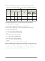
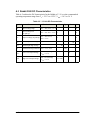
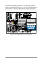
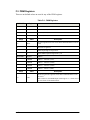
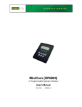
1
RabbitCore RCM3000 C-Programmable Module with Ethernet User’s Manual 019–0110 • 030725–D RabbitCore RCM3000 User’s Manual Part Number 019-0110 • 030725–D • Printed in U.S.A. ©2002–2003 Z-World Inc. • All rights reserved. Z-World reserves the right to make changes and improvements to its products without providing notice. Trademarks Rabbit and Rabbit 3000 are registered trademarks of Rabbit Semiconductor. RabbitCore is a trademark of Rabbit Semiconductor. Dynamic C is a registered trademark of Z-World Inc. Z-World, Inc. Rabbit Semiconductor 2900 Spafford Street Davis, California 95616-6800 USA 2932 Spafford Street Davis, California 95616-6800 USA Telephone: (530) 757-3737 Fax: (530) 757-3792 Telephone: (530) 757-8400 Fax: (530) 757-8402 www.zworld.com www.rabbitsemiconductor.com RabbitCore RCM3000 TABLE OF CONTENTS Chapter 1. Introduction 1 1.1 RCM3000 Features ...............................................................................................................................1 1.2 Advantages of the RCM3000 ...............................................................................................................2 1.3 Development and Evaluation Tools......................................................................................................2 1.4 How to Use This Manual ......................................................................................................................3 1.4.1 Additional Product Information ....................................................................................................3 1.4.2 Online Documentation ..................................................................................................................3 Chapter 2. Hardware Reference 5 2.1 RCM3000 Digital Inputs and Outputs ..................................................................................................6 2.1.1 Memory I/O Interface .................................................................................................................11 2.1.2 Other Inputs and Outputs ............................................................................................................11 2.2 Serial Communication ........................................................................................................................12 2.2.1 Serial Ports ..................................................................................................................................12 2.2.2 Ethernet Port ...............................................................................................................................12 2.2.3 Programming Port .......................................................................................................................13 2.2.3.1 Alternate Uses of the Programming Port ........................................................................... 13 2.3 Other Hardware...................................................................................................................................14 2.3.1 Clock Doubler .............................................................................................................................14 2.3.2 Spectrum Spreader ......................................................................................................................14 2.4 Memory...............................................................................................................................................15 2.4.1 SRAM .........................................................................................................................................15 2.4.2 Flash EPROM .............................................................................................................................15 2.4.3 Dynamic C BIOS Source Files ...................................................................................................15 Chapter 3. Software Reference 17 3.1 More About Dynamic C .....................................................................................................................17 3.2 Programming Cable ............................................................................................................................18 3.2.1 Changing from Program Mode to Run Mode .............................................................................18 3.2.2 Changing from Run Mode to Program Mode .............................................................................18 3.3 Dynamic C Libraries...........................................................................................................................19 3.3.1 I/O ...............................................................................................................................................20 3.3.2 Serial Communication Drivers....................................................................................................20 3.3.3 TCP/IP Drivers............................................................................................................................20 3.4 Sample Programs ................................................................................................................................21 3.5 Upgrading Dynamic C ........................................................................................................................22 3.5.1 Upgrades .....................................................................................................................................22 Appendix A. RabbitCore RCM3000 Specifications 23 A.1 Electrical and Mechanical Characteristics .........................................................................................24 A.1.1 Headers.......................................................................................................................................27 A.1.2 Physical Mounting .....................................................................................................................27 A.2 Bus Loading .......................................................................................................................................28 A.3 Rabbit 3000 DC Characteristics.........................................................................................................31 A.4 I/O Buffer Sourcing and Sinking Limit .............................................................................................32 A.5 Conformal Coating.............................................................................................................................33 A.6 Jumper Configurations.......................................................................................................................34 User’s Manual Appendix B. Prototyping Board 35 B.1 Mechanical Dimensions and Layout ................................................................................................. 36 B.2 Power Supply..................................................................................................................................... 37 B.3 Using the Prototyping Board ............................................................................................................. 38 B.3.1 Adding Other Components ........................................................................................................ 39 B.3.2 Measuring Current Draw ........................................................................................................... 39 B.3.3 Attach Modules to Prototyping Board ....................................................................................... 40 B.3.4 Other Prototyping Board Modules and Options ........................................................................ 40 Appendix C. LCD/Keypad Module 41 C.1 Specifications..................................................................................................................................... 41 C.2 Jumper-Selectable Voltage Settings for All Boards .......................................................................... 43 C.3 Keypad Labeling................................................................................................................................ 44 C.4 Header Pinouts................................................................................................................................... 45 C.4.1 I/O Address Assignments .......................................................................................................... 45 C.5 Mounting LCD/Keypad Module on the Prototyping Board.............................................................. 46 C.6 Bezel-Mount Installation ................................................................................................................... 47 C.6.1 Connect the LCD/Keypad Module to Your Prototyping Board ................................................ 49 C.7 LCD/Keypad Module Function APIs ................................................................................................ 50 C.7.1 LEDs .......................................................................................................................................... 50 C.7.2 LCD Display .............................................................................................................................. 51 C.7.3 Keypad ....................................................................................................................................... 67 C.8 Sample Programs............................................................................................................................... 70 Appendix D. Power Supply 71 D.1 Power Supplies .................................................................................................................................. 71 D.1.1 Battery-Backup Circuits ............................................................................................................ 71 D.1.2 Reset Generator ......................................................................................................................... 72 D.2 Optional +5 V Output........................................................................................................................ 72 Appendix E. Programming Cable 73 Appendix F. Motor Control Option 77 F.1 Overview ............................................................................................................................................ 77 F.2 Header J6............................................................................................................................................ 78 F.3 Using Parallel Port F .......................................................................................................................... 79 F.3.1 Parallel Port F Registers............................................................................................................. 79 F.4 PWM Outputs .................................................................................................................................... 82 F.5 PWM Registers .................................................................................................................................. 83 F.6 Quadrature Decoder ........................................................................................................................... 84 Notice to Users 87 Index 89 Schematics 91 RabbitCore RCM3000 1. INTRODUCTION The RCM3000 RabbitCore module is designed to be the heart of embedded control systems. The RCM3000 features an integrated Ethernet port and provides for LAN and Internet-enabled systems to be built as easily as serial-communication systems. The RCM3000 has a Rabbit 3000 microprocessor operating at 29.4 MHz, static RAM, flash memory, two clocks (main oscillator and timekeeping), and the circuitry necessary for reset and management of battery backup of the Rabbit 3000’s internal real-time clock and the static RAM. Two 34-pin headers bring out the Rabbit 3000 I/O bus lines, parallel ports, and serial ports. The RCM3000 receives its +3.3 V power from the customer-supplied motherboard on which it is mounted. The RabbitCore RCM3000 can interface with all kinds of CMOScompatible digital devices through the motherboard. 1.1 RCM3000 Features • Small size: 1.85" x 2.65"” x 0.86" (47 mm × 67 mm × 22 mm) • Microprocessor: Rabbit 3000 running at 29.4 MHz • 52 parallel 5 V tolerant I/O lines: 44 configurable for I/O, 4 fixed inputs, 4 fixed outputs • Two additional digital inputs, two additional digital outputs • External reset input • Alternate I/O bus can be configured for 8 data lines and 6 address lines (shared with parallel I/O lines), I/O read/write • Ten 8-bit timers (six cascadable) and one 10-bit timer with two match registers • 256K–512K flash memory, 128K–512K SRAM • Real-time clock • Watchdog supervisor • Provision for customer-supplied backup battery via connections on header J2 • 10Base-T RJ-45 Ethernet port User’s Manual 1 • 10-bit free-running PWM counter and four width registers • Two-channel Input Capture can be used to time input signals from various port pins • Two-channel Quadrature Decoder accepts inputs from external incremental encoder modules • Six CMOS-compatible serial ports: maximum asynchronous baud rate of 1.84 Mbps, maximum synchronous baud rate of 7.35 Mbps. Four ports are configurable as a clocked serial port (SPI), and two ports are configurable as SDLC/HDLC serial ports. • Supports 1.15 Mbps IRDA transceiver Appendix A, “RabbitCore RCM3000 Specifications,” provides detailed specifications for the RCM3000. In addition, two different RCM3000 models are available. In addition, the RCM3100 Series RabbitCore modules omit the RCM3000 Series’ Ethernet connectivity, but offer a much smaller footprint, which is one-half the size of the RCM3000 Series. 1.2 Advantages of the RCM3000 • Fast time to market using a fully engineered, “ready to run” microprocessor core. • Competitive pricing when compared with the alternative of purchasing and assembling individual components. • Easy C-language program development and debugging • Utility programs for rapid production loading of programs. • Generous memory size allows large programs with tens of thousands of lines of code, and substantial data storage. • Integrated Ethernet port for network connectivity, royalty-free TCP/IP software. 1.3 Development and Evaluation Tools A complete Development Kit, including a Prototyping Board and Dynamic C development software, is available for the RCM3000. The Development Kit puts together the essentials you need to design an embedded microprocessor-based system rapidly and efficiently. See the RabbitCore RCM3000 Getting Started Manual for complete information on the Development Kit. 2 RabbitCore RCM3000 1.4 How to Use This Manual This user’s manual is intended to give users detailed information on the RCM3000 module. It does not contain detailed information on the Dynamic C development environment or the TCP/IP software support for the integrated Ethernet port. Most users will want more detailed information on some or all of these topics in order to put the RCM3000 module to effective use. 1.4.1 Additional Product Information Introductory information about the RCM3000 and its associated Development Kit and Prototyping Board will be found in the printed RabbitCore RCM3000 Getting Started Manual, which is also provided on the accompanying CD-ROM in both HTML and Adobe PDF format. We recommend that any users unfamiliar with Z-World products, or those who will be using the Prototyping Board for initial evaluation and development, begin with at least a read-through of the Getting Started manual. In addition to the product-specific information contained in the RabbitCore RCM3000 Getting Started Manual and the RabbitCore RCM3000 User’s Manual (this manual), several higher level reference manuals are provided in HTML and PDF form on the accompanying CD-ROM. Advanced users will find these references valuable in developing systems based on the RCM3000 modules: • Dynamic C User’s Manual • Dynamic C Function Reference Manual • An Introduction to TCP/IP • Dynamic C TCP/IP User’s Manual • Rabbit 3000 Microprocessor User’s Manual 1.4.2 Online Documentation The online documentation is installed along with Dynamic C, and an icon for the documentation menu is placed on the workstation’s desktop. Double-click this icon to reach the menu. If the icon is missing, use your browser to find and load default.htm in the docs folder, found in the Dynamic C installation folder. The latest versions of all documents are always available for free, unregistered download from our Web sites as well. User’s Manual 3 4 RabbitCore RCM3000 2. HARDWARE REFERENCE Chapter 2 describes the hardware components and principal hardware subsystems of the RCM3000. Appendix A, “RabbitCore RCM3000 Specifications,” provides complete physical and electrical specifications. Figure 1 shows these Rabbit-based subsystems designed into the RCM3000. 32 kHz 14 MHz osc osc SRAM Flash RABBIT 3000 logic-level serial signal Level converter Ethernet RabbitCore Module RS-232, RS-485, IRDA serial communication drivers on motherboard Figure 1. RCM3000 Subsystems User’s Manual 5 2.1 RCM3000 Digital Inputs and Outputs The RCM3000 has 52 parallel I/O lines grouped in seven 8-bit ports available on headers J1 and J2. The 44 bidirectional I/O lines are located on pins PA0–PA7, PB0, PB2–PB7, PD2–PD7, PE0–PE1, PE3–PE7, PF0–PF7, and PG0–PG7. Figure 2 shows the RCM3000 RabbitCore series pinouts for headers J1 and J2. J1 GND PA7 PA5 PA3 PA1 PF3 PF1 PC0 PC2 PC4 PC6 PG0 PG2 PD4 PD2 PD6 n.c. J2 STATUS PA6 PA4 PA2 PA0 PF2 PF0 PC1 PC3 PC5 PC7 PG1 PG3 PD5 PD3 PD7 n.c. /RES PB2 PB4 PB6 PF4 PF6 PE7 PE5 PE3 PE0 PG6 PG4 /IORD SMODE1 VRAM +3.3V n.c. PB0 PB3 PB5 PB7 PF5 PF7 PE6 PE4 PE1 PG7 PG5 /IOWR SMODE0 /RESET_IN VBAT_EXT GND GND n.c. = not connected Note: These pinouts are as seen on the Bottom Side of the module. Figure 2. RCM3000 Pinouts Headers J1 and J2 are standard 2 × 34 headers with a nominal 2 mm pitch. An RJ-45 Ethernet jack is also included with the RCM3000 series. The signals labeled PD2, PD3, PD6, and PD7 on header J1 (pins 29–32) and the pins that are not connected (pins 33–34 on header J1 and pin 33 on header J2) are reserved for future use on other models in the RCM3000 series. 6 RabbitCore RCM3000 Figure 3 shows the use of the Rabbit 3000 ports in the RCM3000 series RabbitCore modules. PC0, PC2, PC4 PC1, PC3, PC5 PG0PG7 PC6 PB1, PC7, /RES 4 Ethernet signals PA0PA7 PB0, PB2PB7 PD4PD5 Port A Port B (+Ethernet Port) Port C (Serial Ports B,C & D) Port G Port D RABBIT 3000 (Serial Ports E & F) Programming Port (Serial Port A) Ethernet Port RAM Real-Time Clock Watchdog 11 Timers Slave Port Clock Doubler Port E PE0PE1, PE3PE7 Port F PF0PF7 Port G PG0PG1, PG4PG5 /RES_IN /IORD /RESET, /IOWR, STATUS SMODE0 SMODE1 (+Serial Ports) Misc. I/O Backup Battery Support Flash Figure 3. Use of Rabbit 3000 Ports The ports on the Rabbit 3000 microprocessor used in the RCM3000 Series are configurable, and so the factory defaults can be reconfigured. Table 1 lists the Rabbit 3000 factory defaults and the alternate configurations. User’s Manual 7 Table 1. RCM3000 Pinout Configurations Header J1 Pin Pin Name 1 GND 2 STATUS Default Use Alternate Use Output (Status) Output 3–10 PA[7:0] Parallel I/O External data bus (ID0–ID7) Slave port data bus (SD0–SD7) 11 PF3 Input/Output QD2A 12 PF2 Input/Output QD2B 13 PF1 Input/Output QD1A CLKC 14 PF0 Input/Output QD1B CLKD 15 PC0 Output TXD 16 PC1 Input RXD 17 PC2 Output TXC 18 PC3 Input RXC 19 PC4 Output TXB 20 PC5 Input RXB 21 PC6 Output TXA 22 PC7 Input RXA 23 PG0 Input/Output TCLKF 24 PG1 Input/Output RCLKF 25 PG2 Input/Output TXF 26 PG3 Input/Output RXF 27 PD4 Input/Output ATXB 28 PD5 Input/Output ARXB 29 PD2 Input/Output TPOUT– * 30 PD3 Input/Output TPOUT+ * 31 PD6 Input/Output TPIN– * 32 PD7 Input/Output TPIN+ * RCM3000 Use External Data Bus Serial Port A (programming port) Ethernet transmit port Ethernet receive port 33–34 * n.c. * 8 Not connected Pins 29–34 are reserved for future RCM3000 series RabbitCore modules. RabbitCore RCM3000 Table 1. RCM3000 Pinout Configurations (continued) Header J2 Pin Pin Name Default Use Alternate Use RCM3000 Use Reset output from Reset Generator 1 /RES Reset output Reset input 2 PB0 Input/Output CLKB 3 PB2 Input/Output IA0 /SWR External Address 0 4 PB3 Input/Output IA1 /SRD External Address 1 5 PB4 Input/Output IA2 SA0 External Address 2 6 PB5 Input/Output IA3 SA1 External Address 3 7 PB6 Input/Output IA4 External Address 4 8 PB7 Input/Output IA5 /SLAVEATTN External Address 5 9 PF4 Input/Output AQD1B PWM0 10 PF5 Input/Output AQD1A PWM1 11 PF6 Input/Output AQD2B PWM2 12 PF7 Input/Output AQD2A PWM3 13 PE7 Input/Output I7 /SCS 14 PE6 Input/Output I6 15 PE5 Input/Output I5 INT1B 16 PE4 Input/Output I4 INT0B 17 PE3 Input/Output I3 18 PE1 Input/Output I1 INT1A 19 PE0 Input/Output I0 INT0A User’s Manual 9 Table 1. RCM3000 Pinout Configurations (continued) Pin Pin Name Default Use Alternate Use RCM3000 Use 20 PG7 Input/Output RXE 21 PG6 Input/Output TXE 22 PG5 Input/Output RCLKE 23 PG4 Input/Output TCLKE 24 /IOWR Output External write strobe 25 /IORD Input External read strobe Header J2 26–27 SMODE0, SMODE1 (0,0)—start executing at address zero (0,1)—cold boot from slave port (1,0)—cold boot from clocked Serial Port A Also connected to programming cable SMODE0 =1, SMODE1 = 1 Cold boot from asynchronous Serial Port A at 2400 bps (programming cable connected) 28 /RESET_IN Input Input to Reset Generator 29 VRAM Output Maximum Current Draw 15 µA 30 VBAT_EXT 3 V battery Input Minimum battery voltage 2.8 V 31 +3.3V Input 3.15–3.45 V DC 32 GND 33 n.c. 34 GND Future option for +5 V input or +5 V output NOTE: Ports PD0 and PE2 are used for the Ethernet interface. Locations R38–R43 allow the population of 0 Ω resistors (jumpers) that will be used to enable future options. These locations are currently unused. 10 RabbitCore RCM3000 2.1.1 Memory I/O Interface The Rabbit 3000 address lines (A0–A19) and all the data lines (D0–D7) are routed internally to the onboard flash memory and SRAM chips. I/0 write (/IOWR) and I/0 read (/IORD) are available for interfacing to external devices. Parallel Port A can also be used as an external I/O data bus to isolate external I/O from the main data bus. Parallel Port B pins PB2–PB7 can also be used as an external address bus. When using the auxiliary I/O bus, you must add the following line at the beginning of your program. #define PORTA_AUX_IO // required to enable auxiliary I/O bus The STATUS output has three different programmable functions: 1. It can be driven low on the first op code fetch cycle. 2. It can be driven low during an interrupt acknowledge cycle. 3. It can also serve as a general-purpose output. 2.1.2 Other Inputs and Outputs Two status mode pins, SMODE0 and SMODE1, are available as inputs. The logic state of these two pins determines the startup procedure after a reset. /RESET_IN is an external input used to reset the Rabbit 3000 microprocessor and the RabbitCore RCM3000 memory. /RES is an output from the reset circuitry that can be used to reset other peripheral devices. User’s Manual 11 2.2 Serial Communication The RCM3000 Series board does not have an RS-232 or an RS-485 transceiver directly on the board. However, an RS-232 or RS-485 interface may be incorporated on the board the RCM3000 is mounted on. For example, the Prototyping Board has a standard RS-232 transceiver chip. 2.2.1 Serial Ports There are six serial ports designated as Serial Ports A, B, C, D, E, and F. All six serial ports can operate in an asynchronous mode up to the baud rate of the system clock divided by 16. An asynchronous port can handle 7 or 8 data bits. A 9th bit address scheme, where an additional bit is sent to mark the first byte of a message, is also supported. Serial Ports A, B, C, and D can also be operated in the clocked serial mode. In this mode, a clock line synchronously clocks the data in or out. Either of the two communicating devices can supply the clock. When the Rabbit 3000 provides the clock, the baud rate can be up to 80% of the system clock frequency divided by 128, or 183,750 bps for a 29.4 MHz clock speed. Serial Ports E and F can also be configured as SDLC/HDLC serial ports. The IRDA protocol is also supported in SDLC format by these two ports. 2.2.2 Ethernet Port Figure 4 shows the pinout for the RJ-45 Ethernet port (J4). Note that some Ethernet connectors are numbered in reverse to the order used here. ETHERNET 1 8 1. 2. 3. 6. RJ-45 Plug E_Tx+ E_Tx E_Rx+ E_Rx RJ-45 Jack Figure 4. RJ-45 Ethernet Port Pinout Two LEDs are placed next to the RJ-45 Ethernet jack, one to indicate an Ethernet link (LNK) and one to indicate Ethernet activity (ACT). RJ-45 Ethernet Plug The Ethernet signals are also available on header J1. The transformer/connector assembly ground is connected to the RCM3000 printed circuit board digital ground via a 0 Ω resistor, R31, as shown in Figure 5. The RJ-45 connector is shielded to minimize EMI effects to/from the Ethernet signals. 12 R31 Board Ground Chassis Ground Figure 5. Isolation Resistor R31 RabbitCore RCM3000 2.2.3 Programming Port Serial Port A has special features that allow it to cold-boot the system after reset. Serial Port A is also the port that is used for software development under Dynamic C. The RabbitCore RCM3000 Series has a 10-pin program header labeled J3. The Rabbit 3000 startup-mode pins (SMODE0, SMODE1) are presented to the programming port so that an externally connected device can force the RCM3000 to start up in an external bootstrap mode. The Rabbit 3000 Microprocessor User’s Manual provides more information related to the bootstrap mode. The programming port is used to start the RabbitCore RCM3000 in a mode where it will download a program from the port and then execute the program. The programming port transmits information to and from a PC while a program is being debugged in-circuit. The RabbitCore RCM3000 can be reset from the programming port via the /RESET_IN line. The Rabbit 3000 status pin is also presented to the programming port. The status pin is an output that can be used to send a general digital signal. The clock line for Serial Port A is presented to the programming port, which makes synchronous serial communication possible. Programming may also be initiated through the motherboard to which the RCM3000 series module is plugged in to since the Serial Port A (PC6 and PC7), SMODE0, SMODE1, and /RESET_IN are available on headers J1 and J2 (see Table 1). 2.2.3.1 Alternate Uses of the Programming Port The programming port may also be used as an application port with the DIAG connector on the programming cable. All three clocked Serial Port A signals are available as • a synchronous serial port • an asynchronous serial port, with the clock line usable as a general CMOS input • two general CMOS inputs and one general CMOS output. Two startup mode pins, SMODE0 and SMODE1, are available as general CMOS inputs after they are read during the initial boot-up. The logic state of these two pins is very important in determining the startup procedure after a reset. /RES_IN is an external input used to reset the Rabbit 3000 microprocessor. The status pin may also be used as a general CMOS output. See Appendix E, “Programming Cable,” for more information. User’s Manual 13 2.3 Other Hardware 2.3.1 Clock Doubler The RCM3000 takes advantage of the Rabbit 3000 microprocessor’s internal clock doubler. A built-in clock doubler allows half-frequency crystals to be used to reduce radiated emissions. The 29.4 MHz frequency specified for the RCM3000 is generated using a 14.7456 MHz crystal. The clock doubler will not work for crystals with a frequency above 26.7264 MHz. The clock doubler may be disabled if 29.4 MHz clock speeds are not required. Disabling the Rabbit 3000 microprocessor’s internal clock doubler will reduce power consumption and further reduce radiated emissions. The clock doubler is disabled with a simple change to the BIOS as described below. 1. Open the BIOS source code file, RABBITBIOS.C in the BIOS directory. 2. Change the line #define CLOCK_DOUBLED 1 // // // // set to 1 to double clock if Rabbit 2000: crystal <= 12.9024 MHz, Rabbit 3000: crystal <= 26.7264 MHz, or to 0 to always disable clock doubler to read as follows. #define CLOCK_DOUBLED 0 3. Save the change using File > Save. 2.3.2 Spectrum Spreader The Rabbit 3000 features a spectrum spreader, which helps to mitigate EMI problems. By default, the spectrum spreader is on automatically, but it may also be turned off or set to a stronger setting. The means for doing so is through a simple change to the following BIOS line in a way that is similar to the clock doubler described above. #define ENABLE_SPREADER 1 // Set to 0 to disable spectrum spreader. #define SPREADER_SETTING 0 // 0 = normal spreading, 1 = strong spreading NOTE: The strong spectrum-spreading setting is not recommended since it may limit the maximum clock speed or the maximum baud rate. 14 RabbitCore RCM3000 2.4 Memory 2.4.1 SRAM The RCM3000 is designed to accept 128K to 512K of SRAM packaged in a 32-pin TSOP or sTSOP case. 2.4.2 Flash EPROM The RCM3000 is also designed to accept 256K to 512K of flash EPROM packaged in a 32-pin TSOP or sTSOP case. NOTE: Z-World recommends that any customer applications should not be constrained by the sector size of the flash EPROM since it may be necessary to change the sector size in the future. Writing to arbitrary flash memory addresses at run time is also discouraged. Instead, define a “user block” area to store persistent data. The functions writeUserBlock and readUserBlock are provided for this. A Flash Memory Bank Select jumper configuration option based on 0 Ω surface-mounted resistors exists at header JP1 on the RCM3000 Series RabbitCore modules. This option, used in conjunction with some configuration macros, allows Dynamic C to compile two different co-resident programs for the upper and lower halves of the 256K flash in such a way that both programs start at logical address 0000. This is useful for applications that require a resident download manager and a separate downloaded program. See Technical Note 218, Implementing a Serial Download Manager for a 256K Flash, for details. 2.4.3 Dynamic C BIOS Source Files The Dynamic C BIOS source files handle different standard RAM and flash EPROM sizes automatically. User’s Manual 15 16 RabbitCore RCM3000 3. SOFTWARE REFERENCE Dynamic C is an integrated development system for writing embedded software. It runs on an IBM-compatible PC and is designed for use with Z-World controllers and other controllers based on the Rabbit microprocessor. Chapter 3 provides the libraries, function calls, and sample programs related to the RCM3000. 3.1 More About Dynamic C Dynamic C has been in use worldwide since 1989. It is specially designed for programming embedded systems, and features quick compile and interactive debugging in the real environment. A complete reference guide to Dynamic C is contained in the Dynamic C User’s Manual. You have a choice of doing your software development in the flash memory or in the static RAM included on the RCM3000. The advantage of working in RAM is to save wear on the flash memory, which is limited to about 100,000 write cycles. The disadvantage is that the code and data might not both fit in RAM. NOTE: An application can be developed in RAM, but cannot run standalone from RAM after the programming cable is disconnected. All standalone applications can only run from flash memory. NOTE: Do not depend on the flash memory sector size or type. Due to the volatility of the flash memory market, the RCM3000 and Dynamic C were designed to accommodate flash devices with various sector sizes. The disadvantage of using flash memory for debug is that interrupts must be disabled for approximately 5 ms whenever a break point is set in the program. This can crash fast interrupt routines that are running while you stop at a break point or single-step the program. Flash memory or RAM is selected on the Options > Compiler menu. Dynamic C provides a number of debugging features. You can single-step your program, either in C, statement by statement, or in assembly language, instruction by instruction. You can set break points, where the program will stop, on any statement. You can evaluate watch expressions. A watch expression is any C expression that can be evaluated in the context of the program. If the program is at a break point, a watch expression can view any expression using local or global variables. If a periodic call to runwatch() is included in your program, you will be able to evaluate watch expressions by hitting <Ctrl-U> without stopping the program. User’s Manual 17 3.2 Programming Cable The RCM3000 is automatically in program mode when the PROG connector on the programming cable is attached, and is automatically in run mode when no programming cable is attached. The DIAG connector of the programming cable may be used on header J3 of the RCM3000 with the board operating in the run mode. This allows the programming port to be used as an application port. See Appendix E, “Programming Cable,” for more information. MOTOR/ENCODER J6 C11 C10 J14 PA7 MASTER RC15 GND UX11 RCM3000 RABBITCORE RCM2 C44 Y3 R6 R12 RC1 R8 R10 RC22 RC17 RC16 UX2 PF3 PA0 PA1 PB6 PA2 PA3 PB5 PB4 PA4 PA5 PB3 PB2 PA6 PA7 PB0 /RES PE4 GND R32 R29 R28 R12 R11 PROG J3 U1 RESET C6 J5 J4 TxB RxB RESET GND C16 BD4 BD6 RC25 RC4 RC5 C14 RC27 To PC COM port U3 RC28 RC26 UX7 S3 DISPLAY BOARD RC29 PG6 C7 RS-232 U6 RC9 J13 S2 +5V UX4 +5V UX5 R14 C8 RxC TxC BD7 R19 R14 U5 R49 R21 C83 C19 RP2 RC7 C9 C5 J12 RC6 RP1 PF2 PF4 C4 PF6 PF5 RP3 PF7 PB7 Y1 PF1 RP4 PC0 PF0 R4 C3 PC2 PC1 PE7 R5 PC4 PC3 PE5 PE6 C4 PC5 PE3 PE4 +3.3V +5V +5V J8 U3 U2 PE0 PE1 R15 R17 R22 PG7 U12 PD5 D1 PD4 +3.3V +3.3V C17 PG6 R33 J4 PG5 R27 PG0 JP1 PG1 JP2 PG4 JP3 /IOWR R31 PG2 /IORD C23 PD4 SM1 GND GND C84 PD2 PD5 VRAM GND GND +3.3V BD5 RC2 C38 PD6 PD3 +3.3V SM0 JP4 PD7 PG3 GND VBAT EXT /RES IN U6 PD0 R30 R23 C26 PD1 R24 Y2 C25 NC Q1 GND BD2 R9 R11 RC11 GND RC21 RC10 R13 R21 R7 UX3 RC12 BD0 RC13 GND RC24 RC23 UX9 RC14 +3.3V +5V RC20 DS2 DS1 C3 R5 R2 RC19 LNK ACT R4 C47 C2 R1 R3 C41 C1 +3.3V J15 SLAVE UX10 GND J3 R16 PE4 +DC BT1 U9 PA6 /RES C42 PB2 RN2 J1 R46 R47 PB0 C46 PB3 Battery RCM3000 RABBITCORE RCM1 BA1 PA5 BA3 PA4 BD3 PB4 GND PA3 PB5 GND PA1 PA2 BD1 PF3 PA0 PB6 GND PF1 PF2 PF4 +5V BA0 PF0 PF6 PF5 +5V BA2 PE7 PF7 PB7 GND C12 U5 /RES LCD PE6 2.5 MM JACK D2 U4 +5V PC0 +5V PC1 BPE3 PE5 DIAG PC2 PE4 GND PC3 +5V PE3 R16 PC4 PE1 TP1 PD5 PC5 R15 PG0 PD4 PE0 J11 RC18 PG1 PG6 JP1 PG4 PG7 C17 D1 C13 R20 R17 RN4 /IORD PG5 CURRENT MEASUREMENT OPTION PG2 SM0 /IOWR L1 DS3 PD4 +3.3V POWER PD2 PD5 PG3 C15 PD3 SM1 VRAM RN5 POWER VBAT EXT /RES IN GND J9 PD6 +DC PD7 GND PD0 +3.3V GND PD1 GND RN3 NC +5V +3.3V RN1 GND DS1 Programming Cable UX13 RCM3000 PROTOTYPING BOARD PG7 Colored edge DS2 J10 J7 DISPLAY BOARD DISPLAY BOARD RESET RCM300 Module when changing mode: Short out pins 2832 on header J2, OR Press RESET button (if using Prototyping Board), OR Remove, then reapply power after removing or attaching programming cable. Figure 5. Switching Between Program Mode and Run Mode 3.2.1 Changing from Program Mode to Run Mode 1. Disconnect the programming cable from header J3 of the RCM3000. 2. Reset the RCM3000. You may do this as explained in Figure 5. The RCM3000 is now ready to operate in the run mode. 3.2.2 Changing from Run Mode to Program Mode 1. Attach the programming cable to header J3 on the RCM3000. 2. Reset the RCM3000. You may do this as explained in Figure 5. The RCM3000 is now ready to operate in the program mode. 18 RabbitCore RCM3000 3.3 Dynamic C Libraries With Dynamic C running, click File > Open, and select Lib. The following list of Dynamic C libraries will be displayed. There is no unique library that is specific to the RCM3000. The functions in the above libraries are described in the Dynamic C Function Reference Manual. User’s Manual 19 3.3.1 I/O The RCM3000 was designed to interface with other systems, and so there are no drivers written specifically for the I/O. The general Dynamic C read and write functions allow you to customize the parallel I/O to meet your specific needs. For example, use WrPortI(PEDDR, &PEDDRShadow, 0x00); to set all the Port E bits as inputs, or use WrPortI(PEDDR, &PEDDRShadow, 0xFF); to set all the Port E bits as outputs. When using the auxiliary I/O bus on the Rabbit 3000 chip, add the line #define PORTA_AUX_IO // required to enable auxiliary I/O bus to the beginning of any programs using the auxiliary I/O bus. The sample programs in the Dynamic C SAMPLES/RCM3000 directory provide further examples. 3.3.2 Serial Communication Drivers Library files included with Dynamic C provide a full range of serial communications support. The RS232.LIB library provides a set of circular-buffer-based serial functions. The PACKET.LIB library provides packet-based serial functions where packets can be delimited by the 9th bit, by transmission gaps, or with user-defined special characters. Both libraries provide blocking functions, which do not return until they are finished transmitting or receiving, and nonblocking functions, which must be called repeatedly until they are finished. For more information, see the Dynamic C Function Reference Manual and Technical Note 213, Rabbit 2000 Serial Port Software. 3.3.3 TCP/IP Drivers The TCP/IP drivers are located in the TCPIP directory. Complete information on these libraries and the TCP/IP functions is provided in the Dynamic C TCP/IP User’s Manual. 20 RabbitCore RCM3000 3.4 Sample Programs Sample programs are provided in the Dynamic C Samples folder, which is shown below. The various folders contain specific sample programs that illustrate the use of the corresponding Dynamic C libraries. For example, the sample program PONG.C demonstrates the output to the Dynamic C STDIO window. Two folders contain sample programs that illustrate features unique to the RCM3000. • RCM3000—Demonstrates the basic operation and the Ethernet functionality of the RCM3000. • TCPIP—Demonstrates more advanced TCP/IP programming for Z-World’s Ethernetenabled Rabbit-based boards. Follow the instructions included with the sample program to connect the RCM3000 and the other hardware identified in the instructions. To run a sample program, open it with the File menu (if it is not still open), compile it using the Compile menu (or press F5), and then run it by selecting Run in the Run menu (or press F9). The RCM3000 must be in Program Mode (see Figure 5) and must be connected to a PC using the programming cable. More complete information on Dynamic C is provided in the Dynamic C User’s Manual. User’s Manual 21 3.5 Upgrading Dynamic C Dynamic C patches that focus on bug fixes are available from time to time. Check the Web sites • www.zworld.com/support/ or • www.rabbitsemiconductor.com/support/ for the latest patches, workarounds, and bug fixes. The default installation of a patch or bug fix is to install the file in a directory (folder) different from that of the original Dynamic C installation. Z-World recommends using a different directory so that you can verify the operation of the patch without overwriting the existing Dynamic C installation. If you have made any changes to the BIOS or to libraries, or if you have programs in the old directory (folder), make these same changes to the BIOS or libraries in the new directory containing the patch. Do not simply copy over an entire file since you may overwrite a bug fix; of course, you may copy over any programs you have written. Once you are sure the new patch works entirely to your satisfaction, you may retire the existing installation, but keep it available to handle legacy applications. 3.5.1 Upgrades Dynamic C installations are designed for use with the board they are included with, and are included at no charge as part of our low-cost kits. Dynamic C is a complete software development system, but does not include all the Dynamic C features. Z-World also offers add-on Dynamic C modules containing the popular µC/OS-II real-time operating system, as well as PPP, Advanced Encryption Standard (AES), and other select libraries. In addition to the Web-based technical support included at no extra charge, a one-year telephonebased technical support module is also available for purchase. 22 RabbitCore RCM3000 APPENDIX A. RABBITCORE RCM3000 SPECIFICATIONS Appendix A provides the specifications for the RCM3000, and describes the conformal coating. User’s Manual 23 A.1 Electrical and Mechanical Characteristics Figure A-1 shows the mechanical dimensions for the RCM3000. 1.850 (47.0) 1.375 (34.9) Y1 RP1 JP1 RP3 R12 R11 C19 (69.2) U6 R30 R23 C26 2.725 R33 R27 R31 J4 C38 R46 R47 C47 GND 0.67 1.18 (17.0) 0.15 (3.8) J1 (22) 0.86 (22) 0.86 (6.5) (47.0) 0.256 1.850 (2) J2 0.08 (14) 0.55 (69.2) (6.5) (2.5) 2.725 0.256 0.10 (14) 0.55 (30.0) 0.50 C46 (12.7) C44 DS2 DS1 Y3 LNK ACT C41 C42 (33.5) (15.7) 0.625 U9 C23 R49 R32 R29 R28 Q1 C83 R24 Y2 C25 R15 R17 R22 U12 R21 R19 C84 JP4 RP2 U5 D1 R14 C17 R16 1.320 (2.5) JP3 0.100 dia Please refer to the RCM3000 footprint diagram later in this appendix for precise header locations. RP4 JP2 J3 R4 C3 R5 C4 U2 Figure A-1. RCM3000 Dimensions 24 RabbitCore RCM3000 It is recommended that you allow for an “exclusion zone” of 0.04" (1 mm) around the RCM3000 in all directions when the RCM3000 is incorporated into an assembly that includes other printed circuit boards. This “exclusion zone” that you keep free of other components and boards will allow for sufficient air flow, and will help to minimize any electrical or electromagnetic interference between adjacent boards. An “exclusion zone” of 0.08" (2 mm) is recommended below the RCM3000 when the RCM3000 is plugged into another assembly using the shortest connectors for headers J1 and J2. Figure A-2 shows this “exclusion zone.” 2.805 (2) 0.08 0.6 (16) (71.2) 2.725 (69.2) 1.93 (49.0) (2) 0.08 0.6 (16) Exclusion Zone J2 1.850 J1 (47.0) Figure A-2. RCM3000 “Exclusion Zone” User’s Manual 25 Table A-1 lists the electrical, mechanical, and environmental specifications for the RCM3000. Table A-1. RabbitCore RCM3000 Specifications Feature RCM3000 RCM3010 Microprocessor Rabbit 3000 at 29.4 MHz EMI Reduction Spectrum spreader for reduced EMI (radiated emissions) Ethernet Port Flash Memory SRAM Backup Battery General-Purpose I/O Additional Digital Inputs Additional Digital Outputs Auxiliary I/O Bus Serial Ports Serial Rate Slave Interface Real-Time Clock Timers Watchdog/Supervisor 10Base-T, RJ-45, 2 LEDs 512K (2 × 256K) 256K 512K 128K Connection for user-supplied backup battery (to support RTC and SRAM) 52 parallel digital I/0 lines: • 44 configurable I/O, • 4 fixed inputs, • 4 fixed outputs 2 startup mode, reset in Status, reset out 8 data lines and 6 address lines (shared with I/O) plus I/O read/write 6 shared high-speed, CMOS-compatible ports: • 6 configurable as asynchronous (with IrDA), 4 as clocked serial (SPI), and 2 as SDLC/HDLC (with IrDA) • 1 asynchronous serial port dedicated for programming • support for MIR/SIR IrDA transceiver Max. asynchronous baud rate = CLK/8 A slave port allows the RCM3100 to be used as a master or as an intelligent peripheral device with Rabbit-based or any other type of processor Yes Ten 8-bit timers (6 cascadable from the first), one 10-bit timer with 2 match registers Yes Pulse-Width Modulators 10-bit free-running counter and four pulse-width registers Input Capture 2- channel input capture can be used to time input signals from various port pins Quadrature Decoder Power 26 2-channel quadrature decoder accepts inputs from external incremental encoder modules 3.15 V to 3.45 V DC 150 mA @ 3.3 V RabbitCore RCM3000 Table A-1. RabbitCore RCM3000 Specifications (continued) Feature RCM3000 RCM3010 Operating Temperature –40°C to +70°C Humidity 5% to 95%, noncondensing Connectors (for connection to headers J4 and J5) Two 2 × 17, 2 mm pitch 1.850" × 2.725" × 0.86" (47 mm × 69 mm × 22 mm) Board Size A.1.1 Headers The RCM3000 uses headers at J1 and J2 for physical connection to other boards. J1 and J2 are 2 × 17 SMT headers with a 2 mm pin spacing. J3, the programming port, is a 2 × 5 header with a 2 mm pin spacing. Figure A-3 shows the layout of another board for the RCM3000 to be plugged into. These values are relative to the mounting hole. A.1.2 Physical Mounting A 9/32” (7 mm) standoff with a 2-56 screw is recommended to attach the RCM3000 to a user board at the hole position shown in Figure A-3. Either use plastic hardware, or use insulating washers to keep any metal hardware from shorting out signals on the RCM3000. J2 J3 0.973 RCM3000 Footprint (24.7) 1.341 1.121 (28.5) (34.1) 1.136 (28.9) 0.100 dia (2.5) 0.020 sq typ (0.5) 0.079 0.314 (8.0) (2.0) 0.079 (2.0) J1 Figure A-3. User Board Footprint for RCM3000 User’s Manual 27 A.2 Bus Loading You must pay careful attention to bus loading when designing an interface to the RCM3000. This section provides bus loading information for external devices. Table A-2 lists the capacitance for the various RCM3000 I/O ports. Table A-2. Capacitance of Rabbit 3000 I/O Ports I/O Ports Input Capacitance (pF) Output Capacitance (pF) 12 14 Parallel Ports A to G Table A-3 lists the external capacitive bus loading for the various RCM3000 output ports. Be sure to add the loads for the devices you are using in your custom system and verify that they do not exceed the values in Table A-3. Table A-3. External Capacitive Bus Loading -40°C to +70°C Clock Speed (MHz) Maximum External Capacitive Loading (pF) All I/O lines with clock doubler enabled 29.4 30–70 All I/O lines with clock doubler disabled 14.7456 100 Output Port 28 RabbitCore RCM3000 Figure A-4 shows a typical timing diagram for the Rabbit 3000 microprocessor external memory read and write cycles. Memory Read (no wait states) T2 T1 CLK A[19:0] valid Tadr /CSx TCSx TCSx /OEx TOEx D[7:0] TOEx Tsetup valid Thold Memory Write (no extra wait states) T1 Tw T2 CLK A[19:0] /CSx /WEx D[7:0] valid Tadr TCSx TCSx TWEx TWEx valid TDHZV TDVHZ Figure A-4. Memory Read and Write Cycles User’s Manual 29 Table A-4 lists the delays in gross memory access time for several values of VDD. Table A-4. Data and Clock Delays VDD ±10%, Temp, -40°C–+85°C (maximum) Clock to Address Output Delay (ns) 30 pF 60 pF 90 pF Data Setup Time Delay (ns) 3.3 6 8 11 2.7 7 10 2.5 8 1.8 18 VDD Spectrum Spreader Delay (ns) Normal Strong dbl/no dbl dbl/no dbl 1 3/4.5 4.5/9 13 1.5 3.5/5.5 5.5/11 11 15 1.5 4/6 6/12 24 33 3 8/12 11/22 The measurements are taken at the 50% points under the following conditions. • T = -40°C to 85°C, V = VDD ±10% • Internal clock to nonloaded CLK pin delay 1 ns @ 85°V/4.5 V The clock to address output delays are similar, and apply to the following delays. • Tadr, the clock to address delay • TCSx, the clock to memory chip select delay • TWEx, the clock to memory write strobe delay • TIOCSx, the clock to I/O chip select delay • TIORD, the clock to I/O read strobe delay • TIOWR, the clock to I/O write strobe delay • TBUFEN, the clock to I/O buffer enable delay The data setup time delays are similar for both Tsetup and Thold. When the spectrum spreader is enabled with the clock doubler, every other clock cycle is shortened (sometimes lengthened) by a maximum amount given in the table above. The shortening takes place by shortening the high part of the clock. If the doubler is not enabled, then every clock is shortened during the low part of the clock period. The maximum shortening for a pair of clocks combined is shown in the table. 30 RabbitCore RCM3000 A.3 Rabbit 3000 DC Characteristics Table A-5 outlines the DC characteristics for the Rabbit at 3.3 V over the recommended operating temperature range from Ta = –55°C to +125°C, VDD = 3.0 V to 3.6 V. Table A-5. 3.3 Volt DC Characteristics Symbol Parameter Test Conditions Min IIH Input Leakage High VIN = VDD, VDD = 3.3 V IIL Input Leakage Low (no pull-up) VIN = VSS, VDD = 3.3 V -1 IOZ Output Leakage (no pull-up) VIN = VDD or VSS, VDD = 3.3 V VIL CMOS Input Low Voltage VIH CMOS Input High Voltage VT CMOS Switching Threshold VDD = 3.3 V, 25°C VOL Low-Level Output Voltage VOH High-Level Output Voltage User’s Manual Typ Max 1 Units µA µA -1 1 µA 0.3 x VDD V 0.7 x VDD 1.65 IOL = See (sinking) VDD = 3.0 V V 0.4 VDD = 3.0 V IOH = See (sourcing) V 0.7 x VDD V V 31 A.4 I/O Buffer Sourcing and Sinking Limit Unless otherwise specified, the Rabbit I/O buffers are capable of sourcing and sinking 6.8 mA of current per pin at full AC switching speed. Full AC switching assumes a 29.4 MHz CPU clock and capacitive loading on address and data lines of less than 70 pF per pin. The absolute maximum operating voltage on all I/O is 5.5 V. Table A-6 shows the AC and DC output drive limits of the parallel I/O buffers when the Rabbit 3000 is used in the RCM3000. Table A-6. I/O Buffer Sourcing and Sinking Capability Output Drive (Full AC Switching) Pin Name All data, address, and I/O lines with clock doubler enabled Sourcing/Sinking Limits (mA) Sourcing Sinking 6.8 6.8 Under certain conditions, the maximum instantaneous AC/DC sourcing or sinking current may be greater than the limits outlined in Table A-6. The maximum AC/DC sourcing current can be as high as 12.5 mA per buffer as long as the number of sourcing buffers does not exceed three per VDD or VSS pad, or up to six outputs between pads. Similarly, the maximum AC/DC sinking current can be as high as 8.5 mA per buffer as long as the number of sinking buffers does not exceed three per VDD or VSS pad, or up to six outputs between pads. The VDD bus can handle up to 35 mA, and the VSS bus can handle up to 28 mA. All these analyses were measured at 100°C. 32 RabbitCore RCM3000 A.5 Conformal Coating The areas around the 32 kHz real-time clock crystal oscillator has had the Dow Corning silicone-based 1-2620 conformal coating applied. The conformally coated area is shown in Figure A-5. The conformal coating protects these high-impedance circuits from the effects of moisture and contaminants over time. Y1 RP1 JP1 RP3 RP4 JP2 J3 R4 C3 R5 C4 R12 R11 JP3 U2 R33 R30 R23 C26 U6 JP4 C19 C83 C23 R49 R32 R29 R28 Q1 R24 Y2 C25 R15 R17 R22 U12 R21 R19 C84 U9 RP2 U5 D1 R14 C17 R16 Conformally coated area R27 R31 J4 C38 C44 DS2 DS1 Y3 C46 R46 R47 C47 LNK ACT C41 C42 GND Figure A-5. RCM3000 Areas Receiving Conformal Coating Any components in the conformally coated area may be replaced using standard soldering procedures for surface-mounted components. A new conformal coating should then be applied to offer continuing protection against the effects of moisture and contaminants. NOTE: For more information on conformal coatings, refer to Technical Note 303, Conformal Coatings. User’s Manual 33 A.6 Jumper Configurations Figure A-6 shows the header locations used to configure the various RCM3000 options via jumpers. JP1 JP2 JP3 Top Side JP4 Bottom Side JP5 Figure A-6. Location of RCM3000 Configurable Positions Table A-7 lists the configuration options. Table A-7. RCM3000 Jumper Configurations Header JP1 JP2 JP3 JP4 JP5 Description Pins Connected Factory Default × 1–2 Normal Mode 2–3 Bank Mode 1–2 128K/256K 2–3 512K 1–2 128K/256K 2–3 512K 1–2 128K RCM3010 2–3 512K RCM3000 1–2 Buffer disabled 2–3 Buffer enabled Flash Memory Bank Select × Flash Memory Size RCM3000 Flash Memory Size SRAM Size Auxiliary I/O data bus × NOTE: The jumper connections are made using 0 Ω surface-mounted resistors. 34 RabbitCore RCM3000 APPENDIX B. PROTOTYPING BOARD Appendix B describes the features and accessories of the Prototyping Board, and explains the use of the Prototyping Board to demonstrate the RCM3000 and to build prototypes of your own circuits. User’s Manual 35 B.1 Mechanical Dimensions and Layout Figure B-1 shows the mechanical dimensions and layout for the RCM3000 Prototyping Board. MOTOR/ENCODER J6 PE4 PE5 PC1 PC0 PE6 PE7 PF0 PF1 PF7 PF6 PF2 PF3 PF5 PF4 PA0 PA1 PB7 PB6 PA2 PA3 PB5 PB4 PA4 PA5 PB3 PB2 PA6 PA7 /RES PE4 UX10 GND R4 R3 RC20 RC24 RC23 UX9 R8 R12 R6 RC14 R10 C3 R5 R2 RC22 RC17 RC13 RC16 R7 UX3 RC12 RC21 R9 R11 RC10 R13 R21 +5V +3.3V BT1 UX11 RCM3000 RABBITCORE RCM2 RC19 +5V +3.3V J15 SLAVE MASTER RC15 C2 R1 Battery RCM3000 RABBITCORE RCM1 J14 J3 C1 +DC U5 +5V RN2 J1 GND C12 RC1 PB0 2.5 MM JACK D2 U4 5.25 PC2 (133) PC4 PC3 GND PC5 PE3 RC2 RC11 GND PE0 PE1 C11 C10 PG7 R17 GND PD5 +5V PG0 PD4 J11 RC18 PG2 PG1 PG6 JP1 PG3 PG4 DS3 /IORD PG5 C17 D1 C13 R20 RN4 SM0 /IOWR CURRENT MEASUREMENT OPTION PD4 L1 POWER PD2 PD5 +3.3V POWER PD3 SM1 RN5 C15 VRAM VBAT EXT /RES IN GND J9 PD6 +DC PD0 PD7 GND PD1 +3.3V GND NC GND RN3 GND +5V +3.3V RN1 UX2 GND GND GND PE4 PE5 PC1 PC0 PE6 PE7 PF0 PF1 PF7 PF6 PF2 PF3 PF5 PF4 PA0 PA1 PB7 PB6 PA2 PA3 PB5 PB4 PA4 PA5 PB3 PB2 PA6 PA7 PB0 /RES STATUS BD6 PC2 BD4 PC4 PC3 BD2 PC5 PE3 BD7 PE0 PE1 BD5 PG7 BD3 PC6 BD0 PG0 PC7 BA1 PG2 PG1 PG6 +5V UX4 +5V R15 PG3 PG4 C9 U6 C16 DISPLAY BOARD RC25 RC4 RC5 C14 RC27 U3 U3 RC28 RC29 RC26 UX5 R14 RC9 UX7 U1 C5 C8 J12 RESET C4 /IORD PG5 RC7 BA3 SM0 /IOWR +3.3V RC6 BD1 +5V PD4 GND +3.3V PD2 PD5 GND PD6 PD3 SM1 +5V J8 GND PD7 VRAM R16 +3.3V TP1 GND VBAT EXT /RES IN /RES LCD +3.3V BA0 +3.3V +5V PD0 +5V PD1 BPE3 NC BA2 GND GND C6 RxC TxC GND J5 J4 TxB RxB GND S3 PG6 PG7 DS1 DS2 J10 C7 RS-232 UX13 RCM3000 PROTOTYPING BOARD J13 S2 DISPLAY BOARD J7 DISPLAY BOARD 6.75 (171) Figure B-1. RCM3000 Prototyping Board Dimensions 36 RabbitCore RCM3000 Table B-1 lists the electrical, mechanical, and environmental specifications for the Prototyping Board. Table B-1. RCM3000 Prototyping Board Specifications Parameter Specification Board Size 5.25" × 6.75" × 1.00" (133 mm × 171 mm × 25 mm) Operating Temperature –20°C to +60°C Humidity 5% to 95%, noncondensing Input Voltage 8 V to 24 V DC Maximum Current Draw 800 mA max. for +3.3 V supply, (including user-added circuits) 1 A total +3.3 V and +5 V combined Prototyping Area 2.0" × 3.5" (50 mm × 90 mm) throughhole, 0.1" spacing, additional space for SMT components Standoffs/Spacers 5, accept 4-40 × 3/8 screws B.2 Power Supply The RCM3000 requires a regulated 3.3 V ± 0.15 V DC power source to operate. Depending on the amount of current required by the application, different regulators can be used to supply this voltage. The Prototyping Board has an onboard +5 V switching power regulator from which a +3.3 V linear regulator draws its supply. Thus both +5 V and +3.3 V are available on the Prototyping Board. The Prototyping Board itself is protected against reverse polarity by a Shottky diode at D2 as shown in Figure B-2. SWITCHING POWER REGULATOR POWER IN J9/J11 1 2 D2 DCIN DL4003 C17 47 µF +RAW 3 +5 V LINEAR POWER REGULATOR +3.3 V 3 U5 330 µH LM2575 340 µF LM1117 U1 1 2 10 µF L1 D1 1N5819 Figure B-2. Prototyping Board Power Supply User’s Manual 37 B.3 Using the Prototyping Board The Prototyping Board is actually both a demonstration board and a prototyping board. As a demonstration board, it can be used to demonstrate the functionality of the RCM3000 right out of the box without any modifications to either board. There are no jumpers or dip switches to configure or misconfigure on the Prototyping Board so that the initial setup is very straightforward. The Prototyping Board comes with the basic components necessary to demonstrate the operation of the RCM3000. Two LEDs (DS1 and DS2) are connected to PG6 and PG7, and two switches (S2 and S3) are connected to PG1 and PG0 to demonstrate the interface to the Rabbit 3000 microprocessor. Reset switch S1 is the hardware reset for the RCM3000. The Prototyping Board provides the user with RCM3000 connection points brought out conveniently to labeled points at headers J2 and J4 on the Prototyping Board. Small to medium circuits can be prototyped using point-to-point wiring with 20 to 30 AWG wire between the prototyping area and the holes at locations J2 and J4. The holes are spaced at 0.1" (2.5 mm), and 40-pin headers or sockets may be installed at J2 and J4. The pinouts for locations J2 and J4, which correspond to headers J1 and J2, are shown in Figure B-3. J4 J2 GND GND VBAT_EXT /RESET_IN SMODE0 /IOWR PG5 PG7 PE1 PE4 PE6 PF7 PF5 PB7 PB5 PB3 PB0 NC +3.3V VRAM SMODE1 /IORD PG4 PG6 PE0 PE3 PE5 PE7 PF6 PF4 PB6 PB4 PB2 /RES PD1 PD7 PD3 PD5 PG3 PG1 PC7 PC5 PC3 PC1 PF0 PF2 PA0 PA2 PA4 PA6 STATUS PD0 PD6 PD2 PD4 PG2 PG0 PC6 PC4 PC2 PC0 PF1 PF3 PA1 PA3 PA5 PA7 GND n.c. = not connected Figure B-3. RCM3000 Prototyping Board Pinout (Top View) 38 RabbitCore RCM3000 The small holes are also provided for surface-mounted components that may be installed around the prototyping area. There is a 2.0" × 3.5" through-hole prototyping space available on the Prototyping Board. +3.3 V, +5 V, and GND traces run along the edge of the Prototyping Board for easy access. B.3.1 Adding Other Components There are pads that can be used for surface-mount prototyping involving SOIC devices. There is provision for seven 16-pin devices (six on one side, one on the other side). There are 10 sets of pads that can be used for 3- to 6-pin SOT23 packages. There are also pads that can be used for SMT resistors and capacitors in an 0805 SMT package. Each component has every one of its pin pads connected to a hole in which a 30 AWG wire can be soldered (standard wire wrap wire can be soldered in for point-to-point wiring on the Prototyping Board). Because the traces are very thin, carefully determine which set of holes is connected to which surface-mount pad. B.3.2 Measuring Current Draw The Prototyping Board has a current-measurement feature available on header JP1. Normally, a jumper connects pins 1–2 and pins 5–6 on header JP1, which provide jumper connections for the +5 V and the +3.3 V regulated voltages respectively. You may remove a jumper and place an ammeter across the pins instead, as shown in the example in Figure B-4, to measure the current being drawn. 0 +5V +3.3V A CURRENT MEASUREMENT OPTION JP1 Figure B-4. Prototyping Board Current-Measurement Option User’s Manual 39 B.3.3 Attach Modules to Prototyping Board Turn the RCM3000 module so that the Ethernet connector end of the module extends to the right, as shown in Figure B-5 below. Align the module headers J1 and J2 into sockets J12 and J13 (the MASTER slots) on the Prototyping Board. Press the module’s pins firmly into the Prototyping Board headers. MOTOR/ENCODER J6 C41 C11 C10 RC18 GND R33 +5V R19 R12 R11 R7 U2 J3 R9 R11 R13 U12 J4 R27 R15 R17 R22 C4 R5 JP2 RC21 RC2 +5V R49 R32 R29 R28 U5 R31 U6 C83 C23 R14 C17 R21 C84 R16 RC22 UX3 RC10 RP4 R4 C3 RC11 R12 R6 JP3 RC17 RC16 RC12 R21 R8 RC14 RC13 RC24 RC23 UX9 C3 R5 R2 UX11 RCM3000 RABBITCORE D1 RC20 RC1 Y3 C38 R30 R23 C26 R4 R10 JP4 C19 MASTER RCM2 R24 Y2 C25 C2 R3 RC15 RC19 UX2 +3.3V +3.3V +5V RP3 VBAT EXT /RES IN VRAM PD3 PD2 SM1 PD5 PD4 SM0 /IORD PG3 PG2 /IOWR PG4 PG1 PG0 PG5 PG6 PC7 PC6 PG7 PE0 PC5 PC4 PE1 PE3 PC3 PC2 PE4 PE5 PC1 PC0 PE6 PE7 PF0 PF1 PF7 PF6 PF2 PF3 PF5 PF4 PA0 PA1 PB7 PB6 PA2 PA3 PB5 PB4 PA4 PA5 PB3 PB2 PA6 PA7 PB0 /RES STATUS GND GND +3.3V PD6 TP1 PD7 +3.3V RC6 RC7 C9 J13 J12 +5V J8 +5V UX4 +5V R15 +3.3V PD0 U6 C16 DISPLAY BOARD RC25 RC4 RC5 C14 RC27 U3 U3 RC28 RC29 RC26 UX5 R14 RC9 UX7 U1 C5 C8 J12 RESET C4 PD1 Y1 GND NC GND GND RP1 JP1 GND GND C42 C1 J15 SLAVE UX10 BT1 RCM3000 RABBITCORE RCM1 J14 J3 R1 RP2 RN4 RN2 J1 +DC GND GND BD6 PE4 BD4 /RES BD2 PA7 PB0 BD7 PA5 PA6 +5V +3.3V BD5 PA3 PA4 PB2 +5V +3.3V BD3 PA2 PB4 PB3 Battery BD0 PB6 PB5 PA1 BA1 PB7 PF3 BA3 PA0 GND PF1 PF2 PF4 GND PF0 PF6 PF5 BA0 PE7 PF7 BD1 PE6 GND U5 GND PC0 C12 BA2 PC1 2.5 MM JACK D2 U4 /RES LCD PE5 PE4 C44 PC2 Q1 GND PC3 U9 C47 PC4 PE3 PE1 R16 R46 R47 C46 PC5 +5V PD5 PE0 PG7 +5V PG0 PD4 J11 D1 C13 R20 R17 BPE3 PG2 PG1 PG6 C17 JP1 PG3 PG4 CURRENT MEASUREMENT OPTION /IORD PG5 DS2 DS1 LNK ACT RCM3000 SM0 /IOWR L1 DS3 PD4 +3.3V POWER PD2 PD5 C15 PD3 SM1 RN5 POWER VRAM VBAT EXT /RES IN GND J9 PD6 +DC PD7 GND PD0 +3.3V GND PD1 GND RN3 NC +5V +3.3V RN1 GND C6 RxC TxC GND J5 J4 TxB RxB GND RCM3000 PROTOTYPING BOARD J13 S2 S3 PG6 PG7 DS1 DS2 J7 J10 C7 RS-232 UX13 DISPLAY BOARD DISPLAY BOARD Figure B-5. Install the RCM3000 on the Prototyping Board NOTE: It is important that you line up the pins of the module headers exactly with the corresponding pins on the Prototyping Board. The header pins may become bent or damaged if the pin alignment is offset, and the module will not work. Permanent electrical damage to the module may also result if a misaligned module is powered up. With the RCM3000 plugged into the MASTER slots, it has full access to the RS-232 transceiver, and can act as the “master” relative to another RabbitCore RCM3000 or RCM3100 plugged into the SLAVE slots, which acts as the “slave.” B.3.4 Other Prototyping Board Modules and Options An optional LCD/keypad module is available that can be mounted on the Prototyping Board. Refer to Appendix C, “LCD/Keypad Module,” for complete information. A motor control option is available for development by the customer. Refer to Appendix F, “Motor Control Option,” for complete information on using the Rabbit 3000’s Parallel Port F in conjunction with this application. 40 RabbitCore RCM3000 APPENDIX C. LCD/KEYPAD MODULE An optional LCD/keypad is available for the RCM3000 Series Prototyping Board. Appendix C describes the LCD/keypad and provides the software APIs to make full use of the LCD/keypad. C.1 Specifications Two optional LCD/keypad modules—with or without a panel-mounted NEMA 4 waterresistant bezel—are available for use with the RCM3000 Series Prototyping Board. They are shown in Figure C-1. LCD/Keypad Modules Figure C-1. LCD/Keypad Modules Versions One version (no bezel) mounts directly on the Prototyping Board, and the other version is designed to be installed at a remote location up to 60 cm (24") away. Contact your Z-World sales representative or your authorized Z-World distributor for further assistance in purchasing an LCD/keypad module. User’s Manual 41 Mounting hardware and a 60 cm (24") extension cable are also available for the LCD/keypad module through your Z-World sales representative or authorized distributor. Table C-1 lists the electrical, mechanical, and environmental specifications for the LCD/keypad module. Table C-1. LCD/Keypad Specifications Parameter Specification Board Size 2.60" × 3.00" × 0.75" (66 mm × 76 mm × 19 mm) Temperature Operating Range: 0°C to +50°C Storage Range: –40°C to +85°C Humidity 5% to 95%, noncondensing Power Consumption 1.5 W maximum* Connections Connects to high-rise header sockets on RCM3000 Series Prototyping Board LCD Panel Size 122 × 32 graphic display Keypad 7-key keypad LEDs Seven user-programmable LEDs * The backlight adds approximately 650 mW to the power consumption. 42 RabbitCore RCM3000 C.2 Jumper-Selectable Voltage Settings for All Boards Before using the LCD/keypad module, set the voltage for 5 V by not using the jumper across any pins on header J5 as shown in Figure C-2. LCD/Keypad Module Jumper Configurations Description Pins Connected Factory Default 2.8 V 12 × 3.3 V 34 5V n.c. JP1 R3 U2 C4 U1 R4 R5 C11 C13 U4 J5 CR1 C12 R7 LCD1 R6 U3 D1 C7 C10 D2 C1 C6 C9 C5 R2 C3 C2 J5 R1 Header Q1 J5 Part No. 101-0541 R8 R26 R14 2 R20 1 4 R17 3 R10 Q4 Q6 OTHER LP3500 3.3 V 2.8 V n.c. = 5 V R12 R9 Q7 Q2 U6 U5 Q5 R15 R18 R13 R16 R11 J5 R21 2 Q3 R19 4 R23 1 R22 3 J1 R25 Q8 J2 U7 C14 C16 R24 C15 KP1 C17 RN1 DISPLAY BOARD J4 Figure C-2. LCD/Keypad Module Voltage Settings NOTE: Older LCD/keypad modules that do not have a header at J5 are limited to operate only at 5 V, and will work with the RCM3000 Series Prototyping Board. The older LCD/keypad modules are no longer being sold. User’s Manual 43 C.3 Keypad Labeling The keypad may be labeled according to your needs. A template is provided in Figure C-3 to allow you to design your own keypad label insert. 1.10 (28) 2.35 (60) Figure C-3. Keypad Template To replace the keypad legend, remove the old legend and insert your new legend prepared according to the template in Figure C-3. The keypad legend is located under the blue keypad matte, and is accessible from the left only as shown in Figure C-4. Keypad label is located under the blue keypad matte. Figure C-4. Removing and Inserting Keypad Label 44 RabbitCore RCM3000 C.4 Header Pinouts DB6B DB4B DB2B DB0B A1B A3B GND LED7 LED5 LED3 LED1 /RES VCC Figure C-5 shows the pinouts for the LCD/keypad module. J3 GND LED7 LED5 LED3 LED1 /RES VCC GND DB6B DB4B DB2B DB0B A1B A3B DB7B DB5B DB3B DB1B A0B A2B GND GND LED6 LED4 LED2 /CS +5BKLT J1 GND GND LED6 LED4 LED2 PE7 +5BKLT GND DB7B DB5B DB3B DB1B A0B A2B J2 Figure C-5. LCD/Keypad Module Pinouts C.4.1 I/O Address Assignments The LCD and keypad on the LCD/keypad module are addressed by the /CS strobe as explained in Table C-2. Table C-2. LCD/Keypad Module Address Assignment Address User’s Manual Function 0xC000 Device select base address (/CS) 0xCxx0–0xCxx7 LCD control 0xCxx8 LED enable 0xCxx9 Not used 0xCxxA 7-key keypad 0xCxxB (bits 0–6) 7-LED driver 0xCxxB (bit 7) LCD backlight on/off 0xCxxC–ExxF Not used 45 C.5 Mounting LCD/Keypad Module on the Prototyping Board Install the LCD/keypad module on header sockets J7, J8, and J10 of the Prototyping Board as shown in Figure C-6. Be careful to align the pins over the headers, and do not bend them as you press down to mate the LCD/keypad module with the Prototyping Board. MOTOR/ENCODER J6 C11 C10 MASTER C44 +5V Y3 C42 R12 R6 C41 R8 RC1 R10 RC14 RC22 RC17 RC16 UX2 PF6 PF2 PF3 PF5 PF4 PA0 PA1 PB6 PA2 PA3 PB5 PB4 PA4 PA5 PB3 PB2 PA6 PA7 PB0 /RES STATUS R12 R11 C9 BD4 BD6 J8 +5V R15 RC7 BD7 R19 R14 RC6 U6 C16 DISPLAY BOARD RC28 RC26 J3 UX7 C5 C6 RxC TxC GND J5 J4 TxB RxB RC5 RC27 U3 RC9 C8 RESET RC25 RC4 C14 RC29 U1 J12 +5V UX4 UX5 R14 RP1 PF7 PB7 R49 PF1 R21 PC0 PF0 C83 PC2 PC1 PE7 C19 PC4 PC3 PE5 PE6 RP2 PC5 PE3 PE4 C4 PE0 PE1 RP3 PG7 +3.3V +5V +5V J8 U3 Y1 PD5 RP4 PD4 R4 C3 PG6 R5 PG5 C4 PG0 +3.3V +3.3V U2 PG1 R15 R17 R22 PG4 U12 /IOWR C23 PG2 GND GND C84 PD4 PG3 R33 J4 PD2 PD5 /IORD R27 PD3 SM1 R31 VRAM SM0 R24 Y2 C25 VBAT EXT /RES IN GND GND +3.3V BD5 C38 PD6 U6 PD7 R30 R23 C26 +3.3V BD2 RC2 Q1 GND JP1 PD0 JP2 PD1 JP3 NC JP4 GND BD0 R9 R11 RC11 GND RC21 RC10 R13 R21 R7 UX3 RC12 BA1 RC13 GND RC24 RC23 UX9 C3 R5 R2 GND RC20 UX11 RCM3000 RABBITCORE RCM2 DS2 DS1 LNK ACT C2 RC19 C47 RC15 R4 R46 R47 C1 R3 J15 SLAVE UX10 GND R1 +DC BT1 RCM3000 RABBITCORE RCM1 J14 PA7 C46 RN2 J1 PA5 J3 BA3 /RES PB0 PA4 BD3 PA6 PE4 GND PA3 PB2 GND PA2 PB4 PB3 +5V +3.3V BA0 PB6 PB5 +5V +3.3V BD1 PB7 Battery GND PA1 BA2 PF3 PA0 /RES LCD PF1 PF2 PF4 +5V PF0 PF6 PF5 +5V PE7 PF7 BPE3 PE6 GND GND PC0 +5V PC1 C12 U5 R16 PE5 2.5 MM JACK D2 U4 TP1 PE4 J11 RC18 PC2 R32 R29 R28 PC3 U5 PE3 D1 PC4 PE1 C17 PD5 PC5 R16 PG0 PD4 PE0 U9 PG2 PG1 PG6 JP1 PG3 PG4 PG7 CURRENT MEASUREMENT OPTION /IORD PG5 C17 D1 C13 R20 R17 RN4 SM0 /IOWR L1 DS3 PD4 +3.3V POWER PD2 PD5 C15 PD3 SM1 RN5 POWER VRAM VBAT EXT /RES IN GND J9 PD6 +DC PD7 GND PD0 +3.3V GND PD1 GND RN3 NC +5V +3.3V RN1 GND GND S3 PG6 PG7 DS1 DS2 C7 RS-232 UX13 RCM3000 PROTOTYPING BOARD J13 S2 J10 DISPLAY BOARD J10 J7 J7 DISPLAY BOARD Figure C-6. Install LCD/Keypad Module on Prototyping Board 46 RabbitCore RCM3000 C.6 Bezel-Mount Installation This section describes and illustrates how to bezel-mount the LCD/keypad module designed for remote installation. Follow these steps for bezel-mount installation. 1. Cut mounting holes in the mounting panel in accordance with the recommended dimensions in Figure C-7, then use the bezel faceplate to mount the LCD/keypad module onto the panel. 0.125 D, 4x (5.8) 2.870 (86.4) (3.3) 0.230 0.130 CUTOUT 3.400 (3) (72.9) 3.100 (78.8) Figure C-7. Recommended Cutout Dimensions 2. Carefully “drop in” the LCD/keypad module with the bezel and gasket attached. User’s Manual 47 3. Fasten the unit with the four 4-40 screws and washers included with the LCD/keypad module. If your panel is thick, use a 4-40 screw that is approximately 3/16" (5 mm) longer than the thickness of the panel. Bezel/Gasket DISPLAY BOARD U1 C1 U2 C4 U3 C3 C2 Q1 R17 D1 J1 R1 R2 R4 R3 R5 R7 R6 R8 R15 R14 R13 R12 R11 R9 R10 Panel R18 Q2 Q3 Q4 Q5 Q6 Q8 Q7 C5 R16 KP1 J3 RN1 U4 C6 C7 C8 J2 Figure C-8. LCD/Keypad Module Mounted in Panel (rear view) Carefully tighten the screws until the gasket is compressed and the plastic bezel faceplate is touching the panel. Do not tighten each screw fully before moving on to the next screw. Apply only one or two turns to each screw in sequence until all are tightened manually as far as they can be so that the gasket is compressed and the plastic bezel faceplate is touching the panel. 48 RabbitCore RCM3000 C.6.1 Connect the LCD/Keypad Module to Your Prototyping Board The LCD/keypad module can be located as far as 2 ft. (60 cm) away from the RCM3000 Series Prototyping Board, and is connected via a ribbon cable as shown in Figure C-9. MOTOR/ENCODER J6 MASTER RC15 GND R8 R10 Y3 C42 C41 R7 RC21 R9 R11 RC11 R13 RC10 RC2 UX2 C38 PA7 R32 R29 R28 PA5 PA6 /RES STATUS R19 PA4 PB2 PB0 RC7 UX5 R14 +5V J8 GND +5V UX4 +5V U5 PB4 PB3 R14 PB5 RC6 R12 R11 PA3 +5V U6 C9 C16 DISPLAY BOARD RC25 RC4 RC5 C14 RC27 U3 U3 RC28 RC29 RC26 RC9 J3 PA2 +3.3V +3.3V U1 UX7 RP1 PB6 R49 PA1 PB7 R21 PF3 PA0 C83 PF1 PF2 PF4 C19 PF0 PF6 PF5 RP2 PE7 PF7 C5 J12 RESET C8 C4 PE6 RP3 PC0 Y1 PC2 PC1 RP4 PC4 PC3 PE5 R4 C3 PC5 PE3 PE4 R5 PE0 PE1 C4 PG7 U2 PD5 U12 PD4 D1 PG6 C17 PG5 GND +3.3V R16 PG0 R33 J4 PG1 R27 PG4 R15 R17 R22 PG2 /IOWR R31 PD4 PG3 C23 PD2 PD5 /IORD J8 GND GND +3.3V C84 PD3 SM1 U6 VRAM SM0 R30 R23 C26 VBAT EXT /RES IN R24 Y2 C25 PD6 Q1 PD7 U9 +3.3V JP1 GND JP2 PD0 JP3 PD1 JP4 NC GND UX3 GND GND RC22 RC16 RC12 R21 R12 R6 RC17 RC13 +5V UX9 RC14 RC24 RC23 C44 DS2 DS1 C3 R5 R2 LNK ACT R3 RC20 UX11 RCM3000 RABBITCORE RCM2 RC19 C47 C2 R4 R46 R47 C1 RC1 J3 R1 J15 SLAVE UX10 C46 RN2 J1 +DC BT1 RCM3000 RABBITCORE RCM1 J14 BD6 GND BD4 PE4 BD2 /RES BD7 PA7 PB0 BD5 PA5 PA6 +5V +3.3V BD3 PA3 PA4 PB2 C11 C10 PA2 PB4 PB3 +5V BD0 PB6 PB5 GND +3.3V BA1 PB7 Battery BA3 PA1 BD1 PF3 PA0 GND PF1 PF2 PF4 GND PF0 PF6 PF5 GND PE7 PF7 BA0 PE6 BA2 PC0 /RES LCD PC1 U5 +5V PE5 C12 +5V PE4 2.5 MM JACK D2 U4 BPE3 PC2 Pin 1 PC4 PC3 GND PC6 PC5 PE3 R16 PG0 PC7 PE0 PE1 +5V PG1 PG6 PG7 TP1 PG4 PG5 R17 R15 /IOWR J11 D1 C13 R20 RC18 PG2 C17 JP1 PG3 CURRENT MEASUREMENT OPTION /IORD DS3 SM0 +3.3V POWER PD4 C15 PD2 PD5 L1 POWER PD3 SM1 RN5 J9 VRAM VBAT EXT /RES IN GND GND PD6 +DC PD7 GND PD0 +3.3V RN4 PD1 GND RN3 NC +5V +3.3V RN1 GND C6 RxC TxC GND J5 J4 TxB RxB GND RS-232 UX13 RCM3000 PROTOTYPING BOARD J13 S2 S3 PG6 PG7 J7 J10 C7 DS1 DISPLAY BOARD DS2 DISPLAY BOARD U2 C4 Pin 1 DISPLAY BOARD U1 C1 U3 C3 C2 Q1 R17 D1 J5 J1 R25 R1 R26 R2 R4 R3 R5 R7 R6 R8 R15 R14 R13 R12 R11 R9 R10 R18 Q2 Q3 Q4 Q5 Q6 Q8 Q7 C5 R16 KP1 J3 RN1 U4 C6 C7 C8 J2 Figure C-9. Connecting LCD/Keypad Module to RCM3000 Series Prototyping Board Note the locations and connections relative to pin 1 on both the RCM3000 Series Prototyping Board and the LCD/keypad module. Z-World offers 2 ft. (60 cm) extension cables. Contact your authorized Z-World distributor or a Z-World sales representative at +1(530)757-3737 for more information. User’s Manual 49 C.7 LCD/Keypad Module Function APIs When mounted on the RCM3000 Series Prototyping Board, the LCD/keypad module uses the auxiliary I/O bus on the Rabbit 3000 chip. Remember to add the line #define PORTA_AUX_IO to the beginning of any programs using the auxiliary I/O bus. C.7.1 LEDs When power is applied to the LCD/keypad module for the first time, the red LED (DS1) will come on, indicating that power is being applied to the LCD/keypad module. The red LED is turned off when the brdInit function executes. One function is available to control the LEDs, and can be found in the RCM3000.LIB library in the SAMPLES\RCM3000 directory. void ledOut(int led, int value); LED on/off control. This function will only work when the LCD/keypad module is installed on the RCM3000 Series Prototyping Board. PARAMETERS led is the LED to control. 0 = LED DS1 1 = LED DS2 2 = LED DS3 3 = LED DS4 4 = LED DS5 5 = LED DS6 6 = LED DS7 value is the value used to control whether the LED is on or off (0 or 1). 0 = off 1 = on RETURN VALUE None. SEE ALSO brdInit 50 RabbitCore RCM3000 C.7.2 LCD Display The functions used to control the LCD display are contained in the GRAPHIC.LIB library located in the Dynamic C DISPLAYS\GRAPHIC library directory. void glInit(void); Initializes the display devices, clears the screen. RETURN VALUE None. SEE ALSO glDispOnOFF, glBacklight, glSetContrast, glPlotDot, glBlock, glPlotDot, glPlotPolygon, glPlotCircle, glHScroll, glVScroll, glXFontInit, glPrintf, glPutChar, glSetBrushType, glBuffLock, glBuffUnlock, glPlotLine void glBackLight(int onOff); Sets the intensity of the backlight, if circuitry is installed. PARAMETER : onOff reflects the low to high values (typically 0 to 255, depending on the board design) to set the backlight intensity (0 will turn the backlight off completely.) RETURN VALUE None. SEE ALSO glInit, glDispOnoff, glSetContrast void glDispOnOff(int onOff); Sets the LCD screen on or off. Data will not be cleared from the screen. PARAMETER onOff turns the LCD screen on or off 1—turn the LCD screen on 0—turn the LCD screen off RETURN VALUE None. SEE ALSO glInit, glSetContrast, glBackLight User’s Manual 51 void glSetContrast(unsigned level); Sets display contrast (the circuitry is not installed on the LCD/keypad module used with the RCM3000 Series Prototyping Board). PARAMETER level reflects low to high values (typically 0 to 255, depending on the board design) to give high to low contrast respectively. RETURN VALUE None. SEE ALSO glInit, glBacklight, glDispOnoff void glFillScreen(char pattern); Fills the LCD display screen with a pattern. PARAMETER The screen will be set to all black if pattern is 0xFF, all white if pattern is 0x00, and vertical stripes for any other pattern. RETURN VALUE None. SEE ALSO glBlock, glBlankScreen, glPlotPolygon, glPlotCircle void glBlankScreen(void); Blanks the LCD display screen (sets LCD display screen to white). RETURN VALUE None. SEE ALSO glFillScreen, glBlock, glPlotPolygon, glPlotCircle 52 RabbitCore RCM3000 void glBlock(int x, int y, int bmWidth, int bmHeight); Draws a rectangular block in the page buffer and on the LCD if the buffer is unlocked. Any portion of the block that is outside the LCD display area will be clipped. PARAMETERS x is the x coordinate of the upper left corner of the block. y is the y coordinate of the left top corner of the block. bmWidth is the width of the block. bmWidth is the height of the block. RETURN VALUE None. SEE ALSO glFillScreen, glBlankScreen, glPlotPolygon, glPlotCircle void glPlotVPolygon(int n, int *pFirstCoord); Plots the outline of a polygon in the LCD page buffer, and on the LCD if the buffer is unlocked. Any portion of the polygon that is outside the LCD display area will be clipped. The function will also return, doing nothing, if there are less than 3 vertices. PARAMETERS n is the number of vertices. *pFirstCoord is a pointer to array of vertex coordinates: x1,y1, x2,y2, x3,y3,... RETURN VALUE None. SEE ALSO glPlotPolygon, glFillPolygon, glFillVPolygon User’s Manual 53 void glPlotPolygon(int n, int y1, int x2, int y2, ...); Plots the outline of a polygon in the LCD page buffer and on the LCD if the buffer is unlocked. Any portion of the polygon that is outside the LCD display area will be clipped. The function will also return, doing nothing, if there are less than 3 vertices. PARAMETERS n is the number of vertices. y1 is the y coordinate of the first vertex. x1 is the x coordinate of the first vertex. y2 is the y coordinate of the second vertex. x2 is the x coordinate of the second vertex. ... are the coordinates of additional vertices. RETURN VALUE None. SEE ALSO glPlotVPolygon, glFillPolygon, glFillVPolygon void glFillVPolygon(int n, int *pFirstCoord); Fills a polygon in the LCD page buffer and on the LCD screen if the buffer is unlocked. Any portion of the polygon that is outside the LCD display area will be clipped. The function will also return, doing nothing, if there are less than 3 vertices. PARAMETERS n is the number of vertices. *pFirstCoord is a pointer to array of vertex coordinates: x1,y1, x2,y2, x3,y3,... RETURN VALUE None. SEE ALSO glFillPolygon, glPlotPolygon, glPlotVPolygon 54 RabbitCore RCM3000 void glFillPolygon(int n, int x1, int y1, int x2, int y2, ...); Fills a polygon in the LCD page buffer and on the LCD if the buffer is unlocked. Any portion of the polygon that is outside the LCD display area will be clipped. PARAMETERS n is the number of vertices. x1 is the x coordinate of the first vertex. y1 is the y coordinate of the first vertex. x2 is the x coordinate of the second vertex. y2 is the y coordinate of the second vertex. ... are the coordinates of additional vertices. RETURN VALUE None. SEE ALSO glFillVPolygon, glPlotPolygon, glPlotVPolygon void glPlotCircle(int xc, int yc, int rad); Draws a circle in the LCD page buffer and on the LCD if the buffer is unlocked. Any portion of the circle that is outside the LCD display area will be clipped. PARAMETERS xc is the x coordinate of the center of the circle. yc is the y coordinate of the center of the circle. rad is the radius of the center of the circle (in pixels). RETURN VALUE None. SEE ALSO glFillCircle, glPlotPolygon, glFillPolygon void glFillCircle(int xc, int yc, int rad); Draws a filled circle in the LCD page buffer and on the LCD if the buffer is unlocked. Any portion of the circle that is outside the LCD display area will be clipped. PARAMETERS xc is the x coordinate of the center of the circle. yc is the y coordinate of the center of the circle. rad is the radius of the center of the circle (in pixels). RETURN VALUE None. SEE ALSO glPlotCircle, glPlotPolygon, glFillPolygon User’s Manual 55 void glXFontInit(fontInfo *pInfo, char pixWidth, char pixHeight, unsigned startChar, unsigned endChar, unsigned long xmemBuffer); Initializes the font descriptor structure, where the font is stored in xmem. Each font character’s bitmap is column major and byte-aligned. PARAMETERS *pInfo is a pointer to the font descriptor to be initialized. pixWidth is the width (in pixels) of each font item. pixHeight is the height (in pixels) of each font item. startChar is the value of the first printable character in the font character set. endChar is the value of the last printable character in the font character set. xmemBuffer is the xmem pointer to a linear array of font bitmaps. RETURN VALUE None. SEE ALSO glPrinf unsigned long glFontCharAddr(fontInfo *pInfo, char letter); Returns the xmem address of the character from the specified font set. PARAMETERS *pInfo is the xmem address of the bitmap font set. letter is an ASCII character. RETURN VALUE xmem address of bitmap character font, column major, and byte-aligned. SEE ALSO glPutFont, glPrintf 56 RabbitCore RCM3000 void glPutFont(int x, int y, fontInfo *pInfo, char code); Puts an entry from the font table to the page buffer and on the LCD if the buffer is unlocked. Each font character’s bitmap is column major and byte-aligned. Any portion of the bitmap character that is outside the LCD display area will be clipped. PARAMETERS x is the x coordinate (column) of the upper left corner of the text. y is the y coordinate (row) of the left top corner of the text. *pInfo is a pointer to the font descriptor. code is the ASCII character to display. RETURN VALUE None. SEE ALSO glFontCharAddr, glPrintf void glSetPfStep(int stepX, int stepY); Sets the glPrintf() printing step direction. The x and y step directions are independent signed values. The actual step increments depend on the height and width of the font being displayed, which are multiplied by the step values. PARAMETERS stepX is the glPrintf x step value stepY is the glPrintf y step value RETURN VALUE None. SEE ALSO Use glGetPfStep() to examine the current x and y printing step direction. int glGetPfStep(void); Gets the current glPrintf() printing step direction. Each step direction is independent of the other, and is treated as an 8-bit signed value. The actual step increments depends on the height and width of the font being displayed, which are multiplied by the step values. RETURN VALUE The x step is returned in the MSB, and the y step is returned in the LSB of the integer result. SEE ALSO Use glGetPfStep() to control the x and y printing step direction. User’s Manual 57 void glPutChar(char ch, char *ptr, int *cnt, glPutCharInst *pInst) Provides an interface between the STDIO string-handling functions and the graphic library. The STDIO string-formatting function will call this function, one character at a time, until the entire formatted string has been parsed. Any portion of the bitmap character that is outside the LCD display area will be clipped. PARAMETERS ch is the character to be displayed on the LCD. *ptr is not used, but is a place holder for STDIO string functions. *cnt is not used, is a place holder for STDIO string functions. *pInst is a font descriptor pointer. RETURN VALUE None. SEE ALSO glPrintf, glPutFont, doprnt void glPrintf(int x, int y, fontInfo *pInfo, char *fmt, ...); Prints a formatted string (much like printf) on the LCD screen. Only the character codes that exist in the font set are printed, all others are skipped. For example, ’\b’, ’\t’, ’\n’ and ’\r’ (ASCII backspace, tab, new line, and carriage return, respectively) will be printed if they exist in the font set, but will not have any effect as control characters. Any portion of the bitmap character that is outside the LCD display area will be clipped. PARAMETERS x is the x coordinate (column) of the upper left corner of the text. y is the y coordinate (row) of the upper left corner of the text. *pInfo is a font descriptor pointer. *fmt is a formatted string. ... are formatted string conversion parameter(s). EXAMPLE glprintf(0,0, &fi12x16, "Test %d\n", count); RETURN VALUE None. SEE ALSO glXFontInit 58 RabbitCore RCM3000 void glBuffLock(void); Increments LCD screen locking counter. Graphic calls are recorded in the LCD memory buffer and are not transferred to the LCD if the counter is non-zero. NOTE: glBuffLock() and glBuffUnlock() can be nested up to a level of 255, but be sure to balance the calls. It is not a requirement to use these procedures, but a set of glBuffLock() and glBuffUnlock() bracketing a set of related graphic calls speeds up the rendering significantly. RETURN VALUE None. SEE ALSO glBuffUnlock, glSwap void glBuffUnlock(void); Decrements the LCD screen locking counter. The contents of the LCD buffer are transferred to the LCD if the counter goes to zero. RETURN VALUE None. SEE ALSO glBuffLock, glSwap void glSwap(void); Checks the LCD screen locking counter. The contents of the LCD buffer are transferred to the LCD if the counter is zero. RETURN VALUE None. SEE ALSO glBuffUnlock, glBuffLock, _glSwapData (located in the library specifically for the LCD that you are using) void glSetBrushType(int type); Sets the drawing method (or color) of pixels drawn by subsequent graphic calls. PARAMETER type value can be one of the following macros. PIXBLACK draws black pixels. PIXWHITE draws white pixels. PIXXOR draws old pixel XOR’ed with the new pixel. RETURN VALUE None. SEE ALSO glGetBrushType User’s Manual 59 int glGetBrushType(void); Gets the current method (or color) of pixels drawn by subsequent graphic calls. RETURN VALUE The current brush type. SEE ALSO glSetBrushType void glPlotDot(int x, int y); Draws a single pixel in the LCD buffer, and on the LCD if the buffer is unlocked. If the coordinates are outside the LCD display area, the dot will not be plotted. PARAMETERS x is the x coordinate of the dot. y is the y coordinate of the dot. RETURN VALUE None. SEE ALSO glPlotline, glPlotPolygon, glPlotCircle void glPlotLine(int x0, int y0, int x1, int y1); Draws a line in the LCD buffer, and on the LCD if the buffer is unlocked. Any portion of the line that is beyond the LCD display area will be clipped. PARAMETERS x0 is the x coordinate of one endpoint of the line. y0 is the y coordinate of one endpoint of the line. x1 is the x coordinate of the other endpoint of the line. y1 is the y coordinate of the other endpoint of the line. RETURN VALUE None. SEE ALSO glPlotDot, glPlotPolygon, glPlotCircle 60 RabbitCore RCM3000 void glLeft1(int left, int top, int cols, int rows); Scrolls byte-aligned window left one pixel, right column is filled by current pixel type (color). PARAMETERS left is the upper left corner of bitmap, must be evenly divisible by 8. top is the left top corner of the bitmap. cols is the number of columns in the window, must be evenly divisible by 8. rows is the number of rows in the window. RETURN VALUE None. SEE ALSO glHScroll, glRight1 void glRight1(int left, int top, int cols, int rows); Scrolls byte-aligned window right one pixel, left column is filled by current pixel type (color). PARAMETERS left is the upper left corner of bitmap, must be evenly divisible by 8. top is the left top corner of the bitmap. cols is the number of columns in the window, must be evenly divisible by 8. rows is the number of rows in the window. RETURN VALUE None. SEE ALSO glHScroll, glLeft1 void glUp1(int left, int top, int cols, int rows); Scrolls byte-aligned window up one pixel, bottom column is filled by current pixel type (color). PARAMETERS left is the upper left corner of bitmap, must be evenly divisible by 8. top is the left top corner of the bitmap. cols is the number of columns in the window, must be evenly divisible by 8. rows is the number of rows in the window. RETURN VALUE None. SEE ALSO glVScroll, glDown1 User’s Manual 61 void glDown1(int left, int top, int cols, int rows); Scrolls byte-aligned window down one pixel, top column is filled by current pixel type (color). PARAMETERS left is the upper left corner of bitmap, must be evenly divisible by 8. top is the left top corner of the bitmap. cols is the number of columns in the window, must be evenly divisible by 8. rows is the number of rows in the window. RETURN VALUE None. SEE ALSO glVScroll, glUp1 void glHScroll(int left, int top, int cols, int rows, int nPix); Scrolls right or left, within the defined window by x number of pixels. The opposite edge of the scrolled window will be filled in with white pixels. The window must be byte-aligned. Parameters will be verified for the following: 1. The left and cols parameters will be verified that they are evenly divisible by 8. If not, they will be changed to a value that is a multiple of 8. 2. Parameters will be checked to verify that the scrolling area is valid. The minimum scrolling area is a width of 8 pixels and a height of one row. PARAMETERS left is the upper left corner of bitmap, must be evenly divisible by 8. top is the left top corner of the bitmap. cols is the number of columns in the window, must be evenly divisible by 8. rows is the number of rows in the window. nPix is the number of pixels to scroll within the defined window (a negative value will produce a scroll to the left). RETURN VALUE None. SEE ALSO glVScroll 62 RabbitCore RCM3000 void glVScroll(int left, int top, int cols, int rows, int nPix); Scrolls up or down, within the defined window by x number of pixels. The opposite edge of the scrolled window will be filled in with white pixels. The window must be byte-aligned. Parameters will be verified for the following: 1. The left and cols parameters will be verified that they are evenly divisible by 8. If not, they will be changed to a value that is a multiple of 8. 2. Parameters will be checked to verify that the scrolling area is valid. The minimum scrolling area is a width of 8 pixels and a height of one row. PARAMETERS left is the upper left corner of bitmap, must be evenly divisible by 8. top is the left top corner of the bitmap. cols is the number of columns in the window, must be evenly divisible by 8. rows is the number of rows in the window. nPix is the number of pixels to scroll within the defined window (a negative value will produce a scroll up). RETURN VALUE None. SEE ALSO glHScroll void glXPutBitmap(int left, int top, int width, int height, unsigned long bitmap); Draws bitmap in the specified space. The data for the bitmap are stored in xmem. This function calls glXPutFastmap automatically if the bitmap is byte-aligned (the left edge and the width are each evenly divisible by 8). Any portion of a bitmap image or character that is outside the LCD display area will be clipped. PARAMETERS left is the upper left corner of the bitmap. top is the upper left corner of the bitmap. width is the width of the bitmap. height is the height of the bitmap. bitmap is the address of the bitmap in xmem. RETURN VALUE None. SEE ALSO glXPutFastmap, glPrintf User’s Manual 63 void glXPutFastmap(int left, int top, int width, int height, unsigned long bitmap); Draws bitmap in the specified space. The data for the bitmap are stored in xmem. This function is like glXPutBitmap, except that it is faster. The restriction is that the bitmap must be byte-aligned. Any portion of a bitmap image or character that is outside the LCD display area will be clipped. PARAMETERS left is the upper left corner of the bitmap, must be evenly divisible by 8. top is the upper left corner of the bitmap. width is the width of the bitmap, must be evenly divisible by 8. height is the height of the bitmap. bitmap is the address of the bitmap in xmem. RETURN VALUE None. SEE ALSO glXPutBitmap, glPrintf int TextWindowFrame(windowFrame *window, fontInfo *pFont, int x, int y, int winWidth, int winHeight) Defines a text-only display window. This function provides a way to display characters within the text window using only character row and column coordinates. The text window feature provides end-of-line wrapping and clipping after the character in the last column and row is displayed. NOTE: Execute the TextWindowFrame function before other Text... functions. PARAMETERS *window is a window frame descriptor pointer. *pFont is a font descriptor pointer. x is the x coordinate of where the text window frame is to start. y is the y coordinate of where the text window frame is to start. winWidth is the width of the text window frame. winHeight is the height of the text window frame. RETURN VALUE 0—window frame was successfully created. -1—x coordinate + width has exceeded the display boundary. -2—y coordinate + height has exceeded the display boundary. 64 RabbitCore RCM3000 void TextGotoXY(windowFrame *window, int col, int row); Sets the cursor location on the display of where to display the next character. The display location is based on the height and width of the character to be displayed. NOTE: Execute the TextWindowFrame function before using this function. PARAMETERS *window is a pointer to a font descriptor. col is a character column location. row is a character row location. RETURN VALUE None. SEE ALSO TextPutChar, TextPrintf, TextWindowFrame void TextCursorLocation(windowFrame *window, int *col, int *row); Gets the current cursor location that was set by a Graphic Text... function. NOTE: Execute the TextWindowFrame function before using this function. PARAMETERS *window is a pointer to a font descriptor. *col is a pointer to cursor column variable. *row is a pointer to cursor row variable. RETURN VALUE Lower word = Cursor Row location Upper word = Cursor Column location SEE ALSO TextGotoXY, TextPrintf, TextWindowFrame, TextCursorLocation void TextPutChar(struct windowFrame *window, char ch); Displays a character on the display where the cursor is currently pointing. If any portion of a bitmap character is outside the LCD display area, the character will not be displayed. NOTE: Execute the TextWindowFrame function before using this function. PARAMETERS *window is a pointer to a font descriptor. ch is a character to be displayed on the LCD. RETURN VALUE None. SEE ALSO TextGotoXY, TextPrintf, TextWindowFrame, TextCursorLocation User’s Manual 65 void TextPrintf(struct windowFrame *window, char *fmt, ...); Prints a formatted string (much like printf) on the LCD screen. Only printable characters in the font set are printed, also escape sequences, ’\r’ and ’\n’ are recognized. All other escape sequences will be skipped over; for example, ’\b’ and ’t’ will print if they exist in the font set, but will not have any effect as control characters. The text window feature provides end-of-line wrapping and clipping after the character in the last column and row is displayed. NOTE: Execute the TextWindowFrame function before using this function. PARAMETERS *window is a pointer to a font descriptor. *fmt is a formatted string. ... are formatted string conversion parameter(s). EXAMPLE TextPrintf(&TextWindow, "Test %d\n", count); RETURN VALUE None. SEE ALSO TextGotoXY, TextPutChar, TextWindowFrame, TextCursorLocation 66 RabbitCore RCM3000 C.7.3 Keypad The functions used to control the keypad are contained in the KEYPAD7.LIB library located in the Dynamic C KEYPADS library directory. void keyInit(void); Initializes keypad process RETURN VALUE None. SEE ALSO brdInit void keyConfig(char cRaw, char cPress, char cRelease, char cCntHold, char cSpdLo, char cCntLo, char cSpdHi); Assigns each key with key press and release codes, and hold and repeat ticks for auto repeat and debouncing. PARAMETERS cRaw is a raw key code index. 1x7 keypad matrix with raw key code index assignments (in brackets): [0] [1] [4] [2] [5] [3] [6] User Keypad Interface cPress is a key press code An 8-bit value is returned when a key is pressed. 0 = Unused. See keypadDef() for default press codes. cRelease is a key release code. An 8-bit value is returned when a key is pressed. 0 = Unused. cCntHold is a hold tick. How long to hold before repeating. 0 = No Repeat. cSpdLo is a low-speed repeat tick. How many times to repeat. 0 = None. cCntLo is a low-speed hold tick. How long to hold before going to high-speed repeat. 0 = Slow Only. User’s Manual 67 cSpdHi is a high-speed repeat tick. How many times to repeat after low speed repeat. 0 = None. RETURN VALUE None. SEE ALSO keyProcess, keyGet, keypadDef void keyProcess(void); Scans and processes keypad data for key assignment, debouncing, press and release, and repeat. NOTE: This function is also able to process an 8 × 8 matrix keypad. RETURN VALUE None SEE ALSO keyConfig, keyGet, keypadDef char keyGet(void); Get next keypress RETURN VALUE The next keypress, or 0 if none SEE ALSO keyConfig, keyProcess, keypadDef int keyUnget(char cKey); Push keypress on top of input queue PARAMETER cKey RETURN VALUE None. SEE ALSO keyGet 68 RabbitCore RCM3000 void keypadDef(); Configures the physical layout of the keypad with the desired ASCII return key codes. Keypad physical mapping 1 × 7 0 4 1 ['L'] 5 2 ['U'] ['–'] 6 ['D'] 3 ['R'] ['+'] ['E'] where 'E' represents the ENTER key 'D' represents Down Scroll 'U' represents Up Scroll 'R' represents Right Scroll 'L' represents Left Scroll Example: Do the followingfor the above physical vs. ASCII return key codes. keyConfig keyConfig keyConfig keyConfig keyConfig keyConfig keyConfig ( ( ( ( ( ( ( 3,’R’,0, 6,’E’,0, 2,’D’,0, 4,’-’,0, 1,’U’,0, 5,’+’,0, 0,’L’,0, 0, 0, 0, 0, 0, 0, 0, 0, 0, 0, 0, 0, 0, 0, 0, 0, 0, 0, 0, 0, 0, 0 0 0 0 0 0 0 ); ); ); ); ); ); ); Characters are returned upon keypress with no repeat. RETURN VALUE None. SEE ALSO keyConfig, keyGet, keyProcess void keyScan(char *pcKeys); Writes "1" to each row and reads the value. The position of a keypress is indicated by a zero value in a bit position. PARAMETER *pcKeys is the address of the value read. RETURN VALUE None. SEE ALSO keyConfig, keyGet, keypadDef, keyProcess User’s Manual 69 C.8 Sample Programs Sample programs illustrating the use of the LCD/keypad module with the RCM3000 Series Prototyping Board are provided in the SAMPLES\RCM3000 directory. These sample programs use the auxiliary I/O bus on the Rabbit 3000 chip, and so the #define PORTA_AUX_IO line is already included in the sample programs. 70 RabbitCore RCM3000 APPENDIX D. POWER SUPPLY Appendix D provides information on the current requirements of the RCM3000, and includes some background on the chip select circuit used in power management. D.1 Power Supplies The RCM3000 requires a regulated 3.3 V ± 0.15 V DC power source. The RabbitCore design presumes that the voltage regulator is on the user board, and that the power is made available to the RCM3000 Series board through header J2. An RCM3000 with no loading at the outputs operating at 29.4 MHz typically draws 145 mA. The RCM3000 will consume an additional 10 mA when the programming cable is used to connect the programming header, J3, to a PC. D.1.1 Battery-Backup Circuits The RCM3000 does not have a battery, but there is provision for a customer-supplied battery to back up SRAM and keep the internal Rabbit 3000 real-time clock running. Header J2, shown in Figure D-1, allows access to the external battery. This header makes it possible to connect an external 3 V power supply. This allows the SRAM and the internal Rabbit 3000 real-time clock to retain data with the RCM3000 powered down. External Battery J2 VRAM 29 30 VBAT_EXT +3.3V 32 GND 31 Figure D-1. External Battery Connections at Header J5 A lithium battery with a nominal voltage of 3 V and a minimum capacity of 165 mA·h is recommended. A lithium battery is strongly recommended because of its nearly constant nominal voltage over most of its life. User’s Manual 71 The drain on the battery by the RCM3000 is typically 5 µA when no other power is supplied. If a 165 mA·h battery is used, the battery can last more than 3 years: 165 mA·h ------------------------ = 3.7 years. 5 µA The actual life in your application will depend on the current drawn by components not on the RCM3000 and the storage capacity of the battery. Note that the shelf life of a lithium ion battery is ultimately 10 years. The RCM3000 does not drain the battery while it is powered up normally. D.1.2 Reset Generator The RCM3000 uses a reset generator to reset the Rabbit 3000 microprocessor when the voltage drops below the voltage necessary for reliable operation. The reset occurs between 2.85 V and 3.00 V, typically 2.93 V. The RCM3000 has a reset output, pin 1 on header J2. D.2 Optional +5 V Output The RCM3000 Series RabbitCore boards have an onboard charge pump that provides the +5 V needed by the RealTek Ethernet chip. There is provision to have the +5 V supply available on pin 33 of header J2, but the default configuration for the 0 Ω surface-mounted jumpers does not bring out this option. Consult your Z-World or Rabbit Semiconductor sales representative for more information on quantity orders for this option. If the +5 V output option is enabled, you will be able to draw up to 40 mA. 72 RabbitCore RCM3000 APPENDIX E. PROGRAMMING CABLE Appendix E provides additional theoretical information for the Rabbit 3000™ microprocessor when using the DIAG and PROG connectors on the programming cable. The PROG connector is used only when the programming cable is attached to the programming connector (header J3) while a new application is being developed. Otherwise, the DIAG connector on the programming cable allows the programming cable to be used as an RS-232 to CMOS level converter for serial communication, which is appropriate for monitoring or debugging a RabbitCore system while it is running. User’s Manual 73 The programming port, which is shown in Figure E-1, can serve as a convenient communications port for field setup or other occasional communication need (for example, as a diagnostic port). If the port is simply to perform a setup function, that is, write setup information to flash memory, then the controller can be reset through the programming port and a cold boot performed to start execution of a special program dedicated to this functionality. PROGRAMMING PORT PIN ASSIGNMENTS (Rabbit LQFP pins are shown in parenthesis) 1 2 3 4 5 6 7 8 9 10 Programming Port Pin Numbers 1. 2. 3. 4. 5. 6. 7. 8. 9. RXA (66) GND CKLKA (117) +5 V/+3 V /RESET TXA (67) n.c. STATUS (output) (4) SMODE0 (45) 10. SMODE1 (44) ~50 kW ~50 kW ~10 kW ~50 kW ~50 kW + + + GND GND Figure E-1. Programming Port Pin Assignments When the PROG connector is used, the /RESET line can be asserted by manipulating DTR and the STATUS line can be read as DSR on the serial port. The target can be restarted by pulsing reset and then, after a short delay, sending a special character string at 2400 bps. To simply restart the BIOS, the string 80h, 24h, 80h can be sent. When the BIOS is started, it can tell whether the programming cable is connected because the SMODE1 and SMODE0 pins are sensed as being high. Alternatively, the DIAG connector can be used to connect the programming port. The /RESET line and the SMODE1 and SMODE0 pins are not connected to this connector. The programming port is then enabled as a diagnostic port by polling the port periodically to see if communication needs to begin or to enable the port and wait for interrupts. The pull-up resistors on RXA and CLKA prevent spurious data reception that might take place if the pins floated. If the clocked serial mode is used, the serial port can be driven by having two toggling lines that can be driven and one line that can be sensed. This allows a conversation with a device that does not have an asynchronous serial port but that has two output signal lines and one input signal line. The line TXA (also called PC6) is zero after reset if the cold-boot mode is not enabled. A possible way to detect the presence of a cable on the programming port is for the cable to connect TXA to one of the SMODE pins and then test for the connection by raising PC6 (by configuring it as a general output bit) and reading the SMODE pin after the cold-boot mode has been disabled. The value of the SMODE pin is read from the SPCR register. 74 RabbitCore RCM3000 Once you establish that the programming port will never again be needed for programming, it is possible to use the programming port for additional I/O lines. Table E-1 lists the pins available for this alternate configuration. Table E-1. RCM3000 Programming Port Pinout Configurations Header J3 Pin Pin Name Default Use Notes 1 RXA 2 GND 3 CLKA 4 VCC 5 RESET 6 TXA 8 STATUS Output 9 SMODE0 Input Must be low when RCM3000 boots up 10 SMODE1 Input Must be low when RCM3000 boots up User’s Manual Serial Port A Alternate Use PC7—Input PB1—Bitwise or parallel programmable input Connected to reset generator U5 Serial Port A PC6—Output 75 76 RabbitCore RCM3000 APPENDIX F. MOTOR CONTROL OPTION The RCM3000/RCM3100 Prototyping Board has a header at J6 for a motor control option. While Z-World and Rabbit Semiconductor do not support this option at this time, this appendix provides additional information about Parallel Port F on the Rabbit 3000 microprocessor to enable you to use this feature on the Prototyping Board for your needs. F.1 Overview The Parallel Port F connector on the Prototyping Board, J6, gives access to all 8 pins of Parallel Port F, along with +5 V. This appendix describes the function of each pin, and the ways they may be used for motion-control applications. It should be read in conjunction with the Rabbit 3000 Microprocessor User’s Manual and the RCM3000 and the RCM3000/RCM3100 Prototyping Board schematics. User’s Manual 77 F.2 Header J6 The connector is a 2 × 5, 0.1" pitch header suitable for connecting to a IDC receptacle, with the following pin allocations. Table F-1. RCM3000/RCM3100 Prototyping Board Header J6 Pinout Pin Rabbit 3000 Primary Function Alternate Function 1 Alternate Function 2 1 Parallel Port F, bit 0 General-purpose I/O port Quadrature decoder 1 Q SCLK_D input 2 Parallel Port F, bit 1 General-purpose I/O port Quadrature decoder 1 I input 3 Parallel Port F, bit 2 General-purpose I/O port Quadrature decoder 2 Q input 4 Parallel Port F, bit 3 General-purpose I/O port Quadrature decoder 2 I input 5 Parallel Port F, bit 4 General-purpose I/O port PWM[0] output Quadrature decoder 1 Q input 6 Parallel Port F, bit 5 General-purpose I/O port PWM[1] output Quadrature decoder 1 I input 7 Parallel Port F, bit 6 General-purpose I/O port PWM[2] output Quadrature decoder 2 Q input 8 Parallel Port F, bit 7 General-purpose I/O port PWM[3] output Quadrature decoder 2 I input 9 +5 V External buffer logic supply 10 0V Common SCLK_C - All Parallel Port F lines (pins 1 to 8) are pulled up internally to +3.3 V via 100 kΩ resistors. When used as outputs, the port pins will sink up to 6 mA at a VOL of 0.4 V max. (0.2 V typ), and source up to 6 mA at a VOH of 2.2 V typ. When used as inputs, all pins are 5 V tolerant. As the outputs from Parallel Port F are compatible with 3.3 V logic, buffers may be needed when the external circuit drive requirements exceed the 2.2 V typ logic high and/or the 6 mA maximum from the Rabbit 3000. The +5 V supply output is provided for supplying interface logic. When used as inputs, the pins on header J6 do not require buffers unless the input voltage will exceed the 5 V tolerance of the processor pins. Usually, a simple resistive divider with catching diodes will suffice if higher voltage inputs are required. If the outputs are configured for open-drain operation, they may be pulled up to +5 V (while observing the maximum current, of course). 78 RabbitCore RCM3000 F.3 Using Parallel Port F Parallel Port F is a byte-wide port with each bit programmable for data direction and drive. These are simple inputs and outputs controlled and reported in the Port F Data Register. As outputs, the bits of the port are buffered, with the data written to the Port F Data Register transferred to the output pins on a selected timing edge. The outputs of Timer A1, Timer B1, or Timer B2 can be used for this function, with each nibble of the port having a separate select field to control this timing. These inputs and outputs are also used for access to other peripherals on the chip. As outputs, Parallel Port F can carry the four Pulse Width Modulator outputs on PF4–PF 7 (J6, pins 5–8). As inputs, Parallel Port F can carry the inputs to the Quadrature Decoders on PF0–PF3 (J6, pins 1–4). When Serial Port C or Serial Port D is used in clocked serial mode, two pins of Port F (PF0 / J6:1 and PF1 / J6:2) are used to carry the serial clock signals. When the internal clock is selected in these serial ports, the corresponding bit of Parallel Port F is set as an output. F.3.1 Parallel Port F Registers Data Direction Register—PFDDR, address 00111111 (0x3F), write-only, default value on reset 00000000. For each bit position, write a 1 to make the corresponding port line an output, or 0 to produce an input. Drive Control Register—PFDCR, address 00111110 (0x3E), Write-only, no default on reset (port defaults to all inputs). Effective only if the corresponding port bits are set as outputs, each bit set to 1 configures the corresponding port bit as open drain. Setting the bit to 0 configures that output as active high or low. Function Register—PFFR, address 00111101 (0x3D), Write-only, no default on reset. This register sets the alternate output function assigned to each of the pins of the port. When set to 0, the corresponding port pin functions normally as an output (if configured to be an output in PFDDR). When set to 1, each bit sets the corresponding pin to have the alternate output function as shown in the summary table at the end of this section. Control Register—PFCR, address 00111100 (0x3C), Write-only, default on reset xx00xx00. This register sets the transfer clock, which controls the timing of the outputs on each nibble of the output ports to allow close synchronization with other events. The summary table at the end of this section shows the settings for this register. The default values on reset transfer the output values on CLK/2. Data Register—PFDR, address 00111000 (0x38), Read or Write, no default value on reset. On read, the current state of the pins is reported. On write, the output buffer is written with the value for transfer to the output port register on the next rising edge of the transfer clock, set in the PFCR. User’s Manual 79 Table F-2. Parallel Port F Registers Register Name Port F Data Register Mnemonic PFDR Bits 0:7 Port F Control Register R/W 00111000 (0x38) Value Reset Value R/W xxxxxxxx Description Read Current state of pins Write Port buffer. Value transferred to O/P register on next rising edge of transfer clock. PFCR 00111100 (0x3C) Bits 0:1 I/O Address Value W only xx00xx00 Description 00 Lower nibble transfer clock is CLK/2 01 Lower nibble transfer clock is Timer A1 10 Lower nibble transfer clock is Timer B1 11 Lower nibble transfer clock is Timer B2 2:3 xx These bits are ignored 4:5 00 Upper nibble transfer clock is CLK/2 01 Upper nibble transfer clock is Timer A1 10 Upper nibble transfer clock is Timer B1 11 Upper nibble transfer clock is Timer B2 6:7 xx These bits are ignored Port F Function Register PFFR 00111101 (0x3D) Bits Value W xxxxxxxx Description 0:7 0 Corresponding port bits function normally 0 1 Bit 0 carries SCLK_D 1 1 Bit 1 carries SCLK_C 2:3 x No effect 4 1 Bit 4 carries PWM[0] output 5 1 Bit 5 carries PWM[1] output 6 1 Bit 6 carries PWM[2] output 7 1 Bit 7 carries PWM[3] output Port F Drive Control Register PFDCR 00111110 (0x3E) Bits 0:7 80 Value W xxxxxxxx Description 0 Corresponding port bit is active high or low 1 Corresponding port bit is open drain RabbitCore RCM3000 Table F-2. Parallel Port F Registers (continued) Register Name Port F Data Direction Register Mnemonic PFDDR Bits 0:7 User’s Manual Value I/O Address 00111111 (0x3F) R/W W Reset Value 00000000 Description 0 Corresponding port bit is an input 1 Corresponding port bit is an output 81 F.4 PWM Outputs The Pulse-Width Modulator consists of a 10-bit free-running counter and four width registers. Each PWM output is high for n + 1 counts out of the 1024-clock count cycle, where n is the value held in the width register. The PWM output high time can optionally be spread throughout the cycle to reduce ripple on the externally filtered PWM output. The PWM is clocked by the output of Timer A9. The spreading function is implemented by dividing each 1024-clock cycle into four quadrants of 256 clocks each. Within each quadrant, the Pulse-Width Modulator uses the eight MSBs of each pulse-width register to select the base width in each of the quadrants. This is the equivalent to dividing the contents of the pulsewidth register by four and using this value in each quadrant. To get the exact high time, the Pulse-Width Modulator uses the two LSBs of the pulse-width register to modify the high time in each quadrant according to Table F-3 below. The “n/4” term is the base count, and is formed from the eight MSBs of the pulse-width register. Table F-3. PWM Outputs Pulse Width LSBs 1st 2nd 3rd 4th 00 n/4 + 1 n/4 n/4 n/4 01 n/4 + 1 n/4 n/4 + 1 n/4 10 n/4 + 1 n/4 + 1 n/4 + 1 n/4 11 n/4 + 1 n/4 + 1 n/4 + 1 n/4 + 1 The diagram below shows a PWM output for several different width values for both modes of operation. Operation in the spread mode reduces the filtering requirements on the PWM output in most cases. n=255, normal n=255, spread (256 counts) (64 counts) (64 counts) (64 counts) (64 counts) n=256, spread (65 counts) (64 counts) (64 counts ) (64 counts) n=257, spread (65 counts) (64 counts ) (65 counts) (64 counts) n=258, spread (65 counts) (65 counts) (65 counts) (65 counts) n=259, spread n=259, normal (65 counts) (65 counts) (64 counts) (65 counts) (260 counts) Figure F-1. PWM Outputs for Various Normal and Spread Modes 82 RabbitCore RCM3000 F.5 PWM Registers There are no default values on reset for any of the PWM registers. Table F-4. PWM Registers PWM LSBs Register PWL0R 10001000 (0x88) PWL1R 10001010 (0x8A) PWL2R 10001100 (0x8C) PWL3R 10001110 (0x8E) Bit(s) 7:6 Address Value Write 5:1 Description The least significant two bits for the Pulse Width Modulator count are stored These bits are ignored. 0 PWM MSB x Bit(s) 7:0 User’s Manual 0 PWM output High for single block. 1 Spread PWM output throughout the cycle Register Address PWM0R Address = 10001001 (0x89) PWM1R Address = 10001011 (0x8B) PWM2R Address = 10001101 (0x8D) PWM3R Address = 10001111 (0x8F) Value write Description The most significant eight bits for the Pulse-Width Modulator count are stored With a count of n, the PWM output will be high for n +1 clocks out of the 1024 clocks of the PWM counter. 83 F.6 Quadrature Decoder The two-channel Quadrature Decoder accepts inputs via Parallel Port F from two external optical incremental encoder modules. Each channel of the Quadrature Decoder accepts an in-phase (I) and a quadrature-phase (Q) signal, and provides 8-bit counters to track shaft rotation and provide interrupts when the count goes through the zero count in either direction. The Quadrature Decoder contains digital filters on the inputs to prevent false counts and is clocked by the output of Timer A10. Each Quadrature Decoder channel accepts inputs from either the upper nibble or lower nibble of Parallel Port F. The I signal is input on an odd-numbered port bit, while the Q signal is input on an even-numbered port bit. There is also a disable selection, which is guaranteed not to generate a count increment or decrement on either entering or exiting the disable state. The operation of the counter as a function of the I and Q inputs is shown below. I input Q input Counter 00 01 02 03 04 05 06 07 08 07 06 05 04 03 02 01 00 FF Interrupt Figure F-2. Operation of Quadrature Decoder Counter The Quadrature Decoders are clocked by the output of Timer A10, giving a maximum clock rate of one-half of the peripheral clock rate. The time constant of Timer A10 must be fast enough to sample the inputs properly. Both the I and Q inputs go through a digital filter that rejects pulses shorter than two clock periods wide. In addition, the clock rate must be high enough that transitions on the I and Q inputs are sampled in different clock cycles. The Input Capture (see the Rabbit 3000 Microprocessor Users Manual) may be used to measure the pulse width on the I inputs because they come from the odd-numbered port bits. The operation of the digital filter is shown below. Peri Clock Timer A10 Rejected Accepted 84 RabbitCore RCM3000 The Quadrature Decoder generates an interrupt when the counter increments from 0x00 to 0x01 or when the counter decrements from 0x00 to 0xFF. Note that the status bits in the QDCSR are set coincident with the interrupt, and the interrupt (and status bits) are cleared by reading the QDCSR. Table F-5. Quadrature Decoder Registers Register Name Quad Decode Control/Status Register Mnemonic QDCSR Bit 7 (rd-only) Value Address 10010000 (0x90) Description 0 Quadrature Decoder 2 did not increment from 0xFF. 1 Quadrature Decoder 2 incremented from 0xFF to 0x00. This bit is cleared by a read of this register. 0 Quadrature Decoder 2 did not decrement from 0x00. 1 Quadrature Decoder 2 decremented from 0x00 to 0xFF. This bit is cleared by a read of this register 5 0 This bit always reads as zero. 4 (wr-only) 0 No effect on the Quadrature Decoder 2. 1 Reset Quadrature Decoder 2 to 0x00, without causing an interrupt. 0 Quadrature Decoder 1 did not increment from 0xFF. 1 Quadrature Decoder 1 incremented from 0xFF to 0x00. This bit is cleared by a read of this register. 0 Quadrature Decoder 1 did not decrement from 0x00. 1 Quadrature Decoder 1 decremented from 0x00 to 0xFF. This bit is cleared by a read of this register. 0 This bit always reads as zero. 6 (rd-only) 3 (rd-only) 2 (rd-only) 1 Bit 0 (wr-only) User’s Manual Value Description 0 No effect on the Quadrature Decoder 1. 1 Reset Quadrature Decoder 1 to 0x00, without causing an interrupt. 85 Table F-5. Quadrature Decoder Registers (continued) Register Name Quad Decode Control Register Mnemonic QDCR Bit Address = 10010001 (0x91) Description 0x Disable Quadrature Decoder 2 inputs. Writing a new value to these bits will not cause Quadrature Decoder 2 to increment or decrement. 10 Quadrature Decoder 2 inputs from Port F bits 3 and 2. 11 Quadrature Decoder 2 inputs from Port F bits 7 and 6. 5:4 xx These bits are ignored. 3:2 0x Disable Quadrature Decoder 1 inputs. Writing a new value to these bits will not cause Quadrature Decoder 1 to increment or decrement. 10 Quadrature Decoder 1 inputs from Port F bits 1 and 0. 11 Quadrature Decoder 1 inputs from Port F bits 5 and 4. 0 Quadrature Decoder interrupts are disabled. 1 Quadrature Decoder interrupt use Interrupt Priority 1. 10 Quadrature Decoder interrupt use Interrupt Priority 2. 11 Quadrature Decoder interrupt use Interrupt Priority 3. QDC1R Address = 10010100 (0x94) (QDC2R) Address = 10010110 (0x96) 7:6 1:0 Quad Decode Count Register Bit(s) 7:0 86 Value Address Value read Description The current value of the Quadrature Decoder counter is reported. RabbitCore RCM3000 NOTICE TO USERS Z-WORLD PRODUCTS ARE NOT AUTHORIZED FOR USE AS CRITICAL COMPONENTS IN LIFESUPPORT DEVICES OR SYSTEMS UNLESS A SPECIFIC WRITTEN AGREEMENT REGARDING SUCH INTENDED USE IS ENTERED INTO BETWEEN THE CUSTOMER AND Z-WORLD PRIOR TO USE. Life-support devices or systems are devices or systems intended for surgical implantation into the body or to sustain life, and whose failure to perform, when properly used in accordance with instructions for use provided in the labeling and user’s manual, can be reasonably expected to result in significant injury. No complex software or hardware system is perfect. Bugs are always present in a system of any size. In order to prevent danger to life or property, it is the responsibility of the system designer to incorporate redundant protective mechanisms appropriate to the risk involved. All Z-World products are 100 percent functionally tested. Additional testing may include visual quality control inspections or mechanical defects analyzer inspections. Specifications are based on characterization of tested sample units rather than testing over temperature and voltage of each unit. Z-World products may qualify components to operate within a range of parameters that is different from the manufacturer’s recommended range. This strategy is believed to be more economical and effective. Additional testing or burn-in of an individual unit is available by special arrangement. User’s Manual 87 88 RabbitCore RCM3000 INDEX A E additional information Getting Started manual ....... 3 online documentation .......... 3 auxiliary I/O bus ................... 11 Ethernet port ......................... 12 pinout ................................ 12 exclusion zone ...................... 25 B battery backup battery life ......................... 72 external battery connections ............................. 71 reset generator ................... 72 bus loading ............................ 28 C clock doubler ........................ 14 conformal coating ................. 33 D Development Kit RCM3000 ............................ 2 digital I/O ................................ 6 I/O buffer sourcing and sinking limits ................ 32 memory interface .............. 11 SMODE0 .................... 11, 13 SMODE1 .................... 11, 13 dimensions LCD/keypad module ......... 41 LCD/keypad template ....... 44 Prototyping Board ............. 36 RCM3000 .......................... 24 Dynamic C ............................ 17 add-on modules ................. 22 libraries ............................. 19 telephone-based technical support .......................... 22 upgrades and patches ........ 22 User’s Manual keypad template ................ 44 mounting instructions ....... 46 remote cable connection ... 49 removing and inserting keypad label .............................. 44 sample programs ............... 70 versions ............................. 41 voltage settings ................. 43 F features .................................... 1 flash memory addresses use blocks .......................... 15 I I/O address assignments LCD/keypad module ......... 45 I/O buffer sourcing and sinking limits ............................. 32 J jumper configurations ........... 34 JP1 (flash memory bank select) ...................... 15, 34 JP2 (flash memory size) .... 34 JP3 (flash memory size) .... 34 JP4 (SRAM size) .............. 34 JP5 (auxiliary I/O data bus) ....................................... 34 jumper locations ................ 34 K keypad template .................... 44 removing and inserting label ................................ 44 L LCD/keypad module bezel-mount installation .... 47 dimensions ........................ 41 header pinout ..................... 45 I/O address assignments .... 45 M manuals ................................... 3 motor control option quadrature decoder ............ 84 mounting instructions LCD/keypad module ......... 46 P physical mounting ................. 27 pinout Ethernet port ..................... 12 LCD/keypad module ......... 45 programming cable ........... 74 Prototyping Board ............. 38 RCM3000 alternate configurations ................................. 8, 75 RCM3000 headers .............. 6 power supplies +3.3 V ............................... 71 battery backup ................... 71 optional +5 V output ......... 72 Program Mode ...................... 18 switching modes ............... 18 programming cable ......... 73, 77 DIAG connector ................ 74 pinout ................................ 74 programming port ................. 13 alternate pinout configurations .............................. 75 used as diagnostic port ...... 74 via motherboard ................ 13 89 Prototyping Board adding RS-232 transceiver 39 attach modules ...................40 dimensions .........................36 J6 pinout .............................78 motor control option ..........77 pinout .................................38 power supply .....................37 prototyping area .................39 specifications .....................37 PWM outputs ........................82 PWM registers .......................83 Q quadrature decoder ................84 quadrature decoder registers .85 R Rabbit 3000 data and clock delays .........30 Parallel Port F Registers ....79 Parallel Port F registers .....80 PWM outputs .....................82 PWM registers ...................83 quadrature decoder registers ........................................85 spectrum spreader time delays ........................................30 Rabbit subsystems ...................7 Run Mode ..............................18 switching modes ................18 S sample programs LCD/keypad module .........70 serial communication ............12 serial ports .............................12 Ethernet port ......................12 programming port ..............13 software auxiliary I/O bus ....11, 20, 50 I/O drivers .........................20 keypad keyConfig ......................67 keyGet ...........................68 keyInit ............................67 keypadDef .....................69 keyProcess .....................68 keyScan .........................69 keyUnget .......................68 90 LCD display glBackLight ...................51 glBlankScreen ...............52 glBlock ..........................53 glBuffLock ....................59 glBuffUnlock .................59 glDispOnOff ..................51 glDown1 ........................62 glFillCircle .....................55 glFillPolygon .................55 glFillScreen ...................52 glFillVPolygon ..............54 glFontCharAddr .............56 glGetBrushType ............60 glGetPfStep ...................57 glHScroll .......................62 glInit ..............................51 glLeft1 ...........................61 glPlotCircle ....................55 glPlotDot .......................60 glPlotLine ......................60 glPlotPolygon ................54 glPlotVPolygon .............53 glPrintf ...........................58 glPutChar .......................58 glPutFont .......................57 glRight1 .........................61 glSetBrushType .............59 glSetContrast .................52 glSetPfStep ....................57 glSwap ...........................59 glUp1 .............................61 glVScroll .......................63 glXFontInit ....................56 glXPutBitmap ................63 glXPutFastmap ..............64 TextCursorLocation .......65 TextGotoXY ..................65 TextPrintf .......................66 TextPutChar ...................65 TextWindowFrame ........64 LCD/keypad module ledOut ............................50 LCD/keypad module LEDs .......................................50 libraries ..............................19 PACKET.LIB ................20 RCM3000.LIB ...............50 RS232.LIB .....................20 TCP/IP ...........................20 readUserBlock ...................15 sample programs ...............21 PONG.C ........................21 RCM3000 ......................21 TCPIP ............................21 serial communication drivers .......................................20 TCP/IP drivers ...................20 writeUserBlock .................15 specifications .........................23 bus loading ........................28 digital I/O buffer sourcing and sinking limits .................32 dimensions .........................24 electrical, mechanical, and environmental ...................26 exclusion zone ...................25 header footprint .................27 headers ...............................27 LCD/keypad module dimensions .....................41 electrical ........................42 mechanical .....................42 temperature ....................42 physical mounting .............27 Prototyping Board .............37 Rabbit 3000 DC characteristics .................................31 Rabbit 3000 timing diagram .......................................29 relative pin 1 locations ......27 spectrum spreader .................30 subsystems digital inputs and outputs ....6 switching modes ....................18 RabbitCore RCM3000 SCHEMATICS 090-0136 RCM3000 Schematic www.zworld.com/documentation/schemat/090-0136.pdf 090-0137 RCM3000 Series Prototyping Board Schematic www.zworld.com/documentation/schemat/090-0137.pdf 090-0156 LCD/Keypad Module Schematic www.zworld.com/documentation/schemat/090-0156.pdf 090-0128 Programming Cable Schematic www.zworld.com/documentation/schemat/090-0128.pdf The schematics included with the printed manual were the latest revisions available at the time the manual was last revised. The online versions of the manual contain links to the latest revised schematic on the Web site. You may also use the URL information provided above to access the latest schematics directly. User’s Manual 91