1
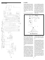
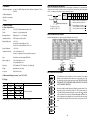
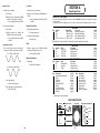
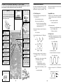
DIGITAL MULTIMETER KIT
MODEL M-2665K
WIDE RANGE DIGITAL MULTIMETER WITH
CAPACITANCE AND TRANSISTOR TESTING FEATURES
Elenco™ Electronics, Inc.
150 W. Carpenter Avenue
Wheeling, IL 60090
(847) 541-3800
http://www.elenco.com
e-mail: [email protected]
Assembly and Instruction Manual
Elenco™ Electronics, Inc.
Copyright © 1991 Elenco™ Electronics, Inc.
Revised 2002
REV-P
753005
INTRODUCTION
QUIZ
Assembly of your M-2665K Digital Multimeter Kit will
prove to be an exciting project and give much
satisfaction and personal achievement. If you have
experience in soldering and wiring technique, you
should have no problems. For the beginner, care
must be given to identifying the proper components
and in good soldering habits. Above all, take your
time and follow the easy step-by-step instructions.
Remember, “An ounce of prevention is worth a
pound of cure”.
The meter kit has been divided into a number of
sections to make the assembly easy and avoid
major problems with the meter operation.
Section A - Meter display circuit assembly.
Section B - DC voltage and current circuit
assembly.
Section C - AC voltage and current circuit
assembly.
Section D - Resistance circuit assembly.
Section E - Capacitance and transistor testing
circuit assembly.
Section F - Final assembly.
1. The function of the A/D converter is to . . .
6. Resistance measurements are made by . . .
A. convert digital to analog.
A. comparing voltage drops in the unknown
resistor and a reference resistor.
B. divide analog signal by 2.
B. measuring the current in the unknown
resistor.
C. convert analog to digital.
D. convert AC to DC.
C. measuring the current in the reference
resistor.
2. What type of divider network is used for voltage
measurements?
D. equalizing the voltage drop in the unknown
and reference resistor.
A. Divide by 20.
B. Capacitance.
7. Measurement cycles performed by the A/D
converter can be divided into what types of time
periods?
C. Divide by 5.
D. Resistor.
A. Long, short.
3. When the AC voltage is measured, it is first . . .
THEORY OF OPERATION
A block diagram of the M-2665K is shown in Figure 1.
Operation centers around a custom LSI chip. This IC
contains a dual slope A/D converter display latches
decoder and the display driver. A block diagram of
the IC functions is shown in Figure 6. The input
voltage, current or ohm signals are conditioned by the
function and selector switches to produce and output
DC voltage between 0 and +199mV. If the input
V
Ω
V/Ω
Voltage
Divider
Ohms
Converter
signal if 100VDC, it is reduced to 100mV DC by
selecting a 1000:1 divider. Should the input be
100VDC, then after the divider it is processed by the
AC converter to produce 100mVDC. If current is to be
read, it is converted to a DC voltage via internal shunt
resistors. For resistance measurements, an internal
voltage source supplies the necessary 0-199mV
voltage to be fed to the IC input.
DC
Analog
Data
V
Ω
Range
Switches
Function
Switches
AC
VAC/mA AC
Converter
mA
mA
Current
Shunts
B. converted to DC.
D. Autozero, read, cycle phase.
C. coupled to a halfwave rectifier.
8. A resistor with band colors green-black-greenbrown-green is what value?
D. low voltage.
A. 50.5kΩ + 5%.
4. When measuring current, the shunt resistors
convert the current to . . .
B. 5.15kΩ + 10%.
A. +0.190 to –0.190.
C. 5.05kΩ + .5%.
B. –1.199 to +1.199.
D. 5.05kΩ + 1%.
C. –0.099 to +0.099.
9. When checking a transistor, the selector knob
should be in the . . .
D. –199 to +0.199.
A. farad position.
Point
A. 358.
B. ohm position.
B. LM324.
C. diode position.
C. 7106R.
D. hFE position.
D. 1N5232.
Decimal
mA
C. Zero, read, interphase.
5. Which IC drives the LCD?
VAC
COMM
A/D
Converter
and
Display
Driver
B. Auto zero, integrate, read.
A. divided down by 2.
10. Where do the leads need to be on the meter
when measuring 450mA?
Display
A. A20, COM.
Figure 1 Simplified Block Diagram
B. V, COM.
C. A, A20.
frequency is divided by four before it clocks the
decade counters. It is further divided to form the
three convert-cycle phases. The final readout is
clocked at about three readings per second.
Digitized measurements data is presented to the
display as four decoded digits (seven segments) plus
polarity. Decimal point position on the display is
determined by the selector switch setting.
Timing for the overall operation of the A/D converter
is derived from an external oscillator whose
frequency is selected to be 40kHz. In the IC, this
-1-
D. A, COM.
Answers: 1. C, 2. D, 3. B, 4. B, 5. C, 6. A, 7. B, 8. C, 9. D, 10. A
The input of the 7106 IC is fed to an A/D (analog to
digital) converter. Here the DC voltage amplitude is
changed into a digital format. The resulting signals
are processed in the decoders to light the appropriate
LCD segment.
-34-
SCHEMATIC DIAGRAM
A/D CONVERTER
A simplified circuit diagram of the analog portion of
the A/D converter is shown in Figure 2. Each of the
switches shown represent analog gates which are
operated by the digital section of the A/D converter.
Basic timing for switch operation is keyed by an
external oscillator. The conversion process is
continuously repeated. A complete cycle is shown
in Figure 2.
converter can be divided into three consecutive time
periods: autozero (AZ), integrate (INTEG) and read.
Both autozero and integrate are fixed time periods.
A counter determines the length of both time
periods by providing an overflow at the end of every
1,000 clock pulses. The read period is a variable
time, which is proportional to the unknown input
voltage. The value of the voltage is determined by
counting the number of clock pulses that occur
during the read period.
Any given measurement cycle performed by the A/D
COMPARATOR
BUFFER
AMP
EXTERNAL
INPUTS
INTEGRATOR
AZ
AZ
READ
TO
DIGITAL
CONTROL
LOGIC
+REF
(FLYING
CAPACITOR)
INTEG
INTEG.
UNKNOWN
INPUT
VOLTAGE+
AZ
INTEG
AZ
READ
AZ
+.20
.15
.10
.05
0
COUNTER OUTPUT
0
10,000
166.7mS
500
1000
1500
2000
0
Figure 2 Dual Slope A/D Converter
by discharging the capacitor at a fixed rate during the
read period, and counting the number of clock pulses
that occur before it returns to the original autozero
level.
During autozero, a ground reference is applied as an
input to the A/D converter. Under ideal conditions the
output of the comparator would also go to zero.
However, input-offset-voltage errors accumulate in the
amplifier loop, and appear at the comparator output as
an error voltage. This error is impressed across the AZ
capacitor where it is stored for the remainder of the
measurement cycle. The stored level is used to provide
offset voltage correction during the integrate and read
periods.
As the read period begins, the INTEG switch opens and
the read switch closes. This applies a known reference
voltage to the input of the A/D converter. The polarity
of this voltage is automatically selected to be opposite
that of unknown input voltage, thus causing the INTEG
capacitor to discharge as fixed rate (slope). When the
charge is equal to the initial starting point (autozero
level), the read period is ended. Since the discharge
slope is fixed during the read period, the time required
is proportional to the unknown input voltage.
The autozero period and thus a new measurement
cycle begins at the end of the read period. At the same
time, the counter is released for operation by
transferring its contents (previous measurement value)
to a series of latches. This stored stat is then decoded
and buffered before being used for driving the LCD
display.
The integrate period begins at the end of the autozero
period. As the period begins, the AZ switch opens and
the INTEG switch closes. This applies the unknown
input voltage to the input of the A/D converter. The
voltage is buffered and passed on to the unknown input
voltage to the input of the A/D converter. The voltage is
buffered and passed on to the integrator to determine
the charge rate (slope) on the INTEG capacitor. At the
end of the fixed integrate period, the capacitor is
charged to a level proportional to the unknown input
voltage. This voltage is translated to a digital indication
-33-
-2-
4. OPERATION MAINTENANCE
VOLTAGE MEASUREMENT
Figure 3 shows a simplified diagram of the voltage
measurement function.
The input divider resistors add up 10MΩ with each
step being a division of 10. The divider output
should be withing –0.199 to +0.199V or the overload
indicator will function. If the AC function is selected,
the divider output is AC coupled to a full wave
rectifier and the DC output is calibrated to equal the
rms level of the AC input.
200mV
Volts
DC
9M
AC
900k
20V
7106R
90k
100mV
Ref
200V
9k
Remove the two phillips head screws. Carefully
remove the plastic back cover. With the instrument
operating and set to the 200mV DC range (20µF
capacitance range), apply 190mV DC (10µF) from
an accurate source. With a small screwdriver
inserted into the semi-fixed resistor VR1 (VR2:
Capacitance), carefully turn the variable resistor
until the reading reads 190mV (10µF).
NOTE: Be sure to proceed basic calibration by DC
range first prior to capacitance.
Be sure to observe the polarity when replacing the
battery.
AC to DC
Converter
1kV
CAUTION
BEFORE ATTEMPTING BATTERY REMOVAL OR
REPLACEMENT, DISCONNECT THE TEST
LEADS FROM ANY ENERGIZED CIRCUITS TO
AVOID SHOCK HAZARD.
The fuse rarely needs replacement and blow almost
always as a result of operator error. To replace the
battery and fuse (2A/250V), remove the two screws
in the bottom of the case. Simply remove the old
battery or fuse and replace with a new one.
Low Pass
Filter
2V
4-1 Battery and Fuse Replacement
4-2 Calibration Procedure
1k
Common
It is normally not necessary to recalibrate for long
intervals. If needed, adjustment should be done
with highly accurate standards (setter than 0.1%
accuracy).
Figure 3 Simplified Voltage Measurement Diagram
5. SAFETY SYMBOLS
CURRENT MEASUREMENT
Figure 4 shows a simplified diagram of the current
measurement positions.
Internal shunt resistors convert the current to
between –0.199 to +0.199V which is then
processed in the 7106 IC to light the appropriate
LCD segments. If the current is AC in nature, the
AC converter changes it to the equivalent DC value.
200µA
!
WARNING
This WARNING sign denotes a hazard. It calls
attention to a procedure, practice or the like, which
if not correctly performed or adhered to, could result
in personal injury.
CAUTION
This CAUTION sign denotes a hazard. It calls
attention to a procedure, practice or the like, which
if not correctly adhered to, could result in damage to
or destruction of part or all of the instrument.
2mA
20mA
200µ
900
2mA
A
20mA
200mA
20A
100
DC
200mA
20A
AC
AC - DC
Converter
Low
Pass
Filter
7106R
100mV
Ref
9Ω
COM
20A
500V max.
1Ω
Shunt
.01Ω
This marking adjacent to another marking or a
terminal operating device indicates that the
operator must refer to an explanation in the
operating instructions to avoid damage to the
equipment and/or to avoid personal injury.
This marking advises the user that the terminal(s)
so marked must not be connected to a circuit point
at which the voltage, with respect to earth ground,
exceeds (in this case) 500 volts.
Figure 4 Simplified Current Measurement Diagram
This symbol adjacent to one or more terminals
identifies them as being associated with ranges that
may in normal use be subjected to particularly
hazardous voltages. For maximum safety, the
instrument and its test leads should not be handled
when these terminals are energized.
-3-
-32-
(D) Diode Test
(F) Capacitance Measurement
1. Set the selector switch to the “Ohm” position.
1. Set the range selector knob to the “FARAD”
position.
2. Connect the red test lead to “V/Ω” input jack and
the black one to the “COM” jack.
3. Set the range selector knob to the “
position.
RESISTANCE MEASUREMENTS
Figure 5 shows a simplified diagram of the resistance measurement function.
2. Set the range selector knob to the desired
capacitance position.
”
DCΩ
Low
Pass
Filter
100
3. Short the leads of the capacitor to be tested
together to insure that there is no charge on the
capacitor.
4. If the semiconductor junction being measured is
connected to the circuit, turn off the power to the
circuit being tested and discharge all of the
capacitors.
4. Insert the capacitor leads into the capacitor test
socket. Note that there are two groups of holes.
One lead must be inserted into one of group one,
and the other lead must be inserted into one of
the holes of group two.
5. Connect the test leads to the device and read
forward value on the digital display.
6. If the digital reads overrange (1), reverse the
lead connections.
5. Read the capacitance value on the digital
display.
The placement of the test leads when the
forward reading is displayed indicates the
orientation of the diode.
900
External
Resistor
9k
90k
2k
Reference
Voltage
20k
200k
2M
20M
900k
9M
Voltage
Source
Figure 5 Simplified Resistance Measurement Diagram
A simple series circuit is formed by the voltage
source, a reference resistor from the voltage divider
(selected by range switches), and the external
unknown resistor. The ratio of the two resistors is
equal to the ratio of their respective voltage drops.
Therefore, since the value of one resistor is known,
the value of the second can be determined by using
the voltage drop across the known resistor as a
reference. This determination is made directly by
the A/D converter.
The red lead is positive and the black lead is
negative.
If overrange (1) is displayed with both lead
connections, the junction is open.
(E) Transistor hFE Measurement
Overall operation of the A/D converter during a
resistance measurement is basically as described
earlier in this section, with one exception. The
reference voltage present during a voltage
measurement is replaced by the voltage drop
across the reference resistor. This allows the
voltage across the unknown resistor to be read
during the read period. As before, the length of the
read period is a direct indication of the value of the
unknown.
1. Set the selector switch to “DC”.
2. The transistor must be out of circuit. Set the
rotary/function switch to the hFE position.
3. Plug the emitter, base and collector leads of the
transistor into the correct holes in either the NPN
of the PNP transistor test socket, whichever is
appropriate for the transistor you are checking.
4. Read the hFE (beta or DC current gain) on the
display.
-31-
7106R
AC CAP
200
-4-
a
a
f
a
b
b
f
g
c
e
b
g
c
e
d
3-3 Method of Measurement
a
f
b
g
d
c
e
d
BACKPLANE
(A) DC/AC Voltage Measurement
(C) Resistance Measurement
1. Set the selector switch to “DC” or “AC”.
1. Set the selector switch to the “Ohm” position.
2. Connect the red test lead to “V/Ω” input jack and
the black one to the “COM” jack.
2. Connect red test lead to the “V/Ω” input jack and
the black one to “COM”.
3. Set the range selector knob to the desired volt
position. If the magnitude of the voltage is not
known, set the range selector knob to the
highest range and reduce until a satisfactory
reading is obtained.
3. Set the range selector knob to desired “Ohm”
position.
20
LCD PHASE DRIVER
7 Segment
Decode
7 Segment
Decode
TYPICAL SEGMENT OUTPUT
V+
7 Segment
Decode
200
0.5mA
LATCH
Segment
Output
2mA
Thousand
Tens
Hundreds
Units
Internal Digital Ground
To Switch Drivers
From Comparator Output
V+
CLOCK
*
6.2V
LOGIC CONTROL
-4
4. If the resistance being measured is connected to
a circuit, turn off the power to the circuit being
tested and discharge all capacitors.
4. Connect the test leads to the device or circuit
being measured.
5. Connect the test leads to the circuit being
measured. When measuring high resistance, be
sure not to contact adjacent point even if
insulated, because some insulators have a
relatively low insulation resistance, causing the
measured resistance to be lower than the actual
resistance.
4
TEST
Internal Digital Ground
1V
500Ω
* Three inverters.
One inverter shown for clarity.
15
1
2
OSC 3
OSC 2
OSC 1
CREF
CREF+
7
V+
5
8
6
A-Z &
Z1
CAZ
A-Z &
Z1
+
2.8V
40
12
Z1
+
A-Z
COMPARATOR
1. Set the selector switch to “DC” or “AC”.
TO
DIGITAL
SECTION
POLARITY
FLIP/FLOP
+
DE (+)
IN LO
ZERO
CROSSING
DETECTOR
DE (+)
A-Z
COMMON
14
+
IN HI
DE (-)
9
11
INT
ANALOG SECTION of 7106R
DE (-)
A-Z & DE(+)
& Z1
15
V
Figure 6 7106R Functions
Pin Configuration
OSC 1
1
40 (+) SUPPLY
OSC 2
2
39 D (UNITS)
OSC 3
3
38 C (UNITS)
TEST
4
37 B (UNITS)
REF HI
5
REF LO
6
+ REF CAP
7
– REF CAP
8
COMMON
9
32 D (TENS)
INPUT HI 10
31 C (TENS)
36 A (UNITS)
7106R
35 F (UNITS)
34 G (UNITS)
33 E (UNITS)
INPUT LO 11
30 B (TENS)
AUTO-ZERO 12
29 A (TENS)
BUFFER 13
28 F (TENS)
INTEGRATOR 14
27 E (TENS)
(–) SUPPLY 15
26 D (100’s)
G (TENS) 16
25 B (100’s)
C (100’s) 17
24 F (100’s)
A (100’s) 18
23 E (100’s)
G (100’s) 19
6. Read resistance value on digital display.
(B) DC/AC Current Measurement
INT
INTEGRATOR
6.2V
6. Turn off the power to the device or circuit being
tested and discharge all of the capacitors prior to
disconnecting the test leads.
CINT
AUTO
ZERO
V+
13
10µA
INT
10
DIGITAL SECTION
RINT
REF LO CREF BUFFER
REF HI
V
3
5. Turn on the power to the device or circuit being
measured. The voltage value will appear on the
digital display along with the voltage polarity.
2. Connect the red test lead to the “A” input jack for
current measurement up to 200mA, and the
black one to “COM”.
3. Set the range selector knob to the desired “Amp”
current position.
If the magnitude of current is not known, set the
rotary/function switch to the highest range and
reduce until a satisfactory reading is obtained.
4. Open the circuit to be measured, and connect
the test leads in series with the load in which
current is to be measured.
5. Read the current value on the digital display.
6. Turn off all power to the circuit being tested and
discharge all of the capacitor prior to
disconnecting the test lead.
7. To measure in the 20A range, use the “20A” jack
as the input jack. Be sure to measure within 10
seconds to avoid high-current hazard.
22 AB (1000)
BACKPLANE 20
(7106R)
21 POLARITY
(MINUS)
7106R Pin Connections
-5-
-30-
Transistor hFE
ASSEMBLY
Range
NPN
PNP
The meter kit has been divided into a number of
sections to make the assembly easy and avoid
major problems with the meter operation.
Test Condition
10mA 2.8V
10mA 2.8V
Diode Test
IMPORTANT CONSTRUCTION NOTES
1. Wash your hands with soap and water before you
assemble this kit. The high impedance areas on
the circuit board can be contaminated by salt
and oil from your skin. If these areas become
contaminated, your completed multimeter may
not meet the listed specifications. Handle the
circuit board only by its edges.
OPEN ONLY THOSE COMPONENT BAGS THAT
ARE CALLED FOR IN YOUR ASSEMBLY
PROCEDURE. DO NOT OPEN ANY OTHER
BAGS.
Measures forward resistance of a semiconductor junction in k Ohm at max. test current of 1.5mA.
3. OPERATION
3-1 Preparation and caution before measurement
1. If the function must be switched during a
measurement, always remove the test leads
from the circuit being measured.
4. In order to prevent damage or injury to the unit,
never fail to keep the maximum tolerable voltage
and current, especially for the 20A current range.
2. If the unit is used near noise generating
equipment, be aware that the display may
become unstable or indicate large errors.
5. Carefully inspect the test lead.
discard and replace.
If damaged,
Do not build more than one section of your meter at
a time. Your instructor must approve the proper
operation of the section you have built before you
proceed to the next section. This procedure will
minimize the problems you may have at the
completion of the project.
2. Avoid any excessive accumulation of resin buildup whenever you solder a connection.
3. Take your time assembling the circuit board.
Work at a slow pace. Remember that accuracy
is far more important than speed.
Your kit program is divided into Sections “A – F”.
The small parts bags will be marked accordingly.
The sections are listed below.
3. Avoid using the unit in places with rapid
temperature variations.
3-2 Panel Description
Section A - Meter display circuit assembly.
4. When you perform the steps in assembly, identify
each respective component before you install it.
Then position it over its outline on the top legend
side of the PC board, unless otherwise indicated.
Section B - DC voltage and current circuit
assembly.
5. Check for the proper polarity of ICs, diodes,
electrolytic capacitors, battery snap and LCD.
Section C - AC voltage and current circuit
assembly.
LCD Display
Section D - Resistance circuit assembly.
Section E - Capacitance and transistor testing
circuit assembly.
Selector Switch
Section F - Final assembly.
Range Selector Knob
hFE Input Socket
Capacitor Input Socket
20A Input Jack
Volt Ohm Input Jack
(200mA Max) A input Jack
Common Input Jack
-29-
-6-
CONSTRUCTION
AC Voltage
Introduction
The most important factor in assembling your M-2665K Digital Multimeter Kit is good soldering techniques.
Using the proper soldering iron is of prime importance. A small pencil type soldering iron of 25 - 40 watts is
recommended. The tip of the iron must be kept clean at all times and well tinned.
Safety Procedures
• Wear eye protection when soldering.
• Locate soldering iron in an area where you do not have to go around it or reach over it.
• Do not hold solder in your mouth. Solder contains lead and is a toxic substance. Wash your hands
thoroughly after handling solder.
• Be sure that there is adequate ventilation present.
Assemble Components
In all of the following assembly steps, the components must be installed on the top side of the PC board unless
otherwise indicated. The top legend shows where each component goes. The leads pass through the
corresponding holes in the board and are soldered on the foil side.
Use only rosin core solder of 63/37 alloy.
DO NOT USE ACID CORE SOLDER!
What Good Soldering Looks Like
Solder all components from
the copper foil side only.
Push the soldering iron tip
against both the lead and
the circuit board foil.
3.
4.
Apply a small amount of
solder to the iron tip. This
allows the heat to leave the
iron and onto the foil.
Immediately apply solder to
the opposite side of the
connection, away from the
iron.
Allow the heated
component and the circuit
foil to melt the solder.
Allow the solder to flow
around the connection.
Then, remove the solder
and the iron and let the
connection cool.
The
solder should have flowed
smoothly and not lump
around the wire lead.
1. Insufficient heat - the
solder will not flow onto the
lead as shown.
Soldering Iron
Component Lead
Rosin
Foil
Soldering iron positioned
incorrectly.
2. Insufficient solder - let the
solder flow over the
connection until it is
covered. Use just enough
solder
to
cover
the
connection.
Soldering Iron
Solder
Foil
Maximum Input
Resolution
0.1Ω
1Ω
10Ω
100Ω
1kΩ
10kΩ
Accuracy
+0.8% of rdg + 2dgt
+0.8% of rdg + 2dgt
+0.8% of rdg + 2dgt
+0.8% of rdg + 2dgt
+1.0% of rdg + 3dgt
+3.0% of rdg + 4dgt
Test Current
Input Protection
Approximately
1.2mA
Protected By
PTC
AC 750V maximum 50Hz - 400Hz
Resistance
Range
200Ω
2kΩ
20kΩ
200kΩ
2MΩ
20MΩ
3. Excessive solder - could
make connections that you
did not intend to between
adjacent foil areas or
terminals.
Soldering Iron
Gap
Solder
Here is what a good solder
connection looks like.
-7-
Resolution
100nA
1µA
10µA
100µA
10mA
Accuracy
+0.5% of rdg + 2dgt
+0.5% of rdg + 2dgt
+0.5% of rdg + 2dgt
+0.5% of rdg + 2dgt
+1.0% of rdg + 3dgt
Protection
Resolution
100nA
1µA
10µA
100µA
10mA
Accuracy
+1.2% of rdg + 3dgt
+1.2% of rdg + 3dgt
+1.2% of rdg + 3dgt
+1.2% of rdg + 3dgt
+3.0% of rdg + 3dgt
Protection
Resolution
1pF
10pF
100pF
1nF
10nF
Accuracy
+3.0% of rdg + 3dgt
+3.0% of rdg + 3dgt
+3.0% of rdg + 3dgt
+3.0% of rdg + 3dgt
+3.0% of rdg + 3dgt
Protection
Protected by
250V/2A Fuse
Range
200µA
2mA
20mA
200mA
20A
Protected by
250V/2A Fuse
Capacitance
Foil
4. Solder bridges - occur
when solder runs between
circuit paths and creates a
short circuit. This is usually
caused by using too much
solder.
To correct this,
simply drag your soldering
iron across the solder
bridge as shown.
Range
200µA
2mA
20mA
200mA
20A
AC Current
Solder
Component Lead
Solder
Accuracy
+1.2% of rdg + 2dgt
+1.2% of rdg + 2dgt
+1.2% of rdg + 2dgt
+1.2% of rdg + 2dgt
+1.2% of rdg + 2dgt
DC Current
Circuit Board
2.
Resolution
100µV
1mV
10mV
100mV
1V
Maximum open circuit voltage: 2.8V
Types of Poor Soldering Connections
A good solder connection should be bright, shiny,
smooth, and uniformly flowed over all surfaces.
1.
Range
200mV
2V
20V
200V
750V
Soldering Iron
Foil
Range
2nF
2nF
200nF
2µF
20µF
Drag
-28-
Test frequency 400Hz+3.0% Test Voltage 120mV
1. FEATURES
• Wide measuring ranges:
IDENTIFYING CAPACITOR VALUES
34 ranges for AC/DC Voltage and Current, Resistance, Capacitance, TR hFE,
Diode Test.
• 10MΩ Input Impedance
Capacitors will be identified by their capacitance value in pF (picofarads), nF (nanofarads), or µF (microfarads). Most
capacitors will have their actual value printed on them. Some capacitors may have their value printed in the following
manner. The maximum operating voltage may also be printed on the capacitor.
Second Digit
• Big LCD for easy reading
0
1
2
3
Multiply By
1
10
100
1k
Tolerance*
100V
4
5
8
10k 100k .01
9
0.1
Note: The letter “R” may be used at times to
signify a decimal point; as in 3R3 = 3.3
* The letter M indicates a tolerance of +20%
2-1 General Specifications
Display
3 1/2 LCD 0.95” height, maximum reading of 1999.
Polarity
Automatic “–” sign for negative polarity.
Overrange Indication
Highest digit of “1” or “–1” is displayed.
Low Battery Indication
“BAT” lettering on the LCD readout.
Operating Temperature
0OC to 50OC.
less than 80% relative humidity up to 35OC.
less than 70% relative humidity from 35OC to 50OC.
Storage Temperature
–15OC to 50OC
Temperature Coefficient
0OC to 18OC and 28OC to 50OC.
less than 0.1 x applicable accuracy specification per degree C.
Power
9V alkaline or carbon zinc battery (NEDA 1604).
Battery Life (typical)
100 hours with carbon zinc cells.
200 hours with alkaline cells.
Dimensions
3.47” (88mm) (W) x 7.52” (191mm) (L) x 1.42” (36mm) (H).
Weight
Approximately 10.4oz. (300g.)
Accessories
Safety Test Lead 1 pair
The value is 10 x 1,000 =
10,000pF or .01µF 100V
The letter K indicates a tolerance of +10%
The letter J indicates a tolerance of +5%
IDENTIFYING RESISTOR VALUES
Use the following information as a guide in properly identifying the value of resistors.
5 Bands
4 Bands
1 2
1
Multiplier
Tolerance
2 3 Multiplier
Tolerance
PART IDENTIFICATION CARDS
2-2 Measurement Ranges (Accuracy: 1 year 18OC to 28OC)
DC Voltage
Resolution
100µV
1mV
10mV
100mV
1V
For the No.
Maximum Working Voltage
2. SPECIFICATIONS
Range
200mV
2V
20V
200V
1000V
103K
Multiplier
10µF 16V
First Digit
• Tilt Stand
Multiplier
Accuracy
+0.5% of rdg + 2dgt
+0.5% of rdg + 2dgt
+0.5% of rdg + 2dgt
+0.5% of rdg + 2dgt
+0.5% of rdg + 2dgt
Maximum Input
DC 1000V or peak AC
Normal Mode Rejection Ratio: Greater than 46dB at 50Hz 60Hz (1k unbalance)
SECTION A
To help identify the resistors and diodes used in the construction of your digital
multimeter we have mounted the diodes and resistors of each section onto a card.
The card will help you find the diodes and resistors quickly. THE PARTS WILL NOT
NECESSARILY BE LISTED IN THE ORDER SHOWN IN THE PARTS LIST SECTION
OR IN THE ASSEMBLY PROCEDURE.
When you are ready to assemble the meter kit, follow the procedure shown. For an
example refer to page 11 for assembly of Section “A”. The first resistor called for is
R-20, 110kΩ resistor (brown-brown-yellow-gold). Locate it on the card ( ), verify that
it is the correct value. Some resistors may be mounted backwards on the card so you
must be certain that you are reading the resistors correctly. When the correct value
has been established, only then will you mount it into its correct position on the PC
board.
EXAMPLE
-27-
-8-
RESISTOR READING EXERCISE
REINSTALLATION OF THE RANGE SELECTOR KNOB
Before starting assembly of your digital multimeter
project, you should be thoroughly familiar with the 5
band color code system. Many of the resistor
values will be identified by color bands and it is easy
to mistake their value if you read the colors
incorrectly or read the value from the wrong end.
Do the following exercise in resistor values. Place
your answer in the box beneath the resistor.
Answers are on the bottom of this page.
(1) yellow-black-black-black-brown
(2) white-black-black-red-green
(3) brown-red-violet-red-brown
If you removed the range selector knob for troubleshooting,
then follow the instructions below to reinstall it.
Bottom View of Selector Knob
& Slide Contacts
Figure L
Place the PC board over the range selector knob and
fasten the knob to the PC board with a M2.3 x 8 screw.
CAUTION: Do not overtighten the screw. The knob
should be snug, but not loose. Turn back the M2.3 x 8
screw 1/2 turn. Slip the two shims under the knob (see
Figure L). If they do not slip in, turn back the screw
another 1/4 turn. Tighten the screw just enough so that
the shims can be pulled out. You should now have the
proper tension to hold the knob and contacts in place and
rotate the knob to the desired positions.
Slide Contact
Shim
Shim
(4) green-black-green-brown-green
USING THE DIGITAL MULTIMETER
(5) brown-black-black-black-brown
(6) brown-green-gray-orange-brown
(7) white-black-black-yellow-green
(8) white-black-black-silver-green
Familiarize yourself with your new digital meter by
taking readings of known resistances and voltages.
You will find that the readings will not be as accurate
on certain ranges for a given measurement. For
example, when measuring a low resistance on a
high range, the reading will show a short 0.00.
When measuring a high resistance on a low range,
the reading will show infinity 1. Likewise, it is
important to use the correct range when measuring
voltages.
MEASURED
RESISTANCE
SHORT
(LEADS TOUCHING)
(9) brown-black-black-orange-green
(10) orange-white-red-red-brown
(11) gray-white-black-black-brown
(12) brown-brown-black-red-brown
Answers to Resistor Reading Exercise: 1) 400Ω+1%; 2) 90kΩ+.5%; 3) 12.7kΩ+1%; 4) 5.05kΩ+.5%; 5) 100Ω+1%;
6) 158kΩ+1%; 7) 9MΩ+.5%; 8) 9Ω+.5%; 9) 100kΩ+.5%; 10) 39.2kΩ+1%; 11) 890Ω+1%; 12) 11kΩ+1%;
-9-
RANGE SETTING
20kΩ 200kΩ
200Ω
2kΩ
* 00.1
.000
0.00
2MΩ
20MΩ
00.0
.000
0.00
INFINITY
1.
1.
1.
1 .
1.
1.
47Ω
52.1
.052
0.05
00.0
.000
0.00
270Ω
1.
.267
0.26
00.2
.000
0.00
10kΩ
1.
1.
10.18
10.2
.010
0.01
47kΩ
1.
1.
1.
52.7
.052
0.05
470kΩ
1.
1.
1.
1 .
.472
0.47
2.2MΩ
1.
1.
1.
1 .
1.
2.12
Table 1
* RESISTANCE OF TEST LEADS
Table 2
Table 1 shows an example of the readouts for
different values of resistance. Table 2 shows an
example of the readouts for 117VAC and 100VDC.
The shaded area indicates the most accurate range.
It must be remembered that the readings will shift
slightly when switching to a different range.
MEASURED
VOLTAGE
200mV
2V
20V
200V
1000V
117VAC
1 .
1.
1.
117.0
117
100VDC
1 .
1.
1.
100.0
100
-26-
Amps Section
hFE Section
1. 200mA scale not working:
1. Check for shorts on socket pins.
A. Check fuse.
2. Measure across B terminal to COM terminal for
251kΩ.
B. Measure across (A) terminal and (COM)
terminal for 1Ω (set meter in 200mA).
A. Lower or higher than 251kΩ; Check R14
and R15.
1. Lower or higher than 1Ω, Check R13.
2. 20mA scale not working:
SECTION A
Meter Display Circuit
PARTS LIST - SECTION A
If any parts are missing or damaged, see instructor or bookstore. DO NOT contact your place of purchase as they will not
be able to help you.
Contact Elenco™ Electronics (address/phone/e-mail is at the back of this manual) for additional assistance, if needed.
Decimal Point Section
A. Check fuse.
1. Displays two decimal points.
B. Measure between (A) terminal and
(COM) for 10Ω (set meter in 20mA).
A. Shorted output on U2.
2. No decimal points displayed.
1. Lower or higher than 10Ω, check R12
and R13.
RESISTORS
Qty.
1
1
1
6
Symbol
R24
R19
R20
R16, 17, 18, 21, 22, 23
Description
56kΩ 5% 1/4W
100kΩ 5% 1/4W
110kΩ 5% 1/4W
1MΩ 5% 1/4W
Color Code
green-blue-orange-gold
brown-black-yellow-gold
brown-brown-yellow-gold
brown-black-green-gold
Part #
155600
161000
161100
171000
A. Check U2 325.
Note: Resistor tolerance (last band) of 5-band resistors may be green instead of brown.
Capacitance Section
Diode
1. Place .001µF cap in the socket and check pin 7
and pin 8 of U4 with a scope (meter set to 2N).
1. Measure voltage across V OHM and COM
terminal (set in diode mode) = 1.3V.
CAPACITORS
A. Low voltage, check R26.
Pin 7 370Hz - 400Hz .12Vpp.
Qty.
1
1
1
2
Symbol
C2
C3
C4
C5, C6
Value
100pF (101)
.047µF (473)
.1µF (104)
.22µF (224)
Description
Ceramic Capacitor
Mylar Capacitor
Mylar Capacitor
Mylar Capacitor
Qty.
1
1
1
Symbol
ZD
U2
U1
Value
1N5232/1N752
4030/4070
7106R
Battery Low Indicator
1. Not working.
A. Check ZD1, R19 and U2.
Pin 14 370Hz - 400Hz .3Vpp.
Part #
221017
244717
251017
252217
SEMICONDUCTORS
Description
Zener Diode
Integrated Circuit
Integrated Circuit
Part #
315232
334030
337106R
MISCELLANEOUS
Qty.
1
1
1
1
1
1
1
* 1
* 1
A. No signal at pin 14.
1. Check D3, D4 and shorts.
B. No signal at pin 7 but present at pin 1.
1. Check D5 and D6.
Description
Liquid Crystal Display (LCD)
Zebra
PC Board
Solder Roll
Battery Snap (BAT)
Battery
LCD Window Plate
Range Selector Knob
Bushing
Part #
35114A
500000
516000A
551135
590098
590009
621002A
622003
624004
Qty.
1
1
2
1
*
1
6
*
1
2
Description
LCD Stopper
LCD Housing
M2.3 x 6 Screw
M2.3 x 8 Screw
IC Socket 40-Pin
Slide Contact
Top Plate (A)
Shims (see page 26)
Part #
629005
629007
642360
642430
664040
680016
724001A
780006
* Parts installed on PC board already.
PARTS IDENTIFICATION
Resistor
Integrated Circuit
Top Plate (A)
LCD Housing
Diode
LCD Window
Plate
Socket
Capacitor
Liquid Crystal Display (LCD)
Battery Snap
LCD
LCD Stopper
Ceramic
-25-
Zebra
Mylar
-10-
ASSEMBLE THE FOLLOWING COMPONENTS TO THE PC BOARD
TROUBLESHOOTING GUIDE
In all of the following steps the components must be installed on the top legend side of the PC board. The
board is turned to solder the component leads on the selector switch side.
If the meter is not working, perform the U1 (7106R)
Voltage Test first. This test is to verify that the IC
and Reference Voltage are operational. Then
perform the tests that pertain to the Function that is
not working on your meter.
U1 (7106R) Voltage Test
Voltage/OHM Section
1. Measure the voltage across pin 40 and pin 15 on
U1 (7106R) for 9V.
1. Measure across V OHM terminal and COM
terminal for 10MΩ (set meter in 200mV) battery
installed.
Figure A
Figure B
Figure C
Align the notch on the socket (if any) with the notch
marked on the PC board. Solder the socket to the PC
board. Insert the IC into the socket with the notch as
shown below. Note: If the IC is already inserted into
the socket, do not attempt to pull it out, as this will
damage the IC and socket. Instead, solder the socket
to the PC board with the IC in it.
Lay resistor flat against the
PC board.
Mount the diodes with the
band in the correct direction
as shown on the top legend.
Band
A. Check the battery connection.
A. Lower or higher than 10MΩ.
B. Check for a 9V and GND short.
U2 - 4030 IC or 4070
No IC socket used
Notch
Notch
U1 - IC Socket 40-pin
U1 - 7106R IC
(see Figure A)
1. Check resistors R1 - R6.
1. One of the ICs may be bad. Remove
one IC at a time and check voltage
again between pins 40 - 15.
2. LCD readings floating.
A. Measure across the COM terminal to pin
6 on U1 (7106R) for 1MΩ.
2. Measure the voltage across pin 40 and pin 9 on
U1 for 3V.
1. R22 open or defective.
A. U1 is defective.
Solder the IC to the PC board
with the notch in the direction
shown on the top legend.
R20 - 110kΩ 5% 1/4W Res.
(brown-brown-yellow-gold)
(see Figure B)
C5 - .22µF (224) Mylar Cap
C6 - .22µF (224) Mylar Cap.
(see Figure D)
C2 - 100pF (101) Ceramic Cap.
(see Figure D)
R21 - 1MΩ 5% 1/4W Res.
R22 - 1MΩ 5% 1/4W Res.
(brown-black-green-gold)
(see Figure B)
R16 - 1MΩ 5% 1/4W Res.
R18 - 1MΩ 5% 1/4W Res.
R17 - 1MΩ 5% 1/4W Res.
(brown-black-green-gold)
(see Figure B)
C3 - .047µF (473) Mylar Cap.
(see Figure D)
R19 - 100kΩ 5% 1/4W Res.
(brown-black-yellow-gold)
(see Figure B)
R23 - 1MΩ 5% 1/4W Res.
(brown-black-green-gold)
(see Figure B)
ZD - 1N5232 Diode
(see Figure C)
C4 - .1µF (104) Mylar Cap.
(may be marked 104)
(see Figure D)
BAT - Battery Snap
Insert both wires through the
hole and mount the red wire to
the (+) hole and the black wire
to the (–) hole. Solder the
wires from the top legend
side.
R24 - 56kΩ 5% 1/4W Res.
(green-blue-orange-gold)
(see Figure B)
AC Voltage Section
3. Check the Main Oscillator on U1 (7106R) pins 1,
2, 3.
1. Apply 15VAC to meter and measure pin 1 and pin
7 of U3 (358) to COM terminal with a scope
(meter on 20VAC scale).
Pin 1
Pin 1 to COM 0.44Vpp
Pin 2
Pin3
A. Check DC/AC switch
B. Check C7, R29 - R32, D7, D8 and U3.
4. Measure the voltage across pin 5 and pin 6 on
U1 (7106R) for 70mV - 105mV (reference
voltage).
Pin 7 to COM 1.4Vpp
A. Adjust VR1 so the the junction of R46,
R27 and R28 equal to 100mV.
1. Can’t set to 100mV.
a. VR1 wrong value or defective.
b. R25, R27 and R28 wrong value.
A. Check R33 - R36, D9, D10, C9 and U3.
B. Can’t obtain 100mV between pin 5 and
pin 6.
2. Check pin 10 and pin 11 of U1 (7106R) with a
scope.
1. Check R21 and R46.
Mount the capacitors with 1/4” of
space between the body and the
PC board. Bend cap over as
shown.
Waveform on pin 10 and pin 11.
0.2Vpp
A. Check C4 and R23.
Figure D
-11-
-24-
Testing Procedure SECTION C - AC voltage
and current circuit
Testing Procedure SECTION F
Measure an AC voltage with a known accurate
meter. Now measure the voltage with the kit meter.
The meters should be the same voltage.
Connect the kit meter and another meter of known
accuracy in series. Set the meters in the 200mA
position. Construct a circuit for an AC current and
measure the circuit current. Both meters should
have close to the same readings. If the meters do
not agree, check the parts just added. Do not readjust VR1 this will change the voltage reading set
in step 1. Check the 200µ - 200mA scales. The 20A
scale requires, a circuit of 1 - 10 amps. If the tests
are not working, check for cold solder joints and part
values. DO NOT PROCEED TO SECTION F
WITHOUT INSTRUCTORS APPROVAL.
ASSEMBLE THE LCD
Set the meter in one of the farad scales. Make sure
that SW1 is in the AC/Cap position. Measure a cap
with another meter and then insert the same cap
into the kit meters CX connectors. Adjust VR2 so
that the meter reads the same as the accurate one.
This calibrates capacitance circuit of meter. Using
two or three different value capacitors, check each
scale. Compare the kit meter readings with another
meter. Turn the meter off and remove the battery.
Assemble the LCD into the housing with the parts
shown in Figure E. The LCD must be put in with
the notch in the direction shown in Figure E. Peel
off the clear protective film on top of the LCD (see
Figure G), then place the LCD plate into the
housing with the two curved corners on the inside
of the plate in the same direction as the two
curved corners on the housing. Wipe off zebra
edges with a lint-free cloth.
Set the meter in the hFE scales. Place an NPN
transistor into the socket. Make sure that the
transistor is in correctly. Depending on the type of
transistor, the meter will range from 20 to 550.
Place a PNP transistor into the PNP socket, the
range will also be 20 to 550. If the tests are not
working, check for cold solder joints and part values.
Mount the LCD unit to the PC board. Insert the
two pins on the side shown in Figure E into the
holes on the PC board. Then push the other end
down until it snaps into place.
Testing Procedure
Placing the top plate (A) over the knob will assist in
obtaining the correct knob position when doing
tests.
Connect the 9V battery and turn the range selector.
The LCD will display random numbers. As you turn
the knob clockwise, the decimal point will move
also. Check that all of the segments that make up
the certain number are displayed. If the LCD is
working correctly, move the knob to the off position
and remove the battery. If the tests are not working,
check for cold solder joints, part values and if the
LCD is assembled correctly. DO NOT PROCEED
TO SECTION B WITHOUT INSTRUCTOR’S
APPROVAL.
Screw the LCD housing to the PC board with two
M2.3 x 6 screws as shown in Figure E.
NOTE: If the range selector switch
becomes hard to turn, then loosen the
M2.3 x 8 screw slightly.
After the LCD unit is assembled, insert
this side into the PC board first.
Clear Protective Film
LCD Housing
LCD Window Plate
LCD
Notch
Figure F
LCD Stopper
Zebra - Do not touch edge
Battery
PC Board
Range
Selector Knob
Figure E
-23-
M2.3 x 6 Screws
-12-
SECTION B
DC Voltage & Current Circuit
(A)
Top Plates
PARTS LIST - SECTION B
RESISTORS
Qty.
1
1
1
1
1
1
1
1
1
1
1
1
1
1
Symbol
R13
R12
R6
R5
R28
R27
R46
R26
R4
R25
R3
R2
R1
VR1
Description
1Ω .5% 1/2W
9Ω .5% 1/4W
100Ω .5% 1/4W
900Ω .5% 1/4W
1.3kΩ 1% 1/4W
2kΩ 1% 1/4W
5.6kΩ 5% 1/4W
8.2kΩ 5% 1/4W
9kΩ .5% 1/4W
39.2kΩ 1% 1/4W
90kΩ .5% 1/4W
900kΩ .5% 1/4W
9MΩ .5% 1/2W
200Ω / 220Ω
(B)
Color Code
brown-black-gold-green / OR brn-blk-blk-sil-grn
white-black-black-silver-green
brown-black-black-black-green
white-black-black-black-green
brown-orange-black-brown-brown
red-black-black-brown-brown
green-blue-red-gold
gray-red-red-gold
white-black-black-brown-green
orange-white-red-red-brown
white-black-black-red-green
white-black-black-orange-green
white-black-black-yellow-green
Potentiometer
Part #
111051
119050
131050
139050
141230
142030
145600
148200
149050
153930
159050
169050
179051
191320
Top Case
Bearings
Ball
Bearing
Springs
Spring
Selector
Knob
Spring
Note: Some resistors may not have a color coding, but they will have the value imprinted on them.
Note: Resistor tolerance (last band) of 5-band resistors may be green instead of brown.
Range Selector Knob
CAPACITORS
Qty.
1
Symbol
C1
Value
22µF
Description
Electrolytic (Lytic)
Part #
272244
Battery
SEMICONDUCTORS
Qty.
2
Symbol
D1, D2
Value
1N4001 or 1N4007
Qty.
1
1
* 1
1
2
4
1
Symbol
Description
Shunt Wire M1.6 x 60
Fuse 2A
Slide Switch
Slide Switch Knob
Fuse Holder Clips
Input Socket
Test Lead Set
Description
Diode
Part #
314001
Shield Plate
MISCELLANEOUS
SW1
Part #
100069
533020
541104
622004
663003
664000
RWTL14
* Part installed on PC board already
Bottom Case
Figure K
Battery
Cushion
M3 x 12 Screws
Stand
-13-
-22-
Grease
FINAL ASSEMBLY
ASSEMBLE THE FOLLOWING COMPONENTS TO THE PC BOARD
Peel off the protective backing on the top plates
(A) and (B) and stick them to the top case. Peel
off the protective backing on the battery cushion
and stick it onto the bottom case. (These may be
installed on the case already).
top of the springs and then place a ball bearing
on each spring. Press the top case onto the PC
board. Using both hands, slide your fingers
under the paper. Press your thumbs down on the
top case and then flip the board. Be sure to hold
the PC board to the case firmly or the ball
bearings will fall out. Fasten the PC board to the
top case with three M2.3 x 6 screws in the places
shown in Figure J.
Turn the selector knob screw one full turn out as
shown in the figure.
Connect the battery and place it in the cavity of
the top case.
Place the PC board on a standard piece of paper
(8 1/2” x 11”). Insert the two springs into the
holes on the range selector knob. Put grease on
Place the bottom case onto the top case. Hold
the two sections together with two M3 x 12
screws.
Solder the spring to the PC board as shown in
Figure Ja.
See Figure K for the following steps.
In all of the following steps the components must be installed on the top legend side of the PC board. The
board is turned to solder the component leads on the selector switch side.
Figure E
Figure F
Stand resistor on end as
shown with the body
inside the white circle.
Lytics have a polarity marking on
them indicating the negative lead, the
opposite lead is positive. The PC
board is marked to show the positive
(+) lead position. Mount the capacitor
with the positive (+) lead in the hole
marked on the PC board. Bend the
capacitor over.
White
Circle
R26 - 8.2kΩ 5% 1/4W Res.
(gray-red-red-gold)
(see Figure E)
R5 - 900Ω .5% 1/4W Res.
(white-blk-blk-blk-green)
(see Figure E)
R25 - 39.2kΩ 1% 1/4W Res.
(orange-white-red-red-brown)
(see Figure E)
C1 - 22µF Lytic Capacitor
(see Figure F)
R27 - 2kΩ 1% 1/4W Res.
(red-blk-blk-brown-brown)
(see Figure E)
R3 - 90kΩ 1/4W .5% Res.
(white-blk-blk-red-green)
(see Figure E)
Spring
Pad
R28 - 1.3kΩ 1% 1/4W Res.
(brn-orange-blk-brn-brn)
(see Figure E)
R2 - 900kΩ .5% 1/4W Res.
(white-blk-blk-orange-green)
(see Figure E)
R46 - 5.6kΩ 5% 1/4W Res.
(green-blue-red-gold)
(see Figure E)
R1 - 9MΩ .5% 1/2W Res.
(white-blk-blk-yellow-green)
(see Figure B)
Solder
Figure Ja
+
+
R6 - 100Ω .5% 1/4W Res.
(brown-blk-blk-blk-green)
(see Figure E)
R4 - 9kΩ .5% 1/4W Res.
(white-blk-blk-brown-green)
(see Figure E)
Spring
C1
VR1 - 200Ω
Potentiometer
D1 - 1N4001 Diode
D2 - 1N4001 Diode
(see Figure C)
R12 - 9Ω 1/4W .5% Res.
(white-blk-blk-silver-green)
(see Figure B)
Screw Holes
R13 - 1Ω .5% 1/2W Res.
(brown-black-gold-green)
(see Figure B)
Shunt
Push into board
up to stops
Fuse Holder Clips
Fuse 2A
Mount holders with the tab
side as shown on the top
legend then insert fuse.
Figure J
Tab
-21-
-14-
Push the four input sockets into the PC board holes from the selector switch side until they stop (see
Figure G). Turn the board over as shown in Figure Ga and solder the sockets in place from the top legend
side. Apply enough heat to allow the solder to flow around the input sockets (see Figure Gb).
Push on the slide switch knob.
Mount the two 9-pin component sockets to the PC board with the notch at the base of the socket in the
direction shown in Figure I. Solder the sockets in place from the top legend side.
Slide Switch Knob
Input
Sockets
Component Socket
Notch
Top Legend Side
Solder
Component Socket
Slide Switch
Figure I
Socket
Notch
Figure G
Top Legend Side
Testing Procedure
Figure Gb
Connect the 9V battery and test leads to the meter
(red to VΩ and black to COM). Set the range
selector knob to the diode scale and set SW1 in the
DC Ohm position. Connect a diode to the test leads
with the correct polarity (see figure below). The
Sockets
meter will range for 100 - 950. If the tests are not
working, check for cold solder joints and part values.
Turn the meter off and remove the battery and test
leads.
COM
VΩ
DO NOT PROCEED TO SECTION E WITHOUT INSTRUCTOR’S APPROVAL.
Figure Ga
– 9V +
SECTION F
47kΩ
Testing Procedure
Final Assembly
Figure Gc
Voltage Test
position. Construct a circuit for a DC current (for
example 9V and a 47kΩ resistor for 190µA) and
measure the circuit. Both meters should have close
to the same readings. If the meters do not agree,
check the parts just added. Do not readjust VR1 for
this will change the voltage reading set in step 1.
Check that 200µA - 200mA scales. The 20A scale
requires a circuit of 1 - 10 amps. If the tests are not
working, check for cold solder joints and part values.
Turn the meter off and remove the battery and test
leads. DO NOT PROCEED TO SECTION C
WITHOUT YOUR INSTRUCTOR’S APPROVAL.
Connect the 9V battery to the meter. Turn the range
selector knob to the 20V position and connect the
test leads (red lead to VΩ and black to COM). Using
another meter of known accuracy, measure a DC
voltage less than 20V (such as a 9 volt battery). You
will calibrate the kit meter by measuring the same
voltage source and adjusting VR1 until the kit meter
reads the same as the accurate meter. When the
two meters agree, the voltage circuit is calibrated.
Turn the range selector knob to the off position.
Current Test
Connect the kit meter and another meter of known
accuracy in series. Set the meters in the 200µA
-15-
PARTS LIST - SECTION F
Qty.
1
1
1
3
2
2
Description
Battery Cushion
Top Case
Bottom Case w/Stand
Screw M2.3 x 6
Screw M3 x 12
Bearing
Part #
620001
623101A
623200A
642360
642367
666001
Qty.
1
2
1
1
1
Note: The shield and battery cushion may be installed already.
-20-
Description
Shield Spring
Knob Spring
Top Plate (B)
Shield
Grease
Part #
680008
680009
724000A
780008
790004
ASSEMBLE THE FOLLOWING COMPONENTS TO THE PC BOARD
SECTION C
In all of the following steps the components must be installed on the top legend side of the PC board. The
board is turned to solder the component leads on the selector switch side.
AC Voltage & Current Circuit
PARTS LIST - SECTION C
D11 - 1N4148 Diode
(see Figure C)
R7 - 98.8Ω 1% 1/4W Res.
(wht-gray-gray-gold-brn)
(see Figure E)
R8 - 900Ω 1% 1/4W Res.
(wht-blk-blk-blk-brn)
(see Figure E)
R9 - 9kΩ 1% 1/4W Res.
(wht-blk-blk-brn-brn)
(see Figure E)
R44 - 76.8kΩ 1% 1/4W Res.
(violet-blue-gray-red-brown)
(see Figure E)
R42 - 39.2kΩ 1% 1/4W Res.
(orange-white-red-red-brn)
(see Figure E)
Description
5.05kΩ .5% 1/4W
5.6kΩ 5% 1/4W
5.62kΩ .5% 1/4W
10kΩ 5% 1/4W
200kΩ 5% 1/4W
390kΩ 5% 1/4W
2.2MΩ 5% 1/4W
Color Code
green-black-green-brown-green
green-blue-red-gold
green-blue-red-brown-green
brown-black-orange-gold
red-black-yellow-gold
orange-white-yellow-gold
red-red-green-gold
Part #
145050
145600
145650
151000
162000
163900
172200
Note: Resistor tolerance (last band) of 5-band resistors may be green instead of brown.
CAPACITORS
C9
C7
C8
.1µF (104)
.1µF (104)
22µF
R11 - 909kΩ 1% 1/4W Res.
(wht-blk-wht-org-brn)
(see Figure E)
4
1
D7 - D10
U3
1N4148
358/17358
VR2 - 200Ω
Potentiometer
1
U3
IC Socket 8-pin
R14 - 240kΩ 5% 1/4W Res.
R15 - 240kΩ 5% 1/4W Res.
(red-yellow-yellow-gold)
(see Figure B)
Ceramic
Mylar
Electrolytic (Lytic)
251010
251017
272244
SEMICONDUCTORS
Diode
Integrated Circuit
314148
330358
MISCELLANEOUS
664008
ASSEMBLE THE FOLLOWING COMPONENTS TO THE PC BOARD
D5 - 1N4001 Diode
D6 - 1N4001 Diode
(see Figure H)
C12 - .01µF (103) Mylar Cap.
C13 - .01µF (103) Mylar Cap.
D3 - 1N4001 Diode
D4 - 1N4001 Diode
(see Figure H)
R39 - 39.2kΩ 1% 1/4W Res.
(org-wht-red-red-brn)
(see Figure E)
R45 - 158kΩ 1% 1/4W Res.
(brown-grn-gray-orange-brn)
(see Figure E)
U4 - IC Socket 14-pin
U4 - 324 Integrated Circuit
D9 - 1N4148 Diode
D10 - 1N4148 Diode
(see Figure H)
R37 - 150Ω 5% 1/4W Res.
(brn-grn-brn-gold)
(see Figure E)
C11 - .01µF (103) Mylar Cap.
C7 - .1µF (104) Mylar Cap.
C10 - .01µF (103) Mylar Cap.
R29 - 10kΩ 5% 1/4W Res.
(brown-black-orange-gold)
(see Figure B)
R38 - 10kΩ 1% 1/4W Res.
(brn-blk-blk-red-brn)
(see Figure E)
Notch
In all of the following steps the components must be installed on the top legend side
of the PC board. The board is turned to solder the component leads on the
selector switch side.
R35 - 5.62kΩ .5% 1/4W Res.
R36 - 5.62kΩ .5% 1/4W Res.
(green-blue-red-brn-green)
(see Figure B)
R41 - 1.91kΩ 1% 1/4W Res.
(brn-wht-brn-brn-brn)
(see Figure E)
Align the notch on the socket (if
any) with the notch marked on
the PC board. Solder the socket
to the PC board. Insert the IC
into the socket with the notch as
shown below.
Symbol
R31
R33
R35, 36
R29
R32
R34
R30
1
1
1
R10 - 90kΩ 1% 1/4W Res.
(wht-blk-blk-red-brn)
(see Figure E)
R43 - 11kΩ 1% 1/4W Res.
(brown-brown-blk-red-brn)
(see Figure E)
RESISTORS
Qty.
1
1
2
1
1
1
1
R40 - 4.12kΩ 1% 1/4W Res.
(yel-brn-red-brn-brn)
(see Figure E)
R33 - 5.6kΩ 5% 1/4W Res.
(green-blue-red-gold)
(see Figure E)
D7 - 1N4148 Diode
D8 - 1N4148 Diode
(see Figure H)
R30 - 2.2MΩ 5% 1/4W Res.
(red-red-green-gold)
(see Figure E)
C8 - 22µF Lytic Capacitor
(see Figure I)
C8
R34 - 390kΩ 5% 1/4W Res.
(orange-white-yellow-gold)
(see Figure E)
R32 - 200kΩ 5% 1/4W Res.
(red-black-yellow-gold)
(see Figure E)
C9 - .1µF (104) Ceramic Cap.
U3 - IC Socket 8-pin
U3 - 358 Integrated Circuit
Figure H
Figure I
Mount the diode with the
band in the direction of the
arrow on the top legend.
Mount the capacitor with the
negative ( ) lead in the negative
hole and the positive (+) lead in
the positive hole marked on the
PC board. Lay the capacitor flat
against the PC board as shown.
R31 - 5.05kΩ .5% 1/4W Res.
(green-blk-green-brn-green)
(see Figure E)
Align the notch on the socket (if any)
with the notch marked on the PC
board. Solder the socket to the PC
board. Insert the IC into the socket with
the notch as shown below.
Socket
-19-
-16-
Notch
SECTION D
SECTION E
Resistance Circuit
Capacitance and Transistor Testing Circuit
PARTS LIST - SECTION D
Qty
1
Symbol
PTC
PARTS LIST - SECTION E
Description
1kΩ Thermister
Part #
190415
ASSEMBLE THE FOLLOWING COMPONENT TO THE PC BOARD
The other components for this section have been installed already.
PTC - Thermister 1kΩ
Mount part in holes shown only
RESISTORS
Qty.
1
1
1
1
1
1
1
1
2
1
1
1
2
1
1
Symbol
R7
R37
R8
R41
R40
R9
R38
R43
R39, R42
R44
R10
R45
R14, R15
Description
98.8Ω 1% 1/4W
150Ω 5% 1/4W
900Ω 1% 1/4W
1.91kΩ 1% 1/4W
4.12kΩ 1% 1/4W
9kΩ 1% 1/4W
10kΩ 1% 1/4W
11kΩ 1% 1/4W
39.2kΩ 1% 1/4W
76.8kΩ 1% 1/4W
90kΩ 1% 1/4W
158kΩ 1% 1/4W
240kΩ 5% 1/4W
R11
VR2
909kΩ 1% 1/4W
200Ω / 220Ω
Color Code
white-gray-gray-gold-brown
brown-green-brown-gold
white-black-black-black-brown
brown-white-brown-brown-brown
yellow-brown-red-brown-brown
white-black-black-brown-brown
brown-black-black-red-brown
brown-brown-black-red-brown
orange-white-red-red-brown
violet-blue-gray-red-brown
white-black-black-red-brown
brown-green-gray-orange-brown
red-yellow-yellow-gold
OR red-yellow-black-orange-green
white-black-white-orange-brown
Potentiometer
Part #
129830
131500
139030
141930
144130
149030
151030
151130
153930
157630
159030
161530
162400
169060
191320
Note: Resistor tolerance (last band) of 5-band resistors may be green instead of brown.
CAPACITORS
Qty.
4
Symbol
C10 - C13
Value
.01µF (103)
Description
Mylar
Part #
241017
SEMICONDUCTORS
Qty.
1
4
1
Testing Procedure
Connect the 9V battery and test leads to the meter
(red to VΩ and black to COM). Set the range
selector knob to one of the Ohm scales. Make sure
that SW1 is in the DC/Ohm position. Using two or
three different value resistors, check each scale.
Compare the kit meter readings with another meter
of known accuracy. If the tests are not working,
check for cold solder joints, part values, and the
contacts on the selector knob to make sure that they
are intact. Turn the meter off and remove the battery
and test leads.
Symbol
U4
D3 - D6
D11
Value
324 / 17324
1N4001 or 1N4007
1N4148
Description
Integrated Circuit
Diode
Diode
MISCELLANEOUS
Qty.
2
1
Symbol
hFE, CX
U4
Description
9-pin Socket
IC Socket 14-pin
Part #
664009
664014
DO NOT PROCEED TO SECTION E WITHOUT INSTRUCTOR’S APPROVAL.
-17-
Part #
330324
314001
314148
-18-