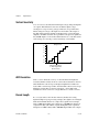
1
Computer-Based
Instruments
NI 5102 User Manual
High-Speed Digitizer
NI 5102 User Manual
June 2001 Edition
Part Number 321390D-01
Support
Worldwide Technical Support and Product Information
ni.com
National Instruments Corporate Headquarters
11500 North Mopac Expressway
Austin, Texas 78759-3504
USA Tel: 512 794 0100
Worldwide Offices
Australia 03 9879 5166, Austria 0662 45 79 90 0, Belgium 02 757 00 20, Brazil 011 284 5011,
Canada (Calgary) 403 274 9391, Canada (Montreal) 514 288 5722, Canada (Ottawa) 613 233 5949,
Canada (Québec) 514 694 8521, Canada (Toronto) 905 785 0085, China (Shanghai) 021 6555 7838,
China (ShenZhen) 0755 3904939, Denmark 45 76 26 00, Finland 09 725 725 11, France 01 48 14 24 24,
Germany 089 741 31 30, Greece 30 1 42 96 427, Hong Kong 2645 3186, India 91805275406,
Israel 03 6120092, Italy 02 413091, Japan 03 5472 2970, Korea 02 596 7456, Malaysia 603 9596711,
Mexico 5 280 7625, Netherlands 0348 433466, New Zealand 09 914 0488, Norway 32 27 73 00,
Poland 0 22 528 94 06, Portugal 351 1 726 9011, Singapore 2265886, Spain 91 640 0085,
Sweden 08 587 895 00, Switzerland 056 200 51 51, Taiwan 02 2528 7227, United Kingdom 01635 523545
For further support information, see the Technical Support Resources appendix. To comment on the
documentation, send e-mail to [email protected].
Copyright © 1997, 2001 National Instruments Corporation. All rights reserved.
Important Information
Warranty
The NI 5102 is warranted against defects in materials and workmanship for a period of one year from the date of shipment, as evidenced by
receipts or other documentation. National Instruments will, at its option, repair or replace equipment that proves to be defective during the
warranty period. This warranty includes parts and labor.
The media on which you receive National Instruments software are warranted not to fail to execute programming instructions, due to defects
in materials and workmanship, for a period of 90 days from date of shipment, as evidenced by receipts or other documentation. National
Instruments will, at its option, repair or replace software media that do not execute programming instructions if National Instruments receives
notice of such defects during the warranty period. National Instruments does not warrant that the operation of the software shall be
uninterrupted or error free.
A Return Material Authorization (RMA) number must be obtained from the factory and clearly marked on the outside of the package before
any equipment will be accepted for warranty work. National Instruments will pay the shipping costs of returning to the owner parts which are
covered by warranty.
National Instruments believes that the information in this document is accurate. The document has been carefully reviewed for technical
accuracy. In the event that technical or typographical errors exist, National Instruments reserves the right to make changes to subsequent
editions of this document without prior notice to holders of this edition. The reader should consult National Instruments if errors are suspected.
In no event shall National Instruments be liable for any damages arising out of or related to this document or the information contained in it.
EXCEPT AS SPECIFIED HEREIN, NATIONAL INSTRUMENTS MAKES NO WARRANTIES, EXPRESS OR IMPLIED, AND SPECIFICALLY DISCLAIMS ANY WARRANTY OF
MERCHANTABILITY OR FITNESS FOR A PARTICULAR PURPOSE. CUSTOMER’S RIGHT TO RECOVER DAMAGES CAUSED BY FAULT OR NEGLIGENCE ON THE PART OF
NATIONAL INSTRUMENTS SHALL BE LIMITED TO THE AMOUNT THERETOFORE PAID BY THE CUSTOMER. NATIONAL INSTRUMENTS WILL NOT BE LIABLE FOR
DAMAGES RESULTING FROM LOSS OF DATA, PROFITS, USE OF PRODUCTS, OR INCIDENTAL OR CONSEQUENTIAL DAMAGES, EVEN IF ADVISED OF THE POSSIBILITY
THEREOF. This limitation of the liability of National Instruments will apply regardless of the form of action, whether in contract or tort, including
negligence. Any action against National Instruments must be brought within one year after the cause of action accrues. National Instruments
shall not be liable for any delay in performance due to causes beyond its reasonable control. The warranty provided herein does not cover
damages, defects, malfunctions, or service failures caused by owner’s failure to follow the National Instruments installation, operation, or
maintenance instructions; owner’s modification of the product; owner’s abuse, misuse, or negligent acts; and power failure or surges, fire,
flood, accident, actions of third parties, or other events outside reasonable control.
Copyright
Under the copyright laws, this publication may not be reproduced or transmitted in any form, electronic or mechanical, including photocopying,
recording, storing in an information retrieval system, or translating, in whole or in part, without the prior written consent of National
Instruments Corporation.
Trademarks
ComponentWorks™, CVI™, LabVIEW™, Measure™, Measurement Studio™, MITE™, National Instruments™, NI™, ni.com™, NI-DAQ™,
PXI™, RTSI™, and SCXI™ are trademarks of National Instruments Corporation.
Product and company names mentioned herein are trademarks or trade names of their respective companies.
WARNING REGARDING USE OF NATIONAL INSTRUMENTS PRODUCTS
(1) NATIONAL INSTRUMENTS PRODUCTS ARE NOT DESIGNED WITH COMPONENTS AND TESTING FOR A LEVEL OF
RELIABILITY SUITABLE FOR USE IN OR IN CONNECTION WITH SURGICAL IMPLANTS OR AS CRITICAL COMPONENTS IN
ANY LIFE SUPPORT SYSTEMS WHOSE FAILURE TO PERFORM CAN REASONABLY BE EXPECTED TO CAUSE SIGNIFICANT
INJURY TO A HUMAN.
(2) IN ANY APPLICATION, INCLUDING THE ABOVE, RELIABILITY OF OPERATION OF THE SOFTWARE PRODUCTS CAN BE
IMPAIRED BY ADVERSE FACTORS, INCLUDING BUT NOT LIMITED TO FLUCTUATIONS IN ELECTRICAL POWER SUPPLY,
COMPUTER HARDWARE MALFUNCTIONS, COMPUTER OPERATING SYSTEM SOFTWARE FITNESS, FITNESS OF COMPILERS
AND DEVELOPMENT SOFTWARE USED TO DEVELOP AN APPLICATION, INSTALLATION ERRORS, SOFTWARE AND
HARDWARE COMPATIBILITY PROBLEMS, MALFUNCTIONS OR FAILURES OF ELECTRONIC MONITORING OR CONTROL
DEVICES, TRANSIENT FAILURES OF ELECTRONIC SYSTEMS (HARDWARE AND/OR SOFTWARE), UNANTICIPATED USES OR
MISUSES, OR ERRORS ON THE PART OF THE USER OR APPLICATIONS DESIGNER (ADVERSE FACTORS SUCH AS THESE ARE
HEREAFTER COLLECTIVELY TERMED “SYSTEM FAILURES”). ANY APPLICATION WHERE A SYSTEM FAILURE WOULD
CREATE A RISK OF HARM TO PROPERTY OR PERSONS (INCLUDING THE RISK OF BODILY INJURY AND DEATH) SHOULD
NOT BE RELIANT SOLELY UPON ONE FORM OF ELECTRONIC SYSTEM DUE TO THE RISK OF SYSTEM FAILURE. TO AVOID
DAMAGE, INJURY, OR DEATH, THE USER OR APPLICATION DESIGNER MUST TAKE REASONABLY PRUDENT STEPS TO
PROTECT AGAINST SYSTEM FAILURES, INCLUDING BUT NOT LIMITED TO BACK-UP OR SHUT DOWN MECHANISMS.
BECAUSE EACH END-USER SYSTEM IS CUSTOMIZED AND DIFFERS FROM NATIONAL INSTRUMENTS' TESTING
PLATFORMS AND BECAUSE A USER OR APPLICATION DESIGNER MAY USE NATIONAL INSTRUMENTS PRODUCTS IN
COMBINATION WITH OTHER PRODUCTS IN A MANNER NOT EVALUATED OR CONTEMPLATED BY NATIONAL
INSTRUMENTS, THE USER OR APPLICATION DESIGNER IS ULTIMATELY RESPONSIBLE FOR VERIFYING AND VALIDATING
THE SUITABILITY OF NATIONAL INSTRUMENTS PRODUCTS WHENEVER NATIONAL INSTRUMENTS PRODUCTS ARE
INCORPORATED IN A SYSTEM OR APPLICATION, INCLUDING, WITHOUT LIMITATION, THE APPROPRIATE DESIGN,
PROCESS AND SAFETY LEVEL OF SUCH SYSTEM OR APPLICATION.
Compliance
FCC/Canada Radio Frequency Interference Compliance*
Determining FCC Class
The Federal Communications Commission (FCC) has rules to protect wireless communications from interference. The FCC
places digital electronics into two classes. These classes are known as Class A (for use in industrial-commercial locations only)
or Class B (for use in residential or commercial locations). Depending on where it is operated, this product could be subject to
restrictions in the FCC rules. (In Canada, the Department of Communications (DOC), of Industry Canada, regulates wireless
interference in much the same way.)
Digital electronics emit weak signals during normal operation that can affect radio, television, or other wireless products. By
examining the product you purchased, you can determine the FCC Class and therefore which of the two FCC/DOC Warnings
apply in the following sections. (Some products may not be labeled at all for FCC; if so, the reader should then assume these are
Class A devices.)
FCC Class A products only display a simple warning statement of one paragraph in length regarding interference and undesired
operation. Most of our products are FCC Class A. The FCC rules have restrictions regarding the locations where FCC Class A
products can be operated.
FCC Class B products display either a FCC ID code, starting with the letters EXN,
or the FCC Class B compliance mark that appears as shown here on the right.
Consult the FCC web site http://www.fcc.gov for more information.
FCC/DOC Warnings
This equipment generates and uses radio frequency energy and, if not installed and used in strict accordance with the instructions
in this manual and the CE Mark Declaration of Conformity**, may cause interference to radio and television reception.
Classification requirements are the same for the Federal Communications Commission (FCC) and the Canadian Department
of Communications (DOC).
Changes or modifications not expressly approved by National Instruments could void the user’s authority to operate the
equipment under the FCC Rules.
Class A
Federal Communications Commission
This equipment has been tested and found to comply with the limits for a Class A digital device, pursuant to part 15 of the FCC
Rules. These limits are designed to provide reasonable protection against harmful interference when the equipment is operated
in a commercial environment. This equipment generates, uses, and can radiate radio frequency energy and, if not installed and
used in accordance with the instruction manual, may cause harmful interference to radio communications. Operation of this
equipment in a residential area is likely to cause harmful interference in which case the user will be required to correct
the interference at his own expense.
Canadian Department of Communications
This Class A digital apparatus meets all requirements of the Canadian Interference-Causing Equipment Regulations.
Cet appareil numérique de la classe A respecte toutes les exigences du Règlement sur le matériel brouilleur du Canada.
Class B
Federal Communications Commission
This equipment has been tested and found to comply with the limits for a Class B digital device, pursuant to part 15 of the
FCC Rules. These limits are designed to provide reasonable protection against harmful interference in a residential installation.
This equipment generates, uses and can radiate radio frequency energy and, if not installed and used in accordance with the
instructions, may cause harmful interference to radio communications. However, there is no guarantee that interference will not
occur in a particular installation. If this equipment does cause harmful interference to radio or television reception, which can
be determined by turning the equipment off and on, the user is encouraged to try to correct the interference by one or more of
the following measures:
• Reorient or relocate the receiving antenna.
• Increase the separation between the equipment and receiver.
• Connect the equipment into an outlet on a circuit different from that to which the receiver is connected.
• Consult the dealer or an experienced radio/TV technician for help.
Canadian Department of Communications
This Class B digital apparatus meets all requirements of the Canadian Interference-Causing Equipment Regulations.
Cet appareil numérique de la classe B respecte toutes les exigences du Règlement sur le matériel brouilleur du Canada.
Compliance to EU Directives
Readers in the European Union (EU) must refer to the Manufacturer's Declaration of Conformity (DoC) for information**
pertaining to the CE Mark compliance scheme. The Manufacturer includes a DoC for most every hardware product except for
those bought for OEMs, if also available from an original manufacturer that also markets in the EU, or where compliance is not
required as for electrically benign apparatus or cables.
To obtain the DoC for this product, click Declaration of Conformity at ni.com/hardref.nsf/. This website lists the DoCs
by product family. Select the appropriate product family, followed by your product, and a link to the DoC appears in Adobe
Acrobat format. Click the Acrobat icon to download or read the DoC.
* Certain exemptions may apply in the USA, see FCC Rules §15.103 Exempted devices, and §15.105(c). Also available in
sections of CFR 47.
** The CE Mark Declaration of Conformity will contain important supplementary information and instructions for the user or
installer.
Contents
About This Manual
Conventions Used in This Manual.................................................................................ix
Related Documentation..................................................................................................x
Chapter 1
Introduction
About Your NI 5102 ......................................................................................................1-1
Acquiring Data with Your NI 5102 ...............................................................................1-2
Interactively Controlling your NI 5102 with the Scope Soft Front Panel.......1-3
NI-SCOPE Driver............................................................................................1-4
NI-DAQ API ...................................................................................................1-4
NI Application Software..................................................................................1-4
Using PXI with CompactPCI.........................................................................................1-5
Optional Equipment .......................................................................................................1-6
Chapter 2
Installation and Configuration
What You Need to Get Started ......................................................................................2-1
Unpacking ......................................................................................................................2-2
Installing the NI 5102 ....................................................................................................2-3
Hardware Configuration ................................................................................................2-4
Chapter 3
Digitizer Basics
Understanding Digitizers ...............................................................................................3-1
Nyquist Theorem .............................................................................................3-1
Analog Bandwidth...........................................................................................3-2
Sample Rate.....................................................................................................3-3
Vertical Sensitivity ..........................................................................................3-4
ADC Resolution ..............................................................................................3-4
Record Length .................................................................................................3-4
Triggering Options ..........................................................................................3-5
Making Accurate Measurements ...................................................................................3-5
Understanding the Probe and Its Effects on Your Waveform .......................................3-8
Passive Probe...................................................................................................3-8
How to Compensate Your Probe ......................................................3-9
Active and Current Probes...............................................................................3-11
© National Instruments Corporation
vii
NI 5102 User Manual
Contents
Chapter 4
Hardware Overview
I/O Connector ................................................................................................................ 4-2
Signal Connections........................................................................................................ 4-5
Serial Communications Port (AUX) ............................................................... 4-6
Analog Input.................................................................................................................. 4-6
ADC Pipeline Delay........................................................................................ 4-8
Acquisition Modes .......................................................................................... 4-8
Posttrigger Acquisition ..................................................................... 4-8
Pretrigger Acquisition....................................................................... 4-11
Trigger Sources ............................................................................................... 4-14
Analog Trigger Circuit.................................................................................... 4-15
Trigger Hold-off.............................................................................................. 4-15
Random Interleaved Sampling ...................................................................................... 4-17
Calibration ..................................................................................................................... 4-17
RTSI Bus Trigger and Clock Lines ............................................................................... 4-18
PFI Lines ....................................................................................................................... 4-20
PFI Lines as Inputs.......................................................................................... 4-20
PFI Lines as Outputs ....................................................................................... 4-20
Master/Slave Operation ................................................................................................. 4-22
Restrictions...................................................................................................... 4-22
Connecting Devices ........................................................................................ 4-22
Appendix A
Specifications
Appendix B
Technical Support Resources
Glossary
Index
NI 5102 User Manual
viii
ni.com
About This Manual
The NI 5102 is an analog input device available in PCI, PXI, ISA,
PCMCIA, and USB form factors. This manual describes the installation
and operation of these digitizers.
Conventions Used in This Manual
The following conventions are used in this manual:
<>
Angle brackets that contain numbers separated by an ellipsis represent a
range of values associated with a bit or signal name—for example,
DBIO<3..0>.
»
The » symbol leads you through nested menu items and dialog box options
to a final action. The sequence File»Page Setup»Options directs you to
pull down the File menu, select the Page Setup item, and select Options
from the last dialog box.
♦
The ♦ symbol indicates that the following text applies only to a specific
product, a specific operating system, or a specific software version.
This icon denotes a note, which alerts you to important information.
This icon denotes a caution, which advises you of precautions to take to
avoid injury, data loss, or a system crash.
bold
Bold text denotes items that you must select or click on in the software,
such as menu items and dialog box options. Bold text also denotes
parameter names.
digitizer
Refers to an NI 5102.
italic
Italic text denotes variables, emphasis, a cross reference, or an introduction
to a key concept. This font also denotes text that is a placeholder for a word
or value that you must supply.
monospace
Text in this font denotes text or characters that you should enter from the
keyboard, sections of code, programming examples, and syntax examples.
This font is also used for the proper names of disk drives, paths, directories,
programs, subprograms, subroutines, device names, functions, operations,
variables, filenames and extensions, and code excerpts.
© National Instruments Corporation
ix
NI 5102 User Manual
About This Manual
NI 5102
NI 5102 is a generic term that denotes one or more of the NI 5102 (PCI),
NI 5102 (PXI), NI 5102 (ISA), NI 5102 (PCMCIA), and NI 5102 (USB)
devices.
NI 5102 (ISA)
Refers to the NI 5102 for ISA bus.
NI 5102 (PCI)
Refers to the NI 5102 for PCI bus.
NI 5102 (PCMCIA)
Refers to the NI 5102 for computers with a Type II PCMCIA slot.
NI 5102 (PXI)
Refers to the NI 5102 for PXI bus.
NI 5102 (USB)
Refers to NI 5102 for computers that are USB compatible.
NI-DAQ
NI-DAQ refers to the NI-DAQ software for PC compatibles unless
otherwise noted.
Plug and Play
Plug and Play refers to a device that is fully compatible with the industry
standard Plug and Play specification. Plug and Play systems automatically
arbitrate and assign system resources, freeing the user from manually
configuring jumpers or switches to configure settings such as the product
base address and interrupt level.
Related Documentation
The NI 5102 User Manual is one piece of documentation for your
measurement system. Depending on the hardware and software in your
system, the following documents may also be helpful:
NI 5102 User Manual
•
Where to Start wih Your NI Digitizer
•
NI-SCOPE Quick Reference Guide
•
NI-SCOPE Software User Manual
•
PXI Systems Alliance PXI Specification, revision 2.0
x
ni.com
1
Introduction
This chapter describes the National Instruments (NI) 5102 and lists
additional equipment.
About Your NI 5102
Thank you for your purchase of an NI 5102. The NI 5102 family consists
of five different devices tailored to your choice of bus: the PCI, the PXI,
the ISA, the PCMCIA, and the universal serial bus (USB). Your NI 5102
has the following features:
•
Two 8-bit resolution analog input channels
•
Real-time sampling rate of 20 MS/s to 1 kS/s; 1 GS/s random
interleaved sampling (RIS)
•
15 MHz analog input bandwidth
•
Analog trigger channel with software-selectable level, slope,
and hysteresis
•
Two digital triggers
•
Software-selectable AC/DC coupling
•
663,000-sample onboard memory
•
Real-Time System Integration (RTSI) triggers (PCI, PXI, and ISA
form factors only)
All NI 5102 devices follow industry-standard Plug and Play specifications
on all platforms and offer seamless integration with compliant systems. If
your application requires more than two channels for data acquisition, you
can synchronize multiple devices on all platforms using RTSI bus triggers,
on devices that use the RTSI bus, or the PFI digital triggers on the
I/O connector. The NI 5102 (PXI) uses the PXI trigger bus for multiboard
synchronization. Unless otherwise noted, any discussion of the RTSI
trigger bus is also applicable to the PXI trigger bus for the NI 5102 (PXI)
in this manual.
© National Instruments Corporation
1-1
NI 5102 User Manual
Chapter 1
Introduction
To improve timing resolution for repetitive signals, you can use random
interleaved sampling (RIS) on your NI 5102. This method of sampling
allows you to view pretrigger data and achieve an effective sampling rate as
high as 1 GS/s, 50 times the real-time sampling rate of the device.
Detailed specifications of the NI 5102 devices are in Appendix A,
Specifications.
Acquiring Data with Your NI 5102
You can acquire data either programmatically by writing an application for
your NI 5102 or interactively with the Scope Soft Front Panel. There are
several options to choose from when programming your NI 5102. If you are
using the NI 5102 as a general-purpose digitizer, you can use the Scope
Soft Front Panel to make measurements interactively without writing code.
If you want to integrate the NI 5102 in your test and measurement
application, you can program the device using LabVIEW,
LabWindows/CVI, C/C++, or Measure. Figure 1-1 illustrates this
relationship. If you are controlling your digitizers programatically you have
two programming choices—the NI-SCOPE driver or the NI-DAQ API.
NI 5102 User Manual
1-2
ni.com
Chapter 1
Scope SFP
(Win 2000/NT/
Me/9x)
LabVIEW
(Win 2000/NT/
Me/9x/3.1)
DAQ VI
Library
C/C++
(Win 2000/NT/
Me/9x)
LabWindows/CVI
(Win 2000/NT/
Me/9x/3.1)
NI-SCOPE
Driver API
Visual Basic
ComponentWorks
Introduction
Microsoft
Excel
Measure
NI-DAQ Driver Software
PCI, PXI (Win 2000/NT/Me/9x/3.1)
PCMCIA, ISA, USB (Win 2000/NT/Me/9x)
NI 5102
Figure 1-1. The Relationship Between the Programming Environment,
NI-DAQ, and Your Hardware
Interactively Controlling your NI 5102 with the Scope Soft Front Panel
The Scope Soft Front Panel allows you to interactively control your
NI 5102 as you would a desktop oscilloscope. To launch the Scope Soft
Front Panel, select Start»Programs»National Instruments»
NI-SCOPE»NI-Scope Soft Front Panel. Refer to the Scope Soft Front
Panel Help file for instructions on configuring and running the Scope Soft
Front Panel for your specific application.
Note
Press F1with the Soft Front Panel running to access the Scope Soft Front Panel
Help.
© National Instruments Corporation
1-3
NI 5102 User Manual
Chapter 1
Introduction
NI-SCOPE Driver
The NI-SCOPE driver is the preferred choice to program your NI 5102.
It provides flexibility and programmability in a standard full-featured
instrument-driver format which lets you avoid low-level software calls and
which works with LabVIEW, LabWindows/CVI, and conventional
languages such as C/C++ and Visual Basic.
To help you get started, NI-SCOPE comes with examples you can use or
modify.
You can find examples for these different ADEs:
•
•
LabVIEW— Go to Program Files\National Instruments\
LabVIEW\Examples\Instr\niscopeExamples\
LabWindows/CVI, C, and Visual Basic with Windows 9x—Go to
vxipnp\win95\Niscope\Examples\c\
•
LabWindows/CVI, C, and Visual Basic with Windows 2000/NT—
Go to vxipnp\winnt\Niscope\Examples\
NI-DAQ API
The NI-DAQ driver software is automatically installed with NI-SCOPE,
and contains all of the device-specific code that is required to program the
NI 5102 using any hardware bus. The NI-DAQ API allows you to program
your NI 5102 in LabVIEW using calls that are supported on other NI-DAQ
devices. The DAQ VI Library offers a collection of VIs that you can use to
program your NI 5102 to function as a digitizer.
NI Application Software
LabVIEW and Measurement Studio are innovative program development
software packages for data acquisition and control applications. Both
packages include extensive libraries for data acquisition, instrument
control, data analysis, and graphical data presentation. Both will greatly
reduce the development time for your data acquisition and control
application.
LabVIEW features interactive graphics, a state-of-the-art user interface,
and a powerful graphical programming language. You can program
the NI 5102 in LabVIEW through an instrument driver application
programming interface (API) for quick application development, or use
the LabVIEW Data Acquisition VI Library, a series of VIs for using
LabVIEW with NI-DAQ hardware, for increased flexibility and control.
NI 5102 User Manual
1-4
ni.com
Chapter 1
Introduction
NI 5102 digitizers use only the easy I/O interface under data acquisition in
LabWindows/CVI. The easy I/O interface provides limited functionality in CVI. To use
the NI 5102 to its full capabilities, use the NI-SCOPE driver as shown in Figure 1-1.
Note
Measurement Studio contains tools for data acquisition and device control
built on NI-DAQ driver software. Measurement Studio provides a
higher-level programming interface for building virtual instruments with
Visual Basic, Visual C++, and LabWindows/CVI. With Measurement
Studio, you can use all of the configuration tools, resource management
utilities, and interactive control utilities included with NI-DAQ.
LabWindows/CVI features interactive graphics, a state-of-the-art user
interface, and uses the ANSI standard C programming language. The
LabWindows/CVI Data Acquisition Library, a series of functions for using
LabWindows/CVI with NI-DAQ hardware, is included with the NI-DAQ
software kit.
Measure is a data acquisition and device control add-in for Microsoft
Excel. With Measure, you can acquire data directly from plug-in DAQ
boards, GPIB tools, or serial (RS-232) devices. Measure has easy-to-use
dialogs for configuring your measurements. Your data is placed directly
into Excel worksheet cells, from which you can perform your analysis and
report generation operations.
Using PXI with CompactPCI
♦
NI 5102 (PXI) Only
Using PXI-compatible products with standard CompactPCI products is an
important feature provided by the PXI Specification, revision 1.0. If you use
a PXI-compatible plug-in device in a standard CompactPCI chassis, you
will be unable to use PXI-specific functions, but you can still use the basic
plug-in device functions. For example, the PXI trigger bus on your
NI 5102 (PXI) is available in a PXI chassis but not in a CompactPCI
chassis.
The CompactPCI specification permits vendors to develop sub-buses that
coexist with the basic PCI interface on the CompactPCI bus. Compatible
operation is not guaranteed between CompactPCI devices with different
sub-buses nor between CompactPCI devices with sub-buses and PXI.
The standard implementation for CompactPCI does not include these
sub-buses. Your NI 5102 (PXI) will work in any standard CompactPCI
chassis.
© National Instruments Corporation
1-5
NI 5102 User Manual
Chapter 1
Introduction
PXI-specific features, RTSI bus trigger, RTSI Clock, and Serial
Communication are implemented on the J2 connector of the CompactPCI
bus. Table 1-1 lists the J2 pins used by your NI 5102 (PXI) digitizer, which
is compatible with any CompactPCI chassis with a sub-bus that does not
drive these lines. Even if the sub-bus is capable of driving these lines, the
NI 5102 (PXI) is still compatible as long as those pins on the sub-bus are
disabled by default and are never enabled. Damage can result if these lines
are driven by the sub-bus.
Table 1-1. NI 5102 (PXI) J2 Pin Assignment
NI 5102 (PXI)
Signal
PXI Pin Name
PXI J2 Pin Number
RTSI Trigger <0..5>
PXI Trigger <0..5>
B16, A16, A17, A18,
B18, C18
RTSI Trigger 6
PXI Star
D17
RTSI Clock
PXI Trigger (7)
E16
Serial
Communication
LBR (6, 7, 8, 9, 10,
11, 12)
EI5, A3, C3, D3, E3,
A2, B2
Optional Equipment
NI offers a variety of products to use with your digitizer, including probes,
cables, and other accessories, as follows:
•
Cables for master/slave timing and triggering
•
Cables for external triggering
•
RTSI bus cables for NI 1502 (PCI, ISA)
•
AUX Interface Cables for NI 5102 (PXI) only
For more specific information about these products, refer to the NI catalog
or website, or call the office nearest you.
NI 5102 User Manual
1-6
ni.com
2
Installation and Configuration
This chapter describes how to unpack, install, and configure your NI 5102.
What You Need to Get Started
To set up and use your NI 5102, you will need the following:
❑ One of the following NI 5102 devices:
–
NI 5102 (PCI)
–
NI 5102 (PXI)
–
NI 5102 (ISA)
–
NI 5102 (PCMCIA)
–
NI 5102 (USB)
❑ NI-SCOPE Driver CD
❑ One of the following software packages and documentation:
–
LabVIEW
–
An application development environment (ADE) such as
LabWindows/CVI, Visual C++, or Visual Basic. Alternatively,
you may use the Scope Soft Front Panel to interactively control
your NI 5102.
–
Measure for MS Excel
❑ Cables and accessories:
–
NI 5102 (PCI, PXI, ISA, PCMCIA, USB)
Two SP200B 10X-1X selectable oscilloscope probes
SMB100 cable and screwdriver for probe compensation
–
NI 5102 (PXI)
AUX to BNC cable
–
NI 5102 (PCMCIA)
PSH32-C5 I/O cable assembly
© National Instruments Corporation
2-1
NI 5102 User Manual
Chapter 2
Installation and Configuration
–
NI 5102 (USB)
NI 5102 (USB) power supply
❑ Vinyl pouch for storing cables and accessories for the
NI 5102 (PCMCIA) only
Unpacking
♦
NI 5102 (PCI, PXI, ISA)
Your device is shipped in an antistatic package to prevent electrostatic
damage to the device. Electrostatic discharge can damage several
components on the device. To avoid such damage in handling the device,
take the following precautions:
♦
•
Ground yourself via a grounding strap or by holding a grounded object.
•
Touch the antistatic package to a metal part of your computer chassis
before removing the device from the package.
•
Remove the device from the package and inspect the device for loose
components or any other sign of damage. Notify NI if the device
appears damaged in any way. Do not install a damaged device into
your computer.
•
Never touch the exposed pins of the connectors.
NI 5102 (PCMCIA)
Your NI 5102 is shipped in an antistatic vinyl case; when you are not using
the card, you should store it in this case. Because the device is enclosed in
a fully shielded case, no additional electrostatic precautions are necessary.
However, for your own safety and to protect the card, never attempt to
touch the pins of the connectors.
♦
NI 5102 (USB)
Your device is shipped in a fully shielded case, and no electrostatic
precautions are necessary. However, for your own safety and to protect your
NI 5102 (USB), never attempt to touch the connector pins.
NI 5102 User Manual
2-2
ni.com
Chapter 2
Installation and Configuration
Installing the NI 5102
There are two main steps involved in installation:
♦
1.
Install the NI-SCOPE driver software. You use this driver to write
programs to control your NI 5102 in different application development
environments (ADEs). Installing NI-SCOPE also allows you to
interactively control your NI 5102 with the Scope Soft Front Panel.
2.
Install your NI 5102. For step-by-step instructions for installing
NI-SCOPE and the NI 5102, see Where to Start with Your NI Digitizer.
NI 5102 (PCI, ISA)
For best noise performance, leave as much room as possible between your
NI 5102 and other hardware.
♦
NI 5102 (PXI)
The NI 5102 (PXI) has connections to several reserved lines on the
CompactPCI J2 connector. Before installing a NI 5102 (PXI) in a
CompactPCI system that uses J2 connector lines for purposes other than
PXI, see the Using PXI with CompactPCI section of Chapter 1,
Introduction, of this manual.
♦
NI 5102 (PCMCIA)
For Windows 3.x, you must have Card and Socket Services 2.0 or later
installed.
♦
NI 5102 (USB)
With your PC running, power on your installed NI 5102 (USB). The PC
automatically detects the device and the LED on the NI 5102 (USB) front
panel will light.
If the LED remains lit after the NI 5102 (USB) is powered on and
connected to the host, it is functioning properly. If the LED is blinking or
off, there may be a problem. Refer to Table 2-1 for the LED pattern
descriptions. The LED blinks on and off for one second each as many times
as necessary, then waits three seconds before repeating the cycle.
© National Instruments Corporation
2-3
NI 5102 User Manual
Chapter 2
Installation and Configuration
Table 2-1. NI 5102 (USB) LED Patterns
LED
NI 5102 (USB) State
Description
On
Configured State
Your NI 5102 (USB) is
configured.
Off
Off or in the
low-power,
suspend mode
Your NI 5102 (USB) is turned off
or in the low-power, suspend
mode.
2 Blinks
Addressed state
This pattern is displayed if the
host computer detects your
NI 5102 (USB) but cannot
configure it because NI-DAQ is
not installed properly or because
there are no system resources
available. If the NI 5102 (USB)
remains in this state, check your
software installation.
4 Blinks
General error state
If this pattern is displayed,
contact NI.
Hardware Configuration
The NI 5102 is a fully software-configurable, Plug and Play device.
Hardware configuration information and resource requirements are stored
in nonvolatile memory. The Plug and Play services query the device, read
the information, and arbitrate resource allocation for items such as base
address, interrupt level, and DMA channel. After assigning these resources,
the operating system enables the device for operation.
NI 5102 User Manual
2-4
ni.com
3
Digitizer Basics
This chapter explains basic information about using digitizers, including
important terminology and use of the probe.
Understanding Digitizers
To understand how digitizers work, you should be familiar with the
Nyquist theorem and how it affects analog bandwidth and sample rate.
You should also understand vertical sensitivity, analog-to-digital converter
(ADC) resolution, record length, and triggering options.
Nyquist Theorem
The Nyquist theorem states that a signal must be sampled at least twice
as fast as its bandwidth in order to accurately reconstruct the waveform;
otherwise, the high-frequency content will alias at a frequency inside
the spectrum of interest (passband). An alias is a false lower frequency
component that appears in sampled data acquired at too low a sampling
rate. Figure 3-1 shows a 5 MHz sine wave digitized by a 6 MS/s ADC.
The dotted line indicates the aliased signal recorded by the ADC at that
sample rate.
t
Figure 3-1. Aliased Sine Wave When Waveform is Under Sampled
The 5 MHz frequency aliases back in the passband, falsely appearing as if
it were a 1 MHz sine wave. To prevent aliasing in the passband, a lowpass
filter limits the frequency content of the input signal above the Nyquist rate.
© National Instruments Corporation
3-1
NI 5102 User Manual
Chapter 3
Digitizer Basics
Analog Bandwidth
Analog bandwidth describes the frequency range (in hertz) in which a
signal can be digitized accurately. This limitation is determined by the
inherent frequency response of the input path—from the tip of the probe
to the input of the ADC—which causes loss of amplitude and phase
information. Analog bandwidth is the frequency at which the measured
amplitude is 3 dB below the actual amplitude of the signal. Figure 3-2
illustrates the effect of analog bandwidth on a high-frequency signal.
The result is a loss of high-frequency components and amplitude in the
original signal as the signal passes through the digitizer.
+2 V
+1 V
0V
a
b
c
a
b
Bandwidth
c
+1/2 V
0V
–1/2 V
–1 V
–2 V
Input Signal
Instrument
Measured Signal
Figure 3-2. Analog Bandwidth
NI 5102 User Manual
3-2
ni.com
Chapter 3
Digitizer Basics
Sample Rate
Sample rate is the rate at which a signal is sampled and digitized by an
ADC. According to the Nyquist theorem, a higher sample rate produces
accurate measurement of higher frequency signals if the analog bandwidth
is wide enough to let the signal to pass through without attenuation.
A higher sample rate also captures more waveform details.
Figure 3-3 illustrates a 1 MHz sine wave sampled by a 2 MS/s ADC and a
20 MS/s ADC. The faster ADC digitizes 20 points per cycle of the input
signal compared with 2 points per cycle with the slower ADC. In this
example, the higher sample rate more accurately captures the waveform
shape as well as frequency.
= Sample Rate 2 MS/s
= Sample Rate 20 MS/s
Figure 3-3. 1 MHz Sine Wave Sample
© National Instruments Corporation
3-3
NI 5102 User Manual
Chapter 3
Digitizer Basics
Vertical Sensitivity
Vertical sensitivity describes the smallest input voltage change the digitizer
can capture. This limitation is because one distinct digital voltage
encompasses a range of analog voltages. Therefore, it is possible that a
minute change in voltage at the input is not noticeable at the output of
the ADC. This parameter depends on the input range, gain of the input
amplifier, and ADC resolution. It is specified in volts per least significant
bit (V/LSB). Figure 3-4 shows the transfer function of a 3-bit ADC with a
vertical range of 5 V having a vertical sensitivity of 5/8 V/LSB.
Range 0-5 V
111
110
101
100
011
010
001
000
0
5 V
Voltage Fluctuations
in This Region Will
Be Unnoticed
Figure 3-4. Transfer Function of a 3-Bit ADC
ADC Resolution
ADC resolution limits the accuracy of a measurement. The higher the
resolution (number of bits), the more accurate the measurement. An 8-bit
ADC divides the vertical range of the input amplifier into 256 discrete
levels. With a vertical range of 10 V, the 8-bit ADC cannot resolve voltage
differences smaller than 39 mV. In comparison, a 12-bit ADC with
4,096 discrete levels can resolve voltage differences as small as 2.4 mV.
Record Length
Record length refers to the amount of memory dedicated to storing
digitized samples for postprocessing or display. In a digitizer, record length
limits the maximum duration of a single-shot acquisition. For example,
with a 1,000-sample buffer and a sample rate of 20 MHz, the duration of
acquisition is 50 µs (the number of points multiplied by the acquisition
time/point or 1,000 × 50 ns). With a 100,000-sample buffer and a sample
NI 5102 User Manual
3-4
ni.com
Chapter 3
Digitizer Basics
rate of 20 MHz, the duration of acquisition is 5 ms (100,000 × 50 ns).
The NI 5102 has a buffer size of 663,000 samples. When performing a
single-channel acquisition, you can use the entire available memory to
capture data for a duration of 33.1 ms at 20 MS/s.
The NI 5102 (PCI, PXI) can transfer data to host memory while acquiring
data, thus expanding their single-shot record length to 16 million samples
on each channel.
Triggering Options
One of the biggest challenges of making a measurement is to successfully
trigger the signal acquisition at the point of interest. Since most high-speed
digitizers actually record the signal for a fraction of the total time, they can
easily miss a signal anomaly if the trigger point is set incorrectly. The
NI 5102 is equipped with sophisticated triggering options, including
256 trigger thresholds, programmable hysteresis, window triggering,
trigger hold-off, and bilevel triggering on input channels as well as on a
dedicated trigger channel. The NI 5102 also has two digital triggers that
give you more flexibility in triggering by allowing you to connect a
TTL/CMOS digital signal to trigger the acquisition. See Chapter 4,
Hardware Overview, for more information on triggering.
Making Accurate Measurements
Choosing the correct settings for your NI 5102 requires knowing certain
characteristics of the signal in consideration. These characteristics may
include:
•
© National Instruments Corporation
Peak-to-peak value—This parameter, in units of volts, reflects the
maximum change in signal voltage. If V is the signal voltage at any
given time, then Vpk-to-pk = Vmax–Vmin. The peak-to-peak value affects
the vertical sensitivity or gain of the input amplifier. If you do not know
the peak-to-peak value, start with the smallest gain (maximum input
range) and increase it until the waveform is digitized using the
maximum dynamic range without clipping the signal. Refer to
Appendix A, Specifications, for the maximum input voltage for your
NI 5102. Figure 3-5 shows that a gain of 5 is the best setting to digitize
a 300 mV, 1 MHz sine wave without clipping the signal.
3-5
NI 5102 User Manual
Chapter 3
Digitizer Basics
+127 LSB
0 LSB
+7 LSB
–8 LSB
–128 LSB
a. Gain = 1, Input Range ±5 V, Number of LSBs = 15
+127 LSB
+38.4 LSB
0 LSB
–38.4 LSB
–128 LSB
b. Gain = 5, Input Range ±1 V, Number of LSBs = 77
+153 LSB
+127 LSB
Acquired Signal
0 LSB
–128 LSB
–154 LSB
c. Gain = 20, Input Range ±250 mV, Number of LSBs = 307.2
Figure 3-5. Dynamic Range of an 8-Bit ADC with Three Different Gain Settings
•
NI 5102 User Manual
Source impedance—Many digitizers and most digital storage
oscilloscopes (DSOs) have a 1 MΩ input resistance in the passband
with an X1 probe and a 10 MΩ input resistance with an X10 probe.
If the source impedance is large, the signal will be attenuated at
the amplifier input and the measurement will be inaccurate. If the
source impedance is unknown but suspected to be high, change
the attenuation ratio on your probe and acquire data. If the X10
measurement results in amplitude gain, your measurement may be
inaccurate. To correct this, try reducing the source impedance by
3-6
ni.com
Chapter 3
Digitizer Basics
buffering. See the Understanding the Probe and Its Effects
on Your Waveform section later in this chapter for more information.
In addition to the input resistance, all digitizers, DSOs, and probes
present some input capacitance in parallel with the resistance. This
capacitance can interfere with your measurement in much the same
way as the resistance does. You can reduce this capacitance by using
an attenuating probe (X10, X100, or X1000) or an active probe. See
Appendix A, Specifications, or your probe specifications for accurate
input capacitance numbers.
•
Input frequency—If your sample rate is less than twice the highest
frequency component at the input, the frequency components above
half your sample rate will alias in the passband at lower frequencies,
indistinguishable from other frequencies in the passband. If the
signal’s highest frequency is unknown, you should start with the
digitizer’s maximum sample rate to prevent aliasing and reduce the
digitizer’s sample rate until the display shows either enough cycles of
the waveform or the information you need.
•
General signal shape—Some signals, such as sinusoidal, triangular,
square, and saw tooth waves are easy to capture with ordinary
triggering methods.
Some of the more elusive waveforms, such as irregular pulse trains,
runt pulses, and transients, may be more difficult to capture. You can
solve this problem without using complicated signal processing
techniques by using trigger hold-off, which lets you specify a time
from the end of the last acquisition during which additional triggers are
ignored.
•
© National Instruments Corporation
Input coupling—You can configure the input channels on your
NI 5102 to be DC coupled or AC coupled. DC coupling allows the
DC and low-frequency components of a signal to pass through without
attenuation. In contrast, AC coupling removes DC offsets and
attenuates the low-frequency components of a signal. This feature
can be exploited to zoom in on AC signals with large DC offsets,
such as switching noise on a 12 V power supply. Refer to Appendix A,
Specifications, for the input limits that must be observed regardless
of coupling.
3-7
NI 5102 User Manual
Chapter 3
Digitizer Basics
Understanding the Probe and Its Effects
on Your Waveform
Signals travel from the tip of the probe to the input amplifier and are then
digitized by the ADC. This signal path makes the probe an important
electrical system component that can severely affect the accuracy of the
measurement. A probe can potentially influence measured amplitude and
phase, and the signal can pick up additional noise on its way to the input
stage. Several types of probes are available including passive, active,
and current probes.
Passive Probe
The passive probe is the most widely used general-purpose oscilloscope
probe. Passive probes are specified by bandwidth (or rise time), attenuation
ratio, compensation range, and mechanical design aspects. Probes with
attenuation, X10, X100, or X1000, have a tunable capacitor that can reduce
capacitive effects at the input. The ability to cancel or minimize effective
capacitance improves the probe’s bandwidth and rise time. Figure 3-6
shows a typical X10 probe model. You should adjust the tunable capacitor,
Cp, to obtain a flat frequency response. Cp is the probe capacitance, Rp is
the probe resistance, Cin is the input capacitance, Rin is the input resistance.
X10 Probe
Digitizer Input
One-tenth of Signal
(1 Vpk-to-pk) at Input
10 Vpk-to-pk
Signal
x pF Cp
20 pF
Cin
Probe Compensation
Adjustment
Cc = Lumped Cable
Capacitance
Figure 3-6. Typical X10 Probe
NI 5102 User Manual
3-8
ni.com
Chapter 3
Digitizer Basics
Analytically, obtaining a flat frequency response means:
Rin/(Rin + Rp) = Cp/(Cp + Cin + Cc)
It can be shown that:
Rin(Cin + Cc) = CpRp
or the time constant of the probe equals the time constant of the digitizer
input.
How to Compensate Your Probe
Adjusting the tunable probe capacitor to get a flat frequency response
is called probe compensation. On the NI 5102, you can select a 0–5 V,
1 kHz pulse train as reference to output on PFI1 or PFI2. Calling
niScope_ProbeCompensation in LabVIEW, however, will only allow
output to PFI1. Refer to Figure 3-7 as you follow these instructions to
compensate your probe:
1.
Connect the BNC end of the probe to an input channel, either CH0
or CH1 and select X10 attenuation on the body of the probe tip.
2.
Attach the BNC adapter (probe accessory) to the tip of the probe.
3.
Connect the SMB100 probe-compensation cable to one of the
PFI lines. On the NI 5102 (PXI) this line is PFI1.
4.
Attach the probe with the BNC adapter to the BNC female end of the
SMB100 cable.
5.
Enable the probe compensation signal on the PFI line you selected in
step 3. See your application software documentation for more
information how to perform this step.
6.
Digitize data on the input channel, amplifying the signal until the
signal starts to clip. Then go back one step so it does not clip anymore.
This step ensures that you use the main dynamic range of the ADC.
7.
Adjust the tunable capacitor to make the waveform look as square as
possible.
8.
For the most accurate measurements, compensate probes for each
channel (CH0 and CH1) and use them on that channel only.
Recompensate when using the same probe on a different channel.
© National Instruments Corporation
3-9
NI 5102 User Manual
Chapter 3
Digitizer Basics
CH0
CH1
BNC Probe
TRIG
PFI1
PFI2
SMB 100
BNC Adapter
NI 5102 (PCI, ISA)
I/O Connectors
Figure 3-7. Connecting the Probe Compensation Cabling
As shown in Figure 3-8, an undercompensated probe attenuates higher
frequency signals, whereas an overcompensated probe amplifies higher
frequencies. Calibrate your probe frequently to ensure accurate
measurements from your NI 5102.
NI 5102 User Manual
3-10
ni.com
Chapter 3
Probe Adjustment Signal
Probe Adjustment Signal
Probe Adjustment Signal
Proper Amplitude of a
1 MHz Test Signal
Reduced Amplitude of a
1 MHz Test Signal
Increased Amplitude of a
1 MHz Test Signal
a. Compensated Correctly
b. Undercompensated
c. Overcompensated
Digitizer Basics
Figure 3-8. Probe Compensation Comparison
Active and Current Probes
You can also use active probes and current probes with digitizers
and DSOs.
Active probes, such as differential and field-effect transistor (FET) probes,
contain active circuitry in the probe itself to reject noise and amplify the
signal. FET probes are useful for low-voltage measurements at high
frequencies and differential probes are noted for their high common mode
rejection ration (CMRR) and nongrounded reference.
Instead of using a series resistance in the loop to measure current, current
probes magnetically measure AC and/or DC current flowing in a conductor.
This lack of series resistance causes very little interference in the circuit
being tested.
© National Instruments Corporation
3-11
NI 5102 User Manual
4
Hardware Overview
This chapter includes an overview of the NI 5102, explains the operation of
each functional unit making up your NI 5102, and describes the signal
connections.
Figure 4-1 shows a block diagram of the NI 5102 (PCI, PXI, ISA).
8-Bit
20 MS/s
ADC
CH 0 Out
Channel 0
Data
FIFO
Channel 1
Gain Stage
Gain Control
FIFO
8-Bit
20 MS/s
ADC
CH 1 Out
Channel 1
AC/DC Coupling
FIFO
DATA(out)
FIFO
DATA(in)
Channel 1
Data
CH1
FIFO
DATA(out)
FIFO
DATA(in)
Expansion ISA, PCI, PXI
CH0
Channel 0
Gain Stage
Channel 0
AC/DC Coupling
FIFO Controls
Gain and
Coupling
Controls
ADC Control
DATA
Path
Timing
Module
FIFO
Control
PFI1
PFI Module
PFI2
NI 5102
(PCI, ISA)
Only
Serial Controls
Serial COMM
Serial DACs
Analog Trigger
Module
ETS Control
Expansion
Bus Interface
Expansion Bus Data and Control Signal
AUX 9-Pin DIN
NI 5102 (PXI)
Only
STOP_COUNT
NI 5102 (PCI, ISA) TRIG<0..6>/NI-5102 (PXI) TRIG<0..5>
Equivalent
Time
Sampling
PFI2 and Serial Communication
Ser
Comm
NI 5102
(PXI)Only
Serial
Communication
RTSI Bus/PXITRIG
TRIG_Out
Analog
Trig MUX
and Level
Comparators
Local Bus
TRIG
CH 1 Out
Trigger
Channel
Amplifier
START_COUNT
CH 0 Out
External
Trigger
AC/DC
Coupling
HTRIGOUT
EEPROM
LTRIGOUT
RTSI Control
Figure 4-1. NI 5102 (PCI, PXI, ISA) Block Diagram
© National Instruments Corporation
4-1
NI 5102 User Manual
Chapter 4
Hardware Overview
Figure 4-2 shows a block diagram of the NI 5102 (PCMCIA, USB).
8-Bit
20 MS/s
ADC
Channel 0
Data
FIFO
Channel 1
Gain Stage
Gain Control
FIFO
8-Bit
20 MS/s
ADC
CH 1 Out
Channel 1
AC/DC Coupling
FIFO
DATA(out)
FIFO
DATA(in)
Channel 1
Data
CH1
FIFO
DATA(out)
FIFO
DATA(in)
FIFO Controls
Gain and
Coupling
Controls
ADC Control
DATA
Path
Timing
Module
FIFO
Control
ETS Control
Expansion
Bus Interface
Expansion USB, PCMCIA Bus
Channel 0
Gain Stage
Channel 0
AC/DC Coupling
CH 0 Out
CH0
PFI1
PFI Module
PFI2
Serial Controls
Serial COMM
TRIG
CH 1 Out
Trigger
Channel
Amplifier
TRIG_Out
Analog
Trig MUX
and Level
Comparators
Expansion Bus Data and Control Signal
STOP_COUNT
CH 0 Out
External
Trigger
AC/DC
Coupling
HTRIGOUT
EEPROM
LTRIGOUT
Analog Trigger
Module
START_COUNT
Serial DACs
Equivalent
Time
Sampling
Figure 4-2. NI 5102 (PCMCIA, USB) Block Diagram
I/O Connector
♦
NI 5102 (PCI, ISA, PCMCIA, USB)
These NI 5102 devices have two standard BNC female connectors for CH0
and CH1 analog input connections, one standard BNC female connector for
the TRIG channel, and two standard SMB female connectors for the
multipurpose digital timing and triggering signals, PFI1 and PFI2.
NI 5102 User Manual
4-2
ni.com
Chapter 4
Hardware Overview
The NI 5102 (PCI, ISA) gives you direct BNC connectivity on the bracket,
as shown in Figure 4-3.
CH0
CH1
TRIG
PFI1
PFI2
Figure 4-3. NI 5102 (PCI, ISA) I/O Connectors
Use the cable assembly provided for these connections on the
NI 5102 (PCMCIA), as shown in Figure 4-4.
CH0
CH1
PFI1
TRIG PFI2
PFI1
CH0
CH1
TRIG
PFI2
Figure 4-4. NI 5102 (PCMCIA) I/O Connectors
© National Instruments Corporation
4-3
NI 5102 User Manual
Chapter 4
Hardware Overview
The NI 5102 (USB) gives you direct BNC connectivity, as shown in
Figure 4-5.
Figure 4-5. NI 5102 (USB) I/O Connectors
♦
NI 5102 (PXI)
The NI 5102 (PXI) has two standard BNC female connectors for CH0 and
CH1 analog input connections, one standard BNC female connector for the
TRIG channel, one standard SMB female connector for a multipurpose
digital timing and triggering signal, PFI1, and a 9-pin mini-DIN connector,
AUX, for serial communication or PFI2. The NI 5102 (PXI) gives you
direct BNC connectivity on the bracket, as shown in Figure 4-6.
NI 5102 User Manual
4-4
ni.com
Chapter 4
Hardware Overview
PFI1
AUX
C
H
0
C
H
1
T
R
I
G
NI 5102
Figure 4-6. NI 5102 (PXI) I/O Connectors
Signal Connections
You can use CH0 and CH1 to digitize data as well as to trigger an
acquisition. Use the TRIG channel for an external analog trigger only;
data on the TRIG channel cannot be digitized. PFI1 and PFI2 are digital
signals that you can use for timing-critical applications. When used as
inputs, PFI lines can trigger an acquisition and/or allow an external
scan clock connection. When used as outputs, PFI lines can output Start
Trigger, Stop Trigger, Scan Clock, and End of Acquisition signals as well
as Analog Trigger Circuit Output, frequency output, and TTL low and high
voltage information. Signal names and descriptions vary depending on the
acquisition mode you are using. See the Acquisition Modes section later
in this chapter for more information on timing and triggering.
Table 4-1. I/O Connector Signal Descriptions
Signal
© National Instruments Corporation
Description
CH0, CH1
Digitizes data and triggers acquisitions
TRIG
Used for external analog triggering
PFI1, PFI2
Software-configurable digital triggers,
external scan clock, or digital outputs
AUX for
NI 5102 (PXI) only
Serial communication or PFI2
(with optional cable)
4-5
NI 5102 User Manual
Chapter 4
Hardware Overview
Serial Communications Port (AUX)
♦
NI 5102 (PXI)
The serial communication port, AUX, provides +5V and GND for
applications that may require up to 100 mA of current operation and PF12
for triggering.
PFI2 has the same functionality as described above, but it is overloaded on
TRIG0 (SCANCLK) on the mini-DIN connector and is accessible only
through the optional 9-pin mini-DIN to BNC female cable adapter.
Analog Input
The two analog input channels are referenced to common ground in bipolar
mode. These settings are fixed; therefore, neither the reference nor the
polarity of input channels can be changed. You cannot use CH0 or CH1 to
make differential measurements or measure floating signals unless you
subtract the digital waveforms in software. For accurate measurements,
make sure the signal being measured is referenced to the same ground as
your NI 5102 by attaching the probe’s ground clip to the signal ground.
Table 4-2 shows the input ranges available on CH0 and CH1.
Table 4-2. CH0 and CH1 Input Ranges
Input range
Gain
X1 Probe
X10 Probe
X100 Probe
X1000 Probe
1
±5 V
(default setting)
±50 V
±500 V
±5000 V
5
±1 V
±10 V
±100 V
±1000 V
20
±0.25 V
±2.5 V
±25 V
±250 V
100
±50 mV
±0.5 V
±5 V
±50 V
The X10, X100, and X1000 designations are used to indicate a signal attenuation
rather than amplification. For example, with a X100 probe and a gain of 1, if you measure
a 400 V signal, the NI 5102 will receive 4 V (400 V/100 = 4 V) at its input connector.
Note
The TRIG channel has a fixed input range of ±5 V. All NI 5102 digitizers
power up with a default gain of 1, thereby allowing the largest input range
available. TRIG channel range values are the same as the gain of 1 values
in Table 4-2.
NI 5102 User Manual
4-6
ni.com
Chapter 4
Hardware Overview
The CH0, CH1, and TRIG channels have a software-programmable
coupling selection between AC and DC. Use AC coupling when your
AC signal contains a large DC component. Without AC coupling, it is
difficult to view details of the AC component with a large DC offset and
a small AC component, such as switching noise on a DC supply. If you
enable AC coupling, you remove the large DC offset for the input amplifier
and amplify only the AC component. This technique makes effective use of
dynamic range to digitize the signal of interest.
The low-frequency corner in an AC-coupled circuit is the frequency below
which signals are attenuated by at least 3 dB. The low-frequency corner
is 11 Hz with an X1 probe, 1.1 Hz with an X10 probe, 0.11 Hz with
anX100 probe, and 4 Hz with an X1000 probe.
When changing coupling on the NI 5102 digitizers, the input stage takes a
finite time to settle, as shown in Table 4-3.
Table 4-3. AC/DC Coupling Change Settling Rates with NI Probes
Action
Time Constant
Switching from AC to DC settling time
0.5 ms
Switching from DC to AC
X1 probe time constant
X10 probe time constant
15 ms
150 ms
When switching coupling from DC to AC, returned data is accurate about 20 time
constants after switching to AC. This delay is based on switching to AC and, at the same
time, switching from a gain of 1 to a gain of 100. NI-SCOPE does not provide the delay to
account for settling time; therefore, acquisitions immediately following a coupling change
may yield incorrect data.
Caution
© National Instruments Corporation
4-7
NI 5102 User Manual
Chapter 4
Hardware Overview
ADC Pipeline Delay
The ADC on the NI 5102 is a pipelined flash converter with a maximum
conversion rate of 20 MS/s. The pipelined architecture imposes a 2.5 Scan
Clock cycle delay to convert analog voltage into a digital value, as shown
in Figure 4-7.
1
2
3
4
5
6
Input
Scan Clock
1
2
3
4
Figure 4-7. Scan Clock Delay
In reference to the Scan Clock signal, the digital value corresponding to the
first conversion (the first falling edge of the Scan Clock signal) outputs
synchronously with the third rising edge of the Scan Clock signal.
Using a pipelined architecture also introduces a lower limit on the scan rate.
For the NI 5102, the accuracy starts to degrade below about 1 kS/s.
The NI 5102 automatically adjusts for pipelined delay when you use the
internal scan clock. If you use an external scan clock, you must provide a
free-running clock to ensure reliable operation. You must also follow
timing specifications on the external scan clock as described in
Appendix A, Specifications.
Acquisition Modes
The NI 5102 supports two acquisition modes—pretrigger acquisition and
posttrigger acquisition.
Posttrigger Acquisition
In posttrigger acquisition mode, the hardware acquires a number of scans
after the Start Trigger occurs. When the trigger occurs, the input signal is
digitized and the desired number of scans are stored in onboard memory.
Table 4-4 shows the minimum and maximum number of samples the
NI 5102 can acquire.
NI 5102 User Manual
4-8
ni.com
Chapter 4
Hardware Overview
Table 4-4. Possible Number of Samples for Posttriggered Scans
Number
of
Channels
NI 5102 (PCI, PXI)
NI 5102 (ISA,
PCMCIA, USB)
Min
Max
Min
Max
One
1
16,777,088*
1
663,000
Two
1
16,777,088*
1
331,500
* Dependent on available memory
If Scan Clock is externally supplied, you must supply a free-running clock for proper
operation.
Note
On the NI 5102 (ISA, PCMCIA, USB), data transfer takes place after an
acquisition ends, limiting the scan count to the size of the onboard memory.
On the NI 5102 (PCI, PXI), data can be moved very quickly from the
digitizer to host memory while an acquisition is in progress. The NI 5102
(PCI, PXI) takes advantage of the NI MITE on the application-specific
integrated circuit (ASIC) to master the PCI bus and transfer data acquired
on both channels to PC memory in real time without losing data. This
technology lets you acquire more data than 663,000 samples, the size of the
onboard memory. This property of the PCI bus extends the maximum scan
count to 16 million scans.
Figure 4-8 shows the timing signals involved in a posttrigger acquisition.
In this example, the hardware is programmed to acquire 10 posttriggered
scans.
Start Trigger
First Scan Clock Pulse
Scan Clock
End of
Acquisition
Input
= Posttrigger Points
Figure 4-8. Posttrigger Acquisition
© National Instruments Corporation
4-9
NI 5102 User Manual
Chapter 4
Hardware Overview
Table 4-5 describes the posttrigger acquisition signals.
Table 4-5. Posttrigger Acquisition Signals
Signal
Description
Start Trigger
Triggers the acquisition. It can be generated through software, or CH0,
CH1, TRIG, PFI1, and PFI2, or any of the seven RTSI bus trigger lines.
RTSI bus trigger lines are available only on the NI 5102 (PCI, PXI, ISA).
Scan Clock
Causes the ADC to convert the input signal into digital data. This signal is
also used in the memory controller to write the data into onboard memory.
This signal can be generated internally, with a 24-bit counter clocked with
a 20 MHz signal to generate pulses from 20 MHz to 1.19 Hz. The 24-bit
counter provides a wide choice of valid frequencies for the Scan Clock
signal. In addition, Scan Clock can also be selected from CH0, CH1, TRIG,
PFI1, and PFI2, or any of the seven RTSI bus trigger lines. RTSI bus trigger
lines are available only on the NI 5102 (PCI, PXI, ISA).
End of Acquisition
Indicates end of acquisition to the control logic in the hardware. It is
generated from a counter that keeps track of the number of points remaining
in the acquisition. It can be exported from the device on the PFI lines.
NI 5102 User Manual
4-10
ni.com
Chapter 4
Hardware Overview
Pretrigger Acquisition
In pretrigger acquisition mode, the device acquires a certain number of
scans, called the pretrigger scan count, before the trigger occurs. After
satisfying the pretrigger scan count requirement, hardware keeps acquiring
data and stores it in a circular buffer implemented in onboard memory. The
size of the circular buffer equals the pretrigger scan count. When the trigger
occurs, hardware acquires and stores the posttrigger scans and the
acquisition terminates. Table 4-6 shows the minimum and maximum
number of samples available on the NI 5102 in pretriggered mode.
Table 4-6. Possible Number of Samples for Pretriggered Mode
NI 5102 (PCI, PXI)
Number of Channels
Min
Max
NI 5102 (ISA, PCMCIA, USB)
Min
Max
One
Pretriggered scans
Posttriggered scans
1
1
663,000
16,777,216*
1
1
663,000 – A
663,000 – B
Two
Pretriggered scans
Posttriggered scans
1
1
331,500
16,777,216*
1
1
331,500 – A
331,500 – B
* Dependent on available memory
A – The number of posttriggered scans
B – The number of pretriggered scans
If Scan Clock is externally supplied, a free-running clock must be used for proper
operation.
Note
© National Instruments Corporation
4-11
NI 5102 User Manual
Chapter 4
Hardware Overview
Figure 4-9 shows the relevant timing signals for a typical pretriggered
acquisition. The illustration represents five pretrigger and five posttrigger
scans, and above-high-level analog triggering is used. See the Analog
Trigger Circuit section later in this chapter for more information on analog
trigger types.
Start Trigger
First Scan
First Posttrigger Scan
Scan Clock
Scan Counter
Terminal Count
Stop Trigger
End of
Acquisition
Trigger Level
Points Discarded
Five Pretrigger, Five Posttrigger
Points Stored
= Discarded Points
= Pretrigger Points
= Posttrigger Points
Figure 4-9. Pretrigger Acquisition
NI 5102 User Manual
4-12
ni.com
Chapter 4
Hardware Overview
Table 4-7 describes the pretrigger acquisition signals.
Table 4-7. Pretrigger Acquisition Signals
Signal
Description
Start Trigger
Starts data acquisition. In pretrigger mode, the Start Trigger signal
enables the storage of pretrigger data. Start Trigger can only be
generated through software in pretrigger mode.
Scan Clock
Causes the ADC to convert the input signal into digital data. This signal
is also used in the memory controller to write the data into onboard
memory. This signal can be generated internally, with a 24-bit down
counter clocked with a 20 MHz signal to generate pulses from 20 MHz
to 1.19 Hz. The 24-bit counter provides a wide choice of valid
frequencies for the Scan Clock signal. In addition, Scan Clock can also
be selected from CH0, CH1, TRIG, PFI1, and PFI2, or any of the seven
RTSI bus trigger lines. RTSI bus trigger lines are available only on the
NI 5102 (PCI, PXI, ISA).
Scan Counter
Terminal Count
Is an internally generated signal that pulses once to indicate that the
pretrigger sample count requirement is met. Between the time when
this signal pulses and the Stop Trigger occurs, hardware overwrites the
oldest points in memory with the most recent points in a circular
fashion. All Stop Triggers occurring before Scan Counter Terminal
Count are ignored by the device.
Stop Trigger
Terminates the acquisition sequence after acquiring the posttrigger
sample count. This trigger can be generated through software, or CH0,
CH1, TRIG, PFI1, and PFI2, or any of the seven RTSI bus trigger lines.
RTSI bus trigger lines are available only on the NI 5102 (PCI,
PXI, ISA).
End of Acquisition
Indicates end of acquisition to the control logic in the hardware.
It is generated from a counter that keeps track of points remaining
to acquire. It can be exported from the device on the PFI lines.
© National Instruments Corporation
4-13
NI 5102 User Manual
Chapter 4
Hardware Overview
Trigger Sources
The Scan Clock, Start Trigger, and Stop Trigger signals can be generated
through software or supplied externally as digital triggers or as analog
triggers on one of the input channels or the TRIG channel. Figure 4-10
shows the different trigger sources. In addition, Scan Clock is available
from a source (counter) internal to the NI 5102.
CH0
Programmable
Gain Amplfier
Gain
ADC 0
Programmable
Gain Amplifier
CH1
High
Level
+
COMP
ADC 1
Gain
Analog Trigger
Analog Circuit Output
Trigger
Circuit
–
Analog
Buffer
Analog
Mux
+
COMP
TRIG
Low
Level
–
a. Analog Trigger Circuit
Star Trigger (PXI)
Software
Analog Trigger
Circuit Output
RTSI <0..6>
(Where Available)
PFI1, PFI2
Digital
Start Trigger
Mux
7
2
Digital
Mux
Stop Trigger
Internal Scan
Analog Trigger
Circuit Output
PFI1, PFI2
Digital
Mux
Scan Clock
2
RTSI <0..6>
(Where Available)
b. Trigger Sources
c. Scan Clock Sources
Figure 4-10. Scan Clock, Start Trigger, and Stop Trigger Signal Sources
NI 5102 User Manual
4-14
ni.com
Chapter 4
Hardware Overview
Analog Trigger Circuit
The NI 5102 contains a sophisticated analog trigger circuit that accepts
boolean outputs from level comparators and makes intelligent decisions
about the trigger. Several triggering modes are available, including edge,
window, and hysteresis. For information on configuring trigger functions,
see the Triggering Functions and Parameters section in Chapter 3,
Common Functions and Examples, of your NI-SCOPE Software User
Manual.
Trigger Hold-off
Trigger hold-off is the length of time that the NI 5102 waits after finishing
an acquisition before it may accept another trigger. Hold-off is provided in
hardware using a 24-bit down counter clocked by a 2.5 MHz internal
timebase. With this configuration, you can select a hardware hold-off value
of 800 ns to 6.71 s in increments of 400 ns.
When an acquisition is in progress, the counter is loaded with a digital value
that corresponds to the desired hold-off time. The End of Acquisition signal
triggers the counter to start counting down. Before the counter reaches its
terminal count (TC), all triggers are rejected in hardware. At TC, the
hold-off counter reloads the hold-off value and prepares to accept the next
trigger. Figure 4-11 shows a timing diagram of signals when hold-off is
enabled.
© National Instruments Corporation
4-15
NI 5102 User Manual
Chapter 4
Hardware Overview
Start
End of
Acquisition
Hold-off
Hold-off Time in nanoseconds
(Adjustable between 800 ns and 6.71 s)
= Trigger Not Accepted
= Trigger Accepted
a. Posttriggered Acquisition with Hold-off
Stop
End of
Acquisition
Hold-off
Acquisition
in Progress
Hold-off Time in nanoseconds
(Adjustable between 800 ns and 6.71 s)
b. Pretriggered Acquisition with Hold-off
Figure 4-11. Pretrigger and Posttrigger Acquisitions with Hold-off
When you use trigger hold-off, you cannot calibrate your probe or generate an
asynchronous frequency at the same time. The counter that is used to implement trigger
hold-off also generates the probe calibration signal and the asynchronous pulse train.
Note
NI 5102 User Manual
4-16
ni.com
Chapter 4
Hardware Overview
Random Interleaved Sampling
The NI 5102 supports Random Interleaved Sampling (RIS), a form of
Equivalent Time Sampling (ETS) which allows multiplication of the
maximum real-time sampling rate. The maximum interpolation factor
on the NI 5102 is 50, resulting in a maximum effective sampling rate
of 1 GS/s. At this rate, the ratio of logical bins to physical bins is
approximately 1:9. The minimum RIS rate is 40 MS/s.
To reconstruct the waveform with RIS, you need to know the RIS OFFSET,
which is the minimum value that the Time-to-Digital Converter (TDC) can
return, and the range of values, RIS GAIN, which is the maximum TDC
value minus the minimum TDC value.
RIS OFFSET and RIS GAIN may vary slightly from digitizer to digitizer.
Both these parameters are computed individually for each digitizer at the
factory and the values are stored in the onboard EEPROM.
Use RIS GAIN to determine the number of physical bins per logical bin for
the desired interpolation factor. You could use RIS OFFSET to start the
waveform reconstruction at the origin, but this parameter may drift over
time and temperature, which could result in an inaccurate waveform.
Note
ETS and RIS work only with repetitive signals.
For an in-depth discussion of these concepts and how to use RIS, see
Chapter 5, Tasks and Examples, in your NI-SCOPE Software User Manual.
Calibration
Calibration is the process of minimizing measurement errors by making
small circuit adjustments. All NI 5102 digitizers come factory calibrated to
the levels indicated in Appendix A, Specifications. However, your digitizer
needs to be periodically recalibrated in order to maintain its specified
accuracy. You have two choices for recalibration, internal (or self)
calibration, and external calibration. A third option, external restore,
restores the factory settings and should be used only in the event of an
internal calibration failure.
Internal calibration is executed with an NI-SCOPE software call or a
LabVIEW VI. It requires no external connections and adjusts only the
timing for RIS acquisitions. It should be performed upon installation of
© National Instruments Corporation
4-17
NI 5102 User Manual
Chapter 4
Hardware Overview
your NI 5102 and afterwards whenever operating environment conditions
change.
Externally recalibrate the NI 5102 when its interval has expired. This
requires connecting a precision reference to your device, and is normally
performed at NI or a metrology lab. See Appendix A, Specifications, for
more information about calibration intervals, and your NI 5102 Calibration
Procedure for detailed external calibration instructions. This procedure
is available at C:\VXIpnp\Win95\NISCOPE\Documents\
ni5102cal.pdf.
You may choose to write your own external calibration procedure in
NI-SCOPE. Refer to your NI-SCOPE Software User Manual for more
information about calibration.
RTSI Bus Trigger and Clock Lines
♦
NI 5102 (PCI and ISA)
The RTSI bus (not available on the NI 5102 PCMCIA or USB) allows
NI digitizers to synchronize timing and triggering on multiple devices.
The RTSI bus has seven bidirectional trigger lines and one bidirectional
clock signal.
You can program any of the seven trigger lines as inputs to provide
Start Trigger, Stop Trigger, Sample Clock and Board Clock signals sourced
from a master device. Similarly, you can program a master NI 5102 to
output its internal Start Trigger, Stop Trigger, Scan Clock, and Analog
Trigger Circuit Output signals on any of the trigger lines, as shown in
Figure 4-12.
NI 5102 User Manual
4-18
ni.com
Chapter 4
Analog Trigger Circuit Output
RTSI In <0..6>
Software
PFI1, PFI2
Analog Trigger Circuit Output
RTSI In <0..6>
PFI1, PFI2
RTSI In <0..6>
Internal Scan
PFI1, PFI2
Analog Trigger Circuit Output
CH0
CH1
TRIG
RTSI Trigger 0
7
Start
Trigger
Selection
Start Trigger
Stop
Trigger
Selection
Stop Trigger
Scan
Clock
Selection
Scan Clock
Hardware Overview
2
7
2
7
2
Analog
Trigger
Circuit
Analog Trigger
Circuit Output
RTSI In 0
Start Trigger
Digital
Mux
RTSI Trigger 1
RTSI In 1
Stop Trigger
Scan Clock
Analog Trigger
Circuit Output
Start Trigger
Digital
Mux
RTSI Trigger 6
Stop Trigger
Scan Clock
Analog Trigger
Circuit Output
Figure 4-12. RTSI Bus Trigger Lines
The RTSI bus clock line is a special clock line on the RTSI bus that can only
carry the timebase of the master to the slaves. For the smallest jitter
between measurements on different devices, you should configure the
slaves to use the RTSI bus clock from the master NI 5102.
♦
NI 5102 (PXI)
The NI 5102 (PXI) uses the PXI Trigger <0..5> to carry RTSI Trigger
<0..5> and uses PXI Trigger 7 to carry the RTSI clock signal to all other
PXI slots in the system. RTSI Trigger 6 is reserved for use with PXI Star
Trigger, which the NI 5102 can receive but may not drive.
© National Instruments Corporation
4-19
NI 5102 User Manual
Chapter 4
Hardware Overview
PFI Lines
All NI 5102 digitizers have two multipurpose programmable function
digital input/output lines, PFI1 and PFI2, that you can use for external
timing and triggering or outputting various signals. You can individually
select the direction of these lines to be input or output.
PFI Lines as Inputs
PFI1 or PFI2 can be selected as inputs for the Start Trigger, Stop Trigger,
and Scan Clock signals. On the NI 5102 (PXI), PFI2 is accessible through
the optional 9-pin mini-DIN to BNC female cable adapter. Unless your
application requires the PFI2 signal to be passed through to the PXI
backplane on TRIG0 (SCANCLK), disable the backplane scan clock via
your application software (reset state is disabled).
PFI Lines as Outputs
On the NI 5102 (PXI), PFI2 is accessible through the optional 9-pin
mini-DIN to BNC female cable adapter. PFI1 or PFI2 can be selected to
output the following digital signals:
NI 5102 User Manual
•
Start Trigger—This signal is synchronized to the 20 MHz timebase.
When the Start condition is satisfied, either through a software,
analog, or digital trigger, Start Trigger will transition high for 100 ns
(two clock periods of the 20 MHz timebase) and transition back
to its idle state.
•
Stop Trigger—This signal is synchronized to the 20 MHz timebase.
When the Stop condition is satisfied, either through an analog or digital
trigger, Stop Trigger will transition high for 100 ns (two clock periods
of the 20 MHz timebase) and transition back to its idle state.
•
Scan Clock—This signal is also the clock to the ADC that represents
the rate at which the input is sampled. The default state of this signal
is high.
•
End of Acquisition—This signal is generated internally to indicate to
internal state machines that acquisition has ended. End of Acquisition,
synchronous to Scan Clock, pulses high for two Scan Clock periods at
the end of acquisition. This signal may be useful to trigger external
circuits for timing critical applications.
4-20
ni.com
Chapter 4
Hardware Overview
•
Analog Trigger Circuit Output—This signal is the digital output of
the Analog Trigger Circuit on the NI 5102. The frequency and duty
cycle of this signal depends on the trigger channel, the trigger levels,
polarity, and triggering mode. For more information, see the Analog
Trigger Circuit section earlier in this chapter or your NI-SCOPE
Software User Manual.
•
Frequency Output—This signal is a digital pulse train with
programmable frequency. The most common application of frequency
output for the NI 5102 is to provide a signal for compensating the
probe. You can select two timebases to generate this frequency as
follows:
–
7.16 MHz (asynchronous to 20 MHz internal timebase)
–
1.25 MHz (synchronous to 20 MHz internal timebase)
The NI 5102 uses a 16-bit counter to programmatically select
frequency at the output. The pulse train frequency as a function
of the counter value can be expressed as:
Frequency = timebase/divide_ratio
where divide_ratio = 3 .. 65,535
Alternatively, to compute divide_ratio for a particular frequency,
the relationship is:
divide_ratio = timebase/frequency
For example, to generate a 1 kHz pulse train, common for probe
compensation, select the following parameters:
–
timebase = 1.25 MHz
–
divide_ratio = 1,250
•
Low—This is the TTL low voltage referenced to the ground potential
of the computer. This is a signal at logic level low. Do not use this as
GND for your circuit.
•
High—This is the TTL high voltage referenced to the ground potential
of the computer. This is a signal at logic level high. Do not use this as
VCC for your circuit.
Caution Refer to the output drive specification of PFI lines in Appendix A, Specifications.
Failure to observe these limits may severely damage your NI 5102.
© National Instruments Corporation
4-21
NI 5102 User Manual
Chapter 4
Hardware Overview
Master/Slave Operation
You can use two or more NI 5102 digitizers in one system to increase the
number of channels for your application by synchronizing devices over the
RTSI bus or PFI lines.
Use the RTSI bus for synchronizing two or more NI 5102 (PCI, PXI, ISA)
devices. For the NI 5102 (PCMCIA, USB), you must use the PFI lines.
Restrictions
To ensure proper master/slave operation of your NI 5102, you must observe
the following restrictions:
•
You must use all channels for acquisition. For example, if you want to
use three channels at a time, you cannot use two channels on the master
and one channel on the slave, you must use four channels for data
acquisition and discard data on the fourth channel.
•
The desired pretrigger number of scans and total number of scans must
be a multiple of four. This is a hardware limitation.
•
There is a maximum of one sample clock timing jitter between master
and slave devices.
Connecting Devices
♦
NI 5102 (PCI, PXI, ISA)
You can synchronize NI 5102 (PCI, PXI, ISA) devices over the RTSI bus.
You can configure a system where a NI 5102 (PCI or ISA) can be the
master device controlling a mix of NI 5102 (PCI, ISA) slave devices. The
NI 5102 (PXI) can control only other NI 5102 (PXI) devices. The NI 5102
(PXI) has the RTSI connectivity on the bus connector; the optional
RTSI bus cable is not needed. However, you need a RTSI bus cable to
synchronize two or more NI 5102 (PCI or ISA) digitizers over the RTSI bus
as follows:
NI 5102 User Manual
1.
If you are using multiple NI 5102 (PXI) digitizers, skip this step. If you
are using the NI 5102 (PCI or ISA), connect the master device with the
slave device over the RTSI connector. The cable and connector are
keyed so there is only one way to insert the cable in the connector.
2.
Ensure that no other device in the system is configured to output its
internal timebase on the RTSI bus clock line. The safest approach is
to restart your system, if possible.
4-22
ni.com
Chapter 4
♦
Hardware Overview
3.
Program the master device to output its internal timebase on the RTSI
bus clock line.
4.
Program the master device to output its Scan Clock and Stop Trigger
on unused RTSI bus trigger lines.
5.
Program the slave device to use RTSI bus clock as its main timebase.
6.
Program the slave device to use external Scan Clock and external Stop
Trigger on RTSI bus trigger lines selected in step 4.
7.
Arm the slave device for acquisition before arming the master device.
NI 5102 (PCMCIA, USB)
You need two SMB200 cables (optional) and two NI 5102 (PCMCIA) or
NI 5102 (USB) devices with cable assemblies to create a four-channel
digitizer as follows:
1.
Connect PFI1 of the master device to PFI1 of the slave device with the
SMB200 cable.
2.
Connect PFI2 of the master device to PFI2 of the slave device with the
SMB200 cable.
3.
Configure PFI1 of the master device to output Scan Clock and PFI2 of
the master device to output Stop Trigger.
4.
Configure the slave device to use external scans on PFI1, external Stop
Trigger on PFI2, and software Start Trigger.
5.
Arm the slave device for acquisition before arming the master device.
You cannot use the PFI1 and PFI2 lines on master and slave devices for any
other purpose when synchronizing two NI 5102s.
© National Instruments Corporation
4-23
NI 5102 User Manual
A
Specifications
This appendix lists the specifications of the NI 5102. These specifications
are typical at 25 °C unless otherwise stated. The operating temperature
range is 0 to 50 °C.
Input Characteristics
Number of input channels ...................... 2 single-ended,
simultaneously sampled
Input impedance..................................... 1 MΩ ±1% in parallel
with 25 pF ±10 pF
(Impedance increases
with attenuating probes)
CH0, CH1, TRIG
ADC resolution ...................................... 8 bits, 1 in 256
Maximum sample rate
Internal ............................................ 20 MS/s each channel
in realtime mode
External sample clock ..................... 20 MS/s
Minimum high or low time...... 24 ns
RIS mode ........................................ 1 GS/s
Minimum sample rate ............................ 1 kS/s (internal/external)
Maximum input range............................ ±5000 V, DC + peak AC < 5 Mhz
(with a X1000 probe)
±500 V, DC + peak AC < 15 Mhz
(with a X100 probe)
±50 V, DC + peak AC < 15 Mhz
(with a X10 probe)
±5 V, DC + peak AC < 15 Mhz
(with a X1 probe)
© National Instruments Corporation
A-1
NI 5102 User Manual
Appendix A
Specifications
Input signal ranges (CH0, CH1)
(without probe attenuation) ....................±5 V at gain of 1
±1 V at gain of 5
±0.25 V at gain of 20
±50 mV at gain of 100
Input coupling.........................................AC or DC, software-selectable
Overvoltage protection ...........................±42 V (DC + peak AC < 10Khz
without external attenuation)
CH0, CH1, TRIG only
Onboard FIFO memory depth ................663,000 samples
Max waveform buffer .............................Up to 16 million samples on each
channel on NI 5102 (PCI, PXI)
with bus mastering, depends on
available host memory
663,000 samples on
NI 5102 (ISA, PCMCIA)
Data transfers ..........................................Programmed I/O supported on all
boards; direct-to-memory burst
transfers with PCI bus mastering
on NI 5102 (PCI, PXI) only
Timebase System
Timebase.................................................20 MHz
Clock accuracy .......................................100 ppm
Interpolator resolution ............................1 ns
External clock .........................................RTSI TRIG<1..6> or PFI<1..2>;
Frequency ≤ 20 ΜΗz with
a 50% duty cycle;
RTSI<0..6> and PFI<1..2>
are CMOS/TTl inputs only.
NI 5102 User Manual
A-2
ni.com
Appendix A
Specifications
Transfer Characteristics
Relative accuracy ................................... ±1 LSB typ, ±1.8 LSB max
Differential nonlinearity......................... ±0.3 LSB typ, ±0.5 LSB max
No missing codes ................................... 8 bits guaranteed
Offset error after calibration .................. ±1.5 LSB max
Gain error after calibration..................... ±1% max
DC accuracy ........................................... ±2.5% of full scale at all gains
Dynamic Characteristics
Bandwidth
Small signal (–3 dB) ....................... 15 MHz typ
Large signal (2% THD) .................. 10 MHz typ
AC coupling low
frequency cut-off............................. 11 Hz (1.1 Hz with X10 probe)
Settling for full-scale step
to ±1% full-scale range .......................... 50 ns typ
System noise .......................................... 0.5 LSB rms typ
Crosstalk................................................. –60 dB
S/H Characteristics
Interchannel skew .................................. 1 ns
Aperture jitter ......................................... 1 ns rms
Stability
Recommended warmup time ................. 15 minutes
Offset temperature coefficient ............... (1 mV/°C)/gain + 30 µV/°C
Gain temperature coefficient.................. 50 ppm/°C
Timebase accuracy ................................. 100 ppm over operating
temperature range
© National Instruments Corporation
A-3
NI 5102 User Manual
Appendix A
Specifications
Triggers
Analog
Source .....................................................CH0, CH1, TRIG
Level .......................................................256 levels between ±Full-scale
for CH0 and CH1;
±5 V for TRIG;
software-selectable
Slope .......................................................Positive or negative,
Software-selectable
Resolution ...............................................8 bits, 1 in 256
Hysteresis................................................Software-programmable,
up to full-scale
Bandwidth...............................................15 MHz
Trigger hold-off ......................................800 ns to 6.71 seconds
Digital (PFI1 and PFI2)
Compatibility ..........................................TTL/CMOS
Response .................................................Rising or falling edge;
software-selectable
Pulse width .............................................10 ns min
DC characteristics over operating range
Symbol
Parameter
Conditions
Min
Max
VIH
Input HIGH voltage
—
2.0 V
Vcc+ 0.5 V
VIL
Input LOW voltage
—
–0.5
0.8 V
VOH
Output HIGH voltage
IOH = –4 mA
IOH = –16 mA
IOH = –10 µA
VOL
Output LOW voltage
IOL = 16 mA
IOL = 10 µA
NI 5102 User Manual
A-4
3.7 V
2.4 V
VCC–0.1 V
—
—
0.45 V
0.1 V
ni.com
Appendix A
Symbol
Parameter
Cin
Input capacitance (nominal)
IOS
Output short circuit current*
Conditions
Min
—
—
VO = GND
VO = Vcc
Specifications
Max
10 pF
–15 mA
40 mA
–120 mA
210 mA
* Only one output at a time; duration should not exceed 30 s.
RTSI (NI 5102 for PCI, PXI, ISA Only)
Trigger lines ........................................... 7 I/O (6 I/O on the PXI-5102)
Clock lines.............................................. 1
Power Consumption
NI 5102 (PCI) 5 V DC (±5%)................ 500 mA typ
NI 5102 (PXI) 5 V DC (±5%)................ 550 mA typ
NI 5102 (ISA) 5 V DC (±5%)................ 300 mA typ
NI 5102 (PCMCIA) 5 V DC (±5%)....... 260 mA typ, active
60 mA standby
NI 5102 (USB)
External power supply .................... 4 W max
Physical
PCMCIA card type................................. Type II
Dimensions
NI 5102 (PCI) ................................. 10.67 by 17.45 cm
(4.2 by 6.87 in.)
NI 5102 (PXI) ................................. 10.00 by 17.00 cm
(3.94 by 6.69 in.)
NI 5102 (ISA) ................................. 10.67 by 17.45 cm
(4.2 by 6.87 in.)
NI 5102 (USB)................................ 14.6 by 21.3 by 3.8 cm
(5.8 by 8.4 by 1.5 in.)
© National Instruments Corporation
A-5
NI 5102 User Manual
Appendix A
Specifications
Maximum Working Voltage
(Signal voltage plus common-mode voltage)
Channel to earth......................................5 V, Installation Category I
Channel to channel .................................5 V, Installation Category I
Environmental
Operating temperature ............................0 to 55 °C
Storage temperature ................................–20 to 70 °C
Relative humidity ...................................10% to 90% noncondensing
Maximum Altitude .................................2000 meters
Pollution degree ......................................2
Indoor use only
Safety
Meets the requirements of the the following standards for safety for
electrical equipment for measurement, control, and laboratory use:
EN 61010-1:1993/A2:1995, IEC 61010-1:1990/A2:1995
UL 3101-1:1993, UL 3111-1:1994, UL 3121:1998
CAN/CSA C22.2 NO. 1010.1:1992/A2:1997
Electromagnetic Compatibility
CE, C-Tick, and FCC Part 15 (Class A) Compliant
Electrical emissions ................................EN 55011 Class A at 10 meters
FCC Part 15A above 1 GHz
Electrical immunity ................................Evaluated to EN
61326:1997/A1:1998, Table 1
For full EMC compliance, you must operate this device with shielded cabling. In
addition, all covers and filler panels must be installed. See the Declaration of Conformity
(DoC) for this product for any additional regulatory compliance information. To obtain the
DoC for this product, click Declaration of Conformity at ni.com/hardref.nsf/. This
website lists the DoCs by product family. Select the appropriate product family, followed
Note
NI 5102 User Manual
A-6
ni.com
Appendix A
Specifications
by your product, and a link to the DoC (in Adobe Acrobat format) appears. Click the
Acrobat icon to download or read the DoC.
Calibration
Internal ................................................... Upon software command; adjusts
timing for RIS acquisitions only
Interval ............................................ 1 week, or anytime operating
environment changes
External .................................................. Internal reference recalibrated
Interval ............................................ 1 year
Warm-up time ........................................ 15 minutes
© National Instruments Corporation
A-7
NI 5102 User Manual
Technical Support Resources
B
Web Support
NI Web support is your first stop for help in solving installation,
configuration, and application problems and questions. Online
problem-solving and diagnostic resources include frequently asked
questions, knowledge bases, product-specific troubleshooting wizards,
manuals, drivers, software updates, and more. Web support is available
through the Technical Support section of ni.com.
NI Developer Zone
The NI Developer Zone at ni.com/zone is the essential resource for
building measurement and automation systems. At the NI Developer Zone,
you can easily access the latest example programs, system configurators,
tutorials, technical news, as well as a community of developers ready to
share their own techniques.
Customer Education
NI provides a number of alternatives to satisfy your training needs, from
self-paced tutorials, videos, and interactive CDs to instructor-led hands-on
courses at locations around the world. Visit the Customer Education section
of ni.com for online course schedules, syllabi, training centers, and class
registration.
System Integration
If you have time constraints, limited in-house technical resources, or other
dilemmas, you may prefer to employ consulting or system integration
services. You can rely on the expertise available through our worldwide
network of Alliance Program members. To find out more about our
Alliance system integration solutions, visit the System Integration section
of ni.com.
© National Instruments Corporation
B-1
NI 5102 User Manual
Appendix B
Technical Support Resources
Worldwide Support
NI has offices located around the world to help address your support needs.
You can access our branch office Web sites from the Worldwide Offices
section of ni.com. Branch office Web sites provide up-to-date contact
information, support phone numbers, e-mail addresses, and current events.
If you have searched the technical support resources on our Web site and
still cannot find the answers you need, contact your local office or NI
corporate. Phone numbers for our worldwide offices are listed at the front
of this manual.
NI 5102 User Manual
B-2
ni.com
Glossary
Prefix
Meaning
Value
p-
pico-
10–12
n-
nano-
10–9
µ-
micro-
10–6
m-
milli-
10–3
k-
kilo-
103
M-
mega-
106
G-
giga-
109
Numbers/Symbols
°
degree
–
negative of, or minus
Ω
ohm
/
per
%
percent
+
positive of, or plus
±
plus or minus
+5 V
+5 Volts signal
A
A
amperes
A/D
analog-to-digital
AC
alternating current
© National Instruments Corporation
G-1
NI 5102 User Manual
Glossary
AC coupled
allowing the transmission of AC signals while blocking DC signals
ADC
analog-to-digital converter—an electronic device, often an integrated
circuit, that converts an analog voltage to a digital number
ADC resolution
the resolution of the ADC, which is measured in bits. An ADC with 16 bits
has a higher resolution, and thus a higher degree of accuracy, than a
12-bit ADC
alias
a false lower frequency component that appears in sampled data acquired
at too low a sampling rate
amplification
a type of signal conditioning that improves accuracy in the resulting
digitized signal and reduces noise
amplitude flatness
a measure of how close to constant the gain of a circuit remains over a range
of frequencies
analog bandwidth
the frequency at which the measured amplitude is 3 dB below the actual
amplitude of the signal. This amplitude loss occurs at very low frequencies
if the signal is AC coupled and at very high frequencies, regardless
of coupling
Analog Trigger
Circuit Output
digital output of the analog trigger circuit
ANSI
American National Standards Institute
ASIC
Application-Specific Integrated Circuit—a proprietary semiconductor
component designed and manufactured to perform a set of specific
functions for a specific customer
attenuate
to decrease the amplitude of a signal
attenuation ratio
the factor by which a signal’s amplitude is decreased
B
b
bit—one binary digit, either 0 or 1
B
byte—eight related bits of data, an eight-bit binary number. Also used to
denote the amount of memory required to store one byte of data
NI 5102 User Manual
G-2
ni.com
Glossary
bandwidth
the range of frequencies present in a signal, or the range of frequencies to
which a measuring device can respond
bipolar
a signal range that includes both positive and negative values
(for example, –5 V to +5 V)
BNC
a type of coaxial signal connector
buffer
temporary storage for acquired or generated data
burst-mode
a high-speed data transfer in which the address of the data is sent followed
by back-to-back data words while a physical signal is asserted
bus
the group of conductors that interconnect individual circuitry in a computer.
Typically, a bus is the expansion vehicle to which I/O or other devices are
connected. Examples of PC buses are the PCI bus, AT bus, NuBus, Micro
Channel, and EISA bus
bus master
a type of a plug-in board or controller with the ability to read and write
devices on the computer bus
C
C
Celsius
cache
high-speed processor memory that buffers commonly used instructions or
data to increase processing throughput
CalDAC
calibration DAC
calibration
the process of minimizing measurement errors by making small circuit
adjustments
cascading
process of extending the counting range of a counter chip by connecting to
the next higher counter
Cc
lumped cable capacitance
CH0
channel number zero
CH1
channel number one
© National Instruments Corporation
G-3
NI 5102 User Manual
Glossary
channel
pin or wire lead to which you apply or from which you read the analog or
digital signal. Analog signals can be single-ended or differential. For digital
signals, you group channels to form ports. Ports usually consist of either
four or eight digital channels
Cin
input capacitance
circuit trigger
a condition for starting or stopping clocks
clock
hardware component that controls timing for reading from or writing
to groups
CMOS
complementary metal-oxide semiconductor
CMRR
common-mode rejection ratio—a measure of an instrument’s ability
to reject interference from a common-mode signal, usually expressed
in decibels (dB)
code width
the smallest detectable change in an input voltage of a DAQ device
cold-junction
compensation
a method of compensating for inaccuracies in thermocouple circuits
common-mode
range
the input range over which a circuit can handle a common-mode signal
common-mode
signal
the mathematical average voltage, relative to the computer’s ground, of the
signals from a differential input
common-mode
voltage
any voltage present at the instrumentation amplifier inputs with respect to
amplifier ground
compensation range
the range of a parameter for which compensating adjustment can be made
conditional retrieval
a method of triggering in which you simulate an analog trigger using
software. Also called software triggering
conversion device
device that transforms a signal from one form to another. For example,
analog-to-digital converters (ADCs) for analog input, digital-to-analog
converters (DACs) for analog output, digital input or output ports, and
counter/timers are conversion devices
conversion time
the time required, in an analog input or output system, from the moment a
channel is interrogated (such as with a read instruction) to the moment that
accurate data is available
NI 5102 User Manual
G-4
ni.com
Glossary
counter/timer
a circuit that counts external pulses or clock pulses (timing)
coupling
the manner in which a signal is connected from one location to another
Cp
probe capacitance
CPU
central processing unit
crosstalk
an unwanted signal on one channel due to an input on a different channel
current drive
capability
the amount of current a digital or analog output channel is capable of
sourcing or sinking while still operating within voltage range specifications
current sinking
the ability of a DAQ device to dissipate current for analog or digital output
signals
current sourcing
the ability of a DAQ device to supply current for analog or digital
output signals
D
D/A
digital-to-analog
D*/A
digital-to-analog, active low
DAC
digital-to-analog converter—an electronic device, often an integrated
circuit, that converts a digital number into a corresponding analog voltage
or current
daisy-chain
a method of propagating signals along a bus, in which the devices are
prioritized on the basis of their position on the bus
DAQ
data acquisition—(1) collecting and measuring electrical signals from
sensors, transducers, and test probes or fixtures and inputting them to a
computer for processing; (2) collecting and measuring the same kinds of
electrical signals with A/D and/or DIO boards plugged into a computer, and
possibly generating control signals with D/A and/or DIO boards in the
same computer
dB
decibel—the unit for expressing a logarithmic measure of the ratio of
two signal levels: dB=20log10 V1/V2, for signals in volts
DC
direct current
© National Instruments Corporation
G-5
NI 5102 User Manual
Glossary
DC coupled
allowing the transmission of both AC and DC signals
default setting
a default parameter value recorded in the driver. In many cases, the default
input of a control is a certain value (often 0) that means use the current
default setting. For example, the default input for a parameter may be do
not change current setting, and the default setting may be no AMUX-64T
boards. If you do change the value of such a parameter, the new value
becomes the new setting. You can set default settings for some parameters
in the configuration utility or manually using switches located on the device
device
a plug-in DAQ device, card, or pad that can contain multiple channels and
conversion devices. Plug-in boards, PCMCIA cards, and devices such as
the DAQPad-1200, which connects to your computer parallel port, are all
examples of DAQ devices. SCXI modules are distinct from devices, with
the exception of the SCXI-1200, which is a hybrid
DIFF
differential mode
differential input
an analog input consisting of two terminals, both of which are isolated from
computer ground, whose difference is measured
differential
measurement system
a way you can configure your device to read signals, in which you do not
need to connect either input to a fixed reference, such as the earth or a
building ground
digital port
see port
digital trigger
a TTL level signal having two discrete levels—a high and a low level
DIN
Deutsche Industrie Norme
DIO
digital input/output
DIP
dual inline package
dithering
the addition of Gaussian noise to an analog input signal
DMA
direct memory access—a method by which data can be transferred to/from
computer memory from/to a device or memory on the bus while the
processor does something else. DMA is the fastest method of transferring
data to/from computer memory
DNL
differential nonlinearity—a measure in LSB of the worst-case deviation of
code widths from their ideal value of 1 LSB
NI 5102 User Manual
G-6
ni.com
Glossary
DOS
disk operating system
down counter
performing frequency division on an internal signal
DRAM
dynamic RAM
drivers
software that controls a specific hardware device such as a DAQ device or
a GPIB interface board
DSO
digital storage oscilloscope
dual-access memory
memory that can be sequentially accessed by more than one controller or
processor but not simultaneously accessed. Also known as shared memory
dynamic range
the ratio of the largest signal level a circuit can handle to the smallest signal
level it can handle (usually taken to be the noise level), normally expressed
in decibels
E
EEPROM
electrically erasable programmable read-only memory—ROM that can be
erased with an electrical signal and reprogrammed
EISA
extended industry standard architecture
electrostatically
coupled
propagating a signal by means of a varying electric field
EMC
electromechanical compliance
encoder
a device that converts linear or rotary displacement into digital or pulse
signals. The most popular type of encoder is the optical encoder, which
uses a rotating disk with alternating opaque areas, a light source, and
a photodetector
End of Acquisition
end of acquisition signal
EPROM
erasable programmable read-only memory—ROM that can be erased
(usually by ultraviolet light exposure) and reprogrammed
ETS
equivalent time sampling
© National Instruments Corporation
G-7
NI 5102 User Manual
Glossary
expansion ROM
an onboard EEPROM that may contain device-specific initialization and
system boot functionality
external trigger
a voltage pulse from an external source that triggers an event such as
A/D conversion
F
false triggering
triggering that occurs at an unintended time
FET
field-effect transistor
fetch-and-deposit
a data transfer in which the data bytes are transferred from the source to the
controller, and then from the controller to the target
FIFO
first-in first-out memory buffer—the first data stored is the first data sent to
the acceptor. FIFOs are often used on DAQ devices to temporarily store
incoming or outgoing data until that data can be retrieved or output. For
example, an analog input FIFO stores the results of A/D conversions until
the data can be retrieved into system memory, a process that requires the
servicing of interrupts and often the programming of the DMA controller.
This process can take several milliseconds in some cases. During this time,
data accumulates in the FIFO for future retrieval. With a larger FIFO,
longer latencies can be tolerated. In the case of analog output, a FIFO
permits faster update rates, because the waveform data can be stored on the
FIFO ahead of time. This again reduces the effect of latencies associated
with getting the data from system memory to the DAQ device
filtering
a type of signal conditioning that allows you to filter unwanted signals from
the signal you are trying to measure
flash ADC
an ADC whose output code is determined in a single step by a bank of
comparators and encoding logic
floating signal sources
signal sources with voltage signals that are not connected to an absolute
reference or system ground. Also called nonreferenced signal sources.
Some common example of floating signal sources are batteries,
transformers, or thermocouples
ft
feet
NI 5102 User Manual
G-8
ni.com
Glossary
G
gain
the factor by which a signal is amplified, sometimes expressed in decibels
gain accuracy
a measure of deviation of the gain of an amplifier from the ideal gain
GND
ground signal
grounded
measurement system
see RSE
H
h
hour
half-flash ADC
an ADC that determines its output code by digitally combining the results
of two sequentially performed, lower-resolution flash conversions
half-power
bandwidth
the frequency range over which a circuit maintains a level of at least –3 dB
with respect to the maximum level
hardware
the physical components of a computer system, such as the circuit boards,
plug-in boards, chassis, enclosures, peripherals, cables, and so on
hex
hexadecimal
Hz
hertz—the number of scans read or updates written per second
I
I/O
input/output—the transfer of data to/from a computer system involving
communications channels, operator interface devices, and/or data
acquisition and control interfaces
IBM
International Business Machines
IC
integrated circuit
ID
identification
IEEE
Institute of Electrical and Electronics Engineers
in.
inches
© National Instruments Corporation
G-9
NI 5102 User Manual
Glossary
input bias current
the current that flows into the inputs of a circuit
input impedance
the measured resistance and capacitance between the input terminal
of a circuit
input offset current
the difference in the input bias currents of the two inputs of an
instrumentation amplifier
instrument driver
a set of high-level software functions that controls a specific GPIB, VXI,
or RS-232 programmable instrument or a specific plug-in DAQ device.
Instrument drivers are available in several forms, ranging from a function
callable language to a virtual instrument (VI) in LabVIEW
interrupt
a computer signal indicating that the CPU should suspend its current task
to service a designated activity
interrupt level
the relative priority at which a device can interrupt
interval scanning
scanning method where there is a longer interval between scans than there
is between individual channels comprising a scan
INTR*
interrupt request signal, active low
IOH
current, output high
IOL
current, output low
IOS
output short circuit current
IRQ
interrupt request
ISA
industry standard architecture
isolation
a type of signal conditioning in which you isolate the transducer signals
from the computer for safety purposes. This protects you and your
computer from large voltage spikes and makes sure the measurements from
the DAQ device are not affected by differences in ground potentials
isolation voltage
the voltage that an isolated circuit can normally withstand, usually
specified from input to input and/or from any input to the amplifier output,
or to the computer bus
NI 5102 User Manual
G-10
ni.com
Glossary
K
k
kilo—the standard metric prefix for 1,000, or 103, used with units of
measure such as volts, hertz, and meters
K
kilo—the prefix for 1,024, or 210, used with B in quantifying data or
computer memory
kbytes/s
a unit for data transfer that means 1,000 or 103 bytes/s
kS
1,000 samples
Kword
1,024 words of memory
L
LabVIEW
laboratory virtual instrument engineering workbench
latched digital I/O
a type of digital acquisition/generation where a device or module accepts
or transfers data after a digital pulse has been received. Also called
handshaked digital I/O
LED
light-emitting diode
low-frequency corner
in an AC-coupled circuit, the frequency below which signals are attenuated
by at least 3 dB
LSB
least significant bit
M
m
meters
M
(1) Mega, the standard metric prefix for 1 million or 106, when used with
units of measure such as volts and hertz; (2) mega, the prefix for 1,048,576,
or 220, when used with B to quantify data or computer memory
MB
megabytes of memory
Mbytes/s
a unit for data transfer that means 1 million or 106 bytes/s
memory buffer
see buffer
© National Instruments Corporation
G-11
NI 5102 User Manual
Glossary
MFLOPS
million floating-point operations per second—the unit for expressing the
computational power of a processor
MIPS
million instructions per second—the unit for expressing the speed of
processor machine code instructions
MISO
Master-In-Slave-Out signal
MITE
MXI Interfaces to Everything—a custom ASIC designed by National
Instruments that implements the PCI bus interface. The MITE supports bus
mastering for high speed data transfers over the PCI bus
MOSI
Master-Out-Slave-In signal
MS
million samples
MSB
most significant bit
MTBF
mean time between failure
mux
multiplexer—a switching device with multiple inputs that sequentially
connects each of its inputs to its output, typically at high speeds, in order to
measure several signals with a single analog input channel
N
NBS
National Bureau of Standards
NI-SCOPE
NI driver software for DAQ hardware
noise
an undesirable electrical signal—Noise comes from external sources such
as the AC power line, motors, generators, transformers, fluorescent lights,
soldering irons, CRT displays, computers, electrical storms, welders, radio
transmitters, and internal sources such as semiconductors, resistors, and
capacitors. Noise corrupts signals you are trying to send or receive
nonreferenced signal
sources
signal sources with voltage signals that are not connected to an absolute
reference or system ground. Also called floating signal sources. Some
common example of nonreferenced signal sources are batteries,
transformers, or thermocouples
NI 5102 User Manual
G-12
ni.com
Glossary
NRSE
nonreferenced single-ended mode—all measurements are made with
respect to a common (NRSE) measurement system reference, but the
voltage at this reference can vary with respect to the measurement
system ground
Nyquist Sampling
Theorem
a law of sampling theory stating that if a continuous bandwidth-limited
signal contains no frequency components higher than half the frequency
at which it is sampled, then the original signal can be recovered without
distortion
O
onboard channels
channels provided by the plug-in DAQ device
onboard RAM
optional RAM usually installed into SIMM slots
operating system
base-level software that controls a computer, runs programs, interacts with
users, and communicates with installed hardware or peripheral devices
P
passband
the range of frequencies that a device can properly propagate or measure
PC Card
a credit-card-sized expansion card that fits in a PCMCIA slot; often
referred to as a PCMCIA card
PCI
Peripheral Component Interconnect—a high-performance expansion bus
architecture originally developed by Intel to replace ISA and EISA. It is
achieving widespread acceptance as a standard for PCs and workstations;
it offers a theoretical maximum transfer rate of 132 Mbytes/s
PCMCIA
an expansion bus architecture that has found widespread acceptance
as a de facto standard in notebook-size computers. It originated as a
specification for add-on memory cards written by the Personal Computer
Memory Card International Association
peak to peak
a measure of signal amplitude; the difference between the highest and
lowest excursions of the signal
pF
picofarads
PFI
programmable function input
© National Instruments Corporation
G-13
NI 5102 User Manual
Glossary
PGIA
programmable gain instrumentation amplifier
pipeline
a high-performance processor structure in which the completion of an
instruction is broken into its elements so that several elements can be
processed simultaneously from different instructions
Plug and Play
devices
devices that do not require DIP switches or jumpers to configure resources
on the devices—also called switchless devices
Plug and Play ISA
a specification prepared by Microsoft, Intel, and other PC-related
companies that will result in PCs with plug-in boards that can be fully
configured in software, without jumpers or switches on the boards
port
(1) a communications connection on a computer or a remote controller
(2) a digital port, consisting of four or eight lines of digital input
and/or output
postriggering
the technique used on a DAQ device to acquire a programmed number of
samples after trigger conditions are met
potentiometer
an electrical device the resistance of which can be manually adjusted; used
for manual adjustment of electrical circuits and as a transducer for linear or
rotary position
ppm
parts per million
pretriggering
the technique used on a DAQ device to keep a continuous buffer filled with
data, so that when the trigger conditions are met, the sample includes the
data leading up to the trigger condition
probe compensation
adjusting the tunable probe capacitor to get a flat frequency response
protocol
the exact sequence of bits, characters, and control codes used to transfer
data between computers and peripherals through a communications
channel, such as the GPIB bus
pts
points
pulse trains
multiple pulses
pulsed output
a form of counter signal generation by which a pulse is outputted when a
counter reaches a certain value
PXI
PCI eXtensions for Instrumentation—an open specification that builds off
the CompactPCI specification by adding instrumentation-specific features
NI 5102 User Manual
G-14
ni.com
Glossary
R
RAM
random-access memory
real time
a property of an event or system in which data is processed as it is acquired
instead of being accumulated and processed at a later time
record length
the amount of memory dedicated to storing digitized samples for
postscripting or display. In a digitizer, this limits the maximum duration of
a single-shot acquisition
referenced signal
sources
signal sources with voltage signals that are referenced to a system ground,
such as the earth or a building ground. Also called grounded signal sources
referenced
single-ended
measurement system
all measurements are made with respect to a common reference
measurement system or a ground. Also called a grounded measurement
system
relative accuracy
a measure in LSB of the accuracy of an ADC. It includes all nonlinearity
and quantization errors. It does not include offset and gain errors of the
circuitry feeding the ADC
resolution
the smallest signal increment that can be detected by a measurement
system. Resolution can be expressed in bits, in proportions, or in percent
of full scale. For example, a system has 12-bit resolution, one part in
4,096 resolution, and 0.0244 percent of full scale
Rin
input resistance
RIS
random-interleaved sampling
RIS GAIN
the range of values that TDC can return; the maximum TDC value minus
the minimum TDC value
RIS OFFSET
the minimum value that the TDC can return
rise time
the difference in time between the 10% and 90% points of a system’s
step response
rms
root mean square—a measure of signal amplitude; the square root of the
average value of the square of the instantaneous signal amplitude
ROM
read-only memory
© National Instruments Corporation
G-15
NI 5102 User Manual
Glossary
Rp
probe resistance
RSE
referenced single-ended mode—all measurements are made with respect
to a common reference measurement system or a ground. Also called a
grounded measurement system
RTSI bus
real-time system integration bus—the NI timing bus that connects DAQ
devices directly, by means of connectors on top of the boards, for precise
synchronization of functions
S
s
seconds
S
samples
S/H
sample-and-hold—a circuit that acquires and stores an analog voltage on a
capacitor for a short period of time
S/s
samples per second—used to express the rate at which a DAQ device
samples an analog signal
sample counter
the clock that counts the output of the channel clock, in other words, the
number of samples taken. On boards with simultaneous sampling, this
counter counts the output of the scan clock and hence the number of scans
sample rate
the rate at which a signal is sampled and digitized by an ADC
scan
one or more analog or digital input samples. Typically, the number of input
samples in a scan is equal to the number of channels in the input group.
For example, one pulse from the scan clock produces one scan which
acquires one new sample from every analog input channel in the group
scan clock
the clock controlling the time interval between scans. On boards with
interval scanning support (for example, the AT-MIO-16F-5), this clock
gates the channel clock on and off. On boards with simultaneous
sampling (for example, the EISA-A2000), this clock clocks the
track-and-hold circuitry
SCANCLK
scan clock signal
scan rate
the number of scans per second. For example, a scan rate of 10 Hz means
sampling each channel 10 times per second
NI 5102 User Manual
G-16
ni.com
Glossary
SC_TC
scan counter terminal count signal
SCXI
Signal Conditioning eXtensions for Instrumentation—the NI product
line for conditioning low-level signals within an external chassis near
sensors so only high-level signals are sent to DAQ devices in the noisy
PC environment
SE
single-ended—a term used to describe an analog input that is measured
with respect to a common ground
self-calibrating
a property of a DAQ device that has an extremely stable onboard reference
and calibrates its own A/D and D/A circuits without manual adjustments by
the user
settling time
the amount of time required for a voltage to reach its final value within
specified limits
shared memory
see dual-access memory
signal divider
performing frequency division on an external signal
SIMM
single in-line memory module
Slot0Sel
slot 0 select signal
SMB
a type of miniature coaxial signal connector
SNR
signal-to-noise ratio—the ratio of the overall rms signal level to the rms
noise level, expressed in decibels
software trigger
a programmed event that triggers an event such as data acquisition
software triggering
a method of triggering in which you simulate an analog trigger using
software. Also called conditional retrieval
source impedance
a parameter of signal sources that reflects current-driving ability of voltage
sources (lower is better) and the voltage-driving ability of current sources
(higher is better)
SPICLK
Serial Peripheral Interface Clock signal
Start Trigger
start trigger signal
STC
system timing controller
© National Instruments Corporation
G-17
NI 5102 User Manual
Glossary
switchless device
devices that do not require dip switches or jumpers to configure resources
on the devices—also called Plug and Play devices
synchronous
(1) hardware—a property of an event that is synchronized to a reference
clock (2) software—a property of a function that begins an operation and
returns only when the operation is complete
system noise
a measure of the amount of noise seen by an analog circuit or an ADC when
the analog inputs are grounded
system RAM
RAM installed on a personal computer and used by the operating system,
as contrasted with onboard RAM
T
T/H
track-and-hold—a circuit that tracks an analog voltage and holds the value
on command
TC
terminal count—the highest value of a counter
TDC
time-to-digital converter
time constant
a measure of a system’s response time
transfer rate
the rate, measured in bytes/s, at which data is moved from source to
destination after software initialization and set up operations; the maximum
rate at which the hardware can operate
TRIG
a trigger channel
trigger
any event that causes or starts some form of data capture
trigger hold-off
a signal processing technique that lets you specify a time from the trigger
event to ignore additional triggers that fall within that time
TTL
transistor-transistor logic
NI 5102 User Manual
G-18
ni.com
Glossary
U
unipolar
a signal range that is always positive (for example, 0 to +10 V)
update
the output equivalent of a scan. One or more analog or digital output
samples. Typically, the number of output samples in an update is equal to
the number of channels in the output group. For example, one pulse from
the update clock produces one update that sends one new sample to every
analog output channel in the group
update rate
the number of output updates per second
V
V
volts
VDC
volts direct current
VDMAD
virtual DMA driver
vertical sensitivity
describes the smallest input voltage change the digitizer can capture
VI
virtual instrument—(1) a combination of hardware and/or software
elements, typically used with a PC, that has the functionality of a classic
stand-alone instrument (2) a LabVIEW software module (VI), which
consists of a front panel user interface and a block diagram program
VIH
volts, input high
VIL
volts, input low
Vin
volts in
VO
volts, output
VOH
volts, output high
VOL
volts, output low
Vpk-to-pk
the maximum signal voltage minus the minimum signal voltage. This
reflects the maximum change in signal voltage and affects the vertical
sensitivity or gain of the input amplifier
Vref
reference voltage
© National Instruments Corporation
G-19
NI 5102 User Manual
Glossary
W
W
watts
waveform
multiple voltage readings taken at a specific sampling rate
word
the standard number of bits that a processor or memory manipulates at one
time. Microprocessors typically use 8-, 16-, or 32-bit words
working voltage
the highest voltage that should be applied to a product in normal use,
normally well under the breakdown voltage for safety margin
Z
zero-overhead
looping
the ability of a high-performance processor to repeat instructions without
requiring time to branch to the beginning of the instructions
zero-wait-state
memory
memory fast enough that the processor does not have to wait during any
reads and writes to the memory
NI 5102 User Manual
G-20
ni.com
Index
A
ADC pipeline delay, 4-8
analog trigger circuit, 4-15
CH0 and CH1 input ranges (table), 4-6
Scan Clock delay (figure), 4-8
trigger hold-off, 4-15 to 4-16
trigger sources, 4-14
Analog Trigger Circuit Output signal, 4-21
analog trigger specifications, A-4
AUX (serial communications port), 4-6
AUX signal (table), 4-5
AC/DC coupling change settling rates
(table), 4-7
acquiring data, 1-2 to 1-5
interactive control of NI 5102 using Scope
Soft Front Panel, 1-3
NI application software, 1-4 to 1-5
NI-DAQ API, 1-4
NI-SCOPE driver, 1-4
overview, 1-2
relationship between programming
environment, NI-DAQ, and your
hardware (figure), 1-3
acquisition modes, 4-8 to 4-13
posttrigger acquisition, 4-8 to 4-10
acquisition signals (table), 4-10
possible number of samples (table), 4-9
timing signals (figure), 4-9
pretrigger acquisition, 4-11 to 4-13
acquisition signals (table), 4-13
possible number of samples
(table), 4-11
timing signals (figure), 4-12
trigger hold-off, 4-15 to 4-16
active probes, 3-11
ADC pipeline delay, 4-8
ADC resolution, 3-4
alias
aliased sine wave (figure), 3-1
definition, 3-1
analog bandwidth, 3-2
analog input, 4-6 to 4-16
AC/DC coupling change settling rates
(table), 4-7
acquisition modes, 4-8 to 4-13
posttrigger acquisition, 4-8 to 4-10
pretrigger acquisition, 4-11 to 4-13
© National Instruments Corporation
B
block diagrams
NI 5102 (PCI, PXI, ISA), 4-1
NI 5102 (PCMCIA, USB), 4-2
C
cables, optional, 1-6
calibration
description, 4-17 to 4-18
specifications, A-7
CH0 signal
description (table), 4-5
input ranges (table), 4-6
CH1 signal
description (table), 4-5
input ranges (table), 4-6
CompactPCI products, using with
PXI-compatible products, 1-5 to 1-6
configuration, 2-4
current probes, 3-11
customer education, B-1
I-1
NI 5102 User Manual
Index
D
F
data acquisition. See acquiring data.
digital trigger specifications, A-4 to A-5
digitizers
ADC resolution, 3-4
analog bandwidth, 3-2
basic principles, 3-1 to 3-5
making accurate measurements,
3-5 to 3-7
dynamic range of 8-bit ADC
(figure), 3-6
general signal shape, 3-7
input coupling, 3-7
input frequency, 3-7
peak-to-peak value, 3-5 to 3-6
source impedance, 3-6 to 3-7
Nyquist theorem, 3-1
probes and waveform effect, 3-8 to 3-11
active and current probes, 3-11
compensating the probe, 3-9 to 3-11
passive probe, 3-8 to 3-11
record length, 3-4 to 3-5
sample rate, 3-3
triggering options, 3-5
vertical sensitivity, 3-4
documentation
conventions used in manual, ix-x
related documentation, x
dynamic characteristic specifications, A-3
Frequency Output signal, 4-21
H
hardware
configuration, 2-4
installation, 2-3 to 2-4
hardware overview, 4-1 to 4-23
analog input, 4-6 to 4-16
AC/DC coupling change settling
rates (table), 4-7
acquisition modes, 4-8 to 4-13
posttrigger acquisition,
4-8 to 4-10
pretrigger acquisition,
4-11 to 4-13
ADC pipeline delay, 4-8
analog trigger circuit, 4-15
CH0 and CH1 input ranges
(table), 4-6
Scan Clock delay (figure), 4-8
trigger hold-off, 4-15 to 4-16
trigger sources, 4-14
block diagrams
NI 5102 (PCI, PXI, ISA), 4-1
NI 5102 (PCMCIA, USB), 4-2
calibration, 4-17 to 4-18
I/O connectors, 4-2 to 4-5
NI 5102 (PCI, ISA, PCMCIA, USB),
4-2 to 4-4
NI 5102 (PCI, ISA) (figure), 4-3
NI 5102 (PCMCIA) (figure), 4-3
NI 5102 (PXI), 4-4 to 4-5
NI 5102 (PXI) (figure), 4-5
NI 5102 (USB) (figure), 4-4
master/slave operation, 4-22 to 4-23
connecting devices, 4-22 to 4-23
restrictions, 4-22
E
electromagnetic compatibility specifications,
A-6 to A-7
End of Acquisition signal
PFI output, 4-20
posttrigger acquisition (table), 4-10
pretrigger acquisition (table), 4-13
environmental specifications, A-6
equipment, optional, 1-6
NI 5102 User Manual
I-2
ni.com
Index
M
PFI lines, 4-20 to 4-21
input lines, 4-20
output lines, 4-20 to 4-21
random interleaved sampling, 4-17
RTSI bus trigger and clock lines,
4-18 to 4-19
manual. See documentation.
master/slave operation, 4-22 to 4-23
connecting devices, 4-22 to 4-23
restrictions, 4-22
maximum working voltage, A-6
Measure data acquisition software, 1-5
measurement accuracy, 3-5 to 3-7
dynamic range of 8-bit ADC (figure), 3-6
general signal shape, 3-7
input coupling, 3-7
input frequency, 3-7
peak-to-peak value, 3-5 to 3-6
source impedance, 3-6 to 3-7
Measurement Studio software, 1-5
I
I/O connectors, 4-2 to 4-5
NI 5102 (PCI, ISA, PCMCIA, USB),
4-2 to 4-4
NI 5102 (PCI, ISA) (figure), 4-3
NI 5102 (PCMCIA) (figure), 4-3
NI 5102 (USB) (figure), 4-4
NI 5102 (PXI), 4-4 to 4-5
serial communications port (AUX), 4-6
signal connections, 4-5 to 4-6
input characteristic specifications, A-1 to A-2
input coupling, 3-7
input frequency, 3-7
installation
hardware configuration, 2-4
hardware installation procedure,
2-3 to 2-4
NI 5102 (USB) LED patterns (table), 2-4
requirements for getting started,
2-1 to 2-2
unpacking NI 5102 instruments, 2-2
N
National Instruments application software,
1-4 to 1-5
NI 5102. See also hardware overview.
acquiring data, 1-2 to 1-5
interactive control of NI 5102 using
Scope Soft Front Panel, 1-3
NI application software, 1-4 to 1-5
NI-DAQ API, 1-4
NI-SCOPE driver, 1-4
overview, 1-2
relationship between programming
environment, NI-DAQ, and your
hardware (figure), 1-3
block diagrams
NI 5102 (PCI, PXI, ISA), 4-1
NI 5102 (PCMCIA, USB), 4-2
configuration, 2-4
features, 1-1 to 1-2
installation, 2-3 to 2-4
optional equipment, 1-6
unpacking, 2-2
using PXI with CompactPCI, 1-5 to 1-6
J
J2 pin assignments (table), 1-6
L
LabVIEW software, 1-4 to 1-5
LabWindows/CVI software, 1-5
LED patterns for NI 5102 (USB) (table), 2-4
low-frequency corner, in AC coupled
circuit, 4-7
© National Instruments Corporation
I-3
NI 5102 User Manual
Index
timing signals (figure), 4-12
trigger hold-off (figure), 4-16
probes and waveform effect, 3-8 to 3-11
active and current probes, 3-11
compensating the probe, 3-9 to 3-11
passive probe, 3-8 to 3-11
PXI-compatible products
NI 5102 J2 pin assignments (table), 1-6
using with standard CompactPCI,
1-5 to 1-6
NI-DAQ driver software
overview of NI-DAQ API, 1-4
relationship with programming
environment and hardware (figure), 1-3
NI Developer Zone, B-1
NI-SCOPE driver, 1-4
Nyquist theorem, 3-1
O
optional equipment, 1-6
R
P
random interleaved sampling (RIS), 4-17
record length, 3-4 to 3-5
requirements for getting started, 2-1 to 2-2
RIS (random interleaved sampling), 4-17
RTSI bus clock line
overview, 4-19
specifications, A-5
RTSI bus trigger lines, 4-18 to 4-19
illustration, 4-19
NI 5102 (PCI and ISA), 4-18 to 4-19
NI 5102 (PXI), 4-19
specifications, A-5
passive probe, 3-8 to 3-11
compensating the probe, 3-9 to 3-11
connecting probe compensation
cabling (figure), 3-10
probe compensation comparison
(figure), 3-11
typical X10 probe (figure), 3-8
peak-to-peak value
description, 3-5
dynamic range of 8-bit ADC (figure), 3-6
PFI lines, 4-20 to 4-21
digital trigger specifications, A-4 to A-5
input lines, 4-20
output lines, 4-20 to 4-21
PFI1 signal (table), 4-5
PFI2 signal (table), 4-5
physical specifications, A-5
Plug and Play compliance, 1-1
posttrigger acquisition, 4-8 to 4-10
acquisition signals (table), 4-10
possible number of samples (table), 4-9
timing signals (figure), 4-9
trigger hold-off (figure), 4-16
power consumption specifications, A-5
pretrigger acquisition, 4-11 to 4-13
acquisition signals (table), 4-13
possible number of samples (table), 4-11
NI 5102 User Manual
S
safety specifications, A-6
sample rate, 3-3
1MHz sine wave (figure), 3-3
definition, 3-3
Scan Clock signal
ADC pipeline delay, 4-8
Scan Clock delay (figure), 4-8
PFI output, 4-20
posttrigger acquisition (table), 4-10
pretrigger acquisition (table), 4-13
trigger source (figure), 4-14
Scan Counter Terminal Count signal
(table), 4-13
I-4
ni.com
Index
T
Scope Soft Front Panel, 1-3
serial communications port (AUX), 4-6
signal connections, 4-5 to 4-6
I/O connector signal descriptions
(table), 4-5
serial communications port (AUX), 4-6
signal shape, general, 3-7
Soft Front Panel, 1-3
software programming choices. See acquiring
data.
source impedance, 3-6 to 3-7
specifications, A-1 to A-7
calibration, A-7
dynamic characteristics, A-3
electromagnetic compatibility,
A-6 to A-7
environmental, A-6
input characteristics, A-1 to A-2
maximum working voltage, A-6
physical, A-5
power consumption, A-5
safety, A-6
stability, A-3
timebase system, A-2
transfer characteristics, A-3
triggers, A-4 to A-5
analog trigger, A-4
digital triggers, A-4 to A-5
RTSI, A-5
stability specifications, A-3
Start Trigger signal
PFI output, 4-20
posttrigger acquisition (table), 4-10
pretrigger acquisition (table), 4-13
trigger source (figure), 4-14
Stop Trigger signal
PFI output, 4-20
pretrigger acquisition (table), 4-13
trigger source (figure), 4-14
system integration, by National
Instruments, B-1
© National Instruments Corporation
technical support resources, B-1 to B-2
timebase system specifications, A-2
transfer characteristic specifications, A-3
TRIG signal (table), 4-5
trigger circuit, analog, 4-15
trigger hold-off
definition and overview, 4-15
pretrigger and postrigger with hold-off
(figure), 4-16
trigger sources, 4-14
trigger specifications, A-4 to A-5
analog trigger, A-4
digital triggers, A-4 to A-5
RTSI, A-5
triggering options, 3-5
U
unpacking NI 5102 instruments, 2-2
V
vertical sensitivity, 3-4
definition, 3-4
transfer function of 3-bit ADC
(figure), 3-4
voltage, maximum, A-6
W
Web support from National Instruments, B-1
Worldwide technical support, B-2
I-5
NI 5102 User Manual