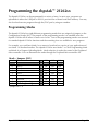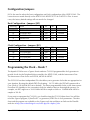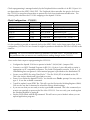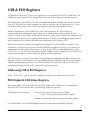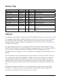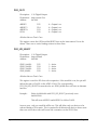
1
Danville Signal Processing, Inc.
dspstak™ 21262sx
User Manual
Version 1.00
Danville Signal Processing, Inc.
dspstak™ 21262sx User Manual
Copyright © 2004 Danville Signal Processing, Inc. All rights reserved. Printed in the USA.
Under the copyright laws, this manual may not be reproduced in any form without prior written
permission from Danville Signal Processing, Inc.
Danville Signal Processing, Inc. strives to deliver the best product to our customers. As part of this
goal, we are constantly trying to improve our products. Danville Signal Processing, Inc., therefore,
reserves the right to make changes to product specification or documentation without prior notice.
Updated operating manuals and product specification sheets are available at our website for
downloading.
This manual may contain errors, omissions or “typo’s”. Please send your comments, suggestions and
corrections to:
Danville Signal Processing, Inc.
38570 100th Avenue
Cannon Falls, MN 55009-5534
Trademark Notice
dspstak is a trademark of Danville Signal Processing, Inc. VisualDSP++, EZ-Kit and SHARC are
trademarks of Analog Devices, Inc. CyberClocks is a trademark of Cypress Semiconductor
Corporation. Windows is a trademark of Microsoft Corporation.
Contact Information
Danville Signal Processing, Inc.
38570 100th Avenue
Cannon Falls, MN 55009
E-mail:
Web Site:
[email protected]
http://www.danvillesignal.com
Voice:
Fax:
507-263-5854
877-230-5629
dspstak™ 21262sx User Manual
Page 2
Table of Contents
Overview ..........................................................................5
Introducing dspstak™.............................................................................5
dspstak™ 21262sx .................................................................................5
Introduction...........................................................................................6
Hardware Description......................................................7
Power Supply ........................................................................................7
RS-232 Interface ....................................................................................8
USB Interface.........................................................................................9
Interconnect Port ...................................................................................9
Programmable Clocks ............................................................................9
JTAG Emulation Port ............................................................................10
dspstak™ 21262sx Architecture .....................................10
Hardware – ADSP-21262 Core ............................................................10
DAI......................................................................................................10
Parallel Port .........................................................................................13
SPI Port................................................................................................14
Programming the dspstak™ 21262sx.............................15
Programming Modes............................................................................15
Configuration Jumpers .........................................................................16
Programming the Clock – Mode 7........................................................16
Uploading Programs – Mode 6.............................................................18
Peripheral Microcontroller API ......................................21
Command Summary ............................................................................21
System Commands ..............................................................................22
Com Port Commands ..........................................................................25
EE Memory Commands........................................................................26
dspstak™ 21262sx User Manual
Page 3
USB & PLD Registers ......................................................28
Addressing USB & PLD Registers ..........................................................28
PLD Output & USB Status Registers .....................................................28
Memory Map.......................................................................................29
USB Port..............................................................................................29
PLD Output Registers...........................................................................31
Software..........................................................................33
Schematic .......................................................................33
Mechanical Drawings.....................................................33
Product Warranty ...........................................................34
dspstak™ 21262sx User Manual
Page 4
Overview
DSP-based embedded applications often take the form of a digital signal processing engine coupled
with a specialized data conversion and signal conditioning front end. The front end electronics and
the DSP are almost always connected via high speed serial ports and the general purpose I/O ports
of the DSP. In most cases, once the local memory and peripheral interfacing needs of the DSP are
fulfilled, the DSP’s data and address busses are no longer needed.
Standardized bus architectures such as PC/104, PCI and cPCI are all based on communicating via
each board’s data and address bus, while ignoring the needs of the most DSP / data conversion
interfaces.
Introducing dspstak™
Danville’s dspstak modules are designed to simplify DSP-based embedded applications. Generally,
each dspstak consists of two modules: a DSP Engine, and a signal conditioning/data conversion I/O
Module. The Interconnect Port consists of SPORTs (high speed serial ports), SPI, general I/O, clocks
and power connections.
DSP Engine modules generally consist of a DSP processor, memory, power supplies and standard
digital I/O such as RS-232 and USB. We currently have products based on Analog Devices’ SHARC®
and ADSP-2191 processors.
The I/O Modules may include signal conditioning electronics, A/D and/or D/A data converters,
audio transceivers, unique connectors and a plethora of other special front end requirements. Since
the I/O Module is separate from the DSP Engine Module, custom interfaces can be created quickly
and inexpensively. Danville has a number of standard I/O Modules and often is willing to create a
new one based on customer request. You can also create your own.
dspstak™ 21262sx
This manual covers the dspstak 21262sx DSP Engine and is complemented by the dspstak Family
Users Manual. The family manual covers topics that all dspstaks have in common. You will want to
review the family manual for mechanical dimensions, system configurations, basic connector
specifications, etc.
The dspstak 21262sx manual covers topics that are relevant to the specific implementation of the
dspstak 21262sx DSP Engine. You will also need the Analog Devices’ ADSP-2126x SHARC DSP
Core and Peripheral manuals. These manuals can be downloaded from the Analog Devices web
site. Links to these manuals and other resources are found on our web site at
http://www.danvillesignal.com/index.php?id=dspdev_links
dspstak™ 21262sx User Manual
Page 5
Intended Audience
The dspstak 21262sx is intended for DSP systems integrators, designers and programmers who may
wish to integrate a dspstak into their products. This manual is primarily aimed at users who have a
working knowledge of microcomputer technology and DSP related design. We assume that you are
familiar with the Analog Devices ADSP-21262 SHARC DSP.
Introduction
The dspstak™ 21262sx is a high performance digital signal processing engine based on the Analog
Devices ADSP-21262 SHARC DSP. The ADSP-21262 supports 32 bit fixed point and 32/40 bit
floating point formats with SIMD instructions running at up to 200 MHz. This translates to a peak
computation rate of 1.2 GFLOPS. The ADSP-21262 also includes very flexible peripherals including
six independent serial ports (SPORTs) and a SPI port. The dspstak 21262sx Interconnect Port
supports the complete DAI interface, SPI, general I/O, clocks and power connections.
The dspstak 21262sx also includes USB and RS-232 ports for easy interfacing to the outside world.
It also has a JTAG interface to facilitate program development.
The dspstak 21262sx includes the following items:
Hardware:
•
dspstak 21262sx board
Documents & Programs (CD):
•
•
•
•
•
This Manual
dspstak Family User Manual
CAD footprints (Gerber & Protel 99SE formats)
Free Terminal Program – Tera Term Pro
USB Device Driver
Firmware (CD):
•
•
Flash Bootloader
Sample Programs
We recommend that you have the following tools and documents:
•
•
•
•
Analog Devices VisualDSP++™ for SHARC®
BeastRider Debugger for the 2126x or ADI JTAG ICE
Danville JTAG adapter kit
Analog Devices ADSP-2126x SHARC® DSP Core Manual
dspstak™ 21262sx User Manual
Page 6
•
•
•
Analog Devices ADSP-2126x SHARC® DSP Peripherals Manual
Analog Devices ADSP-21262S Product Data Sheet
Cypress Semiconductor CyberClocks™
Our website (www.danvillesignal.com) has downloads and links to other supplementary tools and
documents.
Hardware Description
The dspstak 21262sx includes all dspstak DSP Engine standard features. These features are
discussed in a general way in the dspstak Family Users Manual and are as follows:
•
•
•
•
•
•
Power Supply
RS-232 Interface
USB Interface
Interconnect Port
Programmable Clock
JTAG Header
Each of these areas is discussed in more detail in this manual.
If you are creating your own I/O Modules, you may want to restrict your design to rely only on the
standard features. This will insure that your I/O Modules are compatible with future dspstak DSP
Engines. On the other hand, if you want to take advantage of the increased capabilities of the
dspstak 21262sx, you may want to disregard some of the restrictions. In general, you can assume
that future dspstak DSP Engines based on the 3rd generation SHARC family will support the
Interconnect Port in a manner similar to the dspstak 21262sx.
Power Supply
The dspstak 21262sx uses a standard 2.1/5.5mm coaxial power jack to provide power to itself and
also any I/O modules via the Interconnect Port. From the dspstak 21262sx view, this supply may be
either an AC supply or a DC supply with the center of the coaxial power plug connected as the
positive pin. Adjacent to the coaxial jack, there are 3 pads spaced at 0.100 inch that may be used
as an alternative connection to provide a bipolar DC supply to the board. These pads are labeled
JH6 and can accommodate a .025 header or similar connector. This alternate connection method
is not standard in earlier dspstak DSP Engines but will be standard in future products.
The incoming voltage is half wave rectified to create new unregulated DC supplies called Va+ and
Va-. An additional internal supply is also created to provide the input to switching regulators that
are used for digital supplies. From these unregulated supplies, Va+5 (5.0 Volt Analog), Vd+5 (5
dspstak™ 21262sx User Manual
Page 7
Volt Digital) and Vd+3.3 (3.3V Digital) are created and made available to the I/O Modules via the
Interconnect Port. The DSP Core voltage, Vd+1.2 is also created via a switching power supply.
The dspstak 21262sx DSP Engine does not use Va+, Va+5 or Va-. These supplies are available to
I/O Modules. If the I/O Module does not need a negative supply, you can power the dspstak
21262sx with only a positive DC power supply. The recommended input voltages are 9 VAC or 9 to
15VDC. Since switching regulators are used for the digital supplies, the input voltage is not critical.
In all cases, the DC supply or an unregulated DC supply created from an incoming AC supply
should be less than 20VDC. This will protect both the DSP Engine and probably the components on
the I/O Module.
One final thing to remember: The nominal output voltage of a wall adapter is usually much lower
than its actual output voltage. We recommend that unregulated DC wall adapters should have an
maximum nominal voltage of 12VDC.
RS-232 Interface
The RS-232 interface is used to upload user application programs and to program the clock
generator in the command mode. An application program may also use the RS-232 interface for its
own purposes. The RS-232 port is provided by a dedicated microcontroller that also has other
functions on the dspstak 21262sx. These functions are all available via the SPI port of the DSP. The
API for these functions is described in the Software Section of this manual. There are also software
examples on calling these functions on the CD.
The RS-232 interface is configured as a DCE (Data Communications Equipment) device. It uses a
DB-9F connector that is designed to mate without crossover connections to the DB-9M connector
found on PC compatible computers. Connections are defined in the following table:
Signal
DCD
RD
TD
DTR
SIGNAL GND
DSR
RTS
CTS
RI
Direction
DCE -> DTE
DTE -> DCE
DTE -> DCE
DCE -> DTE
dspstak™ 21262sx User Manual
Pin
1
2
3
4
5
6
7
8
9
Notes
DCD, DTR & DSR are connected together
DCD, DTR & DSR are connected together
DCD, DTR & DSR are connected together
Not currently supported
Not currently supported
NC
Page 8
When the dspstak 21262sx is programmed using the RS-232 interface, only RD & TD are used.
DTR, DSR & DCD are simply connected together and ignored by the dspstak.
The dspstak 21262sx supports standard bauds of 9600, 19.2k, 38.4k, 57.6k, 115.2k and 230.4k.
The expected protocol is No parity, 8 data bits, 1 stop bit, (N:8:1).
USB Interface
The USB interface is another way that programs may be uploaded to the dspstak. Unlike most
Analog Devices EZ-Kit development boards, the USB interface is also available for user applications.
A device driver is included with the dspstak 21262sx to support Windows 2000 & Windows XP
applications. The USB connection is made via a standard USB type B connector.
Interconnect Port
The Interconnect Port is the only standard connection between the DSP Engine and I/O Modules.
This port is described in detail in the dspstak Family Users Manual and the DAI section of this
manual.
Programmable Clocks
The dspstak 21262sx has a very flexible clock configuration. A user reprogrammable clock generator
provides the DSP clock and three I/O clocks that are available on the Interconnect Port. The three
programmable clocks on the Interconnect Port allow I/O Modules to use convenient clocks for
whatever devices that might be present. For example, an ADC might use an 18.432 MHz MCLK to
sample at 96k or a 19.6608 MHz MCLK to sample at 102.4k. In addition to the on-board
programmable clock, the DSP clock can also be provided externally by a dspstak I/O Module.
The dspstak 21262sx uses a Cypress Semiconductor CY22393 flash programmable clock generator.
This device has three PLLs which when combined with the reference oscillator can create four
independent clock frequencies. Cypress has a program called CyberClocks on their web site
(www.cypress.com) that you can use to create a JEDEC file to reprogram the clock chip. There are
support functions that allow this file to be uploaded via the RS-232 port. Since reprogramming
certain clocks could make the RS-232 port inoperable, the dspstak DSP Engine filters these
parameters from the JEDEC file to automatically protect the DSP Engine from unfortunate
modifications. Details on programming the clock are in the Programming the dspstak 21262sx
section of this manual.
In many cases, the factory default settings are appropriate and no changes are ever necessary.
dspstak™ 21262sx User Manual
Page 9
JTAG Emulation Port
The dspstak 21262sx has a right angle JTAG connector (JH3) mounted on the lower edge of the pcb
assembly. This connector is assessable even when a dspstak I/O Module is positioned above the
dspstak 21262sx.
Danville JTAG connectors are smaller than the standard ADI recommended JTAG header.
The Danville JTAG connector is a male 16 pin, 2mm dual row header. Each pin directly
corresponds to the same pins on the Analog Devices header. The remaining pins (15&16) are
assigned to Vd+3.3. The extra power supply pins allow you to power a buffer in a system that has
many JTAG devices. A JTAG adapter kit is available from Danville to convert the 2mm header to the
0.100 header used by the Analog Devices and BeastRider emulators.
It is our experience that the ADSP-21262 JTAG port is sensitive to noise. You should place 2mm
jumpers across pins 5&6 (TMS), 7&8 (TCK) and 9&10 (TRST) when you are not using the port.
dspstak™ 21262sx Architecture
Hardware – ADSP-21262 Core
The heart of the dspstak 21262sx is an Analog Devices ADSP-21262 DSP. This manual does not
discuss the internal workings of this DSP, the assembly language and other details specific to this
DSP. You should refer to the fore mentioned ADI documents for this information. The ADSP-21262
has several important peripherals that we will expand on as they relate to the dspstak 21262sx.
They are as follows:
•
•
•
Digital Audio Interface (DAI)
Parallel Port
SPI Interface
DAI
The DAI is comprised of a group of peripherals including the SPORTs and a signal routing unit.
There are 20 pins on the DSP that connect the DAI to the outside world. All 20 DAI pins are
available on the Interconnect Port. Sixteen of these pins are connected to lines that are defined as
SPORT pins on the Interconnect Port. One pin is assigned as the IRQ input and the remaining three
pins are shared with the auxiliary I/O and SPI Slave Select lines. If you are mapping the DAI to use
standard dspstak I/O Modules, the definitions are restrictive to allow dspstak DSP Engines with less
sophisticated I/O to work with these I/O Modules as well. If you are designing your own dspstak I/O
dspstak™ 21262sx User Manual
Page 10
Module, then you may map the DAI any way you want on the Interconnect Port. We expect that
future dspstak DSP Engines will also have DAI mapped connections routed to the same connections
on the Interconnect Port.
Here are the DAI to Interconnect Port Mappings:
Row
A&C
B
Name
1
2
3
4
5
*
*
*
*
*
*
*
*
*
*
AGND
Va+
VaVa+5
AGND
Analog Ground
Unregulated Positive Analog Supply
Unregulated Negative Analog Supply
Regulated Analog +5.0 Volt Supply
Analog Ground
6
7
8
*
*
*
*
*
*
Vd+5
Vd+3.3
DGND
Digital 5.0 Volt Supply
Digital 3.3 Volt Supply
Digital Ground – Main Return
9
9
10
10
11
11
12
12
13
13
14
14
15
15
16
16
*
17
17
18
18
19
19
*
*
*
*
*
*
*
*
*
*
*
*
*
*
*
*
*
*
*
*
*
LED0
LED1
LED2
LED3
LED4
IO5 (#SPISS1)
IO6 (#SPISS2)
IO7 (#SPISS3)
#SPI_SS
SPICLK
SPISO
SPISI
IRQ
#RESET
SYSCLKIN
SYSCLKOUT
Vd+3.3
GND
DRA0
DTA0
GND
MCLK0
dspstak™ 21262sx User Manual
21262sx
PLD
PLD
PLD
PLD
PLD
DAI 2
DAI 3
DAI 1
PLD
Notes
3.3V Digital Output
3.3V Digital Output
3.3V Digital Output
3.3V Digital Output
3.3V Digital Output
(IO5 is alternate function with #SPISS1)
(IO6 is alternate function with #SPISS2)
(IO7 is alternate function with #SPISS3)
Primary SPI Slave Select
SPI Clock – DSP Engine is Master
SPI Serial Out (MISO)
SPI Serial In (MOSI)
DAI 4
PLD
External DSP Clock Input
Programmable clock
SPORT 0 – Full Duplex
DAI 5
DAI 6
Programmable Clock
Page 11
Row
A&C
20
20
21
21
22
22
23
23
24
24
*
25
25
26
26
27
27
28
28
29
29
30
30
31
31
32
32
B
*
*
*
*
*
*
*
*
*
*
*
*
*
*
*
*
*
*
*
*
*
*
*
*
*
Name
RFS0
TFS0
RCLK0
TCLK0
#RESET0
GND
DTB0
DRB0
GND
Vd+3.3
Vd+3.3
GND
DRA1
DTA1
GND
MCLK1
RFS1
TFS1
RCLK1
TCLK1
#RESET1
GND
DTB1
DRB1
GND
Vd+3.3
Notes
DAI 7
DAI 8
DAI 9
DAI 10
PLD
DAI 11
DAI 12
SPORT 1 – Full Duplex
DAI 13
DAI 14
Programmable Clock
DAI 15
DAI 16
DAI 17
DAI 18
PLD
DAI 19
DAI 20
* LEDs, IO5-7, SPI_SSs, DAI 1-3 Enable, & Resets are controlled by the PLD Registers
Refer to the dspstak Family Users Manual for general Interconnect Port information. The USB &
PLD Register section of this manual describes the software interface to those pins mapped by the
PLD.
dspstak™ 21262sx User Manual
Page 12
Parallel Port
The Parallel Port is connected to two major components, the USB Port and a PLD that is used to
create and manage much of the dspstak’s I/O ports. In addition, the Parallel Port is brought out to a
30 pin 2mm female dual row header (JH2).
You can use JH2 to expand to your own Parallel Port devices provided you consider a few simple
points. They are as follows:
•
•
•
The port can be configured for either 8 bit or 16 bit operation but AD15 must select a low
address (A23 or A15 = 0)
A low profile board will fit between the dspstak 21262sx and an I/O Module.
A special 2mm male header can be used to connect from a dspstak I/O Module to JH2 but
there is no guarantee that another dspstak DSP Engine will be compatible. Samtec is a
supplier for this type of connector.
JH2 Pinout
Pin
Name
Pin
Name
Pin
Name
1
2
3
4
5
6
7
8
9
10
GND
GND
Vd+3.3
Vd+3.3
AD7
AD6
AD5
AD4
AD3
AD2
11
12
13
14
15
16
17
18
19
20
AD1
AD0
#WR
#RD
#RESET
ALE
AD15
AD14
AD13
AD12
21
22
23
24
25
26
27
28
29
30
AD11
AD10
AD9
AD8
GND
CLKOUT
Vd+3.3
Vd+3.3
GND
GND
The two onboard components, the USB port and the PLD are both mapped into the upper address
space of the Parallel Port. These devices assume that the interface is configured as a 16 bit data bus.
The memory map and details on using these peripherals are covered in the USB & PLD Registers
section of this manual.
dspstak™ 21262sx User Manual
Page 13
SPI Port
The SPI is used as a general purpose control bus on the dspstak 21262sx. It is connected to two
onboard components, a serial flash memory and the Peripheral Microcontroller. It is also available
on the Interconnect Port to control data converters and provide general purpose I/O expansion.
Like all other dspstak DSP Engines, the DSP is always the master.
The flash memory is selected via Flag 0 of the ADSP-21262. This device is used to bootload your
application program into the internal memory of the DSP. Details on uploading programs to the
flash memory are in the Programming the dspstak 21262sx section of this manual. A special
bootloader program resides in the lowest block of the flash and is unavailable for user applications.
WARNING: Be very careful of writing to the flash memory and never ERASE or WRITE the
lowest block of the flash! The only way to recover from an inadvertent corruption of the
bootloader program is to rewrite this space with an in-circuit emulator.
The Peripheral Microcontroller is a preprogrammed part that provides the RS-232 port, a watchdog
timer, brown out protection and user EE memory. It communicates over the SPI port using Flag 2 as
its slave select. Refer to the Peripheral Microcontroller API section of this manual for more
information.
The SPI Port is also brought out to the Interconnect Port. Flag 3 is expanded via the PLD to provide
four SPI slave select lines. Generally, the #SPI_SS pin of the Interconnect Port is used to control a
data converter on a dspstak I/O module. The additional 3 slave selects are shared with IO5, IO6
and IO7 and are usually used for expanding the SPI interface for additional I/O. For example, you
could use this interface to create a front panel on an instrument where switches or encoders were
scanned and status indicators were controlled. You could control a small LCD display via this
interface. Refer to the USB & PLD Register section of this manual for details.
Danville uses a 2x5 0.100 box header as a standard connector for SPI off-board expansion. It is
described in the dspstak Family Users Manual. We suggest you add a small (33 ohm) series resistor
at the driving end of the SPI SO line for any remote interfaces. Keep in mind that the SPI interface is
not intended for long unbuffered runs. You may need to add buffers or run the SPI interface at slow
Clock speeds for reliable operations.
dspstak™ 21262sx User Manual
Page 14
Programming the dspstak™ 21262sx
The dspstak 21262sx can be programmed in a variety of ways. In most cases, programs are
uploaded via either the USB port or RS-232 port into the on-board serial flash memory. You may
also load and execute programs through the JTAG port by using an emulator.
Programming Modes
The dspstak 21262sx has eight different programming modes that are assigned via jumper on the
Configuration Header (JH5). The purpose of the programming modes is to establish what the
dspstak 21262sx will do when it comes out of reset. Four of the programming modes are reserved
for standard dspstak 21262sx functions and the remaining four are available for user programs.
For example, you could use Mode 0 as a means to bootload one version of your application and
use Mode 1 to bootload another. The dspstak 21262sx uses Mode 7 as Clock Programming Mode
and Mode 6 as Program Uploading Mode. Mode selection is under the control of the Peripheral
Microcontroller. You can determine the mode through the Peripheral Microcontroller API.
Mode – Jumpers (JH5)
Mode
Name
0
User 0
1
User 1
2
User 2
3
User 3
4
Reserved
5
Reserved
6
Program Uploading
7
Clock Programming
* Jumper On = 0
dspstak™ 21262sx User Manual
M2
M1
M0
On
On
On
On
Off
Off
Off
Off
On
On
Off
Off
On
On
Off
Off
On
Off
On
Off
On
Off
On
Off
Page 15
Configuration Jumpers
JH5 is also used to select the boot configuration and clock configuration of the ADSP-21262. The
connections are made directly to the ADSP-21262 BOOTCFG1-0 & CLKCFG1-0 Pins. In most
cases, the factory default settings will not need to be changed.
Boot Configuration – Jumpers (JH5)
Boot Cfg
Name
00
SPI Slave Boot
01
SPI Master Boot
10
Parallel Port Boot
11
Internal Boot
* Jumper On = 0
B1
B0
On
On
Off
Off
On
Off
On
Off
CF1
CF0
On
On
Off
Off
On
Off
On
Off
Default
Clock Configuration – Jumpers (JH5)
Mode
Name
00
3:1 Core/ClkIn
01
16:1 Core/ClkIn
10
8:1 Core/ClkIn
11
Undefined
* Jumper On = 0
Default
Programming the Clock – Mode 7
The dspstak 21262sx uses a Cypress Semiconductor CY22393 programmable clock generator to
provide clocks for the Peripheral Microcontroller, the ADSP-21262, and the Interconnect Port.
The Interconnect Port clocks are SYSCLK, MCLK0 & MCLK1.
The CY22393 has three independent PLLs that allow you to generate clocks that are appropriate for
your situation. By using the default DSP Clock setting - 24.576 MHz, the DSP will operate with a
Core Clock of 196.6 MHz (JH5 set to default). The three programmable clocks on the Interconnect
Port allow I/O Modules to use convenient clocks for whatever devices that might be present. For
example, an ADC might use a 18.432 MHz MCLK to sample at 96k or a 19.6608 MHz MCLK to
sample at 102.4k.
If you want to reprogram the CY22393, you should review the CY22393 data sheet. You will also
need the Cypress program, CyberClocks™ to generate a JEDEC file of clock parameters. The data
sheet and the program are available on the Cypress web site and there are links on the Danville
web site at http://www.danvillesignal.com/index.php?id=dspdev_links.
dspstak™ 21262sx User Manual
Page 16
Clock reprogramming is managed entirely by the Peripheral Microcontroller via its RS-232 port. It is
not dependent on the ADSP-21262 DSP. The Peripheral Microcontroller also gets its clock from
the CY22393 so steps have been taken to protect this clock from inadvertent modification. The
following table describes the CY22393 mapping to the dspstak 21262sx.
Clock Configuration – CY22393
Clock
CY22393
Default
Notes
Peripheral Microcontroller
DSP Clock
SYSCLK
MCLK0
MCLK1
JH1-5
XBUF
CLKB
CLKC
CLKD
CLKA
CLKE
18.432 MHz
24.576 MHz
24.576 MHz
12.288 MHz
12.288 MHz
Off
Xtal, Always On
JH1 Pins 2&3 shorted
Interconnect Port
Interconnect Port – SPORT 0
Interconnect Port – SPORT 1
Not used
It is also possible to provide an external clock to the ADSP-21262 via the Interconnect Port. In this
configuration, JH1 Pins 1&2 are shorted. It might be prudent to disable the DSP Clock (CLKB) in this
situation.
Warning: The CY22393 internal memory is limited to 100 write cycles. You should decide
the parameters that you want to set carefully before making changes to the CY22393.
Here are the basic steps to reprogramming the CY22393:
•
•
•
•
•
•
•
Configure the dspstak 21262sx to operate in Mode 7 (M2,M1,M0 – Jumpers Off).
Connect to an ASCII Terminal Program via RS-232. A 9 pin to 9 pin cable with no twists is
appropriate on PC compatible computers. The Serial Configuration must be 19.2K, 8, 1, N.
Handshaking lines are ignored. A free terminal program is provided on the distribution CD.
Create a new JEDEC file using CyberClocks™. The file 21262.JED is included on the CD.
This is the factory default and a good place to start.
Power Up or Reset the dspstak 21262sx. You should see a Clock> prompt. You may wish to
type ? to see the available commands.
Type U to upload a new JEDEC file. This will copy the file into the Working Registers (RAM).
You can also use the L command to reload the factory default settings.
If you are sure that you are ready to write, type the W command. This is the command you
want to use sparingly to preserve the life of the CY22393. You can verify your results against
the Working Registers by typing V.
Exit the Clock Mode with the Q command. This will vector you to Mode 6 where you can
upload application programs.
dspstak™ 21262sx User Manual
Page 17
Uploading Programs – Mode 6
The dspstak 21262sx uses a 2Mbit SPI serial flash memory device to bootload the ADSP-21262.
Assuming that the boot mode selection is set for SPI Master Boot (see Configuration Jumpers), the
ADSP-21262 will boot from the SPI flash memory after reset is deasserted.
This boot capability is very useful in the ADSP-21262 except that there is no native support in the
DSP to program the flash memory. The dspstak 21262sx (actually all dspstak DSP Engines) has a
resident boot loader and flash writer program that addresses this problem.
The dspstak 21262sx automatically boots a proprietary Danville program called boot262 that is
located in the lowest block of the flash memory. The boot262 program in turn, boots your program
uses the rest of the flash memory. You don’t have to worry about reserving memory for boot262. In
the process of loading your program, the boot262 program that resides in internal RAM is
overwritten.
If the dspstak 21262sx is connected to an ASCII terminal via either RS-232 or USB and it is
operating in Mode 6, you have a five second window to interrupt the boot process before the
application program is automatically loaded. When you interrupt the boot process, the dspstak
enters Command Mode. Command Mode lets you upload programs to the flash memory. If the
dspstak 21262sx is operating in Modes 0 through Mode 3, your program will boot immediately as if
the boot262 program didn’t exist. It is still there and it loads your program, but it does so silently.
You write your DSP applications as normal and create a *.ldr file (Boot Type = SPI Slave, Format =
Binary, Width = 8). You don’t really need to worry about where your program is stored in the flash
memory, but we are going to tell you anyway. Your program starts at the beginning of the second
block of the flash with an offset of 80H. The 80H space is used to store the name of your program,
checksums, etc. When you upload a new program, all the memory in the flash is block erased with
the exception of the first block where the boot262 program resides. It is possible to write the flash
memory in the space above your application and the boot262 program after the application
program has been uploaded, but you must be very careful that the boot262 program is never
overwritten or erased. The only way to rewrite boot262 is with an in-circuit emulator.
It is very hard to damage the contents of the flash by accident, but it is possible. If you never write
directly to the flash, you are unlikely to ever see a problem. Danville supplies sample code that
manages the SPI bus where the flash memory resides. This code makes it even more difficult to
write to the flash inadvertently.
Command mode is available via either the USB port or the RS-232 port. A USB device driver is
included that emulates a COM port for Windows 2000 or Windows XP operating systems.
Bootloader communications automatically switch between the RS-232 port and the USB port. If
the USB port is active (enumerated), the USB port is used; otherwise, the RS232 port will be active.
dspstak™ 21262sx User Manual
Page 18
Here are the basic steps to uploading programs:
•
Configure the dspstak 21262sx to operate in Mode 6.
•
Connect to an ASCII Terminal Program via RS-232 or USB. USB is faster.
o If RS-232 is used, a 9 pin to 9 pin cable with no twists is appropriate on PC
compatible computers. The default serial configuration is 19.2K, N, 8, 1.
Handshaking lines are ignored. There is a command to change the baud rate to
higher speeds. If you don’t know the current baud rate, you can reset the baud via
Mode 7 to 19.2K.
o If USB is used, the baud settings are ignored and the interface will operate like a very
fast COM port.
•
Power Up or Reset the dspstak 21262sx. You should see a DSP> prompt followed by
moving # symbols. After about 5 seconds, the application program will boot unless you press
a key to interrupt the boot process. This will bring a new DSP> prompt signifying
Command Mode.
•
Type ? to view a list of available commands.
•
Type U to upload a new program file. Your program must be a *.ldr (ADI loader file) with
the following parameters:
o Boot Type = SPI Slave
o Format = Binary
o Width = 8
You may also use the UA command to upload a similar file in ASCII format. This will take
longer.
After you confirm the upload, the bootloader will erase all user flash memory space. At the
"Ready:" prompt use your ASCII terminal program to send the .ldr file. Make sure you
enable the "binary transfer" option.
In Tera Term Pro, choose "Send File..." from the "File" menu. Click the "Binary" checkbox,
and then open your .ldr file.
As the file transfers, you will see one progress mark for every 32 bytes transferred. Data
transfer must be continuous. If the host stops sending data for more than approximately
500ms, the bootloader will assume that the code upload is complete and terminate the
transfer.
dspstak™ 21262sx User Manual
Page 19
•
After the program is uploaded, a checksum is calculated and you have the opportunity to
enter a description of the program. The program description is an ASCII string that you can
use to identify your program. It does not impact the function of the DSP module in any
way, but can be a helpful way to track program revisions. A typical program description
might be "Filter version 1.00.” The size of the program is also calculated.
•
Type Q to quit Command Mode and the application program will boot.
There are a number of additional commands that are available in Command Mode. For example,
you can read, write and erase EE memory form the DSP> prompt. This memory is also available to
the DSP via the Peripheral Microcontroller API.
There is no option to read back the application program via the Command Mode. This is to help
you keep your code a little more proprietary. We suggest that you use the checksum information as
a check during production programming to insure that your program was loaded correctly.
dspstak™ 21262sx User Manual
Page 20
Peripheral Microcontroller API
The Peripheral Microcontroller communicates via the SPI bus using a 3 byte packet structure. Flag 1
serves as the SPI slave select line. The SPI bus is bi-directional. Commands are always initiated by
the DSP. The Peripheral Microcontroller only responds.
Most packets will have this form:
Cycle
DSP -> PM
PM-> DSP
Byte 1
Byte 2
Byte 3
Command
Data
0x00
Status
Echo Command
Response
Command Summary
Name
PM_Cmd_NOP
PM_Cmd_COM_WR
PM_Cmd_COM_RD
PM_Cmd_VERSION
PM_Cmd_COM_BAUD
PM_Cmd_EE_ADDR
PM_Cmd_EE_WR
PM_Cmd_WD
PM_Cmd_COM_RESET
PM_Cmd_EE_WREN
PM_Cmd_RESET
PM_Cmd_MODE
-- Reserved
PM_Cmd_EE_RD
-- Reserved
PM_Cmd_RESYNC
-- Reserved
Description
0x00
0x01
0x02
0x03
0x04
0x05
0x06
0x07
0x08
0x09
0x0A
0x0B
0x0C
0x0D
0x0E
0x0F
>0x0F
dspstak™ 21262sx User Manual
No Operation
Transmit a byte from the RS-232 port
Receive a byte from the RS-232 port
Firmware version of the Peripheral Microcontroller
Set the UART baud rate
Set the address of the EE Memory
Write a byte to EE Memory
Watchdog Timeout
Reset the UART
Enable Writes to EE Memory
Reset the dspstak
Get the dspstak mode setting
Read a byte from EE Memory
Used to resync the Peripheral Microcontroller
Page 21
System Commands
Status
Description: Peripheral Microcontroller Status
Command: Any
Status is automatically updated each time a packet is transmitted by the DSP. It is
reported in Byte 1 in the next packet. This means that the status reported in the very
first packet may not be valid.
Status is only valid up to the point of the completion of the previous command. So, if
the last command was 2 weeks ago, the status bits will be two weeks old. Unless you
are doing commands regularly, it's best to always do a PM_Cmd_NOP before you
read the status bits.
Status Bits:
Bit 0:
Bit 1:
Bit 2:
Bit 3:
Bit 4:
Bit 5:
Bit 6:
Bit 7:
UART RX Data Available
UART TX Space Available
-- Reserved
-- Reserved
UART Overrun (Reset using PM_Cmd_COM_RESET)
-- Reserved
EE Busy (Write in progress, will ignore any write attempts)
WDT Reset (The last reset was due to a watchdog timer timeout)
1 = TRUE, 0 = FALSE
PM_Cmd_NOP
Description:
Command:
Data:
Response:
No Operation
0x00
Don’t Care
0x00
The NOP command is a good way to get the status of the Peripheral Microcontroller
without any other action.
dspstak™ 21262sx User Manual
Page 22
PM_Cmd_VERSION
Description:
Command:
Data:
Response:
Returns the firmware version of the Peripheral Microcontroller
0x03
Don’t Care
0x00
The current version is 0x00, but future versions will increment this number. This
allows you to determine what functions this particular Peripheral Microcontroller
implements in the event that there are changes in a later version.
PM_Cmd_WD
Description:
Command:
Data:
Response:
Set Watchdog Timeout Period
0x07
See Below
Don’t Care
If the watchdog timer is active, the application must ping the WD input of the
Peripheral Microcontroller with a state change before the watchdog timer expires or
the system will reboot. The watchdog timer is initially disabled.
Data:
0xA6
0x00
0x01
0x02
0x03
0x04
0x05
0x06
0x07
Disable Watchdog
18 ms
36 ms
72 ms
144 ms
288 ms
576 ms
1.152 s
2.304 s
With the exception of 0xA6, all data is masked to use only the lowest 3
bits, i.e. 0xF1 = 0x01.
The watchdog timer uses an independent RC oscillator with a nominal period of 18
ms. This period can vary from 7 ms to 33 ms, so you may want to assume a worst
case situation of 7ms, to keep the watchdog timer from overflowing inadvertently.
dspstak™ 21262sx User Manual
Page 23
PM_Cmd_RESET
Description:
Command:
Data:
Response:
Reset the dspstak 21262sx
0x0A
0xC4
Don’t Care
This is a software reset that acts just like a hardware reset.
PM_Cmd_MODE
Description:
Command:
Data:
Response:
Return Mode Jumper Settings
0x0B
Don’t Care
See Below
Returns the mode setting selected by M2, M1, M0 in the lowest three bits of the
response. Modes 0 through 3 are User Modes. You may want to use this information
to cause your program to execute different applications depending on the Mode
settings. For example, your product might be an encoder in Mode 0 and a decoder in
Mode 1. You would only need to upload one program for both applications.
The upper 5 bits are 10100. These bits are used as an integrity check to make sure
that the Peripheral Microcontroller is actually present.
Mode 0:
Mode 1:
Mode 2:
Mode 3:
Mode 4:
Mode 5:
Mode 6:
Mode 7:
dspstak™ 21262sx User Manual
0xA0
0xA1
0xA2
0xA3
0xA4
0xA5
0xA6
0xA7
(User Mode 0)
(User Mode 1)
(User Mode 2)
(User Mode 3)
(--Reserved, Do not use)
(--Reserved, Do not use)
(Upload Programming Mode)
(Clock Programming Mode)
Page 24
PM_Cmd_RESYNC
Description:
Command:
Data:
Byte 3 (DSP):
Response:
Resync the Peripheral Microcontroller
0x0F
0x0F
0x0F
0x00
This command is used in the event that packet order is somehow misaligned. After
this command is executed, the Peripheral Controller will expect the next byte to be
Byte 1.
Com Port Commands
PM_Cmd_COM_WR
Description:
Command:
Data:
Response:
Write to the Com Port.
0x01
Byte to transmit
0x00
This command puts a byte on the transmit FIFO. The length of the FIFO is 32 bytes
The Peripheral Controller automatically sends out by bytes at the selected baud rate.
You should check the UART TX Space Available Status bit in the next packet. If the
last byte was unsuccessfully added to the FIFO (the Transmit FIFO was full), the
application can resend this byte.
PM_Cmd_COM_RD
Description:
Command:
Data:
Response:
Read from the Com Port.
0x02
Don’t Care
Next available byte from the Receive FIFO.
This command gets a byte from the receive FIFO. The length of the FIFO is 32 bytes.
You should check the UART RX Data Available Status bit before sending this
command. If there is no pending data (the Receive FIFO was empty), the command
is treated as a NOP, and therefore the Response will be 0x00.
dspstak™ 21262sx User Manual
Page 25
PM_Cmd_COM_BAUD
Description:
Command:
Data:
Response:
Sets the Baud rate
0x04
See Below
0x00
Baud = (1.152 * 10^6 ) / (DATA + 1)
Typical Values:
230.4K
115.2K
38.4K
19.2K
9600
0x04
0x09
0x1F
0x3D
0x79
PM_Cmd_COM_RESET
Description:
Command:
Data:
Response:
Resets the Com Port
0x08
Don’t Care
0x00
This command resets the UART, flushes the Transmit and Receive FIFOs and clears
the UART Overrun Status bit.
EE Memory Commands
PM_Cmd_EE_ADDR
Description:
Command:
Data:
Response:
Sets the EE Address Pointer
0x05
EE Address
0x00
The EE Address pointer is auto incremented after every valid EE_WR or EE_RD
operation. The valid address range is 0x00 to 0x7F (128 bytes). The EE Data at
Address 0x7F is reserved by the bootloader to hold the default baud rate, so don’t
overwrite this location.
dspstak™ 21262sx User Manual
Page 26
PM_Cmd_EE_WREN
Description:
Command:
Data:
Response:
Enables Writes to the EE Memory
0x09
0x42 (Enable), All other values (Disable)
0x00
This command allows the EE memory to be written. You should disable writes after
you are done writing the EE Memory. EE_WREN is always disabled after a system
reset.
PM_Cmd_EE_WR
Description:
Command:
Data:
Response:
Write EE at current EE Address
0x06
EE Data
0x00
This command is only valid if the EE_WREN has been enabled. EE Data is written to
the current address pointed to by the EE Address Pointer. This address is set by the
EE_ADDR command and auto incremented after every EE_WR or EE_RD.
The EE Data at Address 0x7F is reserved by the bootloader to hold the default baud
rate, so don’t overwrite this location.
You cannot write the EE Memory faster than 1 byte every 10 ms. The EE Busy Status
Bit will be 1 while a write is in progress. You can use this bit to time EE writes.
PM_Cmd_EE_RD
Description:
Command:
Data:
Response:
Read EE at current EE Address
0x0D
Don’t Care
EE Data
EE Data is read from the current address pointed to by the EE Address Pointer. This
address is set by the EE_ADDR command and auto incremented after every EE_WR
or EE_RD.
dspstak™ 21262sx User Manual
Page 27
USB & PLD Registers
The dspstak 21262sx uses a PLD for I/O expansion. It is connected to the DSP’s Parallel Port. The
USB port is also connected to the Parallel Port. It uses the PLD for part of its internal interface.
The Parallel Port on the ADSP-21262 has 16 multiplexed address and data lines and three control
lines, ALE, RD & WR. It can be configured as either an 8 bit bus with 24 address lines or a 16 bit
bus with 16 address lines. ALE is used as an address latch enable to demultiplex the bus.
Another characteristic of the Parallel Port is that it always wants to do 32 bit transfers. It
automatically packs and unpacks data so that from an external device point of view, an 8 bit
transfer is always 4 cycles and a 16 bit transfer is always 2 cycles. If the Parallel Port is mapped to an
external memory device such as a parallel flash memory or SRAM, this packing/unpacking feature is
quite convenient, but it creates difficulties when the target is an I/O port or FIFO.
Both the PLD and the USB port are mapped to the upper half of the Parallel Port memory. This
means that you are free to use JH2 for external Parallel Port expansion as long as your devices are
mapped into the lower half of the memory. In other words, AD15 must be demultiplex as either
A15 or A23 = 0. The PLD and USB require that the Parallel Port be configured as a 16 bit data bus,
however external devices can use either the 8 bit or 16 bit configuration.
The PLD is used to create five 4 bit wide write-only registers, demultiplex the upper AD lines, and
map the USB port to the Parallel Port. It also qualifies the RD & WR lines with A0, to deal with the
“helpful” packing/unpacking feature. The RD and WR lines are only active when A0 is low. This
means that the upper 16 bits of the 32 bit word are always ignored.
Addressing USB & PLD Registers
AD15 – AD12 (A15 – A12) are used for address decoding. Lower address bits are ignored.
PLD Output & USB Status Registers
The output registers are 4 bits wide. The D15-D12 nibble of the Parallel Port’s Transmit Buffer
Register (TXPP) is used for the data. The remaining 28 bits are ignored.
TXPP Register Format (Binary):
xxxx xxxx xxxx xxxx abcd xxxx xxxx xxxx where
x is Don’t Care and abcd represents the register.
Example: 0x0000A000 will write 0xA to the output register.
In a similar fashion, the USB Status Register should be extracted from the RXPP Register.
dspstak™ 21262sx User Manual
Page 28
Memory Map
Name
Addr
Dir
Bits Used
Description
USB_DATA
USB_STATUS
PLD_DAI_SPI_SELECT
PLD_OUT0
PLD_OUT1
PLD_SPI_SELECT
PLD_WD
0x8000
0x9000
0xA000
0xB000
0xC000
0xD000
0xE000
R/W
R
W
W
W
W
W
D7-D0
D15-D12
D15-D12
D15-D12
D15-D12
D15-D12
None
USB Data Bus
USB Status
Selects between IO & SPISSs
LED3 – LED0
LED4 & #RESETs
SPI Mask
Watchdog Strobe
User Space (JH2)
<0x8000
User Space (JH2)
0xF000
This space is available to external
devices
This space is available to external
devices
USB Port
The USB port on the dspstak 21262sx uses an FTDI FT245BM USB transceiver. This device is a USB
2.0 compliant, full speed part (12Mb/s). This part is very easy to use since in most cases it just looks
like a COM Port to the USB Master. FTDI has royalty free device drivers on their web site that
support a variety of operating systems. We suggest that you visit their web site (www.ftdichip.com)
for additional information.
We supply Windows® drivers on our distribution CD. The driver files includes dspstak *.inf files
that are used for installation in Microsoft Windows® operating systems. If you are using another OS,
you may want to compare the ftdibus.inf and ftdiport.inf files to the dspstakbus.inf and
dspstakport.inf files to configure your driver. Instructions on installing the Windows® drivers are on
the CD.
The FT245BM has receive and transmit FIFOs that are read from or written to the DSP. There are
three USB status bits: RXF, TXE and PWREN. PWREN is low when the USB port is enumerated
(recognized by the USB Master). If RXF is low, you can receive one byte; if TXE is low, you can
transmit one byte. There is no guarantee that the USB port can accept or deliver more than one
byte based on the flags, therefore you must check the status before sending or receiving the next
byte.
Reading and writing the Parallel Port is more complicated than a simple I/O or Memory R/W
instruction. You will want to review the Analog Devices documentation and the sample code
provided on our Distribution CD to see how it’s done in detail.
dspstak™ 21262sx User Manual
Page 29
USB Status Bits
Address:
0x9000
PWREN:
TXE:
RXF:
D14
D13
D12
0 – USB Port is enumerated
0 – Transmit FIFO can accept a byte
0 – Receive Buffer has a byte ready
All other bits are Don’t Care.
Reading the USB Port
•
•
Read the USB Status Register. If RXF is low (and assuming PWREN is low), you may read
the USB Data.
Read the USB Data Register.
This seems pretty straightforward until you learn the “gotcha.” The Parallel Port has a two
word receive buffer that has to fill before the data can be read internally. This means that
there will be three read cycles before you actually get the data. The USB may or may not
have valid data available if it is clocked successive times since the RXE flag only guarantees
one valid byte is available.
So here’s the trick!
We address the Parallel Port to read from Address 0x8FFE. You may recall that only the
upper nibble is decoded by the PLD. The address then auto increments to 0x9000 which
points to the USB Status Register and does not strobe the USB Read Line. You can read the
USB Status Register successively with no side effects. This is a convenient way to check the
status for the next byte in the USB queue.
This trick may be useful for interfacing high speed ADCs as well since many of the same
issues may apply. Of course, if the FIFO status flags are deeper, then this won’t be a
problem.
Writing the USB Port
•
•
Read the USB Status Register (0x9000). If TXE is low (and assuming PWREN is low), you
may write the USB Data.
Write the USB Data Register (Address 0x8000).
There are no extra buffers in the transmit path, so the Receive “trick” is not needed.
dspstak™ 21262sx User Manual
Page 30
PLD Output Registers
PLD_DAI_SPI_SELECT
Description: Selects I/O or SPI SS mapping
Destination: Interconnect Port
Address:
0xA000
IO7/#SPISS3:
IO6/#SPISS2:
IO5/#SPISS1:
D15
D14
D13
0 – IO7
0 – IO6
0 – IO5
1 – #SPISS3
1 – #SPISS2
1 – #SPISS1
All other bits are Don’t Care.
This register determines whether the IO Pins on the Interconnect Port are bidirectional GP I/O Pins or SPI slave select lines. If the pin is configured as GP I/O, the
DAI connects to the pin as follows:
IO7 = DAI_P1
IO6 = DAI_P3
IO5 = DAI_P2
PLD_OUT0
Description: 3.3V Digital Output
Destination: Interconnect Port
Address:
0xB000
LED3:
LED2:
LED1:
LED0:
D15
D14
D13
D12
0 – Output Low
0 – Output Low
0 – Output Low
0 – Output Low
All other bits are Don’t Care.
This register causes the LED3-LED0 lines on the Interconnect Port to be driven.
Although these pins refer to LEDs, they can be used to drive other devices. There are
no series limiting resistors in these lines.
dspstak™ 21262sx User Manual
Page 31
PLD_OUT1
Description: 3.3V Digital Output
Destination: Interconnect Port
Address:
0xC000
#RESET:
#RESET1
#RESET0:
LED4:
D15
D14
D13
D12
0 – Output Low
0 – Output Low
0 – Output Low
0 – Output Low
All other bits are Don’t Care.
This register causes the LED4 and the RESET lines on the Interconnect Port to be
driven. There are no series limiting resistors in these lines.
PLD_SPI_SELECT
Description: 3.3V Digital Output
Destination: Internal Mask
Address:
0xD000
SPISS3_MASK:
SPISS2_MASK:
SPISS1_MASK:
SPISS_MASK:
D15
D14
D13
D12
1 – Active
1 – Active
1 – Active
1 – Active
All other bits are Don’t Care.
This register is used for SPI slave select expansion. If the mask bit is set, the pin will
follow the state of FLAG3 on the ADSP-21262. The corresponding
PLD_DAI_SPI_SELECT bit must also be set. SPISS_MASK does not have an alternate
function.
Example:
Write 0x0000A000 with PLD_SPI_SELECT previously set to
0x0000F000.
This will cause #SPISS3 and #SPISS1 to follow FLAG3.
In most cases, only one mask bit will be set. This will allow only one device to be
selected during a SPI transfer. This is required for bi-directional devices where more
than one active slave select will cause bus contention on the SPI SO line.
dspstak™ 21262sx User Manual
Page 32
PLD_WD
Description: 3.3V Digital Output
Destination: Peripheral Microcontroller
Address:
0xE000
All data bits are Don’t Care.
A write to this register causes the Watchdog input on the Peripheral Microcontroller
to toggle. If the Watchdog Timer is enabled, you must write to this register before the
Watchdog Timer can overflow or the system will reset.
Software
The Distribution CD includes software examples that demonstrate many of the features of the
dspstak 21262sx. You may use these examples as take off points to start your own applications.
Our software library is constantly expanding. This code and other resources are available to our
customers through our web site. Send an email to [email protected] to gain access to the
customer section of our web site.
Schematic
The Distribution CD includes a schematic diagram of the dspstak 21262sx in files sa21262.pdf and
sb21262.pdf.
Mechanical Drawings
Mechanical Drawings are included in the dspstak Family Users Manual. If you any need additional
information on board mounting, clearances, etc, send an email to [email protected] .
If you are designing your own I/O Module or want to mount the dspstak 21262sx in an unusual
configuration, you may want to check with us for suggestions, design review, etc. We also have PCB
templates available to help you get started on an I/O Module layout. This will help insure that the
connectors and holes on your board actually line up.
dspstak™ 21262sx User Manual
Page 33
Product Warranty
Danville Signal Processing, Inc. products carry the following warranty:
Danville Signal Processing products are warranted against defects in materials and workmanship. If
Danville Signal Processing receives notice of such defects during the warranty period, Danville
Signal Processing shall, at its option, either repair or replace hardware products, which prove to be
defective.
Danville Signal Processing software and firmware products, which are designated by Danville Signal
Processing for use with our hardware products, are warranted not to fail to execute their
programming instructions due to defects in materials and workmanship. If Danville Signal Processing
receives notice of such defects during the warranty period, Danville Signal Processing shall, at its
option, either repair or replace software media or firmware, which do not execute their
programming instructions due to such defects. Danville Signal Processing does not warrant that
operation of the software, firmware, or hardware shall be uninterrupted or error free.
The warranty period for each product is one year from date of installation.
Limitation of Warranty:
The forgoing warranty shall not apply to defects resulting from:
•
•
•
•
•
Improper or inadequate maintenance by the Buyer;
Buyer-supplied software or interfacing;
Unauthorized modification or misuse;
Operation outside the environmental specification of the product;
Improper site preparation and maintenance.
Exclusive Remedies:
The remedies provided herein are the Buyer’s sole and exclusive remedies. In no event shall
Danville Signal Processing, Inc. be liable for direct, indirect, special, incidental or consequential
damages (including loss of profits) whether based on contract, tort, or any other legal theory.
dspstak™ 21262sx User Manual
Page 34