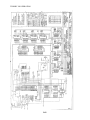
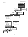
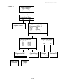
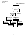
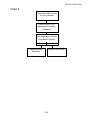
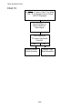
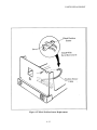
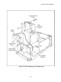
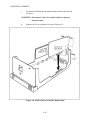
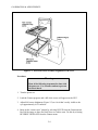
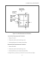
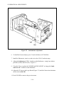
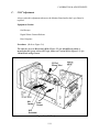
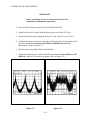
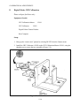
1
Repair Manual
Digital Palettes
Color Film Recorders (CI3000 / CI5000)
October 1990
Americas Business Center
Technical Services
201 Burlington Road
Bedford MA 01730
TEL: 1.781.386.5309
FAX: 1.781.386.5988
This page intentionally blank
POLAROID DIGITAL PALETTE SERVICE MANUAL
CONTENTS
SECTION 1
GENERAL DESCRIPTION
SECTION 2
THEORY OF OPERATION
SECTION 3
TROUBLESHOOTING
SECTION 4
PARTS REPLACEMENT
SECTION 5
CALIBRATION & ADJUSTMENTS
This page intentionally blank
GENERAL DESCRIPTION
1. General Description
Table of Contents
A.
B.
Product Description . . . . . . . . . . . . . . . . . . . . . . . . . . . . . . . . . . . . .
1-3
1.
2.
3,
4.
5.
6.
1-3
1-4
1-4
1-5
1-5
1-5
Model CI-3000 and Model CI-5000 . . . . . . . . . . . . . . . . . . . .
Resolution . . . . . . . . . . . . . . . . . . . . . . . . . . . . . . . . . . . . . . . .
Film Formats . . . . . . . . . . . . . . . . . . . . . . . . . . . . . . . . . . . . .
Film Types . . . . . . . . . . . . . . . . . . . . . . . . . . . . . . . . . . . . . . .
The System . . . . . . . . . . . . . . . . . . . . . . . . . . . . . . . . . . . . . . .
Other Accessories . . . . . . . . . . . . . . . . . . . . . . . . . . . . . . . . . .
Major Components . . . . . . . . . . . . . . . . . . . . . . . . . . . . . . . . . . . . .
1-6
1.
2.
3.
4.
5.
6.
1-7
1-7
1-7
1-7
1-7
1-7
Monitor Board . . . . . . . . . . . . . . . . . . . . . . . . . . . . . . . . . . . .
Logic Board . . . . . . . . . . . . . . . . . . . . . . . . . . . . . . . . . . . . . .
SCSI Board . . . . . . . . . . . . . . . . . . . . . . . . . . . . . . . . . . . . . . .
Power Supply Board . . . . . . . . . . . . . . . . . . . . . . . . . . . . . . . .
CRT . . . . . . . . . . . . . . . . . . . . . . . . . . . . . . . . . . . . . . . . . . . . .
Stepper Motor . . . . . . . . . . . . . . . . . . . . . . . . . . . . . . . . . . . . .
C.
Controls and Indicators . . . . . . . . . . . . . . . . . . . . . . . . . . . . . . . . . .
1-8
D.
Dimensions and Specifications . . . . . . . . . . . . . . . . . . . . . . . . . . . . .
1-9
1.
2.
3.
4.
5.
6.
7.
E.
Dimensions and Weight . . . . . . . . . . . . . . . . . . . . . . . . . . . . .
Addressable Resolution . . . . . . . . . . . . . . . . . . . . . . . . . . . . .
Addressable Color Space . . . . . . . . . . . . . . . . . . . . . . . . . . . .
Addressable Grey Scale . . . . . . . . . . . . . . . . . . . . . . . . . . . . .
Target Image Exposure Times . . . . . . . . . . . . . . . . . . . . . . . .
Power Requirements . . . . . . . . . . . . . . . . . . . . . . . . . . . . . . . .
Safety Requirements . . . . . . . . . . . . . . . . . . . . . . . . . . . . . . . .
1-9
1-9
1-9
1-9
1-9
1-10
1-10
Image Recording Features . . . . . . . . . . . . . . . . . . . . . . . . . . . . . . . . 1-10
1-1
GENERAL DESCRIPTION
This page intentionally blank
1-2
GENERAL DESCRIPTION
A.
Product Description
The Polaroid Digital Palette Film Recorder system is a high resolution imaging device
that produces slides and prints in a variety of formats, using an almost unlimited
spectrum of colors. It represents the next generation of Polaroid desktop film recorders.
1.
Model CI-3000 and Model CI-5000
The system consists of two models:
o
The Model CI-3000 (Figure 1-1) is designed to operate with IBM or
compatible computers only. It connects to the host computer via a standard
Centronics parallel interface.
o
The Model CI-5000 (Figure 1-1) is used with IBM or compatible PC’s,
Macintosh computers, and UNIX-based workstations. It has both a
Centronics parallel interface for IBM and compatible PC’s, and a small
computer system interface (SCSI) for Macintosh computers.
Figure 1-1. Model CI-3000 and Model CI-5000
1-3
GENERAL DESCRIPTION
2.
Resolution
The Model CI-3000 is capable of imaging at resolutions up to 2048 X 1366 (2K),
and the Model CI-5000 can achieve resolutions of up to 4096 X 2732 (4K).
Color resolution is 256 levels for each primary color (red, green, and blue)
resulting in a color space of 16.7 million colors.
3.
Film Formats
The recorder captures images, created by graphics software, on Polaroid 35mm
slides, 3 1/4 X 4 1/4 inch prints and overhead transparencies, 4 X 5 inch prints, or
3 X 4 inch self-developing prints. A 35mm camera back is provided with each
system; camera backs for pack film, AutoFilm, and 4X5 film are available as
accessories (Figure 1-2).
Figure 1-2. Camera Backs
1-4
GENERAL DESCRIPTION
4.
5.
Film Types
35mm:
PolaChrome, PolaChrome HC, PolaPan, PolaGraph, PolaBlue, and
Presentation Chrome, High Definition 100, Conventional 100 ISO
and 200 ISO
Autofilm:
Types 339 and 331 (3" X 4")
Pack::
Types 669, 691, and 664 (3 1/4" X 4 1/4")
4X5:
Types 54, 59, 554, and 559
The System
In addition to the 35mm camera back, the system comes packaged with a user’s
manual, power cord, Polaroid software diskettes and instructions, and a host
interface cable (parallel for IBM and SCSI for Macintosh). For the CI-5000
model, the software diskettes will be packaged in either the IBM or Macintosh
configuration depending on the user’s requirements. The Macintosh package
also includes a SCSI terminator.
6.
Other accessories
Optional accessories include:
35mm Power Processor and Illuminated Slide Mounter,
Pack Film Camera Back,
Autofilm Camera Back,
4" X 5" Camera Back
1-5
GENERAL DESCRIPTION
B.
Major Components
Figure 1-3 shows the major components of the Digital Palette Film Recorder system.
Figure 1-3. Major Components
1-6
GENERAL DESCRIPTION
1.
Monitor Board
2.
The Monitor Board contains the electronics that control the characteristics of
thet CRT - horizontal and vertical deflection, high voltage, luminance, COS4
exposure correction, focus, and the digital video cathode driver.
Logic Board
The Logic Board provides the communications link - receiving and confirming
signals from the host computer. It contains the Centronics Board for parallel
interface and a microprocessor for controlling all memory. The microprocessor
utilizes a Video RAM (V RAM) for exposing the image and Dynamic RAM (D
RAM) for storing picture information that it receives from the computer. In the
Model CI-3000, there is 128K of memory in both V RAM and D RAM, and up to
2K horizontal imaging resolution. The Model CI-5000 has 256K of V RAM,
640K of D RAM, and up to 4K horizontal imaging resolution.
The Logic Board also stores the actual program memory via an EPROM that has
128K of memory; digitally controls vertical deflection up to 4K lines; assures
consistent exposure on every image by digitally controlling autoluminance;
controls the filter wheel, LED (blinks during exposure), and camera back
connection all of which are located on the front panel; it utilizes a frequency
synthesiser to control the system’s resolution — from 256K in the CI-5000,
and from 256K to 2048K in the CI-3000.
3.
SCSI Board
The SCSI Board connects to the Logic Board for Macintosh interface.
4.
Power Supply Board
The Power Supply Board provodes +5V and +12V and automatically switches
from 110VAC to 220VAC at 50/60Hz.
5.
CRT
The CRT is a flat-faced tube which presents a medium-resolution monochrome
black-and-white image. Its normal orientation is rotated 90o around the viewing
axis. This means that the horizontal axis is oriented up-and-down and the vertical
axis is oriented side-to-side—as viewed from the front of the recorder.
6.
Stepper Motor
The Stepper Motor is regulated by signals from the Logic Board, moves the filter
wheel during the exposure sequence. The filter wheel contains three filters
of the primary colors - red, green, and blue.
1-7
GENERAL DESCRIPTION
C.
Controls and Indicators
The function of each of the controls and indicators shown in Figure 1-3 is described
in Table 1-1.
Table 1-1. Controls and Indicators
Controls
Indicators
Front Panel:
Main Power Switch
Turns the system on and off.
Front Panel LED
When lit, indicates the unit is on.
Control Cable Connector
Accepts control cable for powering the
35mm and AutoFilm camera backs.
Rear Panel:
Reset Button
Resets the system without powering down.
On newer units, if held in, will provide test
image of color spectrum.
Centronics Parallel Port
Accepts parallel interface cable for IBM
and compatible PC’s.
SCSI Port
Accepts SCSI interface cable for
Macintosh computers.
Power Connector
Accepts IEC standard three-pin power
cable.
Switchable Voltage Selector
Automatically selects 110VAC or 220VAC.
1-8
GENERAL DESCRIPTION
D.
Dimensions and Specifications
1.
Dimensions and Weight (without camera back)
Height:
Width:
Length
2.
3.
7.125"
7.75"
16.00"
(18.097 CM)
(19.685 CM)
(40.640 CM)
Addressable Resolution (Assuming square pixels)
Model CI-3000
Model CI-5000
35 mm Format:
2048 X 1366
4096 X 2732
AutoFilm/Pack Formats:
2048 X 1536
4096 X 3072
4 X 5 Format:
2029 X 1536
4058 X 3072
Addressable Color Space
256 levels per primary color (16.7 million colors)
4.
Addressable Grey Scale
256 grey levels
5.
Target Image Exposure Times *
4096 x 2732:
2048 X 1366:
1024 X 768:
640 X 480:
6 to 8 minutes
3 to 4 minutes
1.5 to 2 minutes
1 minute
* Target exposure times are based on ISO 100 Polaroid Presentation Chrome film
when exposing run-length encoded business graphics images with up to 256
levels per primary running on PC/AT (8mhz), or equivalent. Exposure times
will decrease with simple word slides and increase for uncompressed “natural”
(captured) images.
1-9
GENERAL DESCRIPTION
6.
Power Requirements
The units meet domestic and international requirements (switchable). +5V and
+12V; 110 to 220VAC at 50/60Hz.
7.
Safety Requirements
The units meet all Polaroid standard safety and certification requirements (e.g.
UL, CSA, FCCB, TUV and VDE).
E.
Image Recording Features
Here are some special features of the Digital Palette Film Recording system:
o
It is a variable and high addressability system ranging from 256 to 4096 pixels. It
will respond to the resolution requirements of the software file that is being imaged.
o
There is progressive line scan — one line at a time which enhances image resolution.
o
The system is capable of imaging up to 16 millions colors; 8 bit per primary color,
or 24 bits total.
o
Exposure time is faster since scanning starts with the brightest level of each line,
rather than beginning at full white.
o In the Model CI-5000, a Buffer Queue Mode provides an additional 512Kb of
buffer memory. This frees up the host computer while imaging is taking place.
There is 128K of buffer memory in the Model CI-3000.
o
A background Mode allows the system to vary the color intensity in the background.
With this feature, it’s possible to lighten or darken areas of the background in order
to highlight the graphic image. Also, this mode makes it possible to select color for a
previously black background.
o A COS4 correction increases the radial luminance of the CRT to prevent light fall-off
in the corners. This provides a more even exposure in the finished print/slide — no
dark corners.
o
A resident test image allows the customer to set up and check the system before
connecting it to the host computer.
o Image Sizing/Configuration - Utility software makes it possible to “Zoom” an image
by +5%. This enables the customer to enlarge or shrink the image to suit individual
needs.
1-10
THEORY OF OPERATION
2. Theory of Operation
Table of Contents
A.
Introduction. . . . . . . . . . . . . . . . . . . . . . . . . . . . . . . . . . . . . . . . . . . . . . . . . . . 2-7
B.
Exposure System. . . . . . . . . . . . . . . . . . . . . . . . . . . . . . . . . . . . . . . . . . . . . . 2-8
1.
Component Description. . . . . . . . . . . . . . . . . . . . . . . . . . . . . . . . . . . . . 2-8
a.
b.
c.
d.
e.
2.
C.
D.
Camera (Back) Adapter Assembly. . . . . . . . . . . . . . . . . . . . . . .
Filter Wheel Assembly. . . . . . . . . . . . . . . . . . . . . . . . . . . . . . . .
Filter Wheel Photo Interrupter (Position Sensor). . . . . . . . . . .
Filter Wheel Stepper Motor. . . . . . . . . . . . . . . . . . . . . . . . . . . .
Auto Luminance Photodiode Assembly (Brightness Sensor). . .
2-8
2-9
2-10
2-10
2-11
Exposure Description. . . . . . . . . . . . . . . . . . . . . . . . . . . . . . . . . . . . . . . 2-11
Power Supply Module. . . . . . . . . . . . . . . . . . . . . . . . . . . . . . . . . . . . . . . . . 2-12
1.
AC Power. . . . . . . . . . . . . . . . . . . . . . . . . . . . . . . . . . . . . . . . . . . . . . . . 2-12
2.
DC Power. . . . . . . . . . . . . . . . . . . . . . . . . . . . . . . . . . . . . . . . . . . . . . . . 2-12
Logic Controller P.C. Board. . . . . . . . . . . . . . . . . . . . . . . . . . . . . . . . . . . . 2-16
1.
Microprocessor Control. . . . . . . . . . . . . . . . . . . . . . . . . . . . . . . . . . . . . 2-16
a.
b.
c.
d.
e.
f.
2.
Microprocessor (CPU). . . . . . . . . . . . . . . . . . . . . . . . . . . . . . . .
40 MHz Clock. . . . . . . . . . . . . . . . . . . . . . . . . . . . . . . . . . . . . . .
Reset Control. . . . . . . . . . . . . . . . . . . . . . . . . . . . . . . . . . . . . . . .
Address Latches. . . . . . . . . . . . . . . . . . . . . . . . . . . . . . . . . . . . . .
Microprocessor Control PAL. . . . . . . . . . . . . . . . . . . . . . . . . . .
Communications Bus. . . . . . . . . . . . . . . . . . . . . . . . . . . . . . . . . .
2-16
2-23
2-24
2-27
2-27
2-29
Erasable Programmable Read Only Memory (EPROM). . . . . . . . . . . .2-29
2-1
THEORY OF OPERATION
3.
Random Access Memory (RAM). . . . . . . . . . . . . . . . . . . . . . . . . . . . . . . 2-30
a.
b.
c.
d.
e.
f.
4.
Video Generation. . . . . . . . . . . . . . . . . . . . . . . . . . . . . . . . . . . . . . . . . . . 2-39
5.
Vertical Deflection. . . . . . . . . . . . . . . . . . . . . . . . . . . . . . . . . . . . . . . . . . 2-40
6.
Horizontal Sync Signal Generation. . . . . . . . . . . . . . . . . . . . . . . . . . . . 2-41
a,
b.
c.
d.
Horizontal Sync and Video Timing Generation. . . . . . . . . . . .
Horizontal Timing Down Counter. . . . . . . . . . . . . . . . . . . . . . .
TIMTBL DMA Transaction. . . . . . . . . . . . . . . . . . . . . . . . . . . .
Frequency Synthesizer. . . . . . . . . . . . . . . . . . . . . . . . . . . . . . . .
2-42
2-44
2-44
2-45
7.
Auto Luminance (Brightness). . . . . . . . . . . . . . . . . . . . . . . . . . . . . . . . 2-47
8.
Digital Palette Operations. . . . . . . . . . . . . . . . . . . . . . . . . . . . . . . . . . . 2-48
a.
b.
c.
E.
Dynamic Random Access Memory (DRAM). . . . . . . . . . . . . . . . 2-30
Video Random Access Memory (VRAM). . . . . . . . . . . . . . . . . . 2-30
RAM Control PAL's. . . . . . . . . . . . . . . . . . . . . . . . . . . . . . . . . . 2-31
DRAM and VRAM Refresh. . . . . . . . . . . . . . . . . . . . . . . . . . . . 2-33
Loading VRAM Shift Registers. . . . . . . . . . . . . . . . . . . . . . . . . 2-34
VRAM Trigger Signal Generation. . . . . . . . . . . . . . . . . . . . . . . 2-38
Camera Back Control. . . . . . . . . . . . . . . . . . . . . . . . . . . . . . . . . 2-48
Filter Wheel Motor Control. . . . . . . . . . . . . . . . . . . . . . . . . . . . 2-51
Filter Wheel Position. . . . . . . . . . . . . . . . . . . . . . . . . . . . . . . . . . 2-55
Monitor Assembly. . . . . . . . . . . . . . . . . . . . . . . . . . . . . . . . . . . . . . . . . . . . . 2-56
1.
Controls. . . . . . . . . . . . . . . . . . . . . . . . . . . . . . . . . . . . . . . . . . . . . . . . . . 2-56
2.
Cathode Ray Tube. . . . . . . . . . . . . . . . . . . . . . . . . . . . . . . . . . . . . . . . . 2-60
a.
b.
3.
Components. . . . . . . . . . . . . . . . . . . . . . . . . . . . . . . . . . . . . . . . . 2-60
Functional Description. . . . . . . . . . . . . . . . . . . . . . . . . . . . . . . . 2-60
DC Power. . . . . . . . . . . . . . . . . . . . . . . . . . . . . . . . . . . . . . . . . . . . . . . . 2-62
a.
b.
c.
+12V_ A Regulated DC Voltage. . . . . . . . . . . . . . . . . . . . . . . . . 2-62
+12V_ B Regulated DC Voltage. . . . . . . . . . . . . . . . . . . . . . . . . 2-62
-12V_ A Regulated DC Voltage. . . . . . . . . . . . . . . . . . . . . . . . . 2-63
2-2
THEORY OF OPERATION
4.
CRT Power. . . . . . . . . . . . . . . . . . . . . . . . . . . . . . . . . . . . . . . . . . . . . . . 2-63
a.
b.
c.
d.
Cathode Driver. . . . . . . . . . . . . . . . . . . . . . . . . . . . . . . . . . . . . . . . . . . . 2-65
6.
Horizontal Deflection. . . . . . . . . . . . . . . . . . . . . . . . . . . . . . . . . . . . . . . 2-66
7.
Beam Deflection. . . . . . . . . . . . . . . . . . . . . . . . . . . . . . . . . . . . . 2-66
Beam Shaping. . . . . . . . . . . . . . . . . . . . . . . . . . . . . . . . . . . . . . . 2-67
Controls. . . . . . . . . . . . . . . . . . . . . . . . . . . . . . . . . . . . . . . . . . . . 2-67
Vertical Deflection. . . . . . . . . . . . . . . . . . . . . . . . . . . . . . . . . . . . . . . . . 2-67
a.
b.
Beam Deflection. . . . . . . . . . . . . . . . . . . . . . . . . . . . . . . . . . . . . 2-67
Controls. . . . . . . . . . . . . . . . . . . . . . . . . . . . . . . . . . . . . . . . . . . 2-68
8.
Luminance. . . . . . . . . . . . . . . . . . . . . . . . . . . . . . . . . . . . . . . . . . . . . .
2-68
9.
COS4 Exposure Correction. . . . . . . . . . . . . . . . . . . . . . . . . . . . . . . . .
2-69
Computer Interface. . . . . . . . . . . . . . . . . . . . . . . . . . . . . . . . . . . . . . . . . . . 2-70
1.
Centronics Interface. . . . . . . . . . . . . . . . . . . . . . . . . . . . . . . . . . . . . . . . 2-70
a.
b.
2.
Host Interface Cable. . . . . . . . . . . . . . . . . . . . . . . . . . . . . . . . . . 2-72
Centronics Interface Network. . . . . . . . . . . . . . . . . . . . . . . . . . . 2-72
Small Computer System Interface (SCSI). . . . . . . . . . . . . . . . . . . . . . 2-75
a.
b.
G.
2-63
2-64
2-64
2-65
5.
a.
b.
c.
F.
+7 KVDC. . . . . . . . . . . . . . . . . . . . . . . . . . . . . . . . . . . . . . . . . . .
+35 VDC. . . . . . . . . . . . . . . . . . . . . . . . . . . . . . . . . . . . . . . . . . .
-130 VDC. . . . . . . . . . . . . . . . . . . . . . . . . . . . . . . . . . . . . . . . . . .
+850 VDC. . . . . . . . . . . . . . . . . . . . . . . . . . . . . . . . . . . . . . . . . .
Host Interface Cable. . . . . . . . . . . . . . . . . . . . . . . . . . . . . . . . . . 2-75
SCSI Interface Board. . . . . . . . . . . . . . . . . . . . . . . . . . . . . . . . . 2-75
System Diagrams and Schematics. . . . . . . . . . . . . . . . . . . . . . . . . . . . . . . 2-79
1.
Digital Palette Block Diagram. . . .. . . . . . . . . . . . . . . . . . . . . . . . . . . . . 2-80
2.
System Interconnection Wiring Diagram. . . . . . . . . . . . . . . . . . . . . . . 2-81
2-3
THEORY OF OPERATION
3.
Logic Controller P.C. Board . . . . . . . . . . . . . . . . . . . . . . . . . . . . . . . . . 2-82
o
o
o
o
o
o
o
Microprocessor Control Network/DRAM Memory
VRAM Memory
Horizontal Timing Down Counter
Video Generation and Pixel Clock
Frequency Synthesizer
Hardware Control/SCSI Interface
Centronics Parallel Port Interface Network
Vertical Deflection/Auto Luminance Control
Sheet 1
Sheet 2
Sheet 3
Sheet 4
2-82
2-83
2-84
2-85
Sheet 5
Sheet 6
Sheet 7
2-86
2-87
2-88
4.
Monitor P.C. Board. . . . . . . . . . . . . . . . . . . . . . . . . . . . . . . . . . . . . . . . 2-89
5.
Small Computer System Interface (SCSI) P. C. Board. . . . . . . . . . . . . 2-90
2-4
THEORY OF OPERATION
List of Illustrations
Figure 2-1
Exposure System. . . . . . . . . . . . . . . . . . . . . . . . . . . . . . . . . . . . . . . . . .
2-9
Figure 2-2
AC/DC Power System. . . . . . . . . . . . . . . . . . . . . . . . . . . . . . . . . . . . . .
2-14
Figure 2-3
Logic Controller P.C. Board Simplified Block Diagram. . . . . . . . . . . 2-17
Figure 2-4
Phase-Locked Loop Frequency Synthesizer Block Diagram. . . . . . . . 2-46
Figure 2-5
Monitor P.C. Board Simplified Block Diagram. . . . . . . . . . . . . . . . . . 2-57
Figure 2-6
Cathode Ray Tube. . . . . . . . . . . . . . . . . . . . . . . . . . . . . . . . . . . . . . . . . 2-60
Figure 2-7
Digital Palette Simplified Block Diagram. . . . . . . . . . . . . . . . . . . . . . . 2-80
Figure 2-8
System Interconnection Wiring Diagram. . . . . . . . . . . . . . . . . . . . . . . 2-81
Figure 2-9
Logic Controller P.C. Board. . . . . . . . . . . . . . . . . . . . . . . . . . . . . . . . . 2-82
o
o
o
o
o
o
o
Microprocessor Control Network/DRAM Memory
VRAM Memory
Horizontal Timing Down Counter
Video Generation and Pixel Clock
Frequency Synthesizer
Hardware Control/SCSI Interface
Centronics Parallel Port Interface Network
Vertical Deflection/Auto Luminance Control
Sheet
Sheet
Sheet
Sheet
1
2
3
4
2-82
2-83
2-84
2-85
Sheet 5
Sheet 6
Sheet 7
2-86
2-87
2-88
Figure 2-10
Monitor P.C. Board. . . . . . . . . . . . . . . . . . . . . . . . . . . . . . . . . . . . . . . . 2-89
Figure 2-11
Small Computer System Interface (SCSI) P.C. Board. . . . . . . . . . . . . 2-90
2-5
THEORY OF OPERATION
List of Tables
Table 2-1
DC Power System. . . . . . . . . . . . . . . . . . . . . . . . . . . . . . . . . . . . . . . . . . 2-13
Table 2-2
Microprocessor's Internal Timers. . . . . . . . . . . . . . . . . . . . . . . . . . . . . 2-18
Table 2-3
External Interrupt Controller Lines. . . . . . . . . . . . . . . . . . . . . . . . . . . 2-19
Table 2-4
Device I/O Data Select Lines. . . . . . . . . . . . . . . . . . . . . . . . . . . . . . . . . 2-20
Table 2-5
DMA Controller Channels. . . . . . . . . . . . . . . . . . . . . . . . . . . . . . . . . . . 2-22
Table 2-6
Clock Signals from Microprocessor. . . . . . . . . . . . . . . . . . . . . . . . . . . . 2-24
Table 2-7
Microprocessor Control PAL Select Signals. . . . . . . . . . . . . . . . . . . . . 2-27
Table 2-8
RAM Control PAL's. . . . . . . . . . . . . . . . . . . . . . . . . . . . . . . . . . . . . . . . 2-31
Table 2-9
TIMTBL Control Bits. . . . . . . . . . . . . . . . . . . . . . . . . . . . . . . . . . . . . . . 2-35
Table 2-10
Significance of Address Segment Bits. . . . . . . . . . . . . . . . . . . . . . . . . . . 2-41
Table 2-11
Camera Type Codes. . . . . . . . . . . . . . . . . . . . . . . . . . . . . . . . . . . . . . . . 2-48
Table 2-12
Monitor P.C. Board Controls. . . . . . . . . . . . . . . . . . . . . . . . . . . . . . . . . 2-58
Table 2-13
Control Line for Bi-Directional Octal Latch. . . . . . . . . . . . . . . . . . . . . 2-71
Table 2-14
Centronics Interface I/O Signal Lines. . . . . . . . . . . . . . . . . . . . . . . . . . 2-73
Table 2-15
SCSI Interface I/O Signal Lines. . . . . . . . . . . . . . . . . . . . . . . . . . . . . . . 2-77
2-6
THEORY OF OPERATION
A.
Introduction
Note
Refer to the provided user manuals for a
detailed description of the host computer
and its software.
This section of the Service Manual pertains to the Digital Palette hardware. It describes
the major systems that make up the Digital Palette and how each system interfaces with
the host computer and its software to create an image on the CRT display screen.
There are five major systems internal to the Digital Palette. They are:
o Exposure
o Power Supply Module
o Logic Controller P.C. Board
o Monitor Assembly
o Computer Interface
2-7
THEORY OF OPERATION
B.
Exposure System
The Exposure System (Figure 2-1) consists of a camera (back) adapter assembly. a filter
wheel assembly, a filter wheel photo interrupter (position sensor), a filter wheel stepper
motor, an auto luminance photodiode assembly (brightness sensor), and a CRT display
assembly.
1.
Component Description
a.
Camera (Back) Adapter Assembly
Four Polaroid camera back assemblies can be used with the Digital
Palette. They are:
o
35mm Camera Back (Auto load, advance, and rewind camera back
with high resolution lens);
o
Autofilm Camera Back (All Polaroid Autofilms);
o
Pack Film Camera Back (All Polaroid 3 1/4 x 4 1/4 pack films);
o
4 x 5 Film Camera Back (All Polaroid 4 x 5 films).
Developed specifically for the Digital Palette by Polaroid, each camera
back has its own lens. Focus and aperture are fixed; exposure is
controlled by the Digital Palette.
35 mm
Camera
Stepper Motor
Turns Filter Wheel
Photo
Interrupter
Adapter
Lens
CRT
Auto Luminance
Photodiode
Figure 2-1. Exposure System
2-8
THEORY OF OPERATION
Digital Palette is designed for use with Polaroid 35mm film and
conventional Polaroid color film. However, conventional 35mm films can
be used if their exposure instructions are programmed into the Digital
Palette software. For hardcopy of the computer-generated images, the
Polaroid Pack Film, AutoFilm, and 4 x 5 Film Camera Backs can be used
with their applicable film:
b.
o
Autofilm Camera Back
- Types 331 and 339
o
Pack Film Camera Back - Types 665, 667, 669, and 691
o
4 x 5 Film Camera Back - Types 52, 53, 55, 59
Filter Wheel Assembly
The filter wheel assembly has five positions associated with it. They are:
o
Film Position 0 - This position is not usually used by the software
driver (host computer); it is a reference point for
the system.
o
Film Position 1 - This position corresponds to the red filter.
o
Film Position 2 - This position corresponds to the green filter.
o
Film Position 3 - This position corresponds to the blue filter.
o
Film Position 4 - This position has no filter. It is a blank opening,
used during testing and calibration.
Digital Palette exposures require the positioning of the appropriate
colored filters (red, green, or blue) between the images displayed on the
CRT and the film.
Filter movement is initiated by the host computer. It instructs the
Digital Palette to rotate the filter wheel so that a specified filter is
moved between the CRT and the film.
Memory of the last filter wheel position is maintained by the
microprocessor control circuit on the Logic Controller P.C. Board.
Refer to paragraph D in this Section of the Service Manual for a
functional description of the Logic Controller P.C. Board.
Initially, the host computer instructs the microprocessor control circuit to
2-9
THEORY OF OPERATION
move the filter wheel to its start (0) position. If the next instruction is to a
higher filter position, the filter wheel rotates directly to the specified
position. If the instruction is to a lower filter position, the microprocessor
control circuit directs the filter wheel to first rotate to the start (0) posi
tion and then counts to the requested filter position.
The filter wheel assembly has six notches (or slots) on its rim. The
notches are read by the photo interrupter (position sensor). By this
method, the specified colored filter is properly positioned in front of the
CRT screen before the images are exposed to the film.
c.
Filter Wheel Photo Interrupter (Position Sensor)
The filter wheel photo interrupter is a U-shaped electrical device
mounted on the Digital Palette housing. It consists of a light emitting
diode (LED) and a phototransistor.
This device, in conjunction with the microprocessor control circuit on the
Logic Controller P.C. Board, generates the signals which are responsible
for positioning the specified filter (red, green, or blue) between the CRT
display screen and the film.
As the filter wheel assembly rotates to bring the specified colored filter
into position, notches on the rim of the filter wheel assembly pass by the
photo interrupter.
Each time a notch passes by, a pulse is generated and sent to the
microprocessor control circuit on the Logic Controller P.C. Board. This
circuit counts the generated pulses to determine when and if the specified
colored filter is properly positioned.
Once the specified number of pulses are counted, indicating that the
specified filter is in position, the microprocessor control circuit on the
Logic Controller P.C. Board stops the filter wheel
in that position.
d.
Filter Wheel Stepper Motor
The filter wheel stepper motor is mounted on the Digital Palette
housing. It provides the required driving power to rotate the filter wheel
assembly. A small rubber roller attached to the stepper motor shaft
transfers this driving power from the stepper motor to the filter wheel
assembly.
Pulses from the microprocessor control circuit on the Logic Controller
2-10
THEORY OF OPERATION
P.C. Board increment the stepper motor. As the stepper motor turns, it
rotates the filter wheel assembly until the specified colored filter (red,
green, or blue) is positioned between the CRT and the film.
e.
Auto Luminance Photodiode Assembly (Brightness Sensor)
The auto luminance photodiode assembly is a photosensitive diode that is
mounted on the Digital Palette housing. This photosensitive diode, in
conjunction with the auto luminance network and the microprocessor
control circuit on the Logic Controller P.C. Board, monitors the CRT so
that its proper brightness is maintained.
2.
Exposure Description
Digital Palette uses the ability of the photographic film to remember light, and
create a final image of a sequence of colored exposures, each one contributing
shape, blending color, or improving resolution. The exposures are made from a
two-level black and white computer-generated video image.
Upon command from the host computer, a black and white video image is
exposed through different colored filters (red, green, or blue) for specified
amounts of time. With this technique, full color images can be created and
recorded on film.
For example, if an image was created with three intensities of red, the
programmer would create and exposure algorithm which would create on film the
image described. The input to the exposure algorithm would be a list of image
items, each to be assigned a different intensity of red on film. Refer to the
Digital palette Software Guide for a detailed description on how to create an
exposure algorithm.
When the image with the three intensities of red is to be recorded by the
Digital Palette, the host computer sends an Expose Color command to it. The
microprocessor control circuit on the Logic Controller P.C. Board decodes the
Expose Color command and positions the red filter on the filter wheel assembly
between the CRT and the film. The CRT turns on to expose the first red image
items through the filter to the film for the specified time. Once the first exposure
is completed, the CRT turns off. This action continues until the film records the
image with the three intensities of red.
This sequential exposure technique can also be used to combine exposures of
each of the primary colors to produce almost any shade or hue desired. Refer to
the Digital Palette Specification Manual for a detailed description of a sequential
exposure.
2-11
THEORY OF OPERATION
C.
Power Supply Module
1.
AC Power
The Digital Palette operates from domestic or international commercial AC
Power (Figure 2-2) applied through the Main Power Switch and the Switchable
Voltage Selector.
Note
The Digital Palette meets domestic and international
power requirements. It automatically operates from
100/115 to 220/240 volts at 50/60 Hz, commercial
AC power.
When the Main Power Switch is set to its ON position, AC power is applied to
the Power Supply Module. A red LED on the upper right corner of the front
panel of the Digital Palette lights to indicate that power is turned on.
The Power Supply Module supplies regulated dc operating voltages to power the
Logic Controller P.C. Board. Regulated dc voltages from the Power Supply
Module are applied through connectors J51, J52, and J53 to the Logic Controller
P.C. Board.
2.
DC Power
The Power Supply Module outputs the following regulated dc voltages through
connectors J51, J52, and J53 to the Logic Controller P.C. Board:
o
o
o
+5 vdc
-12 vdc
+12 vdc
The regulated dc output voltages from the Power Supply Module are used to
power the following:
o
o
o
o
o
Logic Controller P.C. Board.
Monitor Assembly and P.C. Board via connector J9 on the Logic Controller
P.C. Board.
Filter wheel stepper motor via connector J6 on the Logic Controller P.C.
Board.
Camera back via connector J11 on the Logic Controller P.C. Board.
Optional Small System Computer Interface (SCSI) via connector J10 on the
Logic Controller P.C. Board.
2-12
THEORY OF OPERATION
o
Optional Daughter Board via connectors J1 and J2 on the Logic Controller
P.C Board.
Figure 2-2 shows the DC Power system. Table 2-1 identifies the output
voltage/voltages for a particular connector/connectors and indicates the
electronic circuitry that it powers.
Ground
Power Supply
Module
Power
Receptacle
Main Power
ON/OFF Switch
J52
Refer to System Interconnection
Wiring Diagram in Section G
for Detail Pin Connections and
DC Power Distribution.
J53
J51
Logic Controller
P.C. Board
Figure 2-2. AC/DC Power System Block Diagram
Table 2-1. DC Power System
Connector
Output Voltage
J51
-12V_LB
Function
This dc output voltage powers the following
on the Logic Controller P.C Board:
o
o
o
o
2-13
Auto luminance (brightness sensor)
circuit (Sheet 7).
Vertical deflection circuit (Sheet 7).
Optional Daughter Board (Sheet 5).
Optional Small System Computer
Interface (SCSI) (Sheet 5).
THEORY OF OPERATION
Table 2-1. DC Power System (Con't)
Connector
Output Voltage
J51 (Con't)
+12V_LB
Function
This dc output voltage powers the following
on the Logic Controller P.C. Board:
o
o
o
o
o
o
J52
-12V_A
This dc output voltage powers the following
on the Monitor P.C. Board:
o
o
o
+12V_B
Luminance circuit.
Vertical deflection circuit (S-Distortion
Correction, Height, Center, and Driver).
COS4 exposure correction circuit.
This dc output voltage powers the following
on the Monitor P. C. Board:
o
o
o
o
J53
Video Generation circuit (Sheet 4)
(Pixel Clock frequency Synthesizer).
Auto luminance (brightness sensor)
circuit (Sheet 7).
Vertical deflection circuit (Sheet 7).
Optional Daughter Board (Sheet 5).
Optional Small System Computer
Interface (SCSI) (Sheet 5).
Filter wheel stepper motor circuit via
connector J6 (Sheet 5).
CRT Cathode Driver Circuit.
Luminance circuit.
Vertical deflection circuit (S-Distortion
Correction, Height, Center, and Driver).
COS4 exposure correction circuit.
CBVCC (+5vdc)
This dc output voltage powers the camera
back drive motor circuit via connector J11
on the Logic Controller P.C. Board.
-12V_B
This dc output voltage is not used.
2-14
THEORY OF OPERATION
Table 2-1. DC Power System (Con't)
Connector
Output Voltage
J53 (Con't)
+12V_A
Function
This dc output voltage powers the following
on the Monitor P.C. Board:
o
o
J51/J53
VCC (+5vdc)
2-15
Horizontal deflection circuit (Center,
width, and Linearity).
CRT heater filament.
The dc output voltages via these connectors
supply +5 vdc to power the digital circuits
on the Logic Controller P.C. Board
(Sheets 1 - 7).
THEORY OF OPERATION
D.
Logic Controller P.C. Board
The Logic Controller P.C. Board contains all the necessary electronic circuitry to con
trol the Digital Palette operations specified by the computer software and to communi
cate with the host computer.
The electronic circuits that make-up the Logic Controller P.C. Board are:
o
o
o
o
o
o
o
o
Microprocessor Control Network
Erasable Programmable Memory (EPROM)
Random Access Memory (RAM)
Video Signal Generation
Vertical Deflection
Horizontal Sync Signal Generation
Auto Luminance (Brightness)
Digital Palette Operations (Camera Back, Filter Wheel Motor, and Position)
Figure 2-3 shows a simplified block diagram of the Logic Controller P.C. Board. Refer
to the Logic Controller P.C Board logic schematics (Figure 2-9, sheets 1 - 7) in Section
G of this Service Manual for detailed information pertaining to the logic circuits on the
Logic Controller P.C. Board. Both the simplified block diagram and the detailed logic
schematics should be referenced while reading the following functional descriptions of
the circuits that make-up the Logic Controller P.C. Board
1.
Microprocessor Control Network
The Microprocessor Control Network (Figure 2-9, sheet 1) consists of:
a.
b.
c.
d.
e.
f.
a.
Microprocessor (CPU)
40 MHz Clock
Reset Control
Address Latches
Microprocessor Control PAL
Communications Bus
Microprocessor (CPU)
The CPU (Figure 2-9, sheet 1) used in the Digital Palette to control the
sequential exposure of a computer-generated image is an enhanced
80186, 16-Bit microprocessor. Its purpose is to process the instructions
supplied to it by the host computer software. In a sense, this
microprocessor is the Digital Palette's brain: it controls the Digital Palette
by directing the necessary hardware functions that controls the sequential
exposure.
When the microprocessor receives instructions via the applicable parallel
2-16
THEORY OF OPERATION
128K
VRAM
(Optional)
Centronics
Connector
Centronics
Interface
Video
Generation
128K
VRAM
Connector
SCSI Board
HSYNC
Generation
Data
Address
Buffers
Monitor
P.C. Board
512K
DRAM
(Optional)
Luminant
D/A
Vertical
Deflection
D/A
128K
DRAM
RAM Address
Multiplexer
CPU
Autoluma
A/D
Address
Latches
128K
EPROM
Stepper
Motor
Drive
Filter
Wheel
Camera
Back
Control
Camera
Back
Figure 2-3. Logic Controller P.C. Board Simplified Block Diagram
2-17
Photodiode
THEORY OF OPERATION
interface, it interprets (decodes) them and then directs the specified
operating function of the Digital Palette - downloads pixel image
information from Dynamic Memory to Video Memory, correctly
positions the filter wheel so that the specified color filter is placed
between the film frame and the CRT display screen, opens the attached
camera back shutter, exposes the pixel image information, closes the
attached camera back shutter, ejects or advances the film frame.
The instructions that the microprocessor receives are in the
microprocessor’s own vocabulary, known as the microprocessor’s
instruction set. Refer to the Parallel Port Interface Specification Manual
for detailed information pertaining to the instruction set format from the
host computer.
The Microprocessor operating features include:
1)
2)
3)
4)
5)
Programmable Timers
Programmable Interrupt Controller Lines
Device I/O Select Lines
DMA Controller Channels
Programmable Memory
The following paragraphs describe each of the microprocessor features.
1)
Programmable Timers
The microprocessor contains three 16-bit programmable internal
timers: Timer 0 (TIMRO IN/OUT), Timer 1 (TIMR1 IN/OUT),
and Timer 2 (TIMR2 - No Output Lines). Table 2-2 lists and
describes the function of each of the microprocessor ‘s internal
timers.
Table 2-2. Microprocessor’s Internal Timers
Timer
Function
Timer 0 (TIMRO)
This internal timer generates the Horizontal Synthesized
Sync (/HSYNC) signal. It is used for diagnostic purpose to
verify that the pixel frequency synthesizer is functioning
properly.
Timer 1 (TIMR1)
This internal timer generates the Horizontal Sync
(XTALHS) signal. It is programmed to run from the
internal clock.
2-18
THEORY OF OPERATION
Table 2-2. Microprocessor’s Internal Timers (Con't)
Timer
Function
Timer 1 (TIMR1)
(Con't)
The XTALHS signal is used to drive the phase detector of
the pixel clock frequency generator.
Timer 2 (TIMR2)
This internal timer generates a 1 msec interrupt signal that
is used for program timing. IT IS ONLY USED FOR
INTERNAL COUNTING. IT HAS NO
INPUT/OUTPUT LINES.
2)
Programmable Interrupt Controller Lines
The microprocessor has four external interrupt controller
lines. It also has number of internal interrupt sources such
as internal timers and DMA controllers. Refer to the
paragraph 1 for a description of the internal timers and to
paragraph 4 for a description of the DMA Controllers.
Table 2-3 lists and describes each of the microprocessor ‘s
external general purpose interrupt controller lines.
Table 2-3. External Interrupt Controller Lines
Interrupt Controller Line
Function
Interrupt 0 (INTO)
This interrupt line generates the Centronics Port
Interrupt (CPRTINT).
Interrupt 1 (INT1)
This interrupt lines generates the SCSI Port
Interrupt (SCSIINT).
Interrupt 3 and 4
(INT3 and INT4)
These interrupt lines are not used at this time. They
are connected to the external bus and are available
for devices on expansion boards.
2-19
THEORY OF OPERATION
3)
Device I/O Select Lines
The microprocessor has 64 Kbytes of I/O space. Within this I/O
space, the microprocessor is capable of generating select signals
for up to seven devices. The select lines are active for seven
contiguous blocks of 128 bytes above a programmable base
address. This base address is set by the start up code to be 0x0000
in the I/O space.
Table 2-4 lists and describes the microprocessor’s select lines that
control the various devices on the Logic Controller P.C. Board.
Table 2-4. Device I/O Select Lines
Select Line
PCSO
Function
This select line is asserted for I/O addresses 0x0000 to
0x7F. Address Bit 1 is the only address line in this space
which is important.
When this bit is low, DMA controller channel 0 and 1
transactions are disabled. When high, DMA controller
channel 0 and 1 transactions are enabled.
Therefore, a write to I/O address 0 disables DMA
tranactions and a write to I/O address 2 enables I/O
transactions. During these write cycles, the content select
lines are ignored. This capability is required in interrupt
service routines which are time critical. It is important in
these routines to disable further innterrupts and guarantee
that DMA transactions will not occur. In these routines,
the DMA controller channels are temporarily disabled
until the time critical portion of the routine has run.
PCS1
This select line is asserted for I/O addresses 0x80 to 0xFF.
Its I/O space is dedicated to the Centronics Port. Address
Bit 1 is the only address line in this space which is
important.
The I/O map for this space is:
0x0080 WR - Centronics Data Port Write
0x0080 RD - Centronics Data and Control Port
0x0082 WR - Centronics Control Port Write
2-20
THEORY OF OPERATION
Table 2-4. Device I/O Data Select Lines (Con’t)
Select Line
PCS2
Function
This select line is asserted for I/O addresses 0x100 to
0x17F.
The I/O map for this space is:
0x0100 RD
0x0100 WR
108 WR
108 WR
118 RD
118 WR
120 RD
120 WR
140 RD
-
General I/O Read
General I/O Write
Vertical D/A Data Write
Video Data Position Read
Clear Vertical D/A Data Enable
Enable Vertical D/A Data
Clear Refresh DMA Transactions
Enable Refresh DMA Transaction
Auto Luminant A/D Read
PCS3
This select line is asserted for I/O addresses 0x180 to
0x1FF. It address space is used to control the loading of
information into the vertical D/A devices. The low 6 bits
of the address bus (LA0 to LA5) serve as the control bits
for the Vertical D/A’s.
PCS4
This select line is asserted for addresses 0x200 to 0x27F.
Its address space is used for the optional SCSI daughter
board.
PCS5
This select line is asserted for addresses 0x280 to 0x2FF.
It is available on the external bus connectors for I/O
devices on expansion boards. There are no I/O devices at
this time that will respond to reads or writes in this I/O
space.
PCS6
This select line is asserted for addresses 0x300 to 0x37F.
It is available on the external bus connectors for I/O
devices on expansion boards. There are no I/O devices at
this time that will respond to reads or writes in this I/O
space.
2-21
THEORY OF OPERATION
4)
DMA Controller Channels
The microprocessor has two general purpose DMA controller
channels: DMA controller channel 0 and DMA controller channel
1. It also has a third type DMA controller channel transfer that is
generated externally. Table 2-5 lists and describes the DMA
controller channels.
Table 2-5. DMA Controller Channels
DMA Controller Channel
Function
DMA 0
This DMA controller channel is available for
general tasks. It is available for DMA transactions
from the optional SCSI port.
DMA 1
This DMA controller channel is dedicated to
performing a VRAM shift register load at the end
of the active video time of the horizontal scan. It
will read a word from a table in memory and write
to VRAM.
This special write will consider the address as the
VRAM row which is loaded into VRAM shift
register. This data which is written during this
transfer contains the comparator value and the
luminant level. The comparator value is in the low
byte and the luminant level is in the high byte.
DMA External
This external DMA controller channel is used to
update the horizontal time. It is also used to
provide refresh cycles to the DRAM and VRAM
memory. This refresh cycle is called the TIMTBL
DMA cycle. It uses the HOLD/HLDA signals from
the microprocessor.
2-22
THEORY OF OPERATION
5)
Programmable Memory
The Microprocessor Control Network (Figure 2-9, sheet 1) uses
three types of memory:
o
o
o
Erasable Programmable Read Only (EPROM)
Dynamic Random Access Memory (DRAM)
Video Random Access Memory VRAM)
Refer to the paragraphs D3, D4, and D5 for a detailed description
of how the Microprocessor Control Network uses its available
memory.
b.
40 MHz Clock
The 40 MHz Clock is a crystal oscillator (Figure 2-9, sheet 1) that
provides the necessary clock pulses to run the Microprocessor and its
associated circuitry.
When the Digital Palette is powered up, the crystal oscillator generates
a 40 MHz clock (UP CLK) signal. This UP CLK signal provides the
necessary clock pulses that operate the microprocessor. It also provides
the necessary clock pulses that operate the RAM Timing Control PAL
(RCTLP1) in the RAM Contol circuit. Refer to the paragraph 3 for a
functional description of RAM Timing Control PAL.
The UP CLK signal is reduced to 20 Mhz clock signal by the divide-by-2
network and then applied to the clock input of the microprocessor. This
inputted clock signal provides the necessary internal timing for the
microprocessor.
The microprocessor, in turn, divides its input clock signal by 1/2 and then
outputs three clock signals to the associated circuits that are required to
operate synchronously with it. Table 2-6 lists and defines the clock
signals outputted by the microprocessor.
2-23
THEORY OF OPERATION
Table 2-6. Clock Signals from Microprocessor
Clock Signal
Function
OUTCLK
This microprocessor clock signal operates:
o
o
o
o
HSYNC
This microprocessor clock signal operates:
o
o
o
XTALHS
c.
Control PAL for the microprocessor.
Addressable latches for the microprocessor.
Control PAL’s for the Horizontal Timing Generator.
Addressable latch for the optional SCSI Parallel
Interface.
Horizontal Sync Driver. (This Horizontal Sync Driver
produces the necessary Horizontal Sync signal
(MONHS) that operates the Horizontal Deflection
network on the Monitor P.C. Board.
Horizontal Timing Generator.
Horizontal Frequency Synthesizer.
This microprocessor clock signal, in conjunction with the
HSYNC clock signal, operates the Horizontal Frequency
Synthesizer.
Reset Control
The Reset Control circuit (Figure 2-9, sheet 1) provides a reset signal that
initializes the Microprocessor Control network and its associated
circuitry. This reset signal is generated automatically when the computer
Imager is first powered up (turned on) or when the user momentarily
presses the RESET switch on the rear panel of the Digital Palette.
1)
Power Up Reset
When the Digital Palette is turned on, the RC network in the
Reset Control circuit generates a power reset signal that is applied
to the reset line of the microprocessor. This signal initializes the
microprocessor. The microprocessor generates a RESET and a
clear signal that initializes its associated circuitry.
2-24
THEORY OF OPERATION
The generated RESET signal initializes:
o
o
Horizontal Timing Generator (Control PAL, Pixel Latch,
Horizontal 9-Bit Down Counter).
Video Generation Circuit (Address Latch).
Upon Power-up or manual Reset, the firmware in EPROM will
perform system diagnostics. If any diagnostics fail, the front
panel LED will blink the familiar SOS pattern. If all diagnostics
pass, the LED will by turned on. Four diagnostics are performed:
o DRAM diagnostics: the base 128Kbytes of memory are tested
with various patterns. If the optional 512K of DRAM is available, it is also tested.
o VRAM diagnostics: the VRAM devices are tested with similar
patterns to verify their operation.
o Frequency synthesizer operation: the frequency synthesizer is
tested by allowing it to lock and verifying that the synthesized
HSYNC signal, which appears as an input to the TIMR1 input
of the CPU, is stable and at the proper frequency.
o Video data test: the feed-back loop of video data is used to
verify that video data is being properly generated.
If the base 128 Kbytes of memory fails it's diagnostics, the '186 is
unable to perform any additional diagnostics and will not be able
to communicate with the host. Any other diagnostic failure,
however, does not prevent the '186 from communicating with the
host system. In this case, the host can use the INQUIRE ERROR
command to determine the specific diagnostic which has failed.
2)
Manual Reset
The manual RESET switch mounted on the rear panel of the
Digital Palette initializes the Digital Palette just like the
Power Up Reset explained in paragraph 1. However, it is also
used to expose the resident test image to verify that the Digital
Palette is functioning properly.
2-25
THEORY OF OPERATION
When the Digital Palette operator momentarily presses the
RESET switch, the Reset Control circuit generates a reset signal
that initializes the Microprocessor Control network and its
associated circuitry. The reset signal from the RC network of the
Reset Control circuit is ac coupled so that the switch can bepressed
for an extended period of time (in the order of a few
seconds). In most cases, it is released quickly resulting in a very
short reset signal that causes the microprocessor and its associated
circuitry to be initialized.
If the RESET switch is held in (pressed) for an extended period of
time, the microprocessor still initializes the Digital Palette but
it also reads the state of the pressed RESET switch. Once the
microprocessor determines that the RESET switch is in its pressed
state, the microprocessor flags the resident test image program for
the applicable EPROM and then initiates an exposure sequence of
the resident test image.
3)
Host Computer Reset
The Microprocessor Control Network and its associated circuitry
can also be initialized by the host computer prior to or during an
exposure sequence of the computed-generated image. In fact, a
RESET command is typically the first command issued by a host
computer application.
If a RESET command is sent to the Digital Palette by the host
computer, it does not affect the exposure state or any images that
are completely buffered for an exposure. A prior image that was
completely transmitted will be properly exposed. Any partially
transmitted image will be lost (cleared).
For example, assume that a prior application program issused an
Exposure Sequence (Start Exposure, Parameters, Expose Color,
Pixel Image Data for a particular color, and Terminate Exposure)
before it was interrupted by a subsequent Reset command. This
command would cancel the partially transmitted image, set all
parameters to their default values, and if possible eject or advance
the film. After the RESET command, the Digital Palette is
again ready to begin an exposure sequence.
2-26
THEORY OF OPERATION
For detailed information pertaining to the RESET command from
the host computer, refer to the Digital Palette Product
Specification Manual or the applicable Parallel Port Interface
Specifications Manual.
d.
Address Latches
Address latches (figure 2-9, sheet 1) are used because the microprocessor
has a multiplexed address/data communications bus. At the beginning of
a memory or an I/O cycle, the applicable address appears on the
communications bus. It must be externally latched by the address latch.
Data will appear on the communications bus during the remainder of the
memory or I/O cycle.
e.
Microprocessor Control PAL
The Microprocessor Control PAL (Figure 2-9, sheet 1) provide the
necessary decoded select signals for the Digital Palette Buffer Memory
(DRAM and VRAM Memory). It also provides select signals for the
optional SCSI interface.
Specified select signals from the microprocessor Control PAL download
the image data initially stored in the DRAM memory into VRAM
memory. From VRAM memory, the image data is sent to the Video
Generation circuit where it is processed into a serial VIDEO signal that
turns on the CRT in the Monitor P.C. Board.
Table 2-7, on the following page, lists and describes the function of each
of the decoded select signals.
2-27
THEORY OF OPERATION
Table 2-7. Microprocessor Control PAL Select Signals
Select Signal
Function
SCSICS
Asserted during an IO read/write cycle to the optional
SCSI device. This signal is guaranteed to be asserted only
while the address lines are stable.
DRAMCS
Asserted during a memory read/write cycle to the base
128K bytes of memory.
VRAMCS
Asserted druing a memory read/write cycle to the
VRAMS.
NOTE:
For memory read/write cycles to the optional 512K
DRAM, both DRAMCS and VRAMCS are asserted. Both of these signals go to the RAM
control PAL, RCTLP1, which generates the appropriate control signals to the memory devices.
VRSALD
VRAM Shift Register Load. This signal is asserted on any
IO read/write cycle to the IO addresses 800hex to FFEhex.
(LA11 is high) during this cycle, the VRAMS will load a
row of data into their internal shift registers.
XRAMCS
This signal is asserted on any memory read/write cycle
to access additional memory on an expansion board. This
expansion option does not currently exist.
TRANSEN
This signal controls the data buffers for the optional SCSI
board.
LALECLR
This signal clears the latch which generates LALE.
LALE is asserted on the rising edge of OUTCLK and must
be deasserted on the falling edge of OUTCLK to guarantee
that the address lines are valid for the entire duration of
LALE
2-28
THEORY OF OPERATION
f.
Communications Bus
The communications bus consist of 16 lines. It functions as an
address/data bus and a latch /address bus.
As an address/data bus, it provides the signal flow path for all data and
instruction codes between the Digital Palette and the host computer. It
also provides the signal flow path for all data and instruction codes
between the microprocessor and the electrical devices that control the
operations of the Digital Palette.
As a latch/address bus, it provides the signal flow path for address
instructions between the control PALs and the applicable address latches
for a particular operation (i.e., loading the VRAM shift registers).
2.
Erasable Programmable Read Only Memory (EPROM)
Two 8-bit EPROM’s (Figure 2-9, sheet 1) are used in conjunction with the
Microprocessor Control network to contol the operating functions of the Digital
Palette. Depending on the Digital Palette’s configuration, the two 8-bit
EPROM’s can total 64 Kbytes or 128 Kbytes of memory. For 64 Kbyte memory
configurations, each 8-bit EPROM contains 32 Kbytes of memory. For 128
Kbyte memory configurations, each EPROM contains 64 Kbytes of memory.
(On newer boards there are only two 64Kbytes of memory.)
The two 8-bit EPROM’s are considered the Digital Palette’s firmware because
they contain the necessary operating program that make the Digital Palette
work. Collectively, they store the Digital Palette operating programs that:
o
o
o
o
o
o
o
o
o
o
Initializes the Digital Palette when it is first powered Up (Turned On).
Runs POWER ON diagnostics
Checks to see if the Digital Palette has optional DRAM memory available.
Provides a resident test image for the user to self test the exposure operation
by holding in the RESET pushbutton on the back panel of the Digital Palette.
Controls the auto luminance operation.
Controls the positioning of the filter wheel.
Controls the blinking of the front panel LED to indicate when an exposure
sequence is taking place.
Controls the sequential exposure of the computer-generated image.
Controls vertical deflection up to 4K lines, depending on the configuration of
the Digital Palette.
Controls the ejection or the advancement of the film frame after the
sequential exposure computer-generated image is completed.
2-29
THEORY OF OPERATION
3.
Random Access Memory (RAM)
The Digital Palette uses two types of Random Access Memory: Dynamic Read
Address Memory (DRAM) and Video Random Access Memory (VRAM).
The DRAM memory receives and stores the commands and pixel image data via
the applicable parallel interface from the host computer. Its the exposure
sequence (Start Exposure, Parameters, Expose Color, Pixel Image Data for a
particular color, and Terminate Exposure) that is loaded into the DRAM’s.
The VRAM is the exposure memory. It momentarily stores the pixel image data
when it is downloaded from the DRAM memory.
a.
Dynamic Random Access Memory (DRAM) (Figure 2-9, sheet 1)
The basic Digital Palette Configuration uses 256K of DRAM (four
64K x 4-Bit DRAM’s) as its storage memory. The Digital Palette can
accomodate an additional 512K of DRAM (four optional 256K x 4-Bit
DRAM’s).
The DRAM address bus (RA0 - RA7) is generated by two RAM control
PAL’s in the RAM Control circuit. Its data lines are connected directly to
the Address/Data Communications Bus. Select signals (control lines) are
generated by the PAL’s in the RAM Control circuit. Refer to paragraph c
for a functional description of the RAM Control circuit.
b.
Video Random Access Memory (VRAM) (Figure 2-9, sheet 2)
The basic Digital Palette Configuration uses 128K of VRAM (four
64K x 4-Bit VRAM’s) as its exposure memory. The Digital Palette
can accomadate an additional 128K of VRAM (four optional 64K x 4-Bit
VRAM’s).
The VRAM address bus (RA0 - RA7) is generated by two RAM control
PAL’s in the RAM Control circuit. Its data lines are connected directly to
the Address/Data Communications Bus. Select signals (control lines) are
generated by the PAL’s in the RAM Control circuit. Refer to paragraph c
for a functional description of the RAM Control circuit.
The basic Digital Palette Configuration (128K of VRAM) provides the
ability to expose images with a horizontal resolution of 512 to 2048
pixels. This configuration of the Digital Palette uses four 64K x 4
VRAM’s.
2-30
THEORY OF OPERATION
The Digital Palette with the optional VRAM’s added (Additional 128K
of VRAM) provides the ability to expose images with a horizontal
resoultion up to 4096 pixels.
Refer to paragraph d for a functional explanation of the VRAM Internal
Shift Register.
c.
RAM Control PAL’s (Figure 2-9, sheet 3)
There are two types of memory transactions (transfers) for the DRAM
and VRAM memory: when the microprocessor controls the Address/Data
communications bus and when the DMA Channel Controller HOLD/
HLDA (TIMTBL) cycle of the microprocessor controls the Address/Data
communications bus.
When the microprocessor controls the Address/Data communications bus,
the following memory transactions take place:
o
o
o
o
DRAM (128K) Read/Write Cycle
DRAM (512K) Read/Write Cycle
VRAM (2K Mode) Video Resolution Read/Write Cycle
VRAM (4K Mode) Video Resolution Read/Write Cycle
When the DMA Channel Controller Hold/HLDA (TIMTBL) cycle of the
microprocessor controls the Address/Data communications bus, the
following memory transactions take place:
o
o
o
o
DRAM (128K) reads DMA Channel Controller Hold/HLDA
(TIMTBL) entry (no intermediate VRAM shift register load
occurs)
VRAM intermediate shift register load 1 (VRSRINTLD1)
VRAM intermediate shift register load 2 (VRSRINTLD2)
VRAM intermediate shift register load 3 (VRSRINTLD3)
Both types of memory transactions are controlled by five RAM control
PAL’s (Figure 2-9, sheet 3). Table 2-8 lists and defines the function each
of the RAM Control PAL’s.
2-31
THEORY OF OPERATION
Table 2-8. RAM Control PAL’s
Control PAL
RCTLP1
Function
The RCTLP1 control PAL provides the following operation signals:
o
RSEL2
RSEL1
RSELO
-
Control signals sent to the RAM Address Multiplexer
PALS, RCTLP4 and RCTLP5. These control lines
are used to indicate which addresses are sent to the
DRAMS and VRAMS.
o
VCASEN
-
VRAM CAS enable. Asserted when CAS (Column
Address Strobe) should be asserted on the VRAMS.
o
DCASEN
-
DRAM CAS enable. Asserted when CAS should be
asserted to the DRAMs.
o
DRAS
-
This is the RAS (Row Address Strobe) signal for the
DRAM devices.
o
VRAS
-
This is the RAS signal for the VRAM devices.
RCTLP2
This RAM control PAL generates the necessary memory CAS signals. It
also generates the write enable signal (/VRWE) and the output enable
signal (/VROE) for the VRAM’s.
RCTLP3
This RAM control PAL generates all the signals that control the
miscellaneous memory functions. The functions are:
o
/RFSHEN
-
o
o
o
/DROE
/DRWE
RA8
-
o
Internal
Registers
-
RCTLP4/5
This function is the refresh enable. It is set or reset
by a single I/O instruction. When it is asserted, the
TIMTBL DMA transactions occur. When enable is
not true, refresh cycles occurs on every read cycle
which does not involve the DRAM or VRAM.
This function is the DRAM ouput enable.
This function is the DRAM write enable.
This function is the ninth address line for the 512K
DRAM configuration. It multiplexes address lines
LA 17 and LA 18.
This function is used to implement a
4-bit counter which provides the offset into the
timing table during a TIMTBL DMA transaction.
These RAM control PAL’s serve as address multiplexers. They generate
the RAM address signal (RA0 - RA7). They are implemented with 14
input lines and 4 output lines.
2-32
THEORY OF OPERATION
d.
DRAM and VRAM Refresh
All of the DRAM’s and VRAM’ have the CAS before the RAS refresh
feature. With this type of feature, row address data is not required to
properly refresh the DRAM’s. For normal operation, the refresh occurs
as part of a TIMTBL DMA cycle.
For DRAM’s, an entry is read from the timing table and then placed
on the Address/Data communications bus. The CAS and output enables
signals for the DRAM and VRAM memories are maintained which
maintains the data. The RAS signal, however, is de-asserted for more
than 100 nsecs and then re-asserted; thus providing a hidden refresh
cycle.
A CAS before RAS refresh cycle is generated for the VRAM’s for all
TIMTBL DMA cycles which do not include an intermediate shift regis
ter load. This refresh cycle occurs while the timing table data is being
read from the DRAM. On average, a DRAM refresh must be generated
every 15 usec. The horizontal scan at 14.7 KHz takes approximately 63
usecs. This means that the timing table must contain at least five entries,
excluding the entries which generate an intermediate shift register load
to the VRAM, to provide the required number of refresh cycles.
2-33
THEORY OF OPERATION
Before the timing table is set, or when entries in the timing table are
changed, the TIMTBL DMA should be disabled. This is performed with
a single I/O instruction which asserts the /RFSHEN function for the
RCTLP3 control PAL.
When /RFSHEN is asserted, two things occur: first, HOLD is not
generated by horizontal timing (HTIMP3) PAL and, therefore, TIMTBL
DMA cycles do not occur; second, the signal /RFSHALL is generated
and sent to the RCTLP1 control PAL. /RFSHALL is a gated version of
the refresh enable (/RFSHEN) function which is gated by the /RD signal.
When /RFSHALL is asserted for RCTLP1 control PAL, the CAS before
RAS refresh cycle is performed on the DRAM’s and VRAM’s if the
current cycle is not a read/write cycle to one of the DRAM’s. Therefore,
when /RFSHEN is asserted, the DRAM’s will be refreshed on any
EPROM or I/O read cycle.
e.
Loading VRAM Shift Registers
1)
DMA Controller Channel 1 Operation
After the video image data is displayed for the horizontal scan line,
the VRAM shift registers are loaded with the VRAM image data
for the subsequent horizontal scan line. This action continues until
all the image data for a particular sequential exposure is
completed. For each horizontal scan line, the current comparator
(pixel) level and the luminant value is also transfered.
2-34
THEORY OF OPERATION
DMA controller channel 1 of the microprocessor performs the
VRAM shift register load operation after each horizontal scan line.
It is setup to read a memory location and to write an I/O location.
The internal counter of the DMA controller channel 1 is setup to
decrement after each horizontal scan line and to generate an
interrupt when its count reaches zero.
When the DMA controller channel 1 performs an I/O write cycle
to a particular I/O address it generates a VRAM shift register cycle
signal (VRSRLD) on the select line of the comparator
latch. The cycle signal loads the VRAM shift registers with the
contents of a specific row from the VRAM’s internal shift
registers. The row of data that is selected is specified by the
address lines (LA1 - LA8), providing the ability to load one of 256
different lines. During this I/O write cycle, the low 8-bits of the
data bus are loaded into the comparator latch. This value indicates
the current pixel level. Also, the upper 8-bits of the data bus are
loaded into the luminant latch. The value loaded onto the luminant
latch controls the 8-bit Digital/Analog device in the luminant
circuit. Refer to paragraph 7 for a functional description of the
Luminant circuit.
The Exposure command from the host computer contains the
necessary code information to select a specified table that contains
an entry for each level to be exposed. Each entry in the selected
table contains two pieces of information: data which is sent to the
hardware (pixel and luminace level), and the number of horizontal
scan lines for the particular level.
To expose a horizontal scan line, the DMA controller source
address is set for the particular data in the selected table and the
DMA controller transfer count is set for the number of horizontal
scan lines for specified level. Also, the DMA controller destination address is set for the VRAM row which contains the
image data for the current horizontal scan line. DMA transfers
are allowed to occur for the current horizontal scan line. A single
DMA controller transfer occurs at the end of each horizontal scan
line.
2-35
THEORY OF OPERATION
When the DMA controller counter counts down to zero indicating
that the specified number of horizontal scan lines has occurred and
that the particular level has been exposed, an interrupt service
routine (DMA1ISR) is generated. This interrupt service routine
resets the DMA source address and the DMA counter for the next
VRAM shift register load cycle.
2)
Shift Register Load Process
The Digital Palette basic configuration is capable of exposing
images at horizontal resolutions of 512 pixels to 2048 (2K)
pixels. This configuration uses four 4-bit VRAM’s. The VRAM’s
are organized so that two 8-bit pixels are shifted out of their
internal registers simultaneously. Internally, the VRAM’s are
organized as 256 rows; each containing 256, 4-bit values. The
DMA controller channel 1 of the microprocessor, indicated in
paragraph 1, loads the contents of a specific row into the VRAM’s
internal shift register, thus providing 512 bytes of pixel data that is
available for the video image stream.
For horizontal resolutions greater than 512 pixels, a mechanism is
used to reload the VRAM shift registers with the subsequent 512
pixel blocks. It occurs in the middle of a video scan and
in sync with the video clock.
For example, when exposing a 1024 pixel wide image, the DMA
controller channel 1 loads the VRAM shift registers with the first
512 pixels before the shift register clock (SC) starts. This load
occurs while there is no video image being displayed. It can occur
synchrously with the microprocessor clock with no regard to the
video clock. The second 512 pixels must be loaded into the
VRAM shift registers at the same time that the last pixel of the
first block is being shifted out. The second block of 512 pixels
must be from a different row than the first, therefore requiring a
different VRAM address. The row address requirement is satisfied
by specifying in the software that, for a 1K image, all image
buffers in the VRAM must begin on an even 1K boundary in the
VRAM. This guarantees that the least significant (LS) row
address bit is zero. If the DMA controller channel 1 row address is
2-36
THEORY OF OPERATION
latched and remembered, then the subsequent intermediate VRAM
shift register load will read the next row in VRAM by using the
upper 7-bits from the most recent DMA controller channel 1 cycle
and setting the LS row address bit to one.
In order to synchronize an intermediate shift register load, a
normal VRAM shift register load cycle must begin before the
current shift register contents are transferred. The beginning of the
cycle does not have to be synchronized with the video clock.
However, the termination of the cycle must occur when the last
pixel from the previous block is clocked out by the serial clock
(SC). The VRAM intermediate shift register load is a TIMTBL
DMA cycle which is extended. It does not terminate until the last
pixel in the current block is clocked out of the VRAM shift
register. A pixel clock is clocked by the serial clock (SC) and
provides a 256 count. This counter expires at the same time that
the VRAM shift register is emptied. When this counter expires, a
TIMTBL DMA cycle which includes an intermediate shift register
load is terminated.
To accomodate up to 2K wide images, the Digital Palette must be
able to generate three intermediate shift registerloads. Also, the
least significant bits of the row address must be manipulated to
specify the applicable VRAM row address.
Two TIMTBL control bits (VRSR1 and VRSR2) determine
whether a TIMTBL DMA will include an intermediate shift
register load and which row will be loaded. Table 2-9 defines the
TIMTBL control bits.
Table 2-9. TIMTBL Control Bits
Control Bits
Function
VRSR2
VRSR1
0
0
This contol bit function indicates no intermediate shift
register load. The VRAM,s during this cycle will simply
be refreshed with a CAS before a RAS refresh.
0
1
This control function indicates a VRAM intermediate load
1. The row loaded is determined by the upper 7-bits of the
previous DMA1 VRAM load. Row address bit 0 is a one.
2-37
THEORY OF OPERATION
Table 2-9. TIMTBL Control Bits (Con't)
Control Bits
Function
VRSR2
VRSR1
1
0
This control function indicates a VRAM intermediate load
2. The row loaded is determined by the upper 6-bits of the
previous DMA1 VRAM load. Row address 1 is a 1 and
row address 0 is a zero.
1
1
This control function indicates a VRAM intermediate load
3. The row loaded is determined by the upper 6-bits of the
previous DMA1 VRAM load. Row address 1 and row
address 0 are one.
f.
VRAM Trigger Signal Generation
The VRAM Trigger Signal (VRTRG) is generated by the Horizontal
Signal Generation circuit. For a functional description of the Horizontal
Signal Generation circuit refer to paragraph 7 in thi Section of the Service
Manual.
The VRTRG signal serves a dual purpose. It is used for a read and a shift
register load cycle.
For a read cycle, this signal is used as an output enable signal. If VRTRG
is asserted after the assertion of RAS, then the cycle is a VRAM read
cycle.
If the VRTRG signal is asserted before the assertion of RAS, the cycle is a
VRAM shift register load cycle. In this case, the data lines to the micro
processor are not enabled. Instead, the data that is in the row which is
specified by the row address is loaded into the integral 256x4 bit shift
register. the column address during a shift register load cycle indicates the
first pixel in the row which is shifted out. In all cases, the column address
is zero. The first pixel which is clocked out of the shift register is always
the first pixel in the specified row.
The VRTRG signal is generated by the VROE and the TRGSYNC signals.
A control PAL in the Horizontal Generation circuit generates the VROE
2-38
THEORY OF OPERATION
signal. This VROE signal is asserted during a VRAM read and a VRAM
shift register load cycle. During the VRAM cycle, VROE is asserted after
the assertion of the VRAS signal. During a VRAM shift register cycle,
VROE is asserted before the assertion of the
VRAS signal.
The trigger control in the Horizontal Generation circuit generates the
TRGSYNC signal.
4.
Video Generation
The Video Generation circuit (Figure 2-9, sheet 4) processes the parallel pixel
image data from VRAM into a serialized VIDEO signal that is applied via
connector J9 to the input of the Cathode Driver network on the Monitor P.C.
Board. It is then applied to the cathode of the CRT. Refer to paragraph E in this
Section of the Service Manual for a functional description of how the VIDEO
signal turns on the CRT.
When an exposure sequence (Start Exposure, Parameters, Expose Color, Pixel
Image Data for a particular color, and Terminate Exposure) is initiated by the
host computer. the pixel image data is initially downloaded in the dynamic buffer
memory (DRAM) and then subsequently into the video buffer memory (VRAM).
Pixel images are exposed on film with a vertical slow scan where an entire
horizonral line is exposed before the CRT beam is vertically deflected to the next
scan line. Each pixel image is stored in the VRAM’s as a byte value, providing
the ability to distinguish between 256 distinct levels. A typical exposure begins
with the display of all the pixels at the highest level (level 255). After a required
number of scans occurs, the pixels with the next lowest level (level 254) are also
turned on. This process continues until all of the levels, except level 0 which is
always black, have been turned on. Once a pixel is turned on, it is not turned off
until the entire line is exposed.
Upon command from the VRAM control PAL’s, the parallel pixel image data
stored in the VRAM’s is loaded onto shift registers. Refer to paragraph 4 for a
functional description of how the parallel pixel image data is loaded from the
VRAM’s to the shift registers.
The shift registers shift the parallel pixel image data onto four intermediate 8-bit
comparators. The intermediate 8-bit comparators compares the image data from
the VRAM’s with the current exposure level. If the VRAM output is equal to or
greater than the current exposure level, the output of the comparator is a one
value. This comparator output becomes the video signal for the CRT.
2-39
THEORY OF OPERATION
Because the VRAM’s cannot run as fast as the video rate, a number of VRAM
bytes must be read and compared in parallel. The four comparator outputs
(VID0 - VID3) are then applied to the 4-bit latch in the Video Generation circuit.
Note
For 2048 (2K) pixel wide systems,
four VRAM’s are required to
generate two bytes of pixel data in
parallel.
For 4096 (4K) pixel wide systems,
eight VRAM’s are required to read
four bytes of pixel data
simultaneously.
Upon command from the Video Generation control PAL, the 4-bit parallel image
signal is then processed by the Video Genration circuit into a 1-bit serial video
image signal (VIDEO) and a video data signal (VIDDATA). The 1-bit serial
VIDEO signal is then applied to the Cathode Driver network on the Monitor P.C.
Board. The monitor display screen turns on, exposing the film to the video
image. At the end of each exposure sequence, the VIDEO signal is inhibited,
causing the monitor display screen to turn off.
The video data signal (VIDDATA) is a control signal for the Pixel Counter in the
Horizontal Timing Counter circuit. Basically, this counter is read by the micro
processor so that the video diagnostic progrom is able to verify that the video
image is being generated. Refer to paragraph 7 for a functional description of the
Horizontal Timing Counter circuit.
5.
Vertical Deflection
The Vertical Deflection circuit (Figure 2-9, sheet 7) processes the digital
deflection data from the microprocessor control network into an analog vertical
deflection signal (VDEFLECT) with a voltage range of +4.0 to -4.0 vdc. The
vertical deflection is programmed to a specified value (e.g. +4v, 0v, -4v) and
resides in the EPROM. This VDEFLECT signal is applied via connector J9 to
the input of the Vertical Deflection processor on the Monitor P.C. Board. The
Vertical Deflection processor reprocesses the generated VDEFLECT signal into a
vertical drive pulse that is capable of directly driving the vertical yoke of the
CRT. At the end of the exposure of a line of pixels (which requires multiple
scans), the CRT beam is deflected vertically one scan line. Refer to paragraph E
in this Section of the Service Manual for a functional description of how
2-40
THEORY OF OPERATION
the VDEFLCT signal is used to drive the vertical yoke of the CRT.
At the end of each horizontal scan line, the microprocessor network flags the
vertical deflection instructions from the EPROM. The EPROM applies the
specified vertical deflection instructions to the input of the microprocessor net
work via the Address/Data communications bus. The microprocessor network
decodes these instructions from the EPROM and then applies them via the
Address/Data communications to the octal latch in the Vertical Deflection circuit.
Specified data enable signals from the vertical deflect control PAL in the
Horizontal Timing Counter circuit (Figure 2-9, sheet 3) enables the octal latch
and thesample and hold network. The octal latch outputs the 8-bit vertical
deflection data to the digital-to-analog (D/A) converters. The D/A converters
process this 8-bit vertical deflection data into an analog signal. This analog signal
is then processed by the sample and hold network into a vertical deflection
(VDEFLECT) signal.
The sample and hold network, enabled by the vertical data enable (VDATAEN)
signal, applies the processed VDEFLECT signal via connector J9 to the input of
the Vertical Deflection processor on the Monitor P.C. Board. The vertical
Deflection processor generates the necessary vertical drive pulse that is capable of
directly driving the vertical yoke of the CRT. At the end of the exposure of a
RCTLP3 line, the CRT beam is deflected vertically one scan line.
6.
Horizontal Signal Generation
During normal operation of the Digital Palette, timer 1 of the microprocessor
generates the Horizontal Sync (HSYNC) signal. This HSYNC signal is used to
clock the following:
o
Feed back signal for the Frequency Synthesizer circuit (Figure 2-9, sheet 4).
o
Horizontal Sync Driver Network (Figure 2-9, sheet 5).
o
Input to one of the microprocessor’s internal timers (Figure 2-9, sheet 1).
This timer input allows the microprocessor to sense the stability of the
Frequency Synthesizer circuit. It also senses the time that it takes the output
of the Frequency Synthesizer circuit to lock onto the crystal controlled
Horizontal Sync (HSYNC) signal.
The fact that HSYNC signal is being generated indicates that the Horizontal
Timing Generator is operating.
2-41
THEORY OF OPERATION
a.
Horizontal Sync and Video Timing Generation
The Horizontal Sync (HSYNC) and Video Enable signals are generated
by a background DMA process which loads a control register and down
counter from a table of data in memory. There are four major time states
which must be generated: the Horizontal Sync (HSYNC), back porch,
video enable, and front porch. For each of these time states, a distinct
DMA transfer occurs which loads the next time state that occurs into the
control register and the duration of that time state into the down counter.
The microprocessor clock and the base clock for video timing are
asynchronous. It requires a front end register for the control and counter
information. These registers are loaded by a DMA transfer. The control
and counter are loaded with the contents of the register when the previous
video time state expires (current counter value reaches zero).
The DMA transaction which occurs uses the HOLD/HLDA signals from
the microprocessor. The circuitry on the Logic Controller P.C. board
generates the necessary signals to perform the DMA transfer. This type
of transfer, referred to as a TIMTBL DMA, takes precedence over the
microprocessor’s internal DMA channels.
The circuitry on the Logic Controller P.C. board will read a word of data
from a table in low memory. This table resides at offset 0x03E0 (segment
address 0x3E) in memory and can be up to 16 words long. This location
was choosen so that it would not interfere with the DOS operating system.
A 4-bit counter in the RCTLP3 PAL generates the offset into the table.
After each DMA transfer, this counter is incremented. One of the control
bits in the table (ENDTABLE bit) signifies that this is the last entry in the
table. At the end of a DMA cycle, when this bit is set, the 4-bit counter is
reset to zero. The low 9 bits of the 16-bit word contains a count which is
loaded into a input-registered down counter. The upper 7 bits are control
bits which determine which time state occurs. Table 2-10 indicates the
significance of the bits.
2-42
THEORY OF OPERATION
Table 2-10. Significance of Address Segment Bits
Bit
Line
AD15
HSYNC
Function
If this bit is true, the next time state will be an horizontal
sync (HSYNC) state. The HSYNC line will be asserted.
When the HSYNC line is asserted , bits AD11 through AD14 function as follows:
AD14
Not Used
AD13
DATAEN
AD12
Not Used
AD11
Not Used
The data enable (DATAEN) line gets signals from the
video section.
When the HSYNC line is not asserted, bits AD11 through AD14 function as follows:
AD14
SCEN
The shift clock enable (SCEN) line enables the VRAM SC
clock, allowing pixel data to be clocked out of the VRAM
shift registers.
AD13
VRSR2
VRSR2 and VRSR1 indicate which type of VRAM.
AD12
VRSR1
Cycle will occur on the next TIMTBL DMA
transfer.
AD11
Not Used
AD10
ENTABLE
This bit indicates that the particular entry is last in the
offset table. The offset table is reset to zero.
AD9
DMA1REQ
When this bit is true, it indicates that a DMA 1 request
should be generated. The microprocessor responds to this
request by executing the DMA 1 cycle.
2-43
THEORY OF OPERATION
b.
Horizontal Timing Down Counter
The Horizontal Timing Down Counter (Figure 2-9, sheet 3) is a 9-bit
counter. It is driven by a clock which is one-half the frequency of the
output of the Frequency Synthesizer. The video PAL (VIDEP1) is
clocked by the output of the Frequency Synthesizer and has an output
called 20M. The Frequency Synthesizer output has a nominal frequency
range of 20 MHz to 40 MHz. The 20M signal has a nominal frequency
range of 10 MHz to 20 MHz. This nominal frequency range is the range
of frequencies when the Frequency Synthesizer is locked. As the
Frequency Synthesizer locks up, the frequency may run as high as 30%
higher which means that the 20M signal can be a frequency as high as
26 MHz. The Horizontal Down Counter, which provides the down count
function, has a maximum frequency specification of 20 MHz. Therefore,
the least significant bit of down counting is implemented in the HTIMP1
PAL. The upper 8-bits of the counter are implemented in the Horizontal
Timing Down Counter.
The 20M signal is fed as a clock input to the HTIMP2 PAL. This
HTIMP2 PAL performs a number of tasks related to the Horizontal
Timing Down Counter. First, it generates the clock (TCLK) for the down
counter. Second, it generates the counter load (TCLOAD) signal. Third,
it implements the least significant bit of the Horizontal Timing Down
Counter by skipping a TCLK cycle if the least significant bit is set.
c.
TIMTBL DMA Transaction
When the Horizontal Timing Down Counter count expires, the /TRCO
signal is asserted. This causes two functions to occur. The counter value
from the previous DMA cycle is loaded into the Horizontal Timing Down
Counter and the control bits in the control input register are loaded into
the HTIMP2 PAL. The assertion of /TRCO signal also causes the
HTIMP3 PAL to assert the HOLD signal so that the next TIMTBL DMA
cycle can load the input registers.
When the microprocessor senses the HOLD signal, it completes the
current CPU cycle, tri-states the address/data bus, and asserts the HLDA
signal. The HTIMP3 PAL senses /HLDA signal and starts a DMA
transaction. Three of the registers in the HTIMP3 PAL serve as a state
machine for the DMA transaction. These three signals are /HLDA0,
/HLDA1, and /HLDA2.
Referring to the RAM Control section of the Horizontal Timing Down
Counter (Figure 2-9, sheet 4), the signal /HLDA1, asserted shortly after
2-44
THEORY OF OPERATION
the /HLDA signal, is sent to the control PAL 1 (U45) to indicate that a
DRAM read cycle should occur. /HLDA is also sent to the control PAL 3
(U48) so that the time table offset is asserted on the Latched Address
Bus (LA9 - LA12). The /HLDA signal is also available to the RAM
control PAL’s so that the appropriate RAM address lines (RA) are
asserted. Notice that data bit 10 (AD10) and /HLDA2 are inputs to
control PAL 3 (U48). This is the ENDTABLE bit. The 4-bit counter
which is implemented in control PAL 3 is reset to zero when /HLDA2
and AD10 are asserted. When /HLDA2 is asserted and AD10 is false, the
4-bit counter increments.
d.
Frequency Synthesizer
The horizontal resolution of the Digital Palette is programmable and
continuous from 256 pixels up to 2048 pixels (4096 pixels with the
additional VRAM and support circuitry).
The Frequency Synthesizer circuit (Figure 2-9, sheet 4) is used to
generate a base clock from which the pixel clock is derived. This
circuit has a tuning range of 2 to 1. Additional ranges are generated by
dividing the base clock by a factor of 2, 4, or 8. The range of the
Frequency Synthesizer circuit is 20 MHz to 40 MHz. Two low frequency
signals are applied to the input of the Frequency Synthesizer circuit.
The output of the Frequency Synthesizer circuit settles to a frequency
which locks the two inputs. One input is the crystal based Horizontal
Sync (HSYNC) signal which is generated by TIMER 1 of the
microprocessor. The other input is a Horizontal Sync (HSYNC) signal
which is generated by a programmable counter. This programmable
counter is clocked by a derivitive of the frequency synthesizer base clock,
thus providing a feedback loop.
Once the programmable counter is set to a specific count which is
dependent on the horizontal resolution and the Frequency Synthesizer has
locked the two inputs, the base clock becomes stable. This stable base
clock is used to generate all of the necessary signals for the video
section.
The Frequency Synthesizer circuit (Figure 2-9, sheet 4) generates a
continous and programmable horizontal image resolution from 512 pixels
to 2048 pixels (4096 pixels with additional, optional hardware). It uses a
phase-locked loop frequency synthesizer consisting of a phase detector,
an amplifier/filter, and a voltage-controlled oscillator. By adding a
divide-by-N counter in its feedback loop, a stable output frequency will
be generated from a relatively low input frequency. Figure 2-4 shows a
block diagram of the phase-locked loop frequency synthesizer.
2-45
THEORY OF OPERATION
F in A
>
>
Phase
Detector
>
Amplifier/
Filter
>
Voltage
Controlled
Oscillator
F out
>
F in B
<
/N
Counter
<
Figure 2-4. Phase-Locked Loop Frequency Synthesizer Block Diagram
The phase-locked loop frequency synthesizer, when operating properly,
locks onto an input signal, tracks it in frequency, and outputs a fixed
phase signal relative to its input signal. The input frequency to the
phase-locked loop (Fin A) is crystal controlled. The output frequency
(Fout) is changed by varying the programmable divisor (/N). By stepping
N in integer increments, the output frequency is changed by a frequency
of Fin per increment.
The crystal controlled input frequency (Fin A) is outputted by the
internal timer of the microprocessor. Timer 1 output (TIMR1OUT) from
the microprocessor generates an output clock signal (XTALHS) that is
applied to the input of the Frequency Synthesizer circuit.
Upon command, this clock signal (XTALHS) is gated to the input of the
Frequency Synthesizer circuit. This gated input signal (PLLHS) is the
input frequency (Fin A) to the phase detector. Timer 1 output
(TIMR1OUT) from the microprocessor is programmed to provide a
crystal controlled 14.7 KHz Horizontal Sync (HSYNC) signal.
The output frequency from the Frequency Synthesizer circuit is used as
the base frequency thats generates the required timing by the video
circuit.
A derivitive of the clock signal from TIMR1OUT is the serial clock (SC)
and the Horizontal Timing Counter clock (PCLK).
The serial clock signal is used by the Video Read Address Memory
(VRAM’s). The horizontal timing clock clocks the Horizontal Timing
Counter. This counter is controlled by TIMTBL DMA transactions.
2-46
THEORY OF OPERATION
One output of the horizontal timing circuitry is the synthesized
Horizontal Sync (/HSYNC) signal. This signal is used as the feed-back
input to the phase detector.
For a detailed description of a typical phase-locked frequency
synthesizer, refer the Motorola MECL Device Data Book.
7.
Auto Luminance (Brightness) Control
The Auto Luminance Control (Figure 2-9, sheet 7) automatically monitors and
maintains the CRT beam at its adjusted luminance (brightness).
When the host computer starts a sequential exposure of the computer-generated
image, a digital VIDEO signal generated by the Video Signal Generation circuit
is applied through connector J9 to the input of the Cathode Driver circuit on the
Monitor P.C. Board causing the CRT beam to turn on. Refer to paragraph 5 in
Section E of this Service Manual for a functional description on how the Cathode Driver circuit processes the applied VIDEO signal.
As the CRT beam turns on, the photodiode assembly which is mounted on the
Digital Palette housing senses its brightness. The photodiode assembly
converts the sensed brightness into a signal that is applied through connector J13
to the input of the Auto Luminance circuit. The Auto Luminance circuit
processes the applied signal and then inserts the processed auto luminance data
onto the A/D communications bus. The microprocessor inputs and decodes the
auto luminance data.
Once the microprocessor decodes the auto luminance data, it flags the internal
auto luminance program stored in the EPROM to determine if the CRT bright
ness needs to be adjusted. If no adjustment is required, no action is taken.
If it determined that the specified CRT brightness has changed (gone above or
below the specified brightness), the microprocessor decodes the auto luminance
instructions from the EPROM and then applies the necessary auto luminance
data onto the A/D communications bus. The Auto Luminance circuit processes
this applied auto luminance data and then generates a luminance signal (LUM
CTL). The LUM CTL signal is applied through connector J9 to the input of the
Luminance circuit on the Monitor PC Board. The Lum CTL signal causes the
Luminance circuit to re-adjust the CRT beam to the specified brightness by
changing the bias on grid 1 of the CRT. A more negative bias decreases electron flow turning down the brightness. Refer to paragraph 8 in Section E of this
Service Manual for a functional description on how the Luminance circuit
adjusts the CRT beam to the specified bridghness.
2-47
THEORY OF OPERATION
8.
Digital Palette Operations
a.
Camera Back Control
The Digital Palette supports a number of different camera backs:
35mm, Pack Film, Auto Film, and 4 x 5. The user can routinely change
from one camera to another. Each camera back can accept one or more
different types of films. The Camera Back Control circuit indicates which
type of camera is currently attached, but the host computer software must
set a parameter to indicate the type of film that is loaded in the attached
camera. If the film parameter set by the host computer software is
inappropriate for the attached camera, the computer Imager will not allow
a picture or slide to be taken. The film parameter that is appropriate for
the attached camera must be set by the host computer software. Refer to
the Digital Palette Product Specification Manual for detailed parameter
information.
The Camera Back Control circuit is also responsible for opening and
closing the applicable camera shutter and automatically advancing a
motorized type camera back (35mm and Auto Film) to its next film
frame after an exposure is completed. For non-motorized camera
backs (Pack Film and 4 x 5), the user must manually remove the
exposed film.
1)
Camera Back Inquiry
The Camera Back Control Circuit (Figure 2-9, sheet 5, upon
command from an Inquire Camera command from the host
computer, indicates the type of camera that is attached to the
Digital Palette. This circuit sends a 1-byte code followed by an
ASCII string describing the camera currently attached to the
Digital Palette to the host computer via the applicable parallel
interface. The system camera default type is Pack Film. If no
camera is attached to the Digital Palette, a code (Table 2-11)
indicating a Pack Film camera type will be reported when the
host computer inquires about the camera type prior to the start
of an exposure cycle.
2-48
THEORY OF OPERATION
Table 2-11. Camera Type Codes
1-Byte Code
ASCII String
128 (80 hex)
129 (81 hex)
130 (82 hex)
131 (83 hex)
Pack Film
35mm
Auto Film
4x5
When a camera back is attached to the Digital Palette, camera
back data (CBDATA 1-4) indicating the camera back type is
applied via connector J11 to the data select lines of a dual 4-line to
1-line data selector/multiplexer.
Before the exposure process is initiated, the host computer queries
the Digital Palette for the attached camera back type by sending
an Inquire Camera Back command via the applicable parallel
interface to the computer Imager buffer memory. Upon receipt of
this command, the microprocessor network removes and executes
the Inquire Camera Back command from the buffer memory. It
flags the camera back select data instructions from the EPROM.
The EPROM applies the camera back select data instructions to the
input of the microprocessor network via the Address/Data
communications bus. The microprocessor network decodes the
camera back select data instructions from the EPROM and then
applies them via the Address/Data communications bus to the
input of the address latch network.
Specified address latch select signals from the microprocessor
network, output the camera back select data via the Latch/Address
communications bus to the data select lines of dual 4-line to 1-line
data selector/multiplexer.
The dual 4-line to 1-line data selector/multiplexer outputs a 1-byte
code followed by an ASCII string describing the camera currently
attached to the Computer Imager via the Address/Data
communications bus to the applicable parallel interface.
Upon command, the applicable parallel interface sends the data
describing the camera concurrently attached to the Digital Palette
to the host computer. A message is displayed on the host
computer indicating the type of camera back that is attached to the
Digital Palette
2-49
THEORY OF OPERATION
Note
If the film parameter specified by the Expose
Color command (set by the host computer software)
is inappropriate for the attached camera, the Digital
Palette will not allow a picture or slide to be taken.
The film parameter appropriate for the attached
camera must be set by the host computer software.
2)
Film Advance
The Camera Back Control circuit (Figure 2-9, sheet 5) is also
responsible for the film advance functions associated with a typical
exposure sequence:
o
o
o
Opens and closes the attached camera shutter.
Ejects the exposured film frame for a non-motorized camera
back (Pack Film and 4 x 5). For non-motorized camera backs,
the user must manually remove the ejected film frame.
Advances the exposed film frame for a motorized camera back
(35mm and Auto Film)
The Camera Back Control circuit, in conjunction with the
microprocessor network, controls the film advance functions.
Before an exposure takes place, the Expose Color command is sent
by the host computer via the applicable parallel interface to the
Digital Palette buffer memory. Upon receipt of this command, the
microprocessor network removes and executes the Expose Color
command from the buffer memory. The microprocessor network
decodes the Expose Color command and then flags the film
advance instructions from the EPROM. The EPROM applies the
film advance instructions to the input of the microprocessor net
work via the Address/Data communications bus. The
microprocessor network decodes the film advance instructions
from the EPROM and then applies the film advance data via the
Address/Data communications bus to the octal addressable latch in
the camera back drive network.
At the appropriate time in the exposure sequence (start of
exposure), the octal addressable latch outputs the camera advance
(CADVANCE) signal to the camera back drive network. The
camera back drive network applies the CADVANCE signal via
connector J11 to the attached camera back. This signal causes the
2-50
THEORY OF OPERATION
camera back shutter to open allowing the video image that is
displayed on the CRT to expose the film.
Once the exposure sequence is completed, the CADVANCE signal
is removed causing the camera back shutter to close. Closing
the camera back shutter causes the internal mechanism of the
camera back to:
b.
o
Eject the exposured film frame for a non-motorized camera
back (Pack Film and 4 x 5). The user must manually remove
the ejected film frame.
o
Advances the exposed film frame for a motorized camera back
(35mm and Auto Film). The drive motor internal to the
camera back starts. The motor drives the exposed film frame
onto the wind-up reel and the next unexposed film frame is
positioned directly behind the shutter. It stops automatically.
Filter Wheel Motor Control
The Filter Wheel Motor Control circuit (Figure 2-9, sheet 5) initially
rotates the filter wheel assembly to its start (no filter) position. During an
exposure sequence, this control circuit places the specified colored filter
(red, green, or blue) between the monitor display screen and the selected
camera. It accomplishes this action by rotating the filter wheel assembly
until the specified colored is properly positioned.
1)
Initial Operation
When the Digital Palette is initially turned on, the initialization
program internal to the Digital Palette EPROM causes the
stepper motor to rotate the filter wheel assembly to its start (no
filter) position.
Upon command, the initialization instructions from the EPROM
are applied to the input of the microprocessor network via the
Address/Data communications bus. The microprocessor network
decodes these initialization instructions from the EPROM and then
applies the filter wheel position output data via the Address/Data
communications bus to the octal addressable latch in the stepper
motor drive network.
2-51
THEORY OF OPERATION
Upon command, the octal addressable latch outputs the necessary
drive pulses to the stepper motor drive network. The stepper
motor drive network properly phases the output pulses from the
octal addressable latch and then applies them via connector J6 to
the stepper motor. The stepper motor rotates the filter wheel
assembly in a clockwise (CW) direction with respect to the front
of the Digital Palette.
When the double notch in the filter wheel assembly passes the
photo interrupter (position sensor), two filter wheel sense
(FWSENSE) pulses are applied via connector J8 to a dual 4-line
to 1-line data selector/multiplexer network. Upon command, this
network converts the two FWSENSE pulses generated by the
photo interrupter into a 2-bit filter wheel sense signal. It applies
this 2-bit filter wheel sense signal onto the Address/Data
communications bus.
Specified data select signals from the microprocessor network
inputs the 2-bit filter wheel sense signal via the Address/Data
communications bus to the microprocessor network indicating that
the filter wheel assembly reached its start (no filter) position. The
microprocessor network decodes these filter wheel sense pulses.
If it is determined that the filter wheel is in its start (no filter)
position, the microprocessor network stops sending filter wheel
position output data to the stepper motor drive network. The
stepper motor stops, leaving the filter wheel in its start position.
Subsequent Expose Color commands decoded by the
microprocessor network cause the stepper motor to rotate the filter
wheel to the specified colored filter position prior to its exposure
sequence.
2)
Exposure Operation
When the Digital Palette creates a colored print or slide of a
computer-generated image, sequential colored exposures take
place. The red components of the image are exposed first, and
then the green and the blue components.
Before an exposure takes place, the Expose Color command
decoded by the microprocessor network causes the applicable
colored filter (red, green, or blue) to be placed between the
displayed image items with that color and the selected camera.
This command is sent by the host computer via the applicable
parallel interface to the Digital Palette buffer memory. Refer to
2-52
THEORY OF OPERATION
paragraph 4 in this Section of the Service Manual for a functional
description of the Digital Palette buffer memory.
Upon receipt of this command, the microprocessor network
removes and executes the Expose Color command from the buffer
memory. It flags the specified colored filter instructions from the
EPROM. The image data specified by this command will be
exposed once the the filter wheel is rotated to the specified colored
filter position.
The EPROM applies the specified colored filter instructions to the
input of the microprocessor network via the Address/Data
communications bus. The microprocessor network decodes these
colored filter instructions from the EPROM and then applies the
colored filter output data via the Address/Data communications
bus to the octal addressable latch in the stepper motor drive
network.
Upon command, the octal addressable latch outputs the
necessary drive pulses to the stepper motor drive network. The
stepper motor drive network properly phases the output pulses
from the octal addressable latch and then applies them via
connector J6 to the stepper motor. The stepper motor rotates the
filter wheel assembly in a clockwise (CW) direction with respect
to the front of the Digital Palette.
As the stepper motor rotates the specified colored filter into its
exposure position, a notch in the filter wheel adjacent to the
selected colored filter interrupts the photo interrupter
(position sensor). Interrupting this sensor generates a filter wheel
sense (FWSENSE) pulse/pulses that is applied via connector J8 to
a dual 4-line to 1-line data selector/multiplexer network.
Upon command, this network converts the FWSENSE pulse
generated by the photo interrupter into a 2-bit filter wheel sense
signal. It applies this 2-bit filter wheel sense signal onto the
Address/Data communications bus.
Specified data select signals from the microprocessor network
inputs the 2-bit filter wheel sense signal via the Address/Data
communications bus to the microprocessor network indicating that
the filter wheel reached its selected colored filter position. The
microprocessor network determines when the specified colored
filter is properly positioned by decoding the 2-bit filter wheel
sense signal.
2-53
THEORY OF OPERATION
If it is determined that the filter wheel is positioned correctly
(specified colored filter between monitor display screen and the
selected camera), the microprocessor network stops sending filter
wheel position output data to the stepper motor drive network.
The stepper motor stops, leaving the filter wheel with the specified
colored filter in front of the monitor display screen.
Once the specified colored filter is placed between the monitor
display screen and the selected camera, the exposure for the
selected colored filter takes place. The image data for the
specified colored filter that was downloaded into the dynamic
buffer memory (DRAM) and then subsequently into the video
buffer memory (VRAM) gets processed by the Video Signal
Generation Control network.
Upon command, parallel image data in the video buffer memory is
read from the VRAM shift registers and then applied to the latch in
the Video Signal Generation Control network. This circuit
serializes the parallel image data into a VIDEO image signal.
The Video Signal Generation Control circuit applies the VIDEO
image signal via connector J9 to the input of the Cathode Driver
network on the Monitor P.C. Board. The monitor display screen
turns on, exposing the film to the video image. At the end of each
exposure sequence, the VIDEO image signal is inhibited, causing
the monitor display screen turn off. Once the parallel image data
has been exposed, the Digital Palette repeats the exposure cycle
using a different colored filter. This action is repeated until the
entire sequential exposure is completed.
Note
If the next Expose Color command specifies a colored filter
number higher than the previous filter position, the filter
wheel rotates directly to it.
If the next Expose Color command specifies a colored filter
number lower than the previous filter position, the filter
wheel rotates to its home (start) position and then goes to its
specified position.
Refer to paragraph 5 in this Section of the Service Manual for a
functional description of the Video Signal Generation Control
Network.
2-54
THEORY OF OPERATION
c.
Filter Wheel Position Control
The Filter wheel Position Control circuit (Figure 2-9, sheet 5), in
conjunction with the microprocessor network, positions the
colored filter specified by the host computer Expose Color
command between the monitor display screen and the selected
camera.
Before an exposure takes place, the Expose Color command is sent
by the host computer via the applicable parallel interface to the
Digital Palette buffer memory. Upon receipt of this command, the
microprocessor network begins to execute the exposure sequence
specified by the Expose Color command. This network decodes
the specified filter position indicated by the Expose Color
command and then signals the stepper motor to rotate its filter
wheel assembly to the specified colored filter position.
As the stepper motor rotates its filter wheel assembly to the
specified colored filter position, a notch adjacent to each filter
position on the filter wheel assembly interrupts the photo
interrupter (position sensor). The photo interrupter contains a
LED that emits infrared light and a photo-transistor that turns on
when it sees the light emitted from the LED.
The photo interrupter generates a filter wheel sense (FWSENSE)
output pulse that is applied via connector J8 to a dual 4-line to
1-line data selector/multiplexer network. Upon command, this
network converts the FWSENSE pulses generated by the photointerrupter into a 2-bit filter wheel sense signal. It applies this
outputted 2-bit filter wheel sense signal onto the Address/Data
communications bus.
Specified data select signals from the microprocessor network
inputs the 2-bit filter wheel sense signal via the Address/Data
communications bus to the microprocessor network indicating that
the filter wheel assembly reached its selected colored filter
position. The microprocessor network determines when the
specified colored filter is properly positioned by decoding the 2-bit
filter wheel sense signal.
If it is determined that the filter wheel is positioned correctly
(specified colored filter between monitor display screen and the
selected camera), the microprocessor network stops the stepper
motor leaving the specified colored filter in front of the monitor
display screen.
2-55
THEORY OF OPERATION
E.
Monitor Assembly
The Monitor Assembly used in the Digital Palette is basically a medium resolution
black-and-white television. It consists of a rectangular Cathode Ray Tube (CRT) and a
Monitor P.C. Board. The Monitor P.C. Board contains a flyback transformer and the
electronic circuits required to drive the CRT.
The parallel interface port on the rear of the Digital Palette accepts a computer-generated
image from the host computer. The Logic Controller P.C. Board processes this
computer-generated image into a video signal. Electrical circuits in the Monitor
Assembly process the digital video signal into a medium resolution video image which is
displayed by the CRT.
Upn command from the host computer, the microprocessor control circuitry on the
Logic Controller P.C. Board explained in Section D of this Service Manual exposes the
video image processed by the Monitor P.C. board through selected colored filters,
resulting in a colored slide or print of the video image.
The electronic circuits that make-up the Monitor P.C. Board are:
o
o
o
o
o
o
o
o
o
Controls
Cathode Ray Tube
DC Power
CRT Power
Cathode Driver
Horizontal Deflection
Vertical Deflection
Luminance (Brightness)
COS4 Exposure Correction
Figure 2-5 shows a simplified block diagram of the Monitor P.C. Board. Refer to the
Monitor P.C Board schematic (Figure 2-10) in Section G of this Service Manual for a
detailed diagram of the electrical circuits on the Monitor P.C. Board. While reading the
following functional descriptions of the circuits that make-up the Monitor P.C. Board
refer to both diagrams.
1.
Controls
The controls on the Monitor P.C. Board provide the adjustments needed to
properly size and align (horizontally and vertically) the CRT video display.
Table 2-12 lists each control by its assigned name and component number. It also
explains their function.
2-56
THEORY OF OPERATION
Each control listed in Table 2-12 is used in conjunction with the provided Digital
Palette Test Software (Test Diskette) for its applicable adjustment. Refer to the
Calibration and Adjustment Section in this Service Manual for a detailed
description on how each control is used in conjunction with the provided Test
Diskette.
Horizontal
Lineraity
Control
VIDEO
E1
Cathode
Driver
Horizontal
Yoke
Horizontal
Output
Driver
CRT
E2
Anode
Heater
Horizontal
Controls
MONHS
(HSYNC)
Cathode
CRT
E3
+7KV
Vertical
Yoke
Horizontal
Processor
E4
+850
H.V.
Transformer
(Flyback)
+35
COS4
Controls
LUMA_CTL
(Luminance)
VDEFLECT
(Vertical Deflection)
Focus
-130
Cathode
Driver
Luma
Processor
Anode
Luma
Output
Drive
Luminance
Controls
Vertical
Processor
Vertical
Controls
Figure 2-5. Monitor P.C. Board Simplified Block Diagram
2-57
E5
E6
THEORY OF OPERATION
Table 2-12. Monitor P.C. Board Controls
Name
Number
Function
COARSE
LUMA
R46
This control adjust the coarse luminance
(brightness) of the CRT video display to a level
that is easily visible to the eye. It adjust the
electron flow through grid 1 of the CRT for a
coarse brightness of approximately 6 foot-lamberts.
FINE
LUMA
R47
This control adjust the fine luminance (brightness)
of the CRT video display. It adjust the electron
flow through grid 1 of the CRT to bring the
brightness into specification.
Focus
R36
This control adjusts the sharpness of the CRT
video display. It adjusts the electron flow through
grid 7 of the CRT.
H LIN
L11
This control adjusts the horizontal linearity of
the CRT video display.
H CENTER R7
This control horizontally centers the CRT video
display.
H WIDTH
R14
This control adjusts the horizontal width of the
CRT video display.
H COS4
R38
This control horizontally adjust for even
illumation of the CRT video display. The radial
luminance of the CRT video display is increased
preventing light fall-off in the corners. It
provides an even exposure in the finished
picture/slide - no dark corners.
V CENTER R27
This control vertically centers the CRT video
display.
HEIGHT
This control adjusts the vertical size (height) of
the CRT video display.
R48
2-58
THEORY OF OPERATION
Table 2-12. Monitor P.C. Board Controls (Con’t)
Name
Number
V COS4
R26
CRT
Centering
Rings
Function
This control vertically adjust for even illumation
of the CRT video display. The radial luminance of
the CRT video display is increased preventing light
fall-off in the corners. It provides an even
exposure in the finished print/slide - no dark
corners.
The centering rings are located on the CRT Yoke.
They are only used during final assembly of the
Digital Palette to properly center (horizontally
and vertically) the CRT video display.
The centering rings are secured with hot melt glue
at final assembly.
If the horizontal and vertical centering
potentiometers (R7 and R27) can not properly
center the CRT video display, use the centering
rings.
Refer to the Calibration and Adjustment Section in
this Service Manual for a detailed description on
how to properly center the CRT video display.
CRT Yoke
The CRT Yoke is only used during final assembly
of the Digital Palette to square the CRT video
display.
The yoke is secured to the CRT tube with a bracket
at final assembly.
If the video display is tilted, use the yoke to
properly square the video display to the face of
the CRT. Refer to the Calibration and Adjustment
Section in this Service Manual for a detailed
description on how to square the video display to
the face of the CRT.
2-59
THEORY OF OPERATION
2.
Cathode Ray Tube
a.
Components
The Cathode Ray Tube (Figure 2-6) used in the Digital Palette is a
3-inch rectangular tube. It consists of:
o
o
o
o
o
b.
White Phosphorous-Coated Display Screen
Three-Grid Electron Gun
Grid 1 - Brightness (Pin 1)
Grid 2 - Accelerator (Pin 6)
Grid 3 - Focus (Pin 7)
Cathode (Pin 2)
Heater (Pins 3 and 4)
Anode
Functional Description
When the CRT is turned on, its electron flow increases. The electron flow
forms a stream that is attracted by the electron gun. Its three grids per
form several functions. They focus the stream into a sharp beam,
accelerating the electrons to a very high speed.
The acceleration is accomplished because of a positive voltage that is
applied to the accelerator grid of the electron gun. The positive voltage
has an attraction for the electrons which are negatively charged.
Anode
Cathode
Glass Envelope
Yoke
Face Plate
Electron Gun
(Grid 1-3)
Inner Phosphor
Coating
Figure 2-6. Cathode Ray Tube
2-60
THEORY OF OPERATION
Note
This principle is based on the rule in
electricity and electronics that like poles
repel and unlike poles attract.
After the stream of electrons is focused into a beam and accelerated, it
speeds toward the display screen of the CRT. A high positive anode
voltage attracts the beam towards the display screen.
The inner section of the display screen is coated with phosphor, and when
the accelerated beam strikes the phosphor coating, the phosphor fluoresces
and emits light.
The phosphor has a degree of persistence. That is, the glow that results
persists for a small interval of time even after the beam of electrons dies
down or moves away from its original location.
The ability to hold a glow for a short interval of time is valuable because
it permits the beam to leave a trace as it moves across the display screen.
For example, if the electron beam starts at the left side of the CRT and
moves rapidly to its right, a straight-line visible glow appears. By having
the electron beam shoot across the display screen from left to right in
rapid succession, the process know as scanning occurs. This process
literally paints an image on the display screen.
The combined functions of the horizontal and vertical deflection circuits
produce an image on the display screen.
The horizontal deflection circuit processes the horizontal sync (MONHS)
signal from the Logic Controller P.C. Board. It generates a flyback pulse
that drives the horizontal yoke causing the CRT beam to move
horizontally across the display screen.
The vertical deflection circuit processes the vertical deflection
(VDEFLECT) signal from the Logic Controller P.C. Board. It generates
an output signal that drives the vertical yoke causing the beam to deflect
down one scan line.
Timing is essential to the combined effort of both circuits to synchronize
the image on the CRT.
2-61
THEORY OF OPERATION
3.
DC Power
As previously stated, the Monitor P.C. Board contains all the necessary electronic
circuits to process the digital video signals and to drive the CRT.
DC power to operate its electronic circuits and to drive the CRT is supplied by
the Power Supply Module. Refer to Section C in this Service Manual for detailed
information on how the Power Supply Module distributes regulated DC power to
the Monitor P.C. Board. The Power Supply Module supplies the following
regulated DC voltages to the Monitor P.C. Board:
o
o
o
+12V_A (+12vdc)
+12V_B (+12vdc)
-12V_A (-12vdc)
The following paragraphs describe the function of each of the regulated DC
voltages that are applied to the Monitor P.C. Board by the Power Supply Module.
a.
+12V_A Regulated DC Voltage
The +12V_A Regulated DC Voltage is supplied via connector J3 on the
Logic Controller P.C. Board and connector J9 on the Monitor P.C. Board.
This regulated DC voltage is used for the following:
o
o
b.
Positive bias for the Horizontal Deflection circuit (Center, Width, and
Linearity).
CRT heater filament.
+12V_B Regulated DC Voltage
The +12V_B Regulated DC Voltage is supplied via connector J4 on the
Logic Controller P.C. Board and connector J9 on the Monitor P.C. Board.
This regulated DC voltage is used for the following:
o
o
o
o
Positive bias for the CRT Cathode Driver circuit.
Positive bias for the Auto Luminance circuit.
Positive bias for the Vertical Deflection circuit (S-Distortion
Correction, Height, Center, and Driver).
Positive bias for the COS4 Exposure Correction circuit.
2-62
THEORY OF OPERATION
c.
-12V_A Regulated DC Voltage
The -12V_A Regulated DC Voltage is supplied via connector J4 on the
Logic Controller P.C. Board and connector J9 on the Monitor P.C. Board.
This regulated DC voltage is used for the following:
o
o
o
4.
Negative bias for the Auto Luminance circuit.
Negative bias for the Vertical Deflection circuit (S-Distortion
Correction, Height, Center, and Driver).
Negative bias for the COS4 Exposure Correction circuit.
CRT Power
The CRT Power is derived from the Monitor P.C. Board flyback transformer and
its associated circuits.
When power is turned on, the logic Controller P.C. Board generates a horizontal
sync signal (MONHS). This sync signal is applied via connector J9 to the input
of the Horizontal Deflection circuit. The Horizontal Deflection circuit processes
this input sync signal and then applies a flyback pulse to the primary winding of
the flyback transformer. The secondary winding of the flyback transformer then
generates the necessary voltages to power the CRT and its associated circuits. In
other words, the voltages are all derived from the output taps of the flyback
transformer.
The particular voltages generated by the flyback transformer are:
o
o
o
o
+7 KVDC (Anode Voltage)
+35 VDC (Cathode Drive Voltage)
-130 VDC (Auto Luminance - Brightness)
+850 VDC (2nd Anode and Focus Voltage)
Each voltage and the circuit/circuits that it drives is described in the following
paragraphs.
a.
+7 KVDC
This high voltage is used to power the CRT anode. When the Horizontal
Deflection circuit applies a flyback pulse to the primary winding of the
flyback transformer, a high voltage pulse is developed across its
2-63
THEORY OF OPERATION
secondary windings. The high voltage pulse from the secondary windings
of the flyback transformer is then applied to a high voltage rectifier. This
high voltage rectifier converts the developed high voltage pulse to a DC
voltage of +8.5 kilovolts. This converted voltage drives the anode of the
CRT.
When the Digital Palette is turned off, the high voltage supplied to the
anode of the CRT shuts off. A bleeder resistor in its associated circuitry
slowly discharges the high voltage stored by the internal capacitance of
the CRT.
b.
+35 VDC
This voltage, in conjunction with the Cathode Driver circuit, drives the
CRT cathode. When the Horizontal Deflection circuit applies a flyback
pulse to the primary winding of the flyback transformer, a low voltage
output pulse from tap 4 of the flyback transformer secondary winding is
applied to a voltage rectifier. The voltage rectifier converts the low
voltage output pulse into a positive dc bias voltage. This positive dc bias
voltage drives the CRT cathode. Refer to paragraph 5 in this Section of
the Service Manual for a functional description of the Cathode Driver
circuit.
c.
-130 VDC
This voltage, in conjunction with the Luminance (brightness) circuit,
drives grid 1 of the CRT. The Luminance circuit, in conjunction with the
COARSE and FINE LUMA (brightness) controls (R46 and R47), adjusts
the current flow through grid 1 of the CRT. Adjusting the current flow
through grid 1 controls the brightness of the beam when the CRT is turned
on. Once the COARSE and FINE LUMA controls are properly adjusted
for a specified brightness, the Auto Luminance circuit on the logic
Controller P.C. Board monitors and maintains the CRT beam at the
adjusted brightness.
During horizontal retrace, a low voltage output pulse from tap 3 of the
flyback transformer secondary winding is applied to a voltage rectifier.
The voltage rectifier converts the low voltage output pulse into a negative
dc voltage. This negative dc voltage drives grid 1 of the CRT. The
converted dc voltage is applied to the auto luminance output driver
network. The COARSE and FINE LUMA (brightness) potentiometers
R46 and R47 controls the beam brightness by changing the bias on grid 1
of the CRT. A more negative bias decreases electron flow, turning down
the brightness. Refer to paragraph 6 in Section D of this Service Manual
for a functional description of the Auto Luminance circuit.
2-64
THEORY OF OPERATION
d.
+850 VDC
This voltage drives accelerator grid 6 and focus grid 7 of the CRT.
When the Horizontal Deflection circuit applies a flyback pulse to the
primary winding of the flyback transformer, a voltage output pulse from
tap 8 of the flyback transformer secondary winding is applied to a voltage
rectifier. The voltage rectifier converts the voltage output pulse into a
positive dc bias voltage. This positive dc bias voltage is applied to:
o
o
Accelerator circuit
Focus circuit
Accelerator circuit provides a dc output voltage that powers accelerator
grid 6 of the CRT.
Focus circuit and focus adjustment potentiometer R36 provides a dc
output voltage that powers focus grid 3 of the CRT. Potentiometer R36
adjusts the CRT beam for its sharpest image.
5.
Cathode Driver
The Cathode Driver circuit turns the CRT on and off. It also maintains a constant
drive voltage on the cathode of the CRT when it is turned on. Keeping the
cathode drive voltage constant maintains a stable CRT beam with changing
Digital Palette Loads.
When the Logic Controller P.C. Board applies a digital VIDEO signal to the input
of the cathode driver circuit, the CRT turns on. A high signal turns on the CRT
beam and a low signal turns off the CRT beam. The VIDEO signal comes from
the Logic Controller P.C. Board via connector J9. It is is a two-level digital
signal with no composite sync. Refer to Section D of this Service Manual for a
functional description on how the VIDEO signal is generated.
A positive dc bias voltage from tap 4 of the flyback transformer secondary
winding is applied to the Cathode Driver circuit. This positive dc bias voltage
drives the CRT cathode when the Cathode Driver circuit turns on. The voltage
from the secondary winding of the flyback transformer drives the CRT cathode
more negative, causing an increase in its electron flow. This electron flow is
converted into a stream of electrons (beam). The CRT gun and a high anode
voltage accelerates this beam until it strikes the phosphor of the CRT display
screen.
2-65
THEORY OF OPERATION
To maintain a stable CRT beam (image, brightness, and focus) with changing
Digital Palette loads, the Cathode Driver circuit keeps the applied CRT cathode
voltage constant. It does this by maintaining a constant current flow through its
network.
6.
Horizontal Deflection
The Horizontal Deflection circuit generates an output signal that powers the CRT
and deflects the CRT beam horizontally across the display screen. At the end of
each horizontal scan, the Vertical Deflection circuit moves the CRT beam
vertically down one scan line. Refer to paragraph 7 in this Section of the Service
Manual for a functional description of the Vertical Deflection circuit.
When the Horizontal Sync Generation circuit on the Logic Controller P.C. Board
generates the horizontal sync pulse (MONHS), it is processed by the horizontal
processor. This signal is applied via connector J9 to the input of the horizontal
processor. The horizontal processor converts the MONHS signal into a flyback
pulse that is used to drive the horizontal output driver and the flyback
transformer. The horizontal output driver deflects the CRT beam horizontally
across the display screen. Refer to paragraph 2 in this Section of the Service
Manual for a functional description of the flyback transformer and how its output
voltages are used to drive the CRT.
a.
Beam Deflection
The flyback pulse from the horizontal processor is applied to the input of
an inverter network. The output from each inverter in the network is
coupled to the horizontal output driver. The signal from the inverter
network drives the horizontal output driver between cut-off and saturation.
When the horizontal output driver is turned on, the current in the
HORIZONTAL YOKE increases linearly. This action moves the CRT
beam from the left to the right side of the CRT display screen. At this
time, the horizontal output driver turns off causing a large inductive pulse
to develop in the HORIZONTAL YOKE. As this inductive pulse
develops, it charges a capacitor across the horizontal output driver net
work and the horizontal yoke’s internal capacitance. The current in the
horizontal yoke changes direction, and the CRT beam is returned to the
left side of the CRT display screen.
As the horizontal yoke current decays to approximately zero, the beam
returns to the left side of the display screen. At this time, horizontal
output driver turns on again and the deflection cycle is repeated.
2-66
THEORY OF OPERATION
b.
Beam Shaping
A capacitor in the horizontal output driver network blocks the dc current
through the horizontal yoke and provides S-shaping of the current wave
form. S-shaping compensates for stretch at the left and right sides of the
CRT. This stretch is caused by the curvature of the CRT and the failure
of the beam to follow that arc.
c.
Controls
Refer to paragraph 1 in this Section of the Service Manual for a functional
description of the horizontal controls (CENTER and WIDTH) that are
used to properly size and align (horizontally) the CRT video display.
Refer to the Calibration and Adjustment Section in this Service Manual
for a detailed description on how the horizontal controls are used in
conjunction with the provided Digital Palette Test Software (Test
Diskette) to properly size and align (horizontally) the CRT video display.
7.
Vertical Deflection
The Vertical Deflection circuit generates a vertical output pulse that deflects the
CRT beam vertically down one scan line at the end of each horizontal scan.
When the Vertical Deflection circuit on the Logic Controller P.C. Board
generates the vertical deflection signal (VDEFLECT), it is processed by the
vertical processor. This signal is applied via connector J9 to the input of the
vertical processor. The vertical processor generates a vertical drive pulse
capable of directly driving the VERTICAL YOKE. This pulse is used to
deflect the CRT beam vertically down one scan line at the end of each
horizontal scan line.
a.
Beam Deflection
The vertical drive pulse from the vertical processor is applied to the input
of the vertical driver network. The output pulse from the vertical driver
network directly drives the VERTICAL YOKE causing the current in
the vertical yoke to increase linearly. This action deflects the CRT beam
to the bottom right corner of the CRT.
When the CRT beam reaches the bottom, the output from the vertical
driver network switches causing the current in the vertical yoke to reverse.
This action moves the beam up to its starting position. However, the
2-67
THEORY OF OPERATION
beam does not move straight up; it moves from side-to-side during its
upward swing. This is caused by the horizontal lines being traced out
during vertical retrace.
b.
Controls
Refer to paragraph 1 in this Section of the Service Manual for a functional
description of the vertical controls (CENTER and HEIGHT) that are used
to properly size and align (vertically) the CRT video display.
Refer to the Calibration and Adjustment Section in this Service Manual
for a detailed description on how the vertical controls are used in
conjunction with the provided Digital Palette Test Software (Test
Diskette) to properly size and align (vertically) the CRT video display.
8.
Luminance
The Luminance (Brightness) circuit drives grid 1 of the CRT. It maintains the
CRT beam at its adjusted brightness.
This circuit, in conjunction with the COARSE and FINE LUMA (brightness)
controls (R46 and R47), adjust the brightness of the beam by changing the bias on
grid 1 of the CRT. A more negative bias decreases electron flow, turning down
the brightness. These controls are used during initial setup of the Digital Palette
to properly adjust the CRT beam to its specified brightness. Refer to the
Calibration and Adjustment Section in this Service Manual for a detailed
description on how the luminance controls are used to setup the brightness of the
CRT beam.
Once the COARSE and FINE LUMA controls are properly used to adjust the
CRT beam to its specified brightness, the auto luminance circuit and the micro
processor control circuit on the Logic Controller P.C. Board monitors and
maintains the CRT beam at its adjusted brightness. Refer to paragraph D in this
Section of the Service Manual for a functional description of the auto luminance
and microprocessor control circuits.
The necessary power to drive grid 1 of the CRT is supplied by the flyback
transformer. A low voltage output pulse from the secondary winding of the
flyback transformer gets converted into a negative dc voltage. This negative dc
voltage, in conjunction with the output drive network of the luminance circuit,
drives grid 1 of the CRT. Refer to the paragraph 4 in this Section of the Service
Manual for a functional description of how each component of the CRT is
powered.
2-68
THEORY OF OPERATION
9.
COS4 Exposure Correction
The COS4 Exposure Correction circuit adjust and controls the radial luminance
of the CRT video display. This circuit, in conjunction with the Luminance
circuit, increases the brightness of the CRT video display to prevent light fall-off
in the corners. It provides a more even exposure in the finished print/slide - no
dark corners.
The COS4 vertical exposure correction (V COS4) and horizontal exposure
correction (H COS4) controls (R26 and R38), are used during initial setup of the
Digital Palette to properly adjust the vertical and horizontal radial luminance
of the CRT video display. The controls adjust the CRT video display for even
illumination - eliminating dark corners in the finished picture. Refer to the
Calibration and Adjustment Section in this Service Manual for a detailed
description on how the controls are used to adjust the CRT video display for even
illumination.
2-69
THEORY OF OPERATION
F.
Computer Interface
The Digital Palette is designed to operate in the IBM PC, Apple Macintosh (MAC-II),
and UNIX based engineering workstation operating environments. It is connected to a
host computer via a standard Centronics parallel interface, or optionally by a small
system computer interface (SCSI).
1.
Centronics Interface
The Centronics Interface is an industry standard interface defined by the
American National Standards Institute (ANSI). This interface is a parallel
communication port that provides a communication link between the host
computer and the Digital Palette.
Note
Parallel communication means that eight bits
in each byte of data move along eight
separate parallel lines inside the host
interface cable.
This interface (Figure 2-9, sheet 6) consist of a host interface cable and a
Centronics interface network internal to the Digital Palette. The Centronics
interface network is on the Logic Controller P.C. Board.
A bi-directional octal latch is used to read/write the contents of the 8-bit data lines
onto the Centronics connector. The B data lines (B1 - B8) from the devices run
to the data lines of the Centronics connector and the A data lines (A1 - A7, A11)
are connected to the low bytes of the microprocessor’s address/data bus
(ADO - AD7). Four control lines control the operation of the bi-directional octal
latch: /DATAG, CPDIR, /CPSTB, and /CPDATWR. Table 2-13 lists and
describes the control lines of the bi-directional octal latch.
The control lines for the parallel port are controlled by an octal address/data latch.
The outputs of this octal address/data latch feed an inverting buffers. The output
of these buffers run to the Centronics connector. Since all of the control lines are
driven with open collector outputs, the port can serve as either an input or output
port.
2-70
THEORY OF OPERATION
Table 2-13. Control Lines for Bi-Directional Octal Latch
Control Line
Function
CPDIR
This control line indicates whether the port is configured as
an input or output port. When this signal is LOW, the port
is an input port (host to the Digital Palette). CPDIR is a
latch control bit from the octal address/data latch. It is
controlled by microprocessor address/data bit 14 (AD14).
/DATAG
This control line is the data enable line. It will enable
either the A or B lines depending on the state of CPDIR
control line.
When CPDIR is LOW (input mode), /DATAG will enable
latched data onto the microprocessor address/data bus.
When CPDIR is HIGH, the assertion of /DATAG will
place data onto the Centronic data lines.
/CPSTB
This control line is the STROBE line from the Centronics
Connector.
When it is asserted LOW, the contents of the Centronics
data lines are latched into internal latches of the
bi-directional octal latch.
/CPDATWR
This control line is generated by the interface control PAL
when an I/O data write cycle occurs. The data on the
microprocessor’s address/data bus will be latched into the
bi-directional octal latch on the falling edge of this signal.
When configured as an input port, the CPDIR line is LOW. The host computer
will assert the data lines and then assert /CPSTB. This will latch the data from
the bi-directional octal latch bus (B1 - B8) into it’s internal latch. The assertion
of /CPSTB from the interface control PAL will assert CPBUSY. This action
asserts /CPBSY on the Centronics BUSY line. The interrupt line of the
microprocessor (CPRTINT) is also set. At a later time, the microprocessor reads
the control port and senses the /CPBSY line. The /CPBSY line, being asserted,
indicates that data from the host computer is available. First, it reads the data port
which asserts /DATAG and enables data onto the microprocessor’s address/data
bus (A data read instruction will clear CPRTINT). Next, the acknowledge line
(/CPACK) is pulsed low. This action causes the interface control PAL to
2-71
THEORY OF OPERATION
de-assert the /CPBSY line. Also, the assertion of /CPACK and the associated
de-assertion of /CPBSY indicate to the host computer that the data has been
accepted.
If, at any time, the control code senses an error, it can assert either the ERROR
line (/CPERR) or the paper end line (CPPE).
a.
Host Interface Cable
The Host Interface Cable is a 36-pin Centronics connector that is supplied
with a mating cable terminating in a DB-25 pin connector for connection
to an IBM-PC or compatible host computer.
This interface cable provides the I/O signal lines that allows the host
computer and the Digital Palette to communicate with each other. The
signal protocol that takes place between the host computer and the
Digital Palette only uses fourteen of the I/O signal lines of the host
interface cable. All I/O signal lines that are not used are terminated in the
Digital Palette with a 3.3 Kohm resistor to +5 volts dc.
Table 2-14 lists and describes the function of each I/O signal line used to
interface the host computer with the Digital Palette.
Refer to the provided Centronics Parallel Interface Specifications Manual
for a detailed description of the communication signals between the
Digital Palette and the host computer.
b.
Centronics Interface Network
The Centronics Interface Network in conjunction with the host interface
cable provides the following:
o
Processes the transmitted data from the host computer to make it
compatible with the Logic Controller P.C. circuitry.
o
Places the processed data onto the microprocessor address lines. The
microprocessor network decodes the processed data on the address
lines and flags the applicable program internal to the EPROM. The
instructions from the EPROM are processed by the microprocessor.
The processed data is applied on its output port to initiate the
specified Digital Palette operation.
2-72
THEORY OF OPERATION
o
Isolation (buffer) between the host computer and the Digital Palette
to prevent signals internal to the Digital Palette from feeding back to
the host computer. The interface network also cleans the data signals
from the host computer (inhibits any noise riding on the data signals
from being applied to the Digital Palette internal circuitry).
Refer to the provided Centronics Parallel Interface Specifications Manual
for a detailed description of the communication signals between the
Digital Palette and the host computer.
Table 2-14. Centronics Interface I/O Signal Lines
Pin # Name
1
STROBE
Function
This signal line transmits the STROBE pulse from the host
computer to the Digital Palette.
When the host computer asserts the STROBE pulse,the data
asserted on the DATA signal lines by the host computer is
transmitted to the Digital Palette for processing.
2-9
DATA
Upon command from the host computer STROBE pulse, the data
asserted by the host computer is transmitted via the DATA signal
lines to the Digital Palette.
10
ACKNLG
This signal line transmits the ACKNL signal from the Digital
Palette to the host computer to indicate that its transmitted data
was accepted.
Once the Digital Palette acknowledges receipt of the transmitted
data, the Digital Palette clears the BUSY signal line. The host
computer monitors this signal line to determine if its ok to resume
sending data.
11
BUSY
This signal line transmits the asserted BUSY signal from the
Digital Palette to the host computer while data is being
transmitted. It prevents the host computer from sending more data
until the transmitted data has been accepted by the Digital Palette.
Once the host computer determines that the BUSY signal line is
cleared, data can again be asserted on the DATA signal lines and
strobed into the Digital Palette.
2-73
THEORY OF OPERATION
Table 2-14. Centronics Interface I/O Signal Lines (Con't)
Pin # Name
12
PE
Function
This signal line transmits hardware error data from the Digital
Palette to the host computer.
Under normal operating conditions, this signal line is not asserted.
If the Digital Palette experiences, a hardware malfunction (filter
jam, out of film, film previously exposed, etc.), both the PE and
ERROR signals lines are asserted.
The Digital Palette terminates the current data without executing
it, and waits for a Clear Error command from the host computer.
(The command buffer is emptied without executing the commands.
Parameter settings are not affected.)
13
SCLT
This signal line is asserted when the Digital Palette is turned on
(powered up).
If this signal line is not asserted, no commands will be excepted by
the Digital Palette from the host computer.
35
ERROR
This signal line transmits logical error data from the Digital Palette
to the host computer.
Under normal operating conditions, this signal line is not asserted.
If the Digital Palette experiences a logical error (unknown
command, command with an illegal parameter, operator error at
the keyboard, bugs in the software, etc), the ERROR signal line is
asserted.
The Digital Palette terminates only the current exposure. After a
logical error, the Digital Palette is ready to receive a new Start
Exposure. (Parameter settings are not affected. Any prior
exposure which was completely transmitted is not affected; it will
be properly exposed.)
2-74
THEORY OF OPERATION
2.
Small System Computer Interface
The Small System Computer Interface (SCSI - commonly pronounced
“SKUH-zee”) is an industry standard interface defined by the American
National Standards Institute (ANSI). This interface is an optional parallel
communication port that provides high speed data communication link between
the host computer and the Digital Palette.
This optional interface (Figure 2-11) consist of a host interface cable and a SCSI
Board. The SCSI Board when used plugs into the provided connector on the
Logic Controller P.C. Board.
a.
Host Interface Cable
The Host Interface Cable is a 50-pin SCSI connector for connection to an
Apple Macintosh (MAC-II) host computer.
This interface cable provides the signal lines that allows the host computer
and the SCSI Board to communicate with each other. The signal protocol
that takes place between the host computer and the SCSI Board only uses
eighteen of the signal lines of the host interface cable; nine control lines
and nine data I/O lines.
Table 2-15 lists and describes the function of each signal line used to
interface the host computer with the SCSI Board.
Refer to the provided SCSI Parallel Interface Specifications Manual for a
detailed description of the communication signals between the host
computer and the SCSI Board.
b.
SCSI Interface Board
This SCSI Interface Board is a single interface board which is installed as
an option within the Digital Palette. It uses a decode PAL (SCSIP1), a
53C80 SCSI controller, and SCSI connectors.
For data to be transferred to the Digital Palette, the SCSI Interface Board
configures its integrated controller to establish data transfer
characteristics. While the controller is transferring data from the
host computer to the SCSI bus, it monitors and services interrupts and
processes the previously transferred data from the host computer. As
stated, the maximum data transfer rate is 500 K/second. The actual
throughput data rate depends on the system configuration and the host
computer that is being used, as well as the selected resolution and the
film type of the Digital Palette.
2-75
THEORY OF OPERATION
The SCSI Interface Board in conjunction with the host interface cable
provides the following:
o
Buffers and preprocesses the transmitted data from the host computer.
o
Internal queue for handling SCSI commands as they arereceived from
the host computer or the Digital Palette. Some of the received
commands get queued and some get executed immediately.
o
Validates all commands for parameter errors.
o
Buffers and preprocesses the transmitted data from the host computer
or the Digital Palette.
o
Transfers the preprocessed data to the Digital Palette for processing.
Refer to the provided SCSI Parallel Interface Specifications Manual for a
detailed description of the SCSI Interface Board.
2-76
THEORY OF OPERATION
Table 2-15. SCSI Interface I/O Signal Lines
Pin #
Name
Mnemonic
Function
26 - 34
Data
DB0-DB7,
DBP
Upon command, the data asserted by the
host computer is transmitted via these I/O
Data signal lines to the SCSI bus. The
internal CPU on the SCSI transfers the data
on the SCSI bus to the Digital Palette for
processing.
41
Attention
ATN
This control line transmits the ATN signal
from the SCSI Board to the host computer.
It tells the host computer that the SCSI
Board has a message ready. Message
operation transfers information about
command conditions between the SCSI
Board and the host computer.
THE ATN CONDITION IS NOT
SUPPORTED AT THIS TIME.
43
Busy
BSY
This control line transmits the BSY signal
from the SCSI Board to the host computer
to indicate that the SCSI data bus is busy
(data being transmitted from SCSI bus to
Digital Palette).
Once the SCSI Board clears the BSY signal
(SCSI bus free), data can again be asserted
on the I/O data signal lines and transmitted
via the SCSI bus to the Digital Palette.
44
Acknowledge ACK
This control line transmits the ACK signal
from the SCSI Board to the host computer.
It acknowledges that its request for data was
received.
2-77
THEORY OF OPERATION
Table 2-15. SCSI Interface I/O Signal Lines (Con’t)
Pin #
Name
Mnemonic
45
Reset
RST
Function
This control line transmits the RST signal
from the host computer to the SCSI Board.
The SCSI Board responds to the Reset
condition by terminating any data on the
SCSI bus. pletely transmitted will be
No conditions of the Digital Palette are
affected - (Parameter settings are not
affected. Any prior exposure which was
completely transmitted will be properly
exposed.)
46
Message
MSG
This control line transmits the MSG signal
from the host computer to the SCSI Board.
It is used to transfer message information
about command conditions between SCSI
Board and the host computer.
47
Select
SEL
This control line transmits the SEL signal
from the host computer to the SCSI Board
to indicate that the Digital Palette is the
device to receive its image data.
48
Control/Data C/D
This control line transmits the C/D signal
from the host computer to the SCSI Board
to indicate whether control or data
information is being asserted on the I/O data
signal lines.
49
Request
This control line transmits the REQ signal
from the SCSI Board to the host computer
indicate a request for data transfer.
50
Input/Output I/O
REQ
This control line transmits the I/O signa
from the SCSI Board to the host computer
to indicate whether the data signal lines are
being used to input or output data.
2-78
THEORY OF OPERATION
G.
System Diagrams and Schematics
The system diagrams and schematics that are referenced during the functional description
of the Digital Palette hardware are:
1.
Digital Palette Simplified Block Diagram (Figure 2-7)
2.
System Interconnection Wiring Diagram
3.
Logic Controller P.C. Board
o
o
o
o
o
o
o
Microprocessor Control Network/DRAM Memory
VRAM Memory
Horizontal Timing Down Counter
Video Generation and Pixel Clock
Frequency Synthesizer
Hardware Control/SCSI Interface
Centronics Parallel Port Interface Network
Vertical Deflection/Auto Luminance Control
4.
Monitor P.C. Board
5.
Small Computer System Interface (SCSI) P.C. Board
2-79
Sheet 1
Sheet 2
Sheet 3
Sheet 4
Sheet 5
Sheet 6
Sheet 7
THEORY OF OPERATION
Power Supply
Module
Power
Receptacle
Power
ON/OF Switch
Camera
Back
SCSI
Interface
Logic
Controller
Filter wheel
Position Sensor
(Photo Interrupter)
Centronics
Interface
Power On/Exposure
LED
Filter
Wheel
Stepper
Motor
Auto Luminance
Photodiode
Socket
Yoke
H.V.
Transformer
(Flyback)
CRT
Monitor
P.C. Board
Figure 2-7. Digital Palette Block Diagram
2-80
THEORY OF OPERATION
2-81
THEORY OF OPERATION
2-82
THEORY OF OPERATION
2-83
THEORY OF OPERATION
2-84
THEORY OF OPERATION
2-85
THEORY OF OPERATION
2-86
THEORY OF OPERATION
2-87
THEORY OF OPERATION
2-88
THEORY OF OPERATION
2-89
THEORY OF OPERATION
2-90
TROUBLESHOOTING
3. Troubleshooting
TABLE OF CONTENTS
A.
Introduction.................................................................. 3-3
B.
Diagnostics Software/Hardware Procedure.................. 3-4
C.
Digital Palette Gentest Procedures ............................... 3-6
D.
Troubleshooting Charts ................................................ 3-9
3-1
TROUBLESHOOTING
This page intentionally blank
3-2
TROUBLESHOOTING
A. Introduction
The troubleshooting section of this manual contains information designed to help you isolate potential problems in the Polaroid CI3000/CI5000 Digital Palette Image Recorder.
The first section is a brief explanation of Diagnostics, a software tool used in troubleshooting the
Digital Palette.
The second section is a brief description of Gentest, a software tool used in troubleshooting and
image alignment.
The third section is a series of troubleshooting charts that help you locate and eliminate Digital
Palette problems. Reference is made to the software tool Diagnostics
Caution Notes:
Components in the Digital Palette System are static sensitive.
Utilize all electro static discharge protection methods to prevent
internal damage to components.
Preliminary Checkout
1.
Visually inspect all cables and connectors and replace any which
appear to be defective.
2.
Check all connectors to assure that all jacks are firmly mated.
3.
Examine solder joints on electronic components for broken leads,
solder bridges, cold solder joints or other solder defects; repair
as necessary.
3-3
TROUBLESHOOTING
B: Diagnostic Software / Hardware Procedure
Objective: This procedure is intended to describe the use and function of Diagnostic software and
hardware. The diagnostic program which runs on the host computer, sends ASCII
commands to the monitor to perform the specific tests. The bulk of the diagnostic tests
actually reside in the monitor program on the logic board. Typing "DP2DIAG” initiates
the tests and reports the results of each test.
If Diagnostics fails at any point in these tests, replace the logic board.
Tools and Equipment:
Polaroid Part #
IBM-XT or IBM-AT or compatable (IBM-AT is preferred)
(with bidirectional parallel port)
Diagnostic Software
I/O Test Connector
Monitor Test Connector
13436
13434
13435
Procedure:
At this section of the procedure, power should be disconnected and proper static prevention
methods should be utilized.
1.
Remove the following, to access and isolate the logic board.
a. Cover of Digital Palette.
b. Monitor board (insulate to prevent shorting).
c. Connectors J11, J8, J7, J13 (I/O connectors for photocell photointerrupter, stepping
motor, front panel LED and front panel camera connector.)
2.
Place the monitor test connector on J9 and J13.
3.
Place the I/O test connector on J6, J7, J8 and J11.
4.
Connect Digital Palette to the host computer via bidirectional parallel port and
then power the system on.
5.
To initiate diagnostics, type ‘DP2DIAG’ at the DOS prompt. One command
line argument is required and two additional arguments are optional.
3-4
TROUBLESHOOTING
Command Line Arguments
Examples:
DP2DIAG 1 -
run all of the diagnostics; test connectors are installed; parallel port 1 is connected
to the logic board.
DP2DIAG 1 10 -
run all of the diagnostics ten times before pausing; test connectors are installed;
parallel port 1 is connected to the logic board.
DP2DIAG 1 20 1 - run diagnostic tests which do not require the test connectors twenty times before
pausing; parallel port 1 is connected to the logic board.
The first argument, which is required, indicates the parallel port which is connected to the logic board.
If this argument is omitted or the parallel port does not exist, a message is displayed and the diagnostics
will not execute.
The second argument, which is optional, is a loop count. Normally, all of the diagnostic tests are executed
and a message is then displayed which indicates that the tests are complete. At this time, the user must
hit a key to restart the tests. If a marginal problem is cropping up on a board, or if you would like to
exercise the board for an extended period of time, you can specify the number of times to loop through
all of the tests with this argument. If you enter 100, for instance, all of the diagnostic tests would be
repeated 100 times with no intervention required from the operator. The diagnostic, however, will pause
if a failure is detected.
The third argument, which is optional, indicates whether the logic board is currently in a complete system.
The later tests, which test signals on the logic board connectors, require special debug harnesses to
execute. If a logic board is in a system, these harnesses will not be plugged in. If this third argument
is non-zero, then the tests which require a debug harness will not be executed. If this argument is not
entered, or if it is zero, it is assumed that the debug harnesses are plugged onto the logic board.
Two more arguments can be used to force the testing of options which may be available. The fourth
argument, if present and non-zero, indicates that tests on the 512K buffer memory should be run. When
the diagnostics are started, a quick test is made to determine if the buffer memory is available. If the quick
test fails, then the assumption is made that the buffer memory is not plugged in, so that additional tests
on the buffer are not performed. With the fourth argument set to a value of 1, the 512K buffer tests are
always run.
The fifth argument, if present and non-zero, indicates that tests on the SCSI daughter board should be
run. When the diagnostics are started, a quick test is made to determine if the SCSI daughter board is
available. If the quick test fails, then the assumption is made that SCSI is not plugged in and further SCSI
tests are not performed. With the fifth argument set to a value of 1, the SCSI tests are always run.
3-5
TROUBLESHOOTING
C: Digital Palette Gentest
Digital Palette Gentest is a menu driven software tool that allows alignment and calibration of the
Digital Palette System. To use Gentest you will need the following tools:
Description
Tool #
Digital Palette Gentest Software
IBM-XT or IBM-AT or compatible (IBM-AT is perferred)
13437
To initiate Gentest from the diskette, type "DPALETTE", This will initiate a batch file that will set
the environment for Gentest. There are two set commands contained in the Batch file. One sets the
parallel port to LPT1:, and the Digital Palette must be connected to that port. The second set command defines the location of the Gentest Images in subdirectory `A:\Images' on the diskette.
You can install this software on your hard drive if you choose, by adding these Set Command lines
to your AUTOEXEC.BAT file and reconfiguring the drive and port specifications.
The following Gentest Menu will be displayed after proper hardware and software communication
between computer and Digital Palette.
Digital Palette Manufacturing Gentest, Version 150
MAIN MENU
View Image File
Expose Gentest Image
Expose Targa Image
STATUS INFORMATION
<F1>
Film: *Type 669 (type11)
<F2>
Image: (Not Displayed)
<F3>
CRT ON Normal Video
LD Value: 3 (Normal)
<F5>
Reverse Video On
Filter Position: 4 (Clear)
<F6>
Erase Digital Palette CRT
Camera Zoom 0 X : 0 Y: 0
<F7>
Full White Screen
Luminant Setting: 255
<F8>
CRT off
AutoLuma: Check AutoLuma
<F9>
Test/Adjust Menu
Dark Current: 0
<F10> Set Parameters
Buffer: Execute Command a. s. a. p.
<ESC>EXIT to DOS
Queue: Expose Multiple Images
Select an Item from the Main Menu
Figure 1
3-6
TROUBLESHOOTING
The following is a description of each of the selections on the menu of Gentest:
<F1> View Image File - allows user to select and display Gentest
Images on Digitial Palette CRT for alignment purposes.
(Refer to Page 5-7 for complete procedures).
<F2> Expose Gentest Image - allows user to expose availiable
Gentest Images.
<F3> Expose Targa Image - allows you to expose available Targa
Images.
<F5> Reverse Video On - reverses current image displayed, i.e.
black changes to white, white to black.
<F6> Erase Digital Palette CRT - removes the current displayed
image from CRT.
<F7> Full White Screen - Applies full white screen to Digital Palette CRT.
<F8> CRT Off/On - allows user to turn CRT off and on.
<F9> Test and adjust Menu - There are three parts to this option,
one, <F1> Camera Adjust Menu allows you to zoom and to
add X and Y offsets to your image. The second part, <F2>,
AutoLuma Adjustment is used for AutoLuma Calibration.
(Refer to Page 5-7 for the complete procedure.) Finally
<F8> sets AutoLuma Table - this initiates a self calibration
mode of the Digital Palette.
<F10> See Parameters - allows user to set environment of Digital
Palette from the following:
<F1>
<F2>
<F3>
<F4>
<F5>
<F6>
Film Type
Lighten / Darken
Filter Position
See Expose Queue Mode
Set Exposed Buffer Mode
See AutoLuma Mode
Status Information Displays Current settings and conditions of the Digital Palette.
(Refer to Figure 1 on Page 3-4.)
3-7
TROUBLESHOOTING
This page intentionally blank
3-8
TROUBLESHOOTING
D. TROUBLESHOOTING CHARTS
3-9
TROUBLESHOOTING
This page intentionally blank
3-10
TROUBLESHOOTING
Chart 1
No Power / No LED
Line Cord OK?
Yes
Check Power Supply
Fuse F1 OK?
Yes
ON/OFF
Switch OK?
Yes
Yes
TP12
TP13
TP14
TP15
Yes
Check Wiring
& Connectors
Replace Power
Supply
(GRND)
+5vDC
+12vDC
-12v DC
No
Diagnostics OK?
Yes
Repair or
Replace
No
Check Logic Board
Test Points:
No
Check Wiring
& Connectors
Replace Logic
board
3-11
Replace After
Checking Incoming
AC Power
Replace Fuse F1
No
Check Power Supply Voltages
on Connectors J3, J4, J5
Pin 1 -12v
Pin2 +12v
Pin3 (GRND)
Pin4 +5v (vcc)
No
No
TROUBLESHOOTING
Chart 2
SOS on Front Panel:
LED or Unit Does Not
Boot Up
Check Logic Board
Test Points
TP12 (GRND)
TP13 + 5vdc
TP14 +12vdc
TP15 - 12vdc
Yes
No
Run Diagnostics To
Verify Logic Board
Failure
Check Wiring &
Connectors - OK?
Yes
Replace Logic
Board
Replace Power
Supply
3-12
No
Repair or
Replace
TROUBLESHOOTING
Chart 3
Palette Works OK
But No LED
Check J7 Pin 1 to 2
5 vdc?
Yes
Replace LED
No
Check Power Supply Voltages
on Connectors J3, J4, J5
Pin 1
-12v
Pin2
+12v
Pin3
(GRND)
Pin4
+5v (vcc)
Yes
Check Logic Board
Test Points:
TP12
TP13
TP14
TP15
Diagnostics OK?
Yes
Check Wiring
& Connector
Check Power Supply
Fuse F1 OK?
(GRND)
+5vDC
+12vDC
-12v DC
Yes
No
Yes
No
No
Check Wiring
& Connectors
No
Replace Logic
Board
3-13
Replace
Power Supply
Replace F1
TROUBLESHOOTING
Chart 4
Filter Wheel
Indexes Intermittently/
Does Not Function
Diagnostics OK?
Yes
Replace Stepper
Motor Assembly
3-14
No
Replace Logic
Board
TROUBLESHOOTING
Chart 5
35MM Camera Will
Not Function
(Camera OK)
Is Fuse F1 On
Logic Board Open?
Yes
Replace Fuse F1
No
Check Power Supply Voltages
on Connectors J3, J4, J5
Pin 1
-12v
Pin2
+12v
Pin3
(GRND)
Pin4
+5v (vcc)
Yes
Check Logic Board
Test Points:
TP12
TP13
TP14
TP15
Yes
Diagnostics OK?
Yes
Check Wiring
& Connector
(GRND)
+5vDC
+12vDC
-12v DC
No
Check Power Supply
Fuse F1 OK?
Yes
No
No
Check Wiring
& Connectors
No
Replace
Logic
Board
3-15
Replace
Power Supply
Replace F1
TROUBLESHOOTING
Chart 6
Unable to Control Brightness by
Using Function Keys on Host
Computer While in GENTEST
(Autoluma ADT Procedure)
Run Diagnostics To
Verify Logic Board
Function
Yes
Check PhotoCell on
Front Housing - Does
it Function?
Yes
No
Replace Logic Board
No
Replace Monitor Board
Assembly
Replace PhotoCell
3-16
TROUBLESHOOTING
Chart 7
CRT Filament Not Lit
Turn Off Power
Unplug CRT Socket
Use VOM to Check Continuity
Between Pins3 & 4 of CRT
Continuity?
Yes
No
Plug In CRT Socket and
Turn On Power
Replace CRT Assembly
(Depot Repair Only)
Use VOM to Check Voltage
Across E2 and E3
12 vdc + 0.1 vdc?
Yes
No
12 vdc at P9-1
CRT Socket Defective
Yes
Replace Monitor
Board Assembly
No
Check Power Supply Voltages
on Connectors J3, J4, J5
Pin 1 -12v
Check All Wiring &
Correct Defects
Pin2 +12v
Pin3 (GRND)
Pin4 +5v (vcc)
Yes
Check Logic Board Test Points:
TP12 (GRND)
TP13
+5vDC
TP14
+12vDC
TP15
-12v DC
Yes
Diagnostics OK?
Yes
Check All Wiring
Check Power Supply
Fuse F1, OK?
Yes
No
No
Check Wiring
& Connectors
No
Replace Logic Board
3-17
No
Replace
Power Supply
Replace F1
TROUBLESHOOTING
Chart 8
GENTEST - FULL WHITE SCREEN
No Video on CRT
Check Input Voltage on P9
Pin 15 + 12V
Pin 1 + 12 V
Yes
Check E1 Yellow Wire
on Monitor Board For
Video Signal
Yes
No
Replace Monitor
Board Assembly
Check Power
Supply & Wiring
Check Base of Q3 on
Monitor board for Video
Signal
Check U1 Pin 1 for
Horizontal Signal
Yes
No
No
Yes
Replace Monitor
Board Assembly
Run Diagnostics to
Verify Logic Board
Failure
No
Run Diagnostics to
Verify Logic Board
Failure
Replace Monitor
Board Assembly
3-18
TROUBLESHOOTING
Chart 9
Picture Has Dark Corners
on Top or Bottom
Follow HCOS VCOS
Adjustment Procedure
in Manual
Run Diagnostics to Verify
Logic Board Function
Yes
No
Replace Monitor
Assembly
Replace Logic Board
3-19
TROUBLESHOOTING
Chart 10
No Video, or Lines in Video Thru White
Field. Or in Gentest Lines in Circles
(DPGTI Displayed)
Check Q4 Base on
Monitor Board for
Video Signal
Run Diagnostics
To Verify Logic Board
Function?
Yes
No
Replace Logic
Board Assembly
Replace Monitor
Board Assembly
3-20
PARTS REPLACEMENT
4. Parts Replacement
TABLE OF CONTENTS
Page
4-3
Introduction
Special Equipment Required
4-5
A. Replacing the Front Housing Assembly
4-6
B. Replacing the LED
4-8
C. Replacing the filter Wheel Assembly
4-10
D. Replacing the Wheel Position Sensor
4-12
E. Replacing the CRT
4-14
F.
4-17
Replacing the CRT Mounting Fixture
G. Replacing the Stepper Motor
4-20
H. Replacing the Monitor Board Assembly
4-22
I.
4-25
Replacing the Power Board Assembly
J. Replacing the Logic Board Assembly
4-27
K. Replacing the Line Filter Assembly
4-30
L.
4-31
Replacing the Power Switch
M. Replacing the Remote Camera Connector
4-1
4-33
PARTS REPLACEMENT
This page intentionally blank.
4-2
PARTS REPLACEMENT
INTRODUCTION
Follow these procedures to replace Digital Palette parts that are identified as defective during
troubleshooting. In many cases, the unit will have to undergo calibration or adjustment after a
part or assembly is replaced. Where noted, the calibration/adjustment called for is critical to
Digital Palette operation after the new part is replaced.
All calibration and adjustment procedures are described in section 5 of this manual.
NOTE:
After replacing parts, take a test picture to make sure the
system is operating properly prior to returning it to the
customer.
4-3
PARTS REPLACEMENT
Figure 4-1 Replacement Parts
4-4
PARTS REPLACEMENT
SPECIAL EQUIPMENT REQUIRED
Presented below is a list of equipment needed for the required calibration and adjustment of the
Digital Palette, when the following parts are replaced: CRT, CRT Mounting Fixture, Stepper
Motor, Monitor Board Assembly, or Logic Board Assembly.
Digital Palette Gentest Diskette
Host Computer
Video Photometer
Oscilloscope
K42769
Edmonds Scientific 6X Loupe
12979
Final Assembly Alignment Gauge
12991
CRT Collimation Master
12992
CRT Collimator
1-150
Light Source
C-1300
Null Meter
12993
Camera Back Collimator
12988
35mm Collimation Adapter
12996
35mm Fiber Optics Locator Assembly
12995
35mm Adapter Collimation Master
12974
35mm Lens Adjust Wrench
12994
108 Adapter Collimation Master
12974
108 Lens Adjust Wrench
4-5
PARTS REPLACEMENT
A.
REPLACING THE FRONT HOUSING ASSEMBLY
1. REMOVAL: (Figure 4-2)
a.
Disconnect AC power from the system.
b.
Remove the six screws and washers holding the Cover to the bottom
of the chassis. Slide the Cover to the rear and lift it off.
c.
Pull the LED indicator and cable out of its retainer by grasping the
cable with pliers and using the chassis edge as a fulcrum (see
Figure 4-2 )
d.
Remove the four screws holding the Front Housing Assembly to the
chassis, then remove the Front Housing.
2. INSTALLATION
Perform steps a.- d. above in reverse order.
4-6
PARTS REPLACEMENT
Figure 4-2 Cover and Front Housing Removal
4-7
PARTS REPLACEMENT
B.
REPLACING THE LED
1. REMOVAL: (Figure 4-3)
a.
Disconnect AC power from the system.
b.
Remove the six screws and washers holding the Cover to the bottom
of the chassis. Slide the Cover to the rear and lift it off (Figure 4-2).
c.
Using needlenose pliers, firmly grasp the LED wire leads. Using the
chassis edge as a fulcrum, lever the LED out of its retainer.
d.
Unplug the LED cable connector from the Logic Board Assembly.
e.
Remove the LED, cable, and connector.
2. INSTALLATION:
a.
Feed the LED, from inside the chassis, out through its hole in the
upper left front of the chassis.
b.
Plug the LED cable connector into PX on the Logic Board Assembly.
c.
Insert the LED into its retainer on the top front edge of the chassis.
d.
Replace the Cover (Figure 4-2).
4-8
PARTS REPLACEMENT
Figure 4-3 LED Replacement
4-9
PARTS REPLACEMENT
C.
REPLACING THE FILTER WHEEL ASSEMBLY
1. REMOVAL: (Figure 4-4)
a.
Disconnect AC power from the system.
b.
Remove the six screws and washers holding the Cover to the bottom
of the chassis (Figure 4-2). Slide the Cover to the rear and lift it off.
c.
Remove the four screws holding the Front Housing Assembly to the
chassis (Figure 4-2). Remove the Front Housing.
d.
Remove the Filter Wheel Retaining Ring from the pivot shaft.
e.
Lift the Stepper Motor Drive Wheel from the outside rim of the Filter
Wheel Assembly.
f.
Slide the Filter Wheel Assembly off the pivot shaft
2. INSTALLATION:
a.
Perform steps a.--f. above in reverse order
Note: Be sure the Stepper Motor Drive Wheel rests on
the outside of the Filter Wheel Assembly rim.
Important:
When replacing the Filter Wheel, use care
to keep dirt and fingerprints off the filters.
4-10
PARTS REPLACEMENT
Figure 4-4 Filter Wheel Assembly Replacement
4-11
PARTS REPLACEMENT
D.
REPLACING THE WHEEL POSITION SENSOR
1. REMOVAL: (Figure 4-5)
a.
Disconnect AC power from the system.
b.
Remove the six screws and washers holding the Cover to the bottom
of the chassis (Figure 4-2). Slide the Cover to the rear and lift it off.
c.
Unplug the sensor cable from the Logic Board Assembly.
d.
Remove and save the two screws holding the Wheel Position Sensor to
the chassis.
e.
Remove the Sensor, cable, and connector.
2. INSTALLATION:
a.
Insert the sensor in the chassis and secure it with the two screws
Note: Install the Sensor with the beveled prong
downward (see inset in Figure 4-5).
b.
Plug the Sensor cable connector into the Logic Board Assembly.
c.
Replace the Cover (Figure 4-2).
4-12
PARTS REPLACEMENT
Figure 4-5 Wheel Position Sensor Replacement
4-13
PARTS REPLACEMENT
E.
REPLACING THE CRT
Note: CRT replacement is to be performed at depot facilities only.
1. SPECIAL EQUIPMENT NEEDED:
K42769
12979
12991
12992
1-150
C-1300
12993
12988
12996
12995
12974
12994
12974
Host Computer
Oscilloscope
Edmonds Scientific 6X Loupe
Final Assembly Alignment Gauge
CRT Collimation Master
CRT Collimator
Light Source
Null Meter
Camera Back Collimator
35mm Collimation Adapter
35mm Fiber Optics Locator Assembly
35mm Adapter Collimation Master
35mm Lens Adjust Wrench
108 Adapter Collimation Master
108 Lens Adjust Wrench
2. REMOVAL: (Figure 4-6)
a.
Disconnect AC power from the system.
b.
Remove the six screws and washers holding the Cover to the bottom
of the chassis (Figure 4-2). Slide the Cover toward the rear and
remove it from the chassis.
c
Remove the Light Shield.
d.
Cut the tie-wrap holding the grid cathode wires to the CRT gun.
e.
Unplug the CRT socket from the CRT.
f.
Using your fingers, lift up the lip of the anode cap to expose the spring
contacts. While firmly holding the cap, use a greenstick to depress and
unhook one of the contacts. Lift out the anode cap/connector.
Caution:
g.
Do not use metal pliers or a screwdriver since they
could cause accidental CRT breakage.
Unplug the vertical and horizontal deflection connectors from the
Monitor Board Assembly.
4-14
PARTS REPLACEMENT
Figure 4-6 CRT Replacement
4-15
PARTS REPLACEMENT
h.
Unplug the ground lead from P5 on the Monitor Board Assembly.
i.
Loosen the CRT clamp screws far enough to release the CRT, then
gently pull the CRT back and out of the CRT mounting fixture.
2. INSTALLATION:
WARNING: Be sure the AC power cord is unplugged.
a
Plug the CRT ground lead connector into the Monitor Board
Assembly at P5.
b.
Reconnect the vertical and horizontal deflection connectors to J3 and
J4, respectively, on the Monitor Board.
c.
Reconnect the CRT high-voltage lead to the CRT by compressing the
spring contacts with your fingers and inserting the contacts into the
CRT. If necessary, use a greenstick to guide them into place.
d.
Reconnect the CRT socket to the CRT.
e.
Insert the new CRT into the CRT Mounting Fixture and tighten the
CRT clamp screws.
Note: Press firmly on the CRT while inserting it into the fixture, making
sure that it seats properly.
f.
Perform the following Calibration and Adjustment procedures
described in Section 5:
WARNING: Since these procedures must be done with the power on, use
extreme caution to prevent electrical shock.
Electrical/Final Assembly Alignment of CRT
Autoluminant Adjustment
COS4 Adjustment
Electrical Focus Adjustment
Digital Palette CRT Collimation
Taking a Test Picture
g.
Replace the Light Shield.
h.
Replace the cover on the chassis (Figure 4-2).
4-16
PARTS REPLACEMENT
F.
REPLACING THE CRT MOUNTING FIXTURE
Note: CRT Mounting Fixture Replacement is to be done at depot facilities only.
1. SPECIAL EQUIPMENT NEEDED:
Digital Palette Gentest Diskette
Host Computer
Video Photometer
Oscilloscope
K42769
Edmonds Scientific 6X Loupe
12991
CRT Collimation Master
2992
CRT Collimator
1-150
Light Source
C-1300
Null Meter
12993
Camera Back Collimator
12988
35mm Collimation Adapter
12996
35mm Fiber Optics Locator Assembly
12995
35mm Adapter Collimation Master
12974
35mm Lens Adjust Wrench
12994
108 Adapter Collimation Master
12974
108 Lens Adjust Wrench
2. REMOVAL: (Figure 4-7)
a.
Disconnect AC power from the system.
b.
Remove the six screws and washers holding the Cover to the bottom of
the chassis (Figure 4-2). Slide the Cover to the rear and off the chassis.
c.
Remove the light Shield (Figure 4-6).
d.
Loosen the CRT clamp screws (Figure 4-6) enough to release the CRT.
Gently pull the CRT back and out of the CRT Mounting Fixture.
e.
Remove the four screws holding the CRT Mounting Fixture and
remove the fixture.
Note: Save and note the position of the alignment shims located between the
fixture and the chassis. Shim thickness is color-coded as follows:
Yellow
Brown
Blue
0.020"
0.010"
0.005"
4-17
PARTS REPLACEMENT
3. INSTALLATION:
a.
Remove the two CRT clamps (Figure 4-6) from the old CRT
Mounting Fixture and install them on the new Fixture.
b.
Press the Mounting Fixture onto the front of the CRT (Figure 4-6)
and tighten the clamp screws.
Note: Press firmly on the CRT when inserting it into the Fixture, making
sure that it seats properly.
c.
Insert the original shims between the Fixture and the chassis. Secure
the Fixture to the chassis with the four screws.
Note: Install the shims exactly as they were found during disassembly to
insure proper alignment of the CRT.
d.
Perform the following Calibration and Adjustment procedures
described in Section 5:
WARNING: Since these procedures must be done with the power
on, use extreme caution to prevent electrical shock.
Electrical/Final Assembly Alignment of CR
Autoluminant Adjustment
COS4 Adjustment
Electrical Focus Adjustment
Digital Palette CRT Collimation
Taking a Test Picture
e.
Replace the Light Shield (Figure 4-6).
f.
Replace the Cover on the chassis (Figure 4-2).
4-18
PARTS REPLACEMENT
Figure 4-7 CRT Mounting Fixture Replacement
4-19
PARTS REPLACEMENT
G.
REPLACING THE STEPPER MOTOR
Note: Stepper Motor Replacement is to be done at depot facilities only.
1. SPECIAL EQUIPMENT NEEDED:
Digital Palette Gentest Diskette
Host Computer
Video Photometer
Oscilloscope
K42769
Edmonds Scientific 6X Loupe
12979
Final Assembly Alignment Gauge
12991
CRT Collimation Master
12992
CRT Collimator
1-150
Light Source
C-1300
Null Meter
12993
Camera Back Collimator
12988
35mm Collimation Adapter
12996
35mm Fiber Optics Locator Assembly
12995
35mm Adapter Collimation Master
12974
35mm Lens Adjust Wrench
12994
108 Adapter Collimation Master
12974
108 Lens Adjust Wrench
2. REMOVAL: (Figure 4-7)
a.
Disconnect AC power from the system.
b.
Remove the six screws and washers holding the Cover to the bottom of
the chassis (Figure 4-2). Slide the Cover to the rear and off the chassis.
c.
Remove the Light Shield (Figure 4-6).
d.
Loosen the CRT clamp screws (Figure 4-6) enough to release the CRT.
Gently pull the CRT back and out of the CRT Mounting Fixture.
e.
Remove the four screws holding the CRT Mounting Fixture and remove
the Fixture.
Note: Save and locate the position of the alignment shims located between
the Fixture and the chassis. Shim thickness is color-coded as follows:
Yellow
Brown
Blue
0.020"
0.010"
0.005"
4-20
PARTS REPLACEMENT
f.
Unhook the spring from the Stepper Motor remove the retaining
ring from the pivot pin, and slide the Motor out.
g.
Unplug the Stepper Motor cable from the Logic Board Assembly,
then remove the motor and cable.
3. INSTALLATION:
a.
Install the Motor in the chassis and replace the retaining reing on the
pivot shaft. Be sure the Motor drive roller rests on the outside of the
Filter Wheel rim.
b.
Plug the Stepper Motor cable into P6 on the Logic Board.
c.
Press the Mounting Fixture onto the front of the CRT and tighten the
clamp screws.
Note: Press firmly on the CRT while inserting it into the Fixture, making
sure it seats properly.
d.
Insert the original shims between the Fixture and the chassis. Secure
the Fixture to the chassis with the four screws.
Note: Install the shims exactly as they were found during disassembly to
insure proper alignment of the CRT.
e.
Perform the following Calibration and Adjustment procedures
described in Section 5:
WARNING: Since these procedures must be done with the power
on, use extreme caution to prevent electrical shock.
Electrical/Final Assembly Alignment of CR
Autoluminant Adjustment
COS4 Adjustment
Electrical Focus Adjustment
Digital Palette CRT Collimation
Taking a Test Picture
f.
Replace the Light Shield (Figure 4-6).
g.
Replace the Cover on the chassis (Figure 4-2).
4-21
PARTS REPLACEMENT
H.
REPLACING THE MONITOR BOARD ASSEMBLY
Note: Monitor Board Replacement is to be done onloy at depot facilities.
1. SPECIAL EQUIPMENT NEEDED:
Digital Palette Gentest Diskette
Host Computer
Video Photometer
Oscilloscope
K42769
Edmonds Scientific 6X Loupe
12979
Final Assembly Alignment Gauge
12991
CRT Collimation Master
12992
CRT Collimator
1-150
Light Source
C-1300
Null Meter
12993
Camera Back Collimator
12988
35mm Collimation Adapter
12996
35mm Fiber Optics Locator Assembly
12995
35mm Adapter Collimation Master
12974
35mm Lens Adjust Wrench
12994
108 Adapter Collimation Master
12974
108 Lens Adjust Wrench
2. REMOVAL: (Figure 4-7)
a.
Disconnect AC power from the system.
b.
Remove the six screws and washers holding the Cover to the bottom of
the chassis (Figure 4-2). Slide the Cover to the rear and off the chassis.
c.
Remove the high voltage insulation board.
d.
Remove the Light Shield (Figure 4-6).
e.
Remove the three screws holding the Monitor Board Assembly to the
chassis.
Caution:
If parts drop into the chassis, remove them immediately
since they may short out and damage components.
f.
Cut the tie-wrap holding the yellow and green wires on the CRT gun.
(Figure 4-6).
g.
Disconnect the CRT socket from the CRT (Figure 4-6).
4-22
PARTS REPLACEMENT
h.
Disconnect the CRT anode cap by lifting its flange with your fingers and
depressing one contact with a greenstick to release it from the socket
(see inset, Figure 4-6).
i.
Unplug the vertical and horizontal deflection cable connectors from the
Monitor Board Assembly (Figure 4-6).
j.
Unplug the CRT ground lead from P5 on the monitor Board (Figure 4-6).
k.
Disconnect the Monitor Board from the connector on the Logic Board
Assembly as follows: hold the logic board down with the eraser end of a
pencil while pulling upward on the Monitor Board Assembly. A slight
rocking motion helps to disengage one connection between the two
boards.
Note: Avoid contacting the white thermal conductive paste on the copper
heat sink around the flyback transformer.
l.
Remove the Monitor Board Assembly.
3. INSTALLATION
a.
When inserting the new Monitor Board Assembly, firstalign the pins on
the Logic Board with the corresponding connector slots on the Monitor
Board. Gently push down on the Monitor Board.
b.
Plug the CRT ground lead into P5 on the Monitor Board (Figure 4-6).
c.
Plug the vertical and horizontal deflection cable connectors (J3 and J4
respectively) into the Monitor Board Assembly (Figure 4-6).
d.
Snap the CRT anode cap into its socket (Figure 4-6).
e.
Plug the CRT socket into the CRT (Figure 4-6).
f.
Secure the yellow and green wires on the CRT gun with a tie-wrap.
g.
Secure the Monitor Board Assembly to the chassis with three screws.
h.
Replace the light Shield (Figure 4-6).
i.
Replace the high voltage insulation board.
4-23
PARTS REPLACEMENT
j.
Perform the Calibration and Adjustment procedures described in
Section 5.
WARNING: Since power is ON, use extreme caution to prevent
electrical shock.
k.
Replace the Cover using the six screws (Figure 4-2).
Figure 4-8 Monitor Board Assembly Replacement
4-24
PARTS REPLACEMENT
I.
REPLACING THE POWER SUPPLY BOARD ASSEMBLY
1. REMOVAL: (Figure 4-9)
a.
Disconnect AC power from the system.
b.
Remove the six screws and washers holding the Cover to the bottom of
the chassis (Figure 4-2). Slide the cover to the rear and off the chassis.
c.
Disconnect the chassis-ground cable.
d.
Disconnect the power switch cable connector.
e.
Unplug the three lines that bring power to the Logic Board.
f.
Remove the four screws securing the Power Supply Board to the chassis.
g.
Lift the Power Supply Board Assembly out of the chassis.
2. INSTALLATION:
a.
Secure the Power Supply Board Assembly to the chassis using the four
screws.
b.
Plug in the three lines which run from the Logic Board.
c.
Connect the two pin power switch cable.
d.
Connect the chassis-ground cable.
e.
Replace the Cover on the chassis and secure is with the six screws
(Figure 4-2).
4-25
PARTS REPLACEMENT
Figure 4-9 Power Supply Board Assembly Replacement
4-26
PARTS REPLACEMENT
J.
REPLACING THE LOGIC BOARD ASSEMBLY
Note: Logic Board Replacement is to be done only at depot facilities.
1. SPECIAL EQUIPMENT NEEDED:
Digital Palette Gentest Diskette
Host Computer
Video Photometer
Oscilloscope
K42769
Edmonds Scientific 6X Loupe
12979
Final Assembly Alignment Gauge
12991
CRT Collimation Master
12992
CRT Collimator
1-150
Light Source
C-1300
Null Meter
12993
Camera Back Collimator
12988
35mm Collimation Adapter
12996
35mm Fiber Optics Locator Assembly
12995
35mm Adapter Collimation Master
12974
35mm Lens Adjust Wrench
12994
108 Adapter Collimation Master
12974
108 Lens Adjust Wrench
2. REMOVAL: (Figure 4-10)
a.
Disconnect AC power from the system.
b.
Remove the six screws and washers holding the Cover to the bottom
chassis (Figure 4-2). Slide the Cover to the rear and off the chassis.
c.
Remove the Monitor Board Assembly as described in paragraph H
(Figure 4-8).
d.
Remove the Power Supply Board Assembly as described in paragraph I
(Figure 4-9)
e.
Unplug all eight connectors from the Logic Board.
f.
Disconnect the green ground wire which is secured to the chassis with a #
# 8 hex nut and bolt (inset, figure 4-10).
g.
Remove the six screws holding the back plate to the chassis, then remove
the back plate.
4-27
PARTS REPLACEMENT
h.
Remove the eight screws securing the Logic Board Assembly to
the chassis.
i.
Gently slide the Logic Board Assembly out of the chassis. Use care to
prevent damaging the components or circuit etching.
3. INSTALLATION:
a.
Install the new Logic Board Assembly from the rear.
CAUTION: Use extreme care to avoid striking or scraping
the board components against chassis components
when positioning the Logic Board in the chassis.
b.
Secure the Back Plate with the four screws.
c.
Secure the green ground wire to the chassis.
IMPORTANT: When securing the ground wire, be sure to
replace all cables, hexnuts and splitwahsers
in the exact order in which they were removed.
d.
Secure the Logic Board Assembly with the eight screws.
e.
Reconnect the wiring to the eight connectors on the board.
f.
Replace the Power Supply Board (paragraph I).
g.
Replace the Monitor Board Assembly (paragraph H).
h.
Perform the follwoing calibration and adjustment procedures called out
in Section 5.
WARNING: Since power is ON for these procedures, use
extreme care to prevent electrical shock.
i.
Replace the Cover on the chassis using six screws.
4-28
PARTS REPLACEMENT
Figure 4-10 Logic Board Assembly Replacement
4-29
PARTS REPLACEMENT
K.
REPLACING THE LINE FILTER ASSEMBLY
1. REMOVAL: (Figure 4-10)
a.
Disconnect AC power from the system.
b.
Remove the six screws and washers holding the Cover to the bottom of
the chassis (Figure 4-2). Slide the Cover to the rear and off the chassis.
c.
Disconnect the two Power Switch leands and unsolder the green ground
wire from the Line Filter Assembly.
d.
Drill out the pop rivets holding the Line Filter Assembly to the Rear
Cover; remove the assembly.
2. INSTALLATION:
Perform steps a. - d. above, in reverse order.
4-30
PARTS REPLACEMENT
L.
REPLACING THE POWER SWITCH
1. REMOVAL: (Figure 4-11)
a.
Disconnect AC power from the system.
b.
Remove the six screws and washers holding the Cover to the bottom of
the chassis (Figure 4-2). Slide the Cover to the rear and off the chassis.
c.
The Control Panel is secured to the chassis by two posts and retainers.
Rotate the retainers 1/4 turn and lift them off the posts. Remove the
Contro Panel.
d.
Disconnect the leads from the AC Line Filter cable and the power
supply cable.
e.
Squeeze the Switch retainer tabs on the inside of the chassis and press
the Switch out of the chassis.
2. INSTALLATION:
Perform steps a. - e. aboove in reverse order.
4-31
PARTS REPLACEMENT
Figure 4-11 Power Switch Replacement
4-32
PARTS REPLACEMENT
M.
REPLACING THE REMOTE CAMERA CONNECTOR
1. REMOVAL: (Figure 4-11)
a.
Using a flat screwdriver, push against the two detents securing the
Remote Camera Connector to the chassis.
b.
Unplug the Remote Camera cable from the Logic Board.
c.
Gently pull the Remote Camera Connector out through the opening
in the Control Panel and chassis.
2. INSTALLATION:
Perform steps a. - c. above in reverse order.
4-33
PARTS REPLACEMENT
This page intentionally blank.
4-34
CALIBRATION & ADJUSTMENTS
Table of Contents
A.
Electrical/Final Assembly Alignment of the CRT . . . . . . . . . . . . .
5-3
Adjusts the system so that the CRT image is the proper size and is
properly aligned vertically and horizontally.
B.
Autoluminant Adjustment . . . . . . . . . . . . . . . . . . . . . . . . . . . . . . .
5-9
Adjusts the system to bring screen brightness within specification
C.
COS4 Adjustment . . . . . . . . . . . . . . . . . . . . . . . . . . . . . . . . . . . . . .
5-11
Adjusts the system for even illumination - eliminating dark corners in the
finished picture.
D.
Electrical Focus Adjustment (done only at depot facilities). . . . . . 5-13
Adjusts the system for accurate focus
E.
Digital Palette CRT Collimation (done only at depot facilities) . . . 5-15
Collimation should be done only after major repairs have been made.
F.
Taking a Test Picture . . . . . . . . . . . . . . . . . . . . . . . . . . . . . . . . . . .
5-18
G.
35mm Collimation (done only at depot facilities) . . . . . . . . . . . . .
5-19
Determines whether the 35mm Adapter lens is properly collimated.
H.
108 Collimation (done only at depot facilities) . . . . . . . . . . . . . . .
5-23
Determines whether the 108 Adapter lens is properly collimated.
I.
Dual Autoluma Rework . . . . . . . . . . . . . . . . . . . . . . . . . . . . . . . . .
5-1
5-26
CALIBRATION & ADJUSTMENTS
This section includes a series of tests which should be performed whenever a Digital
Palette Film Recording system is suspected of having alignment or collimation problems.
They should also be performed following repairs which may have affected alignment or
collimation.
Important
As you service this product for alignment and collimation problems, make sure that you
follow the procedures (A through H) in sequence. However, please note that procedures
D, E, G, and H should be done only at DEPOT level facilities.
Before Proceeding
Always refer to the latest Digital Palette Film Recorder specification list for current test
parameters.
Also, be sure to allow a 15 minute warm-up time before performing any of these tests.
WARNING:
Many of these tests must be performed with power ON.
Use extreme caution to avoid electrical shock.
5-2
CALIBRATION & ADJUSTMENTS
A.
Electrical/Final Assembly Alignment of the CRT
This procedure must be performed whenever the Monitor Board is replaced or disturbed.
Equipment Needed:
Video Photometer
Oscilloscope
K42769
Edmonds Scientific 6X Loupe
12979
Final Assembly Alignment Gauge
12994
108 Adapter Collimation Master
Digital Palette Gentest Diskette
Host Computer
Setup:
1. Disconnect power.
2. Remove the cover from the Digital Palette system.
3. Connect the digital Palette system to the host computer and insert the
Digital Palette Gentest diskette.
4. Install #12994 108 Adapter Collimation Master on the Digital Palette (Figure 5-1).
5. Insert the Final Assembly Alignment Gauge #12979 onto the 108 Collimation
Master (Figure 5-1).
5-3
CALIBRATION & ADJUSTMENTS
Figure 5-1. Electrical/Final Assembly Alignment of the CRT
Procedure:
Warning
Most of the following steps must be done with
the power on. Use extreme caution to prevent
electrical shock.
1. Turn the power on.
2. Load the Gentest program and a full white screen will appear on the CRT.
3. Adjust R46 course brightness (Figure 5-2) to a level that’s easily visible to the
eye-approximately 6 ft. Lamberts.
4. Bring up the “tennis court” pattern by selecting DP.GTI from the Gentest menu.
Reverse the image so there are black lines on a white court. Do this by selecting
REVERSE VIDEO OFF from the Gentest menu.
5-4
CALIBRATION & ADJUSTMENTS
Figure 5-2. Adjustment Locations
5. View the displayed image on the Final Assembly Alignment gauge (#12579) using
the 6X loupe (#K42769).
Note
When you look through the loupe, make sure the two
scribed lines on the gauge are always visible. This
will eliminate the possibility of having parallax problems.
5-5
CALIBRATION & ADJUSTMENTS
6. Visually inspect the “tennis court” to make sure it’s properly centered horizontally
and vertically. Make sure the image is not tilted.
7. If the image is tilted, remove the 108 Adapter Collimation Master (#12994) and Final
Assembly Alignment Gauge (#12979) loosen the bracket on the CRT tube, then turn
the yoke to square the image with the face of the CRT (Figure 5-3).
Figure 5-3. Centering Rings
8. The displayed image should coincide with the scribed lines in the center of the gauge.
The outside image lines should fall within the two scribed lines along the perimeter
of the gauge. The image must meet the offset specifications for both vertical and
horizontal axis and tilt (Figure 5-4).
5-6
CALIBRATION & ADJUSTMENTS
Figure 5-4. Offset Measurement and Calculation
Vertical Offset Measurement and Calculation:
1. Measure V5 and V6
2. Subtract the smaller value from the larger value.
3. Divide the difference by 2 to obtain Vertical Offset.
Horizontal Offset Measurement and Calculation:
1. Measure H5 and H6
2. Subtract the smaller value from the larger value
3. Divide the difference by 2 to obtain Horizontal Offset.
See Digital Palette specifications for allowable Vertical and Horizontal Offset.
5-7
CALIBRATION & ADJUSTMENTS
IF THE ABOVE CONDITIONS ARE NOT MET, FOLLOW THESE STEPS:
1. Cut the hot melt securing the two centering rings on the yoke of the CRT
(Figure 5-3).
2. Return the Vertical Centering pot (R27) and the Horizontal Centering pot
(R7) - Figure 5-2, to their nominal (center) positions.
3. Adjust the centering rings to obtain proper Vertical and Horizontal Centering.
When centering is O.K., re-secure the centering rings using a hot glue gun.
4. Adjust R7 on the Monitor Board to fine tune Horizontal Centering (Figure 5-2).
5. Adjust R27 on the Monitor Board to fine tune Vertical Centering (Figure 5-2)
6. Adjust R48 on the Monitor Board to obtain proper Vertical Height (Figure 5-2).
Refer to the offset measurement calculations on page 5-10 for proper height.
7. Adjust R14 to obtrain proper Horizontal Width (Figure 5-2).
Refer to the offset measurement calculations on page 5-10 for proper width.
8. Adjust L11 to obtain proper Horizontal Linearity (Figure 5-2).
IF THE IMAGE IS STILL TILTED, MECHANICALLY ADJUST THE CRT AS
FOLLOWS:
1. Loosen, do not remove, the four screws that hold the CRT mount.
2. Again, bring up the “tennis court” pattern by selecting DP. GTI from the Gentest
menu.
3. Carefully move the CRT while observing the pattern on the gauge.
4. When the pattern meets the conditions shown in Figure 5-4, tighten the mounting
screws and reassemble the Digital Palette cover.
5. After tightening the mounting screws, recheck the specifications against the template
(refer to Figure 5-4).
5-8
CALIBRATION & ADJUSTMENTS
B.
Autoluminant Adjustment
Always do the Autoluminant Adjustment whenever the Logic Board and/or the
Monitor Board is replaced.
Equipment Needed:
Video Photometer
Digital Palette Gentest Diskette
Host Computer
Setup:
Turn the Digital Palette system ON and allow it to warm up for a minimum of 15
minutes. To prevent ambient light from affecting the readings, make sure the
Digital Palette is covered during these adjustments.
Procedure:
The objective is for the Gentest to have a reading of 200 with the photometer level at
6.0 ft. Lamberts.
1. Rotate the filter sheel to the clear (no filter) position.
2. Bring up the MAIN MENU.
3. Press F9 to access TEST ADJUST MENU.
4. Press F2, AUTOLUMINANT ADJUSTMENT, to access DARK CURRENT
ADJUST MENU.
5. Following the Gentest procedure, set the Dark Current to 4 by adjusting VR3 on the
Logic Board (Figure 5-5). The Dark Current Level will appear on the Gentest menu.
5-9
CALIBRATION & ADJUSTMENTS
Figure 5-5. Autoluminant Adjustment
6. To End Dark Current Adjust, press F1 and it defaults to AUTOLUMA.
7. Install the Photometer, turn it on, and set it to the 0-20 ft. Lamberts range.
8. Adjust the brightness to 7.5 ft. Lamberts on the Multimeter - using Luma Adjust
pots R46 (course) and R47 (fine) - Figure 5-2.
9. Using the F keys, regulate the COURSE and FINE ADJUST to change the Luminant to 6.0 ft. Lamberts on the Multimeter.
10. Adjust the VR1 pot on the Logic Board (Figure 5-5) until the Gentest Autoluminant
on the screen reads 200.
11. Press ESCAPE to return to the previous menu.
5-10
CALIBRATION & ADJUSTMENTS
C.
COS4 Adjustment
Always make this adjustment whenever the Monitor Board and/or the Logic Board is
replaced.
Equipment Needed:
Oscilloscope
Digital Palette Gentest Diskette
Host Computer
Procedure: (Refer to Figure 5-6)
The objective is to set Horizontal (R38) (Figure 5-2) for 600 millivolts which is
measured at E4 (green wire at CRT cap), and to set Vertical (R26) (Figure 5-2) for
300 millivolts using Gentest.
Figure 5-6. COS4 Adjustment
5-11
CALIBRATION & ADJUSTMENTS
IMPORTANT
Before continuing, be sure to escape from Gentest after
completing Autoluminant Adjustment.
1. Place the Probe Ground on the pin side of the Flyback Shield.
2. Attach the Probe to E4 on the Monitor Board (green wire from CRT cap).
3. Attach the External Input Triggering Probe to J3, Pin 1 (brown wire at Yoke).
4. To obtain the proper signal, first adjust the oscilloscope to 20 microseconds at 100
MV/Division and then set Horizontal (R38) for 600 Millivolts (.6 Volts)
peak-to-peak. Refer to Figure 5-7.
5. Recall Gentest using Digital Palette Test Diskette.
6. Adjust the oscilloscope to 5 milliseconds/Division and set Vertical (R26) for 300
millivolts. Must be in Gentest to get signal. Refer to Figure 5-8.
Figure 5-7.
Figure 5-8.
5-12
CALIBRATION & ADJUSTMENTS
D.
Electrical Focus Adjustment
Done at depot facilities only.
Equipment Needed:
CRT Collimation Master
12991
Digital Palette Gentest Diskette
Host Computer
Setup:
Bring up the “tennis court” pattern by selecting DP.GTI from the Gentest menu.
Precedure:
1. Install the CRT Collimator on the Digital Palette using the thumbscrews to secure it.
Refer to Digital Palette Collimation procedure (Figure 5-10).
2. Turn the focus wheel on the collimator while looking through the collimator
eyepiece. Look in the eyepiece and focus the collimator until the phosphors on the
screen are the sharpest possible. Look at the center cross pattern.
3. When the sharpest image is obtained, adjust R36 focus (Figure 5-2) for optimal
focus.
5-13
CALIBRATION & ADJUSTMENTS
E.
Digital Palette CRT Collimation
Done at depot facilities only.
Equipment Needed:
CRT Collimation Master
CRT Collimator
12991
12992
Digital Palette Gentest Diskette
Host Computer
Setup:
1. Bring up the “tennis court” pattern be selecting DP.GTI from the Gentest menu.
2. Install the CRT Collimator #12992 on the CRT Collimation Master #12991, using the
thumbscrews to secure the two assemblies (Figure 5-9).
Figure 5-9. CRT Collimator
5-14
CALIBRATION & ADJUSTMENTS
Procedure:
1. Turn the focus wheel on the Collimator while looking through the collimator eye
piece. Focus the collimator until the sharpest image is seen in the eyepiece. Do this
several times to be ccertain that the sharpest image possible is obtained. This should
be repeatable to within .002 inch as noted on the collimator dial.
2. When the sharpest image is obtained, set the dial on the collimator to zero.
3. Remove the CRT Collimator from the CRT Collimation Master. Do not disturb the
zero setting on the dial.
4. Install the CRT Collimator on the Digital Pallette using the thumbscrews to secure it.
(Figure 5-10).
Figure 5-10. Installing CRT Collimator onto the Digital Palette
5-15
CALIBRATION & ADJUSTMENTS
5. Turn the focus wheel on the collimator while looking through the collimator
eyepiece. Look in the eypiece and focus the collimator until the phosphors on the
screen are the sharpest possible. Look at the center cross pattern.
6. When the sharpest image is obtained, look at the dial on the collimator. The dial will
indicate in 1000ths of an inch, the amount of shimming needed, if any, between the
CRT mount and the front housing of the Digital Palette. If the reading is within
+ .015 inch, no shimming is necessary.
7. To install the shims, loosen the four screws which secure the CRT mount to the front
housing of the Digital Palette (Figure 5-11).
Figure 5-11. Installing Shims
5-16
CALIBRATION & ADJUSTMENTS
8. Obtain the proper size shims and cut them as shown in Figure 5-11. This will allow
them to be pushed under the mount without having to completely remove the screws.
9. When the proper shims have been installed, retighten the screws securing the mount
to the front housing.
10. After shimming, do the Final Assembly Alignment procedure again and then repeat
this entire procedure from the start.
5-17
CALIBRATION & ADJUSTMENTS
F.
Taking a Test Picture
Equipment:
Pack Film Back and Pack film
Digital Palette Gentest Diskette
Host Computer
Procedure:
1. Select EXPOSE GENTEST IMAGE from the Main Menu.
2. Scroll down the Gentest Image Menu and select DP.GTI.
3. Enter the Digital Palette serial number and hit ENTER.
4. You are instructed to PREPARE CAMERA FOR EXPOSURE. This means pull out
the dark slide.
5. Hit ENTER and Exposure Sequence begins. The LED will blink during exposure.
Be sure the system operates as noted above. If it does not, determine the
reason, correct it, and repeat this procedure.
5-18
CALIBRATION & ADJUSTMENTS
G.
35MM Collimation
Done only at depot facilities
Equipment Needed:
1-150
Light Source
C-1300
Null Meter
12993
Camera back Collimtor (Includes dial gauge assembly)
12988
35mm Collimation Adapter
12996
35mm Fiber Optics Locator Assembly
12995
35mm Adapter Collimation Master
12974
35mm Lens Adjust Wrench
Setup: (Refer to Figure 5-12)
1. Install the Dial Gauge Assembly on the Camera Back Collimator #12993. Be
certain that the gauge assembly is set at the 35mm position.
Caution
In the following step, do not overtighten the
thumbscrews. Hold the master against the adapter
and then alternately turn the two thumbscrews
until the two parts are snugly mated.
2. Install the 35mm Collimation Master #12995 on the 35mm Collimation Adapter
#12988, using the two thumbscrews to secure it in place. Set the master with the
adapter into position on the Camera Back Collimator.
3. Install the 35mm Fiber Optics Locator Assembly #12996 on the Camera Back
Collimator. Connect the fiber optics to the Light Source #1-150 and the Null Meter
#C-13000. Secure the fibers using the setscrews on the connectors. The fiber optics
are interchangeable; either can terminate at the light source or the meter.
5-19
CALIBRATION & ADJUSTMENTS
Figure 5-12. Dial Gauge Assembly
Procedure:
1. First turn on the Light Source and the Null Meter.
Note
Set the Light Source to the lowest intensity possible
in order to preserve the lamps.
5-20
CALIBRATION & ADJUSTMENTS
Before performing the following step, make sure the
plunger on the dial gauge is no more than 1/4 inch
from the end of the tube as shown in the inset of
Figure 5-12.
2. While observing the Null Meter, turn the focus wheel on the Dial Gauge Assembly.
There is a point where the needle starts to rise and then drops back to the lower value
before starting to rise again. The lowest value after the first rise is called the Null
Point (Figure 5-13).
Figure 5-13. Null Point
3. When you have found the Null Point, turn the focus wheel slightly to lose it. Then
turn the wheel to return the the Null point. Do this several times to be sure it’s
accurate.
4. With the meter needle on the Null Point, set the dial on the dial gauge assembly to
zero.
5. Again, turn the focus wheel to loose the Null Point and then adjust the wheel to
re-establish it. The dial gauge should still read zero (+ .002). If it doesn’t, repeat
this procedure.
6. Remove the 35mm Collimation Master #12995 from the Collimation Adapter.
5-21
CALIBRATION & ADJUSTMENTS
7. Install the 35mm Lens Assembly, that you are testing, onto the Collimation Adapter
in place of the master.
8. Carefully turn the focus wheel on the Dial Gauge Assembly while observin the Null
Meter. Stop when you reach the Null Point.
9. Check the dial on the Dial Gauge Assembly. If the dial reading is with +/- .015 from
zero, the lens assembly is in collimation.
When the Dial Gauge Assembly indicates a reading that exceeds +/- .015 from zero,
the lens assembly must be colli9mated as follows:
a. If the reading is higher than + .015 from zero, turn the lens clockwise using the
35mm Lens Adjust Wrench #12974.
If the reading is lower than - .015 from zero, turn the lens counterclockwise using
the 35mm Lens Adjust Wrench.
b. With each lens adjustment, re-establish the Null Point and rechck the dial reading.
When the Null Point is reached, and the dial reading is within + .015, the lens
is in collimation.
c. Glyptol the lens in position.
5-22
CALIBRATION & ADJUSTMENTS
H.
108 COLLIMATION
Done only at depot facilities.
Equipment Needed:
1-150
Light Source
C-13000
Null Meter
12993
Camera Back Collimator (Includes Dial Gauge Assembly)
12994
108 Adapter Collimation Master
12974
108 Lens Adjust Wrench
Setup: (Refer to Figure 5-14)
Figure 5-14. 108 Collimation
5-23
CALIBRATION & ADJUSTMENTS
1. Install the Dial Gauge Assembly on the Camera Back Collimator #12993. Make
sure the Gauge Assembly is set at the 108 position.
2. Install the 108 Adaper Collimation Master #12994 on the Camera Back Collimator.
Make sure the master is firmly attached to the collimator.
3. Connect the fiber optics to the Light Source #1-150 and the Null Meter #C-13000.
Secure the fibers using the setscrews on the connectors. The fiber optics are
interchangeable; either can terminate at the Light Source or Meter.
Procedure:
1. Turn on the Light Source and the Null Meter.
Note
Set the Light Source to the lowest possible intensity
in order to preserve the lamps.
2. While observing the null meter, turn the focus wheel on the Dial Gauge Assembly.
There is a point where the meter starts to rise and then drops back to a lower value
before starting to rise once again. The lowest value before the first rise is called
the Null Point (Figure 5-13).
3. When you have found the Null Point, turn the focus wheel slightly to lose it, then
turn the wheel to once again find the Null point. Do this several times to make sure
you have properly established the Null Point.
4. With the meter needle on the Null Point, set the dial on the Dial Gauge to zero.
5. Again, turn the focus wheel to lose the Null Point, and then re-adjust the focus wheel
to re-establish it. The dial should still read zero +/- .002. If it doesn’t, start this
procedure from the beginning.
6. Remove the 108 Adapter Collimtion Master and install the 108 Camera Back, that
needs to be checked, in its place.
7. Carefully turn the focus wheel on the Dial Gauge Assembly while observing the Null
Meter. Stop when the Null Point is reached.
8. If the reading on the Dial Gauge Assembly is within +/- .015 from zero, the Camera
Back Assembly is in collimation.
5-24
CALIBRATION & ADJUSTMENTS
9. If the Dial Gauge Assembly indicates a reading of more than +/- .015 from zero, the
lens must be collimated as follows:
a. If the reading is higher than + .015 from zero, turn the lens clockwise using the
108 Lens Adjust Wrench #12974.
If the reading is lower than - .015 from zero, turn the lens counterclockwise
using the 108 Lens Adjust Wrench.
b. With each lens adjustment, re-establish the Null Point and recheck the dial
reading.
c. When the Null Point is reached and the dial reading is within +/- .015 of zero,
Glyptol the lens into position.
5-25
CALIBRATION & ADJUSTMENTS
I. Dual Autoluma Rework
The following rework procedure eliminates calibration error due to CRT drift. The rework
includes changing the firmware (EPROMs U8 and U9) on the logic board and the addition of two
resistors on the monitor board. The procedure also requires standard calibration equipment (refer
to the beginning of this section) and the additional material listed below. To perform the rework,
use the steps below. Mechanical and electrical schematics are also included for reference.
Required Materials
Item
Quantity Polaroid Part #
1.84 EPROM U8*
1
CPS368
1.84 ERPOM U9*
1
CPS369
1.84 Gentest*
1
13437
2.49M 1/4W 1% resistor*
1
791326M
26AWG solid wire
* Available through Polaroid Material Services
Rework Procedure
Follow ESD precautions to avoid damage to components
1.
Unplug the Digital Palette and remove the top cover (six screws).
2.
Remove the monitor board from the system (three screws and all connections).
3.
To add resistors, drill four holes (#65 bit) above R7 HCENTER pot leaving adequate
distance between conductors. Insert two resistors on component side and route three
jumper wires on etch side. (Refer to the next page for mechanical layout.)
4.
Replace EPROMs U8 and U9 with 1.84 version EPROMs.
5.
Reinstall the monitor board in the system.
6.
For calibration of autoluma, turn on the Digital Palette and allow a 15-minute warmup
time. To prevent ambient light from affecting the readings, make sure the Digital Palette is
covered during these adjustments.
7.
Using the Gentest diskette, bring up the main menu by typing GEN184.BAT.
8.
Press F2, AUTOLUMINANT ADJUSTMENT, to access DARK CURRENT ADJUST.
9.
Following the Gentest procedure, set the dark current to 4 by adjusting VR3 on the logic
board. The dark current level will actively appear on the Gentest menu.
5-26
CALIBRATION & ADJUSTMENTS
10.
To end dark current, press F1 (it defaults to AUTOLUMA).
11.
Install the photometer and adjust Brightness Pots until the meter reads 6.0 ft-lamberts.
Adjust Autoluma pot VR1 on Logic board until Autoluminant reads 200 on Gentest menu.
12.
Press F7 and verify that brightness reads greater than 8.00 ft-lamberts.
13.
Press F3 to verify calibration.
14.
Verify image alignment according to the procedure at the beginning of this chapter.
5-27
CALIBRATION & ADJUSTMENTS
5-28
CALIBRATION & ADJUSTMENTS
5-29
CALIBRATION & ADJUSTMENTS
This page intentionally blank
5-30