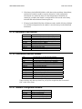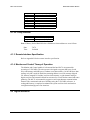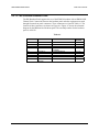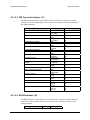
1
Comtech EF Data is an ISO 9001 Registered Company
SDM-309B
Satellite Modem
Installation and Operation Manual
Part Number MN/SDM309B.IOM
Edition 2
February 29, 1992
Comtech EF Data is an ISO 9001 Registered Company
SDM-309B
Satellite Modem
Installation and Operation Manual
Part Number MN/SDM309B.IOM
Edition 2
February 29, 1992
Special Instructions:
This is the second edition of the manual.
Copyright © Comtech EF Data, 2006
All rights reserved.
Printed in the USA.
Comtech EF Data, 2114 West 7th Street, Tempe, Arizona 85281 USA, (480) 333-2200, FAX: (480) 333-2161.
Warranty Policy
This Adaptive Broadband product is warranted against defects in material and
workmanship for a period of one year from the date of shipment. During the warranty
period, Adaptive Broadband will, at its option, repair or replace products that prove to
be defective.
For equipment under warranty, the customer is responsible for freight to Adaptive
Broadband and all related custom, taxes, tariffs, insurance, etc. Adaptive Broadband
is responsible for the freight charges only for return of the equipment from the factory
to the customer. Adaptive Broadband will return the equipment by the same method
(i.e., Air, Express, Surface) as the equipment was sent to Adaptive Broadband.
Limitations of Warranty
The foregoing warranty shall not apply to defects resulting from improper installation
or maintenance, abuse, unauthorized modification, or operation outside of
environmental specifications for the product, or, for damages that occur due to
improper repackaging of equipment for return to Adaptive Broadband.
No other warranty is expressed or implied. Adaptive Broadband specifically
disclaims the implied warranties of merchantability and fitness for particular
purpose.
Exclusive Remedies
The remedies provided herein are the buyer's sole and exclusive remedies. Adaptive
Broadband shall not be liable for any direct, indirect, special, incidental, or
consequential damages, whether based on contract, tort, or any other legal theory.
Disclaimer
Adaptive Broadband has reviewed this manual thoroughly in order that it will be an
easy-to-use guide to your equipment. All statements, technical information, and
recommendations in this manual and in any guides or related documents are believed
reliable, but the accuracy and completeness thereof are not guaranteed or warranted,
and they are not intended to be, nor should they be understood to be, representations
or warranties concerning the products described. Further, Adaptive Broadband
reserves the right to make changes in the specifications of the products described in
this manual at any time without notice and without obligation to notify any person of
such changes.
If you have any questions regarding your equipment or the information in this manual,
please contact the Adaptive Broadband Customer Support Department. (For more
information, refer to the preface.)
Preface
About this Manual
Effective April 29, 1999, California Microwave EFData has changed its name to
Adaptive Broadband Corporation to reflect its focus as a leading architect of the
wireless broadband evolution.
This manual provides installation and operation information for the Adaptive Broadband
SDM-309B satellite modem. This is a technical document intended for earth station
engineers, technicians, and operators responsible for the operation and maintenance of
the SDM-309B.
Conventions and References Used in this Manual
Cautions and Warnings
CAUTION
CAUTION indicates a hazardous situation that, if not avoided, may result in
minor or moderate injury. CAUTION may also be used to indicate other
unsafe practices or risks of property damage.
WARNING indicates a potentially hazardous situation that, if not avoided,
could result in death or serious injury.
WARNING
Metric Conversion
Metric conversion information is located on the inside back cover of this manual. This
information is provided to assist the operator in cross-referencing English to Metric
conversions.
Rev. 0
i
Preface
SDM-309B Satellite Modem
Trademarks
Product names mentioned in this manual may be trademarks or registered trademarks of
their respective companies and are hereby acknowledged.
Reporting Comments or Suggestions Concerning this Manual
Comments and suggestions regarding the content and design of this manual will be
appreciated. To submit comments, please contact the Adaptive Broadband Customer
Support Department according to the following information.
ii
Rev. 0
SDM-309B Satellite Modem
Preface
Customer Support
Contact the Adaptive Broadband Customer Support Department for:
!
!
!
!
!
Product support
Information on returning a product
Information on upgrading a product
Product training
Reporting comments or suggestions concerning manuals
An Adaptive Broadband Customer Support representative may be reached at:
Adaptive Broadband
Attention: Customer Support Department
2114 West 7th Street
Tempe, Arizona 85281 USA
(480) 333-2200 (Main Adaptive Broadband Number)
(480) 333-4357 (Customer Support Desk)
(480) 333-2161 FAX
or, E-Mail can be sent to the Customer Support Department at:
[email protected]
To return an Adaptive Broadband product (in-warranty and out-of-warranty) for repair or
replacement:
1. Request a Return Material Authorization (RMA) number from the Adaptive
Broadband Customer Support Department.
Be prepared to supply the Customer Support representative with the model
number, serial number, and a description of the problem.
2. To ensure that the product is not damaged during shipping, pack the product in
its original shipping carton/packaging.
3. Ship the product back to Adaptive Broadband. (Shipping charges should be
prepaid.)
For more information regarding the warranty policies, refer to the disclaimer page
located behind the title page.
Rev. 0
iii
Preface
SDM-309B Satellite Modem
This page is intentionally blank.
iv
Rev. 0
Table of Contents
CHAPTER 1. INTRODUCTION...................................................................................1–1
1.1 Scope ................................................................................................................................................................. 1–1
1.2 Purpose And Function ..................................................................................................................................... 1–1
1.3 Description........................................................................................................................................................ 1–1
1.4 System Specification ........................................................................................................................................ 1–7
CHAPTER 2. INSTALLATION ....................................................................................2–1
2.1 Unpacking ......................................................................................................................................................... 2–1
2.2 External Connections....................................................................................................................................... 2–1
2.2.1 Data I/O ...................................................................................................................................................... 2–4
2.2.2 Remote (J6) ................................................................................................................................................ 2–4
2.2.2.1 Connector Pinout (J6).......................................................................................................................... 2–4
2.2.3 Fault (J7)..................................................................................................................................................... 2–4
2.2.3.1 Connector Pinout (J7).......................................................................................................................... 2–4
2.2.4 IF Output (CP1) .......................................................................................................................................... 2–5
2.2.5 IF Input (CP2)............................................................................................................................................. 2–5
2.2.6 AC Power ................................................................................................................................................... 2–5
2.2.7 GND ............................................................................................................................................................ 2–5
2.3 System Requirements....................................................................................................................................... 2–5
2.4 System Installation........................................................................................................................................... 2–6
CHAPTER 3. OPERATION .........................................................................................3–1
3.1 SDM 309/M1200P Front Panel ....................................................................................................................... 3–1
3.1.1 General ....................................................................................................................................................... 3–1
3.1.2 LED Indicators ........................................................................................................................................... 3–1
3.1.3 Front Panel Controls ................................................................................................................................... 3–2
3.1.4 Configuration.............................................................................................................................................. 3–4
Rev. 0
v
Table of Contents
SDM-309B Satellite Modem
3.1.4.1 MOD Configuration ............................................................................................................................ 3–4
3.1.4.2 DEMOD Configuration ....................................................................................................................... 3–5
3.1.4.3 Interface Configuration ....................................................................................................................... 3–8
3.1.5 Monitor ..................................................................................................................................................... 3–10
3.1.6 Faults ........................................................................................................................................................ 3–10
3.1.6.1 Mod_Flts - Modulator Faults............................................................................................................. 3–11
3.1.6.2 Dmd_Flts - Demodulator/Decoder Faults ......................................................................................... 3–11
3.1.6.3 CEQ_Flts - Common Equipment Faults............................................................................................ 3–11
3.1.6.4 TX_INTF - Transmit Interface Faults ............................................................................................... 3–11
3.1.6.5 RX_INTF - Receive Interface Faults................................................................................................. 3–11
3.1.7 Stored Faults ............................................................................................................................................. 3–12
3.1.8 Utility........................................................................................................................................................ 3–12
3.2 Drop And Insert Front Panel Operation...................................................................................................... 3–26
3.2.1 General ..................................................................................................................................................... 3–26
3.2.2 Configuration............................................................................................................................................ 3–26
3.2.2.1 MOD Configuration ........................................................................................................................... 3–27
3.2.2.2 DEMOD Configuration ..................................................................................................................... 3–28
3.2.2.3 Interface Configuration ..................................................................................................................... 3–30
3.2.3 Monitor ..................................................................................................................................................... 3–34
3.2.4 Faults ........................................................................................................................................................ 3–35
3.2.4.1 Mod_Flts - Modulator Faults............................................................................................................. 3–35
3.2.4.2 Dmd_Flts - Demodulator/Decoder Faults ......................................................................................... 3–36
3.2.4.3 CEQ_Flts - Common Equipment Faults ....................................................................................... 3–36
3.2.4.4 TX_INTF - Transmit Interface Faults ............................................................................................... 3–36
3.2.4.5 RX_INTF - Receive Interface Faults................................................................................................. 3–36
3.2.5 Stored Faults ............................................................................................................................................. 3–36
3.2.6 Utility......................................................................................................................................................... 3–37
CHAPTER 4. M&C AND INTERFACES .....................................................................4–1
4.1 Monitor And Control....................................................................................................................................... 4–1
4.1.1 General ....................................................................................................................................................... 4–1
4.1.2 Description of Options................................................................................................................................ 4–1
4.1.2.1 Remote Interface ................................................................................................................................. 4–1
4.1.2.2 Remote Baud Rate............................................................................................................................... 4–4
4.1.2.3 Remote Address .................................................................................................................................. 4–4
4.1.2.4 Battery ................................................................................................................................................. 4–4
4.1.2.5 Modulator/Coder Defaults................................................................................................................... 4–5
4.1.2.6 Demodulator/Decoder Defaults........................................................................................................... 4–5
4.1.2.7 Interface Configuration Defaults ......................................................................................................... 4–5
4.1.2.8 Utility Defaults .................................................................................................................................... 4–6
4.1.3 Remote Interface Specification................................................................................................................... 4–6
4.1.4 Monitor and Control Theory of Operation.................................................................................................. 4–6
4.2 Digital Interfaces .............................................................................................................................................. 4–6
4.2.1 IBS/M1200P Interface ................................................................................................................................ 4–7
4.2.1.1 Functional Description ........................................................................................................................ 4–7
4.2.1.2 Data Interface ...................................................................................................................................... 4–7
4.2.1.3 Transmit Multiplexer........................................................................................................................... 4–7
4.2.1.4 Receive Multiplexer .......................................................................................................................... 4–13
4.2.1.5 Plesiochronous Buffer ....................................................................................................................... 4–13
4.2.1.6 Engineering Service Channel (ESC) ................................................................................................. 4–14
4.2.1.7 IBS Interface Connector Pinouts ....................................................................................................... 4–14
vi
Rev. 0
SDM-309B Satellite Modem
Table of Contents
4.2.1.8 IBS Interface Specification................................................................................................................ 4–15
4.2.1.9 IBS Interface Breakout Panel ............................................................................................................ 4–17
4.2.1.9.1 IBS Terrestrial Interface (J1) ..................................................................................................... 4–19
4.2.1.9.2 RS422 Interface (J2) .................................................................................................................. 4–19
4.2.1.9.3 V.35 Interface (J3) ..................................................................................................................... 4–20
4.2.1.9.4 Engineering Service Channel..................................................................................................... 4–20
4.2.1.9.5 G.703 Interface (J5) ................................................................................................................... 4–21
4.2.1.9.6 External Reference Clock (J6) ................................................................................................... 4–21
4.2.1.9.7 Send Data (J7)............................................................................................................................ 4–21
4.2.1.9.8 Receive Data (J8) ....................................................................................................................... 4–22
4.2.1.9.9 Alarm Outputs (TB1) ................................................................................................................. 4–22
4.2.2 Drop & Insert Interface............................................................................................................................. 4–24
4.2.2.1 Functional Description ...................................................................................................................... 4–24
4.2.2.2 Data Interface .................................................................................................................................... 4–25
4.2.2.3 Transmit Multiplexer......................................................................................................................... 4–25
4.2.2.4 Receive Demultiplexer ...................................................................................................................... 4–25
4.2.2.5 Plesiochronous Buffer ....................................................................................................................... 4–26
4.2.2.6 Engineering Service Channel (ESC) ................................................................................................. 4–26
4.2.2.7 Backward Alarm................................................................................................................................ 4–26
4.2.2.8 Drop & Insert Interface Connector Pinouts ....................................................................................... 4–32
4.2.2.9 Drop & Insert Interface Specification ............................................................................................... 4–32
4.2.2.10 Drop & Insert Breakout Panel ......................................................................................................... 4–34
4.2.2.10.1 Drop Data Input, Insert Data Output, and Ext. Ref Clk (J1) .................................................... 4–36
4.2.2.10.2 Drop Data Output (J2).............................................................................................................. 4–36
4.2.2.10.3 Insert Data Input (J3) ............................................................................................................... 4–36
4.2.2.10.4 Insert Data Output (J4)............................................................................................................. 4–37
4.2.2.10.5 Drop Data Input (J5) ................................................................................................................ 4–37
4.2.2.10.6 Drop Data Output (J6).............................................................................................................. 4–37
4.2.2.10.7 Insert Data Input (J7) ............................................................................................................... 4–37
4.2.2.10.8 Insert Data Output (J8)............................................................................................................. 4–37
4.2.2.10.9 External Reference Clock (J9) ................................................................................................. 4–37
4.2.2.10.10 ESC Channel (J10)................................................................................................................. 4–38
4.2.2.10.11 Faults (J11) ............................................................................................................................ 4–38
4.2.2.10.12 Data Interface (J12)................................................................................................................ 4–38
4.2.2.11 Rear Panel Switches ........................................................................................................................ 4–39
4.2.2.11.1 Drop Data Input ....................................................................................................................... 4–39
4.2.2.11.2 Drop Data Output..................................................................................................................... 4–39
4.2.2.11.3 Insert Data Input....................................................................................................................... 4–39
4.2.2.11.4 Insert Data Output.................................................................................................................... 4–40
4.2.2.11.5 External Reference Clock ........................................................................................................ 4–40
4.2.2.11.6 Drop Output/Insert Input (SW4) .............................................................................................. 4–40
4.2.2.11.7 Drop Data Output DCE/DTE Select (SW5)............................................................................. 4–40
4.2.3 External Channel Unit Interface ................................................................................................................ 4–45
4.3 Interface Clocking Options ........................................................................................................................... 4–45
4.3.1 Master/Slave ............................................................................................................................................. 4–45
4.3.1.1 Master/Slave RS422 or V.35............................................................................................................. 4–45
4.3.1.2 Master/Slave G.703 ........................................................................................................................... 4–46
4.3.1.3 Master/Slave X.21 ............................................................................................................................. 4–46
4.3.1.4 Master/Slave External Station Clock................................................................................................. 4–46
4.3.2 Master/Master ........................................................................................................................................... 4–46
4.3.2.1 Master/Master (Customer Clock) ...................................................................................................... 4–47
4.3.2.2 Master/Master (Station Clock) .......................................................................................................... 4–47
Rev. 0
vii
Table of Contents
SDM-309B Satellite Modem
CHAPTER 5. THEORY OF OPERATION ...................................................................5–1
5.1 Modulator ......................................................................................................................................................... 5–1
5.1.1 General description..................................................................................................................................... 5–1
5.1.2 Specifications.............................................................................................................................................. 5–1
5.1.3 Theory of Operation ................................................................................................................................... 5–6
5.2 Viterbi Decoder / Demodulator Processor ..................................................................................................... 5–7
5.2.1 General Description .................................................................................................................................... 5–7
5.2.2 Viterbi Decoder/Demod Processor Specification ....................................................................................... 5–7
5.2.2.1 Demod Processor Specification........................................................................................................... 5–7
5.2.2.2 Viterbi Decoder Specifications............................................................................................................ 5–8
5.2.3 Theory Of Operation................................................................................................................................. 5–14
5.2.3.1 Demod Processor............................................................................................................................... 5–14
5.2.3.2 Viterbi Decoder ................................................................................................................................. 5–14
5.3 Demodulator................................................................................................................................................... 5–15
5.3.1 General Description .................................................................................................................................. 5–15
5.3.2 Specifications............................................................................................................................................ 5–16
5.3.3 Theory of Operation ................................................................................................................................. 5–19
5.4 Reacquisition, Fast Acquisition And Directed Sweep ................................................................................. 5–19
5.4.1 General ..................................................................................................................................................... 5–19
5.4.2 Reacquisition ............................................................................................................................................ 5–20
5.4.3 Fast Acquisition ........................................................................................................................................ 5–21
5.4.4 Directed Sweep......................................................................................................................................... 5–21
CHAPTER 6. MAINTENANCE....................................................................................6–1
6.1 System Checkout .............................................................................................................................................. 6–1
6.1.1 General ....................................................................................................................................................... 6–1
6.1.2 Modulator Checkout ................................................................................................................................... 6–1
6.1.3 Demodulator Checkout ............................................................................................................................... 6–1
6.1.4 Test Points .................................................................................................................................................. 6–8
6.1.4.1 Modulator (Figure 6-5)........................................................................................................................ 6–8
6.1.4.2 Demodulator (Figure 6-6).................................................................................................................... 6–9
6.1.4.3 Viterbi Decoder/demod Card AS/0701 (Figure 6-7) ......................................................................... 6–10
6.1.4.4 Viterbi Decoder/Demod Card AS/0949 (Figure 6-8) ....................................................................... 6–11
6.1.4.5 Viterbi Decoder/Demod Card AS/2133 (Figure 6-9) ....................................................................... 6–12
6.2 Fault Isolation................................................................................................................................................. 6–13
6.2.1 Modulator Faults....................................................................................................................................... 6–13
6.2.2 Demodulator Faults .................................................................................................................................. 6–14
6.2.3 Common Equipment Faults ...................................................................................................................... 6–15
6.3 Interface Fault Isolation ................................................................................................................................ 6–15
6.3.1 Transmit Overhead Framing Unit Faults .................................................................................................. 6–16
6.3.2 Receive Overhead Framing Unit Faults.................................................................................................... 6–16
6.4 Module Replacement ..................................................................................................................................... 6–22
6.5 Module Identification .................................................................................................................................... 6–22
viii
Rev. 0
SDM-309B Satellite Modem
Table of Contents
6.6 Repacking For Shipment............................................................................................................................... 6–22
APPENDIX A. DATA RATES AND FILTERS ............................................................ A–1
APPENDIX B. SATELLITE MODEM REMOTE CONTROL....................................... B–1
APPENDIX C. EXTERNAL CHANNEL UNIT............................................................. C–1
APPENDIX D. SOFTWARE CHANGE SPECIFICATIONS........................................ D–1
Rev. 0
ix
Table of Contents
SDM-309B Satellite Modem
This page is intentionally blank.
x
Rev. 0
Chapter 1.
INTRODUCTION
1.1 Scope
This manual describes the SDM-309B Satellite Modem, hereinafter referred to as the
modem (Figure 1-1). It includes installation, operation, and maintenance instructions. A
description of the equipment is contained in Section 1. Section 2 provides the installation
instructions. The use of controls, indicators, and operation is described in Section 3.
Maintenance instructions are in Section 4.
1.2 Purpose And Function
The modem is a high performance, full-duplex, QPSK digital modulator-demodulator for
Intelsat Business Services (IBS) satellite communication systems. This modem and
internal channel unit complies with the requirements of IESS 309. The internal channel
unit interfaces between SCPC fixed-rate terminal equipment having a data rate of 64
Kbps to 2.048 Mbps and adds overhead/framing to the data. The modem interfaces
between the channel unit and IF converter equipment operating in a 50 to 90 MHz or 100
to 180 MHz band (Figure 1-2). This modem can be used with an external channel unit
(Multipoint/M1200 or equivalent). Refer to Appendix C for more information. The
modem contains built-in scrambler/ descrambler, differential encoder/decoder, transmit
and receive frequency synthesizers, and a multi-rate Forward Error Correction (FEC)
convolutional encoder-viterbi decoder. The modem provides high performance with
narrow occupied bandwidth, automatic signal acquisition, high flexibility, and extensive
on-line monitoring circuits.
1.3 Description
The modem is a complete, self-contained unit in a standard 19-inch rack mountable
enclosure weighing approximately 25 pounds. It is of modular construction (Figure 1-3).
The chassis assembly (with the front and rear panel) encloses seven printed circuit board
assemblies (PCB). The backplane PCB is mounted on the chassis assembly and contains
receptacles for five plug-in PCB’s. Test points are located on the front board edge of the
modulator, demodulator, and decoder PCB. All controls and indicators for operation of
MN/U-SDM309B Rev. #
1-1–1
Introduction
SDM-309B Satellite Modem
the modem are located on the front panel. The chassis also contains the power supply,
and a fan is on the rear panel. A system block diagram is shown in Figure 1-4.
1-1–2
MN/U-SDM309B Rev. #
SDM-309B Satellite Modem
Introduction
Figure 1-1 SDM-309B Modem
MN/U-SDM309B Rev. #
1-1–3
Introduction
SDM-309B Satellite Modem
Figure 1-2 Satellite Communications System With SDM-309B Modem
1-1–4
MN/U-SDM309B Rev. #
SDM-309B Satellite Modem
Introduction
Figure 1-3 Modular Construction
MN/U-SDM309B Rev. #
1-1–5
Introduction
SDM-309B Satellite Modem
Figure 1-4 SDM-309B Block Diagram
1-1–6
MN/U-SDM309B Rev. #
SDM-309B Satellite Modem
Introduction
The modem consists of the following assemblies:
Assembly
Chassis with Power Supply
PCB, Monitor and Control
PCB, Modulator
PCB, Demodulator
PCB, Viterbi Decoder
PCB, Front Panel Control Board
PCB, Mother Board
PCB, Internal Channel Unit
(IBS)
(D&I)
(External Channel Unit)
PCB, Mod Daughter Variable Rate
PCB, Mod Daughter Fixed Rate
PCB, Demod Daughter Variable Rate
PCB, Demod Daughter Fixed Rate
Drawing No.
AS/1100-3
AS/0356
AS/0773-X
AS/0778-X
AS/2133*
AS/0361
AS/0979-1
AS/1010 &
AS/1011 or
AS/1455
See Appendix C
AS/0930-2 or
AS/0715
AS/0929-2 or
AS/0698
Note: X= various options available on the modulator and demodulator boards. Refer to
Table 6-3 for more information on the options available for each board.
*Older versions of the Viterbi Decoder board can also be used in the SDM-309B
modem. Refer to Chapter 5, Section 5.2 for more information on the available revisions
and compatibility information.
1.4 System Specification
Table 1-1 lists the operating specifications of the modem. The bit energy-to-noise ratio
(Eb/N0) required to achieve 10-5 and 10-7 bit error rates is listed in Table 1-2. The
typical bit error rate performance of the modem is shown in Figure 1-5, and a typical
output spectrum of the modem is shown in Figure 1-6.
Table 1-1 SDM-309B Satellite Modem Specification
Operating Frequency Range
Type of Modulation
Operating Channel Spacing
Bit Error Rate
Digital Interface
IBS/M1200P
D&I/M1200P
External Channel Unit
(See Appendix C)
Digital Data Rate
MN/U-SDM309B Rev. #
System Specifications
50 to 90 MHz, or 100 to 180 Mhz
Synthesized in 2.5 KHz Steps
Quadrature Phase Shift Keying
Less Than .5 dB degradation operating with
2 adjacent like channels each 10 dB higher
at 1.3 times the symbol rate or 75 KHz
minimum
See Table 1-2
V.35, RS/422, & G.703
G.703 - T1 & E1
RS422/449, DS1, V.35, G.703
64 to 2048 Kb/s Configurable Choice
of up to Four pre-defined fixed Rates
or Variable Rate Option
1-1–7
Introduction
SDM-309B Satellite Modem
Forward Error Correction
Convolutional Encoding with Soft Decision
K7 Viterbi Decoding
Data Scrambling
Selectable, Synchronous (Per IESS-309
Rev 3 Section 4.4.5) or None
Diagnostic Features
RF Loopback
Digital Data Loopback
Fault Monitoring
Bit Error Rate Monitoring
Remote Control via Serial Port
Prime Power
90-132 VAC or 180 to 264 VAC, 47-63 Hz
75 W Max. Fused at 2 A
Size
5.25" H by 19.0" W by 18.0" D (3RU)
Weight
30 pounds Maximum
Additional Modulator Specifications
Output Power
-5 to -25 dBm, Adjustable
in 0.5 dB Steps
+5 to -20 dBm
Optional
Output Spurious and Harmonics
-50 dBc in Band (50 to 90 Mhz
or 100 to 180 Mhz)
-40 dBc out of band
(spurious measured in 4 KHz BW)
Output Impedance
75 !
Output Return Loss
20 dB
Output Frequency Stability
± 10 ppm
Data Clock Source
Internal or External
Internal Data Clock Stability
± 50 ppm
Additional Demodulator Specifications
Input Power (Desired Carrier)
-30 to -55 dBm
+30 dB power within 20 Mhz
from desired carrier
+40 dB power outside of 20 Mhz
from desired carrier
0 dBm
(Maximum Total)
Input Impedance
75 !
Input Return Loss
20 dB
Carrier Acquisition Range
± 25 KHz minimum
Clock Acquisition Range
± 100 ppm
Remote Control Specifications
Serial Interface
RS-232 or RS-485/449
Baud Rate
300 to 9600 BPS
Signals Controlled/Monitored
Transmit Frequency
Receive Frequency
Transmit Power
Transmitter On/Off
Data Rate Select
RF Loopback
Data Loopback
Scrambler On/Off
Descrambler On/Off
Raw Error Rate
Corrected Bit Error Rate
Receive Eb/N0
TX Clock Internal/External
RX Clock Normal/Invert
Receive Signal Level
Receive Carrier Detect
Power Supply Voltages
Fault Status
Stored Fault Status
1-1–8
MN/U-SDM309B Rev. #
SDM-309B Satellite Modem
Introduction
Configuration Retention
Will Maintain Current
Configuration for 30 days
Minimum Without Power
Addressing
Programmable to 1 of 256
Possibilities
Address 0 Reserved for Global
Addressing
Local Control of All Remote Functions Included Via Pushbutton Entry.
Table 1-2 BER Performance Specification
Note:
The bit energy-to-noise ratio (Eb/N0) required to achieve 10-3 to 10-8 bit error rates at
various data rates for different coding configurations is shown below. All values are for
operation in QPSK mode. The modem alone, without coding, provides operation within
0.5 dB of theoretical for BPSK and within 0.8 dB for QPSK, for BER’s in the range 10-1
to 10-6. Performance measurements are with Transmit and Receive IF connected back to
back through an additive white gaussian noise channel.
Viterbi K=7
1/2 Rate
BER
10-3
10-4
10-6
10-8
MN/U-SDM309B Rev. #
4.2 dB
4.7 dB
6.1 dB
7.2 dB
3/4 rate
5.3 dB
6.0 dB
7.6 dB
8.8 dB
1-1–9
Introduction
SDM-309B Satellite Modem
Figure 1-5 Typical Bit Error Rate Performance
1-1–10
MN/U-SDM309B Rev. #
SDM-309B Satellite Modem
Introduction
Figure 1-6 SDM-309B Modem Typical Output Spectrum
MN/U-SDM309B Rev. #
1-1–11
Introduction
1-1–12
SDM-309B Satellite Modem
MN/U-SDM309B Rev. #
Chapter 2.
INSTALLATION
2.1 Unpacking
The modem and manuals are packaged in pre-formed reusable foam inside a cardboard
carton. To remove the modem proceed as follows:
!
CAUTION
Do not use any cutting edged tool that will extend more than one inch into
the container and cause damage to the modem
a. Cut the tape at the top of the carton.
b. Lift off the foam containing the modem.
c. Save the packing material for reshipment either back to the factory or to another
site.
d. Inspect the equipment for damage incurred during shipment.
e. Check the equipment against the packing list shipped with the equipment to
ensure that the shipment is complete.
2.2 External Connections
Connections between the modem and other equipment are made through six connectors.
These connectors are listed in Table 2-1 and their locations are shown in Figure 2-1. The
use of each of these connectors is described in the following paragraphs.
Table 2-1 Rear Panel Connectors
Name
MN/U-SDM309B Rev. #
Ref Design
DATA I/O
NONE
Connector
Type
VARIOUS
REMOTE
J6
9 PIN "D"
Section
4.2.1
4.2.2
4.2.3
2.2.2
Function
IBS/M1200P I/O
D&I/M1200P I/O
External Channel Unit
INTERFACE
2-2–1
Installation
2-2–2
SDM-309B Satellite Modem
FAULT
J7
9 PIN "D"
2.2.3
IF OUTPUT
IF INPUT
AC POWER
GND
CP1
CP2
NONE
NONE
BNC
BNC
STANDARD
#10-32 STUD
2.2.4
2.2.5
2.2.6
2.2.7
FORM C FAULT
RELAY CONTACTS
TX IF OUTPUT
RX IF INPUT
AC POWER INPUT
CHASSIS GROUND
MN/U-SDM309B Rev. #
SDM-309B Satellite Modem
Installation
Figure 2-1 Rear Panel View
MN/U-SDM309B Rev. #
2-2–3
Installation
SDM-309B Satellite Modem
2.2.1 Data I/O
For information and pinouts on the data connectors, please refer to the appropriate
subSection in Section 4.2 and Appendix C.
2.2.2 Remote (J6)
The remote connector on the modem is used to interface the Monitor and Control
functions to a remote location. This interface can be either RS232 or RS485. For a
complete discussion on the remote interface, refer to Sections 4.1.2 and 4.1.3.
2.2.2.1 Connector Pinout (J6)
The remote interface is provided on a 9 pin female "D" connector. Screw locks and
latching blocks are provided for mechanical security of the mating connector. The
remote connector is a DCE interface.
RS485
Pin#
Name
1.
GND
2.
3.
4.
+RX/TX
5.
-RX/TX
6.
7.
8.
+RX/TX
9.
-RX/TX
RS232
Pin#
1.
2.
3.
4.
5.
6.
7.
8.
9.
Name
RD (RX)
TD (TX)
GND
DSR
RTS
CTS
2.2.3 Fault (J7)
The fault connector on the modem is used to provide FORM C contact closures for the
purpose of fault reporting. There are three (3) FORM C summary fault contacts,
modulator, demodulator, and common equipment. For a complete discussion on what
faults are monitored refer to Section 3.1.5. To get a system summary alarm connect all
the FORM C contacts in parallel.
2.2.3.1 Connector Pinout (J7)
The fault interface is provided on a 9 pin female "D" connector. Screw locks and
latching blocks are provided for mechanical security on the mating connector.
Pin #
1.
2.
2-2–4
Name
NO
COM
COMMON EQUIPMENT IS OK
MN/U-SDM309B Rev. #
SDM-309B Satellite Modem
3.
4.
5.
6.
7.
8.
9.
Installation
NC
NO
COM
NC
NO
COM
NC
COMMON EQUIPMENT IS FAULTED
MODULATOR IS OK
MODULATOR IS FAULTED
DEMODULATOR IS OK
DEMODULATOR IS FAULTED
Note: A connection between the common (COM) and normally open (NO) contacts
indicates no fault.
2.2.4 IF Output (CP1)
This is the transmit IF connector. The output impedance is 75 ! and the output power
level is -5 to -15dBm. In normal operation, the output will be a QPSK modulated result
of the DATA I/O connector between 50 and 90 Mhz.
2.2.5 IF Input (CP2)
This is the receive IF connector. The input impedance is 75 !. For normal operation the
signal level needs to be between -30 and -55 dBm with a maximum composite level of 0
dBm. Signals between 50 and 90 Mhz are selected and demodulated to produce clock
and data at the DATA I/O connector.
2.2.6 AC Power
The AC power is supplied to the modem by a standard detachable, non locking, 3-prong
power cord. Normal input voltage is 90-132 VAC or 180-264 VAC, 47-63 Hz. Maximum
power consumption is less than 75 W.
Note: Damage may result if the incorrect input voltage is applied to this connector. If
there is any question of the compatibility, DO NOT connect up the unit until EFDATA
has been contacted.
2.2.7 GND
A#10-32 stud is available on the rear for the purpose of connecting a common chassis
ground between all of the equipment.
2.3 System Requirements
The standard modem with all the cards installed (Figure 1-3), is full duplex QPSK
satellite modem. The system can also be configured for TX only or RX only.
For a TX only system, the demodulator (0778-X) and decoder (2133, 0949, or 0701) are
removed. You also must enter the Utility Menu on the front panel and select OP MODE
MN/U-SDM309B Rev. #
2-2–5
Installation
SDM-309B Satellite Modem
(Operation Mode). Enter the menu and select TX only. This will mask the receive faults
and receive stored faults in the faults menu.
For a RX only system, the modulator (0773-X) is removed. Enter the Utility Menu on the
front panel and select OP MODE). Enter the menu and select RX only. This will mask
the transmit faults and transmit stored faults in the faults menu.
The modem interface is configured by the selection of the data interface card. Refer to
Section 4.2 for discussion on the data interfaces.
The modem data/code rate is configured by the installation of a daughter card (0715 or
0930) on the modulator and a daughter card (0698 or 0929-X) on the demodulator. The
UTILITIES function must be set up to be compatible with the daughter cards. Refer to
Section 3.1.8 for information on the UTILITIES function. The modem will be set up to
match the daughter cards when it is shipped from the factory.
2.4 System Installation
After unpacking the modem per Section 2.1, installation of the modem can be done as
follows:
a. Mount the modem chassis in the assigned position in the equipment rack.
b. Connect the cables on the rear panel to the appropriate location. Refer to Section
2.2 for connector pinouts, placement, and function.
c. Open the front panel and verify the three (3) main cards and the M&C and Data
Interface cards are properly seated. Refer to Figure 1-3 for position of the cards.
When the cards are installed correctly, the color of the card guides on the chassis
will match the color of the card ejectors on the cards.
d. Before turning on the power switch, read and become familiar with Section 3.1,
the Front Panel Operation.
e. Turn on the power switch that is located inside the front panel.
f.
Check for proper TX signal level and spectrum.
g. Check for proper RX signal level and spectrum.
h. If there is any problem on installation refer to Section 6.0 for trouble shooting
the system.
2-2–6
MN/U-SDM309B Rev. #
Chapter 3.
OPERATION
3.1 SDM 309/M1200P Front Panel
3.1.1 General
The following is a Step by Step explanation and procedure for operating the SDM 309B
modem, hereafter referred to as the modem, with an internal IBS channel unit. The
complete front panel operation is described below.
The Modem front panel (Figure 3-1) provides the local user interface which is necessary
to configure and monitor status of the satellite modem. The front panel features a sixteen
character, two line LCD display and six key key-pad which provides for sophisticated
functions, yet is easy to use. Eight LED indicators are also present on the front panel to
provide overall status at a glance. All functions are accessible at the front panel by
entering one of five predefined ‘sELECT” categories or levels: Configuration
(CONFIG), Monitor, Faults, Stored Faults (StFaults), and Utility.
3.1.2 LED Indicators
General modem status and summary fault information is indicated by eight LED’s on the
front panel. The indicators are defined as follows:
Transmit (Red LED)
Receive (Red LED)
Common (Red LED)
Stored (Red LED)
Power On (Green LED)
Transmitter On (Green LED)
Carrier Detect (Green LED)
MN/U-SDM309B Rev. #
Faults
Indicates that a Modulator fault or a Transmit Interface
fault condition exists.
Indicates that a Demodulator/Decoder fault or a Receive
Interface fault condition exists.
Indicates that a common equipment fault condition exists.
Indicates that a fault has been logged and stored. The
fault may or may not be active.
Status
Indicates power is applied to the modem.
Indicates that the transmitter is currently on. This indicator
reflects the actual condition of the transmitter, as opposed
to the programmed condition.
Indicates that the decoder is locked.
3–1
Operation
SDM-309B Satellite Modem
Test Mode (Yellow LED)
Flashes when the modem is in a test configuration.
3.1.3 Front Panel Controls
The Modem is locally operated by using the front panel key-pad (Figure 3-1). The keypad consists of six keys: Enter, Clear, Right Arrow, Left Arrow, Up Arrow, and Down
Arrow. Each key has it’s own logical function or functions:
Enter Key
Clear Key
Left & Right Arrow Keys
Up & Down Arrow Keys
The “Enter” key is used to select a displayed function or to
execute a change to the Modem’s configuration.
The “Clear” key is used to back out of a selection or to cancel
a configuration change which has not been executed using
the “Enter” key. Pressing the “Clear” key generally returns the
display to the previous selection.
These keys are used to move to the next selection or to move
the cursor for certain functions.
These keys are used primarily to change configuration data
(numbers) but are also used at times to move from one
Section to another.
The Modem responds by beeping whenever a key is pressed. A single beep indicates that
the key pressed was a valid entry and the appropriate action was taken. However, a
double beep when a key is pressed indicates that the key pressed was an invalid entry.
The Modem front panel control uses a tree structured menu system (Figures 3-2 to 3-7)
to access and execute all functions. The base level of this structure is the sign-on
message which is displayed at the front panel upon modem power up. Line one of the
sign-on message is the modem model number (SDM309) and line two is the version
number of the firmware implemented in your modem. The main level of the menu system
is the ‘sELECT” menu which may be accessed from the base level by pressing any of the
arrow keys. From the ‘sELECT” menu you may select any one of five functional
categories: configuration functions, monitor functions, fault functions, stored fault
functions or utility functions. Use the right and left arrow keys to move from one
selection to another, when the desired function is displayed on line two you can enter
that level by pressing the “Enter” key. Once you have entered the functional level of your
choice, move to the desired function by using the right and left arrow keys. Refer to the
following text for information on individual functional categories and there functions.
3–2
MN/U-SDM309B Rev. #
SDM-309B Satellite Modem
Operation
Figure 3-1 Front Panel View
MN/U-SDM309B Rev. #
3–3
Operation
SDM-309B Satellite Modem
3.1.4 Configuration
Modem configuration may be viewed or changed by entering the “CONFIG” level from
the ‘sELECT” menu on the front panel. After entering the “CONFIG” menu, use the
right and left arrow keys to select “MOD”, “DEMOD”, or “INTERFACE” configuration.
Enter the selected configuration menu by pressing the “ENTER” key. Use the right and
left arrow keys to view the selected configuration parameters. If it is desired to change a
configuration parameter press the “Enter” key to begin the change process at which point
you can use the arrow keys to make the changes. After the changes are made and the
display represents the correct parameters execute the change by pressing the “Enter” key.
When the “Enter” key is pressed the necessary programming is initiated by the modem.
If you decide not to change the parameter prior to executing the change simply press the
“Clear” key. The following notes describe each configuration function in detail.
3.1.4.1 MOD Configuration
TXA
Transmitter rate selection. Select one of four predefined transmitter coder/data
rate combinations or a variable rate selection.
On entry the current transmitter rate is displayed with the flashing cursor on
the first character of the code rate on line one. The data rate is displayed on
line two. Use the arrow keys to select one of four predefined rates. Filters that
are not present may display as “N/A” (not assigned) and can not be
programmed. If your modem is equipped with the variable rate option you can
also select TXV and enter the desired data rate.
To change the rate using the variable rate selection, press the “ENTER” key
when “TXV is displayed. A flashing cursor will be displayed on the first
character of the coding type on line one. Use the right and left arrow keys to
move the flashing cursor and the up and down arrow keys to increment or
decrement the digit at the flashing cursor. Press the “ENTER” key to execute
the change.
TX_Freq
Note: When the TX Rate has been programmed, the transmitter is
automatically turned off, to prevent swamping of other channels. To turn on
the transmitter, use the “RF_Out” function.
Programs the modulator transmit frequency between 50mhz and 90MHz or
100MHz and 180MHz in 2.5 KHz Steps.
On entry the current transmitter frequency is displayed with the flashing cursor
on the first character. Use the right and left arrow keys to move the flashing
cursor and the up and down arrow keys to increment or decrement the digit at
the flashing cursor. Press the “ENTER” key to execute the change.
RF_Out
Note: The transmitter frequency is programmable within the specified range
(50 - 90 MHz or 100 - 180 MHz) in 2.5 KHz Steps. When the transmitter
frequency is changed, the transmitter is automatically turned off to prevent the
possible swamping of other channels. To turn the transmitter on, use the
“RF_OUT” function.
Programs the modulator output to On or Off.
On entry the current status of the output is displayed with the flashing cursor
on the first character. Use the arrow keys to select ON or OFF. Press the
“ENTER” key to execute the change.
3–4
MN/U-SDM309B Rev. #
SDM-309B Satellite Modem
TX_Power
Operation
Programs the modulator output power level from -5 dB to -30 dBm in .5 dB
Steps.
On entry the current transmitter power level is displayed with the flashing
cursor on the first character. The up and down keys are used to increase or
decrease the output power level in .5 dBm Steps. Press the “ENTER” key to
execute the change.
DifEncdr
CW_Mode
Note: If your modem has the high power Mod option installed (-11
modulator), you must change the output power range on the front panel. Enter
the Utility menu and find Pow Adj. Press the “ENTER” key and adjust the
maximum output power to read +5.0 dB using the up arrow. This will make the
TX power read +5.0 to -20.0 dB, the output range of a high power mod.
Programs the differential encoder On or Off.
On entry the current status of the DifEncdr is displayed with the flashing cursor
on the first character. Use the arrow keys to select ON or OFF. Press the
“ENTER” key to execute the change.
*Programs the modem for continuous wave mode. Three modes of operation
are available: center, dual, and offset modes.
Center Mode:
Generates a carrier at the current modulator frequency. This can be used to
measure the output power and output frequency.
Dual Mode:
Generates a dual side-band suppressed carrier signal. Side-bands are at one
half (1/2) the symbol rate from the carrier. This is used to check the channel
balance and carrier null.
Offset Mode:
Generates a single upper side-band suppressed carrier signal. The upper
side-band is at one quarter (1/4) the symbol rate from the carrier. This is used
to check the quadrature.
On entry the “CENTER” mode is displayed. To activate this test mode press
the “ENTER” key. Use the arrow keys to select the “DUAL or the “OFFSET”
modes. To return to the “CONFIG” menu press the “CLEAR” key.
Note: When the “CLEAR” key is pressed, the modem is configured to the
state it was in before “CWMode” was invoked and the transmitter is
automatically turned off to prevent the possible swamping of other channels.
To turn the transmitter on use the “RF_OUT” function.
3.1.4.2 DEMOD Configuration
MN/U-SDM309B Rev. #
3–5
Operation
SDM-309B Satellite Modem
RXA
Receiver rate selection. Select one of four predefined receiver
decoder/data rate combinations or a variable rate selection.
On entry the current receiver rate is displayed with the flashing
cursor on the first character of the code rate on line one. The data
rate is displayed on line two. Use the arrow keys to select one of four
predefined rates. Filters that are not present may display as “N/A”
(not assigned) and can not be programmed. If your modem is
equipped with the variable rate option you can also select TXV and
enter the desired data rate.
RX_freq
To change the rate using the variable rate selection, press the
“ENTER” key when “RXV” is displayed. A flashing cursor will be
displayed on the first character of the coding type on line one. Use
the right and left arrow keys to move the flashing cursor and the up
and down arrow keys to increment or decrement the digit at the
flashing cursor. Press the “ENTER” key to execute the change.
Programs the demodulator receive frequency between 50 MHz and
90 MHz or 100 MHz and 180 MHz in 2.5 KHz Steps.
On entry the current receive frequency is displayed with the flashing
cursor on the first character. Use the right and left arrow keys to
move the flashing cursor and the up and down arrow keys to
increment or decrement the digit at the flashing cursor. Press the
“ENTER” key execute the change.
DifDecdr
IFLoopBk
RFLoopBk
Note: The receiver frequency is programmable within the specified
range (50 - 90 MHz or 100 - 180 MHz ) in 2.5 KHz Steps.
Programs the differential decoder On or Off.
On entry the current status of the differential decoder is displayed
with the flashing cursor on the first character. Use the arrow keys to
select ON or OFF. Press the “ENTER” key to execute the change.
*Programs the modem for IF loopback operation. When the IF loopback is turned on the demodulator input is connected to the
modulator output through an attenuator and the demodulator is
programmed to the same frequency as the modulator. An attenuator
within the modem connects the IF out to the IF in. When IF loopback
is turned off the demodulator is turned to it’s previous frequency and
is reconnected to the IF input. See Figure 3-8 for a block diagram of
IF loopback operation.
On entry the current status of the IF loopback is displayed with a
flashing cursor on the first character. Use the arrow keys to select
ON or OFF. Press the “ENTER” key to execute the change.
*Programs the modem for RF loopback operation. When RF
loopback is turned on the demodulator is programmed to the same
frequency as the modulator. When RF loopback is turned off the
demodulator is tuned to it’s previous frequency. See Figure 3-9 for a
block diagram of RF loopback operation.
On entry the current status of the RF Loopback is displayed with the
flashing cursor on the first character. Use the arrow keys to select
ON or OFF. Press the “ENTER” key to execute the change.
3–6
MN/U-SDM309B Rev. #
SDM-309B Satellite Modem
SWP-RACQ
**SWP_CNTR
Operation
Programs the sweep reacquisition mode time duration. The time
selected with this parameter is the time that the modem will remain in
a narrow sweep (± 10%) after acquisition has been accomplished.
After this timer runs out the modem will return to the normal sweep.
On entry the current programmed setting is displayed with a flashing
cursor on the first character. Use the right and left arrow keys to
move the flashing cursor and the up and down arrow keys to
increment and decrement the digit at the flashing cursor. Select the
number of seconds for the reacquisition mode from 0 to 999
seconds. Press the “ENTER” key to execute the change.
Programs the sweep center frequency for the directed sweep
function. The sweep center frequency may be set in the range from
+25000Hz to -25000Hz.
On entry the current programmed setting is displayed with a flashing
cursor on the first character. Use the right and left arrow keys to
move the flashing cursor and the up and down arrow keys to
increment and decrement the digit at the flashing cursor. Select the
sweepcenter frequency from -25000Hz to +25000Hz. Press the
“ENTER” key to execute the change.
**SWP_RNGE
When in directed sweep, the value from the sweep monitor screen
(when the modem was last locked) should be entered for the sweep
center frequency.
Programs the overall travel of the sweep width range during
acquisition in the directed sweep mode. The sweep width may be set
from 0 Hz to 50000 Hz. (When set at 50000 Hz, the modem is in the
fast acquisition mode).
On entry the current programmed setting is displayed with a flashing
cursor on the first character. Use the right and left arrow keys to
move the flashing cursor and the up and down arrow keys to
increment and decrement the digit at the flashing cursor. Select a
sweep range from 0 Hz to 50000 Hz. Press the “ENTER” key to
execute the change.
**SWP_DIR
BERT_set
When in directed sweep, the smaller the range is, the faster the
modem will lock, provided the sweep center frequency is close.
Programs the direction of the sweep travel in the directed sweep
mode.
On entry the current programmed setting is displayed with the
flashing cursor on the first character. Use the arrow keys to select
Forward (+) or Reverse (-). Press the “ENTER” key to execute the
change.
This function is used to set the BER threshold.
If the BER threshold set is exceeded a receive fault will be indicated
by the modem status indicators. BER threshold may be set from 1E3 to 1E-8 or may be disabled by specifying NONE.
On entry the current setting of the BER threshold is dis played. Use
the up and down arrow keys to select the desired setting. Press the
“ENTER” key to execute the change.
* Indicates Test Mode configuration option.
**These windows only show up when the Fast Acquisition has been
turned on in the “Utility” menu.
MN/U-SDM309B Rev. #
3–7
Operation
SDM-309B Satellite Modem
3.1.4.3 Interface Configuration
TX_clock
BUF_Clk
RX_Clock
Ext_REF
BBLoopBk
INTF_LBk
Programs the clock source for the modem transmitter clock. “Internal” sets
the TX clock to operate from the modem internal clock, this is also the
fallback clock. “External” sets the TX clock to operate from the external
reference clock. This clock must be frequency locked to the data that is
being transmitted. “TX Terrestrial” sets the TX clock to recover timing from
the incoming data.
On entry the current transmit clock setting is displayed with the flashing
cursor on the first character. Use the arrow keys to select “Internal”,
“External Reference”, or TX Terrestrial” clock. Press the “ENTER” key to
execute the change.
Programs the interface plesiochronous buffer output clock. “TX Terrestrial”
sets the buffer output clock to recover timing from the incoming TX data
clock. “External” sets this clock source to the external reference clock.
‘satellite” sets the output buffer clock to the satellite clock, this is also the
fallback clock. If ‘satellite” is selected, the doppler shift caused by the
satellite will not be removed. “Internal” set the buffer clock to operate from
the modem internal clock.
On entry the current setting of the plesiochronous buffer clock is displayed
with the flashing cursor on the first character. Use the arrow keys to select
‘satellite”, “Internal”, “Ext Ref”, or “TX_Terr” for the buffer clock. Press the
“ENTER” key to execute the change.
Programs the RX clock to “Normal” or “Inverted”.
On entry the current status of the RX Clock is displayed with the flashing
cursor on the first character. Use the arrow keys to select “Normal” or
“Inverted”. Press the “ENTER” key to execute the change.
Program the external reference clock input frequency between 8 KHz and
10 MHz in 8 KHz Steps.
On entry the current setting for the external reference is displayed with the
flashing cursor on the first character. Use the right and left arrow keys to
move the flashing cursor and the up and down arrow keys to increment or
decrement the digit at the flashing cursor. Press the “ENTER” key to
execute the change.
*Programs the modem for baseband loopback operation. When baseband
loopback is turned on data is looped back on the customer side of the
interface. This is a bidirectional loopback of the baseband data. See Figure
3-10 for a block diagram of baseband loopback operation.
On entry the current status is displayed with the flashing cursor on the first
character. Use the arrow keys to select ON or OFF. Press the “ENTER” key
to execute the change.
*Programs the modem for interface loopback operation. When interface
loop-back is turned on data is looped back on the modem side of the
interface. This is a bidirectional loopback of the data after the baseband
data has had the 16/15 overhead added. See Figure 3-11 for a block
diagram of interface loopback operation.
On entry the current status is displayed with the flashing cursor on the first
character. Use the arrow keys to select ON or OFF. Press the “ENTER” key
to execute the change.
3–8
MN/U-SDM309B Rev. #
SDM-309B Satellite Modem
CODING
TX_2047
TXD_FLT
RXD_FLT
BUF_SIZE
BUF_CNTR
READ_ERR
Operation
Programs the modem for “AMI”, “B8ZS”, “B6ZS”, or “HDB3” coding of the
baseband data.
On entry the current coding format is displayed. Use the arrow keys to
select the desired coding format. Press the “ENTER” key to execute the
change.
*Programs the modem to insert a 2047 pattern in lieu of the normal transmit
data.
On entry the current status is displayed with the flashing cursor on the first
character. Use the arrow keys to select ON or OFF. Press the “ENTER” key
to execute the change.
Transmit Data Fault. This configuration function is used to select a Transmit
Interface fault monitor of AIS, Data, or None. When AIS (Alarm Indication
Signal) is selected the TX_INTF (Transmit Interface) fault “Data/AIS” is
monitoring a fault condition of all 1’s from customer data input to the
modem. When Data_Flt is selected, the TX_INTF fault “Data/AIS” is
monitoring a fault condition of all 1’s or all 0’s. This is referred to as a data
stable condition which means that the data is not transitioning. When None
is selected, the TX_INTF fault “Data/AIS” is not activated. On entry the
current TX Data fault that is being monitored is displayed with the flashing
cursor on the first character.
Use the arrow keys to select Data, AIS, or None. Press the “ENTER” key to
execute the change.
Receive Data Fault. This configuration function is used to select a Receive
Interface fault monitor of AIS, Data, or None. The data monitored for
Receive Data is coming from the Satellite. Refer to TXD_FLT for a
description of the function choices.
On entry the current RX Data fault that is being monitored is displayed with
the flashing cursor on the first character. Use the arrow keys to select Data,
AIS, or None. Press the “ENTER” key to execute the change.
This configuration function is used to set the size of the plesiochronous
buffer.
On entry the current plesiochronous buffer length is displayed. Use the up
and down arrow keys to select the desired buffer size. You may select from
384 to 262,144 bits in increments of sixteen. Press the “ENTER” key to
execute the change.
This configuration function is used to center the plesiochronous buffer.
Press the “ENTER” key twice to center the plesiochronous buffer.
This configuration is used to select the read error function mode. Frame or
2047 errors may be selected.
Dscrmblr
On entry the current read error mode is displayed. Use the arrow keys to
select “2047” errors or “FRAME” errors as desired. Press the “ENTER” key
to display and monitor the selected errors. To exit the read error mode press
the “CLEAR” key.
Programs the demod/decoder for descrambler On or Off.
Scramblr
On entry the current status of the descrambler is displayed with the flashing
cursor on the first character. Use the arrow keys to select ON or OFF. Press
the “ENTER” key to execute the change.
Programs the modulator for scrambler On or Off.
On entry the current status of the scrambler is displayed with the flashing
cursor on the first character. Use the arrow keys to select ON or OFF. Press
the “ENTER” key to execute the change.
* Indicates Test Mode configuration option.
MN/U-SDM309B Rev. #
3–9
Operation
SDM-309B Satellite Modem
3.1.5 Monitor
When the “MONITOR” level is entered use the right and left arrow keys to select the
desired monitor function. Each monitor function is displayed in real time as long as it is
selected.
Raw_BER - Raw bit error rate.
* Range: <1.0E-4 to >2550E-4
Cor_BER - Corrected bit error rate.
* Range: <1.0E-8 to >1E-3
Eb/N0 - Energy(bit)/noise ratio.
* Range: <3.2 dB to >16.0 dB
Swp_Freq - Sweep Monitor**
*Range: -25,000 Hz to +25,000 Hz
RxSignal - Receive signal level.
* Range: <-60 dBm to >-30 dBm
FIL_STAT - Plesiochronous buffer fill status in percent.
* Range: 1% to 99%
FRM_ERR/2047_ERR - Framing pattern bit error rate. Monitors the currently
selected READ_ERR function.
* Range: <8.0E-4 to >1.4E-3
* When the decoder loses lock no data is available and is so indicated.
** Sweep Frequency only shows up in the “Monitor” menu if the Fast Acquisition
has been turned on in the “Utility” menu.
3.1.6 Faults
The “FAULTS” level is accessible from the ‘sELECT” menu. Faults are similar to
monitor functions as they display the current fault status of the group being displayed.
Use the right and left arrow keys to move between the fault groups: Mod_Flts
(modulator faults), Dmd_Flts (demodulator faults), CEQ_Flts (common equipment
faults), TX_INTF (transmitter interface faults), and RX_INTF (receiver interface faults).
The current faults status is displayed on line two of the display in real time. Faults status
is display as “+” (plus) or “-” (minus) for each parameter monitored, “+” indicates that a
fault exists and “-” indicates that no fault exists. To display labels for individual faults
press the “Enter” key. Use the left and right arrow keys to move the flashing cursor to the
fault you wish to identify. The label for that fault is immediately displayed on line one of
the display. The “Clear” key can be used to exit this level of operation and return to the
previous level. The following lists outline the faults monitored and displayed in each
group.
3–10
MN/U-SDM309B Rev. #
SDM-309B Satellite Modem
Operation
3.1.6.1 Mod_Flts - Modulator Faults
RF_Syn
Data_Clk
TClk_Syn
I-Channl
Q-Channl
AGC_level
Module
Modulator RF synthesizer fault.
Transmit data clock activity indicator.
Transmit clock synthesizer fault.
I channel activity fault.
Q channel activity fault.
Automatic gain control level fault.
Modulator module fault. Typically indicates that the modulator module is
missing or will not program.
3.1.6.2 Dmd_Flts - Demodulator/Decoder Faults
C_Detect
RF_Syn
Data_Clk
I-Channl
Q-Channl
BERthrsh
Module
Carrier detect fault. Indicates that the decoder is not locked.
Demodulator RF synthesizer fault.
Receive data clock activity fault.
I channel activity fault.
Q channel activity fault.
Secondary alarm result of BERT_set in the DEMOD configuration menu.
Demodulator/decoder module fault. Typically indicates that the demod/decoder
module is missing or will not program.
3.1.6.3 CEQ_Flts - Common Equipment Faults
Battery
-12 volt
+12 volt
+5 volt
Intrface
Battery fault.
Negative 12 volt power supply fault.
Plus 12 volt power supply fault.
Plus 5 volt power supply fault.
Interface module fault. Typically indicates that the interface module is missing or
will not program.
3.1.6.4 TX_INTF - Transmit Interface Faults
Data/AIS
TX_PLL
CLK_ACT
Data or Alarm indication Signal. When Data_FLT is selected in the Interface
Configuration menu the fault indicates a Data stable condition. When AIS is
selected, fault indicates data is all 1’s. Refer to Section 1.2.3 (Interface
Configuration) for a detailed description of these faults.
Transmitter phase locked loop fault. Indicates that the transmitter PLL is not
locked.
Activity detector alarm of the selected interface transmit clock. The interface
will fall back to the internal clock when this fault is active.
3.1.6.5 RX_INTF - Receive Interface Faults
BUF_UNFL
BUF_OVFL
MN/U-SDM309B Rev. #
Buffer underflow fault. Indicates that a plesiochronous buffer underflow has
occurred.
Buffer overflow fault. Indicates that a plesiochronous buffer overflow has
occurred.
3–11
Operation
SDM-309B Satellite Modem
Data/AIS
FRM_BER
BW_ALM
RX_PLL
Buff_Clk
MUX_lock
Data or Alarm Indication Signal. When Data_FLT is selected in the Interface
Configuration menu the fault indicates a Data stable condition. When AIS is
selected, the fault indicates data is all 1’s. Refer to Section 4.3 (Interface
Configuration for a detailed description of these faults.
Frame BER fault. Indicates that the frame BER exceeds 1E-3.
Backward Alarm Fault.
Receive Phase Locked Loop Fault.
Activity detector alarm of the selected interface receive clock. The interface
will fall back to the satellite clock when this fault is active.
MUX lock fault. Indicates that the MUX is not locked.
3.1.7 Stored Faults
The Modem stores the first ten (Flt0 - Flt9) occurrences of fault status changes in each of
the six major fault categories. Each stored fault status change is stored with the time and
date of the occurrence. Stored faults may be viewed by entering the ‘stFaults” level from
the ‘sELECT” menu. All stored faults may be cleared by executing the “CLEAR ??
StFaults” command from the ‘stFaults” level.
Stored faults are not maintained through a controller power on reset cycle. However, the
last known time is maintained in non volatile RAM and upon power up a common
equipment fault is logged (Flt0) with that time and date. On power up an additional
common equipment fault is also logged (Flt1) to indicate the power up time and date. So
on power up the power down and power up times are logged as common equipment fault
0 and common equipment fault 1.
Upon entering the ‘stFaults” level use the left and right arrow keys to move between the
six fault groups and the “CLEAR ?? StFaults” selections. The time and date of the first
stored faults status (Flt0) for the selected group will be displayed alternately on line two
of the display. Use the up and down arrow keys to cycle through the selected group’s
stored faults status (Flt0 - Flt9). To display the faults status associated with the displayed
time and date press the “Enter” key, at this time you can use the right and left arrow keys
to move the flashing cursor to the fault you wish to identify.
To clear the stored faults currently logged simply press the “ENTER” key when the
“CLEAR ?? StFaults” selection is displayed.
Note: Faults are stored in time sequence with the oldest faults status change stored in
Flt0 and the most recent in Flt9. Only the first ten faults status changes are stored and all
stored faults which have not been used indicate “No Fault” on the display.
3.1.8 Utility
The utility functions provide a means to set the time and date of the modem real time
clock circuit. Provisions are also made for assigning data and code rates to the modulator
and demodulator. A lamp test function is provided for testing of the front panel optical
indicators.
3–12
MN/U-SDM309B Rev. #
SDM-309B Satellite Modem
Operation
After entering the “UTILITY” functions level use the right and left arrow keys to select
the utility function of interest. The current time and date can be displayed and changed as
required. Access to the transmitter and receiver Data/Code Rate assignment and the lamp
test functions are also available from within the utility functions level.
Note: The selection of data/code rates in the “UTILITY” program must match the
hardware filters installed on the modulator and demodulator modules.
The utility functions are as follows:
Time
Time of day set/display function.
Date
The current time that the modem is set for is displayed
when selected. To set the modem time press the “ENTER”
key and use the right and left arrow keys to position the
flashing cursor over the parameter to be changed. Use the
up and down arrow keys to change the parameter to the
desired value. Once the parameters are displayed as
desired press the “ENTER” key to set the time.
Date set/display.
LAMP TEST ??
Address/Parity/Baud Rate
POW ADJ.
Follow the same procedure as outlined for the time function
to view and set the date.
Lamp test function used to illuminate all the front panel
indicators for three seconds.
Press the “ENTER” key to turn on all of the front panel
indicators for three seconds.
The current modem address, parity selection and selected
baud rate of the modem is displayed. This in only a monitor
function. No changes can be made from this menu.
On entry the currently set address of the modem will be
displayed (0 to 255) on the first line. The currently set
parity, even or odd, will be displayed on the second line.
The currently set baud rate from 110 to 9600 will also be
displayed on the second line.
Modulator Power Adjust Offset.
Allows the operator to offset the modulator output power
readout in the configuration menu. This will be the highest
modulator power that will be displayed and programmed.
This feature does not actually change the modulator power
level. The function is to change the actual reading to
display an offset value in the monitor. The modulator
Power Offset can be set between +20.0 to -20.0 dB in 0.5
dB increments.
Note: The maximum output power adjust, set in this
window, must match the maximum output power of the
modulator installed in the modem. In a switching system
the backup modem must be set the same as the prime
modem or a fault will occur.
MN/U-SDM309B Rev. #
3–13
Operation
SDM-309B Satellite Modem
OP MODE
Fast ACQ
INTRFACE
Filter Adjust
Assign TX_Fltrs
Operation Mode. Programs the modem operation for TX
only, RX only, or Duplex operation.
On entry the flashing cursor is on the first character of the
display. Use the arrow keys to select TX only, RX only, or
Duplex. Press the “ENTER” key to execute the change.
When TX only or RX only is selected, the appropriate faults
are masked from the Faults and Stored Faults menu.
Fast Acquisition function.
Turns the fast acquisition and directed sweep function ON
or OFF. When the fast acquisition has been turned OFF,
the Swp_Cntr, SWP_Rnge and SWP_DIR windows in the
configuration menu are disabled and do not appear. Also,
in the “Monitor” menu, Swp_Freq will not appear. When
turned “OFF” fast acquisition does not occur.
This is a monitor function that displays the interface that
has been selected on the M&C card. No changes are
accepted from the front panel.
Variable Rate Filters K factor settings. This is a factory
setting and the operator is not allowed to enter this
parameter without authorization from EFData service
department. Failure to comply will result in a modem
failure.
Transmit filter display/assignment utility. Used to view
current filter rate assignments and to make filter rate
reassignments. The modulator has four symbol rate filters.
Each filter is for a specific symbol rate. The data rate and
code rate for each filter must be established upon initial
modulator installation and when circumstances indicate the
need to do so. Filters are designated as A, B, C, and D.
To view the current filter assignments press the “ENTER”
key when the “Assign TX_Fltrs” selection is displayed from
the utility functions menu. On line one of the display will be
TXA” which indicates transmitter filter A. Following “TXA”
on line one will be the code rate (1/2 or 3/4) or “N/A” which
indicates that the filter is not assigned. On line two will be
the data rate assigned to filter “A”. Use the right and left
arrow keys to see the assignments for filters B, C, and D
(TXB, TXC, and TXD).
If it is desired to change a filter assignment press the
“ENTER” key when the data for that filter is displayed. Use
the right and left arrow keys until the flashing cursor is at
the parameter to be changed. Then use the up and down
arrow keys to change that parameter. When all changes
are made press the “Enter” key to confirm the assignment.
Some filters may have parameters preprogrammed in the
filter board hardware. If the filter parameters are
preprogrammed the previously described programming
techniques will be disabled.
Note: These assignments are used for the selection of
“TXR” (Transmitter Rate) in the configuration functions
menu.
The parameter “N/A” is used to indicate that the specific
filter is not present.
3–14
MN/U-SDM309B Rev. #
SDM-309B Satellite Modem
Assign RX_Fltrs
Operation
Receive filter display/assignment utility. Used to view
current filter rate assignments and to make filter rate
reassignments.
Refer to the previous text under “Assign TX_Fltrs”. The
receive filters assignments are basically identical.
MN/U-SDM309B Rev. #
3–15
Operation
SDM-309B Satellite Modem
Figure 3-2 Menu Tree
3–16
MN/U-SDM309B Rev. #
SDM-309B Satellite Modem
Operation
Figure 3-3 Menu Tree
MN/U-SDM309B Rev. #
3–17
Operation
SDM-309B Satellite Modem
Figure 3-4 Menu Tree
3–18
MN/U-SDM309B Rev. #
SDM-309B Satellite Modem
Operation
Figure 3-5 Menu Tree
MN/U-SDM309B Rev. #
3–19
Operation
SDM-309B Satellite Modem
Figure 3-6 Menu Tree
3–20
MN/U-SDM309B Rev. #
SDM-309B Satellite Modem
Operation
Figure 3-7 Menu Tree
MN/U-SDM309B Rev. #
3–21
Operation
SDM-309B Satellite Modem
Figure 3-8 IF Loopback
3–22
MN/U-SDM309B Rev. #
SDM-309B Satellite Modem
Operation
Figure 3-9 RF Loopback
MN/U-SDM309B Rev. #
3–23
Operation
SDM-309B Satellite Modem
Figure 3-10 Interface Loopback
3–24
MN/U-SDM309B Rev. #
SDM-309B Satellite Modem
Operation
Figure 3-11 Baseband Loopback
MN/U-SDM309B Rev. #
3–25
Operation
SDM-309B Satellite Modem
3.2 Drop And Insert Front Panel Operation
3.2.1 General
The following is a Step by Step explanation and procedure for operating the SDM 309B
modem, hereafter referred to as the modem, with an internal drop and insert channel unit.
The operation of the front panel is the same “look and feel” as the SDM 309 modem
without the drop and insert channel unit, except there are additional commands for the
drop and insert channel unit. The complete front panel operation is described below.
The Modem front panel control uses a tree structured menu system (Figure 3-12 to 3-17)
to access and execute all functions. The base level of this structure is the sign-on
message which is displayed at the front panel upon modem power up. Line one of the
sign-on message is the modem model number (SDM308-5) and line two is the version
number of the firmware implemented in your modem. The main level of the menu system
is the ‘sELECT” menu which may be accessed from the base level by pressing any of the
arrow keys. From the ‘sELECT” menu you may select any one of five functional
categories: configuration functions, monitor functions, fault functions, stored fault
functions or utility functions. Use the right and left arrow keys to move from one
selection to another, when the desired function is displayed on line two you can enter
that level by pressing the “Enter” key. Once you have entered the functional level of your
choice, move to the desired function by using the right and left arrow keys. Refer to the
following text for information on individual functional categories and there functions.
3.2.2 Configuration
Modem configuration may be viewed or changed by entering the “CONFIG” level from
the ‘sELECT” menu on the front panel. After entering the “CONFIG” menu, use the
right and left arrow keys to select “MOD”, “DEMOD”, or “INTERFACE” configuration.
Enter the selected configuration menu by pressing the “ENTER” key. Use the right and
left arrow keys to view the selected configuration parameters. If it is desired to change a
configuration parameter press the “Enter” key to begin the change process at which point
you can use the arrow keys to make the changes. After the changes are made and the
display represents the correct parameters execute the change by pressing the “Enter” key.
When the “Enter” key is pressed the necessary programming is initiated by the modem.
If you decide not to change the parameter prior to executing the change simply press the
“Clear” key. The following notes describe each configuration function in detail.
3–26
MN/U-SDM309B Rev. #
SDM-309B Satellite Modem
Operation
3.2.2.1 MOD Configuration
TXA
TX_Freq
Transmitter rate selection. Select one of four predefined
transmitter coder/data rate combinations or a variable rate
selection.
On entry the current transmitter rate is displayed with the flashing
cursor on the first character of the code rate on line one. The data
rate is displayed on line two. Use the arrow keys to select one of
four predefined rates. Filters that are not present may display as
“N/A” (not assigned) and can not be programmed. If your modem
is equipped with the variable rate option you can also select TXV
and enter the desired data rate.
Programs the modulator transmit frequency between 50 and 90
MHz or 110 and 180 MHz in 2.5 KHz Steps.
On entry the current transmitter frequency is displayed with the
flashing cursor on the first character. Use the right and left arrow
keys to move the flashing cursor and the up and down arrow keys
to increment or decrement the digit at the flashing cursor. Press
the “ENTER” key to execute the change.
To change the rate using the variable rate selection, press the
“ENTER” key when “TXV is displayed. A flashing cursor will be
displayed on the first character of the coding type on line one. Use
the right and left arrow keys to move the flashing cursor and the up
and down arrow keys to increment or decrement the digit at the
flashing cursor. Press the “ENTER” key to execute the change.
RF_Out
TX_Power
Note: The transmitter frequency is programmable within the
specified range (50 - 90 MHz or 110 - 180 MHz) in 2.5 KHz Steps.
When the transmitter frequency is changed, the transmitter is
automatically turned off to prevent the possible swamping of other
channels. To turn the transmitter on, use the “RF_OUT” function.
Programs the modulator output to On or Off.
On entry the current status of the output is displayed with the
flashing cursor on the first character. Use the arrow keys to select
ON or OFF. Press the “ENTER” key to execute the change.
Programs the modulator output power level from -5 dB to -30 dBm
in 0.5 dB Steps.
On entry the current transmitter power level is displayed with the
flashing cursor on the first character. The up and own keys are
used to increase or decrease the output power level in 0.5 dBm
Steps. Press the “ENTER” key to execute the change.
DifEncdr
Note: If your modem has the high power Mod option installed (-11
modulator), you must change the output power range on the front
panel. Enter the Utility menu and find Pow Adj. Press the “ENTER”
key and adjust the maximum output power to read +5.0 dB using
the up arrow. This will make the TX power read +5.0 to -20.0 dB,
the output range of a high power mod.
Programs the differential encoder On or Off.
On entry the current status of the DifEncdr is displayed with the
flashing cursor on the first character. Use the arrow keys to select
ON or OFF. Press the “ENTER” key to execute the change.
MN/U-SDM309B Rev. #
3–27
Operation
SDM-309B Satellite Modem
CW_Mode
*Programs the modem for continuous wave mode. Three modes of
operation are available: center, dual, and offset modes.
Center Mode:
Generates a carrier at the current modulator frequency. This can
be used to measure the output power and output frequency.
Dual Mode:
Generates a dual side-band suppressed carrier signal. Side-bands
are at one half (1/2) the symbol rate from the carrier. This is used
to check the channel balance and carrier null.
Offset Mode:
Generates a single upper side-band suppressed carrier signal.
The upper side-band is at one quarter (1/4) the symbol rate from
the carrier. This is used to check the quadrature.
On entry the “CENTER” mode is displayed. To activate this test
mode press the “ENTER” key. Use the arrow keys to select the
“DUAL or the “OFFSET” modes. To return to the “CONFIG” menu
press the “CLEAR” key.
Note: When the “CLEAR” key is pressed, the modem is
configured to the state it was in before “CWMode” was invoked
and the transmitter is automatically turned off to prevent the
possible swamping of other channels. To turn the transmitter on
use the “RF_OUT” function.
3.2.2.2 DEMOD Configuration
RXA
RX_freq
Receiver rate selection. Select one of four predefined receiver
decoder/data rate combinations or a variable rate selection.
On entry the current receiver rate is displayed with the flashing cursor on
the first character of the code rate on line one. The data rate is displayed
on line two. Use the arrow keys to select one of four predefined rates.
Filters that are not present may display as “N/A” (not assigned) and can
not be programmed. If your modem is equipped with the variable rate
option you can also select TXV and enter the desired data rate.
Programs the demodulator receive frequency between 50 and 90 MHz or
110 and 180 MHz in 2.5 KHz Steps.
On entry the current receive frequency is displayed with the flashing
cursor on the first character. Use the right and left arrow keys to move
the flashing cursor and the up and down arrow keys to increment or
decrement the digit at the flashing cursor. Press the “ENTER” key
execute the change.
DifDecdr
Note: The receiver frequency is programmable within the specified
range (50 - 90 MHz or 110 - 180 MHz) in 2.5 KHz Steps.
Programs the differential decoder On or Off.
On entry the current status of the differential decoder is displayed with
the flashing cursor on the first character. Use the arrow keys to select ON
or OFF. Press the “ENTER” key to execute the change.
3–28
MN/U-SDM309B Rev. #
SDM-309B Satellite Modem
IFLoopBk
RFLoopBk
SWP_RACQ
**SWP_CNTR
Operation
*Programs the modem for IF loopback operation. When the IF loopback
is turned on the demodulator input is connected to the modulator output
through an attenuator and the demodulator is programmed to the same
frequency as the modulator. An attenuator within the modem connects
the IF out to the IF in. When IF loopback is turned off the demodulator is
turned to it’s previous frequency and is reconnected to the IF input. See
Figure 3-8 for a block diagram of IF loopback operation.
On entry the current status of the IF loopback is displayed with a flashing
cursor on the first character. Use the arrow keys to select ON or OFF.
Press the “ENTER” key to execute the change.
*Programs the modem for RF loopback operation. When RF loopback is
turned on the demodulator is programmed to the same frequency as the
modulator. When RF loop-back is turned off the demodulator is tuned to
it’s previous frequency. See Figure 3-9 for a block diagram of RF
loopback operation.
On entry the current status of the RF Loopback is displayed with the
flashing cursor on the first character. Use the arrow keys to select ON or
OFF. Press the “ENTER” key to execute the change.
This function sets the sweep reacquisition rate from 0 to 999 seconds.
The time selected with this parameter is the time that the modem will
remain in a narrow sweep (± 10%) after acquisition has been
accomplished. After this timer runs out the modem will return to the
normal sweep.
On entry the current programmed setting is displayed with a flashing
cursor on the first character. Use the right and left arrow keys to move
the flashing cursor and the up and down arrow keys to increment and
decrement the digit at the flashing cursor. Select the number of seconds
for the reacquisition mode form 0 to 999 seconds. Press the “ENTER”
key to execute the change.
Programs the sweep center frequency for the directed sweep function.
The sweep center frequency may be set in the range from +25000Hz to 25000Hz.
On entry the current programmed setting is displayed with a flashing
cursor on the first character. Use the right and left arrow keys to move
the flashing cursor and the up and down arrow keys to increment and
decrement the digit at the flashing cursor. Select the sweepcenter
frequency from -25000Hz to +25000Hz. Press the “ENTER” key to
execute the change.
**SWP_RNGE
When in directed sweep, the value from the sweep monitor screen (when
the modem was last locked) should be entered for the sweep center
frequency.
Programs the overall travel of the sweep width range during acquisition in
the directed sweep mode. The sweep width may be set from 0 Hz to
50000 Hz. (When set at 50000 Hz, the modem is in the fast acquisition
mode).
On entry the current programmed setting is displayed with a flashing
cursor on the first character. Use the right and left arrow keys to move
the flashing cursor and the up and down arrow keys to increment and
decrement the digit at the flashing cursor. Select a sweep range from 0
Hz to 50000 Hz. Press the “ENTER” key to execute the change.
When in directed sweep, the smaller the range is, the faster the modem
will lock, provided the sweep center frequency is close.
MN/U-SDM309B Rev. #
3–29
Operation
SDM-309B Satellite Modem
**SWP_DIR
Programs the direction of the sweep travel in the directed sweep mode.
BERT_set
On entry the current programmed setting is displayed with the flashing
cursor on the first character. Use the arrow keys to select Forward (+) or
Reverse (-). Press the “ENTER” key to execute the change.
This function is used to set the BER threshold.
If the BER threshold set is exceeded a receive fault will be indicated by
the modem status indicators.
BER threshold may be set from 1E-3 to 1E-8 or may be disabled by
specifying NONE.
On entry the current setting of the BER threshold is displayed. Use the
up and down arrow keys to select the desired setting. Press the “ENTER”
key to execute the change.
* Indicates Test Mode configuration option.
**These windows only show up when the Fast Acquisition has been
turned on in the “Utility” menu.
3.2.2.3 Interface Configuration
INS_Clk
Ext_REF
Programs the interface plesiochronous buffer
clock for Satellite, internal, external reference,
or Insert clock.
On entry the current setting of the
plesiochronous buffer clock is displayed with
the flashing cursor on the first character. Use
the arrow keys to select ‘satellite”, “Internal”,
“External Reference” or “Insert” for the buffer
clock. Press the “ENTER” key to execute the
change.
Programs the data rate of external reference.
Select either 1544 or 2048 Kbps.
On entry the current setting for the external
reference is displayed with the flashing cursor
on the first character. Use the arrow keys to
enter the external data rate desired. Press the
“ENTER” key to execute the change.
3–30
MN/U-SDM309B Rev. #
SDM-309B Satellite Modem
BBLoopBk
Operation
*Programs the modem for baseband loopback
operation.
When baseband loopback is turned on insert
data is looped back on the customer side of
the interface.
Note: The drop data is hard wired into
loopback causing the BBLoopBk function to
affect only the insert data. See Figure 3-10 for
a block diagram of Baseband loopback
operation.
INTF_LBk
On entry the current status is displayed with
the flashing cursor on the first character. Use
the arrow keys to select ON or OFF. Press the
“ENTER” key to execute the change.
*Programs the modem for interface loopback
operation.
When interface loopback is turned on data is
looped back on the modem side of the
interface. See Figure 3-11 for a block diagram
of Interface loopback operation.
On entry the current status is displayed with
the flashing cursor on the first character. Use
the arrow keys to select ON or OFF. Press the
“ENTER” key to execute the change.
TX CODE
RX CODE
TX_2047
Note: Interface loopback only works when
the TX data rate matches the RX data rate.
Programs the transmitter for “AMI”, “HDB3”, or
“B8ZS” data.
On entry the current coding format is
displayed. Use the arrow keys to select the
desired coding format. Press the “ENTER”
key to execute the change.
Programs the receiver for “AMI”, “HDB3”, or
“B8ZS” data.
On entry the current coding format is
displayed. Use the arrow keys to select the
desired coding format. Press the “ENTER”
key to execute the change.
*Programs the modem to insert a 2047
pattern in place of the normal transmit data.
On entry the current status is displayed with
the flashing cursor on the first character. Use
the arrow keys to select ON or OFF. Press the
“ENTER” key to execute the change.
MN/U-SDM309B Rev. #
3–31
Operation
SDM-309B Satellite Modem
TXD_FLT
RXD_FLT
BUF_SIZE
BUF_CNTR
READ_ERR
Transmit Data Fault. This configuration
function is used to select a Transmit Interface
fault monitor of AIS, Data, or none. When AIS
(Alarm Indication Signal) is selected the
TX_INTF (Transmit Interface) fault “Data/AIS”
is monitoring a fault condition of all 1’s from
customer data input to the modem. When
Data_Flt is selected, the TX_INTF fault
“Data/AIS” is monitoring a fault condition of all
1’s or all 0’s. This is referred to as a data
stable condition which means that the data is
not transitioning. When None is selected, the
TX_INTF fault “Data/AIS” is not activated.
On entry the current TX Data fault that is
being monitored is displayed with the flashing
cursor on the first character. Use the arrow
keys to select Data, AIS, or None. Press the
“ENTER” key to execute the change.
Receive Data Fault. This configuration
function is used to select a Receive Interface
fault monitor of AIS, Data, or None. The data
monitored for Receive Data is coming from
the Satellite. Refer to TXD_FLT for a
description of the function choices.
On entry the current RX Data fault that is
being monitored is displayed with the flashing
cursor on the first character. Use the arrow
keys to select Data, AIS, or None. Press the
“ENTER” key to execute the change.
This configuration function is used to set the
size of the plesiochronous buffer.
On entry the current plesiochronous buffer
length is displayed. Use the up and down
arrow keys to select the desired buffer size.
You may select from 1 to 32 seconds. Press
the “ENTER” key to execute the change.
This configuration function is used to center
the plesiochronous buffer. Press the “ENTER”
key twice to center the plesiochronous buffer.
This configuration is used to select the read
error function mode. Frame or 2047 errors
may be selected.
On entry the current read error mode is
displayed. Use the arrow keys to select
“2047” errors or “FRAME” errors as desired.
Press the “ENTER” key to display and monitor
the selected errors. To exit the read error
mode press the “CLEAR” key.
3–32
MN/U-SDM309B Rev. #
SDM-309B Satellite Modem
DRP_DATA
INS_DATA
DROP CHANNELS
Operation
This configuration is used to select the
desired drop data channel signaling. The
choices are E1CCS (E1 Common Channel
Signaling), E1CAS (E1 Channel Associated
Signaling), E1_IBS, T1_IBS, E1_31_TS, T1
(T1 data signal), and T1ESF (T1 Extended
Super Frame).
On entry the current drop data channel signal
is displayed with the flashing cursor on the
first character. Use the arrow keys to select
E1CCS, E1CAS, E1_IBS, T1_IBS,
E1_31_TS, T1, or T1ESF. Press the “ENTER”
key to execute the change.
This configuration is used to select the
desired insert data channel signaling. The
choices are E1CCS (E1 Common Channel
Signaling), E1CAS (E1 Channel Associated
Signaling), E1_IBS, T1_IBS, E1_31_TS, T1
(T1 data signal), and T1ESF (T1 Extended
Super Frame).
On entry the current insert data channel
signal is displayed with the flashing cursor on
the first character. Use the arrow keys to
select E1CCS, E1CAS, E1_IBS, T1_IBS,
E1_31_TS, T1, or T1ESF. Press the “ENTER”
key to execute the change.
Programs the drop channels into the desired
time slot from 1 to 31 for E1CCS, E1_31_TS,
and E1CAS (dropping time slot 0 is not
allowed) and from channels 1 to 24 for T1 and
T1ESF.
Note: The number of drop channels is data
rate dependent. The number of Drop
Channels = DR/64KBPS. When the data rate
is 64 KBPS there is only one drop channel.
When the data rate is 1920 KBPS there are
30 drop channels.
On entry drop channel one and the current
time slot is displayed with the flashing cursor
on drop channel one. Use the up and down
arrow keys to select the drop channel to be
programmed. Use the right and left arrow
keys to choose between drop channels and
time slots. Use the up and down arrow keys to
select the time slot for each available drop
channel by incrementing or decrementing the
digit at the flashing cursor. Press the “Enter”
key to execute the change.
MN/U-SDM309B Rev. #
3–33
Operation
SDM-309B Satellite Modem
INSERT CHANNELS
Programs the Satellite bearer channels into
the desired Terrestrial frame slot from 1 to 31
for E1CCS, E1_31_TS, and E1CAS and from
channels 1 to 24 for T1 and T1ESF.
Note: The number of Satellite bearer
channels is data rate dependent. The number
of Channels = DR/64KBPS. When the
Satellite data rate is 64 KBPS there is only
one Satellite bearer channel. When the
Satellite data rate is 1920 KBPS there are 30
Satellite bearer channels.
On entry Satellite bearer channel one and the
current Terrestrial frame slot is displayed with
the flashing cursor on Satellite bearer channel
one. Use the up and down arrow keys to
select the Satellite bearer channel to be
programmed. Use the right and left arrow
keys to choose between Satellite bearer
channel and Terrestrial frame slot.
Scramblr
Dscrmblr
Use the up and down arrow keys to select the
Terrestrial frame slot for each available
Satellite bearer channel by incrementing or
decrementing the digit at the flashing cursor.
Press the “ENTER” key to execute the
change.
Programs the modulator for scrambler On or
Off.
On entry the current status of the scrambler is
displayed with the flashing cursor on the first
character. Use the arrow keys to select ON or
OFF. Press the “ENTER” key to execute the
change.
Programs the demod/decoder for
descrambler On or Off.
On entry the current status of the descrambler
is displayed with the flashing cursor on the
first character. Use the arrow keys to select
ON or OFF. Press the “ENTER” key to
execute the change.
* Indicates Test Mode configuration option.
3.2.3 Monitor
When the “MONITOR” level is entered use the right and left arrow keys to select the
desired monitor function. Each monitor function is displayed in real time as long as it is
selected.
Raw_BER - Raw bit error rate.
* Range: <1.0E-4 to 2550E-4
Cor_BER - Corrected bit error rate.
3–34
MN/U-SDM309B Rev. #
SDM-309B Satellite Modem
Operation
* Range: <1.0E-8 to >1E-3
Swp_Freq - Sweep Monitor**
*Range: -25,000 Hz to +25,000 Hz
Eb/N0 - Energy(bit)/noise ratio.
* Range: <3.2dB to >16.0 dB
RxSignal - Receive signal level.
* Range: <-60 dBm to >-30 dBm
FIL_STAT - Plesiochronous buffer fill status in percent.
FRM_ERR/2047_ERR - Framing pattern bit error rate. Monitors the currently
selected READ_ERR function.
* When the decoder loses lock no data is available and is so indicated.
** Sweep Frequency only shows up in the “Monitor” menu if the Fast Acquisition
has been turned on in the “Utility” menu.
3.2.4 Faults
The “FAULTS” level is accessible from the ‘sELECT” menu. Faults are similar to
monitor functions as they display the current fault status of the group being displayed.
Use the right and left arrow keys to move between the fault groups: Mod_Flts
(modulator faults), Dmd_Flts (demodulator faults), CEQ_Flts (common equipment
faults), TX_INTF (transmitter interface faults), RX_INTF (receiver interface faults), and
ALARMS (backward alarm indicators). The current faults status is displayed on line two
of the display in real time. Faults status is display as “+” (plus) or “-” (minus) for each
parameter monitored, “+” indicates that a fault exists and “-” indicates that no fault
exists. To display labels for individual faults press the “Enter” key. Use the left and right
arrow keys to move the flashing cursor to the fault you wish to identify. The label for
that fault is immediately displayed on line one of the display. The “Clear” key can be
used to exit this level of operation and return to the previous level. The following lists
outline the faults monitored and displayed in each group.
3.2.4.1 Mod_Flts - Modulator Faults
RF_Syn
Data_Clk
TClk_Syn
I-Channl
Q-Channl
AGC_level
Module
MN/U-SDM309B Rev. #
Modulator RF synthesizer fault.
Transmit data clock activity indicator.
Transmit clock synthesizer fault.
I channel activity fault.
Q channel activity fault.
Automatic gain control level fault.
Modulator module fault. Typically indicates that the modulator module is
missing or will not program.
3–35
Operation
SDM-309B Satellite Modem
3.2.4.2 Dmd_Flts - Demodulator/Decoder Faults
C_Detect
RF_Syn
Data_Clk
I-Channl
Q-Channl
BER Threshold
Module
Carrier detect fault. Indicates that the decoder is not locked.
Demodulator RF synthesizer fault.
Receive data clock activity fault.
I channel activity fault.
Q channel activity fault.
Indicates the set BER threshold has been exceeded.
Demodulator/decoder module fault. Typically indicates that the
demod/decoder module is missing or will not program.
3.2.4.3 CEQ_Flts - Common Equipment Faults
Battery
-12 volt
+12 volt
+5 volt
Controlr
Intrface
Battery fault.
Negative 12 volt power supply fault.
Plus 12 volt power supply fault.
Plus 5 volt power supply fault.
Controller fault. Typically indicates that the controller has gone through a power
on-off cycle.
Interface module fault. Typically indicates that the interface module is missing or
will not program.
3.2.4.4 TX_INTF - Transmit Interface Faults
Data/AIS
DROP
CLK_ACT
Data or Alarm indication Signal. When Data_FLT is selected in the Interface
Configuration menu the fault indicates a Data stable condition. When AIS is
selected, fault indicates data is all 1’s. Refer to Section 3.2.2.3 (Interface
Configuration) for a detailed description of these faults.
Drop Interface Hardware Fault. Typically indicates that the drop interface PLL
is not locked.
Clock Activity fault. Indicates there is no clock activity on the TX interface.
3.2.4.5 RX_INTF - Receive Interface Faults
BUF_UNFL
BUF_OVFL
Data/AIS
FRM_BER
BW_ALM
INSERT
INS_clk
MUX_lock
Buffer underflow fault. Indicates that a plesiochronous buffer underflow has
occurred.
Buffer overflow fault. Indicates that a plesiochronous buffer overflow has
occurred.
Data or Alarm Indication Signal. When Data_FLT is selected in the Interface
Configuration menu the fault indicates a Data stable condition. When AIS is
selected, the fault indicates data is all 1’s. Refer to Section 3.2.2.3 (Interface
Configuration for a detailed description of these faults.
Frame BER fault. Indicates that the frame BER exceeds 1E-3.
Backward Alarm Fault.
Insert Interface Hardware Fault. Typically indicates the insert interface PLL is
not locked.
Insert Clock fault. Indicates no insert clock activity.
MUX lock fault. Indicates that the MUX is not locked.
3.2.5 Stored Faults
3–36
MN/U-SDM309B Rev. #
SDM-309B Satellite Modem
Operation
The Modem stores the first ten (Flt0 - Flt9) occurrences of fault status changes in each of
the six major fault categories. Each stored fault status change is stored with the time and
date of the occurrence. Stored faults may be viewed by entering the ‘stFaults” level from
the ‘sELECT” menu. All stored faults may be cleared by executing the “CLEAR ??
StFaults” command from the ‘stFaults” level.
Stored faults are not maintained through a controller power on reset cycle. However, the
last known time is maintained in non volatile RAM and upon power up a common
equipment fault is logged (Flt0) with that time and date. On power up an additional
common equipment fault is also logged (Flt1) to indicate the power up time and date. So
on power up the power down and power up times are logged as common equipment fault
0 and common equipment fault 1.
Upon entering the ‘stFaults” level use the left and right arrow keys to move between the
six fault groups and the “CLEAR ?? StFaults” selections. The time and date of the first
stored faults status (Flt0) for the selected group will be displayed alternately on line two
of the display. Use the up and down arrow keys to cycle through the selected group’s
stored faults status (Flt0 - Flt9). To display the faults status associated with the displayed
time and date press the “Enter” key, at this time you can use the right and left arrow keys
to move the flashing cursor to the fault you wish to identify.
To clear the stored faults currently logged simply press the “Enter” key when the
“CLEAR ?? StFaults” selection is displayed.
Note: Faults are stored in time sequence with the oldest faults status change stored in
Flt0 and the most recent in Flt9. Only the first ten faults status changes are stored and all
stored faults which have not been used indicate “No Fault” on the display.
3.2.6 Utility
The utility functions provide a means to set the time and date of the modem real time
clock circuit. Provisions are also made for assigning data and code rates to the modulator
and demodulator. A lamp test function is provided for testing of the front panel optical
indicators.
After entering the “UTILITY” functions level use the right and left arrow keys to select
the utility function of interest. The current time and date can be displayed and changed as
required. Access to the transmitter and receiver Data/Code Rate assignment and the lamp
test functions are also available from within the utility functions level.
Note: The selection of data/code rates in the “UTILITY” program must match the
hardware filters installed on the modulator and demodulator modules.
The utility functions are as follows:
MN/U-SDM309B Rev. #
3–37
Operation
SDM-309B Satellite Modem
Time
Time of day set/display function.
Date
The current time that the modem is set for is displayed when
selected. To set the modem time press the “ENTER” key and
use the right and left arrow keys to position the flashing
cursor over the parameter to be changed. Use the up and
down arrow keys to change the parameter to the desired
value. Once the parameters are displayed as desired press
the “ENTER” key to set the time.
Date set/display.
LAMP TEST ??
Address/Parity/Baud Rate
POW ADJ.
Follow the same procedure as outlined for the time function
to view and set the date.
Lamp test function used to illuminate all the front panel
indicators for three seconds.
Press the “ENTER” key to turn on all of the front panel
indicators for three seconds.
The current modem address, parity selection and selected
baud rate of the modem is displayed. This in only a monitor
function. No changes can be made from this menu.
On entry the currently set address of the modem will be
displayed (0 to 255) on the first line. The currently set parity,
even or odd, will be displayed on the second line. The
currently set baud rate from 110 to 9600 will also be
displayed on the second line.
Modulator Power Adjust Offset.
Allows the operator to offset the modulator output power
readout in the configuration menu. This will be the highest
modulator power that will be displayed and programmed.
This feature does not actually change the modulator power
level. The function is to change the actual reading to display
an offset value in the monitor. The modulator Power Offset
can be set between +20.0 to -20.0 dB in 0.5 dB increments.
OP MODE
Fast ACQ
Note: The maximum output power adjust, set in this window,
must match the maximum output power of the modulator
installed in the modem. In a switching system the backup
modem must be set the same as the prime modem or a fault
will occur.
Operation Mode. Programs the modem operation for TX only,
RX only, or Duplex operation.
On entry the flashing cursor is on the first character of the
display. Use the arrow keys to select TX only, RX only, or
Duplex. Press the “ENTER” key to execute the change.
When TX only or RX only is selected, the appropriate faults
are masked from the Faults and Stored Faults menu.
Fast Acquisition function.
Turns the fast acquisition and directed sweep function ON or
OFF. When the fast acquisition has been turned OFF, the
Swp_Cntr, SWP_Rnge and SWP_DIR windows in the
configuration menu are disabled and do not appear. Also, in
the “Monitor” menu, Swp_Freq will not appear. When turned
“OFF” fast acquisition does not occur.
3–38
MN/U-SDM309B Rev. #
SDM-309B Satellite Modem
Filter Adjust
Assign TX_Fltrs
Operation
This is a factory setting and the operator is not allowed to
enter this parameter without authorization from EFData
service department. Failure to comply will result in a modem
failure.
Transmit filter display/assignment utility. Used to view current
filter rate assignments and to make filter rate reassignments.
The modulator has four symbol rate filters. Each filter is for a
specific symbol rate. The data rate and code rate for each
filter must be established upon initial modulator installation
and when circumstances indicate the need to do so. Filters
are designated as A, B, C, and D.
To view the current filter assignments press the “Enter” key
when the “Assign TX_Fltrs” selection is displayed from the
utility functions menu. On line one of the display will be TXA”
which indicates transmitter filter A. Following “TXA” on line
one will be the code rate (1/2 or 3/4) or “N/A” which indicates
that the filter is not assigned. On line two will be the data rate
assigned to filter “A”. Use the right and left arrow keys to see
the assignments for filters B, C, and D (TXB, TXC, and TXD).
If it is desired to change a filter assignment press the “Enter”
key when the data for that filter is displayed. Use the right
and left arrow keys until the flashing cursor is at the
parameter to be changed. Then use the up and down arrow
keys to change that parameter. When all changes are made
press the “ENTER” key to confirm the assignment. Some
filters may have parameters preprogrammed in the filter
board hardware. If the filter parameters are preprogrammed
the previously described programming techniques will be
disabled.
Assign RX_Fltrs
MN/U-SDM309B Rev. #
Note: These assignments are used for the selection of
“TXR” (Transmitter Rate) in the configuration functions menu.
The parameter “N/A” is used to indicate that the specific filter
is not present.
Receive filter display/assignment utility. Used to view current
filter rate assignments and to make filter rate reassignments.
Refer to the previous text under “Assign TX_Fltrs”. The
receive filters assignments are basically identical.
3–39
Operation
SDM-309B Satellite Modem
Figure 3-12 Menu Tree
3–40
MN/U-SDM309B Rev. #
SDM-309B Satellite Modem
Operation
Figure 3-13 Menu Tree
MN/U-SDM309B Rev. #
3–41
Operation
SDM-309B Satellite Modem
Figure 3-14 Menu Tree
3–42
MN/U-SDM309B Rev. #
SDM-309B Satellite Modem
Operation
Figure 3-15 Menu Tree
MN/U-SDM309B Rev. #
3–43
Operation
SDM-309B Satellite Modem
Figure 3-16 Menu Tree
3–44
MN/U-SDM309B Rev. #
SDM-309B Satellite Modem
Operation
Figure 3-17 Menu Tree
MN/U-SDM309B Rev. #
3–45
Operation
3–46
SDM-309B Satellite Modem
MN/U-SDM309B Rev. #
Chapter 4.
M&C AND INTERFACES
4.1 Monitor And Control
4.1.1 General
The Modem uses a sophisticated microcontroller module to perform the monitor and
control functions of the modem. This module is referred to as the Monitor & Control
(M&C) (Figure 4-1). The M&C monitors the modem and provides configuration updates
to other modules within the modem when necessary. Modem configuration parameters
are maintained in battery backed RAM which provides for total recovery after a power
down situation. Extensive fault monitoring and status gathering is provided. All modem
functions are accessible through a local front panel interface and a remote
communications interface.
4.1.2 Description of Options
4.1.2.1 Remote Interface
All modem functions can be remotely controlled and monitored via a RS-485 (optional
RS-232C) communications link. The two wire, half duplex RS-485 interface makes it
possible to operate 255 modems on a common communications link. While the RS-232C
interface is used to communicate with a single Modem. The M&C module must be
hardware configured to one of the two interfaces.
RS-485 Configuration: To configure the M&C for RS-485 operation.
Install jumpers JP1, JP2, and JP3.
Remove jumpers JP4, JP5 and JPX.
Connect JP7 to RS485
MN/U-SDM309B Rev. #
4-4–1
M&C and Interfaces
SDM-309B Satellite Modem
RS-232C Configuration: To configure the M&C for RS-232C operation.
Install jumpers JP4, JP5 and JPX.
Remove jumpers JP1, JP2, and JP3.
Connect JP7 to RS232
4-4–2
MN/U-SDM309B Rev. #
SDM-309B Satellite Modem
M&C and Interfaces
Figure 4-1 Monitor & Control Card
MN/U-SDM309B Rev. #
4-4–3
M&C and Interfaces
SDM-309B Satellite Modem
4.1.2.2 Remote Baud Rate
The remote communications baud rate and parity is programmed by a switch pack (SP1)
on the M&C module. Programming the baud rate and parity is accomplished by setting
the switches. The switches are individually set in the OFF or ON positions. A switch is
programmed “OFF” by placing it in the position furthest away from the PCB (open).
“ON” is programmed by placing the switch in the position nearer the PCB.
BAUD
110
150
300
600
1200
2400
4800
9600
Switch position #1 sets the parity as follows:
Even ParitySP1-1 OFF
Odd ParitySP1-1 ON
Switch positions #2, #3, and #4 set the baud rate as follows:
SP1-2
SP1-3
SP1-4
ON
ON
ON
ON
ON
OFF
ON
OFF
ON
ON
OFF
OFF
OFF
ON
ON
OFF
ON
OFF
OFF
OFF
ON
OFF
OFF
OFF
Note: SP1 on the M&C modules have four additional switches, (SP1-5 through SP1-8).
These four switch locations are not currently assigned or used.
4.1.2.3 Remote Address
Each modem must be configured for one address between 1 and 255 to communicate
using the established remote communications protocol. Each modem on a common
remote communications link (RS-485) must have a distinct address. Addresses are
programmed by a switch pack (SP2) on the M&C module. Addresses are binary coded
numbers set at SP2 with switch #1 (SP2-1) being the most significant bit and switch #8
(SP2-8) the least significant bit.
4.1.2.4 Battery
A rechargeable battery on the M&C module allows it to retain configuration information
without prime power for up to 30 days. A jumper JP6 is supplied on the M&C module to
disconnect battery power from the backup RAM. During normal operation this jumper
should be in the ON position. Should the Modem be powered down the following
sequence is carried out by the M&C microcontroller:
1. When power is applied to the M&C, the microcontroller checks the battery
backed up RAM to see if valid data has been retained. If valid data has been
retained the Modem is reconfigured to the configuration maintained in RAM.
4-4–4
MN/U-SDM309B Rev. #
SDM-309B Satellite Modem
M&C and Interfaces
2. If the battery backed RAM failed the valid data test the modulator, demodulator,
and interface modules would be tested to determine if valid configuration
information was retained by them. If valid configuration information was
retained by a module, that module’s configuration will be stored in the battery
backed RAM and maintained from that point on.
3. If battery backed RAM failed the valid data test and a module fails the valid data
test a default configuration for the module is stored in battery backed RAM and
maintained.
4.1.2.5 Modulator/Coder Defaults
TXA
TXB
TXC
TXD
TXR
TX_Freq
RF_Out
TX_Power
DifEncdr
CW_Mode
Transmit Filter A [1/2 (code rate), 64Kbps]
Transmit Filter B [1/2 (code rate), 256Kbps]
Transmit Filter C [1/2 (code rate), 768Kbps]
Transmit Filter D [1/2 (code rate), 2048Kbps]
Transmit rate selected “A” [1/2, 128Kbps]
Transmitter frequency [70MHz]
RF Output [OFF]
Transmit Power Level [-10dBm]
Differential Encoder [ON]
Continuous Wave Mode [OFF]
4.1.2.6 Demodulator/Decoder Defaults
RXA
RXB
RXC
RXD
RXR
RX_Freq
DifDecdr
RFLoopBk
IFLoopBk
SWP_RACQ
*SWP_CNTR
*SWP_RNGE
*SWP_DIR
BERTset
Receive Filter A [1/2 (decode rate), 64Kbps]
Receive Filter B [1/2 (decode rate), 256Kbps]
Receive Filter C [1/2 (decode rate), 768Kbps]
Receive Filter D [1/2 (decode rate), 2048Kbps]
Receive rate selected “A” [1/2, 128Kbps]
Receiver frequency [70MHz]
Differential Decoder [ON]
RF Loop Back [OFF]
IF loop back [OFF]
Sweep Reacquisition [0 Sec]
Sweep Center [0 Hz]
Sweep Range [50000Hz]
Sweep Direction [Forward]
BER Threshold [None]
*These windows only show up when Fast_ACQ (Fast Acquisition) has been turned
“ON” in the Utility menu.
4.1.2.7 Interface Configuration Defaults
TX_clock
Buf_Clk
RX_clock
Ext_Ref
BBLoopBk
MN/U-SDM309B Rev. #
Transmit Clock [Internal]
Buffer Clock [Satelite]
Receive Clock [Normal]
External Reference [1544KHz]
Base Band Loop Back [OFF]
4-4–5
M&C and Interfaces
SDM-309B Satellite Modem
INTF_LBk
Coding
TX_2047
TXD_Flt
RXD_Flt
Buf_Size
Read_ERR
Dscrmblr
Scramblr
Interface Loop Back [OFF]
[AMI]
[OFF]
[NONE]
[NONE]
[384]
[FRAME]
Descrambler [ON]
Scrambler [ON]
4.1.2.8 Utility Defaults
POW ADJ
OP MODE
Fast_ACQ
Power Adjust [-5.0 dBm]
Operation Mode [Duplex]
Fast Acquisition [OFF]
Note: If Battery backed RAM fails the valid data test time and date are set as follows:
Date
Time
7/4/76
12:00AM
4.1.3 Remote Interface Specification
Refer to Appendix B for the remote interface specification.
4.1.4 Monitor and Control Theory of Operation
The Monitor and Control module is built around the Intel 80C31 microcontroller
operating at 5.5295 MHz. The microsystem is designed to support 64K bytes of read
only code memory and 64K bytes of random access data memory. Of the 64K bytes data
memory only 4K is used for RAM, the remaining address is used for memory mapped
I/O. Memory mapped I/O includes real time clock/memory, a eight channel analog to
digital converter and external buffered bus structure for overall modem control and status
gathering. The 80C31 microcontroller supports a serial asynchronous communications
channel with a maximum baud rate of 9600bps using the 5.5295 MHz reference. A
rechargeable battery is employed to maintain the system real time clock and modem
configuration through power out situations.
4.2 Digital Interfaces
4-4–6
MN/U-SDM309B Rev. #
SDM-309B Satellite Modem
M&C and Interfaces
4.2.1 IBS/M1200P Interface
4.2.1.1 Functional Description
The IBS Interface module (Figure 4-2) consists of two PWB’s that are married together.
The two assembly numbers are AS/1010 and AS/1011. Figure 4-3 is a block diagram of
the IBS/M1200P Channel Unit. Figure 4-4 is a fault and alarm tree designed to explain
the fault and alarm reporting matrix that is designed in the IBS/M1200P Channel Unit.
Refer to Section 3.1.6 (Faults) and Section 3.1.2 (LED Indicators) for a detailed
description of the faults and alarms.
The IBS Interface module provides fully compliant baseband processing in accordance
with Intelsat IESS-309 for serial data rates of 64, 128, 256, 384, 512, 768, 1536, 1544,
1920, and 2048 kb/s. IESS-309 framed operation is not supported by this interface.
Control parameters including data rate may be set by the customer in the interface
configuration menu either from the front panel or remotely through the RS-485 or RS232 interface (see Section 4.1, M&C of the modem manual).
4.2.1.2 Data Interface
The module provides three field selectable data interfaces: V.35, RS422, and G.703. The
G.703 interface supports only the 1544 and 2048 data rate selections, while all data rates
are supported by both the V.35 and RS422 interfaces.
Data rate selection is done by installing a header on the interface card and connecting to
the proper connector on the IBS subpanel. Figure 4-5 (Jumper Table) describes the
different interface header connections and shows the location of JP1, JP2, and JP3 on the
IBS Terrestrial Interface.
A bidirectional data loop back function, "Baseband Loopback" is provided in this
Section so that the user may determine that his baseband data is reaching the interface.
Refer to Figure 3-2 (Front Panel Menu Tree) for the location of the baseband loopback
function.
4.2.1.3 Transmit Multiplexer
The customer data stream is multiplexed with the Engineering Service Channel (ESC)
and the resultant information (16/15 times the data rate) is interfaced to the
Mod/Demod/Coder Sections of the modem. A phase locked loop generates the output
clock from a user selectable reference. Normally this reference will be the recovered
clock from the data interface, but in certain circumstances it may be desirable to use an
external reference clock. An RS-422 input is provided for this purpose (EXC-A and
EXC-B) and may be selected during configuration. Also available is a 10-5 accuracy
MN/U-SDM309B Rev. #
4-4–7
M&C and Interfaces
SDM-309B Satellite Modem
reference clock generated in the modem. The interface will automatically select the
internal clock if it detects a problem with the customer selected clock. A fault will be
signaled if this happens.
4-4–8
MN/U-SDM309B Rev. #
SDM-309B Satellite Modem
M&C and Interfaces
Figure 4-2 IBS Interface Module
MN/U-SDM309B Rev. #
4-4–9
M&C and Interfaces
SDM-309B Satellite Modem
Figure 4-3 IBS Interface Block Diagram
4-4–10
MN/U-SDM309B Rev. #
SDM-309B Satellite Modem
M&C and Interfaces
Figure 4-4 IBS Fault Tree
MN/U-SDM309B Rev. #
4-4–11
M&C and Interfaces
SDM-309B Satellite Modem
Figure 4-5 Jumper Table
4-4–12
MN/U-SDM309B Rev. #
SDM-309B Satellite Modem
M&C and Interfaces
The transmit data will be replaced with an all ones pattern (Alarm Indication Signal or
AIS) in the event of certain failures, per IESS-309. The modem will transparently pass an
incoming AIS signal but can signal that this is happening if interrogated from the front
panel or remotely through the M&C Interface.
As a test mode the transmit data can be replaced with a 2047 pattern. Selecting this overrides AIS. Only user data bits are replaced with the pattern, the Engineering Service
Channel including framing and alarms will operate normally.
The composite multiplexed data stream is normally fed to the modem for further
processing (K7 Viterbi encoding and modulation), but maybe looped back at this point as
a test function called "Interface Loopback". This allows the customer to test virtually the
entire interface as the ESC is looped to itself through the Demultiplexer (Demux). User
data also passes through the a Plesiochronous buffer in this mode, so this may also be
checked. The interface loopback function is bidirectional so that received modem data is
returned to the modulator for transmission. Figure I-2 (Front Panel Menu Tree) shows
the location of the Interface Loopback function.
4.2.1.4 Receive Multiplexer
Receive data including overhead is fed into the demultiplexer for processing (except in
interface loopback). This circuit checks and synchronizes to the frame pattern and
separates the user data from the ESC channel. If the Demux is receiving a correct signal
and synchronized, it will signal the modem that the multiplex system is locked
("Muxlock") and passing data . This is indicated by interrogating the modem and by a
green Light Emitting Diode (LED) on the Interface, and is fed into the receive fault tree
per IESS-309. Under certain fault conditions defined by IESS-309 the receive user data
will be replaced by an all ones pattern. A fault will be signaled when this occurs.
4.2.1.5 Plesiochronous Buffer
User data from the Demux Section is fed into a Plesiochronous buffer. The buffer size is
user selectable in 16 bit increments from 384 to 262144 bits. The buffer is automatically
centered on resumption of service after an outage or may be commanded to center in the
interface configuration Section, from the front panel or remotely. Manual centering will
generally not be Plesiochronous for obvious reasons.
The fill status is available as a monitor function and is accurate to 1%. Overflow or
underflow incidents will be momentarily indicated by red LED’s on the module and are
stored in the ‘stored Fault" Section of the Monitor & Control status registers, along with
the date and time of the incident, provided by the modem internal clock. These are stored
in battery backed RAM.
The user may select to have the data clocked out of the buffer from 4 clock sources; the
recovered "TX Terrestrial" clock from user terrestrial input data, a user supplied
"External" reference clock, the ‘satellite" clock which is the modem receive clock, or the
"Internal" clock source. Satellite clock selection is similar to buffer bypass. Lack of
MN/U-SDM309B Rev. #
4-4–13
M&C and Interfaces
SDM-309B Satellite Modem
activity on either the TX Terrestrial clock or the external clock (if selected) will
substitute Satellite clock and a fault will be signaled.
4.2.1.6 Engineering Service Channel (ESC)
The engineering service channel (ESC) is fully compliant with IESS 309 Rev. 2 for serial
Data Rates as defined in Section 2.1. It generates overhead at a rate of 1/15 times the
data rate which is multiplexed with the customer data to achieve the output data rates.
Circuits included consist of a backward alarm channel and an Earth Station to Earth
Station communication channel.
The backward alarm channel is transmitted by the "near end" to inform the "far end" that
data is not being properly received. It is generated per IESS 309. Receipt of the backward
alarm is reported by closure of the secondary alarm relay.
The Earth Station to Earth Station (ES to ES) channel asynchronously samples the
Transmit Data (TD) signal of the RS-232 channel at a sample rate of 1/512 times the
customer data rate. A minimum of 3 (preferably 4) samples of each bit of the TD signal
are required to reliably reproduce the signal at the far end (RD). Therefore the maximum
RS-232 data rate which will provide for asynchronous communications is approximately
1/2000 times the customer data rate.
For example, if the modem data rate is 64 KBPS, the TD signal would be sampled at a
rate of 64000/512 which is equal to 125 BPS. The minimum of 4 samples of the TD
signal per sample rate of 125 BPS would make a maximum RS-232 data rate of 125
BPS/4 which is equal to 31.25 BPS.
If the modem data rate is 2048 KBPS, the TD signal would be sampled at 2048000/512
which is 4000 BPS. 4000 BPS/ 4 samples would require a maximum RS-232 data rate of
1000 BPS.
4.2.1.7 IBS Interface Connector Pinouts
The IBS interface is the Data Common Equipment (DCE), which receives incoming data,
and is provided on a 50 pin female "D" connector accessible from the rear panel of the
modem. Screw locks are provided for mechanical security of the mating connector.
Signal Function
GROUND
T1/E1 SEND DATA
T1/E1 RECEIVE DATA
EXTERNAL CLOCK IN
RS-422/V.35 SEND DATA
RS-422/V.35 RECEIVE DATA
4-4–14
Name
GND
T1E1_SDA
T1E1_SDB
T1E1_RDA
T1E1_RDB
EXC_A
EXC_B
SD_A
SD_B
RDA
RDB
Pin Number
1,2
34
18
36
20
35
19
37
38
39
40
MN/U-SDM309B Rev. #
SDM-309B Satellite Modem
TERRESTRIAL TX DATA
ENGINEERING SERVICE CHANNEL
RS-422/V.35 RECEIVE TIMING
RS-422/V.35 TRANSMIT TIMING
RS422/V.35 TERMINAL TIMING
RS422 TRANSMIT OCTET
RS422 RECEIVE OCTET
RS422/V.35 REQUEST TO SEND
V.35 DATA SET READY
RS422/V.35 CLEAR TO SEND
RS422/V.35 DATA SET READY
RS422/V.35 RECEIVER READY
PRIMARY ALARM OUT
SECONDARY ALARM OUT
MODULATOR FAULT
DEMODULATOR FAULT
M&C and Interfaces
TERESTXDAT
RXESCDAT
SCR/RTA
SCR/RTB
SCT/STA
SCT/STB
SCTE/TTA
SCTE/TTB
R422TXOA
R422TXOA
R422RXOA
R422RXOB
RTSA
RTSB
V.35_DSR
CTSA
CTSB
DSR/DMA
DSR/DMB
RRA/RLSD
RRB/RLSD
PRI_COM
PRI_NO
PRI_NC
SEC_COM
SEC_NO
SEC_NC
MOD_FLT
DEM_FLT
5
7
23
24
21
22
12
13
14
15
8
9
45
29
41
47
31
48
32
46
30
10
43
27
11
44
28
49
33
4.2.1.8 IBS Interface Specification
Common Interface Specifications
TX_Terrestrial (derived from TT, SCTE, or SD)
Internal (10-5 accuracy) External Reference
(differential receiver)
Buffer Clock Reference
TX_Terrestrial (derived from TT, SCTE, or SD)
Satellite (bypass) External Reference (differential
receiver) Internal (10-5 accuracy)
Modulator Fault
Open collector output
15 V max
20 mA max current sink
Fault is open circuit
Demodulator Fault
Open collector output
15 V max
20 mA max current sink
Fault is open circuit
External Clock Characteristics
Amplitude: Differential .5 - 5 V p-p
Common Mode 0 - 2.5 VDC
Frequency: 8 KHz to 10 MHz, in 8 KHz Steps
Impedance: 100 !
Waveshape: Sine or Square
Duty Cycle: 50 ± 10%
Earth Station to Earth Station Channel
RS-232 TD, RD, DSR, RTS, CTS
Asynchronously sampled at 1/512 of the primary
channel data rate for a usable data rate equal to
1/2000 of the primary channel data rate.
Transmit Clock Reference
MN/U-SDM309B Rev. #
4-4–15
M&C and Interfaces
SDM-309B Satellite Modem
RS-232 Specification
Circuit Supported
RD, TD, DSR, RTS, CTS
Amplitude (RD, RTS)
True: 14 V ± 11 V
False: -14 V ± 11 V
Amplitude (TD, DSR, CTS)
True: 11 V ± 2 V
False: -11 V ± 2 V
Impedance
5000 ± 2000 ! <2500pF
Baud Rate
Max: 1/2000 times the data rate
(Refer to Section 2.1.5 for details)
RS422 Specification
Circuit Supported
SD, ST, TT, RD, RT, DM, RR, MC
Amplitude (RD,RT,ST,DM,RR)
4 ± 2 V differential into 100 !
Impedance (RD,RT,ST,DM,RR)
Less than 100 !, differential
Impedance (SD,TT,MC)
100 ± 20 !, differential
Polarity True when B positive wrt A
False when A positive wrt B
Phasing (RD,RT)
False to True transition of RT nominally in center
of RD data bit.
Symmetry (ST,TT,RT)
50% ± 5%
Frequency Stability (ST)
± 100 ppm
V.35 Specification
Circuit Supported
SD, SCT, SCTE, RD, SCR, DSR, RLSD, MC
Amplitude (RD,SCR,SCT,SD,SCTE)
.55 V pk ± 20% differential, into 100 !
Amplitude (CTS,DSR,RLSD)
10 ± 5 V into 5000 ± 2000 !
Impedance (RD,SCR,SCT)
100 ± 20 !, differential
Impedance (SD,SCTE)
100 ± 10 !, differential
Impedance (RTS)
5000 ± 2000 !, <2500 pf
DC Offset (RD,SCR,SCT)
± .6 V max, 1000 ohm termination to ground
Polarity (SD,SCT,SCTE,RD,SCR)
True when B positive wrt A False when A
positive wrt B
Polarity (RTS,CTS,DSR,RLSD)
True when <-3V wrt ground
False when >+3V wrt ground
Phasing (SCTE,SCR)
False to True transition nominally in center of
data bit.
Symmetry (SCT,SCTE,SCR)
50% ± 5%
Frequency Stability (SCT)
± 100 ppm
G.703 Specification
Composite Data Rates Supported
1544 Kb/s 2048 Kb/s
Primary Data Circuits Supported
T1 - SD,RD E1 - SD,RD
Interface Type
Transformer Coupled Symmetrical Pair
Data Rate
T1 - 1544 Kb/s ± 100 b/s
E1 - 2048 Kb/s ± 130 b/s
Pulse Width
T1 - 324 ± 50 nsec
E1 - 244 ± 25 nsec
SD Amplitude
T1 - 3 +.3/- 1.5 V pk into 100 !
E1 - 3 +.3/- 1.5 V pk into 120 !
RD Amplitude
T1 - 3 ± .3 V pk into 100 !
E1 - 3 ± .3 V pk into 120 !
Pulse Mask
T1 - G.703.2
E1 - G.703.6
Line Code
Selectable AMI, B6ZS, B8ZS, or HDB3
Jitter Attenuation
T1 - per AT&T 43802
T1 - per CCITT G.824
E1 - per CCITT G.823
4-4–16
MN/U-SDM309B Rev. #
SDM-309B Satellite Modem
M&C and Interfaces
4.2.1.9 IBS Interface Breakout Panel
The IBS Breakout Panel supports the use of the SDM-309 modem with an IBS/M1200P
Channel Unit. Connections between the breakout panel and other equipment are made
through front and rear panel connectors. These connectors are listed in Table 4-1. The
location of these connectors are shown in Figure 4-6. Figure 4-7 shows the schematic
diagram for the IBS Interface Breakout panel. The assembly number for the breakout
panel is AS/1030.
Table 4-1
Ref Desig.
MN/U-SDM309B Rev. #
Connector Type
J1
J2
J3
J4
50 PIN “D”
37 PIN “D”
CNV 35 PIN
25 PIN “D”
J5
J6
J7
J8
TB1
15 PIN “D”
BNC
BNC
BNC
TERMINAL
BLOCK
Name
IBS TERR. INTERFACE
RS422 INTERFACE
V.35 INTERFACE
ENGINEERING SERVICE
CHANNEL
G.703 INTERFACE
EXT REF CLOCK
SEND DATA
RECEIVE DATA
ALARMS OUTPUT
Pinout
Section
4.2.1.9.1
4.2.1.9.2
4.2.1.9.3
4.2.1.9.4
4.2.1.9.5
4.2.1.9.6
4.2.1.9.7
4.2.1.9.8
4.2.1.9.9
4-4–17
M&C and Interfaces
SDM-309B Satellite Modem
Figure 4-6 IBS Break-Out Panel
4-4–18
MN/U-SDM309B Rev. #
SDM-309B Satellite Modem
M&C and Interfaces
4.2.1.9.1 IBS Terrestrial Interface (J1)
The IBS terrestrial interface is provided on a 50 pin female "D" connector accessible
from the rear of the breakout panel. Screw locks are provided for mechanical security of
the mating connector.
Signal Function
Name
GROUND
T1E1 SEND DATA
EXTERNAL CLOCK
T1E1 RECEIVE DATA
TERRESTRIAL TX DATA
SEND DATA
SERIAL CLOCK TX/SEND TIMING
TERRESTRIAL RX DATA
RECEIVE DATA
SERIAL CLOCK RX/RECEIVER TIMING
RS422 RX OCTET
SERIAL CLOCK TX EXT./TERMINAL
TIMING
REQUEST TO SEND
RECEIVE LINE SIGNAL
DETECT/RECEIVER READY
RS422 TX OCTET
CLEAR TO SEND
DATA SET READY/DATA MODE
TERRESTRIAL ESC DATA SET READY
PRIMARY ALARM
SECONDARY ALARM
GND
T1E1_SD-A
T1E1_SD-B
EXC-A
EXC-B
T1E1_RD-A
T1E1_RD-B
TXD
SD-A
SD-B
SCT/ST-A
SCT/ST-B
RXD
RD-A
RD-B
SCR/RT-A
SCR/RT-B
RS422RXO-A
RS422RXO-B
SCTE/TT-A
SCTE/TT-B
RTS-A
RTS-B
RLSD/RR-A
RR-B
RS422TXO-A
RS422TXO-B
CTS-A
CTS-B
DSR/DM-A
DM-B
TER_ESC_DSR
PRI_COM
PRI_NO
PRI_NC
SEC_COM
SEC_NO
SEC_NC
Pin Number
1,2
34
18
35
19
36
20
5
37
38
21
22
7
39
40
23
24
8
9
12
13
45
29
46
30
14
15
47
31
48
32
41
10
43
27
11
44
28
4.2.1.9.2 RS422 Interface (J2)
The RS422 interface is provided on a 37 pin female “D” connector accessible from the
front of the break-out panel. Screw locks are provided for mechanical security of the
mating connector.
Signal Function
MN/U-SDM309B Rev. #
Name
Pin Number
4-4–19
M&C and Interfaces
SDM-309B Satellite Modem
GROUND
TX OCTET
SEND DATA
SEND TIMING
RECEIVE DATA
RECEIVER TIMING
EXTERNAL CLOCK
REQUEST TO SEND
CLEAR TO SEND
TERMINAL TIMING
RX OCTET
RECEIVER READY
DATA MODE
GND
TXO-A
TXO-B
SD-A
SD-B
ST-A
ST-B
RD-A
RD-B
RT-A
RT-B
EXC-A
EXC-B
RTS-A
RST-B
CTS-A
CTS-B
TT-A
TT-B
RXO-A
RXO-B
RR-A
RR-B
DM-A
DM-B
1, 19, 20, 37
3
21
4
22
5
23
6
24
8
26
15
33
7
25
9
27
17
35
16
34
13
31
11
29
4.2.1.9.3 V.35 Interface (J3)
The V.35 interface is provided of a 35 pin CNV connector accessible from the front of
the breakout panel. Screw locks are provided for mechanical security of the mating
connector.
Signal Function
GROUND
REQUEST TO SEND
CLEAR TO SEND
DATA SET READY
RECEIVE LINE SIGNAL
DETECT
SEND DATA
RECEIVE DATA
SERIAL CLOCK TRANSMIT
EXTERNAL
SERIAL CLOCK RECEIVE
SERIAL CLOCK TRANSMIT
EXTERNAL CLOCK
Name
GND
RST
CTS
DSR
RLSD
Pin Number
A, B
C
D
E
F
SD-A
SD-B
RD-A
RD-B
SCTE-A
SCTE-B
SCR-A
SCR-B
SCT-A
SCT-B
EXC-A
EXC-B
P
S
R
T
U
W
V
X
Y
AA
CC
DD
4.2.1.9.4 Engineering Service Channel
4-4–20
MN/U-SDM309B Rev. #
SDM-309B Satellite Modem
M&C and Interfaces
The engineering service channel is provided on a 25 pin “D” female connector assessable
from the front panel of the breakout panel. Screw locks are provided for mechanical
security of the mating connector.
Signal Function
GROUND
TRANSMIT DATA
RECEIVE DATA
REQUEST TO
SEND/CLEAR TO SEND
TERRESTRIAL ESC DATA
SET READY
Name
GND
TXD
RXD
RTS/CTS
TER_ESC_DSR
Pin Number
1, 7
2
3
4
5
6
Note: RTS and CTS are looped together on the connector.
4.2.1.9.5 G.703 Interface (J5)
The G.703 interface is provided on a 15 pin female "D" connector and is located on the
front of the break-out panel. Screw locks are provided for mechanical security of the
mating connector.
Signal Function
GROUND
RECEIVE DATA
SEND DATA
EXTERNAL CLOCK
Name
GND
T1E1_RD-A
T1E1_RD-B
T1E1_SD-A
T1E1_SD-B
EXC-A
EXC-B
Pin Number
2, 4
3
11
1
9
7
8
4.2.1.9.6 External Reference Clock (J6)
This connector is the interface for the unbalanced external reference clock input. To
activate this connector, SW1 must be in the UNBAL position. If the balanced external
reference clock input is to be used SW1, must be in the BAL position. Switch 1 is
located on the front panel to the right of the external reference clock input.
4.2.1.9.7 Send Data (J7)
This connector is the interface for the unbalanced Send Data input. To activate this
connector SW2 must be in the UNBAL position. If the balanced Send Data input is to be
used, SW2 must be in the BAL position. Switch 2 is located on the front panel to the
right of the send data input.
MN/U-SDM309B Rev. #
4-4–21
M&C and Interfaces
SDM-309B Satellite Modem
4.2.1.9.8 Receive Data (J8)
This connector is the interface for the unbalanced Receive Data input. To activate this
connector SW3 must be in the UNBAL position. If the balanced Send Data input is to be
used, SW3 must be in the BAL position. Switch 3 is located on the front panel to the
right of the receive data input.
4.2.1.9.9 Alarm Outputs (TB1)
The alarm outputs are provided on a 8 position terminal block located on the front panel
of the breakout panel.
Signal Function
GROUND
PRIMARY ALARM
SECONDARY ALARM
4-4–22
Name
GND
PRI_COM
PRI_NO
PRI_NC
SEC_COM
SEC_NO
SEC_NC
Pin Number
1, 5
2
3
4
66
7
8
MN/U-SDM309B Rev. #
SDM-309B Satellite Modem
M&C and Interfaces
Figure 4-7 IBS Interface Breakout Panel Schematic Diagram
MN/U-SDM309B Rev. #
4-4–23
M&C and Interfaces
SDM-309B Satellite Modem
4.2.2 Drop & Insert Interface
4.2.2.1 Functional Description
The IDR Drop & Insert Interface module (Figure 4-8) consists of two PWBs that are
married together. The two assembly numbers are AS/1010 and AS/1455. Figure 4-9 is a
block diagram of the Drop & Insert Channel Unit. Figure 4-10 is a fault and alarm tree
designed to explain the fault and alarm reporting matrix that is designed in the
IDR/M1200P Channel Unit. Refer to Section 3.1.6 (Faults) and Section 3.1.2 (LED
Indicators) for a detailed description of the faults and alarms.
The IDR Drop & Insert Interface module provides fully compliant baseband processing
in accordance with Intelsat IESS-308 rev. 6 for the Terrestrial information rate of 2048
kbits/s (E1) allowing N X 64 Kbit data rates (see the specifications for N=X) over the
satellite link. The interface also supports IESS-308 rev. 6 transmission and reception
parameters with a G.703 1544 kbits/s (T1) Terrestrial Interface. The interface module
provides interface to transmission level framing compliant to IESS-309 Section 4.6.2,
data type 2. Control parameters including T1 or E1 may be set by the customer in the
interface configuration menu either from the front panel or remotely through the RS-485
or RS-232 interface (see Section 4.1, M&C of the modem manual). Selection is made by
choosing the appropriate Terrestrial Interface under interface configuration. Also, there
are jumpers on the 1455 PWB that must be selected to determine T1 or E1 operation.
Refer to Figure 4-11 for jumper selection.
Selection of the Transmit and Receive data rates may be made in 64 Kbit/s increments
and may be independent of each other. The actual satellite rates is 16/15 of the transmit
or receive data rate to include overhead per IESS-308 rev. 6 but this is transparent to the
user.
The user must select the actual terrestrial time slots to be transmitted or received under
the interface config menu either from the front panel or through the RS-485 or RS-232
interface. Any time slots from 1 to 31 for E1 or channels from 1 to 24 for T1 may be
selected. Note that E1 access to time slot 0 is not allowed.
Time slots may be selected in arbitrary order. The user should be aware that some of the
time slots generally contain framing information instead of data, but this allows greater
flexibility in use. The configuration menu will allow time slots to be selected for
transmission or reception up to the maximum permitted by the particular transmit or
receive data rate.
The satellite overhead includes an Engineering Service Data Channel. Use of this
channel is not specified by IESS-308/309. EFData uses it to implement an oversampled
RS-232 data link which will work at data rates up to 1/2000 of the satellite rate.
4-4–24
MN/U-SDM309B Rev. #
SDM-309B Satellite Modem
M&C and Interfaces
4.2.2.2 Data Interface
The module contains transformer balanced data interfaces supporting CCITT G.703
parameters, (compatible with AT&T DSI service) and de-jitter. Data inputs are named
Drop Send Data Input A and B (DSD-A and DSD-B) and Insert Send Data Input A and B
(ISD-A and ISD-B). Outputs are Drop Receive Data Output A and B (DRD-A and DRDB) and Insert Receive Data Output A and B (IRD-A and IRD-B). Frequently the system
will be used with the Drop Receive Data Output signal looped to feed the Insert Send
Data Input. This is to be done at the far end of any redundancy switching as this will
allow Transmit and Receive chains to be switched independently. Zero substitution
codes are AMI, B8ZS, and HDB3 are user selectable during configuration.
A data loop back function on the "Insert" data is available in this Section so that the user
may determine that his T1, or E1 data parameters correctly match those of this interface.
The "Drop" data is always hard wired into loopback.
4.2.2.3 Transmit Multiplexer
The data stream is multiplexed with a 1/15 overhead channel and the resultant
information rates are interfaced to the Mod/Demod/Coder Sections of the modem. A
phase locked loop generates the output clock (with overhead) using the input clock as a
reference. The input clock is normally the recovered clock from the data interface. If no
valid input signal is present the interface will fall back to a 10-5 accuracy reference clock
generated in the modem and transmit a valid IESS-308 framing pattern. This will keep
the link open to the far end. A fault will be signaled if this happens.
The transmit data will be replaced with an all ones pattern (Alarm Indication Signal or
AIS) in the event of certain failures, per IESS-308.
As a test mode the transmit data can be replaced with a 2047 pattern. Selecting this overrides AIS. Only user data bits are replaced with the pattern, the Engineering Service
Channel including framing and alarms will operate normally.
The composite multiplexed data stream is normally fed to the modem for further
processing (scrambling and K7 Viterbi encoding). The composite data stream may be
looped back at this point as a test function called "Interface Loopback" provided that the
transmit data rate matches the receive data rate. This allows the customer to test virtually
the entire interface as the ESC is looped to itself through the Demultiplexer (Demux).
User data also passes through the a Plesiochronous buffer in this mode, so this may also
be checked.
4.2.2.4 Receive Demultiplexer
Receive data including overhead is fed into the demultiplexer for processing. This circuit
checks and synchronizes to the frame pattern and separates the user data from the ESC
channel. If the Demux is receiving a correct signal and synchronized, it will signal the
modem that the multiplex system is locked ("Muxlock") and passing data . This is
MN/U-SDM309B Rev. #
4-4–25
M&C and Interfaces
SDM-309B Satellite Modem
indicated by interrogating the modem and by a green Light Emitting Diode (LED) on the
Interface, and is fed into the receive fault tree per IESS-308. Under certain fault
conditions defined by IESS-308 the receive user data will be replaced by an all ones
pattern. A fault will be signaled when this occurs.
4.2.2.5 Plesiochronous Buffer
User data from the Demux Section is fed into a Plesiochronous buffer. The buffer size is
user selectable in bit increments that correspond to the length of an IESS-308 satellite
superframe. These increments turn out to be in 1, 2, 4, 6, 8, 12, 24, and 32 msec. The
buffer is automatically centered on resumption of service after an outage or may be
commanded to center in the interface configuration Section, from the front panel or
remotely. The start up buffer will overfill upon centering to match the satellite frame to
the terrestrial frame with a maximum slide of 0.5 msec. Manual centering will generally
not be Plesiochronous for obvious reasons.
The fill status is available as a monitor function and is accurate to 1%. Overflow or
underflow incidents will be momentarily indicated by red LED’s on the module and are
stored in the ‘stored Fault" Section of the Monitor & Control status registers, along with
the date and time of the incident, provided by the modem internal clock. These are stored
in battery backed RAM.
The user will normally select to have the data clocked out of the buffer by the recovered
clock from the Receive Data Input in order to synchronize the Receive data output with
the satellite data. The user may select from 2 other clock sources as a backup, either a
user supplied "External" reference clock, or the internal" clock source. Problems on
either the Recovered Receive data input clock or the external clock (if selected) will
substitute Satellite clock and a fault will be signaled.
4.2.2.6 Engineering Service Channel (ESC)
The engineering service channel (ESC) uses certain of the satellite overhead bits to
implement an asynchronous RS-232 data channel. This channel works by oversampling
input and output RS-232 data so that no clock signal is required. Data rates up to 1/2000
of the satellite rate may be used.
4.2.2.7 Backward Alarm
A backward alarm is included in the overhead. Basically, backward alarms are sent to the
distant side of an satellite link to signal that there is trouble with the receive side which
may be as a result of improper transmission. The M&C computer monitors the receive
side of the link and in the event of trouble sends an alarm over the transmit side to the
distant end. This alarm signal also indirectly includes faults in the downlink chain since
major problems with the antenna, LNA, or downconverter, etc. will cause an interruption
in service which will fault the modem. Reception of a backward alarm is indicated as one
4-4–26
MN/U-SDM309B Rev. #
SDM-309B Satellite Modem
M&C and Interfaces
of the events which cause a secondary alarm. The modem may be interrogated from the
front panel or using the RS-485 or RS-232 interface to identify the cause of the alarm.
MN/U-SDM309B Rev. #
4-4–27
M&C and Interfaces
SDM-309B Satellite Modem
Figure 4-8 Drop and Insert Channel Unit
4-4–28
MN/U-SDM309B Rev. #
SDM-309B Satellite Modem
M&C and Interfaces
Figure 4-9 Drop and Insert Block Diagram
MN/U-SDM309B Rev. #
4-4–29
M&C and Interfaces
SDM-309B Satellite Modem
Figure 4-10 Drop & Insert Fault Tree
4-4–30
MN/U-SDM309B Rev. #
SDM-309B Satellite Modem
M&C and Interfaces
Figure 4-11 Drop & Insert Jumper Table
MN/U-SDM309B Rev. #
4-4–31
M&C and Interfaces
SDM-309B Satellite Modem
4.2.2.8 Drop & Insert Interface Connector Pinouts
The D&I interface is provided on a 50 pin female "D" connector accessible from the rear
panel of the modem. Screw locks are provided for mechanical security of the mating
connector.
Signal Function
GROUND
DROP DATA INPUT
DROP DATA OUTPUT
INSERT DATA INPUT
INSERT DATA OUTPUT
REFERENCE CLOCK
(RS-422) IN
TX RS-232 DATA
RX RS-232 DATA
RS-232 DATA SET READY
PRIMARY FAULT RELAY
SECONDARY FAULT RELAY
MODULATOR FAULT
DEMODULATOR FAULT
RESERVED
Name
GND
DSD-A
DSD-B
DRD-A
DRD-B
ISD-A
ISD-B
IRD-A
IRD-B
EXC-A
EXC-B
TERESTXDAT
TERESRXDAT
DSR
PRI-COM
PRI-NC
PRI-NO
SEC-COM
SEC-NC
SEC-NO
MF
DF
Pin Number
1,2
34
18
37
38
39
40
36
20
35
19
5
7
48
10 (Note 1)
27
43
11 (Note 1)
28
44
49 (Note 2)
33 (Note 2)
3
Notes:
1. ALARM Relay contacts named for normal No Fault condition (xx-COM
connected to xx-NC if no fault).
2. SIGNALS MF,DF, and DMA are Open Collector High Impedance if Faulted.
MF and DF are used by SMS-658 M/N backup switch if used in redundant
system.
4.2.2.9 Drop & Insert Interface Specification
Terrestrial Data Rates Supported
Terrestrial Framing Supported
Primary Data Circuits Supported
4-4–32
1544 Kb/s per G.703
2048 Kb/s per G.703
G.732/G.733, G.704
T1 DSD,DRD,ISD,IRD
E1 DSD,DRD,ISD,IRD
MN/U-SDM309B Rev. #
SDM-309B Satellite Modem
Satellite Data Rates Supported
Satellite Overhead Rate
Drop Time Slot Selection
(Time Slot 0 not allowed)
Insert Time Slot Selection
(Time Slot 0 not allowed)
Interface Type
Data Rate
Pulse Width
SD Amplitude
RD Amplitude
Pulse Mask
Line Code
Jitter Attenuation
Transmit Clock Reference
Plesiochronous Buffer
Buffer Clock Reference
Buffer Depth
T1, T1_ESF, E1_CCS,
E1_IBS, E1_31_TS
E1_CAS
T1_IBS
Depth Status
Buffer Centering
Overflows/Underflows
ESC Data Interface Type
ESC Data Rate
ESC Data Circuits Supported
Backward Alarms Supported
Backward Alarm Output
Modulator Fault
Demodulator Fault
MN/U-SDM309B Rev. #
M&C and Interfaces
N x 64 Kb/s,
N = 1, 2, 3, 4, 5, 6, 8, 10, 12, 15, 16, 20 r 24
(T1)
N = 1, 2, 3, 4, 5, 6, 8, 10, 12, 15, 16, 20, 24,
or 30 (E1)
N = 32 (E1_IBS)
N = 24+ (T1_IBS)
1/16 of Data Rate
per IESS-308 Rev. 6 and IESS-309 Rev. 3
1 to 24 (T1)
1 to 31 (E1)
Arbitrary Order
1 to 24 (T1)
1 to 31 (E1)
Arbitrary Order
Transformer Coupled Symmetrical Pair
T1 1544 Kb/s ± 100 b/s
E1 2048 Kb/s ± 130 b/6s
T1 324 ± 50 nsec
E1 244 ± 25 nsec
T1 3.0 + 0.3/- 1.5 V pk into 100 !
E1 3.0 + 0.3/- 1.5 V pk into 120 !
T1 3.0 ± 0.3 V pk into 100 !
E1 3.0 ± 0.3 V pk into 120 !
T1 G.703.2
E1 G.703.6
Selectable AMI, B8ZS, HDB3
T1, per AT&T 43802
T1, per CCITT G.824
E1, per CCITT G.823
Normal (derived from Drop SD)
Internal (10-5 accuracy)
External (RS-422 Input)
Included in receive path
Derived from Insert Input
External (RS-422)
Internal
1, 2, 4, 6, 8, 12,
24, or 32 msec
7.5, 15, 30 msec
6, 12, 18, 24 or 30 msec
Monitored accurate to 1 %
Automatic (start of service)
Manual
Logged as stored fault
RS-232
1/2000 of Satellite Data Rate,
Maximum (Oversampled)
SD, RD, DSR
1, looped per IESS-309
Sums into Secondary Alarm
Open collector, 15 V max,
20 ma max. Used by Protection switch if in
System
Open collector, 15 V max,
20 ma max. Used by Protection switch if in
System
4-4–33
M&C and Interfaces
SDM-309B Satellite Modem
4.2.2.10 Drop & Insert Breakout Panel
The Drop and Insert Breakout Panel supports the use of the drop and insert channel unit
in the SDM-309 modem. Connections between the breakout panel and other equipment
are made through front and rear panel connectors. These connectors are listed in Table 42. The location of these connectors are shown in Figure 4-12.
Table 4-2 Breakout Panel Connectors
Ref
Desig.
J1
J2
J3
J4
J5
J6
J7
J8
J9
J10
J11
J12
4-4–34
Connector Type
15 PIN “D”
15 PIN “D”
15 PIN “D”
15 PIN “D”
BNC
BNC
BNC
BNC
BNC
25 PIN “D”
TERM. BLOCK
50 PIN “D”
Name
DROP DATA INPUT
DROP DATA OUTPUT
INSERT DATA INPUT
INSERT DATA OUTPUT
DROP DATA INPUT
DROP DATA OUTPUT
INSERT DATA INPUT
INSERT DATA OUTPUT
EXT REF CLOCK
ESC CHANNEL
FAULTS
DATA INTERFACE
Pinout
Section
4.2.2.10.1
4.2.2.10.2
4.2.2.10.3
4.2.2.10.4
4.2.2.10.5
4.2.2.10.6
4.2.2.10.7
4.2.2.10.8
4.2.2.10.9
4.2.2.10.10
4.2.2.10.11
4.2.2.10.12
MN/U-SDM309B Rev. #
SDM-309B Satellite Modem
M&C and Interfaces
Figure 4-12 Drop and Insert Break-Out Panel
MN/U-SDM309B Rev. #
4-4–35
M&C and Interfaces
SDM-309B Satellite Modem
4.2.2.10.1 Drop Data Input, Insert Data Output, and Ext. Ref Clk (J1)
The Drop Data Input, Insert Data Output, and External Reference Clock balanced signals
are provided on a 15 pin “D” female connector accessible from the front of the break-out
panel. Screw locks are provided for mechanical security of the mating connector.
Signal Function
GROUND
INSERT DATA OUT
EXTERNAL CLOCK
DROP DATA INPUT
Name
GND
IDO-A
IDO-B
EXC-A
EXC-B
DDI-A
DDI-B
Pin Number
2, 4
3
11
7
8
1
9
Note: The balanced insert data output signals on J1 are selected by SW2. The balanced
drop data input signals on J1 are selected by SW1. The balanced External Clock signals
on J1 are selected by SW3. Refer to Section 4.2.2.11 for further rear panel switch
information.
4.2.2.10.2 Drop Data Output (J2)
The balanced Drop Data Output signals are provided on a 15 pin “D” female connector
accessible from the front of the breakout panel. Screw locks are provided for mechanical
security of the mating connector.
Signal Function
GROUND
DROP DATA OUTPUT
DROP DATA OUTPUT
Name
GND
DDO-A
DDO-B
DDO-A
DDO-B
Pin Number
2, 4
1
9
3
11
Note: The drop data output signals are connected to SW5 which selects DTE or DCE
operation. Refer to Section 4.2.2.11.7 for further information on SW5. The balanced
drop data output signals on J2 are selected by SW1. Refer to Section 4.2.2.11.2 for
further balanced drop data output selection.
4.2.2.10.3 Insert Data Input (J3)
The balanced Insert Data Input is provided on a 15 pin “D” female connector assessable
from the front panel of the breakout panel. Screw locks are provided for mechanical
security of the mating connector.
Signal Function
GROUND
INSERT DATA INPUT
4-4–36
Name
GND
IDI-A
IDI-B
Pin Number
2, 4
3
11
MN/U-SDM309B Rev. #
SDM-309B Satellite Modem
M&C and Interfaces
Note: The balanced insert data input signals on J3 are selected by SW2. Refer to Section
4.2.2.11.3 for further balanced insert data signal selection information.
4.2.2.10.4 Insert Data Output (J4)
The balanced Insert Data Output is provided on a 15 pin female "D" connector and is
located on the front of the break-out panel. Screw locks are provided for mechanical
security of the mating connector.
Signal Function
GROUND
INSERT DATA OUTPUT
Name
GND
IDO-A
IDO-B
Pin Number
2, 4
3
11
Note: The balanced insert data output signals on J4 are selected by SW2. Refer to
Section 4.2.2.11.4 for further balanced insert data output signal selection information.
4.2.2.10.5 Drop Data Input (J5)
This connector is the interface for the unbalanced drop data input. The unbalanced drop
data input signal on J5 is selected by SW1. Refer to Section 4.2.2.11.1 for further
information on selecting the balanced or unbalanced drop data input signal.
4.2.2.10.6 Drop Data Output (J6)
This connector is the interface for the unbalanced drop data output. The unbalanced drop
data output signal on J6 is selected by SW1. Refer to Section 4.2.2.11.2 for further
information on selection of the balanced or unbalanced drop data output signal.
4.2.2.10.7 Insert Data Input (J7)
This connector is the interface for the unbalanced insert data input. The unbalanced
insert data input signal on J7 is selected by SW2. Refer to Section 4.2.2.11.3 for further
information on selection of the balanced or unbalanced insert data input signal.
4.2.2.10.8 Insert Data Output (J8)
This connector is the interface for the unbalanced insert data output. The unbalanced
insert data output signal on J8 is selected by SW2. Refer to Section 4.2.2.11.4 for further
information on selection of the balanced or unbalanced insert data output signal.
4.2.2.10.9 External Reference Clock (J9)
MN/U-SDM309B Rev. #
4-4–37
M&C and Interfaces
SDM-309B Satellite Modem
This connector is the interface for the unbalanced external reference clock input. The
unbalanced external reference clock signal on J9 is selected by SW3. Refer to Section
4.2.2.11.5 for further information on selection of the balanced or unbalanced external
reference clock signal.
4.2.2.10.10 ESC Channel (J10)
The ESC channel interface is provided on a 25 pin “D” female connector and is located
on the front of the breakout panel. Screw locks are provided for mechanical security of
the mating connector.
Signal Function
GROUND
TERRESTRIAL TX DATA
TERRESTRIAL RX DATA
REQUEST TO SEND
CLEAR TO SEND
DATA SET READY
Name
GND
TERTXDAT
TERRXDAT
RTS
CTS
DSR
Pin Number
1, 7
2
3
4
5
6
Note: RTS and CTS are looped together on the connector.
4.2.2.10.11 Faults (J11)
The faults are provided on an eight position terminal block located on the front of the
breakout panel.
Signal Function
GROUND
PRIMARY COMMON
PRIMARY NORM/OPEN
PRIMARY NORM/CLOSED
SECONDARY COMMON
SECONDARY NORMALLY OPEN
SECONDARY NORMALLY CLOSED
Name
GND
PRI_COM
PRI_NO
PRI_NC
SEC_COM
SEC_NO
SEC_NC
Pin Number
J11-1, J11-5
J11-2
J11-3
J11-4
J11-6
J11-7
J11-8
4.2.2.10.12 Data Interface (J12)
The Data interface is provided on a 50 pin female "D" connector accessible from the rear
of the breakout panel. Screw locks are provided for mechanical security of the mating
connector.
Signal Function
GROUND
DROP DATA INPUT
EXTERNAL CLOCK
INSERT DATA OUTPUT
4-4–38
Name
GND
DDI-A
DDI-B
EXC-A
EXC-B
IDO-A
IDO-B
Pin Number
1, 2
34
18
35
19
36
20
MN/U-SDM309B Rev. #
SDM-309B Satellite Modem
DROP DATA OUTPUT
TERRESTRIAL TX DATA
TERRESTRIAL RX DATA
INSERT DATA INPUT
PRIMARY COMMON
PRIMARY NORMALLY OPEN
PRIMARY NORMALLY CLOSED
SECONDARY COMMON
SECONDARY NORMALLY OPEN
SECONDARY NORMALLY CLOSED
DATA SET READY
M&C and Interfaces
DDO-A
DDO-B
TER_TXDAT
TER_RXDAT
IDI-A
IDI-B
PRI_COM
PRI_NO
PRI_NC
SEC_COM
SEC_NO
SEC_NC
DSR
37
38
5
7
39
40
10
43
27
11
44
28
48
4.2.2.11 Rear Panel Switches
Switch 1 through switch 3 are used to select signals through the BNC connectors or the
DB15 connectors. Switch 4 is used to select normal or loopback conditions. Switch 5 is
used to select DCE or DTE Drop Data Output pin selection. Figure 4-13 shows the
layout of the rear panel switches. Table 4-3 describes their function. Figure 4-14 and
Figure 4-15 is the schematic diagram for the breakout panel.
4.2.2.11.1 Drop Data Input
The drop data input signal has two input sources. The BNC connector has the
unbalanced input signal and the DB15 connector has the balanced input signal. To use
the BNC connector input, SW1 position 1 & 2 must be closed (close to PCB) and SW1
position 3 & 4 must be open (away from PCB). To use the DB15 connector input, SW1
position 1 & 2 must be open and SW1 position 3 & 4 must be closed. The switch pack is
located on the rear of the breakout panel.
4.2.2.11.2 Drop Data Output
The drop data output signal has two outputs. The BNC connector has the unbalanced
output signal and the DB15 connector has the balanced output signal. To use the BNC
connector output, SW1 position 5 & 6 must be closed (close to PCB) and SW1 position 7
& 8 must be open (away from PCB). To use the DB15 connector output, SW1 position 5
& 6 must be open and SW1 position 7 & 8 must be closed.
4.2.2.11.3 Insert Data Input
The insert data input signal has two input sources. The BNC connector has the
unbalanced input signal and the DB15 connector has the balanced input signal. To use
the BNC connector input, SW2 position 1 & 2 must be closed (close to PCB) and SW2
position 3 & 4 must be open (away from PCB). To use the DB15 connector input, SW2
position 1 & 2 must be open and SW2 position 3 & 4 must be closed.
MN/U-SDM309B Rev. #
4-4–39
M&C and Interfaces
SDM-309B Satellite Modem
4.2.2.11.4 Insert Data Output
The insert data output signal has two outputs. The BNC connector has the unbalanced
output signal and the DB15 connector has the balanced output signal. To use the BNC
connector output, SW2 position 5 & 6 must be closed (close to PCB) and SW2 position 7
& 8 must be open (away from PCB). To use the DB15 connector output, SW2 position 5
& 6 must be open and SW2 position 7 & 8 must be closed.
4.2.2.11.5 External Reference Clock
The external reference clock signal has two input sources. The BNC connector has the
unbalanced input signal and the DB15 connector has the balanced input signal. To use
the BNC connector input, SW3 position 1 & 3 must be closed (close to PCB) and SW3
position 2 & 4 must be open (away from PCB). To use the DB15 connector input, SW3
position 1 & 3 must be open and SW3 position 2 & 4 must be closed.
4.2.2.11.6 Drop Output/Insert Input (SW4)
When the Drop Data Output is to be connected directly to the Insert Data Input on a
single breakout panel the loop function may be used. Switch 4 in the UP position
eliminates the need for an external cable from the Drop Data Output to the Insert Data
Input. When the Drop Data Output is not to be connected to the Insert Data Input on the
same breakout panel, the Normal function must be used. Switch 4 in the DOWN position
allows normal operation.
4.2.2.11.7 Drop Data Output DCE/DTE Select (SW5)
When the Drop Data Output is to be connected to another Drop Data Input the DTE
position (DOWN) must be selected for SW5. This puts the Drop Data Output on pins 1
and 9 on J2. When the Drop Data Output is to be connected to an Insert Data Input, the
DCE position (UP) must be selected for SW5. This puts the Drop Data Output on pins 3
and 11 of J2.
4-4–40
MN/U-SDM309B Rev. #
SDM-309B Satellite Modem
M&C and Interfaces
Figure 4-13 Rear Panel Switch Diagram
MN/U-SDM309B Rev. #
4-4–41
M&C and Interfaces
SDM-309B Satellite Modem
Table 4-3
Switch 1
Switch Position
-1UNBALANCED DDI
BALANCED DDI
-5UNBALANCED DDO
BALANCED DDO
-1UNBALANCED IDI
BALANCED IDI
-5UNBALANCED IDO
BALANCED IDO
-1UNBALANCED EXC
BALANCED EXC
LOOPBACK
NORMAL
DCE
DTE
4-4–42
-2-
-3CLOSED
OPEN
Switch Position
-6-7CLOSED
CLOSED
OPEN
OPEN
Switch 2
Switch Position
-2-3CLOSED
CLOSED
OPEN
OPEN
Switch Position
-6-7CLOSED
CLOSED
OPEN
OPEN
Switch 3
Switch Position
-2-3CLOSED
OPEN
OPEN
CLOSED
Switch 4
Drop Data Output/Insert Input
SWITCH POSITION - UP
SWITCH POSITION - DOWN
Switch 5
Drop Data Output Dce/Dte Select
SWITCH POSITION - UP
SWITCH POSITION - DOWN
CLOSED
OPEN
-4OPEN
CLOSED
OPEN
CLOSED
-8OPEN
CLOSED
OPEN
CLOSED
-4OPEN
CLOSED
OPEN
CLOSED
-8OPEN
CLOSED
OPEN
CLOSED
-4CLOSED
OPEN
OPEN
CLOSED
MN/U-SDM309B Rev. #
SDM-309B Satellite Modem
M&C and Interfaces
Figure 4-14 Drop and Insert Schematic Diagram
MN/U-SDM309B Rev. #
4-4–43
M&C and Interfaces
SDM-309B Satellite Modem
Figure 4-15 Drop & Insert Daughter Board Schematic Diagram
4-4–44
MN/U-SDM309B Rev. #
SDM-309B Satellite Modem
M&C and Interfaces
4.2.3 External Channel Unit Interface
Refer to Appendix C for a complete description of the External Channel Unit Interface
and system integration. This is an optional mode of operation, making the SDM-309B
modem compatible with a variety of stand alone channel unit equipment for IBS service.
Please refer to Appendix C for full details.
4.3 Interface Clocking Options
Clocking of the data from the terrestrial circuits to the satellite and visa versa will
depend upon the application. The most common options and recommended
configurations are described in the following Section.
4.3.1 Master/Slave
This application is used where the far end earth station does not have local access to a
high stability reference clock, or where it is not required to synchronize with a local
clock.
The disadvantage of the master/slave application is that the signal received at the slave
station is subject to doppler shift.
Note: The length of the buffer at the master end will need to be twice the length that is
normally required since it will be compensating for the doppler shift on the outward and
return paths.
4.3.1.1 Master/Slave RS422 or V.35
* Clock must be looped externally at slave end.
RS422 Clock Loopback
Join RT-A to TT-A
(pin 8 to pin 17)
Join RT-B to TT-B
(pin 26 to pin 35)
V.35 Clock Loopback
Join SCR-A to SCTE-A
(pin V to pin U)
Join SCR-B to SCTE-B
(pin X to pin Y)
Note: By wiring the interface for clock turnaround, the impedance will be reduced. This
generally will cause no problem providing the cable length to the final terminal
equipment is not excessive. Selecting no loading at the terminal equipment will ensure
correct line matching.
TX_CLOCK
BUF_CLK
RX_CLOCK
MN/U-SDM309B Rev. #
Modem Settings (Master)
TX_TERR
TX_TERR
NORMAL
4-4–45
M&C and Interfaces
SDM-309B Satellite Modem
TX_CLOCK
BUF_CLK
RX_CLOCK
Modem Settings (Slave)
TX_TERR
SATELITE
NORMAL
4.3.1.2 Master/Slave G.703
* There is no loop timing selection on board for G.703. It is assumed that any G.703
termination equipment will extract the clock from the satellite signal and turn it around
for retransmitting. The settings for the Master and Slave modems are the same as listed
above.
4.3.1.3 Master/Slave X.21
* Clock must be looped externally at slave end.
TX_CLOCK
BUF_CLK
RX_CLOCK
TX_CLOCK
BUFF_CLK
RX_CLOCK
Modem Settings (Master)
INT
INT
NORMAL
Modem Settings (Slave)
TX_TERR
SATELITE
NORMAL
4.3.1.4 Master/Slave External Station Clock
* Clock must be looped externally at slave end (For RS422 and V.35 see notes in
previous example).
RX_CLOCK
TX_CLOCK
BUFF_CLOCK
EXT_REF
TX_CLOCK
BUFF_CLK
RX_CLK
EXT_REF
Modem Settings (Master)
NORMAL
EXT_REF
EXT_REF
SET TO FREQUENCY OF STATION CLOCK
Modem Settings (Slave)
TX_TERR
SATELITE
NORMAL
N/A
4.3.2 Master/Master
This application is used where both earth stations have high stability clocks available and
the received data is to be clocked onto the local network.
The disadvantage of the master/master application is that the receive data will slip as the
clock will not be synchronized. The buffer if properly set up will ensure that the slips are
4-4–46
MN/U-SDM309B Rev. #
SDM-309B Satellite Modem
M&C and Interfaces
an exact frame length, causing minimum loss of data. By using very high stability clocks,
the expected time between slips can be many days.
Loss of the buffer clock will mean the buffer will not be emptied and no data will be
available. The buffer clock will normally revert to the low stability internal reference
automatically.
4.3.2.1 Master/Master (Customer Clock)
TX_CLOCK
BUFF_CLK
RX_CLK
EXT_REF
Modem Settings (Master)
TX_TERR
TX_TERR
NORMAL
N/A
4.3.2.2 Master/Master (Station Clock)
Care should be taken when using this mode. Make sure that the station clock is also used
to synchronize the transmit data. Phasing problems may also occur between the transmit
data and the station clock input and for this reason, it is better to use the TERR clock on
transmit.
TX_CLOCK
BUFF_CLK
RX_CLOCK
EXT_REF
MN/U-SDM309B Rev. #
Modem Settings (Master)
SDM-309B
EXT_REF OR TX_TERR
EXT_REF OR TX_TERR
NORMAL
SET TO FREQUENCY OF STATION CLOCK.
4-4–47
Chapter 5.
THEORY OF OPERATION
5.1 Modulator
5.1.1 General description
The modem Modulator card is a 10.25" x 14" card (Figure 5-1) that fits in the top left
slot of the modem chassis. Its function is to create a QPSK modulated carrier within the
50 - 90 MHz or 100 - 180 MHz range from the digital data stream that is provided by the
Interface card. Several subSections make up the card. These include:
1)
2)
3)
4)
5)
6)
7)
8)
The Digital Interface
The Scrambler/Differential Encoder
The Convolutional Encoder
The I/Q Nyquist Filters
The Modulator
The Output Amplifier
The RF Synthesizer
The Clock Synthesizer
A block diagram of the modulator is shown in Figure 5-2. A detailed description of the
subSections appears in Section 5.1.3.
5.1.2 Specifications
Modulation type
Frequency Range
Frequency Select Method
Frequency Step Size
Frequency Stability
Channel Spacing
Phase Error
Filtering Type
Spectral Occupancy
MN/U-SDM309B Rev. #
QPSK (BPSK optional)
50 to 90 MHz or 100 to 180 MHz
Synthesized
2.5 KHz
10 ppm
.7 Times the Data Rate
Divided by the Encoding Rate.
2.5 ° max.
Nyquist, Pre-equalized
See Figure 5-3
dB at ± .75 Symbol Rate
5-5–1
Theory of Operation
SDM-309B Satellite Modem
Spurious and Harmonics
Output Power Level Range
Output Power Adjustment
Output Stability
Output Impedance
Output Return Loss
Differential Encoding
FEC Encoding
I/O Connector
5-5–2
-50 dBc minimum in band, 40 dBc
minimum out of band
-5 to-30 dBm
0.5 dB
Step Size
± .5 dB over -5 to -25 dBm
±1 dB over -25 to -30 dBm
75 ! (50 Optional)
20 dB Minimum
2 Phase or None
Convolutional - Rate 7/8, 3/4, or 1/2
DIN - 96 pin
MN/U-SDM309B Rev. #
SDM-309B Satellite Modem
Theory of Operation
Figure 5-1 Modulator Card
MN/U-SDM309B Rev. #
5-5–3
Theory of Operation
SDM-309B Satellite Modem
Figure 5-2 Modulator Block Diagram
5-5–4
MN/U-SDM309B Rev. #
SDM-309B Satellite Modem
Theory of Operation
Figure 5-3 Modulator Output Spectral Occupancy
MN/U-SDM309B Rev. #
5-5–5
Theory of Operation
SDM-309B Satellite Modem
5.1.3 Theory of Operation
As mentioned in Section 5.1.1, the modulator is composed of eight basic subSections.
SubSections 1-4 and 8 make up the baseband processing portion of the modulator while
subSections 5-7 form the RF portion of the modulator.
Data that is to be transmitted is input to the Digital Interface (1) of the modulator. The
format is RS-422 and includes a clock synchronous with the data. The data at this point
is clean and dejittered. A data rate clock provided by the Clock Synthesizer (8) and
buffered by the Digital Interface is output from the card. The frequency of this clock is
programmable. The use of this clock as the source timing signal for the link is optional.
In addition to these functions the Digital Interface provides buffering of M & C signals
to the microcomputer data bus. The data for all programmable functions pass across this
interface as well as module fault information from the Modulator back to the M & C.
Faults reported include, synthesizers out of lock, RF output leveled, input data clock
activity, and digital filter activity.
The Data is delivered from the Data Interface to the Differential Encoder then the
Scrambler (2). The Differential Encoder is a two bit encoder which allows for resolution
of two of the four ambiguity states of the QPSK demodulator or of both states of a BPSK
demodulator. It is programmable on or off. The Scrambler is according to CCITT V.35.
It provides a pseudo-random characteristic to the data stream for dispersal of the
transmitted energy, independent of the data pattern. It is programmable on or off.
The Data passes to the Convolutional Encoder (3). The Convolutional Encoder generates
the parity bits from the input data stream that allows for error correction at the far end of
the link. The rate of the encoder may be 7/8, 3/4, or 1/2. This means, for instance that for
7/8 rate, 8 bits are output for every 7 bits input. If the modulator is in the QPSK mode,
the Data is split into two separate data streams, to drive the in-phase and quadrature
channels of the modulator.
From the Encoder, the Data passes to the Nyquist Filters (4). There are two identical
Nyquist filters, one for the in-phase channel and one for the quadrature channel. They are
each implemented as an FIR digital filter and provide the proper spectral shaping as well
as proper equalization.
The I and Q filtered data is applied to the Modulator (5) which converts them to a QPSK
modulated carrier. The spectral shape will be identical to that of the input data streams
but double sided about the carrier frequency.
The RF Synthesizer (7) provides the proper frequencies to convert the Modulator IF to
the desired output frequency in the 50 to 90 MHz range. The frequencies generated are
locked to a single, high stability, crystal oscillator which results in an output frequency
of high stability.
The final subSection of the Modulator is the Output Amplifier (6). It take the low level
signal from the Modulator Section and amplifies it to the proper level for output from the
5-5–6
MN/U-SDM309B Rev. #
SDM-309B Satellite Modem
Theory of Operation
module. It contains circuitry which provides programmable control of the output level
over a 10 dB range in .5 dB Steps and power leveling to maintain the stability of the
output level over time and temperature.
5.2 Viterbi Decoder / Demodulator Processor
5.2.1 General Description
The modem Viterbi Decoder/Demod Processor is a 10.25" x 14" card (Figure 5-4
through Figure 5-6) that fits in the middle left slot of the modem chassis. The card
performs four separate functions. It contains the Digital Costas Processor which provides
signals to the Demodulator board for carrier recovery and automatic gain control, it
performs clock recovery of both the symbol clock and the data clock, it provides the
forward error correction function utilizing a Viterbi decoder, and it provides differential
decoding. There are three Viterbi decoder options available in the field.
The 0701 board is the oldest model used in the old SDM-309 modems. The original IBS
modems were used with the external channel units and could operate at data rates of 64
kbs to 2048 kbs. The M&C firmware used with the 0701 board is version 2.XX. If a
customer needs to replace a 0701 decoder board, they will receive the 2133 Viterbi board
and must upgrade the M&C firmware.
The 0949 board and the 2133 board can operate from 9.6 kbs (BPSK) to 8 Mbs.
Firmware is backward compatible between the 0949 and the 2133 boards, but older
firmware will not operate in the newer boards. An example would be a 2133 board that
has 6.XX firmware in the M&C could be replaced with an 0949 board. But an 0949
board that has 4.XX firmware in the M&C could not be replaced with a 2133 board
without upgrading the M&C firmware. All new SDM-309B modems will be shipped
with the new 2133 Viterbi decoder boards.
A block diagram of the board is found in Figure 5-7. A detailed description of the
module appears in Section 5.2.3
5.2.2 Viterbi Decoder/Demod Processor Specification
5.2.2.1 Demod Processor Specification
Operating Symbol Rate Range
Operating Code Rate Range
Input Signal
Output Signals
Carrier Phase Error
Carrier Loop Bandwidth
MN/U-SDM309B Rev. #
19.2 Kb/s to 2048 Kb/s
7/8, 3/4, 1/2
11 Level Quantized I and Q
VCXO Drive, AGC Drive, I sign,
I mag, Q sign, Q mag, Symbol Clock,
Data Clock
± 3 ° Max
Software Controlled
5-5–7
Theory of Operation
SDM-309B Satellite Modem
Clock Phase Error
Clock Loop Bandwidth
Clock Jitter
± 5%
Software Controlled
5% p to p Max
5.2.2.2 Viterbi Decoder Specifications
Bit Error Rate
Maximum Data Rate
Synchronization Time
Output Fault Indicators
Raw BER Detection
Differential Decoding
Constant Length
I/O Connector
5-5–8
See Figure 5-8
6.4 Mb/s (Rate 1/2)
9.5 Mb/s (Rate 3/4)
8000 Bits, max
Activity Detection of I & Q Data
Sign Bits and Descrambler Data
From 0 to 255 Bits Out of 1024 Samples
2 phase or none
7
DIN - 96 pin
MN/U-SDM309B Rev. #
SDM-309B Satellite Modem
Theory of Operation
Figure 5-4 Viterbi Decoder (AS/0701)
MN/U-SDM309B Rev. #
5-5–9
Theory of Operation
SDM-309B Satellite Modem
Figure 5-5 Viterbi Decoder (AS/0949)
5-5–10
MN/U-SDM309B Rev. #
SDM-309B Satellite Modem
Theory of Operation
Figure 5-6 Viterbi Decoder (AS/2133)
MN/U-SDM309B Rev. #
5-5–11
Theory of Operation
SDM-309B Satellite Modem
Figure 5-7 Viterbi Decoder Block Diagram
5-5–12
MN/U-SDM309B Rev. #
SDM-309B Satellite Modem
Theory of Operation
Figure 5-8 Typical Decoder BER Performance
MN/U-SDM309B Rev. #
5-5–13
Theory of Operation
SDM-309B Satellite Modem
5.2.3 Theory Of Operation
5.2.3.1 Demod Processor
The Demod Processor, in conjunction with the Demodulator, reconstructs the digital data
stream that was transmitted but corrupted by transmission channel impairments. The
Demod Processor accepts 11 bit quantized signals from the Demodulator for both the I
and Q channels.
Two of the levels are mainly used for Clock Recovery while the other 9 are used by the
Costas Calculator and in generation of the 2 bit soft decision symbols required by the
Viterbi Decoder.
The Costas Calculator generates a phase error term from the I and Q channel quantized
data. This error term is scaled by input from the M & C, then is output to the analog
portion of the loop. The sweep voltage, which is also controlled by the M & C, is
summed with the integrated error term and is output from the board to drive the VCXO
on the Demodulator.
The Clock Loop is contained on this card. It consists of a phase locked loop with a
VCXO for a reference. The phase locked loop generates a clock, four times the desired
data rate. From this clock Dividers generate the Data Rate Clock and the Symbol Rate
Clock. The Symbol Rate Clock is compared with the Quantized I and Q channel data to
generate a phase error term. The error term is scaled and integrated before it drives the
VCXO on the phase locked loop thus closing the outer loop and driving the Symbol Rate
Clock to synchronize to the incoming Symbols.
The I and Q channel data is sampled and converted to 3 bit quantized R0 and R1 parallel
code bits for use by the Viterbi Decoder.
5.2.3.2 Viterbi Decoder
The Viterbi decoder operates, in conjunction with the convolutional encoder in the
transmit modem, to correct errors in the received data stream from the demodulator due
to the transmission channel. The Viterbi decoder processes three bit quantized R0 and
R1 parallel code bits or symbols from the demodulator. The quantization is three bit soft
decision in sign/magnitude format. This data is a representation of the data transmitted,
corrupted by Additive White Gaussian Noise. The decoder’s task is to determine which
symbols have been corrupted by the transmission channel and correct as many as
possible. The code symbols produced by the encoder provide a means of doing just that.
The Viterbi decoder performs seven functions. The data passes through a ambiguity
resolver which compensates for the potential 90 degree phase ambiguity inherent in a
QPSK demodulator. The data is then "de-punctured" if the decoder is operating in 3/4 or
5-5–14
MN/U-SDM309B Rev. #
SDM-309B Satellite Modem
Theory of Operation
7/8 rate. The "de-puncture" pattern is the same as the "puncture pattern used in the
encoder. A set of "branch metric" values is then computed for each of the received
symbol pairs, related to the probability that the received symbol pair was actually
transmitted as one of the four possible symbol pairs. The "branch metrics" are then
processed by the add-select-compare (ASC) computer. The ASC computer makes
decisions about the most probable transmitted symbol stream by processing the current
branch metrics with the state metrics computed for the sixty-four previous decoder
inputs. The results of the ASC computer are stored in memory called path memory. The
path memory is 80 states in depth. The path with the maximum metric is designated as
the survivor path and its data is used for output. The difference between the minimum
and the maximum path metric’s is used as the means of determining synchronization of
the decoder. The output data may then be descrambled and differentially decoded. Both
of these processes are optional and may be selected by the user locally or remotely. The
data out of the differential decoder is sent to the interface card for formatting and output.
The synchronization signal is used for Lock Detect and sent to the M & C.
The Raw BER count is generated from the minimum and maximum metric’s and sent to
the M & C for further processing
5.3 Demodulator
5.3.1 General Description
The modem Demodulator card is a 10.25" x 14" card (Figure 5-9) that fits in the lower
left slot of the modem chassis. Its function is to accept a desired QPSK modulated signal
in the 50 to 90 MHz or 100 to 180 MHz range and convert it to filtered baseband inphase and quadrature signals which are then quantized and output from the card.
Several subSections make up the card. These include:
1)
2)
3)
4)
5)
6)
The AGC Amplifier
The Quadrature Demodulator
The RF Synthesizer
The Nyquist Filter
The Baseband Amplifier
The Soft Decision Interface
A block diagram of the Demodulator is shown in Figure 5-10. A detailed description of
the subSections appears in Section 5.3.3
MN/U-SDM309B Rev. #
5-5–15
Theory of Operation
SDM-309B Satellite Modem
5.3.2 Specifications
Demodulation Type
Frequency Range
Frequency Select Method
Frequency Step Size
Channel Spacing
Input Level Desired Carrier
Input Overload
Input Impedance
Input Return Loss
Filtering
Image Rejection
Symbol Rate Range
I/O Connector
5-5–16
QPSK
50 to 90 MHz or 100 to 180 MHz
Synthesized
2.5 KHz
.7 Times the Data Rate
Divided by the Encoding Rate.
-55 to -30 dBm
0 dBm max
75 W (50 Optional)
20 dB minimum
Nyquist, 8 pole, 1 of 4 selectable
40 dB minimum
9.1 to 3152 Kb/s
DIN - 96 pin
MN/U-SDM309B Rev. #
SDM-309B Satellite Modem
Theory of Operation
Figure 5-9 Demodulator Card
MN/U-SDM309B Rev. #
5-5–17
Theory of Operation
SDM-309B Satellite Modem
Figure 5-10 Demodulator Block Diagram
5-5–18
MN/U-SDM309B Rev. #
SDM-309B Satellite Modem
Theory of Operation
5.3.3 Theory of Operation
As mentioned in Section 5.3.1, the Demodulator is composed of six basic subSections.
The first three make up the RF portions of the board while the last three handle the
baseband processing. A Costas Loop is used for carrier recovery, however the
Demodulator board provides only the I and Q channel signals and has a VCXO input. It
does not do the costas processing.
The incoming modulated carrier enter the Demodulator in the AGC Amplifier (1) where
it is filtered and amplified. The AGC circuit, which is controlled off card, provides
variable gain to maintain the signal level into the IF converter at a constant level over the
entire input dynamic range. The signal is converted to the fixed IF by the Frequency
Synthesizer (3). The Synthesizer is programmable externally, to allow for acquisitions of
carriers in the 50 to 90 MHz or 100 to 180 MHz range.
The IF is split into two channels in the Quadrature Demodulator (2). Using an in-phase
and a quadrature carrier from a VCXO controlled externally, the quadrature demodulator
produces the I and Q channel baseband signals. These two signals are amplified and
filtered in the Nyquist Filters (4). These filters are matched filters to those of the
transmitter resulting in optimal detection of the transmitted data. In addition, they
effectively remove adjacent channels which could corrupt the detection process.
The signal is amplified to the final level in the Baseband Amplifier (5). At this point the
signal looks like the classic "Eye Pattern". It is then quantized in the Soft Decision
Interface (6) and output to the card I/O connector.
5.4 Reacquisition, Fast Acquisition And Directed Sweep
5.4.1 General
The fast acquisition algorithm has been permanently installed in the 4.XX and 6.XX
versions of the modem software. The carrier should be acquired within 30 seconds
regardless of the symbol rate. The upper limit on the symbol rate for fast acquisition is
128 Kbps. The lower limit is 64 Kbps. Fast acquisition will work in conjunction with the
sweep reacquisition function. However, fast acquisition will not work concurrently with
the directed sweep function. The sweep range parameter must be set at 50000 Hz to
enable fast acquisition. If the sweep range is set at any frequency less than 50000 Hz, the
modem is in the directed sweep mode. Turning on the directed sweep function
automatically disables the fast acquisition function.
MN/U-SDM309B Rev. #
5-5–19
Theory of Operation
SDM-309B Satellite Modem
5.4.2 Reacquisition
Normally the modem sweeps full range of plus/minus 30 KHz during acquisition. The
time it takes to complete one full sweep cycle depends upon the symbol rate of the
demod as follows:
1. If the demod symbol rate is less than or equal to 112 KBPS the sweep time is:
sweep time (in seconds) = 8400/SR (symbol rate in KBPS)
2. If the demod symbol rate is greater that 112 KBPS but less than 257 KBPS the
sweep time is: sweep time (in seconds) = 4200/SR (symbol rate in KBPS)
3. If the demod symbol rate is greater than 256 KBPS the sweep time is: sweep
time (in seconds) = 2100/SR (symbol rate in KBPS)
After initial acquisition (decoder locked for at least three seconds), if the carrier is lost
(decoder becomes unlocked) the modem enters the reacquisition mode. During
reacquisition the sweep is limited to 10% of the nominal sweep range, around the last
known lock point. If reacquisition does not take place during the time set for
reacquisition (0 - 999 seconds) the modem will terminate the reacquisition mode and
begin sweeping the full range of plus/minus 30 KHz.
The reacquisition mode is intended to reduce the time for reacquisition at lower symbol
rates. The following guidelines should be applied when using the re-acquisition mode:
1. The time specified for re-acquisition must be multiples of 10% of the total
nominal sweep time. This will insure that the modem has time to sweep across
the lock point at least once prior to termination of the re-acquisition mode.
2. Add a little to the re-acquisition time to account for the anticipated outage.
EXAMPLE: Demod operating at 64 Kbps, an anticipated outage of 2 seconds. What
should be the minimum re-acquisition setting?
Sweep time = 8400/64 = 132 second (round fractions up). Ten percent of the total sweep
time is 13.2 seconds. Add 2 seconds to the minimum re-acquisition time for the
anticipated outage.
ANSWER = 15.2 seconds, round up for 16 seconds minimum.
The additional function for sweep reacquisition can be found in the Configuration menu
of the front panel. SWP_RACQ is the parameter used to set the minimum reacquisition
time as described above.
5-5–20
MN/U-SDM309B Rev. #
SDM-309B Satellite Modem
Theory of Operation
5.4.3 Fast Acquisition
When Fast Acquisition is enabled the fast acquisition algorithm is used for acquisition of
receive symbol rates of 128 Kbps or lower. If the sweep range is set to less than 50KHz,
acquisition will be dictated by the directed sweep specifications and the fast acquisition
algorithm will not be used.
5.4.4 Directed Sweep
The directed sweep mode was designed to rapidly acquire a carrier of known frequency
offset. If the customer knows where the carrier is going to be, the Directed Sweep Mode
can be much faster than the Fast Acquisition Mode. Due to the reduced speed of the
lower data rates, (up to 30 seconds in fast acquisition) the customer has the option of
controlling the sweep functions. There are four additional functions in the front panel
menu that are directly related to the directed sweep mode. There is a monitor function,
SWP_FREQ, that detects the current sweep frequency and there are three functions in
the configuration menu that are specifically for the directed sweep mode. They are,
Sweep Center, Sweep Range, and Sweep Direction. These functions only show up in the
front panel menu when the Fast Acquisition function has been turned ON in the “Utility”
menu. Refer to the Front Panel Operation instructions for further details of the directed
sweep functions.
MN/U-SDM309B Rev. #
5-5–21
Chapter 6.
MAINTENANCE
6.1 System Checkout
6.1.1 General
The system checkout Section is to be used as an aid in setting up a modem within the
earth station. There are tables for use in checking to see if the Eb/N0 is correct, typical
output spectrum, and typical eye pattern and constellation pictures.
6.1.2 Modulator Checkout
The modem supplies a QPSK modulated result of the DATA I/O connector to the IF
output connector (CP1). A typical output spectrum is shown in Figure 6-1. If the output
does not resemble this picture refer to the fault isolation in Section 6.2.1 to locate the
problem.
The first Step in turning up a carrier is to set the output frequency. This is done in the
“CONFIG” menu on the front panel (Sections 3.1.4. and 3.2.1). The “CONFIG” menu
also allows the operator to set the output level, turn the output ON or OFF, set the
scrambler, differential encoder, clock source, and gives access to the test modes for
system check out. Available test modes are RF loopback, BB loopback, and CW mode.
After the output frequency and level is set the output is to be turned ON.
6.1.3 Demodulator Checkout
The demodulator supplies baseband data to the DATA I/O connector that is a result of
the QPSK modulated signal input at the IF input connector (CP2). Clock and data are
recovered, decoded, and descrambled from the input RF signal by the demodulator and
decoder cards.
The input to the demodulator card must be set within the proper frequency and power
level for the demodulator to lock to the signal. Refer to Figure 6-2 and Table 6-1 to
check for proper Eb/N0 level. Figure 6-2 is an example of a 3/4 rate carrier operating at
MN/U-KST12000 Rev. 0
6–1
Maintenance
SDM-309B Satellite Modem
an Eb/N0 of 7.5 dB. (S+N)/N is measured by taking the average level of the noise and
the average level of the top of the modem spectrum as shown. Use this measurement for
the first column on Table 6-1. Read across the page to find the S/N and Eb/N0 for the
specific code rate. Once the demodulator has locked to the incoming signal the
“MONITOR” menu will display signal level, raw BER, corrected BER, and Eb/N0
(Sections 3.1.5. and 3.2.4). These functions are not displayed until the demodulator is
locked to a carrier. A typical eye pattern with noise and without noise is shown in Figure
6-3 and a typical constellation with noise and without noise is shown in Figure 6-4. If the
demodulator does not lock up refer to the fault isolation in Section 6.2.2 to help find the
problem.
6-6–2
MN/U-SDM309B Rev. #
SDM-309B Satellite Modem
Maintenance
Figure 6-1 Typical Output Spectrum
MN/U-SDM309B Rev. #
6-6–3
Maintenance
SDM-309B Satellite Modem
Figure 6-2 Output Spectrum With Noise
6-6–4
MN/U-SDM309B Rev. #
SDM-309B Satellite Modem
Maintenance
Table 6-1
EFDATA Corporation
Conversion Of (S+N)/N TO S/N And Eb/N0 For Various Code Rates
(dB)
Code Rate 1/2
Code Rate 3/4
Code Rate 7/8
(S+N)/N
S/N
Eb/N0
S/N
Eb/N0
S/N
Eb/N0
4.0
1.8
1.8
1.8
0.0
1.8
-0.6
4.5
2.6
2.6
2.6
0.8
2.6
0.2
5.0
3.3
3.3
3.3
1.6
3.3
0.9
5.5
4.1
4.1
4.1
2.3
4.1
1.6
6.0
4.7
4.7
4.7
3.0
4.7
2.3
6.5
5.4
5.4
5.4
3.6
5.4
3.0
7.0
6.0
6.0
6.0
4.3
6.0
3.6
7.5
6.6
6.6
6.6
4.9
6.6
4.2
8.0
7.3
7.3
7.3
5.5
7.3
4.8
8.5
7.8
7.8
7.8
6.1
7.8
5.4
9.0
8.4
8.4
8.4
6.7
8.4
6.0
9.5
9.0
9.0
9.0
7.2
9.0
6.6
10.0
9.5
9.5
9.5
7.8
9.5
7.1
10.5
10.1
10.1
10.1
8.3
10.1
7.7
11.0
10.6
10.6
10.6
8.9
10.6
8.2
11.5
11.2
11.2
11.2
9.4
11.2
8.8
12.0
11.7
11.7
11.7
10.0
11.7
9.3
12.5
12.2
12.2
12.2
10.5
12.2
9.8
13.0
12.8
12.8
12.8
11.0
12.8
10.3
13.5
13.3
13.3
13.3
11.5
13.3
10.9
14.0
13.8
13.8
13.8
12.1
13.8
11.4
14.5
14.3
14.3
14.3
12.6
14.3
11.9
15.0
14.9
14.9
14.9
13.1
14.9
12.4
15.5
15.4
15.4
15.4
13.6
15.4
12.9
16.0
15.9
15.9
15.9
14.1
15.9
13.5
16.5
16.4
16.4
16.4
14.6
16.4
14.0
17.0
16.9
16.9
16.9
15.2
16.9
14.5
17.5
17.4
17.4
17.4
15.7
17.4
15.0
18.0
17.9
17.9
17.9
16.2
17.9
15.5
18.5
18.4
18.4
18.4
16.7
18.4
16.0
19.0
18.9
18.9
18.9
17.2
18.9
16.5
19.5
19.5
19.5
19.5
17.7
19.5
17.0
20.0
20.0
20.0
20.0
18.2
20.0
17.5
MN/U-SDM309B Rev. #
6-6–5
Maintenance
SDM-309B Satellite Modem
Figure 6-3 Typical Eye Patterns
6-6–6
MN/U-SDM309B Rev. #
SDM-309B Satellite Modem
Maintenance
Figure 6-4 Typical Eye Constellations
MN/U-SDM309B Rev. #
6-6–7
Maintenance
SDM-309B Satellite Modem
6.1.4 Test Points
The following is a list of front panel test points and a description or the signal that is to
be present under normal operation.
6.1.4.1 Modulator (Figure 6-5)
TPG1
TP2
TP3
TP4
TPG2
TP6
TP17
TP18
TP19
TPG6
Ground
Q EYE Pattern
Level is 2 V P-P. The DC offset is 0 V. This signal is the Q input to the QPSK
modulator. The eye pattern at this point is not equalized.
I EYE Pattern
Level is 2 V P-P. The DC offset is 0 V. This signal is the I input to the QPSK
modulator. The eye pattern at this point is not equalized.
Q - Analog Data Eye Pattern
Approximately 1.4 V P-P between eye sample points.
Ground
I - Analog Data Eye Pattern
Approximately 1.4 V P-P between eye sample points.
I channel data
TTL level data that is output from the last register in the digital filter. The I channel
activity fault is monitoring the line.
Q channel data
TTL level data that is output from the last register in the digital filter. The Q channel
activity fault is monitoring the line.
Symbol rate clock
TTL level clock that is locked to the incoming data to the interface card. This clock is
at the symbol frequency and not at the data rate. the frequency is equal to: QPSK(DATA RATE/CODE RATE)/2 BPSK-(DATA RATE/CODE RATE)
Ground
Figure 6-5
6-6–8
MN/U-SDM309B Rev. #
SDM-309B Satellite Modem
Maintenance
6.1.4.2 Demodulator (Figure 6-6)
TP10
TP23
TPG
TP1
TP2
TP3
TP4
TP5
TP6
TP7
TP8
VCXO Control Voltage
Approximately 0 to +2.5V sweep range.
Discriminator Voltage.
Nominally +2.5V with 6 dB noise at 128 Kbs.
Ground test point
Q EYE pattern.
Level is 1V P-P at the center of the eye crossing. The DC offset is about +2.4V.
Q THRS - Q channel threshold voltage. +2.9V DC.
I THRS - I channel threshold voltage. +2.9V DC.
I EYE pattern.
Level is 1V P-P at the center of the eye crossing. The DC offset is about +2.4V.
Q CLK THRS +
Q channel + clock threshold. +2 to +3V DC.
Q CLK THRS Q channel - clock threshold. +2 to +3V DC.
I CLK THRS - I channel + clock threshold. +2 to +3V DC.
I CLK THRS +I channel - clock thr
eshold. +2 to +3V DC.
Figure 6-6
MN/U-SDM309B Rev. #
6-6–9
Maintenance
SDM-309B Satellite Modem
6.1.4.3 Viterbi Decoder/demod Card AS/0701 (Figure 6-7)
TP1
TP2
TP3
TP4
TP5
TP6
TPG
TP7
TP8
TP9
TP10
TP11
Data Clock. Result of the data clock recovery loop in the demod processor Section.
R0C Sign Bit. Result of the hard decision interface.
50% duty cycle random TTL data.
R1C Sign Bit. Result of the hard decision interface.
50% duty cycle random TTL data.
Symbol Clock. Result of the symbol clock recovery loop in the demod processor
Section.
Not used at this time.
Not used at this time.
Ground Test Point.
Sync Change out. Result of Viterbi decoder initiating ambiguity resolution change.
Decoder Synchronization. Result of the Viterbi decoder achieving synchronization.
Decoder Data. Data out of the decoder.
Decoder Clock. Clock out of the decoder.
Decoder Lock. Result of the decoder and clock synchronization and AGC leveling.
Figure 6-7
6-6–10
MN/U-SDM309B Rev. #
SDM-309B Satellite Modem
Maintenance
6.1.4.4 Viterbi Decoder/Demod Card AS/0949 (Figure 6-8)
TPG
TP1
TP2
TP3
TPG
TP4
TP5
TP6
TP7
TPG
Ground Test Point.
Decoder Data. Data out of the decoder.
Decoder Clock. Clock out of the decoder.
Sync Error. Approximate raw error rate. Random TTL pulses. One pulse for every I
channel or Q channel error.
Ground Test Point.
I Channel Data. Result of the hard decision interface.
50% duty cycle random TTL data.
Symbol Clock. Result of the symbol clock recovery loop in the demod processor
Section.
Q Channel Data. Result of the hard decision interface.
50% duty cycle random TTL data.
Data Clock VCO. 8 MHz to 18 MHz TTL master clock for data clock generation.
Ground Test Point.
Figure 6-8
MN/U-SDM309B Rev. #
6-6–11
Maintenance
SDM-309B Satellite Modem
6.1.4.5 Viterbi Decoder/Demod Card AS/2133 (Figure 6-9)
TP2
TP3
TP4
TP8
GND
Ground Test Point.
VIT LOCK
Viterbi lock Result of the decoder and clock synchronization and AGC leveling.
DATA CLK
Data Clock. Result of the data clock recovery loop in the demod processor Section.
SYM CLK
Symbol Clock. Result of the symbol clock recovery loop in the demod processor
Section.
Figure 6-9
6-6–12
MN/U-SDM309B Rev. #
SDM-309B Satellite Modem
Maintenance
6.2 Fault Isolation
System faults are reported in the “FAULT” menu (Figure 3-3). Stored faults are reported
in the ‘sTFAULTS” menu (Figures 3-4 through 3-6). The following list is to be used in
isolating the problem and deciding the appropriate action to be taken.
6.2.1 Modulator Faults
Refer to Sections 3.1.6.1, 3.2.5.1, and Figures 3-3 and 3-4 of the O&I manual.
Fault
RF_SYN
DATA_CLK
TCLK_SYN
I_CHANNL
Q_CHANNL
AGC_LEVL
MN/U-SDM309B Rev. #
Possible Problem And Action
Modulator synthesizer is faulted.
This is considered a major alarm and will turn off the modulator output.
Return the modulator module for repair.
Incoming data clock activity fault.
This fault is not considered a major alarm and will not turn off the modulator
output. Problem is most likely on the interface card or external to the
modem.
Check to see that the incoming data clock is present at the modem DATA
I/O connector. If data and clock are present at the DATA I/O, then replace
the interface card to clear the fault and return for repair.
This fault is an indication that the internal clock VCO has not locked to the
incoming data clock or the internal clock synthesizer has not locked to the
internal reference. This is considered a major alarm and will turn off the
modulator output. Check to see that the proper data rate has been set up
and selected. Verify the incoming data rate to match what has been
selected in the modem. Refer to Table 6.2 for available data rates for the
SDM 309. Or refer to Intelsat document IESS 309 for available data rates
for the SDM 309 modem In the SDM 309 the internal reference is changed
to account for the IBS overhead of 16/15. An SDM 309 would be
programmed for the input data rate to the channel unit. The modem
accounts for the overhead because of the change in internal reference.
Verify the frequency of the input data clock to be within the lock range of
100PPM.
If the inputs to the modem are all correct then the problem could be in one
of two locations. Check the modulator first by replacing it with a spare. If the
problem still exists replace the interface card. When the fault has been
isolated to a single card send that card back for repair.
Activity alarm for the I channel digital filter.
This alarm is considered a major alarm and will turn off the modulator
output.
An alarm in this position indicates either a fault in the scrambler or if the
scrambler is disabled it indicates a loss of incoming data. If the fault is
active with the scrambler turned OFF check to see that there is input data
at the DATA I/O connector. If data is present replace the interface card to
clear the fault and return the interface card for repair. If the fault is active
with the scrambler turned ON replace the modulator card and return it for
repair.
Activity alarm for the Q channel digital filter.
Follow the same procedure as for the I channel.
Output power level fault. Indicates that the level at the modulator output is
not the level that is programmed. Replace the modulator card and return it
for repair.
6-6–13
Maintenance
SDM-309B Satellite Modem
MODULE
Modulator module fault. Indicates a problem in programming the modulator
card. Check to see that the modulator card is present and is properly
seated. If the modulator card is properly seated this could indicate a
problem in the Monitor and Control (M&C) card or in the interface between
the modulator and M&C card. Return the defective card for repair.
6.2.2 Demodulator Faults
Refer to Sections 3.1.6.2, 3.2.5.2, and Figures 3-3 and 3-5 in the O&I manual.
Fault
C_DETECT
RF_SYN
DATA_CLK
I_CHANNL
Q_CHANNL
BERTHRSH
MODULE
6-6–14
Possible Problem And Action
Indicates loss of decoder lock.
This is the most common fault displayed in the modem. Any problem from
the input data on the modulator end of the circuit to the output of the
decoder can cause this alarm.
Check first of all to see that the demodulator has an RF input at the proper
frequency and power level.
Check to see that the demodulator data rate is properly programmed.
Refer to the fault isolation procedure for TCLK_SYN in the modulator
Section 6.2.1. Verify the frequency of the data transmitted from the
modulator is within 100PPM. Look at the test points on the demodulator
and decoder for the eye pattern, data, and clock per Section 6.1. to verify
proper levels, activity, and phase.
Demodulator synthesizer is faulted. Return the demodulator for repair.
Indicates a loss of lock on the reference of the demodulator clock recovery
oscillator. Return the decoder card for repair.
Indicates a loss of activity in the I channel of the quadrature demodulator.
Typically indicates a problem in the modulator side of the circuit.
Check for proper RF input to the demodulator. If the input to the
demodulator is correct then the problem is in the baseband filter on the
daughter card on the demodulator, in the soft decision circuitry on the
demodulator, or it is in the decoder costas processor.
Replace either the demodulator card or the decoder card to isolate the
fault and return the failed card for repair.
Indicates a loss of activity in the Q channel of the quadrature demodulator.
Follow the same procedure as with the I channel fault.
Indication that the preset BER threshold has been exceeded.
Setting of this alarm is done in the “UTILITY” menu. This is an alarm based
on the corrected BER reading on the front panel.
Demodulator module fault. Indicates a problem in programming the
demodulator card.
Check to see that the demodulator card and the decoder card are present
and are properly seated. If the cards are properly seated this could indicate
a problem in the Monitor and Control (M&C) card or in the interface
between the decoder card and M&C card. Return the defective card for
repair.
MN/U-SDM309B Rev. #
SDM-309B Satellite Modem
Maintenance
6.2.3 Common Equipment Faults
Refer to Section 3.1.6.3, 3.2.5.3, and Figures 3-3 and 3-6 in the O&I manual.
Fault
BATTERY
-12 VOLT
+12 VOLT
+5 VOLT
CONTROLR
INTRFACE
Possible Problem And Action
M&C battery voltage fault. Indicates a low voltage in the memory battery.
Typically will be active when a modem is first turned on. Allow the modem
to charge up the battery before any other action is taken. Charge time is 5
to 8 hours depending on how long the modem has been powered down.
-12 volt power supply fault. Indicates a high or low voltage condition. Level
is ± 5%.
Check for a short on the -12 volt line on the mother board or a short on the
-12 volt line of any or the plug-in boards. To gain access to the rear side of
the mother board, remove the rear panel cover. Refer to Figure 6-10 for
location of the -12 V on the mother board. Return the faulty plug-in board or
replace the chassis power supply.
+12 volt power supply fault.
Use the same procedure as with -12 volt fault.
+5 volt power supply fault.
Use the same procedure as with -12 volt fault. The +5 volt supply requires
a minimum load of 1A. This is accomplished with the M&C card and one
other card being plugged into the chassis.
Controller fault. Indicates a loss of power in the M & C card. This fault is
shown only in the stored fault menu.
Interface module fault. Indicates a problem in programming the interface
card. Check to see that the interface card is present and is properly seated.
If the card is properly seated this could indicate a problem in the Monitor
and Control (M&C) card or in the interface between the interface card and
M&C card. Return the defective card for repair.
6.3 Interface Fault Isolation
Stored faults for the interface are reported in the ‘sTFAULTS” menu (Section 3.1.6) of
O&I manual. The following is a list of the interface faults listed in Section 3.1.6.4,
3.1.6.5, 3.2.4.4 and 3.2.4.5. All faults are discussed in the manual for the IBS/M1200P
and the D&I/M1200P interfaces. When a fault is unique to a given interface, it will be
designated as so.
MN/U-SDM309B Rev. #
6-6–15
Maintenance
SDM-309B Satellite Modem
6.3.1 Transmit Overhead Framing Unit Faults
Fault
DATA/AIS
TX_PLL
DROP
Clk_Act
Possible Problem And Action
Data or Incoming Alarm Indication Signal.
When AIS (Alarm Indication Signal) is selected the TX_INTF
(Transmit Interface) fault “Data/AIS is monitoring a fault condition
of all 1’s from customer data input to the modem. When Data_Flt
is selected, the TX_INTF fault “Data/AIS is monitoring a fault
condition of all 1’s or all 0’s. This is referred to as a data stable
condition which means the data is not transitioning.
This fault indicates there is trouble in the chain sending data to the
modem. The modem passes this signal transparently and takes no
other action. This indication is a monitor function only, to help
isolate the source of the trouble in a system.
(IBS/M1200P Only) Indicates a loss of lock on the reference of the
interface transmit clock recovery oscillator. Return the interface
card for repair.
(D&I/M1200P Only) Drop Interface Hardware Fault.
The typical cause of this fault is the drop phase locked loop is not
locked or some other drop interface hard- ware has malfunctioned.
Return the drop and insert channel unit to the factory for repair.
Loss of activity on the selected transmit clock source. The modem
will fallback to the internal SCT clock source with an accuracy of
10-5.
6.3.2 Receive Overhead Framing Unit Faults
Fault
BUF_UNFL
BUF_OVFL
Data/AIS
6-6–16
Possible Problem And Action
Buffer Underflow, the plesiochronous buffer has underflowed. As buffer
underflow is normally a momentary fault (there are clock problems if this is
continuously present) this is included in this Section to be consistent with
the fault reporting system and be correctly registered in the ‘stored Fault"
memory. The time and date of the last 10 Receive "OFU" faults are stored
in battery backed memory as an aid to trouble shooting. The interval
between stored Over-flow/Underflow events can be used to determine
relative clock accuracies.
Buffer Overflow, the plesiochronous buffer has overflowed. See the
"BUF_UNFL" Section for problems and actions as the same comments
apply.
Data or incoming Alarm Indication Signal.
The data monitored for Receive Data is coming from the Satellite. When
AIS (Alarm Indication Signal) is selected the RX_INTF (Receive Interface)
fault “Data/AIS is monitoring a fault condition of all 1’s from customer the
satellite. When Data_Flt is selected, the RX_INTF fault “Data/AIS is
monitoring a fault condition of all 1’s or all 0’s. This is referred to as a data
stable condition which means the data is not transitioning.
This indicates there is trouble in receiving data from the satellite. The
modem passes this signal transparently and takes no other action. This
indication is a monitor function only, to help isolate the source of trouble in
a system.
MN/U-SDM309B Rev. #
SDM-309B Satellite Modem
Maintenance
FRM_BER
BW_ALARM
Insert
Ins_Clk
RX_PLL
BUFF_CLK
MUX_LOCK
Frame Bit Error Rate.
The receive decoded error rate has exceeded 10E-3 over a 60 second
period, measured on the framing bits. This is defined as a major (prompt)
receive alarm by Intelsat Specification IESS-308. In a redundant system a
switchover will be attempted. Since some data must be correctly received
to indicate this fault, receive AIS will not be substituted. This fault is to be
sent as a backward alarm to the distant end. This must be wired externally
as faults other than from the modem may need to enter the fault tree.
Backward Alarm Fault.
Modem is receiving a backward alarm indicating trouble at the distant end
which may be a result of improper transmission at the near end of the link.
This particular alarm is reported and recorded but the modem takes no
other action. In most cases however, this fault is due to some receive
problem with the modem so a "real" fault will probably be occurring if
backward alarm faults are being recorded.
(D&I Only) Insert Interface Hardware Fault.
The typical cause of this fault is the insert phase locked loop is not locked
or some other insert interface hardware has malfunctioned. Return the
Drop and insert channel unit to the factory for repair.
(D&I Only) Insert Clock Fault.
This fault occurs when no data is present on the Terrestrial side of the
interface usually caused by the wrong clock selection such as the insert
clock source is selected as “External” and no external clock is present.
Check the selected clock source and verify the clock is present. If the fault
is modem related, other faults will also occur. If the Satellite clock is
selected a demod fault, “Data Clk_Syn” fault will probably occur. If the
Insert clock is selected a mod fault, “TX_Clk_Syn” fault will probably occur.
(IBS/M1200P Only) Indicates a loss of lock on the reference of the
interface receive clock recovery oscillator. Return the interface card for
repair.
Loss of activity on the selected buffer clock source. The modem will
fallback to the satellite clock.
Demultiplexer Synchronization Lock Fault This fault means that the
demultiplexer is unable to maintain valid frame and multiframe alignment.
The usual cause is invalid or absent receive data. This is a major (prompt)
alarm. It will cause insertion of receive Alarm Indication Signal (all ones)
and switchover will be attempted. This fault is to be sent as a backward
alarm to the distant end. This fault will occur when no carrier is present,
but will probably never occur with a correct signal.
Table 6-2
Programmable Data Rates For The EFData
Variable Rate SDM-309B Modem
64.0
64.5
69.5
74.5
79.5
84.5
89.5
94.5
99.5
104.5
109.5
114.5
119.5
124.5
129.5
134.5
139.5
MN/U-SDM309B Rev. #
65.0
70.0
75.0
80.0
85.0
90.0
95.0
100.0
105.0
110.0
115.0
120.0
125.0
130.0
135.0
140.0
65.5
70.5
75.5
80.5
85.5
90.5
95.5
100.5
105.5
110.5
115.5
120.5
125.5
130.5
135.5
140.5
66.0
71.0
76.0
81.0
86.0
91.0
96.0
101.0
106.0
111.0
116.0
121.0
126.0
131.0
136.0
141.0
66.5
71.5
76.5
81.5
86.5
91.5
96.5
101.5
106.5
111.5
116.5
121.5
126.5
131.5
136.5
141.5
67.0
72.0
77.0
82.0
87.0
92.0
97.0
102.0
107.0
112.0
117.0
122.0
127.0
132.0
137.0
142.0
67.5
72.5
77.5
82.5
87.5
92.5
97.5
102.5
107.5
112.5
117.5
122.5
127.5
132.5
137.5
142.5
68.0
73.0
78.0
83.0
88.0
93.0
98.0
103.0
108.0
113.0
118.0
123.0
128.0
133.0
138.0
143.0
68.5
73.5
78.5
83.5
88.5
93.5
98.5
103.5
108.5
113.5
118.5
123.5
128.5
133.5
138.5
143.5
69.0
74.0
79.0
84.0
89.0
94.0
99.0
104.0
109.0
114.0
119.0
124.0
129.0
134.0
139.0
144.0
6-6–17
Maintenance
SDM-309B Satellite Modem
144.5
149.5
154.5
159.5
164.5
169.5
174.5
179.5
184.5
189.5
194.5
199.5
204.5
208.5
212.5
216.5
220.5
224.5
228.5
232.5
236.5
240.5
244.5
248.5
252.5
257.0
263.0
270.0
276.8
283.2
290.0
297.0
303.0
310.0
316.8
323.2
330.0
337.0
343.0
350.0
356.8
363.2
370.0
377.0
383.0
390.0
396.8
403.2
410.0
417.0
423.0
430.0
436.8
443.2
450.0
457.0
463.0
470.0
476.8
483.2
490.0
497.0
503.0
6-6–18
145.0
150.0
155.0
160.0
165.0
170.0
175.0
180.0
185.0
190.0
195.0
200.0
204.8
209.0
212.8
217.0
220.8
225.0
228.8
233.0
236.8
241.0
244.8
249.0
252.8
257.6
264.0
270.4
277.0
284.0
291.0
297.6
304.0
310.4
317.0
324.0
331.0
337.6
344.0
350.4
357.0
364.0
371.0
377.6
384.0
390.4
397.0
404.0
411.0
417.6
424.0
430.4
437.0
444.0
451.0
457.6
464.0
470.4
477.0
484.0
491.0
497.6
504.0
145.5
150.5
155.5
160.5
165.5
170.5
175.5
180.5
185.5
190.5
195.5
200.5
205.0
209.5
213.0
217.5
221.0
225.5
229.0
233.5
237.0
241.5
245.0
249.5
253.0
258.0
265.0
271.0
278.0
284.8
291.2
298.0
305.0
311.0
318.0
324.8
331.2
338.0
345.0
351.0
358.0
364.8
371.2
378.0
385.0
391.0
398.0
404.8
411.2
418.0
425.0
431.0
438.0
444.8
451.2
458.0
465.0
471.0
478.0
484.8
491.2
498.0
505.0
146.0
151.0
156.0
161.0
166.0
171.0
176.0
181.0
186.0
191.0
196.0
201.0
205.5
209.6
213.5
217.6
221.5
225.6
229.5
233.6
237.5
241.6
245.5
249.6
253.5
259.0
265.6
272.0
278.4
285.0
292.0
299.0
305.6
312.0
318.4
325.0
332.0
339.0
345.6
352.0
358.4
365.0
372.0
379.0
385.6
392.0
398.4
405.0
412.0
419.0
425.6
432.0
438.4
445.0
452.0
459.0
465.6
472.0
478.4
485.0
492.0
499.0
505.6
146.5
151.5
156.5
161.5
166.5
171.5
176.5
181.5
186.5
191.5
196.5
201.5
206.0
210.0
214.0
218.0
222.0
226.0
230.0
234.0
238.0
242.0
246.0
250.0
254.0
259.2
266.0
273.0
279.0
286.0
292.8
299.2
306.0
313.0
319.0
326.0
332.8
339.2
346.0
353.0
359.0
366.0
372.8
379.2
386.0
393.0
399.0
406.0
412.8
419.2
426.0
433.0
439.0
446.0
452.8
459.2
466.0
473.0
479.0
486.0
492.8
499.2
506.0
147.0
152.0
157.0
162.0
167.0
172.0
177.0
182.0
187.0
192.0
197.0
202.0
206.4
210.5
214.4
218.5
222.4
226.5
230.4
234.5
238.4
242.5
246.4
250.5
254.4
260.0
267.0
273.6
280.0
286.4
293.0
300.0
307.0
313.6
320.0
326.4
333.0
340.0
347.0
353.6
360.0
366.4
373.0
380.0
387.0
393.6
400.0
406.4
413.0
420.0
427.0
433.6
440.0
446.4
453.0
460.0
467.0
473.6
480.0
486.4
493.0
500.0
507.0
147.5
152.5
157.5
162.5
167.5
172.5
177.5
182.5
187.5
192.5
197.5
202.5
206.5
211.0
214.5
219.0
222.5
227.0
230.5
235.0
238.5
243.0
246.5
251.0
254.5
260.8
267.2
274.0
281.0
287.0
294.0
300.8
307.2
314.0
321.0
327.0
334.0
340.8
347.2
354.0
361.0
367.0
374.0
380.8
387.2
394.0
401.0
407.0
414.0
420.8
427.2
434.0
441.0
447.0
454.0
460.8
467.2
474.0
481.0
487.0
494.0
500.8
507.2
148.0
153.0
158.0
163.0
168.0
173.0
178.0
183.0
188.0
193.0
198.0
203.0
207.0
211.2
215.0
219.2
223.0
227.2
231.0
235.2
239.0
243.2
247.0
251.2
255.0
261.0
268.0
275.0
281.6
288.0
294.4
301.0
308.0
315.0
321.6
328.0
334.4
341.0
348.0
355.0
361.6
368.0
374.4
381.0
388.0
395.0
401.6
408.0
414.4
421.0
428.0
435.0
441.6
448.0
454.4
461.0
468.0
475.0
481.6
488.0
494.4
501.0
508.0
148.5
153.5
158.5
163.5
168.5
173.5
178.5
183.5
188.5
193.5
198.5
203.5
207.5
211.5
215.5
219.5
223.5
227.5
231.5
235.5
239.5
243.5
247.5
251.5
255.5
262.0
268.8
275.2
282.0
289.0
295.0
302.0
308.8
315.2
322.0
329.0
335.0
342.0
348.8
355.2
362.0
369.0
375.0
382.0
388.8
395.2
402.0
409.0
415.0
422.0
428.8
435.2
442.0
449.0
455.0
462.0
468.8
475.2
482.0
489.0
495.0
502.0
508.8
149.0
154.0
159.0
164.0
169.0
174.0
179.0
184.0
189.0
194.0
199.0
204.0
208.0
212.0
216.0
220.0
224.0
228.0
232.0
236.0
240.0
244.0
248.0
252.0
256.0
262.4
269.0
276.0
283.0
289.6
296.0
302.4
309.0
316.0
323.0
329.6
336.0
342.4
349.0
356.0
363.0
369.6
376.0
382.4
389.0
396.0
403.0
409.6
416.0
422.4
429.0
436.0
443.0
449.6
456.0
462.4
469.0
476.0
483.0
489.6
496.0
502.4
509.0
MN/U-SDM309B Rev. #
SDM-309B Satellite Modem
510.0
518.4
529.6
539.2
548.8
558.4
569.6
579.2
588.8
598.4
609.6
619.2
628.8
638.4
649.6
659.2
668.8
678.4
689.6
699.2
708.8
718.4
729.6
739.2
748.8
758.4
769.6
779.2
788.8
798.4
809.6
820.0
840.0
860.0
880.0
900.0
920.0
940.0
960.0
980.0
1000.0
1020.0
1056.0
1096.0
1136.0
1176.0
1216.0
1256.0
1296.0
1336.0
1376.0
1416.0
1456.0
1496.0
1536.0
1576.0
1616.0
1656.0
1696.0
1736.0
1776.0
1816.0
1856.0
MN/U-SDM309B Rev. #
Maintenance
510.4
520.0
530.0
540.0
550.0
560.0
570.0
580.0
590.0
600.0
610.0
620.0
630.0
640.0
650.0
660.0
670.0
680.0
690.0
700.0
710.0
720.0
730.0
740.0
750.0
760.0
770.0
780.0
790.0
800.0
810.0
822.0
842.0
862.0
882.0
902.0
922.0
942.0
962.0
982.0
1002.0
1022.0
1060.0
1100.0
1140.0
1180.0
1220.0
1260.0
1300.0
1340.0
1380.0
1420.0
1460.0
1500.0
1540.0
1580.0
1620.0
1660.0
1700.0
1740.0
1780.0
1820.0
1860.0
511.0
521.6
531.2
540.8
550.4
561.6
571.2
580.8
590.4
601.6
611.2
620.8
630.4
641.6
651.2
660.8
670.4
681.6
691.2
700.8
710.4
721.6
731.2
740.8
750.4
761.6
771.2
780.8
790.4
801.6
811.2
824.0
844.0
864.0
884.0
904.0
924.0
944.0
964.0
984.0
1004.0
1024.0
1064.0
1104.0
1144.0
1184.0
1224.0
1264.0
1304.0
1344.0
1384.0
1424.0
1464.0
1504.0
1544.0
1584.0
1624.0
1664.0
1704.0
1744.0
1784.0
1824.0
1864.0
512.0
522.0
532.0
542.0
552.0
562.0
572.0
582.0
592.0
602.0
612.0
622.0
632.0
642.0
652.0
662.0
672.0
682.0
692.0
702.0
712.0
722.0
732.0
742.0
752.0
762.0
772.0
782.0
792.0
802.0
812.0
826.0
846.0
866.0
886.0
906.0
926.0
946.0
966.0
986.0
1006.0
1028.0
1068.0
1108.0
1148.0
1188.0
1228.0
1268.0
1308.0
1348.0
1388.0
1428.0
1468.0
1508.0
1548.0
1588.0
1628.0
1668.0
1708.0
1748.0
1788.0
1828.0
1868.0
513.6
523.2
532.8
542.4
553.6
563.2
572.8
582.4
593.6
603.2
612.8
622.4
633.6
643.2
652.8
662.4
673.6
683.2
692.8
702.4
713.6
723.2
732.8
742.4
753.6
763.2
772.8
782.4
793.6
803.2
812.8
828.0
848.0
868.0
888.0
908.0
928.0
948.0
968.0
988.0
1008.0
1032.0
1072.0
1112.0
1152.0
1192.0
1232.0
1272.0
1312.0
1352.0
1392.0
1432.0
1472.0
1512.0
1552.0
1592.0
1632.0
1672.0
1712.0
1752.0
1792.0
1832.0
1872.0
514.0
524.0
534.0
544.0
554.0
564.0
574.0
584.0
594.0
604.0
614.0
624.0
634.0
644.0
654.0
664.0
674.0
684.0
694.0
704.0
714.0
724.0
734.0
744.0
754.0
764.0
774.0
784.0
794.0
804.0
814.0
830.0
850.0
870.0
890.0
910.0
930.0
950.0
970.0
990.0
1010.0
1036.0
1076.0
1116.0
1156.0
1196.0
1236.0
1276.0
1316.0
1356.0
1396.0
1436.0
1476.0
1516.0
1556.0
1596.0
1636.0
1676.0
1716.0
1756.0
1796.0
1836.0
1876.0
515.2
524.8
534.4
545.6
555.2
564.8
574.4
585.6
595.2
604.8
614.4
625.6
635.2
644.8
654.4
665.6
675.2
684.8
694.4
705.6
715.2
724.8
734.4
745.6
755.2
764.8
774.4
785.6
795.2
804.8
814.4
832.0
852.0
872.0
892.0
912.0
932.0
952.0
972.0
992.0
1012.0
1040.0
1080.0
1120.0
1160.0
1200.0
1240.0
1280.0
1320.0
1360.0
1400.0
1440.0
1480.0
1520.0
1560.0
1600.0
1640.0
1680.0
1720.0
1760.0
1800.0
1840.0
1880.0
516.0
526.0
536.0
546.0
556.0
566.0
576.0
586.0
596.0
606.0
616.0
626.0
636.0
646.0
656.0
666.0
676.0
686.0
696.0
706.0
716.0
726.0
736.0
746.0
756.0
766.0
776.0
786.0
796.0
806.0
816.0
834.0
854.0
874.0
894.0
914.0
934.0
954.0
974.0
994.0
1014.0
1044.0
1084.0
1124.0
1164.0
1204.0
1244.0
1284.0
1324.0
1364.0
1404.0
1444.0
1484.0
1524.0
1564.0
1604.0
1644.0
1684.0
1724.0
1764.0
1804.0
1844.0
1884.0
516.8
526.4
537.6
547.2
556.8
566.4
577.6
587.2
596.8
606.4
617.6
627.2
636.8
646.4
657.6
667.2
676.8
686.4
697.6
707.2
716.8
726.4
737.6
747.2
756.8
766.4
777.6
787.2
796.8
806.4
817.6
836.0
856.0
876.0
896.0
916.0
936.0
956.0
976.0
996.0
1016.0
1048.0
1088.0
1128.0
1168.0
1208.0
1248.0
1288.0
1328.0
1368.0
1408.0
1448.0
1488.0
1528.0
1568.0
1608.0
1648.0
1688.0
1728.0
1768.0
1808.0
1848.0
1888.0
518.0
528.0
538.0
548.0
558.0
568.0
578.0
588.0
598.0
608.0
618.0
628.0
638.0
648.0
658.0
668.0
678.0
688.0
698.0
708.0
718.0
728.0
738.0
748.0
758.0
768.0
778.0
788.0
798.0
808.0
818.0
838.0
858.0
878.0
898.0
918.0
938.0
958.0
978.0
998.0
1018.0
1052.0
1092.0
1132.0
1172.0
1212.0
1252.0
1292.0
1332.0
1372.0
1412.0
1452.0
1492.0
1532.0
1572.0
1612.0
1652.0
1692.0
1732.0
1772.0
1812.0
1852.0
1892.0
6-6–19
Maintenance
SDM-309B Satellite Modem
1896.0
1936.0
1976.0
2016.0
1900.0
1940.0
1980.0
2020.0
1904.0
1944.0
1984.0
2024.0
1908.0
1948.0
1988.0
2028.0
1912.0
1952.0
1992.0
2032.0
1916.0
1956.0
1996.0
2036.0
1920.0
1960.0
2000.0
2040.0
1924.0
1964.0
2004.0
2044.0
1928.0
1968.0
2008.0
2048.0
1932.0
1972.0
2012.0
Notes:
1. Programmed variable rates are listed above from 64 Kb/s to 2.048 Mb/s or
Single Data Rate option is available.
2. Maximum 1/2 rate is 2048 Kb/s.
3
6-6–20
Maximum 3/4 rate is 2048 Kb/s.
MN/U-SDM309B Rev. #
SDM-309B Satellite Modem
Maintenance
Figure 6-10 Rear View Without Cover
MN/U-SDM309B Rev. #
6-6–21
Maintenance
SDM-309B Satellite Modem
6.4 Module Replacement
The modem cards are plug-in cards that can be replaced by removing the defective card
and reinserting the replacement. There are card ejectors for use in removing the cards.
On the interface card there are additional screws on the rear panel that need to be
removed before the interface card is removed (refer to Figure 6-10). These screws must
be reinstalled after the replacement card is inserted to hold the card in place while the
data connector is being installed. The power supply in the modem is attached to the
modem chassis. For repair of the power supply module it is recommended that all the
plug-in cards be removed and send the chassis with the power supply back for repair.
For instructions on changing the data rate cards refer to Appendix A. For instructions on
software upgrades refer to Appendix D.
6.5 Module Identification
The modem cards each have an assembly number that is marked on the board. The latest
revision is stamped on the board as is the serial number. EFData tracks the hardware by
the assembly revision and serial number. Data rate dependent hardware is labeled with
the associated symbol rate on a label on the board. When replacing a plug-in module,
care must be taken to assure that the proper daughter card is used. Refer to the individual
Sections on each module for location of the configuration identification. Refer to Table
6-3 for a list of Part Numbers and descriptions of various modules used in the SDM309B Modem.
6.6 Repacking For Shipment
The modem and modem cards are to be shipped in the factory packaging. The three main
cards can be shipped in the caddy pack boxes that they were received in. The M&C and
interface cards can also be shipped in the caddy pack boxes when they are being shipped
without the modem chassis.
When a modem is being transported it is required that the three main cards be removed
and sent with the modem packed in the caddy pack boxes. The M&C and interface cards
are to be installed in the modem chassis with the two screws installed on the rear panel to
hold the interface card in place.
Note: Failure to comply with the repacking procedure will void the warranty.
6-6–22
MN/U-SDM309B Rev. #
SDM-309B Satellite Modem
Maintenance
Table 6-3
EFData Part Numbers For Various Modules
Modulators Base Part Number - AS/0773 OR AS/0773X
Dash #
Description
2
SDM-308/9, Open network filtering
11
SDM-308/9, Open network filtering, +5 dBm output
Demodulators Base Part Number - AS/0778 OR AS/0778X
Dash #
Description
1
SDM-650, 308, 309, 70/140MHZ, 75 ohm
Viterbi Decoders Base Part Number - AS/0701
Dash #
Description
1
SDM-308 (IDR)
2
SDM-309 (IBS)
Viterbi Decoder Base Part Number - AS/0949
NO DASH NUMBERS
Viterbi Decoder Base Part Number - AS/2133
NO DASH NUMBERS
Interfaces & Filter Cards
Part #
Description
AS/1010 & 1011
IBS/M1200P Channel Unit Interface
AS/1010 & 1455
Drop & Insert Channel Unit Interface
AS/0930-2
Modulator Daughter Filter Card (Variable Rate)
AS/0715-X
Modulator Daughter Filter Card (Fixed Rate)
AS/0929-2
Demodulator Daughter Filter Card (Variable Rate)
AS/0698-X
Demodulator Daughter Filter Card (Fixed Rate)
X = 1 to 4, the number of filters installed on a fixed rate filter card.
MN/U-SDM309B Rev. #
6-6–23
Appendix A.
DATA RATES AND FILTERS
The SDM-309B modem will operate at data rates from 64 Kbps to 2.048 Mbps with
variable rate filters or fixed rate filters.
This appendix covers data rate change instructions for fixed rate and variable rate filters
in Section 1. It also covers the differences between a fixed rate filter in Section 2, and a
variable rate filter in Section 3, and describes the modem configuration for each filter
type.
1.0 Data Rate Change Instructions
1.1 Fixed Rate Filters
1. Turn off modem power switch.
2. Remove the modulator card (0773) (Black card ejectors).
3. With a phillips screwdriver, remove the two (2) screws holding the daughter
board in place. See Figure A-1 for location of the hardware.
4. Remove the daughter card (0715) from the modulator. Figure A-3 and Figure A4 are fixed rate filter cards.
5. Install the replacement daughter card (0715) so that both screw holes line up.
See Figure A-1.
!
CAUTION
If the filter is installed in the wrong position, damage will result on
the daughter card.
6. Reinstall the daughter board hold down screws (Figure A-1) and reinsert the
modulator into the chassis.
7. Remove the demodulator card (0778) (white card ejectors).
MN/U-SDMs09B Rev. #
A–1
Data Rates and Filters
SDM-309B Satellite Modem
8. With a phillips screwdriver, remove the four (4) screws holding down the
daughter card. See Figure A-2 for location of the hardware.
9. Remove the daughter card (0698) from the demodulator.
10. Install the replacement daughter card (0698) so that J1 on the daughter card lines
up with J2 on the demodulator card and J2 on the daughter card lines up with J3
on the demodulator card and all four hold down screws line up. See Figure A-2.
!
CAUTION
If the filter is installed in the wrong position, damage will result on
the daughter card.
11. Reinstall the daughter board hold down screws (Figure A-2) and reinsert the
demodulator into the modem chassis.
12. Remove the M&C board and remove JP6 (Battery ON/OFF) for at least 10
seconds. Replace the battery jumper to the ON position and reinsert the M&C
card into the modem.
13. Turn on the power switch.
14. Go to the “Utility” menu on the front panel and program the time and day. Note:
The data/code rate assignment of a fixed rate filter in the “Utility” menu is
automatically read by the M&C when power is turned on. Also each daughter
card is labeled with the filter assignment (A, B, C, and D) and the associated
symbol rate. Example - the label for a 64KBPS, 7/8 rate, QPSK filter is 36.57.
15. Go to the “Config” menu on the front panel and select the TX and RX rate that is
desired and turn ON the RF output. The hardware change is complete.
1.2 Variable Rate Filters
1. Turn on the power switch.
2. Go to the “Utility” menu on the front panel and program the TXA, TXB, TXC,
TXD, RXA, RXB, RXC, and/or RXD to the new desired data/code rates. Refer
to the “Utility” menu of the Front Panel Operation in Chapter 3 for complete
programming details.
3. Go to the “Config” menu on the front panel and select the TX and RX rate that is
desired or select TXV and RXV and enter new desired data/code rates into the
menu and Press “Enter” to execute the change. Remember that you can only
select data rates up to and including 2048 Kpbs with a variable rate filter. Refer
to Table 6-2 for a list of the programmable data rates of the variable rate filters.
Enter the “Config MOD” menu and turn ON the RF output. The software change
is complete.
A–2
MN/U-SDM309B Rev. #
SDM-309B Satellite Modem
Data Rates and Filters
Figure A-1 Modulator Filter Card Change
MN/U-SDM309B Rev. #
A–3
Data Rates and Filters
SDM-309B Satellite Modem
Figure A-2 Demodulator Filter Card Change
A–4
MN/U-SDM309B Rev. #
SDM-309B Satellite Modem
Data Rates and Filters
Figure A-3 Fixed Rate Modulator Filter
MN/U-SDM309B Rev. #
A–5
Data Rates and Filters
SDM-309B Satellite Modem
Figure A-4 Fixed Rate Demodulator Filter
A–6
MN/U-SDM309B Rev. #
SDM-309B Satellite Modem
Data Rates and Filters
Figure A-5 Variable Rate Modulator Filter
MN/U-SDM309B Rev. #
A–7
Data Rates and Filters
SDM-309B Satellite Modem
Figure A-6 Variable Rate Demodulator Filter
A–8
MN/U-SDM309B Rev. #
SDM-309B Satellite Modem
MN/U-SDM309B Rev. #
Data Rates and Filters
A–9
Appendix B.
SATELLITE MODEM REMOTE
CONTROL
1.0 Scope
This document defines the protocol and command structure for remote control and status
monitoring of the EFData SDM308-5 satellite modem. Firmware FW/0713-60E, version
6.05.
2.0 General
Remote control and status information is transferred via a RS-485 (optional RS-232C)
serial communications link. Commands and data are transfered on the remote control
communications link as US ASCII encoded character strings. The remote
communications link is operated in a half duplex mode. Communcations on the remote
link are initiated by a remote controller or terminal. The SDM308-5 never transmits data
on the link unless it is commanded to do so.
3.0 Message Structure
The ASCII character format used requires 10 or 11 bits/character: 1 start bit, 7
information bits, 1 parity bit (odd/even), and 1 or 2 stop bits.
Messages on the remote link fall into the catagories of commands and responses.
Commands are messages which are transmit to a satellite modem, while responses are
messages returned by a satellite modem in response to a command.
The general message structure is as follows:
!
!
!
!
MN/U-SDM309B Rev. #
Start Character
Device Address
“add”
Command/Response
End of Message Character
B-B–1
Remote Control
SDM-309B Satellite Modem
3.1 Start Character
A single character precedes all messages transmit on the remote link.
This character flags the start of a messege. This character is:
!
!
“<“ for commands and
“>“ for responses.
3.2 Device Address
The device address is the address of the one satellite modem which is designated to
receive a transmitted command, or which is responding to a command. Valid device
addresses are 1 to 3 characters long and in the range of 0 to 255. Address 0 is reserved as
a global address which simultaneously addresses all devices on a given communications
link. Devices do not acknowledge global commands.
Each satellite modem which is connected to a common remote communications link must
be assigned its own unique address. Addresses are hardware (dipswitch) selectable at the
modem and must be in the range of 1 to 255.
Note: “add” is used to indicate a valid 1 to 3 character device address in the range
between 0 and 255.
3.3 Command/Responses
The command/response portion of the message contains a variable length character
sequence which conveys command and response data.
If a satellite modem receives a message addressed to it which does not match the
established protocol or can not be implemented a negetive acknowledgement message is
sent in response. This message is:
>add/?ER1_PARITY ERROR”cr””lf”]
(error message for parity errors)
>add/?ER2_INVALID PARAMETER”cr””lf”]
(error message for a recognized command which can not be implemented or has parameters which are
out of range)
>add/?ER3_UNRECOGNIZABLE COMMAND”cr””lf”]
(error message for unrecognizable command or bad command syntax)
>add/?ER4_MODEM IN LOCAL MODE”cr””lf”]
(MODEM in local error, use the REM command to go to remote mode)
>add/?ER5_HARD CODED PARAMETER”cr””lf”]
(error message indicating that the parameter is hardware dependent and may not be changed remotely)
3.4 End Character
B-B–2
MN/U-SDM309B Rev. #
SDM-309B Satellite Modem
Remote Control
Each message is ended with a single character which signals the end of message. This
characters is:
!
!
“cr”
“]”
(carriage return character) for commands.
(end bracket) for responses.
4.0 Configuration Commands/Responses
4.1 Modulator Configuration Commands
4.1.1 Set Modulator Frequency (to nnn.nnnn MHZ, nnn.nnnn = 50.000090.0000)
Command:
Response:
<add/MF_nnn.nnnn”cr”
>add/MF_nnn.nnnn”cr” RF_OFF”cr””lf”]
Note: When modulator frequency is changed the RF output is switched off. nnn.nnnn =
50.0000 to 90.0000 and 100.0000 to 180.0000 for the 140MHz modulator.
Status Only:
Response:
4.1.2 Set RF Output
<add/MF_”cr”
>add/MF_nnn.nnnn”cr””lf”]
ON/OFF
Command:
Response:
<add/RF_xxx”cr”
>add/RF_xxx”cr””lf”]
Status Only:
Response:
<add/RF_”cr”
>add/RF_xxx”cr””lf”]
(xxx = ON or OFF)
4.1.3 Modulator Rate
The modulator has four symbol rate filters. Each filter is for a specific symbol rate. The
data rate and coder rate for each filter must be established upon initial modulator
installation and when circumstances indicate the need to do so. Filters are designated as
A, B, C, and D. If a filter is not physically present in the system it may be assigned N/A
(not assigned). Additionally filters which are factory programmed may not be remotely
programmed and will return the "error 5" message when a programming command is
issued.
*VARIABLE RATE MODULATOR OPTION*
Modulators with the variable rate option installed may have four preprogrammed rates
available by using the filter rate assignment commands. These rates are selected using
MN/U-SDM309B Rev. #
B-B–3
Remote Control
SDM-309B Satellite Modem
the standard ‘sMRx_" commands. Modems that have the variable rate option installed
will also respond to the special ‘sMRV_" command.
4.1.3.1 Modulator Filter Rate Assignment
Command:
<add/AMRx_nnn_mmmm.m”cr”
(x = A,B,C, or D Filter designator)
(nnn = 1/2,3/4, or 7/8 Coder rate)
(mmmm.m = 48.0 to 4080.0 (Data rate)
Response:
>add/AMRx_nnn_mmmm.m”cr””lf”]
Status Only:
Response:
<add/AMRx_”cr”
>add/AMRx_nnn_mmmm.m”cr””lf”]
Note: The parameters nnn_mmmm.m may be replaced by N/A to indicate no assignment.
Example:
Command:
Response:
<add/AMRx_N/A”cr”
>add/AMRx_N/A”cr””lf”]
4.1.3.2 Select Modulator Rate
Command:
Response:
(x = A,B,C, or D Filter designator)
<add/SMRx_”cr”
>add/SMRx_”cr”RF_OFF”cr””lf”]
Setting the modulator turns off the RF transmitter.
Status Only:
see MR command.
Note: If the MODEM is commanded to a filter (rate) which is not assigned (N/A) the
error 2 message will be returned.
4.1.3.3 Select Modulator Rate Variable
*Variable Rate Option Only*
Command:
<add/SMRV_nnn_mmmm.m”cr”
(nnn = 1/2,3/4, or 7/8 Coder rate)
(mmmm.m = 48.0 to 4080.0 Data rate)
Response:
>add/SMRV_nnn_mmmm.m”cr””lf”] RF_OFF”cr””lf”]
*Setting the modulator turns off the RF transmitter.
Status Only:
B-B–4
see MR command.
MN/U-SDM309B Rev. #
SDM-309B Satellite Modem
Remote Control
4.1.4 Set Modulator Power Offset
Command:
Response:
<add/MPO_snn.n”cr”
>add/MPO_snn.n”cr””lf”]
snn.n = +20.0 to -20.0 in 0.5dB increments.
Note: This will be the highet modulator power that will be displayed and programmed.
Use the MOP_ command to actually change the modulator output power.
Status Only:
Response:
<add/MPO_”cr”
>add/MPO_snn.n”cr””lf”]
4.1.5 Set Modulator Output Power Level
Command:
Response:
<add/MOP_snn.n”cr”
>add/MOP_snn.n”cr””lf”]
snn.n = +20.0 to -45.0 in 0.5dB increments for 140MHz modulator.
snn.n = +20.0 to -30.0 in 0.5dB increments for 70MHz modulator.
Note: Must be within 25.0dB of the modulator power offset value (see MPO_) for the
140MHz modulator and within 10.0dB of the modulator power offset for the 70MHz
modulator.
Status Only:
Response:
<add/MOP_”cr”
>add/MOP_snn.n”cr””lf”]
4.1.6 Differential Encoder Enable
Command:
Response:
<add/DENC_xxx”cr”
>add/DENC_xxx”cr”lf”]
Status Only:
Response:
<add/DENC_”cr”
>add/DENC_xxx”cr”lf”]
(xxx = ON or OFF)
4.2 Demodulator Configuration Commands
4.2.1 Set Demodulator Frequency (to nnn.nnnn MHZ, nnn.nnnn = 50.000090.0000)
Command:
Response:
<add/DF_nnn.nnnn”cr”
>add/DF_nnn.nnnn”cr””lf”]
Note: nnn.nnnn = 50.0000 to 90.0000 and 100.0000 to 180.0000 for the 140MHz
demodulator.
MN/U-SDM309B Rev. #
B-B–5
Remote Control
SDM-309B Satellite Modem
Status Only:
Response:
<add/DF_”cr”
>add/DF_nn.nnnn”cr””lf”]
4.2.2 Demodulator Rate
The demodulator has four symbol rate filters. Each filter is for a specific symbol rate.
The data rate and decoder rate for each filter must be established upon initial
demodulator installation and when circumstances indicate the need to do so. Filters are
designated as A, B, C, and D. If a filter is not physically present in the system it may be
assigned N/A (not assigned). Additionally filters which are factory programmed may not
be remotely programmed and will return the "error 5" message when a programming
command is issued.
*VARIABLE RATE DEMODULATOR OPTION*
Demodulators with the variable rate option installed may have four preprogrammed rates
available by using the filter rate assignment commands. These rates are selected using
the standard ‘sDRx_" commands. Modems that have the variable rate option installed
will also respond to the special ‘sDRV_" command. This allows for truly variable rate
control while maintaining compatibility with previous systems.
4.2.2.1 Demodulator Filter Rate Assignment
Command:
<add/ADRx_nnn_mmmm.m”cr”
(x = A,B,C, or D Filter designator)
(nnn = 1/2,3/4, or 7/8 Decoder rate)
(mmmm.m = 48.0 to 4080.0 Data rate)
Response:
>add/ADRx_nnn_mmmm.m”cr””lf”]
Status Only:
Response:
<add/ADRx_”cr”
>add/ADRx_nnn_mmmm.m”cr””lf”]
Note: The parameters nnn_mmmm.m may be replaced by N/A to indicate no assignment.
Example:
Command:
Response:
<add/ADRx_N/A”cr”
>add/ADRx_N/A”cr””lf”]
4.2.2.2 Select Demodulator Rate
Command:
Response:
<add/SDRx_”cr”
>add/SDRx_”cr””lf”]
Status Only:
see DR command.
(x = A,B,C, or D Filter designator)
Note: If the MODEM is commanded to a filter (rate) which is not assigned (N/A) the
error 2 message will be returned.
B-B–6
MN/U-SDM309B Rev. #
SDM-309B Satellite Modem
Remote Control
4.2.2.3 Select Demodulator Rate Variable
*Variable Rate Option Only*
Command:
<add/SDRV_nnn_mmmm.m”cr”
(nnn = 1/2,3/4, or 7/8 Coder rate)
(mmmm.m = 48.0 to 4080.0 Data rate)
Response:
>add/SDRV_nnn_mmmm.m”cr””lf”]
Status Only:
see DR command.
4.2.3 Differential Decoder Enable
Command:
Response:
<add/DDEC_xxx”cr”
>add/DDEC_xxx”cr”lf”]
Status Only:
Response:
<add/DDEC_”cr”
>add/DDEC_xxx”cr”lf”]
(xxx = ON or OFF)
4.2.4 RF Loop-back (ON/OFF)
Command:
Response:
<add/RFL_xxx”cr”
>add/RFL_xxx”cr””lf”]
Status Only:
Response:
<add/RFL_”cr”
>add/RFL_xxx”cr””lf”]
(xxx = ON or OFF)
4.2.5 IF Loop-back (ON/OFF)
Command:
Response:
<add/IFL_xxx”cr”
>add/IFL_xxx”cr””lf”]
Status Only:
Response:
<add/IFL_”cr”
>add/IFL_xxx”cr””lf”]
(xxx = ON or OFF)
4.2.6 Bit Error Rate Threshold
Command:
Response:
<add/BERT_xxxx”cr”
>add/BERT_xxxx”cr””lf”]
(xxxx = NONE, or 1E-n.)
Where n = 3,4,5,6,7 or 8 (exponent of threshold).
Status Only:
Response:
MN/U-SDM309B Rev. #
<add/BERT_”cr”
>add/BERT_xxxx”cr””lf”]
B-B–7
Remote Control
SDM-309B Satellite Modem
4.2.7 Sweep Reacquisition
This command is used to specify time duration of the reacquisition mode. The sweep is
reduced to plus/minus 2500Hz of the last known lock point. Use of this function may
reduce reacquisition times at low data rates. To inhibit the sweep reacquisition mode set
‘sR" to 0 seconds.
Command:
Response:
<add/SR_xxx”cr”
>add/SR_xxx”cr””lf”]
Status Only:
Response:
<add/SR_”cr”
>add/SR_xxx”cr””lf”]
(xxx = 0 to 999 number of seconds)
4.2.8 Fast Acquisition Mode
This command is used to enable or disable fast acquisition and directed sweep modes of
operation.
When fast acquisition is enabled the fast acquisition algorithm (requires hardware
calibration) is used for acquisition of receive symbol rates of 128Ksps or lower.
However, if the sweep range is set to less than 50khz, acquisition will be dictated by the
directed sweep specifications and the fast acquisition algorithm will not be used.
The directed sweep functions are also available when fast acquisition is enabled.
Directed sweep provides three commands for manipulating the acquisition process.
These commands are ‘sCF_" (sweep center frequency), ‘sWR_" (sweep range), and
‘sD_" (sweep direction).
Command:
Response:
<add/FAM_xxx”cr”
>add/FAM_xxx”cr””lf”]
xxx = ON or OFF (OFF disables fast aquisition and directed sweep modes).
Status Only:
Response:
<add/FAM_”cr”
>add/FAM_xxx”cr””lf”]
4.2.9 Sweep Center Frequency
This command sets the sweep center frequency. During carrier acquisition the sweep
starts at a offset which is one half the currently programmed sweep range (SWR_) from
the sweep center frequency. The direction of the offset is determined by the currently
programmed sweep direction (SD_).
The sweep center frequency may be set in the range of +25000Hz to -25000Hz.
Command:
Response:
B-B–8
<add/SCF_xnnnnn”cr””lf”
>add/SCF_xnnnnn”cr””lf”]
MN/U-SDM309B Rev. #
SDM-309B Satellite Modem
Status Only:
Response:
Remote Control
<add/SCF_”cr””lf”
>add/SCF_xnnnnn”cr””lf”]
(x = + or - sweep offset direction).
(nnnnn = 0 to 25000.
*Note: This command is only valid when fast acquisition is enabled. See the "FAM_"
command definition.
4.2.10 Sweep Width Range
This command sets the overall travel of the sweep during acquisition. The sweep width
may be set in the range of 0Hz to 50000Hz.
Command:
Response:
<add/SWR_nnnnn”cr””lf”
>add/SWR_nnnnn”cr””lf”]
Status Only:
Response:
<add/SWR_”cr””lf”
>add/SWR_nnnnn”cr””lf”]
(nnnnn = 0 to 50000.)
*Note: This command is only valid when fast acquisition is enabled. See the "FAM_"
command definition.
4.2.11 Sweep Direction
This command sets the direction of the sweep travel. "+" sets incremental sweep while "" sets decremental sweep.
Command:
Response:
<add/SD_s”cr””lf”
>add/SD_s”cr””lf”]
Status Only:
Response:
<add/SD_”cr””lf”
>add/SD_s”cr””lf”]
s = + or - (direction of sweep travel during acquisition).
*Note: This command is only valid when fast acquisition is enabled. See the "FAM_"
command definition.
4.3 Interface Configuration Commands (Drop & Insert Interface)
4.3.1 Insert Clock (Internal/Reference/Insert/Satellite)
Command:
Response:
<add/IC_xxx”cr”
>add/IC_xxx”cr””lf”]
Status Only:
Response:
<add/IC_”cr”
>add/IC_xxx”cr””lf”]
MN/U-SDM309B Rev. #
(xxx = INT, REF, INS, or SAT)
B-B–9
Remote Control
SDM-309B Satellite Modem
4.3.2 External Reference Frequency
Command:
Response:
<add/ERF_nnnnn”cr”
>add/ERF_nnnnn”cr””lf”]
nnnnn = 8 to 99992 (external reference frequency in KHz, must be a a multiple of 8KHz).
Status Only:
Response:
<add/ERF_”cr”
>add/ERF_nnnnn”cr””lf”]
4.3.3 Interface Loop-back (ON/OFF)
Command:
Response:
<add/ILB_xxx”cr”
>add/ILB_xxx”cr””lf”]
Status Only:
Response:
<add/ILB_”cr”
>add/ILB_xxx”cr””lf”]
(xxx = ON or OFF)
4.3.4 Base Band Loop-back (ON/OFF)
Command:
Response:
<add/BBL_xxx”cr”
>add/BBL_xxx”cr””lf”]
Status Only:
Response:
<add/BBL_”cr”
>add/BBL_xxx”cr””lf”]
(xxx = ON or OFF)
4.3.5 Interface Coding Format Transmit (AMI/HDB3/B8ZS)
Command:
Response:
<add/ICFT_xxxx”cr”
>add/ICFT_xxxx”cr””lf”]
Status Only:
Response:
<add/ICFT_”cr”
>add/ICFT_xxxx”cr””lf”]
(xxxx = AMI,HDB3 or B8ZS)
4.3.6 Interface Coding Format Receive (AMI/HDB3/B8ZS)
Command:
Response:
<add/ICFR_xxxx”cr”
>add/ICFR_xxxx”cr””lf”]
Status Only:
Response:
<add/ICFR_”cr”
>add/ICFR_xxxx”cr””lf”]
(xxxx = AMI,HDB3 or B8ZS)
4.3.7 Scrambler Enable (ON/OFF)
B-B–10
Command:
Response:
<add/SE_xxx”cr”
>add/SE_xxx”cr””lf”]
Status Only:
Response:
<add/SE_”cr”
>add/SE_xxx”cr””lf”]
(xxx = ON or OFF)
MN/U-SDM309B Rev. #
SDM-309B Satellite Modem
Remote Control
4.3.8 Descramble Enable (ON/OFF)
Command:
Response:
<add/DE_xxx”cr”
>add/DE_xxx”cr””lf”]
Status Only:
Response:
<add/DE_”cr”
>add/DE_xxx”cr””lf”]
(xxx = ON or OFF)
4.3.9 Interface Substitute Pattern (Transmit 2047 Pattern)
Command:
Response:
<add/ISP_xxx”cr”
>add/ISP_xxx”cr””lf”]
Status Only:
Response:
<add/ISP_”cr”
>add/ISP_xxx”cr””lf”]
(xxx = ON or OFF)
4.3.10 Interface Read Error Select (FRAME/2047)
This command is used to select the reading of frame error data or 2047 pattern error data.
Command:
Response:
<add/IRE_xxxx”cr”
>add/IRE_xxxx”cr””lf”]
Status Only:
Response:
<add/IRE_”cr”
>add/IRE_xxxx”cr””lf”]
(xxxx = FRM (FRAME) or 2047)
4.3.11 Interface Buffer Center
This command centers the interface buffer.
Command:
Response:
<add/IBC_”cr”
>add/IBC_”cr””lf”]
4.3.12 Interface Buffer Size
Command:
Response:
<add/IBS_nn”cr”
>add/IBS_nn”cr””lf”]
nn = 1, 2, 4, 8, 16, or 32 (buffer size in milli-seconds).
nn = 7.5, 15, or 30 (buffer size in milli-seconds) for E1CAS_format.
nn = 6, 12, 24, or 30 (buffer size in milli-seconds) for T1IBS_format.
Status Only:
Response:
MN/U-SDM309B Rev. #
<add/IBS_”cr”
>add/IBS_nn”cr””lf”]
B-B–11
Remote Control
SDM-309B Satellite Modem
4.3.13 Transmit Data Fault
Command:
Response:
<add/TDF_xxxx”cr”
>add/TDF_xxxx”cr””lf”]
xxxx = NONE, DATA, or AIS (transmit data fault flagged on transmit data loss, AIS from
terrestrial interface or none flagged).
Status Only:
Response:
<add/TDF_”cr”
>add/TDF_xxxx”cr””lf”]
4.3.14 Receive Data Fault
Command:
Response:
<add/RDF_xxxx”cr”
>add/RDF_xxxx”cr””lf”]
xxxx = NONE, DATA, or AIS (receive data fault flagged on satellite receive data loss, AIS
from satellite or none flagged).
Status Only:
Response:
<add/RDF_”cr”
>add/RDF_xxxx”cr””lf”]
4.3.15 Drop Data Format
Command:
Response:
<add/DDF_xxxxxx”cr”
>add/DDF_xxxxxx”cr””lf”]
xxxxx = T1, T1ESF, T1IBS, E1CCS, E1CAS, E1IBS, or E131TS.
Status Only:
Response:
<add/DDF_”cr”
>add/DDF_xxxxxx”cr””lf”]
4.3.16 Insert Data Format
Command:
Response:
<add/IDF_xxxxxx”cr”
>add/IDF_xxxxxx”cr””lf”]
xxxxx = T1, T1ESF, T1IBS, E1CCS, E1CAS, E1IBS, or E131TS.
Status Only:
Response:
<add/IDF_”cr”
>add/IDF_xxxxxx”cr””lf”]
4.3.17 Drop Channels Assignment
Command:
Response:
<add/DCA_dd;cc”cr”
>add/DCA_dd;cc”cr””lf”]
dd = 1 to N, (over the satellite drop channel)
where N = (Modulator Data Rate) divided by (64Kbps).
cc = 1 to 24 (terrestrial channel number for T1 data formats).
B-B–12
MN/U-SDM309B Rev. #
SDM-309B Satellite Modem
Remote Control
cc = 1 to 31 (terrestrial time slot number for E1 data formats).
Status Only:
Response:
<add/DCA_dd”cr”
>add/DCA_dd;cc”cr””lf”]
Note: This command is not valid if the drop data format is specified to be T1IBS or
E1IBS. Also this command is not valid when the drop data format is specified as E1CAS
and the modulator data rate is set to 1920.0Kbps.
4.3.18 Bulk Drop Channels Assignment
Command:
Response:
<add/BDCA_dd;cc_dd;cc_dd;cc_dd;cc......”cr”
>add/BDCA_dd;cc_dd;cc_dd;cc_dd;cc......”cr””lf”]
dd = 1 to N, (over the satellite drop channel)
where N = (Modulator Data Rate) divided by (64Kbps).
cc = 1 to 24 (terrestrial channel number for T1 data formats).
cc = 1 to 31 (terrestrial time slot number for E1 data formats).
Status Only:
Response:
<add/BDCA_”cr”
>add/BDCA_dd;cc_dd;cc_dd;cc_dd;cc......”cr””lf”]
Notes: The status response returns progamming information for 1 to N drop channels.
This command is not valid if the drop data format is specified to be T1IBS or E1IBS.
Also this command is not valid when the drop data format is specified as E1CAS and the
modulator data rate is set to 1920.0Kbps.
4.3.19 Insert Channels Assignment
Command:
Response:
<add/ICA_ii;cc”cr”
>add/ICA_ii;cc”cr””lf”]
ii = 1 to N, (over the satellite insert channel)
where N = (Demodulator Data Rate) divided by (64Kbps).
cc = 1 to 24 (terrestrial channel number for T1 data formats).
cc = 1 to 31 (terrestrial time slot number for E1 data formats).
cc = 0 if no insert is desired for the specified insert channel.
Status Only:
Response:
<add/ICA_ii”cr”
>add/ICA_ii;cc”cr””lf”]
Notes: Time slot 16 (cc = 16) may not be specified when the insert data format is
specified to be E1CAS. This command is not valid if the insert data format is specified to
be T1IBS or E1IBS. Also this command is not valid when the insert data format is
specified as E1CAS and the demodulator data rate is set to 1920.0Kbps.
MN/U-SDM309B Rev. #
B-B–13
Remote Control
SDM-309B Satellite Modem
4.3.20 Bulk Insert Channels Assignment
Command:
Response:
<add/BICA_ii;cc_ii;cc_ii;cc_ii;cc......”cr”
>add/BICA_ii;cc_ii;cc_ii;cc_ii;cc......”cr””lf”]
ii = 1 to N, (over the satellite insert channel)
where N = (Modulator Data Rate) divided by (64Kbps).
cc = 1 to 24 (terrestrial channel number for T1 data formats).
cc = 1 to 31 (terrestrial time slot number for E1 data formats).
cc = 0 if no insert is desired for the specified insert channel.
Status Only:
Response:
<add/BICA_”cr”
>add/BICA_ii;cc_ii;cc_ii;cc_ii;cc......”cr””lf”]
Notes: The status response returns progamming information for 1 to N insert channels.
Time slot 16 (cc = 16) may not be specified when the insert data format is specified to be
E1CAS. This command is not valid if the insert data format is specified to be T1IBS or
E1IBS. Also this command is not valid when the insert data format is specified as
E1CAS and the demodulator data rate is set to 1920.0Kbps.
4.4 System Configuration Commands
4.4.1 Time Of Day
Command:
Response:
<add/TIME_hh:mmxx”cr”
>add/TIME_hh:mmxx”cr””lf”]
Status Only:
Response:
<add/TIME_”cr”
>add/TIME_hh:mmxx”cr””lf”]
(hh = hours, mm = minutes,
xx = AM or PM)
Example: Set modem 67 time to 10:45PM.
Command:
Response:
<67/TIME_10:45PM”cr”
>67/TIME_10:45PM”cr””lf”]
Command:
Response:
<add/DATE_mm/dd/yy”cr”
(mm = month, dd = day, and
>add/DATE_mm/dd/yy”cr””lf”] yy = year)
Status Only:
Response:
<add/DATE_”cr”
>add/DATE_mm/dd/yy”cr””lf”]
4.4.2 Date
Example: Set modem 235 date to 11/30/87.
Command:
Response:
B-B–14
<235/DATE_11/30/87”cr”
>235/DATE_11/30/87”cr””lf”]
MN/U-SDM309B Rev. #
SDM-309B Satellite Modem
4.4.3 Remote
Remote Control
Configures the MODEM for remote operation.
The SDM308-5 will respond to any status request at any time. However, the SDM308-5
must be in “Remote Mode” to change configuration parameters.
Command:
Response:
<add/REM_”cr”
>add/REM_”cr””lf”]
4.4.4 Clear Stored Faults
This command is used to clear all stored faults logged by the SDM308-5.
Command:
Response:
<add/CLSF_”cr”
>add/CLSF_”cr””lf”]
4.4.5 Modem Operation Mode
This command configures the modem for simplex or duplex operation modes. When
transmit only mode is selected receive faults are inhibited and when receive only mode is
selected transmit faults are inhibited.
Command:
Response:
<add/MOM_xxxxxxx”cr”
>add/MOM_xxxxxxx”cr””lf”]
xxxxxxx = TX_ONLY, RX_ONLY, or DUPLEX.
Status Only:
Response:
<add/MOM_”cr”
>add/MOM_xxxxxxx”cr””lf”]
5.0 Status Commands/Responses
5.1 Configuration Status
5.1.1 Modulator/Coder Configuration Status
The Modulator/Coder configuration status command causes a block of data to be
returned by the addressed modem. The block of data reflects the current configuration
status of the Modulator/Coder.
Command:
<add/MCS_”cr”
Response:
>add/MCS_”cr”
RF_xxx”cr”
MF_nnn.nnnn”cr”
MPO_snn.n”cr”
MOP_snn.n”cr”
MR_nnn_mmmm.m”cr”
MN/U-SDM309B Rev. #
RF output (ON/OFF)
Modulator Frequency
Modulator Power Offset
Modulator Output Power
Modulator Rate
B-B–15
Remote Control
SDM-309B Satellite Modem
AMRA_nnn_mmmm.m”cr”
AMRB_nnn_mmmm.m”cr”
AMRC_nnn_mmmm.m”cr”
AMRD_nnn_mmmm.m”cr”
COM_xxx”cr”
DENC_xxx”cr”
AMRV_nnn.mmmm.m”cr””lf”]
filter “A” assignment
filter “B” assignment
filter “C” assignment
filter “D” assignment
Carrier Only Mode (ON/OFF)
Differential Encoder (ON/OFF)
modulator variable rate assignment
*(variable rate option only)*
5.1.2 Modulator/Coder Configuration Program Status
This command is used by the SMS658 M:N protection switch to collect information that
is necessary to configure back-up modems.
Command:
<add/MCP_”cr”
Response:
>add/MCP_”cr”
MF_nnn.nnnn”cr”
Modulator Frequency
MPO_snn.n”cr”
Modulator Power Offset
MOP_snn.n”cr”
Modulator Output Power
MR_nnn_mmmm.m”cr”
Modulator Rate
DENC_xxx”cr”
Differential Encoder (ON/OFF)
SE_xxx”cr”
Scrambler Enable (ON/OFF)
ERF_nnnnn”cr”
External Reference Frequency
BBL_xxx”cr”
Base Band Loop-back (ON/OFF)
ILB_xxx”cr”
Interface Loop-back (ON/OFF)
ICFT_xxxx”cr”
Coding Format Transmit (AMI/HDB3/B8ZS)
ISP_xxx”cr”
Substitution Pattern (ON/OFF)
TDF_xxxx”cr”
Transmit Data Fault (NONE/DATA/AIS)
DDF_xxxxxx”cr”
Drop Data Format
BDCA_dd;cc_dd;cc...”cr” Bulk Drop Channels Assignment
RF_xxx”cr””lf”]
RF output (ON/OFF)
5.1.3 Demodulator/Decoder Configuration Status
The Demodulator/Decoder configuration status command causes a block of data to be
returned by the addressed modem. The block of data reflects the current configuration of
the demod.
Command:
<add/DCS_”cr”
Response:
>add/DCS_”cr”
DF_nnn.nnnn”cr”
DR_nnn_mmmm.m”cr”
ADRA_nnn_mmmm.m”cr”
ADRB_nnn_mmmm.m”cr”
ADRC_nnn_mmmm.m”cr”
ADRD_nnn_mmmm.m”cr”
RFL_xxx”cr”
DDEC_xxx”cr”
BERT_xxxx”cr”
SR_xxx”cr”
IFL_xxx”cr”
SCF_snnnnn”cr”
SWR_nnnnn”cr”
B-B–16
Demodulator Frequency
Demodulator Rate
filter “A” assignment
filter “B” assignment
filter “C” assignment
filter “D” assignment
RF Loop-back (ON/OFF)
Differential Decoder (ON/OFF)
BER Threshold
Sweep Reacqisition (seconds)
IF loop-back (ON/OFF)
*Sweep Center Frequency
*Sweep Width
MN/U-SDM309B Rev. #
SDM-309B Satellite Modem
SD_s”cr”
FAM_xxx”cr”
ADRV_nnn.mmmm.m”cr””lf”]
Remote Control
*Sweep Direction
Fast Acquisition Mode
demodulator variable rate assignment
(variable rate option only)*
*Note: ‘sCF_", ‘sWR_", and ‘sD_" responses are returned only when fast acquisition is
enabled. See the "FAM_" command definition.
5.1.4 Demodulator/Decoder Configuration Program Status
This command is used by the SMS658 M:N protection switch to collect information that
is necessary to configure back-up modems.
Command:
<add/DCP_”cr”
Response:
>add/DCP_”cr”
DF_nnn.nnnn”cr”
Demodulator Frequency
DR_nnn_mmmm.m”cr”
Demodulator Rate
DDEC_xxx”cr”
Differential Decoder (ON/OFF)
BERT_xxxx”cr”
BER Threshold
SR_xxx”cr”
Sweep Reacqisition (seconds)
IFL_xxx”cr”
IF Loop-back (ON/OFF)
DE_xxx”cr”
Descrambler Enable (ON/OFF)
IC_xxx”cr”
Insert Clock (INT/INS/SAT/REF)
ERF_nnnnn”cr”
External Reference Frequency
BBL_xxx”cr”
Base Band Loop-back (ON/OFF)
ILB_xxx”cr”
Interface Loop-back (ON/OFF)
ICFR_xxxx”cr”
Coding Format Receive (AMI/HDB3/B8ZS)
RDF_xxxx”cr”
Receive Data Fault (NONE/DATA/AIS)
IRE_xxxx”cr”
Interface Read Error Select (FRM/2047)
IDF_xxxxxx”cr”
Insert Data Format
IBS_nnnnnn”cr”
Interface Buffer Size
BICA_dd;cc_dd;cc...”cr” Bulk Insert Channels Assignment
FAM_xxx”cr”
Fast Acquisition Mode
SCF_snnnnn”cr”
*Sweep Center Frequency
SWR_nnnnn”cr”
*Sweep Width
SD_s”cr””lf”]
*Sweep Direction
*Note: ‘sCF_", ‘sWR_", and ‘sD_" responses are returned only when fast acquisition is
enabled. See the "FAM_" command definition.
5.1.5 Interface Configuration Status
The Interface configuration status command causes a block of data to be returned by the
addressed MODEM. The block reflects the current configuration of the interface.
Command:
<add/ICS_”cr”
Response:
>add/ICS_”cr”
IC_xxx”cr”
ERF_nnnnn”cr”
BBL_xxx”cr”
ILB_xxx”cr”
ICFT_xxxx”cr”
MN/U-SDM309B Rev. #
Insert Clock (INT,INS,REF,SAT)
External Reference Frequency
Base Band Loop-back (ON/OFF)
Interface Loop-back (ON/OFF)
Coding Format Transmit (AMI/HDB3/B8ZS)
B-B–17
Remote Control
SDM-309B Satellite Modem
ICFR_xxxx”cr”
Coding Format Receive (AMI/HDB3/B8ZS)
ISP_xxx”cr”
Substitution Pattern (ON/OFF)
TDF_xxxx”cr”
Transmit Data Fault (NONE/DATA/AIS)
RDF_xxxx”cr”
Receive Data Fault (NONE/DATA/AIS)
IBS_nnnnnn”cr”
Interface Buffer Size
IRE_xxxx”cr”
Interface Read Error Select (FRM/2047)
DE_xxx”cr”
Descrambler Enable (ON/OFF)
SE_xxx”cr”
Scrambler Enable (ON/OFF)
DDF_xxxxxx”cr”
Drop Data Format
BDCA_dd;cc_dd;cc...”cr” Bulk Drop Channels Assignment
IDF_xxxxxx”cr”
Insert Data Format
BICA_dd;cc_dd;cc...”cr””lf”] Bulk Insert Channels Assignment
5.2 MODEM Faults Status (Summary)
This command returns the current overall fault conditions of the MODEM.
Command:
<add/MFS_”cr”
Response:
>add/MFS_”cr”
DMD_xxx”cr”
MOD_xxx”cr”
CEQ_xxx”cr”
ITX_xxx”cr”
IRX_xxx”cr””lf”]
Demodulator (FLT/OK)
Modulator (FLT/OK)
Common Equipment (FLT/OK)
Interface Transmit Side (OK/FLT)
Interface Receive Side (OK/FLT)
5.3 Modulator Status
The modulator status is returned as a block of data which indicates general status
information.
Command:
<add/MS_”cr”
Response:
>add/MS_”cr”
RF_xxx”cr”
MOD_xxx”cr”
AGC_xxx”cr”
SYN_xxx”cr”
BCLK_xxx”cr”
TCLK_xxx”cr”
ICH_xxx”cr”
QCH_xxx”cr”
SFLT_xx”cr””lf”]
RF output (ON/OFF) actual status not config
Module missing or won’t program (OK/FLT)
AGC leveled (OK/FLT)
Carrier synthesizer (OK/FLT)
Bit clock (OK/FLT)
Transmit clock (OK/FLT)
I-channel (OK/FLT)
Q-channel (OK/FLT)
Number of stored faults logged (0 to 10)
5.4 Demodulator Status
The demodulator status is returned as a block of data which provides general status
information.
Command:
<add/DS_”cr”
Response:
>add/DS_”cr”
DMD_xxx”cr”
CD_xxx”cr”
B-B–18
Demod module (OK/FLT)
Carrier detect (OK/FLT)
MN/U-SDM309B Rev. #
SDM-309B Satellite Modem
SYN_xxx”cr”
ICH_xxx”cr”
QCH_xxx”cr”
BCLK_xxx”cr”
BERT_xxx”cr”
RSL_-nn.ndBm”cr”
CSV_snnnnn”cr”
SFLT_xx”cr””lf”]
Remote Control
Synthesizer lock (OK/FLT)
I-channel (OK/FLT)
Q-channel (OK/FLT)
bit clock (OK/FLT)
BER threshold (OK/FLT)
Receive Signal Level (level or No Data)
Current Sweep Value
Number of stored faults logged (0 to 10)
5.5 Common Equipment Status
The common equipment status command causes a block of data to be returned which
indicates the status of the common equipment.
Command:
<add/CES_”cr”
Response:
>add/CES_”cr”
M&C_xxx”cr
INT_xxx”cr”
BAT_xxx”cr”
PS1_xxx”cr”
PS2_xxx”cr”
PS3_xxx”cr”
MODE_xxxxxx”cr”
SW_x.xxx”cr”
SFLT_xx”cr””lf”]
Monitor & Control Module (OK/FLT)
Data Interface Module (OK/FLT)
battery (OK/FLT)
+5 volt power supply (OK/FLT)
+12 volt power supply (OK/FLT)
-12 volt power supply (OK/FLT)
Mode (LOCAL or REMOTE)
Software Version
Number of stored faults logged (0 to 10)
5.6 Interface Transmit Side Status
Command:
<add/ITXS_”cr”
Response:
>add/ITXS_”cr”
CLK_xxx”cr”
DRP_xxx”cr”
TXD_xxx”cr”
SFLT_xx”cr””lf”]
Selected Transmit Clock Activity (OK/FLT)
Drop (OK/FLT)
Transmit Data (OK/FLT)
Number of Stored Faults Logged (0 to 10)
5.7 Interface Receive Side Status
Command:
<add/IRXS_”cr”
Response:
add/IRXS_”cr”
MUX_xxx”cr”
CLK_xxx”cr”
INS_xxx”cr”
BWA_xxx”cr”
BER_xxx”cr”
RXD_xxx”cr”
OVFL_xxx”cr”
UNFL_xxx”cr”
IRES_xxxx_n.nE-e”cr”
IBFS_nn%”cr”
SFLT_xx”cr””lf”]
MN/U-SDM309B Rev. #
MUX Lock (OK/FLT)
Selected Insert Clock Activity (OK/FLT)
Insert (OK/FLT)
Receive Backward Alarm (OK/FLT)
Frame BER (OK/FLT)
Receive Data Loss/AIS (OK/FLT)
Buffer Overflow (OK/FLT)
Buffer Underflow (OK/FLT)
Read Error Status
Interface Buffer Fill Status
Number of Stored Faults Logged (0 to 10)
B-B–19
Remote Control
SDM-309B Satellite Modem
5.8 Bit Error Rate Status
5.8.1 Raw BER
Command:
Response:
<add/RBER_”cr”
>add/RBER_nnnnE-4”cr””lf”]
nnnn = RBER or nnnn = <1.0 (lower limit)
Example: Request Raw BER from modem 123.
Command:
Response:
<123/RBER_”cr”
>123/RBER_152E-4”cr””lf”]
RBER = .0152 errors/bit
*Note: "No Data" is returned if no carrier is detected (decoder not locked).
5.8.2 Corrected BER
Command:
Response:
<add/CBER_”cr”
>add/CBER_nE-m”cr””lf”]
Example: Request Corrected BER from modem 19.
Command:
Response:
<19/CBER_”cr”
>19/CBER_3E-5”cr””lf”]
CBER = .00003 errors/bit
*Note: Corrected BER limits are; lower <1E-8, upper >1E-3. "No Data" is returned if no
carrier is detected (decoder not locked).
5.8.3 Corrected BER Log
Error data (samples) are compiled at the nominal system rate indicated by the time
parameter (t.t). The samples are stored in a thirty-two-element FIFO. When the “CBEL_”
command is received the samples in the FIFO are formatted and returned as indicated.
The FIFO is then flushed. If the FIFO becomes full the oldest sample will be lost as the
current sample is written.
Command:
Response:
<add/CBEL_”cr”
>add/CBEL_t.t;s1,s2,s3 ... sn”cr””lf”]
t.t = Time between corrected BER samples in seconds (“0.1” to “9.9”).
; = At least one data point has been logged.
s1 to sn = Corrected BER samples in the format of (xmmee):
x - The optional data modifier “<“ or “>“ (less than or greater than).
mm - The corrected BER mantissa (“01” to “99”).
ee - The corrected BER negative exponent (“00” to “99”).
Notes:
1. The most recent sample is represented by ‘sn” while the least recent sample is
represented by ‘s1”.
B-B–20
MN/U-SDM309B Rev. #
SDM-309B Satellite Modem
Remote Control
2. Data delimited by a comma (“,”) will be returned for all time intervals logged.
3. The optional data modifiers “>“ and “<“ are only present if the error rate
exceeds the computational resolution of the system.
Examples:
No Data - >add/CBEL_1.0”cr””lf”]
Momentary lock in 32 time intervals >add/CBEL_1.0;,,,,,,,0203,<0108,<0108,<0108,,,,,,,,,,,,,,,,,,,,,”cr””lf
”]
5.9 Eb/N0 Status
The Eb/N0 status command causes the Eb/N0 ratio to be returned. Eb/N0 is returned in
dB.
Command:
Response:
<add/EBN0_”cr”
>add/EBN0_nn.ndB”cr””lf”]
Example: Request Eb/N0 ratio from modem 2.
Command:
Response:
<2/EBN0_”cr”
>2/EBN0_4.2dB”cr””lf”]
Nb/N0 = 4.2dB
Note: EB/N0 limits are; lower <3.2dB, upper >9.7dB (the upper limit is >16.0dB for the
949 decoder). "No Data" is returned if no carrier is detected (decoder not locked).
5.10 Modulator Rate Status
Command:
Response:
<add/MR_”cr”
>add/MR_nnn_mmmm.m”cr””lf”]
nnn = 1/2,3/4,7/8 (Coder rate).
mmmm.m = 56.0 to 4080.0 (Data rate)
Note: The parameters nnn_mmmm.m may be replaced by N/A to indicate
no assignment.
5.11 Demodulator Rate Status
Command:
Response:
<add/DR_”cr”
>add/DR_nnn_mmmm.m”cr””lf”]
nnn = 1/2,3/4, or 7/8 (Decoder rate).
mmmm.m = 56.0 to 4080.0 (Data rate)
Note: The parameters nnn_mmmm.m may be replaced by N/A to indicate no assignment.
MN/U-SDM309B Rev. #
B-B–21
Remote Control
SDM-309B Satellite Modem
5.12 Receive Signal Level Status
Command:
Response:
<add/RSL_”cr”
>add/RSL_-nn.ndBm”cr””lf”]
5.13 Current Sweep Value
This command returns the current sweep value, and the decoder lock status.
Command:
Response:
<add/CSV_”cr””lf”
>add/CSV_snnnnn”cr”CD_xxx”cr””lf”]
s = + or - (sweep offset direction).
nnnnn = 0 to 25000.
xxx = OK or FLT (decoder lock status OK or FAULT).
5.14 Interface Read Error Status
This command returns frame or 2047 error rate. If data is not valid the message
"No_Data" is returned in lieu of error rate data. The IRE configuration command is used
to select reading of frame or 2047 errors.
Command:
Response:
<add/IRES_”cr”
>add/IRES_xxxx_n.nE-e”cr””lf”]
xxxx = FRM (FRAME) or 2047 (indicates type of error being read).
n.n = 1.0 to 9.9 (error rate number).
e = 2 to 6 (exponent).
Example:
Command:
Response:
<add/IRES_”cr”
>add/IRES_FRM_2.3E-6”cr””lf”]
5.15 Interface Buffer Fill Status
Command:
Response:
<add/IBFS_”cr”
>add/IBFS_nn%”cr””lf”]
nn = 1 to 99 (Relative to buffer depth).
5.16 Stored Faults
Information on stored faults is returned when requested. If no stored fault exists for a
given fault number the words “NO Fault” will be returned in leu of the normal time/date
status information.
The following symbols are commonly used to define the stored faults status commands:
B-B–22
MN/U-SDM309B Rev. #
SDM-309B Satellite Modem
“#”
hh
mm
ss
MM
DD
YY
MN/U-SDM309B Rev. #
Remote Control
Fault number (0 - 9), “0” is the first fault stored.
Hours in twenty four hour format.
Minutes.
Seconds.
Month.
Day
Year.
B-B–23
Remote Control
SDM-309B Satellite Modem
5.16.1 Modulator Stored Faults
Command:
<add/MSF_#”cr”
Response:
>add/MSF_# hh:mm:ss
MOD_xxx”cr”
AGC_xxx”cr”
SYN_xxx”cr”
BCLK_xxx”cr”
TCLK_xxx”cr”
ICH_xxx”cr”
QCH_xxx”cr””lf”]
MM/DD/YY”cr”
Module missing or won”t program (OK/FLT)
AGC leveled (OK/FLT)
Carrier synthesizer (OK/FLT)
Bit clock (OK/FLT)
Transmit clock (OK/FLT)
I-channel (OK/FLT)
Q-channel (OK/FLT)
5.16.2 Demodulator Stored Faults
Command:
<add/DSF_#”cr”
Response:
>add/DSF_# hh:mm:ss
DMD_xxx”cr”
CD_xxx”cr”
SYN_xxx”cr”
ICH_xxx”cr”
QCH_xxx”cr”
BCLK_xxx”cr”
BERT_xxx”cr””lf”]
MM/DD/YY”cr”
Demod module (OK/FLT)
Carrier detect (OK/FLT)
Synthesizer lock (OK/FLT)
I-channel (OK/FLT)
Q-channel (OK/FLT)
bit clock (OK/FLT)
BER threshold (OK/FLT)
5.16.3 Common Equipment Stored Faults
Command:
<add/CSF_#”cr”
Response:
>add/CSF_# hh:mm:ss
M&C_xxx”cr
INT_xxx”cr”
BAT_xxx”cr”
PS1_xxx”cr”
PS2_xxx”cr”
PS3_xxx”cr””lf”]
MM/DD/YY”cr”
Monitor & Control Module (OK/FLT)
Data Interface Module (OK/FLT)
battery (OK/FLT)
+5 volt power supply (OK/FLT)
+12 volt power supply (OK/FLT)
-12 volt power supply (OK/FLT)
5.16.4 Interface Transmit Side Status
Command:
<add/ITSF_#”cr”
Response:
>add/ITSF_# hh:mm:ss
CLK_xxx”cr”
DRP_xxx”cr”
TXD_xxx”cr””lf”]
MM/DD/YY”cr”
Selected Transmit Clock Activity (OK/FLT)
Drop (OK/FLT)
Transmit Data (OK/FLT)
5.16.5 Interface Receive Side Status
Command:
<add/IRSF_#”cr”
Response:
>add/IRSF_# hh:mm:ss
MUX_xxx”cr”
CLK_xxx”cr”
B-B–24
MM/DD/YY”cr”
MUX Lock (OK/FLT)
Selected Insert Clock Activity (OK/FLT)
MN/U-SDM309B Rev. #
SDM-309B Satellite Modem
Remote Control
INS_xxx”cr”
BWA_xxx”cr”
BER_xxx”cr”
RXD_xxx”cr”
OVFL_xxx”cr”
UNFL_xxx”cr””lf”]
Insert (OK/FLT)
Receive Backward Alarm (OK/FLT)
Frame BER (OK/FLT)
Receive Data Loss/AIS (OK/FLT)
Buffer Overflow (OK/FLT)
Buffer Underflow (OK/FLT)
5.17 Bulk Consolidated Status
This command causes bulk modem status to be returned. To reduce the length of the
response, message parameter data are returned without identifiers. However, parameter
identification can be determined by order of return. Each status parameter is terminated
with a “,” (comma) except for the last parameter which has the standard message
termination sequence (“cr””lf”]). The maximum number of characters returned is
approxamately 230. Most of the data returned is formated the same way as the single
command status request (refer to the appropriate portions of this document in preceeding
Sections).
Command:
Response:
<add/BCS_”cr”
>add/BCS_p1,p2,p3, . . . pn”cr””lf”]
Where “pn” is the last parameter returned.
Parameter 1 (p1): Modulator RF output ON/OFF.
p1 = n, where “n” is “0” to indicate off or “1” to indicate on.
Parameter 2 (p2): Modulator IF frequency.
p2 = nnn.nnnn, where “nnn.nnnn” is the modulator IF frequency in MHz.
Parameter 3 (p3): Modulator output power level.
p3 = snn.n, where ‘snn.n” transmitter power output power level in dBm.
Parameter 4 (p4): Modulator rate currently programmed.
p4 = nnn_mmmm.m, where “nnn” is the code rate and “mmmm.m” is the data rate in Kbps.
Parameter 5 (p5): Modulator filter A assignment.
p5 = nnn_mmmm.m, where “nnn” is the code rate and “mmmm.m” is the data rate in Kbps.
Parameter 6 (p6): Modulator filter B assignment.
p6 = nnn_mmmm.m, where “nnn” is the code rate and “mmmm.m” is the data rate in Kbps.
Parameter 7 (p7): Modulator filter C assignment.
p7 = nnn_mmmm.m, where “nnn” is the code rate and “mmmm.m” is the data rate in Kbps.
Parameter 8 (p8): Modulator filter D assignment.
p8 = nnn_mmmm.m, where “nnn” is the code rate and “mmmm.m” is the data rate in Kbps.
Parameter 9 (p9): Carrier only mode ON/OFF.
p9 = n, where “n” is “0” to indicate off or “1” to indicate on.
Parameter 10 (p10): Differential encoder enable ON/OFF.
p10 = n, where “n” is “0” to indicate off or “1” to indicate on.
Parameter 11 (p11): Demodulator IF frequency.
p11 = nnn.nnnn, where “nnn.nnnn” is the demodulator IF frequency in MHz.
Parameter 12 (p12): Demodulator rate currently programmed.
p12 = nnn_mmmm.m, where “nnn” is the code rate and “mmmm.m” is the data rate in Kbps.
Parameter 13 (p13): Demodulator filter A assignment.
p13 = nnn_mmmm.m, where “nnn” is the code rate and “mmmm.m” is the data rate in Kbps.
Parameter 14 (p14): Demodulator filter B assignment.
p14 = nnn_mmmm.m, where “nnn” is the code rate and “mmmm.m” is the data rate in Kbps.
Parameter 15 (p15): Demodulator filter C assignment.
p15 = nnn_mmmm.m, where “nnn” is the code rate and “mmmm.m” is the data rate in Kbps.
Parameter 16 (p16): Demodulator filter D assignment.
p16 = nnn_mmmm.m, where “nnn” is the code rate and “mmmm.m” is the data rate in Kbps.
MN/U-SDM309B Rev. #
B-B–25
Remote Control
SDM-309B Satellite Modem
Parameter 17 (p17): RF loop-back ON/OFF.
p17 = n, where “n” is “0” to indicate off or “1” to indicate on.
Parameter 18 (p18): Differential decoder enable ON/OFF.
p18 = n, where “n” is “0” to indicate off or “1” to indicate on.
Parameter 19 (p19): BER threshold.
p19 = nnnn, where “nnnn” is the currently programmed BER threshold in the same format as the single
command “BERT_”.
Parameter 20 (p20): Sweep Reacquisition.
p20 = nn, where “nn” is the reacquisition parameter in seconds.
Parameter 21 (p21): IF loop-back ON/OFF.
p21 = n, where “n” is “0” to indicate off or “1” to indicate on.
Parameter 22 (p22): Insert clock source (Internal/Reference/Insert/Satellite).
p22 = n, where “n” is “0”, “1”, “2”, or “3” (“0” = INT, “1” = REF, “2” = INS, “3” = SAT).
Parameter 23 (p23): Extrernal Reference Frequency.
p23 = nnnnn, where “nnnnn, is the assigned frequency in KHz.
Parameter 24 (p24): Base band loop-back ON/OFF.
p24 = n, where “n” is “0” to indicate off or “1” to indicate on.
Parameter 25 (p25): Interface loop-back ON/OFF.
p25 = n, where “n” is “0” to indicate off or “1” to indicate on.
Parameter 26 (p26): TX Interface coding format (AMI/B8ZS/HDB3).
p26 = n, where “n” is “0”, “1”, “2”, or “3” (“0” = AMI, “1” = B8ZS, “3” = HDB3).
Parameter 27 (p27): RX Interface coding format (AMI/B8ZS/HDB3).
p28 = n, where “n” is “0”, “1”, “2”, or “3” (“0” = AMI, “1” = B8ZS, “3” = HDB3).
Parameter 28 (p28): Interface substitution pattern 2047 (ON/Off).
p28 = n, where “n” is “0” to indicate off or “1” to indicate on.
Parameter 29 (p29): Transmit Data Fault
p29 = n, where “n” is “0”, “1”, or “2” (“0” = NONE, “1” = AIS, “2” = DATA).
Parameter 30 (p30): Receive Data Fault
p30 = n, where “n” is “0”, “1”, or “2” (“0” = NONE, “1” = AIS, “2” = DATA).
Parameter 31 (p31): Interface buffer size.
p31 = nn, where “nn” is the currently programmed buffer size in milli-seconds.
Parameter 32 (p32): Interface read error select (FRAME/2047).
p32 = n, where “n” is “1” or “2” (“1” = FRAME, “2” = 2047).
Parameter 33 (p33): Descrambler enable ON/OFF.
p33 = n, where “n” is “0” to indicate off or “1” to indicate on.
Parameter 34 (p34): Scrambler enable ON/OFF.
p34 = n, where “n” is “0” to indicate off or “1” to indicate on.
Parameter 35 (p35): Drop Data Format
p35 = n, where “n” is “0”, “1”, “2”, “3”, “4”, “5” or “6” for T1, T1ESF, E1CCS, E1CAS, E1IBS,
T1IBS, and E131TS respectively.
Parameter 36 (p36): Insert Data Format
p36 = n, where “n” is “0”, “1”, “2”, “3”, “4”, “5” or “6” for T1, T1ESF, E1CCS, E1CAS, E1IBS,
T1IBS, and E131TS respectively.
Parameter 37 (p37): Bulk Drop Channels Assignment.
p37 = dd;cc_dd;cc_dd;cc_dd;cc......, as defined by the BDCA_ command.
Parameter 38 (p38): Bulk Insert Channels Assignment.
p37 = ii;cc_ii;cc_ii;cc_ii;cc......, as defined by the BICA_ command.
Parameter 39 (p39): MODEM REMOTE/LOCAL mode.
p39 = n, (“n” is “0” to indicate local or “1” to indicate remote).
*Parameter 40 (p40): Sweep center programmed.
p40 = snnnnn, where ‘s” is “+” or “-” and “nnnnn” is the sweep center currently programmed.
*Parameter 41 (p41): Sweep width range.
p41 = nnnnn, where “nnnnn” is in the range of 0Hz to 50000 Hz.
*Parameter 42 (p42): Sweep direction.
p42 = n, where “n” is “+” for positive or “-” for negative sweep direction.
*Note: Parameters 40, 41, and 42 are only returned when fast acquisiton is enabled. See
the "FAM_" command definition.
B-B–26
MN/U-SDM309B Rev. #
SDM-309B Satellite Modem
Remote Control
5.18 Bulk Consolidated Status Faults
This command causes all modem fault status to be returned. To reduce the length of the
response, fault status is embedded into the bit structure of the characters that are
returned. Faults are indicated by a binary 1 in the designated bit position.
Command:
Response:
<add/BCSF_”cr”
>add/BCSF_abcdefghij”cr””lf”]
Character “a”: Modulator fault status character 1.
Bit 6 = 1 always.
Bit 5 = Modulator fault.
Bit 4 = RF output status, actual not programmed status
(1 = on, 0 = off).
Bit 3 through Bit 0 = Binary representation (0 - 10) of the number of modulator
stored faults.
Character “b”: Modulator fault status character 2.
Bit 6 = 1 always.
Bit 5 = AGC fault.
Bit 4 = Modulator RF synthesizer fault.
Bit 3 = Bit clock fault.
Bit 2 = Transmit clock fault.
Bit 1 = I-channel fault.
Bit 0 = Q-channel fault.
Character “c”: Demodulator fault status character 1.
Bit 6 = 1 always.
Bit 5 = Demodulator fault.
Bit 4 = Carrier detect status (0 for decoder lock).
Bit 3 through Bit 0 = Binary representation (0 - 10) of the number of demodulator
stored faults.
Character “d”: Demodulator fault status character 2.
Bit 6 = 1 always.
Bit 5 = Demodulator RF synthesizer fault.
Bit 4 = not used.
Bit 3 = I-channel fault.
Bit 2 = Q-channel fault.
Bit 1 = Bit clock fault.
Bit 0 = BER threshold fault.
Character “e”: Common equipment fault status character 1.
Bit 6 = 1 always.
Bit 5 = M&C fault.
Bit 4 = Interface fault.
MN/U-SDM309B Rev. #
B-B–27
Remote Control
SDM-309B Satellite Modem
Bit 3 through Bit 0 = Binary representation (0 - 10) of the number of common
equipment stored faults.
Character “f”: Common equipment fault status character 2.
Bit 6 = 1 always.
Bit 5 = Battery fault.
Bit 4 = +5 volt fault.
Bit 3 = +12 volt fault.
Bit 2 = -12 volt fault.
Bit 1 = not used.
Bit 0 = not used.
Character “g”: Interface transmit side faults character 1.
Bit 6 = 1 always.
Bit 5 = not used.
Bit 4 = not used.
Bit 3 through Bit 0 = Binary representation (0 - 10) of the number of interface
transmit side stored faults.
Character “h”: Interface transmit side faults character 2.
Bit 6 = 1 always.
Bit 5 = Transmit clock activity fault.
Bit 4 = Drop fault.
Bit 3 = Transmit DATA/AIS fault.
Bit 2 = not used.
Bit 1 = not used.
Bit 0 = not used.
Character “i”: Interface receive side faults character 1.
Bit 6 = 1 always.
Bit 5 = MUX lock fault.
Bit 4 = Insert clock activity fault.
Bit 3 through Bit 0 = Binary representation (0 - 10) of the number of interface
receive side stored faults.
Character “j”: Interface receive side faults character 2.
Bit 6 = 1 always.
Bit 5 = Insert fault.
Bit 4 = Receive backward alarm fault.
Bit 3 = Frame BER fault.
Bit 2 = Receive DATA/AIS fault.
Bit 1 = Buffer overflow fault.
Bit 0 = Buffer underflow fault.
B-B–28
MN/U-SDM309B Rev. #
SDM-309B Satellite Modem
Remote Control
5.19 Bulk Consolidated Anolog Status
This command is similar to the “BCS_” command but, returns MODEM anolog
parameters.
Command:
Response:
<add/BCAS_”cr”
>add/BCAS_p1,p2,p3, . . . pn”cr””lf”]
Where “pn” is the last parameter returned.
Parameter 1 (p1): Receive signal level.
p1 = -nn, where “nn” is the value of the receive signal level in dBm.
Parameter 2 (p2): Raw BER.
p2 = nnnnE-4, where “nnnn” is the raw bit errors in 10000 bits.
Parameter 3 (p3): Corrected BER.
p3 = nE-e, where “n” is the mantissa and “e” is exponent (power of 10).
Parameter 4 (p4): EB/N0.
p4 = n.n, where “n.n” is EB/N0 in dB.
Parameter 5 (p5): Interface Read Error Status.
p5 = xxxx_n.nE-e, where “xxxx_n.nE-e” is the read error status as defined in this document.
Parameter 6 (p6): Buffer Fill Status.
p6 = nn%, where “nn%” is the buffer fill status.
*Note: Parameters 1 through 6 are dependent on carrier acquisition, if the decoder is not
locked empty data blocks are returned (,,,,,).
5.20 Change Status
This command indicates that a change has or has not occurred on either the BCS_ or the
BCSF_ response since the last BCS_ or BCSF_ poll.
Command:
Response:
<add/CS_”cr”
>add/CS_x”cr””lf”]
The “x” character is defined as follows:
“at” = no change since last CS_ poll
“A” = BCS_ response has changed since last CS_ poll
“B” = BCSF_ response has changed since last CS_ poll
“C” = Both responses have changed since last CS_ poll
5.21 Equipment Type
This command returns the equipment model number and M&C firmware
version number.
Command:
Response:
MN/U-SDM309B Rev. #
<add/ET_”cr”
>add/ET_SDM308-5_x.xx”cr””lf”]
B-B–29
Remote Control
SDM-309B Satellite Modem
Where x.xx is the software version number.
B-B–30
MN/U-SDM309B Rev. #
Appendix C.
EXTERNAL CHANNEL UNIT
1.1 General
The following Appendix is an aide in interconnecting the SDM-309B modem with the
Multipoint M1200 channel unit for IBS service. The interface options are described in
Section 2. Figure C-1 is a block diagram of a satellite communications system using an
external channel unit with the SDM-309B modem.
1.2 System Integration
Connecting the channel unit to the modem as shown in this appendix will allow the
modem and channel unit to be automatically backed up in a M:N or 1:1 System. The use
of the special cables shown in this appendix is required to pass the fault lines to the
switch and to connect the DTE connectors of the channel unit to the DTE connectors of
the M:N or 1:1 switch.
The modem to channel unit interface options are:
RS422/449
V.35
Use cable AS/0741 as the interconnect cable
Use cable AS/0479 as the interconnect cable
The interconnect between the switch and the channel unit requires a special DTE to DCE
adapter cable to connect the two DTE connectors. The channel unit to switch interface
options are:
DS1/G.703
V.35
RS422/449
Use cable AS/0752 as the interconnect cable
Use cable AS/0750 as the interconnect cable
Use cable AS/0751 as the interconnect cable
Note: Verify the switch settings in the M1200 are set for the proper interface selection.
The Alarm cable AS/0753 is used to sum the modem and channel unit alarms together
for fault reporting to the switch. The female molex connector (connector B) is to be
connected to the male molex connector on the cable between the switch and the channel
unit. Likewise, the male molex connector (connector C) is to be connected to the female
MN/U-SDM309B Rev. #
C-C–1
External Channel Unit
SDM-309B Satellite Modem
molex connector on the cable between the modem and the channel unit. The following
drawings (Figure C-2 through C-8) are attached for reference.
C-C–2
MN/U-SDM309B Rev. #
SDM-309B Satellite Modem
External Channel Unit
Figure C-1 Satellite Communications System With External Channel Unit
MN/U-SDM309B Rev. #
C-C–3
External Channel Unit
SDM-309B Satellite Modem
Figure C-2 System Interconnect Diagram
C-C–4
MN/U-SDM309B Rev. #
SDM-309B Satellite Modem
External Channel Unit
Figure C-3 Adapter Cable AS/0749 (V.35)
MN/U-SDM309B Rev. #
C-C–5
External Channel Unit
SDM-309B Satellite Modem
Figure C-4 Adapter Cable AS/0750 (V.35)
C-C–6
MN/U-SDM309B Rev. #
SDM-309B Satellite Modem
External Channel Unit
Figure C-5 Adapter Cable AS/0751 (RS449)
MN/U-SDM309B Rev. #
C-C–7
External Channel Unit
SDM-309B Satellite Modem
Figure C-6 Adapter Cable AS/0752 (15 Pin “D”)
C-C–8
MN/U-SDM309B Rev. #
SDM-309B Satellite Modem
External Channel Unit
Figure C-7 Adapter Cable AS/0741 (RS449)
MN/U-SDM309B Rev. #
C-C–9
External Channel Unit
SDM-309B Satellite Modem
Figure C-8 Adapter Cable AS/0753 (15 Pin “D”)
C-C–10
MN/U-SDM309B Rev. #
SDM-309B Satellite Modem
External Channel Unit
2.0 Digital Interfaces
2.1 RS422 & MIL-STD-188-114 Interface
2.1.1 Functional Description
The RS422 and MIL-STD-188-114 digital interface (Figure C-9) provides the level
translation, buffering and termination between the internal modem signals and the RS422
or MIL-STD-188-114 interface on the rear panel. Electrical characteristics of the RS422
interface signals are defined in EIA STD RS422. Electrical characteristics of the MILSTD-188-114 interface signals are defined in MIL-STD-188-114 in conjunction with
MIL-STD-188-100. MIL-STD-188-114 defines signal levels, offsets, termination
resistors, etc., while MIL-STD-188-100 specifies such characteristics as signal quality,
and clock/data phase relationships and EIA STD RS449 provides details of the
mechanical interface. Both the electrical and mechanical specifications are summarized
in Sections 2.1.2 and 2.1.3. A functional block diagram of the interface is shown in
Figure C-10.
The RS422 and MIL-STD-188-114 interface provides a Send Timing (ST) clock signal at
the modem data rate. In the INTERNAL clock mode, the data to be transmitted, Send
Data (SD) must be synchronized to ST. In the EXTERNAL clock mode, clock is
accepted on the Terminal Timing (TT) input to clock in the data to be transmitted. In
either case, the phase relationship between the clock and data is not important as long as
it meets the jitter specifications of RS422 or MIL-STD-188-100 because a clock phase
correction circuit is provided which shifts the clock away from the data transition times.
The clock phasing is jumper selectable at JP1. When there is no jitter on the clock
source, the AUTO setting is used. The NORMAL setting is used when standard
specifications on clock and data relationships exist. The INVERT mode is used when the
incoming clock is inverted from the standard clock and data relationship.
Data received by the modem is output on the Received Data (RD) lines while the
recovered clock is output on the Receive Timing (RT) lines. For applications that require
the rising edge of the clock to occur in the middle of the data bit time, Receive Clock
NORMAL mode should be selected. INVERT mode puts the falling edge of RT in the
middle of the data bit. This selection can be made from the front panel in the
configuration menu.
The Request to Send (RS) lines are hardwired to the Clear to Send (CS) lines, since the
modem does not support polled operation. Data Mode (DM) indicates that the modem is
powered up. Receiver Ready (RR) indicates that an RF carrier is being received and
demodulated with a sufficiently low error rate for the decoder to remain locked.
MN/U-SDM309B Rev. #
C-C–11
External Channel Unit
SDM-309B Satellite Modem
The RS422 and MIL-STD-188-114 interface also provides bi-directional relay loopback
of both the clock and data at the DCE interface. In LOOPBACK, from the DTE side, SD
is connected to RD, and either ST or TT (in INTERNAL or EXTERNAL mode) is
looped back to RT. From the modem side, the received data and recovered clock are
routed back to the modulator input for retransmission.
Loop timing is supported by the selection of jumper JP10. When in the ON position the
transmit clock (ST) is replaced by the clock recovered from the satellite (RT). Active
loop timing is indicated by a yellow light on the front edge of the card. The JP10 REM
setting is for future options.
Three fault outputs are provided on dry contact Form C relays. These are the COMMON
EQUIPMENT, MODULATOR, and DEMODULATOR faults. They are available on the
FAULT connector on the modem rear panel. Generation of these fault conditions is
described in Section 3.1.5. Fault indicators are also provided on TTL open collector
drivers on the RS422 or MIL-STD-188-114 connector. The TTL MOD fault indicates a
MODULATOR fault or COMMON EQUIPMENT fault, while the TTL DEMOD fault
indicates a DEMOD or COMMON EQUIPMENT fault.
The printed circuit board for the RS422/MIL188-114 interface is used for a number of
different interface types. The differences will be jumper settings on the board as well as
hardware configuration. There will be different parts installed for the various different
configurations. Changing to a different interface can be done by replacing the board.
Table C-1 will describe the jumper settings for a Rev E board and Table C-2 describes
the jumper settings for a Rev C board. These jumpers are factory set for each given
configuration. You should not have to change them. This list is supplied for
troubleshooting purposes only.
C-C–12
MN/U-SDM309B Rev. #
SDM-309B Satellite Modem
External Channel Unit
Figure C-9 RS422 & MIL-STD-188-114 Interface
MN/U-SDM309B Rev. #
C-C–13
External Channel Unit
SDM-309B Satellite Modem
Figure C-10 RS422 & MIL-STD-188-114 Block Diagram
C-C–14
MN/U-SDM309B Rev. #
SDM-309B Satellite Modem
External Channel Unit
Table C-1 AS/0627-3 Rev E Board Jumper Selection
JP1
TX Clock Select
Normal
Invert
Auto*
JP2
Interface Select
V.35 (-2)
Mil-188/RS232 (-3)*
JP3
RX Data
Normal*
Buffer
JP8
RX Clock
Normal*
Buffer
JP4
Address Set
0*
JP5
Address Set
0*
JP6
Address Set
1*
JP7
Address Set
1*
MIL (-3)
JP9
CTS to RTS
V.35 (Processor controller for V.35 & RS232)
Mil 188/RS422* (Hard loops CTS to RTS)
JP10
Loop Timing
REM
On
Off*
JP11
Asyn Clk Syn (-5)
Cut Shorts
JP12
SCT
1 to 2 Invert
2 to 3 Normal*
JP13
RD
1 to 2 Invert
2 to 3 Normal*
JP14
RR
1 to 2 Invert
2 to 3 Normal*
JP15
DM
1 to 2 Invert
2 to 3 Normal*
JP16
SD
1 to 2 Invert
2 to 3 Normal*
*Indicates Factory jumper settings for MIL-188/RS422 interface type.
Table C-2 AS/0627-3 Rev C Board Jumper Selection
MN/U-SDM309B Rev. #
JP1
Clock Select
JP2
Interface Select
JP3
RX Data
JP8
RX Clock
JP4
JP5
JP6
JP7
Address Set
Address Set
Address Set
Address Set
Normal
Invert
Auto*
V.35 (-2)
Mil-188/RS232 (-3)*
Normal*
Buffer
Normal*
Buffer
1*
1*
0*
0*
MIL (-3)
C-C–15
External Channel Unit
SDM-309B Satellite Modem
2.1.2 Connector Pinouts
The RS422 and MIL-STD-188-114 interface is provided on a 37 pin female “D”
connector accessible from the rear panel of the modem. Screw locks and latching blocks
are provided for mechanical security of the mating connector.
Signal Function
SIGNAL GROUND
SEND DATA
SEND TIMING
RECEIVE DATA
REQUEST TO SEND
RECEIVER TIMING
CLEAR TO SEND
DATA MODE
RECEIVER READY
TERMINAL TIMING
MOD FAULT
DEMOD FAULT
MASTER CLOCK
(INPUT)
Name
SG
SD-A
SD-B
ST-A
ST-B
RD-A
RD-B
RS-A
RS-B
RT-A
RT-B
CS-A
CS-B
DM-A
DM-B
RR-A
RR-B
TT-A
TT-B
_
_
MC-A
MC-B
Pin Number
1, 19, 20, 37
4
22
5
23
6
24
7
25
8
26
9
27
11
29
13
31
17
35
3
21
16
34
2.1.3 Specification
Circuit Supported
Amplitude (RD,RT,ST,DM,RR)
DC Offset (RD, RT, ST, DM, RR)
Impedance (RD,RT,ST,DM,RR)
Impedance (SD,TT,MC)
Polarity
Phasing (RD,RT)
Symmetry (ST,TT,RT)
Frequency Stability (ST)
Modulator Fault
Demodulator Fault
C-C–16
SD, ST, TT, RD, RT, DM, RR, MOD
FAULT, DEMOD FAULT, MC
4 ± 2 V differential into 100 !
0 ±.4 V
Less than 100 !, differential
100 ± 20 !, differential
True when B positive wrt A
False when A positive wrt B
False to True transition of RT nominally
in center of RD data bit.
50% ± 5%
± 100 ppm
Open collector output
15 V max
20 mA max current sink
Fault is open circuit
Open collector output
15 V max
20 mA max current sink
Fault is open circuit
MN/U-SDM309B Rev. #
SDM-309B Satellite Modem
External Channel Unit
2.2 V.35 Interface
2.2.1 Functional Description
The V.35 digital interface (Figure C-11) provides level translation, buffering and
termination between the internal modem signals and the V.35 DCE interface on the rear
panel. Electrical characteristics of the interface signals are defined in CCITT
Recommendation V.35. The electrical and mechanical specifications are summarized in
Sections 2.2.2 and 2.2.3. A functional block diagram of the interface is shown in Figure
C-12.
The V.35 interface provides a Serial Clock Transmit (SCT) clock signal at the modem
data rate. In the INTERNAL clock mode, the data to be transmitted, Send Data (SD)
must be synchronized to SCT. In the EXTERNAL clock mode, clock is accepted on the
Serial Clock Transmit External (SCTE) input to clock in the data to be transmitted. In
either case, the phase relationship between the clock and data is not important as long as
it meets the jitter specification because a clock phase correction circuit is provided which
shifts the clock away from the data transition times. The clock selection is jumper
selectable at JP1 on the front edge of the board. When there is no jitter on the clock
source, the AUTO setting is used. The NORMAL setting is used when standard
specifications on clock and data relationships exist. The INVERT mode is used when the
incoming clock is inverted from the standard clock and data relationship.
Data received by the modem is output on the Received Data (RD) lines while the
recovered clock is output on the Serial Clock Receive (SCR) lines. For applications that
require the rising edge of the clock to occur in the middle of the data bit time, Receive
Clock NORMAL mode should be selected. INVERT mode puts the falling edge of SCR
in the middle of the data bit. This selection can be made from the front panel in the
configuration menu.
The Request to Send (RTS) lines are jumpered to the Clear to Send (CTS) lines, since
the modem does not support polled operation. Data Set Ready (DSR) indicates that the
modem is powered up. Receive Line Signal Detect (RLSD) indicates that an RF carrier is
being received and demodulated with a sufficiently low error rate for the decoder to
remain locked.
The V.35 interface also provides bi-directional relay loopback of both the clock and data
at the DCE interface. In LOOPBACK, from the DTE side, SD is connected to RD, and
either SCT or SCTE (in INTERNAL or EXTERNAL mode) is looped back to SCR.
From the modem side, the received data and recovered clock are routed back to the
modulator input for retransmission.
Loop timing is supported by the selection of jumper JP10 on the front edge of the card.
When in the ON position the internal clock (SCT) is replaced by the clock recovered
from the receive (IF) data (RD). Active loop timing is indicated by a yellow light on the
MN/U-SDM309B Rev. #
C-C–17
External Channel Unit
SDM-309B Satellite Modem
front edge of the card. The JP10 REM setting is used when loop timing is supported by
software on the M&C and will be included in the front panel menu.
Three fault outputs are provided on dry contact Form C relays. These are the COMMON
EQUIPMENT, MODULATOR, and DEMODULATOR faults. They are available on the
FAULT connector on the modem rear panel. Generation of these fault conditions is
described in Section 3.1.5. Fault indicators are also provided on TTL open collector
drivers on the V.35 connector. The TTL MOD fault indicates a MODULATOR fault or
COMMON EQUIPMENT fault, while the TTL DEMOD fault indicates a DEMOD or
COMMON EQUIPMENT fault.
Table C-3 lists the jumper settings for the V.35 interface. These jumpers are factory set
for a specific configuration. Clock selections, signal selections and loop timing can be
changed upon individual needs.
Table C-3 AS/0627-2 Rev E Board Jumper Selection
JP1
Normal
Invert
Auto*
JP2
Interface Select
V.35 (-2)*
JP3
RX Data
Normal*
Buffer
JP8
RX Clock
Normal*
Buffer
JP4
Address Set
1*
JP5
Address Set
0*
JP6
Address Set
1*
JP7
Address Set
1*
V.35 (-2)
JP9
CTS to RTS
V.35* (Processor controller for V.35 &
RS232)
JP10
Loop Timing
Auto
On
Off*
JP11
Asyn Clk Syn (-5)
Cut Shorts
JP12
SCT
1 to 2 Invert
2 to 3 Normal*
JP13
RD
1 to 2 Invert
2 to 3 Normal*
JP14
RR
1 to 2 Invert
2 to 3 Normal*
JP15
DM
1 to 2 Invert
2 to 3 Normal*
JP16
SD
1 to 2 Invert
2 to 3 Normal*
*Indicates Factory jumper settings for V.35 interface type.
C-C–18
TX Clock Select
MN/U-SDM309B Rev. #
SDM-309B Satellite Modem
External Channel Unit
Figure C-11 V.35 Interface Card
MN/U-SDM309B Rev. #
C-C–19
External Channel Unit
SDM-309B Satellite Modem
Figure C-12 V.35 Interface Block Diagram
C-C–20
MN/U-SDM309B Rev. #
SDM-309B Satellite Modem
External Channel Unit
2.2.2 Connector Pinouts
The V.35 interface is provided on the industry standard 34 pin block connector
accessible from the rear panel of the modem. Screw locks are provided for mechanical
security of the mating connector.
Signal Function
SIGNAL GROUND
SEND DATA
SERIAL CLOCK TRANSMIT
RECEIVE DATA
REQUEST TO SEND
SERIAL CLOCK RECEIVE
CLEAR TO SEND
DATA SET READY
RECEIVE LINE SIGNAL DETECT
SERIAL CLOCK TRANSMIT EXT.
MODULATOR FAULT
DEMODULATOR FAULT
MASTER CLOCK
(INPUT)
Name
SG
SD-A
SD-B
SCT-A
SCT-B
RD-A
RD-B
RTS
SCR-A
SCR-B
CTS
DSR
RLSD
SCTE-A
SCTE-B
----MC-A
MC-B
Pin Number
A,B
P
S
Y
(AA)
R
T
C
V
X
D
E
F
U
W
(MM) m
(NN) n
(CC) c
(DD) d
2.2.3 Specification
Circuit Supported
Amplitude (RD,SCR,SCT,SD,SCTE)
Amplitude (CTS,DSR,RLSD)
Impedance (RD,SCR,SCT)
Impedance (SD,SCTE)
Impedance (RTS)
DC Offset (RD,SCR,SCT)
Polarity (SD,SCT,SCTE,RD,SCR)
Polarity (RTS,CTS,DSR,RLSD)
Phasing (SCTE,SCR)
Symmetry (SCT,SCTE,SCR)
Frequency Stability (SCT)
Modulator Fault
Demodulator Fault
MN/U-SDM309B Rev. #
SD, SCT, SCTE, RD, SCR, DSR, RLSD,
MOD, FAULT, DEMOD FAULT, MC
.55 V pk ± 20% differential, into 100 !
10 ± 5 V into 5000 ± 2000 !
100 ± 20 !, differential
100 ± 10 !, differential
5000 ± 2000 !, <2500 pf
± .6 V max, 1000 ohm termination to ground
True when B positive wrt A
False when A positive wrt B
True when <-3V wrt ground
False when >+3V wrt ground
False to True transition nominally in center of
data bit.
50% ± 5%
± 100 ppm
Open collector output
15 V max
20 mA current sink max
Fault is open circuit
Open collector output
15 V max
20 mA current sink max
Fault is open circuit
C-C–21
External Channel Unit
SDM-309B Satellite Modem
3.0 Front Panel Operation
3.1 Configuration
Modem configuration may be viewed or changed by entering the “CONFIG” level from
the ‘sELECT” menu on the front panel. Figures C-13 through C-15 show the structure of
the front panel menu tree. The definitions of configurable functions follow:
TXR
Transmitter rate selection. Select one of four predefined transmitter
coder/data rate combinations.
On entry the current transmitter rate is displayed with the flashing
cursor on the first character of the code rate on line one and the data
rate on line two. Use the arrow keys to select one of four predefined
rates.
RXR
TX_Freq
Note: When the TX Rate has been programmed, the transmitter is
automatically turned off, to prevent swamping of other channels. To
turn on the transmitter, use the “RF_Out” function.
Receiver rate selection. Select one of four predefined receiver
decoder/data rate combinations.
On entry the current receiver rate is displayed with the flashing cursor
on the first character of the code rate on line one and the data rate on
line two. Use the arrow keys to select one of four predefined rates.
Programs the modulator transmit frequency between 50 - 90 MHz or
100 - 180 MHz in 2.5 KHz Steps.
On entry, the current transmitter frequency is displayed with the
flashing cursor on the first character. Use the right and left arrow keys
to move the flashing cursor and the up and down arrow keys to
increment or decrement the digit at the flashing cursor. Press the
“Enter” key to execute the change.
RX_Freq
RF_Out
Note: When the transmitter frequency is changed, the transmitter is
automatically turned off to prevent the possible swamping of other
channels. To turn the transmitter on, use the “RF_OUT” function.
Programs the demodulator receive frequency between 50 - 90 MHz or
100 - 180 MHz in 2.5 KHz Steps.
On entry, the current receive frequency is displayed with the flashing
cursor on the first character. Use the right and left arrow keys to move
the flashing cursor and the up and down arrow keys to increment or
decrement the digit at the flashing cursor. Press the “Enter” key
execute the change.
Programs the modulator output to On or Off.
On entry, the current status of the output is displayed with the flashing
cursor on the first character. Use the arrow keys to select ON or OFF.
Press the “Enter” key to execute the change.
C-C–22
MN/U-SDM309B Rev. #
SDM-309B Satellite Modem
TX_Power
RFLoopBk
IFLoopBk
BBLoopBk
External Channel Unit
Programs the modulator output power level from -5 dBm to -15 dBm in
0.5 dB Steps.
On entry the current transmitter power level is displayed with the
flashing cursor on the first character. The up and down keys are used
to increase or decrease the output power level in 0.5 dBm Steps. Press
the “Enter” key to execute the change.
*Programs the modem for RF loop-back operation. When RF loopback is turned on the demodulator is programmed to the same
frequency as the modulator. When RF loop-back is turned off the
demodulator is tuned to it’s previous frequency. The modulator out-put
must be externally connected to the demodulator input for the modem
to operate normally.
On entry, the current status of the RFLoop is displayed with the flashing
cursor on the first character. Use the arrow keys to select ON or OFF.
Press the “Enter” key to execute the change.
*Programs the modem for interface loopback operation. When
interface loopback is turned on the demodulator input is connected to
the modulator output through an attenuator and the demodulator is
programmed to the same frequency as the modulator. An attenuator
within the modem connects the IF out to the IF in. When IF loopback is
turned off the demodulator is turned to it’s previous frequency and is
reconnected to the IF input.
On entry, the current status of the IFLoopback is displayed with the
flashing cursor on the first character. Use the arrow keys to select ON
or OFF. Press the “Enter” key to execute the change.
*Programs the modem for baseband loopback operation. When
baseband loopback is turned on the data and timing signals are hard
wired (relays) from the demodulator to the modulator. The DTE base
band signals are also looped back from transmitter data and clock to
receiver data and clock.
Scramblr
On entry, the current status of the BBLoop is displayed with the flashing
cursor on the first character. Use the arrow keys to select ON or OFF.
Press the “Enter” key to execute the change.
Programs the modulator for scrambler On or Off.
Dscrmblr
On entry, the current status of the scrambler is displayed with the
flashing cursor on the first character. Use the arrow keys to select ON
or OFF. Press the “Enter” key to execute the change.
Programs the demod/decoder for descrambler On or Off.
DifEncdr
On entry, the current status of the descrambler is displayed with the
flashing cursor on the first character. Use the arrow keys to select ON
or OFF. Press the “Enter” key to execute the change.
Programs the differential encoder On or Off.
DifDecdr
On entry, the current status of the Differential Encoder is displayed with
the flashing cursor on the first character. Use the arrow keys to select
ON or OFF. Press the “Enter” key to execute the change.
Programs the differential decoder On or Off.
On entry, the current status of the Differential Decoder is displayed with
the flashing cursor on the first character. Use the arrow keys to select
ON or OFF. Press the “Enter” key to execute the change.
MN/U-SDM309B Rev. #
C-C–23
External Channel Unit
SDM-309B Satellite Modem
TX_Clock
Programs the modem for internal or external transmitter clock.
RX_Clock
On entry, the current status of the Transmit Clock is displayed with the
flashing cursor on the first character. Use the arrow keys to select
“Internal” or “External” transmit clock. Press the “Enter” key to execute
the change.
Programs the modem for inverted or normal receive clock.
Swp_Racq
On entry, the current status of the Receive Clock is displayed with the
flashing cursor on the first character. Use the arrow keys to select
“Inverted” or “Normal” receive clock. Press the “Enter” key to execute
the change.
Programs the sweep reacquisition time from 0 to 999 seconds.
CW_Mode
On entry, the current status of the sweep reacquisition is displayed with
the flashing cursor on the first character. Use the arrow keys to
increment or decrement the digit at the flashing cursor. Press the
“Enter” key to execute the change.
*Programs the modem for continuous wave mode.
Three modes of operation are available: center, dual, and offset
modes.
On entry, the “CENTER” mode is displayed. To activate this test mode
press the “ENTER” key. Use the arrow keys to select the “DUAL or the
“OFFSET” modes. To return to the “CONFIG” menu press the “CLEAR”
key.
Note: When the “CLEAR” key is pressed, the modem is configured to
the state it was in before “CWMode” was invoked and the transmitter is
automatically turned off to prevent the possible swamping of other
channels. To turn the transmitter on, use the “RF_OUT” function.
Center Mode:
Generates carrier at the current modulator frequency. This can be used
to measure the output power and output frequency.
Dual Mode:
Generates a dual side-band suppressed carrier signal. Side-bands are
at one half (1/2) the symbol rate from the carrier. This is used to check
the channel balance and carrier null.
Offset Mode:
Generates a single upper side-band suppressed carrier signal. The
upper side-band is at one quarter (1/4) the symbol rate from the carrier.
This is used to check the quadrature.
* Indicates Test Mode configuration option.
C-C–24
MN/U-SDM309B Rev. #
SDM-309B Satellite Modem
External Channel Unit
3.2 Monitor
The “MONITOR” level is accessible from the ‘sELECT” menu. The following modem
parameters are displayed in real time when selected.
Raw_BER
Raw bit error rate.
* Range: <1.0E-4 to 2550E-4
Corr_BER
Corrected bit error rate.
* Range: <1.0E-8 to>1E-3
Eb/N0
Energy(bit)/noise ratio.
* Range: <3.2dB to>9.7dB
RxSignal
Receive signal level.
* Range: <-60dBm to>-30dBm
* When the decoder loses lock no data is available and is so indicated.
3.3 Faults
Faults are grouped into the categories of modulator faults, demodulator faults, and
common equipment faults. The “FAULTS” level is accessible from the ‘sELECT” menu.
The following lists outline the faults monitored and displayed in each group.
RF_Syn
Data_Clk
TClk_Syn
I-Channl
Q-Channl
AGC_level
Module
C_Detect
RF_Syn
Data_Clk
I-Channl
Q-Channl
Dscrambl
BER Thrshld
Module
Battery
-12 volt
+12 volt
+5 volt
Controlr
Intrface
MN/U-SDM309B Rev. #
Mod_Flts - Modulator Faults
Modulator RF synthesizer fault.
Transmit data clock activity fault.
Transmit clock synthesizer fault.
I channel activity fault.
Q channel activity fault.
Automatic gain control level fault.
Modulator module fault. Typically indicates that the
modulator module is missing or will not program.
Dmd_Flts - Demodulator/Decoder Faults
Carrier detect fault. Indicates that the decoder is not locked.
Demodulator RF synthesizer fault.
Receive data clock activity fault.
I channel activity fault.
Q channel activity fault.
Descrambler activity fault.
BER Threshold fault. Indicates that the corrected BER
Threshold that is set in the “Utility” menu has been
exceeded.
Demodulator/decoder module fault. Typically indicates that
the demod/decoder module is missing or will not program.
CEQ_Flts - Common Equipment Faults
Battery fault.
Negative 12 volt power supply fault.
Plus 12 volt power supply fault.
Plus 5 volt power supply fault.
Controller fault. Typically indicates that the controller has
gone through a power on-off cycle.
Interface module fault. Typically indicates that the interface
module is missing or will not program.
C-C–25
External Channel Unit
SDM-309B Satellite Modem
3.4 Stored Faults
The Modem stores the first ten (Flt0 - Flt9) occurrences of fault status changes in each of
the three major fault categories. Each stored fault status change is also stored with the
time and date of the occurrence. Stored faults may be viewed by entering the ‘stFaults”
level from the ‘sELECT” menu. All stored faults may be cleared by executing the
“CLEAR ?? StFaults” command from the ‘stFaults” level.
Stored faults are not maintained through a controller power on reset cycle. However, the
last known time is maintained in non volatile RAM and upon power up a common
equipment fault is logged (Flt0) with that time and date. On power up an additional
common equipment fault is also logged (Flt1) to indicate the power up time and date. So
on power up the power down and power up times are logged as common equipment fault
0 and common equipment fault 1.
3.5 Utility
Utility functions provide a means to set the time and date of the Modem real time clock
circuit. Also provisions are made for setting a BER Threshold level alarm assigning data
and code rates to the modulator and demodulator. A lamp test is available to test the
front panel indicators.
Note: The selection of data/code rates in the “UTILITY” program must match the
hardware filters installed on the modulator and demodulator modules.
Time: Set Real Clock Time
Date: Set Real Clock Date
Lamp Test:
BERT_Set: BER Threshold Set
C-C–26
The current time that the modem is set for is
displayed when selected. To set the modem time
press the “ENTER” key and use the right and left
arrow keys to position the flashing cursor over the
parameter to be changed. Use the up and down
arrow keys to change the parameter to the desired
value. Once the parameters are displayed as
desired press the “ENTER” key to set the time.
Follow the same procedure as outlined for the
time function to view and set the date.
The lamp test function can be used to verify the
operation of all front panel indicators. Press the
“ENTER” key to energize all front panel indicators
for three seconds; after three seconds current
modem status will be indicated.
A corrected BER Threshold may be set to indicate
a demodulator fault if the threshold is exceeded.
The current BER Threshold is displayed when
selected. Press the “ENTER” key and use the
arrow keys to select the desired BER Threshold.
When the desired Threshold is displayed at the
flashing cursor press the “ENTER” key to select it.
MN/U-SDM309B Rev. #
SDM-309B Satellite Modem
Assign TX_Fltrs: Modulator Symbol Rate
Assignment
External Channel Unit
The modulator has four symbol rate filters. Each
filter is for a specific symbol rate. The data rate
and coder rate for each filter must be established
upon initial modulator installation and when
circumstances indicate the need to do so. Filters
are designated as A, B, C, and D.
To view the current filter assignments press the
“ENTER” key when the “Assign TX_Fltrs” selection
is displayed from the utility functions menu. On
line one of the display will be TXA” which indicates
transmitter filter A. Following “TXA” on line one will
be the coder rate (1/2, 3/4, or 7/8) and on line two
will be the data rate assigned to filter “A”. Use the
right and left arrow keys to see the assignments
for filters “B”, “C”, and “D” (TXB, TXC, and TXD).
Assign RX_Fltrs - Demodulator Symbol
Rate Assignment
MN/U-SDM309B Rev. #
If it is desired to change a filter assignment press
the “ENTER” key when the data for that filter is
displayed. Use the right and left arrow keys until
the flashing cursor is at the parameter to be
changed. Then use the up and down arrow keys
to change that parameter. When all changes are
made press the “ENTER” key to confirm the
assignment.
* Note: These assignments are
used for the selection of “TXR” (Transmitter Rate)
in the configuration functions menu.
Refer to the previous text under “Assign TX_Fltrs”.
The receive filters assignments are basically
identical.
C-C–27
External Channel Unit
SDM-309B Satellite Modem
Figure C-13 Menu Tree
C-C–28
MN/U-SDM309B Rev. #
SDM-309B Satellite Modem
External Channel Unit
Figure C-14 Menu Tree
MN/U-SDM309B Rev. #
C-C–29
External Channel Unit
SDM-309B Satellite Modem
Figure C-15 Menu Tree
C-C–30
MN/U-SDM309B Rev. #
SDM-309B Satellite Modem
MN/U-SDM309B Rev. #
External Channel Unit
C-C–31
Appendix D.
SOFTWARE CHANGE
SPECIFICATIONS
Steps 1 through 5 are instructions for changing software on the Monitor and Control
card. Steps 6 through 9 are instructions for changing software on the Viterbi Decoder
card. If you do not need to change Viterbi Decoder software, skip to Step 10 and
continue.
1. Remove the monitor and control card (0356) (black card ejector on vertical
card).
2. Remove the proms in location U7 and U9 (28 Pin - .6" wide).
3. Install the new firmware, FW0713-XX into U7 position and FW0714-XX into
U9 position making sure that pin 1 is installed properly.
Note: See Table D-1 for the definition of the various firmware that is available.
4. Remove the battery jumper JP6, for about 20 seconds and reinstall in the ON
position.
5. Reinstall the monitor and control card into the modem chassis.
6. Remove the Viterbi Decoder card (0701, 0949, or 2133) from the modem
chassis. The Decoder card is the horizontal card with grey card ejectors.
7. Remove the PROM in proper location on the Viterbi decoder (28 pin - .6" wide).
Refer to the decoder firmware Table D.1 for location and description of the
various Viterbi decoder boards.
8. Install the new firmware FWXXXX in UX position on the Viterbi Decoder. See
Table D.1 for the definition of the various firmware that is available.
9. Reinstall the Decoder into the modem chassis.
10. Turn on the power switch.
MN/U-SDM309B Rev. #
D-D–1
Software Change Instructions
SDM-309B Satellite Modem
11. Go to the “Utility” menu on the front panel and program the time, day, TXA,
TXB, TXC, TXD, RXA, RXB, RXC, and RXD to the new data/code rates.
Note: The data/code rate assignment in the “Utility” menu MUST match the
filter assignment on the daughter card. Each daughter card is labeled with the
filter assignment (A, B, C, and D) and the associated symbol rate. Example - the
label for a 64KBPS, 7/8 rate, QPSK filter is 36.57.
12. Go to the “Config” menu on the front panel and select the TX and RX rate that is
desired and turn ON the RF output. The software change is complete.
Table D.1
The firmware for the M&C cards is contained in three (3) EPROMs. Two EPROM’s
(U7 & U8) contain the various modem program codes and the other (U9) contains
the data information for the various plug-in modules. The firmware for the Viterbi
Decoder card is contained in one EPROM. Refer to the decoder firmware table
below for location.
M&C U#
Description
SDM309 Variable Rate
Standard (Version 2.66)
U7 & U8
FW/0713-19X
SDM309/M1200P Variable Rate
(Version 3.XX)
U7 & U8
FW/0713-56X
SDM309/M1200P Variable
Rate, Fast acquisition, Directed
Sweep (Version 4.XX)
U7 & U8
FW/0713-57X
SDM308-5 Drop & Insert, Fast
Acquisition, Directed Sweep
(Version 6.XX)
U9
FW/0714-7X
SDM309 70/140 MHz
U1
FW/0760-1X
AS/0701 SDM309 Viterbi
Decoder
U17
FW/1910X
AS/0949 SDM309 Viterbi
Decoder
U42
FW/2355X
AS/2133 SDM309 Viterbi
Decoder
Note: The X following each of the firmware numbers stand for the revision release information
of that firmware number.
U7
D-D–2
Firmware Number
FW/0713-11D
MN/U-SDM309B Rev. #