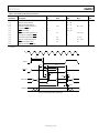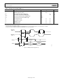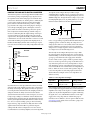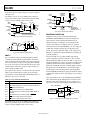
1
FEATURES FUNCTIONAL BLOCK DIAGRAM ANALOG I/O 8-channel, 247 kSPS, 12-Bit ADC DC performance: ±1 LSB INL AC performance: 71 dB SNR DMA controller for high speed ADC-to-RAM capture 2 12-bit (monotonic) voltage output DACs Dual output PWM/Σ-Δ DACs On-chip temperature sensor function: ±3°C On-chip voltage reference Memory 62 kB on-chip Flash/EE program memory 4 kB on-chip Flash/EE data memory Flash/EE, 100 Yr retention, 100,000 cycles of endurance 2304 bytes on-chip data RAM 8051-based core 8051-compatible instruction set (16 MHz maximum) 32 kHz external crystal, on-chip programmable PLL 12 interrupt sources, 2 priority levels Dual data pointer Extended 11-bit stack pointer On-chip peripherals Time interval counter (TIC) UART, I2C, and SPI Serial I/O Watchdog timer (WDT), power supply monitor (PSM) Power Specified for 3 V and 5 V operation Normal, idle, and power-down modes Power-down: 25 µA @ 3 V with wake-up timer running APPLICATIONS Optical networking—laser power control Base station systems Precision instrumentation, smart sensors Transient capture systems DAS and communications systems Upgrade to ADuC812 systems; runs from 32 kHz External crystal with on-chip PLL. Also available: ADuC831 pin-compatible upgrade to existing ADuC812 systems that require additional code or data memory; runs from 1 MHz to 16 MHz External crystal Rev. B ADuC832 ADC0 T/H ADC1 12-BIT DAC BUF DAC0 12-BIT DAC BUF DAC1 12-BIT ADC 16-BIT Σ-Δ DAC MUX ADC5 ADC6 HARDWARE CALIBRATON ADC7 16-BIT Σ-Δ DAC PWM0 MUX 16-BIT PWM TEMP SENSOR PWM1 16-BIT PWM 8051-BASED MCU WITH ADDITIONAL PERIPHERALS PLL INTERNAL BAND GAP VREF VREF 62 kB FLASH/EE PROGRAM MEMORY 4 kB FLASH/EE DATA MEMORY 2304 BYTES USER RAM POWER SUPPLY MON 3 × 16-BIT TIMERS 1 × REAL-TIME CLOCK WATCHDOG TIMER OSC 4 × PARALLEL PORTS XTAL1 UART, I2C, AND SPI SERIAL I/O XTAL2 02987-001 Data Sheet MicroConverter, 12-Bit ADCs and DACs with Embedded 62 kB Flash MCU ADuC832 Figure 1. GENERAL DESCRIPTION The ADuC832 is a complete, smart transducer front end, integrating a high performance self-calibrating multichannel 12-bit ADC, dual 12-bit DACs, and programmable 8-bit MCU on a single chip. The device operates from a 32 kHz crystal with an on-chip PLL, generating a high frequency clock of 16.78 MHz. This clock is, in turn, routed through a programmable clock divider from which the MCU core clock operating frequency is generated. The microcontroller core is an 8052 and is therefore 8051 instruction set compatible with 12 core clock periods per machine cycle. 62 kB of nonvolatile Flash/EE program memory are provided on chip. There are also 4 kB of nonvolatile Flash/EE data memory, 256 bytes of RAM, and 2 kB of extended RAM integrated on chip. The ADuC832 also incorporates additional analog functionality with two 12-bit DACs, a power supply monitor, and a band gap reference. On-chip digital peripherals include two 16-bit Σ-Δ DACs, a dual-output 16-bit PWM, a watchdog timer, time interval counter, three timers/counters, Timer 3 for baud rate generation, and serial I/O ports (SPI, I2C®, and UART). Document Feedback Information furnished by Analog Devices is believed to be accurate and reliable. However, no responsibility is assumed by Analog Devices for its use, nor for any infringements of patents or other rights of third parties that may result from its use. Specifications subject to change without notice. No license is granted by implication or otherwise under any patent or patent rights of Analog Devices. Trademarks and registered trademarks are the property of their respective owners. One Technology Way, P.O. Box 9106, Norwood, MA 02062-9106, U.S.A. Tel: 781.329.4700 ©2002–2013 Analog Devices, Inc. All rights reserved. Technical Support www.analog.com ADuC832 Data Sheet TABLE OF CONTENTS Features .............................................................................................. 1 Initiating Calibration in Code ...................................................... 44 Applications ....................................................................................... 1 Nonvolatile Flash/EE Memory ..................................................... 45 Functional Block Diagram .............................................................. 1 Flash/EE Memory Overview .................................................... 45 General Description ......................................................................... 1 Flash/EE Memory and the ADuC832 ..................................... 45 Revision History ............................................................................... 4 ADuC832 Flash/EE Memory Reliability ................................. 45 Specifications..................................................................................... 6 Using the Flash/EE Program Memory .................................... 46 Timing Specifications ................................................................ 10 Flash/EE Program Memory Security ....................................... 47 Absolute Maximum Ratings.......................................................... 20 Using the Flash/EE Data Memory ............................................... 48 ESD Caution ................................................................................ 20 ECON—Flash/EE Memory Control SFR ................................ 48 Pin Configurations and Function Descriptions ......................... 21 Example: Programming the Flash/EE Data Memory ............ 49 Typical Performance Characteristics ........................................... 26 Flash/EE Memory Timing ........................................................ 49 Terminology .................................................................................... 29 ADuC832 Configuration SFR (CFG832) ................................ 50 ADC Specifications .................................................................... 29 User Interface to Other On-Chip ADuC832 Peripherals ......... 51 DAC Specifications..................................................................... 29 DAC.............................................................................................. 51 Explanation of Typical Performance Plots .................................. 30 Using the DAC ............................................................................ 52 Memory Organization ................................................................... 31 On-Chip PLL................................................................................... 54 Flash/EE Program Memory ...................................................... 31 PLLCON (PLL Control Register)............................................. 54 Flash/EE Data Memory ............................................................. 31 Pulse-Width Modulator (PWM) .................................................. 55 General-Purpose RAM .............................................................. 31 PWMCON (PWM Control SFR) ............................................. 55 External Data Memory (External XRAM) .............................. 32 PWM Modes of Operation............................................................ 56 Internal XRAM ........................................................................... 32 Mode 0: PWM Disabled ............................................................ 56 Special Function Registers (SFRs) ................................................ 33 Mode 1: Single Variable Resolution PWM ............................. 56 Accumulator SFR (ACC) ........................................................... 33 Mode 2: Twin 8-Bit PWM ......................................................... 56 B SFR (B) ..................................................................................... 33 Mode 3: Twin 16-Bit PWM ....................................................... 56 Stack Pointer (SP and SPH)....................................................... 33 Mode 4: Dual NRZ 16-Bit Σ-Δ DAC ....................................... 57 Data Pointer (DPTR) ................................................................. 33 Mode 5: Dual 8-Bit PWM ......................................................... 57 Program Status Word (PSW) .................................................... 33 Mode 6: Dual RZ 16-Bit Σ-Δ DAC .......................................... 57 Power Control SFR (PCON) ..................................................... 33 Serial Peripheral Interface ............................................................. 58 Special Function Registers ............................................................. 34 MISO (Master Input, Slave Output Data Pin)............................ 58 ADC Circuit Information .............................................................. 35 MOSI (Master Output, Slave Input Pin) ................................. 58 General Overview....................................................................... 35 SCLOCK (Serial Clock I/O Pin) .............................................. 58 ADC Transfer Function ............................................................. 35 SS (Slave Select Input Pin)......................................................... 58 Typical Operation ....................................................................... 35 Using the SPI Interface .............................................................. 59 Driving the Analog-to-Digital Converter ............................... 39 SPI Interface—Master Mode .................................................... 59 Voltage Reference Connections ................................................ 40 SPI Interface—Slave Mode ........................................................ 59 Configuring the ADC ................................................................ 41 I C-Compatible Interface .............................................................. 60 ADC DMA Mode ....................................................................... 41 I2C Interface SFRs....................................................................... 60 Micro-Operation During ADC DMA Mode .......................... 42 Overview ..................................................................................... 61 ADC Offset and Gain Calibration Coefficients ..................... 42 Software Master Mode ............................................................... 61 Calibrating the ADC ...................................................................... 43 Hardware Slave Mode ................................................................ 61 2 Rev. B | Page 2 of 92 Data Sheet ADuC832 Dual Data Pointers ..........................................................................62 SCON (UART Serial Port Control Register) ........................... 75 DPCON (Data Pointer Control SFR) .......................................62 Mode 0: 8-Bit Shift Register Mode ........................................... 76 Power Supply Monitor ....................................................................63 Mode 1: 8-Bit UART, Variable Baud Rate ................................ 76 PSMCON (Power Supply Monitor Control Register ) ...........63 Mode 2: 9-Bit UART with Fixed Baud Rate ............................ 76 Watchdog Timer ..............................................................................64 Mode 3: 9-Bit UART with Variable Baud Rate........................ 76 Time Interval Counter (TIC) .........................................................65 UART Serial Port Baud Rate Generation................................. 77 TIMECON (TIC Control Register) ..........................................65 Timer 1 Generated Baud Rates ................................................. 77 INTVAL (User Time Interval Select Register) ........................66 Timer 2 Generated Baud Rates ................................................. 77 HTHSEC (Hundredths Seconds Time Register) ....................66 Timer 3 Generated Baud Rates ................................................. 78 SEC (Seconds Time Register) ....................................................66 Interrupt System .............................................................................. 80 MIN (Minutes Time Register)...................................................66 IE (Interrupt Enable Register) ................................................... 80 HOUR (Hours Time Register) ..................................................66 IP (Interrupt Priority Register ) ................................................ 80 8052-Compatible On-Chip Peripherals .......................................67 IEIP2 (Secondary Interrupt Enable Register) ......................... 80 Parallel I/O ...................................................................................67 Interrupt Priority ........................................................................ 81 Port 0 .............................................................................................67 Interrupt Vectors ......................................................................... 81 Port 1 .............................................................................................67 ADuC832 Hardware Design Considerations .............................. 82 Port 2 .............................................................................................67 Clock Oscillator........................................................................... 82 Port 3 .............................................................................................68 External Memory Interface........................................................ 82 Additional Digital I/O ................................................................68 Power Supplies............................................................................. 83 Read-Modify-Write Instructions ..............................................69 Power Consumption ................................................................... 84 Timers/Counters .........................................................................70 Power Saving Modes ................................................................... 84 Timer/Counter 0 and Timer/Counter 1 Data Registers ........71 Power-On Reset........................................................................... 84 Timer/Counter 0 And Timer/Counter 1 Operating Modes ......72 Grounding and Board Layout Recommendations ................. 85 Mode 0 (13-Bit Timer/Counter) ...............................................72 Other Hardware Considerations ................................................... 87 Mode 1 (16-Bit Timer/Counter) ...............................................72 In-Circuit Serial Download Access .......................................... 87 Mode 2 (8-Bit Timer/Counter with Autoreload) ....................72 Embedded Serial Port Debugger .............................................. 87 Mode 3 (Two 8-Bit Timer/Counters) .......................................72 Single-Pin Emulation Mode ...................................................... 87 Timer/Counter 2 .............................................................................73 Typical System Configuration ................................................... 87 T2CON (Timer/Counter 2 Control Register) .........................73 Development Tools ......................................................................... 88 Timer/Counter 2 Data Registers ...............................................73 QuickStart Development System .............................................. 88 Timer/Counter Operation Modes ............................................74 QuickStart Plus Development System...................................... 88 UART Serial Interface .....................................................................75 Outline Dimensions ........................................................................ 89 SBUF .............................................................................................75 Ordering Guide ........................................................................... 89 Rev. B | Page 3 of 92 ADuC832 Data Sheet REVISION HISTORY 4/13—Rev. A to Rev. B Updated Outline Dimensions ....................................................... 89 Changes to Ordering Guide .......................................................... 89 9/09—Rev. 0 to Rev. A Changes to Figure 1 .......................................................................... 1 Changed 16.77 MHz to 16.78 MHz Throughout ......................... 1 Changes to Reference Input/Output, Output Voltage Parameter, Endnote 19, and Endnote 20, Table 1 ............................................ 9 Moved Timing Specifications Section ......................................... 10 Changes to Figure 3 ........................................................................ 10 Changes to Table 3 .......................................................................... 11 Changes to Table 4 .......................................................................... 12 Changes to Table 5 .......................................................................... 13 Changes to Table 11 ........................................................................ 19 Changes to Figure 15 and Table 13............................................... 21 Changes to Figure 16, Figure 17, Figure 20, and Figure 21 ....... 26 Added Explanation of Typical Performance Plots Section ....... 30 Changes to Flash/EE Program Memory, Flash/EE Data Memory, and General-Purpose RAM Sections .......................... 31 Changes to Figure 36 ...................................................................... 34 Changes to Figure 39 and Figure 40 ............................................. 39 Changes to Table 20 ........................................................................ 40 Changes to A Typical DMA Mode Configuration Example Section .............................................................................................. 41 Changed 16.777216 MHz to 16.78 MHz Throughout .............. 41 Changes to Table 21 ....................................................................... 48 Changes to Using the DAC Section and Figure 52 .................... 52 Changes to Figure 54 Caption ...................................................... 53 Changes to Figure 56...................................................................... 55 Changed 16.77 MHz to 16.78 MHz ............................................. 56 Changes to Figure 60...................................................................... 57 Changes to Table 31 ....................................................................... 63 Deleted Figure 65 and Figure 66; Renumbered Sequentially ... 66 Deleted ASPIRE—IDE Section..................................................... 66 Deleted Figure 67............................................................................ 67 Changes to Table 34 ....................................................................... 67 Changes to Figure 68, Figure 69, Figure 70, and Table 35 ........ 68 Changes to Figure 84...................................................................... 78 Changes to External Memory Interface Section ........................ 82 Changes to Power Supplies Section ............................................. 83 Changes to Table 50 ....................................................................... 84 Changes to Figure 94...................................................................... 86 Changes to Single-Pin Emulation Mode Section ....................... 87 Changes to QuickStart Development System Section and QuickStart Plus Development System Section ........................... 88 Updated Outline Dimensions ....................................................... 89 Changes to Ordering Guide .......................................................... 89 11/02—Revision 0: Initial Version Rev. B | Page 4 of 92 Data Sheet ADuC832 diagram of the ADuC832 is shown in Figure 1 with a more detailed block diagram shown in Figure 2. On-chip factory firmware supports in-circuit serial download and debug modes (via UART) as well as single-pin emulation mode via the EA pin. The ADuC832 is supported by QuickStart™ and QuickStart Plus development systems featuring low cost software and hardware development tools. A functional block The part is specified for 3 V and 5 V operation over the extended industrial temperature range and is available in a 52-lead metric quad flat package (MQFP) and a 56-lead lead frame chip scale package (LFCSP). ADuC832 DAC1 16-BIT Σ-Δ DAC PWM CONTROL ADC6 ADC7 T2 PROG. CLOCK DIVIDER PLL MISO SCLOCK SYNCHRONOUS SERIAL INTERFACE (SPI OR I2C ) SDATA/MOSI SINGLE-PIN EMULATOR EA ALE UART TIMER Figure 2. ADuC832 Block Diagram (Shaded Areas are Features Not Present on the ADuC812) Rev. B | Page 5 of 92 INT0 INT1 TIME INTERVAL COUNTER (WAKEUP CCT) PSEN TxD RxD RESET DGND DGND DVDD DGND DVDD DVDD AVDD AGND POR T1 POWER SUPPLY MONITOR DOWNLOADER DEBUGGER ASYNCHRONOUS SERIAL PORT (UART) T0 T2EX MCU CORE 2 × DATA POINTERS 11-BIT STACK POINTER CREF PWM1 16-BIT COUNTER TIMERS SS BUF WATCHDOG TIMER 8052 2 kB USER XRAM VREF 16-BIT PWM 256 BYTES USER RAM 4 kB DATA FLASH/EE BAND GAP REFERENCE PWM0 MUX 16-BIT PWM 62 kB PROGRAM FLASH/EE INCLUDING USER DOWNLOAD MODE TEMP SENSOR 16-BIT Σ-Δ DAC OSC 02987-004 MUX 12-BIT VOLTAGE OUTPUT DAC XTAL1 ADC1 DAC CONTROL ADC CONTROL AND CALIBRATION 12-BIT ADC T/H DAC0 XTAL2 ADC0 12-BIT VOLTAGE OUTPUT DAC ADuC832 Data Sheet SPECIFICATIONS AVDD = DVDD = 2.7 V to 3.3 V or 4.5 V to 5.5 V; VREF = 2.5 V internal reference, fCORE = 16.78 MHz; all specifications TA = TMIN to TMAX, unless otherwise noted. Table 1. Parameter 1 ADC CHANNEL SPECIFICATIONS DC Accuracy 2, 3 VDD = 5 V Resolution Integral Nonlinearity 12 ±1 ±0.3 ±0.9 ±0.25 ±1.5 +1.5/−0.9 1 12 ±1 ±0.3 ±0.9 ±0.25 ±1.5 +1.5/−0.9 1 Bits LSB max LSB typ LSB max LSB typ LSB max LSB max LSB typ ±4 ±1 ±2 −85 ±4 ±1 ±3 −85 LSB max LSB typ LSB max dB typ 71 −85 −85 −80 71 −85 −85 −80 dB typ dB typ dB typ dB typ 0 to VREF ±1 32 0 to VREF ±1 32 V μA max pF typ 650 −2.0 ±3 ±1.5 650 −2.0 ±3 ±1.5 mV typ mV/°C typ °C typ °C typ 12 ±3 −1 ±1/2 ±50 ±1 ±1 0.5 12 ±3 −1 ±1/2 ±50 ±1 ±1 0.5 Bits LSB typ LSB max LSB typ mV max % max % typ % typ 0 to VREF 0 to VDD 0.5 0 to VREF 0 to VDD 0.5 V typ V typ Ω typ DAC VREF = 2.5 V DAC VREF = VDD 15 15 μs typ 10 10 nV sec typ Full-scale settling time to within ½ LSB of final value 1 LSB change at major carry Differential Nonlinearity Integral Nonlinearity 4 Differential Nonlinearity4 Code Distribution Calibrated Endpoint Errors 5, 6 Offset Error Offset Error Match Gain Error Gain Error Match Dynamic Performance Signal-to-Noise Ratio (SNR) 7 Total Harmonic Distortion (THD) Peak Harmonic or Spurious Noise Channel-to-Channel Crosstalk 8 Analog Input Input Voltage Ranges Leakage Current Input Capacitance Temperature Sensor 9 Voltage Output at 25°C Voltage TC Accuracy DAC CHANNEL SPECIFICATIONS, INTERNAL BUFFER ENABLED DC Accuracy 10 Resolution Relative Accuracy Differential Nonlinearity 11 Offset Error Gain Error Gain Error Mismatch Analog Outputs Voltage Range 0 Voltage Range 1 Output Impedance DAC AC Characteristics Voltage Output Settling Time Digital-to-Analog Glitch Energy VDD = 3 V Unit Test Conditions/Comments fS = 147 kHz, see Figure 16 to Figure 21 at other fS For 2.5 V internal reference 2.5 V internal reference 1 V external reference 1 V external reference ADC input is a dc voltage fIN = 10 kHz sine wave, fS = 147 kHz Rev. B | Page 6 of 92 Internal 2.5 V VREF External 2.5 V VREF DAC load to AGND, RL = 10 kΩ, CL = 100 pF Guaranteed 12-bit monotonic VREF range AVDD range VREF range % of full scale on DAC1 Data Sheet Parameter 1 DAC CHANNEL SPECIFICATIONS 12, 13, INTERNAL BUFFER DISABLED DC Accuracy10 Resolution Relative Accuracy Differential Nonlinearity11 Offset Error Gain Error Gain Error Mismatch4 Analog outputs Voltage Range 0 REFERENCE INPUT/OUTPUT Reference Output 14 Output Voltage (VREF) Accuracy Power Supply Rejection Reference Temperature Coefficient Internal VREF Power-On Time External Reference Input 15 Voltage Range (VREF)4 Input Impedance Input Leakage POWER SUPPLY MONITOR (PSM) DVDD Trip Point Selection Range DVDD Power Supply Trip Point Accuracy WATCHDOG TIMER (WDT)4 Timeout Period ADuC832 VDD = 5 V VDD = 3 V Unit Test Conditions/Comments 12 ±3 −1 ±1/2 ±5 −0.3 0.5 12 ±3 −1 ±1/2 ±5 −0.3 0.5 Bits LSB typ LSB max LSB typ mV max % typ % max VREF range VREF range % of full scale on DAC1 0 to VREF 0 to VREF V typ DAC VREF = 2.5 V 2.5 ±2.5 47 ±100 2.5 ±2.5 47 ±100 80 80 V typ % max dB typ ppm/°C typ ms typ 0.1 VDD 20 1 0.1 VDD 20 1 V min V max kΩ typ μA max Guaranteed 12-bit monotonic Of VREF measured at the CREF pin VREF and CREF pins shorted 2.63 4.37 ±3.5 Internal band gap deselected via ADCCON1[6] V min V max % max Four trip points selectable in this range programmed via TPD1 and TPD0 in PSMCON Nine timeout periods Selectable in this range 0 2000 0 2000 ms min ms max 100,000 100 100,000 100 Cycles min Years min 2.4 0.8 ±10 ±1 2 0.4 ±10 ±1 V min V max μA max μA typ ±10 ±1 −75 −40 −660 −400 ±10 ±1 −25 −15 −250 −140 μA max μA typ μA max μA typ μA max μA typ FLASH/EE MEMORY RELIABILITY CHARACTERISTICS 16 Endurance 17 Data Retention 18 DIGITAL INPUTS Input High Voltage (VINH)4 Input Low Voltage (VINL)4 Input Leakage Current (Port 0, EA) VIN = 0 V or VDD VIN = 0 V or VDD Logic 1 Input Current (All Digital Inputs) Logic 0 Input Current (Port 1, Port 2, and Port 3) Logic 1-to-Logic 0 Transition Current (Port 2, Port 3) Rev. B | Page 7 of 92 VIN = VDD VIN = VDD VIL = 450 mV VIL = 2 V VIL = 2 V ADuC832 Parameter 1 SCLOCK and RESET ONLY4 (Schmitt-Triggered Inputs) VT+ VT− VT+ − VT− CRYSTAL OSCILLATOR Logic Inputs, XTAL1 Only VINL, Input Low Voltage VINH, Input High Voltage XTAL1 Input Capacitance XTAL2 Output Capacitance MCU CLOCK RATE DIGITAL OUTPUTS Output High Voltage (VOH) Output Low Voltage (VOL) ALE, Port 0 and Port 2 Port 3 SCLOCK/SDATA Floating State Leakage Current4 Floating State Output Capacitance START-UP TIME At Power-On From Idle Mode From Power-Down Mode Wakeup with INT0 Interrupt Wakeup with SPI/I2C Interrupt Wakeup with External Reset After External Reset in Normal Mode After WDT Reset in Normal Mode POWER REQUIREMENTS 19, 20 Power Supply Voltages AVDD/DVDD − AGND Data Sheet VDD = 5 V VDD = 3 V Unit 1.3 3.0 0.8 1.4 0.3 0.85 0.95 2.5 0.4 1.1 0.3 0.85 V min V max V min V max V min V max 0.8 3.5 18 18 16.78 0.4 2.5 18 18 16.78 V typ V typ pF typ pF typ MHz max Programmable via PLLCON[2:0] 2.4 2.6 V min V typ V min V typ VDD = 4.5 V to 5.5 V ISOURCE = 80 μA VDD = 2.7 V to 3.3 V ISOURCE = 20 μA 0.4 0.2 0.4 0.4 ±10 ±1 10 0.4 0.2 0.4 0.4 ±10 ±1 10 V max V typ V max V max μA max μA typ pF typ ISINK = 1.6 mA ISINK = 1.6 mA ISINK = 4 mA ISINK = 8 mA, I2C enabled 500 100 500 100 ms typ μs typ 150 150 150 30 3 400 400 400 30 3 μs typ μs typ μs typ ms typ ms typ 2.7 3.3 V min V max V min V max AVDD/DVDD = 3 V nom 2.4 4.0 At any Core_CLK 4.5 5.5 Power Supply Currents Normal Mode DVDD Current4 AVDD Current DVDD Current AVDD Current Power Supply Currents Idle Mode DVDD Current AVDD Current DVDD Current4 AVDD Current Test Conditions/Comments Controlled via WDCON SFR AVDD/DVDD = 5 V nom 6 1.7 23 20 1.7 3 1.7 12 10 1.7 mA max mA max mA max mA typ mA max Core_CLK = 2.097 MHz Core_CLK = 2.097 MHz Core_CLK = 16.78 MHz Core_CLK = 16.78 MHz Core_CLK = 16.78 MHz 4 0.14 10 9 0.14 2 0.14 5 4 0.14 mA typ mA typ mA max mA typ mA typ Core_CLK = 2.097 MHz Core_CLK = 2.097 MHz Core_CLK = 16.78 MHz Core_CLK = 16.78 MHz Core_CLK = 16.78 MHz Rev. B | Page 8 of 92 Data Sheet Parameter 1 Power Supply Currents Power-Down Mode DVDD Current4 AVDD Current DVDD Current Typical Additional Power Supply Currents PSM Peripheral ADC DAC ADuC832 VDD = 5 V VDD = 3 V Unit 80 38 2 35 25 25 14 1 20 12 μA max μA typ μA typ μA max μA typ Test Conditions/Comments Core_CLK = 2.097 MHz or 16.78 MHz Oscillator on Oscillator off AVDD = DVDD = 5 V 50 1.5 150 μA typ mA typ μA typ Temperature range: −40°C to +125°C. ADC linearity is guaranteed during normal MicroConverter core operation. 3 ADC LSB size = VREF/212, that is, for internal VREF = 2.5 V, 1 LSB = 610 µV and for external VREF = 1 V, 1 LSB = 244 µV. 4 Not production tested, but are guaranteed by design and/or characterization data on production release. 5 Offset error, gain error, offset error match, and gain error match are measured after factory calibration. 6 Based on external ADC system components, the user may need to execute a system calibration to remove additional external channel errors and achieve these specifications. 7 SNR calculation includes distortion and noise components. 8 Channel-to-channel crosstalk is measured on adjacent channels. 9 The temperature sensor gives a measure of the die temperature directly; air temperature can be inferred from this result. 10 DAC linearity is calculated using: Reduced code range of 100 to 4095, 0 V to VREF range. Reduced code range of 100 to 3945, 0 V to VDD range. DAC output load = 10 kΩ and 100 pF. 11 DAC differential nonlinearity specified on 0 V to VREF and 0 V to VDD ranges. 12 DAC specification for output impedance in the unbuffered case depends on DAC code. 13 DAC specifications for ISINK, voltage output settling time, and digital-to-analog glitch energy depend on external buffer implementation in unbuffered mode. DAC in unbuffered mode tested with OP270 external buffer, which has a low input leakage current. 14 Measured with VREF and CREF pins decoupled with 0.1 µF capacitors to ground. Power-up time for the internal reference is determined by the value of the decoupling capacitor chosen for both the VREF and CREF pins. 15 When using an external reference device, the internal band gap reference input can be bypassed by setting the ADCCON1[6] bit. In this mode, the VREF and CREF pins need to be shorted together for correct operation. 16 Flash/EE Memory reliability characteristics apply to both the Flash/EE program memory and the Flash/EE data memory. 17 Endurance is qualified to 100,000 cycles as per JEDEC Std. 22 method A117 and measured at −40°C, +25°C, and +125°C. Typical endurance at 25°C is 700,000 cycles. 18 Retention lifetime equivalent at junction temperature (TJ) = 55°C as per JEDEC Std. 22 Method A117. Retention lifetime based on an activation energy of 0.6 eV derates with junction temperature as shown in Figure 48 in the ADuC832 Flash/EE Memory Reliability section. 19 Power supply current consumption is measured in normal, idle, and power-down modes under the following conditions: Normal mode: RESET = 0.4 V, digital I/O pins = open circuit, Core_CLK changed via the CD bits in PLLCON[2:0], core executing internal software loop. Idle mode: RESET = 0.4 V, digital I/O pins = open circuit, Core_CLK changed via the CD bits in PLLCON, PCON[0] = 1, core execution suspended in idle mode. Power-down mode: RESET = 0.4 V, all Port 0 pins = 0.4 V, all other digital I/O and Port 1 pins are open circuit, Core_CLK changed via the CD bits in PLLCON, PCON[1] = 1, core execution suspended in power-down mode, oscillator turned on or off via OSC_PD bit (PLLCON[7]). 20 DVDD power supply current increases typically by 3 mA (3 V operation) and 10 mA (5 V operation) during a Flash/EE memory program or erase cycle. 1 2 Rev. B | Page 9 of 92 ADuC832 Data Sheet TIMING SPECIFICATIONS AVDD = 2.7 V to 3.6 V or 4.75 V to 5.25 V, DVDD = 2.7 V to 3.6 V or 4.75 V to 5.25 V; all specifications TMIN to TMAX, unless otherwise noted. Table 2. Clock Input (External Clock Applied on XTAL1) Parameter1, 2, 3 tCK tCKL tCKH tCKR tCKF 1/tCORE tCORE tCYC Description XTAL1 period (see Figure 3) XTAL1 width low (see Figure 3) XTAL1 width high (see Figure 3) XTAL1 rise time (see Figure 3) XTAL1 fall time (see Figure 3) ADuC832 core clock frequency4 ADuC832 core clock period5 ADuC832 machine cycle time6 Min 0.131 0.72 32.768 kHz External Crystal Typ Max 30.52 15.16 15.16 20 20 16.78 0.476 5.7 91.55 1 Unit μs μs μs ns ns MHz μs μs AC inputs during testing are driven at DVDD − 0.5 V for a Logic 1 and 0.45 V for a Logic 0. Timing measurements are made at VIH minimum for a Logic 1 and VIL maximum for a Logic 0, as shown in Figure 4. 2 For timing purposes, a port pin is no longer floating when a 100 mV change from load voltage occurs. A port pin begins to float when a 100 mV change from the loaded VOH/VOL level occurs, as shown in Figure 4. 3 CLOAD for all outputs = 80 pF, unless otherwise noted. 4 The ADuC832 internal PLL locks onto a multiple (512 times) the external crystal frequency of 32.768 kHz to provide a stable 16.78 MHz internal clock for the system. The core can operate at this frequency or at a binary submultiple called Core_CLK, selected via the PLLCON SFR. 5 This number is measured at the default Core_CLK operating frequency of 2.09 MHz. 6 ADuC832 machine cycle time is nominally defined as 12/Core_CLK. tCKR tCKL tCKF tCK 02987-086 tCKH Figure 3. XTAL1 Input 0.45V 0.2DV DD + 0.9V TEST POINTS 0.2DV DD – 0.1V VLOAD – 0.1V VLOAD VLOAD + 0.1V TIMING REFERENCE POINTS Figure 4. Timing Waveform Characteristics Rev. B | Page 10 of 92 VLOAD – 0.1V VLOAD VLOAD + 0.1V 02987-087 DVDD –0.5V Data Sheet ADuC832 Table 3. External Program Memory Read Cycle Parameter1 tLHLL tAVLL tLLAX tLLIV tLLPL tPLPH tPLIV tPXIX tPXIZ tAVIV tPLAZ tPHAX Min 79 19 29 16.78 MHz Core_CLK Max 138 29 133 73 0 34 193 25 0 Variable Clock Min Max 2tCK − 40 tCK − 40 tCK − 30 4tCK − 100 tCK − 30 3tCK − 45 3tCK − 105 0 tCK − 25 5tCK − 105 25 0 See Figure 5. MCLK tLHLL ALE (O) tAVLL tLLPL tPLPH tLLIV tPLIV PSEN (O) PORT 0 (I/O) tPXIZ tPLAZ tLLAX tPXIX INSTRUCTION (IN) PCL (OUT) tAVIV PORT 2 (O) tPHAX PCH Figure 5. External Program Memory Read Cycle Rev. B | Page 11 of 92 02987-088 1 Description ALE pulse width Address valid to ALE low Address hold after ALE low ALE low to valid instruction in ALE low to PSEN low PSEN pulse width PSEN low to valid instruction in Instruction in, hold after PSEN Instruction in, float after PSEN Address to valid instruction in PSEN low to address float Address hold after PSEN high Unit ns ns ns ns ns ns ns ns ns ns ns ns ADuC832 Data Sheet Table 4. External Data Memory Read Cycle Parameter1 tRLRH tAVLL tLLAX tRLDV tRHDX tRHDZ tLLDV tAVDV tLLWL tAVWL tRLAZ tWHLH Variable Clock Min Max 6tCK − 100 tCK − 40 tCK − 35 5tCK − 165 0 2tCK − 70 8tCK − 150 9tCK − 165 3tCK − 50 3tCK +50 4tCK − 130 0 tCK − 40 6tCK − 100 See Figure 6. MCLK ALE (O) tWHLH PSEN (O) tLLDV tLLWL RD (O) tRLRH tAVWL tRLDV tAVLL tRHDZ tLLAX tRHDX tRLAZ PORT 0 (I/O) A0 TO A7 (OUT) D0 TO D7 (IN) tAVDV PORT 2 (O) A16 TO A23 A8 TO A15 Figure 6. External Data Memory Read Cycle Rev. B | Page 12 of 92 02987-089 1 16.78 MHz Core_CLK Min Max 257 19 24 133 0 49 326 371 128 228 108 0 19 257 Description RD pulse width Address valid before ALE low Address hold after ALE low RD low to valid data in Data and address hold after RD Data float after RD ALE low to valid data in Address to valid data in ALE low to RD low Address valid to RD low RD low to address float RD high to ALE high Unit ns ns ns ns ns ns ns ns ns ns ns ns Data Sheet ADuC832 Table 5. External Data Memory Write Cycle Parameter 1 tWLWH tAVLL tLLAX tLLWL tAVWL tQVWX tQVWH tWHQX tWHLH Variable Clock Min Max 6tCK − 100 tCK − 40 tCK − 35 3tCK − 50 3tCK +50 4tCK − 130 tCK − 50 7tCK − 150 tCK − 50 tCK − 40 6tCK − 100 See Figure 7. MCLK ALE (O) tWHLH PSEN (O) tLLWL tWLWH WR (O) tAVWL tAVLL tLLAX A0 TO A7 PORT 2 (O) A16 TO A23 tQVWX tWHQX tQVWH DATA A8 TO A15 Figure 7. External Data Memory Write Cycle Rev. B | Page 13 of 92 02987-090 1 16.78 MHz Core_CLK Min Max 257 19 24 128 228 108 9 267 9 19 257 Description WR pulse width Address valid before ALE low Address hold after ALE low ALE low to WR low Address valid to WR Low Data valid to WR transition Data setup before WR Data and address hold after WR WR high to ALE high Unit ns ns ns ns ns ns ns ns ns ADuC832 Data Sheet Table 6. UART Timing (Shift Register Mode) Parameter 1 tXLXL tQVXH tDVXH tXHDX tXHQX Variable Clock Typ 12tCK 10tCK − 133 2tCK + 133 0 2tCK − 117 Min Max See Figure 8. ALE (O) tXLXL TxD (OUTPUT CLOCK) 6 1 0 7 SET RI OR SET TI tQVXH tXHQX RxD (OUTPUT DATA) MSB BIT 6 BIT 1 tDVXH RxD (INPUT DATA) MSB LSB tXHDX BIT 6 Figure 8. UART Timing in Shift Register Mode Rev. B | Page 14 of 92 BIT 1 LSB 02987-091 1 16.78 MHz Core_CLK Min Typ Max 715 463 252 0 22 Description Serial port clock cycle time Output data setup to clock Input data setup to clock Input data hold after clock Output data hold after clock Unit μs ns ns ns ns Data Sheet ADuC832 Table 7. I2C-Compatible Interface Timing Parameter 1 tL tH tSHD tDSU tDHD tRSU tPSU tBUF tR tF tSUP 2 2 Min 4.7 4.0 0.6 100 Max Unit μs μs μs μs μs μs μs μs ns ns ns 0.9 0.6 0.6 1.3 300 300 50 See Figure 9. Input filtering on both the SCLOCK and SDATA inputs suppresses noise spikes less than 50 ns. tBUF tSUP SDATA (I/O) LSB MSB tDSU tPSU tDSU 2–7 8 PS tL MSB tF tDHD tR tRSU tH 1 START STOP CONDITION CONDITION ACK tDHD tSHD SCLOCK (I) tR 1 9 tSUP Figure 9. I2C Compatible Interface Timing Rev. B | Page 15 of 92 S(R) REPEATED START tF 02987-092 1 Description SCLOCK low pulse width SCLOCK high pulse width Start condition hold time Data setup time Data hold time Setup time for repeated start Stop condition setup time Bus free time between a stop condition and a start condition Rise time of both SCLOCK and SDATA Fall time of both SCLOCK and SDATA Pulse width of spike suppressed ADuC832 Data Sheet Table 8. SPI Master Mode Timing (CPHA = 1) Parameter1 tSL tSH tDAV tDSU tDHD tDF tDR tSR tSF 2 Min Typ 476 476 Max Unit ns ns ns ns ns ns ns ns ns 50 100 100 10 10 10 10 25 25 25 25 See Figure 10. Characterized under the following conditions: a. Core clock divider bits (CD2, CD1, and CD0 bits in PLLCON SFR) set to 0, 1, and 1, respectively, that is, core clock frequency = 2.09 MHz b. SPI bit rate selection bits (SPR1 and SPR0 bits in SPICON SFR) set to 0 and 0, respectively. SCLOCK (O) (CPOL = 0) tSL tSH tSR tSF SCLOCK (O) (CPOL = 1) tDAV tDF MSB MOSI (O) MISO (I) tDR MSB IN tDSU LSB BIT 6 TO 1 BIT 6 TO 1 LSB IN 02987-093 1 Description SCLOCK low pulse width2 SCLOCK high pulse width2 Data output valid after SCLOCK edge Data input setup time before SCLOCK edge Data input hold time after SCLOCK edge Data output fall time Data output rise time SCLOCK rise time SCLOCK fall time tDHD Figure 10. SPI Master Mode Timing (CPHA = 1) Rev. B | Page 16 of 92 Data Sheet ADuC832 Table 9. SPI Master Mode Timing (CPHA = 0) Parameter 1 tSL tSH tDAV tDOSU tDSU tDHD tDF tDR tSR tSF 2 Min Typ 476 476 Max Unit ns ns ns ns ns ns ns ns ns ns 50 150 100 100 10 10 10 10 25 25 25 25 See Figure 11. Characterized under the following conditions: a. Core clock divider bits (CD2, CD1, and CD0 bits in PLLCON SFR) set to 0, 1, and 1, respectively, that is, core clock frequency = 2.09 MHz b. SPI bit rate selection bits (SPR1 and SPR0 bits in SPICON SFR) set to 0 and 0, respectively. SCLOCK (O) (CPOL = 0) tSL tSH tSF tSR SCLOCK (O) (CPOL = 1) tDAV tDF tDOSU MSB MISO (O) MOSI (I) MSB IN tDSU tDR LSB BIT 6 TO 1 BIT 6 TO 1 LSB IN 02987-094 1 Description SCLOCK low pulse width 2 SCLOCK high pulse width2 Data output valid after SCLOCK edge Data output setup before SCLOCK edge Data input setup time before SCLOCK edge Data input hold time after SCLOCK edge Data output fall time Data output rise time SCLOCK rise time SCLOCK fall time tDHD Figure 11. SPI Master Mode Timing (CPHA = 0) Rev. B | Page 17 of 92 ADuC832 Data Sheet Table 10. SPI Slave Mode Timing (CPHA = 1) Parameter 1 tSS tSL tSH tDAV tDSU tDHD tDF tDR tSR tSF tSFS Min 0 Typ Max 330 330 50 100 100 10 10 10 10 25 25 25 25 0 See Figure 12. SS (I) tSFS tSS SCLOCK (I) (CPOL = 0) tSH tSR tSL tSF SCLOCK (I) (CPOL = 1) tDAV tDF MISO (O) MOSI (I) MSB MSB IN tDSU tDR BITS 6 TO 1 BITS 6 TO 1 LSB LSB IN 02987-095 1 Description SS to SCLOCK edge SCLOCK low pulse width SCLOCK high pulse width Data output valid after SCLOCK edge Data input setup time before SCLOCK edge Data input hold time after SCLOCK edge Data output fall time Data output rise time SCLOCK rise time SCLOCK fall time SS high after SCLOCK edge tDHD Figure 12. SPI Slave Mode Timing (CPHA = 1) Rev. B | Page 18 of 92 Unit ns ns ns ns ns ns ns ns ns ns ns Data Sheet ADuC832 Table 11. SPI Slave Mode Timing (CPHA = 0) Parameter 1 tSS tSL tSH tDAV tDSU tDHD tDF tDR tSR tSF tDOSS tSFS Min 0 Typ Max 330 330 50 100 100 10 10 10 10 25 25 25 25 20 0 See Figure 13. SS (I) tSFS tSS SCLOCK (I) (CPOL = 0) tSH tSL tSR tSF SCLOCK (I) (CPOL = 1) tDAV tDOSS tDF MSB MISO (O) MOSI (I) MSB IN t DSU tDR BIT 6 TO BIT 1 BIT 6 TO BIT 1 LSB LSB IN 02987-096 1 Description SS to SCLOCK edge SCLOCK low pulse width SCLOCK high pulse width Data output valid after SCLOCK edge Data input setup time before SCLOCK edge Data input hold time after SCLOCK edge Data output fall time Data output rise time SCLOCK rise time SCLOCK fall time Data output valid after SS edge SS high after SCLOCK edge t DHD Figure 13. SPI Slave Mode Timing (CPHA = 0) Rev. B | Page 19 of 92 Unit ns ns ns ns ns ns ns ns ns ns ns ns ADuC832 Data Sheet ABSOLUTE MAXIMUM RATINGS TA = 25°C, unless otherwise noted. Table 12. Parameter AVDD to DVDD AGND to DGND DVDD to DGND, AVDD to AGND Digital Input Voltage to DGND Digital Output Voltage to DGND VREF to AGND Analog Inputs to AGND Operating Temperature Range Industrial ADuC832BS Operating Temperature Range Industrial ADuC832BCP Storage Temperature Range Junction Temperature θJA Thermal Impedance (ADuC832BS) θJA Thermal Impedance (ADuC832BCP) Lead Temperature, Soldering Vapor Phase (60 sec) Infrared (15 sec) Rating −0.3 V to +0.3 V −0.3 V to +0.3 V −0.3 V to +7 V −0.3 V to DVDD + 0.3 V −0.3 V to DVDD + 0.3 V −0.3 V to AVDD + 0.3 V −0.3 V to AVDD + 0.3 V Stresses above those listed under Absolute Maximum Ratings may cause permanent damage to the device. This is a stress rating only; functional operation of the device at these or any other conditions above those indicated in the operational section of this specification is not implied. Exposure to absolute maximum rating conditions for extended periods may affect device reliability. ESD CAUTION −40°C to +125°C −40°C to +85°C −65°C to +150°C 150°C 90°C/W 52°C/W 215°C 220°C Rev. B | Page 20 of 92 Data Sheet ADuC832 P1.0/ADC0/T2 P0.7/AD7 P0.6/AD6 P0.5/AD5 P0.4/AD4 DVDD DGND P0.3/AD3 P0.2/AD2 P0.1/AD1 P0.0/AD0 ALE PSEN EA PSEN EA P0.1/AD1 P0.0/AD0 ALE P0.5/AD5 P0.4/AD4 DVDD DGND P0.3/AD3 P0.2/AD2 P0.7/AD7 P0.6/AD6 PIN CONFIGURATIONS AND FUNCTION DESCRIPTIONS 52 51 50 49 48 47 46 45 44 43 42 41 40 39 P2.7/PWM1/A15/A23 PIN 1 IDENTIFIER 38 P2.6/PWM0/A14/A22 37 P2.5/A13/A21 P1.1/ADC1/T2EX P1.2/ADC2 P1.3/ADC3 AVDD AVDD AGND AGND AGND CREF VREF DAC0 DAC1 P1.4/ADC4 P1.5/ADC5/SS 36 P2.4/A12/A20 35 DGND 6 ADuC832 7 TOP VIEW (Not to Scale) 8 34 DVDD 33 XTAL2 32 XTAL1 9 31 P2.3/A11/A19 10 30 P2.2/A10/A18 11 29 P2.1/A9/A17 P1.5/ADC5/SS 12 P1.6/ADC6 13 28 P2.0/A8/A16 27 SDATA/MOSI PIN 1 INDICATOR ADuC832 TOP VIEW (Not to Scale) 42 41 40 39 38 37 36 35 34 33 32 31 30 29 P2.7/PWM1/A15/A23 P2.6/PWM0/A14/A22 P2.5/A13/A21 P2.4/A12/A20 DGND DGND DVDD XTAL2 XTAL1 P2.3/A11/A19 P2.2/A10/A18 P2.1/A9/A17 P2.0/A8/A16 SDATA/MOSI P1.6/ADC6 15 P.7/ADC7 16 RESET 17 P3.0/RxD 18 P3.1/TxD 19 P3.2/INT0 20 P3.3/INT1/MISO/PWM1 21 DVDD 22 DGND 23 P3.4/T0/PWMC/PWM0/EXTCLK 24 P3.5/T1/CONVST 25 P3.6/WR 26 P3.7/RD 27 SCLOCK 28 02987-002 P3.5/T1/CONVST P3.6/WR P3.7/RD SCLOCK P3.2/INT0 P3.3/INT1/MISO/PWM1 DVDD DGND P3.4/T0/PWMC/PWM0/EXTCLK P3.0/RxD P3.1/TxD P1.7/ADC7 RESET 14 15 16 17 18 19 20 21 22 23 24 25 26 1 2 3 4 5 6 7 8 9 10 11 12 13 14 NOTES 1. THE LFCSP HAS AN EXPOSED PADDLE THAT MUST BE SOLDERED TO THE PCB BUT ELECTRICALLY LEFT UNCONNECTED. Figure 14. 52-Lead MQFP 02987-003 P1.2/ADC2 3 P1.3/ADC3 4 AVDD 5 AGND CREF VREF DAC0 DAC1 P1.4/ADC4 56 55 54 53 52 51 50 49 48 47 46 45 44 43 P1.0/ADC0/T2 1 P1.1/ADC1/T2EX 2 Figure 15. 56-Lead LFCSP Table 13. Pin Function Descriptions Mnemonic Exposed Paddle Pin No. MQFP LFCSP N/A 0 Type P1.0/ADC0/T2 1 I 56 I I P1.1/ADC1/T2EX 2 1 I I I P1.2/ADC2 3 2 I P1.3/ADC3 4 3 I I AVDD AGND CREF 5 6 7 4, 5 6, 7, 8 9 I P G I/O Description The LFCSP has an exposed paddle that must be soldered to the PCB but left unconnected. Input Port 1 (P1.0). Port 1 is an 8-bit input port only. Unlike other ports, Port 1 defaults to analog input mode. To configure any Port 1 pin as a digital input, write a 0 to the Port 1 bit. Port 1 pins are multifunctional and share the following functionality. Single-Ended Analog Input (ADC0). Channel selection is via ADCCON2 SFR. Timer/Counter 2 Digital Input (T2). When enabled, Counter 2 is incremented in response to a 1-to-0 transition of the T2 input. Input Port 1 (P1.1). Port 1 is an 8-bit input port only. Unlike other ports, Port 1 defaults to analog input mode. To configure any Port 1 pin as a digital input, write a 0 to the Port 1 bit. Port 1 pins are multifunctional and share the following functionality. Single-Ended Analog Input (ADC1). Channel selection is via ADCCON2 SFR. Digital Input (T2EX). Capture/Reload trigger for Counter 2; also functions as an up/down control input for Counter 2. Input Port 1 (P1.2). Port 1 is an 8-bit input port only. Unlike other ports, Port 1 defaults to analog input mode. To configure any Port 1 pin as a digital input, write a 0 to the Port 1 bit. Port 1 pins are multifunctional and share the following functionality. Single-Ended Analog Input (ADC2). Channel selection is via ADCCON2 SFR. Input Port 1 (P1.3). Port 1 is an 8-bit input port only. Unlike other ports, Port 1 defaults to analog input mode. To configure any Port 1 pin as a digital input, write a 0 to the Port 1 bit. Port 1 pins are multifunctional and share the following functionality. Single-Ended Analog Input (ADC3). Channel selection is via ADCCON2 SFR. Analog Positive Supply Voltage, 3 V or 5 V Nominal. Analog Ground. Ground reference point for the analog circuitry. Decoupling Input for On-Chip Reference. Connect 0.1 μF between this pin and AGND. Rev. B | Page 21 of 92 ADuC832 Data Sheet Mnemonic VREF Pin No. MQFP LFCSP 8 10 Type I/O DAC0 DAC1 P1.4/ADC4 9 10 11 11 12 13 O O I P1.5/ADC5/SS 12 14 I I P1.6/ADC6 13 15 I I I P1.7/ADC7 14 16 I I RESET 15 17 I I P3.0/RxD 16 18 I/O 17 19 P G Digital Ground. Ground reference point for the digital circuitry. I/O O P3.2/INT0 18 20 I I P3.3/INT1/MISO/PWM1 19 21 I I I/O O DVDD DGND 20, 34, 48 21, 35, 47 22, 36, 51 23, 37, 38, 50 Input Port 1 (P1.7). Port 1 is an 8-bit input port only. Unlike other ports, Port 1 defaults to Analog Input mode. To configure any Port 1 pin as a digital input, write a 0 to the Port 1 bit. Port 1 pins are multifunctional and share the following functionality. Single-Ended Analog Input (ADC7). Channel selection is via ADCCON2 SFR. Digital Input. A high level on this pin for 24 master clock cycles while the oscillator is running resets the device. Input/Output Port 3 (P3.0). Port 3 is a bidirectional port with internal pull-up resistors. Port 3 pins that have 1s written to them are pulled high by the internal pull-up resistors, and in that state can be used as inputs. As inputs, Port 3 pins being pulled externally low sources current because of the internal pull-up resistors. Receiver Data Input (Asynchronous) or Data Input/Output (Synchronous) of Serial (UART) Port (RxD). Input/Output Port 3 (P3.1). Port 3 is a bidirectional port with internal pull-up resistors. Port 3 pins that have 1s written to them are pulled high by the internal pull-up resistors, and in that state can be used as inputs. As inputs, Port 3 pins being pulled externally low sources current because of the internal pull-up resistors. Transmitter Data Output (Asynchronous) or Clock Output (Synchronous) of Serial (UART) Port (TxD). Input/Output Port 3 (P3.2). Port 3 is a bidirectional port with internal pull-up resistors. Port 3 pins that have 1s written to them are pulled high by the internal pull-up resistors, and in that state can be used as inputs. As inputs, Port 3 pins being pulled externally low sources current because of the internal pull-up resistors. Interrupt 0 (INT0). This programmable edge or level triggered interrupt input can be programmed to one of two priority levels. This pin can also be used as a gate control input to Timer 0. Input/Output Port 3 (P3.3). Port 3 is a bidirectional port with internal pull-up resistors. Port 3 pins that have 1s written to them are pulled high by the internal pull-up resistors, and in that state can be used as inputs. As inputs, Port 3 pins being pulled externally low sources current because of the internal pull-up resistors. Interrupt 1 (INT1). This programmable edge or level triggered interrupt input can be programmed to one of two priority levels. This pin can also be used as a gate control input to Timer 1. SPI Master Input/Slave Output Data I/O Pin for SPI Serial Interface (MISO). PWM1 Voltage Output (PWM1). See the ADuC832 Configuration SFR (CFG832) section for further information. Digital Positive Supply Voltage, 3 V or 5 V Nominal. I P3.1/TxD Description Reference Input/Output. This pin is connected to the internal reference through a series resistor and is the reference source for the analog-to-digital converter. The nominal internal reference voltage is 2.5 V, which appears at the pin. See the Voltage Reference Connections section on how to connect an external reference. Voltage Output from DAC0. Voltage Output from DAC1. Input Port 1 (P1.4). Port 1 is an 8-bit input port only. Unlike other ports, Port 1 defaults to analog input mode. To configure any Port 1 pin as a digital input, write a 0 to the Port 1 bit. Port 1 pins are multifunctional and share the following functionality. Single-Ended Analog Input (ADC4). Channel selection is via ADCCON2 SFR. Input Port 1 (P1.5). Port 1 is an 8-bit input port only. Unlike other ports, Port 1 defaults to analog input mode. To configure any of these Port Pins as a digital input, write a 0 to the port bit. Port 1 pins are multifunction and share the following functionality. Single-Ended Analog Input (ADC5). Channel selection is via ADCCON2 SFR. Slave Select Input for the SPI Interface (SS). Input Port 1 (P1.6). Port 1 is an 8-bit input port only. Unlike other ports, Port 1 defaults to analog input mode. To configure any Port 1 pin as a digital input, write a 0 to the Port 1 bit. Port 1 pins are multifunctional and share the following functionality. Single-Ended Analog Input (ADC6). Channel selection is via ADCCON2 SFR. Rev. B | Page 22 of 92 Data Sheet Mnemonic P3.4/T0/PWMC/PWM0/EXTCLK ADuC832 Pin No. MQFP LFCSP 22 24 Type I/O I I O I P3.5/T1/CONVST 23 25 I/O I I P3.6/WR 24 26 I/O O P3.7/RD 25 27 SCLOCK SDATA/MOSI 26 27 28 29 P2.0/A8/A16 28 30 O O I/O I/O I/O I/O I/O P2.1/A9/A17 29 31 I/O I/O P2.2/A10/A18 30 32 I/O I/O P2.3/A11/A19 31 33 I/O I/O XTAL1 32 34 I Description Input/Output Port 3 (P3.4). Port 3 is a bidirectional port with internal pull-up resistors. Port 3 pins that have 1s written to them are pulled high by the internal pull-up resistors, and in that state can be used as inputs. As inputs, Port 3 pins being pulled externally low sources current because of the internal pull-up resistors. Timer/Counter 0 Input (T0). PWM Clock Input (PWMC). PWM0 Voltage Output (PWM0). PWM outputs can be configured to uses Port 2.6 and Port 2.7, or Port 3.4 and Port 3.3. Input for External Clock Signal (EXTCLK). This pin must be enabled via the CFG832 register. Input/Output Port 3 (P3.5). Port 3 is a bidirectional port with internal pull-up resistors. Port 3 pins that have 1s written to them are pulled high by the internal pull-up resistors, and in that state can be used as inputs. As inputs, Port 3 pins being pulled externally low sources current because of the internal pull-up resistors. Timer/Counter 1 Input (T1). Active Low Convert Start Logic Input for the ADC Block When the External Convert Start Function is Enabled (CONVST). A low-to-high transition on this input puts the track-and-hold into its hold mode and starts conversion. Input/Output Port 3 (P3.6). Port 3 is a bidirectional port with internal pull-up resistors. Port 3 pins that have 1s written to them are pulled high by the internal pull-up resistors, and in that state can be used as inputs. As inputs, Port 3 pins being pulled externally low sources current because of the internal pull-up resistors. Write Control Signal, Logic Output (WR). Latches the data byte from Port 0 into the external data memory. Input/Output Port 3 (P3.7). Port 3 is a bidirectional port with internal pull-up resistors. Port 3 pins that have 1s written to them are pulled high by the internal pull-up resistors, and in that state can be used as inputs. As inputs, Port 3 pins being pulled externally low sources current because of the internal pull-up resistors. Read Control Signal, Logic Output (RD). Enables the external data memory to Port 0. Serial Clock Pin for I2C-Compatible or SPI Serial Interface Clock. User Selectable, I2C-Compatible or SPI Data Input/Output Pin (SDATA). SPI Master Output/Slave Input Data I/O Pin for SPI Interface (MOSI). Input/Output Port 2 (P2.0). Port 2 is a bidirectional port with internal pull-up resistors. Port 2 pins that have 1s written to them are pulled high by the internal pull-up resistors, and in that state can be used as inputs. As inputs, Port 2 pins being pulled externally low sources current because of the internal pull-up resistors. External Memory Addresses (A8/A16). Port 2 emits the high order address bytes during fetches from external program memory and middle and high order address bytes during accesses to the external 24-bit external data memory space. Input/Output Port 2 (P2.1). Port 2 is a bidirectional port with internal pull-up resistors. Port 2 pins that have 1s written to them are pulled high by the internal pull-up resistors, and in that state can be used as inputs. As inputs, Port 2 pins being pulled externally low sources current because of the internal pull-up resistors. External Memory Addresses (A9/A17). Port 2 emits the high order address bytes during fetches from external program memory and middle and high order address bytes during accesses to the external 24-bit external data memory space. Input/Output Port 2 (P2.2). Port 2 is a bidirectional port with internal pull-up resistors. Port 2 pins that have 1s written to them are pulled high by the internal pull-up resistors, and in that state can be used as inputs. As inputs, Port 2 pins being pulled externally low sources current because of the internal pull-up resistors. External Memory Addresses (A10/A18). Port 2 emits the high order address bytes during fetches from external program memory and middle and high order address bytes during accesses to the external 24-bit external data memory space. Input/Output Port 2 (P2.3). Port 2 is a bidirectional port with internal pull-up resistors. Port 2 pins that have 1s written to them are pulled high by the internal pull-up resistors, and in that state can be used as inputs. As inputs, Port 2 pins being pulled externally low sources current because of the internal pull-up resistors. External Memory Addresses (A11/A19). Port 2 emits the high order address bytes during fetches from external program memory and middle and high order address bytes during accesses to the external 24-bit external data memory space. Input to the Inverting Oscillator Amplifier. Rev. B | Page 23 of 92 ADuC832 Mnemonic XTAL2 P2.4/A12/A20 Data Sheet Pin No. MQFP LFCSP 33 35 36 39 Type O I/O I/O P2.5/A13/A21 37 40 I/O I/O P2.6/PWM0/A14/A22 38 41 I/O O I/O P2.7/PWM1/A15/A23 39 42 I/O O I/O EA 40 43 I PSEN 41 44 O ALE 42 45 O P0.0/AD0 43 46 I/O I/O P0.1/AD1 44 47 I/O I/O Description Output of the Inverting Oscillator Amplifier. Input/Output Port 2 (P2.4). Port 2 is a bidirectional port with internal pull-up resistors. Port 2 pins that have 1s written to them are pulled high by the internal pull-up resistors, and in that state can be used as inputs. As inputs, Port 2 pins being pulled externally low sources current because of the internal pull-up resistors. External Memory Addresses (A12/A20). Port 2 emits the high order address bytes during fetches from external program memory and middle and high order address bytes during accesses to the external 24-bit external data memory space. Input/Output Port 2 (P2.5). Port 2 is a bidirectional port with internal pull-up resistors. Port 2 pins that have 1s written to them are pulled high by the internal pull-up resistors, and in that state can be used as inputs. As inputs, Port 2 pins being pulled externally low sources current because of the internal pull-up resistors. External Memory Addresses (A13/A21). Port 2 emits the high order address bytes during fetches from external program memory and middle and high order address bytes during accesses to the external 24-bit external data memory space. Input/Output Port 2 (P2.6). Port 2 is a bidirectional port with internal pull-up resistors. Port 2 pins that have 1s written to them are pulled high by the internal pull-up resistors, and in that state can be used as inputs. As inputs, Port 2 pins being pulled externally low sources current because of the internal pull-up resistors. PWM0 Voltage Output (PWM0). PWM outputs can be configured to use Port 2.6 and Port 2.7 or Port 3.4 and Port 3.3 External Memory Addresses (A14/A22). Port 2 emits the high order address bytes during fetches from external program memory and middle and high order address bytes during accesses to the external 24-bit external data memory space. Input/Output Port 2 (P2.7). Port 2 is a bidirectional port with internal pull-up resistors. Port 2 pins that have 1s written to them are pulled high by the internal pull-up resistors, and in that state can be used as inputs. As inputs, Port 2 pins being pulled externally low sources current because of the internal pull-up resistors. PWM1 Voltage Output (PWM1). See the ADuC832 Configuration SFR (CFG832) section for further information. External Memory Addresses (A15/A23). Port 2 emits the high order address bytes during fetches from external program memory and middle and high order address bytes during accesses to the external 24-bit external data memory space. External Access Enable, Logic Input. When held high, this input enables the device to fetch code from internal program memory locations 0000H to 1FFFH. When held low, this input enables the device to fetch all instructions from external program memory. This pin should not be left floating. Program Store Enable, Logic Output. This output is a control signal that enables the external program memory to the bus during external fetch operations. It is active every six oscillator periods except during external data memory accesses. This pin remains high during internal program execution. PSEN can also be used to enable serial download mode when pulled low through a resistor on power-up or reset. Address Latch Enable, Logic Output. This output is used to latch the low byte (and page byte for 24-bit address space accesses) of the address into external memory during normal operation. It is activated every six oscillator periods except during an external data memory access. Input/Output Port 0 (P0.0). Port 0 is an 8-Bit Open-Drain Bidirectional I/O Port. Port 0 pins that have 1s written to them float and in that state can be used as high impedance inputs. External Memory Address and Data (AD0). Port 0 is also the multiplexed low order address and data bus during accesses to external program or data memory. In this application, it uses strong internal pull-ups when emitting 1s. Input/Output Port 0 (P0.1). Port 0 is an 8-Bit Open-Drain Bidirectional I/O Port. Port 0 pins that have 1s written to them float and in that state can be used as high impedance inputs. External Memory Address and Data (AD1). Port 0 is also the multiplexed low order address and data bus during accesses to external program or data memory. In this application, it uses strong internal pull-ups when emitting 1s. Rev. B | Page 24 of 92 Data Sheet ADuC832 Mnemonic P0.2/AD2 Pin No. MQFP LFCSP 45 48 Type I/O P0.3/AD3 46 I/O 49 I/O P0.4/AD4 49 52 I/O I/O P0.5/AD5 50 53 I/O I/O P0.6/AD6 51 54 I/O I/O P0.7/AD7 52 56 I/O Description Input/Output Port 0 (P0.2). Port 0 is an 8-Bit Open-Drain Bidirectional I/O Port. Port 0 pins that have 1s written to them float and in that state can be used as high impedance inputs. External Memory Address and Data (AD2). Port 0 is also the multiplexed low order address and data bus during accesses to external program or data memory. In this application, it uses strong internal pull-ups when emitting 1s. Input/Output Port 0 (P0.3). Port 0 is an 8-Bit Open-Drain Bidirectional I/O Port. Port 0 pins that have 1s written to them float and in that state can be used as high impedance inputs. External Memory Address and Data (AD3). Port 0 is also the multiplexed low order address and data bus during accesses to external program or data memory. In this application, it uses strong internal pull-ups when emitting 1s. Input/Output Port 0 (P0.4). Port 0 is an 8-Bit Open-Drain Bidirectional I/O Port. Port 0 pins that have 1s written to them float and in that state can be used as high impedance inputs. External Memory Address and Data (AD4). Port 0 is also the multiplexed low order address and data bus during accesses to external program or data memory. In this application, it uses strong internal pull-ups when emitting 1s. Input/Output Port 0 (P0.5). Port 0 is an 8-Bit Open-Drain Bidirectional I/O Port. Port 0 pins that have 1s written to them float and in that state can be used as high impedance inputs. External Memory Address and Data (AD5). Port 0 is also the multiplexed low order address and data bus during accesses to external program or data memory. In this application, it uses strong internal pull-ups when emitting 1s. Input/Output Port 0 (P0.6). Port 0 is an 8-Bit Open-Drain Bidirectional I/O Port. Port 0 pins that have 1s written to them float and in that state can be used as high impedance inputs. External Memory Address and Data (AD6). Port 0 is also the multiplexed low order address and data bus during accesses to external program or data memory. In this application, it uses strong internal pull-ups when emitting 1s. Input/Output Port 0 (P0.7). Port 0 is an 8-Bit Open-Drain Bidirectional I/O Port. Port 0 pins that have 1s written to them float and in that state can be used as high impedance inputs. External Memory Address and Data (AD7). Port 0 is also the multiplexed low order address and data bus during accesses to external program or data memory. In this application, it uses strong internal pull-ups when emitting 1s. Rev. B | Page 25 of 92 ADuC832 Data Sheet TYPICAL PERFORMANCE CHARACTERISTICS 1.0 0.8 AVDD/DVDD = 5V fS = 152kHz 0.8 0.8 0.6 AVDD/DVDD = 3V fS = 152kHz 0.6 0.4 WCP INL 0.4 0.2 0 –0.2 0.2 0.2 0 0 WCN INL –0.2 –0.2 WCN–INL (LSB) 0.4 WCP–INL (LSB) TYPICAL INL ERROR (LSB) 0.6 –0.4 –0.4 –0.4 –0.6 –0.6 –0.6 0 511 1023 2559 2047 1535 ADC CODES 3583 3071 4095 –0.8 02987-005 –1.0 –0.8 0.5 Figure 16. Typical INL Error, VDD = 5 V 1.0 AVDD/DVDD = 3V fS = 152kHz 0.8 AVDD/DVDD = 5V fS = 152kHz 0.8 0.6 0.6 TYPICAL INL ERROR (LSB) 0.4 0.2 0 –0.2 –0.4 –0.6 0.4 0.2 0 –0.2 –0.4 –0.6 –0.8 511 1023 1535 2047 2559 3583 3071 4095 ADC CODES –1.0 02987-006 0 0 511 Figure 17. Typical INL Error, VDD = 3 V 1.2 AVDD/DVDD = 5V fS = 152kHz 1.0 3583 4095 AVDD/DVDD = 3V fS = 152kHz 0.8 0.6 TYPICAL DNL ERROR (LSB) 0.4 0 0.2 –0.2 WCN–INL (LSB) 0.2 WCP INL WCN INL –0.2 3071 1.0 0.6 0.4 0 2047 2559 1535 ADC CODES Figure 20. Typical DNL Error, VDD = 5 V 0.8 0.6 1023 02987-009 –0.8 –1.0 –0.4 –0.4 0.4 0.2 0 –0.2 –0.4 –0.6 –0.6 –0.6 0.5 1.0 1.5 2.0 2.5 EXTERNAL REFERENCE (V) 5.0 02987-007 –0.8 –1.0 0 511 1023 2047 2559 1535 ADC CODES 3071 Figure 21. Typical DNL Error, VDD = 3 V Figure 18. Typical Worst-Case INL Error vs. VREF, VDD = 5 V Rev. B | Page 26 of 92 3583 4095 02987-010 TYPICAL DNL ERROR (LSB) 3.0 Figure 19. Typical Worst-Case INL Error vs. VREF, VDD = 3 V 1.0 WCP–INL (LSB) 1.0 2.0 1.5 2.5 EXTERNAL REFERENCE (V) 02987-008 –0.8 Data Sheet ADuC832 0.6 10,000 0.6 AVDD/DVDD = 5V fS = 152kHz 7000 0 –0.2 OCCURRENCE 0.2 0 –0.2 8000 WCN–DNL (LSB) WCP DNL 0.2 WCP–DNL (LSB) 9000 0.4 0.4 –0.4 –0.6 –0.6 5000 4000 3000 WCN DNL –0.4 6000 2000 1000 5.0 0 817 0.5 821 AVDD/DVDD = 5V fS = 152kHz fIN = 9.910kHz 0 0.5 SNR = 71.3dB THD = –88.0dB ENOB = 11.6 –20 WCP DNL 0.3 0.3 820 20 0.7 AVDD/DVDD = 3V fS = 152kHz 819 CODE Figure 25. Code Histogram Plot, VDD = 3 V Figure 22. Typical Worst-Case DNL Error vs. VREF, VDD = 5 V 0.7 818 02987-014 1.0 1.5 2.0 2.5 EXTERNAL REFERENCE (V) 02987-011 0.5 –0.1 –0.1 WCN DNL –0.3 –0.3 –0.5 –0.5 (dB) WCN–DNL (LSB) 0.1 0.1 –60 –80 –100 –120 1.0 1.5 2.0 2.5 –160 02987-012 0.5 3.0 EXTERNAL REFERENCE (V) 0 10 20 30 40 50 60 70 FREQUENCY (kHz) Figure 23. Typical Worst-Case DNL Error vs. VREF, VDD = 3 V 02987-015 –140 –0.7 –0.7 Figure 26. Dynamic Performance at VDD = 5 V 10,000 20 AVDD/DVDD = 3V fS = 149.79kHz fIN = 9.910kHz 0 8000 SNR = 71.0dB THD = –83.0dB ENOB = 11.5 –20 –40 (dB) 6000 –60 –80 4000 –100 –120 2000 0 817 818 819 CODE 820 821 –160 0 10 20 30 40 50 60 FREQUENCY (kHz) Figure 27. Dynamic Performance at VDD = 3 V Figure 24. Code Histogram Plot, VDD = 5 V Rev. B | Page 27 of 92 70 02987-016 –140 02987-013 OCCURRENCE WCP–DNL (LSB) –40 ADuC832 Data Sheet –70 80 80 AVDD/DVDD = 5V AVDD/DVDD = 5V fS = 152kHz 78 –75 75 76 SNR THD –85 60 –90 55 –95 72 SNR (dB) 65 THD (dB) SNR (dB) 74 –80 70 70 68 66 64 50 1.0 1.5 2.0 2.5 EXTERNAL REFERENCE (V) 60 65.476 02987-017 –100 0.5 5.0 0.75 SENSOR VOLTAGE OUTPUT (V) –75 SNR –85 60 –90 55 –95 199.41 226.19 AVDD/DVDD = 3V SLOPE = –2mV/°C 0.70 0.65 0.60 0.55 0.50 –100 50 0.5 1.0 1.5 2.0 2.5 EXTERNAL REFERENCE (V) 3.0 0.40 –40 –20 25 0 TEMPERATURE (°C) 50 85 Figure 31. Typical Temperature Sensor Output vs. Temperature Figure 29. Typical Dynamic Performance vs. VREF, VDD = 3 V Rev. B | Page 28 of 92 02987-020 0.45 02987-018 SNR (dB) 65 THD (dB) –80 THD 172.62 0.80 –70 70 145.83 Figure 30. Typical Dynamic Performance vs. Sampling Frequency AVDD/DVDD = 3V fS = 152kHz 75 119.05 FREQUENCY (kHz) Figure 28. Typical Dynamic Performance vs. VREF, VDD = 5 V 80 92.262 02987-019 62 Data Sheet ADuC832 TERMINOLOGY ADC SPECIFICATIONS Integral Nonlinearity This is the maximum deviation of any code from a straight line passing through the endpoints of the ADC transfer function. The endpoints of the transfer function are zero scale, a point ½ LSB below the first code transition, and full scale, a point ½ LSB above the last code transition. Differential Nonlinearity This is the difference between the measured and the ideal 1 LSB change between any two adjacent codes in the ADC. Offset Error This is the deviation of the first code transition (0000 … 000) to (0000 … 001) from the ideal, that is, +½ LSB. Gain Error This is the deviation of the last code transition from the ideal analog input voltage (full scale − 1.5 LSB) after the offset error has been adjusted out. Total Harmonic Distortion Total harmonic distortion is the ratio of the rms sum of the harmonics to the fundamental. DAC SPECIFICATIONS Relative Accuracy Relative accuracy or endpoint linearity is a measure of the maximum deviation from a straight line passing through the endpoints of the DAC transfer function. It is measured after adjusting for zero error and full-scale error. Voltage Output Settling Time This is the amount of time it takes for the output to settle to a specified level for a full-scale input change. Digital-to-Analog Glitch Energy This is the amount of charge injected into the analog output when the inputs change state. It is specified as the area of the glitch in nV sec. Signal-to-Noise and Distortion (SINAD) Ratio This is the measured ratio of signal-to-noise and distortion at the output of the ADC. The signal is the rms amplitude of the fundamental. Noise is the rms sum of all nonfundamental signals up to half the sampling frequency (fS/2), excluding dc. The ratio is dependent upon the number of quantization levels in the digitization process; the more levels there are, the smaller the quantization noise. The theoretical signal to (noise + distortion) ratio for an ideal N-bit converter with a sine wave input is given by: Signal-to-Noise and Distortion = (6.02N + 1.76) dB Thus for a 12-bit converter, this is 74 dB. Rev. B | Page 29 of 92 ADuC832 Data Sheet EXPLANATION OF TYPICAL PERFORMANCE PLOTS The plots presented in the Typical Performance Characteristics section illustrate typical performance of the ADuC832 under various operating conditions. Figure 16 and Figure 17 show typical ADC integral nonlinearity (INL) errors from ADC Code 0 to Code 4095 at 5 V and 3 V supplies, respectively. The ADC is using its internal reference (2.5 V) and operating at a sampling rate of 152 kHz, and the typically worst-case errors in both plots are slightly less than 0.3 LSBs. Figure 18 and Figure 19 show the variation in worst-case positive (WCP) INL and worst-case negative (WCN) INL vs. external reference input voltage. Figure 20 and Figure 21 show typical ADC differential nonlinearity (DNL) errors from ADC Code 0 to Code 4095 at 5 V and 3 V supplies, respectively. The ADC is using its internal reference (2.5 V) and operating at a sampling rate of 152 kHz, and the typically worst-case errors in both plots is slightly less than 0.2 LSBs. Figure 22 and Figure 23 show the variation in worst-case positive (WCP) DNL and worst-case negative (WCN) DNL vs. external reference input voltage. Figure 24 shows a histogram plot of 10,000 ADC conversion results on a dc input with VDD = 5 V. The plot illustrates an excellent code distribution pointing to the low noise performance of the on-chip precision ADC. Figure 25 shows a histogram plot of 10,000 ADC conversion results on a dc input for VDD = 3 V. The plot again illustrates a very tight code distribution of 1 LSB with the majority of codes appearing in one output pin. Figure 26 and Figure 27 show typical FFT plots for the ADuC832. These plots were generated using an external clock input. The ADC is using its internal reference (2.5 V) sampling a full-scale, 10 kHz sine wave test tone input at a sampling rate of 149.79 kHz. The resultant FFTs shown at 5 V and 3 V supplies illustrate an excellent 100 dB noise floor, 71 dB or greater signal-to-noise ratio (SNR), and THD greater than −80 dB. Figure 28 and Figure 29 show typical dynamic performance vs. external reference voltages. Again, excellent ac performance can be observed in both plots with some roll-off being observed as VREF falls below 1 V. Figure 30 shows typical dynamic performance vs. sampling frequency. SNR levels of 71 dB are obtained across the sampling range of the ADuC832. Figure 31 shows the voltage output of the on-chip temperature sensor vs. temperature. Although the initial voltage output at 25°C can vary from part to part, the resulting slope of −2 mV/°C is constant across all parts. Rev. B | Page 30 of 92 Data Sheet ADuC832 MEMORY ORGANIZATION The ADuC832 contains four different memory blocks: 62 kB of on-chip Flash/EE program memory 4 kB of on-chip Flash/EE data memory 256 bytes of general-purpose RAM 2 kB of internal XRAM FLASH/EE PROGRAM MEMORY 7FH The ADuC832 provides 62 kB of Flash/EE program memory to run user code. The user can choose to run code from this internal memory or from an external program memory. This internal code space can be downloaded via the UART serial port while the device is in-circuit. During runtime, 56 kB of the program memory can be reprogrammed; thus the code space can be upgraded in the field using a user defined protocol, or it can be used as a data memory (for more details, see the Using the Flash/EE Program Memory section). FLASH/EE DATA MEMORY 4 kB of Flash/EE data memory are available to the user and can be accessed indirectly via a group of control registers mapped into the Special Function Register (SFR) area. Access to the Flash/EE data memory is discussed in detail in the Using the Flash/EE Data Memory section. GENERAL-PURPOSE RAM The general-purpose RAM is divided into two separate memories, the upper and the lower 128 bytes of RAM. The lower 128 bytes of RAM can be accessed through direct or indirect addressing. The upper 128 bytes of RAM can only be accessed through indirect addressing because it shares the same address space as the SFR space, which can only be accessed through direct addressing. 30H 2FH BIT-ADDRESSABLE (BIT ADDRESSES) BANKS SELECTED VIA BITS IN PSW 20H 1FH 11 18H 17H 10 10H 0FH 01 08H 07H FOUR BANKS OF EIGHT REGISTERS R0 TO R7 RESET VALUE OF STACK POINTER 00 00H 02987-021 If the user applies power or resets the device while the EA pin is pulled low, the part executes code from the external program space; otherwise, the part defaults to code execution from its internal 62 kB of Flash/EE program memory. Unlike the ADuC812, where code execution can overflow from the internal code space to external code space once the PC becomes greater than 1FFFH, the ADuC832 does not support the rollover from F7FFH in internal code space to F800H in external code space. Instead, the 2048 bytes between F800H and FFFFH appear as NOP instructions to user code. GENERAL-PURPOSE AREA Figure 32. Lower 128 Bytes of Internal Data Memory The ADuC832 contains 2048 bytes of internal XRAM, 1792 bytes of which can be configured to be used as an extended 11-bit stack pointer. By default, the stack operates exactly like an 8052 in that it rolls over from FFH to 00H in the general-purpose RAM. On the ADuC832, however, it is possible (by setting CFG832[7]) to enable the 11-bit extended stack pointer. In this case, the stack rolls over from 00FFH in RAM to 0100H in XRAM. The 11-bit stack pointer is visible in the SP and SPH SFRs. The SP SFR is located at 81H as with a standard 8052. The SPH SFR is located at B7H. The three LSBs of this SFR contain the three extra bits necessary to extend the 8-bit stack pointer into an 11-bit stack pointer. The lower 128 bytes of internal data memory are mapped as shown in Figure 32. The lowest 32 bytes are grouped into four banks of eight registers addressed as R0 through R7. The next 16 bytes (128 bits), above the register banks, form a block of bit addressable memory space at Address 20H through Address 2FH. The stack can be located anywhere in the internal memory address space, and the stack depth can be expanded up to 2048 bytes. 07FFH UPPER 1792 BYTES OF ON-CHIP XRAM (DATA + STACK FOR EXSP = 1, DATA ONLY FOR EXSP = 0) CFG832[7] = 0 CFG832[7] = 1 100H FFH 00H 256 BYTES OF ON-CHIP DATA RAM (DATA + STACK) LOWER 256 BYTES OF ON-CHIP XRAM (DATA ONLY) 00H Figure 33. Extended Stack Pointer Operation Rev. B | Page 31 of 92 02987-022 • • • • A reset initializes the stack pointer to Location 07H and increments it once before loading the stack to start from Location 08H, which is also the first register (R0) of Register Bank 1. Thus, if using more than one register bank, the stack pointer should be initialized to an area of RAM not used for data storage. ADuC832 Data Sheet EXTERNAL DATA MEMORY (EXTERNAL XRAM) FFFFFFH FFFFFFH Similar to a standard 8051-compatible core, the ADuC832 can access external data memory using a MOVX instruction. The MOVX instruction automatically outputs the various control strobes required to access the data memory. EXTERNAL DATA MEMORY SPACE (24-BIT ADDRESS SPACE) EXTERNAL DATA MEMORY SPACE (24-BIT ADDRESS SPACE) The ADuC832, however, can access up to 16 MB of external data memory. This is an enhancement of the 64 kB external data memory space available on a standard 8051-compatible core. The external data memory is discussed in more detail in the ADuC832 Hardware Design Considerations section. INTERNAL XRAM There are 2 kB of on-chip data memory on the ADuC832. This memory, although on chip, is also accessed via the MOVX instruction. The 2 kB of internal XRAM are mapped into the bottom 2 kB of the external address space if CFG832[0] is set. Otherwise, access to the external data memory occurs similar to a standard 8051. When using the internal XRAM, Port 0 and Port 2 are free to be used as general-purpose I/Os. Rev. B | Page 32 of 92 000000H 000000H CFG832[0] = 0 2 kB ON-CHIP XRAM CFG832[0] = 1 Figure 34. Internal and External XRAM 02987-023 000800H 0007FFH Data Sheet ADuC832 SPECIAL FUNCTION REGISTERS (SFRS) The SFR space is mapped into the upper 128 bytes of internal data memory space and accessed by direct addressing only. It provides an interface between the CPU and all on-chip peripherals. A block diagram showing the programming model of the ADuC832 via the SFR area is shown in Figure 35. used to provide memory addresses for internal and external code access and external data access. It can be manipulated as a 16-bit register (DPTR = DPH, DPL), although INC DPTR instructions automatically carry over to DPP, or as three independent 8-bit registers (DPP, DPH, and DPL). All registers, except the program counter (PC) and the four general-purpose register banks, reside in the SFR area. The SFR registers include control, configuration, and data registers that provide an interface between the CPU and all on-chip peripherals. The ADuC832 supports dual data pointers. Refer to the Dual Data Pointers section. 4-kB ELECTRICALLY REPROGRAMMABLE NONVOLATILE FLASH/EE DATA MEMORY 62-kB ELECTRICALLY REPROGRAMMABLE NONVOLATILE FLASH/EE PROGRAM MEMORY 8051COMPATIBLE CORE 128-BYTE SPECIAL FUNCTION REGISTER AREA PROGRAM STATUS WORD (PSW) SFR Address: D0H Power-On Default Value: 00H Bit Addressable: Yes The PSW SFR contains several bits reflecting the current status of the CPU, as detailed in Table 14. 8-CHANNEL 12-BIT ADC Table 14. PSW SFR Bit Designations Name CY AC F0 RS[1:0] ACC is the accumulator register and is used for math operations including addition, subtraction, integer multiplication and division, and Boolean bit manipulations. The mnemonics for accumulator-specific instructions refer to the accumulator as A. [2] [1] [0] OV F1 P B SFR (B) SFR Address: 87H The B register is used with the ACC for multiplication and division operations. For other instructions, it can be treated as a general-purpose scratch pad register. Power-On Default Value: 00H Bit Addressable: No STACK POINTER (SP AND SPH) The PCON SFR contains bits for power-saving options and general-purpose status flags, as shown in Table 15. 2304 BYTES RAM OTHER ON-CHIP PERIPHERALS TEMPERATURE SENSOR 2 12-BIT DACs SERIAL I/O WDT PSM TIC PWM 02987-024 Bit [7] [6] [5] [4:3] Figure 35. Programming Model ACCUMULATOR SFR (ACC) The SP SFR is the stack pointer and is used to hold an internal RAM address that is called the top of the stack. The SP register is incremented before data is stored during push and call executions. While the stack may reside anywhere in on-chip RAM, the SP register is initialized to 07H after a reset. This causes the stack to begin at Location 08H. As mentioned previously, the ADuC832 offers an extended 11-bit stack pointer. The three extra bits to make up the 11-bit stack pointer are the three LSBs of the SPH byte located at B7H. DATA POINTER (DPTR) The data pointer is made up of three 8-bit registers, named DPP (page byte), DPH (high byte), and DPL (low byte). These are Description Carry flag Auxiliary carry flag General-purpose flag Register bank select bits RS1 RS0 Selected Bank 0 0 0 0 1 1 1 0 2 1 1 3 Overflow flag General-purpose flag Parity bit POWER CONTROL SFR (PCON) Table 15. PCON SFR Bit Designations Bit [7] [6] [5] [4] [3] [2] [1] [0] Rev. B | Page 33 of 92 Name SMOD SERIPD INT0PD ALEOFF GF1 GF0 PD IDL Description Double UART baud rate I2C/SPI power-down interrupt enable INT0 power-down interrupt enable Disable ALE output General-purpose flag bit General-purpose flag bit Power-down mode enable Idle mode enable ADuC832 Data Sheet SPECIAL FUNCTION REGISTERS that location. If an unoccupied location is read, an unspecified value is returned. SFR locations reserved for on-chip testing are shown lighter shaded in Figure 36 (labeled reserved) and should not be accessed by user software. Sixteen of the SFR locations are also bit addressable and denoted by Footnote 1 in Figure 36, that is, the bit addressable SFRs are those whose address ends in 0H or 8H. All registers except the program counter and the four generalpurpose register banks reside in the special function register (SFR) area. The SFR registers include control, configuration, and data registers that provide an interface between the CPU and other on-chip peripherals. Figure 36 shows a full SFR memory map and SFR contents on reset. Unoccupied SFR locations are shown dark-shaded in Figure 36 (labeled not used). Unoccupied locations in the SFR address space are not implemented, that is, no register exists at ISPI WCOL SPE SPIM CPOL CPHA SPR1 SPR0 FFH 0 FEH 0 FDH 0 FCH 0 FBH 0 FAH 1 F9H 0 F8H 0 F7H 0 F6H 0 F5H 0 F4H 0 F3H 0 F2H 0 F1H 0 F0H 0 MDO EFH E7H ADCI DFH CY D7H TF2 CFH PRE3 C7H MCO MDE 0 EEH 0 E6H 0 E5H RD B7H EA AFH A7H SM0 0 BEH 0 CDH 1 A6H SM1 PRE0 0 C4H PT2 0 BDH PS 0 BCH T1 1 B5H 1 B4H ET2 0 ADH 1 T0 A5H SM2 ES 0 ACH 1 A4H REN I2CRS 0 EAH 0 E3H 0 E2H 0 DAH RS0 EXEN2 0 CBH 0 CAH WDIR 1 C3H PT1 0 BBH 1 B3H 0 ABH 1 A2H TB8 CNT2 0 C9H WDE 0 B9H 1 B1H ET0 0 A9H 9FH 0 9EH 0 9DH 0 9CH 0 9BH 0 9AH 0 99H 97H 1 96H 1 95H 1 94H 1 93H 1 92H 1 91H TF1 TR1 TF0 TR0 IE1 IT1 0 1 EX0 0 1 RI 0 T2 1 90H IE0 0 RxD 0 98H T2EX 0 PX0 1 A0H TI 0 WDWR 1 B0H 1 IT0 8FH 0 8EH 0 8DH 0 8CH 0 8BH 0 8AH 0 89H 0 88H 0 87H 1 86H 1 85H 1 84H 1 83H 1 82H 1 81H 1 80H 1 SFR MAP KEY: F8H DAC0L 04H F9H 00H F1H B1 BITS F0H E8H 00H E0H 00H RESERVED ADCOFSH3 ADCGAINL3 ADCGAINH3 F3H F4H 20H RESERVED RESERVED RESERVED ADCDATAL T2CON 1 C8H 00H RESERVED C0H RESERVED 00H ADCCON3 RESERVED F5H RESERVED 00H C2H 00H B9H 00H CHIPID RESERVED ECON RESERVED RESERVED RESERVED RESERVED RESERVED RESERVED DMAH D3H RCAP2H CBH DMAP TL2 00H CCH RESERVED RESERVED FFH B1H 00H A9H P2 1 00H RESERVED CDH FFH 00H P1 1, 2 90H A1H 88H 99H 80H RESERVED RESERVED RESERVED 2XH EADRL C6H RESERVED RESERVED PWM0H PWM1L EDATA1 BCH B2H 00H EDATA2 BDH 00H 00H B3H 00H 00H EDATA3 BEH 00H PWM1H B4H RESERVED HTHSEC SEC MIN HOUR AEH A3H 00H NOT USED 9AH 00H NOT USED 00H I2CADD 9BH A4H 00H NOT USED A5H 00H T3FD 00H INTVAL A6H 00H EDATA4 BFH 00H 00H 00H CFG832 AFH 00H DPCON A7H 00H NOT USED 9DH NOT USED EADRH C7H T3CON NOT USED 55H RESERVED B7H RESERVED 00H 53H NOT USED 00H RESERVED I2CDAT DEH PLLCON SPH RESERVED A2H PSMCON 00H NOT USED 9EH 00H NOT USED NOT USED RESERVED RESERVED FFH 00H TMOD 89H P0 1 BITS 00H SBUF TCON 1 BITS 00H 00H A0H TIMECON SCON 1 BITS 00H ADCCON1 D7H TH2 PWMCON IEIP2 A8H 98H 00H RESERVED 00H 00H D4H 00H PWM0L IE 1 BITS SPIDAT DFH NOT USED B0H A0H RESERVED 00H CAH P3 1 BITS RESERVED F7H 00H RESERVED RCAP2L RESERVED IP 1 B8H DAH D2H 10H BITS RESERVED 04H RESERVED DMAL 00H WDCON 1 BITS DACCON FDH ADCDATAH 00H 00H D0H BITS 00H EFH 00H D9H PSW 1 BITS DAC1H FCH 00H D8H BITS 00H F2H BITS BITS DAC1L FBH 00H ACC 1 BITS FAH RESERVED I2CCON 1 BITS DAC0H 00H ADCOFSL3 ADCCON2 1 0 CAP2 0 A8H 1 A1H RB8 0 D0H 0 B8H TxD 0 P 0 C0H PT0 0 CS0 0 D8H 0 C8H 0 C1H EX1 0 AAH 1 A3H 0 D1H INT0 1 B2H ET1 F1 PX1 0 BAH INT1 CS1 WDS 0 C2H 0 E0H 0 D9H TR2 I2CI 0 E8H 0 E1H OV 0 D2H 0 D3H I2CTX 0 E9H CS2 CS3 0 DBH TCLK 0 CCH PRE1 0 C5H EADC 0 AEH 0 D4H RCLK WR 1 B6H 0 EBH RS1 0 D5H PADC BFH 0 DCH F0 PRE2 0 C6H I2CM CCONV SCONV EXF2 0 CEH 0 E4H 0 DDH AC 0 D6H 0 ECH 0 EDH DMA 0 DEH MDI SPICON1 BITS FFH TL0 00H 8AH 07H 82H SP 81H TL1 00H 8BH DPL 00H TH0 00H DPH 83H 00H 8CH TH1 00H DPP 84H 00H 8DH 00H RESERVED RESERVED PCON 87H 00H THESE BITS ARE CONTAINED IN THIS BYTE. MNEMONIC SFR ADDRESS IT0 IE0 89H 0 88H 0 TCON 88H 00H DEFAULT VALUE MNEMONIC DEFAULT VALUE SFR ADDRESS WHOSE ADDRESS ENDS IN 0H OR 8H ARE BIT ADDRESSABLE. 2THE PRIMARY FUNCTION OF PORT1 IS AS AN ANALOG INPUT PORT; THEREFORE, TO ENABLE THE DIGITAL SECONDARY FUNCTIONS ON THESE PORT PINS, WRITE A 0 TO THE CORRESPONDING PORT 1 SFR BIT. 3CALIBRATION COEFFICIENTS ARE PRECONFIGURED ON POWER-UP TO FACTORY CALIBRATED VALUES. Figure 36. Special Function Register Locations and Reset Values Rev. B | Page 34 of 92 02987-025 1SFRs Data Sheet ADuC832 ADC CIRCUIT INFORMATION GENERAL OVERVIEW ADC TRANSFER FUNCTION The ADC conversion block incorporates a fast, 8-channel, 12-bit, single-supply ADC. This block provides the user with multichannel mux, track/hold, on-chip reference, calibration features, and an ADC. All components in this block are easily configured via a three-register SFR interface. The analog input range for the ADC is 0 V to VREF. For this range, the designed code transitions occur midway between successive integer LSB values (that is, 1/2 LSB, 3/2 LSBs, 5/2 LSBs…FS − 3/2 LSBs). The output coding is straight binary with 1 LSB = FS/4096 or 2.5 V/4096 = 0.61 mV when VREF = 2.5 V. The ideal input/output transfer characteristic for the 0 V to VREF range is shown in Figure 37. Single step or continuous conversion modes can be initiated in software or alternatively by applying a convert signal to an external pin. Timer 2 can also be configured to generate a repetitive trigger for ADC conversions. The ADC can be configured to operate in a DMA mode whereby the ADC block continuously converts and captures samples to an external RAM space without any interaction from the MCU core. This automatic capture facility can extend through a 16 MB external data memory space. The ADuC832 is shipped with factory programmed calibration coefficients that are automatically downloaded to the ADC on power-up, ensuring optimum ADC performance. The ADC core contains internal offset and gain calibration registers that can be hardware calibrated to minimize system errors. A voltage output from an on-chip band gap reference proportional to absolute temperature can also be routed through the front-end ADC multiplexer (effectively a ninth ADC channel input) facilitating a temperature sensor implementation. OUTPUT CODE 111...111 111...110 111...101 111...100 1LSB = FS 4096 000...011 000...010 000...001 000...000 0V 1LSB VOLTAGE INPUT +FS –1LSB 02987-026 The ADC consists of a conventional successive approximation converter based around a capacitor DAC. The converter accepts an analog input range of 0 V to VREF. A high precision, low drift, and factory calibrated 2.5 V reference is provided on-chip. An external reference can be connected as described in the Voltage Reference Connections section. This external reference can be in the range of 1 V to AVDD. Figure 37. ADC Transfer Function TYPICAL OPERATION Once configured via the ADCCON1 to ADCCON3 SFRs, the ADC converts the analog input and provides an ADC 12-bit result word in the ADCDATAH/ADCDATAHL SFRs. The top four bits of the ADCDATAH SFR are written with the channel selection bits to identify the channel result. The format of the ADC 12-bit result word is shown in Figure 38. ADCDATAH SFR CH–ID TOP 4 BITS HIGH 4 BITS OF ADC RESULT WORD LOW 8 BITS OF THE ADC RESULT WORD Figure 38. ADC Result Format Rev. B | Page 35 of 92 02987-027 ADCDATAL SFR ADuC832 Data Sheet ADCCON1 (ADC Control SFR 1) SFR Address: EFH SFR Power-On Default Value: 00H Bit Addressable: No The ADCCON1 register controls conversion and acquisition times, hardware conversion modes, and power-down modes as detailed in Table 16. Table 16. ADCCON1 SFR Bit Designations Bit [7] Name MD1 [6] [5] [4] EXT_REF CK1 CK0 [3:2] AQ[1:0] [1] T2C [0] EXC Description The mode bit selects the active operating mode of the ADC. Set by the user to power up the ADC. Cleared by the user to power down the ADC. Set by the user to select an external reference. Cleared by the user to use the internal reference. The ADC clock divide bits (CK1, CK0) select the divide ratio for the PLL master clock used to generate the ADC clock. To ensure correct ADC operation, the divider ratio must be chosen to reduce the ADC clock to ≤4.5 MHz. A typical ADC conversion requires 17 ADC clocks. The divider ratio is selected as follows: CK1 CK0 MCLK Divider 0 0 8 0 1 4 1 0 16 1 1 32 The ADC acquisition select bits (AQ1, AQ0) select the time provided for the input track-and-hold amplifier to acquire the input signal. An acquisition of three or more ADC clocks is recommended; clocks are selected as follows: AQ1 AQ0 Number of ADC Clocks 0 0 1 0 1 2 1 0 3 1 1 4 The Timer 2 conversion bit (T2C) is set by the user to enable the Timer 2 overflow bit to be used as the ADC convert start trigger input. The external trigger enable bit (EXC) is set by the user to allow the external Pin P3.5/T1/CONVST to be used as the active low convert start input. This input should be an active low pulse (minimum pulse width >100 ns) at the required sample rate. Rev. B | Page 36 of 92 Data Sheet ADuC832 ADCCON2 (ADC Control SFR 2) SFR Address: D8H SFR Power-On Default Value: 00H Bit Addressable: Yes The ADCCON2 register controls ADC channel selection and conversion modes as detailed in Table 17. Table 17. ADCCON2 SFR Bit Designations Bit [7] Name ADCI [6] DMA [5] CCONV [4] SCONV [3:0] CS[3:0] Description The ADC interrupt bit (ADCI) is set by hardware at the end of a single ADC conversion cycle or at the end of a DMA block conversion. ADCI is cleared by hardware when the PC vectors to the ADC interrupt service routine. Otherwise, the ADCI bit should be cleared by user code. The DMA mode enable bit (DMA) is set by the user to enable a preconfigured ADC DMA mode of operation. A more detailed description of this mode is given in the ADC DMA Mode section. The DMA bit is automatically cleared to 0 at the end of a DMA cycle. Setting this bit causes the ALE output to cease, starting again when DMA is started, and operates correctly after DMA is complete. The continuous conversion bit (CCONV) is set by the user to initiate the ADC into a continuous mode of conversion. In this mode, the ADC starts converting based on the timing and channel configuration already set up in the ADCCONx SFRs; the ADC automatically starts another conversion once a previous conversion has completed. The single conversion bit (SCONV) is set to initiate a single conversion cycle. The SCONV bit is automatically reset to 0 on completion of the single conversion cycle. The channel selection bits (CS[3:0] allow the user to program the ADC channel selection under software control. When a conversion is initiated, the channel converted is the one selected by these channel selection bits. In DMA mode, the channel selection is derived from the channel ID written to the external memory. CS3 CS2 CS1 CS0 Channel Number 0 0 0 0 0 0 0 0 1 1 0 0 1 0 2 0 0 1 1 3 0 1 0 0 4 0 1 0 1 5 0 1 1 0 6 0 1 1 1 7 1 0 0 0 Temperature sensor (requires minimum of 1 μs to acquire) 1 0 0 1 DAC0 (only use with internal DAC output buffer on) 1 0 1 0 DAC1 (only use with internal DAC output buffer on) 1 0 1 1 AGND 1 1 0 0 VREF 1 1 1 1 DMA stop (place in XRAM location to finish DMA sequence, see the ADC DMA Mode section) All other combinations reserved Rev. B | Page 37 of 92 ADuC832 Data Sheet ADCCON3 (ADC Control SFR 3) SFR Address: F5H SFR Power-On Default Value: 00H Bit Addressable: No The ADCCON3 register controls the operation of various calibration modes as well as giving an indication of ADC busy status. Table 18. ADCCON3 SFR Bit Designations Bit [7] Name Busy [6] [5:4] GNCLD AVGS[1:0] [3] [2] [1] RSVD RSVD Typical [0] SCAL Description The ADC busy status bit is a read-only status bit that is set during a valid ADC conversion or calibration cycle. Busy is automatically cleared by the core at the end of conversion or calibration. Gain calibration disable bit. Set to 0 to enable gain calibration. Set to 1 to disable gain calibration. Number of averages selection bits. These bits select the number of ADC readings averaged during a calibration cycle. AVGS1 AVGS0 Number of Averages 0 0 15 0 1 1 1 0 31 1 1 63 Reserved. This bit should always be written as 0. This bit should always be written as 1 by the user when performing calibration. Calibration type select bit. This bit selects between offset (zero-scale) and gain (full-scale) calibration. Set to 0 for offset calibration. Set to 1 for gain calibration. Start calibration cycle bit. When set, this bit starts the selected calibration cycle. It is automatically cleared when the calibration cycle is completed. Rev. B | Page 38 of 92 Data Sheet ADuC832 The ADC incorporates a successive approximation (SAR) architecture involving a charge-sampled input stage. Figure 39 shows the equivalent circuit of the analog input section. Each ADC conversion is divided into two distinct phases as defined by the position of the switches in Figure 39. During the sampling phase (with SW1 and SW2 in the track position), a charge proportional to the voltage on the analog input is developed across the input sampling capacitor. During the conversion phase (with both switches in the hold position) the capacitor DAC is adjusted via internal SAR logic until the voltage on Node A is 0, indicating that the sampled charge on the input capacitor is balanced out by the charge being output by the capacitor DAC. The digital value finally contained in the SAR is then latched out as the result of the ADC conversion. Control of the SAR, and timing of acquisition and sampling modes, is handled automatically by built-in ADC control logic. Acquisition and conversion times are also fully configurable under user control. ADuC832 VREF DAC0 TEMPERATURE SENSOR ADC7 200Ω CAPACITOR DAC SW1 HOLD COMPARATOR 32pF 200Ω NODE A SW2 TRACK HOLD AGND 10Ω ADC0 0.1µF Figure 40. Buffering Analog Inputs It does so by providing a capacitive bank from which the 32 pF sampling capacitor can draw its charge. Its voltage does not change by more than one count (1/4096) of the 12-bit transfer function when the 32 pF charge from a previous channel is dumped onto it. A larger capacitor can be used if desired, but not a larger resistor, for the following reasons. Table 19. Source Impedance Examples 02987-028 TRACK ADuC832 The Schottky diodes in Figure 40 may be necessary to limit the voltage applied to the analog input pin as per the absolute maximum ratings (see Table 12). They are not necessary if the op amp is powered from the same supply as the ADuC832 because in that case the op amp is unable to generate voltages above VDD or below ground. An op amp of some kind is necessary unless the signal source is very low impedance to begin with. DC leakage currents at the ADuC832 analog inputs can cause measurable dc errors with external source impedances as little as ~100 Ω. To ensure accurate ADC operation, keep the total source impedance at each analog input less than 61 Ω. Table 19 illustrates examples of how source impedance can affect dc accuracy. AGND DAC1 ADC0 Though the circuit in Figure 40 may look like a simple antialiasing filter, it actually serves no such purpose because its corner frequency is well above the Nyquist frequency, even at a 200 kHz sample rate. Though the R/C does help to reject some incoming high frequency noise, its primary function is to ensure that the transient demands of the ADC input stage are met. 02987-029 DRIVING THE ANALOG-TO-DIGITAL CONVERTER Figure 39. Internal ADC Structure Note that whenever a new input channel is selected, a residual charge from the 32 pF sampling capacitor places a transient on the newly selected input. The signal source must be capable of recovering from this transient before the sampling switches are changed to hold mode. Delays can be inserted in software (between channel selection and conversion request) to account for input stage settling, but a hardware solution alleviates this burden from the software design task and ultimately results in a cleaner system implementation. One hardware solution would be to choose a very fast settling op amp to drive each analog input. Such an op amp would need to fully settle from a small signal transient in less than 300 ns to guarantee adequate settling under all software configurations. A better solution, recommended for use with any amplifier, is shown in Figure 40. Source Impedance 61 Ω 610 Ω Error from 1 μA Leakage Current 61 μV = 0.1 LSB 610 μV = 1 LSB Error from 10 μA Leakage Current 610 μV = 1 LSB 6.1 mV = 10 LSB Although Figure 40 shows the op amp operating at a gain of 1, it can be configured for any gain needed. Also, an instrumentation amplifier can be easily used in its place to condition differential signals. Use any modern amplifier that is capable of delivering the signal (0 V to VREF) with minimal saturation. Some singlesupply rail-to-rail op amps that are useful for this purpose include, but are not limited to, the ones given in Table 20. Visit www.analog.com for details on these and other op amps and instrumentation amps. Rev. B | Page 39 of 92 ADuC832 Data Sheet Table 20. Some Single-Supply Op Amps Op Amp Model OP281/OP481 OP191/OP291/OP491 OP196/OP296/OP496 OP183/OP249 OP162/OP262/OP462 AD820/AD822/AD824 AD823 Characteristics Micropower I/O Good up to VDD, low cost I/O to VDD, micropower, low cost High gain-bandwidth product (GBP) High GBP, micro package FET input, low cost FET input, high GBP Keep in mind that the ADC’s transfer function is 0 V to VREF, and any signal range lost to amplifier saturation near ground impacts dynamic range. Though the op amps in Table 20 are capable of delivering output signals very closely approaching ground, no amplifier can deliver signals all the way to ground when powered by a single supply. Therefore, if a negative supply is available, consider using it to power the front-end amplifiers. However, be sure to include the Schottky diodes shown in Figure 40 (or at least the lower of the two diodes) to protect the analog input from undervoltage conditions. In summary, use the circuit of Figure 40 to drive the analog input ADCx pins of the ADuC832. The ADuC832 powers up with its internal voltage reference in the on state. This is available at the VREF pin, but as noted previously, there is a gain error between this and that of the ADC. The CREF output becomes available when the ADC is powered up. If an external voltage reference is preferred, it should be connected to the VREF and CREF pins as shown in Figure 42. Bit 6 of the ADCCON1 SFR must be set to 1 to switch in the external reference voltage. To ensure accurate ADC operation, the voltage applied to VREF must be between 1 V and AVDD. In situations where analog input signals are proportional to the power supply (such as some strain gage applications), it may be desirable to connect the CREF and VREF pins directly to AVDD. Operation of the ADC or DACs with a reference voltage below 1 V, however, may incur loss of accuracy, eventually resulting in missing codes or nonmonotonicity. For that reason, do not use a reference voltage less than 1 V. ADuC832 VDD VOLTAGE REFERENCE CONNECTIONS EXTERNAL VOLTAGE REFERENCE The on-chip 2.5 V band gap voltage reference can be used as the reference source for the ADC and DACs. To ensure the accuracy of the voltage reference, the user must decouple the VREF pin to ground with a 0.1 µF capacitor, and the CREF pin to ground with a 0.1 µF capacitor, as shown in Figure 41. 51Ω 2.5V BAND GAP REFERENCE BUFFER 0 = INTERNAL VREF 1 = EXTERNAL 0.1µF ADCCON1[6] ADuC832 51Ω 2.5V BAND GAP REFERENCE 0.1µF 02987-031 CREF Figure 42. Using an External Voltage Reference To maintain compatibility with the ADuC812, the external reference can also be connected to the VREF pin, as shown in Figure 43, to overdrive the internal reference. Note that this introduces a gain error for the ADC that has to be calibrated out; thus the previous method is the recommended one for most users. For this method to work, ADCCON1[6] should be configured to use the internal reference. The external reference then overdrives this. BUFFER VREF 0.1µF CREF 0.1µF 02987-030 BUFFER Figure 41. Decoupling VREF and CREF If the internal voltage reference is to be used as a reference for external circuitry, the CREF output should be used. However, a buffer must be used in this case to ensure that no current is drawn from the CREF pin itself. The voltage on the CREF pin is that of an internal node within the buffer block, and its voltage is critical to ADC and DAC accuracy. On the ADuC812, VREF is the recommended output for the external reference; this can be used but note that there is a gain error between this reference and that of the ADC. Rev. B | Page 40 of 92 Data Sheet ADuC832 cannot sustain the interrupt rate, an ADC DMA mode is provided. ADuC832 51Ω VDD EXTERNAL VOLTAGE REFERENCE To enable DMA mode, Bit 6 in ADCCON2 (DMA) must be set. This allows the ADC results to be written directly to a 16 MB external static memory SRAM (mapped into data memory space) without any interaction from the ADuC832 core. This mode allows the ADuC832 to capture a contiguous sample stream at full ADC update rates (247 kSPS). 2.5V BAND GAP REFERENCE BUFFER VREF 8 A Typical DMA Mode Configuration Example 0.1µF To set the ADuC832 into DMA mode, a number of steps must be followed: 7 02987-032 0.1µF 1. 2. Figure 43. Using an External Voltage Reference CONFIGURING THE ADC The ADuC832’s successive approximation ADC is driven by a divided down version of the master clock. To ensure adequate ADC operation, this ADC clock must be between 400 kHz and 6 MHz, and optimum performance is obtained with ADC clock between 400 kHz and 4.5 MHz. Frequencies within this range can easily be achieved with master clock frequencies from 400 kHz to well above 16 MHz with the four ADC clock divide ratios to choose from. For example, set the ADC clock divide ratio to 4 (that is, ADCCLK = 16.78 MHz/8 = 2 MHz) by setting the appropriate bits in ADCCON1 (ADCCON1[5:4] = 00). The total ADC conversion time is 15 ADC clocks, plus 1 ADC clock for synchronization, plus the selected acquisition time (one, two, three, or four ADC clocks). For the preceding example, with a three-clock acquisition time, total conversion time is 19 ADC clocks (or 9.05 sec for a 2 MHz ADC clock). 3. The ADC must be powered down. This is done by ensuring MD1 is set to 0 in ADCCON1. The DMA address pointer must be set to the start address of where the ADC results are to be written. This is done by writing to the DMA mode address pointers DMAL, DMAH, and DMAP. DMAL must be written to first, followed by DMAH, and then by DMAP. The external memory must be preconfigured. This consists of writing the required ADC channel IDs into the top four bits of every second memory location in the external SRAM, starting at the first address specified by the DMA address pointer. Because the ADC DMA mode operates independent from the ADuC832 core, it is necessary to provide it with a stop command. This is done by duplicating the last channel ID to be converted, followed by 1111 into the next channel selection field. A typical preconfiguration of external memory is as follows: 00000AH In continuous conversion mode, a new conversion begins each time the previous one finishes. The sample rate is then simply the inverse of the total conversion time previously described. In the preceding example, the continuous conversion mode sample rate would be 110.3 kHz. If using the temperature sensor as the ADC input, the ADC should be configured to use an ADCCLK of MCLK/32 and four acquisition clocks. 000000H 1 1 1 1 STOP COMMAND 0 0 1 1 REPEAT LAST CHANNEL FOR A VALID STOP CONDITION 0 0 1 1 CONVERT ADC CH 3 1 0 0 0 CONVERT TEMP SENSOR 0 1 0 1 CONVERT ADC CH 5 0 0 1 0 CONVERT ADC CH 2 Figure 44. Typical DMA External Memory Preconfiguration 4. Increasing the conversion time on the temperature sensor channel improves the accuracy of the reading. To further improve the accuracy, an external reference with low temperature drift should also be used. ADC DMA MODE The on-chip ADC is designed to run at a maximum conversion speed of 4 μs (247 kSPS sampling rate). When converting at this rate, the ADuC832 MicroConverter® has 4 μs to read the ADC result and store the result in memory for further postprocessing; otherwise, the next ADC sample may be lost. In an interrupt driven routine, the MicroConverter also has to jump to the ADC interrupt service routine, which also increases the time required to store the ADC results. In applications where the ADuC832 Rev. B | Page 41 of 92 Initiate the DMA by writing to the ADC SFRs in the following sequence: a. ADCCON2 is written to enable the DMA mode, that is, MOV ADCCON2, #40H; DMA mode enabled. b. ADCCON1 is written to configure the conversion time and power-up of the ADC. It can also enable Timer 2 driven conversions or external triggered conversions if required. c. ADC conversions are initiated. This is done by starting single conversions, starting Timer 2, running for Timer 2 conversions, or receiving an external trigger. 02987-033 CREF ADuC832 Data Sheet When the DMA conversions are completed, the ADC interrupt bit, ADCI, is set by hardware and the external SRAM contains the new ADC conversion results as shown in Figure 45. Note that no result is written to the last two memory locations. When the DMA mode logic is active, it takes the responsibility of storing the ADC results away from both the user and ADuC832 core logic. As it writes the results of the ADC conversions to external memory, it takes over the external memory interface from the core. Thus, any core instructions that access the external memory while DMA mode is enabled do not gain access to it. The core executes the instructions, which take the same time to execute, but do not gain access to the external memory. 000000H 1 1 1 1 STOP COMMAND 0 0 1 1 NO CONVERSION RESULT WRITTEN HERE 0 0 1 1 CONVERSION RESULT FOR ADC CH 3 1 0 0 0 CONVERSION RESULT FOR TEMP SENSOR 0 1 0 1 CONVERSION RESULT FOR ADC CH 5 0 0 1 0 CONVERSION RESULT FOR ADC CH 2 02987-034 00000AH Figure 45. Typical External Memory Configuration Post-ADC DMA Operation The DMA logic operates from the ADC clock and uses pipelining to perform the ADC conversions and to access the external memory at the same time. The time it takes to perform one ADC conversion is called a DMA cycle. The actions performed by the logic during a typical DMA cycle are shown in Figure 46. CONVERT CHANNEL READ DURING PREVIOUS DMA CYCLE READ CHANNEL ID TO BE CONVERTED DURING NEXT DMA CYCLE DMA CYCLE 02987-035 WRITE ADC RESULT CONVERTED DURING PREVIOUS DMA CYCLE Figure 46. DMA Cycle From Figure 46, it can be seen that during one DMA cycle, the following actions are performed by the DMA logic: • • • An ADC conversion is performed on the channel whose ID was read during the previous cycle. The 12-bit result and the channel ID of the conversion performed in the previous cycle is written to the external memory. The ID of the next channel to be converted is read from external memory. For the previous example, the complete flow of events is shown in Figure 46. Because the DMA logic uses pipelining, it takes three cycles before the first correct result is written out. MICRO-OPERATION DURING ADC DMA MODE During ADC DMA mode, the MicroConverter core is free to continue code execution, including general housekeeping and communication tasks. However, note that MCU core accesses to Port 0 and Port 2 (which are being used by the DMA controller) are gated off during ADC DMA mode of operation. This means that even though the instruction that accesses the external Port 0 or Port 2 appears to execute, no data is seen at these external ports as a result. Note that during DMA to the internally contained XRAM, Port 0 and Port 2 are available for use. The only case in which the MCU is able to access XRAM during DMA is when the internal XRAM is enabled and the section of RAM to which the DMA ADC results are being written to lies in an external XRAM. Then the MCU is able to access only the internal XRAM. This is also the case for use of the extended stack pointer. The MicroConverter core can be configured with an interrupt to be triggered by the DMA controller when it has finished filling the requested block of RAM with ADC results, allowing the service routine for this interrupt to postprocess data without any real-time timing constraints. ADC OFFSET AND GAIN CALIBRATION COEFFICIENTS The ADuC832 has two ADC calibration coefficients, one for offset calibration and one for gain calibration. Both the offset and gain calibration coefficients are 14-bit words, and are each stored in two registers located in the special function register (SFR) area. The offset calibration coefficient is divided into ADCOFSH (six bits) and ADCOFSL (eight bits) and the gain calibration coefficient is divided into ADCGAINH (six bits) and ADCGAINL (eight bits). The offset calibration coefficient compensates for dc offset errors in both the ADC and the input signal. Increasing the offset coefficient compensates for positive offset, and effectively pushes the ADC transfer function down. Decreasing the offset coefficient compensates for negative offset, and effectively pushes the ADC transfer function up. The maximum offset that can be compensated is typically ±5% of VREF, which equates to typically ±125 mV with a 2.5 V reference. Similarly, the gain calibration coefficient compensates for dc gain errors in both the ADC and the input signal. Increasing the gain coefficient compensates for a smaller analog input signal range and scales the ADC transfer function up, effectively increasing the slope of the transfer function. Decreasing the gain coefficient compensates for a larger analog input signal range and scales the ADC transfer function down, effectively decreasing the slope of the transfer function. The maximum analog input signal range for which the gain coefficient can compensate is 1.025 × VREF and the minimum input range is 0.975 × VREF, which equates to typically ±2.5% of the reference voltage. Rev. B | Page 42 of 92 Data Sheet ADuC832 CALIBRATING THE ADC There are two hardware calibration modes provided that can be easily initiated by user software. The ADCCON3 SFR is used to calibrate the ADC. The typical bit (ADCCON3[1]) and the CS3 to CS0 bits (ADCCON2[3:0]) set up the calibration modes. Device calibration can be initiated to compensate for significant changes in operating conditions frequency, analog input range, reference voltage, and supply voltages. In this calibration mode, offset calibration uses the internal AGND selected via ADCCON2 register bits CS[3:0] = 1011, and gain calibration uses the internal VREF selected by CS[3:0] = 1100. Offset calibration should be executed first, followed by gain calibration. System calibration can be initiated to compensate for both internal and external system errors. To perform system calibration using an external reference, tie system ground and reference to any two of the six selectable inputs. Enable external reference mode (ADCCON1[6]). Select the channel connected to AGND via CS[3:0] and perform system offset calibration. Select the channel connected to VREF via CS[3:0] and perform system gain calibration. The ADC should be configured to use settings for an ADCCLK of divide-by-16 and divide-by-4 acquisition clocks. Rev. B | Page 43 of 92 ADuC832 Data Sheet INITIATING CALIBRATION IN CODE When calibrating the ADC using ADCCON1, the ADC should be set up into the configuration in which it will be used. The ADCCON3 register can then be used to set up the device and calibrate the ADC offset and gain. MOV ADCCON1,#0ACH ;ADC on; ADCCLK set ;to divide by 16,4 ;acquisition clock tCAL = 14 × ADCCLK × NUMAV × (16 + tACQ) For an ADCCLK/fCORE divide ratio of 16, with tACQ = 4 ADCCLK, and NUMAV = 15, the calibration cycle time is: tCAL = 14 × (1/1,048,576) × 15 × (16 + 4) tCAL = 4.2 ms To calibrate device offset: MOV ADCCON2,#0BH MOV ADCCON3,#25H The calibration cycle time, tCAL, is calculated by the following equation: ;select internal AGND ;select offset calibration, ;31 averages per bit, ;offset calibration To calibrate device gain: MOV ADCCON2,#0CH ;select internal VREF MOV ADCCON3,#27H ;select offset calibration, ;31 averages per bit, ;offset calibration In a calibration cycle, the ADC busy flag (ADCCON3[7]), instead of framing an individual ADC conversion as in normal mode, goes high at the start of calibration and only returns to 0 at the end of the calibration cycle. It can therefore be monitored in code to indicate when the calibration cycle is completed. The following code can be used to monitor the busy signal during a calibration cycle: WAIT: MOV A, ADCCON3 JB ACC.7, WAIT To calibrate system offset: Connect system AGND to an ADC channel input (0). MOV ADCCON2,#00H MOV ADCCON3,#25H ;select external AGND ;select offset calibration, ;31 averages per bit To calibrate system gain: Connect system VREF to an ADC channel input (1). MOV ADCCON2,#01H MOV ADCCON3,#27H ;select external VREF ;select offset calibration ;31 averages per bit, ;offset calibration Rev. B | Page 44 of 92 ;move ADCCON3 to A ;If Bit 7 is set, jump to WAIT, else continue Data Sheet ADuC832 NONVOLATILE FLASH/EE MEMORY FLASH/EE MEMORY OVERVIEW ADUC832 FLASH/EE MEMORY RELIABILITY The ADuC832 incorporates Flash/EE memory technology on chip to provide the user with nonvolatile, in-circuit, reprogrammable code and data memory space. Flash/EE memory is a relatively recent type of nonvolatile memory technology and is based on a single transistor cell architecture. The Flash/EE program and data memory arrays on the ADuC832 are fully qualified for two key Flash/EE memory characteristics, namely Flash/EE memory cycling endurance and Flash/EE memory data retention. This technology is basically an outgrowth of EPROM technology and was developed through the late 1980s. Flash/EE memory takes the flexible in-circuit reprogrammable features of EEPROM and combines them with the space efficient/density features of EPROM (see Figure 47). Because Flash/EE technology is based on a single transistor cell architecture, a Flash memory array, like EPROM, can be implemented to achieve the space efficiencies or memory densities required by a given design. Like EEPROM, Flash memory can be programmed in-system at a byte level, although it must first be erased, the erase being performed in page blocks. Thus, Flash memory is often and more correctly referred to as Flash/EE memory. EPROM TECHNOLOGY EEPROM TECHNOLOGY SPACE EFFICIENT/ DENSITY FLASH/EE MEMORY TECHNOLOGY 02987-036 IN-CIRCUIT REPROGRAMMABLE Figure 47. Flash/EE Memory Development Overall, Flash/EE memory represents a step closer to the ideal memory device that includes nonvolatility, in-circuit programmability, high density, and low cost. Incorporated in the ADuC832, Flash/EE memory technology allows the user to update program code space in-circuit, without the need to replace one-time programmable (OTP) devices at remote operating nodes. FLASH/EE MEMORY AND THE ADUC832 The ADuC832 provides two arrays of Flash/EE memory for user applications. There are 62 kB of Flash/EE program space provided on chip to facilitate code execution without any external discrete ROM device requirements. The program memory can be programmed in-circuit using the serial download mode provided, using conventional third party memory programmers, or via a user defined protocol that can configure it as data if required. Endurance quantifies the ability of the Flash/EE memory to be cycled through many program, read, and erase cycles. In real terms, a single Flash/EE memory endurance cycle is composed of the following four independent, sequential events: • • • • Initial page erase sequence Read/verify sequence Byte program sequence Second read/verify sequence In reliability qualification, every byte in both the program and data Flash/EE memory is cycled from 00H to FFH until a first fail is recorded, signifying the endurance limit of the on-chip Flash/EE memory. As indicated in the Specifications section, the ADuC832 Flash/ EE memory endurance qualification has been carried out in accordance with JEDEC Specification A117 over the industrial temperature range of −40°C to +25°C and +85°C to +125°C. The results allow the specification of a minimum endurance value over supply and temperature of 100,000 cycles, with an endurance value of 700,000 cycles being typical of operation at 25°C. Retention quantifies the ability of the Flash/EE memory to retain its programmed data over time. Again, the ADuC832 has been qualified in accordance with the formal JEDEC retention lifetime specification (A117) at a specific junction temperature (TJ = 55°C). As part of this qualification procedure, the Flash/ EE memory is cycled to its specified endurance limit described previously, before data retention is characterized. This means that the Flash/EE memory is guaranteed to retain its data for its full specified retention lifetime every time the Flash/EE memory is reprogrammed. It should also be noted that retention lifetime, based on an activation energy of 0.6 eV, derates with TJ, as shown in Figure 48. A 4 kB Flash/EE data memory space is also provided on chip. This can be used as a general-purpose nonvolatile scratchpad area. User access to this area is via a group of six SFRs. This space can be programmed at the byte level, although it must first be erased in 4-byte pages. Rev. B | Page 45 of 92 ADuC832 Data Sheet 300 User Download Mode (ULOAD) As shown in Figure 49, it is possible to use the 62 kB of Flash/EE program memory available to the user as one single block of memory. In this mode, all of the Flash/EE memory is read only to user code. 200 ADI SPECIFICATION 100 YEARS MIN. AT TJ = 55°C 150 100 0 40 50 60 70 80 90 TJ JUNCTION TEMPERATURE (°C) 100 110 02987-037 50 Figure 48. Flash/EE Memory Data Retention USING THE FLASH/EE PROGRAM MEMORY The 62 kB Flash/EE program memory array is mapped into the lower 62 kB of the 64 kB program space addressable by the ADuC832, and is used to hold user code in typical applications. The program memory Flash/EE memory arrays can be programmed in three ways: serial downloading, parallel programming, and user download mode. Serial Downloading (In-Circuit Programming) The ADuC832 facilitates code download via the standard UART serial port. The ADuC832 enters serial download mode after a reset or power cycle if the PSEN pin is pulled low through an external 1 kΩ resistor. Once in serial download mode, the user can download code to the full 62 kB of Flash/EE program memory while the device is in-circuit in its target application hardware. A PC serial download executable is provided as part of the ADuC832 QuickStart™ development system. The serial download protocol is detailed in the MicroConverter uC004 Technical Note, Understanding the Serial Download Protocol. However, the Flash/EE program memory can also be written to during run time simply by entering ULOAD mode. In ULOAD mode, the lower 56 kB of program memory can be erased and reprogrammed by user software as shown in Figure 49. ULOAD mode can be used to upgrade your code in the field via any user defined download protocol. Configuring the SPI port on the ADuC832 as a slave, it is possible to completely reprogram the 56 kB of Flash/EE program memory in only 5 seconds (see the uC007 Technical Note, User Download (ULOAD) Mode). Alternatively, ULOAD mode can be used to save data to the 56 kB of Flash/EE memory. This can be extremely useful in data logging applications where the ADuC832 can provide up to 60 kB of NV data memory on chip (4 kB of dedicated Flash/EE data memory also exist). The upper 6 kB of the 62 kB of Flash/EE program memory is only programmable via serial download or parallel programming. This means that this space appears as read only to user code. Therefore, it cannot be accidently erased or reprogrammed by erroneous code execution. This makes it very suitable to use the 6 kB as a bootloader. A bootload enable option exists in the serial downloader to always run from E000H after reset. If using a bootloader, this option is recommended to ensure that the bootloader always executes correct code after reset. Programming the Flash/EE program memory via ULOAD mode is described in more detail in the ECON—Flash/EE Memory Control SFR section and in the uC007 Technical Note, User Download (ULOAD) Mode. EMBEDDED DOWNLOAD/DEBUG KERNEL PERMANENTLY EMBEDDED FIRMWARE ALLOWS CODE TO BE DOWNLOADED TO ANY OF THE 62 kBYTES OF ON-CHIP PROGRAM MEMORY. THE KERNEL PROGRAM APPEARS AS 'NOP' INSTRUCTIONS TO USER CODE. Parallel Programming The parallel programming mode is fully compatible with conventional third-party Flash or EEPROM device programmers. In this mode, Port P0, Port P1, and Port P2 operate as the external data and address bus interface, ALE operates as the write enable strobe, and Port P3 is used as a general configuration port that configures the device for various program and erase operations during parallel programming. The high voltage (12 V) supply required for Flash programming is generated using on-chip charge pumps to supply the high voltage program lines. 62 kBYTES OF USER CODE MEMORY The complete parallel programming specification is available at www.analog.com/microconverter, the MicroConverter home page. Rev. B | Page 46 of 92 USER BOOTLOADER SPACE THE USER BOOTLOADER SPACE CAN BE PROGRAMMED IN DOWNLOAD/DEBUG MODE VIA THE KERNEL BUT IS READ ONLY WHEN EXECUTING USER CODE USER DOWNLOAD SPACE EITHER THE DOWNLOAD/DEBUG KERNEL OR USER CODE (IN ULOAD MODE) CAN PROGRAM THIS SPACE. FFFFH 2 kBYTE F800H F7FFH 6 kBYTE E000H DFFFH 56 kBYTE 0000H Figure 49. Flash/EE Program Memory Map in ULOAD Mode 02987-038 RETENTION (Years) 250 Data Sheet ADuC832 FLASH/EE PROGRAM MEMORY SECURITY Secure Mode The ADuC832 facilitates three modes of Flash/EE program memory security. These modes can be independently activated, restricting access to the internal code space. These security modes can be enabled as part of serial download protocol as described in Technical Note uC004 or via parallel programming. The security modes available on the ADuC832 are described as follows. This mode locks code in memory, disabling parallel programming (program and verify/read commands) as well as disabling the execution of a MOVC instruction from external memory, which attempts to read the op codes from internal memory. Read/write of internal data Flash/EE from external memory is also disabled. This mode is deactivated by initiating a code-erase command in serial download or parallel programming modes. Lock Mode Serial Safe Mode This mode locks the code memory, disabling parallel programming of the program memory. However, reading the memory in parallel mode and reading the memory via a MOVC command from external memory is still allowed. This mode is deactivated by initiating a code-erase command in serial download or parallel programming modes. This mode disables serial download capability on the device. If serial safe mode is activated and an attempt is made to reset the part into serial download mode, that is, RESET asserted and deasserted with PSEN low, the part interprets the serial download reset as a normal reset only. It therefore does not enter serial download mode but only executes a normal reset sequence. Serial safe mode can only be disabled by initiating a code-erase command in parallel programming mode. Rev. B | Page 47 of 92 ADuC832 Data Sheet BYTE 3 (0FFEH) BYTE 4 (0FFFH) BYTE 1 (0FF8H) BYTE 3 (0FFAH) BYTE 4 (0FFBH) 03H BYTE 1 (000CH) BYTE 2 (000DH) BYTE 3 (000EH) BYTE 4 (000FH) 02H BYTE 1 (0008H) BYTE 2 (0009H) BYTE 3 (000AH) BYTE 4 (000BH) 01H BYTE 1 (0004H) BYTE 2 (0005H) BYTE 3 (0006H) BYTE 4 (0007H) 00H BYTE 1 (0000H) BYTE 2 (0001H) BYTE 3 (0002H) BYTE 4 (0003H) EDATA3 SFR EDATA4 SFR 3FEH BYTE 2 (0FFDH) BYTE 2 (0FF9H) EDATA2 SFR Programming of either the Flash/EE data memory or the Flash/EE program memory is done through the Flash/EE memory control SFR (ECON). This SFR allows the user to read, write, erase, or verify the 4 kB of Flash/EE data memory or the 56 kB of Flash/EE program memory. BYTE 1 (0FFCH) EDATA1 SFR A block diagram of the SFR interface to the Flash/EE data memory array is shown in Figure 50. ECON—FLASH/EE MEMORY CONTROL SFR 3FFH PAGE ADDRESS (EADRH/L) The 4 kB of Flash/EE data memory is configured as 1024 pages, each of four bytes. As with the other ADuC832 peripherals, the interface to this memory space is via a group of registers mapped in the SFR space. A group of four data registers (EDATA1 to EDATA4) are used to hold the four bytes of data at each page. The page is addressed via the EADRH and EADRL registers. Finally, ECON is an 8-bit control register that may be written with one of nine Flash/EE memory access commands to trigger various read, write, erase, and verify functions. BYTE ADDRESSES ARE GIVEN IN BRACKETS 02987-039 USING THE FLASH/EE DATA MEMORY Figure 50. Flash/EE Data Memory Control and Configuration Table 21. ECON—Flash/EE Memory Commands ECON Value 01H READPAGE 02H WRITEPAGE 03H 04H VERIFYPAGE 05H ERASEPAGE 06H ERASEALL 81H READBYTE 82H WRITEBYTE 0FH EXULOAD F0H ULOAD 1 Command Description (Normal Mode) (Power-On Default) Results in four bytes in the Flash/EE data memory, addressed by the page address EADRH/L, being read into EDATA1 to EDATA4. Results in four bytes in EDATA1 to EDATA4 being written to the Flash/EE data memory at the page address given by EADRH/L1 (0 ≤ EADRH/L < 0400H). Note that the four bytes in the page being addressed must be pre-erased. Reserved command. Verifies if the data in EDATA[1:4] is contained in the page address given by EADRH/L. A subsequent read of the ECON SFR results in a 0 being read if the verification is valid, or a nonzero value being read to indicate an invalid verification. Results in the erase of the 4-byte page of Flash/EE data memory addressed by the Page Address EADRH/L. Results in the erase of entire 4 kB of Flash/EE data memory. Results in the byte in the Flash/EE data memory, addressed by the Byte Address EADRH/L, being read into EDATA1 (0 ≤ EADRH/L ≤ 0FFFH). Results in the byte in EDATA1 being written into Flash/EE data memory, at the byte address EADRH/L. Leaves the ECON instructions to operate on the Flash/EE data memory. Enters ULOAD mode, directing subsequent ECON instructions to operate on the Flash/EE program memory. Register EADRH and EADRL form the full address, EADRH/L. Rev. B | Page 48 of 92 Command Description (ULOAD Mode) Not implemented. Use the MOVC instruction. Results in Byte 0 to Byte 255 of internal XRAM being written to the 256 bytes of Flash/EE program memory at the page address given by EADRH (0 ≤ EADRH < E0H). Note that the 256 bytes in the page being addressed must be pre-erased. Reserved command. Not implemented. Use the MOVC and MOVX instructions to verify the WRITE in software. Results in the 64-byte page of Flash/EE program memory, addressed by the Byte Address EADRH/L being erased. EADRL can equal any of 64 locations within the page. A new page starts whenever EADRL is equal to 00H, 40H, 80H, or C0H. Results in the erase of the entire 56 kB of ULOAD Flash/EE program memory. Not implemented. Use the MOVC command. Results in the byte in EDATA1 being written into Flash/EE program memory, at the Byte Address EADRH/L (0 ≤ EADRH/L ≤ DFFFH). Enters normal mode directing subsequent ECON instructions to operate on the Flash/EE data memory. Leaves the ECON instructions to operate on the Flash/EE program memory. Data Sheet ADuC832 EXAMPLE: PROGRAMMING THE FLASH/EE DATA MEMORY To program F3H into the second byte on Page 03H of the Flash/EE data memory space while preserving the other three bytes already in this page, a typical program of the Flash/EE data array includes the following steps: 1. 2. 3. Setting EADRH/L with the page address Writing the data to be programmed to EDATA1 to EDATA4 Writing the ECON SFR with the appropriate command The assembly language to set up the address may appear as: ; Set Page Address Pointer Step 2: Set Up the EDATA Registers Next, write the four values to be written into the page into the four SFRs, EDATA1 to EDATA4. Unfortunately, three of these are unknown. Thus, the current page must be read and the second byte overwritten. ; Read Page into EDATA1 to EDATA4 ; Overwrite Byte 2 MOV EDATA2,#0F3H Step 3: Program Page A byte in the Flash/EE array can only be programmed if it has previously been erased; that is, a byte can only be programmed if it already holds the value FFH. Because of the Flash/EE architecture, this erase must happen at a page level; therefore, a minimum of four bytes (one page) is erased when an erase command is initiated. Once the page is erased, the four bytes can be programmed in-page and then a verification of the data performed. MOV MOV MOV MOV JNZ ECON,#5 ECON,#2 ECON,#4 A,ECON ERROR ; ; ; ; ; Erase all Command ; 2 ms Duration Typical program and erase times for the ADuC832 are as detailed in Table 22 and Table 23. The two address registers, EADRH and EADRL, hold the high byte address and the low byte address of the page to be addressed. MOV ECON,#1 MOV ECON,#06H FLASH/EE MEMORY TIMING Step 1: Set Up the Page Address MOV EADRH,#0 MOV EADRL,#03H nonetheless good programming practice to include an erase-all routine as part of any configuration/setup code running on the ADuC832. An erase all command consists of writing 06H to the ECON SFR, which initiates an erase of the 4 kB Flash/EE array. This command coded in 8051 assembly appears as: ERASE Page WRITE Page VERIFY Page Check if ECON = 0 (OK!) Although the 4 kB of Flash/EE data memory are shipped from the factory pre-erased, that is, byte locations set to FFH, it is Table 22. Normal Mode (Operating on Flash/EE Data Memory) Instruction READPAGE (4 bytes) WRITEPAGE (4 bytes) VERIFYPAGE (4 bytes) ERASEPAGE (4 bytes) ERASEALL (4 kB) READBYTE (1 byte) WRITEBYTE (1 byte) Time −5 machine cycles −380 μs −5 machine cycles −2 ms −2 ms −3 machine cycle −200 μs Table 23. ULOAD Mode (Operating on Flash/EE Program Memory) Instruction WRITEPAGE (256 bytes) ERASEPAGE (64 bytes) ERASEALL (56 kB) WRITEBYTE (1 byte) Time −15 ms −2 ms −2 ms −200 μs Note that a given mode of operation is initiated as soon as the command word is written to the ECON SFR. The core microcontroller operation on the ADuC832 is idled until the requested program/read or erase mode is completed. In practice, this means that even though the Flash/EE memory mode of operation is typically initiated with a two-machine cycle MOV instruction (to write to the ECON SFR), the next instruction is not executed until the Flash/EE operation is complete. This means that the core does not respond to interrupt requests until the Flash/EE operation is complete, although the core peripheral functions such as counter/timers continue to count and keep time as configured throughout this period. Rev. B | Page 49 of 92 ADuC832 Data Sheet ADUC832 CONFIGURATION SFR (CFG832) CFG832 (ADuC832 Configuration SFR) The CFG832 SFR contains the necessary bits to configure the internal XRAM, external clock select, PWM output selection, DAC buffer, and the extended SP. By default, it configures the user into 8051 mode; that is, extended SP is disabled and the internal XRAM is disabled. SFR Address: AFH Power-On Default Value: 00H Bit Addressable: No Table 24. CFG832 SFR Bit Designations Bit [7] Name EXSP [6] PWPO [5] DBUF [4] EXTCLK [3] [2] [1] [0] RSVD RSVD RSVD XRAMEN Description Extended SP enable. When set to 1 by the user, the stack rolls over from SPH/SP = 00FFH to SPH/SP = 0100H. When set to 0 by the user, the stack rolls over from SP = FFH to SP = 00H. PWM pinout selection. When set to 1 by the user, the PWM output pins are selected as P3.4 and P3.3. When set to 0 by the user, the PWM output pins are selected as P2.6 and P2.7. DAC output buffer. When set to 1 by the user, the DAC output buffer is bypassed. When set to 0 by the user, the DAC output buffer is enabled. Set by the user to 1 to select an external clock input on P3.4. Set by the user to 0 to use the internal PLL clock. Reserved. This bit should always contain 0. Reserved. This bit should always contain 0. Reserved. This bit should always contain 0. XRAM enable bit. When set to 1 by the user, the internal XRAM is mapped into the lower 2 kB of the external address space. When set to 0 by the user, the internal XRAM is not accessible and the external data memory is mapped into the lower 2 kB of external data memory. Rev. B | Page 50 of 92 Data Sheet ADuC832 USER INTERFACE TO OTHER ON-CHIP ADUC832 PERIPHERALS The following section gives a brief overview of the various peripherals also available on-chip. A summary of the SFRs used to control and configure these peripherals is also given. DACxH/DACxL (DAC Data Registers) Function: DAC data registers, written by user to update the DAC output SFR Address: DAC0L (DAC0 data low byte) = F9H; DAC1L (DAC1 data low byte) = FBH DAC The ADuC832 incorporates two 12-bit voltage output DACs on chip. Each DAC has a rail-to-rail voltage output buffer capable of driving 10 kΩ/100 pF. Each has two selectable ranges, 0 V to VREF (the internal band gap 2.5 V reference) and 0 V to AVDD. Each can operate in 12-bit or 8-bit mode. Both DACs share a control register, DACCON, and four data registers, DAC1H, DAC1L, DAC0H, and DAC0L. Note that in 12-bit asynchronous mode, the DAC voltage output is updated as soon as the DACL data SFR has been written; therefore, the DAC data registers should be updated as DACH first, followed by DACL. Note that for correct DAC operation on the 0 V to VREF range, the ADC must be switched on. This results in the DAC using the correct reference value. DAC0H (DAC0 data high byte) = FAH; DAC1H (DAC1 data high byte) = FCH Power-On Default Value: 00H (all four registers) Bit Addressable: No (all four registers) The 12-bit DAC data should be written into DACxH/DACxL right-justified such that DACxL contains the lower eight bits, and the lower nibble of DACxH contains the upper four bits. DACCON (DAC Control Register) SFR Address: FDH Power-On Default Value: 04H Bit Addressable: No Table 25. DACCON SFR Bit Designations Bit [7] Name Mode [6] RNG1 [5] RNG0 [4] CLR1 [3] [2] CLR0 SYNC [1] PD1 [0] PD0 Description The DAC MODE bit sets the overriding operating mode for both DACs. Set to 1 = 8-bit mode (write eight bits to DACxL SFR). Set to 0 = 12-bit mode. DAC1 range select bit. Set to 1 = DAC1 range 0 V − VDD. Set to 0 = DAC1 range 0 V − VREF. DAC0 range select bit. Set to 1 = DAC0 range 0 V − VDD. Set to 0 = DAC0 range 0 V − VREF. DAC1 clear bit. Set to 0 = DAC1 output forced to 0 V. Set to 1 = DAC1 output normal. DAC0 clear bit. Set to 0 = DAC1 Output Forced to 0 V. Set to 1 = DAC1 output normal. DAC0/DAC1 update synchronization bit. When set to 1, the DAC outputs update as soon as DACxL SFRs are written. The user can simultaneously update both DACs by first updating the DACxL/DACxH SFRs while SYNC is 0. Both DACs then update simultaneously when the SYNC bit is set to 1. DAC1 Power-down bit. Set to 1 = power on DAC1. Set to 0 = power off DAC1. DAC0 Power-Down Bit. Set to 1 = power on DAC0. Set to 0 = power off DAC0. Rev. B | Page 51 of 92 ADuC832 Data Sheet AVDD USING THE DAC The on-chip DAC architecture consists of a resistor string DAC followed by an output buffer amplifier, the functional equivalent of which is illustrated in Figure 51. Details of the actual DAC architecture can be found in U.S. Patent Number 5,969,657. Features of this architecture include inherent guaranteed monotonicity and excellent differential linearity. AVDD –100mV ADuC832 AVDD 100mV R 0mV R FFFH 000H DAC0 02987-041 50mV OUTPUT BUFFER Figure 52. Endpoint Nonlinearities Due to Amplifier Saturation R R 02987-040 R Figure 51. Resistor String DAC Functional Equivalent As illustrated in Figure 51, the reference source for each DAC is user selectable in software. It can be either AVDD or VREF. In 0 V to AVDD mode, the DAC output transfer function spans from 0 V to the voltage at the AVDD pin. In 0 V to VREF mode, the DAC output transfer function spans from 0 V to the internal VREF or, if an external reference is applied, the voltage at the VREF pin. The DAC output buffer amplifier features a true rail-to-rail output stage implementation. This means that, unloaded, each output is capable of swinging to within less than 100 mV of both AVDD and ground. Moreover, the DAC’s linearity specification (when driving a 10 kΩ resistive load to ground) is guaranteed through the full transfer function except Code 0 to Code 100, and, in 0 V to AVDD mode only, Code 3995 to Code 4095. Linearity degradation near ground and AVDD is caused by saturation of the output amplifier, and a general representation of its effects (neglecting offset and gain error) is illustrated in Figure 52. The dotted line in Figure 52 indicates the ideal transfer function, and the solid line represents what the transfer function may look like with endpoint nonlinearities due to saturation of the output amplifier. Note that Figure 52 represents a transfer function in 0 V to AVDD mode only. In 0 V to VREF mode (with VREF < AVDD), the lower nonlinearity is similar, but the upper portion of the transfer function follows the ideal line to the end (VREF in this case, not AVDD), showing no signs of endpoint linearity errors. The endpoint nonlinearities conceptually illustrated in Figure 52 become worse as a function of output loading. Most of the ADuC832 specifications assume a 10 kΩ resistive load to ground at the DAC output. As the output is forced to source or sink more current, the nonlinear regions at the top or bottom (respectively) of Figure 52 become larger. With larger current demands, this can significantly limit output voltage swing. Figure 53 and Figure 54 illustrate this behavior. It should be noted that the upper trace in each of these figures is only valid for an output range selection of 0 V to AVDD. In 0 V to VREF mode, DAC loading does not cause high-side voltage drops as long as the reference voltage remains below the upper trace in the corresponding figure. For example, if AVDD = 3 V and VREF = 2.5 V, the high-side voltage is not affected by loads less than 5 mA. However, around 7 mA, the upper curve in Figure 54 drops below 2.5 V (VREF), indicating that, at these higher currents, the output is not capable of reaching VREF. Rev. B | Page 52 of 92 5 DAC LOADED WITH 0FFFH 4 OUTPUT VOLTAGE (V) HIGH Z DISABLE (FROM MCU) 3 2 1 DAC LOADED WITH 0000H 0 0 5 10 SOURCE/SINK CURRENT (mA) 15 02987-042 VREF AVDD –50mV Figure 53. Source and Sink Current Capability with VREF = AVDD = 5 V Data Sheet ADuC832 4 To drive significant loads with the DAC outputs, external buffering may be required (even with the internal buffer enabled), as illustrated in Figure 55. A list of recommended op amps is shown in Table 20. OUTPUT VOLTAGE (V) DAC LOADED WITH 0FFFH 3 DAC0 1 ADuC832 DAC1 0 5 10 SOURCE/SINK CURRENT (mA) 15 02987-043 0 02987-044 DAC LOADED WITH 0000H Figure 55. Buffering the DAC Outputs Figure 54. Source and Sink Current Capability with VREF = AVDD = 3 V To reduce the effects of the saturation of the output amplifier at values close to ground and to give reduced offset and gain errors, the internal buffer can be bypassed. This is done by setting the DBUF bit in the CFG832 register. This allows a full rail-to-rail output from the DAC, which should then be buffered externally using a dual-supply op amp to obtain a rail-to-rail output. This external buffer should be located as near as physically possible to the DAC output pin on the PCB. Note that the unbuffered mode only works in the 0 V to VREF range. The DAC output buffer also features a high impedance disable function. In the chip’s default power-on state, both DACs are disabled, and their outputs are in a high impedance state (or three-state) where they remain inactive until enabled in software. This means that if a zero output is desired during power-up or power-down transient conditions, then a pulldown resistor must be added to each DAC output. Assuming this resistor is in place, the DAC outputs remain at ground potential whenever the DAC is disabled. Rev. B | Page 53 of 92 ADuC832 Data Sheet ON-CHIP PLL The ADuC832 is intended for use with a 32.768 kHz watch crystal. A PLL locks onto a multiple (512) of this to provide a stable 16.78 MHz clock for the system. The core can operate at this frequency or at binary submultiples of it to allow power saving in cases where maximum core performance is not required. The default core clock is the PLL clock divided by 8 or 2.097152 MHz. The ADC clocks are also derived from the PLL clock, with the modulator rate being the same as the crystal oscillator frequency. The choice of frequencies ensures that the modulators and the core are synchronous, regardless of the core clock rate. The PLL control register is PLLCON. PLLCON (PLL CONTROL REGISTER) SFR Address: D7H Power-On Default Value: 53H Bit Addressable: No Table 26. PLLCON SFR Bit Designations Bit [7] Name OSC_PD [6] LOCK [5] [4] [3] Reserved Reserved FINT [2:0] CD[2:0] Description Oscillator power-down bit. Set by user to halt the 32 kHz oscillator in power-down mode. Cleared by user to enable the 32 kHz oscillator in power-down mode. This feature allows the TIC to continue counting even in power-down mode. PLL lock bit. This is a read-only bit. Set automatically at power-on to indicate the PLL loop is correctly tracking the crystal clock. If the external crystal becomes subsequently disconnected, the PLL rails and the core halt. Cleared automatically at power-on to indicate the PLL is not correctly tracking the crystal clock. This may be due to the absence of a crystal clock or an external crystal at power-on. In this mode, the PLL output can be 16.78 MHz ± 20%. Reserved for future use; should be written with 0. Reserved for future use; should be written with 0. Fast interrupt response bit. Set by user, enabling the response to any interrupt to be executed at the fastest core clock frequency, regardless of the configuration of the CD[2:0] bits. Once user code has returned from an interrupt, the core resumes code execution at the core clock selected by the CD[2:0] bits. Cleared by user to disable the fast interrupt response feature. CPU (core clock) divider bits. These bits determine the frequency at which the microcontroller core operates. CD2 CD1 CD0 Core Clock Frequency, fCORE (MHz) 0 0 0 16.78 0 0 1 8.388608 0 1 0 4.194304 0 1 1 2.097152 (default core clock frequency) 1 0 0 1.048576 1 0 1 0.524288 1 1 0 0.262144 1 1 1 0.131072 Rev. B | Page 54 of 92 Data Sheet ADuC832 PULSE-WIDTH MODULATOR (PWM) The PWM on the ADuC832 is a highly flexible PWM offering programmable resolution and an input clock, and can be configured for any one of six different modes of operation. Two of these modes allow the PWM to be configured as a Σ-Δ DAC with up to 16 bits of resolution. A block diagram of the PWM is shown in Figure 56. fVCO T0/EXTERNAL PWM CLOCK fXTAL /15 CLOCK SELECT PROGRAMMABLE DIVIDER fXTAL 16-BIT PWM COUNTER P2.6 COMPARE PWM0H/L 02987-045 MODE P2.7 PWM1H/L Figure 56. PWM Block Diagram The PWM uses five SFRs: the control SFR (PWMCON) and four data SFRs (PWM0H, PWM0L, PWM1H, and PWM1L). registers that determine the duty cycles of the PWM outputs. The output pins that the PWM uses are determined by the CFG832 register, and can be either P2.6 and P2.7 or P3.4 and P3.3. In this section of the data sheet, it is assumed that P2.6 and P2.7 are selected as the PWM outputs. To use the PWM user software, first write to PWMCON to select the PWM mode of operation and the PWM input clock. Writing to PWMCON also resets the PWM counter. In any of the 16-bit modes of operation (Mode 1, Mode 3, Mode 4, and Mode 6), user software should write to the PWM0L or PWM1L SFR first. This value is written to a hidden SFR. Writing to the PWM0H or PWM1H SFRs updates both the PWMxH and the PWMxL SFRs but does not change the outputs until the end of the PWM cycle in progress. The values written to these 16-bit registers are then used in the next PWM cycle. PWMCON (PWM CONTROL SFR) SFR Address: AEH Power-On Default Value: 00H Bit Addressable: No PWMCON (as described in Table 27) controls the different modes of operation of the PWM as well as the PWM clock frequency. PWM0H/PWM0L and PWM1H/PWM1L are the data Table 27. PWMCON SFR Bit Designations Bit [7] [6:4] Name SNGL MD[2:0] [3:2] CDIV[1:0] [1:0] CSEL[1:0] Description Turns off PWM output at P2.6 or P3.4, leaving port pin free for digital I/O. PWM mode bits. The MD[2:0] bits choose the PWM mode as follows: MD2 MD1 MD0 Mode 0 0 0 Mode 0: PWM disabled 0 0 1 Mode 1: single variable resolution PWM on P2.7 or P3.3 0 1 0 Mode 2: twin 8-bit PWM 0 1 1 Mode 3: twin 16-bit PWM 1 0 0 Mode 4: dual NRZ 16-bit Σ-Δ DAC 1 0 1 Mode 5: dual 8-bit PWM 1 1 0 Mode 6: dual RZ 16-bit Σ-Δ DAC 1 1 1 Reserved for future use PWM clock divider. These bits scale the clock source for the PWM counter as follows: CDIV1 CDIV0 PWM Counter 0 0 Selected clock/1 0 1 Selected clock/4 1 0 Selected clock/16 1 1 Selected clock/64 PWM clock divider. These bits select the clock source for the PWM as follows: CSEL1 CSEL0 PWM Clock 0 0 fXTAL/15 0 1 fXTAL 1 0 External input at P3.4/T0 1 1 fVCO = 16.78 MHz Rev. B | Page 55 of 92 ADuC832 Data Sheet PWM MODES OF OPERATION MODE 0: PWM DISABLED PWM1L PWM COUNTER The PWM is disabled, allowing P2.6 and P2.7 to be used as normal. PWM0H MODE 1: SINGLE VARIABLE RESOLUTION PWM PWM0L In Mode 1, both the pulse length and the cycle time (period) are programmable in user code, allowing the resolution of the PWM to be variable. PWM0H/PWM0L sets the duty cycle of the PWM output waveform, as shown in Figure 57. P2.6 P2.7 Figure 58. PWM Mode 2 MODE 3: TWIN 16-BIT PWM In Mode 3, the PWM counter is fixed to count from 0 to 65,536, giving a fixed 16-bit PWM. Operating from the 16.78 MHz core clock results in a PWM output rate of 256 Hz. The duty cycle of the PWM outputs at P2.6 and P2.7 is independently programmable. As shown in Figure 59, while the PWM counter is less than PWM0H/PWM0L, the output of PWM0 (P2.6) is high. Once the PWM counter equals PWM0H/PWM0L, PWM0 (P2.6) goes low and remains low until the PWM counter rolls over. PWM0H/L 02987-046 0 Figure 57. PWM Mode 1 MODE 2: TWIN 8-BIT PWM In Mode 2, the duty cycle of the PWM outputs and the resolution of the PWM outputs are both programmable. The maximum resolution of the PWM output is eight bits. Similarly, while the PWM counter is less than PWM1H/ PWM1L, the output of PWM1 (P2.7) is high. Once the PWM counter equals PWM1H/PWM1L, PWM1 (P2.7) goes low and remains low until the PWM counter rolls over. In this mode, both PWM outputs are synchronized, that is, once the PWM counter rolls over to 0, both PWM0 (P2.6) and PWM1 (P2.7) go high. 65,536 PWM COUNTER PWM1H/L PWM1L sets the period for both PWM outputs. Typically, this is set to 255 (FFH) to give an 8-bit PWM although it is possible to reduce this as necessary. A value of 100 can be loaded here to give a percentage PWM (that is, the PWM is accurate to 1%). PWM0H/L 0 The outputs of the PWM at P2.6 and P2.7 are shown in Figure 58. As can be seen, the output of PWM0 (P2.6) goes low when the PWM counter equals PWM0L. The output of PWM1 (P2.7) goes high when the PWM counter equals PWM1H and goes low again when the PWM counter equals PWM0H. Setting PWM1H to 0 ensures that both PWM outputs start simultaneously. Rev. B | Page 56 of 92 P2.6 P2.7 Figure 59. PWM Mode 3 02987-048 PWM1H/L PWM COUNTER P2.7 0 02987-047 PWM1H/PWM1L sets the period of the output waveform. Reducing PWM1H/PWM1L reduces the resolution of the PWM output but increases the maximum output rate of the PWM. (for example, setting PWM1H/PWM1L to 65,536 gives a 16-bit PWM with a maximum output rate of 266 Hz (16.78 MHz/65,536). Setting PWM1H/PWM1L to 4096 gives a 12-bit PWM with a maximum output rate of 4096 Hz (16.78 MHz/4096). PWM1H Data Sheet ADuC832 MODE 4: DUAL NRZ 16-BIT Σ-Δ DAC PWM1L PWM COUNTERS Mode 4 provides a high speed PWM output similar to that of a Σ-Δ DAC. Typically, this mode is used with the PWM clock equal to 16.777216 MHz. PWM1H PWM0L PWM0H In this mode, P2.6 and P2.7 are updated every PWM clock (60 ns in the case of 16 MHz). Over every 65,536 cycles (16-bit PWM) PWM0 (P2.6) is high for PWM0H/PWM0L cycles and low for (65,536 − PWM0H/L) cycles. Similarly PWM1 (P2.7) is high for PWM1H/PWM1L cycles and low for (65,536 − PWM1H/PWM1L) cycles. For example, if PWM1H/L was set to 4010H (slightly above one quarter of FS), then typically P2.7 is low for three clocks and high for one clock (each clock is approximately 60 ns). Over every 65,536 clocks, the PWM compensates for the fact that the output should be slightly above one quarter of full scale by having a high cycle followed by only two low cycles. PWM0H/L = C000H CARRY OUT AT P1.0 0 16-BIT 1 1 1 0 1 1 16.78MHz 16-BIT LATCH 16-BIT 0 0 0 1 0 0 02987-050 P2.6 P2.7 Figure 61. PWM Mode 5 MODE 6: DUAL RZ 16-BIT Σ-Δ DAC Mode 6 provides a high speed PWM output similar to that of a Σ-Δ DAC. Mode 6 operates very similarly to Mode 4. However, the key difference is that Mode 6 provides return-to-zero (RZ) Σ-Δ DAC output. Mode 4 provides nonreturn-to-zero Σ-Δ DAC outputs. The RZ mode ensures that any difference in the rise and fall times does not affect the Σ-Δ DAC INL. However, the RZ mode halves the dynamic range of the Σ-Δ DAC outputs from 0 V − AVDD down to 0 V − AVDD/2. For best results, this mode should be used with a PWM clock divider of four. If PWM1H is set to 4010H (slightly above one quarter of FS) then typically P2.7 is low for three full clocks (3 × 60 ns), high for half a clock (30 ns), and then low again for half a clock (30 ns) before repeating itself. Over every 65,536 clocks, the PWM compensates for the fact that the output should be slightly above one quarter of full scale by occasionally leaving the output high for two half clocks in four. 60µs 16-BIT 16-BIT 0 0 CARRY OUT AT P2.7 PWM0H/L = C000H 16-BIT CARRY OUT AT P2.6 02987-049 60µs PWM1H/L = 4000H 0 1 16-BIT Figure 60. PWM Mode 4 1 1 0 1 1 240 s 16-BIT 16-BIT 4MHz 16-BIT LATCH 16-BIT 0 MODE 5: DUAL 8-BIT PWM 0, 3/4, 1/2, 1/4, 0 In Mode 5, the duty cycle of the PWM outputs and the resolution of the PWM outputs are individually programmable. The maximum resolution of the PWM output is eight bits. The output resolution is set by the PWM1L and PWM1H SFRs for the P2.6 and P2.7 outputs, respectively. PWM0L and PWM0H set the duty cycles of the PWM outputs at P2.6 and P2.7, respectively. Both PWMs have same clock source and clock divider. 0 0 1 0 0 0 CARRY OUT AT P2.7 16-BIT 240 s PWM1H/L = 4000H Rev. B | Page 57 of 92 Figure 62. PWM Mode 6 02987-051 For faster DAC outputs (at lower resolution) write 0s to the LSBs that are not required. If, for example, only 12-bit performance is required, then write 0s to the four LSBs. This means that a 12-bit accurate Σ-Δ DAC output can occur at 4.096 kHz. Similarly, writing 0s to the eight LSBs gives an 8-bit accurate Σ-Δ DAC output at 65 kHz. ADuC832 Data Sheet SERIAL PERIPHERAL INTERFACE The ADuC832 integrates a complete hardware serial peripheral interface (SPI) on chip. SPI is an industry standard synchronous serial interface that allows eight bits of data to be synchronously transmitted and received simultaneously, that is, full duplex. It should be noted that the SPI pins are shared with the I2C pins. Therefore, the user can only enable one or the other interface at any given time (see SPE in Table 28). The SPI port can be configured for master or slave operation and typically consists of four pins: MISO, MOSI, SCLOCK, and SS. MISO (MASTER INPUT, SLAVE OUTPUT DATA PIN) The MISO (master input, slave output) pin is configured as an input line in master mode and an output line in slave mode. The MISO line on the master (data in) should be connected to the MISO line in the slave device (data out). The data is transferred as byte-wide (8-bit) serial data, MSB first. MOSI (MASTER OUTPUT, SLAVE INPUT PIN) The MOSI (master output, slave input) pin is configured as an output line in master mode and an input line in slave mode. The MOSI line on the master (data out) should be connected to the MOSI line in the slave device (data in). The data is transferred as byte-wide (8-bit) serial data, MSB first. SCLOCK (SERIAL CLOCK I/O PIN) The master serial clock (SCLOCK) is used to synchronize the data being transmitted and received through the MOSI and MISO data lines. A single data bit is transmitted and received in each SCLOCK period. Therefore, a byte is transmitted/received after eight SCLOCK periods. The SCLOCK pin is configured as an output in master mode and as an input in slave mode. In master mode, the bit rate, polarity, and phase of the clock are controlled by the CPOL, CPHA, SPR0, and SPR1 bits in the SPICON SFR (see Table 28). In slave mode, the SPICON register must be configured with the phase and polarity (CPHA and CPOL) of the expected input clock. In both master and slave modes, the data is transmitted on one edge of the SCLOCK signal and sampled on the other. It is important therefore that the CPHA and CPOL are configured the same for the master and slave devices. SS (SLAVE SELECT INPUT PIN) The slave select (SS) input pin is shared with the ADC5 input. To configure this pin as a digital input, the bit must be cleared, for example, CLR P1.5. This line is active low. Data is only received or transmitted in slave mode when the SS pin is low, allowing the ADuC832 to be used in single master, multislave SPI configurations. If CPHA = 1, then the SS input may be permanently pulled low. With CPHA = 0, the SS input must be driven low before the first bit in a byte-wide transmission or reception, and return high again after the last bit in that byte-wide transmission or reception. In SPI slave mode, the logic level on the external SS pin can be read via the SPR0 bit in the SPICON SFR. The following SFR registers (SPICON and SPIDAT) are used to control the SPI interface. SPICON (SPI Control Register) SFR Address: F8H Power-On Default Value: 04H Bit Addressable: Yes Table 28. SPICON SFR Bit Designations Bit [7] Name ISPI [6] [5] [4] WCOL SPE SPIM [3] [2] CPOL 1 CPHA1 [1:0] SPR[1:0] 1 Description SPI interrupt bit. Set by MicroConverter at the end of each SPI transfer. Cleared directly by user code or indirectly by reading the SPIDAT SFR. Write collision error bit. Set by MicroConverter if SPIDAT is written to while an SPI transfer is in progress. Cleared by user code. SPI interface enable bit. Set by user to enable the SPI interface. Cleared by user to enable the I2C pins. SPI master/slave mode select bit. Set by user to enable Master Mode operation (SCLOCK is an output). Cleared by user to enable slave mode operation (SCLOCK is an input). Clock polarity select bit. Set by user if SCLOCK idles high. Cleared by user if SCLOCK idles low. Clock phase select bit. Set by user if leading SCLOCK edge is to transmit data. Cleared by user if trailing SCLOCK edge is to transmit data. SPI bit rate select bits. These bits select the SCLOCK rate (bit rate) in master mode as follows: SPR1 SPR0 Selected Bit Rate 0 0 fOSC/2 0 1 fOSC/4 1 0 fOSC/8 1 1 fOSC/16 In SPI slave mode, that is, SPIM = 0, the logic level on the external SS pin can be read via the SPR0 bit. The CPOL and CPHA bits should both contain the same values for master and slave devices. Rev. B | Page 58 of 92 Data Sheet ADuC832 SPIDAT (SPI Data Register) SPI INTERFACE—MASTER MODE SFR Address: F7H Power-On Default Value: 00H Bit Addressable: No In master mode, the SCLOCK pin is always an output and generates a burst of eight clocks whenever user code writes to the SPIDAT register. The SCLOCK bit rate is determined by SPR0 and SPR1 in SPICON. It should also be noted that the SS pin is not used in master mode. If the ADuC832 needs to assert the SS pin on an external slave device, a port digital output pin should be used. The SPIDAT SFR is written by the user to transmit data over the SPI interface, or read by the user read data just received by the SPI interface. USING THE SPI INTERFACE Depending on the configuration of the bits in the SPICON SFR shown in Table 28, the ADuC832 SPI interface transmits or receives data in a number of possible modes. Figure 63 shows all possible ADuC832 SPI configurations and the timing relationships and synchronization between the signals involved. Also shown is the SPI interrupt bit (ISPI) and how it is triggered at the end of each byte-wide communication. SCLOCK (CPOL = 1) Transmission is also initiated by a write to SPIDAT. In slave mode, a data bit is transmitted via MISO and a data bit is received via MOSI through each input SCLOCK period. After eight clocks, the transmitted byte is completely transmitted and the input byte waits in the input shift register. The ISPI flag is set automatically and an interrupt occurs if enabled. The value in the shift register is latched into SPIDAT only when the transmission/ reception of a byte has been completed. The end of transmission occurs after the eighth clock has been received if CPHA = 1, or when SS returns high if CPHA = 0. SS SAMPLE INPUT DATA OUTPUT × MSB BIT 6 BIT 5 BIT 4 BIT 3 BIT 2 BIT 1 LSB ISPI FLAG SAMPLE INPUT DATA OUTPUT MSB BIT 6 BIT 5 BIT 4 BIT 3 BIT 2 BIT 1 LSB × ISPI FLAG 02987-052 (CPHA = 0) SPI INTERFACE—SLAVE MODE In slave mode, the SCLOCK is an input. The SS pin must also be driven low externally during the byte communication. SCLOCK (CPOL = 0) (CPHA = 1) In master mode, a byte transmission or reception is initiated by a write to SPIDAT. Eight clock periods are generated via the SCLOCK pin and the SPIDAT byte being transmitted via MOSI. With each SCLOCK period, a data bit is also sampled via MISO. After eight clocks, the transmitted byte is completely transmitted and the input byte waits in the input shift register. The ISPI flag is set automatically and an interrupt occurs if enabled. The value in the shift register is latched into SPIDAT. Figure 63. SPI Timing, All Modes Rev. B | Page 59 of 92 ADuC832 Data Sheet I2C-COMPATIBLE INTERFACE The ADuC832 supports a fully licensed I2C serial interface. The I2C interface is implemented as a full hardware slave and software master. SDATA is the data I/O pin and SCLOCK is the serial clock. These two pins are shared with the MOSI and SCLOCK pins of the on-chip SPI interface. Therefore, the user can only enable one interface or the other at any given time (see SPE in SPICON in Table 28). The uC001 Technical Note, MicroConverter® I2C® Compatible Interface, describes the operation of this interface as implemented, and is available from the MicroConverter website at www.analog.com/microconverter. I2C INTERFACE SFRs Three SFRs are used to control the I C interface. These are described in the following sections. 2 I2CADD (I2C Address Register) SFR Address: 9BH Power-On Default Value: 55H Bit Addressable: No The I2CADD SFR holds the I2C peripheral address for the part. It can be overwritten by user code. Technical Note uC001 at www.analog.com/microconverter describes the format of the I2C standard 7-bit address in detail. I2CDAT (I2C Data Register) SFR Address: 9AH I2CCON (I2Control Register) Power-On Default Value: 00H SFR Address: E8H Bit Addressable: No Power-On Default Value: 00H Bit Addressable: Yes The I2CDAT SFR is written by the user to transmit data over the I2C interface or read by user code to read data just received by the I2C interface. Accessing I2CDAT automatically clears any pending I2C interrupt and the I2CI bit in the I2CCON SFR. User software should only access I2CDAT once per interrupt cycle. Table 29. I2CCON SFR Bit Designations Bit [7] Name MDO [6] MDE [5] MCO [4] MDI [3] I2CM [2] [1] I2CRS I2CTX [0] I2CI Description I2C software master data output bit (master mode only). This data bit is used to implement a master I2C transmitter interface in software. Data written to this bit is output on the SDATA pin if the data output enable (MDE) bit is set. I2C software master data output enable bit (master mode only). Set by user to enable the SDATA pin as an output (Tx). Cleared by the user to enable SDATA pin as an input (Rx). I2C software master clock output bit (master mode only). This data bit is used to implement a master I2C transmitter interface in software. Data written to this bit is output on the SCLOCK pin. I2C software master data input bit (master mode only). This data bit is used to implement a master I2C receiver interface in software. Data on the SDATA pin is latched into this bit on SCLOCK if the data output enable (MDE) bit is 0. I2C master/slave mode bit set by user to enable I2C software master mode. Cleared by user to enable I2C hardware slave mode. I2C reset bit (slave mode only). Set by user to reset the I2C interface. Cleared by user code for normal I2C operation. I2C direction transfer bit (slave mode only). Set by the MicroConverter if the interface is transmitting. Cleared by the MicroConverter if the interface is receiving. I2C interrupt bit (slave mode only). Set by the MicroConverter after a byte has been transmitted or received. Cleared automatically when user code reads the I2CDAT SFR (see the I2CADD (I2C Address Register) section). Rev. B | Page 60 of 92 Data Sheet ADuC832 OVERVIEW The main features of the MicroConverter I2C interface are: • • • Only two bus lines are required; a serial data line (SDATA) and a serial clock line (SCLOCK). An I2C master can communicate with multiple slave devices. Because each slave device has a unique 7-bit address, single master/slave relationships can exist at all times even in a multislave environment (Figure 64). On-chip filtering rejects <50 ns spikes on the SDATA and the SCLOCK lines to preserve data integrity. The I2C peripheral only generates a core interrupt if the user has preconfigured the I2C interrupt enable bit (ESI) in the IEIP2 SFR, as well as the global interrupt bit (EA) in the IE SFR. ; Enabling I2C Interrupts for the ADuC832 MOV IEIP2,#01H ; enable I2C interrupt SETB EA On the ADuC832, an autoclear of the I2CI bit is implemented so this bit is cleared automatically on a read or write access to the I2CDAT SFR. DVDD MOV MOV I2C SLAVE 1 I2C SLAVE 2 I2CDAT, A A, I2CDAT ; I2CI autocleared ; I2CI autocleared If for any reason the user tries to clear the interrupt more than once, that is, access the data SFR more than once per interrupt, then the I2C controller stops. The interface then must be reset using the I2CRS bit. 02987-053 I2C MASTER Once enabled in I2C slave mode, the slave controller waits for a start condition. If the ADuC832 detects a valid start condition, followed by a valid address, followed by the R/W bit, the I2CI interrupt bit is automatically set by hardware. Figure 64. Typical I2C System SOFTWARE MASTER MODE The ADuC832 can be used as an I2C master device by configuring the I2C peripheral in master mode and writing software to output the data bit by bit. This is referred to as a software master. Master mode is enabled by setting the I2CM bit in the I2CCON register. To transmit data on the SDATA line, MDE must be set to enable the output driver on the SDATA pin. If MDE is set, then the SDATA pin is pulled high or low depending on whether the MDO bit is set or cleared. MCO controls the SCLOCK pin and is always configured as an output in master mode. In master mode, the SCLOCK pin is pulled high or low depending on the whether MCO is set or cleared. To receive data, MDE must be cleared to disable the output driver on SDATA. Software must provide the clocks by toggling the MCO bit and reading the SDATA pin via the MDI bit. If MDE is cleared, MDI can be used to read the SDATA pin. The value of the SDATA pin is latched into MDI on a rising edge of SCLOCK. MDI is set if the SDATA pin was high on the last rising edge of SCLOCK. MDI is cleared if the SDATA pin was low on the last rising edge of SCLOCK. Software must control MDO, MCO, and MDE appropriately to generate the start condition, slave address, acknowledge bits, data bytes, and stop conditions appropriately. These functions are provided in Technical Note uC001. HARDWARE SLAVE MODE After reset, the ADuC832 defaults to hardware slave mode. The I2C interface is enabled by clearing the SPE bit in SPICON. Slave mode is enabled by clearing the I2CM bit in I2CCON. The ADuC832 has a full hardware slave. In slave mode, the I2C address is stored in the I2CADD register. Data received or to be transmitted is stored in the I2CDAT register. The user can choose to poll the I2CI bit or enable the interrupt. In the case of the interrupt, the PC counter vectors to 003BH at the end of each complete byte. For the first byte, when the user reaches the I2CI interrupt service routine (ISR), the 7-bit address and the R/W bit appear in the I2CDAT SFR. The I2CTX bit contains the R/W bit sent from the master. If I2CTX is set, then the master waits to receive a byte. Thus the slave transmits data by writing to the I2CDAT register. If I2CTX is cleared, the master transmits a byte. Therefore, the slave receives a serial byte. The software can check the state of I2CTX to determine whether it should write to or read from I2CDAT. Once the ADuC832 has received a valid address, the hardware hold SCLOCK low until the I2CI bit is cleared by software. This allows the master to wait for the slave to be ready before transmitting the clocks for the next byte. The I2CI interrupt bit is set every time a complete data byte is received or transmitted, provided it is followed by a valid ACK. If the byte is followed by a NACK, an interrupt is not generated. The ADuC832 continues to issue interrupts for each complete data byte transferred until a stop condition is received or the interface is reset. When a stop condition is received, the interface resets to a state where it is waiting to be addressed (idle). Similarly, if the interface receives a NACK at the end of a sequence, it also returns to the default idle state. The I2CRS bit can be used to reset the I2C interface. This bit can be used to force the interface back to the default idle state. It should be noted that there is no way (in hardware) to distinguish between an interrupt generated by a received start plus valid address and an interrupt generated by a received data byte. User software must be used to distinguish between these interrupts. Rev. B | Page 61 of 92 ADuC832 Data Sheet DUAL DATA POINTERS The ADuC832 incorporates two data pointers. The second data pointer is a shadow data pointer and is selected via the data pointer control SFR (DPCON). DPCON also includes features such as automatic hardware postincrement and postdecrement, as well as automatic data pointer toggle. DPCON is described in Table 30. DPCON (DATA POINTER CONTROL SFR) SFR Address: A7H Power-On Default Value: 00H Bit Addressable: No Table 30. DPCON SFR Bit Designations Bit [7] [6] Name Reserved DPT [5:4] DP1m[1:0] [3:2] DP0m[1:0] [1] Reserved [0] DPSEL Description Reserved for future use. Data pointer automatic toggle enable. Cleared by user to disable auto swapping of the DPTR. Set in user software to enable automatic toggling of the DPTR after each MOVX or MOVC instruction. Shadow data pointer mode. These two bits enable extra modes of the shadow data pointer operation, allowing for more compact and more efficient code size and execution. DP1m1 DP1m0 Behavior of Shadow Data Pointer 0 0 8052 behavior 0 1 DPTR is postincremented after a MOVX or a MOVC instruction. 1 0 DPTR is postdecremented after a MOVX or MOVC instruction. 1 1 DPTR LSB is toggled after a MOVX or MOVC instruction. (This instruction can be useful for moving 8-bit blocks to/from 16-bit devices.) Main data pointer mode. These two bits enable extra modes of the main data pointer operation, allowing for more compact and more efficient code size and execution. DP0m1 DP0m0 Behavior of the Main Data Pointer 0 0 8052 behavior 0 1 1 DPTR is postincremented after a MOVX or a MOVC instruction. 1 0 DPTR is postdecremented after a MOVX or MOVC instruction. 1 1 DPTR LSB is toggled after a MOVX or MOVC instruction. (This instruction can be useful for moving 8-bit blocks to/from 16-bit devices.) This bit is not implemented to allow the INC DPCON instruction to toggle the data pointer without incrementing the rest of the SFR. Data pointer select. Cleared by user to select the main data pointer. This means that the contents of this 24-bit register are placed into the DPL, DPH, and DPP SFRs. Set by the user to select the shadow data pointer. This means that the contents of a separate 24-bit register appears in the DPL, DPH, and DPP SFRs. Notes This is the only section where the main and shadow data pointers are distinguished. Everywhere else in this data sheet wherever the DPTR is mentioned, operation on the active DPTR is implied. Only MOVC/MOVX @DPTR instructions are relevant in Table 30. MOVC/MOVX PC/@Ri instructions do not cause the DPTR to automatically postincrement or postdecrement. To illustrate the operation of DPCON, the following code copies 256 bytes of code memory at Address D000H into XRAM starting from Address 0000H. The following code uses 16 bytes and 2054 cycles. To perform this on a standard 8051 requires approximately 33 bytes and 7172 cycles (depending on how it is implemented). MOV MOV DPTR,#0 DPCON,#55H MOV DPTR,#0D000H MOVELOOP: CLR A MOVC A,@A+DPTR MOVX @DPTR,A MOV JNZ Rev. B | Page 62 of 92 A, DPL MOVELOOP ; ; ; ; ; ; Main DPTR = 0 Select shadow DPTR DPTR1 increment mode, DPTR0 increment mode DPTR auto toggling on Shadow DPTR = D000H ; ; ; ; ; ; Get data Post Inc DPTR Swap to Main DPTR (Data) Put ACC in XRAM Increment main DPTR Swap Shadow DPTR (Code) Data Sheet ADuC832 POWER SUPPLY MONITOR As its name suggests, the power supply monitor, once enabled, monitors the DVDD supply on the ADuC832. It indicates when any of the supply pins drop below one of four user-selectable voltage trip points from 2.63 V to 4.37 V. For correct operation of the power supply monitor function, AVDD must be equal to or greater than 2.7 V. The monitor function is controlled via the PSMCON SFR. If enabled via the IEIP2 SFR, the monitor interrupts the core using the PSMI bit in the PSMCON SFR. This bit is not cleared until the failing power supply has returned above the trip point for at least 250 ms. This monitor function allows the user to save working registers to avoid possible data loss due to the low supply condition, and ensures that normal code execution does not resume until a safe supply level has been well established. The supply monitor is also protected against spurious glitches triggering the interrupt circuit. PSMCON (POWER SUPPLY MONITOR CONTROL REGISTER ) SFR Address: DFH Power-On Default Value: DEH Bit Addressable : No Table 31. PSMCON SFR Bit Designations Bit [7] [6] Name Reserved CMPD [5] PSMI [4:3] TPD[1:0] [2] [1] [0] Reserved Reserved PSMEN Description Reserved. DVDD comparator bit. This is a read-only bit and directly reflects the state of the DVDD comparator. Read 1 indicates the DVDD supply is above its selected trip point. Read 0 indicates the DVDD supply is below its selected trip point. Power supply monitor interrupt bit. This bit is set high by the MicroConverter if CMPD is low, indicating low analog or digital supply. The PSMI bit can be used to interrupt the processor. Once CMPD returns (and remains) high, a 250 ms counter is started. When this counter times out, the PSMI interrupt is cleared. PSMI can also be written by the user. However, if either comparator output is low, it is not possible for the user to clear PSMI. DVDD trip point selection bits. These bits select the DVDD trip point voltage as follows: TPD1 TPD0 Selected DVDD Trip Point (V) 0 0 4.37 0 1 3.08 1 0 2.93 1 1 2.63 Reserved. Reserved. Power supply monitor enable bit. Set to 1 by the user to enable the power supply monitor circuit. Cleared to 0 by the user to disable the power supply monitor circuit. Rev. B | Page 63 of 92 ADuC832 Data Sheet WATCHDOG TIMER The purpose of the watchdog timer is to generate a device reset or interrupt within a reasonable amount of time if the ADuC832 enters an erroneous state, possibly due to a programming error or electrical noise. The watchdog function can be disabled by clearing the watchdog enable (WDE) bit in the watchdog control (WDCON) SFR. When enabled, the watchdog circuit generates a system reset or interrupt (WDS) if the user program fails to set the watchdog (WDE) bit within a predetermined amount of time (see the PRE[3:0] bits in WDCON). The watchdog timer itself is a 16-bit counter that is clocked directly from the 32.768 kHz external crystal. The watchdog timeout interval can be adjusted via the PRE[3:0] bits in WDCON. Full control and status of the watchdog timer function can be con- trolled via the watchdog timer control SFR (WDCON). The WDCON SFR can only be written by user software if the double write sequence described in the WDWR description (see Table 32) is initiated on every write access to the WDCON SFR. WDCON (Watchdog Timer Control Register) SFR Address: C0H Power-On Default Value: 10H Bit Addressable: Yes Table 32. WDCON SFR Bit Designations Bit [7:4] Name PRE[3:0] [3] WDIR [2] WDS [1] WDE [0] WDWR Description Watchdog timer prescale bits. The watchdog timeout period is given by the following equation: tWD = (2PRE × (29/fXTAL)). where 0 ≤ PRE ≤ 7 and fXTAL = 32.768 kHz). PRE3 PRE2 PRE1 PRE0 Timeout Period (ms) Action 0 0 0 0 15.6 Reset or Interrupt 0 0 0 1 31.2 Reset or Interrupt 0 0 1 0 62.5 Reset or Interrupt 0 0 1 1 125 Reset or Interrupt 0 1 0 0 250 Reset or Interrupt 0 1 0 1 500 Reset or Interrupt 0 1 1 0 1000 Reset or Interrupt 0 1 1 1 2000 Reset or Interrupt 1 0 0 0 0.0 Immediate Reset PRE[3:0] > 1000 = reserved. Watchdog interrupt response enable bit. If this bit is set by the user, the watchdog generates an interrupt response instead of a system reset when the watchdog timeout period has expired. This interrupt is not disabled by the CLR EA instruction and it is also a fixed, high priority interrupt. If the watchdog is not being used to monitor the system, it can alternatively be used as a timer. The prescaler is used to set the timeout period in which an interrupt is generated. Watchdog status bit. Set by the watchdog controller to indicate that a watchdog timeout has occurred. Cleared by writing a 0 or by an external hardware reset. It is not cleared by a watchdog reset. Watchdog enable bit. Set by user to enable the watchdog and clear its counters. If this bit is not set by the user within the watchdog timeout period, the watchdog generates a reset or interrupt, depending on WDIR. Cleared under the following conditions: user writes 0, watchdog reset (WDIR = 0), hardware reset, or PSM interrupt. Watchdog write enable bit. To write data into the WDCON SFR involves a double instruction sequence. The WDWR bit must be set and the very next instruction must be a write instruction to the WDCON SFR. See the Example Write Instruction section. Example Write Instruction CLR EA SETB MOV SETB WDWR WDCON, EA #72H ;disable interrupts while writing ;to WDT ;allow write to WDCON ;enable WDT for 2.0 sec timeout ;enable interrupts again (if rqd) Rev. B | Page 64 of 92 Data Sheet ADuC832 TIME INTERVAL COUNTER (TIC) Six SFRs are associated with the time interval counter, TIMECON being its control register. Depending on the configuration of the ITS0 and ITS1 bits in TIMECON, the selected time counter register overflow clocks the interval counter. When this counter is equal to the time interval value loaded in the INTVAL SFR, the TII bit (TIMECON[2]) is set and generates an interrupt if enabled. If the ADuC832 is in power-down mode, again with the TIC interrupt enabled, the TII bit wakes up the device and resumes code execution by vectoring directly to the TIC interrupt service vector address at 0053H. The TIC-related SFRs are described in the following sections. Note also that the timebase SFRs can be written initially with the current time; the TIC can then be controlled and accessed by user software. In effect, this facilitates the implementation of a real-time clock. A block diagram of the TIC is shown in Figure 65. TCEN 32.768kHz EXTERNAL CRYSTAL ITS0, ITS1 8-BIT PRESCALER HUNDREDTHS COUNTER HTHSEC INTERVAL TIMEBASE SELECTION MUX SECOND COUNTER SEC TIEN MINUTE COUNTER MIN HOUR COUNTER HOUR 8-BIT INTERVAL COUNTER COMPARE COUNT = INTVAL INTERVAL TIMEOUT TIME INTERVAL COUNTER INTERRUPT TIMER INTVAL INTVAL 02987-054 A time interval counter is provided on chip for counting longer intervals than the standard 8051-compatible timers are capable of. The TIC is capable of timeout intervals ranging from 1/128 second to 255 hours. Furthermore, this counter is clocked by the external 32.768 kHz crystal rather than the core clock, and has the ability to remain active in power-down mode and time long power-down intervals. This has obvious applications for remote battery-powered sensors where regular widely spaced readings are required. Note that instructions to the TIC SFRs are also clocked at 32.768 kHz, and sufficient time must be allowed in user code for these instructions to execute. Figure 65. TIC, Simplified Block Diagram TIMECON (TIC CONTROL REGISTER) SFR Address: A1H Power-On Default Value: 00H Bit Addressable: No Table 33. TIMECON SFR Bit Designations Bit [7] [6] Name Reserved TFH [5:4] ITS[1:0] [3] STI [2] [1] TII TIEN [0] TCEN Description Reserved for future use. Twenty-four hour select bit. Set by the user to enable the hour counter to count from 0 to 23. Cleared by the user to enable the hour counter to count from 0 to 255. Interval timebase selection bits. Written by user to determine the interval counter update rate. ITS1 ITS0 Interval Timebase 0 0 1/128 second 0 1 Seconds 1 0 Minutes 1 1 Hours Single-time interval bit. Set by the user to generate a single interval timeout. If set, a timeout clears the TIEN bit. Cleared by the user to allow the interval counter to be automatically reloaded and starts counting again at each interval timeout. TIC interrupt bit. Set when the 8-bit interval counter matches the value in the INTVAL SFR. Cleared by user software. Time interval enable bit. Set by the user to enable the 8-bit time interval counter. Cleared by the user to disable the interval counter. Time clock enable bit. Set by the user to enable the time clock to the time interval counters. Cleared by the user to disable the clock to the time interval counters and to reset the time interval SFRs to the last value written to them by the user. The time registers (HTHSEC, SEC, MIN, and hour) can be written while TCEN is low. Rev. B | Page 65 of 92 ADuC832 Data Sheet INTVAL (USER TIME INTERVAL SELECT REGISTER) MIN (MINUTES TIME REGISTER) SFR Address: A6H SFR Address: A4H Power-On Default Value: 00H Power-On Default Value: 00H Bit Addressable: No Bit Addressable: No Valid Value: 0 to 255 decimal Valid Value: 0 to 59 decimal User code writes the required time interval to this register. When the 8-bit interval counter is equal to the time interval value loaded in the INTVAL SFR, the TII bit (TIMECON[2]) is set and generates an interrupt if enabled. HTHSEC (HUNDREDTHS SECONDS TIME REGISTER) SFR Address: A2H Power-On Default Value: 00H Bit Addressable: No Valid Value: 0 to 127 decimal This register is incremented in 1/128 second intervals when TCEN in TIMECON is active. The HTHSEC SFR counts from 0 to 127 before rolling over to increment the SEC time register. This register is incremented in 1 minute intervals when TCEN in TIMECON is active. The MIN counts from 0 to 59 before rolling over to increment the hour time register. HOUR (HOURS TIME REGISTER) SFR Address: A5H Power-On Default Value: 00H Bit Addressable: No Valid Value: 0 to 23 decimal This register is incremented in 1 hour intervals when TCEN in TIMECON is active. The hour SFR counts from 0 to 23 before rolling over to 0. SEC (SECONDS TIME REGISTER) SFR Address: A3H Power-On Default Value: 00H Bit Addressable: No Valid Value: 0 to 59 decimal This register is incremented in 1 second intervals when TCEN in TIMECON is active. The SEC SFR counts from 0 to 59 before rolling over to increment the MIN time register. Rev. B | Page 66 of 92 Data Sheet ADuC832 8052-COMPATIBLE ON-CHIP PERIPHERALS This section gives a brief overview of the various secondary peripheral circuits that are also available to the user on chip. These remaining functions are mostly 8052 compatible (with a few additional features) and are controlled via standard 8052 SFR bit definitions. NAND gate whose output remains high as long as the control signal is low, thereby disabling the top FET. External pull-up resistors are therefore required when Port 0 pins are used as general-purpose outputs. Port 0 pins with 0s written to them drive a logic low output voltage (VOL) and are capable of sinking 1.6 mA. PARALLEL I/O PORT 1 The ADuC832 uses four input/output ports to exchange data with external devices. In addition to performing general-purpose I/O, some ports are capable of external memory operations whereas others are multiplexed with alternate functions for the peripheral features on the device. In general, when a peripheral is enabled, that pin cannot be used as a general-purpose I/O pin. Port 1 is also an 8-bit port directly controlled via the P1 SFR. Port 0 is an 8-bit, open-drain, bidirectional I/O port that is directly controlled via the Port 0 SFR. Port 0 is also the multiplexed low order address and data bus during accesses to external program or data memory. Figure 66 shows a typical bit latch and I/O buffer for a Port 0 port pin. The bit latch (one bit in the port’s SFR) is represented as a Type D flip-flop, which clocks in a value from the internal bus in response to a write-to-latch signal from the CPU. The Q output of the flip-flop is placed on the internal bus in response to a read latch signal from the CPU. The level of the port pin itself is placed on the internal bus in response to a read pin signal from the CPU. Some instructions that read a port activate the read latch signal, and others activate the read pin signal. See the Read-Modify-Write Instructions section for more details. ADDR/DATA These pins also have various secondary functions described in Table 34. Table 34. Port 1, Alternate Pin Functions Pin P1.0 P1.1 P1.5 Alternate Function T2 (Timer/Counter 2 external input) or ADC0 (singleended analog input) T2EX (Timer/Counter 2 capture/reload trigger) or ADC1 SS (slave select for the SPI interface) or ADC5 READ LATCH INTERNAL BUS WRITE TO LATCH DVDD READ PIN CL Q TO ADC P1.x PIN PORT 2 Q Port 2 is a bidirectional port with internal pull-up resistors directly controlled via the P2 SFR. Port 2 also emits the high order address bytes during fetches from external program memory and middle and high order address bytes during accesses to the 24-bit external data memory space. CL Q LATCH READ PIN Q Figure 67. Port 1 Bit Latch and I/O Buffer P0.x PIN D D LATCH 02987-055 WRITE TO LATCH By (power-on) default, these pins are configured as analog inputs, that is, 1 written in the corresponding Port 1 register bit. To configure any of these pins as digital inputs, write a 0 to these port bits to configure the corresponding pin as a high impedance digital input. CONTROL READ LATCH INTERNAL BUS Port 1 pins can be configured as digital inputs or analog inputs. 02987-056 PORT 0 Port 1 digital output capability is not supported on this device. Figure 66. Port 0 Bit Latch and I/O Buffer As shown in Figure 66, the output drivers of Port 0 pins are switchable to an internal ADDR and ADDR/data bus by an internal control signal for use in external memory accesses. During external memory accesses, 1s are written to the P0 SFR (that is, all of its bit latches become 1). When accessing external memory, the control signal in Figure 66 goes high, enabling push-pull operation of the output pin from the internal address or data bus (ADDR/data line). Therefore, no external pull-ups are required on Port 0 for it to access external memory. In general-purpose I/O port mode, Port 0 pins that have 1s written to them via the Port 0 SFR are configured as open drain and therefore float. In this state, Port 0 pins can be used as high impedance inputs. This is represented in Figure 66 by the As shown in Figure 68, the output drivers of Port 2 are switchable to an internal ADDR and ADDR/data bus by an internal control signal for use in external memory accesses (as for Port 0). In external memory addressing mode (control = 1), the port pins feature push-pull operation controlled by the internal address bus (ADDR line). However, unlike the P0 SFR during external memory accesses, the P2 SFR remains unchanged. In general-purpose I/O port mode, Port 2 pins that have 1s written to them are pulled high by the internal pull-ups (see Figure 69) and, in that state, can be used as inputs. As inputs, Port 2 pins pulled externally low source current because of the internal pull-up resistors. Port 2 pins with 0s written to Rev. B | Page 67 of 92 ADuC832 Data Sheet them drive a logic low output voltage (VOL) and are capable of sinking 1.6 mA. P2.6 and P2.7 can also be used as PWM outputs. If they are selected as the PWM outputs via the CFG832 SFR, the PWM outputs overwrite anything written to P2.6 or P2.7. ADDR CONTROL INTERNAL BUS WRITE TO LATCH DVDD DVDD Q CL Q READ PIN P2.x PIN 02987-057 LATCH READ PIN *SEE FIGURE 69 FOR DETAILS OF INTERNAL PULL-UP Figure 68. Port 2 Bit Latch and I/O Buffer Q FROM PORT LATCH Q1 DVDD Q2 DVDD Q3 Q4 P2.x PIN Figure 69. Internal Pull-Up Configuration PORT 3 Port 3 is a bidirectional port with internal pull-ups directly controlled via the P3 SFR. Port 3 pins that have 1s written to them are pulled high by the internal pull-ups and, in that state, can be used as inputs. As inputs, Port 3 pins pulled externally low source current because of the internal pull-ups. Port 3 pins with 0s written to them drive a logic low output voltage (VOL) and are capable of sinking 4 mA. Port 3 pins also have various secondary functions described in Table 35. The alternate functions of Port 3 pins can only be activated if the corresponding bit latch in the P3 SFR contains a 1. Otherwise, the port pin is stuck at 0. Table 35. Port 3, Alternate Pin Functions Pin P3.0 P3.1 P3.2 P3.3 P3.4 P3.5 P3.6 P3.7 CL Q P3.x PIN *SEE FIGURE 69 FOR DETAILS OF INTERNAL PULL-UP ALTERNATE INPUT FUNCTION Figure 70. Port 3 Bit Latch and I/O Buffer ADDITIONAL DIGITAL I/O In addition to the port pins, the dedicated SPI/I2C pins (SCLOCK and SDATA/MOSI) also feature both input and output functions. Their equivalent I/O architectures are illustrated in Figure 71 and Figure 73, respectively, for SPI operation and in Figure 72 and Figure 74 for I2C operation. 02987-058 DVDD 2 CLK DELAY Q 02987-059 WRITE TO LATCH D D INTERNAL PULL-UP* LATCH INTERNAL PULL-UP* INTERNAL BUS ALTERNATE OUTPUT FUNCTION READ LATCH Alternate Function RxD (UART input pin or serial data I/O in Mode 0) TxD (UART output pin or serial clock output in Mode 0) INT0 (External Interrupt 0) INT1 (External Interrupt 1) or PWM1/MISO T0 (Timer/Counter 0 external input), PWMC, PWM0, or EXTCLK T1 (Timer/Counter 1 external input) or CONVST WR (external data memory write strobe) RD (external data memory read strobe) Notice that in I2C mode (SPE, SPICON[5] = 0), the strong pullup FET (Q1) is disabled, leaving only a weak pull-up (Q2) present. By contrast, in SPI mode (SPE = 1) the strong pull-up FET (Q1) is controlled directly by SPI hardware, giving the pin push-pull capability. In I2C mode (SPE = 0), two pull-down FETs (Q3 and Q4) operate in parallel to provide an extra 60% or 70% of current sinking capability. In SPI mode, however, (SPE = 1) only one of the pull-down FETs (Q3) operates on each pin, resulting in sink capabilities identical to that of Port 0 and Port 2 pins. On the input path of SCLOCK, notice that a Schmitt trigger conditions the signal going to the SPI hardware to prevent false triggers (double triggers) on slow incoming edges. For incoming signals from the SCLOCK and SDATA pins going to I2C hardware, a filter conditions the signals in order to reject glitches of up to 50 ns in duration. Notice also that direct access to the SCLOCK and SDATA/MOSI pins is afforded through the SFR interface in I2C master mode. Therefore, if the SPI or I2C functions are not used, these two pins can be used to give additional high current digital outputs. DVDD SPE = 1 (SPI ENABLE) Q1 Q2 (OFF) HARDWARE SPI (MASTER/SLAVE) P3.3 and P3.4 can also be used as PWM outputs. If they are selected as the PWM outputs via the CFG832 SFR, the PWM outputs overwrite anything written to P3.4 or P3.3. Rev. B | Page 68 of 92 SCLOCK PIN SCHMITT TRIGGER Q4 (OFF) Q3 Figure 71. SCLOCK Pin I/O Functional Equivalent in SPI Mode 02987-060 READ LATCH DVDD Data Sheet ADuC832 HARDWARE I 2C (SLAVE ONLY) SFR BITS MISO is shared with P3.3 and as such has the same configuration as that shown in Figure 70. DVDD SPE = 0 (I2C ENABLE) Q1 (OFF) READ-MODIFY-WRITE INSTRUCTIONS Q2 50ns GLITCH REJECTION FILTER Some 8051 instructions that read a port read the latch while others read the pin. The instructions that read the latch rather than the pins are the ones that read a value, possibly change it, and then rewrite it to the latch. These are called read-modify-write instructions. Listed below are the read-modify-write instructions. When the destination operand is a port, or a port bit, these instructions read the latch rather than the pin. SCLOCK PIN MCO 02987-061 Q4 Q3 I2CM Figure 72. SCLOCK Pin I/O Functional Equivalent in I2C Mode Instruction ANL ORL XRL JBC DVDD SPE = 1 (SPI ENABLE) Q1 Q2 (OFF) SDATA/ MOSI PIN HARDWARE SPI (MASTER/SLAVE) CPL INC DEC DJNZ 02987-062 Q4 (OFF) Q3 Figure 73. SDATA/MOSI Pin I/O Functional Equivalent in SPI Mode MOV PX.Y, C1 CLR PX.Y1 SETB PX.Y1 DVDD SPE = 0 (I2C ENABLE) Q1 (OFF) SDATA/ MOSI PIN MDI Q4 MDO MDE 1 Q2 50ns GLITCH REJECTION FILTER Q3 I2CM Figure 74. SDATA/MOSI Pin I/O Functional Equivalent in I2C Mode 02987-063 SFR BITS HARDWARE I 2C (SLAVE ONLY) Description Logical AND, for example, ANL P1, A Logical OR, for example, ORL P2, A Logical EX-OR, for example., XRL P3, A Jump if bit = 1 and clear bit, for example, JBC P1.1, LABEL Complement bit, for example, CPL P3.0 Increment, for example, INC P2 Decrement, for example, DEC P2 Decrement and jump if not zero, for example, DJNZ P3, LABEL Move carry to Bit Y of Port X Clear Bit Y of Port X Set Bit Y of Port X These instructions read the port byte (all 8 bits), modify the addressed bit and then write the new byte back to the latch. The reason that read-modify-write instructions are directed to the latch rather than the pin is to avoid a possible misinterpretation of the voltage level of a pin. For example, a port pin might be used to drive the base of a transistor. When a 1 is written to the bit, the transistor is turned on. If the CPU then reads the same port bit at the pin rather than the latch, it will read the base voltage of the transistor and interpret it as a logic 0. Reading the latch rather than the pin will return the correct value of 1. Rev. B | Page 69 of 92 ADuC832 Data Sheet TIMERS/COUNTERS The ADuC832 has three 16-bit timer/counters: Timer 0, Timer 1, and Timer 2. The timer/counter hardware has been included on chip to relieve the processor core of the overhead inherent in implementing timer/counter functionality in software. Each timer/counter consists of two 8-bit registers THx and TLx (x = 0, 1, and 2). All three can be configured to operate either as timers or event counters. In the timer function, the TLx register is incremented every machine cycle. Thus, it can be thought of as counting machine cycles. Because a machine cycle consists of 12 core clock periods, the maximum count rate is 1/12 the core clock frequency. In a counter function, the TLx register is incremented by a 1-to0 transition at its corresponding external input pin, T0, T1, or T2. In this function, the external input is sampled during S5P2 of every machine cycle. When the samples show a high in one cycle and a low in the next cycle, the count is incremented. The new count value appears in the register during S3P1 of the cycle following the one in which the transition was detected. Because two machine cycles (24 core clock periods) are needed to recognize a 1-to-0 transition, the maximum count rate is 1/24 the core clock frequency. There are no restrictions on the duty cycle of the external input signal, but to ensure that a given level is sampled at least once before it changes, it must be held for a minimum of one full machine cycle. User configuration and control of all timer operating modes is achieved via three SFRs: TMOD and TCON, which control and configure Timer 0 and Timer 1, and T2CON, which controls and configures Timer 2. TMOD (Timer/Counter 0 and Timer/Counter 1 Mode Register) SFR Address: 89H Power-On Default Value: 00H Bit Addressable: No Table 36. TMOD SFR Bit Designations Bit [7] Name Gate [6] C/T [5:4 M[1:0] [3] Gate [2] C/T [1:0] M[1:0] Description Timer 1 gating control. Set by software to enable Timer/Counter 1 only while INT1 pin is high and TR1 control bit is set. Cleared by software to enable Timer 1 whenever TR1 control bit is set. Timer 1 timer or counter select bit. Set by software to select counter operation (input from T1 pin). Cleared by software to select timer operation (input from internal system clock). Timer 1 Mode Select Bit 1 and Bit 0. M1 M0 Description 0 0 TH1 operates as an 8-bit timer/counter. TL1 serves as a 5-bit prescaler. 0 1 16-bit timer/counter. TH1 and TL1 are cascaded; there is no prescaler. 1 0 8-bit autoreload timer/counter. TH1 holds a value that is to be reloaded into TL1 each time it overflows. 1 1 Timer/Counter 1 stopped. Timer 0 gating control. Set by software to enable Timer/Counter 0 only while INT0 pin is high and TR0 control bit is set. Cleared by software to enable Timer 0 whenever TR0 control bit is set. Timer 0 timer or counter select bit. Set by software to select counter operation (input from T0 pin). Cleared by software to select timer operation (input from internal system clock). Timer 0 Mode Select Bit 1 and Bit 0. M1 M0 Description 0 0 TH0 operates as an 8-bit timer/counter. TL0 serves as a 5-bit prescaler. 0 1 16-bit timer/counter. TH0 and TL0 are cascaded; there is no prescaler. 1 0 8-Bit autoreload timer/counter. TH0 holds a value that is to be reloaded into TL0 each time it overflows. 1 1 TL0 is an 8-bit timer/counter controlled by the standard timer 0 control bits. TH0 is an 8-bit timer only, controlled by Timer 1 control bits. Rev. B | Page 70 of 92 Data Sheet ADuC832 TCON (Timer/Counter 0 and Timer/Counter 1 Control Register) TIMER/COUNTER 0 AND TIMER/COUNTER 1 DATA REGISTERS SFR Address: 88H Power-On Default Value: 00H Each timer consists of two 8-bit registers. These can be used as independent registers or combined to be a single 16-bit register, depending on the timer mode configuration. Bit Addressable: Yes TH0 and TL0 TH0 is the Timer 0 high byte and TL0 is the low byte. The SFR addresses for TH0 and TL0 are 8CH and 8AH, respectively. TH1 and TL1 TH1 is the Timer 1 high byte and TH0 is the low byte. The SFR addresses for TH1 and TL1 are 8DH and 8BH, respectively. Table 37. TCON SFR Bit Designations Bit [7] Name TF1 [6] TR1 [5] TF0 [4] TR0 [3] IE1 1 [2] IT11 [1] IE01 [0] IT01 1 Description Timer 1 overflow flag. Set by hardware on a Timer/Counter 1 overflow. Cleared by hardware when the program counter (PC) vectors to the interrupt service routine. Timer 1 run control bit. Set by the user to turn on Timer/Counter 1. Cleared by the user to turn off Timer/Counter 1. Timer 0 overflow flag. Set by hardware on a Timer/Counter 0 overflow. Cleared by hardware when the PC vectors to the interrupt service routine. Timer 0 run control bit. Set by the user to turn on Timer/Counter 0. Cleared by the user to turn off Timer/Counter 0. External Interrupt 1 (INT1) flag. Set by hardware by a falling edge or zero level being applied to external interrupt Pin INT1, depending on the state of Bit IT1. Cleared by hardware when the PC vectors to the interrupt service routine only if the interrupt was transition-activated. If level-activated, the external requesting source controls the request flag, rather than the on-chip hardware. External Interrupt 1 (IE1) trigger type. Set by software to specify edge-sensitive detection (that is, a 1-to-0 transition). Cleared by software to specify level-sensitive detection (that is, zero level). External Interrupt 0 (INT0) flag. Set by hardware by a falling edge or zero level being applied to external interrupt Pin INT0, depending on the state of Bit IT0. Cleared by hardware when the PC vectors to the interrupt service routine only if the interrupt was transition-activated. If level-activated, the external requesting source controls the request flag, rather than the on-chip hardware. External Interrupt 0 (IE0) trigger type. Set by software to specify edge-sensitive detection (that is, 1-to-0 transition). Cleared by software to specify level-sensitive detection (that is, zero level). These bits are not used in the control of Timer/Counter 0 and Timer/Counter 1, but are used instead in the control and monitoring of the external INT0 and INT1 interrupt pins. Rev. B | Page 71 of 92 ADuC832 Data Sheet TIMER/COUNTER 0 AND TIMER/COUNTER 1 OPERATING MODES MODE 2 (8-BIT TIMER/COUNTER WITH AUTORELOAD) The following sections describe the operating modes for Timer/Counter 0 and Timer/Counter 1. Unless otherwise noted, it should be assumed that these modes of operation are the same for Timer 0 as for Timer 1. Mode 2 configures the timer register as an 8-bit counter (TL0) with automatic reload, as shown in Figure 77. Overflow from TL0 not only sets TF0, but also reloads TL0 with the contents of TH0, which is preset by software. The reload leaves TH0 unchanged. MODE 0 (13-BIT TIMER/COUNTER) Mode 0 configures an 8-bit timer/counter with a divide-by-32 prescaler. Figure 75 shows Mode 0 operation. CORE CLK * ÷12 12 C/T = 0 C/T = 0 TL0 TH0 (5 BITS) (8 BITS) TL0 (8 BITS) INTERRUPT TF0 C/T = 1 C/T = 1 P3.4/T0 P3.4/T0 CONTROL CONTROL TR0 TR0 RELOAD TH0 (8 BITS) GATE GATE P3.2/INT0 02987-064 P3.2/INT0 *CORE CLK IS DEFINED BY THE CD BITS IN PLLCON. *CORE CLK IS DEFINED BY THE CD BITS IN PLLCON. Figure 77. Timer/Counter 0, Mode 2 Figure 75. Timer/Counter 0, Mode 0 In this mode, the timer register is configured as a 13-bit register. As the count rolls over from all 1s to all 0s, it sets the timer overflow flag, TF0. The overflow flag, TF0, can then be used to request an interrupt. The counted input is enabled to the timer when TR0 = 1 and either gate = 0 or INT0 = 1. Setting gate = 1 allows the timer to be controlled by external Input INT0 to facilitate pulse width measurements. TR0 is a control bit in the TCON SFR; gate is in TMOD. The 13-bit register consists of all eight bits of TH0 and the lower five bits of TL0. The upper three bits of TL0 are indeterminate and should be ignored. Setting the run flag (TR0) does not clear the registers. MODE 1 (16-BIT TIMER/COUNTER) Mode 1 is the same as Mode 0, except that the timer register is running with all 16 bits. Mode 1 is shown in Figure 76. CORE CLK* INTERRUPT TF0 MODE 3 (TWO 8-BIT TIMER/COUNTERS) Mode 3 has different effects on Timer 0 and Timer 1. Timer 1 in Mode 3 simply holds its count. The effect is the same as setting TR1 = 0. Timer 0 in Mode 3 establishes TL0 and TH0 as two separate counters. This configuration is shown in Figure 78. TL0 uses the Timer 0 control bits: C/T, gate, TR0, INT0, and TF0. TH0 is locked into a timer function (counting machine cycles) and takes over the use of TR1 and TF1 from Timer 1. Thus, TH0 now controls the Timer 1 interrupt. Mode 3 is provided for applications requiring an extra 8-bit timer or counter. When Timer 0 is in Mode 3, Timer 1 can be turned on and off by switching it out of and into its own Mode 3, or it can still be used by the serial interface as a baud rate generator. It can be used in any application not requiring an interrupt from Timer 1 itself. CORE CLK* ÷12 02987-066 CORE CLK* CORE CLK/12 12 C/T = 0 C/T = 0 TL0 TH0 (8 BITS) (8 BITS) INTERRUPT TF0 INTERRUPT TL0 (8 BITS) TF0 TH0 (8 BITS) TF1 C/T = 1 C/T = 1 P3.4/T0 P3.4/T0 CONTROL CONTROL TR0 TR0 GATE GATE Figure 76. Timer/Counter 0, Mode 1 CORE CLK/12 INTERRUPT TR1 * CORE CLK IS DEFINED BY THE CD BITS IN PLLCON Figure 78. Timer/Counter 0, Mode 3 Rev. B | Page 72 of 92 02987-067 P3.2/INT0 *CORE CLK IS DEFINED BY THE CD BITS IN PLLCON. 02987-065 P3.2/INT0 Data Sheet ADuC832 TIMER/COUNTER 2 T2CON (TIMER/COUNTER 2 CONTROL REGISTER) TIMER/COUNTER 2 DATA REGISTERS SFR Address: C8H Power-On Default Value: 00H Timer/Counter 2 also has two pairs of 8-bit data registers associated with it. These are used as both timer data registers and timer capture/reload registers. Bit Addressable: Yes TH2 and TL2 TH2 is the Timer 2 data high byte and TL2 is the low byte. The SFR addresses for TH2 and TL2 are CDH and CCH, respectively. RCAP2H and RCAP2L RCAP2H is the Timer 2 capture/reload high byte and RCAP2L is the low byte. The SFR addresses for RCAP2H and RCAP2L are CBH and CAH, respectively. Table 38. T2CON SFR Bit Designations Bit [7] Name TF2 [6] EXF2 [5] RCLK [4] TCLK [3] EXEN2 [2] TR2 [1] CNT2 [0] CAP2 Description Timer 2 overflow flag. Set by hardware on a Timer 2 overflow. TF2 is not set when either RCLK = 1 or TCLK = 1. Cleared by user software. Timer 2 external flag. Set by hardware when either a capture or reload is caused by a negative transition on T2EX and EXEN2 = 1. Cleared by user software. Receive clock enable bit. Set by the user to enable the serial port to use Timer 2 overflow pulses for its receive clock in serial port Mode 1 and Mode 3. Cleared by the user to enable Timer 1 overflow to be used for the receive clock. Transmit clock enable bit. Set by the user to enable the serial port to use Timer 2 overflow pulses for its transmit clock in serial port Mode 1 and Mode 3. Cleared by the user to enable Timer 1 overflow to be used for the transmit clock. Timer 2 external enable flag. Set by the user to enable a capture or reload to occur as a result of a negative transition on T2EX if Timer 2 is not being used to clock the serial port. Cleared by the user for Timer 2 to ignore events at T2EX. Timer 2 start/stop control bit. Set by the user to start Timer 2. Cleared by the user to stop Timer 2. Timer 2 timer or counter function select bit. Set by the user to select counter function (input from external T2 pin). Cleared by the user to select timer function (input from on-chip core clock). Timer 2 capture/reload select bit. Set by the user to enable captures on negative transitions at T2EX if EXEN2 = 1. Cleared by the user to enable autoreloads with Timer 2 overflows or negative transitions at T2EX when EXEN2 = 1. When either RCLK = 1 or TCLK = 1, this bit is ignored and the timer is forced to autoreload on Timer 2 overflow. Rev. B | Page 73 of 92 ADuC832 Data Sheet 16-Bit Capture Mode TIMER/COUNTER OPERATION MODES In the capture mode, there are again two options, which are selected by Bit EXEN2 in T2CON. If EXEN2 = 0, then Timer 2 is a 16-bit timer or counter that, upon overflowing, sets Bit TF2, the Timer 2 overflow bit, which can be used to generate an interrupt. If EXEN2 = 1, then Timer 2 still performs the same function as EXEN2 = 0, but a l-to-0 transition on External Input T2EX causes the current value in the Timer 2 registers, TL2 and TH2, to be captured into Register RCAP2L and Register RCAP2H, respectively. In addition, the transition at T2EX causes Bit EXF2 in T2CON to be set, and EXF2, like TF2, can generate an interrupt. The capture mode is illustrated in Figure 80. The following sections describe the operating modes for Timer/ Counter 2. The operating modes are selected by bits in the T2CON SFR as shown in Table 39. Table 39. T2CON Operating Modes CAP2 0 1 X X TR2 1 1 1 0 Mode 16-bit autoreload 16-bit capture Baud rate Off 16-Bit Autoreload Mode The baud rate generator mode is selected by RCLK = 1 and/or TCLK = 1. In autoreload mode, there are two options, which are selected by Bit EXEN2 in T2CON. If EXEN2 = 0, then when Timer 2 rolls over, it not only sets TF2 but also causes the Timer 2 registers to be reloaded with the 16-bit value in Register RCAP2L and Register RCAP2H, which are preset by software. If EXEN2 = 1, then Timer 2 still performs the same function as EXEN2 = 0, but with the added feature that a 1-to-0 transition at External Input T2EX also triggers the 16-bit reload and sets EXF2. The autoreload mode is illustrated in Figure 79. CORE CLK* ÷12 In either case, if Timer 2 is being used to generate the baud rate, the TF2 interrupt flag does not occur. Therefore, Timer 2 interrupts do not occur, so they do not have to be disabled. In this mode, the EXF2 flag, however, can still cause interrupts, and this can be used as a third external interrupt. Baud rate generation is described as part of the UART serial port operation in the UART Serial Interface section. C/T2 = 0 TL2 (8 BITS) TH2 (8 BITS) RCAP2L RCAP2H C/T2 = 1 T2 PIN CONTROL TR2 RELOAD TRANSITION DETECTOR TF2 TIMER INTERRUPT T2EX PIN EXF2 02987-068 CONTROL EXEN2 *CORE CLK IS DEFINED BY THE CD BITS IN PLLCON. Figure 79. Timer/Counter 2, 16-Bit Autoreload Mode CORE CLK* ÷12 C/T2 = 0 TL2 (8 BITS) TH2 (8 BITS) TF2 C/T2 = 1 T2 PIN CONTROL TR2 TIMER INTERRUPT CAPTURE TRANSITION DETECTOR RCAP2L RCAP2H T2EX PIN EXF2 CONTROL EXEN2 *CORE CLK IS DEFINED BY THE CD BITS IN PLLCON. Figure 80. Timer/Counter 2, 16-Bit Capture Mode Rev. B | Page 74 of 92 02987-069 RCLK (or) TCLK 0 0 1 X Data Sheet ADuC832 UART SERIAL INTERFACE The serial port is full duplex, meaning it can transmit and receive simultaneously. It is also receive-buffered, meaning it can commence reception of a second byte before a previously received byte has been read from the receive register. However, if the first byte still has not been read by the time reception of the second byte is complete, the first byte is lost. The physical interface to the serial data network is via the RXD and TXD pins, and the SFR interface to the UART is comprised of SBUF and SCON. SBUF The serial port receive and transmit registers are both accessed through the SBUF SFR (SFR address = 99H). Writing to SBUF loads the transmit register and reading SBUF accesses a physically separate receive register. SCON (UART SERIAL PORT CONTROL REGISTER) SFR Address: 98H Power-On Default Value: 00H Bit Addressable: Yes Table 40. SCON SFR Bit Designations Bit Name Description [7:6] SM[0:1] UART serial mode select bits. These bits select the serial port operating mode as follows: SM0 SM1 Selected Operating Mode 0 0 1 1 [5] SM2 [4] REN [3] TB8 [2] RB8 [1] TI [0] RI 0 1 0 1 Mode 0: shift register, fixed baud rate (Core_CLK/2) Mode 1: 8-bit UART, variable baud rate Mode 2: 9-bit UART, fixed baud rate (Core_CLK/64) or (Core_CLK/32) Mode 3: 9-bit UART, variable baud rate Multiprocessor communication enable bit. Enables multiprocessor communication in Mode 2 and Mode 3. In Mode 0, SM2 should be cleared. In Mode 1, if SM2 is set, RI is not activated if a valid stop bit was not received. If SM2 is cleared, RI is set as soon as the byte of data has been received. In Mode 2 or Mode 3, if SM2 is set, RI is not activated if the received ninth data bit in RB8 is 0. If SM2 is cleared, RI is set as soon as the byte of data has been received. Serial port receive enable bit. Set by user software to enable serial port reception. Cleared by user software to disable serial port reception. Serial Port Transmit Bit 9. The data loaded into TB8 is the ninth data bit that is transmitted in Mode 2 and Mode 3. Serial Port Receiver Bit 9. The ninth data bit received in Mode 2 and Mode 3 is latched into RB8. For Mode 1, the stop bit is latched into RB8. Serial port transmit interrupt flag. Set by hardware at the end of the eighth bit in Mode 0, or at the beginning of the stop bit in Mode 1, Mode 2, and Mode 3. TI must be cleared by user software. Serial port receive interrupt flag. Set by hardware at the end of the eighth bit in Mode 0, or halfway through the stop bit in Mode 1, Mode 2, and Mode 3. RI must be cleared by software. Rev. B | Page 75 of 92 ADuC832 Data Sheet MODE 0: 8-BIT SHIFT REGISTER MODE Mode 0 is selected by clearing both the SM0 and SM1 bits in the SCON SFR. Serial data enter and exit through RxD. TxD outputs the shift clock. Eight data bits are transmitted or received. Transmission is initiated by any instruction that writes to SBUF. The data is shifted out of the RxD line. The eight bits are transmitted with the least significant bit (LSB) first, as shown in Figure 81. MACHINE CYCLE 1 MACHINE CYCLE 2 MACHINE CYCLE 7 S1 S2 S3 S4 S5 S6 S1 S2 S3 S4 MACHINE CYCLE 8 S4 S5 S6 S1 S2 S3 S4 S5 S6 CORE CLK ALE DATA BIT 0 DATA BIT 1 DATA BIT 6 DATA BIT 7 02987-070 RxD (DATA OUT) TxD (SHIFT CLOCK) Figure 81. UART Serial Port Transmission, Mode 0 Reception is initiated when the receive enable bit (REN) is 1 and the receive interrupt bit (RI) is 0. When RI is cleared, the data is clocked into the RxD line and the clock pulses are output from the TxD line. MODE 1: 8-BIT UART, VARIABLE BAUD RATE Mode 1 is selected by clearing SM0 and setting SM1. Each data byte (LSB first) is preceded by a start bit (0), followed by a stop bit (1). Therefore, 10 bits are transmitted on TxD or received on RxD. The baud rate is set by the Timer 1 or Timer 2 overflow rate, or a combination of the two (one for transmission and the other for reception). Transmission is initiated by writing to SBUF. The write to SBUF signal also loads a 1 (stop bit) into the ninth bit position of the transmit shift register. The data is output bit by bit until the stop bit appears on TxD and the transmit interrupt flag (TI) is automatically set, as shown in Figure 82. TxD STOP BIT D0 D1 D2 D3 D4 D5 D6 TI (SCON[1]) SET INTERRUPT THAT IS, READY FOR MORE DATA RI = 0 and either SM2 = 0 or SM2 = 1 The received stop bit = 1 If either of these conditions is not met, the received frame is irretrievably lost, and RI is not set. MODE 2: 9-BIT UART WITH FIXED BAUD RATE Mode 2 is selected by setting SM0 and clearing SM1. In this mode, the UART operates in 9-bit mode with a fixed baud rate. The baud rate is fixed at Core_CLK/64 by default, although by setting the SMOD bit in PCON, the frequency can be doubled to Core_CLK/32. Eleven bits are transmitted or received, a start bit (0), eight data bits, a programmable ninth bit, and a stop bit (1). The ninth bit is most often used as a parity bit, although it can be used for anything, including a ninth data bit if required. To transmit, the eight data bits must be written into SBUF. The ninth bit must be written to TB8 in SCON. When transmission is initiated, the eight data bits (from SBUF) are loaded onto the transmit shift register (LSB first). The contents of TB8 are loaded into the ninth bit position of the transmit shift register. The transmission starts at the next valid baud rate clock. The TI flag is set as soon as the stop bit appears on TxD. Reception for Mode 2 is similar to that of Mode 1. The eight data bytes are input at RxD (LSB first) and loaded onto the receive shift register. When all eight bits have been clocked in, the following events occur: The eight bits in the receive shift register are latched into SBUF. The ninth data bit is latched into RB8 in SCON. The receiver interrupt flag (RI) is set. These events occur only if the following conditions are met at the time the final shift pulse is generated: D7 02987-097 START BIT These events occur only if the following conditions are met at the time the final shift pulse is generated: RI = 0 and either SM2 = 0 or SM2 = 1 The received stop bit = 1 If either of these conditions is not met, the received frame is irretrievably lost, and RI is not set. Figure 82. UART Serial Port Transmission, Mode 0 MODE 3: 9-BIT UART WITH VARIABLE BAUD RATE Reception is initiated when a 1-to-0 transition is detected on RxD. Assuming a valid start bit was detected, character reception continues. The start bit is skipped and the eight data bits are clocked into the serial port shift register. When all eight bits have been clocked in, the following events occur: Mode 3 is selected by setting both SM0 and SM1. In this mode, the 8051 UART serial port operates in 9-bit mode with a variable baud rate determined by either Timer 1 or Timer 2. The operation of the 9-bit UART is the same as for Mode 2 but the baud rate can be varied as for Mode 1. The eight bits in the receive shift register are latched into SBUF. The ninth bit (stop bit) is clocked into RB8 in SCON. The receiver interrupt flag (RI) is set. In all four modes, transmission is initiated by any instruction that uses SBUF as a destination register. Reception is initiated in Mode 0 by the condition RI = 0 and REN = 1. Reception is initiated in the other modes by the incoming start bit if REN = 1. Rev. B | Page 76 of 92 Data Sheet ADuC832 UART SERIAL PORT BAUD RATE GENERATION TIMER 2 GENERATED BAUD RATES Mode 0 Baud Rate Generation The baud rate in Mode 0 is fixed. Mode 0 Baud Rate = (Core_CLK Frequency/12) Mode 2 Baud Rate Generation The baud rate in Mode 2 depends on the value of the SMOD bit in the PCON SFR. If SMOD = 0, the baud rate is 1/64 of the core clock. If SMOD = 1, the baud rate is 1/32 of the core clock: Mode 2 Baud Rate = (2SMOD/64) × (Core_CLK Frequency) Mode 1 and Mode 3 Baud Rate Generation The baud rates in Mode 1 and Mode 3 are determined by the overflow rate in Timer 1 or Timer 2, or both (one for transmit and the other for receive). TIMER 1 GENERATED BAUD RATES When Timer 1 is used as the baud rate generator, the baud rates in Mode 1 and Mode 3 are determined by the Timer 1 overflow rate and the value of SMOD as follows: Mode 1 and Mode 3 Baud Rate = (2SMOD/32) × (Timer 1 Overflow Rate) Modes 1 and 3 Baud Rate = (2SMOD/32) × (Core_CLK/(12 × [256 − TH1])) Table 41 shows some commonly used baud rates and how they can be calculated from a core clock frequency of 16.78 MHz and 2.0971 MHz. A 5% error is tolerable using asynchronous (start/stop) communications. Table 41. Commonly Used Baud Rates, Timer 1 Core_CLK (MHz) 16.78 16.78 16.78 2.10 SMOD Value 1 1 1 0 TH1 Reload Value −9 (F9H) −36 (DCH) −73 (B7H) −9 (F4H) Mode 1 and Mode 3 Baud Rate = (1/16) × (Timer 2 Overflow Rate) Therefore, when Timer 2 is used to generate baud rates, the timer increments every two clock cycles and not every core machine cycle. Thus, it increments six times faster than Timer 1, and therefore baud rates six times faster are possible. Because Timer 2 has 16-bit autoreload capability, very low baud rates are still possible. Timer 2 is selected as the baud rate generator by setting the TCLK and/or RCLK bit in T2CON. The baud rates for transmit and receive can be simultaneously different. Setting RCLK and/or TCLK puts Timer 2 into its baud rate generator mode, as shown in Figure 83. In this case, the baud rate is given by the following formula: The Timer 1 interrupt should be disabled in this application. The timer itself can be configured for either timer or counter operation, and in any of its three running modes. In the most typical application, it is configured for timer operation in the autoreload mode (high nibble of TMOD = 0010 binary). In that case, the baud rate is given by the formula: Ideal Baud 9600 2400 1200 1200 Baud rates can also be generated using Timer 2. Using Timer 2 is similar to using Timer 1 in that the timer must overflow 16 times before a bit is transmitted/received. Because Timer 2 has a 16-bit autoreload mode, a wider range of baud rates is possible using Timer 2. Actual Baud 9709 2427 1197 1213 % Error 1.14 1.14 0.25 1.14 Modes 1 and 3 Baud Rate = (Core_CLK)/(32 × [6556 − (RCAP2H, RCAP2L)]) Table 42 shows some commonly used baud rates and how they can be calculated from a core clock frequency of 16.78 MHz and 2.10 MHz. Table 42. Commonly Used Baud Rates, Timer 2 Ideal Baud 19,200 9600 2400 1200 9600 2400 1200 Rev. B | Page 77 of 92 Core_CLK (MHz) 16.78 16.78 16.78 16.78 2.10 2.10 2.10 RCAP2H Value −1 (FFH) −1 (FFH) −1 (FFH) −2 (FEH) −1 (FFH) −1 (FFH) −1 (FFH) RCAP2L Value −27 (E5H) −55 (C9H) −218 (26H) −181 (4BH) −7 (FBH) −27 (ECH) −55 (C9H) Actual Baud 19418 9532 2405 1199 9362 2427 1191 % Error 1.14 0.7 0.21 0.02 2.4 1.14 0.7 ADuC832 Data Sheet TIMER 1 OVERFLOW 2 OSC. FREQ. IS DIVIDED BY 2, NOT 12. 0 CORE CLK* 1 SMOD CONTROL 2 C/T2 = 0 TL2 (8 BITS) TIMER 2 OVERFLOW TH2 (8 BITS) 1 0 RCLK C/T2 = 1 T2 PIN 16 1 RX CLOCK 0 TR2 TCLK NOTE AVAILABILITY OF ADDITIONAL EXTERNAL INTERRUPT RELOAD 16 RCAP2L T2EX PIN TX CLOCK RCAP2H TIMER 2 INTERRUPT EXF 2 02987-071 CONTROL TRANSITION DETECTOR EXEN2 *CORE CLK IS DEFINED BY THE CD BITS IN PLLCON. Figure 83. Timer 2, UART Baud Rates TIMER 3 GENERATED BAUD RATES Table 43. T3CON SFR Bit Designations The high integer dividers in a UART block mean that high speed baud rates are not always possible using some particular crystals. For example, using a 12 MHz crystal, a baud rate of 115,200 is not possible. To address this problem, the ADuC832 has a dedicated baud rate timer (Timer 3) specifically for generating highly accurate baud rates. Bit [7] Name T3BAUDEN [6:4] [2:0] Reserved DIV[2:0] Timer 3 can be used instead of Timer 1 or Timer 2 for generating very accurate high speed UART baud rates including 115,200 and 230,400. Timer 3 also allows a much wider range of baud rates to be obtained. Every desired bit rate from 12 bits/sec to 393,216 bits/sec can be generated to within an error of ±0.8%. Timer 3 also frees up the other three timers, allowing them to be used for different applications. A block diagram of Timer 3 is shown in Figure 84. CORE CLK* ÷2 TIMER 1/TIMER 2 TX CLOCK (FIG 83) FRACTIONAL DIVIDER ÷ (1 + T3FD/64) 0 RX CLOCK 0 T3EN TX CLOCK *CORE CLK IS DEFINED BY THE CD BITS IN PLLCON. Figure 84. Timer 3, UART Baud Rates Two SFRs (T3CON and T3FD) are used to control Timer 3. T3CON is the baud rate control SFR, allowing Timer 3 to be used to set up the UART baud rate, and setting up the binary divider (DIV). 02987-072 1 T3 RX/TX CLOCK Binary Divider 1 1 1 1 1 1 1 1 f CORE log 32 × Baud Rate DIV = log(2) ÷2DIV ÷16 Binary divider factor DIV2 DIV1 DIV0 0 0 0 0 0 1 0 1 0 0 1 1 1 0 0 1 0 1 1 1 0 1 1 1 The appropriate value to write to the DIV[2:0] bits can be calculated using the following formula TIMER 1/TIMER 2 RX CLOCK (FIG 83) 1 Description T3 UART baud rate enable. Set to enable Timer 3 to generate the baud rate. When set, PCON[7], T2CON[4], and T2CON[5] are ignored. Cleared to let the baud rate be generated as per a standard 8052. where fCORE is defined in the PLLCON SFR, PLLCON[2:0]. Note that the DIV value must be rounded down. T3FD is the fractional divider ratio required to achieve the required baud rate. The appropriate value for T3FD can be calculated using the following formula: T 3FD = 2 × f CORE 2 DIV × Baud Rate Note that T3FD should be rounded to the nearest integer. Rev. B | Page 78 of 92 Data Sheet ADuC832 After the values for DIV and T3FD are calculated, the actual baud rate can be calculated using the following formula: Actual Baud Rate = Table 44. Commonly Used Baud Rates Using Timer 3 2 × f CORE 2 DIV × (T 3FD + 64) For example, to obtain a baud rate of 115,200 while operating at 16.78 MHz, DIV = log(11,059,200/(32 × 115,200))/log(2) = 1.58 = 1 T3FD = (2 × 11,059,200)/(21 × 115,200) − 64 = 32 = 20H Therefore, the actual baud rate is 114,912 bits/sec. Ideal Baud 230,400 115,200 115,200 115,200 57,600 57,600 57,600 57,600 38,400 38,400 38,400 38,400 19,200 19,200 19,200 19,200 19,200 9600 9600 9600 9600 9600 9600 Rev. B | Page 79 of 92 CD 0 0 1 2 0 1 2 3 0 1 2 3 0 1 2 3 4 0 1 2 3 4 5 DIV 1 2 1 0 3 2 1 0 3 2 1 0 4 3 2 1 0 5 4 3 2 1 0 T3CON 81H 82H 81H 80H 83H 82H 81H 80H 83H 82H 81H 80H 84H 83H 82H 81H 80H 85H 84H 83H 82H 81H 80H T3FD 09H 09H 09H 09H 09H 09H 09H 09H 2DH 2DH 2DH 2DH 2DH 2DH 2DH 2DH 2DH 2DH 2DH 2DH 2DH 2DH 2DH % Error 0.25 0.25 0.25 0.25 0.25 0.25 0.25 0.25 0.2 0.2 0.2 0.2 0.2 0.2 0.2 0.2 0.2 0.2 0.2 0.2 0.2 0.2 0.2 ADuC832 Data Sheet INTERRUPT SYSTEM The ADuC832 provides a total of nine interrupt sources with two priority levels. The control and configuration of the interrupt system is carried out through three interrupt-related SFRs: IE (INTERRUPT ENABLE REGISTER) SFR Address: A8H • • • Power-On Default Value: 00H Bit Addressable: Yes IE—interrupt enable register IP—interrupt priority register IEIP2—secondary interrupt enable register Table 45. IE SFR Bit Designations Bit [7] [6] [5] [4] [3] [2] [1] [0] Name EA EADC ET2 ES ET1 EX1 ET0 EX0 Description Written by user to enable or disable all interrupt sources (1 = enable; 0 = disable) Written by user to enable or disable ADC interrupt (1 = enable; 0 = disable) Written by user to enable or disable Timer 2 interrupt (1 = enable; 0 = disable) Written by user to enable or disable UART serial port interrupt (1 = enable; 0 = disable) Written by user to enable or disable Timer 1 interrupt (1 = enable; 0 = disable) Written by user to enable or disable External Interrupt 1 (1 = enable; 0 = disable) Written by user to enable or disable Timer 0 interrupt (1 = enable; 0 = disable) Written by user to enable or disable External Interrupt 0 (1 = enable; 0 = disable) IP (INTERRUPT PRIORITY REGISTER ) SFR Address: B8H Power-On Default Value: 00H Bit Addressable: Yes Table 46. IP SFR Bit Designations Bit [7] [6] [5] [4] [3] [2] [1] [0] Name Reserved PADC PT2 PS PT1 PX1 PT0 PX0 Description Reserved for future use. Written by user to select ADC interrupt priority (1 = high; 0 = low) Written by user to select Timer 2 interrupt priority (1 = high; 0 = low) Written by user to select UART serial port interrupt priority (1 = high; 0 = low) Written by user to select Timer 1 interrupt priority (1 = high; 0 = low) Written by user to select External Interrupt 1 priority (1 = high; 0 = low) Written by user to select Timer 0 interrupt priority (1 = high; 0 = low) Written by user to select External Interrupt 0 priority (1 = high; 0 = low) IEIP2 (SECONDARY INTERRUPT ENABLE REGISTER) SFR Address A9H Power-On Default Value A0H Bit Addressable No Table 47. IEIP2 SFR Bit Designations Bit [7] [6] [5] [4] [3] [2] [1] [0] Name Reserved PTI PPSM PSI Reserved ETI EPSMI ESI Description Reserved for future use Priority for time interval interrupt Priority for power supply monitor interrupt Priority for SPI/I2C interrupt This bit must contain 0. Written by user to enable or disable time interval counter interrupt. (1 = enable; 0 = disable) Written by user to enable or disable power supply monitor interrupt. (1 = enable; 0 = disable) Written by user to enable or disable SPI or I2C serial port interrupt. (1 = enable; 0 = disable) Rev. B | Page 80 of 92 Data Sheet ADuC832 INTERRUPT PRIORITY INTERRUPT VECTORS The interrupt enable registers are written by the user to enable individual interrupt sources, whereas the interrupt priority registers allow the user to select one of two priority levels for each interrupt. An interrupt of a high priority may interrupt the service routine of a low priority interrupt, and if two interrupts of different priority occur at the same time, the higher level interrupt is serviced first. An interrupt cannot be interrupted by another interrupt of the same priority level. If two interrupts of the same priority level occur simultaneously, a polling sequence is observed, as shown in Table 48. When an interrupt occurs, the program counter is pushed onto the stack and the corresponding interrupt vector address is loaded into the program counter. The interrupt vector addresses are shown in Table 49. Table 48. Priority Within an Interrupt Level Source PSMI WDS IE0 ADCI TF0 IE1 TF1 ISPI/I2CI RI + TI TF2 + EXF2 TII Priority 1 (highest) 2 2 3 4 5 6 7 8 9 (lowest) 11 (lowest) Description Power supply monitor interrupt Watchdog timer interrupt External Interrupt 0 ADC interrupt Timer/Counter 0 interrupt External Interrupt 1 Timer/Counter 1 interrupt SPI Interrupt/I2C interrupt Serial interrupt Timer/Counter 2 interrupt Time interval counter interrupt Table 49. Interrupt Vector Addresses Source IE0 TF0 IE1 TF1 RI + TI TF2 + EXF2 ADCI ISPI/I2CI PSMI TII WDS Rev. B | Page 81 of 92 Vector Address 0003H 000BH 0013H 001BH 0023H 002BH 0033H 003BH 0043H 0053H 005BH ADuC832 Data Sheet ADUC832 HARDWARE DESIGN CONSIDERATIONS A second very important function of the EA pin is described in the Single Pin Emulation Mode section. This section outlines some of the key hardware design considerations that must be addressed when integrating the ADuC832 into any hardware system. CLOCK OSCILLATOR The clock source for the ADuC832 can be generated by the internal PLL or by an external clock input. To use the internal PLL, connect a 32.768 kHz parallel resonant crystal between XTAL1 and XTAL2, and connect a capacitor from each pin to ground as shown in Figure 85. This crystal allows the PLL to lock correctly to give a fVCO of 16.78 MHz. If no crystal is present, the PLL free runs, giving a fVCO of 16.7 MHz ± 20%. This is useful if an external clock input is required. The part powers up and the PLL free runs; the user can then write to the CFG832 SFR in the software to enable the external clock input on P3.4. External program memory (if used) must be connected to the ADuC832 as illustrated in Figure 87. Note that 16 I/O lines (Port 0 and Port 2) are dedicated to bus functions during external program memory fetches. Port 0 (P0) serves as a multiplexed address/data bus. It emits the low byte of the program counter as an address, and then goes into a float state awaiting the arrival of the code byte from the program memory. During the time that the low byte of the program counter is valid on P0, the signal address latch enable (ALE) clocks this byte into an address latch. Meanwhile, Port 2 (P2) emits the high byte of the program counter, then PSEN strobes the EPROM and the code byte is read into the ADuC832. ADuC832 ADuC832 XTAL1 EPROM D0 TO D7 (INSTRUCTION) P0 LATCH A0 TO A7 ALE 02987-073 XTAL2 TO INTERNAL TIMING CIRCUITS P2 A8 TO A15 PSEN ADuC832 Figure 87. External Program Memory Interface P3.4 TO INTERNAL TIMING CIRCUITS 02987-074 EXTERNAL CLOCK SOURCE OE 02987-075 Figure 85. External Parallel Resonant Crystal Connections Figure 86. Connecting an External Clock Source Whether using the internal PLL or an external clock source, the ADuC832 specified operational clock speed range is 400 kHz to 16.78 MHz. The core itself is static, and functions all the way down to dc. However, at clock speeds slower than 400 kHz, the ADC no longer functions correctly. Therefore, to ensure specified operation, use a clock frequency of at least 400 kHz and no more than 16.78 MHz. EXTERNAL MEMORY INTERFACE In addition to its internal program and data memories, the ADuC832 can access up to 64 kB of external program memory (such as ROM and PROM) and up to 16 MB of external data memory (SRAM). Note that program memory addresses are always 16 bits wide, even in cases where the actual amount of program memory used is less than 64 kB. External program execution sacrifices two of the 8-bit ports (P0 and P2) to the function of addressing the program memory. While executing from external program memory, Port 0 and Port 2 can be used simultaneously for read/write access to external data memory, but not for generalpurpose I/O. Though both external program memory and external data memory are accessed by some of the same pins, the two are completely independent of each other from a software point of view. For example, the chip can read/write external data memory while executing from external program memory. Figure 88 shows a hardware configuration for accessing up to 64 kB of external RAM. This interface is standard to any 8051compatible MCU. To select from which code space (internal or external program memory) to begin executing instructions, tie the EA (external access) pin high or low, respectively. When EA is high (pulled up to DVDD), the user program execution starts at Address 0 of the internal 62 kB of Flash/EE code space. When EA is low (tied to ground), the user program execution starts at Address 0 of the external code space. Rev. B | Page 82 of 92 Data Sheet ADuC832 avoid damaging the chip (as per the Absolute Maximum Ratings section). Therefore, it is recommended that, unless AVDD and DVDD are connected directly together, back-to-back Schottky diodes be connected between them as shown in Figure 90. SRAM ADuC832 D0 TO D7 (DATA) P0 LATCH A0 TO A7 ALE ANALOG SUPPLY DIGITAL SUPPLY 10µF 10µF P2 A8 TO A15 RD OE WR WE 02987-076 ADuC832 DVDD AVDD DGND AGND 0.1µF 0.1µF Figure 88. External Data Memory Interface (64 kB Address Space) D0 TO D7 (DATA) LATCH A0 TO A7 ALE A8 TO A15 LATCH A16 TO A23 RD OE WR WE 02987-077 P2 DIGITAL SUPPLY 10µF Figure 89. External Data Memory Interface (16 MB Address Space) The ADuC832 operational power supply voltage range is 2.7 V to 5.25 V. Although the guaranteed data sheet specifications are given only for power supplies within 2.7 V to 3.6 V or 10% of the nominal 5 V level, the chip functions equally well at any power supply level between 2.7 V and 5.5 V. Note that Figure 90 and Figure 91 refer to the MQFP package. For the LFCSP package, connect the extra DVDD, DGND, AVDD, and AGND in the same manner. Separate analog and digital power supply pins (AVDD and DVDD, respectively) allow AVDD to be relatively free of noisy digital signals often present on the system DVDD line. However, though AVDD and DVDD can be powered from two separate supplies if desired, they must remain within 0.3 V of one another at all times to 1.6Ω 10µF ADuC832 In either implementation, Port 0 (P0) serves as a multiplexed address/data bus. It emits the low byte of the data pointer (DPL) as an address, which is latched by a pulse of ALE prior to data being placed on the bus by the ADuC832 (write operation) or the SRAM (read operation). Port 2 (P2) provides the data pointer page byte (DPP) to be latched by ALE, followed by the data pointer high byte (DPH). If no latch is connected to P2, DPP is ignored by the SRAM, and the 8051 standard of 64 kB external data memory access is maintained. POWER SUPPLIES BEAD DVDD AVDD 0.1µF 0.1µF DGND AGND 02987-079 P0 Figure 90. External Dual-Supply Connections As an alternative to providing two separate power supplies, the user can keep AVDD quiet by placing a small series resistor and/or ferrite bead between it and DVDD, and then decoupling AVDD separately to ground. An example of this configuration is shown in Figure 91. With this configuration, other analog circuitry (such as op amps and voltage reference) can be powered from the AVDD supply line as well. The user should still include backto-back Schottky diodes between AVDD and DVDD to protect from power-up and power-down transient conditions that may separate the two supply voltages momentarily. SRAM ADuC832 02987-078 If access to more than 64 kB of RAM is desired, a feature unique to the ADuC832 allows addressing up to 16 MB of external RAM simply by adding an additional latch, as illustrated in Figure 89. Figure 91. External Single-Supply Connections Note that, in both Figure 90 and Figure 91, a large value (10 μF) reservoir capacitor is connected to DVDD and a separate 10 μF capacitor is connected to AVDD. Also, local small-value (0.1 μF) capacitors are located at each AVDD pin of the chip. As per standard design practice, be sure to include all of these capacitors, and ensure that the smaller capacitors are close to each AVDD pin with trace lengths as short as possible. Connect the ground terminal of each of these capacitors directly to the underlying ground plane. Finally, it should also be noted that, at all times, the analog and digital ground pins on the ADuC832 must be referenced to the same system ground reference point. Rev. B | Page 83 of 92 ADuC832 Data Sheet The currents consumed by the various sections of the ADuC832 are shown in Table 50. The core values given represent the current drawn by DVDD, and the rest (ADC, DAC, voltage reference) are pulled by the AVDD pin and can be disabled in software when not in use. The other on-chip peripherals (for example, watchdog timer and power supply monitor) consume negligible current and are therefore included with the core operating current. The user must add any currents sourced by the parallel and serial I/O pins and by the DAC to determine the total current needed at the ADuC832 supply pins. Also, current drawn from the DVDD supply increases by approximately 10 mA during Flash/EE erase and program cycles. Table 50. Typical IDD of Core and Peripherals Core/Peripherals Core, Normal Mode Core, Idle Mode ADC DAC (Each) Voltage Reference VDD = 5 V (1.6 nA × MCLK) + 6 mA (0.75 nA × MCLK) + 5 mA 1.3 mA 250 μA 200 μA VDD = 3 V (0.8 nA × MCLK) + 3 mA (0.25 nA × MCLK) + 3 mA 1.0 mA 200 μA 150 μA Because the operating DVDD current is primarily a function of clock speed, the expressions for core supply current in Table 50 are given as functions of MCLK, the core clock frequency. Use a value for MCLK in hertz to determine the current consumed by the core at that oscillator frequency. Because the ADC and DACs can be enabled or disabled in software, add only the currents from the peripherals that are expected to be used. Do not forget to include current sourced by I/O pins, serial port pins, and DAC outputs, plus the additional current drawn during Flash/EE erase and program cycles. A software switch allows the chip to be switched from normal mode into idle mode, and into full power-down mode. The following sections provide brief descriptions of power-down and idle modes. POWER SAVING MODES In idle mode, the oscillator continues to run but the core clock generated from the PLL is halted. The on-chip peripherals continue to receive the clock, and remain functional. The CPU status is preserved with the stack pointer and program counter, and all other internal registers maintain their data during idle mode. Port pins and DAC output pins retain their states in this mode. The chip recovers from idle mode upon receiving any enabled interrupt, or upon receiving a hardware reset. In full power-down mode, both the PLL and the clock to the core are stopped. The on-chip oscillator can be halted or can continue to oscillate depending on the state of the oscillator power-down bit (OSC_PD) in the PLLCON SFR. The TIC, being driven directly from the oscillator, can also be enabled during power-down. All other on-chip peripherals, however, are shut down. Port pins retain their logic levels in this mode, but the DAC output goes to a high impedance state (three-state). During full power-down mode, the ADuC832 consumes a total of approximately 20 μA. There are five ways of terminating power-down mode. Asserting the RESET Pin Asserting the RESET pin returns the part to normal mode. All registers are set to their default state and program execution starts at the reset vector when the RESET pin is deasserted. Cycling Power All registers are set to their default state and program execution starts at the reset vector approximately 128 ms later. Time Interval Counter (TIC) Interrupt Power-down mode is terminated and the CPU services the TIC interrupt. The RETI at the end of the TIC ISR returns the core to the instruction following the one that enabled power-down. I2C or SPI Interrupt Power-down mode is terminated and the CPU services the I2C/SPI interrupt. The RETI at the end of the ISR returns the core to the instruction following the one that enabled powerdown. It should be noted that the I2C/SPI power-down interrupt enable bit (SERIPD) in the PCON SFR must first be set to allow this mode of operation. INT0 Interrupt Power-down mode is terminated and the CPU services the INT0 interrupt. The RETI at the end of the ISR returns the core to the instruction following the one that enabled power-down. The INT0 pin must not be driven low during or within two machine cycles of the instruction that initiates power-down mode. It should be noted that the INT0 power-down interrupt enable bit (INT0PD) in the PCON SFR must first be set to allow this mode of operation. POWER-ON RESET An internal power-on reset (POR) is implemented on the ADuC832. For DVDD below 2.45 V, the internal POR holds the ADuC832 in reset. As DVDD rises above 2.45 V, an internal timer times out for approximately 128 ms before the part is released from reset. The user must ensure that the power supply has reached a stable 2.7 V minimum level by this time. Likewise upon power-down, the internal POR holds the ADuC832 in reset until the power supply drops below 1 V. Figure 92 illustrates the operation of the internal POR in detail. DVDD 2.45V TYP 1.0V TYP 128ms TYP 128ms TYP INTERNAL CORE RESET Rev. B | Page 84 of 92 1.0V TYP 02987-080 POWER CONSUMPTION Figure 92. Internal POR Operation Data Sheet ADuC832 As with all high resolution data converters, special attention must be paid to grounding and PCB layout of ADuC832- based designs to achieve optimum performance from the ADC and DACs. Although the ADuC832 has separate pins for analog and digital ground (AGND and DGND), the user must not tie these to two separate ground planes unless the two ground planes are connected together very close to the ADuC832, as illustrated in the simplified example of Figure 93a. In systems where digital and analog ground planes are connected together at some other location (at the system’s power supply, for example), they cannot be connected again near the ADuC832 because a ground loop then results. In these cases, tie all the ADuC832 AGND and DGND pins to the analog ground plane, as illustrated in Figure 93b. In systems with only one ground plane, ensure that the digital and analog components are physically separated onto separate halves of the board such that digital return currents do not flow near analog circuitry and vice versa. The ADuC832 can then be placed between the digital and analog sections, as illustrated in Figure 93c. to travel a longer path. Also, make all connections to the ground plane directly, with little or no trace separating the pin from its via to ground. To connect fast logic signals (rise/fall time < 5 ns) to any of the ADuC832 digital inputs, add a series resistor to each relevant line to keep rise and fall times longer than 5 ns at the ADuC832 input pins. A value of 100 Ω or 200 Ω is usually sufficient to prevent high speed signals from coupling capacitively into the ADuC832 and affecting the accuracy of ADC conversions. In all of these scenarios, and in more complicated real-life applications, keep in mind the flow of current from the supplies and back to ground. Make sure the return paths for all currents are as close as possible to the paths the currents traveled to reach their destinations. For example, do not power components on the analog side of Figure 93b with DVDD because that forces return currents from DVDD to flow through AGND. Also, try to avoid digital currents flowing under analog circuitry, which may happen if the user places a noisy digital chip on the left half of the board in Figure 93c. Whenever possible, avoid large discontinuities in the ground plane(s) (such as are formed by a long trace on the same layer), because they force return signals Rev. B | Page 85 of 92 a. PLACE ANALOG COMPONENTS HERE PLACE DIGITAL COMPONENTS HERE AGND b. DGND PLACE ANALOG COMPONENTS HERE PLACE DIGITAL COMPONENTS HERE AGND c. DGND PLACE ANALOG COMPONENTS HERE PLACE DIGITAL COMPONENTS HERE GND Figure 93. System Grounding Schemes 02987-081 GROUNDING AND BOARD LAYOUT RECOMMENDATIONS ADuC832 Data Sheet DOWNLOAD/DEBUG ENABLE JUMPER (NORMALLY OPEN) DVDD DVDD 1kΩ 1kΩ 46 45 44 43 42 2-PIN HEADER FOR EMULATION ACCESS (NORMALLY OPEN) 41 40 EA P1.0ADC0/T2 ANALOG INPUT 47 48 PSEN 49 DVDD 50 DGND 51 52 39 38 37 AVDD 36 AVDD AGND VREF OUTPUT DVDD 34 ADuC832 CREF XTAL2 33 VREF XTAL1 32 16 14 32.768kHz DVDD 18 19 DGND 29 P3.1/TxD P3.0/RxD P1.7/ADC7 31 30 RESET DAC0 10 DAC1 DAC OUTPUT DVDD DGND 35 28 27 20 24 26 NOT CONNECTED IN THIS EXAMPLE DVDD VCC V+ DVDD 9-PIN D-SUB FEMALE GND 1 C1– T1OUT 2 C2+ R1IN 3 C2– R1OUT 4 V– T1IN 5 T2OUT T2IN 6 R2OUT 7 R2IN 8 9 Figure 94. Example ADuC832 System (MQFP Package) Rev. B | Page 86 of 92 02987-082 ADM202 C1+ Data Sheet ADuC832 OTHER HARDWARE CONSIDERATIONS To facilitate in-circuit programming, plus in-circuit debug and emulation options, implement some simple connection points in the hardware that allow easy access to download, debug, and emulation modes. IN-CIRCUIT SERIAL DOWNLOAD ACCESS Nearly all ADuC832 designs can take advantage of the in-circuit reprogrammability of the chip. This is accomplished by a connection to the ADuC832 UART, which requires an external RS-232 chip for level translation if downloading code from a PC. Basic configuration of an RS-232 connection is illustrated in Figure 94 with a simple ADM202-based circuit. To avoid designing an RS-232 chip onto a board, refer to the uC006 Technical Note, A 4-Wire UART-to-PC Interface, available at www.analog.com, for a simple (and zero-cost-per-board) method of gaining in-circuit serial download access to the ADuC832. In addition to the basic UART connections, users also need a way to trigger the chip into download mode. This is accomplished via a 1 kΩ pull-down resistor that can be jumpered onto the PSEN pin, as shown in Figure 94. To put the ADuC832 into download mode, connect this jumper and power-cycle the device (or manually reset the device, if a manual reset button is available) so that it can receive a new program serially. With the jumper removed, the device comes up in normal mode (and runs the program) whenever power is cycled or RESET is toggled. Note that PSEN is normally an output (as described in the External Memory Interface section) and is sampled as an input only on the falling edge of RESET (that is, at power-up or upon an external manual reset). Note also that if any external circuitry unintentionally pulls PSEN low during power-up or reset events, it may cause the chip to enter download mode and therefore fail to begin user code execution as it should. To prevent this, ensure that no external signals are capable of pulling the PSEN pin low, except for the external PSEN jumper itself. EMBEDDED SERIAL PORT DEBUGGER From a hardware perspective, entry into serial port debug mode is identical to the serial download entry sequence described in the In-Circuit Serial Download Access section. In fact, both serial download and serial port debug modes can be thought of as essentially one mode of operation used in two different ways. Note that the serial port debugger is fully contained on the ADuC832 device (unlike ROM monitor type debuggers) and therefore no external memory is needed to enable in-system debug sessions. SINGLE-PIN EMULATION MODE Also built into the ADuC832 is a dedicated controller for single-pin in-circuit emulation (ICE) using standard production ADuC832 devices. In this mode, emulation access is gained by connection to a single pin, the EA pin. Normally, this pin is hardwired either high or low to select execution from internal or external program memory space. To enable single-pin emulation mode, however, users need to pull the EA pin high through a 1 kΩ resistor, as shown in Figure 94. The emulator then connects to the 2-pin header, also shown in Figure 94. To be compatible with the standard connector that comes with the single-pin emulator, use a 2-pin 0.1 inch pitch friction lock header from Molex such as Part Number 22-27-2021. Be sure to observe the polarity of this header. As represented in Figure 94, when the friction lock tab is located on the right, the ground pin should be the lower of the two pins (when viewed from the top). TYPICAL SYSTEM CONFIGURATION A typical ADuC832 configuration is shown in Figure 94. It summarizes some of the hardware considerations discussed in the Single-Pin Emulation Mode section. Rev. B | Page 87 of 92 ADuC832 Data Sheet DEVELOPMENT TOOLS Download—In-Circuit Serial Downloader There are two models of development tools available for the ADuC832. • • QuickStart—entry-level development system QuickStart Plus—comprehensive development system QUICKSTART DEVELOPMENT SYSTEM The QuickStart development system is an entry-level, low cost development tool suite supporting the ADuC832. The system consists of the following PC-based (Windows® compatible) hardware and software development tools. Table 51. QuickStart Components Component Hardware Software Miscellaneous Description ADuC832 evaluation board and serial port programming cable Serial download software; incorporates 8051 assembler and serial port debugger CD-ROM documentation and prototype device Hardware contents include: • • • The serial downloader is a Windows application that allows the user to serially download an assembled program (Intel Hex format file) to the on-chip program FLASH memory via the serial COM1 port on a standard PC. The uC004 technical note, which details this serial download protocol, is available from www.analog.com. QUICKSTART PLUS DEVELOPMENT SYSTEM The QuickStart Plus Development system offers users enhanced nonintrusive debug and emulation tools. The system consists of the following PC-based (Windows compatible) hardware and software development tools. Table 52. QuickStart Plus Components Component Hardware Software Miscellaneous Evaluation board Serial download/debug cable International power supply Software contents include: • • • Serial downloader Analog performance analysis package Example code, function libraries, data sheets, and application notes Visit www.analog.com/microcontroller for details on a typical debug session. Rev. B | Page 88 of 92 Description ADuC832 prototype board Features full C code CD-ROM documentation Data Sheet ADuC832 OUTLINE DIMENSIONS 14.15 13.90 SQ 13.65 2.45 MAX 1.03 0.88 0.73 27 39 26 40 SEATING PLANE 7.80 REF TOP VIEW 2.10 2.00 1.95 0.23 0.11 VIEW A PIN 1 52 7° 0° 0.25 MIN 10.20 10.00 SQ 9.80 (PINS DOWN) 10° 6° 2° 14 13 1 0.10 COPLANARITY 0.38 0.22 LEAD WIDTH 0.65 BSC LEAD PITCH VIEW A ROTATED 90° CCW COMPLIANT TO JEDEC STANDARDS MO-112-AC-1 Figure 95. 52-Lead Metric Quad Flat Package [MQFP] (S-52-2) Dimensions shown in millimeters 0.30 0.23 0.18 0.60 MAX 0.60 MAX 43 PIN 1 INDICATOR 7.85 7.75 SQ 7.65 1 0.50 BSC 6.25 6.10 SQ 5.95 EXPOSED PAD 29 TOP VIEW 1.00 0.85 0.80 SEATING PLANE 0.80 MAX 0.65 TYP 12° MAX 0.50 0.40 0.30 14 28 15 BOTTOM VIEW 0.25 MIN 6.50 REF 0.05 MAX 0.02 NOM COPLANARITY 0.20 REF 0.08 SIDE VIEW PIN 1 INDICATOR 56 42 FOR PROPER CONNECTION OF THE EXPOSED PAD, REFER TO THE PIN CONFIGURATION AND FUNCTION DESCRIPTIONS SECTION OF THIS DATA SHEET. COMPLIANT TO JEDEC STANDARDS MO-220-VLLD-2 06-07-2012-A 8.10 8.00 SQ 7.90 Figure 96. 56-Lead Lead Frame Chip Scale Package [LFCSP_VQ] 8 mm × 8 mm Body, Very Thin Quad (CP-56-1) Dimensions shown in millimeters ORDERING GUIDE Model 1 ADuC832BCPZ ADuC832BCPZ-REEL ADuC832BSZ ADuC832BSZ-REEL EVAL-ADuC832QSZ 1 Temperature Range −40°C to +85°C −40°C to +85°C −40°C to +125°C −40°C to +125°C Package Description 56-Lead Lead Frame Chip Scale Package [LFCSP_VQ] 56-Lead Lead Frame Chip Scale Package [LFCSP_VQ] 52-Lead Metric Quad Flat Pack age [MQFP] 52-Lead Metric Quad Flat Pack age [MQFP] QuickStart Development System Z = RoHS Compliant Part. Rev. B | Page 89 of 92 Package Option CP-56-1 CP-56-1 S-52-2 S-52-2 ADuC832 Data Sheet NOTES Rev. B | Page 90 of 92 Data Sheet ADuC832 NOTES Rev. B | Page 91 of 92 ADuC832 Data Sheet NOTES Purchase of licensed I2C components of Analog Devices or one of its sublicensed associated companies conveys a license for the purchaser under the Philips I2C Patent Rights to use the ADuC832 in an I2C system, provided that the system conforms to the I2C Standard Specification as defined by Philips. ©2002–2013 Analog Devices, Inc. All rights reserved. Trademarks and registered trademarks are the property of their respective owners. D02987-0-4/13(B) Rev. B | Page 92 of 92