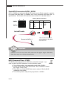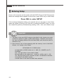
1
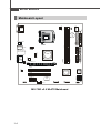
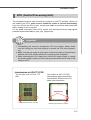
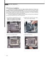
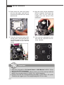
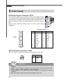
CONTENTS Chapter 1. Getting Started ................................................................................... 1-1 Mainboard Specifications .................................................................................. 1-2 Mainboard Layout .............................................................................................. 1-4 Chapter 2. Hardware Setup ................................................................................. 2-1 Quick Components Guide .................................................................................. 2-2 CPU (Central Processing Unit) ........................................................................... 2-2 Introduction to LGA 775 CPU ..................................................................... 2-3 CPU & Cooler Installation ............................................................................ 2-4 Memory ............................................................................................................... 2-7 Installing DDRII Modules ............................................................................. 2-7 Power Supply ..................................................................................................... 2-8 ATX 24-Pin Power Connector: ATX1 ......................................................... 2-8 ATX 12V Power Connector: JPW1 ............................................................ 2-8 Back Panel .......................................................................................................... 2-9 Connectors ....................................................................................................... 2-11 Floppy Disk Drive Connector: FDD1 ........................................................ 2-11 ATA133 Hard Disk Connectors: IDE1 & IDE2 ........................................... 2-11 Serial ATA Connectors: SATA1, SATA2 .................................................. 2-12 BIOS Password Clear: JPWD1 ................................................................ 2-12 Fan Power Connectors: CPU_FAN1, SYS_FAN1 ................................... 2-13 Front USB Connectors: JUSB1, JUSB2 .................................................. 2-13 SPDIF-Out Connector: SPDOUT1 ............................................................. 2-14 Front Panel Audio Connector: JAUD1 ..................................................... 2-14 BIOS Flash Write Protection: JWP1 ......................................................... 2-14 IEEE 1394 Connectors: J1394_1 ............................................................. 2-15 Front Panel Connectors: JFP1/JFP2 ........................................................ 2-15 Clear CMOS Jumper: JBAT1 .................................................................... 2-16 BIOS Recovery: JBR1 .............................................................................. 2-16 Jumpers ............................................................................................................ 2-16 Slots .................................................................................................................. 2-17 PCI (Peripheral Component Interconnect) Express Slots ....................... 2-17 PCI (Peripheral Component Interconnect) Slots ...................................... 2-17 PCI Interrupt Request Routing .................................................................. 2-18 Chapter 3. BIOS Setup ........................................................................................... 3-1 Entering Setup .................................................................................................... 3-2 Control Keys ............................................................................................... 3-3 Getting Help ................................................................................................ 3-3 i General Help <F1> ...................................................................................... 3-3 The Main Menu ................................................................................................... 3-4 Standard CMOS Features .................................................................................. 3-6 Advanced BIOS Features .................................................................................. 3-8 Advanced Chipset Features ........................................................................... 3-10 Integrated Peripherals ...................................................................................... 3-13 Power Management Setup .............................................................................. 3-15 PNP/PCI Configurations .................................................................................... 3-18 H/W Monitor ...................................................................................................... 3-19 Load Optimized Defaults .................................................................................. 3-20 Set Supervisor/ User Password ..................................................................... 3-21 ii Getting Started Chapter 1 Getting Started Thank you for choosing the MS-7293 Series (MS-7293 v2.X) Micro ATX mainboard. The MS-7293 Series mainboards are based on VIA® PT890 & VIA® 8237A chipsets for optimal system efficiency. Designed to fit the advanced Intel ® Pentium 4 processor, the mainboards deliver a high performance and professional desktop platform solution. 1-1 MS-7293 Mainboard Mainboard Specifications Processor Support - Supports Intel® Pentium 4, Pentium D, Celeron D and intel® CoreTM 2 Duo processors in the LGA775 package. - Supports 3/4 pin CPU Fan Pin-Header with Fan Speed Control. - Supports EIST Technology - Supports Hyper-Threading (HT) Technology - Supports Intel Dual Core Technology Supported FSB - 533/800/1066 MHz Chipset - North Bridge: VIA® PT890 - South Bridge: VIA® 8237A Memory Support - DDRII 400/533 SDRAM (2GB Max) - 2 DDRII DIMMs (240pin / 1.8V) LAN - Supports LAN 10/100 Fast Ethermet by VIA® VT6103L IEEE 1394 - Chip integrated by VIA VT6308 Audio - Chip integrated by Realtek ALC888 - Flexible 8-channel audio with jack sensing - Compliant with Azalia 1.x HD audio. IDE - 2 ports (4 IDE channels). - Supports Ultra DMA 33/66/100/133 mode - Supports PIO, Bus Master operation mode SATA - 2 SATA ports - Supports 2 SATA devices. - Supports storage and data transfers at up to 150 MB/s Floppy - 1 floppy port - Supports 1 FDD with 360K, 720K, 1.2M, 1.44M and 2.88Mbytes 1-2 Getting Started Connectors Backpannel - 1 serial port (COM1) - 1 IEEE 1394 port - 4 USB 2.0 Ports - 1 LAN jack - 6 flexible audio jacks - 1 SPDIF Out connector On-Board Pinheaders - 1 front Audio pinheader - 1 SPDIF-out pinheader - 1 IEEE 1394 pinheaders - 2 USB 2.0 pinheaders - 1 front panel pinheader (JFP1) Slots - 1 PCI Express x16 slot 1 PCI Express x1 slot 2 PCI slots. Support 3.3V/ 5V PCI bus Interface Form Factor - Micro-ATX (24.4cm X 24.4cm) Mounting - 8 mounting holes 1-3 MS-7293 Mainboard Mainboard Layout JBR1 JPWD1 Winbond W83627EHG JBAT1 CPU_FAN1 COM Port BATT + JPW1 Top:1394 Bottom: USB ports VIA PT890 IDE 2 SPDOUT1 IDE 1 PCIE16_1 DIMM2 DIMM1 VIA VT6103L SYS_FAN1 Top: LAN Jack Bottom: USB ports T: Line-In M: Line-Out B: Mic T:RS-Out M:CS-Out B:SS-Out FDD 1 ATX 1 SPDIFOUT1 PCI1 1394 Chip J1394_1 JUSB1 JUSB2 MS-7293 v2.X M-ATX Mainboard 1-4 JFP1 SATA2 JWP1 SATA1 PCIE1_1 JAUD1 BIOS Audio Codec VIA VT8237A PCI2 Hardware Setup Chapter 2 Hardware Setup This chapter provides you with the information about hardware setup procedures. While doing the installation, be careful in holding the components and follow the installation procedures. For some components, if you install in the wrong orientation, the components will not work properly. Use a grounded wrist strap before handling computer components. Static electricity may damage the components. 2-1 MS-7293 Mainboard Quick Components Guide CPU_FAN1, p.2-13 JPW1, p.2-8 DDRII DIMMs, p.2-7 SYS_FAN1, p.2-13 SPDOUT1, p.2-14 CPU, p.2-3 JBAT1, p.2-16 JPWD1, p.2-12 JBR1, p.2-16 Back Panel I/O, p.2-9 FDD1, p.2-11 ATX1, p.2-11 IDE1/2, p.2-12 PCIE Slot, p.2-17 PCI Slots, p.2-17 SATA1/2, p.2-12 PCIE Slot, p.2-17 JWP1, p.2-14 JAUD1, p.2-14 2-2 J1394_1, p.2-15 JFP1, p.2-15 JUSB1/2, p.2-13 Hardware Setup CPU (Central Processing Unit) This mainboard supports Intel® Pentium 4 processor in LGA 775 package. When you are installing the CPU, make sure to install the cooler to prevent overheating. If you do not have the CPU cooler, contact your dealer to purchase and install them before turning on the computer. For the latest information about CPU, please visit http://www.msi.com.tw/program/ products/mainboard/mbd/pro_mbd_cpu_support.php. Important 1. Overheating will seriously damage the CPU and system. Always make sure the cooling fan can work properly to protect the CPU from overheating. 2. Make sure that you apply an even layer of heat sink paste (or thermal tape) between the CPU and the heatsink to enhance heat dissipation. 3. While replacing the CPU, always turn off the ATX power supply or unplug the power supply’s power cord from the grounded outlet first to ensure the safety of CPU. Introduction to LGA 775 CPU The pin-pad side of LGA 775 CPU. Alignment Key Yellow triangle is the Pin 1 indicator The surface of LGA 775 CPU. Remember to apply some silicone heat transfer compound on it for better heat dispersion. Alignment Key Yellow triangle is the Pin 1 indicator 2-3 MS-7293 Mainboard CPU & Cooler Installation When you are installing the CPU, make sure the CPU has a cooler attached on the top to prevent overheating. If you do not have the cooler, contact your dealer to purchase and install them before turning on the computer. Meanwhile, do not forget to apply some silicon heat transfer compound on CPU before installing the heat sink/cooler fan for better heat dispersion. Follow the steps below to install the CPU & cooler correctly. Wrong installation will cause the damage of your CPU & mainboard. 1. The CPU has a plastic cap on it to protect the contact from damage. Before you install the CPU, always cover it to protect the socket pin. 2. Remove the cap from lever hinge side (as the arrow shows). 3. The pins of socket reveal. 4. Open the load lever. 2-4 Hardware Setup Important 1. Confirm if your CPU cooler is firmly installed before turning on your system. 2. Do not touch the CPU socket pins to avoid damaging. 3. The availability of the CPU land side cover depends on your CPU packing. 5. Lift the load lever up and open the load plate. 6. After confirming the CPU direction for correct mating, put down the CPU in the socket housing frame. Be sure to grasp on the edge of the CPU base. Note that the alignment keys are matched. alignment key 7. Visually inspect if the CPU is seated well into the socket. If not, take out the CPU with pure vertical motion and reinstall. 8. Cover the load plate onto the package. 2-5 MS-7293 Mainboard 9. Press down the load lever lightly onto the load plate, and then secure the lever with the hook under retention tab. 10. Align the holes on the mainboard with the heatsink. Push down the cooler until its four clips get wedged into the holes of the mainboard. 11. Press the four hooks down to fasten the cooler. Then rotate the locking switch (refer to the correct direction marked on it) to lock the hooks. 12. Turn over the mainboard to confirm that the clip-ends are correctly inserted. locking switch Important 1. Check the information in PC Health Status of H/W Monitor in BIOS (Chapter 3) for the CPU temperature. 2. Whenever CPU is not installed, always protect your CPU socket pin with the plastic cap covered (shown in Figure 1) to avoid damaging. 3. Please note that the mating/unmating durability of the CPU is 20 cycles. Therefore we suggest you do not plug/unplug the CPU too often. 2-6 Hardware Setup Memory The mainboard provides two 240-pin non-ECC DDRII DIMM slots. For more information on compatible components, please visit http://www.msi.com.tw/ program/products/mainboard/mbd/pro_mbd_trp_list.php. DDRII 240-pin, 1.8V 64x2=128 pin 56x2=112 pin Installing DDRII Modules 1. The memory module has only one notch on the center and will only fit in the right orientation. 2. Insert the memory module vertically into the DIMM slot. Then push it in until the golden finger on the memory module is deeply inserted in the DIMM slot. Important You can barely see the golden finger if the module is properly inserted in the DIMM slot. 3. The plastic clip at each side of the DIMM slot will automatically close. Volt Notch Important - DDRII modules are not interchangeable with DDR and the DDRII standard is not backwards compatible. You should always install DDRII memory modules in the DDRII DIMM slots and DDR memory modules in the DDR DIMM slots. - In dual-channel mode, make sure that you install memory modules of the same type and density in different channel DDR DIMM slots. - To enable successful system boot-up, always insert the memory modules into the DIMM1 first. 2-7 MS-7293 Mainboard Power Supply ATX 24-Pin Power Connector: ATX1 pin 13 This connector allows you to connect an ATX 24-pin power supply. To connect the ATX 24-pin power supply, make sure the plug of the power supply is inserted in the proper orientation and the pins are aligned. Then push down the power supply firmly into the connector. There is also a foolproof design on pin 23 & 24 to avoid wrong installation. pin 12 ATX1 Pin Definition 1 13 ATX1 24 12 PIN SIGNAL PIN SIGNAL 1 2 3 4 5 6 7 8 9 10 11 +3.3V +3.3V GND +5V GND +5V GND PWR OK 5VSB +12V +12V 12 NC 13 14 15 16 17 18 19 20 21 22 23 24 +3.3V -12V GND PS-ON# GND GND GND Res +5V +5V +5V GND ATX 12V Power Connector: JPW1 This 12V power connector is used to provide power to the CPU. JPW1 Pin Definition JPW1 4 2 3 1 PIN SIGNAL 1 2 3 4 GND GND 12V 12V Important 1. Maker sure that all the connectors are connected to proper ATX power supplies to ensure stable operation of the mainboard. 2. Power supply of 350 watts (and above) is highly recommended for system stability. 3. ATX 12V power connection should be greater than 18A. 2-8 Hardware Setup Back Panel L-In RS-Out 1394 Port LAN Serial Port USB Ports SPDIF-Out L-Out CS-Out Mic SS-Out Serial Port Connector The serial port is a 16550A high speed communications port that sends/ receives 16 bytes FIFOs. You can attach a serial mouse or other serial devices directly to the connector. IEEE 1394 Port The 1394 port on the back panel provides connection to 1394 devices. USB Connectors The OHCI (Open Host Controller Interface) Universal Serial Bus root is for attaching USB devices such as keyboard, mouse, or other USB-compatible devices. LAN (RJ-45) Jack The standard RJ-45 jack is for connection to single Local Area Network (LAN). You can connect a network cable to it. Activity Indicator LED Color LED State Left Orange On (steady state) Off Link Indicator Condition LAN link is not established. LAN link is established. On (brighter & pulsing) The computer is communicating with another computer on the LAN. Green Right Orange Off 10 Mbit/sec data rate is selected. On 100 Mbit/sec data rate is selected. On 1000 Mbit/sec data rate is selected. 2-9 MS-7293 Mainboard Optical SPDIF-Out connector This SPDIF (Sony & Philips Digital Interconnect Format) connector is provided for digital audio transmission to external speakers through an optical cable. Audio Port Connectors These audio connectors are used for audio devices. You can differentiate the color of the audio jacks for different audio sound effects. Blue audio jack - Line In, is used for external CD player, tapeplayer or other audio devices. Green audio jack - Line Out, is a connector for speakers or headphones. Pink audio jack - Mic In, is a connector for microphones. Black audio jack - Rear-Surround Out in 4.1/ 5.1/ 7.1 channel mode. Orange audio jack - Center/ Subwoofer Out in 5.1/ 7.1 channel mode. Gray audio jack - Side-Surround Out in 7.1 channel mode. 2-10 Hardware Setup Connectors Floppy Disk Drive Connector: FDD1 This standard FDD connector supports 360K, 720K, 1.2M, 1.44M and 2.88M floppy disk types. FDD1 ATA133 Hard Disk Connectors: IDE1 & IDE2 The mainboard has a 32-bit Enhanced PCI IDE and Ultra DMA 66/100/133 controller that provides PIO mode 0~4, Bus Master, and Ultra DMA 66/100/133 function. You can connect hard disk drives, CD-ROM and other IDE devices. The Ultra ATA133 interface boosts data transfer rates between the computer and the hard drive up to 133 megabytes (MB) per second. The new interface is one-third faster than earlier record-breaking Ultra ATA/100 technology and is backwards compatible with the existing Ultra ATA interface. IDE1 (Primary IDE Connector) IDE1 can connect a Master and a Slave drive. You must configure the second hard drive to Slave mode by setting the jumper accordingly. IDE2 (Secondary IDE Connector) IDE2 can also connect a Master and a Slave drive. IDE1 IDE2 Important If you install two hard disks on cable, you must configure the second drive to Slave mode by setting its jumper. Refer to the hard disk documentation supplied by hard disk vendors for jumper setting instructions. 2-11 MS-7293 Mainboard Serial ATA Connectors: SATA1, SATA2 SATA1, SATA2 are high-speed Serial ATA interface ports. Each supports 1st generation serial ATA data rates of 150MB/s and is fully compliant with Serial ATA 1.0 specifications. Each Serial ATA connector can connect to 1 hard disk device. 7 SATA1 SATA2 7 SATA1, SATA2 Pin Definition 1 1 PIN SIGNAL PIN SIGNAL 1 GND 2 RXN 3 5 7 RXP TXN GND 4 6 GND TXP Serial ATA cable Connect to SATA1, 2 Take out the dust cover and connect to the hard disk devices Important Please do not fold the Serial ATA cable into 90-degree angle. Otherwise, data loss may occur during transmission. BIOS Password Clear: JPWD1 The BIOS password protects the BIOS from undesired changes. If you need to clear the BIOS password, use the following steps: 2 1 JPWD1 1. Turn off the system, then remove the jumper from JPWD1. 2. Power on the system, and BIOS would show “Password Cleared By Jumper” during POST. 3. Press DEL key to enter BIOS Setup menu, and you’ll find the BIOS passwords are cleared. 4. Turn off the system, and put the jumper back on JPWD1. 2-12 Hardware Setup Fan Power Connectors: CPU_FAN1, SYS_FAN1 CONTROL SENSOR +12V GND The fan power connectors support system cooling fan with +12V. When connecting the wire to the connectors, always take note that the red wire is the positive and should be connected to the +12V, the black wire is Ground and should be connected to GND. If the mainboard has a System Hardware Monitor chipset onboard, you must use a specially designed fan with speed sensor to take advantage of the CPU fan control. CPU_FAN1 CONTROL SENSOR +12V GND SYS_FAN1 Important 1. Please refer to the recommended CPU fans at Intel ® official website or consult the vendors for proper CPU cooling fan. 2. CPU_FAN1 supports fan control. Front USB Connectors: JUSB1, JUSB2 The mainboard provides two USB 2.0 pinheaders (optional USB 2.0 bracket available) that are compliant with Intel® I/O Connectivity Design Guide. USB 2.0 technology increases data transfer rate up to a maximum throughput of 480Mbps, which is 40 times faster than USB 1.1, and is ideal for connecting high-speed USB interface peripherals such as USB HDD, digital cameras, MP3 players, printers, modems and the like. Pin Definition PIN SIGNAL 1 VCC 2 VCC 3 USB0- 4 USB1- JUSB1/JUSB2 5 USB0+ 6 USB1+ (USB 2.0) 7 GND 8 GND 9 Key (no pin) 10 USBOC 2 1 10 9 PIN SIGNAL Important Note that the pins of VCC and GND must be connected correctly to avoid possible damage. 2-13 MS-7293 Mainboard SPDOUT1 SPDIF-Out Connector: SPDOUT1 This connector is used to connect SPDIF (Sony & Philips Digital Interconnect Format) interface for digital audio transmission. GND VCC SPDIF Front Panel Audio Connector: JAUD1 The JAUD1 front panel audio connector allows you to connect the front panel audio and is compliant with Intel® Front Panel I/O Connectivity Design Guide. JAUD1 Pin Definition JAUD1 2 1 10 9 PIN SIGNAL 1 2 3 4 5 6 7 8 9 10 AUD_MIC AUD_GND AUD_MIC_BIAS AUD_VCC AUD_FPOUT_R AUD_RET_R HP_ON KEY AUD_FPOUT_L AUD_RET_L DESCRIPTION Front panel microphone input signal Ground used by analog audio circuits Microphone power Filtered +5V used by analog audio circuits Right channel audio signal to front panel Right channel audio signal return from front panel Reserved for future use to control headphone amplifier No pin Left channel audio signal to front panel Left channel audio signal return from front panel BIOS Flash Write Protection: JWP1 This jumper is used to enable/disable the BIOS flash. When you intend to update the BIOS code, uncap this jumper first. Under normal operation, we suggest that you disable the BIOS flash by capping the JWP1 jumper to protect the system BIOS from virus infection. JWP1 2-14 Disable BIOS Flash Enable BIOS Flash Hardware Setup IEEE 1394 Connectors: J1394_1 The mainboard provides IEEE1394 pinheaders that allow you to connect IEEE 1394 ports via an external IEEE1394 bracket (optional). Pin Definition 1 2 9 10 J1394_1 PIN SIGNAL PIN SIGNAL 1 TPA+ 2 TPA- 3 Ground 4 Ground 5 TPB+ 6 TPB- 7 Cable power 8 Cable power 9 Key (no pin) 10 Ground Front Panel Connectors: JFP1 The mainboard provides one front panel connector for electrical connection to the front panel switches and LEDs. It is compliant with Intel® Front Panel I/O Connectivity Design Guide. JFP1 Pin Definition Power Power LED Switch + - JFP1 2 1 10 9 + - - + HDD Reset LED Switch PIN SIGNAL 1 2 3 4 HD_LED + Hard disk LED pull-up FP PWR/SLP MSG LED pull-up HD_LED Hard disk active LED FP PWR/SLP MSG LED pull-up 5 GND 6 7 8 9 RST_SW PWR_SW + RST_SW + PWR_SW RSVD_DNU DESCRIPTION Reset Switch low reference pull-down to Power Switch high reference pull-up Reset Switch high reference pull-up Power Switch low reference pull-down to GND Reserved. Do not use. 2-15 MS-7293 Mainboard Jumpers Clear CMOS Jumper: JBAT1 There is a CMOS RAM onboard that has a power supply from external battery to keep the data of system configuration. With the CMOS RAM, the system can automatically boot OS every time it is turned on. If you want to clear the system configuration, set the JBAT1 (Clear CMOS Jumper ) to clear data. 1 JBAT1 3 3 1 1 Keep Data Clear Data Important You can clear CMOS by shorting 2-3 pin while the system is off. Then return to 1-2 pin position. Avoid clearing the CMOS while the system is on; it will damage the mainboard. BIOS Recovery: JBR1 To recover the BIOS, you have to insert certain boot disk into the floppy drive before powering on the system. After powered on, the system will read the boot disk and enter DOS. This enables you to update the BIOS automatically. JBR1 Normal Mode 2-16 Recovery Mode Hardware Setup Slots PCI (Peripheral Component Interconnect) Express Slots PCI Express architecture provides a high performance I/O infrastructure for Desktop Platforms with transfer rates starting at 2.5 Giga transfers per second over a PCI Express x1 lane for Gigabit Ethernet, TV Tuners, 1394 controllers, and general purpose I/O. Also, desktop platforms with PCI Express Architecture will be designed to deliver highest performance in video, graphics, multimedia and other sophisticated applications. Moreover, PCI Express architecture provides a high performance graphics infrastructure for Desktop Platforms doubling the capability of existing AGP 8x designs with transfer rates of 4.0 GB/s over a PCI Express x16 lane for graphics controllers, while PCI Express x1 supports transfer rate of 250 MB/s. PCI Express x16 Slot PCI Express x1 Slot PCI (Peripheral Component Interconnect) Slots The PCI slots support LAN cards, SCSI cards, USB cards, and other add-on cards that comply with PCI specifications. At 32 bits and 33 MHz, it yields a throughput rate of 133 MBps. 32-bit PCI Slot Important When adding or removing expansion cards, make sure that you unplug the power supply first. Meanwhile, read the documentation for the expansion card to configure any necessary hardware or software settings for the expansion card, such as jumpers, switches or BIOS configuration. 2-17 MS-7293 Mainboard PCI Interrupt Request Routing The IRQ, acronym of interrupt request line and pronounced I-R-Q, are hardware lines over which devices can send interrupt signals to the microprocessor. The PCI IRQ pins are typically connected to the PCI bus pins as follows: Order 1 Order 2 Order 3 Order 4 PCI Slot 1 INT B# INT C# INT D# INT A# PCI Slot 2 INT C# INT D# INT A# INT B# 2-18 BIOS Setup Chapter 3 BIOS Setup This chapter provides information on the BIOS Setup program and allows you to configure the system for optimum use. You may need to run the Setup program when: An error message appears on the screen during the system booting up, and requests you to run SETUP. You want to change the default settings for customized features. 3-1 MS-7293 Mainboard Entering Setup Power on the computer and the system will start POST (Power On Self Test) process. When the message below appears on the screen, press <DEL> key to enter Setup. Press DEL to enter SETUP If the message disappears before you respond and you still wish to enter Setup, restart the system by turning it OFF and On or pressing the RESET button. You may also restart the system by simultaneously pressing <Ctrl>, <Alt>, and <Delete> keys. Important 1. The items under each BIOS category described in this chapter are under continuous update for better system performance. Therefore, the description may be slightly different from the latest BIOS and should be held for reference only. 2. Upon boot-up, the 1st line appearing after the memory count is the BIOS version. It is usually in the format: W7293VMS V2.0 102006 where: 1st digit refers to BIOS maker as A = AMI, W = AWARD, and P = PHOENIX. 2nd - 5th digit refers to the model number. 6th digit refers to the chipset as I = Intel, N = nVidia, and V = VIA. 7th - 8th digit refers to the customer as MS = all standard customers. V2.0 refers to the BIOS version. 102006 refers to the date this BIOS was released. 3-2 BIOS Setup Control Keys <↑> <↓> Move to the previous item Move to the next item <←> <→> Move to the item in the left hand Move to the item in the right hand <Enter> <Esc> Select the item Jumps to the Exit menu or returns to the main menu from a submenu <+/PU> <-/PD> <F1> <F6> <F10> Increase the numeric value or make changes Decrease the numeric value or make changes General Help Load Optimized Defaults Save all the CMOS changes and exit Getting Help After entering the Setup menu, the first menu you will see is the Main Menu. Main Menu The main menu lists the setup functions you can make changes to. You can use the arrow keys ( ↑↓ ) to select the item. The on-line description of the highlighted setup function is displayed at the bottom of the screen. Sub-Menu If you find a right pointer symbol (as shown in the right view) appears to the left of certain fields that means a sub-menu can be launched from this field. A sub-menu contains additional options for a field parameter. You can use arrow keys ( ↑↓ ) to highlight the field and press <Enter> to call up the sub-menu. Then you can use the control keys to enter values and move from field to field within a sub-menu. If you want to return to the main menu, just press the <Esc >. General Help <F1> The BIOS setup program provides a General Help screen. You can call up this screen from any menu by simply pressing <F1>. The Help screen lists the appropriate keys to use and the possible selections for the highlighted item. Press <Esc> to exit the Help screen. 3-3 MS-7293 Mainboard The Main Menu Standard CMOS Features Use this menu for basic system configurations, such as time, date etc. Advanced BIOS Features Use this menu to setup the items of AMI® special enhanced features. Advanced Chipset Features Use this menu to change the values in the chipset registers and optimize your system’s performance. Integrated Peripherals Use this menu to specify your settings for integrated peripherals. Power Management Features Use this menu to specify your settings for power management. PNP/PCI Configurations This entry appears if your system supports PnP/PCI. H/W Monitor This entry shows your PC health status. 3-4 BIOS Setup Load Optimized Defaults Use this menu to load the default values set by the mainboard manufacturer specifically for optimal performance of the mainboard. Set Supervisor Password Use this menu to set the supervisor password for BIOS. Set User Password Use this menu to set the user password for BIOS. Save & Exit Setup Save changes to CMOS and exit setup. Exit Without Saving Abandon all changes and exit setup. 3-5 MS-7293 Mainboard Standard CMOS Features The items in Standard CMOS Features Menu includes some basic setup items. Use the arrow keys to highlight the item and then use the <PgUp> or <PgDn> keys to select the value you want in each item. Date (mm:dd:yy) This allows you to set the system to the date that you want (usually the current date). The format is <day><month> <date> <year>. day Day of the week, from Sun to Sat, determined by BIOS. Read-only. month The month from Jan. through Dec. date The date from 1 to 31 can be keyed by numeric function keys. year The year can be adjusted by users. Time (hh:mm:ss) This allows you to set the system time that you want (usually the current time). The time format is <hour> <minute> <second>. IDE Channel 0/1/2/3 Master/ Slave Press <Enter> to enter the sub-menu. Access Mode Select Access Mode. DMA Mode Select DMA Mode. 3-6 BIOS Setup Important IDE Channel 0/1/2/3 Master/ Slave are appearing when you connect the HD devices to the SATA connector on the mainboard. Drive A This item allows you to set the type of floppy drives installed. Halt On The setting determines whether the system will stop if an error is detected at boot. Available options are: [No Errors] The system doesn’t stop for any detected error. [All, But Keyboard] The system doesn’t stop for a keyboard error. System Information Press <Enter> to enter the sub-menu. This sub-menu shows the CPU information, BIOS version and memory status of your system (read only). 3-7 MS-7293 Mainboard Advanced BIOS Features Quick Booting Setting the item to [Enabled] allows the system to boot within 10 seconds since it will skip some check items. Boot Up Num-Lock LED This setting is to set the Num Lock status when the system is powered on. Setting to [On] will turn on the Num Lock key when the system is powered on. Setting to [Off] will allow users to use the arrow keys on the numeric keypad. Boot to OS/2 This allows you to run the OS/2® operating system with DRAM larger than 64MB. When you choose [No], you cannot run the OS/2® operating system with DRAM larger than 64MB. But it is possible if you choose [Yes]. IOAPIC Function This field is used to enable or disable the APIC (Advanced Programmable Interrupt Controller). Due to compliance with PC2001 design guide, the system is able to run in APIC mode. Enabling APIC mode will expand available IRQ resources for the system. CPU L1 & L2 Cache The item allows you to turn on or off CPU’s internal (L1) and external (L2)cache. CPU L3 Cache Level 3 cache is the extra cache built into motherboards between the microprocessor and the main memory. Located away from the CPU, the L3 cache is slower than the L1 & L2 caches. This setting allows you to turn on or off the L3 cache. 3-8 BIOS Setup S3 HDD Security FreezeLock This field allows you to enable or disable the HDD security in S3. MPS Table Version This field allows you to select which MPS (Multi-Processor Specification) version to be used for the operating system. You need to select the MPS version supported by your operating system. To find out which version to use, consult the vendor of your operating system. Full Screen LOGO Display This item enables you to show the company logo on the bootup screen. Settings are: [Enabled] Shows a still image (logo) on the full screen at boot. [Disabled] Shows the POST messages at boot. CPU Feature Press <Enter> to enter the sub-menu: Limit CPUID MaxVal The item allows you to enable/ disable the CPU ID maximum value. [Enabled] Set to [Enabled] only when you have Prescott CPU and NT4.0 operating system. [Disabled] Set to [Disabled] if you have operating system other than NT4.0. C1E Function When the C1E Support (Enhanced Halt Powerdown State) is enabled, the processor will transition to a lower core to bus ratio and lower voltage ID driven by the processor to the voltage regulator before entering Halt Powerdown State (C1). Not all porcessors support Enhanced Halt Powerdown State (C1E). You can enable C1E Support to lower the CPU power consumption while idle. Execute Disable Bit Excute Bit Support function is designed for memory buffer overflow protection, it can prevent viruses from proliferating. Virtualization Technology It allows you to enable or disable the Virtualzation Technology. Hard Disk Boot Priority Press <Enter> to enter the sub-menu and set the sequency of boot hard disk. Boot Sequence Press <Enter> to enter the sub-menu: 1st/2nd/3rd Boot Device The items allow you to set the sequence of boot devices where BIOS attempts to load the disk operating system. 3-9 MS-7293 Mainboard Advanced Chipset Features DRAM Clock/ Drive Control Press <Enter> to enter the sub-menu: Current FSB/ DRAM Frequency These items show the current FSB/ DRAM frequency (Read only). DRAM Clock It allows you to select the DRAM clock. DRAM Timing This field allows you to select the DDR timing setting. Setting to Auto By SPD enables DRAM timing automatically to be determined by SPD. Selecting Manual allows users to configure these fields manually. SDRAM CAS Latency [DDR/DDR2] When the DRAM Timing sets to [Manual], the field is adjustable.This controls the CAS latency, which determines the timing delay (in clock cycles) before SDRAM starts a read command after receiving it. Bank Interleave When the DRAM Timing sets to [Manual], the field is adjustable. This field selects 2-bank or 4-bank interleave for the installed SDRAM. Disable the function if 16MB SDRAM is installed. 3-10 BIOS Setup Precharge to Active (Trp) When the DRAM Timing sets to [Manual], the field is adjustable. This item controls the number of cycles for Row Address Strobe (RAS) to be allowed to precharge. If insufficient time is allowed for the RAS to accumulate its charge before DRAM refresh, refreshing may be incomplete and DRAM may fail to retain data. This item applies only when synchronous DRAM is installed in the system. Active to Precharge (Tras) When the DRAM Timing sets to [Manual], the field is adjustable. This setting determines the time RAS takes to read from and write to a memory cell. Active to CMD (Trcd) When the DRAM Timing sets to [Manual], the field is adjustable. When DRAM is refreshed, both rows and columns are addressed separately. This setup item allows you to determine the timing of the transition from RAS (row address strobe) to CAS (column address strobe). The less the clock cycles, the faster the DRAM performance. REF to ACT/REF (Trfc) When the DRAM Timing sets to [Manual], the field is adjustable. Auto-refresh -active to RAS#-active or RAS# auto-refresh. ACT(0) to ACT(1) (TRRD) When the DRAM Timing sets to [Manual], the field is adjustable.Specifies the active-to-active delay of different banks. When DRAM is refreshed, both rows and columns are addressed separately. This setup item allows you to determine the timing of the transition from RAS (row address strobe) to CAS (column address strobe). The less the clock cycles, the faster the DRAM performance. 1T CMD Support It allows to enable or disable the 1T command rate. CPU & PCI Bus Control Press <Enter> to enter the sub-menu: PCI Master 0 WS Write When [Enabled], writes to the PCI bus are executed with zero wait states. PCI Delayed Transaction The chipset has an embedded 32-bit posted write buffer to support delay transactions cycles. Select [Enabled] to support compliance with PCI specification. VLink mode selection This item lets you choose the speed mode between the North Bridge & South Bridge. 3-11 MS-7293 Mainboard VLink 8X Supported This item enables or disables the 8X VLink Data Rate. VIA PWR Management This item enables or disables the VIA power management function. Memory Hole In order to improve performance, certain space in memory can be reserved for ISA peripherals. This memory must be mapped into the memory space below 16MB. When this area is reserved, it cannot be cached. System BIOS Cacheable Selecting [Enabled] allows caching of the system BIOS ROM at F0000h-FFFFFh, resulting in better system performance. However, if any program writes to this memory area, a system error may result. Top Performance Set this item to Enabled to increase the system performance. 3-12 BIOS Setup Integrated Peripherals VIA OnChip IDE Device Press <Enter> to enter the sub-menu: SATA Controller It allows you to enable/ disable the SATA controller. SATA Controller Mode It lets you select the SATA controller mode. IDE DMA transfer access Setting to [Enabled] will open DMA bus master and execute DMA action in DOS, which will make the data transferring faster. OnChip IDE Channel 0/1 These allow you to enable/disable the IDE channel 0/1. IDE Prefetch Mode The onboard IDE drive interfaces support IDE prefetching, for faster drive accesses. When you install a primary and/or secondary add-in IDE interface, set this option to Disabled if the interface does not support prefetching. VIA OnChip PCI Device Press <Enter> to enter the sub-menu: Azalia HDA Controller It allows you to enable/ disable the Azalia HDA controller. 3-13 MS-7293 Mainboard LAN Controller It allows you to enable/ disable the LAN controller. Lan Boot ROM This item is used to decide whether to invoke the Boot ROM of the Onboard LAN Chip. Onboard IEEE1394 Controller This item allows you to enable/disable the onboard IEEE1394 controller. Super IO Device Press <Enter> to enter the sub-menu: Onboard FDC Controller Select [Enabled] if your system has a floppy disk controller (FDD) installed on the system board and you wish to use it. If you install add-on FDC or the system has no floppy drive, select [Disabled] in this field. Onboard Serial Port 1 Select an address and corresponding interrupt for the first serial port. USB Device Setting Press <Enter> to enter the sub-menu: USB 1.0/ 2.0 Controller These items allow you to enable/ disable USB 1.0/ 2.0 controller. USB Operation Mode It lets you select the operation mode for USB. USB Keyboard Function Select Enabled if you use the USB keyboard. USB Mouse Function Select Enabled if you use the USB Mouse. USB Storage Function Select Enabled if you use the USB Storage device. 3-14 BIOS Setup Power Management Setup Important S3-related functions described in this section are available only when your BIOS supports S3 sleep mode. ACPI Function This item is to activate the ACPI (Advanced Configuration and Power Management Interface) Function. If your operating system is ACPI-aware, such as Windows 2000/ XP, select [Yes]. ACPI Standby State This item specifies the power saving modes for ACPI function. If your operating system supports ACPI, such as Windows 2000/ XP , you can choose to enter the Standby mode in S1(POS) or S3(STR) fashion through the setting of this field. Settings are: [S1/POS] The S1 sleep mode is a low power state. In this state, no system context is lost (CPU or chipset) and hardware maintains all system context. [S3/STR] The S3 sleep mode is a lower power state where the in formation of system configuration and open applications/files is saved to main memory that remains powered while most other hardware components turn off to save energy. The information stored in memory will be used to restore the system when a “wake up” event occurs. [Auto] 3-15 MS-7293 Mainboard Re-Call VGA BIOS From S3 When ACPI Standby State is set to [S3/STR], users can select the options in this field. Selecting [Yes] allows BIOS to call VGABIOS to initialize the VGA card when system wakes up (resumes) from S3 sleep state. The system resume time is shortened when you disable the function, but system will need an VGA driver to initialize the VGA card. Therefore, if the VGA driver of the card does not support the initialization feature, the display may work abnormally or not function after resuming from S3. Suspend Time Out (Minute) If system activity is not detected for the length of time specified in this field, all devices except CPU will be shut off. Power Button Function This feature sets the function of the power button. Settings are: [On/ Off] The power button functions as normal power off button. [Suspend] When you press the power button, the computer enters the suspend/sleep mode, but if the button is pressed for more than four seconds, the computer is turned off. Restore On AC Power Loss This item specifies whether your system will reboot after a power failure or interrupt occurs. Settings are: [Power Off] Always leaves the computer in the power off state. [Power On] Always leaves the computer in the power on state. [Last State] Restores the system to the status before power failure or interrupt occurred. Wakeup Event Setup Press <Enter> to enter the sub-menu: Resume From S3 By USB Device The item allows the activity of the USB device to wake up the system from S3 (Suspend to RAM) sleep state. Resume By PCI-E Device When set to [Enabled], the feature allows your system to be awakened from the power saving modes through any event on PCIE device. Resume by PCI Card When set to [Enabled], the feature allows your system to be awakened from the power saving modes through any event on PCI device. RTC Alarm Resume The field is used to enable or disable the feature of booting up the system on a scheduled time/date. 3-16 BIOS Setup Date (of Month) Alarm The field specifies the date for Resume by RTC Alarm. Time (hh:mm:ss) Alarm The field specifies the time for Resume by RTC Alarm. Format is <hour><minute><second>. 3-17 MS-7293 Mainboard PNP/PCI Configurations This section describes configuring the PCI bus system and PnP (Plug & Play) feature. PCI, or Peripheral Component Interconnect, is a system which allows I/O devices to operate at speeds nearing the speed the CPU itself uses when communicating with its special components. This section covers some very technical items and it is strongly recommended that only experienced users should make any changes to the default settings. Primary Graphics Adapter This setting specifies which graphics card is your primary graphics adapter. PCI Latency Timer (CLK) This item controls how long each PCI device can hold the bus before another takes over. When set to higher values, every PCI device can conduct transactions for a longer time and thus improve the effective PCI bandwidth. For better PCI performance, you should set the item to higher values. ** PCI Express relative items ** Maximum Payload Size This item allows you to set the PCI Express Maximum payload size per time . 3-18 BIOS Setup H/W Monitor CPU Shutdown Temperature If the CPU temperature reaches the upper limit preset in this setting, the system will be shut down automatically. This helps you to prevent the CPU overheating problem. This item is available only when your OS supports this function. CPU Smart Fan Temp. Select a temperature setting here, and if the temperature of the CPU climbs up to the selected temperature setting, the system will automatically increase the speed of the CPU fan to cool down the overheated CPU. CPU Temp. Tolerance When a particular temperature setting is selected for the previous item, CPU Smart Fan Temperature, a temperature tolerance value between 1 to 5 can be adjusted here. PC Health Status Press <Enter> to enter the sub-menu: System/ CPU Temperature, System/CPU FAN Speed, CPU Vcore, 12V, 5V These items display the current status of all of the monitored hardware devices/ components such as CPU voltage, temperatures and all fans’ speeds. 3-19 MS-7293 Mainboard Load Optimized Defaults The option on the main menu allows users to restore all of the BIOS settings to the default Optimized values. The Optimized Defaults are the default values set by the mainboard manufacturer specifically for optimal performance of the mainboard. When you select Load Optimized Defaults, a message as below appears: Pressing Y loads the default factory settings for optimal system performance. 3-20 BIOS Setup Set Supervisor/ User Password When you select this function, a message as below will appear on the screen: Type the password, up to eight characters in length, and press <Enter>. The password typed now will replace any previously set password from CMOS memory. You will be prompted to confirm the password. Retype the password and press <Enter>. You may also press <Esc> to abort the selection and not enter a password. To clear a set password, just press <Enter> when you are prompted to enter the password. A message will show up confirming the password will be disabled. Once the password is disabled, the system will boot and you can enter Setup without entering any password. When a password has been set, you will be prompted to enter it every time you try to enter Setup. This prevents an unauthorized person from changing any part of your system configuration. Additionally, when a password is enabled, you can also have BIOS to request a password each time the system is booted. This would prevent unauthorized use of your computer. The setting to determine when the password prompt is required is the Security Option of the Advanced BIOS Feature menu. If the Security Option is set to System, the password is required both at boot and at entry to Setup. If set to Setup, password prompt only occurs when you try to enter Setup. Important About Supervisor Password & User Password: Supervisor password: Can enter and change the settings of the setup menu. User password: Can only enter but do not have the right to change the settings of the setup menu. 3-21