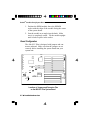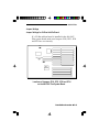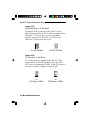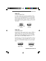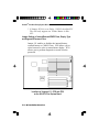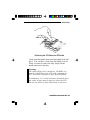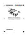
1
486-OCV Plus
System Board
User’s Manual
- D21840429 -
v Copyright 1994, by DFI Inc.
All rights reserved.
No part of this document may be copied or reproduced
in any form or by any means without the prior written
consent of DFI, Inc.
DFI, Inc. makes no warranties with respect to this
documentation and disclaims any implied warranties of
merchantability, quality, or fitness for any particular
purpose. The information in this document is subject to
change without notice. DFI, Inc. reserves the right to
make revisions to this publication and to make changes
to any and/or all parts of its content, at any time,
without obligation to notify any person or entity of such
changes. Further, DFI, Inc. assumes no responsibility
for any errors that may appear in this document.
DFI is a registered trademark, and 486-OCV Plus is a
trademark of Diamond Flower, Inc. All other product
names mentioned are trademarks or registered trademarks of their respective companies.
v
Table of Contents v
Introduction ................................................................................. 1-1
Features and Specifications ................................................. 1-2
2-1
2-1
2-2
2-2
2-2
2-2
2-6
2-7
2-8
2-8
Installation Overview .................................................................
Preparing the Area ................................................................
Handling the System Board ..................................................
Tips in Handling the System Board ...............................
Hardware Installation .............................................................
Memory Installation .........................................................
Installing the Modules ..............................................
Board Configuration ........................................................
Jumper Settings .......................................................
Jumper Settings for VL-Bus Add-On Board .....
Jumper Settings of Internal/External/CMOS
Clean, Display Type and Diagnostic/
Password Clear ..................................................
Cache Configuration ................................................
Jumper Settings for Cache Memory .................
CPU Installation and Upgrade .......................................
CPU Configuration ..................................................
Jumper Settings for CPUs .................................
Installing Upgrade CPUs ........................................
Installing the System Board ..................................................
2-11
2-14
2-16
2-18
2-18
2-19
2-22
2-26
Initial Setup Program .................................................................
AMI BIOS Setup Utilities .......................................................
Standard CMOS Setup ..................................................
Advanced CMOS Setup .................................................
Auto Configuration with BIOS Defaults .........................
Auto Configuration with Power-on Defaults ..................
3-1
3-2
3-3
3-5
3-7
3-7
Change Password .........................................................
Auto Detect Hard Disk ..................................................
Hard Disk Utility .............................................................
Write to CMOS and Exit ................................................
Do not write to CMOS and Exit ....................................
3-8
3-9
3-10
3-11
3-11
Troubleshooting Checklist ...................................................... 4-1
Appendix A: Types of Modules ..............................................
Appendix B: System Error Report .........................................
Appendix C: Memory & I/O Maps ...........................................
Appendix D: 16-Bit ISA I/O Pin Assignments .......................
Appendix E: VL-Bus I/O Pin Assignments ...........................
Appendix F: System Overview ...............................................
Appendix G: Connector Pin Assignments ............................
Appendix H: AMI BIOS Hard Disk Table ...............................
A-1
B-1
C-1
D-1
E-1
F-1
G-1
H-1
486-OCV Plus
v Introduction
The 486-OCV Plus system board is designed so that it
may be equipped with Intel's 80486DX, 80486DX2,
80486SX, and 80486 OverDriveTM Processors which can
run from speeds of 25MHz to 66MHz. It may also use
a PentiumTM OverDrive Processor running at 50MHz or
66MHz. This Pentium-based system board is twice as
fast as the 80486DX-33 and accommodates almost all of
the existing programs designed for 386 or 486-based
systems. The system board also supports a Cyrix or
AMD 486DX CPU running at 40MHz.
The 486-OCV Plus is a jumperless-upgrade board
allowing you to easily upgrade your CPU from a 486SX
to 486DX or DX2 for example, without altering any
jumpers. However, if you change your CPU speed from
25MHz to 33MHz, 40MHz or 50MHz, or change a
Cyrix CPU to an Intel or AMD CPU, you may have to
alter a few jumpers.
The 486-OCV Plus is equipped with a Zero Insertion
Force socket to make upgrading your CPU easy. It also
supports an optional Flash EPROM. Flash EPROM is a
memory chip for the storage of BIOS which can be
erased in bulk or modified using a software utility.
The 486-OCV Plus system board is also equipped with
two VESA compliant local bus slots. The VL-Bus of
the 486-OCV Plus system board operates at the same
frequency (up to 40MHz) and phase as the CPU, supporting all DMA and system I/O bus mastering cycles.
Introduction u 1-1
PentiumTM OverDrive Ready System Board
The 486-OCV Plus uses 256Kx36, 512Kx36, 1Mx36,
2Mx36, 4Mx36 and 8Mx36 HSIM modules with speeds
of at least 80ns. The memory can be configured to
twenty-one different sizes from 1MB to 64MB. The
system is equipped with two 32-bit VESA VL-Bus and
eight 16-bit ISA expansion slots.
Features and Specifications
• Intel 80486DX running at 33/40/50MHz,
80486DX2 running at 50/66MHz, 80486
OverDriveTM Processor, PentiumTM OverDrive
Processor running at 50/66MHz, or 80486SX
running at 25/33MHz
Cyrix or AMD 486DX running at 40MHz
• Uses AMI BIOS: 27512-20 (1)
• Uses OPTi 82C499 chip set
• Cache organization: direct map, write back and bank
interleave
• Supports 64K, 128K and 256K cache sizes
• Memory configurable from 1MB to 64MB
• Uses 256Kx36, 1Mx36 and 4Mx36 HSIMM
Uses 512Kx36, 2Mx36 and 8Mx36 (for Banks 0 and
2 only)
• Supports memory with parity check
• 8MHz bus clock
• Software programmable cache and DRAM wait states
• Supports system BIOS and Video BIOS Shadow
RAM function
• Supports sixteen edge triggered interrupts
• Hidden refresh or slow refresh supported
• Optional Flash memory BIOS supported
• Supports PentiumTM OverDrive Processor Zero
Insertion Force socket
• Supports one PS/2 mouse port
• An optional diagnostic LCD port
1-2 u Introduction
486-OCV Plus
• Supports VESA VL-Bus devices (2 VESA Master/
Slave)
ISA DMA Master access to local device
Local Master access to an ISA device
Fully compatible with VESA VL-Bus rev. 1.0
• Two 32-bit VL-Bus and eight 16-bit ISA slots
• Maximum card length
Full-length cards in all VL-Bus slots and in three
ISA slots
9.75" cards in three ISA slots
• Four layer PCB
• Baby AT size
• Operating temperature: 0oC - 40oC
• One year limited warranty
Warning:
If your 486-OCV Plus system board is using a 486DX
50 CPU, we recommend that you do not install any
VL-Bus devices. The VL-Bus connectors, compliant
with VESA VL-Bus standard rev. 1.0, limit the speed of
a VL-Bus device operating across the connector
(e.g. an add-on board) to 40MHz.
The table below, based on the VESA VL-Bus
specification, shows the recommended number of
installed VL-Bus devices at various CPU speeds. This
table is only a recommendation, not a requirement. Any
VL-Bus add-on board must correspond with the CPU
speed, whether it is buffered or unbuffered.
CPU Speed
<= 33MHz
40MHz
>= 50MHz
Unbuffered
Buffered
2 slots/2 devices 3 slots/3 devices
1 slot/2 devices not recommended
0 slot/2 devices not recommended
Introduction u 1-3
PentiumTM OverDrive Ready System Board
v Installation Overview
This chapter summarizes the steps in installing the
486-OCV Plus system board into your system unit. It
also includes a description of the area in which you must
work and directions for memory installation. Before
installing the system board, obtain the memory you plan
to install.
Preparing the Area
Before unpacking the system board, make sure the
location you have selected is relatively free of dust and
static. Excessive exposure to dust, static electricity,
direct sunlight, excessive humidity, extreme cold and
water can damage the operational capabilities of your
system board. Avoid soft surfaces such as beds and
carpeted floors which can hinder air circulation. These
areas also attract static electricity which can damage
some circuits on your system board.
Be sure that the power source has a properly grounded,
three-pronged socket. It is essential that the power
connection be properly grounded for correct functioning
of your system board. For further protection, we recommend that you use a surge protection socket. This
will protect the system board from damage that may
result from a power surge on the line.
Move items that generate magnetic fields away from
your system board, since magnetic fields can also damage your system board. Once you have selected the
ideal location, unpack the 486-OCV Plus system board
carefully.
2-1 u Installation Overview
486-OCV Plus
Handling the System Board
It is quite easy to inadvertently damage your system
board even before installing it to your system unit.
Static electrical discharge can damage computer components without causing any signs of physical damage. You
must take extra care in handling the system board to
ensure that no static build-up is present.
Tips in Handling the System Board
1) To prevent electrostatic build-up, leave the board in
its anti-static bag until you are ready to install it.
2) Wear an antistatic wriststrap.
3) Do all preparation work on a static-free surface with
components facing up.
4) Hold the system board by its edges only. Be careful
not to touch any of the components, contacts or
connections, especially gold contacts on the board.
5) Avoid touching the pins or contacts on all modules
and connectors. Hold modules and connectors by
their ends.
Hardware Installation
Memory Installation
The 486-OCV Plus system board can support 1MB to
64MB of memory using HSIMMs. HSIMM is an
acronym for High Density Single In-line Memory Module.
Installation Overview u 2-2
PentiumTM OverDrive Ready System Board
An HSIMM consists of several RAM chips soldered
onto a small circuit board. An HSIMM connects to the
system board via a 72-pin card-edge connector.
The HSIMM sockets are divided into four banks on the
system board. The 486-OCV Plus system board uses
256Kx36, 512Kx36, 1Mx36, 2Mx36, 4Mx36 and 8Mx36
HSIM modules.
Note:
The 8Mx36 HSIM module must be the standard size
module. Mechanical problem may occur if a longer
size of module is installed.
You will need 1 to 4 pieces of HSIM modules, depending on the amount of memory you intend to install.
Your system board can be configured with 1MB, 2MB,
4MB, 5MB, 6MB, 8MB, 9MB, 12MB, 13MB, 16MB,
18MB, 20MB, 24MB, 28MB, 32MB, 34MB, 36MB,
40MB, 48MB, 52MB or 64MB of onboard memory.
To install the HSIM modules, first populate Bank 0, then
Bank 1 and so on. Failure to do so will cause the
system board to work improperly.
The following table summarizes the bank locations and
modules needed for the corresponding memory sizes.
Each bank consists of 1 HSIMM socket.
2-3 u Installation Overview
486-OCV Plus
Memory Size
Bank 0
Bank 1
Bank 2
Bank 3
1MB
2MB
2MB
4MB
5MB
6MB
6MB
8MB
8MB
9MB
9MB
12MB
12MB
13MB
13MB
16MB
16MB
16MB
18MB
18MB
20MB
20MB
24MB
24MB
24MB
24MB
28MB
28MB
28MB
28MB
28MB
28MB
32MB
32MB
256Kx36
256Kx36
512Kx36
1Mx36
256Kx36
256Kx36
512Kx36
1Mx36
2Mx36
1Mx36
2Mx36
1Mx36
2Mx36
256Kx36
256Kx36
1Mx36
2Mx36
4Mx36
256Kx36
512Kx36
1Mx36
4Mx36
1Mx36
2Mx36
1Mx36
4Mx36
1Mx36
2Mx36
1Mx36
1Mx36
4Mx36
4Mx36
4Mx36
8Mx36
256Kx36
1Mx36
256Kx36
1Mx36
1Mx36
1Mx36
1Mx36
1Mx36
1Mx36
256Kx36
4Mx36
1Mx36
1Mx36
4Mx36
1Mx36
1Mx36
4Mx36
4Mx36
1Mx36
1Mx36
4Mx36
-
1Mx36
1Mx36
256Kx36
256Kx36
1Mx36
1Mx36
1Mx36
2Mx36
1Mx36
2Mx36
4Mx36
4Mx36
4Mx36
4Mx36
1Mx36
1Mx36
4Mx36
4Mx36
1Mx36
2Mx36
1Mx36
2Mx36
-
1Mx36
1Mx36
1Mx36
1Mx36
1Mx36
1Mx36
-
Installation Overview u 2-4
PentiumTM OverDrive Ready System Board
Memory Size
Bank 0
Bank 1
Bank 2
Bank 3
34MB
34MB
36MB
36MB
36MB
36MB
40MB
40MB
40MB
40MB
40MB
40MB
48MB
48MB
52MB
52MB
52MB
52MB
52MB
52MB
64MB
64MB
256Kx36
512Kx36
1Mx36
4Mx36
4Mx36
8Mx36
1Mx36
2Mx36
1Mx36
4Mx36
4Mx36
8Mx36
4Mx36
8Mx36
1Mx36
1Mx36
4Mx36
4Mx36
4Mx36
8Mx36
4Mx36
8Mx36
256Kx36
4Mx36
1Mx36
4Mx36
1Mx36
4Mx36
1Mx36
4Mx36
4Mx36
4Mx36
4Mx36
1Mx36
1Mx36
4Mx36
4Mx36
-
4Mx36
8Mx36
4Mx36
4Mx36
1Mx36
1Mx36
4Mx36
8Mx36
4Mx36
4Mx36
1Mx36
2Mx36
4Mx36
4Mx36
4Mx36
8Mx36
4Mx36
8Mx36
4Mx36
4Mx36
4Mx36
8Mx36
4Mx36
4Mx36
1Mx36
1Mx36
1Mx36
4Mx36
4Mx36
1Mx36
1Mx36
4Mx36
-
2-5 u Installation Overview
486-OCV Plus
OPTi
82C499
Pin 1 of the HSIMM socket
Bank 0
Bank 1
Bank 2
Bank 3
Locations of the HSIMM Sockets on the System Board
Installing the Modules
HSIMMs simply snap into a socket on the system board.
Pin 1 of the HSIMM must correspond with Pin 1 of the
socket.
Installation Overview u 2-6
PentiumTM OverDrive Ready System Board
1. Position the HSIM module above the HSIMM
socket with the chips of the module facing the center
of the system board.
2. Seat the module at an angle into the bank. Make
sure it is completely seated. Tilt the module upright
until it locks in place in the socket.
Board Configuration
The 486-OCV Plus is designed with jumpers and connectors onboard. Make sure that the jumpers are set
correctly before installing the system board into your
system unit.
JP32
J1
JP18
JP39
J2
J3
JP29
J4
J5
SL1
JP23
J6
JP24
J7
JP38
JP6
SL2
J8
JP34
JP31
JP9
OPTi
82C499
JP7 JP8
JP25 JP26
JP12 JP14
JP13
Locations of Jumpers and Connector Pins
on the 486-OCV Plus System Board
2-7 u Installation Overview
J10
J11
J9
486-OCV Plus
Jumper Settings
Jumper Settings for VL-Bus Add-On Board
If a VL-Bus add-on board is installed in the 486-OCV
Plus system board, make sure Jumpers JP18, JP23, JP24
and JP34 are set correctly.
JP18
JP23
JP24
JP34
OPTi
82C499
Locations of Jumpers JP18, JP23, JP24 and JP34
on the 486-OCV Plus System Board
Installation Overview u 2-8
PentiumTM OverDrive Ready System Board
Jumper JP23
High Speed Mode for VL-Bus Board
Set Jumper JP23 to Off only if the VESA VL-Bus
add-on board installed in the VL-Bus slots support Zero
Wait State. If you are not sure that your add-on
board(s) support Zero Wait State, set JP23 to On;
otherwise, a system error may occur.
On: One Wait State
Off: Zero Wait State
Jumper JP24
CPU Speed for VL-Bus Board
If a VL-Bus board is installed in the 486-OCV Plus
system board, Jumper JP24 must be set to On if the
CPU speed is greater than 33MHz. If the CPU speed is
less than or equal to 33MHz, set JP24 to Off.
On
CPU Speed > 33MHz
2-9 u Installation Overview
Off
CPU Speed <= 33MHz
486-OCV Plus
Jumper JP18
VL-Bus Ready Signal Select
If a VESA VL-Bus add-on board is installed in either
one of the VL-Bus slots and the 486-OCV Plus system
board is using a 486-50DX CPU, we recommend that
you set Jumper JP18 to "Delay 1 PCLK". Your system
board might not work properly if Jumper JP18 is set to
"No Delay".
1
2
3
1-2 On: Delay 1 PCLK
(Default)
1
2
3
2-3 On:
No Delay
Jumper JP34
VL-Bus Address Select
If the 486-OCV Plus system board is using a 40MHz or
50MHz 486DX CPU, VESA VL-Bus add-on boards
may not work when Jumper JP34 is set to "No Delay".
In this case, we recommend that you set Jumper JP34
pins 1-2 and 3-4 to On, "Delay 1 PCLK".
Set JP34 pins 2-3 to On if your system board is using a
386-25/33/40MHz or 486-25/33MHz CPU. If it is not
set to these recommended settings, your system might
hang.
1
2
3
4
1-2, 3-4 On:
Delay 1 PCLK
1
2
3
4
2-3 On: No Delay
(Default)
Installation Overview u 2-10
PentiumTM OverDrive Ready System Board
* If Jumper JP34 is set to Delay 1 PCLK, the 486-OCV
Plus will only support one VL-Bus Master in Slot
SL2.
Jumper Settings of Internal/External/CMOS Clean, Display Type
and Diagnostic/Password Clear
Jumper J11 enables or disables the internal battery,
external battery or CMOS Clean. JP29 allows you to
select between a color or monochrome display. JP39
allows you to perform diagnostic test and clear the
password.
JP39
JP29
OPTi
82C499
Locations of Jumpers J11, JP29 and JP39
on the 486-OCV Plus System Board
2-11 u Installation Overview
J10
J11
486-OCV Plus
Jumper J11
Internal Battery/CMOS Clean Select
The 486-OCV Plus comes with an internal battery. If
there is a problem with the internal battery, or if you
prefer to connect an external battery, set Jumper J11
pins 1-2-3 to Off and connect an external battery to
Connector J10.
1
2
3
1-2-3 Off: External Battery Enable
(Default)
If, for some reason, the CMOS becomes corrupted, the
system can be reconfigured with the default values
stored in the ROM chips. To load the default values, set
J11 pins 2 and 3 to On for approximately one to two
days, then return to the default position.
1
2
3
1-2 On:
Internal Battery Enable
1
2
3
2-3 On: CMOS Clean
Note:
After CMOS has been reset, you must either set the
jumper to Internal or External battery enable. If you
set the jumper to External battery enable, make sure
you connect an external battery to Connector J10.
Installation Overview u 2-12
PentiumTM OverDrive Ready System Board
Jumper JP29
Display Type Select
Jumper JP29 sets the display adapter to color or mono.
This jumper must match the type of display adapter
installed. If you change your video adapter, make sure
that this jumper is changed accordingly.
On: Color Display
(Default)
Off: Mono Display
Jumper JP39
Diagnostic/Password Clear
If you had enabled the Password Checking Option in the
Advanced CMOS Setup and forgot your password, set
Jumper JP39 to On. The 486-OCV Plus system board
will perform diagnostic test and clear the password
stored in your CMOS. Set JP39 to Off after you have
cleared the password.
On: Diagnostic/
Password Clear
2-13 u Installation Overview
Off: Normal
(Default)
486-OCV Plus
Cache Configuration
The 486-OCV Plus system board can be configured to
three different cache sizes: 64KB, 128KB and 256KB.
128KB of cache memory is the default size. Either
8K x 8 (20ns) or 32K x 8 (20ns) chips are used for
cache depending on the size of cache desired. Regardless of the amount of cache memory installed, one 8K x
8 (20ns), one 16K x 8 or one 32K x 8 (20ns) SRAM is
needed for tag RAM to store the cacheable addresses.
Because only one SRAM is installed for tag RAM, the
cacheable system RAM size is dependent on the size of
cache installed on your system board. The system board
can automatically detect the cacheable system RAM size
based on the size of cache installed in the 486-OCV Plus
system board.
The following table summarizes the cacheable system
RAM size for the corresponding cache size.
Cache Memory
64KB
128KB
256KB
Cacheable System RAM Size
16MB and below
32MB and below
64MB (maximum memory)
Important:
When cache size is 64KB or 128KB, an 8K x 8 (20ns)
SRAM should be inserted in socket U3 for tag RAM.
When cache size is 256KB, use a 16K x 8 or 32K x 8
(20ns) SRAM.
Installation Overview u 2-14
PentiumTM OverDrive Ready System Board
U3
U14
U15
U16
U17
U19
U20
U21
U22
Locations of the SRAM Sockets on the
486-OCV Plus System Board
Cache Size
U14/U15/U16/U17
U19/U20/U21/U22
U3
64KB
128KB*
256KB
8K x 8
32K x 8
32K x 8
8K x 8
None
32K x 8
8K x 8
8K x 8
16K x 8 or 32K x 8
* Default setting
2-15 u Installation Overview
486-OCV Plus
Jumper Settings for Cache Memory
JP6
JP9
JP7 JP8
OPTi
82C499
Locations of Jumpers JP6-JP9 on the
486-OCV Plus System Board
Installation Overview u 2-16
PentiumTM OverDrive Ready System Board
Cache Memory Size
Jumpers
64KB
128KB*
256KB
JP6
JP7
JP8
JP9
Off
Off
2-3 On
2-3 On
On
Off
1-2 On
1-2 On
On
On
2-3 On
2-3 On
* Default setting
On
Off
1
1
2
2
3
3
2-3 On
1-2 On
2-17 u Installation Overview
486-OCV Plus
CPU Installation and Upgrade
The 486-OCV Plus is equipped with a Zero Insertion
Force (ZIF) socket to make upgrading flexible and easy.
Make sure the jumpers are set correctly before applying
power, or you may damage the CPU or system board.
CPU Configuration
Location U8 of the 486-OCV Plus system board is a
237-pin ZIF socket for the Intel 486TM family of CPUs,
486 OverDriveTM Processors, and the PentiumTM
OverDrive Processor. This makes upgrading easy and
affordable. Location U26 is a 196-pin PQFP [Plastic
Quad Flatpack Package] for 80486SX.
U8
U26
ZIF
Socket
OPTi
82C499
Location of Pin 1
Locations of the CPU Sockets on the 486-OCV Plus
Installation Overview u 2-18
PentiumTM OverDrive Ready System Board
Jumper Settings for CPUs
JP38
JP12 JP14
JP25
OPTi
82C499
JP13
Locations of Jumpers JP12-JP14, JP25 and JP38
on the 486-OCV Plus System Board
Jumpers JP12-JP14 and JP25
Clock Selection
These jumpers should be set to match the speed of the
CPU installed on the 486-OCV Plus system board.
2-19 u Installation Overview
486-OCV Plus
486SX/DX-25, 486DX2-50, PentiumTM
OverDrive Processor 50MHz
486SX/DX-33, 486DX2-66, PentiumTM
OverDrive Processor 66MHz
486SX/DX-40
486DX-50
JP12
JP13
JP14
JP25
Off
Off
On
2-3 On
On
Off
On
2-3 On
On
Off
On
Off
Off
On
1-2 On
1-2 On
On
3
2
Off
1
2-3 On
3
2
1
1-2 On
Jumper JP38
CPU Type Selection
Jumper JP38 should be set to match the type of CPU
installed on the 486-OCV Plus system board.
On:
Cyrix CPU
Off:
Intel/AMD CPU
Installation Overview u 2-20
PentiumTM OverDrive Ready System Board
The jumpers below are for factory testing only and
should always be set to their default configurations.
Reconfiguring these jumpers will cause problems with
your 486-OCV Plus system board.
JP26: 1-2 On
JP31: 1-2 On
JP32: BIOS ROM Type Select
1-2 On: Flash RAM 28F001BX-T
2-3 On: Flash RAM 28F010 or 64KB ROM
2-21 u Installation Overview
486-OCV Plus
Installing Upgrade CPUs
The 486-OCV Plus is equipped with a 237-pin Zero
Insertion Force (ZIF) socket at location U8 of the
system board. The 486-OCV Plus accommodates all of
the Intel 486TM and 5V PentiumTM family of OverDrive
processors, and Cyrix or AMD 486DX-40 CPU. The
ZIF socket allows easy CPU upgrades and minimizes the
chance of breaking off CPU pins.
Warning:
Open the socket only if actually installing an upgrade
CPU. The warranty on the original CPU will be voided
if the S/N seal is broken. Installation of an OverDriveTM
Processor will not affect the original system warranty.
The 237-pin ZIF socket consists of four rows of pin
holes on each side.
Zero Insertion Force (ZIF) Socket
Installation Overview u 2-22
PentiumTM OverDrive Ready System Board
Install the 80486SX, 80486DX, 80486DX2 or the 80486
OverDriveTM Processor, which only has three rows of
pins, in the three inner rows of the socket. The
outermost row of pin holes should be visible on all four
sides of the socket when any of these CPUs is installed.
The PentiumTM OverDrive Processor has four rows of
pins on each side and should be installed so it covers all
the pin holes of the ZIF socket.
To install, simply move the handle upward. Remove the
original CPU from the socket. If the board has an
486SX CPU soldered on at U26, you should leave it
intact.
Position the upgrade CPU above the socket. Make sure
pin 1 of the CPU is aligned with pin 1 of the socket.
Lower the chip until the pins are inserted properly in
their corresponding holes.
Pin 1
Pin 1 of the ZIF Socket
2-23 u Installation Overview
486-OCV Plus
CPU Pin 1
Positioning the CPU Above the ZIF Socket
Gently push the handle down until the handle locks into
place. You will hear a click when the handle is secure.
When you want to remove the chip, simply lift the
handle and remove the chip.
Warning:
The cables (floppy drive, hard drive, CD-ROM, etc.)
must be routed clear of the CPU with a minimum of
0.25" horizontal clearance to allow heat dissipation.
A minimum of 1.4" vertical clearance (measured above
the socket surface) must be kept free above the CPU.
Do not run cables or other obstructions in this area.
Installation Overview u 2-24
PentiumTM OverDrive Ready System Board
Cable
Adequate airflow for cooling must be provided over the
CPU. For PentiumTM OverDrive Processors, the airflow
must be adequate to keep the system temperature below
40oC, measured 0.5 inch above the CPU and assuming a
room temperature of 25oC.
2-25 u Installation Overview
486-OCV Plus
Installing the System Board
Before installing the system board into your system unit,
you should prepare the tools you will use:
You will need:
• one medium size, flat-bladed screwdriver
• one medium Philips screwdriver
Step 1
Unlock your system unit. Turn off the power and disconnect all power cords and cables.
Step 2
Remove the system unit cover. Refer to the manufacturer's instructions if necessary.
Step 3
Remove expansion cards seated in any of the expansion
slots and detach all connectors from the old system
board.
Step 4
Loosen the screws holding the original system board and
remove the board from the system. Save the screws.
Installation Overview u 2-26
PentiumTM OverDrive Ready System Board
Step 5
Insert the SIM modules into the SIMM banks on the
486-OCV Plus. The quantity and location of the SIM
modules is dependent upon the memory configuration
and type of modules you intend to use.
Step 6
Set the corresponding jumpers.
Step 7
Install the prepared 486-OCV Plus system board into the
case and replace the screws.
Step 8
Reinstall all cards and connectors and replace the system
unit cover. Reconnect all power cords and cables.
2-27 u Installation Overview
486-OCV Plus
v Initial Setup Program
After you power up your system, the BIOS message
appears on your screen and the memory count begins.
After the memory test, the message below will appear on
the screen if your CMOS Setup is correct:
Enter CURRENT Password:
The default password is AMI. You have three chances
to type the correct password. If the password is still
incorrect after the third try, the system will lock up.
You must turn your system off and back on to restart it.
You can change the password under the change password option. Refer to the "Change Password" section
on page 3-8 for more information. A screen similar to
the one shown below will appear. If the password
option is disabled, you will directly access this screen.
Initial Setup Program u 3-1
PentiumTM OverDrive Ready System Board
AMI BIOS Setup Utilities
If you want to change your CMOS setup, press <Del>
when the message, "Hit <Del> if you want to run setup",
appears on the screen. Again, if you enabled the password option, you will be prompted to the message
below:
Enter CURRENT Password:
The default password is AMI. For information on how
to change the password, refer to the "Change Password"
section on page 3-8. After entering the correct password, the screen below appears. If the password option
is disabled, you will directly access this screen.
Use the arrow keys to highlight the option you want and
hit the <ESC> key.
Note:
Before you access the setup utilities, a warning message
will appear.
3-2 u Initial Setup Program
486-OCV Plus
This message warns you that inappropriate modifications
may cause problems. Press <Enter> to continue or
<Esc> to abort. If the system fails after the setup
procedure, power off the computer and turn it on again.
Wait for the message, "Hit <Del> if you want to run
setup", and press <Del>.
Standard CMOS Setup
If you highlight "Standard CMOS Setup" and press
<Enter>, a screen similar to the one below will appear:
Initial Setup Program u 3-3
PentiumTM OverDrive Ready System Board
The upper right hand corner shows the base memory
size and extended memory size of your system. You
cannot alter these items; your computer automatically
detects and displays them.
The left side of the screen lists the modifiable parameters. You can change the date, time, hard disk drive (C
and D), type of floppy drive (A and B), primary display,
and keyboard options. The Daylight Savings function is
intended for use in notebook computers and is not
supported by the 486-OCV Plus, so it does not matter
how it is set.
On the lower right hand corner is a calendar that shows
the current date.
The box at the lower left provides information on each
highlighted parameter.
Navigation and menu selection instructions are located
below the information box. Use the up or down arrow
key to move between options. Once you have highlighted the option you wish to change, use the <Page
Up> or <Page Down> key to view the available selections for that option.
If you have added a hard drive, you must select the
appropriate type for the drive. The 486-OCV Plus has
46 pre-set types and one user-definable type.
The table in Appendix H gives a complete listing of the
available drive types. Any given hard drive must be set
to one specific drive-type number. Please refer to your
hard drive documentation to find the appropriate type
number.
3-4 u Initial Setup Program
486-OCV Plus
If none of the pre-set types is appropriate for your hard
drive, choose 47, which is the user-definable type. To
use this type, highlight either hard disk C or D, depending on your hard drive configuration. Use the <Page
Up> key until type 47 is showing. Fill in all the parameters as specified by the drive manufacturer. To move
between parameters, hit the <Enter> key.
When you are through making changes, press <Esc> to
return to the main menu.
Advanced CMOS Setup
If you highlight "Advanced CMOS Setup" and press
<Enter>, a screen similar to the following one will
appear:
Use the arrow keys to move the highlight bar to the
options you wish to change or modify. Use the <Page
Up> or <Page Down> keys to make the corresponding
changes.
Initial Setup Program u 3-5
PentiumTM OverDrive Ready System Board
Set the password checking option to "Always" or
"Setup" if you want to enable this option. Setting it to
"always" will prompt you for a password every time you
cold boot your system or access setup. When you set
the option to "Setup", you will be prompted for a password only when trying to access setup.
The Boot Sector Virus Protection option may be set to
"enabled" or "disabled". When enabled, the BIOS issues
a warning when any program or virus sends a Disk
Format command or attempts to write to the boot sector
of the hard disk drive.
Note:
Your system must have an American Megatrend Keyboard Controller BIOS, version F or later, for this
option to work.
If the changes made are incorrect, or you change your
mind, press <F6> or <F7> to return to the default
settings. Press <Esc> after making the changes to return
to the main menu.
3-6 u Initial Setup Program
486-OCV Plus
Auto Configuration with BIOS Defaults
If, for some reason, the CMOS becomes corrupted, the
system can be reconfigured with the default values
stored in the ROM chips. The BIOS Setup default
values should provide optimum performance for the
system. You should use these values unless you are
possibly having hardware problems.
Highlight this option on the main menu and press
<Enter>. The message below will appear.
Load BIOS Setup Default Values from ROM Table (Y/N)? N
Type "Y" and press <Enter> to return to the BIOS setup
default values. After pressing <Enter>, you will be
returned to the main menu.
Auto Configuration with Power-on Defaults
The Power-on defaults are similar to the BIOS Setup
defaults. These defaults are the most stable values for
the system and should be used if you are possibly having
hardware problems.
Highlight this option on the main menu and press
<Enter>. The message below will appear.
Load Power-on Default Values from ROM Table (Y/N)? N
Type "Y" and press <Enter> to return to the Power-on
default values. After pressing <Enter>, you will be
returned to the main menu.
Initial Setup Program u 3-7
PentiumTM OverDrive Ready System Board
Change Password
The default password is AMI. If you want to change
the password, make sure you set the Password Checking
Option to "Always" or "Setup" under Advanced CMOS
Setup. If not, the error message below will appear on
the screen:
<Password Option> must be enabled in Advanced CMOS Setup
Press any key to continue
Use the arrow keys to highlight the Change Password
Option and press <Enter>. The message below will
appear.
Enter Current Password:
The preset password is AMI. Type AMI or the current
password and press <Enter>. The message below will
appear:
Enter NEW Password:
Type in the the new password. You are limited to six
ASCII characters. If you type more than six characters,
you will get the following error message:
Error, press any key
3-8 u Initial Setup Program
486-OCV Plus
Press any key on the keyboard to return to the message
below:
Enter NEW Password:
Type in a password that is six characters long or shorter.
When done, you will be asked to verify the new
password:
Re-enter NEW Password:
Type in exactly the same password. Failure to do so
will yield the error message shown below:
Error, press any key
If you receive this error, you will have to start all over.
After typing in the new password, the message below
will appear:
New password installed
Press the <Esc> key to return to the main menu.
Auto Detect Hard Disk
This option detects the hard disk parameters for the hard
disk drives installed in your system. Highlight this
option and press <Enter>. A screen similar to the
following one will appear.
Initial Setup Program u 3-9
PentiumTM OverDrive Ready System Board
The screen displays the parameters detected and allows
you to accept or reject the parameters. Type "Y" and
press <Enter> to accept the parameters or press <Esc>
to abort. If you select "Y", the parameters for hard disk
Type 47 will be displayed in Standard CMOS Setup. If
you select "N", the parameters in the Standard CMOS
Setup will remain the same.
Hard Disk Utility
This option will format, set the interleave mode, and do
a media analysis of your hard drives. Highlight this
option and press <Enter>. A screen similar to the
following one will appear.
Note:
DO NOT use this utility on IDE hard drives. Using
this utility can severely damage your IDE hard drive.
3-10 u Initial Setup Program
486-OCV Plus
Use the arrow keys to select the desired options, and
press <Esc> to exit when done.
Write to CMOS and Exit
When all the changes have been made, highlight "Write
to CMOS and Exit" and press <Enter>. The message
below will appear:
Write to CMOS and Exit (Y/N)? N
Type "Y" and press <Enter>. The modifications you
have made will be written into the CMOS memory, and
the system will reboot. You will once again see the
initial diagnostics on the screen. If you wish to make
additional changes to the setup, press <Del> after
memory testing is done.
Do Not Write to CMOS and Exit
When you do not want to save the changes you have
made, highlight this option and press <Enter>. The
message below will appear:
Want to quit without saving(Y/N)? N
Type "Y" and press <Enter>. The system will reboot
and you will once again see the initial diagnostics on the
screen. If you wish to make any changes to the setup,
press <Del> after memory testing is done.
Initial Setup Program u 3-11
PentiumTM OverDrive Ready System Board
v Troubleshooting Checklist
If you experience difficulty with the 486-OCV Plus
system board, please refer to the checklist below. If you
still cannot isolate the problem, please contact your
dealer.
1) Check the jumper settings to ensure that the jumpers
are properly set. If in doubt, refer to the “Board
Configuration” section.
2) Verify that all SIM modules are seated securely into
the bank sockets.
3) Make sure that the SIM modules are in the correct
locations.
4) Check that all populated memory banks are
completely filled. If not, fill them completely.
5) If your board fails to function, place the board on a
flat surface and seat all socketed components (gently
press each component into the socket).
4-1 u Troubleshooting Checklist
486-OCV Plus
v Appendix A: Types of Modules
The 486-OCV Plus system board allows you to populate
memory with 256Kx36, 512Kx36, 1Mx36, 2Mx36,
4Mx36 and 8Mx36 SIM modules. The following modules have been tested with this board. Most untested
brands will work but a few may fail to do so.
For SIM 256Kx36 Modules
Brand
Chip Number
Hitachi
OKI
Fujitsu
HM514280-JP8
M516256B-80J
81C4256-80
For SIM 512K36 Modules
Brand
Chip Number
Panasonic
Hitachi
OKI
NEC
MN41C256SJ-08
HM514280-JP8
M514256B-80J
44256-70
For SIM 1Mx36 Modules
Brand
Chip Number
Toshiba
Fujitsu
OKI
NEC
TC514400ASJL-70
814400-80
M511000B-70J
424400-80
Appendix A u A-1
PentiumTM OverDrive Ready System Board
For SIM 2Mx36 Modules
Brand
Chip Number
Fujitsu
OKI
814400-80
M511000B-70J
A-2 u Appendix A
486-OCV Plus
v Appendix B: System Error Report
During the POST (Power On Self Test) routines, which
are performed each time the system is powered on,
errors may occur. Errors can be fatal or non-fatal.
Fatal Errors
Fatal errors are those which will not allow a system to
continue the boot-up procedure. If a fatal error occurs,
you should consult your system manufacturer for repair.
Beep Count
1
2
3
4
5
6
7
8
9
10
Error Message
Refresh Failure
Parity Error
Base 64KB Memory Failure
Timer Not Operational
Processor Error
8042 - Gate A20 Failure
Processor Exception Interrupt Error
Display Memory Read/Write Error
ROM Checksum Error
CMOS Shutdown Read/Write Error
Appendix B u B-1
PentiumTM OverDrive Ready System Board
Non-Fatal Errors
Non-fatal errors are those which, in most cases, allow
the system to continue the boot-up process. The error
messages normally appear on the screen.
Error Message
1.
2.
3.
4.
5.
6.
7.
8.
9.
10.
11.
12.
13.
14.
15.
16.
17.
18.
19.
20.
21.
22.
23.
24.
25.
26.
CH-2 Timer Error
INTR #1 Error
INTR #2 Error
CMOS Battery State Low
CMOS Checksum Failure
CMOS Options Not Set
CMOS Display Type Mismatch
Display Switch Not Proper
Keyboard is Locked...Unlock It
Keyboard Error
KB/Interface Error
CMOS Memory Size Mismatch
FDD Controller Failure
HDD Controller Failure
C: Drive Error
D: Drive Error
C: Drive Failure
D: Drive Failure
CMOS Time & Date Not Set
Cache Memory Bad, Do not Enable Cache
8042 Gate-A20 Error
Address Line Short!
DMA #2 Error/DMA #3 Error/DMA Error
No ROM Basic
Diskette Boot Failure/Invalid Boot Diskette
On Board Parity Error/Off Board Parity Error/
Parity Error????
B-2 u Appendix B
486-OCV Plus
v Appendix C: Memory & I/O Maps
Memory Address Map
Address
Name
Function
0000000 to
009FFFF
640K System
Board RAM
System Board Memory
00A0000 to
00BFFFF
128K Video
Display Memory
Reserved for Graphics Display
Memory
00C0000 to
00EFFFF
192K I/O
Expansion ROM
Reserved for ROM on I/O
Adapter Card
00F0000 to
00FFFFF
64K ROM on
the System Board
System Board BIOS
0100000 to
3FFFFFF
Maximum
Memory 63M
System Board Memory
Appendix C u C-1
PentiumTM OverDrive Ready System Board
I/O Address Map
I/O Address
000-01F
020-03F
040-05F
060-06F
070-07F
080-09F
0A0-08F
0C0-0DF
0E8
0F0
0F1
0F8-OFF
1F0-1F8
200-207
278-27F
2F8-2FF
300-31F
360-36F
378-37F
380-38F
3A0-3AF
3B0-3BF
3C0-3CF
3D0-3DF
3F0-3F7
3F8-3FF
Function
DMA Controller 1, 8237A-5
Interrupt Controller 1, 8259A, Master
Timer, 8254-2
8742 (Keyboard Controller)
Real-time Clock, NMI
(Non-maskable Interrupt) Mask
DMA Page Memory, 74LS612
Interrupt Controller 2, 8259A
DMA Controller 2, 8237A-5
Shadow RAM and Cache Control Bit
Clear Numeric Processor
Extension Busy
Reset Numeric Processor Extension
Numeric Processor Extension
Fixed Disk
Game I/O
Parallel Printer Port 2
Serial Port 2
Prototype Card
Reserved
Parallel Printer Port 1
SDLC, Bisynchronous 2
Bisynchronous 1
Monochrome Display and Printer Adapter
Reserved
Color/Graphics Monitor Adapter
Diskette Controller
Serial Port 1
Note:
The I/O address hex 000 to 0FF are reserved for the
system board I/0. Hex 100 to 3FF are available on the
I/O channels.
C-2 u
Appendix C
486-OCV Plus
v Appendix D: 16-Bit ISA I/O Pin Assignments
B
Gnd
Reset Drv
+5V DC
IRQ9
-5V DC
DRQ2
-12V DC
OWS
+12V DC
Gnd
-SEMEMW
-SEMEMR
-IOW
-IOR
-Dack3
-DRQ3
-Dack1
DRQ1
-Refresh
CLK
IRQ7
IRQ6
IRQ5
IRQ4
IRQ3
-Dack2
T/C
Bale
+5V DC
OSC
Gnd
A
- 01 - 02 - 03 - 04 - 05 - 06 - 07 - 08 - 09 - 10 - 11 - 12 - 13 - 14 - 15 - 16 - 17 - 18 - 19 - 20 - 21 - 22 - 23 - 24 - 25 - 26 - 27 - 28 - 29 - 30 - 31 -
-I/O Chck
SD7
SD6
SD5
SD4
SD3
SD2
SD1
SD0
-I/O Chrdy
AEN
SA19
SA18
SA17
SA16
SA15
SA14
SA13
SA12
SA11
SA10
SA9
SA8
SA7
SA6
SA5
SA4
SA3
SA2
SA1
SA0
- 01 - 02 - 03 - 04 - 05 - 06 - 07 - 08 - 09 - 10 - 11 - 12 - 13 - 14 - 15 - 16 - 17 - 18 -
SBHE
LA23
LA22
LA21
LA20
LA19
LA18
LA17
-Memr
-Memw
SD08
SD09
SD10
SD11
SD12
SD13
SD14
SD15
C
D
-Mem CS16
-I/O CS16
IRQ10
IRQ11
IRQ12
IRQ13
IRQ14
-Dack0
DRQ0
-Dack5
DRQ5
-Dack6
DRQ6
-Dack7
DRQ7
+5V DC
-Master
Gnd
Appendix D u D-1
PentiumTM OverDrive Ready System Board
v Appendix E: VL-Bus I/O Pin Assignments
B
DAT00
DAT02
DAT04
DAT06
DAT08
GND
DAT10
DAT12
Vcc
DAT14
DAT16
DAT18
DAT20
GND
DAT22
DAT24
DAT26
DAT28
DAT30
Vcc
ADR31
GND
ADR29
ADR27
ADR25
ADR23
ADR21
ADR19
GND
ADR17
ADR15
Vcc
ADR13
ADR11
ADR09
ADR07
ADR05
GND
ADR03
ADR02
n/c
RESET#
D/C#
M/IO#
W/R#
- 01 - 02 - 03 - 04 - 05 - 06 - 07 - 08 - 09 - 10 - 11 - 12 - 13 - 14 - 15 - 16 - 17 - 18 - 19 - 20 - 21 - 22 - 23 - 24 - 25 - 26 - 27 - 28 - 29 - 30 - 31 - 32 - 33 - 34 - 35 - 36 - 37 - 38 - 39 - 40 - 41 - 42 - 43 - 44 - 45 -
A
DAT01
DAT03
GND
DAT05
DAT07
DAT09
DAT11
DAT13
DAT15
GND
DAT17
Vcc
DAT19
DAT21
DAT23
DAT25
GND
DAT27
DAT29
DAT31
ADR30
ADR28
ADR26
GND
ADR24
ADR22
Vcc
ADR20
ADR18
ADR16
ADR14
ADR12
ADR10
ADR08
GND
ADR06
ADR04
WBACK#
BE0#
Vcc
BE1#
BE2#
GND
BE3#
ADS#
RDYRTN#
GND
IRQ9
BRDY#
BLAST#
ID0
ID1
GND
LCLK
Vcc
LBS16#
- 48 - 49 - 50 - 51 - 52 - 53 - 54 - 55 - 56 - 57 - 58 -
LRDY#
LDEV<x>#
LREQ<x>#
GND
LGNT<x>#
Vcc
ID2
ID3
ID4
LKEN#
LEADS#
Note:
Side "A" of the connector is the add-in board
component side.
Side "B" of the connector is the add-in board solder
side.
E-1 u
Appendix E
486-OCV Plus
Pin Name
No.
LBC1
LBC2
LBM3
LBT
ADR<31..2>
ADS#
BE<3..0>
BLAST#
BRDY#
D/C#
DAT<31..0>
ID<4..0>
IRQ9
LBS16#
LCLK
LDEV<x>#4
LEADS#
LGNT<x>#4
LKEN#
LRDY#
LREQ<x>#4
M/IO#
RDYRTN#
RESET#
W/R#
WBACK#
(power)
(ground)
(reserved)
30
1
4
1
1
1
32
5
1
1
1
1
1
1
1
1
1
1
1
1
1
1
8
14
1
O
O
O
O
I
O
I/O
O
I
I
O
I
O
O
O
I
I
O
O
O
O
O
I
I
I
I
O
I
I/O
O
I
O
O
N/A
I
O
O
I
I
I
O
O
I
O
O
O
O
O
I
O
I/O
I
O
I
I
N/A
O
I
I
N/A
O
O
I
I
O
I
I
I
I
I
O
I
I/O
I
O
O
I
O
I
N/A
I
O
O
I
I
I
I
N/A
Total per slot
112
Direction of signals for the LBC if the host CPU or a system I/O bus
master is active.
2
Direction of signals for the LBC if an LBM is active.
3
Direction of signals for any LBM while it owns the VL-Bus.
4
One unique signal per slot or device.
1
Note:
LBC = VL Local Bus Controller
LBM = VL Local Bus Master
LBT = VL Local Bus Target
Appendix E u E-2
PentiumTM OverDrive Ready System Board
v Appendix F: System Overview
82C206 Integrated Peripherals Controller
The 486-OCV Plus uses an 82C206 integrated peripherals controller that supports the following:
DMA Channels
DMA Controller 1
DMA Controller 2
Ch0-Reserved for User
Ch1-SDLC
Ch2-Diskette (IBM Personal Computer)
Ch3-Reserved for User
Ch4-Cascade for CTRL 1
Ch5-Reserved for User
Ch6-Reserved for User
Ch7-Reserved for User
Note:
DMA controller 1 supports 8-bit data transfer
DMA controller 2 supports 16-bit data transfer
Address generation for DMA Channels 3 to 0
Source
DMA Page Memory
DMA Controller 1
Address
A23
A15
A16
A0
Address generation for DMA Channels 7 to 5
Source
DMA Page Memory
DMA Controller 2
Address
A23
A16
F-1 u Appendix F
A17
A1
486-OCV Plus
Page Memory Address
I/O Port Address
Page Memory
0081H
0082H
0083H
0087H
0089H
008AH
008BH
DMA Channel 2
DMA Channel 3
DMA Channel 1
DMA Channel 0
DMA Channel 6
DMA Channel 7
DMA Channel 5
System Interrupts
NMI
Parity or I/O Channel Check
Note:
The non-maskable interrupt (NMI) of the 486-OCV Plus
is used to report memory parity errors. The memory
parity is derived from the system board memory and I/O
adapter optional memory.
Interrupt Controller 1
Interrupt Controller 2
IRQ0-Timer Output 0 (Out 0)
IRQ1-Keyboard (Output Buffer Full)
IRQ8-Realtime Clock INT
IRQ9-Software Redirected
to INT 0AH (IRQ2)
IRQ10-Reserved
IRQ11-Reserved
IRQ12-PS/2 Mouse
IRQ13-Coprocessor
IRQ14-Fixed Disk Controller
IRQ15-Reserved
IRQ2-Interrupt from INTR2
IRQ3-Serial Port 2
IRQ4-Serial Port 1
IRQ5-Parallel Port 2
IRQ6-Diskette Controller
IRQ7-Parallel Port 1
Appendix F u F-2
PentiumTM OverDrive Ready System Board
Note:
Any or all interrupts including NMI may be masked.
The 15 levels of system interrupts from high to low are
ordered as: IRQ0>IRQ1>IRQ8>IRQ9>IRQ10>IRQ11
>IRQ12>IRQ13>IRQ14>IRQ15>IRQ3>IRQ4>IRQ5>
IRQ6>IRQ7.
System Timers
Channel 0
System Timer (IRQ0)
Channel 1
Refresh Request Generator
(15us Rate Generator Period Signal)
Channel 2
Tone Generation for Speaker
Real-Time Clock
Address
00
01
02
03
04
05
06
07
08
09
0A
0B
0C
0D
F-3 u Appendix F
Function
Seconds
Second Alarm
Minutes
Minute Alarm
Hours
Hour Alarm
Day of Week
Date of Month
Month
Year
Register A
Register B
Register C
Register D
486-OCV Plus
RAM Module
The DRAM memory on the 486-OCV Plus system board
can be expanded to a total of 64MB using 256Kx36,
512Kx36, 1Mx36, 2Mx36, 4Mx36 and 8Mx36
HSIMMs. The DRAM controller uses a page mode
design with an access time of 80ns or less.
Cache Module
The 486-OCV Plus supports 64KB/128KB of direct map
cache using 8Kx8 (20ns) SRAMs or 256KB using
32Kx8 (20ns) SRAMs.
Burst Cycles
The 486 microprocessor accepts burst cycles for any bus
request that requires more than one data cycle. During
burst cycles, a new data item is strobed into the 486
microprocessor for every clock, rather than every other
clock as in non-burst cycles.
Appendix F u F-4
PentiumTM OverDrive Ready System Board
v Appendix G: Connector Pin Assignments
Jumper J1
Diagnostic LCD Port
Pin
Function
1
2
3
4
5
6
7
8
9
10
Vcc
XD0
XD1
XD2
XD3
XD4
XD5
XD6
XD7
Gnd
Connector J2
Keyboard Connector
Pin
Function
1
2
3
4
5
Keyboard Clock
Keyboard Data
NC
Ground
5V
G-1 u Appendix G
486-OCV Plus
Jumper J3
Speaker Connector
Pin
Function
1
2
3
4
Speaker
NC
Ground
VCC
Pin
Function
1
2
3
4
5
LED Power
Key
Ground
Keyboard Inhibitor
Ground
Jumper J4
Keylock Connector
Appendix G u G-2
PentiumTM OverDrive Ready System Board
Jumper J5
Turbo LED Connector
Pin
Function
1
2
-LED
Power
Jumpers J6/J8
Reset Switch Connectors
Pin
Function
1
2
Ground
Reset Switch
Pin
Function
1
2
Switch
GND
Jumper J7
Turbo Switch Connector
G-3 u Appendix G
486-OCV Plus
Jumper J9
PS/2 Mouse Connector
Pin
Function
1
2
3
4
5
6
Mouse Data
N. C.
Gnd
+5V
Mouse Clock
N. C.
Jumper J10
External Battery Connector
Pin
Function
1
2
3
4
Battery +3.6V
NC
Ground
Ground
Appendix G u G-4
PentiumTM OverDrive Ready System Board
Power Connector PL1 and PL2
Connectors
Pin
Function
PL1
1
2
3
4
5
6
Power Good
+5V
+12V
-12V
Ground
Ground
PL2
1
2
3
4
5
6
Ground
Ground
-5V
+5V
+5V
+5V
G-5 u Appendix G
486-OCV Plus
v Appendix H: AMI BIOS Hard Disk Table
Type Cyln
1
2
3
4
5
6
7
8
9
10
11
12
13
14
16
17
18
19
20
21
22
23
24
25
26
27
28
29
306
615
615
940
940
615
462
733
900
820
855
855
306
733
612
977
977
1024
733
733
733
306
925
925
754
754
699
823
Head WPcom LZone
4
4
6
8
6
4
8
5
15
3
5
7
8
7
4
5
7
7
5
7
5
4
7
9
7
11
7
10
128
300
300
512
512
65535
256
65535
65535
65535
65535
65535
128
65535
0
300
65535
512
300
300
300
0
0
65535
754
65535
256
65535
305
615
615
940
940
615
511
733
981
828
855
855
319
733
663
977
977
1024
732
732
733
336
925
925
754
754
699
823
Sect Size
17 10MB
17 20MB
17 31MB
17 62MB
17 47MB
17 20MB
17 31MB
17 30MB
17 112MB
17 20MB
17 35MB
17 50MB
17 28MB
17 43MB
17 20MB
17 41MB
17 57MB
17 60MB
17 30MB
17 43MB
17 30MB
17 10MB
17 54MB
17 69MB
17 44MB
17 69MB
17 41MB
17 68MB
Appendix H u H-1
PentiumTM OverDrive Ready System Board
Type Cyln
30
31
32
33
34
35
36
37
38
39
40
41
42
43
44
45
46
47
918
1024
1024
1024
612
1024
1024
615
987
987
820
977
981
830
830
917
1224
H-2 u Appendix H
Head WPcom LZone
7
11
15
5
2
9
8
8
3
7
6
5
5
7
10
15
15
918
918
65535 1024
65535 1024
1024
1024
128
612
65535 1024
512
1024
128
615
987
987
987
987
820
820
977
977
981
981
512
830
65535 830
65535 918
65535 1223
User defined
Sect Size
17
17
17
17
17
17
17
17
17
17
17
17
17
17
17
17
17
53MB
94MB
128MB
43MB
10MB
77MB
68MB
41MB
25MB
57MB
41MB
41MB
41MB
48MB
69MB
114MB
152MB
486-OCV Plus
System Board
User’s Manual
- 21840429 -