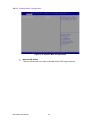
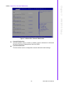
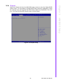
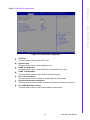
1
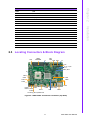
User Manual MIO-9290 Intel® 3rd Core™ i7/i5/i3 rPGA988, 5.25" MI/O SBC, DDR3/DDR3L, DP, HDMI, DVI-I, 48-bit LVDS, 2 GbE, 4 USB3.0, 2 Mini PCIe, mSATA, iManager, MIOe Copyright The documentation and the software included with this product are copyrighted 2014 by Advantech Co., Ltd. All rights are reserved. Advantech Co., Ltd. reserves the right to make improvements in the products described in this manual at any time without notice. No part of this manual may be reproduced, copied, translated or transmitted in any form or by any means without the prior written permission of Advantech Co., Ltd. Information provided in this manual is intended to be accurate and reliable. However, Advantech Co., Ltd. assumes no responsibility for its use, nor for any infringements of the rights of third parties, which may result from its use. Acknowledgements Intel® is a trademark of Intel® Corporation. AMI is a trademark of American Megatrends, Inc. IBM, PC, PS/2 and VGA are trademarks of International Business Machines Corporation. Microsoft Windows® is a registered trademark of Microsoft Corp. All other product names or trademarks are properties of their respective owners. For more information on this and other Advantech products, please visit our websites at: http://www.advantech.com http://www.advantech.com/eplatform For technical support and service, please visit our support website at: http://support.advantech.com/ This manual is for the MIO-9290. MIO-9290 User Manual Part No. 2006929010 Edition 1 Printed in China April 2014 ii Product Warranty (2 years) Advantech warrants to you, the original purchaser, that each of its products will be free from defects in materials and workmanship for two years from the date of purchase. This warranty does not apply to any products which have been repaired or altered by persons other than repair personnel authorized by Advantech, or which have been subject to misuse, abuse, accident or improper installation. Advantech assumes no liability under the terms of this warranty as a consequence of such events. Because of Advantech’s high quality-control standards and rigorous testing, most of our customers never need to use our repair service. If an Advantech product is defective, it will be repaired or replaced at no charge during the warranty period. For outof-warranty repairs, you will be billed according to the cost of replacement materials, service time and freight. Please consult your dealer for more details. If you think you have a defective product, follow these steps: 1. Collect all the information about the problem encountered. (For example, CPU speed, Advantech products used, other hardware and software used, etc.) Note anything abnormal and list any onscreen messages you get when the problem occurs. 2. Call your dealer and describe the problem. Please have your manual, product, and any helpful information readily available. 3. If your product is diagnosed as defective, obtain an RMA (return merchandize authorization) number from your dealer. This allows us to process your return more quickly. 4. Carefully pack the defective product, a fully-completed Repair and Replacement Order Card and a photocopy proof of purchase date (such as your sales receipt) in a shippable container. A product returned without proof of the purchase date is not eligible for warranty service. 5. Write the RMA number visibly on the outside of the package and ship it prepaid to your dealer. iii MIO-9290 User Manual Declaration of Conformity CE This product has passed the CE test for environmental specifications. Test conditions for passing included the equipment being operated within an industrial enclosure. In order to protect the product from being damaged by ESD (Electrostatic Discharge) and EMI leakage, we strongly recommend the use of CE-compliant industrial enclosure products. FCC Class A This equipment has been tested and found to comply with the limits for a Class A digital device, pursuant to part 15 of the FCC Rules. These limits are designed to provide reasonable protection against harmful interference when the equipment is operated in a commercial environment. This equipment generates, uses, and can radiate radio frequency energy and, if not installed and used in accordance with the instruction manual, may cause harmful interference to radio communications. Opera- thin of this equipment in a residential area is likely to cause harmful interference in which case the user will be required to correct the interference at his own expense. Caution! There is a danger of a new battery exploding if it is incorrectly installed. Do not attempt to recharge, force open, or heat the battery. Replace the battery only with the same or equivalent type recommended by the manflatterer. Discard used batteries according to the manufacturer's instructions. Technical Support and Assistance 1. 2. Visit the Advantech website at http://support.advantech.com where you can find the latest information about the product. Contact your distributor, sales representative, or Advantech's customer service center for technical support if you need additional assistance. Please have the following information ready before you call: – Product name and serial number – Description of your peripheral attachments – Description of your software (operating system, version, application software, etc.) – A complete description of the problem – The exact wording of any error messages MIO-9290 User Manual iv Packing List Before you begin installing your card, please make sure that the following materials have been shipped: 1 x MIO-9290 SBC 1 x SATA Cable 30cm (p/n: 1700002155-01) 1 x SATA Power Cable 35cm (p/n: 1700018785) 1 x Audio Cable 20cm (p/n: 1700019584) 2 x COM RS-232/422/485 Cable 22cm (p/n: 1701200220) 1 x Startup Manual (p/n: 2006929000) 1 x Mini Jumper(10pcs package) (p/n: 9689000002) 1 x Screw and stud pack (4 screws for Mini PCIe, 4 M3 (p/n: 9666929000E) studs and screws for MIOe module) If any of these items are missing or damaged, contact your distributor or sales representative immediately. Optional MIOe Module Part Number MIOe-210-D6A1E MIOe-220-L3A1E MIOe-230-L0A1E MIOe-DB5000-01A1E Description 4 x RS232/422/485 2x RS422/485 with DSUB connector, 8-bit GPIO 3 x GbE with RJ45 connector 48-bit LVDS (default) or Display port (by request), backlight power, 2 x USB 2.0 MI/O extension evaluation board Optional Accessories Part number 1700002155-01 1700018785 1703100260 1700021399-01 1910002596-01 96MPI3M-2.4-3M9T 96MPI5-2.7-3M9T 96MPI7M-2.3-6M9T 96MPCM-2.2-2M9T Description SATA cable 30cm SATA power cable 35cm Internal USB cable 26cm RS-232 Tx/Rx only(COM5/6) cable 25cm POST F=M3*10L M=M3*5L B=5 H=19 ST Ni CPU i3-3120ME 2.4G 3M Dual Core CPU i5-3610ME 2.7G 3M Dual Core CPU i7-3610QE 2.3G 6M Quad Core CPU CELERON-1020E 2.2G 2M Dual Core v MIO-9290 User Manual MIO-9290 User Manual vi Contents Chapter 1 General Information ............................1 1.1 1.2 Introduction ............................................................................................... 2 Specifications ............................................................................................ 2 1.2.1 Functional Specifications .............................................................. 2 1.2.2 OS Support ................................................................................... 4 1.2.3 Mechanical Specifications............................................................. 5 1.2.4 Electrical Specifications ................................................................ 5 1.2.5 Environmental ............................................................................... 5 Block Diagram........................................................................................... 6 Board Layout: Dimensions ........................................................................ 6 Figure 1.1 MIO-9290 Mechanical Drawing (Top Side) ................ 6 Figure 1.2 MIO-9290 Mechanical Drawing (Bottom Side) ........... 7 Figure 1.3 MIO-9290 Mechanical Drawing (Coastline)................ 7 1.3 1.4 Chapter 2 Installation............................................9 2.1 Jumpers and Switches ............................................................................ 10 Table 2.1: Jumpers.................................................................... 10 Table 2.2: Switches ................................................................... 10 Connectors.............................................................................................. 10 Table 2.3: Connectors ............................................................... 10 Locating Connectors & Block Diagram ................................................... 11 Figure 2.1 MIO-9290L Connector Locations (Top Side)............ 11 Figure 2.2 MIO-9290 Connector Locations (Bottom Side)......... 12 Figure 2.3 MIO-9290U Connector Locations (Coastline)........... 12 Setting Jumpers ...................................................................................... 13 2.4.1 Jumper List and Setting .............................................................. 13 2.4.2 Switch List and Setting................................................................ 17 2.2 2.3 2.4 Chapter 3 AMI BIOS Setup .................................19 3.1 Introduction ............................................................................................. 20 Figure 3.1 Setup program initial screen..................................... 20 Entering Setup ........................................................................................ 21 3.2.1 Main Setup.................................................................................. 21 Figure 3.2 Main setup screen .................................................... 21 3.2.2 Advanced BIOS Features Setup................................................. 22 Figure 3.3 Advanced BIOS features setup screen .................... 22 Figure 3.4 ACPI Setting ............................................................. 23 Figure 3.5 CPU Configuration.................................................... 24 3.2.3 SATA Configuration .................................................................... 25 Figure 3.6 SATA Configuration.................................................. 25 Figure 3.7 AMT Configuration.................................................... 26 Figure 3.8 PCH-FW Configuration............................................. 27 Figure 3.9 USB Configuration.................................................... 28 Figure 3.10SMART Settings ....................................................... 29 Figure 3.11Embedded Controller Configuration ......................... 30 Figure 3.12Super IO Configuration............................................. 31 Figure 3.13Platform Misc Configuration ..................................... 32 Figure 3.14Serial Port Console Redirection ............................... 33 Figure 3.15CPU PPM Configuration........................................... 34 3.2.4 Chipset........................................................................................ 35 Figure 3.16Chipset Setup ........................................................... 35 3.2 vii MIO-9290 User Manual 3.2.5 3.2.6 3.2.7 Figure 3.17System Agent (SA) Configuration ............................ 36 Figure 3.18 Intel IGFX Configuration.......................................... 37 Figure 3.19LCD Control.............................................................. 38 Figure 3.20PCH-IO Configuration .............................................. 39 Boot Settings .............................................................................. 40 Figure 3.21Boot Setup Utility...................................................... 40 Security Setup ............................................................................ 41 Figure 3.22Password Configuration ........................................... 41 Save & Exit ................................................................................. 42 Figure 3.23Save & Exit............................................................... 42 Appendix A Pin Assignments............................... 45 A.1 Connector Tables.................................................................................... 46 Appendix B System Assignments........................ 71 B.1 System I/O Ports..................................................................................... 72 Table B.1: System I/O Ports ...................................................... 72 DMA Channel Assignments .................................................................... 72 Table B.2: DMA Channel Assignments ..................................... 72 1st MB Memory Map............................................................................... 73 Table B.3: 1st MB Memory Map ................................................ 73 Interrupt Assignments ............................................................................. 73 Table B.4: Interrupt Assignments .............................................. 73 B.2 B.3 B.4 Appendix C Watchdog Timer Sample Code ........ 75 C.1 Watchdog Timer Sample Code............................................................... 76 MIO-9290 User Manual viii Chapter 1 1 General Information This chapter gives background information on the MIO-9290. Sections include: Introduction Specifications Block diagram Board layout and dimensions 1.1 Introduction The MI/O Extension Single Board Computer MIO-9290 based on the 3rd generation Intel® Core™ i3/i5/i7/Celeron rPGA988 processors with QM77 chipset, supports either 2 channel 1600MHz DDR3 or low power DDR3L, 4 USB3.0, 2 SATA III (600 MB/s), AMT 8.0, and can drive three independent displays (DVI-I, Display Port, HDMI) and Dual Display by any combination interface from the board. MIO-9290 provides not only the powerful computing capability but is also a great graphic capable platform. It is aimed at various high level embedded applications. MIO-9290 adapts the newest solution from Intel with 22nm process, up to 15% CPU performance gain over previous generation and contains the latest generation graphics core (Intel® HD Graphics 4000) with DXVA (full AVC/VC-1/MPEG2 Hardware Acceleration), OpenGL* 3.1 and DirectX 11 support. MIO-9290 is high-end level and rich expansion positioning in 5.25“ SBC product line, the rich I/O including 4 USB 3.0/ 2.0, 2 USB2.0, 2 SATA port up to 6Gb/s, 2 GbE, HD Audio, 6 COM, 2 full-size Mini PCIe with mSATA support. Users also can extend Display port, 3 USB2.0, SMBus, LPC and 4 x PCIex1 through Advantech’s innovative MI/O Extension interface. MIO9290 can help customers easily to implement high quality video or graphic applications along with single and simple integrated solution. 1.2 Specifications 1.2.1 Functional Specifications Processor: Mobile 3rd Generation Intel® Core™ Processor (rPGA) – i7 3610QE / i5 3610ME / i3 3120ME / Celeron 1020E – Cache Hierarchy ∗ A 32-KB instruction and 32-KB data first-level cache (L1) for each core ∗ A 256-KB shared instruction/data second-level cache (L2) for each core ∗ 6MB / 3MB / 2MB Intel® Smart Cache for i7 / i5, i3 / Celeron series, shared among all cores – Direct Media Interface (DMI) ∗ DMI 2.0 support ∗ Four lanes in each direction ∗ 5 GT/s point-to-point DMI interface to PCH is supported – Advanced Technologies ∗ Intel® Hyper-Threading Technology 2-threads per core ∗ Intel® Active Management Technology 8.0 (Intel® AMT 8.0, i7, i5 series only) ∗ Intel® Trusted Execution Technology (Intel® TXT) ∗ Intel® 64 Architecture ∗ Thermal Monitoring Technologies ∗ Enhanced Intel® SpeedStep® Technology * Intel® Turbo Boost Technology MIO-9290 User Manual 2 Chipset: Intel® QM77 I/O Controller – Direct Media Interface Chapter 1 ∗ Up to 20 Gb/s each direction, full duplex ∗ Transparent to software – Integrated Serial ATA Host Controller ∗ Data transfer rates up to 6.0 Gb/s (600 MB/s) ∗ Integrated AHCI controller – USB – Power Management Logic ∗ Supports Advanced Configuration and Power Interface (ACPI), Version 4.0a ∗ ACPI-defined power states (processor driven C states) ∗ ACPI Power Management Timer ∗ SMI# generation System Memory Support – Non-ECC, DDR3/DDR3L memory with two SODIMM up to 16GB – DDR3/DDR3L/DDR3L-RS at 1.35 V / 1.5 V Data Transfer Rates ∗ 1333 MT/s (PC3-10600), 1600 MT/s (PC3-12800) – 64-bit wide channels – Intel® Fast Memory Access (Intel® FMA): ∗ Just-in-Time Command Scheduling ∗ Command Overlap ∗ Out-of-Order Scheduling – DDR3/DDR3L default is auto select, but have an option that can select as DDR3/ DDR3L by jumper (J1). Graphic Engine – DirectX* Video Acceleration (DXVA) support for accelerating video processing ∗ Full AVC/VC1/MPEG2 Hardware Acceleration – OpenGL* 3.1 and OpenCL 11 support – DirectX* 11, DirectX* 10.1, DirectX* 10, DirectX* 9 support Display – Multi-display interfaces: DVI-I, HDMI, display port on rear I/O, dual channel 24-bit LVDS on internal connector, display port from MIOe – Support Extend and Clone mode with multi-display device – Dual Independent Display ∗ Any two combination between: VGA, LVDS, HDMI, display port (from Rear I/O), display port (from MIOe) – Triple Independent Display: * DVI-I + HDMI + display port * Triple independent display is not supported under XP with Ivy Bridge processor * Sandy Bridge CPU didn’t support triple independent display. – Integrated Dual LVDS channel support resolution up to 1920 x1080 at 60 Hz – DVI-I output up to resolution 2560x1600 at 60 Hz. Can support Analog RGB display (VGA) through adaptor. – Display Port (DP) supports resolution up to 1920 x 1200 at 60 Hz. * Ivy Bridge CPU didn’t support DP display under DOS * Display Port on rear I/O didn’t support hot plug and audio function because it used Embedded DisplayPort (eDP) from processor connecting to DP connector, Intel eDP didn’t support it. 3 MIO-9290 User Manual General Information ∗ NEW: xHCI Host Controller, supporting SuperSpeed USB 3.0 ports ∗ Two EHCI Host Controllers, supporting HighSpeed USB 2.0 ports ∗ Supports wake-up from sleeping states S1–S4 ∗ Supports legacy Keyboard/Mouse software – HDMI interface supports the HDMI 1.4a specification with audio up to 2560x1600 at 60 Hz Gigabit Ethernet – Port1: QM77 (MAC) + 82579LM GbE (PHY) ∗ Integrated ASF Management Controller ∗ 10/100/1000 BASE-T IEEE 802.3 specification conformance ∗ Energy Efficient Ethernet (EEE) IEEE802.3az support [Low Power Idle (LPI) mode] ∗ Supports up to 9 KB jumbo frames (full duplex) – Port2: I210-IT Gigabit Ethernet Controller ∗ IEEE 802.3az Energy Efficient Ethernet (EEE) ∗ Audio-video bridging ∗ IEEE 1588/802.1AS precision time synchronization ∗ EEE 802.3Qav traffic shaper (with software extensions) ∗ Supports up to 9.5 KB jumbo frames Peripheral interface – MIOe Expansion ∗ Display Port ∗ 4 PCIe x1 ∗ 3 USB 2.0 ∗ LPC ∗ HD Audio: Line out ∗ SMBus ∗ Power: +5/+12Vsb – 2 x Serial-ATA port, up to 6.0 Gb/s (600 MB/s) – 4 x USB 3.0/USB2.0 compliant ports on rear I/O, 2 x USB2.0 compliant ports for internal connection – 2 RS-232 from COM1/2, 2 RS-232/422/485 from COM3/4 (ESD protection for RS-232: Air gap ±15kV, Contact ±8kV), 2 RS-232 from COM5/6 with Tx/Rx only – 16-bit Programmable General Purpose Input/ Output – Watchdog timer: Output System Reset, Programmable counter from 1 ~ 255 minutes/ seconds – Mini PCIe ∗ 2 x Full-size Mini PCIe (Both support mSATA, one is with SIM holder) * Mini PCIe/mSATA default is auto select, but have an option that can select as miniPCIe or mSATA by 4pins switch, default as Mini PCIe. High Definition Audio: – Intel® High Definition Audio Interface – High Definition Audio Codec with Realtek proprietary loss-less content protection technology – Support 1 x Line-input, 1 x Line output, 1 x Mic-input BIOS – AMI 64-Mbit SPI Flash BIOS 1.2.2 OS Support MIO-9290 supports Win 8, Win 7, Win XP, WES7 and WE8S. For further information about OS support of MIO-9290, please Advantech website: http://support.advantech.com.tw/ or contact the technical support center. MIO-9290 User Manual 4 Dimensions: 203 x 146 mm (8" x 5.75") Height: Top Side: 33.12 mm (with cooler); Bottom Side: 9.9 mm Weight: 0.9 kg (1.98 lb) (reference weight of total package) 1.2.4 Electrical Specifications * i7 3610QE w/DDR3: 3.759 A @ 12 V (45.11 W), w/DDR3L: 3.675 A @ 12 V (44.1 W) * i5 3610ME w/DDR3: 2.375 A @ 12 V (28.5 W), w/DDR3L: 2.336 A @ 12 V (28.03 W) * i3 3120ME w/DDR3: 1.675 A @ 12 V (20.1 W), w/DDR3L: 1.656 A @ 12 V (19.87 W) * Celeron 1020E w/DDR3: 1.595 A @ 12 V (19.14 W), w/DDR3L: 1.548 A @ 12 V (18.58 W) – Idle mode * i7 3610QE w/DDR3: 0.646 A @ 12 V (7.75 W), w/DDR3L: 0.662 A @ 12 V (7.94 W) * i5 3610ME w/DDR3: 0.614 A @ 12 V (7.37 W), w/DDR3L: 0.606 A @ 12 V (7.27 W) * i3 3120ME w/DDR3: 0.622 A @ 12 V (7.46 W), w/DDR3L: 0.612 A @ 12 V (7.34 W) * Celeron 1020E w/DDR3: 0.632 A @ 12 V (7.58 W), w/DDR3L: 0.623 A @ 12 V (7.48 W) Power Consumption Conditions: – Max. load: Measure the current value when system in windows mode and running HCT12 system stress – Idle mode: Measure the current value when system in windows mode and without running any program RTC Battery: – Typical Voltage: 3.0 V – Normal discharge capacity: 210 mAh 1.2.5 Environmental Operating Temperature: 0 ~ 60°C (32 ~ 140°F) Operating Humidity: 40°C @ 85% RH Non-Condensing Storage Temperature: Storage temperature: -40~85°C Storage Humidity: Relative humidity: 95% @ 60°C 5 MIO-9290 User Manual General Information Power Requirement: Single +12V DC ± 10% power input Power Consumption: – Max load Chapter 1 1.2.3 Mechanical Specifications 1.3 Block Diagram Intel Ivy Bridge Mobile rPGA DVI-I DDR3/DDR3L SODIMM x2 FDI eDP DMI DP Display port Display port VGA HD Audio, Line Out 48-bit LVDS USB 2.0 x 3 MIOe HDMI Display port MiniPCIe or mSATA (Full size) PCIe x1, SATA MiniPCIe or mSATA (Full size) With SIM holder PCIe x1, SATA SMBus LPC 16-bit GPIO 4 PCIe x 1 USB 2.0 Intel QM77 Panther Point Mobile PCH USB 2.0 PCA9555 64Mbit BIOS SPI 4 USB 3.0 USB 3.0 & 2.0 SMBus HD Audio Realtek ALC 892 Line -in Line out Mic-in PCIe x 1 PHY: Intel 82579LM RJ45 PCIe x 1 GbE: Intel I-210 RJ45 LPC 2 USB 2.0 USB 2.0 2 SATA SATA 6Gb/s Super I/O SCH3106 COM1/2: RS232 COM3/4: RS232/422/485 COM5/6: RS-232 Tx/Rx only Advantech iManager SMBus/I2C 1.4 Board Layout: Dimensions Figure 1.1 MIO-9290 Mechanical Drawing (Top Side) MIO-9290 User Manual 6 Chapter 1 Figure 1.3 MIO-9290 Mechanical Drawing (Coastline) 7 MIO-9290 User Manual General Information Figure 1.2 MIO-9290 Mechanical Drawing (Bottom Side) MIO-9290 User Manual 8 Chapter 2 2 Installation This chapter explains the setup procedures of the MIO-9290 hardware, including instructions on setting jumpers and connecting peripherals, switches and indicators. Be sure to read all safety precautions before you begin the installation procedure. 2.1 Jumpers and Switches The MIO-9290 has a number of jumpers and switches that allow you to configure your system to suit your application. The table below lists the functions of the various jumpers. Table 2.1: Jumpers J1 DDR3/DDR3L Setting * J2 Auto Power On Setting J3 COM4 RS232/422/485 Setting J4 COM4 RS232/422/485 Setting J5 COM4 RS232/422/485 Setting J6 COM3 RS232/422/485 Setting J7 COM4 RS232/422/485 Setting J8 COM3 RS232/422/485 Setting J9 Clear CMOS J10 LCD Power * DDR3/DDR3L default is auto select, but have an option that can select as DDR3/ DDR3L by jumper. Table 2.2: Switches SW1 COM4 RS485 TERMINATION PU/PD SW2 COM3 RS485 TERMINATION PU/PD SW5 CN38 PCIE/ mSATA SELECTION SW6 CN29 PCIE/ mSATA SELECTION 2.2 Connectors Onboard connectors link the MIO-9290 to external devices such as hard disk drives, a keyboard, or floppy drives. The table below lists the function of each of the board's connectors. Table 2.3: Connectors Label Function CN1 12V Power Input CN2 COM3/COM4 CN3 COM1/COM2 CN5 Audio CN7 COM5 TX/RX CN8 COM6 TX/RX CN14 CPU Socket CN15 CPU FAN CN16 Reset CN17 Power Switch CN18 48 bits LVDS Panel CN19 System FAN CN20 SMBus CN21 Inverter Power Output MIO-9290 User Manual 10 Chapter 2 Table 2.3: Connectors LAN CN23 External USB2.0+USB3.0 CN24 External USB2.0+USB3.0 CN25 Display Port CN26 HDMI CN27 DVI-I CN29 Mini PCIE CN30 SATA CN31 SATA CN32 GPIO CN33 GPIO CN34 SATA Power CN35 SATA Power CN36 SIM Card CN37 Internal USB CN38 Mini PCIE CN39 MIOe Installation CN22 2.3 Locating Connectors & Block Diagram CN1 DDR3 SODIMM J1 CN7 CN8 CN2 CN3 J2 CN5 J4, J5, J3, J6 J8, J7 SW2, SW1 J9 CN15 CN16 CN17 CN18 CN20 CN19 CN21 Power CN25 CN26 CN23 CN24 Button Reset CN27 J10 CN22 Button Throttling Alarm/HDD LED Figure 2.1 MIO-9290L Connector Locations (Top Side) 11 MIO-9290 User Manual Figure 2.2 MIO-9290 Connector Locations (Bottom Side) Figure 2.3 MIO-9290U Connector Locations (Coastline) MIO-9290 User Manual 12 You may configure your card to match the needs of your application by setting jumpers. A jumper is a metal bridge used to close an electric circuit. It consists of two metal pins and a small metal clip (often protected by a plastic cover) that slides over the pins to connect them. To “close” a jumper, you connect the pins with the clip. To “open” a jumper, you remove the clip. Sometimes a jumper will have three pins, labeled 1, 2 and 3. In this case you would connect either pins 1 and 2, or 2 and 3. closed closed 2-3 The jumper settings are schematically depicted in this manual as follows: 1 2 1 3 Closed 1-2 2 3 Closed 2-3 A pair of needle-nose pliers may be helpful when working with jumpers. If you have any doubts about the best hardware configuration for your application, contact your local distributor or sales representative before you make any changes. Generally, you simply need a standard cable to make most connections. 2.4.1 Jumper List and Setting J1 DDR3/DDR3L Setting Part Number 1653002101 Footprint HD_2x1P_79_D Description PIN HEADER 2*1P 180D(M)SQUARE 2.0mm DIP W/O Pb Setting Function Open DDR3 Memory module (Default)* Closed DDR3L Memory module * DDR3/DDR3L default is auto select, but have an option that can select as DDR3/ DDR3L by jumper. 13 MIO-9290 User Manual Installation open Chapter 2 2.4 Setting Jumpers J2 Auto Power On Setting Part Number 1653002101 Footprint HD_2x1P_79_D Description PIN HEADER 2*1P 180D(M)SQUARE 2.0mm DIP W/O Pb Setting Function Open Power Button for Power On (Default) Closed Auto Power On J3 & J5 COM4 RS232/422/485 Setting Part Number 1653003260 Footprint HD_3x2P_79 Description PIN HEADER 3x2P 2.0mm 180D(M) SMD 21N22050 Setting Function (1-3)*(2-4) COM4 RS232 (Default) (3-5)*(4-6) COM4 RS422/485 COM4 RS232 COM4 RS422/485 J4 & J6 COM3 RS232/422/485 Setting Part Number 1653003260 Footprint HD_3x2P_79 Description PIN HEADER 3x2P 2.0mm 180D(M) SMD 21N22050 Setting Function (1-3)*(2-4) COM3 RS232 (Default) (3-5)*(4-6) COM3 RS422/485 COM3 RS232 COM3 RS422/485 MIO-9290 User Manual 14 Part Number 1653003260 Footprint HD_3x2P_79 Description PIN HEADER 3x2P 2.0mm 180D(M) SMD 21N22050 Setting Function (1-2) COM4 RS232 (Default) (3-4) COM4 RS485 (5-6) COM4 RS422 Installation COM4 RS232/422/485 Setting COM4 RS232 COM4 RS485 COM4 RS422 J8 COM3 RS232/422/485 Setting Part Number 1653003260 Footprint HD_3x2P_79 Description PIN HEADER 3x2P 2.0mm 180D(M) SMD 21N22050 Setting Function (1-2) COM3 RS232 (Default) (3-4) COM3 RS485 (5-6) COM3 RS422 COM3 RS232 COM3 RS485 COM3 RS422 15 Chapter 2 J7 MIO-9290 User Manual J9 Clear CMOS Part Number 1653003101 Footprint HD_3x1P_79_D Description PIN HEADER 3x1P 2.0mm 180D(M) DIP 2000-13 WS Setting Function (1-2) Normal (Default) (2-3) Clear COMS Normal Clear CMOS J10 LCD Power Part Number 1653003201 Footprint HD_3x2P_79_D Description PIN HEADER 3x2P 2.0mm 180D(M) DIP 21N22050 Setting Function (1-3) +3.3V (Default) (3-5) +5V (3-4) +12V +3.3V +5V +12V MIO-9290 User Manual 16 SW1 COM4 RS485 Termination PU/PD Part Number 1600003089-01 Footprint SW_2x2P_100_198x378 Description DIP SW ESD102LTZ SMD 2x2P 5.04X6.6X3.1mm Setting Function NO TERMINATION (Default) (OFF)1*(ON)3 TEMINATION PU (OFF)2*(ON)4 TERMINATION PD (OFF)1*(OFF)2 (OFF)1*(ON)3 Installation (OFF)1*(OFF)2 (OFF)2*(ON)4 SW2 COM3 RS485 Termination PU/PD Part Number 1600003089-01 Footprint SW_2x2P_100_198x378 Description DIP SW ESD102LTZ SMD 2x2P 5.04X6.6X3.1mm Setting Function (OFF)1*(OFF)2 NO TERMINATION (Default) (OFF)1*(ON)3 TEMINATION PU (OFF)2 (ON)4 TERMINATION PD (OFF)1*(OFF)2 (OFF)1*(ON)3 (OFF)2 (ON)4 SW5 PCIE/ mSATA Selection Part Number 1600003089-01 Footprint SW_2x2P_100_198x378 Description DIP SW ESD102LTZ SMD 2x2P 5.04X6.6X3.1mm Setting Function (OFF)1*(ON)3 AUTO-DETECTION (Default) (OFF)1*(OFF)2 PCIE CARD (OFF)2*(ON)4 mSATA 17 Chapter 2 2.4.2 Switch List and Setting MIO-9290 User Manual (OFF)1*(ON)3 (OFF)1*(OFF)2 (OFF)2*(ON)4 SW6 PCIE/ mSATA Selection Part Number 1600003089-01 Footprint SW_2x2P_100_198x378 Description DIP SW ESD102LTZ SMD 2x2P 5.04X6.6X3.1mm Setting Function (OFF) 1 * (ON) 3 AUTO-DETECTION(Default ) (OFF)1 * (OFF)2 PCIE CARD (OFF)2 * (ON)4 mSATA (OFF)1*(ON)3 MIO-9290 User Manual (OFF)1*(OFF)2 18 (OFF)2*(ON)4 Chapter 3 AMI BIOS Setup 3 3.1 Introduction AMIBIOS has been integrated into many motherboards for over a decade. With the AMIBIOS Setup program, you can modify BIOS settings and control the various system features. This chapter describes the basic navigation of the MIO-9290 BIOS setup screens. Figure 3.1 Setup program initial screen AMI’s BIOS ROM has a built-in Setup program that allows users to modify the basic system configuration. This information is stored in battery-backed CMOS so it retains the Setup information when the power is turned off. MIO-9290 User Manual 20 Turn on the computer and then press <F2> or <DEL> to enter Setup menu. 3.2.1 Main Setup When you first enter the BIOS Setup Utility, you will encounter the Main setup screen. You can always return to the Main setup screen by selecting the Main tab. There are two Main Setup options. They are described in this section. The Main BIOS Setup screen is shown below. Chapter 3 3.2 Entering Setup AMI BIOS Setup Figure 3.2 Main setup screen The Main BIOS setup screen has two main frames. The left frame displays all the options that can be configured. Grayed-out options cannot be configured; options in blue can. The right frame displays the key legend. Above the key legend is an area reserved for a text message. When an option is selected in the left frame, it is highlighted in white. Often a text message will accompany it. 3.2.1.1 System time / System date Use this option to change the system time and date. Highlight System Time or System Date using the <Arrow> keys. Enter new values through the keyboard. Press the <Tab> key or the <Arrow> keys to move between fields. The date must be entered in MM/DD/YY format. The time must be entered in HH:MM:SS format. 21 MIO-9290 User Manual 3.2.2 Advanced BIOS Features Setup Select the Advanced tab from the MIO-9290 setup screen to enter the Advanced BIOS Setup screen. You can select any of the items in the left frame of the screen, such as CPU Configuration, to go to the sub menu for that item. You can display an Advanced BIOS Setup option by highlighting it using the <Arrow> keys. All Advanced BIOS Setup options are described in this section. The Advanced BIOS Setup screens is shown below. The sub menus are described on the following pages. Figure 3.3 Advanced BIOS features setup screen Launch PXE OpROM This item allows users to enable or disable launch PXE OpROM if available. Launch Storage OpROM This item allows users to enable or disable launch storage OpROM if available. MIO-9290 User Manual 22 Chapter 3 3.2.2.1ACPI Settings AMI BIOS Setup Figure 3.4 ACPI Setting Enable ACPI Auto Configuration This item allows users to enable or disable BIOS ACPI auto configuration. Enable Hibernation This item allows users to enable or disable hibernation. ACPI Sleep State This item allows users to set the ACPI sleep state. Lock Legacy Resources This item allows users to lock legacy devices' resources. S3 Video Repost This item allows users to enable or disable VBIOS run after S3 resume. 23 MIO-9290 User Manual 3.2.2.2 CPU Configuration Figure 3.5 CPU Configuration Hyper Threading Technology This item allows users to enable or disable Intel? Hyper Threading technology. Active Processor Cores This item allows users to set how many processor cores should be active. Limit CPUID Maximum This item allows users to limit the maximum value of CPUID. Execute Disable Bit This item allows users to enable or disable the No-Execution page protection technology. Intel Virtualization Technology This item allows users to enable or disable the intel virtualization technology. Hardware Prefetcher This item allows users to enable or disable the hardware prefetcher feature. Adjacent Cache Line Prefetch This item allows users to enable or disable the adjacent cache line prefetch feature. MIO-9290 User Manual 24 Chapter 3 3.2.3 SATA Configuration AMI BIOS Setup Figure 3.6 SATA Configuration SATA Controller(s) This item allows users to enable or disable the SATA controller(s). SATA Mode Selection This item allows users to select mode of SATA controller(s). 25 MIO-9290 User Manual 3.2.3.1 AMT Configuration Figure 3.7 AMT Configuration Intel AMT This item allows users to enable or disable Intel AMT BIOS extension. BIOS Hotkey Pressed This item allows users to enable or disable BIOS hotkey press. MEBx Selection Screen This item allows users to enable or disable MEBx selection screen. Hide Un-Configuration ME Confirmation This item allows users to hide un-configure ME without password confirmation prompt. MEBx Debug Message Output This item allows users to enable or disable MEBx debug message. Un-Configure ME This item allows users to un-configure ME without password. Amt Wait Timer Set timer to wait before sending ASF_GET_BOOT_OPTIONS. Disable ME This item allows users to enable or disable Intel ME. ASF This item allows users to enable or disable Alert Specification Format. Activate Remote Assistance Process This item allows users to enable or disable trigger CIRA boot. USB Configure This item allows users to enable or disable USB configure function. MIO-9290 User Manual 26 3.2.3.2 PCH-FW Configuration Figure 3.8 PCH-FW Configuration MDES BIOS Status Code This item allows users to enable or disable MDES BIOS Status Code function. Firmware Update Configuration This item allows users to enable or disable ME FW image re-flash function. 27 MIO-9290 User Manual AMI BIOS Setup PET Progress This item allows users to enable or disable PET events progress to receive PET events or not. AMT CIRA Timeout OEM defined timeout for MPS connection to be established. WatchDog This item allows users to enable or disable WatchDog Timer. OS Timer Set OS watchdog timer. BIOS Timer Set BIOS watchdog timer. Chapter 3 3.2.3.3 USB Configuration Figure 3.9 USB Configuration Legacy USB Support Enable the support for legacy USB. Auto option disables legacy support if no USB devices are connected. USB3.0 Support This item allows users to enable or disable USB3.0 support. XHCI Hand-Off This is a workaround for the OS without XHCI hand-off support. The XHCI ownership change should claim by XHCI driver. EHCI Hand-Off This is a workaround for the OS without EHCI hand-off support. The EHCI ownership change should claim by EHCI driver. USB transfer time-out Set the time-out value for Control, Bulk, and Interrupt transfers. Device reset time-out Set USB mass storage device Start Unit command time-out value. Device power-up delay Set the maximum time of the device will take before it properly reports itself to the Host Controller. 'Auto' uses default value: for a Root port it is 100 ms, for a Hub port the delay is taken from Hub descriptor. MIO-9290 User Manual 28 Chapter 3 3.2.3.4 SMART Settings AMI BIOS Setup Figure 3.10 SMART Settings SMART Self Test This item allows users to enable or disable SMART Self Test. 29 MIO-9290 User Manual 3.2.3.5 Embedded Controller Configuration Figure 3.11 Embedded Controller Configuration EC iManager WatchDog IRQ This item allows users to set the IRQ number of EC watchdog. EC Power Saving Mode This item allows users to set board's power saving mode when off. EC iManager Smart FAN This item allows users to enable or disable EC iManager smart FAN feature. This item allows users to enable or disable EC serial port B. Backlight Mode This item allows users to set backlight Function. EC Watch Dog Function This item allows users to select EC watchdog timer. MIO-9290 User Manual 30 Chapter 3 3.2.3.6 Super IO Configuration AMI BIOS Setup Figure 3.12 Super IO Configuration Serial Port 1 Configuration This item allows users to configure serial port 1. Serial Port 2 Configuration This item allows users to configure serial port 2. Serial Port 3 Configuration This item allows users to configure serial port 3. Serial Port 4 Configuration This item allows users to configure serial port 4. Serial Port 5 Configuration This item allows users to configure serial port 5. Serial Port 6 Configuration This item allows users to configure serial port 6. 31 MIO-9290 User Manual 3.2.3.7 Platform Misc Configuration Figure 3.13 Platform Misc Configuration Native PCIE Enable This item allows users to enable or disable native PCIE support feature. MIO-9290 User Manual 32 Chapter 3 3.2.3.8 Serial Port Console Redirection AMI BIOS Setup Figure 3.14 Serial Port Console Redirection Console Redirection This item allows users to enable or disable console redirection for Microsoft Windows Emergency Management Services (EMS). Console Redirection This item allows users to configuration console redirection detail settings. 33 MIO-9290 User Manual 3.2.3.9 CPU PPM Configuration Figure 3.15 CPU PPM Configuration EIST CPU runs at its default speed if disabled; CPU speed is controlled by the operating system if enabled. Turbo Mode This item allows users to enable or disable turbo mode. CPU C3/C6/C7 Report This item allows users to enable or disable CPU C-state support. Config TDP LOCK This item allows users to enable or disable Config TDP LOCK. Long duration power limit Long duration power limit in Watts, 0 means use factory default. Long duration maintained Time window which the long duration power is maintained. Short duration power limit Short duration power limit in Watts, 0 means use factory default. ACPI T State This item allows users to enable or disable ACPI T State. MIO-9290 User Manual 34 Select the Chipset tab from the MIO-9290 setup screen to enter the Chipset BIOS Setup screen. You can display a Chipset BIOS Setup option by highlighting it using the <Arrow> keys. All Plug and Play BIOS Setup options are described in this section. The Plug and Play BIOS Setup screen is shown below. Chapter 3 3.2.4 Chipset AMI BIOS Setup Figure 3.16 Chipset Setup 35 MIO-9290 User Manual 3.2.4.1 System Agent (SA) Configuration Figure 3.17 System Agent (SA) Configuration VT-d This item allows users to enable or disable VT-d. DDR Selection This item allows users to select which DDR or DDRL voltage. MIO-9290 User Manual 36 Chapter 3 3.2.4.2 Intel IGFX Configuration AMI BIOS Setup Figure 3.18 Intel IGFX Configuration GTT Size This item allows users to select GTT size. Aperture Size This item allows users to select aperture size. DVMT Pre-Allocated This item allows users to select DVMT pre-allocated memory size. DVMT Total Gfx Mem This item allows users to select DVMT total memory size. Gfx Low Power Mode This item allows users to enable or disable IGD low power mode. Graphics Performance Analyzers This item allows users to enable or disable Graphics Performance Analyzers 2nd LVDS Backlight Control This item allows users to select 2nd backlight control mode. 37 MIO-9290 User Manual LCD Control Figure 3.19 LCD Control – Primary IGFX Boot Display Select boot display device at post stage. – LCD Panel Type This item allows users to select panel resolution. – Panel Scaling This item allows users to enable or disable panel scaling. – Active LVDS/DP This item allows users to select the Active LVDS/DP Configuration. MIO-9290 User Manual 38 Chapter 3 3.2.4.3 PCH-IO Configuration AMI BIOS Setup Figure 3.20 PCH-IO Configuration PCI Express Configuration This item allows users to configuration PCIE1~PCIE8 root port detail settings. USB Configuration This item allows users to configuration detail of USB functions. PCH Azalia Configuration This item allows users to configuration detail of azalia functions. LAN1 control Enables or disables the PCH LAN controller. Wake on LAN Enables or disables PCH LAN wake up from sleep state. LAN2 control Enables or disables the Onboard PCIE LAN controller. PCIE WAKE from S5 PCIE WAKE Enable/Disable from S5. High Precision Timer Enables or disables the high precision timer. SLP_S4 Assertion Width This item allows users to set a delay of sorts. Restore AC Power Loss This item allows users to select off, on and last state. 39 MIO-9290 User Manual 3.2.5 Boot Settings Figure 3.21 Boot Setup Utility Setup Prompt Timeout This item allows users to select the number of seconds to wait for setup activation key. Bootup NumLock State Select the Power-on state for Numlock. Quiet Boot If this option is set to Disabled, the BIOS displays normal POST messages. If Enabled, an OEM Logo is shown instead of POST messages. Option ROM Message Set display mode for option ROM. INT19 Trap Response This item allows option ROMs to trap interrupt 19. MIO-9290 User Manual 40 Chapter 3 3.2.6 Security Setup AMI BIOS Setup Figure 3.22 Password Configuration Select Security Setup from the MIO-9290 Setup main BIOS setup menu. All Security Setup options, such as password protection is described in this section. To access the sub menu for the following items, select the item and press <Enter>: Change Administrator / User Password: Select this option and press <ENTER> to access the sub menu, and then type in the password. 41 MIO-9290 User Manual 3.2.7 Save & Exit Figure 3.23 Save & Exit 3.2.7.1 Save Changes and Exit When users have completed system configuration, select this option to save changes, exit BIOS setup menu and reboot the computer if necessary to take effect all system configuration parameters. 3.2.7.2 Discard Changes and Exit Select this option to quit Setup without making any permanent changes to the system configuration. 3.2.7.3 Save Changes and Reset When users have completed system configuration, select this option to save changes, exit BIOS setup menu and reboot the computer to take effect all system configuration parameters. 3.2.7.4 Discard Changes and Reset Select this option to quit Setup without making any permanent changes to the system configuration and reboot the computer. 3.2.7.5 Save Changes When users have completed system configuration, select this option to save changes without exit BIOS setup menu. 3.2.7.6 Discard Changes Select this option to discard any current changes and load previous system configuration. MIO-9290 User Manual 42 3.2.7.9 Restore User Defaults The users can select this option to restore user defaults. 43 MIO-9290 User Manual AMI BIOS Setup 3.2.7.8 Save User Defaults When users have completed system configuration, select this option to save changes as user defaults without exit BIOS setup menu. Chapter 3 3.2.7.7 Restore Defaults The MIO-9290 automatically configures all setup items to optimal settings when users select this option. Optimal Defaults are designed for maximum system performance, but may not work best for all computer applications. In particular, do not use the Optimal Defaults if the user's computer is experiencing system configuration problems. MIO-9290 User Manual 44 Appendix A A Pin Assignments This appendix contains information of a detailed or specialized nature. Sections include: Connector Tables A.1 Connector Tables CN1 12V Power Input Part Number 1655003861 Footprint WF_2x2P_165_BOX_RA_D_740-77 Description ATX PWR Conn. 2x2P 4.2mm 90D(M) DIP 740-77-04TS0 Pin Pin Name 1 GND 2 GND 3 +12V 4 +12V CN2 COM3/COM4 Part Number 1653004793 Footprint HD_10x2P_79_23N685B-20M10 Description BOX HEADER 10x2P 2.0mm 180D(M)SMD 23N685B-20M10B Pin Pin Name 1 DCD3# 2 DSR3# 3 RXD3 4 RTS3# 5 TXD3 6 CTS3# 7 DTR3# 8 RI3# 9 GND 10 GND 11 DCD4# 12 DSR4# 13 RXD4 14 RTS4# 15 TXD4 16 CTS4# 17 DTR4# 18 RI4# 19 GND 20 GND MIO-9290 User Manual 46 CN3 COM1/COM2 Part Number 1653004793 Footprint HD_10x2P_79_23N685B-20M10 Description BOX HEADER 10x2P 2.0mm 180D(M)SMD 23N685B-20M10B Pin Pin Name 1 DCD1# 2 DSR1# 3 RXD1 4 RTS1# 5 TXD1 6 CTS1# 7 DTR1# 8 RI1# 9 GND 10 GND 11 DCD2# 12 DSR2# 13 RXD2 14 RTS2# 15 TXD2 16 CTS2# 17 DTR2# 18 RI2# 19 GND 20 GND Matching Cable: 1701200220 47 MIO-9290 User Manual Appendix A Pin Assignments Matching Cable: 1701200220 CN4 SODIMMDDR3_204 Part Number 1651001649 Footprint DDR3_204P_2-2013310-1 Description DDR3 SODIMM H=9.2mm 204P SMD 2-2013310-1 Pin Pin Name MIO-9290 User Manual 48 Audio Part Number 1653004099 Footprint HD_5x2P_79_23N685B-10M10 Description BOX HEADER 5x2P 2.00mm 180D(M) SMD 23N685B-10M10 Pin Pin Name 1 LOUTR 2 LINR 3 GND 4 GND 5 LOUTL 6 LINL 7 GND 8 GND 9 MIC1R 10 MIC1L Matching Cable: 1703100152 CN7 COM5 TX/RX Part Number 1655004032 Footprint WF_5P_49_BOX_85205 Description WAFER 5P 1.25mm 180D(M) SMD 85205-05701 Pin Pin Name 1 TXD 2 RTS# 3 RXD 4 CTS# 5 GND Matching Cable: 1700021399-01 49 MIO-9290 User Manual Appendix A Pin Assignments CN5 CN8 COM6 TX/RX Part Number 1655004032 Footprint WF_5P_49_BOX_85205 Description WAFER 5P 1.25mm 180D(M) SMD 85205-05701 Pin Pin Name 1 TXD 2 RTS# 3 RXD 4 CTS# 5 GND Matching Cable : 1700021399-01 MIO-9290 User Manual 50 SODIMMDDR3_204 Part Number 1651001904 Footprint DDR3_204P_2-2013289-1 Description DDR3 SODIMM H=5.2mm 204P SMD 2-2013289-1 Pin Pin Name 51 MIO-9290 User Manual Appendix A Pin Assignments CN9 CN14 CPU Socket Part Number 1651002177 Footprint SOCKET_PGA989 Description CPU Socket rPGA988B 988P SMD 100361HK988J2S6PQ CN15 CPU FAN Part Number 1655004347 Footprint WF_4P_100_D_744-81-04TW30 Description WAFER 2.54 1*4P 180D(M) DIP 744-81-04TW30 Pin Pin Name 1 GND 2 +12V 3 SPEED 4 PWM CN16 Reset Part Number 1655302020 Footprint WF_2P_79_BOX_R1_D Description WAFER BOX 2P 2.0mm 180D(M) DIP A2001WV2-2P Pin Pin Name 1 RESET# 2 GND CN17 Power Switch Part Number 1655302020 Footprint WF_2P_79_BOX_R1_D Description WAFER BOX 2P 2.0mm 180D(M) DIP A2001WV2-2P Pin Pin Name 1 PSIN 2 GND MIO-9290 User Manual 52 48 bits LVDS Panel Part Number 1653920200 Footprint SPH20X2 Description B/B Conn. 40P 1.25mm 90D SMD DF13-40DP-1.25V(91) Pin Pin Name 1 +5V or +3.3V or +V12 2 +5V or +3.3V or +V12 3 GND 4 GND 5 +5V or +3.3V or +V12 6 +5V or +3.3V or +V12 7 LVDS0_D0- 8 LVDS1_D0- 9 LVDS0_D0+ 10 LVDS1_D0+ 11 GND 12 GND 13 LVDS0_D1- 14 LVDS1_D1- 15 LVDS0_D1+ 16 LVDS1_D1+ 17 GND 18 GND 19 LVDS0_D2- 20 LVDS1_D2- 21 LVDS0_D2+ 22 LVDS1_D2+ 23 GND 24 GND 25 LVDS0_CLK- 26 LVDS1_CLK- 25 LVDS0_CLK- 26 LVDS1_CLK- 27 LVDS0_CLK+ 28 LVDS1_CLK+ 29 GND 30 GND 31 NC 32 NC 33 GND 34 GND 35 LVDS0_D3- 36 LVDS1_D3- 37 LVDS0_D3+ 38 LVDS1_D3+ 39 NC 40 NC 53 MIO-9290 User Manual Appendix A Pin Assignments CN18 CN19 System FAN Part Number 1655003010 Footprint WHP3VA Description Wafer 2.54mm 3P 180D(M) DIP 22-27-2031 Pin Pin Name 1 GND 2 +12V 3 NC CN20 SMBus Part Number 1655904020 Footprint FPC4V-125M Description WAFER 4P 1.25mm 180D(M) SMD 85205-04001 Pin Pin Name 1 GND 2 SMB_DAT 3 SMB_CLK 4 +5V MIO-9290 User Manual 54 Inverter Power Output Part Number 1655000453 Footprint WHL5V-2M-24W1140 Description WAFER BOX 2.0mm 5P 180D(M) DIP WO/Pb JIH VEI Pin Pin Name 1 +12V 2 GND 3 ENABKL 4 VBR 5 +5V CN22 LAN Part Number 1652003274 Footprint RJ45_28P_RTB-19GB9J1A Description PHONE JACK RJ45 28P DIP RTB-19GB9J1A Pin Pin Name 1 TX+(10/100),BI_DA+(GHz) 2 TX-(10/100),BI_DA-(GHz) 3 RX+(10/100),BI_DB+(GHz) 4 BI_DC+(GHz) 5 BI_DC-(GHz) 6 RX-(10/100),BI_DB-(GHz) 7 BI_DD+(GHz) 8 BI_DD-(GHz) 55 MIO-9290 User Manual Appendix A Pin Assignments CN21 CN23 External USB2.0+USB3.0 Part Number 1654009860 Footprint USB_9x2P_2360009-603-R Description USB 3.0 CONN 18P 2.0mm 90D(F) DIP 2360009-603-R Pin Pin Name 1 +5V 2 D- 3 D+ 4 GND 5 SSRX- 6 SSRX+ 7 GND 8 SSTX- 9 SSTX+ CN24 External USB2.0+USB3.0 Part Number 1654009860 Footprint USB_9x2P_2360009-603-R Description USB 3.0 CONN 18P 2.0mm 90D(F) DIP 2360009-603-R Pin Pin Name 1 +5V 2 D- 3 D+ 4 GND 5 SSRX- 6 SSRX+ 7 GND 8 SSTX- 9 SSTX+ MIO-9290 User Manual 56 Display Port Part Number 1654010437 Footprint DPCON_20P_3VD51203-H7JJ-7H Description Displayport Conn. 20P 0.5mm 90D(F) SMD 3VD51203 Pin Pin Name 1 ML_Lane0(p) 2 GND 3 ML_Lane0(n) 4 ML_Lane1(p) 5 GND 6 ML_Lane1(n) 7 ML_Lane2(p) 8 GND 9 ML_Lane2(n) 10 ML_Lane3(p) 11 GND 12 ML_Lane3(n) 13 CONFIG1 14 CONFIG2 15 AUX CH(p) 16 GND 17 AUX CH(n) 18 Hot Plug Detect 19 GND 20 +3.3V 57 MIO-9290 User Manual Appendix A Pin Assignments CN25 CN26 HDMI Part Number 1654002198 Footprint HDMI19P-471511002 Description HDMI Conn. 19P 0.5mm 90D(F) SMD 471511002 Pin Pin Name 1 TMDS Data2+ 2 TMDS Data2 Shield 3 TMDS Data2– 4 TMDS Data1+ 5 TMDS Data1 Shield 6 TMDS Data1– 7 TMDS Data0+ 8 TMDS Data0 Shield 9 TMDS Data0– 10 TMDS Clock+ 11 TMDS Clock Shield 12 TMDS Clock– 13 Reserved 14 Reserved 15 SCL 16 SDA 17 DDC Ground 18 +5V Power 19 Hot Plug Detect MIO-9290 User Manual 58 DVI-I Part Number 1654004671 Footprint DVI_29P_QH11121-FAT0-4F Description DVI Conn. 29P 90D(F) DIP QH11121-DAT0-4F Pin Pin Name 1 TMDS Data 2- 2 TMDS Data 2+ 3 TMDS Data 2/4 Shield 4 TMDS Data 4- 5 TMDS Data 4+ 6 DDC Clock 7 DDC Data 8 Analog Vertical Sync 9 TMDS Data 1- 10 TMDS Data 1+ 11 TMDS Data 1/3 Shield 12 TMDS Data 3- 13 TMDS Data 3+ 14 +5V 15 Ground 16 Hot Plug Detect 17 TMDS Data 0- 18 TMDS Data 0+ 19 TMDS Data 0/5 Shield 20 TMDS Data 5- 21 TMDS Data 5+ 22 TMDS Clock Shield 23 TMDS Clock+ 24 TMDS Clock- C1 Analog Red C2 Analog Green C3 Analog Blue C4 Analog Horizontal Sync C5 Analog Ground 59 MIO-9290 User Manual Appendix A Pin Assignments CN27 CN29 Mini PCIE Part Number 1654006715 Footprint MINIPCIE_FULL_HALF_STANDARD Description MINI PCI Express 52P 9.0mm 90D SMD 88911-5204M Pin Pin Name 1 WAKE# 2 +3.3VSB 3 NC 4 GND 5 NC 6 +1.5V 7 NC 8 UIM_PWR 9 GND 10 UIM_DATA 11 REFCLK- 12 UIM_CLK 13 REFCLK+ 14 UIM_RESET 15 GND 16 UIM_VPP 17 NC 18 GND 19 NC 20 W_DISABLE# 21 GND 22 PERST# 23 PERn0 24 +3.3VSB 25 PERp0 26 GND 27 GND 28 +1.5V 29 GND 30 SMB_CLK 31 PETn0 32 SMB_DAT 33 PETp0 34 GND 35 GND 36 USB D- 37 GND 38 USB D+ 39 +3.3VSB 40 GND 41 +3.3VSB MIO-9290 User Manual 60 NC 43 MSATA/PCIe card detect 44 NC 45 NC 46 NC 47 NC 48 +1.5V 49 NC 50 GND 51 NC 52 +3.3 61 Appendix A Pin Assignments 42 MIO-9290 User Manual CN30 SATA Part Number 1654007578 Footprint SATA_7P_WATF-07DBN6SB1U Description Serial ATA 7P 1.27mm 180D(M) SMD WATF-07DBN6SB1U Pin Pin Name 1 GND 2 TX+ 3 TX- 4 GND 5 RX- 6 RX+ 7 GND CN31 SATA Part Number 1654007578 Footprint SATA_7P_WATF-07DBN6SB1U Description Serial ATA 7P 1.27mm 180D(M) SMD WATF-07DBN6SB1U Pin Pin Name 1 GND 2 TX+ 3 TX- 4 GND 5 RX- 6 RX+ 7 GND MIO-9290 User Manual 62 GPIO Part Number 1653004099 Footprint HD_5x2P_79_23N685B-10M10 Description BOX HEADER 5x2P 2.00mm 180D(M) SMD 23N685B-10M10 Pin Pin Name 1 +5V 2 GPIO4 3 GPIO0 4 GPIO5 5 GPIO1 6 GPIO6 7 GPIO2 8 GPIO7 9 GPIO3 10 GND CN33 GPIO Part Number 1653004099 Footprint HD_5x2P_79_23N685B-10M10 Description BOX HEADER 5x2P 2.00mm 180D(M) SMD 23N685B-10M10 Pin Pin Name 1 +5V 2 GPIO4 3 GPIO0 4 GPIO5 5 GPIO1 6 GPIO6 7 GPIO2 8 GPIO7 9 GPIO3 10 GND 63 MIO-9290 User Manual Appendix A Pin Assignments CN32 CN34 SATA Power Part Number 1655001154 Footprint WF_4P_98_BOX_R1_D Description WAFER BOX 4P 2.50mm 180D(M) DIP 24W1170-04S10-01 Pin Pin Name 1 +5V 2 GND 3 GND 4 +12V CN35 SATA Power Part Number 1655001154 Footprint WF_4P_98_BOX_R1_D Description WAFER BOX 4P 2.50mm 180D(M) DIP 24W1170-04S10-01 Pin Pin Name 1 +5V 2 GND 3 GND 4 +12V CN36 SIM Card Part Number 1654010809-01 Footprint SIM_6P_5210622-SINR03 Description SIM card conn. 6p 2.54mm 90D(F) SMD 5210622-SINR Pin Pin Name C1 UIM_PWR C2 UIM_RESET C3 UIM_CLK C5 GND C6 UIM_VPP C7 UIM_DATA MIO-9290 User Manual 64 Internal USB Part Number 1653005260 Footprint HD_5x2P_79_N10 Description PIN HEADER 2x5P 2.0mm 180D(M) SMD 21N22050 Pin Pin Name 1 +5V 2 +5V 3 A_D- 4 B_D- 5 A_D+ 6 B_D+ 7 GND 8 GND 9 GND Matching Cable : 1703100260, 1703100121 CN38 Mini PCIE Part Number 1654006715 Footprint MINIPCIE_FULL_HALF_STANDARD Description MINI PCI Express 52P 9.0mm 90D SMD 88911-5204M Pin Pin Name 1 WAKE# 2 +3.3VSB 3 NC 4 GND 5 NC 6 +1.5V 7 NC 8 UIM_PWR 9 GND 10 UIM_DATA 11 REFCLK- 65 MIO-9290 User Manual Appendix A Pin Assignments CN37 12 UIM_CLK 13 REFCLK+ 14 UIM_RESET 15 GND 16 UIM_VPP 17 NC 18 GND 19 NC 20 W_DISABLE# 21 GND 22 PERST# 23 PERn0 24 +3.3VSB 25 PERp0 26 GND 27 GND 28 +1.5V 29 GND 30 SMB_CLK 31 PETn0 32 SMB_DAT 33 PETp0 34 GND 35 GND 36 USB D- 37 GND 38 USB D+ 39 +3.3VSB 40 GND 41 +3.3VSB 42 NC 43 MSATA/PCIe card detect 44 NC 45 NC 46 NC 47 NC 48 +1.5V 49 NC 50 GND 51 NC 52 +3.3VSB MIO-9290 User Manual 66 Appendix A Pin Assignments CN39 MIOe Part Number 1654006235 Footprint BB_40x2P_32_1625x285_2HOLD Description B/B Conn. 40x2P 0.8mm 180D(F) SMD QSE-040-01-L-D Pin Pin Name 1 GND 2 GND 3 PCIE_RX0+ 4 PCIE_TX0+ 5 PCIE_RX0- 6 PCIE_TX0- 7 GND 8 GND 9 PCIE_RX1+ 10 PCIE_TX1+ 11 PCIE_RX1- 12 PCIE_TX1- 13 GND 14 GND 15 PCIE_RX2+ 16 PCIE_TX2+ 17 PCIE_RX2- 18 PCIE_TX2- 19 GND 20 GND 67 MIO-9290 User Manual 21 PCIE_RX3+ 22 PCIE_TX3+ 23 PCIE_RX3- 24 PCIE_TX3- 25 GND 26 GND 27 PCIE_CLK+ 28 LOUTL 29 PCIE_CLK- 30 LOUTR 31 GND 32 AGND 33 SMB_CLK 34 NC 35 SMB_DAT 36 NC 37 PCIE_WAKE# 38 NC 39 RESET# 40 NC 41 SLP_S3# 42 CLK33M 43 NC 44 LPC_AD0 45 DDP_HPD 46 LPC_AD1 47 GND 48 LPC_AD2 49 DDP_AUX+ 50 LPC_AD3 51 DDP_AUX- 52 LPC_DRQ#0 53 GND 54 LPC_SERIRQ 55 DDP_D0+ 56 LPC_FRAME# 57 DDP_D0- 58 GND 59 GND 60 USB0_D+ 61 DDP_D1+ 62 USB0_D- 63 DDP_D1- 64 GND 65 GND 66 USB1_D+/USB_SSTX+ 67 DDP_D2+ 68 USB1_D-/USB_SSTX- MIO-9290 User Manual 68 DDP_D2- 70 GND 71 GND 72 USB2_D+/USB_SSRX+ 73 DDP_D3+ 74 USB2_D-/USB_SSRX- 75 DDP_D3- 76 GND 77 GND 78 USB_OC# 79 +12VSB 80 +12VSB 83 GND 84 GND 85 GND 86 GND 87 +5VSB 88 +5VSB 89 +5VSB 90 +5VSB 69 Appendix A Pin Assignments 69 MIO-9290 User Manual MIO-9290 User Manual 70 Appendix B B System Assignments This appendix contains information of a detailed nature. Sections include: System I/O Ports DMA Channel Assignments 1st MB Memory Map Interrupt Assignments B.1 System I/O Ports Table B.1: System I/O Ports Addr. Range (Hex) Device 00-1F DMA Controller 20–2D Interrupt Controller 50–52 Timer/Counter 60-6F 8042 (keyboard controller) 70-7F Real-time clock, non-maskable interrupt (NMI) mask 80-9F DMA page register A0-BF 0A0-0BF C0-DF DMA controller 200-207 Communications Port (COM5) 208-20F Communications Port (COM6) 2E8-2EF Communications Port (COM4) 299-29A EC HM Index port and Data port 29C-29D EC Index port and Data port 2F8-2FF Communications Port (COM2) 3B0-3DF Motherboard resources 3E8-3EF Communications Port (COM3) 3F8-3FF Communications Port (COM1) 400-4FF Motherboard resources 500-57F Motherboard resources B.2 DMA Channel Assignments Table B.2: DMA Channel Assignments Channel Function 0 Available 1 Available 2 Available 3 Available 4 Direct memory access controller 5 Available 6 Available 7 Available MIO-9290 User Manual 72 Table B.3: 1st MB Memory Map Addr. Range (Hex) Device E0000h - FFFFFh PCI Bus D0000h - DFFFFh PCI Bus C0000h – CFFFFh System board A0000h - BFFFFh PCI Bus A0000h - BFFFFh Intel® HD Graphics 00000h - 9FFFFh System board B.4 Interrupt Assignments Table B.4: Interrupt Assignments Interrupt# Interrupt Source NMI Parity error detected IRQ0 System timer IRQ1 Standard 101/102-Key or Microsoft Natural PS/2 Keyboard IRQ2 Interrupt from controller 2 (cascade) IRQ3 Communications Port (COM2) IRQ4 Communications Port (COM1) IRQ5 EC Watch DOG IRQ6 Available IRQ7 Communications Port (COM4), Communications Port (COM3) IRQ8 System CMOS/real time clock IRQ9 Microsoft ACPI-Compliant System IRQ10 Communications Port (COM6), Communications Port (COM5) IRQ11 Advantech EC Controller IRQ12 PS/2 Compatible Mouse IRQ13 Numeric data processor IRQ14 Primary IDE IRQ15 Secondary IDE 73 MIO-9290 User Manual Appendix B System Assignments B.3 1st MB Memory Map MIO-9290 User Manual 74 Appendix C Watchdog Timer Sample Code C C.1 Watchdog Timer Sample Code EC_Command_Port = 0x29Ah EC_Data_Port = 0x299h Write EC HW ram = 0x89 Watch dog event flag = 0x57 Watchdog reset delay time = 0x5E (high byte), 0x5F (low byte) Reset event = 0x04 Start WDT function = 0x28 Stop WDT function = 0x29 Reset WDT function = 0x2A =============================================================== .model small .486p .stack 256 .data .code org 100h .STARTup mov dx, EC_Command_Port mov al,89h ; Write EC HW ram. out dx,al mov dx, EC_Data_Port mov al, 5Fh ; Watchdog reset delay time low byte (5Eh is high byte) index, Timebase: 100ms out dx,al mov dx, EC_Data_Port mov al, 64h ;Set 10 seconds delay time. out dx,al mov dx, EC_Command_Port mov al,89h ; Write EC HW ram. out dx,al mov dx, EC_Data_Port mov al, 57h ; Watch dog event flag. out dx,al mov dx, EC_Data_Port mov al, 04h ; Reset event. out dx,al mov dx, EC_Command_Port MIO-9290 User Manual 76 ; start WDT function. (Stop: 0x29, Reset: 0x2A) Appendix C Watchdog Timer Sample Code mov al,28h out dx,al .exit END 77 MIO-9290 User Manual www.advantech.com Please verify specifications before quoting. This guide is intended for reference purposes only. All product specifications are subject to change without notice. No part of this publication may be reproduced in any form or by any means, electronic, photocopying, recording or otherwise, without prior written permission of the publisher. All brand and product names are trademarks or registered trademarks of their respective companies. © Advantech Co., Ltd. 2014