1
CMD11E1
Development Board for the Motorola / Freescale
68HC11E1
xiom
anufacturing
™
© 2000
1226ٛ Exchange Drive,ٛ Richardson, TX 75081 • (972) 437-3737 FAX (972) 437-3736
email: Salesٛ @axman.com • web: http://www.axman.com
CONTENTS
GETTING STARTED............................................................................................ 3
Installing the Software..................................................................... 3
Board Startup.................................................................................. 3
Support Software ............................................................................ 4
Software Development.................................................................... 4
TUTORIAL ........................................................................................................... 4
Creating source code...................................................................... 4
Assembling source code................................................................. 5
Running your application ................................................................ 6
Programming External EEPROM.................................................... 7
MEMORY ............................................................................................................. 8
ADDRESS DECODING .................................................................. 8
MEMORY MAP ............................................................................... 9
JUMPERS .......................................................................................................... 10
MODE Select Jumpers – JP1 and JP2 ......................................... 10
Buffalo Trace Jumper – JP13 ....................................................... 10
Memory Selection Jumpers JP3 – JP10 ....................................... 11
PORTS AND CONNECTORS ............................................................................ 12
LCD_PORT................................................................................... 12
KEYPAD ....................................................................................... 12
SERIAL PORTS............................................................................ 13
COM2 Option Jumpers.............................................................. 13
422/485 OUT ............................................................................. 13
SS: KEBOARD .......................................................................... 14
PARALLEL PORTS ...................................................................... 14
AUX_PORT................................................................................... 15
MCU_PORT.................................................................................. 15
BUS_PORT................................................................................... 16
A/D REFERENCE .............................................................................................. 16
TROUBLESHOOTING ....................................................................................... 17
TABLES ............................................................................................................. 19
TABLE 1. LCD Command Codes................................................. 19
TABLE 2. LCD Character Codes ................................................. 19
TABLE 3. Buffalo Monitor Commands ......................................... 20
2
GETTING STARTED
The Axiom CMD11E1 single board computer is a fully assembled, fully functional development
system for the Motorola 68HC11E1 microcontroller, complete with wall plug power supply and
serial cable. Support software for this development board is provided for Windows 95/98/NT
operating systems. XP and later systems require a host PC with embedded COM serial port that is
PC - AT class compliant.
Follow the steps in this section to get started quickly and verify everything is working correctly.
Installing the Software
1. Insert the Axiom 68HC11 support CD in your PC. If the setup program does not start, run the
file called "SETUP.EXE" on the CD.
2. Follow the instructions on screen to install the AxIDE software onto your hard drive.
3. After installation completes, double-click the AxIDE icon to start the utility program.
4. Select the PC serial port you're using to connect to the board. Click [OK].
5. Select your development board "CMD11E1" from the drop-down menu bar just below the main
menu.
Board Startup
Follow these steps to connect and power on the board. This assumes you're using the provided
AxIDE terminal (installed in the previous section) or a similar communications terminal program on
your PC, and that all jumpers are in their default (from the manufacturer) positions. If you're using a
different terminal program than the one provided, set it's parameters to 9600 baud, N,8,1.
1. Connect one end of the supplied 9-pin serial cable to a free COM port on your PC. Connect
the other end of the cable to the COM1 port on the CMD11E1 board.
2. Apply power to the board by plugging in the wall plug power adapter that came with the
system.
3. If everything is working properly, you should see a Buffalo Monitor prompt similar to that below
in the Terminal window. Press the ENTER key and you should see a prompt which is the >
character.
BUFFALO 3.4AX – Axiom Version of the Motorola Monitor / Debugger
>_
4. Your board is now ready to use!
3
If you do not see the buffalo message prompt like that above, or if the text is garbage, see the
TROUBLESHOOTING section at the end of this manual.
Support Software
There are many useful programs and documents on the included HC11 support CD that can make
developing projects on the CMD11E1 easier. You should browse the CD and copy anything you
want to your hard drive. See the README.TXT file for a description of what is included.
The main programming interface to the CMD11E1 board is the AxIDE program for 32-bit Windows.
This program communicates with the board via its COM1 port and includes a Terminal window for
interfacing with other programs running on the CMD11E1, such as the Buffalo Monitor or the
Basic11 interpreter. It is also useful for displaying information from your own programs that send
output to the serial port.
In addition to the terminal interface, this program also provide an easy to use memory
programming and micro configuration interface to the board. Also on the disk is a free Assembler,
example source code, and other tools to get you started.
Software Development
Software development on the CMD11E1 can be performed using the Buffalo Monitor utility
programmed in U7 EEPROM to test and debug your program stored in RAM on U5. During this
debug phase your program should be located just above the internal register block, for example
$2000 (see the Memory Map section for details).
After satisfactory operation your program can be relocated to start at address $E000 then written to
the EEPROM in U7 using the provided utility called AxIDE. After setting the appropriate jumpers
your program will start automatically when the board is powered on.
TUTORIAL
This section was written to help you get started with the specifics of the CMD11E1 software
development process. Be sure to read the rest of this manual as well as the documentation on the
disk if you need further information.
The following sections take you through the complete development cycle of a simple "hello world"
program, which sends the string "Hello World" to the serial port.
Creating source code
You can write source code for the CMD11E1 board using any language that compiles to Motorola
68HC11 instructions. Included on the software disk is a free Assembler and also a freeware C
compiler and Basic compiler.
You should write your source code using a standard ASCII text editor. Many powerful code editors
4
are available or you can use the free EDIT or NOTEPAD programs that come with your computer.
Once your source code is written and saved to a file, you can assemble or compile it to a Motorola
S-Record (hex) format. This type of output file usually has a .MOT, .HEX or .S19 file extension and
is in a format that can be read by the programming utilities to be programmed into the CMD11E1
board.
It's important to understand your development board's use of Memory and Addressing when writing
source code so you can locate your code at valid addresses. For example, when in "debug"
mode, you should put your program CODE in External RAM. In assembly language, you do this
with ORG statements in your source code. Any lines following an ORG statement will begin at that
ORG location, which is the first number following the word ORG, for example: ORG $2000.
You must start your DATA (or variables) in a RAM location unused by your program, for example:
ORG $1040. When finished debugging, you must change these ORG statements so that your
program is moved to a valid EEPROM area - somewhere after hex E000 (or 8000 on a 32k board).
Do this by putting an ORG $E000 in front of your Program CODE. Data may remain where it is or
be moved down to internal RAM starting at ORG $0000. You must also program the STACK
register somewhere at the top of your available RAM, for example hex 1FF. Do this with this
instruction as the first instruction in your program code: LDS #$01FF.
A look at the example programs on the disk can make all of this clearer. If you're using a Compiler
instead of an assembler, consult the compiler documentation for methods used to locate your code
and data.
Source code created to run under the buffalo monitor environment will be slightly different than
code written for stand-alone operation. The buffalo monitor contains interrupt and RESET vectors
that your code must provide when it's no longer running under the monitor. See the Programming
External EEPROM section for more information on this.
Assembling source code
An example program called “HELLO.ASM” is provided under the \EXAMPLE directory.
You can assemble your source code using command line tools under a DOS prompt by typing:
AS11 HELLO.ASM –l cre s >HELLO.LST
Most compilers and assemblers allow many command line options so using a MAKE utility or batch
file is recommended if you use this method.
The AxIDE utility software provided with this board contains a simple interface to the free
assembler. Use it by selecting "Build" from the menu. This will prompt you for the file to be
assembled.
DO NOT use long path names (> 8 characters). The free assembler is an old DOS tool that does
not recognize them.
If there are no errors in your source code, 2 output files will be created:
HELLO.S19
a Motorola S-Record file that can be programmed into memory
5
HELLO.LST
a common listing file which shows the relationship between source and
output
The listing file is especially helpful to look at when debugging your program. If your program has
errors, they will be displayed and no output will be generated, otherwise the listing file will be
displayed.
Running your application
After creating an S-Record file you can "upload" it to the development board for a test run. The
provided example “HELLO.ASM” was created to run from RAM so you can use the Buffalo Monitor
to test it without programming it into EEPROM.
If you haven’t done so already, verify that the CMD11E1 board is connected and operating properly
by following the steps under “GETTING STARTED” until you see the buffalo prompt, then follow
these steps to run your program:
1. Press and release the RESET button on the CMD11E1 board. You should see the Buffalo
Monitor message. Hit the return key ↵ to get the monitor prompt.
2. Type LOAD T ↵
This will prepare buffalo to receive a program.
3. Select Upload and when prompted for a file name select your assembled program file in srecord format that was created in the previous section called:
HELLO.S19
Your program will be sent to the board thru the serial port.
4. When finished loading you will see the > prompt again.
Type CALL 2400 ↵
This tells buffalo to execute the subroutine at address $2400, which is the start of our test
program.
5. If everything is working properly you should see the message “Hello World” echoed back to
your terminal screen then, since we return at then end of our program, a line containing the
internal register status displayed by buffalo and the buffalo prompt.
6. If you do not get this message, try going thru this tutorial once more, then if still no go, see the
TROUBLESHOOTING section in this manual
You can modify the hello program to display other strings or do anything you want. The
procedures for assembling your code, uploading it to the board and executing it remain the same.
Buffalo has many powerful features such as breakpoints, assembly/disassembly, memory dump
and modify and program trace. Type HELP at the buffalo prompt for a listing of commands or
consult the buffalo documentation file for more information.
6
Programming External EEPROM
When finished with program development you can program your application into EEPROM so it
executes automatically when you apply power to the board. The following procedure does this:
1.
Make a backup copy of the HELLO.ASM source code.
2.
Use a text editor to modify HELLO.ASM. Change the start of the program to $E000 which is
the beginning of the EEPROM in U7. Do this by changing the ”ORG $2400” to ”ORG
$E000” .
3.
Remove the comment * character from before the following lines also:
*
LDS
#$23FF
set the stack pointer
*eloop
*
endless loop
bra
nop
eloop
*
*
org
fdb
$FFFE
START
set the reset vector
4.
This will initialize the stack pointer which is necessary when running outside of buffalo but
should not be done while running under buffalo since it must handle the stack; cause the
program to NOT try to "return" at the end and lastly, program the HC11 reset vector to go to
the beginning of the program (the label START) when powered on.
5.
Re-Assemble HELLO.ASM as described in the "Assembling Source Code" section.
6.
Select "Program” and enter your newly assembled HELLO.S19 file if not already there.
7.
Make sure External EEPROM is selected in this dialog box then click OK and follow the
onscreen instructions (installing the programming jumpers then power off then on or press the
RESET switch).
8.
When finished programming, remove the jumpers as instructed by the program.
9.
Cycle power or press RESET on the board. Your new program should start automatically
and the “Hello World” prompt should be displayed in the terminal window.
To return to the buffalo monitor program, repeat the above steps starting with number 6,
substituting BUF34X.S19 (in the AxIDE program directory) instead of HELLO.S19. The buffalo
monitor should execute again the next time the board is powered on.
7
MEMORY
ADDRESS DECODING
Address decoding is accomplished using a GAL16V8 programmable logic device. Address
lines A<8:15>, AS (address strobe), R/W (read/write), and E (clock) are processed to provide
the memory control signals as shown below by default. Custom configurations, differing from
that shown below, are also possible. Contact the factory for assistance in redefining the
memory map if required.
OE
Output enable to U5, U6, and U7
WR
Write enable to U5 direct, and to U6 and U7 through jumpers JP6 and JP10
respectively.
M1
Chip select to U5 active from 0 to 8K (with mirrored mapping) or 0 to 32k
depending on the status of JP3. See U5 JP3 selection for more information.
M2
Chip select to U6 active for the 24k between 8000 and DFFF, with the
exception of B580 through B7FF inclusive. B580 to B5FF is used to generate
the peripheral chip selects.
M3
Chip select to U7 active for the 8k between E000 and FFFF.
P
Peripheral Access CS0 - CS7. B580 through B5FF.
All of these signals except P are active low. P is active high. Signal line M2 is also connected to
the BUS_PORT expansion connector allowing M2 to work in conjunction with the CS and Address
lines to implement off board, page banked memory. When M2 is used in this manner, U6 must be
removed from the board.
U5 is intended to be either an 8k or a 32k RAM. U6 can accommodate RAM, EEPROM, or ROM.
U7 is to be used primarily for ROM but it can also accommodate EEPROM. Jumpers JP3 through
JP10 determine how U5, U6, and U7 are used. See the Memory Selection Jumpers section for
details.
Peripheral Access 'P' is used in conjunction with A<4:6>, and AS to generate CS<0:7>. Each of
these eight chip selects controls sixteen bytes in the memory map from B580 through B5FF.
CS<7:0> are brought out to the BUS_PORT where they can be used to control peripherals external
to the development board. See the Memory Map on the next page for further clarification.
8
MEMORY MAP
The following memory map is for a 68HC11E9 as shipped in this development board. Other
68HC11 devices in the A and E series may also be used with this board. These optional devices
differ in the amount of internal RAM, ROM and EEPROM available and the factory default value of
the CONFIG register. Consult the HC11 technical reference manual on the support CD for
additional information.
FFFF
FFFE
RESET Vector Address
-
-
-
-
-
-
-
-
-
-
-
-
-
-
-
-
-
-
-
-
Memory Socket U7 (8K device)
(Buffalo Monitor default)
E000
DFFF
Program or Data Memory
EEPROM or RAM in U6
B800
B7FF
HC11 Internal EEPROM in U1
Program or Data
B600
B5FF
B580
B57F
Peripheral Area CS0 – CS7
CS7 = B5F2-B5FF
LCD = B5F0-B5F1
CS6 = B5E0-B5EF
CS5 = B5D0-B5DF
CS4 = B5C0-B5CF
CS3 = B5B0-B5BF
CS2 = B5A0-B5AF
CS1 = B590-B59F
CS0 = B580-B58F
Program or Data Memory
EEPROM or RAM in U6
8000
7FFF
Data Memory
RAM in U5
1040
103F
1000
0FFF
0200
01FF
68HC11 Internal Registers
See 68HC11 Technical Data Manual
Data Memory
RAM in U5
68HC11 Internal RAM in U1 - (0-FF reserved by Buffalo Monitor)
0000
9
-
JUMPERS
The CMD11E1 board is shipped from the manufacturer with the following default jumper settings:
JP1 = OFF
JP2 = OFF
JP10 = ON
JP3 = ON
JP4 = ON
JP5 = OFF
JP6 = ON
JP7 = ON
JP8 = OFF
JP9 = OFF
JP13 = OFF
Memory socket U5 is shipped with a 32K byte RAM device. U7 is shipped with an 8K byte
EEPROM flash memory device. U6 is shipped with a 32K byte EEPROM flash memory device.
Also, the 68HC11 chip configuration word is set as follows:
EEON On Chip EEPROM
ROMON On Chip ROM
NOCOP Watchdog System
NOSEC Security
ENABLED
DISABLED
DISABLED
DISABLED
MODE Select Jumpers – JP1 and JP2
The MODA and MODB pins of the HC11 are pulled high by two 10k resistors. This is the normal
EXPANDED MODE configuration. A shunt on JP1 will take MODA to ground. A shunt on JP2 will
take MODB to ground. These two jumpers allow selection of any of the following modes of
operation:
JP1 – MODA
ON
OFF
ON
OFF
JP2 - MODB
ON
ON
OFF
OFF
MODE OF OPERATION
Special Bootstrap
Special Test
Normal Single Chip
Normal Expanded (default)
Buffalo Trace Jumper – JP13
The Buffalo Monitor Trace and Single Step functions can be enabled by installing option jumper
JP13. This jumper will connect the PA3 Output Compare 5 pin to the XIRQ line for nonmaskable
interrupt service for the Buffalo Trace functions. Use caution when installing this jumper that no
other connections are made to the XIRQ or PA3 I/O pins of the 68HC11.
10
Memory Selection Jumpers JP3 – JP10
The factory setting for the jumpers should be correct for the memory devices that came with your
board. If you add or modify the type or size of memory, you must change the following jumpers
accordingly. All jumpers are two-pin jumpers and are installed vertically.
U7 - ROM or EEPROM
FFFF
U7
E000
JP8
OFF
OFF
OFF
ON
JP9
OFF
OFF
ON
OFF
JP10
ON
OFF
OFF
ON
U7 DEVICE
8k EEPROM
8k EPROM.
32k EPROM.
32k EEPROM.
< DEFAULT >
JP10 write protects U7 memory device when OFF.
U6 - RAM or EEPROM or ROM
DFFF
U6
8000
JP4
OFF
OFF
OFF
ON
JP5
OFF
OFF
ON
OFF
JP7
OFF
OFF
ON
ON
JP6
ON
OFF
OFF
ON
U6 DEVICE
8k RAM or EEPROM.
8k EPROM.
32k EPROM.
32k RAM or EEPROM.
< DEFAULT >
JP6 write protects U6 memory device when OFF.
U5 - RAM
7FFF
For 32K device
JP3 = ON <DEFAULT> 32K bytes from 200 hex to 7FFF hex
(minus register area, see memory map) and recommended
position for Buffalo Monitor and Small C operation. No
segmentation occurs.
For 8K device
JP3 = OFF 8K bytes from 0000 hex to 1FFF hex and
mirrored at 2000 – 3FFF, 4000 – 5FFF, and 6000 - 7FFF.
This position will allow CPU internal Ram and I/O ports to
segment the 8K address space. Use this position to run
Basic11 with an 8K device.
U5
0100
You can determine the size of memory devices by reading the label on top of the chip. Memory
devices that contain 64 in the part number are usually 8K. Those with 256 are usually 32K.
The type of memory can also be determined by reading the chip label. If you don’t recognize the
memory type you can look up the part number in a catalog or device manual. If the chip is by
Atmel™ or XICOR™ it is probably an EEPROM. If it has HY or SEC it is probably RAM.
11
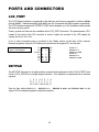
PORTS AND CONNECTORS
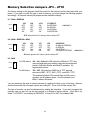
LCD_PORT
The LCD Display interface is connected to the data bus and memory mapped to locations $B5F0
through $B5F3. Addresses $B5F0 and $B5F1 are the Command and Data registers respectfully.
The LCD interface supports all OPTREX™ DMC series displays up to 80 characters and provides
the most common pinout.
Power, ground and Vee are also available at the LCD_PORT connector. The potentiometer, R23,
located to the right of the LCD connector is used to adjust the contrast of the LCD display by
varying Vee from –5v to +5v.
A list of valid command codes is provided in the Tables section at the back of this manual.
Example programs using this LCD device are provided on the support CD, see the files:
B5F0 Command Register
B5F1 Data Register
+5V 2
A0 4
/LCDCS 6
D1 8
D3 10
D5 12
D7 14
1
3
5
7
9
11
13
GND
Vee
/RW
D0
D2
D4
D6
KLCD-D.C
KEYLCD-D.C
KEYLCD-D.ASM
KLCD-E.C
KEYLCD-E.C
KEYLCD-E.ASM
KEYPAD
The KEYPAD Connector is an eight position connector that implements 4 bits of AUX_PORTC and
4 bits of AUX_PORTA as a simple keypad interface. This interface is implemented as a software
keyscan.
1 2 3 4 5 6 7 8
{ { { { { { {
C4 C5 C6 C7 A4 A5 A6 A7
See the files called KLCD-D.C, KEYLCD-D.C, KEYLCD-D.ASM and KEYPAD.BAS on the
support CD for example programs using this connector.
12
SERIAL PORTS
The onboard serial port COM1 is a simple three wire asynchronous serial interface with hard wired
Clear to Send (CTS) and Data Terminal Ready (DTR). It is driven by the HC11 internal SCI port
using I/O pins PD0 and PD1. These two logic level signals are coupled through an RS232 level
shifter to the COM1 connector.
COM1 is the default serial interface for the Buffalo Monitor and programming software.
COM1 DB9 S Style Connector
y 5
9
y
8
y
7
y
GND
•
Cut-Away jumpers between following pins:
4 Æ 1 and 6 (DTR/DSR/DCD)
7 Æ 8 (RTS/CTS)
•
COM1 is set to connect directly to a PC serial port
with a straight thru type of cable (supplied).
•
To connect COM2 to a PC serial port you must use a
NULL modem cable or NULL modem adapter.
•
With U13 removed, CTS, DTR, and DCD will be idled
automatically allowing the R65C51 ACIA to function
normally.
y 4
6
y 3
RXD
y 2
TXD
y
y 1
COM2 DB9 P Style Connector
(E5) DSR
6
y
(E6) RTS
7
y
(E7) CTS
8
y
(E8) NC
9
y
y 1
DCD
y 2
RXD
y 3
TXD
y 4
DTR
y 5
GND
To change COM2 from RS232 to RS485/422:
1. Remove U13 from its socket to isolate P_COM2.
2. Add a jumper wire or connector from E5 thru E8 to the RS422/485 output
connector.
COM2 Option Jumpers
RX_SEL
1 2 3
{{{
2W / 4W
1 {
2 {
3 {
1 - 2 = RS232
2 - 3 = RS485/422
422/485 OUT
4{
3{
2{
1{
A(+)
B(-)
A(+)
B(-)
4W Transmit
4W Transmit
4W Receive, 2W Transmit / Receive
4W Receive, 2W Transmit / Receive
13
1 - 2 = RS485 / 2W
2 - 3 = RS422 / 4W
SS: KEBOARD
The SS:KEYBOARD interface is available but not brought out to a connector. It can be
implemented with software drivers through the SPI feature of the 68HC11. Such a configuration is
used with a serially encoded keyboard. This port can also be used as a keypad by using PD<2:5>
as column lines with E<1:4> as row lines. Note that E<1:4> are open termination’s with pull-down
resistors on the board. E<1:4> are ONLY connected to pins 7, 8, 9, and 10 of the SS:KEYBOARD
connector. In order to use those pins, E<1:4> must be connected to I/O lines. AUX_PORT C is
recommended because it is capable of nibble or 4 bit configuration. While such a dual parallel
matrix will work, it dedicates the SPI to keypad use only. If implemented through the SPI as a
SIMPLE SERIAL port, four separate, additional SPI serial devices can be supported by the SEL
lines defining E<1:4> for a total of five slave serial devices. (Note: this still requires E<1:4> be
connected. Each to its own I/O line, but this will support four additional peripheral devices.)
1
2
3
4
5
6
7
8
9
10
{
{
{
{
{
{
{
{
{
+5
GND
PD2/SI
PD3/SO
PD4/SCLK
PD5/SEL0
SEL1
SEL2
SEL3
SEL4
SPI
Auxiliary select lines terminated to ground
(10kohm)
E1
E2
E3
E4
See the files called KLCD-E.C, KEYLCD-E.C, KEYLCD-E.ASM on the support CD for example
programs using this connector.
PARALLEL PORTS
The 68HC11 is configured for expanded/multiplexed mode. It uses Port B and Port C for address
and data buss to external memory and memory mapped I/O devices. This leaves CPU Port D,
Port A, and Port E to provide all other parallel I/O from the controller. CPU port lines are mixed as
input only, output only, and some are input or output. All CPU port lines serve dual functions with
internal CPU peripherals such as the timer subsystem and port A, the A/D converter on port E, and
the SPI or SCI on port D.
To increase general purpose input/output capability an 82C55 peripheral port expander is memory
mapped onto the data buss providing three auxiliary ports. The auxiliary port lines are all input or
output configurable and are available on the AUX_PORT connector. All port lines are limited to
sinking and sourcing approximately 1mA. maximum. Refer to Chapter 6 Memory Map and
Appendix C for more information on the 82C55.
14
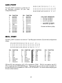
AUX_PORT
25 23
{ {
{ {
26 24
The AUX_PORT connector is a dual row 13
pin Berg-style connector (26 pins total)
configured as follows:
PIN
1
3
5
7
9
11
13
15
17
19
21
23
25
FUNCTION
AUX PA7
AUX PA5
AUX PA3
AUX PA1
AUX PC7
AUX PC5
GND
AUX PC0
AUX PC2
AUX PB0
AUX PB2
AUX PB4
AUX PB6
PIN
2
4
6
8
10
12
14
16
18
20
22
24
26
21 19 17 15 13 11 9
{ { { { { { {
{ { { { { { {
22 20 18 16 14 12 10
FUNCTION
AUX PA6
AUX PA4
AUX PA2
AUX PA0
AUX PC6
AUX PC4
+5
AUX PC1
AUX PC3
AUX PB1
AUX PB3
AUX PB5
AUX PB7
7
{
{
8
5
{
{
6
3
{
{
4
1
{
2
AUX_PORT ADDRESSES
• AUX PA @ $B5F4
• AUX PB @ $B5F5
• AUX PC @ $B5F6
• AUX PORT CONTROL
REGISTER @ $B5F7
See also the Memory Map
MCU_PORT
The MCU_PORT connector is a dual row 17 pin Berg-style connector (34 pins total) configured as
follows:
33 31 29 27 25 23 21 19 17 15 13 11 9 7
5 3
1
{ { { { { { { { { { { { { { { {
{ { { { { { { { { { { { { { { { {
34 32 30 28 26 24 22 20 18 16 14 12 10 8 6
PIN
1
3
5
7
9
11
13
15
17
FUNCTION
PA0
PA2
PA4
PA6
+5
GND
PD0/RXD0
PD2/SI
PD4/SCLK
PIN
2
4
6
8
10
12
14
16
18
FUNCTION
PA1
PA3
PA5
PA7
+5
GND
PD1/TXD0
PD3/SO
PD5/SEL0
PIN
19
21
23
25
27
29
31
33
4
2
FUNCTION
GND
IRQ
VRL
VRH
PE7
PE6
PE5
PE4
PIN
20
22
24
26
28
30
32
34
FUNCTION
+5
XIRQ
VRL
VRH
PE3
PE2
PE1
PE0
PD0 and PD1 are used by the HC11 SCI to implement COM1. PD<2:5> are used by the HC11
SPI to implement the SS:KEYBOARD port. These port D lines can also be used for parallel I/O,
but then they will not be available for COM1 or SS: KEYBOARD. Use caution when assigning port
D lines to other functions.
15
BUS_PORT
The BUS_PORT supports off-board parallel devices. Power (+5V), ground, address lines, data
lines, and control lines are brought out to this 34 pin connector. Pin assignments are as follows:
GND
D2
D1
D0
A0
A1
A10
OE
A11
A9
A8
A12
W/R
CS1
CS3
CS5
+5
PIN
1
3
5
7
9
11
13
15
17
19
21
23
25
27
29
31
33
BUS_PORT
{
{{
{{
{{
{{
{{
{{
{{
{{
{{
{{
{{
{{
{{
{{
{{
{{
PIN
2
4
6
8
10
12
14
16
18
20
22
24
26
28
30
32
34
D3
D4
D5
D6
D7
A2
A3
A4
A5
A6
A7
A13
CS0
CS2
CS4
IRQ
M2
A/D REFERENCE
The VRH and VRL lines from the HC11 are connected to +5v through R3 and to ground through
R2 respectively. These two resistors are located next to the MCU_PORT header. The resistors
are identified on the silk screen by their reference designators. The appropriate resistor(s) need to
be removed in order to apply an external reference to the VRH and/or VRL inputs.
16
TROUBLESHOOTING
The CMD11E1 board is fully tested and operational before shipping. If it fails to function
properly, inspect the board for obvious physical damage first. Ensure that all IC devices in
sockets are properly seated. Verify the communications setup as described under GETTING
STARTED and see the Tips and Suggestions sections following for more information.
The most common problems are improperly configured communications parameters, and
attempting to use the wrong COM port.
1. Verify that your communications port is working by substituting a known good serial device or
by doing a loop back diagnostic.
2. Verify the jumpers on the board are installed correctly.
3. Verify the power source. You should measure approximately 9 volts between the GND
and +9V test point pads on the board.
4. If no voltage is found, verify the wall plug connections to 115VAC outlet and the power
connector.
5. Disconnect all external connections to the board except for COM1 to the PC and the wall
plug.
6. Make sure that the RESET line is not being held low.
Check for this by measuring the RESET pin on P4 for +5V.
7. Verify the presence of an 8MHz sine wave on the crystal, or 2MHz E clock signal if possible.
17
Tips and Suggestions
Following are a number of tips, suggestions and answers to common questions that will solve most
problems users have with the CMD11E1 development system. You can download the latest
software from the Support section of our web page at:
www.axman.com
AxIDE
• If you’re program code memory, make sure jumpers 1 and 2 are set parallel to the
MC68HC11 micro, not pointing away from it.
• If you’re trying to start a program in external EEPROM (U7), make sure jumpers 1 and 2
are NOT installed.
• Be certain that the data cable you’re using is bi-directional and is connected securely to
both the PC and the board. Also, make sure you are using the correct serial port.
• Make sure the correct power is supplied to the board. You should only use a 9 volt,
200mA adapter or power supply. If you’re using a power strip, make sure it is turned on.
• If the configuration file loads (the first 100 bytes or so), but you get a time-out error when
the program section begins to download, make sure the HC11 is internally configured
correctly by selecting Configure Processor from the main menu. During program
development the EEON should be enabled. The other bits should be disabled.
• Make sure you load your code to a valid address. See the Memory Map.
Code Execution
• Make sure ALL jumpers are set correctly according to your board’s configuration. Read
the hardware manual section on jumpers carefully if you’re not sure.
• Always remember to remove JP1 and JP2 after programming the code memory.
• If you programmed your code into external EEPROM memory and it doesn’t run, check
the HC11 reset vector, located at $FFFE - $FFFF. These 2 bytes contain the reset
vector address where execution will begin when the unit is powered on or reset. The
default vector is E000, which is the beginning of the 8k program address space.
• Verify that all peripheral devices are initialized properly in your code. Failure to initialize
the serial port, for example, is a common problem. This is usually the case when the
code works under buffalo but not after programming.
ImageCraft C
• Your make or build should create a .MAP file. Some versions change this to a .MP file.
At the top of this file should be a label __START. This is where you should CALL or GO
to when debugging in buffalo.
18
TABLES
TABLE 1. LCD Command Codes
Command codes are used for LCD setup and control of character and cursor position. All
command codes are written to LCD panel address $B5F0. The BUSY flag (bit 7) should be
tested before any command updates to verify that any previous command is completed. A
read of the command address $B5F0 will return the BUSY flag status and the current display
character location address.
Command
Clear Display, Cursor to Home
Cursor to Home
Entry Mode:
Cursor Decrement, Shift off
Cursor Decrement, Shift on
Cursor Increment, Shift off
Cursor Increment, Shift on
Display Control:
Display, Cursor, and Cursor Blink off
Display on, Cursor and Cursor Blink off
Display and Cursor on, Cursor Blink off
Display, Cursor, and Cursor Blink on
Cursor / Display Shift: (nondestructive move)
Cursor shift left
Cursor shift right
Display shift left
Display shift right
Display Function (default 2x40 size)
Character Generator Ram Address set
Display Ram Address set
Code
$01
$02
Delay
1.65ms
1.65ms
$04
$05
$06
$07
40us
40us
40us
40us
$08
$0C
$0E
$0F
40us
40us
40us
40us
$10
$14
$18
$1C
$3C
$40-$7F
$80- $FF
40us
40us
40us
40us
40us
40us
40us
TABLE 2. LCD Character Codes
$20
$21
$22
$23
$24
$25
$26
$27
$28
$29
$2A
$2B
$2
C
Space
!
“
#
$
%
&
‘
(
)
*
+
,
$2D
$2E
$2F
$30
$31
$32
$33
$34
$35
$36
$37
$38
$39
.
/
0
1
2
3
4
5
6
7
8
9
$3A
$3B
$3C
$3D
$3E
$3F
$40
$41
$42
$43
$44
$45
$46
:
;
{
=
}
?
Time
A
B
C
D
E
F
$47
$48
$49
$4A
$4B
$4C
$4D
$4E
$4F
$50
$51
$52
$53
G
H
I
J
K
L
M
N
O
P
Q
R
S
$54
$55
$56
$57
$58
$59
$5A
$5B
$5C
$5D
$5E
$5F
$60
19
T
U
V
W
X
Y
Z
[
Yen
]
^
_
`
$61
$62
$63
$64
$65
$66
$67
$68
$69
$6A
$6B
$6C
$6D
a
b
c
d
e
f
g
h
i
j
k
l
m
$6E
$6F
$70
$71
$72
$73
$74
$75
$76
$77
$78
$79
$7A
n
o
p
q
r
s
t
u
v
w
x
y
z
$7B
$7C
$7D
$7E
$7F
{
|
}
>
<
TABLE 3. Buffalo Monitor Commands
ASM [<address>]
BF <addr1> <addr2> <data>
BR [-] [<address>]...
BULK
BULKALL
CALL [<address>]
G [<address>]
HELP
LOAD T
MD [<addr1> [<addr2>]]
MM [<address>]
MOVE <addr1> <addr2> [,dest>]
P
RM[p,y,x,a,b,c,s,]
T [<n>]
VERIFY T
Assembler/Disassembler
Block fill memory with data
Breakpoint set
Bulk erase EEPROM
Bulk erase EEPROM + CONFIG register
Execute subroutine
Execute program
Display monitor commands
Download S-records via terminal port
Dump memory to terminal
Memory modify
Move memory to new location
Proceed/continue from breakpoint
Register modify
Trace $1-$FF instructions (TRACE Jumper = ON)
Compare memory to download data via terminal
NOTE
• Address and data values should be given in Hex notation, for example: asm 2bf0
• See the buffalo monitor users guide (on disk) for more information.
20