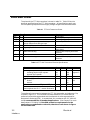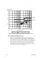
1
®
LONWORKS
FTT-10A Free Topology
Transceiver
User’s Guide
Version 3
@
E C H E L O N®
Corporation
078-0156-01C
Echelon, LON, LONW ORKS , LonBuilder, NodeBuilder, LonManager, LonTalk,
LONMARK , Neuron, 3120, 3150, the LonUsers logo, the LONMARK logo, and the
Echelon logo are trademarks of Echelon Corporation registered in the United
States and other countries. LonLink, LonSupport, and LonMaker are trademarks
of Echelon Corporation.
Other brand and product names are trademarks or registered trademarks of
their respective holders.
Neuron Chips, Free Topology Twisted Pair Transceiver Modules, and other OEM
Products were not designed for use in equipment or systems which involve
danger to human health or safety or a risk of property damage and Echelon
assumes no responsibility or liability for use of the Neuron Chips or Free Topology
Twisted Pair Transceiver Modules in such applications.
Parts manufactured by vendors other than Echelon and referenced in this
document have been described for illustrative purposes only, and may not have
been tested by Echelon. It is the responsibility of the customer to determine the
suitability of these parts for each application.
ECHELON MAKES AND YOU RECEIVE NO WARRANTIES OR CONDITIONS, EXPRESS,
IMPLIED, STATUTORY OR IN ANY COMMUNICATION WITH YOU, AND ECHELON
SPECIFICALLY DISCLAIMS ANY IMPLIED WARRANTY OF MERCHANTABILITY OR
FITNESS FOR A PARTICULAR PURPOSE.
No part of this publication may be reproduced, stored in a retrieval system, or
transmitted, in any form or by any means, electronic, mechanical,
photocopying, recording, or otherwise, without the prior written permission of
Echelon Corporation.
Printed in the United States of America.
Copyright ©1996-1997 by Echelon Corporation.
Echelon Corporation
4015 Miranda Avenue
Palo Alto, CA 94304, USA
Contents
1
Introduction
Applications
Audience
Content
Related Documentation
2
Electrical Interface
Transceiver Pinout
Network Connection
Clock Input
Neuron® Chip Communications Port (CP) Lines
PC Board Layout Guidelines
Physical Layer Repeater
3
Mechanical Considerations
Mechanical Footprint
4
Network Cabling and Connection
Network Overview
System Performance and Cable Selection
System Specifications
Transmission Specifications
Cable Termination
5
Design Issues
EMI Design Issues
Designing Systems for EMC
ESD Design Issues
Designing Systems for ESD Immunity
Vibration and Mechanical Shock Issues
IEC Electromagnetic Compatibility (EMC) Testing
6
Programming Considerations
Application Program Development and Export
LonBuilder ® Developer’s Workbench
NodeBuilder™ Development Tool
7
References
Reference Documentation
LONWORKS FTT-10A Transceiver User’s Guide
1-1
1-3
1-5
1-5
1-6
2-1
2-2
2-5
2-5
2-6
2-6
2-10
3-1
3-2
4-1
4-2
4-4
4-4
4-5
4-6
5-1
5-2
5-2
5-5
5-5
5-6
5-7
6-1
6-2
6-2
6-5
7-1
7-2
iii
Appendix A
Guidelines for FTT-10 Users
Mechanical Differences
Pinout and External Circuit Differences
Replacement in Existing PC Board Designs
External Component Removal from an Existing Board Layout
EMI Comparison Scans for the FTT-10 and FTT-10A Transceivers
Comparison of FTT-10 and FTT-10A Radiated EMI
SLTA-10 Adapter EN 55022-B Test Scan
Appendix B
FTT-10A Transceiver-Based Node Checklist
FTT-10A Transceiver and Neuron Chip Connections
FTT-10A PCB Layout
FTT-10A Transceiver Programming
FTT-10A Transceiver Power Supply - General
FTT-10A Physical Layer Repeater
iv
Echelon
A-1
A-2
A-4
A-5
A-5
A-5
A-6
A-9
B-1
B-2
B-3
B-3
B-3
B-4
1
Introduction
The FTT-10A Free Topology Twisted Pair Transceiver provides a
simple, cost-effective method of adding a LONWORKS transceiver to
any Neuron® Chip-based control system. A replacement for the
popular FTT-10 transceiver, the FTT-10A transceiver supports
polarity insensitive, free topology wiring, freeing the system installer
from the need to wire using a bus topology (differences between the
FTT-10A and FTT-10 transceivers are described in Appendix A). Star,
bus, and loop wiring are all supported by this architecture. Free
topology wiring reduces the time and expense of system installation by
allowing the wiring to be installed in the most expeditious manner. It
also simplifies network expansion by eliminating restrictions on wire
routing, splicing, and node placement.
The FTT-10A transceiver consists of an isolation transformer that is
integrated with a 78kbps differential Manchester coded
communication transceiver. Pins are provided for connections to the
Neuron Chip Communications Port (CP) and clock lines, +5V power,
and the twisted pair network. The FTT-10A transceiver provides
automatic detection of the input clock frequency at 5, 10, and 20MHz.
The pins are keyed to prevent accidental reversal during mounting.
The FTT-10A transceiver appears as a high impedance to the network
when unpowered, and does not interfere with network
communications when powered down.
The transceiver is housed in an encapsulated plastic shell which
contains the transformer and signal processing electronics. The
compact package is only 7.2mm (0.28 inches) high and is ideal for use
in low profile applications such as DIN packs. The sealed housing
LONWORKS FTT-10A Transceiver User’s Guide
1-1
protects the transceiver should conformal coating or other forms of
environmental sealing be required on the printed circuit assembly.
The FTT-10A transceiver is compatible with Echelon's LPT-10 Link
Power Transceiver, and these transceivers can communicate with
each other on a single twisted pair cable. This capability provides an
inexpensive means of interfacing to nodes whose current or voltage
requirements would otherwise exceed the capacity of the link power
segment. When equipped with an FTT-10A transceiver, these nodes
can be operated from a local power supply without the need for
additional electrical isolation from the link power network.
The FTT-10A transceiver also provides electrical isolation for I/O
devices that are grounded, allowing such devices to be used on a link
power network segment. Each segment of a link power network
utilizes a non-isolated design with a single ground point at the LPI-10
Link Power Interface. Proper operation requires that the integrity of
a single point ground be maintained throughout the segment,
including I/O devices that are connected to a Neuron Chip. In many
applications, some I/O devices are grounded, either to meet functional
requirements or safety regulations. The transformer of the FTT-10A
transceiver electrically isolates the node from the segment, allowing
devices connected to the node to be grounded without impairing
communications.
A twisted pair channel may be comprised of multiple segments
separated by physical layer repeaters. A physical layer repeater
permits a twisted pair network to grow inexpensively to encompass
many more nodes or longer wire distances than would otherwise be
possible. The FTT-10A transceiver includes a physical layer repeater
feature that allows LonTalk® data to be exchanged between network
segments by interconnecting two or more FTT-10A or LPT-10
transceivers; FTT-10A-to-LPT-10 physical layer repeaters require the
addition of an external logic circuit. If the repeater includes an LPT10 transceiver then the internal power supply of the LPT-10
transceiver can power the FTT-10A transceiver. Alternately, the FTT10A transceiver can be powered by a local +5VDC power supply.
Using the FTT-10A transceiver can save literally thousands of hours
of development time compared with a custom-designed transceiver.
The transceiver is designed to comply with both FCC and EN55022
EMI requirements, minimizing time consuming and expensive
testing. As a UL Recognized component, the FTT-10A transceiver can
be integrated into a product without further safety testing. The
transceiver is small enough to fit into virtually any application, and is
economically priced for OEM applications of any volume.
Introduction
1-2
Applications
A conventional control system using bus topology wiring (such as RS-485)
consists of a network of sensors and control outputs that are interconnected using
a shielded twisted wire pair. In accordance with RS-485 guidelines, all of the
devices must be wired in a bus topology to limit electrical reflections and ensure
reliable communications. There is a high cost associated with installing and
maintaining the cable plant that links together the many elements of an RS-485based control system. Bus topology wiring is more time consuming and
expensive to install because the installer is unable to branch or star the wiring
where convenient: all devices must be connected directly to the main bus.
The best solution for reducing installation and maintenance costs and
simplifying system modifications is a flexible topology communication system.
Echelon's free topology transceiver (FTT) technology offers just such a solution,
and provides an elegant and inexpensive method of interconnecting the different
elements of a distributed control system.
A free topology architecture allows the user to wire the control devices with
virtually no topology restrictions. Power is supplied by a local +5VDC power
supply located at each node (figure 1.1).
Sensor
Actuator
+5VDC power
FTT-10A
Node
FTT-10A
Node
FTT-10A
Node
Termination
FTT-10A
Node
To
additional
FTT-10A
nodes
FTT-10A
Node
FTT-10A
Node
Figure 1.1
Free Topology Transceiver System
Unlike bus wiring designs, the FTT-10A system uses a free topology wiring
scheme that supports star, loop, and/or bus wiring (figure 1.2). This design has
many advantages. First, the installer is free to select the method of wiring that
LONWORKS FTT-10A Transceiver User’s Guide
1-3
best suits the installation, reducing the need for advanced planning and
allowing last minute changes at the installation site. Second, if installers have
been trained to use one style of wiring for all installations, free topology
technology can be introduced without requiring retraining. Third, retrofit
installations with existing wiring plants can be accommodated with minimal, if
any, rewiring. This capability ensures that FTT-10A technology can be adapted
to both old and new projects, widening the potential market for FTT-10A-based
products. Finally, free topology permits FTT-10A systems to be expanded in the
future by simply tapping into the existing wiring where it is most convenient to do
so. This reduces the time and expense of system expansion, and from the
customer's perspective, keeps down the life cycle cost of the free topology network.
Termination
Singly Termin ated Bus Topology
Termination
Termination
Termination
Star Topology
Doubly Terminated Bus Topology
Termination
Termination
Loop Topology
Figure 1.2
Mixed Topology
Typical Wiring Topologies Supported by the FTT-10A System
System expansion is simplified in another important way, too. Each FTT-10A
transceiver incorporates a repeater function. If a network segment grows beyond
the maximum number of transceivers or total wire distance, then additional
FTT-10A segments can be added by interconnecting transceivers using the
repeater function (figure 1.3). The repeaters will transfer LonTalk data between
the two segments, doubling the number of transceivers as well as the length of
wire over which they communicate. The repeater function permits an FTT-10A
network to grow as system needs expand, without retrofitting existing controllers
or requiring the use of specialized bridges. Note that systems requiring high
levels of network traffic may benefit from the use of LONW ORKS routers which
forward packets only when necessary.
Introduction
1-4
LP Node
FT Node
FT Node
FT Node
FT Node
Term.
FT Node
FT Node
FT Node
LPI-10
FT Node
Term.
LP Node
Power
Supply
LPT-10
FTT-10A
FTT-10A
FTT-10A
FTT-10A
FTT-10A
FT Node
6-way repeater
FT Node
LP Node
LPI-10
FT Node
Term.
FT Node
FT Node
FT Node
FT Node
LP Node
FT Node
FT Node
Term.
FTT-10A
2-way repeater
Power
Supply
LP Node
FT Node
LP Node
LPT-10
LPI-10
FT Node
FT Node
Term.
Figure 1.3
Free Topology Channel Illustrating FTT-10A and LPT-10 Transceiver Compatibility
and Network Expansion Using Physical Layer Repeaters
(Repeaters simplified for illustration purposes)
Audience
The L ON W ORKS FTT-10A Free Topology Transceiver User’s Guide provides
specifications and user instructions for FTT-10A transceiver customers and
users of control modules, network interfaces, and routers based on the FTT-10A
transceiver.
Content
This manual provides detailed technical specifications on the electrical and
mechanical interfaces and operating environment characteristics for the
transceiver module.
This document also provides guidelines for migrating applications from a
LonBuilder Developer’s Workbench Emulator or NodeBuilder Development Tool
to an FTT-10A-based node. Complete references and vendor sources are
included to simplify the task of integrating the transceiver with application
electronics.
This document has a list of references in Chapter 7. Whenever a reference
document is addressed, a superscript number corresponding to the reference has
been placed in the text, e.g., Standler10. Whenever a specific chapter or section
within a reference has been referred to, the reference is enclosed in brackets and
the chapter is addressed by number, e.g., Reference [1], Chapter 7.
LONWORKS FTT-10A Transceiver User’s Guide
1-5
Related Documentation
The following Echelon documents are suggested reading:
LonBuilder User's Guide (078-0001-01)
NodeBuilder User's Guide (078-0141-01)
Neuron C Programmer's Guide (078-0002-01)
LonBuilder Startup and Hardware Guide (078-0003-01)
L ON M ARK ™ Layers 1-6 Interoperability Guidelines (078-0014-01)
L ON M ARK ™ Application Layer Interoperability Guidelines (078-0120-01)
Neuron Chip Data Book (published by Motorola and Toshiba)
L ON W ORKS FTT-10A Free Topology Transceiver data sheet (003-0111-01)
L ON W ORKS Custom Node Development engineering bulletin (005-0024-01)
LPI-10 Link Power Interface Module User’s Guide (078-0104-01)
LPT-10 Link Power Transceiver User's Guide (078-0105-01)
Introduction
1-6
2
Electrical Interface
The FTT-10A Free Topology Transceiver provides a polarity
insensitive connection to the twisted pair network, an interface to the
Neuron Chip communications port, and a physical layer repeater
function for expanding the size of a network.
LONWORKS FTT-10A Transceiver User’s Guide
2-1
Transceiver Pinout
The pinout of the FTT-10A transceiver is shown in table 2.1. Table 2.2 lists the
electrical specifications of the FTT-10A transceiver. All specifications apply over
the full operating temperature and supply voltage ranges unless otherwise noted.
Table 2.1 FTT-10A Transceiver Pinout
Name
VCC
NET_B
NET_A
RXD
Pin
1
2
3
4
Type
TXD
CLK
5
6
CMOS digital output capable of driving one
Neuron Chip and one HC-type input
CMOS digital input with tri-state detection
Digital input, CMOS level
T1
7
Bidirectional analog
GND
T2
8
9
Bidirectional analog
Function
5V DC input
Network port, polarity insensitive
Network port, polarity insensitive
Neuron Chip CP0
Neuron Chip CP1
Transceiver clock input from Neuron
Chip’s CLK2
Used for ESD clamping & transient
protection
Ground
Used for ESD clamping & transient
protection
Table 2.2 FTT-10A Transceiver Electrical Specifications
Parameter
Min
Operating temperature range
excluding physical layer repeater
-40
physical layer repeater
0
Vcc input supply voltage
4.75
Vcc input supply current
receive
transmit
DC resistance between NET_A and NET_B
Transmitter raised cosine waveform peak-topeak amplitude into 52.3 Ω network termination
Typ
Max
Units
degrees C
5
+85
+85
5.25
5
20
20
1.35
Volts
mA
Ω
Volts
The preferred interconnection between the FTT-10A transceiver and a Neuron Chip
is shown in figure 2.1. This schematic has been tested for ESD under both the
preferred contact-discharge method and the alternate air-discharge method for
electrostatic discharge (ESD). It exceeds level 4 in accordance with IEC 1000-4-2,
and is recommended for all standard applications. (See Chapter 5 for more
details about IEC 1000-4-2). If the ESD protection requirements for the
application are undefined or unknown, then the circuit shown in figure
2.1 should be used.
2-2
Interface
Electrical
Figure 2.1 is not a complete schematic, since the clock, reset and power supply
bypass circuits will vary depending on the Neuron Chip type and application. For
complete Neuron Chip application schematics and information, refer to the Neuron
Chip Databook2,3. See chapter 3 for mechanical specifications and printed circuit
board (PCB) footprint information.
See Text
C3
NET1
NET2
D3
Neuron Chip
(Partial)
FTT-10A
CP0
RXD
CP1
TXD
CLK2
CLK
CP2
CP3
CP4
+5V
NET_A
D4
C2
C4
NET_B
VCC
T1
T2
GND
+5V
PCB Spark
Gaps
D1
D2
C1
Figure 2.1 FTT-10A Transceiver Interconnection Using Spark Gaps
Table 2.3 FTT-10A Transceiver External Components
Name
Value
Comments
C1
0.1µF for +5VDC
decoupling
Power supply decoupling capacitor
for FTT-10A transceiver
C2
1000pF, 2kV, low
inductance
ESD snubber capacitor
C3,C4
22µF, +50V, polar
DC blocking capacitors; see text
D1, D2, D3,
D4
BAV99 or 1N4148(x2)
Transient clamping diodes;
BAV99LT1 (National), BAV99LT
(Sprague), MMBD120 (Motorola), or
equivalent
Some applications cannot use spark gaps due to the need for conformally coated or
potted PCBs. In figure 2.2 the spark gaps are replaced with encapsulated discharge
devices Z1 and Z2, which are connected to chassis ground. Each of these devices
has a discharge voltage of approximately 300 volts and introduces very little
capacitance (<1pF) to ground. Also note that diodes D3 through D6 are fast 1A
rectifiers which survive level 3 surge voltages (see chapter 5) and load the network
differentially with less than 150pF. These rectifiers are required to protect the
FTT-10A transceiver from surge voltages seen differentially across Net1 and Net2
as a result of asymmetric firing of the discharge devices in the presence of surge
voltages coupled
LONWORKS FTT-10A Transceiver User’s Guide
2-3
onto the network wiring. The physical placement of Z1 and Z2 should be near the
entry points of the network wiring with a low impedance path to chassis ground (or
alternately to star ground near star ground center). The external components for
figure 2.2 are shown in table 2.4.
See Text
C3
Neuron Chip
(Partial)
D5
D4
D6
NET2
FTT-10A
CP0
RXD
NET_A
CP1
TXD
NET_B
CLK2
CLK
VCC
CP2
CP3
CP4
D3
NET1
+5V
T1
T2
GND
Z1
Z2
C2
C4
+5V
D1
D2
C1
Figure 2.2 FTT-10A Transceiver Interconnection Without Spark Gaps
Table 2.4 FTT-10A Transceiver External Components
Name
Value
Comments
C1
0.1µF for +5VDC decoupling
Power supply decoupling capacitor
for FTT-10A transceiver
C2
1000pF, 2kV, Low inductance
ESD snubber capacitor
C3,C4
22µF, +50V, polar
DC blocking capacitors; see text
D1, D2
BAV99 or 1N4148(x2)
Transient clamping diodes;
BAV99LT1 (National), BAV99LT
(Sprague), MMBD120 (Motorola), or
equivalent
D3, D4, D5, D6
1N4934, 1N4935, or Motorola
SMT version MRA4935T3
Fast switching rectifiers (General
Instruments or Motorola)
Z1, Z2
DSP-301N
Fast surge protectors with microgap
(source: Mitsubishi Materials
Corporation at US phone number
+1-847-577-0200, or fax number
+1-847-577-0201 or Europe
(London) phone +44-171-236-0130)
Some applications require compliance only with Level 4 of the preferred contactdischarge method for electrostatic discharge (ESD) as defined in IEC 1000-4-2. For
these applications, diodes D3 and D4, and capacitor C2, as shown in figure 2.1, can
be deleted. This simplified circuit has been tested at Level 4 under the preferred
2-4
Interface
Electrical
contact-discharge method for electrostatic discharge (ESD) in accordance with IEC
1000-4-2. Note that it is the operation of the Neuron Chip, and not of the FTT-10A
transceiver, which is affected at higher air-discharge levels when using the
modified circuit. It is recommended that the simplified circuit be used only
after determining that contact-discharge ESD protection is acceptable for
the application. If air-discharge ESD protection is required or the need
for it is undefined or unknown, then the circuit shown in figure 2.1 should
be used.
The clock, reset, and power supply bypass circuits in the modified circuit will not
represent a complete schematic, since they will vary depending on the Neuron Chip
type and application. For complete Neuron Chip application schematics and
information, refer to the Neuron Chip Databook2,3. See chapter 3 for mechanical
specifications and printed circuit board (PCB) footprint information.
In all of the interconnection schematics, capacitors C3 and C4 are used to provide
DC voltage isolation for the FTT-10A transformer when the transceiver is used on a
link power network, and may also be used to protect the transformer in the event of
a DC fault on the network. The capacitors are required to meet LonMark
interoperability guidelines. The capacitors are not needed on nodes that will be
connected exclusively to non-link power networks and do not require protection
against DC faults. Two polar capacitors are used to protect against the application
of DC of either polarity while providing total net capacitance of 11µF.
Alternatively, a single non-polar capacitor of 10µF may be used in either of the two
legs which connect to the network. The initial tolerance of the capacitor should
vary no more than ±20%, and degradation due to aging and temperature effects
should not exceed 20% of the initial minimum value.
Network Connection
The network connection (NET1 and NET2) is polarity insensitive and therefore
either of the two twisted pair wires can be connected to either of these network
connections. Details about network wiring are discussed in chapter 5.
Clock Input
The FTT-10A transceiver receives its clock input from the Neuron Chip via the
CMOS input CLK pin. This pin is driven by the CLK2 output of the Neuron Chip,
whether the Neuron Chip's oscillator or an external clock oscillator is used. The
CLK2 trace length should be kept to no more than 2cm (0.8”) to minimize noise
coupling.
The FTT-10A transceiver operates with an input clock of 5,10 or 20MHz. The
transceiver automatically detects the clock rate and configures internal circuitry
appropriately. Echelon has not qualified the FTT-10A transceiver for use with a
20MHz Neuron Chip and does not have a recommended board layout at this time;
please contact Echelon before starting a 20MHz design.
The accuracy of the input clock frequency to the Neuron Chip and
transceiver must be ±200 ppm or better; this requirement can be met with
a suitable crystal, but cannot be met with a ceramic resonator.
LONWORKS FTT-10A Transceiver User’s Guide
2-5
Neuron Chip Communications Port (CP) Lines
The FTT-10A transceiver transmits and receives LonTalk network packets via the
Neuron Chip’s direct, single-ended mode interface using pins CP0 and CP1.
Neuron Chip data input pin CP0 is connected to the RXD pin of the FTT-10A
transceiver. Neuron Chip data output pin CP1 is connected to the TXD pin of the
FTT-10A transceiver. No buffering or other connections should be made to CP1.
The other Neuron Chip CP pins (CP2, 3, 4) are not connected to the FTT-10A
transceiver. The transceiver automatically detects activity on its TXD pin to enable
transmission, thus there is no connection to the Neuron Chip TXEN function on
CP2. The FTT-10A transceiver has a built-in bias circuit to prevent transmission
during the Neuron Chip reset process, when CP1 is not driven. The unused CP4
input should be connected to Vcc to prevent excess supply current draw in the
Neuron Chip input buffer. Table 2.5 summarizes connections between the Neuron
Chip Communication Port and the transceiver.
Table 2.5 Neuron Chip Communication Port Connections
Neuron Chip Pin
Neuron Chip Function
Connect to
CP0
Data input
FTT-10A RXD
CP1
Data output
FTT-10A TXD
CP2
Transmit enable output
Not connected
CP3
~Sleep output
Not connected
CP4
~Collision Detect input
Vcc
PC Board Layout Guidelines
An example of a PC board layout is shown in figure 2.3. The layout uses surface
mount (SMT) components on the top side of the PCB. The scale of the figures is
approximately 4X, but they are not intended for use as finished PCB artwork.
Variations on this suggested PCB layout are possible as long as the general
principles discussed later in this section (and in chapter 5) are followed. Throughhole capacitors and diodes can be used, but SMT components will generally be
superior because of their lower series inductance.
Electrostatic discharge (ESD) and electromagnetic interference (EMI) are two of the
most important design considerations when laying out the PCB for a node. These
topics are discussed in general terms in chapter 5, and the specifics relating to PCB
layout issues are covered here.
Tolerance of ESD and other types of network transients requires good layout of the
power, ground and other node circuitry. In general, an ESD discharge current will
return to earth ground or other nearby metal structures. The node’s ground scheme
must be able to pass this ESD current between the network connection and the
node’s external ground connection without generating significant voltage gradients
across the node’s PCB. The low-inductance "Star" ground scheme illustrated in
figure 2.4 and discussed below accomplishes this task.
2-6
Interface
Electrical
1.
"Star" Ground Configuration: The distribution of functional circuit blocks on the
PCB should be in the form of a star, with the power connector, network connector and
any "chassis ground" connection all located as close as practical to the center of the
star. This star ground distribution is illustrated in figure 2.4. The goal of star
ground distribution is to conduct transients out of the node with minimal disruption
to other function blocks. If the node has a metal chassis, then ESD and other
transients will generally return to that chassis via the star ground center point. If
the node’s logic ground is connected to this chassis ground, then connection should be
made at this single point only. If a node is housed in a plastic enclosure and is
powered with an isolating transformer, then there may not be any explicit earth
ground or "chassis" ground available. In this case, it is still important for the network
connector and power supply connector to be located near the center of the star.
2.
PC Board Spark Gaps: The PC board layout should be designed so that substantial
ESD hits from the network will discharge directly to the star ground center point.
This is accomplished by creating PCB spark gaps from NET1 and NET2 to ground as
detailed in figure 2.4. This design yields a metal-to-metal spacing on the PC board of
0.39mm (0.015”), which permits ESD hits above roughly 3kV to discharge directly to
ground. This limits the amount of energy that must be absorbed by the FTT-10A
transceiver and its associated circuitry. The keep-out area noted in figure 2.3 is
designed to eliminate unintended discharge paths. If the PC board must be
conformally coated or otherwise insulated, please refer to figure 2.2 for an alternate
schematic that does not rely on exposed metal spark gaps.
3.
D1/D2 Clamp Diodes: The diodes D1 and D2 clamp the node side of the FTT-10A
transformer signals between Vcc and ground. The Vcc and ground connections
between D1, D2, and the FTT-10A transceiver must be made using the low
inductance technique shown in figure 2.3 to ensure that transient energy remaining
after any discharge to the spark gap does not disrupt the FTT-10A transceiver or the
Neuron Chip. Note that the Vcc and ground connections of diodes D1 and D2 are
designed to return transient currents to the FTT-10A ground pin and the star ground
center point.
4.
D3/D4 Clamp Diodes: The diodes D3 and D4 in figure 2.1 (D3 through D6 in figure
2.2) clamp the network side of the FTT-10A transformer signals to ground through C2
during ESD transients. The connections between D3, D4, and C2 must be made using
the low inductance technique shown in figure 2.3 to ensure that transient energy
remaining after any discharge to the spark gap does not disrupt the Neuron Chip.
Note that the connection of C2 is designed to return transient currents to the star
ground center point.
LONWORKS FTT-10A Transceiver User’s Guide
2-7
Component Side
D2
D1
VCC
Net
C1
VCC
T2
Solder Side
(X-ray view)
GND
T1
VCC
CLK
T2
GND
CLK
T1
TXD
TXD
RXD
RXD
Keep-out area
NET_B
NET_A
NET_B
NET_A
Star
Ground
Center
C2
D3
D4
C3
C4
Spark Gap
(2X)
2.30mm
0.090"
1.78mm
0.070"
1.00mm
0.040"
Solder Mask
Ground Plane
PCB
0.51mm
0.019" Dia. Via
Spark Gap Detail
Cross-section
Figure 2.3 FTT-10A PCB Layout
2-8
Interface
Electrical
Application
I/O Block
Neuron Chip
Block
Clock Ground
Guard
Power
Supply
Block
Star Ground
Center
Figure 2.4 Star Ground Design
(Ground Distribution is Shown for Clarity Only)
LONWORKS FTT-10A Transceiver User’s Guide
2-9
5.
Ground Planes: As ground is routed from the center of the star out to the function
blocks on the board, planes or very wide traces should be used to lower the inductance
(and therefore the impedance) of the ground distribution system.
6.
+5V Power Distribution & Decoupling: In general, Vcc should be distributed
through low inductance traces and planes in the same manner as ground. At least
two 0.1µF SMT decoupling caps are recommended around the Neuron Chip on the
component side of the PCB; follow the recommendations in the Neuron Chip
2,3
Databooks . In contrast to the wide Vcc distribution to the Neuron Chip and other
node circuitry, the routing of Vcc to the FTT-10A transceiver should be through a
narrow trace of 0.3mm (0.012 inch) width. The inductance of this trace in
combination with the FTT-10A transceiver's Vcc decoupling capacitor, C1, helps to
reduce digital noise at the FTT-10A transceiver's Vcc input (pin 1), which reduces
EMI on the network wiring. Place C1 immediately next to the FTT-10A transceiver
as shown in figure 2.3.
7.
CLK Routing for EMI Control: The CLK input to the FTT-10A needs to be guarded
by ground traces to minimize clock noise, and to help keep EMI levels low (see
chapter 5). In general, the Neuron Chip should be placed close enough to the FTT10A transceiver and oriented correctly so that the CLK trace from the Neuron Chip to
the transceiver is no longer than 2cm (0.8"). At the same time, the Neuron Chip and
any other fast digital circuitry should be kept away from the network connector and
NET_A/NET_B pins (pins 2 and 3) on the transceiver. If noisy digital circuitry is
located too close to the network connector, RF noise may couple out onto the network
cable and cause EMI problems.
8.
FTT-10A Transceiver Grounding for EMI Control: To best control EMI, the
connection between the FTT-10A transceiver ground pin and the center of star
ground should be wide and short as shown in figure 2.3.
Physical Layer Repeater
In the event that the limits on the number of transceivers or total wire distance are
exceeded, a physical layer repeater (figure 2.5) can be added to interconnect two or
more TP/FT-10 network segments. This effectively multiplies overall channel
capability, including node count and network extent, but not bandwidth. To extend
network bandwidth, use LONWORKS Routers.
Designing large networks which rely on physical layer repeaters to extend node
count requires careful consideration of network traffic. Testing of the network
under worst-case traffic conditions while monitoring with a LonManager Protocol
Analyzer is highly recommended to properly evaluate system performance.
LONWORKS Routers and/or topology changes may be used to solve traffic congestion
problems.
2-10
Interface
Electrical
Network
Segment
1
Network
Segment
2
Network
Segment
1
FTT-10A
Transceiver
FTT-10A
Transceiver
FTT-10A
Transceiver
N-Way
Repeater
Two-Way
Repeater
FTT-10A
Transceiver
FTT-10A
Transceiver
Network
Segment
2
FTT-10A
Transceiver
Network
Segment
3
Network
Segment
N
Figure 2.5 Two-Way and N-Way Repeaters
A repeater consists of two or more transceivers, a 5MHz clock source, and
miscellaneous components. Figures 2.6 and 2.7 show schematics for two-way and
N-way repeaters, respectively. The clock oscillator requires CMOS output levels,
±200 ppm total accuracy (use only a crystal-controlled oscillator; do not use a
ceramic resonator-controlled oscillator), and duty cycle between 40/60 and 60/40.
The OR gate in figure 2.7 requires CMOS output levels and 100nsec maximum
propagation delay. Different clock sources may be used for each of the FTT-10A
transceivers in a physical layer repeater. However, the clock sources must be
synchronized. No ESD snubber diodes or capacitors are shown in figures 2.6 and
2.7 because the FTT-10A transceivers (without accompanying Neuron Chips) do not
require them. Resistors R1, R2 and capacitor C5 shown in figures 2.6 and 2.7 are
required for proper repeater operation. The operating temperature range of these
circuits is 0 to +85°C.
LONWORKS FTT-10A Transceiver User’s Guide
2-11
UA
See Text
FTT-10A
TXD
C3A
NET_A
RXD
NET_B
CLK
VCC
NET1
C4A
NET2
+5V
D1A
C1A
PCB
Spark Gaps
R1A
T1
C5A
D2A
T2
R2A
GND
UB
See Text
FTT-10A
TXD
NET_A
RXD
NET_B
CLK
VCC
C3B
NET1
C4B
NET2
+5V
D1B
T1
5MHz Clock
Oscillator
C1B
PCB
Spark Gaps
R1B
C5B
D2B
T2
GND
R2B
R1 1500Ω, 1%
R2 576 Ω, 1%
C5 0.1 µF, X7R or Y5V ceramic
Other components per Table 2.3
Operating temperature range: 0 to +85°C
Figure 2.6 Two-Way Repeater
2-12
Interface
Electrical
UA
See Text
FTT-10A
TXD
C3A
NET_A
RXD
NET_B
CLK
VCC
NET1
C4A
NET2
+5V
D1A
T1
C1A
PCB
Spark Gaps
R1A
C5A
D2A
T2
R2A
GND
UB
See Text
FTT-10A
TXD
C3B
NET_A
RXD
NET_B
CLK
VCC
NET1
C4B
NET2
+5V
D1B
C1B
PCB
Spark Gaps
R1B
T1
C5B
D2B
T2
R2B
GND
N-Input OR
UN
See Text
FTT-10A
TXD
NET_A
RXD
NET_B
CLK
VCC
C3N
NET1
C4N
NET2
+5V
D1N
C1N
R1N
T1
C5N
D2N
5MHz Clock
Oscillator
PCB
Spark Gaps
T2
GND
R2N
R1 1500Ω, 1%
R2 576 Ω, 1%
C5 0.1 µF, X7R or Y5V ceramic
Other components per Table 2.3
Operating temperature range: 0 to +85°C
Figure 2.7 N-Way Repeater
LONWORKS FTT-10A Transceiver User’s Guide
2-13
3
Mechanical Considerations
This chapter discusses the mechanical footprint and pin locations
of the FTT-10A Free Topology Transceiver.
LONWORKS FTT-10A Transceiver User’s Guide
3-1
Mechanical Footprint
The FTT-10A transceiver mechanical dimensions are shown in figures 3.1
through 3.4. The transceiver is mounted to the application board as a throughhole, soldered component. Decisions about component placement on the
application electronics board must also consider electromagnetic interference
(EMI) and electrostatic discharge (ESD) issues as discussed elsewhere in this
document.
7.2mm
(0.28")
max.
3mm
(0.12")
min.
Figure 3.1
Pin 1 is located
at the lower left
corner
FTT-10A Transceiver Side View
ECHELON
FTT-10A
50051
13.7mm
(0.54")
max.
17.8mm(0.70") max.
Figure 3.2 FTT-10A Transceiver Top View
3-2
Mechanical Considerations
6
5
4
3
CLK
TXD
RXD
NET_A
7
T1
11.94
±0.5
10.16
8
GND
7.62
5.08
9
T2
2.54
1
±0.5
1.78
ECHELON
FTT-10A
50051
2
VCC
NET_B
5.02
7.62
12.70
2.10
±0.5
15.70
±0.5
Pin locations are ±0.25mm from ideal 2.54mm grid
Pin diameter is 0.60+0.10/-0.15 mm
Figure 3.3
FTT-10A Transceiver Top “X-RAY” View – dimensions in mm
6
5
4
3
CLK
TXD
RXD
NET_A
7
T1
0.47
±0.02
0.40
8
GND
0.30
0.20
9
T2
0.10
1
0.07 ±0.02
ECHELON
FTT-10A
50051
2
VCC
NET_B
0.20
0.30
0.50
0.08
±0.02
Pin diameter is 0.024+0.003/-0.007 inches
Figure 3.4
0.62
±0.02
Pin locations are ±0.01 inches from ideal 0.10 inch grid
FTT-10A Transceiver Top “X-RAY” View – dimensions in inches
LONWORKS FTT-10A Transceiver User’s Guide
3-3
4
Network Cabling and Connection
This chapter provides information about cabling and network
connections for the FTT-10A Free Topology Transceiver.
LONWORKS FTT-10A Transceiver User’s Guide
4-1
Network Overview
The TP/FT-10 network is designed to support free topology wiring, and will
accommodate bus, star, loop, or any combination of these topologies. FTT-10A
transceivers can be located at any point along the network wiring. This
capability simplifies system installation and makes it easy to add nodes should
the network need to be expanded. Figures 4.1 through 4.5 present five different
network topologies.
Termination
Figure 4.1 Singly Terminated Bus Topology
Termination
Termination
Figure 4.2 Doubly Terminated Bus Topology
Termination
Figure 4.3 Star Topology
4-2
Connection
Network Cabling and
Termination
Figure 4.4 Loop Topology
Termination
Figure 4.5 Mixed Topology
In the event that the limits on the number of transceivers or total wire distance are
exceeded, then an FTT physical layer repeater can be added to interconnect two
segments and double the overall system capability (see chapter 2). The FTT-10A
transceiver can also be used with LONW ORKS Routers to interconnect a TP/FT10 channel with another TP/FT-10 channel, or with any other LONWORKS
channel.
LONWORKS FTT-10A Transceiver User’s Guide
4-3
System Performance and Cable Selection
TP/FT-10 network system and transmission specifications are outlined on the
following pages. Both of these specifications must be met to ensure proper
operation.
The system designer may choose a variety of cables, depending on cost,
availability, and performance. Performance may vary with cable type. The
transmission specification depends on such factors as resistance, mutual
capacitance, and the velocity of propagation. Currently, Echelon has documented
system performance on the cable types shown in table 4.1.
Table 4.1
Cable Types and Typical Parameters
Cable Type
Wire
dia./AWG
Rloop
Ω/km
C
nF/km
Vprop
% of c
Belden 85102, single twisted pair,
stranded 19/29, unshielded, 150°C
1.3mm/16
28
56
62
Belden 8471, single twisted pair,
stranded 19/29, unshielded, 60°C
1.3mm/16
28
72
55
Level IV 22AWG, twisted pair,
typically solid & unshielded
0.65mm/22
106
49
67
JY (St) Y 2x2x0.8, 4-wire helical twist,
solid, shielded
0.8 mm/20.4
73
98
41
TIA568A Category 5 24AWG, twisted
pair
0.51mm/24
168
46
58
If a shielded cable is used, the shield should be connected to earth ground via a
470kΩ, 1/4 Ωatt, ≤10%, metal film resistor to prevent static charge build-up. See
[17] for more information on Level IV cable.
Note that the following specifications are for one network segment.
Multiple segments may be combined using repeaters as described in
chapters 1 and 2 to increase the number of nodes and distance.
System Specifications
• Up to 64 FTT-10/FTT-10A transceivers are allowed per network segment.
• LPT-10 transceivers may be used on network segments with FTT-10/FTT-10A
transceivers, but are subject to additional constraints, particularly on
distance. See the LPT-10 User's Guide for more information.
• The average temperature of the wire must not exceed +55°C, although
individual segments of wire may be as hot as +85°C.
4-4
Connection
Network Cabling and
Transmission Specifications
Table 4.2
Doubly-Terminated Bus Topology Specifications
Maximum bus length
Belden 85102
2700
Belden 8471
2700
Level IV, 22AWG
1400
JY (St) Y 2x2x0.8
900
TIA Category 5
900
Units
meters
A doubly-terminated bus may have stubs of up to 3 meters from the bus to each
node.
Table 4.3
Free Topology Specifications
Maximum
node-to-node
distance
Maximum total
wire length
Belden 85102
500
500
Belden 8471
400
500
Level IV, 22AWG
400
500
JY (St) Y 2x2x0.8
320
500
TIA Category 5
250
450
Units
meters
The free topology transmission specification includes two components which
must both be met for proper system operation. The distance from each transceiver
to all other transceivers and to the termination (including the LPI-10
termination, if used) must not exceed the maximum node-to-node distance. If
multiple paths exist, e.g., a loop topology, then the longest path should be used for
the calculations. The maximum total wire length is the total amount of wire
connected per segment.
LONWORKS FTT-10A Transceiver User’s Guide
4-5
Cable Termination
The FTT-10 network segment requires termination for proper data transmission
performance. A total termination impedance of approximately 52.3Ω is required.
Free Topology Segment
In a free topology segment, only one termination is required and may be placed
anywhere on the free topology segment. There are two choices for the termination:
1.
RC network (figure 4.6), with R1 = 52.3Ω±1%, 1/8W
2.
LPI-10 Link Power Interface, with jumper at "1 CPLR" setting.
Doubly Terminated Bus Topology Segment
In a doubly terminated bus topology, two terminations are required, one at each end
of the bus. There are two choices for each termination:
1.
RC network (figure 4.6), with R1 = 105Ω±1%, 1/8W
2.
LPI-10 Link Power Interface, with jumper at "2 CPLR" setting.
At this time, only one LPI-10 Interface is supported per segment, which provides one
of the two end terminations required. The other terminator must be an RC-type (see
figure below).
C1
+
1 0 0 µF, 50V min
network
connection
R1
C2
+
1 0 0 µF, 50V min
Notes:
1) C1 and C2 are typically aluminum-electrolytic type; observe polarity.
2) C1 and C2 are recommended. They are required for connection
to link power networks and are optional for non-link power
networks.
Figure 4.6 RC Network
4-6
Connection
Network Cabling and
5
Design Issues
This chapter looks at design issues, and includes discussions of
electromagnetic interference (EMI), electrostatic discharge (ESD),
vibration, shock, and IEC 1000-4 testing for the FTT-10A Free
Topology Transceiver.
LONWORKS FTT-10A Transceiver User’s Guide
5-1
EMI Design Issues
The high-speed digital signals associated with microcontroller designs can
generate unintentional electromagnetic interference (EMI). High-speed voltage
transitions generate RF currents that can cause radiation from a product if a
length of wire or piece of metal can serve as an antenna.
Products that use an FTT-10A transceiver together with a Neuron Chip will
generally need to demonstrate compliance with EMI limits enforced by various
regulatory agencies. In the USA, the FCC6 requires that unintentional radiators
comply with Part 15 level “A” for industrial products, and level “B” for products
that can be used in residential environments. Similar regulations are imposed
in most countries throughout the world7,8.
In addition to the following discussion, designers of FTT-10A nodes are strongly
encouraged to read reference [11] for a good treatment of EMC. The EDN
Designer's Guide to EMC12 also contains very good design advice.
Designing Systems for EMC (Electromagnetic Compatibility)
Careful PCB layout is important to ensure that an FTT-10A node will achieve the
desired level of EMC. A typical FTT-10A node will have several digital signals
switching in the 1-10MHz range. These signals will generate voltage noise near
the signal traces, and will also generate current noise in the signal traces and
power supply traces. The goal of good node design is to keep this voltage and
current noise from coupling out of the product's package.
It is very important to minimize the "leakage" capacitance from circuit traces in
the node to any external pieces of metal near the node, because this capacitance
provides a path for the digital noise to couple out of the product's package. Figure
5.1 shows the leakage capacitances to earth ground from a node's logic ground
(Cleak,GND) and from a digital signal line in the node (Cleak,SIGNAL ). If the FTT10A node is housed inside a metal chassis, then that metal chassis will probably
have the largest leakage capacitance to other nearby pieces of metal. If the node is
housed inside a plastic package, then PCB ground guarding must be used to
minimize Cleak,SIGNAL . Effective guarding of digital traces with logic ground
reduces Cleak,SIGNAL significantly, which in turn reduces the level of commonmode RF currents driven onto the network cable.
When a node is mounted near a piece of metal, especially metal that is earth
grounded, any leakage capacitance from fast signal lines to that external metal
will provide a path for RF currents to flow. When Vgate is pulled down to logic
ground, the voltage of logic ground with respect to earth ground will increase
slightly. When Vgate pulls up to Vcc, logic ground will be pushed down slightly
with respect to earth ground. As Cleak,SIGNAL increases, a larger current flows
during Vgate transitions, and more common-mode RF current couples into the
network twisted pair. This common-mode RF current can generate EMI in the
30-500MHz frequency band in excess of FCC/CISPR “B” levels even when
C leak,SIGNAL from a clock line to earth ground is less than 1pF. Guarding of
clock lines is essential for meeting Level “B” limits.
5-2
Issues
Design
"Floating" Node on FTT-10A Network
FTT-10A
Vcc
Vcc
Vgate
Twisted
Pair
Network
C decouple
NET_A
C load
NET_B
Node
Logic
Ground
GND
Leakage
Capacitances to
Earth Ground
"CHASSIS"
GND
C leak,CHASSIS
C leak,GND
C leak,SIGNAL
Figure 5.1 Parasitic Leakage Capacitances to Earth Ground
From this discussion, it is apparent that minimizing Cleak,SIGNAL is very
important. By using 0.1µF or 0.01µF decoupling capacitors at each digital IC
power pin, Vcc and logic ground noise can be reduced. Logic ground can then be
used as a ground shield for other noisy digital signals and clock lines.
For example, in most FTT-10A nodes that use the Neuron 3120 Chip, the fastest
digital signal that needs to be routed across the PCB is the CLK2 line from the
Neuron Chip to the FTT-10A transceiver. If a two-layer PCB is being used, CLK2
can be routed to the transceiver pin with ground guard traces straddling the clock
trace on the top side of the board and a wide ground trace covering the underside of
the clock trace on the bottom side. If a four-layer PCB is being used, the clock
trace can be moved to an inner layer and guarded on all four sides. The CLK2
trace from the Neuron Chip to the FTT-10A transceiver should be as short as
practical, and in all cases no more than 2cm.
Since the Neuron 3150 Chip has an external memory interface bus, there are
many more traces that need to be guarded by logic ground in a Neuron 3150 Chipbased FTT-10A node. In addition, the Vcc noise generated by the memory
interface and external ROM/RAM components requires more Vcc decoupling,
LONWORKS FTT-10A Transceiver User’s Guide
5-3
and may require a four-layer PCB to maintain an RF-quiet Vcc and logic
ground.
Some FTT-10A nodes with fast digital circuitry, such as DSP engines and
memory arrays, may require extra RF attenuation between the FTT-10A
transceiver and the twisted pair network in order to meet FCC/CISPR level "A"
or "B". This extra attenuation can be provided by a ferrite bead (muRata
BLM11A601 or equal) in series with each network line adjacent to the network
connector. Each of these ferrite beads must have an inductance of no more than
30µH. Alternately, a common mode choke (muRata PLT1R53C or equal) could be
used in place of the two ferrite beads.
Some amount of filtering may also be required on an FTT-10A node's power
supply input, depending on the level of noise generated by the application
circuitry. This is best accomplished by placing ferrite chokes in series with the
power input traces adjacent to the power connector. A typical power supply circuit
illustrating the placement of these ferrite chokes is shown in figure 5.2.
3-Terminal
Voltage Regulator
+5V
OUTPUT
L3
OUT
IN
GND
Power
Connector
Input
L4
L3, L4 Suppliers & Part Numbers:
Associated Components WB2-30T
Fair Rite 294366631
Figure 5.2 Illustration of Power Supply Input Filtering Using Ferrite Chokes
In summary, the following general rules apply:
5-4
Issues
•
the faster the Neuron Chip clock speed, the higher the level of EMI;
•
better Vcc decoupling quiets RF noise at the sources (the digital ICs), which
lowers EMI;
•
the Neuron 3120 Chip will generate less EMI than the Neuron 3150 Chip since
the Neuron 3120 Chip has no external memory interface lines;
•
a four-layer PCB will generate less EMI than a two-layer PCB since the extra
layers facilitate better Vcc decoupling and more effective logic ground
guarding;
•
a two-layer FTT-10A node should be able to meet FCC/CISPR level "B" EMC
if good decoupling and ground guarding are used;
Design
•
ferrite beads in series with the network traces at the network connector, and
ferrite chokes in series with the power input traces at the power connector, can
be used to help meet EMC requirements for nodes that have noisy application
circuitry or special circuit requirements.
Early testing of prototype circuits at an outdoor EMI range should be used to
determine the effectiveness of these EMC techniques in a particular application.
ESD Design Issues
Electrostatic discharge (ESD) is encountered frequently in industrial and
commercial use of electronic systems10. In addition, the European Community
has adopted requirements for ESD testing13.
Reliable system designs must consider the effects of ESD and take steps to protect
sensitive components. Static discharges occur frequently in low-humidity
environments when operators touch electronic equipment. Keyboards,
connectors, and enclosures may provide paths for static discharges to reach ESD
sensitive components such as the Neuron Chip and the FTT-10A transceiver.
This section describes the issues involved in designing ESD immunity into
FTT-10A transceiver-based products.
In addition to the following discussion, designers of FTT-10A nodes are strongly
encouraged to read references [10] and [12]. The EDN Designer's Guide to EMC12
is especially helpful in understanding the importance of managing ESD return
currents.
Designing Systems for ESD Immunity
There are two general methods that are used to "ESD harden" products. The first
is to seal the product to prevent static discharges from reaching the sensitive
circuits inside the package. The second method involves designing the
grounding of a product so that ESD hits to user-accessible metal parts can be
shunted around any sensitive circuitry.
Since the network connector is user-accessible, it is not possible to totally seal
FTT-10A nodes. However, the product's package should be designed to minimize
the possibility of ESD hits arcing into the node's circuit board. If the product's
package is made of plastic, then the PCB should be supported in the package so that
unprotected circuitry on the PCB is not adjacent to any seams in the package. The
PCB should not touch the plastic of an enclosure near a seam, since a static
discharge can "creep" along the surface of the plastic, through the seam, and arc
onto the PCB.
Once an ESD hit has arced to the product, the current from the discharge will flow
through all possible paths back to earth ground. The grounding of the PCB and the
protection of user-accessible circuitry must allow these ESD return currents to
flow back to earth ground without disrupting normal circuit operation of the
Neuron Chip or other node circuitry. Generally, this means that the ESD currents
should be shunted to the center of a star ground configuration (see chapter 2) and
LONWORKS FTT-10A Transceiver User’s Guide
5-5
then out to the product's chassis or earth ground connection. If the node is floating
with respect to earth ground, the ESD current will return capacitively to earth via
the network wire, the power supply wires, and the PCB ground plane.
Designers of FTT-10A transceiver-based nodes should follow the PCB layout
guidelines presented in chapter 2. In addition, external clamping of useraccessible circuitry is required to shunt ESD currents from that circuitry to the
center of the star ground on the PCB. For example, if the Neuron Chip in an FTT10A node is scanning a keypad with some of its I/O lines, then the I/O lines to that
keypad will need to be diode-clamped as shown in figure 5.3. If a negative ESD hit
discharges into the keypad, then the diode clamps to ground shunt the ESD current
into the ground plane. If a positive ESD hit discharges into the keypad, then the Vcc
diodes shunt the current to the ground plane via a 0.1µF decoupling capacitor that is
placed directly adjacent to the clamp diodes. The keypad connector, diodes and
decoupling capacitor should all be located close to the center of the star ground so
that the ESD current does not pass through sensitive circuitry on its way out of the
PCB.
+5V
Keypad
+5V
I/O
Lines
Neuron Chip
Circuitry
MMAD1103
Diode Array
(or BAV99/1N4148 Equivalent Diodes)
Figure 5.3 Illustration of I/O Line ESD Clamps
Vibration and Mechanical Shock Issues
The FTT-10A transceiver is designed to withstand moderate levels of vibration
and mechanical shock while operating. Echelon has tested the FTT-10A
transceiver operating in typical two-layer application boards to verify that the
transceiver can withstand occasional vibration levels up to 1.5g peak-to-peak
over the frequency range of 8Hz to 2kHz (where one "g" = 9.8m/s2), and
occasional mechanical shocks up to 100g.
5-6
Issues
Design
IEC Electromagnetic Compatibility (EMC) Testing
Echelon has tested the FTT-10A transceiver operating in typical two-layer
application boards to verify that the transceiver complies with the four applicable
IEC 1000-4 test requirements. As long as a node's PCB is designed following the
guidelines in chapter 2, the FTT-10A transceiver should pass the following IEC
1000-4 tests:
Table 5.1 IEC 1000-4 Test Descriptions
IEC Test
Description
Level
1000-4-2 (formerly 801-2)
ESD
Level 4
1000-4-3 (formerly 801-3)
Radiated
Susceptibility
Level 3
1000-4-4 (formerly 801-4)
Burst
Level 4
1000-4-5 (formerly 801-5)
Surge
Level 3
IEC 1000-4-2 ESD testing is performed on a metal test table using an ESD
transient generator13. Level 4 testing involves injecting up to ±8kV contact
discharges and up to ±15kV air discharges into the product under test. Depending
on the product design, discharges may be injected at the network connector, power
connector and other user-accessible areas. Under the test, proper operation
continues with occasional loss of a packet and infrequent node reset.
IEC 1000-4-3 RF Susceptibility testing is generally performed in an RF-shielded
anechoic chamber14. The product under test is placed on a non-conducting table
in the chamber, and antennas are used to subject the product to intense radio
frequency fields. Under the test, proper operation continues with occasional loss
of a packet. Level 2 testing is performed with a field of 3V/m, which is classified
by the test standard as a "Moderate electromagnetic radiation environment."
Level 3 testing is performed with a field of 10V/m, which is classified by the
standard as a "Severe electromagnetic radiation environment."
IEC 1000-4-4 Burst testing is performed on a non-conducting table, with 1 meter of
the network cable clamped in a high-voltage burst generation apparatus15.
Under the test, proper operation continues with occasional loss of a packet. There
are three bursts injected onto the network cable each second. Level 3 testing is
performed with ±1kV bursts, which are classified by the test standard as
representative of a "Typical industrial environment." Level 4 testing is
performed with ±2kV bursts, which are representative of a "Severe industrial
environment."
IEC 1000-4-5 Surge testing is performed on a non-conducting table using
specialized surge generation equipment16. The surges are injected directly into
the network wiring via a coupling circuit. See figure 10 of IEC 1000-4-5 (formerly
figure 11 of IEC 801-5). Under the test, proper operation continues with occasional
loss of a packet. Level 2 testing is performed with up to ±1kV surges, and Level 3
testing is performed with up to ±2kV surges.
LONWORKS FTT-10A Transceiver User’s Guide
5-7
For more information on levels and installation classes, see IEC 1000-4-5. The
applicable surge test levels and coupling mode specified by IEC 1000-4-5 can be
found in table A.1 of [16] as follows:
5-8
Issues
•
balanced circuits/lines;
•
coupling mode is line-to-ground, either polarity;
•
surge waveform is 1.2/50µs (8/20µs) combination wave for classes 1-4.
Design
6
Programming Considerations
This section explains the integration of the FTT-10A Free Topology
Transceiver using the LonBuilder Developer’s Workbench and
NodeBuilder Development Tool. It covers considerations relating to
channel definition and custom node image generation.
LONWORKS FTT-10 Transceiver User’s Guide
6-1
Application Program Development and Export
Application programs are initially developed, tested, and debugged using the
LonBuilder Developer’s Workbench or the NodeBuilder™ Development tool. See
the LonBuilder User’s Guide and NodeBuilder User’s Guide for detailed
instructions on developing and testing applications. Actual unit and system
testing on the TP/FT-10 channel requires one or more Echelon Model number
77040 FTM-10 Standard Modular Transceivers (SMX™). The following two
sections describe specifics related to each development environment.
LonBuilder Developer’s Workbench
The ideal development environment connects all LonBuilder processor cards to
the TP/FT-10 twisted pair channel to enable system test and protocol analysis of
the functioning control network under test. The FTM-10 attaches to LonBuilder
processor cards using the Echelon Model number 27100 SMX Adapter mounted on
the transceiver expansion connectors. Refer to the LonBuilder Hardare Guide1
and L ON W ORKS SMX Transceiver Installation Instructions9 for detailed
instructions on installing the SMX adapter and FTM-10 transceiver.
Warning: A common mistake is to forget to reposition the backplane transceiver
jumpers on the LonBuilder processor card to the External Transceiver setting
prior to installing the SMX adapter. Also, confirm jumper settings for the FTM10 transceiver prior to installing on the SMX adapter.
LonBuilder configures the Neuron Chip communications port according to the
channel definitions accessed by pressing the Network and Channel buttons of the
LonBuilder Navigator. Create a TP/FT-10 channel definition to use the TP/FT10 as the Std Xcvr Type with the Enforce Std Type option set to Yes. The
TP/FT-10 transceiver parameters are compatible with the FTT-10, FTT-10A, and
LPT-10 transceivers. Versions of LonBuilder prior to release 3.0 do not include
the standard transceiver definition for TP/FT-10. The standard transceiver
definition is listed in table 6.2.
Application development begins by properly specifying the hardware
characteristics of the system under development. Table 6.1 shows the hardware
properties for a typical FTT-10A-based custom node. Assigning these properties to
a LonBuilder emulator for execution will allow the developer to test the application
performance at the true clock rate of the custom node that will eventually host the
application. The emulator can also take on the memory map of the Neuron 3120
Chip by changing the hardware property Neuron Chip model number to 3120. The
backplane network in the LonBuilder Development Station can approximate the
performance of the FTT-10A transceiver by creating a Channel with TP/FT-10
selected as the transceiver type, setting Enforce Std type to ‘No’ and changing
the Comm Mode type to Differential.
6-2
Considerations
Programming
Two or more FTT-10A transceivers can function as a physical layer repeater to
extend the size of the network. The standard channel definition shown in table
6.2 accommodates the delay that occurs as a packet is forwarded by a single
physical layer repeater. If additional repeaters will exist in the path of a packet,
the Rcv Start Delay, and Missed Pream parameters for the channel definition
must be modified according to the notes shown in table 6.2. As the number of
physical layer repeaters increases, the overall channel capacity is reduced
because the inter-packet spacing is increased. In high traffic applications,
L ON W ORKS routers should be used to selectively forward packets. Systems
designed using LON W ORKS routers instead of physical layer repeaters will have
a higher overall network packet capacity. For channels with no repeaters,
channel performance can be improved by adjusting these parameters with N= 0.
Warning: Other parameter variations may be possible but require schematic or
other changes; contact Echelon Technical Support for more information. It is
important to use the standard channel definition to achieve LONMARK
interoperabiity.
The LonBuilder Developer’s Workbench is initially used to develop and debug
applications on emulators. Once application testing on the emulators is
completed, the LonBuilder software is used to generate custom system images for
the actual target hardware (see the LonBuilder User's Guide, Chapter 7, and the
Echelon Engineering Bulletin L ON W ORKS Custom Node Development).
A LonBuilder Router with a LonBuilder SMX Adapter and FTM-10 Modular
Transceiver is typically used to interface the LonBuilder hardware to a TP/FT10 channel. When changing the LonBuilder hardware configuration to attach a
LonBuilder router to a TP/FT-10 channel, ensure the following steps are
completed:
•
Select a backplane channel for side A and a TP/FT-10 channel for side B in
the LonBuilder Router Target HW definition;
•
Ensure that channel A of the router is connected to the backplane channel.
For level 1 and 2 routers, a backplane transceiver must be installed in the
router P2 channel A transceiver expansion connector. For level 3 routers,
JP1 must be in the "B" position;
•
Mount an FTM-10 Modular Transceiver on a LonBuilder SMX Adapter;
•
Mount the LonBuilder SMX Adapter on the router P3 channel B transceiver
expansion connector. For level 3 routers, JP2 must be in the "A" position;
•
Create a router node specification for the LonBuilder Router;
•
Use the LonBuilder tool to install and load/start the router.
A heavily loaded TP/FT-10 channel may generate more traffic than can be
forwarded through the LonBuilder Router. This may cause the LonBuilder
Protocol Analyzer to miss some of the packets on the TP/FT-10 channel. To
ensure that the protocol analyzer receives all packets, it must be directly attached
to the TP/FT-10 channel. This allows the protocol analyzer to monitor all
channel traffic. When changing the LonBuilder hardware configuration to
attach the protocol analyzer to the TP/FT-10 channel, ensure that the following
steps are completed:
LONWORKS FTT-10 Transceiver User’s Guide
6-3
•
Select a TP/FT-10 channel in the protocol analyzer Network Mgmt.Target
HW definition;
•
Mount an FTM-10 Modular Transceiver on a LonBuilder SMX Adapter;
•
Mount the LonBuilder SMX Adapter on the control processor P3 protocol
analyzer transceiver expansion connector. For level 3 control processors,
JP1 must be in the "A" position;
•
Use the LonBuilder software to install the protocol analyzer.
Refer to the custom node section of Chapter 7 of the LonBuilder User's Guide to best
understand the migration of the application from emulators to actual FTT-10Abased custom nodes.
Warning: In custom designs using Flash memory, the programmed device must
be explicitly secured by the PROM programmer once the image is programmed.
See Software Data Protection (SDP) information provided by the manufacturer of
the PROM programmer.
Warning: All Neuron 3120 Chips must be programmed with the generated .NEI
image before the device is soldered in a PCB assembly.
Table 6.1 A Typical Hardware Property Record for an FTT-10A Custom Node
HW Property Name
5MHz_3150
Neuron Chip
3150
Input Clock Rate
5 MHz
ROM Size
128 pages
EEPROM Size
0
RAM Size
0
User's choice
64 for network downloads
Table 6.2. Standard LPT-10 and FTT-10A Channel Definition for both Bus and
Free Topologies
Variable
TP/FT-10 Standard Transceiver Type
Comm Mode
Single-ended (see note 3)
Comm Rate
78.13kbps
Min Clock Rate
5MHz
Num Priorities
4
Osc Accuracy
200ppm
Osc Wakeup
0µsec
Avg Packet Size
15 bytes
Collision Detect
No
CD terminate after preamble
No
6-4
Considerations
Programming
CD through packet end
No
Bit Sync Threshold
4.0 bits
Rcv Start Delay
9.0 bits (see note 1)
Rcv End Delay
0.0 bits
Indeterm Time
24.0 bits
Min Interpacket Time
0.0 bits
Turnaround
0 µsec
Missed Pream
4.0 bits
Use Raw Data?
No
(see note 2)
Notes:
1. For N repeaters in a packet path: Rcv Start Delay = 4.5 * (N + 1) bits.
2. For N repeaters in a packet path: Missed Pream = 2.0 * (N + 1) bits.
3. Use Differential mode when emulating a TP/FT-10 channel on the LonBuilder
backplane.
NodeBuilder Development Tool
The NodeBuilder development tool must be configured to use the TP/FT-10
channel by installing FTM-10 SMX transceivers on both the PCNSS card and the
LTM-10 target. Initial device development is done using the LTMRAM.DTM
device template to target the LTM-10 for the execution environment. NodeBuilder
development tool users must be aware that the LTM-10 has a 10MHz input clock.
If the hardware will run at a lower input clock rate, the design of the application
must be tolerant of the reduced execution performance.
Once the application has been developed, tested, and debugged on the LTM-10
target, a device template must be generated to match the final target hardware.
Success in generating the ROM image for the final custom hardware requires
careful attention to the device template definition. Follow these steps and refer to
chapter 5 of the NodeBuilder User’s Guide5 and L ON W ORKS SMX Transceiver
Installation Instructions9.
1. Open the Device Template editor by pressing the Edit button for the Device
Template frame in the General tab of the Device window.
2. Carefully specify all fields for each tab in the Device Template editor for the
target hardware. Table 6.3 shows an example device template for the Echelon
Model 55030-01 TP/FT-10 control module. Common errors which must be
avoided include: Clock Speed mismatches the hardware, the Transceiver
Type is not selected, Neuron Chip model is not properly specified, Flash based
modules specify the wrong Flash sector size.
3. Select File, Save As.. from the NodeBuilder menu to save the template
file.
LONWORKS FTT-10 Transceiver User’s Guide
6-5
4. Check that the newly defined template file is shown in the Device Template
Frame of the Device Window general tab dialog box.
6-6
Considerations
Programming
5. Select Build, Build from the NodeBuilder menu to generate the necessary
images to program your custom device. Building and Loading the
Application Image in chapter 5 of the NodeBuilder User’s Guide contains a
table which describes the extensions applied to the various images created
when a build occurs. Take the appropriate image to a PROM programmer
and generate the initial PROM or Flash image.
Warning: Flash memory must be explicitly secured by the PROM programmer
once the image is programmed. See SDP information provided by the
manufacturer of the PROM programmer.
Warning: All Neuron 3120 Chips must be programmed with the generated .NEI
image before they are soldered onto a PCB assembly.
Table 6.3. Example NodeBuilder Device Template Values for a TP/FT-10 Control Module
Hardware
Target Hardware:
Other
Neuron Model:
3150
Clock Speed:
5MHz
Transceiver Type:
TP/FT-10
System Image:
Default
Version:
6
Image Name:
SYS3150
Firmware
Memory Map
Start Address
End Address:
ROM:
128
0000
7FFF
NV RAM:
0
0000
0000
RAM:
0
0000
0000
I/O:
0
0000
0000
Memory Type:
LONWORKS FTT-10 Transceiver User’s Guide
6-7
7
References
This section provides a list of the reference material used in the
preparation of this manual.
LONWORKS FTT-10A Transceiver User’s Guide
7-1
Reference Documentation
[1]
LonBuilder Hardware Guide, part number 078-0003-01, Echelon Corporation, 1995.
[2]
Neuron Chip Data Book as published by Motorola.
[3]
Neuron Chip Data Book as published by Toshiba.
[4]
L ON W ORKS Custom Node Development engineering bulletin, part number 005-0024-01,
Echelon Corporation, 1995.
[5]
NodeBuilder User’s Guide, part number 078-0141-01, Echelon Corporation, 1995.
[6]
47CFR15, Subpart B (Unintentional Radiators), U.S. Code of Federal Regulations,
(formerly known as FCC Part 15, Subpart J).
[7]
VDE 0871, Class "B", tested per VFG1046/1984.
[8]
EN55022 Emissions Limits for Information Technology Equipment (based on CISPR 22).
[9]
L ON W ORKS SMX Transceiver Installation Instructions, 078-0145-01, Echelon
Corporation, 1995.
[10]
Protection of Electronic Circuits from Overvoltages, by Ronald B. Standler, John Wiley
& Sons, 1989.
[11]
Noise Reduction Techniques in Electronic Systems, 2nd ed., by Henry W. Ott, John
Wiley & Sons, 1988.
[12]
"ESD as an EMI Problem...How to Prevent and Fix," EDN Designer's Guide to
Electromagnetic Compatibility, EDN Supplement, pp. S23-S29, 1/20/94.
[13]
IEC 1000-4-2, Electromagnetic compatibility for industrial-process Equipment, Part 2:
Electrostatic discharge requirements, International Standard, First Edition, 1995-01.
[14]
IEC 1000-4-3, Electromagnetic compatibility for industrial-process Equipment, Part 3:
Radiated electromagnetic field requirements, International Standard, First Edition,
1995-02.
[15]
IEC 1000-4-4, Electromagnetic compatibility for industrial-process Equipment, Part 4:
Electrical fast transient/burst requirements, International Standard, First Edition,
1995-01.
[16] IEC 1000-4-5, Electromagnetic compatibility for industrial-process Equipment, Part 5:
Surge immunity requirements, International Standard, First Edition, 1995-02.
[17]
7-2
Junction Box and Wiring Guidelines for Twisted Pair LON W ORKS Networks,
005-0023-01, Echelon Corporation, 1994.
References
Appendix A
Guidelines for FTT-10 Users
This appendix contains information on converting an existing design
from the FTT-10 to the FTT-10A transceiver. Also included are EMI
test results comparing devices using the FTT-10 and FTT-10A
transceiver operating at both 5MHz and 10MHz.
LONWORKS FTT-10A Transceiver User’s Guide
A-1
Mechanical Differences
The FTT-10A transceiver is an encapsulated assembly whereas the FTT-10
transceiver has open frame construction. Table A.1 compares mechanical dimensions
of the FTT-10 and FTT-10A transceivers. As shown in figure A.1, the FTT-10A
transceiver is roughly half the height of the FTT-10 transceiver and slightly smaller
in width. The maximum length of both products is identical, however, the pin grid is
shifted a bit with respect to the shorter edges as illustrated in figure A.2. The edge
common to the NET_A and NET_B pins extends farther in the FTT-10A transceiver
than in the FTT-10 transceiver. If the FTT-10A transceiver is placed on a PC board
designed for the FTT-10 transceiver, there may be mechanical interference with
components located adjacent to the NET_A/ NET_B edge of the FTT-10A transceiver.
Table A.1 Mechanical Dimensions Comparison
mm
inches
FTT-10
FTT-10A
FTT-10
FTT-10A
Height maximum
14.1
7.2
0.56
0.28
Width maximum
15.2
13.7
0.60
0.54
Length maximum
17.8
17.8
0.70
0.70
15.1
15.7
0.59
0.62
not specified
16.2
not specified
0.64
Datum to NET_A/ NET_B Edge
nominal
maximum
A-2
Appendix A
FTT-10
FTT-10A
Figure A.1 End View Comparison
DATUM
(PIN 1)
NET_B
NET_A
FTT-10
FTT-10A
Figure A.2 Top View Comparison
LONWORKS FTT-10A Transceiver User’s Guide
A-3
Pinout & External Circuit Differences
The FTT-10A transceiver has a number of built-in functions resulting in fewer pins and simpler external
circuitry than the FTT-10 transceiver. Simplification of external circuitry has been qualified with a layout
optimized for the FTT-10A transceiver as documented in chapter 2 of this user's guide. For information on
existing PC board designs, see the following section.
FTT-10A Pin
FTT-10 Pin
Changes in Pin Function in the FTT-10A Transceiver
1
VCC
1
VCC
None
2
NET_B
5
NET_B
None
3
NET_A
6
NET_A
None
4
RxD
7
RxD
None
5
TXD
8
TXD/
CLKSEL1
The clock select function is multiplexed with the TXD pin in the
FTT-10 transceiver and the CLKSEL1 pin been eliminated due to
automatic input clock detection. The TXD pin remains without the
CLKSEL1 function. To prevent a possible, brief transient on the
network when the Neuron Chip goes through its reset process,
the 47kohm CLKSEL1 resistor R1 as defined in the LONWORKS
FTT-10 Free Topology Transceiver User's Guide figure 2.1 must
be removed.
6
CLK
10
CLK
None
7
T1
11
T1
None
8
GND
12
GND
None
9
T2
13
T2
None
No pin
9
RESET
The FTT-10A transceiver has built-in reset function and therefore
has no reset pin. This eliminates the need for pulse-stretching
LVI and RC circuitry required by the FTT-10 transceiver. An LVI,
if used, should be selected based on Neuron Chip and application
electronics requirements.
No pin
3
CLKSEL0
The FTT-10A transceiver automatically detects the frequency of
the incoming clock and configures itself accordingly. The FTT10A transceiver has no CLKSEL0 pin.
No pin
4
TXEN
The FTT-10A transceiver uses activity on TXD to determine when
to enable transmission, and accordingly has no TXEN pin.
Applications that require a transmit indicator LED can continue to
use a buffered CP2 signal.
No pin
2
RX_ACTIVE
The FTT-10A transceiver uses activity on TXD to determine when
to enable transmission in a repeater configuration, and
accordingly has no RX_ACTIVE pin. Applications that require a
received indication LED can use a buffered RXD signal.
A-4
Appendix A
Replacement in Existing PC Board Designs
In general, the FTT-10A transceiver may be used in place of the FTT-10 transceiver
in any node design, provided that it is done in accordance with the LONWORKS FTT10 Free Topology Transceiver User's Guide. Echelon has conducted a variety of tests
on a typical node using a 2-layer PC board originally designed for the FTT-10, with
the FTT-10A transceiver replacing the FTT-10 transceiver. These tests include
radiated emissions and IEC 1000-4-2, 1000-4-3, 1000-4-4, and 1000-4-5 (formerly IEC
801-2, 3, 4, and 5) tests described in the user's guide. The FTT-10A transceiver
performed as well as, or better than, the FTT-10 transceiver in all tests. Like the
FTT-10 transceiver, the FTT-10A transceiver is a component rather than a system,
and users should choose an appropriate qualification plan for designs incorporating
the FTT-10A transceiver based on specific system requirements.
There are certain cases where the FTT-10A transceiver will require changes to a PC
board designed for the FTT-10 transceiver:
1. As documented above, if the FTT-10A transceiver is placed on a PC board
designed for the FTT-10 transceiver, there may be mechanical interference with
components located adjacent to the NET_A/ NET_B edge of the FTT-10A
transceiver.
2. The FTT-10A transceiver cannot be used as a physical layer repeater using
schematics from the LONWORKS FTT-10 Free Topology Transceiver User's Guide.
It is very important to use only the repeater schematics shown Chapter 2 of this
FTT-10A User’s Guide. In particular, note that the FTT-10A repeater uses a
5MHz rather than a 2.5MHz clock source, that there is no logical inversion in the
path between RXD and TXD signals, and that the external circuitry immediately
around the transceiver is somewhat different.
EXTERNAL COMPONENT REMOVAL FROM AN EXISTING BOARD LAYOUT
1. To prevent a possible, brief transient on the network when the Neuron Chip goes
through its reset process, the 47kΩ CLKSEL1 resistor (R1 in the LONWORKS
FTT-10 Free Topology Transceiver User's Guide figure 2.1) should be removed.
2. The following components can be removed from an existing PC board for simplification:
Rr, C4, and C5. The LVI may be removed if not required by a Neuron Chip or the
application circuitry.
EMI Comparison Scans for the FTT-10 and FTT-10A
Transceivers
This section presents EMI scans of both the FTT-10 and FTT-10A transceivers. EMI
test data for Echelon’s SLTA-10 Serial LonTalk Adapter which utilizes an FTT-10A
transceiver operating at10MHz is also presented.
The net result is that devices using the FTT-10 and FTT-10A transceivers have
comparable EMI performance, and products using the FTT-10A transceiver at both
LONWORKS FTT-10A Transceiver User’s Guide
A-5
5MHz and 10MHz have been demonstrated to comply with both FCC-B and EN
55022-B limits with margin.
Comparison of FTT-10 and FTT-10A Radiated EMI
A typical test setup was scanned at an outdoor EMI test facility in order to compare
radiated emissions from the FTT-10 and FTT-10A transceivers. The test setup is
shown in figure A.3 .
Floor-Mounted Power Strip
FTT
EMI
Echo
Unit
FTT
Device
Under
Test
1 Meter Network Cable
Wooden Test Table
Figure A.3 Test Setup for EMI Comparison of FTT-10 and FTT-10A
Transceivers (Top View)
The “FTT EMI Echo Unit” contains a 5MHz Neuron 3120 Chip and an FTT-10
transceiver on a 2-layer PCB. The layout of this PCB is identical to that shown in
chapter 2 of the FTT-10 Free Topology Transceiver User’s Guide. The Echo Unit
contains no ferrites or other EMI suppression devices in the network connection. The
Neuron Chip in the Echo Unit runs a Neuron C program which continuously queries
the status of the Device Under Test.
The “FTT Device Under Test” (DUT) is based on the Echelon’s LONWORKS Router. A
single control module is placed into the router to serve as the test unit: a production
TP/FT-10 control module was used for the 5MHz FTT-10 baseline scans; an FTT-10A
transceiver in a production TP/FT-10 control module was used for the 5MHz scans;
and an FTT-10A control module (not a production product) was used for the 10MHz
A-6
Appendix A
FTT-10A scans. The FTT-10A control module PCB design followed the layout
guidelines shown in chapter 2 of this user’s guide.
No ferrites or other EMI suppression devices were placed in line with the network
connection. The Neuron Chip in the control modules was programmed to rapidly
transmit short-length explicit messages. The network traffic level was about 80
packets per second when the DUT was running at 5MHz, and about 140 packets per
second when the DUT was running at 10MHz. There were approximately 1 or 2
collisions per second between the DUT and the Echo Unit.
The radiated EMI comparison scans were performed at both 3m and 10m test
distances. The 3m test distance (as measured from the test table to the receiving
antenna) is used to assess compliance with FCC requirements, while the 10m test is
used to assess compliance with EN 55022 requirements. The ANSI C63.4 test
procedure was used for all of the test scans.
The results of the comparison scans are shown in figure A.4 and A.5. Figure A.4
shows the results of the comparison scans performed with the test antenna placed 3m
away from the test table. Both the FTT-10 and FTT-10A transceivers demonstrate
compliance with the FCC-B limit with margin. Figure A.6 shows the results of the
comparison scans performed with the test antenna placed 10m away from the test
table. Both the FTT-10 and FTT-10A transceivers demonstrate compliance with the
EN 55022-B limit with margin.
Figure A.5 also contains test data for the SLTA-10 adapter operating at 10MHz. The
SLTA-10 adapter test results are discussed in the next section.
Field (dBuV/m)
80
FCC-A
FCC-B
60
40
20
0
10
100
1000
Frequency (MHz)
5MHz FTT-10
5MHz FTT-10A
10MHz FTT-10A
Figure A.4 EMI Scan Data at 3m Test Distance for FCC-B Compliance
LONWORKS FTT-10A Transceiver User’s Guide
A-7
Field (dBuV/m)
80
60
EN 55022-A
40
EN 55022-B
20
0
10
100
1000
Frequency (MHz)
5MHz FTT-10
5MHz FTT-10A
10MHz SLTA-10
Figure A.5 EMI Scan Data at 10m Test Distance for EN 55022-B Compliance
SLTA-10 Adpater EN 55022-B Test Scan
Figure A.5 includes EMI test results for Echelon’s SLTA-10 adapters
operating at 10MHz with FTT-10A transceivers. The SLTA-10 adapter is
representative of a moderately complex end product: in addition to a
Neuron 3150 Chip operating at 10MHz, the adapter contains RAM, ROM,
programmable logic, a UART, and a switching power supply. The adapter
was operated without its common-mode ferrite choke in line with the
network connector in order to assess the node emissions without such a
choke, which decreases emissions but adds cost. The EMI test setup for the
SLTA-10 adapter testing is shown in figure A.6.
A-8
Appendix A
Floor-Mounted Power Strip
RS-232
Serial
Cable
HP-95
Palmtop PC
SLTA-10
Echo
Unit
SLTA-10
Stub
Unit
FTT
Termination
1 Meter Network
Cable
Wooden Test Table
Figure A.6 Test Setup for EMI Scan of theSLTA-10 Adapters (Top View)
The SLTA-10 test setup included two SLTA-10 adapters, each with an FTT-10A
transceiver operating at 10MHz. The setup used an HP-95 palmtop PC to send serial
RS-232 data to the Echo Unit, and the data were sent via the FTT-10A network to
the Stub Unit. The Stub Unit returned the data back to the Echo Unit, which then
sent the data back to the PC via the RS-232 serial cable. The returned data pattern
was checked for accuracy by the PC, and the process was then repeated.
The results of the10m EMI scan are plotted together with the 5MHz FTT-10A
transceiver comparison scans in figure 28. The 5MHz FTT-10, 5MHz FTT-10A, and
10MHz SLTA-10 test setup all demonstrate compliance with the EN 55022-B limit
with margin.
LONWORKS FTT-10A Transceiver User’s Guide
A-9
Appendix B
FTT-10A Transceiver-Based
Node Checklist
This appendix includes a checklist to ensure that products using
the FTT-10A transceiver meet the specifications presented in this
user’s guide.
LONWORKS FTT-10A Transceiver User’s Guide
B-1
FTT-10A Transceiver-based Node Checklist
FTT-10A Transceiver and Neuron Chip Connections
Item
B-2
B
Check When
Completed
Description
1
Transceiver pins connected as shown in table 2.1.
2
Environmental and electrical specifications shown in table
2.2.
3
CLK2 from Neuron Chip connected via trace ≤2cm (0.8").
4
The recommended number and placement of 0.1µF bypass
capacitors are near the Neuron Chip. See the Neuron Chip
Data Book from Toshiba or Motorola.
5
The Neuron Chip and transceiver input clock frequency is
≥5MHz and accurate to at least ± 200 ppm.
6
CP2 and CP3 from the Neuron Chip are not connected to
the transceiver.
7
CP4 from the Neuron Chip is connected to VCC
8
The transceiver ground pin is connected to node ground,
with low-impedance traces, using a star pattern to a central
ground point.
9
The Neuron Chip and transceiver are placed adjacent to one
another on the same printed circuit board.
10
If required, a Low Voltage Interrupt (LVI) circuit with open
collector output (such as the Motorola MC33064) is used to
supply a reset signal to the Neuron Chip.
11
CLK2 guarded by ground traces.
12
Spark gaps, clamping diodes, and 1000 pF 2kV snubbing
capacitors used if air-discharge ESD requirements are
applicable.
Appendix
FTT-10A PCB Layout
Item
Check When
Completed
Description
13
Star ground configuration used.
14
Keepout areas observed for PCB.
15
D1/D2 clamp diodes in place with the correct value.
16
Ground planes or wide traces used to lower inductance of the
ground system.
17
Vcc routed to the transceiver via a narrow trace ≤0.3mm
(0.012") width.
18
C1 placed immediately next to the transceiver.
19
Transceiver ground pin connected to center of star ground via
wide and short trace.
20
The “leakage” capacitance from high frequency circuit traces
is controlled via guard traces.
21
The product's package is designed to minimize the possibility
of ESD hits arcing into the node's circuit board. If the
product's package is plastic, then the PCB is supported in
the package so that unprotected circuitry on the PCB is not
adjacent to any seams in the package. The PCB is not
touching the plastic enclosure near a seam.
22
Explicit clamping of user-accessible circuitry is used to shunt
ESD currents from that circuitry to the center of the star
ground on the PCB.
23
The connector, diodes and decoupling capacitor are all
located close to the center of the star ground.
FTT-10A Transceiver Programming
Item
Check When
Completed
24
Description
The correct standard transceiver type is defined for the
transceiver.
FTT-10A Transceiver Power Supply - General
Item
25
Check When
Completed
Description
Supply provides 4.75VDC minimum, 5.25VDC maximum.
LONWORKS FTT-10A Transceiver User’s Guide
B-3
FTT-10A Physical Layer Repeater
Item
B-4
B
Check When
Completed
Description
26
5MHz clock source used.
27
Clock source provides CMOS output level, 200ppm total
accuracy, and 60/40 duty cycle.
28
OR gate provides CMOS output and 100nsec maximum
propagation dealy.
29
Resistors R1, R2 and capacitor C5 are included.
30
Operating temperature range of repeater is 0 to +85°C.
Appendix