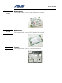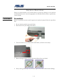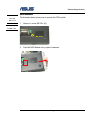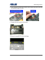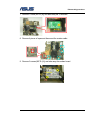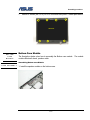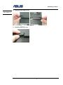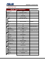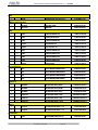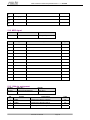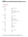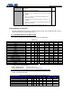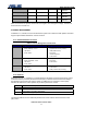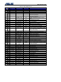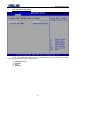
1
service overview 1 Chapter Service Overview Carefully read through this chapter for a look at various components of the notebook and necessary cautions and tools before performing any service and repairs. T o provide the best service and support for the ASUS S62F Series, we have provided the below information for technicians from distributors and resellers to perform the complete notebook disassembly and assembly. But before performing the procedures, please be sure to read through the overview in this chapter for component overview, cautions and tools to avoid any unwarranted damages to the notebook’s hardware. The following chapter includes: • • • • S62F Overview Components Precautions Appropriate Tools 1-1 service overview S62F Series Overview and Components The ASUS S62F Series Notebook is a product combining the power of Intel® Pentium-M CPU. In this section, an overview for the S62F, along with its components, will be presented. S62F Overview O V E R V I E W The illustrations below show the notebook’s overview from front view, right side view, left side view, and rear side view. Most of the parts will be discussed in this manual. LCD panel LCD bezel Keyboard Instant Key Power switch TouchPad Mic input Headphone output 3 in 1 card reader LED Indicators 1-2 service overview USB (2.0) ports PCMCIA slot Kensington Lock VGA Port 1394 port Optical Drive Device Air vents DC Power Input Jack Modem port Battery Module 1-3 LAN port service overview C O M P O N E N T S Components The illustrations below show the components of theS62F Series. L C D I N V E R T E R B O A R D LCD Panel* The illustration below shows the LCD display panel. The S62F Series notebook comes with 15.0” TFT LCD Panel. Inverter Board The illustration below shows the inverter board, which is hidden underneath the lower edge of the LCD front bezel. 1-4 service overview L C D B R A C K E T S H I N G E L C D C O V E R C A S E LCD bracket The illustration below shows the LCD brackets. Hinge Cover The illustration below shows the Hinge Cover. LCD Case The illustration below shows the LCD case. Here is the LCD bezel. 1-5 service overview K E Y B O A R D T O P C A S E B A T T E R Y Keyboard The illustration below shows the keyboard plate. It can be exchanged with keyboard plates with different language layouts, such as U.S., German, Russian, British, Italian and others. Top Case Module The illustration below shows the top case of the notebook. Battery Pack The illustration below shows the battery pack of the notebook. It’s located at bottom of the notebook. 1-6 service overview O P T I C A L D R I V E Optical Drive Device The illustration below shows the Optical Drive Device D E V I C E Hard Disk Drive H D D H D D The illustration below shows the 2.5” industry-standard HDD with 9.5mm height. B R A C K E T C P U HDD Bracket The illustration below shows the HDD Bracket that is placed over the HDD. CPU The illustration below shows the Intel Pentium-M CPU view. 1-7 service overview C P U T H E R M A L CPU Thermal Module The illustration below shows the thermal module for the CPU. It’s located on the top of CPU. M O D U L E M E M O R Y M O T H E R B O A R D Memory Module The illustration below shows the industry-standard 200pin SO-DIMM DDR SDRAM module for the notebook. Motherboard The illustration below shows the motherboard of the notebook. 1-8 service overview M O D E M M O D U L E W A L N M O D U L E T O P C A S E Modem Module The illustration below shows the modem module of the notebook. WALN Module The illustration below shows the WALN module of the notebook. Top Case The illustration below shows the TOP case of the notebook. 1-9 service overview Service Overview Please pay special attention to the cautions below to prevent any damages to the notebook and also please be sure to select the appropriate tools described in this section to perform any services desired. C A U T I O N S Precautions Before you perform any service and/or repair on the notebook, please follow the steps below first. 1. Be sure that the notebook is powered down. 2. Disconnect the AC plug from the notebook 3. Turn the notebook over. Unlock and hold the latches, and remove the battery . 3. Remove all rings, watches and any other metal objects from your hands. 4. Always wear a ground strap on your hand to protect the notebook from static discharge. 1 - 10 service overview T O O L S Appropriate Tools The illustrations below show the appropriate tools that should be used for the notebook’s service and repair. C R O S S S C R E W - Phillips-head Screwdriver Use a Phillips-head screwdriver to fasten/remove the K- or B-typed screws. D R I V E R F L A T H E A D Single-Slotted Screwdriver Use a single-slotted screwdriver to lock/unlock the flexible cable connector locks S C R E W D R I V E R T W E E Z E R S I N S E R T I O N A N D E X T R A C T I O N T O O L Tweezers Use a pair of tweezers to remove/insert flexible cables. Insertion and extraction tool for FPC connector Use insertion and extraction tool for FPC connector to handle locking and unlocking of FPC connectors. F O R F P C C O N N E C T O R V A C U U M H A N D L I N G Vacuum Handling Tool Use Vacuum handling tool to handle CPU. T O O L S P A C E R S C R E W - Spacer Screwdriver Use a spacer screwdriver to fasten/remove spacer screws or hex screws. D R I V E R 1 - 11 Disassembly procedure 2 Chapter Disassembly Procedure Please follow the information provided in this section to perform the complete disassembly procedure of the notebook. Be sure to use proper tools described before. A SUS S62F Series Notebook consists of various modules. This chapter describes the procedures for the complete notebook disassembly. In addition, in between procedures, the detailed disassembly procedure of individual modules will be provided for your service needs. The disassembly procedure consists of the following steps: • • • • • • • • • • • Battery Module HDD Module Wireless Module Memory Module CPU Module ODD Module Keyboard Top Case Module Motherboard Bottom case Module LCD Module 2-1 Disassembly procedure B A T T E R Y Battery Module The illustration below shows how to remove the battery module. B A T T E R Y M O D U L E 1. Unlock and hold the latch No (1). R E M O V A L 1 2. Slide the battery lock (No.2) and pull the battery pack out. 2 3. Pull the battery pack out. 2-2 Disassembly procedure H D D M O D U L E H D D M O D U L E R E M O V A L HDD Module The illustrations below show how to remove the HDD module from the notebook. Removing HDD Module 1. Remove 3 screws (M2.5*4L (K)), then remove the HDD door. M2.5*4L 2. Lift the HDD module and then remove it. 3. Remove 4 screws [M3 * 4(L)] to separate HDD from HDD housing. M3*4L 2-3 Disassembly procedure W I R E L E S S L A N M E M O R Y M O D U L E M E M O R Y R E M O V A L Wireless LAN Module The illustration below shows how to remove the Wireless LAN module. 1. Remove 1 piece of tape and disconnect the MAIN & AUX antenna. 2. And open the two latches to pop the MINI PCI MODULE up then pull it out. Memory Module The S62F Series Notebook does not have RAM onboard. There is one SO-DIMM sockets for installing SO-DIMM RAM. It can upgrade the total memory size up to 1GB . Removing Memory module 1. Remove 2 screws (M2.5*4L (K)), then remove the DIMM door. M2.5*4L 2-4 Disassembly procedure 2. Open the 2 latches aside (No. 1, 2), which will pop the memory module up to an angle of 30°, then pull out the memory module in that angle (No. 3). 1 3 2 30o C P U M O D U L E CPU Module The illustrations below show how to remove the CPU module from the notebook. C P U R E M O V A L Removing CPU Module 1. Remove 2 screws (M2.5*4L (K)), then remove the CPU door. M2.5*4L 2. Remove 4 screws (M2*3L (K)) by order. 2 3 M2*3L 1 4 2-5 Disassembly procedure 3. Disconnect the Fan cable and remove 2 screws (M2.5*4L (K)) then take away the CPU thermal module. M2.5*4L 4. Turn the non-removable screw here 180 degrees counter-clockwise to loosen the CPU. L O Unlock 5. Squeeze the vacuum handling pump and use it to lift the CPU away. 2-6 Disassembly procedure O P T I C A L D R I V E ODD Module The illustration below shows how to remove the ODD module. D E V I C E 1. Remove 1 screw (M2.5*4L (K)). O D D R E M O V A L M2.5*4L 2. Push the ODD Module out by a pair of tweezers. 2-7 Disassembly procedure K E Y B O A R D K / B R E M O V A L Keyboard The illustration of below shows how to remove the keyboard. Removing Keyboard 1. Push the 4 latches in (No.1, No.2, No.3, No.4) with a pair of tweezers or a single-slotted screwdriver and lift the keyboard plate up. 1 2 3 4 2. Lay the keyboard down over the Top case. *Do not remove the keyboard yet. The keyboard cable is still attached. 3. Disconnect the FPC connector by a pair of tweezers. 2-8 Disassembly procedure C A B L E R E M O V A L Removing Keyboard Cable 1. Use a flexible connector tool to unlock the cable connector on both ends (no. 1). 2. Carefully pull out the keyboard cable (no. 2) with a pair of tweezers. 3. Lock the connector (no. 3) again to avoid possible breakage. 2. Cable out 1. Unlock 1. Unlock 3. 3. 4. Remove keyboard from the top case. T O P C A S E M O D U L E Top Case Module The illustrations below show how to disassemble and remove the top case module of the notebook. The module contains the top case itself. Removing top Case Module H I N G E C O V E R R E M O V A L 1. Remove the MIDDLE cover. 2-9 Disassembly procedure 2. Use a pair of tweezers to remove both hinge Cover. 3. Disconnect the LANCH cable and touchpad FFC on the top case. LANCH cable Touchpad FFC 4. Turn over the NB and remove 1 screws (M2*3L (K)). M2*3L I 2 - 10 Disassembly procedure 5. Disconnect the Coaxial & inverter cable. Coaxial cable Inverter cable 6. Arrange the Coaxial & inverter cable and antenna on the bottom case. B O T T O M 7. Remove 15 screws (M2.5*6L (K)) and 1 screw (M2.5*4L) (K)) on the bottom case. C A S E R E M O V A L M2.5*4L M2.5*6L 2 - 11 Disassembly procedure 8. Before separate the bottom case, remove a little bit bottom case and let the cable and antennas through out of hole. Inverter & camera cable Antenna 9. Separate the bottom case from the top case. 10. Remove 2 screws (M2.5*6L (K)) on both hinge. M2.5*6L 2 - 12 Disassembly procedure 11. Separate the LCD module from the Top Case module T O P 12. Remove 2 screws (M2.5*4L (K)) and take away the LANCH board. C A S E R E M O V A L M2.5*4L 13. Remove the LANCH board cable. 2 - 13 Disassembly procedure 14. Disconnect the touch pad FFC and remove 1 piece of tape then take away the touch pad FFC. 15. Remove 5 screws (M2.5*4L (K)) and take away the touchpad bracket. M2.5*4L 16. Take away the touchpad. 2 - 14 Disassembly procedure M O T H E R B O A R D M O T H E R B O A R D R E M O V A L Motherboard The illustrations below show how to disassemble and remove the Motherboard. Removing Motherboard 1. Remove 2 screws (M2.5*4L (K)). 2. Remove 2 screws for CRT on the right side by a spacer screwdriver. 3. Separate the Motherboard from the bottom case. *Do not remove the Motherboard yet. The Bluetooth & Speaker cables are still attached. 2 - 15 Disassembly procedure 4. Disconnect the Bluetooth & Speaker cables then take away the Motherboard. Bluetooth cable Speaker cable 5. Remove 1 screw (M2*3L (K)) on the IO bracket. M2*3L 6. Use a single-slotted screwdriver to remove 2 screws HEX 5mm then take away the IO bracket. 2 - 16 Disassembly procedure 7. Remove 1 screw (M2*3L (K)) and take away the TPM board . M2*3L 8. Remove 4 pieces of tapes and disconnect the modem cable. 9. Remove 2 screws (M2*3L (K)) and take away the modem board. M2*3L 2 - 17 Disassembly procedure B O T T O M C A S E M O D U L E B O T T O M C A S E Bottom Case Module The illustrations below show how to remove and disassemble the Bottom case module. The module contains Bluetooth board, speaker cable. Disassembling Bottom case Module 1. Disconnect the Bluetooth cable and remove it. D I S A S S E M B L Y 2. Take away the Bluetooth board from the bottom case. 3. Take away the speaker module from the bottom case. 2 - 18 Disassembly procedure L C D M O D U L E LCD Module The illustrations below show how to remove and disassemble the LCD module. The module contains LCD panel, Inverter board, LCD bezel, LCD back cover. L C D M O D U L E D I S A S S E M B L Y Disassembling LCD Module 4. Remove 7 rubber pads and 7 screws (M2.5 x 6L) from LCD module. M2.5*6L 5. Prying the inside edges of the LCD bezel, and then separates it from LCD back cover. 2 - 19 Disassembly procedure 6. Disconnect the LCD cable. 7. Remove 2 screws (M2.5*4L (K)) & 4 screws (M2.5*6L (K)) and take away the LCD panel. M2.5*4L M2.5*6L 5. Remove 4 screws(M2*3L(K)) on the right LCD bracket to disassemble the LCD bracket. M2*3L 2 - 20 Disassembly procedure 6. Remove 4 screws(M2*3L(K)) on the left LCD bracket to disassemble the other LCD bracket. M2*3L 7. Remove 2 pieces of tapes and disconnect the coaxial cable then take it away. 8. Remove 1 screw (M2x 4L). . M2*4L 2 - 21 Disassembly procedure 9. Lift a little bit the inverter board and disconnect the inverter cable and then take it away. 6. Remove 2 screws (M2x 6L) on both hinge and take them away. M2.5*6L M2.5*6L 2 - 22 Disassembly procedure 7. Disconnect the camera cable and remove the microphone. 8. Remove the cable and remove mylar then take away the cable. 9. Take away the Camera module from the LCD back cover. 10. Remove 1 screw (M2x 4L) and remove 3 pieces of tapes then take away the wireless black wire. 2 - 23 Disassembly procedure 11. Remove 1 screw (M2x 4L) and remove 3 pieces of tapes then take away the wireless white wire. 2 - 24 Assembly procedure 3 Chapter Assembly Procedure Please follow the information provided in this section to perform the complete assembly procedure of the notebook. Be sure to use proper tools described before. A fter you have completed the previous chapter of complete disassembly, please follow this chapter to assemble the notebook back together. This chapter describes the procedures of the complete notebook assembly. In addition, in between procedures, the detailed assembly procedure of individual modules will be provided for your service needs. The assembly procedure consists of the following steps: • • • • • • • • • • • LCD Module Bottom case Module Motherboard Top Case Module Keyboard ODD Module CPU Module Memory Module Wireless Module HDD Module Battery Module 3-1 Assembly procedure L C D M O D U L E LCD Module The illustrations below show how to assemble and install the LCD module of the notebook. L C D M O D U L E A S S E M B L Y 1. Install the wireless white wire module and secure 1 screw (M2x 4L) then paste 3 pieces of tapes to secure it. 2. Install the wireless black wire module and secure 1 screw (M2x 4L) then paste 3 pieces of tapes to secure it. 3. Install the Camera module on the LCD back cover. 3-2 Assembly procedure 4. Install the microphone on the LCD cover and connect the camera cable. 5. Lay the inverter cable through the locking trench on the LCD back cover. 6. Lay the inverter cable through the locking trench on the LCD back cover. 3-3 Assembly procedure 7. Install the both hinge on LCD back cover and secure 2 screws (M2x 6L) to secure them. M2.5*6L M2.5*6L 8. Install the inverter board on LCD back cover and connect the inverter cable. 9. Secure 1 screw (M2x 4L) to secure it. . M2*4L 3-4 Assembly procedure Assembly LCD Module 1. Connect the coaxial cable and paste 2 pieces of tapes to secure it. 2. Install the left LCD bracket and secure 4 screws (M2*3L (K)) to fix it. M2*3L 3. Install the right LCD bracket and 4 screws(M2*3L(K)) and secure 4 screws (M2*3L (K)) to fix it. M2*3L 3-5 Assembly procedure 4. Install the LCD panel and secure 2 screws (M2.5*4L (K)) & 4 screws (M2.5*6L (K)) to secure it. M2.5*4L M2.5*6L 5. Connect the LCD cable. 6. Combine the LCD bezel and LCD Cover properly and press on all four edges until them snap into position. 3-6 Assembly procedure 7. Secure74 screws (M2.5 x 6L) on LCD front bezel then paste 7 rubber pads above. M2.5*6L B O T T O M C A S E M O D U L E B O T T O M C A S E A S S E M B L Y Bottom Case Module The illustrations below show how to assembly the Bottom case module. The module contains Bluetooth board, speaker cable. Assembling Bottom case Module 1. Install the speaker module on the bottom case. 3-7 Assembly procedure 2. Install the Bluetooth board on the bottom case. 3. Connect the Bluetooth cable and lay it through the locking trench on bottom case. M O T H E R B O A R D M O T H E R B O A R D Motherboard The illustrations below show how to assemble and install the motherboard of the notebook. 1. Install the modem board and secure 2 screws (M2.5*3L (K)). A S S E M B L Y M2*3L 3-8 Assembly procedure 2. Connect the modem cable and paste 4 pieces of tape to fix the cable. 3. Install the TPM board and secure 1 screw (M2*3L (K)) to secure it. M2*3L 4. Install the IO bracket and use a single-slotted screwdriver to secure 2 screws HEX 5mm. 3-9 Assembly procedure 5. Secure 1 screw (M2*3L (K)) on the IO bracket to secure it. M2*3L 6. Connect the Bluetooth & Speaker cables, before install the Motherboard to the bottom case. Bluetooth cable Speaker cable 7. Combine the Motherboard and the bottom case. 8. Remove 2 screws for CRT on the right side by a spacer screwdriver. 3 - 10 Assembly procedure 9. Secure 2 screws (M2.5*4L (K)) to secure the motherboard. Top Case Module T O P C A S E M O D U L E The illustrations below show how to assemble and install the top case module of the notebook. 1. Install the touchpad on the top case. T O P C A S E A S S E M B L Y 2. Install the touchpad bracket and secure 5 screws (M2.5*4L (K)) to secure it. M2.5*4L 3 - 11 Assembly procedure 3. Connect the touch pad FFC and paste 1 piece of tape. 4. Connect the LANCH board cable. 5. Install the LANCH board and secure 2 screws (M2.5*4L (K)). M2.5*4L 3 - 12 Assembly procedure 1. Combine the Top case module and LCD module. T O P C A S E M O D U L E A S S E M B L Y 2. Secure 2 screws (M2.5*6L (K)) to fix the hinge. M2.5*6L B O T T O M C A S E 1. Combine the bottom case from the top case. A S S E M B L Y 3 - 13 Assembly procedure 2. Before secure the bottom case, let the cable and antennas through in the hole. Inverter & camera cable Antenna 3. Secure 15 screws (M2.5*6L (K)) and 1 screw (M2.5*4L) (K)) to secure the bottom case. M2.5*4L M2.5*6L 4. Lay the antennas through the locking trench on bottom case 3 - 14 Assembly procedure 5. Connect the Coaxial & inverter cable and lay the cables through the locking trench on bottom case. Coaxial cable Inverter cable 6. Secure 1 screws (M2*3L (K)) to secure cables. M2*3L I 7. Turn over the NB and connect the LANCH cable and touchpad FFC on top case. LANCH cable Touchpad FFC 3 - 15 Assembly procedure H I N G E C O V E R 8. Install the both hinge Cover. A S S E M A B L Y 9. Install the MIDDLE cover. 3 - 16 Assembly procedure K E Y B O A R D Assembling Keyboard The illustrations below show how to assemble and install the Keyboard of the notebook. K E Y B O A R D A S S E M B L Y 1. Place the Keyboard module on front side of the top case. Then connect Keyboard FPC Cable with a pair of tweezers. 2. Install Keyboard properly and note the lower side should inset first. Push the 4 latches to fix the keyboard. 1 2 3 4 3 - 17 Assembly procedure O D D M O D U L E ODD Module The illustrations below show how to assemble and install the ODD Module of the notebook. O D D 1. Insert the ODD module. 2. Secure 1 screw (M2.5*4L (K)) to secure it. M O D U L E I N S T A L L A T I O N M2.5*4L C P U M O D U L E CPU Module Assembly The illustration below shows how to install CPU and the CPU heat sink of the notebook. C P U I N S T A L L A T I O N 1. Squeeze the vacuum handling pump and use it to install the CPU. 3 - 18 Assembly procedure 2. Turn the non-removable screw here 180 degrees clockwise to lock the CPU. L O Lock 3. Install the CPU thernal module gently and connect the fan cable then secure 2 screws (M2.5*4L (K)) to secure it. M2.5*4L 4. Secure 4 screws (M2*3L (K)) by order. 2 3 M2*3L 1 4 5. Install the CPU door and secure 2 screws (M2.5*4L (K)) to secure it. M2.5*4L 3 - 19 Assembly procedure Assembling Memory Module M E M O R Y M O D U L E The illustrations below show how to assemble and install the memory module to the notebook. 1. Insert the Memory module into the memory socket by an angle of 30 degree, and push down to latch the memory module. M E M O R Y I N S T A L L A T I O N 30o 2. Install the DIMM door and secure 2 screws (M2.5*4L (K)) to secure it. M2.5*4L W I R E L E S S L A N Wireless LAN Module The illustration below shows how to assemble the Wireless LAN module. 1. Install the MINI PCI module into the socket by an angle of 30 degree, and push down to latch the MINI PCI module. 3 - 20 Assembly procedure 2. H D D M O D U L E H D D Connect the MAIN & AUX antenna and paste 1 piece of tape to secure antennas. HDD Module The illustrations below show how to assemble and install the HDD module of the notebook 1. Secure 4 screws [M3 * 4(L)] to fix HDD into HDD housing. I N S T A L L A T I O N M3*4L 2. Insert the HDD module to connect the FPC connector until it’s installed properly. 3 - 21 Assembly procedure 3. Install the bottom case and secure 3 screws (M2.5*4L(K)) to fix it. M2.5*4L B A T T E R Y M O D U L E B A T T E R Y Battery Module The illustrations below show how to install battery module of the notebook. 1. Install the battery module. Slide the battery latch to close the battery lock. I N S T A L L A T I O N 3 - 22 Upgrade & Replacement 4 Chapter Upgrade & Replacement Follow the individual procedures in this chapter to perform the notebook’s upgrade and replacement of various major components. A sus S62F Series Notebook is a 2 spindles product, which means there are less options for you to upgrade to. The key upgradeable and replaceable items include the CPU module, memory module, HDD module, and ODD module. In order to avoid redundancy, please refer to chapters 2 and 3 of this manual for repeated and reused disassembly and assembly procedures, such as keyboard & heat sink replacement, which is used by several different procedures in this chapter. Be sure to follow the safety instructions described in Chapter 1 to safeguard the notebook against any potential damages. For any other components which you need to replace not covered in this chapter, please refer to Chapters 2 and 3 for detailed disassembly and assembly and perform necessary procedures accordingly. This chapter includes the following items: • • • • CPU Upgrade Memory Upgrade HDD Upgrade ODD Replacement 4–1 Upgrade & Replacement C P U CPU Upgrade TheS62F Series Notebook comes standard with a Intel® Micro-FCPGA Socket on the motherboard, which means it can support all Intel Micro-FCPGA CPUs up to 2.13 GHz. Upgrading CPU Remove battery module 1. Unlock and hold the latch No (1). 1 2. Slide the battery lock (No.2) and pull the battery pack out. 2 3. Pull the battery pack out. 4-2 Upgrade & Replacement Removing CPU Module C P U R E M O V A L 1. Remove 2 screws (M2.5*4L (K)), then remove the CPU door. M2.5*4L 2. Remove 4 screws (M2*3L (K)) by order. 2 3 M2*3L 1 3. 4 Disconnect the Fan cable and remove 2 screws (M2.5*4L (K)) then take away the CPU thermal module. M2.5*4L 4-3 Upgrade & Replacement 4. Turn the non-removable screw here 180 degrees counter-clockwise to loosen the CPU. L O Unlock 5. C P U I N S T A L L A T I O N Squeeze the vacuum handling pump and use it to lift the CPU away. Installing CPU The illustration below shows how to install CPU and the heat sink of the notebook. C P U I N S T A L L A T I O N 1. Squeeze the vacuum handling pump and use it to install the CPU. 2. Turn the non-removable screw here 180 degrees clockwise to lock the CPU. L O Lock 4-4 Upgrade & Replacement 3. Install the CPU thermal module gently and connect the fan cable then secure 2 screws (M2.5*4L (K)) to secure it. M2.5*4L 4. Secure 4 screws (M2*3L (K)) by order. 2 3 M2*3L 1 4 5. Install the CPU door and secure 2 screws (M2.5*4L (K)) to secure it. M2.5*4L Install battery module B A T T E R Y 1. Install the battery module. Slide the battery latch to close the battery lock. I N S T A L L A T I O N 4-5 Upgrade & Replacement M E M O R Y Second Memory Upgrade The S62F Series Notebook does not have RAM onboard. There are two SODIMM sockets for installing SO-DIMM RAM. It can upgrade the total memory size up to 1GB with a 512MB module on each socket. Upgrading Memory Module Remove battery module 1. Unlock and hold the latch No (1). 1 2. Slide the battery lock (No.2) and pull the battery pack out. 2 3. Pull the battery pack out. 4-6 Upgrade & Replacement M E M O R Y R E M O V A L Removing Memory module 1. Remove 2 screws (M2.5*4L (K)), then remove the DIMM door. M2.5*4L 2. Open the 2 latches aside (No. 1, 2), which will pop the memory module up to an angle of 30°, then pull out the memory module in that angle (No. 3). 1 3 30 2 o Installing Memory Module M E M O R Y I N S T A L L A T I O N 1. Insert the Memory module into the memory socket by an angle of 30 degree, and push down to latch the memory module. M E M O R Y I N S T A L L A T I O N 30 o 4-7 Upgrade & Replacement 2. Install the DIMM door and secure 2 screws (M2.5*4L (K)) to secure it. M2.5*4L Install battery module B A T T E R Y 3. Install the battery module. Slide the battery latch to close the battery lock. I N S T A L L A T I O N 4-8 Upgrade & Replacement H D D HDD Upgrade The S62F Series Notebook uses an industry-standard 2½” HDD with IDE interface. You can replace the HDD to any capacity of your choice within our approval and prior test. Upgrading HDD Remove battery module 1. Unlock and hold the latch No (1). 1 2. Slide the battery lock (No.2) and pull the battery pack out. 2 3. Pull the battery pack out. 4-9 Upgrade & Replacement H D D M O D U L E Removing HDD Module 1. Remove 3 screws (M2.5*4L (K)), then remove the HDD door. R E M O V A L M2.5*4L 2. Lift the HDD module and then remove it. 3. Remove 4 screws [M3 * 4(L)] to separate HDD from HDD housing. M3*4L 4 - 10 Upgrade & Replacement Installing new HDD module H D D 4. Secure 4 screws [M3 * 4(L)] to fix HDD into HDD housing. I N S T A L L A T I O N M3*4L 5. Insert the HDD module to connect the FPC connector until it’s installed properly. 6. Install the bottom case and secure 3 screws (M2.5*4L(K)) to fix it. M2.5*4L Install battery module B A T T E R Y 7. Install the battery module. Slide the battery latch to close the battery lock. I N S T A L L A T I O N 4 - 11 Upgrade & Replacement W I R E L E S S L A N W A L N Wireless LAN Module The illustration below shows how to remove the Wireless LAN module. Replacing WLAN Remove battery module 1. Unlock and hold the latch No (1). R E M O V A L 1 2. Slide the battery lock (No.2) and pull the battery pack out. 2 3. Pull the battery pack out. 4 - 12 Upgrade & Replacement Removing WALN Module O D D 1. Remove 1 piece of tape and disconnect the MAIN & AUX antenna. 2. And open the two latches to pop the MINI PCI MODULE up then pull it out. R E M O V A L W A L N M O D U L E I N S T A L L A T I O N Installing new WALN module 3. Install the MINI PCI module into the socket by an angle of 30 degree, and push down to latch the MINI PCI module. 4 - 13 Upgrade & Replacement 4. Connect the MAIN & AUX antenna and paste 1 piece of tape to secure antennas. Install battery module B A T T E R Y 1. Install the battery module. Slide the battery latch to close the battery lock. I N S T A L L A T I O N 4 - 14 Upgrade & Replacement O D D ODD Replacement The S62F Series Notebook can support DVD-ROM (8x DVD), COMBO (CD-R 24x/ CD-RW 24x / DVD-ROM 8x/ CD 24x), and DVD-Dual (DVD-R/RW: 4x/2x, DVD+R/RW: 4x/2.4x, CD-R/RW: 24x/ 10x, DVD: 8x, CD: 24x). Replacing ODD O D D Remove battery module 1. Unlock and hold the latch No (1). R E M O V A L 1 2. Slide the battery lock (No.2) and pull the battery pack out. 2 3. Pull the battery pack out. 4 - 15 Upgrade & Replacement Removing ODD Module 1. Remove 1 screw (M2.5*4L (K)). O D D R E M O V A L M2.5*4L 2. Push the ODD Module out by a pair of tweezers. Installing new ODD module 3. O D D Insert the ODD module. M O D U L E I N S T A L L A T I O N 4 - 16 Upgrade & Replacement 4. Secure 1 screw (M2.5*4L (K)) to secure it. M2.5*4L Install battery module B A T T E R Y 5. Install the battery module. Slide the battery latch to close the battery lock. I N S T A L L A T I O N 4 - 17 HARDWARE SPECIFICATION 5 Chapter Hardware Specifications You can enjoy and utilize the S62 series Notebook more effectively with a better comprehension of detailed hardware specifications of the notebook. T his chapter lists the detailed specifications of the notebook’s main system and modules. Please refer to this section when you need to find out specific technical data about the notebook. This chapter contains the following information: • System Specifications • Chipset Specifications • Key Parts List • System Resource • Module Specification 5- 1 HARDWARE SPECIFICATION 1 MARKETING SPEC S62F Specification Product Family Dimension Weight Color CPU Type Speed Package L2 Cache Size Memory Type Base Memory Expansion Memory MAX LCD Size S62F 328 x 288x 27-38mm 2.4 Silver-Gray Intel Yonah 1M/2M 1.66G,1.83G,2.0G,2.16G Micro-PGA 479M 2M None 256/512MB/1GB 2GB 14.1” Panel Type TFT Interface LVDS Contrast Control None Ultra DMA 100 Size On-die cache memory DDR II SDRAM without ECC WXGA,WXGA+ HDD type Socketable Yes Resolution Brightness Control (Two-Spindle Design) Hot-key(16 steps) 2.5", 9.5mm Yes 60/80/100 GB CD Driver CD-ROM N/A DVD N/A COMBO 8X/24X/24X/24X COMBO DVD-RW Super-Multi Chip Set 5- 2 SO-DIMM 1.25" x 2 Slot HARDWARE SPECIFICATION North Bridge INTEL 945GM South Bridge INTEL ICH7M Super IO SMSC LPC47N217 Thermal Sensor ADT7461ARMZ Micro-Processor ITE8510E KBC ITE8510E Flash ROM (ISA) Graphic Accelerator 3D Controller SST Intel 950 internal GPU Yes Intel Internal graphic AGP Support No Dual view/Dual App Yes Graphic Memory TV Out Support 4Mb Share Memory Yes PCMCIA Slot Type Type II x 1 Controller RICOH R5C841 Card Bus Yes ZV port No Sound System Controller AD1986A SW wave table Yes FM synthesizer Yes Speaker I/F Stereo Azalia I/F PC99 Yes S/PDF Yes 6 channel output Yes Audio Amplifier Microphone Modem Controller AC97 CODEC TPA0212 Mono CONEXANT CONEXANT 5- 3 RD02-D110 HARDWARE SPECIFICATION Spec I/F 56K Azalia MDC Jack RJ-11 ACPI Yes V.90 Yes Voice Phone No Digital Line Protection Yes Wake On Ring Yes BT RJ-11 port No Controller CSR I/F USB ANT BT-183 Chip antenna LAN Jack Wake On LAN Controller RJ-45 RJ-45 port YES RealTEK RTL8110SB Internal Keyboard Vendor Key 88 Keys (W/ MS-Windows function keys) Stroke/Pitch - Function Key 12 Function Keys Hot Key Function 10 Hot Keys Suspend (STR or STD) Fn + F1 RF enable Fn + F2 802.11b+g Display stretch No Brightness Up Fn + F6 Brightness Down Fn + F5 Back light on/off Fn + F7 LCD/CRT Fn + F8 PC Speaker Volume Fn + F10 On/Mute PC Speaker Volume Fn + F12 Volume increase 5- 4 Not Implement HARDWARE SPECIFICATION PC Speaker Volume Fn + F11 Number Lock Fn + Ins Scroll Lock Fn + Del Volume decrease Instant Keys Power Saving Power 4 Gear E-mail Direct button Internet Browser Direct button Disable TouchPad Direct button Status Indication 8 LEDs (Machine Base x 8) Power Status Yes (Green on LED when Power on. Blinking when in SUSPEND mode. OFF when power off.) Battery Charge Status Yes (Orange when charging. Blinking when battery low. OFF when fully charged/empty.) HDD/CD-ROM LED Yes (Green while accessing) Number Lock LED Yes (Green) Caps Lock LED Yes (Green) Scroll Lock LED Yes (Green) E-mail notification Yes (Orange) W-LAN/BT LED Pointing Device Yes (Blue) Glide Pad Glide Pad Yes Right Button Yes Left Button Yes Scroll up button No Scroll down button No Synaptics Function Control Power On Button Yes LCD Brightness Yes LCD Lid Switch Yes Sound Volume Yes Password Override Yes (Master Password) 5- 5 Hot Keys Hot Keys HARDWARE SPECIFICATION Reset/Force Off I/O Port Yes (Force Off switch) All ports support hot-plug Parallel NO CRT Yes Port Bar port III Yes Mouse/Keyboard NO IrDA Port NO Fax/Modem Yes RJ11 LAN Jack Yes RJ45 Line In NO Mic In Jack Yes Mono Head Phone Jack Yes Stereo out USB port Yes 4 Ports DC-In Yes 2-pin type/65W 15-pin D-sub Heat Solution Heat Pipe Yes Heat Sink Yes FAN Support Yes AC Adaptor Delta/Liteon Input AC 100-240Volt, 50~60Hz Output DC 19V, 3.42A, 65W 1st Battery 9 Cells/6 Cells Type Li-ION(2400mAH) 1st Battery 2nd Battery 11.2Vx4800mAh/2400mA h Celxpert No Type 2nd Battery Charging time Li-ION (2400mAH) Machine ON TBD. Machine OFF TBD. Battery Life PM Off TBD. TBD. 5- 6 HARDWARE SPECIFICATION PM On Power Management TBD. AMI BIOS LCD Close/Open Yes LCD Back-light Yes Suspend/Resume Yes Hibernation (S2D) Yes Thermal Control Yes ACPI Yes DMI 2.0 Yes Support DMI BIOS 2.1 Yes Password overridden by Master password DTS/Thermal diode Security Password Security Lock TPM Kensington Lock Hole Infineon TPM 1.2 S/W Install OS Option Flash BIOS WinXP Win2000 Yes Drivers Chipset Driver Yes VGA Driver Yes AUDIO Driver Yes LAN Driver Yes Glide Pad Driver Yes Modem Driver Yes Blue tooth Driver Yes WLAN Driver Yes LOGO Audio Driver Yes USB Port Bar 3 Yes Parallel Port Yes VGA Port Yes USB Port X 4 Yes 5- 7 Option HARDWARE SPECIFICATION LAN Port Yes 5- 8 S62F Hardware Technical Specification Rev. 1.0 2 06/03/28 CHIPSET LIST Chipset Summary Table Function S62F HW ACPI/PC99 Intel Yonah Not required 2M Not required North Bridge Intel 945GM YES South Bridge Intel ICH7M YES MEMORY DDR II SDRAM Not required BIOS ROM SST 4Mb Not required VGA Intel internal graphic YES SUPER I/O SMSC LPC47N217 YES RICOH R5C841 YES Azalia CODEC software Audio YES AUDIO AMPLIFIER TPA0212 Not required KB CONTROLLER ITE8510E YES PIC (uP) ITE8510E YES CPU SRAM (L2 Cache) PCMCIA AUDIO IrDA CLOCK Generator NO ICS954310BGLFT YES MODEM CONEXANT YES Bluetooth BT-183 1394 RICOH R5C841 Yes LAN RealTEK RTL8110SB YES ASUSTeK Confidential Page 9 S62F Hardware Technical Specification Rev. 1.0 2.1 06/03/28 CPU Processor Type: Intel Yonah Processor Processor frequency: 1.66 /1.83 /2.0/2.16 GHz Construction method: u-PGA479 with socket Supply voltage: Code:1.25V(High_Frequency_Mode)~0.725V(lowest_Freque ncy_Mode) Function feature: On-die , primary 32-KB instruction cache and 32-KB writeback data cache. On-die , 2MB second level cache with Advanced Transfer Cache Architecture. Data Prefetch. Streaming SIMD extensions 2(SSE2). Enhanced Intel SpeedStep technology 533/667 MHZ FSB support ASUSTeK Confidential Page 10 S62F Hardware Technical Specification Rev. 1.0 2.2 2.2.1 06/03/28 CHIPSET North Bridge Function: Full support 32bits AGTL+ host bus addressing Supports 400/533/667 DDR2 device Integrates the graphic controller Support Intel Rapid Memory power management DMI x2/x4 Interface connect to ICH 2.2.2 Vendor: Intel Parts Number: 945GM Package: 1466-ball micro-FCBGA South Bridge Function: DMI x2/x4 interface link with GMCH Integrated PC/AT compatible system (DMA Controller, INT, Timer/Counters) Integrated one channels IDE controller with Ultra DMA/33/66/100 support Integrated USB 1.1 and 2.0 Host Bus controller with 8 USB ports Integrated HD Audio Interface Build-in RTC LPC Interface IRQ Controller 2.3 2.3.1 Vendor: Intel Parts Number: ICH7M Package: 652-ball BGA DRAM MEMORY ON-BOARD MEMORY None ASUSTeK Confidential Page 11 S62F Hardware Technical Specification Rev. 1.0 2.3.2 06/03/28 EXPANSION MEMORY Number of sockets: Bus: Supply voltage: Two 200 pin SO-DIMM socket 64-bit data path 1.8V Functional features: Hardware features: Parity support: 2.4 Supports up to 16 simultaneous open pages Supports DDR2 400/533/667 DDR devices Maximum of 2GB of system memory without ECC BIOS ROM ROM Type: SST Flash Memory Package: 32-Lead PLCC Supply voltage: 3.3V Serviceability: End user upgradeable for the firmware 2.5 INTERNAL VGA CONTROLLER Function features: 3D Setup and Render Engine Integrated 24 bit RAMDAC that can drive a standard progressive scan analog monitor up to 2048 X 1536 CRT resolution at a maximum refresh rate of 75 Hz Single or dual channel LVDS panel support up to 112MHZ TV out resolution up to 1024x768 Vendor: Intel Chipset 945GM ASUSTeK Confidential Page 12 S62F Hardware Technical Specification Rev. 1.0 2.6 06/03/28 I/O INTERFACE Controller Function: Full ACPI 1.0 and PC98/99 compliant Support 10 options IRQ channel Integrated PC/AT Floppy Disk Controller Support 5.25”/3.5”/2.5” FDD Support 3-mode FDD Integrated Serial Port 232C Controller RS- Integrated Infrared Controller Support IrDA 1.0 Integrated Parallel Controller Port Support Standard, directional, ECP, mode biEPP Support 2 general purpose pins for game port control Support voltage 5V Vendor: SMSC Parts Number: LPC47N217 Package: 64-pin STQFP ASUSTeK Confidential Page 13 S62F Hardware Technical Specification Rev. 1.0 2.7 06/03/28 PCMCIA Controller Function: PC99, ACPI 1.0 and PCI bus management 1.1 Design compliant power Integrated PC Card Controller Support 1995 PC Card (PCMCIA 2.2) Integrated Card Bus Controller PC98/99/2001 compliant Single Chip PCI-CardBus/1394 Bridge Compliant with PCI Specification2.2 1394 PHY 1394 OHCI-LINK Bridge Flash Memory Interface (3 in 1 Media Bay) 2.8 Vendor: RICOH Parts Number: R5C841 Package: 208 pin CSP KEYBOARD CONTROLLER Function features: Embedded controller-style host Support hardware speed-up of GateA20 and RC Local 16x8 keyboard switch matrix support Three industry standard serial keyboard interfaces All three ports are bi-directional Vendor: Parts Number: Package: ITE 8510E 176-pin TQFP ASUSTeK Confidential Page 14 S62F Hardware Technical Specification Rev. 1.0 2.9 06/03/28 AUDIO CODEC Function features: Fully Compliant HD Audio Compliant. 20-bit Stereo Digital to Analog Converters. 18-bit Stereo Analog to Digital Converters. High-quality pseudo-Differential CD input. Meets or exceeds the Microsoft PC99 Audio Performance requirements. S/PDIF digital audio output. 3D Stereo Enhancement. Vendor: Parts Number: Package: ADI 1986A 48-pin LFCSP 2.10 AUDIO AMPLIFIER Function features: 2 X 1.8W BTL audio amplifier with 4ohm load. Depop circuitry integrated BTL or SE mode operation Thermal shutdown circuitry integrated Vendor: Parts Number: Package: TI TPA0212 24-pin TSSOP 2.11 LAN & MODEM 2.11.1 LAN Function features: Integrated Fast Ethernet MAC, Physical chip and transceiver in one chip 10Mb/s, 100Mb/s, 1000Mb/s operation Compliant to PCI Revision 2.2 Compliant to PC99/PC2001 standard Support Wake-on-LAN function and remote wake up (Magic Packet, LinkChg and Microsoft wake-up frame) ASUSTeK Confidential Page 15 S62F Hardware Technical Specification Rev. 1.0 Vendor: Parts Number: Package: 06/03/28 Realtek RTL8110SB 128-Pin LQFP 2.11.2 MODEM Function features: V.90 and K56 flex support Integrated PnP functionality PC99 compliant Support both APM and ACPI power management Support Wake-on-ring functionality Vendor: ASUS Parts Number: RD02-D110 Package: Azalia MDC ASUSTeK Confidential Page 16 S62F Hardware Technical Specification Rev. 1.0 3 06/03/28 KEY PARTS LIST Key Parts Summary: S62F Project Keyparts List Priority Vendor Model No. ASUS Part No. CPU Intel INT CO667 DC 2.16G T2600 L8VN Intel INT CO667 DC 2.0G T2500 L8VP Intel INT CO667 DC 1.83G T2400 L8VQ Intel INT CO667 DC 1.66G T2300 L8VR AUO B141EW01 V1 2 AUO B141EW01 V3(Glare) 2 CMO N141I1_L02 2 CMO N141I1_L03(Glare) 1 AUO B141PW01 V0 1 CMO N141C1-L03 REV C1 CMO N141C1-L02 REV C1 TSST TS-L462C 17G112151102 KME UJDA770 17G112151201 KME UJ-850BAL-A 17G141120000 KME UJ-841BAL-A 17G141113000 TSST TS-L632C 17G141115001 SYNAPTICS SYNAPTICS FOR A6 04G110001710 1 1 LCD 14.1” WXGA 1 14.1” WXGA+ ODD DVD Combo 1 DVD Super Multi 1 2 Touchpad 1 ASUSTeK Confidential Page 17 S62F Hardware Technical Specification Rev. 1.0 06/03/28 MDC 1 MODEM 56K Azalia(Green) 61-BMM011-01 YA HSIN N03P1BG_SM9 04G370030100 CHICONY CMN5622 04G370030000 1 HGST HTS421260H9AT00 17G013131708 1 HGST HTS421280H9AT00 17G013132708 1 HGST HTS421210H9AT00 17G013134701 1 Fujitsu MHV2060AT PL 17G013131119 2 Fujitsu MHV-2100AT PL 17G013134114 2 HGST HTS421212H9AT00 17G013133900 2 HGST HTS541060G9AT00 17G013131706 HGST HTS541080G9AT00 17G013132707 HGST HTS541010G9AT00 17G013134700 Fujitsu MHV2100AH 17G013134112 1 Intel INTEL/WM3945AGM1GEN 04G033051000 1 Intel INTEL/WM3945AGM2GEN 04G033052000 Intel INTEL/WM3945AGRWGEN 04G033052010 Intel INTEL/WM3945AGJPGEN 04G033052020 1 SUNREX KEYBOARD S62 (USA) 04GNG51KUS00 1 SUNREX KEYBOARD S62 (UKB) 04GNG51KUK00 1 SUNREX KEYBOARD S62 (JPN) 04GNG51KJP00 1 DARFON KEYBOARD S62F (US) 04GNG51KUS00-1 2 DARFON KEYBOARD S62F (UK) 04GNG51KUK00-1 2 DARFON KEYBOARD S62F (JPN) 04GNG51KJP00-1 1 Celxpert ICR18650-24E/3S2P 3.7V 07G016A61865 1 Celxpert ICR18650-24E/3S3P 3.7V 07G016B31865 Delta SADP65KB-ABH REV:01 04G266003183 ASUS CMOS Camera Module 1 HDD Minicard WLAN Keyboard Battery AC Adapter 1 ASUSTeK Confidential Page 18 S62F Hardware Technical Specification Rev. 1.0 1 Delta 06/03/28 SADP65KB-BFJ REV:01 04G266003163 SO-DIMM 512MB DDR2 533 1 UNIFOSA GU33512AGHYQ612L3PC 04G001616673 1 NANYA NT512T64UH8A1FN-37B 04G001616619 NANYA NT1GT64U8HA0BN-37B 04G001617633 Infineon M470T6554CZ3-CE6 04G00161662F Nanya NT512T64UH8A1FN-3C 04G00161661B Infineon M470T2953CZ3-CE6 04G001617641 Nanya NT1GT64U8HA0BN-3C 04G001617634 1GB DDR2 533 1 512MB DDR2 667 1GB DDR2 667 ASUSTeK Confidential Page 19 S62F Hardware Technical Specification Rev. 1.0 3.1 06/03/28 Display WXGA Technology: Active color (TFT: Thin Film Transistor) Size: 14.1”W Resolution: WXGA (1280 X 800) Dimension: Pixel Pitch: 0.279mm x 0.279mm Display Colors: 262,144 Vendor: AUO/CMO/Hansstar WXGA Technology: + Active color (TFT: Thin Film Transistor) Size: 14.1”W Resolution: WXGA+ (1440 X 900) Dimension: 3.2 Pixel Pitch: 0.297mm x 0.297mm Display Colors: 262,144 Vendor: AUO/CMO/Hansstar Hard Disk Drive Form factor: 2.5 inch Capacity: 60/80/100 GB Height: 9.5 mm Interface: Enhanced IDE conforming to ATA-5 Functional features: Power Management APM 1.1 and 1.2 (standby/suspend) LBA-modes ASUSTeK Confidential Page 20 S62F Hardware Technical Specification Rev. 1.0 Hardware features: 06/03/28 Standard I/O addresses: 1F0h to 1F7h and 3F6h Support of minimum IRQ 14 Support of at least 3 DMA channels, if DMA is supported Easily removable and exchangeable for user’s future upgrade Vendor/Model: HGST/ HTS421260H9AT00 , HTS421280H9AT00 3.3 Combo Drive Form factor: 5.25 Inch Speed: 24X/24X/8X/24X Height: 12.7mm Interface: IDE (ATAPI) Functional features: Power Management APM 1.1 and 1.2 (standby/suspend) Standard I/O addresses Support of minimum IRQ Vendor/Model: Easily removable and exchangeable for user’s future upgradability Toshiba/TS-L462C , Panasonic/UJDA770 3.4 DVD-Dual Drive Form factor: Speed: 5.25 Inch Height: 12.7mm Interface: IDE (ATAPI) Functional features: Power Management APM 1.1 and 1.2 (standby/suspend) DVD super-multi Standard I/O addresses Support of minimum IRQ Vendor/Model: Easily removable and exchangeable for user’s future upgradability Toshiba/TS-L632C, Panasonic/UJ-841BAL-A ASUSTeK Confidential Page 21 S62F Hardware Technical Specification Rev. 1.0 3.5 06/03/28 Touch Pad Dimensions: 65 mm(W) x 49 mm(H) x 2.82 mm(T) Sensor effective areas: 62.5 mm(W) x 46.5 mm(H) Interface: PS/2 X/Y position resolution: 40 points / mm (graphics mode) Customizing: Custom color can be printed on the sensor pad. Functional features: Accurate positioning Low fatigue pointing action Low power consumption Software configurable Scanner function for signature Low profile, compact size and low weight Vendor/Model 3.6 Synaptics : TM61PDE8G307 Keyboard Compatibility: MS-Windows 2000/XP Functional features: Standard Notebook-Keyboard MF2-Layout Hardware feature: Simultaneously use of internal and external keyboard Easily to assemble or disassemble Dimensions: (H) 300mm x (V) 116.5 mm Type: Key switch Membrane Total travel: 3.0 ± 0.3 mm Key top: ABS material, TANPO printing with UV hardening English, Japanese, Chinese, Korean and European etc., Language versions: Vendor/ Model 3.7 3.7.1 InnovACE/K000962, Chicony/MP-0411 Battery Main Battery Purpose: Main power supply battery Gas-gauge: SMBus interface ASUSTeK Confidential Page 22 S62F Hardware Technical Specification Rev. 1.0 3.7.2 06/03/28 Chemistry: Li-ion rechargeable battery Voltage: Nominal 11.1V (= 3.7V cell 3pcs in serial, 2pcs in parallel) Capacity: 2400mAH/Cell Vendor: Celxpert Duration: Minimum 4 hour (w/o PMU) Charge Method: Fast Charge: 2.5A, 3.0 hour (while System off) Charging Source: AC Adapter Gas-gauge: BENCHMARQ bq2060H RTC Backup Battery Purpose: Backup the RTC/CMOS data While AC adapter off & Main Battery removed 3.8 Chemistry: Coin cell 2032 Li-ion battery Voltage: Nominal 3V Capacity: 200mAH Vendor: TOSHIBA, Panasonic, KTS AC/DC Adapter The notebook can be powered either by an external AC adapter or by an internal battery pack. The AC adapter is used as power source for the DC/DC converter and as constant current source for the battery pack. Input Requirements: AC line voltage: 90V to 264V AC, Full Range AC line current: 1.5A AC line frequency 50 Hz to 60 Hz Efficiency 85% min. Output requirements: Output-Voltage +19V DC +/- 3% Output-Current max.3.42A Ripple voltage 500mVP-P Power cord: Plug to the adapter DC Cable length: 180 mm +/- 50mm ASUSTeK Confidential Page 23 S62F Hardware Technical Specification Rev. 1.0 Regulatory: EMI: FCC Class B Safety: CISPR 22 Class B .Dimension: (L) 114.5 x (W) 49.5 x (H) 29 mm ASUSTeK Confidential Page 24 06/03/28 S62F Hardware Technical Specification Rev. 1.0 4 4.1 SYSTEM System diagram ASUSTeK Confidential Page 25 06/03/28 S62F Hardware Technical Specification Rev. 1.0 4.2 Main components block diagrams ASUSTeK Confidential Page 26 06/03/28 S62F Hardware Technical Specification Rev. 1.0 4.3 4.3.1 4.3.2 System resource IRQ Map IRQ# Description IRQ 0 System Timer IRQ 1 Keyboard IRQ 2 [Cascade] IRQ 3 IrDA IRQ 4 USB Controller IRQ 5 VGA / USB Controller IRQ 6 Available IRQ 7 Parallel Port IRQ 8 System CMOS/RTC IRQ 9 ACPI IRQ Holder IRQ10 Available IRQ11 Available IRQ12 PS/2 Mouse IRQ13 FPU IRQ14 Primary IDE Controller IRQ15 Secondary IDE Controller ISA DMA Map DMA Channel Device DMA 3 Parallel Port DMA 4 DMA Controller ASUSTeK Confidential Page 27 06/03/28 S62F Hardware Technical Specification Rev. 1.0 4.3.3 PCI INT Map INT Description INTA Giga LAN Chip INTB CARDBUS, 1394, INTC INTD 4.3.4 PCI Bus Master Map REQ Description REQ0 CARDBUS, 1394 REQ1 4.3.5 REQ2 LAN REQ3 None REQ4 None IDSEL IDSEL CHIPSET AD23 LAN AD17 CARDBUS,1394 ASUSTeK Confidential Page 28 06/03/28 S62F Hardware Technical Specification Rev. 1.0 5 06/03/28 I/O PORT PIN ASSIGNMENT No FUNCTION DESCRIPTION .CRT Display (Analog) HDD ODD LCD KEYBOARD TOUCHPAD&LED 1ST BATTERY .DC IN Adapter Input .AUDIO Headphone, Microphone-In .FAN .INVERTER .MDC .1394 .USB Universal Serial Bus Port Bar 3 USB, CRT, Parallel Port, RJ-45 LAN & Modem .Card Reader TV OUT 5.1 CRT Vendor Part No. Pin No. SUYIN 070546FR015S215ZU 15 Pin (DIP) No Pin Assignment (by: sort) 1 RED Video (analog) Description Red this DAC analog output drives the CRT interface. 2 GREEN Video (analog) Green this DAC analog output drives the CRT interface. ASUSTeK Confidential Page 29 S62F Hardware Technical Specification Rev. 1.0 3 BLUE Video (analog) 06/03/28 Blue this DAC analog output drives the CRT interface. 4 MONITOR ID Bit 2 NC 5 GROUND Ground 6 RED Return (ground) Ground 7 GREEN Return (ground) Ground 8 BLUE Return (ground) Ground 9 KEY NC 10 SYNC Return (ground) Ground 11 MONITOR ID Bit 0 NC 12 MONITOR ID Bit 1 DDC monitor data 13 HSYNC CRT Horizontal Sync this output is The Horizontal sync pulse for the CRT Monitor. 14 VSYNC CRT Vertical Sync this output is the Vertical sync pulse for the CRT Monitor. 15 MONITOR ID Bit 3 DDC monitor clock ASUSTeK Confidential Page 30 S62F Hardware Technical Specification Rev. 1.0 5.2 06/03/28 Hard disk pin assignment Vendor ALLTOP Part No. Pin No. 44 Pin (SMT) C17851-144A1-L No. Signal Description 44 IDERST#_5S Reset primary disk O 43 GND Ground P 42 PDD7 Primary disk data 7 I/O 41 PDD8 Primary disk data 8 I/O 40 PDD6 Primary disk data 6 I/O 39 PDD9 Primary disk data 9 I/O 38 PDD5 Primary disk data 5 I/O 37 PDD10 Primary disk data 10 I/O 36 PDD4 Primary disk data 4 I/O 35 PDD11 Primary disk data 11 I/O 34 PDD3 Primary disk data 3 I/O 33 PDD12 Primary disk data 12 I/O 32 PDD2 Primary disk data 2 I/O 31 PDD13 Primary disk data 13 I/O 30 PDD1 Primary disk data 1 I/O 29 PDD14 Primary disk data 14 I/O 28 PDD0 Primary disk data 0 I/O 27 PDD15 Primary disk data 15 I/O 26 GND Ground 25 KEY NC 24 PDDRQ_3S Primary DMA request I 23 GND Ground P 22 PDIOW#_3S Primary disk IO write O 21 GND Ground P 20 PDIOR#_3S Primary disk IO read O ASUSTeK Confidential Type P Page 31 S62F Hardware Technical Specification Rev. 1.0 06/03/28 19 GND Ground P 18 PIORDY_3S Primary disk IO channel ready I 17 CSEL Cable select (device configuration) O 16 PDDACK#_3S Primary DMA acknowledge O 15 GND Ground P 14 IRQ14_3S Primary disk interrupt I 13 HIOCS16# Indication to the host I 12 PDA1_3S Primary disk address 1 O 11 PDIAG# Diagnostics status I/O 10 PDA0_3S Primary disk address 0 O 9 PDA2_3S Primary disk address 2 O 8 PDCS1#_3S Primary disk chip select for 100 range O 7 PDCS3 #_3S Primary disk chip select for 300 range O 6 PDASP#_5S Driver active/slave present I/O 5 GND Ground P 4 +5Vs +5V power supply P 3 +5Vs +5V power supply P 2 GND Ground P 1 Reserved NC 5.3 ODD pin assignment Vendor ALLTOP Part No. Pin No. 50 Pin (DIP) C1240Z-250A1-L Pin No. Pin No. 1. CD_L_A 2. CD_R_A 3. CD_GND_A 4. CD_GND_A 5. IDE_RST# 6. IDE_PD8 7. IDE_PD7 8. IDE_PD9 9. IDE_PD6 10. IDE_PD10 11. IDE_PDD5 12. IDE_PDD11 ASUSTeK Confidential Remark Page 32 S62F Hardware Technical Specification Rev. 1.0 13. IDE_PDD4 14. IDE_PDD12 15. IDE_PDD3 16. IDE_PDD13 17. IDE_PDD2 18. IDE_PDD14 19. IDE_PDD1 20. IDE_PDD15 21. IDE_PDD0 22. IDE_PDDREQ 23. GND 24. IDE_PDIOR# 25. IDE_PDIOW# 26. GND 27. IDE_PIORDY 28. IDE_PDDACK# 29. INT_IRQ15# 30. IDE_PIOCS16# 31. IDE_PDA1 32. IDE_PPDIAG# 33. IDE_PDA0 34. IDE_PDA2 35. IDE_PDCS1# 36. IDE_PDCS3# 37. IDE_PDASP# 38. +V5S_IDE 39. +5VS_IDE 40. +V5S_IDE 41. +5VS_IDE 42. +V5S_IDE 43. GND 44. GND 45. GND 46. GND 47. ODD_CSEL 48. GND 49. NC 50. NC ASUSTeK Confidential Page 33 06/03/28 S62F Hardware Technical Specification Rev. 1.0 5.4 LCD pin assignment Vendor Part No. Pin No. ENTERY 3761-Q30C-01R 30 Pin (SMT) No. 06/03/28 Signal Description Type 1 LVDS_U1N Data channel 1- of Channel A O 2 LVDS_L0N Data channel 0+ of Channel B O 3 LVDS_U1P Data channel 1+ of Channel A O 4 LVDS_L0P Data channel 0- of Channel B O 5 GND Ground P 6 GND Ground P 7 LVDS_U0N Data channel 0- of Channel A O 8 LVDS_L1N Data channel 1- of Channel B O 9 LVDS_U0P Data channel 0+ of Channel A O 10 LVDS_L1P Data channel 1+ of Channel B O 11 GND Ground P 12 GND Ground P 13 LVDS_U2N Data channel 2- of Channel A O 14 LVDS_L2N Data channel 2- of Channel B O 15 LVDS_U2P Data channel 2+ of Channel A O 16 LVDS_L2P Data channel 2+ of Channel B O 17 GND Ground P 18 GND Ground P 19 LVDS_UCLKN Clock negative of Channel A O 20 LVDS_LCLKN Clock negative of Channel B O 21 LVDS_UCLKP Clock positive of Channel A O 22 LVDS_LCLKP Clock positive of Channel B O 23 GND Ground P 24 GND Ground P 25 PID_1 Panel ID bit 1 I ASUSTeK Confidential Page 34 S62F Hardware Technical Specification Rev. 1.0 26 EDID_CLK 27 PID_0 28 06/03/28 EDID Clock I Panel ID bit 0 I EDID_DAT EDID DATA I 29 LCD_VCC +3V power supply P 30 LCD_VCC +3V power supply P ASUSTeK Confidential Page 35 S62F Hardware Technical Specification Rev. 1.0 5.5 06/03/28 Internal keyboard pin assignment Vendor Part No. Pin No. ENTERY 6905-E28N-00R 28 Pin (SMT) No Signal Description Type 1 KSI1 Keyboard matrix column 1 I 2 KSO7 Keyboard matrix row 7 O 3 KSI7 Keyboard matrix column 7 I 4 KSO0 Keyboard matrix row 0 O 5 KSI6 Keyboard matrix column 6 I 6 KSO9 Keyboard matrix row 9 O 7 KSI5 Keyboard matrix column 5 I 8 KSO3 Keyboard matrix row 3 O 9 KSI4 Keyboard matrix column 4 I 10 KSO1 Keyboard matrix row 1 O 11 KSI2 Keyboard matrix column 2 I 12 KSI3 Keyboard matrix column 3 I 13 KSO5 Keyboard matrix row 5 O 14 KSO13 Keyboard matrix row 13 O 15 KSI0 Keyboard matrix column 0 I 16 KSO2 Keyboard matrix row 2 O 17 KSO4 Keyboard matrix row 4 O 18 KSO8 Keyboard matrix row 8 O 19 KSO6 Keyboard matrix row 6 O 20 KSO11 Keyboard matrix row 11 O 21 KSO10 Keyboard matrix row 10 O 22 KSO12 Keyboard matrix row 12 O 23 KSO14 Keyboard matrix row 14 O 24 KSO15 Keyboard matrix row 15 O 25 NC ASUSTeK Confidential Page 36 S62F Hardware Technical Specification Rev. 1.0 26 KEYDETECT0 Keyboard ID bit 0 27 GND Ground 28 KEYDETECT1 Keyboard ID bit 1 5.6 06/03/28 I GND I Internal Touch Pad Pin assignment Vendor Part No. Pin No. ENTERY 6701-20 10 Pin (SMT) No Signal Description Type 1 +5VS Power P 2 +5VS Power P 3 TPAD_DAT PS/2 DATA I/O 4 TPAD_DAT PS/2 DATA I/O 5 TPAD_CLK PS/2 Clock I/O 6 TPAD_CLK PS/2 Clock I/O 7 GND Ground P 8 GND Ground P 9 TP_LEFT_SW# Left Switch I 10 NC 11 NC 12 TP_RIGHT_SW# Right Switch ASUSTeK Confidential I Page 37 S62F Hardware Technical Specification Rev. 1.0 5.7 06/03/28 1ST Battery pin assignment No Signal Description Type 1 BAT_CON Battery input/output voltage P 2 BAT_CON Battery input/output voltage P 3 BAT1_CNT1# NVDC control pin 1 I 4 BAT1_CNT2# NVDC control pin 2 I 5 SMCLK_BAT SMB Bus Clock I/O 6 SMDATA_BAT SMB Bus DATA I/O 7 TS# Thermal Pin O 8 GND Ground P 9 GND Ground P 5.8 DC in Jack pin assignment Vendor Part No. Pin No. SINGATRON 2DC-G026B201 No 4 Pin (DIP) Signal Description Type 1 A/D_DOCK_IN Adapter input voltage P 2 GND Ground P 3 GND Ground P 4 GND Ground P 5.9 Audio Jack 5.9.1 Internal Speaker Jack Vendor Part No. Pin No. ACES 85204-04001 4 Pin (SMT) No 1 Signal INTSPKR+ Description Type Internal speaker signal channel positive ASUSTeK Confidential O Page 38 S62F Hardware Technical Specification Rev. 1.0 06/03/28 2 INTSPKR- Internal speaker left sound negative O 3 INTSPKL+ Internal speaker signal channel positive O 4 INTSPKL- Internal speaker left sound negative O 5.9.2 Headphone Jack Vendor Part No. Pin No. SINGATRON 2SJ-A373-001 No 10 Pin (DIP) Signal Description Type 1 EARR Headphone right sound O 4 EARL Headphone left sound O 5 GND Ground P 6 GND Ground P 7 JACK_IN# S/PDIF/Headphone be plugged in I 9 GND Ground P 10 GND Ground P A GND Ground P B +5VS +5V power for S/PDIF P C SPDIF_O S/PDIF output O 5.9.3 Microphone Jack Vendor Part No. Pin No. FOXCONN JA6333L-B200-7F 5 Pin (DIP) No Signal Description Type 1 GND Ground P 2 MIC_CENTER External microphone input O 3 NC No Connection 4 MIC_BIAS Internal MIC connection/BIAS. 5 NC No Connection 6 EXT_MIC Internal Microphone switch out connection ASUSTeK Confidential I O Page 39 S62F Hardware Technical Specification Rev. 1.0 06/03/28 5.10 Fan Pin Assignment Vendor Part No. Pin No. ACES 85205-03701 3 Pin (SMT) No Signal Description Type 1 +5VS_FAN 5V Power Supply P 2 FANSP1 FAN speed signal input I 3 GND Ground P 5.11 Inverter pin assignment Vendor Part No. Pin No. E&T 3753-20 20 Pin (SMT) No Signal Description Type 1 NC No Connection 2 AC_BAT_SYS Ac in voltage P 3 +5V_USB35 USB 5V power P 4 AC_BAT_SYS Ac in voltage P 5 +5V_USB35 USB 5V power P 6 GND Ground P 7 GND Ground I/O LID_SW# LID Switch signal output(Reserve) O GND Ground I/O BACK_ADJ Brightness signal adjustment O GND Ground P BACK_OFF# Turn Off Backlight O USB_P3- USB- signals of CCD Camera I/O +3VA 3.3V power for LID switch USB_P3+ USB+ signals of CCD Camera GND Ground 8 9 10 11 12 13 14 15 16 ASUSTeK Confidential P I/O P Page 40 S62F Hardware Technical Specification Rev. 1.0 17 18 19 20 06/03/28 GND Ground P INTMIC_A_GND Audio Ground P GND Ground P INVMIC_A Internal MIC I *** 5.12 MDC signal Vendor Part No. Pin No. AMP 1-179397-2 12 Pin (SMT) No Signal Description Type 1 GND Ground NC 2 NC None NC 3 SDOUT DATA OUT 4 NC None NC 5 GND Ground NC 6 +3V Power +3V P 7 SYNC SYNC O 8 GND Ground P 9 SDIN DATA IN O 10 GND Ground P 11 RST# AC Reset I 12 BCLK Azalia Clock O I 5.13 1394 pin assignment Vendor Part No. Pin No. SUYIN 020204FR004S502ZA 4 Pin (DIP) No Signal Description Type 1 LTPB0- Twisted-pair cable A negative I/O 2 LTPB0+ Twisted-pair cable B positive I/O 3 LTPA0- Twisted-pair cable A negative I/O ASUSTeK Confidential Page 41 S62F Hardware Technical Specification Rev. 1.0 4 LTPA0+ Twisted-pair cable A positive 06/03/28 I/O 5.14 USB pin assignment Vendor Part No. Pin No. SUYIN 020122MR008S523ZA 8 Pin (DIP) No Signal Description Type 1 +5V_USB01 USB 5V power P 2 USB_P0- USB port 0 negative signal I/O 3 USB_P0+ USB port 0 positive signal I/O 4 GND USB 5V ground P 5 +5V_USB01 USB 5V power P 6 USB_P1- USB port 1 negative signal I/O 7 USB_P1+ USB port 1 positive signal I/O 8 GND USB 5V ground P Vendor Part No. Pin No. SUYIN 020122MR008S523ZA 8 Pin (DIP) No Signal Description Type 1 +5V_USB23 USB 5V power P 2 USB_P2- USB port 2 negative signal I/O 3 USB_P2+ USB port 2 positive signal I/O 4 GND USB 5V ground P 5 +5V_USB23 USB 5V power P 6 USB_P3- USB port 3 negative signal I/O 7 USB_P3+ USB port 3 positive signal I/O 8 GND USB 5V ground P 5.15 LAN & Modem pin assignment Vendor Part No. Pin No. ASUSTeK Confidential Page 42 S62F Hardware Technical Specification Rev. 1.0 ALLTOP No C10089-112A4-Y 06/03/28 12 Pin (DIP) Signal Description Type 1 None None NC 2 RJ11_RING Modem signal I/O 3 RJ11_TIP Modem signal I/O 4 None None NC 5 LAN_TXP Transmit data positive signal O 6 LAN_TXN Transmit data negative signal O 7 LAN_RXP Receive data positive signal I 8 LAN_MDI2P GigaLan MDI2+ I 9 LAN_MDI2N GigaLan MDI2- I 10 LAN_RXN Receive data negative signal I 11 LAN_MDI3P GigaLan MDI3+ I 12 LAN_MDI3N GigaLan MDI3- I 5.16 Card Reader pin assignment Vendor Part No. Pin No. TAITWUN R009-030-LR 21 Pin (SMT) Pin No Signal 1. SD_DAT1 2. SD_DAT0 3 SD_GND 4 MS_GND 5 MS_BS 6 SD_CLK 7 MS_DATA1 8 MS_DATA0 9 VCC 10 MS_DATA2 11 SD_GND Remark ASUSTeK Confidential Page 43 S62F Hardware Technical Specification Rev. 1.0 12 MS_CD 13 MS_DATA3 14 SD_CMD 15 MS_SCLK 16 MS_VCC 17 SD_DAT3 18 GND 19 SD_DAT2 20 SD_WP 21 SD_CD 6 06/03/28 POWER MANAGEMENT 6.1 System power plane Power Group Power Control Pin Controlled Devices +12V SUSC# Control +5V SUSC# PCMCIA Slot 5V, USB +3.3V SUSC# NB, DDR, PCMCIA Controller, PCMCIA Slot 3.3V, Keyboard Controller +2.5VS SUSC# VGA DAC/GLAN power +12VS SUSB# Control +5VS SUSB# HDD, CD-ROM, Internal Touch Pad, Audio AMP +3.3VS SUSB# SB, Audio, Clock Generator, PCI interface, Super I/O, VGA, AC97 CODEC, FWH, Thermal sensor, IR +1.8V SUSC# PCMCIA chip power, DDR2 power +1.5VS SUSB# NB Core +0.9VS SUSB# DDR Termination +1.05VS SUSB# CPU, NB AGTL+ Bus power, NB core +VCORE CPU_VRON CPU power +5VA +3.3VA Resume Power, EC,ISA ROM +V_RTC ICH7-M(RTC) ASUSTeK Confidential Page 44 S62F Hardware Technical Specification Rev. 1.0 6.2 06/03/28 Power management mode 6.2.1 Full-On mode All system devices are not power managed and the system can respond to applications with maximum performance. 6.2.2 Doze mode The CPU clock is slow down but all other devices are full on. 6.2.3 Stand by mode A suspend state where all motherboard components are still powered-on except for the system clock generator device. The PCI and CPU buses are driven to the inactive idle state. The system memory is powered and refreshed by the memory bridge, and the graphics frame buffer is powered and refreshed by the graphic chip. The system provides a 32KHz clock (SUSCLK) in this suspend mode to support refresh of these memory subsystems. Only an enabled “resume event” can bring the system out of the stand by state. The south bridge also provides a resume timer that allows the system to resume after a programmed time has elapsed. 6.2.4 Suspend to RAM mode (STR) A suspend state where all motherboard components are powered-off. The CPU and PCI busses are powered off. All devices connected to the CPU and PCI busses must either be powered-off or isolate their bus interfaces. The system memory is powered and refreshed by the memory bridge, and the graphics frame buffer is powered and refreshed by the graphics chip. The system provides a 32 kHz clock (SUSCLK) in this suspend mode to support refresh of these memory subsystems. Only an enabled “resume event” can bring the platform out of the suspend to RAM (STR) state. 6.2.5 Suspend to disk mode (STD) A suspend state where the context of the entire system is saved to disk, all motherboard components are powered-off, and all clocks are stopped. Any enabled “resume event”, such as Power switch or RTC, can bring the platform out of the suspend to disk (STD) state. 6.2.6 Soft off mode (SOFF) This is the same as suspend to disk except the context of memory is not saved. The system will resume from Soft Off as if a hard reset had occurred. 6.2.7 Mechanical off mode (MOFF) All power except the RTC has been removed from the system. 6.3 PMU mode transition event The following table summarizes the entry events and wake-up events of each power management mode. Power State Entry Event Wake up Event Doze Doze Time out Predefined Memory/IO range access Ring Indicator Keystroke Mouse movement ASUSTeK Confidential Page 45 S62F Hardware Technical Specification Rev. 1.0 06/03/28 IRQ 1-15 Stand by Stand by Time out Predefined Memory/IO range access Stand by hot key pressed Battery Warning Battery Low Ring Indicator Keystroke Mouse movement Schedule Alarm STR STD Suspend Time out Power Button STR hot key pressed Ring Indicator Suspend button Keystroke (Int. KB) Battery Low Schedule Alarm Suspend Time out Power Button STD hot key pressed Schedule Alarm Hibernate Battery Low Soft Off Power button Power Button Execute Windows command shutdown Schedule Alarm ASUSTeK Confidential Page 46 S62F Hardware Technical Specification Rev. 1.0 6.3.1 06/03/28 Lid switch Display mode State Lid close Lid open LCD Full on LCD OFF No action Stand by LCD OFF No action STR/STD LCD OFF No action Full on No action No action Stand by No action No action STR/STD No action No action Full on LCD OFF/CRT ON No action Stand by No action No action STR/STD No action No action CRT SIMUL LCD display will be shut down while closing LCD. 6.3.2 Power button Power button function depends on the definition in Windows power setting or you can force off by pressing power button for 4 seconds. To reset the system, you need to press the reset button. 6.4 Device Power management Power state of local devices table Power Component Doze Stand By STR STD/SOff Quick Start Stop Clock Power Off Power Off North Bridge ON Stop Clock Power Off Power Off South Bridge ON ON Power Off (except +3.3VA,+1.8VA, RTCVCC ) Power Off (except +3.3VA,+1.8VA, RTCVCC) DDR ON Self Refresh Self Refresh Power Off CD-ROM (DVD) ON Power down Power Off Power Off HDD ON Power down Power Off Power Off FDD ON Power Off Power Off Power Off KBC ON ON Power down Power Off VGA ON Power down Power Off Power Off PCMCIA ON Power down Power down Power Off CPU State ASUSTeK Confidential Page 47 S62F Hardware Technical Specification Rev. 1.0 06/03/28 Super I/O ON Power down Power Off Power Off Audio CODEC ON ON Power Off Power Off Audio Amplifier ON Power down Power Off Power Off LCD Backlight ON Power Off Power Off Power Off LAN ON Power down Power down Power down Modem ON Power down Power Off Power Off ASUSTeK Confidential Page 48 S62F Hardware Technical Specification Rev. 1.0 6.4.1 06/03/28 Device PM control during Stand By mode Device Power Controlled by Description CPU Hardware Controlled by LDTSTP# PCMCIA Controller Software Enter PCI PM D3Hot state Super I/O Chip Working Keyboard Controller Working USB FDD Working HDD Software HDD support power down command CD-ROM Software CD-ROM command Audio AMP Hardware Controlled by Jack in detect Internal Modem Software Enter PCI PM D3Hot state LAN Software Enter PCI PM D3Hot state LCD Panel Back light Hardware Controlled by M38857 Clock Synthesizer Hardware Controlled by SUSA# EC M38857 command support support Working ASUSTeK Confidential Page 49 power power down down S62F Hardware Technical Specification Rev. 1.0 6.4.2 Device PM control during STR mode Device Power Down Controlled by Description Super I/O Hardware Power Down HDD Hardware Power Off CD-ROM Hardware Power Off Internal Modem Software Power Off LAN Software Power Down USB FDD Hardware Power Down Audio CODEC Software Power Off Audio AMP Hardware Power Off LCD Panel Hardware Power Off LCD Back light Hardware Power Off Clock Synthesizer Hardware Power Off Keyboard Controller Software Power Off ASUSTeK Confidential Page 50 06/03/28 S62F Hardware Technical Specification Rev. 1.0 6.4.3 06/03/28 Device PM control during STD mode Device Power Down Controlled by Description Core Logic Hardware Power off (except Resume Well) Super I/O Hardware Power off VGA Chip Hardware Power off HDD Hardware Power off CD-ROM Hardware Power off PCMCIA Controller Hardware Power off Internal Modem Hardware Power off LAN Hardware Power off USB FDD Hardware Power off Audio Chip Hardware Power off Audio AMP Hardware Power off LCD Panel Hardware Power off Back light Hardware Power off Clock Synthesizer Hardware Power off EC Software Power off Keyboard Controller ASUSTeK Confidential Page 51 S62F Hardware Technical Specification Rev. 1.0 7 06/03/28 MODULE SPECIFICATION 7.1 Overall System The notebook system consists of the following PCB assembly and modules. 7.1.1 7.2 Board assembly Processor Upgradeable CPU (u-PGA 479) Main Board Main System board Inverter Board LCD Module Back-light TOUCH PAD 5 LED Indicators, 2 Touch Pad Button SO-DIMM Module Memory Expansion Modem Board MDC Processor Feature: Intel Yonah processor with on-die L2 cache. u-PGA 479 [CPU Cooling System] Function: For cooling the CPU Cooling of CPU by heat sink and FAN. FAN is controlled by a thermal sensor and BIOS/ACPI OS. ASUSTeK Confidential Page 52 S62F Hardware Technical Specification Rev. 1.0 7.3 7.3.1 06/03/28 Main board Main system module spec Feature: CPU socket, Intel 945GM, Intel ICH7M, Clock generator, SDRAM & its expansion sockets, PC/AT compatible Timer, … etc) system (RTC, DMA, INT, IDE controller with PIO Mode 4 & Ultra-33/66/100, PCMCIA /Cardbus controller & their sockets I/O peripheral controller (LPT to Port Bar 3 connector) Audio CODEC, Audio amplifier, CPU thermal sensor, I/O connectors, Power management control circuit, Internal Graphic/Display controller, Keyboard Controller, Audio analog signal, Power control, DC/DC, Battery power Regulated power SM bus for Battery Indication Charger LED ASUSTeK Confidential Page 53 S62F Hardware Technical Specification Rev. 1.0 7.3.2 DC/DC module spec Controller: MAX1987, TPS5130, LTC3728, TL494 Input voltage: 8-20V Output voltage/current: Voltage Current Ripple Regulation +5V/+5VS 4.5A 75mV +-3% +3.3V/+3.3VS 4.5A 75mV +-3% +12V/+12VS 150mA 200mV +-5% +3VALWAYS 50mA 75mV +-5% +1.5VALWAYS 50mA 75mV +-5% +5VSUS 50mA 75mV +-5% +v1.8/+V1.8S 1A 75mV +-3% +VCCP 1A 75mV +-3% +V1.2S 2A 75mV +-3% VCORE 22A 75mV +-3% +2.5V 5A 75mV +-3% +1.25VS 2A 75mV +-3% Support OVP Support OCP Frequency: 200~300KHz 7.3.3 Charger Charger spec Controller: IE8510E Input voltage: +3VA Charger Method: CV.CC Li-Ion Battery: Full charger sense I min.: 300mA Max. charge voltage : 4.20V/cell Charger Voltage: 12.6V Charger current: ASUSTeK Confidential Page 54 06/03/28 S62F Hardware Technical Specification Rev. 1.0 06/03/28 Input: Adapter Contain Min Typ. Charge current (3S3P) Charge current (3S2P) Ripple & Noise 500mV Efficiency 90% 7.4 Inverter Board Inverter spec Input voltage: 12~20V Output current: 6.5mA(max) Start voltage: 1500Vrms(min) Efficiency: 80%(min) Brightness adjusted by input voltage. Support output short protection Frequency: 45~60KHz Output connector for CCFT: Pin no 1 2 I/O Input/ Output Description Return Input/ Output High voltage Brightness control duty: 0-100% ASUSTeK Confidential Page 55 Max S62F Hardware Technical Specification Rev. 1.0 7.5 7.5.1 Adapter spec Input Input voltage: 90~240VAC, Full range Input frequency: 47~63Hz Input current: 1.5A(max)/100VAC Inrush current: 60A(max)/100VAC, 120A(max)/240VAC Efficiency: 80%(min) 7.5.2 Output 65W power output Output Voltage/Current: 18.05~19.95V/3.42A Ripple: 500mV 7.5.3 Protection OVP: 24V(max) SCP: Yes OCP: 19V/5A(max) 7.6 Main Battery spec Battery pack capacity: Vendor Cells Voltage Capacity Watts Li-Ion Samsung 8 14.8V 4400mAh 65.12W Li-Ion Samsung 4 14.8V 2200mAh 32.56W Battery warning and low percentage (Li-Ion): Battery low = 10% Battery low low= 0% Gauge controller (BQ2060H) setting: Charging voltage: 16.8V Charging efficiency: 90% Low temperature capacity: 70% ASUSTeK Confidential Page 56 06/03/28 S62F Hardware Technical Specification Rev. 1.0 7.7 06/03/28 LAN Spec Controller: REALTEK RTL8110SB Interface: PCI Compliant to PCI 2.2 Support ACPI , PCI power management Support for Wake-On-LAN during S3,S4 Integrated IEEE 802.3x 10BASE-T and 100 BASE-TX and Giga LAN compatible PHY and transceiver in one chip Full duplex and half duplex support at both 10, 100M and 1000Mbps Low power 3.3V device 128-Pin LQFP package 7.8 Modem spec Part Number: ASUS RD02-D110 Controller: Conexant software modem Interface: AC-link Support Caller ID Support Ring wake up function ITU-T V.90 Data Mode with auto-fall back to K56flex and V.34 V.80 Video ready Modem Data speed: 56Kbps FAX transfer speed: 14.4Kbps Modem modulation format: V.90 PCM ASUSTeK Confidential Page 57 S62F Hardware Technical Specification Rev. 1.0 8 8.1 06/03/28 MISCELLANEOUS Indicators Power LED Feature: Show System power status Type: 5ψLED Color: Green Indication: On: System in ON Mode Flash (0.3Hz): System in SUSPEND Mode Off: System in OFF Mode Location: On board Charging LED Feature: Show Battery status Type: 5ψLED Color: Orange Indication: On: Battery in Charging Flash (0.5Hz): Battery Low Off: Battery is fully charged or absent Location: On board Email LED Feature: Show Receive mail status Type: 5ψLED Color: Orange Indication: On: Receive mail Off: No mail ststus Location: On board WLAN & BT LED Feature: Show Receive mail status Type: 5ψLED Color: Blue ASUSTeK Confidential Page 58 S62F Hardware Technical Specification Rev. 1.0 Indication: On: RF on Off: No ststus Location: On board Hard Disk Drive LED Feature: On: While HDD Read/Write access Type: 5ψLED Color: Green Location: LED Board (in top of System) Caps LOCK LED Feature: On: While CAP Lock activate Type: 5ψLED Color: Green Location: LED Board (in top of System) Num LOCK LED Feature: On: While Num Lock activate Type: 5ψLED Color: Green Location: LED Board (in top of System) SCROLL LOCK LED 8.2 Feature: On: While Num Lock activate Type: 5ψLED Color: Green Location: LED Board (in top of System) Power cord list Where Description Vendor US P-CORD 1.8m 125V 7A UL 2-PIN WS-027-T Well shin UK P-CORD 1.8m 250V 2.5A UK 2-PIN WS-027-T Well shin Japan P-CORD 1.8m 125V 7A T-MARK 2-PIN WS-027-T Well shin ASUSTeK Confidential Page 59 06/03/28 S62F Hardware Technical Specification Rev. 1.0 Europe P-CORD 1.8m 250V 2.5A EUR 2-PIN WS-027-T Well shin Austria P-CORD 1.8m 250V 2.5A AUS 2-PIN WS-027-T Well shin South Asia P-CORD 1.8m 125V 7A WS016+WS027 WS-027-T Well shin 8.3 06/03/28 Safety/ EMI Appliance (TBD): Agency Approval EMC CE Mark (Europe) BCIQ (Taiwan) Other Requirements EMI FCC Class B Certified (USA & Canada), VCCI (Japan) Safety UL, CSA or CUL, NEMKO-CB (Norway), TUV, CE Mark (Europe) Telecomm. FCC Part 68 (USA), DOC (Canada), JATE (Japan), AUSTEL (Australia), TELEPERWIT (New Zealand), CTR21 (EU) Industry Standards Compliance SPA Energy Star Compliance Designed for Windows 95/98 and Windows NT Logo (Compliance with Microsoft PC98) The End……….. ASUSTeK Confidential Page 60 BIOS SPECIFICATION 6 Chapter Software Specifications Get to know more about theS62Fseries Notebook with a detailed look at the software specifications. T he information contained in the chapter can be quite useful when you are troubleshooting the system’s hardware. Each item has its individual usage for you to understand the software side of the notebook’s architecture. 6-1 BIOS SPECIFICATION 1. General Description The specification is a guideline for BIOS development on S62F platform. Anyone who needs the information of system BIOS can read it for reference. The general device specification, SMBUS, PCI Devices IRQ Routing Table, GPIO pins definition and so on are subjected to be depicted in this document. Hotkeys implementation and other BIOS features are also included in. S62F is an IBM PC/AT compatible notebook PC. The system BIOS of S62F is designed to comply with following specifications: . PC2001 System Design Guide . ACPI 1.0b/2.0 . SMBIOS 2.3.3 . PCI 2.2 . USB 2.0 EHCI . PXE 2.0 . Intel Geyserville III . PnP BIOS 1.0a . ATA Specification 6-2 BIOS SPECIFICATION 2. Summary of Hardware Configuration 2.1 KEY COMPONENTS LIST The key components used on S62F are listed below. Table 2-1 Key components Item CPU North Bridge South Bridge VGA Audio Audio Codec USB LAN Modem Modem Codec Cardbus IEEE1394 Clock Gen. Thermal KBC Super I/O CMOS CAM Blue tooth Wireless Vendor Intel Intel Intel Intel Intel Realtek Intel Realtek Intel Conexant Ricoh Ricoh ICS ADI ITE SMSC Vimicro ASUS INTEL Part’s Name Yonah 1.6G/1.8G/2.0G/2.16G Calitoga-945GM ICH7-M Calitoga-945GM High Definition Audio AD1986a ICH7-M (USB2.0) RTL8110 ICH7-M SmartMC 3S R5C841 R5C841 ICS954310 ADT7461 ITE8510 47N217 VC0321 BT-183 Wireless 3945ABG Revision 2.2 PERIPHERAL DEVICES LIST Table 2-2 Peripheral Devices Device HDD Keyboard Pointing Device Description Ultra DMA 33/66/100, 100GB 87-key keyboard supporting(US,JPN,UK) Built-in Touchpad. 2 click buttons Support Pad-Lock Function (Hot Key on/off). Module Bay LED Indicators NA POWER LED : “ON” at power on, “BLINKING” at suspend. NUMLock LED : “ON” when numlock is pressed CAPLock LED : “ON” when capslock is pressed. SCRLock LED : “ON” When Srclock is pressed HDD LED : “BLINKING” when HDD accessing EMAIL LED : “ON” when new E-mail(s) coming. WIRELESS LED : “ON”, when Wireless lan/Bluetooth activity. BATTERY LED : “ON” at charging, “OFF” when a battery is fully charged or there is no battery “BLINKING”Battery Ports capacity is below 5% One VGA port/Mini D-sub 15-pin for external display Four USB2.0 ports One TV Out One Cable In One Headphone-out/ SPDIF One Mic-in One RJ45(LAN) One RJ11(Modem) 6-3 Note BIOS SPECIFICATION One IEEE 1394 B Type Jack One PCMCIA One Memory card reader(SD/MMC/MS) Power Supply AC adapter : Output : 19 VDC, 3.42A, 65W, Input : 100~240V AC, 50/60Hz universal Battery Pack : Main : Li-Ion 6 cells, 14.8V, 4800mAh, 65W battery pack Run-down life 5.5hrs Charging time, 2hrs Quick charge 90% (Power off) / 4hrs (Power on) Battery low will enable the Power Management System under Windows environment. Enters Save-To-Disk mode automatically if less than 5% 2.3 PCI DEVICES ALLOCATION The H/W configuration of PCI Devices includes interrupt routing, device IDSEL allocation, device vendor/device IDs, sub-system/vendor Ids etc. 2.3.1 PCI IDSEL Allocation & IRQs routing PCI devices allocation and interrupt routing are listed in the table below. Device Host Bridge VGA High Definition Audio Controller USB0 USB1 USB2 USB3 USB2.0 PCI2PCI Bridge LPC Bridge IDE Controller SMBus Controller PCIE(802.11) CardBus/1394/SD/MS LAN WLAN Vendor Intel Intel Intel Intel Intel Intel Intel Intel Intel Intel Intel Intel Intel Ricoh Realtek Intel Table 2-3 IDSEL Bus Dev. Fun. INTA 0 0 0 N/A 0 2 0 *PIRQA 0 27 0 *PIQRA 0 29 0 *PIQRH 0 29 1 N/A 0 29 2 N/A 0 29 3 N/A 0 29 7 *PIQRH 0 30 0 N/A 0 31 0 N/A 0 31 1 *PIRQC 0 31 3 N/A 1 1 0 *PIRQB AD17 1 3 0/1/2/3/4 *PIRQB AD23 1 0 0 *PIRQA 2 0 0 *PIRQB INTB N/A N/A N/A N/a *PIQRD N/A N/A N/A N/A N/A N/A *PIRQD N/A *PIRQC N/A *PIRQC INTC INTD N/A N/A N/A N/A N/A N/A N/A N/A N/A N/A *PIQRC n/a N/A *PIQRA N/A N/A N/A N/A N/A N/A N/A N/A N/A N/A N/A N/A *PIRQD N/A N/A N/A *PIRQD *PIRQA * : Device internal routing : Native mode routes to PIRQA IRQs Available (Legacy) : 2,3,4,6,7,9,10,11,15 IRQs Available (ACPI) : 2,3,4,6,7,10,11,12,15,20,21,22 1 2.3.2 PCI Devices Vendor/Device IDs and Sub-System/Vendor IDs As title, we list some IDs below. Table 2-4 Vendor/Device IDs & Sub-System/Vendor IDs Device Host Bridge VGA VGA High Definition Audio Controller USB0 Vendor Bus Dev. Fun. Vendor ID Intel 0 0 0 8086h Intel 0 2 0 8086h Intel 0 2 1 8086h Intel 0 27 0 8086h Intel 0 29 0 8086h 6-4 Device Sub-Vendor Sub-System ID ID ID 27A0h 1043h 1297h 27A2h 1043h 1252h 27A6h 1043h 1252h 27D8h 1043h 1213h 27C8h 1043h 1297h BIOS SPECIFICATION USB1 USB2 USB3 USB2.0 PCI2PCI Bridge LPC Bridge IDE Controller SMBus Controller PCIE(802.11) CardBus Controller 1394 SD MS LAN Intel Intel Intel Intel Intel Intel Intel Intel Intel Ricoh Ricoh Ricoh Ricoh Realtek 0 0 0 0 0 0 0 0 2 3 3 3 3 3 29 29 29 29 30 31 31 31 1 1 1 1 1 7 1 2 3 7 0 0 1 3 0 0 1 2 3 0 8086h 8086h 8086h 8086h 8086h 8086h 8086h 8086h 8086h 1180h 1180h 1180h 1180h 11ABh 27C9h 27CAh 27CBh 27CCh 2448h 27B9h 27DFh 27Dah 4222h 0476h 0552h 0822h 0592h 4320h 1043h 1043h 1043h 1043h 1043h 1043h 1043h 1043h 8086h 1043h 1043h 1043h 1043h 1043h 1297h 1297h 1297h 1297h 1297h 1297h 1297h 1297h 1000h 1297h 1297h 1297h 1297h 11E5h 2.4 PANEL DETECTION AND INITIALIZATION During POST, the VGA BIOS will automatically detect the LCD panel type through EDID and set proper parameters for the LCD panel. 2.5 GPE EVENT The GPE enable register and status register are located at offset 0x2C and 0x28 of PMIO range respectively. The GPI0~GPI15 could be set to trigger SCI, SMI, or nothing by setting their corresponding control bits in Dev#0/Func#0/Reg#B8h “GPI Routing Control Register” if being selected as general purpose input. Table 2-5 GPE event table GPE Bit 3 4 8 11 12 13 14 24 28 Source Event None-ACPI ACPI USB device Wake Up Wake Up USB device Wake Up Wake Up Ring In(PM_RI#) Wake Up Wake Up PCI_PME# Wake Up / Wake Up / SMI SCI USB device Wake Up Wake Up ICH7-M internal device on bus Wake Up / Wake Up / #0 SMI SCI USB device Wake Up Wake Up EXTSMI# SMI SMI KB_SCI# N/A SCI 6-5 Description USB Controller 1 USB Controller 2 Modem ring/Cardbus ring PME# of PCI device USB Controller 3 PME# of internal device on bus 0 USB Controller 4 External SMI from KBC ITE8510 SCI# from KBC ITE8510 BIOS SPECIFICATION 3. Summary of BIOS Requirements Item BIOS Vendor Revision Implemented Specification Supported Operating System (O.S.) Boot Block Crisis Recovery BIOS Update CPU DRAM Cache Security Display Floppy Drive Hard Disk Multiple Boot Plug and Play ACPI SpeedStep(Geyserville III) PXE Battery AC Power Keyboard/Mouse PCI / AMC’97 Device Power Management Description AMI 8.0 PCI Express 1.0, ACPI 1.0b/2.0, PCI BIOS 2.0, PnP 1.0a, SMBIOS (DMI) 2.3.3, SMBus BIOS 1.0, PXE 2.0, Quick Boot, BIOS Boot Flag, Enhanced BIOS Services for Disk Drive, Bootable CD-ROM Format, ATAPI Removable Media Device BIOS, PARTIES, Intel’s SpeedStep, and so on. Windows XP SP2 32 KB boot block is used for initializing DRAM, checking BIOS integrity, decompressing POST/Run-Time BIOS, and doing crisis recovery of BIOS if necessary. Recover BIOS from a hard disk, a host PC connected to parallel port, or a proprietary debug card of ASUS. Update BIOS at DOS or Windows, or from a proprietary debug card, or from a host PC via parallel port. Automatically detect the CPU type and speed; Support CPU host frequency selection. Support SPD and automatic memory sizing; always shadow VGA BIOS and system BIOS as well as shadow NIC boot ROM by selection. Always enable L1 and L2 caches. Unique password protection for system and HDD; dynamic backdoor (master) password verification. Automatically detect and switch among LCD, CRT, and TV display devices when display-switching combination hot key, Fn+F8, pressed. 3 mode floppy supported Support automatic device detection, LBA (28/48 bits) mode for larger capacity HDD, 32-bit PIO transfer, multiple sector transfer, fast PIO mode 1-4, Multiword DMA mode 0-2, Ultra DMA (33/66/100) mode 0-5, SMART function, PARTIES function, and password protection. Boot up an operating system from legacy floppy, IDE Hard Disk / CD-ROM, USB ZIP / CDROM / Floppy / LS-120 & 240 / Hard Disk / Flash Memory Device, or a remote server via LAN (PXE/INT18 Network Boot). Support PnP run time service and conflict-free allocation of resource during POST Support C0, C1, C2/C2E, C3, C4/C4E, S0, S3, S4, & S5 power management modes, control method battery, and proprietary on-screen display utility. Support Intel’s applet (rev. 3.x) and Windows XP Native Process Performance Control. Support PXE LAN boot. Provide control method battery interface for ACPI-enabled O.S., support APM 1.2 “Get Power Status” function, and calibrate capacity when invoked from setup menu. Set AC power ON/OFF trigger conditions and report its state to operating system accordingly. Support U.S./Japan/U.K. keyboards, USB legacy keyboard, built-in Glide Pad, and function hot keys. Initialize and allocate required system source including IRQ, DMA channel, I/O port, memory range, and primary / subordinate bus number as well as sub-system and sub-vendor Ids. The power management methodology is compliant with ACPI 1.0B/2.0 specifications. The supported power states are: Full On Stand-by Suspend to RAM (STR or S3) on ACPI-enabled O.S. only Suspend to Disk (STD or S4) on ACPI-enabled O.S. only Soft Off (S5) 6-6 BIOS SPECIFICATION 4. BIOS Features 4.1 SYSTEM SECURITY The functions of all passwords are listed in following table. Table 4-1 Password Function Function Password User Supervisor Hard Disk Access all setup items V Access only part of setup items V Enter system V Unlock a hard disk V Disable “lock” of a hard disk V Here are some other rules should be followed: If supervisor password is enabled, BIOS allows supervisor setting the authority level of the user password. The authority levels of user password are listed below. [No Access] : User can not access setup menu. [View Only]/[Limited] : User can view setup menu but can not change it. [Full Access] : User can fully access setup menu. 4.2 SYSTEM MEMORY The system BIOS automatically detects the amount of memory in the system and configure the DRAM timing based on the SPD data of DIMM module and the CMOS settings during the POST (Power-On-Self-Test) process. The memory detection only supports DDR2 (Double Data Rate 2) SDRAM. The DRAM clock is routed as follows: DIMM 1 uses SCK0/SCK0#, SCK1/SCK1#, SCK2/SCK2#, CS0/CS1, CKE0/CKE1. DIMM 2 uses SCK3/SCK3#, SCK4/SCK4#, SCK5/SCK5#, CS2/CS3, CKE2/CKE3. 4.3 LCD BRIGHTNESS CONTROL During POST, the LCD brightness will be set by BIOS based on the LEVEL INDEX saved in a designated extended CMOS byte. If the CMOS’ checksum is incorrect or the CMOS is loaded with setup default setting, the LEVEL INDEX will be set to 0Fh in the designated CMOS byte for LCD brightness level. Whenever the function hot key Fn+F5 or Fn+F6 is pressed, the brightness level setting should be updated to the designated CMOS byte as well as setting the new brightness level. In S62F, there are 16 levels for brightness control. The setting values of these 16 levels are different between AC-powering and DC-powering modes. Table 4.3 shows the brightness level for each stage used by BIOS. Table 4.3 LCD BRIGHTNESS LEVEL TABLE LCD BRIGHTNESS LEVEL LEVEL 00h 01h 02h 03h 04h 05h 06h 07h 08h 09h 0Ah 0Bh 0Ch 0Dh 0Eh 0Fh INDEX AC 15h 24h 33h 42h 51h 60h 6Fh 7Fh 8Fh 9Fh AFh BFh CFh DFh EFh FFh DC 0Fh 1Eh 2Dh 3Ch 4Bh 5Ah 69h 78h 87h 96h A5h B4h C3h D2h E1h F0h 4.4 SUPER I/O 6-7 BIOS SPECIFICATION The configuration index/data I/O ports are 2Eh/2Fh. And only Parallel Port function is enabled by BIOS. The Parallel Port Mode can be adjusted in BIOS SETUP MENU during POST. Table 4.4 shows all modes supported by BIOS. Table 4.4 Parallel Port Mode supported by BIOS Parallel Port Mode 1 SPP/Bi-Directional 2 EPP/SPP 3 ECP 4 ECP/EPP 4.5 RESOURCE ALLOCATION The system resources are allocated as follows at POST. Table 4-2 System Resource Allocation Device IRQ - DMA DMA4 Memory - Interrupt Controller System Timer RTC ISA Bus System Speaker System Board Connect Type Resources I/O Static 00~0F, 81~8F, C0~DF Static 20~21, A0~A1 Static 40~43 Static 70~71 Static Static 61 Static - IRQ0 IRQ8 - - PnP Mother Board Keyboard Controller Math Coprocessor Touch Pad IDE Controller USB Host Controller 1 USB Host Controller 2 USB Host Controller 3 USB Host Controller 4 USB 2.0 Host Controller Static Static Static Static Static Dynamic Dynamic Dynamic Dynamic Dynamic IRQ1 IRQ13 IRQ12 IRQ14 IRQ23 IRQ19 IRQ18 IRQ16 IRQ23 - E0000~FFFFF FED14000~FE D19FFF - - High Definition Audio Controller SMBus Video Controller Dynamic IRQ16 - Static Static 400~041F 3B0~3BB, 3C0~3DF D000-D0FF IRQ5 IRQ16 - CardBus Controller Dynamic 3E0~3E1 FE00~FEFF FD00~FDFF IRQ17 - 1394 Controller Dynamic DMA Controller 80 60, 62, 64, 66 F0~FF 1F0~1F7, 3F6 E880~E89F E800~E81F E480~E49F E400~E41F IRQ18 6-8 FEB3BC00~ FEB3BFFF FEB3C000~ FEB3FFFF D0000000~ D7FFFFFF FEAF0000~ FEAFFFFF 000A0000~ 000BFFFF FFEFF000~ FFEFFFFF FFEFE000~ FFEFFFFF F9F00000~ FDEFFFFF DF000~DFFFF FE8FF800~ FE8FFFFF BIOS SPECIFICATION LAN Controller Dynamic D800~D8FF IRQ16 Wireless (802.11abg) Static IRQ17 Ricoh MS Dynamic IRQ19 Ricoh SD Dynamic IRQ19 FE8FEC00~ FE8FECFF FDFFF000~ FDFFFFFF FE8FF000~ FE8FF0FF FE8FF400~ FE8FF4FF Note: The resources of dynamic devices will be changed if users change the settings. The IRQ 9 is reserved for SCI of ACPI O.S. 4.6 POWER MANAGEMENT In addition to C1, C2/C2E, C3 and C4/C4E states at system full on state, the S62F platform must also support suspend states described in next two sections. 4.6.1 ACPI-Enabled Environment Table 4-5 Power Management in ACPI mode Power State S3 S4 Soft Off Entry Event Source Wake Up Event Source z Standby Timer Time out z PME (onboard LAN, CardBus card) z Select “Standby” in O.S. z High Definition Audio (modem) z LID switch z USB (USB devices) z Power button z RTC Alarm z Internal keystroke z Power button z Standby Timer time out z PME (onboard LAN, AC Only) z Select “Hibernate” in O.S. z RTC Alarm z LID switch z Power button z Power button z Select “Shut Down” in O.S. z RTC Alarm z LID switch z Power button z Power button z PME (onboard LAN, AC Only) Note : LID won’t trigger a wake up. 4.6.2 ACPI 2.0 S62F BIOS is ACPI 2.0 compliance. It supports Windows XP Native Processor Performance Control. In Windows XP, the processor performance control policy is linked to the Power Scheme setting in the standard control panel power options applet. No additional UI is employed to set the policy. Windows XP defines four control policies for processor performance control: Constant Adaptive Degrade None Always runs at lowest performance state Performance state chosen based on CPU demand Starts at lowest performance state, then uses linear performance reduction (stop clock throttling) as battery discharges Always runs at highest performance state The following table shows the relationship between the Power Scheme selected and the control policy used. Table 4-6 Power Scheme Table 6-9 BIOS SPECIFICATION Power Scheme Home/office Desk Portable/Laptop Presentation Always On Minimal Power Management Max Battery AC Power None Adaptive Adaptive None Adaptive Adaptive DC Power Adaptive Adaptive Degrade None Adaptive Degrade Three control methods that are implemented to support Windows XP Native Processor Performance Control. _PCT Processor performance control object. _PSS The number of supported processor performance states. _PPC Number of performance states currently supported by the platform. 4.6.3 Intel Geyserville iii & Enhanced intel speedstep Geyserville III Technology allows the CPU performance and power consumption levels to be altered while the computer is functioning. It alters the performance of the CPU by changing the bus to core frequency ratio and CPU voltage. This allows the processor to run at different core frequencies and voltages depending upon the system power source(AC or battery in a mobile computer), CPU thermal state, or OS policy. Note that the external bus frequency(processor system bus) is not altered; only the internal core frequency is changed. In order to run at different speeds, the voltage is altered in step with the bus ratio. This works in accordance with voltage reduction technology that allows a given processor to run at higher frequency when a higher voltage is applied. The side result is that power is increased in a roughly cube-law fashion as the performance is altered in this manner. A software model utilizing Geyserville III is currently referred to as Enhanced Intel SpeedStep Technology. This technology is a software mechanism that involves the fundamental mechanics of Intel SpeedStep Technology and includes demand-based CPU performance. Demand-based CPU performance uses the OS’s knowledge of CPU demand to match the performance of the CPU to the workload of the system. As an example, if the highest performance state provided by the CPU is 1600MHz at 18W and the lowest performance state provided by the CPU is 800MHz at 6W, with performance states available at each 100MHz step in between, and the performance required by the system is effectively 1200MHz, a Geyserville III technology system can provide the required 1200MHz of performance without waste any additional power. 4.6.4 Battery management S62F supports Lithium-Ion battery pack and a battery calibration menu items in “Power Menu Group” for users to calibrate a battery. 4.7 THERMAL AND FAN CONTROL The settings of cooling policies are based on the CPU temperature read back from the “Intel Digital Thermal Sensor” which is embedded in CPU and a external thermal sensor ADT7461. All parameters defined in BIOS are showed in Table 4-7. Table 4-7 FAN Control Mode FAN Control Mode EC Linear FAN STEP Number N/A Definition EC CPU Shutdown temperature Threshold OS Critical Shutdown Threshold (_CRT) OS Passive Cooling Threshild (_PSV) Table 4-8 Parameters for FAN control Parameter Base Temperature 110 CPU Thermal Monitor Label EC S/D 105 CPU OS S/D 95 CPU OS PSV 6-10 BIOS SPECIFICATION THRM Throttle On 95 Threshold THRM Throttle Off 90 Threshold Fan Failure Temp Point 65 Fan Stop Threshold 50 STEP Trip Point 1 55 STEP Trip Point 2 60 STEP Trip Point 3 65 STEP Trip Point 4 70 STEP Trip Point 5 75 STEP Trip Point 6 80 STEP Trip Point 7 85 STEP Trip Point 8 90 Fan Full Run Threshold 95 STEP Trip Pointer 1 3 Hysteresis Offset STEP Trip Pointer 2 3 Hysteresis Offset STEP Trip Pointer 3 3 Hysteresis Offset STEP Trip Pointer 4 3 Hysteresis Offset STEP Trip Pointer 5 3 Hysteresis Offset STEP Trip Pointer 6 3 Hysteresis Offset STEP Trip Pointer 7 3 Hysteresis Offset STEP Trip Pointer 8 3 Hysteresis Offset STEP Trip Pointer 1 Duty 73 STEP Trip Pointer 2 Duty 95 STEP Trip Pointer 3 Duty 117 STEP Trip Pointer 4 Duty 139 STEP Trip Pointer 5 Duty 161 STEP Trip Pointer 6 Duty 183 STEP Trip Pointer 7 Duty 205 STEP Trip Pointer 8 Duty 227 Rising Limit Range 1 6 Rising Limit Range 2 12 Rising Limit Range 3 22 Rising Limit Range 4 24 Rising Limit Value 1 1 Rising Limit Value 2 2 Rising Limit Value 3 4 Rising Limit Value 4 6 Falling Limit Range 1 6 Falling Limit Range 2 12 Falling Limit Range 3 22 Falling Limit Range 4 24 Falling Limit Value 1 1 Falling Limit Value 2 2 Falling Limit Value 3 4 Falling Limit Value 4 6 6-11 CPU THRM_ON CPU THRM_OFF CPU CPU CPU CPU CPU CPU CPU CPU CPU CPU CPU CPU FANERR FSP TS1 TS2 TS3 TS4 TS5 TS6 TS7 TS8 FFP HYS1 CPU HYS2 CPU HYS3 CPU HYS4 CPU HYS5 CPU HYS6 CPU HYS7 CPU HYS8 CPU CPU CPU CPU CPU CPU CPU CPU CPU CPU CPU CPU CPU CPU CPU CPU CPU CPU CPU CPU CPU CPU CPU CPU DA1 DA2 DA3 DA4 DA5 DA6 DA7 DA8 Addscl1 Addscl2 Addscl3 Addscl4 AddDA1 AddDA1 AddDA1 AddDA1 Decscl1 Decscl2 Decscl3 Decscl4 DecDA1 DecDA2 DecDA3 DecDA4 BIOS SPECIFICATION 4.8 NUMERIC PAD CONTROL There is a control switch in setup menu item for enabling or disabling numeric pad lock of an internal keyboard. 4.9 TOUCH PAD CONTROL In ACPI environment, BIOS will notify ATK0100 to enable/disable Touch Pad when the Touch Pad Enable/Disable instant key is pressed. 4.10 HOTKEY USAGE DURING POST The hot keys used during POST are: Hotkey Description 1 TAB Switch from “LOGO” screen to “message” screen, i.e. from “silent” mode to “verbose” mode 2 ESC Pop up “BOOT SELECTION MENU” 3 F1 Load optimum CMOS setting and continue booting process if CMOS checksum is incorrect 4 F2 Enter setup menu 6-12 BIOS SPECIFICATION 5. GPIO Pin Assignment The following tables are the definition of GPIO pins. Some of GPIO pins need to be initialized by system BIOS and some of them need the driver to support. Please check the Description column for reference. Table 5-1. ICH7-M GPIO Definition Usage Power Description BM_BUSY# M Native Function REQ5# M Native Function PIRQE# M Native Function PIRQF# M Native Function PIRQG# M Native Function PIRQH# M Native Function N/A M RF_OFF_SW# M N/A EXTSMI# R From KBC, it is to notify system an external SMI occurred. GPIO09 SATA_DET#0 R SATA indicator GPIO10 N/A R GPIO11/SMBALERT# SMBALERT# R Native Function GPIO12 KBDSCI R From KBC, runtime and wake up event will be sent to system through this pin. GPIO13 SIO_SMI# R Super I/O SMI event GPIO14 PWRLED_1Hz R 1Hz On/Off cycle for Power LED GPIO15 N/A R GPIO16/GNT6# GNT6# M Native Function GPIO17/GNT5# GNT5# M Native Function GPIO18/STP_PCI# STP_PCI# M This signal is an output to the external clock generator for it to turn off the PCI clock. Used to support PCI CLKRUN# protocol. GPIO19/SATA1GP SATA1GP M N/A GPIO20/STP_CPU# STP_CPU# M Output to the external clock generator for it to turn off the CPU clock. Used to support the C3 state. GPIO21/SATA0GP SATA0GP M Native Function GPIO22/REQ4# REQ4# M Native Function GPIO23/LDRQ1# LDRQ1# M Native Function GPIO24 802_LED_EN# R Enable Wireless LED GPIO25 CB_SD# R Disable CardBus function. GPIO26 R GPIO27/EL_STATE0 BT_LED_EN# R Enable BlueTooth LED GPIO28/EL_STATE1 R GPIO29/OC#5 OC#5 R N/A GPIO30/OC#6 OC#6 R N/A GPIO31/OC#7 OC#7 R N/A GPIO32/CLKRUN# PM_CLKRUN# M Used to support PCI clock run protocol. Connects to PCI devices that need to request clock re-start, or prevention of clock stopping. GPIO33/AZ_DOCK_EN# BT_ON M Turn On/Off BlueTooth GPIO34/AZ_DOCK_RST# WLAN_ON# Turn On/Off Wireless LAN GPIO35/SATACLKREQ# SATACLKREQ# M Native Function GPIO36/SATA2GP SATA2GP M Native Function GPIO37/SATA3GP SATA3GP M Native Function GPIO38 PCB_ID0 M 1st PCB ID pin GPIO39 PCB_ID1 M 2nd PCB ID pin GPIO40 N/A N/A N/A GPIO Type Name 0 I GPIO00/BM_BUSY# 1 I GPIO01/REQ5# 2 I GPIO02/PIRQE# 3 I GPIO03/PIRQF# 4 I GPIO04/PIRQG# 5 I GPIO05/PIRQH# 6 I/O GPIO06 7 I GPIO07 8 I GPIO08 9 10 11 12 I I/O I I 13 14 15 16 17 18 I I/O I/O O O O 19 20 I O 21 22 23 24 25 26 27 28 29 30 31 32 I I I/O O O I/O O I/O I I I O 33 34 35 36 37 38 39 40 O O O I I I I N/A 6-13 BIOS SPECIFICATION 41 42 43 44 45 46 47 48 49 N/A N/A N/A N/A N/A N/A N/A O O GPIO41 GPIO42 GPIO43 GPIO44 GPIO45 GPIO46 GPIO47 GPIO48/GNT4# CPUPWRGD N/A N/A N/A N/A N/A N/A N/A GNT4# H_PWRGD 1. Power field: M -> main power will, R-> resume power well 2. pins in light gray: used as Native Function pins 3. pins in gray: no function 6-14 N/A N/A N/A N/A N/A N/A N/A M M N/A N/A N/A N/A N/A N/A N/A Native Function Processor I/F power well BIOS SPECIFICATION Port I/O Input Pin Type Pull-up/down A.0 O A.1 A.2 O A.3 A.4 O A.5 O A.6 O A.7 B.0 B.1 B.2 B.3 B.4 B.5 B.6 B.7 O O O O A A O O O C.0 C.1 C.2 C.3 C.4 C.5 C.6 C.7 D.0 D.1 D.2 D.3 D.4 D.5 D.6 D.7 E.0 E.1 E.2 E.3 E.4 E.5 E.6 E.7 F.0 F.1 F.2 F.3 F.4 F.5 F.6 F.7 A A O A O A I I A O A I I I I A Pull-Up Pull-Up Pull-Up Pull-Up I O O A A I Pull-Up Table 5-2. KBC GPIO Definition Name Output Pin Description Default Value BRIGHT_PWM Low Used to adjust LCD backlight NC BAT1_CNT1# High BAT1_CNT1# signal to battery NC CHG_LED_UP# High When battery is charging, charging LED will be turned on by this pin PWR_LED_UP# High When system is powered on, power LED will be turned on by this pin BATSEL_3S# Low BATSEL_3S# signal to battery charging circuit LCD_BACKOFF# Low For LCD back light control NUM_LED Low Number Lock Indicator CAP_LED Low CAP Lock Indicator SCRL_LED Low Scroll Lock Indicator SMCLK_BAT SMBUS clock pin (to battery) SMDATA_BAT SMBUS data pin (to battery) A20GATE Low A20 is gated by this pin from KBC RCIN# Low System reset signal from KBC THRO_CPU Low This pin is used for CPU throttling. To set it high to enable CPU throttling. To set it low to disable CPU throttling. NC SMB1_CLK SMBUS1 clock pin (to thermal sensor) SMB1_DAT SMBUS1 data pin (to thermal sensor) EMAIL_LED# High Email incoming Indicator ACIN_OC# For AC adapter in/out detection OP_SD# Low EC MUTE on/off switch pin BAT_IN_OC# For battery in/out detection NC PM_SUSB# PM_SUSB signal from ICH7-M PM_SUSC# PM_SUSC signal from ICH7-M PLT_RST# Platform reset signal from ICH7-M KB_SCI# HIGH SCI pin to notify system at runtime or wake up events from KBC NC NC FAN0_TACH FAN0 tachometer NC EMAIL# For Email instant key INTERNET# For Internet instant key MARATHON# For Marathon instant key DISTP# For Padlock instant key PWRSW#_EC For Power Button NC LID_EC# For LID Event NC EXT_PS2_CLK Low External PS2 clock pin EXT_PS2_DAT Low External PS2 data pin NC NC TPAD_CLK Touch Pad clock pin TPAD_DAT Touch Pad data pin PWRLMT# For Power Limit function NC 6-15 BIOS SPECIFICATION G.0 G.1 G.2 G.3 G.4 G.5 G.6 G.7 H.0 H.1 H.2 H.3 H.4 H.5 H.6 H.7 A A A O FA16 FA17 FA18 NC THRM_CPU# To FLASH I/F To FLASH I/F To FLASH I/F Low THRM_CPU# signal from external thermal sensor Low PMTHERM# signal to ICH7-M Low VSUS_ON signal to power circuit VSUS_GD# signal from power circuit IMVPOK# signal from power circuit PM_PWRBTN# signal to ICH7-M SUSC_EC# signal to ICH7-M SUSB_EC# signal to ICH7-M CPU_VRON signal to power circuit At boot, KBCRSM needs to be set low for normal operation ICH_PWROK signal to ICH7-M VSUS_ON signal to power circuit BAT1_CNT1# signal to battery For Battery Charge function For Batter PreCharge function When the pin is set as low, it represents that battery is in very low capacity. This pin is used for battery learning (refresh). To set it low for battery charging. To set it high for battery discharging. O I I O O O O O NC PMTHERM# NC VSUS_ON VSUS_GD# IMVPOK# PM_PWRBTN# SUSC_EC# SUSB_EC# CPU_VRON PM_RSMRST# High Low Low Low Low I.0 I.1 I.2 I.3 I.4 I.5 O O O O O O ICH_PWROK VSUS_ON BAT1_CNT2# CHG_EN# PRECHG BAT_LL Low High Low High Low Low I.6 O BAT_LEARN Low I 1. Name field: NC -> not connected 6-16 BIOS SPECIFICATION PIN# GPI I/O Type O 23 24 25 27 28 29 30 31 32 33 34 35 36 40 40 41 42 43 44 45 46 47 10 11 12 13 14 23 I I I I I I I I I I O I I I Table 5-3. Super I/O GPIO Definition Name Activat Description ed Level NC NC N/A NC NC N/A NC NC N/A NC NC N/A NC NC N/A NC NC N/A NC NC N/A NC NC N/A NC NC N/A N/A NC N/A SIOSMI# Low N/A NC NC N/A NC NC N/A NC NC N/A * : NC -> Not Connected, SI -> Selection ID. 6-17 BIOS SPECIFICATION 6. Devices 6.0 CPU The CPU supported by S62F system is Intel mobile Yonah dual core processor. The supported frequency is from 1.66GHz to 2.16GHz. 6.1 NORTH BRIDGE (CALISTOGA) 6.1.1 DRB Registers (dram row boundary registers) The DRAM Row Boundary Register defines the upper boundary address of each pair of DRAM rows with granularity of 128MB. The offset of these registers are 100h~103h. The following is the mapping of the registers. DRB0(row 0) : 100h DRB1(row 1) : 101h DRB2(row 2) : 102h DRB3(row 3) : 103h DRB0 = Total memory in row 0 (in 128MB increments) DRB1 = Total memory in row 0 + row 1 (in 128MB increments) DRB2 = Total memory in row 0 + row 1+ row 2 (in 128MB increments) DBR3 = Total memory in row 0 + row 1 + row 2 + row 3 (in 128MB increments) 6.2 SOUTH BRIDGE (ICH7-M) 6.2.1 Hub Interface To PCI Bridge 6.2.1.1 Features The device allows software to “hide” PCI devices(0~5) in terms of configuration space. Specifically, when PCI devices(0~5) are hidden, the configuration space is not accessible because the PCI IDSEL pin does not assert. The ICH7-M supports the hiding of 7 external devices, which matches the number of PCI request/grant pairs, and the ability to hide the integrated LAN device by masking out the configuration space decode of LAN controller. 6.2.2 LPC Interface Bridge 6.2.2.1 Specific I/O Base Address (PMBASE, GPIOBASE, TCOBASE) Two specific I/O Base Addresses are defined in this device – PMBase, GPIOBase . PMBase is defined in register 0x40~0x43, also called ACPIBase. The registers offset based on PMBase(ACPIBase) are ACPI2.0 compliance. GPIOBase is defined in register 0x48~0x4B. OS/Utilities can read/write the related I/O registers based on it to control GPIO function, level and interrupt type. Following is the registers setting programmed by BIOS. PMBase Address : 0800h GPIOBase Address : 0480h 6.2.2.2 Interrupt This section contains some interrupts configuration and relative PCI registers. 6.2.2.2.1 SCI Interrupt SCI IRQ routing is generally set to IRQ9. (Power On Default). The relative register is PCI register 0x44. IRQ Selections are described below. Bit2:0 : 000 -> IRQ9 6-18 BIOS SPECIFICATION 001 -> 010 -> 011 -> 100 -> 101 -> 110 -> 111 -> IRQ10 IRQ11 Reserved IRQ20(Only available if APIC enabled) IRQ21(Only available if APIC enabled) IRQ22(Only available if APIC enabled) IRQ23(Only available if APIC enabled) 6.2.2.2.2 PIRQ[A,C,D,E,F,G,H] Routing Control PIRQA Routing Control Register 0x60 PIRQB Routing Control Register 0x61 PIRQC Routing Control Register 0x62 PIRQD Routing Control Register 0x63 PIRQE Routing Control Register 0x68 PIRQF Routing Control Register 0x69 PIRQG Routing Control Register 0x6A PIRQH Routing Control Register 0x6B The description of bit fields are described below. Bit7 : IRQEN Interrupt Routing Enable 0 -> The corresponding PIRQ is routed to one of the ISA-compatible interrupts specified in bits[3:0] 1 -> The PIRQ is not routed to the 8259. Bit6~4 : Reserved Bit3~0 : 0000 = Reserved, 1000 = Reserved 0001 = Reserved, 1001 = IRQ9 0010 = Reserved, 1010 = IRQ10 0011 = IRQ3, 1011 = IRQ11 0100 = IRQ4, 1100 = IRQ12 0101 = IRQ5, 1101 = Reserved 0110 = IRQ6, 1110 = IRQ14 0111 = IRQ7, 1111 = IRQ15 Currently BIOS setting is described below (Legacy Mode), Table 6-1 IRQ Configuration Table PIN IRQ PIN IRQ A 11 E Disabled B 5 F Disabled C 6 G Disabled D 4 H 3 6.2.2.3 DMA Configuration The ICH7-M supports two types of DMA: LPC and PC/PCI. DMA via LPC is similar to ISA DMA. LPC DMA and PC/PCI DMA use the ICH7-M’s DMA Controller. S62F uses LPC DMA I/F for Parallel Port because LPC LN47N217 Super I/O is used to support those functions. Channel 0 1 2 3 Table 6-3 DMA Resource Allocation Allocation Channel Allocation Reserved 4 Cascade Reserved 5 Reserved Reserved 6 Reserved ECP 7 Reserved 6-19 BIOS SPECIFICATION 6.2.3 IDE Controller 6.2.3.1 Function and Feature The ICH7-M IDE controller features two sets of interface signals(Primary and Secondary) that can be independently enabled, tri-stated or driven low. The ICH7-M IDE controller supports both legacy mode and native mode IDE interface. In native mode, the IDE controller is a fully PCI compliant software interface and does not use any legacy I/O or interrupt resources. The IDE interface of the ICH7-M can support several types of data transfers: PIO(Programmed I/O) : CPU is in control of the data transfer. DMA : DMA protocol that resembles the DMA on the ISA bus, although it does not use the 8237 in the ICH7-M. This protocol offloads the CPU from moving data. This allows higher transfer rate of up to 16MB/s. Ultra DMA/33 : DMA protocol that redefines signals on the IDE cable to allow both host and target throttling of data and transfer rates of up to 33MB/s. Ultra DMA/66 : DMA protocol that redefines signals on the IDE cable to allow both host and target throttling of data and transfer rates of up to 66 MB/s. Ultra DMA/100 : DMA protocol that redefines signals on the IDE cable to allow both host and target throttling of data and transfer rates of up to 100 MB/s. 6.2.4 Audio S62F uses the internal High Definition Audio Host Controller of ICH7-M. 6.2.5 USB 2.0 (EHCI) 6.2.5.1 Overview The ICH7-M contains an Enhanced Host Controller Interface(EHCI) compliant host controller which supports up to 8 USB 2.0 specification compliant root ports. USB 2.0 allows data transfer rate up to 480Mbps using the same pins as the 8 USB 1.1 ports. The ICH7-M contains port-routing logic that determines whether a USB port is controlled by one of the UHCI controllers or by the EHCI controller. USB2.0 based Debug Port is also implemented in the ICH7-M. 6.2.5.2 – Device Connects operation mode 1. Configure Flag = 0 and an USB 1.1-Only Device is connected. - In this case, the USB 1.1 Controller is the owner of the port both before and after the connection occurred. The EHC never sees the connection occurred. The UHCI driver handles the connection and initialization process. 2. Configure Flag = 0 and an USB 2.0-Capable Device is connected. - In this case, the USB 1.1 Controller is the owner of the port both before and after the connection occurred. The EHC never sees the connection occurred. The UHCI driver handles the connection and initialization process. Since the USB 1.1 Controller does not perform the high-speed chirp handshake, the device operates in compatible. 3. Configure Flag = 1 and an USB 1.1-only Device is connected. - In this case, the USB 2.0 controller is the owner of the port before the connection occurred. The EHCI driver handles the connection and performs the port reset. After the reset process completes, the EHC hardware has cleared(not set) the Port Enable bit in the EHC’s PORTSC register. The EHCI driver then writes a 1 to the Port Owner bit in the 6-20 BIOS SPECIFICATION same register, causing the USB 1.1 controller to see a connect event and the EHC to see an ‘electrical’ disconnect event. The UHCI driver and hardware handle the connection and initialization process from that point on. The EHCI driver and hardware handle the perceived disconnect. 4. Configure Flag = 1 and an USB 2.0-capable Device is connected - In this case, the USB 2.0 Controller is the owner of the port before, and remains the owner after, the connection occurred. The EHCI driver handles the connection and performs the port reset. After the reset process completes, the EHC hardware has set the Port Enable bit in the EHC’s PORTSC register. The port is functional at this point. The USB 1.1 Controller continues to see an unconnected port. 6.2.5.3 – Device Disconnects operation mode 1. Configure Flag = 0 and the device is disconnected - In this case, the USB 1.1 Controller is the owner of the port both before and after the disconnection occurred. The EHC never sees a device attached. The UHCI driver handles disconnection process. 2. Configure Flag = 1 and a USB 1.1-capable Device is disconnected. - In this case, the USB 1.1 Controller is the owner of the port before the disconnection occurred. The disconnection is reported by the USB 1.1 Controller and serviced by the associated UHCI driver. The port-routing logic in the EHC cluster forces the port owner bit to 0, indicating that the EHC owns the unconnected port. 3. Configure Flag = 1 and an USB 2.0-capable Device is disconnected. - In this case, the USB 2.0 Controller is the owner of the port before, and remains the owner after, the disconnection occurs. The EHCI hardware and driver handle the disconnection process. The USB 1.1 Controller never sees a device attached. 6.3 – SMBUS CONTROLLER 6.3.1 – Devices on SMBUS On S62F platform, totally there are 3 devices connected to ICH7-M SMBUS. They are Clock Generator ICS954310, SODIMM0 and SODIMM1. The slave addresses used by each device are listed in Table 6-5. Table 6-5 SMBus Devices Slave Address SMBus Device Slave Address Clock Generator – ICS954310 D2h SODIMM0 – SA2,SA1,SA0 (0,0,0) A0h SODIMM1 – SA2,SA1,SA0 (0,0,1) A2h 6-21 BIOS SPECIFICATION 7. CMOS Setup Utility S62F system BIOS allows users to change some system hardware/function settings during POST (power on self test) stage, users may hit F2 key to enter SETUP mode in POST, the setup feature is categorized into 7 menus described as below: 7.1 MAIN MENU 7.1.1 Main menu: Main menu describes system overall information with some user changeable setting, it contains below items: AMI BIOS: 1. Version:[xxxx.xxx] -> Current system BIOS version 2. VGA BIOS Version:[xxxx.xxxxxx.xxx] -> Current VGA BIOS version 3. EC BIOS Version:[xxxxxxxxxx] -> Current EC BIOS version Processor 1. Type: Current CPU model name 2. Speed: Current CPU speed System Memory 1. Size: The installed memory size 带格式的: 项目符号和编号 带格式的: 项目符号和编号 带格式的: 项目符号和编号 System Time:[HH/MM/SS] -> Current time System Date:[X MM/DD/YYYY] -> Current date 6-22 BIOS SPECIFICATION 7.2 ADVANCED MENU: In advanced menu, users can configure I/O device resource such as I/O base, interrupt vector or DMA(Direct Memory Access) channel, some auxiliary settings may be changed as well. Detailed I/O device settings are described below: Core Multi-Processing:[Enable] -> enable/disable dual core function Execute Disable Bit:[Enable] -> enable/disable “Execute Disable” function IDE configuration: See 7.2.1 Super I/O configuration: See 7.2.2 Internal pointing device:[Enable] -> enable/disable TouchPad function Internal Numeric Pad Lock[Enable] -> enable/disable “Number Lock” function 6-23 BIOS SPECIFICATION 7.2.1 IDE Configuration: 7.2.1.1 Primary Master/Slave IDE At system boot, the Intel Ultra ATA Storage Driver configures each ATA/ATAPI device to transfer data at particular transfer modes. These transfer modes are defined by ATA standards, and are either Programmed I/O (PIO) or Direct Memory Access (DMA or UltraDMA) type transfers. The Intel Ultra ATA Storage Driver usually configures devices for their fastest capable transfer modes; however, there may be times when a different (perhaps slower) transfer mode is appropriate for a particular device or system configuration. For hard disks and CD-ROM drives, BIOS can detect them automatically. Users may enter the selected(highlighted) item to get more detailed information. The “Type” field can be set by users to force BIOS to apply different setting on the devices when it detects them. There are four types provided by BIOS for users. Detailed description for each type is described below [Not Installed]: Disabled current device [Auto]: To use BIOS default setting [CD/DVD]: Apply CD/DVD setting on the device [ARMD]: Apply ARMD setting on the device 6-24 BIOS SPECIFICATION 7.2.2 SuperIO Configuration: Users can enable/disable Parallel port function and set Parallel Port mode in this page. The Parallel Port modes supported by this system are listed below. 1. 2. 3. 4. SPP/Bi-Directional EPP/SPP ECP ECP/EPP 6-25 BIOS SPECIFICATION 7.3 SECURITY MENU: BIOS supports two levels of password for security protection: Supervisor password: Users may set, change or erase system password, the password data is saved in non-volatile device (CMOS), system password check is done during POST(Power On Self Test). The BIOS will prompt a dialog message to ask user for password check when: The system has password stored, and “Password on boot” setting in BIOS SETUP is enabled. If password verification fails for 3 times, the system BIOS will halt the machine to inhibit users from operating. User Password If your setting of BIOS have been modified by other, You can setting the function [Enable], and key in your password and confirm, Don’t modify BIOS setting if no password. Hard disk password: Users may set, change or erase hard disk password, the password data is stored in the drive itself, the BIOS prompts a dialog message for hard disk password verification whenever it finds the hard disk locked in POST. If hard disk password verification fails for 3 times, the system BIOS will halt the machine to inhibit users from operating. 6-26 BIOS SPECIFICATION 7.4 POWER MENU: LCD Power Saving: LCD exhausts the most part of power while the system is operating. S1A notebook system BIOS support auto backlight saving mode. When the system BIOS detects AC adapter removal, the LCD brightness is tuned down to 80﹪of its original setting, and back to normal when AC adapter is back inserted. Battery Calibration: After long time incomplete charge/discharge cycles, the battery meter becomes less and less accurate (the total power capacity is not significantly affected, however). Battery gauge needs to “learn”, this item helps users to recalibrate the battery gauge.In the learning process, users need to follow system BIOS instruction to insert/remove the AC adapter so that a complete reset and learning cycle may start. 6-27 BIOS SPECIFICATION 7.5 BOOT MENU: In this menu users can decide the boot sequence, as long as the device with highest boot priority exists, system BIOS will boot from it, device boot priority is adjusted by pressing “+”,”-“ or space key on the selected (highlighted) item. 3 bootable devices for S62F system are listed in this menu (BIOS default boot sequence): Removable Device: ← Legacy floppy/USB disk Hard Disk Drives: ← Hard Disk CD/DVD Driver: ← CD-ROM 6-28 BIOS SPECIFICATION 7.6 EXIT MENU: Exit BIOS setup, users may make final decision if they want to save the change just made, or load BIOS default setting, lists are: Save changes and Exit Discard changes and Exit Discard changes Load optimal Defaults Load manufacture Defaults 6-29 BIOS SPECIFICATION 8. BIOS Flash Utility There are two utilities for updating S62F BIOS. One is DOS mode utility and the other is Windows mode utility. The detailed information is in Table 8-1. Table 8-1: BIOS Flash Utilities Utility Name Supported OS Aflash2 DOS Winflash Windows Revision 2.10 and later 2.18 and later 6-30 BIOS SPECIFICATION 9. Embedded Controller (EC) 9.1 HOTKEYS S62F supported Fn+Hotkeys are listed in following table. Table 9-1 Fn+Hotkey Table Fn+ Legacy Hotkey Function Fn+F1 N/A Hotkey ACPI Description SCI Fn+F2 N/A SCI Fn+F3 Fn+F4 N/A N/A N/A SCI Fn+F5 SMI SCI Fn+F6 SMI SCI Fn+F7 Fn+F8 Fn+F9 Fn+F10 Fn+F11 SMI SMI N/A SMI SMI SCI SCI N/A SCI SCI Fn+F12 SMI SCI Standby In ACPI OS, user needs to set sleep button behavior to “Standby” in property of Power Option. Wireless console(WLAN RF status will be kept on next boot.) Not used Hibernation In ACPI OS, user can set power button behavior to “Hibernation” in property of Power Option. Brightness Down (brightness level will be kept on next boot.) Brightness Up (brightness level will be kept on next boot.) LCD OFF LCD/CRT/TV switch Not used Sound mute Volume Down (sound level will be kept on next boot.) Volume Up (sound level will be kept on next boot.) 9.2 INSTANT KEYS Functions of Instant Keys support are listed below. Instant Keys only work in ACPI OS and the ATK driver has to be installed before using instant keys. Table 9-2 Instant Key Table Instant Key Power4 Gear ACPI Description SCI Power4 Gear Key Internet SCI Internet Key Email SCI Email Key Touch Pad Lock SCI Touch Pad Enable/Disable key 9.3 HOTKEY/INSTANT KEYS FUNCTIONS 9.3.1 Display-Switching Function Hotkey When pressing Fn+F8 combination hotkey, it will switch display devices in the following sequence in Windows OS LCD->CRT->LCD+CRT->TV->LCD+TV->CRT+TV->LCD 9.3.2 Internet Key 6-31 BIOS SPECIFICATION When pressing Internet instant key, BIOS will notify ATK to launch Internet browser application. 9.3.3 Email Key When pressing Email instant key, BIOS will notify ATK to launch email application. 9.3.5 Touch Pad Enable/Disable Key When pressing Touch Pad Enable/Disable instant key, BIOS will notify ATK to enable/disable Touch Pad. 9.3.4 Power4 Gear Key When pressing Power4 Gear instant key, BIOS will notify ATK to switch system power scheme. 6-32