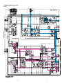
1
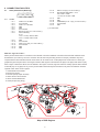
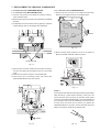
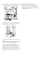
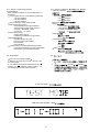
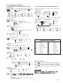
Service
Manual
DV4000/F1N, /K1G
/N1B, /S1G, /U1B
DVD Player
PLAY
DVD PLAYER DV4000
OPEN / CLOSE
STANDBY / ON
DTS
SURROUND
PAUSE
WIDE
DOLBY DIGITAL
DIMMER
POWER
SPATIALIZER
PREV
NEXT
MPEG
STOP
TABLE OF CONTENTS
1.
2.
TECHNICAL SPECIFICATION ............................................................................... 1
CONNECTION FACILITIES .................................................................................... 2
3.
4.
INFORMATIONS ..................................................................................................... 3
SERVICING HINT ................................................................................................... 4
5.
6.
DISASSEMBLY ....................................................................................................... 5
PRINCIPAL PARTS LOCATION .............................................................................. 6
7.
8.
REPLACEMENT OF PRINCIPAL COMPONENTS ................................................. 7
SERVICE MODE .................................................................................................... 9
9.
10.
ELECTRICAL ADJUSTMENT ............................................................................... 15
BLOCK DIAGRAM ................................................................................................ 16
11.
12.
WIRING DIAGRAM ............................................................................................... 22
SCHEMATIC DIAGRAM AND PARTS LOCATION ............................................... 24
13.
14.
EXPLODED VIEW AND PARTS LIST ................................................................... 38
ELECTRICAL PARTS LIST ................................................................................... 40
15.
16.
SCHEMATIC DIAGRAM AND PARTS LOCATION (TKM1000MZ) ................... 15-1
MICROPROCESSOR AND IC DATA .............................................................. 15-15
17.
18.
EXPLODED VIEW AND PARTS LIST (TKM1000MZ) .................................... 15-28
ELECTRICAL PARTS LIST (TKM1000MZ) ..................................................... 15-30
DV4000
Please use this service manual with referring to the user guide (D.F.U) without fail.
DV4000
294W855010 AO
3120 785 22290
First Issue:2000.05
MARANTZ DESIGN AND SERVICE
Using superior design and selected high grade components, MARANTZ company has created the ultimate in stereo sound.
Only original MARANTZ parts can insure that your MARANTZ product will continue to perform to the specifications for which
it is famous.
Parts for your MARANTZ equipment are generally available to our National Marantz Subsidiary or Agent.
ORDERING PARTS :
Parts can be ordered either by mail or by Fax.. In both cases, the correct part number has to be specified.
The following information must be supplied to eliminate delays in processing your order :
1. Complete address
2. Complete part numbers and quantities required
3. Description of parts
4. Model number for which part is required
5. Way of shipment
6. Signature : any order form or Fax. must be signed, otherwise such part order will be considered as null and void.
USA
EUROPE / TRADING
AMERICAS
SUPERSCOPE TECHNOLOGIES, INC.
MARANTZ PROFESSIONAL PRODUCTS
2640 WHITE OAK CIRCLE, SUITE A
AURORA, ILLINOIS 60504 USA
PHONE : 630 - 820 - 4800
FAX
: 630 - 820 - 8103
AUSTRALIA
JAMO AUSTRALIA PTY LTD
1 EXPO COURT, P.O. BOX 350
MT. WAVERLEY VIC 3149
AUSTRALIA
PHONE : +61 - 3 - 9543 - 1522
FAX
: +61 - 3 - 9543 - 3677
NEW ZEALAND
WILDASH AUDIO SYSTEMS NZ
14 MALVERN ROAD MT ALBERT
AUCKLAND NEW ZEALAND
PHONE : +64 - 9 - 8451958
FAX
: +64 - 9 - 8463554
BRAZIL
MARANTZ EUROPE B.V.
P.O.BOX 80002, BUILDING SFF2
5600 JB EINDHOVEN
THE NETHERLANDS
PHONE : +31 - 40 - 2732241
FAX
: +31 - 40 - 2735578
MARANTZ AMERICA, INC.
INC
440 MEDINAH ROAD
ROSELLE, ILLINOIS 60172
USA
PHONE : 630 - 307 - 3100
FAX
: 630 - 307 - 2687
AUSTRALIA
TECHNICAL AUDIO GROUP PTY, LTD
558 DARLING STREET,
BALMAIN, NSW 2041,
AUSTRALIA
PHONE : 61 - 2 - 9810 - 5300
FAX
: 61 - 2 - 9810 - 5355
THAILAND
MRZ STANDARD CO., LTD
746 - 754 MAHACHAI ROAD.,
WANGBURAPAPIROM, PHRANAKORN,
BANGKOK, 10200 THAILAND
PHONE : +66 - 2 - 222 - 9181
FAX
: +66 - 2 - 224 - 6795
TAIWAN
PAI- YUING CO., LTD.
6 TH FL NO, 148 SUNG KIANG ROAD,
TAIPEI, 10429, TAIWAN R.O.C.
PHONE : +886 - 2 - 25221304
FAX
: +886 - 2 - 25630415
JAPAN Technical
MARANTZ JAPAN, INC.
35- 1, 7- CHOME, SAGAMIONO
SAGAMIHARA - SHI, KANAGAWA
JAPAN 228-8505
PHONE : +81 42 748 1013
FAX
: +81 42 741 9190
PHILIP DA AMAZONIA IND. ELET. ITDA
CENTRO DE INFORMACOES AO
CEP 04698-970
SAO PAULO, SP, BRAZIL
PHONE : 0800 - 123123(Discagem Direta Gratuita)
FAX
: +55 11 534. 8988
CANADA
LENBROOK INDUSTRIES LIMITED
633 GRANITE COURT,
PICKERING, ONTARIO L1W 3K1
CANADA
PHONE : 905 - 831 - 6333
FAX
: 905 - 831 - 6936
SINGAPORE
WO KEE HONG (S) PTE LTD
WO KEE HONG CENTRE
NO.23, LORONG 8, TOA PAYOH
SINGAPORE 319257
PHONE : +65 2544555
FAX
: +65 2502213
MALAYSIA
WO KEE HONG ELECTRONICS SDN. BHD.
SUITE 8.1, LEVEL 8, MENARA GENESIS,
NO. 33, JALAN SULTAN ISMAIL,
50250 KUALA LUMPUR, MALAYSIA
PHONE : +60 3 - 2457677
FAX
: +60 3 - 2458180
KOREA
MK ENTERPRISES LTD.
ROOM 604/605, ELECTRO-OFFICETEL, 16-58,
3GA, HANGANG-RO, YONGSAN-KU, SEOUL
KOREA
PHONE : +822 - 3232 - 155
FAX
: +822 - 3232 - 154
SHOCK, FIRE HAZARD SERVICE TEST :
CAUTION : After servicing this appliance and prior to returning to customer, measure the resistance between either primary AC
cord connector pins ( with unit NOT connected to AC mains and its Power switch ON ), and the face or Front Panel of product and
controls and chassis bottom.
Any resistance measurement less than 1 Megohms should cause unit to be repaired or corrected before AC power is applied, and
verified before it is return to the user/customer.
Ref. UL Standard No. 1492.
In case of difficulties, do not hesitate to contact the Technical
Department at above mentioned address.
991207A.O
1. TECHNICAL SPECIFICATIONS
Discs played
DVD video disc ................................................... 12 cm single sided, single layer
12 cm single sided, double layer
12 cm double sided, single layer
12 cm double sided, double layer (one layer per side)
8 cm single sided, single layer
8 cm single sided, double layer
8 cm double sided, single layer
8 cm double sided, double layer (one layer per side)
Compact disc
(CD-DA, Video CD) .............................................12 cm, 8 cm
Video system..........................................................PAL (625/50)/NTSC (525/60)
Audio system..........................................................Linear PCM audio
MPEG 1/2 audio
Dolby Digital (AC-3)
DTS audio (Digital output only)
Video output
Line output level ................................................. 1.0 Vp-p / 75 ohms, unbalanced
RCA pin Jack x 1
S1-output level .................................................... Y output: 1.0 Vp-p/75 ohms unbalanced
C output: 0.3 Vp-p/75 ohms (PAL)
0.286 Vp-p/75 ohms (NTSC)
4 pin mini DIN x 1
R/G/B output....................................................... R/G/B output: 0.7 Vp-p 21-pin SCART connector x 1 (/N1B)
Audio output
Line output ......................................................... 2.0 Vrms / 10 kohms
RCA pin Jack x 1 system
Digital audio output
Optical output ..................................................... Optical connector x 1
Coaxial output ..................................................... RCA pin Jack x 1
DVD Iinear audio characteristics
Frequency response ........................................... 4 Hz-22 kHz (Fs = 48 kHz)
4 Hz-44 kHz (Fs = 96 kHz)
S/N ratio ..............................................................100 dB (Fs = 48 kHz/24 bit PCM)
Dynamic range ....................................................100 dB (Fs = 48 kHz/24 bit PCM)
Total harmonic distortion ..................................... 0.0025% (Fs = 48 kHz/24 bit PCM)
CD audio characteristics:
Frequency response ........................................... 4 Hz-20 kHz (EIAJ)
S/N ratio ..............................................................100 dB (EIAJ)
Dynamic range ....................................................100 dB (EIAJ)
Total harmonic distortion ..................................... 0.0025% (EIAJ)
Pickup.................................................................... Wavelength: 655 nm (DVD)
Wavelength: 790 nm (CD)
Power requirements............................................. 120V AC, 60 Hz (/U1B)
100-240V AC, 50/60 Hz (/N1B)
100V AC, 50/60 Hz (/F1N)
100-240V AC, 50/60 Hz (/K1G,/S1G)
Power consumption............................................. 20 W (standby mode = approx 1.2 W, power off = 0 W)
Operation temperature......................................... 5 C-35 C
Operation humidity range.................................... 5%-90% (no condensation)
Dimensions............................................................ 440 (W) x 88 (H) x 332 (D) mm (excluding protrusions)
Weight.................................................................... 3.3 kg
Supplied accessories
AC power cable ...................................................x 1
Auido / Video cable ............................................. x 1 (/F1N, /K1G, /S1G, /U1B)
D-BUS remote cable ...........................................x 1
Remote control unit ............................................ x 1
Batteries ..............................................................x 2
21-pin SCART cable............................................x 1 (/N1B)
• For improvement purposes, specifications and design are subject to change without notice
1
2. CONNECTION FACILITIES
2.1
Video performance (/N1B only)
1
- Pin 15
- Pin 16
3 5 7 9 11 13 15 17 19
21
Red out :0.7Vpp ( 0.1V into 75 Ohm (*)
fast switching RGB/ CVBS : <0.4V
into 75 Ohm = CVBS
<1V/ <3V into 75 Ohm = RGB
2 4 6 8 10 12 14 16 18 20
-
2.1.1 SCART
-
Pin 1
Pin 2
Pin 3
Pin 4
Pin 5
Pin 6
Pin 7
Pin 8
Audio R out :1.8V RMS
not connected
Audio L out :1.8V RMS
GND
GND
not connected
Blue out :0.7Vpp ( 0.1V into 75 Ohm (*)
funcion switching :
2V TV
>4.5V / <7V asp. ratio 16:9 DVD
>9.5V / <12Vasp. ratio 4:3 DVD
-
Pin 9
Pin 10
Pin 11
Pin 12
Pin 13
Pin 14
GND
not connected
Green out :0.7Vpp ( 0.1V into 75 Ohm (*)
not connected
GND
GND
Pin 17
Pin 18
Pin 19
Pin 20
Pin 21
GND
GND
CVBS/RGB sync out : 1Vpp ( 0.1V into 75 Ohm )
not connected
GND
(*) for 100% white
What are "regional codes"?
Motion picture studios want to control the home release of movies in different countries because theater releases arenít
simultaneous (a movie may come out on DVD in the US when itís just hitting screens in Europe). Therefore they have
required that the DVD standard include codes which can be used to lock out the playback of certain discs in certain geographical regions. Players sold in each region will have that regionís code built into the player. The player will refuse to play
these "region coded" discs which are not allowed in the region. However, regional codes are entirely optional. Discs without
codes will play on any player in any country. Some studios have already announced that only their new releases will have
regional codes. There are six regions:
1. United States and Canada
2. Europe and Japan
3. Far East (except Japan & China)
4. South America and Oceania
5. Africa and the Middle East
6. China (except Hong Kong)
5
1
2
6
2
3
5
4
2
Map of DVD Regions
2
4
3. INFORMATIONS
Multi-angles:
REGION CODE
VERSION
REGION CODE
COUNTRY
/FXX
/KXX
2
6
JAPAN
CHINA
/NXX
/SXX
2
3
EUROPE
SINGAPORE/HONGKONG
/UXX
1
USA/CANADA
On some DVDs, scenes have been filmed from different angles
(up to a maximum of 9). On these discs, you can select the
angle that you want to watch. Please refer to the DVD’s manual
to see which scenes have multi-angles.
Parental guide:
THE DISCS THAT THE DV4000 CAN HANDLE
Some discs have restriction levels that allow you to cut scenes
or prevent playback of discs that have contents that you do
The following discs can be played back with a DV4000.
not want children to watch.
disc
mark
playback capability
DVD
Audio/Video
CD
Audio
size
side
12 cm
single/double
8 cm
12 cm
single
8 cm
Audio/Video
the Safety Lock is set, discs can not be played back.
Cancelling Safety Lock
Press the CLEAR button and hold for 10 seconds while the
12 cm
VCD
Safety Lock
The safety look prevents children from playing discs. When
single
8 cm
player is stopped.
Note: The regional code of the discs must meet to the regional
code of the DV4000.
DVD INFORMATION
Below is a glossary of the new terms related to DVD.
Title:
A disc may have more than one story/movie on it, so each
story/movie is called a “title”.
For example, if there are 2 movies on the disc, they are
separated into Title 1 and Title 2.
Chapter:
A title may also be separated into chapters.
For example, a movie (title) may be separated into 3 scenes
(chapters).
Title 1
Title 2
Chapter Chapter Chapter Chapter Chapter Chapter
1
2
3
1
2
3
Subtitles:
DVDs are recorded with up to 32 different subtitle languages.
If a disc has more than one subtitle language, you can select
the subtitle language that you want to read.
Soundtrack language:
DVDs are recorded with up to 8 different soundtrack languages.
If a disc has more than one language, you can select the
soundtrack language that you want to listen to.
3
4. SERVICING HINT
SERVICE HINTS
SERVICE TOOLS
Audio signals disc
Disc without errors (SBC444)+
Disc with DO errors, black spots and fingerprints (SBC444A)
Disc (65 min 1kHz) without no pause
Max. diameter disc (58.0 mm)
Torx screwdrivers
Set (straight)
Set (square)
13th order filter
DVD test disc
4
4822 397 30184
4822 397 30245
4822 397 30155
4822 397 60141
4822 395 50145
4822 395 50132
4822 395 30204
4822 397 10131
5. DISASSEMBLY
In case of trouble, etc., necessitating dismantling, please
dismantle in the order shown in the illustrations. Reassemble
in the reverse order.
1. Removal of the UPPER COVER
2. Removal of the FRONT PANEL
1) Press the “EJECT” button while the unit’s power is turned on and open the DISC TRAY.
2) Remove the decoration plate on the DISC TRAY by pulling it upward.
3) Remove the three retaining screws on the bottom and two screws on each left and right side of the FRONT PANEL as
shown.
4) Disconnect the flat cable from the P702 connector on the OUTPUT PCB .
5) Remove the FRONT PANEL by pulling it forward while releasing the TABs on both left and right ends of the FRONT
PANEL.
P702
TAB
REMARK : Before disassemble the front panel.
Press open/close button to open the tray.
If the tray doesn’t work, put a small screwdriver into the
hole as shown in picture and slide the knob.
Then the tray comes out. After the first centimeter it is
possible to pull the tray out by hand. Release the door
cover of the tray.
5
TAB
6. PRINCIPAL PARTS LOCATION
POWER SUPPLY PCB
SLED MOTOR
MAIN PCB
OUTPUT PCB
SPINDLE MOTOR
LOADING MOTOR
Fig. 6-1 Top view (DV4000)
6
OPERATION PCB
PICKUP
7. REPLACEMENT OF PRINCIPAL COMPONENTS
7-1. Removal of the TRAVERSE MECHA.
7-1-2. Removal of the TRAVERSE MECHA.
7-1-1. Removal of the MECHANISM BLOCK
1) Turn the unit’s power on and press the “EJECT” button to
1) Remove the four b screws on the MAIN PCB and then
disconnect the P800 connector on the MAIN PCB.
eject the DISC TRAY.
2) Disconnect the power cord and remove the DISC CLAMPER
BLOCK.
3) Completely remove the DISC TRAY by pulling it outwards
while pulling up both of the stopper tabs alternately.
B SCREW
Fig. 7-3
2) Short the laser diode protection circuit on the PICK UP
BLOCK’s flexible cable with solder as shown.
STOPPER TUB
Fig. 7-1
4) Disconnect the two flat cables from the P803 connectors
and one flat cable from the P808 connector on the MAIN
PCB.
5) Disconnect the P807 connector on the MAIN PCB.
6) Remove the four a retaining screws and remove the
MECHANISM BLOCK from the chassis.
P200
Fig. 7-4
Caution
To protect the laser diode from damage caused by high voltage
static electricity, a laser diode protection circuit has to be
shorted before disconnecting the flexible cable (P200
connector on the MECHANISM PCB). It is recommended that
you put solder on the top of the soldering iron as shown in Fig.
3-5 then short the circuit at once. When you replace the
TRAVERSE MECHA., be sure to connect the P200 connector
before removing the solder at the shorted parts.
A SCREW
SOLDER
Fig. 7-5
Fig. 7-2
7
3) Carefully disconnect the two connectors (P500, P600) and
the two flat cables (P200, P300) on the MECHANISM PCB.
7-3. Replacement of the PICK UP BLOCK
Replacement of the PICK UP BLOCK itself is not
recommended because its azimuth adjustment is very
critical and requires a special jig. If PICK UP BLOCK
replacement is necessary, replace with an entire
TRAVERSE MECHANISM only.
P600
P200
P300
P500
Fig. 7-6
4) Using tweezers, release the four retaining HOOKs of the
TRAVERSE MECHA. from the rubber insulators being
careful not to damage the rubber insulators.
Fig. 7-7
5) Remove the TRAVERSE MECHA. from the MECHANISM
BLOCK.
6) Reassemble in the reverse order for installation. Never
remove the solder on the flexible cable before connecting
the P200 connector on the MECHANISM PCB.
7-2. Replacement of the SPINDLE MOTOR
Because the SPINDLE MOTOR position is very critical, jitter
adjustment should be performed after replacement.
1) Disconnect the P300 connector on the MECHANISM PCB.
2) Insert a Philips type screw driver into the hole on the TURN
TABLE of the SPINDLE MOTOR and remove the two
screws.
8
8. SERVICE MODE
8-1 OPERATION
8-1.
8-1-1. Main Microprocessor (IC600 : MB90574)
Functions which operated by main microprocessor
are follows.
Control of following IC's.
AV decoder, DEM/ECC, VIDEO encoder, CDDSP, AUDIO-DAC, PRE-AMP, READ-CHANNEL,
SERVO
Mechanism control
DVD rate control
OSD control
DISC detect, Focus/Tracking alignment
Data transmission between OPE microprocessor
8-1-1. MAIN
(IC600:MB90574)
NAIN
IC
AV
DEM/ECC VIDEO
CD-DSP AUDIO-DAC PRE-AMP READCHANNEL SERVO
DVD
OSD
DISC
OPE
Process from POWER ON (RESET RELEASE) till
PLAY BACK are described in the chart below.
MAIN
RESET
Release REST
RESET
Mechanism initialize
Initial read EEPROM
EEPROM
DEM/ECC initialize
DEM/ECC
Release RESET (IC's)
IC RESET
Digital out of the AV decoder
initial set up. (48Khz liner PCM)
AV
48KHz
PCM )
VIDEO Encoder initial setup
VIDEO
(PAL or NTSC)
Show the start up frame
Release RESET (AV Decoder)
AV
RESET
DISC detect
DISC
Boot up AV Decoder
AV
BOOT UP
CD/VCD
Servo IC initialize
IC
TOC reading
TOC
PLAY BACK /
9
DVD
Control data
reading
8-1-2. OUTPUT CONTROL
OUTPUT CONTROL
8-1-2. Output Control Microprocessor
(IC700:M38022)
Main operation features of this microprocessor is
as follows.
Power supply control : Power efficiency switching.
3.3V line ON/OFF
5.0V line ON/OFF
9.0V line ON/OFF
Out put selection of the OUTPUT PCB.
VIDEO output stage control
21PIN SCART output signal selection
21PIN SCART control signal selection
(TV/DVD, SQUEEZE, RGB)
S-Video out S1 control
AUDIO output control
Output MUTE control
Feedback to the MAIN microprocessor
OPERATION PCB
Operation Button key scan
Remote control code reading
FLD indication
LED indication
Communication between MAIN microprocessor
Command transmission (by user controlable)
Data receiving for FLD/LED indication
(IC700: M38022)
3.3V
ON/OFF
5.0V
ON/OFF
9.0V
ON/OFF
OUTPUT
VIDEO
21PIN SCART
21PIN SCART
(TV/DVD, SQUEEZE , RGB)
S
S1
AUDIO
MUTE
MAIN
OPERATION
FLD
LED
MAIN
FLD/LED
8-2. TEST MODE
8-2.
How to set up the TEST MODE
1. Remove any Disc from the tray, and turn OFF
the mains power.
2. Turn ON the mains power while depress the " "
(STOP) and " " (PAUSE) buttons together. Do
not release buttons till FLD shows follows.
1.
2.
(STOP)
(PAUSE)
FLD
In case of no DISC /
While DVD Video playback / DVD
10
While VCD and CD Video playback / VCD/CD
(CPU :
In case of some fault has happened. (caused with
communications between CPU: IC600 and related
IC's) Some Error code is shown on the FLD.
Each Error codes are described on the table 8-1.
ERORR
CODE
16
17
18
19
20
32
33
34
35
36
37
38
IC600
)
IC
FLD
8-1
ERORR DESCRIPTION /
No access with CD-DSP (IC490).
CD-DSP(IC490)
Sledge motor is not working.
DISC
D/V/C
D/V/C
Tracking ON error.
D/V/C
Focus ON error.
D/V/C
Sub code read error. (CD/VCD)
CD, VCD
No access with Servo-DSC (IC300).
DSC(IC300)
No access with DEM/ECC (IC500).
DEM/ECC(IC500)
No access with A/V decoder (IC700).
A/V
(IC700)
No access with system ROM (IC602).
ROM(IC602)
No access with EEPROM(IC603).
EEPROM(IC603)
No access with A/V encoder (IC850).
A/V
(IC850)
No access with Read channel (IC200).
(IC200)
8-1. / Table 8-1.
11
V/C
D/V/C
D/V/C
D/V/C
D/V/C
D/V/C
D/V/C
D/V/C
D : DVD, V : Video CD, C : CD
3. Press the " " (STOP) button while close the
disctray without any disc. Then all segments of
the FLD right ON.
3.
(STOP)
FLD
4. Press the " " (STOP) button again. The FLD
indication shows below. Then the laser diode for
DVD will right ON.
4.
5. Press the " " (STOP) button again. The FLD
indication shows below. Then the laser diode for
CD will right ON.
5.
6. Press the " " (STOP) button again. Then the
TEST MODE back to the first step.
6.
7. Press the "
" (Forward Search) button while
close the disc tray without any disc. Then the
sledge motor will move.
7.
8. Turn OFF the mains power.
will be released.
FLD
(STOP)
DVD
DVD
(STOP)
CD
CD
(STOP)
(Forward Search)
Then service mode
8.
12
8-3. EEPROM initialize
The memory device (EEPROM) which used in this DVD player
is programmed each functions by products regions at factory.
When that EEPROM (MAIN P.C. Board IC602 : M24C16MN6T) or MAIN P.C. Board has exchanged, EEPROM initialization is necessary. If that the initialization will not be done
correctly, the product might not be work correctly.
The initialize procedure are as follows.
1. Remove any Disc from the tray, and turn OFF the mains
power.
Turn ON the mains power while depress the “
“ (STOP)
and “
“ (Forward skip) buttons together. Do not release
buttons till FLD shows “ A-01 D-XX “. (XX = is depended
on EEPROM status)
REMARK : In case of some failure with the product. The
ERROR code will be shown on the FLD and above
indication will not be shown. Then other confirmation or
repair is necessary before this EEPROM initialization.
2. The address shown as “ A-01 D-XX “ is can be changed
by pressing “
“ and “
“ buttons on the front panel or
remote controller. Which can be changed to “ 0 “ till “ 07 “.
(Address “ 00 “ is not available.)
“
“ (Forward skip) button
: Address UP
“
“ (Reverse skip) button
: Address DOWN
3. The DATA shown as “ XX “ is can be changed by pressing
“ II “ and “
“ buttons on the front panel or remote
controller. Set up data are shown in following table.
“ II “ (PAUSE) button
: Data UP
“
: Data DOWN
“ (STOP) button
4. Press the “ DIMMER “ button, then address data will be
memorize.
5. Memorize data by each address ( from “ 01 “ to “ 07 “), as
order 2., 3. And 4. processes.
6. Turn OFF the mains switch. (This procedure is necessary
for next procedure.)
Address
Data
U1B
F1N
N1B
S1G
K1G
01
02
E1
30
E9
30
F7
70
E7
30
E7
30
03
04
00
53
08
50
00
00
00
00
06
00
05
06
55
C5
4A
C5
00
C5
00
C5
00
C5
07
A9
A9
A9
A9
A9
13
7. Turn ON the mains power while depress the “ DIMMER “
and “
“ (Reverse skip) buttons together. Then the FLD
shows “ -- -- -- -- “.
8. Send the commands “ 1999 “ by the remote controller.
(Press buttons “ 1 “, “ 9 “, “ 9 “ and “ 9 “.) Then the FLD
shows “ A-00 D-XX “. (XX = is depended on EEPROM
status)
9. Send the commands “ D-XX “ (Data) as your product version shows in following table by the remote controller.
Data
U1B
F1N
N1B
S1G
K1G
01
02
02
04
20
10. Press the “ ENTER “ button, then address data will be
memorize and the FLD shows a data number which you
stored. ( EX: “ D-02 “ )
11. Turn OFF the mains switch, then EEPROM initialization
mode will be release.
14
9. ELECTRICAL ADJUSTMENT
VR120
P807
TP120
P804
P800
P803
TP105
TP107
TP300
VR121
TP201
VR110
JITTER ADJ
SCREW A
JITTER ADJ
SCREW B
VR202
Fig. 9-1
9-1. DVD JITTER ADJUSTMENT
1. Stick the provided small round sticker (0.1 mm thickness)
2. Set the oscilloscope to the DC input mode and connect it to
the TP201 (HOT) and the TP102 (D.GND) on the MAIN
at the innermost position of a DVD disc as shown and make
a swayed DVD disc.
PCB.
3. Adjust the VR202 so that the DC level is minimum. (The DC
level should be less than 1.8 V)
Signal recorded side
9-3. CD TRACKING BALANCE
1. Set the VR110 at its center position prior to the adjustment.
2. Connect an oscilloscope to the TP150 (TE) on the MAIN
PCB.
3. Play back an ordinary CD-disc and then set it to the PAUSE
mode. If the play mode does not be engage, turn the VR110
at ±15 degrees. If the play mode does still not be engage
STICKER
even when the VR110 is turned at ±15 degrees, turn the
VR110 at ± 30 degrees and try it again.
Fig. 9-2
2. Play back the swayed DVD disc and press the F.F button
repeatedly until the pickup block reaches the outermost
4. Observe the waveform and adjust it so that the level A of
the waveform is the same as level B.
position of its movable range. Next, press the PAUSE button.
3. Set the oscilloscope to the DC input mode and connect it to
A
the TP201 (HOT) and the TP102 (D.GND) on the MAIN
PCB.
B
4. Adjust the a screw and b screw alternately so that the AC
and DC level of the waveform is minimum. (DC level should
500mV
Fig. 9-4
be less than 1.8 V, AC component should be minimum.)
minimum
9-4. AS ADJUSTMENT
Adjustment point : VR120
Less than 1.8V
Test point : TP120
1. Turn ON the mains power while depress the “
” (STOP)
Fig. 9-3
and “ II ” (PAUSE) buttons together. (TEST MODE)
2. Connect the multi meter to test point TP120. Set the multi
NOTE: If the SPINDLE MOTOR is replaced, this jitter
meter in DC voltage mode.
3. Press the “ ” (STOP) button several times till the FLD
shows “ LD TEST CD ”.
status.
adjustment should be performed for proper performance.
9-2. SLICE LEVEL ADJUSTMENT
1. Play back an ordinary DVD disc (single side, one layer) and
press the F.F button repeatedly until the pickup block
reaches almost the center position of its movable range.
Measure the voltage at that
4. Press the “
” (STOP) button several times till the FLD
shows “ LD TEST DVD ”.
5. Adjust the voltage at that status 50mV lower than “ LD TEST
CD ” status by the trim resister VR120.
15
10. BLOCK DIAGRAM
67
SP_O
SP_P
66
SP_N
RF / SERVO / SYSCON
68
81
82
80
65
64 62
61 60
58 57
56
52
45
44 46
33
72
71 69 70
69
CYC11AP000
40
42
89
41
91
7
37
90
35
92
99
100
16
97 98 95 96 93 94
77 78
73 74
75 76
36 29
34
8
17
AUDIO
Not for /N1B
/N1B ONLY
Not for DV4000
18
19
VIDEO
/N1B ONLY
20
21
11. WIRING DIAGRAM
22
23
12. SCHEMATIC DIAGRAM AND PARTS LOCATION
OUTPUT-1/2
Not for DV4000
Not for /N1B
Not For /N1B
/N1B ONLY
24
25
OUTPUT-2-2
Not for DC4000
26
27
OUTPUT TOP VIEW
TR110
IC200 TR200
OUTPUT BOTTOM VIEW
TR320
TR350 TR361
TR310 TR360 TR321
TR900 TR902 TR901
TR421 TR531 TR530 TR482 TR450
28
IC719
IC700
IC470 IC520
IC570 IC420
TR400~TR405
IC340
TR500~TR505 TR540~TR542
29
TR130~TR133
IC250
OPERATION
Not for DV4000
30
31
OPERATION
TR101
TR102
PH100
PH120
32
33
POWER
34
35
POWER
IC501
36
PH500
PH501
TR558
TR551
IC551
IC556
IC555
TR550
37
IC553
TR559
TR560
(VERS. :VERSION, U:U.S.A., F:JAPAN, K:FAR EAST, **:EUROPE)
13. EXPLODED VIEW AND PARTS LIST
POS.
NO
VERS.
COLOR
001B
/F1N,/S1
G,/K1G
/U1B
/N1B
9965 000 04731
9965 000 04735
4822 454 11825
/F1N,/S1
G,/K1G
/U1B
9965 000 04745
/N1B
/F1N,/S1
G,/K1G
/U1B
9965 000 04736
/N1B
/F1N,/S1
G,/K1G
/U1B
9965 000 04743
/N1B
/F1N,/S1
G,/K1G
/U1B
9965 000 04732
/N1B
/F1N,/S1
G,/K1G
/U1B
9965 000 04733
/N1B
/F1N,/S1
G,/K1G
/U1B
9965 000 04734
/N1B
9965 000 04737
9965 000 04738
9965 000 04739
001B
001B
002B
003B
005B
294W053010
PLATE DVD (GLD)
294W251110
PLATE DVD (BLK)
294W251010
BUTTON POWER (GLD)
294W270110
BUTTON POWER (BLK)
294W270010
BUTTON PLAY (GLD)
294W270120
BUTTON PLAY (BLK)
294W270020
BUTTON SURROUND (GLD)
294W270130
BUTTON SURROUND (BLK)
294W270030
BUTTON EJECT (GLD)
294W270140
BUTTON EJECT (BLK)
294W270040
LENS POWER
LENS DTS
LENS WIDE
294W355010
294W355020
294W355030
001G
9965 000 04744 JOINT POWER
294W357010
12
13
14
15
16
17
17
17
17
nsp
9965 000 04740
nsp
nsp
9965 000 04741
nsp
nsp
nsp
nsp
010B
010B
011B
011B
012B
012B
013B
013B
018B
019B
020B
019B
010B
17
012B
013B
18
20
21
22
25
006B
002B
011B
020B
005B
25
26
27
001B
14
27
38
POS.
NO
VERS.
COLOR
001T
001T
001T
001T
001T
/F1N
/K1G
/N1B
/S1G
/U1B
PACKING
USER GUIDE (JPN)
USER GUIDE (ENG/CHINA)
9965 000 04748 USER GUIDE (5LANGUAGE)
USER GUIDE (ENG/CHINA)
USER GUIDE (ENG/FRAN)
ZK294W0010
/N1B
9965 000 04746 REMOTE CONTROLLER
RC4000DV
nsp
CORD 21P YAF11-0642 1.5M
MAINS CORD (JPN)
MAINS CORD (USA)
9965 000 04747 MAINS CORD (EUR/S-pore)
*YC000420R
*YC000430R
*YC000410R
294W248110
PANEL TRAY (BLK)
006B
018B
PANEL FRONT (GLD)HB
PART NO.
(MJI)
294W248020
294W248010
294W158010
185J251010
294W053110
006B
003B
DESCRIPTION
PANEL FRONT (BLK)V2
PANEL FRONT (BLK)HB
WINDOW FLD
BADGE MARANTZ
PANEL TRAY (GLD)
005B
001G
PART NO.
(FOR PCS)
001Z
002Z
/F1N
/U1B
/N1B
/S1G
/K1G
BT BID26X08STL CMT
nsp
FFC BD P1.0 L230 14P
*YU000590R
ST BID30X06STL CMT
nsp
BT BID30X14STL NI3
nsp
FFC BD P0.5 L160 24P
*YU000620R
/F1N
PANEL REAR DV4000 (J) (CH)
nsp
/U1B
PANEL REAR DV4000(A) (CH)
nsp
/N1B
PANEL REAR DV4000 (E) (CH)
nsp
/S1G
PANEL REAR DV4000(U5)
nsp
(CH)
/K1G
nsp
PANEL REAR DV4000(Y4)
nsp
(CH)
nsp
BT BID30X08STL BZN
nsp
9965 000 04742 FOOT
294W057010
nsp
CUSHION FOOT 12X12X2 (CH)
nsp
nsp
ST BID30X10STL CMT
Nsp
/F1N,/S1
nsp
COVER UPPER (G) (CH)
nsp
G,/K1G
/U1B
nsp
COVER UPPER (B) (CH)
nsp
/N1B
nsp
BT BID30X08STL BZN
nsp
/F1N,/S1
nsp
ST BID40X06STL COP CLEAR
nsp
G,/K1G
/U1B
nsp
ST BID40X06STL BZN
Nsp
/N1B
39
PART NO.
(FOR PCS)
DESCRIPTION
MAINS CORD (CHINA)
PART NO.
(MJI)
294W851110
294W851350
294W851310
294W851350
294W851250
nsp
*YC000440R
14. ELECTRICAL PARTS LIST
NOTE ON SAFETY FOR FUSIBLE RESIST OR :
ASSIGNMENT OF COMMON PARTS CODES.
RESISTORS
R
R
The suppliers and their type numbers of fusible resistors are as
follows ;
1 . KOA Corporation
Part No.(MJI)
Type No.(KOA)
Description
NH05 x x x 140
RF25S x x x x
J 5% (1/4W)
NH05 x x x 120
RF50S x x x x
J 5% (1/2W)
NH85 x x x 110
RF73B2A x x x x
J 5% (1/10W)
NH95 x x x 140
RF73B2E x x x x
J 5% (1/4W)
: 1) GD05 x x x 140, Carbon film fixed resistor, 5% 1/4W
: 2) GD05 x x x 160, Carbon film fixed resistor, 5% 1/6W
1 Resistance value
Examples
1 Resistance value
0.1 ..... 001
10 ...... 100
1k ...... 102 100k ...... 104
0.5 ..... 005
18 ...... 180 2.7k ...... 272 680k ...... 684
1 ..... 010 100 ...... 101 10k ...... 103
1M ...... 105
6.8 ..... 068 390 ...... 391 22k ...... 223 4.7M ...... 475
Note : Please distinguish 1/4W from 1/6W by the shape of parts
used actually.
Resistance value
2. Matsushita Electronic
Part No.(MJI)
NF05 x x x 140
RF05 x x x 140
NF02 x x x 140
RF02 x x x 140
CAPACITORS
C
C
C
: CERAMIC CAP.
3) DD1 x x x x 370, Ceramic capacitor
Disc type
Temp.coeff. P350~N1000, 50V
3 Capacity value
2 Tolerance
Examples
2 Tolerance (Capacity deviation)
0.25 pF ....... 0
0.5 pF ....... 1
5 % ....... 5
Tolerance of COMMON PARTS handled here are as follows :
0.5 pF - 5 pF ....... 0.25 pF
6 pF - 10 pF ..... 0.5 pF
12 pF - 560 pF ... 5 %
3 Capacity value
0.5 pF .... 005
3 pF ..... 030 100 pF ..... 101
1 pF .... 010 10 pF ..... 100 220 pF ..... 221
1.5 pF .... 015 47 pF ..... 470 560 pF ..... 561
- 10k
)
Components Co., Ltd
Type No.(MEC)
Description
ERD-2FCJ x x x
( 5% 1/4W)
ERD-2FCG x x x
( 2% 1/4W)
Resistance value
Examples
Resistance value
0.1 ..... 001
10
0.5 ..... 005
18
1 ..... 010 100
6.8 ..... 068 390
: CERAMIC CAP.
4) DK16 x x x 300, High dielectric constant ceramic
capacitor
Disc type
Temp.chara. 2B4, 50V
4 Capacity value
Examples
4 Capacity value
100 pF ..... 101
1000 pF .... 102 10000 pF .... 103
470 pF ..... 471
2200 pF .... 222
..... 100
..... 180
..... 101
..... 391
1k
2.7k
10k
22k
.....
.....
.....
.....
102
272
103
223
100k
680k
1M
4.7M
.....
.....
.....
.....
104
684
105
475
ABBREVIATION AND MARKS
ANT.
: ANTENNA
BATT.
: BATTERY
CAP.
: CAPACITOR
CER.
: CERAMIC
CONN.
: CONNECTING
DIG.
: DIGITAL
HP
: HEADPHONE
MIC.
: MICROPHONE
: MICROPROCESSOR
REC.
: RECORDING
RES.
: RESISTOR
SPK
: SPEAKER
SW
: SWITCH
TRANSF.
: TRANSFORMER
-PRO
: 5) ELECTROLY CAP.(
), 6)FILM CAP (
)
5) EA x x x x x x 10, Electrolytic capacitor
One-way lead type,Tolerance 20%
6 Working voltage
5 Capacity value
Examples
5 Capacity value
0.1 F .... 104
4.7 F .... 475
100 F ..... 107
0.33 F .... 334
10 F .... 106
330 F ..... 337
1 F .... 105
22 F .... 226
1100 F ..... 118
2200 F .... 228
6 Working voltage
6.3 V ...... 006
25 V ..... 025
10 V ...... 010
35 V ..... 035
16 V ...... 016
50 V ..... 050
6) DF15 x x x 350
DF15 x x x 310
DF16 x x x 310
Resistance value(0.1
TRIM.
: TRIMMING
TRS.
: TRANSISTOR
VAR.
: VARIABLE
X’ TAL
: CRYSTAL
NOTE ON SAFETY:
Plastic film capacitor
One-way type, Mylar 5% 50V
Plastic film capacitor
One-way type, Mylar 10% 50V
Symbol
Fire or electrical shock hazard. Only original
parts should be used to replaced any part marked with
symbol
Any other component substitution ( other than
original type), may increase risk of fire or electrical shock
hazard.
7 Capacity value
Examples
7 Capacity value
0.1 F ...... 104
0.001 F (1000 pF) ...... 102
0.56 F ...... 564
0.0018 F ........................ 182
1 F ...... 105
0.01 F ........................ 103
0.015 F ........................ 153
NOTE 1) The above CODES(R
,R
,C
,C
and C
) are omitted on the schematic diagram in
some case.
2) On the occasion, be confirmed the common parts on the
parts list.
3) Refer to “Common Parts List” for the other common
parts(Rl05, DD4, DK4).
40
990521 A.O
(VERS. :VERSION, U:U.S.A., F:JAPAN, K:FAR EAST, **:EUROPE)
POS.
NO
VERS.
COLOR
PART NO.
(FOR PCS)
OPERATION CIRCUIT BOARD
DIODES
1SS133T-77 T26
1SS133T-77 T26
MTZJ4.7C T26
MTZJ2.0B T26
LED SEL5421ETP15
LED SEL5421ETP15
LED SEL5421ETP15
LED SEL2910ATP6 ORANGE
LED SEL2910ATP6 ORANGE
LED SPR325MVWT31
MTZJ2.0A T26
D101
D102
D105
D106
D120
D121
D122
D123
D124
D140
D142
9965 000 04668
9965 000 04668
9965 000 01138
4822 130 82609
9965 000 04669
9965 000 04669
9965 000 04669
9965 000 04670
9965 000 04670
9965 000 04671
9965 000 04672
IC100
INTEGRATED CIRCUITS
4822 209 90244 IC UPD16311GC-AB6
HC10283060
PH120
TR101
TR102
TRANSISTORS
9965 000 04674 IR SPS-440-4-E
4822 130 61892 2SD2144S U/V/W
4822 130 60889 DTA143ES
*HW100460R
*HT400420R
*BA000800R
FL100
P102
SW101
SW102
SW103
SW104
SW105
SW106
SW120
SW121
9965 000 04673
nsp
4822 276 20508
4822 276 20508
4822 276 20508
4822 276 20508
4822 276 20508
4822 276 20508
4822 276 20508
4822 276 20508
MISCELLANEOUS
FLD 13-BT-160GK
SOCKET 14-FMZ-ST
SW TACT SKHVBE
SW TACT SKHVBE
SW TACT SKHVBE
SW TACT SKHVBE
SW TACT SKHVBE
SW TACT SKHVBE
SW TACT SKHVBE
SW TACT SKHVBE
POS.
NO
PART NO.
(MJI)
DESCRIPTION
14P
C509
C511
C512
C513
C514
nsp
nsp
nsp
nsp
nsp
POWER CIRCUIT BOARD
CAPACITORS
CER.
1000pF 400V
CER.
1000pF 400V
CER.
1000pF 400V
MYLAR
0.1 F 275V
MYLAR 0.22 F 275V
D502
D504
D508
D509
D510
D511
D553
D555
D556
D557
D558
D559
D564
9965 000 04668
9965 000 04668
9965 000 04675
9965 000 04675
9965 000 04675
9965 000 04675
9965 000 04676
9965 000 04677
5322 130 10293
9965 000 04678
9965 000 04679
9965 000 04679
4822 130 11643
DIODES
1SS133T-77 T26
1SS133T-77 T26
1N4006N02 800/1A
1N4006N02 800/1A
1N4006N02 800/1A
1N4006N02 800/1A
AK03V0 T26
1SS244T-77T26 250/0.2A
FMB-G14L 40/5.0A
RK16LF-C1 S15 60/1.5A
AK06V0 T26 60/0.7A
AK06V0 T26 60/0.7A
MTZJ5.1C T26
IC501
IC551
IC553
IC555
IC556
9965 000 04685
9965 000 04686
9965 000 04687
9965 000 04692
4822 209 33232
INTEGRATED CIRCUITS
IC STR-F6672
IC KA431AZTA
IC KA278R33
IC NJM79M09FA
IC NJM78M09FA
TR550
TR551
TR558
TR559
9965 000 04706
9965 000 04707
9965 000 04706
9965 000 04706
TRANSISTORS
DTC143ZS
2SB1326 Q/R
DTC143ZS
DTC143ZS
*HD201380R
*HD201380R
*HD301820R
*HD301780R
*HI100850R
*HI100850R
*HI100850R
HI10031080
HI10031080
*HI100840R
*HD301760R
*HQ300410R
nsp
SP0101128X
SP0101128X
SP0101128X
SP0101128X
SP0101128X
SP0101128X
SP0101128X
SP0101128X
nsp
nsp
nsp
nsp
nsp
*HD201380R
*HD201380R
*HD201300R
*HD201300R
*HD201300R
*HD201300R
*HD201310R
*HD201370R
*HD201340R
*HD201350R
*HD201360R
*HD201360R
*HD301770R
*HC105280R
*HC105270R
*HC105260R
HC3950909F
HC3850909F
*BA000810R
*HT200380R
*BA000810R
*BA000810R
41
VERS.
COLOR
PART NO.
(FOR PCS)
DESCRIPTION
PART NO.
(MJI)
TR560
9965 000 04707 2SB1326 Q/R
FR551
FR552
FR554
FR555
FR556
R504
R505
R508
R512
R553
9965 000 04680
9965 000 04680
9965 000 04681
9965 000 04682
9965 000 04683
4822 050 26801
9965 000 04701
9965 000 04702
9965 000 04703
9965 000 04704
RESISTORS
0.24
10% 1/4W FUSE
0.24
10% 1/4W FUSE
0.1
10% 1/4W FUSE
0.75
10% 1/4W FUSE
22
5% 1/4W FUSE
680
5% 1/4W
5% 1W
0.36
5.6
5% 1/4W
5% 1W
68K
5% 2W
0.75
*NH000110R
*NH000110R
NH05001140
*NH000130R
*NH000120R
GG05681140
*GA000180R
GG05056140
GA05683010
*GA000170R
F500
L500
L501
L551
L553
L554
L556
L557
PH500
PH501
P500A /F1N,/K1
G,/N1B
/S1G
P500B /U1B
SW500
T501
9965 000 04684
9965 000 04693
9965 000 04694
9965 000 04695
9965 000 04696
9965 000 04696
9965 000 04695
9965 000 04697
9965 000 04698
9965 000 04699
9965 000 04700
MISCELLANEOUS
FUSE 219 T 250V 3.15A
COIL LF-4ZA-E263 26.0mH
COIL LU-8SA-V102 1.0mH
COIL FIX 2 PC7 330K
COIL FIX 1 EL0606RA 330J
COIL FIX 1 EL0606RA 330J
COIL FIX 2 PC7 330K
COIL FIX 1 EL0606RA 101J
PHOTO COUP. PF5001-B
PHOTO COUP. PS2561-1-V
MAINS INLET M1932 1P
*FS000720R
*LC200120R
*LC200130R
*LC107270R
LC13333000
LC13333000
*LC107270R
LC11043000
*HC200080R
*HC200070R
*YT001950R
MAINS INLET M1934 1P
9965 000 04705 SW PUSH SDKLA10200 01-1
9965 000 04708 TRANS MAINS D6003KALL
*HT200380R
*YT001960R
*SP000990R
*TS001150R
D110
D111
D112
D120
D121
D350
D351
D540 /N1B
D541 /N1B
D900
9965 000 04620
9965 000 04620
9965 000 04620
9965 000 04620
9965 000 04620
9965 000 04620
9965 000 04620
9965 000 04709
9965 000 04710
9965 000 04620
OUTPUT CIRCUIT BOARD
DIODES
1SS355TE-17
1SS355TE-17
1SS355TE-17
1SS355TE-17
1SS355TE-17
1SS355TE-17
1SS355TE-17
UDZ6.2BTE-17
UDZ12BTE-17
1SS355TE-17
IC200
IC250
IC340
IC470
IC520 /N1B
IC570 /N1B
IC700
IC719
9965 000 04711
9965 000 04713
9965 000 04714
9965 000 04715
4822 209 83368
9965 000 04716
9965 000 04717
9965 000 04718
INTEGRATED CIRCUITS
IC TC7SET08FTE85L
IC TC74HCU04AF
IC NJM4580M
IC BA7666FS-E2
IC TC4053BF
IC BA7660FS-E2
IC M38034M4-053FP
IC XC61AN4002MR
*HC105290R
*HC105310R
*HC105240R
*HC105460R
HC405300Z0
*HC105250R
*HC105510R
*HC105410R
TR110
TR130
TR131
TR132
TR133
TR200
TR350
TR360
TR361
TR400
TR401
TR402
TR403
4822 130 10982
9965 000 04707
9965 000 04725
9965 000 04726
9965 000 04727
9965 000 04727
9965 000 04727
9965 000 04728
9965 000 04728
4822 130 10982
4822 130 10982
4822 130 10982
9965 000 04729
TRANSISTORS
2SA1037AK R/S
2SB1326 Q/R
2SD2097 Q/R/S
DTC143ZKA
DTA143ZKA
DTA143ZKA
DTA143ZKA
2SD2114K
2SD2114K
2SA1037AK R/S
2SA1037AK R/S
2SA1037AK R/S
2SC2412K R/S
*HT100470R
*HT200380R
*HT400430R
*BA000840R
*BA000830R
*BA000830R
*BA000830R
HX421141V0
HX421141V0
*HT100470R
*HT100470R
*HT100470R
*HT300710R
*HD201320R
*HD201320R
*HD201320R
*HD201320R
*HD201320R
*HD201320R
*HD201320R
*HD301790R
*HD301800R
*HD201320R
(VERS. :VERSION, U:U.S.A., F:JAPAN, K:FAR EAST, **:EUROPE)
POS.
NO
TR404
TR405
TR420
TR421
TR450
TR482
TR500
TR501
TR502
TR503
TR504
TR505
TR530
TR531
TR540
TR541
TR542
TR580
TR581
TR582
TR900
TR901
TR902
VERS.
COLOR
/N1B
/N1B
/N1B
/N1B
/N1B
/N1B
/N1B
/N1B
/N1B
/N1B
/N1B
/N1B
/N1B
/N1B
J200
J500 /N1B
L250
PJ250
PJ300 /F1N,/K1
G,/S1G
/U1B
PJ400
PJ900
SW900
X722
PART NO.
(FOR PCS)
DESCRIPTION
PART NO.
(MJI)
9965 000 04729
9965 000 04729
9965 000 04729
9965 000 04729
9965 000 04726
9965 000 04729
4822 130 10982
4822 130 10982
4822 130 10982
9965 000 04729
9965 000 04729
9965 000 04729
9965 000 04726
9965 000 04729
4822 130 10982
9965 000 04726
9965 000 04726
9965 000 04729
9965 000 04729
9965 000 04729
4822 130 10982
9965 000 04729
9965 000 04729
2SC2412K R/S
2SC2412K R/S
2SC2412K R/S
2SC2412K R/S
DTC143ZKA
2SC2412K R/S
2SA1037AK R/S
2SA1037AK R/S
2SA1037AK R/S
2SC2412K R/S
2SC2412K R/S
2SC2412K R/S
DTC143ZKA
2SC2412K R/S
2SA1037AK R/S
DTC143ZKA
DTC143ZKA
2SC2412K R/S
2SC2412K R/S
2SC2412K R/S
2SA1037AK R/S
2SC2412K R/S
2SC2412K R/S
*HT300710R
*HT300710R
*HT300710R
*HT300710R
*BA000840R
*HT300710R
*HT100470R
*HT100470R
*HT100470R
*HT300710R
*HT300710R
*HT300710R
*BA000840R
*HT300710R
*HT100470R
*BA000840R
*BA000840R
*HT300710R
*HT300710R
*HT300710R
*HT100470R
*HT300710R
*HT300710R
4822 267 31369
9965 000 04719
9965 000 04720
9965 000 04721
MISCELLANEOUS
SOCKET OPTICAL GP1F32T
SCART YKF41-5021 21P
TRANS PULSE TC-1027-04
RCA JACK HSP-241V1B (1P)
RCA JACK HSP-243V2-07 (3P)
YJ15000090
*YT001970R
*TP000030R
*YT002000R
*YT001980R
9965 000 04722
9965 000 04723
9965 000 04724
9965 000 04730
S-VIDEO HDC-050A (4P)
RCA JACK HSP-242V3-23 (2P)
SW SLIDE SK12P7.2G4 1-01-02
RESONATOR CCR8.0MC5T
*YT001990R
*YT002010R
*SS000610R
*FQ000420R
42
<<IMPORTANT NOTICE>>
This service manual explains the product DV4000
which mounted the DVD module TKM1000MZ with
the main board <C3M1> only.
Products which
mounted <C3M1> are as follows. (see table)
All other
products have mounted <M3C1> main board.
Spare
parts for <M3C1> main board are not available.
In
case of defects are found with the <M3C1> main board,
complete DVD module must be replaced by the
TKM1000MZ with the main board <C3M1>.
Versions
/F1N
/N1B
/U1B
Serial numbers (C3M mounted)
MZ000002140001
MZ000004150001
MZ009950100001
MZ000003130001
MZ000003130501
MZ009950090001
MZ000002120001
—
MZ000002141000
MZ000004151000
MZ009950101000
MZ000003130500
MZ000003131000
MZ009950091300
MZ000002120200
15. SCHEMATIC DIAGRAM AND PARTS LOCATION (TKM1000MZ)
MAIN-1/3
Not for DV4000
15-1
15-2
MAIN-2/3
15-3
15-4
MAIN-3/3
Not for DV4000
15-5
15-6
MAIN TOP VIEW
TR113
TR100 ~TR106
IC111
TR120
TR115
IC122 IC121 IC120
TR201 TR202
15-7
TR802 TR801
TR804 ~TR806
TR190 IC202 IC203
TR300
TR200
IC311
IC607
IC507 IC503
IC610 ~IC613
TR500
IC502
IC702
15-8
IC501
MAIN BOTTOM VIEW
IC701
IC700
IC500
IC550
IC614
15-9
IC851 IC606
IC703 IC602 IC605
IC852 TR490 TR491
IC490
IC850
IC600
TR600 IC603 IC300
IC201
IC801 IC901
IC800
IC803
TR117 TR167
IC802 IC991
TR112 IC110
IC100 TR170 ~TR712
IC911
IC971 TR114
IC951 TR111
IC931 TR110
15-10
TR125
MECHA
15-11
15-12
MECHA TOP VIEW
TR90
TR37
MECHA BOTTOM VIEW
TR34
TR33
IC1
TR1
TR35
LOADING
MT100
15-13
15-14
TR36
IC2
IC4 IC3
TR32
TR31
VCD7
98
99
92
1
VIN4
VIN3
VIN2
90
91
VIN1
89
2
SP-N
67
3
8
8
4
LPC
5
A3
VIN4
VIN2
VIN3
VIN1
A1
6
A2
83
82
A4
7
VREF
VGA
VCD
VCD
VCD
VCD
14 8 16
VCD
VCD
VCD
VCD
RF1
81
8
8
10
10
RFAS3
RF-VCD2
RF-VCD1
13
VREF
A4
A3
A2
A1
69
65 63
64
9
FEO
11
10 12 15 17
FE
TP-AMP
LDON
SRV
FULL
RF
ADD1
A4
A3
A2
A1
RF
ENV
18 19 20 21 22
26
TE
AGC
27
10
62
60
59
28 23 24 25
10k
POF
25uF
30k
32
POF-NEG
BDO
BDOIN BDOV1 CBDO
61
SIN/COS
DDS BLOCK
10
MODULATOR
+
HUE
CONTROL
YUV TO
RBG
MATRIX
+
YUV
LEVEL
CONTROL
BLOCK
RFO1 RFO2 PCD2 PDVD2 PCD1 PDVD1 RF13 PEAK BOTTOM RFENV RF12 CAGC AGCREF ARF
72 71 70
12
GND
39
SCRESET/RTC
80 79 78 77 76 75 74 73
AVDD
PROGRAMMABLE
CHROMA
FILTER
LUMA
PROGRAMMABLE
FILTER
+
SHARPNESS
FILTER
REAL-TIME
CONTROL CIRCUIT
SATURATION CONTROL
+
ADD BURST
10
+
INTERPOLATOR
RF FULL
RFAS2 RFAS1 RF2
84
V
YCrCb
TO
U
YUV
MATRIX
RF ADD2
SP-P
66
SP-O
68
SPARE
5.32k
AVSS
100 VCD8
VCD6
97
VCD4
VCD3
VCD2
VCD1
VIN8
VIN7
VIN6
VIN5
VCD5
96
95
94
93
88
87
86
85
P7 9
COLOR
DATA
4:2:2 TO
4:4:4
INTERPOLATOR
LPCVREF
8
VFEI-P
Y
VFEI-N
8
FE3XINN
P0 2
LPCI1
BRIGHTNESS AND
CONTRAST CONTROL
+
ADD SYNC
+
INTERPOLATOR
VFE1N3
1
LPCI2
I C MPU PORT
ASI
VAA
LPCO
2
ASO
TELETEXT
INSERTION BLOCK
LDON
17
AVSS
TTX 41
TTXREQ 40
FE3XINP
ALSB
TPSP
RESET 44
VFE2N4
21
TPSO
VIDEO TIMING
GENERATOR
FBAL
20
TPSN
HSYNC 14
FIELD/
VSYNC 15
BLANK 16
VGAOUT
SCLOCK SDATA
REFCAPFIX
42
REFCAPDLY
45
CLIMITER
10
AVSS
43
AVDD
48
AVDD
15-16
33
53
55
DAC
CONTROL
BLOCK
10-BIT
DAC
10-BIT
DAC
10-BIT
DAC
56
29
10k
VREF
OFTR
30 31
VREF
34
30k
100k
1k
1k
100k
35
POFN
AVSS
XDVD
XCD2
XCD4
OFTR
VUP
36
TE
25uF
TE-N
CMN
CMOUT
38
37
39
40
41
42
43
CMP
47
AVDD
44
45
46
48
49
50
51
52
54
AVSS
COFTR-FAST
36 COMP1
38 RSET1
28 DAC D
24 DAC F
25 DAC E
37 VREF
22 RSET2
23 COMP2
29 DAC C
33 DAC B
35 DAC A
POF-2.2
POFP
OFTR-2
DVD-OFTR
SEL OFTR
CD-OFTR
CD-OFTR
OFTRIN COFTR BUF-COFTR OFTRVTH
57
10-BIT
DAC
10-BIT
DAC
10-BIT
DAC
DAC
CONTROL
BLOCK
10
10
10
M
U
L 10
T
I
P
L 10
E
X
E 10
R
M
U
L
T
I
P
L
E
X
E
R
VDOWN
POF
BDO
58
10
10
10
10
10
10
HOLD
15-15
LIMIT
ADV7172 (Video signal decoder)
TBAL
CLOCK PAL_NTSC CS0_HSO VSO CLAMP
16. MICROPROCESSOR AND IC DATA
CYC11AP000 (DVD Pre AMP)
52
53
54
55
56
57
58
59
60
61
62
63
64
AGC-CAP
AGCVRF
VDD
AGCLVL
VSS
AGCINN
AGCINP
VMIDI
LOENV
VIN
HIENV
RSLICE
RIREF
15-17
VBG
1
VBG
49
50
51
JZ3V
LZ3V
VSS
RIREF2
VO1
VO2
3
4
46
VOUT
VL1
VL2
5
LOGIC
45 44
PWDNB TRSON XRFOK PLLOK
2
DATA
SLICER
AGC
48 47
6
SEN
5
D/A
7
SCK
5
D/A
FILTER
8
SDTIO
BF1
BF2
9
FREQ
10
RFCP
(8X)
DIFF-TOSINGLE
CONVERTER
41 40
ADDR3-D[0..3]
43 42
VBF1 VBF2
37
D
OUT
12
13
14
CK
15
XCK
XCLK
DMSRVR
DMSRVP
DMSRCK
DMSRDT
11
XCK/3456 DT VCO/3456
VELOCITY DETECTOR
VCO-IN
PULSE-CTRL
DSRF-IN
UP
RFCP
U
ON
TW/2
DOWN
36
VDD
FREQ-CP
MUX
38
TRI-STATE
39
SLDTIN EXT-SD DSRF
VSS
UP
16 17
DOWN
18
VCO
PD
35
RPCP
DLY-DATA
RJIT
SYNK
DLY
VCO-IN
CP
33
VDD
19
JITOUT
JIT
OVER
JITOUT
VCO-IN JITFLR
34
FCPO
JITFLR
JITOVER
20
RJIT
CAP5
ADJDSRFD
VSS
RDCK
SRD
VDD
PDWIN
VCOIN
PLFLT
VSS
21
22
23
24
25
26
27
28
29
30
31
32
CYC12MP000(DVD Read Channel)
MB90574 (CPU/System control MI-COM)
Pin No.
1
2
3
4
5
6
7
8,54,94
9-11,21,23, 56
12
13
14
15
16
17
18
19
20
22
24
25
26
27
28
29
30
31
32
33,63,91,119
34
35
36
37
38
39
40
41
42
43
44
45
46
47
48
49
50
51
52
53
55
57
58
59
60
61
62
64
65
66
Port Name
RDX
WEX
BOOT
CDLOW
LD.SW1
RDY
LD.SW2
Vcc
N.C
OPE.DOUT
OPE.DIN
OPE.CLK
SLI.LV
L.M.V.C
XAVRST
SYS.XBSY
DVD.L
SUBQ
SQCK
CRCOK
XCHANGER
XDAMUTE0
ICESEL
XDAMUTE1
CLKSEL1
CLKSEL2
SYSRST
DRPOUT
Vss
C
PAL/NTSC
ENRST
XDARST
DVcc
DVss
FCSBAL
TRKBAL
Avcc
AVRH
AVRL
Avss
TE
RFENV
FE
JIT.OUT
DASW1
DACML
DACMC
DACMD
DASW0
DEC.CS
XDACS1
XDACS2
XDACS3
XDACS0
CHG.V.C
DISC.CHK
XMULTI
DASW2
I/O
O
O
O
O
O
I
O
–
–
I
O
I
O
O
O
O
O
I
O
I
I
O
O
O
O
O
O
I
–
–
O
O
O
–
–
I
I
–
I
I
–
I
I
I
I
O
O
O
O
O
O
O
O
O
O
O
I
I
O
FUNCTION
System bus read strobe signal output.
System bus lower 8 bit write strobe signal output.
Ziva MI-COM transmission control output.
Disc judge output.
Laser control output 1.
System bus ready input.
Laser control output 2.
+5 V power supply pin.
No connection.
Serial data input from the output control MI-COM.
Serial data output to the output control MI-COM.
Serial clock input from the output control MI-COM.
PWM output for data slice level control of the read channel MI-COM.
PWM output for disc changer tray rotation control.
Reset control output for the Ziva-3 MI-COM.
Serial data ready/busy output to the output control MI-COM.
DVD/CD laser select control output.
CD-DSP Q data input.
Clock output for CD-DSP Q data.
Sector ID error O.K. input.
Disc changer operation setting pin.
Audio section mute control output. (L: mute on)
IEC958 digital out select output. (L: Ziva, H: CD)
Audio section mute control output. (L: mute on)
Clock generator SRO control output. (L: normal, H: double)
Clock generator FSO control output. (L: 48 kHz, H: 44.1 kHz)
System reset output.
Drop out input.
Ground pin.
Capacitor connecting pin.
Video decoder PAL/NTSC select output.
Video encoder IC reset output.
DAC reset output.
+5 V power supply pin for digital circuit.
Ground pin for digital circuit.
Focus balance adjustment input.
Tracking balance adjustment input.
+5 V power supply pin for analog circuit.
Connect to +5 V.
Connect to ground.
Ground pin for analog circuit.
A/D input for disc judge signal 1 (Tracking error).
A/D input for disc judge signal 2 (RF envelope).
A/D input for disc judge signal 3 (Focus error).
A/D input for jitter out.
Audio DAC L/R channel input data select control output.
Audio DAC serial latch output.
Audio DAC serial clock output.
Audio DAC serial data output.
Audio DAC mix channel input data select control output.
Ziva MI-COM chip select output.
Audio DAC (L/R) chip select output.
Audio DAC (SL/SR) chip select output.
Audio DAC (C/SUBW) chip select output.
Audio DAC (MIXL/MIXR) chip select output.
Disc changer motor control output.
Disc judge assist.
2 CH/XMULTICH setting control input.
Four audio DAC test mode input data select.
15-18
Pin No.
67
68,69
70
71
72
73
74
75
76
77
78
79
80
81
82
83
84
85
86
87-89
90
92
93
95-102
103-116
117,118
120
Port Name
AVRTM
DGND
SDA(I2C)
SCL
STAT
X0A
X1A
XSRTM
XINT.DEC
XINT.SER
OPEN-SW
CLOSE-SW
CLAMP-SW
PHOT-IN
LOAD.F
LOAD.R
CHG.M.R
CHG.M.L
HSTX
MD0-MD2
RSTOUT
X0
X1
HAD00-HAD07
HA08-HA21
HA22,HA23
ALE
I/O
I
–
I/O
O
I
I
O
I
I
I
I
I
I
I
FUNCTION
ECC interruption request input (end of output stream of 2060 bytes data) .
Ground for digital section.
Serial data in/out from/to EEP-ROM & video encoder.
Serial clock output to the EEP-ROM & video encoder.
CD-DSP status input.
Not used.
Not used.
ECC interruption request input (end of block signal).
Interruption request from the Ziva MI-COM.
Interruption request from the servo MI-COM.
Disc tray open detect input pin.
Disc tray close detect input pin.
Disc changer tray position detect input pin.
Disc changer tray position detect photo sensor input pin.
O
Loading motor direction control output.
O
Disc changer motor control output.
I
I
I
I
O
I/O
O
O
O
hardware standby pin. (Pulled up)
Bus mode setting pins.
Reset signal input from the output control MI-COM.
4 MHz crystal connecting pin.
System bus serial data/address I/O pins.
System bus address output pins.
System bus address output pins for chip select circuit.
System bus address latch enable output.
BU9253 (Digital delay)
15-19
MN66261 (CD signal processing)
15-20
MN66261 (CD signal processing)
15-21
MN67700 (Servo processing IC)
15-22
MN67700 (Servo processing IC)
15-23
YMC13D000 (DVD Sync/ECC/Formatter)
Pin No.
1,12,26,35,46,
52,63,73,81,
95,105,118,
131,142,156,
170,182,195
2
3
4-6,8,10,10
11,14-22,28
29,116,117
119,125,126
132,171-174
194,197-206
7
9
13,25,33,45,53,
62,72,140,157,
169,196,208
23
Port Name
I/O
FUNCTION
VSS1-18
–
Ground pins.
SEL0
SEL1
–
Test mode select pins.
TEST9-46
–
Test mode output pins. (Leave them open)
AVRTM
XSRTM
O
O
End of output stream of 2060 bytes data to CSS.
End of block signal.
VDD5-1to 5-12
–
+5 V power supply pin.
MLD
O
24
MCLK
O
25
26
27
30
31
VDD5-2
VSS3
MDATA
DEMPH
DMUTE
–
–
O
I
O
32
STAT
I
34
36
37
38
39
40
41
42
43
44
47-51,54-56
57-61,64-71
74-77
78
79
80
83-90
91-93
96-103,106
107
108
109
110
111
112
113
115
120
121
122-124
PLLCLK
CHNDATA
SDTIO
ASPSCK
SEN
PLLOK
LDON
XDVD
XCD2
XCD4
SRMDT0-7
I
I
I/O
O
O
O
O
O
O
O
I/O
Microprocessor command load signal for CD-DA section. (L: load).
Microprocessor command clock signal for CD-DA section.
(data is atched on rising edge)
+5 V power supply pin.
Ground pin.
Microprocessor command data for CD-DA section.
De-emphasis control input (H: on).
Muting output for CD-DA section.
Status signal (CRC, CUE, CLVS, TTSTOP, FCLV, SQOK) from CD-DA, STAT
also goes to CPU.
27 MHz clock input pin.
Inverted bit data, which is changed on the falling edge of PLLCLK.
Serial bit data I/O.
296ns clock (27 MHz/8) output.
High enable CPU to write data to 8 read-channel registers.
DVD frame sync (H: O.K)
Turn on the Laser diode.
DVD mode control output.
2X CD mode control output.
4X CD mode control output.
SRAM data bus.
SRMADR0-16
O
SRAM address bus.
XSRMCE
XSRMOE
XSRMWE
SDMDT0-7
O
O
O
I/O
Chip enable signal to SRAM.
Output enable signal to SRAM.
Write enable signal to SRAM.
SDRAM data bus.
SDMADR0-11
O
SDRAM address bus.
SDMRAS
SDMCAS
SDMWE
SDMDQML
SDMCLK
SDMCS
SDMDQML
SDMCKE
XDSCO
CRCOK
CPUADR0-2
O
O
O
O
O
O
O
O
O
O
O
SDRAM row address strobe output.
SDRAM column address strobe output.
SDRAM write enable output.
SDRAM lower byte input/output mask.
Clock signal output to SDRAM.
SDRAM chip select control.
SDRAM upper byte input/output mask.
SDRAM clock enable.
Chip select signal to the SERVO MI-COM.
Sector IDs are O.K.
(Video/Audio) HAL [2:0], V/A decoder, CPU address bus.
15-24
Pin No.
127-130
133-139
143-147
141
148-152
153
154
155
158
159
168
176
177-181
185-187
183
188
189
190
191
192
193
207
Port Name
I/O
FUNCTION
CPUADT0-15
I/O
CPU address/data bus.
XRESET
CPUADT16-20
XALE
XRE
XINTO
XWEH
XWAIT
XHSTCS
STENABLE
I
I
I
I
O
I
O
O
I
Global reset input.
CPU address bus.
Address latch enable input.
Read strobe.
ECC interrupt request.
Write strobe signal.
CPU wait state control.
Decipher chip select.
Stream data request.
STD0-7
O
Output stream data bus.
GENCLK
STCLK
STVALID
XVCS
XVDS
HRXW
ASCK
SELCPU
I
O
O
O
O
O
O
I
27 MHz clock input.
Output stream data transfer clock, falling edge active, 6.75 MHz.
Output stream data valid.
Latched video decoder chip select.
CPU read/write strobe.
CPU write strobe, XWEH
Latched audio decoder chip select.
1: data corresponds to CPUADT15-8. 0: data corresponds to CPUADT7-0.
15-25
ZIVA-3 (Advanced DVD decoder with integrated Audio DSP)
Pin No.
1,52,129
133,138,141
147,153,156
174,190
2-4,6,8-11
5,12,17,27
36,40,47,55
61,65,69,75
81,87,91.95
101,107,113
117,123,134
149,160,181
193
7,14,19,29
38,42,49,57
63,67,71,77
83,89,93,97
103,109,115
119,125,136
146,151,162
170,183,195
199
13
15
16
21-26,28,30
31-35,37,39
41,43-46
51,130
53,54,56,58
59,60,62,64
66,68,70,72
73,74,76,78
79
80
82
84
85
86
88,90
92
94
96,98-100
102,104-106
108,110-112
114,115,116
120-122,124
126,127
128
131,132,135
137,139,140
142,143,145
148,150,152
154,155
157
158
159
161,163-165
Port Name
I/O
PIO0-10
I/O
Programmable I/O pins.
HDATA0-7
I/O
8 bit bi-directional host data bus.
VDD1-29
–
+3.3 V power supply pins.
VSS1-29
–
Ground pins.
RESET
WAIT/DTACK
INT
HDATA8-15
HADDR12-23
NC
I
O
O
I/O
I/O
FUNCTION
Hardware reset pin.
Transfer not complete / data acknowledge.
Host interrupt.
Programmable I/O pins. Input mode after reset.
Programmable I/O pins. Output mode after reset.
–
No connection.
MDATA0-15
I/O
Memory data.
LDQM
UDQM
MWE
SD-CLK
SD-CAS
SD-RAS
SDCS0,1
EDO-CAS
EDO-RAS
O
O
O
O
O
O
O
O
O
SDRAM LDQM.
SDRAM UDQM.
SDRAM write enable.
SDRAM system clock.
Active low SDRAM column address.
Active low SDRAM row address.
Active low SDRAM bank select.
EDO column address (Not used).
EDO row address (Not used).
MADDR0-11
O
Memory address output.
HADDR3-11
O
Memory address output (not used).
ROM-CS
VDDA-F
O
–
Not used.
Connect to +3.3 V power supply line.
VDATA0-7
O
Video data bus.
HSYNC
VSYNC
DA-IEC
DA-DATA0-3
I/O
I/O
O
O
Horizontal sync.
Vertical sync.
Bit stream data in IEC-1937 or PCM data out in IEC-958 format.
PCM data out, eight channels. Serial audio samples relative to DA-BCK clock.
15-26
Pin No.
166
167
169
171
172
173
175
176
177
178
179
Port Name
DA-LRCK
DA-BCK
DA-XCK
DAI-DATA
DAI-LRCK
DAI-BCK
CLKSEL
A-VDD
VCLK
SYSCLK
A-VSS
DVD-DATA0
/CD-DATA
DVD DATA1
/CD LRCK
DVD-DATA2
/CD BCK
DVD-DATA3
/CD-C2PO
DVD-DATA4-7
CDG 4-7
I/O
O
O
I/O
I
I
I
I
–
O
I
–
191
VREQUEST
O
192
VSTROBE
I
194
AREQUEST
O
196
198
V-DACK
A-DACK
I
I
200
ERROR
I
202-204
HADDR0-2
I
205
DTACKSEL
I
206
CS
I
207
R/W
I
208
RD
I
180
182
184
185
186-189
FUNCTION
PCM left/right clock. Identifies the channel for each audio sample.
PCM bit clock output.
Audio master frequency clock.
PCM input DATA (not used).
PCM input LRCK (not used).
PCM input BCK (not used).
Clock select pin. (H: internal, L: external)
+3.3 V power supply for analog section.
Video clock. (27 MHz)
System clock input. Decoder requires an external 27 MHz TTL oscillator.
Analog ground for PLL.
I
Serial CD data.
I
DVD DATA1 input or CD-LRCK input.
I
DVD DATA2 input or CD bit clock input.
I
DVD DATA3 input. Asserted HIGH indicates a corrupted byte.
I
DVD parallel compressed data from DVD DSP or
CDG-SDATA/ VSFY/S0S1/SCLK signal input.
Video request. Decoder asserts VREQUEST to indicate that the video input
buffer has available space.
Video strobe signal input.
Audio request. Decoder asserts AREQUEST to indicate that the audio input
buffer has available space.
Video data acknowledge (in synchronous mode). Asserted when DVD is valid.
Audio data acknowledge.
Error in input data. If error signal is not available from the DSP, it must be
grounded.
Host address bus. 3-bit address bus selects one of eight host interface registers.
Tie HIGH to select WAIT signal, LOW to select DTACK signal.
(Motorola 68 K mode)
Host chip select. Host asserts CS to select the decoder for a read or write
operation.
Read/write strobe in M mode. Write strobe in I mode.
Host asserts R/W LOW to select write and LOW to select read.
Read strobe in I mode. Must be held HIGH in M mode.
ZIVA-3 (MPEG AV decoder)
15-27
17. EXPLODED VIEW AND PARTS LIST (TKM1000MZ)
15-28
(VERS. :VERSION, U:U.S.A., F:JAPAN, K:FAR EAST, **:EUROPE)
POS.
NO
VERS.
COLOR
PART NO.
(FOR PCS)
1
2
3
4
5
6
7
8
9
10
11
12
13
14
15
9965 000 04593
9965 000 04594
9965 000 04595
nsp
nsp
9965 000 04596
9965 000 04597
9965 000 04598
nsp
9965 000 04599
9965 000 04600
nsp
9965 000 04601
nsp
9965 000 04602
16
17
18
19
20
21
22
23
24
25
26
27
9965 000 04603
9965 000 04604
9965 000 04605
9965 000 04606
9965 000 04607
nsp
9965 000 04608
9965 000 04609
nsp
9965 000 04610
9965 000 04611
nsp
28
29
30
DESCRIPTION
PLATE CLAMP
MAGNET
DISC CLAMP
ST PAN26X06STL CMT
PT PAN20X05STL CMT C060
GEAR LOAD 2
SLIDER UD
BELT LOADING
SLIT W.21X050X050PSL
PULLEY GEAR
GEAR LOAD 1
PAN17X2.5STL BZN PS3
LOADING MOTOR PART
BT BID30X08STL CMT
DISC TRAY
HOLDER TRAVERSE
INSULATOR
SP PUSH HOOK
HOOK L.S
SHAFT SCREW PART
PAN17X3.5STL CMT PS3
SP PUSH L.S
SW MICRO MPU10420MLB0
ST BID20X08STL CMT
SLED MOTOR PART
MOTOR CDS8A50T30-A/TT
CH TRAVERSE BLK
TKM-002
9965 000 04612 FFC BD P0.5 L50 30P
nsp
ST BID30X06STL NI3
9965 000 04613 FFC BD P0.5 L70 40P
PART NO.
(MJI)
294W051010
294W012010
294W005010
nsp
nsp
294W058010
294W360010
294W264010
nsp
294W262010
294W058020
nsp
*MM001050R
nsp
294W163010
294W104010
294W130010
294W115010
294W258010
294W117010
nsp
*SP000980R
*SM000330R
nsp
*MM001040R
*MM001060R
nsp
*YU000610R
nsp
*YU000600R
SW100
9965 000 04614 SW LEVER MXS01070MLB0
1-01-02S
*SC000670R
001A
9965 000 04619 DVD MODULE BLKTKM100MZ ZK370K0100
(PCB C3M1)
15-29
18. ELECTRICAL PARTS LIST (TKM1000MZ)
NOTE ON SAFETY FOR FUSIBLE RESIST OR :
ASSIGNMENT OF COMMON PARTS CODES.
RESISTORS
R
R
: 1) GD05 x x x 140, Carbon film fixed resistor, 5% 1/4W
: 2) GD05 x x x 160, Carbon film fixed resistor, 5% 1/6W
1 Resistance value
Examples
1 Resistance value
0.1 ..... 001
10 ...... 100
1k ...... 102 100k ...... 104
0.5 ..... 005
18 ...... 180 2.7k ...... 272 680k ...... 684
1 ..... 010 100 ...... 101 10k ...... 103
1M ...... 105
6.8 ..... 068 390 ...... 391 22k ...... 223 4.7M ...... 475
Note : Please distinguish 1/4W from 1/6W by the shape of parts
used actually.
C
C
: CERAMIC CAP.
3) DD1 x x x x 370, Ceramic capacitor
Disc type
Temp.coeff. P350~N1000, 50V
3 Capacity value
2 Tolerance
Examples
2 Tolerance (Capacity deviation)
0.25 pF ....... 0
0.5 pF ....... 1
5 % ....... 5
Tolerance of COMMON PARTS handled here are as follows :
0.5 pF - 5 pF ....... 0.25 pF
6 pF - 10 pF ..... 0.5 pF
12 pF - 560 pF ... 5 %
3 Capacity value
0.5 pF .... 005
3 pF ..... 030 100 pF ..... 101
1 pF .... 010 10 pF ..... 100 220 pF ..... 221
1.5 pF .... 015 47 pF ..... 470 560 pF ..... 561
Resistance value(0.1
- 10k
)
Components Co., Ltd
Type No.(MEC)
Description
ERD-2FCJ x x x
( 5% 1/4W)
ERD-2FCG x x x
( 2% 1/4W)
Resistance value
Examples
Resistance value
0.1 ..... 001
10
0.5 ..... 005
18
1 ..... 010 100
6.8 ..... 068 390
: CERAMIC CAP.
4) DK16 x x x 300, High dielectric constant ceramic
capacitor
Disc type
Temp.chara. 2B4, 50V
4 Capacity value
Examples
4 Capacity value
100 pF ..... 101
1000 pF .... 102 10000 pF .... 103
470 pF ..... 471
2200 pF .... 222
..... 100
..... 180
..... 101
..... 391
1k
2.7k
10k
22k
.....
.....
.....
.....
102
272
103
223
100k
680k
1M
4.7M
.....
.....
.....
.....
104
684
105
475
ABBREVIATION AND MARKS
: 5) ELECTROLY CAP.(
), 6)FILM CAP (
)
5) EA x x x x x x 10, Electrolytic capacitor
One-way lead type,Tolerance 20%
6 Working voltage
5 Capacity value
Examples
5 Capacity value
0.1 F .... 104
4.7 F .... 475
100 F ..... 107
0.33 F .... 334
10 F .... 106
330 F ..... 337
1 F .... 105
22 F .... 226
1100 F ..... 118
2200 F .... 228
6 Working voltage
6.3 V ...... 006
25 V ..... 025
10 V ...... 010
35 V ..... 035
16 V ...... 016
50 V ..... 050
6) DF15 x x x 350
DF15 x x x 310
DF16 x x x 310
Resistance value
2. Matsushita Electronic
Part No.(MJI)
NF05 x x x 140
RF05 x x x 140
NF02 x x x 140
RF02 x x x 140
CAPACITORS
C
The suppliers and their type numbers of fusible resistors are as
follows ;
1 . KOA Corporation
Part No.(MJI)
Type No.(KOA)
Description
NH05 x x x 140
RF25S x x x x
J 5% (1/4W)
NH05 x x x 120
RF50S x x x x
J 5% (1/2W)
NH85 x x x 110
RF73B2A x x x x
J 5% (1/10W)
NH95 x x x 140
RF73B2E x x x x
J 5% (1/4W)
ANT.
: ANTENNA
BATT.
: BATTERY
CAP.
: CAPACITOR
CER.
: CERAMIC
CONN.
: CONNECTING
DIG.
: DIGITAL
HP
: HEADPHONE
MIC.
: MICROPHONE
-PRO
RES.
: MICROPROCESSOR
REC.
: RECORDING
: RESISTOR
SPK
: SPEAKER
SW
: SWITCH
TRANSF.
: TRANSFORMER
TRIM.
: TRIMMING
TRS.
: TRANSISTOR
VAR.
: VARIABLE
X’ TAL
: CRYSTAL
NOTE ON SAFETY:
Plastic film capacitor
One-way type, Mylar 5% 50V
Plastic film capacitor
One-way type, Mylar 10% 50V
Symbol
Fire or electrical shock hazard. Only original
parts should be used to replaced any part marked with
symbol
Any other component substitution ( other than
original type), may increase risk of fire or electrical shock
hazard.
7 Capacity value
Examples
7 Capacity value
0.1 F ...... 104
0.001 F (1000 pF) ...... 102
0.56 F ...... 564
0.0018 F ........................ 182
1 F ...... 105
0.01 F ........................ 103
0.015 F ........................ 153
NOTE 1) The above CODES(R
,R
,C
,C
and C
) are omitted on the schematic diagram in
some case.
2) On the occasion, be confirmed the common parts on the
parts list.
3) Refer to “Common Parts List” for the other common
parts(Rl05, DD4, DK4).
15-30
990521 A.O
(VERS. :VERSION, U:U.S.A., F:JAPAN, K:FAR EAST, **:EUROPE)
POS.
NO
VERS.
COLOR
PART NO.
(FOR PCS)
DESCRIPTION
MAIN CIRCUIT BOARD
DIODES
1SS355TE-17
1SS355TE-17
1SS355TE-17
DA204U
1SS355TE-17
1SS355TE-17
1SS355TE-17
1SS355TE-17
1SS355TE-17
UMN11N
UMN11N
1SS355TE-17
1SS355TE-17
D101
D103
D190
D191
D193
D300
D301
D500
D501
D850
D901
D902
D903
9965 000 04620
9965 000 04620
9965 000 04620
4822 130 80523
9965 000 04620
9965 000 04620
9965 000 04620
9965 000 04620
9965 000 04620
9965 000 04621
9965 000 04621
9965 000 04620
9965 000 04620
IC100
IC110
IC111
IC120
IC121
IC201
IC202
IC203
IC250
IC300
IC311
IC490
IC500
IC501
IC502
IC503
IC550
IC600
nsp
4822 209 83357
4822 209 71451
9965 000 04622
9965 000 04624
nsp
9965 000 04625
4822 209 71451
9965 000 04626
9965 000 04627
9965 000 04628
9965 000 04629
9965 000 04630
9965 000 04631
9965 000 01910
9965 000 04632
9965 000 04633
nsp
IC602
IC603
IC605
IC606
IC607
IC610
IC611
IC612
IC613
IC614
IC700
IC701
IC702
IC703
IC800
IC801
IC802
IC803
IC850
IC901
IC911
IC931
IC951
IC971
IC991
9965 000 04634
4822 209 16907
9965 000 04632
9965 000 04635
9965 000 04636
4822 209 33521
9965 000 04632
9965 000 04637
9965 000 04639
9965 000 04640
9965 000 04644
9965 000 01910
9965 000 01910
9965 000 04645
9965 000 04646
4822 209 17194
9965 000 04628
4822 209 17194
9965 000 04647
9965 000 04648
9965 000 04649
9965 000 04649
9965 000 04649
9965 000 04649
9965 000 04650
INTEGRATED CIRCUITS
IC CYC11AP000(HERCULES)
IC.NJM4560M
IC NJM4558M
IC BU4011BFV-E2
IC BU4S81-TR
IC CYC12MP000 (LION)
IC AN8623FBQ
IC NJM4558M
IC EL5244C
IC MN67700VRZB
IC TC7SHU04FUTE85L
IC MN66261
IC CYC13DD000(MERMAID)
IC HY628100ALG-55
IC HY57V161610DTC-8
IC TC74VHC00FT
IC TC74VHC157FTEL
IC
MB90F574APFV-G249-AKSYS1
IC MX23C1610MC-12
IC M24C16-MN6T
IC TC74VHC00FT
IC TC74VHCT245AFTEL
IC TC74VHC574FTEL
IC TC7W04FUTE12L
IC TC74VHC00FT
IC TC7WH74FUTE12L
IC TC74VHC08FTEL
IC TC74VHC86FT
IC ZIVA3
IC HY57V161610DTC-8
IC HY57V161610DTC-8
IC TC7WH157FUTE12L
IC SM8701BM-ET
IC TC7WU04FUTE12L
IC TC7SHU04FUTE85L
IC TC7WU04FUTE12L
IC ADV7172 KST
IC BA05FP-E2
IC PCM1735E/2K
IC PCM1735E/2K
IC PCM1735E/2K
IC PCM1735E/2K
IC TC74HC4053AFTEL
TR100
TR101
TR102
TR103
TR104
TR105
9965 000 04651
9965 000 04651
9965 000 04651
9965 000 04651
9965 000 04651
9965 000 04651
TRANSISTORS
UMG4N
UMG4N
UMG4N
UMG4N
UMG4N
UMG4N
POS.
NO
PART NO.
(MJI)
*HD201320R
*HD201320R
*HD201320R
HZ20008210
*HD201320R
*HD201320R
*HD201320R
*HD201320R
*HD201320R
*HD201330R
*HD201330R
*HD201320R
*HD201320R
nsp
HC10029090
HC10011090
*HC105480R
*HC105470R
nsp
*HC105420R
HC10011090
*HC105500R
*HC105220R
*HC105430R
*HC105210R
*HC105340R
*HC105350R
HC10092000
HC005105K0
HC005805K0
nsp
*HC105490R
*HC105440R
HC005105K0
*HC105230R
HC006205K0
HC10382050
HC005105K0
*HC105450R
HC005305K0
*HC105330R
*HU100380R
HC10092000
HC10092000
*HC105370R
*HC105390R
HC700405U0
*HC105430R
HC700405U0
*HC105380R
*HC105530R
*HC105400R
*HC105400R
*HC105400R
*HC105400R
*HC105360R
15-31
PART NO.
(FOR PCS)
DESCRIPTION
PART NO.
(MJI)
TR106
TR110
TR111
TR112
TR117
TR167
TR170
TR171
TR172
TR190
TR200
TR201
TR202
TR300
TR490
TR491
TR500
TR600
TR801
TR802
TR804
TR805
TR806
9965 000 04651
4822 130 63618
4822 130 63618
9965 000 04652
4822 130 11352
9965 000 04653
4822 130 11352
9965 000 04654
4822 130 10698
4822 130 60856
4822 130 60669
4822 130 60669
4822 130 60669
4822 130 61199
4822 130 60856
4822 130 11352
4822 130 11352
4822 130 60856
4822 130 10698
4822 130 10698
4822 130 10698
4822 130 10698
4822 130 10698
UMG4N
FET 2SK880
FET 2SK880
FET 2SK2145
DTC144TU
FMY4A
DTC144TU
UMX3N
2SA1576A Q/R/S
DTC144EUA
2SC4081 R/S
2SC4081 R/S
2SC4081 R/S
DTA144EU
DTC144EUA
DTC144TU
DTC144TU
DTC144EUA
2SA1576A Q/R/S
2SA1576A Q/R/S
2SA1576A Q/R/S
2SA1576A Q/R/S
2SA1576A Q/R/S
BA21711000
HY208802B0
HY208802B0
*HF200260R
*BA000820R
*BA000850R
*BA000820R
*BA000860R
HX100012A0
BA20021210
HX340811B0
HX340811B0
HX340811B0
BA1001421O
BA20021210
*BA000820R
*BA000820R
BA20021210
HX100012A0
HX100012A0
HX100012A0
HX100012A0
HX100012A0
VR110
VR120
VR121
VR202
9965 000 04655
9965 000 04655
9965 000 04655
9965 000 04656
RESISTORS
TRIM T08 MVR32 222
TRIM T08 MVR32 222
TRIM T08 MVR32 222
TRIM T08 MVR32 232
*NY000290R
*NY000290R
*NY000290R
*NY000300R
X301
X601
X800
MISCELLANEOUS
9965 000 04643 X-TAL CX-16F 40.000MHz
9965 000 04659 RESONATOR CCR4.0MC3T
9965 000 04660 X-TAL CX-11F 27MH z15PPM
*JX000640R
*FQ000410R
*JX000650R
D11
D31
D32
D33
9965 000 04620
9965 000 04620
9965 000 04620
9965 000 04661
MECHA CIRCUIT BOARD
DIODES
1SS355TE-17
1SS355TE-17
1SS355TE-17
UDZ10BTE-17
IC1
IC2
IC3
IC4
9965 000 04662
9965 000 04663
4822 209 71451
4822 209 83361
INTEGRATED CIRCUITS
IC BA6859AFP-E2
IC BA5938FM-E2
IC NJM4558M
IC NJM2904M
*HC105320R
*HC105300R
HC10011090
*HC105520R
TR1
TR31
TR32
TR33
TR34
TR35
TR36
TR37
TR38
4822 130 60856
9965 000 04667
9965 000 04667
4822 130 10698
4822 130 10698
4822 130 60669
4822 130 63496
4822 130 60669
4822 130 61903
TRANSISTORS
DTC144EUA
2SB1132 P/Q/R
2SB1132 P/Q/R
2SA1576A Q/R/S
2SA1576A Q/R/S
2SC4081 R/S
DTC114TU
2SC4081 R/S
DTA114EUA
BA20021210
*HT200370R
*HT200370R
HX100012A0
HX100012A0
HX340811B0
BA20019210
HX340811B0
BA10026210
P100
P200
BA21711000
BA21711000
BA21711000
BA21711000
BA21711000
BA21711000
VERS.
COLOR
P300
MISCELLANEOUS
9965 000 04664 SOCKET
40FLZ-RSM1-RTB40P T44E
9965 000 04665 SOCKET
30FLS-RSM1-TB30P T32E
9965 000 04666 SOCKET
SFW11R-1STE1 11P T24E
*HD201320R
*HD201320R
*HD201320R
*HD301810R
*YJ002180R
*YJ002200R
*YJ002190R