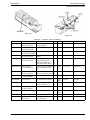
1
GM300 Mobile Radios 136-162 MHz 146-174 MHz 403-433 MHz 438-470 MHz 465-495 MHz 490-520 MHz Service Manual 6880902Z32-A Table of Contents Scope of Manual . . . . . . . . . . . . . . . . . . . . . . . . . . . . . . . . . . . . . . . . . . . . . . . . . . . . . . . . . . . . . . . . . . . . . . . . . . . . . . . iii How to Use This Manual. . . . . . . . . . . . . . . . . . . . . . . . . . . . . . . . . . . . . . . . . . . . . . . . . . . . . . . . . . . . . . . . . . . . . . . . iii Other Documentation . . . . . . . . . . . . . . . . . . . . . . . . . . . . . . . . . . . . . . . . . . . . . . . . . . . . . . . . . . . . . . . . . . . . . . . . . . iii Technical Support . . . . . . . . . . . . . . . . . . . . . . . . . . . . . . . . . . . . . . . . . . . . . . . . . . . . . . . . . . . . . . . . . . . . . . . . . . . . . . iii Service Policy. . . . . . . . . . . . . . . . . . . . . . . . . . . . . . . . . . . . . . . . . . . . . . . . . . . . . . . . . . . . . . . . . . . . . . . . . . . . . . . . . . iii Ordering Replacement Parts . . . . . . . . . . . . . . . . . . . . . . . . . . . . . . . . . . . . . . . . . . . . . . . . . . . . . . . . . . . . . . . . . . . . . iii Model Charts . . . . . . . . . . . . . . . . . . . . . . . . . . . . . . . . . . . . . . . . . . . . . . . . . . . . . . . . . . . . . . . . . . . . . . . . . . . . . . . . . . iv Accessories. . . . . . . . . . . . . . . . . . . . . . . . . . . . . . . . . . . . . . . . . . . . . . . . . . . . . . . . . . . . . . . . . . . . . . . . . . . . . . . . . . . xv SpeciÞcations . . . . . . . . . . . . . . . . . . . . . . . . . . . . . . . . . . . . . . . . . . . . . . . . . . . . . . . . . . . . . . . . . . . . . . . . . . . . . . . . xvii Section 1 Disassembly/Re-assembly Radio Disassembly and Assembly . . . . . . . . . . . . . . . . . . . . . . . . . . . . . . . . . . . . . . . . . . . . . . . . . . . . . . . . . . . . . . . 1-1 To Remove RF Chassis Shield . . . . . . . . . . . . . . . . . . . . . . . . . . . . . . . . . . . . . . . . . . . . . . . . . . . . . . . . . . . . . . . 1-1 To Remove the PA Heatsink. . . . . . . . . . . . . . . . . . . . . . . . . . . . . . . . . . . . . . . . . . . . . . . . . . . . . . . . . . . . . . . . . 1-1 To Remove the RF Circuit Boards . . . . . . . . . . . . . . . . . . . . . . . . . . . . . . . . . . . . . . . . . . . . . . . . . . . . . . . . . . . . 1-1 To Remove the Logic Circuit Board . . . . . . . . . . . . . . . . . . . . . . . . . . . . . . . . . . . . . . . . . . . . . . . . . . . . . . . . . . 1-2 To Remove the PA Circuit Board . . . . . . . . . . . . . . . . . . . . . . . . . . . . . . . . . . . . . . . . . . . . . . . . . . . . . . . . . . . . . 1-2 To Re-Assemble the Radio . . . . . . . . . . . . . . . . . . . . . . . . . . . . . . . . . . . . . . . . . . . . . . . . . . . . . . . . . . . . . . . . . . 1-2 Alignment . . . . . . . . . . . . . . . . . . . . . . . . . . . . . . . . . . . . . . . . . . . . . . . . . . . . . . . . . . . . . . . . . . . . . . . . . . . . . . . . . . . 1-4 Programming. . . . . . . . . . . . . . . . . . . . . . . . . . . . . . . . . . . . . . . . . . . . . . . . . . . . . . . . . . . . . . . . . . . . . . . . . . . . . . . . . 1-4 Recommended Test Equipment . . . . . . . . . . . . . . . . . . . . . . . . . . . . . . . . . . . . . . . . . . . . . . . . . . . . . . . . . . . . . . . . . 1-4 Board Replacement and Calibration . . . . . . . . . . . . . . . . . . . . . . . . . . . . . . . . . . . . . . . . . . . . . . . . . . . . . . . . . . . . . 1-4 Section 2 Theory of Operation RF Board. . . . . . . . . . . . . . . . . . . . . . . . . . . . . . . . . . . . . . . . . . . . . . . . . . . . . . . . . . . . . . . . . . . . . . . . . . . . . . . . . . . . . 2-1 VHF Receiver Front End, 146-174 MHz . . . . . . . . . . . . . . . . . . . . . . . . . . . . . . . . . . . . . . . . . . . . . . . . . . . . . . . 2-1 UHF Receiver Front End . . . . . . . . . . . . . . . . . . . . . . . . . . . . . . . . . . . . . . . . . . . . . . . . . . . . . . . . . . . . . . . . . . . 2-1 Receiver Back End . . . . . . . . . . . . . . . . . . . . . . . . . . . . . . . . . . . . . . . . . . . . . . . . . . . . . . . . . . . . . . . . . . . . . . . . . 2-2 Frequency Synthesizer . . . . . . . . . . . . . . . . . . . . . . . . . . . . . . . . . . . . . . . . . . . . . . . . . . . . . . . . . . . . . . . . . . . . . 2-2 Charge Pump . . . . . . . . . . . . . . . . . . . . . . . . . . . . . . . . . . . . . . . . . . . . . . . . . . . . . . . . . . . . . . . . . . . . . . . . . 2-5 Loop Filter . . . . . . . . . . . . . . . . . . . . . . . . . . . . . . . . . . . . . . . . . . . . . . . . . . . . . . . . . . . . . . . . . . . . . . . . . . . . 2-5 Reference Oscillator . . . . . . . . . . . . . . . . . . . . . . . . . . . . . . . . . . . . . . . . . . . . . . . . . . . . . . . . . . . . . . . . . . . . 2-5 VCOÕs and Buffers . . . . . . . . . . . . . . . . . . . . . . . . . . . . . . . . . . . . . . . . . . . . . . . . . . . . . . . . . . . . . . . . . . . . . . . . . 2-5 Logic Board . . . . . . . . . . . . . . . . . . . . . . . . . . . . . . . . . . . . . . . . . . . . . . . . . . . . . . . . . . . . . . . . . . . . . . . . . . . . . . . . . . 2-6 DC Distribution and Regulation . . . . . . . . . . . . . . . . . . . . . . . . . . . . . . . . . . . . . . . . . . . . . . . . . . . . . . . . . . . . . 2-6 Microcomputer and Logic . . . . . . . . . . . . . . . . . . . . . . . . . . . . . . . . . . . . . . . . . . . . . . . . . . . . . . . . . . . . . . . . . . 2-7 Microcomputer Start-Up Routine . . . . . . . . . . . . . . . . . . . . . . . . . . . . . . . . . . . . . . . . . . . . . . . . . . . . . . . . 2-7 Microcomputer Operation-Expanded Logic . . . . . . . . . . . . . . . . . . . . . . . . . . . . . . . . . . . . . . . . . . . . . . . 2-7 Reading or Writing in Memory-Expanded Logic . . . . . . . . . . . . . . . . . . . . . . . . . . . . . . . . . . . . . . . . . . . 2-8 Programmable I/OÕs . . . . . . . . . . . . . . . . . . . . . . . . . . . . . . . . . . . . . . . . . . . . . . . . . . . . . . . . . . . . . . . . . . . 2-8 Receiver Audio. . . . . . . . . . . . . . . . . . . . . . . . . . . . . . . . . . . . . . . . . . . . . . . . . . . . . . . . . . . . . . . . . . . . . . . . . . . . 2-8 Voice Path . . . . . . . . . . . . . . . . . . . . . . . . . . . . . . . . . . . . . . . . . . . . . . . . . . . . . . . . . . . . . . . . . . . . . . . . . . . . 2-8 Data Path . . . . . . . . . . . . . . . . . . . . . . . . . . . . . . . . . . . . . . . . . . . . . . . . . . . . . . . . . . . . . . . . . . . . . . . . . . . . . 2-9 Transmitter Audio . . . . . . . . . . . . . . . . . . . . . . . . . . . . . . . . . . . . . . . . . . . . . . . . . . . . . . . . . . . . . . . . . . . . . . . . . 2-9 Voice Path . . . . . . . . . . . . . . . . . . . . . . . . . . . . . . . . . . . . . . . . . . . . . . . . . . . . . . . . . . . . . . . . . . . . . . . . . . . . 2-9 Data Path . . . . . . . . . . . . . . . . . . . . . . . . . . . . . . . . . . . . . . . . . . . . . . . . . . . . . . . . . . . . . . . . . . . . . . . . . . . . . 2-9 Motorola,. All Rights Reserved Printed In U.S.A. 1997 68 No. i Table of Contents Name of Manual Transmitter Power Control. . . . . . . . . . . . . . . . . . . . . . . . . . . . . . . . . . . . . . . . . . . . . . . . . . . . . . . . . . . . . . . . . 2-10 Control Line Functions . . . . . . . . . . . . . . . . . . . . . . . . . . . . . . . . . . . . . . . . . . . . . . . . . . . . . . . . . . . . . . . . 2-10 Power Control Operation . . . . . . . . . . . . . . . . . . . . . . . . . . . . . . . . . . . . . . . . . . . . . . . . . . . . . . . . . . . . . . 2-10 RF Power AmpliÞers . . . . . . . . . . . . . . . . . . . . . . . . . . . . . . . . . . . . . . . . . . . . . . . . . . . . . . . . . . . . . . . . . . . . . . . . . 2-10 1-10 Watt VHF Power AmpliÞer . . . . . . . . . . . . . . . . . . . . . . . . . . . . . . . . . . . . . . . . . . . . . . . . . . . . . . . . . . . . 2-10 10-25 Watt VHF Power AmpliÞer . . . . . . . . . . . . . . . . . . . . . . . . . . . . . . . . . . . . . . . . . . . . . . . . . . . . . . . . . . . 2-11 25-45 Watt VHF Power AmpliÞer . . . . . . . . . . . . . . . . . . . . . . . . . . . . . . . . . . . . . . . . . . . . . . . . . . . . . . . . . . . 2-11 1-10 Watt UHF Power AmpliÞer . . . . . . . . . . . . . . . . . . . . . . . . . . . . . . . . . . . . . . . . . . . . . . . . . . . . . . . . . . . . 2-11 10-25 Watt UHF Power AmpliÞer . . . . . . . . . . . . . . . . . . . . . . . . . . . . . . . . . . . . . . . . . . . . . . . . . . . . . . . . . . . 2-12 25-35/40 Watt UHF Power AmpliÞers . . . . . . . . . . . . . . . . . . . . . . . . . . . . . . . . . . . . . . . . . . . . . . . . . . . . . . . 2-12 Front Panel Boards . . . . . . . . . . . . . . . . . . . . . . . . . . . . . . . . . . . . . . . . . . . . . . . . . . . . . . . . . . . . . . . . . . . . . . . . . . . 2-13 Display Board . . . . . . . . . . . . . . . . . . . . . . . . . . . . . . . . . . . . . . . . . . . . . . . . . . . . . . . . . . . . . . . . . . . . . . . . . . . . 2-13 Display Board (8/16 Freq Models) . . . . . . . . . . . . . . . . . . . . . . . . . . . . . . . . . . . . . . . . . . . . . . . . . . . . . . . . . . 2-13 Vol/Mic Board . . . . . . . . . . . . . . . . . . . . . . . . . . . . . . . . . . . . . . . . . . . . . . . . . . . . . . . . . . . . . . . . . . . . . . . . . . . 2-14 Front Panel Filter Board . . . . . . . . . . . . . . . . . . . . . . . . . . . . . . . . . . . . . . . . . . . . . . . . . . . . . . . . . . . . . . . . . . . 2-14 Section 3 Jumper-Selectable Options Overview . . . . . . . . . . . . . . . . . . . . . . . . . . . . . . . . . . . . . . . . . . . . . . . . . . . . . . . . . . . . . . . . . . . . . . . . . . . . . . . . . . . . 3-1 Jumper Positions . . . . . . . . . . . . . . . . . . . . . . . . . . . . . . . . . . . . . . . . . . . . . . . . . . . . . . . . . . . . . . . . . . . . . . . . . . . . . . 3-1 Section 4 Non-Field Servicable Components Operation of the Reference Oscillator . . . . . . . . . . . . . . . . . . . . . . . . . . . . . . . . . . . . . . . . . . . . . . . . . . . . . . . . . . . . 4-1 Non-Field Servicable Components. . . . . . . . . . . . . . . . . . . . . . . . . . . . . . . . . . . . . . . . . . . . . . . . . . . . . . . . . . . . . . . 4-1 Schematic Diagrams & Circuit Board Details Schematic Diagram for HLD8265A and HLD88266A VHF RF Boards, 136-162 MHz . . . . . . . . . . . . . . . . . . . . . .1 Circuit Board Details for HLD8265A and HLD8266A VHF RF Boards, 136-162 MHz . . . . . . . . . . . . . . . . . . . . .2 Schematic Diagram for HLD8029A and HLD8031A VHF RF Boards, 146-174 MHz . . . . . . . . . . . . . . . . . . . . . . .3 Circuit Board Details for HLD8029A and HLD8031A VHF RF Boards, 146-174 MHz . . . . . . . . . . . . . . . . . . . . .4 Schematic Diagram for HLE8229A and HLE8230A UHF RF Boards, 403-433 MHz . . . . . . . . . . . . . . . . . . . . . . .5 Circuit Board Details for HLE8229A and HLE8230A UHF RF Boards, 403-433 MHz . . . . . . . . . . . . . . . . . . . . . .6 Schematic Diagram for HLE8300A and HLE8301A UHF RF Boards, 438-470 MHz . . . . . . . . . . . . . . . . . . . . . . .7 Circuit Board Details for HLE8300A and HLE8301A UHF RF Boards, 438-470 MHz . . . . . . . . . . . . . . . . . . . . . .8 Schematic Diagram for HLE8263A and HLE8264A UHF RF Boards, 465-490 MHz . . . . . . . . . . . . . . . . . . . . . . .9 Circuit Board Details for HLE8263A and HLE8264A UHF RF Boards, 465-490 MHz . . . . . . . . . . . . . . . . . . . . .10 Schematic Diagram for HLE8227A and HLE8228A UHF RF Boards, 490-520 MHz . . . . . . . . . . . . . . . . . . . . . .11 Circuit Board Details for HLE8227A and HLE8228A UHF RF Boards, 490-520 MHz . . . . . . . . . . . . . . . . . . . . .12 Schematic Diagram for HLE8074A Masked Logic Board (2-Layer) (Sheet 1 of 2) . . . . . . . . . . . . . . . . . . . . . . . .13 Schematic Diagram for HLE8074A Masked Logic Board (2-Layer) (Sheet 2 of 2) . . . . . . . . . . . . . . . . . . . . . . . .14 Circuit Board Details for HLN8074A Masked Logic Board (2-Layer) . . . . . . . . . . . . . . . . . . . . . . . . . . . . . . . . . .15 Schematic Diagram for HLN8070A Expanded Logic Board (4-Layer) (Sheet 1 of 2) . . . . . . . . . . . . . . . . . . . . . .16 Schematic Diagram for HLN8070A Expanded Logic Board (4-Layer) (Sheet 2 of 2) . . . . . . . . . . . . . . . . . . . . . .17 Circuit Board Details for HLN8070A Expanded Logic Board (4-Layer) . . . . . . . . . . . . . . . . . . . . . . . . . . . . . . . .18 Circuit Board Details and Schematic for HLD8293A VHF Power Amplifier, 136-162 MHz, 10-25 Watts . . . . . . . . . . . . . . . . . . . . . . . . . . . . . . . . . . . . . . . . . . . . . . . .19 Circuit Board Details and Schematic For HLD8299A VHF Power Amplifier, 146-174 MHz, 1-10 Watts . . . . . . . . . . . . . . . . . . . . . . . . . . . . . . . . . . . . . . . . . . . . . . . . .20 Circuit Board Details and Schematic For HLD8033A VHF Power Amplifier, 146-174 MHz, 10-25 Watts . . . . . . . . . . . . . . . . . . . . . . . . . . . . . . . . . . . . . . . . . . . . . . . .21 Circuit Board Details and Schematic for HLD8287A VHF Power Amplifier, 146-174 MHz, 25-45 Watts . . . . . . . . . . . . . . . . . . . . . . . . . . . . . . . . . . . . . . . . . . . . . . . .22 ii 68 No. March, 1997 Name of Manual Table of Contents Circuit Board Details and Schematic for HLE8385A UHF Power Amplifier, 403-433 MHz, 1-10 Watts . . . . . . . . . . . . . . . . . . . . . . . . . . . . . . . . . . . . . . . . . . . . . . . . .23 Circuit Board Details and Schematic for HLE8275A UHF Power Amplifier, 403-433 MHz, 25-40 Watts . . . . . . . . . . . . . . . . . . . . . . . . . . . . . . . . . . . . . . . . . . . . . . . .24 Circuit Board Details and Schematic for HLE8267A UHF Power Amplifier, 438-470 MHz, 1-10 Watts . . . . . . . . . . . . . . . . . . . . . . . . . . . . . . . . . . . . . . . . . . . . . . . . .25 Circuit Board Details and Schematic for HLE8034A UHF Power Amplifier, 438-470 MHz, 10-25 Watts . . . . . . . . . . . . . . . . . . . . . . . . . . . . . . . . . . . . . . . . . . . . . . . .26 Circuit Board Details, and Schematic for HLE8271A UHF Power Amplifier, 438-470 MHz, 25-40 Watts . . . . . . . . . . . . . . . . . . . . . . . . . . . . . . . . . . . . . . . . . . . . . . . .27 Circuit Board Details and Schematic for HLE8284A UHF Power Amplifier, 465-495 MHz, 25-40 Watts . . . . . . . . . . . . . . . . . . . . . . . . . . . . . . . . . . . . . . . . . . . . . . . .28 Circuit Board Details and Schematic for HLE8269A UHF Power Amplifier, 490-520 MHz, 25-35 Watts . . . . . . . . . . . . . . . . . . . . . . . . . . . . . . . . . . . . . . . . . . . . . . . .29 Circuit Board Detail, Schematic and Parts List for Front Panel Filter Board (01-80704Y83) . . . . . . . . . . . . . . . .30 Schematic Diagram and Parts List for HLN8075A Display Board . . . . . . . . . . . . . . . . . . . . . . . . . . . . . . . . . . . . .31 Circuit Board Details for HLN8075A Display Board . . . . . . . . . . . . . . . . . . . . . . . . . . . . . . . . . . . . . . . . . . . . . . . .32 Circuit Board Detail, Schematic and Parts List for HLN8071A Volume/Microphone Board . . . . . . . . . . . . . .33 Exploded View, Schematic, Circuit Board Detail and Parts List for Microphone . . . . . . . . . . . . . . . . . . . . . . . .34 Exploded Mechanical View and Parts List for Radio . . . . . . . . . . . . . . . . . . . . . . . . . . . . . . . . . . . . . . . . . . . . . . . .35 Parts Lists for RF, Logic, & PA Boards RF Boards . . . . . . . . . . . . . . . . . . . . . . . . . . . . . . . . . . . . . . . . . . . . . . . . . . . . . . . . . . . . . . . . . . . . . . . . . . . . . . . . . . . . . . . Logic Boards . . . . . . . . . . . . . . . . . . . . . . . . . . . . . . . . . . . . . . . . . . . . . . . . . . . . . . . . . . . . . . . . . . . . . . . . . . . . . . . . . . . . PA Boards. . . . . . . . . . . . . . . . . . . . . . . . . . . . . . . . . . . . . . . . . . . . . . . . . . . . . . . . . . . . . . . . . . . . . . . . . . . . . . . . . . . . . . . March, 1997 68 No. iii Table of Contents iv Name of Manual 68 No. March, 1997 l Foreword Scope of Manual Scope of Manual tiÞcation number for all chassis, kits, and components. If you do not know a part number, include with your order the number of the chassis or kit which contains the part, and a detailed description of the desired component. If a Motorola part number is identiÞed on a parts list, you should be able to order the part through Motorola Parts. If only a generic part is listed, the part is not normally available through Motorola. If no parts list is shown, generally, no user serviceable parts are available for the kit. This manual is intended for use by experienced technicians familiar with similar types of equipment. It contains all service information required for the equipment described and is current as of the printing date. Changes which occur after the printing date are incorporated by instruction manual revision. These revisions are added to the manuals as the engineering changes are incorporated into the equipment. How to Use This Manual Technical Support Radius Product Services Hwy. 34 West Mt. Pleasant, IA 52641 USA 1-800-356-1520 319-385-5395 (International) This manual contains introductory material such as model charts, accessories, and speciÞcations, as well as four sections that deal with speciÞc service aspects of the GM300. Refer to the Table of Contents for a general overview of the manual, or to the ÒOverviewÓ paragraph in each section for a speciÞc overview of the information in that section. Radius 30-Day Warranty Radius Repair Depot Attention: Warranty Return 1000 W. Washington Street Mt. Pleasant, IA 52641 USA 1-800-356-1520 319-385-5395 (International) Other Documentation Table 1 lists other documentation for the GM300 Mobile Radios. Table 1. Information Radius Major Component Repair Radius Repair Depot 1000 W. Washington Street Mt. Pleasant, IA 52641 USA Location Basic Use of GM300 GM300 OwnerÕs Manual (6880902Z09) Programming GM300 RSS Basic Manual (6880902Z36) GM300 RSS RapidCall Manual (6880902Z64) Motorola Parts Worldwide System and Aftermarket Products Division Attention: Order Processing 1313 E. Algonquin Road Schaumburg, IL 60196 Technical Support To obtain technical support, you may call MotorolaÕs Radius Product Services. When you call, we ask that you have ready the model and serial numbers of the respective radio or its parts. Worldwide System and Aftermarket Products Division Attention: International Order Processing 1313 E. Algonquin Road Schaumburg, IL 60196 Service Policy If malfunctions occur within 30 days that cannot be resolved over the phone with Radius Product Services, a defective major component should be returned. You must obtain authorization from Radius Product Services before returning the component. Customer Service 1-800-422-4210 1-708-538-8198 (FAX) Ordering Replacement Parts You can order additional components and some piece parts directly through your Radius price pages. When ordering replacement parts, include the complete iden- March, 1997 Parts IdentiÞcation 1-708-538-0021 1-708-538-8194 68 No. iii Foreword Model Charts Item X X X Chassis, 12.5 kHz (Masked) HUD3833_ Chassis, 20/25/30 kHz (Masked) HUD3832_ Chassis, 12.5 kHz (Expanded) Chassis, 20/25/30 kHz (Expanded) X X X X HLD3850_ PA Kit (part of chassis) X X X X HCN3503_ Control Head, 8/16 Channel HLN8122_ X X HLN8123_ X X HHN8073_ X X HHN8170_ X X X X HLN8120_ X X HLN8121_ Logic Board Masked Logic Board, Expanded Display Board 8/16 Frequency Vol/Mic Board Front Panel Hardware, 8/16 Freq PA Board PA Hardware Chassis Hardware HLN8070_ HLN8075_ HLN8071_ HLN8072_ HLD8293_ HLN8295_ HLN8076_ RF Board 20/25/30 kHz HLD8265_ HLN8074_ RF Board 12.5 kHz HLD8266_ Description HUD3834_ X HUD3831_ X X DESCRIPTION GM300 VHF Mobile Radio 136 - 162 MHz 10 - 25 Watts RF Power ITEM GM300 20/25/30 kHz 16 M33GMC29C1A_ GM300 12.5 kHz GM300 20/25/30 kHz 16 M33GMC09C1A_ M33GMC20D1A_ 8 8 DESCRIPTION FREQ. MODEL M33GMC00D1A_ GM300 12.5 kHz Model Charts X X X X X X X X X X X X X X X X X Front Panel Lens, 8 Channel Front Panel Lens, 16 Channel Housing Kit, masked Housing Kit, expanded Nameplate ROM Kit X X X X HKN4137_ Power Cable X X X X HMN3413_ Microphone w/hangup clip X X X X HLN5189_ Installation Kit X X X X 6880902Z09 Owners Manual GM300 X X 6880902Z26 Operator Card 8 Channel X X 6880902Z41 Operator Card 16 Channel iv 68 No. March, 1997 Name of Manual Foreword Item X HUD3794_ X X Chassis, 12.5 kHz (Masked) HUD3792_ Chassis, 20/25/30 kHz (Masked) Chassis, 12.5 kHz (Expanded) X HUD3791_ Chassis, 20/25/30 kHz (Expanded) Control Head, 8/16 Channel X X Panel Lens 8 Channel X X HLN8123_ HHN8073_ X X HHN8170_ X X X X HLN8120_ X X HLN8121_ X X X X HKN4137_ Logic Board Masked Logic Board, Expanded Display Board 8/16 Frequency Vol/Mic Board Front Panel Hardware, 8/16 Freq PA Board PA Hardware Chassis Hardware HLN8070_ HLN8075_ HLN8071_ HLN8072_ HLD8299_ HLN8274_ HLN8076_ RF Board 20/25/30 kHz HLN8074_ RF Board 12.5 kHz HLD8031_ X X X X X X X X X X X X PA Kit (part of chassis) X X X X HCN3503_ HLN8122_ HLD8029_ Description HUD3793_ X X X X HLD3852_ X X DESCRIPTION GM300 VHF Mobile Radio 146 - 174 MHz 1 - 10 Watts RF Power ITEM GM300 20/25/30 kHz 16 M03GMC29C2A_ GM300 12.5 kHz GM300 20/25/30 kHz 16 M03GMC09C2A_ M03GMC20D2A_ 8 8 DESCRIPTION FREQ. MODEL M03GMC00D2A_ GM300 12.5 kHz Model Charts X X X X X Panel Lens 16 Channel Housing Kit, masked Housing Kit, expanded Nameplate ROM Kit Power Cable X X X X HMN3413_ Microphone w/hangup clip X X X X HLN5189_ Installation Kit X X X X 6880902Z09 Owners Manual GM300 X X 6880902Z26 Operator Card 8 Channel X X 6880902Z41 Operator Card 16 Channel March, 1997 68 No. v Foreword Name of Manual Item X X X HUD3409_ Chassis, 12.5 kHz (Masked) HUD3410_ Chassis, 20/25/30 kHz (Masked) HUD3570_ Chassis, 12.5 kHz (Expanded) X HUD3571_ Chassis, 20/25/30 kHz (Expanded) PA Kit (part of chassis) X X X X HCN3503_ Control Head, 8/16 Channel X X Front Panel Lens, 8 Channel HLN8122_ X X HLN8123_ HHN8073_ X X HHN8170_ X X X X HLN8120_ X X HLN8121_ Logic Board Masked Logic Board, Expanded Display Board 8/16 Frequency Vol/Mic Board Front Panel Hardware, 8/16 Freq PA Board PA Hardware Chassis Hardware HLN8070_ HLN8075_ HLN8071_ HLN8072_ HLD8033_ HLN8069_ HLN8076_ RF Board 20/25/30 kHz HLD8031_ HLN8074_ RF Board 12.5 kHz HLD8029_ Description X X X X HLD3502_ X X DESCRIPTION GM300 VHF Mobile Radio 146 - 174 MHz 10 - 25 Watts RF Power ITEM GM300 20/25/30 kHz 16 M33GMC29C2A_ GM300 12.5 kHz GM300 20/25/30 kHz 16 M33GMC09C2A_ M33GMC20D2A_ 8 8 DESCRIPTION FREQ. MODEL M33GMC00D2A_ GM300 12.5 kHz Model Charts X X X X X X X X X X X X X X X X X Front Panel Lens, 16 Channel Housing Kit, masked Housing Kit, expanded Nameplate ROM Kit X X X X HKN4137_ Power Cable X X X X HMN3413_ Microphone w/hangup clip X X X X HLN5189_ Installation Kit X X X X 6880902Z09 Owners Manual GM300 X X 6880902Z26 Operator Card 8 Channel X X 6880902Z41 Operator Card 16 Channel vi 68 No. March, 1997 Name of Manual Foreword Item X X X X HUD3931_ Chassis, 12.5 kHz (Masked) HUD3790_ Chassis, 20/25/30 kHz (Masked) HUD3930_ Chassis, 12.5 kHz (Expanded) HUD3823_ Chassis, 20/25/30 kHz (Expanded) X HUD3123_ Chassis, 20/25/30 kHz (Expanded) PA Kit (part of chassis) X X X X X HCN3503_ Control Head, 8/16 Channel HLN8122_ X X X HLN8123_ X X HHN8073_ X X X HHN8170_ X X X X X HLN8120_ X X X HLN8121_ PA Board Chassis Hardware HLN8076_ Front Panel Hardware, 8/16 Freq PA Hardware Vol/Mic Board HLN8071_ HLN8072_ HLN8289_ Display Board 8/16 Frequency HLN8075_ HLD8287_ Logic Board Masked Logic Board, Expanded RF Board 20/25/30 kHz HLD9002_ HLN8070_ RF Board 20/25/30 kHz HLD8031_ HLN8074_ RF Board 12.5 kHz HLD8029_ Description X X X X X HLD3848_ X X DESCRIPTION GM300 VHF Mobile Radio 146 - 174 MHz 25 - 45 Watts RF Power ITEM GM300 20/25/30 kHz 16 M43GMR29C2A_ GM300 12.5 kHz 16 M43GMC29C2A_ GM300 20/25/30 kHz 16 M43GMC09C2A_ GM300 20/25/30 kHz 8 8 M43GMC20D2A_ M43GMC00D2A_ DESCRIPTION FREQ. MODEL GM300 12.5 kHz Model Charts X X X X X X X X X X X X X X X X X X X X Front Panel Lens, 8 Channel Front Panel Lens, 16 Channel Housing Kit, masked Housing Kit, expanded Nameplate ROM Kit X X X X X HKN4137_ Power Cable X X X X X HMN3413_ Microphone w/hangup clip X X X X X HLN5189_ Installation Kit X X X X X 6880902Z09 Owners Manual GM300 X X 6880902Z26 Operator Card 8 Channel X X X 6880902Z41 Operator Card 16 Channel March, 1997 68 No. vii Foreword Name of Manual Item X X X Chassis, 12.5 kHz (Masked) HUE3945_ Chassis, 20/25 kHz (Masked) HUE3946_ Chassis, 12.5 kHz (Expanded) Chassis, 20/25 kHz (Expanded) X X X X HLE3929_ PA Kit (part of chassis) X X X X HCN3503_ Control Head, 8/16 Channel X X Front Panel Lens, 8 Channel HLN8122_ X X HLN8123_ X X HHN8073_ X X HHN8170_ X X X X HLN8120_ X X HLN8121_ X X X X HKN4137_ Logic Board Masked Logic Board, Expanded Display Board 8/16 Frequency Vol/Mic Board Front Panel Hardware, 8/16 Freq PA Board PA Hardware Chassis Hardware HLN8074_ HLN8070_ HLN8075_ HLN8071_ HLN8072_ HLE8385_ HLN8386_ HLN8076_ RF Board 20/25 kHz HLE8300_ DESCRIPTION Description HUE3944_ X HUE3947_ RF Board 12.5 kHz ITEM GM300 UHF Mobile Radio 403 - 433 MHz 1 - 10 Watts RF Power HLE8301_ GM300 20/25 kHz 16 M04GMC29C1A_ GM300 12.5 kHz GM300 20/25 kHz 16 M04GMC09C1A_ M04GMC20D1A_ 8 8 DESCRIPTION FREQ. MODEL M04GMC00D1A_ GM300 12.5 kHz Model Charts X X X X X X X X X X X X X X X X X Front Panel Lens, 16 Channel Housing Kit, masked Housing Kit, expanded Nameplate ROM Kit Power Cable X X X X HMN3413_ Microphone w/hangup clip X X X X HLN5189_ Installation Kit X X X X 6880902Z09 Owners Manual GM300 X X 6880902Z26 Operator Card 8 Channel X X 6880902Z41 Operator Card 16 Channel viii 68 No. March, 1997 Name of Manual Foreword Item X X X Chassis, 12.5 kHz (Masked) HUE3811_ Chassis, 20/25 kHz (Masked) HUE3810_ Chassis, 12.5 kHz (Expanded) X HUE3809_ Chassis, 20/25 kHz (Expanded) Control Head, 8/16 Channel X X Front Panel Lens, 8 Channel HLN8122_ X X HLN8123_ HHN8073_ X X HHN8170_ X X X X HLN8120_ X X HLN8121_ Logic Board Masked Logic Board, Expanded Display Board 8/16 Frequency Vol/Mic Board Front Panel Hardware, 8/16 Freq PA Board PA Hardware Chassis Hardware HLN8074_ HLN8070_ HLN8075_ HLN8071_ HLN8072_ HLE8275_ HLN8277_ HLN8076_ RF Board 20/25 kHz HLE8229_ X X X X X X X X X X X X PA Kit (part of chassis) X X X X HCN3503_ X X DESCRIPTION Description HUE3812_ X X X X HLE3853_ RF Board 12.5 kHz ITEM GM300 UHF Mobile Radio 403 - 433 MHz 25 - 40 Watts RF Power HLE8230_ GM300 20/25 kHz 16 M44GMC29C1A_ GM300 12.5 kHz GM300 20/25 kHz 16 M44GMC09C1A_ M44GMC20D1A_ 8 8 DESCRIPTION FREQ. MODEL M44GMC00D1A_ GM300 12.5 kHz Model Charts X X X X X Front Panel Lens, 16 Channel Housing Kit, masked Housing Kit, expanded Nameplate ROM Kit X X X X HKN4137_ Power Cable X X X X HMN3413_ Microphone w/hangup clip X X X X HLN5189_ Installation Kit X X X X 6880902Z09 Owners Manual GM300 X X 6880902Z26 Operator Card 8 Channel X X 6880902Z41 Operator Card 16 Channel March, 1997 68 No. ix Foreword Name of Manual Item X X X Chassis, 12.5 kHz (Masked) HUE3815_ Chassis, 20/25 kHz (Masked) HUE3814_ Chassis, 12.5 kHz (Expanded) Chassis, 20/25 kHz (Expanded) X X X X HLE3770_ PA Kit (part of chassis) X X X X HCN3503_ Control Head, 8/16 Channel X X Front Panel Lens, 8 Channel HLN8122_ X X HLN8123_ X X HHN8073_ X X HHN8170_ X X X X HLN8120_ X X HLN8121_ Logic Board Masked Logic Board, Expanded Display Board 8/16 Frequency Vol/Mic Board Front Panel Hardware, 8/16 Freq PA Board PA Hardware Chassis Hardware HLN8074_ HLN8070_ HLN8075_ HLN8071_ HLN8072_ HLE8267_ HLN8268_ HLN8076_ RF Board 20/25 kHz HLE8300_ DESCRIPTION Description HUE3816_ X HUE3813_ RF Board 12.5 kHz ITEM GM300 UHF Mobile Radio 438 - 470 MHz 1 - 10 Watts RF Power HLE8301_ GM300 20/25 kHz 16 M04GMC29C3A_ GM300 12.5 kHz GM300 20/25 kHz 16 M04GMC09C3A_ M04GMC20D3A_ 8 8 DESCRIPTION FREQ. MODEL M04GMC00D3A_ GM300 12.5 kHz Model Charts X X X X X X X X X X X X X X X X X Front Panel Lens, 16 Channel Housing Kit, masked Housing Kit, expanded Nameplate ROM Kit X X X X HKN4137_ Power Cable X X X X HMN3413_ Microphone w/hangup clip X X X X HLN5189_ Installation Kit X X X X 6880902Z09 Owners Manual GM300 X X 6880902Z26 Operator Card 8 Channel X X 6880902Z41 Operator Card 16 Channel x 68 No. March, 1997 Name of Manual Foreword Item X X X Chassis, 12.5 kHz (Masked) HUE3819_ Chassis, 20/25 kHz (Masked) HUE3818_ Chassis, 12.5 kHz (Expanded) X HUE3817_ Chassis, 20/25 kHz (Expanded) Control Head, 8/16 Channel X X Front Panel Lens, 8 Channel HLN8122_ X X HLN8123_ HHN8073_ X X HHN8170_ X X X X HLN8120_ X X HLN8121_ Logic Board Masked Logic Board, Expanded Display Board 8/16 Frequency Vol/Mic Board Front Panel Hardware, 8/16 Freq PA Board PA Hardware Chassis Hardware HLN8074_ HLN8070_ HLN8075_ HLN8071_ HLN8072_ HLE8034_ HLN8068_ HLN8076_ RF Board 20/25 kHz HLE8300_ X X X X X X X X X X X X PA Kit (part of chassis) X X X X HCN3503_ X X DESCRIPTION Description HUE3820_ X X X X HLE3501_ RF Board 12.5 kHz ITEM GM300 UHF Mobile Radio 438 - 470 MHz 10 - 25 Watts RF Power HLE8301_ GM300 20/25 kHz 16 M34GMC29C3A_ GM300 12.5 kHz GM300 20/25 kHz 16 M34GMC09C3A_ M34GMC20D3A_ 8 8 DESCRIPTION FREQ. MODEL M34GMC00D3A_ GM300 12.5 kHz Model Charts X X X X X Front Panel Lens, 16 Channel Housing Kit, masked Housing Kit, expanded Nameplate ROM Kit X X X X HKN4137_ Power Cable X X X X HMN3413_ Microphone w/hangup clip X X X X HLN5189_ Installation Kit X X X X 6880902Z09 Owners Manual GM300 X X 6880902Z26 Operator Card 8 Channel X X 6880902Z41 Operator Card 16 Channel March, 1997 68 No. xi Foreword Name of Manual Item X X X Chassis, 12.5 kHz (Masked) HUE3822_ Chassis, 20/25 kHz (Masked) HUE3917_ Chassis, 12.5 kHz (Expanded) Chassis, 20/25 kHz (Expanded) X X X X HLE3772_ PA Kit (part of chassis) X X X X HCN3503_ Control Head, 8/16 Channel X X Front Panel Lens, 8 Channel HLN8122_ X X HLN8123_ X X HHN8073_ X X HHN8170_ X X X X HLN8120_ X X HLN8121_ Logic Board Masked Logic Board, Expanded Display Board 8/16 Frequency Vol/Mic Board Front Panel Hardware, 8/16 Freq PA Board PA Hardware Chassis Hardware HLN8074_ HLN8070_ HLN8075_ HLN8071_ HLN8072_ HLE8271_ HLN8272_ HLN8076_ RF Board 20/25 kHz HLE8300_ DESCRIPTION Description HUE3918_ X HUE3821_ RF Board 12.5 kHz ITEM GM300 UHF Mobile Radio 438 - 470 MHz 25 - 40 Watts RF Power HLE8301_ GM300 20/25 kHz 16 M44GMC29C3A_ GM300 12.5 kHz GM300 20/25 kHz 16 M44GMC09C3A_ M44GMC20D3A_ 8 8 DESCRIPTION FREQ. MODEL M44GMC00D3A_ GM300 12.5 kHz Model Charts X X X X X X X X X X X X X X X X X Front Panel Lens, 16 Channel Housing Kit, masked Housing Kit, expanded Nameplate ROM Kit X X X X HKN4137_ Power Cable X X X X HMN3413_ Microphone w/hangup clip X X X X HLN5189_ Installation Kit X X X X 6880902Z09 Owners Manual GM300 X X 6880902Z26 Operator Card 8 Channel X X 6880902Z41 Operator Card 16 Channel xii 68 No. March, 1997 Name of Manual Foreword Item X X X Chassis, 12.5 kHz (Masked) HUE3841_ Chassis, 20/25 kHz (Masked) HUE3840_ Chassis, 12.5 kHz (Expanded) X HUE3839_ Chassis, 20/25 kHz (Expanded) Control Head, 8/16 Channel X X Front Panel Lens, 8 Channel HLN8122_ X X HLN8123_ HHN8073_ X X HHN8170_ X X X X HLN8120_ X X HLN8121_ Logic Board Masked Logic Board, Expanded Display Board 8/16 Frequency Vol/Mic Board Front Panel Hardware, 8/16 Freq PA Board PA Hardware Chassis Hardware HLN8074_ HLN8070_ HLN8075_ HLN8071_ HLN8072_ HLE8284_ HLN8286_ HLN8076_ RF Board 20/25 kHz HLE8263_ X X X X X X X X X X X X PA Kit (part of chassis) X X X X HCN3503_ X X DESCRIPTION Description HUE3842_ X X X X HLE3847_ RF Board 12.5 kHz ITEM GM300 UHF Mobile Radio 465 - 495 MHz 25 - 40 Watts RF Power HLE8264_ GM300 20/25 kHz 16 M44GMC29C4A_ GM300 12.5 kHz GM300 20/25 kHz 16 M44GMC09C4A_ M44GMC20D4A_ 8 8 DESCRIPTION FREQ. MODEL M44GMC00D4A_ GM300 12.5 kHz Model Charts X X X X X Front Panel Lens, 16 Channel Housing Kit, masked Housing Kit, expanded Nameplate ROM Kit X X X X HKN4137_ Power Cable X X X X HMN3413_ Microphone w/hangup clip X X X X HLN5189_ Installation Kit X X X X 6880902Z09 Owners Manual GM300 X X 6880902Z26 Operator Card 8 Channel X X 6880902Z41 Operator Card 16 Channel March, 1997 68 No. xiii Foreword Name of Manual Item X X X Chassis, 12.5 kHz (Masked) HUE3837_ Chassis, 20/25 kHz (Masked) HUE3836_ Chassis, 12.5 kHz (Expanded) Chassis, 20/25 kHz (Expanded) X X X X HLE3771_ PA Kit (part of chassis) X X X X HCN3503_ Control Head, 8/16 Channel X X Front Panel Lens, 8 Channel HLN8122_ X X HLN8123_ X X HHN8073_ X X HHN8170_ X X X X HLN8120_ X X HLN8121_ Logic Board Masked Logic Board, Expanded Display Board 8/16 Frequency Vol/Mic Board Front Panel Hardware, 8/16 Freq PA Board PA Hardware Chassis Hardware HLN8074_ HLN8070_ HLN8075_ HLN8071_ HLN8072_ HLE8269_ HLN8270_ HLN8076_ RF Board 20/25 kHz HLE8227_ DESCRIPTION Description HUE3838_ X HUE3835_ RF Board 12.5 kHz ITEM GM300 UHF Mobile Radio 490 - 520 MHz 25 - 35 Watts RF Power HLE8228_ GM300 20/25 kHz 16 M44GMC29C5A_ GM300 12.5 kHz GM300 20/25 kHz 16 M44GMC09C5A_ M44GMC20D5A_ 8 8 DESCRIPTION FREQ. MODEL M44GMC00D5A_ GM300 12.5 kHz Model Charts X X X X X X X X X X X X X X X X X Front Panel Lens, 16 Channel Housing Kit, masked Housing Kit, expanded Nameplate ROM Kit X X X X HKN4137_ Power Cable X X X X HMN3413_ Microphone w/hangup clip X X X X HLN5189_ Installation Kit X X X X 6880902Z09 Owners Manual GM300 X X 6880902Z26 Operator Card 8 Channel X X 6880902Z41 Operator Card 16 Channel xiv 68 No. March, 1997 Name of Manual Foreword Accessories Accessories Radius offers many accessories to increase communications efÞciency. Some of the accessories available are listed below. For a complete list, consult your Radius dealer. Antennas: HAD4007_R HAD4008_R HAD4009_R HAD4014_R HAE4003_R HAE4011_R HAE4019_R HAE4002_R HAE4010_R HAE4004_R HAE4012_R HAE4013_R VHF 146-150.8 MHz, 1/4 wave roof mount VHF 150.8-162 MHz, 1/4 wave roof mount VHF 162-174 MHz, 1/4 wave roof mount VHF 146-172 MHz, 3db gain roof mount UHF 450-470 MHz, 1/4 wave roof mount UHF 450-470 MHz, 3.5 db gain roof mount UHF 450-470 MHz, 5 db gain roof mount UHF 403-430 MHz, 1/4 wave roof mount UHF 406-420 MHz, 3.5 db gain roof mount UHF 470-512 MHz, 1/4 wave roof mount UHF 470-494 MHz, 3.5 db gain roof mount UHF 494-512 MHz, 5 db gain roof mount Installation Accessories: HLN9284_R HLN5189_R HLN5226_R HLN9450_R HLN9404_R HKN4137_R HLN5282_R HKN9557_R HLN8027_R HLN8097_R HLN8098_R HLN8099_R HLN8413_ HLN8143_R HLN8144_R HLN9027_ Key lock mount Non-locking bracket Extra stability mount (use with HLN5189) 45 - 60 degree ßoor mount wedge (requires HLN9404) Sleeve mounting bracket Power cable w/ 15 Amp fuse Mini-UHF connector PL259/Mini-UHF antenna adapter - 8 inch cable Mini-UHF to BNC antenna adapter Removable slide mount tray package Radio slide mount tray Vehicle slide mount tray Slidemount tray bracket Remote mount kit (17 foot length) Remote mount kit (8 foot length) In-Dash mounting kit Control Station Accessories: HMN1038_R HMN3000_ HPN1007_R HPN4001_R HKN4139_R HKN9455_R Desk Microphone Desk Microphone (black) Power supply, 117 Vac (for 25 Watt or less radio models only) 1 Power supply and cables, 117 Vac (for any radio model up to 45 Watts) Low power control station power cable (for HPN1007_R) High power control station power cable (for HPN4001_R) Microphones: HMN3596_R HMN1035_R HMN1037_R TDN8305_R TMN6169_R HMN3141_R HLN9559_R HLN9560_R HLN9073_R Compact Microphone with 7 foot cord Heavy Duty Palm Microphone with 10.5 foot cord Touch-code Microphone with hang-up clip Touch-code Microphone with backlit keypad & hang-up clip Touch-code Microphone with memory dial, backlit keypad & hang-up clip Handset with hang-up cup 7 foot coil cord Heavy Duty Microphones 10.5 foot extended coil cord for Heavy Duty Microphones Microphone hang-up clip (all microphones) 1. Convertible to 230 Vac by changing internal switch and modifying the power cord. March, 1997 68 No. xv Foreword Name of Manual Accessories Accessories / Kits Interfacing with the 16 Pin Connector: HKN9327_R HSN8145_R HLN9457_R HLN9328_R HLN9329_R HLN9330_R HLN8375_R HLN3145_R HLN3333_ TDN8300_ TDN8301_ L1661 TDN8196 TDN7891 TDN7892 HLN9573_R Ignition switch cable 7.5 Watt external speaker - for receiver audio Hardware kit-includes 16 connector pins, (9) 8Ó wires with pins & extra housing Horn/Lights relay and cable (external alarm) Emergency pushbutton switch and cable Emergency footswitch and cable DTMF Decoder board (mounts inside radio - soldering required) Public Address kit 2 Repeater Interface kit DC Remote Adapter - 2 channel operation (requires at least one L1662 deskset) Tone Remote Adapter - 2 channel operation (requires at least one L1663 deskset) C100 Extended Local Deskset i50X Low Tier Radio-Telephone Interconnect and cable i150X Mid Tier Radio-Telephone Interconnect and cable i250X High Tier Radio-Telephone Interconnect and cable Shorting Plug - Þlls microphone jack when no microphone is being used Manuals: 6880902Z26 6880902Z41 6880902Z09 6880902Z32 OperatorÕs card - GM300 8 channel radios OperatorÕs card - GM300 16 channel radios OwnerÕs manual - GM300 Service manual - GM300 2. The Public Address kit allows from one to five HSN1000_ amplified speakers. A minimum of one HSN1000_ speaker is required. One HKN9323_R (8 foot) cable or one HKN9324_R (15 foot) cable is required for each HSN1000_ speaker. xvi 68 No. March, 1997 Name of Manual Foreword Specifications Specifications GENERAL VHF Model Series: Frequency Range: M03GMC M33GMC 146-174 MHz 136-162 MHz RF Output: 1-10 W* UHF M33GMC M43GMC M43GMR 146-174 MHz 10-25 W* M04GMC 403-433 MHz 45 W 25-45 W M44GMC M44GMC 438-470 MHz 403-433 MHz 438-470 MHz 465-495 MHz 490-520 MHz 25/40 W 25/35 W 1-10 W* Channel Capacity: M44GMC 10-25 W* 25/40 W 25-40 W* 32 MHz 30 MHz 32 MHz M44GMC 8 or 16 Frequency Separation: 28 MHz 32 MHz Primary Input Voltage EIA: CEPT 84: FCC Designation: 438-470 MHz M34GMC 30 MHz 13.8 ±10% 13.2 ±20% ABZ99FT3032 ?? ABZ99FT3030 ABZ99FT3033 ?? ?? ABZ99FT4033 ABZ99FT4030 ABZ99FT4032 ABZ99FT4034 Typical Current Drain Rated Audio (7.5 W): Pending Pending 1.5A Transmit: 4.0A ?? 7.0A 15.0A ?? ?? Standby: 4.0A 7.5A 12.5A 400 mA Squelch Capability: Tone Coded, Digital Coded and/or Carrier Squelch Dimensions: 2Ó x 7Ó x 7.75Ó (50.8 x 178 x 198 mm) Weight: 61 z. (1.7 kg) *Continuously variable power MILITARY STANDARDS 810 C, D, & E TRANSMITTER VHF Applicable MIL-STD Frequency Stability (-30ûC to +60ûC): ±.00025% Spurs/Harmonics 1 to 25 W: >25 W: Exceptions: -36 dBm (0.25 µW) -13 dBm (50 µW) (403-433 MHz)/-36 dBm (0.25 µW) Audio Response: (From a 6 dB/Oct. Pre-Emphasis 300-3000 Hz, 2550 Hz @ 12.5 kHz) +1 / -3 dB Audio Distrotion: (@ 1000 Hz, 60% of Rated Max. Deviation) <3% EIA FCC Modulation @20/25/30 kHz: @12.5 kHz: Methods 810E Procedures Methods Procedures Low Pressure: 500.1 1 500.2 1 500.3 1 High Temperature: 501.1 1, 2 501.2 1, 2 501.3 1, 2 Low Temperature: 502.1 1 502.2 1, 2 502.3 1, 2 Temperature Shock: 503.1 1 503.2 1 503.3 1 Solar Radiation: 505.1 1 505.2 1 505.3 1 Rain: 506.1 2 506.2 2 506.3 2 Humidity: 507.1 2 507.2 2 507.3 2 Salt Fog: 509.1 1 509.2 1 509.3 1 Dust: 510.1 1 510.2 1 510.3 1 Vibration: 514.2 8, 10 514.3 1 514.4 1 Shock: 516.2 1, 3, 5 516.3 1, 5 516.4 1, 5 VHF 80 mV for 60% max. deviation at 1000 Hz 20/25/30 kHz 12.5 kHz 20/25/30 kHz 12.5 kHz 45 dB 55 dB 40 dB 50 dB 40 dB 50 dB 35 dB 45 dB Available in 16-Channel Models Only Signalling Format: encode/decode PTT ID Call Alert X Quick-Call II: X X DTMF: X Start (encode only): X X UHF Channel Spacing: 12.5 kHz 20/25/30 kHz 12.5 kHz 20/25 kHz Sensitivity EIA: 12 dB SINAD: CEPT 84: 20 dB SINAD: 0.35 µV 0.45 µV 0.30 µV 0.40 µV 0.35 µV 0.45 µV 0.30 µV 0.40 µV Squelch: OPTIONAL SIGNALLING FEATURES WITH RAPIDCALL PACKAGE MDC-1200: Procedures RECEIVER 50 ohms Modulation Sensitivity: FM Noise EIA: CEPT 84: 810D Methods 16KOF1D, 16KOF2D, 16KOF3E, 11KOF1D, 11KOF2D, 11KOF3E Output Impedance: Channel Spacing: 810C UHF Voice SelCall Emergency Radio Check X X X 10 dB SINAD Selectivity EIA: CEPT 84: -70 dB -70 dB -80 dB -80 dB -65 dB -65 dB -75 dB -75 dB Intermodulation* EIA: CEPT 84: -70 dB -73 dB -78 dB -73 dB -65 dB -70 dB -75 dB -70 dB Frequency Stability: (-30ûC to +60ûC) X X X Also includes Singletone Repeater Access & DTMF - ANI for Phone Access & Select V Signalling. ±.00025% Spur Rejection EIA: CEPT 84: -80 dB -75 dB -75 dB -70 dB Image Rejection EIA: CEPT 84: -80 dB -80 dB -75 dB -75 dB Audio Output: External Speaker (8Ω) EIA (@ <5% Dist): CEPT 84 (@ <10% Dist.): Internal Speaker: EIA Usable Bandwidth: Input Impedance: 7.5 W 5.0 W 3.0 W Nominal 1.2 kHz 20. kHz 1.2 kHz 2.0 kHz 50 Ω * Local mode provides an additional 10 dB protection against wideband interference. March, 1997 68 No. xvii Foreword Name of Manual Specifications xviii 68 No. March, 1997 Section 1 Disassembly/Re-assembly Radio Disassembly / Re-assembly Radio Disassembly and Assembly To Remove Control Head & Chassis Covers 1. Remove control (Figure 1-1). head mounting screws 2. Pull control head off and away from the radio. 3. Carefully remove control head connectors from chassis. 4. Remove the two chassis cover screws from each side (Figure 1-1). 5. Remove top and bottom covers from chassis. Figure 1-2. COVER SCREWS TOP COVER CONTROL HEAD MOUNTING SCREWS COVER COAX CABLES SCREWS CONTROL HEAD Figure 1-3. Figure 1-1. 3. Remove the (Figure 1-4). 4. Pull heatsink off of chassis while carefully feeding the transmit and receive coax cables through their respective holes in the chassis. To Remove RF Chassis Shield Remove RF chassis shield by prying each of the four corners at the indentations provided (Figure 1-2). Be careful not to over bend any one corner. To Remove the PA Heatsink 1. Disconnect the transmit and receive coaxial cables from the RF board (Figure 1-3). 2. Disconnect the 6-pin connector from the logic board (Figure 1-4). mounting screws To Remove the RF Circuit Boards 1. March, 1997 heatsink 68 No. After the PA heatsink has been removed, pry off the RF shield (Figure 1-5). Be careful not to over bend any one corner or side. 1-1 Disassembly/Re-assembly Name of Manual Radio Disassembly and Assembly LOGIC BOARD MOUNTING SCREWS 6-PIN CONNECTOR HEATSINK MOUNTING SCREWS Figure 1-4. 2. FILTER BOARD After removing the RF shield, remove all RF board mounting screws and take out the RF board (Figure 1-5). FILTER BOARD SCREWS Figure 1-6. RF BOARD MOUNTING SCREWS RF SHIELD Figure 1-5. Figure 1-7. To Remove the Logic Circuit Board 1. After the RF board has been removed, turn the radio over and pry off the logic shield, again being careful not to bend any one corner or side. 3. Unsolder the A+ power connector feed-thru leads and the antenna connector lead (Figure 1-9). 2. Remove all logic board mounting screws (Figure 1-6). 4. 3. Remove the two Þlter board screws from the front of the chassis (Figure 1-6). The logic and Þlter boards can now be lifted out of the chassis. UHF ONLY - Remove the stud mount transistor mounting nut from the back of the heatsink (Figure 1-8). 5. Remove two power device mounting screws and all PA board mounting screws (Figure 1-9), and then take out the PA board. To Remove the PA Circuit Board 1-2 1. Remove the power ampliÞer shield by carefully prying each corner and side until you can slide the shield off easily (Figure 1-7). To Re-Assemble the Radio 2. Remove the shield completely by guiding the coaxial cables out. Reverse the disassembly procedure and tighten all screws to the torques speciÞed in Table 1-1. 68 No. March, 1997 Name of Manual Disassembly/Re-assembly Radio Disassembly and Assembly Figure 1-8. Figure 1-9. Table 1-1. Part Number Description 03-10945A11 M3 x 8 Plastite Slt Torx¨ Pan Hd. 03-80270L01 M4 x 0.7 x 38 Mach. Torx¨ Cap Scr Blk 03-80271L01 M4 x 0.7 x 27 Mach. Slt Torx¨ Pan Hd Blk 03-10943M04 M2.5 x 8 Taptite Slt Torx¨ Pan Hd 03-10943M09 M3 x 6 Taptite Slt Torx¨ Pan Hd 03-10943M10 M3 x 8 Taptite Slt Torx¨ Pan Hd 03-10943M11 M3 x 10 Taptite Slt Torx¨ Pan Hd 03-10943R55 M3 x 8 Taptite Torx¨ Flt Hd Blk 02-00007003 Hex Nut 8-32 04-00136334 Flat Washer 04-80943V01 Washer-Lock 3/8 Ext., Stl. Zinc 09-80131M01 3/8 Nut 38-80041M01 Plug, button 03-11994A23 5-20 x 7/8Ó Plastite Phl Pan Hd March, 1997 Fasteners, Tools and Torques Location Qty Drv Control Head Board and 9 T10 Internal Speaker Control Head Mount 2 T15 Input Torq. 8 in.-lbs. Repair Torq. 8 in.-lbs. 8 in.-lbs. 8 in.-lbs. Heatsink Mount 2 T15 12-14 in.-lbs. 12-14 in.-lbs. Logic Heatsink Device Mount RF Board Mount Logic Board Mount Chassis Feedthru Plt Front Panel Filter Board PA Device/Board Mount Logic Heatsink to Chassis Power Connector Device to Logic Heatsink Chassis Covers 2 T8 6-8 in.-lbs. 4-6 in.-lbs. 7 6 2 2 8 2 T10 8-10 in.-lbs. 6-8 in.-lbs. T10 11-13 in.-lbs. 8-10 in.-lbs. 2 2 4 T10 9-11 in.-lbs. 7-9 in.-lbs. T10 8-10 in.-lbs. 6-8 in.-lbs. PA - Stud Device Mount 1 5 in.-lbs. 5 in.-lbs. Device to Logic Heatsink Power Connector Antenna Connector 2 2 1 5/16Ó Hex ---- ---- ---- Antenna Connector 1 18-20 in.-lbs. 18-20 in.-lbs Heatsink Plug Mic. Rear Housing to Front Housing 1 3 3/8Ó Hex -1 -9-11 in.-lbs. -9-11 in.-lbs. 68 No. 1-3 Disassembly/Re-assembly Name of Manual Alignment Alignment Recommended Test Equipment The advanced design and manufacturing procedures eliminate the need for traditional tuning tasks. R2001D: Communication Systems Analyzer or All the circuits in the GM300 radio have been aligned at the factory with specialized equipment. R2200B: Service Monitor Alignment in the Þeld should not be attempted or necessary. R1011B: Power Supply Programming R1037A: Digital Multimeter or The GM300 radios can be programmed in the Þeld to these parameters: R1024B: Digital Multimeter ¥ Receive and transmit frequencies Board Replacement and Calibration ¥ Transmit Frequency Adjustment (warp) ¥ PL or DPL encode and decode Codes Replacement of the Logic board, RF board, or Power AmpliÞer requires that recalibration must be performed with the Motorola Radio Service Software. The procedures for calibration are covered in the GM300 Radio Service Software Manual. ¥ Transmit Power Output ¥ Transmit Deviation ¥ Time Out Timer Failure to perform the required calibration procedure will affect the performance of the Reference Oscillator, RF Power Leveling and Protection, and Transmitter Modulation over frequency and temperature. An uncalibrated radio may not comply with your Local Communications Agency rules and may be unreliable at temperature extremes. ConÞguration information for programming these parameters is contained in the GM300 RADIO SERVICE SOFTWARE package HVN8177 Version B04.03.00 (or later versions )for 5.25 inch drives and 3.5 inch drive diskettes must be used. A personal computer (P.C.) and the appropriate software diskette will be required in addition to the items listed in Recommended Test Equipment. The GM300 radio was designed to be serviced at the board level only. There are a number of non-Þeld serviceable parts in the radio. Field replacement of these parts will affect the factory calibrated numbers on the tuning label. If any of these parts fail, board replacement is the only way to service the radio. We strongly suggest the servicer become familiar with the programming techniques applicable to the GM300 radios. Table 1-2. Tone 1. High pitch Beep (900Hz 119ms) on initial turn on or when key is pressed. 2. Low pitched tone (163Hz) for 5 seconds following turn on. 3. Low frequency (163Hz) continuous tone present whenever radio is on. 4. Low pitch beep (300Hz 200 MS) when a button is pressed. 5. Low frequency (150Hz or 112.5Hz) continuous tone while PTT is held. 1-4 Error Tones Problem 1. Normal operation - no error. 2. Code plug error. For all code plug errors try to re-program radio. If this does not clear the fault or if problem recurs, replace the logic board 3. Logic board failure. Replace logic board. 4. Button is not allowed in the current operating condition. Change operating condition (select another mode, etc.) 5. Transmit is not allowed. If it was time-out-timer, you may release PTT then continue your call. 68 No. March, 1997 Theory of Operation RF Board +13 dBm is delivered to the Þrst mixer from the second RX buffer in the synthesizer circuit. VHF Receiver Front End, 146-174 MHz The mixer output is connected to a diplexer network which matches its output to the Þrst IF ampliÞer Q51 at the IF frequency of 45.1 MHz, and terminates it in a 50 ohm resistor, R51, at all other frequencies. The received signal applied to the radioÕs antenna input connector is Þrst routed through the harmonic Þlter/antenna switch on the RF Power AmpliÞer Board, and then applied via coax to J4 on the RF Board. The insertion loss of the harmonic Þlter/antenna switch is less than 1 dB. UHF Receiver Front End The signal applied to J4 is routed to a Þxed-tuned 4pole Þlter having a 3 dB bandwidth of 57 MHz and a 1 dB bandwidth of 37 MHz centered at 160 MHz. Insertion loss is 1.5 dB typically, and 2 dB at 146 MHz. Attenuation for image protection is 32 dB at 236 MHz, with increasing attenuation at higher frequencies. The received signal applied to the radioÕs antenna input connector is Þrst routed through the harmonic Þlter/antenna switch on the RF Power AmpliÞer Board, and then applied via coax to J4 on the RF Board. The insertion loss of the harmonic Þlter/antenna switch is less than 1 dB. The output of the Þlter is matched to the base of RF ampliÞer Q1, which provides 12 dB of gain and has a noise Þgure of 3.6 dB. Current source Q2 is used to maintain the collector current of Q1 constant at 26 mA. Diode CR2 clamps excessive input signals, protecting Q1. The signal applied to J4 is routed to a Þxed-tuned 3pole shunt resonator Þlter having the following characteristics: The output of Q1 is applied to a 3-pole Þxed-tuned Þlter having a 3 dB bandwidth of 59 MHz and a 1 dB bandwidth of 48 MHz centered at 160 MHz. Insertion loss is 1.3 dB. Attenuation for image protection is 35 dB at 236 MHz, with increasing attenuation at higher frequencies. Additional image protection is provided by the transmitter harmonic Þlter, which provides at least 20 dB of attenuation at 236 MHz and above. 403-433 438-470 465-495 490-520 41 MHz 77 MHz 3 dB 418 MHz 33 dB 343 MHz 45 MHz 65 MHz 1.8 dB 455 MHz 30 dB 380 MHz 40 MHz 60 MHz 2.2 dB 480 MHz 35 dB 405 MHz 40 MHz 55 MHz 2.2 dB 510 MHz 37 dB 430 MHz Attenuation for image protection increases for frequencies lower than fIMAGE. A pin diode attenuator is located between the 3-pole Þlter and the Þrst mixer. In the Distance mode, Q5 and Q6 are turned on, CR5 is forward-biased which bypasses R12, and no loss is introduced. In the Local mode, Q5, Q6 and CR5 are off, inserting 10 dB of attenuation due to R12. Because the attenuator is located after the RF ampliÞer, receiver sensitivity is reduced only by 5 dB, while the overall third order input intercept is raised by 15 dB. Thus, the Local mode signiÞcantly reduces the susceptibility to IM-related interference. The output of the Þlter is matched to the base of RF ampliÞer Q1. Current source Q2 is used to maintain the collector current of Q1 constant at 30 mA. Transistors Q3 and Q4 turn off the DC supply to Q1 and Q2 during transmit, reducing the dissipation in Q1. Diodes CR2 and CR3 clamp excessive input signals, protecting Q1. The RF ampliÞer parameters are: Range Gain: N.F.: The Þrst mixer is a passive, double-balanced type consisting of T1, T2 and U1. This mixer provides all of the necessary rejection of the half-IF spurious response, since the improvement due to Þlter selectivity is negligible for much of the band. High-side injection at March, 1997 Range 1 dB BW: 3 dB BW: Loss: fCENTER: Image Rej: At fIMAGE: 403-433 438-470 465-495 490-520 16 dB 1.4 dB 15 dB 1.4 dB 15 dB 1.8 dB 15 dB 1.8 dB The output of Q1 is applied to a tunable 4 pole shunt resonator Þlter with these characteristics: 68 No. 2-1 Theory of Operation Name of Manual RF Board Range 403-433 438-470 465-495 490-520 1 dB BW: 3 dB BW: Loss: fCENTER: Image Rej: At fIMAGE: 35 MHz 44 MHz 4.2 dB 418 MHz 55 dB 343 MHz 45 MHz 60 MHz 3.7 dB 455 MHz 40 dB 380 MHz 40 MHz 60 MHz 3.8 dB 480 MHz 52 dB 405 MHz 40 MHz 55 MHz 3.8 dB 510 MHz 54 dB 430 MHz point is linearly related to the input signal level at the antenna, allowing a convenient metering point for Þlter tuning and gain measurements. The audio detector is a peak-differential type, with the necessary phase shift (90û at 455 KHz) provided by L-C network L61. Recovered audio from U51-5 is routed to the receiver audio circuitry on the logic board, and to the squelch circuitry contained in U51. When an onchannel signal is present, the amount of high-frequency audio noise at the detector output is reduced. This change in noise level is sensed to indicate the presence of an on-channel signal. Audio noise at U51-5 is applied to U51-7 via R61 and C82. Extreme high-frequency noise is removed by C81. The noise is ampliÞed and appears at U51-6 where it is coupled via C80 to the SQUELCH adjust pot R60. The output of this control is applied via R59, C79 and C78 to pin 8 which is the input of a limiting ampliÞer and threshold detector. Again, image attenuation increases for frequencies lower than fIMAGE. A pin diode attenuator is located between the 4 pole Þlter and the Þrst mixer. In the Distance mode, Q5 and Q6 are turned on, CR5 is forward-biased which bypasses R12, and no loss is introduced. In the Local mode, Q5, Q6 and CR5 are off, inserting 10 dB of attenuation due to R12. Because the attenuator is located after the RF ampliÞer, receiver sensitivity is reduced only by 5 dB, while the overall third order input intercept is raised by 15 dB. Thus, the Local mode signiÞcantly reduces the susceptibility to IM-related interference. Noise levels greater than a preset threshold cause U5111 to go high. This is buffered by Q53 and routed to the microcomputer circuitry on the logic board. This corresponds to no channel activity. When the noise level decreases below the threshold, due to on-channel quieting, U51-11 goes low, providing a low to the logic circuitry. This implies an on-channel signal is present, causing unmuting of the receive audio path by the microcomputer. The Þrst mixer is a passive, double-balanced type consisting of T1, T2 and U1. This mixer provides all of the necessary rejection of the half-IF spurious response, since the improvement due to Þlter selectivity is negligible at 470 MHz. Low-side injection is delivered to the Þrst mixer from the second RX buffer in the synthesizer circuit. The injection level is +11.6 dBm for 403-433 range, +5 dBm for the 438-470 MHz range, and +6.5 dBm for the 465-495 and 490-520 MHz ranges. Components R58, C75 and C76 determine squelch time constants as a function of the charging currents supplied by U51. These charging currents vary from weak to strong signal conditions, providing a variable squelch closing time-constant. For weak signals the time constant is long to minimize ÒchatteringÓ or rapid muting and unmuting of the audio. For strong signals, where the carrier-absent to carrier-present conditions are substantial, the closing time-constant is shortened to minimize the length of the Òsquelch-tailÓ. The mixer output is connected to a diplexer network which matches its output to the Þrst IF ampliÞer Q51 at the IF frequency of 45.1 MHz, and terminates it in a 50 ohm resistor, R51, at all other frequencies. Receiver Back End Q51 ampliÞes the IF signal by approximately 17 dB. The output of Q51 is Þltered by a four pole crystal Þlter (comprised of two matched units Y51A and Y51B). The 3 dB bandwidth of the crystal Þlter is 14 kHz for 20/ 25 kHz channel spacing models, and 8 kHz for 12.5 kHz channel spacing models. The signal is ampliÞed 18 dB by the second IF ampliÞer Q52, and applied to the input of the receiver system IC U51-19 (see Figure 2-1). Frequency Synthesizer To determine the synthesizerÕs operating frequency, the microcomputer loads the frequency divider information into the PLL IC U101 (see Figure 2-2). The PLL IC contains three programmable dividers. The program is serially loaded via the SR DATA line to U10110. The data is loaded one bit at a time, with each lowto-high transition of the SR CLOCK at U101-11 latching data from shift registers into the reference divider (R), divide-by-N, or divide-by-A latches depending on the control bit. A logic high of the control bit selects the reference counter latch, while a logic low selects the divide-by-N, or divide-by-A counter latch. The 45.1 MHz Þrst IF signal is applied to the second mixer section of U51. A 44.645 MHz crystal oscillator provides the low side injection signal, which is also applied to U51-19. The output of the second mixer is a 455 kHz second IF signal which is Þltered by ceramic Þlter FL51, ampliÞed, Þltered by ceramic Þlter FL52, and applied to the audio detector. As with the crystal Þlter, the bandwidth of the ceramic Þlters are narrower for 12.5 kHz channel spacing models than for 20/ 25 kHz. The IF test point is located at the output of Þlter FL52. The level of the 455 kHz signal at this test 2-2 After the microcomputer loads data into the PLL IC, the SYNTH LATCH ENABLE line goes low. The synthesizer is then ready to generate a receive Þrst-injection or transmit frequency. 68 No. March, 1997 Name of Manual Theory of Operation RF Board Figure 2-1. Receiver IC Block Diagram In UHF radios, for example, the latches are loaded with data to give 5 kHz (or 6.25 kHz) at the output of the divide-by-R counter when the reference signal is applied at U101-1, and 5 kHz (or 6.25 kHz) at the output of the divide-by-N counter when the VCO is operating at the desired receive injection or transmit frequency. N = 128 x A + 127 x (N-A) = 127 x N + A The output of the divide-by-N counter is equal to: fVCO / (127 x N + A) When the phase-locked loop is locked: fVCO / (127 x N + A) = 5 kHz = fVCO / NT During the frequency synthesis, the divide-by-A and divide-by-N counters begin counting down from the programmed values (A and N respectively) at the same time. The modulus control line U101-12 is low so the divide-by-127/128 prescaler divides by 128. Therefore, the effect of the prescaler U102 is to divide the VCO output by 128 and apply it to U102-8. When the divideby-A counter completes counting down, the control logic sets the modulus control line high, and the divide-by-127/128 prescaler divides by 127 until the divide-by-N counter completes the programmed value on N. After the divide-by-N counter completes counting down, the counters are set back to their programmed values. The effect of the prescaler and divide-by-A, divide-by-N counters is to divide the VCO frequency by a number, N, where: March, 1997 The reference oscillator frequency is 14.4 MHz and the output of the divide-by-R must be 5 kHz. Therefore: R = 14.4 MHz / 5 kHz The values of A and N are dependent on the desired VCO frequency which is equal to the transmit frequency, or to the receive frequency minus 45.1 MHz (for UHF radios). N = integer part of NT / 127 A = remainder of NT / 127 The 5 kHz outputs of the divide-by-A and divide-by-N counters are applied to phase detector A. The output of 68 No. 2-3 Theory of Operation Name of Manual RF Board Figure 2-2. 2-4 Synthesizer Section Block Diagram 68 No. March, 1997 Name of Manual Theory of Operation RF Board phase detector A is applied to phase detector B. There are two output signals for phase detector B, phase R (U101-16) and phase V (U101-15), which consist of pulses whose pulse width depends on the phase error between the two signals at phase detector A. If the frequency fV is greater than fR, then error information is provided by phase V pulsing low, while phase R remains essentially high. When fV and fR are both in phase, both phase V and phase R remain high, except for a small minimum time period, and they both pulse low in phase. These pulses are applied to the charge pump and are used to correct (steer) the VCO frequency. of summed current pulses to the loop Þlter that charges or discharges C110 to the new SL voltage. If the frequency of the VCO is higher than that of phase R, then C110 discharges; if lower, C110 charges. Loop Filter The loop Þlter consists of R119 through R121 and C109 through C112, as well as C205 and C258 in the VCO compartment. The loop Þlter is a low pass Þlter that attenuates noise and rejects the loop reference frequency so that these signals cannot modulate the VCO. The voltage across C110 is the steering line voltage which controls the VCO frequency. The above discussion is for a UHF radio with a 5 kHz reference frequency. VHF radios use a divide-by-64/65 prescaler, and the receive VCO frequency is equal to the receive frequency plus 45.1 MHz. Either a 5 or 6.25 kHz reference frequency may be used depending on the desired frequencies and channel spacing. Reference Oscillator The reference oscillator is a Colpitts design using a 14.4 MHz crystal element. Each crystal has a unique 8digit temperature coefÞcient code which must be keyed into the radio during chassis auto tune. The reference oscillator is warped to the desired range by adjusting L151 while supplying 5.2 ±0.01V DC at J6-9. Further frequency warp adjustment is done electronically by changing the control voltage applied to varactors CR151 and CR152 by the logic board. When the synthesizer is locked, U101-7 applies a high level signal with very narrow negative-going pulses to the out-of-lock detector. The very narrow low pulses have a high average DC level that is not sufÞcient to turn on transistor Q101. This keeps the voltage across C102 low, which indicates an in-lock condition. Temperature compensation is applied in the same manner, based on the temperature of the crystal as sensed by zener diode VR176, which is physically close to Y151. The forward voltage drop of this diode is proportional to the actual crystal temperature. This forward voltage is ampliÞed by a precision DC ampliÞer, U176 and associated components, to a DC level sufÞcient to be read by one of the A/D inputs of the microcomputer on the logic board. The appropriate control voltage is applied, based on the crystalÕs temperature coefÞcient code, to maintain ±2.5 ppm stability over the entire operating temperature range. When the synthesizer is out-of-lock, the output of U101-7 becomes a pulsating DC signal with an average DC level that varies between 0.5V and 4.4V. This turns on Q101 and charges C102 to at least 3.0 volts, indicating an out-of-lock condition. Transmitter output and receiver audio are inhibited under these circumstances. The 5V DC operating voltage for the synthesizer and prescaler is derived from a voltage divider buffered by Q106. Due to the low and relatively constant current drain requirements, a more elaborate regulator is unnecessary. For transmissions of PL/DPL or data with low-frequency content, the reference oscillator is modulated to extend the low frequency modulation capability of the synthesizer below the loop Þlter cutoff frequency. Modulation is applied to the frequency control varactors CR151 and CR152 via J6-13 and REF MOD adjust pot R164. Charge Pump The charge pump consists of Q102-Q105. The phase V (U101-15) signal from the PLL IC is applied to Q103 while phase R (U101-16) is applied to Q102. Then the synthesizer is locked, both signals consist of a pulse train with a period of 160 or 200 usec and negativegoing pulses. The phase R negative pulse turns off Q102 and brings the emitter of Q104 to 9.6V which turns on Q104. The negative pulse of phase V turns Q103 off which reduces the current ßow to R114 and in turn reduces the voltage across R114. This will cause Q105 to turn on and sink current from Q104. VCO’s and Buffers Two VCOÕs are used, one for transmit and one for receive. These are selected by switching circuitry Q277 through Q279, which applies 8.5V DC supply voltage to the appropriate oscillator and buffers. The incoming 9.6V DC voltage is Þrst Þltered by Q276 to remove noise which might be introduced into the VCOÕs. Q276 acts as a C- multiplier, which effectively multiplies the capacitance of C277 by the gain of transistor Q276. In the receive mode, J6-4 is pulled high by R276, turning off Q277 and Q278, allowing Q279 to conduct and supply RX 8.5V. In the transmit mode, J6-4 is pulled low by When the synthesizer reaches lock, the voltage at the steering line will be between 1.3V and 7.8 V DC. When the synthesizer is reprogrammed to a new frequency, the previous SL voltage would now give a wrong frequency and will cause the phase R and phase V to have different pulse widths. This will cause Q104 and Q105 to turn on and off at different times, resulting in a series March, 1997 68 No. 2-5 Theory of Operation Name of Manual Logic Board the logic board. Q277 conducts to supply TX 8.5V, and Q278 saturates across the base-emitter of Q279, turning it off. ¥ Receiver audio circuitry Each VCO consists of a FET oscillator whose frequency is determined by a parallel L-C network consisting of a tunable coil and a network of varactors. As the steering line varies over the range of 2V to 7.8V DC, the capacitance of the varactors decreases as voltage is raised, causing the oscillator frequency to increase. The transmit VCO has an additional varactor, CR208, which is very lightly coupled to the tank circuit, which provides frequency modulation of the VCO from the audio signal applied at J6-10 and adjusted by VCO MOD adjust pot R302. ¥ Transmitter power control circuitry ¥ Transmitter audio circuitry DC Distribution and Regulation All operating voltage for the radio is supplied from the RF power ampliÞerÕs battery input connector J2. This voltage is protected from reverse polarity or excessive positive transients by CR2270, CR2370, CR2470, CR2570, CR2670 or CR2770 (depending on power ampliÞer kit), which acts as a power diode for reverse polarity protection, as well as a power transient suppressor due to its reverse avalanche characteristics. The supply voltage is routed to the logic board via J7-5 (UNSW B+). Each VCO has an AGC rectiÞer circuit (CR206 or CR214) which varies the DC gate bias on the VCO FET as a function of the RF output level at the VCOÕs drain. This helps maintain a more constant VCO output level, and prevents RF voltages from increasing to levels which might cause rectiÞcation by the varactors. Whenever UNSW B+ is supplied, a continuous source of 5V DC is applied to pin 2 of the microcomputer from the RAM 5V supply (VR402, CR403, R410 and C408). This maintains the radioÕs scan list, current operating mode, etc., when the radio is turned off. Due to the storage of C408, this information can be maintained for up to several hours even if the battery supply voltage is interrupted. Transistors Q204, Q205 are receive buffer ampliÞers. These raise the RF output of the VCO to the level required as injection for the Þrst mixer, typically between +5 and +13 dBm depending on the frequency band, as detailed in sections 1.1 and 1.2. The RF at Q205Õs base is sampled and fed back to the synthesizer via buffer Q107, allowing the synthesizer to ÒknowÓ if the VCO is operating at the correct frequency. When ignition control is not used, UNSW B+ via fuse F801 becomes B+ which is routed through the on-off switch to become SW B+. When ignition control is used, fuse F801 is removed, and the vehicleÕs ignitionswitched voltage is supplied to J3-10 which is the B+ that is routed through the on-off switch to become SW B+. Thus, with ignition control, ignition-controlled voltage must be present at J3-10 for the radio to operate. Similarly, transistors Q207, Q208 are transmit buffer ampliÞers. These raise the RF output of the VCO to the level required by the RF power ampliÞer, typically +13 to +14.5 dBm, as measured at J5, which is a 50 ohm port. The VCO frequency is sampled at Q208Õs base and fed back to the synthesizer via buffer Q107. In 2-layer masked logic boards, when the radio is turned on, SW B+ turns on Q404 via R414, which then turns on Q403 via R412. When Q403 is on, UNSW B+ is applied to to the supply pins of opamps U401 and U451 (energizing the 9.6 volt regulator and transmitter power control circuits). The low saturation voltage of Q403 keeps the supply voltage of the transmitter power control circuit essentially equal to the UNSW B+ voltage present in the RF Power AmpliÞer. This is important for accurate power control operation. SW B+ is also routed to 5 volt regulator U402 (powering the microcomputer and logic circuitry) and to J3-13, the SW A+ sense pin on the accessory connector. The current drawn through the on-off switch is relatively low, less than 400 mA, and the majority is that required by the 5V regulator. All high current stages, such as the RF and audio power ampliÞers, operate from UNSW B+ and are controlled by low currents. Logic Board There are two versions of logic boards used in GM300 series mobile radios, ÒmaskedÓ and Òexpanded.Ó The expanded logic board has a shielded compartment which encloses the microcomputer, custom gate array, and external memory ICÕs, and has a four-layer printed circuit board layout. The masked logic board uses a two- layer circuit board without the shielded compartment, with all software functions contained in a single masked microcomputer IC. In general, the masked logic board is used in 2 and 8 channel models with basic signaling capabilities, while the expanded logic board is found in 16 channel models having more elaborate signaling systems or requiring programmable accessory connector I/OÕs. In 4-layer expanded logic boards, power distribution is similar except that Q403 also switches the supply voltage to the 5 volt regulator IC U402. The higher current drain from the 5V regulator due to the expanded logic circuitry does not need to ßow through the radioÕs on- The logic board circuitry consists of Þve major sections: ¥ DC distribution and regulation ¥ Microcomputer and logic 2-6 68 No. March, 1997 Name of Manual Theory of Operation Logic Board off switch in this case. However, in 4-layer boards Q403 is a TMOS device, which exhibits very low on- resistance (less than 0.6 ohm) and therefore negligible voltage drop, without requiring large base current ßow to saturate it. mation which tells the microcomputer the input port status and the desired state of the output ports. Used in expanded logic boards only. The 9.6V regulator uses an opamp as a controlling element. The regulated output voltage is divided by R404 and R405 and compared with an accurate reference voltage (5.03V DC) determined by VR401. The opampÕs output voltage (U401A-1) varies the amount of conduction in in Q402 and Q401 as necessary to keep these two voltages (U401A-2 and -3) equal. A characteristic of the opamp which allows the regulator to start up is the fact that the output is high when both inputs are low, which occurs momentarily at turn-on. Diode CR401 is used to protect Q401 if the 9.6V line is grounded. When this happens, Q402Õs base can only be 0.7V DC and Q401 will be turned off. Diode CR402 provides temperature compensation of the regulated output voltage. The 9.6V supply powers the opamps in the receive and transmit audio circuits, the D/A converter, the RF board circuitry, and low level stages of the RF power ampliÞer. 3. EPROM U804. This is an Erasable Programmable Read Only Memory, whose function is to store the microcomputerÕs operating program. Used in expanded logic boards only. 4. EEPROM U805. This is an Erasable Programmable Read Only Memory, which acts as the radioÕs code plug. It supplements the capability of the EEPROM contained within U802, storing additional operating information pertinent to a particular radio, such as operating frequencies, signaling codes, scan lists, timeout timer, programmable I/O assignments, and other special functions. Used in expanded logic boards only. 5. SRAM U806. This Static Random Access Memory is used for Òscratch padÓ operations. Used in expanded logic boards only. In masked logic boards, the microcomputerÕs operating program is permanently written or ÒmaskedÓ within the microcomputer. Included in U802 is an EEPROM memory which stores channel, signaling, and scan list information, similar in function to U805 but with less storage capability. The 4.8V DC reference is formed by divider R408-R409, Þltered by C405, and buffered by unity gain opamp U401B to provide a low- impedance and low noise half-supply reference voltage for the opamps in the audio circuits. The 5V regulator uses an IC, U402, to provide operating voltage for the microcomputer and logic circuits and the front panel LED displays. This IC generates a low reset pulse when turned on which is used to initialize the microcomputer at power-up. The timing of this pulse is determined by C409. Microcomputer Start-Up Routine The microcomputer is operational after the RESET line is released by U402 at turn-on. Y801, the crystal oscillator, should be stable at this point. Y801Õs frequency is divided by four by U802 to produce the E-CLOCK (1.944 MHz, at U802-5) which is the data clock for microcomputer and, in expanded logic boards, gate array U803. The microcomputer then executes a selftest routine and generates an error tone if a failure is detected. Q807 shifts the crystal frequency very slightly by introducing network L801/C831 when Q807 is off. This can be used to remove an on-channel self-quieting signal which is a harmonic of the crystal, if necessary. Microcomputer and Logic GM300 radios use the Motorola 68HC11E9 microcomputer, U802, which utilizes: ¥ 7.776 MHz clock rate ¥ Multiplexed 8 bit address/data lines ¥ 16 bit addressing ¥ Internal watchdog circuitry Microcomputer Operation-Expanded Logic ¥ Analog to digital conversion input ports In expanded logic boards, a successful self test of the control logic will activate the multiplexed address/ data bus. The microcomputer has an eight bit address/ data bus and an eight bit address-only bus. These bus lines are connected to gate array U803 for I/O port information, and to the external memory ICÕs to send and receive information. Additional control logic surrounding U802 consists of: 1. D/A CONVERTER U801. This IC is used to generate precision analog voltages for transmitter power control, deviation adjustment, and reference oscillator frequency warp. 2. CUSTOM GATE ARRAY U803. This device expands the input/output capabilities of the control logic. U802 and U803 exchange infor- March, 1997 The custom gate array must de-multiplex the lower order address byte from the address/data bus (AD0AD7) in order to address a particular function or memory location. 68 No. 2-7 Theory of Operation Name of Manual Logic Board to provide an additional 6 dB of receiver audio gain in 12.5 kHz channel spacing models, where full system deviation is one half of that used for 25/30 kHz channel spacing. The gain of U551A is chosen so that supply-rail limiting occurs at 20% above full system deviation. This limits the amplitude of impulse-type ignition noise. Noise above 3 kHz is attenuated by a 3pole low pass Þlter (U551B) whose Bessel-Thompson characteristic is chosen to minimize ringing due to impulse-type noise. Following is a 5-pole biquadratic 300 Hz high-pass Þlter (U552A and B) which attenuates subaudible signaling tones such as PL and DPL. This is followed by de-emphasis ampliÞer U553A, mute gate Q551 and summing ampliÞer U553B which combines the receive audio signal with alert tones generated by the microcomputer at U802-29 and Þltered by C566 and C567. The output of U553B is routed to the volume control via J8-1, from the volume control via J82 to the input of the audio power ampliÞer, U501. The microcomputer puts the address information on AD0-AD7 and the information is then passed to U803. The address strobe ÒASÓ is pulsed low and the byte is latched. The de-multiplexed address byte A0-A7 is then available on U803. The bus is now ready for the transmission of data. The higher order address byte A8-A15 is not multiplexed and is readily available at the microcomputer U802. Reading or Writing in Memory-Expanded Logic In expanded logic boards, the speciÞed memory IC must Þrst be enabled before a read/write operation can take place. Each memory IC has its own chip select line. EPROM SEL originates at U803- 13, EEPROM SEL at U803-14, and SRAM SEL at U803-15. The lines are normally logic high; a speciÞc IC is selected when the appropriate line is pulsed low. The R/W line from U803-16 determines if data is being read (logic high) or written (logic low). EPROM U804 is a read-only memory and does not require a R/W input. The audio power ampliÞer is a BTL (bridge-tied load) conÞguration providing 7.5 watts rms into an external 8 ohm speaker. Both sides of the speaker are driven with out-of-phase signals, therefore neither side of the speaker can be grounded. The outputs are internally protected against accidental short circuits to supply or ground. The internal speaker has a 22 ohm impedance which limits the power delivered to it to 3 watts, which is within its rating. The audio power ampliÞer is turned on when a sense voltage greater than 8 volts DC is applied to pin 8. This is obtained from SW B+ via R501. When no audio output is required, U501 is turned off by saturating transistor Q501, providing 0 volts to U451 pin 8. This allows muting of the audio power ampliÞer. When the radio is turned off, SW B+ is not present, so there is no source of voltage to pin 8 via R501, keeping U501 off. When muted (pin 8 low), U501 draws no current from the UNSW B+ source. Capacitor C504 controls the turn on and turn off timing of the power ampliÞer to minimize transients. C501 and C502 provide low and high frequency Þltering respectively. The output enable line ÒOEÓ, when pulsed low, will enable the tri-state output gates to pass the contents of the desired address out onto the A/D bus. Programmable I/O’s In masked logic boards, the function of J3-14 is programmable by the placement of push-on jumper JU809. In the ÒREMOTEÓ position, J3-14 provides the hook function for a remote desk set. When pulled low, the radio is forced Òoff-hookÓ or into a monitor condition. In the ÒPAÓ position, J3-14 provides the public address enable function; when pulled low, transmitter PTT is inhibited. In expanded logic boards, pins 8, 12 and 14 are software- programmable I/OÕs, pins 6 and 9 are software programmable inputs, and pin 4 is a software-programmable output. If, for example, J3-14 is used as an input, U803-39 will be logic low, keeping Q814 off. When an accessory pulls J3-14 low, Q813 will turn off, and the resulting logic high at its collector will be read by U803-24. If J3-14 is programmed as an output, the signal provided by U803-39 will turn Q814 on or off as needed, supplying either an active low or a logic high (pulled up by R901, 4.7k) to the accessory. By moving JU808 from its normal PROG I/O position to the SCI+ position, J3-12 can be used as an SCI programming line, electrically connected via J8-9 to the SCI+ pin on the microphone connector (pin 7). When any front panel button is pressed, a beep is heard in the speaker. This is produced by the microcomputergenerated alert tone applied to stage U553B, as discussed above. U501 is enabled by turning off Q501, however mute gate Q551 remains muted so that the beep is heard but noise or signals from the receiver are not. Alert tones are also used by various signaling systems, or for error tones during self-test. Receiver audio is available at the accessory connector J3-11. Depending on the position of push-on jumper JU551, audio may be either de-emphasized, Þltered and muted, derived from the output of U553B, or ßat and unmuted, derived from the output of U551A in masked logic boards or from buffer U651B in expanded logic boards. Receiver Audio Voice Path Detector audio from the RF board is routed via J6-3 to U551A. A series resistor on the RF board, R62, is chosen 2-8 68 No. March, 1997 Name of Manual Theory of Operation Logic Board tion is adjusted by programming the DC output voltage of D/A converter U801-6. This allows electronic adjustment of deviation, compensation for sensitivity variations across the operating frequency band, and choice of full system voice deviation on non-PL or DPL channels, or reduced voice deviation on channels with PL or DPL. The output of attenuator U653 is routed through U652B, a 3-pole biquadratic 3000 Hz low-pass ÒsplatterÓ Þlter, before being applied to the RF board as VCO modulation via J6-10. Data Path Receiver audio is also used for decoding of signaling tones or codes. There are two general classiÞcations of the types of data involved. High-speed data refers to data which occupies the voice range of frequencies (between 300 and 3000 Hz, although it can also occupy the entire range from less than 1 Hz to 3000 Hz). This data is not transmitted simultaneously with voice. The other type is low-speed data, which is contained to frequencies below 300 Hz, generally at reduced deviation levels, and may be transmitted simultaneously with voice. MDC1200 and Select 5 are examples of highspeed data; PL and DPL are examples of low- speed data. Radios used in 12.5 kHz channel spacing systems require full deviation of 2.5 kHz, instead of 5 kHz for 25/30 kHz systems. This reduction is accomplished by resistor values on the RF board surrounding the VCO MOD and REF MOD adjust posts. Low speed data is obtained from U551B-7, which contains frequencies between 0.6 Hz and 3000 Hz. It is buffered by U602A and Þltered by U603A and U603B in masked logic boards, or U602B and U603A in expanded logic boards. These form a 5-pole biquadratic low pass Þlter, attenuating all signals above 250 Hz. This Þlter prevents voice from interfering with low-speed data detection. This is fed to a center-slicer (U601B in masked, U603B in expanded) which converts the tone or data into a symmetrical square wave which can be decoded by the microcomputer. The center slicer tracks out near-DC offsets to maintain waveform symmetry. In expanded boards, U603B is an opamp rather than a comparator, and transistor Q601 is used to provide level shifting to a 0-to-5V logic level. Data Path High speed data is generated by microcomputer outputs U802-30 and 31 which are summed by opamp U602B (masked) or U701A (expanded). The ratio of R701 and R702, and the relative timing of the transitions of the two microcomputer outputs, allow lowdistortion simulated sinewaves to be generated. The opamp output is routed to the input of limiter U651A, where it is summed with pre-emphasized mic audio. The audio path from U651A to the limiter is not preemphasized. The remainder of the audio path to the modulator is the same as for the voice signal path. High speed data can be obtained from either U551B-7, the same point as for low-speed data, or from U552B-7, which only contains frequencies between 300 and 3000 Hz. If the type of data does not contain information below 300 Hz, the use of additional 300 Hz high-pass Þltering improves detector sensitivity. No additional Þltering is required, only that the signal is squared up by center-slicer U601A before being applied to the microcomputer for decoding. In masked logic boards, audio applied to accessory connector J3-5 is applied, without pre-emphasis, to the input of the limiter U651A. In expanded logic boards, jumper JU701 allows either this path to be chosen (position ÒAÓ), or allows J3-5 audio to be routed via low-speed data Þlter U701B (JU701 in position ÒBÓ) and introduced into the transmitter audio path after the limiter. In this conÞguration, externally-generated PL may be applied to the transmitter without being ÒcapturedÓ (attenuated or removed entirely) when limiting due to voice peaks occurs. Transmitter Audio Voice Path Low speed data is generated by microcomputer outputs U802-27 and 28 which are summed by opamp U651B (masked) or U701B (expanded). The ratio of R706 and R707 allow low-distortion simulated sinewaves to be generated. The opamp is conÞgured as a 3pole biquadratic low pass Þlter to remove any distortion components of the low speed data signal above 300 Hz which would fall within the voice range. This audio is resistively summed with the output of the limiter U651A. In this manner, limiting on voice peaks will not affect the continuous low speed data transmission. The summed audio is then routed to the REF MOD input of the RF board via J6-13, and to the voltage controlled attenuator, splatter Þlter, and VCO MOD input of the RF board (J6-10), following the same path as voice signals. Microphone audio is routed from the front panel mic jack via J8- 14, or from accessory connector J3-2, to the mic mute gate Q651. DC bias is applied to operate the transistor ampliÞer within the micro-phone. Q651 is controlled by Q652 and mutes the microphone audio path during receive mode or during transmission of high- speed signaling or data. When low mic gain (80 mV rms for 60% deviation) is selected by JU651, the signal is pre-emphasized by C652 and R655; for highgain (40 mV rms), by C667 and R647. Supply rail limiting by U651A prevents over-deviation. The signal is then routed to the RF board reference oscillator modulation input via J6-13, and, via buffer U652A, to voltage controlled attenuator U652. Devia- March, 1997 68 No. 2-9 Theory of Operation Name of Manual RF Power Amplifiers Transmitter Power Control microcomputer reduces power via the D/A converter to achieve a safe equilibrium. Control Line Functions As discussed earlier, all DC operating voltage for the radio originates from the RF power ampliÞer via J7-5 (UNSW B+). In addition, J7 receives DC control voltages from, and supplied DC control voltages to, the RF power ampliÞer circuitry. Under any circumstance, controlled B+ is prevented from exceeding a pre-programmed DC voltage. The voltage is divided by R471 and R472 and monitored by microcomputer A/D input U802-45 every 17 msec. If voltage exceeds the maximum allowable, the DAC is decremented one step, and this process is repeated as needed. In the transmit mode, Q455 conducts, supplying 9.6T (keyed 9.6V DC) via J7-1 to the antenna switch and providing bias (and collector voltage, in UHF models) for the Þrst transmitter stage. RF Power Amplifiers This manual covers several different power ampliÞer kits. Each is optimized for the speciÞc frequency and power output range of the radio model in which it is used. All are similar in that they can be divided into three basic circuits: Controlled B+ is supplied via J7-2 to the collector of the Þrst (VHF) or second (UHF) transmitter stage. As this voltage varies over the range of 3 to 12.5V DC, transmitter output power is varied over the range of 10 to 25 watts. ¥ Power ampliÞer A small-value (.01 to 0.2 ohm) resistor is placed in series with the DC supply to the RF Þnal ampliÞer, and the voltage across this resistor is measured via the current sense high (J7-3) and low (J7-4) lines. ¥ Antenna switch ¥ Harmonic Þlter 1-10 Watt VHF Power Amplifier The temperature of the Þnal RF ampliÞer is monitored by a thermistor mounted next to it. The thermistor is part of a voltage divider network whose output voltage is routed, via J7-6, to an A/D input of the microcomputer, U802-49. The 1-10 watt VHF power ampliÞer is designed to cover the range of 146-174 MHz. It consists of three stages. The Þrst stage, Q2210, operates in Class A with its operating voltage supplied by the 9.6T source. It has a gain of 9 dB and delivers 160 mW of output power. Power Control Operation The second stage, Q2220, is operated in Class C and also has 9 dB of gain. The collector voltage is supplied from controlled B+. The output level of this stage is varied by changes in the controlled B+ voltage. This stage delivers up to 1.3 watts output. Power level is programmed electronically during radio tune-up at the factory. The software varies the DC output voltages of D/A converters U801-2 and U801-4 (two D/AÕs are summed for increased resolution) and applied to the (+) input of opamp U451A. As D/A voltage increases, U451A-1 output voltage increases, which causes greater conduction in Q453 and Q452, thus increasing the control voltage and RF power output. The values of R810, R811, R462 and R463 reduce the D/A output voltage range (0 to 9V DC) to the required 4V to 6V DC range at U451A-3. The third stage, Q2230, is the Class C RF Þnal power ampliÞer. It can output in excess of 14 watts. Collector current is monitored by the power control circuit by measuring the voltage drop across a 0.2 ohm resistor, R2274, placed in series with the collector DC supply lead. If the DC current of the Þnal RF ampliÞer increases excessively due to, for example, an antenna system fault, the increased voltage drop across the series resistor will be sensed by U451B, causing the current through Q454 to increase until the two inputs of U451B are again equal (the collector resistor of Q454 is on the RF power ampliÞer board since its value is optimized for different power ampliÞers). The increase in Q454 current raises its emitter voltage which is applied to the (-) input of U451A. This is in a direction to reduce the output voltage of U451A-1, reducing conduction in Q453 and Q452, lowering the controlled B+ voltage to counteract the excessive current condition. The antenna switch consists of two pin diodes, CR2250 and CR2251. L2252 is parallel-resonant with the off capacitance of CR2250, increasing its attenuation when off. C2253 is a DC block. In the receive mode, both diodes are off. Signals applied at the antenna jack J1 are routed, via the harmonic Þlter, through network L2251, C2251 and C2252 to the receiver input. In the transmit mode, 9.6T is present and both diodes are forward-biased into conduction. The transmitter RF from Q2230 is routed through CR2250, and via the harmonic Þlter to the antenna jack. CR2251 conducts, shunting RF power and preventing it from reaching the receiver. L2251 is selected to appear as a 1/4 wave at VHF, so that the low Excessive RF Þnal ampliÞer temperature causes an increase in the THERMAL DC voltage at U802-49. The 2-10 68 No. March, 1997 Name of Manual Theory of Operation RF Power Amplifiers impedance of CR2251 appears as a high impedance at the junction of CR2250 and the harmonic Þlter input. provides 11 dB of gain and has an output power of 250 mW. The harmonic Þlter is a nine pole 0.1 dB ripple Chebychev low pass Þlter with a 3 dB frequency of approximately 205 MHz and less than 1 dB insertion loss in the passband. The second stage, Q2320, is operated in Class C. The collector voltage is supplied from controlled B+. The output level of this stage is varied by changes in the controlled B+ voltage. It has a gain of 9.1 dB and provides up to 2 watts of output power. 10-25 Watt VHF Power Amplifier The third stage, Q2430, also operates in Class C. The collector voltage is supplied directly from the UNSW B+ source. This stage has a gain of 8.8 dB and an output power of 15 watts. Feedback is used to control the gain and maintain stability. The 10-25 watt VHF power ampliÞer is designed to cover the range of 146-174 MHz. It consists of three stages. The Þrst stage, Q2310, operates in Class A with base bias supplied by the 9.6T source. The collector voltage is supplied from controlled B+. The output level of this stage is varied by changes in the controlled B+ voltage. The fourth stage, Q2440, is the Class C RF Þnal power ampliÞer. It has a gain of 6 dB and can output in excess of 60 watts with 15 watts of input power. The power control circuit monitors this stageÕs collector current by measuring the voltage drop across a .01 ohm resistor, R2471, placed in series with the collector DC supply lead. The second stage, Q2320, is operated in Class C. Collector voltage is supplied by UNSW B+. This stage delivers up to 3 watts output. The third stage, Q2330, is the Class C RF Þnal power ampliÞer. It can output in excess of 30 watts with 3 watts input power. Collector current is monitored by the power control circuit by measuring the voltage drop across a .05 ohm resistor, R2371, placed in series with the collector DC supply lead. The antenna switch consists of two pin diodes, CR2450 and CR2451. L2453 and C2453, combined with the internal ÒonÓ inductance of CR2451, form a series resonant circuit to lower the shunt impedance presented by CR2451 when it is conducting. The antenna switch consists of two pin diodes, CR2350 and CR2351. L2353 is parallel-resonant with the off capacitance of CR2350, increasing its isolation when turned off. C2354 is a DC block. L2352 and C2352, combined with the ÒonÓ inductance of CR2351, form a series resonant circuit to lower the shunt impedance presented by CR2351 when it is turned on. In the receive mode, both diodes are off. Signals applied at the antenna jack J1 are routed, via the harmonic Þlter, through network L2452, C2454 and C2455 to the receiver input. In the transmit mode, 9.6T is present and both diodes are forward-biased into conduction. The transmitter RF from Q2440 is routed through CR2450, and via the harmonic Þlter to the antenna jack. CR2451 conducts, shunting RF power and preventing it from reaching the receiver. L2452 is selected to appear as a 1/4 wave at VHF, so that the low impedance of CR2451 appears as a high impedance at the junction of CR2450 and the harmonic Þlter input. In the receive mode, both diodes are off. Signals applied at the antenna jack J1 are routed, via the harmonic Þlter, through network L2351, C2351 and C2353 to the receiver input. In the transmit mode, 9.6T is present and both diodes are forward-biased into conduction. The transmitter RF from Q2330 is routed through CR2350, and via the harmonic Þlter to the antenna jack. CR2351 conducts, shunting RF power and preventing it from reaching the receiver. L2351 is selected to appear as a 1/4 wave at VHF, so that the low impedance of CR2351 appears as a high impedance at the junction of CR2350 and the harmonic Þlter input. The harmonic Þlter is a seven pole 0.1 dB ripple Chebychev low pass Þlter with a 3 dB frequency of approximately 200 MHz and a typical insertion loss of 0.8 dB in the passband. 1-10 Watt UHF Power Amplifier The harmonic Þlter is a nine pole 0.1 dB ripple Chebychev low pass Þlter with a 3 dB frequency of approximately 205 MHz and less than 1 dB insertion loss in the passband. The 1-10 watt UHF power ampliÞer is designed to cover the range of 438-470 MHz and has three stages. The Þrst stage, Q2510, operates in Class A. Its operating voltage is supplied from 9.6T. This stage provides 9 dB of gain and an output of 200 milliwatts. 25-45 Watt VHF Power Amplifier The second stage, Q2520, has a nominal gain of 10 dB and power output of up to 2 watts. The output of this stage is adjusted by varying the controlled B+ which supplies DC operating voltage to its collector. This stage operates in Class C. The 25-45 watt VHF power ampliÞer is designed to cover the range of 146-174 MHz. It consists of four stages. The Þrst stage, Q2410, operates in Class A with its operating voltage supplied by the 9.6T source. It March, 1997 68 No. 2-11 Theory of Operation Name of Manual RF Power Amplifiers The third stage, Q2530, is the Class C RF Þnal power ampliÞer. It provides 8.75 dB of gain and an output power of up to 15 watts. Collector voltage is supplied from UNSW B+ via a 0.2 ohm resistor, R2570. By measuring the voltage drop across this resistor, the power control circuit compensates for variations in Q2530Õs collector current. CR2651 when it is turned on. In the receive mode, both diodes are off. Signals applied at the antenna jack J1 are routed, via the harmonic Þlter, through network L2651, C2652 and C2653 to the receiver input. In the transmit mode, 9.6T is present and both diodes are forwardbiased into conduction. The transmitter RF from Q2640 is routed through CR2650, and via the harmonic Þlter to the antenna jack. CR2651 conducts, shunting RF power and preventing it from reaching the receiver. L2651 is selected to appear as a 1/4 wave at UHF, so that the low impedance of CR2651 appears as a high impedance at the junction of CR2650 and the harmonic Þlter input. The antenna switch consists of two pin diodes, CR2550 and CR2551. L2553 is parallel-resonant with the off capacitance of CR2550, increasing the diodeÕs isolation when turned off. C2555 is a DC block. L2552 and C2551, combined with the ÒonÓ inductance of CR2551, form a series resonant circuit to lower the shunt impedance presented by CR2551 when it is turned on. The harmonic Þlter is a seven pole 0.1 dB ripple Chebychev low pass Þlter with a 3 dB frequency of approximately 500 MHz and less than 1 dB insertion loss in the passband. In the receive mode, both diodes are off. Signals applied at the antenna jack J1 are routed, via the harmonic Þlter, through network L2551, C2552 and C2553 to the receiver input. In the transmit mode, 9.6T is present and both diodes are forward-biased into conduction. The transmitter RF from Q2530 is routed through CR2550, and via the harmonic Þlter to the antenna jack. CR2551 conducts, shunting RF power and preventing it from reaching the receiver. L2551 is selected to appear as a 1/4 wave at UHF, so that the low impedance of CR2551 appears as a high impedance at the junction of CR2550 and the harmonic Þlter input. 25-35/40 Watt UHF Power Amplifiers There are four high-power UHF ampliÞers, which provide 25-40 watts output in the 403-433, 438-470 or 465490 MHz bands, or 25-35 watts output in the 490-520 MHz band. All have four stages and are similar in circuitry and layout. The Þrst stage, Q2710, operates in Class A with operating voltage obtained from 9.6T. The second stage, Q2720, is a gain- controlled Class C stage, the output power of which is adjusted by varying the controlled B+ collector DC supply. The third stage, Q2730, operates in Class C with collector voltage obtained directly from UNSW B+. The fourth stage, Q2740, is the Þnal RF power ampliÞer, which operates Class C directly from UNSW B+. SpeciÞc operating parameters are: The harmonic Þlter is a seven pole 0.1 dB ripple Chebychev low pass Þlter with a 3 dB frequency of approximately 700 MHz and less than 1 dB insertion loss. 10-25 Watt UHF Power Amplifier The 10-25 watt UHF power ampliÞer is designed to cover the range of 438-470 MHz and has four stages. The Þrst stage, Q2610, operates in Class A with base bias from 9.6T. It provides 11.8 dB of gain and an output of 300 milliwatts. Range Stage 1 Gain: POUT: Stage 2 Gain: POUT: Stage 3 Gain: POUT: Stage 4 Gain: POUT: The second stage, Q2620, has a nominal gain of 8.2 dB and power output of up to 2 watts. The output of this stage is adjusted by the controlled B+ voltage which supplies its collector. The third stage, Q2630, operates in Class C with 8.1 dB gain and a power output of up to 13 watts. Collector voltage is directly from UNSW B+. The fourth stage, Q2640, is the Þnal RF power ampliÞer, which operates Class C directly from UNSW B+. It provides up to 30 watts output. Collector current is monitored by the power control circuit by measuring the voltage drop across a .05 ohm resistor, R2670, in series with the collector DC supply lead. 438-470 465-495 490-520 11.8 dB 300 mW 11.8 dB 300 mW 10 dB 200 mW 10 dB 200 mW 8.2 dB 2W 8.2 dB 2W 9.5 dB 1.8 W 9.5 dB 1.8 W 8.1 dB 13 W 8.1 dB 12.9 W 8.5 dB 13 W 8.5 dB 13 W 5.9 dB 50 W 6.1 dB 52.8 W 6.3 dB 55 W 5.7 dB 48 W Collector current of the Þnal stage is monitored by the power control circuit by measuring the voltage drop across a .01 ohm resistor, R2770, in series with the collector DC supply lead. The antenna switch consists of two pin diodes, CR2750 and CR2751. L2753, when used, is parallel-resonant with the off capacitance of CR2750, increasing the diodeÕs isolation when turned off. C2755 is a DC block, present if L2753 is used. L2752 and C2750-1, combined The antenna switch consists of two pin diodes, CR2650 and CR2651. L2652 and C2651-2, combined with the ÒonÓ inductance of CR2651, form a series resonant circuit to lower the shunt impedance presented by 2-12 403-433 68 No. March, 1997 Name of Manual Theory of Operation Front Panel Boards ¥ F1 TRANSMIT: P9-4 is low, therefore Q1003 is off (DS1002 cannot light) and Q1001 is on (DS1001 cathodes are grounded). In transmit, P9-1 is active low, turning off Q1002 and allowing DS1001 RED to light via R1004. Also, since P9-1 is low, DS1001 GRN is shorted out and cannot light. with the internal ÒonÓ inductance of CR2751, form a series resonant circuit to lower the shunt impedance presented by CR2751 when it is conducting. In the receive mode, both diodes are off. Signals applied at the antenna jack J1 are routed, via the harmonic Þlter, through network L2751, C2752 and C2753 to the receiver input. In the transmit mode, 9.6T is present and both diodes are forward-biased into conduction. The transmitter RF from Q2740 is routed through CR2750, and via the harmonic Þlter to the antenna jack. CR2751 conducts, shunting RF power and preventing it from reaching the receiver. L2751 is selected to appear as a 1/4 wave at the appropriate operating frequency range so that the low impedance of CR2751 appears as a high impedance at the junction of CR2750 and the harmonic Þlter input. ¥ F2 RECEIVE: P9-4 is high via 10k, therefore Q1003 is saturated, grounding the cathodes of DS1002 and turning off Q1001. Since Q1001 is off, DS1001 cannot light. In receive, P9-1 ßoats, causing DS1002 GRN to light via R1003, and Q1002 is saturated, shorting out DS1002 RED so it doesnÕt light. ¥ F2 TRANSMIT: P9-4 is high via 10k, therefore Q1003 is saturated, grounding the cathodes of DS1002 and turning off Q1001. Since Q1001 is off, DS1001 cannot light. In transmit, P9-1 is active low, turning off Q1002 and allowing DS1002 RED to light via R1004. Also, since P9-1 is low, DS1002 GRN is shorted out and cannot light. The harmonic Þlters are seven pole low pass designs having either a 0.1 dB ripple Chebychev response (403433 MHz and 438-470 MHz bands) or a Butterworth response (465-495 and 490-520 MHz). They are characterized as follows: Range f(-3 dB): Loss: 403-433 438-470 465-495 490-520 520 MHz 0.8 dB 510 MHz 0.8 dB 620 MHz 0.8 dB 650 MHz 0.8 dB DS1004 (Monitor) lights when Q1004 is saturated by 5V via 10k applied to FPD (P9-3). DS1004 (Busy) lights when Q1005 is saturated by 5V via 10k applied to FPC (P9-6). Front Panel Boards SW1001 (Mode) and SW1002 (Monitor) are normally-open pushbuttons which provide a low to FPA (P9-7) and FPB (P9-5) respectively. The front panel housing itself contains two circuit boards, the Display Board and the Volume/Mic Board. There are two different types of Display Boards, depending on model. In 2-frequency models, discrete LEDÕs provide channel indication. In 8 or 16 frequency models, seven-segment LED displays are used. Display Board (8/16 Freq Models) The 8/16 Frequency Display Board consists of three colored indicator LEDÕs (DS1101-3), three green LEDÕs which illuminate the keypad buttons (DS1105-7), a dual 7-segment LED display (DS1104), a display driver IC (U1101) and Þve momentary pushbuttons (SW11015). A third board, the Front Panel Filter Board, is located on the front of the radio chassis. Display Board The 2-Frequency Display Board consists of four discrete LEDÕs. Two are dual color type. They indicate channel 1 or 2, and turn from green to red when the radio is in the transmit mode. TX/BUSY (P9-1) is ßoating in RX mode, and active low in TX mode; FPE (P9-4) supplies 5V via 10k for F2, and 0V via 10k for F1. This allows four display conditions, as follows: After power up, the microcomputer loads U1101 with information using the SERIAL DATA (P9-10), SERIAL CLOCK (P9-11), and DISPLAY ENABLE (P9-2) lines. This data tells U1101 which segments and indicator LEDÕs to illuminate. U1101 is a shift register latch. Its outputs are active low when a particular LED is to be illuminated, or open circuit when an LED is to remain off. The anodes of all LED indicators or segments are connected to the +5V DC source. The three keypad illumination LEDÕs are lit at all times when +5V is present. ¥ F1 RECEIVE: P9-4 is low, therefore Q1003 is off (DS1002 cannot light) and Q1001 is on (DS1001 cathodes are grounded). In receive, P9-1 ßoats, causing DS1001 GRN to light via R1003, and Q1002 is saturated, shorting out DS1001 RED so it doesnÕt light. SW1101 through SW1105 are normally-open momentary pushbuttons. When pressed, the conductive ink on the back side of the rubber pushbutton comes in contact with the exposed circuit pattern on the display circuit board, providing a low resistance (less than 100 ohms) path to ground. The logic board provides the following control signals: March, 1997 68 No. 2-13 Theory of Operation Name of Manual Front Panel Boards Vol/Mic Board Front Panel Filter Board The VOL/MIC circuit board provides mounting and electrical connection to the microphone jack J11 and the on-off/volume control R9002. Connections are made to the logic board via P8. This cable/connector assembly also contains the two wires which route receiver audio to the internal 22 ohm speaker mounted in the front panel. The front panel Þlter board is mounted to the front of the radio chassis. The pins of logic board connectors J8 and J9 pass through this board and are soldered to it. This board allows capacitive bypassing of all signal leads leaving the front of the radio chassis. This, combined with the shielding covers over the RF board, logic board and RF power ampliÞer, reduces the levels of cabinet radiation to extremely low levels. A 10 ohm resistor, R9001, is located between the CCW side of the volume control element and ground. At minimum volume setting, this maintains the attenuation at no greater than 46 dB, to avoid missing a message if the volume control is inadvertently turned to minimum. In addition, the front panel Þlter board also provides protection against electrostatic discharge into front panel controls or indicators. Zener diodes are installed on any lines which are susceptible to damage from excessive static voltage transients, limiting voltage excursions to +27V or -0.7V DC. 2-14 68 No. March, 1997 Section 3 Jumper-Selectable Options Overview Push-on jumpers, located on the logic board, allow the operation of the radio to be customized to speciÞc applications, as explained below. This section contains information about the possible positions for each jumper, and the corresponding options. Jumper Positions The standard position of each jumper, as shipped from the factory, is indicated in bold. JU551 POSITION (A) POSITION (B) JU601 POSITION (A) POSITION (B) JU651 POSITION (A) POSITION (B) **JU701 POSITION (A) POSITION (B) **JU808 POSITION (A) POSITION (B) *JU809 POSITION (A) POSITION (B) The receiver audio applied to the accessories connector J3 pin 11 is flat (not de-emphasized) and unmuted. The receiver audio applied to the accessories connector J3 pin 11 is de-emphasized and muted. Muting is controlled by the RX MUTE output from the microcomputer, as determined by carrier or tone squelch status. The high-speed receive data path to the microcomputer is Þltered to remove audio information below 300 Hz. This is used when decoding signaling data or tones which do not contain low frequency information. The high-speed receive data path to the microcomputer is essentially ßat over the frequency range of less than 1 Hz to 3 kHz. This is used when decoding signaling data which includes very low frequency components. Selects low microphone audio sensitivity, which is 80 mV rms for 60% of full system deviation. Selects high microphone audio sensitivity, which is 40 mV rms for 60% of full system deviation. This position is not recommended in applications where high ambient noise is present. J3-5 functions as a Flat TX Audio Input which is routed through the limiter. Response is 0.6-3000 Hz. Sensitivity is 180 mV rms for 60% of full system deviation. J3-5 functions as an External PL Input, bypassing the limiter. Response is 0.7-300 Hz. Pin 12 of accessories connector J3 functions as a programmable I/O (input or output) as determined by the RSS. Pin 12 of accessories connector J3 functions as the SCI+ programming line. It is connected directly to the SCI+ line on microphone connector J11. Allows the use of a remote desk set which is connected to accessories connector J3. Pin 14 functions as the HOOK line. When pulled low, the radio is forced into the monitor (off-hook) position. Note that this is the opposite polarity of the HOOK function on the microphone connector J11. Allows the use of an HLN3145 Public Address system. Pin 14 of accessories connector J3 functions as the PA ENABLE line. In the public address mode this line is pulled low, inhibiting transmit PTT operation, but leaving all other radio functions unchanged. Note: When a R*I*C*K Repeater adapter is used, the push-on jumper JU809 must be removed entirely. *Present on 2-layer masked logic board (HLN8074) only. **Present on 4-layer expanded logic board (HLN8070) only March, 1997 68 No. 3-1 Jumper-Selectable Options Name of Manual Jumper Positions 3-2 68 No. March, 1997 Section 4 Non-Field Servicable Components Overview This section explains the operation of the reference oscillator and lists all non-Þeld serviceable components in the GM300 moible radios. Operation of the Reference Oscillator The frequency stability of the reference oscillator in the GM300 mobile radios is maintained by electronically measuring the temperature of the oscillatorÕs crystal, computing the control voltage needed to accurately compensate for the temperature-dependent frequency shift of the crystal, and applying this voltage to the tuning varactors in the oscillator circuit. For accurate temperature compensation, the characteristics of the oscillator and crystal are measured at the factory, and this information is programmed into the microcomputer on the logic board. Non-Field Servicable Components Field-replacement of the microcomputer on the logic board, or of any components in the reference oscillator or temperature-sensing circuit on the RF board, will impair the accuracy of this compensation technique. For this reason, these components cannot be replaced in the Þeld. If any of these components require service, the entire RF or logic board must be replaced. The Radio Service Software calibration procedure for board replacement must be performed after the new board has been installed. This step re-enters the temperature characteristic of the new oscillator into the old microcomputer, or vice-versa. The following components are not Þeld-serviceable: Ref. No. Part No. Description Location _________________________________________________________________________________________________ C151 C152 C153 C154 C155, 156 C157 C158 C159 C160 C161 C163 C164 C165 C166 thru 168 C176 C177 CR151, 152 CR153 L151 L152 Q151 Q152 R151 R152 R153 R154 R155 R156 R157 R158 R161 March, 1997 21-13740B73 21-13740B47 21-13740B25 21-13741B45 21-13740B55 21-13741B45 08-11051A15 21-13740B35 21-13740B29 21-13740B73 08-11051A17 21-13741B69 21-13740B73 21-13740B49 21-13740B73 21-13741B69 48-80006E10 48-84336R03 24-80299D01 24-11087A35 48-11043C19 48-11043C06 06-11077B15 06-11077B11 06-11077B15 06-11077A34 06-11077A98 06-11077B03 06-11077A78 06-11077A74 06-11077A98 chip capacitor, 1000 pF chip capacitor, 82 pF chip capacitor, 10 pF chip capacitor, .01 uF chip capacitor, 180 pF chip capacitor, .01 uF poly capacitor, 0.22 uF, 63 V chip capacitor, 27 pF chip capacitor, 15 pF chip capacitor, 1000 pF poly capacitor, 0.47 uF, 63 V chip capacitor, 0.1 uF chip capacitor, 1000 pF chip capacitor, 100 pF chip capacitor, 1000 pF chip capacitor, 0.1 uF silicon varactor SOT dual silicon SOT MMBD7000 coil, tunable 17-3/4 turns chip coil, 5.6 uH, 10% NPN; type M43C19/M9658 PNP; type M43C06/M9643 chip resistor, 47k chip resistor, 33k chip resistor, 47k chip resistor, 22 chip resistor, 10k chip resistor, 15k chip resistor, 1.5k chip resistor, 1k chip resistor, 10k 68 No. RF Board RF Board RF Board RF Board RF Board RF Board RF Board RF Board RF Board RF Board RF Board RF Board RF Board RF Board RF Board RF Board RF Board RF Board RF Board RF Board RF Board RF Board RF Board RF Board RF Board RF Board RF Board RF Board RF Board RF Board RF Board 4-1 Non-Field Servicable Components Name of Manual Non-Field Servicable Components Ref. No. Part No. Description Location _________________________________________________________________________________________________ R176 R177 R178, 179 R180 R181 R182 U176 VR176 Y151 U401 U401 4-2 06-11077G26 06-11077G18 06-11077F91 06-11077G52 06-11077F91 06-11077C28 51-80932W01 48-82256C11 48-80174D05 51-80649B01 51-80960T01 chip resistor, 22.6k, 1% chip resistor, 18.7k, 1% chip resistor, 10.0k, 1% chip resistor, 42.2k, 1% chip resistor, 10.0k, 1% chip resistor, 23.7k, 1% dual op-amp Zener diode, 10 V, 5% crystal, 14.4 MHz microcomputer microcomputer 68 No. RF Board RF Board RF Board RF Board RF Board RF Board RF Board RF Board RF Board 2-Layer Masked Logic Board 4-Layer Expanded Logic Board March, 1997 Parts List HLE8230A RF Board, 403-433 MHz, 12.5 kHz (N) HLE8229A RF Board, 403-433 MHz, 25 kHz (W) PL-921021-O REFERENCE MOTOROLA SYMBOL PART NO. DESCRIPTION C1, 2 C3 C4 C5 C6 C7 C8 C9 C10 C11 C12 C13 C14 C15 C16 C17 C18 C19 C20 C21 C22 C23 C24 C25 C26 C27 C28 C29 C30 C33 C51 C52 C53 C54 C55, 56 C57(N) C57(W) C58(N) C58(W) C59(N) C59(W) C60, 61 C65 C66 C67 C68 C69 C70 C71, 72 C73 C74 C75 C76 C77, 78 C79 C80 C81 C82, 83 C84 C85 C86, 87 C90 C91 C101 C102 C103 C104 C105 C106 C107, 108 C109 C110 C111 C112 C113 C114 C115 C116 C117, 118 C119, 120 C121 21-13740G27 21-13740G17 21-13740G30 21-13740G21 21-13740G19 21-13740G27 21-13740G17 21-13740G21 21-13740G27 21-13740G32 21-13740B45 21-13740G27 21-13740G13 21-13740G20 21-13740G37 21-13740G19 21-13740G16 21-13740G36 21-13740G18 21-13740G17 21-13740G35 21-13740G20 21-13740G29 21-13740G31 21-11032B15 21-13740B45 21-13740B35 21-13741B45 21-13740B55 21-13740B27 21-13740B47 21-13740B61 21-13741B45 21-13740B29 21-13740B31 21-13740B25 21-13740B27 21-13740B29 21-13740B31 21-13741B45 21-11032B15 21-13741B45 23-13749C39 21-13740B29 21-13740B39 21-13740B29 21-11032B15 23-13749C39 23-11048B13 21-13741B69 23-11048B05 21-11032B15 21-13741B29 21-11032B15 21-13740B55 21-11032B15 21-13740B09 21-13740B25 21-11032B15 21-13741B45 21-13740B49 23-11048B13 08-11051A13 21-11032B15 21-13741B45 23-11048B13 21-13740B29 21-13741B69 08-11051A13 08-11051A19 08-11051A09 08-11051A01 21-13741B45 21-13740B45 21-13741B45 21-13740B49 21-13740B45 21-13740B19 capacitor, chip: +/-5%; 5 V: unless otherwise stated 8.2 ±0.1 pF 3.9 ±0.1 pF 11 pF 2% 5.6 ±0.1 pF 4.7 ±0.1 pF 8.2 ±0.1 pF 3.9 ±0.1 pF 5.6 ±0.1 pF 8.2 ±0.1 pF 13 pF 2% 68 pF 8.2 ±0.1 pF not used 2.7 ±0.1 pF 5.1 ±0.1 pF 22 pF 2% 4.7 ±0.1 pF 3.6 ±0.1 pF 20 pF 2% 4.3 ±0.1 pF 3.9 ±0.1 pF 18 pF 2% 5.1 ±0.1 pF 10 pF 2% 12 pF 2% 0.22 uF +80/-20% 68 pF not used 27 pF .01 uF 180 pF 12 pF 82 pF 330 pF .01 uF 15 pF 18 pF 10 pF 12 pF 15 pF 18 pF .01 uF 0.22 uF +80/-20% .01 uF tantalum 10 uF 10% 20V 15 pF 39 pF 15 pF 0.22 uF +80/-20% tantalum 10 uF 10% 20V lytic 10 uF 20% 16V 0.1 uF lytic 1 uF 20% 50V 0.22 uF +80/-20% .0022 uF 0.22 uF +80/-20% 180 pF 0.22 uF +80/-20% 2.2 ±.25 pF 10 pF 0.22 uF +80/-20% .01 uF 100 pF lytic 10 uF 20% 16V poly 0.1 uF 63V 0.22 uF +80/-20% .01 uF lytic 10 uF 20% 16V 15 pF 0.1 uF poly 0.1 uF 63V poly 1 uF 63V poly .022 uF 63V poly .001 uF 63V .01 uF 68 pF .01 uF 100 pF not used 68 pF 5.6 ±.25 pF HLE8230A RF Board, 403-433 MHz, 12.5 kHz (N) HLE8229A RF Board, 403-433 MHz, 25 kHz (W) PL-921021-O REFERENCE MOTOROLA SYMBOL PART NO. DESCRIPTION C122 C123 C124 C125 C126 C127 thru 132 C133 C151 C152 C153 C154 C155, 156 C157 C158 C159 C160 C161 C162 C163 C164 C165 C176 C201 C205 C206 C207 C208 C209 C210 C212 C213 C214 C215 C216 C218 C220 C221 C222 C224, 225 C228 C230, 231 C233 C234 C235 C236 C237 C239 C240 C242 C243 C244 C245 C247 C248 C249 C251 C252 C253 C255 C256 C257 C258 C259 C260 C261 C262 C263 C264 C265 C266 C267 C268 C269 C270, 271 C272 C273 C274 C275, 276 C277, 278 C279 C280 C301 C302, thru 313 21-13740B49 21-13740B45 21-13740B25 21-13740B73 21-11032B15 21-13740B49 21-13740B73 21-13740B47 21-13740B25 21-13741B45 21-13740B55 08-11051A15 21-13740B35 21-13740B29 21-13740B73 23-11048B13 08-11051A17 21-11032B15 21-13741B33 21-13740B73 23-11048B13 21-13740B49 21-13740B16 21-13740B19 21-13740B14 21-13740B14 21-13740B49 21-13740B49 21-13740B01 21-13740B13 21-13740B49 21-13740B13 21-13740B49 21-13740B25 21-13740B05 21-13740B49 21-13740B49 21-13741B29 21-13740B05 21-13740B18 21-13740B23 21-13740B22 21-13740B22 21-13740B49 21-13740B49 21-13740B05 21-13740B49 21-13740B13 21-11032B15 21-13740B45 21-13740B23 21-13740B01 21-13740B49 21-13740B45 21-13740B49 21-13740B45 21-13741B45 08-11051A07 21-13740B23 21-13741B45 21-13740B19 21-13740B03 21-13740B01 21-13740B13 21-13740B09 21-13740B45 21-13740B49 21-13741B45 23-11048B19 21-13740B45 21-11032B15 21-13741B45 21-13740B45 100 pF 68 pF 10 pF 1000 pF not used 0.22 uF +80/-20% 100 pF 1000 pF 82 pF 10 pF .01 uF 180 pF not used poly 0.22 uF 63V 27 pF 15 pF 1000 pF lytic 10 uF 20% 16V poly 0.47 uF 63V 0.22 uF +80/-20% .0033 uF 1000 pF lytic 10 uF 20% 16V 100 pF 4.3 ±0.25 pF 5.6 ±0.25 pF 3.6 ±0.25 pF 3.6 ±0.25 pF 100 pF 100 pF 1 ±0.25 pF 3.3 ±0.25 pF 100 pF 3.3 ±0.25 pF 100 pF 10 pF 1.5 ±0.25 pF 100 pF 100 pF .0022 uF 1.5 ±0.25 pF 5.1 ±0.25 pF 8.2 ±0.25 pF 7.5 ±0.25 pF 7.5 ±0.25 pF 100 pF 100 pF 1.5 ±0.25 pF 100 pF 3.3 ±0.25 pF 0.22 uF +80/-20% 68 pF 8.2 ±0.25 pF 1 ±0.25 pF 100 pF 68 pF 100 pF 68 pF not used .01 uF not used poly .01 uF 63V 8.2 ±0.25 pF not used .01 uF not used 5.6 ±.25 pF not used not used 1.2 ±0.25 pF 1 ±0.25 pF 3.3 ±0.25 pF 2.2 ±0.25 pF not used 68 pF not used 100 pF .01 uF lytic 47 uF 20% 16V 68 pF 0.22 uF +80/-20% .01 uF 68 pF HLE8230A RF Board, 403-433 MHz, 12.5 kHz (N) HLE8229A RF Board, 403-433 MHz, 25 kHz (W) PL-921021-O REFERENCE MOTOROLA SYMBOL PART NO. DESCRIPTION C314 21-13740B49 100 pF CR2 CR3 CR5 CR51 CR52 CR101 CR102 CR151 CR152 CR153 CR203 CR205 CR206 CR209 CR211 CR213 CR214 48-80154K03 48-80939T01 48-80142L01 48-05129M76 48-05129M76 48-05129M76 48-05129M76 48-80006E10 48-80006E10 48-84336R03 48-84534N02 48-84534N02 48-80154K02 48-84534N02 48-84534N02 48-84534N02 48-80939T01 diode: (see note) dual Schottky SOT Schottky SOT silicon PIN SOT MMBV3401 silicon SOT silicon SOT silicon SOT silicon SOT silicon varactor SOT silicon varactor SOT dual silicon SOT MMBD7000 silicon varactor SOT silicon varactor SOT dual Schottky SOT silicon varactor SOT silicon varactor SOT silicon varactor SOT Schottky SOT FL51(N) FL51(W) FL52(N) FL52(W) 91-80097D04 91-80097D06 91-80098D04 91-80098D06 filter: 455 kHz 6F 455 kHz 6D 455 kHz 4F 455 kHz 4D J4, 5 J6 09-80135M01 09-80130M03 connector, receptacle: coaxial (RX) 14-pin, RF board JU1 thru 3 JU51 JU52 JU201 06-11077A01 06-11077A01 06-11077A01 jumper: jumper jumper jumper not used L1 thru 7 L8 L9 L10 L51 L52 L53 L54 L55 L56 L57 L58 L59 L60 L61 L101 L102 L151 L152 L202 L203 L204 L205 L206 L207 L209 L210 L211 L213 L214 L215 L216 L217 L218 L220 L221 L222 L223 24-84562T04 24-62587N42 24-62587N44 24-62587N54 24-11030B12 24-62587N68 24-62587N56 24-62587N76 24-80164M02 24-80164M01 24-80164M04 24-62587N76 24-80164M03 24-62587N69 25-80000E01 24-62587N56 24-62587N47 24-80299D01 24-11087A35 24-80148M02 24-62587N55 24-11030A04 24-62587N55 24-62587N55 24-62587N57 24-11030B05 24-11030B08 24-62587N57 24-80148M01 24-62587N55 24-11030B08 24-62587N55 24-62587N55 24-62587N57 24-11030B05 24-11030B08 24-62587N56 coil, rf: 4 turns airwound chip 12 nH 5% chip 18 nH 5% chip 0.12 uH 5% 7-1/2 turns YEL chip 1 uH 5% chip 0.18 uH 5% chip 4.7 uH 5% tunable 0.7 uH E715 tunable 0.7 uH E713 tunable 0.7 uH E714 chip 4.7 uH 5% tunable 0.7 uH E716 chip 1.2 uH 5% tunable 455 kHz with cap chip 0.18 uH 5% chip 33 nH 5% tunable 17-3/4 turns chip 5.6 uH 10% tunable 2-1/2 turns RED chip 0.15 uH 5% 5 turns GRN chip 0.15 uH 5% chip 0.15 uH 5% chip 0.22 uH 5% 2-1/2 turns GRN 4-1/2 turns BRN chip 0.22 uH 5% tunable 1-1/2 turns BRN chip 0.15 uH 5% 4-1/2 turns BRN chip 0.15 uH 5% chip 0.15 uH 5% chip 0.22 uH 5% 2-1/2 turns GRN 4-1/2 turns BRN chip 0.18 uH 5% not used Q1 Q2 thru 5 Q6 Q51, 52 Q53 48-80950X01 48-05128M67 48-80214G02 48-05128M66 48-80214G02 transistor: (see note) NPN; type M50X01 PNP; type MMBT3906 NPN; type MMBT3904 field effect; type MMBFU310 NPN; type MMBT3904 HLE8230A RF Board, 403-433 MHz, 12.5 kHz (N) HLE8229A RF Board, 403-433 MHz, 25 kHz (W) PL-921021-O REFERENCE MOTOROLA SYMBOL PART NO. DESCRIPTION Q101 Q102, 103 Q104 Q105, 106 Q107 Q151 Q152 Q203 Q204, 205 Q206 Q207, 208 Q276 Q277 thru 279 R1 R2 R3 R4 R5 R6 R7, 8 R9 R10 R11 R12 R13 R51 R52 R53 R54 R56 R57 R58 R59 R60 R61(N) R61(W) R62(N) R62(W) R63 R102 R103, 104 R105 R106 R107 R108, 109 R110 R111 R112 R113 R114 R115 R116 R118 R119, 120 R121 R122 R123 R124 R125 R126 R127 R128 R151 R152 R153 R154 R155 R156 R157 R158, 159 R161 R162 R163(N) R163(W) R164 R165(N) R165(W) R176 R177 R178, 179 48-05128M67 48-80182D20 48-05128M67 48-80214G02 48-11043C19 48-11043C19 48-11043C06 48-05128M66 48-80950X01 48-05128M66 48-80950X01 48-80214G02 48-05128M67 06-11077A84 06-11077A54 06-11077A60 06-11077B07 06-11077A95 06-11077A90 06-11077A98 06-11077A90 06-11077B07 06-11077B15 06-11077A45 06-11077A65 06-11077A44 06-11077A54 06-11077A88 06-11077A54 06-11077B45 06-11077A72 06-11077B23 06-11077B27 18-05500L08 06-11077B07 06-11077B19 06-11077A26 06-11077B09 06-11077B21 06-11077A62 06-11077A98 06-11077B11 06-11077A73 06-11077A78 06-11077A26 06-11077B03 06-11077A54 06-11077A72 06-11077A58 06-11077A54 06-11077A70 06-11077A92 06-11077A70 06-11077A88 06-11077A84 06-11077A88 06-11077A74 06-11077A78 06-11077A44 06-11077A50 06-11077A84 06-11077A72 06-11077B15 06-11077B11 06-11077B15 06-11077A34 06-11077A98 06-11077B03 06-11077A78 06-11077A74 06-11077A98 06-11077B23 06-11077B17 18-05500L08 06-11077A98 06-11077B03 06-11077G26 06-11077G18 06-11077F91 PNP; type MMBT3906 NPN; type M82D20/M9987 PNP; type MMBT3906 NPN; type MMBT3904 NPN; type M43C19/M9658 NPN; type M43C19/M9658 PNP; type M43C06/M9643 field effect; type MMBFU310 NPN; type M50X01 field effect; type MMBFU310 NPN; type M50X01 NPN; type MMBT3904 PNP; type MMBT3906 resistor, fixed: +/-5%; 1/10 W: unless otherwise stated 2.7k 150 270 22k 7.5k 4.7k 10k 4.7k 22k 47k 62 430 56 150 3.9k 150 820k 820 100k 150k variable 22k 22k 68k 10 27k 82k 330 10k 33k 910 1.5k 10 15k 150 820 220 150 680 5.6k 680 3.9k 2.7k 3.9k 1k 1.5k 56 100 2.7k 820 47k 33k 47k 22 10k 15k 1.5k 1k 10k not used 100k 56k variable 22k 10k 15k 22.6k 1% 18.7k 1% 10.0k 1% HLE8230A RF Board, 403-433 MHz, 12.5 kHz (N) HLE8229A RF Board, 403-433 MHz, 25 kHz (W) PL-921021-O REFERENCE MOTOROLA SYMBOL PART NO. DESCRIPTION R180 R181 R182 R207 R208, 209 R210 R212 R213 R214 R215 R216 R217 R218 R219 R220 R222 R223 R224 R225 R226 R227, 228 R229 R231 R232 R233 R234 R235 R236 R237 R238 R239 R240 R243 R244, 245 R246 R276 R277 R278 R279 R280 R281 R301(N) R301(W) R302 R303 06-11077G52 06-11077F91 06-11077G28 06-11077A44 06-11077A38 06-11077A98 06-11077A84 06-11077A72 06-11077A50 06-11077A84 06-11077A72 06-11077A50 06-11077A53 06-11077A41 06-11077A53 06-11077A88 06-11077A94 06-11077B23 06-11077A88 06-11077A44 06-11077A38 06-11077A98 06-11077A84 06-11077A72 06-11077A50 06-11077A84 06-11077A72 06-11077A50 06-11077A61 06-11077A32 06-11077A61 06-11077B23 06-11077A74 06-11077B09 06-11077A98 06-11077A60 06-11077A26 06-11077A90 06-11077A98 06-11077A90 06-11077B03 06-11077A82 18-05500L08 06-11077A94 42.2k 1% 10.0k 1% 23.7k 1% 56 33 10k 2.7k 820 100 2.7k 820 100 130 43 130 3.9k 6.8k 100k 3.9k 56 33 10k 2.7k 820 100 2.7k 820 100 300 18 300 not used 100k 1k 27k 10k 270 10 4.7k 10k 4.7k 15k 2.2k variable 22k 6.8k T1, 2 25-80163M02 transformer: balun U1 U51 U101 U102 U176 48-80174R01 51-05479G05 51-84704M75 51-83977M45 51-80932W01 integrated circuit: (see note) quad Schottky ring SOIC receiver system synthesizer prescaler dual op-amp VR176 48-82256C11 voltage regulator: (see note) Zener diode 10V 5% Y51(N) Y51(W) Y52 Y151 91-80022M03 91-80022M02 48-80008K02 48-80174D05 crystal: (see note) filter 45.1 MHz 12.5 kHz filter 45.1 MHz 25 kHz 44.645 MHz 14.4 MHz non-referenced items 26-80097M01 26-80098M01 26-80228L01 26-80229L03 26-80256L02 42-80957X01 75-05295B02 75-05295B07 shield coil can (for L151) shield coil can (17 used) shield can (for J4) shield VCO frame shield image ground clip insulator (for Y151) insulator (3 used, for Y51A/B, Y52) note: For optimum performance, diodes, transistors, and integrated circuits must be ordered by Motorola part numbers. HLE8230A RF Board, 403-433 MHz, 12.5 kHz (N) HLE8229A RF Board, 403-433 MHz, 25 kHz (W) PL-921021-O REFERENCE MOTOROLA SYMBOL PART NO. DESCRIPTION Parts List HLE8275A PA Board, 403-433 MHz, 25/40 Watt REFERENCE SYMBOL MOTOROLA PART NO. PL-921030-O DESCRIPTION C2710 21-13740B49 C2711 21-13740B27 C2712 21-13740B34 C2713, 2714 21-13740B73 C2715 21-13740B21 C2716 21-13741B69 C2717 21-13740B36 C2718 21-13740B49 C2719 C2720, 2721 21-13740B32 C2722 thru 2725 C2726 21-13740B49 C2727 21-13740B73 C2728 21-11032B15 C2729 21-13740B36 C2730 21-13740B32 C2731, 2732 21-11078B25 C2733 21-11032B15 C2735 C2736 21-13740B49 C2737 21-13740B73 C2738 21-13741B69 C2739 23-11048A17 C2740 21-11078B35 C2745 21-80060M20 C2746 21-80060M13 C2747 21-80060M31 C2748 21-11032B15 C2749 21-13740B49 C2750 21-80060M26 C2751 21-13740B17 C2752 C2753 21-13740B27 C2754, 2755 21-13740B49 C2756 21-80060M20 C2757 21-80060M13 C2758 C2760 21-80060M19 C2761 21-80060M15 C2762 21-80060M17 C2763 21-80060M11 C2764 21-80060M43 C2765 23-11048A17 C2768 C2770, 2771 21-13740B36 C2772 21-13740B73 C2773 21-13741B69 C2774 21-13740B36 C2775 08-11051A17 C2776 21-13740B36 C2777 21-13740B73 C2778 21-13741B69 C2779, 2780 21-13740B36 C2781, 2782 capacitor, chip: +/-5%; 50 V: unless otherwise stated 100 pF 12 pF 24 pF 1000 pF 6.8 ±0.25 pF 0.1 uF 30 pF 100 pF not used 20 pF not used 100 pF 1000 pF 0.22 uF +80/-20% 30 pF 20 pF 27 pF 100V 0.22 uF +80/-20% not used 100 pF 1000 pF 0.1 uF lytic 33 uF 20% 25V 51 pF 100V 11 pF 500V 7 ±0.25 pF 500V 33 pF 500V 0.22 uF +80/-20% 100 pF 20 pF 500V 4.7 ±0.25 pF not used 12 pF 100 pF 11 pF 500V 7 ±0.25 pF 500V not used 10 pF 500V 8 ±0.25 pF 500V 9 ±0.25 pF 500V 6 ±0.25 pF 500V 100 pF 100V lytic 33 uF 20% 25V not used 30 pF 1000 pF 0.1 uF 30 pF poly 0.47 uF 63V 30 pF 1000 pF 0.1 uF 30 pF not used CR2750, 2751 CR2770 48-80010E01 48-80236E07 diode: (see note) silicon PIN UM9401 transient suppressor diode E2722 E2770, 2771 76-83960B01 76-83960B01 ferrite beads: ferrite bead 1/2 turn ferrite bead 1/2 turn L2710 L2711 L2712 L2713 L2714 L2720 L2721 L2722 L2730 L2731 L2732 L2740 L2741 L2742 L2743 L2744 L2750 24-11030E02 24-11030B04 24-11030E04 24-11030B01 24-80036A01 24-11030E01 24-82723H44 24-11030A03 24-80036A01 24-11030A06 24-80036A01 24-11030A02 24-80908T11 24-80908T01 24-82723H40 coil, rf: 1/2 turn RED 1-1/2 turns YEL 1/2 turn YEL 1-1/2 turns BRN ferrite bead 1/2 turn 1/2 turn BRN not used .039 uH 4 turns YEL ferrite bead 1/2 turn 7 turns VIO ferrite bead 1/2 turn 3 turns ORN 1-1/2 turns RED 1-1/2 turns RED not used 0.29 uH HLE8275A PA Board, 403-433 MHz, 25/40 Watt REFERENCE SYMBOL MOTOROLA PART NO. PL-921030-O DESCRIPTION L2751 L2752 L2753 L2760 L2761 L2762 L2763 L2770 L2771 24-11030B04 24-82723H40 24-11030B11 24-80908T08 24-80908T10 24-80908T11 24-11030B11 24-82723H46 24-84346A02 1-1/2 turns YEL 0.29 uH 6-1/2 turns ORN 1-1/2 turns GRN 1-1/2 turns GRN 1-1/2 turns RED 6-1/2 turns ORN 0.2 uH 0.23 uH Q2710 Q2720 48-82233P39 48-80225C09 transistor: (see note) NPN; type MRF559 NPN; type MRF630 R2710 R2711 R2712 R2713 R2714 R2715 R2720 R2740 R2741 R2750, 2751 R2770 R2771 R2772 R2773 R2774 R2775 06-11077A60 06-11077A58 06-11077A52 06-11077A38 06-11077A38 06-11077A62 06-11077A26 06-02369M10 06-80194M15 06-80147M02 06-11077A28 06-05621T02 06-11077B11 06-11077A76 06-11077A26 resistor, chip: +/-5%; 1/10 W: unless otherwise stated 270 220 120 33 33 330 10 not used metal film 5.6 0.6 watt 39 1 watt metal plate .01 10% 2 watt 12 thermistor 50k 33k 1.2k 10 non-referenced items 26-80158L01 26-80275M01 29-80014A03 heat sink (for Q2720) heat sink (2 used for CR2750 and CR2751) clip coax terminal (2 used) note: For optimum performance, diodes, transistors, and integrated circuits must be ordered by Motorola part numbers. Parts List HLN8277A PA Hardware Kit 403-433 MHz, 25/40 Watt REFERENCE SYMBOL MOTOROLA PART NO. PL-921031-O DESCRIPTION capacitor, chip: 56 pF 100V 62 pF 100V 51 pF 100V not used C2741 C2742 C2743, 2744 C2766, 2767 21-11078B36 21-11078B37 21-11078B35 J1 J2 09-80131M01 09-80255E01 connector, receptacle: mini UHF coax power (includes feedthru) P4 P5 30-80138M08 30-80138M07 connector, plug: coaxial cable 200 mm with plug coaxial cable 150 mm with plug Q2730 Q2740 48-80225C19 48-80225C24 transistor: (see note) NPN; type MRF654 NPN; type MRF650 non-referenced items 02-00007003 03-10943M10 03-10943M11 04-00131974 04-05587G01 04-80943V01 26-80124L03 26-80223M07 26-80514C01 26-80551C01 32-80014N03 42-80281L01 nut 8-32x5/16x1/8 (for J1) screw M3x.5x8 (8 used) screw M3x.5x10 (2 used for J2) washer (2 used for J2) washer nylon (for J2) lockwasher (for J1) heat sink PA shield filter shield antenna connector shield gasket, accessory connector ground clip (2 used for Q2740) note: For optimum performance, diodes, transistors, and integrated circuits must be ordered by Motorola part numbers. 6880902Z32-A Motorola Radius Division Hwy 34, West. Mt. Pleasant, IA 52641