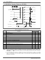
1
MF1072-04
S1D13504 Series
Technicl Manual
Dot Matrix Graphics LCD Controller
S1D13504 Series
Technical Manual
S1D13504 Series Technical Manual
ELECTRONIC DEVICES MARKETING DIVISION
EPSON Electronic Devices Website
http://www.epson.co.jp/device/
This manual was made with recycle papaer,
and printed using soy-based inks.
First issue September,1998
Printed April, 2001 in Japan
M
CB
NOTICE
No part of this material may be reproduced or duplicated in any form or by any means without the written
permission of Seiko Epson. Seiko Epson reserves the right to make changes to this material without notice.
Seiko Epson does not assume any liability of any kind arising out of any inaccuracies contained in this material
or due to its application or use in any product or circuit and, further, there is no representation that this material
is applicable to products requiring high level reliability, such as medical products. Moreover, no license to any
intellectual property rights is granted by implication or otherwise, and there is no representation or warranty that
anything made in accordance with this material will be free from any patent or copyright infringement of a third
party. This material or portions thereof may contain technology or the subject relating to strategic products under
the control of the Foreign Exchange and Foreign Trade Law of Japan and may require an export license from
the Ministry of International Trade and Industry or other approval from another government agency.
MS-DOS and Windows are registered trademarks of Microsoft Corporation, U.S.A.
PC-DOS, PC/AT, VGA, EGA and IBM are registered trademarks of International Business Machines Corporation, U.S.A.
All other product names mentioned herein are trademarks and/or registered trademarks of their respective owners.
© SEIKO EPSON CORPORATION 2001, All rights reserved.
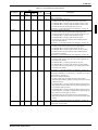
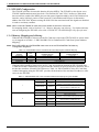
The information of the product number change
Starting April 1, 2001, the product number will be changed as listed below. To order from April 1,
2001 please use the new product number. For further information, please contact Epson sales
representative.
Configuration of product number
Devices
S1
D
13706
F
00A0
00
Packing specification
Specification
Package (B: CSP, F: QFP)
Corresponding model number
Model name (D: driver, digital products)
Product classification (S1: semiconductor)
Evaluation Board
S5U
13705 P00C
Specification
Corresponding model number (13705: for S1D13705)
Product classification (S5U: development tool for semiconductor)
Comparison table between new and previous number
• S1D13305 Series
Previous No.
SED1335 Series
SED1335D0A
SED1335F0A
SED1335F0B
• S1D1370x Series
New No.
S1D13305 Series
S1D13305D00A
S1D13305F00A
S1D13305F00B
• S1D1350x Series
Previous No.
New No.
SED135x Series
SED1353D0A
SED1353F0A
SED1353F1A
S1D1350x Series
S1D13503D00A
S1D13503F00A
S1D13503F01A
SED1354F0A
SED1354F1A
SED1354F2A
S1D13504F00A
S1D13504F01A
S1D13504F02A
SED1355F0A
S1D13505F00A
SED1356F0A
S1D13506F00A
• S1D1380x Series
New No.
Previous No.
SED137x Series
SED1374F0A
S1D1370x Series
S1D13704F00A
SED1375F0A
S1D13705F00A
SED1376B0A
SED1376F0A
S1D13706B00A
S1D13706F00A
SED1378 Series
S1D13708 Series
New No.
Previous No.
SED138x Series
SED1386F0A
S1D1380x Series
S1D13806F00A
• S1D13A0x Series
Previous No.
New No.
SED13Ax Series
SED13A3F0A
SED13A3B0B
S1D13A0x Series
S1D13A03F00A
S1D13A03B00B
SED13A4B0B
S1D13A04B00B
Comparison table between new and previous number of Evaluation Boards
• S1D1350x Series
Previous No.
• S1D1370x Series
New No.
• S1D1380x Series
New No.
Previous No.
SDU1353#0C
S5U13503P00C
SDU1374#0C
S5U13704P00C
SDU1354#0C
S5U13504P00C
SDU1375#0C
S5U13705P00C
SDU1355#0C
S5U13505P00C
SDU1356#0C
S5U13506P00C
SDU1376#0C
SDU1376BVR
S5U13706P00C
S5U13706B32R
SDU1378#0C
S5U13708P00C
• S1D13A0x Series
Previous No.
SDU13A3#0C
SDU13A4#0C
New No.
S5U13A03P00C
S5U13A04P00C
Previous No.
SDU1386#0C
New No.
S5U13806P00C
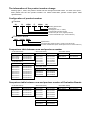
Tobira.fm Page 1 Sunday, April 15, 2001 4:19 PM
S1D13504 Series Technical Manual
HARDWARE FUNCTIONAL SPECIFICATION
PROGRAMMING NOTES AND EXAMPLES
UTILITIES
S5U13504P00C ISA BUS EVALUATION
BOARD USER’S MANUAL
APPLICATION NOTES
ll er
o
s
r
e
t
ri n
4
0
5
3 hic
1
D p
S1 Gra
x
ri
t
a
D
M
t
o
o
e
C
S D
i
ct
n
u
F
LC wareation
rd cific
a
H pe
S
l
a
n
o
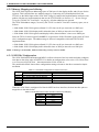
CONTENTS
Contents
Table of Contents
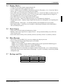
1 INTRODUCTION .........................................................................................................................1-1
1.1 Scope ............................................................................................................................................1-1
1.2 Overview Description ....................................................................................................................1-1
2 FEATURES ...............................................................................................................................1-2
2.1
2.2
2.3
2.4
2.5
2.6
2.7
Memory Interface ..........................................................................................................................1-2
CPU Interface ................................................................................................................................1-2
Display Support .............................................................................................................................1-2
Display Modes ...............................................................................................................................1-3
Clock Source .................................................................................................................................1-3
Miscellaneous................................................................................................................................1-3
Package and Pin ...........................................................................................................................1-3
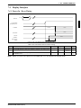
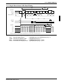
3 TYPICAL SYSTEM IMPLEMENTATION DIAGRAMS ...........................................................................1-4
4 BLOCK DESCRIPTION ................................................................................................................1-6
4.1 Functional Block Diagram .............................................................................................................1-6
4.2 Functional Block Descriptions .......................................................................................................1-6
Host Interface.............................................................................................................................1-6
Memory Controller......................................................................................................................1-6
Display FIFO ..............................................................................................................................1-6
Look-Up Table ...........................................................................................................................1-6
LCD Interface .............................................................................................................................1-6
Power Save................................................................................................................................1-6
5 PIN OUT..................................................................................................................................1-7
5.1
5.2
5.3
5.4
Pinout Diagram for S1D13504F00A ..............................................................................................1-7
Pinout Diagram for S1D13504F01A ..............................................................................................1-8
Pinout Diagram for S1D13504F02A ..............................................................................................1-9
Pin Description ............................................................................................................................1-10
Host Interface...........................................................................................................................1-10
Memory Interface .....................................................................................................................1-12
LCD Interface ...........................................................................................................................1-13
Clock Input ...............................................................................................................................1-13
CRT and External RAMDAC Interface .....................................................................................1-13
Miscellaneous ..........................................................................................................................1-14
Power Supply ...........................................................................................................................1-15
5.5 Summary of Configuration Options .............................................................................................1-16
5.6 Multiple Function Pin Mapping .................................................................................................... 1-16
6 D.C. CHARACTERISTICS .........................................................................................................1-18
7 A.C. CHARACTERISTICS .........................................................................................................1-19
7.1 CPU Interface Timing ..................................................................................................................1-20
SH-3 Interface Timing ..............................................................................................................1-20
MC68K Bus 1 Interface Timing (e.g. MC68000) ......................................................................1-22
MC68K Bus 2 Interface Timing (e.g. MC68030) ......................................................................1-24
Generic MPU Interface Synchronous Timing...........................................................................1-26
Generic MPU Interface Asynchronous Timing .........................................................................1-28
7.2 Clock Input Requirements ...........................................................................................................1-30
7.3 Memory Interface Timing.............................................................................................................1-31
EDO-DRAM Read Timing ........................................................................................................1-31
EDO-DRAM Write Timing ........................................................................................................1-32
EDO-DRAM Read-Write Timing...............................................................................................1-33
EDO-DRAM CAS Before RAS Refresh Timing........................................................................1-34
EDO-DRAM Self-Refresh Timing.............................................................................................1-34
FPM-DRAM Read Timing ........................................................................................................1-35
S1D13504 SERIES HARDWARE FUNCTIONAL
SPECIFICATION (X19A-A-002-17)
EPSON
1-i
CONTENTS
FPM-DRAM Write Timing ........................................................................................................ 1-36
FPM-DRAM Read-Write Timing ............................................................................................. 1-37
FPM-DRAM CAS# Before RAS# Refresh Timing.................................................................... 1-38
FPM-DRAM Self-Refresh Timing............................................................................................. 1-38
7.4 Display Interface ......................................................................................................................... 1-39
Power On / Reset Timing......................................................................................................... 1-39
Suspend Timing....................................................................................................................... 1-40
Single Monochrome 4-Bit Panel Timing .................................................................................. 1-41
Single Monochrome 8-Bit Panel Timing .................................................................................. 1-43
Single Color 4-Bit Panel Timing............................................................................................... 1-45
Single Color 8-Bit Panel Timing (Format 1) ............................................................................. 1-47
Single Color 8-Bit Panel Timing (Format 2) ............................................................................. 1-49
Single Color 16-Bit Panel Timing............................................................................................. 1-51
Dual Monochrome 8-Bit Panel Timing ..................................................................................... 1-53
Dual Color 8-Bit Panel Timing ................................................................................................. 1-55
Dual Color 16-Bit Panel Timing ............................................................................................... 1-57
16-Bit TFT Panel Timing.......................................................................................................... 1-59
CRT Timing.............................................................................................................................. 1-61
External RAMDAC Read / Write Timing .................................................................................. 1-63
8 REGISTERS ............................................................................................................................1-64
8.1 Register Mapping ........................................................................................................................ 1-64
8.2 Register Descriptions .................................................................................................................. 1-65
Revision Code Register ........................................................................................................... 1-65
Memory Configuration Registers ............................................................................................. 1-65
Panel/Monitor Configuration Registers .................................................................................... 1-66
Display Configuration Registers .............................................................................................. 1-70
Clock Configuration Register ................................................................................................... 1-74
Power Save Configuration Registers....................................................................................... 1-75
Miscellaneous Registers.......................................................................................................... 1-76
Look-Up Table Registers ......................................................................................................... 1-83
External RAMDAC Control Registers ...................................................................................... 1-85
9 DISPLAY BUFFER ...................................................................................................................1-86
9.1 Image Buffer................................................................................................................................ 1-87
9.2 Half Frame Buffer........................................................................................................................ 1-87
10 DISPLAY CONFIGURATION .......................................................................................................1-88
10.1 Display Mode Data Format ......................................................................................................... 1-88
10.2 Image Manipulation..................................................................................................................... 1-90
11 CLOCKING .............................................................................................................................1-91
11.1 Maximum MCLK : PCLK Ratios .................................................................................................. 1-91
11.2 Frame Rate Calculation .............................................................................................................. 1-92
12 LOOK-UP TABLE ARCHITECTURE .............................................................................................1-94
12.1 Gray Shade Display Modes ........................................................................................................ 1-94
1 Bit-Per-Pixel Mode .......................................................................................................... 1-94
2 Bit-Per-Pixel Mode .......................................................................................................... 1-94
4 Bit-Per-Pixel Mode .......................................................................................................... 1-95
12.2 Color Display Modes ................................................................................................................... 1-95
1 Bit-Per-Pixel Color Mode ................................................................................................ 1-95
2 Bit-Per-Pixel Color Mode ................................................................................................ 1-96
4 Bit-Per-Pixel Color Mode ................................................................................................ 1-97
8 Bit-Per-Pixel Color Mode ................................................................................................ 1-98
13 POWER SAVE MODES .............................................................................................................1-99
13.1 Hardware Suspend ..................................................................................................................... 1-99
13.2 Software Suspend....................................................................................................................... 1-99
13.3 Power Save Mode Function Summary...................................................................................... 1-100
1-ii
EPSON
S1D13504 SERIES HARDWARE FUNCTIONAL
SPECIFICATION (X19A-A-002-17)
CONTENTS
13.4 Pin States in Power Save Modes ..............................................................................................1-100
14 MECHANICAL DATA ..............................................................................................................1-101
14.1 QFP15-128pin (S1D13504F00A) ..............................................................................................1-101
14.2 TQFP15-128pin (S1D13504F01A) ............................................................................................1-102
14.3 QFP20-144pin (S1D13504F02A) ..............................................................................................1-103
S1D13504 SERIES HARDWARE FUNCTIONAL
SPECIFICATION (X19A-A-002-17)
EPSON
1-iii
CONTENTS
List of Figures
Figure 3-1
Figure 3-2
Figure 3-3
Figure 3-4
Figure 4-1
Figure 5-1
Figure 5-2
Figure 5-3
Figure 7-1
Figure 7-2
Figure 7-3
Figure 7-4
Figure 7-5
Figure 7-6
Figure 7-7
Figure 7-8
Figure 7-9
Figure 7-10
Figure 7-11
Figure 7-12
Figure 7-13
Figure 7-14
Figure 7-15
Figure 7-16
Figure 7-17
Figure 7-18
Figure 7-19
Figure 7-20
Figure 7-21
Figure 7-22
Figure 7-23
Figure 7-24
Figure 7-25
Figure 7-26
Figure 7-27
Figure 7-28
Figure 7-29
Figure 7-30
Figure 7-31
Figure 7-32
Figure 7-33
Figure 7-34
Figure 7-35
Figure 7-36
Figure 7-37
Figure 7-38
Figure 7-39
Figure 7-40
1-iv
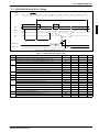
Typical System Diagram – SH-3 Bus, 1Mx16 FPM/EDO-DRAM......................................... 1-4
Typical System Diagram – MC68K Bus 1, 1Mx16 FPM/EDO-DRAM (16-Bit MC68000)..... 1-4
Typical System Diagram – MC68K Bus 2, 256Kx16 FPM/EDO-DRAM (32-Bit MC68030) . 1-5
Typical System Diagram – Generic Bus, 1Mx16 FPM/EDO-DRAM .................................... 1-5
System Block Diagram Showing Datapaths ........................................................................ 1-6
Pinout Diagram of S1D13504F00A...................................................................................... 1-7
Pinout Diagram of S1D13504F01A...................................................................................... 1-8
Pinout Diagram of S1D13504F02A...................................................................................... 1-9
SH-3 Interface Timing ........................................................................................................ 1-20
SH-3 Write Bus Timing....................................................................................................... 1-21
MC68000 Bus 1 InterfaceTiming ....................................................................................... 1-22
MC68000 Read Bus Timing ............................................................................................... 1-23
MC68030 Bus 2 Interface Timing ...................................................................................... 1-24
MC68030 Read Bus Timing ............................................................................................... 1-25
Generic MPU Interface Synchronous Timing..................................................................... 1-26
Generic Write Bus Synchronous Timing ............................................................................ 1-27
Generic MPU Interface Asynchronous Timing ................................................................... 1-28
Generic Write Bus Asynchronous Timing .......................................................................... 1-29
Clock Input Requirements.................................................................................................. 1-30
EDO-DRAM Read Timing .................................................................................................. 1-31
EDO-DRAM Write Timing .................................................................................................. 1-32
EDO-DRAM Read-Write Timing......................................................................................... 1-33
EDO-DRAM CAS Before RAS Refresh Timing.................................................................. 1-34
EDO-DRAM Self-Refresh Timing....................................................................................... 1-34
FPM-DRAM Read Timing .................................................................................................. 1-35
FPM-DRAM Write Timing................................................................................................... 1-36
FPM-DRAM Read-Write Timing......................................................................................... 1-37
FPM-DRAM CAS# Before RAS# Refresh Timing .............................................................. 1-38
FPM-DRAM CBR Self-Refresh Timing .............................................................................. 1-38
LCD Panel Power On / Reset Timing ................................................................................ 1-39
LCD Panel Suspend Timing............................................................................................... 1-40
Single Monochrome 4-Bit Panel Timing............................................................................. 1-41
Single Monochrome 4-Bit Panel A.C. Timing..................................................................... 1-42
Single Monochrome 8-Bit Panel Timing............................................................................. 1-43
Single Monochrome 8-Bit Panel A.C. Timing..................................................................... 1-44
Single Color 4-Bit Panel Timing ......................................................................................... 1-45
Single Color 4-Bit Panel A.C. Timing ................................................................................. 1-46
Single Color 8-Bit Panel Timing (Format 1) ....................................................................... 1-47
Single Color 8-Bit Panel A.C. Timing (Format 1) ............................................................... 1-48
Single Color 8-Bit Panel Timing (Format 2) ....................................................................... 1-49
Single Color 8-Bit Panel A.C. Timing (Format 2) ............................................................... 1-50
Single Color 16-Bit Panel Timing ....................................................................................... 1-51
Single Color 16-Bit Panel A.C. Timing ............................................................................... 1-52
Dual Monochrome 8-Bit Panel Timing ............................................................................... 1-53
Dual Monochrome 8-Bit Panel A.C. Timing ....................................................................... 1-54
Dual Color 8-Bit Panel Timing............................................................................................ 1-55
Dual Color 8-Bit Panel A.C. Timing.................................................................................... 1-56
Dual Color 16-Bit Panel Timing.......................................................................................... 1-57
EPSON
S1D13504 SERIES HARDWARE FUNCTIONAL
SPECIFICATION (X19A-A-002-17)
CONTENTS
Figure 7-41
Figure 7-42
Figure 7-43
Figure 7-44
Figure 7-45
Figure 7-46
Figure 9-1
Figure 10-1
Figure 10-2
Figure 10-3
Figure 12-1
Figure 12-2
Figure 12-3
Figure 12-4
Figure 12-5
Figure 12-6
Figure 12-7
Figure 14-1
Figure 14-2
Figure 14-3
Dual Color 16-Bit Panel A.C. Timing ..................................................................................1-58
16-Bit TFT Panel Timing ....................................................................................................1-59
TFT A.C. Timing .................................................................................................................1-60
CRT Timing ........................................................................................................................1-61
CRT A.C. Timing ................................................................................................................1-62
Generic Bus RAMDAC Read / Write Timing ......................................................................1-63
Display Buffer Addressing ..................................................................................................1-86
1/2/4/8 Bit-Per-Pixel Format Memory Organization............................................................1-88
15/16 Bit-Per-Pixel Format Memory Organization..............................................................1-89
Image Manipulation ............................................................................................................1-90
1 Bit-Per-Pixel – 2-Level Gray-Shade Mode Look-Up Table Architecture .........................1-94
2 Bit-Per-Pixel – 4-Level Gray-Shade Mode Look-Up Table Architecture .........................1-94
4 Bit-Per-Pixel – 16-Level Gray-Shade Mode Look-Up Table Architecture .......................1-95
1 Bit-Per-Pixel – 2-Level Color Look-Up Table Architecture ..............................................1-95
2 Bit-Per-Pixel – 4-Level Color Mode Look-Up Table Architecture ....................................1-96
4 Bit-Per-Pixel – 16-Level Color Mode Look-Up Table Architecture ..................................1-97
8 Bit-Per-Pixel – 256-Level Color Mode Look-Up Table Architecture ................................1-98
Mechanical Drawing QFP15-128pin.................................................................................1-101
Mechanical Drawing TQFP15-128pin ..............................................................................1-102
Mechanical Drawing QFP20-144pin.................................................................................1-103
Table 2-1
Table 5-1
Table 5-2
Table 5-3
Table 5-4
Table 5-5
Table 5-6
Table 5-7
Table 5-8
Table 5-9
Table 5-10
Table 5-11
Table 6-1
Table 6-2
Table 6-3
Table 6-4
Table 7-1
Table 7-2
Table 7-3
Table 7-4
Table 7-5
Table 7-6
Table 7-7
Table 7-8
Table 7-9
Table 7-10
Table 7-11
Table 7-12
Table 7-13
S1D13504 Series Package List............................................................................................1-3
Host Interface Pin Descriptions ..........................................................................................1-10
Memory Interface Pin Descriptions ....................................................................................1-12
LCD Interface Pin Descriptions ..........................................................................................1-13
Clock Input Pin Description ................................................................................................1-13
CRT and RAMDAC Interface Pin Descriptions ..................................................................1-13
Miscellaneous Pin Descriptions..........................................................................................1-14
Power Supply Pin Descriptions ..........................................................................................1-15
Summary of Power On / Reset Options .............................................................................1-16
Host Bus Interface Pin Mapping.........................................................................................1-16
Memory Interface Pin Mapping ..........................................................................................1-16
LCD, CRT, RAMDAC Interface Pin Mapping .....................................................................1-17
Absolute Maximum Ratings................................................................................................1-18
Recommended Operating Conditions ................................................................................1-18
Input Specifications ............................................................................................................1-18
Output Specifications .........................................................................................................1-18
SH-3 Interface Timing ........................................................................................................1-20
SH-3 Write Bus Timing.......................................................................................................1-21
MC68000 Bus 1 InterfaceTiming........................................................................................1-22
MC68000 Read Bus Timing ...............................................................................................1-23
MC68030 Bus 2 Interface Timing.......................................................................................1-24
MC68030 Read Bus Timing ...............................................................................................1-25
Generic MPU Interface Synchronous Timing .....................................................................1-26
Generic Write Bus Synchronous Timing ............................................................................1-27
Generic MPU Interface Asynchronous Timing ...................................................................1-28
Generic Write Bus Asynchronoud Timing ..........................................................................1-29
Clock Input Requirements ..................................................................................................1-30
EDO DRAM Read Timing...................................................................................................1-31
EDO DRAM Write Timing...................................................................................................1-32
List of Tables
S1D13504 SERIES HARDWARE FUNCTIONAL
SPECIFICATION (X19A-A-002-17)
EPSON
1-v
CONTENTS
Table 7-14
Table 7-15
Table 7-16
Table 7-17
Table 7-18
Table 7-19
Table 7-20
Table 7-21
Table 7-22
Table 7-23
Table 7-24
Table 7-25
Table 7-26
Table 7-27
Table 7-28
Table 7-29
Table 7-30
Table 7-31
Table 7-32
Table 7-33
Table 7-34
Table 7-35
Table 8-1
Table 8-2
Table 8-3
Table 8-4
Table 8-5
Table 8-6
Table 8-7
Table 8-8
Table 8-9
Table 8-10
Table 8-11
Table 8-12
Table 8-13
Table 8-14
Table 8-15
Table 9-1
Table 11-1
Table 11-2
Table 11-3
Table 12-1
Table 13-1
Table 13-2
1-vi
EDO DRAM Read-Write Timing......................................................................................... 1-33
EDO-DRAM CAS Before RAS Refresh Timing.................................................................. 1-34
EDO-DRAM Self-Refresh Timing....................................................................................... 1-34
FPM DRAM Read Timing................................................................................................... 1-35
FPM-DRAM Write Timing................................................................................................... 1-36
FPM-DRAM Read-Write Timing......................................................................................... 1-37
FPM-DRAM CAS# Before RAS# Refresh Timing .............................................................. 1-38
FPM-DRAM CBR Self-Refresh Timing .............................................................................. 1-38
LCD Panel Power On / Reset Timing ................................................................................ 1-39
LCD Panel Suspend Timing............................................................................................... 1-40
Single Monochrome 4-Bit Panel A.C. Timing..................................................................... 1-42
Single Monochrome 8-Bit Panel A.C. Timing..................................................................... 1-44
Single Color 4-Bit Panel A.C. Timing ................................................................................. 1-46
Single Color 8-Bit Panel A.C. Timing (Format 1) ............................................................... 1-48
Single Color 8-Bit Panel A.C. Timing (Format 2) ............................................................... 1-50
Single Color 16-Bit Panel A.C. Timing ............................................................................... 1-52
Dual Monochrome 8-Bit Panel A.C. Timing ....................................................................... 1-54
Dual Color 8-Bit Panel A.C. Timing.................................................................................... 1-56
Dual Color 16-Bit Panel A.C. Timing.................................................................................. 1-58
TFT A.C. Timing................................................................................................................. 1-60
CRT A.C. Timing ................................................................................................................ 1-62
Generic Bus RAMDAC Read / Write Timing ...................................................................... 1-63
S1D13504 Addressing ....................................................................................................... 1-64
DRAM Refresh Rate Selection .......................................................................................... 1-65
Panel Data Width Selection ............................................................................................... 1-66
FPLINE Polarity Selection.................................................................................................. 1-67
FPFRAME Polarity Selection ............................................................................................. 1-69
Simultaneous Display Option Selection ............................................................................. 1-70
Number of Bits-Per-Pixel Selection.................................................................................... 1-70
Pixel Panning Selection ..................................................................................................... 1-73
PCLK Divide Selection ....................................................................................................... 1-74
Suspend Refresh Selection ............................................................................................... 1-75
Minimum Memory Timing Selection ................................................................................... 1-81
RAS#-to-CAS# Delay Timing Select .................................................................................. 1-82
RAS# Precharge Timing Select ......................................................................................... 1-82
Optimal NRC, NRP, and NRCD Values at Maximum MCLK Frequency................................ 1-82
RGB Index Selection.......................................................................................................... 1-83
S1D13504 Addressing ....................................................................................................... 1-86
Maximum PCLK Frequency with EDO-DRAM ................................................................... 1-91
Maximum PCLK Frequency with FPM-DRAM ................................................................... 1-91
Example Frame Rates ....................................................................................................... 1-92
Look-Up Table Configurations ........................................................................................... 1-94
Power Save Mode Function Summary ............................................................................ 1-100
Pin States in Power Save Modes..................................................................................... 1-100
EPSON
S1D13504 SERIES HARDWARE FUNCTIONAL
SPECIFICATION (X19A-A-002-17)
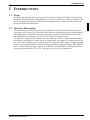
1: INTRODUCTION
1 INTRODUCTION
1.1 Scope
This is the Functional Specification for the S1D13504 Color Graphics LCD/CRT Controller Chip.
Included in this document are timing diagrams, AC and DC characteristics, register descriptions, and
power management descriptions. This document is intended for two audiences: Video Subsystem
Designers and Software Developers.
1.2 Overview Description
The S1D13504 is a low cost, low power color/monochrome LCD/CRT controller interfacing to a
wide range of CPUs and LCDs. The S1D13504 architecture is designed to meet the requirements of
embedded markets such as Office Automation equipment, Mobile Communications devices and
Hand-Held PCs where Windows CE may serve as a primary operating system.
The S1D13504 supports LCD interfaces with data widths up to 16 bits. Using Frame Rate Modulation (FRM), it can display 16 shades of gray on monochrome LCD panels, up to 4096 colors on passive color LCDs, and 64K colors on active matrix TFT LCD panels. CRT support is handled through
the use of an external RAMDAC interface allowing simultaneous display of both the CRT and LCD
panel. A 16-bit memory interface supports up to 2M bytes of FPM-DRAM or EDO-DRAM. Flexible operating voltages from 2.7V to 5.5V provide for very low power consumption.
S1D13504 SERIES HARDWARE FUNCTIONAL
SPECIFICATION (X19A-A-002-17)
EPSON
1-1
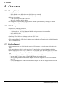
2: FEATURES
2 FEATURES
2.1 Memory Interface
• 16-bit DRAM interface:
- EDO-DRAM up to 40MHz data rate (80M bytes per second).
- FPM-DRAM up to 25MHz data rate (50M bytes per second).
• Memory size options:
- 512K bytes using one 256K×16 device.
- 2M bytes using one 1M×16 device.
• A configuration register can be programmed to enhance performance by tailoring the memory
control output timing to the DRAM device.
2.2 CPU Interface
• Supports the following interfaces:
- 8/16-bit Hitachi SH-3 bus interface.
- 16-bit interface to 16/32-bit Motorola MC68K microprocessors/microcontrollers.
- Philips MIPS PR31500 / PR31700.
- NEC MIPS VR4102.
- 8/16-bit generic interface bus.
• One-Stage write buffer for minimum wait-state CPU writes.
• Registers are memory-mapped; M/R# pin selects between memory and register address space.
• The complete 2M byte display buffer address space is directly and contiguously available through
the 21-bit address bus.
2.3 Display Support
• 4/8-bit monochrome or 4/8/16-bit color passive LCD interface for single-panel, single-drive displays.
• 8-bit monochrome or 8/16-bit color passive LCD interface for dual-panel, dual-drive displays.
• Direct support for 9/12-bit TFT, 18/24-bit TFT are supported up to 64K color depth (16-bit data).
• External RAMDAC support using the upper byte of the LCD data bus for the RAMDAC pixel data
bus.
• Simultaneous display of CRT and 4/8-bit passive panel or 9-bit TFT panel:
- Normal mode for cases where LCD and CRT image sizes are identical.
- Line-Doubling mode for simultaneous display of 240-line images on 240-line LCD and 480line CRT.
- Even-Scan and interlace modes for simultaneous display of 480-line images on 240-line LCD
and 480-line CRT.
1-2
EPSON
S1D13504 SERIES HARDWARE FUNCTIONAL
SPECIFICATION (X19A-A-002-17)
2: FEATURES
2.4 Display Modes
• 1/2/4/8/16 bit-per-pixel modes supported on LCD.
• 1/2/4/8 bit-per-pixel modes supported on CRT.
• Up to 16 shades of gray by FRM on monochrome passive LCD panels; a 16 × 4 Look-Up Table is
used to map 1/2/4 bit-per-pixel modes into these shades.
• Up to 4096 colors on color passive LCD panels; three 16 × 4 Look-Up Tables are used to map 1/2/
4/8 bit-per-pixel modes into these colors, 16 bit-per-pixel mode is mapped directly using the 4
most significant bits of the red, green and blue colors.
• Up to 64K colors in 16 bit-per-pixel mode on TFT panels.
• Split screen mode – allows two different images to be simultaneously displayed.
• Virtual display mode – displays images larger than the panel size through the use of panning and
scrolling.
• Double buffering / multi-pages – for smooth animation and instantaneous screen update.
• Fast-Update feature – accelerates screen update by allocating full display buffer bandwidth to
CPU (see REG[23h] bit 7).
2.5 Clock Source
• Single clock input for both pixel and memory clocks.
• Memory clock can be input clock or (input clock)/2 – this provides flexibility to use CPU bus
clock as input clock.
• Pixel clock can be memory clock, (memory clock)/2, (memory clock)/3 or (memory clock)/4.
2.6 Miscellaneous
• The memory data bus MD[15:0], is used to configure the chip at power-on.
• Up to 12 General Purpose Input/Output pins are available:
- GPIO0 is always available.
- GPIO[3:1] are available if upper Memory Address pins are not required for DRAM support.
- GPIO[11:4] are available if there is no external RAMDAC.
• Suspend power save mode is initiated by hardware or software.
• The SUSPEND# pin is used either as an input to initiate Suspend mode, or as a General Purpose
Output that can be used to control the LCD backlight – its power-on polarity is selected by an MD
configuration pin.
2.7 Package and Pin
Table 2-1 S1D13504 Series Package List
Name
Package
Pin
S1D13504F00A
QFP15
128
S1D13504F01A
TQFP15
128
S1D13504F02A
QFP20
144
S1D13504 SERIES HARDWARE FUNCTIONAL
SPECIFICATION (X19A-A-002-17)
EPSON
1-3
3: TYPICAL SYSTEM IMPLEMENTATION DIAGRAMS
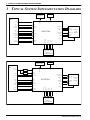
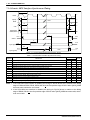
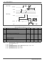
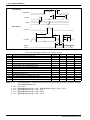
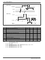
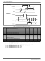
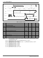
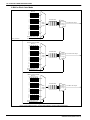
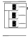
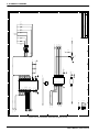
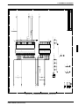
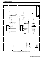
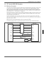
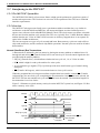
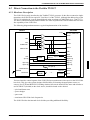
3 TYPICAL SYSTEM IMPLEMENTATION DIAGRAMS
Power
Management
Oscillator
CSn#
CS#
A[20:0]
AB[20:0]
D[15:0]
DB[15:0]
WE1#
SUSPEND#
M/R#
A21
CLKI
SH-3
BUS
WE1#
BS#
S1D13504
BS#
RD/WR#
RD/WR#
RD#
WE0#
WAIT#
WAIT#
UD[7:0]
FPDAT[7:0]
LD[7:0]
FPSHIFT
FPSHIFT
4/8/16-bit
FPFRAME
FPFRAME
LCD
Display
FPLINE
RD#
WE0#
FPDAT[15:8]
DRDY
FPLINE
MOD
UCAS#
UCAS#
RAS#
LCAS#
LCAS#
WE#
RAS#
MD[15:0]
WE#
RESET#
MA[11:0]
RESET#
A[11:0]
BUSCLK
D[15:0]
LCDPWR
CKIO
1Mx16
FPM/EDO-DRAM
Figure 3-1 Typical System Diagram – SH-3 Bus, 1Mx16 FPM/EDO-DRAM
Power
Management
Oscillator
Decoder
Decoder
M/R#
CS#
A[20:1]
AB[20:1]
D[15:0]
DB[15:0]
LDS#
AB0#
UDS#
WE1#
AS#
R/W#
DTACK#
SUSPEND#
A[23:21]
FC0, FC1
CLKI
MC68000
BUS
S1D13504
FPDAT[15:8]
UD[7:0]
FPDAT[7:0]
LD[7:0]
FPSHIFT
FPSHIFT
4/8/16-bit
FPFRAME
FPFRAME
LCD
Display
FPLINE
BS#
DRDY
RD/WR#
FPLINE
MOD
WAIT#
WE#
RAS#
LCAS#
UCAS#
RAS#
LCAS#
UCAS#
MD[15:0]
WE#
MA[11:0]
RESET#
A[11:0]
RESET#
BUSCLK
D[15:0]
LCDPWR
BCLK
1Mx16
FPM/EDO-DRAM
Figure 3-2 Typical System Diagram – MC68K Bus 1, 1Mx16 FPM/EDO-DRAM (16-Bit MC68000)
1-4
EPSON
S1D13504 SERIES HARDWARE FUNCTIONAL
SPECIFICATION (X19A-A-002-17)
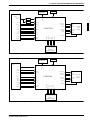
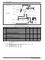
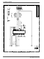
3: TYPICAL SYSTEM IMPLEMENTATION DIAGRAMS
Power
Management
Oscillator
M/R#
Decoder
CS#
Decoder
A[20:0]
AB[20:0]
D[31:16]
DB[15:0]
DS#
WE1#
AS#
BS#
R/W#
SUSPEND#
A[31:21]
FC0, FC1
CLKI
MC68030
BUS
S1D13504
RD/WR#
SIZ1
RD#
SIZ0
WE0#
DSACK1#
FPDAT[15:8]
UD[7:0]
FPDAT[7:0]
LD[7:0]
FPSHIFT
FPSHIFT
4/8/16-bit
FPFRAME
FPFRAME
LCD
Display
FPLINE
DRDY
FPLINE
MOD
WAIT#
UCAS#
UCAS#
RAS#
LCAS#
WE#
LCAS#
RAS#
MD[15:0]
WE#
RESET#
MA[8:0]
RESET#
A[8:0]
BUSCLK
D[15:0]
LCDPWR
BCLK
256Kx16
FPM/EDO-DRAM
Figure 3-3 Typical System Diagram – MC68K Bus 2, 256Kx16 FPM/EDO-DRAM (32-Bit MC68030)
Power
Management
Oscillator
M/R#
CSn#
CS#
A[20:0]
AB[20:0]
D[15:0]
DB[15:0]
WE0#
WE0#
WE1#
WE1#
RD0#
RD#
RD1#
RD/WR#
WAIT#
SUSPEND#
A21
CLKI
GENERIC
BUS
S1D13504
FPDAT[15:8]
UD[7:0]
FPDAT[7:0]
LD[7:0]
FPSHIFT
FPSHIFT
4/8/16-bit
FPFRAME
FPFRAME
LCD
Display
FPLINE
DRDY
FPLINE
MOD
WAIT#
RAS#
LCAS#
UCAS#
RAS#
LCAS#
UCAS#
WE#
WE#
MD[15:0]
RESET#
MA[11:0]
RESET#
A[11:0]
BUSCLK
D[15:0]
LCDPWR
BCLK
1Mx16
FPM/EDO-DRAM
Figure 3-4 Typical System Diagram – Generic Bus, 1Mx16 FPM/EDO-DRAM
S1D13504 SERIES HARDWARE FUNCTIONAL
SPECIFICATION (X19A-A-002-17)
EPSON
1-5
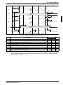
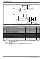
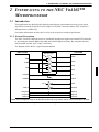
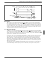
4: BLOCK DESCRIPTION
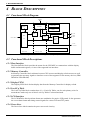
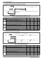
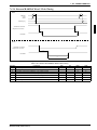
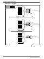
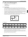
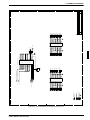
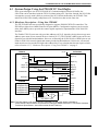
4 BLOCK DESCRIPTION
4.1 Functional Block Diagram
16-bit FPM/EDO
DRAM
Memory
Controller
Register
Power Save
Clocks
CPU
R/W
LCD
Display
FIFO
Host
CPU / MPU
I/F
I/F
LCD
DAC
Data
Look-Up
Table
DAC
Control
CRTC
Bus Clock
Memory Clock
Pixel Clock
Figure 4-1 System Block Diagram Showing Datapaths
4.2 Functional Block Descriptions
4.2.1 Host Interface
The Host Interface block provides the means for the CPU/MPU to communicate with the display
buffer and internal registers, via one of the supported bus interfaces.
4.2.2 Memory Controller
he Memory Controller block arbitrates between CPU accesses and display refresh accesses as well
as generates the necessary signals to interface to one of the supported 16-bit memory devices (FPMDRAM or EDO-DRAM).
4.2.3 Display FIFO
The Display FIFO block fetches display data from the Memory Controller for display refresh.
4.2.4 Look-Up Table
The Look-Up Table block contains three 16 × 4 Look-Up Tables, one for each primary color. In
monochrome mode only one of these Look-Up Tables is selected and used.
4.2.5 LCD Interface
The LCD Interface block performs frame rate modulation for passive LCD panels. It also generates
the correct data format and timing control signals for various LCD and TFT panels.
4.2.6 Power Save
The Power Save block contains the power save mode circuitry.
1-6
EPSON
S1D13504 SERIES HARDWARE FUNCTIONAL
SPECIFICATION (X19A-A-002-17)
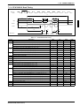
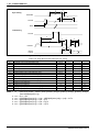
5: PIN OUT
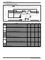
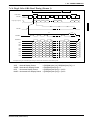
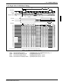
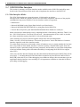
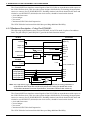
5 PIN OUT
96
95
94
93
92
91
90
89
88
87
86
85
84
83
82
81
80
79
78
77
76
75
74
73
72
71
70
69
68
67
66
65
VSS
FPDAT15
FPDAT14
FPDAT13
FPDAT12
FPDAT11
FPDAT10
FPDAT9
FPDAT8
VSS
DACCLK
BLANK#
DACRD#
IOVDD
FPDAT7
FPDAT6
FPDAT5
FPDAT4
FPDAT3
FPDAT2
FPDAT1
FPDAT0
VSS
FPSHIFT
DRDY
LCDPWR
FPLINE
FPFRAME
VSS
MD15
MD0
MD14
5.1 Pinout Diagram for S1D13504F00A
97
98
99
100
101
102
103
104
105
106
107
108
109
110
111
112
113
114
115
116
117
118
119
120
121
122
123
124
125
126
127
128
S1D13504F00A
64
63
62
61
60
59
58
57
56
55
54
53
52
51
50
49
48
47
46
45
44
43
42
41
40
39
38
37
36
35
34
33
MD1
MD13
MD2
MD12
MD3
MD11
MD4
MD10
MD5
MD9
MD6
MD8
MD7
VSS
LCAS#
UCAS#
WE#
RAS#
IOVDD
MA9
MA11
MA8
MA10
MA7
MA0
MA6
MA1
MA5
MA2
MA4
MA3
COREVDD
AB2
AB1
AB0
CS#
M/R#
BS#
RD#
WE0#
WE1#
RD/WR#
RESET#
GPIO0
WAIT#
IOVDD
VSS
DB15
DB14
DB13
DB12
DB11
DB10
DB9
DB8
DB7
DB6
DB5
DB4
DB3
DB2
DB1
DB0
VSS
1
2
3
4
5
6
7
8
9
10
11
12
13
14
15
16
17
18
19
20
21
22
23
24
25
26
27
28
29
30
31
32
COREVDD
DACP0
DACWR#
DACRS0
DACRS1
HRTC
VRTC
VSS
CLKI
SUSPEND#
TESTEN
BUSCLK
VSS
IOVDD
AB20
AB19
AB18
AB17
AB16
AB15
AB14
AB13
AB12
AB11
AB10
AB9
AB8
AB7
AB6
AB5
AB4
AB3
Figure 5-1 Pinout Diagram of S1D13504F00A
Package type: 128 pin surface mount QFP15
S1D13504 SERIES HARDWARE FUNCTIONAL
SPECIFICATION (X19A-A-002-17)
EPSON
1-7
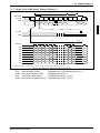
5: PIN OUT
96
95
94
93
92
91
90
89
88
87
86
85
84
83
82
81
80
79
78
77
76
75
74
73
72
71
70
69
68
67
66
65
VSS
FPDAT15
FPDAT14
FPDAT13
FPDAT12
FPDAT11
FPDAT10
FPDAT9
FPDAT8
VSS
DACCLK
BLANK#
DACRD#
IOVDD
FPDAT7
FPDAT6
FPDAT5
FPDAT4
FPDAT3
FPDAT2
FPDAT1
FPDAT0
VSS
FPSHIFT
DRDY
LCDPWR
FPLINE
FPFRAME
VSS
MD15
MD0
MD14
5.2 Pinout Diagram for S1D13504F01A
97
98
99
100
101
102
103
104
105
106
107
108
109
110
111
112
113
114
115
116
117
118
119
120
121
122
123
124
125
126
127
128
64
63
62
61
60
59
58
57
56
55
54
53
52
51
50
49
48
47
46
45
44
43
42
41
40
39
38
37
36
35
34
33
S1D13504F01A
MD1
MD13
MD2
MD12
MD3
MD11
MD4
MD10
MD5
MD9
MD6
MD8
MD7
VSS
LCAS#
UCAS#
WE#
RAS#
IOVDD
MA9
MA11
MA8
MA10
MA7
MA0
MA6
MA1
MA5
MA2
MA4
MA3
COREVDD
AB2
AB1
AB0
CS#
M/R#
BS#
RD#
WE0#
WE1#
RD/WR#
RESET#
GPIO0
WAIT#
IOVDD
VSS
DB15
DB14
DB13
DB12
DB11
DB10
DB9
DB8
DB7
DB6
DB5
DB4
DB3
DB2
DB1
DB0
VSS
1
2
3
4
5
6
7
8
9
10
11
12
13
14
15
16
17
18
19
20
21
22
23
24
25
26
27
28
29
30
31
32
COREVDD
DACP0
DACWR#
DACRS0
DACRS1
HRTC
VRTC
VSS
CLKI
SUSPEND#
TESTEN
BUSCLK
VSS
IOVDD
AB20
AB19
AB18
AB17
AB16
AB15
AB14
AB13
AB12
AB11
AB10
AB9
AB8
AB7
AB6
AB5
AB4
AB3
Figure 5-2 Pinout Diagram of S1D13504F01A
Package type: 128 pin surface mount TQFP15
1-8
EPSON
S1D13504 SERIES HARDWARE FUNCTIONAL
SPECIFICATION (X19A-A-002-17)
5: PIN OUT
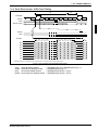
109
110
111
112
113
114
115
116
117
118
119
120
121
122
123
124
125
126
127
128
129
130
131
132
133
134
135
136
137
138
139
140
141
142
143
144
S1D13504F02A
72
71
70
69
68
67
66
65
64
63
62
61
60
59
58
57
56
55
54
53
52
51
50
49
48
47
46
45
44
43
42
41
40
39
38
37
NC
NC
MD1
MD13
MD2
MD12
MD3
MD11
MD4
MD10
MD5
MD9
MD6
MD8
MD7
VSS
LCAS#
UCAS#
WE#
RAS#
IOVDD
MA9
MA11
MA8
MA10
MA7
MA0
MA6
MA1
MA5
MA2
MA4
MA3
COREVDD
NC
NC
NC
NC
AB2
AB1
AB0
CS#
M/R#
BS#
RD#
WE0#
WE1#
RD/WR#
RESET#
GPIO0
WAIT#
IOVDD
VSS
DB15
DB14
DB13
DB12
DB11
DB10
DB9
DB8
DB7
DB6
DB5
DB4
DB3
DB2
DB1
DB0
VSS
NC
NC
1
2
3
4
5
6
7
8
9
10
11
12
13
14
15
16
17
18
19
20
21
22
23
24
25
26
27
28
29
30
31
32
33
34
35
36
NC
NC
COREVDD
DACP0
DACWR#
DACRS0
DACRS1
HRTC
VRTC
VSS
CLKI
SUSPEND#
TESTEN
BUSCLK
VSS
IOVDD
AB20
AB19
AB18
AB17
AB16
AB15
AB14
AB13
AB12
AB11
AB10
AB9
AB8
AB7
AB6
AB5
AB4
AB3
NC
NC
108
107
106
105
104
103
102
101
100
99
98
97
96
95
94
93
92
91
90
89
88
87
86
85
84
83
82
81
80
79
78
77
76
75
74
73
NC
NC
VSS
FPDAT15
FPDAT14
FPDAT13
FPDAT12
FPDAT11
FPDAT10
FPDAT9
FPDAT8
VSS
DACCLK
BLANK#
DACRD#
IOVDD
FPDAT7
FPDAT6
FPDAT5
FPDAT4
FPDAT3
FPDAT2
FPDAT1
FPDAT0
VSS
FPSHIFT
DRDY
LCDPWR
FPLINE
FPFRAME
VSS
MD15
MD0
MD14
NC
NC
5.3 Pinout Diagram for S1D13504F02A
Figure 5-3 Pinout Diagram of S1D13504F02A
Package type: 144 pin surface mount QFP20
S1D13504 SERIES HARDWARE FUNCTIONAL
SPECIFICATION (X19A-A-002-17)
EPSON
1-9
5: PIN OUT
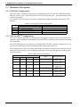
5.4 Pin Description
Key:
I
O
I/O
P
C
CD
= Input
= Output
= Bi-Directional (Input/Output)
= Power pin
= CMOS level input
= CMOS level input with pull-down resistor
(typical values of 100KΩ/180KΩ at 5V/3.3V respectively)
= CMOS level Schmitt input
= CMOS output driver, x denotes driver type (1=3/-1.5mA, 2=6/-3mA, 3=12/-6mA)
= Tri-state CMOS output driver, x denotes driver type
(1=3/-1.5mA, 2=6/-3mA, 3=12/-6mA)
= Tri-state CMOS output driver with pull-down resistor (typical values of 100KΩ/180KΩ
at 5V/3.3V respectively), x denotes driver type (1=3/-1.5mA, 2=6/-3mA, 3=12/-6mA)
= CMOS low-noise output driver, x denotes driver type
(1=3/-1.5mA, 2=6/-3mA, 3=12/-6mA)
CS
COx
TSx
TSxD
CNx
5.4.1 Host Interface
Table 5-1 Host Interface Pin Descriptions
Pin Names
Type
AB0
I
AB[20:1]
I
DB[15:0]
I/O
Pin #
F00A,
F02A
F01A
3
5
111–128 125–142
1, 2
3, 4
16–31
18–33
Driver
Reset
= 0 Value
CS
Hi-Z
C
Hi-Z
C/TS2
Hi-Z
WE1#
I
9
11
CS
Hi-Z
M/R#
I
5
7
C
Hi-Z
CS#
I
4
6
C
Hi-Z
1-10
Description
This pin has multiple functions.
• For SH-3 mode, this pin inputs system address bit 0 (A0).
• For MC68K Bus 1, this pin inputs the lower data strobe
(LDS#).
• For MC68K Bus 2, this pin inputs system address bit 0 (A0).
• For Generic Bus, this pin inputs system address bit 0 (A0).
See Table 5-9, “Host Bus Interface Pin Mapping,” on page 16 for
summary.
System address bus bits [20:1].
System data bus. Unused data pins should be connected to IO
VDD.
• For SH-3 mode, these pins are connected to D[15:0].
• For MC68K Bus 1, these pins are connected to D[15:0].
• For MC68K Bus 2, these pins are connected to D[31:16] for
32-bit devices (e.g. MC68030) or D[15:0] for 16-bit devices
(e.g. MC68340).
• For Generic Bus, these pins are connected to D[15:0].
See Table 5-9, “Host Bus Interface Pin Mapping,” on page 16 for
summary.
This pin has multiple functions.
• For SH-3 mode, this pin inputs the write enable signal for the
upper data byte (WE1#).
• For MC68K Bus 1, this pin inputs the upper data strobe
(UDS#).
• For MC68K Bus 2, this pin inputs the data strobe (DS#).
• For Generic Bus, this pin inputs the write enable signal for the
upper data byte (WE1#).
See Table 5-9, “Host Bus Interface Pin Mapping,” on page 16.
This input pin is used to select between the memory and register
address spaces of the S1D13504. M/R# is set high to access the
memory and low to access the registers. See Section 8.1, “Register Mapping” on page 64.
See Table 5-9, “Host Bus Interface Pin Mapping,” on page 16.
Chip select input. See Table 5-9, “Host Bus Interface Pin Mapping,” on page 16.
EPSON
S1D13504 SERIES HARDWARE FUNCTIONAL
SPECIFICATION (X19A-A-002-17)
5: PIN OUT
Table 5-1 Host Interface Pin Descriptions
Pin Names
Type
Pin #
F00A,
F02A
F01A
108
122
Driver
Reset
= 0 Value
C
Hi-Z
BUSCLK
I
BS#
I
6
8
CS
Hi-Z
RD/WR#
I
10
12
CS
Hi-Z
RD#
I
7
9
CS
Hi-Z
WE0#
I
8
10
CS
Hi-Z
WAIT#
O
13
15
TS2
Hi-Z
RESET#
I
11
13
CS
Input 0
S1D13504 SERIES HARDWARE FUNCTIONAL
SPECIFICATION (X19A-A-002-17)
Description
System bus clock. See Table 5-9, “Host Bus Interface Pin Mapping,” on page 16.
This pin has multiple functions.
• For SH-3 mode, this pin inputs the bus start signal (BS#).
• For MC68K Bus 1, this pin inputs the address strobe (AS#).
• For MC68K Bus 2, this pin inputs the address strobe (AS#).
• For Generic Bus, this pin must be tied to IO VDD.
See Table 5-9, “Host Bus Interface Pin Mapping,” on page 16.
This pin has multiple functions.
• For SH-3 mode, this pin inputs the RD/WR# signal. The
S1D13504 needs this signal for early decode of the bus cycle.
• For MC68K Bus 1, this pin inputs the R/W# signal.
• For MC68K Bus 2, this pin inputs the R/W# signal.
• For Generic Bus, this pin inputs the read command for the
upper data byte (RD1#).
See Table 5-9, “Host Bus Interface Pin Mapping,” on page 16.
This pin has multiple functions.
• For SH-3 mode, this pin inputs the read signal (RD#).
• For MC68K Bus 1, this pin must be tied to IO VDD.
• For MC68K Bus 2, this pin inputs the bus size bit 1 (SIZ1).
• For Generic Bus, this pin inputs the read command for the
lower data byte (RD0#).
See Table 5-9, “Host Bus Interface Pin Mapping,” on page 16.
This pin has multiple functions.
• For SH-3 mode, this pin inputs the write enable signal for the
lower data byte (WE0#).
• For MC68K Bus 1, this pin must be tied to IO VDD.
• For MC68K Bus 2, this pin inputs the bus size bit 0 (SIZ0).
• For Generic Bus, this pin inputs the write enable signal for the
lower data byte (WE0#).
See Table 5-9, “Host Bus Interface Pin Mapping,” on page 16.
The active polarity of the WAIT# output is configurable on the
rising edge of RESET# - see Section 5.5, “Summary of Configuration Options” on page 16.
This pin has multiple functions.
• For SH-3 mode, this pin outputs the wait request signal
(WAIT#); MD5 must be pulled low during reset by the internal
pull-down resistor.
• For MC68K Bus 1, this pin outputs the data transfer acknowledge signal (DTACK#); MD5 must be pulled high during reset
by an external pull-up resistor.
• For MC68K Bus 2, this pin outputs the data transfer and size
acknowledge bit 1 (DSACK1#); MD5 must be pulled high during reset by an external pull-up resistor.
• For Generic Bus, this pin outputs the wait signal (WAIT#);
MD5 must be pulled low during reset by the internal pull-down
resistor.
See Table 5-9, “Host Bus Interface Pin Mapping,” on page 16.
Active low input to clear all internal registers and to force all signals to their inactive states.
EPSON
1-11
5: PIN OUT
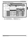
5.4.2 Memory Interface
Pin Names
Type
LCAS#
O
UCAS#
O
WE#
O
RAS#
MD[15:0]
O
I/O
MA[8:0]
O
MA9
I/O
MA10
I/O
MA11
I/O
Table 5-2 Memory Interface Pin Descriptions
Pin #
Reset
F00A,
Driver
Description
F02A
= 0 Value
F01A
50
56
CO1
Output 1 This pin has multiple functions.
• For dual CAS# DRAM, this is the column address strobe for
the lower byte (LCAS#).
• For single CAS# DRAM, this is the column address strobe
(CAS#).
See Table 5-10, “Memory Interface Pin Mapping,” on page 16
for summary.
49
55
CO1
Output 1 This pin has multiple functions.
• For dual CAS# DRAM, this is the column address strobe for
the upper byte (UCAS#).
• For single CAS# DRAM, this is the write enable signal for the
upper byte (UWE#).
See Table 5-10, “Memory Interface Pin Mapping,” on page 16
for summary.
48
54
CO1
Output 1 This pin has multiple functions.
• For dual CAS# DRAM, this is the write enable signal (WE#).
• For single CAS# DRAM, this is the write enable signal for the
lower byte (LWE#).
See Table 5-10, “Memory Interface Pin Mapping,” on page 16
for summary.
47
53
CO1
Output 1 Row address strobe.
67, 65
76, 70 CD2/TS1
Hi-Z
These pins have multiple functions.
63, 61
68, 66
(pulled 0) • Bi-directional memory data bus.
59, 57
64, 62
• During reset, these pins are inputs and their states at the rising
55, 53
60, 58
edge of RESET# are used to configure the chip. Internal pull52, 54
59, 61
down resistors (typical values of 100KΩ/100KΩ/120KΩ at
56, 58
63, 65
5.0V/3.3V/3.0V respectively) pull the reset states to 0. External
60, 62
67, 69
pull-up resistors can be used to pull the reset states to 1. See
64, 66
75, 77
Section 5.5, “Summary of Configuration Options” on page 16.
43, 41
46, 44
CO1
Output 0 Multiplexed memory address.
39, 37
42, 40
35, 34
41, 43
36, 38
45, 47
40
49
45
51
C/TS1
Hi-Z / This pin has multiple functions.
Output 0 • For 2M byte DRAM, this is memory address bit 9 (MA9).
(∗1)
• For asymmetrical 512K byte DRAM, this is memory address
bit 9 (MA9).
• For symmetrical 512K byte DRAM, this pin can be used as
general purpose IO (GPIO3).
See Table 5-10, “Memory Interface Pin Mapping,” on page 16
for summary.
42
48
C/TS1
Hi-Z / This pin has multiple functions.
Output 0 • For asymmetrical 2M byte DRAM, this is memory address bit
(∗1)
10 (MA10).
• For symmetrical 2M byte DRAM and all 512K byte DRAM,
this pin can be used as general purpose IO (GPIO1).
See Table 5-10, “Memory Interface Pin Mapping,” on page 16
for summary.
44
50
C/TS1
Hi-Z / This pin has multiple functions.
Output 0 • For asymmetrical 2M byte DRAM, this is memory address bit
(∗1)
11 (MA11).
• For symmetrical 2M byte DRAM and all 512K byte DRAM,
this pin can be used as general purpose IO (GPIO2).
See Table 5-10, “Memory Interface Pin Mapping,” on page 16
for summary.
*1: When configured as IO pins.
1-12
EPSON
S1D13504 SERIES HARDWARE FUNCTIONAL
SPECIFICATION (X19A-A-002-17)
5: PIN OUT
5.4.3 LCD Interface
Table 5-3 LCD Interface Pin Descriptions
Pin Names
Type
Pin #
F00A,
F02A
F01A
88
98
82–75
92–85
95–89
105–99
Driver
FPDAT[8:0]
O
FPDAT[15:9]
O
FPFRAME
FPLINE
FPSHIFT
LCDPWR
O
O
O
O
69
70
73
71
79
80
83
81
CN3
CN3
CN3
CO1
DRDY
O
72
82
CN3
Reset
= 0 Value
Description
CN3
Output 0 Panel Data
CN3
Output 0 These pins have multiple functions.
• Panel Data for 16-bit panels .
• Pixel Data for external RAMDAC support.
See Table 5-11, “LCD, CRT, RAMDAC Interface Pin Mapping,”
on page 17.
Output 0 Frame Pulse
Output 0 Line Pulse
Output 0 Shift Clock Pulse
Output LCD power control output. The active polarity of this output is
(∗1)
selected by the state of MD10 at the rising edge of RESET# - see
Section 5.5, “Summary of Configuration Options” on page 16.
This output is controlled by the power save mode circuitry - see
Section 13, “Power Save Modes” on page 99 for details.
Output 0 This pin has multiple functions which are automatically selected
depending on panel type used.
• For TFT panels, this is the display enable output (DRDY).
• For passive LCDs with Format 1 interfaces, this is the 2nd Shift
Clock (FPSHIFT2).
• For all other LCD panels, this is the LCD backplane bias signal
(MOD).
See Table 5-11, “LCD, CRT, RAMDAC Interface Pin Mapping,”
on page 17 and REG[02h] for details.
∗1: Output may be 1 or 0.
5.4.4 Clock Input
Table 5-4 Clock Input Pin Description
Pin Names
CLKI
Type
I
Pin #
F00A,
F02A
F01A
105
119
Driver
Reset
= 0 Value
C
Hi-Z
Description
Input clock for the internal pixel clock (PCLK) and memory
clock (MCLK). PCLK and MCLK are derived from CLKI – see
REG[19h] for details.
5.4.5 CRT and External RAMDAC Interface
Pin Names
Type
DACRD#
I/O
DACWR#
I/O
DACRS1
I/O
Table 5-5 CRT and RAMDAC Interface Pin Descriptions
Pin #
Reset
F00A,
Driver
Description
F02A
= 0 Value
F01A
84
94
C/TS1
Hi-Z / This pin has multiple functions.
Output 1 • Read signal for external RAMDAC support.
(∗1)
• General Purpose IO (GPIO4).
See Table 5-11, “LCD, CRT, RAMDAC Interface Pin Mapping,”
on page 17.
99
113
C/TS1
Hi-Z / This pin has multiple functions.
Output 1 • Write signal for external RAMDAC support.
(∗1)
• General Purpose IO (GPIO7).
See Table 5-11, “LCD, CRT, RAMDAC Interface Pin Mapping,”
on page 17.
101
115
C/TS1
Hi-Z / This pin has multiple functions.
Output 0 • Register Select bit 1 for external RAMDAC support.
(∗1)
• General Purpose IO (GPIO9).
See Table 5-11, “LCD, CRT, RAMDAC Interface Pin Mapping,”
on page 17.
S1D13504 SERIES HARDWARE FUNCTIONAL
SPECIFICATION (X19A-A-002-17)
EPSON
1-13
5: PIN OUT
Pin Names
Type
DACRS0
I/O
DACP0
I/O
HRTC
I/O
VRTC
I/O
BLANK#
I/O
DACCLK
O
Table 5-5 CRT and RAMDAC Interface Pin Descriptions
Pin #
Reset
F00A,
Driver
Description
F02A
= 0 Value
F01A
100
114
C/TS1
Hi-Z / This pin has multiple functions.
Output 0 • Register Select bit 0 for external RAMDAC support.
(∗1)
• General Purpose IO (GPIO8).
See Table 5-11, “LCD, CRT, RAMDAC Interface Pin Mapping,”
on page 17.
98
112
C/CN3
Hi-Z / This pin has multiple functions.
Output 0 • Pixel Data bit 0 for external RAMDAC support.
(∗1)
• General Purpose IO (GPIO6).
See Table 5-11, “LCD, CRT, RAMDAC Interface Pin Mapping,”
on page 17.
102
116
C/CN3
Hi-Z / This pin has multiple functions.
Output 0 • Horizontal Retrace signal for CRT.
(∗1)
• General Purpose IO (GPIO10).
See Table 5-11, “LCD, CRT, RAMDAC Interface Pin Mapping,”
on page 17.
103
117
C/CN3
Hi-Z / This pin has multiple functions.
Output 0 • Vertical Retrace signal for CRT.
(∗1)
• General Purpose IO (GPIO11).
See Table 5-11, “LCD, CRT, RAMDAC Interface Pin Mapping,”
on page 17.
85
95
C/CN3
Hi-Z / This pin has multiple functions.
Output 0 • Blanking signal for DAC.
(∗1)
• General Purpose IO (GPIO5).
See Table 5-11, “LCD, CRT, RAMDAC Interface Pin Mapping,”
on page 17.
86
96
C/CN3 Output 0 Pixel Clock for RAMDAC.
*1: When configured as IO pins.
5.4.6 Miscellaneous
Table 5-6 Miscellaneous Pin Descriptions
Pin Names
Type
Pin #
F00A,
F02A
F01A
106
120
Driver
SUSPEND#
I/O
GPIO0
TSTEN
I/O
I
12
107
14
121
C/TS1
CD
–
–
1, 2
35–38
71–74
107–110
143, 144
–
NC
CS/TS1
Reset
= 0 Value
Description
Hi-Z /
Output
(∗1)
This pin has multiple functions.
• When MD9 = 0 at rising edge of RESET#, this pin is an activelow input used to place the S1D13504 into suspend mode; see
Section 13, “Power Save Modes” on page 99 for details.
• When MD[10:9] = 01 at rising edge of RESET#, this pin is an
output with a reset state of 0. Its state is controlled by
REG[21h] bit 7.
• When MD[10:9] = 11 at rising edge of RESET#, this pin is an
output with a reset state of 1. Its state is controlled by
REG[21h] bit 7.
Hi-Z
General Purpose IO pin 0.
Hi-Z
Test Enable. This in should be connected to VSS for normal oper(pulled 0) ation.
–
No connect
∗1: When configured as IO pin. Output may be 1 or 0.
1-14
EPSON
S1D13504 SERIES HARDWARE FUNCTIONAL
SPECIFICATION (X19A-A-002-17)
5: PIN OUT
5.4.7 Power Supply
Pin Names
COREVDD
IOVDD
VSS
Table 5-7 Power Supply Pin Descriptions
Pin #
Type
Driver
F00A, F01A
F02A
P
33, 97
39, 111
P
Core VDD
P 14, 46, 83, 110 16, 52, 93, 124
P
IO VDD
P
15, 32, 51, 68 17, 34, 57, 78
P
Common VSS
74, 87, 96 104
84, 97, 106
109
118, 123
S1D13504 SERIES HARDWARE FUNCTIONAL
SPECIFICATION (X19A-A-002-17)
EPSON
Description
1-15
5: PIN OUT
5.5 Summary of Configuration Options
Pin Name
MD0
MD[3:1]
MD4
MD5
MD[7:6]
MD8
MD9
MD10
MD[15:11]
Table 5-8 Summary of Power On / Reset Options
Value on this pin at rising edge of RESET# is used to configure:
(1/0)
1
0
8-bit host bus interface
16-bit host bus interface
Select host bus interface:
000 = SH-3 bus interface
001 = MC68K bus 1 (e.g. MC68000)
010 = MC68K bus 2 (e.g. MC68030)
011 = Generic bus interface (e.g. Philips MIPS PR31500/PR31700; NEC MIPS VR4102)
1XX = reserved
Little Endian
Big Endian
WAIT# is active high (1 = insert wait state)
WAIT# is active low (0 = insert wait state)
Memory Address/GPIO configuration:
00 = symmetrical 256K×16 DRAM. MA[8:0] = DRAM address. MA[11:9] = GPIO[2:1] and GPIO3
01 = symmetrical 1M×16 DRAM.
MA[9:0] = DRAM address. MA[11:10] = GPIO[2:1]
10 = asymmetrical 256K×16 DRAM. MA[9:0] = DRAM address. MA[11:10] = GPIO[2:1]
11 = asymmetrical 1M×16 DRAM. MA[11:0] = DRAM address.
Configure DACRD#, BLANK#, DACP0,
Configure DACRD#, BLANK#, DACP0, DACWR#,
DACWR#, DACRS0, DACRS1, HRTC, VRTC as DACRS0, DACRS1, HRTC, VRTC as DAC and CRT
General Purpose IO (GPIO[11:4]).
outputs.
SUSPEND# pin configured as GPO output.
SUSPEND# pin configured as SUSPEND# input.
Active low LCDPWR or GPO polarities.
Active high LCDPWR or GPO polarities.
Not used.
5.6 Multiple Function Pin Mapping
Table 5-9 Host Bus Interface Pin Mapping
S1D13504
Pin Names
AB[20:1]
AB0
DB[15:0]
WE1#
M/R#
CS#
BUSCLK
BS#
RD/WR#
RD#
WE0#
WAIT#
RESET#
S1D13504
Pin Names
MD[15:0]
MA[8:0]
MA9
MA10
MA11
UCAS#
LCAS#
WE#
RAS#
SH-3
MC68K Bus 1
MC68K Bus 2
Generic MPU
A[20:1]
A0
D[15:0]
WE1#
External Decode
CSn#
CKIO
BS#
RD/WR#
RD#
WE0#
WAIT#
RESET#
A[20:1]
LDS#
D[15:0]
UDS#
External Decode
External Decode
CLK
AS#
R/W#
Connect to IO VDD
Connect to IO VDD
DTACK#
RESET#
A[20:1]
A0
D[31:16]
DS#
External Decode
External Decode
CLK
AS#
R/W#
SIZ1
SIZ0
DSACK1#
RESET#
A[20:1]
A0
D[15:0]
WE1#
External Decode
External Decode
BCLK
Connect to IO VDD
RD1#
RD0#
WE0#
WAIT#
RESET#
Sym 256K × 16
2CAS#
2WE#
GPIO3∗1
UCAS#
LCAS#
WE#
UWE#
CAS#
LWE#
Table 5-10 Memory Interface Pin Mapping
FPM/EDO-DRAM
Asym 256K × 16
Sym 1M × 16
2CAS#
2WE#
2CAS#
2WE#
DQ[15:0]
A[8:0]
A9
GPIO1∗1
GPIO2∗1
UCAS#
UWE#
UCAS#
UWE#
LCAS#
CAS#
LCAS#
CAS#
WE#
LWE#
WE#
LWE#
RAS#
Asym 1M × 16
2CAS#
2WE#
A10
A11
UCAS#
LCAS#
WE#
UWE#
CAS#
LWE#
*1: All GPIO pins default to input on reset, and unless programmed otherwise should be connected to either
VSS or IO VDD if not used.
1-16
EPSON
S1D13504 SERIES HARDWARE FUNCTIONAL
SPECIFICATION (X19A-A-002-17)
5: PIN OUT
Table 5-11 LCD, CRT, RAMDAC Interface Pin Mapping
Monochrome Passive Panel
S1D13504
Pin Names
Single
4-bit
FPFRAME
FPLINE
FPSHIFT
DRDY
FPDAT0
FPDAT1
FPDAT2
FPDAT3
FPDAT4
FPDAT5
FPDAT6
FPDAT7
FPDAT8
FPDAT9
FPDAT10
FPDAT11
FPDAT12
FPDAT13
FPDAT14
FPDAT15
DACRD#
BLANK#
DACP0
DACWR#
DACRS0
DACRS1
HRTC
VRTC
DACCLK
driven 0
driven 0
driven 0
driven 0
D0
D1
D2
D3
driven 0
driven 0
driven 0
driven 0
driven 0
driven 0
driven 0
driven 0
8-bit
Dual
Single
8-bit
4-bit
MOD
D0
LD0
D1
LD1
D2
LD2
D3
LD3
D4
UD0
D5
UD1
D6
UD2
D7
UD3
driven 0 driven 0
driven 0 driven 0
driven 0 driven 0
driven 0 driven 0
driven 0 driven 0
driven 0 driven 0
driven 0 driven 0
driven 0 driven 0
driven 0
driven 0
driven 0
driven 0
D0
D1
D2
D3
driven 0
driven 0
driven 0
driven 0
driven 0
driven 0
driven 0
driven 0
Color Passive Panel
Single
Single
Dual
Format 1 Format 2
8-bit
8-bit
8-bit
16-bit
FPFRAME
FPLINE
FPSHIFT
FPSHIFT2
MOD
D0
D0
LD0
LD0
D1
D1
LD1
LD1
D2
D2
LD2
LD2
D3
D3
LD3
LD3
D4
D4
UD0
UD0
D5
D5
UD1
UD1
D6
D6
UD2
UD2
D7
D7
UD3
UD3
driven 0
driven 0 driven 0
LD4
driven 0
driven 0 driven 0
LD5
driven 0
driven 0 driven 0
LD6
driven 0
driven 0 driven 0
LD7
driven 0
driven 0 driven 0
UD4
driven 0
driven 0 driven 0
UD5
driven 0
driven 0 driven 0
UD6
driven 0
driven 0 driven 0
UD7
GPIO4∗3
GPIO5∗3
GPIO6∗3
GPIO7∗3
GPIO8∗3
GPIO9∗3
GPIO10∗3
GPIO11∗3
driven 0
Color TFT Panel
9-bit
R2
R1
R0
G2
G1
G0
B2
B1
B0
driven 0
driven 0
driven 0
driven 0
driven 0
driven 0
driven 0
12-bit
DRDY
R3
R2
R1
G3
G2
G1
B3
B2
B1
R0
driven 0
G0
driven 0
driven 0
B0
driven 0
CRT
18-bit∗1
R5
R4
R3
G5
G4
G3
B5
B4
B3
R2
R1
G2
G1
G0
B2
B1
Note∗2
Note∗2
Note∗2
Note∗2
Note∗2
Note∗2
Note∗2
Note∗2
Note∗2
Note∗2
Note∗2
Note∗2
Note∗2
DACP7
DACP6
DACP5
DACP4
DACP3
DACP2
DACP1
DACRD#
BLANK#
DACP0
DACWR#
DACRS0
DACRS1
HRTC
VRTC
DACCLK
*1: Although 18-bit TFT panels are supported only 16 data bits (64K colors) are available
- R0 and B0 are not used.
*2: If no LCD is active these pins are driven low.
*3: All GPIO pins default to input on reset, and unless programmed otherwise should be connected to either
VSS or IO VDD if not used.
S1D13504 SERIES HARDWARE FUNCTIONAL
SPECIFICATION (X19A-A-002-17)
EPSON
1-17
6: D.C. CHARACTERISTICS
6 D.C. CHARACTERISTICS
Parameter
Supply Voltage
Supply Voltage
Input Voltage
Output Voltage
Storage Temperature
Solder Temperature/Time
Symbol
CoreVDD
IOVDD
VIN
TOPR
Table 6-2 Recommended Operating Conditions
Parameter
Condition
Min.
Typ.
Supply Voltage
VSS = 0 V
2.7
3.0/3.3
Supply Voltage
VSS = 0 V
2.7
3.0/3.3/5.0
Input Voltage
VSS
Operating Temperature
-40
25
Symbol
VIL
VIH
VT+
VT-
IIZ
CIN
HRPD
Symbol
VOL
VOH
1-18
Table 6-1 Absolute Maximum Ratings
Rating
VSS - 0.3 to 4.6
VSS - 0.3 to 6.0
VSS - 0.3 to IOVDD + 0.5
VSS - 0.3 to IOVDD + 0.5
-65 to 150
260 for 10 sec. max. at lead
Symbol
CoreVDD
IOVDD
VIN
VOUT
TSTG
TSOL
Table 6-3 Input Specifications
Condition
Min.
IOVDD = 3.0V
Low Level Input Voltage
IOVDD = 3.3V
CMOS inputs
IOVDD = 5.0V
IOVDD = 3.0V
1.9
High Level Input Voltage
IOVDD = 3.3V
2.0
CMOS inputs
IOVDD = 5.0V
3.5
IOVDD = 3.0V
1.0
Positive-Going Threshold
IOVDD = 3.3V
1.1
CMOS Schmitt inputs
IOVDD = 5.0V
2.0
IOVDD = 3.0V
0.5
Negative-Going Threshold
IOVDD = 3.3V
0.6
CMOS Schmitt inputs
IOVDD = 5.0V
0.8
VDD = Max..
Input Leakage Current
VIH = IOVDD
-1
VIL = VSS
Input Pin Capacitance
VIN = VDD = 3.0V
60
Pull-down Resistance
VIN = VDD = 3.3V
50
VIN = VDD = 5.0V
50
Parameter
Parameter
Low Level Output Voltage
Type 1 - TS1, CO1, TS1D
Type 2 - TS2, CO2
Type 3 - TS3, CO3
High Level Output Voltage
Type 1 - TS1, CO1, TS1D
Type 2 - TS2, CO2
Type 3 - TS3, CO3
IOZ
Output Leakage Current
COUT
CBID
Output Pin Capacitance
Bidirectional Pin Capacitance
Typ.
Units
V
V
V
°C
Max.
0.8
0.8
1.0
Units
2.3
2.4
4.0
1.7
1.8
3.1
IOL = 3mA
IOL = 6mA
IOL = 12mA
EPSON
Max.
3.6
5.5
IOVDD
85
V
V
1
µA
10
300
300
300
pF
120
100
100
Typ.
Max.
Units
0.4
V
IOVDD-0.4
-1
V
V
Table 6-4 Output Specifications
Condition
Min.
IOH = -1.5mA
IOH = -3mA
IOH = -6mA
IOVDD = Max..
VOH = VDD
VOL = VSS
Units
V
V
V
V
°C
°C
kΩ
V
1
µA
10
10
pF
pF
S1D13504 SERIES HARDWARE FUNCTIONAL
SPECIFICATION (X19A-A-002-17)
7: A.C. CHARACTERISTICS
7 A.C. CHARACTERISTICS
Conditions: IOVDD = 2.7V to 5.5V unless otherwise specified
TA = -40°C to 85°C
Trise and Tfall for all inputs must be ≤ 5 nsec (10% to 90%)
CL = 50pF (Bus / MPU Interface)
CL = 100pF (LCD Panel Interface)
CL = 10pF (Display Buffer Interface) CL = 10pF (CRT / DAC Interface)
S1D13504 SERIES HARDWARE FUNCTIONAL
SPECIFICATION (X19A-A-002-17)
EPSON
1-19
7: A.C. CHARACTERISTICS
7.1 CPU Interface Timing
7.1.1 SH-3 Interface Timing
t1
t2
t3
CKIO
t4
t5
A[20:0], M/R#
RD/WR#
t6
t7
BS#
t8
t12
CSn#
t10
t9
WEn#
RD#
t12
t11
WAIT#
t14
t13
D[15:0](write)
t15
t16
D[15:0](read)
Figure 7-1 SH-3 Interface Timing
Note: The SH-3 Wait State Control Register for the area in which the S1D13504 resides must be set to a
non-zero value.
Table 7-1 SH-3 Interface Timing
Symbol
t1
t2
t3
t4
t5
t6
t7
t8
t9 2
t10
t11
t12
t13
t14
t15
t16
Parameter
Clock period
Clock pulse width high
Clock pulse width low
A[20:0], M/R#, RD/WR# setup to CKIO
A[20:0], M/R#, RD/WR# hold from CS#
BS# setup
BS# hold
CSn# setup
Falling edge RD# to D[15:0] driven
Rising edge CSn# to WAIT# tri-state
Falling edge CSn# to WAIT# driven
CKIO to WAIT# delay
D[15:0] setup to first CKIO after BS# (write cycle)
D[15:0] hold (write cycle)
D[15:0] valid to WAIT# rising edge (read cycle)
Rising edge RD# to D[15:0] tri-state (read cycle)
3.3V
Min.
Max.
25
5
5
4
0
3
0
0
3
0
4
1
11
3
15
0
0
0
2
9
Units
ns
ns
ns
ns
ns
ns
ns
ns
ns
ns
ns
ns
ns
ns
ns
ns
Note: 1. If the S1D13504 host interface is disabled, the timing for WAIT# driven is relative to the falling edge
of CSn# or the first positive edge of CKIO after A[20:0], M/R# becomes valid, whichever one is later.
2. If the S1D13504 host interface is disabled, the timing for D[15:0] driven is relative to the falling edge
of RD# or the first positive edge of CKIO after A[20:0], M/R# becomes valid, whichever one is later.
1-20
EPSON
S1D13504 SERIES HARDWARE FUNCTIONAL
SPECIFICATION (X19A-A-002-17)
7: A.C. CHARACTERISTICS
TCKIO
CKIO
t1
A[20:0]
Valid
M/R#
t3
t2
t4
CSn#
t5
t5
RD/WR#
WE0#, WE1#
t7
t8
t9
Hi-Z
Hi-Z
Valid
D[15:0]
t10
t10
BS#
t6
t11
t13
t12
Hi-Z
t13
Hi-Z
WAIT#
Figure 7-2 SH-3 Write Bus Timing
Note: The SH-3 Wait State Control Register for the area in which the S1D13504 resides must be set to a
non-zero value.
Table 7-2 SH-3 Write Bus Timing
Symbol
Parameter
TCKIO Bus clock period
A[20:0], M/R# delay time
t1
CSn# delay time
t2
A[20:0], M/R# hold time
t3
Read write hold time
t4
Read write delay time
t5
t6 1 Falling edge of CSn# to WAIT# driven
Write Data hold time 1
t7
Write Data delay time
t8
Write Data hold time 2
t9
t10 BS# delay time
t11 CKIO to WAIT# low
t12 CKIO to WAIT# high
t13 CSn# high to WAIT# high impedance
3.3V
Min.
Max.
33
15
14
8
0
14
0
11
0
17
0
14
14
15
4
Units
ns
ns
ns
ns
ns
ns
ns
ns
ns
ns
ns
ns
ns
ns
Note: 1. If the S1D13504 host interface is disabled, the timing for WAIT# driven is relative to the falling edge
of CSn# or the first positive edge of CKIO after A[20:0], M/R# becomes valid, whichever one is later.
S1D13504 SERIES HARDWARE FUNCTIONAL
SPECIFICATION (X19A-A-002-17)
EPSON
1-21
7: A.C. CHARACTERISTICS
7.1.2 MC68K Bus 1 Interface Timing (e.g. MC68000)
t1
t2
t3
CLK
t5
t4
A[20:1]
M/R#
t6
CS#
t16
AS#
UDS#
LDS#
t8
t7
R/W#
t9
t10
DTACK#
t12
t11
D[15:0](write)
t13
t14
t15
D[15:0](read)
Figure 7-3 MC68000 Bus 1 InterfaceTiming
Table 7-3 MC68000 Bus 1 InterfaceTiming
3.3V
Symbol
Parameter
Min.
Max.
33
TCLK Bus clock period
A[20:1], CS#, M/R# valid before AS# falling edge
0
t1
A[20:1], CS#, M/R# hold from AS# rising edge
0
t2
7
t3 1 AS# low to DTACK# driven high
CLK to DTACK# low
14
t4
AS# high to DTACK# high impedance
5
t5
AS# falling edge to D[15:0] valid
TCLK
t6
D[15:0] hold from AS# rising edge
0
t7
5V
Min.
33
0
0
Max.
7
14
5
TCLK
0
Units
ns
ns
ns
ns
ns
ns
ns
ns
Note: 1. If the S1D13504 host interface is disabled, the timing for DTACK# driven high is relative to the falling edge of AS# or the first positive edge of CLK after A[20:1], M/R# becomes valid, whichever
one is later.
1-22
EPSON
S1D13504 SERIES HARDWARE FUNCTIONAL
SPECIFICATION (X19A-A-002-17)
7: A.C. CHARACTERISTICS
TCLK
CLK
A[20:1]
CS#
M/R#
Valid
t1
t2
AS#
LDS#
UDS#
Invalid
R/W#
t3
DTACK#
Hi-Z
Hi-Z
t7
t6
D[15:0]
t5
t4
t8
Hi-Z
Hi-Z
Valid
Figure 7-4 MC68000 Read Bus Timing
Table 7-4 MC68000 Read Bus Timing
3.3V
Symbol
Parameter
t1
t2
t3
Clock period
Clock pulse width high
Clock pulse width low
A[20:1], M/R# setup to first CLK where CS# = 0 AS# = 0, and either UDS#=0 or
LDS# = 0
A[20:1], M/R# hold from AS#
CS# hold from AS#
R/W# setup to before to either UDS#=0 or LDS# = 0
R/W# hold from AS#
AS# = 0 and CS# = 0 to DTACK# driven high
AS# high to DTACK# high impedance
D[15:0] valid to second CLK where CS# = 0 AS# = 0, and either UDS#=0 or
LDS# = 0 (write cycle)
D[15:0] hold from falling edge of DTACK# (write cycle)
Falling edge of UDS#=0 or LDS# = 0 to D[15:0] driven (read cycle)
D[15:0] valid to DTACK# falling edge (read cycle)
UDS# and LDS# high to D[15:0] invalid/high impedance (read cycle)
AS# high setup to CLK
t4
t5
t6
t7
t8
t9 1
t10
t11
t12
t13 2
t14
t15
t16
Min.
30
5
5
Max.
Units
ns
ns
ns
4
ns
0
0
5
0
1
1
0
ns
ns
ns
ns
ns
ns
ns
0
3
0
2
3
5
11
ns
ns
ns
ns
ns
Note: 1. If the S1D13504 host interface is disabled, the timing for DTACK# driven high is relative to the falling edge of AS# or the first positive edge of CLK after A[20:1], M/R# becomes valid, whichever
one is later.
2. If the S1D13504 host interface is disabled, the timing for D[15:0] driven is relative to the falling
edge of UDS#/LDS# or the first positive edge of CLK after A[20:1], M/R# becomes valid, whichever one is later.
S1D13504 SERIES HARDWARE FUNCTIONAL
SPECIFICATION (X19A-A-002-17)
EPSON
1-23
7: A.C. CHARACTERISTICS
7.1.3 MC68K Bus 2 Interface Timing (e.g. MC68030)
t1
t2
t3
CLK
t5
t4
A[20:0]
SIZ[1:0] M/R#
t6
CS#
t16
AS#
DS#
t7
t8
R/W#
t9
t10
DSACK1#
t11
t12
D[31:16](write)
t13
t15
t14
D[31:16](read)
Figure 7-5 MC68030 Bus 2 Interface Timing
Table 7-5 MC68030 Bus 2 Interface Timing
5V
Symbol
Parameter
t1
t2
t3
Clock period
Clock pulse width high
Clock pulse width low
A[20:0], SIZ[1:0], M/R# setup to first CLK where CS# = 0 AS# = 0, and either UDS#=0 or
LDS# = 0
A[20:0], SIZ[1:0], M/R# hold from AS#
CS# hold from AS#
R/W# setup to DS#
R/W# hold from AS#
AS# = 0 and CS# = 0 to DSACK1# driven high
AS# high to DSACK1# high impedance
D[31:16] valid to second CLK where CS# = 0 AS# = 0, and either UDS#=0 or LDS# = 0
(write cycle)
D[31:16] hold from falling edge of DSACK1# (write cycle)
Falling edge of UDS# = 0 or LDS# = 0 to D[31:16] driven (read cycle)
D[31:16] valid to DSACK1# falling edge (read cycle)
UDS# and LDS# high to D[31:16] invalid/high impedance (read cycle)
AS# high setup to CLK
t4
t5
t6 1
t7
t8
t9
t10
t11
t12
t13
t14
t15
t16
Min.
30
5
5
Max.
Units
ns
ns
ns
4
ns
0
0
5
0
1
1
ns
ns
ns
ns
ns
ns
5
0
ns
0
3
0
2
3
ns
ns
ns
ns
ns
11
Note: 1. If the S1D13504 host interface is disabled, the timing for DSACK1# driven high is relative to the
falling edge of AS# or the first positive edge of CLK after A[20:0], M/R# becomes valid, whichever
one is later.
2. If the S1D13504 host interface is disabled, the timing for D[15:0] driven is relative to the falling
edge of UDS#/LDS# or the first positive edge of CLK after A[20:1] and M/R# becomes valid,
whichever occurs later.
1-24
EPSON
S1D13504 SERIES HARDWARE FUNCTIONAL
SPECIFICATION (X19A-A-002-17)
7: A.C. CHARACTERISTICS
TCLK
CLK
A[20:0]
CS#
M/R#
SIZ0, SIZ1
Valid
t2
t1
AS#
DS#
t3
R/W#
t5
t4
t6
Hi-Z
Hi-Z
DSACK1#
t8
t7
D[31:16]
t9
Hi-Z
Hi-Z
Valid
Figure 7-6 MC68030 Read Bus Timing
Table 7-6 MC68030 Read Bus Timing
Symbol
TCLK
t1
t2
t3
t4 1
t5
t6
t7
t8
t9
5V
Parameter
Bus clock period
A[20:0], CS#, M/R#, SIZ0, SIZ1 valid before AS#, DS# falling edge
A[20:0], CS#, M/R#, SIZ0, SIZ1 hold from AS#, DS# rising edge
R/W# rising edge to AS#, DS# falling edge
AS# low to DSACK1# driven high
CLK to DSACK1# low
AS# high to DSACK1# high impedance
AS#, DS# falling edge to D[31:16]
Read Data valid to DSACK1# low
AS#, DS# rising edge to D[31:16] high impedance
Min.
30
5
5
5
Max.
7
14
5
12
0
11
Units
ns
ns
ns
ns
ns
ns
ns
ns
ns
ns
Note: 1 .If the S1D13504 host interface is disabled, the timing for DSACK1# driven high is relative to the
falling edge of AS# or the first positive edge of CLK after A[20:0], M/R# becomes valid, whichever
one is later.
S1D13504 SERIES HARDWARE FUNCTIONAL
SPECIFICATION (X19A-A-002-17)
EPSON
1-25
7: A.C. CHARACTERISTICS
7.1.4 Generic MPU Interface Synchronous Timing
TBCLK
BCLK
t1
t2
A[20:0]
M/R#
t1
t2
t2
Valid
t1
t2
t1
t1
t2
t1
CS#
t3
RD0#,RD1#
WE0#,WE1#
t4
t5
t2
t6
Hi-Z
Hi-Z
WAIT#
t8
t7
Hi-Z
Hi-Z
Valid
D[15:0](write)
t10
t9
Hi-Z
t11
Hi-Z
Valid
D[15:0](read)
Figure 7-7 Generic MPU Interface Synchronous Timing
Table 7-7 Generic MPU Interface Synchronous Timing
Symbol
Parameter
TBCLK Bus clock period
A[20:0], M/R#, CS#, RD0#,RD1#,WE0#,WE1# hold time
t1
A[20:0], M/R#, CS#, RD0#,RD1#,WE0#,WE1# setup time
t2
RD0#,RD1#,WE0#,WE1# high to A[20:0], M/R# invalid and CS# high
t3
t4 1 RD0#,RD1#,WE0#,WE1# low and CS# low to WAIT# driven low
BCLK to WAIT# high
t5
RD0#,RD1#,WE0#,WE1# high to WAIT# high impedance
t6
D[15:0] valid to second BCLK where RD0#,RD1#,WE0#,WE1# low and CS# low (write cycle)
t7
D[15:0] hold from WE0#, WE1# high (write cycle)
t8
t9 2 RD0#,RD1# low to D[15:0] driven (read cycle)
t10 D[15:0] valid to WAIT# high (read cycle)
t11 RD0#, RD1# high to D[15:0] high impedance (read cycle)
3.3V
Min.
Max.
25
1
5
0
1
7
0
15
1
6
5
0
3
15
0
2
10
Units
ns
ns
ns
ns
ns
ns
ns
ns
ns
ns
Note: 1. If the S1D13504 host interface is disabled, the timing for WAIT# driven low is relative to the falling
edge of CS# and RD0#, RD1#, WE0#, WE1# or the first positive edge of BCLK after A[20:0], M/R#
becomes valid, whichever one is later.
2. If the S1D13504 host interface is disabled, the timing for D[15:0] driven is relative to the falling
edge of RD0#, RD1# or the first positive edge of BCLK after A[20:0], M/R# becomes valid, whichever one is later.
1-26
EPSON
S1D13504 SERIES HARDWARE FUNCTIONAL
SPECIFICATION (X19A-A-002-17)
7: A.C. CHARACTERISTICS
TBCLK
BCLK
t1
t2
t2
t1
A[20:0]
M/R#
Valid
t1
t2
t1
t2
t1
CS#
t2
t3
t2
t1
WE0#
WE1#
t5
t4
Hi-Z
Hi-Z
Valid
D[15:0]
t6
t7
t8
Hi-Z
Hi-Z
WAIT#
Figure 7-8 Generic Write Bus Synchronous Timing
Table 7-8 Generic Write Bus Synchronous Timing
Symbol
3.3V
Parameter
TBCLK Bus clock period
A[20:0], M/R#, CS#, RD0#, RD1# hold time
t1
A[20:0], M/R#, CS#, RD0#, RD1# setup time
t2
WE0#, WE1# high to A[20:0], CS#, M/R# invalid
t3
D[15:0] setup time
t4
D[15:0] hold from WE0#, WE1# high
t5
t6 1 WE0#, WE1# low and CS# low to WAIT# driven low
BCLK to WAIT# high
t7
WE0#, WE1# high to WAIT# high impedance
t8
Min.
25
1
5
0
5
0
Max.
7
15
6
Units
ns
ns
ns
ns
ns
ns
ns
ns
ns
Note: 1. If the S1D13504 host interface is disabled, the timing for WAIT# driven low is relative to the falling
edge of CS# and WE0#, WE1# or the first positive edge of BCLK after A[20:0], M/R# becomes valid, whichever one is later.
S1D13504 SERIES HARDWARE FUNCTIONAL
SPECIFICATION (X19A-A-002-17)
EPSON
1-27
7: A.C. CHARACTERISTICS
7.1.5 Generic MPU Interface Asynchronous Timing
TBCLK
BCLK
A[20:0]
M/R#
Valid
t1
CS#
t2
t3
RD0#,RD1#
WE0#,WE1#
Hi-Z
t5
t4
Hi-Z
WAIT#
t7
t6
D[15:0](write)
Hi-Z
t9
t8
D[15:0](read)
Hi-Z
Valid
t10
Hi-Z
Hi-Z
Valid
Figure 7-9 Generic MPU Interface Asynchronous Timing
Table 7-9 Generic MPU Interface Asynchronous Timing
Symbol
3.3V
Parameter
TBCLK Bus clock period
RD0#, RD1#, WE0#, WE1# low to CS# low
t1
A[20:0], M/R# valid to RD0#, RD1#, WE0#, WE1# low
t2
RD0#, RD1#, WE0#, WE1# high to A[20:0], CS#, M/R# invalid and CS# high
t3
t4 1 CS# low to WAIT# driven low
RD0#, RD1#, WE0#, WE1# high to WAIT# high impedance
t5
WE0#, WE1# low to D[15:0] valid (write cycle)
t6
D[15:0] hold from WE0#, WE1# high (write cycle)
t7
t8 2 RD0#, RD1# low to D[15:0] driven (read cycle)
D[15:0] valid to WAIT# high (read cycle)
t9
t10 RD0#, RD1# high to D[15:0] high impedance (read cycle)
Min.
25
4
0
0
1
1
0
3
0
2
Max.
7
6
20
15
Units
ns
ns
ns
ns
ns
ns
ns
ns
ns
10
Note: 1. If the S1D13504 host interface is disabled, the timing for WAIT# driven low is relative to the falling
edge of CS# or the first positive edge of BCLK after A[20:0], M/R# becomes valid, whichever one
is later.
2. If the S1D13504 host interface is disabled, the timing for D[15:0] driven is relative to the falling
edge of RD0#, RD1# or the first positive edge of BCLK after A[20:0], M/R# becomes valid, whichever one is later.
1-28
EPSON
S1D13504 SERIES HARDWARE FUNCTIONAL
SPECIFICATION (X19A-A-002-17)
7: A.C. CHARACTERISTICS
TBCLK
BCLK
A[20:0]
M/R#
Valid
t1
CS#
t3
t2
WE0#
WE1#
t5
t4
Hi-Z
Hi-Z
Valid
D[15:0]
t7
t6
Hi-Z
Hi-Z
WAIT#
Figure 7-10 Generic Write Bus Asynchronous Timing
Table 7-10 Generic Write Bus Asynchronoud Timing
Symbol
3.3V
Parameter
Min.
25
4
0
0
TBCLK Bus clock period
WE0#, WE1# low to CS# low
t1
A[20:0], M/R# valid to WE0#, WE1# low
t2
WE0#, WE1# high to A[20:0], CS#, M/R# invalid
t3
WE0#, WE1# low to D[15:0] valid
t4
D[15:0] hold from WE0#, WE1# high
t5
t6 1 CS# low to WAIT# driven low
WE0#, WE1# high to WAIT# high impedance
t7
Max.
20
0
7
6
Units
ns
ns
ns
ns
ns
ns
ns
ns
Note: 1. If the S1D13504 host interface is disabled, the timing for WAIT# driven low is relative to the falling
edge of CS# or the first positive edge of BCLK after A[20:0], M/R# becomes valid, whichever one
is later.
S1D13504 SERIES HARDWARE FUNCTIONAL
SPECIFICATION (X19A-A-002-17)
EPSON
1-29
7: A.C. CHARACTERISTICS
7.2 Clock Input Requirements
Clock Input Waveform
tPWH
tPWL
VIH
VIL
TCLKI
Figure 7-11 Clock Input Requirements
Table 7-11 Clock Input Requirements
Symbol
Parameter
TCLKI Input Clock Period (CLKI)
TPCLK Pixel Clock Period (PCLK) not shown
TMCLK Memory Clock Period (MCLK) not shown
tPWH Input Clock Pulse Width High (CLKI)
tPWL Input Clock Pulse Width Low (CLKI)
Min.
12.5
25
25
45%
45%
Typ.
Max.
55%
55%
Units
ns
ns
ns
TCLKI
TCLKI
Note: When CLKI is more than 40MHz, REG[19h] bit 2 must be set to 1 (MCLK = CLKI/2).
1-30
EPSON
S1D13504 SERIES HARDWARE FUNCTIONAL
SPECIFICATION (X19A-A-002-17)
7: A.C. CHARACTERISTICS
7.3 Memory Interface Timing
7.3.1 EDO-DRAM Read Timing
t1
Memory
Clock
t2
t3
MA
t4
t5
R
C1
t7
t6
C2
t8
t9
C3
C4
RAS#
CAS#
t10
t11
t14
t12
t16
t15
t13
MD(Read)
d1
d2
d3
d4
Figure 7-12 EDO-DRAM Read Timing
Symbol
t1
t2
t3
t4
t5
t6
t7
t8
t9
t10
t11
t12
t13
t14
t15
t16
Table 7-12 EDO DRAM Read Timing
Parameter
Min.
Memory clock period
25
Random read or write cycle time (REG[22h] bits [6:5] = 00)
5 t1
Random read or write cycle time (REG[22h] bits [6:5] = 01)
4 t1
Random read or write cycle time (REG[22h] bits [6:5] = 10)
3 t1
Row address setup time (REG[22h] bits [3:2] = 00)
2.45 t1
Row address setup time (REG[22h] bits [3:2] = 01)
2 t1
Row address setup time (REG[22h] bits [3:2] = 10)
1.45 t1
Row address hold time (REG[22h] bits [3:2] = 00 or 10)
0.45 t1 - 1
Row address hold time (REG[22h] bits [3:2] = 01)
t1 - 1
Column address setup time
0.45 t1 - 1
Column address hold time
0.45 t1 - 1
CAS# pulse width
0.45 t1
CAS# precharge time
0.45 t1 - 1
RAS# hold time
1 t1
RAS# precharge time (REG[22h] bits [3:2] = 00)
2 t1 - 1
RAS# precharge time (REG[22h] bits [3:2] = 01)
1.45 t1 - 1
RAS# precharge time (REG[22h] bits [3:2] = 10)
1 t1 - 1
RAS# to CAS# delay time (REG[22h] bit 4 = 0 and bits [3:2] = 00 or 10)
2 t1 - 2
RAS# to CAS# delay time (REG[22h] bit 4 = 1 and bits [3:2] = 00 or 10)
1 t1 - 2
RAS# to CAS# delay time (REG[22h] bits [3:2] = 01)
1.45 t1 - 2
Access time from RAS# (REG[22h] bit 4 = 0 and bits [3:2] = 00 or 10)
Access time from RAS# (REG[22h] bit 4 = 1 and bits [3:2] = 00 or 10)
Access time from RAS# (REG[22h] bits [3:2] = 01)
Access time from CAS#
Access time from CAS# precharge, column address
Read Data hold after CAS# low
2
Read Data turn-off delay from RAS#
2
S1D13504 SERIES HARDWARE FUNCTIONAL
SPECIFICATION (X19A-A-002-17)
EPSON
Typ.
Max.
0.55 t1 + 1
0.55 t1
2 t1
1 t1
1.55 t1
3 t1 - 11
2 t1 - 11
2.45 t1 - 12
t1 - 10
1.45 t1 - 6
Units
ns
ns
ns
ns
ns
ns
ns
ns
ns
ns
ns
ns
ns
ns
ns
ns
ns
ns
ns
ns
ns
ns
ns
ns
ns
ns
ns
1-31
7: A.C. CHARACTERISTICS
7.3.2 EDO-DRAM Write Timing
t1
Memory
Clock
t2
MA
t5
t4
t3
R
C1
t6
t8
C2
C3
t9
C4
t7
RAS#
CAS#
WE#
t13
t12
t10
t11
t14
MD(Write)
d1
d2
t15
d3
d4
Figure 7-13 EDO-DRAM Write Timing
Symbol
t1
t2
t3
t4
t5
t6
t7
t8
t9
t10
t11
t12
t13
t14
t15
1-32
Table 7-13 EDO DRAM Write Timing
Parameter
Min.
Memory clock period
25
Random read or write cycle time (REG[22h] bits [6:5] = 00)
5 t1
Random read or write cycle time (REG[22h] bits [6:5] = 01)
4 t1
Random read or write cycle time (REG[22h] bits [6:5] = 10)
3 t1
Row address setup time (REG[22h] bits [3:2] = 00)
2.45 t1
Row address setup time (REG[22h] bits [3:2] = 01)
2 t1
Row address setup time (REG[22h] bits [3:2] = 10)
1.45 t1
Row address hold time (REG[22h] bits [3:2] = 00 or 10)
0.45 t1 - 1
Row address hold time (REG[22h] bits [3:2] = 01)
t1 - 1
Column address setup time
0.45 t1 - 1
Column address hold time
0.45 t1 - 1
CAS# pulse width
0.45 t1
CAS# precharge time
0.45 t1 - 1
RAS# hold time
1 t1
RAS# precharge time (REG[22h] bits [3:2] = 00)
2 t1 - 1
RAS# precharge time (REG[22h] bits [3:2] = 01)
1.45 t1 - 1
RAS# precharge time (REG[22h] bits [3:2] = 10)
1 t1 - 1
RAS# to CAS# delay time (REG[22h] bit 4 = 0 and bits [3:2] = 00 or 10)
2 t1 - 2
RAS# to CAS# delay time (REG[22h] bit 4 = 1 and bits [3:2] = 00 or 10)
1 t1 - 2
RAS# to CAS# delay time (REG[22h] bits [3:2] = 01)
1.45 t1 - 2
Write command setup time
0.45 t1 - 1
Write command hold time
0.45 t1
Write Data setup time
0.45 t1 - 3
Write Data hold time
0.45 t1 - 2
EPSON
Typ.
Max.
0.55 t1 + 1
0.55 t1
2 t1
1 t1
1.55 t1
Units
ns
ns
ns
ns
ns
ns
ns
ns
ns
ns
ns
ns
ns
ns
ns
ns
ns
ns
ns
ns
ns
ns
ns
ns
S1D13504 SERIES HARDWARE FUNCTIONAL
SPECIFICATION (X19A-A-002-17)
7: A.C. CHARACTERISTICS
7.3.3 EDO-DRAM Read-Write Timing
t1
Memory
Clock
t2
t3
MA
t4
t5
R
C1
t6
C2
C3
RAS#
CAS#
WE#
t8
t7
t10
t9
MD(Read)
d1
d2
MD(Write)
d3
Figure 7-14 EDO-DRAM Read-Write Timing
Symbol
t1
t2
t3
t4
t5
t6
t7
t8
t9
t10
Table 7-14 EDO DRAM Read-Write Timing
Parameter
Min.
Memory clock period
25
Random read or write cycle time (REG[22h] bits [6:5] = 00)
5 t1
Random read or write cycle time (REG[22h] bits [6:5] = 01)
4 t1
Random read or write cycle time (REG[22h] bits [6:5] = 10)
3 t1
Row address setup time (REG[22h] bits [3:2] = 00)
2.45 t1
Row address setup time (REG[22h] bits [3:2] = 01)
2 t1
Row address setup time (REG[22h] bits [3:2] = 10)
1.45 t1
Row address hold time (REG[22h] bits [3:2] = 00 or 10)
0.45 t1 - 1
Row address hold time (REG[22h] bits [3:2] = 01)
t1 - 1
Column address setup time
0.45 t1 - 1
Column address hold time
0.45 t1 - 1
RAS# precharge time (REG[22h] bits [3:2] = 00)
2 t1 - 1
RAS# precharge time (REG[22h] bits [3:2] = 01)
1.45 t1 - 1
RAS# precharge time (REG[22h] bits [3:2] = 10)
1 t1 - 1
RAS# to CAS# delay time (REG[22h] bit 4 = 0 and bits [3:2] = 00 or 10)
2 t1 - 2
RAS# to CAS# delay time (REG[22h] bit 4 = 1 and bits [3:2] = 00 or 10)
1 t1 - 2
RAS# to CAS# delay time (REG[22h] bits [3:2] = 01)
1.45 t1 - 2
Read Data turn-off delay from WE#
0
Write Data delay from WE# (REG[22h] bit 7 = 0)
1.45 t1
Write Data delay from WE# (REG[22h] bit 7 = 1)
0.45 t1
S1D13504 SERIES HARDWARE FUNCTIONAL
SPECIFICATION (X19A-A-002-17)
EPSON
Typ.
Max.
2 t1
1 t1
1.55 t1
Units
ns
ns
ns
ns
ns
ns
ns
ns
ns
ns
ns
ns
ns
ns
ns
ns
ns
ns
ns
ns
1-33
7: A.C. CHARACTERISTICS
7.3.4 EDO-DRAM CAS Before RAS Refresh Timing
t1
Memory
Clock
t2
t3
RAS#
CAS#
t4
t5
t6
Figure 7-15 EDO-DRAM CAS Before RAS Refresh Timing
Symbol
t1
t2
t3
t4
t5
t6
Table 7-15 EDO-DRAM CAS Before RAS Refresh Timing
Parameter
Min.
Memory clock period
25
RAS# to CAS# precharge time (REG[22h] bits [3:2] = 00)
1.45 t1
RAS# to CAS# precharge time (REG[22h] bits [3:2] = 01 or 10)
0.45 t1
Random read or write cycle time (REG[22h] bits [6:5] = 00)
5 t1
Random read or write cycle time (REG[22h] bits [6:5] = 01)
4 t1
Random read or write cycle time (REG[22h] bits [6:5] = 10)
3 t1
CAS# precharge time (REG[22h] bits [3:2] = 00)
2 t1
CAS# precharge time (REG[22h] bits [3:2] = 01 or 10)
1 t1
CAS# setup time (REG[22h] bits [3:2] = 00 or 10)
0.45 t1 - 2
CAS# setup time (REG[22h] bits [3:2] = 01)
1 t1 - 2
RAS# precharge time (REG[22h] bits [3:2] = 00)
2 t1 - 1
RAS# precharge time (REG[22h] bits [3:2] = 01)
1.45 t1 - 1
RAS# precharge time (REG[22h] bits [3:2] = 10)
1 t1 - 1
Typ.
Max.
Units
ns
ns
ns
ns
ns
ns
ns
ns
ns
ns
ns
ns
ns
Typ.
Max.
Units
ns
ns
ns
ns
ns
ns
ns
ns
ns
ns
7.3.5 EDO-DRAM Self-Refresh Timing
Restarted for
active mode
Stopped for
suspend mode
t1
Memory
Clock
t5
t2
RAS#
CAS#
t3
t4
Figure 7-16 EDO-DRAM Self-Refresh Timing
Symbol
t1
t2
t3
t4
t5
1-34
Table 7-16 EDO-DRAM Self-Refresh Timing
Parameter
Min.
Memory clock period
25
RAS# to CAS# precharge time (REG[22h] bits [3:2] = 00)
1.45 t1
RAS# to CAS# precharge time (REG[22h] bits [3:2] = 01 or 10)
0.45 t1
CAS# precharge time (REG[22h] bits [3:2] = 00)
2 t1
CAS# precharge time (REG[22h] bits [3:2] = 01 or 10)
1 t1
CAS# setup time (REG[22h] bits [3:2] = 00 or 10)
0.45 t1 - 2
CAS# setup time (REG[22h] bits [3:2] = 01)
1 t1 - 2
RAS# precharge time (REG[22h] bits [3:2] = 00)
2 t1 - 1
RAS# precharge time (REG[22h] bits [3:2] = 01)
1.45 t1 - 1
RAS# precharge time (REG[22h] bits [3:2] = 10)
1 t1 - 1
EPSON
S1D13504 SERIES HARDWARE FUNCTIONAL
SPECIFICATION (X19A-A-002-17)
7: A.C. CHARACTERISTICS
7.3.6 FPM-DRAM Read Timing
t1
Memory
Clock
t2
t3
t5
t4
C1
R
MA
t8
t6
C2
C3
t9
C4
t7
RAS#
CAS#
t10
t11
t12
t15
t13
t14
MD(Read)
d1
d2
d3
d4
Figure 7-17 FPM-DRAM Read Timing
Symbol
t1
t2
t3
t4
t5
t6
t7
t8
t9
t10
t11
t12
t13
t14
t15
Table 7-17 FPM DRAM Read Timing
Parameter
Min.
Memory clock
40
Random read or write cycle time (REG[22h] bits [6:5] = 00)
5 t1
Random read or write cycle time (REG[22h] bits [6:5] = 01)
4 t1
Random read or write cycle time (REG[22h] bits [6:5] = 10)
3 t1
Row address setup time (REG[22h] bits [3:2] = 00)
2 t1
Row address setup time (REG[22h] bits [3:2] = 01)
1.45 t1
Row address setup time (REG[22h] bits [3:2] = 10)
1 t1
Row address hold time (REG[22h] bits [3:2] = 00 or 10)
t1 - 1
Row address hold time (REG[22h] bits [3:2] = 01)
0.45 t1 - 1
Column address setup time
0.45 t1 - 1
Column address hold time
0.45 t1 - 1
CAS# pulse width
0.45 t1
CAS# precharge time
0.45 t1 - 1
RAS# hold time
0.45 t1
RAS# precharge time (REG[22h] bits [3:2] = 00)
2 t1 - 1
RAS# precharge time (REG[22h] bits [3:2] = 01)
1.45 t1 - 1
RAS# precharge time (REG[22h] bits [3:2] = 10)
1 t1 - 1
RAS# to CAS# delay time (REG[22h] bit 4 = 1 and bits [3:2] = 00 or 10) 1.45 t1 - 2
RAS# to CAS# delay time (REG[22h] bit 4 = 0 and bits [3:2] = 00 or 10) 2.45 t1 - 2
RAS# to CAS# delay time (REG[22h] bit 4 = 1 and bits [3:2] = 01)
1 t1 - 2
RAS# to CAS# delay time (REG[22h] bit 4 = 0 and bits [3:2] = 01)
2 t1 - 2
Access time from RAS# (REG[22h] bit 4 = 1 and bits [3:2] = 00 or 10)
Access time from RAS# (REG[22h] bit 4 = 0 and bits [3:2] = 00 or 10)
Access time from RAS# (REG[22h] bit 4 = 1 and bits [3:2] = 01)
Access time from RAS# (REG[22h] bit 4 = 0 and bits [3:2] = 01)
Access time from CAS#
Access time from CAS# precharge
Read Data hold from CAS# or RAS#
2
S1D13504 SERIES HARDWARE FUNCTIONAL
SPECIFICATION (X19A-A-002-17)
EPSON
Typ.
Max.
0.55 t1 + 1
0.55 t1
1.55 t1
2.55 t1
1 t1
2 t1
2 t1 - 2
3 t1 - 2
1.45 t1 - 2
2.45 t1 - 2
0.45 t1 - 1
1 t1 - 2
Units
ns
ns
ns
ns
ns
ns
ns
ns
ns
ns
ns
ns
ns
ns
ns
ns
ns
ns
ns
ns
ns
ns
ns
ns
ns
ns
ns
ns
1-35
7: A.C. CHARACTERISTICS
7.3.7 FPM-DRAM Write Timing
t1
Memory
Clock
t2
t3
t5
t4
C1
R
MA
t6
t8
C2
C3
t9
C4
t7
RAS#
CAS#
WE#
t12
t10
t13
t11
t14
MD(Write)
d1
d2
t15
d3
d4
Figure 7-18 FPM-DRAM Write Timing
Symbol
t1
t2
t3
t4
t5
t6
t7
t8
t9
t10
t11
t12
t13
t14
t15
1-36
Table 7-18 FPM-DRAM Write Timing
Parameter
Min.
Memory clock
40
Random read or write cycle time (REG[22h] bits [6:5] = 00)
5 t1
Random read or write cycle time (REG[22h] bits [6:5] = 01)
4 t1
Random read or write cycle time (REG[22h] bits [6:5] = 10)
3 t1
Row address setup time (REG[22h] bits [3:2] = 00)
2 t1
Row address setup time (REG[22h] bits [3:2] = 01)
1.45 t1
Row address setup time (REG[22h] bits [3:2] = 10)
1 t1
Row address hold time (REG[22h] bits [3:2] = 00 or 10)
t1 - 1
Row address hold time (REG[22h] bits [3:2] = 01)
0.45 t1 - 1
Column address setup time
0.45 t1 - 1
Column address hold time
0.45 t1 - 1
CAS# pulse width
0.45 t1
CAS# precharge time
0.45 t1 - 1
RAS# hold time
0.45 t1
RAS# precharge time (REG[22h] bits [3:2] = 00)
2 t1 - 1
RAS# precharge time (REG[22h] bits [3:2] = 01)
1.45 t1 - 1
RAS# precharge time (REG[22h] bits [3:2] = 10)
1 t1 - 1
RAS# to CAS# delay time (REG[22h] bit 4 = 1 and bits [3:2] = 00 or 10) 1.45 t1 - 2
RAS# to CAS# delay time (REG[22h] bit 4 = 0 and bits [3:2] = 00 or 10) 2.45 t1 - 2
RAS# to CAS# delay time (REG[22h] bit 4 = 1 and bits [3:2] = 01)
1 t1 - 2
RAS# to CAS# delay time (REG[22h] bit 4 = 0 and bits [3:2] = 01)
2 t1 - 2
Write command setup time
0.45 t1 - 1
Write command hold time
0.45 t1
Write Data setup time
0.45 t1 - 3
Write Data hold time
0.45 t1 - 2
EPSON
Typ.
Max.
0.55 t1 + 1
0.55 t1
1.55 t1
2.55 t1
1 t1
2 t1
Units
ns
ns
ns
ns
ns
ns
ns
ns
ns
ns
ns
ns
ns
ns
ns
ns
ns
ns
ns
ns
ns
ns
ns
ns
ns
S1D13504 SERIES HARDWARE FUNCTIONAL
SPECIFICATION (X19A-A-002-17)
7: A.C. CHARACTERISTICS
7.3.8 FPM-DRAM Read-Write Timing
t1
Memory
Clock
t2
t3
t4
t5
C1
R
MA
t6
C2
C3
RAS#
CAS#
WE#
t8
t7
t10
t9
MD(Read)
d1
d2
MD(Write)
d3
Figure 7-19 FPM-DRAM Read-Write Timing
Symbol
t1
t2
t3
t4
t5
t6
t7
t8
t9
t10
Table 7-19 FPM-DRAM Read-Write Timing
Parameter
Min.
Memory clock
40
Random read or write cycle time (REG[22h] bits [6:5] = 00)
5 t1
Random read or write cycle time (REG[22h] bits [6:5] = 01)
4 t1
Random read or write cycle time (REG[22h] bits [6:5] = 10)
3 t1
Row address setup time (REG[22h] bits [3:2] = 00)
2 t1
Row address setup time (REG[22h] bits [3:2] = 01)
1.45 t1
Row address setup time (REG[22h] bits [3:2] = 10)
1 t1
Row address hold time (REG[22h] bits [3:2] = 00 or 10)
t1 - 1
Row address hold time (REG[22h] bits [3:2] = 01)
0.45 t1 - 1
Column address setup time
0.45 t1 - 1
Column address hold time
0.45 t1 - 1
RAS# precharge time (REG[22h] bits [3:2] = 00)
2 t1 - 1
RAS# precharge time (REG[22h] bits [3:2] = 01)
1.45 t1 - 1
RAS# precharge time (REG[22h] bits [3:2] = 10)
1 t1 - 1
RAS# to CAS# delay time (REG[22h] bit 4 = 1 and bits [3:2] = 00 or 10) 1.45 t1 - 2
RAS# to CAS# delay time (REG[22h] bit 4 = 0 and bits [3:2] = 00 or 10) 2.45 t1 - 2
RAS# to CAS# delay time (REG[22h] bit 4 = 1 and bits [3:2] = 01)
1 t1 - 2
RAS# to CAS# delay time (REG[22h] bit 4 = 0 and bits [3:2] = 01)
2 t1 - 2
Read Data turn-off delay from CAS#
2
Write Data enable delay from WE#
0.45 t1
S1D13504 SERIES HARDWARE FUNCTIONAL
SPECIFICATION (X19A-A-002-17)
EPSON
Typ.
Max.
1.55 t1
2.55 t1
1 t1
2 t1
Units
ns
ns
ns
ns
ns
ns
ns
ns
ns
ns
ns
ns
ns
ns
ns
ns
ns
ns
ns
ns
1-37
7: A.C. CHARACTERISTICS
7.3.9 FPM-DRAM CAS# Before RAS# Refresh Timing
t1
Memory
Clock
t2
t3
RAS#
CAS#
t5
t4
t6
Figure 7-20 FPM-DRAM CAS# Before RAS# Refresh Timing
Symbol
t1
t2
t3
t4
t5
t6
Table 7-20 FPM-DRAM CAS# Before RAS# Refresh Timing
Parameter
Min.
Memory clock
40
RAS# to CAS# precharge time (REG[22h] bits [3:2] = 00)
2 t1
RAS# to CAS# precharge time (REG[22h] bits [3:2] = 01 or 10)
1 t1
Random read or write cycle time (REG[22h] bits [6:5] = 00)
5 t1
Random read or write cycle time (REG[22h] bits [6:5] = 01)
4 t1
Random read or write cycle time (REG[22h] bits [6:5] = 10)
3 t1
CAS# precharge time (REG[22h] bits [3:2] = 00)
2 t1
CAS# precharge time (REG[22h] bits [3:2] = 01 or 10)
1 t1
CAS# setup time (CAS# before RAS# refresh)
0.45 t1 - 2
RAS# precharge time (REG[22h] bits [3:2] = 00)
2.45 t1 - 1
RAS# precharge time (REG[22h] bits [3:2] = 01 or 10)
1.45 t1 - 1
Typ.
Max.
Units
ns
ns
ns
ns
ns
ns
ns
ns
ns
ns
ns
Typ.
Max.
Units
ns
ns
ns
ns
ns
ns
ns
ns
7.3.10FPM-DRAM Self-Refresh Timing
t1
Restarted for
active mode
Stopped for
suspend mode
Memory
Clock
t5
t2
RAS#
CAS#
t3
t4
Figure 7-21 FPM-DRAM CBR Self-Refresh Timing
Symbol
t1
t2
t3
t4
t5
1-38
Table 7-21 FPM-DRAM CBR Self-Refresh Timing
Parameter
Min.
Memory clock
40
RAS# to CAS# precharge time (REG[22h] bits [3:2] = 00)
2 t1
RAS# to CAS# precharge time (REG[22h] bits [3:2] = 01 or 10)
1 t1
CAS# precharge time (REG[22h] bits [3:2] = 00)
2 t1
CAS# precharge time (REG[22h] bits [3:2] = 01 or 10)
1 t1
CAS# setup time (CAS# before RAS# refresh)
0.45 t1 - 2
RAS# precharge time (REG[22h] bits [3:2] = 00)
2.45 t1 - 1
RAS# precharge time (REG[22h] bits [3:2] = 01 or 10)
1.45 t1 - 1
EPSON
S1D13504 SERIES HARDWARE FUNCTIONAL
SPECIFICATION (X19A-A-002-17)
7: A.C. CHARACTERISTICS
7.4 Display Interface
7.4.1 Power On / Reset Timing
TRESET#
RESET#
LCD ENABLE
(REG[0Dh] bit 0)
Inactive
LCDPWR
Active
Active
FPFRAME
FPLINE
FPSHIFT
FPDAT[15:0]
DRDY
Active
t1
t2
Figure 7-22 LCD Panel Power On / Reset Timing
Table 7-22 LCD Panel Power On / Reset Timing
Symbol
Parameter
Min.
TRESET# RESET# pulse time
100
LCD Enable bit high to FPLINE, FPSHIFT, FPDAT[15:0], DRDY active
Typ.
TFPFRAME
+ 6TPCLK
t1
t2
FPLINE, FPSHIFT, FPDAT[15:0], DRDY active to LCDPWR, on and
FPFRAME active
Max.
128
Units
us
ns
Frames
Note: Where TFPFRAME is the period of FPFRAME and TPCLK is the period of the pixel clock.
S1D13504 SERIES HARDWARE FUNCTIONAL
SPECIFICATION (X19A-A-002-17)
EPSON
1-39
7: A.C. CHARACTERISTICS
7.4.2 Suspend Timing
SUSPEND#
Software Suspend
Note 1
t1
Note 2
CLKI
t2
LCDPWR
FPFRAME
t3
Inactive
Active
Active
t4
FPLINE
DRDY
Active
FPSHIFT
FPDAT[15:0]
Active
t5
Active
Inactive
Active
t6
Memory Access
t7
Allowed
Allowed
Not Allowed
Figure 7-23 LCD Panel Suspend Timing
Symbol
t1
t2
t3
t4
t5
t6
t7
Table 7-23 LCD Panel Suspend Timing
Parameter
Min.
LCDPWR inactive to CLKI inactive
128
SUSPEND# active to FPFRAME, LCDPWR inactive
0
First CLKI after SUSPEND# inactive to FPFRAME, LCDPWR active
LCDPWR inactive to FPLINE, FPSHIFT, FPDAT[15:0], DRDY active
First CLKI after SUSPEND# inactive to FPLINE, FPSHIFT,
0
FPDAT[15:0], DRDY active
LCDPWR inactive to Memory Access not allowed
First CLKI after SUSPEND# inactive to Memory Access allowed
0
Typ.
Max.
1
1
128
Units
Frames
Frames
Frames
Frames
Frames
8
MCLK
MCLK
Note: 1. t3, t5, and t7 are measured from the first CLKI after SUSPEND# inactive.
2. CLKI may be active throughout SUSPEND# active.
3. Where MCLK is the period of the memory clock.
1-40
EPSON
S1D13504 SERIES HARDWARE FUNCTIONAL
SPECIFICATION (X19A-A-002-17)
7: A.C. CHARACTERISTICS
7.4.3 Single Monochrome 4-Bit Panel Timing
VDP
VNDP
FPFRAME
FPLINE
MOD
LINE1
UD[3:0], UD[3:0]
LINE2
LINE3
LINE4
LINE239 LINE240
LINE1
LINE2
FPLINE
MOD
HDP
HNDP
FPSHIFT
UD3
1-1
1-5
1-317
UD2
1-2
1-6
1-318
UD1
1-3
1-7
1-319
UD0
1-4
1-8
1-320
∗ Example timing for a 320x240 panel. Diagram drawn with 2 FPLINE vertical blank period.
Figure 7-24 Single Monochrome 4-Bit Panel Timing
VDP
VNDP
HDP
HNDP
= Vertical Display Period
= Vertical Non-Display Period
= Horizontal Display Period
= Horizontal Non-Display Period
S1D13504 SERIES HARDWARE FUNCTIONAL
SPECIFICATION (X19A-A-002-17)
= (REG[09h] bits [1:0], REG[08h] bits [7:0]) + 1
= (REG[0Ah] bits [5:0]) + 1
= ((REG[04h] bits [6:0]) + 1)∗8Ts
= ((REG[05h] bits [4:0]) + 1)∗8Ts
EPSON
1-41
7: A.C. CHARACTERISTICS
t1
Sync Timing
t2
FPFRAME
t4
t3
FPLINE
t5
MOD
Data Timing
FPLINE
t6
t7
t9
t8
t10
t11
t12
FPSHIFT
t13
t14
1
UD[3:0]
2
Figure 7-25 Single Monochrome 4-Bit Panel A.C. Timing
Symbol
t1
t2
t3
t4
t5
t6
t7
t8
t9
t10
t11
t12
t13
t14
Table 7-24 Single Monochrome 4-Bit Panel A.C. Timing
Parameter
Min.
Typ.
FPFRAME setup to FPLINE falling edge
note 2
FPFRAME hold from FPLINE falling edge
9
FPLINE pulse width
9
FPLINE period
note 3
MOD delay from FPLINE falling edge
note 4
FPSHIFT falling edge to FPLINE rising edge
note 5
FPLINE falling edge to FPSHIFT falling edge
t14 + 2
FPSHIFT period
4
FPSHIFT falling edge to FPLINE falling edge
note 6
FPLINE falling edge to FPSHIFT rising edge
18
FPSHIFT pulse width high
2
FPSHIFT pulse width low
2
UD[3:0] setup to FPSHIFT falling edge
2
UD[3:0] hold to FPSHIFT falling edge
2
Note: 1. Ts
2.
3.
4.
5.
6.
1-42
t1min
t4min
t5min
t6min
t9min
Max.
Units
Ts (note 1)
Ts
Ts
Ts
Ts
Ts
Ts
Ts
Ts
= pixel clock period = memory clock, [memory clock]/2, [memory clock]/3, [memory clock]/4
(see REG[19h] bits [1:0])
= t4min - 9Ts
= [((REG[04h] bits [6:0]) + 1)∗8 + ((REG[05h] bits [4:0]) + 1)∗8] + 33 Ts
= [((REG[04h] bits [6:0]) + 1)∗8 - 1] Ts
= [((REG[05h] bits [4:0]) + 1)∗8 - 25] Ts
= [((REG[05h] bits [4:0]) + 1)∗8 - 16] Ts
EPSON
S1D13504 SERIES HARDWARE FUNCTIONAL
SPECIFICATION (X19A-A-002-17)
7: A.C. CHARACTERISTICS
7.4.4 Single Monochrome 8-Bit Panel Timing
VDP
VNDP
FPFRAME
FPLINE
MOD
UD[3:0], LD[3:0]
LINE1
LINE2
LINE3
LINE4
LINE479 LINE480
LINE1
LINE2
FPLINE
MOD
HDP
HNDP
FPSHIFT
UD3
1-1
1-9
1-633
UD2
1-2
1-10
1-634
UD1
1-3
1-11
1-635
UD0
1-4
1-12
1-636
LD3
1-5
1-13
1-637
LD2
1-6
1-14
1-638
LD1
1-7
1-15
1-639
LD0
1-8
1-16
1-640
∗ Example timing for a 640x480 panel. Diagram drawn with 2 FPLINE vertical blank period.
Figure 7-26 Single Monochrome 8-Bit Panel Timing
VDP
VNDP
HDP
HNDP
= Vertical Display Period
= Vertical Non-Display Period
= Horizontal Display Period
= Horizontal Non-Display Period
S1D13504 SERIES HARDWARE FUNCTIONAL
SPECIFICATION (X19A-A-002-17)
= (REG[09h] bits [1:0], REG[08h] bits [7:0]) + 1
= (REG[0Ah] bits [5:0]) + 1
= ((REG[04h] bits [6:0]) + 1)∗8Ts
= ((REG[05h] bits [4:0]) + 1)∗8Ts
EPSON
1-43
7: A.C. CHARACTERISTICS
t1
t2
Sync Timing
FPFRAME
t4
t3
FPLINE
t5
MOD
Data Timing
FPLINE
t6
t7
t9
t8
t10
t11
t12
FPSHIFT
t13
UD[3:0]
LD[3:0]
t14
1
2
Figure 7-27 Single Monochrome 8-Bit Panel A.C. Timing
Symbol
t1
t2
t3
t4
t5
t6
t7
t8
t9
t10
t11
t12
t13
t14
Table 7-25 Single Monochrome 8-Bit Panel A.C. Timing
Parameter
Min.
Typ.
FPFRAME setup to FPLINE falling edge
note 2
FPFRAME hold from FPLINE falling edge
9
FPLINE pulse width
9
FPLINE period
note 3
MOD delay from FPLINE falling edge
note 4
FPSHIFT falling edge to FPLINE rising edge
note 5
FPLINE falling edge to FPSHIFT falling edge
t14 + 4
FPSHIFT period
8
FPSHIFT falling edge to FPLINE falling edge
note 6
FPLINE falling edge to FPSHIFT rising edge
18
FPSHIFT pulse width high
4
FPSHIFT pulse width low
4
UD[3:0], LD[3:0] setup to FPSHIFT falling edge
4
UD[3:0], LD[3:0] hold to FPSHIFT falling edge
4
Note: 1. Ts
2.
3.
4.
5.
6.
1-44
t1min
t4min
t5min
t6min
t9min
Max.
Units
Ts (note 1)
Ts
Ts
Ts
Ts
Ts
Ts
Ts
Ts
= pixel clock period = memory clock, [memory clock]/2, [memory clock]/3, [memory clock]/4
(see REG[19h] bits [1:0])
= t4min - 9Ts
= [((REG[04h] bits [6:0]) + 1)∗8 + ((REG[05h] bits [4:0]) + 1)∗8] + 33 Ts
= [((REG[04h] bits [6:0]) + 1)∗8 - 1] Ts
= [((REG[05h] bits [4:0]) + 1)∗8 - 23] Ts
= [((REG[05h] bits [4:0]) + 1)∗8 - 14] Ts
EPSON
S1D13504 SERIES HARDWARE FUNCTIONAL
SPECIFICATION (X19A-A-002-17)
7: A.C. CHARACTERISTICS
7.4.5 Single Color 4-Bit Panel Timing
VNDP
VDP
FPFRAME
FPLINE
MOD
UD[3:0]
LINE1
LINE2
LINE3
LINE4
LINE479 LINE480
LINE1
LINE2
FPLINE
MOD
HDP
HNDP
FPSHIFT
UD3
1-R1
1-G2
1-B3
1-B319
UD2
1-G1
1-B2
1-R4
1-R320
UD1
1-B1
1-R3
1-G4
1-G320
UD0
1-R2
1-G3
1-B4
1-B320
∗ Example timing for a 640x480 panel. Diagram drawn with 2 FPLINE vertical blank period.
Figure 7-28 Single Color 4-Bit Panel Timing
VDP
VNDP
HDP
HNDP
= Vertical Display Period
= Vertical Non-Display Period
= Horizontal Display Period
= Horizontal Non-Display Period
S1D13504 SERIES HARDWARE FUNCTIONAL
SPECIFICATION (X19A-A-002-17)
= (REG[09h] bits [1:0], REG[08h] bits [7:0]) + 1
= (REG[0Ah] bits [5:0]) + 1
= ((REG[04h] bits [6:0]) + 1)∗8Ts
= ((REG[05h] bits [4:0]) + 1)∗8Ts
EPSON
1-45
7: A.C. CHARACTERISTICS
t1
t2
Sync Timing
FPFRAME
t4
t3
FPLINE
t5
MOD
Data Timing
FPLINE
t6
t7
t9
t8
t10
t11
t12
FPSHIFT
t13
t14
1
UD[3:0]
2
Figure 7-29 Single Color 4-Bit Panel A.C. Timing
Symbol
t1
t2
t3
t4
t5
t6
t7
t8
t9
t10
t11
t12
t13
t14
Table 7-26 Single Color 4-Bit Panel A.C. Timing
Parameter
Min.
FPFRAME setup to FPLINE falling edge
note 2
FPFRAME hold from FPLINE falling edge
9
FPLINE pulse width
9
FPLINE period
note 3
MOD transition to FPLINE falling edge
33
FPSHIFT falling edge to FPLINE rising edge
note 5
FPLINE falling edge to FPSHIFT falling edge
t14 + 0.5
FPSHIFT period
1
FPSHIFT falling edge to FPLINE falling edge
note 6
FPLINE falling edge to FPSHIFT rising edge
19
FPSHIFT pulse width high
0.45
FPSHIFT pulse width low
0.45
UD[3:0], setup to FPSHIFT falling edge
0.45
UD[3:0], hold from FPSHIFT falling edge
0.45
Note: 1. Ts
2.
3.
4.
5.
6.
1-46
t1min
t4min
t5min
t6min
t9min
Typ.
Max.
Units
Ts (note 1)
Ts
note 4
Ts
Ts
Ts
Ts
Ts
Ts
Ts
Ts
= pixel clock period = memory clock, [memory clock]/2, [memory clock]/3, [memory clock]/4
(see REG[19h] bits [1:0])
= t4min - 9Ts
= [((REG[04h] bits [6:0]) + 1)∗8 + ((REG[05h] bits [4:0]) + 1)∗8] + 33 Ts
= [((REG[04h] bits [6:0]) + 1)∗8 - 1] Ts
= [((REG[05h] bits [4:0]) + 1)∗8 - 26] Ts
= [((REG[05h] bits [4:0]) + 1)∗8 - 17] Ts
EPSON
S1D13504 SERIES HARDWARE FUNCTIONAL
SPECIFICATION (X19A-A-002-17)
7: A.C. CHARACTERISTICS
7.4.6 Single Color 8-Bit Panel Timing (Format 1)
VNDP
VDP
FPFRAME
FPLINE
UD[3:0], LD[3:0]
LINE1
LINE2
LINE3
LINE4
LINE479 LINE480
LINE1
LINE2
FPLINE
HDP
HNDP
FPSHIFT
FPSHIFT2
UD3
1-R1
1-G1
1-G6
1-B6
1-B11
1-R12
1-R636
UD2
1-B1
1-R2
1-R7
1-G7
1-G12
1-B12
1-B636
UD1
1-G2
1-B2
1-B7
1-R8
1-R13
1-G13
1-G637
UD0
1-R3
1-G3
1-G8
1-B8
1-B13
1-R14
1-R638
LD3
1-B3
1-R4
1-R9
1-G9
1-G14
1-B14
1-B638
LD2
1-G4
1-B4
1-B9
1-R10
1-R15
1-G15
1-G639
LD1
1-R5
1-G5
1-G10
1-B10
1-B15
1-R16
1-R640
LD0
1-B5
1-R6
1-R11
1-G11 1-G16
1-B16
1-B640
∗ Example timing for a 640x480 panel. Diagram drawn with 2 FPLINE vertical blank period.
Figure 7-30 Single Color 8-Bit Panel Timing (Format 1)
VDP
VNDP
HDP
HNDP
= Vertical Display Period
= Vertical Non-Display Period
= Horizontal Display Period
= Horizontal Non-Display Period
S1D13504 SERIES HARDWARE FUNCTIONAL
SPECIFICATION (X19A-A-002-17)
= (REG[09h] bits [1:0], REG[08h] bits [7:0]) + 1
= (REG[0Ah] bits [5:0]) + 1
= ((REG[04h] bits [6:0]) + 1)∗8Ts
= ((REG[05h] bits [4:0]) + 1)∗8Ts
EPSON
1-47
7: A.C. CHARACTERISTICS
t1
Sync Timing
t2
FPFRAME
t4
t3
FPLINE
Data Timing
FPLINE
t5a
t5b
t6
t8a
t7
t9
t10
t11
FPSHIFT
t8b
FPSHIFT2
t12
UD[3:0]
LD[3:0]
t13
1
2
Figure 7-31 Single Color 8-Bit Panel A.C. Timing (Format 1)
Symbol
t1
t2
t3
t4
t5a
t5b
t6
t7
t8a
t8b
t9
t10
t11
t12
t13
Table 7-27 Single Color 8-Bit Panel A.C. Timing (Format 1)
Parameter
Min.
Typ.
FPFRAME setup to FPLINE falling edge
note 2
FPFRAME hold from FPLINE falling edge
9
FPLINE pulse width
9
FPLINE period
note 3
FPSHIFT2 falling edge to FPLINE rising edge
note 4
FPSHIFT falling edge to FPLINE rising edge
note 5
FPLINE falling edge to FPSHIFT2 rising, FPSHIFT falling edge
t14 + 2
FPSHIFT2, FPSHIFT period
4
FPSHIFT falling edge to FPLINE falling edge
note 6
FPSHIFT2 falling edge to FPLINE falling edge
note 7
FPLINE falling edge to FPSHIFT rising edge
18
FPSHIFT2, FPSHIFT pulse width high
2
FPSHIFT2, FPSHIFT pulse width low
2
UD[3:0], LD[3:0] setup to FPSHIFT2 rising, FPSHIFT falling edge
1
UD[3:0], LD[3:0] hold from FPSHIFT2 rising, FPSHIFT falling edge
1
Note: 1. Ts
2.
3.
4.
5.
6.
7.
1-48
t1min
t4min
t5min
t5min
t8min
t8min
Max.
Units
Ts (note 1)
Ts
Ts
Ts
Ts
Ts
Ts
Ts
Ts
= pixel clock period = memory clock, [memory clock]/2, [memory clock]/3, [memory clock]/4
(see REG[19h] bits [1:0])
= t4min - 9Ts
= [((REG[04h] bits [6:0]) + 1)∗8 + ((REG[05h] bits [4:0]) + 1)∗8] Ts
= [((REG[05h] bits [4:0]) + 1)∗8 - 27]+T11 Ts
= [((REG[05h] bits [4:0]) + 1)∗8 - 27] Ts
= [((REG[05h] bits [4:0]) + 1)∗8 - 18] Ts
= [((REG[05h] bits [4:0]) + 1)∗8 - 18]+T11 Ts
EPSON
S1D13504 SERIES HARDWARE FUNCTIONAL
SPECIFICATION (X19A-A-002-17)
7: A.C. CHARACTERISTICS
7.4.7 Single Color 8-Bit Panel Timing (Format 2)
VDP
VNDP
FPFRAME
FPLINE
MOD
LINE1
LINE2
LINE3
LINE4
LINE479 LINE480
LINE1
LINE2
FPLINE
MOD
HDP
HNDP
FPSHIFT
UD3
1-R1
1-B3
1-G6
1-G638
UD2
1-G1
1-R4
1-B6
1-B638
UD1
1-B1
1-G4
1-R7
1-R639
UD0
1-R2
1-B4
1-G7
1-G639
LD3
1-G2
1-R5
1-B7
1-B639
LD2
1-B2
1-G5
1-R8
1-R640
LD1
1-R3
1-B5
1-G8
1-G640
LD0
1-G3
1-R6
1-B8
1-B640
∗ Example timing for a 640x480 panel. Diagram drawn with 2 FPLINE vertical blank period.
Figure 7-32 Single Color 8-Bit Panel Timing (Format 2)
VDP
VNDP
HDP
HNDP
= Vertical Display Period
= Vertical Non-Display Period
= Horizontal Display Period
= Horizontal Non-Display Period
S1D13504 SERIES HARDWARE FUNCTIONAL
SPECIFICATION (X19A-A-002-17)
= (REG[09h] bits [1:0], REG[08h] bits [7:0]) + 1
= (REG[0Ah] bits [5:0]) + 1
= ((REG[04h] bits [6:0]) + 1)∗8Ts
= ((REG[05h] bits [4:0]) + 1)∗8Ts
EPSON
1-49
7: A.C. CHARACTERISTICS
t1
Sync Timing
t2
FPFRAME
t3
t4
FPLINE
t5
MOD
Data Timing
FPLINE
t6
t8
t7
t9
t14
t11
t10
FPSHIFT
t12
UD[3:0]
LD[3:0]
t13
1
2
Figure 7-33 Single Color 8-Bit Panel A.C. Timing (Format 2)
Symbol
t1
t2
t3
t4
t5
t6
t7
t8
t9
t10
t11
t12
t13
t14
Table 7-28 Single Color 8-Bit Panel A.C. Timing (Format 2)
Parameter
Min.
Typ.
FPFRAME setup to FPLINE falling edge
note 2
FPFRAME hold from FPLINE falling edge
9
FPLINE period
note 3
FPLINE pulse width
9
MOD delay from FPLINE falling edge
note 4
FPSHIFT falling edge to FPLINE rising edge
note 5
FPSHIFT falling edge to FPLINE falling edge
note 6
FPLINE falling edge to FPSHIFT falling edge
t14 + 2
FPSHIFT period
2
FPSHIFT pulse width low
1
FPSHIFT pulse width high
1
UD[3:0], LD[3:0] setup to FPSHIFT falling edge
1
UD[3:0], LD[3:0] hold to FPSHIFT falling edge
1
FPLINE falling edge to FPSHIFT rising edge
18
Note: 1. Ts
2.
3.
4.
5.
6.
1-50
t1min
t3min
t5min
t6min
t7min
Max.
Units
Ts (note 1)
Ts
Ts
Ts
Ts
Ts
Ts
Ts
= pixel clock period = memory clock, [memory clock]/2, [memory clock]/3, [memory clock]/4
(see REG[19h] bits [1:0])
= t3min - 9Ts
= [((REG[04h] bits [6:0]) + 1)∗8 + ((REG[05h] bits [4:0]) + 1)∗8] + 33 Ts
= [((REG[04h] bits [6:0]) + 1)∗8 - 1] Ts
= [((REG[05h] bits [4:0]) + 1)∗8 - 26] Ts
= [((REG[05h] bits [4:0]) + 1)∗8 - 17] Ts
EPSON
S1D13504 SERIES HARDWARE FUNCTIONAL
SPECIFICATION (X19A-A-002-17)
7: A.C. CHARACTERISTICS
7.4.8 Single Color 16-Bit Panel Timing
VDP
VNDP
FPFRAME
FPLINE
MOD
UD[7:0], LD[7:0]
LINE1
LINE2
LINE3
LINE4
LINE479 LINE480
LINE1
LINE2
FPLINE
MOD
HDP
HNDP
FPSHIFT
UD7
1-R1
1-G6
1-B11
1-G635
UD6
1-B1
1-R7
1-G12
1-G636
UD5
1-G2
1-B7
1-R13
1-R637
UD4
1-R3
1-G8
1-B13
1-B637
UD3
1-B3
1-R9
1-G14
1-G638
UD2
1-G4
1-B9
1-R15
1-R639
UD1
1-R5
1-G10 1-B15
1-B639
UD0
1-B5
1-R11
1-G16
1-G640
LD7
1-G1
1-B6
1-R12
1-R636
LD6
1-R2
1-G7
1-B12
1-B636
LD5
1-B2
1-R8
1-G13
1-G637
LD4
1-G3
1-B8
1-R14
1-R638
LD3
1-R4
1-G9
1-B14
1-B638
LD2
1-B4
1-R10
1-G15
1-G639
LD1
1-G5
1-B10 1-R16
1-R640
LD0
1-R6
1-G11
1-B640
1-B16
∗ Example timing for a 640x480 panel. Diagram drawn with 2 FPLINE vertical blank period.
Figure 7-34 Single Color 16-Bit Panel Timing
VDP
VNDP
HDP
HNDP
= Vertical Display Period
= Vertical Non-Display Period
= Horizontal Display Period
= Horizontal Non-Display Period
S1D13504 SERIES HARDWARE FUNCTIONAL
SPECIFICATION (X19A-A-002-17)
= (REG[09h] bits [1:0], REG[08h] bits [7:0]) + 1
= (REG[0Ah] bits [5:0]) + 1
= ((REG[04h] bits [6:0]) + 1)∗8Ts
= ((REG[05h] bits [4:0]) + 1)∗8Ts
EPSON
1-51
7: A.C. CHARACTERISTICS
t1
Sync Timing
t2
FPFRAME
t3
t4
FPLINE
t5
MOD
Data Timing
FPLINE
t6
t8
t7
t9
t14
t10
t11
FPSHIFT
t12
UD[7:0]
LD[7:0]
t13
1
2
Figure 7-35 Single Color 16-Bit Panel A.C. Timing
Symbol
t1
t2
t3
t4
t5
t6
t7
t8
t9
t10
t11
t12
t13
t14
Table 7-29 Single Color 16-Bit Panel A.C. Timing
Parameter
Min.
FPFRAME setup to FPLINE falling edge
note 2
FPFRAME hold from FPLINE falling edge
9
FPLINE period
note 3
FPLINE pulse width
9
MOD delay from FPLINE falling edge
note 4
FPSHIFT falling edge to FPLINE rising edge
note 5
FPSHIFT falling edge to FPLINE falling edge
note 6
FPLINE falling edge to FPSHIFT falling edge
t14 + 3
FPSHIFT period
5
FPSHIFT pulse width low
2
FPSHIFT pulse width high
2
UD[7:0], LD[7:0] setup to FPSHIFT falling edge
2
UD[7:0], LD[7:0] hold to FPSHIFT falling edge
2
FPLINE falling edge to FPSHIFT rising edge
18
Note: 1. Ts
2.
3.
4.
5.
6.
1-52
t1min
t3min
t5min
t6min
t7min
Typ.
Max.
Units
Ts (note 1)
Ts
Ts
Ts
Ts
Ts
Ts
Ts
Ts
= pixel clock period = memory clock, [memory clock]/2, [memory clock]/3, [memory clock]/4
(see REG[19h] bits [1:0])
= t3min - 9Ts
= [((REG[04h] bits [6:0]) + 1)∗8 + ((REG[05h] bits [4:0]) + 1)∗8] + 33 Ts
= [((REG[04h] bits [6:0]) + 1)∗8 - 1] Ts
= [((REG[05h] bits [4:0]) + 1)∗8 - 25] Ts
= [((REG[05h] bits [4:0]) + 1)∗8 - 16] Ts
EPSON
S1D13504 SERIES HARDWARE FUNCTIONAL
SPECIFICATION (X19A-A-002-17)
7: A.C. CHARACTERISTICS
7.4.9 Dual Monochrome 8-Bit Panel Timing
VNDP
VDP
FPFRAME
FPLINE
MOD
UD[3:0], LD[3:0]
LINE 1/241
LINE 2/242
LINE 3/243
LINE 4/244
LINE 239/479 LINE 240/480
LINE 1/241
LINE 2/242
FPLINE
MOD
HNDP
HDP
FPSHIFT
UD3
1-1
1-5
UD2
1-2
1-6
1-638
UD1
1-3
1-7
1-639
1-637
UD0
1-4
1-8
1-640
LD3
241-1
241-5
241-637
LD2
241-2
241-6
241-638
LD1
241-3
241-7
241-639
LD0
241-4
241-8
241-640
∗ Example timing for a 640x480 panel. Diagram drawn with 2 FPLINE vertical blank period.
Figure 7-36 Dual Monochrome 8-Bit Panel Timing
VDP
VNDP
HDP
HNDP
= Vertical Display Period
= Vertical Non-Display Period
= Horizontal Display Period
= Horizontal Non-Display Period
S1D13504 SERIES HARDWARE FUNCTIONAL
SPECIFICATION (X19A-A-002-17)
= (REG[09h] bits [1:0], REG[08h] bits [7:0]) + 1
= (REG[0Ah] bits [5:0]) + 1
= ((REG[04h] bits [6:0]) + 1)∗8Ts
= ((REG[05h] bits [4:0]) + 1)∗8Ts
EPSON
1-53
7: A.C. CHARACTERISTICS
t1
Sync Timing
t2
FPFRAME
t4
t3
FPLINE
t5
MOD
Data Timing
FPLINE
t6
t8
t7
t9
t14
t10
t11
FPSHIFT
t12
UD[3:0]
LD[3:0]
t13
1
2
Figure 7-37 Dual Monochrome 8-Bit Panel A.C. Timing
Symbol
t1
t2
t3
t4
t5
t6
t7
t8
t9
t10
t11
t12
t13
t14
Table 7-30 Dual Monochrome 8-Bit Panel A.C. Timing
Parameter
Min.
Typ.
FPFRAME setup to FPLINE falling edge
note 2
FPFRAME hold from FPLINE falling edge
9
FPLINE period
note 3
FPLINE pulse width
9
MOD delay from FPLINE falling edge
note 4
FPSHIFT falling edge to FPLINE rising edge
note 5
FPSHIFT falling edge to FPLINE falling edge
note 6
FPLINE falling edge to FPSHIFT falling edge
t14 + 2
FPSHIFT period
4
FPSHIFT pulse width low
2
FPSHIFT pulse width high
2
UD[3:0], LD[3:0] setup to FPSHIFT falling edge
2
UD[3:0], LD[3:0] hold to FPSHIFT falling edge
2
FPLINE falling edge to FPSHIFT rising edge
10
Note: 1. Ts
2.
3.
4.
5.
6.
1-54
t1min
t3min
t5min
t6min
t7min
Max.
Units
Ts (note 1)
Ts
Ts
Ts
Ts
Ts
Ts
Ts
Ts
= pixel clock period = memory clock, [memory clock]/2, [memory clock]/3, [memory clock]/4
(see REG[19h] bits [1:0])
= t3min - 9Ts
= [((REG[04h] bits [6:0]) + 1)∗8 + ((REG[05h] bits [4:0]) + 1)∗8] + 33 Ts
= [((REG[04h] bits [6:0]) + 1)∗8 - 1] Ts
= [((REG[05h] bits [4:0]) + 1)∗8 - 17] Ts
= [((REG[05h] bits [4:0]) + 1)∗8 - 8] Ts
EPSON
S1D13504 SERIES HARDWARE FUNCTIONAL
SPECIFICATION (X19A-A-002-17)
7: A.C. CHARACTERISTICS
7.4.10 Dual Color 8-Bit Panel Timing
VDP
VNDP
FPFRAME
FPLINE
MOD
UD[3:0], LD[3:0]
LINE 1/241
LINE 2/242
LINE 239/479 LINE 240/480
LINE 1/241
FPLINE
MOD
HNDP
HDP
FPSHIFT
UD3
1-R1
1-G2
1-B3
1-R5
1-G6
1-B7
1-B639
UD2
1-G1
1-B2
1-R4
1-G5
1-B6
1-R8
1-R640
UD1
1-B1
1-R3
1-G4
1-B5
1-R7
1-G8
1-G640
UD0
1-R2
1-G3
1-B4
1-R6
1-G7
1-B8
1-B640
LD3
241-R1 241-G2 241-B3 241-R5 241-G6 241-B7
241B639
LD2
241-G1 241-B2 241-R4 241-G 5 241-B6 241-R8
241R640
LD1
241-B1 241-R3 241-G4 241-B5 241-R7 241-G8
241G640
LD0
241-R2 241-G3 241-B4 241-R6 241-G7 241-B8
241B640
∗ Example timing for a 640x480 panel. Diagram drawn with 2 FPLINE vertical blank period.
Figure 7-38 Dual Color 8-Bit Panel Timing
VDP
VNDP
HDP
HNDP
= Vertical Display Period
= Vertical Non-Display Period
= Horizontal Display Period
= Horizontal Non-Display Period
S1D13504 SERIES HARDWARE FUNCTIONAL
SPECIFICATION (X19A-A-002-17)
= (REG[09h] bits [1:0], REG[08h] bits [7:0]) + 1
= (REG[0Ah] bits [5:0]) + 1
= ((REG[04h] bits [6:0]) + 1)∗8Ts
= ((REG[05h] bits [4:0]) + 1)∗8Ts
EPSON
1-55
7: A.C. CHARACTERISTICS
t1
t2
Sync Timing
FPFRAME
t4
t3
FPLINE
t5
MOD
Data Timing
FPLINE
t6
t8
t7
t9
t14
t11
t10
FPSHIFT
t12
UD[3:0]
LD[3:0]
t13
1
2
Figure 7-39 Dual Color 8-Bit Panel A.C. Timing
Symbol
t1
t2
t3
t4
t5
t6
t7
t8
t9
t10
t11
t12
t13
t14
Table 7-31 Dual Color 8-Bit Panel A.C. Timing
Parameter
Min.
FPFRAME setup to FPLINE falling edge
note 2
FPFRAME hold from FPLINE falling edge
9
FPLINE period
note 3
FPLINE pulse width
9
MOD delay from FPLINE falling edge
note 4
FPSHIFT falling edge to FPLINE rising edge
note 5
FPSHIFT falling edge to FPLINE falling edge
note 6
FPLINE falling edge to FPSHIFT falling edge
t14 + 1
FPSHIFT period
1
FPSHIFT pulse width low
0.45
FPSHIFT pulse width high
0.45
UD[3:0], LD[3:0] setup to FPSHIFT falling edge
0.45
UD[3:0], LD[3:0] hold to FPSHIFT falling edge
0.45
FPLINE falling edge to FPSHIFT rising edge
11
Note: 1. Ts
2.
3.
4.
5.
6.
1-56
t1min
t3min
t5min
t6min
t7min
Typ.
Max.
Units
Ts (note 1)
Ts
Ts
Ts
Ts
Ts
Ts
Ts
Ts
= pixel clock period = memory clock, [memory clock]/2, [memory clock]/3, [memory clock]/4
(see REG[19h] bits [1:0])
= t3min - 9Ts
= [((REG[04h] bits [6:0]) + 1)∗8 + ((REG[05h] bits [4:0]) + 1)∗8] + 33 Ts
= [((REG[04h] bits [6:0]) + 1)∗8 - 1] Ts
= [((REG[05h] bits [4:0]) + 1)∗8 - 18] Ts
= [((REG[05h] bits [4:0]) + 1)∗8 - 9] Ts
EPSON
S1D13504 SERIES HARDWARE FUNCTIONAL
SPECIFICATION (X19A-A-002-17)
7: A.C. CHARACTERISTICS
7.4.11 Dual Color 16-Bit Panel Timing
VNDP
VDP
FPFRAME
FPLINE
MOD
UD[7:0], LD[7:0]
LINE 1/241
LINE 2/242
LINE 3/243
LINE 4/244
LINE 239/479 LINE 240/480
LINE 1/241
LINE 2/242
FPLINE
MOD
HNDP
HDP
FPSHIFT
UD7, LD7
1-R1,
241-R1
1-B3,
241-B 3
1-G638,
241-G638
UD6, LD6
1-G1,
241-G1
1-R4,
241-R4
1-B638,
241-B638
UD5, LD5
1-B1,
241-B 1
1-G4,
241-G4
1-R639,
241-R639
UD4, LD4
1-R2,
241-R2
1-B4,
241-B 4
1-G639,
241-G63 9
UD3, LD3
1-G2,
241-G2
1-R5,
241-R5
1-B639,
241-B639
UD2, LD2
1-B2,
241-B 2
1-G5,
241-G5
1-R640,
241-R640
UD1, LD1
1-R3,
241-R3
1-B5,
241-B5
1-G640,
241-G640
UD0, LD0
1-G3,
241-G3
1-R6,
241-R6
1-B640,
241-B640
∗ Example timing for a 640x480 panel. Diagram drawn with 2 FPLINE vertical blank period.
Figure 7-40 Dual Color 16-Bit Panel Timing
VDP
VNDP
HDP
HNDP
= Vertical Display Period
= Vertical Non-Display Period
= Horizontal Display Period
= Horizontal Non-Display Period
S1D13504 SERIES HARDWARE FUNCTIONAL
SPECIFICATION (X19A-A-002-17)
= (REG[09h] bits [1:0], REG[08h] bits [7:0]) + 1
= (REG[0Ah] bits [5:0]) + 1
= ((REG[04h] bits [6:0]) + 1)∗8Ts
= ((REG[05h] bits [4:0]) + 1)∗8Ts
EPSON
1-57
7: A.C. CHARACTERISTICS
t1
t2
Sync Timing
FPFRAME
t4
t3
FPLINE
t5
MOD
Data Timing
FPLINE
t6
t8
t7
t9
t14
t11
t10
FPSHIFT
t12
UD[7:0]
LD[7:0]
t13
1
2
Figure 7-41 Dual Color 16-Bit Panel A.C. Timing
Symbol
t1
t2
t3
t4
t5
t6
t7
t8
t9
t10
t11
t12
t13
t14
Table 7-32 Dual Color 16-Bit Panel A.C. Timing
Parameter
Min.
FPFRAME setup to FPLINE falling edge
note 2
FPFRAME hold from FPLINE falling edge
9
FPLINE period
note 3
FPLINE pulse width
9
MOD delay from FPLINE falling edge
note 4
FPSHIFT falling edge to FPLINE rising edge
note 5
FPSHIFT falling edge to FPLINE falling edge
note 6
FPLINE falling edge to FPSHIFT falling edge
t14 + 2
FPSHIFT period
2
FPSHIFT pulse width low
1
FPSHIFT pulse width high
1
UD[7:0], LD[7:0] setup to FPSHIFT falling edge
1
UD[7:0], LD[7:0] hold to FPSHIFT falling edge
1
FPLINE falling edge to FPSHIFT rising edge
10
Note: 1. Ts
2.
3.
4.
5.
6.
1-58
t1min
t3min
t5min
t6min
t7min
Typ.
Max.
Units
Ts (note 1)
Ts
Ts
Ts
Ts
Ts
Ts
Ts
= pixel clock period = memory clock, [memory clock]/2, [memory clock]/3, [memory clock]/4
(see REG[19h] bits [1:0])
= t3min - 9Ts
= [((REG[04h] bits [6:0]) + 1)∗8 + ((REG[05h] bits [4:0]) + 1)∗8] + 33 Ts
= [((REG[04h] bits [6:0]) + 1)∗8 - 1] Ts
= [((REG[05h] bits [4:0]) + 1)∗8 - 18] Ts
= [((REG[05h] bits [4:0]) + 1)∗8 - 9] Ts
EPSON
S1D13504 SERIES HARDWARE FUNCTIONAL
SPECIFICATION (X19A-A-002-17)
7: A.C. CHARACTERISTICS
7.4.12 16-Bit TFT Panel Timing
VNDP
VDP
FPFRAME
FPLINE
R [5:1], G [5:0], B[5:1]
LINE480
LINE1
LINE480
DRDY
FPLINE
HDP
HNDP1
HNDP2
FPSHIFT
DRDY
R [5:1]
G [5 :0]
B[5 :1 ]
1-1
1-2
1-640
1-1
1-2
1-640
1-1
1-2
1-640
Note: Example Timing for 640x480 panel. DRDY is used to indicate the first pixel.
Figure 7-42 16-Bit TFT Panel Timing
VDP
VNDP
HDP
HNDP
= Vertical Display Period
= Vertical Non-Display Period
= Horizontal Display Period
= Horizontal Non-Display Period
S1D13504 SERIES HARDWARE FUNCTIONAL
SPECIFICATION (X19A-A-002-17)
= (REG[09h] bits [1:0], REG[08h] bits [7:0]) + 1
= (REG[0Ah] bits [5:0]) +1
= ((REG[04h] bits [6:0]) + 1)∗8Ts
= HNDP1 + HNDP2 = ((REG[05h] bits [4:0]) + 1)∗8Ts
EPSON
1-59
7: A.C. CHARACTERISTICS
t8
t9
FPFRAME
t12
FPLINE
t6
FPLINE
t15
t7
t17
DRDY
t14
t1
t2
t3
t11
t13
t16
FPSHIFT
t4
R[5:1]
G[5:0]
B[5:1]
t5
1
2
639
640
t10
Note: DRDY is used to indicate the first pixel.
Figure 7-43 TFT A.C. Timing
Table 7-33 TFT A.C. Timing
Symbol
t1
t2
t3
t4
t5
t6
t7
t8
t9
t10
t11
t12
t13
t14
t15
t16
t17
Parameter
FPSHIFT period
FPSHIFT pulse width high
FPSHIFT pulse width low
data setup to FPSHIFT falling edge
data hold from FPSHIFT falling edge
FPLINE cycle time
FPLINE pulse width low
FPFRAME cycle time
FPFRAME pulse width low
horizontal display period
FPLINE setup to FPSHIFT falling edge
FPFRAME falling edge to FPLINE falling edge phase difference
DRDY to FPSHIFT falling edge setup time
DRDY pulse width
DRDY falling edge to FPLINE falling edge
DRDY hold from FPSHIFT falling edge
FPLINE falling edge to DRDY active
Note: 1. Ts
2. t6min
3. t7min
4. t8 min
5. t9min
6. t10min
7. t12min
8. t14min
9. t15min
10. t17min
1-60
Min.
1
0.45
0.45
0.45
0.45
note 2
note 3
note 4
note 5
note 6
0.45
note 7
0.45
note 8
note 9
0.45
note 10
Typ.
Max.
Units
Ts (note 1)
Ts
Ts
Ts
Ts
Ts
Ts
250
Ts
Ts
= pixel clock period = memory clock, [memory clock]/2, [memory clock]/3, [memory clock]/4
(see REG[19h] bits [1:0])
= [((REG[04h] bits [6:0]) + 1)∗8 + ((REG[05h] bits [4:0]) + 1)∗8] Ts
= [((REG[07h] bits [3:0]) + 1)∗8] Ts
= [((REG[09h] bits [1:0], REG[08h] bits [7:0]) + 1) + ((REG[0Ah] bits [5:0]) + 1)] lines
= [((REG[0Ch] bits [2:0]) + 1)] lines
= [((REG[04h] bits [6:0]) + 1)∗8] Ts
= [((REG[06h] bits [4:0]) + 1)∗8] Ts
= [((REG[04h] bits [6:0]) + 1)∗8] Ts
= [((REG[06h] bits [4:0]) + 1)∗8 - 2] Ts
= [((REG[05h] bits [4:0]) + 1)∗8 - ((REG[06h] bits [4:0]) + 1)∗8 + 2]
EPSON
S1D13504 SERIES HARDWARE FUNCTIONAL
SPECIFICATION (X19A-A-002-17)
7: A.C. CHARACTERISTICS
7.4.13 CRT Timing
Example Timing for 640x480 CRT
VNDP
VDP
VRTC
HRTC
DACP[7:0]
LINE480
LINE1
LINE480
BLANK#
HRTC
HDP
HNDP1
HNDP2
DACCLK
BLANK#
DACD[7:0]
1-1
1-2
1-640
Figure 7-44 CRT Timing
VDP
VNDP
HDP
HNDP
= Vertical Display Period
= Vertical Non-Display Period
= Horizontal Display Period
= Horizontal Non-Display Period
S1D13504 SERIES HARDWARE FUNCTIONAL
SPECIFICATION (X19A-A-002-17)
= (REG[09h] bits [1:0], REG[08h] bits [7:0]) + 1
= (REG[0Ah] bits [5:0]) + 1
= ((REG[04h] bits [6:0]) + 1)∗8 Ts
= HNDP1 + HNDP2 = ((REG[05h] bits [4:0]) + 1)∗8 Ts
EPSON
1-61
7: A.C. CHARACTERISTICS
t8
t9
VRTC
t12
HRTC
t6
HRTC
t15
t7
BLANK#
t14
t1
t2
t3
t11
t13
t16
DACCLK
t4
DACD[7:0]
t5
1
2
639
640
t10
Figure 7-45 CRT A.C. Timing
Table 7-34 CRT A.C. Timing
Symbol
t1
t2
t3
t4
t5
t6
t7
t8
t9
t10
t11
t12
t13
t14
t15
t16
Parameter
DACCLK period
DACCLK pulse width high
DACCLK pulse width low
data setup to DACCLK rising edge
data hold from DACCLK rising edge
HRTC cycle time
HRTC pulse width (shown active low)
VRTC cycle time
VRTC pulse width (shown active low)
horizontal display period
HRTC setup to DACCLK rising edge
VRTC falling edge to FPLINE falling edge phase difference
BLANK# to DACCLK rising edge setup time
BLANK# pulse width
BLANK# falling edge to HRTC falling edge
BLANK# hold from DACCLK rising edge
Min.
1
0.45
0.45
0.45
0.45
note 2
note 3
note 4
note 5
note 6
0.45
note 7
0.45
note 8
note 9
0.45
Typ.
Max.
Units
Ts (note 1)
Ts
Ts
Ts
Ts
Ts
Ts
Ts
Note: 1. Ts
2.
3.
4.
5.
6.
7.
8.
9.
1-62
= pixel clock period = memory clock, [memory clock]/2, [memory clock]/3, [memory clock]/4
(see REG[19h] bits [1:0])
t6min = [((REG[04h] bits [6:0]) + 1)∗8 + ((REG[05h] bits [4:0]) + 1)∗8] Ts
t7min = [((REG[07h] bits [3:0]) + 1)∗8] Ts
t8min = [((REG[09h] bits [1:0], REG[08h] bits [7:0]) + 1) + ((REG[0Ah] bits [6:0]) + 1)] lines
t9min = [((REG[0Ch] bits [2:0]) + 1)] lines
t10min = [((REG[04h] bits [6:0]) + 1)∗8] Ts
t12min = [((REG[06h] bits [4:0]) + 1)∗8] Ts
t14min = [((REG[04h] bits [6:0]) + 1)∗8] Ts
t15min = [((REG[06h] bits [4:0]) + 1)∗8 - 2] Ts
EPSON
S1D13504 SERIES HARDWARE FUNCTIONAL
SPECIFICATION (X19A-A-002-17)
7: A.C. CHARACTERISTICS
7.4.14 External RAMDAC Read / Write Timing
Read
t2
t1
AB[20:0]
CS#
M/R#
DACRS[1:0]
Valid RD# command
(depends on CPU bus)
t4
t3
DACRD#
Write
Valid WR# command
(depends on CPU bus)
t5
DACWR#
t6
Figure 7-46 Generic Bus RAMDAC Read / Write Timing
Table 7-35 Generic Bus RAMDAC Read / Write Timing
Symbol
Parameter
Min.
Typ.
TBCLK Bus clock period
30
AB[20:0], CS#, M/R# delay to DACRS[1:0]
t1
DACRS[1:0] hold from AB[20:0], CS#, M/R# negated
t2
Valid RD# command to DACRS[1:0] delay
8
t3
DACRD# hold from valid RD# command negated
3
t4
Valid WR# command to DACWR# delay
2 TBCLK
t5
DACWR# pulse width low
2.45 TBCLK
t6
S1D13504 SERIES HARDWARE FUNCTIONAL
SPECIFICATION (X19A-A-002-17)
EPSON
Max.
10
10
33
14
2.55 TBCLK
Units
ns
ns
ns
ns
ns
ns
ns
1-63
8: REGISTERS
8 REGISTERS
8.1 Register Mapping
The S1D13504 registers are all memory mapped. The system must provide the external address
decoding through the CS# and M/R# input pins. When CS# = 0 and M/R# = 0, the registers are
mapped by address bits AB[5:0], e.g. REG[00h] is mapped to AB[5:0] = 000000, REG[01h] is
mapped to AB[5:0] = 000001. See the table below:
Table 8-1 S1D13504 Addressing
1-64
CS#
M/R#
0
0
0
1
1
×
Access
Register access:
• REG[00h] is addressed when AB[5:0] = 0
• REG[01h] is addressed when AB[5:0] = 1
• REG[n] is addressed when AB[5:0] = n
Memory access: the 2M byte display buffer is addressed by AB[20:0]
S1D13504 not selected
EPSON
S1D13504 SERIES HARDWARE FUNCTIONAL
SPECIFICATION (X19A-A-002-17)
8: REGISTERS
8.2 Register Descriptions
Note: Unless specified otherwise, all register bits are reset to 0 during power up. Reserved bits should be
written 0 when programming unless otherwise noted.
8.2.1 Revision Code Register
Revision Code Register
REG[00h]
Product Code Product Code
Bit 5
Bit 4
Product Code
Bit 3
Product Code
Bit 2
Product Code
Bit 1
Product Code
Bit 0
RO
Revision Code Revision Code
Bit 1
Bit 0
bits 7–2 Product Code Bits [5:0]
This is a read-only register that indicates the product code of the chip. The product code is
000001.
bits 1–0 Revision Code Bits [1:0]
This is a read-only register that indicates the revision code of the chip. The revision code
is 00.
8.2.2 Memory Configuration Registers
Memory Configuration Register
REG[01h]
Refresh Rate Refresh Rate
n/a
Bit 2
Bit 1
RW
Refresh Rate
Bit 0
n/a
WE# Control
n/a
Memory Type
bits 6–4 DRAM Refresh Rate Select Bits [2:0]
These bits specify the amount of divide from the input clock (CLKI) to generate the
DRAM refresh clock rate, which is equal to 2(ValueOfTheseBits + 6).
Refresh Rate Bits [2:0]
000
001
010
011
100
101
110
111
Table 8-2 DRAM Refresh Rate Selection
Refresh Rate for 33MHz
CLKI Divide Amount
CLKI
64
520 kHz
128
260 kHz
256
130 kHz
512
65 kHz
1024
33 kHz
2048
16 kHz
4096
8 kHz
8192
4 kHz
DRAM Refresh
Time/256 Cycles
0.5 ms
1 ms
2 ms
4 ms
8 ms
16 ms
32 ms
64 ms
bit 2
WE# Control
When this bit = 1, 2-WE# DRAM is selected. When this bit = 0 2-CAS# DRAM is
selected.
bit 0
Memory Type
When this bit = 1, FPM-DRAM is selected. When this bit = 0, EDO-DRAM is selected.
This bit should be changed only when there are no read/write DRAM cycles. This condition occurs when both the Display FIFO is disabled (REG[23h] bit 7 = 1) and the Half
Frame Buffer is disabled (REG[1Bh] bit 0 = 1). For programming information, see
“S1D13504 Programming Notes and Examples”, document number S19A-G-002-xx.
S1D13504 SERIES HARDWARE FUNCTIONAL
SPECIFICATION (X19A-A-002-17)
EPSON
1-65
8: REGISTERS
8.2.3 Panel/Monitor Configuration Registers
Panel Type Register
REG[02h]
n/a
n/a
Panel Data
Width Bit 1
Panel Data
Width Bit 0
Panel Data
Format Select
Color/Mono
Panel Select
Dual/Single
Panel Select
RW
TFT/Passive
LCD Panel
Select
bits 5–4 Panel Data Width Bits [1:0]
These bits select passive LCD/TFT panel data width size.
Panel Data Width Bits [1:0]
00
01
10
11
Table 8-3 Panel Data Width Selection
Passive LCD Panel Data Width Size
4-bit
8-bit
16-bit
Reserved
TFT Panel Data Width Size
9-bit
12-bit
16-bit
Reserved
bit 3
Panel Data Format Select
When this bit = 1, 8-bit single color passive LCD panel data format 2 is selected. This bit
must be set to 0 for all other LCD panel formats.
bit 2
Color/Mono Panel Select
When this bit = 1, color passive LCD panel is selected. When this bit = 0, monochrome
passive LCD panel is selected.
bit 1
Dual/Single Panel Select
When this bit = 1, dual passive LCD panel is selected. When this bit = 0, single passive
LCD panel is selected.
Setting this bit for single panel mode should be done only when the Half Frame Buffer is
idle. The Half Frame Buffer is idle during vertical non-display periods or while in suspend mode. For programming information, see “S1D13504 Programming Notes and
Examples”, document number S19A-G-002-xx.
bit 0
TFT/Passive LCD Panel Select
When this bit = 1, TFT panel is selected. When this bit = 0, passive LCD panel is selected.
MOD Rate Register
REG[03h]
n/a
n/a
RW
MOD Rate Bit MOD Rate Bit MOD Rate Bit MOD Rate Bit MOD Rate Bit MOD Rate Bit
5
4
3
2
1
0
bits 5–0 MOD Rate Bits [5:0]
For a non-zero value these bits specify the number of FPLINE between toggles of the
MOD output signal. When these bits are all 0’s the MOD output signal toggles every
FPFRAME. These bits are for passive LCD panels only.
Horizontal Display Width Register
REG[04h]
RW
Horizontal
Horizontal
Horizontal
Horizontal
Horizontal
Horizontal
Horizontal
n/a
Display Width Display Width Display Width Display Width Display Width Display Width Display Width
Bit 6
Bit 5
Bit 4
Bit 3
Bit 2
Bit 1
Bit 0
bits 6–0 Horizontal Display Width Bits [6:0]
These bits specify the LCD panel and/or the CRT horizontal display width as follows.
Contents of this Register = (Horizontal Display Width ÷ 8) - 1
For passive LCD panels the Horizontal Display Width must be divisible by 16, and for
TFT LCD panels/CRTs the Horizontal Display Width must be divisible by 8. The maximum horizontal display width is 1024 pixels.
Note: This register must be programmed such that REG[04h] ≥ 3 (32 pixels)
1-66
EPSON
S1D13504 SERIES HARDWARE FUNCTIONAL
SPECIFICATION (X19A-A-002-17)
8: REGISTERS
Horizontal Non-Display Period Register
REG[05h]
n/a
n/a
n/a
Horizontal
Non-Display
Period Bit 4
Horizontal
Non-Display
Period Bit 3
Horizontal
Non-Display
Period Bit 2
Horizontal
Non-Display
Period Bit 1
RW
Horizontal
Non-Display
Period Bit 0
bits 4–0 Horizontal Non-Display Period Bits [4:0]
These bits specify the horizontal non-display period width in 8-pixel resolution.
Horizontal non-display period width in number of pixels = ((ContentsOfThisRegister) + 1) × 8.
The recommended minimum value which should be programmed into this register is 3
(32 pixels). The maximum value which can be programmed into this register is 1F, which
gives a horizontal non-display period width of 256 pixels.
Note: This register must be programmed such that
REG[05h] ≥ 3 and (REG[05h] + 1) ≥ (REG[06h] + 1) + (REG[07h] bits [3:0] + 1)
HRTC/FPLINE Start Position Register
REG[06h]
RW
HRTC/FPLINE HRTC/FPLINE HRTC/FPLINE HRTC/FPLINE HRTC/FPLINE
n/a
n/a
n/a
Start Position
Start Position
Start Position
Start Position
Start Position
Bit 4
Bit 3
Bit 2
Bit 1
Bit 0
bits 4–0 HRTC/FPLINE Start Position Bits [4:0]
For CRTs and TFTs, these bits specify the delay from the start of the horizontal non-display period to the leading edge of the HRTC pulse and FPLINE pulse respectively.
Contents of this Register = (HRTC/FPLINE Start Position ÷ 8) - 1.
The maximum HRTC start delay is 256 pixels.
Note: This register must be programmed such that
(REG[05h] + 1) ≥ (REG[06h] + 1) + (REG[07h] bits [3:0] + 1)
HRTC/FPLINE Pulse Width Register
REG[07h]
HRTC
FPLINE
Polarity Select Polarity Select
n/a
n/a
RW
HRTC/FPLINE HRTC/FPLINE HRTC/FPLINE HRTC/FPLINE
Pulse Width Bit Pulse Width Bit Pulse Width Bit Pulse Width Bit
3
2
1
0
bit 7
HRTC Polarity Select
For CRTs, this bit selects the polarity of the HRTC. When this bit = 1, the HRTC pulse is
active high. When this bit = 0, the HRTC pulse is active low.
bit 6
FPLINE Polarity Select
This bit selects the polarity of the FPLINE for TFT and passive LCD. When this bit = 1,
the FPLINE pulse is active high for TFT and active low for passive LCD. When this bit =
0, the FPLINE pulse is active low for TFT and active high for passive LCD.
FPLINE Polarity Select
0
1
Table 8-4 FPLINE Polarity Selection
Passive LCD FPLINE Polarity
active high
active low
TFT FPLINE Polarity
active low
active high
bits 3–0 HRTC/FPLINE Pulse Width Bits [3:0]
For CRTs and TFTs, these bits specify the pulse width of HRTC and FPLINE respectively. For passive LCDs, FPLINE is automatically created and these bits have no effect.
HRTC/FPLINE pulse width (pixels) = (HRTC/FPLINE Pulse Width Bits [3:0] + 1) × 8.
The maximum HRTC pulse width is 128 pixels.
Note: This register must be programmed such that
(REG[05h] + 1) ≥ (REG[06h] + 1) + (REG[07h] bits [3:0] + 1)
S1D13504 SERIES HARDWARE FUNCTIONAL
SPECIFICATION (X19A-A-002-17)
EPSON
1-67
8: REGISTERS
Vertical Display Height Register 0
REG[08h]
RW
Vertical
Vertical
Vertical
Vertical
Vertical
Vertical
Vertical
Vertical
Display Height Display Height Display Height Display Height Display Height Display Height Display Height Display Height
Bit 7
Bit 6
Bit 5
Bit 4
Bit 3
Bit 2
Bit 1
Bit 0
Vertical Display Height Register 1
REG[09h]
n/a
n/a
n/a
n/a
n/a
n/a
RW
Vertical
Vertical
Display Height Display Height
Bit 9
Bit 8
REG[08h] bits 7–0, REG[09h] bits 1–0
Vertical Display Height Bits [9:0]
These bits specify the LCD panel and/or the CRT vertical display height, in 1-line resolution. For a dual LCD panel only configuration, this register should be programmed to half
the panel size.
Vertical display height in number of lines = (ContentsOfThisRegister) + 1.
The maximum vertical display height is 1024 lines.
Vertical Non-Display Period Register
REG[0Ah]
Vertical
Vertical
Non-Display
n/a
Non-Display
Period Status
Period Bit 5
(RO)
bit 7
RW
Vertical
Non-Display
Period Bit 4
Vertical
Non-Display
Period Bit 3
Vertical
Non-Display
Period Bit 2
Vertical
Non-Display
Period Bit 1
Vertical
Non-Display
Period Bit 0
Vertical Non-Display Period Status
This is a read-only status bit. A “1” indicates that a vertical non-display period is occurring. A “0” indicates that display output is in a vertical display period.
Note: When configured for a dual panel, this bit will toggle at twice the frame rate.
bits 5–0 Vertical Non-Display Period Bits [5:0]
These bits specify the vertical non-display period height in 1-line resolution.
Vertical non-display period height in number of lines = (ContentsOfThisRegister) + 1.
The maximum vertical non-display period height is 64 lines.
Note: This register must be programmed such that
REG[0Ah] ≥ 1 and (REG[0Ah] bits [5:0] + 1) ≥ (REG[0Bh] + 1) + (REG[0Ch] bits [2:0]
+ 1)
VRTC/FPFRAME Start Position Register
REG[0Bh]
VRTC/
FPFRAME
n/a
n/a
Start Position
Bit 5
VRTC/
FPFRAME
Start Position
Bit 4
VRTC/
FPFRAME
Start Position
Bit 3
VRTC/
FPFRAME
Start Position
Bit 2
VRTC/
FPFRAME
Start Position
Bit 1
RW
VRTC/
FPFRAME
Start Position
Bit 0
bits 5–0 VRTC/FPFRAME Start Position Bits [5:0]
For CRTs and TFTs, these bits specify the delay in lines from the start of the vertical nondisplay period to the leading edge of the VRTC pulse and FPFRAME pulse respectively.
For passive LCDs, FPFRAME is automatically created and these bits have no effect.
VRTC/FPFRAME start position (lines) = VRTC/FPFRAME Start Position Bits [5:0] + 1.
The maximum VRTC start delay is 64 lines.
Note: This register must be programmed such that
(REG[0Ah] bits [5:0] + 1) ≥ (REG[0Bh] + 1) + (REG[0Ch] bits [2:0] + 1)
1-68
EPSON
S1D13504 SERIES HARDWARE FUNCTIONAL
SPECIFICATION (X19A-A-002-17)
8: REGISTERS
VRTC/FPFRAME Pulse Width Register
REG[0Ch]
VRTC Polarity Select
FPFRAME
Polarity Select
n/a
n/a
n/a
VRTC/
FPFRAME
Pulse Width
Bit 2
VRTC/
FPFRAME
Pulse Width
Bit 1
RW
VRTC/
FPFRAME
Pulse Width
Bit 0
bit 7
VRTC Polarity Select
For CRTs, this bit selects the polarity of the VRTC. When this bit = 1, the VRTC pulse is
active high. When this bit = 0, the VRTC pulse is active low.
bit 6
FPFRAME Polarity Select
This bit selects the polarity of the FPFRAME for TFT and passive LCD. When this bit =
1, the FPFRAME pulse is active high for TFT and active low for passive LCD. When this
bit = 0, the FRAME pulse is active low for TFT and active high for passive LCD.
FPFRAME Polarity Select
0
1
Table 8-5 FPFRAME Polarity Selection
Passive LCD FPFRAME Polarity
TFT FPFRAME Polarity
active high
active low
active low
active high
bits 2–0 VRTC/FPFRAME Pulse Width Bits [2:0]
For CRTs and TFTs, these bits specify the pulse width of VRTC and FPFRAME respectively. For passive LCDs, FPFRAME is automatically created and these bits have no
effect.
VRTC/FPFRAME pulse width (lines) = VRTC/FPFRAME Pulse Width Bits [2:0] + 1.
The maximum VRTC pulse width is 8 lines.
Note: This register must be programmed such that
(REG[0Ah] bits [5:0] + 1) ≥ (REG[0Bh] + 1) + (REG[0Ch] bits [2:0] + 1)
S1D13504 SERIES HARDWARE FUNCTIONAL
SPECIFICATION (X19A-A-002-17)
EPSON
1-69
8: REGISTERS
8.2.4 Display Configuration Registers
Display Mode Register
REG[0Dh]
Simultaneous Simultaneous
n/a
Display Option Display Option
Select Bit 1
Select Bit 0
RW
Number Of
Bits/Pixel
Select Bit 2
Number Of
Bits/Pixel
Select Bit 1
Number Of
Bits/Pixel
Select Bit 0
CRT Enable
LCD Enable
bits 6–5 Simultaneous Display Option Select Bits [1:0]
These bits are used to select one of four different simultaneous display mode options:
Normal, Line Doubling, Interlace, or Even Scan Only. The purpose of these modes is to
manipulate the vertical resolution of the image so that it fits on both CRT, typically 640 x
480, and LCD. The following gives descriptions of the four modes using a 640 x 480 CRT
as an example:
Table 8-6 Simultaneous Display Option Selection
Simultaneous Display Option Select Bits [1:0]
Simultaneous Display Option
00
Normal
01
Line Doubling
10
Interlace
11
Even Scan Only
Note: 1. Line doubling option is not supported with dual panel.
2. Dual Panel Considerations
When configured for a dual panel LCD and using Simultaneous Display,
the Half Frame Buffer Disable, REG[1Bh] bit 0, must be set to 1. This will result in a
lower contrast on the LCD panel, which then may require adjustment.
Normal - the image is the same on both displays, i.e. 640 x 240. CRT parameters determine the LCD image. The LCD image will appear to be washed out due to the 1/525 duty
cycle of the CRT.
Line Doubling - each line is sent to the CRT twice, giving a 640 x 480 image which has a
long aspect ratio. The image on the LCD has each line sent twice but only one FPLINE.
This gives a duty cycle of 2/525, which is very close to the LCD only mode duty cycle of
1/242, so the image on the LCD will have almost the same contrast as that of a single
LCD.
Interlace - odd frames receive odd scan lines and even frames receive even scan lines.
The 640 x 480 image on the CRT will be normal while the image on the 640 x 240 LCD
will appear to be squashed, though text will be readable.
Even Scan Only - the 640 x 480 image on the CRT is normal. The LCD (640 x 240) only
receives the even scan lines. The image on the LCD does not flicker, but it may be hard to
read text.
bits 4–2 Number of Bits-Per-Pixel Select Bits [2:0]
These bits select the number of bits-per-pixel (bpp) for the displayed data.
Note: 15 and 16-bpp modes bypass the LUT and are supported as 12-bpp on passive panels
and 15/16-bpp on TFT panels. These modes are not supported on CRT. See Figure 10-2,
“15/16 Bit-Per-Pixel Format Memory Organization,” on page 89 for a description of passive
panel support.
Table 8-7 Number of Bits-Per-Pixel Selection
Number of Bits-Per-Pixel Select Bits [2:0]
Number of Bits-Per-Pixel
000
1
001
2
010
4
011
8
100
15
101
16
110–111
Reserved
1-70
EPSON
S1D13504 SERIES HARDWARE FUNCTIONAL
SPECIFICATION (X19A-A-002-17)
8: REGISTERS
bit 1
CRT Enable
This bit enables the CRT control signals.
Note: REG[02h] bit 1 must = 0 when in CRT only mode.
bit 0
LCD Enable
This bit enables the LCD control signals. Programming this bit from a 0 to a 1 starts the
LCD power-on sequence. Programming this bit from a 1 to a 0 starts the LCD power-off
sequence.
Screen 1 Line Compare Register 0
REG[0Eh]
RW
Screen 1 Line Screen 1 Line Screen 1 Line Screen 1 Line Screen 1 Line Screen 1 Line Screen 1 Line Screen 1 Line
Compare Bit 7 Compare Bit 6 Compare Bit 5 Compare Bit 4 Compare Bit 3 Compare Bit 2 Compare Bit 1 Compare Bit 0
Screen 1 Line Compare Register 1
REG[0Fh]
n/a
n/a
n/a
n/a
n/a
n/a
RW
Screen 1 Line Screen 1 Line
Compare Bit 9 Compare Bit 8
REG[0Eh] bits 7–0, REG[0Fh] bits 1–0
Screen 1 Line Compare Bits [9:0]
In split screen mode, the panel is divided into screen 1 and screen 2, with screen 1 above
screen 2. This is the 10-bit value that specifies the screen 1 size in 1-line resolution for
split screen mode.
Split screen 1 vertical size in number of lines = (ContentsOfThisRegister) + 1.
Where ContentsOfThisRegister is a 10-bit value comprising of these registers. The maximum screen 1 vertical size is 1024 lines. Screen 2 is visible only if the screen 1 line compare is less than the vertical panel size. The starting address for screen 1 is given by the
Screen 1 Display Start Address registers. The starting address for screen 2 is given by the
Screen 2 Display Start Address registers. See Section 10.2, “Image Manipulation” on
page 90 and “S1D13504 Programming Notes and Examples”, document number S19AG-002-xx, Section 4 for more details.
Note: For normal operation (no split screen) this register must be set greater than the vertical
display height REG[08h] and REG[09h] (e.g. set to 3FFh).
Screen 1 Display Start Address Register 0
REG[10h]
Start Address Start Address Start Address Start Address
Bit 7
Bit 6
Bit 5
Bit 4
Start Address
Bit 3
Start Address
Bit 2
Start Address
Bit 1
RW
Start Address
Bit 0
Screen 1 Display Start Address Register 1
REG[11h]
Start Address Start Address Start Address Start Address
Bit 15
Bit 14
Bit 13
Bit 12
Start Address
Bit 11
Start Address
Bit 10
Start Address
Bit 9
RW
Start Address
Bit 8
Start Address
Bit 19
Start Address
Bit 18
Start Address
Bit 17
RW
Start Address
Bit 16
Screen 1 Display Start Address Register 2
REG[12h]
n/a
n/a
n/a
n/a
REG[10h] bits 7–0, REG[11h] bits 7–0, REG[12h] bits 3–0
Screen 1 Start Address Bits [19:0]
This register forms the 20-bit address for the starting word of the screen 1 image in the
display buffer. Note that this is a word address. An entry of 0000h into these registers represents the first word of display memory, an entry of 0001h represents the second word of
display memory, and so on. See Section 10, “Display Configuration” on page 88 for
details.
S1D13504 SERIES HARDWARE FUNCTIONAL
SPECIFICATION (X19A-A-002-17)
EPSON
1-71
8: REGISTERS
Screen 2 Display Start Address Register 0
REG[13h]
Start Address Start Address Start Address Start Address
Bit 7
Bit 6
Bit 5
Bit 4
Start Address
Bit 3
Start Address
Bit 2
Start Address
Bit 1
RW
Start Address
Bit 0
Screen 2 Display Start Address Register 1
REG[14h]
Start Address Start Address Start Address Start Address
Bit 15
Bit 14
Bit 13
Bit 12
Start Address
Bit 11
Start Address
Bit 10
Start Address
Bit 9
RW
Start Address
Bit 8
Start Address
Bit 19
Start Address
Bit 18
Start Address
Bit 17
RW
Start Address
Bit 16
Screen 2 Display Start Address Register 2
REG[15h]
n/a
n/a
n/a
n/a
REG[13h] bits 7–0, REG[14h] bits 7–0, REG[15h] bits 3–0
Screen 2 Start Address Bits [19:0]
This register forms the 20-bit address for the starting word of the screen 2 image in the
display buffer. Note that this is a word address. An entry of 0000h into these registers represents the first word of display memory, an entry of 0001h represents the second word of
display memory, and so on. See Section 10, “Display Configuration” on page 88 for
details.
Memory Address Offset Register 0
REG[16h]
Memory
Memory
Memory
Address
Address
Address
Offset Bit 7
Offset Bit 6
Offset Bit 5
Memory
Address
Offset Bit 4
Memory
Address
Offset Bit 3
Memory
Address
Offset Bit 2
Memory
Address
Offset Bit 1
RW
Memory
Address
Offset Bit 0
n/a
Memory
Address
Offset Bit 9
RW
Memory
Address
Offset Bit 8
Memory Address Offset Register 1
REG[17h]
n/a
n/a
n/a
n/a
n/a
REG[16] bits 7-0, REG[17] bits 1-0
Memory Address Offset Bits [9:0]
These bits are the 10-bit address offset from the starting word of line “n” to the starting
word of line “n + 1”. This value is applied to both screen 1 and screen 2.
Note: This value is in words and must be programmed ≥ REG[04h].
A virtual image can be formed by setting this register to a value greater than the width of
the display. The displayed image is a window into the larger virtual image.
See Section 10, “Display Configuration” on page 88 for details.
1-72
EPSON
S1D13504 SERIES HARDWARE FUNCTIONAL
SPECIFICATION (X19A-A-002-17)
8: REGISTERS
Pixel Panning Register
REG[18h]
RW
Screen 2 Pixel Screen 2 Pixel Screen 2 Pixel Screen 2 Pixel Screen 1 Pixel Screen 1 Pixel Screen 1 Pixel Screen 1 Pixel
Panning Bit 3 Panning Bit 2 Panning Bit 1 Panning Bit 0 Panning Bit 3 Panning Bit 2 Panning Bit 1 Panning Bit 0
This register is used to control the horizontal pixel panning of screen 1 and screen 2. Each
screen can be independently panned to the left by programming its respective Pixel Panning Bits to a non-zero value. This value represents the number of pixels panned. The
maximum pan value is dependent on the display mode as shown in the table below.
Table 8-8 Pixel Panning Selection
Number of Bits-Per-Pixe
Screen 2 Pixel Panning Bits Used
1
Bits [3:0]
2
Bits [2:0]
4
Bits [1:0]
8
Bit 0
15/16
—
Smooth horizontal panning can be achieved by a combination of this register and the Display Start Address register. See Section 10, “Display Configuration” on page 88 and
“S1D13504 Programming Notes and Examples”, document number S19A-G-002-xx,
Section 4 for details.
bits 7–4 Screen 2 Pixel Panning Bits [3:0]
Pixel panning bits for screen 2.
bits 3–0 Screen 1 Pixel Panning Bits [3:0]
Pixel panning bits for screen 1.
S1D13504 SERIES HARDWARE FUNCTIONAL
SPECIFICATION (X19A-A-002-17)
EPSON
1-73
8: REGISTERS
8.2.5 Clock Configuration Register
Clock Configuration Register
REG[19h]
n/a
bit 2
n/a
n/a
n/a
n/a
MCLK Divide
Select
PCLK Divide
Select Bit 1
RW
PCLK Divide
Select Bit 0
MCLK Divide Select
When this bit = 1 the memory clock (MCLK) frequency is half of the input clock frequency. When this bit = 0 the memory clock frequency is equal to the input clock frequency.
bits 1–0 PCLK Divide Select Bits [1:0]
These bits determine the amount of divide from the memory clock to generate the pixel
clock (PCLK):
Table 8-9 PCLK Divide Selection
PCLK Divide Select Bits [1:0]
MCLK/PCLK Frequency Ratio
00
1:1
01
2:1
10
3:1
11
4:1
See Section 11.2, “Frame Rate Calculation” on page 92 for selection of PCLK frequency.
1-74
EPSON
S1D13504 SERIES HARDWARE FUNCTIONAL
SPECIFICATION (X19A-A-002-17)
8: REGISTERS
8.2.6 Power Save Configuration Registers
Power Save Configuration Register
REG[1Ah]
n/a
n/a
bit 3
n/a
n/a
LCD Power
Disable
RW
Suspend
Suspend
Software
Refresh Select Refresh Select Suspend Mode
Bit 1
Bit 0
Enable
LCD Power Disable
When this bit = 1 the LCDPWR output is directly forced to the Off state. The LCDPWR
“On/Off” state is configured by MD10 at the rising edge of RESET#. When this bit = 0
the LCDPWR output is controlled by the panel on/off sequencing logic. See Table 5-8,
“Summary of Power On / Reset Options,” on page 16.
bits 2–1 Suspend Refresh Select Bits [1:0]
These bits specify the type of DRAM refresh to use in Suspend mode.
Table 8-10 Suspend Refresh Selection
Suspend Refresh Select Bits [1:0]
DRAM Refresh Type
00
CBR Refresh
01
Self-Refresh
1x
No Refresh
Note:
bit 0
These bits should not be changed when suspend mode is enabled.
Software Suspend Mode Enable
When this bit = 1 software suspend mode is enabled. When this bit = 0 software suspend
mode is disabled.
S1D13504 SERIES HARDWARE FUNCTIONAL
SPECIFICATION (X19A-A-002-17)
EPSON
1-75
8: REGISTERS
8.2.7 Miscellaneous Registers
Miscellaneous Disable Register
REG[1Bh]
Host Interface
n/a
Disable
n/a
n/a
n/a
n/a
n/a
RW
Half Frame
Buffer Disable
bit 7
Host Interface Disable
This bit must be programmed to 0 to enable the Host Interface. This bit goes high on
reset. When this bit is high, all memory and all registers except REG[1Ah] (read-only),
REG[28h] through REG[2Fh], and REG[1Bh] are inaccessible.
bit 0
Half Frame Buffer Disable
This bit is used to disable the half frame buffer.
When this bit = 1, the Half Frame Buffer is disabled. When this bit = 0, the Half Frame
Buffer is enabled. When a single panel is selected, the Half Frame Buffer is automatically
disabled and this bit has no hardware effect.
The Half Frame Buffer is needed to fully support dual panels. Disabling the Half Frame
Buffer reduces memory bandwidth requirements and increases the supportable pixel
clock frequency, but results in reduced contrast on the LCD panel. This mode is not normally used except in special
circumstances such as simultaneous display on a CRT and dual panel LCD. See Section
11.2 on page 92 for details.
Note:
The Half Frame Buffer should be disabled only when idle. The Half Frame Buffer is idle
during vertical non-display periods (i.e. when REG[0Ah] bit 7 = 1), or while in suspend
mode. For programming information, see “S1D13504 Programming Notes and Examples”,
document number S19A-G-002-xx.
MD Configuration Readback Register 0
REG[1Ch]
MD7 Status
MD6 Status
MD5 Status
MD4 Status
MD3 Status
MD2 Status
MD1 Status
RO
MD0 Status
MD Configuration Readback Register 1
REG[1Dh]
MD15 Status MD14 Status MD13 Status
MD12 Status
MD11 Status
MD10 Status
MD9 Status
RO
MD8 Status
REG[1Ch] bits 7–0, REG[1Dh] bits 7–0
MD[15:0] Configuration Status
These are read-only status bits for the MD[15:0] pins configuration status at the rising
edge of RESET#.
See Table 5-8, “Summary of Power On / Reset Options,” on page 16.
1-76
EPSON
S1D13504 SERIES HARDWARE FUNCTIONAL
SPECIFICATION (X19A-A-002-17)
8: REGISTERS
GPIO Configuration Register 0
REG[1Eh]
GPIO7 Pin
GPIO6 Pin
GPIO5 Pin
IO Config.
IO Config.
IO Config.
GPIO4 Pin
IO Config.
GPIO3 Pin
IO Config.
GPIO2 Pin
IO Config.
GPIO1 Pin
IO Config.
RW
GPIO0 Pin
IO Config.
bit 7
GPIO7 Pin IO Configuration
When this bit = 1, GPIO7 is configured as an output. When this bit = 0 (default), GPIO7 is
configured as an input. Note the MD8 pin must be high at the rising edge of RESET# to
enable GPIO7, otherwise the DACWR# pin is controlled automatically and this bit will
have no effect on hardware.
bit 6
GPIO6 Pin IO Configuration
When this bit = 1, GPIO6 is configured as an output. When this bit = 0 (default), GPIO6 is
configured as an input. Note the MD8 pin must be high at the rising edge of RESET# to
enable GPIO6, otherwise the DACP0 pin is controlled automatically and this bit will have
no effect on hardware.
bit 5
GPIO5 Pin IO Configuration
When this bit = 1, GPIO5 is configured as an output. When this bit = 0 (default), GPIO5 is
configured as an input. Note the MD8 pin must be high at the rising edge of RESET# to
enable GPIO5, otherwise the BLANK# pin is controlled automatically and this bit will
have no effect on hardware.
bit 4
GPIO4 Pin IO Configuration
When this bit = 1, GPIO4 is configured as an output. When this bit = 0 (default), GPIO4 is
configured as an input. Note the MD8 pin must be high at the rising edge of RESET# to
enable GPIO4, otherwise the DACRD# pin is controlled automatically and this bit will
have no effect on hardware.
bit 3
GPIO3 Pin IO Configuration
When this bit = 1, GPIO3 is configured as an output. When this bit = 0 (default), GPIO3 is
configured as an input. Note the MD[7:6] pins must be properly configured at the rising
edge of RESET# to enable GPIO3, otherwise the MA9 pin is controlled automatically
and this bit will have no effect on hardware.
bit 2
GPIO2 Pin IO Configuration
When this bit = 1, GPIO2 is configured as an output. When this bit = 0 (default), GPIO2 is
configured as an input. Note the MD[7:6] pins must be properly configured at the rising
edge of RESET# to enable GPIO2, otherwise the MA11 pin is controlled automatically
and this bit will have no effect on hardware.
bit 1
GPIO1 Pin IO Configuration
When this bit = 1, GPIO1 is configured as an output. When this bit = 0 (default), GPIO1 is
configured as an input. Note the MD[7:6] pins must be properly configured at the rising
edge of RESET# to enable GPIO1, otherwise the MA10 pin is controlled automatically
and this bit will have no effect on hardware.
bit 0
GPIO0 Pin IO Configuration
When this bit = 1, GPIO0 is configured as an output. When this bit = 0 (default), GPIO0 is
configured as an input.
S1D13504 SERIES HARDWARE FUNCTIONAL
SPECIFICATION (X19A-A-002-17)
EPSON
1-77
8: REGISTERS
GPIO Configuration Register 1
REG[1Fh]
n/a
n/a
n/a
n/a
GPIO11 Pin
IO Config.
GPIO10 Pin
IO Config.
GPIO9 Pin
IO Config.
RW
GPIO8 Pin
IO Config.
bit 3
GPIO11 Pin IO Configuration
When this bit = 1, GPIO11 is configured as an output. When this bit = 0 (default),
GPIO11 is configured as an input. Note the MD8 pin must be high at the rising edge of
RESET# to enable GPIO11, otherwise the VRTC pin is controlled automatically and this
bit will have no effect on hardware.
bit 2
GPIO10 Pin IO Configuration
When this bit = 1, GPIO10 is configured as an output. When this bit = 0 (default),
GPIO10 is configured as an input. Note the MD8 pin must be high at the rising edge of
RESET# to enable GPIO10, otherwise the HRTC pin is controlled automatically and this
bit will have no effect on hardware.
bit 1
GPIO9 Pin IO Configuration
When this bit = 1, GPIO9 is configured as an output. When this bit = 0 (default), GPIO9 is
configured as an input. Note the MD8 pin must be high at the rising edge of RESET# to
enable GPIO9, otherwise the DACRS1 pin is controlled automatically and this bit will
have no effect on hardware.
bit 0
GPIO8 Pin IO Configuration
When this bit = 1, GPIO8 is configured as an output. When this bit = 0 (default), GPIO8 is
configured as an input. Note the MD8 pin must be high at the rising edge of RESET# to
enable GPIO8, otherwise the DACRS0 pin is controlled automatically and this bit will
have no effect on hardware.
Note:
GPIO8 and GPIO9 must always be set to the same function (both to input or both to output).
The MD8 pin must be high at the rising edge of RESET# to enable GPIO8, otherwise the
DACRS0 pin is controlled automatically and this bit will have no effect on hardware.
1-78
EPSON
S1D13504 SERIES HARDWARE FUNCTIONAL
SPECIFICATION (X19A-A-002-17)
8: REGISTERS
GPIO Status / Control Register 0
REG[20h]
GPIO7 Pin
GPIO6 Pin
GPIO5 Pin
IO Status
IO Status
IO Status
GPIO4 Pin
IO Status
GPIO3 Pin
IO Status
GPIO2 Pin
IO Status
GPIO1 Pin
IO Status
RW
GPIO0 Pin
IO Status
bit 7
GPIO7 Pin IO Status
When GPIO7 is configured as an output, a “1” in this bit drives GPIO7 to high and a “0”
in this bit drives GPIO7 to low. When GPIO7 is configured as an input, a read from this
bit returns the status of GPIO7. Note the MD8 pin must be high at the rising edge of
RESET# to enable GPIO7, otherwise the DACWR# pin is controlled automatically and
this bit will have no effect on hardware.
bit 6
GPIO6 Pin IO Status
When GPIO6 is configured as an output, a “1” in this bit drives GPIO6 to high and a “0”
in this bit drives GPIO6 to low. When GPIO6 is configured as an input, a read from this
bit returns the status of GPIO6. Note the MD8 pin must be high at the rising edge of
RESET# to enable GPIO6, otherwise the DACP0 pin is controlled automatically and this
bit will have no effect on hardware.
bit 5
GPIO5 Pin IO Status
When GPIO5 is configured as an output, a “1” in this bit drives GPIO5 to high and a “0”
in this bit drives GPIO5 to low. When GPIO5 is configured as an input, a read from this
bit returns the status of GPIO5. Note the MD8 pin must be high at the rising edge of
RESET# to enable GPIO5, otherwise the BLANK# pin is controlled automatically and
this bit will have no effect on hardware.
bit 4
GPIO4 Pin IO Status
When GPIO4 is configured as an output, a “1” in this bit drives GPIO4 to high and a “0”
in this bit drives GPIO4 to low. When GPIO4 is configured as an input, a read from this
bit returns the status of GPIO4. Note the MD8 pin must be high at the rising edge of
RESET# to enable GPIO4, otherwise the DACRD# pin is controlled automatically and
this bit will have no effect on hardware.
bit 3
GPIO3 Pin IO Status
When GPIO3 is configured as an output, a “1” in this bit drives GPIO3 to high and a “0”
in this bit drives GPIO3 to low. When GPIO3 is configured as an input, a read from this
bit returns the status of GPIO3. Note the MD[7:6] pins must be properly configured at the
rising edge of RESET# to enable GPIO3, otherwise the MA9 pin is controlled automatically and this bit will have no effect on hardware.
bit 2
GPIO2 Pin IO Status
When GPIO2 is configured as an output, a “1” in this bit drives GPIO2 to high and a “0”
in this bit drives GPIO2 to low. When GPIO2 is configured as an input, a read from this
bit returns the status of GPIO2. Note the MD[7:6] pins must be properly configured at the
rising edge of RESET# to enable GPIO2, otherwise the MA11 pin is controlled automatically and this bit will have no effect on hardware.
bit 1
GPIO1 Pin IO Status
When GPIO1 is configured as an output, a “1” in this bit drives GPIO1 to high and a “0”
in this bit drives GPIO1 to low. When GPIO1 is configured as an input, a read from this
bit returns the status of GPIO1. Note the MD[7:6] pins must be properly configured at the
rising edge of RESET# to enable GPIO1, otherwise the MA10 pin is controlled automatically and this bit will have no effect on hardware.
bit 0
GPIO0 Pin IO Status
When GPIO0 is configured as an output, a “1” in this bit drives GPIO0 to high and a “0”
in this bit drives GPIO0 to low. When GPIO0 is configured as an input, a read from this
bit returns the status of GPIO0.
S1D13504 SERIES HARDWARE FUNCTIONAL
SPECIFICATION (X19A-A-002-17)
EPSON
1-79
8: REGISTERS
GPIO Status / Control Register 1
REG[21h]
GPO
n/a
n/a
Control
bit 7
n/a
GPIO11 Pin
IO Status
GPIO10 Pin
IO Status
GPIO9 Pin
IO Status
RW
GPIO8 Pin
IO Status
GPO Control
This bit is used to control the state of the SUSPEND# pin when it is configured as GPO.
The SUSPEND# pin can be used as a power-down input (SUSPEND#) or as an output
(GPO) possibly used for controlling the LCD backlight power:
• When MD9 = 0 at rising edge of RESET#, SUSPEND# is an active-low Schmitt input
used to put the S1D13504 into suspend mode - see Section 13, “Power Save Modes” on
page 99 for details.
• When MD[10:9] = 01 at rising edge of RESET#, SUSPEND# is an output with a reset
state of 1.
• When MD[10:9] = 11 at rising edge of RESET#, SUSPEND# is an output with a reset
state of 0.
When this bit = 0 the GPO output is set to the reset state. When this bit = 1 the GPO output pin is set to the inverse of the reset state.
1-80
bit 3
GPIO11 Pin IO Status
When GPIO11 is configured as an output, a “1” in this bit drives GPIO11 to high and a
“0” in this bit drives GPIO11 to low. When GPIO11 is configured as an input, a read from
this bit returns the status of GPIO11. Note the MD8 pin must be high at the rising edge of
RESET# to enable GPIO11, otherwise the VRTC pin is controlled automatically and this
bit will have no effect on hardware.
bit 2
GPIO10 Pin IO Status
When GPIO10 is configured as an output, a “1” in this bit drives GPIO10 to high and a
“0” in this bit drives GPIO10 to low. When GPIO10 is configured as an input, a read from
this bit returns the status of GPIO10. Note the MD8 pin must be high at the rising edge of
RESET# to enable GPIO10, otherwise the HRTC pin is controlled automatically and this
bit will have no effect on hardware.
bit 1
GPIO9 Pin IO Status
When GPIO9 is configured as an output, a “1” in this bit drives GPIO9 to high and a “0”
in this bit drives GPIO9 to low. When GPIO9 is configured as an input, a read from this
bit returns the status of GPIO9. Note the MD8 pin must be high at the rising edge of
RESET# to enable GPIO9, otherwise the DACRS1 pin is controlled automatically and
this bit will have no effect on hardware.
bit 0
GPIO8 Pin IO Status
When GPIO8 is configured as an output, a “1” in this bit drives GPIO8 to high and a “0”
in this bit drives GPIO8 to low. When GPIO8 is configured as an input, a read from this
bit returns the status of GPIO8. Note the MD8 pin must be high at the rising edge of
RESET# to enable GPIO8, otherwise the DACRS0 pin is controlled automatically and
this bit will have no effect on hardware.
EPSON
S1D13504 SERIES HARDWARE FUNCTIONAL
SPECIFICATION (X19A-A-002-17)
8: REGISTERS
Performance Enhancement Register 0
REG[22h]
EDO ReadWrite Delay
RC Timing
Value Bit 1
RC Timing
Value Bit 0
RW
RAS# to CAS#
Delay
RAS#
Precharge
Timing Bit 1
RAS#
Precharge
Timing Bit 0
n/a
Reserved
Note: Changing this register to non-zero value, or to a different non-zero value, should be done
only when there are no read/write DRAM cycles. This condition occurs when both the Display FIFO is disabled (REG[23h] bit 7 = 1) and the Half Frame Buffer is disabled
(REG[1Bh] bit 0 = 1). For programming information, see “S1D13504 Programming Notes
and Examples”, document number S19A-G-002-xx.
bit 7
EDO Read-Write Delay
This bit is used for EDO-DRAM to select the delay during the read-write transition. A “0”
selects 2 MCLK delay for the read-write transition. A “1” selects 1 MCLK delay for the
read-write DRAM. This bit has no effect for FPM-DRAM which always uses 1 MCLK
delay for the read-write transition. This bit may be programmed to 1 when the MCLK frequency is less than 30MHz.
bits 6–5 RC Timing Value (NRC) Bits [1:0]
These bits select the DRAM random-cycle timing parameter, tRC. These bits specify the
number (NRC) of MCLK periods (TM) used to create tRC. NRC should be chosen to meet
tRC as well as tRAS, the RAS pulse width. Use the following two formulae to calculate
NRC then choose the larger value. Note, these formulae assume an MCLK duty cycle of
50 ± 5%.
NRC = Round-Up (tRC/TM)
NRC = Round-Up (tRAS/TM + NRP)
= Round-Up (tRAS/TM + 1.55)
if NRP = 1 or 2
if NRP = 1.5
The resulting tRC is related to NRC as follows:
tRC = (NRC) TM
REG[22h] Bits [6:5]
00
01
10
11
bit 4
Table 8-11 Minimum Memory Timing Selection
Minimum Random Cycle Width (tRC)
NRC
5
5 TM
4
4 TM
3
3 TM
Reserved
Reserved
RAS# to CAS# Delay (NRCD)
This bit selects the DRAM RAS# to CAS# delay parameter, tRCD. This bit specifies the
number (NRCD) of MCLK periods (TM) used to create tRCD. NRCD must be chosen to satisfy the RAS# access time, tRAC. Note, these formulae assume an MCLK duty cycle of 50
± 5%.
NRCD = Round-Up ((tRAC + 5)/TM - 1)
=2
= Round-Up (tRAC/TM - 1)
= Round-Up (tRAC/TM - 0.45)
if EDO and NRP = 1 or 2
if EDO and NRP = 1.5
if FPM and NRP = 1 or 2
if FPM and NRP = 1.5
Note that for EDO-DRAM and NRP = 1.5, this bit is automatically forced to 0 to select 2
MCLK for NRCD. This is done to satisfy the CAS# address setup time, tASC.
The resulting tRCD is related to NRCD as follows:
tRCD
tRCD
tRCD
tRCD
= (NRCD) TM
= (1.5) TM
= (NRCD + 0.5) TM
= (NRCD) TM
S1D13504 SERIES HARDWARE FUNCTIONAL
SPECIFICATION (X19A-A-002-17)
if EDO and NRP = 1 or 2
if EDO and NRP = 1.5
if FPM and NRP = 1 or 2
if FPM and NRP = 1.5
EPSON
1-81
8: REGISTERS
REG[22h] Bit 4
0
1
Table 8-12 RAS#-to-CAS# Delay Timing Select
NRCD
RAS# - CAS# Delay (tRCD)
2
2 TM
1
1 TM
bits 3–2 RAS# Precharge Timing (NRP) Bits [1:0]
Minimum Memory Timing for RAS precharge
These bits select the DRAM RAS# Precharge timing parameter, tRP. These bits specify
the number (NRP) of MCLK periods (TM) used to create tRP - see the following formulae.
Note, these formulae assume an MCLK duty cycle of 50 ± 5%.
NRP = 1
= 1.5
=2
if (tRP/TM) < 1
if 1 ≤ (tRP/TM) < 1.45
if (tRP/TM) ≥ 1.45
The resulting tRP is related to NRP as follows:
tRP = (NRP + 0.5) TM
tRP = (NRP) TM
REG[22h] Bits [3:2]
00
01
10
11
if FPM refresh cycle and NRP = 1 or 2
for all other
Table 8-13 RAS# Precharge Timing Select
NRP
RAS# Precharge Width (tRP)
2
2 TM
1.5
1.5 TM
1
1 TM
Reserved
Reserved
Optimal DRAM Timing
The following table contains the optimally programmed values of NRC, NRP, and NRCD
for different DRAM types, at maximum MCLK frequencies.
Table 8-14 Optimal NRC, NRP, and NRCD Values at Maximum MCLK Frequency
DRAM Speed
TM
NRC
NRP
NRCD
DRAM Type
(ns)
(ns)
(#MCLK)
(#MCLK)
(#MCLK)
50
25
4
1.5
2
EDO
60
30
4
1.5
2
70
33
5
2
2
60
40
4
1.5
2
FPM
70
50
3
1.5
1
bit 0
Reserved
Must be set to 0.
Performance Enhancement Register 1
REG[23h]
Display FIFO
Disable
bit 7
n/a
n/a
Display FIFO
Threshold
Bit 4
Display FIFO
Threshold
Bit 3
Display FIFO
Threshold
Bit 2
Display FIFO
Threshold
Bit 1
RW
Display FIFO
Threshold
Bit 0
Display FIFO Disable
When this bit = 1 the display FIFO is disabled and all data outputs are forced to zero (i.e.
the screen is blanked). This allows the S1D13504 to be dedicated to service CPU to memory accesses. When this bit = 0 the display FIFO is enabled.
bits 4–0 Display FIFO Threshold Bits [4:0]
These bits should be set to a value of 10h upon initialization as this provides the best
overall performance for all display modes.
1-82
EPSON
S1D13504 SERIES HARDWARE FUNCTIONAL
SPECIFICATION (X19A-A-002-17)
8: REGISTERS
8.2.8 Look-Up Table Registers
The S1D13504 has three internal 16 position, 4-bit wide Look-Up Tables. The 4-bit value programmed into each table position determines the color weighting of display data; the output gray
shade is derived from the Green Look-Up Table. These tables are bypassed in 15/16-bpp mode.
These three 16 position Look-Up Tables can be arranged in many different configurations to accommodate all the gray shade / color display modes.
Look-Up Table Address Register
REG[24h]
RGB Index
n/a
n/a
Bit 1
RGB Index
Bit 0
LUT Address
Bit 3
LUT Address
Bit 2
LUT Address
Bit 1
RW
LUT Address
Bit 0
bits 5–4 RGB Index Bits [1:0]
These bits are also used to provide access to the three internal Look-Up Tables (RGB).
RGB Index Bits [1:0]
00
01
10
11
Table 8-15 RGB Index Selection
Look-Up Table Access
Pointer Sequence
Auto-Increment R, G, B LUT
R[n], G[n], B[n], R[n+1], G[n+1] . . .
Auto-Increment Red LUT only
R[n], R[n+1], R[n+2] . . .
Auto-Increment Green LUT only
G[n], G[n+1], G[n+2] . . .
Auto-Increment Blue LUT only
B[n], B[n+1], B[n+2] . . .
A write to this register with RGB Index bits = 00 selected will position the internal
pointer to the Red LUT. Each read/write access to the LUT data will increment the
counter to point to the next LUT in order (R to G to B to R...). A read/write access to the
Blue LUT will also automatically increment the LUT address by 1. This provides an efficient method for sequential writing of RGB data.
When the RGB Index bits = 01, 10, or 11, the internal pointer always points to the respective R, G, or B LUT. A read/write access to the LUT data will increment the LUT address
by 1.
bits 3–0 LUT Address Bits [3:0]
These 4 bits provide a pointer into the 16 position Look-Up Table currently selected for
CPU read/write access.
The Look-Up Table configuration (e.g. 1/2/4 banks) does not affect the read/write access
from the CPU as all 16 positions can be accessed sequentially.
Look-Up Table Data Register
REG[26h]
n/a
n/a
n/a
n/a
LUT Data
Bit 3
LUT Data
Bit 2
LUT Data
Bit 1
RW
LUT Data
Bit 0
bits 3–0 LUT Data Bits [3:0]
These 4 bits are the gray shade/color values used for display data output. They are programmed into the 4-bit Look-Up Table positions pointed to by LUT Address bits [3:0]
and RGB Index bits [1:0] (if in color display modes).
For example: in a 16-level gray shade display mode, a data value of 0001b (4 bits-perpixel) will point to Look-Up Table position one and display the 4-bit gray shade corresponding to the value programmed into that location.
S1D13504 SERIES HARDWARE FUNCTIONAL
SPECIFICATION (X19A-A-002-17)
EPSON
1-83
8: REGISTERS
Look-Up Table Bank Select Register
REG[27h]
Red Bank
n/a
n/a
Select Bit 1
Red Bank
Select Bit 0
Blue Bank
Select Bit 1
Blue Bank
Select Bit 0
Green Bank
Select Bit 1
RW
Green Bank
Select Bit 0
bits 5–4 Red Bank Select Bits [1:0]
In 2-bpp mode, the 16 position Red LUT is arranged into four, 4 position “banks.” These
two bits control which bank is currently selected.
In 8-bpp mode, the 16 position Red LUT is arranged into two, 8 position “banks.” Only
bit 0 of these two bits controls which bank is currently selected.
These bits have no effect in 1-bpp, 4-bpp, 15/16-bpp mode, or all monochrome modes.
bits 3–2 Blue Bank Select Bits [1:0]
In both 2-bpp and 8-bpp modes, the 16 position Blue LUT is arranged into four 4 position
“banks.” These two bits control which bank is currently selected.
These bits have no effect in 1-bpp, 4-bpp, 15/16-bpp mode, or all monochrome modes.
bits 1–0 Green Bank Select Bits [1:0]
In 2-bpp mode, the 16 position Green LUT is arranged into four, 4 position “banks.”
These two bits control which bank is currently selected.
In 8-bpp mode, the 16 position Green LUT is arranged into two, 8 position “banks.” Only
bit 0 of these two bits controls which bank is currently selected.
These bits have no effect in 1-bpp, 4-bpp, and 15/16-bpp modes.
1-84
EPSON
S1D13504 SERIES HARDWARE FUNCTIONAL
SPECIFICATION (X19A-A-002-17)
8: REGISTERS
8.2.9 External RAMDAC Control Registers
Note: 1. In a Little-Endian system, the RAMDAC should be connected to the low byte of the CPU data bus
and the following registers are accessed at the lower address given for each register (28h, 2Ah,
2Ch, and 2Eh).
In a Big-Endian system, the RAMDAC should be connected to the high byte of the CPU data bus
and the following registers are accessed at the higher address given for each register (29h, 2Bh,
2Dh, and 2Fh).
2. When accessing the External RAMDAC Control registers with either of the architectures
described in note 1, accessing the adjacent unused registers is prohibited.
3. To access the RAMDAC registers the CRT enable bit, REG[0Dh] bit 1, must be set to 1.
RAMDAC Pixel Read Mask Register
REG[28h] or REG[29h]
RAMDAC
RAMDAC
RAMDAC
Data Bit 7
Data Bit 6
Data Bit 5
RAMDAC
Data Bit 4
RAMDAC
Data Bit 3
RAMDAC
Data Bit 2
RAMDAC
Data Bit 1
RW
RAMDAC
Data Bit 0
bits 7–0 RAMDAC Pixel Read Mask Bits [7:0]
A CPU read or write to this register will generate a DACRD# or DACWR# pulse and
DACRS1 = 1 and DACRS0 = 0 to the external RAMDAC for a pixel read mask register
access. The RAMDAC data must be transferred directly between the system data bus and
the external RAMDAC through either data bus bits [7:0] in a Little-Endian system or data
bus bits [15:8] in a Big-Endian system.
RAMDAC Read Mode Address Register
REG[2Ah] or REG[2Bh]
RAMDAC
RAMDAC
RAMDAC
Address Bit 7 Address Bit 6 Address Bit 5
RAMDAC
Address Bit 4
RAMDAC
Address Bit 3
RAMDAC
Address Bit 2
RAMDAC
Address Bit 1
RW
RAMDAC
Address Bit 0
bits 7–0 RAMDAC Read Mode Address Bits [7:0]
A CPU read or write to this register will generate a DACRD# or DACWR# pulse and
DACRS1 = 1 and DACRS0 = 1 to the external RAMDAC for a read-mode address register access. The RAMDAC address must be transferred directly between the system data
bus and the external RAMDAC through either data bus bits [7:0] in a Little-Endian system or data bus bits [15:8] in a Big-Endian system.
RAMDAC Write Mode Address Register
REG[2Ch] or REG[2Dh]
RAMDAC
RAMDAC
RAMDAC
Address Bit 7 Address Bit 6 Address Bit 5
RAMDAC
Address Bit 4
RAMDAC
Address Bit 3
RAMDAC
Address Bit 2
RAMDAC
Address Bit 1
RW
RAMDAC
Address Bit 0
bits 7–0 RAMDAC Write Mode Address Bits [7:0]
A CPU read or write to this register will generate a DACRD# or DACWR# pulse and
DACRS1 = 0 and DACRS0 = 0 to the external RAMDAC for a write-mode address register access. The RAMDAC address must be transferred directly between the system data
bus and the external RAMDAC through either data bus bits [7:0] in a Little-Endian system or data bus bits [15:8] in a Big-Endian system.
RAMDAC Palette Data Register
REG[2Eh] or REG[2Fh]
RAMDAC
RAMDAC
RAMDAC
Data Bit 7
Data Bit 6
Data Bit 5
RAMDAC
Data Bit 4
RAMDAC
Data Bit 3
RAMDAC
Data Bit 2
RAMDAC
Data Bit 1
RW
RAMDAC
Data Bit 0
bits 7–0 RAMDAC Palette Data Bits [7:0]
A CPU read or write to this register will generate a DACRD# or DACWR# pulse and
DACRS1 = 0 and DACRS0 = 1 to the external RAMDAC for a palette data register
access. The RAMDAC data must be transferred directly between the system data bus and
the external RAMDAC through either data bus bits [7:0] in a Little-Endian system or data
bus bits [15:8] in a Big-Endian system.
S1D13504 SERIES HARDWARE FUNCTIONAL
SPECIFICATION (X19A-A-002-17)
EPSON
1-85
9: DISPLAY BUFFER
9 DISPLAY BUFFER
The system addresses the display buffer through the CS#, M/R#, and AB[20:0] input pins. When
CS# = 0 and M/R# = 1, the display buffer is addressed by bits AB[20:0] as shown in the following
table.
Table 9-1 S1D13504 Addressing
CS#
M/R#
0
0
0
1
1
×
Access
Register access:
• REG[00h] is addressed when AB[5:0] = 0
• REG[01h] is addressed when AB[5:0] = 1
• REG[n] is addressed when AB[5:0] = n
Memory access: the 2M byte display buffer is addressed by AB[20:0]
S1D13504 not selected
The display buffer address space is always 2M bytes. However, the physical display buffer may be
either 512K bytes or 2M bytes. See Section 5.5, “Summary of Configuration Options” on page 16.
The 512K byte display buffer is replicated in the 2M byte address space as shown below.
512K byte Memory
AB[20:0]
2M byte Memory
000000h
Image Buffer
Half-Frame Buffer
07FFFFh
080000h
Image Buffer
Half-Frame Buffer
0FFFFFh
100000h
Image Buffer
Image Buffer
Half-Frame Buffer
17FFFFh
180000h
Image Buffer
Half-Frame Buffer
Half-Frame Buffer
1FFFFFh
Figure 9-1 Display Buffer Addressing
The display buffer will contain an image buffer and may also contain a half-frame buffer.
1-86
EPSON
S1D13504 SERIES HARDWARE FUNCTIONAL
SPECIFICATION (X19A-A-002-17)
9: DISPLAY BUFFER
9.1 Image Buffer
The image buffer contains the formatted display data - see Section 10.1, “Display Mode Data Format” on page 88.
The displayed image(s) may take up only a portion of the image buffer; the remaining area can be
used for multiple images - possibly for animation or general storage. See Section 10, “Display Configuration” on page 88 for details on the relationship between the image buffer and the display.
9.2 Half Frame Buffer
In dual panel mode, with the half frame buffer enabled, the top of the display buffer is allocated to
the half-frame buffer. The size of the half frame buffer is a function of the panel resolution and
whether the panel is color or monochrome:
Half Frame Buffer Size (in bytes) = (panel width x panel length) ∗ factor / 16
where factor = 4 for color panel
= 1 for monochrome panel
For example, for a 640 x 480 8 bpp color panel the half frame buffer size is 75K bytes. In a 512K
byte display buffer, the half-frame buffer resides from 6D400h to 7FFFFh. In a 2M byte display
buffer, the half-frame buffer resides from 1ED400h to 1FFFFFh.
S1D13504 SERIES HARDWARE FUNCTIONAL
SPECIFICATION (X19A-A-002-17)
EPSON
1-87
10: DISPLAY CONFIGURATION
10 DISPLAY CONFIGURATION
10.1 Display Mode Data Format
1-bpp:
Byte 0
bit 7
A0
bit 0
A1
A2
A3
A4
A5
A6
P0 P1 P2 P3 P4 P5 P6 P7
A7
Pn = (An)
Panel Display
Host Address
2-bpp:
Display Buffer
bit 7
bit 0
Byte 0
A0
B0
A1
B1
A2
B2
A3
B3
Byte 1
A4
B4
A5
B5
A6
B6
A7
B7
P0 P1 P2 P3 P4 P5 P6 P7
Pn = (An, Bn)
Panel Display
Host Address
Display Buffer
4-bpp:
bit 7
bit 0
Byte 0
A0
B0
C0
D0
A1
B1
C1
D1
Byte 1
A2
B2
C2
D2
A3
B3
C3
D3
Byte 2
A4
B4
C4
D4
A5
B5
C5
D5
P0 P1 P2 P3 P4 P5 P6 P7
Pn = (An, Bn, Cn, Dn)
Panel Display
Host Address
Display Buffer
8-bpp:
3-3-2 RGB
bit 7
bit 0
Byte 0
R02
R01
R00 G02 G01 G00 B01 B00
Byte 1
R12
R11
R10 G12 G11 G10 B11 B10
Byte 2
R22
R21
R20 G22 G21 G20 B21 B20
P0 P1 P2 P3 P4 P5 P6 P7
Pn = (Rn2-0, Gn2-0, Bn1-0)
Panel Display
Host Address
Display Buffer
Figure 10-1 1/2/4/8 Bit-Per-Pixel Format Memory Organization
1-88
EPSON
S1D13504 SERIES HARDWARE FUNCTIONAL
SPECIFICATION (X19A-A-002-17)
10: DISPLAY CONFIGURATION
15-bpp:
P0 P1 P2 P3 P4 P5 P6 P7
5-5-5 RGB
bit 7
Byte 0
Byte 1
Byte 2
bit 0
G02 G01
G12
Byte 3
G00 B04
B03 B02 B01 B00
R04 R03
R02
R01 R00
G04
G11
G10
B14
B13
B12
B11
R14 R13
R12
R11 R10 G14 G13
G03
B10
TFT
Pn = (Rn4-0, Gn4-0, Bn4-0)
Passive
Pn = (Rn4-1, Gn4-1, Bn4-1)
Panel Display
Display Buffer
Host Address
16-bpp:
5-6-5 RGB
bit 7
P0 P1 P2 P3 P4 P5 P6 P7
bit 0
Byte 0
G02 G01
G00 B04
B03 B02 B01 B00
Byte 1
R04 R03
R02 R01
R00 G05 G04 G03
Byte 2
G12 G11
G10 B14
B13 B12 B11 B10
Byte 3
R14 R13
R12 R11
R10 G15 G14 G13
TFT
Pn = (Rn4-0, Gn5-0, Bn4-0)
Passive
Pn = (Rn4-1, Gn5-2, Bn4-1)
Panel Display
Display Buffer
Host Address
Figure 10-2 15/16 Bit-Per-Pixel Format Memory Organization
Note: 1. The Host-to-Display mapping described here assumes that a Little-Endian interface is being used.
2. For 8/15/16 bit-per-pixel formats, Rn, Gn, Bn represent the red, green, and blue color components.
S1D13504 SERIES HARDWARE FUNCTIONAL
SPECIFICATION (X19A-A-002-17)
EPSON
1-89
10: DISPLAY CONFIGURATION
10.2 Image Manipulation
The figure below shows how screen 1 and screen 2 images stored in the image buffer are positioned
on the display. The screen 1 and screen 2 images can be parts of a larger virtual image or images.
• (REG[17h], REG[16h]) defines the width of the virtual image(s).
• (REG[12h], REG[11h], REG[10h]) defines the starting word of the screen 1,
(REG[15h], REG[14h], REG[13h]) defines the starting word of the screen 2.
• REG[18h] bits [3:0] define the starting pixel within the starting word for screen 1,
REG[18h] bits [7:4] define the starting pixel within the starting word for screen 2.
• (REG[0Fh], REG[0Eh]) define the last line of screen 1, the remainder of the display is taken up by
screen 2.
Image Buffer
Display
(REG[12h], REG[11h], REG[10h])
REG[18h] bits [3:0]
((REG[09h], REG[08h])+1) lines
Screen 1
Line 0
Line 1
Screen 1
(REG[15h], REG[14h], REG[13h])
Line (REG[0Fh], REG[0Eh])
REG[18h] bits [7:4]
Screen 2
Screen 2
((REG[04h]+1)∗8) pixels
(REG[17h], REG[16h])
Figure 10-3 Image Manipulation
1-90
EPSON
S1D13504 SERIES HARDWARE FUNCTIONAL
SPECIFICATION (X19A-A-002-17)
11: CLOCKING
11 CLOCKING
11.1 Maximum MCLK : PCLK Ratios
Table 11-1 Maximum PCLK Frequency with EDO-DRAM
Maximum PCLK Allowed
Display Type
NRC
1 bpp
2 bpp
4 bpp
8 bpp
• Single Panel.
• CRT.
• Dual Monochrome/Color Panel with Half Frame Buffer
Disabled.
• Simultaneous CRT + Single Panel.
• Simultaneous CRT + Dual Monochrome/Color Panel with
Half Frame Buffer Disabled.
• Dual Monochrome Panel with Half Frame Buffer Enabled.
• Simultaneous CRT + Dual Monochrome Panel with Half
Frame Buffer Enable.
• Dual Color Panel with Half Frame Buffer Enabled.
• Simultaneous CRT + Dual Color Panel with Half Frame
Buffer Enable.
5, 4, 3
5
4
3
5
4
3
MCLK
MCLK/2
MCLK/2
MCLK
MCLK/2
MCLK/2
MCLK/2
MCLK/2
MCLK/2
MCLK
MCLK/2
MCLK/2
MCLK/2
MCLK/2
MCLK/2
MCLK/2
MCLK/2
MCLK/2
MCLK/2
MCLK/2
MCLK/2
MCLK/2
MCLK/3
MCLK/2
MCLK/2
Table 11-2 Maximum PCLK Frequency with FPM-DRAM
Maximum PCLK Allowed
Display Type
NRC
1 bpp
2 bpp
4 bpp
8 bpp
• Single Panel.
• CRT.
• Dual Monochrome/Color Panel with Half Frame Buffer
Disabled.
• Simultaneous CRT + Single Panel.
• Simultaneous CRT + Dual Monochrome/Color Panel with
Half Frame Buffer Disabled.
• Dual Monochrome Panel with Half Frame Buffer Enabled.
• Simultaneous CRT + Dual Monochrome Panel with Half
Frame Buffer Enable.
• Dual Color Panel with Half Frame Buffer Enabled.
• Simultaneous CRT + Dual Color Panel with Half Frame
Buffer Enable.
S1D13504 SERIES HARDWARE FUNCTIONAL
SPECIFICATION (X19A-A-002-17)
5, 4, 3
5
4
3
5
4
3
EPSON
16 bpp
MCLK/3
MCLK/3
MCLK/2
MCLK/3
MCLK/3
MCLK/3
16 bpp
MCLK
MCLK/2
MCLK/2
MCLK
MCLK/2
MCLK/2
MCLK/2
MCLK/2
MCLK/2
MCLK
MCLK/2
MCLK/2
MCLK/2
MCLK/2
MCLK/2
MCLK
MCLK/2
MCLK/2
MCLK/2
MCLK/2
MCLK/2
MCLK/2
MCLK/2
MCLK/2
MCLK/2
MCLK/3
MCLK/2
MCLK/2
MCLK/3
MCLK/3
MCLK/2
1-91
11: CLOCKING
11.2 Frame Rate Calculation
The frame rate is calculated with the following formula:
PCLKmax
FrameRate = --------------------------------------------------------------------------------------( HDP + HNDP ) × ( VDP + VNDP )
Where: VDP
VNDP
HDP
HNDP
Ts
= Vertical Display Period
= Vertical Non-Display Period
= Horizontal Display Period
= Horizontal Non-Display Period
= Pixel Clock
= REG[09h] bits [1:0], REG[08h] bits [7:0] + 1
= REG[0Ah] bits [5:0] + 1
= ((REG[04h] bits [6:0]) + 1) ∗ 8Ts
= ((REG[05h] bits [4:0]) + 1) ∗ 8Ts
= given in table below
= PCLK
Table 11-3 Example Frame Rates
DRAM Type1
(Speed Grade)
Display
50ns
EDO-DRAM
• Single Panel.
• CRT.
• Dual Monochrome/Color Panel
MCLK = 40MHz with Half Frame Buffer Disabled.5
NRC = 4
• Simultaneous CRT + Single Panel.
NRP = 1.5
• Simultaneous CRT + Dual MonoNRCD = 2
chrome/Color Panel with Half
Frame Buffer Disabled.5
Resolution
800×6002
640×480
640×240
480×320
320×240
• Dual Color with Half Frame
Buffer Enabled.
• Dual Mono with Half Frame
Buffer Enabled.
60ns
• Single Panel.
EDO-DRAM
• CRT.
• Dual Mono/Color Panel with Half
MCLK = 33MHz Frame Buffer Disabled.5
NRC = 4
• Simultaneous CRT + Single Panel.
NRP = 1.5
• Simultaneous CRT + Dual Mono/
NRCD = 2
Color Panel with Half Frame
Buffer Disabled.5
800×6002,3
640×480
800×6002
640×480
640×240
480×320
320×240
• Dual Color with Half Frame
Buffer Enabled.
• Dual Mono with Half Frame
Buffer Enabled.
60ns
• Single Panel.
FPM-DRAM
• CRT.
• Dual Mono/Color Panel with Half
MCLK = 25MHz Frame Buffer Disabled.5
NRC = 4
• Simultaneous CRT + Single Panel.
NRP = 1.5
• Simultaneous CRT + Dual Mono/
NRCD = 2
Color Panel with Half Frame
Buffer Disabled.5
800×6002,3
640×480
800×6002
640×480
640×240
480×320
320×240
• Dual Mono with Half Frame
Buffer Enabled.
• Dual Color with Half Frame
Buffer Enabled.
800×6002
640×480
640×400
800×6002,3
640×480
1-92
EPSON
Color
Maximum Minimum
Depth Pixel Clock Panel
(bpp)
(MHz)
HNDP(Ts)
1/2/4/8
40
32
16
56
1/2/4/8
32
16
56
1/2/4/8
32
16
56
1/2/4/8
32
16
56
1/2/4/8
32
16
56
1/2/4/8
20
32
16
13.3
32
1/2/4/8
20
32
16
13.3
32
1/2/4/8
33
32
16
56
1/2/4/8
32
16
56
1/2/4/8
32
16
56
1/2/4/8
32
16
56
1/2/4/8
32
16
56
1/2/4/8
16.5
32
16
11
32
1/2/4/8
16.5
32
16
11
32
1/2/4/8
25
32
16
56
1/2/4/8
32
16
56
1/2/4/8
32
16
56
1/2/4/8
32
16
56
1/2/4/8
32
16
56
1/2/4/8/16
12.5
32
1/2/4/8/16
12.5
32
1/2/4/8/16
12.5
32
1/2/4/8
12.5
32
16
8.33
32
1/2/4/8
12.5
32
16
8.33
32
Maximum Frame
Rate (Hz)
CRT
Panel4
80
60
78
60
123
85
119
85
247
242
243
232
471
441
80
53
123
82
66
55
65
55
101
78
98
78
203
200
200
196
388
380
66
43
103
68
50
48
77
60
75
60
142
136
152
145
294
280
50
77
92
50
33
77
51
-
S1D13504 SERIES HARDWARE FUNCTIONAL
SPECIFICATION (X19A-A-002-17)
11: CLOCKING
Note: 1. Must set NRC = 4MCLK. See REG[22h], “Performance Enhancement Register 0”.
2. 800x600 @ 16 bpp requires 2M bytes of display buffer for all display types.
3. 800x600 @ 8 bpp on a dual color panel requires 2M bytes of display buffer if the half frame buffer
is enabled.
4. Optimum frame rates for panels range from 60Hz to 150Hz. If the maximum refresh rate is too
high for a panel, MCLK should be reduced or PCLK should be divided down.
5. Half Frame Buffer disabled by REG[1Bh] bit 0.
S1D13504 SERIES HARDWARE FUNCTIONAL
SPECIFICATION (X19A-A-002-17)
EPSON
1-93
12: LOOK-UP TABLE ARCHITECTURE
12 LOOK-UP TABLE ARCHITECTURE
Table 12-1 Look-Up Table Configurations
4-Bit Wide Look-Up Table
RED
GREEN
1 bank of 2 entries
4 banks of 4 entries
1 bank of 16 entries
1 bank of 2 entries
1 bank of 2 entries
4 banks of 4 entries
4 banks of 4 entries
1 bank of 16 entries
1 bank of 16 entries
2 banks of 8 entries
2 banks of 8 entries
Display Mode
Black & White
4-level gray
16-level gray
2 color
4 color
16 color
256 color
BLUE
1 bank of 2 entries
4 banks of 4 entries
1 bank of 16 entries
4 banks of 4 entries
Indicates the Look-Up Table is not used for that display mode
The following depictions are intended to show the display data output path only. The CPU R/W
access to the individual Look-Up Tables is not affected by the various “banking” configurations.
12.1 Gray Shade Display Modes
1 Bit-Per-Pixel Mode
Green Look-Up Table
0 Entry
1 Select
Logic
0
1
4-bit display data output
1-bit pixel data
Figure 12-1 1 Bit-Per-Pixel – 2-Level Gray-Shade Mode Look-Up Table Architecture
2 Bit-Per-Pixel Mode
Green Look-Up Table
Bank 0
0
1
2
3
Bank 1
4
5
6
7
Bank 2
8
9
A
B
Bank 3
C
D
E
F
00
Selected Bank
01
00 Entry
01 Select
10
11 Logic
Bank
Select
Logic
4-bit display data output
10
11
Bank Select bits [1:0]
REG[27h] bits [1:0]
2-bit pixel data
Figure 12-2 2 Bit-Per-Pixel – 4-Level Gray-Shade Mode Look-Up Table Architecture
1-94
EPSON
S1D13504 SERIES HARDWARE FUNCTIONAL
SPECIFICATION (X19A-A-002-17)
12: LOOK-UP TABLE ARCHITECTURE
4 Bit-Per-Pixel Mode
Green Look-Up Table
0000
0001
0010
0011
0100
0101
0110
0111
1000
1001
1010
1011
1100
1101
1110
1111
0
1
2
3
4
5
6
7
8
9
A
B
C
D
E
F
Entry
Select
Logic
4-bit display data output
4-bit pixel data
Figure 12-3 4 Bit-Per-Pixel – 16-Level Gray-Shade Mode Look-Up Table Architecture
12.2 Color Display Modes
1 Bit-Per-Pixel Color Mode
Red Look-Up Table
0
1
0 Entry
1 Select
Logic
4-bit Red data output
0 Entry
1 Select
Logic
4-bit Green data output
0 Entry
1 Select
Logic
4-bit Blue data output
1-bit pixel data
Green Look-Up Table
0
1
Blue Look-Up Table
0
1
Figure 12-4 1 Bit-Per-Pixel – 2-Level Color Look-Up Table Architecture
S1D13504 SERIES HARDWARE FUNCTIONAL
SPECIFICATION (X19A-A-002-17)
EPSON
1-95
12: LOOK-UP TABLE ARCHITECTURE
2 Bit-Per-Pixel Color Mode
Red Look-Up Table
Bank 0
0
1
2
3
00
Bank 1
4
5
6
7
Bank 2
8
9
A
B
01
Bank
Select
Logic
10
Selected Bank
00 Entry
01 Select
10
11 Logic
4-bit Red data output
Bank 3
C
D
E
F
2-bit pixel data
11
Bank Select bits [1:0]
REG[27h] bits [5:4]
Green Look-Up Table
Bank 0
0
1
2
3
00
Bank 1
4
5
6
7
Bank 2
8
9
A
B
01
Bank
Select
Logic
10
Selected Bank
00 Entry
01 Select
10
11 Logic
4-bit Green data output
Bank 3
C
D
E
F
11
Bank Select bits [1:0]
REG[27h] bits [1:0]
Blue Look-Up Table
Bank 0
0
1
2
3
00
Bank 1
4
5
6
7
Bank 2
8
9
A
B
01
Bank
Select
Logic
10
Selected Bank
00 Entry
01 Select
10
11 Logic
4-bit Blue data output
Bank 3
C
D
E
F
11
Bank Select bits [1:0]
REG[27h] bits [3:2]
Figure 12-5 2 Bit-Per-Pixel – 4-Level Color Mode Look-Up Table Architecture
1-96
EPSON
S1D13504 SERIES HARDWARE FUNCTIONAL
SPECIFICATION (X19A-A-002-17)
12: LOOK-UP TABLE ARCHITECTURE
4 Bit-Per-Pixel Color Mode
Red Look-Up Table
0000
0001
0010
0011
0100
0101
0110
0111
1000
1001
1010
1011
1100
1101
1110
1111
0
1
2
3
4
5
6
7
8
9
A
B
C
D
E
F
Entry
Select
Logic
4-bit Red data output
4-bit pixel data
Green Look-Up Table
0000
0001
0010
0011
0100
0101
0110
0111
1000
1001
1010
1011
1100
1101
1110
1111
0
1
2
3
4
5
6
7
8
9
A
B
C
D
E
F
Entry
Select
Logic
4-bit Green data output
Blue Look-Up Table
0000
0001
0010
0011
0100
0101
0110
0111
1000
1001
1010
1011
1100
1101
1110
1111
0
1
2
3
4
5
6
7
8
9
A
B
C
D
E
F
Entry
Select
Logic
4-bit Blue data output
Figure 12-6 4 Bit-Per-Pixel – 16-Level Color Mode Look-Up Table Architecture
S1D13504 SERIES HARDWARE FUNCTIONAL
SPECIFICATION (X19A-A-002-17)
EPSON
1-97
12: LOOK-UP TABLE ARCHITECTURE
8 Bit-Per-Pixel Color Mode
256 Color Data Format:
7
6
5
4
3
Red Look-Up Table
2
1
0
Bank 0
R2 R1 R0 G2 G1 G0 B1 B0
0
1
2
3
4
5
6
7
0
Selected Bank
000
001
010 Entry
011
100 Select
101 Logic
110
111
Bank
Select
Logic
Bank 1
8
9
A
B
C
D
E
F
4-bit Red data output
1
Bank Select bit
REG[27h] bit 4
3-bit pixel data
Green Look-Up Table
Bank 0
0
1
2
3
4
5
6
7
0
Selected Bank
000
001
010 Entry
011
100 Select
101 Logic
110
111
Bank
Select
Logic
Bank 1
8
9
A
B
C
D
E
F
4-bit Green data output
1
Bank Select bit
REG[27h] bit 0
3-bit pixel data
Blue Look-Up Table
Bank 0
0
1
2
3
00
Bank 1
4
5
6
7
01
Bank
Select
Logic
10
Bank 2
8
9
A
B
Selected Bank
00 Entry
01 Select
10
11 Logic
4-bit Blue data output
Bank 3
C
D
E
F
2-bit pixel data
11
Bank Select bits [1:0]
REG[27h] bits [3:2]
Figure 12-7 8 Bit-Per-Pixel – 256-Level Color Mode Look-Up Table Architecture
1-98
EPSON
S1D13504 SERIES HARDWARE FUNCTIONAL
SPECIFICATION (X19A-A-002-17)
13: POWER SAVE MODES
13 POWER SAVE MODES
Two Power Save Modes have been incorporated into the S1D13504 to accommodate the important
need for power reduction in the hand-held devices market. These modes are hardware suspend and
software suspend.
13.1 Hardware Suspend
• Register read/write disallowed.
• Memory read/write disallowed.
• LCD outputs are forced low (see Note 1 of Section 13.4, “Pin States in Power Save Modes” on
page 100).
• LCDPWR forced to Off state.
• CRT outputs are disabled.
• If suspend mode CBR refresh is selected, all internal modules and clocks except the Memory I/F
are shut down.
• If suspend mode self-refresh or no-refresh is selected, all internal modules and clocks are shut
down.
13.2 Software Suspend
• Register read/write allowed except for RAMDAC registers.
• Memory read/write disallowed.
• LCD outputs are forced low (see Note 1 of Section 13.4, “Pin States in Power Save Modes” on
page 100).
• LCDPWR forced to Off state.
• CRT outputs are disabled.
• If suspend mode CBR refresh is selected, all internal modules and clocks except the Host Bus I/F
and the Memory I/F are shut down.
• If suspend mode self-refresh or no-refresh is selected, all internal modules and clocks except the
Host Bus I/F are shut down.
S1D13504 SERIES HARDWARE FUNCTIONAL
SPECIFICATION (X19A-A-002-17)
EPSON
1-99
13: POWER SAVE MODES
13.3 Power Save Mode Function Summary
Function
Display Active?
Register Access Possible?
Memory Access Possible?
Host Bus Interface Running?
Memory Interface Running?
Table 13-1 Power Save Mode Function Summary
Power Save Mode (PSM)
Normal (Active)
Software Suspend
Yes
No
Yes
Yes (1)
Yes
No
Yes
Yes
Yes
No (2)
Hardware Suspend
No
No
No
No
No (2)
Note: 1. Except for RAMDAC registers.
2. Yes if CBR suspend mode refresh is selected.
13.4 Pin States in Power Save Modes
Pins
LCD outputs
LCDPWR
DRAM outputs
CRT / DAC outputs
Host Interface outputs
Table 13-2 Pin States in Power Save Modes
Pin State
Normal (Active)
Software Suspend
Active
Forced Low (1)
On
Off
Active
Refresh Only (2)
Active
Disabled (3)
Active
Active (4)
Hardware Suspend
Forced Low (1)
Off
Refresh Only (2)
Disabled (3)
Disabled
Note: 1. FPFRAME and FPLINE are forced to their inactive states as defined by REG[0Ch] bit 6 and
REG[07h] bit 6 respectively.
2. Selectable: may be CBR refresh, self-refresh or no refresh at all.
3. DACWR#, DACRD#, DACRS0, DACRS1 are active but DACCLK is disabled.
4. Active for non-DAC register access only.
1-100
EPSON
S1D13504 SERIES HARDWARE FUNCTIONAL
SPECIFICATION (X19A-A-002-17)
14: MECHANICAL DATA
14 MECHANICAL DATA
14.1 QFP15-128pin (S1D13504F00A)
Unit: mm
QFP15-128pin
16±0.4
14±0.1
96
65
16±0.4
64
14±0.1
97
INDEX
128
33
32
1.4±0.1
0.4
+0.1
0.16 –0.05
+0.05
0.125–0.025
0°
10°
0.5±0.2
0.1
1.7max
1
1
Figure 14-1 Mechanical Drawing QFP15-128pin
S1D13504 SERIES HARDWARE FUNCTIONAL
SPECIFICATION (X19A-A-002-17)
EPSON
1-101
14: MECHANICAL DATA
14.2 TQFP15-128pin (S1D13504F01A)
Unit: mm
TQFP15-128pin
16±0.4
14±0.1
96
65
16±0.4
64
14±0.1
97
INDEX
128
33
1
32
+0.05
1±0.1
0.16–0.03
+0.05
0.125 –0.025
0°
10°
0.5±0.2
0.1
1.2max
0.4
1
Figure 14-2 Mechanical Drawing TQFP15-128pin
1-102
EPSON
S1D13504 SERIES HARDWARE FUNCTIONAL
SPECIFICATION (X19A-A-002-17)
14: MECHANICAL DATA
14.3 QFP20-144pin (S1D13504F02A)
Unit: mm
QFP20-144pin
22±0.4
20±0.1
108
73
22±0.4
72
20±0.1
109
INDEX
144
37
1
+0.1
36
1.4±0.1
0.2 –0.05
+0.05
0.125–0.025
0°
10°
0.5±0.2
0.1
1.7max
0.5
1
Figure 14-3 Mechanical Drawing QFP20-144pin
S1D13504 SERIES HARDWARE FUNCTIONAL
SPECIFICATION (X19A-A-002-17)
EPSON
1-103
14: MECHANICAL DATA
THIS PAGE IS BLANK.
1-104
EPSON
S1D13504 SERIES HARDWARE FUNCTIONAL
SPECIFICATION (X19A-A-002-17)
ll er
o
s
r
e
t
ri n
o
e
C
S D
4 C
0
5 L
3 hic
1
D p
S1 Gra
x
ri
t
a
D
M
t
o
es
t
No
g
in es
m pl
m
ra am
g
o x
Pr nd E
a
CONTENTS
Contents
Table of Contents
1 INTRODUCTION .........................................................................................................................2-1
2 PROGRAMMING THE S1D13504 REGISTERS ...............................................................................2-2
2.1 Registers Requiring Special Consideration ...................................................................................2-2
2.1.1 REG[01] bit 0 - Memory Type ..........................................................................................2-2
2.1.2 REG[22] bits 7–2 - Performance Enhancement Register 0 .............................................2-2
2.1.3 REG[02] bit 1 - Dual/Single Panel Type ..........................................................................2-2
2.1.4 REG[1B] bit 0 - Half Frame Buffer Disable ......................................................................2-2
2.1.5 REG[23] Display FIFO .....................................................................................................2-2
2.2 Register Initialization .....................................................................................................................2-3
2.2.1 Initialization Sequence .....................................................................................................2-3
2.2.2 Initialization Example .......................................................................................................2-3
2.2.3 Re-Programming Registers .............................................................................................2-4
2.3 Disabling the Half Frame Buffer Sequence ...................................................................................2-5
3 DISPLAY BUFFER .....................................................................................................................2-6
3.1 Display Buffer Location .................................................................................................................2-6
3.2 Display Buffer Organization...........................................................................................................2-6
3.2.1 Memory Organization for One Bit-per-pixel (2 Colors/Gray Shades)...............................2-6
3.2.2 Memory Organization for Two Bit-per-pixel (4 Colors/Gray Shades)...............................2-6
3.2.3 Memory Organization for Four Bit-per-pixel (16 Colors/Gray Shades) ............................2-6
3.2.4 Memory Organization for Eight Bit-per-pixel (256 Colors) ...............................................2-7
3.2.5 Memory Organization for 15 Bit-per-pixel (32768 Colors) ...............................................2-7
3.2.6 Memory Organization for 16 Bit-per-pixel (65536 Colors) ...............................................2-7
3.3 Look-Up Table (LUT).....................................................................................................................2-8
3.3.1 Look-Up Table Registers .................................................................................................2-8
3.3.2 Look-Up Table Organization ............................................................................................2-9
4 ADVANCED TECHNIQUES .........................................................................................................2-13
4.1 Virtual Display .............................................................................................................................2-13
4.1.1 Registers........................................................................................................................2-13
4.1.2 Examples .......................................................................................................................2-14
4.2 Panning and Scrolling .................................................................................................................2-15
4.2.1 Registers........................................................................................................................2-16
4.2.2 Examples .......................................................................................................................2-17
4.3 Split Screen .................................................................................................................................2-18
4.3.1 Registers........................................................................................................................2-18
4.3.2 Examples .......................................................................................................................2-19
5 LCD POWER SEQUENCING AND POWER SAVE MODES ..............................................................2-20
5.1
5.2
5.3
5.4
Introduction to LCD Power Sequencing ......................................................................................2-20
Introduction to Power Save Modes .............................................................................................2-20
Registers .....................................................................................................................................2-20
Suspend Sequencing ..................................................................................................................2-21
5.4.1 Suspend Enable Sequence ...........................................................................................2-21
5.4.2 Suspend Disable Sequence ..........................................................................................2-21
5.5 LCD Enable/Disable Sequencing (REG[0D] bit 0) ......................................................................2-22
6 CRT CONSIDERATIONS...........................................................................................................2-23
6.1 Introduction..................................................................................................................................2-23
6.1.1 CRT Only .......................................................................................................................2-23
6.1.2 Simultaneous Display ....................................................................................................2-24
7 IDENTIFYING THE S1D13504 ..................................................................................................2-26
8 HARDWARE ABSTRACTION LAYER (HAL).................................................................................2-27
8.1 Introduction..................................................................................................................................2-27
S1D13504 PROGRAMMING NOTES
AND EXAMPLES (S19A-G-002-06)
EPSON
2-i
CONTENTS
8.2 API for 13504HAL ....................................................................................................................... 2-27
8.2.1 Initialization.................................................................................................................... 2-27
8.2.2 Screen Manipulation...................................................................................................... 2-29
8.2.3 Color Manipulation......................................................................................................... 2-33
8.2.4 Drawing ......................................................................................................................... 2-35
8.2.5 Register Manipulation.................................................................................................... 2-37
8.2.6 Miscellaneous................................................................................................................ 2-37
9 SAMPLE CODE .......................................................................................................................2-38
9.1 Introduction ................................................................................................................................. 2-38
9.1.1 Sample Code Using 13504HAL API.............................................................................. 2-38
9.1.2 Sample Code Without Using 13504HAL API................................................................. 2-39
APPENDIX
2-ii
SUPPORTED PANEL VALUES .....................................................................................2-43
EPSON
S1D13504 PROGRAMMING NOTES
AND EXAMPLES (S19A-G-002-06)
CONTENTS
List of Figures
Figure 4-1
Figure 4-2
Viewport Inside a Virtual Display........................................................................................2-13
320x240 Single Panel For Split Screen..............................................................................2-18
Table 2-1
Table 3-1
Table 3-2
Table 3-3
Table 3-4
Table 3-5
Table 3-6
Table 3-7
Table 3-8
Table 3-9
Table 3-10
Table 3-11
Table 3-12
Table 3-13
Table 3-14
Table 3-15
Table 4-1
Table 4-2
Table 6-1
Table 6-2
Table 6-3
Table 6-4
Table A-1
Table A-2
Table A-3
Initializing the S1D13504 Registers .....................................................................................2-4
Pixel Storage for 1 bpp (2 Colors/Gray Shades) in One Byte of Display Buffer...................2-6
Pixel Storage for 2 bpp (4 Colors/Gray Shades) in One Byte of Display Buffer...................2-6
Pixel Storage for 4 bpp (16 Colors/Gray Shades) in One Byte of Display Buffer.................2-6
Pixel Storage for 8 bpp (256 Colors) in One Byte of Display Buffer.....................................2-7
Pixel Storage for 15 bpp (32768 Colors) in Two Bytes of Display Buffer .............................2-7
Pixel Storage for 16 bpp (65536 Colors) in Two Bytes of Display Buffer .............................2-7
Look-Up Table Configurations..............................................................................................2-9
Recommended LUT Values for 1 bpp Color Mode ............................................................2-10
Recommended LUT Values for 2 bpp Color Mode ............................................................2-10
Recommended LUT Values to Simulate VGA Default 16 Color Palette ............................2-10
Recommended LUT Values For 8 bpp Color Mode ...........................................................2-10
Examples of 256 Pixel Colors Using Linear LUT ...............................................................2-11
Recommended LUT Values for 1 bpp Gray Shades ..........................................................2-11
Recommended LUT Values for 2 bpp Gray Shades ..........................................................2-11
Recommended LUT Values for 8 bpp Gray Shade............................................................2-12
Number of Pixels Panned Using Start Address..................................................................2-16
Active Pixel Pan Bits ..........................................................................................................2-16
RAMDAC Register Mapping for Little/Big-Endian ..............................................................2-23
Related Register Data for CRT Only ..................................................................................2-23
8 bpp Recommended RAMDAC Palette Data for Simultaneous Display...........................2-24
Related Register Data for Simultaneous Display ...............................................................2-25
Passive Single Panel..........................................................................................................2-43
Passive Dual Panel ............................................................................................................2-43
TFT Panel...........................................................................................................................2-43
List of Tables
S1D13504 PROGRAMMING NOTES
AND EXAMPLES (S19A-G-002-06)
EPSON
2-iii
1: INTRODUCTION
1 INTRODUCTION
This guide demonstrates how to program the S1D13504 Color Graphics LCD/CRT Controller. The
first half of this guide presents the basic concepts of the LCD controller and provides methods to
directly program the registers.
The second half of this guide introduces the Hardware Abstraction Layer (HAL), designed to make
programming the S1D13504 as easy as possible. Future S1D1350x products will support the HAL
which will allow OEMs the ability to upgrade to future chips with relative ease.
S1D13504 PROGRAMMING NOTES
AND EXAMPLES (S19A-G-002-06)
EPSON
2-1
2: PROGRAMMING THE S1D13504 REGISTERS
2 PROGRAMMING THE S1D13504 REGISTERS
This section describes how to program the S1D13504 registers that require special consideration. It
also provides the correct sequence for initializing the S1D13504 and disabling the half frame buffer.
For further information on the any of the registers described below, refer to the “S1D13504 Hardware Functional Specification”, document number S19A-A-002-xx.
2.1 Registers Requiring Special Consideration
2.1.1 REG[01] bit 0 - Memory Type
This bit must not be changed during a DRAM R/W access. Configuring this bit during a DRAM
Refresh will not cause any problems.
Note: This register should be programmed only during initialization and never changed after that. However,
it still must be programmed BEFORE the internal blocks start to R/W the memory (see “Register Initialization” in Section 2.2).
2.1.2 REG[22] bits 7–2 - Performance Enhancement Register 0
This bit must not be changed during a DRAM R/W access. Configuring this bit during a DRAM
Refresh will not cause any problems.
Note: This register should be programmed only during initialization and never changed after that. However,
it still must be programmed BEFORE the internal blocks start to R/W the memory (see “Register Initialization” in Section 2.2).
2.1.3 REG[02] bit 1 - Dual/Single Panel Type
This bit must not be changed while the Half Frame Buffer (HFB) is active.
Note: This register should be programmed only during initialization and never changed after that. However,
it still must be programmed BEFORE the HFB starts to R/W the memory (see “Register Initialization”
in Section 2.2).
2.1.4 REG[1B] bit 0 - Half Frame Buffer Disable
This bit must not be changed while the HFB is active.
This register 'might' be disabled during normal operation for two reasons:
1. to increase bandwidth for simultaneous display.
2. to test 'all' available memory.
To disable the HFB see Section 2.3, “Disabling the Half Frame Buffer Sequence” on page 5.
Note: The HFB is enabled after RESET (default condition). It will start to Read and Write the DRAM if the
DUAL bit set + (Horizontal resolution > 0) + HFB enabled (default power-on state).
2.1.5 REG[23] Display FIFO
This register can be asynchronously enabled/disabled.
Note: The Display FIFO starts to access DRAM after RESET.
2-2
EPSON
S1D13504 PROGRAMMING NOTES
AND EXAMPLES (S19A-G-002-06)
2: PROGRAMMING THE S1D13504 REGISTERS
2.2 Register Initialization
2.2.1 Initialization Sequence
To initialize the S1D13504 after POWER-ON or a HARDWARE RESET, do the following:
1. Enable the host interface (REG[1Bh] bit 7 = 0).
2. Disable the display FIFO (REG[23h] bit 7 = 1) after stopping FIFO accesses to the DRAM.
3. Set memory type (REG[01h] bit 0).
4. Set performance register (REG[22h]).
5. Set dual/single panel (REG[02h] bit 1).
6. Program all other registers as required.
7. Enable the display FIFO (REG[23h] bit 7 = 0).
8. Enable display.
Note: The Half Frame Buffer does not actually start to access DRAM until step 5, therefore, this initialization
sequence will not cause any problems.
2.2.2 Initialization Example
This section presents an example of how to initialize the S1D13504 registers.
Example 1
Initialize the registers for a 16 color 640x480 dual passive LCD using a 16 bit data
interface; assume 2M byte of display buffer.
Program the S1D13504 registers in the following order with the data supplied. Note that for this
example, it is assumed that the arrays “unsigned char RED[16], GREEN[16], BLUE[16]” are
defined and initialized for the required colors. For example, RED[2], GREEN[2], and BLUE[2]
refer to the color components of pixel value 2.
In addition, it is assumed that there is no external RAMDAC since only the LCD is being programmed. Consequently, the RAMDAC registers are not programmed.
For code examples, see Section 9, “Sample Code” on page 38.
S1D13504 PROGRAMMING NOTES
AND EXAMPLES (S19A-G-002-06)
EPSON
2-3
2: PROGRAMMING THE S1D13504 REGISTERS
Table 2-1 Initializing the S1D13504 Registers
Operation
Description
REG[1Bh] = 0x00
Enable Host Interface
REG[23h] = 0x80
Disable the Display FIFO
REG[01h] = 0x30
Set Memory Type
REG[22h] = 0x24
Set Performance Register
REG[02h] = 0x26
Set Dual/Single Panel
REG[03h] = 0x00
MOD Rate
REG[04h] = 0x4F
Horizontal Display Width
REG[05h] = 0x1F
Horizontal Non-Display Period
REG[06h] = 0x00
HSYNC Start Position
REG[07h] = 0x00
HSYNC Pulse Width
REG[08h] = 0xEF
Vertical Display Height
REG[09h] = 0x00
REG[0Ah] = 0x01
Vertical Non-Display Period
REG[0Bh] = 0x00
VSYNC Start Position
REG[0Ch] = 0x00
VSYNC Pulse Width
REG[0Eh] = 0xFF
Screen 1 Line Compare
REG[0Fh] = 0x03
REG[10h] = 0x00
REG[11h] = 0x00
Screen 1 Display Start Address
REG[12h] = 0x00
REG[13h] = 0x00
REG[14h] = 0x00
Screen 2 Display Start Address
REG[15h] = 0x00
REG[16h] = 0xA0
Memory Address Offset
REG[17h] = 0x00
REG[18h] = 0x00
Pixel Panning
REG[19h] = 0x01
Clock Configuration
REG[1Ah] = 0x00
Power Save Configuration
REG[1Eh] = 0x00
General I/O Configuration
REG[1Fh] = 0x00
REG[20h] = 0x00
General I/O Control
REG[21h] = 0x00
REG[24h] = 0x00
Look-Up Table Address
for (index = 0; index < 16; ++index) {
REG[26h] = RED[index];
Update Look-Up Table based on the
REG[26h] = GREEN[index];
RED[16], GREEN[16], and BLUE[16]
REG[26h] = BLUE[index];
tables defined earlier in your program.
}
REG[27h] = 0x0
Look-Up Table Bank Select
REG[23h] = 0x10
Enable the Display FIFO
REG[0Dh] = 0x09
Enable Display
2.2.3 Re-Programming Registers
The only register which may require modification after the initialization sequence is the Half Frame
Buffer. The Memory Type, DUAL/SINGLE, and the Performance Register bits should never be
modified after initialization.
2-4
EPSON
S1D13504 PROGRAMMING NOTES
AND EXAMPLES (S19A-G-002-06)
2: PROGRAMMING THE S1D13504 REGISTERS
2.3 Disabling the Half Frame Buffer Sequence
The Half Frame Buffer can be ENABLED asynchronously.
To DISABLE the Half Frame Buffer, do the following:
1. Disable the display FIFO REG[23] bit 7 = 1.
2. Set the horizontal resolution to 0 (REG[04] = 0).
Setting the horizontal resolution = 0 will shut-off any Half Frame Buffer DRAM accesses within
1024 PCLK's or less (1024 PCLK’s is the worst case).
3. Wait for VNDP 1→0→1 transitions (REG[0A] bit 7).
Waiting for 1 FRAME delay will guarantee that the Half Frame Buffer is idle.
4. Disable the Half Frame Buffer (REG[1B] bit 0 = 1).
5. Re-program the horizontal resolution to your original value.
S1D13504 PROGRAMMING NOTES
AND EXAMPLES (S19A-G-002-06)
EPSON
2-5
3: DISPLAY BUFFER
3 DISPLAY BUFFER
This section discusses how the S1D13504 stores pixels in the display buffer and where the display
buffer is located.
3.1 Display Buffer Location
The S1D13504 requires either a 512K byte or a 2M byte block of memory to be decoded by the system. System logic will determine the location of this memory block; the S5U13504P00C evaluation
board decodes the display buffer at the 12M byte location of system memory.
3.2 Display Buffer Organization
3.2.1 Memory Organization for One Bit-per-pixel (2 Colors/Gray Shades)
Eight pixels are grouped into one byte of display buffer as shown below:
Bit 7
Pixel 0
Bit 0
Table 3-1 Pixel Storage for 1 bpp (2 Colors/Gray Shades) in One Byte of Display Buffer
Bit 6
Bit 5
Bit 4
Bit 3
Bit 2
Bit 1
Pixel 1
Pixel 2
Pixel 3
Pixel 4
Pixel 5
Pixel 6
Bit 0
Bit 0
Bit 0
Bit 0
Bit 0
Bit 0
Bit 0
Pixel 7
Bit 0
One bit-per-pixel provides two shades of gray by indexing into positions 0 and 1 of the Green LookUp Table (LUT) and two levels of color by indexing into positions 0 and 1 of the Red/Green/Blue
LUTs.
3.2.2 Memory Organization for Two Bit-per-pixel (4 Colors/Gray Shades)
Four pixels are grouped into one byte of display buffer as shown below:
Bit 7
Pixel 0
Bit 1
Table 3-2 Pixel Storage for 2 bpp (4 Colors/Gray Shades) in One Byte of Display Buffer
Bit 6
Bit 5
Bit 4
Bit 3
Bit 2
Bit 1
Pixel 0
Pixel 1
Pixel 1
Pixel 2
Pixel 2
Pixel 3
Bit 0
Bit 1
Bit 0
Bit 1
Bit 0
Bit 1
Bit 0
Pixel 3
Bit 0
Two bit-per-pixel provides four shades of gray by indexing into positions 0 through 3 of the Green
LUT and four levels of color by indexing into positions 0 through 3 of the Red/Green/Blue LUTs.
3.2.3 Memory Organization for Four Bit-per-pixel (16 Colors/Gray Shades)
Two pixels are grouped into one byte of display buffer as shown below:
Bit 7
Pixel 0
Bit 3
Table 3-3 Pixel Storage for 4 bpp (16 Colors/Gray Shades) in One Byte of Display Buffer
Bit 6
Bit 5
Bit 4
Bit 3
Bit 2
Bit 1
Pixel 0
Pixel 0
Pixel 0
Pixel 1
Pixel 1
Pixel 1
Bit 2
Bit 1
Bit 0
Bit 3
Bit 2
Bit 1
Bit 0
Pixel 1
Bit 0
Four bit-per-pixel provides sixteen shades of gray by indexing into positions 0 through F of the
Green LUT and 16 levels of color by indexing into positions 0 through F of the Red/Green/Blue
LUTs.
2-6
EPSON
S1D13504 PROGRAMMING NOTES
AND EXAMPLES (S19A-G-002-06)
3: DISPLAY BUFFER
3.2.4 Memory Organization for Eight Bit-per-pixel (256 Colors)
One pixel is stored in one byte of display buffer as shown below:
Bit 7
Red Bit 2
Table 3-4 Pixel Storage for 8 bpp (256 Colors) in One Byte of Display Buffer
Bit 6
Bit 5
Bit 4
Bit 3
Bit 2
Bit 1
Red Bit 1
Red Bit 0
Green Bit 2
Green Bit 1
Green Bit 0
Blue Bit 1
Bit 0
Blue Bit 0
As shown above, the 256 color pixel is divided into three parts: three bits for red, three bits for
green, and two bits for blue. The red bits represent an index into the red LUT, the green bits represent an index into the green LUT, and the blue bits represent an index into the blue LUT. Although
eight bit-per-pixel only makes sense for a color panel, this memory model can be set on a monochrome panel, however only eight shades of gray will be visible.
3.2.5 Memory Organization for 15 Bit-per-pixel (32768 Colors)
One pixel is stored in two bytes of display buffer as shown below:
Bit 15
Reserved
Bit 7
Green Bit 2
Table 3-5 Pixel Storage for 15 bpp (32768 Colors) in Two Bytes of Display Buffer
Bit 14
Bit 13
Bit 12
Bit 11
Bit 10
Bit 9
Red Bit 4
Red Bit 3
Red Bit 2
Red Bit 1
Red Bit 0
Green Bit 4
Bit 6
Bit 5
Bit 4
Bit 3
Bit 2
Bit 1
Green Bit 1
Green Bit 0
Blue Bit 4
Blue Bit 3
Blue Bit 2
Blue Bit 1
Bit 8
Green Bit 3
Bit 0
Blue Bit 0
As shown above, the 32768 color pixel is divided into four parts: five bits for red, five bits for green,
and five bits for blue and one reserved bit. The output bypasses the LUT and goes directly into the
Frame Rate Modulator. Although 15 bit-per-pixel only make sense for a color panel, this memory
model can be set on a monochrome panel, however only 16 shades of gray will be visible.
3.2.6 Memory Organization for 16 Bit-per-pixel (65536 Colors)
One pixel is stored in two bytes of display buffer as shown below:
Bit 15
Red Bit 4
Bit 7
Green Bit 2
Table 3-6 Pixel Storage for 16 bpp (65536 Colors) in Two Bytes of Display Buffer
Bit 14
Bit 13
Bit 12
Bit 11
Bit 10
Bit 9
Red Bit 3
Red Bit 2
Red Bit 1
Red Bit 0
Green Bit 5
Green Bit 4
Bit 6
Bit 5
Bit 4
Bit 3
Bit 2
Bit 1
Green Bit 1
Green Bit 0
Blue Bit 4
Blue Bit 3
Blue Bit 2
Blue Bit 1
Bit 8
Green Bit 3
Bit 0
Blue Bit 0
As shown above, the 65536 color pixel is divided into three parts: five bits for red, six bits for green,
and five bits for blue. The output bypasses the LUT and goes directly into the Frame Rate Modulator. Although 16 bit-per-pixel only make sense for a color panel, this memory model can be set on a
monochrome panel, however only 16 shades of gray will be visible.
S1D13504 PROGRAMMING NOTES
AND EXAMPLES (S19A-G-002-06)
EPSON
2-7
3: DISPLAY BUFFER
3.3 Look-Up Table (LUT)
This section provides a description of the LUT registers, followed by a description of the color and
gray shade LUTs and a discussion of the banks available in the 2 and 8 bit-per-pixel (bpp) modes.
The S1D13504 LUT is only used for the panel interface. The optional RAMDAC is used to determine the colors for the CRT. See Section 6, “CRT Considerations” on page 23.
3.3.1 Look-Up Table Registers
REG[24h] Look-Up Table Address Register
RGB Index
RGB Index
n/a
n/a
Bit 1
Bit 0
REG[26h] Look-Up Table Data Register
n/a
n/a
n/a
REG[27h] Look-Up Table Bank Register
Red Bank
n/a
n/a
Select Bit 1
LUT Address
Bit 3
LUT Address
Bit 2
LUT Address
Bit 1
n/a
LUT Data
Bit 3
LUT Data
Bit 2
LUT Data
Bit 1
Red Bank
Select Bit 0
Blue Bank
Select Bit 1
Blue Bank
Select Bit 0
Green Bank
Select Bit 1
Read/Write
LUT Address
Bit 0
Read/Write
LUT Data
Bit 0
Read/Write
Green Bank
Select Bit 0
The S1D13504 LUT Registers are located at offsets 24h, 26h and 27h. They consist of a LUT
address register, data register and bank register. Refer to the “S1D13504 Hardware Functional
Specification”, document number S19A-A-002-xx for more details.
RGB Index
Selects which LUT to program. If set for Auto-increment, it will start at the Red LUT of the Index
selected. Then with consecutive writes/reads it will increment to Green, then Blue of the same index,
it will then increment the index and start at the Red LUT again.
Auto-increment algorithm:
1. Set RGB Index to 0 for Auto-increment, set LUT address to 0 (i.e. REG[24h]=00h).
2. While count < or = to (16*3), write data byte to REG[26h].
R, G or B Index select algorithm:
1. Set RGB Index to R(01b), G(10b), or B(11b), set LUT address to 0 (e.g. REG[24h]=10h).
2. While count < or = 16, write data byte to REG[26h], increment LUT address.
LUT Address
Selects start index of the LUT in which to read data from, or write data to. Bank select has no effect
on the CPU read/write to the LUT.
LUT Data
4-bit data value to write.
Bank Select Bits
LUT banks are provided to give the application developer a choice of colors/gray shades. While the
chosen color depth (bpp) may limit the simultaneous colors available, the panel is capable of storing
different combinations of colors in banks. This is useful when an application developer chooses to
set Bank 0 to low intensity colors and set Bank 1 to high intensity. The application can easily switch
between low intensity output and high intensity output by using one register write.
Only two display modes support these bits: 2 bpp and 8 bpp. All other modes either bypass the LUT
or have only Bank 0 starting at Index 00h.
In 2 bpp mode, the 16 entry LUTs are logically split into 4 groups of 4 entries for each of R, G, B.
Bank 0 = Indexes 00–03h
Bank 1 = Indexes 04–07h
Bank 2 = Indexes 08–0Bh
Bank 3 = Indexes 0C–0Fh
2-8
EPSON
S1D13504 PROGRAMMING NOTES
AND EXAMPLES (S19A-G-002-06)
3: DISPLAY BUFFER
In 8 bpp mode, the 16 entry LUTs are logically split into 2 groups of 8 entries for both Red and
Green as follows:
Bank 0 = Indexes 00–07h
Bank 1 = Indexes 08–0Fh
For Blue the 16 entry LUT is logically split into 4 groups of 4 entries as follows:
Bank 0 = Indexes 00–03h
Bank 1 = Indexes 04–07h
Bank 2 = Indexes 08–0Bh
Bank 3 = Indexes 0C–0Fh
The bank select bits only affect data output. CPU access to the LUT indexes are done directly as in
the example below:
To program index 3 of the current LUT, with Green bank select bits set to 11b and 2 bpp gray shade
mode selected, you would program LUT address to [ [ 3 (bank select value) * 4 (entries in LUT ] +
3 (index to modify) - 1 (to zero-base the value) ] = 14 (0Eh).
3.3.2 Look-Up Table Organization
• The Look-Up Table (LUT) treats the value of a pixel as an index into an array of colors or gray
shades. For example, a pixel value of zero would point to the first LUT entry; a pixel value of 7
would point to the eighth LUT entry.
• The value inside each LUT entry represents the intensity of the given color or gray shade. This
value ranges between 0 and 0Fh.
• The S1D13504 LUT is linear; increasing the LUT number results in a lighter color or gray shade.
For example, a LUT entry of 0Fh into the red Look-Up entry will always result in a bright red output.
Table 3-7 Look-Up Table Configurations
4-Bit Wide Look-Up Table
RED
GREEN
BLUE
1 bank of 2
4 banks of 4
1 bank of 16
2 banks of 8
Display Mode
1 bpp gray
2 bpp gray
4 bpp gray
8 bpp gray
15 bpp gray
16 bpp gray
1 bpp color
2 bpp color
4 bpp color
8 bpp color
15 bpp color
16 bpp color
1 bank of 2
4 banks of 4
1 bank of 16
2 banks of 8
1 bank of 2
4 banks of 4
1 bank of 16
2 banks of 8
1 bank of 2
4 banks of 4
1 bank of 16
4 banks of 4
Effective Grays/Colors
on an Passive Panel
2 gray shades
4 gray shades
16 gray shades
8 gray shades
16 gray shades
16 gray shades
2 colors
4 colors
16 colors
256 colors
4096 colors*
4096 colors*
* On a TFT panel the effective colors are determined by the interface width (i.e. 9-bit=512, 12-bit=4096,
18-bit=64K colors). Passive panels are limited to 12-bits (4096) through the frame rate modulator.
Indicates the Look-Up Table is not used for that display mode.
Color Modes
In color mode, the S1D13504 supports three, 16 position, 4 bit wide color LUTs (red, green, and
blue). Depending on the selected pixel size, these LUTs will provide from 1 to 4 banks.
1 bpp Color
In 1 bpp color mode, the LUT is limited to a single 2 entry bank per color. The LUT bank select bits
have no effect in this mode.
S1D13504 PROGRAMMING NOTES
AND EXAMPLES (S19A-G-002-06)
EPSON
2-9
3: DISPLAY BUFFER
The following table shows the recommended values for obtaining a Black-and-White mode while on
a color panel.
Address
00
01
02
03
04
05
06
07
Red
00
0F
00
00
00
00
00
00
Table 3-8 Recommended LUT Values for 1 bpp Color Mode
Green
Blue
Address
Red
00
00
08
00
0F
0F
09
00
00
00
0A
00
00
00
0B
00
00
00
0C
00
00
00
0D
00
00
00
0E
00
00
00
0F
00
Green
00
00
00
00
00
00
00
00
Blue
00
00
00
00
00
00
00
00
2 bpp Color
In 2 bpp color mode, the 16 LUT entries are divided into four separate 4 entry banks per color.
The following table demonstrates recommended LUT data values which produce Bank 0 = low
intensity, Bank 1 = high intensity, Bank 2 = inverted low intensity, Bank 3 = inverted high intensity.
Address
00
01
02
03
04
05
06
07
Red
00
03
05
07
00
0A
0D
0F
Table 3-9 Recommended LUT Values for 2 bpp Color Mode
Green
Blue
Address
Red
00
00
08
07
03
03
09
05
05
05
0A
03
07
07
0B
00
00
00
0C
0F
0A
0A
0D
0D
0D
0D
0E
0A
0F
0F
0F
00
Green
07
05
03
00
0F
0D
0A
00
Blue
07
05
03
00
0F
0D
0A
00
4 bpp Color
In 4 bpp color mode, the LUT is limited to a single 16 entry bank per color. The LUT bank select
bits have no effect in this mode.
The following table is a recommended set of data values to simulate the 16 colors in a VGA. The
second recommendation for this mode is to program the register values to data values equalling the
register number. (i.e. R[0] = 0, G[0]=0, B[0]=0, R[1]=1 ... R[F]=0Fh ...)
Address
00
01
02
03
04
05
06
07
Table 3-10 Recommended LUT Values to Simulate VGA Default 16 Color Palette
Red
Green
Blue
Address
Red
Green
00
00
00
08
00
00
00
00
0A
09
00
00
00
0A
00
0A
00
0F
00
0A
0A
0B
00
0F
0A
00
00
0C
0F
00
0A
00
0A
0D
0F
00
0A
0A
00
0E
0F
0F
0A
0A
0A
0F
0F
0F
Blue
00
0F
00
0F
00
0F
00
0F
8 bpp Color
In 8 bpp color mode, pixel bits [7:5] represent the red LUT index, bits [4:2] represent the green LUT
index, and bits [1:0] represent the blue LUT index. It is recommended that the three LUTs are programmed according to the following format:
Address
00
01
02
03
04
05
06
07
2-10
Table 3-11 Recommended LUT Values For 8 bpp Color Mode
Red
Green
00
00
03
03
05
05
07
07
09
09
0B
0B
0D
0D
0F
0F
EPSON
Blue
00
05
0A
0F
bank 1
bank 1
bank 1
bank 1
S1D13504 PROGRAMMING NOTES
AND EXAMPLES (S19A-G-002-06)
3: DISPLAY BUFFER
This recommended palette assumes that you are using only bank 0 of the three color components.
By programming in the above fashion the following colors will result:
Pixel Value (binary)
000 000 00
000 000 10
000 100 00
000 100 10
100 000 00
100 000 10
100 100 00
100 100 10
Table 3-12 Examples of 256 Pixel Colors Using Linear LUT
Color
Pixel Value (binary)
black
000 000 00
dark blue
000 000 11
dark green
000 111 00
dark cyan
000 111 11
dark red
111 000 00
dark magenta
111 000 11
dark yellow
111 111 00
gray
111 111 11
Color
black
bright blue
bright green
bright cyan
bright red
bright magenta
bright yellow
white
15 bpp Color
Since the Look-Up Table is bypassed in this mode, the LUT programming is unimportant. The colors on the display are derived from only the top 4 bits of each color combination. Resulting in a
maximum of 212=4096 colors.
16 bpp Color
Since the Look-Up Table is bypassed in this mode, the LUT programming is unimportant. The colors on the display are derived from only the top 4 bits of each color combination. Resulting in a
maximum of 212=4096 colors.
Gray Shade Modes
In gray shade mode, the S1D13504 treats the Green LUT as a 16 position, 4 bit wide monochrome
LUT. Depending on the selected pixel size, this LUT will provide from 1 to 4 banks.
1 bpp Gray Shade
The S1D13504 has no true Black-and-White mode. 1 bpp Gray consists of a single bank of two
entries. For Black-and-White mode, the LUT entry must be programmed as such:
Table 3-13 Recommended LUT Values for 1 bpp Gray Shades
Index (hex)
Look-Up Table Data (hex)
00
00
01
0F
2 bpp Gray Shade
In 2 bpp gray shade mode, the 16 LUT entries are divided into four separate banks, each having four
entries:
Table 3-14 Recommended LUT Values for 2 bpp Gray Shades
Index (hex)
Look-Up Table Data (hex)
00
00
01
05
02
0A
03
0F
4 bpp Gray Shade
In 4 bpp gray shade mode, the pixel value indexes into one of 16 LUT entries. The LUT bank bits
are ignored in this mode. The recommendation for this mode is to program the register values to data
values equalling the register number (i.e. G[0] = 0, G[1]=1, G[2]=2, ... G[F]=0Fh).
S1D13504 PROGRAMMING NOTES
AND EXAMPLES (S19A-G-002-06)
EPSON
2-11
3: DISPLAY BUFFER
8 bpp Gray Shade
When the S1D13504 is configured for 8 bpp gray shade mode, bits [7:5] are ignored, bits [4:2] represent the green LUT index, and bits [1:0] are ignored. Only 3 bits of the 8 that actually represent
any shade value, therefore the maximum gray shade combination is 8 shades. If this limitation is
deemed appropriate for your application, it is recommended that the LUTs are programmed according to the following format: Red and Blue LUT entries are not important, Green LUT indexes 0–7
should be programmed 0–F as in the table below:
Table 3-15 Recommended LUT Values for 8 bpp Gray Shade
LUT Address
Green LUT Data
00
00
01
02
02
04
03
06
04
08
05
0A
06
0C
07
0F
This recommended LUT assumes that you are using only bank 0.
15 bpp Gray Shade
Since the Look-Up Table is bypassed in this mode, the LUT programming is unimportant. The gray
shades on the display are derived from the 4 most significant bits of the Green component of the
pixel data. Resulting in a maximum of 24=16 colors.
16 bpp Gray Shade
Since the Look-Up Table is bypassed in this mode, the LUT programming is unimportant. The gray
shades on the display are derived from the 4 most significant bits of the Green component of the
pixel data. Resulting in a maximum of 24=16 colors.
2-12
EPSON
S1D13504 PROGRAMMING NOTES
AND EXAMPLES (S19A-G-002-06)
4: ADVANCED TECHNIQUES
4 ADVANCED TECHNIQUES
This section presents information on the following:
• virtual display
• panning and scrolling
• split screen display
4.1 Virtual Display
A virtual display is when the image to be displayed is larger than the physical display device in
either the horizontal dimension, the vertical dimension, or both. To view the image, the physical display is used as a window or viewport into the display buffer, allowing the user to see a portion of the
entire image. This viewport can be panned and scrolled, enabling the user to view the entire image.
The size of the virtual display is limited by the amount of available display buffer. In the case of an
S1D13504 with 2M byte of display buffer, the maximum virtual width ranges from 16,368 pixels in
1 bpp mode to 1023 pixels in 16 bpp mode. The maximum vertical size at the horizontal maximum
is 1025 lines. By trading off horizontal size a greater vertical size can be achieved.
Seldom are the maximum sizes required. Figure 4-1 “Viewport Inside a Virtual Display,” depicts a
more typical use of a virtual display. An image of 640x480 pixels can be viewed by navigating a
320x240 pixel viewport around the image using panning and scrolling.
320x240
Viewport
640x480
“Virtual” Display
Figure 4-1 Viewport Inside a Virtual Display
4.1.1 Registers
REG[16h] Memory Address Offset Register 0
Memory
Memory
Memory
Memory
Memory
Memory
Memory
Memory
Address Offset Address Offset Address Offset Address Offset Address Offset Address Offset Address Offset Address Offset
Bit 7
Bit 6
Bit 5
Bit 4
Bit 3
Bit 2
Bit 1
Bit 0
REG[17h] Memory Address Offset Register 1
n/a
n/a
n/a
n/a
n/a
n/a
Memory
Memory
Address Offset Address Offset
Bit 9
Bit 8
Registers [16h] and [17h] form a ten bit value referred to as the memory offset. This offset is the
number of words from the first byte of one line of display buffer to the first byte in the next line. This
value takes into account the number of non-displayed pixels on each line.
Different color depths have different numbers of pixels per word. To represent an offset of a given
number of pixels the offset registers will contain different values at different color depths. The formula to calculate the offset to write to these registers is:
offset_register = pixels_per_line / pixels_per_word
S1D13504 PROGRAMMING NOTES
AND EXAMPLES (S19A-G-002-06)
EPSON
2-13
4: ADVANCED TECHNIQUES
4.1.2 Examples
Example 2
Determine the offset value required for 800 pixels at a color depth of 8 bpp.
A color depth of 8 bpp means each pixel requires one byte therefore each word contains two pixels.
offset = pixels_per_line / pixels_per_word = 800 / 2 = 400 = 0x190 words
Register [17h] would be set to 0x01 and register [16h] would be set to 0x90.
Example 3
Program the Memory Address Offset Registers to support a 16 color (4 bpp)
640x480 virtual display on a 320x240 LCD panel.
To create a virtual display the offset registers must be programmed to the horizontal size of the
larger “virtual” image. After determining the amount of memory used by each line, do a calculation
to see if there is enough memory to support the desired number of lines.
1. Initialize the S1D13504 registers for a 320x240 panel. (See Section 2.2, “Register Initialization”
on page 3.)
2. Determine the number of words required per line (the offset). In this case we want a width of 640
pixels and there are four pixels to every word.
offset = pixels_per_line / pixels_per_word = 640 / 4 = 160 words = 0xA0 words
3. Check that we have enough memory for the required virtual height.
Each line uses 160 words and we need 480 lines (160*480) for a total of 76,800 words, less than
the minimum supported memory size of 512K bytes. It is safe to continue with these values.
4. Program the Memory Address Offset Registers. Register [17h] will be set to 0 and register [16h]
will be set to 0xA0.
2-14
EPSON
S1D13504 PROGRAMMING NOTES
AND EXAMPLES (S19A-G-002-06)
4: ADVANCED TECHNIQUES
4.2 Panning and Scrolling
Panning and scrolling are typically used to navigate within an image which is too large to be shown
completely on the display device. Although the image is stored entirely in display buffer, only a portion is actually visible at any given time.
Panning and scrolling refers to the direction the viewport appears to move. Panning describes the
action where the viewport moves horizontally. When panning to the right the image in the viewport
appears to slide to the left. A pan to the left causes the image to appear as if it’s sliding to the right.
Scrolling describes the up and down motion of the viewport. Scrolling down causes the image to
appear to slide upwards and scrolling up results in an image that appears to slide downwards.
On the S1D13504 panning is performed by setting two components: the start address registers provide a word granularity in movement (more than one pixel) while the pixel panning register allows
panning at the pixel level. Scrolling requires changing only the start address registers.
There is an order these registers should be accessed to provide the smoothest apparent movement
possible. Understanding the sequence of operations performed by the S1D13504 will make it apparent why the order should be followed.
The start address is latched at the beginning of each frame, the pixel panning value is latched immediately upon being set. Setting the registers in the wrong sequence or at the wrong time will result in
a “tearing” or jitter on the display. The correct sequence for programing these registers is:
1. Wait until just after a vertical non-display period (read register [0Ah] and watch bit 7 for the nondisplay status).
2. Update the start address registers.
3. Wait until the next vertical non-display period.
4. Update the pixel paning register.
Note: The S1D13504 provides a false indication of vertical non-display period when used with a dual panel
display. In this case it is impossible to identify the false signal from the true non-display period. The
result is that panning operations at less than 15 bpp may exhibit an occasional tear as the result of
updating registers in the wrong order. This effect is barely noticeable at 8 bpp but becomes pronounced at 4 bpp, and lower, color depths. Setting the registers out of sequence will make the tear
more apparent.
S1D13504 PROGRAMMING NOTES
AND EXAMPLES (S19A-G-002-06)
EPSON
2-15
4: ADVANCED TECHNIQUES
4.2.1 Registers
REG[10h] Screen 1 Display Start Address 0
Start Address Start Address Start Address Start Address
Bit 7
Bit 6
Bit 5
Bit 4
Start Address
Bit 3
Start Address
Bit 2
Start Address
Bit 1
Start Address
Bit 0
REG[11h] Screen 1 Display Start Address 1
Start Address Start Address Start Address Start Address
Bit 15
Bit 14
Bit 13
Bit 12
Start Address
Bit 11
Start Address
Bit 10
Start Address
Bit 9
Start Address
Bit 8
Start Address
Bit 19
Start Address
Bit 18
Start Address
Bit 17
Start Address
Bit 16
REG[12h] Screen 1 Display Start Address 2
n/a
n/a
n/a
n/a
These three registers form the address of the word in the display buffer where screen 1 will start displaying from. Changing these registers by one will cause a change of 0 to 16 pixels depending on the
current color depth. Refer to the following table to see the minimum number of pixels affected by a
change of one to these registers.
Table 4-1 Number of Pixels Panned Using Start Address
Color Depth (bpp)
1
2
4
8
15
16
Pixels Per Word
16
8
4
2
1
1
Number of Pixels Panned
16
8
4
2
1
1
REG[18h] Pixel Panning Register
Screen 2 Pixel Screen 2 Pixel Screen 2 Pixel Screen 2 Pixel Screen 1 Pixel Screen 1 Pixel Screen 1 Pixel Screen 1 Pixel
Pan
Pan
Pan
Pan
Pan
Pan
Pan
Pan
Bit 3
Bit 2
Bit 1
Bit 0
Bit 3
Bit 2
Bit 1
Bit 0
The pixel panning register offers finer control over pixel pans than is available with the Start Address
Registers. Using this register it is possible to pan the displayed image one pixel at a time. Depending
on the current color depth certain bits of the pixel pan register are not used. The following table
shows this.
Table 4-2 Active Pixel Pan Bits
Color Depth (bpp)
1
2
4
8
15/16
2-16
Pixel Pan Bits Used
bits [3:0]
bits [2:0]
bits [1:0]
bit 0
---
EPSON
S1D13504 PROGRAMMING NOTES
AND EXAMPLES (S19A-G-002-06)
4: ADVANCED TECHNIQUES
4.2.2 Examples
For the examples in this section assume that the display system has been set up to view a 640x480
pixel image in a 320x200 viewport. Refer to Section 2.2, “Register Initialization” on page 3 and
Section 4.1, “Virtual Display” on page 13 for assistance with these settings.
Example 4
Panning - Right and Left
To pan to the right, increment the pixel pan value. If the pixel pan value is now equal to the current
color depth then set the pixel pan value to zero and increment the start address value. To pan to the
left decrement the pixel pan value. If the pixel pan value is now less than zero set it to the color depth
(bpp) less one and decrement the start address value.
The following pans to the right by one pixel in 4 bpp display mode.
1. It’s better to keep one value (call it pan_value) to track both the pixel panning and start address
rather than maintain separate values for each of these.
2. To pan to the right increment pan_value.
pan_value = pan_value + 1
3. Mask off the values from pan_value for the pixel panning and start address register portions. In
this case, 4 bpp, the lower two bits are the pixel panning value and the upper bits are the start
address.
pixel_pan = pan_value AND 3
start_address = pan_value SHR 3
(shift right by 3 gives words)
4. Write the pixel panning and start address values to their respective registers using the procedure
outlined in the registers section.
Example 5
Scrolling - Up and Down
To scroll down, increase the value in the Screen 1 Display Start Address Register by the number of
words in one virtual scan line. To scroll up, decrease the value in the Screen 1 Display Start Address
Register by the number of words in one virtual scan line.
Example 6
Scroll down one line for a 16 color 640x480 virtual image using a 320x240 single
panel LCD.
1. To scroll down we need to know how many words each line takes up. At sixteen colors (4 bpp)
each byte contains two pixels so each word contains 4 pixels.
words (offset) = pixels_per_line / pixels_per_word = 640 / 4 = 160 = 0xA0
We now know how much to add to the start address to scroll down one line.
2. Increment the start address by the number of words per virtual line.
start_address = start_address + words
3. Separate the start address value into three bytes. Write the LSB to register [10h] and the MSB to
register [12h].
S1D13504 PROGRAMMING NOTES
AND EXAMPLES (S19A-G-002-06)
EPSON
2-17
4: ADVANCED TECHNIQUES
4.3 Split Screen
Occasionally the need arises to display two distinct images on the display. For example, we may
want to write a game where the main play area will be rapidly updated and we want an unchanging
status display at the bottom of the screen.
The Split Screen feature of the S1D13504 allows a programmer to set up a display for such an application. The figure below illustrates setting up a 320x240 panel to have Image 1 displaying from scan
line 0 to scan line 99 and image 2 displaying from scan line 100 to scan line 239. Although this
example picks specific values, image 1 and image 2 can be shown as varying portions of the screen.
Scan Line 0
...
Scan Line 99
Scan Line 100
Image 1
...
Image 2
Scan Line 239
Screen 1 Display Line Count Register = 99 lines
Figure 4-2 320x240 Single Panel For Split Screen
4.3.1 Registers
The other registers required for split screen operations, [10h] through [12h] (Screen 1 Display Start
Address) and [18h] (Pixel Panning Register), are described in Section 4.2 on page 16.
REG[0E] Screen 1 Line Compare Register 0
Line Compare Line Compare Line Compare Line Compare Line Compare Line Compare Line Compare Line Compare
Bit 7
Bit 6
Bit 5
Bit 4
Bit 3
Bit 2
Bit 1
Bit 0
REG[0F] Screen 1 Line Compare Register 1
n/a
n/a
n/a
n/a
n/a
Line Compare Line Compare
Bit 9
Bit 8
n/a
These two registers form a value known as the line compare. When the line compare value is equal
to or greater than the physical number of lines being displayed there is no visible effect on the display. When the line compare value is less than the number of physically displayed lines, display
operation works like this:
1. From the end of vertical non-display to the number of lines indicated by line compare the display
data will be from the memory pointed to by the Screen 1 Display Start Address.
2. After line compare lines have been displayed the display will begin showing data from Screen 2
Display Start Address memory.
REG[13h] Screen 2 Display Start Address Register 0
Start Address Start Address Start Address Start Address
Bit 7
Bit 6
Bit 5
Bit 4
Start Address
Bit 3
Start Address
Bit 2
Start Address
Bit 1
Start Address
Bit 0
REG[14h] Screen 2 Display Start Address Register 1
Start Address Start Address Start Address Start Address
Bit 15
Bit 14
Bit 13
Bit 12
Start Address
Bit 11
Start Address
Bit 10
Start Address
Bit 9
Start Address
Bit 8
Start Address
Bit 19
Start Address
Bit 18
Start Address
Bit 17
Start Address
Bit 16
REG[15h] Screen 2 Display Start Address Register 2
n/a
n/a
n/a
n/a
These three registers form the twenty bit offset to the first word in display buffer that will be shown
in the screen 2 portion of the display.
2-18
EPSON
S1D13504 PROGRAMMING NOTES
AND EXAMPLES (S19A-G-002-06)
4: ADVANCED TECHNIQUES
Screen 1 memory is always the first memory displayed at the top of the screen followed by screen 2
memory. However, the start address for the screen 2 image may in fact be lower in memory than that
of screen 1 (i.e. screen 2 could be coming from offset 0 in the display buffer while screen 1 was
coming from an offset located several thousand bytes into display buffer). While not particularly
useful, it is possible to set screen 1 and screen 2 to the same address.
4.3.2 Examples
Example 7
Display 380 scanlines of image 1 and 100 scanlines of image 2. Image 2 is located
immediately after image 1 in the display buffer. Assume a 640x480 display and a
color depth of 1 bpp.
1. The value for the line compare is not dependent on any other setting so we can set it immediately
(380 = 0x17C).
Write the line compare registers [0Fh] with 0x01 and register [0Eh] with 0x7C.
2. Screen 1 is coming from offset 0 in the display buffer. Although not necessary, ensure that the
screen 1 start address is set to zero.
Write 0x00 to registers [10h], [11h] and [12h].
3. Calculate the size of the screen 1 image (so we know where the screen 2 image is located). This
calculation must be performed on the virtual size (offset register). Since a virtual size was not
specified assume the virtual size to be the same as the physical size.
offset = pixels_per_line / pixels_per_word = 640 / 16 = 40 words per line
screen1_size = offset * lines = 40 * 380 = 15,200 words = 0x3B60 words
4. Set the screen 2 start address to the value we just calculated.
Write the screen 2 start address registers [13h], [14h] and [15h] with the values 0x60, 0x3B and
0x00 respectively.
S1D13504 PROGRAMMING NOTES
AND EXAMPLES (S19A-G-002-06)
EPSON
2-19
5: LCD POWER SEQUENCING AND POWER SAVE MODES
5 LCD POWER SEQUENCING AND POWER
SAVE MODES
5.1 Introduction to LCD Power Sequencing
LCD Power Sequencing allows the LCD power supply to discharge prior to shutting down the LCD
signals. Power sequencing is required to prevent long term damage to the panel and to avoid
unsightly “lines” on power down and start-up.
LCD Power Sequencing is performed on the S1D13504 through a software procedure even when
using hardware power save modes. Most “green” systems today use some sort of software power
down procedure in conjunction with external circuitry to set hardware suspend modes. These procedures typically save/restore state information, or provide a timer prior to initiating power down. The
S1D13504 requires a timer between the time the LCD power is disabled and the time the LCD signals are shut down. Conversely, the LCD signals must be active prior to the power supply starting
up. For simplicity, we have chosen to use the same time value for power up and power down procedures.
The time interval required varies depending on the power supply design. The power supply on the
S5U13504P00C Evaluation board requires 0.5 seconds to fully discharge. Your power supply design
may vary.
Below are the procedures for all cases in which power sequencing is required.
5.2 Introduction to Power Save Modes
The S1D13504 has two power save modes. One is hardware-initiated via the SUSPEND# pin, the
other is software-initiated through REG[1A] bit 0. Both require power sequencing as described
above.
5.3 Registers
Register bits discussed in this section are highlighted.
REG[0D] Display Mode Register
Simultaneous Simultaneous
n/a
Display Option Display Option
Select Bit 1
Select Bit 0
Number of
BPP Select
Bit 2
Number of
BPP Select
Bit 1
n/a
LCD Power
Disable
Number of
BPP Select
Bit 0
CRT Enable
LCD Enable
REG[1A] Power Save Configuration Register
n/a
n/a
n/a
Suspend
Suspend
Software
Refresh Select Refresh Select Suspend Mode
Bit 1
Bit 0
Enable
Suspend Refresh Select bits [1:0] should be set on power up depending on the type of DRAM available. See the “S1D13504 Hardware Functional Specification”, document number S19A-A-002-xx.
All other bits should be masked into the register on a write. i.e. do a read, modify with mask, and
write to set the bits.
2-20
EPSON
S1D13504 PROGRAMMING NOTES
AND EXAMPLES (S19A-G-002-06)
5: LCD POWER SEQUENCING AND POWER SAVE MODES
5.4 Suspend Sequencing
Care must be taken when enabling Suspend Mode with respect to the external Power Supply used to
provide the LCD Drive voltage. The LCD Drive voltage must be 0V before removing the LCD interface signals to prevent panel damage.
Controlling the LCD Drive Power Supply can be done using the S1D13504 LCDPWR# output signal or by 'other' means. The following example assumes that the LCDPWR# pin is being used.
5.4.1 Suspend Enable Sequence
Enable Suspend (Software Suspend= REG[1A] bit 0=1) or (Hardware Suspend enabled by the SUSPEND# input pin (MA9=0)): LCDPWR# will go to its inactive state within one vertical frame, while
maintaining the LCD interface signals for 128 Vertical Frames (with the exception of FPFRAME
which goes inactive at the same time as LCDPWR#).
If 128 frames is not enough 'time' to allow the LCD Drive power supply to decay to 0V, LCDPWR#
can be controlled manually using REG[1A] bit 3.
After the 128 frame delay, the various clock sources may be disabled (depending on the specific
application and DRAM Refresh options). The actual 'time' for the 128 frame delay can be shortened
by using the following example.
Shortening the 128 Frame Delay using Software Suspend
1. Disable the Display FIFO: blank the screen.
2. Change the Horizontal and Vertical resolution to the minimum values allowed by the registers.
3. Enable Software Suspend: this same 128 frame delay still applies however the actual frame
period is now greatly reduced.
4. Restore the Horizontal and Vertical resolution registers to their original values.
5. Disable Software Suspend.
6. Enable the Display FIFO.
Shortening the 128 Frame Delay using Hardware SUSPEND#
Due to the fact that the registers can not be programmed in Hardware Suspend Mode, the following
routine must be followed to shorten the delay:
1. Disable the Display FIFO: blank the screen.
2. Change the Horizontal and Vertical resolutions to the minimum values as allowed by the registers.
3. Enable Hardware Suspend: this same 128 frame delay still applies however the actual frame
period is now greatly reduced.
4. Disable Hardware Suspend.
5. Restore the Horzontal and Vertical resolution registers to their original values.
6. Enable the Display FIFO.
5.4.2 Suspend Disable Sequence
Disable Suspend (either {REG[1A] bit 0 = 0, or SUSPEND# pin inactive): LCDPWR# and
FPFRAME will start within 1 frame, while the remaining LCD interface signals will start immediately.
S1D13504 PROGRAMMING NOTES
AND EXAMPLES (S19A-G-002-06)
EPSON
2-21
5: LCD POWER SEQUENCING AND POWER SAVE MODES
5.5 LCD Enable/Disable Sequencing (REG[0D] bit 0)
In an LCD only product, the LCD Enable bit should only be disabled automatically by using a
Power Save Mode. In a product having both a CRT and LCD, this bit will need to be controlled manually - examples for both situations are given below.
LCD Enable / Disable using Power Save Modes
In all supported Power Save Modes, the LCD Enable bit and associated functionality is automatically controlled by the internal Power Save circuitry. See above for Power Save sequences.
LCD Enable / Disable using Manual Control
It may become necessary to enable / disable the LCD when switching back and forth to and from the
CRT. In this case care must be taken when disabling the LCD with respect to the external Power
Supply used to provide the LCD Drive voltage. The LCD Drive voltage must be 0V before removing
the LCD interface signals to prevent panel damage.
Enable
Setting REG[0D] bit 0=1: immediately enables the LCD interface signals. Note: FPLINE,
FPSHIFT2/DRY signals are always toggling regardless of the state of this bit and are only shutdown completely during Power Save Modes. The LCDPWR# pin will go to its active state immediately after the LCD Enable bit is set.
Disable
Setting REG[0D] bit 0=0: LCDPWR# will go to its inactive state within one vertical frame, while
maintaining the LCD interface signals for 128 Vertical Frames (with the exception of FPFRAME
which goes inactive at the same time as LCDPWR#).
If 128 frames is not enough 'time' to allow the LCD Drive power supply to decay to 0V, LCDPWR#
can be controlled manually using REG[1A] bit 3.
2-22
EPSON
S1D13504 PROGRAMMING NOTES
AND EXAMPLES (S19A-G-002-06)
6: CRT CONSIDERATIONS
6 CRT CONSIDERATIONS
6.1 Introduction
The CRT timing is based on both the “VESA Monitor Timing Standards Version 1.0” and “Clocking” (Chapter 11) in the “S1D13504 Hardware Functional Specification”. The following sections
describe CRT considerations.
6.1.1 CRT Only
For CRT only, the Dual/Single Panel Select bit of Panel Type Register (REG[02h]) must first be set
to single passive LCD panel. The monitor configuration registers then need to be set to follow the
VESA timing standard.
Note: If only the CRT is used, it is also useful to disable the LCD power (set REG[1Ah] bit 4 = 1). This will
reduce power consumption.
To program the external RAMDAC, set the CRT Enable bit in the Display Mode Register
(REG[0Dh]) to 1. Once the CRT is enabled, the GPIO registers will be automatically set to access
the external RAMDAC. Next, program the RAMDAC Write Mode Address register and the RAMDAC Palette Data register as desired (refer to sample code in Section 9.1 for details).
When programming the RAMDAC control registers, connect the RAMDAC to the low-byte of the
CPU data bus for Little-Endian and the high-byte for Big-Endian. The RAMDAC registers are
mapped as follows:
Table 6-1 RAMDAC Register Mapping for Little/Big-Endian
Register Name
Little-Endian
Big-Endian
RAMDAC Pixel Read Mask
REG[28h]
REG[29h]
RAMDAC Read Mode Address
REG[2Ah]
REG[2Bh]
RAMDAC Write Mode Address
REG[2Ch]
REG[2Dh]
RAMDAC Palette Data
REG[2Eh]
REG[2Fh]
Note: When accessing the External RAMDAC Control registers with either of the Little-Endian or Big-Endian architectures described above, accessing the adjacent unused registers is prohibited.
Table 6-2 shows some example register data for setting up CRT only mode for certain combinations
of resolutions, frame rates and pixel clocks. All the examples in this chapter are assumed to be for a
Little-Endian system, 8 bpp color depth and 2M bytes of 60ns EDO-DRAM.
Table 6-2 Related Register Data for CRT Only
Register
640X480@60Hz
PCLK=25.175MHz
640X480@75Hz
PCLK=31.500MHz
800X600@56Hz
PCLK=36.0MHz
800X600@60Hz
PCLK=40.0MHz
Notes
REG[04h]
REG[05h]
REG[06h]
REG[07h]
REG[08h]
REG[09h]
REG[0Ah]
REG[0Bh]
REG[0Ch]
REG[0Dh]
REG[19h]
REG[2Ch]
REG[2Eh]
0100 1111
0001 0011
0000 0001
0000 1011
1101 1111
0000 0001
0010 1100
0000 1001
0000 0001
0000 1110
0000 0000
0000 0000
0100 1111
0001 1000
0000 0001
0000 0111
1101 1111
0000 0001
0001 0011
0000 0000
0000 0010
0000 1110
0000 0000
0000 0000
0110 0011
0001 1011
0000 0010
1000 1000
0101 0111
0000 0010
0001 1000
0000 0000
1000 0001
0000 1110
0000 0000
0000 0000
0110 0011
0001 1111
0000 0100
1000 1111
0101 0111
0000 0010
0001 1011
0000 0000
1000 0011
0000 1110
0000 0000
0000 0000
set horizontal display width
set horizontal non-display period
set HSYNC start position
set HSYNC polarity and pulse width
set vertical display height bits 7–0
set vertical display height bits 9–8
set vertical non-display period
set VSYNC start position
set VSYNC polarity and pulse width
set 8 bpp and CRT enable
set MCLK and PCLK divide
set write mode address to 0
load RAMDAC palette data
S1D13504 PROGRAMMING NOTES
AND EXAMPLES (S19A-G-002-06)
EPSON
2-23
6: CRT CONSIDERATIONS
6.1.2 Simultaneous Display
For Simultaneous Display, only 4/8-bit single passive LCD panels and 9-bit active matrix TFT panels can be used. Simultaneous Display requires that the panel timing be taken from the CRT timing
registers and thereby limits the number of useful modes supported.
The configuration of both CRT and panel must not violate the limitations as described in “Clocking”
(Chapter 11) of the “S1D13504 Hardware Functional Specification”. For example, on a 640x480
single panel, the maximum values of both the panel pixel clock and CRT frame rate are 40 MHz and
85 Hz respectively. When pixel depth is less than 8 bpp, the RAMDAC is programmed with the
same values as the Look-Up Table. The S1D13504 does not support Simultaneous Display in a color
depth greater than 8 bpp.
When color depth is 8 bpp, the RAMDAC should be programmed to mimic the recommended values
in the Look-Up Table as described in Section 3.3. The recommendation is that the intensities of the
three prime colors (RGB) be distributed evenly. Table 6-3 shows the recommended RAMDAC palette data for 8 bpp Simultaneous Display. Table 6-4 shows the related register data for some possible
CRT options with an 8-bit Color 640x480 single passive panel.
Address
00
01
02
03
04
05
06
07
08
09
0A
0B
0C
0D
0E
0F
10
11
12
13
14
15
16
17
18
19
1A
1B
1C
1D
1E
1F
2-24
R
00
00
00
00
00
00
00
00
00
00
00
00
00
00
00
00
00
00
00
00
00
00
00
00
00
00
00
00
00
00
00
00
Table 6-3 8 bpp Recommended RAMDAC Palette Data for Simultaneous Display
G
B
Address R
G
B
Address R
G
B
Address
00
00
20
09
00
00
40
12
00
00
60
00
15
21
09
00
15
41
12
00
15
61
00
2A
22
09
00
2A
42
12
00
2A
62
00
3F
23
09
00
3F
43
12
00
3F
63
09
00
24
09
09
00
44
12
09
00
64
09
15
25
09
09
15
45
12
09
15
65
09
2A
26
09
09
2A
46
12
09
2A
66
09
3F
27
09
09
3F
47
12
09
3F
67
12
00
28
09
12
00
48
12
12
00
68
12
15
29
09
12
15
49
12
12
15
69
12
2A
2A
09
12
2A
4A
12
12
2A
6A
12
3F
2B
09
12
3F
4B
12
12
3F
6B
1B
00
2C
09
1B
00
4C
12
1B
00
6C
1B
15
2D
09
1B
15
4D
12
1B
15
6D
1B
2A
2E
09
1B
2A
4E
12
1B
2A
6E
1B
3F
2F
09
1B
3F
4F
12
1B
3F
6F
24
00
30
09
24
00
50
12
24
00
70
24
15
31
09
24
15
51
12
24
15
71
24
2A
32
09
24
2A
52
12
24
2A
72
24
3F
33
09
24
3F
53
12
24
3F
73
2D
00
34
09
2D
00
54
12
2D
00
74
2D
15
35
09
2D
15
55
12
2D
15
75
2D
2A
36
09
2D
2A
56
12
2D
2A
76
2D
3F
37
09
2D
3F
57
12
2D
3F
77
36
00
38
09
36
00
58
12
36
00
78
36
15
39
09
36
15
59
12
36
15
79
36
2A
3A
09
36
2A
5A
12
36
2A
7A
36
3F
3B
09
36
3F
5B
12
36
3F
7B
3F
00
3C
09
3F
00
5C
12
3F
00
7C
3F
15
3D
09
3F
15
5D
12
3F
15
7D
3F
2A
3E
09
3F
2A
5E
12
3F
2A
7E
3F
3F
3F
09
3F
3F
5F
12
3F
3F
7F
EPSON
R
1B
1B
1B
1B
1B
1B
1B
1B
1B
1B
1B
1B
1B
1B
1B
1B
1B
1B
1B
1B
1B
1B
1B
1B
1B
1B
1B
1B
1B
1B
1B
1B
G
00
00
00
00
09
09
09
09
12
12
12
12
1B
1B
1B
1B
24
24
24
24
2D
2D
2D
2D
36
36
36
36
3F
3F
3F
3F
B
00
15
2A
3F
00
15
2A
3F
00
15
2A
3F
00
15
2A
3F
00
15
2A
3F
00
15
2A
3F
00
15
2A
3F
00
15
2A
3F
S1D13504 PROGRAMMING NOTES
AND EXAMPLES (S19A-G-002-06)
6: CRT CONSIDERATIONS
Address
80
81
82
83
84
85
86
87
88
89
8A
8B
8C
8D
8E
8F
90
91
92
93
94
95
96
97
98
99
9A
9B
9C
9D
9E
9F
R
24
24
24
24
24
24
24
24
24
24
24
24
24
24
24
24
24
24
24
24
24
24
24
24
24
24
24
24
24
24
24
24
G
00
00
00
00
09
09
09
09
12
12
12
12
1B
1B
1B
1B
24
24
24
24
2D
2D
2D
2D
36
36
36
36
3F
3F
3F
3F
B
00
15
2A
3F
00
15
2A
3F
00
15
2A
3F
00
15
2A
3F
00
15
2A
3F
00
15
2A
3F
00
15
2A
3F
00
15
2A
3F
Register
REG[04h]
REG[05h]
REG[06h]
REG[07h]
REG[08h]
REG[09h]
REG[0Ah]
REG[0Bh]
REG[0Ch]
REG[0Dh]
REG[19h]
REG[24h]
REG[26h]
REG[27h]
REG[2Ch]
REG[2Eh]
Address
A0
A1
A2
A3
A4
A5
A6
A7
A8
A9
AA
AB
AC
AD
AE
AF
B0
B1
B2
B3
B4
B5
B6
B7
B8
B9
BA
BB
BC
BD
BE
BF
R
2D
2D
2D
2D
2D
2D
2D
2D
2D
2D
2D
2D
2D
2D
2D
2D
2D
2D
2D
2D
2D
2D
2D
2D
2D
2D
2D
2D
2D
2D
2D
2D
G
00
00
00
00
09
09
09
09
12
12
12
12
1B
1B
1B
1B
24
24
24
24
2D
2D
2D
2D
36
36
36
36
3F
3F
3F
3F
B
00
15
2A
3F
00
15
2A
3F
00
15
2A
3F
00
15
2A
3F
00
15
2A
3F
00
15
2A
3F
00
15
2A
3F
00
15
2A
3F
Address
C0
C1
C2
C3
C4
C5
C6
C7
C8
C9
CA
CB
CC
CD
CE
CF
D0
D1
D2
D3
D4
D5
D6
D7
D8
D9
DA
DB
DC
DD
DE
DF
R
36
36
36
36
36
36
36
36
36
36
36
36
36
36
36
36
36
36
36
36
36
36
36
36
36
36
36
36
36
36
36
36
G
00
00
00
00
09
09
09
09
12
12
12
12
1B
1B
1B
1B
24
24
24
24
2D
2D
2D
2D
36
36
36
36
3F
3F
3F
3F
B
00
15
2A
3F
00
15
2A
3F
00
15
2A
3F
00
15
2A
3F
00
15
2A
3F
00
15
2A
3F
00
15
2A
3F
00
15
2A
3F
Address
E0
E1
E2
E3
E4
E5
E6
E7
E8
E9
EA
EB
EC
ED
EE
EF
F0
F1
F2
F3
F4
F5
F6
F7
F8
F9
FA
FB
FC
FD
FE
FF
R
3F
3F
3F
3F
3F
3F
3F
3F
3F
3F
3F
3F
3F
3F
3F
3F
3F
3F
3F
3F
3F
3F
3F
3F
3F
3F
3F
3F
3F
3F
3F
3F
G
00
00
00
00
09
09
09
09
12
12
12
12
1B
1B
1B
1B
24
24
24
24
2D
2D
2D
2D
36
36
36
36
3F
3F
3F
3F
B
00
15
2A
3F
00
15
2A
3F
00
15
2A
3F
00
15
2A
3F
00
15
2A
3F
00
15
2A
3F
00
15
2A
3F
00
15
2A
3F
Table 6-4 Related Register Data for Simultaneous Display
640X480@75Hz 640X480@60Hz
Notes
PCLK=40.0MHz
PCLK=40.0MHz
0100 1111
0100 1111
set horizontal display width
0001 1101
0001 0011
set horizontal non-display period
0000 0011
0000 0001
set HSYNC start position
0000 0111
0000 1011
set HSYNC polarity and pulse width
1000 1111
1101 1111
set vertical display height bits 7–0
0000 0001
0000 0001
set vertical display height bits 9–8
0010 1100
0010 1100
set vertical non-display period
0000 0000
0000 1001
set VSYNC start position
1000 0010
0000 0001
set VSYNC polarity and pulse width
0000 1111
0000 1111
set 8 bpp and CRT enable
0000 0000
0000 0000
set MCLK and PCLK divide
0000 0000
0000 0000
set look-up table address to 0
load look-up table
0000 0000
0000 0000
set look-up table to bank 0
program RAMDAC program RAMDAC set write mode address to 0
load RAMDAC palette data
S1D13504 PROGRAMMING NOTES
AND EXAMPLES (S19A-G-002-06)
EPSON
2-25
7: IDENTIFYING THE S1D13504
7 IDENTIFYING THE S1D13504
Unlike previous generations of S1D1350x products, the S1D13504 can be identified at any time
after power on / reset. The S1D13504 and future S1D1350x products can be identified by reading
REG[00h]. The value of this register for the S1D13504 is 04h.
2-26
EPSON
S1D13504 PROGRAMMING NOTES
AND EXAMPLES (S19A-G-002-06)
8: HARDWARE ABSTRACTION LAYER (HAL)
8 HARDWARE ABSTRACTION LAYER (HAL)
8.1 Introduction
The HAL is a processor independent programming library provided by Seiko Epson. HAL provides
an easy method to program and configure the S1D13504. HAL allows easy porting from one
S1D1350x product to another and between system architectures. HAL is included in the utilities
provided with the S1D13504 evaluation system.
8.2 API for 13504HAL
The following is a description of the HAL library. Updates and revisions to the HAL may include
new functions not included in the following documentation.
8.2.1 Initialization
int seDeRegisterDevice(int device)
Description:
Removes a device's handle from the HAL library.
Parameter:
device
- registered device ID
Return Value: ERR_OK
- operation completed with no problems
ERR_INVALID_REG_DEVICE - device argument is not valid
void seGetHalVersion(const char **pVersion, const char **pStatus,
const char **pStatusRevision)
Description:
Gets HAL library version.
Parameter:
pVersion
- must point to an allocated string of size VER_SIZE
pStatus
- must point to an allocated string of size STATUS_SIZE
pStatusRevision - must point to an allocated string of size STAT_REV_SIZE
Return Value: None
int seGetId(int device, BYTE *pId)
Description:
Reads the revision code register to determine the ID.
Parameter:
device
pId
- registered device ID
- pointer to allocated byte. The following are the possible values
set to *pId:
ID_S1D13504F00A
ID_S1D13505F00A
ID_UNKNOWN
Return Value: ERR_OK
- operation completed with no problems.
ERR_INVALID_REG_DEVICE - device argument is not valid.
Note: seGetId() will disable hardware suspend (on the Intel platform only), and will enable the host
interface (on all platforms).
S1D13504 PROGRAMMING NOTES
AND EXAMPLES (S19A-G-002-06)
EPSON
2-27
8: HARDWARE ABSTRACTION LAYER (HAL)
int seInitHal(void)
Description:
Initializes HAL library variables. Must be called once when application starts (see
note below).
Parameter:
None
Return Value: ERR_OK
- operation completed with no problems.
Note: For Intel platforms, seRegisterDevice() automatically calls seInitHal() once. Consecutive calls
to seRegisterDevice() will not call seInitHal() again. For embedded platforms, the startup code
which is linked in addition to the HAL library will call seInitHal(). In this case, seInitHal() is
called before main() is called in the application.
int seRegisterDevice(const DeviceInfoDef *pDeviceInfo, const DEVICE_CHIP_DEF
*pDeviceChip, int *Device)
Description:
Registers a device with the HAL library. The setup for the device is provided in the
structures *pDeviceInfo and *pDeviceChip. In addition, it allocates memory
addressing space for accessing registers and the display buffer.
Parameter:
pDeviceInfo
pDeviceChip
Device
- pointer to HAL library structures
- pointer to HAL library structure dealing with chip specific
features
- pointer to an allocated INT
This routine will set *Device to the registered device ID.
Return Value: ERR_OK
- operation completed with no problems.
ERR_INVALID_STD_DEVICE
- device argument is not HAL_STDOUT or HAL_STDIN.
Note: No registers are actually changed by calling seRegisterDevice().
int seSetInit(int device)
Description:
Sets the system to an operational state by initializing memory size, clocks, panel and
CRT parameters,... etc.
Parameter:
device
- registered device ID
Return Value: ERR_OK
- operation completed with no problems.
ERR_INVALID_REG_DEVICE - device argument is not valid.
ERR_FAILED - unable to complete operation because registers have not been
initialized.
int seValidRegisteredDevice(int device)
Description:
Determines if the device handle is valid.
Parameter:
device
- registered device ID
Return Value: ERR_OK
- operation completed with no problems.
ERR_INVALID_REG_DEVICE - device argument is not valid.
int seValidStdDevice(int device)
Description:
Determines if the device handle is HAL_STDOUT or HAL_STDIN.
Parameter:
device
- registered device ID
Return Value: ERR_OK
- operation completed with no problems.
ERR_HAL_DEVICE_ERR - could not find free device handle.
2-28
EPSON
S1D13504 PROGRAMMING NOTES
AND EXAMPLES (S19A-G-002-06)
8: HARDWARE ABSTRACTION LAYER (HAL)
8.2.2 Screen Manipulation
int seDisplayEnable(int device, BYTE NewState)
Description:
Performs the necessary power sequencing to enable or disable the display.
Parameter:
device
NewState
- registered device ID
- use the predefined definitions ENABLE and DISABLE.
Return Value: ERR_OK
- operation completed with no problems.
ERR_INVALID_REG_DEVICE - device argument is not valid.
ERR_FAILED - unable to complete operation because registers have not been
initialized.
int seGetBitsPerPixel(int device, BYTE *pBitsPerPixel)
Description:
Determines the color depth of current display mode.
Parameter:
device
pBitsPerPixel
- registered device ID
- if ERR_OK, *pBitsPerPixel set
Return Value: ERR_OK
- operation completed with no problems.
ERR_INVALID_REG_DEVICE - device argument is not valid.
ERR_COULD_NOT_GET_VALUE - value read from registers is invalid.
int seGetBytesPerScanline(int device, int *pBytes)
Description:
Determines the number of bytes per scan line of current display mode. It is assumed
that the registers have already been correctly initialized before seGetBytesPerScanline() is called.
Parameter:
device
pBytes
- registered device ID
- pointer to an integer which indicates the number of bytes per scan
line
Return Value: ERR_OK
- operation completed with no problems.
ERR_INVALID_REG_DEVICE - device argument is not valid.
int seGetLastUsableByte(int device, DWORD *pLastByte)
Description:
Determines the address of the last byte in the display buffer which can be used by
applications. Addresses following LastByte are reserved for system use (such as the
half frame buffer for dual panels). It is assumed that the registers have already been
correctly initialized before seGetLastUsableByte() is called.
Parameter:
device
pLastByte
- registered device ID
- pointer to an integer which indicates the last byte address
Return Value: ERR_OK
- operation completed with no problems.
ERR_INVALID_REG_DEVICE - device argument is not valid.
int seGetLinearDispAddr(int device, DWORD *pDispLogicalAddr)
Description:
Determines the logical address of the start of the display buffer. This address may
be used in programs for direct control over the display buffer.
Parameter:
device
- registered device ID
pDispLogicalAddr - logical address is returned in this variable.
Return Value: ERR_OK
- operation completed with no problems.
ERR_INVALID_REG_DEVICE - device argument is not valid.
S1D13504 PROGRAMMING NOTES
AND EXAMPLES (S19A-G-002-06)
EPSON
2-29
8: HARDWARE ABSTRACTION LAYER (HAL)
int seGetScreenSize(int device, int *width, int *height)
Description:
Determines the width and height of the active display device (LCD or CRT).
Parameter:
device
width
height
- registered device ID
- width of display in pixels
- height of display in pixels
Return Value: ERR_OK
- operation completed with no problems.
ERR_INVALID_REG_DEVICE - device argument is not valid.
int seReadDisplayByte(int device, DWORD offset, BYTE *pByte)
Description:
Reads a byte from the display buffer.
Parameter:
device
offset
pByte
- registered device ID
- offset (in bytes) from start of the display buffer
- returns value of byte.
Return Value: ERR_OK
- operation completed with no problems.
ERR_INVALID_REG_DEVICE - device argument is not valid.
int seReadDisplayWord(int device, DWORD offset, WORD *pWord)
Description:
Reads a word from the display buffer.
Parameter:
device
offset
pWord
- registered device ID
- offset (in bytes) from start of the display buffer
- returns value of word.
Return Value: ERR_OK
- operation completed with no problems.
ERR_INVALID_REG_DEVICE - device argument is not valid.
int seReadDisplayDword(int device, DWORD offset, DWORD *pDword)
Description:
Reads a dword from the display buffer.
Parameter:
device
offset
pDword
- registered device ID
- offset from start of the display buffer
- returns value of dword.
Return Value: ERR_OK
- operation completed with no problems.
ERR_INVALID_REG_DEVICE - device argument is not valid.
int seSetBitsPerPixel(int device, BYTE BitsPerPixel)
Description:
Sets the number of bpp. This function is equivalent to a mode set.
Parameter:
device
BitsPerPixel
- registered device ID
- desired number of bpp
Return Value: ERR_OK
- operation completed with no problems.
ERR_INVALID_REG_DEVICE - device argument is not valid.
ERR_COULD_NOT_GET_VALUE - value read from registers is invalid.
ERR_HAL_BAD_ARG - argument BitsPerPixel is invalid.
2-30
EPSON
S1D13504 PROGRAMMING NOTES
AND EXAMPLES (S19A-G-002-06)
8: HARDWARE ABSTRACTION LAYER (HAL)
int seSplitInit(int device, DWORD Scrn1Addr, DWORD Scrn2Addr)
Description:
Sets the relevant registers for split screen.
Parameter:
device
Scrn1Addr
Scrn2Addr
- registered device ID
- starting address of top image
(addr = 0 refers to beginning of the display buffer)
- starting address of bottom image
(addr = 0 refers to beginning of the display buffer)
Return Value: ERR_OK
- operation completed with no problems.
ERR_INVALID_REG_DEVICE - device argument is not valid.
Note: seSetInit() must first be called before calling seSplitInit(). This is because the VNDP is used
for timing, and this would not be possible if the registers were not first initialized.
int seSplitScreen(int device, BYTE WhichScreen, int VisibleScanlines)
Description:
Changes the relevant registers for moving the split screen up or down.
Parameter:
device
WhichScreen
- registered device ID
- Use one of the following definitions: SCREEN1 or SCREEN2.
SCREEN1 is the top screen.
VisibleScanlines - number of lines to show for the selected screen
Return Value: ERR_OK
- operation completed with no problems.
ERR_INVALID_REG_DEVICE - device argument is not valid.
ERR_HAL_BAD_ARG
-argument VisibleScanlines is negative or is greater than vertical
panel size.
Note: seSplitInit() must have been called once before calling seSplitScreen().
int seVirtInit(int device, int xVirt, long *yVirt)
Description:
Creates a virtual display with the given horizontal size and determines the maximum
number of available lines.
Parameter:
device
xVirt
yVirt
- registered device ID
- horizontal size of virtual display in pixels. Must be greater or
equal to physical size of display.
- seVirtInit() calculates the maximum number of lines available for
virtual display and returns value in yVirt.
Return Value: ERR_OK
- operation completed with no problems.
ERR_INVALID_REG_DEVICE - device argument is not valid.
ERR_HAL_BAD_ARG
- argument xVirt is too large. Select xVirt such that the Memory
Address Offset register does not exceed 0x3ff. The maximum
allowable xVirt is 0x3ff * (16 / bpp). If bppl is 15, use the above
equation with bpp = 16.
Note: seSetInit() must have been called before calling seVirtInit(). This is because the VNDP is used
for timing, and this would not be possible if the registers were not first initialized.
S1D13504 PROGRAMMING NOTES
AND EXAMPLES (S19A-G-002-06)
EPSON
2-31
8: HARDWARE ABSTRACTION LAYER (HAL)
int seVirtMove(int device, BYTE WhichScreen, int x, int y)
Description:
Pans or scrolls the virtual display.
Parameter:
device
WhichScreen
x
y
- registered device ID
- Use one of the following definitions: SCREEN1 or SCREEN2.
SCREEN1 is the top screen.
- new starting X position in pixels
- new starting Y position in pixels
Return Value: ERR_OK
- operation completed with no problems.
ERR_INVALID_REG_DEVICE - device argument is not valid.
ERR_HAL_BAD_ARG
- argument WhichScreen is not SCREEN1 or SCREEN2.
- argument Y is too large.
- bpp is invalid in HAL structure (this would occur if the
application changed the registers directly instead of
calling seSetBitsPerPixel()).
Note: seVirtInit() must have been called once before calling seVirtMove().
int seWriteDisplayBytes(int device, DWORD addr, BYTE val, DWORD count)
Description:
Writes one or more bytes to the display buffer.
Parameter:
device
addr
val
count
- registered device ID
- offset from start of the display buffer
- value to write
- number of bytes to write
Return Value: ERR_OK
- operation completed with no problems.
ERR_INVALID_REG_DEVICE - device argument is not valid.
int seWriteDisplayWords(int device, DWORD addr, WORD val, DWORD count)
Description:
Writes one or more words to the display buffer.
Parameter:
device
addr
val
count
- registered device ID
- offset from start of the display buffer
- value to write
- number of words to write
Return Value: ERR_OK
- operation completed with no problems.
ERR_INVALID_REG_DEVICE - device argument is not valid.
int seWriteDisplayDwords(int device, DWORD addr, DWORD val, DWORD count)
Description:
Writes one or more dwords to the display buffer.
Parameter:
device
addr
val
count
- registered device ID
- offset from start of the display buffer
- value to write
- number of dwords to write
Return Value: ERR_OK
- operation completed with no problems.
ERR_INVALID_REG_DEVICE - device argument is not valid.
2-32
EPSON
S1D13504 PROGRAMMING NOTES
AND EXAMPLES (S19A-G-002-06)
8: HARDWARE ABSTRACTION LAYER (HAL)
8.2.3 Color Manipulation
int seGetDac(int device, BYTE *pDac)
Description:
Reads the entire DAC into an array.
Parameter:
device
pDac
- registered device ID
- pointer to an array of BYTE dac[256][3]
dac[x][0] == RED component
dac[x][1] == GREEN component
dac[x][2] == BLUE component
Return Value: ERR_OK
- operation completed with no problems.
ERR_INVALID_REG_DEVICE - device argument is not valid.
int seGetDacEntry(int device, BYTE index, BYTE *pEntry)
Description:
Reads one DAC entry.
Parameter:
device
index
pEntry
- registered device ID
- index to DAC entry (0 to 255)
- pointer to an array of BYTE entry[3]
entry[x][0] == RED component
entry[x][1] == GREEN component
entry[x][2] == BLUE component
Return Value: ERR_OK
- operation completed with no problems.
ERR_INVALID_REG_DEVICE - device argument is not valid.
int seGetLut(int device, BYTE *pLut)
Description:
Reads the entire LUT into an array.
Parameter:
device
pLut
- registered device ID
- pointer to an array of BYTE lut[16][3]
lut[x][0] == RED component
lut[x][1] == GREEN component
lut[x][2] == BLUE component
Return Value: ERR_OK
- operation completed with no problems.
ERR_INVALID_REG_DEVICE - device argument is not valid.
int seGetLutEntry(int device, BYTE index, BYTE *pEntry);
Description:
Reads one LUT entry.
Parameter:
device
index
pEntry
- registered device ID
- index to LUT entry (0 to 15)
- pointer to an array of BYTE entry[3]
entry[x][0] == RED component
entry[x][1] == GREEN component
entry[x][2] == BLUE component
Return Value: ERR_OK
- operation completed with no problems.
ERR_INVALID_REG_DEVICE - device argument is not valid.
S1D13504 PROGRAMMING NOTES
AND EXAMPLES (S19A-G-002-06)
EPSON
2-33
8: HARDWARE ABSTRACTION LAYER (HAL)
int seSetDac(int device, BYTE *pDac)
Description:
Writes the entire DAC from an array into the DAC registers.
Parameter:
device
pDac
- registered device ID
- pointer to an array of BYTE dac[256][3]
dac[x][0] == RED component
dac[x][1] == GREEN component
dac[x][2] == BLUE component
Return Value: ERR_OK
- operation completed with no problems.
ERR_INVALID_REG_DEVICE - device argument is not valid.
int seSetDacEntry(int device, BYTE index, BYTE *pEntry)
Description:
Writes one DAC entry.
Parameter:
device
index
pEntry
- registered device ID
- index to DAC entry (0 to 255)
- pointer to an array of BYTE entry[3]
entry[x][0] == RED component
entry[x][1] == GREEN component
entry[x][2] == BLUE component
Return Value: ERR_OK
- operation completed with no problems.
ERR_INVALID_REG_DEVICE - device argument is not valid.
int seSetLut(int device, BYTE *pLut)
Description:
Writes the entire LUT from an array into the LUT registers.
Parameter:
device
pLut
- registered device ID
- pointer to an array of BYTE lut[16][3]
lut[x][0] == RED component
lut[x][1] == GREEN component
lut[x][2] == BLUE component
Return Value: ERR_OK
- operation completed with no problems.
ERR_INVALID_REG_DEVICE - device argument is not valid.
int seSetLutEntry(int device, BYTE index, BYTE *pEntry)
Description:
Writes one LUT entry.
Parameter:
device
index
pEntry
- registered device ID
- index to LUT entry (0 to 15)
- pointer to an array of BYTE entry[3]
entry[x][0] == RED component
entry[x][1] == GREEN component
entry[x][2] == BLUE component
Return Value: ERR_OK
- operation completed with no problems.
ERR_INVALID_REG_DEVICE - device argument is not valid.
2-34
EPSON
S1D13504 PROGRAMMING NOTES
AND EXAMPLES (S19A-G-002-06)
8: HARDWARE ABSTRACTION LAYER (HAL)
int seGet15BppInfo(int device, unsigned *RedMask, unsigned *GreenMask,
unsigned *BlueMask)
Description:
Determines the bit fields for the red, green, and blue components of a 15 bpp stored
in a WORD.
Parameter:
device
RedMask
GreenMask
BlueMask
- registered device ID
- all bits set to 1 are used by the red component.
- all bits set to 1 are used by the green component.
- all bits set to 1 are used by the blue component.
Return Value: ERR_OK
- operation completed with no problems.
ERR_INVALID_REG_DEVICE - device argument is not valid.
8.2.4 Drawing
int seDrawLine(int device, int x1, int y1, int x2, int y2, DWORD color)
Description:
Draws a line on the display.
Parameter:
device
(x1, y1)
(x2, y2)
color
- registered device ID
- top left corner of line
- bottom right corner of line (see note below)
- color of line
For 1, 2, 4, and 8 bpp, color refers to the pixel value which points
to the respective LUT/DAC entry. For 15 and 16 bpp, color refers
to the pixel value which stores the red, green, and blue intensities
within a WORD.
Return Value: ERR_OK
- operation completed with no problems.
ERR_INVALID_REG_DEVICE - device argument is not valid.
Note: seDrawLine() only draws horizontal and vertical lines, and that the line drawn does not include
the endpoint (x2, y2).
int seDrawText(int device, char *fmt, ...)
Description:
For Intel platforms, draws text to standard output. For embedded platforms, draws
text to terminal.
Parameter:
device
fmt
...
- registered device ID
- identical to printf() formatting strings
- identical to printf() arguments for formatting strings
Return Value: ERR_OK
- operation completed with no problems.
ERR_INVALID_REG_DEVICE - device argument is not valid.
ERR_INVALID_STD_DEVICE
- device is not HAL_STDOUT or HAL_STDIN
(but don't use HAL_STDIN for seDrawText()).
Note: seDrawText() currently doesn't write text to the display buffer.
S1D13504 PROGRAMMING NOTES
AND EXAMPLES (S19A-G-002-06)
EPSON
2-35
8: HARDWARE ABSTRACTION LAYER (HAL)
int seFillRect(int device, int x1, int y1, int x2, int y2, DWORD color)
Description:
Draws a solid rectangle on the display.
Parameter:
device
(x1, y1)
(x2, y2)
color
- registered device ID
- top left corner of rectangle
- bottom right corner of rectangle (see note below)
- color of rectangle
For 1, 2, 4, and 8 bpp, color refers to the pixel value which points
to the respective LUT/DAC entry. For 15 and 16 bpp, color refers
to the pixel value which stores the red, green, and blue intensities
within a WORD.
Return Value: ERR_OK
- operation completed with no problems.
ERR_INVALID_REG_DEVICE - device argument is not valid.
Note: seFillRect() does not fill the rectangle's right and bottom sides.
int seGetchar(void)
Description:
Gets a character from platform (typically from a terminal).
Parameter:
None
Return Value: Character returned from platform.
int sePutchar(int ch)
Description:
Writes a character to platform (typically to a terminal).
Parameter:
ch
- character to send to platform
Return Value: ERR_OK
- operation completed with no problems.
ERR_FAILED - operation failed.
int sePutc(int device, int ch)
Description:
Writes a character to platform (typically to a terminal).
Parameter:
device
ch
- registered device ID
- character to send to platform
Return Value: ERR_OK
- operation completed with no problems.
ERR_FAILED - operation failed.
int seSetPixel(int device, int x, int y, DWORD color)
Description:
Writes a pixel to the display buffer.
Parameter:
device
x
y
color
- registered device ID
- horizontal coordinate of the pixel (starting from 0)
- vertical coordinate of the pixel (starting from 0)
- for 1,2,4,8 bpp: refers to index into LUT/DAC. For 15,16 bpp:
defines color directly (not LUT/DAC index).
Return Value: ERR_OK
- operation completed with no problems.
ERR_INVALID_REG_DEVICE - device argument is not valid.
2-36
EPSON
S1D13504 PROGRAMMING NOTES
AND EXAMPLES (S19A-G-002-06)
8: HARDWARE ABSTRACTION LAYER (HAL)
8.2.5 Register Manipulation
int seGetReg(int device, int index, BYTE *pVal)
Description:
Reads a register value.
Parameter:
device
index
pVal
- registered device ID
- register index
- returns value of the register
Return Value: ERR_OK
- operation completed with no problems.
ERR_INVALID_REG_DEVICE - device argument is not valid.
int seSetReg(int device, int index, BYTE val)
Description:
Writes a register value.
Parameter:
device
index
val
- registered device ID
- register index
- value to write to the register
Return Value: ERR_OK
- operation completed with no problems.
ERR_INVALID_REG_DEVICE - device argument is not valid.
8.2.6 Miscellaneous
int seDelay(int device, DWORD Seconds)
Description:
Delays for the given amount of time. For non-Intel platforms, the 13504 registers
must be initialized and the VNDP set active (the VNDP is used as the timer).
Parameter:
device
Seconds
- registered device ID
- delay time in seconds
Return Value: ERR_OK
- operation completed with no problems.
ERR_INVALID_REG_DEVICE - device argument is not valid.
ERR_FAILED - registers have not been initialized (for non-Intel platforms).
WORD seRotateByteLeft(BYTE val, BYTE bits)
Description:
Rotates the bits in “val” left as many times as stated in “bits”.
Parameter:
val
bits
Return Value: bits 15–8:
bits 7–0:
- value to rotate
- how many bits to rotate
non-zero if carry flag set
rotated byte
WORD seRotateByteRight(BYTE val, BYTE bits)
Description:
Rotates the bits in “val” right as many times as stated in “bits”.
Parameter:
val
bits
Return Value: bits 15–8:
bits 7–0:
S1D13504 PROGRAMMING NOTES
AND EXAMPLES (S19A-G-002-06)
- value to rotate
- how many bits to rotate
non-zero if carry flag set
rotated byte
EPSON
2-37
9: SAMPLE CODE
9 SAMPLE CODE
9.1 Introduction
The following code samples demonstrate two approaches to initializing the S1D13504 color graphics controller with/without using the 13504HAL API. These code samples are for example purposes
only.
9.1.1 Sample Code Using 13504HAL API
/*
**------------------------------------------------------------------------**
** Sample Code using 1354HAL API
**
** Copyright (c) Seiko Epson Corp. 1998. All rights reserved.
**
**------------------------------------------------------------------------*/
#include
#include
#include
#include
#include
<stdio.h>
<stdlib.h>
<string.h>
"hal.h"
"appcfg.h"
/*--------------------------------------------------------------------------*/
void main(void)
{
BYTE ChipId;
int Device;
switch (seRegisterDevice(&Cfg.DeviceInfo[0], &Cfg.DeviceChip, &Device))
{
case ERR_OK:
break;
case HAL_DEVICE_ERR:
printf("ERROR: Too many devices registered.\n");
exit(1);
default:
printf("ERROR: Could not register SED1354 device.\n");
exit(1);
}
seGetId(Device, &ChipId);
if (ChipId != ID_SED1354F0A)
{
printf("ERROR: Did not detect SED1354.\n");
exit(1);
}
if (seSetInit(Device) != ERR_OK)
{
printf("ERROR: Could not initialize device.\n");
exit(1);
}
/***************************************************************************
* Fill 2 MBytes of memory with 0xffffffff (white)
* Note that 0x200000 == 2 M bytes. Divide by 4 for number of Dwords to fill
***************************************************************************/
seWriteDisplayDwords(Device, 0, 0xffffffff, 0x200000/4);
exit(0);
}
2-38
EPSON
S1D13504 PROGRAMMING NOTES
AND EXAMPLES (S19A-G-002-06)
9: SAMPLE CODE
9.1.2 Sample Code Without Using 13504HAL API
/*
**===========================================================================
** INIT1354.C - sample code demonstrating the initialization of the S1D13504.
**
Beta release 2.0 98-10-22
**
** The code in this example will perform initialization to the following
** specification:
**
** - 320 x 240 single 8-bit color passive panel.
** - 75 Hz frame rate.
** - 8 BPP (256 colors).
** - 33 MHz input clock.
** - 2 MB of 60 ns FPM memory.
**
**
*** This is sample code only! ***
** This means:
** 1) Generic C is used. I assume that pointers can access the
**
relevant memory addresses (this is not always the case).
**
i.e. using the 1354B0B card on an Intel 16 bit platform will require
**
changes to use a DOS extender to access memory and registers.
** 2) Register setup is done with discreet writes rather than being
**
table driven. This allows for clearer commenting. A real program
**
would probably store the register settings in an array and loop
**
through the array writing each element to a control register.
** 3) The pointer assignment for the register offset does not work on
**
Intel 16 bit platforms.
**
**--------------------------------------------------------------------------** Created 1998, Epson Research & Development
**
Vancouver Design Centre
** Copyright (c) 1998 Epson Research and Development, Inc.
** All rights reserved.
**--------------------------------------------------------------------------**
** $Header:
$
**
** $Revision: $
**
** $Log:
$
**
**===========================================================================
*/
unsigned char LUT8[8*3] = {
0x00, 0x00, 0x00,
0x02, 0x02, 0x05,
0x04, 0x04, 0x0A,
0x06, 0x06, 0x0F,
0x09, 0x09, 0x00,
0x0B, 0x0B, 0x00,
0x0D, 0x0D, 0x00,
0x0F, 0x0F, 0x00,
};
/*
** REGISTER_OFFSET points to the starting address of the SED1354 registers
*/
#define REGISTER_OFFSET
((unsigned char *) 0x1234)
void main(void)
{
unsigned char * pRegs;
unsigned char * pLUT;
int idx;
int rgb;
pRegs = REGISTER_OFFSET;
/*
** Initialize the chip.
*/
/*
** Step 1: Enable the host interface.
**
S1D13504 PROGRAMMING NOTES
AND EXAMPLES (S19A-G-002-06)
EPSON
2-39
9: SAMPLE CODE
** Register 1B: Miscellaneous Disable - host interface enabled, half frame
**
buffer enabled.
*/
*(pRegs + 0x1B) = 0x00;
/* 0000 0000 */
/*
** Step 2: Disable the display FIFO
*/
*(pRegs + 0x23) = 0x80;
/*
** Step 3: Set the memory type
**
** Register 1: Memory Configuration - 4 ms refresh, EDO
*/
*(pRegs + 0x01) = 0x30;
/* 0011 0000 */
/*
** Step 4: Set the performance register
**
** Register 22: Performance Enhancement */
*(pRegs + 0x22) = 0x24;
/* 0010 0100 */
/*
** Step 5: Set dual/single panel
**
** Register 2: Panel Type - 8-bit, format 2, color, single, passive.
*/
*(pRegs + 0x02) = 0x1C;
/* 0001 1100 */
/*
** Step 6: Set the rest of the registers in order.
*/
/*
** Register 3: Mod Rate */
*(pRegs + 0x03) = 0x00;
/* 0000 0000 */
/*
** Register 4: Horizontal Display Width (HDP) - 320 pixels
**
(320 / 8) - 1 = 39t = 27h
*/
*(pRegs + 0x04) = 0x27;
/* 0010 0111 */
/*
** Register 5: Horizontal Non-Display Period (HNDP)
**
PCLK
**
Frame Rate = ----------------------------**
(HDP + HNDP) * (VDP + VNDP)
**
**
8,250,000
**
= ----------------------------**
(320 + HNDP) * (240 + VNDP)
**
** HNDP and VNDP must be calculated such that the desired frame rate
** is achieved.
*/
*(pRegs + 0x05) = 0x0F;
/* 0000 1111 */
/*
** Register 6: HRTC/FPLINE Start Position - applicable to CRT/TFT only.
*/
*(pRegs + 0x06) = 0x00;
/* 0000 0000 */
/*
** Register 7: HRTC/FPLINE Pulse Width - applicable to CRT/TFT only.
*/
*(pRegs + 0x07) = 0x00;
/* 0000 0000*/
/*
** Registers 8-9: Vertical Display Height (VDP) - 240 lines.
**
240 - 1 = 239t = 0xEF
*/
*(pRegs + 0x08) = 0xEF;
/* 1110 1111 */
*(pRegs + 0x09) = 0x00;
/* 0000 0000 */
/*
** Register A: Vertical Non-Display Period (VNDP)
**
This register must be programed with register 5 (HNDP)
**
to arrive at the frame rate closest to the desired
**
frame rate.
2-40
EPSON
S1D13504 PROGRAMMING NOTES
AND EXAMPLES (S19A-G-002-06)
9: SAMPLE CODE
*/
*(pRegs + 0x0A) = 0x01;
/* 0000 0001 */
/*
** Register B: VRTC/FPFRAME Start Position - applicable to CRT/TFT only.
*/
*(pRegs + 0x0B) = 0x00;
/* 0000 0000 */
/*
** Register C: VRTC/FPFRAME Pulse Width - applicable to CRT/TFT only.
*/
*(pRegs + 0x0C) = 0x00;
/* 0000 0000 */
/*
** Registers E-F: Screen 1 Line Compare - unless setting up for
**
split screen operation use 0x3FF.
*/
*(pRegs + 0x0E) = 0xFF;
/* 1111 1111 */
*(pRegs + 0x0F) = 0x03;
/* 0000 0011 */
/*
** Registers 10-12: Screen 1 Display Start Address - start at the
**
first byte in display memory.
*/
*(pRegs + 0x10) = 0x00;
/* 0000 0000 */
*(pRegs + 0x11) = 0x00;
/* 0000 0000 */
*(pRegs + 0x12) = 0x00;
/* 0000 0000 */
/*
** Register 13-15: Screen 2 Display Start Address - not applicable
**
unless setting up for split screen operation.
*/
*(pRegs + 0x13) = 0x00;
/* 0000 0000 */
*(pRegs + 0x14) = 0x00;
/* 0000 0000 */
*(pRegs + 0x15) = 0x00;
/* 0000 0000 */
/*
** Register 16-17: Memory Address Offset - this address represents the
**
starting WORD. At 8BPP our 320 pixel width is 160
**
WORDS
*/
*(pRegs + 0x16) = 0xA0;
/* 1010 0000 */
*(pRegs + 0x17) = 0x00;
/* 0000 0000 */
/*
** Register 18: Pixel Panning */
*(pRegs + 0x18) = 0x00;
/* 0000 0000 */
/*
** Register 19: Clock Configuration - In this case we must divide
**
MCLK by 4 to arrive at the best frequency to set
**
our desired panel frame rate.
*/
*(pRegs + 0x19) = 0x03;
/* 0000 0011 */
/*
** Register 1A: Power Save Configuration - enable LCD power, CBR refresh,
**
not suspended.
*/
*(pRegs + 0x1A) = 0x00;
/* 0000 0000 */
/*
** Register 1C-1D: MD Configuration Readback - don't write anything to
**
these registers.
*/
/*
** Register 1E-1F: General I/O Pins Configuration - these values
**
may need to be changed according to your system
*/
*(pRegs + 0x1E) = 0x00;
/* 0000 0000 */
*(pRegs + 0x1F) = 0x00;
/* 0000 0000 */
/*
** Register 20-21: General I/O Pins Control - these values
**
may need to be changed according to your system
*/
*(pRegs + 0x20) = 0x00;
/* 0000 0000 */
*(pRegs + 0x21) = 0x00;
/* 0000 0000 */
/*
** Registers 24-27: LUT control.
**
For this example do a typical 8BPP LUT setup.
S1D13504 PROGRAMMING NOTES
AND EXAMPLES (S19A-G-002-06)
EPSON
2-41
9: SAMPLE CODE
**
In 8BPP mode only the first 8 red, first 8 green
**
and first 4 blue values are used.
**
** Setup the pointer to the LUT data and reset the LUT index register.
** Then, loop writing each of the RGB LUT data elements.
*/
pLUT = LUT8;
*(pRegs + 0x24) = 0;
for (idx = 0; idx < 8; idx++)
{
for (rgb = 0; rgb < 3; rgb++)
{
*(pRegs + 0x26) = *pLUT;
pLUT++;
}
}
/*
** Registers 28-2E: RAMDAC - not used in this example. Programmed very
**
similarly to the LUT but all 256 entries are used.
*/
/*
** Register 23: Performance Enhancement - display FIFO enabled, optimum
**
performance.
*/
*(pRegs + 0x23) = 0x10;
/* 0001 0000 */
/*
** Register D: Display Mode - 8 BPP, LCD enable.
*/
*(pRegs + 0x0D) = 0x0D;
/* 0000 1101 */
}
2-42
EPSON
S1D13504 PROGRAMMING NOTES
AND EXAMPLES (S19A-G-002-06)
APPENDIX: SUPPORTED PANEL VALUES
APPENDIX SUPPORTED PANEL VALUES
The following tables show related register data for different panels. All the examples are based on
8 bpp, 40MHz pixel clock and 2M bytes of 60ns EDO-DRAM.
Table A-1 Passive Single Panel
Passive
Passive
Passive
Passive
Passive
4-Bit Single
8-Bit Single
8-Bit Single
8-Bit Single
16-Bit Single
Register
Notes
320X240@60Hz 320X240@60Hz 640X480@60Hz 640X480@60Hz 640X480@47Hz
Monocrome
Color
Monocrome
Color
Color
REG[02h]
0000 0000
0001 0100
0001 0000
0001 0100
0010 0100
set panel type
REG[03h]
0000 0000
0000 0000
0000 0000
0000 0000
0000 0000
set MOD rate
REG[04h]
0010 0111
0010 0111
0100 1111
0100 1111
0100 1111
set horizontal display width
REG[05h]
0001 0000
0001 0000
0000 0101
0000 0101
0000 0101
set horizontal non-display period
REG[08h]
1110 1111
1110 1111
1101 1111
1101 1111
1101 1111
set vertical display height bits 7–0
REG[09h]
0000 0000
0000 0000
0000 0001
0000 0001
0000 0001
set vertical display height bits 9–8
REG[0Ah]
0000 0001
0000 0001
0000 0001
0000 0001
0000 0001
set vertical non-display period
REG[0Dh]
0000 1101
0000 1101
0000 1101
0000 1101
0000 1101
set 8 bpp and LCD enable
REG[19h]
0000 0110
0000 0110
0000 0001
0000 0001
0000 0001
set MCLK and PCLK divide
REG[24h]
0000 0000
0000 0000
0000 0000
0000 0000
0000 0000
set Look-Up Table address to 0
REG[26h]
load LUT
load LUT
load LUT
load LUT
load LUT
load Look-Up Table
REG[27h]
0000 0000
0000 0000
0000 0000
0000 0000
0000 0000
set Look-Up Table to bank 0
Table A-2 Passive Dual Panel
Register
REG[02h]
REG[03h]
REG[04h]
REG[05h]
REG[08h]
REG[09h]
REG[0Ah]
REG[0Dh]
REG[19h]
REG[1Bh]
REG[24h]
REG[26h]
REG[27h]
Passive
8-Bit Dual
640X480@60Hz
Monocrome
0001 0010
0000 0000
0100 1111
0000 0101
1110 1111
0000 0000
0000 0001
0000 1101
0000 0011
0000 0000
0000 0000
load LUT
0000 0000
Passive
8-Bit Dual
640X480@60Hz
Color
0001 0110
0000 0000
0100 1111
0000 0101
1110 1111
0000 0000
0000 0001
0000 1101
0000 0011
0000 0000
0000 0000
load LUT
0000 0000
Passive
16-Bit Dual
640X480@60Hz
Color
0010 0110
0000 0000
0100 1111
0000 0101
1110 1111
0000 0000
0000 0001
0000 1101
0000 0011
0000 0000
0000 0000
load LUT
0000 0000
Notes
set panel type
set MOD rate
set horizontal display width
set horizontal non-display period
set vertical display height bits 7–0
set vertical display height bits 9–8
set vertical non-display period
set 8 bpp and LCD enable
set MCLK and PCLK divide
enable half frame buffer
set Look-Up Table address to 0
load Look-Up Table
set Look-Up Table to bank 0
Table A-3 TFT Panel
Register
REG[02h]
REG[03h]
REG[04h]
REG[05h]
REG[06h]
REG[07h]
REG[08h]
REG[09h]
REG[0Ah]
REG[0Bh]
REG[0Ch]
REG[0Dh]
REG[19h]
REG[24h]
REG[26h]
REG[27h]
S1D13504 PROGRAMMING NOTES
AND EXAMPLES (S19A-G-002-06)
TFT 16-Bit Single
640X480@47Hz
Color
0010 0101
0000 0000
0100 1111
0001 0011
0000 0110
0000 0111
1101 1111
0000 0001
0010 1101
0000 0000
0000 0010
0000 1101
0000 0001
0000 0000
load LUT
0000 0000
Notes
set panel type
set MOD rate
set horizontal display width
set horizontal non-display period
set HSYNC start position
set HSYNC polarity and pulse width
set vertical display height bits 7–0
set vertical display height bits 9–8
set vertical non-display period
set VSYNC start position
set VSYNC polarity and pulse width
set 8 bpp and LCD enable
set MCLK and PCLK divide
set Look-Up Table address to 0
load Look-Up Table
set Look-Up Table to bank 0
EPSON
2-43
APPENDIX: SUPPORTED PANEL VALUES
THIS PAGE IS BLANK.
2-44
EPSON
S1D13504 PROGRAMMING NOTES
AND EXAMPLES (S19A-G-002-06)
ll er
o
s
r
e
t
ri n
o
e
C
S D
4 C
0
5 L
13 hic
D rap
1
S
G
x
ri
t
o
D
t
a
M
s
Ut
ie
ilit
CONTENTS
Contents
Table of Contents
1 13504CFG.EXE CONFIGURATION PROGRAM ............................................................................3-1
1.1
1.2
1.3
1.4
1.5
Program Requirements .................................................................................................................3-1
Installation .....................................................................................................................................3-1
Usage ............................................................................................................................................3-2
Script Mode ...................................................................................................................................3-2
Interactive Mode ............................................................................................................................3-3
1.5.1 13504CFG Menu Bar.......................................................................................................3-3
1.5.2 Files Menu .......................................................................................................................3-4
1.5.3 View Menu .......................................................................................................................3-5
1.5.4 Device Menu ....................................................................................................................3-6
1.5.5 Help Menu .....................................................................................................................3-12
1.6 Comments ...................................................................................................................................3-13
1.7 Sample Program Messages ........................................................................................................3-13
2 13504SHOW DEMONSTRATION PROGRAM ..............................................................................3-14
2.1
2.2
2.3
2.4
2.5
S1D13504 Supported Evaluation Platforms ................................................................................3-14
Installation ...................................................................................................................................3-14
Usage ..........................................................................................................................................3-14
Comments ...................................................................................................................................3-15
Program Messages .....................................................................................................................3-15
3 13504SPLT DISPLAY UTILITY ................................................................................................3-16
3.1
3.2
3.3
3.4
3.5
3.6
S1D13504 Supported Evaluation Platforms ................................................................................3-16
Installation ...................................................................................................................................3-16
Usage ..........................................................................................................................................3-16
13504SPLT Example ..................................................................................................................3-17
Comments ...................................................................................................................................3-17
Program Messages .....................................................................................................................3-17
4 13504VIRT DISPLAY UTILITY .................................................................................................3-18
4.1
4.2
4.3
4.4
4.5
4.6
S1D13504 Supported Evaluation Platforms ................................................................................3-18
Installation ...................................................................................................................................3-18
Usage ..........................................................................................................................................3-18
13504VIRT Example ...................................................................................................................3-19
Comments ...................................................................................................................................3-19
Program Messages .....................................................................................................................3-19
5 13504PLAY DIAGNOSTIC UTILITY ..........................................................................................3-20
5.1
5.2
5.3
5.4
5.5
5.6
5.7
S1D13504 Supported Evaluation Platforms ................................................................................3-20
Installation ...................................................................................................................................3-20
Usage ..........................................................................................................................................3-20
13504PLAY Example ..................................................................................................................3-22
Scripting ......................................................................................................................................3-22
Comments ...................................................................................................................................3-22
Program Messages .....................................................................................................................3-23
6 13504BMP DEMONSTRATION PROGRAM .................................................................................3-24
6.1
6.2
6.3
6.4
Installation ...................................................................................................................................3-24
Usage ..........................................................................................................................................3-24
Comments ...................................................................................................................................3-24
Program Messages .....................................................................................................................3-25
UTILITIES (S19A-B-001-03)
EPSON
3-i
CONTENTS
7 13504PWR SOFTWARE SUSPEND POWER SEQUENCING UTILITY ...............................................3-26
7.1
7.2
7.3
7.4
7.5
3-ii
S1D13504 Supported Evaluation Platforms................................................................................ 3-26
Installation ................................................................................................................................... 3-26
Usage.......................................................................................................................................... 3-26
Comments................................................................................................................................... 3-27
Program Messages ..................................................................................................................... 3-27
EPSON
UTILITIES (S19A-B-001-03)
CONTENTS
List of Figures
Figure 1-1
Figure 1-2
Figure 1-3
Figure 1-4
Figure 1-5
Figure 1-6
Figure 1-7
Figure 1-8
Figure 1-9
Figure 1-10
Figure 1-11
Figure 1-12
Figure 1-13
Figure 1-14
Figure 1-15
Figure 1-16
Figure 1-17
Figure 1-18
Figure 1-19
Figure 1-20
Figure 1-21
Figure 1-22
Figure 1-23
Figure 1-24
13504CFG Menu Bar ...........................................................................................................3-3
13504CFG Open File ...........................................................................................................3-3
13504CFG Files Menu .........................................................................................................3-4
13504CFG View Menu .........................................................................................................3-5
13504CFG Current Configuration ........................................................................................3-5
13504CFG Advanced Configuration (Partial View of Screen)..............................................3-5
13504CFG Device Menu......................................................................................................3-6
13504CFG Panel Setup .......................................................................................................3-7
13504CFG Edit Panel Setup ................................................................................................3-7
13504CFG Panel Parameter Edit.........................................................................................3-7
13504CFG CRT Setup .........................................................................................................3-8
13504CFG Edit CRT Setup..................................................................................................3-8
13504CFG CRT Parameter Edit ..........................................................................................3-8
13504CFG Advanced Memory Setup ..................................................................................3-9
13504CFG Edit Advanced Memory Setup ...........................................................................3-9
13504CFG Memory Parameter Edit.....................................................................................3-9
13504CFG Power Setup ....................................................................................................3-10
13504CFG Edit Power Setup .............................................................................................3-10
13504CFG Power Parameter Edit......................................................................................3-10
13504CFG LUT Setup........................................................................................................3-11
13504CFG Edit LUT Setup ................................................................................................3-11
13504CFG LUT Parameter Edit .........................................................................................3-11
13504CFG Setup ...............................................................................................................3-12
13504CFG Setup Parameter Edit For Register Location, Memory Location,
and Memory Size ...............................................................................................................3-12
UTILITIES (S19A-B-001-03)
EPSON
3-iii
1: 13504CFG.EXE CONFIGURATION PROGRAM
1 13504CFG.EXE CONFIGURATION PROGRAM
13504CFG gives a software/hardware developer an easy way to modify panel types, modes, etc. for
the S1D13504 utilities without recompiling. Once the correct operating environment has been determined, the software/hardware developer can modify the source code manually for a permanent
change. 13504CFG changes the hardware configuration setup for each of the 13504 utilities, as well
as any program designed by a software/hardware developer using the Hardware Abstraction Layer
(HAL) library.
• 13504CFG runs in two modes: one mode reads script files and the other mode is interactive.
• In the interactive mode, the 13504CFG DOS-based program uses an interface similar to Windows
to present one menu for each configuration section. Each section has its own dialog box showing
all of the relevant elements for that section.
• 13504CFG reads the configuration from a specific EXE file for Intel platforms, and from a specific
S9 file for non-Intel platforms.
• 13504CFG can select all EXE files for configuration writes.
• 13504CFG prints or displays the configuration setup.
• 13504CFG supports scripts to quickly reprogram all files to a given configuration setup. The given
configuration is defined in an INI file.
• 13504CFG is designed to work with a given version of the configuration setup structure. If the
structure is of a different version, an error message is displayed and the program exits.
1.1 Program Requirements
Video Controller
Display Type
BIOS
DOS Program
DOS Version
Windows Program
Windows DOS Box
Windows DOS Full Screen
OS/2 DOS Full Screen
:
:
:
:
:
:
:
:
:
Any VGA
LCD or CRT
Any manufacturer’s VGA BIOS
Yes
3.0 or greater
No
Yes
Yes, Windows 3.1x and Windows 95
Yes
1.2 Installation
Copy the following files to a directory that is in the DOS path on your hard drive:
• 13504CFG.EXE
• G032.EXE
• OBJCOPY.EXE
Note: G032.EXE and OBJCOPY.EXE are called by 13504CFG.EXE for non-Intel platforms. Neither program is intended to run independent of 13504CFG.
UTILITIES (S19A-B-001-03)
EPSON
3-1
1: 13504CFG.EXE CONFIGURATION PROGRAM
1.3 Usage
At the DOS Prompt, type 13504cfg.
13504cfg [filename.exe script.ini] [/?]
Where: filename.exe
is the 13504 utility to be modified
script.ini
is the list of HAL configuration changes
(see Section 1.4, “Script Mode” )
/?
displays the usage screen
no argument
runs 13504CFG in the interactive mode
1.4 Script Mode
In script mode, a file provides 13504CFG with all the information necessary to reconfigure the
selected 13504 utility. Any changes which can be made by the interactive user interface can also be
done by the script file.
Note that it is not necessary to list all of the possible items in the script file. For example, if the script
is only to change the panel resolution, the script would only have the following lines:
;
;File TEST.INI
;
Panel.x = 640
Panel.y = 480
To use this script file on the 13504PLAY utility, type the following:
13504CFG 13504PLAY.EXE TEST.INI
In this example, all of the other panel settings in the 13504 utility remain the same. In general, however, it is necessary to set several more panel parameters before the panel is properly configured. The
full list of all the possible parameters to 13504CFG is included in the file 13504.INI.
3-2
EPSON
UTILITIES (S19A-B-001-03)
1: 13504CFG.EXE CONFIGURATION PROGRAM
1.5 Interactive Mode
1.5.1 13504CFG Menu Bar
Menu Bar
Figure 1-1 13504CFG Menu Bar
13504CFG has four main menus: Files, View, Device, and Help. Menu contents can be viewed by
using either the mouse or the keyboard.
Viewing 13504CFG Menu Contents
Mouse
Move the on-screen arrow with the mouse and point at the desired menu. Click the left mouse button
and the contents of the menu will be displayed.
Keyboard
Press: <Alt> <F> to select the Files menu.
<Alt> <V> to select the View menu.
<Alt> <D> to select the Device menu.
<Alt> <H> to select the Help menu.
<↑>, <↓>, or the highlighted letter in the menu to select a menu item.
Making 13504CFG Menu Selections
In 13504CFG, a selection is made by clicking the left mouse button, or by pressing the tab and arrow
keys on the keyboard. In the example below, there are three ways to select and open
13504SHOW.EXE in the Files box in the Open File window (Figure 1-2).
Mouse
• Click the left mouse button on 13504SHOW.EXE to highlight it in the Files box. Then click on the
OK button.
• Point to the file 13504SHOW.EXE with the arrow and click the left mouse button twice in rapid
succession (double-clicking).
Keyboard
• Press <Tab> to highlight the Files box (or press <Alt><F>). Press <↓> to highlight
13504SHOW.EXE. Press <Enter>.
All selections in 13504CFG can be made in one of the three ways listed above.
Figure 1-2 13504CFG Open File
UTILITIES (S19A-B-001-03)
EPSON
3-3
1: 13504CFG.EXE CONFIGURATION PROGRAM
1.5.2 Files Menu
Figure 1-3 13504CFG Files Menu
The Files menu contains these functions:
• Open - reads the HAL configuration for a given utility.
Note:A utility must be opened before any other menu command can be executed.
• Save - saves the current changes to the opened file.
• Save As - saves a file to a different name and/or different location.
• Save All - saves modifications to all 13504 files that are in the same directory as the file being
saved. This function ensures that the display parameters are consistent. “Save All” is only available for utilities run on an Intel (EXE) platform.
• Exit - exits the 13504CFG application.
3-4
EPSON
UTILITIES (S19A-B-001-03)
1: 13504CFG.EXE CONFIGURATION PROGRAM
1.5.3 View Menu
Figure 1-4 13504CFG View Menu
The View menu displays the Current Configuration and the Advanced Configuration of an opened
utility.
In the Current or Advanced Configuration window, the configuration of an opened file can be viewed
only, not edited. Configuration parameters must be edited in the Panel, CRT, Advanced Memory,
Power Management, Look-Up Table, and Setup sub-menus in the Device menu.
Some configuration parameters cannot be readily changed as they depend on several factors for consistency (eg. Frame Rate, Clock Divides etc.). Refer to the “S1D13504 Hardware Functional Specification” manual, document number S19A-A-002-xx, and the “S1D13504 Programming Notes and
Examples” manual, document number S19A-G-002-xx for formulas and other information.
Note: Seiko Epson Corp. cannot be held liable for damage done to the display as a result of software configuration errors.
Cancel and Print commands are available in the Current/Advanced Configuration windows. Help is
listed, but is not available for this version of 13504CFG.
Figure 1-5 13504CFG Current Configuration
Figure 1-6 13504CFG Advanced Configuration (Partial View of Screen)
UTILITIES (S19A-B-001-03)
EPSON
3-5
1: 13504CFG.EXE CONFIGURATION PROGRAM
1.5.4 Device Menu
Figure 1-7 13504CFG Device Menu
The Device menu contains the following sub-menus where parameters for a S1D13504 utility can be
edited:
• Panel
• CRT
• Advanced Memory
• Power Management
• Lookup Table
• Setup
3-6
EPSON
UTILITIES (S19A-B-001-03)
1: 13504CFG.EXE CONFIGURATION PROGRAM
Panel
Panel Setup
When Panel is selected from the Device menu, the Panel Setup dialog box is displayed. To select a
panel assignment, highlight it (in the example window below, “STN 4 Bit Mono Single 320 x 240”
is highlighted) and click OK. If the highlighted panel assignment needs changes, click Edit and see
the next section “Edit Panel Setup.”
Whenever a panel assignment is edited or selected in the Panel Setup dialog box, the setup is copied
to Current Configuration. The editing is automatically performed on the current configuration.
In addition to OK, Cancel, and Edit commands, a Help command is listed in the Panel Setup windows. In this version of 13504CFG, the Help files are unavailable.
Figure 1-8 13504CFG Panel Setup
Edit Panel Setup
When a selection is highlighted in the Panel Setup window and Edit is clicked, the Edit Panel Setup
window is displayed. The Edit Panel Setup window lists parameters which can be edited, as shown
below in Figure 1-9, “13504CFG Edit Panel Setup.” In this example window, “X Resolution: 320
pixels” is highlighted.
Figure 1-9 13504CFG Edit Panel Setup
Panel Parameter Edit
When a selection is highlighted for editing in the Edit Panel Setup window and Edit is clicked, the
Panel Parameter Edit window displays for parameter editing. See Figure 1-10, “13504CFG Panel
Parameter Edit” below. In this example window, “X Resolution: 320 pixels” can be edited.
Figure 1-10 13504CFG Panel Parameter Edit
UTILITIES (S19A-B-001-03)
EPSON
3-7
1: 13504CFG.EXE CONFIGURATION PROGRAM
CRT
CRT Setup
When CRT is selected from the Device menu, the CRT Setup window is displayed. To select a CRT
assignment, highlight it (in the example window below, “CRT 640 x 400 @ 85Hz, CLKI = 33.333
MHz” is highlighted) and click OK. If the highlighted CRT assignment needs changes, click Edit
and see the next section “Edit CRT Setup.”
Whenever a CRT assignment is edited or selected in the CRT Setup dialog box, the setup is copied to
Current Configuration. The editing is automatically performed on the current configuration.
In addition to OK, Cancel, and Edit commands, a Help command is listed in the CRT setup windows. In this version of 13504CFG, the Help files are unavailable.
Figure 1-11 13504CFG CRT Setup
Edit CRT Setup
When a selection is highlighted in the CRT Setup window and Edit is clicked, the Edit CRT Setup
window is displayed. The Edit CRT Setup window lists parameters which can be edited, as shown
below in Figure 1-12, “13504CFG Edit CRT Setup.” In this example window, “Horiz Non-Display:
240 pixels” is highlighted.
Figure 1-12 13504CFG Edit CRT Setup
CRT Parameter Edit
When a selection is highlighted for editing in the Edit CRT Setup window and Edit is clicked, the
CRT Parameter Edit window displays for parameter editing. See Figure 1-13, “13504CFG CRT
Parameter Edit” below. In this example window, “Horiz Non-Display: 240 pixels” can be edited.
Figure 1-13 13504CFG CRT Parameter Edit
3-8
EPSON
UTILITIES (S19A-B-001-03)
1: 13504CFG.EXE CONFIGURATION PROGRAM
Advanced Memory
Memory Setup
When Advanced Memory is selected from the Device menu, the Memory Setup dialog box is displayed. To select a memory assignment, highlight it ( in the example window below, “Memory Type
0” is highlighted) and click OK. If the highlighted memory assignment needs changes, click Edit
and see the next section “Edit Memory Setup.”
Whenever a memory assignment is edited or selected in the Memory Setup dialog box, the setup is
copied to Current Configuration. The editing is automatically performed on the current configuration.
In addition to OK, Cancel, and Edit commands, a Help command is listed in the Memory setup windows. In this version of 13504CFG, the Help files are unavailable.
Figure 1-14 13504CFG Advanced Memory Setup
Edit Advanced Memory Setup
When a selection is highlighted in the Memory Setup window and Edit is clicked, the Edit Advanced
Memory Setup window is displayed. The Edit Advanced Memory window lists parameters which
can be edited, as shown below in Figure 1-15, “13504CFG Edit Advanced Memory Setup.” In this
example window, “Refresh Time: 4000 Cycles” is highlighted.
Figure 1-15 13504CFG Edit Advanced Memory Setup
Memory Parameter Edit
When a selection is highlighted for editing in the Edit Advanced Memory Setup window and Edit is
clicked, the Memory Parameter Edit window is displayed for parameter editing. See Figure 1-16,
“13504CFG Memory Parameter Edit” below. In this example window, “Refresh Time: 4000 Cycles”
can be edited.
Figure 1-16 13504CFG Memory Parameter Edit
UTILITIES (S19A-B-001-03)
EPSON
3-9
1: 13504CFG.EXE CONFIGURATION PROGRAM
Power Management
Power Setup
When Power Management is selected from the Device menu, the Power Setup dialog box is displayed. To select a power assignment, highlight it (in the example window below, “Power Type 0” is
highlighted) and click OK. If the highlighted power assignment needs changes, click Edit and see
the next section “Edit Power Setup.”
Whenever a power assignment is edited or selected in the Power Setup dialog box, the setup is copied to Current Configuration. The editing is automatically performed on the current configuration.
In addition to OK, Cancel, and Edit commands, a Help command is listed in the Power setup windows. In this version of 13504CFG, the Help files are unavailable.
Figure 1-17 13504CFG Power Setup
Edit Power Setup
When a selection is highlighted in the Power Setup window and Edit is clicked, the Edit Power
Setup window is displayed. The Edit Power Setup window lists parameters which can be edited, as
shown below in Figure 1-18, “13504CFG Edit Power Setup.” In this example window, “Suspend
Refresh: CBR Refresh” is highlighted.
Figure 1-18 13504CFG Edit Power Setup
Power Parameter Edit
When a selection is highlighted for editing in the Edit Power Setup window and Edit is clicked, the
Power Parameter Edit window displays for parameter editing. See Figure 1-19, “13504CFG Power
Parameter Edit” below. In this example window, “Suspend Refresh: CBR Refresh” can be edited.
Figure 1-19 13504CFG Power Parameter Edit
3-10
EPSON
UTILITIES (S19A-B-001-03)
1: 13504CFG.EXE CONFIGURATION PROGRAM
Lookup Table (LUT)
LUT Setup
When Lookup Table is selected from the Device menu, the LUT Setup dialog box is displayed. To
select a LUT assignment, highlight it (in the example window below, “LUT Internal 4 Color” is
highlighted) and click OK. If the highlighted LUT assignment needs changes, click Edit and see the
next section “Edit LUT Setup.”
Whenever a LUT assignment is edited or selected in the LUT Setup dialog box, the setup is copied
to Current Configuration. The editing is automatically performed on the current configuration.
In addition to OK, Cancel, and Edit commands, a Help command is listed in the LUT setup windows. In this version of 13504CFG, the Help files are unavailable.
Figure 1-20 13504CFG LUT Setup
Edit LUT Setup
When a selection is highlighted in the LUT Setup window and Edit is clicked, the Edit LUT Setup
window is displayed. The Edit LUT Setup window lists parameters which can be edited, as shown
below in Figure 1-21, “13504CFG Edit LUT Setup.” In this example window, “Bits Per Pixel: 2” is
highlighted.
Note: A future release of 13504CFG will enable components in the lookup table palette to be edited. (For
example, the red, green, and blue components of LUT palette entry 0Fh could be edited.)
Figure 1-21 13504CFG Edit LUT Setup
LUT Parameter Edit
When a selection is highlighted for editing in the Edit LUT Setup window and Edit is clicked, the
LUT Parameter Edit window displays for parameter editing. See Figure 1-22, “13504CFG LUT
Parameter Edit” below. In this example window, “Bits Per Pixel: 2” can be edited.
Figure 1-22 13504CFG LUT Parameter Edit
UTILITIES (S19A-B-001-03)
EPSON
3-11
1: 13504CFG.EXE CONFIGURATION PROGRAM
Setup
When Setup is selected from the Device menu, the Setup dialog box is displayed. To select either
Register Location, Memory Location, or Memory Size, highlight it (in the example window below,
“Register Location: 00C00000 (hex)” is highlighted) and click OK. If the highlighted Setup assignment needs changes, click Edit and see the next section “Setup Parameter Edit.”
In addition to OK, Cancel, and Edit commands, a Help command is listed in the Setup windows. In
this version of 13504CFG, the Help files are unavailable.
Figure 1-23 13504CFG Setup
Setup Parameter Edit
When a selection is highlighted in the Setup window and Edit is clicked, a Setup Parameter Edit
window is displayed for parameter editing. The Setup Parameter Edit windows for Register Location, Memory Location, and Memory Size respectively are shown below.
Figure 1-24 13504CFG Setup Parameter Edit For Register Location, Memory Location, and Memory Size
1.5.5 Help Menu
There are three files in the Help menu.
• Help: not available in this version of 13504CFG.
• Help on Help: not available in this version of 13504CFG.
• About: displays copyright and program version information.
3-12
EPSON
UTILITIES (S19A-B-001-03)
1: 13504CFG.EXE CONFIGURATION PROGRAM
1.6 Comments
It is assumed that the 13504CFG user is familiar with S1D13504 hardware and software. Refer to
the “S1D13504 Hardware Functional Specification,” document number S19A-A-002-xx, and the
“S1D13504 Programming Notes and Examples,” document number S19A-G-002-xx for information.
In addition, the 13504CFG user must know the hardware setup for the panel and CRT, and the setup
for the given hardware platform (such as memory addresses and memory speed).
1.7 Sample Program Messages
ERROR: Could not open <filename>.
Could not open the 13504 utility called <filename>. This message is generated from the command
line: 13504CFG filename script.ini.
ILLEGAL VALUE: Choose between 8 and 800, in multiples of 8 pixels.
The user entered an invalid number when changing the Panel X Resolution.
ERROR: Failed to open the file!
The selected program does not have the HAL structure, therefore cannot be opened by 13504CFG.
UTILITIES (S19A-B-001-03)
EPSON
3-13
2: 13504SHOW DEMONSTRATION PROGRAM
2 13504SHOW DEMONSTRATION PROGRAM
13504SHOW demonstrates S1D13504 display capabilities by drawing a pattern image at different
pixel depths (i.e. 16 bits-per-pixel, 2 bits-per-pixel, etc.) on the display.
The 13504SHOW display utility must be configured and/or compiled to work with your hardware
platform. Consult documentation for the program 13504CFG.EXE which can be used to configure
13504SHOW.
This software is designed to work in both embedded and personal computer (PC) environments. For
the embedded environment, it is assumed that the system has a means of downloading software from
the PC to the target platform. Typically this is done by serial communications, where the PC uses a
terminal program to send control commands and information to the target processor. Alternatively,
the PC can program an EPROM, which is then placed in the target platform. Some target platforms
can also communicate with the PC via a parallel port connection, or an Ethernet connection.
2.1 S1D13504 Supported Evaluation Platforms
13504SHOW has been tested with the following S1D13504 supported evaluation platforms:
• PC system with an Intel 80x86 processor.
• M68332BCC (Business Card Computer) board, revision B, with a Motorola MC68332 processor.
• M68EC000IDP (Integrated Development Platform) board, revision 3.0, with a Motorola
M68EC000 processor.
• SH3-LCEVB board, revision B, with an Hitachi SH-3 HD6417780 processor.
If the platform you are using is different from the above, please see the “S1D13504 Programming
Notes and Examples,” document number S19A-G-002-xx.
2.2 Installation
PC platform: copy the file 13504SHOW.EXE to a directory that is in the DOS path on your hard
drive.
Embedded platform: download the program 13504SHOW to the system.
2.3 Usage
PC platform: at the prompt, type 13504show [b=??] [/a] [/lcd] [/crt] [/vertical] [/?].
Embedded platform: execute 13504show and at the prompt, type the command line argument.
Where: b=??
/a
/lcd
/crt
/vertical
/?
/noinit
3-14
starts 13504SHOW at a user specified bits-per-pixel (bpp) level,
where ?? can be: 1, 2, 4, 8, 15, or 16
automatically cycles through all video modes
displays on the LCD panel
displays on the CRT
displays vertical line pattern
displays the help screen
bypasses register initialization
EPSON
UTILITIES (S19A-B-001-03)
2: 13504SHOW DEMONSTRATION PROGRAM
2.4 Comments
• 13504SHOW cannot show a greater color depth than the display allows.
• The PC must not have more than 12M bytes of system memory when used with the
S5U13504P00C board.
• Follow simultaneous display guidelines for correct simultaneous display operation.
• To determine if the CRT will operate correctly when using a dual panel, refer to the “Maximum
Frame Rates” table in the “S1D13504 Hardware Functional Specification,” document number
S19A-A-002-xx.
• When editing in 13504CFG with CRT enabled and panel disabled, select “Single Panel” from the
“Edit Panel Setup” submenu.
• When a CRT is enabled, the CRT settings will override the panel settings. If a panel is also used,
the CRT timing values will have to be changed to more closely match the panel's timing.
• A CRT cannot show 15 or 16 bits-per-pixel.
• Do not attach a panel with a 16-bit interface to the S1D13504 when a CRT is also attached.
2.5 Program Messages
ERROR: Too many devices registered.
There are too many display devices attached to the HAL. The HAL can only manage 10 devices
simultaneously.
ERROR: Could not register S1D13504F00A device.
A 13504 device was not found at the configured addresses. Check the configuration address using
the 13504CFG configuration program.
ERROR: Did not detect S1D13504.
The HAL was unable to read the revision code register on the S1D13504. Ensure that the S1D13504
hardware is installed and that the hardware platform has been set up correctly.
UTILITIES (S19A-B-001-03)
EPSON
3-15
3: 13504SPLT DISPLAY UTILITY
3 13504SPLT DISPLAY UTILITY
13504SPLT demonstrates S1D13504 split screen capability by showing two different areas of display memory on the screen simultaneously. Screen 1 shows horizontal bars, and Screen 2 shows vertical bars.
Screen 1 memory is located at the start of the display buffer. Screen 2 memory is located immediately after Screen 1 in the display buffer. On user input or elapsed time, the line compare register
value is changed to adjust the amount of area displayed on either screen.
The 13504SPLT display utility must be configured and/or compiled to work with your hardware
platform. Consult documentation for the program 13504CFG.EXE which can be used to configure
13504SPLT.
This software is designed to work in both embedded and personal computer (PC) environments. For
the embedded environment, it is assumed that the system has a means of downloading software from
the PC to the target platform. Typically this is done by serial communications, where the PC uses a
terminal program to send control commands and information to the target processor. Alternatively,
the PC can program an EPROM, which is then placed in the target platform. Some target platforms
can also communicate with the PC via a parallel port connection, or an Ethernet connection.
3.1 S1D13504 Supported Evaluation Platforms
13504SPLT has been tested with the following S1D13504 supported evaluation platforms:
• PC system with an Intel 80x86 processor.
• M68332BCC (Business Card Computer) board, revision B, with a Motorola MC68332 processor.
• M68EC000IDP (Integrated Development Platform) board, revision 3.0, with a Motorola
M68EC000 processor.
• SH3-LCEVB board, revision B, with an Hitachi SH-3 HD6417780 processor.
If the platform you are using is different from the above, please see the “S1D13504 Programming
Notes and Examples,” document number S19A-G-002-xx.
3.2 Installation
PC platform: copy the file 13504SPLT.EXE to a directory that is in the DOS path on your hard
drive.
Embedded platform: download the program 13504SPLT to the system.
3.3 Usage
PC platform: at the prompt, type 13504splt [/a].
Embedded platform: execute 13504splt and at the prompt, type the command line argument.
Where:
no argument
/a
enables manual split screen operation
enables automatic split screen operation
The following keyboard commands are for navigation within the program.
Manual mode:
3-16
↑
↓
HOME
END
moves Screen 2 up
moves Screen 2 down
covers Screen 1 with Screen 2
displays only Screen 1
Automatic mode: Z
changes the direction of split-screen movement
Both modes:
changes the color depth (bits-per-pixel)
exits 13504SPLT
B
ESC
EPSON
UTILITIES (S19A-B-001-03)
3: 13504SPLT DISPLAY UTILITY
3.4 13504SPLT Example
1. Type “13504splt /a” to automatically move the split screen.
2. Press "b" to change the bits-per-pixel from 1 bit-per-pixel to 2 bits-per-pixel.
3. Repeat step 2 for the remaining bits-per-pixel colour depths: 1, 2, 4, 8, 15, and 16.
4. Press <ESC> to exit the program.
3.5 Comments
• The PC must not have more than 12M bytes of system memory when used with the
S5U13504P00C board.
• Follow simultaneous display guidelines for correct simultaneous display operation.
• To determine if the CRT will operate correctly when using a dual panel, refer to the “Maximum
Frame Rates” table in the “S1D13504 Hardware Functional Specification,” document number
S19A-A-002-xx.
• When editing in 13504CFG with CRT enabled and panel disabled, select “Single Panel” from the
“Edit Panel Setup” submenu.
• When a CRT is enabled, the CRT settings will override the panel settings. If a panel is also used,
the CRT timing values will have to be changed to more closely match the panel's timing.
• A CRT cannot show 15 or 16 bits-per-pixel.
• Do not attach a panel with a 16-bit interface to the S1D13504 when a CRT is also attached.
3.6 Program Messages
ERROR: Too many devices registered.
There are too many display devices attached to the HAL. The HAL can only manage 10 devices
simultaneously.
ERROR: Could not register S1D13504F00A device.
A 13504 device was not found at the configured addresses. Check the configuration address using
the 13504CFG configuration program.
ERROR: Did not detect S1D13504.
The HAL was unable to read the revision code register on the S1D13504. Ensure that the S1D13504
hardware is installed and that the hardware platform has been set up correctly.
UTILITIES (S19A-B-001-03)
EPSON
3-17
4: 13504VIRT DISPLAY UTILITY
4 13504VIRT DISPLAY UTILITY
13504VIRT shows the virtual display capability of the S1D13504. A virtual display is where the
image to be displayed is larger than the physical display device (CRT or LCD) and can be viewed by
panning and scrolling. 13504VIRT allows the display device to be used as a “window” to view the
entire image.
The 13504VIRT display utility must be configured and/or compiled to work with your hardware
platform. Consult documentation for the program 13504CFG.EXE which can be used to configure
13504VIRT.
This software is designed to work in both embedded and personal computer (PC) environments. For
the embedded environment, it is assumed that the system has a means of downloading software from
the PC to the target platform. Typically this is done by serial communications, where the PC uses a
terminal program to send control commands and information to the target processor. Alternatively,
the PC can program an EPROM, which is then placed in the target platform. Some target platforms
can also communicate with the PC via a parallel port connection, or an Ethernet connection.
4.1 S1D13504 Supported Evaluation Platforms
13504VIRT has been tested with the following S1D13504 supported evaluation platforms:
• PC system with an Intel 80x86 processor.
• M68332BCC (Business Card Computer) board, revision B, with a Motorola MC68332 processor.
• M68EC000IDP (Integrated Development Platform) board, revision 3.0, with a Motorola
M68EC000 processor.
• SH3-LCEVB board, revision B, with an Hitachi SH-3 HD6417780 processor.
If the platform you are using is different from the above, please see the “S1D13504 Programming
Notes and Examples,” document number S19A-G-002-xx.
4.2 Installation
PC platform: copy the file 13504VIRT.EXE to a directory that is in the DOS path on your hard
drive.
Embedded platform: download the program 13504VIRT to the system.
4.3 Usage
PC platform: at the prompt, type 13504virt [/a] [/w=???].
Embedded platform: execute 13504virt and at the prompt, type the command line argument.
Where:
3-18
no argument
/a
/w=???
panning and scrolling is performed manually
panning and scrolling is performed automatically
for manual mode, specifies the width of the virtual display
which must be a multiple of 8 and less than 1024 (the default
width is 1024 pixels); the maximum height is based on the display memory and the width of the virtual display
EPSON
UTILITIES (S19A-B-001-03)
4: 13504VIRT DISPLAY UTILITY
The following keyboard commands are for navigation within the program.
Manual mode:
↑
↓
←
→
HOME
END
scrolls up
scrolls down
pans to the left
pans to the right
moves the display screen so that the upper right of the virtual
screen shows in the upper right of the display
moves the display screen so that the lower left of the virtual
screen shows in the lower left of the display
Automatic mode: Z
changes the direction of screen
Both modes:
changes the color depth (bits-per-pixel)
exits 13504VIRT
B
ESC
4.4 13504VIRT Example
1. Type "13504virt /a" to automatically pan and scroll.
2. Press "b" to change the bits-per-pixel from 1 bit-per-pixel to 2 bits-per-pixel.
3. Repeat steps 1 and 2 for the following bits-per-pixel values: 1, 2, 4, 8, 15, and 16.
4. Press <ESC> to exit the program.
4.5 Comments
• The maximum virtual display width is 1024 pixels, except in 15 and 16 bits-per-pixel mode where
the maximum width is 1023 pixels.
• The PC must not have more than 12M bytes of system memory when used with the
S5U13504P00C board.
• Follow simultaneous display guidelines for correct simultaneous display operation.
• To determine if the CRT will operate correctly when using a dual panel, refer to the “Maximum
Frame Rates” table in the “S1D13504 Hardware Functional Specification,” document number
S19A-A-002-xx.
• When editing in 13504CFG with CRT enabled and panel disabled, select “Single Panel” from the
“Edit Panel Setup” submenu.
• When a CRT is enabled, the CRT settings will override the panel settings. If a panel is also used,
the CRT timing values will have to be changed to more closely match the panel's timing.
• A CRT cannot show 15 or 16 bits-per-pixel.
• Do not attach a panel with a 16-bit interface to the S1D13504 when a CRT is also attached.
4.6 Program Messages
ERROR: Too many devices registered.
There are too many display devices attached to the HAL. The HAL can only manage 10 devices
simultaneously.
ERROR: Could not register S1D13504F00A device.
A 13504 device was not found at the configured addresses. Check the configuration address using
the 13504CFG configuration program.
ERROR: Did not detect S1D13504.
The HAL was unable to read the revision code register on the S1D13504. Ensure that the S1D13504
hardware is installed and that the hardware platform has been set up correctly.
UTILITIES (S19A-B-001-03)
EPSON
3-19
5: 13504PLAY DIAGNOSTIC UTILITY
5 13504PLAY DIAGNOSTIC UTILITY
13504PLAY allows the user to read/write to all S1D13504 registers/look up tables and display memory.
13504PLAY is similar to the DOS DEBUG program; commands are received from the standard
input device, and output is sent to the standard output device (console for Intel, terminal for embedded platforms). This utility requires the target platform to support standard IO (stdio).
13504PLAY commands can be entered interactively using a keyboard/monitor or they can be executed from a script file. Scripting is a powerful feature which allows command sequences to be used
repeatedly without re-entry.
The 13504PLAY display utility must be configured and/or compiled to work with your hardware
platform. Consult documentation for the program 13504CFG.EXE which can be used to configure
13504PLAY.
This software is designed to work in both embedded and personal computer (PC) environments. For
the embedded environment, it is assumed that the system has a means of downloading software from
the PC to the target platform. Typically this is done by serial communications, where the PC uses a
terminal program to send control commands and information to the target processor. Alternatively,
the PC can program an EPROM, which is then placed in the target platform. Some target platforms
can also communicate with the PC via a parallel port connection, or an Ethernet connection.
5.1 S1D13504 Supported Evaluation Platforms
13504PLAY has been tested with the following S1D13504 supported evaluation platforms:
• PC system with an Intel 80x86 processor.
• M68332BCC (Business Card Computer) board, revision B, with a Motorola MC68332 processor.
• M68EC000IDP (Integrated Development Platform) board, revision 3.0, with a Motorola
M68EC000 processor.
• SH3-LCEVB board, revision B, with an Hitachi SH-3 HD6417780 processor.
If the platform you are using is different from the above, please see the “S1D13504 Programming
Notes and Examples,” document number S19A-G-002-xx.
5.2 Installation
PC platform: copy the file 13504PLAY.EXE to a directory that is in the DOS path on your hard
drive.
Embedded platform: download the program 13504PLAY to the system.
5.3 Usage
PC platform: at the prompt, type 13504play [/?].
Embedded platform: execute 13504play and at the prompt, type the command line argument.
Where: /?
3-20
displays program revision information.
EPSON
UTILITIES (S19A-B-001-03)
5: 13504PLAY DIAGNOSTIC UTILITY
The following commands are valid within the 13504PLAY program.
X index [data]
- Reads/writes the registers.
- Writes data to the register specified by the index when
“data” is specified; otherwise the register is read.
XA
- Reads all registers.
D index [data1 data2 data3]
- Reads/writes DAC values.
- Writes data to the DAC index when “data” is specified;
otherwise the register is read.
- Data consists of 3 bytes: 1 red, 1 green, 1 blue.
DA
- Reads all DAC values.
L index [data1 data2 data3]
- Reads/writes Look-Up Table (LUT) values.
- Writes data to the LUT index when “data” is specified;
otherwise the LUT index is read.
- Data consists of 3 bytes: 1 red, 1 green, 1 blue.
LA
- Reads all LUT values.
F[W] addr1 addr2 data . . .
- Fills bytes or words from address 1 to address 2 with data.
- Data can be multiple values (e.g. F 0 20 1 2 3 4 fills 0 to
0x20 with a repeating pattern of 1 2 3 4).
R[W] addr [count]
- Reads number of bytes or words from the address specified by
“addr”. If “count” is not specified, then 16 bytes/words are read.
W[W] addr data . . .
- Writes bytes or words of data to address specified by “addr”.
- Data can be multiple values (e.g. W 0 1 2 3 4 writes the byte
values 1 2 3 4 starting at address 0).
I
- Initializes the chip with user specified configuration.
M [bpp]
- Gets current mode information.
- If “bpp” is specified then set that pixel depth.
P 1:0
- 1 = set/0 = reset hardware suspend (power mode).
- This feature only works on the S5U13504P00C ISA evaluation
board while operating in the x86 environment.
- Do not use with the S5U13504P00C evaluation board.
H [lines]
- Halts after lines of display. This feature halts the display during
long read operations to prevent data from scrolling off the display.
- Set 0 to disable.
Q
- Quits this utility.
?
- Displays Help information.
UTILITIES (S19A-B-001-03)
EPSON
3-21
5: 13504PLAY DIAGNOSTIC UTILITY
5.4 13504PLAY Example
1. Type "13504PLAY" to start the program.
2. Type "?" for help.
3. Type "i" to initialize the registers.
4. Type "xa" to display the contents of the registers.
5. Type "x 5" to read register 5.
6. Type "x 3 10" to write 10 hex to register 3.
7. Type "f 0 ffff aa" to fill the first FFFF hex bytes of display memory with AA hex.
8. Type "f 0 1fffff aa" to fill 2M bytes of display memory.
9. Type "r 0 ff" to read the first 100 hex bytes of display memory.
10. Type "q" to exit the program.
5.5 Scripting
13504PLAY can be driven by a script file. This is useful when:
• there is no display output and a current register status is required,
• various registers must be quickly changed to view results.
A script file is an ASCII text file with one 13504PLAY command per line. All scripts must end with
a “q” (quit) command.
On a PC platform, a typical script command line is: “13504PLAY < dumpregs.scr > results.”
This causes the file “dumpregs.scr” to be interpreted and the results to be sent to the file “results.”
Example: Create an ASCII text file that contains the commands i, xa, and q.
; This file initializes the S1D13504 and reads the registers
; Note: after a semi-colon (;), all characters on a line are ignored
i
xa
q
5.6 Comments
• All numeric values are considered to be hexadecimal unless identified otherwise. For example,
10 = 10h = 16 decimal; 10t = 10 decimal; 010b = 2 decimal.
• Redirecting commands from a script file (PC platform) allows those commands to be executed as
though they were typed.
• The PC must not have more than 12M bytes of memory when used with the S5U13504P00C
board.
• Follow simultaneous display guidelines for correct simultaneous display operation.
• To determine if the CRT will operate correctly when using a dual panel, refer to the “Maximum
Frame Rates” table in the “S1D13504 Hardware Functional Specification,” document number
S19A-A-002-xx.
• When editing in 13504CFG with CRT enabled and panel disabled, select “Single Panel” from the
“Edit Panel Setup” submenu.
• When a CRT is enabled, the CRT settings will override the panel settings. If a panel is also used,
the CRT timing values will have to be changed to more closely match the panel's timing.
• A CRT cannot show 15 or 16 bits-per-pixel.
• Do not attach a panel with a 16-bit interface to the S1D13504 when a CRT is also attached.
3-22
EPSON
UTILITIES (S19A-B-001-03)
5: 13504PLAY DIAGNOSTIC UTILITY
5.7 Program Messages
ERROR: Too many devices registered.
There are too many display devices attached to the HAL. The HAL can only manage 10 devices
simultaneously.
ERROR: Could not register S1D13504F00A device.
A 13504 device was not found at the configured addresses. Check the configuration address using
the 13504CFG configuration program.
UTILITIES (S19A-B-001-03)
EPSON
3-23
6: 13504BMP DEMONSTRATION PROGRAM
6 13504BMP DEMONSTRATION PROGRAM
13504BMP demonstrates S1D13504 display capabilities by rendering bitmap images on the display.
The 13504BMP display utility is designed to operate in a personal computer (PC) DOS environment
and must be configured to work with your display hardware. Consult documentation for the program
13504CFG.EXE which can be used to configure 13504BMP.
13504BMP is not supported on non-PC platforms.
6.1 Installation
Copy the file 13504BMP.EXE to a directory that is in the DOS path on your hard drive.
6.2 Usage
At the prompt, type 13504bmp bmp file [/a] [/lcd] [/crt] [/?].
Where: bmp file
/a
/lcd
/crt
/?
displays the bmp format file
automatically exits after 5 seconds
displays the image on a LCD
displays the image on a CRT
displays the Help screen
6.3 Comments
• 13504BMP only currently decodes Windows BMP format images.
• The PC must not have more than 12M bytes of memory when used with the S5U13504P00C
board.
• Follow simultaneous display guidelines for correct simultaneous display operation.
• To determine if the CRT will operate correctly when using a dual panel, refer to the “Maximum
Frame Rates” table in the “S1D13504 Hardware Functional Specification,” document number
S19A-A-002-xx.
• When editing in 13504CFG with CRT enabled and panel disabled, select “Single Panel” from the
“Edit Panel Setup” submenu.
• When a CRT is enabled, the CRT settings will override the panel settings. If a panel is also used,
the CRT timing values will have to be changed to more closely match the panel's timing.
• A CRT cannot show 15 or 16 bits-per-pixel.
• Do not attach a panel with a 16-bit interface to the S1D13504 when a CRT is also attached.
3-24
EPSON
UTILITIES (S19A-B-001-03)
6: 13504BMP DEMONSTRATION PROGRAM
6.4 Program Messages
ERROR: Too many devices registered.
There are too many display devices attached to the HAL. The HAL can only manage 10 devices
simultaneously.
ERROR: Could not register S1D13504F00A device.
A 13504 device was not found at the configured addresses. Check the configuration address using
the 13504CFG configuration program.
ERROR: Did not detect S1D13504.
The HAL was unable to read the revision code register on the S1D13504. Ensure that the S1D13504
hardware is installed and that the hardware platform has been set up correctly.
UTILITIES (S19A-B-001-03)
EPSON
3-25
7: 13504PWR SOFTWARE SUSPEND POWER SEQUENCING UTILITY
7 13504PWR SOFTWARE SUSPEND POWER
SEQUENCING UTILITY
The 13504PWR Software Suspend Power Sequencing Utility enables or disables the S1D13504
software suspend mode and LCD.
Refer to the section titled “LCD Power Sequencing and Power Save Modes” in the “S1D13504 Programming Notes and Examples,” document number S19A-G-002-xx. Also, refer to the “S1D13504
Hardware Functional Specification,” document number S19A-A-002-xx for further information.
The 13504PWR display utility must be configured and/or compiled to work with your hardware
platform. Consult documentation for the program 13504CFG.EXE which can be used to configure
13504PWR.
This software is designed to work in both embedded and personal computer (PC) environments. For
the embedded environment, it is assumed that the system has a means of downloading software from
the PC to the target platform. Typically this is done by serial communications, where the PC uses a
terminal program to send control commands and information to the target processor. Alternatively,
the PC can program an EPROM, which is then placed in the target platform. Some target platforms
can also communicate with the PC via a parallel port connection, or an Ethernet connection.
7.1 S1D13504 Supported Evaluation Platforms
13504PWR has been tested with the following S1D13504 supported evaluation platforms:
• PC system with an Intel 80x86 processor.
• M68332BCC (Business Card Computer) board, revision B, with a Motorola MC68332 processor.
• M68EC000IDP (Integrated Development Platform) board, revision 3.0, with a Motorola
M68EC000 processor.
• SH3-LCEVB board, revision B, with an Hitachi SH-3 HD6417780 processor.
If the platform you are using is different from the above, please see the “S1D13504 Programming
Notes and Examples,” document number S19A-G-002-xx.
7.2 Installation
PC platform: copy the file 13504PWR.EXE to a directory that is in the DOS path on your hard
drive.
Embedded platform: download the program 13504PWR to the system.
7.3 Usage
PC platform: at the prompt, type 13504pwr [/software /lcd] [/enable /disable] [/i] [/?].
Embedded platform: execute 13504pwr and at the prompt, type the command line argument.
Where:
3-26
/software
/lcd
/enable
/disable
/i
/?
selects software suspend
selects the LCD
activates software suspend or the LCD
deactivates software suspend or the LCD
initializes registers
displays this usage message
EPSON
UTILITIES (S19A-B-001-03)
7: 13504PWR SOFTWARE SUSPEND POWER SEQUENCING UTILITY
Examples:
To enable software suspend mode, use the following arguments:
/software /enable
To disable software suspend mode, use the following arguments:
/software /disable
To enable the LCD, use the following arguments:
/lcd /enable
To disable the LCD, use the following arguments:
/lcd /disable
7.4 Comments
•
•
•
•
The /i argument is to be used when the registers have not been previously initialized.
The PC must not have more than 12M bytes of memory when used with the S5U13504P00C board.
Follow simultaneous display guidelines for correct simultaneous display operation.
Do not use a dual panel with a CRT. Select “Panel Single” whenever using a CRT, even if a panel
is not attached. Also, the panel section of 13504CFG must be programmed to “Single Panel.”
• When a CRT is enabled, the settings for the CRT will override the panel settings. If a panel is also
used, the CRT timing values will have to be changed to more closely match the panel's timing.
• A CRT cannot show 15 or 16 bits-per-pixel.
• Do not attach a 16-bit panel when using the CRT.
7.5 Program Messages
ERROR: Unknown command line argument.
An invalid command line argument was entered. Enter a valid command line argument.
ERROR: Already selected SOFTWARE.
Command line argument /software was selected more than once. Select /software only once.
ERROR: Already selected HARDWARE.
Command line argument /hardware was selected more than once. Select /hardware only once.
ERROR: Already selected ENABLE.
Command line argument /enable was selected more than once. Select /enable only once.
ERROR: Already selected DISABLE.
Command line argument /disable was selected more than once. Select /disable only once.
ERROR: Select /software or /hardware.
Neither command line argument /software or /hardware was selected. Select /software or /hardware.
ERROR: Select /enable or /disable.
Neither command line argument /enable or /disable was selected. Select /enable or /disable.
ERROR: Too many devices registered.
There are too many display devices attached to the HAL. The HAL can only manage 10 devices
simultaneously.
ERROR: Could not register S1D13504F00A device.
A 13504 device was not found at the configured addresses. Check the configuration address using
the 13504CFG configuration program.
ERROR: Did not detect S1D13504.
The HAL was unable to read the revision code register on the S1D13504. Ensure that the S1D13504
hardware is installed and that the hardware platform has been set up correctly.
UTILITIES (S19A-B-001-03)
EPSON
3-27
7: 13504PWR SOFTWARE SUSPEND POWER SEQUENCING UTILITY
THIS PAGE IS BLANK.
3-28
EPSON
UTILITIES (S19A-B-001-03)
ll er
o
s
r
e
t
ri n
o
e
C
S D
4 C
0
5 L
3 hic
1
D p
S1 Gra
x
ri
t
a
D
M
t
o
C
0
P0
rd
4
a
0
35 s n Boal
1
U u o u
S5 A B uati an
IS val ’s M
E ser
U
CONTENTS
Contents
Table of Contents
1 INTRODUCTION .........................................................................................................................4-1
1.1 Features ........................................................................................................................................4-1
2 INSTALLATION AND CONFIGURATION ...........................................................................................4-2
3 LCD/RAMDAC INTERFACE PIN MAPPING.................................................................................4-3
4 CPU/BUS INTERFACE CONNECTOR PINOUTS.............................................................................4-4
5 HOST BUS INTERFACE PIN MAPPING .........................................................................................4-6
6 TECHNICAL DESCRIPTION ..........................................................................................................4-7
6.1 ISA Bus Support ............................................................................................................................4-7
6.2 Non-ISA Bus Support ....................................................................................................................4-7
6.3 DRAM Support ..............................................................................................................................4-7
6.4 Decode Logic ................................................................................................................................4-8
6.5 Clock Input Support .......................................................................................................................4-8
6.6 Monochrome LCD Panel Support .................................................................................................4-8
6.7 Color Passive LCD Panel Support ................................................................................................4-8
6.8 Color TFT LCD Panel Support ......................................................................................................4-8
6.9 External CMOS RAMDAC Support ...............................................................................................4-8
6.10 Power Save Modes ......................................................................................................................4-9
6.11 Core VDD Power Supply ................................................................................................................4-9
6.12 IO VDD Power Supply ....................................................................................................................4-9
6.13 Adjustable LCD Panel Negative Power Supply .............................................................................4-9
6.14 Adjustable LCD Panel Positive Power Supply ..............................................................................4-9
6.15 CPU/Bus Interface Header Strips..................................................................................................4-9
6.16 Schematic Notes ...........................................................................................................................4-9
7 PARTS LIST ...........................................................................................................................4-10
8 SCHEMATIC DIAGRAMS ...........................................................................................................4-11
S5U13504P00C REV1.0 ISA BUS EVALUATION BOARD
USER’S MANUAL (S19A-G-004-05)
EPSON
4-i
CONTENTS
List of Figures
Figure 8-1
Figure 8-2
Figure 8-3
Figure 8-4
Figure 8-5
Figure 8-6
S5U13504P00C Schematic Diagram (1 of 6) .................................................................... 4-11
S5U13504P00C Schematic Diagram (2 of 6) .................................................................... 4-12
S5U13504P00C Schematic Diagram (3 of 6) .................................................................... 4-13
S5U13504P00C Schematic Diagram (4 of 6) .................................................................... 4-14
S5U13504P00C Schematic Diagram (5 of 6) .................................................................... 4-15
S5U13504P00C Schematic Diagram (6 of 6) .................................................................... 4-16
Table 2-1
Table 2-2
Table 2-3
Table 3-1
Table 4-1
Table 4-2
Table 5-1
Configuration DIP Switch Settings ....................................................................................... 4-2
Host Bus Selection............................................................................................................... 4-2
Jumper Settings ................................................................................................................... 4-2
LCD Signal Connector (J6) .................................................................................................. 4-3
CPU/BUS Connector (H1) Pinout ........................................................................................ 4-4
CPU/BUS Connector (H2) Pinout ........................................................................................ 4-5
Host Bus Interface Pin Mapping .......................................................................................... 4-6
List of Tables
4-ii
EPSON
S5U13504P00C REV1.0 ISA BUS EVALUATION BOARD
USER’S MANUAL (S19A-G-004-05)
1: INTRODUCTION
1 INTRODUCTION
This manual describes the setup and operation of the S5U13504P00C Rev. 1.0 Evaluation Board
when used with the S1D13504 Color Graphics LCD/CRT Controller in the ISA bus environment.
For more information regarding the S1D13504, refer to the “S1D13504 Hardware Functional Specification,” document number S19A-A-002-xx.
1.1 Features
•
•
•
•
•
•
•
•
•
•
•
•
128 pin QFP15 package.
SMT technology for all appropriate devices.
4/8-bit monochrome passive LCD panels support.
4/8/16-bit color passive LCD panels support.
9/12/18-bit LCD TFT panels support.
External RAMDAC support.
16-bit ISA bus support.
Oscillator support for CLKI (up to 40.0MHz).
5.0V 1M x 16 EDO-DRAM.
Support for software power save modes.
3.3V Core VDD power supply.
Selectable 3.3V or 5.0V IO VDD power supply (via jumper JP2).
• On-board adjustable LCD BIAS negative power supply (-14V to -24V).
• On-board adjustable LCD BIAS positive power supply (+23V to +40V).
• CPU/Bus interface header strips for non-ISA bus support.
S5U13504P00C REV1.0 ISA BUS EVALUATION BOARD
USER’S MANUAL (S19A-G-004-05)
EPSON
4-1
2: INSTALLATION AND CONFIGURATION
2 INSTALLATION AND CONFIGURATION
The S1D13504 has 16 configuration inputs MD[15:0] which are read on the rising edge of RESET#.
S1D13504 configuration inputs MD[5:1] are fully configurable on this evaluation board for different
host bus selections; one five-position DIP switch is provided for this purpose. All remaining configuration inputs are hard-wired. See the “S1D13504 Hardware Functional Specification,” document
number S19A-A-002-xx for more information.
When using the S5U13504P00C with the ISA bus, the following are the recommended settings.
Switch
SW1-1
SW1-2
SW1-3
SW1-4
SW1-5
Table 2-1 Configuration DIP Switch Settings
Signal
Closed
Open
MD1
MD2 See “Host Bus Selection” table below
See “Host Bus Selection” table below
MD3
MD4 Little Endian
Big Endian
Wait# signal is active low
MD5 Wait# signal is active high
The polarity of the Configuration DIP Switches is closed = 1 or high; open = 0 or low.
= required settings for ISA bus support.
MD3
0
0
0
0
1
MD2
0
0
1
1
×
MD1
0
1
0
1
×
Table 2-2 Host Bus Selection
Option
Host Bus Interface
1
SH-3 bus interface
2
MC68K bus 1 interface (e.g. MC68000)
3
MC68K bus 2 interface (e.g. MC68030)
4
Generic bus interface (e.g. ISA bus)
5
Reserved
Closed = 1 or high; open = 0 or low.
= required settings for ISA bus support.
Description
JP1
BS# signal pin 6 selection
JP2
3.3V/5.0V IO VDD selection
JP3
DRDY signal selection
Table 2-3 Jumper Settings
1-2
2-3
NC, signal may be needed for 68K bus
Pulled-up to IO VDD for ISA bus
and other bus support
5.0V IO VDD
3.3V IO VDD
Support for all panels which require Support for 8-bit panels which require
MOD/DRDY signal
2 shift clocks
= default settings for ISA bus and LCD panel support.
4-2
EPSON
S5U13504P00C REV1.0 ISA BUS EVALUATION BOARD
USER’S MANUAL (S19A-G-004-05)
3: LCD/RAMDAC INTERFACE PIN MAPPING
3 LCD/RAMDAC INTERFACE PIN MAPPING
Table 3-1 LCD Signal Connector (J6)
S1D13504 Connector
Pin Names Pin No.
FPDAT0
FPDAT1
FPDAT2
FPDAT3
FPDAT4
FPDAT5
FPDAT6
FPDAT7
FPDAT8
FPDAT9
FPDAT10
FPDAT11
FPDAT12
FPDAT13
FPDAT14
FPDAT15
FPSHIFT
DRDY
FPLINE
FPFRAME
DACP0
DACRD#
DACWR#
DACRS1
DACRS0
HRTC
VRTC
BLANK#
DACCLK
GND
N/C
VLCD
VCC
+12V
VDDH
DRDY
LCDPWR
1
3
5
7
9
11
13
15
17
19
21
23
25
27
29
31
33
35
37
39
Color TFT
Color Passive
9-bit
12-bit
18-bit
R2
R1
R0
G2
G1
G0
B2
B1
B0
R3
R2
R1
G3
G2
G1
B3
B2
B1
R0
FPSHIFT
FPLINE
FPFRAME
FPSHIFT
FPSHIFT
R5
R4
R3
G5
G4
G3
B5
B4
B3
R2
R1
G2
G1
G0
B2
B1
FPSHIFT
FPLINE
FPFRAME
FPLINE
FPFRAME
FPLINE
FPFRAME
G0
B0
Mono Passive
4-bit
8-bit
16-bit
UD0
UD1
UD2
UD3
LD0
LD1
LD2
LD3
UD0
UD1
UD2
UD3
LD0
LD1
LD2
LD3
UD0
UD1
UD2
UD3
LD4
LD5
LD6
LD7
UD4
UD5
UD6
UD7
FPSHIFT
FPSHIFT
FPSHIFT
FPLINE
FPFRAME
FPLINE
FPFRAME
FPLINE
FPFRAME
FPSHIFT
FPSHIFT2
FPLINE
FPFRAME
4-bit
8-bit
UD0
UD1
UD2
UD3
LD0
LD1
LD2
LD3
UD0
UD1
UD2
UD3
External
RAMDAC
(CRT)
DACP7
DACP6
DACP5
DACP4
DACP3
DACP2
DACP1
DACP0
DACRD#
DACWR#
DACRS1
DACRS0
HRTC
VRTC
BLANK#
PCLK
GND
2–26
GND
GND
GND
GND
GND
GND
GND
GND
(Even Pins)
28
30
VLCD
VLCD
32
+5V
+5V
+5V
+5V
+5V
+5V
+5V
+5V
34
+12V
+12V
+12V
+12V
+12V
+12V
+12V
+12V
36
VDDH
VDDH
VDDH
38
DRDY
DRDY
DRDY
MOD
FPSHIFT2
MOD
MOD
MOD
40
LCDPWR# LCDPWR# LCDPWR# LCDPWR# LCDPWR# LCDPWR# LCDPWR# LCDPWR# LCDPWR#
S5U13504P00C REV1.0 ISA BUS EVALUATION BOARD
USER’S MANUAL (S19A-G-004-05)
EPSON
4-3
4: CPU/BUS INTERFACE CONNECTOR PINOUTS
4 CPU/BUS INTERFACE CONNECTOR PINOUTS
Table 4-1 CPU/BUS Connector (H1) Pinout
Connector
Comments
Pin No.
1
Connected to DB0 of the S1D13504
2
Connected to DB1 of the S1D13504
3
Connected to DB2 of the S1D13504
4
Connected to DB3 of the S1D13504
5
Ground
6
Ground
7
Connected to DB4 of the S1D13504
8
Connected to DB5 of the S1D13504
9
Connected to DB6 of the S1D13504
10
Connected to DB7 of the S1D13504
11
Ground
12
Ground
13
Connected to DB8 of the S1D13504
14
Connected to DB9 of the S1D13504
15
Connected to DB10 of the S1D13504
16
Connected to DB11 of the S1D13504
17
Ground
18
Ground
19
Connected to DB12 of the S1D13504
20
Connected to DB13 of the S1D13504
21
Connected to DB14 of the S1D13504
22
Connected to DB15 of the S1D13504
23
Connected to RESET# of the S1D13504
24
Ground
25
Ground
26
Ground
27
12 volt supply
28
12 volt supply
29
Connected to WE0# of the S1D13504
30
Connected to WAIT# of the S1D13504
31
Connected to CS# of the S1D13504
32
Connected to MR# of the S1D13504
33
Connected to WE#1 of the S1D13504
34
Not connected
4-4
EPSON
S5U13504P00C REV1.0 ISA BUS EVALUATION BOARD
USER’S MANUAL (S19A-G-004-05)
4: CPU/BUS INTERFACE CONNECTOR PINOUTS
Table 4-2 CPU/BUS Connector (H2) Pinout
Connector
Comments
Pin No.
1
Connected to AB0 of the S1D13504
2
Connected to AB1 of the S1D13504
3
Connected to AB2 of the S1D13504
4
Connected to AB3 of the S1D13504
5
Connected to AB4 of the S1D13504
6
Connected to AB5 of the S1D13504
7
Connected to AB6 of the S1D13504
8
Connected to AB7 of the S1D13504
9
Ground
10
Ground
11
Connected to AB8 of the S1D13504
12
Connected to AB9 of the S1D13504
13
Connected to AB10 of the S1D13504
14
Connected to AB11 of the S1D13504
15
Connected to AB12 of the S1D13504
16
Connected to AB13 of the S1D13504
17
Ground
18
Ground
19
Connected to AB14 of the S1D13504
20
Connected to AB15 of the S1D13504
21
Connected to AB16 of the S1D13504
22
Connected to AB17 of the S1D13504
23
Connected to AB18 of the S1D13504
24
Connected to AB19 of the S1D13504
25
Ground
26
Ground
27
5 volt supply
28
5 volt supply
29
Connected to RD/WR# of the S1D13504
30
Connected to BS# of the S1D13504
31
Connected to BUSCLK of the S1D13504
32
Connected to RD# of the S1D13504
33
Connected to AB20 of the S1D13504
34
Not connected
S5U13504P00C REV1.0 ISA BUS EVALUATION BOARD
USER’S MANUAL (S19A-G-004-05)
EPSON
4-5
5: HOST BUS INTERFACE PIN MAPPING
5 HOST BUS INTERFACE PIN MAPPING
Table 5-1 Host Bus Interface Pin Mapping
S1D13504 Pin
Names
AB[20:1]
AB0
DB[15:0]
WE1#
M/R#
CS#
BUSCLK
BS#
RD/WR#
RD#
WE0#
WAIT#
RESET#
4-6
SH-3
MC68K Bus 1
MC68K Bus 2
Generic MPU
A[20:1]
A0
D[15:0]
WE1#
External Decode
CSn#
CKIO
BS#
RD/WR#
RD#
WE0#
WAIT#
RESET#
A[20:1]
LDS#
D[15:0]
UDS#
External Decode
External Decode
CLK
AS#
R/W#
Connect to IO VDD
Connect to IO VDD
DTACK#
RESET#
A[20:1]
A0
D[31:16]
DS#
External Decode
External Decode
CLK
AS#
R/W#
SIZ1
SIZ0
DSACK1#
RESET#
A[20:1]
A0
D[15:0]
WE1#
External Decode
External Decode
BCLK
Connect to IO VDD
RD1#
RD0#
WE0#
WAIT#
RESET#
EPSON
S5U13504P00C REV1.0 ISA BUS EVALUATION BOARD
USER’S MANUAL (S19A-G-004-05)
6: TECHNICAL DESCRIPTION
6 TECHNICAL DESCRIPTION
6.1 ISA Bus Support
The S5U13504P00C directly supports the 16-bit ISA bus environment. All the configuration options
[MD15:0] are either hard-wired or selectable through the five-position DIP Switch S1. Refer to
Table 2-1, “Configuration DIP Switch Settings,” on page 2 for details.
Note: 1. The 8-bit ISA bus is not supported by the S5U13504P00C board design.
2. The S1D13504 is a memory-mapped device with 2M bytes of linear addressed display buffer
memory as well as a separate 37 byte register space. On the S5U13504P00C, the S1D13504
registers have been mapped to a start-address of C00000h and the 2M-byte display buffer has
been mapped to a start-address of E00000h.
3. When using this board in a PC environment, system memory must be limited to 12M bytes as
more than this will conflict with the S1D13504 display buffer/register addresses.
4. Due to backwards compatibility with the S5U13504P00C Evaluation Board, which supports both
an 8 and a 16-bit CPU interface, third party software must perform a write to address D00000h to
enable a 16-bit ISA environment. This must be done prior to initializing the S1D13504. Failure to
do so will result in the S1D13504 being configured as a 16-bit device (default, power-up), with the
ISA Bus interface (supported through the PAL (U4)) configured for an 8-bit interface.
The Epson supplied software performs this function automatically.
6.2 Non-ISA Bus Support
This evaluation board is specifically designed to support the standard 16-bit ISA bus, however, the
S1D13504 directly supports many other host bus interfaces. Header strips (H1 and H2) have been
provided and contain all the necessary IO pins to interface to these buses. See Section 4, “CPU/BUS
Interface Connector Pinouts” on page 4; Table 2-1, “Configuration DIP Switch Settings,” on
page 2; and Table 2-3, “Jumper Settings,” on page 2 for details.
When using the header strips to provide the bus interface observe the following:
• All IO signals on the ISA bus card edge must be isolated from the ISA bus (do not plug the card
into a computer). Voltage lines are provided on the header strips.
• U3, a TIBPAL22V10 PAL, is currently used to provide the S1D13504 CS# (pin 4), M/R# (pin 5)
and other decode logic signals for ISA bus use. This functionality must now be provided externally; remove the PAL from its socket to eliminate conflicts resulting from two different outputs
driving the same input. Refer to Table 5-1, “Host Bus Interface Pin Mapping,” on page 6 for connection details.
Note: When using a 3.3V CPU Interface, JP2 must be used to configure the S1D13504 IO VDD to 3.3V. In
this configuration all S1D13504 IO pins are configured for 3.3V output (e.g. LCD interface, DRAM interface, RAMDAC interface, etc.). Although the DRAM and RAMDAC devices are 5.0V parts, they
only require a TTL VIH of 2.4V, therefore they will operate correctly with the CMOS level output drive
of the S1D13504.
6.3 DRAM Support
The S1D13504 supports 256K x 16 as well as 1M x 16 DRAM (FPM and EDO) in symmetrical and
asymmetrical formats.
The S5U13504P00C board supports 5.0V 1M x 16 EDO DRAM (42-pin SOJ package) in symmetrical format, providing a 2M byte display buffer.
S5U13504P00C REV1.0 ISA BUS EVALUATION BOARD
USER’S MANUAL (S19A-G-004-05)
EPSON
4-7
6: TECHNICAL DESCRIPTION
6.4 Decode Logic
This board design utilizes the Generic MPU Interface of the S5U13504P00C (see the “S1D13504
Hardware Functional Specification,” document number S19A-A-002-xx).
All required decode logic between the ISA bus and the S1D13504 is provided through a
TIBPAL22V10 PAL (U3, socketed).
6.5 Clock Input Support
The input clock frequency can be up to 40.0MHz for the S1D13504. A 40.0MHz oscillator (U4,
socketed) is provided as the clock (CLKI) source.
6.6 Monochrome LCD Panel Support
The S1D13504 supports 4 and 8-bit dual and single, monochrome passive LCD panels. All necessary signals are provided on the 40-pin ribbon cable header J6. The interface signals are alternated
with grounds on the cable to reduce cross-talk and noise-related problems.
Refer to Table 3-1, “LCD Signal Connector (J6),” on page 3 for connection information.
6.7 Color Passive LCD Panel Support
The S1D13504 directly supports 4/8/16-bit dual and single, color passive LCD panels. All the necessary signals are provided on the 40-pin ribbon cable header J6. The interface signals are alternated
with grounds on the cable to reduce cross-talk and noise-related problems.
The S1D13504 cannot support 12 or 18-bit TFT panels when CRT is enabled. FPDAT [15:8] is used
for RAMDAC data and is not available for LCD. Refer to the “S1D13504 Hardware Functional
Specification,” document number S19A-A-002-xx for details.
Refer to Table 3-1, “LCD Signal Connector (J6),” on page 3 for connection information.
6.8 Color TFT LCD Panel Support
The S1D13504 supports 9/12/18-bit active matrix color TFT panels. All the necessary signals can
also be found on the 40-pin LCD connector J6. The interface signals are alternated with grounds on
the cable to reduce cross-talk and noise-related problems.
When supporting an 18-bit TFT panel, the S1D13504 can display 64K of a possible 262K colors. A
maximum 16 of the possible 18-bits of LCD data is available from the S1D13504. Refer to the
“S1D13504 Hardware Functional Specification,” document number S19A-A-002-xx for details.
The S1D13504 cannot support 12 or 18-bit TFT panels when CRT is enabled. FPDAT [15:8] is used
for RAMDAC data and is not available for LCD. Refer to the “S1D13504 Hardware Functional
Specification,” document number S19A-A-002-xx for details.
Refer to Table 3-1, “LCD Signal Connector (J6),” on page 3 for connection information.
6.9 External CMOS RAMDAC Support
This evaluation board design provides CRT support with the addition of an external RAMDAC
(BrookTree BT481A or equivalent). The presence of an external RAMDAC/CRT can be determined
by software once the S1D13504 is properly initialized after power-up.
The BT481A RAMDAC is provided on the board to fully test all of the CRT display modes available. Refer to the section “Display Support” of the “S1D13504 Hardware Functional Specification,” document number S19A-A-002-xx for details.
The overlay function and sprite/hardware cursor display features are not supported.
4-8
EPSON
S5U13504P00C REV1.0 ISA BUS EVALUATION BOARD
USER’S MANUAL (S19A-G-004-05)
6: TECHNICAL DESCRIPTION
6.10 Power Save Modes
The S1D13504 supports one hardware and one software suspend Power Save Mode.
The hardware suspend mode is not supported by the S5U13504P00C.
The software suspend mode is controlled by the utility 1354PWR Software Suspend Power
Sequencing.
6.11 Core VDD Power Supply
An independent fixed 3.3V power supply for Core VDD is provided. A National LP2960AIN-3.3
voltage regulator is used for the power supply and is capable of supplying 500mA @ 3.3V.
6.12 IO VDD Power Supply
The IO VDD voltage is selectable between 3.3V and 5.0V through jumper JP2. For the 5.0V host bus
interface, select IO VDD at 5.0V, and for the 3.3V host bus interface, select IO VDD at 3.3V.
Refer to Table 2-3, “Jumper Settings,” on page 2.
6.13 Adjustable LCD Panel Negative Power Supply
Most monochrome passive LCD panels require a negative power supply to provide between -18V
and -23V (Iout = 45mA). For ease of implementation, such a power supply has been provided as an
integral part of this design. The signal VLCD can be adjusted by R37 to supply an output voltage
from -14V to -23V and is enabled/disabled by the S1D13504 control signal LCDPWR.
Determine the panel’s specific power requirements and set the potentiometer accordingly before
connecting the panel.
6.14 Adjustable LCD Panel Positive Power Supply
Most passive LCD passive color panels and most single monochrome 640 x 480 passive LCD panels
require a positive power supply to supply between +23V and +40V (Iout = 45mA). For ease of implementation, such a power supply has been provided as an integral part of this design. The signal
VDDH can be adjusted by R31 to provide an output voltage from +23V to +40V and is enabled/disabled by the S1D13504 control signal LCDPWR.
Determine the panel’s specific power requirements and set the potentiometer accordingly before
connecting the panel.
6.15 CPU/Bus Interface Header Strips
All of the CPU/Bus interface pins of the S1D13504 are connected to the header strips H1 and H2 for
easy interface to a CPU/Bus other than the ISA bus.
Refer to Table 4-1, “CPU/BUS Connector (H1) Pinout,” on page 4 and Table 4-2, “CPU/BUS Connector (H2) Pinout,” on page 5 for specific settings.
Note: These headers only provide the CPU/BUS interface signals from the S1D13504. When another host
bus interface is selected through MD[3:1] configuration, appropriate external decode logic MUST be
used to access the S1D13504. See the section “Host Bus Interface Pin Mapping” of the “S1D13504
Hardware Functional Specification,” document number S19A-A-002-xx.
6.16 Schematic Notes
The following schematics are for reference only and may not reflect actual implementation. Please
request updated information before starting any hardware design.
S5U13504P00C REV1.0 ISA BUS EVALUATION BOARD
USER’S MANUAL (S19A-G-004-05)
EPSON
4-9
7: PARTS LIST
7 PARTS LIST
No.
Qty.
1
4
C13, C14, C19, C28 10µF
Designation
Part Value
10µF/25V Tantalum D-Size
Description
2
16
C1–C12, C15–C18
0.01µF
0.01µF, 1206 package
3
3
C20, C21, C30
0.1µF
0.1µF, 1206 package
4
3
C23–C25
10µF/63V
Electrolytic/Radial (LXF63VB10RM5X11LL)
5
3
C22, C26, C27
56µF/35V
LXF35VB56RM6X11LL
6
1
C29
33µF
33µF/10V Tantalum D-Size
7
1
D7
LM385BZ-1.2
TO-92 PTH Zener Diode 0.1" spc.
3 pin TO-92 package
8
6
D1–D6
1N4148
Signal Diode/PTH
9
3
JP1–JP3
0.1 × 3 Male Header
PTH; include 2 pin jumper (shunt)
10
2
H1, H2
CON34A Male Header
0.1" 2 × 17 Male Header
11
1
J5
PS/2 CONNECTOR
Assman A-HDF 15 A KG/T or equivalent
12
1
J6
CON40A
Shrouded Header 40 pin Dual-row, center-key PTH
13
8
L1–L5, L7–L9
Ferrite Bead
Fair-rite 2743001111 PTH
14
1
L6
1µH
Dale Inductor IM-4-1.0µH PTH
15
1
Q1
2N3906
PNP Signal Transistor TO-92 PTH
16
1
Q2
2N3903
NPN Signal Transistor TO-92 PTH
17
9
R10–R16, R18–R19 10K
10K Ohm/1206/5%
18
1
R27
182
182 Ohm/PTH/1%
19
3
R26, R33–R34
1K
1K Ohm/1206/5%
20
6
R17, R20–R22,
R28–R29
39
39 Ohm/1206/5%
21
3
R23–R25
150
150 Ohm/1206/5%
22
8
R2–R9
15K
15K Ohm/1206/5%
23
3
R1, R35–R36
100K
100K Ohm/1206/5%
24
1
R37
100K
100K Ohm/Trim POT
Spectrol 63S104T607 or equivalent
25
1
R30
470K
470K Ohm/1206/5%
26
1
R31
200K
200K Ohm/Trim POT
Spectrol 63S204T607 or equivalent
27
1
R32
14K
14K Ohm/1206/1%
28
1
S1
SW-DIP-5
Switch DIP 5 position
29
1
U1
S1D13504F00A
QFP15-128/128 pin
30
1
U2
UPD4218S165LE-50
NEC 1M × 16, EDO, Self-Refresh, DRAM, SOJ package
31
1
U3
TIBPAL22V1015BCNT
Texas Instrument PAL 24 pin DIP package/socketed
32
1
U4
Osc. -14
Fox 40.0MHz Oscillator or equiv. 14 pin DIP/socketed
33
1
U5
74LS125
14 pin SO-14 package
34
1
U6
BT481A
BrookTree RAMDAC PLCC package, 44-pin PLCC SMT part
35
1
U7
RD-0412
XENTECK - Positive Power Supply
36
1
U8
EPN001
XENTECK - Negative Power Supply
37
1
U9
LP2960AIN-3.3
National 3.3V Fixed Voltage Regulator N16G 16-PIN DIP package
4-10
EPSON
S5U13504P00C REV1.0 ISA BUS EVALUATION BOARD
USER’S MANUAL (S19A-G-004-05)
S5U13504P00C REV1.0 ISA BUS EVALUATION BOARD
USER’S MANUAL (S19A-G-004-05)
EPSON
D
C
B
A
3.3V
+12V
VCC
VSS
+12V
VCC
GND
IOVDD
3.3V
IOVDD
READY
CLKI
BUSCLK
CS#
M/R#
RESET#
RD1#
WE1#
WE0#
RD0#
BS#
SD[0..15]
A20
SA[0..19]
3.3V
1
1
2
2
R1
SD[0..15]
SA[0..19]
100K
3
3
31
30
29
28
27
26
25
24
23
22
21
20
19
18
17
16
SD0
SD1
SD2
SD3
SD4
SD5
SD6
SD7
SD8
SD9
SD10
SD11
SD12
SD13
SD14
SD15
15
32
51
68
74
87
96
104
109
14
46
83
110
33
97
107
106
12
13
105
108
4
5
11
10
9
8
7
6
3
2
1
128
127
126
125
124
123
122
121
120
119
118
117
116
115
114
113
112
111
SA0
SA1
SA2
SA3
SA4
SA5
SA6
SA7
SA8
SA9
SA10
SA11
SA12
SA13
SA14
SA15
SA16
SA17
SA18
SA19
A20
S1D13504F00A
VSS
VSS
VSS
VSS
VSS
VSS
VSS
VSS
VSS
IOVDD
IOVDD
IOVDD
IOVDD
COREVDD
COREVDD
TESTEN
SUSPEND #/GPO
GPIO0
WAIT#
CLKI
BUSCLK
CS#
M/R#
RESET#
RD/WR#
WE1#
WE0#
RD#
BS#
DB0
DB1
DB2
DB3
DB4
DB5
DB6
DB7
DB8
DB9
DB10
DB11
DB12
DB13
DB14
DB15
AB0
AB1
AB2
AB3
AB4
AB5
AB6
AB7
AB8
AB9
AB10
AB11
AB12
AB13
AB14
AB15
AB16
AB17
AB18
AB19
AB20
U1
4
4
DACRS0/GPIO8
DACRS1/GPIO9
HRTC/GPIO10
VRTC/GPIO11
BLANK#/GPIO5
DACRD#/GPIO4
DACWR#/GPIO7
DACCLK
DACP0/GPIO6
FPDAT8
FPDAT9
FPDAT10
FPDAT11
FPDAT12
FPDAT13
FPDAT14
FPDAT15
FPDAT0
FPDAT1
FPDAT2
FPDAT3
FPDAT4
FPDAT5
FPDAT6
FPDAT7
FPFRAME
FPLINE
FPSHIFT
MOD/DRDY/FPSHIFT2
LCDPWR
RAS#
LCAS#
UCAS#
WE#
MD0
MD1
MD2
MD3
MD4
MD5
MD6
MD7
MD8
MD9
MD10
MD11
MD12
MD13
MD14
MD15
MA0
MA1
MA2
MA3
MA4
MA5
MA6
MA7
MA8
MA9/GPIO3
MA10/GPIO1
MA11/GPIO2
100
101
102
103
85
84
99
86
98
88
89
90
91
92
93
94
95
75
76
77
78
79
80
81
82
69
70
73
72
71
FPDAT8
FPDAT9
FPDAT10
FPDAT11
FPDAT12
FPDAT13
FPDAT14
FPDAT15
FPDAT0
FPDAT1
FPDAT2
FPDAT3
FPDAT4
FPDAT5
FPDAT6
FPDAT7
MD0
MD1
MD2
MD3
MD4
MD5
MD6
MD7
MD8
MD9
MD10
MD11
MD12
MD13
MD14
MD15
66
64
62
60
58
56
54
52
53
55
57
59
61
63
65
67
47
50
49
48
MA0
MA1
MA2
MA3
MA4
MA5
MA6
MA7
MA8
40
38
36
34
35
37
39
41
43
45
42
44
5
5
FPD AT[8..15]
FPDAT[0..7]
MD[0..15]
MA[0..8]
6
6
PSHIFT2
Date:
Size
B
7
Monday, Sep tember 29, 1997
Document Number
S5U13504P00C ISA-Bus Rev. 1.0 Evaluation Board
EPSON RESEARCH AND DEVELOPMENT, INC.
DACRS0
DACRS1
HRTC
VRTC
BLANK#
DACRD#
DACWR#
DACCLK
DACP0
FPD AT[8..15]
FPFRAME
FPLINE
FPSHIFT
MOD/DRDY/F
FPDAT[0..7]
LCDPWR#
RAS#
LCAS#
UCAS#
WE#
MA9
MA10
MA11
MD[0..15]
MA[0..8]
7
Sheet
1
8
8
of
6
Rev
1.0
D
C
B
A
8: SCHEMATIC DIAGRAMS
8 SCHEMATIC DIAGRAMS
Figure 8-1 S5U13504P00C Schematic Diagram (1 of 6)
4-11
EPSON
D
C
B
A
WE#
RAS#
UCAS#
LCAS#
MA9
MA10
MA11
+12V
VCC
VSS
+12V
VCC
GND
1
3.3V
3.3V
CLKI
BALE
/MEMR
/MEMW
/SBHE
/REFRESH
RESET
SA[0..19]
LA[17..23]
BS#
MA[0..8]
MD[0..15]
SA[0..19]
2
LA[17..23]
2
MA0
MA1
MA2
MA3
MA4
MA5
MA6
MA7
MA8
29
11
12
32
13
14
30
31
17
18
19
20
23
24
25
26
27
28
16
15
LA23
LA22
LA21
LA20
SA0
3
2
1
8
1
12
GND
VCC
22
37
42
1
6
21
2
3
4
5
7
8
9
10
33
34
35
36
38
39
40
41
3
40.0Mhz Oscillator
OUT
NC
U4
TIBPAL22V10
GND
CLK/IN
IN
IN
IN
IN
IN
IN
IN
IN
IN
IN
U3
VSS
VSS
VSS
VCC
VCC
VCC
DQ0
DQ1
DQ2
DQ3
DQ4
DQ5
DQ6
DQ7
DQ8
DQ9
DQ10
DQ11
DQ12
DQ13
DQ14
DQ15
HEADER 3
JP1
1
2
3
4
5
6
7
8
9
10
11
uPD4218 165LE-50
/OE
NC
NC
NC
/W
/RAS
/UCAS
/LCAS
A0
A1
A2
A3
A4
A5
A6
A7
A8R/A8
A9R/A9
A10/NC
A11/NC
U2
3
7
14
VCC
I/O
I/O
I/O
I/O
I/O
I/O
I/O
I/O
I/O
I/O
IN
24
23
22
21
20
19
18
17
16
15
14
13
IOVDD
MD0
MD1
MD2
MD3
MD4
MD5
MD6
MD7
MD8
MD9
MD10
MD11
MD12
MD13
MD14
MD15
C5
.01
MEMSEL
VCC
C4
.01
C1
.01
4
4
VCC
C2
.01
MD[0..15]
C3
.01
VCC
2
5
5
74LS125
U5A
1
4-12
MA[0..8]
MD[0..15]
1
3
VCC
MD6
MD9
MD10
MD1
MD2
MD3
MD4
MD5
10K
R10
1
2
3
4
5
SW DIP-5
S1
CS#
M/R#
A20
WE1#
WE0#
RD1#
RD0#
RESET#
10
9
8
7
6
6
6
15K
15K
/MEMCS16
R3
R2
15K
R5
15K
R6
15K
R7
Date:
B
Size
7
Tuesday, Se ptember 30, 1997
Document Number
S5U13504P00C ISA-Bus Rev. 1.0 Evaluation Board
EPSON RESEARCH AND DEVELOPMENT, INC.
15K
R4
VCC
7
15K
R8
Sheet
15K
R9
2
8
8
of
6
Rev
1.0
D
C
B
A
8: SCHEMATIC DIAGRAMS
Figure 8-2 S5U13504P00C Schematic Diagram (2 of 6)
S5U13504P00C REV1.0 ISA BUS EVALUATION BOARD
USER’S MANUAL (S19A-G-004-05)
S5U13504P00C REV1.0 ISA BUS EVALUATION BOARD
USER’S MANUAL (S19A-G-004-05)
EPSON
D
C
B
A
3.3V
+12V
VCC
VSS
+12V
VCC
GND
VCC
SD[0..15]
3.3V
1
/MEMR
/MEMW
/SBHE
LA[17..23]
SA[0..19]
READY
SD[0..15]
1
R15
10K
2
VCC
VCC
2
3
2
1
HEADER 3
JP2
R16
10K
R12
10K
VCC
+
VCC
VCC
3.3V
LA[17..23]
SA[0..19]
C13
10uF
10K
R14
C6
.01
3
+
+12V
C14
10uF
C7
.01
C8
.01
IOVDD BY-PASS CAPACITORS (1/POWER PIN)
3
VCC
C9
.01
4
LA23
LA22
LA21
LA20
LA19
LA18
LA17
SA19
SA18
SA17
SA16
SA15
SA14
SA13
SA12
SA11
SA10
SA9
SA8
SA7
SA6
SA5
SA4
SA3
SA2
SA1
SA0
SD8
SD9
SD10
SD11
SD12
SD13
SD14
SD15
SD7
SD6
SD5
SD4
SD3
SD2
SD1
SD0
4
AT CON-C
/SBHE
LA23
LA22
LA21
LA20
LA19
LA18
LA17
/MEMR
/MEMW
SD8
SD9
SD10
SD11
SD12
SD13
SD14
SD15
J3
AT CON-A
/IOCHCK
SD7
SD6
SD5
SD4
SD3
SD2
SD1
SD0
IOCHRDY
AEN
SA19
SA18
SA17
SA16
SA15
SA14
SA13
SA12
SA11
SA10
SA9
SA8
SA7
SA6
SA5
SA4
SA3
SA2
SA1
SA0
3.3V
C12
.01
GND
RESET
+5V
IRQ9
-5V
DRQ2
-12V
OWS
+12V
GND
/SMEMW
/SMEMR
/IOW
/IOR
/DACK3
DRQ3
/DACK1
DRQ1
/REFRESH
CLK
IRQ7
IRQ6
IRQ5
IRQ4
IRQ3
/DACK2
T/C
BALE
+5V
OSC
GND
/MEMCS16
/IOCS16
IRQ10
IRQ11
IRQ12
IRQ15
IRQ14
/DACK0
DRQ0
/DACK5
DRQ5
/DACK6
DRQ6
/DACK7
DRQ7
+5V
MASTER
GND
1
2
3
4
5
6
7
8
9
10
11
12
13
14
15
16
17
18
1
2
3
4
5
6
7
8
9
10
11
12
13
14
15
16
17
18
19
20
21
22
23
24
25
26
27
28
29
30
31
VCC
VCC
+12V
5
C10
.01
C11
.01
COREVDD BY-PASS CAPACITORS (1/POWER PIN)
AT CON-D
J4
AT CON-B
J2
BY-PASS CAPACITORS (1/POWER PIN)
IOVDD
1
2
3
4
5
6
7
8
9
10
11
12
13
14
15
16
17
18
1
2
3
4
5
6
7
8
9
10
11
12
13
14
15
16
17
18
19
20
21
22
23
24
25
26
27
28
29
30
31
J1
5
6
VCC
6
10K
R13
VCC
Date:
Size
B
7
Tuesday, Se ptember 30, 1997
Document Number
S5U13504P00C ISA-Bus Rev. 1.0 Evaluation Board
EPSON RESEARCH AND DEVELOPMENT, INC.
R11
10K
7
Sheet
3
8
of
/MEMCS16
BALE
BUSCLK
/REFRESH
RESET
8
6
Rev
1.0
D
C
B
A
8: SCHEMATIC DIAGRAMS
Figure 8-3 S5U13504P00C Schematic Diagram (3 of 6)
4-13
EPSON
D
C
B
+12V
VCC
VSS
+12V
VCC
GND
IOVDD
3.3V
VRTC
HRTC
BLANK#
DACRS0
DACRS1
DACRD#
DACWR#
SD[0..15]
DACP0
3.3V
1
DACCLK
FPD AT[8..15]
R18
10K
SD[0..15]
2
FPD AT[8..15]
2
R19
10K
R21
39
R22
39
39
R17
R20
39
3
R29
R28
3
AVCC
39
39
SD0
SD1
SD2
SD3
SD4
SD5
SD6
SD7
3
24
4
20
21
22
41
42
43
44
5
7
23
1
2
17
18
19
6
16
8
9
10
11
12
13
14
15
BT481A
GND
GND
AVCC
/TRUECOL
AVCC
AVCC
OL0
OL1
OL2
OL3
/SYNC
/BLANK
SETUP
/SENSE
6*/8
RS0
RS1
RS2
/RD
/WR
D0
D1
D2
D3
D4
D5
D6
D7
U6
RED
CLK
P0
P1
P2
P3
P4
P5
P6
P7
4
IREF
VREF
OPA
COMP
BLUE
GREEN
4
AVCC
R26
1K
AVCC
28
31
30
29
R23
150
1%
R24
150
1%
R25
150
1%
C21
.1
5
3
LM385BZ-1.2
D7
1
1
27
6
6
C15
.01
26
C20
.1
VCC
1
R27
182
1%
DACP0
FPDAT15
FPDAT14
FPDAT13
FPDAT12
FPDAT11
FPDAT10
FPDAT9
5
25
40
32
33
34
35
36
37
38
39
2
1
L5
L4
L3
1
2
1N4148
2
2
2
1N4148
FERRITE BEAD
L1
1
PHILL IPS 431202036690
D4
D1
L2
FERR OXCUBE VK20019-4B
FAI R-RITE 2743001111
1
AVCC
D5
D2
2
C16
.01
Date:
7
Document Number
Tuesday, Se ptember 30, 1997
Size
B
S5U13504P00C ISA-Bus Rev. 1.0 Evaluation Board
EPSON RESEARCH AND DEVELOPMENT, INC.
D6
D3
C17
.01
Sheet
C18
.01
PLACE CLOSE TO RAMDAC AVCC PINS
7
2
2
1
1
2
2
1
1
2
1
4-14
2
A
1
+
4
AVCC
8
6
1
11
7
2
12
8
3
13
9
4
14
10
5
15
of
J5
C19
10uF
Tantulum
8
6
Rev
1.0
D
C
B
A
8: SCHEMATIC DIAGRAMS
Figure 8-4 S5U13504P00C Schematic Diagram (4 of 6)
S5U13504P00C REV1.0 ISA BUS EVALUATION BOARD
USER’S MANUAL (S19A-G-004-05)
S5U13504P00C REV1.0 ISA BUS EVALUATION BOARD
USER’S MANUAL (S19A-G-004-05)
EPSON
D
C
B
A
3.3V
+12V
VCC
VSS
3.3V
+12V
VCC
GND
1
1
+12V
WE0#
CS#
WE1#
SD12
SD14
RESET#
SD8
SD10
SD4
SD6
SD0
SD2
FPDAT[0..7]
2
FPSHIFT
PSHIFT2
FPLINE
FPFRAME
FPD AT[8..15]
MOD/DRDY/F
2
2
4
6
8
10
12
14
16
18
20
22
24
26
28
30
32
34
HEADER 17X2
1
3
5
7
9
11
13
15
17
19
21
23
25
27
29
31
33
H1
3
FPD AT[8..15]
F PDAT[0..7]
3
1
2
3
+12V
READY
M/R#
SD13
SD15
SD9
SD11
SD5
SD7
SD1
SD3
HEADER 3
JP3
FPLINE
FPFRAME
FPDAT0
FPDAT1
FPDAT2
FPDAT3
FPDAT4
FPDAT5
FPDAT6
FPDAT7
FPDAT8
FPDAT9
FPDAT10
FPDAT11
FPDAT12
FPDAT13
FPDAT14
FPDAT15
FPSHIFT
4
CON40A
1
3
5
7
9
11
13
15
17
19
21
23
25
27
29
31
33
35
37
39
J6
2
4
6
8
10
12
14
16
18
20
22
24
26
28
30
32
34
36
38
40
COLOR/MONO LCD CONNECTOR
4
VCC
RD1#
BUSCLK
A20
SA14
SA16
SA18
SA8
SA10
SA12
SA0
SA2
SA4
SA6
5
5
VDDH
VLCD
2
4
6
8
10
12
14
16
18
20
22
24
26
28
30
32
34
HEADER 17X2
1
3
5
7
9
11
13
15
17
19
21
23
25
27
29
31
33
H2
LCDPWR#
VCC
+12V
6
6
Date:
Size
B
7
Tuesday, Se ptember 30, 1997
Document Number
S5U13504P00C ISA-Bus Rev. 1.0 Evaluation Board
EPSON RESEARCH AND DEVELOPMENT, INC.
VCC
BS#
RD0#
SA15
SA17
SA19
SA9
SA11
SA13
SA1
SA3
SA5
SA7
7
Sheet
5
8
8
of
6
Rev
1.0
D
C
B
A
8: SCHEMATIC DIAGRAMS
Figure 8-5 S5U13504P00C Schematic Diagram (5 of 6)
4-15
D
C
B
+12V
VCC
VSS
VCC
GND
2
+12V
L9
L8
L7
3.3V
1
1
1
3.3V
1
VCC
IOVDD
LCDPWR#
2
2
PSGND
PSVCC
PSIOVDD
2
3
PSVCC
3
VCC
+
C26
56uF/35V
C22
C28
10uF
Tantulum
56uF/35V
PSVCC
+
4
U8
EPN001
2
REMOTE
3
DC_IN
U7
RD-0412
2
R37
100K
3
2
8
9
1
14
15
GND
GND
4
VOUT_ADJ
6
3
1
DC_IN
DC_IN
11
10
GND
GND
GND
GND
GND
GND
GND
4
5
6
7
8
10
11
LP29 60AIN-3.3
CIN
VREF
SHTDN
N/C
FDBK
VTAP
VIN
U9
5
4
COUT
ERR
N/C
VOUT
SENS
16
10
11
6
7
DC_OUT
2
5
3
5
1
12
DC_OUT
NC
9
NC
NC
NC
NC
9
8
7
3
VOUT_ADJ
1
DC_OUT
2
EPSON
1
R32
14K
R31
200K
R30
470K
C23
10uF/63V
Low ESR
C29
33uF
Tantulum
C27
56uF/35V
Low ESR
+
100K
R36
PSGND
1K
R33
6
6
2
C30
.1uF
+
2
1
5
Q2
2N3903
3
R34
1K
Q1
2N3906
PSIOVDD
C24
10uF/63V
Low ESR
1uH
L6
1
3
4-16
2
A
2
+
1
C25
10uF/63V
3.3V
PSGND
VLCD
VDDH
Date:
7
Document Number
Monday, Sep tember 29, 1997
Size
B
S5U13504P00C ISA-Bus Rev. 1.0 Evaluation Board
EPSON RESEARCH AND DEVELOPMENT, INC.
R35
100K
PSVCC
+
7
Sheet
6
8
8
of
6
Rev
1.0
D
C
B
A
8: SCHEMATIC DIAGRAMS
Figure 8-6 S5U13504P00C Schematic Diagram (6 of 6)
S5U13504P00C REV1.0 ISA BUS EVALUATION BOARD
USER’S MANUAL (S19A-G-004-05)
ll er
o
s
r
e
t
ri n
o
e
C
S D
4 C
0
5 L
3 hic
1
D p
S1 Gra
x
ri
t
a
D
M
t
o
p
Ap
l
t
ica
i
on
s
N
e
ot
CONTENTS
Contents
Table of Contents
1 INTERFACING TO THE PHILIPS MIPS PR31500/PR31700 PROCESSOR .......................................5-1
1.1 Introduction....................................................................................................................................5-1
1.1.1 General Description .........................................................................................................5-1
1.2 Direct Connection to the Philips PR31500/PR31700 ....................................................................5-2
1.2.1 Hardware Description ......................................................................................................5-2
1.2.2 Memory Mapping and Aliasing ........................................................................................5-3
1.2.3 S1D13504 Configuration .................................................................................................5-3
1.3 System Design Using the IT8368E PC Card Buffer ......................................................................5-4
1.3.1 Hardware Description—Using One IT8368E ...................................................................5-4
1.3.2 Hardware Description—Using Two IT8368E’s ................................................................5-5
1.3.3 IT8368E Configuration .....................................................................................................5-6
1.3.4 Memory Mapping and Aliasing ........................................................................................5-6
1.3.5 S1D13504 Configuration .................................................................................................5-7
1.4 Software ........................................................................................................................................5-8
2 INTERFACING TO THE NEC VR4102TM MICROPROCESSOR ..........................................................5-9
2.1 Introduction....................................................................................................................................5-9
2.1.1 General Description .........................................................................................................5-9
2.2 Hardware Description ..................................................................................................................5-10
2.2.1 S1D13504 Configuration ...............................................................................................5-10
2.2.2 NEC VR4102TM Configuration........................................................................................5-10
2.3 Software ......................................................................................................................................5-11
3 INTERFACING TO THE PC CARD BUS .......................................................................................5-12
3.1 Introduction..................................................................................................................................5-12
3.2 Interfacing to the PC Card Bus....................................................................................................5-13
3.2.1 The PC Card System Bus..............................................................................................5-13
3.3 S1D13504 Host Bus Interface .....................................................................................................5-15
3.3.1 Bus Interface Modes ......................................................................................................5-15
3.3.2 Generic MPU Host Bus Interface...................................................................................5-16
3.4 PC Card to S1D13504 Interface..................................................................................................5-17
3.4.1 Hardware Description ....................................................................................................5-17
3.4.2 S1D13504 Hardware Configuration ...............................................................................5-18
3.4.3 PAL Equations ...............................................................................................................5-18
3.4.4 Register/Memory Mapping.............................................................................................5-19
3.5 Software ......................................................................................................................................5-20
3.6 References ..................................................................................................................................5-21
3.6.1 Documents.....................................................................................................................5-21
3.6.2 Document Sources ........................................................................................................5-21
4 INTERFACING TO THE MOTOROLA MPC821 MICROPROCESSOR ..................................................5-22
4.1 Introduction..................................................................................................................................5-22
4.2 Interfacing to the MPC821...........................................................................................................5-23
4.2.1 The MPC8xx System Bus ..............................................................................................5-23
4.2.2 Overview ........................................................................................................................5-23
4.2.3 Memory Controller Module ............................................................................................5-26
4.3 S1D13504 Bus Interface .............................................................................................................5-27
4.3.1 Bus Interface Modes ......................................................................................................5-27
4.3.2 Generic Bus Interface Mode ..........................................................................................5-28
4.4 MPC821/S1D13504 Interface .....................................................................................................5-29
4.4.1 Hardware Connections ..................................................................................................5-29
4.4.2 S1D13504 Hardware Configuration ...............................................................................5-31
4.4.3 MPC821 Chip Select Configuration ...............................................................................5-32
4.4.4 Test Software.................................................................................................................5-33
4.5 References ..................................................................................................................................5-34
APPLICATION NOTES (S19A-G-005-05)
EPSON
5-i
CONTENTS
4.5.1 Documents .................................................................................................................... 5-34
4.5.2 Document Sources ........................................................................................................ 5-34
5 INTERFACING TO THE MOTOROLA MCF5307 MICROPROCESSOR ................................................5-35
5.1 Introduction ................................................................................................................................. 5-35
5.2 Interfacing to the MCF5307......................................................................................................... 5-36
5.2.1 The MCF5307 System Bus ........................................................................................... 5-36
5.2.2 Overview........................................................................................................................ 5-36
5.2.3 Chip-Select Module ....................................................................................................... 5-37
5.3 S1D13504 Bus Interface ............................................................................................................. 5-38
5.3.1 Bus Interface Modes...................................................................................................... 5-38
5.3.2 Generic Bus Interface Mode.......................................................................................... 5-39
5.4 MCF5307 To S1D13504 Interface .............................................................................................. 5-40
5.4.1 Hardware Connections .................................................................................................. 5-40
5.4.2 S1D13504 Hardware Configuration............................................................................... 5-41
5.4.3 MCF5307 Chip Select Configuration ............................................................................. 5-42
5.5 References.................................................................................................................................. 5-43
5.5.1 Documents .................................................................................................................... 5-43
5.5.2 Document Sources ........................................................................................................ 5-43
6 INTERFACING TO THE TOSHIBA MIPS TX3912 PROCESSOR ......................................................5-44
6.1 Introduction ................................................................................................................................. 5-44
6.1.1 General Description....................................................................................................... 5-44
6.2 Direct Connection to the Toshiba TX3912 .................................................................................. 5-45
6.2.1 Hardware Description .................................................................................................... 5-45
6.2.2 Memory Mapping and Aliasing ...................................................................................... 5-46
6.2.3 S1D13504 Configuration ............................................................................................... 5-46
6.3 System Design Using the IT8368E PC Card Buffer.................................................................... 5-47
6.3.1 Hardware Description—Using One IT8368E................................................................. 5-47
6.3.2 Hardware Description—Using Two IT8368E’s .............................................................. 5-48
6.3.3 IT8368E Configuration................................................................................................... 5-49
6.3.4 Memory Mapping and Aliasing ...................................................................................... 5-49
6.3.5 S1D13504 Configuration ............................................................................................... 5-50
6.4 Software ...................................................................................................................................... 5-51
7 POWER CONSUMPTION ...........................................................................................................5-52
7.1 S1D13504 Power Consumption.................................................................................................. 5-52
7.1.1 Conditions...................................................................................................................... 5-53
7.2 Summary..................................................................................................................................... 5-53
5-ii
EPSON
APPLICATION NOTES (S19A-G-005-05)
CONTENTS
List of Figures
Figure 1-1
Figure 1-2
Figure 1-3
Figure 2-1
Figure 3-1
Figure 3-2
Figure 3-3
Figure 4-1
Figure 4-2
Figure 4-3
Figure 5-1
Figure 5-2
Figure 5-3
Figure 6-1
Figure 6-2
Figure 6-3
S1D13504 to PR31500/PR31700 Direct Connection...........................................................5-2
S1D13504 to PR31500/PR31700 Connection using One IT8368E .....................................5-4
S1D13504 to PR31500/PR31700 Connection using Two IT8368E .....................................5-5
NEC VR4102TM Configuration Schematic ............................................................................5-9
PC Card Read Cycle ..........................................................................................................5-14
PC Card Write Cycle ..........................................................................................................5-14
Typical Implementation of PC Card to S1D13504 Interface...............................................5-17
Power PC Memory Read Cycle..........................................................................................5-24
Power PC Memory Write Cycle..........................................................................................5-24
Block Diagram of MPC821/S1D13504 Interface ................................................................5-29
MCF5307 Memory Read Cycle ..........................................................................................5-36
MCF5307 Memory Write Cycle ..........................................................................................5-37
Block Diagram of MCF5307 to S1D13504 Interface ..........................................................5-40
S1D13504 to TX3912 for Direct Connection ......................................................................5-45
S1D13504 to TX3912 Connection using One IT8368E......................................................5-47
S1D13504 to TX3912 Connection using Two IT8368E......................................................5-48
Table 1-1
Table 1-2
Table 1-3
Table 1-4
Table 1-5
Table 1-6
Table 2-1
Table 2-2
Table 3-1
Table 3-2
Table 3-3
Table 4-1
Table 4-2
Table 4-3
Table 4-4
Table 5-1
Table 5-2
Table 5-3
Table 6-1
Table 6-2
Table 6-3
Table 6-4
Table 6-5
Table 6-6
Table 7-1
S1D13504 Configuration for Direct Connection ...................................................................5-3
S1D13504 Generic MPU Host Bus Interface Pin Mapping ..................................................5-3
PR31500/PR31700 to Unbuffered PC Card Slots System Address Mapping......................5-6
PR31500/PR31700 to PC Card Slots Address Remapping using the IT8368E...................5-6
S1D13504 Configuration using the IT8368E........................................................................5-7
S1D13504 Generic MPU Host Bus Interface Pin Mapping ..................................................5-7
Summary of Power On / Reset Options .............................................................................5-10
NEC / S1D13504 Truth Table ............................................................................................5-10
Host Bus Interface Pin Mapping.........................................................................................5-15
Summary of Power-On/Reset Options ...............................................................................5-18
Host Bus Interface Selection ..............................................................................................5-18
List of Connections from MPC821ADS to S1D13504 .......................................................5-30
S1D13504 Configuration Settings ......................................................................................5-31
Host Bus Selection .............................................................................................................5-31
Memory Configuration ........................................................................................................5-31
S1D13504 Configuration Settings ......................................................................................5-41
Host Bus Selection .............................................................................................................5-41
Memory Configuration ........................................................................................................5-41
S1D13504 Configuration for Direct Connection .................................................................5-46
S1D13504 Generic MPU Host Bus Interface Pin Mapping ................................................5-46
TX3912 to Unbuffered PC Card Slots System Address Mapping ......................................5-49
TX3912 to PC Card Slots Address Remapping using the IT8368E ...................................5-49
S1D13504 Configuration using the IT8368E......................................................................5-50
S1D13504 Generic MPU Host Bus Interface Pin Mapping ................................................5-50
S1D13504 Total Power Consumption ................................................................................5-53
List of Tables
APPLICATION NOTES (S19A-G-005-05)
EPSON
5-iii
1: INTERFACING TO THE PHILIPS MIPS PR31500/PR31700 PROCESSOR
1 INTERFACING TO THE PHILIPS MIPS
PR31500/PR31700 PROCESSOR
1.1 Introduction
This application note describes the hardware and software environment necessary to provide an
interface between the S1D13504 Color Graphics LCD / CRT Controller and the Philips MIPS
PR31500 / PR31700 Processor.
For further information on the S1D13504, refer to the “S1D13504 Hardware Functional Specification”, document number S19A-A-002-xx.
For further information on the PR31500/PR31700, contact Philips or refer to the Philips website at
http://www.philips.com.
For further information on the ITE IT8368E, refer to the “IT8368E PC Card / GPIO Buffer Chip
Specification”.
1.1.1 General Description
The Philips PR31500/PR31700 processor supports up to two PC Card (PCMCIA) slots. It is through
this host bus interface that the S1D13504 connects to the PR31500/PR31700 processor.
The S1D13504 can be successfully interfaced using one of three configurations:
• Direct connection to PR31500/PR31700 (see Section 1.2, “Direct Connection to the Philips
PR31500/PR31700” on page 2).
• System design using one ITE8368E PC Card/GPIO buffer chip (see Section 1.3.1, “Hardware
Description—Using One IT8368E” on page 4).
• System design using two ITE8368E PC Card/GPIO buffer chips (see Section 1.3.2, “Hardware
Description—Using Two IT8368E’s” on page 5).
APPLICATION NOTES (S19A-G-005-05)
EPSON
5-1
1: INTERFACING TO THE PHILIPS MIPS PR31500/PR31700 PROCESSOR
1.2 Direct Connection to the Philips PR31500/PR31700
1.2.1 Hardware Description
The S1D13504 is easily interfaced to the Philips PR31500/PR31700 processor. In the direct connection implementation, the S1D13504 occupies PC Card slot #1 of the PR31500/PR31700. Although
the address bus of the PR31500/PR31700 is multiplexed, it can be demultiplexed using an advanced
CMOS latch (e.g., 74ACT373). The direct connection implementation makes use of the Asynchronous Generic MPU host bus interface capability of the S1D13504.
The following diagram demonstrates a typical implementation of the interface.
PR31500/PR31700
S1D13504
+3.3V
IO VDD, CORE VDD
RD0#
/RD
RD1#
/WE
/CARD1CSL
WE0#
WE1#
/CARD1CSH
CS#
A23
ALE
A[12:0]
D[31:24]
D[23:16]
Latch
System RESET
A20:13
VDD
M/R#
RESET#
AB[20:13]
AB[12:0]
DB[7:0]
DB[15:8]
15K pull-up
/CARD1WAIT
See text
ENDIAN
DCLKOUT
Clock
divider
... or ...
Oscillator
WAIT#
BUSCLK
CLKI
Figure 1-1 S1D13504 to PR31500/PR31700 Direct Connection
The host interface control signals of the S1D13504 are asynchronous with respect to the S1D13504
bus clock. This gives the system designer full flexibility in choosing the appropriate source (or
sources) for CLKI and BUSCLK. Deciding whether both clocks should be the same and whether to
use DCLKOUT (divided) as the clock source, should be based on the desired:
• pixel and frame rates.
• power budget.
• part count.
• maximum S1D13504 clock frequencies.
The S1D13504 also has internal clock dividers providing additional flexibility.
5-2
EPSON
APPLICATION NOTES (S19A-G-005-05)
1: INTERFACING TO THE PHILIPS MIPS PR31500/PR31700 PROCESSOR
1.2.2 Memory Mapping and Aliasing
The S1D13504 requires an addressing space of 2M bytes for the display buffer and 64 bytes for the
registers. This is divided into two address ranges by connecting A23 (demultiplexed from the
PR31500/PR31700) to the M/R# input of the S1D13504. Using A23 makes this implementation
software compatible with the two implementations that use the ITE IT8368E (see Section 1.3, “System Design Using the IT8368E PC Card Buffer” on page 4). All other addresses are ignored.
The S1D13504 address ranges, as seen by the PR31500/PR31700 on the PC Card slot 1 memory
space, are as follows:
• 6400 0000h: S1D13504 registers aliased 131,072 times at 64 byte intervals over 8M bytes.
• 6480 0000h: S1D13504 display buffer aliased 4 times at 2M byte intervals over 8M bytes.
• 6500 0000h: S1D13504 registers and display buffer, aliased another 3 times over 48M bytes.
Since the PR31500/PR31700 control signal /CARDREG is ignored, the S1D13504 takes up the
entire PC Card slot 1 configuration space. The address range is software compatible with both ITE
IT8368E implementations.
• 0900 0000h: S1D13504 registers aliased 131,072 times at 64 byte intervals over 8M bytes.
• 0980 0000h: S1D13504 display buffer aliased 4 times at 2M byte intervals over 8M bytes.
Note: If aliasing is undesirable, additional decoding circuitry must be added.
1.2.3 S1D13504 Configuration
The S1D13504 latches MD0 through MD15 to allow selection of the bus mode and other configuration data on the rising edge of RESET#. For details on configuration, refer to the “S1D13504 Hardware Functional Specification”, document number S19A-A-002-xx.
The partial table below shows those configuration settings relevant to the direct connection implementation.
S1D13504
Pin Name
MD0
MD[3:1]
MD4
MD5
Table 1-1 S1D13504 Configuration for Direct Connection
Value on this pin at rising edge of RESET# is used to configure:
1 (IO VDD)
0 (VSS)
8-bit host bus interface
16-bit host bus interface
011 = Generic MPU host bus interface
Little Endian
Big Endian
WAIT# is active high (1 = insert wait state)
WAIT# is active low (0 = insert wait state)
= configuration for direct connection with PR31500/PR31700
When the S1D13504 is configured for Generic MPU host bus interface, the host interface pins are
mapped as in the table below.
Table 1-2 S1D13504 Generic MPU Host Bus Interface Pin Mapping
Pin Name
Pin Function
WE1#
WE1#
BS#
Connect to IO VDD
RD/WR#
RD1#
RD#
RD0#
WE0#
WE0#
APPLICATION NOTES (S19A-G-005-05)
EPSON
5-3
1: INTERFACING TO THE PHILIPS MIPS PR31500/PR31700 PROCESSOR
1.3 System Design Using the IT8368E PC Card Buffer
If the system designer uses an ITE IT8368E PC Card and multiple-function IO buffer, the
S1D13504 can be interfaced with the PR31500/PR31700 without using a PC Card slot. Instead, the
S1D13504 is mapped to a rarely-used 16M byte portion of the PC Card slot buffered by the
IT8368E. This makes the S1D13504 virtually transparent to PC Card devices that use the same slot.
1.3.1 Hardware Description—Using One IT8368E
The ITE IT8368E has been specifically designed to support EPSON CRT/LCD controllers. The
IT8368E provides eleven Multi-Function IO pins (MFIO). Configuration registers can be used to
allow these MFIO pins to provide the control signals required to implement the S1D13504 CPU
interface.
The Philips PR31500/PR31700 processor only provides addresses A[12:0], therefore devices that
occupy more address space must use an external device to latch A[25:13]. The IT8368E’s MFIO
pins can be configured to provide this latched address. However, when using the S1D13504, five
MFIO pins are utilized for S1D13504 control signals and cannot provide latched addresses. In this
case, an external latch must be used to provide the high-order address bits. For a solution that does
not require a latch, refer to Section 1.3.2, “Hardware Description—Using Two IT8368E’s” on page
5.
PR31500/PR31700
S1D13504
+3.3V
IO VDD, CORE VDD
AB[12:0]
HA[12:0]
ENDIAN
ALE
HD[31:24]
HD[23:16]
Latch
AB[20:13]
VDD
See text
Oscillator
BUSCLK
System RESET
Pull-up
/CARDxWAIT
DCLKOUT
DB[7:0]
DB[15:8]
RESET#
WAIT#
M/R#
CLKI
A23
Clock
divider
... or ...
IT8368E
LHA[23]/MFIO[10]
LHA[22]/MFIO[9]
LHA[21]/MFIO[8]
LHA[20]/MFIO[7]
LHA[19]/MFIO[6]
WE1#
WE0#
RD1#
RD0#
CS#
Chip Select Logic
Note: The Chip Select Logic shown above is necessary to guarantee timing parameter t1
of the Generic MPU Interface Asynchronous Timing (for details refer to the “S1D13504 Hardware
Functional Specification”, document number S19A-A-002-xx).
Figure 1-2 S1D13504 to PR31500/PR31700 Connection using One IT8368E
5-4
EPSON
APPLICATION NOTES (S19A-G-005-05)
1: INTERFACING TO THE PHILIPS MIPS PR31500/PR31700 PROCESSOR
The Generic MPU host interface control signals of the S1D13504 are asynchronous with respect to
the S1D13504 bus clock. This gives the system designer full flexibility in choosing the appropriate
source (or sources) for CLKI and BUSCLK. Deciding whether both clocks should be the same and
whether to use DCLKOUT (divided) as the clock source, should be based on the desired:
• pixel and frame rates.
• power budget.
• part count.
• maximum S1D13504 clock frequencies.
The S1D13504 also has internal clock dividers providing additional flexibility.
1.3.2 Hardware Description—Using Two IT8368E’s
The following implementation uses a second IT8368E, not in VGA mode, in place of an address
latch. The pins LHA[23] and LHA[20:13] provide the latch function instead.
S1D13504
PR31500/PR31700
HA[12:0]
ENDIAN
HD[31:24]
HD[23:16]
AB[12:0]
AB[20:13]
VDD
System RESET
Pull-up
/CARDxWAIT
DCLKOUT
LHA23
Clock
divider
... or ...
IT8368E
Oscillator
See text
LHA[20:13],
LHA23
DB[7:0]
DB[15:8]
RESET#
WAIT#
M/R#
BUSCLK
CLKI
+3.3V
IO VDD, CORE VDD
IT8368E
LHA[23]/MFIO[10]
LHA[22]/MFIO[9]
LHA[21]/MFIO[8]
LHA[20]/MFIO[7]
LHA[19]/MFIO[6]
WE1#
WE0#
RD1#
RD0#
CS#
Chip Select Logic
Note: The Chip Select Logic shown above is necessary to guarantee the timing parameter t1
of the Generic MPU Host Bus Interface Asynchronous Timing (for details refer to the
“S1D13504 Hardware Functional Specification”, document number S19A-A-002-xx).
Figure 1-3 S1D13504 to PR31500/PR31700 Connection using Two IT8368E
The Generic MPU host interface control signals of the S1D13504 are asynchronous with respect to
the S1D13504 bus clock. This gives the system designer full flexibility in choosing the appropriate
source (or sources) for CLKI and BUSCLK. Deciding whether both clocks should be the same and
whether to use DCLKOUT (divided) as the clock source, should be based on the desired:
• pixel and frame rates.
• power budget.
• part count.
• maximum S1D13504 clock frequencies.
The S1D13504 also has internal clock dividers providing additional flexibility.
APPLICATION NOTES (S19A-G-005-05)
EPSON
5-5
1: INTERFACING TO THE PHILIPS MIPS PR31500/PR31700 PROCESSOR
1.3.3 IT8368E Configuration
The IT8368E provides eleven multi-function IO pins (MFIO). The IT8368E (or the first in a twoIT8368E implementation) must have both “Fix Attribute/IO” and “VGA” modes on. When both
these modes are enabled, the MFIO pins provide control signals needed by the S1D13504 host bus
interface, and a 16M byte portion of the system PC Card attribute and IO space is allocated to
address the S1D13504. When accessing the S1D13504 the associated card-side signals are disabled
in order to avoid any conflicts.
Note: When a second IT8368E is used, that circuit should not be set in VGA mode.
For mapping details, refer to Section 1.3.4, “Memory Mapping and Aliasing”. For further information on configuring the IT8368E, refer to the “IT8368E PC Card/GPIO Buffer Chip Specification”.
1.3.4 Memory Mapping and Aliasing
When the PR31500/PR31700 accesses the PC Card slots without the ITE IT8368E, its system memory is mapped as in Table 1-3 “PR31500/PR31700 to Unbuffered PC Card Slots System Address
Mapping”.
Note: Bits CARD1IOEN and CARD2IOEN need to be set in the PR31500/PR31700 Memory
Configuration Register 3.
Table 1-3 PR31500/PR31700 to Unbuffered PC Card Slots System Address Mapping
PR31500/31700
Function
Function
Size
Address
(CARDnIOEN=0)
(CARDnIOEN=1)
0800 0000h
64Mb
Card 1 Attribute
Card 1 IO
0C00 0000h
64Mb
Card 2 Attribute
Card 2 IO
6400 0000h
64Mb
Card 1 Memory
6400 0000h
64Mb
Card 2 Memory
When the PR31500/PR31700 accesses the PC Card slots buffered through the ITE IT8368E, bits
CARD1IOEN and CARD2IOEN are ignored and the attribute/IO space of the PR31500/PR31700 is
divided into Attribute, IO and S1D13504 access. Table 1-4 “PR31500/PR31700 to PC Card Slots
Address Remapping using the IT8368E” provides all the details of the Attribute/IO address re-allocation by the IT8368E.
Table 1-4 PR31500/PR31700 to PC Card Slots Address Remapping using the IT8368E
IT8368E Uses PC Card Slot # Philips Address
Size
Function
0800 0000h
16M byte
Card 1 IO
S1D13504 registers,
0900 0000h
8M byte
aliased 131,072 times at 64 byte intervals
1
S1D13504 display buffer,
0980 0000h
8M byte
aliased 4 times at 2Mb intervals
0A00 0000h
32M byte
Card 1 Attribute
6400 0000h
64M byte
Card 1 Memory
0C00 0000h
16M byte
Card 2 IO
S1D13504 registers,
0D00 0000h
8M byte
aliased 131,072 times at 64 byte intervals
2
S1D13504 display buffer,
0D80 0000h
8M byte
aliased 4 times at 2Mb intervals
0E00 0000h
32M byte
Card 2 Attribute
6800 0000h
64M byte
Card 2 Memory
5-6
EPSON
APPLICATION NOTES (S19A-G-005-05)
1: INTERFACING TO THE PHILIPS MIPS PR31500/PR31700 PROCESSOR
1.3.5 S1D13504 Configuration
The S1D13504 latches MD0 through MD15 to allow selection of the bus mode and other
configuration data on the rising edge of RESET#. For details on configuration, refer to the
“S1D13504 Hardware Functional Specification”, document number S19A-A-002-xx.
The partial table below only shows those configuration settings relevant to the IT8368E implementation.
S1D13504
Pin Name
MD0
MD[3:1]
MD4
MD5
Table 1-5 S1D13504 Configuration using the IT8368E
Value on this pin at rising edge of RESET# is used to configure:
1 (IO VDD)
0 (VSS)
8-bit host bus interface
16-bit host bus interface
011 = Generic MPU host bus interface
Little Endian
Big Endian
WAIT# is active high (1 = insert wait state)
WAIT# is active low (0 = insert wait state)
= configuration for connection using ITE IT8368E
When the S1D13504 is configured for Generic MPU host bus interface, the host interface pins are
mapped as in the table below.
Table 1-6 S1D13504 Generic MPU Host Bus Interface Pin Mapping
Pin Name
Pin Function
WE1#
WE1#
BS#
Connect to IO VDD
RD/WR#
RD1#
RD#
RD0#
WE0#
WE0#
APPLICATION NOTES (S19A-G-005-05)
EPSON
5-7
1: INTERFACING TO THE PHILIPS MIPS PR31500/PR31700 PROCESSOR
1.4 Software
Test utilities and Windows® CE v2.0 display drivers are available for the S1D13504. Full source
code is available for both the test utilities and the drivers.
The test utilities are configurable for different panel types using a program called 13504CFG, or by
directly modifying the source. The Windows CE v2.0 display drivers can be customized by the OEM
for different panel types, resolutions and color depths only by modifying the source.
The S1D13504 test utilities and Windows CE v2.0 display drivers are available from your sales support contact or www.erd.epson.com.
5-8
EPSON
APPLICATION NOTES (S19A-G-005-05)
2: INTERFACING TO THE NEC VR4102TM MICROPROCESSOR
2 INTERFACING TO THE NEC VR4102TM
MICROPROCESSOR
2.1 Introduction
This application note describes the hardware and software environment necessary to provide an
interface between the S1D13504 Color Graphics LCD/CRT Controller and the NEC VR4102TM
Microprocessor (µPD30102).
For further information on either device refer to the respective technical specification.
2.1.1 General Description
The NEC VR4102TM Microprocessor is specifically designed to support an external LCD controller
by providing the internal address decoding and control signals necessary. By using this interface
only minimal external “glue” logic is necessary.
The diagram below shows a typical implementation.
Read/Write
Decode Logic
A0
NEC VR4102
S1D13504
WE0#
WR#
WE1#
SHB#
A0
RD0#
RD#
RD1#
LCDCS#
CS#
Pull-up
LCDRDY
WAIT#
A21
M/R#
RSOUT
RESET#
ADD[25:0]
DAT[15:0]
BUSCLK
AB[20:0]
DB[15:0]
BUSCLK
Note: The propagation delay of the Read/write Decode Logic shown above must be less than 10 nsec.
Figure 2-1 NEC VR4102TM Configuration Schematic
APPLICATION NOTES (S19A-G-005-05)
EPSON
5-9
2: INTERFACING TO THE NEC VR4102TM MICROPROCESSOR
2.2 Hardware Description
2.2.1 S1D13504 Configuration
The S1D13504 is configured on power-up by latching the power-on state of the DRAM data pins,
MD[15:0]. Refer to the “S1D13504 Hardware Functional Specification”, document number S19AA-002-xx for details.
The “partial” table below only shows those configuration settings important to this specific CPU
interface.
S1D13504
Pin Name
MD0
MD[3:1]
MD4
MD5
Table 2-1 Summary of Power On / Reset Options
Value on this pin at rising edge of RESET# is used to configure:(1/0)
1
0
8-bit host bus interface
16-bit host bus interface
011 = Generic bus interface
Little Endian
Big Endian
WAIT# is active high (1 = insert wait state)
WAIT# is active low (0 = insert wait state)
2.2.2 NEC VR4102TM Configuration
The NEC VR4102TM provides the internal address decoding necessary to map to an external LCD
controller. Physical address 0x0A000000h to 0x0AFFFFFFh (16M bytes) is reserved for an external
LCD controller.
The S1D13504 supports up to 2M bytes of display buffer. The NEC VR4102TM address line A21 is
used to select between the S1D13504 display buffer and internal register set.
The VR4102TM uses a read, write and system high-byte enable to interface to an external LCD controller. The S1D13504 uses low and high byte read and write strobes and therefore minimal “glue”
logic is necessary.
SHB#
1
5-10
Table 2-2 NEC / S1D13504 Truth Table
NEC Signals
Cycle
RD#
WR#
A0
0
1
0
8-bit even address Read
1
0
1
1
8-bit odd address Read
0
0
1
x
16-bit Read
1
1
0
0
8-bit even address Write
1
1
0
1
8-bit odd address Write
0
1
0
x
16-bit Write
EPSON
S1D13504 Signals
RD0# = low
RD1# = high
RD0# = high
RD1# - low
RD0# = low
RD1# - low
WR0# = low
WR1# = high
WR0# = high
WR1# = low
WR0# = low
WR1# = low
APPLICATION NOTES (S19A-G-005-05)
2: INTERFACING TO THE NEC VR4102TM MICROPROCESSOR
2.3 Software
Epson provides software source code for both the test utilities and the Windows CE 2.0TM display
driver. The test utilities are configurable for different panel types using an MS-DOS program called
13504CFG, or by modifying the source. The Windows CE 2.0TM display driver is customized by the
OEM at the source level for different panel types, resolutions and color depths.
This software is available from your sales support contact.
APPLICATION NOTES (S19A-G-005-05)
EPSON
5-11
3: INTERFACING TO THE PC CARD BUS
3 INTERFACING TO THE PC CARD BUS
3.1 Introduction
This application note describes the hardware and software environment required to provide an interface between the S1D13504 Color Graphics LCD/CRT Controller and the PC Card (PCMCIA) bus.
The designs described in this document are presented only as examples of how such interfaces might
be implemented. This application note will be updated as appropriate. Please check the Epson
Research and Development Website at http://www.erd.epson.com for the latest revision of this document before beginning any development.
We appreciate your comments on our documentation. Please contact us via email at
[email protected].
5-12
EPSON
APPLICATION NOTES (S19A-G-005-05)
3: INTERFACING TO THE PC CARD BUS
3.2 Interfacing to the PC Card Bus
3.2.1 The PC Card System Bus
PC Card technology has gained wide acceptance in the mobile computing field as well as in other
markets due to its portability and ruggedness. This section is an overview of the operation of the
16-bit PC Card interface conforming to the PCMCIA 2.0/JEIDA 4.1 Standard (or later).
PC Card Overview
The 16-bit PC Card provides a 26-bit address bus and additional control lines which allow access to
three 64M byte address ranges. These ranges are used for common memory space, IO space, and
attribute memory space. Common memory may be accessed by a host system for memory read and
write operations. Attribute memory is used for defining card specific information such as
configuration registers, card capabilities, and card use. IO space maintains software and hardware
compatibility with hosts such as the Intel x86 architecture, which address peripherals independently
from memory space.
Bit notation follows the convention used by most micro-processors, the high bit is the most
significant. Therefore, signals A25 and D15 are the most significant bits for the address and data bus
respectively.
Support is provided for on-chip DMA controllers. To find further information on these topics, refer
to Section 3.6, “References” on page 21.
PC Card bus signals are asynchronous to the host CPU bus signals. Bus cycles are started with the
assertion of either the CE1# and/or the CE2# card enable signals. The cycle ends once these signals
are de-asserted. Bus cycles can be lengthened using the WAIT# signal.
Note: The PCMCIA 2.0/JEIDA 4.1 (and later) PC Card Standard support the two signals WAIT# and RESET which are not supported in earlier versions of the standard. The WAIT# signal allows for asynchronous data transfers for memory, attribute, and IO access cycles. The RESET signal allows
resetting of the card configuration by the reset line of the host CPU.
Memory Access Cycles
A data transfer is initiated when the memory address is placed on the PC Card bus and one, or both,
of the card enable signals (CE1# and CE2#) are driven low. REG# must be kept inactive. If only
CE1# is driven low, 8-bit data transfers are enabled and A0 specifies whether the even or odd data
byte appears on data bus lines D[7:0]. If both CE1# and CE2# are driven low, a 16-bit word transfer
takes place. If only CE2# is driven low, an odd byte transfer occurs on data lines D[15:8].
During a read cycle, OE# (output enable) is driven low. A write cycle is specified by driving OE#
high and driving the write enable signal (WE#) low. The cycle can be lengthened by driving WAIT#
low for the time needed to complete the cycle.
APPLICATION NOTES (S19A-G-005-05)
EPSON
5-13
3: INTERFACING TO THE PC CARD BUS
Figure 3-1 and Figure 3-2 illustrate typical memory access cycles on the PC Card bus.
A[25:0]
REG#
ADDRESS VALID
CE1#
CE2#
OE#
WAIT#
D[15:0]
Hi-Z
DATA VALID
Transfer Start
Hi-Z
Transfer Complete
Figure 3-1 PC Card Read Cycle
A[25:0]
REG#
ADDRESS VALID
CE1#
CE2#
OE#
WE#
WAIT#
D[15:0]
Hi-Z
Hi-Z
DATA VALID
Transfer Start
Transfer Complete
Figure 3-2 PC Card Write Cycle
5-14
EPSON
APPLICATION NOTES (S19A-G-005-05)
3: INTERFACING TO THE PC CARD BUS
3.3 S1D13504 Host Bus Interface
This section is a summary of the host bus interface modes available on the S1D13504 and offers
some detail on the Generic MPU host bus interface used to implement the interface to the PC Card
bus.
3.3.1 Bus Interface Modes
The S1D13504 implements a 16-bit interface to the host microprocessor which may operate in one
of several modes compatible with most of the popular embedded microprocessor families. Four host
bus interface modes are supported:
• Hitachi SH-3.
• Motorola MC68000 (using Upper Data Strobe/Lower Data Strobe).
• Motorola MC68020/MC68030/MC683xx (using Data Strobe/DSACKx).
• Generic MPU.
The S1D13504 latches MD3 through MD1 to allow selection of the host bus interface on the rising
edge of RESET#. After releasing reset, the bus interface signals assume their selected configuration.
The following table shows the functions of each host bus interface signal.
Table 3-1 Host Bus Interface Pin Mapping
S1D13504
Pin Names
AB[20:1]
AB0
DB[15:0]
WE1#
M/R#
CS#
BUSCLK
BS#
RD/WR#
RD#
WE0#
WAIT#
RESET#
SH-3
MC68K Bus 1
MC68K Bus 2
Generic MPU
A[20:1]
A0
D[15:0]
WE1#
External Decode
CSn#
CKIO
BS#
RD/WR#
RD#
WE0#
WAIT#
RESET#
A[20:1]
LDS#
D[15:0]
UDS#
External Decode
External Decode
CLK
AS#
R/W#
Connect to IO VDD
Connect to IO VDD
DTACK#
RESET#
A[20:1]
A0
D[31:16]
DS#
External Decode
External Decode
CLK
AS#
R/W#
SIZ1
SIZ0
DSACK1#
RESET#
A[20:1]
A0
D[15:0]
WE1#
External Decode
External Decode
BCLK
Connect to IO VDD
RD1#
RD0#
WE0#
WAIT#
RESET#
Two other configuration options (MD[5:4]) are also made at the time of hardware reset:
• endian mode setting (big endian or little endian).
• polarity of the WAIT# signal.
The capability to select the endian mode independent of the host bus interface offers more flexibility
in configuring the S1D13504 with other CPUs.
For details on configuration, refer to the “S1D13504 Hardware Functional Specification”, document
number S19A-A-002-xx.
APPLICATION NOTES (S19A-G-005-05)
EPSON
5-15
3: INTERFACING TO THE PC CARD BUS
3.3.2 Generic MPU Host Bus Interface
Generic MPU host bus interface is the least processor-specific interface mode supported by the
S1D13504. The Generic MPU host bus interface was chosen to implement this interface due to the
simplicity of its timing.
The interface requires the following signals:
• BUSCLK is a clock input which is required by the S1D13504 host bus interface. It is separate
from the input clock (CLKI) and is typically driven by the host CPU system clock.
• The address inputs AB0 through AB20, and the data bus DB0 through DB15, connect directly to
the CPU address and data bus, respectively. On 32-bit big endian architectures such as the Power
PC, the data bus would connect to the high-order data lines; on little endian hosts, or 16-bit big
endian hosts, they would connect to the low-order data lines. The hardware engineer must ensure
that MD4 selects the proper endian mode upon reset.
• M/R# (memory/register) may be considered an address line, allowing system address A21 to be
connected to the M/R# line.
• Chip Select (CS#) must be driven low whenever the S1D13504 is accessed by the host CPU.
• WE0# and WE1# are write enables for the low-order and high-order bytes, respectively, to be
driven low when the host CPU is writing data to the S1D13504. These signals must be generated
by external hardware based on the control outputs from the host CPU.
• RD# (RD0#) and RD/WR# (RD1#) are read enables for the low-order and high-order bytes,
respectively, to be driven low when the host CPU is reading data from the S1D13504. These signals must be generated by external hardware based on the control outputs from the host CPU.
• WAIT# is a signal output from the S1D13504 that indicates the host CPU must wait until data is
ready (read cycle) or accepted (write cycle) on the host bus. Since host CPU accesses to the
S1D13504 may occur asynchronously to the display update, it is possible that contention may
occur in accessing the S1D13504 internal registers and/or display buffer. The WAIT# line resolves
these contentions by forcing the host to wait until the resource arbitration is complete. This signal
is active low and may need to be inverted using MD5 if the host CPU wait state signal is active
high.
• The Bus Start (BS#) signal is not used for the Generic MPU host bus interface and should be tied
low (connected to GND).
5-16
EPSON
APPLICATION NOTES (S19A-G-005-05)
3: INTERFACING TO THE PC CARD BUS
3.4 PC Card to S1D13504 Interface
3.4.1 Hardware Description
The S1D13504 is interfaced to the PC Card bus with a minimal amount of glue logic. A PAL is used
to decode the write and read signals of the PC Card bus which generate RD#, RD/WR#, WE0#,
WE1#, and CS# for the S1D13504. The also PAL inverts the reset signal of the PC card since it is
active high and the S1D13504 uses an active low reset. For PAL equations for this implementation
refer to Section 3.4.3, “PAL Equations” on page 18.
In this implementation, the address inputs (AB[20:0]) and data bus (DB[15:0] connect directly to the
CPU address (A[20:0]) and data bus (D[15:0]). M/R# is treated as an address line so that it can be
controlled using system address A21.
The PC Card interface does not provide a bus clock, so one must be supplied for the S1D13504.
Since the bus clock frequency is not critical, nor does it have to be synchronous to the bus signals, it
may be the same as CLKI.
BS# (bus start) is not used and should be tied low (connected to GND).
The following diagram shows a typical implementation of the PC Card to S1D13504 interface.
PC Card socket
PAL16L8-10
S1D13504
OE#
WE#
RD#
RD/WR#
CE1#
CE2#
WE0#
WE1#
REG#
CS#
RESET
RESET#
A21
A[21:0]
D[15:0]
M/R#
AB[20:0]
DB[15:0]
15K pull-up
WAIT#
Oscillator
WAIT#
BUSCLK
CLKI
Figure 3-3 Typical Implementation of PC Card to S1D13504 Interface
APPLICATION NOTES (S19A-G-005-05)
EPSON
5-17
3: INTERFACING TO THE PC CARD BUS
3.4.2 S1D13504 Hardware Configuration
The S1D13504 uses MD15 through MD0 to allow selection of the bus mode and other configuration
data on the rising edge of RESET#. Refer to the “S1D13504 Hardware Functional Specification”,
document number S19A-A-002-xx for details.
The tables below show only those configuration settings important to the PC Card host bus interface.
S1D13504
Pin Name
MD0
MD1
MD2
MD3
MD4
MD5
Table 3-2 Summary of Power-On/Reset Options
Value on this pin at rising edge of RESET# is used to configure:(1/0)
1
0
16-bit host bus interface
8-bit host bus interface
For host bus interface selection see Table 3-3 “Host Bus Interface Selection”
Little Endian
WAIT# is active high (1 = insert wait state)
Big Endian
WAIT# is active low (0 = insert wait state)
= configuration for PC Card host bus interface
MD3
0
0
0
0
1
MD2
0
0
1
1
×
Table 3-3 Host Bus Interface Selection
MD1
Host Bus Interface
0
SH-3
1
MC68K Bus 1 (e.g. MC68000)
0
MC68K Bus 2 (e.g. MC68030)
1
Generic MPU
×
Reserved
= configuration for PC Card host bus interface
3.4.3 PAL Equations
The PAL equations used for the implementation presented in this document are as follows. Note that
PALASM syntax uses positive logic. Active low pins are inverted in the pin declaration section.
CHIP
PCCAPP
PAL16L8
PIN
PIN
PIN
PIN
PIN
PIN
1
2
3
4
5
6
/oe
/we
/ce1
/ce2
/pcreg
breset
COMBINATORIAL
COMBINATORIAL
COMBINATORIAL
COMBINATORIAL
COMBINATORIAL
COMBINATORIAL
;
;
;
;
;
;
bus
bus
bus
bus
bus
bus
PIN
PIN
PIN
PIN
PIN
PIN
12
13
14
15
16
17
/we0
/we1
/cs
/rd0
/rd1
/reset
COMBINATORIAL
COMBINATORIAL
COMBINATORIAL
COMBINATORIAL
COMBINATORIAL
COMBINATORIAL
;
;
;
;
;
;
SED1354
SED1354
SED1354
SED1354
SED1354
SED1354
PIN
PIN
10
20
gnd
vcc
read enable
write enable
low byte enable
high byte enable
CIS cycle enable
reset (active high)
low byte write
high byte write
chip select
low byte read
high byte read
reset
; supply
; supply
EQUATIONS
rd0 = oe * ce1
rd1 = oe * ce2
we0 = we * ce1
we1 = we * ce2
cs = rd0 + rd1
reset = breset
5-18
*
*
*
*
+
/pcreg
/pcreg
/pcreg
/pcreg
we0 + we1
;
;
;
;
/pcreg
/pcreg
/pcreg
/pcreg
means
means
means
means
disable
disable
disable
disable
in
in
in
in
attribute
attribute
attribute
attribute
mode
mode
mode
mode
; inversion appears in pin declaration
; section
EPSON
APPLICATION NOTES (S19A-G-005-05)
3: INTERFACING TO THE PC CARD BUS
3.4.4 Register/Memory Mapping
The S1D13504 is a memory mapped device. The internal registers mapped in the lower PC Card
memory address space starting at zero. The display buffer requires 2M bytes and is mapped in the
third and fourth megabytes of the PC Card memory address space (ranging from 200000h to 3fffffh).
The PC Card socket provides 64M bytes of address space. Without further resolution on the decoding logic (M/R# connected to A21), the entire register set is aliased for every 64 byte boundary
within the specified address range above. Since address bits A[25:22] are ignored, the S1D13504
registers and display buffer are aliased 16 times.
Note: If aliasing is not desirable, the upper addresses must be fully decoded.
APPLICATION NOTES (S19A-G-005-05)
EPSON
5-19
3: INTERFACING TO THE PC CARD BUS
3.5 Software
Test utilities and Windows® CE v2.0 display drivers are available for the S1D13504. Full source
code is available for both the test utilities and the drivers.
The test utilities are configurable for different panel types using a program called 13504CFG, or by
directly modifying the source. The Windows CE v2.0 display drivers can be customized by the OEM
for different panel types, resolutions and color depths only by modifying the source.
The S1D13504 test utilities and Windows CE v2.0 display drivers are available from your sales support contact or on the internet at http://www.erd.epson.com.
5-20
EPSON
APPLICATION NOTES (S19A-G-005-05)
3: INTERFACING TO THE PC CARD BUS
3.6 References
3.6.1 Documents
• PCMCIA/JEIDA, “PC Card Standard -- March 1997”
• “S1D13504 Hardware Functional Specification”, Document Number S19A-A-002-xx.
• “S1D13504 Programming Notes and Examples”, Document Number S19A-G-002-xx.
• “S5U13504P00C Rev. 1.0 ISA Bus Evaluation Board User’s Manual”, Document Number S19AG-004-xx.
3.6.2 Document Sources
• PC Card Website: http://www.pc-card.com.
• Epson Research and Development Website: http://www.erd.epson.com.
APPLICATION NOTES (S19A-G-005-05)
EPSON
5-21
4: INTERFACING TO THE MOTOROLA MPC821 MICROPROCESSOR
4 INTERFACING TO THE MOTOROLA
MPC821 MICROPROCESSOR
4.1 Introduction
This applications note describes the hardware and software required to implement an interface
between the S1D13504 Color Graphics LCD / CRT Controller and the Motorola MPC821 Processor.
The MPC821 can generate up to eight independent chip select outputs, each of which may be controlled by one of two types of timing generators, the General Purpose Chip Select Module (GPCM)
or the User-Programmable Machine (UPM). Examples are given using the GPCM.
5-22
EPSON
APPLICATION NOTES (S19A-G-005-05)
4: INTERFACING TO THE MOTOROLA MPC821 MICROPROCESSOR
4.2 Interfacing to the MPC821
4.2.1 The MPC8xx System Bus
The MPC8xx family of processors feature a high-speed synchronous system bus typical of modern
RISC microprocessors. This section is an overview of the operation of the CPU bus to establish
interface requirements.
4.2.2 Overview
The MPC8xx microprocessor family uses a synchronous address and data bus. All outputs and
inputs are timed with respect to a square-wave reference clock called MCLK (Master Clock). This
clock runs at the machine cycle speed of the CPU core, typically 25 to 50 MHz1. Most outputs from
the processor change state on the rising edge of this clock; similarly, most inputs to the processor are
sampled on the rising edge.
It should be noted that all Power PC microprocessors, including the MPC8xx family, use bit notation
that is reversed from the convention used in most other microprocessor systems. Bit numbering
always starts at zero with the most significant bit, and increments in value to the least-significant bit.
This means that the most significant bits of the address bus and data bus are A0 and D0, respectively,
while the least significant bits are A31 and D31, respectively.
Both the address and the data bus are 32 bits in width. A parity bit is supported for each of the four
byte lanes on the data bus. Parity checking is done when data is read from external memory or
peripherals, and generated by the MPC8xx bus controller on write cycles. All IO accesses are memory-mapped; there is no separate IO space in the Power PC architecture.
Support is provided for alternate bus masters, both on-chip (DMA controllers) and off-chip (other
processors and peripheral controllers). For more detail on this topic, please refer to the literature referenced at the end of this document.
The bus can support two types of cycle, normal and burst. Burst memory cycles are used to fill onchip cache memories, and for certain on-chip DMA operations. Normal cycles are used for all other
data transfers.
1. An option in the clock control register allows the external bus to run at one-half the CPU core speed; this is
typically used when the CPU core is operated above 50 MHz.
APPLICATION NOTES (S19A-G-005-05)
EPSON
5-23
4: INTERFACING TO THE MOTOROLA MPC821 MICROPROCESSOR
Normal (Non-Burst) Bus Transactions
A data transfer is initiated by the bus master by placing the memory address on address lines A0
through A31 and driving TS (Transfer Start) low for one clock cycle. Several control signals are also
provided with the memory address:
• TSIZ[0:1] (Transfer Size), which indicate whether the bus cycle is 8, 16, or 32 bits in width.
• RD/WR, which is high for read cycles and low for write cycles.
• A set of address type signals (AT[0:3]) which provide more detail on the type of transfer being
attempted.
When the peripheral device being accessed has completed the bus transfer, it asserts TA (Transfer
Acknowledge) for one clock cycle, completing the bus transaction. Once TA has been asserted, the
MPC821 will not start another bus cycle until TA has been de-asserted. The minimum length of a
bus transaction is two bus clocks.
Figure 4-1 illustrates a typical memory read cycle on the Power PC system bus, and Figure 4-2 illustrates a memory write cycle.
SYSCLK
TS
TA
A[0:31]
RD/WR
TSIZ[0:1], AT[0:3]
D[0:31]
Sampled when TA low
Transfer Start
Wait States
Transfer
Complete
Next Transfer
Starts
Figure 4-1 Power PC Memory Read Cycle
SYSCLK
TS
TA
A[0:31]
RD/WR
TSIZ[0:1], AT[0:3]
D[0:31]
Valid
Transfer Start
Wait States
Transfer
Complete
Next Transfer
Starts
Figure 4-2 Power PC Memory Write Cycle
5-24
EPSON
APPLICATION NOTES (S19A-G-005-05)
4: INTERFACING TO THE MOTOROLA MPC821 MICROPROCESSOR
If an error occurs, TEA (Transfer Error Acknowledge) is asserted and the bus cycle is aborted. The
peripheral device may assert TEA, for example, if a parity error was detected; or the MPC821’s bus
controller may assert TEA itself if no peripheral device responds at the addressed memory location
within a bus time-out period.
If the transfer size is 32 bits, then all data lines (D0:31) are used in the transfer, and the two loworder address lines A30 and A31 are ignored. If the transfer is 16 bits, data lines D0 through D151
are used, and address line A30 is ignored. For an 8-bit transfer, data lines D0–D7 and all address
lines are used.
Burst Cycles
Burst memory cycles are used to fill on-chip cache memories, and for certain on-chip DMA operations. They are very similar to normal bus cycles, except that burst cycles:
• Are always 32 bits in width.
• Always attempt to transfer four 32-bit words sequentially.
• Always address longword-aligned memory (i.e. A30 and A31 are always 0:0).
• Do not increment address bits A28 and A29 between successive transfers; the addressed device
must increment these address bits internally.
If a peripheral is not capable of supporting burst cycles, it can assert Burst Inhibit (BI) simultaneously with TA, and the processor will revert to normal bus cycles for the remaining data transfers.
Since burst cycles are mainly intended to facilitate cache line fill from program or data memory, they
are typically not used for transfers to or from IO peripheral devices such as the S1D13504, and the
interfaces described in this document do not attempt to support these bus cycles. However, it makes
sense to include circuitry to detect the assertion of BDIP and respond with BI, in case caching is
accidently enabled for the S1D13504 address space; this support is included in the example interfaces.
1. This assumes that the Power PC core is operating in big endian mode, which is the typical case for embedded
systems.
APPLICATION NOTES (S19A-G-005-05)
EPSON
5-25
4: INTERFACING TO THE MOTOROLA MPC821 MICROPROCESSOR
4.2.3 Memory Controller Module
General-Purpose Chip Select Module (GPCM)
The General-Purpose Chip Select Module (GPCM) is used to control memory and peripheral
devices which do not require special timing or address multiplexing. In addition to the chip select
output, it can generate active-low Output Enable (OE) and Write Enable (WE) signals compatible
with most memory and x86-style peripherals. The MPC821 bus controller also provides a Read/
Write (RD/WR) signal which is compatible with most 68K peripherals.
The GPCM is controlled by the values programmed into the Base Register (BR) and Option Register
(OR) of the respective chip select. In addition to setting the base address and block size of the chip
select, the option register allows control over several timing parameters:
• The ACS bit field allows the chip select assertion to be delayed with respect to the address bus
valid, by 0, 1/4, or 1/2 clock cycle.
• The CSNT bit causes chip select and WE to be negated 1/2 clock cycle earlier than normal.
• The TRLX (Relaxed timing) bit will insert an additional 1 clock delay between assertion of the
address bus and chip select, to accommodate memories and peripherals with long setup times.
• The EHTR (Extended hold time) bit will insert an additional 1-clock delay on the first access to a
chip select.
• Up to 15 wait states may be inserted, or the peripheral can terminate the bus cycle itself by asserting TA (Transfer Acknowledge).
• Any chip select may be programmed to assert BI (Burst Inhibit) automatically when its memory
space is addressed by the processor core.
User-Programmable Machine (UPM)
The UPM is typically used to control memories, such as Dynamic RAMs, which have complex control or address multiplexing requirements. The UPM is a general purpose RAM-based pattern generator which can control address multiplexing, wait state generation, and five general-purpose output
lines on the MPC821. Up to 64 pattern locations are available, each 32 bits wide. Separate patterns
may be programmed for normal accesses, burst accesses, refresh (timer) events, and exception conditions. Because of this flexibility, almost any type of memory or peripheral device may be accommodated by the MPC821.
In this application note, the GPCM is used instead of the UPM, since the GPCM has enough flexibility to accommodate the S1D13504 and it is desirable to leave the UPMs free to handle other interfacing duties, such as EDO DRAM.
5-26
EPSON
APPLICATION NOTES (S19A-G-005-05)
4: INTERFACING TO THE MOTOROLA MPC821 MICROPROCESSOR
4.3 S1D13504 Bus Interface
This section is summary of the bus interface modes available on the S1D13504, and offers some
detail on the General Purpose Bus mode used to implement the interface to the MPC821.
4.3.1 Bus Interface Modes
The S1D13504 implements a general-purpose 16-bit interface to the host microprocessor, which
may operate in one of several modes compatible with most of the popular embedded microprocessor
families. Four bus interface modes are supported:
• Hitachi SH-3.
• Motorola MC68000 (using Upper Data Strobe/Lower Data Strobe).
• Motorola MC68020/MC68030/MC683xx (using Data Strobe/DSACKx).
• Generic Bus (Chip Select, plus individual Read Enable/Write Enable for each byte).
Mode selections are made during reset by sampling the state of the memory data lines. Table 5-8 in
the “S1D13504 Hardware Functional Specification”, document number S19A-A-002-xx, details
the values needed the memory data lines, to select the desired mode.
After releasing reset, the bus interface signals assume their selected configuration. Table 5-9 in the
“S1D13504 Hardware Functional Specification” shows the function of each bus interface signal for
each of the interface modes.
Two other mode selections are also made at time of hardware reset, to control whether the bus interface is big endian or little endian, and also to select the polarity of the READY signal. Some bus
interfaces require a particular setting for these parameters, but the ability to select them independent
of the bus interface timing offers tremendous flexibility in configuring the S1D13504 to support
other CPUs.
After reset, the Host Interface Disable bit in the Miscellaneous Disable Register (REG[1Bh]) will be
set to logic ‘1’, meaning that the S1D13504 will not respond to any host accesses until a write to
REG[1Bh] clears this bit to 0. When debugging a new hardware design, this can sometimes give the
appearance that the interface is not working, so it is important to remember to clear this bit before
proceeding with debugging.
APPLICATION NOTES (S19A-G-005-05)
EPSON
5-27
4: INTERFACING TO THE MOTOROLA MPC821 MICROPROCESSOR
4.3.2 Generic Bus Interface Mode
Generic Bus Interface Mode is the most general and least processor-specific interface mode on the
S1D13504. Although the Power PC bus is similar in many respects to the M68K bus, the generic bus
interface mode was chosen for this interface due to the simplicity of its timing and compatibility
with the control signals available from the MPC821’s General-Purpose Chip Select Module.
The interface requires the following signals:
• BUSCLK is a clock input which synchronizes transfers between the host CPU and the S1D13504.
It is separate from the pixel clock (CLKI) and is typically driven by the host CPU system clock.
• The address inputs AB0 through AB20, and the data bus DB0 through DB15, connect directly to
the CPU address and data bus, respectively. On 32-bit big endian architectures such as the Power
PC, the data bus would connect to the high-order data lines; on little endian hosts, or 16-bit big
endian hosts, they would connect to the low-order data lines. The hardware engineer must ensure
that MD4 selects the proper endian mode upon reset.
• Chip Select (CS#) is driven by decoding the high-order address lines to select the proper IO or
memory address space.
• M/R# is driven high for memory accesses, or low for S1D13504 register accesses. On CPUs
which implement memory-mapped IO, this pin is typically tied to an address line; on CPUs with
separate IO spaces, this pin is typically driven by control logic from the CPU.
• WE0# and WE1# are write enables for the low-order and high-order bytes, respectively, to be
driven low when the host CPU is writing data to the S1D13504. These must be generated by external decode hardware based upon the control outputs from the host CPU.
• RD# and RD1# are read enables for the low-order and high-order bytes, respectively, to be driven
low when the host CPU is reading data from the S1D13504. These must be generated by external
decode hardware based upon the control outputs from the host CPU.
• WAIT# is a signal which is output from the S1D13504 to the host CPU which indicates when data
is ready (read cycle) or accepted (write cycle) on the host bus. Since host CPU accesses to the
S1D13504 may occur asynchronously to the display update, it is possible that contention may
occur in access to the 13504 internal registers and/or refresh memory. The WAIT# line resolves
these contentions by forcing the host to wait until the resource arbitration is complete. This signal
may be either active high or active low, depending upon the state of MD5 at reset.
• The Bus Status (BS#) signal is unused in general purpose bus mode, and should be tied high (connected to IO VDD).
5-28
EPSON
APPLICATION NOTES (S19A-G-005-05)
4: INTERFACING TO THE MOTOROLA MPC821 MICROPROCESSOR
4.4 MPC821/S1D13504 Interface
4.4.1 Hardware Connections
Due to the flexibility of the MPC821 and S1D13504 bus interfaces no glue logic is required. A single resistor is used to speed up the rise time of the WAIT# (TA) signal when terminating the bus
cycle. Figure 4-3 shows a block diagram of the interface.
MPC821
S1D13504
A10
A[31:11]
D[15:0]
CS4
M/R#
AB[20:0]
SD[15:0]
CS#
Vcc
470 pull-up
TA
WE0
WE1
OE
WAIT#
WE1#
WE0#
RD1#
RD0#
BUSCLK
RESET#
SYSCLK
RESET
Figure 4-3 Block Diagram of MPC821/S1D13504 Interface
Table 4-1 details the connections between the pins and signals of the MPC821 and the S1D13504.
APPLICATION NOTES (S19A-G-005-05)
EPSON
5-29
4: INTERFACING TO THE MOTOROLA MPC821 MICROPROCESSOR
Table 4-1 List of Connections from MPC821ADS to S1D13504
MPC821 Signal Name#1
Vcc
A10
A11
A12
A13
A14
A15
A16
A17
A18
A19
A20
A21
A22
A23
A24
A25
A26
A27
A28
A29
A30
A31
D0
D1
D2
D3
D4
D5
D6
D7
D8
D9
D10
D11
D12
D13
D14
D15
SRESET
SYSCLK
CS4
TA
WE0
WE1
OE
Gnd
MPC821ADS Connector and Pin Name
S1D13504 Signal Name
P6-A1, P6-B1
P6-C23
P6-A22
P6-B22
P6-C21
P6-C20
P6-D20
P6-B24
P6-C24
P6-D23
P6-D22
P6-D19
P6-A19
P6-D28
P6-A28
P6-C27
P6-A26
P6-C26
P6-A25
P6-D26
P6-B25
P6-B19
P6-D17
P12-A9
P12-C9
P12-D9
P12-A8
P12-B8
P12-D8
P12-B7
P12-C7
P12-A15
P12-C15
P12-D15
P12-A14
P12-B14
P12-D14
P12-B13
P12-C13
P9-D15
P9-C2
P6-D13
P6-B6
P6-B15
P6-A14
P6-B16
P12-A1, P12-B1, P12-A2, P12-B2, P12-A3, P12-B3,
P12-A4, P12-B4, P12-A5, P12-B5, P12-A6, P12-B6,
P12-A7
Vcc
M/R#
SA20
SA19
SA18
SA17
SA16
SA15
SA14
SA13
SA12
SA11
SA10
SA9
SA8
SA7
SA6
SA5
SA4
SA3
SA2
SA1
SA0
SD15
SD14
SD13
SD12
SD11
SD10
SD9
SD8
SD7
SD6
SD5
SD4
SD3
SD2
SD1
SD0
RESET#
BUSCLK
CS#
WAIT#
WE1#
WE0#
RD1#, RD0#
Vss
#1 Note that the bit numbering of the Power PC bus signals is reversed from convention, e.g.: the most
significant address bit is A0, the next is A1, A2, etc.
5-30
EPSON
APPLICATION NOTES (S19A-G-005-05)
4: INTERFACING TO THE MOTOROLA MPC821 MICROPROCESSOR
4.4.2 S1D13504 Hardware Configuration
The S1D13504 uses MD0 through MD15 to allow selection of the bus mode and other configuration
data on the rising edge of RESET#. Table 4-2 shows the settings used for the S1D13504 in this interface. These are very similar to the ISA bus, except that the WAIT# signal is set to active high rather
than active low, and the Power PC is big endian rather than little endian.
Signal
MD0
MD1
MD2
MD3
MD4
MD5
MD6
MD7
MD8
MD9
MD10
MD11
MD12
MD13
MD14
MD15
8-bit host bus interface
Table 4-2 S1D13504 Configuration Settings
1
16-bit host bus interface
0
See “Host Bus Selection” table below
See “Host Bus Selection” table below
Little Endian
WAIT# signal is active high
Big Endian
WAIT# signal is active low
See “Memory Configuration” table below
See “Memory Configuration” table below
Configure DACRD#, BLANK#, DACP0, DACWR#, Configure DACRD#, BLANK#, DACP0, DACWR#,
DACRS0, DACRS1, HRTC, VRTC as GPIO4–11
DACRS0, DACRS1, HRTC, VRTC as DAC / CRT outputs
Configure SUSPEND# pin as Hardware Suspend
Reserved
Enable
Active low (On) LCDPWR / GPO polarity
Active high (On) LCDPWR / GPO polarity
Reserved
Reserved
Reserved
Reserved
Reserved
Reserved
Reserved
Reserved
Reserved
Reserved
= required settings for MPC821 support.
MD3
0
0
0
0
1
MD2
0
0
1
1
x
MD1
0
1
0
1
x
Table 4-3 Host Bus Selection
Option
Host Bus Interface
1
SH-3 bus interface
2
MC68K bus 1 interface (e.g. MC68000)
3
MC68K bus 2 interface (e.g. MC68030)
4
Generic bus interface (e.g. MPC821, ISA bus interface)
5
Reserved
= required settings for MPC821 support.
MD7
0
0
1
1
MD6
0
1
0
1
APPLICATION NOTES (S19A-G-005-05)
Table 4-4 Memory Configuration
Option
Memory Selection
1
Symmetrical 256K x 16 DRAM
2
Symmetrical 1M x 16 DRAM
3
Asymmetrical 256K x 16 DRAM
4
Asymmetrical 1M x 16 DRAM
EPSON
5-31
4: INTERFACING TO THE MOTOROLA MPC821 MICROPROCESSOR
4.4.3 MPC821 Chip Select Configuration
The DRAM on the MPC821 ADS board extends from address 0 through 0x3fffff, so the S1D13504
is addressed starting at 0x400000. A total of 4M bytes of address space is used, where the lower 2M
bytes is reserved for the S1D13504 on-chip registers and the upper 2M bytes is used to access the
S1D13504 display buffer.
Chip select 4 is used to control the S1D13504. The following options are selected in the base address
register (BR4):
• BA (0:16) = 0000 0000 0100 0000 0 – set starting address of S1D13504 to 0x40 0000
• AT (0:2) = 0 – ignore address type bits
• PS (0:1) = 1:0 – memory port size is 16 bits
• PARE = 0 – disable parity checking
• WP = 0 – disable write protect
• MS (0:1) = 0:0 – select General Purpose Chip Select module to control this chip select
• V = 1 – set valid bit to enable chip select
The following options were selected in the option register (OR4):
• AM (0:16) = 1111 1111 1100 0000 0 – mask all but upper 10 address bits; S1D13504 consumes
4M byte of address space
• ATM (0:2) = 0 – ignore address type bits
• CSNT = 0 – normal CS/WE negation
• ACS (0:1) = 1:1 – delay CS assertion by 1/2 clock cycle from address lines
• BI = 1 – assert Burst Inhibit
• SCY (0:3) = 0 – wait state selection; this field is ignored since external transfer acknowledge is
used; see SETA below
• SETA = 1 – the S1D13504 generates an external transfer acknowledge using the WAIT# line
• TRLX = 0 – normal timing
• EHTR = 0 – normal timing
5-32
EPSON
APPLICATION NOTES (S19A-G-005-05)
4: INTERFACING TO THE MOTOROLA MPC821 MICROPROCESSOR
4.4.4 Test Software
The test software to exercise this interface is very simple. It configures chip select 4 on the MPC821
to map the S1D13504 to an unused 4M byte block of address space; loads the appropriate values
into the option register for CS4; and then writes the value 0 to the S1D13504 register REG[1Bh], to
enable the S1D13504 host interface. At that point the software runs in a tight loop reading the
S1D13504 Revision Code Register REG[00h], which allows monitoring of the bus timing on a logic
analyzer.
The source code for this test routine is as follows:
BR4
OR4
MemStart
DisableReg
RevCodeReg
equ
equ
equ
equ
equ
$120
$124
$40
$1b
0
;
;
;
;
;
CS4 base register
CS4 option register
upper word of S1D13504 start address
address of S1D13504 Disable Register
address of Revision Code Register
Start
mfspr
andis.
andis.
oris
ori
stw
andis.
oris
ori
r1,IMMR
r1,r1,$ffff
r2,r0,0
r2,r2,MemStart
r2,r2,$0801
r2,BR4(r1)
r2,r0,0
r2,r2,$ffc0
r2,r2,$0708
stw
andis.
oris
stb
lbz
b
r2,OR4(r1)
r1,r0,0
r1,r1,MemStart
r1,DisableReg(r1)
r0,RevCodeReg(r1)
Loop
;
;
;
;
;
;
;
;
;
;
;
;
;
;
;
;
get base address of internal registers
clear lower 16 bits to 0
clear r2
write base address
port size 16 bits; select GPCM; enable
write value to base register
clear r2
address mask – use upper 10 bits
normal CS negation; delay CS 1/2 clock;
inhibit burst
write to option register
clear r1
point r1 to start of SED1354 mem space
write 0 to disable register
read revision code into r1
branch forever
Loop
end
This code was entered into the memory of the MPC821ADS using the line-by-line assembler in
MPC8BUG, the debugger provided with the ADS board.1 It was executed on the ADS and a logic
analyzer was used to verify operation of the interface hardware.
It is important to note that when the MPC821 comes out of reset, its on-chip caches and MMU are
disabled. If the data cache is enabled, then the MMU must be set up so that the S1D13504 memory
block is tagged as non-cacheable, to ensure that accesses to the S1D13504 will occur in proper
order, and also to ensure that the MPC821 does not attempt to cache any data read from or written to
the S1D13504 or its display refresh buffer.
1. MPC8BUG does not support comments or symbolic equates; these have been added for clarity.
APPLICATION NOTES (S19A-G-005-05)
EPSON
5-33
4: INTERFACING TO THE MOTOROLA MPC821 MICROPROCESSOR
4.5 References
4.5.1 Documents
• Motorola Inc., “Power PC MPC821 Portable Systems Microprocessor User’s Manual”; Motorola
Publication no. MPC821UM/AD; available on the Internet at http://www.mot.com/SPS/ADC/pps/
_subpgs/_documentation/821/821UM.html.
• “S1D13504 Hardware Functional Specification”; Document Number S19A-A-002-xx
• “S5U13504P00C Rev. 1.0 ISA Bus Evaluation Board User’s Manual”; Document Number S19AG-004-xx,
• “S1D13504 Programming Notes and Examples”; Document Number S19A-G-002-xx
4.5.2 Document Sources
• Motorola Inc.: Motorola Literature Distribution Center, (800) 441-2447.
• EPSON Research and Development web page: www.erd.epson.com
5-34
EPSON
APPLICATION NOTES (S19A-G-005-05)
5: INTERFACING TO THE MOTOROLA MCF5307 MICROPROCESSOR
5 INTERFACING TO THE MOTOROLA
MCF5307 MICROPROCESSOR
5.1 Introduction
This application note describes the hardware required to implement an interface between the
S1D13504 Color Graphics LCD/CRT Controller and the Motorola MCF5307 Processor. The pairing
of these two devices results in an embedded system offering impressive display capability with very
low power consumption.
The interface described herein has not been prototyped or tested, and is presented only as an example of how such an interface might be achieved. As more development is done to verify the interface,
this application note will be updated as appropriate.
APPLICATION NOTES (S19A-G-005-05)
EPSON
5-35
5: INTERFACING TO THE MOTOROLA MCF5307 MICROPROCESSOR
5.2 Interfacing to the MCF5307
5.2.1 The MCF5307 System Bus
The MCF5200/5300 family of processors feature a high-speed synchronous system bus typical of
modern microprocessors. This section is an overview of the operation of the CPU bus to establish
interface requirements.
5.2.2 Overview
The MCF5307 microprocessor family uses a synchronous address and data bus, very similar in
architecture to the MC68040 and MPC8xx. All outputs and inputs are timed with respect to a
square-wave reference clock called BCLK0 (Master Clock). This clock runs at a software-selectable
divisor rate from the machine cycle speed of the CPU core, typically 20 to 33 MHz. Both the address
and the data bus are 32 bits in width. All IO accesses are memory-mapped; there is no separate IO
space in the Coldfire architecture.
The bus can support two types of cycle, normal and burst. Burst memory cycles are used to fill onchip cache memories, and for certain on-chip DMA operations. Normal cycles are used for all other
data transfers.
Normal (Non-Burst) Bus Transactions
A data transfer is initiated by the bus master by placing the memory address on address lines A31
through A0 and driving TS (Transfer Start) low for one clock cycle. Several control signals are also
provided with the memory address:
• SIZ[1:0] (Transfer Size), which indicate whether the bus cycle is 8, 16, or 32 bits in width.
• R/W, which is high for read cycles and low for write cycles.
• A set of transfer type signals (TT[1:0]) which provide more detail on the type of transfer being
attempted.
• TIP (Transfer In Progress), which is asserted whenever a bus cycle is active.
When the peripheral device being accessed has completed the bus transfer, it asserts TA (Transfer
Acknowledge) for one clock cycle, completing the bus transaction. Once TA has been asserted, the
MCF5307 will not start another bus cycle until TA has been de-asserted. The minimum length of a
bus transaction is two bus clocks.
Figure 5-1 illustrates a typical memory read cycle on the MCF5307 system bus, and Figure 5-2 illustrates a memory write cycle.
BCLK0
TS
TA
TIP
A[31:0]
R/W
SIZ[1:0], TT[1:0]
D[31:0]
Sampled when TA low
Transfer Start
Wait States
Transfer
Complete
Next Transfer
Starts
Figure 5-1 MCF5307 Memory Read Cycle
5-36
EPSON
APPLICATION NOTES (S19A-G-005-05)
5: INTERFACING TO THE MOTOROLA MCF5307 MICROPROCESSOR
BCLK0
TS
TA
TIP
A[31:0]
R/W
SIZ[1:0], TT[1:0]
D[31:0]
Valid
Transfer Start
Wait States
Transfer
Complete
Next Transfer
Starts
Figure 5-2 MCF5307 Memory Write Cycle
Burst Cycles
Burst cycles are very similar to normal cycles, except that they occur as a series of four back-toback, 32-bit memory reads or writes, with the TIP (Transfer In Progress) output asserted continuously through the burst. Burst memory cycles are mainly intended to facilitate cache line fill from
program or data memory; they are typically not used for transfers to or from IO peripheral devices
such as the S1D13504. The MCF5307 chip selects provide a mechanism to disable burst accesses
for peripheral devices which are not able to support them.
5.2.3 Chip-Select Module
In addition to generating eight independent chip-select outputs, the MCF5307 Chip Select Module
can generate active-low Output Enable (OE) and Write Enable (WE) signals compatible with most
memory and x86-style peripherals. The MCF5307 bus controller also provides a Read/Write (R/W)
signal which is compatible with most 68K peripherals.
Chip selects 0 and 1 can be programmed independently to respond to any base address and block
size. Chip select 0 can be active immediately after reset, and is typically used to control a boot
ROM. Chip select 1 is likewise typically used to control a large static or dynamic RAM block.
Chip selects 2 through 7 have fixed block sizes of 2M bytes each. Each has a unique, fixed offset
from a common, programmable starting address. These chip selects are well-suited to typical I/O
addressing requirements.
Each chip select may be individually programmed for port size (8/16/32 bits), 0-15 wait states or
external acknowledge, address space type, burst or non-burst cycle support, and write protect.
APPLICATION NOTES (S19A-G-005-05)
EPSON
5-37
5: INTERFACING TO THE MOTOROLA MCF5307 MICROPROCESSOR
5.3 S1D13504 Bus Interface
This section is summary of the bus interface modes available on the S1D13504, and offers some
detail on the General Purpose Bus mode used to implement the interface to the MCF5307.
5.3.1 Bus Interface Modes
The S1D13504 implements a general-purpose 16-bit interface to the host
microprocessor, which may operate in one of several modes compatible with most of the popular
embedded microprocessor families. Four bus interface modes are supported:
• Hitachi SH-3.
• Motorola MC68000 (using Upper Data Strobe/Lower Data Strobe).
• Motorola MC68020/MC68030/MC683xx (using Data Strobe/DSACKx).
• Generic Bus (Chip Select, plus individual Read Enable/Write Enable for each byte).
Mode selections are made during reset by sampling the state of the memory data lines. Table 5-8 in
the “S1D13504 Hardware Functional Specification”, document number S19A-A-002-xx, details
the values needed the memory data lines, to select the desired mode.
After releasing reset, the bus interface signals assume their selected configuration.
Table 5-9 in the “S1D13504 Hardware Functional Specification” shows the function of each bus
interface signal for each of the interface modes.
Two other mode selections are also made at time of hardware reset, to control whether the bus interface is big endian or little endian, and also to select the polarity of the READY signal. Some bus
interfaces require a particular setting for these parameters, but the ability to select them independent
of the bus interface timing offers tremendous flexibility in configuring the S1D13504 to support
other CPUs.
After reset, the Host Interface Disable bit in the Miscellaneous Disable Register (REG[1Bh]) will be
set to logic ‘1’, meaning that the S1D13504 will not respond to any host accesses until a write to
REG[1Bh] clears this bit to 0. When debugging a new hardware design, this can sometimes give the
appearance that the interface is not working, so it is important to remember to clear this bit before
proceeding with debugging.
5-38
EPSON
APPLICATION NOTES (S19A-G-005-05)
5: INTERFACING TO THE MOTOROLA MCF5307 MICROPROCESSOR
5.3.2 Generic Bus Interface Mode
Generic Bus Interface Mode is the most general and least processor-specific interface mode on the
S1D13504. The generic bus interface mode was chosen for this interface, due to the simplicity of its
timing and compatibility with the control signals available from the MCF5307’s General-Purpose
Chip Select Module.
The interface requires the following signals:
• BUSCLK is a clock input which synchronizes transfers between the host CPU and the S1D13504.
It is separate from the pixel clock (CLKI) and is typically driven by the host CPU system clock.
• The address inputs AB0 through AB20, and the data bus DB0 through DB15, connect directly to
the CPU address and data bus, respectively. On 32-bit big endian architectures such as the Coldfire, the data bus would connect to the high-order data lines; on little endian hosts, or 16-bit big
endian hosts, they would connect to the low-order data lines. The hardware engineer must ensure
that MD4 selects the proper endian mode upon reset.
• Chip Select (CS#) is driven by decoding the high-order address lines to select the proper IO or
memory address space.
• M/R# is driven high for memory accesses, or low for S1D13504 register accesses. On CPUs
which implement memory-mapped IO, this pin is typically tied to an address line; on CPUs with
separate IO spaces, this pin is typically driven by control logic from the CPU.
• WE0# and WE1# are write enables for the low-order and high-order bytes, respectively, to be
driven low when the host CPU is writing data to the S1D13504. These must be generated by external decode hardware based upon the control outputs from the host CPU.
• RD0# and RD1# are read enables for the low-order and high-order bytes, respectively, to be driven
low when the host CPU is reading data from the S1D13504. These must be generated by external
decode hardware based upon the control outputs from the host CPU.
• WAIT# is a signal which is output from the S1D13504 to the host CPU which indicates when data
is ready (read cycle) or accepted (write cycle) on the host bus. Since host CPU accesses to the
S1D13504 may occur asynchronously to the display update, it is possible that contention may
occur in access to the 13504 internal registers and/or refresh memory. The WAIT# line resolves
these contentions by forcing the host to wait until the resource arbitration is complete. This signal
may be either active high or active low, depending upon the state of MD5 at reset.
• The Bus Status (BS#) signal is unused in general purpose bus mode, and should be tied high (connected to IO VDD).
APPLICATION NOTES (S19A-G-005-05)
EPSON
5-39
5: INTERFACING TO THE MOTOROLA MCF5307 MICROPROCESSOR
5.4 MCF5307 To S1D13504 Interface
5.4.1 Hardware Connections
The S1D13504 requires a 2M byte address space for the display buffer RAM, plus a few more locations to access its internal registers. Chip selects 0 and 1 have programmable block sizes from 64K
bytes through 2G bytes, however these chip selects would normally be needed to control system
RAM and ROM. Two of the I/O chip selects (CS2 through CS7) are required to address the entire
address space of the S1D13504, since these chip selects have a fixed 2M byte block size.
Since the S1D13504 has a single chip select input for both display RAM and registers, a single
external gate is required to produce a negative-OR function of the two MCF5307 chip selects. A single resistor is used to speed up the rise time of the WAIT# (TA) signal when terminating the bus
cycle. Figure 5-3 shows a block diagram of the interface.
MCF5307
S1D13504
A21
A[20:0]
D[31:15]
CS4
CS5
M/R#
AB[20:0]
SD[15:0]
74AC08 (or equivalent)
CS#
Vcc
470 pull-up
TA
WE0
WE1
OE
WAIT#
WE1#
WE0#
RD1#
RD0#
BUSCLK
RESET#
BCLK0
RESET
Figure 5-3 Block Diagram of MCF5307 to S1D13504 Interface
5-40
EPSON
APPLICATION NOTES (S19A-G-005-05)
5: INTERFACING TO THE MOTOROLA MCF5307 MICROPROCESSOR
5.4.2 S1D13504 Hardware Configuration
The S1D13504 uses MD0 through MD15 to allow selection of the bus mode and other configuration
data on the rising edge of RESET#. Table 4-2 shows the settings used for the S1D13504 in this interface. These settings are very similar to the ISA bus, except that the WAIT# signal is set to active high
rather than active low, and the Coldfire is big endian rather than little endian.
Signal
MD0
MD1
MD2
MD3
MD4
MD5
MD6
MD7
MD8
MD9
MD10
MD11
MD12
MD13
MD14
MD15
8-bit host bus interface
Table 5-1 S1D13504 Configuration Settings
1
16-bit host bus interface
0
See “Host Bus Selection” table below
See “Host Bus Selection” table below
Little Endian
WAIT# signal is active high
Big Endian
WAIT# signal is active low
See “Memory Configuration” table below
See “Memory Configuration” table below
Configure DACRD#, BLANK#, DACP0, DACWR#, Configure DACRD#, BLANK#, DACP0, DACWR#,
DACRS0, DACRS1, HRTC, VRTC as GPIO4–11
DACRS0, DACRS1, HRTC, VRTC as DAC / CRT outputs
Configure SUSPEND# pin as Hardware Suspend
Configure SUSPEND# pin as GPO output
Enable
Active low (On) LCDPWR / GPO polarity
Active high (On) LCDPWR / GPO polarity
Reserved
Reserved
Reserved
Reserved
Reserved
Reserved
Reserved
Reserved
Reserved
Reserved
= required settings for MCF5307 support.
MD3
0
0
0
0
1
MD2
0
0
1
1
x
MD1
0
1
0
1
x
Table 5-2 Host Bus Selection
Option
Host Bus Interface
1
SH-3 bus interface
2
MC68K bus 1 interface (e.g. MC68000)
3
MC68K bus 2 interface (e.g. MC68030)
4
Generic bus interface (e.g. MCF5307, ISA bus interface)
5
Reserved
= required settings for MCF5307 support.
MD7
0
0
1
1
MD6
0
1
0
1
APPLICATION NOTES (S19A-G-005-05)
Table 5-3 Memory Configuration
Option
Memory Selection
1
Symmetrical 256K x 16 DRAM
2
Symmetrical 1M x 16 DRAM
3
Asymmetrical 256K x 16 DRAM
4
Asymmetrical 1M x 16 DRAM
EPSON
5-41
5: INTERFACING TO THE MOTOROLA MCF5307 MICROPROCESSOR
5.4.3 MCF5307 Chip Select Configuration
In the example interface, chip selects 4 and 5 are used to control the S1D13504. CS4 selects a 2M
byte address space for the S1D13504’s control registers, while CS5 selects the 2M byte display
RAM buffer. The CSBAR register should be set to the upper 8 bits of the desired base address.
The following options should be selected in the chip select mask registers (CSMR4/5):
• WP = 0 – disable write protect
• AM = 0 – enable alternate bus master access to the S1D13504
• C/I = 1 – disable CPU space access to the S1D13504
• SC = 1 – disable Supervisor Code space access to the S1D13504
• SD = 0 – enable Supervisor Data space access to the S1D13504
• UC = 1 – disable User Code space access to the S1D13504
• UD = 0 – enable User Data space access to the S1D13504
• V = 1 – global enable (“Valid”) for the chip select
The following options should be selected in the chip select control registers (CSCR4/5):
• WS0–3 = 0 – no internal wait state setting
• AA = 0 – no automatic acknowledgment
• PS (1:0) = 1:0 – memory port size is 16 bits
• BEM = 0 – Byte enable/write enable active on writes only
• BSTR = 0 – disable burst reads
• BSTW = 0 – disable burst writes
5-42
EPSON
APPLICATION NOTES (S19A-G-005-05)
5: INTERFACING TO THE MOTOROLA MCF5307 MICROPROCESSOR
5.5 References
5.5.1 Documents
• Motorola Inc., “MCF5307 ColdFire® Integrated Microprocessor User’s Manual”; Motorola Publication no. MCF5307UM/AD; available on the Internet at http://www.mot.com/SPS/HPESD/
prod/coldfire/5307UM.html.
• “S1D13504 Hardware Functional Specification”; Document Number S19A-A-002-xx
• “S5U13504P00C Rev. 1.0 ISA Bus Evaluation Board User’s Manual”; Document Number S19AG-004-xx
• “S1D13504 Programming Notes and Examples”; Document Number S19A-G-002-xx
5.5.2 Document Sources
• Motorola Inc.: Motorola Literature Distribution Center, (800) 441-2447.
• EPSON Research and Development web page: www.erd.epson.com
APPLICATION NOTES (S19A-G-005-05)
EPSON
5-43
6: INTERFACING TO THE TOSHIBA MIPS TX3912 PROCESSOR
6 INTERFACING TO THE TOSHIBA MIPS
TX3912 PROCESSOR
6.1 Introduction
This application note describes the hardware and software environment required to provide an interface between the S1D13504 Color Graphics LCD/CRT Controller and the Toshiba MIPS TX3912
Processor.
For further information on the S1D13504, refer to the “S1D13504 Hardware Functional Specification”, document number S19A-A-002-xx.
For further information on the TX3912, contact Toshiba or refer to the Toshiba website under semiconductors at http://www.toshiba.com/taec/nonflash/indexproducts.html.
For further information on the ITE IT8368E, refer to the “IT8368E PC Card / GPIO Buffer Chip
Specification”.
6.1.1 General Description
The Toshiba MIPS TX3912 processor supports up to two PC Card (PCMCIA) slots. It is through
this host bus interface that the S1D13504 connects to the TX3912 processor.
The S1D13504 can be successfully interfaced using one of three configurations:
• Direct connection to TX3912 (see Section 1.2, “Direct Connection to the Philips PR31500/
PR31700” on page 2).
• System design using one ITE8368E PC Card/GPIO buffer chip (see Section 1.3.1, “Hardware
Description—Using One IT8368E” on page 4).
• System design using two ITE8368E PC Card/GPIO buffer chips (see Section 1.3.2, “Hardware
Description—Using Two IT8368E’s” on page 5).
5-44
EPSON
APPLICATION NOTES (S19A-G-005-05)
6: INTERFACING TO THE TOSHIBA MIPS TX3912 PROCESSOR
6.2 Direct Connection to the Toshiba TX3912
6.2.1 Hardware Description
The S1D13504 is easily interfaced to the Toshiba TX3912 processor. In the direct connection implementation, the S1D13504 occupies PC Card slot #1 of the TX3912. Although the address bus of the
TX3912 is multiplexed, it can be demultiplexed using an advanced CMOS latch (e.g., 74ACT373).
The direct connection implementation makes use of the Asynchronous Generic MPU host bus interface capability of the S1D13504.
The following diagram demonstrates a typical implementation of the interface.
TX3912
S1D13504
+3.3V
IO VDD, CORE VDD
RD0#
RD*
RD1#
WE*
CARD1CSL*
WE0#
WE1#
CARD1CSH*
CS#
A23
ALE
A[12:0]
Latch
D[31:24]
D[23:16]
System RESET
A20:13
VDD
M/R#
RESET#
AB[20:13]
AB[12:0]
DB[7:0]
DB[15:8]
15K pull-up
CARD1WAIT*
See text
ENDIAN
Clock
divider
DCLKOUT
... or ...
Oscillator
WAIT#
BUSCLK
CLKI
Figure 6-1 S1D13504 to TX3912 for Direct Connection
The host interface control signals of the S1D13504 are asynchronous with respect to the S1D13504
bus clock. This gives the system designer full flexibility in choosing the appropriate source (or
sources) for CLKI and BUSCLK. Deciding whether both clocks should be the same and whether to
use DCLKOUT (divided) as the clock source, should be based on the desired:
• pixel and frame rates.
• power budget.
• part count.
• maximum S1D13504 clock frequencies.
The S1D13504 also has internal clock dividers providing additional flexibility.
APPLICATION NOTES (S19A-G-005-05)
EPSON
5-45
6: INTERFACING TO THE TOSHIBA MIPS TX3912 PROCESSOR
6.2.2 Memory Mapping and Aliasing
The S1D13504 requires an addressing space of 2M bytes for the display buffer and 64 bytes for the
registers. This is divided into two address ranges by connecting A23 (demultiplexed from the
TX3912) to the M/R# input of the S1D13504. Using A23 makes this implementation software compatible with the two implementations that use the ITE IT8368E (see Section 1.3, “System Design
Using the IT8368E PC Card Buffer” on page 4). All other addresses are ignored.
The S1D13504 address ranges, as seen by the TX3912 on the PC Card slot 1 memory space, are as
follows:
• 6400 0000h: S1D13504 registers aliased 131,072 times at 64 byte intervals over 8M bytes.
• 6480 0000h: S1D13504 display buffer aliased 4 times at 2M byte intervals over 8M bytes.
• 6500 0000h: S1D13504 registers and display buffer, aliased another 3 times over 48M bytes.
Since the TX3912 control signal CARDREG* is ignored, the S1D13504 takes up the entire PC Card
slot 1 configuration space. The address range is software compatible with both ITE IT8368E
implementations.
• 0900 0000h: S1D13504 registers aliased 131,072 times at 64 byte intervals over 8M bytes.
• 0980 0000h: S1D13504 display buffer aliased 4 times at 2M byte intervals over 8M bytes.
Note: If aliasing is undesirable, additional decoding circuitry must be added.
6.2.3 S1D13504 Configuration
The S1D13504 latches MD0 through MD15 to allow selection of the bus mode and other configuration data on the rising edge of RESET#. For details on configuration, refer to the “S1D13504 Hardware Functional Specification”, document number S19A-A-002-xx.
The partial table below shows those configuration settings relevant to the direct connection implementation.
S1D13504
Pin Name
MD0
MD[3:1]
MD4
MD5
Table 6-1 S1D13504 Configuration for Direct Connection
Value on this pin at rising edge of RESET# is used to configure:
1 (IO VDD)
0 (VSS)
16-bit host bus interface
8-bit host bus interface
011 = Generic MPU host bus interface
Little Endian
Big Endian
WAIT# is active high (1 = insert wait state)
WAIT# is active low (0 = insert wait state)
= configuration for direct connection with TX3912.
When the S1D13504 is configured for Generic MPU host bus interface, the host interface pins are
mapped as in the table below.
Table 6-2 S1D13504 Generic MPU Host Bus Interface Pin Mapping
Pin Name
Pin Function
WE1#
WE1#
BS#
Connect to IO VDD
RD/WR#
RD1#
RD#
RD0#
WE0#
WE0#
5-46
EPSON
APPLICATION NOTES (S19A-G-005-05)
6: INTERFACING TO THE TOSHIBA MIPS TX3912 PROCESSOR
6.3 System Design Using the IT8368E PC Card Buffer
If the system designer uses an ITE IT8368E PC Card and multiple-function IO buffer, the
S1D13504 can be interfaced with the TX3912 without using a PC Card slot. Instead, the S1D13504
is mapped to a rarely-used 16M byte portion of the PC Card slot buffered by the IT8368E. This
makes the S1D13504 virtually transparent to PC Card devices that use the same slot.
6.3.1 Hardware Description—Using One IT8368E
The ITE IT8368E has been specifically designed to support EPSON CRT/LCD controllers. The
IT8368E provides eleven Multi-Function IO pins (MFIO). Configuration registers can be used to
allow these MFIO pins to provide the control signals required to implement the S1D13504 CPU
interface.
The Toshiba TX3912 processor only provides addresses A[12:0], therefore devices that occupy more
address space must use an external device to latch A[25:13]. The IT8368E’s MFIO pins can be configured to provide this latched address. However, when using the S1D13504, five MFIO pins are utilized for S1D13504 control signals and cannot provide latched addresses. In this case, an external
latch must be used to provide the high-order address bits. For a solution that does not require a latch,
refer to Section 1.3.2, “Hardware Description—Using Two IT8368E’s” on page 5.
TX3912
IO VDD, CORE VDD
AB[12:0]
HA[12:0]
ENDIAN
ALE
HD[31:24]
HD[23:16]
S1D13504
+3.3V
Latch
AB[20:13]
VDD
See text
DB[7:0]
DB[15:8]
RESET#
WAIT#
M/R#
CLKI
Oscillator
BUSCLK
System RESET
Pull-up
CARDxWAIT*
A23
Clock
divider
DCLKOUT
... or ...
IT8368E
LHA[23]/MFIO[10]
LHA[22]/MFIO[9]
LHA[21]/MFIO[8]
LHA[20]/MFIO[7]
LHA[19]/MFIO[6]
WE1#
WE0#
RD1#
RD0#
CS#
Chip Select Logic
Note: The Chip Select Logic shown above is necessary to guarantee timing parameter t1
of the Generic MPU Interface Asynchronous Timing (for details refer to the “S1D13504 Hardware
Functional Specification”, document number S19A-A-002-xx).
Figure 6-2 S1D13504 to TX3912 Connection using One IT8368E
APPLICATION NOTES (S19A-G-005-05)
EPSON
5-47
6: INTERFACING TO THE TOSHIBA MIPS TX3912 PROCESSOR
The Generic MPU host interface control signals of the S1D13504 are asynchronous with respect to
the S1D13504 bus clock. This gives the system designer full flexibility in choosing the appropriate
source (or sources) for CLKI and BUSCLK. Deciding whether both clocks should be the same and
whether to use DCLKOUT (divided) as the clock source, should be based on the desired:
• pixel and frame rates.
• power budget.
• part count.
• maximum S1D13504 clock frequencies.
The S1D13504 also has internal clock dividers providing additional flexibility.
6.3.2 Hardware Description—Using Two IT8368E’s
The following implementation uses a second IT8368E, not in VGA mode, in place of an address
latch. The pins LHA[23] and LHA[20:13] provide the latch function instead.
S1D13504
TX3912
HA[12:0]
ENDIAN
HD[31:24]
HD[23:16]
AB[12:0]
AB[20:13]
VDD
System RESET
Pull-up
CARDxWAIT*
DCLKOUT
LHA23
Clock
divider
... or ...
IT8368E
Oscillator
See text
LHA[20:13],
LHA23
DB[7:0]
DB[15:8]
RESET#
WAIT#
M/R#
BUSCLK
CLKI
+3.3V
IO VDD, CORE VDD
IT8368E
LHA[23]/MFIO[10]
LHA[22]/MFIO[9]
LHA[21]/MFIO[8]
LHA[20]/MFIO[7]
LHA[19]/MFIO[6]
WE1#
WE0#
RD1#
RD0#
CS#
Chip Select Logic
Note: The Chip Select Logic shown above is necessary to guarantee the timing parameter t1
of the Generic MPU Host Bus Interface Asynchronous Timing (for details refer to the
“S1D13504 Hardware Functional Specification”, document number S19A-A-002-xx).
Figure 6-3 S1D13504 to TX3912 Connection using Two IT8368E
The Generic MPU host interface control signals of the S1D13504 are asynchronous with respect to
the S1D13504 bus clock. This gives the system designer full flexibility in choosing the appropriate
source (or sources) for CLKI and BUSCLK. Deciding whether both clocks should be the same and
whether to use DCLKOUT (divided) as the clock source, should be based on the desired:
• pixel and frame rates.
• power budget.
• part count.
• maximum S1D13504 clock frequencies.
The S1D13504 also has internal clock dividers providing additional flexibility.
5-48
EPSON
APPLICATION NOTES (S19A-G-005-05)
6: INTERFACING TO THE TOSHIBA MIPS TX3912 PROCESSOR
6.3.3 IT8368E Configuration
The IT8368E provides eleven multi-function IO pins (MFIO). The IT8368E (or the first in a twoIT8368E implementation) must have both “Fix Attribute/IO” and “VGA” modes on. When both
these modes are enabled, the MFIO pins provide control signals needed by the S1D13504 host bus
interface, and a 16M byte portion of the system PC Card attribute and IO space is allocated to
address the S1D13504. When accessing the S1D13504 the associated card-side signals are disabled
in order to avoid any conflicts.
Note: When a second IT8368E is used, that circuit should not be set in VGA mode.
For mapping details, refer to Section 6.3.4, “Memory Mapping and Aliasing” on page 49. For further information on configuring the IT8368E, refer to the “IT8368E PC Card/GPIO Buffer Chip
Specification”.
6.3.4 Memory Mapping and Aliasing
When the TX3912 accesses the PC Card slots without the ITE IT8368E, its system memory is
mapped as in Table 6-3 “TX3912 to Unbuffered PC Card Slots System Address Mapping”.
Bits CARD1IOEN and CARD2IOEN need to be set in the TX3912 Memory Configuration
Register 3.
Table 6-3 TX3912 to Unbuffered PC Card Slots System Address Mapping
Function
Function
TX3912 Address
Size
(CARDnIOEN=0)
(CARDnIOEN=1)
0800 0000h
64Mb
Card 1 Attribute
Card 1 IO
0C00 0000h
64Mb
Card 2 Attribute
Card 2 IO
6400 0000h
64Mb
Card 1 Memory
6400 0000h
64Mb
Card 2 Memory
When the TX3912 accesses the PC Card slots buffered through the ITE IT8368E, bits CARD1IOEN
and CARD2IOEN are ignored and the attribute/IO space of the TX3912 is divided into Attribute, IO
and S1D13504 access. Table 1-4 “PR31500/PR31700 to PC Card Slots Address Remapping using
the IT8368E” provides all the details of the Attribute/IO address re-allocation by the IT8368E.
Table 6-4 TX3912 to PC Card Slots Address Remapping using the IT8368E
IT8368E Uses PC Card Slot # TX3912 Address
Size
Function
0800 0000h
16M byte
Card 1 IO
S1D13504 registers,
0900 0000h
8M byte
aliased 131,072 times at 64 byte intervals
1
S1D13504 display buffer,
0980 0000h
8M byte
aliased 4 times at 2M byte intervals
0A00 0000h
32M byte
Card 1 Attribute
6400 0000h
64M byte
Card 1 Memory
0C00 0000h
16M byte
Card 2 IO
S1D13504 registers,
0D00 0000h
8M byte
aliased 131,072 times at 64 byte intervals
2
S1D13504 display buffer,
0D80 0000h
8M byte
aliased 4 times at 2M byte intervals
0E00 0000h
32M byte
Card 2 Attribute
6800 0000h
64M byte
Card 2 Memory
APPLICATION NOTES (S19A-G-005-05)
EPSON
5-49
6: INTERFACING TO THE TOSHIBA MIPS TX3912 PROCESSOR
6.3.5 S1D13504 Configuration
The S1D13504 latches MD0 through MD15 to allow selection of the bus mode and other configuration data on the rising edge of RESET#. For details on configuration, refer to the “S1D13504 Hardware Functional Specification”, document number S19A-A-002-xx.
The partial table below only shows those configuration settings relevant to the IT8368E implementation.
S1D13504
Pin Name
MD0
MD[3:1]
MD4
MD5
Table 6-5 S1D13504 Configuration using the IT8368E
Value on this pin at rising edge of RESET# is used to configure:
1 (IO VDD)
0 (VSS)
8-bit host bus interface
16-bit host bus interface
011 = Generic MPU host bus interface
Little Endian
Big Endian
WAIT# is active high (1 = insert wait state)
WAIT# is active low (0 = insert wait state)
= configuration for connection using ITE IT8368E.
When the S1D13504 is configured for Generic MPU host bus interface, the host interface pins are
mapped as in the table below.
Table 6-6 S1D13504 Generic MPU Host Bus Interface Pin Mapping
Pin Name
Pin Function
WE1#
WE1#
BS#
Connect to IO VDD
RD/WR#
RD1#
RD#
RD0#
WE0#
WE0#
5-50
EPSON
APPLICATION NOTES (S19A-G-005-05)
6: INTERFACING TO THE TOSHIBA MIPS TX3912 PROCESSOR
6.4 Software
Test utilities and Windows® CE v2.0 display drivers are available for the S1D13504. Full source
code is available for both the test utilities and the drivers.
The test utilities are configurable for different panel types using a program called 13504CFG, or by
directly modifying the source. The Windows CE v2.0 display drivers can be customized by the OEM
for different panel types, resolutions and color depths only by modifying the source.
The S1D13504 test utilities and Windows CE v2.0 display drivers are available from your sales support contact or www.erd.epson.com.
APPLICATION NOTES (S19A-G-005-05)
EPSON
5-51
7: POWER CONSUMPTION
7 POWER CONSUMPTION
7.1 S1D13504 Power Consumption
S1D13504 power consumption is affected by many system design variables.
• Input clock frequency (CLKI): the CLKI frequency determines the LCD frame-rate, CPU performance to memory, and other functions – the higher the input clock frequency, the higher the
frame-rate, performance and power consumption.
• CPU interface: the S1D13504 IOVDD current consumption depends on the BUSCLK frequency,
data width, number of toggling pins, and other factors – the higher the BUSCLK, the higher the
CPU performance and power consumption.
• CoreVDD, IOVDD voltage levels: the voltage levels of the two independent VDD groups (Core,
IO) affect power consumption – the higher the voltage, the higher the consumption.
• Display mode: the resolution and color depth affect power consumption – the higher the
resolution/color depth, the higher the consumption.
• Internal CLK divide: internal registers allow the input clock to be divided before going to the
internal logic blocks – the higher the divide, the lower the power consumption.
There are two power save modes in the S1D13504: Software and Hardware SUSPEND. The power
consumption of these modes is also affected by various system design variables.
• DRAM refresh mode, CBR or self-refresh: self-refresh capable DRAM allows the S1D13504
to disable the internal memory clock thereby saving power.
• CPU bus state during SUSPEND: the state of the CPU bus signals during SUSPEND has a substantial effect on power consumption. An inactive bus (e.g. BUSCLK = low, Addr = low etc.)
reduces overall system power consumption.
• CLKI state during SUSPEND: disabling the CLKI during SUSPEND has substantial power savings.
5-52
EPSON
APPLICATION NOTES (S19A-G-005-05)
7: POWER CONSUMPTION
7.1.1 Conditions
The Table 7-1 “S1D13504 Total Power Consumption” below gives an example of a particular environment and its effects on power consumption.
Table 7-1 S1D13504 Total Power Consumption
Test Condition
Total Power Consumption
Core VDD = 3.3V, IO VDD = 5.0V
Gray Shades / Colors
Power Save Mode
Active
ISA Bus (8MHz)
Software
Hardware
1 Input Clock = 6MHz
Black-and-White
38.7mW
20mW ∗1
7.59µW ∗2
LCD Panel Connected = 320x240 Monochrome
4 Grays
43.9mW
16 Grays
46.8mW
2 Input Clock = 6MHz
4 Colors
44.4mW
20mW ∗1
7.59µW ∗2
LCD Panel Connected = 320x240 Color
16 Colors
49.7mW
256 Colors
51.2mW
3 Input Clock = 25MHz
Black-and-White
113.3mW
24mW ∗1
7.59µW ∗2
LCD Panel Connected = 640x480 Monochrome
16 Grays
124.6mW
4 Input Clock = 25MHz
LCD Panel Connected = 640x480 Color
16 Colors
256 Colors
64K Colors
145.6mW
150.6mW
150.0mW
24mW ∗1
7.59µW
∗2
Note: ∗1. Conditions for Software SUSPEND:
• CPU interface active (signals toggling)
• CLKI active (6MHz)
• Self-Refresh DRAM
∗2.Conditions for Hardware SUSPEND:
• CPU interface inactive (high impedance)
• CLKI stopped
• Self-Refresh DRAM
7.2 Summary
The system design variables in Section 7.1, “S1D13504 Power Consumption” and in Table 7-1
“S1D13504 Total Power Consumption” show that S1D13504 power consumption depends on the
specific implementation. Active Mode power consumption depends on the desired CPU performance and LCD frame-rate, whereas Power Save Mode consumption depends on the CPU Interface
and Input Clock state.
In a typical design environment, the S1D13504 can be configured to be an extremely power-efficient
LCD Controller with high performance and flexibility.
APPLICATION NOTES (S19A-G-005-05)
EPSON
5-53
International Sales Operations
AMERICA
ASIA
EPSON ELECTRONICS AMERICA, INC.
EPSON (CHINA) CO., LTD.
- HEADQUARTERS -
28F, Beijing Silver Tower 2# North RD DongSanHuan ChaoYang
District, Beijing, CHINA
Phone: 64106655
Fax: 64107319
150 River Oaks Parkway
San Jose, CA 95134, U.S.A.
Phone: +1-408-922-0200
Fax: +1-408-922-0238
SHANGHAI BRANCH
4F, Bldg., 27, No. 69, Gui Jing Road
Caohejing, Shanghai, CHINA
Phone: 21-6485-5552
Fax: 21-6485-0775
- SALES OFFICES West
1960 E. Grand Avenue
EI Segundo, CA 90245, U.S.A.
Phone: +1-310-955-5300
Fax: +1-310-955-5400
Central
101 Virginia Street, Suite 290
Crystal Lake, IL 60014, U.S.A.
Phone: +1-815-455-7630
Fax: +1-815-455-7633
EPSON HONG KONG LTD.
20/F., Harbour Centre, 25 Harbour Road
Wanchai, Hong Kong
Phone: +852-2585-4600 Fax: +852-2827-4346
Telex: 65542 EPSCO HX
Northeast
EPSON TAIWAN TECHNOLOGY & TRADING LTD.
301 Edgewater Place, Suite 120
Wakefield, MA 01880, U.S.A.
Phone: +1-781-246-3600
Fax: +1-781-246-5443
10F, No. 287, Nanking East Road, Sec. 3
Taipei
Phone: 02-2717-7360
Fax: 02-2712-9164
Telex: 24444 EPSONTB
Southeast
3010 Royal Blvd. South, Suite 170
Alpharetta, GA 30005, U.S.A.
Phone: +1-877-EEA-0020 Fax: +1-770-777-2637
HSINCHU OFFICE
EUROPE
EPSON SINGAPORE PTE., LTD.
EPSON EUROPE ELECTRONICS GmbH
No. 1 Temasek Avenue, #36-00
Millenia Tower, SINGAPORE 039192
Phone: +65-337-7911
Fax: +65-334-2716
13F-3, No. 295, Kuang-Fu Road, Sec. 2
HsinChu 300
Phone: 03-573-9900
Fax: 03-573-9169
- HEADQUARTERS Riesstrasse 15
80992 Munich, GERMANY
Phone: +49-(0)89-14005-0
Fax: +49-(0)89-14005-110
SALES OFFICE
Altstadtstrasse 176
51379 Leverkusen, GERMANY
Phone: +49-(0)2171-5045-0
Fax: +49-(0)2171-5045-10
UK BRANCH OFFICE
Unit 2.4, Doncastle House, Doncastle Road
Bracknell, Berkshire RG12 8PE, ENGLAND
Phone: +44-(0)1344-381700
Fax: +44-(0)1344-381701
FRENCH BRANCH OFFICE
1 Avenue de l' Atlantique, LP 915 Les Conquerants
Z.A. de Courtaboeuf 2, F-91976 Les Ulis Cedex, FRANCE
Phone: +33-(0)1-64862350
Fax: +33-(0)1-64862355
BARCELONA BRANCH OFFICE
Barcelona Design Center
Edificio Prima Sant Cugat
Avda. Alcalde Barrils num. 64-68
E-08190 Sant Cugat del Vallès, SPAIN
Phone:+34-93-544-2490
Fax:+34-93-544-2491
SEIKO EPSON CORPORATION
KOREA OFFICE
50F, KLI 63 Bldg., 60 Yoido-dong
Youngdeungpo-Ku, Seoul, 150-763, KOREA
Phone: 02-784-6027
Fax: 02-767-3677
SEIKO EPSON CORPORATION
ELECTRONIC DEVICES MARKETING DIVISION
Electronic Device Marketing Department
IC Marketing & Engineering Group
421-8, Hino, Hino-shi, Tokyo 191-8501, JAPAN
Phone: +81-(0)42-587-5816
Fax: +81-(0)42-587-5624
ED International Marketing Department
Europe & U.S.A.
421-8, Hino, Hino-shi, Tokyo 191-8501, JAPAN
Phone: +81-(0)42-587-5812
Fax: +81-(0)42-587-5564
ED International Marketing Department
Asia
421-8, Hino, Hino-shi, Tokyo 191-8501, JAPAN
Phone: +81-(0)42-587-5814
Fax: +81-(0)42-587-5110
In pursuit of “Saving” Technology, Epson electronic devices.
Our lineup of semiconductors, liquid crystal displays and quartz devices
assists in creating the products of our customers’ dreams.
Epson IS energy savings.
MF1072-04
S1D13504 Series
Technicl Manual
Dot Matrix Graphics LCD Controller
S1D13504 Series
Technical Manual
S1D13504 Series Technical Manual
ELECTRONIC DEVICES MARKETING DIVISION
EPSON Electronic Devices Website
http://www.epson.co.jp/device/
This manual was made with recycle papaer,
and printed using soy-based inks.
First issue September,1998
Printed April, 2001 in Japan
M
CB