1
AVR32416: AVR32 AP7 Linux LCD Panel
Customization
Features
• Hardware
- Display connection
- Special wirings (color swap)
- Bandwidth considerations
• Software
- Editing the LCD configuration
- Adding a LCD driver
- Using the low level LCD abstraction layer
32-bit
Microcontrollers
Application Note
1 Introduction
This application note describes all necessary steps to successfully connect a
custom LCD display to an AP7 device running the Linux® operating system. The
application note contains valuable design considerations, hardware wiring
examples and a complete guide to set up the Linux frame buffer environment.
Rev. 32105-AVR32-07/08
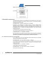
2 Hardware
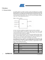
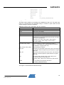
2.1 Display interface
The typical interface of a display is based on analog and digital inputs. The digital
lines are a data bus, pixel clock, vertical and horizontal synchronization signals and a
data enable line. The voltage input is generally used for contrast control. The LCD
Controller drives all these interface lines. If more inputs are required by the display, it
may be managed by GPIOs (power control, AC bias on some STN displays, backlight
control, etc.) or other peripheral (SPI,I2C etc.).
Figure 1. Display Interface
In order to verify the compatibility of a display some points must be considered.
The LCD controller supports TFT RGB (up to 16M colors), color STN (up to 4096
colors) and Monochrome STN (up to 16 gray shades) displays. Other technologies
may also be used if their interface is compatible.
The screen size is fully programmable. The maximum size supported is 2048 x 2048.
Most of standard display resolution levels are compatible: VGA (640x480), QVGA
(320 x 240), etc. In STN mode, single and double scan modes are supported. For a
double scan mode, the maximum size for each panel is 1024 x 2048.
The interface must be 3.3V compliant. All the display lines should be present in the
lines description list, see Table 2-1. If the display features more lines (i.e. gate
command), the LCD Controller is not able to manage them. They could be managed
by the PIO Controller or other peripherals. The polarity is programmable on PCLK,
DVAL, VSYNC and HSYNC I/O lines.
Table 2-1. I/O Lines of the LCD controller
Name
Description
Type
CC
HSYNC
Contrast control signal
Line synchronous signal (STN) or Horizontal synchronous
signal (TFT)
LCD clock signal (STN/TFT)
Output
PCLK
Output
Output
DVAL
Frame synchronous signal (STN) or Vertical synchronization
signal (TFT)
STN AC bias signal for the driver or Data enable signal (TFT)
MOD
LCD Modulation signal
Output
VSYNC
2
Output
Output
AVR32416
32105-AVR32-07/08
AVR32416
Name
PWR
GP[7:0]
LCDD[23:0]
Description
LCD panel Power enable control signal
LCD General purpose lines
LCD Data Bus output
Type
Output
Output
Output
2.1.1 Standard configurations
The Controller supports the following interface configurations:
4-bit single scan STN display
4 parallel data lines are used to shift data to successive single horizontal lines one at
a time until the entire frame has been shifted and transferred. The 4 LSB pins of LCD
Data Bus (LCDD [3:0]) can be directly connected to the LCD driver; the upper 20 bits
of the bus (LCDD [23:4]) are not used.
8-bit single scan STN display
8 parallel data lines are used to shift data to successive single horizontal lines one at
a time until the entire frame has been shifted and transferred. The 8 LSB pins of LCD
Data Bus (LCDD [7:0]) can be directly connected to the LCD driver; the upper pins of
the bus(LCDD [23:8]) are not used.
8-bit Dual Scan STN display
Two sets of 4 parallel data lines are used to shift data to successive upper and lower
panel horizontal lines one at a time until the entire frame has been shifted and
transferred. The bus LCDD[3:0] is connected to the upper panel data lines and the
bus LCDD[7:4] is connected to the lower panel data lines. The rest of the LCD Data
Bus lines (LCDD[23:8]) are not used.
16-bit Dual Scan STN display
Two sets of 8 parallel data lines are used to shift data to successive upper and lower
panel horizontal lines one at a time until the entire frame has been shifted and
transferred. The bus LCDD[7:0] is connected to the upper panel data lines and the
bus LCDD[15:8] is connected to the lower panel data lines. The rest of the LCD Data
Bus lines (LCDD[23:16]) are not used.
TFT single scan display (24-bit resolution)
Up to 24 parallel data lines are used to shift data to successive horizontal lines one at
a time until the entire frame has been shifted and transferred. The 24 data lines are
divided in three bytes that define the color shade of each color component of each
pixel. The LCDD bus is split as LCDD[23:16] for the blue component, LCDD[15:8] for
the green component and LCDD[7:0] for the red component. If the LCD Module has
lower color resolution (fewer bits per color component), only the most significant bits
of each component are used.
TFT single scan display (16-bit resolution)
Up to 16 data lines are used to shift the pixel data at each pixel clock cycle. Each
color gets six data lines of which 5-bits are color information and 1-bit the intensity.
The LCDD bus is split as LCDD[23:18] for the blue component, LCDD[15:10] for the
green component and LCDD[7:2] for the red component.
The Table 2-2 summarizes the above configurations and signal multiplexing.
3
32105-AVR32-07/08
Table 2-2 LCD controller data signal multiplexing
LCD Data Bus
4-bit STN
Single Scan
(mono, color)
8-bit STN
Single Scan
(mono, color)
8-bit STN Dual
Scan (mono,
color)
16-bit STN
Dual Scan
(mono, color)
24-bit TFT
16-bit TFT
LCDD[23]
BLUE7
BLUE4
LCDD[22]
BLUE6
BLUE3
LCDD[21]
BLUE5
BLUE2
LCDD[20]
BLUE4
BLUE1
LCDD[19]
BLUE3
BLUE0
LCDD[18]
BLUE2
Intensity Bit
LCDD[17]
BLUE1
LCDD[16]
BLUE0
LCDD[15]
LCDLP7
GREEN7
GREEN4
LCDD[14]
LCDLP6
GREEN6
GREEN3
LCDD[13]
LCDLP5
GREEN5
GREEN2
LCDD[12]
LCDLP4
GREEN4
GREEN1
LCDD[11]
LCDLP3
GREEN3
GREEN0
LCDD[10]
LCDLP2
GREEN2
Intensity Bit
LCDD[9]
LCDLP1
GREEN1
LCDD[8]
LCDLP0
GREEN0
LCDD[7]
LCD7
LCDLP3
LCDUP7
RED7
RED4
LCDD[6]
LCD6
LCDLP2
LCDUP6
RED6
RED3
LCDD[5]
LCD5
LCDLP1
LCDUP5
RED5
RED2
LCDD[4]
LCD4
LCDLP0
LCDUP4
RED4
RED1
LCDD[3]
LCD3
LCD3
LCDUP3
LCDUP3
RED3
RED0
LCDD[2]
LCD2
LCD2
LCDUP2
LCDUP2
RED2
Intensity Bit
LCDD[1]
LCD1
LCD1
LCDUP1
LCDUP1
RED1
LCDD[0]
LCD0
LCD0
LCDUP0
LCDUP0
RED0
2.1.2 Special wirings
2.1.2.1 Using a hardware swap to get RGB frame buffer data ordering
The LCD controller uses the “BGR-888” color mode in 24-bit resolution and "BGR555.1" in a 16-bit resolution configuration. If a graphical library needs a "RGB-565" or
a “RGB-888” mode a swap of the colors is needed. This can be done by software but
this will lead to a performance decrease which can be avoided by a special hardware
wiring. To tell the frame buffer driver of the special hardware wiring the driver needs a
special configuration. This will be explained later in the chapter “3.6.2.1 RGB frame
buffer layout support with hardware swap”.
2.1.2.2 Hardware swap for 24-bit resolution
The hardware swap for a 24-bit resolution is straight forward because only the red
and blue signals have to be swapped. At any time can a display be used with a lower
resolution by using only the MSB bits of the colors from the LCD controller.
4
AVR32416
32105-AVR32-07/08
AVR32416
2.1.2.3 Hardware swap for 16-bit resolution
In a 16-bit resolution the opposite of the BGR-555.1 format is considered as the RGB565 format. Therefore a hardware swap for a 16-bit resolution needs more
considerations especially because here the intensity bit needs to be used
appropriately. More information about the frame buffer layout and data ordering can
be found in chapter “3.5 Frame buffer”. Table 2-3 shows how an 18-bit display can be
connected to the LCD controller that uses a frame buffer with a RGB-565 pixel format.
One of the intensity signals can be chosen as the B4 component as described in the
table. Data lines B0 and R0 are not used on the 18-bit display in this setup.
Table 2-3. Hardware swap for 16-bit resolution to a 18-bit display
RGB-565 format in the BGR-555.1 format LCD Controller
memory
in the memory
interface
Display interface
0
B0
R0
LCDD[3]
B1
1
B1
R1
LCDD[4]
B2
2
B2
R2
LCDD[5]
B3
3
B3
R3
LCDD[6]
B4
4
B4
R4
LCDD[7]
B5
5
G0
G0
LCDD[11]
G0
6
G1
G1
LCDD[12]
G1
7
G2
G2
LCDD[13]
G2
8
G3
G3
LCDD[14]
G3
9
G4
G4
LCDD[15]
G4
10
G5
B0
LCDD[19]
G5
11
R0
B1
LCDD[20]
R1
12
R1
B2
LCDD[21]
R2
13
R2
B3
LCDD[22]
R3
14
R3
B4
LCDD[23]
R4
15
R4
I
LCDD[2]
LCDD[10]
LCDD[18]
R5
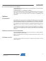
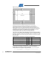
2.2 Double buffering (2D Memory Addressing)
The LCD controller can be configured to work on a frame buffer larger than the actual
screen size. By changing the values in a few registers, it is easy to move the
displayed area along the frame buffer width and height. The LCD controller
increments the frame buffer pointer according to the pixel offset and the address
increment to enable panning. This is used to implement a double buffering of the
frame buffer. The updating of the new data is handled by the LCD controller driver
and is used by the Linux frame buffer driver. The only thing the user has to do is to
activate this feature in the setup and make sure that the double memory size is
reserved for the frame buffer. Further software details are explained in chapter 1.
5
32105-AVR32-07/08
Figure 2. 2D Frame Buffer Addressing
2.3 Bandwidth considerations
An attached display needs a lot of bandwidth from the expansion bus of the system.
This must be considered in the display selection process. The bandwidth needed is
calculated by following formula:
NeededBandwidth = DispaySize x BitsPerPixel x FrameRate
Depending on the applications an operating system is running in parallel enough
bandwidth should be available. For instance considering that the updating of the
frame buffer could be at the same frame rate as the display the above formula must
be multiplied by two. To calculate the available bandwidth on the system following
formula can be used:
AvailableBandwidth = BusSpeed x BusInterfaceWidth
The maximum available bandwidth for the AP700x devices is
AvailableBandwidth = 75 x 32/8 MB/s = 300 MB/s
due to the maximum bus speed of 75 MHz. With the maximum speed it is possible to
use displays up to VGA with full 24bit resolution and doing MPEG4 decoding at the
same time. Larger displays can be used when the resolution is decreased.
2.3.1 32-bit memory example (as on the STK1000)
For the display on the STK®1000 (DisplaySize 320x240, BitsPerPixel 24, FrameRate
75Hz) the formula delivers following result.
NeededBandwidth = 320 x 240 x 24/8 x 75 Byte/s = 17MByte/s
For the AP700x device the maximum bus frequency is 75MHz and the interface width
to the memory on the STK1000 is 32bit wide. This results in the following maximum
available bandwidth:
AvailableBandwidth = 75 x 32/8 MB/s = 300 MB/s
A VGA display would need approximately
NeededBandwidth = 640 x 480 x 24/8 x 75 Bytes/s = 69 MByte/s
assuming the same frame rate.
6
AVR32416
32105-AVR32-07/08
AVR32416
2.3.2 16-bit memory example (as on the NGW100)
The NGW100 uses a 16bit wide interface to the external memory. Thus the maximum
available bandwidth is:
AvailableBandwidth = 75 x 16/8 Bytes/s = 150 MB/s
While a QVGA display leaves enough room for MPEG4 decoding and other tasks a
VGA display may not be used in this constellation. Never the less it is possible to
show graphics on the VGA display which do not need to be updated at high
frequencies.
3 Software
3.1 Prerequisites
The needed Linux kernel sources are available from different places like the Atmel
Buildroot website or avr32linux.org. The application note “AVR32737: AVR32 AP7
Linux Getting Started” includes all necessary references to sources and tools needed.
Also the application note “AVR32743 AVR32 AP7 Linux kernel module application example” is
recommended to read in order to understand the principles of creating or adapting a Linux
driver.
To understand the LCD controller on AP700x devices better the application note “AVR32114:
Using the AVR32 LCD Controller” could be of interest. This application note describes the
usage of the LCD controller without an operating system and includes some example
applications.
3.2 Naming conventions used in this document
All source directories related to the Linux kernel are shown as relative paths like
include/linux (without a leading slash).
Paths on the target system are used with a leading slash as their location is fixed
against the root.
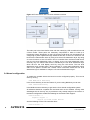
3.3 Software overview
The major software parts that are involved in configuring and driving the LCD are
shown in Figure 3-1.
7
32105-AVR32-07/08
Figure 3-1 Frame buffer and LCD driver software overview
The main part is the frame buffer driver with the underlying LCD controller driver and
a frame buffer. These parts are necessary components in order to build up a
functioning system. Depending on the LCD an extra LCD driver may be needed to do
configuring or power up/down through interfaces like SPI or GPIO. A LCD driver can
be tied to the frame buffer driver by using a low level LCD abstraction layer. By doing
so some functions of the LCD driver can be controlled from the frame buffer driver
over the low level abstraction layer or directly by the low level abstraction layer.
Currently only one frame buffer event is handled by the low level abstraction layer
which will turn the LCD display on/off by using the LCD driver. The low level
abstraction layer provides also a direct interface to a user-space application which
offers more specific controls like contrast. More information about the low level
abstraction layer is available in chapter “LCD low level abstraction layer”.
3.4 Kernel configuration
To enable the needed drivers the kernel must be configured properly. This can be
done by running
make ARCH=avr32 menuconfig
in the source directory of the Linux kernel. If you are using Buildroot you can use
make linux26-menuconfig
in the Buildroot source directory to get into the Linux kernel configuration system.
All software should be compiled into the kernel and not as modules. Among other
advantages this is the only way to provide an early startup image on the screen. In
the kernel configuration enable the following for the frame buffer support:
Device Drivers ->
Graphics support ->
Support for frame buffer devices
And the following for the LCD controller driver:
Device Drivers ->
8
AVR32416
32105-AVR32-07/08
AVR32416
Graphics support ->
Support for frame buffer devices ->
AT91/AT32 LCD Controller support
These will add the LCD controller driver and the frame buffer driver to the kernel. If
one of the LCD low level abstraction layers should be used with the LCD driver they
can be activated under
Device Drivers ->
Graphics support ->
Support for frame buffer devices ->
Backlight & LCD device support
A selection entry for a custom LCD driver should be added here if necessary. For
example the LCD driver for the Samsung LTV350QV display that is mounted on the
STK1000 can be selected here after enabling the low level LCD controls. The
LTV350QV driver depends on the low level LCD layer and is thus listed as sub-menu
entry.
3.5 Frame buffer
3.5.1 Configuration
The size and location of the frame buffer can be specified upon startup of the kernel
on the kernel command line. This approach is optional but may especially be needed
if the frame buffer shall be placed at a dedicated location or when the available
memory is scarce. The size of the frame buffer depends on the display size and must
be calculated. The LCD controller has support for a double buffering of the frames.
This means one frame can be displayed while the other buffer is filled with new data.
If this feature is needed the frame buffer size must be doubled. If the following line is
added to kernel command line (this can be done in U-Boot by editing the bootargs
variable)
fbmem=600k@0x10500000
a frame buffer of the size 600KiB at the address 0x10500000 will be reserved. This
frame buffer size can be used on the STK1000 for the QVGA display (320x240x4x2).
The display has the size of 320x240 pixels. One pixel can be represented as 32bits in
the frame buffer which leads to 4 bytes for a pixel (3x8bit for the colors and 8bit
empty). This is the largest possible pixel size but is actually not used by default on the
STK1000 (default 24bit = 3x8bit colors). The larger frame buffer leaves room to a
user that wants to set up the frame buffer with a 32bit pixel size. To provide the
double buffering the size must be doubled.
If no frame buffer was specified on the kernel command line the LCD controller driver
will allocate the needed memory automatically. For the STK1000 this will be 225KiB
(320x240x3) which will not provide a double buffering. This can be verified by reading
out the kernel log with the dmesg tool.
3.5.2 Memory layout
The LCD controller expects a BGR data ordering in the frame buffer. Table 3-1 shows
how the data must be placed in the frame buffer for a configuration that uses a 24-bit
unpacked resolution. The unpacked version uses 32-bit with an 8-bit space that is
unused.
9
32105-AVR32-07/08
Table 3-1. Frame buffer data ordering 24-bit resolution not packed
MSB
LSB
31 – 24
Unused
23 – 16
Blue
15 – 8
Green
7-0
Red
The packed 24-bit resolution removes the unneeded empty 8-bit which results in a
smaller frame buffer. Table 3-2 shows how the data must be placed in the frame
buffer in order to be compliant with a packed 24-bit configuration. The second blue
component belongs to the next pixel.
Table 3-2. Frame buffer data ordering 24-bit resolution packed
MSB
LSB
31 – 24
Blue
23 – 16
Green
15 – 8
Red
7-0
Blue
In a 16-bit resolution configuration a BGR-555.1 format is used by the LCD controller.
This means each color component uses 5-bits and the whole pixel gets one intensity
bit. Table 3-3 describes the needed data ordering in the frame buffer for a 16-bit
resolution configuration.
Table 3-3. Frame buffer data ordering 16-bit resolution
MSB
LSB
15
14
13
12
11
10
9
8
7
6
5
4
3
2
1
0
I
B4
B3
B2
B1
B0
G4
G3
G2
G1
G0
R4
R3
R2
R1
R0
If a graphics library does not support the frame buffer layout natively it has to swap
the colors accordingly. This will decrease the performance.
The formats RGB-888 and RGB-565 for instance can be supported by a special
hardware wiring and software configuration. The chapter 2.1.2 describes the needed
hardware wiring and 3.6.2.1 the needed software configuration for these examples.
3.6 Board setup code
Two things must be done to add the LCD controller and the LCD driver in the board
setup code. These are the registering of the LCD controller as a platform device and
the registering of the LCD driver as a platform driver.
3.6.1 Registering the LCD controller as platform device
Three structures must be edited and combined to form the information for the frame
buffer driver and the LCD controller driver. The LCD configuration of the STK1000
serves here as an example to explain the needed editing. The first structure specifies
the default mode (configuration) of the LCD controller.
static struct fb_videomode __initdata ltv350qv_modes[] = {
{
10
.name
= "320x240 @ 75",
.refresh
= 75,
.xres
= 320,
.yres
= 240,
.pixclock
= KHZ2PICOS(6891),
.left_margin
= 17,
AVR32416
32105-AVR32-07/08
AVR32416
.right_margin
= 33,
.upper_margin
= 10,
.lower_margin
= 10,
.hsync_len
= 16,
.vsync_len
= 1,
.sync
= 0,
.vmode
= FB_VMODE_NONINTERLACED,
},
};
The fields must be filled out according to the datasheet of the LCD. The pixel clock
must be in picoseconds, the horizontal timings in number of pixel clocks and the
vertical timings in number of scanlines.
Table 3-4. Video mode configuration structure members
Parameter
Description
name
Name of the frame buffer video mode
refresh
Refresh rate of the display
xres
Horizontal display size in pixels (active/visible pixels)
yres
Vertical display size in pixels
pixelclock
Desired pixel clock rate in pico seconds. Use the macro
KHZ2PICOS() to convert from kHz to pico seconds. The pixel
clock can be calculated from:
Pixel clock in Hz = (xres + left_margin + right_margin +
hsync_len) x (yres + upper_margin + lower_margin +
vsync_len) x refresh
left_margin, right_margin
Horizontal blanking in number of pixel clocks (refer to
picture…). The minimum is 1 although 0 will be accepted too
(both will lead to a register value of 0)
upper_margin, lower_margin
Vertical blanking in scanlines
hsync_len
Horizontal sync pulse width in pixel clock cycles. The minimum
is 1 although 0 will be accepted too (both will lead to a register
value of 0)
vsync_len
Vertical sync pulse width in pixel clock cycles. The minimum is
1 although 0 will be accepted too (both will lead to a register
value of 0)
sync
Sync pulse polarity. Set FB_SYNC_HOR_HIGH_ACT if
horizontal sync pulse is active high. Set
FB_SYNC_VERT_HIGH_ACT if vertical sync pulse is active
high.
vmode
Only non-interlaced is supported. Set this to
FB_VMODE_NONINTERLACED
The Figure 3-2 summarizes all relevant timings.
11
32105-AVR32-07/08
Figure 3-2 Display timings
All timings in the gray area represent the blanking area. For the internal
synchronization mechanism, the display may need some dummy data at the
beginning and/or end of a line, and at the beginning and/or end of a frame. This is
called blanking. The dummy pixels/lines are not part of the frame buffer are therefore
managed by the LCD Controller. Some delays must be introduced in vertical and
horizontal timings to support it. These delays are often described as
vertical/horizontal front/back porch delays in the display datasheets.
The maximum and minimum timing supported by the LCD Controller are listed in
Table 3-5. Thus if the display should be supported it should not exceed these timing
parameters. Especially if monitor that need VESA timings is connected via a video
DAC these maximum and minimum ratings are relevant due to the short maximum
pulse sync length.
Table 3-5. Maximum and minimum LCD controller timing parameters
Parameter
Min
Max
Unit
Vertical Front Porch (lower_margin)
1
256
Lines
Vertical Back Porch (upper_margin)
1
256
Lines
Horizontal Front Porch (right_margin)
1
2048
Pixel Clock Cycles
Horizontal Back Porch (left_margin)
1
256
Pixel Clock Cycles
Vertical Pulse Width (vsync_len)
1
64
Lines
Horizontal Pulse Width (hsync_len)
1
64
Pixel Clock Cycles
The next structure that is needed is fb_monspecs and it contains as the name implies
the specification of the display. The definition can be found in the header file
include/linux/fb.h with information to all structure members. At least following fields
should be filled out according to the monitor specification:
static struct fb_monspecs __initdata atstk1000_default_monspecs = {
.manufacturer
12
= "SNG",
AVR32416
32105-AVR32-07/08
AVR32416
.monitor
= "LTV350QV",
.modedb
= ltv350qv_modes,
.modedb_len
= ARRAY_SIZE(ltv350qv_modes),
.hfmin
= 14820,
.hfmax
= 22230,
.vfmin
= 60,
.vfmax
= 90,
.dclkmax
= 30000000,
};
The maximum and minimum parameters specified here will make sure that the LCD
controller can not be configured with values that do not fit into that range. A
configuration value below or above the specification will be set to the lower or the
upper limit. This prevents from a faulty configuration of the LCD controller that could
damage an attached LCD. Table 3-6 lists the structure members, which at least
should be set, with a description.
Table 3-6. Monitor specification structure members
Parameter
Description
manufacturer
Display manufacturer name (max. 4 characters)
monitor
Name of the display (max. 14 characters)
modedb
Pointer to the video modes array (fb_videomode structure)
modedb_len
Length of the video modes array. The macro ARRAY_SIZE()
can be used to get the length.
hfmin
Lower limit of the horizontal display frequency in Hz
hfmax
Upper limit of the horizontal display frequency in HZ
vfmin
Lower limit of the vertical display frequency in Hz
vfmax
Upper limit of the vertical display frequency in Hz
dclkmax
Upper limit of the pixel clock
The last structure that is needed is atmel_lcdfb_info. It will be used as the platform
device data and therefore be available for the LCD controller driver to do the default
configuration. The definition of the structure is in include/video/atmel_lcdc.h and
contains some more members as in the example below.
struct atmel_lcdfb_info __initdata atstk1000_lcdc_data = {
.default_bpp
= 24,
.default_dmacon
= ATMEL_LCDC_DMAEN | ATMEL_LCDC_DMA2DEN,
.default_lcdcon2
= (ATMEL_LCDC_DISTYPE_TFT
| ATMEL_LCDC_INVCLK
| ATMEL_LCDC_CLKMOD_ALWAYSACTIVE
| ATMEL_LCDC_MEMOR_BIG),
.default_monspecs
= &atstk1000_default_monspecs,
.guard_time
= 2,
};
Table 3-7. LCD controller specific configuration data
Parameter
Description
13
32105-AVR32-07/08
Parameter
Description
default_bpp
Bits per pixel to use. Possible values are 1, 2, 4, 8, 15, 16, 24
and 32. The memory layout for these values is described in the
datasheet of the device. For instance 32bit means 3x8bit for
the three colors red, green, blue and empty 8bit at the end.
default_dmacon
Setting ATMEL_LCDC_DMAEN is mandatory in order to
enable the LCD controller DMA engine. The
ATMEL_LCDC_DMA2DEN will activate the double buffering of
the frame buffer.
default_lcdcon2
This is the default configuration of the LCD controller register
“LCDCON2”. The bit-fields INVFRAME, INVLINE and
PIXELSIZE are automatically set according to the video mode
settings. All other settings of this register may be configured by
using the available macros in the include/video/atmel_lcdc.h
file.
default_monspecs
Pointer to the monitor specifications structure.
guard_time
Delay in frame periods between applying control signals to the
LCD module and setting PWR high, and between setting
PWR low and removing control signals from LCD module.
lcd_wiring_mode
Specifies the hardware wiring of the LCD. Possible values are
ATMEL_LCDC_WIRING_BGR and
ATMEL_LCDC_WIRING_RGB (see chapter “3.6.2.1 RGB
frame buffer layout support with hardware swap” for more
details)
3.6.2 Special configurations
Sometimes a more specific setup of the LCD controller is needed. This is the case
when exact timings are needed or unused pins of the LCD controller must be used for
other things. Also the LCD controller may need a higher priority for accesses to the
memory to keep the DMA in sync. Another special setup needs to be done to support
RGB frame buffer layout without a software swap. These extended configurations will
be discussed in the next chapters.
3.6.2.1 RGB frame buffer layout support with hardware swap
The needed hardware swapping was already described in the hardware section of
this document. Since the frame buffer driver can not know about the actual wiring of
the LCD display the driver needs be made aware of it. Therefore the variable
lcd_wiring_mode is available in the struct atmel_lcdfb_info that was already described
in chapter 3.6.1. This variable should be available since the kernel version 2.6.26.
Use the macro ATMEL_LCDC_WIRING_BGR to inform the frame buffer driver of a
normal wiring of the LCD. The macro ATMEL_LCDC_WIRING_RGB will tell the frame
buffer driver that the colors have been swapped in hardware. For more information
about the hardware wiring that needs to be done take a look at chapter “2.1.2.1 Using
a hardware swap to get RGB frame buffer data ordering”.
3.6.2.2 Freeing unused LCD pins
The standard LCD controller setup reserves all 24 data lines for the LCD. This may not
be necessary if a display is used that does not need all 24 data lines. If these pins should be
14
AVR32416
32105-AVR32-07/08
AVR32416
needed for other things the following function must be edited in the file arch/avr32/mach-
at32ap/at32ap700x.c.
struct platform_device *__init at32_add_device_lcdc(
unsigned int id,
struct atmel_lcdfb_info *data,
unsigned long fbmem_start,
unsigned long fbmem_len
)
In this function the pins can be freed by commenting out or removing lines like:
select_peripheral(PD(16), PERIPH_A, 0); /* DATA22 */
3.6.2.3 Setting up exact timings
In the standard configuration the LCD controller uses the main system clock as input for the
pixel clock. This main clock is generated by the PLL0 and can be divided by 2^n (n=0…). Due
to this restriction an exact setup of the pixel clock may not be feasible with these settings.
To get an exact pixel clock the clock source must be changed. Possible other sources
are PLL1, OSC0 and OSC1. The pll1is in most cases unused and can be set up to
match the desired pixel clock rate more accurate. To get an overview of the clock
distribution on the system the following description is very useful but shall not replace
a detailed study of the device datasheet.
The system clock tree
The debug file system on Linux provides a lot of useful information about the system.
Especially the system “clock tree” is very useful to get an overview of all available
clocks in the system and their distribution. As the name “tree” implies the different
clocks are listed in a manner that looks like a tree. Each clock has a parent clock
which it connects to and thus spanning up a tree to the main clocks as root. On the
AVR32 AP7 series two main clocks are available OSC0 and OSC1. For a detailed
description of the clock system a look into the respective datasheet is needed.
The debug file system can be found under /sys/kernel/debug but may not be mounted
by default. To mount the debug file system there run
mount –t debugfs none /sys/kernel/debug
The system clock tree can be read from the file /sys/kernel/debug/ by following
command
cat /sys/kernel/debug/at32ap_clk
The output depends on the current system configuration and may look similar to this:
MCCTRL
CKSEL
CPUMASK
HSBMASK
PBAMASK
PBBMASK
PLL0
PLL1
IMR
GCCTRL0
GCCTRL1
GCCTRL2
GCCTRL3
GCCTRL4
=
2
= 80818000
=
1
=
59f
=
17cd1
=
224f
= 10060011
=
0
=
0
=
516
=
0
=
0
=
0
=
0
15
32105-AVR32-07/08
GCCTRL6 =
GCCTRL7 =
0
16
osc32k
osc0
pll0
cpu
hsb
pba
pclk
mck
mck
mck
mck
mck
usart
usart
spi_clk
twi_pclk
pclk
pbb
pclk
pclk
hmatrix_clk
pclk
pclk
pclk
mci_clk
pclk
pclk
pclk
ebi
hramc
mck
hclk
hclk
hclk
hck1
hclk
pico
lcdc_clk
*
gclk0
*
pll1
sample_clk
*
gclk1
*
gclk2
*
gclk3
*
gclk4
*
osc1
users= 1
users=24
users=23
users=22
users=20
users=10
users= 1
users= 1
users= 1
users= 1
users= 1
users= 1
users= 1
users= 1
users= 1
users= 0
users= 1
users= 6
users= 1
users= 1
users= 1
users= 1
users= 1
users= 1
users= 1
users= 0
users= 0
users= 0
users= 1
users= 1
users= 1
users= 1
users= 1
users= 1
users= 1
users= 0
users= 1
users= 1
users= 1
users= 0
users= 0
users= 0
users= 0
users= 0
users= 0
users= 0
on
32768 Hz
on
20000000 Hz
on 140000000 Hz
on 140000000 Hz
on
70000000 Hz
on
35000000 Hz
on
35000000 Hz,
on
35000000 Hz,
on
35000000 Hz,
on
35000000 Hz,
on
35000000 Hz,
on
35000000 Hz,
on
35000000 Hz,
on
35000000 Hz,
on
35000000 Hz,
off 35000000 Hz,
on
35000000 Hz,
on
70000000 Hz
on
70000000 Hz,
on
70000000 Hz,
on
70000000 Hz
on
70000000 Hz,
on
70000000 Hz,
on
70000000 Hz,
on
70000000 Hz,
off 70000000 Hz,
off 70000000 Hz
off 70000000 Hz,
on
70000000 Hz
on
70000000 Hz
on
70000000 Hz,
on
70000000 Hz,
on
70000000 Hz,
on
70000000 Hz,
on
70000000 Hz,
off 70000000 Hz,
on 140000000 Hz
on
70000000 Hz,
on
11666666 Hz
off
0 Hz
off 20000000 Hz,
off 20000000 Hz
off 20000000 Hz
off 20000000 Hz
off 20000000 Hz
off 12000000 Hz
for
for
for
for
for
for
for
for
for
for
for
pdc.0
pio.0
pio.1
pio.2
pio.3
pio.4
atmel_usart.0
atmel_usart.2
atmel_spi.0
atmel_twi.0
ssc.0
for at32_pm.0
for intc.0
for
for
for
for
for
smc.0
systc.0
macb.0
atmel_mci.0
atmel_usba_udc.0
for abdac.0
for
for
for
for
for
for
smc.0
pdc.0
dmaca.0
macb.0
atmel_lcdfb.0
atmel_usba_udc.0
for atmel_lcdfb.0
for abdac.0
The first part of the output shows the content of registers that are relevant for the configuration
of the clock system. The register content is described in the device datasheet. The rest of the
output is the clock tree. An asterisk (*) means that this clock may be tied to another parent
clock. For example a generic clock (gclk0, gclk1 …) can be tied to osc0, osc1, pll0 and pll1.
The user count shows how many active sub clock nets are tied to this parent. The on/off value
shows if the clock is active or not. The last two values describe the frequency at which the
clock runs and which driver module uses the clock.
Setting up an exact pixel clock
For the LCD controller setup is especially the “lcdc_clk” in the clock tree of interest. This clock
is fed into the LCD controller and will end up as pixel clock output after a prescaler unit. The
16
AVR32416
32105-AVR32-07/08
AVR32416
LCD controller driver configures the prescaler unit according the configuration it gets from the
board setup code or later on from the fbset tool. As previously mentioned can a scaler only
divide the clock by 2^n (n=0…). If an exact pixel clock is needed the “lcdc_clk” must be a
multiple of 2 or exactly the desired clock rate.
A good solution is to use the PLL1 as input for the “lcdc_clk” because it provides the ability to
get very close to desired clock rate. To switch the “lcdc_clk” to PLL1 following function calls
have to be edited by replacing “pll0” with “pll1” (in file arch/avr32/machat32ap/at32ap700x.c):
clk_set_parent(&atmel_lcdfb0_pixclk, &pll0);
clk_set_rate(&atmel_lcdfb0_pixclk, clk_get_rate(&pll0));
Next step is to actually configure the PLL1 to get the desired clock rate. Following
functions can be used to set up the PLL1 (available since kernel version 2.6.25; for
earlier versions the user has to set up the PLL1 manually).
static int pll1_set_parent(struct clk *clk, struct clk *parent)
static long pll1_set_rate(struct clk *clk, unsigned long rate,
int apply)
static void pll1_mode(struct clk *clk, int enabled)
3.6.2.4 DMA optimizations
If the LCD Controller has to transfer a lot of data from or to the external memory some
optimizations may be needed to avoid a buffer-underrun resulting in desynchronization of the timing generator. To get the maximum available bandwidth
also the HSB bus matrix should run at the maximum possible frequency. Keep in
mind that the CPU must always at the same or higher rate of the HSB bus.
LCD controller as fixed master
A High Speed Bus Matrix slave can only be connected to one master at a time. After
the master has finished, the slave device has three possibilities that can be
configured:
• If no other master request is pending, the slave disconnects the master.
• If no other master request is pending, the slave stays connected to the current
master.
• If no other master request is pending, the slave connects to the fixed master that
has been specified in the configuration.
The DMA Controller of the LCD Controller can be set as a fixed master for the
external bus interface. This means after another master has accessed the external
bus interface it sets the bus back to the LCD Controller. So no switching has to be
done when new data has to be fetched from a frame buffer in the external memory.
This results in a faster access time. To set up the LCD Controller as default master of
the external bus interface the fields DEFMSTR_TYPE and FIXED_DEFMSTR have to
be set up in the SCFG4 register. Please take a look at chapter “HSB Bus Matrix” and
chapter “Memories” of the device datasheet for a detailed description.
Priority-Based Arbitration
The slave, here the external bus interface, uses a round robin algorithm by default to
schedule accesses of masters to its self. This can be critical if other masters request
access to the slave and thus reducing the bandwidth for the LCD Controller. This can
lead to a buffer underflow in the LCD Controller, resulting in loss of synchronization. A
typical symptom of a buffer underflow is when the image on the screen is shifted
vertically/horizontally. To resynchronize the timing generator and thus getting back a
17
32105-AVR32-07/08
correct view, the LCD Controller and its DMA engine have to be restarted. A possible
solution to guarantee access to the external bus interface for the LCD Controller is to
enable a priority based arbitration algorithm for this slave. If the LCD Controller gets
the highest priority for the slave it is guaranteed that it gets access before all other
masters. A major drawback is that all other masters will have a reduced access or
even in a worst case no access at all to the slave. Chapter “HSB Bus Matrix” of the
device datasheet describes how to activate the priority-based arbitration and the
setting of priorities.
Code example
The following code sample can be used in the board setup code to set up the LCD
controller as fixed master with priority-based arbitration on the external bus interface.
The right place would be in the file arch/avr32/mach-at32ap/at32ap700x.c in the LCD
controller setup function.
hmatrix_writel(SCFG4, HMATRIX_BIT(ARBT)
| HMATRIX_BF(FIXED_DEFMSTR, 0x5)
| HMATRIX_BF(SLOT_CYCLE, 0x10)
| HMATRIX_BF(DEFMSTR_TYPE,
HMATRIX_DEFMSTR_TYPE_FIXED_DEFAULT));
hmatrix_writel(PRAS4, HMATRIX_BF(M5PR, 0xF));
The above example sets the priority to the maximum and uses a reasonable slot
cycle but these settings may be changed to fit the actual needs.
3.7 LCD low level abstraction layer
The low level LCD abstraction layer consists of several independent clients that are
connected to the frame buffer driver. If a change has been made by an application in
the frame buffer driver the clients will be notified and they have to decide if they have
to react to this change. After the client has decided that the change is relevant it will
provide the new settings to the actual LCD driver.
3.7.1 LCD layer
The LCD layer (or client) currently supports basic functions like power on/off and contrast. The
abstraction layer registers itself as a client with the frame buffer driver and installs a callback
routine that is called when settings like contrast are changed through the frame buffer driver
core. The settings are also available through the sys file system. For the display on the
STK1000 the attribute files contrast, lcd_power and max_contrast are available in the directory
/sys/class/lcd/ltv350qv. Currently only the lcd_power attribute file is functional because the
contrast setting is not implemented in the LCD driver for the LTV350QV display. The display
can be turned off with following command:
echo 2 > /sys/class/lcd/ltv350qv/lcd_power
To turn the display on again use
echo 1 > /sys/class/lcd/ltv350qv/lcd_power
Custom LCDs and their corresponding drivers will use another directory in /sys/class/lcd
depending on the driver name.
The API of the LCD layer is defined in the header file include/linux/lcd.h and can be included in
a LCD driver in order to use it. The source code can be found in drivers/video/backlight/lcd.c.
LCD drivers can register/un-register itself with the LCD layer with the functions
struct lcd_device *lcd_device_register(const char *name,
18
AVR32416
32105-AVR32-07/08
AVR32416
struct device *parent,
void *devdata,
struct lcd_ops *ops);
void lcd_device_unregister(struct lcd_device *ld);
Functions that can be implemented in a LCD driver are listed in the struct lcd_ops.
3.7.2 Backlight layer
The backlight client provides an easy integration of the backlight control in the frame
buffer driver and the LCD driver.
Relevant files are include/linux/backlight.h and drivers/video/backlight/backlight.c.
A LCD driver can register/un-register itself with the backlight client with the following
functions:
struct backlight_device *backlight_device_register(
const char *name,
struct device *dev,
void *devdata,
struct backlight_ops *ops);
void backlight_device_unregister(struct backlight_device *bd);
The functions named in struct backlight_ops can be implemented in the LCD driver
and tied to the structure.
The backlight client will also provide some attribute files in the sys file system. These
are bl_power, brightness, actual_brightness and max_brightness.
3.8 LCD driver
A LCD driver may be needed to do initialization, power on/off and other things that depend on
the used LCD. An example driver that was written for the LCD on the STK1000 board is
drivers/video/backlight/ltv350qv.c.
Depending on the display different configuration interfaces may be present such as SPI or TWI
(I2C). The reading of the application note “AVR32743 AVR32 AP7 Linux kernel module
application example” is recommended to understand the implementation approach for Linux
kernel modules. Especially the SPI example may be very helpful if the display provides a SPI
interface for configuration.
The LCD driver can provide a configuration interface for the LCD display by using the sys file
system and attribute files. Other interfaces are also possible (device file with ioctl or read/write
interface) but are too much effort for such simple tasks as power on/off and other display
controls.
By using the LCD abstraction layer the LCD driver can provide some of its functionalities to the
system. This has the advance that it is more general.
3.8.1 Adding a LCD driver to the Linux kernel configuration system
To make a custom LCD driver appear in the Linux kernel configuration system the file
drivers/video/backlight/Kconfig must be edited. Following example is taken from the
file and represents the entry for the LTV350QV display.
config LCD_LTV350QV
tristate "Samsung LTV350QV LCD Panel"
depends on LCD_CLASS_DEVICE && SPI_MASTER
19
32105-AVR32-07/08
default n
help
If you have a Samsung LTV350QV LCD panel, say y to
include a power control driver for it. The panel starts
up in power off state, so you need this driver in order
to see any output.
The LTV350QV panel is present on all ATSTK1000 boards.
For a custom LCD driver a similar entry has to be made in the same file. First a
custom configuration name needs to be added to the “config” entry. This name will be
referred to from other modules or configuration dependencies. The “depends on”
entry reflects the software parts that are needed in combination with the LCD driver. If
the driver does not need SPI the SPI_MASTER can be removed. Also if the driver
does not use the LCD layer the LCD_CLASS_DEVICE can be removed. In order to
add a dependency to the backlight framework BACKLIGHT_CLASS_DEVICE should
be added here.
Next step is to edit the Makefile drivers/video/backlight/Makefile. One line needs to be
added to build the driver:
obj-$(CONFIG_LCD_LTV350QV)
+= ltv350qv.o
The CONFIG_LCD_LTV350QV should reflect the “config” name in the Kconfig file by
adding a CONFIG_ before the name. The “ltv350qv.o” should be changed to the
source file name.
More information about the Linux kernel configuration system can be found in the
Linux kernel documentation (Documentation directory in the kernel sources).
4 References
Application notes from http://www.atmel.com/products/avr32/default.asp :
•
“AVR32737: AVR32 AP7 Linux Getting Started”
•
“AVR32743 AVR32 AP7 Linux kernel module application example”
•
“AVR32114: Using the AVR32 LCD Controller”
Linux kernel frame buffer documentation: Can be found in Documentation/fb/ in the
Linux kernel sources.
20
AVR32416
32105-AVR32-07/08
Disclaimer
Headquarters
International
Atmel Corporation
2325 Orchard Parkway
San Jose, CA 95131
USA
Tel: 1(408) 441-0311
Fax: 1(408) 487-2600
Atmel Asia
Room 1219
Chinachem Golden Plaza
77 Mody Road Tsimshatsui
East Kowloon
Hong Kong
Tel: (852) 2721-9778
Fax: (852) 2722-1369
Atmel Europe
Le Krebs
8, Rue Jean-Pierre Timbaud
BP 309
78054 Saint-Quentin-enYvelines Cedex
France
Tel: (33) 1-30-60-70-00
Fax: (33) 1-30-60-71-11
Atmel Japan
9F, Tonetsu Shinkawa Bldg.
1-24-8 Shinkawa
Chuo-ku, Tokyo 104-0033
Japan
Tel: (81) 3-3523-3551
Fax: (81) 3-3523-7581
Technical Support
[email protected]
Sales Contact
www.atmel.com/contacts
Product Contact
Web Site
www.atmel.com
Literature Request
www.atmel.com/literature
Disclaimer: The information in this document is provided in connection with Atmel products. No license, express or implied, by estoppel or otherwise, to any
intellectual property right is granted by this document or in connection with the sale of Atmel products. EXCEPT AS SET FORTH IN ATMEL’S TERMS AND
CONDITIONS OF SALE LOCATED ON ATMEL’S WEB SITE, ATMEL ASSUMES NO LIABILITY WHATSOEVER AND DISCLAIMS ANY EXPRESS, IMPLIED
OR STATUTORY WARRANTY RELATING TO ITS PRODUCTS INCLUDING, BUT NOT LIMITED TO, THE IMPLIED WARRANTY OF MERCHANTABILITY,
FITNESS FOR A PARTICULAR PURPOSE, OR NON-INFRINGEMENT. IN NO EVENT SHALL ATMEL BE LIABLE FOR ANY DIRECT, INDIRECT,
CONSEQUENTIAL, PUNITIVE, SPECIAL OR INCIDENTAL DAMAGES (INCLUDING, WITHOUT LIMITATION, DAMAGES FOR LOSS OF PROFITS,
BUSINESS INTERRUPTION, OR LOSS OF INFORMATION) ARISING OUT OF THE USE OR INABILITY TO USE THIS DOCUMENT, EVEN IF ATMEL HAS
BEEN ADVISED OF THE POSSIBILITY OF SUCH DAMAGES. Atmel makes no representations or warranties with respect to the accuracy or completeness of the
contents of this document and reserves the right to make changes to specifications and product descriptions at any time without notice. Atmel does not make any
commitment to update the information contained herein. Unless specifically provided otherwise, Atmel products are not suitable for, and shall not be used in,
automotive applications. Atmel’s products are not intended, authorized, or warranted for use as components in applications intended to support or sustain life.
© 2008 Atmel Corporation. All rights reserved. Atmel®, logo and combinations thereof, AVR®, STK® and others, are the registered
trademarks or trademarks of Atmel Corporation or its subsidiaries. Other terms and product names may be trademarks of others.
32105-AVR32-07/08