1
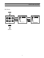
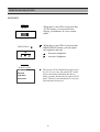
Service Manual
LCD COLOR MONITOR
Model : CML-710
DAEWOO LUCOMS CO., LTD.
http://www.lucoms.com
2004
CONTENTS
SAFETY PRECAUTIONS
2
GENERAL SAFETY INFORMATION
3
SERVICING PRECAUTIONS
4
TECHNICAL INFORMATION
8
GENERAL INFORMATION
9
PIN CONNECTOR
9
CAUTIONS FOR ADJUSTMENT AND REPAIR
9
OPERATION & ADJUSTMENT
10
ALIGNMENT PROCEDURE
16
TROUBLESHOOTING HINTS
17
BLOCK DIAGRAM
24
SCHEMATIC DIAGRAM
25
PCB PATTERN
30
INFORMATION OF PART DESCRIPTION
34
ELECTRICAL PARTS LIST
35
1
SAFETY PRECAUTIONS
CAUTION: No modifications of any circuits should be attempted. Service work should be performed
only after you are thoroughly familiar with all of the following safety checks and servicing
guidelines.
◆ Safety Check
Care should be taken while servicing the inverter that generates the high voltage to lighten CCFL of the
LCD panel.
◆ Fire & Shock Hazard
• Insert an isolation transformer between the analog color display and AC power line before servicing the
chassis.
• When servicing, pay close attention to the original lead dress especially in the high voltage circuit area;
if a short circuit is found, replace all parts which have been overheated as a result of the short circuit.
• All the protective devices must be reinstalled per original design.
• Soldering must be inspected for possible cold solder points, frayed leads, damaged insulation, solder
splashes or sharp solder points. Be certain to remove all foreign materials.
2
GENERAL SAFETY INFORMATION
◆ Terms in the manual
CAUTION
Statements identify conditions or practices that could result in damage to the equipment or
other property.
WARNING Statements identify conditions or practices that could result in personal injury or loss of
life.
◆ Terms as marked on equipment
CAUTION
Statements indicate a personal injury hazard not immediately accessible as one reads the
marking or a hazard which is properly included on the equipment itself.
WARNING Statements are clearly concerning indicated personal injury hazards.
◆ Symbols in the manual
The symbols indicate where applicable cautionary or other information is to be found.
◆ Symbols as marked on equipment
Protective GROUND terminal
◆ High Voltage Warning
And Critical Component Warning Label
The following warning label is on the inverter isolation case.
3
SERVICING PRECAUTIONS
CAUTION: Before servicing instruments covered by this service manual, its supplements, and
addendum, please read and follow the SAFETY PRECAUTIONS of this manual.
NOTE: If unforeseen circumstances create conflict between the following servicing precautions and any
of the safety precautions on page 1 of this manual, always follow the safety precautions.
Remember: Safety First.
◆ General Servicing Precautions
1. Always unplug the AC power cord from the AC power source before:
a. Removing or reinstalling any component, circuit board, module, or any other instrument assembly.
b. Disconnecting or reconnecting any electrical plug or other electrical connection.
c. Connecting a test substitute in parallel with an electrolytic capacitor in the instrument.
CAUTION: A wrong part substitution or incorrect polarity installation of electrolytic capacitors
may result in a explosion.
2. Test high voltage only by measuring it with an appropriate high voltage meter or other voltage
measuring device (DVM, FETVOM. etc.) equipped with a suitable high voltage probe. Do not test high
voltage by “drawing an arc”.
3. Do not any spray chemicals on or near this instrument, or any of its assemblies.
4. Unless otherwise specified in this service manual, only clean electrical contacts by applying the
following mixture to the contacts with a pipe cleaner, cotton-tipped stick, or comparable nonabrasive
applicator: 10% (by volume) Aceton and 90% (by volume) isopropyl alchohol (90%-99% strength).
CAUTION: This is a flammable mixture. Unless specified in this service manual, lubrication of
contacts is not required.
5. Do not apply AC power to this instrument and/or any other of its electrical assemblies unless all the
solid-state device heat sinks are correctly installed.
6. Always connect the test instrument ground lead to the appropriate instrument chassis ground before
connecting the test instrument positive lead. Always remove the test instrument ground lead last.
7. Only use the test fixtures specified in this service manual with this instrument.
4
SERVICING PRECAUTIONS
◆ Electrostatically Sensitive (ES) Devices
Some semiconductor (solid state) devices can be damaged easily by static electricity.
Such components are commonly called Electrostatically Sensitive (ES) Devices.
The typical examples of ES devices are integrated circuits, some field-effect transistors, and
semiconductor “chip” components. The following techniques should be used to help reduce the incidence
of component damage caused by static electricity.
1. Immediately before handling any semiconductor component or semiconductor-equipped assembly,
wipe off any electrostatic charge on your body by touching any known earth ground. Alternatively,
obtain and wear a commercially available discharging wrist strap device which should be removed for
potential shock reasons prior to applying power to the unit under testing conditions.
2. After removing the electrical assembly equipped with ES devices, place the assembly on a conductive
surface such as aluminum foil to prevent electrostatic charge buildup or exposure to the assembly.
3. Only use a grounded-tip soldering iron to solder or unsolder ES devices.
4. Only use an anti-static type solder removal device. Some solder removal devices not classified as “antistatic” can generate enough electrical charges to damage ES devices.
5. Do not use freon-propelled chemicals. These can generate enough electrical charges to damage ES devices.
6. Do not remove a replacement ES device from its protective package until immediately before you are
ready to install it. (Most replacement ES devices are packaged with leads electrically shorted together
by conductive foam, aluminum foil, or comparable conductive material).
7. Immediately before removing the protective material from the leads of replacement ES devices, touch
the protective material to the chassis or circuit assembly into which the device will be installed.
CAUTION: Be sure that no power is applied to the chassis or circuit, and observe all other safety
precautions.
8. Minimize bodily movements when handling unpackaged replacement ES devices. (Otherwise harmful
motion such as the brushing together clothes fabric or the lifting your foot from a carpeted floor can
generate enough static electricity to damage ES devices).
◆ General Soldering Guidelines
1. Use a grounded-tip, low-wattage soldering iron with appropriate tip size and shape that will maintain
tip temperature between a 550°F-660°F (288°C-316°C) range.
2. Use an appropriate gauge of RMA resin-core solder composed of 60 parts tin/40 parts lead.
3. Keep the soldering iron tip clean.
4. Throughly clean the surface to be soldered. Use a small wire-bristle (0.5 inch or 1.25cm) brush with a
metal handle. Do not use freon-propelled spray-on cleaners.
5. Use the following soldering technique:
a. Allow the soldering iron tip to reach normal temperature (550°F to 660°F or 288°C to 316°C)
b. Hold the soldering iron tip and solder strand against the component lead until the solder melts.
c. Quickly move the soldering iron tip to the junction of the component lead and the printed circuit foil,
and hold it there until the solder flows onto and around both the component lead and the foil.
d. Closely inspect the solder area and remove any excess or splashed solder with a small wire-bristle brush.
CAUTION: Work quickly to avoid overheating the circuit board printed foil.
5
SERVICING PRECAUTIONS
FIGURE 1. USE SOLDERING IRON TO PRY LEADS
◆ IC Removal/Replacement
Some utilized chassis circuit boards have slotted (oblong) holes through which the IC leads are inserted
and then bent flat against the circuit foil. When holes are slotted, the following technique should be used
to remove and replace the IC. When working with boards using the familiar round hole, use the standard
technique as outlined in paragraphs 5 on the page under the title of general soldering guidelines.
◆ Removal
1. Desolder and straighten each IC lead in one operation by gently prying up on the lead with the
soldering iron tip as the solder melts.
2. Draw away the melted solder with an anti-static suction-type solder removal device (or with
desoldering braid before removing the IC.
◆ Replacement
1. Carefully insert the replacement IC in the circuit board.
2. Carefully bend each IC lead against the circuit foil pad and solder it.
3. Clean the soldered areas with a small wire-bristle brush. (lt is not necessary to reapply acrylic coating
to the area).
◆ “Small-Signal” Discrete Transistor Removal/Replacement
1. Remove the defective transistor by clipping its leads as close as possible to the component body.
2. Bend the ends of each of three leads remaining on the circuit board into a “U” shape.
3. Bend the replacement transistor leads into a “U” shape.
4. Connect the replacement transistor leads to the corresponding leads extending from the circuit board
and crimp the “U” with long nose pliers to ensure metal-to-metal contact, then solder each connection.
◆ Power IC, Transistor or Devices Removal/Replacement
1. Heat and remove all solders from the device leads.
2. Remove the heatsink mounting screw (if applicable).
3. Carefully remove the device from the circuit board.
4. Insert new device in circuit board.
5. Solder each device lead and then clip off excess lead.
6. Replace heatsink.
6
SERVICING PRECAUTIONS
◆ Diode Removal/Replacement
1. Remove defective diode by clipping its leads as close as possible to diode body.
2. Bend the two remaining leads perpendicularly to the circuit board.
3. Observing diode polarity, wrap each lead out of the new diode around the corresponding lead on the
circuit board.
4. Securely crimp each connection and solder it.
5. Inspect the solder joints of the two “original” leads on the circuit board copper side. If they are not
shiny, reheat them and apply additional solder if necessary.
7
TECHNICAL INFORMATION
Panel
Synchronization
Video Bandwidth
Max Resolution
Optimal Resolution
Colors
Display Area
PC Input Signal
Plug and Play
Power Source
Power Consumption
Dimension-W x H x D
(without speaker)
Weight-net/gross
Power Saving
Tilt Range
Operating Temperature
Size
17-inch (43.2 cm) diagonal
Pixel Pitch
0.264 x 0.264 mm
Viewing Angle 70°(Right/Left)
60°(up), 60°(down)
Contrast Ratio 400:1 contrast ratio (typ)
Brightness
250cd/m2 brightness (typ)
Color Filter
RGB vertical stripe
Horizontal
30 - 80 KHz
Vertical
56 - 77 Hz
135 MHz
1280 x 1024@75Hz
1280 x 1024@75Hz
8 bit (16M Colors)
337.9mm x 270.3mm
Sync
H/V separate (TTL)
Video
15 pin mini D-sub(Analog RGB)
VESA DDC Compatible
100-240 Vac, 50/60 Hz (Free Voltage)
40 W
386 x 398 x 190 mm (with stand)
386 x 346 x 60 mm (without stand)
6.2/7.6 Kg(13.6/16.7 lbs)
EPA, VESA DPMS, Nutek Compliant
5° forward, 30° backward
10 ~ 40°C /50 ~ 104°F
8
GENERAL INFORMATION
This TFT LCD monitor automatically scans all horizontal frequencies from 30KHz to 80KHz, and all vertical frequencies
from 56Hz to 77Hz(15”- 50KHz to 75KHz). This TFT LCD monitor supports IBM PC, PC/XT, PC/AT, personal System/2
(PS/2), Apple Macintosh, and compatible users crisp text and vivid color graphics display when using the following graphics
adapters : (VGA, Super VGA, VESA, XGA, SXGA and Apple Macintosh Video Card). And so, this TFT LCD monitor has a
maximum horizontal resolution of 1280 dots and a maximum vertical resolution of 1024 lines for superior clarity of display.
By accepting analog signal inputs which level is zero to 0.7 Volts. This TFT LCD monitor can display 16.7M colors
depending on the graphics adapter and software being used.
◆ Abbreviations
ADJ
AFC
TFT-LCD
CCFL
H.SYNC
OSC
P.S.U
PWA
R.G.B
V.Sync
ADC
Adjustment
Automatic Frequency Control
Thin Film Transistor Liquid Crystal Diplay
Cold Cathode Fluorescent Lamp
Horizontal Synchronization
Oscillator
Power Supply Unit
Printed Circuit Board Wiring Assembly
Red, Green, Blue
Vertical Synchronization
Analog Digital Converter
PIN CONNECTOR
Pin
Signal
1
2
3
4
5
6
7
8
9
10
11
12
13
14
15
Red
Green
Blue
GND
GND
GND - Red
GND - Green
GND - Blue
+5Vdc
GND - H.Sync
GND - V.Sync
Bi-directional Data (SDA)
Horizontal Sync
Vertical Sync (VCLK)
Data Clock (SCL)
1
6
10
15
Arrangement of 15-pin D-sub connector
CAUTIONS FOR ADJUSTMENT AND REPAIR
• The white balance adjustment has been done by a color analyzer in factroy. The adjustment procedure, described in
the service manual is made by a visual check.
• Allow 20 minutes warm-up time for the display before checking or adjusting only electrical specification or
function.
• Reform the leadwire after any repair work.
◆ Caution For Servicing
• In case of servicing or replacing inverter, high voltage sometimes remains in the output of the inverter. Completely
discharge high voltage before servicing or replacing inverter to prevent a shock to the serviceman.
9
OPERATION AND ADJUSTMENT
<< L710 >>
2 POWER Indicator
1 POWER
Shows both normal operation
and power management status
with power indicator light.
Swithes the monitor on and
off.
5
8
3
7
6
4
3
1
(*)
2
4
Moves cursor to the right or
low window in the OSD
window and increases the
value of any selected function.
5 POWER LIGHT
Moves cursor to the left or
high window in the OSD
window and decreases value
of any selected function.
6 SELECT
While the OSD screen is off,
you can adjust the screen
brightness according to each
situation.
7 MENU/EXIT
(*)
Moves from top menu to sub
menu in the OSD window and
opens the function window for
the selected icon.
8 AUTO ( * )
Turns the OSD window on.
Launches the AUTO
TRACKING function directly.
Turns the OSD (On-Screen
Display) window off and moves
from sub menu to top menu in
the OSD window.
( * ) : Hot Key
10
OPERATION AND ADJUSTMENT
Key Process
MENU
1280X1024
80K
UT L TY
75
UT L TY
OSD
OSD
SELECT
UT L TY
EXIT
SELECT
SHARPNESS
EXIT
11
EXIT
SHARPNESS
OPERATION AND ADJUSTMENT
HOT KEY
AUTO
AUTO T R AC K I N G
BRIGHTNESS /
When there is no OSD, if you press this
AUTO button, you can use the best
display performance fit for a current
mode.
When there is no OSD, if you press this
BRIGHTNESS button, you can adjust
the brightness directly.
: decreases brightness
: increases brightness
POWER LIGHT
POWER LIGHT
PC MODE
GAME MODE
MOVIE MODE
The screen will be brightened progressively
by 10%. If you carry out general PC works
such as document edition on the Movie
mode,you may shorten the life span of LCD
panel. Thus,it is recommended to verify the
selected mode before use.
12
OPERATION AND ADJUSTMENT
Adjustment Procedure
No
Is the H.Size
proper?
Adjust the CLOCK
control.
Yes
Is the
noise displayed on
the screen?
Perform the AUTO
POSITION.
No
Yes
Perform the AUTO
TRACKING.
Is the
noise displayed on
the screen yet?
No
Yes
Adjust the CLOCK FINE
until the screen is
cleared.
Yes
Is the
noise displayed on
the screen yet?
No
End
13
OPERATION AND ADJUSTMENT
OSD Functions
ICON
CONTROL
FUNCTIONS
LANGUAGE
Select language for OSD (6 languages).
CLOCK
Adjust the width (horizontal size) of the screen image.
CLOCK FINE
Sharpen the focus by aligning the illuminated pixels and adjust until the
screen image looks focused, crisp and sharp. Adjusting the CLOCK
FINE after the CLOCK adjustment will produce a clear screen.
AUTO TRACKING
Adjust the horizontal & vertical picture image quality and size.
COLOR
TEMPERATURE
Choose different preset color temperatures or set your own customized
color parameters.
R
RED CONTROL
Adjust the red color.
G
GREEN CONTROL
Adjust the green color.
B
BLUE CONTROL
Adjust the blue color.
H. CENTER &
V. CENTER
Adjust the position of the display horizontally(left or right) and
vertically (up or down).
SHARPNESS
Adjust the display image quality (if the screen proceed to scaling up).
OSD POSITION
Adjust the OSD position horizontally (left or right) and vertically (up or
down).
OSD
TIME OUT
Adjust the display OSD Menu.
STATUS
Display horizontal & vertical frequency and polarity.
RECALL
Reset the screen to the Factory Preset Display Settings.
AUTO POSITION
Choose automatically the proper horizontal position and vertical
position & size of the screen image.
CONTRAST
Adjust the contrast of image, the difference between light and dark
areas on the screen.
OSD
14
OPERATION AND ADJUSTMENT
Self Diagnosis
If there is no image, the Self Diagnosis screen will be displayed. Self Diagnosis function checks if the
status of the monitor screen is No Signal, Out of range or None support.
“No Signal” screen is displayed when the D-Sub signal connector is not connected or
the status of the monitor is on DPMS mode.
“Out of Range” screen is displayed when the applied frequency is under or over
normal range.
Normal range
(Non-interlaced mode only)
H : 30 - 80 KHz
V : 56 - 77 Hz
“None support” screen is displayed when the applied frequency is under or over
factory preset timings.
Check cable screen is displayed when the
signal cable is disconnected.
15
ALIGNMENT PROCEDURE
Standard Check point
1. Power source : 100 - 240Vac, 50/60Hz.
2. Aging : Take at least 20 minutes warm-up time.
3. Signal
• Video input : Analog 0.7Vpp 75Ω terminal positive polarity
• Synchronizing : acceptable negative or positive at TTL level
• Max. Resolution :
17”-1280 x 1024@75Hz,
• Frequency:
17”- Horizontal : 30KHz - 80KHz
Vertical : 56Hz - 77Hz (available only non interlace mode)
Adjustment
1. Sharpness set to 0%
2. Contrast set to 100%
3. Brightness set to 100%
4. Switching to factory alignment mode
Press power key with Brightness left key at the power off status.
5. Set up the tracking
See the SVC manual at page 14th.
6. Switching to user’s mode
If turn-off and turn-on then switched to user’s mode.
* All of adjusted data stores by fade out of OSD.
16
TROUBLESHOOTING HINTS (L710)
1. Abnormal mode detect
Abnormal mode
detect
Yes
Is a input
H-sync of Scaler(pin126,
U6) correct?
No
Trouble in the H-sync
input circuit.
Yes
Trouble
in Scaler(U6).
17
TROUBLESHOOTING HINTS
2. Trouble in Power on
Trouble in
Power on
Yes
Is the
Power LED toggled
between on and
off?
On
Refer to No video
or No raster.
Off
Is the power
cord well
connected?
No
Check if the power switch
is on position and
Connect the power
cord correctly.
Yes
Check the
waveform of pin 17
of -com(U4).
No
Trouble in Scaler(U6)
Yes
Is VCC5V line
normal(pin 8 of
CON1)?
No
Yes
Check on Scaler(U6).
18
Check the power board
(VCC5V of CON2).
TROUBLESHOOTING HINTS
3. No Raster
No Raster
Yes
Check the
output of Q1 or
pin 15 of U14.
low
Trouble in Q1 or
pin 15 of -com.
high
Is 12V
plugged in pin 5
of CN2(power
board)?
No
Check the output of
12V line(power board).
Yes
Is the output of
inverter correct?
No
Replace the inverter.
Yes
Replace a LCD panal.
19
TROUBLESHOOTING HINTS
4. One color is missing
One color is missing
Yes
Is the OSD color
normal?
No
Check the output
signal of Scaler.
Yes
Is the input
signal normal?
No
Check the video signal
cable or R,G,B
con-ass’y.
Yes
Are the
R,G,B Digital values
(every eight bits) correct
on Scaler output
stage?
No
Check the ambient
circuit of Scaler.
Yes
Trouble in the soldering
of R,G,B data lines
from output of Scaler
to Scaler(U6).
20
TROUBLESHOOTING HINTS
5. No Video
No Video
Yes
Has display image
only white?
No
Next page.
Yes
Check if
the CON3 wafer is
well connected at
the LCD panel.
No
Connection trouble.
Yes
Is pin 5, 6, 7, 8
of U2 5V?
No
Yes
Check interface
scalier pin LAV (0P~3P, 0M~3M)
and solding of CON3.
21
Check U2, its ambient
circuit and pin 14 of U8.
TROUBLESHOOTING HINTS
5-1. No Video
Black
Yes
Is OSD normal?
No
3. No raster
Yes
Is the contrast
at its maximum?
No
Set the contrast
up to Max.
Yes
Is the output
of Scaler correct?
No
Is the input of
Scaler correct?
No
Yes
Yes
Replace the main board
(or replace Scaler).
Check If
the CON3 wafer is
well connected at
the LCD panel.
22
TROUBLESHOOTING HINTS
6. Power Problem
Power problem
Yes
Is the power
cord well
connected?
No
Yes
Check +3.3V, +5V, +12V
of CN2.
Yes
Check the main board.
23
Check if the power
cord is correctly
connected.
BLOCK DIAGRAM
24
SCHEMATIC DIAGRAM(L710)
25
SCHEMATIC DIAGRAM
26
SCHEMATIC DIAGRAM
27
SCHEMATIC DIAGRAM
28
SCHEMATIC DIAGRAM
29
PCB PATTERN
30
PCB PATTERN
31
PCB PATTERN
32
PCB PATTERN
33
INFORMATION OF PART DESCRIPTION
Important Safety Notice
Components identified with the International Symbol have special characteristics important for safety.
When replacing any components, use only manufacturer’s specified parts.
Abbreviation of Description
RESISTOR Description
Tolerance
F
± 1%
J
± 5%
K
± 10%
M
± 20%
G
± 2%
Example:
Fig &
Index
Part No
Description
Resistors
RD-4Z820J
Carbon : 82J
HRFS472JBA Chip 4.7K OHM J
R101
R30
CAPACITOR Description
C
D
F
J
K
P
Z
Tolerance
± 0.25pF
± 0.5%
± 1pF
± 5%
± 10%
± 100% ~ 0%
± 80% ~ –
Example:
Fig &
Index
C28
C63
C44
Part No
Description
Capacitors
HCFK104ZBA
Chip Cera 50V Z
HCBK393KBA
Chip Cera 50V K
HCQK102JBA
Chip Cera 50V J
34
ELECTRICAL PARTS LIST (L710)
The components identified by mark
have special characteristics important for safety and x-ray radiation.
These should be replaced only with the types specified in the parts list.
LOC
Z1010
CA001
LCD
LIPS
YF010
00010
00010
00020
00030
00020
00010
00020
00030
YF030
YF040
YF050
YF060
YF070
YF080
YF090
YF110
YF120
YF130
YF140
YF150
YF160
YF170
Z2010
CON1
CON2
J3
U4
Y1
Y2
Z3010
C1
C11
C12
C14
C15
C17
C18
C19
C21
C23
C24
C25
C28
C29
C32
C35
C38
C39
PART-CODE
PCFMCAJ267
9970703003
9979617103
DDML1701—
99720226A1
9972022600
22211102H4
223126GY03
2233020801
9974828700
22210807A6
223126GY03
2233020801
9972712800
9977912902
9974116900
7003300511
7173301011
9975212000
9979500029
7173300611
7S103B30B1
7173300611
9977249900
7173300611
9975112700
9976811200
PCMPM1J266
9979220118
9979220087
9979200207
1WT61P4L44
5PZTT120MT
5XJ14R318F
PCMPJ1J266
HCFK104ZBA
HCFK104ZBA
HCBK103KBA
HCFK104ZBA
HCFD105ZBA
HCFK104ZBA
HCBK103KBA
HCFK104ZBA
HCFK104ZBA
HCFK104ZBA
HCFK104ZBA
HCFK104ZBA
HCFK104ZBA
HCFK104ZBA
HCFK104ZBA
HCFK104ZBA
HCFK104ZBA
HCFK104ZBA
PART-NAME
PART-DESC
COVER FRONT AS
CONN AS
LCD PANEL
LCD INVERTER + POWER
COVER FRONT AS
COVER FRONT
RESIN HIPS
PAINT ACRYL
THINNER
BUTTON TACT
RESIN ABS
PAINT ACRYL
THINNER
FOOT
TAPE ACETATE
FRAME
SCREW MACHINE
SCREW TAPPTITE
PLATE I/O
RECEPTACLE
SCREW TAPPTITE
SCREW SPECIAL
SCREW TAPPTITE
SHIELD REAR
SCREW TAPPTITE
DECO LINE
CLAMP MOUNT
PCB MAIN MANUAL AS
CONN WAFER
CONN WAFER
D-SUB 15P ANGLE
IC MICOM
RESONATOR CERA
CRYSTAL QUARTZ
PCB MAIN SMD AS
C CHIP CERA
C CHIP CERA
C CHIP CERA
C CHIP CERA
C CHIP CERA
C CHIP CERA
C CHIP CERA
C CHIP CERA
C CHIP CERA
C CHIP CERA
C CHIP CERA
C CHIP CERA
C CHIP CERA
C CHIP CERA
C CHIP CERA
C CHIP CERA
C CHIP CERA
C CHIP CERA
35
CML-710
12507HS-30+FI-X30H+1571#30=120
LM170E01-A
DML-1701
CML-710M C/FRONT AS
HB-HIPS GY-340A (SILVER SPRAY)
CH HR-1360 GY-340A G7851
SILVER SV3109BP
AC THINNER
L710 HB-ABS GY-340A (SILVER)
HB-ABS CH HF-0680 G7851
SILVER SV3109BP
AC THINNER
RUBBER
ACETATE 0.27*30M
“L710 EGI 0.8T ( LGP,HYDIS )”
BIN 3X5 MFZN
TT2 BIN 3X10 MFZN
L710 PC (0.5T)
JR-101S(C)
TT2 BIN 3X6 MFZN
M/C BIN 3*8 TW(B) MFZN
TT2 BIN 3X6 MFZN
L710 EGI (0.8T)
TT2 BIN 3X6 MFZN
L710 HALF MIRROR
NYLON 66 (DAMC-20)
CML-710
YDW200-10
SMAW200-06/68163-0610
15P DDC BLUE W/OUT SCREW
WT61P4-L44
ZTT12.0MT
HC-49/S 14.31818MHZ 50PPM
CML-710
50V Y5V 0.1MF Z 1608
50V Y5V 0.1MF Z 1608
50V X7R 0.01MF K 1608
50V Y5V 0.1MF Z 1608
Y5V 10V 1MF Z 1608
50V Y5V 0.1MF Z 1608
50V X7R 0.01MF K 1608
50V Y5V 0.1MF Z 1608
50V Y5V 0.1MF Z 1608
50V Y5V 0.1MF Z 1608
50V Y5V 0.1MF Z 1608
50V Y5V 0.1MF Z 1608
50V Y5V 0.1MF Z 1608
50V Y5V 0.1MF Z 1608
50V Y5V 0.1MF Z 1608
50V Y5V 0.1MF Z 1608
50V Y5V 0.1MF Z 1608
50V Y5V 0.1MF Z 1608
ELECTRICAL PARTS LIST
LOC
C40
C41
C42
C43
C45
C46
C47
C48
C49
C50
C51
C53
C54
C55
C56
C58
C59
C6
C60
C61
C63
C64
C65
C66
C67
C69
C7
C70
C71
C72
C8
C81
C82
C83
C84
C85
C86
C87
C88
C89
C90
C91
C92
CON3
D1
D10
D4
D5
D6
L1
L10
L11
L12
L13
L14
PART-CODE
HCQK101JBA
HCQK471JBA
HCFK104ZBA
HCFK104ZBA
HCFK104ZBA
HCFK104ZBA
HCFK104ZBA
HCFK104ZBA
HCFK104ZBA
HCFK104ZBA
HCFK104ZBA
HCFK104ZBA
HCFK104ZBA
HCFK104ZBA
HCFK104ZBA
HCFK104ZBA
HCFK104ZBA
HCFK104ZBA
HCFK104ZBA
HCFK104ZBA
HCFK104ZBA
HCFK104ZBA
HCFK104ZBA
HCFK104ZBA
HCFK104ZBA
HCFK104ZBA
HCBK103KBA
HCFK104ZBA
HCQK220JBA
HCQK220JBA
HCFK104ZBA
HCFD105ZBA
HCFD105ZBA
HCFD105ZBA
HCBK102KBA
HCQK200JBA
HCQK200JBA
HCQK200JBA
HCFD105ZBA
HCFD105ZBA
HCFD105ZBA
HCQK330JBA
HCQK221JBA
9979220152
DKDS193—DZZ02W5R6V
DKDS226RTK
DKDS226RTK
DKDS226RTK
HFFHH1M601
HFFHH1M601
HFFHH1M601
HFFHH1M601
HFFHH1M601
HFFHH1M601
PART-NAME
PART-DESC
C CHIP CERA
C CHIP CERA
C CHIP CERA
C CHIP CERA
C CHIP CERA
C CHIP CERA
C CHIP CERA
C CHIP CERA
C CHIP CERA
C CHIP CERA
C CHIP CERA
C CHIP CERA
C CHIP CERA
C CHIP CERA
C CHIP CERA
C CHIP CERA
C CHIP CERA
C CHIP CERA
C CHIP CERA
C CHIP CERA
C CHIP CERA
C CHIP CERA
C CHIP CERA
C CHIP CERA
C CHIP CERA
C CHIP CERA
C CHIP CERA
C CHIP CERA
C CHIP CERA
C CHIP CERA
C CHIP CERA
C CHIP CERA
C CHIP CERA
C CHIP CERA
C CHIP CERA
C CHIP CERA
C CHIP CERA
C CHIP CERA
C CHIP CERA
C CHIP CERA
C CHIP CERA
C CHIP CERA
C CHIP CERA
LVDS WAFER
DIODE
DIODE ZENER
DIODE CHIP
DIODE CHIP
DIODE CHIP
COIL CHIP BEAD
COIL CHIP BEAD
COIL CHIP BEAD
COIL CHIP BEAD
COIL CHIP BEAD
COIL CHIP BEAD
50V CH 100PF J 1608
50V CH 470PF J 1608
50V Y5V 0.1MF Z 1608
50V Y5V 0.1MF Z 1608
50V Y5V 0.1MF Z 1608
50V Y5V 0.1MF Z 1608
50V Y5V 0.1MF Z 1608
50V Y5V 0.1MF Z 1608
50V Y5V 0.1MF Z 1608
50V Y5V 0.1MF Z 1608
50V Y5V 0.1MF Z 1608
50V Y5V 0.1MF Z 1608
50V Y5V 0.1MF Z 1608
50V Y5V 0.1MF Z 1608
50V Y5V 0.1MF Z 1608
50V Y5V 0.1MF Z 1608
50V Y5V 0.1MF Z 1608
50V Y5V 0.1MF Z 1608
50V Y5V 0.1MF Z 1608
50V Y5V 0.1MF Z 1608
50V Y5V 0.1MF Z 1608
50V Y5V 0.1MF Z 1608
50V Y5V 0.1MF Z 1608
50V Y5V 0.1MF Z 1608
50V Y5V 0.1MF Z 1608
50V Y5V 0.1MF Z 1608
50V X7R 0.01MF K 1608
50V Y5V 0.1MF Z 1608
50V CH 22PF J 1608
50V CH 22PF J 1608
50V Y5V 0.1MF Z 1608
Y5V 10V 1MF Z 1608
Y5V 10V 1MF Z 1608
Y5V 10V 1MF Z 1608
50V X7R 1000PF K 1608
50V CH 20PF J 1608
50V CH 20PF J 1608
50V CH 20PF J 1608
Y5V 10V 1MF Z 1608
Y5V 10V 1MF Z 1608
Y5V 10V 1MF Z 1608
50V CH 33PF J 1608
50V CH 220PF J 1608
12507WR-30
KDS193
Z02W5.6V
KDS226(RTK)
KDS226(RTK)
KDS226(RTK)
HH-1M3216-601JT
HH-1M3216-601JT
HH-1M3216-601JT
HH-1M3216-601JT
HH-1M3216-601JT
HH-1M3216-601JT
36
ELECTRICAL PARTS LIST
LOC
L2
L3
L4
L5
L6
L7
L8
L9
Q1
R1
R10
R11
R12
R14
R15
R16
R17
R18
R19
R2
R20
R21
R22
R23
R24
R25
R26
R27
R28
R29
R3
R30
R31
R32
R33
R34
R35
R36
R37
R38
R39
R40
R41
R49
R5
R50
R51
R52
R53
R54
R55
R56
R57
R58
R59
PART-CODE
HFFHH1M601
HFFHH1M601
HFFHH1M601
HFFHH1M601
HFFHH1M601
HFFHH1M601
HFFHH1M601
HFFHH1M601
TKTC3875SY
HRFS102JBA
HRFS472JBA
HRFS472JBA
HRFS101JBA
HRFS472JBA
HRFS472JBA
HRFS103JBA
HRFS472JBA
HRFS472JBA
HRFS473JBA
HRFS102JBA
HRFS101JBA
HRFS101JBA
HRFS472JBA
HRFS101JBA
HRFS151JBA
HRFS151JBA
HRFS472JBA
HRFS103JBA
HRFS473JBA
HRFS473JBA
HRFS102JBA
HRFS101JBA
HRFS223JBA
HRFS101JBA
HRFS223JBA
HRFS151JBA
HRFS151JBA
HRFS223JBA
HRFS472JBA
HRFS472JBA
HRFS223JBA
HRFS101JBA
HRFS101JBA
HRFS000JBA
HRFS472JBA
HRFS101JBA
HRFS000JBA
HRFS101JBA
HRFS000JBA
HRFS101JBA
HRFS750JBA
HRFS750JBA
HRFS750JBA
HRFS101JBA
HRFS101JBA
PART-NAME
PART-DESC
COIL CHIP BEAD
COIL CHIP BEAD
COIL CHIP BEAD
COIL CHIP BEAD
COIL CHIP BEAD
COIL CHIP BEAD
COIL CHIP BEAD
COIL CHIP BEAD
TR CHIP
R CHIP
R CHIP
R CHIP
R CHIP
R CHIP
R CHIP
R CHIP
R CHIP
R CHIP
R CHIP
R CHIP
R CHIP
R CHIP
R CHIP
R CHIP
R CHIP
R CHIP
R CHIP
R CHIP
R CHIP
R CHIP
R CHIP
R CHIP
R CHIP
R CHIP
R CHIP
R CHIP
R CHIP
R CHIP
R CHIP
R CHIP
R CHIP
R CHIP
R CHIP
R CHIP
R CHIP
R CHIP
R CHIP
R CHIP
R CHIP
R CHIP
R CHIP
R CHIP
R CHIP
R CHIP
R CHIP
HH-1M3216-601JT
HH-1M3216-601JT
HH-1M3216-601JT
HH-1M3216-601JT
HH-1M3216-601JT
HH-1M3216-601JT
HH-1M3216-601JT
HH-1M3216-601JT
KTC3875SY(RTK)
1/16 1K OHM J 1608
1/16 4.7K OHM J 1608
1/16 4.7K OHM J 1608
1/16 100 OHM J 1608
1/16 4.7K OHM J 1608
1/16 4.7K OHM J 1608
1/16 10K OHM J 1608
1/16 4.7K OHM J 1608
1/16 4.7K OHM J 1608
1/16 47K OHM J 1608
1/16 1K OHM J 1608
1/16 100 OHM J 1608
1/16 100 OHM J 1608
1/16 4.7K OHM J 1608
1/16 100 OHM J 1608
1/16 150 OHM J 1608
1/16 150 OHM J 1608
1/16 4.7K OHM J 1608
1/16 10K OHM J 1608
1/16 47K OHM J 1608
1/16 47K OHM J 1608
1/16 1K OHM J 1608
1/16 100 OHM J 1608
1/16 22K OHM J 1608
1/16 100 OHM J 1608
1/16 22K OHM J 1608
1/16 150 OHM J 1608
1/16 150 OHM J 1608
1/16 22K OHM J 1608
1/16 4.7K OHM J 1608
1/16 4.7K OHM J 1608
1/16 22K OHM J 1608
1/16 100 OHM J 1608
1/16 100 OHM J 1608
1/16 0 OHM J 1608
1/16 4.7K OHM J 1608
1/16 100 OHM J 1608
1/16 0 OHM J 1608
1/16 100 OHM J 1608
1/16 0 OHM J 1608
1/16 100 OHM J 1608
1/16 75 OHM J 1608
1/16 75 OHM J 1608
1/16 75 OHM J 1608
1/16 100 OHM J 1608
1/16 100 OHM J 1608
37
ELECTRICAL PARTS LIST
LOC
R6
R60
R61
R62
R64
R65
R66
R67
R68
R69
R7
R70
R74
R8
R9
U2
U3
U4S
U5
U6
Z4010
Z5010
C10
C13
C16
C2
C20
C22
C26
C27
C30
C31
C33
C36
C44
C5
C52
C57
C62
C68
C9
Z6010
DZ1
DZ2
DZ3
DZ4
DZ5
PCB
Z2020
CN901
LED1
Z3030
SW901
SW902
SW903
PART-CODE
HRFS472JBA
HRFS101JBA
HRFS000JBA
HRFS000JBA
HRFS000JBA
HRFS101JBA
HRFS103JBA
HRFS101JBA
HRFS101JBA
HRFS101JBA
HRFS472JBA
HRFS391JBA
HRFS472JBA
HRFS103JBA
HRFS472JBA
TFDS4435A1B1117N259979300502
1CAT24WC08
1MST9111—
PCMPJ0J266
PCMPJRJ266
CEXF1C101C
CEXF1C101C
CEXF1C101C
CEXF1H100C
CEXF1C101C
CEXF1C101C
CEXF1C101C
CEXF1C101C
CEXF1H100C
CEXF1C470C
CEXF1C470C
CEXF1C470C
CEXF1H100C
CEXF1C101C
CEXF1H100C
CEXF1H100C
CEXF1H100C
CEXF1H100C
CEXF1C101C
PCMPJAJ266
DDZ5R1B—DDZ5R1B—DDZ5R1B—DDZ5R1B—DDZ5R1B—9979800626
PCPLSWJ267
9970760057
DSD50GYWSPCPLJRJ267
5S50101Z10
5S50101Z10
5S50101Z10
PART-NAME
PART-DESC
R CHIP
R CHIP
R CHIP
R CHIP
R CHIP
R CHIP
R CHIP
R CHIP
R CHIP
R CHIP
R CHIP
R CHIP
R CHIP
R CHIP
R CHIP
FET
IC REGULATOR
SOCKET IC
IC EEPROM
IC LCD CONTROLLER
PCB MAIN ODD SHAPE AS
PCB MAIN RADIAL AS
C ELECTRO
C ELECTRO
C ELECTRO
C ELECTRO
C ELECTRO
C ELECTRO
C ELECTRO
C ELECTRO
C ELECTRO
C ELECTRO
C ELECTRO
C ELECTRO
C ELECTRO
C ELECTRO
C ELECTRO
C ELECTRO
C ELECTRO
C ELECTRO
C ELECTRO
PCB MAIN AXIAL AS
DIODE ZENER
DIODE ZENER
DIODE ZENER
DIODE ZENER
DIODE ZENER
PCB MAIN
PCB CONTROL AS
CONN AS
LED
PCB CONTROL RAD.AS
SW TACT
SW TACT
SW TACT
38
1/16 4.7K OHM J 1608
1/16 100 OHM J 1608
1/16 0 OHM J 1608
1/16 0 OHM J 1608
1/16 0 OHM J 1608
1/16 100 OHM J 1608
1/16 10K OHM J 1608
1/16 100 OHM J 1608
1/16 100 OHM J 1608
1/16 100 OHM J 1608
1/16 4.7K OHM J 1608
1/16 390 OHM J 1608
1/16 4.7K OHM J 1608
1/16 10K OHM J 1608
1/16 4.7K OHM J 1608
FDS4435A
B1117N-2.5
PLCC 1.27PT 44PIN(22*22)
CAT24WC08 J
MST9111
CML-710
CML-710
16V RUS 100MF (6.3X11) TP
16V RUS 100MF (6.3X11) TP
16V RUS 100MF (6.3X11) TP
50V RUS 10MF (5X11) TP
16V RUS 100MF (6.3X11) TP
16V RUS 100MF (6.3X11) TP
16V RUS 100MF (6.3X11) TP
16V RUS 100MF (6.3X11) TP
50V RUS 10MF (5X11) TP
16V RUS 47MF (5X11) TP
16V RUS 47MF (5X11) TP
16V RUS 47MF (5X11) TP
50V RUS 10MF (5X11) TP
16V RUS 100MF (6.3X11) TP
50V RUS 10MF (5X11) TP
50V RUS 10MF (5X11) TP
50V RUS 10MF (5X11) TP
50V RUS 10MF (5X11) TP
16V RUS 100MF (6.3X11) TP
CML-710
DZ-5.1B
DZ-5.1B
DZ-5.1B
DZ-5.1B
DZ-5.1B
CML-710D T=1.6T
CML-710
SMH200-06+YBNH200-07+1007#26=220
SD50GYWS(GREEN/AMBER)
CML-710
KPT-1115AM
KPT-1115AM
KPT-1115AM
ELECTRICAL PARTS LIST
LOC
SW904
SW905
SW906
SW907
Z4030
PCB
R207
R209
R901
R902
R903
R904
R905
R906
R907
Z1020
YR010
00010
YR020
YR030
YR040
YR050
YR060
Z1030
YST10
00010
00010
00020
00030
00040
YST20
YST30
00010
YST40
YST50
00010
Z1040
TP061
TP062
TP063
YP001
YP010
YP020
YP030
YP040
YP050
YP060
YP120
YP130
PART-CODE
5S50101Z10
5S50101Z10
5S50101Z10
5S50101Z10
PCPLJAJ267
9979800630
RD-AZ101JRD-AZ101JRD-AZ303JRD-AZ153JRD-AZ302JRD-AZ471JRD-AZ302JRD-AZ153JRD-AZ471JPCBCCPJ267
9972117600
22211102H5
99779234A0
99779235A0
7173400811
7173301212
9975842800
PCSSSWJ266
99729251A0
9972925100
22211102H5
9973924900
7175400811
9972712900
7003400811
9972925200
22211102H5
7173400811
9972925300
22211102H5
PCPKCPJ267
W1113D8319970800058
9978212900
9975433001
9972610300
9978215400
2TP00075CL
9978051901
9978137200
9978634902
9975842900
9919310000
PART-NAME
PART-DESC
SW TACT
SW TACT
SW TACT
SW TACT
PCB CONTROL AXIAL AS
PCB CONTROL
R CARBON FILM
R CARBON FILM
R CARBON FILM
R CARBON FILM
R CARBON FILM
R CARBON FILM
R CARBON FILM
R CARBON FILM
R CARBON FILM
COVER REAR AS
COVER REAR
RESIN HIPS
HINGE AS L
HINGE AS R
SCREW TAPPTITE
SCREW TAPPTITE
LABEL I/O
STAND AS
STAND AS
STAND BASE
RESIN HIPS
BKT STAND
SCREW TAPPTITE
FOOT
SCREW MACHINE
STAND FRONT
RESIN HIPS
SCREW TAPPTITE
STAND REAR
RESIN HIPS
PACKING AS
CORD POWER
CABLE SIGNAL AS
BAG POLY
LABEL RATING
HANDLE
BAG POLY
TAPE OPP
BOX CARTON
CUSHION
MANUAL INSTRUCTION
LABEL CLEAR
LABEL BARCODE E
39
KPT-1115AM
KPT-1115AM
KPT-1115AM
KPT-1115AM
CML-710
CML-710D T=1.6*
1/6 100 OHM J
1/6 100 OHM J
1/6 30K OHM J
1/6 15K OHM J
1/6 3K OHM J
1/6 470 OHM J
1/6 3K OHM J
1/6 15K OHM J
1/6 470 OHM J
CML-710
HB-HIPS GY-8105A (DARK GRAY)
CH HR-1360 GY-8105A G4646
CML-710 HINGE AS
CML-710 HINGE AS
TT2 BIN 4X8 MFZN
TT2 BIN 3X12 MFZN BK
P.E T=0.1*220*11 (L710)
CML-710DMW-LU
CML-710 STAND AS
L710 HB-HIPS ( SPRAY )
CH HR-1360 GY-8105A G4646
L710 EGI(2.3T)
TT2 FLT 4X8 MFZN
RUBBER (BLACK)
BIN 4X8 MFZN
L710 HB-HIPS
CH HR-1360 GY-8105A G4646
TT2 BIN 4X8 MFZN
L710 HB-HIPS
CH HR-1360 GY-8105A G4646
CML-710
1 SVT 3X18AWG 1.8M BK
15P+15P/DDC=1.5M(GY641A)
PE FILM T0.05*250*350
PE 710
66 SHEET
PEHD T=0.5*600*850
50X75 CLEAR
SW-3 466*443*134 (L710 )
EPS CML-710
CML-710/710M
STICKER CLEAR •’20 PVC
ART PAPER COM IMPRINTABLE