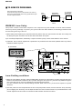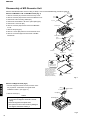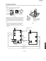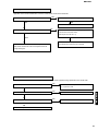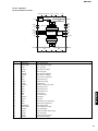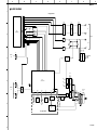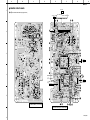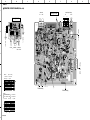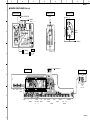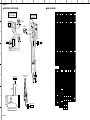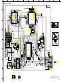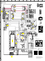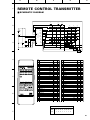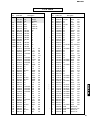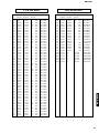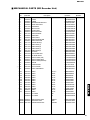
1
MDX-596
MINIDISC RECORDER
MDX-596
SERVICE MANUAL
!
?
S/F
A-B
&
–
RNDM
PROG
ABC
DEF
DISPLAY
(
GHI
✽
)
JKL
MNO
1
2
3
4
5
PQR
STU
VWX
YZ
/
6
7
8
9
0
SPACE
This manual has been provided for the use of authorized YAMAHA Retailers and their service personnel.
It has been assumed that basic service procedures inherant to the industry, and more specifically YAMAHA Products, are already
known and understood by the users, and have therefore not been restated.
WARNING:
+10
TITLE
IMPORTANT NOTICE
SCROLL
REPEAT
CHAR.
SEARCH
E
NUMBER
DELETE
SET
M-MARK
MONO/ST
INPUT
R
SKIP
IMPORTANT: The presentation or sale of this manual to any individual or firm does not constitute authorization, certification or
recognition of any applicable technical capabilities, or establish a principle-agent relationship of any form.
REC
TIME
T
Y
PLAY
PAUSE
STOP
REC
W
D
A
S
SYNC
CD-P
Failure to follow appropriate service and safety procedures when servicing this product may result in personal
injury, destruction of expensive components and failure of the product to perform as specified. For these reasons,
we advise all YAMAHA product owners that all service required should be performed by an authorized
YAMAHA Retailer or the appointed service representative.
The data provided is believed to be accurate and applicable to the unit(s) indicated on the cover. The research, engineering, and
service departments of YAMAHA are continually striving to improve YAMAHA products. Modifications are, therefore, inevitable
and specifications are subject to change without notice or obligation to retrofit. Should any discrepancy appear to exist, please contact
the distributor's Service Division.
WARNING:
Static discharges can destroy expensive components. Discharge any static electricity your body may have accumulated by grounding yourself to the ground buss in the unit (heavy gauge black wires connect to this buss).
IMPORTANT: Turn the unit OFF during disassembly and parts replacement. Recheck all work before you apply power to the unit.
TO SERVICE PERSONNEL . . . . . . . . . . . . . . . . . 1—2
REAR PANELS . . . . . . . . . . . . . . . . . . . . . . . . . . . . . . 2
SPECIFICATIONS . . . . . . . . . . . . . . . . . . . . . . . . . . . . 3
INTERNAL VIEW . . . . . . . . . . . . . . . . . . . . . . . . . . . . . 4
DISASSEMBLY PROCEDURES . . . . . . . . . . . . . . 4—6
ADJUSTMENT & TEST MODE . . . . . . . . . . . . . . 7—16
SPECIAL TEST MODE . . . . . . . . . . . . . . . . . . . . . . . 17
ERROR DISPLAY . . . . . . . . . . . . . . . . . . . . . . . 18—19
TROUBLESHOOTING . . . . . . . . . . . . . . . . . . . . 20—24
100718
IC DATA . . . . . . . . . . . . . . . . . . . . . . . . . . . . . . . 25—34
BLOCK DIAGRAM . . . . . . . . . . . . . . . . . . . . . . . 35—37
TEST POINT WAVEFORMS . . . . . . . . . . . . . . . 38—39
PRINTED CIRCUIT BOARD . . . . . . . . . . . . . . . 40—46
MD VOLTAGES . . . . . . . . . . . . . . . . . . . . . . . . . . . . . 47
SCHEMATIC DIAGRAM . . . . . . . . . . . . . . . . . . 48—50
REMOTE CONTROL TRANSMITTER . . . . . . . . . . . 51
PARTS LIST . . . . . . . . . . . . . . . . . . . . . . . . . . . . 52—61
GREASE APPLICATION DIAGRAM . . . . . . . . . . . . 62
MDX-596
■ CONTENTS
MDX-596
■ TO SERVICE PERSONNEL
Critical Components Information
Components having special characteristics are marked Z
and must be replaced with parts having specifications equal
to those originally installed.
WALL
OUTLET
EQUIPMENT
UNDER TEST
AC LEAKAGE
TESTER OR
EQUIVALENT
INSULATING
TABLE
WARNING: Laser Safety
This product contains a laser beam component. This component may emit invisible, as well as visible radiation,
which may cause eye damage. To protect your eyes and skin from laser radiation, the following precautions must
be used during servicing of the unit.
1) When testing and/or repairing any component within the product, keep your eyes and skin more than 30 cm away from
the laser pick-up unit at all times. Do not stare at the laser beam at any time.
2) Do not attempt readjustment, disassembly or repair of the laser pick-up, unless noted elsewhere in this manual.
3) CAUTION : Use of controls, adjustments or performance of procedures other than those specified herein may result in
hazardous radiation exposure.
R, G, B models
R, G, B models
Cover (MD)
MDX-596
Laser Emitting conditions:
1) When the Cover (MD) is removed, and the POWER SW is turned to the "ON" position, the laser component will emit a
beam for several seconds to detect if a disc is present. During this time (5-10 sec.), the laser may radiate through the
lens of the laser pick-up unit. Do not attempt any servicing during this period!
If no disc is detected, the laser will stop emitting the beam. When a disc is set, you will not be exposed to any laser
emissions.
2) The laser power level can be adjusted with the VR on the pickup PWB, however, this level has been set by the factory
prior to shipping from the factory. Do not adjust this laser level control unless instruction is provided elsewhere in this
manual. Adjustment of this control can increase the laser emission level from the device.
1
MDX-596
Laser Diode Properties
Magnetic head
Material :
GaAlAs
Wavelength :
785 nm
Emission duration : Continuous
Pulse Durations and Max. Output at the lens of the Laser Pick Up Unit ;
Read mode :
0.8 mW (Continuous)
Write mode :
Max 10 mW for 0.5s, Min. Cycle 1.5s
ANSI Class :
Class 1
* This output is the value measured at a distance of about 200 mm from
the objective lens surface on the Optical Pick-up Block.
Optical pick-up
VARO!
: AVATTAESSA JA SUOJALUKITUS OHITETTAESSA OLET ALTTIINA NÄKYMÄTTÖMÄLLE
LASER-SÄTEILYLLE. ÄLÄ KATSO SÄTEESEEN.
VARNING! : OSYNLIG LASERSTRÅLNING NÄR DENNA DEL ÄR ÖPPNAD OCH SPÄRREN ÄR URKOPPLAD.
BETRAKTA EJ STRÅLEN.
■ REAR PANELS
▼ R model
▼ G, B models
MDX-596
▼ A model
2
MDX-596
■ SPECIFICATIONS
Digital audio system
GENERAL
System
MiniDisc digital audio system
Disc
MiniDisc
Recording method
Magnetic field variation overwrite
Reading method
Non-contact optical pickup (using semiconductor laser)
Laser
Semiconductor laser
Laser Diode Properties
Material: GaAIAs
Wavelength: 785 nm
Pulse time:
Read mode ... 0.8 mW Continuous
Write mode ... max 10 mW 0.5S
min cycle 1.5S
Repetition
Record/playback time
Max. 80 minutes
80 minutes (stereo)
160 minutes (mono)
Revolutions
Approx. 400~900 rpm (CLV)
Error Correction
ACIRC (Advanced Cross Interleave Reed-solomon Code)
Sampling frequency
44.1 kHz (32 kHz and 48 kHz signals converted to 44.1 kHz
for recording)
Coding
ATRAC (Adaptive TRansform Acoustic Coding)
Modulation system
EFM (Eight-to-Fourteen Modulation)
Number of channels
2 (stereo) or 1 (mono, for extended recording)
Frequency Response
5 ~ 20,000 Hz ±0.5 dB
Signal-to-Noise Ratio
More than 99 dB during playback
Wow and Flutter
Below measurable limit
Power Supplies
A model
AC 240 V, 50 Hz
G, B models
AC 230 V, 50 Hz
R models AC 110/120/220/240 V, 50/60 Hz
Power Consumption
18 W
Dimensions (W x H x D)
435 x 96 x 288 mm (17-1/8" x 3-3/4" x 11-5/16")
Weight
4.0 kg (8 lbs. 13 oz.)
Finish
Titanium color/Black color
Accessories
Remote Control.... 1
Audio cord... 2
Optical cord... 1
Batteries (size AA, R6, UM-3).... 2
Specifications subject to change without notice.
R : General model
B : British model
A : Australian model
G : European model
265.9 (10–1/2")
15.2
(5/8")
LINE IN (REC)
Type: pin jack
Input impedance: greater than 50 k-ohms
Standard input level: 300 mV
DIGITAL IN (OPTICAL) 1/2
Type: square optical connector jack
Outputs
3
96
(3–3/4")
435 (17–1/8")
80
(3–1/8")
LINE OUT (PLAY)
Type: pin jack
Standard output level: 2.0 ± 0.5 Vrms
DIGITAL OUT (OPTICAL)
Type: square optical connector jack
PHONES
Standard output level
(Input 150 ohms shorted, – 20 dB): 300 ± 60 mV
16
(5/8")
MDX-596
Inputs
287.8 (11–5/16")
6.7
(1/4")
* US and foreign patents licensed from Dolby Laboratories
Licensing Corporation.
Units : mm (inch)
MDX-596
■ INTERNAL VIEW
q
w
e
r
t
q
POWER TRANSFORMER
MAIN (1) P.C.B.
POWER SWITCH
MD RECORDER UNIT
MAIN (2) P.C.B.
w
CB1
CB6
CB5
CB401
e
r
t
■ DISASSEMBLY PROCEDURES
(Remove parts in disassembly order as numbered.)
CB7
Top Cover
w
q
1. Removal of Top Cover
a. Remove 4 screws ( q ) and 3 screw ( w ) in Fig. 1.
2. Removal of Front Panel
a. Remove 4 connectors.
CB5, CB6, CB7, CB401
b. Remove 3 screws ( e ) in Fig. 1.
*
Arrow marks (
removed.
t
MD Recorder Unit
) are printed to identify the screws to be
q
t
r
c. Remove 2 screws ( r ) in Fig. 1.
3. Removal of MD Recorder Unit
a. Remove 1 connector.
CB1
b. Remove 4 screws ( t ) in Fig. 1.
c. Remove 4 screws ( y ) in Fig. 2.
e
r
Fig. 1
MDX-596
Front Panel
MD Recorder Unit
y
Support (Mechanism)
y
Fig. 2
4
MDX-596
Disassembly of MD Recorder Unit
Remove the MD Recorder unit according to Steps 1 and 3 of the disassembly procedure (page 4).
(K1)x1
ø2x 3mm
Removal of MD Main P.C.B. and MD Mechanism (Fig. 3)
1. Remove 3 screws (K1) and then remove the Top Cover.
2. Remove 2 screws (K2) and then remove the Bottom Cover.
(K1)x1
ø2x 3mm
3. Disconnect 3 flat connecting cables (K3).
4. Disconnect the flexible P.C.B. for the optical pickup (K4).
Top Cover
(K1)x1
ø2x 3mm
5. Disconnect a connector (K5).
6. Remove 2 screws (K6) and then remove the MD Main
MD Mechanism
P.C.B.
7. Remove the spring (K7).
Boss
8. Remove 1 screw (K8) and then remove the Side Cover.
9. Remove 4 cushions (K9) from the bosses of the MD
Boss
Mechanism.
Cushion
(K9)x2
Spring
(K7)x1
(K8)x1
ø2x 3mm
Cushion
(K9)x2
Side Cover
MD Main P.C.B.
(K3)x2
(K3)x1
(K5)x1
(K6)x2
ø1.7x 3mm
Pull
Pull
(K4)x1
Flexible P.C.B. for
optical pickup (*1)
(*1) After pulling off the flexible
P.C.B. for the optical pickup
from the connector, cover its
end with aluminum foil or the
like which is electrically
conductive so as to prevent the
optical pickup from being
damaged by static electricity.
(K2)x1
ø2x 3mm
Bottom Cover
(K2)x1
ø2x 2mm
Fig. 3
MDX-596
Removal of Magnetic Head (Fig.4)
• Once the magnetic head is removed, it will be necessary to perform “Confirmation of magnetic head
installation Position”. (See page 13.)
1. Remove screw (A1).
Caution
a. When removing the magnetic head, hold its base and
do not touch the magnetic head itself or the leaf
spring.
b. Place the magnetic head upside down.
c. Use special care so as not to cause any damage to
the magnetic head when installing it.
(A1)x1
ø1.7x 5mm
Magnetic Head
Leaf Spring
MD Mechanism
Fig. 4
5
MDX-596
Removal of MD Loading P.C.B./Loading Motor (Fig. 5)
1. Remove 1 screw (B1).
2. Remove 3 hooks (B2) and then remove the MD
Loading P.C.B.
(B1)x1
ø1.7x 6mm
Loading Motor
3. Remove 2 screws (B3) and then remove the Loading
Motor.
MD Loading P.C.B.
(B2)x1
(B2)x2
(B3)x2
ø1.7x 3mm
Removal of Sled Motor/Optical Pickup Head (Fig. 6)
• Once the MD mechanism switch P.C.B. is removed, it
will be necessary to perform “Adjustment of Lead-in
Switch Position”. (See page 13.)
Fig. 5
(C1)x1
ø1.4x 5mm
Optical Pickup Head
• Once the optical pickup head is removed, it will be
necessary to perform “Confirmation of magnetic head
(C1)x2
ø1.4x 4.5mm
Sled Motor
installation Position”. (See page 13.)
MD Mechanism P.C.B.
1. Remove 3 screws (C1) and then remove the sled
motor.
2. Remove the Optical Pickup Head.
Caution
Use care so as not to cause any damage to the gear.
(The damaged gear will cause abnormal noise to occur
while searching.)
sary to perform “Pickup Rating”. (See page 14.)
MDX-596
Removal of Spindle Motor (Fig. 7)
• Once the spindle motor is removed, it will be neces-
Fig. 6
(D1)x3
ø1.4x 3mm
Spindle Motor
1. Remove 3 screws (D1) and then remove the Spindle
Motor.
Caution
a. Be careful not to scratch the gear.
(Scratched gear will produce noises during searching.)
b. As the turn-table is magnetized, keep foreign objects
from being attracted.
Fig. 7
6
MDX-596
■ ADJUSTMENT & TEST MODE
Servicing Procedure
Perform adjustment and setup in the TEST mode. Specific adjustments and procedures vary depending on the type of servicing performed.
TEMP standard
Type of servicing
EEPROM setting AUTO preliminary
Required item
AUTO
AUTO AFB EEPROM adjustment
Operation confirmation
value confirmation
EEPROM SET
adjustment
AUT YOBI
–
–
q
–
w
–
e
–
r
–
t
–
y
–
u
q
–
q
w
e
r
t
y
u
q
–
w
q
e
–
r
_
t
_
y
w
u
e
i
r
–
_
q
w
e
r
t
y
q
q
w
w
e
e
r
r
t
t
y
y
u
u
i
i
PICKUP replacement
Magnetic head replacement
Mechanical unit replacement
(including PICKUP)
MD main PCB replacement
MD microprocessor (IC1401)
replacement
MD LSI (IC1201) replacement
RF IC (IC101) replacement
EEPROM IC (IC1402) replacement
adjustment adjustment
value entry (*1)
AUTO AJST AUT AFB TEST mode cancel
(With AUTO main adjustment done in advance)
TEST-PLAY
TEST-REC
setting
TEMP
Numbers in the table, e.g., q, w, e, indicate the order in which required items should be performed.
"–" means that item needs not be performed.
(*1): The result of EEPROM entry is displayed at the end of the TEST mode.
OK_EEPROM:
Both "setting value" and "preliminary adjustment completed" have been entered properly.
WR_EEPROM:
The "setting value" has been entered properly but not "preliminary adjustment completed".
Perform preliminary adjustment properly and then enter "preliminary adjustment completed".
NG_EEPROM:
The "setting value" has not been entered.
Check the MD microprocessor and EEPROM for connection.
Preparation before Adjustment
● Test disc
● Extension cable (see connection diagram on page 14.)
Type
Test disc
High reflecting disc
TDYS1 (SONY) [for reproduction] (P/No. TX945850)
Low reflecting disc
Commercially available mini disc for recording
Low reflecting disc
MMD-318 [for pre-adjustment] (P/No. AAX04890)
––––––––
Clear disc for checking the head (P/No. AAX18050)
Type
1. Extension P.C.B. for servicing
AAX16620
3. 6-pin flat cable for servicing
AAX16640
4. 5-pin flat cable for servicing
TX946190
5. 28-pin flat cable for servicing
TX946220
MDX-596
1. How to enter the test mode
1) Press the POWER button while pressing the SET/ENTER button and the PLAY/PAUSE button.
Version of microprocessor is displayed about 1 second.
t s m 1 C * * e * *
Version of EEPROM protect data (from 01)
Version of microprocessor ROM (from 01)
2) Load either a disc for reproduction or a disc for recording.
“AUTO AJST” on display
7
AAX16660
2. 2-pin extension connector for servicing
TEST MODE
“EJECT” on display
Part No.
MDX-596
2. How to set to each mode
Every time the DISPLAY (forward) or EDIT (reverse) button is pressed, the mode changes. (For operation of each
mode, refer to the section describing each mode.)
Since this mode is not required for servicing , proceed to another mode promptly.
AUTO_AJST (AUTO adjustment)
@
AUT_AFB (AUTO AFB adjustment)
@
RST_YOBI (RESULT preparation)
@
RESULT (RESULT)
@
MNU_YOBI (MANUAL preliminary adjustment)
@
MNU_AJST (MANUAL adjustment)
@
EEPROM_SET (EEPROM setting)
@
AUT_YOBI (AUTO preliminary adjustment)
@
*
● Panel keys used in TEST mode
Panel key
REC
EJECT
DISPLAY
TITLE
CHARA.
EDIT
SET/ENTER
DELETE/CANCEL
SEARCH w
SEARCH e
MDX-596
JOG DIAL y
JOG DIAL t
INPUT
RANDOM
REPEAT S/F
REPEAT A-B
SCROLL
PLAY/PAUSE
STOP
Function
Command code
TEST mode end (entry of EEPROM)
1FH
Eject
B3H
Menu feeding in TEST mode (1) / (Feeding of menus mainly related to adjustment and EEPROM)
B2H
Menu feeding in TEST mode (2) / (Feeding of menus mainly related to continuous playback and continuous recording)
B4H
Menu feeding in TEST mode (3) (Feeding of menus mainly related to INNER mode and JUMP SELECT)
F2H
Menu feeding in reverse in TEST mode (Menu feeding in reverse in each TEST mode)
A8H
Finalization of menu selection or starting of its execution
A2H
Stopping each test item and shifting to menu selection at one step upper level
A7H
Forced feeding of the slide (in FWD direction) / Execution of JUMP function (FWD)
AAH
ADDRESS setting value increased / Specification of direction when setting the tracking
Forced feeding of the slide (in REV direction) / Execution of JUMP function (REV)
ACH
ADDRESS setting value reduced / Specification of direction when setting the tracking
Forced feeding of the disc to EJECT / setting value increased
F3H
Forced feeding of the disc to LOAD / setting value reduced
F4H
Switching of laser power at EJECT / switching of display for continuous playback / switching of digit setting when setting ADDRESS
F5H
–
–
–
–
–
–
3. How to cancel test mode (Entry of EEPROM adjustment value)
1) Be sure to perform AUTO preliminary adjustment, AUTO adjustment and AUTO AFB adjustment.
( “COMPLETE” appears on the display)
2) After completing above ajustments, press the REC button. (Entry to EEPROM initiates then.)
The TEST mode is completed. ( “Test End” appears on the display)
3) Press the EJECT button to take out the disc.
4) Turn off the power.
8
MDX-596
Description of TEST modes
1. EJECT mode
To TEMP setting (of EEPROM setting)
[ _ _ EJECT _ _ _ ]
To CONTROL setting (of EEPROM setting)
Laser power setting (record/reproduction power) is performed.
2. AUTO preliminary adjustment mode
[ _ AUT _ YOBI _ ]
3. AUTO adjustment mode
[ AUTO _ AJST _ ]
Automatic preliminary adjustment is performed.
Adjusted values are output by using the interface.
Automatic adjustment is performed. (Grating adjustment mode after this adjustment.)
Adjusted values are output by using the interface.
Continuous reproduction is performed. (Error rate on display, jump test)
4. AUTO AFB adjustment mode
Automatic focus balance adjustment is performed.
[ _ AUT _ AFB _ _ ]
Adjusted values are output by using the interface.
RESULT preparation mode
Not used (Do not use this function as it is not for servicing)
[ _ RST _ YOBI _ ]
RESULT mode (main adjustment)
Not used (Do not use this function as it is not for servicing)
[ _ RESULT _ _ _ ]
MANUAL preliminary adjustment mode
Not used (Do not use this function as it is not for servicing)
[ _ MNU _ YOBI _ ]
MANUAL adjustment mode
Not used (Do not use this function as it is not for servicing)
[ _ MNU _ AJST _ ]
5. EEPROM setting mode
[ EEPROM _ SET ]
6. TEST-PLAY mode
[ TEST _ PLAY _ ]
7. TEST-REC mode
Various factors of the digital servo function are changed manually.
The voltage is measured at the temperature detect terminal and the standard value is set.
Continuous reproduction from the specified address is performed.
C1 error rate is measured and ADIP error rate is measured.
Continuous recording from the specified address is performed.
[ TEST _ REC _ _ ]
8. INNER mode
The position where the INNER switch is turned ON is measured.
[ _ _ INNER _ _ _ ]
1. EJECT mode
MDX-596
Step
9
Setting method
1
2
3
4
5
EJECT status in the TEST mode
Press the INPUT button.
Press the INPUT button.
Press the INPUT button.
Press the TITLE edit button.
6
7
8
Press the CHARA. button.
Press the DISPLAY button.
Press the DELETE/CANCEL button.
Remark
EJECT menu (No disc is loaded.)
Reproduction power output status
Recording power output status
Since this mode is not required for servicing , proceed to another mode promptly.
To TEMP setting
(Refer to TEMP setting)
To CONTROL1 setting
To CONTROL2 setting
EJECT menu
Display
[ _ _ EJECT _ _ _ ]
[ ppw _ _ _ _ _ _ _ ]
[ rpw _ _ _ _ _ _ _ ]
[ xpw _ _ _ _ _ _ _ ]
[ TEMP _❍ ❍ _◆ ◆]
[ CONTROL1 _ 08 ]
[ CONTROL2 _ 02 ]
[ _ _ EJECT _ _ _ ]
MDX-596
Check procedure Mode
q
Playback power output “ppw”
w
Recording power output “rpw”
“rpw” not achieved.
Check item
(Pin 3 of IC1401)
DC 0.2V
DC 1.5V
DC 1.8V
Less than DC1.5V
–
Judgement
Possible cause and check content
OK (Move on to check w.)
NG
OK (End of checking.)
NG
NG
–
Perform *1.
–
Perform *2.
Perform *1.
*1: Poor soldering of the line at Pin 100 of IC1401.
Check the line of Pin 93 of IC1401 for short and poor soldering. (Check all the way to the SW P.C.B.)
*2: Check the line of Pin 3 of IC1401 for poor soldering and short with other patterns.
Check the pick-up laser for breakage.
● Confirmation of pick-up laser power
Recording and reproduction can be checked by using the laser power meter. However it should be
used for checking only because there is variation in its measurement.
When the measured value is excessively deviated from the reference value, replace the pick-up.
Reference value (measured at room temperature of 25 °C)
During reproduction (ppw) : 0.72 ± 0.1 mW
During recording : 5.5 ± 0.5 mW
Note : Be very careful when using the laser power meter. The laser beam would cause damage to
your eye if exposed to it directly.
● TEMP (temperature standard) setting
(Make this setting quickly when the room temperature is within the range of 21 ˚C to 29 ˚C and
the P.C.B. is cold.)
(1) Set to the TEMP setting mode menu.
[ TEMP ❍ ❍ ◆ ◆ ]
❍ ❍ : Temperature measured value
◆ ◆ : Temperature setting value
(2) Make temperature correction based on the ambient temperature and according to the following
table.
Ambient temperature
+ 21.0 ˚C ~ + 23.2 ˚C
+ 23.3 ˚C ~ + 26.8 ˚C
+ 26.9 ˚C ~ + 30.7 ˚C
Correction value
– 1H
± 0H
+ 1H
Example : When the temperature measured value is 7AH and the ambient temperature is 22 ˚C:
MDX-596
7AH (measured value) - 01H (correction value) = 79H (setting value)
* If the temperature measured value deflects between two values, use the smaller value (If 7AH and 79H in the
above example, use 79H.)
(3) Using the jog dial, match the value obtained in Step (2) with the temperature setting value.
Example : When the temperature measured value is 7AH and the ambient temperature is 22 ˚C:
[ TEMP 7A 79 ]
Temperature setting value
10
MDX-596
2. AUTO preliminary adjustment mode
Step
Setting method
1
2
Set the Test mode.
Load a disc.
3
4
Press the EDIT button once.
Press the SET/ENTER button once.
Adjusted values are output.
Adjustment is completed.
5
6
Disc in use: MMD-318 [for pre-adjustment]
When adjustment is OK, press the
DELETE/CANCEL button.
When adjustment is NG, press the
DELETE/CANCEL button.
3. AUTO adjustment mode
Remark
Display
No disc is loaded.
Auto adjustment menu
Auto preliminary adjustment menu
Auto preliminary adjustment is started after sliding to the
innermost track.
“ *** ” changes in the following order during automatic
adjustment.
HAo -> ................. -> TCO
Proceed to Step 5 when adjustment is OK.
Proceed to Step 6 when adjustment is NG.
The display returns to the AUTO preliminary adjustment menu.
There is an abnormality at the adjusted point such as HAo.
Refer to “Troubleshooting”. (page 20)
[ EJECT ]
[ LOADING ]
[ AUTO _ AJST _ ]
[ _ AUT _ YOBI _ ]
[ *** : _ _ _ _ _ _ ]
[ _ COMPLETE _ ]
[ Can't _ ADJ. ]
[ _ AUT _ YOBI _ ]
[ Can't _ ADJ. ]
Disc in use: TDYS1 (SONY) [for reproduction] or commercially available
mini disc for recording
Step
Setting method
1
2
Set the TEST mode.
Load a disc.
3
Press the SET/ENTER button once.
Adjusted values are output.
Adjustment is completed.
4
5
MDX-596
6
When adjustment is OK, press the
SET/ENTER button.
Press the INPUT button.
Press the DELETE/CANCEL button.
When adjustment is NG, press the
DELETE/CANCEL button.
Remark
Display
No disc is loaded.
AUTO adjustment menu
Automatic adjustment is started after sliding to the innermost
track.
“ *** ” changes in the following order when a high reflecting disc
(disc for reproduction) is used.
PEG -> HAG
“ *** ” changes in the following order when a low reflecting disc
(disc for recording) is used.
PEG -> LAg -> GCG -> GEG -> LAG
Proceed to Step 4 when adjustment is OK.
Proceed to Step 6 when adjustment is NG.
Continuous reproduction (bit section) (Address + C1 error display)
Continuous reproduction (group section) (Address + C1 error display)
Continuous reproduction (group section) (Address + ADIP error display)
Display returns to the AUTO adjustment menu display.
There is an abnormality at the adjusted point such as PEG.
Refer to “Troubleshooting”. (page 20)
[ EJECT ]
[ LOADING ]
[ AUTO _ AJST _ ]
[ *** : _ _ _ _ _ _ ]
[ _ COMPLETE _ ]
[ Can't _ ADJ. ]
[ s XXXX c YYYY ]
[ a XXXX c YYYY ]
[ a XXXX a YYYY ]
[ AUTO _ AJST _ ]
[ Can't _ ADJ. ]
Note) *** : Adjustment name, XXXX: Address, YYYY: Measured value
4. AUTO AFB adjustment mode
Step
Disc in use: Commercially available mini disc for recording
Setting method
1
2
Set the Test mode.
Load a disc.
3
4
Press the DISPLAY button once.
Press the SET/ENTER button once.
5
Press the DELETE/CANCEL button.
Remark
Display
No disc is loaded.
Auto adjustment menu
Auto AFB adjustment menu
Auto AFB adjustment is started.
Adjusted values are output.
The display returns to the AUTO AFB adjustment menu.
[ EJECT ]
[ LOADING ]
[ AUTO _ AJST _ ]
[ _ AUT _ AFB _ _ ]
[ FAB YY _ ZZZZ ]
[ YY _ ZZZZ _ _ _ ]
[ _ AUT _ AFB _ _ ]
Note) YY, ZZZZ: Measured value
11
MDX-596
5. EEPROM setting mode
(used to confirm/adjust setting values)
Disc in use: Commercially available mini disc for recording
Refer to p.15 for EEPROM setting.
6. TEST-PLAY mode
Using the disc: Commercially available mini disc for recording
(Use this mode to check that the playback function is provided at the specified address.)
Step
Setting method
Remark
Display
Press the INPUT button.
AUTO adjustment menu
TEST-PLAY menu
ADDRESS setting (The initial value of the target address is displayed.)
Continuous reproduction (bit section) (Address + C1 error display)
Continuous reproduction (group section) (Address + C1 error display)
Continuous reproduction (group section) (Address + ADIP error display)
[ AUTO _ AJST _ ]
[ TEST _ PLAY _ ]
[ ADRES _ 0032 ]
[ s XXXX c YYYY ]
[ a XXXX c YYYY ]
[ a XXXX a YYYY ]
Press the DELETE/CANCEL button.
TEST-PLAY menu
[ TEST _ PLAY _ ]
1
2
3
4
Load a disc.
Press the TITLE button.
Press the INPUT button.
Press the SET/ENTER button.
5
6
• Every time the TITLE button is pressed in the address setting mode, the address changes in the order of 0032-> 03C0 -> 0700 -> 08A0
-> 0950 -> —
• Pressing the DISPLAY button in the TEST-PLAY menu changes to the AUTO adjustment menu.
7. TEST-REC mode
Disc in use: Commercially available mini disc for recording
(It is used to check the REC function at the specified address.)
Step
Setting method
Remark
Display
1
2
3
4
Load a disc.
Press the TITLE button twice.
Press the SET/ENTER button.
Press the SET/ENTER button.
AUTO adjustment menu
TEST-REC menu
ADDRESS setting (The initial value of the address is displayed.)
Continuous recording
[ AUTO _ AJST _ ]
[ TEST _ REC _ _ ]
[ a0032 _ pw ZZ ]
[ a XXXX _ pw ZZ ]
5
Press the DELETE/CANCEL button.
TEST-REC menu
[ TEST _ REC _ _ ]
• Every time the TITLE button is pressed in the address setting mode, the address changes in the order of 0032-> 03C0 -> 0700 -> 08A0
-> 0950 -> —
• Pressing the DISPLAY button in the TEST-REC menu changes to the AUTO adjustment menu.
8. INNER mode
Step
Disc in use: Commercially available mini disc for recording
Setting method
Load a disc.
Press the CHARA. button.
Press the SET/ENTER button.
4
Press the DELETE/CANCEL button.
Remark
AUTO adjustment menu
INNER menu
INNER switch position is measured.
(Both SUBQ address and C1 error are displayed.)
INNER menu
Display
[ AUTO _ AJST _ ]
[ _ _ INNER _ _ _ ]
[ s XXXX c YYYY ]
MDX-596
1
2
3
[ _ _ INNER _ _ _ ]
• Pressing the DISPLAY button in the INNER menu changes to the AUTO adjustment menu.
12
MDX-596
● Lead-in switch position adjustment
Adjust the lead-in switch position so that it is between FF85 and FFD2.
1. Load a TDYS1 (SONY) (P/No. TX945850) disc for reproduction.
2. Loosen the screw (A1) (1 pc) attaching the mechanical switch P.C.B.
3. Retighten the screw (A1) (1 pc) while pressing the mechanical switch P.C.B in the arrow A direction in the figure for
FF85 or less and in the arrow B direction for FFD2 or more.
Measure the lead-in switch position again and check that it is in the range between FF85 and FFD2.
A
B
(A1) X1
Note) Apply thread lock to the screw (A1) (1 pc) of
the P.C.B. after tightening it.
Fig.8
● Forced rotation of loading motor
It is possible to force the loading motor to rotate by turning the jog dial when the microprocessor version (tsm1C**e**)
of the test mode or EJECT appears on display. (This is used when the disc cannot be ejected.)
JOG DIAL y : Forced feeding of the disc to EJECT
JOG DIAL t : Forced feeding of the disc to LOAD
* To obtain the microprocessor version on display when a disc is loaded, “ AUTO _ AJST _ ” appears on display. Press
the DELETE/CANCEL key in this state, and the microprocessor version will appear.
● Confirmation of magnetic head installation position
• After replacing the magnetic head and the optical pick-up, be
sure to confirm their installation positions.
MDX-596
• To facilitate adjustment of their installation positions, bring the
optical pick-up to the center position and follow the procedure
described below.
1.Load a clear disc (P/No. AAX18050) for checking the head.
2.Push down the up-shift arm of the magnetic head with a finger to
raise the magnetic head.
3.Looking at the unit from above, check if the magnetic head
matches with the optical pick-up objective lens.
4.Check to ensure that the magnetic head moves up and down
smoothly.
Push down with a finger.
Fig.9
13
Magnetic head
Objective lens
Radial direction
Circumferentical direction
MDX-596
MECHANISM ADJUSTMENT
When making an adjustment, be sure to connect an extension cable for servicing and an expansion P.C.B. as shown in
Fig.12.
1. Optical pickup rating inspection method
2
(Externally attached)
GND (TP1202)
IC1201 No.4 pin
EIN (TP1253)
IC1201 No.11 pin
Oscilloscope
3
a
1
100K
470p
GND CH1 CH2
470p
FIN (TP1254)
IC1201 No.12 pin
X
Y
100K
b
Lissajous waveform
a:b = Within 4:1
(See page E41/J39)
2
Fig. 10
After performing automatic adjustment in the AUTO mode
1
selected from the test mode by using a TDYS1 (SONY) (P/
No. TX945850) disc for reproduction (COMPLETE status
Check the Lissajous waveform
while adjusting the installation
position by using a screwdriver in
the adjustment hole in the
spindle motor.
3
on display), adjust the EOUT to FOUT Lissajous waveform
(x-y).
Adjustment hole
1. Loosen 3 screws of the spindle motor a little and make
adjustment while watching the Lissajous waveform.
Fig. 11
2. After adjustment, tighten screws in the order of (q), (w)
and (e).
From magnetic head
Connector for 2P extension
AAX16620
From optical pickup
Mechanism
P.C.B.
FFC for 28P extension
TX946220
MD Main P.C.B.
MDX-596
Extension P.C.B. for servicing
(AAX16660)
Install an Extension P.C.B. for servicing
to the mechanism.
FFC for 6P extension
AAX16640
FFC for 5P extension
TX946190
Fig. 12
14
5. EEPROM setting mode
Disc in use: Commercially available mini disc for recording
(used to confirm/adjust setting values)
1) Start the TEST mode.
2) Load the disc.
[AUTO AJST]
3) Press the DISPLAY button 6 times.
[EEPROM SET]
4) Execute the procedure to have “EEPROM setting mode transition diagram” displayed and adjust
the jog dial so that the same setting values as those in “EEPROM contents list” are obtained.
(Refer to p.10 for TEMP setting.)
5) Press the REC button to cancel the TEST mode.
(Entry into EEPROM can be started here.)
6) Set to the TEST mode again and perform AUTO preliminary adjustment, AUTO adjustment and
AUTO AFB adjustment.
EEPROM SETTING MODE TRANSITION DIAGRAM
Note)
15
To return to the SUB MENU or MAIN MENU display of the test mode, press the DELETE/CANCEL button.
EEPROM CONTENTS LIST
● Focus setting (Focus)
Item on display
FG
❍❍
FF0
❍❍
FF1
❍❍
FF2
❍❍
FZHLEV
❍❍
FOKLEVh
❍❍
FOKLEVL
❍❍
FOSTn
❍❍
DISCJG
❍❍
● Slide setting (Sled)
Set value
B1 H
10 H
70 H
E0 H
ED H
07 H
09 H
2C H
14 H
● Spin setting (Spindle)
Item on display
SPG
❍❍
SPG-in
❍❍
SPG-mid
❍❍
SPG-out
❍❍
SP1
❍❍
SP2
❍❍
SP3
❍❍
SP4
❍❍
SP5
❍❍
SPDLIM
❍❍
SPKLEVm
❍❍
Set value
10 H
5C H
48 H
38 H
10 H
93 H
ED H
EE H
20 H
64 H
15 H
● Tracking setting (Tracking)
Item on display
TG
❍❍
TF0
❍❍
TF1
❍❍
TF2
❍❍
FT3
❍❍
SVCNT4
❍❍
TRBLVo
❍❍
TRBLVt
❍❍
TRKLVo
❍❍
TRKLVt
❍❍
TDPWo
❍❍
TDPWt
❍❍
SLCTo
❍❍
SLCTt
❍❍
SLCTm
❍❍
TCRSC1P
❍❍
TCRSC0h
❍❍
TCRSC0L
❍❍
TCRSCHh
❍❍
TCRSCHL
❍❍
COTLVP
❍❍
COTLVr
❍❍
JPint
❍❍
KIK10
❍❍
Set value
6B H
10 H
6B H
F0 H
08 H
01 H
68 H
50 H
60 H
2E H
67 H
21 H
00 H
50 H
53 H
16 H
00 H
FA H
02 H
02 H
05 H
15 H
00 H
64 H
Item on display
SLG
❍❍
SL2
❍❍
SLDLIM
❍❍
SLDLEV
❍❍
SLKLVk
❍❍
SLKLVt
❍❍
SLKLVm
❍❍
SLBKm
❍❍
SLKrio
❍❍
SLKroi
❍❍
SLK1io
❍❍
SLK1oi
❍❍
Set value
3E H
10 H
7F H
12 H
55 H
2E H
55 H
08 H
60 H
68 H
68 H
60 H
● Control setting (Control)
Item on display
CONTROL1
❍❍
CONTROL2
❍❍
ADJTTM
❍❍
HDEQAD
❍❍
LDEQAD
❍❍
GDEQAD
❍❍
MDEQBC
❍❍
LDEQBC
❍❍
GDEQBC
❍❍
HALSG
❍❍
LALSG
❍❍
GALSG
❍❍
HALSOFS
❍❍
LALSOFS
❍❍
GALSOFS
❍❍
Set value
08 H
02 H
14 H
92 H
8E H
91 H
8C H
8F H
8A H
11 H
11 H
11 H
FC H
00 H
00 H
● Adjust setting (ADJSET)
COK
FAT
TAT
CAT
FAB
STR
SFS
STC
Item on display
❍❍
❍❍
❍❍
❍❍
❍❍
❍❍
❍❍
❍❍
Set value
58 H
C0 H
3E H
40 H
5C H
0B H
0D H
0D H
16
MDX-596
■ SPECIAL TEST MODE
● How to set to the special test mode
Press the POWER button while pressing the SET/ENTER button and the STOP button. Then all the indicators will light up.
● Operation procedure
Every time the SET/ENTER button is pressed, lighting of indicators and items on the display change as follows.
1) All indicators light up.
2)
3)
All indicators turn off.
Segments not sharing the border light up.
4)
5)
Above segments turn off and other segments light up.
The date when the software was entered appears on the display.
6)
7)
The version of the micro processor appears on the display.
The time of auto-marking appears on the display.
[ CPU Ver:TP03 ]
[ AM Time :C8h ]
8)
9)
The analog level of auto-marking appears on the display.
The digital level of auto-marking appears on the display.
[ AM Lv1_A:24h ]
[ AM Lv1_D:1Ah ]
10) The parameter of the bit distribution during recording on the display.
11) The parameter of the bit distribution during recording on the display.
[ Rec Bit0:C0h ]
[ Rec Bit1:FEh ]
12) Write/read check for EEPROM appears on the display
[ EE W/R Check ]
When the INPUT button is pressed at this point, whether the micro processor executed data write/read function into
EEPROM or not is checked.
If [OK] appears on the display and the pin 6 of IC6 is at “H”, the check result is satisfactory.
[NG] is displayed when there is an error while writing or reading the data.
In such a case, check EEPROM (IC7).
● How to cancel the special mode
Press the STOP button, and the mode will change from the special test mode to the factory preset mode and the data in
RAM will be cleared.
Note : Turning off the power will cancel the special test mode but will not clear the data in RAM (ie., user settings are
maintained).
MDX-596
Data to write in EEPROM (IC7)
INPUT mode
REPEAT mode
RANDOM mode
PROGRAM mode
REC mode (STEREO/MONO)
AUTO MARK/MANUAL
DISPLAY mode
17
Initial settings
ANALOG
OFF
OFF
OFF
STEREO
AUTO (“MANUAL” does not light up.)
DISC TITLE
MDX-596
■ ERROR DISPLAY
Error on display
Can't REC
Description
• DEFECT occurred 10 times continuously during RECPLAY.
• Recordable cluster became “0” due to occurrence of
DEFECT during REC-PLAY.
Countermeasure
• Check that the disc is free from any scratch,
dust, finger print, black spot, etc. and that
decentering, face deflection, etc. are not
excessive.
• REC mode cannot be set for 20 seconds even after
repeatedly trying to read the read disabled address.
Can't Copy
• One of the following judgments has been made
depending on the channel status of the digital signal
• Check if the CD is a copy inhibited on (e.g., CDR, etc.)
input from D-IN during REC-PAUSE or REC-PLAY.
(1) Other than audio
(2) Other than civil purpose
(3) Copy NG due to reversed COPY bit of CD (ie., copy
protected)
DIGin Unlock
• Either of the following symptoms occurred for the digital
signal input from D-IN during REC-PAUSE or REC-
• Check that the D-IN signal line is free from
abnormality.
PLAY.
(1) Digital IN PLL is unlocked.
(2) Locked under conditions other than FS=44.1kHz.
TOC Full
• No space is left to register music No and character data
(song name, disc name, etc.) while the REC-PLAY
• Use a disc for recording and reproduction with a
space left to register UTOC.
function is used.
• No recordable space is left when trying to activate the
REC-PAUSE function.
UTOC ERR R
• “FTNO > LTNO” occurred.
• “FTNO = 0 or 1” occurred.
• As an abnormality exists in the UTOC data, use
another disc.
• UTOC recorded in the disc could not be read.
UTOC ERR A
• “Start address > end address” occurred.
UTOC ERR L0 ~ 4
• Any one of the UTOC0 ~ 4 data was looped.
Not Audio
• Data not for audio purpose is recorded in the track mode
• Select another TNO or use another disc.
Disc Full
• No recordable space is left when trying to activate the
REC-PAUSE function.
Playback MD
• The loaded disc was for reproduction only when trying to
activate the REC-PAUSE function or trying to edit.
Protected
• Recording or editing was attempted while the data
protector of the disc for recording and reproduction is
set to the data protected state.
• Editing the track subject to write protect function was
MDX-596
of TNO which is currently selected.
• Use another disc for recording with a recordable
space left.
• As the loaded disc is for reproduction only, use
a disc for recording.
• Try again with the data protector set to the
original position.
• As the track to be edited is write protected, try
again with another track.
attempted by using the data written in UTOC.
18
MDX-596
Error on display
Can' t Edit
Description
Countermeasure
• Editing conditions were not satisfied with respect to
• Wrong operation procedure was used. Try
again by using the correct procedure.
each editing function.
TMP Over!!
• The temperature in the set (MD unit) went up excessively high due to occurrence of some abnormality.
• Check according to troubleshooting.
• Check the temperature of the area where the
unit is used.
DISC ERR R
DISC ERR S
DISC ERR W
• The data was not correct or it was not possible to read it
• Use another disc as there is an abnormality in
TOC or UTOC data or the disc has a scratch or
correctly.
• Recording the music data failed as an abnormality
other faulty condition.
occurred while recording it.
TOC ERR S
• The TOC data was not correct.
TOC ERR R
• It was not possible to read the TOC data.
• The TOC data recorded in the disc is not in
compliance with the MD standard.
• Use another disc as the disc has a scratch or
other faulty condition.
U TOC W ERR
• It was not possible to rewrite UTOC correctly and an
abnormality occurred while rewriting it.
FOCUS ERR
• The disc was loaded but it was not possible to achieve
• Use another disc as the disc has a scratch or
other faulty condition.
• Check that the disc is free from any scratch,
dust, finger print, black spot, etc. and that
FOCUS.
decentering, face deflection, etc. are not
excessive.
BLANK DISC
• The total number of TNO and NAME characters was “0”
as a result of reading UTOC.
TOC W ERROR
• UTOC can be read but cannot be rewritten.
• Check if the disc is recordable by actually
recording.
• Check if the recording head contacts properly
and if wiring from the circuit board to the
recording head is free from breakage.
EEPROM ERROR
• The EEPROM data is not correct
• Try again after resetting and if still NG, replace
MDX-596
EEPROM.
Mechanism Error
Error on display
Description
Er_MD2_*
The head fails to move up.
Er_MD3_*
The head fails to move down.
HINF (IC1401 No.93 pin)
*=E
19
Eject completed position
< 1.0 V
* = M Horizontal midway position
> 3.01 V
*=L
Load completed position
1.31 — 2.36 V
*=D
Head down position
1.01 — 1.31 V
MDX-596
■ TROUBLESHOOTING
When MD fails to operate
When the objective lens of the optical pickup becomes dirty, MD may fail to operate. Clean the objective lens first and
check MD for reproduction function. If it still fails to operate, check according to the following flow charts.
Contaminant on the pickup lens such as dust or other foreign matter may cause the pickup to skip or the TOC (content of
the selection) not to be displayed. Check if the lens is clean before making adjustments. If the lens is dirty, clean it as
follows.
● Turn off the power. Dampen the lens cleaning paper with a small amount of isopropyl alcohol and wipe the lens with it,
using care not to cause any damage to the lens. Be sure not to touch the lens with your hand directly.
▲
Check the trouble item “Play mode is not available.”.
▲
Check the trouble item “Audio reproduction circuit”.
▲
Check the trouble item “Recording/reproduction function”.
▲
Check the display section.
▲
Check the power supply section and CN1501.
▲
Check IC6 and CN1501.
▲
Check around Q1804 and IC1401.
▲
Check IC1201.
▲
NO
Check IC1401.
YES
Is appropriate audio output provided?
▼
NO
YES
Is the play mode available when the PLAY/PAUSE button is pressed?
▼
Check the trouble item “Disc cannot be loaded properly.”.
YES
Does the disc loading function work properly?
▼
Check the trouble item “Power fails to turn on”.
▲
▼
NO
▲
Does the power turn on when the POWER button of the main unit is pressed?
NO
YES
NO
Does recording/reproduction function work properly?
Power fails to turn on.
Does the unit operate properly when its STOP button of is pressed?
YES
NO
▼
Is +5V ~ +6V voltage applied to No.17 and 18 pins of CN1501?
NO
YES
▼
Is a pulse applied to No.6 pin of CN1501 when the reset power is turned on?
YES
Is the voltage at No.62 pin of IC1401 +3.2V?
YES
MDX-596
▼
NO
NO
▼
Is a 8.4672MHz pulse applied to No.15 pin of IC1401?
NO
YES
▼
Is a pulse output from No.34 pin of IC1401?
NO
YES
▼
Check CN1501 and IC6.
20
MDX-596
Disc cannot be loaded properly.
Does the loading function work properly when a disc is inserted?
YES
NO
Check CN1401, CN1931 and SW1932.
▲
Check IC1401.
▲
▼
▲
NO
Does No.5 pin of CN1401 become “H”?
Check CN1401, CN1931 and IC1601.
YES
NO
Does a change occur at either No.19 or 20 pin of IC1601?
▼
YES
▼
NO
Does a change occur at either No.12 or 13 pin of IC1601?
YES
▼
Check M903.
▼
YES
Does eject function work when the MD eject button is pressed?
▼
NO
YES
Is the disc drawn in again immediately after it is ejected?
YES
▼
Check CN1901 and SW1932.
Play mode is not available.
YES
▲
Is the play mode unavailable with either high reflecting disc
Proceed to the check item “Checking by using the test mode”.
MDX-596
or low reflecting disc?
▼
NO
NO
▼
Is the play mode unavailable only with the high reflecting disc?
The play mode unavailable only with the low reflecting disc.
YES
YES
▼
▼
Is the voltage at No.93 pin of IC1401 1.45 ± 0.15V in the test
Is the voltage at No.93 pin of IC1401 with a low reflecting disc loaded
mode state with a high reflecting disc loaded?
1.75V ± 0.15V (recordable) or 2.15V ± 0.15V (recording inhibited)?
YES
▼
▼
After readjustment, proceed to the check item “Normal reproduction”.
21
▼
NO
YES
NO
▼
Check SW1931, loading circuit board and CN1931.
MDX-596
Normal reproduction
Applicable when the E2-PROM value has been confirmed as normal in the test mode
▲
YES
Is initialization done properly for reproduction of a high reflecting disc?
Does the play time display count up properly?
NO
▼
NO
Check IC1201.
▼
▲
NO
Is the disc turning properly?
Does the lead-in switch turn on with the pickup at the
innermost track in the test mode?
(Is No.63 pin of IC1401 at “L”?)
NO
YES
▼
▼
Check SW1936, soldered points in the mechanical switch
Check the position of the lead-in switch by selecting the lead-in
circuit board and around No.6 pin of CN1932.
switch position measurement mode from the adjustment items for
the high reflecting disc.
Audio reproduction circuit
Applicable when no sound is produced although the play time display counts up properly during reproduction in the normal mode
NO
▲
Is the audio output waveform obtained at No.24 and 26 pins of IC1701?
17, 19 pins of IC1701.
YES
▼
Check No.70 — 72, 74 pins of IC1201 and No.12, 16,
NO
Check the connection line IC1701 and CN1501.
▲
Check IC3.
MDX-596
▲
Is the audio output waveform obtained at No.26 and 28 pins of CN1501?
YES
▼
Is the audio output waveform obtained at No.1 and 7 pins of IC3?
NO
YES
▼
Check the muting section of IC8.
22
MDX-596
Recording/reproduction function
Load a low reflection disc and after confirming the audio output in the normal reproduction mode, execute recording/reproduction.
Check that the disc is not in the recording inhibited status.
▲
Check around IC1401.
▲
Check IC1201 for proper soldering.
▲
▼
NO
▲
Does the recording function fail from the starting address?
Check around IC4 and IC5 and also check the REC
YES
Is an RF waveform available at No.1 pin of IC1201 or TP1201
YES
during reproduction after recording?
▼
NO
Does the level of No.3, 26 and 39 pins of IC1401 change
NO
between recording and reproduction?
YES
▼
Is an RF pattern provided at No.50 pin of IC1201?
▼
NO
YES
Check IC1300 — 1302 and CN1300.
▼
Is an output waveform available at No. 1 and 7 pins of IC4 and No. 1
NO
and 7 pins of IC5 while recording the LINE input in the normal mode?
▼ YES
▼ YES
MDX-596
Check around IC1701 and No.70 — 73 pins of IC1201.
23
NO
▲
Is an input waveform applied to No.3 and 5 pins of IC1701?
LEVEL volume.
Check around IC1701 and CN1501.
MDX-596
Checking by using the test mode
Spindle motor does not run.
NO
▲
Is a correct waveform provided at No.24 and 25 pins of IC1201
Check No.24 and 25 pins of IC1201 as well as solder
connections and parts of the peripheral circuit.
during the AUTO adjustment mode step 3 in the test mode?
YES
▼
NO
▲
Is a waveform provided at No.9 and 10 pins of IC1601 as
well as at No.5 and 6 pins of CN1402?
▼
Check IC1601, CN1402 and the mechanism switch circuit
board solder connections.
YES
Replace the spindle motor as a complete unit.
Sled motor does not run.
NO
▲
Does a change occur at No.22 and 23 pins of IC1201 when
Check the waveform at No.22 and 23 pins of IC1201,
peripheral parts and solder connections.
R and E buttons are pressed?
YES
▼
Check IC1601 and CN1402 solder connections.
▲
NO
▲
Does a change occur at No.14 and 15 pins of IC1601 and No.3 and
Check the connection section to the sled motor for any
4 pins of CN1402 when the R and E buttons are pressed?
YES
▼
Does a voltage change occur at the + and - terminals of the
sled motor when the R and E buttons are pressed?
NO
poor solder connections or broken wires.
YES
▼
Replace the sled motor.
MDX-596
24
MDX-596
RF1 1
RF2 2
RF3 3
RF4 4
1+2
PIN
3+4
PITG
NIN
GND1
BIAS
VCC1
EFMAGC
DCNF
EFMO
48
47
46
45
44
43
42
41
40
39
38
37
36 2-1
RESISTOR & SW
IC1101 : IR3R58M
RF Signal Processing
1234
■ IC DATA
35 ADAGI
EFM AGC
34 ADAGC
DIFF
33 ADIPNF
ADIP AGC
REFI 5
32 ADIPO
BIAS
31 GND2
REFO 6
AOUT 7
30 WBO
BPF
29 VCC2
ASW 8
AIN 9
SW
MODE
BIN 10
MDX-596
No. Pin Name
1
RF1
2
RF2
3
RF3
4
RF4
5
REFI
6
REFO
7
AOUT
8
ASW
9
AIN
10
BIN
11
BSW
12
BOUT
13
EOUT
14
ESW
15
EIN
16
FIN
17
FSW
18
FOUT
19
EOUT
20
BOUT
21
AOUT
22
TCGO
23
TCGI
24
RFADD
25
DTEMP
26
SGAIN
27
DISC
28* OPICPW
29
VCC2
30* WBO
31
GND2
32
ADPO
27 DISC
13
14
15
16
17
18
19
20
21
22
23
24
FIN
FSW
FOUT
EOUT
BOUT
AOUT
TCGO
TCGI
RFADD
25 DTEMP
EIN
BOUT 12
ESW
26 SGAIN
EOUT
BSW 11
Function
RF signal input terminal 1 to input RF signal output from pickup
RF signal input terminal 2 to input RF signal output from pickup
RF signal input terminal 3 to input RF signal output from pickup
RF signal input terminal 4 to input RF signal output from pickup
Amplifier input terminal for reference voltage
Amplifier output terminal for reference voltage
Amplifier (focus servo system) output terminal 1 for servo signal
Amplifier (focus servo system) output terminal 2 for servo signal
Amplifier (focus servo system) reverse input terminal for servo signal
Amplifier (focus servo system) reverse input terminal for servo signal
Amplifier (focus servo system) output terminal 2 for servo signal
Amplifier (focus servo system) output terminal 1 for servo signal
Amplifier (tracking servo system) output terminal 1 for servo signal
Amplifier (tracking servo system) output terminal 2 for servo signal
Amplifier (tracking servo system) reverse input terminal for servo signal
Amplifier (tracking servo system) reverse input terminal for servo signal
Amplifier (tracking servo system) output terminal 2 for servo signal
Amplifier (tracking servo system) output terminal 1 for servo signal
Amplifier (tracking servo system) output terminal 1 for servo signal
Amplifier (tracking servo system) output terminal 1 for servo signal
Amplifier (tracking servo system) output terminal 1 for servo signal
Amplifier output terminal for track cross detect signal when in groove section
Amplifier input terminal for track cross detect signal when in groove section
Output terminal for added resistance of RF1 ~ 4
Chip temperature detect terminal
Switch control terminal for servo amplifier
Pit/grove mode select control terminal
Power supply output terminal for OPIC section
Power supply terminal for digital/power section
Comparator output terminal to make ADIP signal into binary value
Ground terminal for digital/power section
Pre-amplifier output terminal for ADIP signal
The * marked terminal is a terminal which is not connected externally (open terminal).
25
28 OPICPW
MDX-596
IC1101 : IR3R58M
RF Signal Processing
No. Pin Name
33* ADIPNF
34
ADAGC
35
ADAGI
36
2-1
37
EFMO
38
DCNF
39
EFMAGO
40
VCC1
41
BIAS
42
GND1
43
NIN
44
PITG
45
3+4
46
PIN
47
1+2
48
1234
Function
AGC amplifier output terminal for ADIP signal
AGC smooth capacitor connecting terminal for ADIP signal
AGC amplifier input terminal for ADIP signal
RF1, RF2 differential signal
AGC amplifier output terminal for RF signal
Reference voltage smooth capacitor connecting terminal for RF signal AGC amplifier
AGC smooth capacitor connecting terminal for RF signal
Power supply terminal for analog section
Bias input terminal
Ground terminal for analog section
AGC amplifier reverse input terminal for RF signal
Ground terminal when in pit section
Output terminal for added resistance of RF3 and RF4 when in groove section
AGC amplifier reverse input terminal for RF signal
Output terminal for added resistance of RF1 and RF2 when in groove section
Output terminal for added resistance of RF1 ~ 4 when in pit section
The * marked terminal is a terminal which is not connected externally (open terminal).
FEMON
DADATA
ADDATA
DFCK
BCLK
LRCK
DGND
PLLBVC
DOUT
DIN
XO
XI
DGND
VDD1
VPO
VXI
CDBCLK
CDLRCK
CDDATA
DIN2
DILOCK
TEST1
TEST0
TCRS
X700KO
IC1201 : LR37814
ATRAC Encoder/Decoder
75 74 73 72 71 70 69 68 67 66 65 64 63 62 61 60 59 58 57 56 55 54 53 52 51
76
77
78
79
80
81
82
83
84
85
86
87
88
89
90
91
92
93
94
95
96
97
98
99
100
LR37814
50
49
48
47
46
45
44
43
42
41
40
39
38
37
36
35
34
33
32
31
30
29
28
27
26
EFMO
PLCK
ACRCEF
RAA11
RAD0
RAD1
RAWEX
RARASX
RAA9
RAD3
RAD2
RACASX
DGND
RACEX
RAA8
RAA7
RAA6
RAA5
RAA4
VDD2
RAA10
RAA0
RAA1
RAA2
RAA3
MDX-596
TOTMON
TEMCN
SBCK
SBO
SBSY
SFSY
FCK
SENSE
COUT
MCCK
DINIX
VDD2
DGND
RSTX
SYD0
SYD1
SYD2
SYD3
SYD4
SYD5
SYD6
SYD7
SYWRX
SYRDX
SYRS
EFMMON
AVCC1
EFM1
AGND1
AVCC2
VREF
WBI
TCG
AIN
BIN
EIN
FIN
VBAT
VDD1
DGND
TEST2
X176KO
FODRF
FODRR
TRDRF
TRDRR
SLDRF
SLDRR
SPDRF
SPDRR
1 2 3 4 5 6 7 8 9 10 11 12 13 14 15 16 17 18 19 20 21 22 23 24 25
No.
1*
2
3
4
5
6
7
8
9
Pin Name
EFMMON
AVCC
EFMI
AGND1
AVCC2
VREF
WBI
TCG
AIN
I/O
O
I
I
I
I
I
Function
EFM monitor output
Power supply terminal for analog section
Input terminal for EFM signal from RF amplifier
Ground terminal for analog section
Power supply terminal for analog section
Reference voltage input for RF amplifier
ADIP wobble signal
Tracking cross signal
Focus error signal A
The * marked terminal is a terminal which is not connected externally (open terminal).
26
MDX-596
IC1201 : LR37814
ATRAC Encoder/Decoder
MDX-596
No.
10
11
12
13
14
15
16
17*
18
19
20
21
22
23
24
25
26
27
28
29
30*
31
32
33
34
35
36
37
38
39
40
41
42
43
44
45
46
47*
48*
49*
50
51*
52*
53,54
55
56
57
58
59
60
61*
62
63
64
Pin Name
BIN
EIN
FIN
VBAT
VDD1
DGND
TEST2
X176KO
FODRF
FODRR
TRDRF
TRDRR
SLDRF
SLDRR
SPDRF
SPDRR
RAA3
RAA2
RAA1
RAA0
RAA10
VDD2
RAA4
RAA5
RAA6
RAA7
RAA8
RAOEX
DGND
RACASX
RAD2
RAD3
RAA9
RARASX
RAWEX
RAD1
RAD0
RAA11
ACRCER
PLCK
EFM0
X700KO
TCRS
TEST0,TEST1
DILOCK
DIN2
CDDATA
CDLRCK
CDBCLK
VXI
VPO
VDD1
DGND
XI
I/O
I
I
I
I
I
O
O
O
O
O
O
O
O
O
O
O
O
O
O
O
O
O
O
O
O
O
I/O
I/O
O
O
O
I/O
I/O
O
O
O
O
O
O
I
O
I/O
I/O
I/O
I/O
I
O
I
Function
Focus error signal B
Tracking error signal E
Tracking error signal F
Power supply voltage detect signal for constant voltage servo
Power supply terminal for digital section
Digital ground terminal
Connected to GND in normal use
Clock output. f=176.4KHz (4fs)
Focus servo forward output. PWM
Focus servo reverse output. PWM
Tracking servo forward output. PWM
Tracking servo reverse output. PWM
Slide servo forward output. PWM
Slide servo reverse output. PWM
Spindle servo forward output or spindle serve output. PWM
Spindle servo reverse output or switching of spindle rotation forward/reverse
Address output to external D-RAM. ADR3
Address output to external D-RAM. ADR2
Address output to external D-RAM. ADR1
Address output to external D-RAM. ADR0 (LSB)
Address output to external D-RAM. ADR10 (MSB)
Power supply terminal for DRAM interface
Address output to external D-RAM. ADR4
Address output to external D-RAM. ADR5
Address output to external D-RAM. ADR6
Address output to external D-RAM. ADR7
Address output to external D-RAM. ADR8
Data output enable signal output to external D-RAM
Ground terminal for digital section
Column address strobe signal output to external D-RAM
Data input/output with external D-RAM. D2
Data input/output with external D-RAM. D3 (MSB)
Address output to external D-RAM. ADR9
Low address strobe signal output to external D-RAM
Data write enable signal output to external D-RAM
Data input/output with external D-RAM. D1
Data input/output with external D-RAM. D0 (LSB)
ADR11 (MSB 64Mbit)
CRC error flag monitor output of ADIP
EFM PLL clock output during reproduction
EFM signal output during recording and C1F (C1 error flag) monitor output during reproduction
Clock output. f=705.6KHz. No clock output when RSTX=0.
Track cross signal
Test input terminal, connected to GND when in normal use
DIN lock detect
Digital input signal. Expansion port 0
Data input for high speed dubbing. Microprocessor expansion output port 5 when switching.
LR clock input for high speed dubbing. Microprocessor expansion output port 6 when switching.
Bit clock input for high speed dubbing. Microprocessor expansion output port 7 when switching.
PLL clock input for variable pitch.
PLL phase error output for variable pitch.
Power supply terminal for digital section
Ground terminal for digital section
Oscillation circuit input. 33.8688MHz
The * marked terminal is a terminal which is not connected externally (open terminal).
27
MDX-596
IC1201 : LR37814
ATRAC Encoder/Decoder
No.
65
66
67
68
69
70
71
72
73
74
75*
76*
77*
78
79
80
81
82
83
84
85
86
87
88
89
90
91—96
97
98
99
100
Pin Name
XO
DIN
DOUT
PLLBVG
DGND
LRCK
BCLK
DFCK
ADDATA
DADATA
FEMON
TOTMON
TEMON
SBCK
SBO
SBSY
SFSY
FOK
SENSE
COUT
MCCK
DINTX
VDD2
DGND
RSTX
SYD0
SYD1 — SYD6
SYD7
SYWRX
SYRDX
SYRS
I/O
O
I
O
O
O
O
O
I
O
O
O
O
I/O
I/O
I/O
I/O
O
O
O
O
O
I
I/O
I/O
I/O
I
I
I
Function
Oscillation circuit output. 33.8688MHz
Digital input signal
Digital output signal
External capacitor terminal for internal PLL
Ground terminal for digital section
Output terminal for switching music data to Lch, Rch
Shift clock for music data
Clock for AD/DA converter digital filter. 256Fs
Voice data input
Voice data output
Focus error signal monitor output
Total signal monitor output
Tracking error signal monitor output
DIN sub-code reading clock. EIAJ CP-309 format
DIN sub-code serial data. EIAJ CP-309 format.
DIN sub-code block synchronous signal. EIAJ CP-309 format.
DIN sub-code frame synchronous signal. EIAJ CP-309 format.
Focus OK detect signal. "0": focus OK
Servo state detect signal. "1": Auto move, auto jump, auto focus being drawn in
Track cross signal output
Clock output for microprocessor. Clock output also when RSTX=0
Output terminal used to request interrupt into system control interface.
Power supply terminal for interface section
Ground terminal for digital section
Chip reset input. Reset at "L" (Note)
Data bus terminal of system control interface (LSB)
Data bus terminal of system control interface.
Data bus terminal of system control interface. (MSB)
Input terminal for register write pulse of system control interface
Input terminal for register read pulse of system control interface
Input terminal for register selection of system control interface
The * marked terminal is a terminal which is not connected externally (open terminal).
(Note) Set RSTX to "L" when or after turning on the power supply.
MDX-596
28
MDX-596
IC1202 : IX2474AF
4M Bit D-RAM
RAS 4
Write Clock
Generator
Clock Generator
CAS 17
CBR Refresh
Counter
Row Address
Buffer
Row Decoder
Word Driver
A9 15
Row Address
Buffer
Column Decoder
Sense Amp.
VSS 20
On ChipVBB
Generator
CAS 17
Pin No.
1, 2
3
4
5
6—9
10
11 — 15
16
17
18, 19
20
Name
DQ0, DQ1
WE
RAS
A9
A0-A3
VDD
A4-A8
OE
CAS
DQ2, DQ3
Vss
VBB
WP
SCL
SDA
A2
VSS
5
VCC
6
A1
7
A0
MDX-596
29
8
1
2
3
4
Name
A0 — A2
VSS
SDA
SCL
WP
VCC
Function
Device address
Ground
Serial data input/output
Serial clock input
Write protect
Power supply
1
2
DQ0~DQ3
18
19
Memory
Cell
I/O
Selection
Function
Data input/data output
Write enable
Low address strobe
Address input
Address input
Power supply (3.3V)
Address input
Output enable
Column address strobe
Data input/data output
Power supply (0V)
IC1402 : 58X2402T
EEPROM
Pin No.
1—3
4
5
6
7
8
Data Input
Buffer
SELF Refresh
Timer
MN42V4400 only
A0 5
3 WE
Data Output
Buffer
16 OE
MDX-596
IC1401 : iX0324AW
MD System Microprocessor
Pin Name
4M/16M
64M
LDVAR
ADJS
CIN
NC
UNLOCK
BYTE
CNVss
STID OUT
SEACH OUT
RESET
NC
Vss
MCCK
Vcc
P85
DINT
SFSY
ST-ID
SERCH
MDRSW
CDB SEL
DSENSE
P-DOWN
HD ON
EEPRO
HFON
EEPK
EEPD
MD DATA
K DATA
DSCK
DSTB
NC
SBO
SBCK
DISC
R/P
FOK
FLASH L
SGAIN
SYRS
SYRD
SYWR
FLASH H
SYS D7
SYS D6
SYS D5
SYS D4
SYS D3
SYS D2
SYS D1
SYS D0
I/O
O
O
O
O
I
I
I
I
O
O
I
I
I
I
I
I
I
O
O
I
I
O
O
O
O
I/O
O
I
I
O
O
I
O
O
O
I
I
O
O
O
O
I
I/O
I/O
I/O
I/O
I/O
I/O
I/O
I/O
Function
4M/16M DRAM select input
64M DRAM select input
LDVAR (Laser power adjustment output)
ADJS (for automatic adjustment step check)
CIN (Track count signal input)
Unused
ERR input (to unlock monitor PLL)
GND
GND
ST-ID output
MD search output
RESET input
Clock output
GND
EXTAL (8.4672MHz)
+3.15V
Input/output port P85
DINT (interrupt input from MD•LSI)
Interrupt input
ST-ID input (MD-ON)
CD search input (Synchro REC interrupt input)
MD RSW output
CD BLK SEL output
DSENSE (Servo sense input from MD-LSI)
P-DOWN (power failure detect)
HDON (Magnetic head current ON/OFF output)
EEPROM protect cancel output
HFON
EEPROM serial clock output
EEPROM data input/output
MD data output
System computer data input
System computer communication clock input
DSTB (system computer communication enabled and during communication)
Unused
Sub-code serial data input
Sub-code communication serial clock output
DISC
R/P output (REC/PLAY select)
FOK (focus servo state monitor input)
Flash write select
SGAIN
MD LSI register select signal output
SYRD (MD-LSI read signal output)
SYWR (MD-LSI write signal output)
Flash write select
SYS D7 (data bus 7)
SYS D6 (data bus 6)
SYS D5 (data bus 5)
SYS D4 (data bus 4)
SYS D3 (data bus 3)
SYS D2 (data bus 2)
SYS D1 (data bus 1)
SYS D0 (Data bus 0)
MDX-596
No.
1
2
3
4*
5
6*
7
8
9
10*
11*
12
13*
14
15
16
17
18
19
20
21
22
23*
24
25
26
27
28
29
30
31
32
33
34
35*
36
37
38
39
40
41
42
43
44
45
46
47
48
49
50
51
52
53
54
The * marked terminal is a terminal which is not connected externally (open terminal).
30
MDX-596
IC1401 : iX0324AW
MD System Microprocessor
MDX-596
No.
55*
56*
57*
58*
59*
60*
61
62
63
64
65
66
67
68*
69*
70
71*
72
73
74
75*
76*
77*
78
79
80
81*
82
83
84*
85*
86*
87*
88*
89
90
91
92
93
94*
95*
96
97*
98
99
100
Pin Name
P37
P36
P35
P34
P33
P32
P31
Vcc
INNSW
GND
L3 DATA
L3 MODE
L3 CLK
P24
P23
PCNT0
LAST
LD ON
A/B
SBSY
DAP ON
DFS0
DFS1
P12
P11
XRST
AD MUTE
LD+
LDMUTE
RAST
TEST2
TEST1
TEST0
AVCK3
AVCK2
AVCK1
DTEMP
MINF
TEST K1
TEST K2
GND
NC
VREF
AVcc
PR
I/O
O
O
O
O
O
O
O
I
I
O
O
O
O
O
O
O
O
O
O
O
O
O
O
O
O
O
O
O
O
O
I
I
I
I
I
I
I
I
I
I
I
Function
Input/output port P37
Input/output port P36
Input/output port P35
Input/output port P34
Input/output port P33
Input/output port P32
Input/output port P31
+3.15V
Pick innermost track detect input
GND
L3 DATA (soft serial communication, with 2 modes, LSB first)
L3 MODE (soft serial communication, with 2 modes, LSB first)
L3 CLK (soft serial communication, with 2 modes, LSB first)
Input/output port P24
Input/output port P23
PCNT0 output
LAST
LDON output (H: ON)
ANLPTR output
ADPON output (for CK)
DAPON output (for CK)
DFS0 output
DFS1 output
Input/output port P12
Input/output port P11
XRST (system reset output)
ADMUTE output (for CK)
Loading motor + side control output
Loading motor - side control output
MUTE output
RAST
TEST 2 (special mode select 2)
TEST 1 (special mode select 1)
TEST 0 (special mode select 0)
AVCK3 (motor driver power supply monitor input)
AVCK2 (AD/DA block 3.1V monitor input)
AVCK1 (head circuit power supply monitor input)
DTEMP (temperature detect input)
MINF (by disc type / REC input)
TEST K1 (test key input 1)
TEST K2 (test key input 2)
GND
Unused
+3.15V
+3.15V
Playback/recording reset input
The * marked terminal is a terminal which is not connected externally (open terminal).
31
MDX-596
IC1701 : UDA1347T
AD Converter/DA Convereter
VDDA(ADC) VSSA(ADC) VADCP
2
VINL
3
1
7
10
VSSD
11
6
Vref(A)
4
0dB/6dB
switch
ADC
VDDD
VADCN
UDA1347
5
VINR
8
21
MC1
20
MP5
ADC
DECIMATION FILTER
MC2
DC-CANCELLATION FILTER
DATAO
BCK
WS
DATAI
MP1
18
16
17
19
DIGITAL
INTERFACE
9
L3-BUS
INTERFACE
13
MP2
14
15
MP3
MP4
12
SYSCLK
24
VOUTR
DSP FEATURES
INTERPOLATION FILTER
NOISE SHAPER
DAC
VOUTL
26
25
VDDO
Pin No.
DAC
28
27
22
23
VSSO VDDA(DAC) VSSA(DAC) Vref(D)
Name
VSSA(ADC)
ADC analog ground
Function
2
3
4
5
6
7
8*
9*
10
11
12
13
14
15
16
17
18
19
20*
21*
22
23
24
25
26
27
28
VDDA(ADC)
VINL
Vref(A)
VINR
VADCN
VADCP
MC1
MP1
VDDD
VSSD
SYSCLK
MP2
MP3
MP4
BCK
WS
DATAO
DATAI
MP5
MC2
VSSA(DAC)
VDDA(ADC)
VOUTR
VDDO
VOUTL
VSSO
Vref(D)
ADC analog power supply
ADC input (left)
ADC reference voltage
ADC input (right)
ADC reference voltage N
ADC reference voltage P
Mode control 1 (pull-down)
Multi-purpose pin 1
Digital power supply
Digital ground
System clock 256, 384, 512fs
Multi-purpose pin 2
Multi-purpose pin 3
Multi-purpose pin 4
Bit clock input
Word select input
Data output
Data input
Multi-purpose pin 5 (pull-down)
Mode control 2 (pull-down)
DAC analog ground
DAC analog power supply
DAC output (right)
Operation amplifier power supply
DAC output (left)
Operation amplifier ground
DAC reference voltage
MDX-596
1
The * marked terminal is a terminal which is not connected externally (open terminal).
32
MDX-596
1
2
3
4
5
6
7
8
9
10
11
12
13
14
15
16
17
18
19
20
21
22
23
24
25
26
27
28
29
30
81
82
83
84
85
86
87
88
89
90
91
92
93
94
95
96
97
98
99
100
50
49
48
47
46
45
44
43
42
41
40
39
38
37
36
35
34
33
32
31
MDX-596
P96/ANEX1
P95/ANEX0
P94/DA1
P93/DA0
P92/TB2IN
P91/TB1IN
P90/TB0IN
BYTE
CNVSS
P87/XCIN
P86/XCOUT
RESET
XOUT
VSS
XIN
VCC
P85/NMI
P84/INT2
P83/INT1
P82/INT0
P81/TA4IN
P80/TA4OUT
P77/TA3IN
P76/TA3OUT
P75/TA2IN
P74/TA2OUT
P73/CTS2/RTS2/TA1IN
P72/CLK2/TA1OUT
P71/RXD2/TA0IN
P70/TXD2/TA0OUT
P07/D7
P06/D6
P05/D5
P04/D4
P03/D3
P02/D2
P01/D1
P00/D0
P107/AN7/K13
P106/AN6/K12
P105/AN5/K11
P104/AN4/K10
P103/AN3
P102/AN2
P101/AN1
AVSS
P100/AN0
VREF
AVCC
P97/ADTRG
80
79
78
77
76
75
74
73
72
71
70
69
68
67
66
65
64
63
62
61
60
59
58
57
56
55
54
53
52
51
P10/D8
P11/D9
P12/D10
P13/D11
P14/D12
P15/D13
P16/D14
P17/D15
P20/A0/(/D0/-)
P21/A1/(/D1/D0)
P22/A2/(/D2/D1)
P23/A3/(/D3/D2)
P24/A4/(/D4/D3)
P25/A5/(/D5/D4)
P26/A6/(/D6/D5)
P27/A7/(/D7/D6)
VSS
P30/A8(/-/D7)
VCC
P31/A9
P32/A10
P33/A11
P34/A12
P35/A13
P36/A14
P37/A15
P40/A16
P41/A17
P42/A18
P43/A19
IC6 : M30622M8-xxxFP
Main System Microprocessor
33
No.
1
2
3
4
5
6
7
8
9
10
11
12
13
14
15
16
17
18
19
20
21
22
23
24
25
26
27
28
29
30
31
32
33
34
35
36
37
38
39
Port
P96/ANEX1
P95/ANEX0
P94/DA1
P93/DA0
P92/TB2in
P91/TB1in
P90/TB0in
BYTE
CNVss
P87/Xcin
P86/Xcout
/RESET
Xout
Vss
Xin
Vcc
P85//NMI
P84//INT2
P83//INT1
P82//INT0
P81/TA4in
P80/TA4out
P77/TA3in
P76/TA3out
P75/TA2in
P74/TA2out
P73/TA1in
P72/TA1out
P71/TA0in
P70/TA0out
P67/TxD1
P66/RxD1
P65/CLK1
P64//CTS
P63/TxD0
P62/RxD0
P61/CLK0
P60//CTS0,/RTS0
P57//RDY,CLKout
I/O
I/O
I/O
I/O
I/O
O
O
I
I
I/O
I/O
I
O
I
I
I
I
I
I
I
I/O
I/O
I/O
I/O
I/O
I/O
I/O
O
I
O
O
O
O
O
O
I
O
O
O
Function
Name
DIG_SW
/LMUTE
GND
GND
/RESET
XOUT
GND
XIN
VCC
MD-DSTB
P-IN
REM
EE-CLK
EE-DTin
EE-DTout
FLDAT
FLCE
FLCLK
/FLRES
MD-KDATA
MD-MDATA
MD-DSCK
MD-ST
/MD-RESET
Unused (Pull-down at 10 kΩ)
Unused (Pull-down at 10 kΩ)
Unused (Pull-down at 10 kΩ)
Unused (Open)
Digital input switching
LINE MUTE
Unused (GND)
(Pull-down at 5.1 kΩ)
Unused (Pull-down at 10 kΩ)
Unused (Pull-down at 10 kΩ)
Reset input
Ceramic clock 10MHz
GND level input
Ceramic clock 10MHz
Microprocessor power supply input
PU to Vcc
MD strobe input
Power failure detect (Power down)
Remote controller input
Unused (Pull-down at 10 kΩ)
Unused (Pull-down at 10 kΩ)
Unused (Pull-down at 10 kΩ)
Unused (Pull-down at 10 kΩ)
Unused (Pull-down at 10 kΩ)
Unused (Pull-down at 10 kΩ)
Unused (Pull-down at 10 kΩ)
Clock to EEPROM
Data input for EEPROM
Data to EEPROM
Data to FL driver
CE FL driver
Clock FL data
Reset FL driver
MD key data
MD data input
MD clock output
MD start (MD-ON)
MD reset output
P44/CS0
P45/CS1
P46/CS2
P47/CS3
P50/WRL/WR
P51/WRH/BHE
P52/RD
P53/BCLK
P54/HLDA
P55/HOLD
P56/ALE
P57/RDY/CLKOUT
P60/CTS0/RTS0
P61/CLK0
P62/RXD0
P63/TXD0
P64/CTS1/RTS1/CTS0/CLKS1
P65/CLK1
P66/RXD1
P67/TXD1
MDX-596
IC6 : M30622M8-xxxFP
Main System Microprocessor
Port
P56/ALE
P55//HOLD
P54//HLDA
P53/BCLK
P52//RD
P51//WRH,/BHE
P50//WRL,/WR
P47//CS3
P46//CS2
P45//CS1
P44//CS0
P43/A19
P42/A18
P41/A17
P40/A16
P37/A15
P36/A14
P35/A13
P34/A12
P33/A11
P32/A10
P31/A9
Vcc
P30/A8
Vss
P27/A7
P26/A6
P25/A5
P24/A4
P23/A3
P22/A2
P21/A1
P20/A0
P17/D15
P16/D14
P15/D13
P14/D12
P13/D11
P12/D10
P11/D9
P10/D8
P07/D7
P06/D6
P05/D5
P04/D4
P03/D3
P02/D2
P01/D1
P00/D0
P107/AN7
P106/AN6
P105/AN5
P104/AN4
P103/AN3
P102/AN2
P101/AN1
AVss
P100/AN0
Vref
AVcc
P97//ADTRG
I/O
I/O
I
O
I/O
I/O
I/O
I
I/O
I/O
I
I
I/O
I/O
I/O
I/O
I/O
I/O
I/O
I/O
I/O
I/O
I/O
I
I/O
I
I/O
I/O
I/O
I/O
I/O
I/O
I/O
I/O
I/O
I/O
I/O
I/O
I/O
I/O
I/O
I/O
I/O
I/O
I/O
I
I
I/O
I
I
I/O
I/O
I/O
I/O
I/O
I
I
I
I
I
I
I/O
Name
Function
Unused (Pull-down at 10 kΩ)
FLASH_GND
POWERDOWN
FLASH_VCC
INT
MD-LOAD
VCC
GND
TREC
TPLY
JOG2
JOG1
KEY3
KEY2
GND
KEY1
VREF
VCC
Used at MD unit power failure
Unused (Pull-down at 10 kΩ)
Unused (Pull-down at 10 kΩ)
Unused (Pull-down at 10 kΩ)
PU at 10kΩ
Unused (pull up)
Unused (pull up)
Destination input
L-H: DISC IN
Unused (Pull-down at 10 kΩ)
Unused (Pull-down at 10 kΩ)
Unused (Pull-down at 10 kΩ)
Unused (Pull-down at 10 kΩ)
Unused (Pull-down at 10 kΩ)
Unused (Pull-down at 10 kΩ)
Unused (Pull-down at 10 kΩ)
Unused (Pull-down at 10 kΩ)
Unused (Pull-down at 10 kΩ)
Unused ((Pull-down at 10 kΩ)
Unused (Pull-down at 10 kΩ)
Microprocessor power supply input
Unused (Pull-down at 10 kΩ)
GND level input
Unused (Pull-down at 10 kΩ)
Unused (Pull-down at 10 kΩ)
Unused (Pull-down at 10 kΩ)
Unused (Pull-down at 10 kΩ)
Unused (Pull-down at 10 kΩ)
Unused (Pull-down at 10 kΩ)
Unused (Pull-down at 10 kΩ)
Unused (Pull-down at 10 kΩ)
Unused (Pull-down at 10 kΩ)
Unused (Pull-down at 10 kΩ)
Unused (Pull-down at 10 kΩ)
Unused (Pull-down at 10 kΩ)
Unused (Pull-down at 10 kΩ)
Unused (Pull-down at 10 kΩ)
Unused (Pull-down at 10 kΩ)
Unused ((Pull-down at 10 kΩ)
Unused (Pull-down at 10 kΩ)
Unused (Pull-down at 10 kΩ)
Unused (Pull-down at 10 kΩ)
Timer SW input
Timer SW input
Unused (Pull-down at 10 kΩ)
JOG input 2
JOG input 1
Unused (Pull-down at 10 kΩ)
Unused (Pull-down at 10 kΩ)
Unused ((Pull-down at 10 kΩ)
Unused (Pull-down at 10 kΩ)
Unused (Pull-down at 10 kΩ)
KEY input 3
KEY input 2
GND level input for AD
KEY input 1
Reference voltage input for AD
Power supply terminal for AD
Unused (Pull-down at 10 kΩ)
MDX-596
No.
40
41
42
43
44
45
46
47
48
49
50
51
52
53
54
55
56
57
58
59
60
61
62
63
64
65
66
67
68
69
70
71
72
73
74
75
76
77
78
79
80
81
82
83
84
85
86
87
88
89
90
91
92
93
94
95
96
97
98
99
100
● KEY INPUT (A-D)
Voltage
KEY 1
KEY 2
KEY 3
0—0.5V
REW
NO KEY
NO KEY
0.5—1.0V
FF
TITLE
RANDOM
1.0—1.5V
SELECTER
CHARA
REPEAT S/F
1.5—2.0V
REC
DELETE
REPEAT A-B
2.0—2.5V
STOP
EDIT
DISPLAY
2.5—3.0V
PLAY
ENTER
SCROLL
3.0—3.5V
NO KEY
EJECT
NO KEY
34
M
M
M
IC1601
M56788FP
MOTOR DRIVER
MECHANISM
+4.75~5.25V
5
9
11
● See page E-48/J-46
Schematic diagram MD unit
15
IC1701
UDA1347T
AD/DA
CONVERTER
1
2
15
10
D/A
CONVERTER
3
IC1702
NJM431U
REGULTOR
IC1801
XC62EP32
REGULATOR
+3.2V
AUDIO OUT
AUDIO IN
+4.75~5.25V
MECHANISM
RESET
MD-ST
CN1501
R OUT
AA GND
L OUT
AD GND
R IN
AA GND
L IN
AVCC
LOADSW
PCONTO
DVDD
DVDD
D GND
D GND
D GND
D GND
DSTB
MDDATA
KDATA
SERCH
DSCK
BACKUP
DIG IN
P DOWN
9 10 11 12 13 14 15 16 17 18 19 20 21 22 23 24 25 26 27 28
A/D
CONVERTER
+3.2V
MECHANISM
+4.75~5.25V
+3.2V
5
SW1932
LOADING
+3.2V
6
30
IC1402
58X2402T
EEPROM
29
SW1933
RECORD
IC1202
IX2474AF
4M-BIT
DRAM
8
SW1934
PLAY
98
SW1936
LEAD IN
+3.2V
IC1401
IX0324AW
MD SYSTEM
MICROCOMPUTER
BACKUP
DIG OUT
D GND
8
SW1931
DISC MEDIA
+3.2V
DIN
7
MONITOR
DIODE
DOUT
6
SW1930
WRITE PRO
RF4
RF1~RF4 SIGNAL
IC1101
IR3R58M
RF SIGNAL
PROCESSOR
36
RF3
RF2
RF1
E-F SIGNAL A-B SIGNAL
+3.2V
5
LASER DIODE
E
B
A
F
TRACKING
FOCUS
IC1201
LR37814
ENDEC/ATRAC
IX
XO
32
LIGHT
RECEIVING
SECTION
RF
LIGHT
RECEIVING
SECTION
ERROR
SIGNAL
PICKUP UNIT
+4.75~5.25V
29
4
M903
LOADING MOTOR
M902
SLED MOTOR
M901
SPINDLE
MOTOR
IC1300
74ACT02T
HEAD DRIVER
26
~
MD
3
~
RECORD
HEAD
XL1201
33.8688MHz
65
66
2
~
35
64
67
1
~
MDX-596
MDX-596
■ BLOCK DIAGRAM (MD)
70 34 25 12 20 33 21 32 31
3
L
R
3
5
L R
26 24
42
12
A
B
C
D
E
F
G
H
MDX-596
■ BLOCK DIAGRAM
1
See page E-49/J-47
CB1
@8
@7
@6
@5
@4
@3
@2
@1
@0
!9
!8
!7
!6
!5
!4
!3
!2
!1
!0
o
i
u
y
t
r
e
w
q
MD
(MDM-07A)
2
R.OUT
L.OUT
R.IN
L.IN
AVCC
/LOADIN
BUFFER
AMP
Va+6V
BUFFER
AMP
L
VR202
5V
5V
5V
DSTB
MDDATA
KDATA
DECK
MD-ST
RESET
PDOWN
BACKUP
DIGIN
REC
LEVEL
IC1
IC4
3
10
5
8
R
ANALOG
IC3
5
7
L
Q4
Q5
Q6
Q7
Q1
D1,2
OUT
DIGOUT
IC3
3
1
R
PHONES PHONES
LEVEL
AMP
3
1
VR201
CB2
3
DIGITAL
OUT
IN
IC5
OPTICAL
42
39
38
37
35
36
18
PHONES
IC201
MUTE
CONTROL
Q8,D3,4,6
5
7
50
6
/MUTE
+BV
-BV
Va+6V
4
IC6 CPU
M30622M8-XXXFP
CB3
IC8
Q9,10
D7-10
Va-6V
13
OPTICAL1
XL1
4
10MHz
2
DIGITAL
IN
1
3
SEL
IC9
Q11
Vd+5V
15
12
5
84, 85
94, 95, 97
87, 88
20
31 ~ 34
19
/RES
TH301
L302
D11,12
IC2
Q2,14
D5
OPTICAL2
KEY MATRIX
SW601-612
SW614-618
5
POWER SW
SW401
/PDN
CB4
TIMER
SW
SW501
JOG
REMOTE
SENSOR
U601
DISPLAY DRIVE
IC601
Q13
D14,16
D15
ROTARY
ENCODER
SW613
-BV
TH302
D17
FL1
DISPLAY
V601
FL2
See page E-50/J-48
E-37/J-35
6
A
B
C
D
E
F
G
H
MDX-596
■ TEST POINT WAVEFORM
1
1
2
TP1510
(MD-ST)
3
TP1800
(3.2V)
1ms/div
CH1: 2V (DC, 10:1), CH2: 2V (DC, 10:1), CH3: 5V (DC, 10:1), CH4: 5V (DC, 10:1)
500ms/div
CH1: 5V (DC, 10:1), CH2: 2V (DC, 10:1), CH3: 5V (DC, 10:1), CH4: 5V (DC, 10:1)
4
TP1122
(F+)
6
TP1207
(TEMON)
10
TP1603
(SP+)
11
TP1602
(SP-)
TP1518
(RESET)
REC
PLAY(Low reflection disc)
TOC READ(Low reflection disc)
POWER ON
20ms/div
CH1: 2V (DC, 10:1), CH2: 2V (DC, 10:1), CH3: 2V (DC, 10:1)
14
TP1201
(EFMMON)
6
TP1207
(TEMON)
16
TP1121
(T+)
17
TP1421
(CIN)
500ms/div
CH1: 50V (DC, 10:1), CH2: 5V (DC, 10:1), CH3: 2V (DC, 10:1), CH4: 5V (DC, 10:1)
28 (RECTP1300
HEAD)
29
TP1302
(EFMO)
30
TP1105
(LDVAL)
31
TP1113
(R/P)
2
TOC READ(High reflection disc)
TOC READ(Low reflection disc)
4
TP1122
(F+)
5
TP1212
(FEMON)
6
TP1207
(TEMON)
7
TP1451
(ADJUST)
PLAY(High reflection disc)
4
TP1122
(F+)
6
TP1207
(TEMON)
10
TP1603
(SP+)
11
TP1602
(SP-)
ANALOG REC
5µs/div
CH1: 5V (DC, 10:1), CH2: 5V (DC, 10:1), CH3: 5V (DC, 10:1), CH4: 5V (DC, 10:1)
1ms/div
CH1: 2V (DC, 10:1), CH2: 2V (DC, 10:1), CH3: 5V (DC, 10:1), CH4: 5V (DC, 10:1)
200ms/div
CH1: 5V (DC, 10:1), CH2: 2V (DC, 10:1), CH3: 5V (DC, 10:1), CH4: 5V (DC, 10:1)
500ms/div
CH1: 5V (DC, 10:1), CH2: 2V (DC, 10:1), CH3: 2V (DC, 10:1), CH4: 2V (DC, 10:1)
14
TP1201
(EFMMON)
6
TP1207
(TEMON)
16
TP1121
(T+)
17
TP1421
(CIN)
18
IC1201 72
(DFCK)
32
IC1201 73
(ADDATA)
20
IC1201 71
(BCLK)
21
IC1201 70
(LRCK)
3
STOP^PLAY
TOC READ(High reflection disc)
4
TP1122
(F+)
5
TP1212
(FEMON)
TP1207
(TEMON)
12
TP1422
(DSENSE)
TP1451
7 (ADJUST)
13
4
TP1122
(F+)
5
TP1212
(FEMON)
6
4
TP1122
(F+)
6
TP1207
(TEMON)
8
TP1601
(SLD+)
9
TP1600
(SLD-)
5
CH1: 500mV (DC, 10:1)
TP1201
(EFMMON)
6
TP1207
(TEMON)
8
TP1601
(SLD+)
9
TP1600
(SLD-)
E-38/J-36
6
19
IC1201 74
(DADATA)
20
IC1201 71
(BCLK)
21
IC1201 70
(LRCK)
PLAY
2µs/div
CH1: 5V (DC, 10:1), CH2: 5V (DC, 10:1), CH3: 5V (DC, 10:1), CH4: 5V (DC, 10:1)
22
IC1202 3
(WE)
23
IC1202 17
(CAS)
24
IC1202 1
(I/01)
25
IC1202 6
(A0)
PLAY(Low reflection disc)
TOC READ(High reflection disc)
4
IC1201 72
(DFCK)
500ns/div
14
500ms/div
CH1: 5V (DC, 10:1), CH2: 2V (DC, 10:1), CH3: 5V (DC, 10:1), CH4: 5V (DC, 10:1)
TP1122
(F+)
18
PLAY(Low reflection disc)
TOC READ(Low reflection disc)
CH1: 500mV (DC, 10:1)
20µs/div
PLAY(1kHz 0dB)
CH1: 2V (DC, 10:1), CH2: 2V (DC, 10:1)
15
DIGITAL REC
5µs/div
CH1: 5V (DC, 10:1), CH2: 5V (DC, 10:1), CH3: 5V (DC, 10:1), CH4: 5V (DC, 10:1)
CH1: 1V (DC, 10:1)
33
TP1420
(FOK)
1s/div
CH1: 5V (DC, 10:1), CH2: 2V (DC, 10:1), CH3: 5V (DC, 10:1), CH4: 5V (DC, 10:1)
4
PLAY
200µs/div
CH1: 2V (DC, 10:1), CH2: 2V (DC, 10:1), CH3: 5V (DC, 10:1), CH4: 2V (DC, 10:1)
200ms/div
CH1: 5V (DC, 10:1), CH2: 2V (DC, 10:1), CH3: 2V (DC, 10:1), CH4: 2V (DC, 10:1)
26
TP1524
(L OUT)
27
TP1526
(R OUT)
TP1135
(ADIPO)
500µs/div
TP1515
(DIGIN)
1µs/div
A
B
C
D
E
F
G
H
MDX-596
■ PRINTED CIRCUIT BOARD
1
TO MAIN PWB
CB1
q to #3: TEST POINT WAVEFORMS (See page E38/J36)
TO MAGNET HEAD
CW1501
CW1903
28
MD MAIN PWB-C (TOP VIEW)
TP1519
TP1521
R1540
60
20
6
5
15
FL1501
FL1502
FL1503
15
TP1210
30
TP1208
35
1
9
CN1401
TP1600
10
CN1932
TO MD
MECHANISM
SWITCH PWB
8
10
11
40
TP1630
TP1135
42
1
TP1607
11
15
16
25
20
TP1122
TP1123
TP1121
TP1101
TP1136
C1741
R1709
C1402
51
TP1400
5
IC1202
1
CW1932
25
50
R1207
10
TP1203
CK3
R1706
R1707
21
IC1601
25
26
45
20
6
20
TP1206
40
21
TP1601
R1217
C1209
TP1213
R1214
C1208
55
35
R1624
C1655
TP1211
TP1214 22
R1206
R1100
TP1212
65
IC1201
R1210
TP1250
75
80
R1222
R1221
R1219
R1211
CN1402
C1200
TP1112
CN1101
85
TP1204
TP1119
TP1100
TP1102
TP1215
TP1207
76
C1205
CK1
TP1217
70
30
6
5
32
18
TP1423
TP1408
TP1120
30
TP1107
R1208
TP1205
TP1116
C1113
R1101
TP1407
81
80
C1203
C1117
1
48
TP1103
C1115
5
28
TP1131
45
C1111
40
TP1130
C1112
36
37
C1121
C1119
C1114
IC1101
35
15
C1100
R1112
R1111
30
10
TP1200
TP1104
TP1110
TP1115
TP1109
TP1108
TP1105
TP1106
15
10
TP1253
TP1118
R1113
C1110 R1110
20
R1115
13
12
R1114
24
25
MD PICKUP UNIT
TP1111
R1261
R1121 C1124
C1123
R1116
C1116
C1230
R1118
C1118
R1230
R1231
FIN
(TP1254)
90
CW1931
CN1931
TO MD LOADING
PWB
TP1604
TP1216
75
85
1
TP1218
TP1602
70
5
C1266
TP1252
1
100
1
C1201
TP1251
EIN
(TP1253)
TP1605
TP1406
TP1201
TP1202
C1211
TP1254
R1117
R1120
C1122
R1202
R1203
R1204
R1205
R1600
C1601
L1100
R1518
90
CK25
5
TP1542
CK2 TP1603
65
CK26
C1610
60
17
7
CK27
TP1541
TP1209
55
CK28
TP1415
100
95
51
GND
(TP1201)
C1265
C1261
R1264
C1262
R1266
L1202
R1200
R1102
R1201
L1200
C1602
R1262
R1119
C1611
R1616
C1612
R1617
C1603
L1201
C1202
R1606
R1601 R1605 C1604
R1618
C1607
XL1201
C1210
C1206
C1615
R1620
C1619
C1264
R1265
C1263
5
85
TP1409
50
14
C1125
TP1801
C1407
10
IC1401
TP1117
R1232
R1212
L1101
R1517 R1524
C1713
C1502
TP1508
15
45
TP1404
R1263
C1232
L1600
1
20
12
CK30
CK29
TP1451
R1414
R1209
R1444
R1623
R1123
R1124
R1122
R1430
C1616
C1613
5
C1404
TP1402
TP1405
C1708
TP1413
40
R1125
13
TP1700
TP1411
R1105
TP1113
TP1523
TP1522
R1461
1
28
C1703
TP1412
R1408
TP1133
R1621
C1709
35
C1107
R1710
C1705
TP1410
C1204
R1401
C1411
R1443
R1403
R1420
31
TP1420
D1402
Q1807
TP1704
5
25
R1441
3
5
R1418 R1417
30
31
25
TP1706
10
20
C1207
R1463
C1403
14
TP1421
4
1
15
TP1703
TP1401
IC1802
R1440
TP1511
R1539
TP1503
TP1800
Q1402 Q1403
TP1506 R1538
L1501
TP1507
R1526
IC1402 8
1
R1460
R1405
TP1303
TP1526
IC1701
TP1705
C1750
C1405
29
3
L1502
TP1414
R1809
R1435
4
1
C1801
C1806
R1622
5
R1415
C1303
R1424
C1409
R1804
3
4
TP1302
R1801
Q1802
TP1801
R1529
R1510
R1532
R1300
C1805
5
R1521
TP1403
R1702
C1301
TP1513
CN1300
83
R1406
R1806
R1805
IC1302
TP1525
TP1509 TP1512 R1528
R1527
C1507
TP1505 TP1510
R1523
R1512
C1804
C1505
TP1504
TP1606
TP1502
R1807
R1811
Q1804
Q1806
R1407
3
R1701
TP1501
2
1
D1401
Q1803
R1520
TP1516
1
2
2
14
R1534 R1536
R1533 R1535 R1537
TP1422
8
C1802
TP1515
C1406
10
Q1801
5
1
TP1514
TP1520
TP1524
28
IC1801
R1614
Q1800
TP1701
TP1543
5
R1808
TP1330
1
7
IC1300
R1612
IC1301
C1800
Q1501
Q1805
R1301
C1302
D1300
5
3
4
C1700
C1711
R1803
R1802
C1300
CN1501
1
TP1518
TP1517
TP1300
2 1
L1701
C1803
R1714
C1706
C1501 C1714
L1702
R1708
R1711
28
R1304
R1716
R1712
L1300
R1703
C1716
C1710
TP1301
C1304
R1705
C1704
C1712
TP1702
R1704
C1701
R1511
2
C1606
IC1702
C1702
C1503
Q1702
Q1701
R1515
Q1700
C1707
C1506
C1509
R1516
R1513
27
26
33
R1215
1
C1715
1
4
23 24 22 16
MD MAIN PWB-C (BOTTOM VIEW)
E-41/J-39
6
A
B
C
D
E
F
G
H
MDX-596
■ PRINTED CIRCUIT BOARD (Foil side)
1
ANALOG
IN
DIGITAL(OPTICAL)
MAIN (1) P.C.B.
IN
OUT
1
w
OUT
2
MAIN (2) P.C.B.
LIN
RIN
GND
V+VB
V-VB
L202
8
1
1
16
8
9
#6
2
FROM : MAIN(3)
W201
LIN
LOUT
G
G
ROUT
RIN
8
FL2
FL1
8
16
5
1
1
4
PHONES
ANALOG
REC LEVEL
AC2
GND
AC1
5
1
9
8
4
8
5
1
TO : MAIN(1)
4
#7
TO : MAIN(1)
W202
LEVEL
3
1
8
4
5
30
31
RIN
ROUT
G
G
LOUT
LIN
80
1
81
R119
KEY1
KEY3
log2
TREC
Vd+5v
/FLCE
/FLRES
FL2
VP
(Pin 13 of IC6)
H : 20 µsec/div
1 : 1 probe
7
R116
R117
R118
10
0
V-VB
V+VB
GND
Point q
V : 2V/div
DC range
RIN
LIN
4
14
1
51
50
8
DGND
KEY2
Jog1
TPLY
REM
FLDAT
/FLCLK
FLGND
FL1
DGND
0V
R, G, B, A only
FROM: MAIN(2)
q
FROM : MAIN(6)
5
Point w
CH1 : Emitter of Q2
CH2 : Collector of Q14
H : 5 sec/div
DC range
CH 1
CH 2
AC CORD
ON
E-42/J-40
6
AC CORD
OFF
V : 2V/div CH1
V : 2V/div CH2
1 : 1 probe
DIGout
DIGin
PDOWN
MD-ST
SEARCH
MDDATA
GNDd
GNDd
D6.5/5V
X
AVcc
AAGND
ADGND
AAGND
FROM : MD MAIN
J only
GNDd
5
/MD-RES
DSCK
KDATA
DSTB
GNDd
GNDd
D6.5/5V
/LOADIN
LIN
RIN
LOUT
ROUT
A
B
C
D
E
F
G
H
MDX-596
■ PRINTED CIRCUIT BOARD (Foil side)
1
MAIN (3) P.C.B.
MAIN (7) P.C.B.
MAIN (4) P.C.B.
YE
BR
POWER
TO : MAIN (7)
R only
RE
OR
BR
YE
BL
FROM : POWER CORD
BE
VOLTAGE
SELECTOR
FROM : MAIN(3)
2
RE
BL
WH
OR
FL2
FL1
AC2
GND
AC1
TO : MAIN (3)
#401
3
L301
W302
TO : MAIN(4)
#8
TO : MAIN(1)
W301
DGND
KEY2
Jog1
TPLY
REM
FLDAT
FLCLK
FLGND
DGND
MAIN (5) P.C.B.
KEY1
KEY3
Jog2
TREC
Vd+5V
/FLCE
/FLRES
VP
FL2
FL1
FROM: MAIN (1)
MAIN (6) P.C.B.
4
49
32
16
17
W501
33
1
STOP
48
64
REC
TIMER
EJECT
OFF
PLAY REC
PLAY/
PAUSE
5
INPUT
e
r
SEARCH
DIGITAL
REC LEVEL
t
y
SET
ENTER
EDIT
DELETE
CANCEL
TITLE
CHARA.
DISPLAY
RAMDOM
SCROLL
A-B
S-F
REPEAT
E-45/J-43
6
A
B
C
D
E
F
G
H
MDX-595
■ PRINTED CIRCUIT BOARD
■ MD VOLTAGES
1
IC1101
MD MECHANISM
SWITCH PWB-E1
MD LOADING
PWB-E2
M902
MD SLED MOTOR
SW1936
LEAD IN
TP1946
BL
TP1945
OR
SW1934
PLAY
TP1941
M903
MD LOADING MOTOR
BK
TP1972
SW1932
LOADING
2
M901
MD SPINDLE MOTOR
RD
SW1933
RECORD
TP1971
TP1973
TP1974
TP1975
CN1932
1
CN1931
5
CN1402
TO MD MAIN
PWB
1
6
CW1932
TP1943
CW1931
BK
TP1944
RD
3
R1933
R1932
R1930
R1931
CN1401
TO MD MAIN
PWB
PIN
NO.
1
2
3
4
5
6
7
8
9
10
11
12
13
14
15
16
17
18
19
20
21
22
23
24
25
26
27
28
29
30
31
32
33
34
35
36
37
38
39
40
41
42
43
44
45
46
47
48
VOLTAGE
0.7V
0.7V
0.7V
0.7V
1.3V
1.3V
1.3V
1.3V
1.3V
1.3V
1.3V
1.3V
1.3V
1.3V
1.3V
1.3V
1.3V
1.3V
1.3V
1.3V
1.3V
1.3V
1.3V
0.7V
1.5V
0V
3.2V (0V)
2.6V
2.6V
1.3V
0V
1.3V
1.3V
0V
1.3V
1.3V
1.3V
1.3V
0V
2.6V
1.6V
0V
1.3V
1.1V
0.7V
1.3V
0.7V
0V
PIN
NO.
1
2
3
4
5
6
7
8
9
10
11
12
13
14
15
16
17
18
19
20
21
22
23
24
25
26
27
28
29
30
31
32
33
34
35
36
37
38
39
40
41
42
43
44
45
46
47
48
49
50
TO MD MAIN PWB
MAGNET HEAD(34)
RECORD
SW1930
WRITE PRO
4
CN1101
FLEXIBLE
PWB
PIN
NO.
1
2
3
4
5
6
7
8
9
10
11
12
13
14
15
16
17
18
19
20
VOLTAGE
1.3V
1.8V
3.1V
2.3V
1.3V
1.7V
0.7V
0.7V
0.7V
3.2V
0.7V
1.1V
1.1V
1.1V
1.1V
2.3V
2.5V
1.8V
1.9V
0V
IC1402
5
MD PICKUP UNIT
E-46/J-44
6
BK 1
2
BK
CW1903
TO MD MAIN PWB
CN1300
PIN
NO.
1
2
3
4
5
6
7
8
VOLTAGE
0V
0V
0V
0V
3.2V
3.2V
3.2V
3.2V
1.3V
2.6V
1.3V
0V
2.6V
1.3V
1.3V
1.3V
1.3V
1.3V
1.3V
1.3V
2.6V
2.6V
0V
0V
1.6V
1.6V
1.6V
1.6V
1.6V
1.6V
1.6V
1.6V
1.6V
0.7V
0.7V
0.7V
1.7V
1.3V
3.2V
0.7V
1.1V
1.1V
1.1V
1.1V
2.3V
0V
2.5V
1.8V
1.9V
1.3V
2.3V
3.1V
1.8V
1.3V
1.3V
3.0V
2.6V
1.4V
VOLTAGE
1.6V
0V
0V
0V
3.2V
0V
3.2V
3.2V
3.2V
3.2V
0V
2.5V
0V
1.0V
1.0V
1.6V
1.6V
0V
0V
1.6V
1.6V
1.6V
0V
0V
1.6V
1.6V
1.6V
0V
3.2V
3.2V
3.2V
3.2V
0V
0V
1.6V
3.2V
3.2V
0V
3.2V
0.2V
0V
0V
0V
0V
0.1V
0V
0V
3.2V
3.2V
0V
IC1300
IC1202
SW1931
DISC MEDIA
IC1201
PIN
NO.
51
52
53
54
55
56
57
58
59
60
61
62
63
64
65
66
67
68
69
70
71
72
73
74
75
76
77
78
79
80
81
82
83
84
85
86
87
88
89
90
91
92
93
94
95
96
97
98
99
100
VOLTAGE
PIN
NO.
1
2
3
4
5
6
7
8
9
10
11
12
13
14
VOLTAGE
(2.6V)
(2.6V)
(0.1V)
(2.6V)
(2.6V)
(0.1V)
(0V)
(1.4V)
(0.1V)
(2.6V)
(1.4V)
(0.1V)
(2.6V)
(5.0V)
IC1301
PIN
NO.
1
2
3
4
5
6
7
8
VOLTAGE
(5.0V)
(1.4V)
(1.4V)
(2.5V)
(2.5V)
(1.4V)
(1.4V)
(5.0V)
IC1302
PIN
NO.
1
2
3
4
5
(
VOLTAGE
(1.5V)
(1.5V)
(2.5V)
(0V)
(2.5V)
):REC MODE
PIN
NO.
1
2
3
4
5
6
7
8
9
10
11
12
13
14
15
16
17
18
19
20
21
PIN
NO.
1
2
3
4
5
6
7
8
9
10
11
12
13
14
15
16
17
18
19
20
21
22
23
24
25
26
27
28
29
30
31
32
33
34
35
36
37
38
39
40
41
42
43
44
45
46
47
48
49
50
IC1601
PIN
NO.
22
23
24
25
26
27
28
29
30
31
32
33
34
35
36
37
38
39
40
41
42
VOLTAGE
1.6V
1.6V
1.6V
5.0V
5.0V
0V
0V
1.6V
2.5V
2.5V
0V
2.5V
2.5V
2.5V
2.5V
1.6V
1.6V
1.6V
1.2V
1.2V
1.6V
VOLTAGE
0V
5.0V
3.2V
3.1V
0V
IC1802
PIN
NO.
1
2
3
VOLTAGE
0V
3.2V
2.6V
PIN
NO.
1
2
3
VOLTAGE
0V
0V
0V
0.2V
0V
0V
0V
0V
0V
0V
0V
3.2V
3.2V
0V
3.2V
3.2V
3.2V
0V
0V
3.1V
0V
0V
0V
3.2V
3.2V
0V
0V
0V
0V
3.2V
0V
0V
0V
3.2V
0V
3.2V
3.2V
3.2V
2.0V
1.8V
2.2V
1.5V
0.7V
0V
0V
0V
0V
3.2V
3.2V
0V
IC1701
VOLTAGE
1.6V
1.6V
0V
3.2V
3.2V
1.6V
1.6V
0V
1.6V
2.5V
2.5V
0V
2.5V
2.5V
1.6V
1.6V
5.0V
5.0V
1.6V
5.0V
0.9V
IC1702
IC1801
PIN
NO.
1
2
3
4
5
IC1401
PIN
NO.
0V
51
0V
52
0V
53
0.4V
54
0V
55
0V
56
3.2V
57
0V
58
0V
59
0V
60
0V
61
3.2V
62
1.5V
63
0V
64
1.6V
65
3.2V
66
3.2V
67
3.2V
68
3.2V
69
0V
70
0V
71
3.2V
72
0V
73
0V
74
2.9V
75
3.2V
76
3.2V
77
0V
78
3.2V
79
3.2V
80
1.5V
81
0V
82
2.6V
83
0.8V
84
3.2V
85
3.2V
86
0V
87
0V
88
0V (3.2V)
89
3.2V
90
0V
91
0V
92
0V
93
3.2V
94
3.2V
95
3.2V
96
0V
97
0V
98
0.1V
99
0V
100
VOLTAGE
VOLTAGE
2.46V
0V
3.85V
PIN
NO.
1
2
3
4
5
6
7
8
9
10
11
12
13
14
15
16
17
18
19
20
21
22
23
24
25
26
27
28
VOLTAGE
0V
3.2V
1.6V
1.6V
1.6V
0V
3.2V
0V
0V
3.2V
0V
3.2V
3.2V
3.2V
3.2V
0V
1.6V
0V
0V
0V
0V
0V
0V
0V
0V
1.6V
A
B
C
D
E
F
G
H
I
J
K
NDX-596
1
q to #3 : TEST POINT WAVEFORMS (See page E38/J36)
■ SCHEMATIC DIAGRAM
MD MAIN PWB-C
C1232
0.001
R1219
47K
XL1201
33.8688MHz
R1222
47K
RAS 4
TP1214
TP1211
CBR Refresh
Counter
R1210
220
TP1213
2
8
IC1301 : FTD2005
Head Driver
FEMON
DFCK
L3DATA
TP1703
TP1705
VREFD
VSSO
VOUTL
VDDO
VOUTR
AVDD
AVSS
MC2
MP5
DATAI
DATAO
WS
BCK
MP4
C1704
47/4
10
11
UDA1347
MP1
18
16
17
19
C1715
0.1 L3MODE
TP1704
TP1706
C1711
47/4
R1706
39K
4
5
VINR
8
21
MC1
20
MP5
ADC
DECIMATION FILTER
MC2
L3-BUS
INTERFACE
13
MP2
14
15
MP3
MP4
12
SYSCLK
24
VOUTR
DSP FEATURES
NOISE SHAPER
DAC
VOUTL
L3CLK
DAC
26
25
VDDO
28
27
22
23
VSSO VDDA(DAC) VSSA(DAC) Vref(D)
R1710
680K
C1716
47/4
C1741
820P
C1230
1
R1231
10K
2
R1708
1
1K
Q1701
UN2213
R1714
12
R1712
27K
R1520
47K
R1808
1.8K
Q1805
C1803 2SA1314C
100/10
TP1801
R1802
56K
R1803
33K
Q1702 R1711
2SA1162G 12
C1714
1
TP1702
3
P.GND
3
DIN
R1529
220
C1505 R1526
0.047 6.8K
TP1513
PDOWN
Q1501
UN2214
RESET
3
2
1
TP1501
STID
TP1502
DSCK
SERCH TP1503
KDATA TP1504
MDDATA TP1505
DSTB TP1506
3
1
33
BACKUP
R1510
1K
IC1801
XC62EP32
REGULATOR
R1424
47K
BACKUP
R1811
1
C1501
1
R1805
270
3
2
1 Q1803
1 Q1806
UN221N
UN221N
2
L1600
1µH
C1502
330P(CH)
1
R1532 3.3K
R1533
1K
R1534
1K
R1535
1K
R1536
1K
R1537
220
R1538
220
R1527
47K
R1806
1
R1807
27K
DOUT
C1707
1
R1512
Z2134SC
5
R1230
10K
BACKUP
R1809
1
2
Q1802
UN2214
3
Q1804
2SA1242Y
4
3
2
Vref(A)
6
INTERPOLATION FILTER
IC1702
NJM431U
REGULATOR
TP1800
C1800
220/4
C1801
10
R1804
390
2
1
VADCN
DIGITAL
INTERFACE
9
R1709
39K
C1710
10/16
C1712
10/16
L1701
10µH
C1804
2.2
3
DATAO
BCK
WS
DATAI
IC1701
UDA1347T
AD/DA CONVERTER
C1708
0.01
C1705
0.1
C1706
0.01
C1802
10
3
VREF3.2V
R1801
270
Q1800
UN2214
IC1802
XC62FP26P
C1806
1
R1443
1K
C1411
0.022
1
LOADIN
R1435
10K
3
2
Q1801
2SA1162G
7
R1701
39K
TP1415
UCON3.2V
1
R1430
10K
TP1700
VREF3.2V
D1401
SB00703Q
13
Q1403
UN2213
16 OE
DC-CANCELLATION FILTER
28 27 26 25 24 23 22 21 20 19 18 17 16 15
R1707
L1702
1M
C1701
10µH
47/4
TP1701
Q1700
AA.GND
2SD601AR
R1702
R1703
30K
1K
C1702
1
3
0.001
R1705
R1704
820
2
3.3K
AA.GND
AA.GND
R1444
10K
PCNT0
TP1411
TP1412
TP1413
PCNT0
SYSD4
R1440
100 TP1414
C1409
1
C1713
0.01
VDDD
VSSD
1 2 3 4 5 6 7 8 9 10 11 12 13 14
C1700
47/4
TP1410
SLOT5
SLOT4
SLOT3
SLOT2
SLOT1
SYSD0
SYSD1
SYSD2
SYSD3
TP1409 SYD7
SYD6
SYD5
SYD4
FOK
TP1420
STID
R1461
10K
Data Output
Buffer
0dB/6dB
switch
VSSA
VDDA
VINL
VREFA
VINR
VADCN
VADCP
MC1
MP1
VDDD
VSSD
SYSCLK
MP2
MP3
R1441
47K
80
79
78
77
76
75
74
73
72
71
70
69
68
67
66
65
64
63
62
61
60
59
58
57
56
55
54
53
52
51
3
1
ADC
R1716
100K
C1703
0.1
TP1406
TP1407
TP1408
SBO
SBCK
DISC
R/P
FOK
FLASH L
SGAIN
SYRS
SYRD
SYWR
FRASH H
SYSD7
SYSD6
SYSD5
SBO
SBCK
DISC
MDDATA
KDATA
DSCK
DSTB
R1405
100K
TP1607
C1616
100/10
TP1404
TP1402
TP1403
GND
TEST-K
TESTK1
MINF
DTEMP
AVCK1
AVCK2
AVCK3
TEST0
TEST1
TEST2
RAST
MUTE
LDLD+
AVCC
VREF
P/R
R1418
1K
KDATA
DSCK
DSTB
TP1451
R1623
22K
INNSW
Q1402
UN2113
3
2
2
1
1
L3CLK
L3MODE
L3DATA
GND
INNER
VCC
CRTRG SW
31 32 33 34 35 36 37 38 39 40 41 42 43 44 45 46 47 48 49 50
R/P
R1601
6.8K
VREF
R1605
10K
C1613
0.015
LEAD IN
8 11 10
C1655
0.015
MDDATA
XRST
C/N
5/3
DFS1
DFS0
DAPON
SBSY
A/B
LDON
LAST
PCNT0
VINL
C1507
0.047
D.GND
C1503 R1523
47K L1501
0.33
1µH R1521
R1524
120
Z2134SC
LOADIN
L1502
R1539
4.7µH
120
R1515
1.8K
R1516
1.8K
R1517
R1528
47
Z2134SC
R1518
47
R1513
8.2K
R1540
C1506
100P(CH) Z2134SC
TP1514
TP1515
TP1516
TP1517
TP1518
TP1507
TP1508
TP1509
TP1510
TP1511
TP1512
TP1519
TP1520
TP1521
TP1522
TP1523
TP1524
TP1525
TP1526
2
26
27
1
2
3
4
5
6
7
8
9
10
11
12
13
14
15
16
17
18
19
20
21
22
23
24
25
26
27
28
CN1501
CN1932
TP1602
TP1603
DINT
SFSY
ST-ID
SERCH
MDRSW
CDB SEL
DSENSE
P-DOWN
HDON
EEPRO
HFON
EEPK
EEPD
I/O
Selection
VBB
VDDA(ADC) VSSA(ADC) VADCP
C1509
100P(CH)
–
SLD+
SLDSPSP+
MCCK
VCC
IC1401
IX0324AW
MD SYSTEM
MICROCOMPUTER
Sense Amp.
Q1807
2SD601AR
DADATA
ADDATA
LRCK
BCLK
A9
RAS
WE
I/O2
I/O1
OE
CAS
I/O3
I/O4
GND
16 17 18 19 20
R1511
8.2K
M
1
2
3
4
5
6
42
C1601
41
820P
40
TRDRF
39
VBS1
38
TRDRR
IN137
OUT1
36
VM1TN
35
VM1+
C1602
TP
34
820P
GND
VM2+ 33 FP
32
VM2C1603
31 FN
820P
OUT2
30
GND
29
FODRR
IN228
IN2+ 27
FODRF
MUTE1 26
MUTE2 25
R1606
SS.GND 24
10K
VREF
23
VREFO 22
VREF
C1607
1
C1604
820P
+
+
CW1932
1
2
3
4
5
6
IC1601
M56788FP
MOTOR DRIVER
M901
SPINDLE
MOTOR
M
LEAD IN
TP1941
TP1942
TP1946
TP1945
TP1943
TP1944
0.015
15K
6.8K
M902
SLED
MOTOR
C1615
R1620
R1621
R1622
22K
SW1936
LEAD IN
–
TP1600
TP1601
7
CN1402
MD MECHANISM
SWITCH PWB-E1
TP1400
9
R1463
10K
T+T-
REG+
REGB
1.25V IN1+
+
8 R1406
10K
7
6
5
VSS
Column Decoder
L1202
0.47µH
VCC
A3
A2
A1
A0
11 12 13 14 15
VREF3.2V
UNLOCK
BYTE
CNVSS
STID OUT
SEACH OUT
RESET
R1600
6.8K
–
1 CH3IN
2 OUT3
IN3SPDRR
3
SPDRF
4 VBS2
Vm2
C1612
5
0.0056
C1610
4.7 6 NC
GND
7
C1619
8 VM3- IN3+
330P(CH)
9
10
VM3+
11 GND
12 VM4+
13 VM4R1618
14 VM5+
15K
15 VM516 OUT5
SLDRR
17 IN5SLDRF
18
R1624 IN5+
6.8K 19 IN4+
20 IN421 OUT4
TP1630
F+F-
M
C1403
0.1
R1617
10K
M903
LOADING
MOTOR
C1611
0.0056
LEAD IN
A0 VCC
A1 WP
A2 SCL
VSS SDA
R1408
3.3K
1
2
3
4
R/P
SW1934
PLAY
R1616
10K
C1404
C1405
0.047
680P
R1414
220K
C1406
680P
R1415
1K
TP1401
HDON
IC1402
58X2402T
EEPROM
HDON
D1402
1SS355
GND
+
R1403
470
MINF
TP1303
TP1302
IC1300
74ACT02T
HEAD DRIVER
12
LOADING
TP1606
LOADING
MINF
R1460
10K
TRY+
C1304
220P
(CH)
LD+
LDR/P
LOADING
MINF
C1402
0.022
TP1541
TP1542
TP1543
TP1605
TRY-
1
2
3
4
5
F+F-T+T-
TP1330
R1300
LD+
LD-
SW1933
RECORD
R1933
270
6
1
2
3
4
5
TP1604
SW1932
LOADING
R1932
120
CN1931
R1931
560
TP1975
LOADING
TP1974
MINF
TP1973
GND
LD- TP1972
LD+
TP1971
HDON
F+F-T+T-
CW1931
SW1931
DISC MEDIA
1 D1 G1 5
S 4
2 D2 G2 3
8.2
IC1302
CPH5608
HEAD DRIVER
CN1401
R1930
390
2
1 2 3 4 5 6 7
17
R1401
2.7K
MD LOADING PWB-E2
C1302
C1303
1
14 13 12 11 10 9 8
4M/16M
64M
LDVAR
ADJS
CIN
Row Address
Buffer
1
2
DQ0~DQ3
18
19
Memory
Cell
IC1701 : UDA1347T
AD Converter & DA Converter
C1750
820P
100 99 98 97 96 95 94 93 92 91 90 89 88 87 86 85 84 83 82 81
ADMUT
1
2
3
4
TP1421
R1407 5
6
3.3K
7
8
9
10
11
12
13
14
15
16
17
18
19
20
21
22
23
DSENSE 24
TP1422
25
26
R1417 27
28
1K
29
30
A9 15
24
23
C1407
0.047
7
R1304
150
EFMO
8
7
6
5
5 4 3
MD PICKUP UNIT
SW1930
WRITE PRO
D1300
SBE803
D2
S2
S2
G2
GND
5
C1301
0.027
D1
S1
S1
G1
29
VCC
6
1
2
3
4
L1300
4.7µH
10
1
CN1300
TP1300
CW1903
7
TP1301
C1300
47P(CH)
8
1
2
R1301
10
R1614
100K
Word Driver
22
5 4 3 2 1
R1420
1K
TP1405 SGAIN
SYRS
SYRD
SYWR
F.COIL
T.COIL
I/V
I/V
I/V
I/V
1 LDOUT VCC
2 EXT.C GND
3 APC
LDON
4 LVV
LDVAR
5
1
2
IC1301
FTD2005
HEAD DRIVER
28
Row Decoder
CAS 17
LDVAR
LDON
SW
+2.8V
B
LVVOUT
APCOUT
LDVCC
DGND
DGND
LDON
LDVAR
A
COM
RF1
F
E
RF3
RF4
VCC
AGND
MP/R
RF2
APCIN
DGND
LVVIN
FT+
F+
T-
MINF
Row Address
Buffer
On ChipVBB
Generator
3 WE
Data Input
Buffer
SELF Refresh
Timer
MN42V4400 only
A0 5
VSS 20
C1709
0.01
R1612
150K
Write Clock
Generator
Clock Generator
CAS 17
28 27 26 25 24 23 22 21 20 19 18 17 16 15 14 13 12 11 10 9 8 7 6 5 4 3 2 1
MAGNET HEAD
(RECORD)
IC1202 : IX2474AF
4M Bit D-RAM
R1221
47K
16
28 27 26 25 24 23 22 21 20 19 18 17 16 15 14 13 12 11 10 9 8 7 6 5 4 3 2 1
C1210
22P(CH)
C1209 R1217
12P(CH) 150
C1208
12P(CH)
R1214
10K
TP1218
TP1207
TP1209
R1212
47
R1215
C1207 1M
1
C1805
1
4
DADATA
ADDATA
DFCK
BCLK
LRCK
R1211
220
C1206
0.1
L1200
4.7µH
TP1113
TP1115
TP1117
TP1118
TP1119
TP1120
TP1121
TP1122
TP1123
TP1107
TP1108
TP1109
TP1110
TP1111
TP1112
R1101
1
25
10 9 8 7 6
A4
A5
A6
A7
A8
FN
TP
FP
TN
C1100
TP1103 4.7
R1102
10K
TP1104
TP1105
TP1106
R1100
27
TP1100
TP1101
TP1102
IC1202
IX2474AF
4MBIT D-RAM
R/P
R/P
R1105
1.2K
C1107
0.033
31
C1203
1
A4
A5
A6
A7
A8
30
FLEXIBLE
PWB
SYRS
SYRDX
SYWRX
SYD7
SYD6
SYD5
SYD4
SYD3
SYD2
SYD1
SYD0
RSTX
DGND
VDD2
DINTX
MCCK
COUT
SENSE
FOK
SFSY
SBSY
SBO
SBCK
TEMON
TOTMON
2.6V
L1100
0.47µH
TP1212
TP1210
TP1208
TP1203
A3
A2
A1
A0
3.2V
75
74
73
72
71
70
69
68
67
66
65
64
63
62
61
60
59
58
57
56
55
54
53
52
51
L1201
0.47µH
C1125
1
R1117
47K
L1101
10µH
CN1101
EFMMON
26 27 28 29 30 31 32 33 34 35 36 37 38 39 40 41 42 43 44 45 46 47 48 49 50
3.2V
4
100K
100K
120K
120K
82K
82K
62K
62K
IC1201
LR37814
ENDEC/ATRAC
DGND
TEST2
X176KO
FODRF
FODRR
TRDRF
TRDRR
SLDRF
SLDRR
SPDRF
TP1205
TP1206
24
R1121
39K
C1124
0.22
R1200
R1201
R1202
R1203
R1204
R1205
R1206
R1207
21
A9
23
SGAIN
R1125
2.2K DTEMP
26
25
FODRF
FODRR
TRDRF
TRDRR
SLDRF
SLDRR
SPDRF
SPDRR
DADATA
ADDATA
DFCK
BCLK
LRCK
DGND
PLLBVC
DOUT
DIN
XO
XI
DGND
VDD1
VPD
VXI
CDBCLK
CDLRCK
CDDATA
DIN2
DILOCK
TEST1
TEST0
TCRS
18
20
A9
R1118
330K
FIN
EIN
R1115 R1116
330K 47K
22
19
A4
A5
A6
A7
A8
21
TCGI
AOUT
TCGO
BOUT
20
R1124
TP1133 2.2K
DISC
27
32
A3
A2
A1
A0 C1202
1
19
DISC
C1266
27P
(CH)
C1122
1
TP1136
18
R1120
270K
17
3
EOUT
FOUT
FSW
EIN
16
30
VCC2 29
OPICPW
28
SW
FIN
EOUT
ESW
15
WBO
TCG
AOUT-IN
BOUT-IN
EOUT-IN
FOUT-IN
BPF
MODE
14
15
GND2 31
BIAS
ASW
AIN
TP1135
ADIPO 32
C1265
270P(CH)
DCNF
EFMO
AGC
R1122
12K
REFO
AOUT
ADIP
C1211
0.1
WBO-I
TCG
AOUT-IN TP1250
BOUT-IN TP1251
EOUT-IN TP1252
FOUT-IN TP1253
TP1254
C1200
1
22K
22K
22K
22K
22K
22K
R1123
12K
IC1101
IR3R58M
RF SIGNAL
PROCESSOR
RFADD SGAIN
DTEMP
RF4
R1266
R1261
R1262
R1263
R1264
R1265
WBO-I
C1261
270P(CH)
C1262
270P(CH)
C1263
270P(CH)
C1264
270P(CH)
34
AVCC1
EFMI
AGND1
AVCC2
VREF
WBI
TCG
AIN
BIN
EIN
FIN
VBAT
VDD1
X700KO
C1121
0.22
1
2
3
4
5
6
7
8
9
10
11
12
13
14
15
16
17
18
19
20
21
22
23
24
25
SPDRR
35
EFMO-I
EFMO-I
ADIPNF 33
11 BSW
R1112
82K
12
R1113 BOUT
560K
13
RF2
RF3
RF4
RF1
AIN
C1123
0.1
TP1201
C1201
10
RAA3
RAA2
RAA1
RAA0
RAA10
VDD2
RAA4
RAA5
RAA6
RAA7
RAA8
RAOEX
DGND
RACASX
RAD2
RAD3
RAA9
RARASX
RAWEX
RAD1
RAD0
RAA11
ACRCER
PLCK
EFMO
C1118
0.47
C1119
0.47
ADAGC
5
100 99 98 97 96 95 94 93 92 91 90 89 88 87 86 85 84 83 82 81 80 79 78 77 76
36
DIFF
10 BIN
BIN
37
ADAGI
C1205
1
TP1202
14
TP1116
38
VCC1 EFMAGC
BIAS
GND1
39
SW
5 REFI
6
C1111
TP1130
1
7
R1110
560K
8
R1111
82K 9
TP1131
AGC
3 RF3
4
43
and
2 RF2
C1110
1
44
C1117
1
R1119
220K
42 41 40
NIN
1 RF1 R
45
PITG
1+2
1234
46
PIN
47
3+4
C1112
5P(CH)
48
2
C1116
1
R1114
12K
C1114
0.1
C1115
0.1
C1113
1
6
SYRS
SYRD
SYWR
SYD7
SYD6
SYD5
SYD4
SYD3
SYD2
SYD1
SYD0
TP1204
XRST
R1208
220
DINT
R1232 12K MCCK
R1209 100 CIN
DSENSE
FOK
TP1215 SFSY
TP1216 SBSY
TP1217 SBO
SBCK
C1204
0.047
DIGOUT
GND
DIGIN
BACKUP
PDOWN
RESET
MD-ST
DSCK
SERCH
KDATA
MDDATA
DSTB
D.GND
D.GND
CB1
D.GND
D.GND
TO MAIN PWB
DVDD
DVDD
PCONT0
LOAD SW
AVCC
L IN
AA.GND
R IN
AD.GND
L OUT
AA.GND
R OUT
P-E49/J47
[A-2]
CW1501
IC1302 : CPH5608
Head Driver
G2 5
4 G1
S2 6
3 S1
S2 7
2 S1
D2 8
1 D1
G1
S
G2
5
4
3
1
2
D1
D2
* All voltages are measured with a 10MΩ/DC electric volt meter.
* Components having special characteristics are marked Z and must be
replaced with parts having specifications equal to those originally installed.
* Schematic diagram is subject to change without notice.
E-48/J-46
A
B
C
D
E
F
G
H
I
J
K
L
MDX-596
OUT1 1
3
4
5
6
7
8
+VCC
2
OUT2
0
1
–IN2
5 +IN2
+IN2
–VCC 4
-5.9
0
–
–VCC
6 –IN2
0
LPF
+
–
–IN1
0
+
7 OUT2
+ –
+IN1 3
6.0
0
+ –
+IN1
0
8 +VCC
–IN1 2
MUTING
IC201 : BA15218N
Dual OP-Amp
OUT1
1
IC3 ~ 5 : NJM2068D-D
Dual OP-Amp
■ SCHEMATIC DIAGRAM
-5.9
0
IC1 : TC74HCT04AP
Hex Inverters
0
0
-5.9
0
-5.9
1A 1
14 VDD
1Y 2
13 6A
2A 3
12 6Y
0
0
2
0
P-E48/J46
[K-7]
0
-6.0
2Y 4
11 5A
3A 5
10 5Y
3Y 6
9 4A
VSS 7
8 4Y
4.9
6.0
6.0
0
4.9
0
0
0
4.9
1.9
1.9
0
0
~
~
~
0
0
IC2 : TC74VHC157F
2 to 1 Data Selectors
~
BUFFER
0
BUFFER
16
~
3.2
4.9
0
3
OUTPUT
INPUTS
VCC STROBE 4A
INPUTS
OUTPUT
4B
4Y
3A
3B
3Y
9
15
14
13
12
11
10
G
4A
4B
4Y
3A
3B
1A
1B
1Y
2A
2B
2Y
0
3.6
0
0
0
S
3Y
0
3.6
-6.0
-6.0
0
1
2
SELECT 1A
1.6
3
4
5
6
7
8
1B
1Y
2A
2B
2Y
GND
OUTPUT
INPUTS
5.0
INPUTS
OUTPUT
0
~
FUNCTION TABLE
INPUTS
~
MUTE CONTROL
11.2
8
PHONES
AMP
0 3
~
0
1
0
4.9
IC7 : S-24C01ADP
Electrically Erasable PROM
-6.0
4.4
L
A
B
TEST
7
0
4.9
4.4
8 VCC
SCL 6
SDA 5
0
5.0
4 GND
START / STOP
LOGIC
SERIAL
CLOCK
CONTROL
0 6
0
05
4.0
-13.3
-12.8
5.0
-13.5
-13.2
0
H.V.GENERATOR
LOAD
7
0
DEVICE
ADDRESS
COMPARATOR
4
A2 3
-12.3
COMP
LOAD
DATA
REGISTER
INC
X
DECODER
0
0
4.0
0.1
4.9
0
4
4.4
DIGITAL INPUT
SELECTOR
0
0
0
0
2
0
OUTPUT
Y
SELECT STROBE
G
X
H
L
L
H
L
10.2
10.6
ADDRESS
COUNTER
R/W
A1 2
A0 1
-6.0
4.0
-13.3
Y DECODER
AC21.3
-12.6
E2PROM
SELECTOR
DATA OUT
ACK OUT
CONTROL
DIN
0
0
-13.2
-12.6
0
0
0
0
11.2
0
q
10.7
0
6.0
0
0
0
1.2
0
0
10.7
RESET
0
AC4.2
11.2
4.9
0
6.0
4.9
0
0
0
0
MAIN CPU
0
0
11.3
w
0
0
IC8 : M5290P
Constant-Voltage Tracking Supply with Reset
0
0
0
6.2
4.9
0
2.4
0
0
0
2.1
0
5.0
0
4.9
VCC
16
0
0
5.0
0
10.9
6.2
0
E– C+
15
14
NC
OUTPUT
(+5V)
13
12
DELAY
7
5.4
~
0
4.2
0
0
DELAY
CIRCUIT
5.0
4.4
0
0
0
0
0
4.9
0.1
0
0
0
0
0
0
0
5.0
0
0
0
0
REFERENCE
REGULATOR
0
0
0
EEP
ROM
11.3
5.0
ON/OFF 10
ON/OFF
CONTROL
8
RESET OUT
6
BAL. ADJ.
+
10.6
CURRENT
CONTROL
10.6
4.9
1.2
1
3
2
4
5
–VCC
E–
C–
NC
OUTPUT
(–5V)
0.6
4.8
0.2
Point q
V : 2V/div
DC range
4.9
~
0
4.5
0
0
4.9
0
PROTECTION
0
0
0
0
0
5.0
5.0
CURRENT
CONTROL
GND 9
0
7
REFERENCE
IN
0
0
0
4.9
0
11
+
6
POWER
SUPPLY
5.0
5.0
0
4.9
0
0
0
0
0
0
0
0
0
0
0
0
0
0
4.9
5
1.3
4.9
-6.0
DOUT
0
4.9
CIRCUIT CHANGES BY MARKET.
(Pin 13 of IC6)
H : 20 µsec/div
1 : 1 probe
Point w
CH1 : Emitter of Q2
CH2 : Collector of Q14
H : 5 sec/div
DC range
V : 2V/div CH1
V : 2V/div CH2
1 : 1 probe
-29.6
-13.4
-28.9
-28.9
-35.4
-35.4
-24.2
-24.2
0V
CH 1
CH 2
8
AC CORD
ON
AC CORD
OFF
P-E50/J48
[A-4]
X : NOT USED
E-49/J-47
* All voltages are measured with a 10MΩ/DC electric volt meter.
* Components having special characteristics are marked Z and must be
replaced with parts having specifications equal to those originally installed.
* Schematic diagram is subject to change without notice.
A
B
C
D
E
F
G
H
I
J
K
NDX-596
1
■ SCHEMATIC DIAGRAM
AA5/G15
AA4/G16
AA3
AA2
AA1
AA35
AA34
AA33
39
38
37
36
35
VFL
-22.9
34
33
15
16
AM16
BLINKCYCLE
REGISTER
BLINK
GENERATOR
DISPLAY
REGISTER
DISPLAY
CONTROL
DUTYCYCLE
REGISTER
DUTY
GENERATOR
GRID
REGISTER
GRID
CONTROL
INSTRUCTION
DECODER
CONTROL
DIVIDER
TIMING
GENERATOR
AD
RAM
LATCH
AM2
ANODE
DRIVER
ADDRESS
COUNTER
AM1
AM35
AA2
AA3
AA4/G16
AA5/G15
AA6/G14
AA7/G13
AA8/G12
G11
G10
GRID
DRIVER
-22.9
RES
-22.9
-22.9
ADDRESS
REGISTER
CG
ROM
TEST
~
~
~
~
~
~
~
~
~
~
~
~
DC RAM
CG
ROM
AA1
VSS
-26.7
-26.7
-26.7
-26.7
-26.7
-26.7
-26.7
-26.7
-26.7
-26.7
-26.7
-26.7
~
AM15
SHIFT
REGISTER
LATCH
DI
~
~
~
~
~
~
~
~
~
~
~
~
~
~
~
~
~
~
~
CONTROL
~
~
14
AM17
AM14
AM18
17
13
18
64
AM13
63
DI
12
AM19
CL
11
19
AM12
62
AM11
AM20
CE
10
20
AM10
61
~
~
~
~
~
AA6/G14
AM21
RES
-26.7
-26.7
~
-26.7
~
~
~
~
AA7/G13
AM22
21
-22.9
~
40
22
60
9
59
VDD
AM9
AM23
OSCI
-22.9
~
AA8/G12
23
VDD
~
41
58
~
CE
~
42
AM24
OSCO
-26.7
8
24
7
57
~
AM8
AM25
VSS
-26.7
AM7
25
CL
~
G11
56
~
~
43
AM26
TEST
6
AM27
VFL
26
AM6
27
55
4
~
G10
54
~
~
G9
AM28
G1
~
~
~
44
28
5
53
~
AM5
AM29
G2
FL DRIVER
P-E49/J47
[C-8]
~
G8
29
~
~
45
52
~
~
46
AM30
G3
~
4
AM31
G4
30
3
AM32
31
51
AM4
32
50
AM3
49
G5
-26.7
-22.9
G7
G6
~
-26.7
-22.9
47
~
-26.7
2
~
-26.7
1
~
-26.7
-26.7
5
48
0.2
0
4.9
0
0
-26.7
AM2
3
IC601 : LC75710NE
FL Driver
AM1
4.4
0
4.4
0
-26.7
-26.7
-26.7
-26.7
-26.7
-26.7
4.9
2.4
2.4
-28.9
2
OSC I
OSC
DECODER
G2
G1
OSC O
6
● ANODE CONNECTION
7
V601 : 15-BT-53GN
*2
$2
PATTERN AREA
q
$1
● PIN CONNECTION
● GRID ASSIGMENT
8
Note 1) F1, F2 ........ Filament
2) NP .............. No Pin
3) NX .............. No extend Pin
4) P1~P35 ...... Datum Line
5) 1G~15G ..... Grid
* All voltages are measured with a 10MΩ/DC electric volt meter.
* Components having special characteristics are marked Z and must be
replaced with parts having specifications equal to those originally installed.
* Schematic diagram is subject to change without notice.
E-50/J-48
A
B
C
D
E
MDX-596
1
REMOTE CONTROL TRANSMITTER
■ SCHEMATIC DIAGRAM
K1
2
K3
K4
K5
K6
K7
K8
K9
K10
K11
K12
K38
K39
K40
K42
K43
K44
K46
K47
K48
K49
K50
K51
K52
K53
K54
K55
K56
K57
K58
K59
IC1
2
3
4
Q1
5
6
7
8
X1
3
9
455KHz
C3
R1
2.2Ω 47µF
10
3(V)
C2
C1
220pF
220pF
KI/O5
KI/O8
KI/O7
KI/O4
SO
KI/O3
SI/LED
REM
VDD
XOUT
µPD6133GS–459
1
IED1
KI/O2
KI/O1
KI/O0
KI3
XIN
KI2
VSS
KI1
RESET
KI0
20
K41
19
18
17
16
15
K21
K22
K23
K25
K26
K27
K24
14
13
12
11
D1
D2
D3
D4
4
!
?
S/F
A-B
&
–
RNDM
PROG
ABC
DEF
DISPLAY
SCROLL
REPEAT
(
GHI
✽
)
JKL
MNO
1
2
3
4
5
PQR
STU
VWX
YZ
/
6
7
8
9
0
CHAR.
NUMBER
DELETE
SET
M-MARK
MONO/ST
INPUT
SPACE
5
+10
TITLE
SEARCH
E
R
SKIP
6
REC
TIME
T
Y
PLAY
PAUSE
STOP
REC
W
D
A
S
SYNC
CD-P
Key
No.
1
2
3
4
5
6
7
8
9
10
11
12
13
14
15
16
17
18
19
20
21
22
23
24
25
26
27
28
29
30
Key
No.
31
32
33
34
35
36
37
38
39
40
41
42
43
44
45
46
47
48
49
50
51
52
53
54
55
56
57
58
59
60
CUSTOM DATA
(HEX)
(HEX)
FUNCTION
A–B
?
DISPLAY
SCROLL
2
3
4
5
7
8
9
0
DEF
GHI
JKL
MNO
STU
VWX
YZ
/
82
B6
A5
A6
86
87
88
89
8B
8C
8D
8E
B5
9D
9E
9F
94
95
96
97
AC
AD
B3
B4
A7
B2
02
B7
B8
B9
79
79
79
79
79
79
79
79
79
79
79
79
79
79
79
79
79
79
79
79
79
79
79
79
79
79
79
79
79
79
SEARCH e
SEARCH r
M–MARK
MONO/ST
INPUT
REC SYNC
CD–P
CUSTOM DATA
(HEX)
(HEX)
FUNCTION
TITLE
CHAR
NUMBER
DELETE
SET
SKIP t
SKIP y
REC TIME
PLAY w
PAUSE d
STOP a
REC s
S/F
RNDM
PROG
(
)
✽
1
6
+10
!
&
–
ABC
PQR
SPACE
79
79
79
79
79
79
79
79
79
79
79
79
79
79
79
79
79
79
79
79
79
79
79
79
79
79
79
79
79
79
BA
BB
98
99
9A
9B
9C
A0
A1
A2
A4
A3
AB
AE
B1
B0
A8
A9
AA
AF
81
83
84
91
90
92
85
8A
8F
93
CUSTOM CODE
HEX
7
79
C0 C1 C2 C3 C4 C5 C6 C7
1
0
0
1
1
1
1
0
51
MDX-596
PARTS LIST
■ ELECTRICAL PARTS
■ WARNING
Components having special characteristics are marked Z and must be replaced
with parts having specifications equal to those originally installed.
● Carbon resistors (1/6W or 1/4W) are not included in the ELECTRICAL PARTS
List. For the parts No. of the carbon resistors, refer to last page.
ABBREVIATIONS IN THIS LIST ARE AS FOLLOWS :
MDX-596
C.A.EL.CHP
C.CE
C.CE.ARRAY
C.CE.CHP
C.CE.ML
C.CE.M.CHP
C.CE.SAFTY
C.CE.TUBLR
C.CE.SMI
C.EL
C.MICA
C.ML.FLM
C.MP
C.MYLAR
C.MYLAR.ML
C.PAPER
C.PLS
C.POL
C.POLY
C.PP
C.TNTL
C.TNTL.CHP
C.TRIM
CN
CN.BS.PIN
CN.CANNON
CN.DIN
CN.FLAT
CN.POST
COIL.MX.AM
COIL.AT.FM
COIL.DT.FM
COIL.MX.FM
COIL.OUTPT
DIOD.ARRAY
DIODE.BRG
DIODE.CHP
DIODE.VAR
DIOD.Z.CHP
DIODE.ZENR
DSCR.CE
FER.BEAD
FER.CORE
FET.CHP
FL.DSPLY
FLTR.CE
FLTR.COMB
FLTR.LC.RF
GND.MTL
GND.TERM
HOLDER.FUS
IC.PRTCT
JUMPER.CN
JUMPER.TST
L.DTCT
:
:
:
:
:
:
:
:
:
:
:
:
:
:
:
:
:
:
:
:
:
:
:
:
:
:
:
:
:
:
:
:
:
:
:
:
:
:
:
:
:
:
:
:
:
:
:
:
:
:
:
:
:
:
:
CHIP ALUMI. ELECTROLYTIC CAP
CERAMIC CAP
CERAMIC CAP ARRAY
CHIP CERAMIC CAP
MULTILAYER CERAMIC CAP
CHIP MULTILAYER CERAMIC CAP
RECOGNIZED CERAMIC CAP
CERAMIC TUBULAR CAP
SEMI CONDUCTIVE CERAMIC CAP
ELECTROLYTIC CAP
MICA CAP
MULTILAYER FILM CAP
METALLIZED PAPER CAP
MYLAR FILM CAP
MULTILAYER MYLAR FILM CAP
PAPER CAPACITOR
POLYSTYRENE FILM CAP
POLYESTER FILM CAP
POLYETHYLENE FILM CAP
POLYPROPYLENE FILM CAP
TANTALUM CAP
CHIP TANTALUM CAP
TRIMMER CAP
CONNECTOR
CONNECTOR, BASE PIN
CONNECTOR, CANNON
CONNECTOR, DIN
CONNECTOR, FLAT CABLE
CONNECTOR, BASE POST
COIL, AM MIX
COIL, FM ANTENNA
COIL, FM DETECT
COIL, FM MIX
OUTPUT COIL
DIODE ARRAY
DIODE BRIDGE
CHIP DIODE
VARACTOR DIODE
CHIP ZENER DIODE
ZENER DIODE
CERAMIC DISCRIMINATOR
FERRITE BEADS
FERRITE CORE
CHIP FET
FLUORESCENT DISPLAY
CERAMIC FILTER
COMB FILTER MODULE
LC FILTER ,EMI
GROUND PLATE
GROUND TERMINAL
FUSE HOLDER
IC PROTECTOR
JUMPER CONNECTOR
JUMPER, TEST POINT
LIGHT DETECTING MODULE
L.EMIT
LED.DSPLY
LED.INFRD
MODUL.RF
PHOT.CPL
PHOT.INTR
PHOT.RFLCT
PIN.TEST
PLST.RIVET
R.ARRAY
R.CAR
R.CAR.CHP
R.CAR.FP
R.FUS
R.MTL.CHP
R.MTL.FLM
R.MTL.OXD
R.MTL.PLAT
RSNR.CE
RSNR.CRYS
R.TW.CEM
R.WW
SCR.BND.HD
SCR.BW.HD
SCR.CUP
SCR.TERM
SCR.TR
SUPRT.PCB
SURG.PRTCT
SW.TACT
SW.LEAF
SW.LEVER
SW.MICRO
SW.PUSH
SW.RT.ENC
SW.RT.MTR
SW.RT
SW.SLIDE
TERM.SP
TERM.WRAP
THRMST.CHP
TR.CHP
TR.DGT
TR.DGT.CHP
TRANS
TRANS.PULS
TRANS.PWR
TUNER.AM
TUNER.FM
TUNER.PK
VR
VR.MTR
VR.SW
VR.SLIDE
VR.TRIM
Note) Those parts marked with “#” are not included in the P.C.B. ass'y.
52
:
:
:
:
:
:
:
:
:
:
:
:
:
:
:
:
:
:
:
:
:
:
:
:
:
:
:
:
:
:
:
:
:
:
:
:
:
:
:
:
:
:
:
:
:
:
:
:
:
:
:
:
:
:
:
LIGHT EMITTING MODULE
LED DISPLAY
LED, INFRARED
MODULATOR, RF
PHOTO COUPLER
PHOTO INTERRUPTER
PHOTO REFLECTOR
PIN, TEST POINT
PLASTIC RIVET
RESISTOR ARRAY
CARBON RESISTOR
CHIP RESISTOR
FLAME PROOF CARBON RESISTOR
FUSABLE RESISTOR
CHIP METAL FILM RESISTOR
METAL FILM RESISTOR
METAL OXIDE FILM RESISTOR
METAL PLATE RESISTOR
CERAMIC RESONATOR
CRYSTAL RESONATOR
TWIN CEMENT FIXED RESISTOR
WIRE WOUND RESISTOR
BIND HEAD B-TITE SCREW
BW HEAD TAPPING SCREW
CUP TITE SCREW
SCREW TERMINAL
SCREW, TRANSISTOR
SUPPORT, P.C.B.
SURGE PROTECTOR
TACT SWITCH
LEAF SWITCH
LEVER SWITCH
MICRO SWITCH
PUSH SWITCH
ROTARY ENCODER
ROTARY SWITCH WITH MOTOR
ROTARY SWITCH
SLIDE SWITCH
SPEAKER TERMINAL
WRAPPING TERMINAL
CHIP THERMISTOR
CHIP TRANSISTOR
DIGITAL TRANSISTOR
CHIP DIGITAL TRANSISTOR
TRANSFORMER
PULSE TRANSFORMER
POWER TRANSFORMER ASS’y
TUNER PACK, AM
TUNER PACK, FM
FRONT-END TUNER PACK
ROTARY POTENTIOMETER
POTENTIOMETER WITH MOTOR
POTENTIOMETER WITH ROTARY SW
SLIDE POTENTIOMETER
TRIMMER POTENTIOMETER
MDX-596
P.C.B. MAIN
Schm
Ref. PART NO.
*
*
*
* New Parts
P.C.B.
P.C.B.
P.C.B.
CN
L.EMIT
L.DTCT
L.DTCT
CN.BS.PIN
CN.BS.PIN
CN.BS.PIN
CN.BS.PIN
CN.BS.PIN
CN.BS.PIN
CN
CN.BS.PIN
CN.BS.PIN
CN.BS.PIN
C.CE.TUBLR
C.CE.TUBLR
C.EL
C.CE.TUBLR
C.EL
C.CE.TUBLR
C.CE.TUBLR
C.CE.TUBLR
C.CE.TUBLR
C.MYLAR
C.EL
C.EL
C.MYLAR
C.EL
C.EL
C.EL
C.MYLAR
C.MYLAR
C.EL
C.EL
C.EL
C.CE.TUBLR
C.CE.TUBLR
C.CE.TUBLR
C.CE.TUBLR
C.EL
C.EL
C.EL
C.CE.TUBLR
C.EL
C.EL
C.MYLAR
C.EL
C.EL
C.MYLAR
C.EL
MAIN(R)
MAIN(A)
MAIN(BG)
28P
TOTX178
TORX178A
TORX178A
19P
6P
5P
5P
8P
2P
2P
3P
19P
3P
0.1uF
0.1uF
100uF
0.1uF
4700uF
0.1uF
0.022uF
0.1uF
0.1uF
3000pF
47uF
47uF
3000pF
100uF
100uF
100uF
3900pF
3900pF
100uF
4.7uF
10uF
10pF
47pF
47pF
10pF
10uF
4.7uF
470uF
0.1uF
100uF
100uF
560pF
1uF
4.7uF
220pF
10uF
50V
50V
16V
50V
5.5V
50V
25V
50V
50V
50V
16V
16V
50V
16V
16V
25V
50V
50V
25V
25V
16V
50V
50V
50V
50V
16V
25V
16V
50V
25V
25V
50V
50V
25V
50V
16V
C39
C40
C42
C43
C44
C45
C46
C47
C48
C49
C50
* C51
C52
C53
C54
C55
C58
C59
C60
C61
C62
C63
C64
C65
C66
C67
C68
C70
C71
C72
C201
C202
C203
C204
C205
C206
C207
Z
C301
Z
C302
Z
C401
C601
C603
C604
C605
C606
C607
C608
C609
C610
D1
* D2
D3
D4
UR837100
UA952220
UR866100
UR846470
UA952560
VK534100
UR837100
VG289800
VG289100
VG289800
VG289800
UJ739820
VK534100
VG291200
UR866100
VR169000
UR866470
VJ599100
UR868330
UR867470
UR866470
VL883800
VL883800
VG278400
VG278400
UR866220
VJ599100
VR498100
VR498100
VR498100
UR838330
UR837100
VJ599100
VJ599100
UR837100
VJ599100
UR838330
VS741700
VS741700
VS741700
VJ599100
VJ599100
VG277000
VJ599100
VJ599100
UM416470
UM416470
UM416470
VF466800
VD631600
VG436500
VD631600
VD631600
Description
C.EL
C.MYLAR
C.EL
C.EL
C.MYLAR
C.PP
C.EL
C.EL
C.EL
C.EL
C.EL
C.EL
C.PP
C.EL
C.EL
C.MYLAR.ML
C.EL
C.CE.TUBLR
C.EL
C.EL
C.EL
C.PP
C.PP
C.CE.TUBLR
C.CE.TUBLR
C.EL
C.CE.TUBLR
C.EL
C.EL
C.EL
C.EL
C.EL
C.CE.TUBLR
C.CE.TUBLR
C.EL
C.CE.TUBLR
C.EL
C.CE.SAFTY
C.CE.SAFTY
C.CE.SAFTY
C.CE.TUBLR
C.CE.TUBLR
C.CE.TUBLR
C.CE.TUBLR
C.CE.TUBLR
C.EL
C.EL
C.EL
C.CE.TUBLR
DIODE
DIODE.ZENR
DIODE
DIODE
10uF
16V
220pF
50V
1uF
50V
4.7uF
25V
560pF
50V
0.01uF
100V
10uF
16V
1000uF
50V
330uF
25V
1000uF
50V
1000uF
50V
8200uF
16V
0.01uF
100V
47uF
50V
1uF
50V
ECQ-V1H334JL3
4.7uF
50V
0.1uF
50V
330uF
50V
47uF
50V
4.7uF
50V
2200pF
100V
2200pF
100V
220pF
50V
220pF
50V
2.2uF
50V
0.1uF
50V
6.8uF
6.3V
6.8uF
6.3V
6.8uF
6.3V
330uF
16V
10uF
16V
0.1uF
50V
0.1uF
50V
10uF
16V
0.1uF
50V
330uF
16V
0.01uF
275V
0.01uF
275V
0.01uF
275V
0.1uF
50V
0.1uF
50V
33pF
50V
0.1uF
50V
0.1uF
50V
4.7uF
50V
4.7uF
50V
4.7uF
50V
100pF
50V
1SS133,176
MTZJ3.9A 3.9V
1SS133,176
1SS133,176
MDX-596
CB1
CB2
CB3
CB4
CB5
CB6
CB7
CB8
CB9
CB301
CB401
CB501
CB601
CB602
C1
C2
C3
C4
C5
C6
C7
C8
C9
C10
C11
C12
C13
C14
C15
C16
C17
C18
C19
C20
C21
C22
C23
C24
C25
C26
C27
C29
C30
C31
C32
C33
C35
C36
C37
C38
V5731000
V5731100
V5731200
V3733000
VT707200
VT620100
VT620100
VQ047400
VB390200
VB390100
VB390100
VP682200
VG879900
VP245600
Vi878100
VQ044900
Vi878100
VJ599100
VJ599100
UR838100
VJ599100
VF992600
VJ599100
VG280100
VJ599100
VJ599100
UA653300
VQ083000
VQ083000
UA653300
UR838100
UR838100
VG287600
UA953390
UA953390
VG287600
UR846470
UR837100
VF466600
VF466700
VF466700
VF466600
UR837100
UR846470
UR838470
VJ599100
VQ569900
VQ569900
UA952560
UR866100
UR846470
UA952220
UR837100
Schm
Ref. PART NO.
Description
* New Parts
53
MDX-596
P.C.B. MAIN
Schm
Ref. PART NO.
MDX-596
* D5
* D6
Z
D7
Z
D8
Z
D9
Z
D10
Z
D11
Z
D12
* D14
D15
D16
D17
D18
D19
D201
D202
G1
* HS1
HS2
IC1
* IC2
IC3
IC4
IC5
* IC6
IC7
IC8
IC9
IC201
IC601
JK201
L1
L2
L3
L4
L5
L6
L202
L203
L204
L205
L301
Z
L302
PJ1
PN1
PN2
Q1
Q2
Q4
Q5
Q6
Q7
Q8
VG437600
VG436500
VU264100
VU264100
VU264100
VU264100
VU264100
VU264100
VG443500
VG437800
VU264100
VU264100
VD631600
VD631600
VU264100
VU264100
VR463400
V5094900
V2984900
XA830A00
XN966A00
XA987A00
XA987A00
XA987A00
XY834A00
XS070A00
XD201A00
XQ667A00
XG938A00
XR188A00
V2086700
VD473700
VD473700
GE300610
GE300610
GE300610
GE300610
Vi491100
VD473700
VD473700
VD473700
Vi491100
VH227500
V3007700
V3750200
V3750200
iC174020
iA093320
iC287820
iC287820
iC287820
iC287820
iA093320
* New Parts
54
Schm
Ref. PART NO.
Description
DIODE.ZENR
DIODE.ZENR
DIODE
DIODE
DIODE
DIODE
DIODE
DIODE
DIODE.ZENR
DIODE.ZENR
DIODE
DIODE
DIODE
DIODE
DIODE
DIODE
TERM.GND
HEAT.SINK
HEAT.SINK
IC
IC
IC
IC
IC
IC
IC
IC
IC
IC
IC
JACK.PHONE
COIL
COIL
FER.BEAD
FER.BEAD
FER.BEAD
FER.BEAD
FER.CORE
COIL
COIL
COIL
FER.CORE
FLTR
JACK.PIN
PIN
PIN
TR
TR
TR
TR
TR
TR
TR
MTZJ5.6A 5.6V
MTZJ3.9A 3.9V
1SR139-400
1SR139-400
1SR139-400
1SR139-400
1SR139-400
1SR139-400
MTZJ30D 30V
MTZJ5.6C 5.6V
1SR139-400
1SR139-400
1SS133,176
1SS133,176
1SR139-400
1SR139-400
D3.5 TP00385
PUH46-50
PUH16-25
TC74HCT04AP INV
TC74VHC157F DATA-S
NJM2068D-D
NJM2068D-D
NJM2068D-D
CPU
S-24C01ADP EEPROM
M5290P
M5237L
BA15218N
LC75710NE FLD
YKB21-5236
60uH
60uH
BL02RN1-R62T4
BL02RN1-R62T4
BL02RN1-R62T4
BL02RN1-R62T4
BP53RB19012080M
60uH
60uH
60uH
BP53RB19012080M
20uH SU10VD-10020
4P
L=70
L=70
2SC1740S R,S
2SA933S Q,R
2SC2878 A,B
2SC2878 A,B
2SC2878 A,B
2SC2878 A,B
2SA933S Q,R
Z
Z
Z
*
*
Z
*
Z
Z
Z*
Z*
Z
Z
Q9
Q10
Q11
Q13
Q14
R51
R57
R79
R83
R86
R91
R92
R93
R115
R201
R214
ST1
SW401
SW501
SW601
SW602
SW603
SW604
SW605
SW606
SW607
SW608
SW609
SW610
SW611
SW612
SW613
SW614
SW615
SW616
SW617
SW618
SW701
T301
T301
T301
TH301
TH302
U601
V601
VR201
VR202
XL1
iD040040
VS883300
VC141900
iA093320
VG722000
VP940600
VP441800
VP940700
VP440400
VP442400
VP440700
HV755100
HV755100
HV754560
HV755100
HV755100
V4040500
VZ364100
VZ364300
VG392900
VG392900
VG392900
VG392900
VG392900
VG392900
VG392900
VG392900
VG392900
VG392900
VG392900
VG392900
V5286000
VG392900
VG392900
VG392900
VG392900
VG392900
VL908000
XT874A00
XW084A00
XW085A00
VT865700
VT865700
V2856200
V3200000
V3703700
V3703700
VQ791000
V3747500
VR519500
V3747400
EG330030
* New Parts
Description
TR
TR
TR
TR
TR.DGT
R.MTL.OXD
R.MTL.FLM
R.MTL.OXD
R.MTL.FLM
R.MTL.FLM
R.MTL.FLM
R.CAR.FP
R.CAR.FP
R.CAR.FP
R.CAR.FP
R.CAR.FP
SCR.TERM
SW.PUSH
SW.RT
SW.TACT
SW.TACT
SW.TACT
SW.TACT
SW.TACT
SW.TACT
SW.TACT
SW.TACT
SW.TACT
SW.TACT
SW.TACT
SW.TACT
SW.RT.ENC
SW.TACT
SW.TACT
SW.TACT
SW.TACT
SW.TACT
VOLT.SELCT
TRANS.PWR
TRANS.PWR
TRANS.PWR
POSISTOR
POSISTOR
L.DTCT
FL.DSPLY
VR
VR
RSNR.CE
SUPRT
SHEET.FL
SPACER.FL
SCR.BND.HD
2SD400
2SB1565 E,F
2SB941 P,Q
2SA933S Q,R
DTC144ES
220Ω
1W
15KΩ
1/4W
330Ω
1W
3.9KΩ
1/4W
27KΩ
1/4W
5.1K Ω
1/4W
100Ω
1/4W
100Ω
1/4W
56Ω
1/4W
100Ω
1/4W
100Ω
1/4W
M3
SDDLD1-A2-F-1
RK09K113
SKHVAA
SKHVAA
SKHVAA
SKHVAA
SKHVAA
SKHVAA
SKHVAA
SKHVAA
SKHVAA
SKHVAA
SKHVAA
SKHVAA
REB161
SKHVAA
SKHVAA
SKHVAA
SKHVAA
SKHVAA
ESE-370(R)
(BG)
(A)
(R)
PTH8L14AR0R5M1C030
PTH8L14AR0R5M1C030
PIC-28043TH2
15-BT-53G
A20KΩ
A20KΩ
10MHz
GD
T4x6x18
3x6
FCRM3-BL
MDX-596
P.C.B. MD MAIN
Schm
Ref.
Schm
PART NO.
Description
Remarks
Ref.
PART NO.
Description
P.C.B.
MD MAIN
C1506
AAX02540
C.CHP
100pF
50V
VCCCCY1HH101J
RCKZ0003AWZZ
C1507
AAX02660
C.CHP
0.047uF 16V
VCKYCY1CB473K
VCCCCY1HH101J
10V
Remarks
C1100
AAX02530
C.CHP
4.7uF
C1107
AAX02650
C.CHP
0.033uF 16V
VCKYCY1CB333K
C1509
AAX02540
C.CHP
100pF
50V
C1110
AAX02750
C.CHP
1uF
6.3V
VCKYTV0JB105K
C1601
AAX02610
C.CHP
820pF
50V
VCCSCY1HL821J
C1111
AAX02780
C.CHP
1uF
16V
VCKYTV1CF105Z
C1602
AAX02680
C.CHP
1500pF 50V
VCKYCY1HB152K
* C1112
AAX17430
C.CHP
5pF
50V
VCCCCY1HH5R0C
* C1603
AAX17500
C.CHP
1200pF 50V
VCKYCY1HB122K
C1113
AAX02750
C.CHP
1uF
6.3V
VCKYTV0JB105K
C1604
AAX02610
C.CHP
820pF
50V
VCCSCY1HL821J
* C1114
AAX17460
C.CHP
0.1uF
16V
VCKYCY1CB104K
C1606
AAX02520
C.CHP
10uF
10V
RCKZ0002AWZZ
* C1115
AAX17460
C.CHP
0.1uF
16V
VCKYCY1CB104K
C1607
AAX02780
C.CHP
1uF
16V
VCKYTV1CF105Z
C1116
AAX02750
C.CHP
1uF
6.3V
VCKYTV0JB105K
C1610
AAX02530
C.CHP
4.7uF
10V
RCKZ0003AWZZ
C1117
AAX02750
C.CHP
1uF
6.3V
VCKYTV0JB105K
* C1611
AAX17510
C.CHP
0.0056uF 50V
C1118
AAX02760
C.CHP
0.47uF
16V
VCKYTV1CB474K
* C1613
AAX17480
C.CHP
0.015uF 25V
VCKYCY1EB822K
C1119
AAX02760
C.CHP
0.47uF
16V
VCKYTV1CB474K
C1616
AAX02490
C.EL.CHP
100pF
10V
VCEAPS107AF1A
* C1121
AAX17530
C.CHP
0.22uF
16V
VCKYTV1CB224K
C1619
AAX02590
C.CHP
330pF
50V
VCCCCY1HH331J
C1122
AAX02750
C.CHP
1uF
6.3V
VCKYTV0JB105K
* C1655
AAX17470
C.CHP
0.015uF 25V
VCKYCY1EB153K
* C1123
AAX17460
C.CHP
0.1uF
16V
VCKYCY1CB104K
C1700
AAX02510
C.EL.CHP
47uF
4V
VCEAPS476AF0G
* C1124
AAX17530
C.CHP
0.22uF
16V
VCKYTV1CB224K
C1701
AAX02510
C.EL.CHP
47uF
4V
C1125
AAX02780
C.CHP
1uF
16V
VCKYTV1CF105Z
* C1702
AAX17490
C.CHP
0.001uF 50V
VCKYCY1HB102K
C1200
AAX02780
C.CHP
1uF
16V
VCKYTV1CF105Z
C1703
AAX02670
C.CHP
0.1uF
25V
VCKYCY1EF104Z
C1201
AAX02520
C.CHP
10uF
10V
RCKZ0002AWZZ
C1704
AAX02510
C.EL.CHP
47uF
4V
VCEAPS476AF0G
C1202
AAX02780
C.CHP
1uF
16V
VCKYTV1CF105Z
C1705
AAX02670
C.CHP
0.1uF
25V
VCKYCY1EF104Z
C1203
AAX02780
C.CHP
1uF
16V
VCKYTV1CF105Z
C1706
AAX02830
C.CHP
0.01uF
50V
VCKYTV1HF103Z
C1204
AAX02660
C.CHP
0.047uF 16V
VCKYCY1CB473K
C1707
AAX02780
C.CHP
1uF
16V
VCKYTV1CF105Z
VCKYTV1HF103Z
VCKYCY1HB272K
VCEAPS476AF0G
C1205
AAX02780
C.CHP
1uF
16V
VCKYTV1CF105Z
C1708
AAX02830
C.CHP
0.01uF
50V
* C1206
AAX17460
C.CHP
0.1uF
16V
VCKYCY1CB104K
C1709
AAX02830
C.CHP
0.01uF
50V
VCKYTV1HF103Z
C1207
AAX02780
C.CHP
1uF
16V
VCKYTV1CF105Z
C1710
AAX02480
C.EL.CHP
10uF
16V
RCEZ1620AFZZ
C1208
AAX02550
C.CHP
12pF
50V
VCCCCY1HH120J
C1711
AAX02510
C.EL.CHP
47uF
4V
VCEAPS476AF0G
C1209
AAX02550
C.CHP
12pF
50V
VCCCCY1HH120J
C1712
AAX02480
C.EL.CHP
10uF
16V
RCEZ1620AFZZ
C1210
AAX02560
C.CHP
22pF
50V
VCCCCY1HH220J
C1713
AAX02830
C.CHP
0.01uF
50V
VCKYTV1HF103Z
C1211
AAX02670
C.CHP
0.1uF
25V
VCKYCY1EF104Z
C1714
AAX02780
C.CHP
1uF
16V
VCKYTV1CF105Z
C1230
AAX02780
C.CHP
1uF
16V
VCKYTV1CF105Z
* C1715
AAX17520
C.CHP
0.1uF
16V
VCKYTV1CB104K
C1261
AAX02580
C.CHP
270pF
50V
VCCCCY1HH271J
C1716
AAX02510
C.EL.CHP
47uF
4V
VCEAPS476AF0G
C1262
AAX02580
C.CHP
270pF
50V
VCCCCY1HH271J
C1741
AAX02610
C.CHP
820pF
50V
VCCSCY1HL821J
C1263
AAX02580
C.CHP
270pF
50V
VCCCCY1HH271J
C1750
AAX02610
C.CHP
820pF
50V
VCCSCY1HL821J
C1264
AAX02580
C.CHP
270pF
50V
VCCCCY1HH271J
C1800
AAX02500
C.EL.CHP
220uF
4V
VCEAPS227AF0G
C1265
AAX02580
C.CHP
270pF
50V
VCCCCY1HH271J
C1801
AAX02520
C.CHP
10uF
10V
RCKZ0002AWZZ
* C1266
AAX17420
C.CHP
27pF
50V
VCCCCY1HH270J
C1802
AAX02520
C.CHP
10uF
10V
RCKZ0002AWZZ
* C1300
AAX17450
C.CHP
47pF
50V
VCCCTV1HH470J
C1803
AAX02490
C.EL.CHP
100pF
10V
VCEAPS107AF1A
C1301
AAX02640
C.CHP
0.027uF 16V
VCKYCY1CB273K
C1804
AAX02740
C.CHP
2.2uF
16V
VCKYTQ1CF225Z
VCKYTV1CF105Z
* C1302
AAX17410
C.CHP
10uF
10V
RC-KZ0002AWZZ
C1805
AAX02780
C.CHP
1uF
16V
C1303
AAX02780
C.CHP
1uF
16V
VCKYTV1CF105Z
C1806
AAX02780
C.CHP
1uF
16V
* C1304
AAX17440
C.CHP
220PpF 50V
VCCCTV1HH221J
* CN1300 AAX17630
CN.PLUG
2P
QCNCM970BAFZZ
C1402
AAX02630
C.CHP
0.022uF 16V
VCKYCY1CB223K
CN1401 AAX01390
CN.PLUG
5P
QCNCWXC05AFZZ
C1403
AAX02670
C.CHP
0.1uF
25V
VCKYCY1EF104Z
* CN1402 AAX17640
CN.PLUG
6P
QCNCWXC06AFZZ
C1404
AAX02660
C.CHP
0.047uF 16V
VCKYCY1CB473K
CN1931 AAX01390
CN.PLUG
5P
QCNCWXC05AFZZ
C1405
AAX02700
C.CHP
680pF
50V
VCKYCY1HB681K
* CN1932 AAX17640
CN.PLUG
6P
QCNCWXC06AFZZ
C1406
AAX02700
C.CHP
680pF
50V
VCKYCY1HB681K
* CW1501 AAX17620
CN.FLAT
28P
QCNWN1549AWZZ
C1407
AAX02660
C.CHP
0.047uF 16V
VCKYCY1CB473K
* CW1931 AAX17600
CN.FLAT
5P
QCNWN1512AWZZ
C1409
AAX02780
C.CHP
1uF
16V
VCKYTV1CF105Z
* CW1932 AAX17610
CN.FLAT
6P
QCNWN1513AWZZ
C1411
AAX02630
C.CHP
0.022uF 16V
VCKYCY1CB223K
* D1300
AAX17400
DIODE
SBE803
VHDSBE803//1
C1501
AAX02780
C.CHP
1uF
16V
VCKYTV1CF105Z
D1401
AAX02460
DIODE
SB00703Q
VHDSB00703Q1
C1503
AAX02720
C.CHP
0.33uF
16V
VCKYTQ1CB334K
* D1402
AAX17390
DIODE
1SS355
VHD1SS355//1
C1505
AAX02660
C.CHP
0.047uF 16V
VCKYCY1CB473K
* IC1101
AAX17300
IC
IR3R58M
VHIIR3R58M/1
*
MDX-596
*
New Parts
VCKYTV1CF105Z
New Parts
55
MDX-596
P.C.B. MD MAIN
Schm
MDX-596
Ref.
Description
Remarks
PART NO.
Description
Remarks
* IC1201
AAX17310
IC
LR37814
VHILR37814/1
* R1123
AAX17680
R.CAR.CHP
12KΩ
1/16W
VRSCY1JB123J
IC1202
AAX02150
IC
IX2474AF
RHIX2474AFZZ
* R1124
AAX17710
R.CAR.CHP
2.2KΩ
1/16W
VRSCY1JB222J
* IC1300
AAX17270
IC
74ACT02T
VHI74ACT02T1
* R1125
AAX17710
R.CAR.CHP
2.2KΩ
1/16W
VRSCY1JB222J
* IC1301
AAX17290
IC
FTD2005
VHIFTD2005/1
* R1201
AAX17750
R.CAR.CHP
33KΩ
1/16W
VRSCY1JB333F
* IC1302
AAX17280
IC
CPH5608
VHICPH5608/1
* R1202
AAX17690
R.CAR.CHP
120KΩ
1/16W
VRSCY1JB124F
* IC1401
AAX17250
IC
IX0324AW
RHIX0349AWZZ
* R1203
AAX17750
R.CAR.CHP
33KΩ
1/16W
VRSCY1JB333F
* IC1402
AAX17260
IC
58X2402T
VHI58X2402T1
* R1205
AAX17850
R.CAR.CHP
82KΩ
1/16W
VRSCY1JB823J
* IC1601
AAX17320
IC
M56788FP
VHIM56788FP1
* R1207
AAX17830
R.CAR.CHP
68KΩ
1/16W
VRSCY1JB683J
* IC1701
AAX17330
IC
UDA1347T
VHIUDA1347T1
R1208
AAX01900
R.CAR.CHP
220Ω
1/16W
VRSCY1JB221J
IC1702
AAX02190
IC
NJM431U
VHINJM431U/1
R1209
AAX01730
R.CAR.CHP
100Ω
1/16W
VRSCY1JB101J
IC1801
AAX02220
IC
XC62EP32
VHIXC62EP321
R1210
AAX01900
R.CAR.CHP
220Ω
1/16W
VRSCY1JB221J
* IC1802
AAX17340
IC
XC62FP26
VHIXC62FP26P1
R1211
AAX01900
R.CAR.CHP
220Ω
1/16W
VRSCY1JB221J
L1100
AAX02230
IC
0.47uH
VPBNNR47K0000
R1212
AAX02030
R.CAR.CHP
47Ω
1/16W
VRSCY1JB470J
L1101
AAX02330
COIL
10uH
VPBNN100K0000
R1214
AAX01760
R.CAR.CHP
10KΩ
1/16W
VRSCY1JB103J
L1200
AAX02340
COIL
4.7uH
VPBNN4R7K0000
R1215
AAX01790
R.CAR.CHP
1MΩ
1/16W
VRSCY1JB105J
L1201
AAX02230
IC
0.47uH
VPBNNR47K0000
R1217
AAX01830
R.CAR.CHP
150Ω
1/16W
VRSCY1JB151J
* L1300
AAX17350
COIL
4.7uH
RCILC0358AFZZ
R1219
AAX02040
R.CAR.CHP
47KΩ
1/16W
VRSCY1JB473J
L1501
AAX02320
COIL
1uH
RCILZ0016AWZZ
R1221
AAX02040
R.CAR.CHP
47KΩ
1/16W
VRSCY1JB473J
L1502
AAX02340
COIL
4.7uH
VPBNN4R7K0000
R1222
AAX02040
R.CAR.CHP
47KΩ
1/16W
VRSCY1JB473J
L1600
AAX02320
COIL
1uH
RCILZ0016AWZZ
* R1230
AAX17660
R.CAR.CHP
10KΩ
1/16W
VRSCY1JB103F
L1701
AAX02330
COIL
10uH
VPBNN100K0000
* R1231
AAX17660
R.CAR.CHP
10KΩ
1/16W
VRSCY1JB103F
L1702
AAX02330
COIL
10uH
VPBNN100K0000
R1232
AAX01710
R.CAR.CHP
0Ω
1/16W
VRSCY1JB000J
* Q1402
AAX17560
TR
UN2113
VSUN2113///1
R1240
AAX01710
R.CAR.CHP
0Ω
1/16W
VRSCY1JB000J
* Q1403
AAX17570
TR
UN2213
VSUN2213///1
R1261
AAX01910
R.CAR.CHP
22KΩ
1/16W
VRSCY1JB223J
* Q1501
AAX17580
TR
UN2214
VSUN2214///1
R1262
AAX01910
R.CAR.CHP
22KΩ
1/16W
VRSCY1JB223J
* Q1700
AAX17550
TR
2SD601 AR
VS2SD601AR/1
R1263
AAX01910
R.CAR.CHP
22KΩ
1/16W
VRSCY1JB223J
* Q1701
AAX17570
TR
UN2213
VSUN2213///1
R1264
AAX01910
R.CAR.CHP
22KΩ
1/16W
VRSCY1JB223J
Q1702
AAX02840
TR
2SA1162G
VS2SA1162G/1
R1265
AAX01910
R.CAR.CHP
22KΩ
1/16W
VRSCY1JB223J
* Q1800
AAX17580
TR
UN2214
VSUN2214///1
R1266
AAX01910
R.CAR.CHP
22KΩ
1/16W
VRSCY1JB223J
Q1801
AAX02840
TR
2SA1162G
VS2SA1162G/1
* R1300
AAX17910
R.CAR.CHP
8.2Ω
1/10W
VRSTV2AB8R2J
* Q1802
AAX17580
TR
UN2214
VSUN2214///1
R1301
AAX01720
R.CAR.CHP
10Ω
1/16W
VRSCY1JB100J
* Q1803
AAX17590
TR
UN221 N
VSUN221N///1
* R1304
AAX17870
R.CAR.CHP
150Ω
1/10W
VRSTV2AB151J
* Q1804
AAX17540
TR
2SA1242 Y
VS2SA1242Y/1
R1401
AAX01940
R.CAR.CHP
2.7KΩ
1/16W
VRSCY1JB272J
Ref.
Q1805
AAX02850
TR
2SA1314C
VS2SA1314C/1
* R1403
AAX17780
R.CAR.CHP
470Ω
1/16W
VRSCY1JB471J
* Q1806
AAX17590
TR
UN221 N
VSUN221N///1
R1405
AAX01780
R.CAR.CHP
100KΩ
1/16W
VRSCY1JB104J
* Q1807
AAX17550
TR
2SD601AR
VS2SD601AR/1
R1406
AAX01760
R.CAR.CHP
10KΩ
1/16W
VRSCY1JB103J
R1100
AAX03080
R.CAR.CHP
27Ω
1/8W
VRSTQ2BB270J
R1407
AAX01980
R.CAR.CHP
3.3KΩ
1/16W
VRSCY1JB332J
R1101
AAX01880
R.CAR.CHP
1Ω
1/16W
VRSCY1JB1R0J
R1408
AAX01980
R.CAR.CHP
3.3KΩ
1/16W
VRSCY1JB332J
R1102
AAX01760
R.CAR.CHP
10KΩ
1/16W
VRSCY1JB103J
R1409
AAX01710
R.CAR.CHP
0Ω
1/16W
VRSCY1JB000J
R1105
AAX01810
R.CAR.CHP
1.2KΩ
1/16W
VRSCY1JB122J
* R1414
AAX17720
R.CAR.CHP
220KΩ
1/16W
VRSCY1JB224J
* R1110
AAX17810
R.CAR.CHP
560KΩ
1/16W
VRSCY1JB564F
R1415
AAX01750
R.CAR.CHP
1KΩ
1/16W
VRSCY1JB102J
* R1111
AAX17840
R.CAR.CHP
82KΩ
1/16W
VRSCY1JB823F
R1417
AAX01750
R.CAR.CHP
1KΩ
1/16W
VRSCY1JB102J
* R1112
AAX17840
R.CAR.CHP
82KΩ
1/16W
VRSCY1JB823F
R1418
AAX01750
R.CAR.CHP
1KΩ
1/16W
VRSCY1JB102J
* R1113
AAX17810
R.CAR.CHP
560KΩ
1/16W
VRSCY1JB564F
R1420
AAX01750
R.CAR.CHP
1KΩ
1/16W
VRSCY1JB102J
* R1114
AAX17680
R.CAR.CHP
12KKΩ
1/16W
VRSCY1JB123J
R1424
AAX02040
R.CAR.CHP
47KΩ
1/16W
VRSCY1JB473J
* R1115
AAX17760
R.CAR.CHP
330KΩ
1/16W
VRSCY1JB334F
R1430
AAX01760
R.CAR.CHP
10KΩ
1/16W
VRSCY1JB103J
* R1116
AAX17790
R.CAR.CHP
47KΩ
1/16W
VRSCY1JB473F
R1435
AAX01760
R.CAR.CHP
10KΩ
1/16W
VRSCY1JB103J
* R1117
AAX17790
R.CAR.CHP
47KKΩ
1/16W
VRSCY1JB473F
R1440
AAX01730
R.CAR.CHP
100Ω
1/16W
VRSCY1JB101J
* R1118
AAX17760
R.CAR.CHP
330KΩ
1/16W
VRSCY1JB334F
R1441
AAX02040
R.CAR.CHP
47KΩ
1/16W
VRSCY1JB473J
* R1119
AAX17720
R.CAR.CHP
220KΩ
1/16W
VRSCY1JB224J
R1443
AAX01750
R.CAR.CHP
1KΩ
1/16W
VRSCY1JB102J
* R1120
AAX17730
R.CAR.CHP
270KΩ
1/16W
VRSCY1JB274J
R1444
AAX01760
R.CAR.CHP
10KΩ
1/16W
VRSCY1JB103J
R1121
AAX02010
R.CAR.CHP
39KΩ
1/16W
VRSCY1JB393J
R1460
AAX01760
R.CAR.CHP
10KΩ
1/16W
VRSCY1JB103J
* R1122
AAX17680
R.CAR.CHP
12KΩ
1/16W
VRSCY1JB123J
R1461
AAX01760
R.CAR.CHP
10KΩ
1/16W
VRSCY1JB103J
*
56
Schm
PART NO.
New Parts
*
New Parts
MDX-596
P.C.B. MD MAIN
CHIP RESISTORS
Schm
Schm
Ref.
PART NO.
Description
Remarks
PART NO.
Description
R1463
AAX01760
R.CAR.CHP
10KΩ
1/16W
VRSCY1JB103J
* R1803
Ref.
AAX17750
R.CAR.CHP
Remarks
33KΩ
1/16W
VRSCY1JB333F
R1510
AAX01750
R.CAR.CHP
1KΩ
1/16W
VRSCY1JB102J
R1804
AAX02000
R.CAR.CHP
390Ω
1/16W
VRSCY1JB391J
R1511
AAX03050
R.CAR.CHP
8.2KΩ
1/16W
VRSCY1JB822J
R1805
AAX01930
R.CAR.CHP
270Ω
1/16W
VRSCY1JB271J
R1513
AAX03050
R.CAR.CHP
8.2KΩ
1/16W
VRSCY1JB822J
R1806
AAX03070
R.CAR.CHP
1Ω
1/8W
VRSTQ2BB1R0J
R1515
AAX01870
R.CAR.CHP
1.8KΩ
1/16W
VRSCY1JB182J
R1807
AAX01950
R.CAR.CHP
27KΩ
1/16W
VRSCY1JB273J
R1516
AAX01870
R.CAR.CHP
1.8KΩ
1/16W
VRSCY1JB182J
R1808
AAX01870
R.CAR.CHP
1.8KΩ
1/16W
VRSCY1JB182J
R1517
AAX02030
R.CAR.CHP
47Ω
1/16W
VRSCY1JB470J
R1809
AAX03070
R.CAR.CHP
1Ω
1/8W
VRSTQ2BB1R0J
R1518
AAX02030
R.CAR.CHP
47Ω
1/16W
VRSCY1JB470J
R1811
AAX03070
R.CAR.CHP
1Ω
1/8W
VRSTQ2BB1R0J
R1520
AAX02040
R.CAR.CHP
47KΩ
1/16W
VRSCY1JB473J
* R1930
AAX17890
R.CAR.CHP
390Ω
1/10
VRSTV2AB391J
R1521
AAX01800
R.CAR.CHP
120Ω
1/16W
VRSCY1JB121J
* R1931
AAX17900
R.CAR.CHP
560Ω
1/10
VRSTV2AB561J
R1523
AAX02040
R.CAR.CHP
47KΩ
1/16W
VRSCY1JB473J
* R1932
AAX17860
R.CAR.CHP
120Ω
1/10
VRSTV2AB121J
* R1933
AAX17880
R.CAR.CHP
270Ω
1/10
AAX01660
RSNR.CRYS
R1526
AAX03020
R.CAR.CHP
6.8KΩ
1/16W
VRSCY1JB682J
R1527
AAX02040
R.CAR.CHP
47KΩ
1/16W
VRSCY1JB473J
XL1201
R1529
AAX01900
R.CAR.CHP
220Ω
1/16W
VRSCY1JB221J
R1512
AAX03130
R.CAR.CHP
47Ω
1/10W
VRSTV2AB470J
R1530
AAX01710
R.CAR.CHP
0Ω
1/16W
VRSCY1JB000J
R1524
AAX03090
R.CAR.CHP
0Ω
1/10W
VRSTV2AB000J
R1532
AAX01980
R.CAR.CHP
3.3KΩ
1/16W
VRSCY1JB332J
R1525
AAX03090
R.CAR.CHP
0Ω
1/10W
VRSTV2AB000J
R1533
AAX01750
R.CAR.CHP
1KΩ
1/16W
VRSCY1JB102J
R1528
AAX03090
R.CAR.CHP
0Ω
1/10W
VRSTV2AB000J
R1534
AAX01750
R.CAR.CHP
1KΩ
1/16W
VRSCY1JB102J
R1540
AAX03090
R.CAR.CHP
0Ω
1/10W
R1535
AAX01750
R.CAR.CHP
1KΩ
1/16W
VRSCY1JB102J
* SW1930 AAX17370
SW
PUSH TYPE
QSWP0011AWZZ
VRSTV2AB271J
RCRSC0001AWZZ
VRSTV2AB000J
AAX01750
R.CAR.CHP
1KΩ
1/16W
VRSCY1JB102J
* SW1931 AAX17380
SW
PUSH TYPE
QSWP0012AWZZ
R1537
AAX01900
R.CAR.CHP
220Ω
1/16W
VRSCY1JB221J
* SW1932 AAX17360
SW
PUSH TYPE
QSWM0007AWZZ
R1538
AAX01900
R.CAR.CHP
220Ω
1/16W
VRSCY1JB221J
* SW1933 AAX17360
SW
PUSH TYPE
QSWM0007AWZZ
R1539
AAX01800
R.CAR.CHP
120Ω
1/16W
VRSCY1JB121J
* SW1934 AAX17360
SW
PUSH TYPE
QSWM0007AWZZ
R1600
AAX01710
R.CAR.CHP
0Ω
1/16W
VRSCY1JB000J
SW1936 AAX02400
SW
SLIDE TYPE
QSWM0157AFZZ
* R1601
AAX17770
R.CAR.CHP
3.9KΩ
1/16W
VRSCY1JB392F
* R1605
AAX17820
R.CAR.CHP
10KΩ
1/16W
VRSCY1JB682F
R1606
AAX01710
R.CAR.CHP
0Ω
1/16W
VRSCY1JB000J
* R1612
AAX17700
R.CAR.CHP
150KΩ
1/16W
VRSCY1JB154F
* R1614
AAX17670
R.CAR.CHP
100KΩ
1/16W
VRSCY1JB104F
R1616
AAX01910
R.CAR.CHP
22KΩ
1/16W
VRSCY1JB223J
R1617
AAX01710
R.CAR.CHP
0Ω
1/16W
VRSCY1JB000J
R1618
AAX01960
R.CAR.CHP
30KΩ
1/16W
VRSCY1JB303J
R1620
AAX01720
R.CAR.CHP
10Ω
1/16W
VRSCY1JB100J
R1621
AAX03020
R.CAR.CHP
6.8KΩ
1/16W
VRSCY1JB682J
R1622
AAX01910
R.CAR.CHP
22KΩ
1/16W
VRSCY1JB223J
R1623
AAX01910
R.CAR.CHP
22KΩ
1/16W
VRSCY1JB223J
R1624
AAX03020
R.CAR.CHP
6.8KΩ
1/16W
VRSCY1JB682J
R1701
AAX02010
R.CAR.CHP
39KΩ
1/16W
VRSCY1JB393J
R1702
AAX01960
R.CAR.CHP
30KΩ
1/16W
VRSCY1JB303J
* R1703
AAX17650
R.CAR.CHP
1KΩ
1/16W
VRSCY1JB102F
* R1704
AAX17740
R.CAR.CHP
3.3KΩ
1/16W
VRSCY1JB332F
R1705
AAX03040
R.CAR.CHP
820Ω
1/16W
VRSCY1JB821J
R1706
AAX02010
R.CAR.CHP
39KΩ
1/16W
VRSCY1JB393J
R1707
AAX01790
R.CAR.CHP
1MΩ
1/16W
VRSCY1JB105J
R1708
AAX01750
R.CAR.CHP
1KΩ
1/16W
VRSCY1JB102J
R1709
AAX02010
R.CAR.CHP
39KΩ
1/16W
VRSCY1JB393J
R1710
AAX03030
R.CAR.CHP
680KΩ
1/16W
VRSCY1JB684J
R1711
AAX03100
R.CAR.CHP
12Ω
1/10W
VRSTV2AB120J
R1712
AAX01950
R.CAR.CHP
27KΩ
1/16W
VRSCY1JB273J
R1714
AAX03100
R.CAR.CHP
12Ω
1/10W
VRSTV2AB120J
R1716
AAX01780
R.CAR.CHP
100KΩ
1/16W
VRSCY1JB104J
R1801
AAX01930
R.CAR.CHP
270Ω
1/16W
VRSCY1JB271J
* R1802
AAX17800
R.CAR.CHP
56KΩ
1/16W
VRSCY1JB563F
*
New Parts
MDX-596
R1536
* New Parts
57
A
B
C
D
E
MDX-596
■ EXPLODED VIEW
1
11
43
43
R model
only
41
43
45
43
12
43
2
9
43
21
22
2
R model
only
(7)
29
24
47
47
41
3
27
42
49
46
2
(1)
49
4
1-21
1-32
23
2
(4)
1-32
2
(5)
48
5
30
2
(3)
1-32
26
25
1-16
1-17
1-5
1-13
25
28
45
1-11
2 (6)
1-32
45
1-27
6
1-32
200
1-26
48
1-24
1-12
2
(2)
1-32
1-15
1-32
1-22
7
1-23
58
1-31
44
200-1
MDX-596
■ MECHANICAL PARTS
*
*
*
*
*
*
*
*
*
*
*
*
*
Z
Z
Z
Z
*
*
*
*
*
200
200-1
PART NO.
MF119200
V5235500
V5235600
V3080600
V3080700
V3082300
V3081800
V3082200
V3204800
V3080800
V3080900
VZ494400
VZ494500
V2047400
V2047500
V3322700
V3322800
VR308400
VU114800
V3081500
V2269200
VN413300
EP630290
V5731000
V5731100
V5731200
V5063300
V2296800
VN363700
VV437300
VZ542500
V2438700
V5236000
V5236100
V5236300
VZ151900
VZ152000
VZ151800
V5235300
VQ780300
V3205000
CB836200
V6204200
VS257300
V2113100
21991500
VH313200
V2728500
VN413300
VE190700
EP600250
VT669300
EP600530
VF378100
V2500400
VZ480500
CX680450
V3541900
VY952200
Description
FLEXIBLE FLAT CABLE
FRONT PANEL
FRONT PANEL
PANEL, SUB
PANEL, SUB
SPRING
SUPPORT, VR
GRILL, LID
GRILL, LID
LID, MD
LID, MD
BUTTON
BUTTON
KNOB
KNOB
KNOB, ED
KNOB, ED
KNOB, VR
KNOB, VR
WINDOW PANEL, LID
DAMPER
BIND HEAD BONDING B-T. SCREW
BIND HEAD P-TITE SCREW
P.C.B. ASS’Y
P.C.B. ASS’Y
P.C.B. ASS’Y
MD RECORDER UNIT
POWER CORD ASS’Y
POWER CORD ASS’Y
POWER CORD ASS’Y
POWER CORD ASS’Y
CORD STOPPER
REAR PANEL
REAR PANEL
REAR PANEL
TOP COVER
TOP COVER
CHASSIS, MAIN
SUPPORT, MECH
LEG
CARD EDGE SPACER
BINDING TIE
SHEET
PLATE, R
SPACER
PW HEAD S-TITE SCREW
BW HEAD S-TITE SCREW
BIND HEAD S-TITE SCREW
BIND HEAD BONDING B-T. SCREW
BIND HEAD BONDING B-T. SCREW
BIND HEAD B-TITE SCREW
PW HEAD B-TITE SCREW
BIND HEAD S-TITE SCREW
FLAT HEAD SCREW
BIND HEAD SCREW
Remarks
Markets
19P 200mm
BL
TI
BL
TI
BL
TI
BL
TI
BL
TI
BL
TI
BL
TI
BL
TI
11x22
11x22
D14ED
D14ED
D10
D10
T1x13x13
3x8
MFZN2-BL
3x6
FCRM3-BL
MAIN
MAIN
MAIN
MDM-07A
(R)
(A)
(BG)
(A)
(G)
(B)
(R)
10P1
(R)
(A)
(BG)
BL
TI
ALL
D60xH16
KGES-18
S-70B
(R)
4x8-10
4x8-10
4x7
3x8
3x6
3x8
3x8-8
3x8
3x6
3x3
FCRM3-BL
FNM3-BL
MFZN2-BL
MFZN2-BL
FCRM3-BL
ZMC2-Y
MFC2
ZMC2-BL
ZMC2-Y
MFZN2-BL
MDX-596
Ref.
No.
1-5
1-11
1-11
1-12
1-12
1-13
1-15
1-16
1-16
1-17
1-17
1-21
1-21
1-22
1-22
1-23
1-23
1-24
1-24
1-26
1-27
1-31
1-32
2
2
2
9
11
11
11
11
12
21
21
21
22
22
23
24
25
26
27
28
29
30
41
41
42
43
44
45
46
47
48
49
BL
TI
ACCESSORIES
REMOTE CONTROL TRANSMITTER
LID
OPTICAL CABLE
1P
PIN-PLUG CORD
2P 1.0m
BATTERY, MANGANESE
SUM-3,AA,R06
* New Parts
59
A
B
C
D
E
MDX-596
■ EXPLODED VIEW (MD Recorder Unit)
1
30
509
12
16
512
509
4
7
2
509
20
5
33x2
19
10
36
18
21
509
3
8
512x2
33x2
31
22
4
2
M903
SW1934
SW1932 SW1933
PWB-E2
SW1931
506
SW1930
PWB-C
17
9
504
3
5
510x2
34
506x2
SW1936
M902
27
509
PWB-E1
15
501x2
511
M901
6
505x3
506
28
507
507
513
35
24
14
503
32
502
7
60
MDX-596
■ MECHANICAL PARTS (MD Recorder Unit)
*
*
*
*
*
*
*
*
*
*
*
*
*
*
*
*
*
*
*
*
*
*
*
*
*
*
Z*
*
PART NO.
2
3
4
5
7
8
9
10
12
14
15
16
17
18
19
20
21
22
24
27
28
30
31
32
33
34
35
36
V5063300
AAX16830
AAX16840
AAX16860
AAX16980
AAX17100
AAX16960
AAX16820
AAX16870
AAX17150
AAX16890
AAX16950
AAX17160
AAX16940
AAX17170
AAX17110
AAX17120
AAX17130
AAX17140
AAX16900
AAX17000
AAX17090
AAX16920
AAX16910
AAX16930
AAX16880
AAX17210
AAX17200
AAX16850
MD RECORDER UNIT
LD BASE
MD BASE
CARTRIDGE HOLDER ASSY
SLIDER LEVER ASSY
HOLDER ARM
SWITCH PLATE
H/A SHIFT ARM
CAM PLATE LEVER
SPRING,ROADING
SPRING,GRIP
SPRING,SHAFT
SPRING,ROADING ARM
SPRING,SHIFT ARM
LOADING GEAR (A)
MIDDLE GEAR (A)
MIDDLE GEAR (B)
MIDDLE GEAR (C)
MIDDLE GEAR (D)
GRIP RACK
DRIVE SCREW ASSY
PICK GUIDE SHAFT
SEALED COVER (TOP)
SEALED COVER (SIDE)
SEALED COVER (BOTTOM)
CUSSION
MAGNETIC HEAD
OPTICAL PICKUP
SPRING, GROUNDING
AAX17010
AAX17020
AAX17030
AAX01280
AAX17040
AAX17050
AAX17060
AAX17080
AAX01300
AAX17190
AAX03010
AAX17070
AAX16630
AAX16650
SCREW
SCREW
SCREW
SCREW
SCREW
SCREW
SCREW
SCREW
SCREW
WASHER
SCREW
SCREW
FLAT CABLE
FLAT CABLE
* 501
* 502
* 503
504
* 505
* 506
* 507
* 509
510
* 511
512
* 513
Description
* M0901 AAX16970 SPINDLE MOTOR ASSY
* M0902 AAX16990 SLED MOTOR ASSY
* M0903 AAX17180 LOADING MOTOR ASSY
Remarks
A
A
B
C
D
Markets
V5063300
LCHSM0089AWZZ
LCHSM0090AWZZ
LHLDX3007AWM1
MLEVF0051AWM1
MLEVF0046AWFW
MLEVF0047AWFW
MLEVF0048AWFW
MLEVP0095AWZZ
MSPRD0132AWFJ
MSPRP0030AWFJ
MSPRP0031AWFJ
MSPRT0031AWFJ
MSPRT0032AWFJ
NGERH0085AWZZ
NGERH0086AWZZ
NGERH0087AWZZ
NGERH0088AWZZ
NGERH0089AWZZ
NGERR0004AWZZ
NSFTD0006AWM1
NSFTM0019AWFW
PCOVS3029AWFW
PCOVS3033AWFW
PCOVS3031AWFW
PCUSG0045AWZZ
RCILH0113AFZZ
RCTRH8198AFZZ
MSPRT0034AWFJ
M1.4x1.5
M2.0x2
M1.4x2
M1.7x5
M1.4x3
M1.7x6
M1.4x4
M2.0x3
M1.7x3
1.4x0.5
M1.7x3
M1.4x5
28P
5P
LXBZ0040AWZZ
LXBZ0046AWZZ
LXBZ0800AFZZ
LXBZ0883AFZZ
LXJZ0020AWZZ
LXJZ0022AWZZ
LXJZ0024AWZZ
XBPSD20P03K00
XSPSN17P03K00
XWSSD1405000
LXBZ0846AFZZ
LXJZ0025AWZZ
QCNWK0108AFZZ
QCNWK0109AFZZ
SPINDLE
SLED
LOADING
RMOTV0025AWZZ
92LMTR3167BASY
92LMTR3167AASY
MDX-596
Ref.
No.
* New Parts
61
A
B
C
D
MDX-596
1
GREASE APPLICATION DIAGRAM
G
G
4
7
G
2
G
G
5
10
G
3
18
21
G
22
4
G
2
O
9
G
5
3
G
M902
27
6
G
Grease
7
62
G
: Molykote PG-662
O
: HYDRO-FLUTE EP-68
E
MDX-596
Parts List for Carbon Resistors
1/4W Type Part No. 1/6W Type Part No.
HJ35 3100
HF85 3100
❊
HJ35 3180
HJ35 3220
HF85 3220
HJ35 3330
HF85 3330
HJ35 3470
HF85 3470
HJ35 3560
HF85 3560
HF45 4100
HF45 4100
HJ35 4150
HF85 4150
HF45 4220
HF45 4220
HJ35 4270
HF85 4270
HF45 4330
HF45 4330
HJ35 4470
HF85 4390
HF45 4470
HF45 4470
HF45 4560
HF45 4560
HF45 4680
HF45 4680
HF45 4750
HF45 4750
HF45 4820
HF45 4820
HF45 4910
HF45 4910
HF45 5100
HF45 5100
HJ35 5110
HF85 5110
HF45 5120
HF45 5120
HF45 5150
HF45 5150
❊
HJ35 5160
HF45 5180
HF45 5180
HF45 5200
HF45 5200
HF45 5220
HF45 5220
HF45 5270
HF45 5270
HF45 5330
HF45 5330
HF45 5390
HF45 5390
HF45 5430
HF45 5430
HF45 5470
HF45 5470
HF45 5510
HF45 5510
HF45 5560
HF45 5560
HF45 5680
HF45 5680
HF45 5820
HF45 5820
HF45 5910
HF45 5910
HF45 6100
HF45 6100
HF45 6120
HF45 6120
HF45 6150
HF45 6150
HF45 6180
HF45 6180
HJ35 6200
HF85 6200
HF45 6220
HF45 6220
HJ35 6240
HF85 6240
HF45 6270
HF45 6270
HF45 6300
HF45 6300
HF45 6330
HF45 6330
HJ35 6360
HF85 6360
HF45 6390
HF45 6390
HF45 6470
HF45 6470
HF45 6510
HF45 6510
HF45 6560
HF45 6560
HF45 6680
HF45 6680
HF45 6820
HF45 6820
HF45 6910
HF45 6910
Value
10 kΩ
11 kΩ
12 kΩ
13 kΩ
15 kΩ
18 kΩ
22 kΩ
24 kΩ
27 kΩ
30 kΩ
33 kΩ
36 kΩ
39 kΩ
47 kΩ
51 kΩ
56 kΩ
62 kΩ
68 kΩ
82 kΩ
91 kΩ
100 kΩ
110 kΩ
120 kΩ
150 kΩ
180 kΩ
220 kΩ
270 kΩ
300 kΩ
330 kΩ
390 kΩ
470 kΩ
560 kΩ
680 kΩ
820 kΩ
1.0 MΩ
1.2 MΩ
1.5 MΩ
1.8 MΩ
2.2 MΩ
3.3 MΩ
3.9 MΩ
4.7 MΩ
1/4W Type Part No. 1/6W Type Part No.
HF45 7100
HF45 7100
HF45 7110
HF45 7110
HF85 7120
HJ35 7120
HF45 7130
HF45 7130
HF45 7150
HF45 7150
HF45 7180
HF45 7180
HF45 7220
HF45 7220
HF45 7240
HF45 7240
HF85 7270
HJ35 7270
HF45 7300
HF45 7300
HF45 7330
HF45 7330
HF45 7360
HF45 7360
HF45 7390
HF45 7390
HF45 7470
HF45 7470
HF45 7510
HF45 7510
HF45 7560
HF45 7560
HF45 7620
HF45 7620
HF45 7680
HF45 7680
HF45 7820
HF45 7820
HF45 7910
HF45 7910
HF45 8100
HF45 8100
HF45 8110
HF45 8110
HF45 8120
HF45 8120
HF45 8150
HF45 8150
HF45 8180
HF45 8180
HF85 8220
HJ35 8220
HF45 8270
HF45 8270
HF45 8300
HF45 8300
HF45 8330
HF45 8330
HF85 8390
HJ35 8390
HF45 8470
HF45 8470
HF85 8560
HJ35 8560
HF85 8680
HJ35 8680
HF85 8820
HJ35 8820
HF45 9100
HF45 9100
❊
HJ35 9120
HF85 9150
HJ35 9150
HF85 9180
HJ35 9180
HF85 9220
HJ35 9220
HF85 9330
HJ35 9330
❊
HJ35 9390
HF85 9470
HJ35 9470
MDX-596
Value
1.0 Ω
1.8 Ω
2.2 Ω
3.3 Ω
4.7 Ω
5.6 Ω
10 Ω
15 Ω
22 Ω
27 Ω
33 Ω
39 Ω
47 Ω
56 Ω
68 Ω
75 Ω
82 Ω
91 Ω
100 Ω
110 Ω
120 Ω
150 Ω
160 Ω
180 Ω
200 Ω
220 Ω
270 Ω
330 Ω
390 Ω
430 Ω
470 Ω
510 Ω
560 Ω
680 Ω
820 Ω
910 Ω
1.0 kΩ
1.2 kΩ
1.5 kΩ
1.8 kΩ
2.0 kΩ
2.2 kΩ
2.4 kΩ
2.7 kΩ
3.0 kΩ
3.3 kΩ
3.6 kΩ
3.9 kΩ
4.7 kΩ
5.1 kΩ
5.6 kΩ
6.8 kΩ
8.2 kΩ
9.1 kΩ
1/4W Type
HF45
1/4W Type
HJ35
1/6W Type
HF85
10mm
5mm
1992
63
MDX-596
MDX-596