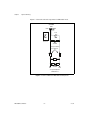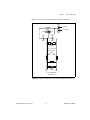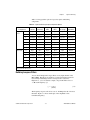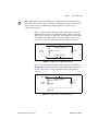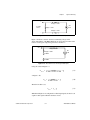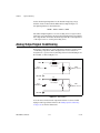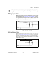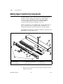
1
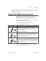
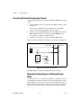
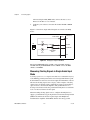
DAQ
BNC-2090A User Manual
Rack-Mount Connector Accessory for E/M Series DAQ Devices
BNC-2090A User Manual
January 2007
372101A-01
Support
Worldwide Technical Support and Product Information
ni.com
National Instruments Corporate Headquarters
11500 North Mopac Expressway
Austin, Texas 78759-3504
USA Tel: 512 683 0100
Worldwide Offices
Australia 1800 300 800, Austria 43 662 457990-0, Belgium 32 (0) 2 757 0020, Brazil 55 11 3262 3599,
Canada 800 433 3488, China 86 21 6555 7838, Czech Republic 420 224 235 774, Denmark 45 45 76 26 00,
Finland 385 (0) 9 725 72511, France 33 (0) 1 48 14 24 24, Germany 49 89 7413130, India 91 80 41190000,
Israel 972 3 6393737, Italy 39 02 413091, Japan 81 3 5472 2970, Korea 82 02 3451 3400,
Lebanon 961 (0) 1 33 28 28, Malaysia 1800 887710, Mexico 01 800 010 0793, Netherlands 31 (0) 348 433 466,
New Zealand 0800 553 322, Norway 47 (0) 66 90 76 60, Poland 48 22 3390150, Portugal 351 210 311 210,
Russia 7 495 783 6851, Singapore 1800 226 5886, Slovenia 386 3 425 42 00, South Africa 27 0 11 805 8197,
Spain 34 91 640 0085, Sweden 46 (0) 8 587 895 00, Switzerland 41 56 2005151, Taiwan 886 02 2377 2222,
Thailand 662 278 6777, Turkey 90 212 279 3031, United Kingdom 44 (0) 1635 523545
For further support information, refer to the Technical Support and Professional Services appendix. To comment
on National Instruments documentation, refer to the National Instruments Web site at ni.com/info and enter
the info code feedback.
© 2007 National Instruments Corporation. All rights reserved.
Important Information
Warranty
The BNC-2090A is warranted against defects in materials and workmanship for a period of one year from the date of shipment, as evidenced
by receipts or other documentation. National Instruments will, at its option, repair or replace equipment that proves to be defective during the
warranty period. This warranty includes parts and labor.
The media on which you receive National Instruments software are warranted not to fail to execute programming instructions, due to defects in
materials and workmanship, for a period of 90 days from date of shipment, as evidenced by receipts or other documentation. National Instruments
will, at its option, repair or replace software media that do not execute programming instructions if National Instruments receives notice of such defects
during the warranty period. National Instruments does not warrant that the operation of the software shall be uninterrupted or error free.
A Return Material Authorization (RMA) number must be obtained from the factory and clearly marked on the outside of the package before any
equipment will be accepted for warranty work. National Instruments will pay the shipping costs of returning to the owner parts which are covered by
warranty.
National Instruments believes that the information in this document is accurate. The document has been carefully reviewed for technical accuracy. In
the event that technical or typographical errors exist, National Instruments reserves the right to make changes to subsequent editions of this document
without prior notice to holders of this edition. The reader should consult National Instruments if errors are suspected. In no event shall National
Instruments be liable for any damages arising out of or related to this document or the information contained in it.
EXCEPT AS SPECIFIED HEREIN, NATIONAL INSTRUMENTS MAKES NO WARRANTIES, EXPRESS OR IMPLIED, AND SPECIFICALLY DISCLAIMS ANY WARRANTY OF
MERCHANTABILITY OR FITNESS FOR A PARTICULAR PURPOSE. CUSTOMER’S RIGHT TO RECOVER DAMAGES CAUSED BY FAULT OR NEGLIGENCE ON THE PART OF NATIONAL
INSTRUMENTS SHALL BE LIMITED TO THE AMOUNT THERETOFORE PAID BY THE CUSTOMER. NATIONAL INSTRUMENTS WILL NOT BE LIABLE FOR DAMAGES RESULTING
FROM LOSS OF DATA, PROFITS, USE OF PRODUCTS, OR INCIDENTAL OR CONSEQUENTIAL DAMAGES, EVEN IF ADVISED OF THE POSSIBILITY THEREOF. This limitation of
the liability of National Instruments will apply regardless of the form of action, whether in contract or tort, including negligence. Any action against
National Instruments must be brought within one year after the cause of action accrues. National Instruments shall not be liable for any delay in
performance due to causes beyond its reasonable control. The warranty provided herein does not cover damages, defects, malfunctions, or service
failures caused by owner’s failure to follow the National Instruments installation, operation, or maintenance instructions; owner’s modification of the
product; owner’s abuse, misuse, or negligent acts; and power failure or surges, fire, flood, accident, actions of third parties, or other events outside
reasonable control.
Copyright
Under the copyright laws, this publication may not be reproduced or transmitted in any form, electronic or mechanical, including photocopying,
recording, storing in an information retrieval system, or translating, in whole or in part, without the prior written consent of National
Instruments Corporation.
National Instruments respects the intellectual property of others, and we ask our users to do the same. NI software is protected by copyright and other
intellectual property laws. Where NI software may be used to reproduce software or other materials belonging to others, you may use NI software only
to reproduce materials that you may reproduce in accordance with the terms of any applicable license or other legal restriction.
Trademarks
National Instruments, NI, ni.com, and LabVIEW are trademarks of National Instruments Corporation. Refer to the Terms of Use section
on ni.com/legal for more information about National Instruments trademarks.
Other product and company names mentioned herein are trademarks or trade names of their respective companies.
Members of the National Instruments Alliance Partner Program are business entities independent from National Instruments and have no agency,
partnership, or joint-venture relationship with National Instruments.
Patents
For patents covering National Instruments products, refer to the appropriate location: Help»Patents in your software, the patents.txt file
on your CD, or ni.com/patents.
WARNING REGARDING USE OF NATIONAL INSTRUMENTS PRODUCTS
(1) NATIONAL INSTRUMENTS PRODUCTS ARE NOT DESIGNED WITH COMPONENTS AND TESTING FOR A LEVEL OF
RELIABILITY SUITABLE FOR USE IN OR IN CONNECTION WITH SURGICAL IMPLANTS OR AS CRITICAL COMPONENTS IN
ANY LIFE SUPPORT SYSTEMS WHOSE FAILURE TO PERFORM CAN REASONABLY BE EXPECTED TO CAUSE SIGNIFICANT
INJURY TO A HUMAN.
(2) IN ANY APPLICATION, INCLUDING THE ABOVE, RELIABILITY OF OPERATION OF THE SOFTWARE PRODUCTS CAN BE
IMPAIRED BY ADVERSE FACTORS, INCLUDING BUT NOT LIMITED TO FLUCTUATIONS IN ELECTRICAL POWER SUPPLY,
COMPUTER HARDWARE MALFUNCTIONS, COMPUTER OPERATING SYSTEM SOFTWARE FITNESS, FITNESS OF COMPILERS
AND DEVELOPMENT SOFTWARE USED TO DEVELOP AN APPLICATION, INSTALLATION ERRORS, SOFTWARE AND HARDWARE
COMPATIBILITY PROBLEMS, MALFUNCTIONS OR FAILURES OF ELECTRONIC MONITORING OR CONTROL DEVICES,
TRANSIENT FAILURES OF ELECTRONIC SYSTEMS (HARDWARE AND/OR SOFTWARE), UNANTICIPATED USES OR MISUSES, OR
ERRORS ON THE PART OF THE USER OR APPLICATIONS DESIGNER (ADVERSE FACTORS SUCH AS THESE ARE HEREAFTER
COLLECTIVELY TERMED “SYSTEM FAILURES”). ANY APPLICATION WHERE A SYSTEM FAILURE WOULD CREATE A RISK OF
HARM TO PROPERTY OR PERSONS (INCLUDING THE RISK OF BODILY INJURY AND DEATH) SHOULD NOT BE RELIANT SOLELY
UPON ONE FORM OF ELECTRONIC SYSTEM DUE TO THE RISK OF SYSTEM FAILURE. TO AVOID DAMAGE, INJURY, OR DEATH,
THE USER OR APPLICATION DESIGNER MUST TAKE REASONABLY PRUDENT STEPS TO PROTECT AGAINST SYSTEM FAILURES,
INCLUDING BUT NOT LIMITED TO BACK-UP OR SHUT DOWN MECHANISMS. BECAUSE EACH END-USER SYSTEM IS
CUSTOMIZED AND DIFFERS FROM NATIONAL INSTRUMENTS' TESTING PLATFORMS AND BECAUSE A USER OR APPLICATION
DESIGNER MAY USE NATIONAL INSTRUMENTS PRODUCTS IN COMBINATION WITH OTHER PRODUCTS IN A MANNER NOT
EVALUATED OR CONTEMPLATED BY NATIONAL INSTRUMENTS, THE USER OR APPLICATION DESIGNER IS ULTIMATELY
RESPONSIBLE FOR VERIFYING AND VALIDATING THE SUITABILITY OF NATIONAL INSTRUMENTS PRODUCTS WHENEVER
NATIONAL INSTRUMENTS PRODUCTS ARE INCORPORATED IN A SYSTEM OR APPLICATION, INCLUDING, WITHOUT
LIMITATION, THE APPROPRIATE DESIGN, PROCESS AND SAFETY LEVEL OF SUCH SYSTEM OR APPLICATION.
Compliance
Compliance with FCC/Canada Radio Frequency Interference
Regulations
Determining FCC Class
The Federal Communications Commission (FCC) has rules to protect wireless communications from interference. The FCC
places digital electronics into two classes. These classes are known as Class A (for use in industrial-commercial locations only)
or Class B (for use in residential or commercial locations). All National Instruments (NI) products are FCC Class A products.
Depending on where it is operated, this Class A product could be subject to restrictions in the FCC rules. (In Canada, the
Department of Communications (DOC), of Industry Canada, regulates wireless interference in much the same way.) Digital
electronics emit weak signals during normal operation that can affect radio, television, or other wireless products.
All Class A products display a simple warning statement of one paragraph in length regarding interference and undesired
operation. The FCC rules have restrictions regarding the locations where FCC Class A products can be operated.
Consult the FCC Web site at www.fcc.gov for more information.
FCC/DOC Warnings
This equipment generates and uses radio frequency energy and, if not installed and used in strict accordance with the instructions
in this manual and the CE marking Declaration of Conformity*, may cause interference to radio and television reception.
Classification requirements are the same for the Federal Communications Commission (FCC) and the Canadian Department
of Communications (DOC).
Changes or modifications not expressly approved by NI could void the user’s authority to operate the equipment under the
FCC Rules.
Class A
Federal Communications Commission
This equipment has been tested and found to comply with the limits for a Class A digital device, pursuant to part 15 of the FCC
Rules. These limits are designed to provide reasonable protection against harmful interference when the equipment is operated
in a commercial environment. This equipment generates, uses, and can radiate radio frequency energy and, if not installed and
used in accordance with the instruction manual, may cause harmful interference to radio communications. Operation of this
equipment in a residential area is likely to cause harmful interference in which case the user is required to correct the interference
at their own expense.
Canadian Department of Communications
This Class A digital apparatus meets all requirements of the Canadian Interference-Causing Equipment Regulations.
Cet appareil numérique de la classe A respecte toutes les exigences du Règlement sur le matériel brouilleur du Canada.
Compliance with EU Directives
Users in the European Union (EU) should refer to the Declaration of Conformity (DoC) for information* pertaining to the
CE marking. Refer to the Declaration of Conformity (DoC) for this product for any additional regulatory compliance
information. To obtain the DoC for this product, visit ni.com/certification, search by model number or product line,
and click the appropriate link in the Certification column.
* The CE marking Declaration of Conformity contains important supplementary information and instructions for the user or
installer.
Conventions
The following conventions are used in this manual:
<>
Angle brackets that contain numbers separated by an ellipsis represent
a range of values associated with a bit or signal name—for example,
AO <3..0>.
»
The » symbol leads you through nested menu items and dialog box options
to a final action. The sequence File»Page Setup»Options directs you to
pull down the File menu, select the Page Setup item, and select Options
from the last dialog box.
This icon denotes a note, which alerts you to important information.
This icon denotes a caution, which advises you of precautions to take
to avoid injury, data loss, or a system crash. When this symbol is marked
on a product, refer to the Read Me First: Safety and Radio-Frequency
Interference document, available on ni.com/manuals, for information
about precautions to take.
bold
Bold text denotes items that you must select or click in the software, such
as menu items and dialog box options. Bold text also denotes parameter
names.
italic
Italic text denotes variables, emphasis, a cross-reference, or an introduction
to a key concept. Italic text also denotes text that is a placeholder for a word
or value that you must supply.
monospace
Text in this font denotes text or characters that you should enter from the
keyboard, sections of code, programming examples, and syntax examples.
This font is also used for the proper names of disk drives, paths, directories,
programs, subprograms, subroutines, device names, functions, operations,
variables, filenames, and extensions.
Contents
Chapter 1
BNC-2090A Overview
What You Need to Get Started ......................................................................................1-2
Installing the BNC-2090A .............................................................................................1-3
Setting the BNC-2090A Shield Ground Jumper............................................................1-7
Chapter 2
Connecting Signals
Connecting Analog Input Signals ..................................................................................2-1
Connecting Differential Analog Input Signals ................................................2-2
Measuring Floating Signals in Differential Input Mode ...................2-2
Measuring Ground-Referenced Signals in Differential
Input Mode .....................................................................................2-3
Connecting Single-Ended Analog Input Signals.............................................2-3
Measuring Floating Signals in Single-Ended Input Mode................2-4
Measuring Ground-Referenced Signals in Single-Ended
Input Mode .....................................................................................2-5
Connecting AO, APFI 0, and PFI 0 Signals ..................................................................2-5
Connecting Digital Signals ............................................................................................2-6
Using the USER 1 and USER 2 BNC Connectors ........................................................2-7
Chapter 3
Signal Conditioning
Analog Input Signal Conditioning .................................................................................3-1
Building Lowpass Filters.................................................................................3-5
Example ............................................................................................3-6
Building Highpass Filters ................................................................................3-7
Example ............................................................................................3-8
Building Attenuators (Voltage Dividers) ........................................................3-10
Analog Output Signal Conditioning ..............................................................................3-12
Building Lowpass Filters.................................................................................3-13
Building Highpass Filters ................................................................................3-13
Adding Signal Conditioning Components .....................................................................3-14
Soldering and Desoldering on the BNC-2090A..............................................3-15
Installing Bias Resistors ..................................................................................3-15
© National Instruments Corporation
vii
BNC-2090A User Manual
Contents
Appendix A
Specifications
Appendix B
Frequently Asked Questions
Appendix C
Technical Support and Professional Services
Index
BNC-2090A User Manual
viii
ni.com
1
BNC-2090A Overview
This user manual contains in-depth information about using the National
Instruments BNC-2090A.
The BNC-2090A is a desktop or rack-mount analog breakout accessory
you can connect to E/M Series multifunction DAQ devices1. The
BNC-2090A has the following features:
•
16 analog input (AI) BNC connectors for eight differential
or 16 single-ended channels
•
Two analog output (AO) BNC connectors
•
Two user-defined BNC connectors
•
One APFI BNC connector
•
One PFI BNC connector
•
Spring terminal block for digital input/output (DIO) and
Programmable Function Interface (PFI) connections
•
Silkscreened component locations for resistors and capacitors for
building single-pole highpass and lowpass filters and voltage dividers
•
Two 68-pin input/output (I/O) connectors for DAQ device connection
Refer to the BNC-2090A Quick Start Guide for basic installation and signal
connection instructions.
Figure 1-1 shows the front panel and enclosure back of the BNC-2090A.
1
You can also use the BNC-2090A with PCI-6013 and PCI-6014 B Series devices.
© National Instruments Corporation
1-1
BNC-2090A User Manual
Chapter 1
BNC-2090A Overview
1
2
3
4
NATIONAL
INSTRUMENTS
SE
SE
SE
SE
SE
SE
SE
SE
RSE
DIFF
DIFF
DIFF
DIFF
DIFF
DIFF
DIFF
DIFF
NRSE
5
BNC-2090A
6
2
1
2
3
BNC Connectors
68-Position Connectors
Spring Terminal Block
4
5
6
+5V LED
SE/DIFF Switches
RSE/NRSE Switch
Figure 1-1. BNC-2090A Front Panel and Back of Enclosure
What You Need to Get Started
To set up and use your BNC-2090A accessory, you need the following:
❑ BNC-2090A accessory
❑ BNC-2090A Quick Start Guide and BNC-2090A User Manual
❑ One of the following DAQ devices:
–
68-pin M Series device (with one or two I/O connectors)
–
68-pin E Series device
–
100-pin E Series device
❑ 68-position1 or 100-position cable(s)
❑ The E Series User Manual or the M Series User Manual
❑ BNC cables
❑ 20 AWG wire or smaller
❑ Wire strippers
1
Two-connector M Series devices can be cabled to two BNC-2090A accessories with two cables.
BNC-2090A User Manual
1-2
ni.com
Chapter 1
BNC-2090A Overview
❑ Small flathead screwdriver
❑ Four adhesive rubber feet (supplied)
You can find detailed specifications for the BNC-2090A in Appendix A,
Specifications.
Installing the BNC-2090A
The BNC-2090A Quick Start Guide contains general installation
information for the BNC-2090A. To connect the BNC-2090A to your DAQ
device, refer to Figure 1-2 as you complete the following steps. Consult
your computer user manual or technical reference manual for specific
instructions and warnings.
Note If you have not already installed your DAQ device, refer to the DAQ Getting Started
Guide for instructions.
4
3
2
1
N
TI
INA
ST ONA
RU L
M
BN
C-20 ENTS
90A
1
2
BNC-2090A
Shielded Cable
3
4
E/M Series DAQ Device
Personal Computer
Figure 1-2. Connecting the BNC-2090A to Your DAQ Device
1.
© National Instruments Corporation
Verify that the SE/DIFF switches and RSE/NRSE switch are set
correctly for your current application, as described in Chapter 2,
Connecting Signals.
1-3
BNC-2090A User Manual
Chapter 1
BNC-2090A Overview
2.
(Optional) If you need to connect the BNC-2090A shield directly to
digital ground (D GND), verify that the shield ground jumper is set
correctly for your current application. Refer to the Setting the
BNC-2090A Shield Ground Jumper section for more information.
3.
(Optional) If you are performing signal conditioning, determine what
signal conditioning you need for analog inputs and install the
necessary components into the open component positions. Refer to the
Adding Signal Conditioning Components section of Chapter 3, Signal
Conditioning for more information.
4.
Place the BNC-2090A near the host computer or mount the
BNC-2090A into a 19 inch rack. If you do not rack-mount the
accessory, attach the four adhesive rubber feet included in the
BNC-2090A kit to the bottom of the accessory.
Caution Do not connect the BNC-2090A to any device other than a National Instruments
E Series or M Series DAQ device. Doing so can damage the BNC-2090A, the DAQ device,
or host computer. National Instruments is not liable for damages resulting from these
connections.
5.
BNC-2090A User Manual
Connect the BNC-2090A to the DAQ device using the front or rear
68-position connector, as shown in Figure 1-1.
1-4
ni.com
Chapter 1
BNC-2090A Overview
Figure 1-3 shows the BNC-2090A connected directly to different
M Series DAQ systems.
68-Position
VHDCI Connector
68-Pin
M Series
DAQ Device
68-Position
Connector
SHC68-68-EPM or RC68-68 Cable
BNC-2090A
68-Position
Connector
68-Position
VHDCI Connector
Two 68-Pin
Connector
M Series
DAQ Device
BNC-2090A
SHC68-68-EPM or RC68-68 Cable
SHC68-68-EPM or RC68-68 Cable
68-Position
VHDCI Connector
BNC-2090A
68-Position
Connector
68-Position
Connector
68-Position
Connector
68-Pin
M Series USB
Mass Termination
DAQ Device
SH68-68-EP or R6868 Cable
BNC-2090A
68-Position
Connector
Two 68-Pin
Connector
M Series USB
Mass Termination
DAQ Device
68-Position
Connector
BNC-2090A
SH68-68-EP or R6868 Cable
SH68-68-EP or R6868 Cable
68-Position
Connector
BNC-2090A
68-Position
Connector
Figure 1-3. Direct Connection of M Series DAQ Devices to the BNC-2090A
© National Instruments Corporation
1-5
BNC-2090A User Manual
Chapter 1
BNC-2090A Overview
Figure 1-4 shows the BNC-2090A connected directly to different
E Series DAQ systems.
68-Position
Connector
68-Pin
E Series
DAQ Device
68-Position
Connector
SH68-68-EP or R6868 Cable
68-Position
VHDCI Connector
68-Pin
E Series
DAQCard Device
68-Position
Connector
SHC68-68-EPM or RC68-68 Cable
BNC-2090A
MIO-16
68-Position
Connector
100-Position
Connector
100-Pin
E Series
DAQ Device
BNC-2090A
SH1006868 Cable
BNC-2090A
Extended DIO
68-Position
Connector
Figure 1-4. Direct Connection of E Series DAQ Devices to the BNC-2090A
If the +5V LED does not light, check the cable connections.
6.
Connect signals to the BNC connectors and spring terminal block as
described in Chapter 2, Connecting Signals.
When you have finished using the BNC-2090A, power off any external
signals connected to the BNC-2090A before you power off your computer.
You can connect 68-pin cables to both the front connector and the rear connector of
the BNC-2090A to create a pass-through.
Note
Caution Do not connect input voltages greater than 42.4 Vpk/60 VDC to the BNC-2090A.
The BNC-2090A is not designed for any input voltages greater than 42.4 Vpk/60 VDC,
even if a user-installed voltage divider reduces the voltage to within the input range of the
DAQ device. Input voltages greater than 42.4 Vpk/60 VDC can damage the BNC-2090A,
BNC-2090A User Manual
1-6
ni.com
Chapter 1
BNC-2090A Overview
all devices connected to it, and the host computer. Overvoltage can also cause an electric
shock hazard for the operator. National Instruments is not liable for damage or injury
resulting from such misuse.
Setting the BNC-2090A Shield Ground Jumper
The BNC-2090A shield ground jumper, labeled W1 on the PCB, is
factory-configured to connect the shield of the 68-position connectors and
BNC-2090A metal case through a 100 Ω resistor to D GND.
You must reconfigure the jumper if you want to connect the BNC-2090A
shield directly to digital ground (D GND).
Table 1-1 shows the shield ground jumper setting options.
Table 1-1. Shield Ground Jumper Settings
Setting
Shield
Description
100 Ω to Digital Ground—Use this setting to reduce any potential
ground loop current, thereby improving the system noise
performance. When the BNC-2090A is rack-mounted, it is connected
to a different ground.
R53
100 Ω
W1
This is the factory default setting.
Factory Default
Digital Ground—Use this setting when the BNC-2090A metal case
is not connected to any other ground through a rack mount or
connected to the DAQ ground through a shielded cable. Use this
setting when using unshielded cables.
Shield
R53
100 Ω
W1
You can also disconnect the shield from the DAQ ground by removing
shield ground jumper, which prevents the ground loop current from
being carried in the D GND return of the shielded cable. This option
is best for rack-mount configurations where the BNC-2090A metal
case is already grounded.
Shield
R53
100 Ω
W1
To access and reconfigure the shield ground jumper, complete the
following steps while referring to Figure 1-5.
© National Instruments Corporation
1-7
BNC-2090A User Manual
Chapter 1
BNC-2090A Overview
5
4
6
N
T
INA
ST IONA
RU L
ME
BN
NT
C-2
0 90
A
S
2
1
1
2
3
Front Panel Screws
Shield Ground Jumper (W1)
3
4
Side Panel Screw
Rear Panel Screws
5
6
Top Screw
Bottom Screw
Figure 1-5. Accessing the Shield Ground Jumper
BNC-2090A User Manual
1.
Remove the two rear panel screws and one side panel screw.
2.
Remove the top and bottom screws and two front panel screws.
3.
Hold the front panel and slide the unit out of the metal case.
4.
Set the shield ground jumper, labeled W1 on the PCB, as needed.
5.
Reassemble the BNC-2090A in reverse order.
1-8
ni.com
2
Connecting Signals
The BNC-2090A features 22 BNC connectors and a spring terminal block
for analog and digital signal connection. Refer to the E Series User Manual
or the M Series User Manual for information about the use of these signals.
Figure 2-1 shows an overview of the BNC-2090A circuitry.
Rear 68-Pin
SCSI Connector
AI/AO/APFI/PFI 0
DIO/PFI
USER <1..2>
BNC
Connectors
Front 68-Pin
SCSI Connector
Spring
Terminals
Figure 2-1. BNC-2090A Circuitry Overview
Connecting Analog Input Signals
The BNC-2090A can be configured in three analog input modes:
•
Differential (factory-default setting)
•
Referenced single-ended
•
Nonreferenced single-ended
For more information about choosing an analog input mode, refer to
E Series User Manual or the M Series User Manual.
© National Instruments Corporation
2-1
BNC-2090A User Manual
Chapter 2
Connecting Signals
Connecting Differential Analog Input Signals
Complete the following steps to measure a differential (DIFF) analog input
signal.
1.
Connect the BNC cable to one of the AI <0..7> BNC connectors on the
front panel.
Do not connect anything to the corresponding AI <8..15> BNC
connector below the AI <0..7> BNC connector you use.
2.
Move the corresponding SE/DIFF switch to the DIFF position. On the
BNC-2090A front panel, a line indicates which SE/DIFF switch
corresponds to each AI <0..7> BNC connector.
3.
Configure your software to measure this channel differentially.
Figure 2-2 shows how differential AI signals are routed to the DAQ device.
BNC-2090A
Cable
DAQ Device
AI 0
SE
AI 0
AI 8
DIFF
AI 8
RSE
NRSE
Do Not
Connect
RSE/NRSE
Switch
Not Used
Figure 2-2. Analog Input Differential Mode
The BNC-2090A is configured for differential mode by default.
Measuring Floating Signals in Differential Input
Mode
A floating signal source is a signal source that is not connected in any way
to the building ground system, but has an isolated ground-reference point.
If an instrument or device has an isolated output, that instrument or device
falls into the floating signal source category. Some examples of floating
signal sources are thermocouples, transformers, battery-powered devices,
BNC-2090A User Manual
2-2
ni.com
Chapter 2
Connecting Signals
optical isolators, and isolation amplifiers. The ground reference of a
floating source must be tied to the ground of the DAQ device to establish a
local or on-device reference for the signal.
To provide a return path for the instrumentation amplifier bias currents,
floating sources must have a 10–100 kΩ resistor to AI GND on one input
if DC-coupled, or both inputs if AC-coupled. For more information about
connections to floating signal sources and differential inputs, refer to
E Series User Manual or the M Series User Manual. Refer to the Installing
Bias Resistors section of Chapter 3, Signal Conditioning, for information
about installing bias resistors.
Measuring Ground-Referenced Signals in
Differential Input Mode
A grounded signal source is connected in some way to the building system
ground; therefore, the signal source is already connected to a common
ground point with respect to the DAQ device (assuming the host computer
is plugged into the same power system). The non-isolated outputs of
instruments and devices that plug into the building power system fall into
this category.
If the DAQ device is configured for differential inputs, ground-referenced
signal sources connected to the BNC-2090A need no special components
added to the BNC-2090A. You can leave the inputs of the BNC-2090A in
the factory-default configuration, with the 0 Ω jumpers in the two series
positions, C and D, as listed in Table 3-1, Channel Component Positions.
Refer to Chapter 3, Signal Conditioning, for information about building
signal-conditioning circuitry, such as filters and attenuators, in the
open-component positions.
Connecting Single-Ended Analog Input Signals
Complete the following steps to measure a single-ended (SE) analog input
signal.
1.
Connect the BNC cable to one of the AI <0..15> BNC connectors on
the front panel.
2.
Move the corresponding SE/DIFF switch to the SE position. On the
BNC-2090A front panel, a line indicates which SE/DIFF switch
corresponds to each AI <0..15> BNC connector.
3.
Move the RSE/NRSE switch to select how the ground signal is routed.
All single-ended signals share the one RSE/NRSE switch. For more
information about non-referenced single-ended (NRSE) and
© National Instruments Corporation
2-3
BNC-2090A User Manual
Chapter 2
Connecting Signals
referenced single-ended (RSE) modes, refer to the E Series User
Manual or the M Series User Manual.
4.
Configure your software to measure this channel in RSE or NRSE
mode.
Figure 2-3 shows how single-ended AI signals are routed to the DAQ
device.
BNC-2090A
Cable
DAQ Device
AI 0
AI 0
SE
RSE
NRSE
AI GND
AI SENSE
DIFF
RSE/NRSE
Switch
AI 8
AI 8
Figure 2-3. Analog Input Single-Ended Mode
Moving the RSE/NRSE switch to RSE, connects the BNC shields to
AI GND. Moving the RSE/NRSE switch to NRSE connects the BNC
shields to AI SENSE.
Measuring Floating Signals in Single-Ended Input
Mode
A floating signal source is a signal source that is not connected in any way
to the building ground system, but has an isolated ground-reference point.
If an instrument or device has an isolated output, that instrument or device
falls into the floating signal source category. Some examples of floating
signal sources are thermocouples, transformers, battery-powered devices,
optical isolators, and isolation amplifiers. The ground reference of a
floating source must be tied to the ground of the DAQ device to establish a
local or on-device reference for the signal.
When measuring floating signal sources, configure the DAQ device to
supply a ground reference by placing the device in referenced single-ended
(RSE) mode. This mode ties the negative input of the DAQ device
instrumentation amplifier and the BNC shield to the analog ground.
BNC-2090A User Manual
2-4
ni.com
Chapter 2
Connecting Signals
Refer to Chapter 3, Signal Conditioning, for information about building
additional signal-conditioning circuitry, such as filters and attenuators,
in the open-component positions.
Measuring Ground-Referenced Signals in
Single-Ended Input Mode
A grounded signal source is connected in some way to the building system
ground; therefore, the signal source is already connected to a common
ground point with respect to the DAQ device (assuming the host computer
is plugged into the same power system). The non-isolated outputs of
instruments and devices that plug into the building power system fall into
this category.
When measuring ground-referenced signals, the external signal supplies its
own reference ground point and the DAQ device should not supply one.
Therefore, configure the DAQ device for the nonreferenced single-ended
(NRSE) mode, in which all of the signal grounds are tied to AI SENSE,
which connects to the negative input of the instrumentation amplifier on the
DAQ device.
Refer to Chapter 3, Signal Conditioning, for information about building
additional signal-conditioning circuitry, such as filters and attenuators, in
the open-component positions.
Connecting AO, APFI 0, and PFI 0 Signals
Use the BNC-2090A BNC connectors on the front panel to connect
AO <0..1>, APFI 0, and PFI 0 signals to your DAQ device. Refer to the
E Series User Manual or the M Series User Manual for information about
the use of these signals.
© National Instruments Corporation
2-5
BNC-2090A User Manual
Chapter 2
Connecting Signals
Figure 2-4 shows how AO 0, AO 1, APFI 0, and PFI 0 signals are routed to
the DAQ device.
BNC-2090A
Cable
DAQ Device
AO 0
AO 0
AO GND
AO 1
AO 1
APFI 0
AI GND
APFI 0
PFI 0
D GND
PFI 0
Figure 2-4. Analog Output, APFI 0, and PFI 0
Refer to Chapter 3, Signal Conditioning, for information about building
additional signal-conditioning circuitry.
Connecting Digital Signals
Use the BNC-2090A spring terminal block on the front panel to connect
digital signals to your DAQ device. Refer to the E Series User Manual or
the M Series User Manual for information about the use of these signals.
When connecting signals to the spring terminal blocks, you can use up to
20 AWG wire with the insulation stripped to 0.5 in.
BNC-2090A User Manual
2-6
ni.com
Chapter 2
Connecting Signals
Using the USER 1 and USER 2 BNC Connectors
The USER 1 and USER 2 BNC connectors allow you to use a BNC
connector for a digital or timing I/O signal of your choice. The USER 1 and
USER 2 BNC connectors are routed (internal to the BNC-2090A) to the
USER1 and USER2 spring terminals, as shown in Figure 2-5.
USER 1 BNC
P0
PFI
USER2
DGND
15
14
13
12
11
10
9
8
7
6
5
4
3
2
1
DGND
+5V
7
6
5
4
3
2
1
0
DGND
USER1
D GND
USER 2 BNC
Screw Terminal Block
Internal Connection
D GND
Figure 2-5. USER <1..2> BNC Connections
Figure 2-6 shows an example of how to use the USER <1..2> BNCs.
To access the PFI 5 signal from a BNC, connect USER1 on the spring
terminal block to PFI 5 with a wire.
P0
PFI
USER2
DGND
15
14
13
12
11
10
9
8
7
6
5
4
3
2
1
DGND
+5V
7
6
5
4
3
2
1
0
DGND
USER1
USER 1 BNC
Internal
Connection
BNC Cable
Wire
Screw Terminal Block
D GND
PFI 5
Signal
Figure 2-6. Connecting PFI 5 to USER 1 BNC
© National Instruments Corporation
2-7
BNC-2090A User Manual
3
Signal Conditioning
This chapter contains information about adding signal conditioning
components to the BNC-2090A and signal conditioning examples for using
the BNC-2090A with your DAQ device.
Analog Input Signal Conditioning
Each analog input signal has several open positions for passive signal
conditioning components. The factory-default positions for the 0 Ω jumpers
are the C and D positions of the input network, as shown in Figure 3-1. You
can remove these 0 Ω jumpers to build analog input signal conditioning
circuits. You can also add passive analog input signal conditioning, such as
filters and dividers.
© National Instruments Corporation
3-1
BNC-2090A User Manual
Chapter 3
Signal Conditioning
Figure 3-1 shows the onboard components for differential mode.
COMMON
SW9
DIFF
SE
AI 8
AI 0
BNC
BNC
R31
R32
B
A
AI GND
Do Not
Connect
R33
D
R30
Factory-Installed
0 Ω Jumpers
C
C10
E
AI 8
R50
R51
G
F
AI GND
AI 0
To Input Multiplexer
of DAQ Device
Figure 3-1. Channel 0 Differential Mode Onboard Components
BNC-2090A User Manual
3-2
ni.com
Chapter 3
Signal Conditioning
Figure 3-2 shows the onboard components for single-ended mode.
RSE
AI GND
COMMON
SW9
DIFF
AI SENSE
SE
AI 8
NRSE
SW1
AI 0
BNC
BNC
R31
R32
B
A
AI GND
R33
D
R30
Factory-Installed
0 Ω Jumpers
C
C10
E
AI 8
R50
R51
G
F
AI GND
AI 0
To Input Multiplexer
of DAQ Device
Figure 3-2. Channel 0 and Channel 8 Single-Ended Mode Onboard Components
© National Instruments Corporation
3-3
BNC-2090A User Manual
Chapter 3
Signal Conditioning
Table 3-1 lists the different component positions for each channel.
Table 3-1. Channel Component Positions
Channel
Differential
Single-Ended
Position in Figures 3-1 and 3-2
A
B
C*
D*
E
F
G
0
0, 8
R32
R31
R33
R30
C10
R51
R50
1
1, 9
R28
R27
R29
R26
C9
R49
R48
2
2, 10
R24
R23
R25
R22
C8
R47
R46
3
3, 11
R20
R19
R21
R18
C7
R45
R44
4
4, 12
R16
R15
R17
R14
C6
R43
R42
5
5, 13
R12
R11
R13
R10
C5
R41
R40
6
6, 14
R8
R7
R9
R6
C4
R39
R38
7
7, 15
R4
R3
R5
R2
C3
R37
R36
*
Factory-installed 0 Ω jumpers.
BNC-2090A User Manual
3-4
ni.com
Chapter 3
Signal Conditioning
Table 3-2 lists population options for passive signal conditioning
components.
Table 3-2. Signal Conditioning Component Population Options
Normal
Attenuator
Lowpass
Filter
Highpass
Filter
AC Couple
Termination
A
Open
Open
Open
Open
Open
Resistor
B
Open
Open
Open
Open
Open
Resistor
C*
0 Ω Jumper
Resistor
Resistor
Capacitor
Capacitor
0 Ω Jumper
D*
0 Ω Jumper
Resistor
Resistor
Capacitor
Capacitor
0 Ω Jumper
E
Open
Open
Open
Open
Open
Open
F
Open
Resistor
Capacitor
Resistor
Open
Open
G
Open
Resistor
Capacitor
Resistor
Open
Open
A
Open
Open
Open
Open
Open
Resistor
B
Open
Open
Open
Open
Open
Resistor
C*
0 Ω Jumper
Resistor
Resistor
Capacitor
Capacitor
0 Ω Jumper
D*
0 Ω Jumper
Resistor
Resistor
Capacitor
Capacitor
0 Ω Jumper
E
Open
Resistor
Capacitor
Resistor
Open
Open
F
Open
Open
Open
Open
Open
Open
G
Open
Open
Open
Open
Open
Open
Configuration
SingleEnded
Differential
*
Factory-installed 0 Ω resistor.
Building Lowpass Filters
You can install simple, RC lowpass filters on any input channel of the
BNC-2090A. The filters are useful for accurate measurement and noise
rejection. By substituting resistance and capacitance values into
Equation 3-1, you can calculate a simple, one-pole RC filter to have a
–3 dB cutoff frequency (fc):
1
f c = ------------------( 2πRC )
(3-1)
The frequency response rolls off at a rate of –20 dB per decade of increase
thereafter. Figure 3-3 shows a Bode plot of the amplitude versus
normalized frequency.
© National Instruments Corporation
3-5
BNC-2090A User Manual
Chapter 3
Signal Conditioning
Output Amplitude (dB)
0
–20
–40
–60
–80
–100
0.01
0.1
1
10
100
Normalized Frequency (fc)
1000
10000
Figure 3-3. Normalized Frequency Response of Lowpass Filter
Example
When measuring low-frequency signals (about 4 Hz), if you have 400 Hz
noise on your input signals, you can add a lowpass filter with a cutoff
frequency of 4 Hz. The 400 Hz noise then attenuates by 40 dB. Notice that
your 4 Hz signal also attenuates, by 3 dB. Do not neglect any potential
attenuation of signals of interest by this low-order filter.
You must also choose the filter component values. You can select the
resistance or the capacitance arbitrarily; one value determines the other.
Picking the capacitor first and letting its value determine the resistance
required is preferable because more standard resistor values are available.
If a capacitance of 1μF is available, the resistance is (by substitution into
Equation 3-1) about 39.8 kΩ. This resistance must be split evenly between
each input of a differential channel. Therefore, in this example, each input
channel has a 19.89 kΩ resistor (or the closest standard value) in its series
positions, C and D. NI recommends using 1% or better tolerance resistors
in this application because differences between the resistor values degrade
the common-mode rejection ratio (CMRR).
Figure 3-4 shows both the schematic and the component placement for a
4 Hz lowpass filter placed on differential input channel 1. If the input signal
source is floating, you must place a bias return resistor in positions A and/or
B (R28 and R27, respectively).
BNC-2090A User Manual
3-6
ni.com
Chapter 3
Signal Conditioning
+
R29(C) = 19.8 kΩ
To DAQ
Device
AI 1
J10
C9(E) = 1 μF
R26(D) = 19.8 kΩ
–
Figure 3-4. Lowpass Filter on Differential Channel 1
Figure 3-5 shows both the schematic and the component placement for a
4 Hz lowpass filter placed on single-ended input channel 1. Refer to the
Installing Bias Resistors section for information about installing bias
resistors.
AI 1
R29(C) = 39.8 kΩ
R49(F)= 1 μF
To DAQ
Device
AI 1
J10
AI GND
AI GND
Figure 3-5. Lowpass Filter on Single-Ended Channel 1
Building Highpass Filters
You can install simple, RC highpass filters on any input channel of the
BNC-2090A. The filters are useful for accurate high-frequency
measurement and low-frequency noise rejection. By substituting resistance
and capacitance values into Equation 3-1, you can calculate a simple,
one-pole RC filter to have a –3 dB cutoff frequency, fc. The frequency
response rolls off at a rate of –20 dB per decade decrease thereafter.
Figure 3-6 shows a Bode plot of the amplitude versus normalized
frequency.
© National Instruments Corporation
3-7
BNC-2090A User Manual
Chapter 3
Signal Conditioning
Output Amplitude (dB)
0
–20
–40
–60
–80
–100
0.0001
0.001
0.01
0.1
1
Normalized Frequency (fc)
10
100
Figure 3-6. Normalized Frequency Response of Highpass Filter
Example
When measuring high-frequency signals (about 50 kHz), if you have 50 Hz
noise on your input signals, you can add a highpass filter with a cutoff
frequency of 50 kHz. The 50 Hz noise then attenuates by 60 dB. Notice that
your 50 kHz signal also attenuates, by 3 dB. Do not neglect any potential
attenuation of signals of interest if you add a low-order filter.
You must also choose the filter component values. You can select the
resistance or the capacitance arbitrarily; one value determines the other.
Picking the capacitor first and letting its value determine the resistance
required is preferable because more standard resistor values are available.
The filter circuit has one series capacitor on each input signal of the
differential channel. Because the two capacitors are in series, the
capacitance value that must be substituted into Equation 3-1 is the series
capacitance of the two capacitors. For two capacitors in series, the net
capacitance is the reciprocal of the sum of the reciprocals of the
two capacitances. For example, two 0.001 μF capacitors in series have a net
capacitance of 0.0005 μF. The two capacitors should be the same value,
or the CMRR is degraded. If capacitors of 0.001 μF are available, the
resistance is (by substitution into Equation 3-1) about 6.4 kΩ. Therefore,
in this example, the input channel has a 6.34 kΩ resistor (or the closest
standard value) in position E.
BNC-2090A User Manual
3-8
ni.com
Chapter 3
Signal Conditioning
Highpass filters generally exhibit poorer common-mode rejection characteristics
than lowpass filters because capacitors are in the series input paths. Capacitors have poorer
tolerances than resistors, and matching the input impedances is crucial for good
common-mode rejection.
Note
Figure 3-7 shows both the schematic and the component placement for a
50 kHz highpass filter placed on differential input channel 1. If the input
signal source is floating, you must place a bias return resistor in positions
A and/or B position (R28 and R27, respectively). Refer to the Installing
Bias Resistors section for information about installing bias resistors.
+
R29(C) = .001 μF
To DAQ
Device
AI 1
J10
C9(E) = 6.34 kΩ
R26(D) = .001 μF
–
Figure 3-7. Highpass Filter on Differential Channel 1
Figure 3-8 shows both the schematic and the component placement for a
50 kHz highpass filter placed on single-ended input channel 1. Refer to the
Installing Bias Resistors section for information about installing bias
resistors.
AI 1
R29(C) = .0005 μF
R49(F) = 6.34 kΩ
To DAQ
Device
AI 1
J10
AI GND
AI GND
Figure 3-8. Highpass Filter on Single-Ended Channel 1
© National Instruments Corporation
3-9
BNC-2090A User Manual
Chapter 3
Signal Conditioning
Building Attenuators (Voltage Dividers)
Attenuators or voltage dividers allow voltage measurements larger than the
maximum input range of DAQ devices. For example, voltage signals in the
±20 V range can be measured by building a 2:1 voltage divider circuit.
You can connect attenuators to the analog inputs of the BNC-2090A when
the inputs from its DAQ device are in differential or single-ended mode.
Caution Do not connect input voltages greater than 42.4 Vpk/60 VDC to the BNC-2090A.
The BNC-2090A is not designed for any input voltages greater than 42.4 Vpk/60 VDC,
even if a user-installed voltage divider reduces the voltage to within the input range of the
DAQ device. Input voltages greater than 42.4 Vpk/60 VDC can damage the BNC-2090A,
all devices connected to it, and the host computer. Overvoltage can also cause an electric
shock hazard for the operator. National Instruments is not liable for damage or injury
resulting from such misuse.
The gain in differential mode, GDIFF, of this attenuator is given by the
Equation 3-2.
RE
G DIFF = -----------------------------------( RC + RD + RE )
(3-2)
The gain in single-ended mode, GSE, of this attenuator is given by the
Equation 3-3.
RF
G SE = -----------------RC + RF
(3-3)
Therefore, the input to the DAQ device (VMIO) for Equation 3-2 or 3-3 is as
follows:
VMIO = Vin ⋅ G
(3-4)
where Vin is the voltage applied to the BNC connectors of the BNC-2090A.
The accuracy of this gain equation depends on the tolerances of the
resistors used.
Figure 3-9 shows a resistor circuit for attenuating voltages at the
differential inputs of the BNC-2090A. It also shows the placement of the
resistors on the open-component positions for channel 1.
BNC-2090A User Manual
3-10
ni.com
Chapter 3
Signal Conditioning
+
R29(C) = 10 kΩ
To DAQ
Device
AI 1
J10
C9(E) = 10 kΩ
R26(D) = 10 kΩ
–
Figure 3-9. Attenuator for Use with Differential Inputs
Figure 3-10 shows a resistor circuit for attenuating voltages at the
single-ended inputs of the BNC-2090A. It also shows the placement of the
resistors on the open-component positions for channel 1.
AI 1
R29(C) = 20 kΩ
AI 1
J10
R49(F) = 10 kΩ
AI GND
AI GND
Figure 3-10. Attenuator for Use with Single-Ended Inputs
Using the values in Figure 3-9,
10 kΩ
G DIFF = ------------------------------------------------------------ = 1
--10 kΩ + 10 kΩ + 10 kΩ
3
(3-5)
or Figure 3-10,
10 kΩ
1
G SE = -------------------------------------- = --20 kΩ + 10 kΩ
3
(3-6)
Therefore in either case,
1
V MIO = V in ⋅ --3
(3-7)
When the DAQ device is configured for ±10 V input signals, the device can
acquire ±30 V signals with this attenuator circuit.
© National Instruments Corporation
3-11
BNC-2090A User Manual
Chapter 3
Signal Conditioning
Notice that the input impedance for the channels employing voltage
dividers circuit is reduced. In the differential example in Figure 3-9,
the input impedance has been reduced to:
10 kΩ + 10 kΩ + 10 kΩ = 30 kΩ
The reduced input impedance can cause loading errors for signal sources
with large source impedance. In general, the input impedance presented by
the voltage divider circuit must be much larger than the source impedance
of the signal source to avoid signal loading errors.
Analog Output Signal Conditioning
Each analog output has two open-component positions for passive signal
conditioning components. One is designated as a resistor and one is
designated as a capacitor. Factory-default positions for the 0 Ω jumpers are
R34 and R1 as shown in Figure 3-11.
R34
AO 0
From
DAQ Device
Factory-Installed
0 Ω Jumper
C1
AO 0
BNC Connector
C2
AO 1
BNC Connector
AO GND
R1
AO 1
From
DAQ Device
Factory-Installed
0 Ω Jumper
AO GND
Figure 3-11. AO 0 and AO 1
You can remove and/or install components in these locations to build
highpass and lowpass filters. Refer to the Adding Signal Conditioning
Components section for instructions.
BNC-2090A User Manual
3-12
ni.com
Chapter 3
Signal Conditioning
Note Channels that use these filters have greater output impedance. This can result in
loading errors if the connected load impedance is not much higher than the filter’s output
impedance.
Building Lowpass Filters
Building lowpass filters for the analog output signals is the same as for the
analog inputs. Refer to the Analog Input Signal Conditioning section for
more detailed information about lowpass filters and how to calculate values
for lowpass filters. Refer to Figure 3-14 for component locations.
Figure 3-12 shows a 4 Hz lowpass filter for AO 0.
AO 0
R34 = 39.8 kΩ
C1 = 1 μF
AO 0
BNC Connector
AO GND
Figure 3-12. Lowpass Filter on AO 0
Building Highpass Filters
Building highpass filters for analog output is the same as for analog input.
Refer to the Analog Input Signal Conditioning section for more detailed
information about highpass filters and how to calculate values for them.
Refer to Figure 3-14 for component locations. Figure 3-13 shows a 50 kHz
highpass filter for AO 0.
AO 0
R34 = .0005 μF
C1 = 6.34 kΩ
AO 0
BNC Connector
AO GND
Figure 3-13. Highpass Filter on AO 0
© National Instruments Corporation
3-13
BNC-2090A User Manual
Chapter 3
Signal Conditioning
Adding Signal Conditioning Components
The BNC-2090A has open-component positions in the input paths into
which you can insert resistors and capacitors for conditioning the
16 single-ended or eight differential analog input signals and the
two analog output signals. You can also use the BNC-2090A in
conjunction with other signal conditioning accessories.
Figures 3-1 through 3-13 give examples using a specific channel. If you
want to install the circuit in a different channel, consult Table 3-1 to
determine the equivalent component positions for the other channels.
Complete the following steps to add signal conditioning components to the
BNC-2090A, as shown in Figure 3-14.
8
7
9
2
5
N
T
INA
ST IONA
RU L
ME
BN
N
C
3
-20
90A
TS
6
4
1
1
2
3
Front Panel Screws
Front Panel Nuts
Front Panel Washers
4
5
6
Front Connector Screws
Shield Ground Jumper (W1)
Side Panel Screw
7
8
9
Rear Panel Screws
Top Screw
Bottom Screw
Figure 3-14. Disassembly of the BNC-2090A
1.
BNC-2090A User Manual
Remove the two rear panel screws, the side panel screw, the top screw,
and the bottom screw.
3-14
ni.com
Chapter 3
Signal Conditioning
2.
Remove the two front panel screws.
3.
Hold the front panel and slide the unit out of the metal case.
4.
Install and/or remove components as necessary. Refer to the Soldering
and Desoldering on the BNC-2090A section for more information.
5.
Reassemble the BNC-2090A in reverse order.
Soldering and Desoldering on the BNC-2090A
Caution Use a low-wattage (20 to 30 W) soldering iron when soldering to the device. You
should use only rosin-core, electronic-grade solder. Acid-core solder damages the printed
circuit device and components. Use vacuum-type tools when desoldering on the
BNC-2090A to avoid damaging component pads.
Some applications require you to modify the PWB, usually by removing
0 Ω jumpers and adding components. The BNC-2090A is shipped with 0 Ω
jumpers in the C and D positions, as listed in Table 3-1 and shown in
Figure 3-1.
This product is RoHS-compliant. If you require that the product remain
RoHS-compliant, ensure that you use RoHS-compliant solder and components.
Visit ni.com/rohs for more information.
Note
Installing Bias Resistors
You can install bias resistors in positions A and B on the BNC-2090A, as
listed in Table 3-1 and shown in Figure 3-1. Refer to the steps in the Adding
Signal Conditioning Components section for instructions about accessing
the resistors on the BNC-2090A.
Figure 3-15 shows both the schematic and the component placement for a
single 100 kΩ bias return resistor on the negative input from a floating
source connected to channel 1, the B position in Table 3-1. Refer to the
Analog Input Signal Conditioning section for information about building
additional signal conditioning circuitry, such as filters and attenuators, in
the open component positions.
© National Instruments Corporation
3-15
BNC-2090A User Manual
Chapter 3
Signal Conditioning
+
R29(C)
R28(A)
AI 1
To DAQ
Device
C9(E)
AI GND
J10
R27(B) = 100 kΩ
R26(D)
–
Figure 3-15. Bias Return Resistor for DC-Coupled Floating Source on Channel 1 in
DIFF Mode
Figure 3-16 shows both the schematic and the component placement for an
optional user-installed bias resistor, R35, between AI SENSE and AI GND.
AI SENSE
2
R35
User-Installed
Bias Resistor
1
AI GND
Figure 3-16. User-Installed Bias Resistor between AI SENSE and AI GND
BNC-2090A User Manual
3-16
ni.com
A
Specifications
This appendix lists the specifications of the BNC-2090A. These
specifications are typical at 25 °C unless otherwise specified.
Analog Input
Channels................................................. 8 differential (default),
16 single-ended
Field connections ................................... 16 BNC connectors
Signal conditioning ................................ 7 component positions per
differential channel
Analog Output
Channels................................................. 2 single-ended
Field connections ................................... 2 BNC connectors for AO,
1 BNC connector for APFI 0
input
Signal conditioning ................................ 2 component positions per output
channel
Digital Input and Output
Channels................................................. 8 digital I/O, 16 PFI
Field connections ................................... 1 BNC connector for PFI 0.
2 BNC connectors for
user-defined,
spring terminals for all other
digital I/O and PFI
Signal conditioning ................................ 2 component positions per output
channel
© National Instruments Corporation
A-1
BNC-2090A User Manual
Appendix A
Specifications
Power Requirement
+5 VDC (±5%) provided by DAQ device
Typical power consumed
by BNC-2090A................................10 mA
Maximum power available
at +5 V spring terminal....................1 A (fuse-limited by host
DAQ device)
Physical
Dimensions .............................................4.39 × 48.26 × 9.7 cm
(1.73 × 19 × 3.82 in.)
Weight ....................................................700 g (24.69 oz)
I/O connector ..........................................Two 68-position male connectors
BNC connectors......................................22
Spring terminal block .............................29 positions
Environment
The BNC-2090A is intended for indoor use only.
Operating temperature ............................0 to 70 °C
Storage temperature ................................–55 to 125 °C
Relative humidity ...................................5 to 90% RH, noncondensing
Pollution Degree (indoor use only) ........2
Maximum Altitude .................................2,000 m
Safety
This product is designed to meet the requirements of the following
standards of safety for electrical equipment for measurement, control,
and laboratory use:
BNC-2090A User Manual
•
IEC 61010-1, EN 61010-1
•
UL 61010-1, CSA 61010-1
A-2
ni.com
Appendix A
Specifications
Note For UL and other safety certifications, refer to the product label or visit
ni.com/certification, search by model number or product line, and click the
appropriate link in the Certification column.
Electromagnetic Compatibility
This product is designed to meet the requirements of the following
standards of EMC for electrical equipment for measurement, control,
and laboratory use:
Note
•
EN 61326 EMC requirements; Minimum Immunity
•
EN 55011 Emissions; Group 1, Class A
•
CE, C-Tick, ICES, and FCC Part 15 Emissions; Class A
For EMC compliance, operate this device according to product documentation.
CE Compliance
This product meets the essential requirements of applicable European
Directives, as amended for CE marking, as follows:
•
73/23/EEC; Low-Voltage Directive (safety)
•
89/336/EEC; Electromagnetic Compatibility Directive (EMC)
Refer to the Declaration of Conformity (DoC) for this product for any additional
regulatory compliance information. To obtain the DoC for this product, visit
ni.com/certification, search by model number or product line, and click the
appropriate link in the Certification column.
Note
Waste Electrical and Electronic Equipment (WEEE)
EU Customers At the end of their life cycle, all products must be sent to a WEEE recycling
center. For more information about WEEE recycling centers and National Instruments
WEEE initiatives, visit ni.com/environment/weee.htm.
© National Instruments Corporation
A-3
BNC-2090A User Manual
B
Frequently Asked Questions
How does the BNC-2090A differ from the BNC-2090?
The BNC-2090A is based on the BNC-2090. The main differences between
these two accessories are listed in Table B-1.
Table B-1. BNC-2090A and BNC-2090 Comparison
BNC-2090A
BNC-2090
Can be used with E/M Series devices
Can be used with E/M Series and PC-LPM-16
devices
NI-DAQmx naming conventions on front panel
Traditional NI-DAQ (Legacy) naming
conventions on front panel
Extra spring terminal to access PFI 15
N/A
User-installed signal conditioning components
are easy to access
N/A
More signal conditioning component options
N/A
Attenuators (voltage dividers) can be used with
the DAQ device in both single-ended and
differential modes
Attenuators (voltage dividers) can be used with
the DAQ device in differential mode only
User-installed AI SENSE bias resistor
N/A
Clear labeling on the PCB for easier signal
conditioning component installation
N/A
Easy assembly and disassembly
N/A
Smaller dimensions and weight
N/A
RoHS compliant
N/A
© National Instruments Corporation
B-1
BNC-2090A User Manual
Appendix B
Frequently Asked Questions
Can I use the SCXI resistor kit to build attenuators for my
BNC-2090A?
Yes. You can use the SCXI resistor kit, which consists of four high
precision 249 Ω resistors, to build attenuators (voltage dividers) for the
BNC-2090A. Refer to the Building Attenuators (Voltage Dividers) section
of Chapter 3, Signal Conditioning, for more information about building
attenuators for the BNC-2090A.
Can I configure the BNC-2090A to measure current?
Yes. You can use a pair of channels to route current through the a sense
resistor located in position E. Refer to the Analog Input Signal
Conditioning section of Chapter 3, Signal Conditioning, for the exact
location of this component.
Caution When adding custom signal conditioning, do not exceed the components’ power
dissipation ratings. Limit current into the BNC-2090A to ≤100 mA.
Set the SE/DIFF switch to SE mode and the RSE/NRSE switch to RSE.
This connects the BNC shields to AI GND. Configure the DAQ device for
a differential measurement across the sense resistor.
Can I attach 68-pin DAQ cables to the front and back of the
BNC-2090A to make it a pass-through?
Yes.
BNC-2090A User Manual
B-2
ni.com
Technical Support and
Professional Services
C
Visit the following sections of the National Instruments Web site at
ni.com for technical support and professional services:
•
Support—Online technical support resources at ni.com/support
include the following:
–
Self-Help Resources—For answers and solutions, visit the
award-winning National Instruments Web site for software drivers
and updates, a searchable KnowledgeBase, product manuals,
step-by-step troubleshooting wizards, thousands of example
programs, tutorials, application notes, instrument drivers, and
so on.
–
Free Technical Support—All registered users receive free Basic
Service, which includes access to hundreds of Application
Engineers worldwide in the NI Discussion Forums at
ni.com/forums. National Instruments Application Engineers
make sure every question receives an answer.
For information about other technical support options in your
area, visit ni.com/services or contact your local office at
ni.com/contact.
•
Training and Certification—Visit ni.com/training for
self-paced training, eLearning virtual classrooms, interactive CDs,
and Certification program information. You also can register for
instructor-led, hands-on courses at locations around the world.
•
System Integration—If you have time constraints, limited in-house
technical resources, or other project challenges, National Instruments
Alliance Partner members can help. To learn more, call your local
NI office or visit ni.com/alliance.
•
Declaration of Conformity (DoC)—A DoC is our claim of
compliance with the Council of the European Communities using
the manufacturer’s declaration of conformity. This system affords
the user protection for electronic compatibility (EMC) and product
safety. You can obtain the DoC for your product by visiting
ni.com/certification.
© National Instruments Corporation
C-1
BNC-2090A User Manual
Appendix C
Technical Support and Professional Services
•
Calibration Certificate—If your product supports calibration,
you can obtain the calibration certificate for your product at
ni.com/calibration.
If you searched ni.com and could not find the answers you need, contact
your local office or NI corporate headquarters. Phone numbers for our
worldwide offices are listed at the front of this manual. You also can visit
the Worldwide Offices section of ni.com/niglobal to access the branch
office Web sites, which provide up-to-date contact information, support
phone numbers, email addresses, and current events.
BNC-2090A User Manual
C-2
ni.com
Index
Symbols
APFI
diagram, 2-6
signals, 2-5
attenuators, 3-10
for use with differential inputs, 3-11
for use with single-ended inputs, 3-11
using SCXI resistor kit, B-2
+5V LED, 1-6
Numerics
100 Ω to digital ground jumper setting, 1-7
A
B
accessing
digital/timing I/O signals from a BNC, 2-7
PCB, 3-14
signal conditioning components, 3-14
the shield ground jumper, 1-8
adding signal conditioning components, 3-14
AI. See analog input
analog input, 2-1
connecting differential signals, 2-2
connecting single-ended signals, 2-3
differential mode (figure), 2-2
highpass filters, 3-7
lowpass filters, 3-5
normalized frequency response, 3-6
on differential channel 1, 3-7
signal conditioning, 3-1
diagram, 3-2
differential mode diagram, 3-2
single-ended mode (figure), 2-4
specifications, A-1
analog output, 2-5
diagram, 2-6
highpass filters, 3-13
lowpass filters, 3-13
signal conditioning, 3-12
diagram, 3-12
AO. See analog output
© National Instruments Corporation
bias resistors
adding, 3-14
for DC-coupled floating source on channel 1
in differential mode, 3-16
installing, 3-15
between AI SENSE and AI GND, 3-16
BNC connectors
accessing digital/timing I/O signals, 2-7
USER <1..2>, 2-7
BNC-2090, differences from BNC-2090A, B-1
BNC-2090A
circuitry (diagram), 2-1
connections to E Series devices, 1-6
connections to M Series devices, 1-5
differences from BNC-2090, B-1
disassembly diagram, 3-14
features, 1-1
frequently asked questions, B-1
front panel and enclosure back diagram, 1-2
getting started, 1-2
installing, 1-3
overview, 1-1
soldering and desoldering, 3-15
specifications, A-1
building
analog output highpass filters, 3-13
analog output lowpass filters, 3-13
I-1
BNC-2090A User Manual
Index
digital/timing signals to a BNC, 2-7
PFI 0 signals, 2-5
signals, 2-1
single-ended analog input signals, 2-3
to E Series devices, 1-6
to M Series devices, 1-5
USER <1..2>, 2-7
connectors, USER <1..2> BNC, 2-7
conventions used in the manual, v
current measurement, B-2
attenuators, 3-10
with SCXI resistor kit, B-2
highpass filters, 3-7
lowpass filters, 3-5
voltage dividers, 3-10
C
cabling
to E Series devices, 1-6
to M Series devices, 1-5
calibration certificate (NI resources), C-2
capacitor
adding, 3-14
locations, 3-4
locations on highpass filters on
single-ended channel 1, 3-9
placement for lowpass filter on
differential channel 1, 3-7
population options, 3-5
channel component positions, 3-4
components
adding, 3-14
location for analog output signal
conditioning, 3-12
location for attenuator for use with
single-ended inputs, 3-11
locations for attenuator for use with
differential inputs, 3-11
locations on highpass filter on
single-ended channel 1, 3-9
placement for lowpass filter on
differential channel 1, 3-7
population options, 3-5
positions, 3-4
connecting
analog input signals, 2-1
analog output signals, 2-5
APFI 0 signals, 2-5
differential analog input signals, 2-2
digital signals, 2-6
BNC-2090A User Manual
D
Declaration of Conformity (NI resources), C-1
desoldering, 3-15
diagnostic tools (NI resources), C-1
diagram
100 Ω to digital ground shield ground
jumper setting, 1-7
accessing the shield ground jumper, 1-8
analog input normalized frequency
response of highpass filters, 3-8
analog input signal conditioning, 3-2
analog input single-ended mode signal
conditioning, 3-3
analog output
signals, 2-6
analog output signal conditioning, 3-12
APFI 0 signals, 2-6
attenuator for use with differential
inputs, 3-11
attenuator for use with single-ended
inputs, 3-11
BNC-2090A circuitry, 2-1
BNC-2090A disassembly, 3-14
differential mode, 2-2
digital ground jumper setting, 1-7
disconnecting the shield from the DAQ
ground jumper setting, 1-7
E Series device connections, 1-6
I-2
ni.com
Index
enclosure back, 1-2
examples (NI resources), C-1
front panel
and enclosure back, 1-2
highpass filter on differential
channel 1, 3-9
highpass filter on single-ended
channel 1, 3-9
installation, 1-3
lowpass filter on differential
channel 1, 3-7
M Series device connections, 1-5
normalized frequency response of
lowpass filter, 3-6
PFI 0 signals, 2-6
USER <1..2>
BNC connections, 2-7
example, 2-7
DIFF mode. See differential mode
differential mode
analog input signal conditioning
(figure), 3-2
attenuators use, 3-11
highpass filter (figure), 3-9
measuring floating signals, 2-2
measuring ground-referenced signals, 2-3
signals, 2-2
digital
ground jumper setting, 1-7
signals, 2-6
wire specifications, 2-6
disconnecting the shield from the DAQ ground
jumper setting, 1-7
documentation
conventions used in the manual, v
NI resources, C-1
drivers (NI resources), C-1
F
FAQs, B-1
features, 1-1
filters
analog input lowpass, 3-5
analog output
lowpass, 3-13
analog output highpass, 3-13
highpass, 3-7
note, 3-9
highpass on single-ended channel 1, 3-9
floating signals
measuring in differential mode, 2-2
measuring in single-ended mode, 2-4
frequently asked questions, B-1
front panel, 1-2
diagram, 1-2
G
ground-referenced signals
measuring in differential mode, 2-3
measuring in single-ended mode, 2-5
H
help, technical support, C-1
highpass filters, 3-7
analog output, 3-13
normalized frequency response, 3-8
note, 3-9
on differential channel 1, 3-9
on single-ended channel 1, 3-9
E
E Series
device connections, 1-6
diagram, 1-6
© National Instruments Corporation
I-3
BNC-2090A User Manual
Index
I
normalized frequency response
of highpass filters, 3-8
NRSE mode. See non-referenced single-ended
mode
installation, 1-3
getting started, 1-2
supplies, 1-2
installing
bias resistors, 3-15
signal conditioning components, 3-14
instrument drivers (NI resources), C-1
O
overview, 1-1
P
J
PFI, 2-5
connecting to USER 1 BNC, 2-7
diagram, 2-6
programming examples (NI resources), C-1
jumper, 1-7
accessing, 1-8
settings, 1-7
K
R
KnowledgeBase, C-1
referenced single-ended mode
measuring floating signals, 2-4
resistors
adding, 3-14
bias, 3-15
between AI SENSE and
AI GND, 3-16
locations, 3-4
locations on highpass filters on
single-ended channel 1, 3-9
placement for lowpass filter on
differential channel 1, 3-7
population options, 3-5
RSE mode. See referenced single-ended mode
L
lowpass filters
analog input normalized frequency
response, 3-6
analog output, 3-13
on differential channel 1, 3-7
on single-ended channel 1, 3-7
M
M Series
device connections, 1-5
diagram, 1-5
measuring current, B-2
S
SCXI resistor kit use, B-2
SE mode. See single-ended mode
shield ground jumper, 1-7
accessing, 1-8
descriptions, 1-7
settings, 1-7
N
National Instruments support and
services, C-1
non-referenced single-ended mode, measuring
ground-referenced signals, 2-5
BNC-2090A User Manual
I-4
ni.com
Index
T
signal conditioning, 3-1
adding components, 3-14
analog input, 3-1
highpass filters, 3-7
lowpass filters, 3-5
lowpass filters normalized frequency
response, 3-6
analog output, 3-12
channel component positions (table), 3-4
component population options (table), 3-5
signals
analog input, 2-1
connecting, 2-2
analog output, 2-5
APFI, 2-5
connecting, 2-1
digital, 2-6
PFI, 2-5
timing, 2-7
single-ended mode
analog input signal conditioning
(figure), 3-3
attenuator use, 3-11
diagram, 2-4
measuring floating signals, 2-4
measuring ground-referenced signals, 2-5
signals, 2-3
software (NI resources), C-1
soldering, 3-15
caution, 3-15
specifications, A-1
spring terminal block, using the USER<1..2>
pins, 2-7
support, technical, C-1
© National Instruments Corporation
technical support, C-1
training and certification (NI resources), C-1
troubleshooting (NI resources), C-1
U
USER <1..2>
BNC connectors, 2-7
diagram, 2-7
using the BNC connectors, 2-7
USER<1..2> pins, 2-7
V
voltage
caution, 3-10
dividers, 3-10
voltage dividers, 3-10
W
W1, 1-7
Web resources, C-1
what you need to get started, 1-2
wire
AWG specifications, 2-6
connecting USER<1..2> pins, 2-7
I-5
BNC-2090A User Manual