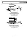
1
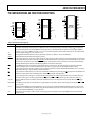
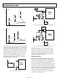
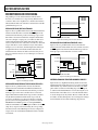
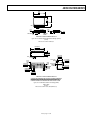
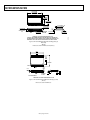
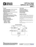
3 V/5 V, 2 MSPS, 8-Bit, 1-/4-/8-Channel
Sampling ADCs
AD7822/AD7825/AD7829
FEATURES
VDD
CONVST EOC A01 A11 A22 PD3
CONTROL
LOGIC
VIN1
VIN24
VIN34
VIN44
VIN55
VIN65
VIN75
VIN85
INPUT
MUX
1A0, A1
2A2
3PD
4V
IN2 TO VIN4
5V
IN5 TO VIN8
Data acquisition systems, DSP front ends
Disk drives
Mobile communication systems, subsampling
applications
2.5V
REF
BUF
T/H
VMID
APPLICATIONS
COMP
8-BIT
HALF
FLASH
ADC
DGND
AGND
PARALLEL
PORT
VREF IN/OUT
DB7
DB0
CS RD
AD7825/AD7829
AD7829
AD7822/AD7825
AD7825/AD7829
AD7829
01321-001
8-bit half-flash ADC with 420 ns conversion time
One, four, and eight single-ended analog input channels
Available with input offset adjust
On-chip track-and-hold
SNR performance given for input frequencies up to 10 MHz
On-chip reference (2.5 V)
Automatic power-down at the end of conversion
Wide operating supply range
3 V ± 10% and 5 V ± 10%
Input ranges
0 V to 2 V p-p, VDD = 3 V ± 10%
0 V to 2.5 V p-p, VDD = 5 V ± 10%
Flexible parallel interface with EOC pulse to allow
standalone operation
FUNCTIONAL BLOCK DIAGRAM
Figure 1.
GENERAL DESCRIPTION
The AD7822/AD7825/AD7829 are high speed, 1-, 4-, and
8-channel, microprocessor-compatible, 8-bit analog-to-digital
converters with a maximum throughput of 2 MSPS. The AD7822/
AD7825/AD7829 contain an on-chip reference of 2.5 V
(2% tolerance); a track-and-hold amplifier; a 420 ns, 8-bit halfflash ADC; and a high speed parallel interface. The converters
can operate from a single 3 V ± 10% and 5 V ± 10% supply.
The AD7822 and AD7825 are available in 20-lead and 24-lead,
0.3" wide, plastic dual in-line packages (PDIP); 20-lead and
24-lead standard small outline packages (SOIC); and 20-lead
and 24-lead thin shrink small outline packages (TSSOP). The
AD7829 is available in a 28-lead, 0.6" wide PDIP; a 28-lead
SOIC; and a 28-lead TSSOP.
The AD7822/AD7825/AD7829 combine the convert start and
power-down functions at one pin, that is, the CONVST pin.
This allows a unique automatic power-down at the end of a
conversion to be implemented. The logic level on the CONVST
pin is sampled after the end of a conversion when an EOC (end
of conversion) signal goes high. If it is logic low at that point,
the ADC is powered down. The AD7822 and AD7825 also have
a separate power-down pin (see the Operating Modes section).
1.
Fast Conversion Time. The AD7822/AD7825/AD7829
have a conversion time of 420 ns. Faster conversion times
maximize the DSP processing time in a real-time system.
2.
Analog Input Span Adjustment. The VMID pin allows the
user to offset the input span. This feature can reduce the
requirements of single-supply op amps and take into
account any system offsets.
3.
FPBW (Full Power Bandwidth) of Track-and-Hold.
The track-and-hold amplifier has an excellent high
frequency performance. The AD7822/AD7825/AD7829
are capable of converting full-scale input signals up to a
frequency of 10 MHz. This makes the parts ideally suited
to subsampling applications.
4.
Channel Selection. Channel selection is made without the
necessity of writing to the part.
The parallel interface is designed to allow easy interfacing to
microprocessors and DSPs. Using only address decoding logic,
the parts are easily mapped into the microprocessor address
space. The EOC pulse allows the ADCs to be used in a standalone manner (see the Parallel Interface section.)
PRODUCT HIGHLIGHTS
Rev. C
Information furnished by Analog Devices is believed to be accurate and reliable. However, no
responsibility is assumed by Analog Devices for its use, nor for any infringements of patents or other
rights of third parties that may result from its use. Specifications subject to change without notice. No
license is granted by implication or otherwise under any patent or patent rights of Analog Devices.
Trademarks and registered trademarks are the property of their respective owners.
One Technology Way, P.O. Box 9106, Norwood, MA 02062-9106, U.S.A.
Tel: 781.329.4700
www.analog.com
Fax: 781.461.3113
©2006 Analog Devices, Inc. All rights reserved.
AD7822/AD7825/AD7829
TABLE OF CONTENTS
Features .............................................................................................. 1
Typical Connection Diagram ................................................... 10
Applications....................................................................................... 1
ADC Transfer Function............................................................. 11
General Description ......................................................................... 1
Analog Input ............................................................................... 11
Functional Block Diagram .............................................................. 1
Power-Up Times......................................................................... 14
Product Highlights ....................................................................... 1
Power vs. Throughput................................................................ 15
Revision History ............................................................................... 2
Operating Modes........................................................................ 15
Specifications..................................................................................... 3
Parallel Interface......................................................................... 17
Timing Characteristics ................................................................ 5
Microprocessor Interfacing........................................................... 18
Timing Diagram ........................................................................... 5
AD7822/AD7825/AD7829 to 8051 ......................................... 18
Absolute Maximum Ratings............................................................ 6
AD7822/AD7825/AD7829 to PIC16C6x/PIC16C7x................ 18
ESD Caution.................................................................................. 6
AD7822/AD7825/AD7829 to ADSP-21xx ............................. 18
Pin Configurations and Function Descriptions ........................... 7
Interfacing Multiplexer Address Inputs .................................. 18
Terminology ...................................................................................... 8
AD7822 Standalone Operation ................................................ 19
Circuit Information ........................................................................ 10
Outline Dimensions ....................................................................... 20
Circuit Description..................................................................... 10
Ordering Guide .......................................................................... 25
REVISION HISTORY
8/06—Rev. B to Rev. C
Changes to General Description .................................................... 1
Changes to Table 1............................................................................ 3
Changes to Typical Connection Diagram Section ..................... 10
Updated Outline Dimensions ....................................................... 20
Changes to Ordering Guide .......................................................... 25
Changes to Typical Connection Diagram Section........................7
Changes to Analog Input Section....................................................8
Changes to Analog Input Selection Section...................................9
Changes to Power-Up Times Section .......................................... 10
Changes to Power vs. Throughput Section ................................. 11
Added AD7822 Stand-Alone Operation section ....................... 15
10/01—Rev. A to Rev. B
Changes to Power Requirements.................................................... 3
Changes to Pin Function Description ........................................... 5
Changes to Circuit Description ...................................................... 7
12/99—Rev. 0 to Rev. A
Rev. C | Page 2 of 28
AD7822/AD7825/AD7829
SPECIFICATIONS
VDD = 3 V ± 10%, VDD = 5 V ± 10%, GND = 0 V, VREF IN/OUT = 2.5 V. All specifications −40°C to +85°C, unless otherwise noted.
Table 1.
Parameter
DYNAMIC PERFORMANCE
Signal to (Noise + Distortion) Ratio 1
Total Harmonic Distortion1
Peak Harmonic or Spurious Noise1
Intermodulation Distortion1
Second-Order Terms
Third-Order Terms
Channel-to-Channel Isolation1
DC ACCURACY
Resolution
Minimum Resolution for Which
No Missing Codes Are Guaranteed
Integral Nonlinearity (INL)1
Differential Nonlinearity (DNL)1
Gain Error1
Gain Error Match1
Offset Error1
Offset Error Match1
ANALOG INPUTS 2
VDD = 5 V ± 10%
VIN1 to VIN8 Input Voltage
VMID Input Voltage
VDD = 3 V ± 10%
VIN1 to VIN8 Input Voltage
VMID Input Voltage
VIN Input Leakage Current
VIN Input Capacitance
VMID Input Impedance
REFERENCE INPUT
VREF IN/OUT Input Voltage Range
Input Current
ON-CHIP REFERENCE
Reference Error
Temperature Coefficient
LOGIC INPUTS
Input High Voltage, VINH
Input Low Voltage, VINL
Input High Voltage, VINH
Input Low Voltage, VINL
Input Current, IIN
Input Capacitance, CIN
Version B
Unit
48
−55
−55
dB min
dB max
dB max
−65
−65
−70
dB typ
dB typ
dB typ
8
Bits
8
±0.75
±0.75
±2
±0.1
±1
±0.1
Bits
LSB max
LSB max
LSB max
LSB typ
LSB max
LSB typ
Test Condition/Comment
fIN = 30 kHz, fSAMPLE = 2 MHz
fa = 27.3 kHz, fb = 28.3 kHz
fIN = 20 kHz
See Analog Input section
Input voltage span = 2.5 V
VDD
0
VDD − 1.25
1.25
V max
V min
V max
V min
VDD
0
VDD − 1
1
±1
15
6
V max
V min
V max
V min
μA max
pF max
kΩ typ
2.55
2.45
1
100
V max
V min
μA typ
μA max
±50
50
mV max
ppm/°C typ
2.4
0.8
2
0.4
±1
10
V min
V max
V min
V max
μA max
pF max
Default VMID = 1.25 V
Input voltage span = 2 V
Default VMID = 1 V
2.5 V + 2%
2.5 V − 2%
Nominal 2.5 V
Rev. C | Page 3 of 28
VDD = 5 V ± 10%
VDD = 5 V ± 10%
VDD = 3 V ± 10%
VDD = 3 V ± 10%
10 nA typical, VIN = 0 V to VDD
AD7822/AD7825/AD7829
Parameter
LOGIC OUTPUTS
Output High Voltage, VOH
Version B
Unit
4
2.4
V min
V min
0.4
0.2
±1
10
V max
V max
μA max
pF max
200
420
ns max
ns max
±1
LSB max
4.5
5.5
2.7
3.3
V min
V max
V min
V max
5 V ± 10%; for specified performance
12
5
0.2
mA max
μA max
μA typ
8 mA typical
Logic inputs = 0 V or VDD
36
mW max
9.58
23.94
mW typ
mW typ
Output Low Voltage, VOL
High Impedance Leakage Current
High Impedance Capacitance
CONVERSION RATE
Track-and-Hold Acquisition Time
Conversion Time
POWER SUPPLY REJECTION
VDD ± 10%
POWER REQUIREMENTS
VDD
VDD
Test Condition/Comment
ISOURCE = 200 μA
VDD = 5 V ± 10%
VDD = 3 V ± 10%
ISINK = 200 μA
VDD = 5 V ± 10%
VDD = 3 V ± 10%
See Circuit Description section
3 V ± 10%; for specified performance
IDD
Normal Operation
Power-Down
Power Dissipation
Normal Operation
Power-Down
200 kSPS
500 kSPS
1
2
See the Terminology section of this data sheet.
Refer to the Analog Input section for an explanation of the analog input(s).
Rev. C | Page 4 of 28
VDD = 3 V
24 mW typical
AD7822/AD7825/AD7829
TIMING CHARACTERISTICS
VREF IN/OUT = 2.5 V. All specifications −40°C to +85°C, unless otherwise noted.
Table 2.
Parameter 1,
2
t1
t2
t3
t4
t5
t6
t7
t8
t9 3
t10 4
t11
t12
t13
tPOWER UP
tPOWER UP
5 V ± 10%
420
20
30
110
70
10
0
0
30
10
5
20
10
15
200
25
1
3 V ± 10%
420
20
30
110
70
10
0
0
30
20
5
20
10
15
200
25
1
Unit
ns max
ns min
ns min
ns max
ns min
ns max
ns min
ns min
ns min
ns max
ns min
ns max
ns min
ns min
ns min
μs typ
μs max
Conditions/Comments
Conversion time
Minimum CONVST pulse width
Minimum time between the rising edge of RD and the next falling edge of convert star
EOC pulse width
RD rising edge to EOC pulse high
CS to RD setup time
CS to RD hold time
Minimum RD pulse width
Data access time after RD low
Bus relinquish time after RD high
Address setup time before falling edge of RD
Address hold time after falling edge of RD
Minimum time between new channel selection and convert start
Power-up time from rising edge of CONVST using on-chip reference
Power-up time from rising edge of CONVST using external 2.5 V reference
1
Sample tested to ensure compliance.
See Figure 24, Figure 25, and Figure 26.
3
Measured with the load circuit of Figure 2 and defined as the time required for an output to cross 0.8 V or 2.4 V with VDD = 5 V ± 10%, and time required for an output
to cross 0.4 V or 2.0 V with VDD = 3 V ± 10%.
4
Derived from the measured time taken by the data outputs to change 0.5 V when loaded with the circuit of Figure 2. The measured number is then extrapolated back
to remove the effects of charging or discharging the 50 pF capacitor. This means that the time, t10, quoted in the timing characteristics is the true bus relinquish time
of the part and, as such, is independent of external bus loading capacitances.
2
TIMING DIAGRAM
200µA
2.1V
CL
50pF
200µA
IOH
01321-002
TO OUTPUT
PIN
IOL
Figure 2. Load Circuit for Access Time and Bus Relinquish Time
Rev. C | Page 5 of 28
AD7822/AD7825/AD7829
ABSOLUTE MAXIMUM RATINGS
TA = 25°C, unless otherwise noted.
Table 3.
Parameter
VDD to AGND
VDD to DGND
Analog Input Voltage to AGND
VIN1 to VIN8
Reference Input Voltage to AGND
VMID Input Voltage to AGND
Digital Input Voltage to DGND
Digital Output Voltage to DGND
Operating Temperature Range
Industrial (B Version)
Storage Temperature Range
Junction Temperature
PDIP Package, Power Dissipation
θJA Thermal Impedance
Lead Temperature, (Soldering, 10 sec)
SOIC Package, Power Dissipation
θJA Thermal Impedance
Lead Temperature, Soldering
Vapor Phase (60 sec)
Infrared (15 sec)
TSSOP Package, Power Dissipation
θJA Thermal Impedance
Lead Temperature, Soldering
Vapor Phase (60 sec)
Infrared (15 sec)
ESD
Rating
−0.3 V to +7 V
−0.3 V to +7 V
−0.3 V to VDD + 0.3 V
−0.3 V to VDD + 0.3 V
−0.3 V to VDD + 0.3 V
−0.3 V to VDD + 0.3 V
−0.3 V to VDD + 0.3 V
Stresses above those listed under Absolute Maximum Ratings
may cause permanent damage to the device. This is a stress
rating only; functional operation of the device at these or any
other conditions above those indicated in the operational
section of this specification is not implied. Exposure to absolute
maximum rating conditions for extended periods may affect
device reliability.
−40°C to +85°C
−65°C to +150°C
150°C
450 mW
105°C/W
260°C
450 mW
75°C/W
215°C
220°C
450 mW
128°C/W
215°C
220°C
1 kV
ESD CAUTION
ESD (electrostatic discharge) sensitive device. Electrostatic charges as high as 4000 V readily accumulate on
the human body and test equipment and can discharge without detection. Although this product features
proprietary ESD protection circuitry, permanent damage may occur on devices subjected to high energy
electrostatic discharges. Therefore, proper ESD precautions are recommended to avoid performance
degradation or loss of functionality.
Rev. C | Page 6 of 28
AD7822/AD7825/AD7829
26
DB1 2
23
DB4
CONVST 4
25
DB6
22
DB5
CS 5
24
DB7
21
DB6
RD 6
23
AGND
20
DB7
DGND 7
DB1 2
19
DB4
CONVST 4
DB0 3
18
DB5
CS 5
TOP VIEW 19 AGND
(Not to Scale)
DGND 7
18 VDD
RD 6
AD7822
16 DB7
TOP VIEW
15 AGND
(Not to Scale)
DGND 7
14 VDD
13
VREF IN/OUT
PD 9
12
VMID
NC 10
11
VIN1
NC = NO CONNECT
Figure 3. Pin Configuration
01321-003
EOC 8
AD7825
EOC 8
AD7829
TOP VIEW
(Not to Scale)
22
VDD
21
VREF IN/OUT
A2 9
20
VMID
EOC 8
17
VREF IN/OUT
A1 10
19
VIN1
A1 9
16
VMID
A0 11
18
VIN2
A0 10
15
VIN1
VIN8 12
17
VIN3
PD 11
14
VIN2
VIN7 13
16
VIN4
VIN4 12
13
VIN3
VIN6 14
15
VIN5
Figure 4. Pin Configuration
01321-004
CS 5
DB5
DB0 3
DB0 3
RD 6
DB4
DB3
DB3
DB6
DB3
27
24
20
17
28
DB2 1
DB2 1
CONVST 4
DB2 1
DB1 2
01321-005
PIN CONFIGURATIONS AND FUNCTION DESCRIPTIONS
Figure 5. Pin Configuration
Table 4. Pin Function Descriptions
Mnemonic
VIN1 to VIN8
VDD
AGND
DGND
CONVST
EOC
CS
PD
RD
A0 to A2
DB0 to DB7
VREF IN/OUT
VMID
Description
Analog Input Channels. The AD7822 has a single input channel; the AD7825 and AD7829 have four and eight analog input
channels, respectively. The inputs have an input span of 2.5 V and 2 V depending on the supply voltage (VDD). This span can
be centered anywhere in the range AGND to VDD using the VMID pin. The default input range (VMID unconnected) is AGND to
2 V (VDD = 3 V ± 10%) or AGND to 2.5 V (VDD = 5 V ± 10%). See the Analog Input section of the data sheet for more information.
Positive Supply Voltage, 3 V ± 10% and 5 V ± 10%.
Analog Ground. Ground reference for track-and-hold, comparators, reference circuit, and multiplexer.
Digital Ground. Ground reference for digital circuitry.
Logic Input Signal. The convert start signal initiates an 8-bit analog-to-digital conversion on the falling edge of this signal. The
falling edge of this signal places the track-and-hold in hold mode. The track-and-hold goes into track mode again 120 ns after
the start of a conversion. The state of the CONVST signal is checked at the end of a conversion. If it is logic low, the AD7822/
AD7825/AD7829 powers down (see the Operating Modes section of the data sheet).
Logic Output. The end-of-conversion signal indicates when a conversion has finished. The signal can be used to interrupt
a microcontroller when a conversion has finished or latch data into a gate array (see the Parallel Interface section).
Logic Input Signal. The chip select signal is used to enable the parallel port of the AD7822/AD7825/AD7829. This is necessary
if the ADC is sharing a common data bus with another device.
Logic Input. The power-down pin is present on the AD7822 and AD7825 only. Bringing the PD pin low places the AD7822 and
AD7825 in power-down mode. The ADCs power up when PD is brought logic high again.
Logic Input Signal. The read signal is used to take the output buffers out of their high impedance state and drive data onto
the data bus. The signal is internally gated with the CS signal. Both RD and CS must be logic low to enable the data bus.
Channel Address Inputs. The address of the next multiplexer channel must be present on these inputs when the RD signal
goes low.
Data Output Lines. They are normally held in a high impedance state. Data is driven onto the data bus when both RD and CS
go active low.
Analog Input and Output. An external reference can be connected to the AD7822/AD7825/AD7829 at this pin. The on-chip
reference is also available at this pin. When using the internal reference, this pin can be left unconnected or, in some cases, it
can be decoupled to AGND with a 0.1 μF capacitor.
The VMID pin, if connected, is used to center the analog input span anywhere in the range of AGND to VDD (see the Analog
Input section).
Rev. C | Page 7 of 28
AD7822/AD7825/AD7829
TERMINOLOGY
Signal-to-(Noise + Distortion) Ratio
The measured ratio of signal-to-(noise + distortion) at the
output of the analog-to-digital converter. The signal is the rms
amplitude of the fundamental. Noise is the rms sum of all
nonfundamental signals up to half the sampling frequency
(fS/2), excluding dc. The ratio is dependent upon the number of
quantization levels in the digitization process: the more levels,
the smaller the quantization noise. The theoretical signal-to-(noise
+ distortion) ratio for an ideal N-bit converter with a sine wave
input is given by
Signal-to-(Noise + Distortion) = (6.02 N + 1.76) dB
Thus, for an 8-bit converter, this is 50 dB.
Total Harmonic Distortion (THD)
The ratio of the rms sum of harmonics to the fundamental. For
the AD7822/AD7825/AD7829, it is defined as
V 2 + V 3 + V 4 + V 5 + V6
2
THD (dB) = 20 log
2
2
2
2
V1
where V1 is the rms amplitude of the fundamental and V2, V3,
V4, V5, and V6 are the rms amplitudes of the second through the
sixth harmonics.
Peak Harmonic or Spurious Noise
The ratio of the rms value of the next largest component in the
ADC output spectrum (up to fS/2 and excluding dc) to the rms
value of the fundamental. Normally, the value of this specification
is determined by the largest harmonic in the spectrum, but for
parts where the harmonics are buried in the noise floor, it is a
noise peak.
Intermodulation Distortion
With inputs consisting of sine waves at two frequencies, fa and
fb, any active device with nonlinearities creates distortion
products at sum and difference frequencies of mfa ± nfb, where
m, n = 0, 1, 2, 3, … . Intermodulation terms are those for which
neither m nor n is equal to zero. For example, the second-order
terms include (fa + fb) and (fa − fb), and the third-order terms
include (2fa + fb), (2fa − fb), (fa + 2fb), and (fa − 2fb).
The AD7822/AD7825/AD7829 are tested using the CCIF
standard, where two input frequencies near the top end of the
input bandwidth are used. In this case, the second- and thirdorder terms are of different significance. The second-order terms
are usually distanced in frequency from the original sine waves,
and the third-order terms are usually at a frequency close to the
input frequencies. As a result, the second- and third-order terms
are specified separately. The calculation of the intermodulation
distortion is as per the THD specification, where it is the ratio
of the rms sum of the individual distortion products to the rms
amplitude of the fundamental expressed in decibels (dB).
Channel-to-Channel Isolation
A measure of the level of crosstalk between channels. It is
measured by applying a full-scale 20 kHz sine wave signal to
one input channel and determining how much that signal is
attenuated in each of the other channels. The figure given is the
worst case across all four or eight channels of the AD7825 and
AD7829, respectively.
Relative Accuracy or Endpoint Nonlinearity
The maximum deviation from a straight line passing through
the endpoints of the ADC transfer function.
Differential Nonlinearity
The difference between the measured and the ideal one LSB
change between any two adjacent codes in the ADC.
Offset Error
The deviation of the 128th code transition (01111111) to
(10000000) from the ideal, that is, VMID.
Offset Error Match
The difference in offset error between any two channels.
Zero-Scale Error
The deviation of the first code transition (00000000) to
(00000001) from the ideal; that is, VMID − 1.25 V + 1 LSB (VDD =
5 V ± 10%), or VMID − 1.0 V + 1 LSB (VDD = 3 V ± 10%).
Full-Scale Error
The deviation of the last code transition (11111110) to (11111111)
from the ideal; that is, VMID + 1.25 V − 1 LSB (VDD = 5 V ± 10%),
or VMID + 1.0 V − 1 LSB (VDD = 3 V ± 10%).
Rev. C | Page 8 of 28
AD7822/AD7825/AD7829
Gain Error Match
The difference in gain error between any two channels.
It also applies to situations where a change in the selected input
channel takes place or where there is a step input change on the
input voltage applied to the selected VIN input of the AD7822/
AD7825/AD7829. It means that the user must wait for the
duration of the track-and-hold acquisition time after a channel
change/step input change to VIN before starting another
conversion, to ensure that the part operates to specification.
Track-and-Hold Acquisition Time
The time required for the output of the track-and-hold amplifier to
reach its final value, within ±1/2 LSB, after the point at which the
track-and-hold returns to track mode. This happens approximately
120 ns after the falling edge of CONVST.
PSR (Power Supply Rejection)
Variations in power supply affect the full-scale transition but
not the converter linearity. Power supply rejection is the
maximum change in the full-scale transition point due to a
change in power supply voltage from the nominal value.
Gain Error
The deviation of the last code transition (1111 . . . 110) to
(1111 . . . 111) from the ideal, that is, VREF − 1 LSB, after the
offset error has been adjusted out.
Rev. C | Page 9 of 28
AD7822/AD7825/AD7829
CIRCUIT INFORMATION
CIRCUIT DESCRIPTION
REFERENCE
R16
15
DB6
R15
DB5
14
SAMPLING
CAPACITOR
B
HOLD
R14
13
OUTPUT
DRIVERS
SW2
OUTPUT
REGISTER
T/H 1
VIN
A
DB7
DECODE
LOGIC
DB4
DB3
DB2
R13
DB1
DB0
1
R1
TIMING AND
CONTROL
LOGIC
01321-007
Figure 6 and Figure 7 show simplified schematics of the ADC.
When the ADC starts a conversion, the track-and-hold goes
into hold mode and holds the analog input for 120 ns. This is
the acquisition phase, as shown in Figure 6, when Switch 2 is in
Position A. At the point when the track-and-hold returns to its
track mode, this signal is sampled by the sampling capacitor,
as Switch 2 moves into Position B. The first flash occurs at this
instant and is then followed by the second flash. Typically, the
first flash is complete after 100 ns, that is, at 220 ns; and the end
of the second flash and, hence, the 8-bit conversion result is
available at 330 ns (minimum). The maximum conversion time
is 420 ns. As shown in Figure 8, the track-and-hold returns to
track mode after 120 ns and starts the next acquisition before
the end of the current conversion. Figure 10 shows the ADC
transfer function.
Figure 7. ADC Conversion Phase
120ns
TRACK
CONVST
EOC
TRACK
HOLD
HOLD
t2
t1
CS
t3
RD
VALID
DATA
DB0 TO DB7
01321-008
The AD7822/AD7825/AD7829 consist of a track-and-hold
amplifier followed by a half-flash analog-to-digital converter.
These devices use a half-flash conversion technique where one
4-bit flash ADC is used to achieve an 8-bit result. The 4-bit flash
ADC contains a sampling capacitor followed by 15 comparators
that compare the unknown input to a reference ladder to
achieve a 4-bit result. This first flash (that is, coarse conversion)
provides the four MSBs. For a full 8-bit reading to be realized,
a second flash (that is, fine conversion) must be performed to
provide the four LSBs. The 8-bit word is then placed on the data
output bus.
Figure 8. Track-and-Hold Timing
REFERENCE
TYPICAL CONNECTION DIAGRAM
R16
15
R14
13
OUTPUT
DRIVERS
B
DB4
DB3
DB2
R13
DB1
1
DB0
R1
TIMING AND
CONTROL
LOGIC
Figure 6. ADC Acquisition Phase
01321-006
HOLD
DB5
14
SAMPLING
CAPACITOR
OUTPUT
REGISTER
T/H 1
DB6
R15
SW2
DECODE
LOGIC
VIN
A
DB7
Figure 9 shows a typical connection diagram for the AD7822/
AD7825/AD7829. The AGND and DGND are connected
together at the device for good noise suppression. The parallel
interface is implemented using an 8-bit data bus. The end of
conversion signal (EOC) idles high, the falling edge of CONVST
initiates a conversion, and at the end of conversion the falling
edge of EOC is used to initiate an interrupt service routine
(ISR) on a microprocessor (see the Parallel Interface section for
more details.) VREF and VMID are connected to a voltage source
such as the AD780, and VDD is connected to a voltage source
that can vary from 4.5 V to 5.5 V (see Table 5 in the Analog Input
section). When VDD is first connected, the AD7822/AD7825/
AD7829 power up in a low current mode, that is, power-down
mode, with the default logic level on the EOC pin on the
AD7822 and AD7825 equal to a low. Ensure the CONVST line is
not floating when VDD is applied, because this can put the
AD7822/AD7825/AD7829 into an unknown state.
Rev. C | Page 10 of 28
AD7822/AD7825/AD7829
A suggestion is to tie CONVST to VDD or DGND through a pull-up
or pull-down resistor. A rising edge on the CONVST pin causes
the AD7829 to fully power up, while a rising edge on the PD pin
causes the AD7822 and AD7825 to fully power up. For applications where power consumption is of concern, the automatic
power-down at the end of a conversion should be used to improve
power performance (see the Power vs. Throughput section).
SUPPLY
4.5V TO 5.5V
2.5V
AD780
10µF
0.1µF
PARALLEL
INTERFACE
VDD
VREF
1.25V TO
3.75V INPUT
EOC
VIN24
AD7822/
AD7825/
AD7829
RD
CS
µC/µP
CONVST
VIN4(VIN85)
A01
AGND
If, however, an external VMID is applied, the analog input range
is from VMID − 1.0 V to VMID + 1.0 V (VDD = 3 V ± 10%), or
from VMID − 1.25 V to VMID + 1.25 V (VDD = 5 V ± 10%).
A11
A22
DGND
PD3
1A0, A1
2A2
3PD
4V
IN2 TO VIN4
5V
IN5 TO VIN8
01321-009
AD7825/AD7829
AD7829
AD7822/AD7825
AD7825/AD7829
AD7829
Figure 9. Typical Connection Diagram
ADC TRANSFER FUNCTION
(VDD = 5V)
1LSB = VREF /256
VDD
5.5
5.0
4.5
3.3
3.0
2.7
111...000
10000000
(VDD = 3V)
1LSB = 0.8VREF /256
000...111
000...010
000...001
00000000
1LSB
(VDD = 5V) VMID – 1.25V
(VDD = 3V) VMID – 1V
VMID
VMID + 1.25V – 1LSB
VMID + 1V – 1LSB
ANALOG INPUT VOLTAGE
01321-010
ADC CODE
The range of values of VMID that can be applied depends on the
value of VDD. For VDD = 3 V ± 10%, the range of values that can
be applied to VMID is from 1.0 V to VDD − 1.0 V and from 1.25 V to
VDD − 1.25 V when VDD = 5 V ± 10%. Table 5 shows the relevant
ranges of VMID and the input span for various values of VDD.
Figure 11 illustrates the input signal range available with various
values of VMID.
Table 5.
The output coding of the AD7822/AD7825/AD7829 is straight
binary. The designed code transitions occur at successive integer
LSB values (that is, 1 LSB, 2 LSBs, and so on). The LSB size =
VREF/256 (VDD = 5 V) or the LSB size = (0.8 VREF)/256 (VDD =
3 V). The ideal transfer characteristic for the AD7822/AD7825/
AD7829 is shown in Figure 10.
11111111
111...110
The AD7822 has a single input channel, and the AD7825 and
AD7829 have four and eight input channels, respectively. Each
input channel has an input span of 2.5 V or 2.0 V, depending on
the supply voltage (VDD). This input span is automatically set up
by an on-chip VDD detector circuit. A 5 V operation of the ADCs
is detected when VDD exceeds 4.1 V, and a 3 V operation is
detected when VDD falls below 3.8 V. This circuit also possesses
a degree of glitch rejection; for example, a glitch from 5.5 V to
2.7 V up to 60 ns wide does not trip the VDD detector.
The VMID pin is used to center this input span anywhere in the
range of AGND to VDD. If no input voltage is applied to VMID,
the default input range is AGND to 2.0 V (VDD = 3 V ± 10%),
that is, centered about 1.0 V; or AGND to 2.5 V (VDD = 5 V ±
10%), that is, centered about 1.25 V. When using the default
input range, the VMID pin can be left unconnected, or in some
cases, it can be decoupled to AGND with a 0.1 μF capacitor.
VMID
DB0 TO DB7
VIN1
ANALOG INPUT
Figure 10. Transfer Characteristic
Rev. C | Page 11 of 28
VMID
Internal
1.25
1.25
1.25
1.00
1.00
1.00
VMID Ext
Max
4.25
3.75
3.25
2.3
2.0
1.7
VIN Span
3.0 to 5.5
2.5 to 5.0
2.0 to 4.5
1.3 to 3.3
1.0 to 3.0
0.7 to 2.7
VMID Ext
Min
1.25
1.25
1.25
1.00
1.00
1.00
VIN Span
0 to 2.5
0 to 2.5
0 to 2.5
0 to 2.0
0 to 2.0
0 to 2.0
Unit
V
V
V
V
V
V
AD7822/AD7825/AD7829
2.5V
VDD = 5V
VREF
5V
VMID
R4
4V
R3
VMID = 3.75V
V
3V
VMID = 2.5V
V
AD7822/
AD7825/
AD7829
VIN
R2
R1
0V
VIN
2V
VMID = N/C (1.25V)
INPUT SIGNAL RANGE
FOR VARIOUS VMID
01321-013
2.5V
1V
0V
Figure 13. Accommodating Bipolar Signals Using External VMID
EXTERNAL
2.5V
VDD = 3V
3V
VREF
VMID
AD7822/
AD7825/
AD7829
R4
2V
R3
VMID = 2V
VMID = 1.5V
V
VMID = N/C (1V)
0V
R1
VIN
VMID
Figure 11. Analog Input Span Variation with VMID
0V
VMID can be used to remove offsets in a system by applying the
offset to the VMID pin as shown in Figure 12, or it can be used to
accommodate bipolar signals by applying VMID to a level-shifting
circuit before VIN, as shown in Figure 13. When VMID is being
driven by an external source, the source can be directly tied to
the level-shifting circuitry (see Figure 13). However, if the
internal VMID, that is, the default value, is being used as an
output, it must be buffered before applying it to the levelshifting circuitry because the VMID pin has an impedance of
approximately 6 kΩ (see Figure 14).
VIN
VIN
AD7822/
AD7825/
AD7829
VMID
VMID
Figure 12. Removing Offsets Using VMID
01321-012
VMID
01321-014
INPUT SIGNAL RANGE
FOR VARIOUS VMID
VIN
R2
01321-011
1V
V
Figure 14. Accommodating Bipolar Signals Using Internal VMID
NOTE: Although there is a VREF pin from which a voltage
reference of 2.5 V can be sourced, or to which an external
reference can be applied, this does not provide an option of
varying the value of the voltage reference. As stated in the
specifications for the AD7822/AD7825/AD7829, the input
voltage range at this pin is 2.5 V ± 2%.
Analog Input Structure
Figure 15 shows an equivalent circuit of the analog input
structure of the AD7822/AD7825/AD7829. The two diodes,
D1 and D2, provide ESD protection for the analog inputs. Care
must be taken to ensure that the analog input signal never
exceeds the supply rails by more than 200 mV. Doing so causes
these diodes to become forward biased and start conducting
current into the substrate. A maximum current of 20 mA can be
conducted by these diodes without causing irreversible damage
to the part. However, it is worth noting that a small amount of
current (1 mA) being conducted into the substrate, due to an
overvoltage on an unselected channel, can cause inaccurate
conversions on a selected channel.
Rev. C | Page 12 of 28
AD7822/AD7825/AD7829
Capacitor C2 in Figure 15 is typically about 4 pF and can be
primarily attributed to pin capacitance. The resistor, R1, is a
lumped component made up of the on resistance of several
components, including that of the multiplexer and the trackand-hold. This resistor is typically about 310 Ω. Capacitor C1
is the track-and-hold capacitor and has a capacitance of 0.5 pF.
Switch 1 is the track-and-hold switch, and Switch 2 is that of the
sampling capacitor, as shown in Figure 6 and Figure 7.
120ns
TRACK CHx
HOLD CHx
TRACK CHx
TRACK CHy
CONVST
t1
EOC
CS
t3
RD
VDD
C2
4pF
D2
DB0 TO DB7
C1
0.5pF A SW2
R1
310Ω
SW1
A0 TO A2
B
ADDRESS CHANNEL y
01321-015
Figure 15. Equivalent Analog Input Circuit
When in track phase, Switch 1 is closed and Switch 2 is in
Position A. When in hold mode, Switch 1 opens and Switch 2
remains in Position A. The track-and-hold remains in hold
mode for 120 ns (see the Circuit Description section), after
which it returns to track mode and the ADC enters its conversion
phase. At this point, Switch 1 opens and Switch 2 moves to
Position B. At the end of the conversion, Switch 2 moves back
to Position A.
Figure 16. Channel Hopping Timing
There is a minimum time delay between the falling edge of RD
and the next falling edge of the CONVST signal, t13. This is the
minimum acquisition time required of the track-and-hold to
maintain 8-bit performance. Figure 17 shows the typical performance of the AD7825 when channel hopping for various acquisition
times. These results are obtained using an external reference
and internal VMID while channel hopping between VIN1 and VIN4
with 0 V on Channel 4 and 0.5 V on Channel 1.
8.5
Analog Input Selection
8.0
On power-up, the default VIN selection is VIN1. When returning
to normal operation from power-down, the VIN selected is the
same one that was selected prior to initiation of power-down.
Table 6 shows the multiplexer address corresponding to each
analog input from VIN1 to VIN4(8) for the AD7825 or AD7829.
ENOB
7.5
Table 6.
A2
0
0
0
0
1
1
1
1
7.0
6.5
6.0
A1
0
0
1
1
0
0
1
1
A0
0
1
0
1
0
1
0
1
Analog Input Selected
VIN1
VIN2
VIN3
VIN4
VIN5
VIN6
VIN7
VIN8
5.5
5.0
500
200
100
50
40
30
20
ACQUISITION TIME (ns)
15
10
01321-017
VIN
t13
VALID
DATA
01321-016
D1
HOLD CHy
t2
Figure 17. Effective Number of Bits vs. Acquisition Time for the AD7825
Channel selection on the AD7825 and AD7829 is made without
the necessity of a write operation. The address of the next channel
to be converted is latched at the start of the current read operation,
that is, on the falling edge of RD while CS is low, as shown in
Figure 16. This allows for improved throughput rates in “channel
hopping” applications.
The on-chip track-and-hold can accommodate input frequencies
to 10 MHz, making the AD7822/AD7825/AD7829 ideal for
subsampling applications. When the AD7825 is converting a
10 MHz input signal at a sampling rate of 2 MSPS, the effective
number of bits typically remains above seven, corresponding to
a signal-to-noise ratio of 42 dBs, as shown in Figure 18.
Rev. C | Page 13 of 28
AD7822/AD7825/AD7829
EXTERNAL REFERENCE
50
fSAMPLE = 2MHz
VDD
48
tPOWER-UP
1µs
CONVST
SNR (dB)
46
CONVERSION
INITIATED HERE
44
ON-CHIP REFERENCE
42
VDD
tPOWER-UP
25µs
40
1
3
4
5
6
INPUT FREQUENCY (MHz)
8
10
CONVERSION
INITIATED HERE
01321-018
38
0.2
01321-019
CONVST
Figure 19. AD7829 Power-Up Time
Figure 18. SNR vs. Input Frequency on the AD7825
POWER-UP TIMES
The AD7822/AD7825/AD7829 have a 1 μs power-up time
when using an external reference and a 25 μs power-up time
when using the on-chip reference. When VDD is first connected,
the AD7822/AD7825/AD7829 are in a low current mode of
operation. Ensure that the CONVST line is not floating when
VDD is applied. If there is a glitch on CONVST while VDD is
rising, the part attempts to power up before VDD has fully settled
and can enter an unknown state. To carry out a conversion, the
AD7822/AD7825/AD7829 must first be powered up. The
AD7829 is powered up by a rising edge on the CONVST pin,
and a conversion is initiated on the falling edge of CONVST.
Figure 19 shows how to power up the AD7829 when VDD is first
connected or after the AD7829 has been powered down using
the CONVST pin when using either the on-chip reference or an
external reference. When using an external reference, the falling
edge of CONVST may occur before the required power-up time
has elapsed; however, the conversion is not initiated on the
falling edge of CONVST but rather at the moment when the
part has completely powered up, that is, after 1 μs. If the falling
edge of CONVST occurs after the required power-up time has
elapsed, then it is upon this falling edge that a conversion is
initiated. When using the on-chip reference, it is necessary to
wait the required power-up time of approximately 25 μs before
initiating a conversion; that is, a falling edge on CONVST must
not occur before the required power-up time has elapsed, when
VDD is first connected or after the AD7829 has been powered
down using the CONVST pin, as shown in Figure 19.
Figure 20 shows how to power up the AD7822 or AD7825 when
VDD is first connected or after the ADCs have been powered down,
using the PD pin or the CONVST pin, with either the on-chip
reference or an external reference. When the supplies are first
connected or after the part has been powered down by the PD
pin, only a rising edge on the PD pin causes the part to power
up. When the part has been powered down using the CONVST
pin, a rising edge on either the PD pin or the CONVST pin powers
the part up again.
As with the AD7829, when using an external reference with the
AD7822 or AD7825, the falling edge of CONVST may occur
before the required power-up time has elapsed. If this is the
case, the conversion is not initiated on the falling edge of CONVST,
but rather at the moment when the part has powered up
completely, that is, after 1 μs. If the falling edge of CONVST
occurs after the required power-up time has elapsed, it is upon
this falling edge that a conversion is initiated. When using the
on-chip reference, it is necessary to wait the required power-up
time of approximately 25 μs before initiating a conversion; that
is, a falling edge on CONVST must not occur before the
required power-up time has elapsed, when supplies are first
connected to the AD7822 or AD7825, or when the ADCs have
been powered down using the PD pin or the CONVST pin, as
shown in Figure 20.
Rev. C | Page 14 of 28
AD7822/AD7825/AD7829
EXTERNAL REFERENCE
Figure 22 shows the power vs. throughput rate for automatic
full power-down.
VDD
PD
tPOWER-UP
100
tPOWER-UP
1µs
1µs
CONVST
10
CONVERSION
INITIATED HERE
POWER (mW)
CONVERSION
INITIATED HERE
ON-CHIP REFERENCE
VDD
1
tPOWER-UP
tPOWER-UP
25µs
25µs
CONVST
CONVERSION
INITIATED HERE
01321-020
0
CONVERSION
INITIATED HERE
0
50
100
150 200 250 300 350
THROUGHPUT (kSPS)
400
450
500
01321-023
0.1
PD
Figure 22. AD7822/AD7825/AD7829 Power vs. Throughput
Figure 20. AD7822/AD7825 Power-Up Time
0
POWER VS. THROUGHPUT
2048 POINT FFT
SAMPLING
2MSPS
fIN = 200kHz
–10
Superior power performance can be achieved by using the
automatic power-down (Mode 2) at the end of a conversion
(see the Operating Modes section).
–20
(dB)
–30
Figure 21 shows how the automatic power-down is implemented
using the CONVST signal to achieve the optimum power
performance for the AD7822/AD7825/AD7829. The duration
of the CONVST pulse is set to be equal to or less than the power-up
time of the devices (see the Operating Modes section). As the
throughput rate is reduced, the device remains in its powerdown state longer and the average power consumption over time
drops accordingly.
–40
–50
–60
FREQUENCY (kHz)
01321-024
–80
0
28
57
85
113
142
170
198
227
255
283
312
340
368
396
425
453
481
510
538
566
595
623
651
680
708
736
765
793
821
850
878
906
935
963
991
–70
Figure 23. AD7822/AD7825/AD7829 SNR
tPOWER-UP tCONVERT
1µs
330ns
OPERATING MODES
POWER-DOWN
01321-022
CONVST
tCYCLE
10µs @ 100kSPS
Figure 21. Automatic Power-Down
For example, if the AD7822 is operated in a continuous
sampling mode, with a throughput rate of 100 kSPS and using
an external reference, the power consumption is calculated as
follows. The power dissipation during normal operation is
36 mW, VDD = 3 V. If the power-up time is 1 μs and the conversion
time is 330 ns (@ +25°C), the AD7822 can be said to dissipate
36 mW (maximum) for 1.33 μs during each conversion cycle.
If the throughput rate is 100 kSPS, the cycle time is 10 μs and
the average power dissipated during each cycle is (1.33/10) ×
(36 mW) = 4.79 mW. This calculation uses the minimum
conversion time, thus giving the best-case power dissipation at
this throughput rate. However, the actual power dissipated
during each conversion cycle could increase, depending on the
actual conversion time (up to a maximum of 420 ns).
The AD7822/AD7825/AD7829 have two possible modes of
operation, depending on the state of the CONVST pulse
approximately 100 ns after the end of a conversion, that is, upon
the rising edge of the EOC pulse.
Mode 1 Operation (High Speed Sampling)
When the AD7822/AD7825/AD7829 are operated in Mode 1,
they are not powered down between conversions. This mode of
operation allows high throughput rates to be achieved.
Figure 24 shows how this optimum throughput rate is achieved
by bringing CONVST high before the end of a conversion, that
is, before the EOC pulses low. When operating in this mode, a
new conversion should not be initiated until 30 ns after the end
of a read operation. This allows the track-and-hold to acquire
the analog signal to 0.5 LSB accuracy.
Rev. C | Page 15 of 28
AD7822/AD7825/AD7829
Mode 2 Operation (Automatic Power-Down)
When the AD7822/AD7825/AD7829 are operated in Mode 2
(see Figure 25), they automatically power down at the end of
a conversion. The CONVST signal is brought low to initiate
a conversion and is left logic low until after the EOC goes high,
that is, approximately 100 ns after the end of the conversion.
The state of the CONVST signal is sampled at this point (that is,
530 ns maximum after CONVST falling edge), and the AD7822/
AD7825/AD7829 power down as long as CONVST is low.
The ADC is powered up again on the rising edge of the
CONVST signal. Superior power performance can be achieved
in this mode of operation by powering up the AD7822/AD7825/
AD7829 only to carry out a conversion. The parallel interface of
the AD7822/AD7825/AD7829 remains fully operational while
the ADCs are powered down. A read may occur while the part
is powered down, and, therefore, it does not necessarily need to
be placed within the EOC pulse, as shown in Figure 25.
120ns
TRACK
HOLD
TRACK
HOLD
t2
CONVST
t1
EOC
CS
t3
VALID
DATA
DB0 TO DB7
01321-025
RD
Figure 24. Mode 1 Operation
tPOWER-UP
POWER
DOWN
HERE
CONVST
t1
EOC
CS
VALID
DATA
DB0 TO DB7
Figure 25. Mode 2 Operation
Rev. C | Page 16 of 28
01321-026
RD
AD7822/AD7825/AD7829
PARALLEL INTERFACE
The parallel interface of the AD7822/AD7825/AD7829 is eight
bits wide. Figure 26 shows a timing diagram illustrating the
operational sequence of the AD7822/AD7825/AD7829 parallel
interface. The multiplexer address is latched into the AD7822/
AD7825/AD7829 on the falling edge of the RD input. The onchip track-and-hold goes into hold mode on the falling edge of
CONVST, and a conversion is also initiated at this point. When
the conversion is complete, the end of conversion line (EOC)
pulses low to indicate that new data is available in the output
register of the AD7822/AD7825/AD7829. The EOC pulse stays
logic low for a maximum time of 110 ns.
However, the EOC pulse can be reset high by a rising edge
of RD. This EOC line can be used to drive an edge-triggered
interrupt of a microprocessor. CS and RD going low accesses
the 8-bit conversion result. It is possible to tie CS permanently
low and use only RD to access the data. In systems where the
part is interfaced to a gate array or ASIC, this EOC pulse can be
applied to the CS and RD inputs to latch data out of the AD7822/
AD7825/AD7829 and into the gate array or ASIC. This means
that the gate array or ASIC does not need any conversion status
recognition logic, and it also eliminates the logic required in the
gate array or ASIC to generate the read signal for the AD7822/
AD7825/AD7829.
t2
CONVST
t1
t4
EOC
t5
CS
t7
t6
t8
RD
t3
t9
VALID
DATA
t11
t12
t13
NEXT
CHANNEL
ADDRESS
Figure 26. AD7822/AD7825/AD7829 Parallel Port Timing
Rev. C | Page 17 of 28
01321-027
DB0 TO DB7
A0 TO A2
t10
AD7822/AD7825/AD7829
MICROPROCESSOR INTERFACING
PIC16C6x/7x1
DB0 TO DB7
PSP0 TO PSP7
1ADDITIONAL
CS
CS
RD
RD
INT
EOC
PINS OMITTED FOR CLARITY.
Figure 28. Interfacing to the PIC16C6x/ PIC16C7x
AD7822/AD7825/AD7829 TO ADSP-21xx
Figure 29 shows a parallel interface between the AD7822/
AD7825/AD7829 and the ADSP-21xx series of DSPs. As before,
the EOC signal on the AD7822/AD7825/AD7829 provides an
interrupt request to the DSP when a conversion ends.
ADSP-21xx1
D7 TO D0
80511
LATCH
DMS
CS
ALE
A8 TO A15
RD
EOC
1ADDITIONAL
01321-028
1ADDITIONAL
RD
INT
AD7822/
AD7825/
AD78291
ADDRESS
DECODE
LOGIC
AD7822/
AD7825/
AD78291
DECODER
DB0 TO DB7
A13 TO A0
DB0 TO DB7
AD0 TO AD7
01321-029
AD7822/AD7825/AD7829 TO 8051
Figure 27 shows a parallel interface between the AD7822/AD7825/
AD7829 and the 8051 microcontroller. The EOCsignal on the
AD7822/AD7825/AD7829 provides an interrupt request to the
8051 when a conversion ends and data is ready. Port 0 of the 8051
can serve as an input or output port; or, as in this case when used
together with the address latch enable (ALE) of the 8051, can be
used as a bidirectional low order address and data bus. The ALE
output of the 8051 is used to latch the low byte of the address
during accesses to the device, while the high order address byte
is supplied from Port 2. Port 2 latches remain stable when the
AD7822/AD7825/ AD7829 are addressed because they do not
have to be turned around (set to 1) for data input, as is the case
for Port 0.
AD7822/
AD7825/
AD78291
PINS OMITTED FOR CLARITY.
Figure 27. Interfacing to the 8051
AD7822/AD7825/AD7829 TO PIC16C6x/PIC16C7x
Figure 28 shows a parallel interface between the AD7822/
AD7825/AD7829 and the PIC16C64/PIC16C65/PIC16C74.
The EOC signal on the AD7822/AD7825/AD7829 provides an
interrupt request to the microcontroller when a conversion
begins. Of the PIC16C6x/PIC16C7x range of microcontrollers,
only the PIC16C64/PIC16C65/PIC16C74 can provide the
option of a parallel slave port. Port D of the microcontroller
operates as an 8-bit wide parallel slave port when Control Bit
PSPMODE in the TRISE register is set. Setting PSPMODE
enables Port Pin RE0 to be the RD output and RE2 to be the CS
(chip select) output. For this functionality, the corresponding
data direction bits of the TRISE register must be configured as
outputs (reset to 0). See the PIC16C6x/PIC16C7x microcontroller
user manual.
EN
CS
RD
RD
IRQ
EOC
PINS OMITTED FOR CLARITY.
01321-030
The parallel port on the AD7822/AD7825/AD7829 allows
the ADCs to be interfaced to a range of many different microcontrollers. This section explains how to interface the AD7822/
AD7825/AD7829 with some of the more common microcontroller
parallel interface protocols.
Figure 29. Interfacing to the ADSP-21xx
INTERFACING MULTIPLEXER ADDRESS INPUTS
Figure 30 shows a simplified interfacing scheme between the
AD7825/AD7829 and any microprocessor or microcontroller,
which facilitates easy channel selection on the ADCs. The multiplexer address is latched on the falling edge of the RD signal,
as outlined in the Parallel Interface section, allowing the use of
the three LSBs of the address bus to select the channel address.
As shown in Figure 30, only Address Bit A3 to Address Bit A15
are address decoded, allowing A0 to A2 to be changed according to
desired channel selection without affecting chip selection.
Rev. C | Page 18 of 28
AD7822/AD7825/AD7829
AD7822 STANDALONE OPERATION
The resulting signal can be used as an interrupt request signal
(IRQ) on a DSP, as a WR signal to memory, or as a CLK to a
latch or ASIC. The timing for this interface, as shown in Figure 31,
demonstrates how, with the CONVST signal alone, a conversion
can be initiated, data is latched out, and the operating mode of
the AD7822 can be selected.
The AD7822, being the single channel device, does not have any
multiplexer addressing associated with it and can be controlled
with just one signal, that is, the CONVST signal. As shown in
Figure 31, the RD and CS pins are both tied to the EOC pin.
SYSTEM BUS
MICROPROCESSOR READ CYCLE
A0
A1
A2
A15 TO A3
ADDRESS
DECODE
CS
CS
AD7825/
AD7829
RD
ADC I/O ADDRESS
A15 TO A3
RD
A2 TO A0
MUX ADDRESS
DB7 TO DB0
MUX ADDRESS
(CHANNEL SELECTION A0 TO A2)
LATCHED
01321-031
A/D RESULT
DB0 TO DB7
Figure 30. AD7825/AD7829 Simplified Microinterfacing Scheme
t1
RD
AD7822
CS
EOC
DB7 TO DB0
DSP/
LATCH/ASIC
CONVST
t4
EOC
CS
RD
DB0 TO DB7
Figure 31. AD7822 Standalone Operation
Rev. C | Page 19 of 28
A/D RESULT
01321-032
CONVST
AD7822/AD7825/AD7829
OUTLINE DIMENSIONS
1.060 (26.92)
1.030 (26.16)
0.980 (24.89)
20
11
1
10
0.280 (7.11)
0.250 (6.35)
0.240 (6.10)
0.325 (8.26)
0.310 (7.87)
0.300 (7.62)
PIN 1
0.100 (2.54)
BSC
0.060 (1.52)
MAX
0.210
(5.33)
MAX
0.195 (4.95)
0.130 (3.30)
0.115 (2.92)
0.015
(0.38)
MIN
0.150 (3.81)
0.130 (3.30)
0.115 (2.92)
0.015 (0.38)
GAUGE
PLANE
SEATING
PLANE
0.022 (0.56)
0.018 (0.46)
0.014 (0.36)
0.430 (10.92)
MAX
0.005 (0.13)
MIN
0.014 (0.36)
0.010 (0.25)
0.008 (0.20)
0.070 (1.78)
0.060 (1.52)
0.045 (1.14)
COMPLIANT TO JEDEC STANDARDS MS-001-AD
CONTROLLING DIMENSIONS ARE IN INCHES; MILLIMETER DIMENSIONS
(IN PARENTHESES) ARE ROUNDED-OFF INCH EQUIVALENTS FOR
REFERENCE ONLY AND ARE NOT APPROPRIATE FOR USE IN DESIGN.
CORNER LEADS MAY BE CONFIGURED AS WHOLE OR HALF LEADS.
Figure 32. 20-Lead Plastic Dual In-Line Package [PDIP]
Narrow Body
(N-20)
Dimensions shown in inches and (millimeters)
13.00 (0.5118)
12.60 (0.4961)
20
11
7.60 (0.2992)
7.40 (0.2913)
10
2.65 (0.1043)
2.35 (0.0925)
0.30 (0.0118)
0.10 (0.0039)
COPLANARITY
0.10
10.65 (0.4193)
10.00 (0.3937)
1.27
(0.0500)
BSC
0.51 (0.0201)
0.31 (0.0122)
SEATING
PLANE
0.75 (0.0295)
0.25 (0.0098)
8°
0°
0.33 (0.0130)
0.20 (0.0079)
COMPLIANT TO JEDEC STANDARDS MS-013-AC
CONTROLLING DIMENSIONS ARE IN MILLIMETERS; INCH DIMENSIONS
(IN PARENTHESES) ARE ROUNDED-OFF MILLIMETER EQUIVALENTS FOR
REFERENCE ONLY AND ARE NOT APPROPRIATE FOR USE IN DESIGN.
Figure 33. 20-Lead Standard Small Outline Package [SOIC_W]
Wide Body
(RW-20)
Dimensions shown in millimeters and (inches)
Rev. C | Page 20 of 28
45°
1.27 (0.0500)
0.40 (0.0157)
060706-A
1
AD7822/AD7825/AD7829
6.60
6.50
6.40
20
11
4.50
4.40
4.30
6.40 BSC
1
10
PIN 1
0.65
BSC
1.20 MAX
0.15
0.05
COPLANARITY
0.10
0.30
0.19
0.20
0.09
0.75
0.60
0.45
8°
0°
SEATING
PLANE
COMPLIANT TO JEDEC STANDARDS MO-153-AC
Figure 34. 20-Lead Thin Shrink Small Outline Package [TSSOP]
(RU-20)
Dimensions shown in millimeters
1.280 (32.51)
1.250 (31.75)
1.230 (31.24)
24
13
1
12
0.280 (7.11)
0.250 (6.35)
0.240 (6.10)
0.325 (8.26)
0.310 (7.87)
0.300 (7.62)
PIN 1
0.100 (2.54)
BSC
0.210
(5.33)
MAX
0.195 (4.95)
0.130 (3.30)
0.115 (2.92)
0.015
(0.38)
MIN
0.150 (3.81)
0.130 (3.30)
0.115 (2.92)
0.022 (0.56)
0.018 (0.46)
0.014 (0.36)
0.060 (1.52)
MAX
0.015 (0.38)
GAUGE
PLANE
SEATING
PLANE
0.005 (0.13)
MIN
0.430 (10.92)
MAX
0.070 (1.78)
0.060 (1.52)
0.045 (1.14)
COMPLIANT TO JEDEC STANDARDS MS-001-AF
CONTROLLING DIMENSIONS ARE IN INCHES; MILLIMETER DIMENSIONS
(IN PARENTHESES) ARE ROUNDED-OFF INCH EQUIVALENTS FOR
REFERENCE ONLY AND ARE NOT APPROPRIATE FOR USE IN DESIGN.
CORNER LEADS MAY BE CONFIGURED AS WHOLE OR HALF LEADS.
Figure 35. 24-Lead Plastic Dual In-Line Package [PDIP]
Narrow Body
(N-24-1)
Dimensions shown in inches and (millimeters)
Rev. C | Page 21 of 28
0.014 (0.36)
0.010 (0.25)
0.008 (0.20)
AD7822/AD7825/AD7829
15.60 (0.6142)
15.20 (0.5984)
13
24
7.60 (0.2992)
7.40 (0.2913)
10.65 (0.4193)
10.00 (0.3937)
12
0.30 (0.0118)
0.10 (0.0039)
COPLANARITY
0.10
0.75 (0.0295)
0.25 (0.0098)
2.65 (0.1043)
2.35 (0.0925)
1.27 (0.0500)
BSC
SEATING
PLANE
0.51 (0.0201)
0.31 (0.0122)
8°
0°
1.27 (0.0500)
0.40 (0.0157)
0.33 (0.0130)
0.20 (0.0079)
COMPLIANT TO JEDEC STANDARDS MS-013-AD
CONTROLLING DIMENSIONS ARE IN MILLIMETERS; INCH DIMENSIONS
(IN PARENTHESES) ARE ROUNDED-OFF MILLIMETER EQUIVALENTS FOR
REFERENCE ONLY AND ARE NOT APPROPRIATE FOR USE IN DESIGN.
Figure 36. 24-Lead Standard Small Outline Package [SOIC_W]
Wide Body
(RW-24)
Dimensions shown in millimeters and (inches)
7.90
7.80
7.70
24
13
4.50
4.40
4.30
1
6.40 BSC
12
PIN 1
0.65
BSC
0.15
0.05
0.30
0.19
0.10 COPLANARITY
1.20
MAX
SEATING
PLANE
0.20
0.09
8°
0°
0.75
0.60
0.45
COMPLIANT TO JEDEC STANDARDS MO-153-AD
Figure 37. 24-Lead Thin Shrink Small Outline Package [TSSOP]
(RU-24)
Dimensions shown in millimeters
Rev. C | Page 22 of 28
45°
060706-A
1
AD7822/AD7825/AD7829
1.565 (39.75)
1.380 (35.05)
28
15
0.580 (14.73)
0.485 (12.31)
1
14
0.625 (15.88)
0.600 (15.24)
PIN 1
0.100 (2.54)
BSC
0.250
(6.35)
MAX
0.195 (4.95)
0.125 (3.17)
0.015 (0.38)
GAUGE
PLANE
0.015
(0.38)
MIN
0.200 (5.08)
0.115 (2.92)
SEATING
PLANE
0.022 (0.56)
0.014 (0.36)
0.700 (17.78)
MAX
0.005 (0.13)
MIN
0.015 (0.38)
0.008 (0.20)
0.070 (1.78)
0.030 (0.76)
COMPLIANT TO JEDEC STANDARDS MS-011-AB
CONTROLLING DIMENSIONS ARE IN INCHES; MILLIMETER DIMENSIONS
(IN PARENTHESES) ARE ROUNDED-OFF INCH EQUIVALENTS FOR
REFERENCE ONLY AND ARE NOT APPROPRIATE FOR USE IN DESIGN.
CORNER LEADS MAY BE CONFIGURED AS WHOLE OR HALF LEADS.
Figure 38. 28-Lead Plastic Dual In-Line Package [PDIP]
Wide Body
(N-28-2)
Dimensions shown in inches and (millimeters)
18.10 (0.7126)
17.70 (0.6969)
15
28
7.60 (0.2992)
7.40 (0.2913)
14
2.65 (0.1043)
2.35 (0.0925)
0.30 (0.0118)
0.10 (0.0039)
COPLANARITY
0.10
10.65 (0.4193)
10.00 (0.3937)
1.27 (0.0500)
BSC
0.51 (0.0201)
0.31 (0.0122)
SEATING
PLANE
0.75 (0.0295)
0.25 (0.0098)
8°
0°
0.33 (0.0130)
0.20 (0.0079)
COMPLIANT TO JEDEC STANDARDS MS-013-AE
CONTROLLING DIMENSIONS ARE IN MILLIMETERS; INCH DIMENSIONS
(IN PARENTHESES) ARE ROUNDED-OFF MILLIMETER EQUIVALENTS FOR
REFERENCE ONLY AND ARE NOT APPROPRIATE FOR USE IN DESIGN.
Figure 39. 28-Lead Standard Small Outline Package [SOIC_W]
Wide Body
(RW-28)
Dimensions shown in millimeters and (inches)
Rev. C | Page 23 of 28
45°
1.27 (0.0500)
0.40 (0.0157)
060706-A
1
AD7822/AD7825/AD7829
9.80
9.70
9.60
28
15
4.50
4.40
4.30
1
6.40 BSC
14
PIN 1
0.65
BSC
0.15
0.05
COPLANARITY
0.10
0.30
0.19
1.20 MAX
SEATING
PLANE
0.20
0.09
8°
0°
0.75
0.60
0.45
COMPLIANT TO JEDEC STANDARDS MO-153-AE
Figure 40. 28-Lead Thin Shrink Small Outline Package [TSSOP]
(RU-28)
Dimensions shown in millimeters
Rev. C | Page 24 of 28
AD7822/AD7825/AD7829
ORDERING GUIDE
Model
AD7822BN
AD7822BNZ 1
AD7822BR
AD7822BR-REEL
AD7822BR-REEL7
AD7822BRZ1
AD7822BRZ-REEL1
AD7822BRZ-REEL71
AD7822BRU
AD7822BRU-REEL
AD7822BRU-REEL7
AD7822BRUZ1
AD7822BRUZ-REEL1
AD7822BRUZ-REEL71
AD7825BN
AD7825BNZ1
AD7825BR
AD7825BR-REEL
AD7825BR-REEL7
AD7825BRZ1
AD7825BRZ-REEL1
AD7825BRZ-REEL71
AD7825BRU
AD7825BRU-REEL
AD7825BRU-REEL7
AD7825BRUZ1
AD7825BRUZ-REEL1
AD7825BRUZ-REEL71
AD7829BN
AD7829BNZ1
AD7829BR
AD7829BR-REEL
AD7829BR-REEL7
AD7829BRZ1
AD7829BRZ-REEL1
AD7829BRZ-REEL71
AD7829BRU
AD7829BRU-REEL
AD7829BRU-REEL7
AD7829BRUZ1
AD7829BRUZ-REEL1
AD7829BRUZ-REEL71
1
Temperature Range
−40°C to +85°C
−40°C to +85°C
−40°C to +85°C
−40°C to +85°C
−40°C to +85°C
−40°C to +85°C
−40°C to +85°C
−40°C to +85°C
−40°C to +85°C
−40°C to +85°C
−40°C to +85°C
−40°C to +85°C
−40°C to +85°C
−40°C to +85°C
−40°C to +85°C
−40°C to +85°C
−40°C to +85°C
−40°C to +85°C
−40°C to +85°C
−40°C to +85°C
−40°C to +85°C
−40°C to +85°C
−40°C to +85°C
−40°C to +85°C
−40°C to +85°C
−40°C to +85°C
−40°C to +85°C
−40°C to +85°C
−40°C to +85°C
−40°C to +85°C
−40°C to +85°C
−40°C to +85°C
−40°C to +85°C
−40°C to +85°C
−40°C to +85°C
−40°C to +85°C
−40°C to +85°C
−40°C to +85°C
−40°C to +85°C
−40°C to +85°C
−40°C to +85°C
−40°C to +85°C
Package Description
20-Lead PDIP
20-Lead PDIP
20-Lead SOIC_W
20-Lead SOIC_W
20-Lead SOIC_W
20-Lead SOIC_W
20-Lead SOIC_W
20-Lead SOIC_W
20-Lead TSSOP
20-Lead TSSOP
20-Lead TSSOP
20-Lead TSSOP
20-Lead TSSOP
20-Lead TSSOP
24-Lead PDIP
24-Lead PDIP
24-Lead SOIC_W
24-Lead SOIC_W
24-Lead SOIC_W
24-Lead SOIC_W
24-Lead SOIC_W
24-Lead SOIC_W
24-Lead TSSOP
24-Lead TSSOP
24-Lead TSSOP
24-Lead TSSOP
24-Lead TSSOP
24-Lead TSSOP
28-Lead PDIP
28-Lead PDIP
28-Lead SOIC_W
28-Lead SOIC_W
28-Lead SOIC_W
28-Lead SOIC_W
28-Lead SOIC_W
28-Lead SOIC_W
28-Lead TSSOP
28-Lead TSSOP
28-Lead TSSOP
28-Lead TSSOP
28-Lead TSSOP
28-Lead TSSOP
Z = Pb-free part.
Rev. C | Page 25 of 28
Package Option
N-20
N-20
RW-20
RW-20
RW-20
RW-20
RW-20
RW-20
RU-20
RU-20
RU-20
RU-20
RU-20
RU-20
N-24-1
N-24-1
RW-24
RW-24
RW-24
RW-24
RW-24
RW-24
RU-24
RU-24
RU-24
RU-24
RU-24
RU-24
N-28-2
N-28-2
RW-28
RW-28
RW-28
RW-28
RW-28
RW-28
RU-28
RU-28
RU-28
RU-28
RU-28
RU-28
Linearity Error
±0.75 LSB
±0.75 LSB
±0.75 LSB
±0.75 LSB
±0.75 LSB
±0.75 LSB
±0.75 LSB
±0.75 LSB
±0.75 LSB
±0.75 LSB
±0.75 LSB
±0.75 LSB
±0.75 LSB
±0.75 LSB
±0.75 LSB
±0.75 LSB
±0.75 LSB
±0.75 LSB
±0.75 LSB
±0.75 LSB
±0.75 LSB
±0.75 LSB
±0.75 LSB
±0.75 LSB
±0.75 LSB
±0.75 LSB
±0.75 LSB
±0.75 LSB
±0.75 LSB
±0.75 LSB
±0.75 LSB
±0.75 LSB
±0.75 LSB
±0.75 LSB
±0.75 LSB
±0.75 LSB
±0.75 LSB
±0.75 LSB
±0.75 LSB
±0.75 LSB
±0.75 LSB
±0.75 LSB
AD7822/AD7825/AD7829
NOTES
Rev. C | Page 26 of 28
AD7822/AD7825/AD7829
NOTES
Rev. C | Page 27 of 28
AD7822/AD7825/AD7829
NOTES
©2006 Analog Devices, Inc. All rights reserved. Trademarks and
registered trademarks are the property of their respective owners.
C01321-0-8/06(C)
Rev. C | Page 28 of 28