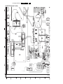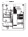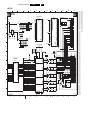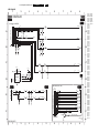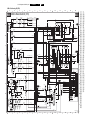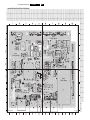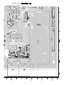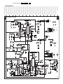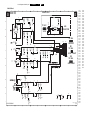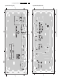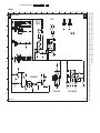
1
Color Television
Chassis
LC4.9U
AA
For manual LGE plasma panel see: 3122 785 15590
For manual FHP PDP panel see: 3122 785 14580
For manual SDI PDP panel see: 3122 785 14990
F_16110_001.eps
101105
Contents
Page
1. Technical Specifications, Connections, and Chassis
Overview
2
2. Safety Instructions, Warnings, and Notes
4
3. Directions for Use
6
4. Mechanical Instructions
7
5. Service Modes, Error Codes, and Fault Finding 14
6. Block Diagrams, Test Point Overviews, and
Waveforms
Wiring Diagram 42” FHP
23
Wiring Diagram 42” SDI
24
Block Diagram Supply 42” FHP/LGE
25
Block Diagram Video
26
Block Diagram Audio
27
I2C Overview
28
Supply Line Overview
29
7. Circuit Diagrams and PWB Layouts
Diagram
PDP FHP Supply: Filter Standby
(A2) 30
PDP FHP Supply: Protection
(A3) 31
PDP FHP Supply: Pre Conditioner
(A5) 32
PDP FHP Supply: LLC Supply
(A6) 33
PDP FHP Supply: AUX Supply
(A7) 34
SSB: Tuner and IF
(B1) 41
SSB: Hercules
(B2) 42
SSB: Sync Interface
(B3) 43
SSB: Audio Delay Line (Lipsync)
(B4) 44
SSB: Audio Processing
(B5) 45
SSB: DC-DC Converter
(B6) 46
SSB: Diversity Tables B1-B6
(B1-B6) 47
SSB: Scaler
(B7) 48
SSB: Scaler
(B8) 49
SSB: Scaler Interface
(B9) 50
SSB: SDRAM
(B10) 51
SSB: Flash / Control
(B11) 52
SSB: HDMI
(B12) 53
Contents
PWB
35-40
35-40
35-40
35-40
35-40
64-73
64-73
64-73
64-73
64-73
64-73
8.
9.
10.
11.
Page
SSB: MUX-Sync Interface
(B13) 54
SSB: Top Connectors
(B16) 55
SSB: Side Connectors
(B17) 56
SSB: ADC
(B18) 57
SSB: Columbus
(B19) 58
SSB: EPLD
(B20) 59
SSB: EPLD
(B21) 60
SSB: Diversity Tables B9-B21
(B9-B21) 61
SSB: Digital I/O
(B22) 62
SSB: Cinch Analog I/O (1FH)
(B23) 63
PDP Audio Amplifier Panel
(C) 74
Side I/O Panel
(D) 76
Control Board
(E) 78
LED Panel
(J) 79
Alignments
81
Circuit Descriptions, Abbreviation List, and IC Data
Sheets
85
Abbreviation List
93
IC Data Sheets
96
Spare Parts List
100
Revision List
106
64-73
64-73
64-73
64-73
64-73
64-73
64-73
64-73
64-73
75
77
78
80
64-73
64-73
64-73
64-73
64-73
64-73
©
Copyright 2005 Philips Consumer Electronics B.V. Eindhoven, The Netherlands.
All rights reserved. No part of this publication may be reproduced, stored in a
retrieval system or transmitted, in any form or by any means, electronic,
mechanical, photocopying, or otherwise without the prior permission of Philips.
Published by WS 0665 BG CD Customer Service
Printed in the Netherlands
Subject to modification
EN 3122 785 16111
EN 2
1.
Technical Specifications, Connections, and Chassis Overview
LC4.9U AA
1. Technical Specifications, Connections, and Chassis Overview
1.2
Index of this chapter:
1.1 Technical Specifications
1.2 Connection Overview
1.3 Chassis Overview
Note: The following connector colour abbreviations are used
(acc. to DIN/IEC 757): Bk= Black, Bu= Blue, Gn= Green, Gy=
Grey, Rd= Red, Wh= White, and Ye= Yellow.
Notes:
• Figures can deviate due to the different set executions.
• Specifications are indicative (subject to change).
1.1
Technical Specifications
1.1.1
Vision
Connection Overview
1.2.1
Side I/O connections
S-Video Video Audio
L
Display type
Screen size
Resolution (HxV pixels)
Contrast ratio
- 42PF7320 /28
Light output (cd/m2)
Viewing angle (HxV degrees)
Tuning system
TV Colour systems
Video playback
Supported computer formats
Supported video formats
Presets/channels
Tuner bands
1.1.2
:
:
:
:
:
:
:
:
:
:
:
:
:
:
:
:
:
:
:
:
:
:
:
:
:
:
:
Plasma
42” (107 cm), 16:9
42 inch: 852 x 480
10,000:1
1000
160x160
PLL
PAL N, PAL M
NTSC
PAL B/G; PAL
NTSC M/N 3.58, 4.43
VGA (640x480)
SVGA (800x600)
XVGA (1024x768)
640x480i - 1fH
720x576i - 1fH
640x480p - 2fH
720x576p - 2fH
852x480p - 2fH
1280x720 - 3fH
1920x1080i - 2fH
125 presets
VHF
UHF
S-band
Hyperband
R
E_14710_005.eps
210404
Figure 1-1 Side I/O connections
S-Video (Hosiden): Video Y/C - In
1 - Ground Y
Gnd
2 - Ground C
Gnd
3 - Video Y
1 VPP / 75 ohm
4 - Video C
0.3 VPP / 75 ohm
1.2.2
H
H
j
j
Cinch: Video CVBS - In, Audio - In
Ye - Video CVBS
1 VPP / 75 ohm
Wh - Audio L
0.5 VRMS / 10 kohm
Rd - Audio R
0.5 VRMS / 10 kohm
jq
jq
jq
Mini Jack: Audio Head phone - Out
Bk - Head phone
32 - 600 ohm / 10 mW
ot
Rear Connections
Sound
F_15270_071.eps
060705
Sound systems
Maximum power (WRMS)
1.1.3
: Virtual Dolby
Surround
: Stereo
: SAP
: 2 x 15
Figure 1-2 Rear I/O
Aerial - In
- - IEC-type (EU)
Coax, 75 ohm
D
Miscellaneous
Power supply:
- Mains voltage (VAC)
: 100 - 250
- Mains frequency (Hz)
: 50 - 60
Ambient conditions:
- Temperature range (°C)
- Maximum humidity
: +5 to +40
: 90% R.H.
Power consumption
- Normal operation (W)
- Stand-by (W)
: ≈ 220
: <2
Dimensions (WxHxD cm)
: 42 inch: 124x68x12.6
Weight (kg)
: 42 inch: 42
Cinch: Video CVBS - In, Audio - In
Ye - Video CVBS
1 VPP / 75 ohm
Wh - Audio L
0.5 VRMS / 10 kohm
Rd - Audio R
0.5 VRMS / 10 kohm
jq
jq
jq
Cinch: Video CVBS - Out, Audio - Out
Ye - Video CVBS
1 VPP / 75 ohm
Wh - Audio L
0.5 VRMS /10 kohm
Rd - Audio R
0.5 VRMS / 10 kohm
kq
kq
kq
Cinch: CVI-1 Video YPbPr - In
Gn - Video Y
1 VPP / 75 ohm
Bu - Video Pb
0.7 VPP / 75 ohm
Rd - Video Pr
0.7 VPP / 75 ohm
jq
jq
jq
Cinch: CVI-1 Audio - In
Rd - Audio - R
0.5 VRMS / 10 kohm
Wh - Audio - L
0.5 VRMS / 10 kohm
jq
jq
Technical Specifications, Connections, and Chassis Overview
Cinch: PC Audio - In
Rd - Audio - R
0.5 VRMS / 10 kohm
Wh - Audio - L
0.5 VRMS / 10 kohm
jq
jq
S-Video (Hosiden): Video Y/C - In
1 - Ground Y
Gnd
2 - Ground C
Gnd
3 - Video Y
1 VPP / 75 ohm
4 - Video C
0.3 VPPP / 75 ohm
H
H
j
j
Service connector (ComPair)
1 - SDA-S
I2C Data (0 - 5 V)
2 - SCL-S
I2C Clock (0 - 5 V)
3 - Ground
Gnd
jk
j
H
9
10
11
12
13
14
15
16
17
18
19
20
LC4.9U AA
- D0- CLK+
- Shield
- CLK- n.c.
- n.c.
- DDC_SCL
- DDC_SDA
- Ground
- +5V
- HPD
- Ground
EN 3
j
j
H
j
Data channel
Data channel
Gnd
Data channel
j
jk
H
j
j
H
DDC clock
DDC data
Gnd
Hot Plug Detect
Gnd
PC VGA/DVI-2: Video 2fH RGB/YPbPr - In
1
Service connector (UART)
1 - UART_TX
Transmit
2 - Ground
Gnd
3 - UART_RX
Receive
1.
5
10
6
k
H
j
15
11
E_06532_002.eps
050404
Figure 1-4 VGA Connector
HDMI/PC-D: Digital Video, Digital Audio - In
19
18
1
2
E_06532_017.eps
250505
Figure 1-3 HDMI (type A) connector
1
2
3
4
5
6
7
8
1.3
- D2+
- Shield
- D2- D1+
- Shield
- D1- D0+
- Shield
Data channel
Gnd
Data channel
Data channel
Gnd
Data channel
Data channel
Gnd
j
H
j
j
H
j
j
H
1
2
3
4
5
6
7
8
9
10
11
12
13
14
15
- Video Red/Pr
- Video Green/Y
- Video Blue/Pb
- n.c.
- Ground
- Ground Red
- Ground Green
- Ground Blue
- +5VDC
- Ground Sync
- n.c.
- DDC_SDA
- H-sync
- V-sync
- DDC_SCL
0.7 VPP / 75 ohm
0.7 VPP / 75 ohm
0.7 VPP / 75 ohm
j
j
j
Gnd
Gnd
Gnd
Gnd
+5 V
Gnd
H
H
H
H
j
H
DDC data
0-5V
0-5V
DDC clock
j
j
j
j
Chassis Overview
PLASMA
DISPLAY PANEL
LOUDSPEAKER
COMPARTMENT
B
SMALL SIGNAL
BOARD
E
KEYBOARD CONTROL
PANEL
PDP AUDIO
AMPLIFIER PANEL
C
POWER SUPPLY
PANEL
A
LOUDSPEAKER
COMPARTMENT
IR & LED PANEL
J
SIDE I/O PANEL
D
F_15430_057.eps
260705
Figure 1-5 CBA locations
EN 4
2.
LC4.9U AA
Safety Instructions, Warnings, and Notes
2. Safety Instructions, Warnings, and Notes
Index of this chapter:
2.1 Safety Instructions
2.2 Warnings
2.3 Notes
2.3
Notes
2.3.1
General
•
2.1
Safety Instructions
Safety regulations require the following during a repair:
• Connect the set to the Mains (AC Power) via an isolation
transformer (> 800 VA).
• Replace safety components, indicated by the symbol h,
only by components identical to the original ones. Any
other component substitution (other than original type) may
increase risk of fire or electrical shock hazard.
Safety regulations require that after a repair, the set must be
returned in its original condition. Pay in particular attention to
the following points:
• Route the wire trees correctly and fix them with the
mounted cable clamps.
• Check the insulation of the Mains (AC Power) lead for
external damage.
• Check the strain relief of the Mains (AC Power) cord for
proper function.
• Check the electrical DC resistance between the Mains (AC
Power) plug and the secondary side (only for sets that have
a Mains (AC Power) isolated power supply):
1. Unplug the Mains (AC Power) cord and connect a wire
between the two pins of the Mains (AC Power) plug.
2. Set the Mains (AC Power) switch to the "on" position
(keep the Mains (AC Power) cord unplugged!).
3. Measure the resistance value between the pins of the
Mains (AC Power) plug and the metal shielding of the
tuner or the aerial connection on the set. The reading
should be between 4.5 Mohm and 12 Mohm.
4. Switch "off" the set, and remove the wire between the
two pins of the Mains (AC Power) plug.
• Check the cabinet for defects, to prevent touching of any
inner parts by the customer.
2.2
Warnings
•
•
•
•
All ICs and many other semiconductors are susceptible to
electrostatic discharges (ESD w). Careless handling
during repair can reduce life drastically. Make sure that,
during repair, you are connected with the same potential as
the mass of the set by a wristband with resistance. Keep
components and tools also at this same potential. Available
ESD protection equipment:
– Complete kit ESD3 (small tablemat, wristband,
connection box, extension cable and earth cable) 4822
310 10671.
– Wristband tester 4822 344 13999.
Be careful during measurements in the high voltage
section.
Never replace modules or other components while the unit
is switched "on".
When you align the set, use plastic rather than metal tools.
This will prevent any short circuits and the danger of a
circuit becoming unstable.
•
•
2.3.2
Schematic Notes
•
•
•
•
•
•
2.3.3
Measure the voltages and waveforms with regard to the
chassis (= tuner) ground (H), or hot ground (I), depending
on the tested area of circuitry. The voltages and waveforms
shown in the diagrams are indicative. Measure them in the
Service Default Mode (see chapter 5) with a colour bar
signal and stereo sound (L: 3 kHz, R: 1 kHz unless stated
otherwise) and picture carrier at 475.25 MHz for PAL, or
61.25 MHz for NTSC (channel 3).
Where necessary, measure the waveforms and voltages
with (D) and without (E) aerial signal. Measure the
voltages in the power supply section both in normal
operation (G) and in stand-by (F). These values are
indicated by means of the appropriate symbols.
The semiconductors indicated in the circuit diagram and in
the parts lists, are interchangeable per position with the
semiconductors in the unit, irrespective of the type
indication on these semiconductors.
All resistor values are in ohms, and the value multiplier is
often used to indicate the decimal point location (e.g. 2K2
indicates 2.2 kohm).
Resistor values with no multiplier may be indicated with
either an "E" or an "R" (e.g. 220E or 220R indicates 220
ohm).
All capacitor values are given in micro-farads (µ= x10-6),
nano-farads (n= x10-9), or pico-farads (p= x10-12).
Capacitor values may also use the value multiplier as the
decimal point indication (e.g. 2p2 indicates 2.2 pF).
An "asterisk" (*) indicates component usage varies. Refer
to the diversity tables for the correct values.
The correct component values are listed in the Spare Parts
List. Therefore, always check this list when there is any
doubt.
Rework on BGA (Ball Grid Array) ICs
General
Although (LF)BGA assembly yields are very high, there may
still be a requirement for component rework. By rework, we
mean the process of removing the component from the PWB
and replacing it with a new component. If an (LF)BGA is
removed from a PWB, the solder balls of the component are
deformed drastically so the removed (LF)BGA has to be
discarded.
Device Removal
As is the case with any component that, is being removed, it is
essential when removing an (LF)BGA, that the board, tracks,
solder lands, or surrounding components are not damaged. To
remove an (LF)BGA, the board must be uniformly heated to a
temperature close to the reflow soldering temperature.
A uniform temperature reduces the risk of warping the PWB. To
do this, we recommend that the board is heated until it is certain
that all the joints are molten. Then carefully pull the component
off the board with a vacuum nozzle. For the appropriate
temperature profiles, see the IC data sheet.
Area Preparation
When the component has been removed, the vacant IC area
must be cleaned before replacing the (LF)BGA.
Removing an IC often leaves varying amounts of solder on the
mounting lands. This excessive solder can be removed with
either a solder sucker or solder wick. The remaining flux can be
removed with a brush and cleaning agent.
Safety Instructions, Warnings, and Notes
After the board is properly cleaned and inspected, apply flux on
the solder lands and on the connection balls of the (LF)BGA.
Note: Do not apply solder paste, as this has been shown to
result in problems during re-soldering.
•
Device Replacement
The last step in the repair process is to solder the new
component on the board. Ideally, the (LF)BGA should be
aligned under a microscope or magnifying glass. If this is not
possible, try to align the (LF)BGA with any board markers.
So as not to damage neighbouring components, it may be
necessary to reduce some temperatures and times.
•
•
More Information
For more information on how to handle BGA devices, visit this
URL: www.atyourservice.ce.philips.com (needs subscription,
not available for all regions). After login, select “Magazine”,
then go to “Repair Downloads”. Here you will find Information
on how to deal with BGA-ICs.
2.3.4
•
Lead-free Solder
Philips CE is producing lead-free sets (PBF) from 1.1.2005
onwards.
LC4.9U AA
2.
EN 5
To avoid wear-out of tips, switch “off” unused equipment or
reduce heat.
Mix of lead-free soldering tin/parts with leaded soldering
tin/parts is possible but PHILIPS recommends strongly to
avoid mixed regimes. If this cannot be avoided, carefully
clear the solder-joint from old tin and re-solder with new tin.
Use only original spare-parts listed in the Service-Manuals.
Not listed standard material (commodities) has to be
purchased at external companies.
Special information for lead-free BGA ICs: these ICs will be
delivered in so-called "dry-packaging" to protect the IC
against moisture. This packaging may only be opened
shortly before it is used (soldered). Otherwise the body of
the IC gets "wet" inside and during the heating time the
structure of the IC will be destroyed due to high (steam-)
pressure inside the body. If the packaging was opened
before usage, the IC has to be heated up for some hours
(around 90°C) for drying (think of ESD-protection!).
Do not re-use BGAs at all!
For sets produced before 1.1.2005, containing leaded
soldering tin and components, all needed spare parts will
be available till the end of the service period. For the repair
of such sets nothing changes.
In case of doubt whether the board is lead-free or not (or with
mixed technologies), you can use the following method:
• Always use the highest temperature to solder, when using
SAC305 (see also instructions below).
• De-solder thoroughly (clean solder joints to avoid the
mixing of two alloys).
Identification: The bottom line of a type plate gives a 14-digit
serial number. Digits 5 and 6 refer to the production year, digits
7 and 8 refer to production week (in example below it is 1991
week 18).
Caution: For BGA-ICs, you must use the correct temperature
profile, which is coupled to the 12NC. For an overview of these
profiles, visit the website www.atyourservice.ce.philips.com
(needs subscription, but is not available for all regions).
You will find this and more technical information within the
"Magazine", chapter "Repair Downloads".
For additional questions please contact your local repair help
desk.
E_06532_024.eps
230205
Figure 2-1 Serial number example
Regardless of the special lead-free logo (which is not always
indicated), one must treat all sets from this date onwards
according to the rules as described below.
P
b
Figure 2-2 Lead-free logo
Due to lead-free technology some rules have to be respected
by the workshop during a repair:
• Use only lead-free soldering tin Philips SAC305 with order
code 0622 149 00106. If lead-free solder paste is required,
please contact the manufacturer of your soldering
equipment. In general, use of solder paste within
workshops should be avoided because paste is not easy to
store and to handle.
• Use only adequate solder tools applicable for lead-free
soldering tin. The solder tool must be able:
– To reach a solder-tip temperature of at least 400°C.
– To stabilise the adjusted temperature at the solder-tip.
– To exchange solder-tips for different applications.
• Adjust your solder tool so that a temperature of around
360°C - 380°C is reached and stabilised at the solder joint.
Heating time of the solder-joint should not exceed ~ 4 sec.
Avoid temperatures above 400°C, otherwise wear-out of
tips will increase drastically and flux-fluid will be destroyed.
2.3.5
Practical Service Precautions
•
•
It makes sense to avoid exposure to electrical shock.
While some sources are expected to have a possible
dangerous impact, others of quite high potential are of
limited current and are sometimes held in less regard.
Always respect voltages. While some may not be
dangerous in themselves, they can cause unexpected
reactions that are best avoided. Before reaching into a
powered TV set, it is best to test the high voltage insulation.
It is easy to do, and is a good service precaution.
EN 6
3.
LC4.9U AA
Directions for Use
3. Directions for Use
You can download this information from the following websites:
http://www.philips.com/support
http://www.p4c.philips.com
Mechanical Instructions
LC4.9U AA
4.
EN 7
4. Mechanical Instructions
Notes:
• Figures below can deviate slightly from the actual situation,
due to the different set executions.
• Follow the disassembling instructions in described order.
Index of this chapter:
4.1 Cable Dressing
4.2 Service Positions
4.3 Assy/Panel Removal
4.4 Set Re-assembly
4.1
Cable Dressing
F_15430_043.eps
080605
Figure 4-1 Cable dressing
4.2
Service Positions
For easy servicing of this set, there are a few possibilities
created:
• The buffers from the packaging (see figure "Rear cover").
• Foam bars (created for service).
• Aluminium service stands (created for Service).
4.2.1
face down on the (ESD protective) foam bars, a stable situation
is created to perform measurements and alignments.
By placing a mirror under the TV, you can monitor the screen.
4.2.2
Aluminium Stands
Foam Bars
E_06532_019.eps
170504
E_06532_018.eps
170504
Figure 4-2 Foam bars
The foam bars (order code 3122 785 90580 for two pieces) can
be used for all types and sizes of Flat TVs. By laying the TV
Figure 4-3 Aluminium stands (drawing of MkI)
The aluminium stands (order code 3122 785 90480) can be
mounted with the back cover removed or still left on. So, the
stand can be used to store products or to do measurements. It
is also very suitable to perform duration tests without taking
much space, without having the risk of overheating, or the risk
of products falling. The stands can be mounted and removed
EN 8
4.
LC4.9U AA
Mechanical Instructions
quick and easy with use of the delivered screws that can be
tightened and loosened manually without the use of tools. See
figure above.
Note: Only use the delivered screws to mount the monitor to
the stands.
4.3
Assy/Panel Removal
4.3.1
Metal Rear Cover
Caution: Disconnect the Mains/AC Power cord before you
remove the rear cover!
3
1. Place the TV set upside down on a table top, using the
foam bars (see part "Foam Bars").
Caution: do not put pressure on the display, but let the
monitor lean on the speakers or the Front cover.
2. Remove all T10 screws around the edges of the metal rear
cover: “parker” screws around the outer rim, “tapping”
screws around the connector plate.
3. Remove the four "mushrooms" from the rear cover.
4. Lift the metal rear cover from the set. Make sure that wires
and flat foils are not damaged.
4.3.2
F_15430_046.eps
100605
Speaker Compartment Cover
Figure 4-5 Grounding clamp
After removing the metal rear cover, you gain access to the
Speaker Compartment covers.
1. Remove all T10 screws [1] around the outer rim of the
cover (see Figure “Speaker compartment cover removal”).
2. Remove the T10 screws [2] on top of the inner rim,
including the one which secures the grounding clamp (3,
see Figure “Grounding clamp”).
3. Now, remove the plastic cable fixation noose (4, see Figure
“Cable fixation noose”).
4. After removal of all the screws, slightly push the top of the
cover inwards. This will lift the outer rim slightly up so you
can take the cover out.
4
F_15430_047.eps
100605
Figure 4-6 Cable fixation noose
1
2
F_15430_045.eps
100605
Figure 4-4 Speaker compartment cover removal
Mechanical Instructions
4.3.3
4.3.4
Side I/O Panel
LC4.9U AA
4.
EN 9
LED Panel
After removal of the Speaker Compartment Covers, this panel
is accessible.
1. Disconnect the cable (1) from the panel.
2. Remove the T10 mounting screws [2] that hold the assy.
3. Remove the panel from its bracket [3], by pushing against
the front side of the side I/O cinch connectors.
1
2
1
F_15420_036.eps
070605
3
Figure 4-8 LED panel
1. Remove the fixation screws (1) and take the panel out of its
brackets.
2. Disconnect the cable (2) from the panel.
4.3.5
Keyboard Control Panel
2
F_15430_048.eps
100605
Figure 4-7 Side I/O panel removal
When it is defective, replace the whole unit.
2
1
3
F_15420_037.eps
070605
Figure 4-9 Keyboard control panel
1. Remove the panel (1) from its three brackets (2).
2. Disconnect the cable (3) from the panel.
EN 10
4.3.6
4.
Mechanical Instructions
LC4.9U AA
4.3.7
SSB Cover Shield
Small Signal Board
3
1
2
1
2
3
F_15420_040.eps
070605
F_15430_049.eps
100605
Figure 4-12 SSB
Figure 4-10 SSB cover shield
1. Remove the two fixation screws (1) that secure the SSB
board on the lower part of the SSB shielding, see Figure
“SSB”.
2. Remove the SSB.
4.3.8
3
Power Supply Panel
3
F_15270_075.eps
260505
1
Figure 4-11 DVI-I connector and rear I/O panel screws
2
1. Very cautiously disconnect the LVDS cable (1) from the
SSB panel (see Figure “SSB board cover shield”). Notice
that this cable is very fragile.
2. Remove all other cables (2) from the SSB board (see
Figure “SSB board cover shield”), including the grounding
cable.
3. Remove the fixation screws (3), see Figure “SSB board
cover shield” and remove the SSB shield with the SSB
board inside, and the rear I/O panel still attached to it.
4. Remove the fixation screws (1) from the DVI-I connector
and from the rear panel, see Figure “DVI-I connector and
rear panel screws”, and remove the rear I/O panel from the
SSB board.
5. Remove the upper part of the shield from the SSB panel,
by unhooking it from its brackets. Be careful not to damage
the LVDS connector on the SSB board, see Figure “SSB
board cover shield”.
F_15430_050.eps
100605
Figure 4-13 Power supply panel
1. Disconnect all cables (1) from the panel.
2. Remove the fixation screws (2) from the panel.
3. Take the panel out of its brackets.
Mechanical Instructions
4.3.9
Class D Audio Amplifier Panel
3
1
2
F_15430_051.eps
100605
Figure 4-14 Class D audio amplifier panel
1. Disconnect all cables (1) from the panel.
2. Pinch the plastic fixation clamps (2) firmly between your
fingers, and pull the panel upwards.
3. Take the panel out of its brackets (3).
LC4.9U AA
4.
EN 11
EN 12
4.
Mechanical Instructions
LC4.9U AA
4.3.10 Plasma Display Panel / Glass Plate
1. Remove the T20 display panel mounting screws [1].
2. Remove the T10 screws [2] from the mounting frame.
3. Unplug all cable(s):
– LVDS cable at SSB side (fragile connector!).
– SSB supply cables at the Main Supply board.
– Mains cable at the Main Supply board.
– Side I/O cable at SSB side (fragile connector!).
– Cable at LED panel.
– Keyboard cable at SSB side.
– Audio Amplifier supply cable at the Main Supply board.
– Loudspeaker cables (incl. ferrites) at the Audio panel.
4. Lift the metal frame (together with all PWBs) from the
display panel (see figure “Frame lift”).
5. After removal of the frame, lift the PDP from the set.
2
2
1
1
2
2
F_15400_121.eps
200505
Figure 4-15 Display panel removal
F_15400_120.eps
200505
Figure 4-16 Frame lift
Mechanical Instructions
LC4.9U AA
4.
4.3.11 PDP Glass Plate
In order to remove/exchange the PDP glass plate:
1. Remove the PDP as described earlier.
2. Remove the T10 screws [1] from the mounting frame.
3. After removal of the frame, you can lift the glass plate from
the set.
1
F_15400_119.eps
200505
Figure 4-17 Glass plate removal
4.4
Set Re-assembly
To re-assemble the whole set, execute all processes in reverse
order.
Notes:
• While re-assembling, make sure that all cables are placed
and connected in their original positions. See Figure "Cable
dressing". Be careful with the fragile LVDS cable.
• For a complete description of the Plasma panel, see the
LGE plasma panel Service Manual (12nc is listed on the
front page).
EN 13
EN 14
5.
LC4.9U AA
Service Modes, Error Codes, and Fault Finding
5. Service Modes, Error Codes, and Fault Finding
Index of this chapter:
5.1 Test Points
5.2 Service Modes
5.3 Problems and Solving Tips Related to CSM
5.4 Service Tools
5.5 Error Codes
5.6 The Blinking LED Procedure
5.7 Fault Finding and Repair Tips
5.1
Test Points
This chassis is equipped with test points in the service printing.
In the schematics test points are identified with a rectangle box
around Fxxx or Ixxx.
Perform measurements under the following conditions:
• Television set in Service Default Alignment Mode.
• Video input: Colour bar signal.
• Audio input: 3 kHz left channel, 1 kHz right channel.
5.2
How to Enter
To enter SDM, use one of the following methods:
• Press the following key sequence on the remote control
transmitter: “062596” directly followed by the MENU button
(do not allow the display to time out between entries while
keying the sequence).
• Short "Service" jumpers on the TV board during cold start
and apply mains (see Figure "Service jumpers"). Then
press the mains button (remove the short after start-up).
Caution: Entering SDM by shorting "Service" jumpers will
override the +8V-protection. Do this only for a short period.
When doing this, the service-technician must know exactly
what he is doing, as it could damage the television set.
• Or via ComPair.
Service Modes
1
Service Default mode (SDM) and Service Alignment Mode
(SAM) offers several features for the service technician, while
the Customer Service Mode (CSM) is used for communication
between the call centre and the customer.
This chassis also offers the option of using ComPair, a
hardware interface between a computer and the TV chassis. It
offers the possibilities of structured troubleshooting, error code
reading, and software version read-out for all chassis.
Minimum requirements for ComPair: a Pentium processor, a
Windows OS, and a CD-ROM drive (see also paragraph
"ComPair").
5.2.1
F_15270_053.eps
180505
Figure 5-1 Service jumpers
Service Default Mode (SDM)
Purpose
• To create a predefined setting for measurements to be
made.
• To override software protections.
• To start the blinking LED procedure.
• To inspect the error buffer.
• To check the life timer.
After entering SDM, the following screen is visible, with SDM in
the upper right corner of the screen to indicate that the
television is in Service Default Mode.
00035
LC4XAP1 1.14/S4XGNV 1.17
SDM
ERR 0 0 0 0 0
OP 000 057 140 032 120 128 000
Specifications
• Tuning frequency: 61.25 MHz.
• Colour system: NTSC.
• All picture settings at 50% (brightness, colour contrast,
hue).
• Bass, treble, and balance at 50 %; volume at 25 %.
• All service-unfriendly modes (if present) are disabled. The
service unfriendly modes are:
– Timer / Sleep timer.
– Child / parental lock.
– Blue mute.
– Hotel / hospital mode.
– Auto shut off (when no “IDENT” video signal is
received for 15 minutes).
– Skipping of non-favourite presets / channels.
– Auto-storage of personal presets.
– Auto user menu time-out.
– Auto Volume Levelling (AVL).
F_15430_058.eps
260705
Figure 5-2 SDM menu
Service Modes, Error Codes, and Fault Finding
How to Navigate
Use one of the following methods:
• When you press the MENU button on the remote control,
the set will switch on the normal user menu in the SDM
mode.
• On the TV, press and hold the VOLUME DOWN and press
the CHANNEL DOWN for a few seconds, to switch from
SDM to SAM and reverse.
How to Exit
Switch the set to STANDBY by pressing the mains button on
the remote control transmitter or the television set.
If you turn the television set off by removing the mains (i.e.,
unplugging the television) without using the mains button, the
television set will remain in SDM when mains is re-applied, and
the error buffer is not cleared.
5.2.2
Service Alignment Mode (SAM)
Purpose
• To change option settings.
• To display / clear the error code buffer.
• To perform alignments.
Specifications
• Operation hours counter (maximum five digits displayed).
• Software version, Error codes, and Option settings display.
• Error buffer clearing.
• Option settings.
• AKB switching.
• Software alignments (Tuner, White Tone, Geometry &
Audio).
• NVM Editor.
• ComPair Mode switching.
How to Enter
To enter SAM, use one of the following methods:
• Press the following key sequence on the remote control
transmitter: “062596" directly followed by the OSD/
STATUS/INFO(I+) button (do not allow the display to time
out between entries while keying the sequence).
• Or via ComPair.
After entering SAM, the following screen is visible, with SAM in
the upper right corner of the screen to indicate that the
television is in Service Alignment Mode.
00035 LC4XAP1 1.14/S4XGNV 1.17
ERR 0 0 0 0 0
SAM
OP 000 057 140 032 120 128 000
. Clear
. Options
. Tuner
. White Tone
. Audio
. NVM Editor
. SC NVM Editor
Clear ?
. ComPair Mode
On
F_15430_059.eps
080605
Figure 5-3 SAM menu
LC4.9U AA
5.
EN 15
Menu Explanation
1. LLLLL. This represents the run timer. The run timer counts
normal operation hours, but does not count standby hours.
2. AAABCD-X.Y. This is the software identification of the
main microprocessor:
– A= the project name (LC04.x).
– B= the region: E= Europe, A= Asia Pacific, U= NAFTA,
L= LATAM.
– C= the software diversity:
• Europe: T= 1 page TXT, F= Full TXT, V= Voice
control.
• LATAM and NAFTA: N= Stereo non-dBx, S=
Stereo dBx.
• Asian Pacific: T= TXT, N= non-TXT, C= NTSC.
• ALL regions: M= mono, D= DVD, Q= Mk2.
– D= the language cluster number.
– X= the main software version number (updated with a
major change that is incompatible with previous
versions).
– Y= the sub software version number (updated with a
minor change that is compatible with previous
versions).
3. EEEEE-F.GG. This is the software identification of the
Scaler:
– EEEEEE= the scaler sw cluster
– F= the main sw version no.
– GG= the sub-version no.
4. SAM. Indication of the Service Alignment Mode.
5. Error Buffer. Shows all errors detected since the last time
the buffer was erased. Five errors possible.
6. Option Bytes. Used to set the option bytes. See “Options”
in the Alignments section for a detailed description. Seven
codes are possible.
7. Clear. Erases the contents of the error buffer. Select the
CLEAR menu item and press the MENU RIGHT key. The
content of the error buffer is cleared.
8. Options. Used to set the option bits. See “Options” in the
Alignments section for a detailed description.
9. Tuner. Used to align the tuner. See “Tuner” in the
Alignments section for a detailed description.
10. White Tone. Used to align the white tone. See “White
Tone” in the Alignments section for a detailed description.
11. Audio. No audio alignment is necessary for this television
set.
12. NVM Editor. Can be used to change the NVM data in the
television set. See table “NVM data” further on.
13. SC NVM Editor. Can be used to edit Scaler NVM.
14. ComPaIr. Can be used to switch on the television to In
System Programming (ISP) mode, for software uploading
via ComPair.
Caution: When this mode is selected without ComPair
connected, the TV will be blocked. Remove the AC power
to reset the TV.
How to Navigate
• In SAM, select menu items with the MENU UP/DOWN keys
on the remote control transmitter. The selected item will be
highlighted. When not all menu items fit on the screen, use
the MENU UP/DOWN keys to display the next / previous
menu items.
• With the MENU LEFT/RIGHT keys, it is possible to:
– Activate the selected menu item.
– Change the value of the selected menu item.
– Activate the selected submenu.
• In SAM, when you press the MENU button twice, the set
will switch to the normal user menus (with the SAM mode
still active in the background). To return to the SAM menu
press the MENU or STATUS/EXIT button.
• When you press the MENU key in while in a submenu, you
will return to the previous menu.
EN 16
5.
LC4.9U AA
Service Modes, Error Codes, and Fault Finding
8. Displays the detected Audio (e.g. stereo/mono).
9. Displays the picture setting information.
10. Displays the sound setting information.
How to Store SAM Settings
To store the settings changed in SAM mode, leave the top level
SAM menu by using the POWER button on the remote control
transmitter or the television set.
5.2.3
How to Exit
To exit CSM, use one of the following methods:
• Press the MENU, STATUS/EXIT, or POWER button on the
remote control transmitter.
• Press the POWER button on the television set.
How to Exit
Switch the set to STANDBY by pressing the mains button on
the remote control transmitter or the television set.
If you turn the television set “off” by removing the mains (i.e.,
unplugging the television) without using the mains button, the
television set will remain in SAM when mains is re-applied, and
the error buffer is not cleared.
5.3
Problems and Solving Tips Related to CSM
Customer Service Mode (CSM)
5.3.1
Picture Problems
Purpose
The Customer Service Mode shows error codes and
information on the TV’s operation settings. The call centre can
instruct the customer (by telephone) to enter CSM in order to
identify the status of the set. This helps the call centre to
diagnose problems and failures in the TV set before making a
service call.
The CSM is a read-only mode; therefore, modifications are not
possible in this mode.
How to Enter
To enter CSM, press the following key sequence on the remote
control transmitter: “123654” (do not allow the display to time
out between entries while keying the sequence).
Upon entering the Customer Service Mode, the following
screen will appear:
1 00035
LC4XAP1 1.14/S4XGNV 1.17 CSM
2 CODES 0 0 0 0 0
3 OP 000 057 140 032 120 128 000
4
5
6 NOT TUNED
7 PAL
8 STEREO
9 CO 50 CL 50 BR 50
0 AVL Off
Note: The problems described below are all related to the TV
settings. The procedures used to change the value (or status)
of the different settings are described.
Picture too Dark or too Bright
If:
• The picture improves when you press the AUTO PICTURE
button on the remote control transmitter, or
• The picture improves when you enter the Customer
Service Mode,
Then:
1. Press the AUTO PICTURE button on the remote control
transmitter repeatedly (if necessary) to choose
PERSONAL picture mode.
2. Press the MENU button on the remote control transmitter.
This brings up the normal user menu.
3. In the normal user menu, use the MENU UP/DOWN keys
to highlight the PICTURE sub menu.
4. Press the MENU LEFT/RIGHT keys to enter the PICTURE
sub menu.
5. Use the MENU UP/DOWN keys (if necessary) to select
BRIGHTNESS.
6. Press the MENU LEFT/RIGHT keys to increase or
decrease the BRIGHTNESS value.
7. Use the MENU UP/DOWN keys to select PICTURE.
8. Press the MENU LEFT/RIGHT keys to increase or
decrease the PICTURE value.
9. Press the MENU button on the remote control transmitter
twice to exit the user menu.
10. The new PERSONAL preference values are automatically
stored.
White Line around Picture Elements and Text
F_15430_060.eps
080605
Figure 5-4 CSM menu
Menu Explanation
1. Indication of the decimal value of the operation hours
counter, Software identification of the main microprocessor
(see "Service Default or Alignment Mode" for an
explanation), and the service mode (CSM = Customer
Service Mode).
2. Displays the last five errors detected in the error code
buffer.
3. Displays the option bytes.
4. Displays the type number version of the set.
5. Reserved item for P3C call centres (AKBS stands for
Advanced Knowledge Base System).
6. Indicates the television is receiving an "IDENT" signal on
the selected source. If no "IDENT" signal is detected, the
display will read "NOT TUNED"
7. Displays the detected Colour system (e.g. PAL/NTSC).
If:
The picture improves after you have pressed the AUTO
PICTURE button on the remote control transmitter,
Then:
1. Press the AUTO PICTURE button on the remote control
transmitter repeatedly (if necessary) to choose
PERSONAL picture mode.
2. Press the MENU button on the remote control transmitter.
This brings up the normal user menu.
3. In the normal user menu, use the MENU UP/DOWN keys
to highlight the PICTURE sub menu.
4. Press the MENU LEFT/RIGHT keys to enter the PICTURE
sub menu.
5. Use the MENU UP/DOWN keys to select SHARPNESS.
6. Press the MENU LEFT key to decrease the SHARPNESS
value.
7. Press the MENU button on the remote control transmitter
twice to exit the user menu.
8. The new PERSONAL preference value is automatically
stored.
Service Modes, Error Codes, and Fault Finding
LC4.9U AA
5.
EN 17
Snowy Picture
Check CSM line 6. If this line reads “Not Tuned”, check the
following:
• Antenna not connected. Connect the antenna.
• No antenna signal or bad antenna signal. Connect a proper
antenna signal.
• The tuner is faulty (in this case line 2, the Error Buffer line,
will contain error number 10). Check the tuner and replace/
repair the tuner if necessary.
You do not have to know anything about I2C commands
yourself because ComPair takes care of this.
3. ComPair speeds up the repair time since it can
automatically communicate with the chassis (when the
microprocessor is working) and all repair information is
directly available. When ComPair is installed together with
the Force/SearchMan electronic manual of the defective
chassis, schematics and PWBs are only a mouse click
away.
Black and White Picture
Specifications
ComPair consists of a Windows based fault finding program
and an interface box between PC and the (defective) product.
The ComPair interface box is connected to the PC via a serial
(or RS-232) cable.
For this chassis, the ComPair interface box and the TV
communicate via a bi-directional service cable via the service
connector(s).
If:
• The picture improves after you have pressed the AUTO
PICTURE button on the remote control transmitter,
Then:
1. Press the AUTO PICTURE button on the remote control
transmitter repeatedly (if necessary) to choose
PERSONAL picture mode.
2. Press the MENU button on the remote control transmitter.
This brings up the normal user menu.
3. In the normal user menu, use the MENU UP/DOWN keys
to highlight the PICTURE sub menu.
4. Press the MENU LEFT/RIGHT keys to enter the PICTURE
sub menu.
5. Use the MENU UP/DOWN keys to select COLOR.
6. Press the MENU RIGHT key to increase the COLOR value.
7. Press the MENU button on the remote control transmitter
twice to exit the user menu.
8. The new PERSONAL preference value is automatically
stored.
Menu Text not Sharp Enough
If:
• The picture improves after you have pressed the AUTO
PICTURE button on the remote control transmitter,
Then:
1. Press the AUTO PICTURE button on the remote control
transmitter repeatedly (if necessary) to choose
PERSONAL picture mode.
2. Press the MENU button on the remote control transmitter.
This brings up the normal user menu.
3. In the normal user menu, use the MENU UP/DOWN keys
to highlight the PICTURE sub menu.
4. Press the MENU LEFT/RIGHT keys to enter the PICTURE
sub menu.
5. Use the MENU UP/DOWN keys to select PICTURE.
6. Press the MENU LEFT key to decrease the PICTURE
value.
7. Press the MENU button on the remote control transmitter
twice to exit the user menu.
8. The new PERSONAL preference value is automatically
stored.
5.4
Service Tools
5.4.1
ComPair
Introduction
ComPair (Computer Aided Repair) is a service tool for Philips
Consumer Electronics products. ComPair is a further
development on the European DST (service remote control),
which allows faster and more accurate diagnostics. ComPair
has three big advantages:
1. ComPair helps you to quickly get an understanding on how
to repair the chassis in a short time by guiding you
systematically through the repair procedures.
2. ComPair allows very detailed diagnostics (on I2C level) and
is therefore capable of accurately indicating problem areas.
The ComPair fault finding program is able to determine the
problem of the defective television. ComPair can gather
diagnostic information in two ways:
• Automatically (by communicating with the television):
ComPair can automatically read out the contents of the
entire error buffer. Diagnosis is done on I2C/UART level.
ComPair can access the I2C/UART bus of the television.
ComPair can send and receive I2C/UART commands to
the micro controller of the television. In this way, it is
possible for ComPair to communicate (read and write) to
devices on the I2C/UART buses of the TV-set.
• Manually (by asking questions to you): Automatic
diagnosis is only possible if the micro controller of the
television is working correctly and only to a certain extent.
When this is not the case, ComPair will guide you through
the fault finding tree by asking you questions (e.g. Does the
screen give a picture? Click on the correct answer: YES /
NO) and showing you examples (e.g. Measure test-point I7
and click on the correct oscillogram you see on the
oscilloscope). You can answer by clicking on a link (e.g.
text or a waveform picture) that will bring you to the next
step in the fault finding process.
By a combination of automatic diagnostics and an interactive
question / answer procedure, ComPair will enable you to find
most problems in a fast and effective way.
How to Connect
This is described in the chassis fault finding database in
ComPair.
Caution: It is compulsory to connect the TV to the PC as
shown in the picture below (with the ComPair interface in
between), as the ComPair interface acts as a level shifter. If
one connects the TV directly to the PC (via UART), ICs will be
blown!
TO
UART SERVICE
CONNECTOR
PC
TO
I2C SERVICE
CONNECTOR
VCR
Power
9V DC
I2C
E_06532_021.eps
180804
Figure 5-5 ComPair interface connection
EN 18
5.
LC4.9U AA
Service Modes, Error Codes, and Fault Finding
How to Order
ComPair order codes (US):
• ComPair Software: ST4191.
• ComPair Interface Box: 4822 727 21631.
• AC Adapter: T405-ND.
• ComPair Quick Start Guide: ST4190.
• ComPair interface extension cable: 3139 131 03791.
• ComPair UART interface cable: 3122 785 90630.
Note: If you encounter any problems, contact your local
support desk.
5.4.2
5.5
The error code buffer contains all errors detected since the last
time the buffer was erased. The buffer is written from left to
right. When an error occurs that is not yet in the error code
buffer, it is displayed at the left side and all other errors shift one
position to the right.
5.5.1
Introduction
This service tool (also called “ComPair Assistant 1“) may help
you to identify, in case the TV does not show any picture,
whether the Small Signal Board (SSB) or the display of a Flat
TV is defective.
Furthermore it is possible to program EPLDs with this tool
(Byteblaster). Read the user manual for an explanation of this
feature.
5.5.2
When operating, the tool will show a small (scaled) picture on
a VGA monitor. Due to a limited memory capacity, it is not
possible to increase the size when processing high-resolution
LVDS signals (>= 1280x768). Generally this tool is intended to
determine if the SSB is working or not. Thus to determine if
LVDS, RGB, and sync signals are okay.
How to Connect
Connections are explained in the user manual, which is
delivered with the tool.
Note: To use the LVDS tool, you must have ComPair release
2004-1 (or later) on your PC (engine version >= 2.2.05).
For every TV type number and screen size, one must choose
the proper settings via ComPair. The ComPair file will be
updated regularly with new introduced chassis information.
How to Order
• LVDS tool (incl. two LVDS cables: 31p and 20p):
3122 785 90671.
• Service Manual LVDS tool:
3122 785 00810.
How to Read the Error Buffer
You can read the error buffer in 3 ways:
• On screen via the SAM (if you have a picture).
Examples:
– ERROR: 0 0 0 0 0 : No errors detected
– ERROR: 6 0 0 0 0 : Error code 6 is the last and only
detected error
– ERROR: 9 6 0 0 0 : Error code 6 was detected first and
error code 9 is the last detected (newest) error
• Via the blinking LED procedure (when you have no
picture). See “The Blinking LED Procedure”.
• Via ComPair.
LVDS Tool
Since 2004, the LVDS output connectors in our Flat TV models
are standardised (with some exceptions). With the two
delivered LVDS interface cables (31p and 20p) you can cover
most chassis (in special cases, an extra cable will be offered).
Error Codes
How to Clear the Error Buffer
The error code buffer is cleared in the following cases:
• By using the CLEAR command in the SAM menu:
– To enter SAM, press the following key sequence on the
remote control transmitter: “062596” directly followed
by the OSD/STATUS button (do not allow the display
to time out between entries while keying the
sequence).
– Make sure the menu item CLEAR is highlighted. Use
the MENU UP/DOWN buttons, if necessary.
– Press the MENU RIGHT button to clear the error
buffer. The text on the right side of the “CLEAR” line will
change from “CLEAR?” to “CLEARED”
• If the contents of the error buffer have not changed for 50
hours, the error buffer resets automatically.
Note: If you exit SAM by disconnecting the mains from the
television set, the error buffer is not reset.
Service Modes, Error Codes, and Fault Finding
5.5.3
5.6
Error Codes
In case of non-intermittent faults, write down the errors present
in the error buffer and clear the error buffer before you begin
the repair. This ensures that old error codes are no longer
present.
If possible, check the entire contents of the error buffer. In
some situations, an error code is only the result of another error
and not the actual cause of the problem (for example, a fault in
the protection detection circuitry can also lead to a protection).
Device
Error Description
0
Not applicable
No Error
Check Item
Diagram
1
Not applicable
Mis-match of TV
Hercules SW and
Scaler SW
-
-
2
3
Not applicable
-
-
-
Not applicable
-
-
4
-
Genesis Scaler
I2C error while
7801
communicating with
the Genesis Scaler
and/or Flash-ROM 7B01
is faulty/empty
B7 + B8
+5V protection
B6
Flash-ROM
5
Scaler supply
7752
2C
error
7752
General I
7
ADC
I2C error
7L04
B18
8
Scaler EEPROM
I2
C error while
7C01
communicating with
the Scaler
EEPROM
B11
9
Hercules
EEPROM
7207
I2C error while
communicating with
the Hercules
EEPROM (NVM for
TV).
Remark: when the
Hercules EEPROM
is defective, the
Hercules should
operate with its
default values.
B2
Tuner
error while
1102, F102, F104, B1
communicating with F107
the PLL tuner
11
Columbus
I2C error while
7M00
communicating with
the 2D/3D
combfilter
Columbus
B19
12
Not applicable
-
-
13
HDMI Panellink
Receiver/
Decoder
7D03
I2C error while
communicating with
the iBoard HDMI
Panellink Receiver/
Decoder (only in
NAFTA and AP
sets)
B12
(only in
NAFTA
and AP
sets)
Read-write error
with the Scaler
SDRAM
7B01
B10
-
Scaler SDRAM
5.7
Fault Finding and Repair Tips
Notes:
• It is assumed that the components are mounted correctly
with correct values and no bad solder joints.
• Before any fault finding actions, check if the correct options
are set.
NVM Editor
In some cases, it can be handy if one directly can change the
NVM contents. This can be done with the “NVM Editor” in SAM
mode. With this option, single bytes can be changed.
10
14
Example of error buffer: 12 9 6 0 0
After entering SDM, the following occurs:
• 1 long blink of 5 seconds to start the sequence,
• 12 short blinks followed by a pause of 1.5 seconds,
• 9 short blinks followed by a pause of 1.5 seconds,
• 6 short blinks followed by a pause of 1.5 seconds,
• 1 long blink of 1.5 seconds to finish the sequence,
• The sequence starts again with 12 short blinks.
5.7.1
I2C
-
The Blinking LED Procedure
Any RC5 command terminates this sequence.
1102, 7L04, 7M00 B1 + B18
+ B19
Not applicable
Caution:
• Do not change the NVM settings without
understanding the function of each setting, because
incorrect NVM settings may seriously hamper the
correct functioning of the TV set!
• Do not change the Scaler NVM settings, as this will
hamper the DVI functionality of the TV set!
• Always note down the existing NVM settings, before
changing the settings. This will enable you to return to the
original settings, if the new settings turn out to be incorrect.
Table 5-2 NVM editor overview
Hex
Dec
Description
.ADR
0x000A
10
Existing value
.VAL
0x0000
0
New value
.Store
15
Not applicable
-
16
EPLD
I2C error while
7N02
communicating with
EPLD
17
Digital Module
(only on Digital
sets)
I2C error while
Digital Module
communicating with (only on Digital
the Digital Module sets)
(only on Digital
sets)
18
Not applicable
-
-
EN 19
When the SDM is entered, the front LED will blink the contents
of the error-buffer:
• The LED blinks with as many pulses as the error code
number, followed by a time period of 1.5 seconds, in which
the LED is “off”.
• Then this sequence is repeated.
B10
6
5.
Using this procedure, you can make the contents of the error
buffer visible via the front LED. This is especially useful when
there is no picture.
Table 5-1 Error code overview
Error
LC4.9U AA
B20 +
B21
-
Store?
EN 20
5.
LC4.9U AA
Service Modes, Error Codes, and Fault Finding
Table 5-3 NVM Default values (option bit settings through NVM Editor in SAM Mode)
Byte Nr.
Byte 0
174(dec)
Byte 1
175(dec)
Bit
0
Feature/Mode
QSS (LSB)
Description
Mode of quasi split sound amplifier
1
FMI
Connection of output of QSS amplifier
0
2
HCO
EHT tracking mode
0
3
HP2
Synchronization of OSD/Text display
1
4
FSL
Forced slicing level for vertical sync
1
5
TFR
DC transfer ratio of luminance signal
1
6
OSVE
Black current measuring in overscan
0
7
MVK (MSB)
(For Future Usage, as defined by software)
0
Byte 3
177(dec)
Byte 4
178(dec)
Total Dec Values
56
Total Hex Values
38
0
PSE
PSE
1
OPC
OPC
0
2
PRIS
PRIS
0
3
CONTINUOUS FACTORY Continuous factory mode
1
4
WHITE PATTERN ON
0
5
SDM MODE
Service default mode on/off
0
6
SAM MODE
Service Align mode on/off
0
SVMA
Scavem On / Off
7
Byte 2
176(dec)
42PF7320/28
0
Last colour pattern status in factory mode
0
0
Total Dec Values
8
Total Hex Values
08
0
MUTE STATUS
Mute status
0
1
TUNER AUTO MODE
Auto mode
1
2
CABLE MODE
Cable/Antenna mode
0
3
LAST POWER MODE
Last power status of the set
1
4
CHILD LOCK MODE
Child lock enabled
0
5
SURF MODE
Surf mode on/off
0
6
FACTORY MODE
Factory mode on
1
7
PSNS
For PAL colour enhancement in ES4
1
Total Dec Values
202
Total Hex Values
CA
0
RADIO/TV MODE
Radio mode or TV mode
0
1
WAKE-UP MODE
WAKE-UP MODE
0
2
HOTEL MODE
TV in Hotel mode
0
3
HOTEL KBD LOCK
Keyboard locked
0
4
HBL
HBL
0
5
BLS
Blue stretch mode
1
6
SL
SL
0
7
CFA0
Comb filter On/Off
0
Total Dec Values
32
Total Hex Values
20
0
Signal Strength
Signal Strength Switch in MK2
1
LPG
LPG
0
0
2
DVD TRAY LOCK
Lock/Unlock DVD tray
0
3
SCRSAVER MODE
Screen saver mode
1
4
BKS
Black Stretch Mode
1
5
BSD
Black Stretch Depth
1
6
CRA0
Coring on SVM
1
7
PIP QSS
PIP QSS
0
Total Dec Values
120
Total Hex Values
78
Service Modes, Error Codes, and Fault Finding
Byte Nr.
Byte 5
179(dec)
Byte 6
180(dec)
Byte 7
181(dec)
5.7.2
Bit
0
Feature/Mode
FFI
LC4.9U AA
Description
Fast Filter
5.
42PF7320/28
0
1
NNR
No red reduction during blue stretch
1
2
MUS
NTSC matrix
1
3
GAM
Gamma control
1
4
CBS
Control sequence of beam current limiting
0
5
LLB
Low level of beam current limiter
0
6
DSA
Dynamic skin tone angle area
1
7
DSK
Dynamic skin tone angle on/ off
0
Total Dec Values
78
Total Hex Values
4E
0
LTI status
LTI last status
1
Inc_Life_Time
Inc_Life_Time
0
2
PC_Mode
PC_Mode
0
3
HD_Mode
HD_Mode
0
4
Tact_Switch
Tact_Switch
0
5
Set_In_Special_Stby
Set_In_Special_Stby
0
6
Hotel_OSDDisplay
Hotel_OSDDisplay
0
7
Hotel_MonitorOut
Hotel_MonitorOut
0
0
Total Dec Values
0
Total Hex Values
00
0
Hotel_IconMode
Hotel_IconMode
0
1
DBE
DBE
1
2
SD
SD
0
3
Set_in_PC_Sleep_Mode
Set_in_PC_Sleep_Mode
0
4
Reserved
Reserved
0
5
Reserved
Reserved
0
6
Reserved
Reserved
0
7
Reserved
Reserved
0
Total Dec Values
2
Total Hex Values
02
Load Default NVM Values
5.7.3
Tuner and IF
No Picture in RF Mode, but there is a Noise Raster
1. Check whether picture is present in AV. If not, go to Video
processing troubleshooting section.
2. If present, check if the Option settings are correct.
3. Check if all the supply voltages are present (3.3/5/8/12/33
V).
4. Check if the I2C lines are working correctly (3.3 V).
5. Manually store a known channel and check if there is IF
output at Tuner pin 11.
6. Check the tuning DC voltage at pin 2 of the Tuner. The DC
voltage should vary according to the frequency/channel
being chosen.
7. If the tuning voltage is OK, check the tuner output, pin 11.
8. If it has no output, the Tuner may have a defect. Change
the Tuner.
In case a blank NVM is placed or when the NVM content is
corrupted, default values can be downloaded into the NVM.
(For empty NVM replacement, short the SDM with a jumper
and apply the mains voltage. Remember to remove the jumper
after the reload is completed). After the default values are
downloaded, it will be possible to start up and to start aligning
the TV set. This is no longer initiated automatically; to initiate
the download the following action has to be performed:
1. Switch “off” the TV set by disconnecting the AC Power
plug.
2. Short circuit the SDM jumpers (keep short-circuited).
3. Press P+ or Ch+ on the local keyboard (and keep it
pressed).
4. Switch on the TV set via the AC Power plug.
5. Keep pressing the P+/Ch+ button until the set has started
up and the SDM is shown.
Alternative method:
1. Go to SAM.
2. Select NVM Editor (not SC NVM Editor).
3. Select ADR (address) to 1 (dec).
4. Change the VAL (value) to 170 (dec).
5. Store the value.
6. Disconnect the mains plug and wait for a few seconds.
7. Reconnect the mains plug and wait until the set goes into
its standby mode (red LED lights up).
8. Restart the set.
EN 21
Required System is not Selected Correctly
Check whether a Service jumper (#4204 & 4205, 0805 size) is
present. If yes, remove it.
5.7.4
Video Processing
No Power
1. Check +12 V and 3V3 at position 1J02.
2. If no supply, check the connector 1J02.
3. If it is correct, check the power supply board.
Power Supply is Correct, but no Green LED
1. Check if the connectors 1K00 are properly inserted.
2. If they are inserted correctly, check if the 3V3 is present.
EN 22
5.
LC4.9U AA
Service Modes, Error Codes, and Fault Finding
No Picture Display (blank screen with correct sound
output)
1. Check whether the user menu is visible.
2. If the user menu is OK, activate teletext mode.
3. If teletext is OK, the problem is in the ADC (B18) &
Columbus 3D combfilter (B19), if present (depending on
model, see also paragraph “Teletext Path” in chapter 9).
4. If the user menu is not visible, check if the LCD panel
backlight is ON.
5. If the backlight is OFF, the problem is in the power supply
board or LCD panel. Also check pin 12 (LAMP_ON_OFF)
of 1J02. It should be HIGH during normal operation.
Note: For fault finding purposes, it is important to know the
following: in Pixel Plus and Digital Crystal Clear models, which
have an ADC (B18) and Columbus 3D combfilter (B19), the
digital input of the scaler is used for the digital video path
(Hercules output), whereas the analogue RGB input (analogue
input of the scaler) is only used for teletext. This means that no
mixed mode (video plus teletext simultaneously) is possible. If
there is sound and teletext, but no video and user menu (blank
screen), the digital path (Hercules - ADC - Columbus - Scaler)
is faulty. If there is sound but no teletext, the back-end part
(Scaler - LCD panel) is faulty. In Crystal Clear models, which
do not have an ADC and Columbus, the RGB path (analogue
input of scaler) is used for both video and teletext.
No TV, but PC is Present
1. Check if Hsync_SDTV and Vsync_SDTV are present at pin
1 & pin13 of 7E03.
2. If they are present, check teletext output.
3. If there is no teletext output, the IC TDA150xx may be
defect.
5.7.5
Power Supply
In case the power supply does not work, check (apart from the
obvious fuse-check) if the oscillators in IC7001 (in TV sets with
37 inch screens) or in IC7001 and IC7U01 (in TV sets with 42
inch screens) are working. If not, replace the ICs.
Block Diagrams, Test Point Overviews, and Waveforms
LC4.9U AA
6.
EN 23
6. Block Diagrams, Test Point Overviews, and Waveforms
Wiring Diagram 42” FHP
WIRING 42” FHP
8736
A
PDP POWER SUPPLY
1M52
9P
7P
1M02
2P3
1736
2P3
8735
AUDIO AMPLIFIER
1735
C
3P4
1M03
1M46
2P3
9P
10P
11P
7PP
8323
LEFT
SPEAKER
8P13
8150
8900
CN22
8P13
CN32
8202
RIGHT
SPEAKER
10P
0311
8103
0308
INVERTER
C561
INVERTER
8102
10P
0323
1002
1M10
8199
8146
1P07
9P
3P
6P
9P
1J04
11P
10P
1J00
3P
11P
1J01
1K00
31P
1K04
B
1K02
8152
SSB
8120
DISPLAY
CONTROL BOARD
LVDS
CONNECTOR
D
SIDE I/O
11P
8136
E
AC INLET
1107 1101
3P
3P
UART Compair
J
1M01
1M36
Tuner
LED PANEL
6P
3P
0345
8101
F_15451_001.eps
151205
Block Diagrams, Test Point Overviews, and Waveforms
LC4.9U AA
6.
EN 24
Wiring Diagram 42” SDI
WIRING 42” SDI
8736
CN06
10P
4P
7P
1M52
9P
7P
1M02
2P3
1736
2P3
8P
1K00
PDP POWER SUPPLY
1M02
CN07
8735
AUDIO AMPLIFIER
1735
C
CN308
2P3
P5
10P
INVERTER
1M46
10P
11P
LEFT
SPEAKER
8900
P1
8P
8103
P6
1M03
INVERTER
4P
RIGHT
SPEAKER
8102
9P
1J04
6P
10P
1J00
(1M03)
11P
1J04
11P
1J01
(1M46)
3P
31P
1K00
SSB
1K04
B
8152
1K02
8199
8150
8146
8120
31P
CONTROL BOARD
LVDS
CONNECTOR
1103
3P
D
SIDE I/O
AC INLET
1101
3P
11P
1107
3P
8136
1M36
Tuner
E
UART Compair
J
1M01
LED PANEL
6P
3P
0345
8101
F_15430_052.eps
281105
Block Diagrams, Test Point Overviews, and Waveforms
LC4.9U AA
6.
EN 25
Block Diagram Supply 42” FHP/LGE
6600
GBU8J
100-230VAC2
F601
1
2 4
F600
6611
6
3081 6002
7610
+5V_INT_SW
3651
6507
2
IN OUT
A7
VCC
COM
R2
IBO SUPPLY
(RES)
A2
A6
A3
I514
3503
A
3
3 OSCCC
6 EAO
FI 10
8 lp
12
OB
7 ln
F609
F610
GATE
MULT
F004
2
7008
7021
LOW
SIDE
DRIVE
10
7006
5
VRS
VCEGO
6
7640
VS
14
2045
3
12
I083
1082
9
6
6045
T2.5A
10
+30V
2029
1083
11
6021
7010
7011
T2.5A
TO CN11
PDP DISPLAY
4
1
3
2
7002
TCET1102
6029
VRS
VRS
FEEDBACK
3022
3080
6012
A2
9
HOT GROUND
A7 AUX SUPPLY
A3 PROTECTIONS
1260
5260
12
- VCC PROTECTION -
- 12V PROTECTION -
5268
7 REGULATOR 2
8 VCC OUT 3
T2A
COLD GROUND
- +12V-SUPPLY -
7260
L4973V3.3
+30V
- VA PROTECTION -
3039
16
7
8
VSAGO
VTUN
7042
5004
4
VRA
2
1
VB
9
COLD GROUND
- VS PROTECTION -
3072
10
9
PDP AUDIO
70-90V
11
6
I057
7641
I625 7642
3641
2294
12
C
3
3037
2664
2662
3675
SOFTSTART
CONTROL
&
CURRENT
PROTECTION
F016
+12V
3268
VFB
- DC_PROT -
+12V
1M10
1
2
3
4
+5V_INT_SW
3107÷3109
I105
6365
3364
CONTROL
1
GND
3335
3323
8
VCC
+5V_STBY_SW
VTUN
DEM
+12V
+9V_STBY
6
4
CTRL
3113
6113
6111
2114
3389
3373
VA
4
2
7120
TCET1102
I213
+5V_INT_SW
VCC_GO
3214
3213
4
5
12
11
7
7230
6230
IN OUT
8
SSB
10
0323
1
3
4
TO CN23
6 PDP DISPLAY
8
9
10
VCC
+8V6
COM
3228
VA
VCC
F116
3
6202
1
2
7220
TCET1102
SUPPLY_ON
4
A6
1
K
3203
5
7
8
9
10
7502
VA
B16
VS
I200
3084
6050
+5V_INT_SW
I202
POK
VA
7052
0342
1
3
4
TO CN42
5 PDP DISPLAY
(RES)
7
0352
1
4
5
VS
7050
PDP DISPLAY
R2
A
3
6142
TO 1M03(1J00)
VCC
3224
4
3220
3229
6213
3
POWER_OK
POK
7217
I220
2
STANDBY
3328
3149
6211
1M03
1
7391
7366-4
A6
+5V_INT_SW
5225
7202
6
+8V6
B16
6226
2021
3393
LATCH
I208
+5V_STBY_SW
STANDBY
8V6
UNDERVOLTAGE
PROTECTION
8
9
I236
CONTROL
8
DRAIN
3
CTRL
4
DEMAG
6
I214
DRIVE
1
VCC
GND
+T
3392
IAK
BUFFER
14
13
3053
A7
3202
VCC_GO
7341
7004
7348
6325
7200
A6
7363
7366-1
+5V_INT_SW
7326
7327
7212
TEA1507P
5229
T2A
3349
VCEGO
LATCH
VS
VSA_CONTROL
3218
A7
I905
VCEGO
7
TO (1J01)
1M46
5220
1
+5V_INT_SW
A2
6
5
A2
VA
Adj.
A3
VSA_CONTROL
A2
7352
7351
5
- VCC-SUPPLY -
RES
3206
3209
VSAGO
VCC
VRA
1200
VSA
CONTROL
7121
7130
1
3
+12V_OVP
+30V
+5V_INT_SW
3115
7389
+9V_STBY
3
I106
2
+5V_INT_SW
3388
+8V6
VCC
5
ISENCE
DRIVER
3
7375
7376
DRAIN
K3
2
2121
3359
3358
6364
3361
8
14
6362
9
3340
6340
6333
3333
10
2V5
13
6341
2
4
11
6334
5
7333 1+2
3334
8
3322
14
1
6
2V5
6322
9
3302
3320
3103
3321
6321
3311
2
3313
3306
4
10
2V5
7
13
3317
R2
5
11
7362
7333 3+4
7112
TEA1507P
AL
AMBI LIGHT
OR 1301
1M46
1
VA
7110
3102
A
3
6
7308 1+2
3307
7304
3324
2V5
1
K
1
3312
7
6313
3304
7308 3+4
6312
3300
3301
+5V_INT_SW
5121
3118
7117
T5A
A6
- 2.5 Vref -
I101
1110
70-90V
3111
A7
DC_PROT
6133
+12V
VCC
3117
VA
TO 1M10
IBO ZAPPER
- VA-SUPPLY -
3111
POK
3116
3308
70-90V
TO 1M02
4
F294
5292 VSND_NEG
14
F005
3
7
3
A3
HOT GROUND
BIAS
GND_SND
6044
2
I517
+3V3_STBY_SW
7502
5
3677
6
F003
4
14
3050
7501
TCET1102
1
K
6665
2 5660
OA
0311
1
+3V3_STBY_SW
3505
2
7540
6507
VCC
5
I618
SWE
VCC
6642
7461
1
3
3660
400V_HOT
3501
1M05
1
3661
3679
3682
+5V_STBY_SW
9
4
I620
7650
MC33368P
12
VCC
7 ZCDET
6 CS
3 FB
11
VCC
1 SWC
7 IS
8 DCOL
15
16
6
5
6042
5503
6
3659
+9V_STBY
7661
MC34063D
I613
5291
5002
7005
I038
F293
5293 VSND_POS
2269
F503
6505
4
1
6291
6642
7007
7020
HIGH
SIDE
DRIVE
5001
7001
MC34067P
SW25V_HOT
3671
3104
5
5290
T1.0A
3269
7
8
3666
3609
3603
F502
6504
3605
5500
I510
EN|UV
2
SOURCE
400V_HOT
3604
2505
+T
3506
DRAIN
25V_HOT
2
6501
6502
6506
I508
4
I504
3508
6661
3675
6512 6513
3509
6503
2663
7
DC_PROT
400V_HOT
- CONTROL -
A5
7500
TNY256P
1002
A3
1084
A6
6
LATCH
F608
SUPPLY_ON
F500
2
A3
3606
3663
3507
3035
3026
3
7003
TCET1102
ACTIVATING
DELAY
ACTIVATING
6511
6510
400V_HOT
1
3610
7608
3608
3082
4
3097
4
6111
SW25V_HOT
400V_HOT
5612
3
4
1460
3
1450
RELAY CONTROL
+5V_INT_SW
COM
PROTECTION
MAINS
INPUT
95-264Vac
F001
IN OUT
2294
-T
7090
7091
7092
3057
MAINS
FILTER
14
2053
2
5600
16
7093
LM317T
7013
3095
T6.3A
1
2
100-230VAC1
25V_HOT
3096
1
1
-T
3036
6606
1400
3090
3092
3452
+T
+T
6605
0308
2
A6 LLC SUPPLY
A5 PRECONDITIONER
3451
3450
5401
5005
5402
3089
SUPPLY42” FHP
A2 FILTERS STANDBY
VCC
7
I201
SEQUENCE
DISCHARGE
F_16040_022.eps
240206
TO CN52
PDP DISPLAY
(RES)
Block Diagrams, Test Point Overviews, and Waveforms
LC4.9U AA
6.
EN 26
Block Diagram Video
7
8
3
VIF2
24
25
CVBS1
RGB Matrix
Blue & Black
Strech
Gamma Corr.
HERCULES
RF_AGC
AC
31
SDA
DC
7101
1106
B2 SEL_IF_SDM
SIF1
29
8 SIF2
30
7
Video
Switch
+
Control c
AGC
Detect
Skin Tone
U/V Tint
Saturation
SAT
QSS/FM
QSS Mixer
AM Demod. AM
2
7208
EF
RO
85
RO
Sound
Traps
1
3104
SCL
VIF1
GO
86
GO
BO
87
BO
7E01
FE00
7209
EF
R_SDTV
27
G_SDTV
3
B_SDTV
7
SOG
OCMDATA
C3
FE01
7210
EF
FE02
SC1_R_CVI_Pr_IN
17 R_PR-ADC
R_PR+
D2
14 G_Y-ADC
G_Y+
C2
11 B_PB-ADC
B_PB+
B2
EXTERNAL
ROM
INTERFACE
OCMADDR
SC1_G_CVI_Y_IN
1
SC1_B_CVI_Pb_IN
5
SCL_IO
6
SDA_IO
5
NVM_WP_SCALER
7
ANALOG
INPUT
PORT
7E02
B22
3
4
15
14
RINA|Pr
1
2
B13
Vsync_SDTV
1
V_PC
2
15
5
8 AVSYNC
L3
H_PC
12
14
1
4 AHSYNC
L4
Hsync_SDTV
13
B22
7436-1
1
3
Hsync_SDTV
B13
B22
B3
B10 SDRAM
+2V5_DDR
7B01
K4D263238F
95
FSDATA
78
79
80
74
75
76
70
71
72
B18 HISTO-
SC1_CV1_DMMI_G_Y_IN
7M00
T6TU5XBG
31
7L01
EF
INTF_V_OUT
54
7L03
EF
INTF_U_OUT
B17 SIDE
SIDE AV
(Dig. PAL/NTC Comb)
30
SC1_B_CVI_Pb_IN
SC1_G_CVI_Y_IN
SC1_FBL_IN_1
B13
SC1_R_CVI_Pr_IN
SC1_CV1_DMMI_B_Pb_IN
B19 COLUMBUS
7L04
MST9883C
GRAM
N.C.
B13
4R69
CVI_Pb_IN
Pb
FRAME
STORE
CONTROL
SDRAM
1Mx32x4
N.C.
4R70
CVI_Y_IN
GRAPHIC
ZOOM
SD_HD_SEL B7
10,11
FSADDR
77
Y
OR
B22
B13
1R06
7L02
EF
INTF_Y_OUT
43
TXB0-
4N03
TXB0+
4N01
LVDSAn
LVDSAp
LVDSALVDSA+
10
12
AE15
AF15
TXB1TXB1+
4N07
4N05
LVDSBn
LVDSBp
LVDSBLVDSB+
14
13
15
AE14
TXB2-
4N11
LVDSCn
LVDSCp
LVDSCLVDSC+
AF14
TXB2+
4N09
AF12
AF11
TXB3TXB3+
4N15
4N13
LVDSDn
LVDSD-
LVDSDp
LVDSD+
AF13
AE12
TXBCTXBC+
4N19
LVDSCLKn
LVDSCLK-
4N17
LVDSCLKp
LVDSCLK+
1
3
FRONT_C_IN
57
B23
7M01
MSM56V16
B23
TXB1+
TXB1TXB2+
TXB2-
4
7E00
B22 DIGITAL IO
B23
SC1_CV1_DMMI_R_Pr_IN
13
B23
B23
SC1_CV1_DMMI_G_Y_IN
1
SC1_CV1_DMMI_B_Pb_IN
3
RINA|Pr
GINA|YINA
12
2
BINA|Pb
5
10
5
15
1Q01
1
2
5Q01
5Q06
5Q11
1
11
6
3
13
14
5Q21
5Q23
RINA|Pr
GINA|YINA
BINA|Pb
H_PC
V_PC
B13
B13
B13
B13
B13
14
SC1_R_CVI_Pr_IN
15
4
SC1_G_CVI_Y_IN
B2,B13
SC1_B_CVI_Pb_IN
B2,B13
B2,B13
LVDS
INTERFACE
RECEIVER
UART
INTERFACE
LVDSBn
LVDSBp
LVDSCn
LVDS
TRANSMITTER
LVDSCp
LVDSDn
LVDSDp
TXB3+
TXB3TXBC+
LVDSCLKn
TXBC-
LVDSCLKp
7N02
EP1C12F256C8N
RGB|CVI_HDA_SEL B7
9
LVDSAn
LVDSAp
TXB0-
5
EPLD
PIXEL+
PROCESSOR
7E05
PC-VGA/
CVI-2
H_HDMI
5
8 HDMI_VHS
C14
V_HDMI
1
4 HDMI_VVS
B14
B12 HDMI
1Q03
1
7D03
SII9993CTG100
RX2+
97
3
4
5
RX2RX1+
96
92
6
7
RX1RX0+
91
9
10
11
RX0RXC+
86
84
HDMI/PC-D
12
RXC-
83
DVI/HDMI
INPUT
PORT
MICRO
CONTROLLER
33
2
1
2
2
7P02
THC63LVDM83R
TXB0+
DRAM
512Kx16x2
19
18
SVHS
4
56
B13
1001
4
B13
C
B13
Y
VIDEO
IN
SDA
21
23
Only for sets with
PIXEL PLUS
7N04
THC63LVDF84B
COL_D
SCL
1K04
2
FRONT_YCVBS_IN
26
28
22
OR
COL_YB(1-7)
COL_YA(1-7)
COL_A
1002
19
18
20
27
VIDEO
ZOOM
COLUMBUS
DIGITAL COMB
FILTER
48
DISPLAY
TIMING
GEN.
AE16
AF16
COL_Do(1-7)
COL_Di(1-7)
A/D
CONV.
1P06
1
11
LVDS_VCC
CONNECTIONS
1M36
2
21
22
RGB
HOUT
67
RGB
HOUT
YIN
Pr
43
24
25
26
B20 EPLD
B9 SCALER
7604
RGB/Pr Pb Insert
YUV Interface
48
55
SC1_CV1_DMMI_R_Pr_IN
LVDSD-
PC_HD_DET B7
19
9
VIDEO
OUT
19
20
LVDSCLK+
OUT BLENDER
12
17
18
LVDSC+
LVDSCLK-
Vsync_SDTV
CVBS/Y
58
Vint
13
14
B7 SC2_OUT_SW
4R68
VSYNC
B3
Sync Sep
H-OSC
H-Shift
H-Drive
H/V
UIN
1R07
4R12
51
52
7219
SC2_CVBS_MON_OUT
Uint
PAL/NTSC/
SECAM
Decoder &
Baseband
Delay
VIN
4R64
CVBS_COMB
SC2_Y_IN_1
D
GINA|YINA
B22
22
BRIGHTNESS/CONTRAST/HUE/SAT
13
B17
CVI_Pr_IN
VDRB
14
15
16
Chroma
64
SC2_AV3_Y_IN
VOUT
15
7R12
EF
Vertical &
East-West
Geometry
YUV in/out
UOUT
4
FRONT_C_IN
Peaking
SCAVEM
U/V Delay
7E03
7206
EF
YOUT
SC2_C_IN
59
Yint
SCAVEM
on text
B/Pb-3
1
12
S-VHS 5
2
SC2_AV3_C_IN
14
FRONT_Y_CVBS_IN
B17
3
cvbs/y
G/Y3
1
2
INSSW3
VIDEO
IN
Dig. 2H/4H
Combfilter
Y Delay Adj.
R/Pr-3
SC2_Y_IN
OSD CONTROLLER
7R57
1R02
LVDSBLVDSB+
LVDSD+
7436-2
B23 CINCH ANALOGUE IO
12
13
LVDSC-
4Kx8
SCALER
12
11
BINA|Pb
LVDSALVDSA+
EEPOM
9
B13
YUV
1P07
1
11
LVDS_VCC
7C01
M24C32
B13
B3 SYNC INTERFACE
FLASH
ROM
512Kx8
25
B13
B21 EPLD
7C00
MX29LV040QC
TO DISPLAY (LC4.8 LC4.9)
1104
R_OSD
5
2
6104
TUNER
4
2106
B_OSD
11 IF-TER
7801
GM1501
Fast Blanking
9
7
B11 FLASH/CONTROL
B7 SCALER
7217
TDA15021H
G_OSD
1102
RF UV1318SD 6
IN
B13 MUX-SYNC INTERFACE
B2 HERCULES
+5SW_a
+VTUN
TO DISPLAY (LC4.3)
VIDEO
B1 TUNER & VIF
34
HDMI
PANELLINK
RECEIVER
INTERNAL
RAM
HDMI_Y(0-7)
SD_HD_SEL
87
8
HDMI_CbCr(1-7)
PC_HD_DET
RGB|CVI_HDA_SEL
TV
H
H
L
EXT1 EXT2 Side-AV
H
H
H
H
H
H
L
H
L
PC
H
HD
H
L
L
H
L
F_15420_049.eps
251005
Block Diagrams, Test Point Overviews, and Waveforms
LC4.9U AA
6.
EN 27
Block Diagram Audio
AUDIO
B1 TUNER & IF
B2 HERCULES
B5 AUDIO PROCESSING
B16
C AUDIO AMPLIFIER
1735
1
(CLASS-D)
1102
UV1316E/A I H-4
IFOUT
2106
4110
6104
TUNER
1106
7101
4
5
QSS Mixer
AM Demod. QSS/FM
AD Conv.
Std Stereo
Decoder
33
4212
AUDOUTLSL
4618
AUDIO-L
1
1
AUDIO-R
3
1
61
4211
AUDOUTLSR
4619
AUDIO-R
3
3
AUDIO-L
5
7
7706-7710
SOUND-ENABLE_1
POR_AUDIO
B5
SC1_COMP_AV1_L_IN
34
SC1_COMP_AV1_R_IN
SC1_COMP_AV1_R_IN
35
56
SC2_L_IN
SC2_R_IN
SC2_R_IN
B22 DIGITAL IO
57
12
2
1
2
19
18
HDMI
15
AudioIN2L
1
3
4
RX2+
97
RX2RX1+
6
7
RX1RX0+
96
92
91
87
14
AudioIN2R
AUDIO
SELECT
ADC/DAC
54
9
RX0RXC+
86
84
RXC-
83
10,11
AV3_HDMI-AUDIO_SEL
HDMI
PANELINK
RECEIVER
B16
6
L_FRONT_IN
AUDIO
L/R IN
R_FRONT_IN
8
FRONT_L_IN
6
GND
OUT
FRONT_R_IN
8
6705
-19-16V
5
6
A
PDP
SUPPLY
D SIDE I/O
1M36
10
SOUND L-HEADPHONE-OUT
11
11
SOUND R-HEADPHONE-OUT
7
7
DETECT
HP_LOUT
1K04
10
HP_ROUT
N.C.
1010
2
3
5
HEADPHONE
3
&
6
&
OUT_MUTE 8
&
POR_AUDIO
&
2
1
SOUND_ENABLE B2
5
9
POWER_DOWN B16
EXT_MUTE
10
12
13
3628
B23 CINCH ANALOGUE
B2
+5V
SC2_R_MON_OUT
SC2_R_MON_OUT
AUDIO
OUT L/R
SC2_L
MUTE
SC2_R
SC1_L_RF_OUT
50
N.C.
B2 HERCULES
B6 DC-DC CONVERTER
7217
TDA15021H
1702
KEYBOARD
1M01
2
1K02
(1M01)
2
114
SEL_IF_SDM
4022
KEYBOARD
B1
120
5756
SERVICE
SDM
+12VSW
3758
7754
5754
LVDS_VCC
PAN_VCC
0345
3
3
LIGHT-SENSOR
1
1
2
2
5
5
IR
97
6070
+5V2-STBY
6051
Red
3063
3051
LIGHT_SENSOR
STATUS_1
119
STATUS_2
102
EXT_MUTE
115
111
SOUND-ENABLE
122
SC_STANDBY
127
AV2_DMMI_SW
7755
B3
B3
B8
PANEL-PWR-CTL
+3V3STBY
3759
B5
+3V3SW
7756
B5
B6 B15
7758
B2
SC_STANDBY
B15
B3 SYNC INTERFACE
3061
6050
Green 7062
116
1K00
RC
1
7051
AUDIO
SUPPLY
PROT,CIRCUIT
63
SC1_R_RF_OUT
3
7052
+19-16V
SC2_L_MON_OUT
37
+5V2-STBY
VS
6702
LEFT
SPEAKER
MUTE
J LED PANEL
2
7715-7717
SC2_L_MON_OUT
36
HERCULES
1040
DC-PROT
62
49
1705
1701
1706
B17 SIDE
SOUND
ENABLE
1M02
1
2
7 TO 1M02
1K04
B17 SIDE CONNECTORS
VolumePower
7
7202
1703
1704
Menu
Volume+
PROT-AUDIOSUPPLY
-19-16V
1R07
14
CONTROL
E CONTROL BOARD
Channel+
Channel-
6
B7
B17 SIDE CONNECTORS
1M36
3
16
OUT_MUTE
1302
1
3629
7D03
SII9993CT
D SIDE AV
1
53
1
1Q03
7
RIGHT
SPEAKER
1736
5700
7602
74HC08PW
AV3_LEFT
10
12
2
B12 HDMI
3Q31 AV3_RIGHT
AV3_R
5702
CONNECTORS
OUT_MUTE
13
PC
AUDIO
IN L/R
POR
7606
7D05
3Q30
AV3_L
SOUND-ENABLE
7601
TS482ID
1R03
SC2_L_IN
8
9
1J00
TO PDP 8
SUPPLY
I2S
Processor
AV
AUDIO
IN L/R
8
9
7
PROTECT_AUD
1R06
SC1_COMP_AV1_L_IN
3
17 CLASS_D 11
AMPLIFIER
1
7
4
B23 CINCH ANALOGUE
CVI-1
AUDIO
IN L/R
7701
TDA8925ST
7700
LM393PT
1M52
60
AUDIO
CONTROL
Vol/Treb/
Bass
Features
DACs
SDA
SCL
B2
SEL_IF_SDM
1J04
(1M52)
AM
30
SIF2
8
3
29
SIF1
7
3750
RF OUT
Only on
DVB Sets
2
3755
RF IN
F108
IF-TER
11
7217
TDA15021H
3431
+5V2-STBY
+3V3STBY
+3v3STBY
7430
6F00
+5VSW
LED1
4
4
LED_SEL
3432
ITV_IR_SW_RESET
123
RES
LED2
6
6
PC-TV-LED
10
107
1202
11
F_15451_002.eps
291105
Block Diagrams, Test Point Overviews, and Waveforms
LC4.9U AA
6.
EN 28
I2C Overview
I²C
HERCULUS
B8
B1
SCALER
TUNER & IF
B19
COLUMBUS
ADC
B18
+3V3STBY
SCL
N1
N2
5
4
1102
UV1318S
EEPROM
NVM
SCALER
TUNER
ERR
9
ERR
4
3125
7801
GM1501H
SDA
2
+3V3STBY
ERR
10
B7
SCALER
M1
UART_TX 3122
M2
UART_RX 3123
3L20
3L19
7L04
MST9883C
+3V3SWB
COLUMBUS
CTRL
3
ANALOG
INTERFACE
ERR
11
SERVICE
CONNECTOR
COMPAIR
1107
1
56
57
7M00
T6TU5XBG
1101
1
SCL
3120
3249
7
7207
M24C16
7L06
B15
A15
+3V3STBY
104 NVM_WP_HERC
3M15
3M14
ERR
6
3124
6
3121
5
7L07
3101
(5107)
HERCULES
SET
PROCESSOR
3L37
3L36
SDA
108
3102
(5108)
109
+3V3SWB
3232
7217
TDA15021H
3233
ERR
7
2
3
SERVICE
CONNECTOR
UART
+3V3SW
SCALER INTERFACE
B21
EPLD
HDMI
B12
B22
DIGITAL IO
B20
EPLD
SDA_IO
4N21
P4
SCL_IO
4N22
ERR
8
ADDRESS
3
6
SDA_DMA_BUS1_DISP
31
2
7
SDA_DMA_BUS1_DISP
30
RES
7C00
MX29LV040
OCMADDR
76
HDMI
PANELLINK
RECEIVER
+3V3IO
3837
B10
JTAG_TDI_SDA
TO
DISPLAY
5
7N02
EP1C12F256C8N
EPLD
BANK 4
15
+3V3SW
ERR
16
1N02
1
6
7D00
M24C02
HDMI
CONNECTOR
+3V3SW
SDA
2
3
SCL
EEPROM
256x8
4
FOR
DEVELOPMENT
USE ONLY
SDRAM
1802
2
1
JTAG_CLK_SCL
JTAG
I2C
7B01
K4D263238F
FSADDR
ADDRESS
DOC_SCL
ERR
13
FOR
PDP ONLY
AD6
7D02
DOC_SDA 16
R2
4A00
OCMDATA
AF7
1Q03
7D01
77
4A01
FLASH ROM
DATA
7D03
SII9993CT
T2
1
2
EEPROM
+3V3SW
74
19
18
7
1P07
(1G50)
3D08
NVM_WP_SCALER
AF5
75
7A00
PCA9515ADP
3D07
6
7C01
M24C32
3D06
5
3D05
P3
3N47
3817
3818
B9
3N46
FLASH / CONTROL
B11
3838
SDRAM
FSDATA
DATA
ERR
14
IBO ZAPPER (Only For DVB Sets)
B22
DIGITAL IO
10
1Q01
15
I2C_local_SCL
MEMORY
5
I2C_TDA_SCL
K7
12
SDA_VGA
15
SCL_VGA
8
5
6
3
8
6
9
8
7
1600
TD1316L
7602
M24C256
7600
TDA10046
7100
PNX8316HS
TUNER
DIGITAL
EEPROM
COFDM
CHANNEL DECODER
MOJO
6
5
185 WP
7
6
3700
3701
3210
+5V
3209
3143
3144
3146
3147
3629
3631
4
3625
9
3625
11
1
I2C_local_SDA
MEMORY
3206
3207
I2C_TDA_SDA
K2
+5V
6
ERR
17
MOJO
3627
2
K1
+5V
3626
3513 I2C_TV_SDA
3512 I2C_TV_SCL
FRONT END
3630
2
1500
1
K6
3633
SW_I2C_SCL
113
1R03
1
ANALOG BACKEND
3632
SW_I2C_SDA
112
K5
CINCH ANALOGUE IO (1FH)
3605
B23
3607
B2
30
31
7203
M24C64
7700
ST70700
EEPROM
PCMCIA
CONTROLLER
VGA
CONNECTOR
5
6
7Q25
M24C02
EEPROM
256x8
F_15270_083.eps
170106
Block Diagrams, Test Point Overviews, and Waveforms
LC4.9U AA
6.
EN 29
Supply Line Overview
SUPPLY LINE OVERVIEW
B16 TOP CONNECTORS
B1 TUNER & IF
B6
SUPPLY
PANEL
(PSU)
+5VSW_a
5102
MFD SUPPY
1J03
VP
1
1J02
1
2
+1V8_CORE
+2V5_DDR
+2V5_DDR
+3V3SW
+3V3SW
+3V3_IO
+3V3_IO
B6
+3V3STBY
3
+1V8_CORE
B16
+3V3STBY
+3V3STBY
4
5
7
5J03
8
9
+12VUNREG
B6
B16
11
12
+3V3STBY
+3V3STBY
POWER_DOWN
STANDBY
BACKLIGHT_CTRL
LAMP_ON_OFF
10
3265
3264
UFD SUPPY
3262
1M46
6
9
10
+12VUFD
1J08
+5V_UFD
11
+5VSW
+5VSW
+8VSW_TV
+8VSW_TV
5901
3V3_ADC
5902
3V3_DVI
5903
3V3_IO
5904
3V3_LBADC
5905
3V3_LVDSA
5906
3V3_LVDSB
5907
3V3_LVDS
7900
B5,B6,B9
B3
B16
4J01
3V3_PLL
IN OUT
COM
SYNC INTERFACE
1
2
3
UFD CONTROL
+3V3SW
+3V3SW
+5VSW
+5VSW
7901
IN OUT
COM
1M03
7
FAN_SPEED
N.C.
8
9
10
+5VSWI
+3V3SW
+3V3SW
+3V3STBY
+3V3STBY
+5V (Only UFD)
+1V8_DV1
5911
+1V8_CORE
5M04
+5VSWIA
+5VSWI
B7,B10
B20 EPLD
B7
+3V3SW
+3V3SW
+3V3-IO
+3V3-IO
B21 EPLD
+3V3SW
+3V3SW
+3V3STBY
+3V3STBY
+5VSWI
+5VSWI
+5V
+5V
+3V3SW
+3V3SW
+3V3-IO
5P01
7P01
1V5
B6
B10 SDRAM
+5V
5P02
1V5-PLL
5P03
1V5-INT
3B01
FSVREF
B22 DIGITAL IO (Not for EUR Sets)
+12VUNREG
+12VUNREG
B11 FLASH / CONTROL
+12VSW
B8
7738
5738
HDMI
+3V3_IO
+3V3_IO
+3V3SW
+3V3SW
+8VSW_TV
IN OUT
COM
B2
B6
6708
+5VSWI
DC/DC 5754
Converter
7730
5730
VGA
5753
7752
5752
PWR
REG
5733
B4,B9,B13,
B14,B19
6735 +VTUN
B6
5737 +5VSW
B22
5700
LVDS_VCC
B6
+3V3SW
+3V3SW
+5VHDMI
+5VHDMI
B6
B21
B6
(Only UFD)
+3V3SW
+3V3SW
+5VSWI
+5VSWI
3F20
+5V
+3V3STBY
B1,B2,B3, DVI
B5,B9,B17
+3V3STBY
7758
6Q16
10
3Q17
3Q18
5Q16
DDC_5V
+5VSWI
+5VSWI
+5VSW
+5VSW
AUDIO AMPLIFIER
B3,B5,B7,
B8,B9,B11
B12,B13,
B19,B20,
B21
+3V3SW
SC_STANDBY
B6
1F00
1
B15
-19-16V
2
5708
+5VSWI
6F00
IN OUT
COM
3Q16
C
+5VSWI
B6
7708
5704
1870
9
1M02
1
5712
+5V
B12
B6
B14 DIGITAL IO (Only for EUR Sets)
7710
+5VSW
B23 CINCH ANALOGUE (Not for EUR Sets)
PANEL-PWR-CTL
IN OUT
COM
1Q03
18
B13 MUX-SYNC INTERFACE
PAN+VCC
5757
B12 HDMI (Not for EUR Sets)
B1,B2,B3,
B15,B17
(Only LCD)
7754
LVDS_VCC
LVDS_VCC
B6
+2V5_DDR
+2V5_DDR
B6 DC-DC CONVERTER
5709
1M02(1002)
+3V3SWA
IN OUT
COM
B8
N.C.
5M03
+5VSWI
B6
+5VSW
+5VSW
B16
+3V3SW
+3V3SW
B6
B6
B16
+5V2-STBY
B19 COLUMBUS
B16
B5 AUDIO PROCESSING
B16
B7,
B11,B20
B6
B6
TO 1M02
C
AUDIO
AMPLIFIER
+1V8_ADC
5910
B16
STANDBY
PROTECT_AUD
B16
0345
5
LED PANEL
+3V3SWB
IN OUT
COM
B9 SCALER INTERFACE
+5VD
5501
POWER_UP_OK
7K05
B8
B6
N.C.
J
+5VSWIA
+5VSWIA
B7
B6
+5VSWI
5
5909
B4 AUDIO DELAY LINE (RESERVED)
LAMP_ON_OFF
1M36
D
+1V8
B6
4
6
1K04
7
B18
+3V3STBY
+3V3STBY
BACKLIGHT_CTRL
N.C.
+2V5_DDR
5908
B6
1J00
(1M03)
+5VSW
0345
J
+5VSW
B19
B6
B6
+5V_UFD
N.C.
N.C.
HERCULES
B6
N.C.
7
8
1J07
+1V8_B
7216-2
1
2
N.C.
5900
7216-1
7217
1K04
B17
B18 ADC
+3V3SW
+3V3SW
B6
3263
1J01
(1M46)
5
+5VSW_1
SIDE I/0
1M36
7
1K00
B17
B8 SCALER
+1V8_A
7215
RES
4
5K01
1K00
5
B2 HERCULES
6
3
+3V3STBY_1
+3V3_PLL
+3V3_PLL
B8
5K00
+5VSW
B6
B8
+3V3STBY
+3V3STBY
B16
+5VSW_b
5103
N.C.
B8
B8
D
B17 SIDE CONNECTORS
B7 SCALER
+5VSW
+5VSW
5F03
DDC_5V
1M02
PSU
7702
-19-16VS1
5714
-19-16VS2
5701
VDDOPAMP
5705
+19-16VS1
5709
+19-16VS2
6F01
DVI_5V
+19-16V
5
6
SCART ANALOGUE IO (Only for EUR Sets)
+5VSW
+5VSW
F_15430_054.eps
301105
Circuit Diagrams and PWB Layouts
LC4.9U AA
7.
EN 30
7. Circuit Diagrams and PWB Layouts
PDP FHP Supply: Filter Standby
1
3
4
5
6
7
8
9
10
11
FILTER STANDBY
A2
I405
470n
470n
2401
2004
470n
2407
4
3
SDT-SS-109DM
COLD
GROUND
4
COLD
GROUND
SDT-SS-109DM
SECOND STBY
6510
I501
I502
6511
I503
6512
6513
BYG10
BYG10
6471
BAS316
F411
I417
6470
I415
3469
4K7
7470
BC817-25W
D
10K
RELAY CONTROL
400V_HOT
BYG10
10K
3467
3470
B2P-VA-BF
I416
10K
TO
IBO SUPPLY
2K2
1
2
10K
7460
BC817-25W
3461
400V_HOT
3460
D
I412
I413
I414
3463
1M05
C
7465
BC857BW
10K
6461
6460
BAS316
I411
GROUND
GROUND
B
I407
C
GROUND
HOT
GROUND
100-230VAC1
4
3465
250V
47p 1000V
470p
470p
2405
47p 1000V
AC5
I404
AC3
2404
I410
2465
F409
B57464
6W7
-T 1R0
DMF28
2406
I403
3036
2
2
3
6W7
B57464
1
250V
AC3
2
3
4
DMF28
DMF28
5402
1
2
3
4
1
I409
470p
3
5005
1
470n
2403
2
470n
2001
470n
3400
470n
2002
F410
5401
250V
AC3
2402
F408
1
I402
2019
B
F406 F407
2400
1
B2P-VA-BF
T6,3AH/250V
19181
1M0
VR37
F402 F404
3401
2
470n
0308
-T 1R0
I406
I520
I521
AC2
3452
100u 16V
AC2
2003
1400
A
+T 10R
232266293
600V
1460
1450
220R
ERC12
470n
2408
I401
100-230VAC2
3451
I408
AC5
+T 10R
232266293
600V
3404
500V
DSP-501N
F405
3450
BAS316
V_NOM
1402
F401 F403
AC3
MAINS
FILTER
I400
1003
MAINS
INPUT
95-264Vac
V
495
2322595
A
13
12
BAS316
A2
2
BYG10
F412
SUPPLY_ON
I507
5500
2509
100p 50V
6
4
6505
22u
6501
F505
BZT03-C
+3V3_STBY_SW
F507
9
8
7
6
5
4
3
2
1
F508
F509
F510
F511
F513 F512
I511
6502
100n 25V
B9B-PH-K
1004
6506
G
9401
F506
BZT03-C
1
TO
CN11
PDP (DISPLAY)
0311
PFCGO
VSAGO
VCEGO
VRS
VRA
I523
I512
3501
1K0
7461
BC869
+5V_INT_SW
3471
1u0
400V
5
BZT03-C
TNY256P
I509
4
9023
D
BP
F
I519
5503
I510
47p 1000V
RES
2513
EN|UV
S5
S4
S3
S2
S1
8
7
6
3
2
BS16421-00
2410
1n0 50V
2504
7500
F504
9
F503
1
9025
F501
680K
3026
I508
2
47u
2503
8
I525
G
SS34
2534
680K
3035
7
3
F500
+9V_STBY
9003
9004
T2A/250V
19382
2505
1m0 35V
680K
3507
1005
F 750mA
5
I524
F502
6504
RS1G
2508
I506
100u 16V
I505
6503
RS1G
2510
I518
3508
10R PR02
CONTROL
9028
12R
I504
E
+9V_STBY_SW
I418
2502
220p
220p 50V
25V_HOT
F
I522
2507
3509
1m0 16V
3506
E
10R +T
232266293
600V
STANDBY SUPPLY
1K0
3472
I526
VCC
VCC
S1D
I517
2
COM
2541
2542
7540
2533
33K
4K7
100u
16V
OUT
2532
IN
1
100u 16V
EMC HOLE
3
1%
1405
I527
+3V3_STBY_SW
+5V_STBY_SW
100u 16V
STANDBY (. . .)
3503
3
EMC HOLE
H
LD1117DT33C
100u 16V
1404
2512
I
1%
2
A
3504
R
HEATSINK
0201
I514
100n 16V
HEATSINK
0203
NORMAL . . .
6507
SS34
2540
2511
7502 1
TS2431
K
MEASURED DC-VOLTAGES
3505
I513
2
16V 100n
7501
TCET1102(G)
3
4K7
6508
1
100n
3502
4
470R
1K0
H
I
4
3
2
1
3
2
1
0309
0-106451-1
GROUND
HOT
COLD
GROUND GROUND
3104 313 6128.1
1
2
3
4
5
6
E_16040_031.eps
271005
GROUND
7
8
9
10
11
12
13
0201 I4
0203 I3
0308 B1
0309 I10
0311 F10
1003 A3
1004 G9
1005 E7
1400 B1
1402 A3
1404 I8
1405 I9
1450 A8
1460 A9
1M05 D4
2001 B4
2002 B2
2003 B3
2004 B5
2019 C4
2400 B2
2401 B5
2402 B2
2403 B5
2404 B3
2405 C4
2406 B4
2407 C5
2408 B4
2410 G5
2465 C11
2502 E7
2503 F5
2504 G3
2505 F4
2507 E6
2508 F7
2509 F7
2510 F7
2511 I7
2512 I7
2513 G4
2532 H12
2533 I11
2534 H11
2540 I10
2541 I11
2542 I10
3026 G3
3035 F3
3036 A11
3400 B2
3401 B1
3404 A3
3450 A9
3451 A10
3452 A11
3460 D10
3461 D10
3463 D11
3465 D11
3467 C11
3469 D12
3470 D12
3471 G12
3472 H12
3501 H7
3502 H7
3503 I7
3504 I8
3505 H8
3506 E4
3507 F3
3508 E5
3509 E5
5005 B4
5401 B3
5402 B5
5500 F6
5503 F8
6460 C10
6461 C10
6470 D12
6471 C12
6501 G6
6502 H5
6503 E5
6504 E6
6505 F7
6506 G6
6507 H10
6508 H10
6510 E3
6511 E3
6512 E4
6513 E5
7460 D10
7461 G11
7465 C12
7470 D12
7500 G4
7501 H6
7502 I6
7540 I11
9003 F7
9004 F7
9023 G5
9025 G5
9028 E8
9401 G11
F401 A1
F402 B1
F403 B1
F404 B1
F405 B1
F406 B1
F407 B1
F408 B1
F409 B1
F410 B1
F411 D12
F412 E12
F500 F5
F501 G5
F502 E7
F503 F8
F504 F7
F505 F7
F506 G9
F507 F9
F508 G9
F509 G9
F510 G9
F511 G9
F512 G9
F513 G9
I400 A3
I401 A2
I402 B4
I403 B4
I404 B5
I405 A6
I406 A8
I407 C8
I408 A9
I409 A9
I410 A11
I411 C10
I412 D10
I413 C11
I414 D11
I415 D12
I416 D12
I417 C12
I418 E7
I501 E3
I502 E4
I503 E5
I504 E4
I505 E6
I506 E6
I507 F6
I508 F4
I509 G4
I510 G5
I511 G6
I512 H6
I513 H7
I514 I7
I517 H11
I518 E5
I519 F9
I520 A6
I521 A5
I522 E7
I523 G6
I524 F4
I525 F4
I526 H11
I527 H10
Circuit Diagrams and PWB Layouts
LC4.9U AA
7.
EN 31
PDP FHP Supply: Protection
2397 C13
2398 C1
3068 F10
3074 G10
3102 E1
3103 C4
3300 B1
3301 C1
3304 D1
2364 E11
2366 F15
2376 G2
2377 G10
2381 H1
2385 F5
2386 G4
2387 G5
2388 G6
3306 D1
3307 E1
3308 C2
3311 C3
3312 C3
3313 D3
3317 E3
3320 B4
3321 C4
1
3334 D6
3335 E6
3340 C7
3341 C7
3342 D7
3343 E7
3344 D8
3345 C8
3346 C8
3322 D4
3323 E4
3324 D1
3325 G12
3326 G12
3327 G13
3328 F13
3332 C6
3333 C6
2
3347 D8
3348 C8
3349 C9
3350 D9
3351 D9
3352 E9
3353 E10
3354 E9
3355 D13
3356 D14
3357 D14
3358 C11
3359 C11
3360 D10
3361 C10
3362 D15
3363 E10
3364 E11
3
3378 E13
3380 H2
3381 H2
3383 E15
3384 F15
3386 G4
3388 F8
3389 F9
3390 G5
3366 D12
3367 D12
3368 D13
3369 D13
3370 D13
3373 F1
3374 F2
3376 G2
3377 G1
4
3391 F11
3392 G3
3393 G4
3394 G3
3395 G5
3396 G5
3397 F5
3398 F5
3399 F6
5
6325 F12
6333 C5
6334 D5
6335 G11
6340 C7
6341 D7
6344 D8
6347 C8
6362 D10
3806 G10
3807 H12
3808 G10
3809 F10
3811 F11
6312 C2
6313 D2
6321 C4
6322 D4
6
6364 D11
6365 E12
6366 G11
6367 F7
6375 F1
6376 G1
6378 F14
7004 D8
7304 E1
7330-4 D5
7341 C8
7348 D8
7351 D10
7352 D9
7362 D11
7363 G4
7366-1 F6
7366-2 E14
7308-1 D4
7308-2 D4
7308-3 D2
7308-4 D2
7326 G13
7327 G14
7330-1 D6
7330-2 D6
7330-3 D5
7
7366-3 D12
7366-4 F11
7375 F1
7376 H1
7389 F9
7391 F12
9005 C1
9006 B13
9020 B14
8
F311 G5
F312 G9
F318 G8
F319 H2
F320 H1
F322 H2
F323 H1
F325 D13
F326 D2
F327 D4
F328 D5
F329 D7
F330 C1
F335 C12
F343 D7
F368 C3
F370 A14
F371 B15
9
F937 D14
I301 G4
I302 C2
I303 F1
I304 D1
I305 F1
I306 E1
I307 E1
I308 F2
F372 B14
F374 B15
F375 B14
F376 B15
F377 B14
F378 B15
F379 B13
F381 F13
F390 F9
10
I323 D12
I325 G12
I326 G13
I327 F13
I330 D4
I332 C6
I335 D6
I339 E11
I341 D7
I310 G1
I311 G2
I313 C1
I316 D3
I318 C8
I319 D8
I320 D10
I321 D11
I322 D4
11
I364 D11
I367 D11
I379 E14
I380 E15
I381 F10
I382 F1
I383 D1
I384 C4
I385 F5
I344 D8
I345 D8
I347 D8
I348 D8
I349 C9
I350 D9
I351 D9
I352 D10
I363 D11
12
I386 F6
I387 F6
I389 F9
I390 B13
I392 F11
I393 G4
I905 G8
I906 G2
I935 F12
13
I936 D14
I939 G10
I942 G11
14
15
PROTECTION
POK
A3
POK
A3
VCC_GO
1M03 A15
2304 D1
2305 D1
2306 D3
2322 D4
2324 E6
2343 E8
2350 D9
2352 E9
A
A
VCC
+12V
DC_PROT
LATCH
5V1(4V2)
1M03
0V(0V)
F370
F372
9020
VCC
1
2
3
4
5
6
7
8
9
10
F371
F374
F375
F376
F377
2397
470R +T
232267191
+T 120R
10K
3368
3366
1K0
3378
3
10K
I379
5
4
6
7366-2
LM324
4V(0V1)
7
7391
BC857BW
4
12
14
I939
3074
13
I327
3326
7327
BC847BW
I326
7326
BC847BW
11
10K
3327
3325
470R
BAS316
6366
10K
100n
3808
I905
10n
2388
100u 16V
1K0
10n
2377
3390
8V6 UNDER VOLTAGE
PROTECTION
10K
I325
7366-4
LM324
F
F381
3328
I381
+12V_OVP
6325
100R
I935
11
F312
3811
BZX384-C6V8
27K
10K
3809
1K0
7389
BC857BW
BAS316
+5V_INT_SW
+8V6
3389
3068
5K6
I389
3396
10n 16V
1 I387
2
6367
G
F318
6335
BAS316
H
VSAGO
VCEGO
SUPPLY_ON
47K
F322
I942
10K
470R
3807
3806
VSAGO
47K
VSA_CONTROL
F323
100n 16V
3381
2381
F320
3380
I386
7366-1
LM324
1K0
VCEGO
0V7(0V)
I906 F319
47K
2386
3394
4K7
3377
I310
I311
BC847BW
H
I392
10K
4K7
F311
100R
7363
BC847BW
3
3388
F390
15K
2387
G
3386
47K
2385
3398
47K
47K
3393
I301
I393
100K
3395
0V7
(0V6)
3392
2376
100n 16V
3376
BAS316
6376
I308
47K
I385
7375
BC847BW
BAS316
7376
4
3399
6375
47K
I382
47K
4K7
I305
6378
3391
+5V_INT_SW
3374
F
+5V_INT_SW
I303
3397
3373
BAT54 COL
STANDBY
E_16040_032.eps
271005
3104 313 6128.1
1
3384
IAK BUFFER
2
3
E
I380
11
VSA
CONTROL
10K
3383
I339
10K
2366
3369
3367
6365
BAS316
I936
A
+9V_STBY
D
2K7
3362
3356
560R
2K7
3355
I323
100R
3357
9
11
1K0
3364
F937
F325
10
8
10K
6364
BAS316
4
7366-3
LM324
3370
5K6
3358
2K2
3359
I363
F335
I364
2364
3363
10K
100n 16V
3353
10K
2352
4K7
3354
3352
7352
I350
4K7
I367
I320
DCPROT
7362
BC847BW
100n 16V
I352
6362
10K
BC847BW
BAS316
2350
3361
+9V_STBY_SW
1K2
3349
1K0
3360
I321
7351
BC847BW
1K0
P0102BL
7004
100u 16V
4K7
3350
3348
330R
BAT54 COL
I347
3347
I319
1K0
I345
6344
2343
I351
3351
7348
BC847BW
2u2 50V
1K0
F343
3343
BZX384-C3V3
10K
3344
I341
I344
14
330R
7341
BC857BW
I349
I348
6347
10K
1K0
I318
12
100n 16V
I335
3335
2324
12
10K 1%
3342
6341
7330-1
LM339P
8
2
F329
12
3
10K 1%
3334
9
BAT54 COL
3340
6340
13
BAT54 COL
3
1K0
10
7330-3
LM339P
4
7330-2
LM339P
15K 1%
3
5
BAT54 COL
3333
6333
12
6334
1
11
3341
C
BAT54 COL
3
7330-4
LM339P F328
6
3K9 1%
3322
100n 16V
I322
3323
12
14
VCEGO
100u 16V
1K0
3346
1K0
3345
1%
+5V_STBY_SW
68K
3332
3320
10K 1%
1K0 1%
1K0
3321
6321
8
7K5 1%
BAT54 COL
7308-1
LM339P
2322
I316
3317
12
3
+5V_INT_SW
9
2
F327
6322
12
7K5 1%
100n 16V
3313
6313
BAT54 COL
2306
F326
13
7
I330
BAT54 COL
3
1K0
3312
6312
BAT54 COL
7308-2
LM339P
10
12K 1%
3307
I307
R 2
11
7308-3
LM339P
4
3102
I306
TS2431
K
5
1K0 1%
1K0
3324
7304
3
3306
10K 1%
12
1 (0V3)
+5V_INT_SW
I383
2V5 (2V5)
1
E
3
2305
100n 16V
1K0
3304
6
I304
2304
1n0 50V
D
7308-4
LM339P 5V
B
POWER_OK
LATCH
F368
1K0
SSB
F379
I302
3308
7
12V
PROTECTION
I332
F330
VCC
PROTECTION
9006
+9V_STBY_SW
I384
3103
3311
220K 1%
3301
2398
10u 16V
C
2.5 Vref
220K 1%
220K 1%
3300
9005
RES
I313
VA
PROTECTION
VS
PROTECTION
F378
STANDBY
I390
B
TO 1J00
100n 16V
VA
+5V_STBY_SW
70-90V
+5V_INT_SW
+5V_STBY_SW
5V(0V3)
4
5
6
7
8
9
10
11
12
13
14
15
Circuit Diagrams and PWB Layouts
LC4.9U AA
7.
EN 32
PDP FHP Supply: Pre Conditioner
1
2
3
4
5
6
7
8
9
10
11
12
13
PRECONDITIONER
A5
A5
F996
A
F997
F998
3999
F999
A
S3J
6605
S3J
6606
1K0
5600
PRECONDITIONER
14
16
BS42228-02
100-230VAC2
I604
6
4
SS14
100-230VAC1
7610
STW26NM50
I634
1n0 50V
I608
5601
220u 400V
2617
2W
2R2
2R2
3622
I635
I655
C
3621
15R
2n2
2n2
0R27
BZG03-C18
2677
3686
2W
I601
1K0
2616
6609
2614
3611
I609
220u 400V
I630
3R3
2W
7608
2613
100R
I607
3610
1n0 50V
BC369
3614
I606
2n2
3606
SW25V_HOT
I602
4M7
RES
5660
I638
6663
REGULATOR
6665
VCC
2660
REFERENCE
I640
220u
I641
CIN_NEG
GND
BIAS
4
15V(1V8)
2662
47K
4K7
3677
47K 3676
5
3678 1n0
100u 50V
BYG22D
E
SL04
1R0
3675
I613
6661
1u0 50V
6660
3660
I612
2663
270R
3604
3605
I647
I637
OSC
6
470K
BZX384-C39
6601
F
I611
TIMC
3 I642
IPK
I656
(0V)
I632
2
Q
IS
32V
1R0 NFR25
MEASURED DC-VOLTAGES
NORMAL . . .
I631
470K
I610
NFR25
1R0
3663
2661
I651
3662
2664
RES
BYG22D
3603
470K
E
SWE
3668
F
10K
7655
BC847BW
3679
150K
1K0
NFR25H
3680
220K
3673
10n
10n 500V
2675
10n 500V
2674
I628
220K
3681
3682
220K
3104
1K0 1%
2673
10n 500V
3683
330K
3685
330K
2671
100n 16V
I661
3671
10K 1%
3664
120K
120K
F606
H
I662
I648
3669
2670
S
100n 16V
I629
5V
(0V)
D
I636
BSN20
330K
3684
SS14
2642
1n0 50V
6642
BAS316
6641
3692
I626
I658
3K9
I665
7656
BC847BW
3690
I664
2K2
BCP56
G
I667
I
1n0
2690
I668
2691
3693
I624
BZX384-C18
3667
7640
6643
10
330R
8
PGND
I657
7642
470R
1K0
ZCDET
470p 50V
2640
15
NC2
3640
CS
AGND
7641
BC817-25W
3641
14
NC1
2676
270K
3665
3619
3K3
10K
3613
47K
3617
33K
3618
I623
13
FC
LEB
G
I660
I666
8K2
BZX384-C8V2
6653
680p 50V
BAT54 COL
2653
6651
SS14
6652
100R
2666
4n7 50V
2K2
3666
10n 16V
3612
22K
2651
3651
1u0 10V
2655
MULT
10K
I
I625
11
GATE
I659
SS14
1n0 50V
3639
7
100n
220R
6640
1
VREF
COMP
100n
2608
I620
7654
2656
2654
BC857BW
47u 16V
1K0
6
LINE
FB
470p 50V
2672
1K8
9
I619
16
6666
3
4
3655
I643
PDZ8.2-B
2665
1M0
I617
RDCONTROL
1n0
3691
10K
3654
2
5
3656
6654
BAS316
I616
I618
I615
12K
I644
7601
BC847BW
VCC
3652
I633
I646
I627
3643
220R
3642
3616
F610
I622
7650
MC33368P
I621
I663
6602
BZX384-C15
12
220R
3659
G
I649
1K0
7602
BC857BW
I645
I652
3623
1K0
NFR25H
F609
PRECONDITIONER
CONTROL
270R
3661
3607
220K
I653
STANDBY ( . . . )
HOT GROUND
E_16040_033.eps
271005
3104 313 6066.1
1
2
3
4
5
6
7
D
R
7
COLD GROUND
1
1m0 25V
3609
470K
F602
S
I639
SWC
SL04
3601
7661
MC34063AD
8
DCOL
470p
4M7
F608
I650
H
F605
RES
3602
F604
D
B
1n8
12R
3608
RES
1u
2605
2603
2604
C
RES
I654
I614
2610
2602
3620
2612
400V_HOT
BYV29X-500
0R27
2
F600
6611
6608
3615
I605
0R27
2
I603
F601
1
5612
2601
1n0 1000V
4
220p 2000V
1
2600
6600
GBU8J
B
1n0 1000V
2611
3
8
9
10
11
12
13
2600 B3
2601 B2
2602 C6
2603 C3
2604 C2
2605 C3
2608 H8
2610 B7
2611 B8
2612 B5
2613 C6
2614 C6
2616 C9
2617 C9
2640 H8
2642 G11
2651 H3
2653 H5
2654 H1
2655 H3
2656 H2
2660 E10
2661 F8
2662 F11
2663 E6
2664 E7
2665 H8
2666 H4
2670 H12
2671 H12
2672 H8
2673 G12
2674 G12
2675 G11
2676 G12
2677 C7
2690 I6
2691 I7
3104 H12
3601 D2
3602 D2
3603 E3
3604 E3
3605 F3
3606 C5
3607 F3
3608 C5
3609 D3
3610 C6
3611 C6
3612 H4
3613 G8
3614 C7
3615 C8
3616 G9
3617 G7
3618 G7
3619 F8
3620 C8
3621 C8
3622 C9
3623 G6
3639 H8
3640 H8
3641 H9
3642 G11
3643 F11
3651 H3
3652 G5
3654 G1
3655 H1
3656 H1
3659 G5
3660 F5
3661 F5
3662 E6
3663 E6
3664 H12
3665 F9
3666 H4
3667 H6
3668 F10
3669 H12
3671 H12
3673 F12
3675 E8
3676 F8
3677 F8
3678 F8
3679 F12
3680 G12
3681 G12
3682 H12
3683 G12
3684 G12
3685 H12
3686 C7
3690 I7
3691 I7
3692 I7
3693 I6
3999 A10
5600 A5
5601 B8
5612 B7
5660 E10
6600 B2
6601 F3
6602 G6
6605 A3
6606 A2
6608 B6
6609 C7
6611 B8
6640 G11
6641 H10
6642 H11
6643 H9
6651 H5
6652 H4
6653 H5
6654 G1
6660 F7
6661 E7
6663 E10
6665 E11
6666 H7
7601 G8
7602 F8
7608 C6
7610 B7
7640 H9
7641 G10
7642 G11
7650 G6
7654 H2
7655 I7
7656 I6
7661 D8
F600 B10
F601 B3
F602 D2
F604 C10
F605 D10
F606 I10
F608 D11
F609 F9
F610 G9
F996 A10
F997 A10
F998 A11
F999 A11
I601 C7
I602 D2
I603 B4
I604 B7
I605 B5
I606 C6
I607 C6
I608 B7
I609 C8
I610 E5
I611 E6
I612 E7
I613 E7
I614 B8
I615 H1
I616 G5
I617 G2
I618 H4
I619 H4
I620 H5
I621 G4
I622 G7
I623 H8
I624 H9
I625 G10
I626 H10
I627 F12
I628 G11
I629 H11
I630 C8
I631 E5
I632 E6
I633 H1
I634 B6
I635 C7
I636 H12
I637 F3
I638 E10
I639 D8
I640 E11
I641 E8
I642 E10
I643 G7
I644 G8
I645 G8
I646 G8
I647 F3
I648 H12
I649 G6
I650 E3
I651 E3
I652 G5
I653 F5
I654 C5
I655 C7
I656 E8
I657 G12
I658 H12
I659 G12
I660 G12
I661 G12
I662 H12
I663 G1
I664 I6
I665 I7
I666 I6
I667 I7
I668 I7
Circuit Diagrams and PWB Layouts
LC4.9U AA
7.
EN 33
PDP FHP Supply: LLC Supply
2012 D9
2013 C9
2014 F6
2015 F5
2016 E6
2017 C9
2018 C1
2020 C11
2022 E11
2023 E14
1083 F11
1084 G10
2000 G9
2005 C1
2006 C2
2007 F1
2008 F3
2009 E5
2010 F5
2011 E9
2024 E12
2025 E13
2026 F3
2027 E2
2028 C11
2029 G11
2030 F12
2031 F15
2032 D2
2033 D1
2044 D11
2045 F11
2046 C8
2047 E1
2048 F6
2049 C1
2052 B3
2053 B5
2060 F6
2062 A4
2034 E1
2035 F1
2036 D2
2037 E2
2038 C13
2039 D7
2040 D7
2041 D8
2042 D9
2043 D13
1
2070 E7
2071 C7
2090 B2
2290 H10
2291 G11
2292 H11
2293 H11
2294 H11
2295 G11
2296 H11
2
3021 F5
3022 C12
3023 E12
3024 E13
3025 F13
3027 F2
3028 F13
3029 E13
3030 F12
3031 F13
3011 E5
3012 F3
3013 F4
3014 C7
3015 C7
3016 C7
3017 D7
3018 D7
3019 E7
3020 F5
3001 E6
3002 C6
3003 C1
3004 C1
3005 C2
3006 D2
3007 E2
3008 E2
3009 F1
3010 E4
3
3044 D1
3045 E2
3046 E1
3047 E2
3048 D1
3049 D3
3050 F7
3052 E12
3054 D6
3056 E4
3032 F14
3033 D8
3034 F13
3037 C13
3038 C13
3039 C14
3040 E13
3041 F13
3042 D1
3043 D1
4
3089 A4
3090 A2
3091 B2
3092 A3
3093 B2
3094 A3
3095 A5
3096 A5
3097 B5
3098 F15
3071 F2
3072 B13
3073 D7
3075 B8
3076 C8
3077 E8
3078 E8
3080 C12
3081 A4
3082 B5
3057 D12
3059 D8
3060 C8
3061 D8
3064 F3
3065 E4
3066 F2
3067 F5
3069 E1
3070 E5
5
3100 F14
3292 H10
5001 C6
5002 C9
5004 E9
5290 G10
5291 H12
5292 H12
5293 G12
6002 A4
6
6034 D2
6035 D2
6042 C13
6044 C11
6045 F11
6075 B8
6077 D8
6095 A5
6291 H11
6292 H11
6018 C8
6019 E7
6021 F11
6023 E13
6027 C7
6028 E7
6029 B11
6031 D2
6032 D2
6033 E1
6003 A3
6004 D6
6005 D5
6006 D7
6007 C7
6008 D7
6009 F4
6010 F4
6011 F4
6012 B11
7
8
9
F296 G13
F297 H12
F298 H12
I001 A2
I002 A3
I003 A5
I004 A5
I005 B2
I006 B4
I007 C2
I008 C2
I009 C2
I010 D2
I011 D1
I012 D4
I013 D2
I014 E1
I015 D2
I016 E2
I017 E2
10
I028 G3
I029 G3
I030 E5
I031 E4
I032 E5
I033 F4
I034 F5
I035 F5
I036 F5
I037 C8
I018 E2
I019 E1
I020 E3
I021 E1
I022 F2
I023 F3
I024 F3
I025 F2
I026 F1
I027 C2
11
I038 C8
I039 D6
I041 B8
I042 B7
I043 B7
I044 B8
I045 C6
I046 C7
I047 D7
I048 D7
I060 A10
I061 A10
I062 B10
I063 B10
I064 B8
I065 C9
I066 C8
I067 C8
I070 B11
I071 F10
I049 D8
I050 D8
I051 E7
I052 D7
I053 E7
I054 E7
I055 E8
I056 A2
I057 D7
I059 E8
12
I072 D11
I073 F10
I074 F11
I075 C13
I077 F11
I078 C13
I079 C13
I080 G10
I081 F7
I082 F7
I095 H6
I096 H7
I098 H8
I282 D1
I283 F14
I284 E15
I285 A4
I286 A4
I287 A4
I288 B5
I083 F8
I084 F8
I085 E12
I088 E13
I089 E12
I090 E13
I091 E14
I092 F13
I093 F12
I094 F12
13
I289 A5
I290 G11
I291 H11
I292 H10
I293 H11
I294 D13
I295 D6
I296 F6
I297 E7
I298 C7
14
I299 B11
15
400V_HOT
1n0 50V
3038
100K
I075
2038
10K
3037
680R
3022
2013
9
I074
6021
2025
50V
1u0
150K
150K
3024
I088
100n
2023
4K7
100K
3029
3040
R
2
1V9(0V7)
3032
1K0
1%
10K
1%
I283
I284
3098
VRS
1K0
10n
3100
2031
I092
10K 1%
F
A
3
I094
1084
220n
BS42315-02
1083
I091
3031
7011
TS2431 1
K
33K
220p 200V
I073
I296
(0V6)
3041
2045
10
7K5 1%
1K8
6045
BY328/20
I090
3028
3025
I077
F014
I093
1082
T2,5A/250V
19382
A
3
E
BAS316
2V5
3034
I071
R 2
2030
12
11
I084
6023
220R
2011
100K
3078
I083
3R9
NFR25
220n
2060
6R8
3021
PR02
15K
I029
3050
3052
15n 1600V
470R
I053
2016
10K
3011
560R
3070
2009
2010
I082
1n5 2000V
56K
10n 50V
6010
10K
10n 50V
3013
I081
3n3
50V
7010
1 TS2431
K
1m0 50V
6
2014
2048
I028
I034
I036
10n 50V
I035
3020
BAS316
2008
2n2 50V
47K
2026
2015
6009
7018
BC847BW
3027
3
GND4
3067
4K7
3012
I023
F007
47K
I033
6011
BAS316
10K
3064
10K
I024
BAS316
15n
16V
2027
I022
3071
U13
VRS
FEEDBACK
2024
47K
GND3
CURRENT
PROTECTION
I089
3023
14
2022
7017
F
I026
50V 1u0
5004
I055
BAS316
I294
2043
100R
16
I020
BC857BW
3066
100n
16V
I025
1n0
I054
34V(4V)
18K
4K7
I059
9
3030
1K0
U14
I032
150K
330p 2000V
2017
BC517
BS42315-02
7006
STP15NK50ZFP
GND4
19370
3007
I297
I018
3047
2012
I049
D
3057
7008
6019
BZX384-C47
2044
10
BC327-25
2070
1M0
I079
220p 200V
F1A/250V
3008
2u2 50V
BZX384-C47
I021
2u2 50V
I017
I072
100n 16V
BAS316
6042
I085
1K0
I051
VS
I078
12
11
1M0
6028
C
3039
3
330p 2000V
27p
100p
GND4
F006
3077
3019
7042
PMST5401
2
6077
7021
10R
33R
3018
I052
F017
14
I065
330p
56K
GND4
I057
70-90V
220p 200V
6
BZG03-C270
GND4
3017
Vs_unsw
F016
86V(6V)
1
18K
2042
220K
3059
GND4
GND4
GND4
6008
I039
3001
BC847BW
330R
3056
7009
I016
1K0
47p
1M0
3075
I050
100K
3076
33p
3033
B
6012
BZX384-C5V6
2028
6044 3
STTH2003C
I066
3061
3060
BZX384-C6V8
5002
15n 1600V
10R
I067
180K
2040
2n2
1M0
2039
3073
470R
2046
2041
470R
3002
3015
I047
BAS316
I030
15K
SOFTSTART
CONTROL
2037
6033
1K0
2007
3009
7012
BC847BW I048 6006
BAS316
5M6
1n0 50V
7007
1n0
2
16
F005
I299
6029
I070
STP15NK50ZFP
BC327-25
12K
3065
470R
F009
7020
BC517
3049
I031
GND4
BAS316
BAS316
I295
BZG03-C270
7005
I037
2071
10
6075
I038
BZX384-C5V6
1K0
2034
VR25
I046
I063
680R
3080
3095
13
3010
I014
F002
1K0
10
I044
6018
LOW SIDE DRIVE
BAS316
22n 25V
FI
2
F008
I013
33R
I298
9
F004
12
I012 4
6032
I015
47p 1000V
I019
PGND
In
SOST
3014
6027
3
Ip
BAS316
3046
2035
11
BZX384-C5V6
1K0
4
BAS316
6035
6031
3045
GND4
7
6007
7
OB
EAO
8
I010
10K
2036
3006
2032
I011
I282
100n
3069
22n 25V
100p
50V
2005
3044
470R
3042
4K7
6034
14
OA
OS
6
100n
16V
D
4K7
2033
3048
15K
3004
I009
3043
OSCCC
16
3054
3
27K
6005
3005
F003
BAS316
6004
I008
6
OSCR
GND
100p
50V
100p
50V
2049
2018
3003
100K
2006
I027
5001
S13932-04
5
I043
BAS316
3016
I045
VREF
OSCC
2
1n0 50V
GND4
EN|UA
1
VCC
9
I007
I042
VTUN
4K7
3
15
7001
MC34067P
F040
3072
2020
I041
HIGH SIDE DRIVE
GND4
I062
1
7002
TCET1102(G)
I064
LATCH
3m3 100V
3082
I288
I006
VS-CONTROLLER
I061
5V1(4V2)
4
CONTROL
+5V_INT_SW
2
3
I005
1K0
1
7003
TCET1102(G)
6095
1K0
GND4
SW25V_HOT
A
I060
4
I289
2053
6002
I004
BAS316
22u 35V
I287
1K0
2062
I003
470R
10K
3089
BCP56
7013
F001
2
3097
2052
OUT
15V9
I286 3081
1m0 35V
I056
1K0
3093
2090
4u7 35V
3091
B
18V6
6003
19V3
(24V)
7091 (0V)
BC857BW
IN
ADJ
1
7092
BC807-25W
7090
16V2(4V7)
3
5K6
I285
9007
2u2 50V
BC857BW
A
I002
1K0
3096
I001
A6
820R
1K0
3092
3090
2047
F009 D6
F014 E12
F016 B13
F017 C11
F040 B14
F290 H12
F292 H12
F293 G12
F294 H12
F295 H12
7093
LM317T
18V6
(22V1)
BAS316
18V(22V5)
100R
E
7093 A4
9007 A3
F001 A6
F002 C7
F003 C5
F004 C5
F005 C9
F006 D8
F007 F3
F008 D5
BIAS SUPPLY
3094
25V_HOT
C
7012 D7
7013 A3
7017 F3
7018 F3
7020 C8
7021 D8
7042 C13
7090 A2
7091 A3
7092 A3
7001 B3
7002 B9
7003 A9
7005 B8
7006 E8
7007 C7
7008 E7
7009 E4
7010 E12
7011 F13
LLC SUPPLY
A6
BZX384-C33
U13 E9
U14 E6
0204 H9
1000 G6
1001 G7
1002 H14
1006 G8
1008 G9
1009 G8
1082 F11
T2,5A/250V
19382
BY328/20
2029
35V(4V)
+30V
220p 200V
VB
I080
2000
2291
2295
470p 50V
470p
F296
DC_PROT
1m0
I291
GND_SND
5291
1002
2296
470p 50V
470p
1m0
F294
5292
I293
7
6
5
4
3
2
1
F290
22u
2294
6292
I292
COLD
2293
STPS745F
I098
I096
I095
HEATSINK
0204
HOT
VSND_POS
F292
F297
560R
STANDBY ( . . . )
HOT GROUND
F293
5293
22u
2292
6291
10n 50V
3292
STPS745F
2290
NORMAL . .
I290
2
EMC HOLE
1008
EMC HOLE
1006
MEASURED DC-VOLTAGES
H
5290
EMC HOLE
1009
1
EMC HOLE
1001
BD15403
470p 250V
EMC HOLE
1000
G
4
3
G
22u
F298
VSND_NEG
F295
TO 1MO2
PDP AUDIO
35V(4V)
COLD GROUND
1
2
3
E_16040_034.eps
271005
3104 313 6128.1
1
H
2
3
4
5
6
7
8
9
10
11
12
13
14
15
Circuit Diagrams and PWB Layouts
LC4.9U AA
7.
EN 34
PDP FHP Supply: AUX Supply
1260
6
5260
F265
6268
SS14
10K
3262
2m2
1K0
3268
VSA_CONTROL
100n
2273
F130
F131
2121
2200u 100V
F119
F120
F134
F140
A
I171
2237
H
3
F114
47u 16V
+8V6
2231
OUT
COM
2
3
1u0
RES
IN
1u0
2234
470u 16V
1
2230
I224
NORMAL . . .
7230
L4940P
2232
2235
33R
MEASURED DC-VOLTAGES
F116
10V4(0V7)
SS34
6270
F135
3228
10K
1%
6230
16V
2210
2 R
2V5(0V3)
F139
7227
K
3225
I170
I148
3220
I245
I240
0R051
6269
330n
16V
2225
STANDBY (. . . )
SS14
I243
E_16040_035.eps
271005
3104 313 6128.1
1
2
3
4
5
6
7
8
G
10u 16V
220u
F138
1
TS2431
10u 6.3V
470u 16V
10K
I237
2233
8
BS29238-00
B7B-PH-K
TO
CN52
PDP
(DISPLAY)
3226
100n 16V
5229
2236
7
I209
150R
F136
100p 50V
10u 16V
11
100p 50V
2226
F137
B7B-PH-K
2228
5
2222
2227
10u 6.3V
12
I234
VA
1
2 NC
3 NC
4
5
6 NC
7 VCC
F107
TO
CN42
PDP
(DISPLAY)
1K0
1%
STPS20L40CFP
I238
3210
3n3 1600V
2218
4u7
2229
BYG10
3218
I219
10p
10K
2219
3219
4
0352
1
NC 2
NC 3
4
5
NC 6
VCC 7
VCC
5225
10K
2217
1K0
33K
3215
6213
3213
3
13
6216
I169
120K
I218
3214
S
3216
100n
6062
BZX384-C18
2051
4R7
NFR25
BAS316
1K0
2212
220n 16V
3212
I216
3149
I221
6211
47u
BZX384-C18
50V
2205
2u2
6205
100K
3205
100K
2203
100n 16V
3204
6202
I222
1K0
3203
3m3 100V
2021
4n7
2214
I217
2211
470p
6
7
8
DRIVER
HVS
DRAIN
14
1
0342
VA
100p 50V
4n7
I244
2213
6061
BZX384-C18
47K
2059
100n 16V
3088
BC847BW
2061
7059
PMST5550
100n 16V
I204
I203
7058
BAS316
I201
10K
3084
I207
47K
3085
47K
104V(0V)
470p
CTRL
DEM
ISENSE
BZX384-C18
3217
I223
2215
CONTROL
GND
2
47R
3202
10R
232266293
600V
3053
+T
1K0
3062
I208
2050
22n 50V
6050
BZX384-C18
1u0 250V
I213
7202
BSN20
I202
3086
BAS316
3
4
5
8K2
0V
(0V5)
I236
7217
PSMN070
D
G
100p 50V
BYG10
I215
87V
5220
1
I231
2223
I233
VCC
Φ
SMPS CONTROL
270K
VS
0V1(8V)
47K
10n
3
2K7
12K 1%
3209
3224
I168
3208
2K7
2K7
7212
TEA1507P
I220
6086
F106
F
I235
I167
3207
220K
7050
PSMN035
3200
I200
F133
E
B10P-VH
I230
2m2 25V
I166
7200
BSH114
T2A/250V
19382
7052
IRFR18N15D
5V2(0V)
F128
4
7220
TCET1102(G)
I210
S3J
105V
(0V)
6142
1M0
3058
2058
1K0
3083
+5V_INT_SW
F127
TO
CN23
PDP
(DISPLAY)
VCC-SUPPLY
3229
3206
I212
VA
BAS316
(0V5)
3087
F132
F126
560R
VCC_GO
87V
(0V5)
3051
10 VS
9
8
7 NC
6
5
4
3 VCC
2 NC
1 VA
F123
47K
11V5(0V7)
6206
1200
F113
I225
VRA
IAKS
3136
F118
I129
2133
33K
3
F121
3V3
(8V4)
47K
I214
I
0323
R
I132
D
I122
3135
2
3128
680R
2274
680R
3134
1K0
1%
3101
7134
BC847BW
22u 50V
2K2
K
VCC
I125
10K
1%
A
100n 16V
3132
Adj.
10K 1%
3131
7130 1
TS2431
7K5 1%
220R
2126
VA
I128
VS
F102
6225
I211
6204
2K7
I161
C
AMBI LIGHT
1K0
3079
3147
12K
18K
3130
3123
3124
7K5 1%
3125
I131
3
I126
I127
3126
(0V3)
3063
1n5
BZX384-C5V6
H
2K7
220n
2268
100R
3133
63V
1u0
2122
F111
I120
75K
1%
BAS316
2
1M0
3148
3142
I174
3n3 50V
2V5
R
RES
75K 1%
RES
I157
3141
75K 1%
RES
3140
4K7
3122
K
A
5K6 1%
RES
RES
BC857BS
7140-1
3143
1K8
3120
I124
I154
I153
3139
220R 1%
RES
47K
7121 1
TS2431
3
7142
PMST5401
3150
RES
2123
6123
7140-2
BC857BS
5
I121
3121
4
I156
2
6
10V
I155
I123
F129
+30V
SEQUENCE
DISCHARGE
TO
1M10
VA
2138 RES
1u0
1
B
SSB
1
2
3
4
B4B-PH-K
2057
1n5 50V
F122
TO
1J01
B11B-PH-K
70-90V
I165
F380
BZX384-C6V8
F125
F
G
2269
3269
330p
SB540
2266
4n7
6267
4
5
6
13
14
15
2n7
2267
25V
47u
3264
10K
3263
2263
560R
2265
220n
2262
2270
6133
BAS316
4
BAS316
6112
F124
I152
0R51 RES
2W 1%
Vs_unsw
2055
11
10
9
8
7
6
5
4
3
2
1
VCC
6114
I247
3146
I111
I114
I160
VTUN
+5V_STBY_SW
10K
3111
1000V
2118
6120
3115
3114
560K
BAS316
220K
I115
470K
1M46
+9V_STBY
I134
I136
6201
0R51 RES
I249
1
3
330n 16V
BAS321
POK
I118
2117
I112
1K0
I117
6113
2
10K
3116
I116
I107
3117
I110
I137
1M10
220R
RES
1%
DRIVER
HVS
DRAIN
5121
BD21232
2114
6055
I133
+8V6
220n
220u 25V
2113
BAS321
6054
I159
220p 50V
2111
6111
BAS316
I113
3118
0R051
6
7
8
GND
2
3113
6117
9000
9001
+12V
3145
64V (0V5)
BZX384-C18
F115
F264
+12V
3138
CTRL
DEM
ISENSE
+9V_STBY_SW
9009
I135
I108
CONTROL
3
4
5
1n0 50V
1K0
2112
3112
D
E
1
12V6(ON)
I175
100u
9002
VCC
Φ
SMPS CONTROL
I109
GND
I246
I106
I248
7112
TEA1507P
COMP
SYNC
SS
INH
I130
+30V
I147
2K7
V5.1
VFB
OSC
BOOT
5268
I138
2
3
11
18
I141
17
10
I140
3
BYW29EX-200
2K7
7117
PSMN035
OUT
BZX384-C5V6
2
1n0
2K7
3106
2054
2K7
220p
2056
1K0
VCC
1
1K0 1%
RES
1110
T5A/250V
19382
I105
10K
SFR16
3055
I158
I164
220p 50V
C
7120
TCET1102(G)
A
Φ
REGULATOR
7
8
16
12
1
9
I139
+5V_INT_SW
B
7110
I163
I162 PMST5401
3107
3108
3109
13
A7
+12V-SUPPLY
I142
4
12
7260
L4973V3.3
1K0
1u0
3260
2260
F110
I104
I102
11
35V(4V)
I173
1m0
3261
1K0
2261
50V
I172
70-90V
3110
10
+12V_OVP
FROM
PROTECTION
I101
9
100u
MP200
39812
A
8
I103
+30V
6260
BT151X-500R
VB
7
4u7
F260
AUX SUPPLY
A7
5
470n
4
1K0
2264
3
3265
2
1
9
10
11
12
13
I
0323 E13
0342 G12
0352 G13
1110 B1
1200 G4
1260 A5
1M10 C13
1M46 B13
2021 I4
2050 G3
2051 H6
2054 C1
2055 E2
2056 C1
2057 E3
2058 G2
2059 I1
2061 I2
2111 D1
2112 D1
2113 E1
2114 E2
2117 D3
2118 C4
2121 E11
2122 D8
2123 D7
2126 E8
2133 E9
2138 D6
2203 I4
2205 I5
2210 I6
2211 I6
2212 G6
2213 I4
2214 I4
2215 I6
2217 H8
2218 G9
2219 I7
2222 G10
2223 F10
2225 H10
2226 G11
2227 G11
2228 H12
2229 H10
2230 I10
2231 I12
2232 I10
2233 H13
2234 I11
2235 I12
2236 H12
2237 H13
2260 A6
2261 A6
2262 A6
2263 B6
2264 B8
2265 A9
2266 B8
2267 B9
2268 B9
2269 A10
2270 B7
2273 D12
2274 D10
3051 G2
3053 H3
3055 B1
3058 G2
3062 H2
3063 D10
3079 D9
3083 H2
3084 I1
3085 I1
3086 I1
3087 I1
3088 I1
3101 D9
3106 C1
3107 C1
3108 C2
3109 C2
3110 C2
3111 C5
3112 D1
3113 D2
3114 D2
3115 D3
3116 D3
3117 D3
3118 C4
3120 D7
3121 D7
3122 D8
3123 D8
3124 D8
3125 E8
3126 E7
3128 E8
3130 D8
3131 D9
3132 E7
3133 C8
3134 D10
3135 E10
3136 E10
3138 D5
3139 D6
3140 E6
3141 E6
3142 E6
3143 E5
3145 C6
3146 C6
3147 D9
3148 E7
3149 G8
3150 D7
3151 B10
3152 B11
3153 B11
3154 C11
3155 C11
3156 B11
3157 D11
3158 D11
3200 G5
3202 H5
3203 I4
3204 I5
3205 I5
3206 F6
3207 F6
3208 F7
3209 F7
3210 H11
3212 G6
3213 I7
3214 H7
3215 I7
3216 H7
3217 H8
3218 I9
3219 I7
3220 I9
3224 G11
3225 H11
3226 G11
3228 F12
3229 F10
3260 A6
3261 A6
3262 A6
3263 A6
3264 A9
3265 B8
3268 B10
3269 A10
5121 C5
5220 G9
5225 G11
5229 H10
5260 A5
5268 A10
6050 G3
6054 E1
6055 E1
6061 I3
6062 H6
6086 I1
6111 D1
6112 E1
6113 D2
6114 B9
6117 C3
6120 D4
6123 D8
6133 B5
6142 G4
6201 B8
6202 I4
6204 F4
6205 I5
6206 F5
6211 I6
6213 H7
6216 H8
6225 G10
6230 I10
6260 A5
6267 B9
6268 A9
6269 H8
6270 I8
6271 B10
7050 G3
7052 I3
7058 I1
7059 I2
7060-1 B11
7060-2 B11
7061 C11
7110 C2
7112 C2
7117 C3
7120 B5
7121 D7
7130 E8
7134 D10
7140-1 D5
7140-2 D6
7142 D6
7200 G6
7202 H5
7212 G7
7217 G8
7220 F9
7227 H12
7230 I11
7260 A8
9000 A12
9001 A12
9002 C6
9009 A11
F102 D12
F106 E13
F107 G13
F110 A1
F111 D9
F113 G4
F114 I12
F115 A12
F116 I12
F118 E12
F119 E12
F120 F12
F121 E13
F122 B12
F123 E13
F124 B12
F125 E10
F126 E11
F127 E11
F128 E11
F129 E12
F130 D12
F131 D12
F132 E13
F133 E12
F134 F12
F135 F12
F136 G12
F137 G13
F138 H12
F139 H12
F140 G12
F260 A5
F264 A12
F265 A5
F380 B13
I101 B2
I102 B3
I103 A7
I104 A6
I105 B1
I106 C3
I107 C4
I108 D4
I109 C2
I110 D3
I111 C5
I112 D3
I113 D1
I114 E2
I115 D2
I116 D2
I117 D3
I118 D4
I120 D8
I121 D7
I122 D10
I123 D9
I124 D7
I125 D9
I126 D8
I127 D7
I128 D8
I129 E10
I130 A9
I131 E7
I132 E9
I133 B9
I134 B10
I135 C6
I136 B10
I137 B13
I138 A9
I139 A7
I140 B8
I141 A8
I142 A6
I147 C2
I148 H9
I152 C9
I153 D6
I154 D6
I155 D6
I156 D6
I157 E6
I158 C1
I159 E1
I160 E2
I161 G2
I162 C2
I163 C1
I164 C1
I165 E3
I166 F6
I167 F7
I168 F7
I169 H8
I170 H10
I171 H11
I172 A6
I173 A6
I174 D9
I175 A10
I176 B10
I177 B11
I178 B11
I179 B11
I180 B11
I181 C11
I200 G3
I201 H3
I202 I3
I203 I1
I204 I2
I207 I1
I208 H5
I209 H9
I210 G5
I211 F5
I212 F6
I213 G5
I214 G7
I215 G6
I216 G8
I217 H7
I218 H7
I219 H8
I220 H4
I221 H7
I222 I4
I223 I7
I224 I7
I225 I1
I230 F11
I231 F11
I233 F10
I234 G11
I235 G11
I236 G9
I237 H11
I238 G10
I240 H9
I243 I11
I244 I3
I245 I8
I246 B6
I247 B9
I248 C4
I249 C5
Circuit Diagrams and PWB Layouts
LC4.9U AA
7.
EN 35
Layout PDP FHP Supply (Overview Top Side)
0201
0203
0204
0308
0309
0311
B4
D3
D7
G1
G1
G3
0323
0342
0352
1002
1003
1004
F8
F8
E8
A8
F1
F8
1005
1082
1083
1084
1110
1200
G4
C8
B8
A8
D6
E6
1260
1400
1402
1450
1460
1M03
F8
F1
F1
F4
E4
G5
1M05
1M10
1M46
2000
2001
2002
G3
A8
G8
A5
E2
G1
2003
2004
2005
2006
2007
2008
E2
E2
A4
A4
A5
A4
2009
2010
2011
2012
2013
2014
A4
A3
B5
A5
C5
B5
2015
2016
2017
2018
2019
2020
A4
A4
C5
A4
E1
B8
2021
2022
2023
2024
2025
2026
D8
B8
E5
E5
E8
A4
2027
2028
2029
2030
2031
2032
A4
C8
C8
E5
E5
A4
2033
2034
2035
2036
2037
2038
A4
B5
A5
A4
B5
D8
2039
2040
2041
2042
2043
2044
B3
B3
B3
B4
E8
C8
2045
2046
2047
2048
2049
2050
C8
B3
A4
A5
A4
E8
2051
2052
2053
2054
2055
2056
F6
B4
A4
D8
D8
D8
2057
2058
2059
2060
2061
2062
D8
C8
D8
A5
D8
A4
2070
2071
2090
2111
2112
2113
B4
B4
B3
D5
D5
D5
2114
2117
2118
2121
2122
2123
D5
D6
C6
C8
E6
D5
2126
2133
2138
2203
2205
2210
D6
E5
E6
F5
F5
F6
2211
2212
2213
2214
2215
2217
F6
F6
D8
D8
F6
F6
2218
2219
2222
2223
2225
2226
E6
F5
F8
F8
F8
E8
2227
2228
2229
2230
2231
2232
E8
E8
E6
E6
E7
E6
2233
2234
2235
2236
2237
2260
E8
E8
E8
E8
E8
F8
2261
2262
2263
2264
2265
2266
G8
G8
G8
G8
G8
G8
2267
2268
2269
2270
2273
2274
G8
G8
F8
G8
G8
D6
2290
2291
2292
2293
2294
2295
B8
B8
A8
C8
A8
B8
2296
2304
2305
2306
2322
2324
C8
G7
G7
G7
G7
G7
2343
2350
2352
2364
2366
2376
G6
G7
G6
G6
G6
G6
2377
2381
2385
2386
2387
2388
G6
G6
G6
G4
G4
G6
2397
2398
2400
2401
2402
2403
G4
G7
G1
E1
G1
E1
2404
2405
2406
2407
2408
2410
Part 2
F_16040_036b.eps
Part 1
F_16040_036a.eps
Part 4
F_16040_036d.eps
Part 3
F_16040_036c.eps
3104 303 5016.1
E_16040_036.eps
281005
F2
E1
E2
D1
E2
F3
2465
2502
2503
2504
2505
2507
2508
2509
2510
2511
2512
2513
2532
2533
2534
2540
2541
2542
2600
2601
2602
2603
2604
2605
2608
2610
2611
2612
2613
2614
2616
2617
2640
2642
2651
2653
2654
2655
2656
2660
2661
2662
2663
2664
2665
2666
2670
2671
2672
2673
2674
2675
2676
2677
2690
2691
3001
3002
3003
3004
3005
3006
3007
3008
3009
3010
3011
3012
3013
3014
3015
3016
3017
3018
3019
3020
3021
3022
3023
3024
3025
3026
3027
3028
3029
3030
3031
3032
3033
3034
3035
3036
3037
3038
3039
3040
3041
3042
3043
3044
3045
3046
3047
3048
3049
3050
3051
3052
3053
3054
3055
E5
F5
F4
G4
B3
F5
F5
F5
F5
G4
G4
G4
G3
G4
G5
G5
G5
F5
E2
D2
B2
B1
C1
C1
A2
C2
D2
B2
B2
B2
D4
C4
A2
A2
A2
A2
B2
A3
B3
A2
A1
A3
A2
A2
B3
A2
A3
A3
A2
B2
B2
B2
B2
B2
B3
B3
B4
B4
A4
A4
A4
A4
A4
A5
A5
A4
A4
A4
A4
C4
C4
C4
B4
B4
B4
A3
B5
E5
E5
D8
E5
G4
A4
E5
E5
E5
E5
E5
B3
E5
F4
D1
D8
D8
D8
E5
E5
A4
A4
A4
A4
A5
A4
A4
A3
B5
D8
D8
D8
B3
C8
3056
3057
3058
3059
3060
3061
3062
3063
3064
3065
3066
3067
3068
3069
3070
3071
3072
3073
3074
3075
3076
3077
3078
3079
3080
3081
3082
3083
3084
3085
3086
3087
3088
3089
3090
3091
3092
3093
3094
3095
3096
3097
3098
3100
3101
3102
3103
3104
3106
3107
3108
3109
3110
3111
3112
3113
3114
3115
3116
3117
3118
3120
3121
3122
3123
3124
3125
3126
3128
3130
3131
3132
3133
3134
3135
3136
3138
3139
3140
3141
3142
3143
3145
3146
3147
3148
3149
3150
3200
3202
3203
3204
3205
3206
3207
3208
3209
3210
3212
3213
3214
3215
3216
3217
3218
3219
3220
3224
3225
3226
3228
A3
E5
D8
B4
B3
B4
D8
D6
A4
A4
A4
A4
G5
A4
A4
A4
D8
B3
G6
C4
C4
A5
B4
D5
E5
B4
B3
D8
D8
D8
D8
D8
D8
A4
A3
B3
A3
B3
A3
A4
A4
A4
E5
E5
D6
G7
G7
A3
D6
D6
D6
D6
D6
E5
D5
D5
D5
D5
D6
D6
D7
D5
D5
E6
E6
D6
D6
E6
E6
D5
D6
E5
E5
D5
D5
D5
E6
E6
E6
E6
E6
E6
E6
E6
D6
E6
F5
D5
F5
F6
G6
F5
F5
F5
F5
F5
F5
E8
F6
F6
F6
F6
F6
F6
F6
F5
G6
E8
E8
E8
E8
3229
3260
3261
3262
3263
3264
3265
3268
3269
3292
3300
3301
3304
3306
3307
3308
3311
3312
3313
3317
3320
3321
3322
3323
3324
3325
3326
3327
3328
3332
3333
3334
3335
3340
3341
3342
3343
3344
3345
3346
3347
3348
3349
3350
3351
3352
3353
3354
3355
3356
3357
3358
3359
3360
3361
3362
3363
3364
3366
3367
3368
3369
3370
3373
3374
3376
3377
3378
3380
3381
3383
3384
3386
3388
3389
3390
3391
3392
3393
3394
3395
3396
3397
3398
3399
3400
3401
3404
3450
3451
3452
3460
3461
3463
3465
3467
3469
3470
3471
3472
3501
3502
3503
3504
3505
3506
3507
3508
3509
3601
3602
E8
F8
F8
G8
G8
G8
G8
G8
G7
B8
E6
E6
G7
G7
G7
G6
F8
G7
G7
G7
G7
G7
G7
G7
G7
F7
G7
F7
G8
G7
G7
G7
G7
G7
G6
G6
G6
G6
G6
G6
G6
G6
G7
G7
G7
G6
G6
G6
G5
G4
G5
G6
G6
G5
G5
G4
G5
G6
G7
G6
F7
G6
F7
G6
G6
G6
G6
G5
G6
G6
G6
G6
G4
G7
G7
G6
G6
G4
G5
G5
G4
G4
G6
G6
G6
F2
G1
E1
E4
E4
C1
E5
E5
F5
F5
F5
E5
F5
G5
G5
G4
G4
G5
G5
F5
E4
F4
D4
D4
A5
A5
3603
3604
3605
3606
3607
3608
3609
3610
3611
3612
3613
3614
3615
3616
3617
3618
3619
3620
3621
3622
3623
3639
3640
3641
3642
3643
3651
3652
3654
3655
3656
3659
3660
3661
3662
3663
3664
3665
3666
3667
3668
3669
3671
3673
3675
3676
3677
3678
3679
3680
3681
3682
3683
3684
3685
3686
3690
3691
3692
3693
3806
3807
3808
3809
3811
3999
5001
5002
5004
5005
5121
5220
5225
5229
5260
5268
5290
5291
5292
5293
5401
5402
5500
5503
5600
5601
5612
5660
6002
6003
6004
6005
6006
6007
6008
6009
6010
6011
6012
6018
6019
6021
6023
6027
6028
6029
6031
6032
6033
6034
6035
A2
A2
A2
B2
A2
B2
A2
B2
B2
A2
B2
C2
C2
B2
A2
A2
B2
C2
C2
C2
A3
A2
A2
A2
A2
A2
A2
B2
B2
A3
B2
A2
A2
A2
A2
A2
A3
B2
A2
A2
B2
A3
A3
B2
A1
A1
A1
A1
B2
B2
B2
B2
B2
B2
B2
B2
B3
B3
B3
A2
G6
G6
G6
G6
G6
A7
B4
A5
C5
E1
D6
E7
E8
E8
G8
G8
A8
A8
A8
A8
F3
D2
F4
F5
B2
B3
C2
A1
A4
B4
B4
B4
B3
C4
B4
A4
A4
A3
E5
C4
B4
C8
E5
C4
B4
E5
A4
A4
A5
A4
A4
6042
6044
6045
6050
6054
6055
6061
6062
6075
6077
6086
6095
6111
6112
6113
6114
6117
6120
6123
6133
6142
6201
6202
6204
6205
6206
6211
6213
6216
6225
6230
6260
6267
6268
6269
6270
6291
6292
6312
6313
6321
6322
6325
6333
6334
6335
6340
6341
6344
6347
6362
6364
6365
6366
6367
6375
6376
6378
6460
6461
6470
6471
6501
6502
6503
6504
6505
6506
6507
6508
6510
6511
6512
6513
6600
6601
6602
6605
6606
6608
6609
6611
6640
6641
6642
6643
6651
6652
6653
6654
6660
6661
6663
6665
6666
7001
7002
7003
7004
7005
7006
7007
7008
7009
7010
7011
7012
7013
7017
7018
7020
D8
C8
C8
E8
D8
D8
D8
F6
D5
B5
D8
A3
D5
D5
D5
E5
D7
D8
D6
D6
E8
E5
F5
G6
F6
G6
F6
F5
F6
F8
E6
F8
G8
G8
E5
E5
B8
B8
G6
G7
G6
G7
F7
G7
G7
G6
G7
G7
G6
G6
G5
G6
G6
G6
G6
G6
G6
G6
F5
E5
E5
E5
F3
F3
D4
F4
F5
F3
F5
F5
E3
E3
E3
F3
E3
A2
A3
D3
E3
B2
B2
C3
A2
A2
A2
A2
A3
A2
A2
B2
A3
A3
A2
A1
B2
A4
D5
E5
G6
D5
B5
C4
B4
A3
E5
E5
B3
B4
A4
A4
C4
7021
7042
7050
7052
7058
7059
7090
7091
7092
7093
7110
7112
7117
7120
7121
7130
7134
7140
7142
7200
7202
7212
7217
7220
7227
7230
7260
7304
7308
7326
7327
7330
7341
7348
7351
7352
7362
7363
7366
7375
7376
7389
7391
7460
7461
7465
7470
7500
7501
7502
7540
7601
7602
7608
7610
7640
7641
7642
7650
7654
7655
7656
7661
9000
9001
9002
9003
9004
9005
9006
9007
9009
9020
9023
9025
9028
9401
B4
D8
D8
D8
D8
D8
A3
B3
B4
A3
D6
D5
D6
D5
D6
D6
D5
E7
E6
F6
F5
G6
F6
E8
E8
E8
G8
G7
G7
F8
G8
G7
G6
G6
G6
G6
G5
G4
G6
G6
G6
G7
G6
E5
G5
F5
E5
G4
G4
G5
F5
B2
B2
B2
B3
A2
A2
A2
A2
A3
B3
B3
A2
G6
G8
E7
F4
G4
G6
G5
B4
G7
G5
F3
F3
G6
G5
Circuit Diagrams and PWB Layouts
LC4.9U AA
7.
EN 36
Layout PDP FHP Supply (Part 1 Top Side)
Part 1
E_16040_036a.eps
161205
Circuit Diagrams and PWB Layouts
LC4.9U AA
7.
EN 37
Layout PDP FHP Supply (Part 2 Top Side)
Part 2
E_16040_036b.eps
161205
Circuit Diagrams and PWB Layouts
LC4.9U AA
7.
EN 38
Layout PDP FHP Supply (Part 3 Top Side)
Part 3
E_16040_036c.eps
161205
Circuit Diagrams and PWB Layouts
LC4.9U AA
7.
EN 39
Layout PDP FHP Supply (Part 4 Top Side)
Part 4
E_16040_036d.eps
161205
Circuit Diagrams and PWB Layouts
LC4.9U AA
7.
EN 40
Layout PDP FHP Supply (Bottom View)
3104 303 5016.1
E_16040_037.eps
271005
Circuit Diagrams and PWB Layouts
LC4.9U AA
7.
EN 41
SSB: Tuner and IF
2
1
3
4
5
6
8
B1
5102
5VSW_a
+5VSW
A
1102
UV1318ST/AIH-MK3
F101
12
TUNER
13
15
4115 RES
16
4116 RES
6u8
2101
100u
16V
17
4102
4103
4104
4106
4110
4111
4113
4107
4108
5VSW_b
2113
100u
16V
STANDARD SD2
IDTV SD2
FM RADIO SD2
EUROPE
UV1318S/AI H N3 UV1318SD/A CPHN 3 UR1316S/A I H3
UV1318SI/AI C H3
UR1316S/A I H3
CHINA
AP(PAL)
UV1316E/A I H4
UR1316S/A I H3
UR1336/A F I S H3
NA/LA/AP(NTSC) UV1338/A F SH4
-
*
1V7 1
NC 2
5V3 3
2V6 4
2V6 5
6
5V3 7
NC 8
7V1 9
0V 10
0V 11
AGC
TU
AS
SCL
SDA
NC1
5V
ADC
33V
NC2
IFOUT
*
2102
10n
5103
6u8
14
F108
EU
Y
--Y
Y
Y
----
AP
Y
-Y
-Y
-Y
---
CHINA NAFTA
-Y
-Y
---Y
Y
Y
--Y
--Y
-Y
3125
100R
5
SCL
SDA
I102
3108
2K2
3107
6K8
I113
RES
RES
100R
100R
3105
+VTUN
*
3109
2K2
1105
OFWK3955L
*
10K
I110
3113
F107
D
2108
2u2
50V
2107
47n
NonEU EU
3104 0R 10K
6103 - Yes
*
3106
RES
2109
22u
16V
7101
BC847BW
F109
1
2
3
4
6
3111
I104
I105
0V
I106
22K
2114
1u0
0V
3114
47K
3112
18K
5
5105
RES
11
12
16
17
NC
VIF2
B
F111
**
*
+5VSW
E
4109
4110
4111
4112
+3V3STBY
3116
100K
3117
820R
I108
3115
3120
10K
FROM SCALER
C
7
8
O1
O2
I1
I2
38M
NC
11
12
16
17
D
GND
I111
2110
7103
BFS20
1n0
SERVICE
3121
10K
I107
EUROPE & AP
PAL-MULTI
ONLY
1n0
I109
UART
100R
UART_RX
3123
100R
6106
F115
F116
F117
5
4
3118
150K
1
2
3
3119
560R
*
*
1
4
5
6
9
10
13
14
15
18
*
5106 RES
O1
O2
I
ISWI
7
8
SIF1
SIF2
F112
F113
NC
GND
4114
2112
1n0
40M4
F
F114
6107
FOR FM RADIO ONLY
F_16040_001.eps
241105
3139 123 6145.1
2
3
4
5
6
E
11
12
16
17
SSIF
3122
BZX384-C6V8
BZX384-C6V8
UART_TX
1106
OFWK9656L
2
3
*
2111
1107
1
F110
FOR I93 ONLY
SEL_IF_SDM
F
38M9
VIF1
GND
1
4
5
6
9
10
13
14
15
18
7102
BC847BW
22K
1103
For ITV Only
2
3
3104
1K0
100R
100R
6103
BAS316
3103
10K
F106
RF_AGC
A
10n
2105
22p
I101 2104
22p
7
8
O1
O2
I1
I2
1
4
5
6
9
10
13
14
15
18
6105
1SS356
I103
2106
5VSW_a
6102
BZX384-C6V8
6101
BZX384-C6V8
SCL 3126
SDA 3127
+3V3STBY
6104
1SS356
F105
5107
5108
3102
3101
*
*
F103
I112
**
4104
4105
3110
2K2
*
2
3
4113
4
F104
1104
OFWK3953L
4102
4103
4106
1
2
3
F102
1106
OFWK9656L
OFWK9361L
OFWK9352L
--
4107
4108
5101
390n
5VSW_a
3124
100R
1105
--OFWK9355L
--
2103
10n
5VSW_b
SERVICE
COMPAIR
1104
OFWK3953L
OFWK7265L
OFWK3956L
OFWM1967L
*
EUROPE
AP
CHINA
NAFTA
IF-TER
B
1101
9
TUNER & IF
B1
C
7
7
8
9
1101 B1
1102 A1
1103 D1
1104 B8
1105 C8
1106 E8
1107 F3
2101 A6
2102 A6
2103 A6
2104 C2
2105 C3
2106 C5
2107 D2
2108 D2
2109 D4
2110 E5
2111 E6
2112 F6
2113 A6
2114 D6
3101 C1
3102 C1
3103 C2
3104 C3
3105 D1
3106 D2
3107 B5
3108 B6
3109 C5
3110 B7
3111 D4
3112 D5
3113 D6
3114 D6
3115 E5
3116 E6
3117 E6
3118 F6
3119 F6
3120 F2
3121 F2
3122 F1
3123 F1
3124 B1
3125 C1
3126 D1
3127 D1
4102 B7
4103 B7
4104 B7
4105 B7
4106 C7
4107 C9
4108 C9
4109 E7
4110 E7
4111 E7
4112 E7
4113 E8
4114 F6
4115 A3
4116 A3
5101 B4
5102 A5
5103 A5
5105 B9
5106 E9
5107 C1
5108 C1
6101 C1
6102 C1
6103 C3
6104 C6
6105 C7
6106 F2
6107 F2
7101 D5
7102 D7
7103 E6
F101 B1
F102 B1
F103 C2
F104 C1
F105 C3
F106 D1
F107 D2
F108 A4
F109 D4
F110 B9
F111 B9
F112 E9
F113 E9
F114 F7
F115 F3
F116 F3
F117 F3
I101 C2
I102 B6
I103 C5
I104 D5
I105 D5
I106 D6
I107 E5
I108 E6
I109 F6
I110 D7
I111 E5
I112 C1
I113 C1
Circuit Diagrams and PWB Layouts
SSB: Hercules
1
2
8
7
9
220n I223
F228
100n
I224
220n
B3/B18
B3/B15/B17/B23
2227 1n0
8
B3
I270
I271
0
1
2
1
2
3
F219
4
+3V3STBY
VSYNC
INTF_V_OUT
ITV_IR_SW_RESET
INTF_U_OUT
I272
4K7
RES
3246
3243
2293
3245
4K7
10K
220K
B9
B18
B6/B15/ B23
SC_STANDBY
100R
3241
3236
3240
2225
3n3
I214 2226
I215
F216 3242
+3V3STBY
B17
LIGHT_SENSOR
B15
STATUS_1
STATUS_2
1K0 1%
B15
+3V3STBY
1n0
B17
KEYBOARD
B8
4K7
B15/
B23
3235
FOR SERVICE
4204 RES
4205 RES
3237
RES
3238
100R
F214
F215
100R I241
3239
3234
3K3
3233
4K7
+3V3STBY
3229
BAT54 COL
6205
D
6206
RES
BAT54 COL
6204
74
23
22
76
65
75
39
I216
I213
115
116 0V
119 0V
120 I225
111 3V2
112
113
114 0V
122 3V2
123
98
99
126
107
127
128 3V2
108
109
105
104
103
102
97
106
B15/
B23
B8
B8
+3V3STBY
+3V3STBY
SCL
3226
3230
3231
3232
3222
100R
I210 3V2
I278
10R
3223
3227
100R I211
2224
1u0
3224 +3V3STBY
4K7
RES
3V1
I212
F211
0V
+3V3STBY
SDA
SOUND_ENABLE
B5
4K7
+3V3STBY
SW_I2C_SDA
4K7
+3V3STBY
SW_I2C_SCL
B7
B7
TV_IRQ
TV_SC_COM
PC-TV-LED B17
100R I275
10K I274
2K2
3K3
B15/B17
IR
+3V3STBY
I297
3225
3290
RES
RES
3283
3284
I209
I298
67
48
66
F208
21
43
44
100R
F247
1
68
GND1
E
95
12
92
GNDA
81
GND3 40
GND2
18
GND1
GNDIF
F
28
F249
+8VSW_TV
100n
2279
100R
I268
H
POWER-DOWN_BOLT-ON
3279
B7
B18
Y_NOTCH
RES
8p2
2276
7218
BC847BW
B6/B7 POWER_DOWN
I266
2282
2283
2284
3277
2271
2272
2273
5216
2274
2275
RES
8p2
3276
2269
2270
1V9
1V9
G
3278
68K
8V
0V
INTF_Y_OUT
SIF2
1m0
2u2 50V
2268
2260
3295
3281
2263
10u
50V
2264 470n10V
2265 1u010V
I262
2266 100n
100n
2259
2262
I264
10u 16V
F244
100n
I232
I233
10u
100K
39K
I259
6n8
I234
I235
4K7
1K0
I236
390R
I237
220n
I226
2256
2257
I231
100R
100n
100n
2254
2255
F243
I229
F242
3275
100n
100n
2286
2253
F245
100n
2252
27p I267
2278
RES
1202
24M576
100n
5215
47u
+3V3STBY
B15/B23
DMMI_RGB_SW
B1
VIF1
B1
VIF2
5214
+3V3STBY
10u 25V I228
2251
2292
I265
0R
RES
2287
RES
RES
J
F_16040_002.eps
241105
3
I
5217
2288
LCD-TV LC04SD2 MULTIPLE 12NC :- 3139_123_61401_01 / 61441_01
LCD-TV LC04SD2 SINGLE 12NC :- 3139_123_61411_01 / 61451_01
CELL 12NC :- 8239_125_11402
24
75R
25
8
6
470u 16V
9
100n
I238
5
100u 16V
7
100n
I239
91
89
220n
I240
90
150n
F246
26
1V4 10
1V4 11
71
RES
70
RES
72
RES
1K5 2277 100n
73
30
1V9
13
29
1V9
20
14
38
118
32
77
27
17
16
41
19
42
51
58
52
55
83
84
59
78
79
3285
3286
I230
RES
F241
2258 10u
2209
10u 16V
CVBS_COMB
3139 123 6145.1
1
2
B
B15/B23
2208
1u0 50V
2285
100n
B1
SC2_OUT_SW
RES
SIF1
+1V8_A
+1V8_B
F231
87
86
85
64
31 2V4
62
63
60
61
36
37
33 0V
46
53
F230
F248
I255
B1
1V9
100n
100R
I258
CVBS_COMB
1
1V9
I257
B15/B23 SC2_Y_IN_1
4
2u2
7215
BCP69-25
6
2
3
I256
B15/B23 SC1_CVBS_IN
7216-2
BC847BS
2V7
2
4
5
2V5
2V8
2V
7216-1
BC847BS 1
2207
220n
4201
4202
4203
SC1_CVI_DMMI_G_Y_IN 4213
SC1_CVI_DMMI_R_Pr_IN 4214
SC1_CVI_DMMI_B_Pb_IN 4215
SC1_FBL_IN_1
3
3265
3R9
VSSA1
100n
100n
2u2
50V
5K6
5K6
I217
VSSADC
B15/B23 SC2_AV3_C_IN
8
3
1
2V1
7
VSS VEE
2244
2245
2246
3268
SC1_G_CVI_Y_IN
SC1_R_CVI_Pr_IN
SC1_B_CVI_Pb_IN
3
5
9
3264
22K
RES
3263
3R9
7214
BCP69-25
3262
22K
3293
3294
4
VDDA_1.8
45
VCC8V
8V
+3V3STBY
4u7
3267
1
2
10
VDDA1
Φ
10u 16V
F232
F233
F234
3266
3282 150R
2290
88
F235
1K0
2205
15
13
12
11
7211
BC847BW
2206
1
2
4X1
4X2
SC2_CVBS_MON_OUT
I242
2
4
G4
B15/B23 F210 14
6
4206
MDX
RES
3254
RES
RES
2291
7219
RES 16
VDD
100n
ES10.3B RESET (RESERVED)
+1V8_B
+5VSW
3291
3292
5218 RES
2243
BAS321
3260
330R
RES
RES
G
3259
330R
2242
1R0
4
VDDA3_3.3
94
VDDA2_3.3
220n
F229
VDDADC_1.8
1n0
6201
+5VSW
3258
330R
96
93
+8VSW_TV
F207
F212
F226
3V2
2
VSSC4
125
VSSC3 101
VSSC2
121
VSSC1|P
HERCULES
TDA15021H/N1A11
+3V3STBY
+1V8_A
3280
B13 R_SDTV
B13 B_SDTV
B13 G_SDTV
5213
2241
220n
3
VDDC4
124
VDDC3
100
117 VDDC2
VDDC1
F240
4209
RES
3257
0R
F225
7207
M24C16-WMN6
POWER_DOWN_BOLTON_P50
I269
I277
3270
3271
2250
4208
RES
3256
0R
220n
4K7
C
VSSCOMB
B13
B13
B13
B15/B23
B15/B23
B15/B23
B15/B23
F
4207
RES
3255
0R
I222
F213
VDDCOMB
B15/B23 SC1_COMP_AV1_R_IN
100R
69
F239
I221
5208
220n
+1V8_B
2236
+1V8_A
5209
F227
2237
5210
+3V3STBY
2238
5211
+3V3STBY
2239
5212
+3V3STBY
2240
I273
3249
3V2
(2Kx8)
NVM_WP_HERC
7 WC
2V9
EEPROM
3247
100R 6
SCL
3248
100R
ADR
5
SDA
+3V3STBY 2V8
VSSP2
Φ
100R
3253
100n I220
10u 16V
220n
+3V3STBY
+3V3STBY
F218
VDDP_3.3
VIDEO
SIGNAL
PROCESSOR
I218
110
54
56
57
49
50
34
35
80
3252
F224
I254
F236
F237
F238
F221
I247
100R
5206
2234
5207
2235
100n
220n
I227
F220
+5VSW
GND1
GND
+1V8_B
3251
2230
5204
2231
5205
2232
2233
2247
+1V8_A
7210
BC847BW
2203
10u
16V
7208
BC847BW
J
13
A
AGCOUT
AUDOUTHPL
AUDOUTHPR
AUDOUTLSL
AUDOUTLSR
AUDOUTSL
AUDOUTSR
AVL
SWO
SSIF
REFO
REFIN
BO
GO
RO
CVBSO
PIP
DVBO
FMRO
DVBO
IFVO
FMRO
EWD
AVL
FBISO
CSY
HOUT
IFVO
SVO
CVBSI
I2SDI1
O
I2SDO1
I2SDO2
I2SCLK
I2SWS
INT0
P0<0:5>
INT1
T0
INT2
T1
RX
TX
SCL
SDA
P1<0:7>
TPWM
PWM0
PWM1
PWM2
PWM3
PWM4
P2<0:5>
ADC0
ADC1
ADC2
ADC3
P3<0:3>
QSSO
AMOUT
AUDEEM
SVM
UOUT
INSSW2
VDRA
VDRB
VOUT
SWO1
YOUT
+3V3STBY
B12/B14 AudioIN2L
B12/B14 AudioIN2R
B15/B23 SC2_L_IN_1
B15/B23 SC2_R_IN_1
FRONT_L_IN
B17
FRONT_R_IN
B17
SC1_COMP_AV1_L_IN
RES 2248
B15/B23
RES 2249
I246
7209
BC847BW
B7
12
AGC2SIF
AUDIOIN2L
SSIF
AUDIOIN2R
AUDIOIN3L
AUDIOIN3R
AUDIOIN4L
AUDIOIN4R
AUDIOIN5L
AUDIOIN5R
B
PBIN3
G
YIN3
R
PRIN3
BCLIN
BLKIN
C2
C3
C4
CVBS2
Y2
CVBS3
Y3
CVBS4
Y4
DECBG
DECDIG
DECSDEM
DECV1V8
EHTO
INSSW3
IREF
PH1LF
PH2LF
PLLIF
SECPLL
SIFAGC
DVBAGC
SIFIN1
DVBIN1
SIFIN2
DVBIN2
VGUARD
SWIO
VIFIN1
VIFIN2
VREF_NEG_HPL+HPR
VREF_NEG_LSL+HPL
VREF_POS_HPR
VREF_POS_LSL
VREF_POS_LSR+HPR
VREFAD
VREFAD_NEG
VREFAD_POS
VSC
XTALIN
XTALOUT
UIN
VIN
YIN
YSYNC
RES
RES
I248
E
I
11
7217
82
VP3
F222 47 VP2
F223 15
VP1
RES
3228
3244
3289
100R
2229 10u
RES
2228 100n
I243
RESERVED
INTF_V_OUT
INTF_Y_OUT
INTF_U_OUT
+5VSW
3250
4K7
100p
I2SDO1
I2SCLK
EXT_MUTE
I2SDI1
HOUT
RES
F250
SANDCASTLE
RES
RES
3287
3288
2220
3V9
I219
2223
B4
B4
B5
B4
B3
B15
5203
F209
47K
1K0
100K
3218
3217
3214
680R
3
RES
O
I208
100R
3219
I244
1V6
7206
BC857B
100u
16V
1
2
I
GND
2V2
3220
B15
B15
3215
330R
1201
SFSKA
4M5
RES
2221
+5VSW
SC1_CVBS_RF_OUT
I206
RES
I207
7203-2
PUMH7
3V9
D
H
10
3272
3273
3274
2267
3V9
7202-1
PUMH7
7201-2 PUMH7 3V9
3207
2210
0V
Const_L_OUT
Const_R_OUT
3V9
7202-2
7203-1
PUMH7
PUMH7
220n
3296
5201
7205-1
BC857BS
680R
+5VSW+5VSW
5202
3206
4212
I294
7205-2
BC857BS
I203 2211 10n
I288 3208
100R
I285 3209
100R
I284 3210
100R
I283 3211
100R
I204 2214 1n0
100R
3212
F205
2216 1n0 *EMC
100R F206
I205 *EMC 3213
MAIN_OUTL
*
100R
1u0
I293
2218 100n
B1
+8VSW_TV
+8VSW_TV
*
I292
4u7
100R 2202
2219
MAIN_OUTR
OUT_MUTE
C
B1
B1
I201
+5VSW
SC1_L_RF_OUT
SC1_R_RF_OUT
CVBS_COMB
3216
330R
I291
7204-2
BC857BS
I202
2281
3204
F201
F202
7201-1 PUMH7
7204-1
BC857BS
3205
F203
F204
3V9
4211
SSIF
3203
RF_AGC
Const_R_OUT
Const_L_OUT
SC2_L_MON_OUT
SC2_R_MON_OUT
SC1_L
SC1_R
SC2_L
SC2_R
AUDOUTLSL
I290
B15/B23
B15
B15
I289
4u7
100R 2201 1u0
2280
3201
HETV MTV
(15W) (5W)
3203 5K6 820R
3202 5K6 10K
3206 5K6 820R
3205 5K6 10K
B5
6
AV2_DMMI_SW
SEL_IF_SDM
*
*
3202
AUDOUTLSR
B5
+8VSW_TV
+8VSW_TV
AUDIO PROCESSING
B
EN 42
B2
B15 / B23
B5
5
7.
HERCULES
B2
A
4
3
LC4.9U AA
4
5
6
7
8
9
10
11
12
13
1201 B7
1202 G10
2201 A3
2202 B3
2203 D2
2205 G4
2206 G4
2207 F5
2208 G4
2209 G4
2210 B5
2211 B6
2214 B6
2216 B6
2218 A7
2219 A7
2220 B7
2221 A7
2223 B8
2224 C8
2225 B10
2226 C10
2227 B11
2228 C5
2229 C5
2230 D5
2231 D5
2232 D5
2233 D5
2234 E4
2235 E4
2236 D5
2237 D5
2238 E5
2239 E5
2240 E5
2241 E5
2242 E5
2243 E5
2244 E5
2245 E5
2246 F5
2247 F6
2248 G6
2249 G6
2250 F7
2251 F7
2252 F7
2253 F7
2254 F7
2255 F7
2256 F8
2257 F8
2258 G5
2259 G8
2260 F8
2262 G8
2263 F8
2264 G8
2265 G8
2266 G8
2267 F8
2268 G8
2269 F9
2270 F9
2271 F9
2272 F9
2273 F10
2274 F10
2275 G9
2276 G10
2277 F10
2278 F11
2279 F11
2280 A3
2281 B3
2282 F10
2283 F10
2284 F10
2285 F6
2286 F7
2287 H7
2288 H6
2290 F3
2291 F2
2292 E11
2293 C10
3201 A3
3202 A4
3203 A4
3204 B3
3205 B4
3206 B4
3207 B6
3208 B6
3209 B6
3210 B6
3211 B6
3212 B6
3213 B6
3214 B7
3215 B6
3216 A6
3217 B7
3218 B7
3219 B7
3220 B7
3222 B8
3223 B8
3224 B8
3225 B8
3226 B9
3227 C8
3228 D2
3229 C9
3230 B9
3231 B9
3232 B9
3233 B9
3234 B9
3235 B9
3236 B9
3237 C9
3238 C10
3239 C10
3240 B10
3241 B10
3242 C10
3243 C10
3244 D2
3245 C10
3246 C11
3247 B11
3248 B11
3249 A11
3250 D2
3251 D3
3252 D3
3253 D3
3254 F3
3255 E2
3256 E2
3257 E3
3258 E2
3259 E2
3260 E3
3262 F3
3263 F3
3264 F4
3265 F4
3266 F4
3267 F4
3268 F5
3270 F7
3271 F7
3272 F8
3273 F8
3274 F8
3275 F9
3276 F9
3277 F10
3278 F11
3279 G11
3280 E4
3281 F8
3282 F3
3283 B8
3284 B8
3285 G6
3286 H6
3287 B7
3288 C8
3289 D2
3290 B8
3291 F2
3292 F2
3293 G2
3294 G2
3295 F8
3296 B5
4201 F5
4202 F5
4203 F5
4204 C9
4205 C9
4206 F3
4207 E2
4208 E2
4209 E3
4211 A4
4212 B4
4213 F5
4214 F5
4215 F5
5201 B5
5202 B5
5203 B7
5204 D5
5205 D5
5206 D4
5207 D4
5208 D5
5209 D5
5210 D5
5211 E5
5212 E5
5213 E5
5214 G9
5215 F10
5216 F10
5217 H7
5218 F2
6201 E4
6204 C11
6205 C11
6206 C12
7201-1 B1
7201-2 C2
7202-1 C2
7202-2 C3
7203-1 C3
7203-2 C3
7204-1 A4
7204-2 A3
7205-1 B4
7205-2 B4
7206 B6
7207 B11
7208 D2
7209 D2
7210 D3
7211 F4
7214 G3
7215 G4
7216-1 G3
7216-2 G3
7217 C6
7218 F11
7219 F2
F201 B2
F202 B2
F203 B3
F204 B3
F205 B6
F206 B6
F207 C7
F208 C7
F209 B7
F210 F2
F211 C9
F212 C8
F213 C10
F214 C10
F215 C10
F216 C10
F218 A11
F219 B12
F220 D3
F221 D3
F222 D5
F223 D5
F224 D5
F225 D5
F226 D5
F227 D4
F228 E5
F229 E5
F230 G4
F231 G4
F232 F5
F233 F5
F234 F5
F235 F5
F236 F6
F237 F6
F238 F6
F239 F6
F240 F6
F241 G7
F242 G7
F243 G7
F244 F8
F245 F9
F246 F10
F247 D11
F248 F8
F249 E11
F250 A7
I201 A5
I202 B5
I203 B6
I204 B6
I205 B6
I206 A7
I207 C7
I208 B7
I209 C8
I210 C8
I211 B8
I212 B9
I213 C10
I214 C10
I215 C10
I216 C10
I217 C11
I218 D3
I219 C5
I220 D5
I221 D5
I222 D5
I223 D5
I224 E5
I225 C10
I226 F8
I227 F6
I228 F7
I229 F7
I230 F7
I231 F7
I232 F8
I233 F8
I234 F8
I235 F8
I236 F8
I237 F8
I238 F9
I239 F9
I240 G11
I241 B10
I242 F4
I243 C4
I244 B7
I246 D2
I247 D4
I248 D4
I254 F6
I255 F6
I256 E7
I257 E7
I258 E7
I259 F8
I262 F8
I264 F9
I265 F10
I266 F10
I267 F11
I268 G11
I269 C11
I270 B11
I271 B10
I272 B10
I273 C9
I274 A9
I275 A9
I277 C8
I278 C8
I283 B6
I284 B6
I285 B6
I288 B6
I289 A3
I290 A3
I291 A4
I292 B3
I293 B3
I294 B3
I297 B8
I298 C7
Circuit Diagrams and PWB Layouts
LC4.9U AA
7.
EN 43
SSB: Sync Interface
1
3
4
5
6
8
7
9
SYNC INTERFACE
A
B3
+3V3STBY
B3
2
+5VSW
+3V3STBY
A
4436
RES
+3V3SW
6430
BZX384-C2V7
3451
4K7
3431
1K0
7436-1
74LVC14APW
14
I453
3453
I443
HOUT
TO SIDE CONNECTORS
100R
6431
1N4148
B
LED_SEL
I454
7430
0V PDTC114ET
2
1
3454
Hsync_SDTV
100R
7
B
I430
3432
ITV_IR_SW_RESET
RES
3V1
4437
RES
+3V3SW
7436-2
74LVC14APW
14
C
VSYNC
3463
I440
3455
100R
RES
14
3458
5
100R
D
H_DELAY
7
3456
C
Vsync_SDTV
100R
7436-4
74LVC14APW
14
7436-3
74LVC14APW
4440
4
+3V3SW
+3V3SW
COL_HREF
3
6
9
8
1440
H_1FH
1
2
3
4
5
7
SC1_CVBS_RF_OUT
100R
7
7
3459
I449
I450
4438
RES
&
D
6
BM05B-SRSS-TBT
+3V3SW
+3V3SW
2449
7436-6
7436-5
74LVC14APW74LVC14APW
14
14
COL_VA
E
3461
4441
100R
Vsync_SDTV
13
12
7
11
100n
10
7
5431
+12VSW
3462
2447
10p
V_1FH
1441
I451
+5V
I452
2448
10p
1
2
3
5
4
B3B-PH-SM4-TBT(LF)
100R
4439
RES
FOR ITV ONLY
F_16040_003.eps
251005
3139 123 6145.1
1
2
3
4
5
6
7
8
9
E
1440 D9
1441 E9
2447 E8
2448 E9
2449 E4
3431 A3
3432 B3
3451 A5
3453 B6
3454 B7
3455 C6
3456 C7
3458 D2
3459 D4
3461 E2
3462 E4
3463 C4
4436 A6
4437 B6
4438 D2
4439 E2
4440 D2
4441 E2
5431 E8
6430 A3
6431 B3
7430 B3
7436-1 A6
7436-2 C7
7436-3 D3
7436-4 D4
7436-5 E4
7436-6 E3
I430 B3
I440 C6
I443 B5
I449 D8
I450 D8
I451 E9
I452 E9
I453 B3
I454 B2
Circuit Diagrams and PWB Layouts
LC4.9U AA
7.
EN 44
SSB: Audio Delay Line (Lipsync)
1
B4
2
4
3
7
8
9
10
AUDIO DELAY LINE (LIPSYNC)
B4
F501
5501 1u0
+5VSWI
+5VD
A
A
C2
CT=0
2V3
2V5
2V5
2V5
2V5
2V5
2V5
2V5
14
2C1
G2
4
5V3
0
1
2
3
4
5
6
7
8
9
10
11
12
13
14
1+ (CT=255)Z4
2502
100n
9
5V3
2EN
CTR8
0
32k-1
28
C
1
2V6
2
2V6
3
2V6
4
2V6
5
2V6
6
2V6
7
2V6
7505
74HC573PW
27
20
15
21
23
24
25
26
1
2
3
4
5
6
7
8
9
10
2D 3
LATCH
2504
LATCH
100n
7506
74HC573PW
5V3 20
2V3
1
11
2505
5V3
EN
C1
2V3
2 2V6
1D
3
4
5
6
7
8
9
B
+5VD
+5VD
F502
22
G1
11
2V3
10
5V3
A
12
+5VD
7502
CY62256LL-70ZC
+5VD
RAM
32kx8
13
2V3
VCC
A
A,1D
EN3
100n
2V5
14
2501
16
12
13
15
16
17
18
19
7501
M74HC590T
11
+5VD
COUNTER
B
6
5
19
18
17
16
15
14
13
12
1
11
2
3
4
5
6
7
8
9
100n
20
EN
C1
19
18
17
16
15
14
13
12
1D
4507
4508
4509
4510
4511
4512
4513
4514
RES
RES
RES
RES
RES
RES
RES
C
F503
I2SDI1
2V6
10
10
GND
8
2506
330p
+5VD
2503
14
EN3
G1
4
9
CT=0
2D 3
E
15
2V6
1
2V6
2
2V6
3
GND
8
7503
M74HC590T
E
2V6
4
I503
5
I504
6
I505
4501
2V6
4502
2V6
4503 *
2V6
7
F
+5VD
*
LCD PDP
4503 N
Y
N
4504 Y
*
3501
470R
I501 2V3
7504
BC847BW
0V2
COUNTER
I502
2508
82p
3502
47K
F
2509
82p
F505
I2SCLK
F_16040_004.eps
251005
3139 123 6145.1
1
D
CTR8
1+ (CT=255)Z4
4506 RES
12
5V3
11
+5VD 2V3
10
5V3
I2SDO1
2507
470p
5V3
C2
4505 RES
13
F504
VCC
4504
D
100n
16
2
3
4
5
6
7
8
9
10
2501 A2
2502 B2
2503 D2
2504 B8
2505 B9
2506 C10
2507 D10
2508 F6
2509 F7
3501 E6
3502 F6
4501 E2
4502 E2
4503 F2
4504 F3
4505 F3
4506 F3
4507 C9
4508 C9
4509 C9
4510 C9
4511 C9
4512 C9
4513 C9
4514 C9
5501 A1
7501 A1
7502 A3
7503 F1
7504 F6
7505 B7
7506 B8
F501 A2
F502 B2
F503 C10
F504 D10
F505 F10
I501 F5
I502 F6
I503 E2
I504 E2
I505 E2
Circuit Diagrams and PWB Layouts
LC4.9U AA
7.
EN 45
SSB: Audio Processing
1
B5
2
3
4
5
7
6
8
9
AUDIO PROCESSING
B5
FROM HERCULES
3605
A
4609
22K
AUDOUTLSL
2615
I604
3604
HPIC_LIN
I618
22K
1u0
F603
2604
470p
4618
F602
AUDOUTLSR
2V6
2
2V6
3
I602
HPIC_LOUT
5V3
1u0
3612
22K
4610
I605
2618
3610
100K
2617
AUDIO-R
2608
2u2
I610 HPIC_RIN
3609
22K
1u0
2609
470p
4612
RES
4619
RES
F604
F605
3611
100K
2610
1u0
2611
100u
16V
7601-2
TS482IDT
4
B
2V6
6
2V6
5
I603
HPIC_ROUT
+5VSW
2V6 7
+5VSW
RES
4617
4616
7602-1
74HC08PW
14
SOUND_ENABLE
ITV ONLY
+5VSW
3
3V3
I612
6
2
2613
1u0
10V
+3V3SW
I611
3615
3V2
10K
7607
BC847BW
7602-2
74HC08PW 14
4
1
4601
RES
3626
10K
4606
5
7604
BC847BW
7
7
3619
SOUND_ENABLE_1
3618
22K
RESERVED FOR UFD
C
+3V3STBY
3617
1K0
I619
10K
4613
HP_DET_R_DC
D
I607
3.2 TO 4.3V
+3V3STBY
3V4
I606
**
B
HP_ROUT
4605
RES
2614
100n
4602
C
39R
5V3
3625
3K3
+3V3SW
3633
470u 16V
8
AUDIO-L
3627
22K
D
+5V
14
POWER_DOWN
3628
RES
7602-3
74HC08PW
8
9
I613
EXT_MUTE
7602-4
14 74HC08PW
12
3616
1K0
13
I614
POR_AUDIO
7
3629
RES
7603
BC847BW
0V
+5V +5VSW
E
4621
RES
4620
3630
7605
PDTA143ET
6601
BZX384-C3V3
3620
10K
7606-1
BC847BS
470R
I616
E
2612
1u0
10V
3621
RES
5V2
I615
0V
5V
I617
0V
4603
3631
7606-2
BC847BS
470R
2619
47u
F
+3V3STBY
RESERVED FOR UFD
11
10
7
3623
47K
4614
F
RES
4615
RES
OUT_MUTE
F_16040_005.eps
251005
3139 123 6145.1
1
2
A
** 4604
RES
2V6 1
2605
RES
4611
RES
7601-1
TS482IDT
4
F601
2u2
I608
8
2603
HP_LOUT
39R
470u 16V
2616
3632
3
4
5
6
7
8
9
2603 A5
2604 A6
2605 B6
2608 B5
2609 B6
2610 B6
2611 B6
2612 E9
2613 C8
2614 B8
2615 A8
2616 A4
2617 B4
2618 B8
2619 F5
3604 A6
3605 A7
3609 B6
3610 B6
3611 B6
3612 B7
3615 C7
3616 E9
3617 C9
3618 C8
3619 D8
3620 E8
3621 E8
3623 F5
3625 C6
3626 D2
3627 D2
3628 D5
3629 E5
3630 E5
3631 F5
3632 A9
3633 B9
4601 D2
4602 C8
4603 F8
4604 A9
4605 B9
4606 C7
4609 A9
4610 B9
4611 B4
4612 B4
4613 D2
4614 F8
4615 F8
4616 C4
4617 C5
4618 A4
4619 B4
4620 E5
4621 E5
6601 E4
7601-1 A7
7601-2 B7
7602-1 C4
7602-2 C5
7602-3 D5
7602-4 D6
7603 E8
7604 D8
7605 E4
7606-1 E6
7606-2 F6
7607 C7
F601 A4
F602 B4
F603 A6
F604 B6
F605 B6
I602 A8
I603 B8
I604 A9
I605 B9
I606 C4
I607 C4
I608 A5
I610 B5
I611 C7
I612 C6
I613 E3
I614 E4
I615 E4
I616 E8
I617 F5
I618 A6
I619 D8
Circuit Diagrams and PWB Layouts
SSB: DC-DC Converter
1
2
B6
3
LC4.9U AA
4
5
7.
EN 46
6
8
7
9
10
11
13
DC-DC CONVERTER
B6
FOR LCD ONLY
I757
+3V3STBY
+12VSW
+5VSWI
FROM TOP CONNECTORS
A
12
7
6
I749
+12VSW
5758
RES
2704
10u 16V
5755
RES
I756
+5V
2749
10u
I706
B
I709
1
I708
3709
6K8
OUT
4
FROM SCALER
F710 +3V3STBY
5
CTRL NC
TO EPLD
7753
5759
RES L4940D2T12
I759
1
3760
100R
PANEL-PWR-CTL
NC
A
1751
RES
5757
IN
2759
RES
7755
I760
PDTC114ET
OUT
PAN_VCC
3
5700
F700
B
LVDS_VCC
11V5
COM
RES
2752
47u 16V
2701
100p
2700
RES
2760
1u0
25V
F755 (0V)
0V6
COM
2709
47u 16V
2708
RES
1
I747 6V8
C
3
6709
SS14
6708
SS24
IN
2
+12VUNREG
C
2751
100n
3758
15K
7708
LF33CPT
I750
7754
SI2301BDS-T1-E3
3
11V5 2
5704
2706
10u 16V
3708 10K
3755
10K
5756
2
F701
SS = 4V9
+12VUNREG
5
4
3
2
1
FOR UFD ONLY
I710
7710
L5973D
8
I711
VCC
3
2
NC
SUP_GND2
SUP_GND2
SUP_GND2
E
SYNC
3712
5K6
1%
I716
D
10u
7752
MC34063AD
22n
GND GND_HS
SUP_GND2
FOR UFD ONLY
2715
I715
4
COMP
SUPPLY TO SCALER
5713
I713
33u
I714
5
FB
5712
I712
1
OUT
INH
6712
SS36
9
2711
10u
Φ VREF
7
2710
10u
D
NC
6
5709
10u
8
2714
220p
3716
4K7
3713
3K3
1%
S Q
+12VSW
SUP_GND2
SUP_GND2 SUP_GND2 SUP_GND2 SUP_GND2
SUP_GND2
I751
SUPPLY TO TUNER & HERCULES
3751
1R0
5752
10u
8
I705
4
2730
10u
25V
2734
22n
3
2733
220p
G
7
VCC
COMP
INH
GND
OUT
FB
SYNC
VREF
I733
1
6733
5733
220u
3736
4K7
SS14
SUP_GND1
3732
+12VSW
5738
H
1
2738
47u 16V
7738
L78M08CDT
IN
OUT
COM
SUP_GND1
3
2739
47u 16V
3742
15K
BZX384-C8V2
3740
I741
1K5
3741
1K5
I
3750
22K
FROM HERCULES
5V2
8V
+5VSW
F737
F738
0V
+8VSW_TV
2731
470u 16V
F754
+5VSWI
5V4
2758
470u 16V
G
SUP_GND3
2750
2u2
2762
22u 16V
7758
SI9433BDY-T1-E3
SI4433DY
4
I748
+3V3SW
3V2
7756
PDTC114ET
3V1
2737
470u 16V
H
3761
100R
2761
1u0
25V
B7
B16
7741
BC847BW
1K0
SC_STANDBY
B5
22K
2741
220n
2757
470u 16V
+3V3STBY
3759
5737
10u
7742
BC847BW
TO LIPSYNC
3V2
TO HERCULES CELL
F743 POWER_DOWN
I742
+12VUNREG 6740 I740
I732
I736
3K3
1%
TO SCALER CELL
4n7
SUP_GND1
3743
+3V3STBY
2
1K0 1%
3733
10u
3K3 1%
2755
5735
1m0
SUP_GND1
SUP_GND1
SUP_GND1 SUP_GND1 SUP_GND1
F
SUP_GND3
5754
I754
SUP_GND1
SUP_GND1
SUP_GND1
SUP_GND1
3754
2735
470p
3735
1K0
6751
SS14
5753
220u
SUP_GND3
RES
SUP_GND3
I734
2756
470p
SUP_GND3
GND 4
CIN_NEG
5
1V2
2754
GND
2
6
REFERENCE
REGULATOR
I758
SUP_GND3
6736
BZX384-C33
I735
7735
BC817-25
5
TIMC 3
6
VCC
11V7
I753
3753
1K0 1%
2736
22u
35V
SWE 2
1
2
3
I731
10u
6735
BAV99
I755
5
6
7
8
5730
2753
470u 16V
TO TUNER CELL
7730
L5970D
+12VSW
+VTUN
E
3734
2K2
IPK
OSC
I752
F736
R
IS
7
11V7
3752
1R0
32V9
F
SWC 1
11V7
DCOL
2716
470u 16V
2713
470u 16V
FOR UFD ONLY
SUP_GND1
I
FOR UFD ONLY
F_16040_006.eps
251005
3139 123 6145.1
1
2
3
4
5
6
7
8
9
10
11
12
13
1751 A10
2700 B11
2701 B11
2704 A3
2706 B4
2708 C3
2709 B4
2710 C2
2711 C3
2713 D5
2714 D4
2715 C5
2716 D6
2730 E3
2731 G6
2733 E3
2734 E3
2735 E6
2736 E6
2737 G7
2738 F2
2739 F3
2741 G3
2749 B9
2750 F9
2751 B9
2752 B10
2753 E8
2754 E8
2755 E9
2756 D11
2757 E11
2758 E11
2759 B10
2760 B9
2761 G9
2762 F9
3708 B2
3709 C3
3712 C5
3713 D5
3716 D5
3732 F4
3733 F4
3734 D11
3735 F5
3736 F3
3740 G2
3741 G2
3742 G4
3743 F4
3750 F9
3751 D8
3752 D8
3753 E8
3754 E9
3755 B9
3758 B8
3759 F9
3760 B9
3761 F9
5700 B11
5704 B4
5709 C2
5712 C4
5713 C6
5730 E2
5733 F5
5735 F6
5737 F6
5738 F2
5752 D8
5753 E11
5754 E11
5755 A9
5756 A9
5757 A10
5758 A9
5759 B10
6708 C2
6709 B3
6712 D4
6733 F5
6735 E6
6736 E7
6740 G2
6751 E11
7708 B4
7710 C3
7730 E4
7735 E5
7738 F3
7741 G3
7742 G4
7752 C9
7753 B10
7754 A9
7755 B8
7756 F8
7758 F10
F700 B11
F701 A4
F710 B6
F736 E6
F737 F7
F738 F7
F743 F6
F754 E11
F755 B8
I705 E3
I706 B4
I708 B4
I709 B4
I710 C2
I711 C3
I712 C4
I713 C5
I714 C4
I715 C4
I716 C5
I731 E3
I732 F4
I733 E5
I734 E5
I735 E6
I736 F5
I740 G2
I741 G3
I742 G4
I747 B9
I748 F9
I749 A10
I750 A10
I751 D9
I752 E9
I753 E9
I754 E9
I755 D11
I756 A9
I757 A9
I758 D11
I759 B9
I760 B9
Circuit Diagrams and PWB Layouts
LC4.9U AA
7.
EN 47
SSB: Diversity Tables B1-B6
V
1105
V
V
FIL SAW SM 38MHZ OFWK9352L R
2244
V
V
V
V
CER2 0402 Y5V 16V 100N COL
V
2449
ELCAP SM 16V 10U PM20 COL R
3432
CER2 0805 X5R 6V3 10U PM10 R
3458
V
V
V
V
Description
RST SM 0402 2K7 PM5 COL
V
RST SM 0402 100R PM5 COL
3459
V
V
V
RST SM 0402 100R PM5 COL
1106
V
FIL SAW SM 38MHZ9 OFWK9361L R
2245
V
V
V
V
CER2 0402 Y5V 16V 100N COL
3461
V
V
V
RST SM 0402 100R PM5 COL
3101
V
V
V
RST SM 0603 100R PM5 COL
2246
V
V
V
V
CER2 0402 Y5V 16V 100N COL
3462
V
V
V
RST SM 0402 100R PM5 COL
3102
V
V
V
RST SM 0603 100R PM5 COL
2255
V
V
V
V
V
V
CER2 0402 Y5V 16V 100N COL
4436
V
RST SM 0402 JUMP. 0R05 COL
RST SM 0603 10K PM5COL
2286
V
V
V
V
V
V
CER2 0402 Y5V 16V 100N COL
4437
V
RST SM 0402 JUMP. 0R05 COL
V
RST SM 0603 JUMP. 0R05 COL
2289
V
CER2 0805 Y5V 10V 4U7 P8020 R
4440
V
V
V
RST SM 0402 JUMP. 0R05 COL
RST SM 0603 150R PM5 COL
4441
V
V
V
RST SM 0402 JUMP. 0R05 COL
CER2 0805 Y5V 10V 4U7 P8020 R
6430
V
V
V
DIO REG SM PDZ2.4B (PHSE) R
CER2 0402 Y5V 16V 100N COL
6431
7436
V
V
V
DIO SIG SM 1N4148WS (VISH) R
IC SM 74LVC14APW (PHSE) R
V
V
3104
V
V
V
V
CER2 0603 Y5V 10V 1U COL
2616
V
CER2 0603 X5R 6V3 2U2 PM10 R
2617
V
CER2 0603 X5R 6V3 2U2 PM10 R
3615
V
RST SM 0402 10K PM5 COL
3616
V
RST SM 0402 1K PM5 COL
3617
V
RST SM 0402 1K PM5 COL
V
RST SM 0402 22K PM5 COL
3619
V
RST SM 0402 10K PM5 COL
3620
V
RST SM 0402 10K PM5 COL
3623
V
RST SM 0402 47K PM5 COL
3625
V
RST SM 0402 3K3 PM5 COL
3627
V
3628
3629
3630
RST SM 0402 10K PM5 COL
V
RST SM 0402 22K PM5 COL
V
RST SM 0402 330R PM5 COL
V
3630
3631
RST SM 0402 22K PM5 COL
V
V
RST SM 0402 470R PM5 COL
RST SM 0402 330R PM5 COL
3631
V
RST SM 0402 470R PM5 COL
3632
V
RST SM 0402 RC31 39R PM5 R
3633
V
RST SM 0402 RC31 39R PM5 R
4601
V
RST SM 0603 JUMP. 0R05 COL
3104
V
3107
V
V
V
V
V
RST SM 0603 6K8 PM5 COL
2289
3108
V
V
V
V
V
RST SM 0603 2K2 PM5 COL
2290
V
V
V
3109
V
V
V
V
V
RST SM 0603 2K2 PM5 COL
2291
V
V
V
V
RST SM 0603 2K2 PM5 COL
2292
V
4602
V
RST SM 0603 JUMP. 0R05 COL
3111
V
V
V
V
V
RST SM 0603 22K PM5 COL
3250
V
V
V
V
V
RST SM 0402 100R PM5 COL
4603
V
RST SM 0603 JUMP. 0R05 COL
3112
V
V
V
V
V
RST SM 0603 18K PM5 COL
3251
V
V
V
V
V
RST SM 0402 100R PM5 COL
4606
V
RST SM 0603 22K PM5 COL
3252
V
V
V
V
V
RST SM 0402 100R PM5 COL
4609
V
RST SM 0603 JUMP. 0R05 COL
V
RST SM 0603 47K PM5 COL
3253
V
V
V
V
V
RST SM 0402 100R PM5 COL
4610
V
RST SM 0603 JUMP. 0R05 COL
RST SM 0603 JUMP. 0R05 COL
3255
V
V
V
V
V
RST SM 0402 JUMP. 0R05 COL
4611
V
RST SM 0603 JUMP. 0R05 COL
RST SM 0603 JUMP. 0R05 COL
3256
V
V
V
V
V
RST SM 0402 JUMP. 0R05 COL
4612
V
RST SM 0603 JUMP. 0R05 COL
RST SM 0603 JUMP. 0R05 COL
3257
V
V
V
V
V
RST SM 0402 JUMP. 0R05 COL
4613
V
RST SM 0603 JUMP. 0R05 COL
3258
V
V
V
V
V
RST SM 0402 1K PM5 COL
4614
V
RST SM 0603 JUMP. 0R05 COL
V
RST SM 0603 JUMP. 0R05 COL
3110
3113
3114
4102
V
V
V
V
V
V
4103
4104
V
V
V
CER2 0402 Y5V 16V 100N COL
V
V
V
V
RST SM 0603 JUMP. 0R05 COL
V
RST SM 0603 JUMP. 0R05 COL
V
RST SM 0603 JUMP. 0R05 COL
3259
V
V
V
V
V
RST SM 0402 1K PM5 COL
4615
4108
V
RST SM 0603 JUMP. 0R05 COL
3260
V
V
V
V
V
RST SM 0402 1K PM5 COL
4616
V
RST SM 0603 JUMP. 0R05 COL
3270
RST SM 0402 10K PM5 COL
4617
V
RST SM 0603 JUMP. 0R05 COL
RST SM 0603 JUMP. 0R05 COL
3282
RST SM 0603 150R PM5 COL
4618
V
RST SM 0603 JUMP. 0R05 COL
V
RST SM 0603 JUMP. 0R05 COL
3285
V
V
V
V
V
V
RST SM 0402 JUMP. 0R05 COL
4619
V
RST SM 0603 JUMP. 0R05 COL
V
FXDIND SM 0805 0U39 PM10 COL R
3286
V
V
V
V
V
V
RST SM 0402 100R PM5 COL
4620
FXDIND SM 0805 0U68 PM10 COL R
3291
V
RST SM 0402 47K PM5 COL
4621
V
RST SM 0603 JUMP. 0R05 COL
4110
V
V
V
V
4111
4113
V
5101
V
V
V
V
V
V
V
V
5101
5102
V
V
4107
4106
V
V
V
V
V
V
5108
V
6103
V
V
V
RST SM 0603 JUMP. 0R05 COL
FXDIND SM 0805 12U PM10 COL R
3292
RST SM 0402 12K PM5 COL
7603
V
TRA SIG SM BC847BW (COL) R
3292
V
RST SM 0402 47K PM5 COL
V
V
V
FXDIND 0603 100MHZ 600R COL R
3293
V
RST SM 0402 47K PM5 COL
7604
7607
TRA SIG SM BC847BW (COL) R
TRA SIG SM BC847BW (COL) R
RST SM 0603 100R PM5 COL
3294
V
V
V
V
V
FXDIND 0603 100MHZ 600R COL R
3295
V
V
V
RST SM 0603 100R PM5 COL
3296
V
V
DIO SIG SM BAS316 (COL) R
4206
V
DIO SIG SM 1SS356 (RHM0) R
4213
V
V
RST SM 0402 JUMP. 0R05 COL
V
TRA SIG SM BC847BW (COL) R
TRA SIG SM BC847BW (COL) R
4214
V
V
RST SM 0402 JUMP. 0R05 COL
4215
V
V
5218
V
V
6206
V
V
V
6105
7101
7102
V
FXDIND SM 1008 6U8 PM5 COL R
V
5107
5108
RST SM 0603 JUMP. 0R05 COL
V
5102
5107
V
V
V
V
V
V
V
V
V
V
RST SM 0402 100K PM5 COL
V
V
V
RST SM 0805 JUMP. 0R05 COL R
V
V
V
V
V
V
V
V
V
V
V
V
V
V
V
V
V
V
V
V
V
V
V
V
V
V
V
V
V
V
V
V
V
V
V
V
V
V
V
V
V
V
V
V
V
V
V
V
V
V
V
V
V
V
V
V
V
V
V
V
V
V
DVB LCD 37PF
Description
CER1 0402 NP0 50V 100P COL
ELCAP SM 16V 10U PM20 COL R
ELCAP SM 16V 47U PM20 COL R
CER2 1210 Y5V 25V 10U P8020 R
CER2 1210 Y5V 25V 10U P8020 R
ELCAP SM SEV 16V 470U PM20 R
CER2 0402 X7R 50V 220P COL
CER2 0402 X7R 16V 22N PM10 R
CER2 0603 X7R 10V 220N COL
CER2 0402 Y5V 16V 100N COL
ELCAP SM 16V 47U PM20 COL R
CER2 1206 X7R 25V 1U PM10 R
CER2 1206 X7R 25V 1U PM10 R
RST SM 0402 10K PM5 COL
RST SM 0402 6K8 PM5 COL
RST SM 0603 RC22H 5K6 PM1 R
RST SM 0603 RC22H 3K3 PM1 R
RST SM 0402 4K7 PM5 COL
RST SM 0402 1K5 PM5 COL
RST SM 0402 1K5 PM5 COL
RST SM 0402 15K PM5 COL
RST SM 0402 22K PM5 COL
RST SM 0402 10K PM5 COL
RST SM 0402 15K PM5 COL
RST SM 0402 100R PM5 COL
RST SM 0402 100R PM5 COL
IND FXD 1206 EMI 100MHZ 120R R
IND FXD SM 1206 10U PM20 R
IND FXD SM 7032 10U PM20 R
IND FXD SM 12565 33U PM20 R
INDFXD SM 10145 10U PM20 R
IND FXD 1206 EMI 100MHZ 120R R
IND FXD 1206 EMI 100MHZ 120R R
DIO REC SS24 COL R
DIO REC SS14 COL R
DIO REC SS36 COL R
DIO REG SM PDZ8.2B (PHSE) R
IC SM LF33CPT (ST00) R
IC SM E-L5973D (ST00) R
TRA SIG SM BC847BW (COL) R
TRA SIG SM BC847BW (COL) R
FET POW SM SI2301BDS-E3(VISH)R
TRA SIG SM PDTC114ET (COL) R
IND FXD 1206 EMI 100MHZ 120R R
DIO SIG SM BAT54 SOD323 COL R
V
V
V
V
TRA SIG SM BC847BW (COL) R
7209
V
V
V
V
V
TRA SIG SM BC847BW (COL) R
7210
V
V
V
V
V
V
V
V
V
V
V
V
V
V
V
V
V
V
V
V
V
V
V
V
V
V
V
V
V
V
V
V
V
V
V
V
V
V
V
V
V
V
V
V
V
V
V
V
V
V
V
V
V
V
V
V
V
V
V
V
V
V
RST SM 0402 JUMP. 0R05 COL
V
V
V
V
V
V
V
V
V
V
V
V
V
V
V
V
V
V
V
V
V
V
V
V
V
V
V
V
V
V
V
V
V
V
V
V
V
V
V
V
V
V
V
V
V
V
V
RST SM 0402 47K PM5 COL
V
7208
7217
7219
V
RST SM 0402 100R PM5 COL
V
7217
V
Item
2701
2706
2709
2710
2711
2713
2714
2715
2741
2751
2752
2760
2761
3708
3709
3712
3713
3716
3740
3741
3742
3743
3755
3758
3760
3761
5700
5704
5709
5712
5713
5756
5757
6708
6709
6712
6740
7708
7710
7741
7742
7754
7755
DVB PDP 42PF
37/42/50PF
26/32PF
Description
CER2 0603 Y5V 10V 1U COL
2613
3618
CER2 0402 Y5V 16V 100N COL
V
V
V
42/50PF PDP
V
2229
LC4.3E/LC4.9x/LC4.8x/LC4.3A-China
V
2203
26PF4310/10
V
FIL SAW SM 38MHZ OFWK3955L R
FIL SAW SM 38MHZ9 OFWK9656L R
V
1106
V
Description
Item
2612
B6 DC DC CONVERTER
37/42PF LCD
V
Item
B5 AUDIO WITHOUT AMPLIFIER
26/32PF LCD
V
FIL SAW SM 45MHZ75 OFWM1967L R
EU & AP DVB sets
V
1104
FIL SAW SM 38MHZ OFWM3956L R
26/32PFxxxx - AP/NAFTA/LT
V
1104
LC4.3A - AP (non-China)
V
FIL SAW SM 38MHZ9 OFWK3953L R
LC4.3A - CHINA
V
V
LC4.3E W/O 3D COMB FILTER
Item
TUNER UV1318SD/A CP H N-4
B3 SYNC INTERFACE
LC4.3E/LC4.8E/LC4.9E
V
V
LC4.3U/L
V
1106
FIL SAW SM 38MHZ9 OFWK7265L R
TUNER UV1316E/A I H-4
1102
1104
TUN V+U PLL IEC BGDKM B
TUNER UV1338/A F S H-4
V
1104
Description
TUN V+U PLL IEC BGHIL B
V
1102
LC4.3E AB/LC4.8E AB/LC4.9E AB (DVB-T)
V
1102
LC4.3A AB (DVB-T)
V
1102
1102
China
Europe - DVB
B2 HERCULES
AP - DVB
NAFTA/LT
Europe
Item
AP - non China
B1 TUNER & IF
V
V
V
V
TRA SIG SM BC847BW (COL) R
IC SM TDA15011H/N1BD0 (PHSE) Y
V
IC SM TDA15021H/N1B91 (PHSE) Y
IC SM 74HC4053D (PHSE) R
F_15270_069.eps
230505
Circuit Diagrams and PWB Layouts
LC4.9U AA
7.
EN 48
SSB: Scaler
1
2
3
4
5
6
7
8
9
11
F802
10K F801
J24
FSVREF1
K26 FSVREFVSS1
2813 2814
100n 100n
W25 FSVREF2
W24
FSVREF
FSVREFVSS2
4
3
2
1
5
6
7
8
22R
22R
22R
22R
FSDATAU0
FSDATAU1
FSDATAU2
FSDATAU29
FSDATA(26)
FSDATA(7)
FSDATA(25)
FSDATA(24)
3802-4
3802-3
3802-2
3802-1
4
3
2
1
5
6
7
8
22R
22R
22R
22R
FSDATAU26
FSDATAU7
FSDATAU25
FSDATAU24
FSDATA(21)
FSDATA(11)
FSDATA(10)
FSDATA(19)
3803-4
3803-3
3803-2
3803-1
4
3
2
1
5
6
7
8
22R
22R
22R
22R
FSDATAU21
FSDATAU11
FSDATAU10
FSDATAU19
FSDATA(14)
FSDATA(18)
FSDATA(16)
FSDATA(15)
3804-1
3804-2
3804-3
3804-4
1
2
3
4
8
7
6
5
22R
22R
22R
22R
FSDATAU14
FSDATAU18
FSDATAU16
FSDATAU15
FSDATA(17)
FSDATA(20)
FSDATA(12)
FSDATA(13)
3805-4
3805-3
3805-2
3805-1
4
3
2
1
5
6
7
8
22R
22R
22R
22R
FSDATAU17
FSDATAU20
FSDATAU12
FSDATAU13
FSDATA(23)
FSDATA(22)
FSDATA(9)
FSDATA(8)
3806-1
3806-2
3806-3
3806-4
1
2
3
4
8
7
6
5
22R
22R
22R
22R
FSDATAU23
FSDATAU22
FSDATAU9
FSDATAU8
FSDATA(5)
FSDATA(6)
FSDATA(4)
FSDATA(3)
3807-4
3807-3
3807-2
3807-1
4
3
2
1
5
6
7
8
22R
22R
22R
22R
FSDATAU5
FSDATAU6
FSDATAU4
FSDATAU3
FSDATA(30)
FSDATA(31)
FSDATA(27)
FSDATA(28)
3808-2
3808-3
3808-4
3808-1
2
3
4
1
7
6
5
8
22R
22R
22R
22R
FSDATAU30
FSDATAU31
FSDATAU27
FSDATAU28
FSDATAU0 E24 FSDATA0
FSDATAU1 E25 FSDATA1
FSDATAU2 E26 FSDATA2
FSDATAU3 G26 FSDATA3
FSDATAU4 G24 FSDATA4
FSDATAU5 H26 FSDATA5
FSDATAU6 H24 FSDATA6
FSDATAU7 J25 FSDATA7
FSDATAU8 T26 FSDATA8
FSDATAU9 R25 FSDATA9
FSDATAU10 P24 FSDATA10
FSDATAU11 P26 FSDATA11
FSDATAU12 N24 FSDATA12
FSDATAU13 N26 FSDATA13
FSDATAU14 M25 FSDATA14
FSDATAU15 L24 FSDATA15
FSDATAU16 L25 FSDATA16
FSDATAU17 M26 FSDATA17
FSDATAU18 M24 FSDATA18
FSDATAU19 N25 FSDATA19
FSDATAU20 N23 FSDATA20
FSDATAU21 P25 FSDATA21
FSDATAU22 R26 FSDATA22
FSDATAU23 R24 FSDATA23
FSDATAU24 K24 FSDATA24
FSDATAU25 J26 FSDATA25
FSDATAU26 H25 FSDATA26
FSDATAU27 G23 FSDATA27
FSDATAU28 G25 FSDATA28
FSDATAU29 F24 FSDATA29
FSDATAU30 F25 FSDATA30
FSDATAU31 F26 FSDATA31
FSDQM0
FSDQM1
FSDQM2
FSDQM3
T25
U25
U26
T24
FSDQMU0
FSDQMU1
FSDQMU2
FSDQMU3
FSCKE
W26
FSWE
V26
FSWEU
FSCAS
V25
FSCASU
FSRAS
V24
FSRASU
FSCLKn
U23
FSCLKp
U24
FSDQS
L26
MSTR_SCL|GPI_03
MSTR_SDA|GPI_04
FSCKEU
1
2
3
4
8
7
6
5
22R
22R
22R
22R
FSADDR(8)
FSADDR(7)
FSADDR(6)
FSADDR(5)
FSADDRU4
FSADDRU9
FSADDRU11
FSADDRU10
3811-4
3811-3
3811-2
3811-1
4
3
2
1
5
6
7
8
22R
22R
22R
22R
FSADDR(4)
FSADDR(9)
FSADDR(11)
FSADDR(10)
FSDQMU0
FSDQMU1
FSDQMU2
FSDQMU3
3812-1
3812-3
3812-4
3812-2
1
3
4
2
8
6
5
7
22R
22R
22R
22R
FSDQM(0)
FSDQM(1)
FSDQM(2)
FSDQM(3)
FSWEU
FSCASU
FSRASU
FSCKEU
3813-1
3813-2
3813-3
3813-4
1
2
3
4
8
7
6
5
22R
22R
22R
22R
FSWE
FSCAS
FSRAS
FSCKE
22R
22R
FSBKSEL(0)
FSBKSEL(1)
FSBKSELU0
FSBKSELU1
3814
3815
OCMADDR(0)
OCMADDR(1)
OCMADDR(2)
OCMADDR(3)
OCMADDR(4)
OCMADDR(5)
OCMADDR(6)
OCMADDR(7)
OCMADDR(8)
OCMADDR(9)
P4
P3
3818
22R
3820
10K
3839
G
H
V_1FH
I800
H_1FH
I816
B17
D20
I815
B20 VODD|HSOUT|GPIO_06
100R
SCL_IO
SDA_IO
+3V3SW
10K
FROM MUX-SYNC INTF
3823
B25
A25
D24
C24
B24
A24
C23
B23
HDMI_CbCr(0)
HDMI_CbCr(1)
HDMI_CbCr(2)
HDMI_CbCr(3)
HDMI_CbCr(4)
HDMI_CbCr(5)
HDMI_CbCr(6)
HDMI_CbCr(7)
FROM MUX-SYNC INTF
COL_Do(8)_INV
VDDD33_PLL
H1
J1
VDDD33_SDDS
VDDA33_FPLL
VDDD33_DDDS
G1
J3
F4
F2
OCMADDR(10)
OCMADDR(11)
OCMADDR(12)
OCMADDR(13)
OCMADDR(14)
OCMADDR(15)
OCMADDR(16)
OCMADDR(17)
OCMADDR(18)
OCMADDR(19)
V2
V3
V4
U1
U2
U3
U4
T1
T2
T3
D
TO SCALER INTRF
OCM_DATA
OCMDATA(0)
OCMDATA(1)
OCMDATA(2)
OCMDATA(3)
OCMDATA(4)
OCMDATA(5)
OCMDATA(6)
OCMDATA(7)
3
2
1
3
1
4
2
4
6
7
8
6
8
5
7
5
I802
I803
AD4 OCMDATA0
OCM_TIMER1|PWM3|GPIO_13
AF3 OCMDATA1
AE3 OCMDATA2
OCM_UDI|GPIO_27
AD3 OCMDATA3
AF2 OCMDATA4
OCM_UDO|GPIO_26
AE2 OCMDATA5
AD2 OCMDATA6
OCM_INT1|GPIO_30
AF1 OCMDATA7
AE1 OCMDATA8|GPIO_G10_B0
OCM_INT2|GPI_10
AD1 OCMDATA9|GPIO_G10_B1
AC1 OCMDATA10|GPIO_G10_B2
OCM_WE_
AC2 OCMDATA11|GPIO_G10_B3
AC3 OCMDATA12|GPIO_G10_B4
OCM_RE_
AB1 OCMDATA13|GPIO_G10_B5
AB2 OCMDATA14|GPIO_G10_B6 OCM_CS0_|GPIO_23
AB3 OCMDATA15|GPIO_G10_B7 OCM_CS1_|GPIO_24
I804
D25
UART_RX
UART_TX
M1
ROM_CS_|GPI_9
TO TUNER
POWER_DOWN
I805
L2
V-CHIP_INT
(RESERVED)
L1
TO DC-DC CONVERTER
#OCM_WE
R3
#OCM_RE
R2
3827
3828
3829
I806
I807
I808
T4
P1
OCM_CS2_|GPIO_25 P2
FROM HDMI
E
BU_LHT_ADJ1
M2
F
10K
10K
10K
+3V3SW
#ROM_CS
R1
B3B-PH-SM4-TBT(LF)
SVCLK|GPI_0
SVHSYNC|GPIO_02
SVVSYNC|GPIO_01
C19
B19
A19
D18
C18
B18
A18
C17
B
7801-5
GM1501-LF-BD
3825-3
3825-2
3825-1
3826-3
3826-1
3825-4
3826-2
3826-4
VCLAMP|GPIO_31
D19 VHS_CSYNC|GPIO_04
A23
C22
B22
A22
D21
C21
B21
A21
1801
14M31818
SMD-49
C
OCMADDR0
OCMADDR10|GPIO_G11_B2
OCMADDR1
OCMADDR11|GPIO_G11_B3
OCMADDR2
OCMADDR12|GPIO_G11_B4
OCMADDR3
OCMADDR13|GPIO_G11_B5
OCMADDR4
OCMADDR14|GPIO_G11_B6
OCMADDR5
OCMADDR15|GPIO_G11_B7
OCMADDR6
OCMADDR16|GPIO_19
OCMADDR7|GPIO_18
OCMADDR17|GPIO_20
OCMADDR8|GPIO_G11_B0 OCMADDR18|GPIO_21
OCMADDR9|GPIO_G11_B1 OCMADDR19|GPIO_22
TO FLASH CONTROL
VDV|VSOG|GPIO07
3824
3K3
TO FLASH / CONTROL
TO SCALER INTRF
TO HDMI
C20 VVS|GPIO_05
FROM SYNC INTERFACE
COL_YB(1)
COL_YB(2)
COL_YB(3)
COL_YB(4)
COL_YB(1:8)
COL_YB(5)
COL_YB(6)
COL_YB(7)
COL_YB(8)
COL_Do(1:7)
COL_Do(1)
COL_Do(2)
COL_Do(3)
COL_Do(4)
COL_Do(5)
COL_Do(6)
FROM HDMI
COL_Do(7)
AA1
AA2
AA3
Y1
Y2
Y3
W1
W2
W3
V1
10K
I818
I801
FSDQS
10K
VIDEO
COL_DE
K2
FSCLK+
3816
3817
7801-6
GM1501-LF-BD
I812
ACS_RSET_HD
G4
FSCLK-
TO EPLD
3819
RES
2824
22p
XTAL
7801-4
GM1501-LF-BD
OCM-ADR
VGRN0|GPIO_G02_B0
VGRN1|GPIO_G02_B1
VGRN2|GPIO_G02_B2
VGRN3|GPIO_G02_B3
VGRN4|GPIO_G02_B4
VGRN5|GPIO_G02_B5
VGRN6|GPIO_G02_B6
VGRN7|GPIO_G02_B7
SVODD|GPIO_00
SVDV|VCOAST|GPIO_03
SVDATA7|GPIO_G00_B7
SVDATA6|GPIO_G00_B6
SVDATA5|GPIO_G00_B5
SVDATA4|GPIO_G00_B4
SVDATA3|GPIO_G00_B3
SVDATA2|GPIO_G00_B2
SVDATA1|GPIO_G00_B1
SVDATA0|GPIO_G00_B0
VRED0|GPIO_G01_B0
VRED1|GPIO_G01_B1
VRED2|GPIO_G01_B2
VRED3|GPIO_G01_B3
VRED4|GPIO_G01_B4
VRED5|GPIO_G01_B5
VRED6|GPIO_G01_B6
VRED7|GPIO_G01_B7
VCLK|GPI_01
D16
RES
C14
HDMI_VHS
B14
HDMI_VVS
A14
HDMI_VCLK
3822
+3V3_IO
TO HDMI
3830
RES
FROM DIGITAL-IO
(CINCH)
TO EPLD
HDMI_HOTPLUG_RESET
COL_CLKASA
FROM COLUMBUS
PIXEL+_RESET
(RESERVED FOR CINCH ONLY)
CVI_VGA_SEL
AV3_HDMI-AUDIO_SEL
VBLU0|GPIO_G03_B0
VBLU1|GPIO_G03_B1
VBLU2|GPIO_G03_B2
VBLU3|GPIO_G03_B3
VBLU4|GPIO_G03_B4
VBLU5|GPIO_G03_B5
VBLU6|GPIO_G03_B6
VBLU7|GPIO_G03_B7
3831
3832
100R PDP_GO_UP I819
100R VS_ON
POWER_UP_OK
3833
10R
RESERVED
FROM ANALOG-IO
(CINCH)
3840
22R
AD23
GPIO_G04_B0|DOBLU2
AD24
GPIO_G04_B1|DOBLU3
AE24
GPIO_G04_B2|DOBLU4
AF24
GPIO_G04_B3|DOBLU5
AF25
GPIO_G04_B4|DOBLU6
AF26
GPIO_G04_B5|DOBLU7
AE25
GPIO_G04_B6|DOBLU8
AE26
GPIO_G04_B7|DOBLU9
GPIO_G08_B0|JTAG_CLK|DORED0
GPIO_G08_B1|JTAG_MODE|DORED1
GPIO_G08_B2|JTAG_TDI|DOGRN0
GPIO_G08_B3|DVS|DOGRN1
GPIO_G08_B4|JTAG_TDO|DOBLU0
GPIO_G08_B5|JTAG_RESET|DOBLU1
GPIO_G09_B0|DERED0
GPIO_G09_B1|DERED1
GPIO_G09_B2|DEGRN0
GPIO_G09_B3|DEGRN1
GPIO_G09_B4|DEBLU0
GPIO_G09_B5|DEBLU1
NC
AD21
GPIO_G05_B0|DOGRN2
AD22
GPIO_G05_B3|DOGRN5
COL_CLKASB
4801
3837
10K
GPIO
HDMI_VDV
HDMI_Y(7)
HDMI_Y(6)
HDMI_Y(5)
HDMI_Y(4)
HDMI_Y(3)
HDMI_Y(2)
HDMI_Y(1)
HDMI_Y(0)
I817
1802
7801-9
GM1501-LF-BD
100R
A17
D14
A15
B15
C15
D15
A16
B16
C16
A20
FOR SW TESTING
(RES)
+3V3_IO
I820
I821
SD_HD_SEL
TO COLUMBUS
A
+3V3_PLL
TO FLASH / CONTROL
+3V3SW
F
VSSD33_PLL
FSBKSELU0
FSBKSELU1
3810-1
3810-2
3810-3
3810-4
VSSD33_DDDS
Y25
Y26
FSADDRU8
FSADDRU7
FSADDRU6
FSADDRU5
VSSD33_SDDS
FSBKSEL0
FSBKSEL1
VSSA18_DLL
3801-4
3801-3
3801-2
3801-1
AD25 FSADDRU0
AD26 FSADDRU1
AC24 FSADDRU2
AC25 FSADDRU3
AB26 FSADDRU4
AA24 FSADDRU5
AA25 FSADDRU6
AA26 FSADDRU7
Y24
FSADDRU8
AB25 FSADDRU9
AC26 FSADDRU10
AB24 FSADDRU11
FSADDR(3)
FSADDR(2)
FSADDR(1)
FSADDR(0)
K25
FSDATA(0)
FSDATA(1)
FSDATA(2)
FSDATA(29)
FSADDR0
FSADDR1
FSADDR2
FSADDR3
FSADDR4
FSADDR5
FSADDR6
FSADDR7
FSADDR8
FSADDR9
FSADDR10
FSADDR11
22R
22R
22R
22R
2822
100n
G2
EXTCLK|GPI_02
5
6
7
8
K4
R4
4
3
2
1
J4
3800
FROM SDRAM
3809-4
3809-3
3809-2
3809-1
CLK-SYN
VSSA33_FPLL
IR1|GPIO_28
B
FSADDRU3
FSADDRU2
FSADDRU1
FSADDRU0
TCLK
VSSA33_RPLL
G3
TO SDRAM
VDDA33_RPLL
K23
2823
22p
7801-11
GM1501-LF-BD
H4
RESET_
M3
IR0|GPIO_29
M4
VDDA33_SDDS
FS_2.5
F3
K1
#RESET
SYSTEM
H2 VSSA33_SDDS
FS_2.5
VDDA18_DLL
P23
M23
L23
J23
H23
F23
E23
AC23
AB23
AA23
Y23
W23
V23
T23
R23
7801-12
GM1501-LF-BD
FROM SDRAM
VSSA33_DDDS
+1V8_CORE
J2
+2V5_DDR
+2V5_DDR
2821
100n
2820
100n
2816 2817 2818 2819
100n 100n 100n 100n
H3
I813
2815
22u 16V
VDDA33_DDDS
2801 2802 2803 2804 2805 2806 2807 2808 2809 2810 2811 2812
100n 100n 100n 100n 100n 100n 100n 100n 100n 100n 100n 100n
+3V3_PLL
E
14
B7
F800
2800
100u16V
D
13
+3V3_PLL
+2V5_DDR
C
12
SCALER
B7
A
10
HOT_PLUG
TO DIGITAL-IO
AC18
GPIO_G06_B0|DORED2
AD18
GPIO_G06_B1|DORED3
AE18
GPIO_G06_B2|DORED4
AF18
GPIO_G06_B3|DORED5
GPIO_14|DHS
GPIO_15|DVS
AE8
GPIO_G07_B0|DERED2
AF8
GPIO_G07_B1|DERED3
AC9
GPIO_G07_B2|DERED4
AD9
GPIO_G07_B3|DERED5
AE9
GPIO_G07_B4|DERED6
AF9
GPIO_G07_B5|DERED7
AD10
GPIO_G07_B6|DERED8
AE10
GPIO_G07_B7|DERED9
GPIO_16|DEN
AD6
I809
AE6
AF6 NC
I810
AE7
AF7
I822
AD8
AE4
AF4
AC5
AD5
AE5
AF5
JTAG_CLK_SCL
3834
10K
3835
10K
3836
10K
3838
I811
10K
F803
F804
4
3
2
1
PC_HD_SEL
TO MUX-SYNC INTF
+3V3_IO
RGB|CVI_HDA_SEL
TV_SC_COM
TV_IRQ
NVM_WP_SCALER
TO FLASH / CONTROL
3841
10K
COL_RST
SC2_OUT_SW
AD16
AD7
TO ANALOG-IO
(SCART)
/
TO HERCULES
TO COLUMBUS
(CINCH)
I
F_16040_007.eps
251005
3139 123 6145.1
2
3
4
5
6
7
8
9
H
Y_NOTCH
(SCART)
1
G
JTAG_TDI_SDA
SC2|AV2_SIDE_SW
AF17
5
10
11
12
13
14
1801 B12
1802 G14
2800 A1
2801 A1
2802 A1
2803 A1
2804 A2
2805 A2
2806 A2
2807 A2
2808 A2
2809 A3
2810 A3
2811 A3
2812 A3
2813 B2
2814 B3
2815 A9
2816 A9
2817 A10
2818 A10
2819 A10
2820 A12
2821 A12
2822 A12
2823 A10
2824 A12
3800 B3
3801-1 C1
3801-2 C1
3801-3 C1
3801-4 C1
3802-1 C1
3802-2 C1
3802-3 C1
3802-4 C1
3803-1 D1
3803-2 D1
3803-3 C1
3803-4 C1
3804-1 D1
3804-2 D1
3804-3 D1
3804-4 D1
3805-1 D1
3805-2 D1
3805-3 D1
3805-4 D1
3806-1 D1
3806-2 E1
3806-3 E1
3806-4 E1
3807-1 E1
3807-2 E1
3807-3 E1
3807-4 E1
3808-1 E1
3808-2 E1
3808-3 E1
3808-4 E1
3809-1 B6
3809-2 B6
3809-3 B6
3809-4 B6
3810-1 B6
3810-2 B6
3810-3 B6
3810-4 B6
3811-1 C6
3811-2 C6
3811-3 C6
3811-4 C6
3812-1 C6
3812-2 C6
3812-3 C6
3812-4 C6
3813-1 C6
3813-2 D6
3813-3 D6
3813-4 D6
3814 D6
3815 D6
3816 D6
3817 D6
3818 E6
3819 F2
3820 F1
3822 G5
3823 F5
3824 B12
3825-1 F9
3825-2 F9
3825-3 F9
3825-4 F9
3826-1 F9
3826-2 F9
3826-3 F9
3826-4 F9
3827 F13
3828 F13
3829 F13
3830 H10
3831 I9
3832 I9
3833 I9
3834 G13
3835 G13
3836 G13
3837 G14
3838 G14
3839 G3
3840 I3
3841 H14
4801 H5
7801-11 A11
7801-12 A4
7801-4 C11
7801-5 E11
7801-6 F4
7801-9 G11
F800 A1
F801 B3
F802 A9
F803 G14
F804 G14
I800 G2
I801 B12
I802 F10
I803 F10
I804 E12
I805 E12
I806 F12
I807 F12
I808 F12
I809 G12
I810 G12
I811 G14
I812 F3
I813 A1
I815 G3
I816 G2
I817 H5
I818 F3
I819 I10
I820 I10
I821 I10
I822 G12
Circuit Diagrams and PWB Layouts
SSB: Scaler
1
2
3
LC4.9U AA
4
7.
5
EN 49
6
8
7
10
11
12
13
SCALER
B8
+3V3_IO
F902
NC
SUPPLY FOR SCALER
2905
100u
16V
+3V3SW
2906
100n
2907
100n
2909
100n
2908
100n
2910
100n
2911
100n
2913
100n
2912
100n
2914
100n
2917
100u
16V
2916
100n
2915
100n
2919
100n
2918
100n
2920
100n
2921
100n
2922
100n
2923
100n
2925
100n
2924
100n
2926
100n
2927
100n
2928
100n
2929
100n
A1
NC C5
NC
+3V3_IO
5900
B8
7801-14
GM1501-LF-BD
+1V8_CORE
F901
A
9
NC
AC17
NC
A
K3 NC
NC NC
D5
F1
NC
+1V8_CORE
7801-13
GM1501-LF-BD
SUPPLY
5902
B
CORE_1.8
2940
47u 16V
+3V3_DVI
2941
100n
7801-3
GM1501-LF-BD
5903
ADC
+3V3_IO
5904
KEYBOARD
C12
4900 RES
F900
+3V3_LBADC
5905
D_GND
D_GND
D_GND
5906
OUT
I900
2932
100n
+2V5_DDR
TO DIGITAL-IO (SCART ONLY)
2
2901
1n0
2902
470u 16V
+3V3SW
5909
7901
LD1086D2T18
IN
OUT
+1V8_ADC
2
I902 +1V8
RX0+IN
RX0-IN
A8
B8
RX1+IN
RX1-IN
A9
B9
RX2+IN
RX2-IN
A10
RX2p
B10
RX2n
5910
B11
LBADC_RETURN
LBADC_GND
2936
100n
2937
100n
2938
100n
2939
100n
D
7801-10
GM1501-LF-BD
DVI_3.3
DISPLAY PWR
+3V3_LVDS
AD19
RXCp
RXCn
AC19
AC20
RX0p
RX0n
AC13
RX1p
RX1n
AC14
AC15
AD17
LVDSA_GND_1
VDDD33_LVDS
LVDSA_GND_2
LVDSA_3.3_3
LVDSA_GND_3
LVDSA_3.3_2
LVDSB_GND_1
LVDSA_3.3_1
LVDSB_GND_2
LVDSB_3.3_3
LVDSB_GND_3
LVDSB_3.3_2
VSSD33_LVDS
LVDSB_3.3_1
AE17
F905
+3V3_LVDSA
AC22
F906
2945
22u 16V
AC21
2946
100n
2947
100n
2948
100n
2949
100n
AD20
+3V3_LVDSB
AC12
E
F907
AD13
2950
22u 16V
2951
100n
2952
100n
AD12
REXT
DVI_GND
2904
47u 16V
1
2903
100n
A6
B6
+1V8_DVI
COM
F
2935
100n
DVI_SCL|GPI_07
DVI_SDA|GPI_08
RXC+IN
RXC-IN
C
LBADC_IN3
5911
F
A7
A11
B5
B7
C7
D7
D11
I901 3
N4
N3
SCL_DVI
SDA_DVI
E
DVI
DVI_1.8
COM
2900
100n
2934
47u 16V
7801-2
GM1501-LF-BD
5908
LBADC_IN2
F904
2933
100n
D6
D8
D9
D10
3
2931
100n
+3V3_DVI
C11
C10
C9
C8
C6
2930
100n
7900
LF25CDT
IN
+1V8_DVI
F903
LBADC_IN1
D13
I905
+3V3_LVDS
1
A12
2942
100n
5907
D
B12
D12
+3V3_LVDSB
+3V3SW
(RES)
(RES)
A13
B13
K12
K13
K14
K15
L10
L12
L13
L14
L15
L17
M10
M11
M12
M13
M14
M15
M16
M17
N10
N11
N12
N13
N14
N15
N16
N17
P10
P11
P12
P13
P14
P15
P16
P17
R10
R11
R12
R13
R14
R15
R16
R17
T10
T12
T13
T14
T15
U12
U13
U14
U15
AD15
+3V3_LVDSA
C
C13
IO_3.3
B
+3V3_LBADC
LBADC_33
+3V3_ADC
U17
U16
U11
U10
T17
T16
T11
L16
L11
K17
K16
K11
K10
AC10
AC8
AC6
AC4
AB4
AA4
Y4
W4
D23
D22
D17
+3V3_PLL
5901
+1V8_CORE
I906
+3V3STBY
3901
RES
3902
RES
2953
100n
TO COLUMBUS
2955
22u 16V
HERCULES
L3
AVSYNC
7801-7
GM1501-LF-BD
FROM DC-DC CONVERTER
CTRL
3900 3K3 I904
FAN_SPEED
H
AC16
C26
OEXTR
PPWR|GPIO_08
PWM0|GPIO_10
PBIAS|GPIO_09
HD_FILTER
C25
A26
PANEL-PWR-CTL
B26
LAMP_ON_OFF
AC7
NC
I903 BU_LHT_ADJ2
D26
PWM2|GPIO_12
(RES)
DCLK|GPIO_17
PWM1|GPIO_11
L4
AHSYNC
SCL
SDA
3903
3904
F909
2954
100n
&
G
+3V3_ADC
100R
100R
N2
N1
SOG
C3
R_PR+
R_PR-
D2
D1
G_Y+
G_Y-
C2
C1
B_PB+
B_PB-
B2
B1
ADC_1.8
AVSYNC
2956
100n
2957
100n
2958
100n
2959
100n
B3
E3
D3
A2
ADC
+1V8_ADC
A4
A3
TO MUX-SYNC INTERFACE
F908
7801-1
GM1501-LF-BD
ANA-IN
G
ADC_3.3
AHSYNC
VGA_SCL|GPI_05
VGA_SDA|GPI_06
SOG
H
REDp
REDn
GREENp
GREENn
BLUEp
BLUEn
ADC_AGND
ADC_DGND
I
I
A5
B4
C4
D4
E1
E2
E4
TO TOP CONN.
F910
F_16040_008.eps
251005
3139 123 6145.1
1
2
3
4
5
6
7
8
9
10
11
12
13
2900 C2 7900 C2
2901 C2 7901 D2
2902 C3 F900 B2
F901 A4
2903 E2
F902 A7
2904 E3
2905 A4
F903 C5
F904 C8
2906 A4
F905 D11
2907 A5
F906 D11
2908 A5
F907 D11
2909 A5
F908 E9
2910 A5
F909 E10
2911 A6
F910 G10
2912 A6
I900 C2
2913 A6
I901 E2
2914 A6
I902 E2
2915 A6
I903 G7
2916 A7
I904 F5
2917 A7
2918 A7 I905 C4
2919 A8 I906 E6
2920 A8
2921 A8
2922 A8
2923 A9
2924 A9
2925 A9
2926 A9
2927 A9
2928 A10
2929 A10
2930 C5
2931 C6
2932 C6
2933 C6
2934 C8
2935 C8
2936 C8
2937 C8
2938 C8
2939 C9
2940 B10
2941 B10
2942 C10
2945 D11
2946 D11
2947 D11
2948 D12
2949 D12
2950 D11
2951 D11
2952 D12
2953 E9
2954 E9
2955 E10
2956 E11
2957 E11
2958 E11
2959 E12
3900 F5
3901 E8
3902 E9
3903 F9
3904 F9
4900 B9
5900 A2
5901 B2
5902 B2
5903 B2
5904 B2
5905 B2
5906 C2
5907 C2
5908 C3
5909 D3
5910 E3
5911 E3
7801-1 F10
7801-10 C10
7801-13 B6
7801-14 A11
7801-2 C7
7801-3 B11
7801-7 F6
Circuit Diagrams and PWB Layouts
LC4.9U AA
7.
EN 50
SSB: Scaler Interface
1
B9
2
3
5
4
6
7
9
8
SCALER INTERFACE
B9
7801-8
GM1501-LF-BD
ACp|GPIO_G06_B6|DORED8
AE20
ACn|GPIO_G06_B7|DORED9
AF20
TO SCALER
A3p|GPIO_G06_B4|DORED6
AE19
A3n|GPIO_G06_B5|DORED7
AF19
A
A
A2p|GPIO_G05_B1|DOGRN3
AE21
A2n|GPIO_G05_B2|DOGRN4
AF21
A1p|GPIO_G05_B4|DOGRN6
AE22
A1n|GPIO_G05_B5|DOGRN7
AF22
NC
IA07
SHIELD5|DEBLU5
AD14
SHIELD4|DEBLU2
AE13
SHIELD3|DEGRN5
AE11
SHIELD2|DEGRN4
AD11
SHIELD1|DEGRN3
AC11
SHIELD0|DEGRN2
AF10
3A03
3A05
3A04
7A01
4A03
3A06
2A03
RES
+5VSWI
TO EPLD
3A03 RES
1
1K0
TXB3+
TXB3-
B3p|DEGRN6
AF11
B3n|DEGRN7
AF12
2
3A02
BU_LHT_ADJ1
TXBC+
TXBC-
BCp|DEGRN8
AE12
BCn|DEGRN9
AF13
3A05
RES
IA06
3
7A01
SI2301DS-T1
3A06
BACKLIGHT_DIM
BACKLIGHT CONTROL
5V DC 5V PWM 3V3 DC 3V3 PWM
390R
390R
1K
1K
Y
Y
Y
Y
10K
0R
10K
0R
1u
1u
-
TO TOP CONNECTORS
B
IA00
BACKLIGHT_CTRL
10K
3A04
1K0
TXB2+
TXB2-
B2p|DEBLU3
AF14
B2n|DEBLU4
AE14
2A03
1u0
TXB1+
TXB1-
B1p|DEBLU6
AF15
B1n|DEBLU7
AE15
C
IA05
4A02
RES
A0p|GPIO_G05_B6|DOGRN8
AE23
A0n|GPIO_G05_B7|DOGRN9
AF23
B
FROM EPLD
RESERVED
TXB0+
TXB0-
B0p|DEBLU8
AF16
B0n|DEBLU9
AE16
C
4A03
LVDS
+3V3STBY
FOR UFD ONLY
FOR PDP ONLY
+3V3SW
+3V3SW
D
3A08
10K
+3V3STBY
5A00
2A13
100n
3A13
10K
D
+5V
8
3A07
10K
2A00
100n
7A00
PCA9515ADP
VCC
TO EPLD
SDA_DMA_BUS1_DISP
6
SDA1
SDA0
SDA_IO
3
68R
SCL_DMA_BUS1_DISP
68R
2A01
100p
2A02
100p
7A03
BC847BW
IA09
7
1
NC
SCL1
NC
2
EN
5
GND
SCL_IO
4A04
(PDP)
BUF_ENABLE
7A02
BC847BW
FROM HERCULES
SC_STANDBY
4
E
SCL0
3A10
STANDBY
IA03
6A01
3A01
3A14
4K7
3A11
4K7
IA08
10K
2A12
10n
4A00 RES
4A01 RES
4A05
BZX384-C3V9
3A00
E
4A06
F_16040_009.eps
251005
3139 123 6145.1
1
2
3
4
5
6
7
8
9
2A00 D3
2A01 E2
2A02 E2
2A03 B7
2A12 E6
2A13 D8
3A00 E2
3A01 E2
3A02 B5
3A03 B6
3A04 B6
3A05 B6
3A06 B7
3A07 D2
3A08 D2
3A10 E6
3A11 D7
3A13 D8
3A14 D9
4A00 E3
4A01 E3
4A02 A6
4A03 C6
4A04 E4
4A05 E6
4A06 E8
5A00 D3
6A01 E9
7801-8 A2
7A00 D4
7A01 B6
7A02 E6
7A03 E8
IA00 B7
IA03 E6
IA05 A8
IA06 B7
IA07 A6
IA08 D3
IA09 E3
Circuit Diagrams and PWB Layouts
LC4.9U AA
7.
EN 51
SSB: SDRAM
1
B10
2
3
4
5
6
7
8
SDRAM
B10
+2V5_DDR
A
2B01
47u
16V
2B02
47u
6.3V
2B03
100n
2B04
100n
2B06
100n
2B05
100n
2B07
100n
2B08
100n
2B09
100n
2B10
100n
2B11
100n
2B12
100n
2B13
100n
2B14
100n
2B15
100n
2B16
100n
A
TO/FROM SCALER
+2V5_DDR
TO/FROM SCALER
3B01
10K
1%
FB01
FSVREF
2B18
FSDATA(0)
16V 22u
2B17
FSDATA(1)
FSDATA(2)
+2V5_DDR
100n
7B01
K4D263238F-UC50
VREF
28
27
26
25
FSRAS
FSCAS
FSWE
FSCLK+
FSCLKFSCKE
C
D
3B03
IB03
IB02
150R 1%
55
54
53
FSDQM(0)
FSDQM(1)
FSDQM(2)
FSDQM(3)
23
56
24
57
FSBKSEL(0)
FSBKSEL(1)
29
30
FSADDR(0)
FSADDR(1)
FSADDR(2)
FSADDR(3)
FSADDR(4)
FSADDR(5)
FSADDR(6)
FSADDR(7)
FSADDR(8)
FSADDR(9)
FSADDR(10)
FSADDR(11)
31
32
33
34
47
48
49
50
51
45
36
37
38
39
40
41
42
43
93
52
E
VDD
CS
RAS
CAS
WE
Φ
VDDQ
SDRAM
1M X 32 X 4
NC
CK
CK
CKE
0
1 DM
2
3
D
0
BA
1
0
1
2
3
4
5 A
6
7
8
9
10
11
D
NC
RFU
MCL
VSSQ
0
1
2
3
4
5
6
7
8
9
10
11
12
13
14
15
16
17
18
19
20
21
22
23
24
25
26
27
28
29
30
31
DQS
44
87
88
89
90
91
B
FSDATA(5)
FSDATA(6)
FSDATA(7)
97
98
100
1
3
4
6
7
60
61
63
64
68
69
71
72
9
10
12
13
17
18
20
21
74
75
77
78
80
81
83
84
FSDATA(8)
FSDATA(9)
FSDATA(10)
C
FSDATA(11)
FSDATA(12)
FSDATA(13)
FSDATA(14)
FSDATA(15)
FSDATA(16)
D
FSDATA(17)
FSDATA(18)
FSDATA(19)
FSDATA(20)
FSDATA(21)
FSDATA(22)
94
FSDATA(23)
E
5
11
19
62
70
76
82
92
99
VSS
16
46
66
85
FSDATA(4)
2
8
14
22
59
67
73
79
86
95
B
58
15
35
65
96
FSDATA(3)
3B02
10K
1%
FSDATA(24)
FSDATA(25)
FSDATA(26)
FSDATA(27)
FSDATA(28)
F
FSDATA(29)
FSDQS
FSDATA(30)
FSDATA(31)
F_16040_010.eps
251005
3139 123 6145.1
1
2
3
4
5
6
7
8
F
2B01 A1
2B02 A1
2B03 A1
2B04 A2
2B05 A2
2B06 A2
2B07 A2
2B08 A3
2B09 A3
2B10 A3
2B11 A4
2B12 A4
2B13 A4
2B14 A4
2B15 A5
2B16 A5
2B17 B4
2B18 A4
3B01 A3
3B02 B3
3B03 C3
7B01 B3
FB01 B3
IB02 C2
IB03 C2
Circuit Diagrams and PWB Layouts
LC4.9U AA
7.
EN 52
SSB: Flash / Control
1
B11
3
2
4
5
7
6
FLASH / CONTROL
B11
+3V3_IO
5C00
TO SCALER
2C00
A
3C11
3C12
3C13
3C14
3C15
10u 16V
C
#OCM_RE
#OCM_WE
#ROM_CS
A
2
1
3
4
7
8
6
5
10K
10K
10K
10K
OCMADDR(12)
OCMADDR(15)
OCMADDR(16)
OCMADDR(18)
3C09-1
3C09-2
3C09-3
3C09-4
1
2
3
4
8
7
6
5
10K
10K
10K
10K
OCMADDR(17)
OCMADDR(14)
OCMADDR(13)
OCMADDR(19)
3C10-1
3C10-2
3C10-3
3C10-4
1
2
3
4
8
7
6
5
10K
10K
10K
10K
OCMDATA(0:7)
13
14
15
17
18
19
20
21
0
DQ
7
OCMDATA(0)
OCMDATA(1)
OCMDATA(2)
OCMDATA(3)
OCMDATA(4)
OCMDATA(5)
OCMDATA(6)
OCMDATA(7)
OE
WE
CE
7
3C08-2
3C08-1
3C08-3
3C08-4
3C18
10K
B
2
OCMADDR(8)
OCMADDR(9)
OCMADDR(10)
OCMADDR(11)
0
512K-1
8
10K
10K
10K
10K
3C16-2
8
7
6
5
3C16-1
1
2
3
4
1
3C07-1
3C07-2
3C07-3
3C07-4
6
OCMADDR(4)
OCMADDR(5)
OCMADDR(6)
OCMADDR(7)
+3V3_IO
10K
10K
10K
10K
10K
10K
3C16-3
8
7
6
5
RES
RES
RES
RES
RES
3
1
2
3
4
5
3C06-1
3C06-2
3C06-3
3C06-4
3C16-4
0
1
2
3
4
5
6
7
8
9
10
11
12
13
14
15
16
17
18
OCMADDR(0:19)
OCMADDR(0)
OCMADDR(1)
OCMADDR(2)
OCMADDR(3)
FC09
FC10
FC08
FC07
C
FC06
3C19
RES
16
24
31
22
ROM
512Kx8
[FLASH]
4
B
12
11
10
9
8
7
6
5
27
26
23
25
4
28
29
3
2
30
1
OCMADDR(0)
OCMADDR(1)
OCMADDR(2)
OCMADDR(3)
OCMADDR(4)
OCMADDR(5)
OCMADDR(6)
OCMADDR(7)
OCMADDR(8)
OCMADDR(9)
OCMADDR(10)
OCMADDR(11)
OCMADDR(12)
OCMADDR(13)
OCMADDR(14)
OCMADDR(15)
OCMADDR(16)
OCMADDR(17)
OCMADDR(18)
32
7C00
M29W040B-55K1
3C17
100n
2C01
3C05
1
2
3
4
FC00
TO SCALER
3C04-1
3C04-2
3C04-3
3C04-4
A
10K
8
7
6
5
10K
10K
10K
10K
+3V3_IO
3C20
RES
3C21
RES
D
D
+3V3SW
+3V3SW
+3V3SW
3V2
2C02
3V2
Φ
7
3V2
FC02
6
3V2
FC03
5
WC
(4Kx8)
EEPROM
SCL
ADR
SDA
5
FC01
0
1
2
1
2
3
4
1C00
SKQR
2
4
1
3
For Software
Development
only - (RES)
FC04
1
0V
MR
&
&
7C02
PST596J
VCC
0V
3C02
1K0
GND
SDA_IO
2C03
100n
SUB
E
SCL_IO
7C01
8 M24C32-WMN6
3
NVM_WP_SCALER
100n
2
3C00
10K
VOUT
TO SCALER
4
FC05
#RESET
TO HDMI
3V2
3C03
RES
3C01
10K
F_16040_011.eps
251005
3139 123 6145.1
1
E
TO COLUMBUS
2
3
4
5
6
7
1C00 E4
2C00 A3
2C01 A3
2C02 E2
2C03 E5
3C00 E2
3C01 E5
3C02 E6
3C03 E6
3C04-1 A6
3C04-2 A6
3C04-3 A6
3C04-4 A6
3C05 A6
3C06-1 B5
3C06-2 B5
3C06-3 B5
3C06-4 B5
3C07-1 B5
3C07-2 B5
3C07-3 B5
3C07-4 B5
3C08-1 B5
3C08-2 B5
3C08-3 C5
3C08-4 C5
3C09-1 C5
3C09-2 C5
3C09-3 C5
3C09-4 C5
3C10-1 C5
3C10-2 C5
3C10-3 C5
3C10-4 C5
3C11 A6
3C12 A6
3C13 A6
3C14 B6
3C15 B6
3C16-1 B7
3C16-2 B7
3C16-3 B6
3C16-4 B6
3C17 B6
3C18 B7
3C19 C6
3C20 C7
3C21 C7
5C00 A3
7C00 A2
7C01 E3
7C02 E5
FC00 A3
FC01 E2
FC02 E2
FC03 E2
FC04 E4
FC05 E6
FC06 C6
FC07 C6
FC08 C7
FC09 B7
FC10 B7
Circuit Diagrams and PWB Layouts
LC4.9U AA
7.
EN 53
SSB: HDMI
2D00 A3
2D01 C2
2D02 C3
2D03 F4
2D04 F4
2D05 F4
2D06 F4
2D07 A5
2D08 B5
2D09 B5
2D10 B5
2D11 B5
2D12 A5
2D13 B5
2D14 B5
2D15 B5
2D16 B5
2D17 A6
1
2D24 B7
2D25 B7
2D26 B7
2D27 A8
2D28 B8
2D29 B8
2D18 B6
2D19 B6
2D20 A7
2D21 B6
2D22 B6
2D23 A7
2
2D30 B8
2D31 B8
2D32 E11
2D33 E11
2D34 E12
2D35 E12
2D44 F14
2D45 G14
3D00 A2
3D01 A3
3D02 A3
3D03 C2
2D36 G11
2D37 H11
2D38 G12
2D39 G12
2D40 G12
2D41 H13
3
4
5
3D17-2 D11
3D17-3 D11
3D17-4 D11
3D18-1 D11
3D18-2 D11
3D18-3 D11
3D18-4 D11
3D19 E12
3D20 E12
3D21-1 G9
3D21-2 G9
3D21-3 F9
6
3D27 H13
3D30 F14
3D31 F14
3D32 G14
3D33 G14
3D34 H11
3D21-4 F9
3D22 G9
3D23 G9
3D24 G11
3D25 H11
3D26 G12
7
3D35 H12
4D00 F13
4D01 F13
5D00 A5
5D01 A6
5D02 A6
8
5D03 A7
5D04 A7
7D00 A2
7D01 D3
7D02 D4
7D03 C5
7D04 E11
7D05 F13
FD00 B3
FD01 C2
FD02 C2
FD03 C2
9
FD10 A6
FD11 A7
FD12 F9
FD13 E11
FD14 E12
FD15 F10
FD04 D2
FD05 G2
FD06 G2
FD07 A5
FD08 A6
FD09 A6
10
ID04 F5
ID05 F5
ID06 F5
ID07 G5
ID08 G10
ID09 G11
FD16 E13
FD17 H7
ID00 C3
ID01 D3
ID02 D4
ID03 D4
11
ID10 G12
ID11 G12
ID12 H12
ID13 H12
ID14 H12
ID15 F13
12
ID22 F4
ID16 E13
ID17 E13
ID18 F14
ID19 G14
ID20 F14
ID21 G14
13
14
15
HDMI
B12
B12
+3V3SW
+3V3SW
FROM SCALER
A
3D15-4 C11
3D16-1 C11
3D16-2 C11
3D16-3 C11
3D16-4 C11
3D17-1 C11
3D10 C5
3D11 F4
3D12 F4
3D15-1 B11
3D15-2 B11
3D15-3 C11
3D04 C2
3D05 C4
3D06 C4
3D07 D4
3D08 D4
3D09 C5
+3V3SW
+3V3SW
+3V3SW
TO SCALER
SCL_IO
5D00
SDA_IO
Φ
(256x8)
EEPROM
1
2
3
WC
SCL
ADR
SDA
7
3D02
4K7
5D02
FD10
2D20 10u
FD08
FD09
FD07
2D17 10u
2D12 22u
2D07 22u
6.3V
6.3V
2D00
100n
6
5
FD11 2D23 22u
6.3V
2D08 100n
2D13 100n
2D18 100n
2D21 100n
2D24 100n
2D09 1n0
2D14 1n0
2D19 1n0
2D22 1n0
2D25 1n0
2D10 1n0
2D15 1n0
2D11 1n0
2D16 1n0
FD00
A
5D04
5D03
22u
6.3V
2D27
2D28 100n
2D29 1n0
2D26 1n0
B
2D30 1n0
4
B
0
1
2
3D00 3D01
4K7 4K7
8
7D00
M24C02-WMN6
5D01
HDMI_Y(0:7)
2D31 1n0
PLLIN
3D10
D
+3V3SW
7D01
BSN20
E
ID02
7D02
BSN20
77
ID03
76
RXC-
83
RXC+
84
RX0-
86
RX0+
87
RX1-
91
RX1+
92
RX2-
96
RX2+
97
67
56
47
14
11
21
DACVCCB
6
1
23
80
100
CSCL
RSVDL
18
73
RSVDO
19
20
CSDA
0
1
2
3
4
5
6
7
8
9
10
Q 11
12
13
14
15
16
17
18
19
20
21
22
23
DSCL
DSDA
RXCRXC+
RX0RX0+
RX1RX1+
RX2RX2+
ANRPR
COMP
F
PLLIN
10u
2D04
10n
2D05
ID04
100R
ID05
ID06
47n
ID22 3D12
2D06 10u
3K9
TO MUX-SYNC INTF
G
2D03
3D11
H_HDMI
FD05
V_HDMI
FD06
9
8
24
25
RSET
ANGY
COMP
ANBPB
PLLIN
SPDIF
PLLOUT
SDO
ID07
81
33
34
EXT-RES
WS
SCK
70
69
68
63
62
61
60
59
58
55
54
53
52
51
50
49
48
44
43
42
39
38
37
36
HDMI_Y(2)
3D15-4 4
5 33R
HDMI_Y(3)
3D16-11
8 33R
HDMI_Y(4)
3D16-2 2
7 33R
HDMI_Y(5)
3D16-3 3
6 33R
HDMI_Y(6)
3D16-4 4
5 33R
HDMI_Y(7)
3D17-11
8 33R
HDMI_CbCr(0)
3D17-2 2
7 33R
HDMI_CbCr(1)
HDMI_CbCr(0:7)
3D17-3 3
6 33R
HDMI_CbCr(2)
3D17-4 4
5 33R
HDMI_CbCr(3)
3D18-1 1
8 33R
HDMI_CbCr(4)
3D18-22
7 33R
HDMI_CbCr(5)
3D18-33
6 33R
HDMI_CbCr(6)
3D18-44
5 33R
HDMI_CbCr(7)
DE
ODCK
3D19
1R0
2D32
100n
7D04
UDA1334BT/N2
1
3D20
1R0
FD14
13
29 SPDIF
(NC)
5 33R
FD15
FD12
30
3D21-33
6 33R
31
3D21-22
7 33R
32
3D21-11
8 33R
35
3D22
33R
46
3D23
33R
ID08
H
WS
3
DATAI
8
MUTE
INTERPOLATION
FILTER
9
DEEM
NOISE SHAPER
10
PCS
14
VOL
SFOR0
11
SFOR1
7
FOR SET WO AV3
+3V3SW
+3V3SW
7D05
HEF4053B
15
VSSD
VREF-DAC
5
2D38
47u 6.3V
2D39
100n
3D34100R
100K
2D37
10n
1
2
4X1
4X2
3D31
RES
2D44 ID18
3D30
RES
14
1V7
15
1V7
ID20
TO HERCULES
AudioIN2R
1u0
ID21
2D45 ID19
AudioIN2L
1u0
3D32
RES
4 NC
NC 3
5
NC 9
3D26
220R
3D27
100R
3D35
100K
3D25
MDX
G4
1V7 1
0V 2
10
2D40
1u0 10V
ID11
NC
3D24
220R
16
12
ID10
1V6 13
0V 12
0V 11
F
3V3
VDD
6
ID15
VOR
VSSA
ID09
GND_HS
AV3_RIGHT
4D00
4D01
DIGITAL
INTERFACE
SYSCLK
2D36
1u0
101
78
66
57
45
OGND
28
DACGNDG
DACGNDR
DACGNDB
13
10
5
2
22
79
PGND
99
65
41
16
GND
98
94
90
88
85
AGND
DACGND
INT
AV3_HDMI-AUDIO_SEL
ID16
BCK
2
6
AV3_LEFT
100n
DE-EMPHASIS
3D21-4 4
E
ID17
FD16
VDDD
12 NC
15
TO DIGITAL-IO (CINCH ONLY)
47u 6.3V
2D35
4
VDDA
AUDIO DAC
2D34
FD13
47u 6.3V
2D33
7
71
D
+3V3SW
HSYNC
VSYNC
C
16
75
MCLKOUT
3
4 NC
6 33R
G
3D33
RES
VEE VSS
8
74
+3V3SW
NC
HDMI_Y(1)
3D15-3 3
7
ID01
MCLKIN
DACVCCG
3D09 27
33R
26
DACVCC
+3V3SW +3V3SW
3D06
100R
3D07
3D08
4K7
4K7
OVCC1
HDMI_Y(0)
7 33R
DAC
FD04
3D05
100R
2D02
1n0
Φ
HDMI
PANELLINK
RECEIVER
8 33R
3D15-2 2
DAC
2D01
10n
VCC
DACVCCR
FD03
AVCC
RESET
PVCC2
+5VHDMI
72
#RESET
PVCC1
0R ID00
64
FD02 3D04
40
DOC_SCL
17
0R
95
FD01 3D03
89
DOC_SDA
7D03
SII9993CTG100
82
FROM
FLASH/CONTROL
93
390R
FROM DIGITAL-IO (CINCH ONLY)
C
COMP
3D15-1 1
2D41
10n
H
FD17
ID12
ID13
HDMI_VDV
ID14
HDMI_VCLK
FROM SCALER
F_16040_012.eps
251005
3139 123 6145.1
1
2
3
4
5
6
7
8
9
10
11
12
13
14
15
Circuit Diagrams and PWB Layouts
SSB: MUX-Sync Interface
1
2
B13
3
LC4.9U AA
4
5
7.
EN 54
6
8
7
9
10
11
12
13
MUX-SYNC INTERFACE
B13
5E02
+5VSWI
2E15
IE08
A
VDD
FROM HERCULES
56R
56R
56R
IE17
IE29
IE30
2E21
+5VSWI
1u0
1u0
1u0
IE35
IE36
IE37
5E01
+5VSWI
3E18
330R
FE06
5E00
IE00
+5VSWI
3E06
3E08
3E07
7E00
ADG733BRU 16
VDD
3E09
3E10
3E11
IE13
IE14
IE15
4u7
Φ EN
47K
47K
47K
IE16
A0
A1
A2
12
13
2E34
GINA|YINA
4u7
2
1
4u7 IE18
FROM DIGITAL-IO
/
3
47K
47K
5
47K
2E35
BINA|Pb
S1A
D1
14
23
22
SD_HD_SEL
3E12 10K
26
RGB|CVI_HDA_SEL
3V2
3E19
FE03
2E08
IE25
56R
2E07
33p
IE20
4u7
25
27
IE19
SC1_R_CVI_Pr_IN
2
IE26 2E10
56R
SC1_G_CVI_Y_IN
15
9
2E09
33p
IE22
4u7
1
3
6
S3A
D3
2E12
3E21
IE21
SC1_B_CVI_Pb_IN
4
56R
S3B
3E55
3E54
3E53
(CINCH)
6
11
10
9
S2B
VSS GND
8
7
(SCART)
FE04
3V2
3E20
D2
IE02
4E03 RES
S1B
S2A
IE01
I_PC_HD_SEL
TO HERCULES
2E11
33p
IE23
4u7
IE04
IE03
HD_FILTER
FE05
3E22
0V
5
7
TO SCALER
4E12 RES
4E13 RES
4E14 RES
2E33
RINA|Pr
4u7
4u7
4u7
3E52
3E50
2E00
2E01
2E02
SC1_CVI_DMMI_R_Pr_IN
SC1_CVI_DMMI_G_Y_IN
SC1_CVI_DMMI_B_Pb_IN
3E51
C
18
0V
100n
FROM ANALOG-IO
D
2E03
20
21
VCC
DISABLE
Φ
4u7IE06
2E23
4u7IE07
2E37
2E38
2E39
15p
15p
15p
GSR1
IN3
IN4
7
GND_HS GND
FE09
3E24
470R
2E24 100n
RINB|YINB
ROUT|YOUT
GINA|UINA
TO SCALER
IE33
C
SOG
GOUT|UOUT
17
R-PR-ADC
FE10
FE11
3E25
3E26
39R
22R
IE32
2E25 100n
2E26 100n
R_PR+
R_PR-
14
G-Y-ADC
FE12
3E27
3E28
39R
22R
2E27 100n
2E28 100n
G_Y+
G_Y-
11
B-PB-ADC
FE13
3E29
3E30
39R
22R
IE34
2E29 100n
2E30 100n
B_PB+
B_PB-
GINB|UINB
BOUT|VOUT
GSB1
9
28
NC3
GSG1
B
FE08
17
3V3
8
NC2
RINA|YINA
PC_HD_SEL
3V2
D4
4
NC1
IN2
TO SCALER
19
IN1
12
S3
0V4
11
D3
2V7
4
S4
5
D
BINA|VINA
BINB|VINB
RFC
E
VFC
GND
2E14
33p
47u
6.3V
7E01
SM5301BS-G
VCC
MUXSEL
100K
2E13
1u0
2E22
THROUGH
16
13
10
19
47K
47K
/
47K
47K
(CINCH)
47K
(SCART)
47K
FROM SCALER
24
3E17
330R
3E16
330R
100n
100n
100n
100n
2E16
2E17
2E18
2E19
2E20
6
8
10
NC
21
2E04
2E05
2E06
330R
330R
330R
12
3E13
3E14
3E15
NC
2
S1
0V6
1
D1
2V7
14
S2
0V8
15
D2
A
7E02
ADG781BCP
3E23
820R
GND_HS
29
30
B
RESERVED
FE00
FE01
FE02
15
R_SDTV
G_SDTV
B_SDTV
4u7IE05
Φ
SPST
SWITCH
16
18
20
3
3E00
3E01
3E02
E
13
100n
5V4
FE07
+3V3SW
F
F
5E03
100n
2E31
6
FROM DIGITAL-IO
/
6E00
14
6E01
3E35
14
1
2
4X1
4X2
1
100R
15
100R
4
100n
3E39
7
14
7E04-4
74LVC14APW
14
7E05-2
74LVC14APW
7E05-1
74LVC14APW
FROM HDMI
14
14
IE27
AHSYNC
3E41
V_HDMI
100R
7
5
IE12
3
7E04-3
74LVC14APW
FROM ADC
IE11
6E02
2
2E36
1
2
100R
3
7
4
3E44
IE31
HDMI_VVS
100R
7
G
3E36
1
2
10
3
5
9
6
9
8
4
7
TO SCALER
14
14
3E38
IE24
AVSYNC
H_HDMI
3E42
6
5
100R
100R
7
7E05-4
74LVC14APW
7E05-3
74LVC14APW
9
8
3E45
HDMI_VHS
100R
7
7
H
6E03
VEE VSS
(CINCH)
SD_HD_SEL
3V2
(SCART)
IE10
MDX
G4
8
BZX384-C2V7
H
100R
100R
13
12
11
7
Vsync_SDTV 3E33
V_PC
3E34
IE09
BZX384-C2V7
BZX384-C2V7
G
100R
100R
BZX384-C2V7
Hsync_SDTV 3E31
H_PC
3E32
100n
7E04-2
74LVC14APW
14
7E04-1
74LVC14APW
VDD
+3V3SW
2E32
16
7E03
CD74HC4053M96
4E10
RES
SYNC INTERFACE
+3V3SW
7E04-5
74LVC14APW
COL_Di(8) 3E37
4E11
RES
3E49
22R
14
11
22R
10
7
COL_Di(8)_INV COL_Do(8)
7E04-6
74LVC14APW
14
13
12
7E05-6
74LVC14APW
7E05-5
74LVC14APW
14
14
IE28
COL_Do(8)_INV
3E43
PC_HD_SEL
100R
7
11
10
7
13
12
3E46
(NC)
100R
7
I_PC_HD_SEL
I
I
F_16040_013.eps
231105
3139 123 6145.1
1
2
3
4
5
6
7
8
9
10
11
12
13
2E00 C3
2E01 C3
2E02 C3
2E03 B5
2E04 A7
2E05 B7
2E06 B7
2E07 C7
2E08 C8
2E09 C7
2E10 C8
2E11 D7
2E12 D8
2E13 D7
2E14 D8
2E15 A11
2E16 B9
2E17 B9
2E18 B9
2E19 B9
2E20 B9
2E21 A10
2E22 B10
2E23 B10
2E24 C11
2E25 C11
2E26 C11
2E27 C11
2E28 C11
2E29 D11
2E30 D11
2E31 E4
2E32 E7
2E33 C3
2E34 C3
2E35 D3
2E36 E11
2E37 B10
2E38 B10
2E39 B10
3E00 A3
3E01 A3
3E02 A3
3E06 B4
3E07 B4
3E08 B4
3E09 C4
3E10 C4
3E11 C4
3E12 C5
3E13 B6
3E14 B6
3E15 B6
3E16 B7
3E17 B7
3E18 B7
3E19 C7
3E20 C7
3E21 D7
3E22 D7
3E23 D8
3E24 C10
3E25 C10
3E26 C10
3E27 C10
3E28 C10
3E29 D10
3E30 D10
3E31 E2
3E32 F2
3E33 F2
3E34 F2
3E35 E5
3E36 F5
3E37 G5
3E38 F7
3E39 E7
3E41 E9
3E42 F9
3E43 G9
3E44 E11
3E45 F11
3E46 G11
3E49 G6
3E50 B3
3E51 B3
3E52 B4
3E53 D3
3E54 D3
3E55 D4
4E03 B7
4E10 E3
4E11 G4
4E12 D5
4E13 D5
4E14 D5
5E00 B5
5E01 B8
5E02 A10
5E03 E4
6E00 F3
6E01 F3
6E02 F3
6E03 F3
7E00 B5
7E01 B9
7E02 A11
7E03 E4
7E04-1 E6
7E04-2 E7
7E04-3 F6
7E04-4 F7
7E04-5 G5
7E04-6 G7
7E05-1 E10
7E05-2 E11
7E05-3 F10
7E05-4 F11
7E05-5 G10
7E05-6 G11
FE00 B2
FE01 B2
FE02 B2
FE03 C6
FE04 B8
FE05 D8
FE06 B9
FE07 D9
FE08 B11
FE09 C10
FE10 C10
FE11 C10
FE12 C10
FE13 D10
IE00 B5
IE01 B8
IE02 B8
IE03 D7
IE04 D8
IE05 A10
IE06 B10
IE07 B10
IE08 A11
IE09 E3
IE10 E3
IE11 F3
IE12 F3
IE13 C3
IE14 C3
IE15 C3
IE16 C3
IE17 A10
IE18 D3
IE19 C6
IE20 C8
IE21 D6
IE22 C8
IE23 D8
IE24 F7
IE25 C7
IE26 C7
IE27 E7
IE28 G7
IE29 A10
IE30 A10
IE31 E12
IE32 C11
IE33 C11
IE34 C11
IE35 A8
IE36 B8
IE37 B8
Circuit Diagrams and PWB Layouts
LC4.9U AA
7.
EN 55
SSB: Top Connectors
1
B16
2
3
4
5
6
7
8
TOP CONNECTORS
B16
FOR UFD ONLY
1
2
3
4
5
6
7
8
9
10
IJ01
IJ02
IJ03
IJ04
POR (NC)
FROM AUDIO
LAMP_ON_OFF_1
5J05
FAN_SPEED
IJ06
IJ07
NC
3J06
POWER_UP_OK
RES
RES
RES
RES
2J33
2J20
2J34
RES
2J16
POWER_UP_OK_1
AUDIO-SW (NC)
FROM SCALER
3V3
3V3
SOUND_ENABLE_1
POR_AUDIO
FJ13
FJ14
2J26
100p
2J27 2J28
100p 100p
2J29
100p
2J36
1n0
B9B-PH-K-S(LF)
A
B
(1M46)
1J01
FJ00
TO DC-DC CONVERTER
100p
100p
100p
2J08
2J09
FJ18
FJ19
FJ20
2J07
B_RT_PWM
G_RT_PWM
R_RT_PWM
100p
4J01
2J31 1n0
NC
FJ15
FJ16
FJ17
2J06
+5V
5J04
+33V_TUN(NC)
FJ05
AMBIENT LIGHT
(TOP)
1J05
B_LT_PWM
G_LT_PWM
R_LT_PWM
100p
3A T
1J08 +5V_UFD
100p
5V(NC)
FJ03
FJ04
FROM EPLD
1J07 +12V_UFD
2J05
(NC)
2J04
FJ01
FJ02
UFD SUPPLY
C
1
2
3
4
5
6
7
8
9
FJ11
FJ12
IJ12
B
1
2
3
4
5
6
7
8
9
10
11
FJ10
5J02
AUDIO-R
PROTECT_AUD
PROTECT_AUD
(1M52)
1J04
5J01
AUDIO-L
RES
TEMP_SENSOR (NC)
IJ05
STANDBY_1
4J02 RES
UFD CONTROL
A
TO/FROM 1002 OF
CLASS-D AUDIO AMPLIFIER
FROM SCALER INTERFACE
FROM SCALER
(1M03)
1J00
1
2
3
4
5
6
7
C
B7B-PH-K-S(LF)
100p
100p
100p
100p
2J13
2J14
2J15
3V2
IJ13
2J12
3V1
100p
STANDBY
BACKLIGHT_CTRL
LAMP_ON_OFF
FJ24
FJ25
FJ26
100p
100p
100p
100p
2J22
2J23
2J21
2J18
2J19
2J17
1n0
1n0
100p
100p
1n0
68R
68R
68R
2J02
2J35
3J05
3J03
3J04
FROM SCALER
FROM SCALER INTERFACE
B_RB_PWM
G_RB_PWM
R_RB_PWM
2J10
11V6
+12VUNREG
5J03
POWER_DOWN
FJ21
FJ22
FJ23
2J11
+3V3STBY
1n0
TO/FROM 1003 OF
CLASS-D AUDIO AMP
(+18V / +24V)
3V2
FJ07
IJ08
IJ09
IJ10
IJ11
B12P-PH-K-S(LF)
E
1J06
B_LB_PWM
G_LB_PWM
R_LB_PWM
1
2
3
4
5
6
7
B7B-PH-K-S(LF)
(BOTTOM)
VP
GND_AUDIO
FJ06
2J30
TO/FROM PSU
(SUPPLY FOR LCD)
D
1
2
3
4
5
6
7
8
9
10
11
12
AMBIENT LIGHT
1J02
D
RESERVED
E
1J03
B3B-PH-K-S(LF)
FJ08
3
2
1
3139 123 6145.1
1
VP
FJ09
2J03
1n0
GND_AUDIO
GND_AUDIO
2
F_16040_014.eps
251005
3
4
5
6
7
8
1J00 A1
1J01 B1
1J02 D1
1J03 E1
1J04 A8
1J05 C8
1J06 D8
1J07 B2
1J08 C2
2J02 E2
2J03 E2
2J04 C6
2J05 C7
2J06 C7
2J07 C7
2J08 C7
2J09 C7
2J10 E6
2J11 E7
2J12 E7
2J13 E7
2J14 E7
2J15 E7
2J16 B2
2J17 E3
2J18 E2
2J19 E3
2J20 B3
2J21 E3
2J22 E3
2J23 E3
2J26 B6
2J27 B7
2J28 B7
2J29 B7
2J30 E2
2J31 C2
2J33 B2
2J34 B3
2J35 E2
2J36 B7
3J03 E3
3J04 E3
3J05 D3
3J06 B3
4J01 C2
4J02 B2
5J01 A7
5J02 A7
5J03 D2
5J04 C2
5J05 A3
FJ00 B1
FJ01 B1
FJ02 C1
FJ03 C1
FJ04 C1
FJ05 C1
FJ06 D2
FJ07 D2
FJ08 E1
FJ09 E2
FJ10 A7
FJ11 A8
FJ12 A7
FJ13 B7
FJ14 B7
FJ15 C7
FJ16 C7
FJ17 C7
FJ18 C7
FJ19 C7
FJ20 C7
FJ21 D7
FJ22 D7
FJ23 D7
FJ24 D7
FJ25 D7
FJ26 D7
IJ01 A1
IJ02 A1
IJ03 A1
IJ04 A1
IJ05 A1
IJ06 A1
IJ07 A1
IJ08 D2
IJ09 D2
IJ10 D2
IJ11 E2
IJ12 A4
IJ13 E4
Circuit Diagrams and PWB Layouts
LC4.9U AA
7.
EN 56
SSB: Side Connectors
1
5
4
7
6
8
SIDE CONNECTORS
B17
4K01 RES
FOR DISC/ ARCH CABINET
IR
LIGHT_SENSOR
2K01
1n0
2K23 100p
+3V3STBY_1
2K22 100p
3K13
68R
1u0 IK16
1u0
68R
4K04
IK00
4K05
IK01
IK02
2K00
1n0
PC-TV-LED_1
+3V3STBY_1
LED_SEL_1
IR_1
LIGHT_SENSOR_1
B6B-PH-K
FK11
B
PC-TV-LED_1
LED_SEL_1
+3V3STBY_1
4K06
4K07 RES
+5VSW_1
A
6
5
4
3
2
1
IK03
68R
2K28 100p
5K00
5K02
3K12
2K26 100p
+3V3STBY
LED_SEL
2K25 100p
3K11
PC-TV-LED
20
19
18
17
16
15
14
13
12
11
10
9
8
7
6
5
4
3
2
1
B
1K00 (1M21)
2K24 100p
1K03
TO/FROM 1540 OF
IR/ LED
4K03 RES
RESERVED
2K21 100p
A
2K27 100p
B17
3
2
LIGHT_SENSOR_1
IR_1
KEYBOARD
ITV_IR_SW_RESET
/
3K00
C
FRONT_Y_CVBS_IN
100R
2K02
10p
3K01
FRONT_C_IN
100R
2K04
10p
RES
1K04
E
2K05
10p
IK17
3K02
D
1
2
3
4
5
6
7
8
9
10
11
10K
2K06
100p
TO/FROM 1304
OF SIDE I/O
1
2
3
4
5
6
7
8
9
10
11
12
FK00
2K08
2K07
100p
3K03
15K
+5VSW
1u0
2K20
2K19
1n0
1n0
FRONT_Y_CVBS_IN_1
FRONT_C_IN_1
FK01
FRONT_L_IN_1
FK02
+5VSW_1
FK03
FRONT_R_IN_1
FK04
FK10
HP_LOUT_1
FK05
HP_DET_R_DC_1
FK06
HP_ROUT_1
FK07
2K12
3K05
3V3
FRONT_L_IN
IK18
10K
2K10
100p
2K11
100p
*
2K13
2K14
2K16
2K17
3K07
3K09
/
UFD
10p
10p
10p
10p
10R
10R
/
TOP/SIDE KEYBOARD
FK08
FK09
KEYBOARD
FRONT_R_IN
B3B-PH-K-S(LF)
2K18
100p
2u2
E
3K06
15K
* 3K07
39R
HP_LOUT
*
2K13
100p
2K14
100p
3K08
HP_DET_R_DC
68R
2K15
100p
4K02
RES
F
3K09
*
* 39R
HP_ROUT
*
2K16
100p
2K17
100p
F_16040_015.eps
251005
3139 123 6145.1
1
1K02 (1M01)
1
2
3
3V3
*
F
D
2u2
5K01
1K01 (1M06)
C
2K03
10p
2
3
4
5
6
7
8
1K00 A8
1K01 D1
1K02 E8
1K03 A1
1K04 D1
2K00 B7
2K01 B6
2K02 C3
2K03 C3
2K04 D3
2K05 D3
2K06 D3
2K07 D3
2K08 D4
2K10 E3
2K11 E3
2K12 E4
2K13 F3
2K14 E3
2K15 F3
2K16 F3
2K17 F3
2K18 E8
2K19 E3
2K20 E3
2K21 B6
2K22 B6
2K23 B6
2K24 B6
2K25 B7
2K26 B7
2K27 B7
2K28 B7
3K00 C3
3K01 C3
3K02 D3
3K03 D3
3K05 E3
3K06 E3
3K07 E3
3K08 F3
3K09 F3
3K11 A7
3K12 A7
3K13 B7
4K01 A7
4K02 F2
4K03 A7
4K04 A7
4K05 A7
4K06 B1
4K07 B1
5K00 A7
5K01 D3
5K02 A7
FK00 E1
FK01 E1
FK02 E1
FK03 E1
FK04 E1
FK05 E1
FK06 E1
FK07 E1
FK08 E8
FK09 E8
FK10 E1
FK11 B8
IK00 A8
IK01 A8
IK02 A8
IK03 B8
IK16 A7
IK17 D3
IK18 E3
Circuit Diagrams and PWB Layouts
LC4.9U AA
7.
EN 57
SSB: ADC
1
3
2
4
5
7L05
LD1117DT33
B18 ADC
3
+5VSWIA
IN
6
+3V3SWB
IL16
2
OUT
3V3
9
+3V3SWB
B18
5L02
5L01
2L30
10u 16V
1
8
+3V3SWB
COM
A
7
A
IL18
+3V3SWB
TO HERCULES
+5VSWIA
5L00
3L01
RES
IL04
INTF_V_OUT
3L00
B
2L03
100n
2L04
100n
2L05
100n
2L06
100n
2L07
10u
2L08
100n
2L09
100n
2L10
100n
2L11
100n
2L27
10u 16V
IL19
5V4
1V5
1K0
2L35
RES
2L02
10u
7L01
BC847BW
3L04
3L03
RES
0V9
3L33
2L29
16V 10u
220R
3L05
150R
0R
2L33
100n
2L34
100n
2L28
10u 16V
IL17
2L22
10u
2L23
100n
2L24
100n
B
+5VSWIA
4L04
RES
INTF_Y_OUT
4L02
IL05
3L06
2L38
0R
C
3L10
FROM SYNC INTERFACE
RES
7L08
RES
3L38
5L03 10u
330R
3L09
RES
COL_Di(8)
IL07
7L04
AD9985KSTZ
9883(MSTAR)
3L39
RES
0R
2L37
68p
5L04
3L11
150R
3L34
2L39
82p
2L13
47n IL01
2L26
220n
0R
3L08
RES
IL03
IL08
3L21 2K2
0H
Hsync_SDTV
Vsync_SDTV
4L00 RES
4L01 RES
D
54
48
43
30
3L22 2K2
2L15
IL02
31
RES
49
3L23
RES
38
3L24
2K2
29
2L20
100n
58
2L21
100n
37
+5VSWIA
3L13
RES
INTF_U_OUT
3L12
IL06
1K0
2L36
RES
5V4
1V5
2L18 82n
7L03
BC847BW
3L16
3L15
RES
0V9
E
IL09
3L35
220R
3L17
150R
0R
2L19
2L17
3L18 2K7
33
8n2
57
56
47n
55
2L31
100u
16V
2L32
100u
16V
VD
RAIN
Φ VDD
BAIN
0
1
2
3
GREEN
4
5
6
7
VSYNC
SOGIN
CLAMP
COAST
0
1
2
3
BLUE
4
5
6
7
REF_BYPASS
MIDSCV
FILT
SDA
SCL
DATACK
A0
HSOUT
VSOUT
FROM HERCULES
SOGOUT
3
2
3139 123 6145.1
9
8
7
6
5
4
3
2
IL13
IL14
IL15
3L27-4
3L27-3
3L27-2
3L27-1
3L28-4
3L28-3
3L28-2
3L28-1
22R
22R
22R
22R
22R
22R
22R
22R
COL_Di(1)
COL_Di(2)
COL_Di(3)
COL_Di(4)
COL_Di(5)
COL_Di(6)
COL_Di(7)
COL_YA(1:8)
COL_YA(1)
COL_YA(2)
COL_YA(3)
COL_YA(4)
COL_YA(5)
COL_YA(6)
COL_YA(7)
COL_YA(8)
19
18
17
16
15
14
13
12
COL_CLKASA
COL_CLKASA
66
3L30
22R
COL_HREF
COL_HREF
64
3L31
22R
COL_VA
COL_VA
65
3L32
2K2
67
7L07
BSN20
E
F
F_16040_016.eps
251005
3
D
SYNC INTF
+3V3SWB
2
C
TO SCALER
1
1
F
22R
22R
22R
22R
22R
22R
22R
150R
150R
2
7L06
BSN20
3L25-1
3L25-2
3L25-3
3L25-4
3L26-1
3L26-2
3L26-3
1
10
20
21
24
25
28
32
36
40
41
44
47
50
53
60
61
63
68
80
3L20
3
IL10
IL11
IL12
CLAMP_ADC
3L19
SDA
SCL
COL_Di(1:7)
77
76
75
74
73
72
71
70
GND
3L37
3K3
3L36
3K3
1
0
1
2
3
RED
4
5
6
7
HSYNC
+3V3SWB
+3V3SWB
PVD
ANALOG INTERFACE FOR
FLAT PANEL DISPLAY
GAIN
TO COLUMBUS
26
27
34
35
+5VSWIA
3L07
RES
7L02
BC847BW
11
22
23
69
78
79
4L03
RES
39
42
45
46
51
52
59
62
CVBS_COMB
4L05
4
5
6
7
8
9
2L02 A7
2L03 A7
2L04 A7
2L05 A8
2L06 A8
2L07 B7
2L08 B7
2L09 B7
2L10 B8
2L11 B8
2L13 C4
2L15 D4
2L17 E3
2L18 D4
2L19 E4
2L20 D4
2L21 D4
2L22 B5
2L23 B5
2L24 B5
2L26 C4
2L27 A8
2L28 B9
2L29 B4
2L30 A3
2L31 E4
2L32 E5
2L33 B8
2L34 B8
2L35 B2
2L36 E1
2L37 C3
2L38 C3
2L39 C3
3L00 B2
3L01 B2
3L03 B2
3L04 B3
3L05 B3
3L06 C1
3L07 C2
3L08 C3
3L09 C2
3L10 C2
3L11 C2
3L12 D1
3L13 D2
3L15 E2
3L16 E3
3L17 E3
3L18 D4
3L19 F3
3L20 F3
3L21 C4
3L22 C4
3L23 D4
3L24 D4
3L25-1 C7
3L25-2 C7
3L25-3 C7
3L25-4 C7
3L26-1 C7
3L26-2 C7
3L26-3 C7
3L27-1 D7
3L27-2 D7
3L27-3 D7
3L27-4 C7
3L28-1 D7
3L28-2 D7
3L28-3 D7
3L28-4 D7
3L30 E7
3L31 E7
3L32 E7
3L33 B3
3L34 C4
3L35 E3
3L36 E2
3L37 E3
3L38 C3
3L39 C4
4L00 D3
4L01 D3
4L02 C1
4L03 C1
4L04 B3
4L05 B4
5L00 A4
5L01 A5
5L02 A6
5L03 C3
5L04 C3
7L01 B3
7L02 C2
7L03 E2
7L04 C5
7L05 A2
7L06 F2
7L07 F3
7L08 C3
IL01 C5
IL02 C5
IL03 C5
IL04 B2
IL05 C1
IL06 E1
IL07 C4
IL08 C4
IL09 E3
IL10 C7
IL11 C7
IL12 C7
IL13 C7
IL14 C7
IL15 D7
IL16 A3
IL17 B4
IL18 A5
IL19 A6
Circuit Diagrams and PWB Layouts
SSB: Columbus
1
2
3
LC4.9U AA
4
5
6
8
7
11
12
3M86
RES
3M79
3K3
COL_YA(1)
COL_YA(2)
COL_YA(3)
COL_YA(4)
COL_YA(5)
COL_YA(6)
COL_YA(7)
COL_YA(8)
D
IM03
IM04
IM06
IM07
B7
B9
A9
B10
A10
B11
A11
B12
A12
COL_VA
COL_HREF
A13
A14
COL_Di(1:7)
E
FROM ADC
COL_Di(8)_INV
3M27
COL_Di(1)
COL_Di(2)
COL_Di(3)
COL_Di(4)
COL_Di(5)
COL_Di(6)
COL_Di(7)
3M90
0R
22R
MUX
656
Decod
656
Encod
68R
68R
68R
68R
68R
68R
68R
68R
68R
68R
68R
68R
68R
68R
68R
68R
COL_DQ1
COL_DQ2
COL_DQ3
COL_DQ4
COL_DQ5
COL_DQ6
COL_DQ7
COL_DQ8
COL_DQ9
COL_DQ10
COL_DQ11
COL_DQ12
COL_DQ13
COL_DQ14
COL_DQ15
COL_DQ16
YB0 / Do9
YB1
YB2
YB3
YB4
YB5
YB6
YB7
YB8
IM00
IM10
G2
F2
E2
E1
D2
D1
C2
C1
B1
UVA0 / Di0
UVA1 / Di1
UVA2 / Di2
UVA3 / Di3
UVA4 / Di4
UVA5 / Di5
UVA6 / Di6
UVA7 / Di7
UVA8 / Di8
UVB0 / Do0
UVB1 / Do1
UVB2 / Do2
UVB3 / Do3
UVB4 / Do4
UVB5 / Do5
UVB6 / Do6
UVB7 / Do7
UVB8 / Do8
MUX
M2
M1
L2
L1
K2
K1
J2
J1
H2
IM01
COL_CLK
RES
8 22R
7 22R
6 22R
5 22R
8 22R
7 22R
6 22R
5 22R
COL_YB(1)
COL_YB(2)
COL_YB(3)
COL_YB(4)
COL_YB(5)
COL_YB(6)
COL_YB(7)
COL_YB(8)
3M29
3M08-1 1
3M08-2 2
3M08-3 3
3M08-4 4
3M09-1 1
3M09-2 2
3M09-3 3
RES
8 22R
7 22R
6 22R
5 22R
8 22R
7 22R
6 22R
COL_Do(1)
COL_Do(2)
COL_Do(3)
COL_Do(4)
COL_Do(5)
COL_Do(6)
COL_Do(7)
COL_RAS
COL_CAS
COL_WE
H14
4K7
I
47R
47R
47R
47R
47R
4M06 RES
4M16
3M58
10K
A7
D15
F15
E15
E14
F14
A8
F1
H3
3M51
10K
B8
3M12
+3V3SWA
RES
3V2 3 OUT
100n
2u2
2M20
2M21
IN
44
38
7
13
VSSQ
COL_DQ1
COL_DQ2
COL_DQ3
COL_DQ4
COL_DQ5
COL_DQ6
COL_DQ7
COL_DQ8
COL_DQ9
COL_DQ10
COL_DQ11
COL_DQ12
COL_DQ13
COL_DQ14
COL_DQ15
COL_DQ16
36
14
COL_DQM
D
F
1
IM09
1V5
2M22
100n
5M00
2M23
100u
16V
+5VSWIA
+5VSWIA
3M68
15K
1
2
Hsync_SDTV
RESET
AVD
CLKSEL
AVS
SNDA
CLKEXT
COLUMBUS_CTRL
SNCL
A0IIC
SNRST
656SEL
TCK
TDI
TDO
TMS
TRST
SDA
SCL
7M14-1
74HCT221D
VCC
3M69
10K
9
10
13
2M60
1n0
3
14
15
R
CX
CX|RX
100n
GND
11
6
7
C14
+5VSWIA
1K0 +3V3SWA
3M78
D14
4M08
C15
4M09
3M71
2K7
1
2
FROM HERCULES
G
5
2M61
1n0
+5VSWIA
P1
7M14-2
74HCT221D
VCC
4
8
2M24
IM11
N1
+5VSWIA
+5VSWIA
+3V3SWA
R
CX
CX|RX
12
H_DELAY
GND
7M15-1
74HCT221D
H
VCC
13
A15
3M14
100R
SDA
B15
3M15
100R
SCL
2M62
1n0
3
14
15
R
CX
CX|RX
4
GND
TO ADC
TST1
TST2
TST3
NC_2
NC_3
I
D4
N2
BISTEN
VSS
3M13
4K7
F_16040_017.eps
251005
3139 123 6145.1
2
C
E
TO/FROM SYNC INTERFACE
COM
2
100u
16V
2M56
100n
2M19
100n
100n
2M17
2M18
100n
100n
2M15
2M16
100n
100n
2M13
C8
C7
D3
C11
H13
E13
N6
N9
K3
2M14
100n
100n
2M12
100u
16V
2M11
C4
C12
G3
G13
L13
M3
N3
N8
N11
N14
P13
100n
2M31
100n
VSS
U
DQM
L
2
3
5
6
8
9
11
12
39
40
42
43
45
46
48
49
B2
C3
C5
C6
C13
D13
C9
M13
C10
N4
N12
N13
P2
P14
B14
E3
F3
F13
J3
J13
K13
L3
N5
N7
N10
R9
R11
10K
10K
10K
3M11
CLK
CKE
CS
RAS
CAS
WE
B
33
37
8
H15
4M05
3M56
3M52
3M50
3M53
3M54
3M55
3M57
3M59
2M10
100n
100p
RES
2M33
3M10
G14
FM01
FM02
FM03
FM04
FM05
2M09
2M08
100n
100n
2M07
2M06
100n
100n
100n
2M03
2M04
100n
100n
2M02
100n
2M00
2M01
2M05
G15
A11
35
4K7 34
18
17
16
15
3M16
3M28
3M06-1 1
3M06-2 2
3M06-3 3
3M06-4 4
3M07-1 1
3M07-2 2
3M07-3 3
3M07-4 4
5M01
VDDC
VDDS
4M04 RES
1
2
3
4
5
6
7
8
9
10
11
12
13
14
15
16
D
4M17
FROM SCALER
#RESET
H
19
NC
COL_Do(8)
5M02
+3V3SWA
COL_A11
7M01
VDDQ
VDD
Φ
0
DRAM
1
512K X 16 X 2
2
3
4
0
5 A 512K-1
6
7
8
MSM56V16160F-7T3
9
10
VA
HREF
IM08 A2
B3
A3
B4
A4
B5
A5
B6
A6
+3V3SWA
7M00-2
COLUMBUS
21
22
23
24
27
28
29
30
31
32
20
COL_CLKASB
7M03
LF15ABDT
COL_RST
COL_A0
COL_A1
COL_A2
COL_A3
COL_A4
COL_A5
COL_A6
COL_A7
COL_A8
COL_A9
COL_A10
+3V3SWA
CLKASB
WEB / DAVB
MUX
8
7
6
5
8
7
6
5
5
6
7
8
5
6
7
8
3M88 22R
G1
A1
F
FROM FLASH/
CONTROL
25
1
YA0 / Di9
YA1
YA2
YA3
YA4
YA5
YA6
YA7
YA8
1
2
3
4
1
2
3
4
4
3
2
1
4
3
2
1
16
0R
Interface
3M01-1
3M01-2
3M01-3
3M01-4
3M02-1
3M02-2
3M02-3
3M02-4
3M03-4
3M03-3
3M03-2
3M03-1
3M04-4
3M04-3
3M04-2
3M04-1
8
3M26
Memory
CLKASA
WEA / DAVA
P12
R12
P11
P10
R10
P9
P8
R8
R13
R14
R15
P15
N15
M14
M15
L15
DQ1
DQ2
DQ3
DQ4
DQ5
DQ6
DQ7
DQ8
DQ9
DQ10
DQ11
DQ12
DQ13
DQ14
DQ15
DQ16
2M30
100n
47
22R
COL_YA(1:8)
A0
A1
A2
A3
A4
A5
A6
A7
A8
A9
A10
A11
H1
B13
2M29
100n
2M28
100n
41
3M89
COL_CLKASA
2M27
100n
4
P6
R6
P5
R5
R1
R2
R3
P3
R4
P4
R7
P7
COL_A0
COL_A1
COL_A2
COL_A3
COL_A4
COL_A5
COL_A6
COL_A7
COL_A8
COL_A9
COL_A10
COL_A11
C
DQM
RAS_
CAS_
CLK
WE_
2M26
100n
10
470R
470R
470R
470R
L14
K15
K14
J14
J15
4M00
4M01
4M02
4M03
2M25
100n
CLAMP_ADC
8
7
6
5
COL_DQM
COL_RAS
COL_CAS
COL_CLK
COL_WE
2M68
100u
16V
SWAN 3D
Noise Reduct
1
2
3
4
+5VSWIA
2M67
100n
2M32
100u
16V
COLUMBUS_IO
3D Comb
5V3
A
5M05
7M00-1
COLUMBUS
100u 16V
5M04
3M05-1
3M05-2
3M05-3
3M05-4
TO SCALER
COL_DE
0R
50
2M66
3M87
26
7M17
RES
16
+3V3SWA
16
3V2
+5VSWI
1
13
+3V3SWA
+3V3SWA
3M00
RES
J
10
4M10
5M03
+3V3SW
2M65
100n
G
9
B19
+3V3SWA
B
EN 58
COLUMBUS
B19
A
7.
3
4
5
6
7
8
9
10
11
12
13
J
2M00 E2
2M01 E2
2M02 E3
2M03 E3
2M04 E3
2M05 E3
2M06 E3
2M07 E3
2M08 E3
2M09 E4
2M10 E4
2M11 E5
2M12 E5
2M13 E6
2M14 E6
2M15 E6
2M16 E6
2M17 E6
2M18 E7
2M19 E7
2M20 E7
2M21 E7
2M22 E8
2M23 E8
2M24 F7
2M25 A9
2M26 A10
2M27 A10
2M28 A10
2M29 A11
2M30 A11
2M31 E4
2M32 A9
2M33 F3
2M56 E7
2M60 F9
2M61 F11
2M62 G9
2M65 A2
2M66 A2
2M67 B3
2M68 B3
3M00 A4
3M01-1 B7
3M01-2 B7
3M01-3 B7
3M01-4 B7
3M02-1 B7
3M02-2 B7
3M02-3 B7
3M02-4 B7
3M03-1 B7
3M03-2 B7
3M03-3 B7
3M03-4 B7
3M04-1 C7
3M04-2 C7
3M04-3 C7
3M04-4 C7
3M05 B2
3M05 B2
3M05 B2
3M05 B2
3M06-1 C7
3M06-2 C7
3M06-3 C7
3M06-4 C7
3M07-1 C7
3M07-2 D7
3M07-3 D7
3M07-4 D7
3M08-1 D7
3M08-2 D7
3M08-3 D7
3M08-4 D7
3M09-1 D7
3M09-2 D7
3M09-3 E7
3M10 F3
3M11 F3
3M12 G3
3M13 H3
3M14 G7
3M15 G7
3M16 C9
3M26 C4
3M27 D4
3M28 C7
3M29 D7
3M50 G3
3M51 G3
3M52 G3
3M53 G2
3M54 G2
3M55 G2
3M56 G2
3M57 G2
3M58 G2
3M59 G2
3M68 E9
3M69 E11
3M71 F9
3M78 F7
3M79 A5
3M86 A6
3M87 A5
3M88 C8
3M89 C5
3M90 E4
4M00 B5
4M01 B5
4M02 B5
4M03 B5
4M04 F3
4M05 F3
4M06 F3
4M08 F7
4M09 F7
4M10 D10
4M16 F3
4M17 F3
5M00 E8
5M01 F7
5M02 E2
5M03 A2
5M04 A2
5M05 A10
7M00-1 A7
7M00-2 F4
7M01 B11
7M03 E8
7M14-1 E10
7M14-2 E11
7M15-1 F10
7M17 A4
FM01 G2
FM02 G2
FM03 G2
FM04 G2
FM05 G2
IM00 C8
IM01 E7
IM03 C5
IM04 C5
IM06 C5
IM07 C5
IM08 D5
IM09 E8
IM10 C8
IM11 F7
Circuit Diagrams and PWB Layouts
SSB: EPLD
1
2
3
IN11
5N01
10K
10K
FN09
RES
RES
FN07
2N14
RES
FN06
RES
CLK_REF
FN08
FN05
FN10
1
2
3
4
5
6
7
8
9
10
B
2N15
100p
C
+3V3-IO
3N20
IN12
47R
2N04
1n0
47R
47R
47R
47R
FN02
3N19
10K
100n
TO SCALER
FN35
2N09
3N21
10
100R
TXB0-
9
TXB1+
12
3N22
100R
11
TXB1-
TXB2+
16
3N23
100R
TXB2-
15
Φ
RA+
RA-
LCD PANEL
INTERFACE
RECEIVER
RB+
RC+
RC-
G
3N24
100R
TXB3-
19
TXBC+
18
3N25
100R
TXBC-
17
H
25
FN25
26
RD+
RD-
RCLK+
0
1
2
RD 3
4
5
6
RCLKPDWN
CLKOUT
8
14
21
LVDSGND
GND
4N21
3N46
100R
4N22
3N47
100R
6
7N02-2
EP1C12F256C8
27
29
30
32
33
35
37
FN11 R_IN(0)
R_IN(1)
R_IN(2)
R_IN(3)
R_IN(4)
R_IN(5)
FN12 G_IN(0)
38
39
43
45
46
47
51
G_IN(1)
G_IN(2)
G_IN(3)
G_IN(4)
G_IN(5)
FN13 B_IN(0)
B_IN(1)
53
54
55
1
3
5
6
B_IN(2)
B_IN(3)
B_IN(4)
B_IN(5)
FN14 HS_IN
FN15 VS_IN
FN16 DE_IN
7
34
41
42
49
50
2
R_IN(6)
R_IN(7)
G_IN(6)
G_IN(7)
B_IN(6)
B_IN(7)
PARITY_IN
FN17
R_IN(1)
R_IN(2)
R_IN(0)
R_IN(5)
R_IN(7)
G_IN(1)
G_IN(0)
G_IN(3)
G_IN(7)
R_IN(3)
R_IN(4)
G_IN(2)
G_IN(6)
G_IN(4)
N4
P3
P2
R1
L4
K5
N3
M4
L5
M3
N2
M2
N1
M1
L2
L1
K1
L3
K2
J1
IO_40
IO_39
IO_38
IO_37
IO_36
IO_35
IO_34
IO_33
IO_32
IO_31
IO_30
IO_29
IO_28
IO_27
IO_26
IO_25
IO_24
IO_23
IO_22
IO_21
BANK
Φ
5
1 FOR DEVELOPMENT
2 USE ONLY
3
4
7N02-5
EP1C12F256C8
IO_20
IO_19
IO_18
IO_17
IO_16
IO_15
IO_14
IO_13
IO_12
IO_11
IO_10
1
IO_9
IO_8
IO_7
IO_6
IO_5
IO_4
IO_3
IO_2
IO_1
CLKUSR
INIT_DONE
H5
F1
G2
E1
F2
G3
F3
D1
E2
D2
E3
F5
E4
D3
F4
G5
B1
C2
C3
D4
B_IN(7)
B_IN(0)
G_IN(5)
B_IN(4)
R_IN(6)
B_IN(6)
B_IN(1)
PARITY_IN
DE_IN
B_IN(5)
VS_IN
B_IN(3)
LVDS_PWR_DWN
B21
HS_IN
B_IN(2)
+3V3-IO
PIXEL+_RESET
IN19
3N28
180R
6N01
LED_OUT FN20
R2
T2
R3
P4
R4
T4
R5
P5
M5
M6
N5
N6
P6
R6
M7
T6
R7
P7
N7
R8
T8
M8
N8
P8
IO_41
IO_42
IO_43
IO_44
IO_45
IO_46
IO_47
IO_48
IO_49
IO_50
IO_51
IO_52
IO_53
IO_54
IO_55
IO_56
IO_57
IO_58
IO_59
IO_60
IO_61
IO_62
IO_63
IO_64
Φ
BANK 4
E
TO SCALER INTERFACE
IO_65
IO_66
IO_67
IO_68
IO_69
IO_70
IO_71
IO_72
IO_73
IO_74
IO_75
IO_76
IO_77
IO_78
IO_79
IO_80
IO_81
IO_82
IO_83
IO_84
IO_85
IO_86
IO_87
IO_88
M10
R9
T9
P9
N9
R10
T11
N10
P10
R11
P11
N11
N12
M9
M11
M12
P12
R12
T13
R13
R14
P13
T15
R15
3N29
100R
BACKLIGHT_DIM
2N16
TO TOP CONN.
100p
3N30
3N31
3N32
3N33
3N34
3N35
3N36
3N37
3N38
3N39
3N40
3N41
3N42
3N43
3N44
3N45
B_LT_PWM
G_LT_PWM
R_LT_PWM
B_RT_PWM
G_RT_PWM
R_RT_PWM
B_LB_PWM
G_LB_PWM
R_LB_PWM
B_RB_PWM
G_RB_PWM
R_RB_PWM
FN21
FN22
FN23
100R
100R
100R
100R
100R
100R
100R
100R
100R
100R
100R
100R
100R
100R
100R
100R
G
1N03
FN24
TLMG3100
F
7
6
1
2
3
4
5
BM05B-SRSS-TBT
RES
H
PLLGND
22
24
20
0
1
2
RC 3
4
5
6
4
28
36
44
52
TXB3+
0
1
2
RA 3
4
5
6
0
1
2
RB 3
4
5
6
RB-
SCL_IO FN19
7N04
THC63LVDF84B
PLLVCC
LVDSVCC
VCC
IN07
TXB0+
13
31
48
40
56
3N26
4K7
SDA_IO FN18
3N27
47R
100n
1N02
B4B-PH-SM4-TBT(LF)
IN15
IN16
IN17
IN18
2N20 100p
5N04
2N08
+3V3SW
IN13
IN14
2N19 100p
100n
100n
2N10
100n
2N18 100p
2N06
2N07
D
1
2N17 100p
100n
5N03
5N02
LVDSCLKn
4N20
2N05
1N05
14M31818
OC
2
+3V3SW
+3V3SW
3
4N19
4N18
LVDSCLKp
4N17
4N16
4N15
FN34
LVDSDn
LVDSDp
4N14
FN32
4N13
FN33
LVDSCn
4N12
FN31
4
LVDS IN
23
3N08
3N11
+3V3SW
4N11
LVDSCp
4N10
FN30
4N09
LVDSBn
4N08
FN29
4N07
LVDSBp
4N06
FN28
4N05
4N03
FN27
4N04
LVDSAn
TO EPLD
4
1N01
RES
FN03
7N03-1
BC847BS
1
2
33K
33K
1u0
2N03
3N10
100n
3N07
2N02
IN06
3
7N03-2
BC847BS
LVDSAp
H4
CEO
G1
0
H1
1
G16
CLK
2
H16
3
6
IN09
4N02
3N15
3N16
3N17
3N18
3N09
1K0
5
FN26
H14
TDI
H15
TDO
J14
TCK
J15
TMS
2N13
IN10
+3V3-IO
4N01
13
FOR DEBUGGING
FN04
2N11
FN01
IN05
IN04
CONTROL
DATA0
DCLK
CSO
ASDO
0
MSEL
1
CONF_DONE
STATUS
CONFIG
CE
SCAN
2N12
4
GND
F
12
A
3N14
10K
H2
K4
G4
K3
J3
J2
K13
J13
H3
J4
IN03
3N13
3N06
Φ
3N12
10K
10K
10K
3N05
7N02-1
EP1C12F256C8
IN02
5
ASDI
TO SCALER
INTERFACE
11
5N05
IN01
6
DCLK
3N04
3N03
3N02
1
CS_
SCD
B
E
10
+3V3-IO
47R
DATA
3N01
8
7
3
Φ
FOR NONPIXEL+ SETS
9
8
7
+3V3-IO +3V3-IO
7N01
EPCS4SI8
VCC
D
6
10K
2N01 100n
+3V3-IO
10K
10K
10K
+3V3-IO
A
IN08
5
4
EN 59
B20
+3V3-IO
C
7.
EPLD
B20
2
LC4.9U AA
I
I
F_16040_018.eps
251005
3139 123 6145.1
1
2
3
4
5
6
7
8
9
10
11
12
13
1N01 A9
1N02 D11
1N03 F12
1N05 D5
2N01 A2
2N02 C1
2N03 C2
2N04 C2
2N05 D4
2N06 D4
2N07 D5
2N08 D5
2N09 D5
2N10 D6
2N11 B7
2N12 B7
2N13 B7
2N14 B7
2N15 B8
2N16 E11
2N17 F11
2N18 F11
2N19 F11
2N20 F11
3N01 A3
3N02 A3
3N03 A3
3N04 A3
3N05 A3
3N06 A3
3N07 C2
3N08 C2
3N09 B4
3N10 C2
3N11 C4
3N12 A5
3N13 A5
3N14 A5
3N15 B6
3N16 B6
3N17 B6
3N18 B6
3N19 C5
3N20 C5
3N21 E3
3N22 E3
3N23 E3
3N24 F3
3N25 F3
3N26 D4
3N27 D6
3N28 F8
3N29 E11
3N30 E11
3N31 E11
3N32 E11
3N33 E11
3N34 E11
3N35 E11
3N36 E11
3N37 E11
3N38 F11
3N39 F11
3N40 F11
3N41 F11
3N42 F11
3N43 F11
3N44 F11
3N45 F11
3N46 D10
3N47 D10
4N01 D2
4N02 D2
4N03 D2
4N04 D2
4N05 D2
4N06 D2
4N07 D2
4N08 D2
4N09 D2
4N10 D2
4N11 D2
4N12 D2
4N13 D2
4N14 D2
4N15 D3
4N16 D3
4N17 D3
4N18 D3
4N19 D3
4N20 D3
4N21 D9
4N22 D9
5N01 A8
5N02 D4
5N03 D4
5N04 D5
5N05 C6
6N01 F9
7N01 A2
7N02-1 A4
7N02-2 D7
7N02-5 D10
7N03-1 C3
7N03-2 C2
7N04 D5
FN01 B4
FN02 B6
FN03 C5
FN04 A8
FN05 B8
FN06 B8
FN07 B8
FN08 B8
FN09 B8
FN10 B8
FN11 D5
FN12 E5
FN13 E5
FN14 F5
FN15 F5
FN16 F5
FN17 G5
FN18 D9
FN19 D9
FN20 F9
FN21 F11
FN22 F11
FN23 F11
FN24 F12
FN25 F4
FN26 D2
FN27 D2
FN28 D2
FN29 D2
FN30 D2
FN31 D2
FN32 D2
FN33 D3
FN34 D3
FN35 D3
IN01 B3
IN02 B3
IN03 B3
IN04 B3
IN05 B3
IN06 C2
IN07 D4
IN08 C2
IN09 C2
IN10 B3
IN11 B4
IN12 C5
IN13 D5
IN14 D4
IN15 D11
IN16 D11
IN17 D11
IN18 D11
IN19 F9
Circuit Diagrams and PWB Layouts
SSB: EPLD
1
3
4
5
7.
EN 60
6
8
7
9
5P01
FP02
+3V3-IO
100n
100n
100n
100n
2P13
2P14
100n
2P10
2P12
100n
2P09
2P11
100n
100n
2P07
2P08
100n
100n
100n
2P04
2P06
100n
2P03
2P05
2u2
100n
2P01
2P02
FP01
5P02
FP04
+1V5-PLL
2P21 100n
2P17
2u2
2P20 100n
+1V5
2u2
COM
2
FP03
2P19 100n
3
OUT
2P18
2P16
100n
IN
N.C.
7P01
LF15ABDT
C
5P03
FP05
Φ
BANK
D8
E8
A8
B8
D7
C7
B7
A6
E7
B6
C6
D6
D5
E6
E5
C5
B5
A4
B4
C4
B3
A2
B2
IO_157
2 IO_158
IO_159
IO_160
IO_161
IO_162
IO_163
IO_164
IO_165
IO_166
IO_167
IO_168
IO_169
IO_170
IO_171
IO_172
IO_173
IO_174
IO_175
IO_176
IO_177
IO_178
IO_179
DEV_OE
DEV_CLR
C1
G6
P1
A14
F10
F7
A3
P16
K11
C16
T3
L7
L10
T14
+3V3-IO
Φ
BANK1
POWER
BANK2
VCCIO
BANK3
GND
BANK4
A7
A10
G8
G10
H7
H9
J8
J10
K7
K9
T7
T10
+1V5-INT
100n
IO_132
IO_133
IO_134
IO_135
IO_136
IO_137
IO_138
IO_139
IO_140
IO_141
IO_142
IO_143
IO_144
IO_145
IO_146
IO_147
IO_148
IO_149
IO_150
IO_151
IO_152
IO_153
IO_154
IO_155
IO_156
VCCINT
PLL1
PLL2
PLL1
GNDG
PLL2
GNDA
H6
PLL1
H11
VCCA
PLL2
+1V5-PLL
2P30
100n
100n
2P29
2P27
2P28
100n
100n
2P26
100n
100n
2P25
2P24
2u2
2P22
2P23
100n
+1V5-INT
B15
A15
B14
C13
B13
A13
B12
C12
E12
E11
E9
D12
D11
C11
B11
A11
B10
C10
D10
A9
B9
D9
C9
E10
C8
N.C.
+3V3SW
2P15
100u
16V
12
13
B21
7N02-6
EP1C12F256C8
7N02-3
EP1C12F256C8
A
1
11
EPLD
EAGLE INTERFACE
B
10
LVDS TRANSMITTER
FOR MFD ONLY
A1
A16
A5
A12
F6
F8
F9
F11
G7
G9
G11
H8
H10
J7
J9
K6
K8
K10
L6
L8
L9
L11
T1
T5
T12
T16
*
4P01
4P02
26"/32"
16X9
YES
A
1P06
LVDS_VCC
23"
15X9
LVDS_OPT
NC
J6
J11
J5
J12
32
1
2
3
4
5
6
7
8
9
10
11
12
13
14
15
16
17
18
19
20
21
22
23
24
25
26
27
28
29
30
31
TO LCD PANEL (TIMING CONTROL)
B21
2
LC4.9U AA
B
C
+3V3SW
D
D
0-1453230-3
34
FP14
50
2
8
10
16
18
25
2
2P39
10p
LVDSB+
LVDSB-
3
LVDSA-
0
FP17
LVDSA+
LVDSA+
TB
-
6
45 LVDSBp
46 LVDSBn
2P40 10p
LVDSB+
LVDSB-
+3V3SW
0
+3V3STBY
TC
+
TC
6
-
41 LVDSCp
42 LVDSCn
DLW21S
2P42 10p
4P03
4P04
4P05
4P06
4P07
4P08
+3V3SW
+3V3SW
2P41 10p
3
TB
2
DLW21S
LVDSC+
2P43 10p
LVDSC-
3P06
4P09
7P03
BC847BW
3P07
10K
0
2P46
10n
DLW21S
TD
+
TD
-
6
5
13
21
29
53
GND
I
48 LVDSAn
LVDS GND PLL GND
37 LVDSDp
38 LVDSDn
2P44 10p
+3V3SW
4K7
*
*
4P01
4P02
(RESET)
4P12
SC_STANDBY
FROM HERCULES
FP11
FP12
FP13
-
LVDSC+
LVDSC-
LVDSA+
2P38 10p
LAMP_ON_OFF
R(6)
R(7)
G(6)
G(7)
B(6)
B(7)
PARITY_OUT
20
22
23
24
27
28
30
+
TA
6
47 LVDSAp
2
FP10
B(2)
B(3)
B(4)
B(5)
HS_OUT
VS_OUT
DE_OUT
H
6
7
11
12
14
15
19
DLW21S
TA
3
G(1)
G(2)
G(3)
R(3)
G(4)
G(5)
R(4) B(0)
G(3) B(1)
LVDSCLK+
LVDSCLK-
2
FP09
R(7)
R(6)
R(0)
LVDSCLK-
0
4 1P02 1
R(5)
G(0)
2P37 10p
DLW21S
51
52
54
55
56
3
4
4 1P03 1
R(2)
2
44
26
9
R(1)
G(6)
G(2)
G(1)
LVDSCLK+
FP16
4P11
LVDS_OPT
CTRL_DISP2
CTRL_DISP1
(NC)VDISP_2
(NC) VDISP2
LVDS_VCC
FROM DC-DC CONVERTER
33
32
31
30
29
28
27
26
25
24
23
22
21
20
19
18
17
16
15
14
13
12
11
10
9
8
7
6
5
4
3
2
1
E
FI-WE31P-HFE-E1500
FI-TWE31P-VF-E1400
3
4
5
6
7
8
G
H
2P45 10p
LVDSD-
F_16040_019.eps
231105
2
F
FOR LCD ONLY
LVDSD+
3139 123 6145.1
1
1P08
32
31
30
29
28
27
26
25
24
23
22
21
20
19
18
17
16
15
14
13
12
11
10
9
8
7
6
5
4
3
2
1
TO PLASMA PANEL (TIMING CONTROL)
40 LVDSCLKn
2P36 10p
3
FP08
-
4 1P01 1
R(0)
R(1)
R(2)
R(3)
R(4)
R(5)
G(0)
TCLK
39 LVDSCLKp
3
G14
G13
G15
F16
F14
F13
F15
E16
E15
D16
D15
E14
F12
E13
D14
H13
G12
B16
C15
C14
D13
+
1
IO_111
IO_112
IO_113
IO_114
IO_115
IO_116
IO_117
IO_118
IO_119
IO_120
IO_121
IO_122
IO_123
IO_124
IO_125
IO_126
IO_127
IO_128
IO_129
IO_130
IO_131
47R
FROM EPLD
4 1P04
B(3)
B(2)
G(4)
G(5)
B(1)
B(7)
B(0)
CLK_OUT
G(7)
BANK 3
3P03
RS
PDWN
R|F
CLKIN
FP15
SDA_DMA_BUS1_DISP
SCL_DMA_BUS1_DISP
+3V3SW
4000 RES
3P05
100R
3P04
100R
4P10 RES
+3V3SW
LVDSD+
LVDSD-
PLL VCC
4 1P05 1
G
IO_89
IO_90
IO_91
IO_92
IO_93
IO_94
IO_95
IO_96
IO_97
IO_98
IO_99
IO_100
IO_101
IO_102
IO_103
IO_104
IO_105
IO_106
IO_107
IO_108
IO_109
IO_110
FP07
LVDS VCC
7P02
THC63LVDM83R
33
33
35
B(6)
N13
P14
P15
R16
N15
N16
K12
K14
L12
N14
M13
M14
L13
M15
M16
L14
L15
L16
K16
K15
J16
H12
CLK_OUT
1
32
17
31
VCC
36
43
49
F
PARITY_OUT
HS_OUT
VS_OUT
DE_OUT
B(5)
B(4)
Φ
FP06
(1G50)
1P07
FROM SCALER INTERFACE
3P01
4K7
7N02-4
EP1C12F256C8
FOR UFD ONLY
100n
E
B20 (H=NORMAL)
LVDS_PWR_DWN
2P35 100n
2P34 100n
2P33
+3V3-IO
LVDS OUT
5P06
2P32 100n
5P05
5P04
2P31 100n
9
10
11
12
13
I
1P01 D8
1P02 E8
1P03 F8
1P04 F8
1P05 G8
1P06 A11
1P07 D11
1P08 D12
2P01 B3
2P02 B3
2P03 B3
2P04 B4
2P05 B4
2P06 B4
2P07 B4
2P08 B4
2P09 B4
2P10 B4
2P11 B5
2P12 B5
2P13 B5
2P14 B5
2P15 B1
2P16 B2
2P17 B2
2P18 B3
2P19 B3
2P20 B3
2P21 B4
2P22 C3
2P23 C3
2P24 C3
2P25 C4
2P26 C4
2P27 C4
2P28 C4
2P29 C4
2P30 C4
2P31 C5
2P32 D5
2P33 D5
2P34 D6
2P35 D7
2P36 D8
2P37 D8
2P38 E8
2P39 E8
2P40 F8
2P41 F8
2P42 F8
2P43 F8
2P44 G8
2P45 G8
2P46 F10
3P01 D5
3P03 E5
3P04 D10
3P05 D10
3P06 F10
3P07 F9
4000 D10
4P01 F11
4P02 F11
4P03 F10
4P04 F10
4P05 F10
4P06 F10
4P07 F10
4P08 F10
4P09 F10
4P10 D10
4P11 F11
4P12 F11
5P01 A3
5P02 B3
5P03 C3
5P04 D6
5P05 D6
5P06 D7
7N02-3 A6
7N02-4 D2
7N02-6 A8
7P01 B2
7P02 D7
7P03 F10
FP01 A1
FP02 A5
FP03 B2
FP04 B4
FP05 C4
FP06 D5
FP07 E5
FP08 E5
FP09 E5
FP10 F5
FP11 F5
FP12 F5
FP13 F5
FP14 F5
FP15 D11
FP16 D11
FP17 E1
1
Circuit Diagrams and PWB Layouts
LC4.9U AA
7.
EN 61
SSB: Diversity Tables B9-B21
3A06
3A06
V
RST SM 0402 1K PM5 COL
V
RST SM 0603 10K PM5COL
V
RST SM 0603 JUMP. 0R05 COL
V
3A07
3A07
RST SM 0402 10K PM5 COL
RST SM 0402 68R PM5 COL
3A08
V
FUSE SM T 3A 125V UL R
2G30
V
V
CER2 0603 X7R 16V 100N COL
1J08
V
V
FUSE SM F 630MA 50V UL R
2G31
V
V
2G32
V
CER2 0603 X7R 16V 100N COL
2J31
V
CER1 0402 NP0 50V 100P COL
CER2 0603 Y5V 25V 100N COL
3J03
V
V
V
RST SM 0402 68R PM5 COL
V
V
V
RST SM 0402 68R PM5 COL
V
V
V
V
RST SM 0402 JUMP. 0R05 COL
IND FXD 1206 EMI 100MHZ 120R R
V
ELCAP SM 16V 10U PM20 COL R
2G35
V
V
CER2 0603 Y5V 25V 100N COL
4J01
5J04
CER2 0402 X5R 6V3 1U PM20 R
V
RST SM 0402 10K PM5 COL
2E05
V
V
CER2 0402 X5R 6V3 1U PM20 R
V
V
RST SM 0402 10K PM5 COL
2E06
V
V
CER2 0402 X5R 6V3 1U PM20 R
3A13
V
V
RST SM 0402 10K PM5 COL
3E06
V
V
RST SM 0402 47K PM5 COL
3A14
V
V
RST SM 0402 560R PM5 COL
3E07
V
V
RST SM 0402 47K PM5 COL
3E08
V
V
RST SM 0402 47K PM5 COL
2G36
V
V
CER2 0603 Y5V 10V 1U COL
2G37
V
V
RST SM 0603 330R PM5 COL
2G38
V
V
CER2 0603 Y5V 10V 1U COL
2G39
V
V
CER2 0603 Y5V 10V 1U COL
2G40
V
V
RST SM 0603 JUMP. 0R05 COL
2G41
V
V
RST SM 0603 330R PM5 COL
4A05
V
RST SM 0402 JUMP. 0R05 COL
3E13
V
V
RST SM 0402 330R PM5 COL
2G43
V
V
CER2 0603 X7R 50V 1N COL
4A06
V
RST SM 0402 JUMP. 0R05 COL
3E14
V
V
RST SM 0402 330R PM5 COL
2G45
V
V
CER2 0603 X7R 50V 1N COL
V
FXDIND 0805 100MHZ 30R COL R
3E15
V
V
RST SM 0402 330R PM5 COL
V
DIO REG SM BZX384-C3V9 COL R
3E16
V
V
RST SM 0402 330R PM5 COL
3E17
V
V
RST SM 0402 330R PM5 COL
3E18
V
V
RST SM 0402 330R PM5 COL
5A00
6A01
V
V
7A00
7A02
7A03
V
V
V
V
IC SM PCA9515ADP (PHSE) R
TRA SIG SM BC847BW (COL) R
TRA SIG SM BC847BW (COL) R
V
2G46
V
V
V
CER2 0603 X5R 6V3 2U2 PM10 R
V
V
CER2 0603 X5R 6V3 2U2 PM10 R
2G65
V
V
CER2 0603 X5R 6V3 4U7 PM10 R
2G65
V
V
CER2 0603 X5R 6V3 4U7 PM10 R
2G66
V
V
CER2 0603 X5R 6V3 4U7 PM10 R
2G66
V
V
CER2 0603 X5R 6V3 4U7 PM10 R
3G63
V
V
RST SM 0603 10K PM5COL
3G64
V
V
RST SM 0603 10K PM5COL
3G65
V
V
RST SM 0603 10K PM5COL
V
RST SM 0603 150R PM5 COL
3G67
V
V
RST SM 0603 15K PM5 COL
3G68
V
V
RST SM 0603 15K PM5 COL
3G69
V
V
RST SM 0603 47K PM5 COL
3G70
V
V
RST SM 0603 47K PM5 COL
3G71
V
V
RST SM 0603 560R PM5 COL
3G72
V
V
RST SM 0603 10K PM5COL
3G73
V
V
RST SM 0603 47K PM5 COL
3G75
V
V
RST SM 0603 100R PM5 COL
V
3G76
V
V
V
RST SM 0603 47K PM5 COL
V
V
RST SM 0603 47K PM5 COL
3G81
V
V
RST SM 0603 47K PM5 COL
3G83
V
V
RST SM 0603 100R PM5 COL
3G84
V
V
RST SM 0603 100R PM5 COL
3G86
V
V
RST SM 0603 47K PM5 COL
3G88
V
V
RST SM 0603 75R PM5 COL
3G89
V
V
RST SM 0603 47K PM5 COL
V
V
RST SM 0603 47K PM5 COL
3G93
V
V
RST SM 0603 47K PM5 COL
3G94
V
V
RST SM 0603 47K PM5 COL
3G95
V
V
RST SM 0603 47K PM5 COL
4G09
V
V
RST SM 0603 JUMP. 0R05 COL
4G11
V
V
RST SM 0603 JUMP. 0R05 COL
4G12
V
V
RST SM 0603 JUMP. 0R05 COL
4G13
V
V
RST SM 0603 JUMP. 0R05 COL
4G14
V
V
RST SM 0603 JUMP. 0R05 COL
4G15
V
V
RST SM 0603 JUMP. 0R05 COL
4G16
V
V
RST SM 0603 JUMP. 0R05 COL
4G17
V
V
RST SM 0603 JUMP. 0R05 COL
4G18
V
V
RST SM 0603 JUMP. 0R05 COL
4G19
V
V
4G22
V
Item
1K00
V
1K01
V
V
CON V 6P M 2.00 PH B
CON V 20P F 1.25 FFC 0.3 B
V
2K15
V
V
3K08
V
V
V
V
V
CON V 11P M 2.00 PH B
CER1 0402 NP0 50V 100P COL
RST SM 0402 68R PM5 COL
V
4K02
V
Description
CON V 12P M 2.00 PH B
1K04
4K06
5K01
V
V
1K03
V
RST SM 0603 JUMP. 0R05 COL
V
RST SM 0402 JUMP. 0R05 COL
FXDIND SM 0603 1U PM10 COL R
B18 ADC
RST SM 0603 100R PM5 COL
3G77
3G79
3G92
B17 SIDE CONNECTORS
CER2 0603 X7R 50V 1N COL
2G63
2G64
3G66
CON V 3P M 2.00 PH B
V
V
V
RST SM 0402 JUMP. 0R05 COL
V
2G34
V
RST SM 0603 JUMP. 0R05 COL
1J07
CER2 0603 X5R 6V3 4U7 PM10 R
2E04
V
1J03
3J04
RST SM 0402 10K PM5 COL
V
CON H 32P F 0.50 SM FPC 0.3 R
ELCAP SM 16V 10U PM20 COL R
CER2 0603 Y5V 16V 220N COL
V
V
V
V
V
3A11
4A04
V
V
V
3A10
4A03
1G03
2G29
2G33
V
CON V 12P M 2.00 PH B
Item
3L38
4L05
5L04
Description
V RST SM 0402 JUMP. 0R05 COL
V RST SM 0402 JUMP. 0R05 COL
V RST SM 0603 JUMP. 0R05 COL
V
V
V
V
V
V
V
V
V
V
V
V
V
V
V
V
V
V
V
V
V
V
V
V
V
V
V
V
V
V
V
V
V
V
V
V
V
V
V
V
V
V
V
V
V
V
V
V
V
V
V
V
V
V
V
V
V
V
V
V
V
V
V
V
V
V
V
V
V
V
V
V
V
V
V
V
V
V
V
V
V
V
V
V
V
V
V
V
V
V
V
V
V
V
V
V
V
V
V
V
V
V
V
V
V
V
V
V
V
V
V
V
V
V
V
V
V
V
V
V
V
V
V
V
V
V
V
V
V
V
V
V
V
V
V
V
V
V
Description
V CON V 4P M 2.00 SM PH R
V OSC XTL SM 14M31818 15P OC R
CON V 30P M 1.25 SM 1453230 R
V CON H 31P F 1.25 SM FI-WE R
V CER2 0402 Y5V 16V 100N COL
V CER2 0402 Y5V 16V 100N COL
V CER2 0402 X5R 6V3 1U PM20 R
V CER2 0402 X7R 50V 1N COL
V CER2 0402 Y5V 16V 100N COL
V CER2 0402 Y5V 16V 100N COL
V CER2 0402 Y5V 16V 100N COL
V CER2 0402 Y5V 16V 100N COL
V CER2 0402 Y5V 16V 100N COL
V CER2 0402 Y5V 16V 100N COL
V CER1 0402 NP0 50V 100P COL
V CER1 0402 NP0 50V 100P COL
V CER1 0402 NP0 50V 100P COL
V CER1 0402 NP0 50V 100P COL
V CER1 0402 NP0 50V 100P COL
V CER1 0402 NP0 50V 100P COL
V CER2 0603 X5R 6V3 2U2 PM10 R
V CER2 0402 Y5V 16V 100N COL
V CER2 0402 Y5V 16V 100N COL
V CER2 0402 Y5V 16V 100N COL
V CER2 0402 Y5V 16V 100N COL
V CER2 0402 Y5V 16V 100N COL
V CER2 0402 Y5V 16V 100N COL
V CER2 0402 Y5V 16V 100N COL
V CER2 0402 Y5V 16V 100N COL
V CER2 0402 Y5V 16V 100N COL
V CER2 0402 Y5V 16V 100N COL
V CER2 0402 Y5V 16V 100N COL
V CER2 0402 Y5V 16V 100N COL
V CER2 0402 Y5V 16V 100N COL
V ELCAP SM 16V 100U PM20 COL R
V CER2 0402 Y5V 16V 100N COL
V CER2 0603 X5R 6V3 2U2 PM10 R
V CER2 0603 X5R 6V3 2U2 PM10 R
V CER2 0402 Y5V 16V 100N COL
V CER2 0402 Y5V 16V 100N COL
V CER2 0402 Y5V 16V 100N COL
V CER2 0603 X5R 6V3 2U2 PM10 R
V CER2 0402 Y5V 16V 100N COL
V CER2 0402 Y5V 16V 100N COL
V CER2 0402 Y5V 16V 100N COL
V CER2 0402 Y5V 16V 100N COL
V CER2 0402 Y5V 16V 100N COL
V CER2 0402 Y5V 16V 100N COL
V CER2 0402 Y5V 16V 100N COL
V CER2 0402 Y5V 16V 100N COL
V CER2 0402 Y5V 16V 100N COL
V CER2 0402 Y5V 16V 100N COL
V CER2 0402 Y5V 16V 100N COL
V CER2 0402 Y5V 16V 100N COL
V CER2 0402 Y5V 16V 100N COL
V RST SM 0402 10K PM5 COL
V RST SM 0402 10K PM5 COL
V RST SM 0402 10K PM5 COL
V RST SM 0402 10K PM5 COL
V RST SM 0402 10K PM5 COL
V RST SM 0402 10K PM5 COL
V RST SM 0603 33K PM5 COL
V RST SM 0402 10K PM5 COL
V RST SM 0402 1K PM5 COL
V RST SM 0402 33K PM5 COL
V RST SM 0402 47R PM5 COL
V RST SM 0402 10K PM5 COL
V RST SM 0402 10K PM5 COL
V RST SM 0402 10K PM5 COL
V RST SM 0402 47R PM5 COL
V RST SM 0402 47R PM5 COL
Item
3N17
3N18
3N19
3N20
3N21
3N22
3N23
3N24
3N25
3N26
3N27
3N28
3N29
3N30
3N31
3N32
3N33
3N34
3N35
3N46
3N47
3P01
3P03
3P04
3P04
3P05
3P05
4N01
4N02
4N03
4N04
4N05
4N06
4N07
4N08
4N09
4N10
4N11
4N12
4N13
4N14
4N15
4N16
4N17
4N18
4N19
4N20
4N21
4N22
4P01
4P02
4P07
5N01
5N02
5N03
5N04
5N05
5P01
5P02
5P03
5P04
5P05
5P06
6N01
7N01
7N02
7N03
7N04
7P01
7P02
V
V
V
V
V
V
V
V
V
V
V
V
V
V
V
V
V
V
V
V
V
V
V
V
V
V
V
V
V
V
V
V
V
V
V
V
V
V
V
V
V
V
V
V
V
V
L C4.8/LC4.9 non PIXEL+
V
V
V
V
L C4.8/LC4.9 with PIXEL+
Item
1N02
1N05
1P06
1P07
2N01
2N02
2N03
2N04
2N05
2N06
2N07
2N08
2N09
2N10
2N11
2N12
2N13
2N14
2N15
2N16
2P01
2P02
2P03
2P04
2P05
2P06
2P07
2P08
2P09
2P10
2P11
2P12
2P13
2P14
2P15
2P16
2P17
2P18
2P19
2P20
2P21
2P22
2P23
2P24
2P25
2P26
2P27
2P28
2P29
2P30
2P31
2P32
2P33
2P34
2P35
3N01
3N02
3N03
3N04
3N05
3N06
3N07
3N08
3N09
3N10
3N11
3N12
3N13
3N14
3N15
3N16
LC4.3 non PIXEL+
V
CON V 11P M 2.00 PH B
L C4.8/LC4.9 non PIXEL+
V
V
V
L C4.8/LC4.9 with PIXEL+
2E02
V
V
Description
42PF7320/28
CER2 0603 X5R 6V3 4U7 PM10 R
V
CON V 10P M 2.00 PH B
LC4.3 with PIXEL+
V
V
LC4.8x - LCD
V
1J02
LC4.9x - PDP
2E01
LC4.3E - SCART
CER2 0603 X5R 6V3 4U7 PM10 R
LC4.3x - CINCH
DESCRIPTION
V
ITEM
1J01
SOC EURO H 21P F SHD R-GRND Y
V
42PF7320/28
V
SOC EURO H 21P F BK R-GRND B
V
LC4.3 with PIXEL+
3A02
V
1J00
B20 & B21 PIXEL PLUS
LC4.3 non PIXEL+
RST SM 0402 68R PM5 COL
V
V
1G02
Item
SOC EURO H 21P F SHD R-GRND Y
LC4.9x - PDP
V
V
V
LC4.8x - LCD
RST SM 0402 68R PM5 COL
3A01
1G02
V
LC4.3x - Arch Styling
CER2 0402 Y5V 16V 100N COL
V
1G01
Description
SOC EURO H 21P F BK R-GRND B
LC4.3x - ME5 styling
V
3A00
2A13
V
CER2 0402 X7R 16V 10N COL
V
non-DVB sets with 3D Comb Filter
V
V
V
B16 SIDE CONNECTORS
DVB sets with 3D Comb Filter
V
CER2 0603 Y5V 10V 1U COL
Item
1G01
DVB.T 37/42PF
CER1 0402 NP0 50V 100P COL
37/42PF
CER1 0402 NP0 50V 100P COL
V
DVB.T 26/32PF
V
2A02
B15 ANALOG I/O SCART
26/32PF
2A01
2A12
NAFTA/LT & China (non-Teletext)
CER2 0603 X7R 16V 100N COL
EU-DVB (with Teletext)
V
V
2E00
Description
2A00
2A03
B13 MUX-SYNC INTERFACE
AP/EU/AP-DVB (with Teletext)
LC4.9x
LC4.8x
Item
LC4.3x
B9 MUX-SYNC INTERFACE
V
V
V
V
V
V
V
V
V
V
V
V
V
V
V
V
V
V
V
V
V
V
V
V
V
V
V
V
V
V
V
V
V
V
V
V
V
V
V
V
V
V
V
V
V
V
V
V
V
V
V
V
V
V
V
V
V
V
V
V
V
V
V
V
V
V
V
V
V
V
V
V
V
V
V
V
V
V
V
V
V
V
V
V
V
V
V
V
V
V
V
V
V
V
V
V
V
V
V
V
V
V
V
V
V
V
V
V
V
V
V
V
V
V
V
V
V
V
V
V
V
V
V
V
V
V
V
V
Description
RST SM 0402 47R PM5 COL
RST SM 0402 47R PM5 COL
RST SM 0402 10K PM5 COL
RST SM 0402 47R PM5 COL
RST SM 0402 100R PM5 COL
RST SM 0402 100R PM5 COL
RST SM 0402 100R PM5 COL
RST SM 0402 100R PM5 COL
RST SM 0402 100R PM5 COL
RST SM 0402 4K7 PM5 COL
RST SM 0402 47R PM5 COL
RST SM 0603 180R PM5 COL
RST SM 0402 100R PM5 COL
RST SM 0402 100R PM5 COL
RST SM 0402 100R PM5 COL
RST SM 0402 100R PM5 COL
RST SM 0402 100R PM5 COL
RST SM 0402 100R PM5 COL
RST SM 0402 100R PM5 COL
RST SM 0402 100R PM5 COL
RST SM 0402 100R PM5 COL
RST SM 0402 4K7 PM5 COL
RST SM 0402 47R PM5 COL
RST SM 0402 100R PM5 COL
RST SM 0402 JUMP. 0R05 COL
RST SM 0402 100R PM5 COL
RST SM 0402 JUMP. 0R05 COL
RST SM 0402 JUMP. 0R05 COL
RST SM 0402 JUMP. 0R05 COL
RST SM 0402 JUMP. 0R05 COL
RST SM 0402 JUMP. 0R05 COL
RST SM 0402 JUMP. 0R05 COL
RST SM 0402 JUMP. 0R05 COL
RST SM 0402 JUMP. 0R05 COL
RST SM 0402 JUMP. 0R05 COL
RST SM 0402 JUMP. 0R05 COL
RST SM 0402 JUMP. 0R05 COL
RST SM 0402 JUMP. 0R05 COL
RST SM 0402 JUMP. 0R05 COL
RST SM 0402 JUMP. 0R05 COL
RST SM 0402 JUMP. 0R05 COL
RST SM 0402 JUMP. 0R05 COL
RST SM 0402 JUMP. 0R05 COL
RST SM 0402 JUMP. 0R05 COL
RST SM 0402 JUMP. 0R05 COL
RST SM 0402 JUMP. 0R05 COL
RST SM 0402 JUMP. 0R05 COL
RST SM 0402 JUMP. 0R05 COL
RST SM 0402 JUMP. 0R05 COL
RST SM 0402 JUMP. 0R05 COL
RST SM 0402 JUMP. 0R05 COL
RST SM 0402 JUMP. 0R05 COL
FXDIND 0805 100MHZ 30R COL R
FXDIND 0805 100MHZ 30R COL R
FXDIND 0805 100MHZ 30R COL R
FXDIND 0805 100MHZ 30R COL R
FXDIND 0805 100MHZ 30R COL R
FXDIND 0805 100MHZ 30R COL R
FXDIND 0805 100MHZ 30R COL R
FXDIND 0805 100MHZ 30R COL R
FXDIND 0805 100MHZ 30R COL R
FXDIND 0805 100MHZ 30R COL R
FXDIND 0805 100MHZ 30R COL R
LED VS SM TLMG3100 (VISH) R
IC SM EPCS4SI8N (ALT0) R
IC SM EP1C12F256C8N (ALT0) Y
TRA SIG SM BC847BS (PHSE) R
IC SM THC63LVDF84B (THIN) R
IC SM LF15ABDT (ST00) R
IC SM THC63LVDM83R (THIN) R
RST SM 0603 JUMP. 0R05 COL
V
RST SM 0603 JUMP. 0R05 COL
5G01
V
V
FXDIND 0603 100MHZ 120R COL R
6G02
V
V
DIO SIG SM BAS316 (COL) R
7G07
V
V
IC SM 74HC4053D (PHSE) R
7G08
7G09
V
V
V
V
TRA SIG SM BC847B (COL) R
IC SM ADG734BRUZ (ANA0) R
F_15270_070.eps
240505
Circuit Diagrams and PWB Layouts
LC4.9U AA
7.
EN 62
SSB: Digital I/O
1
2
3
4
5
6
8
7
9
DIGITAL IO
B22
B22
AV3: VGA + 2fHYPbPr
TO PCHD-MUX
A
B
VGA Connector
1Q01
1
2
3
4
5
6
7
8
9
10
11
12
13
14
15
5Q01
FQ01
FQ02
FQ03
FQ04
IQ01
FQ05
FQ06
3Q17 IQ03
17 16
3Q01
75R
+5VSWI
10K
2Q06
RES
FQ07
FQ08
FQ09
FQ10
SCL_VGA
A
2Q18
330p
2Q11
RES
C
GINA|YINA
B13
5Q11
BINA|Pb
B13
B
3Q11
75R
3Q22
5Q21
3Q21
2K2
DDC_5V
5Q06
3Q06
75R
1285-15S-064-98F
2Q17
330p
B13
3Q18
1K0
SDA_VGA
DDC_5V
5Q16
6Q16 IQ02
BAS316
3Q16
150R 2Q16
100n
2Q01
RES
RINA|Pr
220R
IQ23
H_PC
B13
IQ21
V_PC
B13
C
2Q21
100p
DDC_5V
2Q25
8
IQ25
7Q25
M24C02-WMN6
5Q23
Φ
(256x8)
EEPROM
1
2
3
WC
SCL
ADR
SDA
FQ25
7
6
3Q25
3Q26
10K
3Q23
2K2
3Q27
10K
220R
2Q23
100p
TO SCALER
10K
D
5
4
D
0
1
2
3Q24
100n
HDMI - (NAFTA & AP ONLY)
FROM CINCH ANALOG
FQ31
3Q30
2Q32
10K
2Q30
180p
S081
3Q31
2Q31
180p
IQ30
AV3_LEFT
3Q32
15K
2Q33
10K
2u2
2u2
IQ31
AV3_RIGHT
3Q33
15K
F
TO HDMI
1Q03
DC1R019JDA
HDMI CONNECTOR
AV3_R
FQ30
S080
PC AUDIO IN
E
AV3_L
TO HDMI
1
2
3
4
5
6
7
8
9
10
11
12
13
14
15
16
17
18
19
FQ40
RX2+
FQ41
FQ42
FQ43
RX2RX1+
FQ44
FQ45
RX1RX0+
FQ46
FQ47
RX0RXC+
FQ48
RXC-
NC (CEC)
DOC_SCL
DOC_SDA
FQ49
FQ50
+5VHDMI
FQ51
FQ52
3Q40
1K0
3Q34
2K2
F
21 20
23 22
7Q01
BC847BW
HDMI_HOTPLUG_RESET
F_16040_020.eps
251005
3139 123 6145.1
1
E
2
3
4
5
6
7
8
9
1Q01 A1
1Q03 E6
1R03-2 E1
2Q01 A4
2Q06 B4
2Q11 B4
2Q16 A2
2Q17 B1
2Q18 B2
2Q21 C5
2Q23 D5
2Q25 C2
2Q30 E3
2Q31 E3
2Q32 E3
2Q33 E3
3Q01 A5
3Q06 B5
3Q11 B5
3Q16 A2
3Q17 A2
3Q18 A3
3Q21 C4
3Q22 C5
3Q23 D4
3Q24 D5
3Q25 D2
3Q26 D3
3Q27 D3
3Q28 D4
3Q29 D4
3Q30 E2
3Q31 E2
3Q32 E3
3Q33 E3
3Q34 F7
3Q40 F7
5Q01 A5
5Q06 A5
5Q11 B5
5Q16 A3
5Q21 C4
5Q23 D4
6Q16 A3
7Q01 F7
7Q25 D1
FQ01 A2
FQ02 A2
FQ03 A2
FQ04 A2
FQ05 A1
FQ06 A2
FQ07 B2
FQ08 B2
FQ09 B2
FQ10 B2
FQ25 D2
FQ30 E1
FQ31 E1
FQ32 E1
FQ40 E6
FQ41 E6
FQ42 E6
FQ43 E6
FQ44 E6
FQ45 E6
FQ46 E6
FQ47 E6
FQ48 F6
FQ49 F6
FQ50 F6
FQ51 F6
FQ52 F6
IQ01 A2
IQ02 A3
IQ03 A2
IQ21 D8
IQ23 C8
IQ25 C1
IQ28 D8
IQ29 D8
IQ30 E4
IQ31 E4
S080 E2
S081 E2
Circuit Diagrams and PWB Layouts
LC4.9U AA
7.
EN 63
SSB: Cinch Analog I/O (1FH)
2
3
4
3R90
220K
2R81
330p
3R89
220K
SC2_L_MON_OUT
10u 16V
RESERVED FOR DMMI
2R60
10u 16V
2R61
7R60
100n CD74HC4053M96
16
SC2_R
6
DMMI_L_IN
+5VSW
SC2_R_IN
CVI_Pr_IN
DMMI_R_IN
39K
3R61
100R
3R28
75R
2R66
2u2
10K
2R62
2R63
3R62
RES
3R23 IR22
+5VSW
4R62
4R63
4R64
3R14
RES
3R20
DMMI_RGB_SW
FR03
3R02
15K
2R00
180p
10K
SC1_COMP_AV1_L_IN
2u2
2R04
180p
3R05
15K
4
2
G
4R41
IR40
GND
3R34
FR41
FR34
FR42
0R
10R
4u7
10R
2R42
RES
IR60
IR59
3R81
17
IR58
100R
S2B
S4B
3R82
47K
2R72
1u0
GND VSS
3R83
47K
TO HERCULES
B2
+5VSW
2R41
3R58
47K
FROM SIDE CONNECTOR
3R46
47K
FRONT_C_IN
IR20
SC2_Y_IN
2R14 4u7
FROM SCALER
13
12
11
SC2_C_IN
SC2|AV2_SIDE_SW
2R51 IR51
IR50
SC2_L_IN
2u2
FRONT_Y_CVBS_IN
3R53
15K
IR54
IR24
2R59
4u7
2R54 IR55
2R57
100n
7R57
16
3R10CD74HC4053M96
47K
VDD
MDX
6
G4
+5VSW
14 SC2_AV3_C_IN
1
2
4X1
4X2
FR13
DMMI_G_Y_IN
FR14
3R96
47K
B2
SC2_R_MON_OUT
FR19
SC2_CVBS_MON_OUT
FR20
IR
B2
ITV_IR_SW_RESET
B17
B2
HP_DET_R_DC
SC_STANDBY
2
FR21
NC
FR23
FR24
+3V3STBY
NC
NC
B2
FR29
1
2
3
4
5
6
7
8
9
10
11
12
13
14
15
16
17
18
19
20
21
22
23
24
25
26
27
28
29
30
31
32
33 34
FR25
FR26
FR27
F
SC2_R_IN
2R15
4u7
4R15
3R18
47K
3
5
9
4
I
SC2_Y_IN
3R56
15K
AV2_DMMI_SW
4R16
F_16040_021.eps
251005
3
4
5
6
7
H
AF732L-N2G1A
VEE VSS
2u2
2R55
180p
G
3R11
47K
3R98
47K
3139 123 6145.1
1
1R01
FR15
FR17
FR18
DMMI_FBL_IN
SC2_L_MON_OUT
15 SC2_AV3_Y_IN
1
2
10
7
S061
DMMI_B_Pb_IN
B2
B2
4R14
3R77
47K
7R47
BC857BW
3R09
47K IR83
IR21
4u7
IR18
4u7
2R58
3R43
47K
10K
S062
FR09
FR08
FR07
1n0
DMMI_R_Pr_IN
10K
BZX384-C3V9
BZX384-C3V9
E
3R85
47K
FR12
4R13
IR25
FR54 3R54
3R84
47K
3R08 150R
+5VSW
2R50
180p
4R03
FR11
+5VSW
3R51
SC1_CVI_DMMI_B_Pb_IN
DMMI_L_IN
+5VSW
IR48
IR81
FR10
+5VSW
3R50
6R65
BZX384-C3V9
TO CINCH DIGITAL
19
18
D4
DMMI_R_IN
DMMI_CVBS_IN
56K
6R67
3
1u0
6R68
1
FQ32
6R66
BZX384-C3V9
5
D2
3R37
47K
9
100K
IR47
FR50
AV3_R
S4A
IR82
3R47
AV3_L
IN4
S2A
+5VSW
75R
FR47 2R47
1R03 2
IN2
2R79
SC2_C_IN
3R40
75R
3R42
1u0
D
4R02
SC1_COMP_AV1_R_IN
2R33
RES
3R41
2R75
SC1_CVI_DMMI_G_Y_IN
RESERVED FOR DMMI
2R35
3R49
1K0
3R57 2R46
75R RES
7
1u0
4R69
4R70
3R35 IR34
FR40
FR46
IR64
2R74
20
3R78 3R79
47K 47K
+5VSW
H
1u0
8
100R
2u2
3R36
47K
4R42
RES
S063
1R02-3
2R71
4R01
+5VSW
S060
1R02-2 8
IR65
3R80
IR61
1u0
15
AV2: SVHS+CVBS+Audio L/R
S059
6
100R
IR62
14
S3B
5R57
6R63
BZX384-C3V9
3
3R76
10
9
13
2R73
D3
S1B
SW_I2C_SDA
SW_I2C_SCL
POWER-DOWN_BOLT-ON
1
5
IR66
D1
TO MUX-SYNC INTF
IR63
NC
2R03 IR03
IR02
3R03
S052
6R64
2R01 IR01
1u0
12
1n0
10K
S051
6R62
6R61
BZX384-C3V9 BZX384-C3V9
BZX384-C3V9
3
3R00
TO MUX-SYNC INTF
SC1_CVI_DMMI_R_Pr_IN
2R70
S3A
1n0
FR00
1
4R68
5 FR85
IR00
4
IR68
3R15
RES
3R13
1K0
3
11
IN3
S1A
2R78
68R
6
2
Φ
SPDT
SWITCH
IN1
2R80
4
NC
100R
SC2_CVBS_MON_OUT
1K0
3R12
7R68
ADG734BRU
75R
1R06 2
IR67
3R75
SC1_FBL_IN_1
4R12
1R02-1
MSP-801V1-02-01-A NI LF(PHT)
MSD-244V-01 NIDIP (765A) LF
16
1
7R12
BC847BW
C
3R74
47K
VDD
RES
+5VSW
D
MSD-244V-91 NIDIP (765A) LF
SC1_CVBS_IN
3R73
47K
75R
3R19
IR06
3R72
47K
3R71
47K
2R69
100n
3R95
2R13
RES
4R06
RES
2R68
10u
16V
8
S056
AV1_CVBS_IN
RES
3R06
RES
SC2_R_IN_1
IR69
5R68
3R68 3R69 3R70
10K 47K 47K
3R07
B
RESERVED FOR SET WITH DMMI ONLY
100R
3R22
75R
FR06
3R91
560R
SC2_L_IN_1
6
C
CVI_Y_IN
SC2_Y_IN_1
VEE VSS
5
S055
FR22
A
4
SC2_AV3_Y_IN
CVI_Pr_IN
CVI_Pb_IN
CVI_Y_IN
2R64
220n
3R67
47K
15
3
5
9
3R64
47K
3R63
47K
7R61
BC847B
BAS316
1
2
10
100n
100n
TO HERCULES
6R60
14
1
2
4X1
4X2
75R
S054
CVI_Pb_IN
100R
2u2
G4
13
12
11
7
3R17 IR16
3R16
75R
2R65
4R60
4R61
3R65
MDX
3R86
S053
39K
3R60
AV2_DMMI_SW
DMMI_RGB_SW
3R29 IR28
3R66
47K
VDD
AV1:CVBS+YPbPr+Audio L/R
FR16
6
14
SC2_R_MON_OUT
10u 16V
DMMI_CVBS_IN
4
13
TO HERCULES
SC2_L_IN
FR28
7
12
SC2_L
1
B
11
10
+5VSW
2R86
2R83
RES
IR04
3
9
B23
FR83
5
8
3R94
S057
2R82
330p
3R87 150R
S058
MSD-244V-90 NIDIP (765A) LF
FR84
2R85
2R84
RES
3R93 0R
1R07 2
6
7
8
3R88 150R
3R92 0R
4
6
CINCH ANALOGUE IO (1FH)
B23
A
5
DMMI CONNECTOR (V1.1)
1
8
9
10
11
12
13
14
1R01 F14
1R02-1 F1
1R02-2 G1
1R02-3 H1
1R03-1 H1
1R06-1 E1
1R06-2 D1
1R07-1 A1
1R07-2 A1
2R00 E3
2R01 E4
2R03 E4
2R04 E3
2R13 D2
2R14 H9
2R15 I8
2R33 G3
2R35 G4
2R41 H4
2R42 G3
2R46 H2
2R47 H2
2R50 I3
2R51 I4
2R54 I4
2R55 I3
2R57 H10
2R58 H8
2R59 I8
2R60 A10
2R61 A11
2R62 B10
2R63 B10
2R64 A12
2R65 A10
2R66 A10
2R68 C10
2R69 C10
2R70 D9
2R71 E9
2R72 E11
2R73 D12
2R74 D12
2R75 E12
2R78 H13
2R79 F12
2R80 I13
2R81 A4
2R82 A4
2R83 A3
2R84 A3
2R85 A5
2R86 A5
3R00 E2
3R02 E3
3R03 E2
3R05 E3
3R06 D2
3R07 C2
3R08 F8
3R09 G9
3R10 H9
3R11 I9
3R12 D3
3R13 D3
3R14 D3
3R15 D3
3R16 B2
3R17 B2
3R18 I9
3R19 D3
3R20 D3
3R22 C2
3R23 C2
3R28 B2
3R29 A2
3R34 G3
3R35 G3
3R36 F4
3R37 G4
3R40 G3
3R41 G2
3R42 G3
3R43 H4
3R46 G4
3R47 H2
3R49 H3
3R50 H2
3R51 I2
3R53 I3
3R54 I2
3R56 I3
3R57 H1
3R58 G8
3R60 A9
3R61 A9
3R62 B9
3R63 B9
3R64 B9
3R65 A10
3R66 A12
3R67 A12
3R68 C9
3R69 C10
3R70 C10
3R71 C11
3R72 C12
3R73 C12
3R74 C12
3R75 D9
3R76 E9
3R77 H8
3R78 E10
3R79 E10
3R80 D12
3R81 E12
3R82 E11
3R83 E12
3R84 E12
3R85 E12
3R86 I13
3R87 A3
3R88 A3
3R89 A4
3R90 A4
3R91 A13
3R92 A2
3R93 A2
3R94 I13
3R95 I13
3R96 I8
3R98 I8
4R01 E7
4R02 D13
4R03 E13
4R06 C3
4R12 D4
4R13 G8
4R14 H9
4R15 I9
4R16 I10
4R41 G1
4R42 H2
4R60 A10
4R61 A10
4R62 B11
4R63 B11
4R64 C11
4R68 E8
4R69 F10
4R70 F10
5R57 G10
5R68 C9
6R60 A12
6R61 E1
6R62 F2
6R63 F2
6R64 E2
6R65 I2
6R66 I2
6R67 I2
6R68 I2
7R12 D3
7R47 H3
7R57 H10
7R60 A11
7R61 A13
7R68 C11
FR00 E2
FR03 E2
FR06 C2
FR07 F14
FR08 F14
FR09 F14
FR10 F14
FR11 F14
FR12 F14
FR13 G14
FR14 G14
FR15 G14
FR16 B1
FR17 G14
FR18 G14
FR19 G14
FR20 G14
FR21 G14
FR22 C1
FR23 H14
FR24 H14
FR25 H14
FR26 H14
FR27 H14
FR28 A1
FR29 H14
FR34 G2
FR40 H2
FR41 G2
FR42 G2
FR46 I1
FR47 H2
FR50 I2
FR54 I2
FR83 A1
FR84 A1
FR85 E1
IR00 E3
IR01 E4
IR02 E3
IR03 E4
IR04 A1
IR06 C3
IR16 B2
IR18 H4
IR20 H7
IR21 H8
IR22 C2
IR24 I7
IR25 H8
IR28 A2
IR34 G3
IR40 G1
IR47 H2
IR48 H3
IR50 I3
IR51 I4
IR54 I3
IR55 I4
IR58 E11
IR59 E11
IR60 D11
IR61 D11
IR62 D11
IR63 D11
IR64 E10
IR65 E10
IR66 D10
IR67 D10
IR68 D10
IR69 C9
IR81 E12
IR82 G4
IR83 G9
S051 E2
S052 E2
S053 B1
S054 B1
S055 C1
S056 D1
S057 A1
S058 A1
S059 G2
S060 G2
S061 I2
S062 I2
S063 H1
Circuit Diagrams and PWB Layouts
LC4.9U AA
7.
EN 64
Layout Small Signal Board (Top Side Overview)
1101
1104
1106
1107
1751
1802
1C00
1N01
1N02
1N03
1N05
2101
2102
2103
2104
2105
F2
C2
C2
F3
A7
C8
D6
B10
B10
A10
A9
E2
E2
E2
F2
E2
2106
2107
2108
2109
2110
2111
2112
2113
2114
2201
2202
2219
2220
2225
2227
2239
E2
E2
E2
F2
E2
E3
E3
E2
D2
A2
A2
C3
C3
B3
B3
B4
2252
2253
2254
2273
2280
2281
2282
2283
2284
2292
2293
2449
2603
2604
2605
2608
C3
C3
C3
B4
A2
A2
C4
C4
C4
C4
C2
D4
A2
A2
B2
A2
2609
2610
2612
2613
2614
2616
2617
2619
2700
2701
2708
2710
2711
2714
2715
2730
A2
B2
B2
B1
A2
A2
A2
B2
A8
A8
A6
B6
B6
B6
B6
B5
2733
2734
2735
2741
2749
2750
2751
2759
2760
2761
2762
2801
2802
2803
2804
2805
B5
B5
A4
B5
B8
B7
B8
B7
B7
B7
B7
C8
C8
C8
C8
C8
2806
2807
2808
2809
2810
2811
2812
2813
2814
2816
2817
2818
2819
2820
2821
2822
C8
D8
D8
D8
D8
D8
D8
C8
D8
D7
D7
D7
D7
D7
D7
D7
2823
2824
2900
2905
2906
2907
2908
2909
2910
2911
2912
2913
2914
2915
2916
2918
D7
D7
C10
C7
C7
C7
C7
C7
C7
C7
C7
C7
D8
D8
D8
D7
2919
2920
2921
2922
2923
2924
2925
2926
2927
2928
2929
2930
2931
2932
2933
2935
D7
D8
D8
D8
C8
C8
C8
C8
C7
C7
C7
D7
D7
D7
D7
D7
2936
2937
2938
2939
2941
2942
2945
2946
2947
2948
2949
2950
2951
2952
2953
2954
D7
D7
D7
D7
D8
D7
C8
C8
C8
C8
C8
C7
C8
C8
D7
D7
2955
2956
2957
2958
2959
2A03
2B03
2B04
2B06
2B07
2B08
2B09
2B10
2B11
2B12
2B13
E7
D7
D7
D7
D7
D8
C9
C9
C9
C9
C9
D9
D9
D9
D9
C9
2B14
2B15
2B16
2C00
2C01
2C02
2C03
2D00
2D01
2D02
2D08
2D09
2D10
2D11
2D13
2D14
D9
C9
C9
C7
C7
C7
D7
D10
E10
E10
E10
E10
E10
E10
D9
E9
2D16
2D18
2D19
2D28
2D29
2D30
2D33
2D35
2D36
2D37
2D39
2D40
2D44
2D45
2E24
2E25
E10
D10
D10
D9
D9
D9
D9
E9
D9
D9
D9
D9
D10
D10
D7
D7
2E26
2E27
2E28
2E29
2E30
2E31
2E32
2E36
2E37
2E38
2E39
2K00
2K01
2K02
2K03
2K04
D7
D7
D7
D7
D7
E7
E6
E6
D7
D7
D7
B1
B1
C1
C1
C1
2K05
2K06
2K07
2K08
2K10
2K11
2K12
2K13
2K14
2K15
2K16
2K17
2K18
2K19
2K20
2K21
C1
C1
C1
C1
C1
D1
C1
D1
D1
D1
D1
D1
D1
C1
C1
B1
2K22
2K23
2K24
2K25
2K26
2K27
2K28
2L07
2L08
2L09
2L10
2L11
2L13
2L15
2L17
2L18
B1
B1
B1
A1
B1
B1
B1
C5
C5
C5
D5
D5
D4
C4
C4
C5
2L19
2L23
2L24
2L26
2L33
2L34
2L35
2L36
2L37
2L38
2L39
2M24
2M25
2M26
2M65
2M67
C5
C5
C5
C4
C5
D5
C4
C4
C4
C4
C4
D5
D5
D5
C5
C4
2N01
2N02
2N03
2N04
2N05
2N06
2N07
2N08
2N09
2N10
2N11
2N12
2N13
2N14
2N15
2N16
B8
B8
B8
A8
B9
B8
B8
B8
B8
A9
B10
B10
B10
B10
B10
A8
2N17
2N18
2N19
2N20
2P01
2P02
2P03
2P04
2P05
2P06
2P07
2P08
2P09
2P10
2P11
2P12
A10
A10
A10
A10
A8
A9
A9
B9
A8
B9
B8
B9
A8
A9
A9
B8
2P13
2P14
2P16
2P17
2P18
2P19
2P20
2P21
2P22
2P23
2P24
2P25
2P26
2P27
2P28
2P29
B8
A8
A8
B8
B8
B9
B8
B8
B8
A8
B9
A9
B8
B8
B9
B9
2P30
2P31
2P32
2P33
2P34
2P35
2R15
2R58
2R59
3101
3102
3103
3104
3105
3106
3107
B8
B10
B9
B9
B9
B9
E7
F7
F7
F2
E2
E2
F2
E2
E2
E2
3108
3109
3110
3111
3112
3113
3114
3115
3116
3117
3118
3119
3120
3121
3122
3123
E2
E2
E2
D2
D2
D2
D2
E2
E2
E2
E2
E3
F3
F3
F2
F3
3124
3125
3201
3202
3203
3204
3205
3206
3208
3209
3210
3211
3212
3213
3218
3219
E2
E2
A3
A2
A2
A2
A2
A2
C3
C3
C3
C3
C3
C3
C3
C3
3220
3228
3229
3232
3233
3237
3238
3239
3240
3241
3243
3246
3247
3248
3249
3250
B2
C4
B2
B3
B3
B3
B3
B3
A3
B3
A3
B2
B3
B3
B3
B4
3251
3252
3253
3254
3255
3256
3257
3258
3259
3260
3275
3276
3283
3284
3287
3288
B4
B4
B4
B3
B4
B4
B4
B4
B4
B4
B2
B2
C3
C3
C4
C4
3289
3290
3296
3431
3432
3451
3453
3454
3455
3456
3458
3459
3461
3462
3463
3604
C4
C3
B3
B2
B2
C4
D4
D4
D4
D4
D4
D4
D4
D4
D4
A2
3605
3609
3610
3611
3612
3615
3616
3617
3618
3619
3620
3621
3623
3625
3626
3627
A2
A2
B2
B2
B2
B2
B2
B1
B1
B2
B2
B2
B2
B1
B2
B2
3628
3629
3630
3631
3632
3633
3708
3709
3712
3713
3716
3732
3733
3735
3736
3740
B2
B2
B2
B2
A2
A2
A6
A6
B6
B6
B6
B5
B5
A5
B5
B4
3741
3742
3743
3750
3755
3758
3759
3760
3761
3800
3817
3818
3820
3822
3823
3824
B4
B4
B4
B7
B7
B8
B7
B7
B7
C7
C7
C7
D8
D8
D8
D7
3825
3826
3827
3828
3829
3830
3831
3832
3833
3834
3835
3836
3837
3838
3839
3840
C7
C7
C7
D7
C7
C7
C7
C7
C7
C7
C7
C7
C7
C7
D8
D8
3841
3900
3901
3902
3903
3904
3A02
3A03
3A04
3A05
3A06
3C00
3C01
3C02
3C03
3C04
C8
C8
D7
D7
D7
D7
D8
D8
D8
D8
D8
C7
D7
D7
D7
C6
3C05
3C06
3C07
3C08
3C09
3C10
3C11
3C12
3C13
3C14
3C15
3C16
3C17
3C18
3C19
3C20
C6
C6
C6
C6
C6
C6
C6
C6
C6
C6
C6
C6
D6
D6
C6
C6
3C21
3D00
3D01
3D02
3D03
3D04
3D11
3D19
3D21
3D22
3D23
3D24
3D25
3D26
3D27
3D30
C6
D10
D10
D10
E10
E10
E9
D9
E9
E9
D9
D9
D9
D9
D9
D10
3D31
3D32
3D33
3D34
3D35
3E01
3E02
3E24
3E25
3E26
3E27
3E28
3E29
3E30
3E31
3E32
D10
D10
D10
D9
D9
E6
E6
D7
D7
D7
D7
D7
D7
D7
E7
E7
3E33
3E34
3E35
3E36
3E37
3E38
3E39
3E41
3E42
3E43
3E44
3E45
3E46
3E49
3E51
3E54
E7
E7
E6
E6
E6
E6
E6
E6
E6
E6
E6
E6
E6
E6
E6
E6
3K00
3K01
3K02
3K03
3K05
3K06
3K07
3K08
3K09
3K11
3K12
3K13
3L00
3L01
3L03
3L04
C1
C1
C1
C1
C1
D1
D1
D1
D1
A1
B1
B1
C4
C4
C4
D4
3L05
3L06
3L08
3L10
3L11
3L12
3L13
3L15
3L16
3L17
3L18
3L19
3L20
3L21
3L22
3L23
D4
C4
C4
C4
C4
C4
C4
C4
C4
C4
C5
D4
D4
C5
C5
C5
3L24
3L25
3L26
3L27
3L28
3L30
3L31
3L32
3L33
3L34
3L35
3L36
3L37
3L38
3L39
3M00
Part 2
F_16040_039b.eps
Part 1
F_16040_039a.eps
Part 3
F_16040_039c.eps
Part 4
F_16040_039d.eps
3139 123 6144.1
F_16040_039.eps
211105
C5
D5
D5
C5
C5
D5
D5
D5
D4
C4
C4
D5
D4
C4
C4
D5
3M01
3M02
3M03
3M04
3M05
3M06
3M07
3M08
3M09
3M10
3M11
3M14
3M15
3M27
3M29
3M50
3M51
3M52
3M53
3M54
3M55
3M56
3M57
3M58
3M59
3M78
3M79
3M86
3M87
3N01
3N02
3N03
3N04
3N05
3N06
3N07
3N08
3N09
3N10
3N11
3N12
3N13
3N14
3N15
3N16
3N17
3N18
3N19
3N20
3N26
3N27
3N28
3N29
3N30
3N31
3N32
3N33
3N34
3N35
3N42
3N43
3N44
3N45
3N46
3N47
3P01
3P03
3Q34
3R11
3R18
3R58
3R77
3R96
3R98
4000
4102
4103
4104
4105
4106
4109
4110
4111
4112
4113
4114
4115
4116
4204
4207
4208
4209
4211
4212
4436
4437
4438
4439
4440
4441
4501
4502
4503
4504
4505
4506
4601
4602
4603
4604
4605
4606
4609
4610
4611
4612
4613
4614
4615
4618
4619
4801
4A02
4A03
4D00
4D01
4E03
4E10
4E11
4K01
4K02
D5
D5
D5
D5
C4
D4
D4
D4
D4
D5
D5
D5
D5
D5
D5
D5
D5
D5
D5
D5
D5
D5
D5
D5
D5
D5
D5
C5
D5
B8
B8
B8
B8
A9
A9
B8
A8
A8
B8
B8
B9
B9
A9
B10
B10
B10
B10
B9
B9
B8
B9
A10
A8
A10
A10
A10
A10
A10
A10
A10
A10
A10
A10
B9
B9
A8
A9
F10
F7
E7
F7
F7
F7
F8
A9
D2
D2
D2
D2
D2
D2
D2
D2
D2
D2
E3
D3
D3
D3
B4
B4
B4
A2
A2
D4
D4
D4
D4
D4
D4
A3
A3
A3
A3
A3
A3
B2
B1
B2
A2
A2
B1
A2
A2
A2
A2
B2
A2
A2
A2
A2
D8
D8
D8
D10
D10
E7
E7
E7
A1
D1
4K03
4K04
4K05
4K06
4K07
4L00
4L01
4L02
4L03
4L04
4L05
4M00
4M01
4M02
4M03
4M05
4M06
4M08
4M09
4M10
4N21
4N22
4P10
4P11
4R01
4R02
4R03
4R15
5101
5102
5103
5105
5106
5107
5108
5211
5214
5216
5700
5704
5709
5713
5730
5733
5735
5738
5755
5756
5757
5758
5759
5901
5902
5903
5904
5905
5906
5907
5908
5909
5910
5911
5C00
5E03
5K00
5K01
5K02
5L03
5L04
5M00
5M01
5M03
5M04
5N01
5N02
5N03
5N04
5N05
5P01
5P02
5P03
5P04
5P05
5P06
6101
6102
6103
6104
6105
6106
6107
6204
6205
6206
6430
6431
6601
6709
6712
6733
6740
6E00
6E01
6E02
6E03
6N01
7101
7102
7103
7201
7202
7203
7204
7205
7207
7208
7209
7210
7211
7217
7430
7436
7601
7602
7603
7604
7605
7606
7607
7708
7710
B1
A1
B1
C1
C1
C5
C5
C4
C4
C4
C4
D5
D5
D5
D5
D5
D5
D5
D5
D5
B8
B8
A9
A10
E3
E4
F4
E7
E2
E2
E2
C2
C2
E2
E2
B4
B2
B4
A8
A6
A6
B6
B5
A5
A4
B4
B7
B7
A7
B7
B7
D7
E8
C7
E7
C8
C8
C8
C10
D7
D7
D8
C7
E7
B1
C1
B1
C4
C4
C5
D4
C5
C4
B10
B8
B8
B8
A9
A8
B8
B8
B9
B9
B9
E2
E2
E2
D2
E2
F3
F2
B2
B2
A2
B2
B2
B2
A6
B6
B5
B5
E7
E7
E7
E7
A10
D2
D2
E2
A3
A3
A3
A2
A2
A3
B4
B4
B4
B3
B3
A2
D4
B2
B2
B2
B1
B2
B2
B2
A7
B6
7730
7735
7738
7741
7742
7753
7754
7755
7756
7758
7900
7A01
7C01
7C02
7D00
7D04
7D05
7E03
7E04
7E05
7L01
7L02
7L03
7L04
7L06
7L07
7L08
7M00
7M01
7M17
7N01
7N03
7P01
7Q01
B5
A4
B4
B4
B4
B7
B7
B8
B7
B7
C10
D8
D7
D7
E10
E9
D10
E7
E6
E6
D4
C4
C4
C5
D4
D4
C4
D5
E5
D5
B8
B8
B8
F10
Circuit Diagrams and PWB Layouts
LC4.9U AA
7.
EN 65
Layout Small Signal Board (Top Side Part 1)
Part 1
F_16040_039a.eps
211105
Circuit Diagrams and PWB Layouts
LC4.9U AA
7.
EN 66
Layout Small Signal Board (Top Side Part 2)
Part 2
F_16040_039b.eps
211105
Circuit Diagrams and PWB Layouts
LC4.9U AA
7.
EN 67
Layout Small Signal Board (Top Side Part 3)
Part 3
F_16040_039c.eps
211105
Circuit Diagrams and PWB Layouts
LC4.9U AA
7.
EN 68
Layout Small Signal Board (Top Side Part 4)
Part 4
F_16040_039d.eps
211105
Circuit Diagrams and PWB Layouts
LC4.9U AA
7.
EN 69
Layout Small Signal Board (Bottom Side Overview)
1102
1103
1105
1201
1202
1440
1441
1801
1J00
1J01
1J02
1J03
1J04
1J05
E9
C9
C9
C8
B9
C7
B7
D4
A7
A5
A6
A8
A9
A1
1J06
1J07
1J08
1K00
1K01
1K02
1K03
1K04
1P01
1P02
1P03
1P04
1P05
1P06
A4 1P07
A6 1P08
A5 1Q01
B10 1Q03
C10 1R01
D10 1R02
E10 1R03
C10 1R06
A2 1R07
A1 2203
A2 2205
A2 2206
A2 2207
A2 2208
A2
A2
F2
F1
E6
F5
F4
F7
F6
B7
C8
C8
C8
B8
2209
2210
2211
2214
2216
2218
2221
2223
2224
2226
2228
2229
2230
2231
B8
B7
C9
C8
C8
C7
B9
B7
B8
C8
C8
C8
B8
B8
2232
2233
2234
2235
2236
2237
2238
2240
2241
2242
2243
2244
2245
2246
C8
C8
B8
B8
B8
B7
B8
B7
B7
C8
C8
B7
B7
B7
2247
2248
2249
2250
2251
2255
2256
2257
2258
2259
2260
2262
2263
2264
C8
C8
C8
B7
B7
C8
B8
C9
B8
C8
B8
C9
B8
B9
2265
2266
2267
2268
2269
2270
2271
2272
2274
2275
2276
2277
2278
2279
C9
C8
C8
C8
B9
B8
B7
B7
C9
B8
B8
C7
C7
C7
2285
2286
2287
2288
2290
2291
2447
2448
2501
2502
2503
2504
2505
2506
B9
C8
C8
C8
D8
D8
B7
B7
B8
B8
A8
A9
B9
B8
2507
2508
2509
2611
2615
2618
2704
2706
2709
2713
2716
2731
2736
2737
A9
A7
A7
B9
A9
A9
A5
A5
A5
B5
B5
A6
A7
B6
2738
2739
2752
2753
2754
2755
2756
2757
2758
2800
2815
2901
2902
2903
B7
B7
A4
B4
B4
B4
B4
B4
B4
E3
D4
C1
C1
D5
2904
2917
2934
2940
2A00
2A01
2A02
2A12
2A13
2B01
2B02
2B05
2B17
2B18
D5
E3
E4
E4
C4
C3
C3
C5
C5
D1
D1
C1
C1
C1
2D03
2D04
2D05
2D06
2D07
2D12
2D15
2D17
2D20
2D21
2D22
2D23
2D24
2D25
E1
E2
E2
E2
E1
D1
E2
E1
E2
E2
E2
E2
E2
E2
2D26
2D27
2D31
2D32
2D34
2D38
2D41
2E00
2E01
2E02
2E03
2E04
2E05
2E06
E2
D2
E2
D1
E2
E1
D1
E5
E5
E5
E5
E4
E5
E5
2E07
2E08
2E09
2E10
2E11
2E12
2E13
2E14
2E15
2E16
2E17
2E18
2E19
2E20
E4
E4
E5
E5
E5
E5
E4
E4
E5
E5
E4
E4
E4
E4
2E21
2E22
2E23
2E33
2E34
2E35
2J02
2J03
2J04
2J05
2J06
2J07
2J08
2J09
E5
E5
E5
E5
E5
E5
A6
A8
A1
A1
A1
A1
A1
A1
2J10
2J11
2J12
2J13
2J14
2J15
2J16
2J17
2J18
2J19
2J20
2J21
2J22
2J23
A4
A4
A4
A4
A4
A4
A8
A7
A7
A7
A8
A7
A7
A7
2J26
2J27
2J28
2J29
2J30
2J31
2J33
2J34
2J35
2J36
2L02
2L03
2L04
2L05
A8
A9
A8
A8
A5
A5
A7
A7
A6
A9
C6
C6
C6
C6
2L06
2L20
2L21
2L22
2L27
2L28
2L29
2L30
2L31
2L32
2M00
2M01
2M02
2M03
C6
C6
C6
C7
C6
C6
C6
C6
C7
C6
D6
D6
D6
D6
2M04
2M05
2M06
2M07
2M08
2M09
2M10
2M11
2M12
2M13
2M14
2M15
2M16
2M17
D6
D6
D6
D6
D6
D6
D6
D6
D6
D6
D6
D6
D6
D6
2M18
2M19
2M20
2M21
2M22
2M23
2M27
2M28
2M29
2M30
2M31
2M32
2M33
2M56
D6
D6
D6
D6
C6
C6
E6
E6
E6
E6
D6
E6
D6
D6
2M60
2M61
2M62
2M66
2M68
2P15
2P36
2P37
2P38
2P39
2P40
2P41
2P42
2P43
E6
E6
E7
C6
C7
B3
A2
A2
A2
A1
A2
A2
A2
A2
2P44
2P45
2P46
2Q01
2Q06
2Q11
2Q16
2Q17
2Q18
2Q21
2Q23
2Q25
2Q30
2Q31
A2
A2
A1
F3
F2
F2
F2
F3
F3
F2
F2
F3
F4
F4
2Q32
2Q33
2R00
2R01
2R03
2R04
2R13
2R14
2R33
2R35
2R41
2R42
2R46
2R47
F4
F4
F7
F7
F8
F8
F7
F4
F5
F5
F5
F5
F4
F4
2R50
2R51
2R54
2R55
2R57
2R60
2R61
2R62
2R63
2R64
2R65
2R66
2R68
2R69
F5
F5
F4
F4
E4
F3
F4
F4
F3
F3
F3
F4
E8
E8
2R70
2R71
2R72
2R73
2R74
2R75
2R78
2R79
2R80
2R81
2R82
2R83
2R84
2R85
E8
E8
F7
E7
F7
F7
F6
F7
F6
F6
F6
F6
F6
F6
2R86
3126
3127
3207
3214
3215
3216
3217
3222
3223
3224
3225
3226
3227
F6
C9
C9
C9
C9
C7
C7
C7
B8
B7
B8
B7
B8
B8
3230
3231
3234
3235
3236
3242
3244
3245
3262
3263
3264
3265
3266
3267
B8
B8
B8
B8
B8
C7
C7
C9
C8
C8
B8
C8
C8
C8
3268
3270
3271
3272
3273
3274
3277
3278
3279
3280
3281
3282
3285
3286
C7
B8
B7
B9
B8
C8
C7
C7
C7
C8
C8
D8
C8
C8
3291
3292
3293
3294
3295
3501
3502
3734
3751
3752
3753
3754
3801
3802
D8
D8
D8
D8
C9
A8
A7
B4
B5
B5
B4
B4
D2
D2
3803
3804
3805
3806
3807
3808
3809
3810
3811
3812
3813
3814
3815
3816
C2
D2
D2
C2
D2
D2
C2
C2
C2
C2
C2
C2
C2
D2
3819
3A00
3A01
3A07
3A08
3A10
3A11
3A13
3A14
3B01
3B02
3B03
3D05
3D06
D3
C3
C3
C3
C3
C5
C5
C5
C4
C1
C1
C1
D1
D1
3D07
3D08
3D09
3D10
3D12
3D15
3D16
3D17
3D18
3D20
3E00
3E06
3E07
3E08
D1
D1
E2
D1
E2
D2
D2
E3
E3
E2
E5
E5
E5
E5
3E09
3E10
3E11
3E12
3E13
3E14
3E15
3E16
3E17
3E18
3E19
3E20
3E21
3E22
E5
E5
E5
E5
E4
E5
E5
E4
E5
E5
E4
E5
E5
E4
3E23
3E50
3E52
3E53
3E55
3J03
3J04
3J05
3J06
3L07
3L09
3M12
3M13
3M16
E4
E5
E5
E5
E5
A6
A7
A7
A8
C7
C7
D6
D6
E6
3M26
3M28
3M68
3M69
3M71
3M88
3M89
3M90
3N21
3N22
3N23
3N24
3N25
3N36
D6
D6
E6
E6
E7
D6
D6
D6
C3
C3
C3
C3
C3
A3
3N37
3N38
3N39
3N40
3N41
3P04
3P05
3P06
3P07
3Q01
3Q06
3Q11
3Q16
3Q17
A3
A3
A3
A3
A3
A2
A2
A1
A1
F3
F2
F2
F2
F2
3Q18
3Q21
3Q22
3Q23
3Q24
3Q25
3Q26
3Q27
3Q30
3Q31
3Q32
3Q33
3Q40
3R00
F2
F2
F2
F2
F2
F3
F3
F3
F4
F4
F4
F4
F1
F7
3R02
3R03
3R05
3R06
3R07
3R08
3R09
3R10
3R12
3R13
3R14
3R15
3R16
3R17
F7
F8
F8
F7
F7
F4
F4
F4
F7
F7
F7
F7
F7
F7
Part 2
F_16040_040b.eps
Part 1
F_16040_040a.eps
Part 4
F_16040_040d.eps
Part 3
F_16040_040c.eps
3139 123 6144.1
F_16040_040.eps
211105
3R19
3R20
3R22
3R23
3R28
3R29
3R34
3R35
3R36
3R37
3R40
3R41
3R42
3R43
F7
F7
F7
F7
F6
F6
F5
F5
E5
E5
F5
F5
F5
F5
3R46
3R47
3R49
3R50
3R51
3R53
3R54
3R56
3R57
3R60
3R61
3R62
3R63
3R64
3R65
3R66
3R67
3R68
3R69
3R70
3R71
3R72
3R73
3R74
3R75
3R76
3R78
3R79
3R80
3R81
3R82
3R83
3R84
3R85
3R86
3R87
3R88
3R89
3R90
3R91
3R92
3R93
3R94
3R95
4107
4108
4201
4202
4203
4205
4206
4213
4214
4215
4507
4508
4509
4510
4511
4512
4513
4514
4616
4617
4620
4621
4900
4A00
4A01
4A04
4A05
4A06
4E12
4E13
4E14
4J01
4J02
4M04
4M16
4M17
4N01
4N02
4N03
4N04
4N05
4N06
4N07
4N08
4N09
4N10
4N11
4N12
4N13
4N14
4N15
4N16
4N17
4N18
4N19
4N20
4P01
4P02
4P03
4P04
4P05
4P06
4P07
4P08
4P09
4P12
4R06
4R12
4R13
4R14
4R16
4R41
4R42
4R60
4R61
4R62
4R63
4R64
F5
F5
F5
E5
F5
F5
F4
F4
F4
F3
F4
F3
F4
F3
F3
F3
F3
F7
E8
E7
F7
F7
E7
E7
F7
E7
E7
E7
E7
F7
F7
F7
E7
E7
F6
F6
F6
F6
F6
F4
F6
F6
F6
F6
C9
C9
C7
C7
C7
D8
D8
C7
C7
C7
B9
B9
B9
B9
B8
B8
B8
B8
B9
B9
B9
B9
C4
C4
C4
C5
C5
C5
E5
E5
E5
A5
A7
D6
D6
D6
B2
B1
B2
B1
B3
B2
B2
B2
B3
B2
B3
B2
B3
B2
B3
B2
B3
B2
B3
B2
A1
A2
A1
A1
A1
A1
A1
A1
A1
A2
F7
F7
F4
F4
F7
F5
F5
F3
F3
F3
F4
F4
4R68
4R69
4R70
5201
5202
5203
5204
5205
5206
5207
5208
5209
5210
5212
5213
5215
5217
5218
5431
5501
5712
5737
5752
5753
5754
5900
5A00
5D00
5D01
5D02
5D03
5D04
5E00
5E01
5E02
5J01
5J02
5J03
5J04
5J05
5L00
5L01
5L02
5M02
5M05
5Q01
5Q06
5Q11
5Q16
5Q21
5Q23
5R57
5R68
6201
6708
6735
6736
6751
6A01
6Q16
6R60
6R61
6R62
6R63
6R64
6R65
6R66
6R67
6R68
7206
7214
7215
7216
7218
7219
7501
7502
7503
7504
7505
7506
7752
7801
7901
7A00
7A02
7A03
7B01
7C00
7D01
7D02
7D03
7E00
7E01
7E02
7L05
7M03
7M14
7M15
7N02
7N04
7P02
7P03
7Q25
7R12
7R47
7R57
7R60
7R61
7R68
E8
F7
E7
C8
B8
B8
B8
C8
B8
B8
B8
B8
B8
B8
B8
C7
C8
D7
B7
B8
B5
B6
B5
B4
B4
D5
C3
E1
D1
E1
E2
E2
E5
E4
E5
A8
A9
A5
A5
A7
C6
C6
C6
D6
E6
F3
F3
F2
F2
F2
F2
E4
E8
C8
A5
A6
A7
A4
C4
F2
F3
F7
F7
F8
F8
F5
F5
F4
F4
C7
C8
C8
C8
C7
D7
B8
A8
A8
A7
A9
B9
B4
D3
D5
C4
C5
C4
C2
C5
D1
D1
E2
E5
E4
E5
D7
D6
E6
E7
B3
B3
B2
A1
F3
F7
F5
F4
F3
F3
E7
Circuit Diagrams and PWB Layouts
LC4.9U AA
7.
EN 70
Layout Small Signal Board (Bottom Side Part 1)
Part 1
F_16040_040a.eps
211105
Circuit Diagrams and PWB Layouts
LC4.9U AA
7.
EN 71
Layout Small Signal Board (Bottom Side Part 2)
Part 2
F_16040_040b.eps
211105
Circuit Diagrams and PWB Layouts
LC4.9U AA
7.
EN 72
Layout Small Signal Board (Bottom Side Part 3)
Part 3
F_16040_040c.eps
211105
Circuit Diagrams and PWB Layouts
LC4.9U AA
7.
EN 73
Layout Small Signal Board (Bottom Side Part 4)
Part 4
F_16040_040d.eps
211105
Circuit Diagrams and PWB Layouts
LC4.9U AA
7.
EN 74
PDP Audio Amplifier Panel
2717 A8
2718 B5
2719 A4
2720 B5
2721 B6
2722 B4
2723 B8
2724 H10
2725 H10
2726 B4
2727 C9
2728 H10
2705 B10
2706 A3
2707 C5
2708 F9
2709 A6
2710 A7
2711 A2
2712 A10
2713 A4
2714 G14
2715 A10
2716 A10
2745 B7
2746 C7
2747 C2
2748 C2
2749 C3
2750 G9
2751 F4
2752 G5
2754 D15
2755 G2
2756 G7
2757 G7
2729 H10
2731 C9
2732 C10
2733 G9
2736 D10
2737 D10
2739 D6
2740 F11
2741 E6
2742 G11
2743 E5
2744 E3
1
2772 G2
2773 G3
2774 G3
2775 H5
2776 A6
2778 E9
2779 E8
2780 A10
2782 F8
2783 G8
2788 H8
2789 D10
2758 G5
2759 G11
2760 G6
2761 G1
2762 G2
2763 H5
2764 E8
2766 H11
2767 H11
2768 H5
2770 A15
2771 H6
2
2790 G15
2791 D14
2793 H1
2794 H3
2795 H3
2796 H3
2797 H4
2798 H4
2799 H9
3700 A2
3701 A10
3702 C2
3
3727 D6
3728 D4
3729 D2
3730 D1
3731 D3
3732 E4
3733 E6
3734 E4
3735 F5
3736 F3
3737 F3
3738 F5
3715 B8
3716 C10
3717 C5
3718 C2
3719 C2
3720 D10
3721 C3
3722 A3
3723 A3
3724 C2
3725 D2
3726 D4
3703 A2
3704 A10
3705 A5
3706 A4
3707 A8
3708 A10
3709 A3
3710 B8
3711 B9
3712 B3
3713 C13
3714 B4
4
3751 H13
3752 H14
3753 H11
3754 G4
3755 H5
3756 H5
3757 G3
3758 G2
3759 G7
3760 E2
3761 H11
3762 H9
3739 F9
3740 F15
3741 G10
3742 G14
3743 G5
3744 G5
3745 G11
3746 G13
3747 G5
3748 G15
3749 G5
3750 G2
5
6
7
7706 D3
7707 D2
7708 E6
7709 E5
7710 E4
7711 F5
7712 G6
7713 G6
7714 F8
7715 G15
7716 G14
7717 H14
5709 E9
5714 H8
6700 D13
6702 D5
6703 E3
6704 G13
6705 H13
7700-1 C4
7700-2 A4
7701 A7
7702 C14
7705 D5
8
7718-1 G2
7718-2 G4
7719-1 H6
7719-2 H6
7720 H15
9700 E12
9701 E12
9702 E12
9703 E13
9704 G12
9705 H12
9706 G7
9
10
11
14
15
470u 25V
470n
+19-16VS1
I775
-19-16VS1
C
3716
5702
+19-16VS2
I759
3756
2796
39n
8K2
7 I735
6
5
I764
2778
15n
6700
47R
470u 25V
220n
120K
9708
2799
3762
470p
22R
9709
100u 16V
2714
2K2
3746
G
3748
I760
3752
100K
2
3
3
7717
BC847BW
I701
3753
2790
6704
9705
15n
470n
2767
2766
470n
TO
CENTER
SPEAKER
6705
2702
7715
BC847BW
2
7716
BC847BW
2
1
I769
I773
F722
BZX384-C10
9704
470n
I768
100K
3775
1
2K2
1u0
2750
2724
100K
10K
1
I765
7720
BC847BW
2
22R
15n
-19-16V
I758
1
I751
3742
B3B-PH-K
3766
3
I748
3
100K
F749
3
2
1
F721 F720
100K
I700
F719
C (4x)
+19-16VS2
39K
I711
3767
DC
470n
9706
2788
-19-16VS2
LM393PT
7719-2
-19-16VS2
560p
100K
4
2775
I741
1738
470n
2729
I763
220p
F723
-19-16VS2
100n
F
3740
3751
5
13
I728
25V 470u
VDDOPAMP
3K9
470n
3771
11
2725
470n
3755
I702
3745
33u
3768
5704
5714
560p
I770
2795
220n
2771
1u0
10K
H
VSS2
4
2768
+19-16VS2
2K2
2794
-19-16VS2
3763
I767
1
LM393PT
7719-1
+19-16V
2742
5706
33u
F724
8
47K
3772
3770
3
5R6
2783
100n
2
220p
-19-16VS2
560p 2797
OUT2
VSS1
12
3776
2798
I731
F750
I754
I774
2728
1u0
2763
F733
8
100n
BOOT2
SW2
REL2
EN2
10
2758
+19-16VS2
I747
3
DIAG
8
I757
SSB
LC4.x
560p
3741
POWERUP
17
16
14
9707
3749
100n
LM833D
2K2
2756
6
-19-16VS2
2760
100K
STAB
15
3744
100K
3K3
7
I761
3K3
I753
22u 100V
2757
120p
7718-2
10K
-19-16VS2
I772
3774
3743
7
BZX384-C10
9
+19-16VS2
39K
2759
F725
SSB
BP2.x / FTP2.x
2740
3739
470n
I752
I746
6
BOOT1
OUT1
47K
4
1u0
2779
2764
1
7713
BC847BW
2
SW1
REL1
EN1
1u0
7712
BC847BW
2
OR
PROT-AUDIOSUPLLY
2733
1
1
2
4
F717
TO 1J04
VDD2
3759
5
2772
120p
3
3
3747
1u0
Φ
4V7
0V3
0V
B9B-PH-K
18K
470R
I756
2774
8
2773
2752
4
F748
LM833D
22K
3758
7718-1
1
8K2
3
2
3754
3757
1u0
8
I750
1u0
3773
VDD1
100n
2761
220n
7714
TDA8925ST
CLASS-D
AMPLIFIER
47u 25V
2751
2755
I771
270K
3735
47K
3737
VDDOPAMP
2793
-19-16VS2
I745
3
47K
F714
F715
F716
F718
PROT-AUDIOSUPLLY
SOUND-ENABLE
POR
2708
TO 1M52
1
2
3
4
5
6
7
8
9
F711
F712
AUDIO-R
2782
100K
1M52
F710
AUDIO-L
220n
I744
I743
+19-16V
-19-16VS2
3738
1
E
9702
5709
F747
+19-16VS1
2
BC857BW
7711
3736
I766
470n
2737
2736
470n
2732
220p
9701
-19-16VS1
AUDIO-C
D
AUDIO-C
22u 100V
7710
BC847BW
2
5K6
2741
7709
BC847BW
2
22K
3734
1
330R
I755
2762
VDDOPAMP
9703
9700
3733
1
I742
3750
F713
3
2
3
I740
3732
I749
5701
7708
BC857BW
3
DC
I732
2
1K0
POR
DC-PROT
1
I729
470n
2789
-19-16VS1
47R
3778
I739
3731
7702
BC847BW 3
I733
3720
7705
BC847BW
2
100n
1
2739
I709
BZX384-C39
10K
15K
3727
15K
I708
6702
3728
1
BZX384-C3V3
100n
22K
2744
I738
3
1n0
47K
7707
BC847BW
2
22K
3760
3
7706
BC847BW
2
6703
I736
F730
22K
2743
3777
47K
3725
1K0
+19-16VS1
3
1
+19-16V
F709
F708
I727
I737
DC
100K
C (4x)
2754
-19-16VS1
100K
I734
3730
TO
RIGHT
SPEAKER
B3B-PH-K
560p
3765
SOUND-ENABLE
1735
3
2
1
1K0
1
F745
F707
560p
22u 100V
5708
33u
3729
15n
47R
2727
5R6
I730
I717
B
-19-16VS1
2731
3726
SDI
SUPPLY
PDP
SUPPLY
B7B-EH-A
B7B-PH-K
TO
OR
220n
I724
3715
I725
220n
2746
+19-16VS1
D
470n
2716
2715
2712
3708
560p
I776
I722
3724
1V2
TO 1M02
2705
470u 25V
2707
3n9
2749
1n5
2748
3718
560R
5R6
39K
F706
DC-PROT
+19-16VS1
F729
7700-1
LM393PT
2701
+19-16VS1
11
2745
100n
470R
1u0
10n
1
GND screw
1M06
1
2
3
4
5
6
7
1
2
3
4
5
6
7
3713
2
I713
C
-19-16V
0001
560p
F744
1
A
2770
10
8
3
I707
3721
2K2
3717
3K9
I714
OUT2
12
I726
3711
3710
VSS2
VSS1
4
2747
BOOT2
SW2
REL2
EN2
F705
+19-16V
I720
8
120K
3719
8K2
3702
I723
4n7
3714
F703
F743
F731
3
F734
3999
1K0
1M02
F704 F742
-19-16V
7
POWERUP
F735
3K3
17
16
14
-6V7
470n
2726
6
TO
LEFT
SPEAKER
3
2
1
BZX384-C15
2791
100n
22u 100V
2721
2722
DIAG
F741
I719
I718
STAB
15
F740
F701
+19-16VS1
1u0
BOOT1
1u0
9
F728
2720
4K7
3707
39K
2717
SW1
REL1
EN1
F700
470n
I715
2780
VDD2
CLASS-D
AMPLIFIER
47R
3701
2704
220n
Φ
C (4x)
B3B-PH-K
I716
220n
13
5
VDD1
DC
F702
100K
-19-16VS1
7701
TDA8925ST
100n
2718
I721
3712
3764
2710
220n
OUT1
AUDIO-R
I777
100K
33u
2723
3n9
2706
2n7
2700
560R
7700-2
LM393PT
5700
-19-16VS1
F727
7
6
1
2
4
G
I772 H2
I773 H10
I774 G10
I775 C9
I776 B10
I777 A11
I760 H14
I761 H4
I762 H9
I763 H5
I764 H3
I765 H15
I766 G1
I767 H3
I768 H10
I769 H11
I770 H3
I771 H1
I748 G15
I749 G1
I750 G3
I751 G14
I752 G5
I753 G5
I754 G5
I755 G2
I756 G4
I757 G5
I758 H11
I759 H5
I736 D2
I737 D2
I738 D3
I739 D4
I740 E4
I741 G11
I742 E3
I743 F3
I744 F5
I745 F6
I746 F9
I747 G10
13
I712
2709
8
5
3K9
2K2
3723
470R
1u0
3700
4n7
3706
3705
I704
I703
I706
I705
3704
+19-16V
4
3722
2711
5705
F726
2703
I710
120K
8K2
3703
A
C (4x)
12
1736
+19-16VS1
2776
470n
22u 100V
2719
4K7
-19-16VS1
3709
2713
F
I724 B9
I725 C8
I726 B10
I727 D10
I728 G9
I729 D13
I730 D3
I731 G7
I732 D14
I733 D10
I734 D3
I735 H7
I712 A9
I713 C2
I714 C2
I715 A8
I716 A10
I717 D2
I718 A8
I719 A10
I720 B8
I721 B4
I722 C9
I723 B4
I700 G13
I701 H13
I702 G11
I703 A2
I704 A3
I705 A3
I706 A4
I707 C3
I708 D4
I709 D5
I710 A4
I711 G10
F734 A15
F735 A14
F740 A12
F741 A12
F742 A13
F743 B13
F744 C7
F745 C12
F747 E8
F748 G3
F749 G12
F750 G7
F721 G12
F722 H8
F723 H8
F724 H6
F725 G7
F726 A7
F727 A5
F728 B6
F729 C5
F730 D6
F731 B8
F733 H4
C
VDDOPAMP
AUDIO-L
E
F709 C11
F710 E13
F711 E14
F712 E13
F713 D15
F714 F13
F715 F13
F716 F13
F717 F13
F718 F13
F719 G12
F720 G12
9707 H7
9708 H7
9709 G14
F700 A12
F701 A12
F702 A11
F703 B13
F704 A13
F705 B13
F706 B12
F707 C12
F708 C12
PDP AUDIO AMPLIFIER
C
B
3775 H9
3776 H9
3777 D3
3778 D10
3999 A15
5700 A10
5701 D14
5702 C10
5704 G9
5705 A7
5706 G10
5708 C7
3763 H7
3764 A10
3765 D10
3766 H10
3767 H9
3768 G10
3769 H8
3770 H2
3771 H3
3772 H2
3773 H2
3774 H2
100n
0001 A15
1735 C12
1736 A13
1738 G13
1M02 A13
1M06 A14
1M52 E14
2700 A3
2701 B10
2702 H11
2703 A7
2704 A7
H
-19-16V
3761
DC
C (4x)
100K
3769
I762
5R6
3K9
F_15430_055.eps
140605
3104 313 6056.4
1
2
3
4
5
6
7
8
9
10
11
12
13
14
15
Circuit Diagrams and PWB Layouts
Layout PDP Audio Amplifier Panel (Top Side)
0001
1735
1736
1738
1M02
1M06
1M52
2704
2714
2715
2720
2728
2736
2746
2751
2754
2756
2764
2766
2776
2778
2788
3753
3762
5700
5702
5704
5705
5706
5708
5709
5714
7701
7714
9704
9705
9708
9715
9716
9721
9723
9724
9725
9726
9727
9728
9730
9731
9732
9733
9734
9735
9739
9740
9741
9742
9744
9745
9747
9749
9774
9797
9798
9799
9801
9804
9805
9810
9811
3104 313 6056.4
F_15400_062.eps
090505
LC4.9U AA
7.
EN 75
Layout PDP Audio Amplifier Panel (Bottom Side)
C1
E1
E1
B1
C1
C1
B1
D1
C1
E1
D1
B1
E1
D1
B1
C1
A1
A1
B1
D1
A1
A1
B1
A1
E1
E1
A1
D1
A1
D1
B1
A1
D1
A1
B1
B1
A1
E1
B1
A1
B1
A1
A1
C1
A1
B1
B1
A1
A1
A1
A1
B1
D1
D1
E1
D1
D1
D1
E1
A1
A1
C1
B1
B1
C1
C1
C1
C1
C1
9800
3104 313 6056.4
F_15400_063.eps
090505
2700
2701
2702
2703
2705
2706
2707
2708
2709
2710
2711
2712
2713
2716
2717
2718
2719
2721
2722
2723
2724
2725
2726
2727
2729
2731
2732
2733
2737
2739
2740
2741
2742
2743
2744
2745
2747
2748
2749
2750
2752
2755
2757
2758
2759
2760
2761
2762
2763
2767
2768
2770
2771
2772
2773
2774
2775
2779
2780
2782
2783
2789
2790
2791
2793
2794
2795
2796
2797
2798
2799
3700
3701
3702
3703
3704
3705
3706
3707
3708
3709
3710
3711
3712
3713
3714
3715
3716
3717
3718
3719
3720
3721
3722
3723
3724
3725
3726
3727
3728
3729
3730
3731
3732
3733
3734
3735
3736
3737
3738
3739
D1
D1
B1
E1
D1
D1
C1
A1
E1
E1
D1
E1
D1
E1
D1
C1
C1
E1
C1
D1
B1
B1
C1
E1
B1
E1
E1
A1
E1
E1
A1
E1
A1
B1
B1
D1
C1
C1
C1
A1
A1
A1
A1
A1
B1
A1
A1
A1
A1
B1
A1
B1
A1
A1
A1
A1
A1
A1
E1
A1
A1
E1
D1
C1
A1
A1
A1
A1
A1
A1
A1
C1
E1
C1
D1
E1
D1
D1
D1
E1
C1
D1
D1
C1
C1
C1
D1
E1
D1
C1
C1
E1
C1
D1
D1
B1
B1
E1
E1
E1
B1
B1
B1
B1
E1
B1
B1
C1
B1
B1
A1
3740
3741
3742
3743
3744
3745
3746
3747
3748
3749
3750
3751
3752
3754
3755
3756
3757
3758
3759
3760
3761
3763
3764
3765
3766
3767
3768
3769
3770
3771
3772
3773
3774
3775
3776
3777
3778
3999
5701
6700
6702
6703
6704
6705
7700
7702
7705
7706
7707
7708
7709
7710
7711
7712
7713
7715
7716
7717
7718
7719
7720
9700
9701
9702
9703
9706
9707
9709
9710
9711
9712
9713
9748
9757
9758
9759
9760
9761
9762
9763
9764
9765
9766
9768
9770
9775
9776
9777
9778
9779
9780
9781
9782
9783
9784
9785
9786
9787
9788
9789
9790
9792
9793
9795
9796
9800
9801
9802
9803
9806
9807
C1
A1
C1
A1
A1
B1
C1
A1
D1
A1
A1
D1
D1
A1
A1
A1
A1
A1
A1
B1
B1
A1
E1
E1
A1
A1
A1
A1
A1
A1
A1
A1
A1
A1
A1
B1
E1
A1
C1
C1
E1
B1
C1
D1
C1
C1
E1
B1
B1
B1
B1
B1
B1
B1
B1
C1
C1
D1
A1
A1
D1
C1
C1
B1
C1
A1
A1
C1
D1
E1
D1
D1
D1
D1
D1
D1
D1
D1
D1
D1
D1
D1
D1
D1
D1
A1
A1
A1
A1
A1
A1
A1
A1
A1
A1
A1
A1
A1
A1
A1
C1
A1
A1
D1
B1
B1
C1
B1
C1
B1
C1
9808
9809
9812
9813
9814
C1
C1
C1
C1
C1
Circuit Diagrams and PWB Layouts
LC4.9U AA
7.
EN 76
Side I/O Panel
1
3
4
5
6
7
SIDE I/O
5000
3
1
9
F002
1112
A
1H01
OR
1M60
TO 1H01
1005
1
2
3
4
VIPER
3004
5
I009
6003
F003
F015
1050
F016
F017
5
DLW31S
5
6
1
2
3
4
USB
CONNECTOR
B
TO 1M36
PDZ6.8-B
B
6
F014
75R
PDZ6.8-B
6002
1102
F020
1001
D
F013
75R
3000
PDZ6.8-B
4
I004
6001
Y / CVBS
A
6000
F001
C
PDZ6.8-B
F012
2
8
JAGUAR ONLY
1101
D
2
1
1002-1
YELLOW
1M36
2
F022
3009
F021
GND_AUD
9003
1u0
2003
RES
13
GNDB
B11B-PH-SM3-TBT
3012
100p
33K
3013
2006
I003
D
F023
1
2
3
4
5
6
7
8
9
10
11
12
SSB EMGT
OR
TO 1M36
C
SCART 3 EMGT
OR
TO 1M36
1K0
PDZ6.8-B
9
6006
8
1108
9005
1002-3
RED
680p
F006
7
GND_AUD
2007
6005
GND_AUD
PDZ6.8-B
I001
2K2
I002
3K9
3011
9004
6
3008
100p
2005
33K
3010
F005
5
680p
C
2004
GND_AUD
1K0
PDZ6.8-B
1106
F004
1002-2
WHITE
6004
4
1M37
1
2
3
4
5
6
7
8
9
10
11
SSB JAGUAR
D
6007
GND_AUD
PDZ6.8-B
I010
GND_AUD
1109
E
I008
F025
10n
2011
9010
I014
10K
6010
3020
1111
PDZ6.8-B
F019
GNDB
GNDB
GNDB
GNDB
I006
9006
10n
2009
10K
3016
9008
I011
I013
GNDB
6009
F018
F
3999
9007
2
1102 B3
1106 C3
1108 D3
F010 F8
F011 F9
F012 A6
1109 E3
1110 F3
F013 A7
F014 A6
1111 E3
F015 A7
1112 A7
1H01 A6
1M36 B8
F016 A6
F017 A7
F018 F7
1M37 B8
2003 C5
F019 F2
F020 B4
2004 C3
2005 C4
2006 D3
F021 C6
F022 C6
F023 C6
2007 D4
F024 E6
2008 F2
2009 F5
2010 E2
F025 E6
I001 C2
I002 C3
2011 E5
3000 A4
3004 B3
I003 D2
I004 A3
I005 F4
3008 C5
3009 C4
3010 C4
I006 F4
I007 E4
I008 E4
3011 C5
I009 B3
3012 D4
3013 D4
I010 D3
I011 F7
3016 F5
I012 F8
I013 F3
I014 E3
3020 E5
3999 F9
5000 A7
3
GNDB
GNDB
GND_AUD
F010
5
6
7
8
9003 C6
9004 C2
9005 D2
9006 F7
9009 F4
9010 E4
9011 E4
F011
F_15420_008.eps
030605
4
6005 C3
6006 D3
6007 D3
6008 F3
9007 F8
9008 F4
150R
I012
GNDB
3104 313 6008.4
1
I005
6008
PDZ6.8-B
GNDB
PDZ6.8-B
GNDB
1110
2008
22n
9009
F
F006 D2
F007 E2
6009 F3
6010 E3
6011 F3
GNDB
GNDB
6011
F009
I007
PDZ6.8-B
3
7
8
1
F008
22n
5
4
2
2010
9011
1010
1005 A8
1010 E1
1050 A7
1101 A3
6003 B3
6004 C3
GNDB
GNDB
F003 B2
F004 C2
F005 C2
6002 B3
F024
E
F002 A2
1002-1 B1
1002-2 C1
1002-3 D1
6000 A3
6001 A3
GND_AUD
F007
1001 B2
9
F001 A2
F008 E2
F009 E2
Circuit Diagrams and PWB Layouts
LC4.9U AA
7.
EN 77
Layout Side I/O Panel (Top Side)
Layout Side I/O Panel (Bottom Side)
1001
1002
1005
1010
1050
1H01
1M36
1M37
5000
3104 313 6008.4
F_15420_009.eps
060605
2003
2004
2005
2006
2007
2008
2009
2010
2011
3000
3004
3008
3009
3010
3011
3012
3013
3016
3020
3999
6000
6001
6002
6003
6004
6005
6006
6007
6008
6009
6010
6011
9003
9004
9005
9006
9007
9008
9009
9010
9011
B1
A1
A1
A1
A1
A1
B1
B1
A1
3104 313 6008.4
F_15420_010.eps
060605
A1
A1
A1
A1
A1
A1
A1
A1
A1
B1
B1
A1
A1
A1
A1
A1
A1
A1
A1
B1
B1
B1
B1
B1
A1
A1
A1
A1
A1
A1
A1
A1
A1
A1
A1
A1
B1
A1
A1
A1
A1
Circuit Diagrams and PWB Layouts
LC4.9U AA
7.
EN 78
Control Board
1701 A1
1702 A1
1703 A2
1704 A2
1705 A1
1706 A3
Layout Control Board
3004 C1
3005 C1
3006 C1
1M01 A4
3002 C2
3003 C2
3007 C1
3008 C1
3009 C2
1
3999 C4
9001 C3
9002 C1
9003 C2
F001 A4
F002 A4
2
F003 C4
F004 C4
I006 C1
I007 C1
I008 C1
I009 C2
I010 C2
I100 B1
I101 B1
3
I102 B1
I103 B2
I104 B2
4
CONTROL BOARD
E
I105 B3
E
To 1M01
1M01
KEYBOARD
F001
F002
1
2
3
A
LED PANEL
OR
TO 1K02
A
*
I009
SKQNAB
OR
TO 1M01
ON / OFF
1706
SKQNAB
CHANNEL+ 1703
SKQNAB
1704
CHANNEL-
SKQNAB
*
I008
I104
3002
*
I007
I103
3003
*
3004
MENU
1705
SKQNAB
I102
I006
EXTERNALS
B
I105
*
I010
9001
*
9003
*
3009
*
3008
*
3007
F003
9002
C
1702
VOLUME-
I101
3005
I100
3006
B
VOLUME+
1701
SKQNAB
SSB LC4.x
3999
F004
10K
D
C
D
F_16040_042.eps
231105
3104 313 6129.1
1
2
3
4
3104 313 6129.1
F_16040_043.eps
231105
Circuit Diagrams and PWB Layouts
LC4.9U AA
7.
EN 79
LED Panel
1
2
3
4
5
6
7
8
9
11
10
12
13
14
+8V
A
9121
9120
9064
9012
B
LED2
F039
3999
6051
2
OPT_LED
I062
1
10K
9065
+5V2-STBY
F038
I053
SML512BC4T
3061
F018
3062
F016
560R
14
3052
F013
F014
J
0002
EMC HOLE
560R
RC
LIGHT-SENSOR
3051
F017
330R
LED1
9017
(RES)
9016
F015
"RED"
+8V
100R
F012
0001
EMC HOLE
+8V
"BLUE" or
"GREEN"
COM-SND
+5V2-STBY
KEYBOARD
LED1
9015
3011
F011
+5V2-STBY
1
2
3
4
SSB
JL2.x / LC4.x 5
6
OR
TO 1M20 7
8
9
10
EXTERNALS 11
FTx2.x / Bx2.x 12
13
B
F010
1M20
TO 1M20
330R
A
STATUS-POWER
LED PANEL
J
9053
7062
BC857B
TO 1M01
7051
BC847BW
I065
10K
3055
100R
10K
3053
9056
10K
9054
I051
RC
8
+5V2-STBY
E
+5V2-STBY
3040
7032
BC847BW BAS316
9070
F
8
4
TEMD5000
6070
7
6
4
8
9122
100u 16V
+8V
I073
7070-2
LM358P
I076
3075
4K7
3073
3K3
3076
1K0
3K3
3072
3077
3K3
2071
2040
I072
10K
I074
BCP53
7031
BLACKLIGHT-TC
5
1
LM358P
7070-1
10u 16V
BC857BW
7030
1K0
4M7
I048
3074
+8V
2
3
3070
1K0
100K
3032
180K
3033
9072
I040
3078
BAS316
I033
6031
3031
2030
I047
10u 16V
I039
10K
6030
9042
I049
3034
I037
3096
I075
I042
3041
2R2
2R2
3037
3036
4K7
3035
I038
GND
TSOP34836YA1
9071
I071
I045
OUT
9040
9031
I011
10K
3091
G
4K7
3030
9093
+8V
STATUS-POWER
330R
I043
VS
"LED DIMMING"
6K8
3042
9043
9041
1040
3071
4M7
10K
10K
+5V2-STBY
7092
BC847BW
+5V2-STBY
I093
+5V2-STBY
3094
I094
10K
I010
COM-SND
470n
3093
F
E
I026
2070
I044
10K
3092
+5V2-STBY
I046
2M2
7
I013
9081
F089
9082
I054
LIGHT-SENSOR
I012
F086
D
LIGHT-SENSOR
F084
LIGHT-SENSOR
KEYBOARD
RC
BLACKLIGHT-TC
LED1
LED2
LED1
9111
9113
9115
9117
3056
F083
LED1
1
2
3
4
5
6
(RES)
I064
0345
9110
9112
9114
9116
9118
9119
7052
BC847BW
9066
100R
10K
9083
+5V2-STBY
TOP CONTROL
3064
3063
D
I063
7061
BC847BW
LED2
(RES)
9063
I061
3054
I095
6060
2014
9062
5
TO 0345
C
I052
(RES)
4
KEYBOARD
9052
F021
SML512BC4T
CONTROL
BOARD
1
2
3
100n
C
9011
1M01
G
I041
"IR RECEIVER"
"LIGHT SENSOR"
H
H
F_15420_014.eps
030605
3104 313 6074.3
1
2
3
4
5
6
7
8
9
10
11
12
13
14
0001 A10
0002 A11
0345 D2
1040 F9
1M01 C2
1M20 A2
2014 C4
2030 G5
2040 F9
2070 F12
2071 G12
3011 A4
3030 G4
3031 G5
3032 G5
3033 G5
3034 G6
3035 G6
3036 G7
3037 G7
3040 F9
3041 G9
3042 F9
3051 B8
3052 B8
3053 C8
3054 C8
3055 C8
3056 D6
3061 B6
3062 B6
3063 D5
3064 D5
3070 G11
3071 F12
3072 G13
3073 G13
3074 F13
3075 F14
3076 G14
3077 G12
3078 G11
3091 G2
3092 F2
3093 F3
3094 F2
3096 G3
3999 B12
6030 G4
6031 G4
6051 C8
6060 C6
6070 G11
7030 G6
7031 G7
7032 G4
7051 C8
7052 D8
7061 D6
7062 C6
7070-1 F12
7070-2 G13
7092 F2
9011 C6
9012 B4
9015 A4
9016 A4
9017 A4
9031 G4
9040 G9
9041 F9
9042 G9
9043 F9
9052 C9
9053 C8
9054 D9
9056 D7
9062 D7
9063 D6
9064 B7
9065 B7
9066 D7
9070 F11
9071 F11
9072 G11
9081 E4
9082 E3
9083 D3
9093 G2
9110 D2
9111 D4
9112 D2
9113 D4
9114 E2
9115 E4
9116 E2
9117 E4
9118 E2
9119 E2
9120 B10
9121 B11
9122 F11
F010 A3
F011 A3
F012 A3
F013 B3
F014 B3
F015 A3
F016 B3
F017 B3
F018 B2
F021 C3
F038 B12
F039 B12
F083 D3
F084 D3
F086 E3
F089 E3
I010 F2
I011 G2
I012 E3
I013 E4
I026 F12
I033 G4
I037 G7
I038 G6
I039 G4
I040 G5
I041 G9
I042 G9
I043 F9
I044 F9
I045 F9
I046 E9
I047 G4
I048 G5
I049 G7
I051 D8
I052 C8
I053 B9
I054 D7
I061 D6
I062 C6
I063 D7
I064 D5
I065 C9
I071 F11
I072 F14
I073 G12
I074 G12
I075 F12
I076 F13
I093 F2
I094 F3
I095 C6
Circuit Diagrams and PWB Layouts
LC4.9U AA
7.
EN 80
Layout LED Panel
1040
3031
3032
3033
3055
3056
3070
6030
6031
6051
6060
6070
7030
7031
7052
7062
9011
9031
9054
9056
9066
9110
9112
9114
9116
9118
9119
9120
3104 313 6074.3
F_15420_015.eps
060605
0345
1M01
1M20
2014
2030
2040
2070
2071
3011
3030
3034
3035
3036
3037
3040
3041
3042
3051
3052
3053
3054
3061
3062
3063
3064
3071
3072
3073
3074
3075
3076
3077
3078
3091
3092
3093
3094
3096
3999
7032
7051
7061
7070
7092
9012
9015
9016
9017
9040
9041
9042
9043
9052
9053
9062
9063
9064
9065
9070
9071
9072
9081
9082
9083
9093
9111
9113
9115
9117
9121
9122
-----------------------------
3104 313 6074.3
F_15420_016.eps
060605
------------------------------------------------------------------------
Personal Notes:
E_06532_012.eps
131004
Alignments
8. Alignments
Index of this chapter:
8.1 General Alignment Conditions
8.2 Hardware Alignments
8.3 Software Alignments
Note: Figures below can deviate slightly from the actual
situation, due to the different set executions.
General: The Service Default Mode (SDM) and Service
Alignment Mode (SAM) are described in chapter 5. Menu
navigation is done with the Cursor Up, Down, Left or Right keys
of the remote control transmitter.
8.1
General Alignment Conditions
Perform all electrical adjustments under the following
conditions:
Mains voltage and frequency: 100-240 V / 50/60 Hz.
Allow the set to warm up for approximately 10 minutes.
Test probe: Ri > 10 MΩ; Ci < 2.5 pF.
8.2
Hardware Alignments
There are no hardware alignments foreseen for the plasma-TV.
8.3
Software Alignments
With the software alignments of the Service Alignment Mode
(SAM) the geometry, white tone and tuner (IF) can be aligned.
To store the data: Use the RC button Menu to switch to the
main menu and next, switch to ‘Stand-by’ mode.
LC4.9U AA
8.
EN 81
EN 82
8.3.1
8.
LC4.9U AA
Alignments
SAM Menu
00035
LC4XAP1 1.14/S4XGNV 1.17
SAM
SDM
SAM
ERR 0 0 0 0 0
OP 000 057 140 032 120 128 000
00035 LC4XAP1 1.14/S4XGNV 1.17
ERR 0 0 0 0 0
. OP1
. OP2
. OP3
. OP4
. OP5
. OP6
0
57
140
32
120
128
. OP7
0
. Delta Cool Red -3
. Delta Cool Green -1
. Delta Cool Blue 5
SAM
SAM
SAM
OP 000 057 140 032 120 128 000
. Clear
. Options
. Tuner
. White Tone
. Audio
. NVM Editor
. SC NVM Editor
Clear ?
. IFPLL
. AGC
. AGCL'
32
30
255
. Normal Red
. Normal Green
. Normal Blue
32
35
41
. Test Pattern
. ComPair Mode
On
SAM
1 00035
SAM
LC4XAP1 1.14/S4XGNV 1.17 CSM
2 CODES 0 0 0 0 0
3 OP 000 057 140 032 120 128 000
4
5
6 NOT TUNED
. Cool
. Normal
. Delta Warm Red
. Delta Warm Green
2
-3
. Warm
. Delta Warm Blue
-13
7 PAL
8 STEREO
9 CO 50 CL 50 BR 50
0 AVL Off
SAM
. QSS Off
. FMI On
. NICAM Alignment 63
. Lip Sync
Off
. DBE
Off
SAM
.ADR
.VAL
0x0000
0x0000
.Store
Store ?
0
0
SAM
.ADR
.VAL
0x0000
0x0000
.Store
Store ?
0
0
F_15430_061.eps
260705
Figure 8-1 Overview SAM menu.
8.3.2
Tuner Adjustment
AGC (RF AGC Take Over Point)
• Activate the SAM menu.
• Go to the sub-menu Tuner.
• Select the AGC sub-menu.
• Adjust the AGC value to AGC = 27.
• Adjust the AGC L’ value to AGC L’ = 27 (Europe only).
• Adjust the IFPLL value to IFPLL = 32 (Europe only).
• Switch the set to standby to store the data.
Alignments
8.3.3
8.3.4
ADC Gain and Grey Scale Alignment
The table below shows a number of NVM settings used for
each model of TV set. Be sure to use the correct editor in the
SAM menu (NVM Editor or SC NVM Editor), because the first
one is used for the Hercules NVM, and the second one for the
SCALER (SC) part of the TV set. For further important NVM
settings, see also the other NVM tables elsewhere in this
manual.
Caution:
• Do not change the NVM settings without
understanding the function of each setting, because
incorrect NVM settings may seriously hamper the
correct functioning of the TV set!
• Do not change the Scaler NVM settings, as this will
hamper the DVI functionality of the TV set!
• Always note down the existing NVM settings, before
changing the settings. This will enable you to return to the
original settings, if the new settings turn out to be incorrect.
Table 8-1 ADC gain and grey scale alignment
SDTV ADC Gain settings: Use the NVM Editor in SAM to set these values in
the Hercules NVM
This model is with ADC &
Columbus 3D Combfilter
Setting
NVM_ADC_GAIN_R
NVM_ADC_GAIN_G
NVM_ADC_GAIN_B
Hercules NVM Address
(decimal value)
006
007
008
42PF7320/28
145
185
165
SDTV Greyscale settings: Use the SC NVM Editor in SAM to set these values
in the Scaler NVM
This model is with ADC &
Columbus 3D Combfilter
Setting
ADC_RED_OFFSET2
ADC_GRN_OFFSET
2
ADC_BLU_OFFSET2
ADC_RED_GAIN
ADC_GRN_GAIN
ADC_BLU_GAIN
Scaler NVM Address
(decimal value)
338
339
340
341
343
345
42PF7320/28
080
080
080
154
154
154
PC Greyscale settings
This model is with ADC &
Columbus 3D Combfilter
Setting
ADC_RED_OFFSET2
ADC_GRN_OFFSET
2
ADC_BLU_OFFSET2
ADC_RED_GAIN
ADC_GRN_GAIN
ADC_BLU_GAIN
Scaler NVM Address
(decimal value)
325
326
327
328
330
332
080
080
080
154
154
154
This model is with ADC &
Columbus 3D Combfilter
ADC_RED_OFFSET2
ADC_GRN_OFFSET
2
ADC_BLU_OFFSET2
ADC_RED_GAIN
ADC_GRN_GAIN
ADC_BLU_GAIN
Scaler NVM Address
(decimal value)
351
352
353
354
356
358
EN 83
No adjustments needed for sound.
Options
Options OP1...OP7 in the SAM menu can be used for quickly
restoring 64 features or settings of the HERCULES part of the
TV set to their original default factory values (8 groups of 8
features/settings each). When the decimal value of one option
byte OP1...OP7 is changed (see the first table below) then a
group of 8 bits, representing 8 HERCULES options or features,
is changed as well (see the second table below for a detailed
description of the features or settings that are changed).
The second table shows which option byte (OP1...OP7)
represents which group of 8 option bits. Each bit (0...7)
switches a particular HERCULES feature or setting ON or OFF,
depending on its value (1 or 0).
It is also possible to change the features or settings mentioned
in the second table directly at bit level, by means of the NVM
Editor in the SAM menu. In the NVM Editor, first the correct
NVM address (ADR) has to be entered, then the correct value
(VAL, 1 or 0) for each bit (see second table), and finally the
settings have to be stored (STORE). For quickly restoring the
HERCULES part of the TV set to its original factory settings,
however, it is more convenient to simply enter the default
factory settings OP1...OP7 that are given in the first table
below. How to do this, is described in the next paragraph.
How to Change an Option Byte
As has been explained above, an Option byte (OP) represents
a number of different HERCULES options. Changing these
bytes directly makes it possible to set all HERCULES options
very fast. All options are controlled via seven option bytes.
Select the option byte (OP1.. OP7) with the Menu Up/ Down
keys, and enter the new (decimal) value. For the correct
Factory Default settings, see the first table below. For more
detailed information, see the second table.
Leaving the Option submenu saves the changes in the Option
Byte settings. Some changes will only take effect after the set
has been switched “off” and “on” with the AC power switch (cold
start).
Table 8-2 Option codes OP1...OP7
42PF7320/28
HD Greyscale settings
Setting
8.
Sound
•
8.3.5
LC4.9U AA
Option table for quickly restoring the HERCULES to its
Factory Default settings
Model number
42PF7320/28
OP1
128
OP2
5
OP3
77
OP4
226
OP5
252
OP6
90
OP7
16
Options (can be changed only via the SAM Total decimal value for each opmenu)
tion per model number
42PF7320/28
064
082
064
159
144
147
How to Change Options at Bit Level
If you wish to know which features or settings of the
HERCULES are changed via OP1...OP7, or if you want to
change each option or feature bit by bit, use the more detailed
table below.
Note: the table below contains only part of the NVM settings
that can be changed. A second range of settings and features
can be found in Chapter 5 of this manual, in table NVM Default
values. The settings mentioned there can only be changed via
the NVM editor. For further settings, see also the table “ADC
Gain and Grey scale alignment” elsewhere in this manual.
EN 84
8.
LC4.9U AA
Alignments
Table 8-3 Option codes in detail, at bit level
Option byte & bit table for restoring the TV set to its original Factory Default settings via the NVM Editor in the SAM menu
Model number
OP1
bit 7 (msb)
bit 6
bit 5
bit 4
bit 3
bit 2
bit 1
bit 0 (lsb)
OP2
bit 7 (msb)
bit 6
bit 5
bit 4
bit 3
bit 2
bit 1
bit 0 (lsb)
OP3
bit 7 (msb)
bit 6
bit 5
bit 4
bit 3
bit 2
bit 1
bit 0 (lsb)
OP4
bit 7 (msb)
bit 6
bit 5
bit 4
bit 3
bit 2
bit 1
bit 0 (lsb)
OP5
bit 7 (msb)
bit 6
bit 5
bit 4
bit 3
bit 2
bit 1
bit 0 (lsb)
OP6
bit 7 (msb)
bit 6
bit 5
bit 4
bit 3
bit 2
bit 1
bit 0 (lsb)
OP7
bit 7 (msb)
bit 6
bit 5
bit 4
bit 3
bit 2
bit 1
bit 0 (lsb)
42PF7320/28
Description of feature/option to be switched ON or OFF
OP_PHILIPS_TUNER
OP_FM_RADIO
OP_LNA
OP_ATS // for EU
OP_ACI
OP_UK_PNP
OP_VIRGIN_MODE
OP_CHINA
Total DEC Value
Total HEX Value
1
0
0
0
0
0
0
0
128
80
OP_HE8340
OP_IBEX
OP_CHANNEL_NAMING
OP_LTI (Lum Transcient Improvmt)
OP_TILT
OP_FINE_TUNING
OP_PIP_PHILIPS_TUNER
OP_HUE
Total DEC Value
Total HEX Value
0
0
0
0
0
1
0
1
5
05
OP_EW_FUNCTION
OP_PIXEL_PLUS
OP_PIP_SPLITTER // temp
OP_SPLITTER
// temp
OP_VIRTUAL_DOLBY
OP_WIDE_SCREEN
OP_WSSB
OP_OP_ME5 // OP_ME5 - 5/6 local buttons implementation
Total DEC Value
Total HEX Value
0
0
0
0
1
1
0
1
77
4D
OP_LIP_SYNC
OP_HD
OP_ULTRA_BASS
OP_DELTA_VOLUME
OP_TAIWAN_KOREA
OP_VOLUME_LIMITER
OP_STEREO_DBX
OP_STEREO_NICAM_2CS
Total DEC Value
Total HEX Value
1
1
1
0
0
0
1
0
226
E2
OP_AV1
OP_AV2
OP_AV3
OP_CVI
OP_SVHS2
OP_SVHS3
OP_HOTEL_MODE
OP_SIMPLY_FACTORY=OP_BTSC_AVSTEREO
Total DEC Value
Total HEX Value
1
1
1
1
1
1
0
0
252
FC
OP_PERSONAL_ZAPPING
OP_SMART_SURF
OP_FMTRAP
OP_COMBFILTER
OP_ACTIVE_CONTROL
OP_VIDEO_TEXT
OP_LIGHT_SENSOR
OP_TWIN_TEXT
Total DEC Value
Total HEX Value
0
1
0
1
1
0
1
0
90
5A
OP_TIME_WIN1
OP_DVB_USB = OP_MALAY
OP_AMBILIGHT
OP_COLUMBUS
OP_DUMMY6
OP_DUMMY7
OP_WEST_EU
OP_MULTI_STANDARD_EUR
Total DEC Value
Total HEX Value
0
0
0
1
0
0
0
0
16
10
Circuit Descriptions, Abbreviation List, and IC Data Sheets
LC4.9U AA
9.
EN 85
9. Circuit Descriptions, Abbreviation List, and IC Data Sheets
Crystal Clear. The block diagram below (Figure “Block
diagram”) shows the Pixel Plus architecture; the architectures
of the other models are shown in the block diagram on the next
page (Figure “Block diagram of the internal building blocks”).
Index of this chapter:
9.1 Introduction
9.2 Block Diagram
9.3 Input/Output
9.4 Tuner and IF
9.5 Video: TV Part (Diagrams B1, B2, and B3)
9.6 Columbus
9.7 Video: Scaler Part (Diagram B7, B8 and B9)
9.8 Audio Processing
9.9 Control
9.10 Abbreviation List
9.11 IC Data Sheets
Introduction
The “LC4.9 Plasma TV” is a global plasma TV for the year
2005. It is the successor of the “LC4.7” and has a screen size
of 42 inch or 50 inch (in 16:9 ratio). It has a new styling, called
Entry+ 05. Globally, there are three different picture qualities
available, depending on the model: Pixel Plus (used in the
models discussed in this manual), Digital Crystal Clear, and
Block Diagram
SDRAM
IF
CVBS
CVBS,U,V
Y
C
A/D
AD9945 601 INTERF.
COLUMBUS
601 INTERF.
SCALER
HERCULES
INTERNAL LIP SYNC CKT
HDMI
SCART/
CINCH
I/O
EPLD
LVDSRx
TUNER
NVM FLASH DDR
LCD
PANEL
601 INTERFACE
SM5301
DVI TMDS
9.2
LVDSRx
9.1
The architecture consists of a TV and Scaler panel, an EPLD
(only in the Pixel Plus model), an I/O panel, a Side I/O and
Local Keyboard panel and a Power Supply panel.
The functions for video/audio processing, microprocessor (µP),
and CC/Teletext (TXT) decoder are all combined in one IC
(TDA150xx, item 7217), the so-called third generation Ultimate
One Chip (UOC-III) or “Hercules”. This chip has the following
features:
• Control, small signal, mono/stereo, and extensive Audio/
Video switching in one IC.
• Upgrade with digital sound & video processing.
• Alignment free IF, including SECAM-L/L1 and AM.
• FM sound 4.5/5.5/6.0/6.5, no traps/bandpass filters.
• Full multi-standard colour decoder.
• One Xtal reference for all functions (microprocessor, RCP,
TXT/CC, RDS, colour decoder, and stereo sound
processor).
ComPair
NVM
HP
TO
AUDIO
AMP
DMMI
HDMI
DVI-I
AUDIO
AMPLIFIER
F_15270_007.eps
200505
Figure 9-1 Block Diagram
The PLL tuner UV1316E/1318SD/TEDE9 delivers the IFsignal, via audio & video SAW-filters, to the Video Signal
Processor and FLASH embedded TEXT/Control/Graphics
Micro Controller TDA120x1 (item 7011, also called Hercules).
This IC has the following functions:
• Analogue Video Processing
• Sound Demodulation
• Audio Interfaces and switching
• Volume and tone control for loudspeakers
• Reflection and delay for loudspeaker channels
• Micro Controller
• Data Capture
• Display
The Hercules has one input for the internal CVBS signal and a
video switch with 3 external CVBS inputs and a CVBS output.
All CVBS inputs can be used as Y-input for Y/C signals.
However, only 2 Y/C sources can be selected because the
circuit has 2 chroma inputs. It is possible to add an additional
CVBS(Y)/C input (CVBS/YX and CX) when the YUV interface
and the RGB/YPRPB input are not needed. There are two rear
analogue video inputs: AV is for SVHS in and video (CVBS) in,
and CVI-1 is meant for RGB/YUV in). The rear VIDEO OUT
cinch connector can be used for monitoring purposes:
WYSIWYR (What you see is what you record).
Depending on the model of the TV set, the Hercules delivers its
RGB signals either directly to the Scaler IC or indirectly, via a
Columbus chip (for 2D/3D comb filtering and spatial/temporal
noise reduction, for its description: see further down in this
text). The EPLD, which is present in the Pixel Plus models
discussed in this manual, provides additional sharpening to the
picture. For a general outline, see the table and the block
diagrams below, in which the architectures of the various
models are given, together with their electronic building blocks.
EN 86
9.
Circuit Descriptions, Abbreviation List, and IC Data Sheets
LC4.9U AA
9.4.1
Table 9-1 Models and picture quality
Model
Picture quality
42PF7320/28
N.a.
Pixel Plus
Digital Crystal Clear
N.a.
Crystal Clear
PIXEL PLUS
HERCULES
DIGITAL
CRYSTAL CLEAR
HERCULES
CRYSTAL CLEAR
HERCULES
CVBS
Pb, Pr
CVBS
Pb, Pr
R, G, B
ADC
COLUMBUS
SCALER
ADC
COLUMBUS
SCALER
The IF-filter is integrated in a SAW (Surface Acoustic Wave)
filter. One for filtering IF-video (1104, in some models: 1105)
and one for IF-audio (1106). The type of these filters depends
on the standard(s) that has/have to be received.
EPLD
LVDS
LVDS
SCALER
LVDS
F_15270_008.eps
240505
Figure 9-2 Block diagram of the internal building blocks
The Genesis GM1501 Malibu Scaler IC can receive two video
input signals: SDTV (directly from Hercules or via Columbus),
DVI (from an external DVI source), or PC (from external
computer).
After the video processing, the digital data is sent via a Low
Voltage Differential Signalling bus to the LCD panel. LVDS is
used to improve data speed and to reduce EMI significantly.
There are two I2C lines and two interrupt and communication
lines (TV_IRQ and TV_SC_COM) for the Scaler control. The
Scaler communicates with the Hercules as a slave device. To
avoid buffer overflow at the Scaler side, the TV_SC_COM line
provides the necessary hardware flow control. To allow bidirectional communication, the Scaler can initiate a service
interrupt-request to the Hercules via the TV_IRQ line.
The Hercules, and EEPROM are supplied with 3.3 V, which is
also present during STANDBY.
The EEPROM, or NVM (Non Volatile Memory) is used to store
the settings.
The sound part is built up around the Hercules. The Source
Selection, Decoding and Processing are all done by the
Hercules.
Power supply input are several DC voltages coming from a
supply panel.
9.3
Input/Output
The I/O is divided over two parts: Rear I/O and Side I/O. The
rear has two AV inputs with CVBS, Y/C and YUV, a PC (VGA)
input, and an HDMI input. The side has a CVBS and Y/C
(SVHS) input.
The selection of the external I/O's is controlled by the Hercules.
AV1 / CVI-1: The input of AV1 / CVI-1 is CVBS + YUV + L/R.
AV2: The input of AV2 is Y/C + CVBS + L/R.
PC-VGA/CVI-2: This input is directly going to the Scaler IC.
See paragraph “Video: Scaler Part”.
HDMI in / PC-D: This input is directly going to the Scaler IC.
See paragraph “Video: Scaler Part”.
9.4
Video IF Amplifier
Tuner and IF
A Philips UV1316E/1318SD/TEDE9 Tuner is used in the TV
board. The SIF signals are decoded by the Hercules. Tuning is
done via I2C.
The output of the tuner is controlled via an IF-amplifier with
AGC-control. This is a voltage feedback from pin 31 of the
Hercules to pin 1 of the tuner. The AGC-detector operates on
top sync and top white level. AGC take-over point is adjusted
via the service alignment mode ’Tuner' - 'AGC’. If there is too
much noise in the picture, then it could be that the AGC setting
is wrong. The AGC-setting could also be mis-aligned if the
picture deforms with perfect signal; the IF-amplifier amplifies
too much.
SCL
5
1
Figure 9-3 Block diagram video processing
D
Pb
Y
Pr
VIDEO
OUT
1R06
3
4
1R07
2
1
5
4
3
4
C
15
14
SC1_CV1_DMMI_B_Pb_IN
FRONT_C_IN
B23
B23
SC1_CV1_DMMI_G_Y_IN
1K01
2
FRONT_YCVBS_IN
14
9
B13
B13
B13
7G19
SC2_Y_IN_1
12
13
CVBS_COMB
7206
EF
43
55
48
58
52
51
64
59
QSS/FM
CVBS1
QSS Mixer
AM Demod. AM
Sound
Traps
SC2_AV3_C_IN
AGC
Detect
B7 SC2_OUT_SW
4R12
4R69
CONNECTIONS
AC
SC2_AV3_Y_IN
DC
SC1_CV1_DMMI_R_Pr_IN
SC2_CVBS_MON_OUT
13
12
7R57
30
29
31
25
24
4R70
4R68
7R12
EF
FRONT_C_IN
SC2_C_IN
1
B17 SIDE
4
SIF1
8 SIF2
7
FRONT_Y_CVBS_IN
1106
VIF2
RF_AGC
8
2
2
2
VIF1
SC2_Y_IN
F108
2106
7
cvbs/y
Video
Switch
+
Control c
PAL/NTSC/
SECAM
Decoder &
Baseband
Delay
Yint
79
78
77
SCAVEM
on text
80
74
75
76
Sync Sep
H-OSC
H-Shift
H-Drive
72
INTF_Y_OUT
INTF_U_OUT
INTF_V_OUT
N.C.
71
H/V
Fast Blanking
Vertical &
East-West
Geometry
YUV in/out
YUV
70
Peaking
SCAVEM
U/V Delay
Skin Tone
U/V Tint
Saturation
RGB/Pr Pb Insert
YUV Interface
Vint
Uint
Chroma
Dig. 2H/4H
Combfilter
Y Delay Adj.
SAT
HERCULES
RGB Matrix
Blue & Black
Strech
Gamma Corr.
HOUT
67
3
1
7436-1
7436-2
BO
87
BO
22
GO
86
GO
VDRB
RO
85
RO
4
2
7210
EF
7208
EF
F_15270_080.eps
270505
Hsync_SDTV
Vsync_SDTV
7209
EF
9.
SVHS
2
1
2
Y/CVBS
1304
(1M06)
CVI_Pb_IN
CVI_Y_IN
CVI_Pr_IN
3104
11 IF-TER
1104
B3 SYNC INTERFACE
LC4.9U AA
1080
1060
SIDE AV
S-VHS 5
VIDEO
IN
1R02
B23 CINCH ANALOGUE IO
4
SDA
TUNER
7
4R64
1102
RF UX1318ST 6
IN
YOUT
7217
TDA15021H
UOUT
B2 HERCULES
UIN
+VTUN
+5SW_a
B13
INSSW3
N.C.
SC1_FBL_IN_1
R/Pr-3
SC1_G_CVI_Y_IN
SC1_R_CVI_Pr_IN
G/Y3
SC1_B_CVI_Pb_IN
B/Pb-3
B13
VOUT
G_OSD
VIDEO
B1 TUNER & VIF
VIN
R_OSD
YIN
B_OSD
CVBS/Y
9.5
B13
Circuit Descriptions, Abbreviation List, and IC Data Sheets
EN 87
Video: TV Part (Diagrams B1, B2, and B3)
EN 88
9.
LC4.9U AA
Circuit Descriptions, Abbreviation List, and IC Data Sheets
The video processing is completely handled by the Hercules
• IF demodulator.
• Chrominance decoder
• Sync separator.
• Horizontal & vertical drive.
• RGB processing.
• CVBS and SVHS source select.
It has also built-in features like:
• CTI.
• Black stretch.
• Blue stretch.
• White stretch.
• Slow start up.
• Dynamic skin tone correction etc.
Further, it also incorporates sound IF traps and filters, and
requires only one crystal for all systems.
9.6
Columbus
9.6.1
Introduction
The Columbus is a combination of:
• A 2D/3D Comb filter for both PAL and NTSC, and
• A spatial/temporal noise reduction system for both
colour and luminance signals.
The Columbus 3D Comb filter uses digitised CVBS, U, and V
(or C) signals and can be used with or without an external 16
MBit SDRAM. Without external 16Mbit SDRAM, 3D comb
filtering and temporal noise reduction are not possible.
The noise reduction part of the Columbus is controlled by the
FBX software using the SNERT interface. The 2D/3D Comb
filter part is controlled by the Main software using the I2C bus.
9.6.2
•
•
•
•
Comb filter. Such a signal must be bypassed. Notch mode
is not even an option since e.g. in double window, one part
can be a PAL signal while the other part is NTSC or
SECAM.
In cases where a SECAM signal is presented to the
Columbus Comb filter; both the luminance and UV path
must be bypassed. The PAL delay line inside the
Columbus cannot be used for SECAM signals so it must
also be bypassed. The luminance path must have
luminance at its input instead of CVBS. A chroma delay line
outside Columbus must be used for SECAM signals.
Reason for this: the Columbus PAL delay line halves the
output of the chroma signals in case of SECAM.
Y/C, YPbPr, and RGB signals do not have to be combed.
So both the luminance and UV path must be bypassed.
The PAL delay line will also be bypassed.
In cases where the Columbus Comb filter does not receive
a CVBS signal with burst at the right place according to the
standard (this includes black and white signals without
burst), phase correction results become unpredictable and
the Comb filter must be set in bypass (= luminance path
bypassed, UV path bypassed, PAL delay line bypassed)
VCR signals cannot be combed and must be processed in
notch mode, or bypassed.
Columbus Modes
The several modes of the Columbus 3D Comb filter are:
• Bypass mode.
• Band-Pass-Notch mode.
• 2D Comb filter modes.
– Simple median.
– Median.
• Field Comb filter mode.
• Frame Comb filter mode.
Bypass Mode
The 3D Comb filter can be set in bypass mode. In this mode,
the CVBS, U and V signals are just bypassed to the output.
2D/3D Comb Filter
Introduction
The “3D Comb filter Columbus” is a combined 2D/3D Comb
filter function that is part of the Columbus chip (circuit diagram
B19, item 7M00). It is a comb filter for both PAL and NTSC.
The 3D Comb filter is used to separate chroma and luminance
components out of a CVBS signal. It is of no use when the
CVBS signal is a SECAM signal (SECAM signals cannot be
combed) The Columbus chip can be used with or without 16
Mbit external SDRAM (circuit diagram B10, item 7B01). When
an external SDRAM is connected to the IC, the Comb filter
function can work in combined 2D/3D processing (depending
on the detected pixel based motion). When no external
SDRAM is connected, only 2D Comb filtering is possible.
The Columbus can comb the following standard signals:
• PAL B, PAL G, PAL H, PAL I, PAL D, PAL K: Colour
standard PAL, Colour carrier at 4.43 MHz, field frequency:
50 Hz
• PAL M: Colour standard PAL, Colour carrier at 3.58 MHz,
field frequency: 60 Hz
• PAL N: Colour standard PAL, Colour carrier at 3.58 MHz,
field frequency: 50 Hz
• NTSC M: Colour standard NTSC, Colour carrier at 3.58
MHz, field frequency: 60 Hz
For NTSC signals, the PAL delay line must always be
bypassed.
The following signals CANNOT be combed:
• Double Window signals or Multi PIP. For these signals,
only one part or even no part of the signal is in relation with
the burst. The part that is not in relation with the burst can
become very blurred when combed by the Columbus
Band-Pass-Notch Mode
This is a mode where no Comb filtering is applied. A “Band
Pass Filter” is used to filter the chroma information out of the
CVBS signal. A “Notch Filter” is used to subtract the sub carrier
out of the CVBS in order to make a luminance signal without
chroma sub carrier.
In terms of cross colour and cross luminance, this mode has
the worst performance of all. It is only used on these signals
where no comb filtering can be applied (non-standard signals
and most VCR signals for example).
2D Comb Filter Modes
A Comb filter does an action on a current pixel and a delayed
pixel. When the delayed pixel is a line-delayed pixel, we talk
about a “Spatial or 2D Comb Filter” (for NTSC the delay must
be 1 line, for PAL it must be 2 lines).
Spatial or 2D Comb filters show problems on vertical colour
transients and on single coloured lines. For these situations,
extra hardware is added in the Columbus chip to avoid these
kinds of problems. However even with these extra measures,
there are still situations where the 2D Comb filter does not
perform optimally (diagonal resolution and single lines with
equal luminance content). In order to restrict the working area
of the 2D Comb filter to the frequencies where the sub carrier
is present, a horizontal band pass filter always precedes a 2D
Comb filter.
When a 2D Comb filter has no extra hardware to avoid
problems at vertical colour transients (or this extra hardware is
switched “off”), the Comb filter is called a “simple median filter”.
When there is extra hardware to avoid these kinds of problems,
the filter is called a “median filter”.
Field Comb Filter Mode
A Comb filter does an action on a current pixel and a delayed
pixel. When the delayed pixel is a field-delayed pixel, we talk
Circuit Descriptions, Abbreviation List, and IC Data Sheets
about a “Field Comb Filter”. Field Comb filters are only for PAL
of commercial interest.
Field Comb filters show also problems on vertical colour
transients and on motion. For the vertical transients, a hanging
dots detector has been added, however the performance on
vertical transients of the field Comb filter, even with this
hanging dots detector, is worse than the performance of the 2D
Comb filter. On motion, the field Comb filter performs very
badly. A motion detector must detect the pixels where there is
motion and on these pixels, the Comb filter must be forced back
to 2D Comb filter mode. This switching back is not
implemented with a hard switch, but with a motion controlled
fader. When there is a lot of motion, the fader will take a lot of
the 2D Comb filter output, when there is less motion, more fieldcombed signal will be taken.
A field Comb filter is also called a “vertical-temporal filter”
because it filters in the vertical and temporal direction.
Frame Comb Filter Mode
A Comb filter does an action on a current pixel and a delayed
pixel. When the delay is a frame, we talk about a “Frame Comb
Filter”. For NTSC we need a delay of one frame, for PAL
however the delay must be two frames.
Frame Comb filters have the best performance, but just like the
Field Comb filter, they perform very badly on motion. A motion
detector will have to detect motion and on these motion pixels,
2D Comb filtering will have to be applied. A frame Comb filter
is a pure “temporal filter”.
The Columbus needs an external memory connected to it,
before it can do a temporal or vertical-temporal Comb filter
action. When no external memory is connected, field or frame
Comb filtering is impossible.
Block Diagram
In the next block diagram, two main parts of the Columbus 2D/
3D Comb filter can be seen:
• The upper part is what is called the luminance Comb filter.
It tries to make an as clean as possible luminance signal
out of the CVBS signal at the input.
• The lower part receives U and V signals (sequentially) that
are normally only band pass filtered in front of the 3D Comb
filter. It filters all left over luminance signals out of it, in order
to make an as clean as possible U and V signal.
CVBS-IN
LUMINANCE
COMB FILTER
FIELD/FRAME
DELAY
UV-IN
UV
COMB FILTER
OFFSET
Y-OUT
HORIZONTAL
DYN
PEAKING
(EXTERNAL SDRAM)
UV-OUT
PAL
DELAY
LINE
E_14600_043.eps
230304
Figure 9-4 Columbus 2D/3D Comb Filter block diagram
The Comb filter has two inputs. One is the CVBS where clean
luminance (Y) will be extracted from; the other one is UV where
a clean U and V signal will be extracted. Both input signals are
digital signals.
The field or frame delay is used for the Field and Frame Comb
filter mode. An external memory connected to the Columbus IC
provides this delay.
Phase correction is done at the inputs of both the Comb filter
blocks. There is a phase correction for spatial filtering (called
the spatial phase corrector) and a separate phase correction
on the signals used for temporal (Frame or Field) Comb filtering
(called the temporal phase corrector).
LC4.9U AA
9.
EN 89
The offset block receives the motion dependant 2D/3D Comb
filtered signal as input. The black level of the luminance signal
is restored and the result is output. The black level restoration
is corrected continuously. However, on VCR signals, this
restoration can become unstable. Therefore, on VCR signals,
a fixed black level restoration value must be forced.
A horizontal dynamic peaking can be done on the luminance
signal. This peaking is adaptive in order not to amplify any
cross luminance distortion. It detects where there could be left
over sub carrier in the luminance signal and reduces the
peaking over there. The detection of the left over cross
luminance is different depending on the pre-filter or post-filter
mode.
The amount of peaking and coring can be chosen. The peaking
algorithm behind it is a simplified copy of the luminance
peaking of picnic. After the peaking block, the signal is output
as clean luminance.
The bypass switches have the obvious purpose of bypassing
the input signal, in case no Comb filtering is wanted.
A PAL delay line is added in the UV path. This is done because
a delay line in front of the 3D Comb filter does need an extra
vertical filter action on the UV signals. This vertical filtering
deteriorates the vertical transient performance for colours. The
Columbus Comb filter cannot undo this. However, this
reduction in performance can be omitted by putting the PAL
delay line after the 3D Comb filter block.
For PAL signals, the PAL delay line in front of the Columbus 3D
Comb filter is bypassed and the Columbus delay line is
switched “on”. In cases where the delay line in front of
Columbus cannot be bypassed, the Columbus PAL delay line
is bypassed.
For NTSC signals, the PAL delay line is bypassed as usual.
9.6.3
9.
Circuit Descriptions, Abbreviation List, and IC Data Sheets
LC4.9U AA
9.7
Noise Reduction and Noise Estimator
The noise reduction function is a sophisticated successor of the
noise reduction module from the PICNIC-chip, also known as
“LIMERIC”.
Video: Scaler Part (Diagram B7, B8 and B9)
The Genesis gm1501 Scaler is a dual channel graphics and
video processing IC for LCD and plasma monitors and
televisions incorporating Picture in Picture, up to SXGA output
resolutions. The Scaler controls the display processing in an
LCD or plasma TV, e.g. like the deflection circuit in a CRTbased TV. It controls all the view modes (e.g. like "zooming"
and "shifting"). Features like PC (VGA) or HD inputs, are also
handled by this part.
Besides the noise reduction part, the Columbus noise
reduction module also comprises a noise estimator. This noise
estimator (the LORE-noise estimator) is a new design with the
ambition of more accuracy and with less control complexity
than the existing noise estimators.
B13 MUX-SYNC INTERFACE
B11 FLASH/CONTROL
B7 SCALER
7401
GM1501
7E01
F624
B3
R_SDTV
27
G_SDTV
3
SOG
C3
17 R-PR-ADC
R_PR+
D2
14
G-Y-ADC
G_Y+
C2
11
B-PB-ADC
B_PB+
B2
OCMDATA
F625
B3
F626
B_SDTV
7
SC1_R_CVI_Pr_IN
25
B3
B13
SC1_G_CVI_Y_IN
1
SC1_B_CVI_Pb_IN
5
BINA|Pb
7E02
11
GINA|YINA
15
B21 EPLD
7C00
MX29LV040QC
EXTERNAL
ROM
INTERFACE
FLASH
ROM
512Kx8
OCMADDR
1P07
1
11
LVDS_VCC
B20 EPLD
LVDSALVDSA+
12
13
LVDSBLVDSB+
14
15
16
17
18
B13
I_PC_HD_SEL
9
LVDSC-
ANALOG
INPUT
PORT
B13
SCALER
12
B14
LVDSC+
19
20
LVDSD-
24
25
26
LVDSD+
14
21
22
LVDSCLK-
B14
RINA|Pr
LVDSCLK+
2
1
B14
PC_HD_DET
PC_HD_SEL
19
TO PLASMA PANEL
EN 90
7E03
1
7604
V_PC
2
15
5
8 AVSYNC
L3
H_PC
12
14
1
4 AHSYNC
L4
Hsync_SDTV
13
OR
B14
B9 SCALER
B14
+2V5_DDR
7B010
K4D263238F
95
FRAME
STORE
CONTROL
FSDATA
SDRAM
1Mx32x4
Vsync_SDTV
B13
FSADDR
B13
B19 COLUMBUS
7L04
MST9883C
(Dig. PAL/NTC Comb)
30
7M00
T6TU5XBG
31
7L03
EF
INTF_U_OUT
INTF_Y_OUT
54
7L02
EF
43
COL_Di(1-7)
A/D
CONV.
COL_YA(1-7)
48
SCL
SDA
57
10
15
6
11
LVDSBLVDSB+
14
13
15
AE14
TXB2-
4N11
AF14
TXB2+
4N09
LVDSCn
LVDSCp
LVDSCLVDSC+
AF12
AF11
TXB3TXB3+
4N15
4N13
LVDSDn
LVDSD-
LVDSDp
LVDSD+
AF13
AE12
TXBCTXBC+
4N19
LVDSCLKn
LVDSCLK-
4N17
LVDSCLKp
LVDSCLK+
TXB1TXB2+
TXB2-
B23
B23
SC1_CV1_DMMI_G_Y_IN
1
SC1_CV1_DMMI_B_Pb_IN
3
14
SC1_R_CVI_Pr_IN
SC1_G_CVI_Y_IN
B2,B13
5
15
4
SC1_B_CVI_Pb_IN
B2,B13
B2,B13
BINA|Pb
B13
BINA|Pb
B13
B13
GINA|YINA
2
RINA|Pr
12
RINA|Pr
5Q23
H_PC
V_PC
RX2+
3
4
5
RX2RX1+
6
7
RX1RX0+
8
9
10
11
RX0RXC+
12
RXC-
19
18
20
27
26
28
22
21
23
RGB|CVI_HDA_SEL B7
9
7P02
THC63LVDM83R
LVDSAn
LVDSAp
LVDS
INTERFACE
RECEIVER
B13
B13
LVDSBn
LVDSBp
LVDSCn
LVDS
TRANSMITTER
LVDSCp
LVDSDn
LVDSDp
TXB3+
TXB3TXBC+
LVDSCLKn
TXBC-
LVDSCLKp
7N02
EP1C12F256C8N
UART
INTERFACE
EPLD
PIXEL+
PROCESSOR
MICRO
CONTROLLER
H_HDMI
5
8 HDMI_VHS
C14
V_HDMI
1
4 HDMI_VVS
B14
DVI/HDMI
INPUT
PORT
INTERNAL
RAM
SD_HD_SEL
PC_HD_DET
RGB|CVI_HDA_SEL
7D03
SII9993CTG100
2
1
2
LVDSBn
LVDSBp
TXB1+
B12 HDMI
HDMI/PC-D
4N07
4N05
Only for sets with
PIXEL PLUS
7E05
1Q03
1
TXB1TXB1+
TXB0-
B23
GINA|YINA
5Q11
5Q21
AE15
AF15
TXB0+
13
PC-VGA/
CVI-2
19
18
B2
B2
B2
5
1
14
10
12
7N04
THC63LVDF84B
SC1_CV1_DMMI_R_Pr_IN
1Q01
13
LVDSALVDSA+
56
B22 DIGITAL IO
5Q01
LVDSAn
LVDSAp
OR
7E00
5Q06
4N01
VIDEO
ZOOM
DRAM
512Kx16x2
3
4N03
TXB0+
COL_YB(1-7)
7M01
MSM56V16
1
2
TXB0-
COL_Do(1-7)
COLUMBUS
DIGITAL COMB
FILTER
COL_D
7L01
EF
COL_A
INTF_V_OUT
DISPLAY
TIMING
GEN.
AE16
AF16
RGB
B18 ADC
1P06
1
11
LVDS_VCC
RGB
Hsync_SDTV
OUT BLENDER
B10 SDRAM
BRIGHTNESS/CONTRAST/HUE/SAT
GRAPHIC
ZOOM
SD_HD_SEL B7
10,11
OSD CONTROLLER
B3
TO LCD PANEL
Vsync_SDTV
B3
TV
H
H
L
EXT1 EXT2 Side-AV
H
H
H
H
H
H
L
H
L
PC
H
HD
H
L
L
H
L
RXC+IN
33
RXC-IN
HOTPLUG 34
HDMI
PANELLINK
RECEIVER
HDMI_Y(0-7)
HDMI_CbCr(1-7)
F_15430_062.eps
260705
Figure 9-5 Block diagram scaler part
Circuit Descriptions, Abbreviation List, and IC Data Sheets
9.7.1
Teletext Path
In Pixel Plus and Digital Crystal Clear models, which have an
ADC (B18) and Columbus 3D combfilter (B19), the digital input
of the scaler is used for the digital video signal (Columbus
output), whereas the analogue RGB input of the scaler is used
for teletext. This means that no mixed mode (video plus teletext
simultaneously) is possible. In Crystal Clear models, which do
not have an ADC and Columbus, the analogue RGB input of
scaler is used for both video and teletext (generated by the
Hercules). The digital input of the Scaler is not used in Crystal
Clear TV sets. See also the block diagrams at the beginning of
this chapter. When fault finding, checking the teletext path may
be useful: if there is sound and teletext, but no video and user
menu (blank screen), the digital path (Hercules - ADC Columbus - Scaler) is faulty. If there is sound but no teletext,
the back-end part (Scaler - LCD panel) is faulty.
9.8
9.
Audio Processing
AUDIO-LSL
AUDIO-LSR
SIF
SIF Input
FM
SSIF Input
Tuner
AUDIO-IN5L
AUDIO-IN5R
Is used on the DMMI
=> No SCART2/AV2 for
Bolt-on
Constant Level Out
*Europe only
Amplifier
AV2 in
*AP/USA/Latam
Side in
*All region
SCART2 out
*Europe only
AUDIOI-N4L
AUDIO-IN4R
3X SPDT
AUDIO-IN2L
AUDIO-IN2R
I2S
AUDIO-OUTSL
AUDIO-OUTSR
SCART1 out
*Europe only
DAC
PC_HDMI_AUD_SEL
(From Scaler,
GPIO_G07_B0)
P0.0/I2SDO1
P0.3/I2SCLK
106
105
Lip Sync
Circuit
103
E_14490_061.eps
121104
Figure 9-6 Block diagram audio processing
The audio decoding is done entirely via the Hercules. The IF
output from the Tuner is fed directly to either the Video-IF or the
Sound-IF input depending on the type of concept chosen.
There are mainly two types of decoder in the Hercules, an
analogue decoder that decodes only Mono, regardless of any
standards, and a digital decoder (or DEMDEC) that can decode
both Mono as well as Stereo, again regardless of any
standards.
Analog RGB
The RGB input is fed to pins B2, C2 and D2 of the Scaler IC
(Genesis GM1501, item 7801, see circuit diagram B8). This
input consists of either the Hercules RGB output or the RGB/
YpbPr input of the VGA connector. The Scaler can switch
between the two signals via the PC_HD_SEL signal and
selection IC SM5301 (see circuit diagram B13).
In this chassis, the analogue decoder is used in two cases:
• It is used for AM Sound demodulation in the Europe
SECAM LL’ transmission.
• It is used for all FM demodulation in AV-Stereo sets.
9.8.1
The Display Output Port provides data and control signals that
permit the Scaler to connect to a variety of display devices
using a TTL or LVDS interface. The output interface is
configurable for single or dual wide TTL/LVDS in 18, 24 or 30bit RGB pixels format. All display data and timing signals are
synchronous with the DCLK output clock. The integrated LVDS
transmitter is programmable to allow the data and control
signals to be mapped into any sequence depending on the
specified receiver format.
Monitor out
* Not available
AUDIO-OUTHPL
AUDIO-OUTHPR
HEF4053
PC in
Inputs
Output
Headphone
For iTV only
AUDIO-IN3L
AUDIO-IN3R
SCART2 in
*Europe only
The Scaler provides several key IC functions:
• Scaling.
• Auto-configuration/ Auto-Detection.
• Various Input Ports:
– Analog RGB.
– Video Graphics.
• Integrated LVDS Transmitter.
• On-chip Micro-controller
9.7.4
2x Stereo
Speaker
SCART1 in
*Europe only
Features
PC (VGA) Input
The VGA input is processed by the VGA block of the Scaler.
The Scaler supports pixel frequencies up to 165MHz.
YpbPr format is also supported via the VGA interface and
covers a resolution of 480p/560p/720p/1080i.
2x
Amplifier
AV1 in
*AP/USA/Latam
P0.0/I2SDI1
9.7.3
EN 91
Hercules
HDMI
9.7.2
LC4.9U AA
Diversity
The diversity for the Audio decoding can be broken up into two
main concepts:
• The Quasi Split Sound concept used in Europe and some
AP sets.
• The Inter Carrier concept, used in NAFTA and LATAM.
The UOC-III family makes no difference anymore between
QSS- and Intercarrier IF, nearly all types are softwareswitchable between the two SAW-filter constructions.
Simple data settings are required for the set to determine
whether it is using the Inter Carrier or the QSS concept. These
settings are done via the “QSS” and “FMI” bit found in SAM
mode. Due to the diversity involved, the data for the 2 bits are
placed in the NVM location and it is required to write once
during start-up.
On top of that, it can be further broken down into various
systems depending on the region. The systems or region
chosen, will in turn affect the type of sound standard that is/are
allowed to be decoded.
• For the case of Europe, the standard consists of BG/DK/I/
LL’ for a Multi-System set. There are also versions of
Eastern Europe and Western Europe set and the standard
for decoding will be BG/DK and I/DK respectively. FM
Radio (not applicable for the models discussed in this
manual) is a feature diversity for some Europe TV sets.
The same version can have either FM Radio or not,
independent of the system (e.g. sets with BG/DK/I/LL’ can
have or not have FM radio).
• For the case of NAFTA and LATAM, there is only one
transmission standard, which is the M standard. The
diversity then will be based on whether it has a dBx noise
reduction or a Non-dBx (no dBx noise reduction).
EN 92
•
9.8.2
9.
LC4.9U AA
Circuit Descriptions, Abbreviation List, and IC Data Sheets
For the case of AP, the standard consists of BG/DK/I/M for
a Multi-System set. The diversity here will then depend on
the region. AP China can have a Multi-System and I/DK
version. For India, it might only be BG standard.
9.8.4
Audio Amplifier
HREC
RST
127
P1.4
Sel IF/
SDM
114
P2.3
Status1
Sound
Amp
NVM
Sound_Enable
NVM_WP
111
P2.0
104
P0.2
93
NVRAM
_SDA
SDA
83
GPIO2
72
71
194 193 187
85
(GPIO4)
88
(GPIO5)
SCALER
82 GPIO1
INT1 98
TV_SC_COM
81 GPIO0
P1.1 99
POWER_DOWN
90 GPIO7
97
INT0
102
P0.4
122
P2.4
128
P1.5
SD_PCHD_SEL
PC_HD_SEL
68
(PBIAS)
LAMP_ON_OFF
67
(PPWR)
PANEL_PWR_CTL
HD_FILTER
99
(PWM1)
Keyboard
ADC3 120
123
P2.5
P50_LINE_ITV_IR_SW
+3V3STBY
PC_DET
89
(GPIO6)
77 DDC_SCL_VGA
TV_IRQ
HERCULES
Light
Sense
92
NVRAM
_SCL
78 DDC_SDA_VGA
SCL
SCL 108
115
ADC0
1407
1406
1405
NVM_WP
SDA 109
116
ADC1
GPROBE for Debug
or ComPair(Scaler)
NVM
111 103 106 107 108
GPIO23
5
126
INT2
ROM_DATA0-7
6
7
98
(GPIO11/
PWM0)
BACK_LIGHT_ADJ1
ROM_ADD0-17
RC
MUX
+3V3STBY
Standby
TV_IR
EXT_MUTE
HIGH or
LOW
level input
POWER
DOWN
Flash ROM
E_14490_062.eps
160904
Figure 9-7 Micro Controller block diagram
9.9.3
Basic Specification
The Micro Controller operates at the following supply voltages:
• +3.3 VDC at pins 4, 88, 94, and 109.
• +1.8 VDC at pins 93, 96, and 117.
• I2C pull up supply: +3.3VDC.
9.9.4
Pin Configuration and Functionality
The audio amplifier part is very straightforward. It uses two
integrated TDA8931T power amplifiers for the L and R
channels; each amplifier IC is able to deliver a maximum output
of 20 WRMS continuously in a 4-6 ohm speaker without needing
a heatsink.
The operating supply for the amplifier may range from 12 V to
32 V; in the LC04x TV set, depending on the model, supply
voltages of 18 V (for the 5 W / 8 ohm version) or 24 V (for the
15 W / 4 ohm version) are used.
Muting is done via the SOUND_ENABLE line connected to pins
7 of both amplifier-ICs, which comes from the Hercules.
The ports of the Micro Controller can be configured as follows:
• A normal input port.
• An input ADC port.
• An output Open Drain port.
• An output Push-Pull port.
• An output PWM port.
• Input/Output Port
Audio: Lip Sync
Pin
Name
Description
97
INT0/ P0.5
IR
INT0
98
P1.0/ INT1
TV_IRQ
INT2
99
P1.1/ T0
No Lip Sync adjustments are necessary in this model.
9.9
Control
9.9.1
Hercules
The System Board has two main micro-controllers on board.
These are:
• On-chip x86 micro-controller (OCM) from Genesis LCD or
plasma TV/Monitor Controller.
• On-chip 80C51 micro-controller from Philips
Semiconductor UOCIII (Hercules) series.
Each micro-controller has it own I2C bus which hosts its own
internal devices.
The Hercules is integrated with the Video and Audio Processor.
For dynamic data storage, such as SMART PICTURE and
SMART SOUND settings, an external NVM IC is being used.
Another feature includes an optional Teletext/Closed Caption
decoder with the possibility of different page storage depending
on the Hercules type number.
9.9.2
IIC BUS 2
ComPair
Functionality
The features available in the Hercules are as follows:
• Treble and Bass Control.
• Surround Sound Effect that includes:
– Incredible Stereo.
– Incredible Mono.
– 3D Sound (not for AV Stereo).
– TruSurround (not for AV Stereo).
– Virtual Dolby Surround, VDS422 (not for AV Stereo).
– Virtual Dolby Surround, VDS423 (not for AV Stereo).
– Dolby Pro-Logic (not for AV Stereo).
• Bass Feature that includes:
– Dynamic Ultra-Bass.
– Dynamic Bass Enhancement.
– BBE (not for AV Stereo).
• Auto-Volume Leveller.
• 5 Band Equalizer.
• Loudness Control.
All the features stated are available for the Full Stereo versions
and limited features for the AV Stereo
9.8.3
IIC BUS1
Tuner
Block Diagram
The block diagram of the Micro Controller application is shown
below.
The following table shows the ports used for the LC04 control:
Table 9-2 Micro Controller ports overview
Configuration
TV_SC_COM
P1.1
102 P0.4/ I2SWS
EXT_MUTE
P0.4
103 P0.3/ I2SCLK
Lip Sync
I2SCLK
104 P0.2/ I2SDO2 NVM_WP
P0.2
105 P0.1/ I2SDO1 Lip Sync
I2SDO1
106 P0.0/ I2SDI/O Lip Sync
I2SDI/O
107 P1.3/ T1
PC-TV_LED
P1.3
108 P1.6/ SCL
SCL
SCL
109 P1.7/ SDA
SDA
SDA
111 P2.0/ TPWM
SOUND_ENABLE
P2.0
112 P2.1/ PWM0
(for future use)
-
113 P2.2/ PWM1
(for future use)
-
114 P2.3/ PWM2
SEL_IF
P2.3
115 P3.0/ ADC0
Light Sensor - SDM
ADC0
116 P3.1/ ADC1
STATUS_1
ADC1
119 P3.2/ ADC2
STATUS_2
ADC2
120 P3.3/ ADC3
KEYBOARD
ADC3
122 P2.4/ PWM3
STANDBY
P2.4
123 P2.5/ PWM4
(for future use)
-
126 P1.2/ INT2
(for future use)
-
127 P1.4/ RX
HERC_RESET
-
128 P1.5/ TX
POWER_DOWN
P1.5
The description of each functional pin is explained below:
Circuit Descriptions, Abbreviation List, and IC Data Sheets
•
•
•
•
•
•
•
•
•
•
•
•
•
LED. This signal is used as an indication for the Standby,
Remote and Error Indicator. Region diversity:
– During protection mode, the LED blinks and the set is
in standby mode.
– During error conditions it blinks at a predefined rate.
– After receiving a valid RC-5 or local keyboard
command it flashes once.
– For sets with error message indication, the LED blinks
when message is active and the set is in standby
mode.
SCL. This is the clock wire of the two-wire single master bidirectional I2C bus.
SDA. This is the data wire of the two-wire single master bidirectional I2C bus.
STANDBY. The Hercules generates this signal. This can
enable the power supply in normal operation and disable it
during Standby. It is of logic “high” (3.3 V) under normal
operation and “low” (0 V) during Standby.
IR. This input pin is connected to an RC5 remote control
receiver.
SEL-IF. This is an output pin to switch the Video SAW filter
between M system and other systems.
– 0: NTSC M (default)
– 1: PAL B/G, DK, I, L
NVM_WP. The global protection line is used to enable and
disable write protection to the NVM. When write to the NVM
is required, pin 7 of the NVM must be pulled to logic ‘0’ first
(via Write_Protect of the micro-controller pin) before a write
is performed. Otherwise pin 7 of NVM must always be at
logic “1”
– 0: Disabled
– 1: Enabled (default)
SOUND_ENABLE. This pin is used to MUTE the audio
amplifier. It is configured as push pull.
STATUS_1. This signal is used to read the status of the
SCART 1 input.
STATUS_2. This signal is used to read the status of the
SCART 2 input.
HERC_RESET. This pin is used to switch the +1.8V
supply.
POWER_DOWN. The power supply generates this signal.
Logic “high” (3.3 V) under normal operation of the TV and
goes “low” (0 V) when the Mains input voltage supply goes
below 70 VAC.
KEYBOARD. Following are the Keyboard functions and
the step values (8 bit) for it.
LC4.9U AA
Voltage
(VDC)
Step values
(8 bit)
NAFTA Standby
0
0-6
Ch +
0.43
7 - 33
Exit Factory (Ch- and Vol-) 0.69
34 - 53
Ch -
0.93
54 - 73
Menu (Vol - and Vol +)
1.19
74 - 96
Vol -
1.49
97 - 121
DVD Eject (not applicable) 1.8
122 - 147
Vol +
148 - 169
•
•
•
2.12
TV_IRQ. This signal is the interrupt from the Scaler IC.
TV_SC_COM. This signal is used for the communication
with the Scaler IC.
EXT_MUTE. This signal is used to reduce the Switch-off
plop.
EN 93
9.10 Abbreviation List
0/6/12
1080i
1080p
2CS
480i
480p
ACI
ADC
AFC
AGC
AM
AP or A/P
AR
ASD
AV
B-SC1-IN
B-SC2-IN
B-TXT
B/G
BOCMA
C-FRONT
CBA
CL
CLUT
COLUMBUS
Table 9-3 Local keyboard values
Function
9.
ComPair
CSM
CVBS
CVBS-EXT
CVBS-INT
CVBS-MON
CVBS-TER-OUT
DAC
DBE
DFU
DNR
DRAM
DSP
DST
SCART switch control signal on A/V
board. 0 = loop through (AUX to TV), 6
= play 16:9 format, 12 = play 4:3
format
1080 visible lines, interlaced
1080 visible lines, progressive scan
2 Carrier Sound (or 2 Channel Stereo)
480 visible lines, interlaced
480 visible lines, progressive scan
Automatic Channel Installation:
algorithm that installs TV channels
directly from a cable network by
means of a predefined TXT page
Analogue to Digital Converter
Automatic Frequency Control; Control
signal used to tune and lock to the
correct frequency
Automatic gain control (feedback)
signal to the tuner. This circuit ensures
a constant output amplitude
regardless of the input amplitude
Amplitude Modulation; A "data
encoding to a carrier" method, such
that the carrier amplitude is
proportional to the data value
Asia Pacific
Aspect Ratio: 4 by 3 or 16 by 9
Automatic Standard Detection
External Audio Video
Blue SCART1/EXT1 in
Blue SCART2/EXT2 in
Blue TeleteXT
Monochrome TV system. Sound
carrier distance is 5.5 MHz. B= VHFband, G= UHF-band
Bimos one Chip Mid-end Architecture:
video and chroma decoder
Chrominance front input
Circuit Board Assembly (also called
PCB or PWB)
Constant Level: audio output to
connect with an external amplifier
Colour Look-Up Table
COLour LUMinance Baseband
Universal Subsystem. IC performing
noise reduction and 2D/3D comb
filtering
Computer aided rePair. A tool for
diagnosing a TV through a PC
controlled interface
Customer Service Mode
Composite Video and Blanking Signal;
A single video signal that contains
luminance, colour, and timing
information
CVBS signal from external source
(VCR, VCD, etc.)
CVBS signal from internal Tuner
CVBS monitor signal
CVBS TERrestrial OUTput signal
Digital to Analogue Converter
Dynamic Bass Enhancement: extra
low frequency amplification
Directions For Use: Owner's manual
Dynamic Noise Reduction / Digital
Noise Reduction; Noise reduction
feature of the set
Dynamic RAM; dynamically refreshed
RAM
Digital Signal Processing
Dealer Service Tool; Special remote
control designed for dealers to enter
EN 94
9.
DTS
DVD
EEPROM
EPLD
EPG
EU
EXT
FBL
FBL-SC1-IN
FBL-SC2-IN
FBL-TXT
FM
FMR
FRC
FRONT-C
FRONT-DETECT
FRONT-Y_CVBS
G-SC1-IN
G-SC2-IN
G-TXT
H
HA
HD
HP
I
I2 C
I2 S
IC
IF
Interlaced
IR
IRQ
Last Status
LATAM
LC04
LCD
LED
LINE-DRIVE
LC4.9U AA
Circuit Descriptions, Abbreviation List, and IC Data Sheets
e.g. service mode (a DST-emulator is
available in ComPair)
Digital Theatre System; A multichannel surround sound format,
similar to Dolby Digital
Digital Versatile Disc
Electrically Erasable and
Programmable Read Only Memory
Erasable Programmable Logic Device
Electronic Program Guide: system
used by broadcasters to transmit TV
guide information (= NexTView)
Europe
EXTernal (source), entering the set by
SCART or by cinches (jacks)
Fast BLanking; DC signal
accompanying RGB signals. To blank
the video signal when it is returning
from the right side of the screen to the
left side. The video level is brought
down below the black video level
Fast blanking signal for SCART1 in
Fast blanking signal for SCART2 in
Fast Blanking Teletext
Field Memory; A memory chip that is
capable of storing one or more TV
picture fields / Frequency Modulation;
A technique that sends data as
frequency variations of a carrier signal
Radio receiver that can receive the FM
Band 87.5 - 108 MHz
Frame Rate Converter
Front input chrominance (SVHS)
Control line for detection of
headphone insertion, Service Mode
jumper, power failure detection
Front input luminance or CVBS
(SVHS)
Green SCART1/EXT1 in
Green SCART2/EXT2 in
Green teletext
H_sync to the module
Horizontal Acquisition; horizontal sync
pulse
High Definition
HeadPhone
Monochrome TV system. Sound
carrier distance is 6.0 MHz. VHF- and
UHF-band
Integrated IC bus
Integrated IC Sound bus
Integrated Circuit
Intermediate Frequency
Scan mode where two fields are used
to form one frame. Each field contains
half the number of the total amount of
lines. The fields are written in "pairs",
causing line flicker.
Infra Red
Interrupt ReQuest
The settings last chosen by the
customer and read and stored in RAM
or in the NVM. They are called at startup of the set to configure it according
to the customer's preferences
LATin AMerica
Philips chassis name for LCD TV 2004
project
Liquid Crystal Display
Light Emitting Diode; A semiconductor
diode that emits light when a current is
passed through it
Horizontal (line) deflection drive signal
(for the Line transistor)
L/L'
LS
LVDS
M/N
MOSFET
MPEG
MSP
MUTE
NC
NICAM
NTSC
NVM
O/C
ON/OFF LED
OSD
PAL
PC
PCB
PIG
PIP
PLL
Progressive Scan
PWB
RAM
RC
RC5 or 6
RGB
RGBHV
ROM
SAM
SC
SC-IN
SC-OUT
S/C
SCART
Monochrome TV system. Sound
carrier distance is 6.5 MHz. L' is Band
I, L is all bands except for Band I
LoudSpeaker
Low Voltage Differential Signalling,
data transmission system for high
speed and low EMI communication.
Monochrome TV system. Sound
carrier distance is 4.5 MHz. M= 525
lines @ 60 Hz, N= 625 lines @ 50 Hz
Metal Oxide Semiconductor Field
Effect Transistor
Motion Pictures Experts Group. An
ISO/IEC body that has given its name
to an image compressing scheme for
moving video
Multi-standard Sound Processor: ITT
sound decoder
MUTE Line
Not Connected
Near Instantaneously Companded
Audio Multiplexing; This is a digital
sound system, mainly used in Europe
National Television Standard
Committee. Colour system used
mainly in North America and Japan.
Colour carrier NTSC M/N = 3.579545
MHz, NTSC 4.43 = 4.433619 MHz
(this is a VCR norm, it is not
transmitted off-air)
Non Volatile Memory; IC containing
data such as alignment values, preset
stations
Open Circuit
On/Off control signal for the LED
On Screen Display
Phase Alternating Line. Colour system
used mainly in Western Europe
(colour carrier = 4.433619 MHz) and
South America (colour carrier PAL M =
3.575612 MHz and PAL N = 3.582056
MHz)
Personal Computer
Printed Circuit Board (or PWB)
Picture In Graphic
Picture In Picture
Phase Locked Loop. Used, for
example, in FST tuning systems. The
customer can directly provide the
desired frequency
Scan mode where all scan lines are
displayed in one frame at the same
time, creating a double vertical
resolution.
Printed Wiring Board (also called PCB
or CBA)
Random Access Memory
Remote Control transmitter
Remote Control system 5 or 6, the
signal from the remote control receiver
Red, Green, and Blue colour space;
The primary colour signals for TV. By
mixing levels of R, G, and B, all colours
(Y/C) are reproduced
Red, Green, Blue, Horizontal sync,
and Vertical sync
Read Only Memory
Service Alignment Mode
SandCastle: two-level pulse derived
from sync signals
SCART in
SCART out
Short Circuit
Syndicat des Constructeurs
d'Appareils Radiorécepteurs et
Circuit Descriptions, Abbreviation List, and IC Data Sheets
SCL
SD
SDA
SDRAM
SECAM
SIF
SMPS
SND
SOPS
S/PDIF
SRAM
STBY
SVHS
SW
THD
TXT
µP
VA
VL
VCR
VGA
WD
WYSIWYR
XTAL
Y
Y/C
YPbPr
YUV
Téléviseurs; This is a 21-pin connector
used in EU, that carries various audio,
video, and control signals (it is also
called Péritel connector)
Serial CLock Signal on I2C bus
Standard Definition
Serial DAta Signal on I2C bus
Synchronous DRAM
SÉquence Couleur Avec Mémoire;
Colour system mainly used in France
and East Europe. The chroma is FM
modulated and the R-Y and B-Y
signals are transmitted line
sequentially. Colour carriers=
4.406250 MHz and 4.250000 MHz
Sound Intermediate Frequency
Switched Mode Power Supply
SouND
Self Oscillating Power Supply
Sony Philips Digital InterFace; This is
a consumer interface used to transfer
digital audio
Static RAM
STandBY
Super Video Home System
Software or Subwoofer or Switch
Total Harmonic Distortion
Teletext; TXT is a digital addition to
analogue TV signals that contain
textual and graphical information (25
rows x 40 columns). The information is
transmitted within the first 25 lines
during the Vertical Blank Interval (VBI)
Microprocessor
Vertical Acquisition
Variable Level out: processed audio
output towards external amplifier
Video Cassette Recorder
Video Graphics Array; 640x480 (4:3)
Watch Dog
What You See Is What You Record:
record selection that follows main
picture and sound
Quartz crystal
Luminance signal
Y consists of luminance signal,
blanking level and sync; C consists of
chroma (colour) signal
This is a scaled version of the YUV
colour space. Y= Luminance, Pb/Pr=
Colour difference signals B-Y and R-Y,
other amplitudes w.r.t. to YUV
Colour space used by the NTSC and
PAL video systems. Y is the luminance
and U/V are the colour difference
signals
LC4.9U AA
9.
EN 95
EN 96
9.
Circuit Descriptions, Abbreviation List, and IC Data Sheets
LC4.9U AA
9.11 IC Data Sheets
This section shows the internal block diagrams and pin layouts
of ICs that are drawn as "black boxes" in the electrical diagrams
(with the exception of "memory" and "logic" ICs).
9.11.1 Diagram B2, Type TDA15021H (IC7217, Hercules)
Block Diagram
Block diagram of the “AV-stereo” TV processor with audio DSP
SSIF
QSSO/AMOUT
SCART/CINCH IN/OUT
REFO
SIFIN/DVBIN
DVBO/IFVO/
FMRO
DVBO/FMRO
SWITCH
QSS SOUND IF
AGC
QSS MIXER
AM DEMODULATOR
LS-OUT
I2S
R
L
L
R
AUDIO CONTROL
VOLUME
TREBBLE/BASS
FEATURES
DACs
AUDIO SELECT
SOUND PLL
ADC/DAC
DEEMPHASIS
HP-OUT
AM
I/Os
RDS
AGCOUT
VIFIN
VISION IF/AGC/AFC
PLL DEMOD.
SOUND TRAP
GROUP DELAY
VIDEO AMP.
IFVO/SVO/
CVBSI
YSYNC
CVBS2/Y2
BASE-BAND
µ-PROCESSOR AND TELETEXT DECODER
DECODER
DELAY LINE
DIGITAL SIGNAL PROCESSING FEATURES
REF
YUV IN/OUT
CVBS3/Y3
C2/C3
CVBS4/Y4
C4
PAL/SECAM/NTSC
C
DIGITAL
2H/4H
COMB FILTER
VIDEO SWITCH
VIDEO IDENT.
VIDEO FILTERS
Y DELAY ADJ.
SCAVEM
ON TEXT
BL R
CON.
PEAKING
SCAN VELOCITY
MODULATION
U/V DELAY
BRI
Y
CVBSO/
PIP
H/V SYNC SEP.
H-OSC. + PLL
2nd LOOP
H-SHIFT
H-DRIVE
G
B
CR
RO
GO
RGB CONTROL
OSD/TEXT INSERT
CONTR/BRIGHTN
CCC
WHITE-P. ADJ.
BO
BCLIN
BLKIN
SVM
H/V
VERTICAL
RGB/YPRPB INSERT
& EAST-WEST
YUV INTERFACE
SKIN TONE
U/V TINT
RGB MATRIX
BLUE STRETCH
BLACK STRETCH
SATURATION
GEOMETRY
GAMMA CONTROL
SAT
Vo Uo Yo Yi Vi Ui
V-DRIVE
EHTO BL
G/Y
R/PR B/PB
EWD
HOUT
B/PB
SWO1 BL
R/PR
G/Y
(CVBSx/Yx) (Cx)
P1.5/TX 1
P1.4/RX 2
P1.2/INT2 3
VSSC3 4
VDDC3 5
P2.5/PWM4 6
P2.4/PWM3 7
VSSC1/P 8
P0.2/I2SDO2
P0.3/I2SCLK
P0.4/I2SWS
VSSC2
VDDC2
P1.1/T0
P1.O/INT1
INT0/P0.5
97 EHTO
99 DVBIN2/SIFIN2
98 AGCOUT
IREF
GNDIF
DVBIN1/SIFIN1
VIFIN1
VIFIN2
VSC
105
104
103
102
101
100
DECBG
AVL/EWD
107 VDRB
106 VDRA
PH1LF
GND1
SECPLL
DECDIG
VP1
PH2LF
115
114
113
112
111
110
109
108
119 XTALIN
118 XTALOUT
117 VSSA1
116 VGUARD/SWIO
122 VREF_POS_LSR+HPL
121 VREF_NEG_HPL+HPR
120 VREF_POS_HPR
88 PLLIF
87 SIFAGC/DVBAGC
86 DVBO//IFVO/FMRO
85 DVBO/FMRO
11
12
13
14
15
16
17
18
19
20
21
22
23
24
25
26
27
28
29
30
31
32
84 VCC8V
83 AGC2SIF
82 VP2
81 SVO/IFOUT/CVBSI
80 AUDIOIN4L
79 AUDIOIN4R
78 CVBS4/Y4
77 C4
76 AUDIOIN2L/SSIF
75 AUDIOIN2R
74
73
72
71
70
69
68
67
66
65
QFP-128 0.8 mm pitch “face down version”
CVBS2/Y2
AUDIOIN3L
AUDIOIN3R
CVBS3/Y3
C2/C3
AUDOUTLSL
AUDOUTLSR
AUDOUTHPL
AUDOUTHPR
CVBSO/PIP
VIN(R/PR-2/C-X) 59
VDDcomb 60
VSScomb 61
HOUT 62
FBISO/CSY 63
SVM 64
P1.7/SDA
P1.6/SCL
P1.3/T1
P0.0/I2SDI1
P0.1/I2SDO1
89 GND2
9
10
R/PR-3 51
INSSW3 52
VOUT(SWO1) 53
UOUT(INSW-2) 54
YOUT 55
YSYNC 56
YIN(G/Y-2/CVBS/Y-X) 57
UIN (B/PB-2) 58
P2.1/PWM0
P2.0/PMW
VDDP(3.3V)
92 AUDOUTSR
91 DECSDEM
90 AMOUT/QSSO/AUDEEM
VP3 47
GND3 48
B/PB-3 49
G/Y-3 50
P2.3/PWM2
P2.2/PWM1
AVL/SWO/SSIF/
96 REFIN/REFOUT
95 AUDIOIN5L
94 AUDIOIN5R
93 AUDOUTSL
VDDA1(3.3V.) 41
BO 42
GO 43
RO 44
BLKIN 45
BCLIN 46
P3.2/ADC2
DECV1V8
VDDC1(1.8)
P3.1/ADC1
P3.0/ADC0
Pin configuration “stereo” and “AV-stereo” versions with Audio DSP
VDDadc(1.8) 33
VSSadc 34
VDDA2(3.3V) 35
VDDA(1.8V) 36
GNDA 37
VREFAD 38
VREFAD_POS 39
VREFAD_NEG 40
P3.3/ADC3
127 VSSC4
126 VDDC4
125 VDDA3(3.3V)
124 VREF_POS_LSL
123 VREF_NEG_LSL+LSR
128 VSSP2
Pin Configuration
Figure 9-8 Internal block diagram and pin configuration
E_14490_063.eps
240505
Circuit Descriptions, Abbreviation List, and IC Data Sheets
LC4.9U AA
9.
EN 97
9.11.2 Diagram B19, Type T6TU5XB (IC7M00, Columbus)
Figure 1 Package outline (top view)
A
1
2
3
4
5
6
7
8
9
10
11
12
13
14
15
WEB/
DAVB
UVA0
/Di0
UVA2
/Di2
UVA4
/Di4
UVA6
/Di6
UVA8
/Di8
SEL656
TST1
YA2
YA4
YA6
YA8
VA
HREF
SDA
A
UVA3
/Di3
UVA5
/Di5
UVA7
/Di7
YA 0
/Di9
BISTEN
YA1
YA3
YA5
YA7
WEA/
DAVA
VSS
SCL
B
VSS
VSS
VDDC
VDDC
VSS
VSS
VDDC
VDDS
VSS
SNDA
SNRST
C
VSS
SNCL
TCK
D
B
YB8
VSS
UVA1
/Di1
C
YB7
YB6
VSS
VDDS
D
YB5
YB4
VDDC
N.C.
E
YB3
YB2
VSS
VDDC
TMS
TDO
E
F
TST2
YB1
VSS
VSS
TRST
TDI
F
G
CLKASB
YB0
/Do9
VDDS
VDDS
A0ICC
RESET
G
H
CLKASA
UVB8/
Do8
TST3
VDDC
CLK
EXT
CLKSEL
H
J
UVB7
/Do7
UVB6/
Do6
VSS
VSS
CLK
WEN
J
K
UVB5
/Do5
UVB4/
Do4
VDDC
VSS
CASN
RASN
K
L
UVB3
/Do3
UVB2
/Do2
VSS
VDDS
DQM
DQ16
L
M
UVB1
/Do1
UVB0
/Do0
VDDS
VSS
DQ14
DQ15
M
N
AVD
N.C.
VDDS
VSS
VSS
VDDC
VSS
VDDS
VDDC
VSS
VDDS
VSS
VSS
VDDS
DQ13
N
P
AVS
VSS
A7
A9
A2
A0
A11
DQ7
DQ6
DQ4
DQ3
DQ1
VDDS
VSS
DQ12
P
R
A4
A5
A6
A8
A3
A1
A10
DQ8
VSS
DQ5
VSS
DQ2
DQ9
DQ10
DQ11
R
1
2
3
4
5
6
7
8
9
10
11
12
13
14
COLUMBUS
TOP-VIEW
PPA Version 2.7
15
E_14600_059.eps
200804
Figure 9-9 Pin configuration
EN 98
9.
Circuit Descriptions, Abbreviation List, and IC Data Sheets
LC4.9U AA
9.11.3 Diagram B7+B8+B9, Type GM1501 (IC7401, Genesis)
Block Diagram
2-wire
Serial I/F
Parallel
ROM
IF/external
micro
JTAG GPIO
Low
Bandwidth
ADC
Pulse Width
Modulator
Internal
ROM
Internal
RAM
Clock
Generation
14.318 MHz
Crystal
Reference
Infra-red Rx
External
ROM I/F
X186
Microcontroller
Interface
TTL/
LVDS
Tx
DVI-Compliant
Input
Ultra-Reliable
DVI Rx
DDC2Bi
DVI
Analog RGB
Input
Display
Timing
Generator
Image
Capture
and
Measure
ment
Triple ADC
and PLL
Graphics
Zoom
Filter
Graphics
Shrink
Filter
DDC2Bi
analog
OSD
Controller
Frame
Store
Control
Test Pattern
Generator
8/16/24 bit
video
(4:4:4/4:2:2/
CCIR656)
Image
Capture
and
Measure
ment
8/16 bit video
4:2:2/CCIR656
Panel Data
/Control
Color Table
RAMs
Motion
Adapt.
Video
Shrink
Filter
RealColorTM
Output
Blender
Video
Zoom
Filter
3:2/2:2
detection
DDR SDRAM
I/F
Pin Configuration
A
NC
ADC_3.3
ADC_1.8
ADC_1.8
ADC_DGND
RXC+
DVI_GND
RX0+
RX1+
RX2+
B
BLUE-
BLUE+
ADC_3.3
ADC_DGND
DVI_GND
RXC-
DVI_GND
RX0-
RX1-
RX2-
C
GREEN-
GREEN+
SOG
ADC_AGND
NC
DVI_3.3
DVI_GND
DVI_3.3
DVI_3.3
DVI_3.3
DVI_3.3
LBADC_IN1 LBADC_33
D
RED-
RED+
ADC_3.3 ADC_AGND
NC
DVI_1.8
DVI_GND
DVI_1.8
DVI_1.8
DVI_1.8
DVI_GND
LBADC_
LBADC_GND
RETURN
E
DVI_GND LBADC_IN3
REXT
LBADC_IN2
D_GND
D_GND
ADC_AGNDADC_AGND ADC_3.3 ADC_AGND
NC
VDDD33_
PLL
G
VDDA33_
FPLL
VSSD33_
PLL
TCLK
XTAL
H
VDDD33_
SDDS
VSSA33_
SDDS
VDDA33_
SDDS
VSSA33_
FPLL
J
VDDD33_
DDDS
VSSA33_
DDDS
VDDA33_
DDDS
VSSD33_
SDDS
RESETn
ACS_
RSET_HD
NC
VSSD33_
DDDS
D_GND
D_GND
AVSYNC
AHSYNC
D_GND
CORE_1.8
D_GND
D_GND
F
K
VSSA33_
RPLL
VDDA33_
RPLL
CORE_1.8 CORE_1.8
L
OCM_INT2 OCM_INT1
M
OCM_UDO OCM_UDI
IR0
IR1
D_GND
D_GND
D_GND
D_GND
N
VGA_SDA VGA_SCL
DVI_SDA
DVI_SCL
D_GND
D_GND
D_GND
D_GND
OCM_CS1n OCM_CS2n MSTR_SDA MSTR_SCL
D_GND
D_GND
D_GND
D_GND
R
ROM_CSn OCM_REn OCM_WEn
D_GND
D_GND
D_GND
D_GND
T
OCMADDR OCMADDR OCMADDR
OCM_CS0n
17
18
19
D_GND
CORE_1.8
D_GND
D_GND
U
OCMADDR OCMADDR OCMADDR OCMADDR
13
14
15
16
CORE_1.8 CORE_1.8
D_GND
D_GND
V
OCMADDR OCMADDR OCMADDR OCMADDR
9
10
11
12
W
OCMADDR OCMADDR OCMADDR
6
7
8
IO_3.3
Y
OCMADDR OCMADDR OCMADDR
3
4
5
IO_3.3
AA OCMADDR OCMADDR OCMADDR
0
1
2
IO_3.3
AB OCMDATA13 OCMDATA14 OCMDATA15
IO_3.3
AC OCMDATA10 OCMDATA11 OCMDATA12
IO_3.3
P
AD
EXTCLK
GPIO_G09_ B2
(DEGRN0)
IO_3.3
OCMDATA9 OCMDATA6 OCMDATA3 OCMDATA0 GPIO_G09_ B3 GPIO_G08_ B0
(DORED0)
(DEGRN1)
DCLK
DEN
GPIO_G07_ B2
(DERED4)
SHIELD[1]
(DEGRN3)
LVDSB_3.3 LVDSB_GND
GPIO_G08_ B5 GPIO_G07_ B3 GPIO_G07_ B6 SHIELD[2]
(DERED5)
(DOBLU1)
(DERED8)
(DEGRN4)
LVDSB_3.3 LVDSB_3.3
IO_3.3
IO_3.3
AE OCMDATA8 OCMDATA5 OCMDATA2GPIO_G09_ B0 GPIO_G09_ B4 GPIO_G08_ B1 GPIO_G08_ B3 GPIO_G07_ B0 GPIO_G07_ B4 GPIO_G07_ B7 SHIELD[3]
(DERED9)
(DEGRN5)
BC+
(DEGRN8)
SHIELD[4]
(DEBLU2)
AF OCMDATA7 OCMDATA4 OCMDATA1GPIO_G09_ B1 GPIO_G09_ B5 GPIO_G08_ B2 GPIO_G08_ B4 GPIO_G07_ B1 GPIO_G07_ B5 SHIELD[0]
B3(DEGRN7)
BC(DEGRN9)
12
13
(DERED0)
1
2
3
(DEBLU0)
(DORED1)
(DOGRN1)
(DERED2)
(DERED6)
(DERED1)
(DEBLU1)
(DOGRN0)
(DOBLU0)
(DERED3)
(DERED7)
(DEGRN2)
B3+
(DEGRN6)
4
5
6
7
8
9
10
11
E_14490_099.eps
241204
Figure 9-10 Internal block diagram and pin configuration
Circuit Descriptions, Abbreviation List, and IC Data Sheets
LC4.9U AA
9.
9.11.4 Diagram B12, Type S9993CT (IC7D03, HDMI Panellink), Reserved
INT
Block Diagram
RESET#
I2C
DSCL
Slave
HDCP
Keys
EEPROM
Mode
Control
MCLKIN
SCK
WS
SD0
DE
control
signals
RX2±
Video
Color
Space
Converter
Up/Down
Sampling
control
signals
HSYNC
VSYNC
ODCK
24
Video
DAC
SETR
30
Q[23:0]
AnGY
AnRPr
AnBPb
Q14
Q15
Q16
OVCC
ODCK
OGND
Q17
Q18
Q19
GND
VCC
Q20
Q21
Q22
Q23
DE
VSYNC
HSYNC
SCK
WS
SDO
SPDIF
OGND
MCLKIN
MCLKOUT
50
49
48
47
46
45
44
43
42
41
40
39
38
37
36
35
34
33
32
31
30
29
28
27
26
Pin Configuration
Q13
51
25
N/C
Q12
52
24
PLLIN
Q11
53
23
PVCC2
Q10
54
22
PGND2
Q9
55
21
OVCC
OVCC
56
20
RSVDO
OGND
57
19
RSVDO
Q8
58
18
RSVDL
Q7
59
17
VCC
Q6
60
Q5
61
Q4
62
Q3
63
VCC
64
GND
65
OGND
66
OVCC
9
RSET
Q2
68
8
COMP
Q1
69
7
AnRPr
Q0
70
6
DACVCCR
INT
71
5
DACGNDR
RESET#
72
4
N/C
RSVDL
73
3
N/C
CSCL
74
2
DACGND
CSDA
75
1
DACVCC
AGND
RX1RX1+
AVCC
AGND
AVCC
RX2-
PGND1
PVCC1
EXT_RES
AVCC
RXC-
OGND
DSDA
DSCL
99
100
DACGNDG
67
GND
VCC
10
98
DACVCCG
(Top View)
97
AnGY
11
RX2+
DACGNDB
12
AGND
13
92
93
94
95
96
DACVCCB
100-Pin
TQFP
86
87
88
89
90
91
AnBPb
14
77
78
79
80
81
GND
15
76
16
SiI 9993
RXC+
AGND
RX0RX0+
AGND
AVCC
RX1±
MCLKOUT
SPDIF
82
83
84
85
RX0±
PanelLink
TMDS TM
Digital
Core
MCLK
Gen
Audio
Data
Decode
Logic
Block
R_EXT
RXC±
CSCL
Aux Data
Logic
Block
HDCP
Decryption
Engine
XOR
Mask
CSDA
OMPC
DSDA
I2 C
Slave
Registers
---------------Configuration
Logic Block
Figure 9-11 Internal block diagram and pin configuration
E_14620_149.eps
170305
EN 99
EN 100
10.
LC4.9U AA
Spare Parts List
10. Spare Parts List
Sets Listed
2223
2225
2226
8670 000 22814 42PF7320/28
2227
2228
2229
Set Level
2230
2231
Various
2232
2233
1004h
9322 226 37682 PDP S42SD-YD07
2234
1012
3104 328 39571 LED panel LC04SD2
2235
1062
2422 549 00148 Socket 3p m
2237
1102
3139 267 15982 ASSY SSB 42PF7320/28 2238
1116
3104 328 40501 Side I/O Assy 42"/50"
2239
1174
3104 328 40312 Audio-Stdby Assy
2241
8102
3104 311 07241 Cable 7p/1000/7p
2242
8103
3104 311 06511 Cable 10p/280/10p
2243
8120
3104 311 07421 Cable 6p/680/6p
2250
8136
3104 311 10733 Cable 11p/1000/11p
2251
8146
3104 311 08621 Cable 11p/220/11p
2252
8150
3104 311 08831 Cable 31p/300/31p
2253
8152
3104 311 09921 Cable 9p/680/9p
2254
8321
3104 311 08731 Cable POSI/100/POSI
2255
8900
3104 311 07911 Cable ring/180/ring
2256
2257
2258
Small Signal Board [B]
2259
2262
2263
e Software (see Philips Service Website)
2264
2265
7050
uP Hercules
Downloadable file
2266
7051
Scaler Genesis Downloadable file
2267
7052
ELPD
Downloadable file
2269
7053
Hercules NVM Downloadable file
2270
7054
Genesis NVM
Downloadable file
2271
7055
DCC VGA
Downloadable file
2272
7056
DCC HDMI
Downloadable file
2273
2274
Various
2277
2280
1101
2422 025 18749 Connector 3p m
2281
1102
3139 147 21461 Tuner UV1338/A F S H-4 2285
1104
2422 549 44377 Filter 45.75MHz
2286
1107
2422 025 18749 Connector 3p m
2449
1202
2422 543 01414 Xtal 24.576MHz
2501
1801
2422 543 01133 Xtal 14.32MHz 20pF
2502
1J00
2422 025 10771 Connector 10p m
2503
1J01
2422 025 10655 Connector 11p m
2504
1J04
2422 025 10769 Connector 9p m
2505
1J07
2422 086 11081 Fuse T3A 125V
2506
1J08
4822 051 10008 Jumper 1206
2507
1K00
2422 025 08149 Connector 6p m
2508
1K02
2422 025 10768 Connector 3p m
2509
1K04
2422 025 10655 Connector 11p m
2603
1N05
2722 171 08825 Xtal 14.31818Mhz 15pF 2604
1P01
2422 549 45325 Bead 67Ω at 100MHz
2605
1P02
2422 549 45325 Bead 67Ω at 100MHz
2608
1P03
2422 549 45325 Bead 67Ω at 100MHz
2609
1P04
2422 549 45325 Bead 67Ω at 100MHz
2610
1P05
2422 549 45325 Bead 67Ω at 100MHz
2611
1P07
2422 025 18427 Connector 31p f
2612
1Q01
2422 025 18477 Socket sub-D 15p f h
2614
1Q03
2422 033 00505 Socket HDMI 19p f
2615
1R02
2422 033 00533 Socket Combi 2p f
2618
1R03
2422 026 05652 Socket Cinch 4p f WhRd 2704
1R06
2422 026 05705 Socket Cinch 4p f
2706
1R07
2422 026 05704 Socket Cinch 4p f
2709
2710
2711
g
2713
2714
2101
4822 124 12095 100µF 20% 16V
2715
2102
5322 126 11583 10nF 10% 50V 0603
2716
2103
5322 126 11583 10nF 10% 50V 0603
2730
2104
4822 122 33761 22pF 5% 50V
2731
2105
4822 122 33761 22pF 5% 50V
2733
2106
5322 126 11583 10nF 10% 50V 0603
2734
2107
3198 024 44730 47nF 50V 0603
2735
2109
5322 124 41945 22µF 20% 35V
2736
2113
4822 124 12095 100µF 20% 16V
2737
2207
2020 552 96718 220nF 10% 6.3V 0402
2738
2208
4822 124 12084 1µF 20% 50V
2739
2210
2020 552 96718 220nF 10% 6.3V 0402
2741
2211
2020 552 96628 10nF 10% 16V 0402
2750
2214
2020 552 96618 1nF 10% 50V 0402
2753
2216
2020 552 96618 1nF 10% 50V 0402
2755
2218
3198 035 71040 100nF 10% 16V 0402
2756
2221
4822 124 12095 100µF 20% 16V
2238 869 15101
2020 552 96618
3198 035 03320
2020 552 96618
3198 035 71040
2020 552 96637
3198 035 71040
2020 552 96718
3198 035 71040
4822 124 23002
2020 552 96718
2020 552 96718
2020 552 96718
2020 552 96718
3198 035 71040
2020 552 96718
3198 035 71040
4822 124 23002
2020 552 96618
2020 552 96656
3198 035 71040
3198 035 71040
3198 035 71040
3198 035 71040
4822 124 23002
3198 035 71040
2020 552 96637
3198 035 71040
4822 124 12082
3198 035 26820
3198 017 44740
3198 017 41050
3198 035 71040
2020 552 96718
2022 031 00373
3198 035 71040
4822 124 12095
3198 035 71040
2020 552 96718
3198 017 31540
3198 035 71040
2020 552 00027
2020 552 00027
3198 035 71040
3198 035 71040
3198 035 71040
3198 035 71040
3198 035 71040
3198 035 71040
3198 035 71040
3198 035 71040
3198 035 03310
3198 035 04710
2238 869 15829
2238 869 15829
2020 552 96834
3198 035 04710
2020 552 96834
2020 552 96834
3198 035 04710
2020 552 96834
4822 124 12095
3198 017 41050
3198 035 71040
2022 031 00373
2022 031 00373
4822 124 23002
4822 124 23002
4822 124 80151
2020 552 96656
2020 552 96656
2020 012 00028
3198 035 02210
2020 552 96455
2020 012 00028
2020 552 96656
2022 031 00373
3198 035 02210
2238 787 15641
3198 035 04710
2022 031 00308
2022 031 00373
4822 124 80151
4822 124 80151
4822 126 13879
2020 552 00183
2022 031 00373
3198 035 14720
3198 035 04710
100pF 5% 50V 0402
1nF 10% 50V 0402
3.3nF 5% 50V 0402
1nF 10% 50V 0402
100nF 10% 16V 0402
10µF 10% 6.3V 0805
100nF 10% 16V 0402
220nF 10% 6.3V 0402
100nF 10% 16V 0402
10µF 16V
220nF 10% 6.3V 0402
220nF 10% 6.3V 0402
220nF 10% 6.3V 0402
220nF 10% 6.3V 0402
100nF 10% 16V 0402
220nF 10% 6.3V 0402
100nF 10% 16V 0402
10µF 16V
1nF 10% 50V 0402
10µF 20% 25V 1210
100nF 10% 16V 0402
100nF 10% 16V 0402
100nF 10% 16V 0402
100nF 10% 16V 0402
10µF 16V
100nF 10% 16V 0402
10µF 10% 6.3V 0805
100nF 10% 16V 0402
10µF 20% 50V
6.8nF 10% 16V 0402
470nF 10V 0603
1µF 10V 0603
100nF 10% 16V 0402
220nF 10% 6.3V 0402
470µF 20% 16V
100nF 10% 16V 0402
100µF 20% 16V
100nF 10% 16V 0402
220nF 10% 6.3V 0402
150nF 10V 0603
100nF 10% 16V 0402
4.7µF 2% 6.3V 0603
4.7µF 2% 6.3V 0603
100nF 10% 16V 0402
100nF 10% 16V 0402
100nF 10% 16V 0402
100nF 10% 16V 0402
100nF 10% 16V 0402
100nF 10% 16V 0402
100nF 10% 16V 0402
100nF 10% 16V 0402
330pF 5% 50V 0402
470pF 50V 0402
82pF 5% 50V 0402
82pF 5% 50V 0402
1µF 20% 6.3V 0402
470pF 50V 0402
1µF 20% 6.3V 0402
1µF 20% 6.3V 0402
470pF 50V 0402
1µF 20% 6.3V 0402
100µF 20% 16V
1µF 10V 0603
100nF 10% 16V 0402
470µF 20% 16V
470µF 20% 16V
10µF 16V
10µF 16V
47µF 16V
10µF 20% 25V 1210
10µF 20% 25V 1210
470µF 20% 16V
220pF 5% 50V 0402
22nF 10% 16V 0402
470µF 20% 16V
10µF 20% 25V 1210
470µF 20% 16V
220pF 5% 50V 0402
22nF 5% 16V 0402
470pF 50V 0402
22µF 20% 35V
470µF 20% 16V
47µF 16V
47µF 16V
220nF +80-20% 16V
2.2µF 10% 6.3V 0603
470µF 20% 16V
4.7nF 5% 25V 0402
470pF 50V 0402
2757
2758
2761
2762
2800
2801
2802
2803
2804
2805
2806
2807
2808
2809
2810
2811
2812
2813
2814
2815
2816
2817
2818
2819
2820
2821
2822
2823
2824
2900
2901
2902
2903
2904
2905
2906
2907
2908
2909
2910
2911
2912
2913
2914
2915
2916
2917
2918
2919
2920
2921
2922
2923
2924
2925
2926
2927
2928
2929
2930
2931
2932
2933
2934
2935
2936
2937
2938
2939
2940
2941
2942
2945
2946
2947
2948
2949
2950
2951
2952
2953
2954
2955
2956
2957
2958
2959
2A01
2A02
2022 031 00373
2022 031 00373
2020 552 96671
4822 124 23237
2020 021 91557
3198 035 71040
3198 035 71040
3198 035 71040
3198 035 71040
3198 035 71040
3198 035 71040
3198 035 71040
3198 035 71040
3198 035 71040
3198 035 71040
3198 035 71040
3198 035 71040
3198 035 71040
3198 035 71040
5322 124 41945
3198 035 71040
3198 035 71040
3198 035 71040
3198 035 71040
3198 035 71040
3198 035 71040
3198 035 71040
4822 126 14519
4822 126 14519
3198 035 71040
2020 552 96618
2020 021 00046
3198 035 71040
4822 124 80151
2020 021 91557
3198 035 71040
3198 035 71040
3198 035 71040
3198 035 71040
3198 035 71040
3198 035 71040
3198 035 71040
3198 035 71040
3198 035 71040
3198 035 71040
3198 035 71040
2020 021 91557
3198 035 71040
3198 035 71040
3198 035 71040
3198 035 71040
3198 035 71040
3198 035 71040
3198 035 71040
3198 035 71040
3198 035 71040
3198 035 71040
3198 035 71040
3198 035 71040
3198 035 71040
3198 035 71040
3198 035 71040
3198 035 71040
4822 124 80151
3198 035 71040
3198 035 71040
3198 035 71040
3198 035 71040
3198 035 71040
4822 124 80151
3198 035 71040
3198 035 71040
5322 124 41945
3198 035 71040
3198 035 71040
3198 035 71040
3198 035 71040
5322 124 41945
3198 035 71040
3198 035 71040
3198 035 71040
3198 035 71040
5322 124 41945
3198 035 71040
3198 035 71040
3198 035 71040
3198 035 71040
2238 869 15101
2238 869 15101
470µF 20% 16V
470µF 20% 16V
1µF 10% 25V
22µF 6.3V
100µF 20% 16V
100nF 10% 16V 0402
100nF 10% 16V 0402
100nF 10% 16V 0402
100nF 10% 16V 0402
100nF 10% 16V 0402
100nF 10% 16V 0402
100nF 10% 16V 0402
100nF 10% 16V 0402
100nF 10% 16V 0402
100nF 10% 16V 0402
100nF 10% 16V 0402
100nF 10% 16V 0402
100nF 10% 16V 0402
100nF 10% 16V 0402
22µF 20% 35V
100nF 10% 16V 0402
100nF 10% 16V 0402
100nF 10% 16V 0402
100nF 10% 16V 0402
100nF 10% 16V 0402
100nF 10% 16V 0402
100nF 10% 16V 0402
22pF 5% 50V 0402
22pF 5% 50V 0402
100nF 10% 16V 0402
1nF 10% 50V 0402
470µF 20% 16V
100nF 10% 16V 0402
47µF 16V
100µF 20% 16V
100nF 10% 16V 0402
100nF 10% 16V 0402
100nF 10% 16V 0402
100nF 10% 16V 0402
100nF 10% 16V 0402
100nF 10% 16V 0402
100nF 10% 16V 0402
100nF 10% 16V 0402
100nF 10% 16V 0402
100nF 10% 16V 0402
100nF 10% 16V 0402
100µF 20% 16V
100nF 10% 16V 0402
100nF 10% 16V 0402
100nF 10% 16V 0402
100nF 10% 16V 0402
100nF 10% 16V 0402
100nF 10% 16V 0402
100nF 10% 16V 0402
100nF 10% 16V 0402
100nF 10% 16V 0402
100nF 10% 16V 0402
100nF 10% 16V 0402
100nF 10% 16V 0402
100nF 10% 16V 0402
100nF 10% 16V 0402
100nF 10% 16V 0402
100nF 10% 16V 0402
47µF 16V
100nF 10% 16V 0402
100nF 10% 16V 0402
100nF 10% 16V 0402
100nF 10% 16V 0402
100nF 10% 16V 0402
47µF 16V
100nF 10% 16V 0402
100nF 10% 16V 0402
22µF 20% 35V
100nF 10% 16V 0402
100nF 10% 16V 0402
100nF 10% 16V 0402
100nF 10% 16V 0402
22µF 20% 35V
100nF 10% 16V 0402
100nF 10% 16V 0402
100nF 10% 16V 0402
100nF 10% 16V 0402
22µF 20% 35V
100nF 10% 16V 0402
100nF 10% 16V 0402
100nF 10% 16V 0402
100nF 10% 16V 0402
100pF 5% 50V 0402
100pF 5% 50V 0402
Spare Parts List
2A12
2A13
2B01
2B02
2B03
2B04
2B05
2B06
2B07
2B08
2B09
2B10
2B11
2B12
2B13
2B14
2B15
2B16
2B17
2B18
2C00
2C01
2C02
2C03
2D00
2D01
2D02
2D03
2D04
2D05
2D06
2D07
2D08
2D09
2D10
2D11
2D12
2D13
2D14
2D15
2D16
2D17
2D18
2D19
2D20
2D21
2D22
2D23
2D24
2D25
2D26
2D27
2D28
2D29
2D30
2D31
2D32
2D33
2D34
2D35
2D36
2D37
2D38
2D39
2D40
2D41
2E00
2E01
2E02
2E03
2E07
2E08
2E09
2E10
2E11
2E12
2E13
2E14
2E15
2E16
2E17
2E18
2E19
2E20
2E21
2E22
2E23
2E24
2E25
2E26
2E27
2E28
2E29
2E30
2020 552 96628
3198 035 71040
4822 124 80151
4822 124 11131
3198 035 71040
3198 035 71040
3198 035 71040
3198 035 71040
3198 035 71040
3198 035 71040
3198 035 71040
3198 035 71040
3198 035 71040
3198 035 71040
3198 035 71040
3198 035 71040
3198 035 71040
3198 035 71040
3198 035 71040
5322 124 41945
3198 035 71040
4822 124 23002
3198 035 71040
3198 035 71040
3198 035 71040
2020 552 96628
2020 552 96618
2020 552 96656
2020 552 96628
3198 035 74730
2020 552 96656
4822 124 23237
3198 035 71040
2020 552 96618
2020 552 96618
2020 552 96618
4822 124 23237
3198 035 71040
2020 552 96618
2020 552 96618
2020 552 96618
2020 552 96656
3198 035 71040
2020 552 96618
2020 552 96656
3198 035 71040
2020 552 96618
4822 124 23002
3198 035 71040
2020 552 96618
2020 552 96618
4822 124 23237
3198 035 71040
2020 552 96618
2020 552 96618
2020 552 96618
4822 124 11131
3198 035 71040
4822 124 11131
3198 035 71040
3198 017 41050
2020 552 96628
4822 124 11131
3198 035 71040
3198 017 41050
2020 552 96628
2020 552 00005
2020 552 00005
2020 552 00005
3198 035 71040
4822 126 14324
2020 552 00005
4822 126 14324
2020 552 00005
4822 126 14324
2020 552 00005
3198 017 41050
4822 126 14324
3198 035 71040
3198 035 71040
3198 035 71040
3198 035 71040
3198 035 71040
4822 124 11131
2020 552 00005
2020 552 00005
2020 552 00005
3198 035 71040
3198 035 71040
3198 035 71040
3198 035 71040
3198 035 71040
3198 035 71040
3198 035 71040
10nF 10% 16V 0402
100nF 10% 16V 0402
47µF 16V
47µF 6.3V
100nF 10% 16V 0402
100nF 10% 16V 0402
100nF 10% 16V 0402
100nF 10% 16V 0402
100nF 10% 16V 0402
100nF 10% 16V 0402
100nF 10% 16V 0402
100nF 10% 16V 0402
100nF 10% 16V 0402
100nF 10% 16V 0402
100nF 10% 16V 0402
100nF 10% 16V 0402
100nF 10% 16V 0402
100nF 10% 16V 0402
100nF 10% 16V 0402
22µF 20% 35V
100nF 10% 16V 0402
10µF 16V
100nF 10% 16V 0402
100nF 10% 16V 0402
100nF 10% 16V 0402
10nF 10% 16V 0402
1nF 10% 50V 0402
10µF 20% 25V 1210
10nF 10% 16V 0402
47nF 5% 16V 0402
10µF 20% 25V 1210
22µF 6.3V
100nF 10% 16V 0402
1nF 10% 50V 0402
1nF 10% 50V 0402
1nF 10% 50V 0402
22µF 6.3V
100nF 10% 16V 0402
1nF 10% 50V 0402
1nF 10% 50V 0402
1nF 10% 50V 0402
10µF 20% 25V 1210
100nF 10% 16V 0402
1nF 10% 50V 0402
10µF 20% 25V 1210
100nF 10% 16V 0402
1nF 10% 50V 0402
10µF 16V
100nF 10% 16V 0402
1nF 10% 50V 0402
1nF 10% 50V 0402
22µF 6.3V
100nF 10% 16V 0402
1nF 10% 50V 0402
1nF 10% 50V 0402
1nF 10% 50V 0402
47µF 6.3V
100nF 10% 16V 0402
47µF 6.3V
100nF 10% 16V 0402
1µF 10V 0603
10nF 10% 16V 0402
47µF 6.3V
100nF 10% 16V 0402
1µF 10V 0603
10nF 10% 16V 0402
4.7µF 10% 6.3V 0603
4.7µF 10% 6.3V 0603
4.7µF 10% 6.3V 0603
100nF 10% 16V 0402
33pF 5% 50V 0402
4.7µF 10% 6.3V 0603
33pF 5% 50V 0402
4.7µF 10% 6.3V 0603
33pF 5% 50V 0402
4.7µF 10% 6.3V 0603
1µF 10V 0603
33pF 5% 50V 0402
100nF 10% 16V 0402
100nF 10% 16V 0402
100nF 10% 16V 0402
100nF 10% 16V 0402
100nF 10% 16V 0402
47µF 6.3V
4.7µF 10% 6.3V 0603
4.7µF 10% 6.3V 0603
4.7µF 10% 6.3V 0603
100nF 10% 16V 0402
100nF 10% 16V 0402
100nF 10% 16V 0402
100nF 10% 16V 0402
100nF 10% 16V 0402
100nF 10% 16V 0402
100nF 10% 16V 0402
2E31
2E32
2E33
2E34
2E35
2E36
2J02
2J03
2J17
2J18
2J19
2J21
2J22
2J23
2J26
2J27
2J28
2J29
2J30
2J31
2J35
2J36
2K00
2K01
2K02
2K03
2K04
2K05
2K06
2K07
2K08
2K10
2K11
2K12
2K13
2K14
2K16
2K17
2K18
2K19
2K20
2K21
2K22
2K23
2K24
2K25
2K26
2K27
2K28
2L02
2L03
2L04
2L05
2L06
2L07
2L08
2L09
2L10
2L11
2L13
2L17
2L20
2L21
2L22
2L23
2L24
2L26
2L27
2L28
2L29
2L30
2L31
2L32
2L33
2L34
2L37
2L39
2M00
2M01
2M02
2M03
2M04
2M05
2M06
2M07
2M08
2M09
2M10
2M11
2M12
2M13
2M14
2M15
2M16
3198 035 71040
3198 035 71040
2020 552 00005
2020 552 00005
2020 552 00005
3198 035 71040
2020 552 96618
2020 552 96618
2020 552 96618
2238 869 15101
2238 869 15101
2238 869 15101
2238 869 15101
2238 869 15101
2238 869 15101
2238 869 15101
2238 869 15101
2238 869 15101
2020 552 96618
2238 869 15101
2020 552 96618
2020 552 96618
2020 552 96618
2020 552 96618
2238 869 15109
2238 869 15109
2238 869 15109
2238 869 15109
2238 869 15101
2238 869 15101
2020 552 00183
2238 869 15101
2238 869 15101
2020 552 00183
2238 869 15101
2238 869 15101
2238 869 15101
2238 869 15101
2238 869 15101
2020 552 96618
2020 552 96618
2238 869 15101
2238 869 15101
2238 869 15101
2238 869 15101
2238 869 15101
2238 869 15101
2238 869 15101
2238 869 15101
2020 552 96637
3198 035 71040
3198 035 71040
3198 035 71040
3198 035 71040
2020 552 96637
3198 035 71040
3198 035 71040
3198 035 71040
3198 035 71040
3198 035 74730
3198 035 74730
3198 035 71040
3198 035 71040
2020 552 96637
3198 035 71040
3198 035 71040
2020 552 96718
4822 124 23002
4822 124 23002
4822 124 23002
4822 124 23002
4822 124 12095
4822 124 12095
3198 035 71040
3198 035 71040
4822 126 14524
2238 869 15829
3198 035 71040
3198 035 71040
3198 035 71040
3198 035 71040
3198 035 71040
3198 035 71040
3198 035 71040
3198 035 71040
3198 035 71040
3198 035 71040
3198 035 71040
3198 035 71040
3198 035 71040
3198 035 71040
3198 035 71040
3198 035 71040
3198 035 71040
100nF 10% 16V 0402
100nF 10% 16V 0402
4.7µF 10% 6.3V 0603
4.7µF 10% 6.3V 0603
4.7µF 10% 6.3V 0603
100nF 10% 16V 0402
1nF 10% 50V 0402
1nF 10% 50V 0402
1nF 10% 50V 0402
100pF 5% 50V 0402
100pF 5% 50V 0402
100pF 5% 50V 0402
100pF 5% 50V 0402
100pF 5% 50V 0402
100pF 5% 50V 0402
100pF 5% 50V 0402
100pF 5% 50V 0402
100pF 5% 50V 0402
1nF 10% 50V 0402
100pF 5% 50V 0402
1nF 10% 50V 0402
1nF 10% 50V 0402
1nF 10% 50V 0402
1nF 10% 50V 0402
10pF 5% 50V 0402
10pF 5% 50V 0402
10pF 5% 50V 0402
10pF 5% 50V 0402
100pF 5% 50V 0402
100pF 5% 50V 0402
2.2µF 10% 6.3V 0603
100pF 5% 50V 0402
100pF 5% 50V 0402
2.2µF 10% 6.3V 0603
100pF 5% 50V 0402
100pF 5% 50V 0402
100pF 5% 50V 0402
100pF 5% 50V 0402
100pF 5% 50V 0402
1nF 10% 50V 0402
1nF 10% 50V 0402
100pF 5% 50V 0402
100pF 5% 50V 0402
100pF 5% 50V 0402
100pF 5% 50V 0402
100pF 5% 50V 0402
100pF 5% 50V 0402
100pF 5% 50V 0402
100pF 5% 50V 0402
10µF 10% 6.3V 0805
100nF 10% 16V 0402
100nF 10% 16V 0402
100nF 10% 16V 0402
100nF 10% 16V 0402
10µF 10% 6.3V 0805
100nF 10% 16V 0402
100nF 10% 16V 0402
100nF 10% 16V 0402
100nF 10% 16V 0402
47nF 5% 16V 0402
47nF 5% 16V 0402
100nF 10% 16V 0402
100nF 10% 16V 0402
10µF 10% 6.3V 0805
100nF 10% 16V 0402
100nF 10% 16V 0402
220nF 10% 6.3V 0402
10µF 16V
10µF 16V
10µF 16V
10µF 16V
100µF 20% 16V
100µF 20% 16V
100nF 10% 16V 0402
100nF 10% 16V 0402
68pF 5% 50V 0402
82pF 5% 50V 0402
100nF 10% 16V 0402
100nF 10% 16V 0402
100nF 10% 16V 0402
100nF 10% 16V 0402
100nF 10% 16V 0402
100nF 10% 16V 0402
100nF 10% 16V 0402
100nF 10% 16V 0402
100nF 10% 16V 0402
100nF 10% 16V 0402
100nF 10% 16V 0402
100nF 10% 16V 0402
100nF 10% 16V 0402
100nF 10% 16V 0402
100nF 10% 16V 0402
100nF 10% 16V 0402
100nF 10% 16V 0402
LC4.9U AA
2M17
2M18
2M19
2M20
2M21
2M22
2M23
2M24
2M25
2M26
2M27
2M28
2M29
2M30
2M31
2M32
2M56
2M65
2M66
2M67
2M68
2N01
2N02
2N03
2N04
2N05
2N06
2N07
2N08
2N09
2N10
2N11
2N12
2N13
2N14
2N15
2N16
2P01
2P02
2P03
2P04
2P05
2P06
2P07
2P08
2P09
2P10
2P11
2P12
2P13
2P14
2P15
2P16
2P17
2P18
2P19
2P20
2P21
2P22
2P23
2P24
2P25
2P26
2P27
2P28
2P29
2P30
2P31
2P32
2P33
2P34
2P35
2P36
2P37
2P38
2P39
2P40
2P41
2P42
2P43
2P44
2P45
2Q16
2Q17
2Q18
2Q21
2Q23
2Q25
2Q30
2Q31
2Q32
2Q33
2R00
2R01
3198 035 71040
3198 035 71040
3198 035 71040
3198 035 71040
2020 552 00183
3198 035 71040
4822 124 12095
3198 035 71040
3198 035 71040
3198 035 71040
3198 035 71040
3198 035 71040
3198 035 71040
3198 035 71040
4822 124 12095
4822 124 12095
4822 124 12095
3198 035 71040
4822 124 12095
3198 035 71040
4822 124 12095
3198 035 71040
3198 035 71040
2020 552 96834
2020 552 96618
3198 035 71040
3198 035 71040
3198 035 71040
3198 035 71040
3198 035 71040
3198 035 71040
2238 869 15101
2238 869 15101
2238 869 15101
2238 869 15101
2238 869 15101
2238 869 15101
2020 552 00183
3198 035 71040
3198 035 71040
3198 035 71040
3198 035 71040
3198 035 71040
3198 035 71040
3198 035 71040
3198 035 71040
3198 035 71040
3198 035 71040
3198 035 71040
3198 035 71040
3198 035 71040
4822 124 12095
3198 035 71040
2020 552 00183
2020 552 00183
3198 035 71040
3198 035 71040
3198 035 71040
2020 552 00183
3198 035 71040
3198 035 71040
3198 035 71040
3198 035 71040
3198 035 71040
3198 035 71040
3198 035 71040
3198 035 71040
3198 035 71040
3198 035 71040
3198 035 71040
3198 035 71040
3198 035 71040
2238 869 15109
2238 869 15109
2238 869 15109
2238 869 15109
2238 869 15109
2238 869 15109
2238 869 15109
2238 869 15109
2238 869 15109
2238 869 15109
2238 586 59812
4822 126 14241
4822 126 14241
2020 552 94427
2020 552 94427
2238 586 59812
4822 126 14508
4822 126 14508
2020 552 00183
2020 552 00183
4822 126 14508
2020 552 00183
10.
EN 101
100nF 10% 16V 0402
100nF 10% 16V 0402
100nF 10% 16V 0402
100nF 10% 16V 0402
2.2µF 10% 6.3V 0603
100nF 10% 16V 0402
100µF 20% 16V
100nF 10% 16V 0402
100nF 10% 16V 0402
100nF 10% 16V 0402
100nF 10% 16V 0402
100nF 10% 16V 0402
100nF 10% 16V 0402
100nF 10% 16V 0402
100µF 20% 16V
100µF 20% 16V
100µF 20% 16V
100nF 10% 16V 0402
100µF 20% 16V
100nF 10% 16V 0402
100µF 20% 16V
100nF 10% 16V 0402
100nF 10% 16V 0402
1µF 20% 6.3V 0402
1nF 10% 50V 0402
100nF 10% 16V 0402
100nF 10% 16V 0402
100nF 10% 16V 0402
100nF 10% 16V 0402
100nF 10% 16V 0402
100nF 10% 16V 0402
100pF 5% 50V 0402
100pF 5% 50V 0402
100pF 5% 50V 0402
100pF 5% 50V 0402
100pF 5% 50V 0402
100pF 5% 50V 0402
2.2µF 10% 6.3V 0603
100nF 10% 16V 0402
100nF 10% 16V 0402
100nF 10% 16V 0402
100nF 10% 16V 0402
100nF 10% 16V 0402
100nF 10% 16V 0402
100nF 10% 16V 0402
100nF 10% 16V 0402
100nF 10% 16V 0402
100nF 10% 16V 0402
100nF 10% 16V 0402
100nF 10% 16V 0402
100nF 10% 16V 0402
100µF 20% 16V
100nF 10% 16V 0402
2.2µF 10% 6.3V 0603
2.2µF 10% 6.3V 0603
100nF 10% 16V 0402
100nF 10% 16V 0402
100nF 10% 16V 0402
2.2µF 10% 6.3V 0603
100nF 10% 16V 0402
100nF 10% 16V 0402
100nF 10% 16V 0402
100nF 10% 16V 0402
100nF 10% 16V 0402
100nF 10% 16V 0402
100nF 10% 16V 0402
100nF 10% 16V 0402
100nF 10% 16V 0402
100nF 10% 16V 0402
100nF 10% 16V 0402
100nF 10% 16V 0402
100nF 10% 16V 0402
10pF 5% 50V 0402
10pF 5% 50V 0402
10pF 5% 50V 0402
10pF 5% 50V 0402
10pF 5% 50V 0402
10pF 5% 50V 0402
10pF 5% 50V 0402
10pF 5% 50V 0402
10pF 5% 50V 0402
10pF 5% 50V 0402
100nF 20% 50V 0603
330pF 0603 50V
330pF 0603 50V
100pF 5% 50V
100pF 5% 50V
100nF 20% 50V 0603
180pF 5% 50V 0603
180pF 5% 50V 0603
2.2µF 10% 6.3V 0603
2.2µF 10% 6.3V 0603
180pF 5% 50V 0603
2.2µF 10% 6.3V 0603
EN 102
2R03
2R04
2R35
2R41
2R50
2R51
2R54
2R55
2R57
2R58
2R59
2R81
2R82
2R85
2R86
10.
LC4.9U AA
2020 552 00183
4822 126 14508
2020 552 00005
2020 552 00005
4822 126 14508
2020 552 00183
2020 552 00183
4822 126 14508
2238 586 59812
2020 552 00005
2020 552 00005
4822 126 14241
4822 126 14241
4822 124 23002
4822 124 23002
2.2µF 10% 6.3V 0603
180pF 5% 50V 0603
4.7µF 10% 6.3V 0603
4.7µF 10% 6.3V 0603
180pF 5% 50V 0603
2.2µF 10% 6.3V 0603
2.2µF 10% 6.3V 0603
180pF 5% 50V 0603
100nF 20% 50V 0603
4.7µF 10% 6.3V 0603
4.7µF 10% 6.3V 0603
330pF 0603 50V
330pF 0603 50V
10µF 16V
10µF 16V
4822 051 30101
4822 051 30101
4822 117 13606
4822 117 13548
4822 117 13606
4822 117 13606
4822 117 13545
4822 117 13545
4822 117 13545
4822 117 13545
3198 031 06810
4822 117 13545
4822 117 13545
4822 117 13545
4822 117 13545
4822 117 13545
4822 117 13545
3198 031 06810
3198 031 02710
4822 117 13597
4822 117 13548
4822 117 11297
4822 117 13545
3198 031 04730
4822 117 13545
3198 031 01090
3198 031 04720
3198 031 04720
4822 117 13545
4822 117 13545
3198 031 04720
4822 117 13606
4822 117 13602
3198 031 03320
3198 031 03320
3198 031 04720
3198 031 04720
3198 031 04720
4822 117 13545
4822 117 13545
2322 704 61002
4822 117 13545
4822 117 13606
3198 031 04720
3198 031 02240
3198 031 04720
4822 117 13545
4822 117 13545
3198 031 04720
4822 117 13601
2322 702 70398
4822 117 13601
2322 702 70398
3198 031 05620
3198 031 05620
4822 117 13545
3198 031 01230
4822 117 13548
3198 031 03910
4822 117 13545
3198 031 07590
3198 031 01520
4822 117 11151
3198 031 03930
4822 117 13605
4822 117 13545
4822 117 13548
3198 031 04720
4822 117 13545
4822 117 13545
4822 117 13545
4822 117 13545
4822 117 13545
4822 117 13545
4822 117 13545
100Ω 5% 0.062W
100Ω 5% 0.062W
10kΩ 5% 0.01W 0402
1kΩ 5% 0402
10kΩ 5% 0.01W 0402
10kΩ 5% 0.01W 0402
100Ω 1% 0402
100Ω 1% 0402
100Ω 1% 0402
100Ω 1% 0402
680Ω 5% 0.01W 0402
100Ω 1% 0402
100Ω 1% 0402
100Ω 1% 0402
100Ω 1% 0402
100Ω 1% 0402
100Ω 1% 0402
680Ω 5% 0.01W 0402
270Ω 5% 0.1W 0402
330Ω 5% 0.01W 0402
1kΩ 5% 0402
100kΩ 5% 0.1W
100Ω 1% 0402
47Ω 5% 0402
100Ω 1% 0402
10Ω 5% 0.01W 0402
4.7kΩ 5% 0402
4.7kΩ 5% 0402
100Ω 1% 0402
100Ω 1% 0402
4.7kΩ 5% 0402
10kΩ 5% 0.01W 0402
2.2kΩ 5% 0.01W 0402
3.3kΩ 5% 0402
3.3kΩ 5% 0402
4.7kΩ 5% 0402
4.7kΩ 5% 0402
4.7kΩ 5% 0402
100Ω 1% 0402
100Ω 1% 0402
1kΩ 1%
100Ω 1% 0402
10kΩ 5% 0.01W 0402
4.7kΩ 5% 0402
220kΩ 5% 0.1W 0402
4.7kΩ 5% 0402
100Ω 1% 0402
100Ω 1% 0402
4.7kΩ 5% 0402
22kΩ 5% 0402
3.9Ω 5% 0603
22kΩ 5% 0402
3.9Ω 5% 0603
5.6kΩ 5% 0.01W 0402
5.6kΩ 5% 0.01W 0402
100Ω 1% 0402
12kΩ 5% 0402
1kΩ 5% 0402
390Ω 1% 0402
100Ω 1% 0402
75Ω 5% 0402
1.2kΩ 5% 0.01W 0402
1Ω 5%
39kΩ 5% 0402
Jumper 0402
100Ω 1% 0402
1kΩ 5% 0402
4.7kΩ 5% 0402
100Ω 1% 0402
100Ω 1% 0402
100Ω 1% 0402
100Ω 1% 0402
100Ω 1% 0402
100Ω 1% 0402
100Ω 1% 0402
f
3101
3102
3103
3105
3120
3121
3122
3123
3124
3125
3207
3208
3209
3210
3211
3212
3213
3214
3215
3216
3217
3218
3219
3220
3222
3223
3224
3225
3226
3227
3229
3230
3231
3232
3233
3234
3235
3236
3238
3239
3240
3241
3242
3243
3245
3246
3247
3248
3249
3262
3263
3264
3265
3266
3267
3268
3272
3273
3274
3275
3276
3277
3280
3281
3285
3286
3431
3451
3453
3454
3455
3456
3458
3459
3461
Spare Parts List
3462
3501
3502
3604
3605
3609
3610
3611
3612
3616
3617
3619
3620
3628
3629
3630
3631
3632
3633
3708
3709
3712
3713
3716
3732
3733
3734
3735
3736
3740
3741
3742
3743
3750
3751
3752
3753
3754
3759
3761
3800
3801
3802
3803
3804
3805
3806
3807
3808
3809
3810
3811
3812
3813
3814
3815
3816
3817
3818
3820
3822
3824
3825
3826
3827
3828
3829
3831
3832
3833
3834
3835
3836
3837
3838
3839
3840
3841
3900
3901
3902
3903
3904
3A07
3A08
3A10
3A11
3A13
3A14
3B01
3B02
3B03
3C00
3C01
4822 117 13545
4822 117 13543
3198 031 04730
4822 117 13601
4822 117 13601
4822 117 13601
4822 117 11297
4822 117 11297
4822 117 13601
4822 117 13548
4822 117 13548
4822 117 13606
4822 117 13606
4822 117 13606
4822 117 13601
4822 117 13602
4822 117 13602
2322 705 70569
2322 705 70569
4822 117 13606
3198 031 06820
5322 117 13031
2322 704 63302
3198 031 04720
2322 704 61002
2322 704 63302
4822 117 13602
4822 117 13548
3198 031 04720
3198 031 01520
3198 031 01520
3198 031 01530
4822 117 13601
4822 117 13601
3198 021 31080
3198 021 31080
2322 704 61002
2322 704 63302
3198 031 01230
4822 117 13545
4822 117 13606
2350 035 10229
2350 035 10229
2350 035 10229
2350 035 10229
2350 035 10229
2350 035 10229
2350 035 10229
2350 035 10229
2350 035 10229
2350 035 10229
2350 035 10229
2350 035 10229
2350 035 10229
3198 031 02290
3198 031 02290
3198 031 02290
4822 117 13606
4822 117 13606
4822 117 13606
4822 117 13545
3198 031 03320
3198 031 11030
3198 031 11030
4822 117 13606
4822 117 13606
4822 117 13606
4822 117 13545
4822 117 13545
3198 031 01090
4822 117 13606
4822 117 13606
4822 117 13606
4822 117 13606
4822 117 13606
4822 117 13545
3198 031 02290
4822 117 13606
3198 031 03320
4822 117 13606
4822 117 13606
4822 117 13545
4822 117 13545
4822 117 13606
4822 117 13606
4822 117 13606
4822 117 13606
4822 117 13606
3198 031 04720
4822 117 12706
4822 117 12706
2322 704 61501
4822 117 13606
4822 117 13606
100Ω 1% 0402
470Ω 5% 0402
47Ω 5% 0402
22kΩ 5% 0402
22kΩ 5% 0402
22kΩ 5% 0402
100kΩ 5% 0.1W
100kΩ 5% 0.1W
22kΩ 5% 0402
1kΩ 5% 0402
1kΩ 5% 0402
10kΩ 5% 0.01W 0402
10kΩ 5% 0.01W 0402
10kΩ 5% 0.01W 0402
22kΩ 5% 0402
2.2kΩ 5% 0.01W 0402
2.2kΩ 5% 0.01W 0402
56Ω 5% 0402
56Ω 5% 0402
10kΩ 5% 0.01W 0402
6.8kΩ 5% 0.01W 0402
5.6kΩ 1% 0.063W 0603
3.3kΩ 1% 0603
4.7kΩ 5% 0402
1kΩ 1%
3.3kΩ 1% 0603
2.2kΩ 5% 0.01W 0402
1kΩ 5% 0402
4.7kΩ 5% 0402
1.2kΩ 5% 0.01W 0402
1.2kΩ 5% 0.01W 0402
15kΩ 5% 0.01W 0402
22kΩ 5% 0402
22kΩ 5% 0402
1Ω 5% 0603
1Ω 5% 0603
1kΩ 1%
3.3kΩ 1% 0603
12kΩ 5% 0402
100Ω 1% 0402
10kΩ 5% 0.01W 0402
4 x 22Ω 5% 1206
4 x 22Ω 5% 1206
4 x 22Ω 5% 1206
4 x 22Ω 5% 1206
4 x 22Ω 5% 1206
4 x 22Ω 5% 1206
4 x 22Ω 5% 1206
4 x 22Ω 5% 1206
4 x 22Ω 5% 1206
4 x 22Ω 5% 1206
4 x 22Ω 5% 1206
4 x 22Ω 5% 1206
4 x 22Ω 5% 1206
22Ω 5% 0.1W 0402
22Ω 5% 0.1W 0402
22Ω 5% 0.1W 0402
10kΩ 5% 0.01W 0402
10kΩ 5% 0.01W 0402
10kΩ 5% 0.01W 0402
100Ω 1% 0402
3.3kΩ 5% 0402
4 x 10kΩ 5% 1206
4 x 10kΩ 5% 1206
10kΩ 5% 0.01W 0402
10kΩ 5% 0.01W 0402
10kΩ 5% 0.01W 0402
100Ω 1% 0402
100Ω 1% 0402
10Ω 5% 0.01W 0402
10kΩ 5% 0.01W 0402
10kΩ 5% 0.01W 0402
10kΩ 5% 0.01W 0402
10kΩ 5% 0.01W 0402
10kΩ 5% 0.01W 0402
100Ω 1% 0402
22Ω 5% 0.1W 0402
10kΩ 5% 0.01W 0402
3.3kΩ 5% 0402
10kΩ 5% 0.01W 0402
10kΩ 5% 0.01W 0402
100Ω 1% 0402
100Ω 1% 0402
10kΩ 5% 0.01W 0402
10kΩ 5% 0.01W 0402
10kΩ 5% 0.01W 0402
10kΩ 5% 0.01W 0402
10kΩ 5% 0.01W 0402
4.7kΩ 5% 0402
10kΩ 1% 0.063W 0603
10kΩ 1% 0.063W 0603
150Ω 1% 0603
10kΩ 5% 0.01W 0402
10kΩ 5% 0.01W 0402
3C02
3C04
3C05
3C06
3C07
3C08
3C09
3C10
3C16
3C17
3C18
3D00
3D01
3D02
3D03
3D04
3D05
3D06
3D07
3D08
3D09
3D10
3D11
3D12
3D15
3D16
3D17
3D18
3D19
3D20
3D21
3D22
3D23
3D24
3D25
3D26
3D27
3E00
3E01
3E02
3E06
3E07
3E08
3E09
3E10
3E11
3E12
3E19
3E20
3E21
3E22
3E23
3E24
3E25
3E26
3E27
3E28
3E29
3E30
3E31
3E32
3E33
3E34
3E35
3E36
3E37
3E38
3E39
3E41
3E42
3E43
3E44
3E45
3E49
3E50
3E51
3E52
3E53
3E54
3E55
3J05
3K00
3K01
3K02
3K03
3K05
3K06
3K07
3K09
3K11
3K12
3K13
3L00
3L04
4822 117 13548
3198 031 11030
4822 117 13606
3198 031 11030
3198 031 11030
3198 031 11030
3198 031 11030
3198 031 11030
3198 031 11030
4822 117 13606
4822 117 13606
3198 031 04720
3198 031 04720
3198 031 04720
4822 117 13605
4822 117 13605
4822 117 13545
4822 117 13545
3198 031 04720
3198 031 04720
3198 031 03390
3198 031 03910
4822 117 13545
3198 031 03920
3198 031 13390
3198 031 13390
3198 031 13390
3198 031 13390
3198 021 31080
3198 021 31080
3198 031 13390
3198 031 03390
3198 031 03390
4822 117 13596
4822 117 13545
4822 117 13596
4822 117 13545
2322 705 70569
2322 705 70569
2322 705 70569
3198 031 04730
3198 031 04730
3198 031 04730
3198 031 04730
3198 031 04730
3198 031 04730
4822 117 13606
2322 705 70569
2322 705 70569
2322 705 70569
4822 117 13632
3198 031 08210
4822 117 13543
2322 705 70399
3198 031 02290
2322 705 70399
3198 031 02290
2322 705 70399
3198 031 02290
4822 117 13545
4822 117 13545
4822 117 13545
4822 117 13545
4822 117 13545
4822 117 13545
3198 031 02290
4822 117 13545
4822 117 13545
4822 117 13545
4822 117 13545
4822 117 13545
4822 117 13545
4822 117 13545
3198 031 02290
3198 031 04730
3198 031 04730
3198 031 04730
3198 031 04730
3198 031 04730
3198 031 04730
3198 031 06890
4822 117 13545
4822 117 13545
4822 117 13606
3198 031 01530
4822 117 13606
3198 031 01530
2322 705 70399
2322 705 70399
3198 031 06890
3198 031 06890
3198 031 06890
4822 117 13548
4822 117 13605
1kΩ 5% 0402
4 x 10kΩ 5% 1206
10kΩ 5% 0.01W 0402
4 x 10kΩ 5% 1206
4 x 10kΩ 5% 1206
4 x 10kΩ 5% 1206
4 x 10kΩ 5% 1206
4 x 10kΩ 5% 1206
4 x 10kΩ 5% 1206
10kΩ 5% 0.01W 0402
10kΩ 5% 0.01W 0402
4.7kΩ 5% 0402
4.7kΩ 5% 0402
4.7kΩ 5% 0402
Jumper 0402
Jumper 0402
100Ω 1% 0402
100Ω 1% 0402
4.7kΩ 5% 0402
4.7kΩ 5% 0402
33Ω 1% 0402
390Ω 1% 0402
100Ω 1% 0402
3.9kΩ 5% 0402
4 x 33Ω 5% 1206
4 x 33Ω 5% 1206
4 x 33Ω 5% 1206
4 x 33Ω 5% 1206
1Ω 5% 0603
1Ω 5% 0603
4 x 33Ω 5% 1206
33Ω 1% 0402
33Ω 1% 0402
220Ω 5% 0.01W 0402
100Ω 1% 0402
220Ω 5% 0.01W 0402
100Ω 1% 0402
56Ω 5% 0402
56Ω 5% 0402
56Ω 5% 0402
47Ω 5% 0402
47Ω 5% 0402
47Ω 5% 0402
47Ω 5% 0402
47Ω 5% 0402
47Ω 5% 0402
10kΩ 5% 0.01W 0402
56Ω 5% 0402
56Ω 5% 0402
56Ω 5% 0402
100kΩ 1% 0603 0.62W
820Ω 5% 0.5W
470Ω 5% 0402
39Ω 5% 0402
22Ω 5% 0.1W 0402
39Ω 5% 0402
22Ω 5% 0.1W 0402
39Ω 5% 0402
22Ω 5% 0.1W 0402
100Ω 1% 0402
100Ω 1% 0402
100Ω 1% 0402
100Ω 1% 0402
100Ω 1% 0402
100Ω 1% 0402
22Ω 5% 0.1W 0402
100Ω 1% 0402
100Ω 1% 0402
100Ω 1% 0402
100Ω 1% 0402
100Ω 1% 0402
100Ω 1% 0402
100Ω 1% 0402
22Ω 5% 0.1W 0402
47Ω 5% 0402
47Ω 5% 0402
47Ω 5% 0402
47Ω 5% 0402
47Ω 5% 0402
47Ω 5% 0402
68Ω 5% 0402
100Ω 1% 0402
100Ω 1% 0402
10kΩ 5% 0.01W 0402
15kΩ 5% 0.01W 0402
10kΩ 5% 0.01W 0402
15kΩ 5% 0.01W 0402
39Ω 5% 0402
39Ω 5% 0402
68Ω 5% 0402
68Ω 5% 0402
68Ω 5% 0402
1kΩ 5% 0402
Jumper 0402
Spare Parts List
3L05
3L06
3L10
3L11
3L12
3L16
3L17
3L19
3L20
3L21
3L22
3L24
3L25
3L26
3L27
3L28
3L30
3L31
3L32
3L33
3L34
3L35
3L36
3L37
3L38
3M01
3M02
3M03
3M04
3M06
3M07
3M08
3M09
3M11
3M13
3M14
3M15
3M16
3M26
3M27
3M50
3M51
3M52
3M53
3M54
3M55
3M56
3M57
3M58
3M59
3M78
3M79
3M87
3M89
3M90
3N01
3N02
3N03
3N04
3N05
3N06
3N07
3N08
3N09
3N10
3N11
3N12
3N13
3N14
3N15
3N16
3N17
3N18
3N19
3N20
3N21
3N22
3N23
3N24
3N25
3N26
3N27
3N28
3N29
3N30
3N31
3N32
3N33
3N34
3N35
3N46
3N47
3P01
3P03
3198 031 01510
4822 117 13605
4822 117 13597
3198 031 01510
4822 117 13548
4822 117 13605
3198 031 01510
3198 031 01510
3198 031 01510
4822 117 13602
4822 117 13602
4822 117 13602
2350 035 10229
2350 035 10229
2350 035 10229
2350 035 10229
3198 031 02290
3198 031 02290
4822 117 13602
4822 117 13596
4822 117 13605
4822 117 13596
3198 031 03320
3198 031 03320
4822 117 13605
2350 035 10689
2350 035 10689
2350 035 10689
2350 035 10689
2350 035 10229
2350 035 10229
2350 035 10229
2350 035 10229
3198 031 04720
3198 031 04720
4822 117 13545
4822 117 13545
3198 031 04720
4822 117 13605
4822 117 13605
4822 117 13606
4822 117 13606
4822 117 13606
4822 117 13546
4822 117 13546
4822 117 13546
4822 117 13606
4822 117 13546
4822 117 13606
4822 117 13546
4822 117 13548
3198 031 03320
4822 117 13605
3198 031 02290
3198 031 02290
4822 117 13606
4822 117 13606
4822 117 13606
4822 117 13606
4822 117 13606
4822 117 13606
4822 051 30333
4822 117 13606
4822 117 13548
4822 117 13603
4822 117 13546
4822 117 13606
4822 117 13606
4822 117 13606
4822 117 13546
4822 117 13546
4822 117 13546
4822 117 13546
4822 117 13606
4822 117 13546
4822 117 13545
4822 117 13545
4822 117 13545
4822 117 13545
4822 117 13545
3198 031 04720
4822 117 13546
4822 051 30181
4822 117 13545
4822 117 13545
4822 117 13545
4822 117 13545
4822 117 13545
4822 117 13545
4822 117 13545
4822 117 13545
4822 117 13545
3198 031 04720
4822 117 13546
150Ω 5% 0.01W 0402
Jumper 0402
330Ω 5% 0.01W 0402
150Ω 5% 0.01W 0402
1kΩ 5% 0402
Jumper 0402
150Ω 5% 0.01W 0402
150Ω 5% 0.01W 0402
150Ω 5% 0.01W 0402
2.2kΩ 5% 0.01W 0402
2.2kΩ 5% 0.01W 0402
2.2kΩ 5% 0.01W 0402
4 x 22Ω 5% 1206
4 x 22Ω 5% 1206
4 x 22Ω 5% 1206
4 x 22Ω 5% 1206
22Ω 5% 0.1W 0402
22Ω 5% 0.1W 0402
2.2kΩ 5% 0.01W 0402
220Ω 5% 0.01W 0402
Jumper 0402
220Ω 5% 0.01W 0402
3.3kΩ 5% 0402
3.3kΩ 5% 0402
Jumper 0402
4 x 68Ω 5%
4 x 68Ω 5%
4 x 68Ω 5%
4 x 68Ω 5%
4 x 22Ω 5% 1206
4 x 22Ω 5% 1206
4 x 22Ω 5% 1206
4 x 22Ω 5% 1206
4.7kΩ 5% 0402
4.7kΩ 5% 0402
100Ω 1% 0402
100Ω 1% 0402
4.7kΩ 5% 0402
Jumper 0402
Jumper 0402
10kΩ 5% 0.01W 0402
10kΩ 5% 0.01W 0402
10kΩ 5% 0.01W 0402
47Ω 5% 0402
47Ω 5% 0402
47Ω 5% 0402
10kΩ 5% 0.01W 0402
47Ω 5% 0402
10kΩ 5% 0.01W 0402
47Ω 5% 0402
1kΩ 5% 0402
3.3kΩ 5% 0402
Jumper 0402
22Ω 5% 0.1W 0402
22Ω 5% 0.1W 0402
10kΩ 5% 0.01W 0402
10kΩ 5% 0.01W 0402
10kΩ 5% 0.01W 0402
10kΩ 5% 0.01W 0402
10kΩ 5% 0.01W 0402
10kΩ 5% 0.01W 0402
33kΩ 5% 0.062W
10kΩ 5% 0.01W 0402
1kΩ 5% 0402
33kΩ 5% 0402
47Ω 5% 0402
10kΩ 5% 0.01W 0402
10kΩ 5% 0.01W 0402
10kΩ 5% 0.01W 0402
47Ω 5% 0402
47Ω 5% 0402
47Ω 5% 0402
47Ω 5% 0402
10kΩ 5% 0.01W 0402
47Ω 5% 0402
100Ω 1% 0402
100Ω 1% 0402
100Ω 1% 0402
100Ω 1% 0402
100Ω 1% 0402
4.7kΩ 5% 0402
47Ω 5% 0402
180Ω 5% 0.062W
100Ω 1% 0402
100Ω 1% 0402
100Ω 1% 0402
100Ω 1% 0402
100Ω 1% 0402
100Ω 1% 0402
100Ω 1% 0402
100Ω 1% 0402
100Ω 1% 0402
4.7kΩ 5% 0402
47Ω 5% 0402
3Q01
3Q06
3Q11
3Q16
3Q17
3Q18
3Q21
3Q22
3Q23
3Q24
3Q25
3Q26
3Q27
3Q30
3Q31
3Q32
3Q33
3Q34
3Q40
3R00
3R02
3R03
3R05
3R12
3R13
3R16
3R17
3R20
3R22
3R23
3R28
3R29
3R35
3R36
3R37
3R40
3R42
3R43
3R46
3R51
3R53
3R54
3R56
3R57
3R58
3R77
3R87
3R88
3R89
3R90
3R96
3R98
4206
4211
4212
4440
4441
4501
4502
4504
4511
4801
4A04
4J01
4K04
4K05
4L02
4L05
4M00
4M01
4M02
4M03
4M05
4M08
4M09
4M10
4M16
4M17
4N21
4N22
4822 051 30759
4822 051 30759
4822 051 30759
4822 051 30151
4822 051 30102
4822 051 30103
4822 051 30222
4822 051 30221
4822 051 30222
4822 051 30221
4822 051 30103
4822 051 30103
4822 051 30103
4822 051 30103
4822 051 30103
4822 051 30153
4822 051 30153
4822 051 30222
4822 051 30102
4822 051 30103
4822 051 30153
4822 051 30103
4822 051 30153
4822 051 30689
4822 051 30102
4822 051 30759
4822 051 30101
4822 051 30102
4822 051 30759
4822 051 30101
4822 051 30759
4822 051 30101
4822 051 30101
4822 051 30103
4822 117 12925
4822 051 30759
4822 051 30101
4822 117 12925
4822 117 12925
4822 051 30103
4822 051 30153
4822 051 30103
4822 051 30153
4822 051 30759
4822 117 12925
4822 117 12925
4822 051 30151
4822 051 30151
4822 117 12891
4822 117 12891
4822 117 12925
4822 117 12925
4822 051 20008
4822 117 13605
4822 117 13605
4822 117 13605
4822 117 13605
4822 117 13605
4822 117 13605
4822 117 13605
4822 117 13605
4822 117 13605
4822 117 13605
4822 117 13605
4822 117 13605
4822 117 13605
4822 117 13605
4822 117 13605
4822 117 13605
4822 117 13605
4822 117 13605
4822 117 13605
4822 117 13605
4822 117 13605
4822 117 13605
4822 117 13605
4822 117 13605
4822 117 13605
4822 117 13605
4822 117 13605
75Ω 5% 0.062W
75Ω 5% 0.062W
75Ω 5% 0.062W
150Ω 5% 0.062W
1kΩ 5% 0.062W
10kΩ 5% 0.062W
2.2kΩ 5% 0.062W
220Ω 5% 0.062W
2.2kΩ 5% 0.062W
220Ω 5% 0.062W
10kΩ 5% 0.062W
10kΩ 5% 0.062W
10kΩ 5% 0.062W
10kΩ 5% 0.062W
10kΩ 5% 0.062W
15kΩ 5% 0.062W
15kΩ 5% 0.062W
2.2kΩ 5% 0.062W
1kΩ 5% 0.062W
10kΩ 5% 0.062W
15kΩ 5% 0.062W
10kΩ 5% 0.062W
15kΩ 5% 0.062W
68Ω 5% 0.063W 0603
1kΩ 5% 0.062W
75Ω 5% 0.062W
100Ω 5% 0.062W
1kΩ 5% 0.062W
75Ω 5% 0.062W
100Ω 5% 0.062W
75Ω 5% 0.062W
100Ω 5% 0.062W
100Ω 5% 0.062W
10kΩ 5% 0.062W
47kΩ 1% 0.063W 0603
75Ω 5% 0.062W
100Ω 5% 0.062W
47kΩ 1% 0.063W 0603
47kΩ 1% 0.063W 0603
10kΩ 5% 0.062W
15kΩ 5% 0.062W
10kΩ 5% 0.062W
15kΩ 5% 0.062W
75Ω 5% 0.062W
47kΩ 1% 0.063W 0603
47kΩ 1% 0.063W 0603
150Ω 5% 0.062W
150Ω 5% 0.062W
220kΩ 1%
220kΩ 1%
47kΩ 1% 0.063W 0603
47kΩ 1% 0.063W 0603
Jumper 0805
Jumper 0402
Jumper 0402
Jumper 0402
Jumper 0402
Jumper 0402
Jumper 0402
Jumper 0402
Jumper 0402
Jumper 0402
Jumper 0402
Jumper 0402
Jumper 0402
Jumper 0402
Jumper 0402
Jumper 0402
Jumper 0402
Jumper 0402
Jumper 0402
Jumper 0402
Jumper 0402
Jumper 0402
Jumper 0402
Jumper 0402
Jumper 0402
Jumper 0402
Jumper 0402
Jumper 0402
4822 157 71334
4822 157 71334
4822 157 11716
4822 157 11716
4822 157 11716
2422 549 42896
4822 157 11716
4822 157 11716
2422 549 42896
4822 157 11716
0.68µH 5% 1008
0.68µH 5% 1008
Bead 30Ω at 100MHz
Bead 30Ω at 100MHz
Bead 30Ω at 100MHz
Bead 120Ω 100MHz
Bead 30Ω at 100MHz
Bead 30Ω at 100MHz
Bead 120Ω 100MHz
Bead 30Ω at 100MHz
b
5102
5103
5201
5202
5203
5204
5205
5206
5207
5208
LC4.9U AA
5209
5210
5211
5212
5213
5214
5216
5501
5704
5709
5712
5713
5730
5733
5735
5737
5738
5752
5753
5754
5900
5901
5902
5903
5904
5905
5906
5907
5908
5909
5910
5911
5C00
5D00
5D01
5D02
5D03
5D04
5E00
5E01
5E02
5E03
5J01
5J02
5J03
5J04
5L00
5L01
5L02
5M00
5M01
5M02
5M03
5M04
5M05
5N01
5N02
5N03
5N04
5N05
5P01
5P02
5P03
5P04
5P05
5P06
5Q01
5Q06
5Q11
5Q16
5Q21
5Q23
5R57
10.
EN 103
4822 157 11716
4822 157 11716
4822 157 11716
4822 157 11716
4822 157 11716
2422 536 00667
4822 157 11716
3198 018 31080
2422 549 45333
2422 535 94134
2422 536 00339
2422 535 94995
2422 535 94134
2422 536 00689
2422 536 00667
2422 535 94134
2422 549 45333
2422 535 94134
2422 536 01178
2422 535 94134
2422 549 45333
2422 549 45333
2422 549 45333
2422 549 45333
2422 549 45333
2422 549 45333
2422 549 45333
2422 549 45333
2422 549 45333
2422 549 45333
2422 549 45333
2422 549 45333
2422 549 45333
2422 549 42896
2422 549 42896
2422 549 42896
2422 549 42896
2422 549 42896
2422 549 45333
2422 549 45333
2422 549 45333
2422 549 45333
2422 549 42896
2422 549 42896
2422 549 45333
2422 549 45333
2422 549 45333
2422 549 45333
2422 549 45333
2422 549 45333
2422 549 45333
2422 549 45333
2422 549 45333
2422 549 45333
2422 549 45333
4822 157 11716
4822 157 11716
4822 157 11716
4822 157 11716
4822 157 11716
4822 157 11716
4822 157 11716
4822 157 11716
4822 157 11716
4822 157 11716
4822 157 11716
2422 549 45333
2422 549 45333
2422 549 45333
2422 549 45333
2422 549 45333
2422 549 45333
2422 549 45333
Bead 30Ω at 100MHz
Bead 30Ω at 100MHz
Bead 30Ω at 100MHz
Bead 30Ω at 100MHz
Bead 30Ω at 100MHz
1000µH 20% 7032
Bead 30Ω at 100MHz
1µH 10% 0805
Bead 120Ω at 100MHz
10µH 20% 0805
33µH 20%
10µH 20%
10µH 20% 0805
220µH 20%
1000µH 20% 7032
10µH 20% 0805
Bead 120Ω at 100MHz
10µH 20% 0805
470µH 20% 10145
10µH 20% 0805
Bead 120Ω at 100MHz
Bead 120Ω at 100MHz
Bead 120Ω at 100MHz
Bead 120Ω at 100MHz
Bead 120Ω at 100MHz
Bead 120Ω at 100MHz
Bead 120Ω at 100MHz
Bead 120Ω at 100MHz
Bead 120Ω at 100MHz
Bead 120Ω at 100MHz
Bead 120Ω at 100MHz
Bead 120Ω at 100MHz
Bead 120Ω at 100MHz
Bead 120Ω 100MHz
Bead 120Ω 100MHz
Bead 120Ω 100MHz
Bead 120Ω 100MHz
Bead 120Ω 100MHz
Bead 120Ω at 100MHz
Bead 120Ω at 100MHz
Bead 120Ω at 100MHz
Bead 120Ω at 100MHz
Bead 120Ω 100MHz
Bead 120Ω 100MHz
Bead 120Ω at 100MHz
Bead 120Ω at 100MHz
Bead 120Ω at 100MHz
Bead 120Ω at 100MHz
Bead 120Ω at 100MHz
Bead 120Ω at 100MHz
Bead 120Ω at 100MHz
Bead 120Ω at 100MHz
Bead 120Ω at 100MHz
Bead 120Ω at 100MHz
Bead 120Ω at 100MHz
Bead 30Ω at 100MHz
Bead 30Ω at 100MHz
Bead 30Ω at 100MHz
Bead 30Ω at 100MHz
Bead 30Ω at 100MHz
Bead 30Ω at 100MHz
Bead 30Ω at 100MHz
Bead 30Ω at 100MHz
Bead 30Ω at 100MHz
Bead 30Ω at 100MHz
Bead 30Ω at 100MHz
Bead 120Ω at 100MHz
Bead 120Ω at 100MHz
Bead 120Ω at 100MHz
Bead 120Ω at 100MHz
Bead 120Ω at 100MHz
Bead 120Ω at 100MHz
Bead 120Ω at 100MHz
4822 130 11416
4822 130 11416
4822 130 80622
4822 130 80622
9340 548 42115
9965 000 20150
4822 130 10838
3198 010 10720
9322 128 70685
3198 010 10730
9322 128 70685
5322 130 34337
9340 548 71115
4822 130 10837
9322 128 70685
9322 102 64685
9322 102 64685
PDZ6.8B
PDZ6.8B
BAT54
BAT54
PDZ2.4B
1N4148WS SOD-323
UDZ3.3B
SS24
SMSS14
SS36
SMSS14
BAV99
PDZ33B
UDZS8.2B
SMSS14
UDZ2.7B
UDZ2.7B
d
6101
6102
6204
6205
6430
6431
6601
6708
6709
6712
6733
6735
6736
6740
6751
6E01
6E03
EN 104
6N01
6Q16
6R61
6R62
6R63
6R64
6R65
6R66
6R67
6R68
10.
9322 085 77685
4822 130 11397
4822 130 11416
4822 130 11416
4822 130 11416
4822 130 11416
4822 130 11416
4822 130 11416
4822 130 11416
4822 130 11416
LC4.9U AA
TLMG3100
BAS316
PDZ6.8B
PDZ6.8B
PDZ6.8B
PDZ6.8B
PDZ6.8B
PDZ6.8B
PDZ6.8B
PDZ6.8B
ce
7201
7202
7206
7207
7214
7215
7216
7217
7430
7436
7501
7502
7503
7504
7505
7506
7601
7602
7603
7604
7605
7606
7708
7710
7730
7735
7738
7741
7742
7752
7756
7758
7801
7900
7901
7A02
7A03
7B01
7C00
7C01
7C02
7D00
7D01
7D02
7D03
7D04
7D05
7E00
7E01
7E02
7E03
7E04
7E05
7L01
7L02
7L03
7L04
7L05
7L06
7L07
7M00
7M01
7M03
7N01
7N02
7N03
7N04
7P01
7P02
7Q01
7Q25
7R12
7R57
9340 550 49115 PUMH7
9340 550 49115 PUMH7
4822 130 60373 BC856B
For SW see item 7053
9339 693 90135 BCP69-25
9339 693 90135 BCP69-25
9340 425 20115 BC847BS
For SW see item 7050
4822 130 11155 PDTC114ET
9322 221 97668 SN74LVC14APW
9322 199 16668 M74HC590T
9322 208 98668 M68AF031AM70N6
9322 199 16668 M74HC590T
3198 010 42310 BC847BW
9351 870 00118 74HC573PW
9351 870 00118 74HC573PW
9322 183 05668 TS482ID
9351 742 70118 74HC08PW
3198 010 42310 BC847BW
3198 010 42310 BC847BW
9340 310 50215 PDTA143ET
9340 425 20115 BC847BS
9322 139 16668 LF33CPT
9322 202 34668 L5973D
9322 191 07668 L5970D
4822 130 42804 BC817-25
9322 163 24668 L78M08CDT
3198 010 42310 BC847BW
3198 010 42310 BC847BW
5322 209 90529 MC34063AD
4822 130 11155 PDTC114ET
9322 212 14668 SI4423DY
9322 200 07671 GM1501-LF-BD
9322 142 88668 LF25CDT
9322 189 19668 LD1086D2T18
3198 010 42310 BC847BW
3198 010 42310 BC847BW
9322 214 42671 K4D263238F-QC50
For SW see item 7051
For SW see item 7054
9322 215 39685 PST596JN
For SW see item 7056
9965 000 04199 BSN20
9965 000 04199 BSN20
9322 199 35671 SII9993CTG100
9352 703 94118 UDA1334BT/N2
9322 164 91668 CD74HC4053M
9322 195 23668 ADG733BRU
9322 199 80668 SM5301BS-G
9322 199 56668 ADG781BCP
9322 164 91668 CD74HC4053M
9322 221 97668 SN74LVC14APW
9322 221 97668 SN74LVC14APW
3198 010 42310 BC847BW
3198 010 42310 BC847BW
3198 010 42310 BC847BW
9322 212 77672 MST9883C-LF-110
4822 209 17398 LD1117DT33
9965 000 04199 BSN20
9965 000 04199 BSN20
9322 204 76671 T6TU5XBG-0001
9322 206 19672 MSM56V16160F-7T3-FG
9322 170 14668 LF15ABDT
For SW see item 7052
9322 217 35671 EP1C12F256C8N
9340 425 20115 BC847BS
9322 210 59668 THC63LVDF84B
9322 170 14668 LF15ABDT
9322 201 03668 THC63LVDM83R
3198 010 42310 BC847BW
For SW see item 7055
3198 010 42310 BC847BW
9322 164 91668 CD74HC4053M
Spare Parts List
PDP Audio Amplifier Panel [C]
Various
1735
1736
1M01
1M02
1M02
1M03
1M04
1M06
1M52
4822 267 10918
2422 025 10768
2422 025 18744
2422 025 18742
4822 267 10618
2422 025 18738
2422 025 19515
2422 025 11244
2422 025 10769
Connector 3p
Connector 3p m
Connector 9p m
Connector 7p m
Connector 7p
Connector 3p m
Connector 3p m
Connector 7p m
Connector 9p m
4822 126 14247
4822 126 14249
5322 116 80853
2020 552 96683
4822 124 11767
4822 126 14249
5322 116 80853
5322 126 11579
2222 580 15649
2020 552 96683
2020 552 96683
2022 552 05679
4822 126 14583
4822 126 13193
4822 121 51252
3198 017 31530
2022 552 05679
2222 580 15649
4822 126 14583
2020 021 91431
2222 580 15649
4822 126 14583
2022 552 05679
4822 126 13193
4822 126 14249
5322 116 80853
4822 126 14249
5322 116 80853
4822 126 14583
4822 121 51252
3198 017 31530
2222 580 15649
4822 126 13883
3198 016 31020
2222 580 15649
2020 552 96683
4822 124 11767
2022 552 05679
4822 126 14247
5322 126 11579
4822 124 40433
2020 021 91431
3198 017 41050
2020 021 91431
4822 126 14583
4822 122 33761
4822 122 33761
4822 122 33761
4822 122 33761
4822 126 14583
4822 126 13879
5322 122 32448
5322 122 32448
2020 552 96637
2238 869 15101
2020 552 96628
2250 200 13667
2222 580 15649
2222 580 15649
2222 580 15649
2222 580 15649
2222 580 15649
2020 021 00215
2020 021 00215
2022 552 05679
2022 552 05679
2020 021 00215
2020 552 96628
2020 552 96628
2020 552 96621
2020 552 96621
2020 552 96621
2020 552 96621
2222 580 15649
2020 552 96621
1.5nF 50V 0603
560pF 10% 50V 0603
560pF 5% 63V
220nF 10% 50V
470µF 20% 25V
560pF 10% 50V 0603
560pF 5% 63V
3.3nF 10% 63V
100nF 10% 50V 0805
220nF 10% 50V
220nF 10% 50V
1µF 10% 16V 0805
470nF 10% 16V 0805
4.7nF 10% 63V
470nF 5% 63V
15nF 20% 50V 0603
1µF 10% 16V 0805
100nF 10% 50V 0805
470nF 10% 16V 0805
22µF 20% 100V
100nF 10% 50V 0805
470nF 10% 16V 0805
1µF 10% 16V 0805
4.7nF 10% 63V
560pF 10% 50V 0603
560pF 5% 63V
560pF 10% 50V 0603
560pF 5% 63V
470nF 10% 16V 0805
470nF 5% 63V
15nF 20% 50V 0603
100nF 10% 50V 0805
220pF 5% 50V
1nF 25V 0603
100nF 10% 50V 0805
220nF 10% 50V
470µF 20% 25V
1µF 10% 16V 0805
1.5nF 50V 0603
3.3nF 10% 63V
47µF 20% 25V
22µF 20% 100V
1µF 10V 0603
22µF 20% 100V
470nF 10% 16V 0805
22pF 5% 50V
22pF 5% 50V
22pF 5% 50V
22pF 5% 50V
470nF 10% 16V 0805
220nF +80-20% 16V
10pF 5% 63V
10pF 5% 63V
10µF 10% 6.3V 0805
100pF 5% 50V 0402
10nF 10% 16V 0402
2.2µF 10% 6.3V 0805
100nF 10% 50V 0805
100nF 10% 50V 0805
100nF 10% 50V 0805
100nF 10% 50V 0805
100nF 10% 50V 0805
220µF 20% 25V
220µF 20% 25V
1µF 10% 16V 0805
1µF 10% 16V 0805
220µF 20% 25V
10nF 10% 16V 0402
10nF 10% 16V 0402
1.5nF 10% 50V 0402
1.5nF 10% 50V 0402
1.5nF 10% 50V 0402
1.5nF 10% 50V 0402
100nF 10% 50V 0805
1.5nF 10% 50V 0402
g
2700
2701
2701
2703
2704
2705
2705
2706
2707
2709
2710
2711
2712
2713
2715
2716
2717
2718
2719
2720
2721
2722
2723
2726
2727
2727
2731
2731
2732
2736
2737
2739
2741
2743
2744
2745
2746
2747
2748
2749
2751
2754
2770
2776
2780
2784
2785
2786
2787
2789
2791
27A0
27A1
2D02
2D03
2D04
2D11
2D14
2D17
2D19
2D20
2D21
2D22
2D23
2D26
2D27
2D28
2D30
2D31
2D32
2D35
2D36
2D37
2D38
2D39
2D40
2D41
2D43
2D45
2D46
2D47
2D48
2D49
2D50
2D51
2D52
2D53
2D54
2D55
2D63
2D64
2D65
2D66
2D67
2D68
2D71
2D71
2D72
2D72
2D73
2M10
2M11
2M12
2M13
2M14
2M15
2M16
2M17
2M18
2M19
2020 552 96621
2222 580 15649
2222 580 15649
4822 126 14585
4822 126 14585
2020 552 96621
2020 552 96621
2020 552 96621
2020 552 96621
2020 552 96618
2020 021 00215
2020 552 96828
2020 552 96828
2020 552 96621
2020 552 96628
3198 034 02280
3198 034 02280
3198 034 02280
2238 586 59812
2238 586 59812
3198 034 01080
3198 034 04780
3198 034 01080
3198 034 04780
2020 552 96628
2020 552 96618
2020 552 96618
2020 552 96618
2020 552 96618
2020 552 96618
2020 552 96623
2020 552 96623
2020 552 96623
2020 552 96623
2020 552 96618
1.5nF 10% 50V 0402
100nF 10% 50V 0805
100nF 10% 50V 0805
100nF 10% 0805 50V
100nF 10% 0805 50V
1.5nF 10% 50V 0402
1.5nF 10% 50V 0402
1.5nF 10% 50V 0402
1.5nF 10% 50V 0402
1nF 10% 50V 0402
220µF 20% 25V
470nF 20% 25V
470nF 20% 25V
1.5nF 10% 50V 0402
10nF 10% 16V 0402
2.2pF 1% 50V 0402
2.2pF 1% 50V 0402
2.2pF 1% 50V 0402
100nF 20% 50V 0603
100nF 20% 50V 0603
1pF 1% 50V 0402
4.7pF 50V NP0 0402
1pF 1% 50V 0402
4.7pF 50V NP0 0402
10nF 10% 16V 0402
1nF 10% 50V 0402
1nF 10% 50V 0402
1nF 10% 50V 0402
1nF 10% 50V 0402
1nF 10% 50V 0402
2.2nF 10% 50V 0402
2.2nF 10% 50V 0402
2.2nF 10% 50V 0402
2.2nF 10% 50V 0402
1nF 10% 50V 0402
4822 051 30561
4822 051 30479
3198 021 38220
3198 021 38220
4822 117 13632
4822 051 30222
4822 051 30682
4822 051 30393
4822 051 30479
4822 051 30272
4822 051 30393
2322 762 60568
4822 051 30272
4822 051 30332
4822 051 30682
2322 762 60568
4822 117 13632
4822 051 30222
4822 051 30561
4822 051 30124
4822 051 30479
4822 051 30471
4822 051 30124
4822 051 30471
4822 051 30102
4822 117 12925
4822 051 30153
4822 051 30103
4822 051 30153
4822 117 12925
4822 051 30223
4822 051 30102
4822 051 30223
4822 051 30562
4822 051 30223
4822 117 12889
4822 117 12925
4822 117 12925
4822 117 13632
4822 051 30223
4822 117 13632
4822 117 13632
4822 051 30102
4822 051 30479
4822 051 30472
3198 031 02240
4822 117 11297
3198 031 04730
4822 117 13601
4822 117 13601
3198 031 02720
3198 031 02240
3198 031 04740
4822 117 13602
3198 031 02240
560Ω 5% 0.062W
47Ω 5% 0.062W
8.2kΩ 5% 0.062W 0603
8.2kΩ 5% 0.062W 0603
100kΩ 1% 0603 0.62W
2.2kΩ 5% 0.062W
6.8Ω 5% 0.062W
39kΩ 5% 0.062W
47Ω 5% 0.062W
2.7kΩ 5% 0.062W
39kΩ 5% 0.062W
5.6Ω 5% 5% 2512
2.7kΩ 5% 0.062W
3.3Ω 5% 0.062W
6.8Ω 5% 0.062W
5.6Ω 5% 5% 2512
100kΩ 1% 0603 0.62W
2.2kΩ 5% 0.062W
560Ω 5% 0.062W
120kΩ 5% 0.062W
47Ω 5% 0.062W
47Ω 5% 0.062W
120kΩ 5% 0.062W
47Ω 5% 0.062W
1kΩ 5% 0.062W
47kΩ 1% 0.063W 0603
15kΩ 5% 0.062W
10kΩ 5% 0.062W
15kΩ 5% 0.062W
47kΩ 1% 0.063W 0603
22kΩ 5% 0.062W
1kΩ 5% 0.062W
22kΩ 5% 0.062W
5.6kΩ 5% 0.063W 0603
22kΩ 5% 0.062W
270kΩ 1% 0.063W 0603
47kΩ 1% 0.063W 0603
47kΩ 1% 0.063W 0603
100kΩ 1% 0603 0.62W
22kΩ 5% 0.062W
100kΩ 1% 0603 0.62W
100kΩ 1% 0603 0.62W
1kΩ 5% 0.062W
47Ω 5% 0.062W
4.7Ω 5% 0.062W
220kΩ 5% 0.1W 0402
100kΩ 5% 0.1W
47Ω 5% 0402
22kΩ 5% 0402
22kΩ 5% 0402
2.7kΩ 5% 0.01W 0402
220kΩ 5% 0.1W 0402
470kΩ 5% 0402
2.2kΩ 5% 0.01W 0402
220kΩ 5% 0.1W 0402
f
3700
3701
3702
3703
3704
3705
3706
3707
3708
3709
3710
3711
3712
3713
3714
3715
3716
3717
3718
3719
3720
3721
3722
3723
3724
3725
3726
3727
3728
3729
3730
3731
3732
3733
3734
3735
3736
3737
3738
3760
3764
3765
3777
3778
3999
3D01
3D01
3D10
3D11
3D12
3D13
3D14
3D15
3D16
3D17
Spare Parts List
3D18
3D20
3D21
3D22
3D23
3D24
3D25
3D26
3D34
3D35
3D37
3D38
3D39
3D40
3D42
3D43
3D44
3D45
3D46
3D47
3D49
3D50
3D51
3D54
3D56
3D57
3D58
3D64
3D65
3D67
3D68
3D69
3D70
3D71
3D72
3D73
3D74
3D75
3D76
3D78
3D79
3D81
3D82
3D83
3D84
3D85
3D86
3D87
3D88
3D89
3D91
3M04
9710
9711
9712
9713
9748
9757
9758
9759
9760
9761
9762
9763
9764
9765
9766
9768
9770
9790
9795
9796
9806
9807
9808
9D03
9D04
3198 031 04730
4822 117 13601
3198 031 02720
4822 117 13606
4822 117 13602
4822 117 13606
4822 117 13548
4822 117 13602
2322 762 60332
4822 117 13548
2322 762 60332
4822 117 13548
2350 033 11223
2350 033 11223
3198 031 04730
5322 117 11726
2322 762 60331
2322 762 60331
3198 031 04780
3198 031 04780
3198 031 01530
3198 031 06820
3198 031 06820
3198 031 04730
3198 031 01530
3198 031 01530
3198 031 06810
4822 117 13548
4822 117 13548
3198 031 03920
4822 117 11297
3198 031 03920
4822 117 11297
4822 117 13606
4822 117 13606
3198 031 05610
3198 031 05610
3198 031 04730
4822 117 13601
4822 117 13601
4822 117 13601
3198 031 06810
3198 031 04730
3198 031 04730
3198 031 04730
3198 031 04730
4822 117 11297
3198 031 04730
4822 117 13603
4822 117 13601
4822 117 13603
4822 117 13545
4822 051 20008
4822 051 20008
4822 051 20008
4822 051 20008
4822 051 20008
4822 051 20008
4822 051 20008
4822 051 20008
4822 051 20008
4822 051 20008
4822 051 20008
4822 051 20008
4822 051 20008
4822 051 20008
4822 051 20008
4822 051 20008
4822 051 20008
4822 051 20008
4822 051 20008
4822 051 20008
4822 051 20008
4822 051 20008
4822 051 20008
2350 033 91001
2350 033 91001
47Ω 5% 0402
22kΩ 5% 0402
2.7kΩ 5% 0.01W 0402
10kΩ 5% 0.01W 0402
2.2kΩ 5% 0.01W 0402
10kΩ 5% 0.01W 0402
1kΩ 5% 0402
2.2kΩ 5% 0.01W 0402
3.3kΩ 5% 2512
1kΩ 5% 0402
3.3kΩ 5% 2512
1kΩ 5% 0402
22kΩ 5%
22kΩ 5%
47Ω 5% 0402
10Ω 5%
330Ω 5% 2512
330Ω 5% 2512
4.7Ω 5% 0402
4.7Ω 5% 0402
15kΩ 5% 0.01W 0402
6.8kΩ 5% 0.01W 0402
6.8kΩ 5% 0.01W 0402
47Ω 5% 0402
15kΩ 5% 0.01W 0402
15kΩ 5% 0.01W 0402
680Ω 5% 0.01W 0402
1kΩ 5% 0402
1kΩ 5% 0402
3.9kΩ 5% 0402
100kΩ 5% 0.1W
3.9kΩ 5% 0402
100kΩ 5% 0.1W
10kΩ 5% 0.01W 0402
10kΩ 5% 0.01W 0402
560Ω 5% 0.01W 0402
560Ω 5% 0.01W 0402
47Ω 5% 0402
22kΩ 5% 0402
22kΩ 5% 0402
22kΩ 5% 0402
680Ω 5% 0.01W 0402
47Ω 5% 0402
47Ω 5% 0402
47Ω 5% 0402
47Ω 5% 0402
100kΩ 5% 0.1W
47Ω 5% 0402
33kΩ 5% 0402
22kΩ 5% 0402
33kΩ 5% 0402
100Ω 1% 0402
Jumper 0805
Jumper 0805
Jumper 0805
Jumper 0805
Jumper 0805
Jumper 0805
Jumper 0805
Jumper 0805
Jumper 0805
Jumper 0805
Jumper 0805
Jumper 0805
Jumper 0805
Jumper 0805
Jumper 0805
Jumper 0805
Jumper 0805
Jumper 0805
Jumper 0805
Jumper 0805
Jumper 0805
Jumper 0805
Jumper 0805
4 x Jumper
4 x Jumper
2422 536 00942
4822 157 11716
2422 536 00942
4822 157 11411
4822 157 11411
2422 549 44197
2422 549 44197
2422 536 00137
2422 536 00137
2422 549 44197
2422 549 44197
2422 549 44197
2422 549 44197
33µH 20%
Bead 30Ω at 100MHz
33µH 20%
Bead 80Ω at 100MHz
Bead 80Ω at 100MHz
Bead 220Ω at 100MHz
Bead 220Ω at 100MHz
33µH 10%
33µH 10%
Bead 220Ω at 100MHz
Bead 220Ω at 100MHz
Bead 220Ω at 100MHz
Bead 220Ω at 100MHz
b
5700
5701
5702
5705
5708
5D10
5D11
5D12
5D13
5D14
5D15
5D16
5M02
5M03
5M09
5M10
5M11
5M12
2422 549 44197
2422 549 44197
2422 549 44197
2422 549 44197
2422 549 44197
Bead 220Ω at 100MHz
Bead 220Ω at 100MHz
Bead 220Ω at 100MHz
Bead 220Ω at 100MHz
Bead 220Ω at 100MHz
4822 130 11522
9322 150 18685
4822 130 10838
4822 130 11397
9340 548 69115
4822 130 11397
UDZ15B
BZX384-C47
UDZ3.3B
BAS316
PDZ27B
BAS316
9322 202 89668
9352 729 65112
3198 010 42310
3198 010 42310
3198 010 42310
3198 010 42310
3198 010 42320
3198 010 42310
3198 010 42310
3198 010 42320
3198 010 42310
3198 010 42310
9322 213 35668
9340 425 20115
9340 425 20115
3198 010 42310
3198 010 44350
9340 425 30115
9340 219 30115
9322 224 40668
3198 010 42310
3198 010 44350
9340 425 30115
9340 219 30115
9322 224 40668
9340 219 30115
9340 425 30115
9340 425 30115
LM393P
TDA8925ST/N1
BC847BW
BC847BW
BC847BW
BC847BW
BC857BW
BC847BW
BC847BW
BC857BW
BC847BW
BC847BW
LM339P
BC847BS
BC847BS
BC847BW
BC807-25W
BC847BPN
BC817-25W
FET FDS4559_NL
BC847BW
BC807-25W
BC847BPN
BC817-25W
FET FDS4559_NL
BC817-25W
BC847BPN
BC847BPN
d
6700
6702
6703
6D10
6D11
6D12
ce
7700
7701
7702
7705
7706
7707
7708
7709
7710
7711
7712
7713
7D10
7D11
7D12
7D14
7D15
7D16
7D17
7D18
7D19
7D20
7D21
7D22
7D23
7D24
7D25
7D26
d
6000
6001
6002
6003
6004
6005
6006
6007
6008
6009
6010
6011
4822 130 11416
4822 130 11416
4822 130 11416
4822 130 11416
4822 130 11416
4822 130 11416
4822 130 11416
4822 130 11416
4822 130 11416
4822 130 11416
4822 130 11416
4822 130 11416
PDZ6.8B
PDZ6.8B
PDZ6.8B
PDZ6.8B
PDZ6.8B
PDZ6.8B
PDZ6.8B
PDZ6.8B
PDZ6.8B
PDZ6.8B
PDZ6.8B
PDZ6.8B
Various
1701
1702
1703
1704
1705
1706
1M01
4822 276 13775
4822 276 13775
4822 276 13775
4822 276 13775
4822 276 13775
4822 276 13775
2422 025 10775
Switch 1p 0.1A 12V
Switch 1p 0.1A 12V
Switch 1p 0.1A 12V
Switch 1p 0.1A 12V
Switch 1p 0.1A 12V
Switch 1p 0.1A 12V
Connector 3p m
4822 051 30151
4822 051 30391
4822 051 30561
4822 117 12968
3198 021 31820
4822 117 11454
150Ω 5% 0.062W
390Ω 5% 0.062W
560Ω 5% 0.062W
820Ω 5% 0.62W
1.8kΩ 5% 0.062W 0603
820Ω 1% 0.1W
f
3002
3003
3004
3005
3006
3999
LED Panel [J]
Various
0163
0345
1040
2040
2422 026 05133
2422 026 05807
4822 267 31014
2422 025 17179
Connector SVHS 4p f
Sckt Cinch 3p f YeWhRd
Sckt headphone
Connector 11p m
2022 552 05679
3198 016 36810
2020 552 94427
3198 016 36810
2020 552 94427
2238 916 15641
5322 126 11583
2238 916 15641
5322 126 11583
1µF 10% 16V 0805
680pF 25V 0603
100pF 5% 50V
680pF 25V 0603
100pF 5% 50V
22nF 10% 25V 0603
10nF 10% 50V 0603
22nF 10% 25V 0603
10nF 10% 50V 0603
4822 051 30759
4822 051 30759
4822 051 30222
4822 051 30102
4822 051 30333
4822 051 30392
4822 051 30102
4822 051 30333
4822 051 30103
4822 051 30103
4822 051 30008
4822 051 30008
4822 051 30008
4822 051 30008
4822 051 30008
4822 051 30008
4822 051 30008
4822 051 30008
75Ω 5% 0.062W
75Ω 5% 0.062W
2.2kΩ 5% 0.062W
1kΩ 5% 0.062W
33kΩ 5% 0.062W
3.9Ω 5% 0.063W 0603
1kΩ 5% 0.062W
33kΩ 5% 0.062W
10kΩ 5% 0.062W
10kΩ 5% 0.062W
Jumper 0603
Jumper 0603
Jumper 0603
Jumper 0603
Jumper 0603
Jumper 0603
Jumper 0603
Jumper 0603
g
f
3000
3004
3008
3009
3010
3011
3012
3013
3016
3020
9004
9005
9006
9007
9008
9009
9010
9011
EN 105
3122 124 36081 Day light filter
2422 025 18741 Connector 6p m
9322 206 81667 TSOP34836YA1
g
Various
2003
2004
2005
2006
2007
2008
2009
2010
2011
10.
Control Board [E]
Side I/O Panel [D]
1001
1002
1010
1M36
LC4.9U AA
4822 124 12095 100µF 20% 16V
f
3040
3051
3061
3063
3078
9012
9041
9042
9062
9066
9070
9081
9082
9111
9112
9115
9122
4822 117 13597
4822 051 30221
4822 051 30221
4822 117 13606
3198 031 02250
4822 117 13605
4822 117 13605
4822 117 13605
4822 117 13605
4822 117 13606
4822 117 13605
4822 117 13605
4822 117 13605
4822 117 13605
4822 117 13605
4822 117 13605
4822 117 13605
330Ω 5% 0.01W 0402
220Ω 5% 0.062W
220Ω 5% 0.062W
10kΩ 5% 0.01W 0402
2.2MΩ 5% 0.1W 0402
Jumper 0402
Jumper 0402
Jumper 0402
Jumper 0402
10kΩ 5% 0.01W 0402
Jumper 0402
Jumper 0402
Jumper 0402
Jumper 0402
Jumper 0402
Jumper 0402
Jumper 0402
d
6051
6060
6070
9322 218 97685 SML-310VTK
9322 134 46685 SML-310MT
9322 140 63685 TEMD5000
ce
7051
7052
7062
3198 010 42310 BC847BW
3198 010 42310 BC847BW
4822 130 60373 BC856B
EN 106
11.
LC4.9U AA
11. Revision List
Manual xxxx xxx xxxx.0
• First release.
Manual xxxx xxx xxxx.1
• I2C Diagram positioned.
• Spare Parts List added.
Revision List