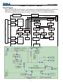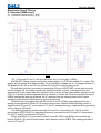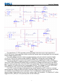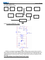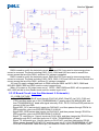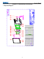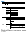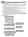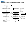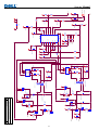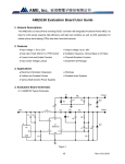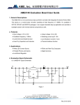
1
Service Manual
Service Manual
LCD Monitor S1909WXf
-0-
1
Service Manual Versions and Revision
No.
Version
Release Date
Revision
1
1.0
2008/07/10
Initial Release
Copyright
Copyright 2007 InnoLux Display. Corp. Ltd
All Rights Reserved
This manual may not, in whole or in part, be copied, Photocopied, reproduced, translated, or converted to any
electronic or machine readable form without prior written permission of Foxconn Tech. Corp. Ltd.
Dell S1909W Service Manual
Service Manual
Table of Contents
CHAPTER 1- PRECAUTIONS & SAFETY NOTICES ...........................................................................................................3
1.
2.
3.
SAFETY PRECAUTIONS......................................................................................................................................3
PRODUCT SAFETY NOTICE................................................................................................................................3
SERVICE NOTES..................................................................................................................................................3
CHAPTER 2- SERVICE TOOLS & EQUIPMENT REQUIRED ..............................................................................................4
CHAPTER 3- CIRCUIT THEORY...........................................................................................................................................5
1.
2.
3.
4.
5.
6.
7.
8.
BLOCK DIAGRAM ......................................................................................................................................................5
ELECTRONIC CIRCUIT THEORY .................................................................................................................................7
FACTORY PRESET TIMING TABLE ...................................................................................................................13
POWER ON/OFF SEQUENCY ...................................................................................................................................13
D-SUB CONNECTOR PIN ASSIGNMENT ...................................................................................................................14
AC OUTLET PIN ASSIGNMENT .................................................................................................................................14
INNER CONNECTOR PIN ASSIGNMENT .....................................................................................................................14
KEY PARTS PIN ASSIGNMENTS ................................................................................................................................16
CHAPTER 4- DISASSEMBLY & ASSEMBLY .....................................................................................................................21
1.
2.
3.
EXPLODED DIAGRAM ..............................................................................................................................................21
S1909WFPF DISASSEMBLY BLOCK ........................................................................................................................22
ASSEMBLY BLOCK ..................................................................................................................................................23
CHAPTER 5- TEST AND ADJUSTMENT............................................................................................................................24
1.
2.
3.
4.
5.
6.
7.
FUNCTION KEY DEFINITIONS ...................................................................................................................................24
OSD CONTROL .....................................................................................................................................................24
FACTORY MODE INTRODUCTION..............................................................................................................................26
BURN-IN PATTERN ..................................................................................................................................................27
AUTO COLOR BALANCE (AUTOMATICALLY CALIBRATE CHIP ADC PARAMETER BY USING CHIP INTERNAL DAC.) ............27
UPLOAD FIRMWARE TO MCU VIA VGA CABLE ..........................................................................................................26
AFTER REPAIR, TO ENSURE THE QUALITY YOU SHOULD DO THE FOLLOWING TEST AND ADJUSTMENT.............................27
CHAPTER 6- TROUBLE SHOOTING..................................................................................................................................30
1.
2.
3.
4.
5.
6.
COMMON ACKNOWLEDGE .......................................................................................................................................30
NO POWER LED OFF .............................................................................................................................................30
POWER NORMAL LED AMBER .................................................................................................................................31
BACKLIGHT CAN’T BE TURNED ON ............................................................................................................................32
NO PICTURE BACKLIGHT ON..................................................................................................................................33
AT 32-GRAY SCALE PATTERN, COLOR LOST IN SOME SCALE .......................................................................................34
CHAPTER 7- RECOMMENDED PART LIST.......................................................................................................................35
ATTACHMENT 1- BILL OF MATERIAL ...............................................................................................................................37
ATTACHMENT 2- SCHEMATIC ...........................................................................................................................................47
ATTACHMENT 3- PCB LAYOUT .........................................................................................................................................52
2
Service Manual
Chapter 1- PRECAUTIONS & SAFETY NOTICES
SAFETY PRECAUTIONS
This monitor is manufactured and tested on a ground principle that a user’s safety comes first.
However, improper used or installation may cause damage to the monitor as well as to the
user.
WARNINGS:
This monitor should be operated only at the correct power sources indicated on the rating
label on the rear cover of the monitor. If you’re unsure the power supply in your residence,
consult your local dealer or Power Company.
Use only the specified power cord that comes with this monitor.
Do not try to repair the monitor by yourself, as it contains no user-serviceable parts. This
monitor should only be repaired by a qualified technician.
Do not remove the monitor cabinet. There is high-voltage parts inside that may cause
electric shock to human bodies.
Stop using the monitor if the cabinet is damaged. Have it checked by a service technician.
Put your monitor only in a lean, cool, dry environment. If it gets wet, unplug the power
cable immediately and consult your closed dealer.
Always unplug the monitor before cleaning it. Clean the cabinet with a clean, dry cloth.
Apply non-ammonia based cleaner onto the cloth, not directly onto the class screen.
Do not place heavy objects on the monitor or power cord.
z
z
z
z
z
z
z
z
PRODUCT SAFETY NOTICE
Many electrical and mechanical parts in this chassis have special safety visual inspections
and the protection afforded by them cannot necessarily be obtained by using replacement
components rated for higher voltage, wattage, etc. Before replacing any of these components
read the parts list in this manual carefully. The use of substitute replacement parts, which do
not have the same safety characteristics as specified in the parts list, may create shock, fire,
or other hazards.
SERVICE NOTES
z
When replacing parts on circuit boards, clamp the solder wires around terminals before
soldering.
z
Keep wires away from high voltage, high temperature components and sharp edges.
z
Keep wires in their original position so as to reduce interference.
z
Adjustment of this product please refers to the user’ manual.
z
Use Pb free solder wire for circuit board preparation.
3
Service Manual
Chapter 2- SERVICE TOOLS & EQUIPMENT REQUIRED
1.
2.
3.
4.
5.
6.
7.
8.
9.
SIGNAL GENERATOR
MULTIMETER
SCREW DRIVER
OSCILLOSCOPE
Soldering IRON
SOLDER (Lead free, RoHS compliance)
Color Analyzer
Fox_VISP_Programmer
Fox_VEDID_Programmer
4
Service Manual
Chapter 3- CIRCUIT THEORY
Block Diagram
There are 2pcs PCBA in this monitor, one is power& inverter&Audio board which is a single layer
board, one is keypad which is OSD control.The system function block diagram as below
This PWA is included switching power supplier, inverter for CCFL and interface board.(fig.1)
INVERTER
POWER
ON/OFF Control
+5V DC output
Lamp1
+16V DC output
1
Transformer1
To
Snubber
&Schottky
Snubber
&Schottky
Lamp2
2
Panel
Power
Transformer
MOSFET
Feedback
and OVP
OZ9937
Rectifier&
Filter Circuit
MOSFET
Power
MOSFET
Photocoupler
CCFL
Feedback
Control
Lamp3
AC Line Filter
3
Transformer2
Lamp4
4
AC Input
90V~264V
Fig.1
5
SG5841
PW M
Control
To IF Board
Brightness Control
Service Manual
Electronic Circuit Theory
2.1 Inverter PWM circuit
2.1.1) Inverter Control circuit :( fig.2)
Fig.2
DC_5V through R1 and C1 will provide power for U1 on the pin2 (VDDA).
EN-ON/OFF voltage signal coming from scalar which is on IF BD will enable U1 to work. This
applies a level greater than approximately 2V to pin8 (ENA) enables the IC, A voltage less than 1V
will disable the IC. R3 is used to limit current.C3 and C40 is used to dump noise.
The soft-start function is provided by connecting C8 to pin12(SSTCMP), In the start-up mode,
current charges C8, its voltage controls the gradual increase in power to the transformer and
subsequently to the output load, this reduces in-rush current and provides reliable operation to the
CCFL.If no current is sensed approximately 2 seconds, U1 shuts off. Once the voltage at the pin4
(ISEN) reaches the lamp on threshold, the IC switches from the striking mode to the normal
operation mode and the PWM dimming control is activated.
DIM-ADJ duty cycle signal through R2 and C2 is on Pin 3(DIM), which adjusted will can
change the brightness of Panel.C41 is used to dump noise. Internal LPWM dimming control is
determined by R11 and C7 connected to LCT (pin11), analog dimming is implemented by providing
a DC voltage to PID (pin5).
The striking frequency is determined by R12 and C11 connected to Pin 13(CT) and R6
connected to RSTR (Pin6).The operating frequency is determined by R12 and C11 connected to
Pin 13(CT) and R7 connected to RT (pin7).
DRV1 and DRV2 of U1 are used to drive Q1 and Q2. DRV1 and DRV2 are controlled by
build-in PWM IC. Q1 and Q2 are switches which has two build-in IGBTs. The working principle of
circuit of T1 and T2.
6
Service Manual
2.1.2) Output Circuit and Protection Circuit :( fig.3)
fig.3
The transformer (T1/T2) secondary winding leakage inductance and output capacitance
(C31/C32) forms a lower pass filter, which converts the square-wave driving signal into a sinusoidal
output voltage signal for CCFL.
The over-voltage protection feature is implemented by using an external capacitor divider
(C31/C32, C33/C34) or resistor divider (R20/R21, R22/R24) to sense the output voltage. The
divide-down voltage signal is sent to the IC Pin9 (VSEN), thus regulating the output voltage.
The voltage signal on negative pole of ZD1 sensed through R35 comes to Pin4 of U1 (ISEN).
The CCFL current detected at resistor R35 is converted to a voltage level and input to the ISEN
pin.C6 is used to dump noise. Once the CCFLs are ignited and current is sensed through resistor
R35, capacitor C6 performs the loop compensation function. The voltage at IC pin12 (SSTCMP)
controls the drive duty cycle of the power MOSFETs to regulate the CCFL current.
If a CCFL is removed, fails or damaged during normal operation, CCFL current is no longer
sensed and the voltage on ISEN pin drops. Once the voltage at the ISEN pin is less than the lamp”
on” threshold, the shutdown timer is activated. The IC maintains the output voltage for
approximately 2-3seconds and once the timer expires, the IC will shutdown. To restart the IC, either
toggle the SST_CMP pin or recycle the power on the VDDA pin.
7
Service Manual
2.2 Power PWM circuit
2.2.1) Block diagram :( fig.4)
EMI Filter
Rectifier and
filter
PWM controller
Isolation power
transformer
Rectifier and filter
Switching element
Inverter circuit
Rectifier and filter
LDO regulator
Feedback Isolation
Fig.4
2.2.2) AC Input and EMI Filter :( fig.5)
fig.5
CN850 is a connector for connecting AC Power. F850 is a fuse to protect all the circuit AC.
Input voltage is from 90V to 264V. R850 and R851 are joined between two inputting main circuit
to prevent man from shock. L851 is used to clear up low frequency wave. C850 and C851 are
used to discharge the waves that L851 produced. High frequency waves are damped by C852
and C853.
2.2.3) High Voltage to Low Voltage Control Circuit :( fig.6)
8
Service Manual
fig.6
D850 is a rectifier in which there are 4 build-in diodes, inverting AC to DC.
C854 is used to smooth the wave from rectifier. R852 is a fuse resistor to protect the following
circuit when inrush current is too large. U850 is a highly integrated PWM controller. Typical
start-up current for U830 is only 8uA; R838, R839 and R840 are serial circuit to limit current flow.
When current flow through R838, R839 and R840 gets to Pin 3 of U830, with VDD hold-up
capacitor C857, U830 is enough for starting up.
When U830 begins to work, Pin8 (GATE) of U830 will output square wave to drive Q850, and
then the main current flow get to GND by passing through T850, Q850. Because of the change of
current flow, wires in the other side of T850 will induct current.At the same time, the current
inducted by wires which connected T850 Pin 1 and Pin 2, with components of D852, R855, C857
and C839, will be supplied to U830 for normal operating.
When the sense voltage across the sense resistor R859, reaches the threshold voltage around
0.85V, the output GATE drive will be turned off. Every time when the output of power supply is
shorted or over loaded, the FB voltage will increase, the build-in PWM output will then be turned off.
Both will prevent the power supply from being overheated under over loading condition. The PWM
duty cycle is determined by this current sense signal and VFB, the feedback voltage. When the
voltage on sense pin reaches Vcomp = (VFB-1.0)/3, a switch cycle will be terminated immediately.
Vcomp is internally clamped to a variable voltage around 0.85 V for output power limit.
When Q850 are turned off, the main current flow will be consumed through D851, C880, R880
and D853. This will prevent Q850 from being damaged under large current impulse and voltage
spike.
2.2.4) DC_16V and 5V Output Circuit and Feedback circuit :( fig.7)
9
Service Manual
fig.7
D854 is used to rectify the inducted current. R860 and C861 are used to store energy when
current is reversed. The parts including C862, C865, C864 and L853 are used to smooth the
current waves that are from D854, and then 16V voltage is supplied.
D856 is used to rectify the inducted current. R869 and C876 are used to store energy when
current is reversed. The parts including C856, C870, C859, C872 and L855 are used to smooth the
current waves that are from D856, and then 5V voltage is supplied.
16V and 5V supply voltage feed back to PWM controller U830 via R871, R872, R868 and
I850,I851.R865,C866 and C855 used to control respond time.
When 16V output or 5V output come out of SPEC , D857,D858 and Q851 will be operated, via
I850 ,U850 will be in Auto Restart mode until the matter is got rid of .
2.3 I/F Board Circuit (see the Attachment 2- Schematic)
2.3.1 RGB CAPTURE
- Signal RED,GREEN,BLUE input through CN101 #1,#2,#3, Stop DC via C101, C102 and
C103, and then enter into U104 (TSUM56BWHK-LF) analog input PIN #59,#56,#54, and
then TSUM56BWHK-LF deals with signal internally. D101, D102, D103 are ESD protector to
prevent U104 from ESD.
- Signal DDC_SCL (series clock) inputs via CN101#15, and then passes through ZD104 for
ESD protection, goes into EDID EEPROM IC U102 #6.
- Signal DDC_SDA (series data) inputs via CN101#12, and then passes through ZD105 for
ESD protection, goes into EDID EEPROM IC U102 #5.
- Signal TTL vertical sync. (Vsync) inputs via CN101 #14, and then clamped by ZD103 Zener,
passes through R116, and then goes into IC U104 (TSUM56BWHK-LF) #64.
- Signal TTL horizontal sync. (Hsync) inputs via CN101 #13, and then clamped by ZD102
Zener, passes throughFB104 & R115, and then goes into IC U104 (TSUM56BWHK-LF) #63.
- CN101#5 is defined as cable detect pin, this detector realize via R113 and U104#26, and
10
Service Manual
ZD109 is ESD protector.
- U102 +3.3V is supplied by PC via CN101#9 with D104 and ZD101 for ESD protection, or
supplied by Monitor self via D104.
- U102 is an EEPROM IC which is memory and EDID data saved in it.
2.3.2 DVI CAPTURE
- Differential Signal input RX0+,RX0-,RX1+,RX1-,RX2+,RX2-,RXC+,RXC- through CN102
#18,#17,#10,#9,#2,#1,#23,#24 via R130,R131,R132,R133,R134,R135,R137,R138 enter
into U104 (TSUM56BWHK-LF) Digital input terminal #39,#40,#42,#43,#45,#46,#48,#49,
and then TSUM56BWHK-LF deals with signal internally. D108, D109, D110, D111, D112,
D113, D114, D115 are ESD protector to prevent U104 from ESD
- Signal DDC_SCL (series clock) inputs via CN102#6, and then passes through ZD106 Zener
for ESD protection, via R126, goes into EDID EEPROM IC U101 #6.
- Signal DDC_SDA (series data) inputs via CN102#7, and then passes through ZD107 Zener
for ESD protection, via R127, goes into EDID EEPROM IC U101 #5.
- CN102#15 is defined as cable detect pin, this detector realize passes through R125 ,go into
U104#27, and ZD110 is ESD protector.
- U101 +5V is supplied by PC via CN102#14 through D107, or supplied by Monitor self via
D107.
- U101 is an EEPROM IC which is memory and DVI input EDID data saved in it.
2.3.3 Buttons Control
- Button “Power” on front bezel connects to U104 (TSUM56BWHK-LF) #23 through CN104 #1,
U104 #23 is defined as power on/off.
- Button “Ï” on front bezel connects to U104 (TSUM56BWHK-LF) #24 through CN104 #2,
U104#24 Voltage is defined as “Plus”.
- Button “Д on front bezel connects to U104 (TSUM56BWHK-LF) #24 through CN104 #2,
U104 #24 Voltage is defined as “Minus”.
- Button “Menu” on front bezel connects to U104 (TSUM56BWHK-LF) #25 through CN104 #4,
U104 #25 Voltage is defined as “Menu”.
- Button “ENTER” on front bezel connects to U104 (TSUM56BWHK-LF) #25 through CN104
#4, U104 #25 Voltage is defined as “ENTER”.
- LED Indicator on Front Bezel
a. When press button “power”, U104 (TSUM56BWHK-LF) #31 be send in low Voltage, make
Q109#3 sends out high Voltage , and then to CN01#2 on keypad, LED white on.
b. When in “Suspend” mode, U104 (TSUM56BWHK-LF) #35 sends out a low Voltage, make
Q108#3 sends out high Voltage and then to CN01 #3 on keypad, LED Amber ON.
2.3.4 MATAR CHIP U104 (TSUM56BWHK-LF)
- U104 (TSUM56BWHK-LF ) #105~#114 output 8 bit even and #118~#127 output 8 bit odd
LVDS digital data to panel control circuit through CN106.
- U104 (TSUM56BWHK-LF ) #75 output PPWR ”H” potential to make Q106 conducted, and
then make Q103 conducted, +5V flow to CN106#1~#3 as Panel Vdd .
- U104 (TSUM56BWHK-LF) #20 output CCFL_ON/OFF ”L” potential to control Inverter on/off.
- U104 (TSUM56BWHK-LF) #21 outputs Brightness “PWM” signals to control CCFL
brightness.
- TCLK by Crystal 14.318MHz input to U104 (TSUM56BWHK-LF) #32.
- U104 (TSUM56BWHK-LF) #19 is RESET signals input pin
Please refer to TSUM56BWHK-LF Pin Assignments table in page
2.3.5 Regulator Circuit
- +5V is from switching mode power supply for panel
- +3.3V is generated from Regulator U103 which is supplied by+5V through C168 filtering,
C130 is 3.3V output filter ,the output 3.3V supplies toU104, U108,U107,U106,U105,U102,
U101.
11
Service Manual
- +1.8V is generated from Regulator U108 which is supplied byU103-3.3V through C143
filtering.The1.8V via FB105 supplies to U104.
3. FACTORY PRESET TIMING TABLE
Standard
VESA
IBM DOS
Resolution
640 x 480
640 x 480
800 x 600
800 x 600
1024 x 768
1024 x 768
1152x864
1280x1024
1280x1024
1440x900
720 x 400
Horizontal Frequency
(KHz)
31.469
37.500
37.879
46.875
48.363
60.023
67.500
48.483
60.087
55.935
31.469
Vertical Frequency
(Hz)
59.940
75.000
60.317
75.000
60.004
75.029
75.000
60.042
75.034
59.887
70.087
4. Power On/Off Sequency
Hardware power On/Off
When power cord plug into AC socket, Power provides 16V and DC_5V.
DC_5V is main voltage for panel and Regulator U103.
DC_3.3V is coming from Regulator U103, DC_3.3v is main voltage for U104. When DC_3.3V
input to U104 and U104 reset circuit active, U104 all registers will be set to default, that means
finish hardware power on.
When pull out power cord from AC socket,the system shut down instantly for no supply
Software power On/Off
- When press power key, U104 #23 receives low pulse, then (TSUM56BWHK-LF) U104 will be
wake up and send control signals(at 20,75pin) to on CCFL and switch 5.0v to panel module,
at the same time,U104 make the VGA/DVI cable input signal source display normal on panel
if the VGA/DVI cable input signal is active
- If power ON, U104 #31 (LED_green) will send out low potential, and then LED white on.
- If power saveing, U104 #35 (LED_Amber) will send out low potential, and then LED Amber
on.
- If power ON or power saveing, when press power key, U104 #23 receives low pulse, then
U104 will be sleeping and turn off backlight, at the same time, the panel will lose +5V.
The Panel_Vcc, Backlight_En, CLK/DATA output to panel will follow the following sequency.
12
Service Manual
Power supply for panel+5V VDD
90%
90%
10%
0V
10%
T1
T2
T5
Signals
(Digital RGB, HS, VS, DE, CLOCK)
0V
T6
T7
Valid data
T3
T4
Power supply for backlight
T1 (ms) T2 (ms) T3 (ms)
0.3~10 0.0~50
>500
SPEC
(Samsung)
SPEC (LPL)
0.5~10 0.01~50
>500
T4 (ms)
>200
T5 (ms)
0.0~50
T6 (ms)
NA
T7(ms)
>1000
>200
0.01~50
NA
>1000
5. D-SUB Connector Pin Assignment
Pin
1
2
3
4
5
Pin
6
7
8
9
10
Symbol
Red_GND
Green_GND
Blue_GND
PC+5V
GND
Pin
11
12
13
14
15
Symbol
GND
DDC_SDA
Hsync
Vsync
DDC_SCL
AC input connector Pin Assignment
2
6.
Symbol
Red
Green
Blue
GND
Cable Detect
1
3
CN850
Pin
1
2
3
Symbol
Line
GND
Neutral
Description
AC Line(Vin=100 to 240 Vrms,50/60Hz)
GND
AC Line(Vin=100 to 240 Vrms,50/60Hz)
7. Inner Connector Pin Assignment
7.1 CN106 (Connect M/B to Panel,)
Pin
Symbol
Description
1
Panel_Vcc
Panel power supply (typ.5.0V)
2
Panel_Vcc
Panel power supply (typ. 5.0V)
3
Panel_Vcc
Panel power supply (typ. 5.0V)
4
NC
13
Service Manual
5
6
7
8
9
10
11
12
13
14
15
16
17
18
19
20
21
22
23
24
25
26
27
28
29
30
NC
NC
GND_LVDS
RXE3+
RXE3RXEC+
RXECRXE2+
RXE2GND_LVDS
RXE1+
RXE1GND_LVDS
RXE0+
RXE0RXO3+
RXO3RXOC+
RXOCGND_LVDS
RXO2+
RXO2RXO1+
RXO1RXO0+
RXO0-
LVDS Ground
LVDS signal of even channel 3(-)
LVDS signal of even channel 3(+)
LVDS signal of even channel clock (+)
LVDS signal of even channel clock (-)
LVDS signal of even channel 2(+)
LVDS signal of even channel 2(-)
LVDS Ground
LVDS signal of even channel 1(+)
LVDS signal of even channel 1(-)
LVDS Ground
LVDS signal of odd channel 0(+)
LVDS signal of odd channel 0(-)
LVDS signal of odd channel 3(+)
LVDS signal of odd channel 3(-)
LVDS signal of even channel clock (+)
LVDS signal of even channel clock (-)
LVDS Ground
LVDS signal of even channel 2(+)
LVDS signal of even channel 2(-)
LVDS signal of even channel 1(+)
LVDS signal of even channel 1(-)
LVDS signal of odd channel 0(+)
LVDS signal of odd channel 0(-)
7.2 CN1, CN2, CN3, CN4 (Connect to Panel Backlight,)
Pin
Symbol
Description
1
HV
High voltage for lamp
2
LV
Low voltage for lamp
7.3 CN104 (Connect to keypad, WAFER2*4P or compatible connector)
Pin
Symbol
Description
1
POWER
OSD “POWER” control
2
PLUS/MINUS
OSD “+/-” control and “AUTO/Brightness”adjustable hot
key
3
LED white
LED white on/off control
4
MENU/ENTER
OSD “MENU/ENTER” control
5
LED Amber
LED amber on/off control
6
GND
Ground
7
GND
Ground
8
GND
Ground
14
Service Manual
8. Key Parts Pin Assignments
8.1 U104(TSUM56BWHK-LF-2)
15
Service Manual
16
Service Manual
17
Service Manual
8.2 U105 (Serial Flash)
Pin
Symbol
I/O
1
CE#
I
2
SO
I/O
3
WP#
I/O
4
5
VSS
SI
G
I/O
6
SCK
I/O
7
HOLD
I/O
8
VDD
P
Description
The device is enabled by a high to low transition on CE#.
CE#
must remain low for the duration of any command
sequence.
To transfer commands, addresses, or data serially into the
device.
The write protect (WP#) pin is used to enable/disable BPL
bit in
the status register.
Connect ground
To transfer commands, addresses, or data serially into the
device
input are latched on the rising edge of the serial clock.
To provide the timing of serial interface.
Commands, addresses, or input data are latched on the
rising edge of the clock input, while output data is shifted
out on the
Falling edge of the clock input.
To temporarily stop serial communication with SPI flash
memory without resetting the device.
To provide power supply.
18
Service Manual
8.3 U830 (SG5841, PWM Power Controller)
Pin
Symbol
I/O
Description
1
GND
Ground
2
FB
I
Feedback, the FB pin provides the information
of the regulation. The PWM duty cycle is
controlled by FB
3
VIN
I
Start-up current input
4
RI
I
Reference setting, typical voltage 1.3V
5
RT
N.C.(not connected)
6
SENSE
I
Current sense for over current protection
7
VDD
I
Power supply
8
GATE
O
PWM output
8.4 U1 (OZ9937, CCFL Inverter controller IC)
Pin
Symbol
I/O
Description
1
DRV1
O
Drive output1
2
VDDA
I
Supply voltage input
3
DIM
I
Internal LPWM dimming or external PWM pulse
input for dimming function
4
ISEN
I
Current sense feedback
5
PID
I
Analog dim input
6
RSTR
I
Resistor to set striking frequency
7
RT
I
Resistor to set operating frequency
compensation range
8
ENA
I
ON/OFF control of IC
9
VSEN
I
Voltage sense
10
OVPT
I
Over-voltage/over-current protecting threshold
setting
11
LCT
I
Timing capacitor to set internal PWM dimming
frequency
12
SSTCMP
I
Capacitor for soft start time and loop
compensation
13
CT
I
Timing resistor and capacitor for operation and
striking frequency
14
TIMER
I
Timing capacitor to set striking time and
shutdown delay time
15
GNDA
I
Ground
16
DRV2
O
Drive output2
19
NO.
20
Designation
LE19D5
RUBBER,FOOT,10*3,for cmo
TAPE,ACE,85*20mm,LE1913
INSULATOR,MYLAR,CHASSIS 02,LE19D5
INSULATOR MYLAR PANEL LP1903 ROHS
SHIELD EMI LP2207
CHASSIS FOR SAM
ASSY,CHASSIS FOR SAM,LE19D5
KENSINGTON LOCK LE1963
OSD BUTTON,LE19D5
COVER,BACK LE19D5
ASSY,COVER,BACK,LE19D5
LOGO PALTE DELL Apollo 4
POWER,BUTTON,FOR SAM,LE19D5
BEZEL,FRONT,FOR SAM LE19D5
ASSY,BEZEL,FRONT,FOR SAM LE19D5
1
1
5
1
1
1
2
714011202600R
505040202600R
505040208500R
506380001730R
506381001301R
1
1
1
714050014900R
501020220600R
502210100400R
501030209820R
701000007600R
502090310800R
502040400600R
NO.
Remark
1
1
1
1
Identification NO. Q't
714030016300R
501010216300R
501030209800R
501110500301R
S-1 S-7
S-2
Screw,B,CROSS,W/W-SPR,M3*9,Zn
Screw,I,Cross,M3*6,Zn-Cc
Bolt,#4-40*12.5,Ni
Screw,P,Cross,M4*10,Black-NL
Screw,I,Cross,M3*4,Zn-Cc
SCREW,F,CROSS,T.T-2*3,BLK
Screw,P,Cross,W/WAS(7.8),M3*6,Zn-Cc
LVDS FFC
PCBA,KEYPAD(power key +LED)BOARD
PCBA,KEYPAD(4fuction key)BOARD,LE19D5
PCBA,I/F BOARD,W/O SPK LE19D5-812 ROHS
PCBA,PWR&INV./B,LE19D5-812 ROHS
LCP 19" LTM190M2-L31(A)(SAMSUNG) Glare R
Designation
S-6 S-5 S-3
5
1
4
509146306202R
509212103500R
509016304200R
509116610510R
509000001000R
509016306200R
509446309100R
4
4
2
1
1
1
1
1
1
1
631102090811RD
Identification NO. Q't
Remark
Star.hu
2008/01/31
S-4
LE19D5
Exploded Drawing (for SAM)
Service Manual
Chapter 4- Disassembly & Assembly
1. Exploded Diagram
Service Manual
2.
S1909WX Disassembly Block
LE19D5 DISASSEMBLY BLOCK
front bezel *1
Power -button *1
logo plate*1
FINAL ASSY*1
TAPE ACE 85x20mm LE1913*1
insulator mylar panel*1
panel*1
Power-button keyapd*1
Screw,P,Cross,
T,T-2*3,BLK*1
(I,Cross,M3*4,Zn-Cc)*4
STAND ASSY*1
(P,Cross,M4*10,BLACK-NL)*2
(P,Cross,W/WAS,M3*6,Zn-Cc)*3
(B,Cross,W/W-SPR,M3*9,Zn)*1
(I,Cross,M3*6,Zn-Cc)*3
power board*1
back cover*1
OSD button *1
FRONT BEZEL ASSY *1
(P,Cross,W/WAS,M3*6,Zn-Cc)*2
(BOLT,#4-40,NI)*4
FFC-CABLE*1
I/F board*1
kensington lock*1
insulator mylar chassis02*1
BACK COVER ASSY*1
Rubber Foot *2 For CMO
CHASSIS ASSY *1
PANEL ASSY*1
(P,Cross,M4*10,BLACK-NL)*2
shield EMI LP2207* 5
chassis*1
Note:
1. The arrows point out the direction of disassembly.
2.The foil which sticked on the panel need re-sticked on original
position after sample repaired.
21
Service Manual
3.
S1909WX Assembly Block
LE19D5 ASSEMBLY BLOCK
power-button*1
chassis*1
CHASSIS ASSY*1
shield EMI LP2207*5
insulator mylar chassis*1
I/F board *1
FFC-CABLE*1
(P,Cross,W/WAS,M3*6,Zn-Cc)*2
(BOLT,#4-40,NI)*4
front bezel *1
logo plate *1
power-button
keypad*1
(screw,f,cross,
T-2*3,BLK)*1
power board *1
back cover*1
OSD button *1
(P,Cross,W/WAS,M3*6,Zn-Cc)*3
(B,Cross,W/W-SPR,M3*9,Zn)*1
(I,Cross,M3*6,Zn-Cc)*2
panel*1
insulator mylar panel*1
FRONT BEZEL ASSY*1
STAND ASSY *1
(P,Cross,M4*10,BLACK-NL)*2
TAPE ACE 85x20mm LE1913*1
kensington lock*1
Rubber Foot *2 10*3 For Cmo
(I,Cross,M3*4,Zn-Cc)*4
PANEL ASSY*1
(P,Cross,M4*10,BLACK-NL)*2
FINALASSY*1
BACK COVER ASSY*1
Note: 1. The arrows point out the direction of assembly
2. After repair, the foil need re-sticked on original position on the
panel.
22
Service Manual
Chapter 5- TEST AND ADJUSTMENT
1. Function key Definitions
POWER
Every bottom function defining
Power Switch with power LED indicator
Panel Controls
Factory Modes Keys Function
Power: On/Off, includes power indicator and Power ICON
white- Active On
Amber- DPMS
1. Menu: When OSD isn’t shown on screen, press [MENU] to enter OSD
interface ,When OSD displays, press [MENU] to exit OSD
2. (↑): When “MENU OSD” displays, press these keys to change the contents
of an adjustment item, or change an adjustment value
When “MENU OSD” un-displays, press [(] to adjust Brightness and
Contrast;
3. (↓):When “MENU OSD” displays, press these keys to change the contents
of an adjustment item, or change an adjustment value
When “MENU OSD” un-displays, press [(]to execute the Auto
Adjust function
4. Enter: When “MENU OSD” displays, press these keys Enter the OSD sub
menu
When “MENU OSD” displays, press these keys to select the input
source
5. Power: Power on or off the monitor
Auto Color Balance
Purpose: Automatically calibrate chip ADC parameter by using chip internal
DAC.
Process: If we want to do “Auto Color Balance” again, please confirm the
following steps.
1) Connect the VGA cable with the standard video pattern generator and
display the pattern with blackest and whitest colors.
2) Press “Power Key”, to power off the monitor.
3) Press “Menu Key” and “Up Key” simultaneously, and then press “Power
Key” to power on the monitor.
4) Press “Ï”, then entry “Factory”mode.
5) Execute Auto Color item.
6) After the “Auto Color Balance” process finished, go back to Main Menu,
choose “Other settings” item and press “Enter” to enter sub-Menu , then
choose “factory reset” item and press “Enter” again execute Reset all
settings.
.
Hot Key Operation
HOT KEY OPERATION
FUNCTION
FACTORY MODE
Brightness&
Contrast
DESCRIPTION
MENU
Ï
●
●
Ð
ENTER
POWER
ON
Press [Ï]& [MENU] at the same time, and then
press [POWER] for DC power on. Press theÏ key to
enter factory menu
To show the Brightness&
Contrast menu
●
23
Service Manual
●
AUTO ADJUST
Execute the AUTO ADJUST function
●
Select Input
Select the input source
OSD Control
OSD Control
First
Brightness
Second
Brightness
Contrast
Third
Default
75
75
Auto Adjust
Input Source
Auto Select
VGA
DVI-D
Input Color Format
Mode Selection
Color Settings
Present Modes
Display Settings
RGB
YPbPr
Graphics
Video
Standard
Multimedia
Game
Warm
Cool
Custom(R,G,B)
Reset Color Settings
Horizontal Position
Vertical Position
Sharpness
Pixel Clock
Phase
50
50
50
50
Reset Display Settings
Language
Other Settings
English
Espanol
Francais
Deutsch
日本語
Menu Transparency
Menu Timer
Menu Lock
DDC/CI
LCD Conditioning
Factory Reset
20
20s
Unlock
Lock
Enable
Disable
Disable
Enable
Reset All Setting
VGA Input
Yes
Yes
Yes
DVI Input
Yes
Yes
No
Yes
Yes
Yes
Yes
Yes
Yes
Yes
Yes
Yes
No
No
Yes
No
No
Yes
Yes
Yes
Yes
Yes
Yes
Yes
Yes
Yes
Yes
Yes
Yes
Yes
Yes
Yes
Yes
Yes
Yes
Yes
Yes
Yes
Yes
Factory Mode Introduction
With signal input, press “Power” button to turn off the monitor. Press “Menu” and “Ï” buttons together,
and then press “Power” button to turn on the monitor. After power on, press “Ï” button to call out
FactoryMenu(Fig.10).
24
Service Manual
Fig9
Fig10
Back: Exit from Factory mode and back to NO OSD Status.
Panel: The current-setting panel is highlighted.
Auto Color: Automatically calibrate chip ADC parameters by using internal DAC.
Burn In: Enable or disable the Burn-in mode by choosing ON or OFF.
Reset Timer: Reset the “Turn-on time” of the panel to 0H0M.
25
Service Manual
Color Temp: The R, G, B of Blue Preset (9300K), Red Preset (5700K) and Normal Preset (6500K) are
generated
from scaling chip’s back-end white-balance program.
Time: Turn-on time of the panel.
DEBUG: Debug tool of scale IC U104.
Dell panel P/N
LCD supplier
Samsung
Panel
Supplier P/N
Dell P/N
19”W
PANEL_SAM_LTM190M2L31
Y714H
Burn-in pattern
Burn-in pattern will self-generate automatically without VGA and DVI cable plugged in when the monitor
set at Burn-in on mode and burn-in pattern will not be stopped until plugging in the VGA cable. Exit
Burn-in mode method as followe: plugging in the VGA/DVI cable, press “Menu” button to call out OSD
Main Menu, Press “Plus Key”to select“Other Settings Menu”then pop submenu and choose Factory reset.
Auto Color Balance (Automatically calibrate chip ADC parameter by using chip
internal DAC.)
5.1 If it is a new-built set, press “Auto Color” button on Factory menu to execute “Auto Color” at
standard video pattern 5-MOSAIC pattern
5.2 Please confirm the following steps to perform “Auto Color Balance”:
- Connect the VGA cable with the standard video pattern generator and display 5-MOSAIC
pattern on the monitor.
- Press “Power” button to power off the monitor.
- Press “Menu” and “Ï” buttons simultaneously; then press “Power” button to power on the
monitor.
- Press “Ï” to call out factory menu
- Execute Auto Color item.
- After the “Auto Color Balance” process finished, go back to “Other Settings Menu”, and press “Factory Reset” to
exit Factory mode
Upgrade Firmware to Serial via Flash Cable by ISP_Tool V4.100.exe
7.1 Connect the monitor and PC follow Fig 11
26
Service Manual
Fig 11
※ The detailed reprogramming procedures will be described in ISP User's Guide.
Edid 8.4.rar
Edid.rar
ISP User's Guide_20070312.rar
ISP_Tool V4.100.rar
After repair, to ensure the quality you should do the following test and adjustment.
27
Service Manual
Item
Test OSD
function
Content
1.Signal is set as 1440×900@60Hz under General-1
2. LCM button are from left to right, checking whether each
single function key and compound function key can be
worked.
Contrast Check 1. Set input mode to 1440×900@60Hz
2. Set to 32gray scale pattern
3. Set contrast to the maximum. At most 6 bars cannot be
distinguished.
Color
1. Do “Auto color Balance” at 1440×900@60Hz,
Temperature
32gray scale pattern
2. Measure color temperature, check if it complies with
the following temperature :
Warm x=0.328 +/- 0.015, y=0.344+/-0.015
Standard x= 0.313 +/- 0.015, y=0.329+/-0.015
Cool x= 0.283 +/- 0.015, y=0.298+/-0.015
1. Use Chroma Pattern Generator to make sequence.
Modes
VESA (640x480 800x600 1024x768 1152x864
switching check 1280x1024 1440×900@60Hz), the detail supported
modes (see table 1) and power saving signal.
2. Confirm the above timing modes must be full screen
and the picture must be normal.
3. LED is amber at power saving mode.
VGA
cable
detector
Y measurement
at default
setting
OSD Lock Test
Panel Flicker
check
Power saving
When select VGA model and VGA cable is not plugged
out, self-test OSD will be floated.
1. Set brightness and contrast to default value 75 at
6500K
2. With full white pattern, Y shall be 220 ± 20 cd/m2
Soft Lock: When OSD is locked, this icon should appear for
only 2 seconds with all buttons pressed, except for the
“Menu” and “Power” ones.
Hard Lock: Press “Menu” button for 15 seconds enables
the “locked” icon to be displayed, which will lock All
buttons expect for the “Power”. Press “Menu” button for
another 15 seconds enables the “unlock” icon to be
shown.
1. Mode:1440×900@60Hz
2. Set Brightness& Contrast to default value (75%)
3. Do “Auto Adjustment”
4. Shut down PC to check whether there’s flicker on the
center of the picture.
1. Mode:1440×900@60Hz
2. Pattern: full Black
3. Brightness: Max.
4. Contrast: Default
5. Check power consumption at each modes
State
Power Consumption
LED color
Normal
<37W
White
Stand By
Power Key Off
<2W
<1W
Amber
No
28
Equipment
Chroma
Signal Generator
Chroma
Signal Generator
Chroma Signal
Generator and
color analyzer
Chroma
Signal Generator
Visual check
Chroma Signal
Generator and
Color Analyzer
Visual Inspection
Equipment::
Chroma Signal
Generator & PC
Chroma signal
generator and
Power meter
AC
input:230V/50Hz
Service Manual
Chapter 6- TROUBLE SHOOTING
Common Acknowledge
z
z
z
z
z
z
z
z
z
If you change the M/B, be sure that the U101, U102 and U105 these three components also
changed to the new M/B because there was program inside. If not, please re-write EDID or
upload firmware into serial flash (U105) via VGA Cable. How to do please refer to the Page
19.
If you adjust clock and phase, please do it at condition of Windows shut down pattern.
Please confirm the R/G/B color under 32gray scale pattern.
This LCM is analog interface. So if the entire screen is an abnormal color that means the
problem happen in the analog circuit part, if only some scale appears abnormal color that
stand the problem happen in the digital circuit part.
If you check the H/V position, please use the crosshatch pattern.
This LCM support 10 timing modes, if the input timing mode is out of specification, “Cannot
Display this Video Mode” will be displayed on the screen.
If brightness uneven, repairs Inverter circuit or change a new panel.
If you find the vertical line or horizontal line lost on the screen, please change panel.
If the self-test pattern is moving on the screen, please check whether VGA Cable is plugged
in the Monitor or PC if select analog model on OSD or check whether DVI Cable is plugged in
the Monitor or PC if select DVI model on OSD . If the VGA or DVI Cable is plugged in well,
please change another VGA or DVI cable.
No Power and LED Off
Is there DC16V at L853?
Is there DC5V at L855?
NO
Is the voltage at C854 in the
range of 127V~373V?
YES
NO
Check RT850, F850
Is the voltage at pin3 of U830 18.4V?
YES
NO
Check R852
Is the voltage at pin6 of U830 0.9V?
YES
NO
Check D852, Q850
Is the voltage at pin7&pin8of T850 38V?
YES
Check D856
29
Service Manual
Power (include IF +5Vand +3.3V) supply normal but LED off and no display
Is the key function OK?
Yes
Press power key to DC on the monitor,if
display ok the process is end,if no display see
the no backlight process
NO
Is the frequency 14.318MHz at #32 of
IF Board U104?
NO
Change crystal X101
NO
Change C160
Yes
Is the low active reset signal at #19 of
IF Board U104 normal?
NO
Yes
Yes
Change U104
NO
Is the serial clock signal at #6 of IF
Board U105 normal when power AC on?
Change U105
Yes
Upgrade Firmware to Serial Flash U105
by VGA port with ISP_Tool V4.100.exe
END
Power (include IF +5Vand +3.3V) supply and display normal only LED off
NO
Is the keypad cable connective OK
Reassembly or changing
Yes
NO
Is LED at keypad work OK
Yes
Is R188 open?
Yes
Change LED
Change R188
NO
Is Q109 work normal?
NO
Change Q109
Yes
Is theLED control signal at 31# of U104
high-low convertible when DC on/off
NO
END
30
Change U104
Service Manual
Power (include IF +5Vand +3.3V) supply and display normal but LED Amber
Is Power LED Amber?
YES
Do the Hsync. & Vsync. Signals exist
in CN101 #13& #14 separately when
select VGA mode by OSD?
NO
Insert VGA Cable correctly
YES
Do the Hsync. & Vsync. Signals exist
in R115 & R116?
NO
Check R115 & R116
YES
Do the Hsync. & Vsync. Signals exist
in U104#63& #64?
NO
Change R115 & R116
YES
Is the Q108 work normal?
NO
Change Q108
YES
Is theLED control signal at 35# of
U104 high-low convertible when DC
on/off
NO
END
31
Change U104
Service Manual
Power (include IF +5Vand +3.3V) supply normal, key function OK,but backlight
can’t be turned on
Backlight cannot be turned on,is the
on-off control signal come from IF ok?
NO
Is the CN853
inserted CN103 OK?
Yes
Yes
Yes
Is the on-off control signal #20 of U104
high-low convertible when DC on/off
NO
Is the
voltage
16V at T1
PIN4?
NO
Check
T850,
D854
Yes
Is the frequency 14.318MHz at #32
of IF Board U104?
Is the serial clock signal at #6 of IF
Board U105 normal when power AC
Yes
Change
X101
Yes
Is the low active reset signal at #19 of
IF Board U104 normal?
Yes
Check U1
pin4 Voltage
is 2V
NO
NO
Change
C160
NO
Change
U105
Yes
Check U1 pin8
Voltage is high
NO
Check
Q1 or
Q2
Upgrade Firmware to Serial Flash U105
by VGA port with ISP_Tool
V4.100.exe,after this process,no the
control signal yet,change U104
YES
Check T1/T2 pin7 and pin10 Open
or Short
Yes
Change T1/T2
32
Service Manual
Backlight on, key function and LED accurate indication ok but no picture
Backlight on, key function and LED
accurate indication ok but no picture
YES
IS the display is white and cannot
display OSD when press key?
YES
Check DC 5.0V on
CN106#1, #2, #3
NO
Is the panel enable
signal at 75# of
U104,if no check
Q106 circuit or change
U104,if yes Check
Q103 circuit
NO
Is display selftest picture at
VGA mode or DVI mode?
VGA
DVI
Is there DVI signal in U104
#39, #40, #42, #43, #45, #46,
#48 #49?
Is there R.G.B signal in
U104 #59, #56 #54?
NO
Change D101,
D102 & D103
YES
Is the FFC cable
inserting ok,if no
reinsert else
change FFC cable
Yes
YES
Are there data output on
U104#105~#114,
#118~#127
No
Change U104
Change
D108,D109,D110,D111,D112,
D113,D114,D115
END
33
Service Manual
At 32-gray scale pattern, color lost in some scale
Color lost in some scale at 32-gray scale pattern
Re-insert the FFC Cable
OK,
END
NO
Change FFC Cable
NO
Change U104
34
OK,
END
Service Manual
Chapter 7- RECOMMENDED PART LIST
Itm
Category
Component
Location
Type
Supplier
Component
number
Suppiler PN
1
Function
Power IC
U830
SG
412000582020R
SG5841JSZ
2
Function
Inverter IC
U1
O2
412000531630R
OZ9937GN
Safety
Inverter
Transformer
Safety
Power
Transformer
3
4
5
6
7
8
9
10
Safety
Aluminium.
Electrolytic
CAP.
Performance EEPROM
Performance EEPROM
Critical
Critical
Function
Regulator
Regulator
Serial Flash
T1,T2
T850
C854
FOXCONN
DARFON
426000090600R
FRONTIE
LI SHIN
FRONTIER,
FOXCONN 426000090810R
2MVLA1905-007A
TK.2034.M.101
SEH1947-05-LFR
IFK5007HL
SRF2801-17-LFR
2MWWA2834-006A
LI SHIN
PFK6013EL
SAMXON
SU'SCON
420431014083R
ELITE
U101,U102
EKM107M2WL40PB□□P
SK450M101K40L12R
PW2W101MSG1840R
CATALYST
412000480990R
CAT24FC02WI-TE13
ST
ATMEL
412000480280R
412000435480R
M24C02-WMN6TP
AT24C02BN-10SU-1.8
ATMEL
412000435481R
AT24C02BN-SH-T 2K
ATMEL
412000279480R
AT24C04N-10SU-2.7
412000279280R
M24C04-WMN6TP4K
CATALYST
412000479990R
CAT24C04WI-TE13
ANACHIP,
412000332130R
AP1117D33LA 3.3V
AME,
412000241550R
AME1117CCCTZ 3.3V
UTC,
412000332020R
A1SEMI,
412000332830R
AS1117R-3.3.TR-LF,
ANACHIP
UTC
A1-SEMI
AME
412000330130R
412000330020R
412000330830R
412000330550R
AP1117E18LA
LD1117AL-1.8V-A
AS1117L-1.8/TR
AME1117ECGTZ
SST
412000494190R
MXIC
412000661620R
PMC
412000494310R
MSTAR
412000564060R
U106,U107 ST
U103
U108
U105
11
Function
Scaler
U104
12
Function
connector
CN501
13
PCB
PCB
14
PCB
PCB
15
PCB
PCB
16
PCB
PCB
CVILUX
P-TWO
TAT CHUN
HUIHO
TIP TOP
EXPRESS
TIP TOP
EXPRESS
TAT CHUN
HUIHO
444099030040R
LD1117AL-3.3-A
Object description
Purpose
PWM
IC SG5841JSZ SOP8(SG)RoHS
Control IC
for Power
PWM
IC
OZ9937GN
SOP16(O2
Control IC
MICRO)ROHS
for Inverter
XFMR
SW,DIP
SPW-060,RoHS
EEL19
High-vol.
transformer
for CCFLs
Transfer
ERL28 PC40 500uH AC220V
to
DC16V/5V
Filter
AC
CAP SEK 100uF/450V M,105℃ line
CF,18x40(2.5)
voltage to
DC
IC
CAT24C02WI-TE13
SOIC-8(CATALYST)RoHS
IC M24C02-WMN6TP SO8 2K (ST)
EEPROM
IC AT24C02BN-10SU-1.8 SOIC8 2K
IC
AT24C02BN-SH-T
2K
SOIC8(ATMEL)RoHS
IC AT24C04N-10SU-2.7 SOP8 4K(A
TMEL)RoHS
IC M24C04-WMN6TP4K SOP8 (ST)
EEPROM
RoHS
IC
CAT24C04WI-TE13
SOIC-8(CATALYST)RoHS
IC AP1117D33LA 3.3V (ANACHIP)
TO-252-3L,
IC AME1117CCCTZ 3.3V,TO-252(AM
DC to DC
E)RoHS
IC
LD1117AL-3.3-A convert
TO-252(UTC)RoHS
IC
AS1117R-3.3.TR-LF,TO-252(A1
SEMI)RoHS
IC AP1117E18LA 1.8V (ANACHIP)
IC LD1117AL-1.8V-A SOT223(UTC)
DC to DC
convert
IC AS1117L-1.8/TR-LF,SOT223(A1
XFMR SW DIP
SPW-081,Ro
IC AME1117ECGTZ 1.8V,SOT223(AM
IC SST25LF020A-33-4C-SAE SOIC8
SST25LF020A-33-4C-SAE
(SST) ROHS
IC MX25L2025MC
IC MX25L2025MC-11G (MXIC)RoHS
IC PM25LV020-100SCE SOIC8 (PMC)
PM25LV020-100SCE
RoHS
IC TSUM56BWHK-LF-2 PQFP128
TSUM56BWHK-LF-2
(MSTAR)
C11330MG
CON, SMD 1.0MM 30PIN with lock
RoHS
HS9030E
F/W storage
Scalar
LVDS Cable
Connector
491391500000R
PCB
PCB,keypad (4fuction key)BOARD,
LE19D5-812 ROHS
491391500100R
PCB
PCB,keypad
(power
+LED)BOARD,
LE19D5-812 ROHS
491391300100R
PCB
PCB,I/F BOARD,LE19D5-812 ROHS
PCB
491391400100R
PCB
PCB,PWR&INV./B,LE19D5 ROHS
PCB
E:\S1709 1909W\
proto3\S1909W critica
35
PCB
key
PCB
Service Manual
ATTACHMENT 1- Bill of Material
1. Interface board BOM
20080122
ITEM
P/N
Revision Description
791431300800R
10
Supplier
Usage Location
PCBA,I/F BOARD,W/O SPK LE19D5-812 ROHS
629030015700R
PROGRAM,W/O SPK LE19D5-812 ROHS
1
PCBA,I/F BOARD,W/O SPK,MI LE19D5-812
ROH
PCBA,I/F BOARD,W/O SPK,SMT LE19D5-812
RO
20
791431320800R
30
791431340800R
40
641120000010R
11
HDCP
50
511130001200R
A
SOLDER BAR,Sn96.5/Ag3.0/Cu0.5/Ni0.06/Ge0
RECEIVE DEVICE KEY
1
1
DCP LLC,
TOMAS,
1
2.1
20080126
ITEM
P/N
Revision Description
791431320800R
Supplier
Usage Location
PCBA,I/F BOARD,W/O SPK,MI LE19D5-812
ROH
CON D-SUB FEM.15P RA W/O SCREW
DLK,FOXCONN,TEKCON,ZJGHJ,
DZ11AA1-H
CON DVI-D RA 24+1P FEM.W/O SCR EW
DLK,FOXCONN,ZJGHJ,
QH1112
1
CN101,
1
CN102,
10
440819015030R
A
20
443842024060R
B
30
430631080170R
A
WFR
8P 2.0MM 180° W/LOCK ROHS
CVILUX,JOWLE,
1
CN103,
40
430631080180R
A
WFR
2X4P 2.0MM 180° W/LOCK ROHS
CVILUX,FOXCONN,
1
CN104,
50
420221010420R
A
CAP HG 100uF/16V M,105℃ S,6.3X11,ROHS
CAPXON,SAMXON,SU'SCON,TEAPO,
1
C130,
60
420422200420R
A
CAP SD 22uF/16V M,105℃,S,5X11 ROHS
CAPXON,SAMXON,SU'SCON,TEAPO,
2
C152,C138,
70
432008010270R
A
XTAL 14.31818MHz HC-49US DIP 16pF 30PPM HARMONY,HUAN MOUN,TXC,
1
X101,
80
420421010420R
A
CAP SD 100uF 16V M,105℃ S,5x11,RoHS
CAPXON,SAMXON,SU'SCON,TEAPO,
1
C135,
90
420424790420R
A
CAP SD 4.7uF 16V M,105℃ S,5x11,RoHS
CAPXON,SAMXON,SU'SCON,TEAPO,
1
C137,
110
420224700220R
A
CAP HG 47UF 25V M,105℃,S,5X11,ROHS
CAPXON,SAMXON,SU'SCON,TEAPO,
1
C132,
120
420222200420R
A
CAP HG 22uF/16V M,105℃,S,5X11 ROHS
CAPXON,SAMXON,SU'SCON,TEAPO,
1
C144
20080228
ITEM
P/N
Revision Description
Supplier
Usage Location
PCBA,I/F BOARD,W/O SPK,SMT LE19D5-812
RO
791431340800R
10
444099030040R
A
CON, SMD 1.0MM 30PIN with lock RoHS
CVILUX,P-TWO,
1
20
419301010560R
A
C SMD(0603) NPO 100PF/50V J RoHS
MURATA,TDK,WALSIN,YAGEO,
5
30
419351044010R
A
C SMD(0402) X5R 0.1uF/16V K,RoHS
MURATA,TDK,WALSIN,YAGEO,
16
40
419311040060R
A
C SMD(0603) X7R 0.1uF/50V K RoHS
MURATA,TDK,WALSIN,YAGEO,
10
50
419312254070R
A
C SMD(0805) X7R 2.2uF 16V K RoHS
50
419352254070R
A
C SMD(0805) X5R 2.2uF/16V K, RoHS
70
419301000560R
A
C SMD(0603) NPO 10PF/50V J RoHS
MURATA,TDK,WALSIN,YAGEO,
2
C158,C159,
80
419302700560R
A
C SMD(0603) NPO 27PF/50V J RoHS
MURATA,TDK,WALSIN,YAGEO,
2
C116,C115,
90
419314734010R
A
C SMD(0402) X7R 0.047uF/16V K,RoHS
DARFON,TDK,WALSIN,YAGEO,
7
100
414918010050R
A
RES SMD (0402) 10Ω J,RT,RoHS
TA-I,WALSIN,YAGEO,
8
110
414916000050R
A
RES SMD (0603) 0Ω J,RT RoHS
TA-I,WALSIN,YAGEO,
1
FB104,
120
414918047150R
A
RES SMD (0402) 470Ω J,RT,RoHS
TA-I,WALSIN,YAGEO,
1
R104,
130
414918560910R
A
RES SMD (0402) 56Ω F,RT,RoHS
TA-I,WALSIN,YAGEO,
3
R101,R102,R103,
140
414916010150R
A
RES SMD (0603) 100Ω J,RT RoHS REV:A
TA-I,WALSIN,YAGEO,
2
R185,R186,
DARFON,MURATA,SAMSUNG,
TAIYO,TDK,WALSIN,YAGEO,
DARFON,SAMSUNG,TAIYO,
WALSIN,YAGEO,
36
2
CN106,
C163,C164,C165,C166,
C167,
C139,C140,C141,C142,
C145,C146,C147,C148,
C149,C153,C154,C155,
C156,C157,C134,C168,
C117,C120,C121,C131,
C133,C136,C143,C151,
C161,C162,
C160,C137,
0
C101,C102,C103,C104,
C106,C108,C110,
R130,R131,R132,R133,
R134,R135,R137,R138,
Service Manual
R113,R115,R116,R143,
R155,R156,R167,R168
,R175,
R111,R119,R120,R123,
R128,R129,R136,R151,
R152,R157,R158,R160,
R161,R164,R172,R174,
R178,R179,R181,R182,
R183,R184,
150
414916010250R
A
RES SMD (0603) 1KΩ J,RT RoHS REV:A
TA-I,WALSIN,YAGEO,
10
160
414916010350R
A
RES SMD (0603) 10KΩ J,RT RoHS
TA-I,WALSIN,YAGEO,
22
170
414918010450R
A
RES SMD (0402)100KΩ J,RT,RoHS
TA-I,WALSIN,YAGEO,
1
R147,
180
414916027350R
A
RES SMD (0603) 27KΩ J,RT RoHS
TA-I,WALSIN,YAGEO,
1
R150,
200
414916022250R
A
RES SMD (0603) 2.2KΩ J,RT RoHS
TA-I,WALSIN,YAGEO,
2
R118,R117,
210
414918390010R
A
RES SMD (0402) 390Ω F,RT,RoHS
TA-I,WALSIN,YAGEO,
1
R154,
220
414916047050R
A
RES SMD (0603) 47Ω J,RT RoHS
TA-I,WALSIN,YAGEO,
4
R121,R122,R126,R127,
230
414916047250R
A
RES SMD (0603) 4.7KΩ J,RT RoHS
TA-I,WALSIN,YAGEO,
1
R139,
240
414916750910R
A
RES SMD (0603) 75Ω F,RT RoHS REV:A
TA-I,WALSIN,YAGEO,
3
R105,R106,R107,
D101,D102,D103,D106,
D108,D109,D110,D111,
D112,D113,D114,D115,
250
411020026210R
A
DIO BAV99 350mW 70V SOT-23(PHI RoHS
PHILIPS,
12
250
411020026390R
A
DIO BAV99,SOT-23(INFINEON)RoHS
INFINEON,
0
250
411020026020R
A
DIO BAV99-LF 350mW 70V SOT-23 (FEC)RoHS FRONTIER,
0
250
411020026090R
A
DIO BAV99 350mW 75V SOT-23(PEC RoHS
PANJIT,
0
260
411020047210R
A
DIO BAV70 85V SOT23
PHILIPS,
2
260
411020047020R
A
DIO BAV70-LF, 70V SOT-23(FEC) ROHS
FRONTIER,
0
290
432002319041R
A
CHILISIN,TAI-TECH,
3
FB101,FB102,FB103,
300
432002360012R
A
CHILISIN,TAI-TECH,
3
FB105,FB106,FB107,
310
410500045210R
A
PHILIPS,
3
Q102,Q106,Q101,
310
410500045140R
A
ON SEMI,
0
310
410500045090R
XSTR MMBT3904 NPN SOT-23(PANJIT)RoHS
PANJIT,
0
320
410500068290R
A
XSTR AP2305GN P-CH SOT23(APEC) RoHS
APEC,
1
320
410500075270R
A
XSTR AO3415 P-CH,SOT23(AOS) RoHS
AOS,
0
(PHILIPS) RoHS
BEAD
CORE
SMD(0603)19Ω
500mA,
SBK160808
BEAD
CORE
SMD(0805)60Ω
800mA
GBK201209T
XSTR
PMBT3904
NPN
200MA,40V
SOT23(PHILIP
XSTR MMBT3904LT1G NPN 200MA 40V
SOT23(ON
XSTR
ASM2307M/TR-LF
P-CH
A1SEMI,
SOT-23(A1SEMI)R
XSTR
PMBT3906
PNP
200MA,40V
PHILIPS,
SOT23(PHILIP
XSTR
MMBT3906
PNP
SOT-23(INFIN
INFINEON,
EON)RoHS
XSTR MMBT3906LT1G PNP 200mA 40V
ON SEMI,
SOT23(ON
D104,D107,
Q103,
320
410060011390R
A
330
410500046210R
A
330
410500046130R
A
330
410500046180R
A
330
410500046090R
A
XSTR MMBT3906 PNP SOT-23(PANJIT)RoHS
PANJIT,
0
340
412000435481R
A
IC AT24C02BN-SH-T 2K SOIC8(ATMEL)RoHS
ATMEL,
2
340
412000480280R
A
IC M24C02-RMN6TP SO8(ST)RoHS
ST,
0
CATALYST,
0
MSTAR,
1
U104,
U105,
2
0
340
412000480990R
A
350
412000564060R
A
IC TSUM56BWHK-LF-2
360
412000494190R
A
IC SST25LF020A-33-4C-SAE SOIC8(SST)ROHS SST,
1
360
412000661620R
A
IC MX25L2025MC-11G
MXIC,
0
360
412000494310R
A
IC PM25LV020-100SCE SOIC8(PMC)RoHS
PMC,
0
370
412000279480R
A
IC AT24C04N-10SU-2.7 SOP8 4K(A TMEL)RoHS ATMEL,
2
370
412000279280R
A
IC M24C04-WMN6TP4K SOP8 (ST) RoHS
ST,
0
370
412000479990R
A
IC
SOIC-8(CATALYST)RoHS
CATALYST,
0
380
411131562950R
A
380
411121462950R
A
ZENER
6.2V
SOD-123(WILLAS)ROH
PQFP128(MSTAR)
(MXIC)RoH
CAT24C04WI-TE13
BZT52C6V2-7-F
BZT52-C6V2
37
Q109,Q108,
0
IC
SOIC-8(CATALYST)RoHS
ZENER
6.2V
SOD-123(DIODES)
CAT24C02WI-TE13
0
DIODES,
9
WILLAS,
0
U101,U102,
U107,U106,
ZD101,ZD102,ZD103,
ZD104,ZD105,ZD106,
ZD107,ZD108,
ZD109,
Service Manual
380
411130962950R
A
ZENER
6.2V
SOD-123(PANJIT)RoH
390
412000330020R
A
390
412000330130R
390
MMSZ5234B
PANJIT,
0
IC LD1117AL-1.8V-A SOT223(UTC) RoHS
UTC,
1
A
IC AP1117E18LA 1.8V (ANACHIP) SOT223-3L
ANACHIP,
0
412000330830R
A
IC AS1117L-1.8/TR-LF,SOT223(A1 SEMI)RoHS A1SEMI,
0
390
412000330550R
A
IC AME1117ECGTZ 1.8V,SOT223(AM E)RoHS
AME,
0
400
419311020010R
A
C SMD(0402) X7R 1000PF/50V K,RoHS
MURATA,TDK,WALSIN,YAGEO,
2
C170,C171,
410
414916010050R
A
RES SMD (0603) 10Ω J,RT RoHS
TA-I,WALSIN,YAGEO,
2
R159,R165,
420
414918010150R
A
RES SMD (0402) 100Ω J,RT,RoHS
TA-I,WALSIN,YAGEO,
3
R108,R109,R110,
430
419341054660R
A
C SMD(0603) Y5V 1uF/16V Z,RoHS
MURATA,TDK,WALSIN,YAGEO,
1
C150,
440
491391300100R
PCB,I/F BOARD,LE19D5 ROHS
EXPRESS,TIP TOP,
1
450
511130002200R
A
SOLDER PASTE,Sn96.5-Ag3.0-Cu0.5 ROHS
TOMAS,
0.5
450
511130002201R
A
SOLDER PASTE,Sn96.5%Ag3.0%Cu0.5%
TOMAS,
0
450
511130002202R
A
SOLDER PASTE,Sn95.5%Ag3.9%Cu0.6%
TAMURA,
0
1
U108,
480
506140005700R
A
LABEL,BARCODE,BLANK,33x7mm, ROHS,FOR
JIAYINMEI,KAIDA,
PCB
490
414916022150R
A
RES SMD (0603) 220Ω J,RT RoHS REV:A
TA-I,WALSIN,YAGEO,
1
R187,
500
414918010350R
A
RES SMD (0402) 10KΩ J,RT,RoHS
TA-I,WALSIN,YAGEO,
3
R124,R141,R114
510
414918000050R
A
RES SMD (0402) 0Ω J,RT,RoHS
TA-I,WALSIN,YAGEO,
2
R142,
520
414918010250R
A
RES SMD (0402) 1KΩ J,RT,RoHS
TA-I,WALSIN,YAGEO,
1
R125,
530
414916100210R
A
RES SMD (0603) 10KΩ F,RT RoHS
TA-I,WALSIN,YAGEO,
2
R173,R153,
540
412000332130R
A
IC AP1117D33LA 3.3V (ANACHIP) TO-252-3L,
ANACHIP,
1
U103,
540
412000241550R
A
IC AME1117CCCTZ 3.3V,TO-252(AM E)RoHS
AME,
0
540
412000332020R
A
IC LD1117AL-3.3-A TO-252(UTC)RoHS
UTC,
0
540
412000332830R
A
IC AS1117R-3.3.TR-LF,TO-252(A1 SEMI)RoHS
A1SEMI,
0
550
414916047150R
A
RES SMD (0603) 470Ω J,RT,RoHS
TA-I,WALSIN,YAGEO,
1
R188,
2. Power board BOM
ITEM
P/N
Revision Description
791431400800R
PCBA,PWR&INV./B,LE19D5-812 ROHS
10
416203323620R
A
CAP MEY 3300pF 250V M Y2 Y5V P=10mm,W/O
20
416194743011R
A
CAP MEX 0.47uF 275V K X2,F15 RoHS
30
416191043010R
A
CAP MEX 0.1uF 275V K X2,F15 RoHS
40
50
50
60
70
70
70
80
80
90
90
90
100
110
120
420431014083R
416213323620R
416203324620R
416304723510R
418103051920R
418103058920R
418103051820R
418115051520R
418115058520R
411050007010R
411050006041R
411050005021R
412140002380R
425000010900R
432002200190R
A
A
A
A
A
A
A
A
A
A
A
A
A
A
A
130
425000010690R
160
170
200
Supplier
JNC,POE,
SUCCESS(SEC),TDK,
ARCOTRONIC,SCC,
EUROPTRONIC,HJC,
Usage Location
2
C850,C851,
1
C852,
ARCOTRONIC,SCC,
EUROPTRONIC,HJC,
1
C853,
CAP SEK 100uF/450V M,105℃ CF,18x40(2.5)
CAP MEY 3300pF 250V M Y1,F10mm W/O FORMI
CAP MEY 3300pF 400V M Y,P10mm W/O FORMIN
CAP PP 0.0047uF 250V J,F7.5 RoHS
CAP CD NPO 3pF 3KV D,S7.5, RoHS
CAP CD SL 3pF 3KV D,S7.5,RoHS
CAP CD NPO 3pF 3KV C,S7.5,RoHS
CAP CD NPO 15pF 3KV J,S7.5 RoHS
CAP CD SL 15pF 3KV J,S7.5,RoHS
DIO BRDG KBL405G 600V/4A(TSC) RoHS
DIO BRDG KBL06M 600V/4A(MOSPEC RoHS
DIO BRDG BL4-06-G-BF52-LF 600V/4A(FEC)Ro
IC LTV817M-PR VDE (LITE-ON) P=10mm RoHS
COIL CHK 17mH A10 ET24 CHK-090,RoHS
FERR BEAD 3.5x9x0.65,VT,RoHS,RH03509ST-B
ELITE,SAMXON,SU'SCON,
POE,SUCCESS(SEC),
JNC,
EUROPTRONIC,HJC,SCC,
SUCCESS(SEC),
JNC,
VISHAY,
SUCCESS(SEC),
JNC,TDK,
TSC,
MOSPEC,
FRONTIER,
LITEON,
FOXCONN,FRONTIER, LISHIN,
CHILISIN,TAI-TECH,
1
1
0
1
2
0
0
2
0
1
0
0
1
1
1
C854,
C860,
A
COIL CHK 4.5uH DR10x10 CHK-069 RoHS
CHILISIN,DARFON,
EASYMAGNET,
FOXCONN,FRONTIER,
3
L853,L855, L856,
430300801820R
440149000350R
A
HRN ASS'Y 8P 120mm UL1007#24 ROHS
SKT AC 10A/250V U/C/V, H 1.0MM ROHS
FOXCONN,HEIGHTEN,JVE,
TECX,DLK
1
1
CN853,
CN850,
415350823550R
A
RES MOF 2W 82KΩ J,MINI,HK15 RoHS
FUTABA,QUEENMAO,TZAI
YUAN,
1
R880,
38
C880,
C33,C34,
C31,C32,
D850,
I850,
L851,
L852,
Service Manual
RES WW NKNP 2W 0.2Ω J,VF7.5 MINI ROHS
FUTABA,QUEENMAO,TZAI
YUAN,
1
R859,
210
415502208521R
220
415350100550R
A
RES MOF 2W 10Ω J,MINI,HK15, RoHS
FUTABA,QUEENMAO,TZAI
YUAN,
2
R860,R869,
230
432009401000R
A
NTC 8Ω 5A +-20% 15ψ P=7.5mm,RoHS
THINKING,
1
RT850,
2
T1,T2,
240
426000090600R
A
XFMR SW,DIP EEL19 SPW-060,RoHS
DARFON,FOXCONN,
FRONTIER,LISHIN,
250
426000090810R
A
XFMR SW DIP
FOXCONN,FRONTIER, LISHIN,
1
T850,
260
430637020030R
A
WFR. 2P P=3.5mm 90°W/LOCK,RoHS
FCN,FOXCONN,
4
CN1,CN2, CN3,CN4,
270
270
290
310
320
330
340
350
360
370
380
390
400
400
410500071290R
410500061271R
735110002980R
735110007000R
735110007020R
791431440800R
511130001200R
511110000101R
511110000103R
511110000501R
502040603200R
418310413630R
410052001370R
410052005150R
A
A
XSTR AP9971GD,N-CH,PDIP-8(APEC RoHS
XSTR AOP802 DUAL N-CH PDIP-8(AOS)RoHS
ASSY,H/S,SP10200-LF ,LE19D5 ROHS
ASSY,H/S,AP2761I-A,LE19D5 ROHS
ASSY,H/S,SRF10-10CT-LF,LE19D5 ROHS
PCBA,PWR&INV./B,SMD,LE19D5-812 ROHS
SOLDER BAR,Sn96.5/Ag3.0/Cu0.5/Ni0.06/Ge0
HOT-MELT ADHESIVES (#526)
HOT-MELT ADHESIVES,UB-618
SILICONE RTV RUBBER,UB-511(EURO)
SHIELD TRANSFORMER LE1703 RoHS
CAP CD Y5V 0.1uF 50V Z,VT RoHS
XSTR SF0R3G42 TO-92 VT(TOSHIBA RoHS
THYRI MCR101L-6 TO-92(UTC)RoHS
APEC,
AOS,
ITEM
A
A
A
A
A
A
A
A
ERL28 PC40 500uH SPW-081,Ro
10
10
10
10
P/N
Revision Description
735110002980R
ASSY,H/S,SP10200-LF ,LE19D5 ROHS
411090031460R
A
SCHTKY SP10200-LF 200V/10A ITO220(SECOS)
411090031040R
A
SCHTKY SRF10200C 200V/10A(MOSP EC)ITO-22
411090031010R
A
SCHTKY MBRF10200CT 200V/10A ITO220AB(TSC
411090030020R
A
SCHTKY SRF10-20CT-LF 200V/10A,ITO-220AB(
20
507200007600R
30
509146308102R
ITEM
A
Supplier
1
0
0
0
HEATSINK,"U" ,LE19D5,
DMC,ORIENTAL
POWER,ZHONGJIAN,
1
SCREW,PW,CROSS W/WAS,M3*8,Zn
GAOYI,LIQUAN,YIJIE,
1
10
10
10
20
507200004310R
A
30
509146308102R
A
Supplier
1
0
0
HEATSINK,45x16.7xt10mm(TWO HOL E),LE1911
DMC,ORIENTAL POWER,TOP
RICH,
1
SCREW,PW,CROSS W/WAS,M3*8,Zn
GAOYI,LIQUAN,YIJIE,
1
10
10
10
20
507300003400R
A
HEATSINK,"-", LE1513
DMC,K-ENERGY,TOP
ORIENTAL POWER
30
509146306200R
A
SCREW,P,CROSS,W/WAS,M3*6,Zn-Cc
GAOYI,LIQUAN,YIJIE,
ITEM
10
10
10
10
P/N
Revision Description
735110007020R
ASSY,H/S,SRF10-10CT-LF,LE19D5 ROHS
411090009020R
A
SCHTKY SRF10-10CT-LF 100V/10A TO-220AB(F
411090009040R
A
SCHTKY SRF10100C 100V/10A(MOSP EC)ITO-22
411090009010R
A
SCHTKY MBRF10100CT 100V/10A(TS C)ITO-220
411090028090R
A
SCHTKY SB10100FCT 100V/10A ITO -220AB(PA
20
507200004200R
A
30
509146308102R
A
ITEM
Supplier
ANACHIP,
NS,
AXELITE,
1
0
0
RICH,
Supplier
U851,
1
Usage Location
HEATSINK,35x16.7xt10mm, LE1911
DMC,K-ENERGY,ORIENTAL
POWER,TOP RICH,
1
SCREW,PW,CROSS W/WAS,M3*8,Zn
GAOYI,LIQUAN,YIJIE,
1
39
Q850,
1
1
0
0
0
Supplier
D854,
Usage Location
FRONTIER,
MOSPEC,
TSC,
PANJIT,
P/N
Revision Description
791431440800R
PCBA,PWR&INV./B,SMD,LE19D5-812 ROHS
SP1,
C855,C40,
Q851,
Usage Location
INFINEON,
FUJI,
APEC,
P/N
Revision Description
735110007010R
ASSY,H/S,AP1506-ADJT5RL,LE19D5 ROHS
412000407130R
A
IC AP1506-ADJT5RL TO220-5L(R) ANACHIP)Ro
412000408200R
A
IC LM2596T-ADJ TO-220(T)(NS)Ro HS
412000407650R
A
IC AX3002-T5R TO220-5L-R(Axelite)RoHS
Q1,Q2,
Usage Location
SECOS,
MOSPEC,
TSC,
FRONTIER,
P/N
Revision Description
735110007000R
ASSY,H/S,AP2761I-A,LE19D5 ROHS
410050060130R
A
XSTR SPA06N80C3 N-CH PG-TO220- 3-31(INFI
410050103050R
XSTR FMA09N65GX N-CH TO-220F(FUJI) RoHS
410500059290R
A
XSTR AP2761I-A N-CH TO-220CFM ADVANCED P
ITEM
TOMAS,
EXCELSTAR,
U-BOND,
EURO,
ORIENTAL POWER,TOP RICH,
JNC,POE,SUCCESS(SEC),
TOSHIBA,
UTC,
2
0
1
1
1
1
10
5
5
0.45
1
2
1
0
D856,
Usage Location
Service Manual
DARFON,TDK,WALSIN,
YAGEO,
DARFON,TDK,WALSIN,YAGEO
DARFON,TDK,WALSIN,YAGEO
10
419311020060R
A
C SMD(0603) X7R 1000PF/50V K RoHS
20
30
419301010560R
419311030070R
A
A
C SMD(0603) NPO 100PF/50V J RoHS
C SMD(0805) X7R 0.01uF/50V K RoHS
50
419311040070R
A
C SMD(0805) X7R 0.1uF/50V K RoHS REV:A
DARFON,MURATA,
TDK,WALSIN,YAGEO,
2
C2,C3,
1
2
C837,
C839,C867,
4
C872 , C7, C23,C24,
60
419314733060R
A
C SMD(0603) X7R 0.047uF/25V K RoHS
DARFON,TDK,WALSIN,YAGEO,
1
C8,
70
419301510560R
A
C SMD(0603) NPO 150PF/50V J RoHS
MURATA,TDK,WALSIN,YAGEO,
1
C9,
80
419311020070R
A
C SMD(0805) X7R 1000PF/50V K RoHS
DARFON,TDK,WALSIN,YAGEO,
4
C25,C26, C27,C28,
90
100
419314723060R
419313333060R
A
A
C SMD(0603) X7R 4700pF/25V K RoHS
C SMD(0603) X7R 0.033uF/25V K RoHS
DARFON,TDK,WALSIN,YAGEO,
DARFON,TDK,WALSIN,YAGEO,
1
1
C36,
C6,
110
419311043060R
A
C SMD(0603) X7R 0.1uF/25V,K RoHS
MURATA,TDK,WALSIN,YAGEO,
2
C13,C39,
120
130
419311033060R
419312213060R
A
A
C SMD(0603) X7R 0.01uF/25V K RoHS
C SMD(0603) X7R 220PF/25V K RoHS
DARFON,TDK,WALSIN,YAGEO,
DARFON,TDK,WALSIN,YAGEO,
2
2
C14,C838,
C37,C38,
140
419312254070R
A
C SMD(0805) X7R 2.2uF 16V K RoHS
DARFON,MURATA,
SAMSUNG,TAIYO,TDK,
WALSIN,YAGEO,
3
C1,C10,C4,
140
419352254070R
A
C SMD(0805) X5R 2.2uF/16V K, RoHS
DARFON,MURATA, SAMSUNG,
TAIYO,TDK,WALSIN,YAGEO,
0
140
419352255070R
A
C SMD(0805) X5R 2.2uF/10V K, RoHS
DARFON,MURATA, SAMSUNG,
TAIYO,TDK,WALSIN, YAGEO,
0
150
419313343070R
A
C SMD(0805) X7R 0.33uF/25V K,RoHS
DARFON,MURATA, SAMSUNG,
TAIYO,TDK,WALSIN,YAGEO,
1
C5,
160
180
190
414916000050R
414916261210R
414908150910R
A
A
A
RES SMD (0603) 0Ω J,RT RoHS
RES SMD (0603) 26.1KΩ F,RT RoHS
RES SMD (0805) 15Ω F,RT RoHS
TA-I,WALSIN,YAGEO,
TA-I,WALSIN,YAGEO,
TA-I,WALSIN,YAGEO,
1
1
1
L831,
R836,
R837,
200
414904499310R
A
RES SMD (1206) 499KΩ F,RT RoHS REV:A
TA-I,WALSIN,YAGEO,
3
R838,R839, R840,
210
220
230
414904047450R
414904010050R
414908100210R
A
A
A
RES SMD (1206) 470KΩ J,RT RoHS
RES SMD (1206) 10Ω J,RT RoHS
RES SMD (0805) 10KΩ F,RT RoHS REV:A
TA-I,WALSIN,YAGEO,
TA-I,WALSIN,YAGEO,
TA-I,WALSIN,YAGEO,
2
1
2
R850,R851,
R855,
R865,R890,
240
414908330110R
A
RES SMD (0805) 3.3KΩ F,RT RoHS REV:A
TA-I,WALSIN,YAGEO,
3
R868,R22, R24,
250
260
270
414908270310R
414908010150R
414908100110R
A
A
A
RES SMD (0805) 270KΩ F,RT RoHS
RES SMD (0805) 100Ω J,RT RoHS REV:A
RES SMD (0805) 1KΩ F,RT RoHS REV:A
TA-I,WALSIN,YAGEO,
TA-I,WALSIN,YAGEO,
TA-I,WALSIN,YAGEO,
1
1
1
R871,
R876,
R875,
310
414916100410R
A
RES SMD (0603) 1MΩ F,RT RoHS
TA-I,WALSIN,YAGEO,
3
R7,R13, R14,
320
414916020410R
A
RES SMD (0603) 200KΩ F,RT RoHS
TA-I,WALSIN,YAGEO,
1
R8,
330
414908033050R
A
RES SMD (0805) 33Ω J,RT RoHS
TA-I,WALSIN,YAGEO,
4
R15,R16, R17,R18,
340
414908330010R
A
RES SMD (0805) 330Ω F,RT,RoHS
TA-I,WALSIN,YAGEO,
4
R31,R32, R33,R34,
350
360
370
390
390
414916470210R
414916680010R
414908360110R
411130656952R
411120956950R
A
A
A
A
A
RES SMD (0603) 47KΩ F,RT RoHS
RES SMD (0603) 680Ω F,RT RoHS
RES SMD (0805) 3.6KΩ F,RT RoHS
ZENER 5.6V 0.5W BZT52C5V6-LF,S OD123(FRO
ZENER 5.6V 0.41W BZT52-C5V6,SO D123(PANJ
TA-I,WALSIN,YAGEO,
TA-I,WALSIN,YAGEO,
TA-I,WALSIN,YAGEO,
FRONTIER,
PANJIT,
1
2
1
1
0
R5,
R30,R35,
R872,
D857,
400
411020046090R
A
DIO 1N4148W 75V/0.15A(PEC)RoHS SOD-123
PANJIT,
3
D1,D2, D832,
400
400
420
430
411023004021R
411020046310R
412000582020R
412000531630R
B
A
A
A
DIO SN4148-LF 75V/0.15A SMD 1206 (FEC)Ro
DIO 1N4148W-F 75V/0.15A(DIODES RoHS,SODIC SG5841JSZ SOP8(SG)RoHS
IC OZ9937GN SOP16(O2 MICRO)ROHS
FRONTIER,
DIODES,
SG,
O2,
0
0
1
1
U830,
U1,
440
411020026020R
A
DIO BAV99-LF 350mW 70V SOT-23 (FEC)RoHS
FRONTIER,
6
440
440
440
450
460
470
480
490
500
411020026090R
411020026210R
411020026390R
791431410800R
414904020350R
414916180310R
419312220060R
414908100910R
511110001101R
A
A
A
DIO BAV99 350mW 75V SOT-23(PEC RoHS
DIO BAV99 350mW 70V SOT-23(PHI RoHS
DIO BAV99,SOT-23(INFINEON)RoHS
PCBA,PWR&INV./B,AI,LE19D5-812 ROHS
RES SMD (1206) 20KΩ J,RT RoHS
RES SMD (0603) 180KΩ F,RT RoHS
C SMD(0603) X7R 2200PF/50V K RoHS
RES SMD(0805)10Ω F,RT ROHS
SEAL-GLUE,3629,(LOCTITE)
PANJIT,
PHILIPS,
INFINEON,
A
A
A
A
A
40
0
0
0
1
TA-I,WALSIN,YAGEO,
1
TA-I,WALSIN,YAGEO,
1
DARFON,TDK,WALSIN,YAGEO,
1
TA-I,WALSIN,YAGEO,
2
EURO,
0.02
ZD1,ZD2, ZD3,ZD4,
ZD5,ZD6,
R854,
R6,
C836,
R28,R29,
Service Manual
500
500
500
510
530
540
ITEM
511110001104R
511110001100R
511110000700R
419314720070R
414908047050R
414904330110R
A
A
A
A
A
SEAL-GLUE,3611,(EURO)
SEAL-GLUE,NE8800K,(FUJI)
HERAEUS SMT-ADHESIVE,PD955PY(TAMURA)
C SMD(0805) X7R 4700PF/50V K ROHS
RES SMD (0805) 47Ω J,RT RoHS
RES SMD (1206) 3.3KΩ F,RT ROHS
EURO,
FUJI,
D-TEK,TAMURA,
DARFON,TDK,WALSIN,YAGEO,
TA-I,WALSIN,YAGEO,
TA-I,WALSIN,YAGEO,
P/N
Revision Description
791431410800R
PCBA,PWR&INV./B,AI,LE19D5-812 ROHS
791431450800R
PCBA,PWR&INV./B,AI/A,LE19D5-812 ROHS
791431460800R
PCBA,PWR&INV./B,AI/R,LE19D5-812 ROHS
Supplier
Supplier
10
10
10
10
20
20
30
30
30
40
40
40
P/N
Revision Description
791431450800R
PCBA,PWR&INV./B,AI/A,LE19D5-812 ROHS
411020053010R
A
DIO HER108G 1000V/1A DO-41(TSC RoHS
411032006020R
A
DIO FR10-10-LF 1000V/1A AT(FRO NTIER)RoH
411032006040R
A
DIO FR107 1000V/1A DO-41(MOSPE C)RoHS
411020053090R
A
DIO PS1010R 1000V/1A DO-41(PAN JIT)RoHS
411020064090R
A
DIO ER104 400V/1A DO-41(PANJIT RoHS
411032001020R
A
DIO SF10-04-LF 400V/1A DO-41(F RONTIER)R
411130622011R
A
ZENER 22V GDZ22A-LF DO-34(FRON TIER)RoHS
411131422011R
A
ZENER 22V 0.5W GDZ22A DO-35(WI LLAS)RoHS
411130922011R
A
ZENER22V 0.5W GDZ22A DO35(PANJIT)RoHS
411022003020R
A
DIO 1N4148-LF 75V/0.15A AT (FEC)RoHS
411022003210R
A
DIO 1N4148 75V/0.2A AT (PHIL) RoHS
411020048090R
A
DIO 1N4148-35 75V/0.15A,DO35(P EC)RoHS
60
414040208540R
A
70
80
80
80
415224300140R
414833004540R
414730305540R
414870305540R
90
10
20
ITEM
0
0
0
1
1
1
C35,
R835,
R834,
Usage Location
1
1
Usage Location
TSC,
FRONTIER,
MOSPEC,
PANJIT,
PANJIT,
FRONTIER,
FRONTIER,
WILLAS,
PANJIT,
FRONTIER,
PHILIPS,
PANJIT,
1
0
0
0
1
0
1
0
0
2
0
0
RES FSM 1W 0.2Ω J,AT MINI RoHS
FUTABA,QUEENMAO,TZAI
YUAN,
1
R852,
A
A
A
RES MF 1/4W 430Ω F,AT MINI
RES MG HV 1/2W 3MΩ 2KV J,AT RoHS
RES MF HV 1/2Ws 3MΩ 3.5KV J,A T RoHS
RES MG HV 1/2Ws 3MΩ 3KV J,AT RoHS
QUEENMAO,TZAI YUAN,
KAMAYA,KOA,
WELWYN,
QUEENMAO,
1
2
0
0
R867,
R20,R21,
415310102540R
A
RES MOF 1/8W 1KΩ J,AT,RoHS
FUTABA,QUEENMAO,TZAI
YUAN,
2
R3,R10,
100
415211009140R
A
RES MF 1/8W 10Ω F,AT,RoHS
QUEENMAO,TZAI YUAN,
1
R1,
110
415211002140R
A
RES MF 1/8W 10KΩ F,AT RoHS
QUEENMAO,TZAI YUAN,
3
R2,R4, R874,
120
415310105540R
A
RES MOF 1/8W 1M J,AT ROHS
FUTABA,QUEENMAO,TZAI
YUAN,
1
R11,
130
140
415211543140R
415213002140R
A
A
RES MF 1/8W 154KΩ F,AT RoHS
RES MF 1/8W 30KΩ F,AT,RoHS
QUEENMAO,TZAI YUAN,
QUEENMAO,TZAI YUAN,
1
1
R12,
R9,
150
430405000000R
A
JMPR ROLL/KG D=0.6mm,AT,RoHS 6MM
HOTRON,YUANYE,
150
430405000000R
A
JMPR ROLL/KG D=0.6mm,AT,RoHS 6MM
HOTRON,YUANYE,
0
160
430405000000R
A
JMPR ROLL/KG D=0.6mm,AT,RoHS 7.5MM
HOTRON,YUANYE,
364
160
430405000000R
A
JMPR ROLL/KG D=0.6mm,AT,RoHS 7.5MM
HOTRON,YUANYE,
0
170
430405000000R
A
JMPR ROLL/KG D=0.6mm,AT,RoHS 10MM
HOTRON,YUANYE,
170
430405000000R
A
JMPR ROLL/KG D=0.6mm,AT,RoHS 10MM
HOTRON,YUANYE,
180
430405000000R
A
JMPR ROLL/KG D=0.6mm,AT,RoHS 12.5MM
HOTRON,YUANYE,
208 J11,J20, J21,J23,
180
190
190
200
200
210
210
220
430405000000R
430405000000R
430405000000R
430405000000R
430405000000R
430405000000R
430405000000R
491391400100R
A
A
A
A
A
A
A
JMPR ROLL/KG D=0.6mm,AT,RoHS 12.5MM
JMPR ROLL/KG D=0.6mm,AT,RoHS 15MM
JMPR ROLL/KG D=0.6mm,AT,RoHS 15MM
JMPR ROLL/KG D=0.6mm,AT,RoHS 17.5MM
JMPR ROLL/KG D=0.6mm,AT,RoHS 17.5MM
JMPR ROLL/KG D=0.6mm,AT,RoHS 20MM
JMPR ROLL/KG D=0.6mm,AT,RoHS 20MM
PCB,PWR&INV./B,LE19D5 ROHS
LABEL,BARCODE,BLANK,33x7mm, ROHS,FOR
PCB
DIO P6KE200A 600W/100A DO-15(T SC)RoHS
DIO P6KE200A-LF 600W/100A DO-1 5(FRONTIE
DIO P6KE200A 600W/100A,DO-15(P ANJIT)RoH
HOTRON,YUANYE,
HOTRON,YUANYE,
HOTRON,YUANYE,
HOTRON,YUANYE,
HOTRON,YUANYE,
HOTRON,YUANYE,
HOTRON,YUANYE,
HUIHO,TATCHUN,
0
52 J4,
0
104 J1,J8,
0
52 J19,
0
1
230
506140005700R
A
240
240
240
411022020010R
411022020020R
411022020090R
A
A
A
41
D851,
D852,
D858,
D3,D4,
156 J3,L859, L860,
J5,J7,J13, J14,
J16, J17,J22,
208 J2,J6, J12,J15,
0
JIAYINMEI,KAIDA,
1
TSC,
FRONTIER,
PANJIT,
1
0
0
D853,
Service Manual
ITEM
P/N
Revision Description
791431460800R
PCBA,PWR&INV./B,AI/R,LE19D5-812 ROHS
Supplier
Usage Location
LELON,SAMXON,
SU'SCON,TEAPO,
1
C857 ,
CAP HG 10uF 50V M,105℃ VT,5x11,RoHS
CAP CD X7R 1000pF/1KV K,VT 2X7R102K102K5
CAP CD Y5P 0.01uF 50V K,VT RoHS
CAP CD X7R 100pF 1KV K VT RoHS
IC KA431AZ 1%,VT (FAIRCHILD) RoHS
IC AS431 TO-92 VT(A1SEMI)RoHS
IC TL431ACLPG TO-92 1%,VT(ON)RoHS
IC AZ431BZ-ATRE1 TO-92(BCD) RoHS
SAMXON,SU'SCON,
JNC,POE,SUCCESS(SEC),
JNC,POE,SUCCESS(SEC),
JNC,POE,SUCCESS(SEC),
FAIRCHILD,
A1SEMI,
ON SEMI,
BCD,
1
2
1
2
1
0
0
0
C869,
C861,C876,
C866,
C875,C41,
I851,
A
CAP SD 470uF/25V M 105℃ VT 10x16 RoHS
LELON,SAMXON,
SU'SCON,TEAPO,
3
C856,C859C870,
430613850290R
A
FUSE TIME LAG 5A/250V,8.5x8mm,RoHS
BELFUSE,CONQUER,
LITTELFUSE,WALTER,
1
F850,
420424710360R
A
CAP SD 470UF/35V M 105℃ ST 10X20 ROHS
LELON,SAMXON,
SU'SCON,TEAPO,
5
C862,C864 C865,
C21 C22,
10
420421000530R
A
CAP SD
20
30
40
50
70
70
70
70
420221000530R
418210233030R
418210311030R
418210133030R
412022002240R
412022002830R
412022002840R
412022002440R
A
A
A
A
A
A
A
A
80
420424710231R
90
100
10uF/50V M,VT 105℃ 5x11 RoHS
3. PCBA OSD KEY BOM
20080126
ITEM
P/N
Revision Description
Supplier
Usage Location
PCBA,KEYPAD(4fuction
keys)BOARD,LE19D5ROH
791431500000R
10 430639040060R
WFR 4P 1.25MM R/A SMD W/LOCK ROHS
JOWLE,
1
CN02,
20 414916820110R
A
RES SMD (0603) 8.2K F,RT,RoHS
TA-I,WALSIN,YAGEO,
2
R06,R04,
30 414916470110R
A
RES SMD (0603) 4.7K F,RT,RoHS
TA-I,WALSIN,YAGEO,
2
R05,R03,
40 491391500000R
PCB,keypad (4fuction key)BOARD,LE19D5 RO HUIHO,TATCHUN,
1
50 430602980110R
A
SW TACT 160gf 1P,R/A SMD 1BT00
2-0120L,R
ALPS,HUA-JIE,ZJGHJ,
4
60 511130002200R
A
SOLDER PASTE,Sn96.5-Ag3.0-Cu0.5 ROHS
TOMAS,
0.08
60 511130002201R
A
SOLDER PASTE,Sn96.5%Ag3.0%Cu0.5%
TOMAS,
0
60 511130002202R
A
SOLDER PASTE,Sn95.5%Ag3.9%Cu0.6%
TAMURA,
0
70 411131562950R
A
ZENER 6.2V BZT52C6V2-7-F
SOD-123(DIODES)
DIODES,
6
70 411121462950R
A
WILLAS,
0
70 411130962950R
A
PANJIT,
0
ZENER 6.2V BZT52-C6V2
SOD-123(WILLAS)ROH
ZENER 6.2V MMSZ5234B
SOD-123(PANJIT)RoH
S02,S03,S04,S05,
ZD02,ZD03,ZD04,ZD05,ZD06,ZD07
4. PCBA POWER KEY BOM
20080125
ITEM
P/N
Revision Description
Supplier
791431500010R
PCBA,KEYPAD(power key +LED)BOARD,LE19D5R
791431540010R
PCBA,KEYPAD(power key +LED)BD,SMT LE19D5ROHS
Usage
10 430602680120R
SW,METAL DOME 180gf 1P ROHS
FOXCONN,HUA-JIE,
50 511130002200R A
SOLDER PASTE,Sn96.5-Ag3.0-Cu0.5 ROHS
TOMAS,
0.08
50 511130002201R A
SOLDER PASTE,Sn96.5%Ag3.0%Cu0.5%
TOMAS,
0
50 511130002202R A
SOLDER PASTE,Sn95.5%Ag3.9%Cu0.6%
TAMURA,
0
JOWLE,
1
791431540010R
20 430639040050R
1
Location
S01
PCBA,KEYPAD(power key +LED)BD,SMT LE19D5ROHS
WFR
4P 1.25MM V/A SMD W/LOCK ROHS
42
CN01,
Service Manual
30 411070133500R
411070141500R
LED SMD LTW-C195UCKS-5A(liteon) Rohs
LITEON,
1
LED SMD
Rohs
Kingbright
0
W/Y KPTB-1612FX385-SZ(Kingbright)
40 491391500100R
PCB,keypad (power key +LED)BOARD,LE19D5
EXPRESS,TIP TOP,
1
60 411101756950R A
ZENER 5.6V MMPZ5232BPT SOD323(Chenmko)Ro
CHENMKO,
1
60 411100956952R A
ZENER 5.6V BZT52-C5V6S
PANJIT,
0
SOD323(PANJIT)Ro
LED01,
ZD01
5. Assembly BOM
20080125
ITEM
P/N
Description
Supplier
Usage
Un
Revision
1
PC B
1
PC A
8191D551D010R
LE19D5-512(B)W/O SPK,US(DAO/S1909W)
10
453010100320R
CABLE D-SUB 15P MALE 6FT BLACK/BLUE AB 8
20
453030300440R
CABLE DVI-D 18+1P MALE 1.8M BLACK ROHS
30
453070800150R
PWR CORD 10A/125V BLK 6FT UL/CSA SVT 3Cx
1
PC C
40
714072850000R
ASSY,FINAL(B)W/O SPK,LE19D5-512(S1909W)
1
PC A
50
713100002400R
ASSY, PACKAGE, PACK, DAO, LE19D5
1
PC A
Usage
Un
FOXCONN,GREATLANE,
HOTRON,JVE,廣宇,
FOXCONN,GREATLANE,
HOTRON,JVE,廣宇,
FOXCONN,I-SHENG,
20080703
ITEM
P/N
Description
Supplier
Revision
713100002400R
ASSY, PACKAGE, PACK, DAO, LE19D5
506140005800R
LABEL BARCODE LE1963
20
506250021100R
LABEL,AGENCY, LE19D5
1
PC A
30
506431005000R
FILM,SCREEN,PROTECTION,PRINTED,LE19A2
1
PC A
40
506380001400R
TAPE 3M-897 12x45000mm
0.00333 ROL A
50
506280007200R
POSTER,QUICK SETUP, WEST,LE19D5
1
60
703000017100R
KIT,ACCESSORY, DOC, DAO, LE19D5
1
PC A
90
506120009300R
BAG,PLASTIC,L300xW250mm(PRINTED), LE19D5
1
PC A
100
506120009310R
BAG,PLASTIC,L550xW550mm(PRINTED), LE19D5
1
PC A
110
506020022700R
CARTON,DELL(WWW), LE19D5
1
PC A
120
506060009100R
CUSHION TOP FOR LE19D5
1
PC A
130
506060009110R
CUSHION BOTTOM FOR LE19D5
1
PC A
140
506060009120R
EPE CUSHION FOR LE19D5
1
PC A
150
506340004700R
LABEL BLANK 101X50mm DELL EMEA CARTON
1
PC A
10
A
1
PC B
PC A
160
506380002622R
TAPE, WRAPPING TYPE PRINTED(DELL), BLACK
0.00153 ROL A
170
713000095901R
ASSY PACK,40STD,LE19D5
1
PC A
170
713000095900R
ASSY PACK,20STD,LE19D5
0
PC A
170
713000095902R
ASSY PACK,40HQ,LE19D5
0
PC A
170
713000095908R
ASSY PACK,AIR CARGO(20STD),LE19D5
0
PC A
170
713000095903R
ASSY PACK,AIR CARGO(40STD), LE19D5
0
PC A
Usage
Un
20080126
ITEM
P/N
Description
Supplier
Revision
714072850000R
ASSY,FINAL(B)W/O SPK,LE19D5-512(S1909W)
10
503020004500R
RUBBER,FOOT,10*3,for cmo
久威,
2
PC A
20
509212103500R
SCREW,F,CROSS,T.T-2*3,BLK
高億,
1
PC A
30
509116610510R
SCREW,P,CROSS,M4*10,BLACK-NL(NYLOK)
立侑,高億,
4
PC A
40
714050014900R
ASSY,BACK COVER,LE19D5
MMP,
1
PC A
50
714011202600R
ASSY STAND LE19D5
CJC,富鴻齊,
1
PC A
60
714030016310R
ASSY,FRONT BEZEL(For CMO panel)L,LE19D5
MMP,
1
PC A
70
714082850000R
ASSY,PANEL,W/O SPK,LE19D5-512(S1909W)
1
PC A
43
A
Service Manual
20080703
ITEM
P/N
713000095900R
Description
Supplier
Usage
Un
ASSY PACK,20STD,LE19D5
Revision
A
10
506432003500R
SLIP SHEET,L1320xW1062xH100mm, LE19D5
0
PC A
20
506037009100R
CARDBOARD,COVER,L1320xW1062xH100xT3mm,LE 佳藝,美盈森,
SUNSTREAM,
0
PC A
30
506039008800R
CORNER PAPER 1060x50x50xT3mm LE1963
佳藝,
0
PC A
40
506431000300R
FILM,PE 500mmx900M ROHS
三輝,柏興,
0
ROL A
50
506120400100R
BAG AIR DUNNAGE 2000x1000mmLE1X03 ROHS
SISUN,
0
PC A
60
506380002612R
TAPE,WRAPPING TYPE,50Mx82mm
佳普森,
0
ROL A
Description
Supplier
Usage
Un
20080703
ITEM
P/N
Revision
713000095901R
ASSY PACK,40STD,LE19D5
A
10
506432003500R
SLIP SHEET,L1320xW1062xH100mm, LE19D5
20
506037009100R
CARDBOARD,COVER,L1320xW1062xH100xT3mm,LE 佳藝,美盈森,
0.04167 PC A
30
506039008800R
CORNER PAPER 1060x50x50xT3mm LE1963
佳藝,
0.08333 PC A
40
506431000300R
FILM,PE 500mmx900M ROHS
三輝,柏興,
0.00165 ROL A
50
506120400100R
BAG AIR DUNNAGE 2000x1000mmLE1X03 ROHS
SISUN,
0.00232 PC A
60
506380002612R
TAPE,WRAPPING TYPE,50Mx82mm
佳普森,
0.00028 ROL A
Description
Supplier
Usage
SUNSTREAM,
0.02083 PC A
20080703
ITEM
P/N
713000095902R
Un
ASSY PACK,40HQ,LE19D5
Revision
A
10
506432003500R
SLIP SHEET,L1320xW1062xH100mm, LE19D5
0
PC A
20
506037009100R
CARDBOARD,COVER,L1320xW1062xH100xT3mm,LE 佳藝,美盈森,
SUNSTREAM,
0
PC A
30
506039007210R
CORNER PAPER 1200x50x50xT3mm LE1718
佳藝,金惠,
0
PC A
40
506431000300R
FILM,PE 500mmx900M ROHS
三輝,柏興,
0
ROL A
50
506120400100R
BAG AIR DUNNAGE 2000x1000mmLE1X03 ROHS
SISUN,
0
PC A
60
506380002612R
TAPE,WRAPPING TYPE,50Mx82mm
佳普森,
0
ROL A
Description
Supplier
Usage
Un
20080724
ITEM
P/N
713000095903R
ASSY PACK,AIR CARGO(40STD), LE19D5
10
506150005200R
PALLET L1139xW1310xH120mm LE1730
20
506037009100R
30
40
Revision
A
0
PC C
CARDBOARD,COVER,L1320xW1062xH100xT3mm,LE 佳藝,美盈森,
0
PC A
506039006900R
CORNER PAPER 950x50x50xT3mm LE1712
佳藝,金惠,
0
PC A
506039001400R
CORNER PAPER 200x50x50mm ROHS
佳藝,金惠,
0
PC A
50
506431000300R
FILM,PE 500mmx900M ROHS
三輝,柏興,
0
ROL A
60
506380002612R
TAPE,WRAPPING TYPE,50Mx82mm
佳普森,
0
ROL A
Description
Supplier
Usage
Un
惠達,實習工廠,
20080724
ITEM
P/N
Revision
713000095908R
ASSY PACK,AIR CARGO(20STD),LE19D5
10
506150005200R
PALLET L1139xW1310xH120mm LE1730
0
PC C
20
506037009100R
CARDBOARD,COVER,L1320xW1062xH100xT3mm,LE 佳藝,美盈森,
0
PC A
30
506039006900R
CORNER PAPER 950x50x50xT3mm LE1712
佳藝,金惠,
0
PC A
40
506039001400R
CORNER PAPER 200x50x50mm ROHS
佳藝,金惠,
0
PC A
50
506431000300R
FILM,PE 500mmx900M ROHS
三輝,柏興,
0
ROL A
60
506120400100R
BAG AIR DUNNAGE 2000x1000mmLE1X03 ROHS
SISUN,
0
PC A
44
A
惠達,實習工廠,
Service Manual
70
506380002612R
TAPE,WRAPPING TYPE,50Mx82mm
佳普森,
0
ROL A
Description
Supplier
Usage
Un
1
PC A
1
PC
1
PC A
1
PC
Usage
Un
20080626
ITEM
10
20
30
40
P/N
714030016310R
ASSY,FRONT BEZEL(For CMO panel)L,LE19D5
501010216310R
FRONT BEZEL(For CMO panel)L,LE19D5
A
3C0702200-000-GX2 LOGO PLATE,DELL,LE19D5
501030209810R
Revision
POWER BUTTON(For CMO panel),LE19D5
3B3519E00-000-GX2 BEZEL RIGHT PROTECTIVE FILM
20080703
ITEM
P/N
Description
Supplier
Revision
714050014900R
ASSY,BACK COVER,LE19D5
10
501020220600R
BACK COVER,LE19D5
1
PC A
A
20
501030209820R
OSD BUTTON,LE19D5
1
PC A
30
502210100400R
KENSINGTON LOCK LE1963
1
PC A
Usage
Un
20080310
ITEM
P/N
714082850000R
Description
Supplier
ASSY,PANEL,W/O SPK,LE19D5-512(S1909W)
Revision
A
10
631102090920RD
1
PC A
20
509146306200R
SCREW,P,CROSS,W/WAS,M3*6,Zn-Cc
LCD PANEL 19" M190A1-L07-A(A)(CMO)RoHS
立侑,高億,
4
PC A
30
509446309100R
SCREW,B,CROSS,W/W-SPR,M3*9,Zn,ROHS
立君,卓越,
2
PC A
40
509016304200R
SCREW,I,CROSS,M3*4,Zn-CcROHS
高億,
4
PC A
50
509016306200R
SCREW,I,CROSS,M3*6,Zn-Cc
高億,
2
PC A
60
509000001000R
BOLT,#4-40x12.5,Ni ROHS
高億,
4
PC A
70
505040208500R
INSULATOR,MYLAR,CHASSIS 02,LE19D5
久威,富准,
1
PC A
80
506380001730R
TAPE ACE 85x20mm LE1913
久威,
1
PC A
90
505040202600R
INSULATOR MYLAR PANEL LP1903 ROHS
久威,富創橡塑,
1
PC A
100
701000007610R
ASSY,CHASSIS(For CMO panel),FOR LE19D5
MMP,
1
PC A
110
791431400800R
PCBA,PWR&INV./B,LE19D5-812 ROHS
1
PC AA
120
791431300500R
PCBA,I/F BOARD,W/O SPK LE19D5-512 ROHS
1
PC
130
430300801840R
GREATLANE,HEIGHTEN,
1
PC A
140
430303001590R
HRN LVDS FFC 30P 185mm Core RoHs
P-TWO,
1
PC A
150
791431500000R
PCBA,KEYPAD(4fuction key)BOARD,LE19D5ROH
1
PC AA
160
791431500010R
PCBA,KEYPAD(power key +LED)BOARD,LE19D5R
1
PC AA
Usage
Un
HRN ASS'Y 2x4P to 4P 375mm433mmUL1571#2
20080626
ITEM
P/N
501030209810R
10
Description
Supplier
POWER BUTTON(For CMO panel),LE19D5
Revision
A
1B01Q5F00-600-GX2 BUTTON,POWER,PAINTING,FOR CMO,LE19D5
1
PC
Usage
Un
20080117
ITEM
P/N
Description
Supplier
Revision
701000007610R
ASSY,CHASSIS(For CMO panel),FOR LE19D5
10
502090310810R
CHASSIS(For CMO panel),FOR LE19D5
1
PC A
20
502040400600R
SHIELD EMI LP2207
4
PC A
Attachment 2- Schematic
45
A
Service Manual
1. Interface board schematic
CN102
DVI-D_CON
17
18
19
20
21
22
23
24
9
10
11
12
13
14
15
16
1
2
3
4
5
6
7
8
DET_DVI
RX2RX2+
GND
RX4RX4+
SCL
SDA
VS
RX1RX1+
GND
RX3RX3+
5V
GND
HP
RX0RX0+
GND
RX5RX5+
GND
RXC+
RXC-
CN101
DZ11AA1-H5W6-4F
RED+
11
1
RED6
GREEN+
12
2
GREEN7
BLUE+
13
3
BLUE8
4
PC5V
9
PC5V
5
10
14
15
C111
2
D101
BAV99
1
C113
2
D102
BAV99
1
C112
2
R105
FB101
FB102
FB103
R106 R107
19
19
19
C105
2K2
R118
27p/50V
C116
R101
C109
R130
R131
R132
R133
R134
R135
10
10
10
10
10
10
10
10
C101 0.047u/16V
470
56 1%
C106 0.047u/16V
C104 0.047u/16V
C103 0.047u/16V
C102 0.047u/16V
R103
C108 0.047u/16V
56 1%
R104
100
C110 0.047u/16V
R102
R108
100
4
4
R121
R122
10K
R128
DDCA_SDA
DDCA_SCL
DDCD_SDA
DDCD_SCL
4
4
C114
NC / 0.1/16V
100
4
4
4
4
4
4
R110
R113
1K
B+
BG+
GR+
R-
CLK+
CLK-
+5V
4
4
R109
R111
10K
VCC3.3
R116
1K
56 1%
NC / 4.7p/50V C
R137
R138
D114
BAV99
1
NC / 0.1/16V
C129
DET-DVI
D113
BAV99
1
2
4
NC / 4.7p/50V C
NC / 4.7p/50V C C107
R115
1K
75 1% 75 1% 75 1%
D103
BAV99
1
+5V
NC / 0.1/16V
C115
0
NC / 0.1/16V
R117
27p/50V
FB104
2K2
SCL_VGA
D112
BAV99
1
2
C128
RIN
4
4
4
4
GIN
BIN
4
4
SOG
GNDR
4
GNDG
GNDB
R123
1
2
3
4
A0
A1
A2
GND
4
AT24C02BN
VCC
WP
SCL
SDA
U102
BAV70
8
7
6
5
WP1
A0
A1
A2
GND
R136
0.1/16V
C121
DVI5V
AT24C02BN
VCC
WP
SCL
SDA
U101
BAV70
D107
D104
VCC3.3 PC5V
R120
4
4
DET_VGA 4
HSY NC
R119
10K
R114
10K
6V2
ZD108
8
7
6
5
DVI5V
10K
+5V
10K
VSY NC
47
47
R129
10K
DVI5V
HPDDVI
1
ZD101
6V2
ZD109
6V2
ZD105
NC / 0.1/16V
ZD103
6V2
+5V
6V2
6V2
ZD104
D106
BAV99
1
1K
3
3
D111
BAV99
1
2
C127
1
2
3
4
C120
C117
4K7
HDCP FUNCTION
0.1/16V
0.1/16V
10K
PMBT3904
1
R139
Q101
HPD_CTRL 4
Title
Size
C
Date:
Sheet
S1909W x
INPUT
Saturday , May 31, 2008
Document Number
1
of
3
Rev
V02
46
2
3
1
R124
10K
47
R125
47
R140
20K/NC
R126
C126
D110
BAV99
1
2
R127
ZD107
6V2
D115
BAV99
2
1
C125
2
3
2
DATA2DATA2+
DATA1DATA1+
SCL_DVI
SDA_DVI
DET_DVI
HPDDVI
3
C119
NC / 0.1/16V
ZD106
6V2
D109
BAV99
1
2
C124
3
ZD102
6V2
+5V
SCL_DVI
SDA_DVI
DATA0+
DATA0DATA1+
DATA1DATA2+
DATA2-
D108
BAV99
1
2
DVI5V
DATA0DATA0+
DCLK+
DCLK-
3
2
DCLK+
DCLK-
2
C123
3
3
3
3
NC / 0.1/16V NC / 0.1/16V NC / 0.1/16V NC / 0.1/16V NC / 0.1/16V NC / 0.1/16V NC / 0.1/16V
C122
3
3
3
17
DVI5V
3
16
Service Manual
+5V
VCC3.3
R141
10K
C170
Q103
3
AP2305GN
0
1000p/50V
R142
1000p/50VC171
0/NC
2
Q106
PMBT3904
Q102
PMBT3904
R147
100K
1
R151
10K
+5V
Size
A
3
3
VOUT
VOUT
2
2
U103 AP1084K33LA
VIN
VIN
U108
LD1117AL-1.8V
Friday , July 11, 2008
Document Number
100u/16V
CN103
8
7
6
5
4
3
2
1
8P 2.0mm
VCC3.3
VLCD
C136
VLCD
Backlight_on/of f
4
+
0.1/16V
0.1/16V C168
Title
C143 0.1/16V
Date:
+
+
VCC3.3
VCC1.8
2
S1909W x
Sheet
DCINPUT
VCC3.3
4
2,4
3
VCC1.8
of
Rev
V02
47
0.1/16V C131
C133 0.1/16V
ADJ
1
ADJ
1
C130
100u/16V
C132
3
2
Backlight_on/of f
4 Adjust_Brightness
4
Audio_det
4
Audio_on/of f
R191
R143 1
1K
C134
0.1/16V
27K
+
100u/16V
C135
High OFF
R150
High ON
1
3
2
4 on_Backlight
Low ON
+5V
4 PANEL_ENABLE
Low OFF
4.7u/16V
C137
Service Manual
2
HPD_CTRL
+5V
2
2
DDCA_SDA
DDCA_SCL
2
2
2
2
2
2
2
2
2
R+
RG+
GB+
BCLK+
CLKDDCD_SDA
DDCD_SCL
RIN
GNDR
GIN
GNDG
SOG
BIN
GNDB
HSY NC
VSY NC
R154
2
2
2
2
2
2
2
2
2
2
VDVI
VDVI VMPLL VPLL AVDD VDDP
VDDC
TSUM56BWHK-LF-2
RIN0P
RIN0N
GIN0P
GIN0N
SOGIN0
BIN0P
BIN0N
HSYNC0
VSYNC0
DDCA_SDA/RS232_TX
DDCA_SCL/RS232_RX
R+
RG+
GB+
BCK+
CKDDCD_SDA
DDCD_SCL
REXT
REFP
REFM
VCTRL
LVA3P
LVA3M
LVACKP
LVACKM
LVA2P
LVA2M
LVA1P
LVA1M
LVA0P
LVA0M
LVB3P
LVB3M
LVBCKP
LVBCKM
LVB2P
LVB2M
LVB1P
LVB1M
LVB0P
LVB0M
11
105
106
107
108
109
110
111
112
113
114
118
119
120
121
122
123
124
125
126
127
23
24
LVA3P
LVA3M
LVACKP
LVACKM
LVA2P
LVA2M
LVA1P
LVA1M
LVA0P
LVA0M
LVB3P
LVB3M
LVBCKP
LVBCKM
LVB2P
LVB2M
LVB1P
LVB1M
LVB0P
LVB0M
+5V
R160
10K
R168
1K
WP1
LED-W
2
U107
VCC
WP
SCL
SDA
VCC3.3
AT24C04N
1
2
3
4
R155
R156
470 LED_W
A0
A1
A2
GND
Audio_det 3
WP3
Audio_on/of f 3
WP3
WP4
WP2
PANEL_ENABLE 3
Adjust_Brightness 3
on_Backlight 3
10K R153
59
58
56
55
57
54
53
63
64
65
66
39
40
42
43
45
46
48
49
36
37
62
390 1% 51
61
LVDS
GPIO_P01/SAR1
GPIO_P02/SAR2
80
81
82
83
84
85
86
87
88
2
LED-A
VCC3.3
C162
0.1/16V
8
7
6
5
WP2
+5V
Q109
R188
R164
C150
1u/16V
70
71
72
73
74
VCLK
VD[0]
VD[1]
VD[2]
VD[3]
VD[4]
VD[5]
VD[6]
VD[7]
1K
+5V
10K
DET-DVI
R167
R161
DET_VGA 2
1K/NC
100
100
1
10K R152
PMBT3906
1K
1K
VCC3.3
8
7
6
5
1
2
3
4
1K
Power
KEY1
A0
A1
A2
GND
AT24C04N
VCC
WP
SCL
SDA
U106
R175
VCC3.3
R172
10K
VCC3.3
R162
SDO
CSZ
SCK
SDI
GPIO_P47
RST
XIN
27
31
28
35
69
78
79
75
21
20
22
25
26
R176
10K/NC
0/NC
R180
R177
VCC3.3
R185
R186
LED-W
R163
VCC3.3
U105
PM25LV020-100SCE
8
2
SO 1
7 VCC
3 HOLD# CS# 6
SCK 5
4 WP#
GND
SI
32
XOUT
GPIO_P07
GPIO_P13
GPIO_P15
GPIO_P14/PWM0
GPIO_P22/PWM0
PWM2/GPIO_P24
GPIO_P45/PWM1
GPIO_P46
PWM5/GPIO_P27
GPIO_P25
GPIO_P00/SAR0
GPIO_P03/SAR3
GPIO_P17
29
30
77
76
220 LED_A
10K/NC
+5V
C151 WP4
0.1/16V
10
33
BY PASS
MODE[0]
MODE[1]
PWM1/GPIO_P16
GPIO_P12
+5V
R187
PMBT3906
Q108
GPIO_P10/I2C_MCL
GPIO_P11/I2C_MDA
1
10K/NC
19
C158
10
10p/50V R159
X101
14.31818MHz
10p/50V R165
C159
4
102
104
CN104
LED-A
KEY2
2,3
2,3
3
VCC3.3
VCC1.8
VCC3.3
VCC3.3
VDDC
+
60Ω
C138
VDDP
+
AVDD
C139 C140 C141 C142
0.1/16V0.1/16V0.1/16V0.1/16V
C145 C146 C147 C148 C149
0/NC
CN106
30
29
28
27
26
25
24
23
22
21
20
19
18
17
16
15
14
13
12
11
10
9
8
7
6
5
4
3
2
1
C155
VPLL
FFC-CON
Sheet
C156 C157
VDVI
S1909Wx
SCALER
3
of
0.1/16V 0.1/16V 0.1/16V0.1/16V
C154
VMPLL
0.1/16V0.1/16V0.1/16V0.1/16V0.1/16V
C153
0/NC
0.1/16V
R189
+
R190
3
Friday , July 11, 2008
Document Number
17'' or 19''
VLCD
LVA2M
LVA2P
LVACKM
LVACKP
LVA3M
LVA3P
LVA1M
LVA1P
LVBCKM
LVBCKP
LVB3M
LVB3P
LVA0M
LVA0P
LVB0M
LVB0P
LVB1M
LVB1P
LVB2M
LVB2P
C152
22u/16V
60Ω
C144
22u/16V
60Ω
22u/16V
FB105
VCC1.8
FB106
FB107
VCC3.3
VLCD
Title
Size
C
Date:
3
Rev
V02
48
C160
R179
1
2
3
4
5
6
7
8
2x4P 2.0mm
R173
10K
2.2u/16V
C161
R178
10K
0.1/16V 13
10K
C167
100p/50V 100p/50V
C166
10K R184
R174
C165
10K R183
10K
R181
10K
10K
KEY ACTIVE STATUS
KEY2
1.2V
KEY1
MENU
1.58V
SAR3 active
1.2V
SELECT
SAR2 active
PLUS
1.58V
C164
2
3
MINUS
Power
KEY1
LED_W
KEY2
LED_A
C163
2
3
10K R158
100p/50V 100p/50V 100p/50V
10K R182
68
VDDC_OTP
12
97
117
VDDC
VDDC
VDDC
14
67
95
103
115
VDDP
VDDP
VDDP
VDDP
VDDP
60
AVDD_ADC
44
50
AVDD_DVI
AVDD_DVI
34
AVDD_MPLL
52
AVDD_PLL
GND
GND
GND
GND
GND
GND
13
38
41
47
96
116
R157
10K
Service Manual
2. Power board schematic
2.0 Power AC to DC
1.0 Contents
SCHEMATIC
3
2
1
SHEET
SEC/CMO PANEL
3.0 Inverter DC to AC
Reversion of History
Dell S1909WXf Power/Inverter Schematic Diagram
REV1
Open the components in audio circuit
REV2
REVA for MP
Document Number
Wednesday , July 09, 2008
Sheet
1.0 Content for DELL S1909WXf
FOXCONN
Title
Size
A3
Date:
1
of
3
Rev
02
49
Service Manual
0.1uF X2
R851
C853
R850
470K 1/4W
2
3
RT850
8R5A
470K 1/4W
J859
bead/Jump
L851
CHK-090
C852
0.47uF X2
VZ850
TVS/Open
C851
332 Y1
3
HF-301PCB 7MM
J860
bead/Jump
4 -
3
C837
5
2
Vin
R838
499K
R839
499K
R840
499K
D850
BL4-06
+ 1
R852
0.2R 1W Fuse
C854
100uF/450V
R855
L831
0R
MM4148 or OPEN
D831
R837
15R 1%
10R 1/4W
C857
10uF/50V
Signal_GND
C839
0.01uF/50V X7R
4
6
Signal_GND
C836
2.2nF/50V X7R
Signal_GND
26.1K 1%
R836
Signal_GND
8
GATE
SNESE
RI
U830
SG5841JSZ
VIN
RT
FB
C838
U851
AP1506
FB
2
4
L854
R886 17.8K 1%
Components are open
Signal_GND
10nF/50V X7R
2
100pF/50V
Signal_GND
1
Vout
CHK-057
100nF/50V
C863
D855
SS34A
C880
472P
D832
47R
R835
MM4148/short
C871
680uF/25V
R834
3.3K/NC
C874
0.1uF
R880
82K 2W
TVS-P6KE200A
D853
D851
FR10-10
bead
L852
D852
SF10-04
C875
4
6
1
2
.
.
T850
SPW-081
.
C860
332 Y1
1
3
D854
C861 200V10A
1nF/1KV X7R
R860
10R 2W
1
2
2
C865
L855
4.5uH
470uF/35V
C870
C862
470uF/25V
470uF/35V
C856
R876
100R 1%
R875
1K 1%
D857
GDZ5.6A
470uF/25V
C866
R866
2.2K/Open
R865
10nF/50V Y5V
3.3K 1%
R868
10K
C855
100nF/50V
Q851
SFOR3G42
R869
C876
10R 2W 1nF/1KV X7R
3
11
12
7
TL431
I851
R867
430R 1/4W
D856
100V10A
8
1
9
10
4
2
100P/1KV Y5P
I850
LTV-817B
3
CN855
BNC-2
2
1
Signal_GND
C877
220uF/25V
+12V
0.2R/2W 1%
R859
AP2761
Q850
C869
10uF/50V/NC
2
R890
10K
L858
CHK-091
L853
4.5uH
C859
C864
470uF/35V
+5V
C872
R831
1K
C868
10uF/50V
Sheet
2
of
1
2
3
4
5
6
7
8
CN853
02
E
C
+5V
+5V
GND
GND
ENA
DIM
Audio_detect
Audio_on/of f
+5V
SIP-10P
Q852
3
Rev
2N3904
B
R830
4.7K
Components are open
270K 1%
R871
3 Brightness
3 CCFL_ON/OFF
+16V
R856
OPEN
R854
20K
R872
3.6K 1%
Wednesday , July 09, 2008
Document Number
<Doc>
2.0 Power for Dell S1909WXf
470uF/25V 0.1uF/100V
R874
10K 1%
D858
GDZ22A
C867
10nF/50V X7R
Title
Size
A3
Date:
50
4
1
C850
332 Y1
F850
5A 250V
1
CN850
+16V
C858
470uF/25V
R885
2K 1%
R853
10R/open
3
GND
1
1
3
4
3
1
2
7
VDD
3
GND
3
L857
4.5uH
C873
0.1uF
ON/OFF
5
2
Service Manual
+16V
3 Brightness
C40
100nF/50V
C41
100pF/50V
R2
10K
C2
+5V
1nF/50V X7R
C10
R1
10R
C1
2.2uF/10V
R7
1M
R9
30K
R27
open
1
2
3
4
5
6
7
8
RLS4148 D1
RLS4148 D2
RLS4148 D3
VDDA
DRV1
CT
TIMER
GNDA
DRV2
VSEN
OVPT
LCT
SSTCMP
DIM
OZ 9937
ENA
RT
RSTR
PID
ISEN
U1
C13
100nF/25V X7R
RLS4148 D4
C3
1nF/50V X7R
ISEN1
ISEN2
ISEN3
R13
1M
16
15
14
13
12
11
10
9
R28
10R
R11
1M
R29
10R
10nF/25V X7R
C14
R8
C7
C8
200K
0.1uF/16V
47nF/16V
C4
2.2uF/10V
C5
0.33uF/10V
R14
1M
R12
154K 1%
C9
150pF/16V
C21
470uF/35V
C23
0.1uF/25V Y5V
33R
R15
33R
R16
DIP EEL19 SPW-060
1
7
10
T1
3
4
6
C24
32:32:2400
0.1uF/25V Y 5V
3
6
3
4
1
10
7
32:32:2400
T2
DIP EEL19 SPW-060
C22
1nF/50V X7R
C28
33R
R18
470uF/35V
1nF/50V X7R
C26
AP9971GD
R17
33R
C27
1nF/50V X7R
Q1
1nF/50V X7R
C25
6
AP9971GD
R20
3M/2KV
R22
ZD3 3.3K 1%
BAV99
C36
C31
C35
C33
R25
220pF/25V
C37
ty pe 3pF/3KV NP0
4700pF/25V X7R
ZD4
BAV99
R24
OPEN
R21
3M/2KV
3.3K 1%
ZD6
BAV99
1
2
CN1
4100-D02
R31
330R 1%
ZD1
BAV99
1
2
CN2
4100-D02
R32
330R 1%
1
2
CN4
4100-D02
R33
330R 1%
ZD2
BAV99
1
2
CN3
4100-D02
ISEN3
3
of
ISEN1
3
02
Rev
ISEN2
C39
100nF/16V
R35
680R 1%
R30
680R
R34
330R 1%
Sheet
3.0 DC to AC Inverter for DELL S1909WXf
Document Number
220pF/25V
C38
ty pe 3pF/3KV NP0
C34
ty pe 15pF/3KV NP0
C32
OPEN
R23
ty pe 15pF/3KV NP0
4700pF/25V X7R
3
1
Wednesday , July 09, 2008
51
3 CCFL_ON/OFF
+5V
R4
10K
R5
47K
R6
180K
R10
1K
Q2
ZD5
BAV99
Title
Size
A3
2
8
2
3
1
3
1
Date:
2
C6
33nF/16V
4
2
3
1
5
D2
G2
D2
S2
2.2uF/10V
R3 1K
L856
4.5uH
2
G1
1
5
D2
3
8
G2
4
D1
6
D2
S2
3
7
2
D1
S1
1
2
3
1
7
D1
G1
2
D1
S1
1
Service Manual
Attachment 3- PCB Layout power/inverter bd:
Power/inverter bd:
Top Layer
52
Service Manual
Bottom Layer
53
Service Manual
I/F board:
Top Layer
54
Service Manual
Bottom Layer
55
Service Manual
Keypad:
Top Layer
Power key:
Top Layer
Bottom Layer
56