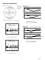
1
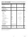
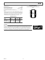
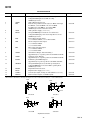
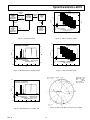
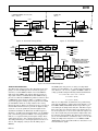
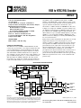
a
RGB to NTSC/PAL Encoder
AD722
FEATURES
Low Cost, Integrated Solution
+5 V Operation
Accepts FSC Clock or Crystal, or 4FSC Clock
Composite Video and Separate Y/C (S-Video) Outputs
Minimal External Components:
No External Filters or Delay Lines Required
Onboard DC Restoration
Accepts Either HSYNC & VSYNC or CSYNC
Phase Lock to External Subcarrier
Drives 75 Ω Reverse-Terminated Loads
Logic Selectable NTSC or PAL Encoding Modes
Compact 16-Pin SOIC
The AD722 accepts either FSC or 4FSC clock. When a clock is
not available, a low cost parallel-resonant crystal (3.58 MHz
(NTSC) or 4.43 MHz (PAL)) and the AD722’s on-chip oscillator generate the necessary subcarrier clock. The AD722 also accepts the subcarrier clock from an external video source.
APPLICATIONS
RGB to NTSC or PAL Encoding
Delays in the U and V chroma filters are matched by an on-chip
sampled-data delay line in the Y signal path. To prevent
aliasing, a prefilter at 5 MHz is included ahead of the delay line
and a post-filter at 5 MHz is added after the delay line to suppress harmonics in the output. These low-pass filters are optimized for minimum pulse overshoot. The overall luma delay,
relative to chroma, has been designed to be 170 ns, which
precompensates for delays in the filters used in the IF section of
a television receiver. This precompensation delay is already
present in TV broadcasts. The AD722 comes in a space-saving
SOIC and is specified for the 0°C to +70°C commercial temperature range.
The interface to VGA Controllers and MPEG Video Decoders
is simple: an on-chip logic “XNOR” accepts the available vertical (VSYNC) and horizontal sync (HSYNC) signals and creates
the composite sync (CSYNC) signal on-chip. If available, the
AD722 will also accept a standard CSYNC signal by connecting
VSYNC to +5 V and applying CSYNC to HSYNC pin. The
AD722 contains decoding logic to identify valid HSYNC pulses
for correct burst insertion.
PRODUCT DESCRIPTION
The AD722 is a low cost RGB to NTSC/PAL Encoder that
converts red, green and blue color component signals into their
corresponding luminance (baseband amplitude) and chrominance (subcarrier amplitude and phase) signals in accordance
with either NTSC or PAL standards. These two outputs are
also combined to provide composite video output. All three outputs can simultaneously drive 75 Ω, reverse-terminated cables.
All logical inputs are CMOS compatible. The chip operates
from a single +5 V supply. No external delay lines or filters are
required. The AD722 may be powered down when not in use.
FUNCTIONAL BLOCK DIAGRAM
SUBCARRIER
PHASE
DETECTOR
FSC
CHARGE
PUMP
XOSC
4FSC
4FSC
FSC
SYNC
SEPARATOR
NTSC/PAL
HSYNC
VSYNC
CSYNC
4FSC
QUADRATURE
+4
DECODER
4FSC
VCO
CSYNC
BURST
XNOR
FILTER
LOOP
FSC 90°
NTSC/PAL
±180°
(PAL ONLY)
SC 90°/270°
NTSC/PAL
FSC 0°
CLOCK
AT 4FSC
BURST
RED
GREEN
BLUE
Y
DC
CLAMP
DC
CLAMP
DC
CLAMP
RGB-TO-YUV
ENCODING
MATRIX
U
V
3-POLE
LP PREFILTER
4-POLE
LPF
4-POLE
LPF
CSYNC
INSERTION
U
CLAMP
V
CLAMP
BALANCED
MODULATORS
SAMPLEDDATA
DELAY
LINE
2-POLE
LP POSTFILTER
X2
LUMINANCE
OUTPUT
NTSC/PAL
X2
COMPOSITE
OUTPUT
3-POLE LPF
3.6MHz (NTSC)
4.4MHz (PAL)
X2
CHROMINANCE
OUTPUT
REV. 0
Information furnished by Analog Devices is believed to be accurate and
reliable. However, no responsibility is assumed by Analog Devices for its
use, nor for any infringements of patents or other rights of third parties
which may result from its use. No license is granted by implication or
otherwise under any patent or patent rights of Analog Devices.
© Analog Devices, Inc., 1995
One Technology Way, P.O. Box 9106, Norwood. MA 02062-9106, U.S.A.
Tel: 617/329-4700
Fax: 617/326-8703
(Unless otherwise noted, VS = +5, TA = +25°C, using FSC synchronous clock. All loads are
AD722–SPECIFICATIONS 150 Ω ± 5% at the IC pins. Outputs are measured at the 75 Ω reverse terminated load.)
Parameter
SIGNAL INPUTS (RDIN, GRIN, BLIN)
Input Amplitude
Black Level
Input Resistance1
Input Capacitance
LOGIC INPUTS (SYNC, FSC, ENCD, NTSC)
Logic LO Input Voltage
Logic HI Input Voltage
Logic LO Input Current (DC)
Logic HI Input Current (DC)
VIDEO OUTPUTS2
Luminance (LUMA)
Roll-off @ 5 MHz
Gain Error
Linearity
Sync Level
Conditions
Min
Color Burst Amplitude
Color Signal to Burst Ratio Error
Color Burst Width
Red, Green, Blue
Composite (COMP)
Absolute Gain Error
Differential Gain
Differential Phase
DC Black Level
POWER SUPPLIES
Recommended Supply Range
Quiescent Current—Encode Mode
Quiescent Current—Power Down
Units
714
700
3
mV p-p
mV p-p
V
MΩ
pF
1
<1
<1
V
V
µA
µA
–10
–7
–5
± 0.6
286
300
1.3
dB
dB
%
%
mV
mV
V
0
1
5
CMOS Logic Levels
4
NTSC
PAL
–15
NTSC
PAL
243
NTSC
PAL
NTSC
PAL
170
–15
NTSC
PAL
Phase Error3
DC Black Level
Chroma Feedthrough
Chroma/Luma Time Alignment
Max
NTSC
PAL
DC Black Level
Chrominance (CRMA)
Bandwidth
Typ
R, G, B = 0
–5
With Respect to Chroma
With Respect to Chroma
Single Supply
3.6
4.4
240
252
±3
2.51
2.28
±3
2.1
+15
329
330
15
MHz
MHz
mV p-p
mV
%
µs
µs
Degrees
V
10
–140
40
mV p-p
ns
±1
0.5
2.0
1.6
5
%
%
%
V
+5.25
40
V
mA
mA
+4.75
30
1
NOTES
1
R, G, and B signals are inputted to an on-chip AC coupling capacitor.
2
All outputs measured at a 75 Ω reverse-terminated load; voltages at the IC output pins are twice those specified here.
3
Difference between ideal color-bar phases and the actual values.
Specifications are subject to change without notice.
–2–
REV. 0
AD722
ABSOLUTE MAXIMUM RATINGS*
PIN CONFIGURATION
16-Pin Small Outline Package (Wide Body)
(R-16)
Supply Voltage VS . . . . . . . . . . . . . . . . . . . . . . . . . . . . . . +6 V
Internal Power Dissipation . . . . . . . . . . . . . . . . . . . . . . 600 mW
Operating Temperature Range . . . . . . . . . . . . . . 0°C to +70°C
Storage Temperature Range . . . . . . . . . . . . . –65°C to +125°C
Lead Temperature Range (Soldering 60 sec) . . . . . . . . +300°C
NOTE
*Stresses above those listed under “Absolute Maximum Ratings” may cause
permanent damage to the device. This is a stress rating only and functional
operation of the device at these or any other conditions above those indicated in the
operational section of this specification is not implied. Exposure to absolute
maximum rating conditions for extended periods may affect device reliability.
Thermal Characteristics: 16-Pin SOIC Package: θJA = 100°C/W.
ORDERING GUIDE
Model
Temperature Package
Package
Range
Description Option
AD722JR-16
AD722JR-16-Reel
AD722JR-16-Reel7
0°C to +70°C
0°C to +70°C
0°C to +70°C
STND
1
16 HSYNC
AGND
2
15 VSYNC
FIN
3
APOS
4
AD722
ENCD
5
TOP VIEW
(Not to Scale)
RIN
6
11 LUMA
GIN
7
10 COMP
BIN
8
9 CRMA
13 DGND
12 SELECT
16-Pin SOIC R-16
16-Pin SOIC R-16
16-Pin SOIC R-16
CAUTION
ESD (electrostatic discharge) sensitive device. Electrostatic charges as high as 4000 V readily
accumulate on the human body and test equipment and can discharge without detection.
Although the AD722 features proprietary ESD protection circuitry, permanent damage may
occur on devices subjected to high energy electrostatic discharges. Therefore, proper ESD
precautions are recommended to avoid performance degradation or loss of functionality.
REV. 0
14 DPOS
–3–
WARNING!
ESD SENSITIVE DEVICE
AD722
PIN DESCRIPTIONS
Pin
Mnemonic
Description
Equivalent Circuit
1
STND
Circuit A
2
3
AGND
FIN
4
5
APOS
ENCD
6
RIN
7
GIN
8
BIN
9
CRMA
10
COMP
11
LUMA
12
SELECT
13
14
15
16
DGND
DPOS
VSYNC
HSYNC
A Logical HIGH input selects NTSC encoding.
A Logical LOW input selects PAL encoding.
CMOS Logic Levels.
Analog Ground Connection.
FSC clock or parallel-resonant crystal, or 4FSC clock input.
For NTSC: 3.579 545 MHz or 14.318 180 MHz.
For PAL: 4.433 619 MHz or 17.734 480 MHz.
CMOS Logic Levels for subcarrier clocks.
Analog Positive Supply (+5 V ± 5%).
A Logical HIGH input enables the encode function.
A Logical LOW input powers down chip when not in use.
CMOS Logic Levels.
Red Component Video Input.
0 to 714 mV for NTSC; 0 to 700 mV for PAL.
Green Component Video Input.
0 to 714 mV for NTSC.
0 to 700 mV for PAL.
Blue Component Video Input.
0 to 714 mV for NTSC.
0 to 700 mV for PAL.
Chrominance Output (Subcarrier Only).*
Approximately 1.8 V peak-to-peak for both NTSC and PAL.
Composite Video Output.*
Approximately 2.5 V peak-to-peak for both NTSC and PAL.
Luminance plus SYNC Output.*
Approximately 2 V peak-to-peak for both NTSC and PAL.
A Logical LOW input selects the FSC operating mode.
A Logical HIGH input selects the 4FSC operating mode.
CMOS Logic Levels.
Digital Ground Connections.
Digital Positive Supply (+5 V ± 5%) .
Vertical Sync Signal (if using external CSYNC set at +5 V).
Horizontal Sync Signal (or CSYNC signal).
Circuit B
Circuit A
Circuit C
Circuit C
Circuit C
Circuit D
Circuit D
Circuit D
Circuit A
Circuit A
Circuit A
*The Luminance, Chrominance, and Composite Outputs are at twice normal levels for driving 75 Ω reverse-terminated lines.
DPOS
APOS
4pF
TYP
1
6
5
7
12
8
VCLAMP
15
16
Circuit C
Circuit A
APOS
APOS
3
9
10
VBIAS
11
Circuit D
Circuit B
Equivalent Circuits
–4–
REV. 0
Typical Characteristics–AD722
0.10
75Ω
RGB
AD722
RGB TO
NTSC/PAL
ENCODER
COMPOSITE
VIDEO
100
SONY
MONITOR
MODEL
1342
0.5
3
IRE
75Ω
GENLOCK
50
VOLTS
TEKTRONIX
TSG 300
COMPONENT
VIDEO
WAVEFORM
GENERATOR
APL = 50.8%
525 LINE NTSC NO FILTERING
SLOW CLAMP TO 0.00V @ 6.63µs
COMPOSITE
SYNC
0
0.0
TEKTRONIX
1910
COMPOSITE
VIDEO
WAVEFORM
GENERATOR
TEKTRONIX
VM700A
WAVEFORM
MONITOR
FSC
PRECISION MODE OFF
SYNCHRONOUS
SYNC = SOURCE
FRAMES SELECTED : 1 2
–0.5
0
Figure 1. Evaluation Setup
10
20
30
µs
–50
40
50
60
Figure 4. 100% Color Bars, NTSC
0.10
0.10
APL = 49.5%
525 LINE NTSC NO FILTERING
SLOW CLAMP TO 0.00V @ 6.63µs
APL = 50.6%
625 LINE PAL NO FILTERING
SLOW CLAMP TO 0.00V @ 6.72µs
100
0.5
0.5
VOLTS
IRE
VOLTS
50
0
0.0
PRECISION MODE OFF
SYNCHRONOUS
SYNC = SOURCE
FRAMES SELECTED : 1 2
–0.5
0
10
20
30
µs
40
50
0.0
PRECISION MODE OFF
SOUND-IN-SYNC OFF
SYNCHRONOUS
SYNC = SOURCE
FRAMES SELECTED : 1 2 3 4
–50
–0.5
60
Figure 2. Modulated Pulse and Bar, NTSC
0
10
20
30
µs
40
50
60
Figure 5. 100% Color Bars, PAL
0.10
APL = 49.7%
625 LINE PAL NO FILTERING
SLOW CLAMP TO 0.00V @ 6.72µs
VOLTS
0.5
0.0
PRECISION MODE OFF
SOUND-IN-SYNC OFF
SYNCHRONOUS
SYNC = SOURCE
FRAMES SELECTED : 1 2 3 4
–0.5
0
10
20
30
µs
40
50
60
Figure 6. 100% Color Bars on Vector Scope, NTSC
Figure 3. Modulated Pulse and Bar, PAL
REV. 0
–5–
AD722–Typical Characteristics
DG DP (NTSC) (SYNC = EXT)
FIELD = 1 LINE = 27, 100 IRE RAMP
MIN = –0.53
DIFFERENTIAL GAIN (%)
0.00
–0.16
–0.49
–0.53
0.2
MAX = 0.00
–0.52
p–p/MAX = 0.53
–0.38
MAX = 0.00
–0.53
pk–pk = 1.14
–0.01
0.0
–0.2
–0.4
–0.6
–0.8
DIFFERENTIAL PHASE (deg)
0.00
–0.44
0.5
MIN = –1.14
–1.14
–1.01
0.0
–0.5
–1.0
–1.5
1ST
2ND
3RD
4TH
5TH
6TH
Figure 7. 100% Color Bars on Vector Scope, PAL
Figure 10. Composite Output
Differential Phase and Gain, NTSC
0.10
APL = 11.6%
525 LINE NTSC NO FILTERING
SLOW CLAMP TO 0.00V @ 6.63µs
100
DG DP (PAL) (SYNC = EXT)
LINE = 25, 700mV RAMP
DIFFERENTIAL GAIN (%)
0.00
–0.14
0.3
0.2
0.1
0.0
–0.1
–0.2
–0.3
–0.4
–0.5
0.5
IRE
VOLTS
50
0
0.0
PRECISION MODE OFF
SYNCHRONOUS
SYNC = SOURCE
FRAMES SELECTED : 1 2
–0.5
0
10
20
30
µs
40
50
–50
DIFFERENTIAL PHASE (deg)
0.00
–1.01
1.5
1.0
0.5
0.0
–0.5
–1.0
–1.5
–2.0
1ST
2ND
60
Figure 8. Multipulse, NTSC
MIN = –0.32
–0.32
–0.16
MAX = 0.10
0.04
pk–pk = 0.42
0.10
MIN = –1.18
–1.18
–0.44
MAX = 0.70
0.42
pk–pk = 1.89
0.70
3RD
4TH
5TH
6TH
0.10
Figure 11. Composite Output
Differential Phase and Gain, PAL
APL = 11.4%
625 LINE PAL NO FILTERING
SLOW CLAMP TO 0.00V @ 6.72µs
VOLTS
0.5
0.0
PRECISION MODE OFF
SOUND-IN-SYNC OFF
SYNCHRONOUS
SYNC = SOURCE
FRAMES SELECTED : 1 2 3 4
–0.5
0
10
20
30
µs
40
50
60
Figure 9. Multipulse, PAL
–6–
REV. 0
AD722
H TIMING MEASUREMENT RS–170A (NTSC)
FIELD = 1 LINE = 22
H TIMING (PAL)
LINE = 25
9.72µs
9.0 CYCLES
5.49µs
5.59µs
2.28µs
4.60µs
4.59µs
249.0mV
33.8 IRE
100ns
94ns
39.7 IRE
102ns
293.5mV
124ns
AVERAGE 256 ≥ 256
AVERAGE 256 ≥ 256
Figure 13. Horizontal Timing, PAL
Figure 12. Horizontal Timing, NTSC
SUBCARRIER
PHASE
DETECTOR
FSC
CHARGE
PUMP
XOSC
4FSC
4FSC
FSC
SYNC
SEPARATOR
NTSC/PAL
HSYNC
VSYNC
CSYNC
4FSC
FSC 90°
QUADRATURE
+4
DECODER
POWER AND GROUNDS
4FSC
VCO
NTSC/PAL
±180°
(PAL ONLY)
GREEN
BLUE
DC
CLAMP
DC
CLAMP
RGB-TO-YUV
ENCODING
MATRIX
U
V
+5V
ANALOG
ANALOG
DGND
LOGIC
NTSC/PAL
FSC 0°
Y
DC
CLAMP
CLOCK
AT 4FSC
3-POLE
LP PREFILTER
4-POLE
LPF
4-POLE
LPF
LOGIC
SC 90°/270°
BURST
RED
+5V
AGND
CSYNC
BURST
XNOR
FILTER
LOOP
CSYNC
INSERTION
SAMPLEDDATA
DELAY
LINE
U
CLAMP
BALANCED
MODULATORS
V
CLAMP
NOTE:
THE LUMINANCE, COMPOSITE, AND
CHROMINANCE OUTPUTS ARE AT
TWICE NORMAL LEVELS FOR DRIVING
75Ω REVERSE-TERMINATED LINES.
5 MHz
2-POLE
LP POSTFILTER
X2
LUMINANCE
OUTPUT
NTSC/PAL
X2
COMPOSITE
OUTPUT
3-POLE LPF
3.6MHz (NTSC)
4.4MHz (PAL)
X2
CHROMINANCE
OUTPUT
Figure 14. Functional Block Diagram
The RGB inputs then pass into an analog encoding matrix
which creates the luminance (“Y”) signal and the chrominance
color difference (“U” and “V”) signals. The RGB to YUV encoding is performed using the following standard transformation:
THEORY OF OPERATION
The AD722 was designed to have three allowable modes of applying a clock via the FIN pin. These are FSC (frequency of
subcarrier, 3.579545 MHz for NTSC or 4.433618 MHz for
PAL) mode with CMOS clock applied, FSC mode using onchip crystal oscillator, and 4FSC mode with CMOS clock applied. To use FSC mode SELECT is pulled low and then either
a CMOS FSC clock is applied to FIN, or a parallel-resonant
crystal and appropriate tuning capacitor is placed between FIN
pin and GND to utilize the on-chip oscillator. The on-chip
Phase Locked Loop (PLL) is used in these modes to generate an
internal 4FSC which is divided to perform the digital clocking
as well as to create the quadrature subcarrier signals for the
chrominance modulation. In 4FSC mode the PLL is bypassed.
Y = 0.299 × R + 0.587 × G + 0.114 × B
U = 0.493 × (B–Y)
V = 0.877 × (R–Y)
After the encoding matrix, the AD722 has two parallel analog
paths. The Y (luminance) signal is first passed through a 3-pole
4.85 MHz/6 MHz (NTSC/PAL) Bessel low-pass filter to prevent aliasing in the sampled-data delay line. This first low-pass
filter is also where the unclocked analog sync signal is injected
into the Y signal (more on the creation of this sync signal to follow). The Y signal then passes through the sampled-data delay
line, which is clocked at 4FSC. The delay line was designed to
give an overall chrominance to luminance delay of –170 ns. Following the sampled-data delay line is a 5.25 MHz/6.5 MHz
(NTSC/PAL) 2-pole low-pass Bessel filter to smooth the reconstructed luminance signal.
Referring to the AD722 block diagram (Figure 14), the RGB inputs (each 714 mV p-p max for NTSC or 700 mV p-p max for
PAL) are ac-coupled and then pass through dc clamps. These
clamps allow the user to have a black level which is not at 0 V.
The clamps will clamp to a black input signal level between 0 V
and 3 V. The clamping occurs just after the falling edge of
HSYNC.
REV. 0
–7–
AD722
create visual artifacts in some high-end video systems. The burst
flag which is generated goes to the reference cell and allows a reference voltage to be inserted to the U and V low-pass filters.
The other analog path is the chrominance path which is where
the U and V color difference signals are processed. The U and V
signals first pass through 4-pole modified Bessel low-pass filters
with –3 dB frequencies of 1.2 MHz/1.5 MHz (NTSC/PAL) to
prevent aliasing in the modulators. The color burst signal is injected into the U and V channels in these premodulation filters.
The U and V signals are then modulated independently by a
pair of balanced switching modulators driven in quadrature by
the color subcarrier.
APPLYING THE AD722
Inputs
RIN, BIN, GIN are analog inputs that should be terminated to
ground with 75 Ω in close proximity to the IC. When properly
terminated the peak-to-peak voltage for a maximum input level
should be 714 mV p-p for NTSC or 700 mV p-p for PAL. The
horizontal blanking interval should be the most negative part of
each signal.
The bandwidths of all the on-chip filters are tuned using proprietary auto-tuning circuitry. The basic principle is to match an
RC time constant to a reference time period, that time being
one cycle of a subcarrier clock. The auto-tuning is done during
the vertical blanking interval and has some added hysteresis so
that once an acceptable tuning value is reached the part won’t
toggle between tuning values from field to field. The bandwidths stated in the above discussion are the design target bandwidths for NTSC and PAL.
The signal should be flat during the horizontal blanking interval.
Internal circuitry will clamp this level during HSYNC to a reference that is used internally as the black level. The horizontal
blanking level at the input pins can range between 0 V and 3 V
with respect to the ground level of the AD722.
HSYNC and VSYNC are two logic level inputs that are combined internally to produce a composite sync signal. If a composite sync signal is to be used, it can be input to HSYNC while
VSYNC is pulled to logic HI (+5 V).
The AD722’s 4FSC clock (either produced by the on-chip PLL
or user supplied) drives a digital divide-by-4 circuit to create the
quadrature signals for modulation. The reference phase 0° is
used for the U signal. In the NTSC mode, the V signal is modulated at 90°, but in PAL mode, the V modulation alternates between 90° and 270° at half the line rate as required by the PAL
standard. The outputs of the U and V balanced modulators
are summed and passed through a 3-pole low-pass filter with
3.6 MHz/4.4 MHz bandwidths (NTSC/PAL) in order to remove the harmonics generated during the switching modulation.
The form of the input sync signal(s) will determine the form of
the composite sync on the composite video (COMP) and luminance (LUMA) outputs. If no equalization or serration pulses
are included in the HSYNC input there won’t be any in the outputs. Although sync signals without equalization and serration
pulses do not technically meet the video standards’ specifications, many monitors do not require these pulses in order to
display good pictures. The decision whether to include these
signals is a system tradeoff between cost and complexity and
adhering strictly to the video standards.
The filtered chrominance signal is then summed with the filtered luminance signal to create the composite video signal. The
separate luminance, chrominance, and composite video signals
are amplified by a factor of two in order to drive 75 Ω reverseterminated lines. The separate luminance and chrominance outputs together are known as S-video. The composite and S-video
outputs are simultaneously available.
The SELECT input is a CMOS logic level that programs the
AD722 to use a subcarrier at a 1FSC (LO) frequency or a
4FSC (HI) frequency for the appropriate standard being used.
A 4FSC clock is used directly, while a 1FSC input is multiplied
up to 4FSC by an internal phase locked loop.
The two sync inputs HSYNC and VSYNC are fed into an
XNOR gate to create a CSYNC signal for the AD722. If the
user produces, or has access to, a true composite sync signal, it
can be input to the HSYNC pin while the VSYNC pin is held
high. In either case the CSYNC signal which is present after the
XNOR gate, is used to generate the sync and burst signals
which ultimately get injected into the analog signal chain. The
unclocked CSYNC signal is sent to a reference cell on the chip
which, when CSYNC is low, allows a reference voltage (based
on a power supply division) to be injected into the luminance
chain. The width of the injected sync is the same as the width of
the supplied sync signal.
The FIN input can be a logic level clock at either FSC or 4FSC
frequency or can be a parallel resonant crystal at 1FSC frequency. An on-chip oscillator will drive the crystal. Most crystals will require a shunt capacitance of between 10 pF and 30
pF for reliable start up and proper frequency of operation.
The NTSC specification calls for a frequency accuracy of ±10 Hz
from the nominal subcarrier frequency of 3.579545 MHz. While
maintaining this accuracy in a broadcast studio might not be a
severe hardship, it can be quite expensive in a low cost consumer application.
The AD722 will operate with subcarrier frequencies that deviate
quite far from those specified by the TV standards. However,
the monitor will in general not be quite so forgiving. Most monitors can tolerate a subcarrier frequency that deviates several hundred Hz from the nominal standard without any degradation in
picture quality. These conditions imply that the subcarrier frequency accuracy is a system specification and not a specification
of the AD722 itself.
The CSYNC signal (after the XNOR gate) also goes to the digital section of the AD722 where it is clocked in by a 2FSC clock.
The digital section then measures the width of the CSYNC
pulses to separate horizontal pulses from vertical equalizing and
serration pulses. A burst flag is generated only after valid horizontal sync pulses and is timed from the falling edge of the
clocked-in CSYNC signal. In synchronous systems (those in
which the subcarrier clock, sync signals, and RGB signals are all
synchronous) this will give a fixed burst position relative to the
falling edge of the output sync. However, in asynchronous systems the sync to burst position can change line to line by as
much as 140 ns (the period of a 2FSC clock cycle) due to the
fact that the burst flag is generated from a clocked CSYNC while
the sync is injected unclocked. This phenomenon may or may not
The STND pin is used to select between NTSC and PAL operation. Various blocks inside the AD722 use this input to program
their operation. Most of the more common variants of NTSC
and PAL are supported. There are, however, two known specific
standards which are not supported. These are NTSC 4.43 and
M-PAL.
–8–
REV. 0
AD722
resistor is required close to each AD722 output, while 75 Ω to
ground should terminate the far end of each line.
Basically these two standards use most of the features of the
standard that their names imply, but use the subcarrier that is
equal to or approximately equal to the frequency of the other
standard. Because of the automatic programming of the filters in
the chrominance path and other timing considerations, it is not
possible to support these standards.
The outputs have a dc bias and must be ac coupled for proper
operation. The COMP and LUMA outputs have information
down to 30 Hz that must be transmitted. Each output requires a
220 µF series capacitor to work with the 75 Ω resistance to pass
these low frequencies. The CRMA signal has information
mostly up at the chroma frequency and can use a smaller capacitor if desired, but 220 µF can be used to minimize the number of different components used in the design.
Layout Considerations
The AD722 is an all CMOS mixed signal part. It has separate
pins for the analog and digital +5 V and ground power supplies.
Both the analog and digital ground pins should be tied to the
ground plane by a short, low inductance path. Each power
supply pin should be bypassed to ground by a low inductance
0.1 µF capacitor and a larger tantalum capacitor of about 10 µF.
Displaying VGA Output on a TV
The AD722 can be used to convert the analog RGB output from a
personal computer’s VGA card to the NTSC or PAL television
standards. To accomplish this it is important to understand that
the AD722 requires interlaced RGB video and clock rates that
are consistent with those required by the television standards. In
most computers the default output is a noninterlaced RGB signal at a frame rate higher than used by either NTSC or PAL.
The three analog inputs (RIN, GIN, BIN) should be terminated
with 75 Ω to ground close to the respective pins. However, as
these are high impedance inputs, they can be in a loop-thru
configuration. This technique is used to drive two or more
devices with high frequency signals that are separated by some
distance. A connection is made to the AD722 with no local
termination, and the signals are run to another distant device
where the termination for these signals is provided.
Most VGA controllers support a wide variety of output modes
that are controlled by altering the contents of internal registers.
It is best to consult with the VGA controller manufacturer to
determine the exact configuration required to provide an interlaced output at 60 Hz (50 Hz for PAL).
The output amplitudes of the AD722 are double that required
by the devices that it drives. This compensates for the halving of
the signal levels by the required terminations. A 75 Ω series
SELECT
10µF
+
+5V
4
14
APOS
DPOS
+
0.1µF
6
1
+5V
0.1µF
5 ENCD
11
6 RIN
3
+
LUMA 11
16 HSYNC
75Ω
+
+5V
75Ω
10kΩ
+5V
75Ω
CRMA 9
75Ω
9
75Ω
Y
220µF
15 VSYNC
13
COMPOSITE
VIDEO
AD722
8 BIN
8
75Ω
220µF
7 GIN
12
+
CMPS 10
7
2
10µF
C
220µF
12 SELECT
4
10
JMP
OSC
15
0.1µF
S-VIDEO
(Y/C VIDEO)
1 STND
+5V
5
JMP
10kΩ
14
**
3 FIN
*
CRYSTAL
10–30pF
* PARALLEL–RESONANT
AGND
DGND
2
13
CRYSTAL; 3.579545MHz (NTSC)
OR 4.433620MHz (PAL)
CAPACITOR VALUE DEPENDS ON
CRYSTAL CHOSEN
+5V (VAA)
VGA OUTPUT
CONNECTOR
11
5
6
**FSC OR 4FSC CLOCK; 3.579545MHz,
0.1µF
AD813
14.31818MHz (NTSC) OR 4.433620MHZ,
17.734480MHz(PAL)
75Ω
1/3
VSYNC
7
HSYNC
1
649Ω
649Ω
B
75Ω
12
14
13 1/3
2
649Ω
75Ω
G
75Ω
649Ω
R
75Ω
10
9 1/3
3
649Ω
649Ω
FROM VGA PORT
8
4
75Ω
RGB MONITOR
–5V
Figure 15. Interfacing the AD722 to the (Interlaced) VGA Port of a PC
REV. 0
–9–
AD722
+5V (VAA)
0.01µF
+5V (VAA)
0.1µF
0.1µF
COMP
0.01µF
VREF
24
AD722
10kΩ
12 SELECT
SYNC
CLOCK
IOR
6 RIN
IOG
7 GIN
IOB
8 BIN
75Ω
75Ω
75Ω
75Ω
75Ω
HSYNC
VSYNC
VSYNC
* PARALLEL–RESONANT
CRYSTAL; 3.579545MHz (NTSC)
OR 4.433620MHz (PAL)
CAPACITOR VALUE DEPENDS ON
CRYSTAL CHOSEN
LUMA 11
CRMA
9
COMPOSITE
VIDEO
75Ω
+
220µF
75Ω
HSYNC
75Ω
+
COMP 10
220µF
BLANK
GND
33µF
5 ENCD
10kΩ
MPEG
DECODER
L1 (FERRITE BEAD)
10µF
GND
+5V
RSET
550Ω
ADV7120
14
DPOS
10kΩ
AD589
(1.2V REF)
FSADJ
4
APOS
+5V
0.1µF
DATA IN
+5V (VAA)
0.1µF
+5V
VAA
+5V (VCC)
S-VIDEO
75Ω
+
16 HSYNC
220µF
15 VSYNC
+5V
+5V
OSC
10kΩ
**
3 FIN
STND
0.1µF
*
CRYSTAL
**FSC OR 4FSC CLOCK; 3.579545MHz,
10–30pF
DGND
AGND
13
2
1
14.31818MHz (NTSC) OR 4.433620MHZ,
17.734480MHz(PAL)
Figure 16. AD722 and ADV7120/ADV7122 Providing MPEG Video Solution
video from an MPEG decoder and creating both analog RGB
video and composite video.
Figure 15 shows a circuit for connection to the VGA port of a
PC. The RGB outputs connect directly to the respective inputs
of the AD722. These signals should each be terminated to
ground with 75 Ω.
The 24-bit wide RGB video is converted to analog RGB by the
ADV7120 (Triple 8-bit video DAC–available in 48-pin TQFP).
The analog current outputs from the DAC are terminated to
ground at both ends with 75 Ω as called for in the data sheet.
These signals directly feed the analog inputs of the AD722. The
HSYNC and VSYNC signals from the MPEG Controller are directly applied to the AD722.
The standard 15-pin VGA connector has HSYNC on Pin 13
and VSYNC on Pin 14. These signals also connect directly to
the same name signals on the AD722. The FIN signal can be
provided by any of the means described elsewhere in the data
sheet. For a synchronous NTSC system, the internal 4FSC
(14.31818 MHz) clock that drives the VGA controller can be
used for FIN on the AD722. This signal is not directly accessible
from outside the computer, but it does appear on the VGA card.
If a separate RGB monitor is also to be used, it is not possible to
simply connect it to the R, G, and B signals. The monitor provides a termination that would double terminate these signals.
The R, G, and B signals should be buffered by three amplifiers
with high input impedances. These should be configured for a
gain of two, which is normalized by the divide by two termination scheme used for the RGB monitor.
The AD813 is a triple video amplifier that can provide the necessary buffering in a single package. It also provides a disable
pin for each amplifier which can be used to disable the drive to
the RGB monitor when interlaced video is used (SELECT = LO).
When the RGB signals are noninterlaced, setting SELECT HI will
enable the AD813 to drive the RGB monitor and disable the encoding function of the AD722 via Pin 5. HSYNC and VSYNC
are logic level signals that can drive both the AD722 and RGB
monitor in parallel.
AD722 Used with an MPEG Decoder
MPEG decoding of compressed video signals is becoming a
more prevalent feature in many PC systems. To display images
on the computer monitor, video in RGB format is required.
However, to display the images on a TV monitor or to record
the images on a VCR, video in composite format is required.
Figure 16 shows a schematic for taking the 24-bit wide RGB
If the set of termination resistors closest to the AD722 are removed, an RGB monitor can be connected to these signals and
it will provide the required second termination. This scenario is
acceptable as long as the RGB monitor is always present and
connected. If it is to be removed on occasion, another termination scheme is required.
The AD813 triple video op amp can provide buffering for such
applications. Each channel is set for a gain of two while the outputs are back terminated with a series 75 Ω resistor. This provides the proper signal levels at the monitor which terminates
the lines with 75 Ω.
AD722 APPLICATION DISCUSSION
Chrominance and Luminance Alignment
Inside the AD722 the chrominance and luminance signals are processed by separate paths. They both are either output separately
(Y/C), or they are added together by the composite video amplifier. Although both channels are filtered, the chrominance signal
experiences a greater filtering delay due to the higher order of
the chrominance path filters. To compensate, a sampled delay
line is used in the luminance path.
For baseband video it is desirable for the chrominance and luminance to be accurately aligned with zero offset. However, the
situation for modulated RF video is a bit more complicated due
to the effects of the IF circuitry used in TV sets.
–10–
REV. 0
AD722
one field and will be refreshed at a rate of 30 Hz (25 Hz for
PAL). During the time that the other field is being displayed the
line will not be displayed. The human eye is capable of detecting this, and the display will be perceived to have a pulsating or
flickering black line. This effect is highly content sensitive and
is most pronounced in applications in which text and thin
horizontal lines are present. In applications such as CD video,
photography and animation, portions of objects naturally
occur in both odd and even fields and the effect of flicker is
imperceptible.
The IF strips used in TVs delay the chrominance by 170 ns
more than the luminance. To compensate for this, transmitted
video has the chrominance lead the luminance by 170 ns. The
term used for this is chrominance delay, and it is specified as
–170 ns, the negative (–) indicating that chrominance leads the
luminance. This correction to TV broadcasts was made in the
early days of TV and is the standard to this day.
The delay line used in the luminance path of the AD722 creates
a –170 ns chrominance delay. This will be realigned by the RF
section of a TV when it is used for receiving the signal.
However, for baseband inputs, the chrominance will lead the
luminance by a small amount. This will show up as a slight
color shadow to the left of objects. The physical offset can be
calculated by approximating the active horizontal line time of a
TV as 50 µs. Thus, the chrominance offset distance will be the
width of the screen times (50 µs/170 ns) or 0.0034. For a 13
inch monitor the screen width is about 10 in. (25 cm), so the
offset distance will be 0.034 in. (0.85 mm).
Dot Crawl
There are numerous distortions that are apparent in the presentation of composite NTSC signals on TV monitors. These effects will vary in degree depending on the circuitry used by the
monitor to process the signal and on the nature of the image being displayed. It is generally not possible to produce pictures on
a composite monitor that are as high quality as those produced
by standard quality RGB, VGA monitors.
One well known distortion of composite video images is called
dot crawl. It shows up as a moving dot pattern at the interface
between two areas of different color. It is caused by the inability
of the monitor circuitry to adequately separate the luminance
and chrominance signals.
One way to prevent dot crawl is to use a video signal that has
separate luminance and chrominance. Such a signal is referred
to as S-video or Y/C video. Since the luminance and chrominance are already separated, the monitor does not have to perform this function. The S-Video outputs of the AD722 can be
used to create higher quality pictures when there is an S-Video
input available on the monitor.
In a VGA conversion application, where the software controlled
registers are correctly set, there are two techniques that are commonly used by VGA controller manufacturers to generate the
interlaced signal. Each of these techniques introduces a unique
characteristic into the display created by the AD722. The artifacts described below are not due to the encoder or its encoding
algorithm as all encoders will generate the same display when
presented with these inputs. They are due to the method used
by the controller display chip to convert a noninterlaced output
to an interlaced signal. The method used is a feature of the design of the VGA chip and is not programmable.
REV. 0
There are methods to dramatically reduce the effect of flicker and
maintain high resolution. The most common is to ensure that display data never exists solely in a single line. This can be accomplished by averaging/weighting the contents of successive/multiple
noninterlaced lines prior to creating a true interlaced output (Figure 17c). In a sense this provides an output which will lie between
the two extremes described above. The weight or percentage of one
line that appears in another and the number of lines used are variables that must be considered in developing a system of this type. If
this type of signal processing is performed, it must be completed
prior to the data being presented to the AD722 for encoding.
Vertical Scaling
Flicker
The first interlacing technique outputs a true interlaced signal
with odd and even fields (one each to a frame Figure 17a). This
provides the best picture quality when displaying photography,
CD video and animation (games, etc.). However, it will introduce a defect commonly referred to as flicker into the display.
Flicker is a fundamental defect of all interlaced displays and is
caused by the alternating field characteristic of the interlace
technique. Consider a one pixel high black line which extends
horizontally across a white screen. This line will exist in only
The second technique which is commonly used is to output an odd
and even field which are identical (Figure 17b). This ignores the
data which naturally occurs in one of the fields. In this case the
same one pixel high line mentioned above would either appear
as a two pixel high line, (one pixel high in both the odd and even
field) or will not appear at all if it is in the data which is ignored by
the controller. Which of these cases occurs is dependent on the
placement of the line on the screen. This technique provides a
stable (i.e., nonflickering) display for all applications, but small
text can be difficult to read and lines in drawings (or spreadsheets) can disappear. As above, graphics and animation are not
particularly affected although some resolution is lost.
In addition to converting the computer generated image from
noninterlaced to interlaced format, it is also necessary to scale
the image down to fit into NTSC or PAL format. The most
common vertical lines/screen for VGA display are 480 and 600
lines. NTSC can only accommodate approximately 400 visible
lines/frame (200 per field), PAL can accommodate 576 lines/
frame (288 per field). If scaling is not performed, portions of
the original image will not appear in the television display.
This line reduction can be performed by merely eliminating every Nth (6th line in converting 480 lines to NSTC or every 25th
line in converting 600 lines to PAL). This risks generation of
jagged edges and jerky movement. It is best to combine the scaling
with the interpolation/averaging technique discussed above to
ensure that valuable data is not arbitrarily discarded in the scaling
process. Like the flicker reduction technique mentioned above,
the line reduction must be accomplished prior to the AD722 encoding operation.
There is a new generation of VGA controllers on the market
specifically designed to utilize these techniques to provide a
crisp and stable display for both text and graphics oriented applications. In addition these chips rescale the output from the
computer to fit correctly on the screen of a television. A list of
known devices is available through Analog Devices’ Applications
group, but the most complete and current information will be
available from the manufacturers of graphics controller ICs.
–11–
AD722
Synchronous vs. Asynchronous Operation
NONINTERLACED
The source of RGB video and synchronization used as an input
to the AD722 in some systems is derived from the same clock
signal as used for the AD722 subcarrier input (FIN). These
systems are said to be operating synchronously. In systems
where two different clock sources are used for these signals, the
operation is called asynchronous.
1
2
3
4
5
6
7
EVEN FIELD
2
3
=
+
4
5
6
7
C2031–10–5/95
The AD722 supports both synchronous and asynchronous operation, but some minor differences might be noticed between
them. These can be caused by some details of the internal
circuitry of the AD722.
ODD FIELD
1
a. Conversion of Noninterlace to Interlace
NONINTERLACED
1
2
3
4
5
6
7
There is an attempt to process all of the video and synchronization signals totally asynchronous with respect to the subcarrier
signal. This was achieved everywhere except for the sampled delay line used in the luminance channel to time align the luminance and chrominance. This delay line uses a signal at twice
the subcarrier frequency as its clock.
ODD FIELD
EVEN FIELD
1
2
3
=
+
4
5
6
7
b. Line Doubled Conversion Technique
The phasing between the delay line clock and the luminance signal (with inserted composite sync) will be constant during synchronous operation, while the phasing will demonstrate a
periodic variation during asynchronous operation. The jitter of
the asynchronous video output will be slightly greater due to
these periodic phase variations.
NONINTERLACED
1
2
3
4
5
6
7
ODD FIELD
EVEN FIELD
1
2
3
=
+
4
5
6
7
c. Line Averaging Technique
Figure 17.
OUTLINE DIMENSIONS
Dimensions shown in inches and (mm).
16-Lead SOIC (R-16) (Wide Body)
9
16
0.2992 (7.60)
0.2914 (7.40)
0.4193 (10.65)
0.3937 (10.00)
PIN 1
8
0.4133 (10.50)
0.3977 (10.00)
0.0118 (0.30)
0.0040 (0.10)
0.0500 (1.27)
BSC
0.0192 (0.49)
0.0138 (0.35)
0.1043 (2.65)
0.0926 (2.35)
0.0125 (0.32)
0.0091 (0.23)
–12–
0.0291 (0.74)
x 45 °
0.0098 (0.25)
8°
0°
PRINTED IN U.S.A.
1
0.0500 (1.27)
0.0157 (0.40)
REV. 0