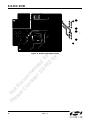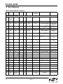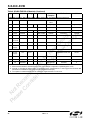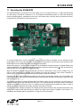
1
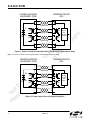
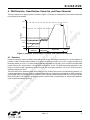
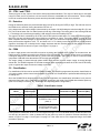
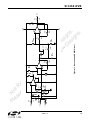
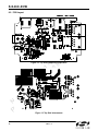
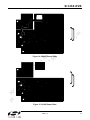
Si 3 4 6 0 - EVB Si3460 E VALUATION B OARD U SER ’ S G U I D E 1. Introduction This document is intended to be used in conjunction with the Si3460 data sheet for designers interested in: An Pl No ea t se Re C com on si me de n r S de i3 d f 46 or 2 N fo ew rN D ew es D ign es s. ig ns . introduction to Power-over-Ethernet (PoE) and Power Sourcing Equipment (PSE) design considerations How the Si3460 PSE controller operates in the Si3460-EVB reference design Configuring and operating the Si3460-EVB 2. Overview of the Si3460 and Evaluation Board The Si3460 is a single-port –48 V power management controller for IEEE 802.3af compliant Power Sourcing Equipment (PSE). The Si3460 operates directly from a 12 or 15 V isolated input supply and integrates a digital PWM-based dc-dc converter for generating the –48 V PSE output supply. The negative polarity on the PSE supply provides safety-extra-low-voltage (SELV) compatibility with telephony ports in the same system. The complete Si3460 reference design (i.e., the Si3460-EVB) also provides full IEEE-compliant classification and detection as well as a robust disconnect algorithm. Intelligent protection circuitry includes input under-voltage lockout (UVLO), current limiting, and output short-circuit protection. The Si3460 is designed to operate completely independently of host processor control. A reset input and an optional LED status signal is provided to indicate the port status, including detect, power good and output fault event information for use within the host system. The Si3460 is pin programmable to support: Endpoint and midspan applications, with support for either 10/100BASE-T or 10/100/1000BASE-T All four classification power levels specified by the IEEE 802.3 standard Classification-based current limiting Automatic or manual restart after various fault events are detected 3. Introduction to PoE IEEE 802.3-2005 clause 33 (formerly IEEE 802.3af) is the standard for providing power to a remote Ethernet device on the same cable that is carrying data. The power is either carried common mode on one of the data pairs (for 10/100/1000BASE-T) or on the spare pairs for 10/100BASE-T only applications. Figures 1 and 2 show the possible connections for the power. The connections shown in Figure 1 should be used for power injection in an Ethernet midspan, and the connections shown in Figure 2 can be used for either midspan or endpoint (switch) applications. Designed for use on the PSE side for providing power to a single Ethernet PD port, the Si3460 can be configured to operate in either midspan or endpoint applications. Although at this time the existing IEEE specification doesn't specifically allow or prohibit gigabit (10/100/1000BASE-T) midspans, in midspan mode, the Si3460-EVB is designed to operate in 10/100BASE-T mode, as the power is carried on the spare pairs. However, the Si3460 controller can also be designed into gigabit endpoints with the power connected to either the data or spare pairs. Rev. 1.2 3/13 Copyright © 2013 by Silicon Laboratories Si3460-EVB Si3460-EVB POWER SOURCING EQUIPMENT (PSE) POWERED DEVICE (PD) 4 4 5 5 SPARE PAIR TX 1 2 2 RX PD I/F and DC-DC Converter Pl No ea t se Re C com on si me de n r S de i3 d f 46 or 2 N fo ew rN D ew es D ign es s. ig ns . + 1 3 _ 48 V RX SIGNAL PAIR 6 3 6 TX SIGNAL PAIR 7 7 8 8 SPARE PAIR Figure 1. Power Carried Over the Spare Pair (10/100BASE-T Applications Only) Note: This is the connection scheme implemented on the Si3460-EVB reference design. POWER SOURCING EQUIPMENT (PSE) POWERED DEVICE (PD) 4 4 5 5 SPARE PAIR ± 48 V ± TX 1 1 2 2 3 RX SIGNAL PAIR 6 RX 3 6 DC-DC Converter and PD I/F TX SIGNAL PAIR 7 7 8 8 SPARE PAIR Figure 2. Power Carried Over the Signal (Data) Pair 2 Rev. 1.2 Si3460-EVB 4. PSE Detection, Classification, Power-Up, and Power Removal The basic sequence for applying power is shown in Figure 3. Following is a description of the functions that must be performed in each phase. 57 V Voltage Pl No ea t se Re C com on si me de n r S de i3 d f 46 or 2 N fo ew rN D ew es D ign es s. ig ns . 44 V 20.5 V 15.5 V 10 V Time 2.8 V Detection Classification Apply Power Turn off Figure 3. Detection, Classification, Powerup, and Disconnect Sequence 4.1. Detection During the detection phase, the PSE probes with limited current and voltage to determine if a 25 k signature is present. A valid PD must present between 23.75 and 26.25 k in the range of 2.7 to 10.1 V, with an offset (due to the bridge diodes) of up to 1.9 V, and a parallel capacitance of between 0.05 and 0.12 µF. An IEEE-compliant PSE probes 2.8 and 10 V, with at least a 1 V step and current limit of <5 mA. The PSE must accept signatures in the range of 19–26.5 k with capacitance of up to 0.15 µF and must reject resistance <15 k or >33 k as well as capacitive signatures >10 µF. The strict limits on the detection phase ensure that non PoE enabled devices are not inadvertently powered. For endpoint applications, detection must be completed within 500 ms of applying a valid signature. When configured as a midspan there is a possibility that the PSE circuit will compete with an endpoint PSE, and, as required by the IEEE specifications, the Si3460 is therefore required to wait at least 2 seconds after an unsuccessful detection cycle to repeat the detection process. Rev. 1.2 3 Si3460-EVB 4.2. Classification Classification is optional and is performed by applying between 15.5 and 20.5 V to the PD and measuring the current. The maximum power level that can be drawn by the PD is determined according the following table. Table 1. Classification Levels Minimum PSE Power Level Current Measured Class 0 15.4 W <5 mA Class 1 4W 8–13 mA Class 2 7W 16–21 mA Pl No ea t se Re C com on si me de n r S de i3 d f 46 or 2 N fo ew rN D ew es D ign es s. ig ns . Classification Level Class 3 15.4 W 25–31 mA Class 4 15.4 W 35–45 mA Currents not falling in these ranges maybe be treated as the higher or lower classification level. Currents above 45 mA may be treated as class level 0 or 4, which is 15.4 W in either case. 4.3. Power-Up After the optional classification step, power is applied. Per the IEEE specification, the PSE must supply between 44 and 57 V to the PD. For longer durations above 50 ms the power may be removed if the maximum power level of either 4, 7, or 15.4 W is exceeded. If the current exceeds 400 mA, the power must be removed in 75 ms. For short-circuit protection, output power is removed immediately if the output current exceeds 800 mA or the output voltage drops below 30 V. If power is removed due to an overload condition, detection must not be attempted again for at least 2 s. 4.4. Disconnect (Power Removal) The Si3460 supports a robust disconnect algorithm to avoid false disconnection. Removal of a PD can be sensed by determining that the dc current is less than 5 mA for between 300 and 400 ms. If the current then exceeds 10 mA for at least 60 ms, the power must not be removed, and the 300–400 ms timer restarts. 4 Rev. 1.2 Si3460-EVB 5. The Si3460 PSE Controller In addition to providing a complete dc-dc controller to generate the PSE output supply, the Si3460 is a fully IEEE compliant PSE power management controller. The Si3460 is specifically designed and configured to work with an applications circuit (Si3460-EVB) that together implement a single port PSE solution for either midspans or endpoints. Referring to the detailed evaluation board schematics in Section “8. Si3460-EVB Schematics and PCB Layout”, the overall functionality is described for each operating state of the Si3460 as follows: 5.1. Initialization and Operating Mode Configuration Pl No ea t se Re C com on si me de n r S de i3 d f 46 or 2 N fo ew rN D ew es D ign es s. ig ns . The Si3460 is initialized at power up, or whenever pin 8 (RST) is held low and then allowed to transition high. Upon reset (RST asserted), the voltage at the STATUS pin (as determined by resistors R28 and R30) is sensed to determine the operating mode of the Si3460. The detection process begins immediately after initialization. Any combination of the following three operating modes can be set by the R28 and R30 resistor pair, as indicated below: Classification level: sets what maximum power level the Si3460 will support. or midspan mode: controls the backoff timing per the IEEE specifications. Restart action on fault or overload: determines whether or not the Si3460 will automatically restart after 2 s when a fault or overload condition (e.g., input UVLO, output short-circuit event, classification power level exceeded) is detected, or wait to restart until the RST pin is asserted. Endpoint Table 2. Operating Modes Nominal Status Pin Voltage Operating Mode R28, R30 Power Level Supported (W) Classes Supported Endpoint/ Midspan Restart Action on Fault or Overload Event 2 k, NP 15.4 All class levels Endpoint Auto restart after 2 s 3.0 V 2.21 k, 22.1 k 7.0 Class 1 or 2 2.75 V 2.37 k, 11.8 k 4.0 Class 1 2.5 V 2.61 k, 8.06 k 15.4 All class levels 2.25 V 2.94 k, 6.19 k 7.0 Class 1 or 2 2.0 V 3.32 k, 4.99 k 4.0 Class 1 1.75 V 3.83 k, 4.22 k 4.0 Class 1 1.5 V 4.42 k, 3.57 k 7.0 Class 1 or 2 1.25 V 5.36 k, 3.16 k 15.4 All class levels 1.0 V 6.81 k, 2.80 k 4.0 Class 1 0.5 V 14 k, 2.26 k 7.0 Class 1 or 2 NP, 2 k 15.4 All class levels Pin voltage at VEE < 0.25 V Rev. 1.2 Restart on RST low or when open circuit detected Midspan Restart on RST low or when open circuit detected Auto restart after 2 s 5 Si3460-EVB 5.2. CTRL1 and CTRL2 These two pins are the output of two 96 kHz 8-bit pulse width modulators. The output of these pins is averaged using R15, R29, and C5 to produce a dc level across C5 that is controllable with 16-bit resolution. This dc voltage is used to control both the detection process and the pulse width modulator for the dc-dc converter. 5.3. Detection During the detection phase, the pass transistor M2 is held off by driving the GATE pin high. The 250 kHz clock for the PWM circuit is held low, forcing the switcher FET M1 off. Pl No ea t se Re C com on si me de n r S de i3 d f 46 or 2 N fo ew rN D ew es D ign es s. ig ns . In the detect state, the output voltage is determined by the output of U18A feeding the resistive bridge R1, R2, and R3. The PD at the other end of a cable forms the fourth leg of the bridge. The return path to Vee is through D8 and L1. The bridge null is read through amplifier U18B, which is fed to the Si3460 pin DETA. The output of U18A is controlled by the CTRL1 and CTRL2 pins as noted earlier. For most of the detection cycle, the CTRL pins are held high which forces U18A low, producing no output. The bridge voltage is varied to force IEEE compliant detection voltages of approximately 4.5 and 7.5 V across the bridge with 20 ms delay and robust three-point detection algorithm at 4.5, 7.5, and back to 4.5 V. To robustly insure that the PD has a valid resistive signature, the bridge null is checked as the voltage increases and then checked again as the voltage decreases. Relevant waveforms are shown in Figure 4 and Figure 5 on page 11. 5.4. PWM In order to apply power to the load, M2 is turned on by driving the Si3460's GATE pin high. At the same time, the PWM circuitry is enabled by turning on the 250 kHz clock (250 kHz pin). The 250 kHz square wave is converted to a triangular shape by the filter R14 and C6. The dc level set by CTRL1 and CTRL2 is used to control the PWM comparator U19B that drives the switcher FET through gate driver U3. The output voltage is sensed through resistor divider R43 and R44, and the output current is sensed through resistor R4. The Si3460 integrates an A/D that measures these quantities and varies the CTRL1 and CTRL2 duty cycle to regulate the output current and voltage as desired. 5.5. Classification For classification, M2 is turned on and the PWM is enabled. The Si3460 is programmed to perform classification at 18 V output voltage, with a current limit of between 50 and 100 mA. Classification is performed after allowing 20 ms of settling time. Since the Si3460-EVB is designed for a single port PSE application, the classification information is only used to determine if the load is in the range that is supported, according to the mode of the Si3460 determined at power up (refer to STATUS pin in Section “5.1. Initialization and Operating Mode Configuration”). Table 3. Classification Levels Overload Current Overload Current Threshold ICUT (Max) Limit ILIM (Max) Classification Mode PSE Minimum Output Power Action Performed Full power 15.4 W Always apply full power 400 mA 450 mA Class 1 only 4W Only apply power if the current is between 8 and 13 mA (class 1) 98 mA 450 mA Class 1 or Class 2 7W Only apply full power if the current is between 8 and 21 mA (class 1 or class 2) 180 mA 450 mA If the measured classification level is not in the supported range, an error is declared and the Si3460 will either time out and retry and wait for a reset as determined by the power up mode of operation. Relevant waveforms are shown in Figure 5 on page 11 and Figure 6 on page 12. If the class level is in the supported range, the Si3460 proceeds to powerup. 6 Rev. 1.2 Si3460-EVB 5.6. Power-Up After successful classification, the Si3460 is configured to produce a nominal –50 V output voltage. The overload current limits are set based on the classification voltage on the STATUS pin at powerup. Refer to Table 1 of the Si3460 data sheet for more information. For output current durations lasting longer than 60 ms, the power is removed if the maximum power level of either 4, 7, or 15.4 W is exceeded by approximately 10%, as determined by the operating mode detected at start up (refer to Section “5.1. Initialization and Operating Mode Configuration”). In the event of an output short circuit, the Si3460 will immediately disconnect so as to prevent shorting the input supply through D8 and L1. Pl No ea t se Re C com on si me de n r S de i3 d f 46 or 2 N fo ew rN D ew es D ign es s. ig ns . The Si3460 can be configured to operate in a mode where it will automatically retry detection and power up after an overload. Alternatively, the Si3460 can be programmed to signal an error condition has occurred, in which case the user must assert RST (e.g., by pushing the reset switch on the Si3460-EVB) to start a new detection and power up cycle. As set by the initial voltage on the STATUS pin at powerup, the Si3460 will then automatically resume the detection process for "automatic restart configuration" unless the Si3460 is configured in a "restart after a RESET condition" mode and a fault condition is detected; in that case, the LED will flash rapidly, and the detection process will automatically start again after 2.2 seconds. Power will not be provided until an open-circuit condition is detected. Once the Si3460-EVB detects an open-circuit condition (normally by removing the Ethernet cable from the Si3460-EVB’s RJ-45 jack labeled “To PD”), the detection process begins, the status LED blinks at the rate of 3 times per second, and the Si3460 is then allowed to go into classification and powerup mode if a valid PD signature resistance is detected. The relevant waveform is shown in Figure 6 on page 12. 5.7. Disconnect (Power Removal) The Si3460 supports a robust disconnect algorithm. If the current drops below 5 mA for between 300 and 400 ms, the power is removed. If the output current then exceeds 10 mA for at least 60 ms, the power is not removed. The Si3460 will continue to provide power unless a disconnect or overload condition is sensed. The only other way to force the Si3460 to disconnect power is by doing a reset. The relevant waveform is shown in Figure 7 on page 12. 5.8. Current Limit Control The Si3460's overcurrent trip point is determined by the output power set during the classification stage power granting process. If the output current exceeds the threshold, a timer counts up towards a time-out of 60 ms. If the current drops below the set threshold, the timer counts down towards zero at 1/16th the rate. If the timer reaches 60 ms, an overcurrent fault is declared, and the channel is shut down by turning off the dc-dc converter clock and then turning off the FET M1. After an overcurrent fault event, the LED will flash rapidly. As set by the initial voltage on the STATUS pin at powerup, the Si3460 will then automatically resume the detection process for "automatic restart configuration" unless the Si3460 is configured in a "restart after a RESET condition" mode and a fault condition is detected; in that case, the LED will flash rapidly, and the detection process will automatically start again after 2.2 seconds. Power will not be provided until an open-circuit condition is detected. Once the Si3460-EVB detects an open-circuit condition (normally by removing the Ethernet cable from the Si3460-EVB’s RJ-45 jack labeled “To PD”), the detection process begins, the status LED blinks at the rate of 3 times per second, and the Si3460 is then allowed to go into classification and powerup mode if a valid PD signature resistance is detected. 5.9. UVLO The Si3460-EVB reference design is optimized for 12 to 15 V nominal input voltages* (11 V minimum to 16 V maximum). If the input voltage drops below 10 V in detection mode or if the output voltage drops below 10 V in classification or power up mode, a UVLO condition is declared which generates the error condition (LED flashing rapidly). An under-voltage event is a fault condition which is reported through the status LED as a rapid blinking of 10 flashes per second. The UVLO condition is continuously monitored in all operating states. *Note: Some MOSFET gate drivers operate at a maximum supply voltage of 14 V (for example, TPS2828). In that case, the input voltage must be limited to a maximum of 12 V. Rev. 1.2 7 Si3460-EVB 5.10. Status LED Function During the normal detection sequence, the STATUS LED flashes at approximately 3 times per second as the detection process continues. After successful power up, the LED glows continuously. If there is an error condition (i.e., class level is beyond programmed value, or a fault or over current condition has been detected), the LED flashes rapidly at 10 times per second). This occurs for two seconds for normal error delay and, in the case of the "restart after a RESET condition," the LED will flash rapidly, and the detection process will automatically start again after 2.2 s and power will not be provided until an open circuit condition is detected. Once the Si3460-EVB detects an open circuit condition, the LED blinks at 3 times per second. Pl No ea t se Re C com on si me de n r S de i3 d f 46 or 2 N fo ew rN D ew es D ign es s. ig ns . If the Powered Device (PD) is disconnected so that a disconnect event occurs, the LED will start flashing at 3 times per second once the detect process resumes. 8 Rev. 1.2 Si3460-EVB 6. Design and Layout Considerations 6.1. General Recommendations The Si3460-EVB schematic and layout are intended to be used as a reference for all customer designs. The Si3460-EVB has been tested by the University of New Hampshire Interoperability Lab (UNH IoL) to comply with the relevant IEEE 802.3 Clause 33 specifications. UNH test reports can be downloaded from www.silabs.com/PoE. Since the Si3460’s performance in an application depends on external components and PCB layout, customers are ultimately responsible for validating their design’s conformance to all relevant industry, safety, and customer-specific requirements. For applications support, contact [email protected]. Pl No ea t se Re C com on si me de n r S de i3 d f 46 or 2 N fo ew rN D ew es D ign es s. ig ns . 6.2. Isolation The IEEE 802.3 specification requires the PSE output power to be isolated from earth ground*. To accomplish this, the input power source must be isolated from earth ground. Also, do not connect the Si3460's ground connection (pin #11) to earth ground, as this pin serves a circuit reference point only in the Si3460-EVB. *Note: If the input power supply is referenced to earth ground, and if one of the output pads is connected to ground, it can create a high-current fault condition that will not be protected. 6.3. SELV-Compliant Output Voltage Since the output of the Si3460-EVB reference design is designed to be less than 57 Vdc under all conditions, it is considered a SELV circuit. The Si3460-EVB is designed to produce a negative output voltage with respect to the input voltage. The reason this is done is because the Si3460 will often be used in applications and environments where a standard telephone circuit or SLIC, such as the Si3210/15/32/33, will be powered from the same 12 to 15 V isolated input power supply. Conventionally, these circuits produce large negative operating voltages. Since the Si3460-EVB reference design is also designed to produce negative voltages, the Si3460-EVB implementation eliminates the possibility of a hazardous voltage difference between a SLIC output and the Si3460-EVB's PSE output. 6.4. Surge Protection The SI3460-EVB applications design includes a clamp diode, D12, to protect against the 50 µs intra-building lightening surges, as specified in IEEE 802.3. Additional protection, such as a 1 A fuse in the output circuit, may be required for applications in which the Ethernet cabling is not intra-building. 6.5. EMI and EMC The SI3460-EVB applications solution is designed to be compliant with FCC Class B (CISPR22) for radiated emissions, as well as FCC Part 15 (EN55022) for conducted emissions. The PCB layout of the Si3460-EVB should be closely followed to prevent EMI and EMC issues. The keys to robust EMI and EMC performance are: Keep the current loops in the switcher circuit small-diameter. Lay out the current loop when the FET is on similarly to the current loop when the FET is off. Connect filter caps to the power circuitry and not to reference planes. For better EMI performance, use shielded inductors for L1 and L4. 6.6. Thermal Considerations Inductor L1: For improved thermal performance, Silicon Laboratories strongly recommends using a shielded inductor for L1. The recommended shielded inductor is available from Coilcraft: MSS1278T-154. Please refer to: http://www.coilcraft.com/pdfs/mss1278t.pdf. Rev. 1.2 9 Si3460-EVB 6.7. R43 and R47 Pl No ea t se Re C com on si me de n r S de i3 d f 46 or 2 N fo ew rN D ew es D ign es s. ig ns . Resistors R43 and R47 together dissipate about 1 W of power during normal operation. Resistors R43, R47, and R44 (127 ) are chosen based on the IEEE minimum disconnect current specifications and to ensure good transient response for sudden load changes. To help ensure that heat dissipated by R43 and R47 does not unduly contribute to the heating of the PCB, it is recommended to move these resistors away from other heat-dissipating components, such as switching FET M1, inductor L1, and switching diode D8. 10 Rev. 1.2 Si3460-EVB 7. Output Voltage and Load Current Waveforms Pl No ea t se Re C com on si me de n r S de i3 d f 46 or 2 N fo ew rN D ew es D ign es s. ig ns . Figures 4 through 9 show output voltage and load current waveforms during startup and fault conditions. See the Si3460-EVB schematics in Figures 10 and 11. CH1: Output Voltage (VOUT+) Figure 4. Waveform Showing Detection Pulse into Open-Circuit CH1: Output Voltage (VOUT+) Figure 5. Output Voltage Waveform Showing both Detection and Classification Pulse during Startup Rev. 1.2 11 Si3460-EVB Pl No ea t se Re C com on si me de n r S de i3 d f 46 or 2 N fo ew rN D ew es D ign es s. ig ns . CH1: Output Voltage (VOUT+) Load = 25 k Figure 6. Waveforms Showing Successful Powerup CH1: Output Voltage (VOUT+) CH2: Load Current IOUT+(VOUT+) Figure 7. Disconnect Waveforms with Time Delay of 350 ms 12 Rev. 1.2 Si3460-EVB Pl No ea t se Re C com on si me de n r S de i3 d f 46 or 2 N fo ew rN D ew es D ign es s. ig ns . CH1: Output Voltage (VOUT+) CH2: Load Current IOUT+(VOUT+) Figure 8. Waveform Showing Overcurrent Disconnect Delay Time of 60 ms CH1: Output Voltage (VOUT+) CH2: Load Current IOUT+(VOUT+) Figure 9. Overcurrent during Startup with 400 mA Overload Rev. 1.2 13 J4 C21 Vin (-) 0.1u /50V 35V 5 6 7 8 Vee RJ45 J7 1 2 3 4 0.5W R5 499 TLV431 0 0 R22 0.1u C15 0.1u C17 0.1u C18 0.1u C13 1K 0.1u C1 C20 68u 10u Place both near MCU C2 R8 66.5K R7 40.2K Reset S1 U1 1u C16 RJ45 J8 5 6 7 8 Si3460 1 2 4 5 6 7 9 10 L3A FA2536-ALD - + PWM 0.3V LM319 5 4 U19A 4 1 12 CTL Out GND Vcc U3 3 MIC4417 G OUT C7 0.1u Common mode chokes for GbE midspan 5 4 2 3 L3B 6 1 FA2536-ALD Drain D13 551-0207 Q12 BC856 DC1 DC2 250K DETA R40 332 100K Figure 10. Si3460 and Power Circuit 1 2 3 4 8 R18 GATE CTRL1 CTRL2 RST 250KHz DETA VSENSE ISENSE STATUS U2 3 VDD GND 11 R41 18.2K R42 1.82K 1k R24 NP R31 11 V+ V- 6 27n 10n NP C11 C12 R28 R30 2K 1W 1W 2 3 0.1u R44 127 Vdd C9 Vin (+) R45 20K 1 2 10.5 R27 C19 47u 0.1u C4 1u C14 1u C3 1 2 Vout(-) 1 2 Drain Vout(+) M2 FQT5P10 R4 2.49 0.5W M1 FQD12P10 L1 150uH Vdd Schottky 1 2 3 C8 0.1u 330Ohms 1.3k 1.3k R47 R43 B2100 D8 4.7uH L2 Rev. 1.2 L5 14 SMAJ58A D12 CONN JACK PWR Pl No ea t se Re C com on si me de n r S de i3 d f 46 or 2 N fo ew rN D ew es D ign es s. ig ns . Si3460-EVB 8. Si3460-EVB Schematics and PCB Layout Full schematics and layout information are provided in the following sections. To ensure you are using the latest schematic and PCB layout database revisions, download the following zip file from the Silicon Laboratories Si3460 documentation page: http://www.silabs.com/products/power/poe/Pages/PowerSourcingEquipment.aspx 8.1. Schematics DC2 DC1 250K R29 2.15K R15 549K R20 10K 2K 0 C10 470pF 10K R19 0 C5 0.015u 100K R17 LM319 10 9 - + U19B 11 G OUT V+ V- 6 7 8 R49 53.6K R48 53.6K R26 10K 2K R46 Rev. 1.2 - + U18A LM2904 2 3 324K R16 OUT 1 R2 24.9K R1 10K R3 10K 1meg R10 Drain Figure 11. Detection and PWM Circuit PWM R21 5.9K 8 V+ V- 4 0 R9 383K 1meg R12 R6 1.40meg - + U18B 301K R13 OUT Vee LM2904 6 5 Vdd 8 V+ V4 0.1u 7 C22 R14 Pl No ea t se Re C com on si me de n r S de i3 d f 46 or 2 N fo ew rN D ew es D ign es s. ig ns . 10K R11 DETA Si3460-EVB 15 Si3460-EVB Pl No ea t se Re C com on si me de n r S de i3 d f 46 or 2 N fo ew rN D ew es D ign es s. ig ns . 8.2. PCB Layout Figure 12. Top Side Component Placement Figure 13. Top Side Interconnect 16 Rev. 1.2 Pl No ea t se Re C com on si me de n r S de i3 d f 46 or 2 N fo ew rN D ew es D ign es s. ig ns . Si3460-EVB Figure 14. Si3460 Ground Plane Figure 15. Si3460 Power Plane Rev. 1.2 17 Pl No ea t se Re C com on si me de n r S de i3 d f 46 or 2 N fo ew rN D ew es D ign es s. ig ns . Si3460-EVB Figure 16. Bottom Side Interconnect 18 Rev. 1.2 Si3460-EVB 9. BOM Component Considerations See Section “10. Bill of Materials”. To achieve optimal performance and full specification compliance, Silicon Labs strongly encourages the use of the components and vendor part numbers listed in the BOM. If alternate components must be substituted, please note the following recommendations for components in the power section. The Pl No ea t se Re C com on si me de n r S de i3 d f 46 or 2 N fo ew rN D ew es D ign es s. ig ns . digital control loop for the dc-dc converter has been optimized for stability with the ~41 µF total output capacitance and 150 µH shielded inductor (L1). Capacitors C19, C20, C3, and C14 must provide suitably low ESR for ripple considerations. Diode D8 must have suitable high voltage and low recovery time. A Schottky diode works well. Diode D12 must not clamp at 57 V and must clamp to <100 V under worst case surge conditions. Transistors M1 and M2 are sized for overall efficiency. The larger FQD8P10 can be used in both places, if desired. The FET gate driver should be capable of sinking and sourcing approximately 2 A. Heat dissipating components must be separated from each other and moved away from components that are heat-sensitive. An example would be moving heat-dissipating inductor L1 so that it is kept away from electrolytic capacitors C19 and C20. For better electromagnetic interference (EMI) performance, high current carrying inductors must be of the shielded type. Other component considerations: Resistors R23, R25 and the programming header J6 are used for development purposes only. The Si3460 is not user programmable, and it is not recommended these components be included in actual layouts (short R23 and R25, and remove J6). Rev. 1.2 19 Si3460-EVB 10. Bill of Materials Table 4. Si3460-EVB Bill of Materials Qty Ref Value Rating Tol Dielectric PCB Footprint Mfr Part # Mfr External PSE BOM (R-BOM) C1,C7, C8, C21, C22 0.1 µF 100 V 10% X7R 603 C0603X7R101104K Venkel or equiv. 1 C16 1 µF 10 V 10% X7R 603 C0603X7R100106K Venkel or equiv. 1 C2 10 µF 6.3 V 10% X5R 603 C0603X5R6R3106K Venkel or equiv. or Murata 1 C11 27 nF 100 V 10% X7R 603 C0603X7R101273K Venkel or equiv. 1 C12 10 nF 100 V 10% X7R 603 C0603X7R101103K Venkel or equiv. 1 C20 68 µF 25 V 20% Al Elec 10mm EEEFC1E680P Panasonic or equiv. 1 D12 SMAJ58A 58 V SMA 1 M2 FQT5P10 100 V SOT-223 FQT5P10 Diodes Inc or equiv. 1 Q12 BC856 SOT23 BC856A Diodes Inc or equiv. 3 R1,R11, R26 10 k 1% RC0603 CR0603-10W-1002F Venkel or equiv. 1 R2 24.9 k 1% RC0603 CR0603-10W-1002F Venkel or equiv. 1 R3 10 k 1% RC0805 CR0805-8W-1002F Venkel or equiv. 1 R4 2.49 1% RC1210-2W CR1210-2W-2R49F Venkel or equiv. 1 R5 499 1% RC1210-2W CR1210-2W-4990F Venkel or equiv. 1 R6 1.40 M 1% RC0603 CR0603-10W-1404F Venkel or equiv. 1 R7 40.2 k 1% RC0603 CR0603-10W-4022F Venkel or equiv. 1 R8 66.5 k 1% RC0603 CR0603-10W-6652F Venkel or equiv. 1 R9 383 k 1% RC0603 CR0603-10W-3833F Venkel or equiv. 2 R10,R12 1 M 1% RC0805 CR0805-10W-1004F Venkel or equiv. 2 R13 301 k 1% RC0603 CR0603-10W-3013F Venkel or equiv. 1 R31 NP 1% RC0603 NP Venkel or equiv 1 R16 324 k 1% RC0603 CR0603-10W-3243F Venkel or equiv. 2 R17,R18 100 k 1% RC0603 CR0603-10W-1003F Venkel or equiv. 1 R21 5.90 k 1% RC0603 CR0603-10W-5901F Venkel or equiv. 0 R28 NP - see table 1% RC0603 See table Venkel or equiv. Pl No ea t se Re C com on si me de n r S de i3 d f 46 or 2 N fo ew rN D ew es D ign es s. ig ns . 4 20 Rev. 1.2 Diodes Inc or equiv. Si3460-EVB Table 4. Si3460-EVB Bill of Materials (Continued) Ref Value 1 R30 2 k - see table 2 R22,R24 1 Rating Tol Dielectric PCB Footprint Mfr Part # Mfr 1% RC0603 CR0603-10W-2001F Venkel or equiv. 1 k 1% RC0603 CR0603-10W-1001F Venkel or equiv. R40 332 1% RC0603 CR0603-10W-3320F Venkel or equiv. 1 R44 127 1% RC0603 CR0603-10W-1270F Venkel or equiv. 1 R41 18.2 k 1% RC0603 CR0603-10W-1822F Venkel or equiv. 1 R42 1.82 k 1% RC0603 CR0603-10W-1821F Venkel or equiv. 1 R45 20 kK 1% RC0603 CR0603-10W-2002F Venkel or equiv. 2 R48,R49 53.6 k 1% RC0603 CR0603-10W-5362F Venkel or equiv. 1 U1 TLV431 SOT23 TLV431 On Semi or equiv. 1 U18 LM2904 SO8 LM2904 On, Fairchild or equiv. Pl No ea t se Re C com on si me de n r S de i3 d f 46 or 2 N fo ew rN D ew es D ign es s. ig ns . Qty Step-Up DC/DC Converter (R-BOM) 2 C3,C14 1 µF 100 V 10% X7R 1210 C1210X7R101105K Venkel or equiv. 2 C4, C9 0.1 µF 100 V 10% X7R 603 C0603X7R101104K Venkel or equiv. 1 C5 0.015 µF 16 V 10% X7R 603 C0603X7R160153K Venkel 1 C10 470 pF 100 V 10% X7R 603 C0603X7R101471K Venkel or equiv. 1 C19 47 µF 100 V 20% Al Elec 12.5mm EEVFK2A470Q Panasonic 1 D8 B2100 SMB B2100 Diodes Inc 1 L1 150 µH DO3340 MSS1278T-154KLD Coilcraft 1 L2 4.7 µH LPS3314 LPS3314-472ML Coilcraft 1 M1 FQD12P10 TO252 (D-PAK) FQD12P10 Fairchild 2 R14,R46 2 k 1% RC0603 CR0603-10W-2001F Venkel or equiv. 1 R15 549 k 1% RC0603 CR0603-10W-5493F Venkel or equiv. 2 R19, R20 10 k 1% RC0603 CR0603-10W-1002F Venkel or equiv. 1 R27 10.5 1% RC0603 CR0603-16W-10R5FT Venkel or equiv. 1 R29 2.15 k 1% RC0603 CR0603-10W-2151F Venkel or equiv. 1 R43, R47 1.3 k 5% RC2512-1W CR2512-1W-132JT Venkel 1 U3 MIC4417 SOT143-4 MIC4417 Micrel or equiv. 1 U19 LM319 SO14 LM319 ST, Fairchild or equiv. 100 V Schottky 2A 100 V Rev. 1.2 21 Si3460-EVB Table 4. Si3460-EVB Bill of Materials (Continued) Qty Ref Value Rating Tol Dielectric PCB Footprint Mfr Part # Mfr Si3460 PSE Controller, GbE Common Mode Chokes, Status LED, and Other Optional Components 1 U2 Si3460 PSE + PWM DC-DC Controller 1 D13 551-0207 1 J4 JACK PWR 2 J7,J8 RJ45 1 L3a,b FA2536 1 L5 330 1.5 A 4 C13,C15, C17,C18 0.1 µF 250 V 1 S1 Sw_tOpen 1 Power supply 12 V 1.5 A DPS120150U-P5P CUI inc 12 V 2.5 A EMS120150-P5P-SZ CUI inc DMS120250-P5P-IC CUI inc 10 mm EEUFC2A390L Panasonic SOT-23 5pin TPS2828 TI LED 3x3 mm 11-p QFN Si3460 Silicon Labs 100 right angle 551-0207 Dailight or equiv. 16PJ031 Kobiconn PCB 8/8 95001-2881 Molex FA2536 FA2536-AL Coilcraft 805 BLM21PG331SN1D Murata 1210 C1210X7R251104K Venkel or equiv. Pl No ea t se Re C com on si me de n r S de i3 d f 46 or 2 N fo ew rN D ew es D ign es s. ig ns . 2.1ID 5.5OD GbE chokes 25% Ferrite Bead 0.1 For chokes Mouser 101-0161 BOM Alternates 1 Power supply 1 C19 39 µF 1 U3 TPS2828 100 V 20% Al Elec Notes: 1. R28 and R30 indicate the classification level. Full power midspan configuration is (R28 NP) (R30 = 2 k. 2. Although V1.3a EVBs are shipped with a non-shielded inductor, shielded inductor L1 is strongly recommended for EMI performance considerations (See www.coilcraft.com/pdfs/mss1278t.pdf). 3. The capacitor is radial-leaded and can be used if the height restriction is not an issue. 22 Rev. 1.2 Si3460-EVB 11. Operating the Si3460-EVB Pl No ea t se Re C com on si me de n r S de i3 d f 46 or 2 N fo ew rN D ew es D ign es s. ig ns . The Si3460-EVB itself is very simple to use. Only a basic 12 or 15 V dc power source (i.e., a wall wart) with at least an 18 W rating is needed for connection to J4. The Si3460 will automatically power up, detect the operational modes (midspan/endpoint, classification power level, and restart mode), and then begin the detection process, during which the LED flashes at 3 times per second. Figure 17. Si3460-EVB To test the Si3460-EVB in a PoE environment, many commercial PDs are available, such as Wireless Access Points (WAPs), Voice over IP phones (VoIP), and IP-based security cameras. Any of these can be connected to the Si3460-EVB to receive PSE power while exchanging Ethernet traffic. Another PD option is to use the Si3460-EVB with one of the Si3400/01 evaluation boards. If a Si3400 EVB is used with the Si3460-EVB, the S3400 EVB should be configured to present a minimum load of > 0.25 W to ensure that it draws at least 10 mA to comply with the IEEE standard. When the Si3460 is applying power to a valid PD, the LED is continuously lit. After an error condition (e.g., an UVLO or short-circuit event) is detected, the LED flashes at 10 times per second, or until a reset is asserted, or when an open circuit is detected as determined by the operating mode of the Si3460. Resistors R23, R25, and the programming header J6 are used for development purposes only. The Si3460 is not user programmable, and it is not recommended these components be included in actual layouts (short R23 and R25, and remove J6). The Si3460 mode is set by resistors R28 and R30. Placeholder values of 10 k are shown in the schematics. To keep the voltage level at the transistor base accurate, it is recommended that the parallel resistor combination setting the pin voltage be less than 2 k. It is expected that most applications will support full power in either a midspan or endpoint application and enable automatic reset after an overload. The reference board is shipped configured for midspan power injection with full power support and automatic retry after a fault. Resistors R28 and R30 may be replaced to support other modes of operation. See Section "5.1. Initialization and Operating Mode Configuration" on page 5 for more information. Rev. 1.2 23 Si3460-EVB 12. Summary With its integrated dc-dc converter and fully compliant PSE interface, the Si3460-EVB provides a simple and comprehensive applications solution for PSE systems designers who require IEEE-compliant PSE functionality and safe operation with standard telephone interfaces and voltages. 13. Ordering Guide Ordering Part Number Evaluation board for Si3460 single-port PSE controller for embedded applications. Pl No ea t se Re C com on si me de n r S de i3 d f 46 or 2 N fo ew rN D ew es D ign es s. ig ns . Si3460-EVB Description Si3460-XYY-GM 24 Refer to the Si3460 data sheet ordering guide section for more information. Rev. 1.2 Si3460-EVB DOCUMENT CHANGE LIST Revision 1.0 to Revision 1.1 Revision 0.1 to Revision 0.2 Updated Figure 17, “Si3460-EVB,” on page 23. Revised document formatting throughout. Revision 0.2 to Revision 0.3 Pl No ea t se Re C com on si me de n r S de i3 d f 46 or 2 N fo ew rN D ew es D ign es s. ig ns . Added Figures 4 through 9. Updated "2. Overview of the Si3460 and Evaluation Board" on page 1. Updated "4.3. Power-Up" on page 4. Updated "4.4. Disconnect (Power Removal)" on page 4. Updated "5.3. Detection" on page 6. Updated "5.5. Classification" on page 6. Updated "5.6. Power-Up" on page 7. Updated "5.7. Disconnect (Power Removal)" on page 7. Updated "5.8. Current Limit Control" on page 7. Updated "5.9. UVLO" on page 7. Updated "6.2. Isolation" on page 9. Added "7. Output Voltage and Load Current Waveforms" on page 11. Updated title of Figure 9 on page 13. Updated Figure 17 on page 23. Reformatted "10. Bill of Materials" on page 20. Updated schematics, PCB layouts, and BOM. Updated "6.5. EMI and EMC" on page 9. Updated "8. Si3460-EVB Schematics and PCB Layout" on page 14. Updated Figure 10, “Si3460 and Power Circuit,” on page 14. Updated Figure 11, “Detection and PWM Circuit,” on page 15. Updated Figure 12, “Top Side Component Placement,” on page 16. Updated Figure 13, “Top Side Interconnect,” on page 16. Updated Figure 14, “Si3460 Ground Plane,” on page 17. Updated Figure 15, “Si3460 Power Plane,” on page 17. Updated Figure 16, “Bottom Side Interconnect,” on page 18. Updated "9. BOM Component Considerations" on page 19. Updated "10. Bill of Materials" on page 20. Updated "11. Operating the Si3460-EVB" on page 23. Revision 1.1 to Revision 1.2 Added custom watermark. Revision 0.3 to Revision 1.0 Updated Table 3 on page 6. Updated "5.6. Power-Up" on page 7. Updated "5.8. Current Limit Control" on page 7. Updated "5.10. Status LED Function" on page 8. Updated "6.5. EMI and EMC" on page 9. Updated schematics. Removed R31. Updated "10. Bill of Materials" on page 20. Rev. 1.2 25 Si3460-EVB CONTACT INFORMATION Silicon Laboratories Inc. 400 West Cesar Chavez Austin, TX 78701 Tel: 1+(512) 416-8500 Fax: 1+(512) 416-9669 Toll Free: 1+(877) 444-3032 Pl No ea t se Re C com on si me de n r S de i3 d f 46 or 2 N fo ew rN D ew es D ign es s. ig ns . Email: [email protected] Internet: www.silabs.com Patent Notice Silicon Labs invests in research and development to help our customers differentiate in the market with innovative low-power, small size, analog-intensive mixed-signal solutions. Silicon Labs' extensive patent portfolio is a testament to our unique approach and world-class engineering team. The information in this document is believed to be accurate in all respects at the time of publication but is subject to change without notice. Silicon Laboratories assumes no responsibility for errors and omissions, and disclaims responsibility for any consequences resulting from the use of information included herein. Additionally, Silicon Laboratories assumes no responsibility for the functioning of undescribed features or parameters. Silicon Laboratories reserves the right to make changes without further notice. Silicon Laboratories makes no warranty, representation or guarantee regarding the suitability of its products for any particular purpose, nor does Silicon Laboratories assume any liability arising out of the application or use of any product or circuit, and specifically disclaims any and all liability, including without limitation consequential or incidental damages. Silicon Laboratories products are not designed, intended, or authorized for use in applications intended to support or sustain life, or for any other application in which the failure of the Silicon Laboratories product could create a situation where personal injury or death may occur. Should Buyer purchase or use Silicon Laboratories products for any such unintended or unauthorized application, Buyer shall indemnify and hold Silicon Laboratories harmless against all claims and damages. Silicon Laboratories and Silicon Labs are trademarks of Silicon Laboratories Inc. Other products or brandnames mentioned herein are trademarks or registered trademarks of their respective holders. 26 Rev. 1.2