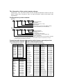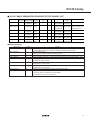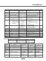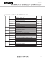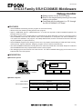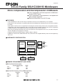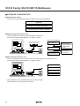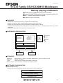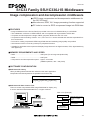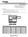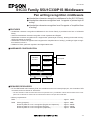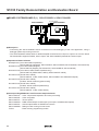
1
PF1084-05
S1C33 Family Data Sheets
• S1C33 Family
• S1C33000 Core
• S1C33209
• S1C33T01
• S1C33L01
• S1C33S01
• S1C33221/222
• S1C33240
• S1C33210
• S1C33205/225/226/245
• S1C33L03
• S1C33 Family Development Environment
• S1C33 Family Middleware and Firmware
• List of Hardware Resources used by Middleware
• S1C33 Family D/A Technology PCM15
• S1C33 Family S5U1C330R1S Middleware
• S1C33 Family S5U1C330M2S Middleware
• S1C33 Family S5U1C330V1S Middleware
• S1C33 Family S5U1C330M1S Middleware
• S1C33 Family S5U1C330S1S Middleware
• S1C33 Family S5U1C330T1S Middleware
• S1C33 Family S5U1C330V2S Middleware
• S1C33 Family S5U1C330J1S Middleware
• S1C33 Family S5U1C330C1S Middleware
• S1C33 Family S5U1C330G1S Middleware
• S1C33 Family S5U1C330P1S Middleware
• S1C33 Family S5U1C330H1S Middleware
• S1C33 Family S5U1C330S2S Middleware
• S1C33 Family S5U1C330U1S Middleware
• S1C33 Family S5U1C330G3S Middleware
• S1C33 Family Demonstration and Evaluation Board
• S1C33 Family Tool Selection Guide
The information of the product number change
Starting April 1, 2001, the product number has been changed as listed below. Please use the new
product number when you place an order. For further information, please contact Epson sales
representative.
Configuration of product number
Devices
S1
C
33209
F
00E1
00
Packing specification
Specification
Package (D: die form; F: QFP)
Model number
Model name (C: microcomputer, digital products)
Product classification (S1: semiconductor)
Development tools
C
33000
S5U1
H2
1
00
Packing specification
Version (1: Version 1 ∗2)
Tool type (∗1)
Corresponding model number
Tool classification (C: microcomputer use)
Product classification
(S5U1: development tool for semiconductor products)
∗1: For details about tool types, see the tables below. (In some manuals, tool types are represented by one digit.)
∗2: Actual versions are not written in the manuals.
Comparison table between Comparison table between new and previous
new and previous number number of development tools
S1C33 Family processors
Previous No.
E0C33A104
E0C33202
E0C33204
E0C33208
E0C33209
E0C332T01
E0C332L01
E0C332L02
E0C332S08
E0C332129
E0C33264
E0C332F128
Previous No.
CC33
CF33
COSIM33
GRAPHIC33
HMM33
JPEG33
MON33
MELODY33
PEN33
ROS33
SOUND33
SMT33
TS33
USB33
VOX33
VRE33
New No.
S1C33104
S1C33202
S1C33204
S1C33208
S1C33209
S1C33T01
S1C33L01
S1C33L02
S1C33S01
S1C33221
S1C33222
S1C33240
New No.
S5U1C33000C
S5U1C330C1S
S5U1C330C2S
S5U1C330G1S
S5U1C330H1S
S5U1C330J1S
S5U1C330M2S
S5U1C330M1S
S5U1C330P1S
S5U1C330R1S
S5U1C330S1S
S5U1C330S2S
S5U1C330T1S
S5U1C330U1S
S5U1C330V1S
S5U1C330V2S
Development tools for the S1C33 Family
Previous No.
New No.
Previous No.
New No.
ICE33
S5U1C33104H
DMT33LIF
S5U1C330L1D1
EM33-4M
S5U1C33104E
DMT33SMT
S5U1C330S1D1
PRC33001
S5U1C33104P1
DMT33LCD26
S5U1C330L2D1
POD33001
S5U1C33104P2
DMT33LCD37
S5U1C330L3D1
ICD33
S5U1C33000H
EPOD33001
S5U1C33208E1
DMT33004
S5U1C33104D1
EPOD33001LV
S5U1C33208E2
DMT33004PD
S5U1C33104D2
EPOD33208
S5U1C33208E3
DMT33005
S5U1C33208D1
EPOD33208LV
S5U1C33208E4
DMT33005PD
S5U1C33208D2
EPOD332L01LV
S5U1C33L01E1
DMT33006LV
S5U1C33L01D1
EPOD332T01
S5U1C33T01E1
DMT33006PDLV
S5U1C33L01D2
EPOD332T01LV
S5U1C33T01E2
DMT33007
S5U1C33208D3
EPOD33209
S5U1C33209E1
DMT33007PD
S5U1C33208D4
EPOD33209LV
S5U1C33209E2
DMT33008LV
S5U1C33T01D1
EPOD332128
S5U1C33220E1
DMT33008PDLV
S5U1C33T01D2
EPOD332128LV
S5U1C33220E2
DMT332S08LV
S5U1C33S01D1
EPOD332S08LV
S5U1C33S01E1
DMT332S08PDLV
S5U1C33S01D2
MEM33201
S5U1C33001M1
DMT33209LV
S5U1C33209D1
MEM33201LV
S5U1C33001M2
DMT33209PDLV
S5U1C33209D2
MEM33202
S5U1C33002M1
DMT332F128LV
S5U1C33240D1
MEM33202LV
S5U1C33002M2
DMT33MON
S5U1C330M1D1
MEM33203
S5U1C33003M1
DMT33MONLV
S5U1C330M2D1
MEM33203LV
S5U1C33003M2
DMT33AMP
S5U1C330A1D1
MEM33DIP42
S5U1C330D1M1
DMT33AMP2
S5U1C330A2D1
MEM33TSOP48
S5U1C330T1M1
DMT33AMP3
S5U1C330A3D1
EPOD176CABLE
S5U1C33T00E31
DMT33AMP4
S5U1C330A4D1
EPOD100CABLE
S5U1C33S00E31
DMT33CF
S5U1C330C1D1
EPOD33SRAM5V
S5U1C33000S
DMT33CPLD400KLV S5U1C330C2D1
EPOD33SRAM3V
S5U1C33001S
PF1130-03
S1C33 Family
32-bit Single Chip Microcomputer
■ DESCRIPTION
The S1C33 Family microcomputer consists of a Seiko Epson original CMOS 32-bit RISC core, ROM, RAM, DMA,
timers, SIO, PLL, A/D and other circuits. Featuring high-speed operation, low power consumption, reduced code
size, and multiplication/accumulation function, this product may be used in a wide range of applications, from OA
equipment to portable equipment. This product is also available as an ASIC or custom microcomputer.
■ S1C33000 CORE DESCRIPTION
Operating frequency
Instruction set
: DC to 60MHz (differs depending on the S1C33xxx model)
: 16-bit fixed code size, 105 types of instructions
Immediate and addressing mode extension with EXT instruction
Multiplication/accumulation function : MAC operation (16 bits × 16 bits + 64 bits → 64 bits) is executed
in two cycles
Register set
: Sixteen 32-bit general-purpose registers, Five 32-bit special registers
Memory space
: 28-bit (256MB) space
■ S1C33 FAMILY GENERAL-PURPOSE MICROCOMPUTER LIST
PKG
S1C33S01 QFP15-100
S1C33240∗ QFP5-128
S1C33210
QFP15-128
S1C33205∗ QFP15-128
S1C33225∗
1.8
~3.6
2.7
~3.6
Same
as core
2.7
~5.5
2.7
~3.6
Same
as core
1.8
~3.6
1.8
~5.5
S1C33226∗
S1C33245∗
Main clock
Sub
ROM
PLL
max. frequency
clock
(KB)
60MHz(3.3V)
32.768kHz
–
20MHz(2.0V)
50MHz(3.3V)
32.768kHz 128
20MHz(2.0V)
60MHz(3.3V)
20MHz(2.0V)
50MHz(3.3V)
20MHz(2.0V)
RAM
(KB)
8/4/2
DMA(ch) SIO Timer(ch)
I/O(bit) A/D D/A
RTC
HS I (ch) 16bit 8bit
I I/O (ch) (ch)
4 128 4
6
6
– –
13 29 8
4
8+
40
(VRAM)
32.768kHz
–
8
4
32.768kHz
128
8
4
Others
6
4
13 29
8
– Built-in LCDC
equivalent to
S1D13705
128 4 + 10
I2C x 2
6
128 4
6
13 69
8
– –
6
13 29
8
– –
2
6
4
– 29
–
– –
128
2
64
50MHz(3.3V)
20MHz(2.0V)
40MHz(3.3V)
20MHz(Flash
access: 0 wait)
50MHz
60MHz(3.3V)
20MHz(2.0V)
50MHz(3.3V)
20MHz(2.0V)
x1, x2, x4 selectable
Voltage(V)
Core
I/O
S1C33209 QFP5-128
1.8
1.8
QFP15-128 ~3.6
~5.5
S1C33L01 QFP18-176 1.8
1.8~5.5
~3.6 (I/O, Bus)
3.0~5.5
(LCD I/F)
S1C33T01 QFP18-176 1.8
1.8~5.5
~3.6 (I/O, Bus)
S1C33221 QFP5-128
1.8
1.8
~3.6
~5.5
S1C33222∗
Model
32.768kHz
–
8
–
32.768kHz
128
(Flash)
8
4
128
4
6
4
13 29
8
– –
32.768kHz
–
8
4
128
3
6
6
7 27
4
32.768kHz
–
8
4
128
4
6
6
13 29
8
– PDC I/F: 1ch
PHS I/F: 1ch
HDLC: 1ch
– –
8
– –
128
64
2.7
~3.6
2.7
~5.5
128
40MHz(3.3V)
(Flash)
20MHz(Flash
access: 0 wait)
4 128 4
6
6
S1C33L03∗ QFP20-144 1.8
1.8
50MHz(3.3V)
13 29
32.768kHz
–
8
~3.6
~5.5
20MHz(2.0V)
LCDC:
25MHz(3.3V)
∗: Under development (This model is under development, therefore the contents of the above specifications may be revised at final.)
: Available
– : None
1
S1C33 Family
■ S1C33 FAMILY CUSTOM MICROCOMPUTER
Available as a custom microcomputer incorporating S1C33 macros based on the S1X50000 series of Epson
embedded arrays.
C33 peripheral macro
(required)
C33
DMA macro
SRAM
User logic
C33
core macro (required)
Macro
for S1X50000
ROM
Flash
10-bit A/D
■ S1C33 FAMILY DEVELOPMENT ENVIRONMENT LIST
● Software Tools
Tool
S5U1C33000C
S5U1C330M2S +
S5U1C330M1D1 (5V)
S5U1C330M2D1 (3.3V)
Description
C compiler package (running under Windows 95/98 and NT4.0)
Includes C compiler to debugger and utilities. An evaluation version is also available.
Debug monitor
Enables the creation of an inexpensive debug environment using user resources (ROM 10KB,
RAM 2.5KB, SIO 1ch.) to connect to the debugger.
● Basic Hardware Tool
Tool
S5U1C33000H
2
Description
In-circuit debugger for the S1C33 chip with on-chip ICE
This is a reduced-pin connecting-type ICE requiring only 4 or 10 pins for connection.
S1C33 Family
● Hardware Expansion Tools
Tool
S5U1C33209E1 (5V)
S5U1C33209E2 (3.3V)
S5U1C33L01E1 (3.3V)
S5U1C33T01E1 (5V)
S5U1C33T01E2 (3.3V)
S5U1C33221E1 (5V)
S5U1C33221E2 (3.3V)
S5U1C33240E1 (5V)
S5U1C33240E2 (3.3V)
S5U1C33S01E1 (3.3V)
S5U1C330D1M1 (5–3.3V)
S5U1C33T1M1 (5–3.3V)
S5U1C33001M1 (5V)
S5U1C33001M2 (3.3V)
S5U1C33002M1 (5V)
S5U1C33002M2 (3.3V)
S5U1C33003M1 (5V)
S5U1C33003M2 (3.3V)
Description
Emulation pod for the S1C33209 (with emulation memory board I/F)
Note)
With the capacity to emulate up to 256KB of internal ROM. (maximum 50MHz, 0 wait state)
Emulation pod for the S1C33L01 (with emulation memory board I/F)
Note)
Supports ROM development using the internal ROM emulation function. (maximum 50MHz, 0 wait state)
Emulation pod for the S1C33T01 (with emulation memory board I/F)
Note)
With the capacity to emulate up to 256KB of internal ROM. (maximum 50MHz, 0 wait state)
Emulation pod for the S1C33221 (with emulation memory board I/F)
Note)
With the capacity to emulate up to 256KB of internal ROM. (maximum 50MHz, 0 wait state)
Emulation pod for the S1C33240 (with emulation memory board I/F)
Emulation pod for the S1C33S01 (with emulation memory board I/F)
Note)
With the capacity to emulate up to 256KB of internal ROM. (maximum 50MHz, 0 wait state)
ROM emulation I/F board
The DIP socket for the target board ROM and the S5U1C33001Mx/S5U1C33002Mx are connected
to emulate ROM. It supports ×16 type of 1M, 2M, 4M, 8M, and 16M-bit ROMs in 40 to 42-pin DIPs.
Flash emulation I/F board
The S5U1C33001Mx/S5U1C33002Mx is connected to the 48-pin TSOP flash memory board pattern on the target board to emulate flash memory. It supports ×16 type of 4M, 8M, 16M, and 32Mbit flash memory in 48-pin TSOPs.
2MB × 2 block emulation memory board (accessible with 1 wait state up to 33MHz)
When two boards are cascaded, up to 2MB × 4 blocks can be emulated.
Powerful break functions for a map break, six bus breaks and two area breaks can also be added
to the S5U1C33000H (with S5U1C33xxxEx connected).
1MB emulation memory board (accessible with 1 wait state, up to 33MHz)
When two boards are cascaded, up to 1MB × 2 blocks can be emulated.
2MB × 2 block emulation memory board (accessible with 1 wait state up to 33MHz)
When two boards are cascaded, up to 2MB × 4 blocks can be emulated. This board has no flex10k
for expanding break functions but other functions are the same as S5U1C33001Mx.
Note: High-speed SRAM for ROM emulation is a rental option.
S5U1C33001S (for 3.3V), S5U1C33000S (for 5V)
● Simulation and Emulation Tools
Tool
S1C33 ASIC design kit
S5U1C330C2S
Description
Contains a simulation model for C33-macro and provides a simulation environment required to
create custom microcomputers. It is customized to suit the specifications of your custom microcomputer.
Containing a simulation model for the S1C33209 etc., it provides emulation environment with
CPLD, and co-simulation environment via the debugger.
Supports software development, also including provisions for external ASIC.
3
S1C33 Family
■ S1C33 FAMILY MIDDLEWARE AND FIRMWARE LIST
Classification
Trade name
Voice
S5U1C330V1S
S5U1C330G3S
S5U1C330T1S
S5U1C330V2S
S5U1C330H1S
Sound
S5U1C330M1S
S5U1C330S1S
Image
S5U1C330J1S
S5U1C330G1S
S5U1C330P1S
OS
S5U1C330R1S
Debug tool
S5U1C330M2S
FLS33
PC I/F
S5U1C330C1S
Contents
Voice compression/expansion and voice processing
Voice compression/expansion G72SA, G723.1A
Simple text to speech
Voice recognition
High-performance Japanese voice recognition using phoneme model
PWM method simple melody output
MIDI-like sound output based on WAVE sound source
JPEG compression/expansion (high-speed version is under development)
Graphics and GUI library
Japanese handwritten character recognition
µITRON3.0 compliant real-time OS
Debug monitor running on user board
On-board/on-chip flash memory erase/programming routine executable using a
debugger (included with S5U1C33000C Ver.2.0 or later)
I/O firmware for compact flash memory
S5U1C330S2S
S5U1C330U1S
Supports DOS file (FAT12/16)
DOS file system supporting SmartMedia
USB sample program
Evaluation versions are available for all of the above products. Various demonstration version software applications are also available for the demonstration board.
4
S1C33 Family
■ S1C33 FAMILY DEMONSTRATION/PROPTOTYPE BOARD LIST
IC
Input voltage
Operating S5U1C330M2S
Bus I/O
Flash SRAM
I/F
area
output
supported Operating voltage frequency
S5U1C33209D1 S1C33209 5V input
40MHz
Flash 1MB
1MB 1MB S5U1C330M2D1 Bus and
Board name
3.3V operation
S5U1C33L01D1 S1C33L01 5V input
32kHz
40MHz
S5U1C33L01D2
32kHz
3.3V operation
S5U1C33T01D1 S1C33T01 5V input
3.3V operation
S5U1C33S01D1 S1C33S01 5V input
40MHz
32kHz
40MHz
3.3V operation
S5U1C33240D1 S1C33240 5V input
32kHz
40MHz
3.3V operation
S5U1C33210D1 S1C33210 5V input
32kHz
40MHz
3.3V operation
32kHz
Flash 1MB
1MB
Others
–
S5U1C330AxD1 I/O pin output
1MB S5U1C330M2D1 Bus and
D2 is for S5U1C33L01E1
S5U1C330AxD1 I/O pin output With 12V, 5 to 28V, -5 to
S5U1C330LxD
-28V outputs for LCD
Flash 1MB
1MB
Flash 1MB
1MB
1MB S5U1C330M2D1 Bus and
–
S5U1C330AxD1 I/O pin output
1MB S5U1C330M2D1 Bus and
–
Flash 1MB
1MB
S5U1C330AxD1 I/O pin output
1MB S5U1C330M2D1 Bus and
–
Flash 1MB
1MB
S5U1C330AxD1 I/O pin output
1MB S5U1C330M2D1 Bus and
–
S5U1C330AxD1 I/O pin output
● Expansion Board
Board name
S5U1C330A3D1
Power
5V
S5U1C330A4D1
5V
S5U1C330L2D1
S5U1C330L3D1
S5U1C330C1D1
5V
5V
3.3V
S5U1C330L1D1
3.3 to 5V
S5U1C330S1D1
3.3V
S5U1C330U1D1
S5U1C330C2D1
3.3V
3.3V
Function
8–32kHz sampling audio input/output board
Supports PCM15, stereo output, and S5U1C330M1S piezoelectric buzzer output.
Audio input/output board
Contains low-cost transistor amplifier supporting PCM15.
LCD demonstration board with 2.6-inch DTFD panel (exclusive use for S5U1C33L01D1) Note)
LCD demonstration board with 3.7-inch DTFD panel (exclusive use for S5U1C33L01D1) Note)
Demonstration board for compact flash
Connected with a bus connector.
I/F board for Agilent Technologies (former HP) 16500A
Connected with a bus connector.
Memory card board for smart medium and S5U1C330S2S
Connected with a bus connector.
Evaluation board for USB macro that can be implemented to ASIC
ASIC emulation board for Altera APEX20K
400 (400,000 gates) is installed in the socket (default).
Interchaneable with 1000 (1,000,000 gates).
Note: A rental board only is available because the quantity is limited.
5
S1C33 Family
■ S1C33 STARTUP GUIDE
The following describes available materials and how to use them as references when you examine the type of
S1C33 product to choose or when you actually start developing your application system.
1) Collection of S1C33 Family data sheets
First, take a look at the list shown previously to get an overall view of the S1C33 Family, including the types
of microcomputers, development tools, middleware, and demonstration boards. For an outline description of
each product, see the relevant part of this collection of data sheets. Each type of microcomputer and
middleware is outlined in one to several pages.
2) Manuals
When you need detailed information about any microcomputer, development tool, middleware, or demonstration board, refer to the manual for that product. When manuals are needed, please contact Seiko Epson or a
local Seiko Epson distributor. Manuals in PDF format are also included in the data CD described in (3) below.
The following lists the typical manuals that are needed first:
• S1C33000 Core CPU Manual
• S1C33 Family C Compiler Package Manual
• S1C33xxx Technical Manual (xxx denotes the microcomputer type which includes, for example, 209 or
L01)
• S1C33 Family Application Note
In particular, S1C33 Family Application Note contains information on how to write CPU core and S1C33
programs, as well as S1C33 peripheral function programming, and information on basic circuit board and
sound output features. Please be sure to read S1C33 Family Application Note before starting development.
3) S1C33 Family data CD
Obtain the "S1C33 Family data CD" from Seiko Epson.
The following are included. Refer to the necessary data.
•
•
•
•
•
•
Manuals for all PDFs in the S1C33 Family (in English and Japanese)
Bug reports (regarding the IC, tools, etc.)
Circuit diagrams of all demonstration boards (PDF)
Photographs of all hardware tools and demonstration boards
Q & A (in Japanese only)
Patches (e.g., function extensions and bug fixes) for the latest versions of development tools and
middleware
• Middleware demonstration software (demonstration samples that can be run after downloading to the demonstration board)
• Evaluation versions of development tools
Primary tools are included so that you can start development before purchasing tools.
• Evaluation versions of middleware
Samples, execution files, and PC tools are included. Check this data to see what kinds of samples and
tools are available. Note that because binary libraries are not included, you cannot use this data for
development purposes using the make utility.
Before starting development, be sure to consult the bug reports for the microcomputer used. Also, because
bug reports are updated and/or released from time to time, be sure to get the latest information from Seiko
Epson. Bug reports are distributed in the file named "reportdate.exe" (e.g., report00_09_20.exe). When this
file is executed, the data is expanded into "c:\s1c33\reprt" in the same form as the data CD.
6
S1C33 Family
4) Evaluation of development tools at start of development
Since the S1C33 Family has a wide range of hardware tools available, you may have difficulty choosing the
appropriate product for your needs. For help, please refer to "S1C33 Tool Selection Guide", provided in this
collection of data sheets, when choosing the desired tool.
Also, we recommend installing the evaluation versions of development tools from the S1C33 Family data CD
to your computer following instructions from Chapter 2, "Installation", in the S1C33 Family C Compiler Package Manual, and run them according to Section 3.2, "Tutorial". This will help you get accustomed to the series
of operations needed for a range of tools from the C compiler to the debugger. The debugger's simulator
facility allows you to perform a series of processing functions—compiling, assembling, linking, and debugging—without using the ICE or target board.
Furthermore, looking over the S1C33 Family Application Note will prove helpful.
5) Middleware evaluation
The S1C33 middleware made by Seiko Epson has a demonstration version that can be run on the demonstration board for evaluation purposes. Install the demonstration software from the S1C33 Family data CD to
your computer by executing the file. Prepare the necessary demonstration board or equivalent, and download the demonstration software to the demonstration board, following the instructions in the readme file.
Note that the evaluation version of middleware is included in the data CD, although it cannot be used in actual
development.
When using middleware, please also refer to "List of Hardware Resources used by Middleware" in this collection of data sheets. Although you need to read the respective manuals to obtain details on middleware, this
list helps you get outline information on hardware resources used by each middleware. Resource assignments are important items to consider when designing your application board.
7
THIS PAGE IS BLANK.
PF881-03
S1C33000 Core
32-bit Single Chip Microcomputer
● 32-bit RISC Core
● High-code-efficient Instruction Set
● Multiplication and Accumulation Instruction
● High-speed Operation and Low Current Consumption
■ DESCRIPTION
The S1C33000 is a 32-bit RISC-type core CPU for the S1C33 Family microprocessors. The S1C33 Family will
be developed using this core as the main unit and implementing various peripheral circuits such as RAM, ROM,
DMA, A/D and D/A converters. The S1C33000 core has a high-code efficient instruction set, MAC (multiplication
and accumulation) instruction and features high-speed operation and low current consumption. It is suitable for
a wide range of embedded applications such as portable equipment, OA and FA equipment, digital signal
processing systems and various controllers.
■ FEATURES
● Processor type ................................................ Seiko Epson original 32-bit RISC core
● Operating frequency ....................................... DC to 60MHz (differs depending on the S1C33xxx model)
● Instruction set .................................................. 16-bit fixed code size
105 types of instructions with high linearity
Principle instructions can be executed in one cycle.
● Multiplication and accumulation instruction .... MAC instruction (16 bits × 16 bits + 64 bits → 64 bits)
Executable in two cycles per operation
● Register set ..................................................... Sixteen 32-bit general-purpose registers
Five 32-bit special registers
● Memory space ................................................ 28-bit (256MB) space
A linear space including code, data and I/O areas.
The memory space is divided into 19 areas and they can be
accessed with the select signals delivered from the core.
● Immediate data extension ............................... Immediate data in the instruction codes can be extended up
to 32 bits using the EXT instruction.
● Interrupts ......................................................... Reset, NMI and 216 external interrupts
Four software exceptions and two instruction execution exceptions
The core fetches vectors in the trap table to branch processing.
● Reset ............................................................... Cold reset (for resetting all conditions)
Hot reset (resetting except for bus and port status)
Trap table is selectable from internal or external memory
when booting and is relocatable.
● Power down mode .......................................... HALT instruction (stops the core only.)
SLP instruction (stops all the circuits.)
● Others ............................................................. Little endian/Big endian format
Harvard architecture
9
S1C33000 Core
■ MEMORY MAP AND TRAP TABLE
Memory Map
Trap Table
0xFFFFFFF Area 18
Area 17
Area 16
Area 15
Area 14
Area 13
Area 12
0x1000000 Area 11
0x0C00000 Area 10
Area 9
Area 8
Area 7
Area 6
Area 5
0x0100000 Area 4
0x0080000 Area 3
0x0060000 Area 2
0x0040000 Area 1
0x0000000 Area 0
External memory
External memory
External memory
External memory
External memory
External memory
External memory
External memory
External memory
External memory
External memory
External memory
External I/O
External memory
External memory
On-chip ROM
Reserved
Internal I/O
On-chip RAM
Area size
64MB
64MB
32MB
32MB
16MB
16MB
8MB
8MB
4MB
4MB
2MB
2MB
1MB
1MB
1MB
512KB
128KB
128KB
256KB
Reserved
External maskable interrupt 215
:
External maskable interrupt 0
Software exception 3
:
Software exception 0
Reserved
NMI
Address error
Reserved
Zero division
Reserved
Reset
Address offset
1023
929
64
60
48
32–44
28
24
20
16
4–12
0
Trap table start address
When booting from built-in ROM:
0x0080000
When booting from external memory: 0x0C00000
The trap table can be relocated using the trap table
base register TTBR (memory-mapped register) after
resetting the CPU.
Vectors will be fetched from the trap table for booting
and interrupts.
■ REGISTERS
General-purpose registers (16)
31
0
Special registers (5)
31
0
R15
R14
:
R1
R0
PC
PSR
SP
ALR
AHR
Program counter
Processor status register
Stack pointer
Arithmetic operation low register
Arithmetic operation high register
(AHR, ALR: Option for Multiplication & Accumulation, Multiplication, and Division)
■ INSTRUCTION SET
● Instruction Format and Operation
∗ The cycle lists the number of execution cycles assuming that the instructions are stored in the built-in ROM and access to the built-in RAM.
∗ Sample format: signX and immX = immediate data, %XX = register
Classification
Relative
branch
Relative
delayed
branch
Absolute
branch
Special
branch
Logic
operation
Arithmetic
operation
10
Instruction
jp, jrgt, jrge, jrlt, jrle, jrugt, jruge,
jrult, jrule, jreq, jrne, call
jp.d, jrgt.d, jrge.d, jrlt.d, jrle.d,
jrugt.d, jruge.d, jrult.d, jrule.d,
jreq.d, jrne.d, call.d
call, jp, call.d, jp.d
Sample format
jp sing8
jp.d sing8
call %rb
ret, ret.d, int imm2, reti, brk, retb
and, or, xor, not
add, sub
and
and
add
add
add
%rd, %rs
%rd, sign6
%rd, %rs
%rd, imm6
%sp, imm12
Operation
Branches to PC + (sign8 × 2)
Cycle
1,2 (branch)
or 3 (call)
Branches to PC + (sign8 × 2)
1
Executes the next instruction before
or 2 (call)
branching.
Branches to the address indicated
1 to 3
with %rb.
Return, interrupt, etc.
3 to 10
%rd = %rd & %rs
%rd = %rd & sign6
%rd = %rd + %rs
%rd = %rd + imm6
%sp = %sp + imm12
1
1
S1C33000 Core
Classification
Comparison cmp
Instruction
Sample format
cmp %rd, %rs
cmp %rd, sign6
adc %rd, %rs
Operation
adc, sbc
with carry
Multiplication mlt.h, mlt.uh (16 bits)
mlt.h %rd, %rs
mlt.w, mlt.uw (32 bits)
Division
div0s, div0u, div1, div2s, div3s
Shift
Memory
data load
Register
data load
Conversion
Bit
System
MAC
Stack
Scan
Swap
Extension
Operation
%rd - %rs (changes the flags only)
%rd - sign6
%rd = %rd + %rs + carry flag
Cycle
1
1
%alr = %rd × %rs
(32 = 16 × 16)
1
%ahr:%alr = %rd × %rs (64 = 32 × 32)
5
Division is performed according to a
1
combination of these instructions.
srl, sll (logical shift)
srl %rd, imm4
%rd = %rd >> imm4
1
sra, sla (arithmetical shift)
srl %rd, %rs
%rd = %rd >> %rs
rr, rl
(rotate)
0 to 8 shift count can be specified.
ld.b
(signed 8-bit load)
ld.w %rd, [%sp+imm6] %rd = [%sp+imm6] (stack relative access) 1 or 2
ld.ub
(unsigned 8-bit load) ld.w [%sp+imm6], %rs [%sp+imm6] = %rs
ld.h
(signed 16-bit load)
ld.w %rd, [%rb]
%rd = [%rb] (register indirect access)
ld.uh
(unsigned 16-bit load) ld.w %rd, [%rb]+
%rd = [%rb], %rb = %rb + 4 (post inc.)
ld.w
(32-bit load)
ld.w [%rb], %rs
[%rb] = %rs
ld.w [%rb]+, %rs
[%rb] = %rs, %rb = %rb + 4
ld.w
ld.w %rd, %rs
Copy between registers
1
ld.w %rd, sign6
Immediate data substitution
ld.w %rd, %ss
Copy from a special register
ld.w %ss, %rs
Copy to a special register
ld.b, ld.ub, ld.h, ld.uh
ld.b %rd, %rs
Type conversion
1
btst, bset, bclr, bnot
btst [%rb], imm3
Bit test, set, clear and negation
3
nop, slp, hlt
No operation, clock stop
1
mac
Repeats <%ahr:%alr= [%r14] × [%r15]
2×N+4
+ %ahr:%alr> %r13 times.
pushn, popn
pushn %rs
Continuous push/pop from %r0 to %rs
1×N
scan0, scan1
scan0 %rd, %rs
Gets the length of 0s or 1s within 8 bits
1
from MSB.
Bit swap, mirror operation in 8-bit units
1
swap, miror
swap %rd, %rs
ext
ext imm13
Extends immediate data in the instruction.
1
● Immediate Extension with EXT Instruction
Examples)
Classification
Relative
branch
3-operand
operation
Operation
Stack
load
Absolute
load
Bit
Original instruction
call sign8
Extension with one EXT
Extension with two EXTs
ext imm13
ext imm13
call sign8 (= call sign21) ext imm13
call sign8 (= call sign31)
Instruction
jp,jrgt,jrge,jrlt jrle,jrugt,jruge,jrult,jrule,
jreq,jrne,call and delayed instructions
add, sub, and, or, xor, not, cmp
add, sub, and, or, xor, not, cmp, ld.w
ld.b, ld.ub, ld.h, ld.uh, ld.w
ld.b, ld.ub, ld.h, ld.uh, ld.w
btst, bset, bclr, bnot
Original format
jp
sing8
add %rd, %rs
add
ld.w
ld.w
ld.w
ld.w
ld.w
ld.w
btst
Extended operation
with one EXT
jp sign21
add %rd, %rs, imm13
Operand extension
%rd, imm6 /sign6 add %rd, imm19/sign19
%rd, [%sp+imm6] [%sp+imm19]
[%sp+imm6], %rs Offset extension
%rd, [%rb]
[%rb+imm13]
%rd, [%rb]+
Offset addition
[%rb], %rs
[%rb]+, %rs
[%rb], imm3
[%rb+imm13]
Offset addition
Extended operation
with two EXTs
jp sign31
add %rd, %rs, imm26
Operand extension
add %rd, imm32
[%sp+imm32]
Offset extension
[%rb+imm28]
Offset addition
[%rb+imm26]
Offset addition
11
THIS PAGE IS BLANK.
PF1185-02
S1C33209
32-bit Single Chip Microcomputer
● 32-bit S1C33000 RISC Core
● Multiply Accumulation
● Built-in 8K-byte RAM
● 10-bit ADC
● 4-ch. SIO
● High-speed DMA, Intelligent DMA
■ DESCRIPTION
The S1C33209 is a CMOS 32-bit microcomputer composed of a CMOS 32-bit RISC core, 8K-byte RAM, 4channel SIO, A/D converter, timers, PLL and other circuits. The S1C33209 features high-speed operation and
low current consumption. It is suitable for various portable equipment and multimedia control systems. The
S1C33209 also provides a DSP function using the internal MAC (multiplication and accumulation) operation
function with the A/D converter, this makes it possible to achieve speech recognition and voice synthesis systems.
■ FEATURES
● CMOS LSI 32-bit parallel processing ............. S1C33000 RISC core
● Main clock ....................................................... 60MHz (Max., up to 15MHz external clock input)
● Sub clock ........................................................ 32.768kHz (Typ., crystal)
● Instruction set .................................................. 16-bit fixed length, 105 instructions
(MAC instruction is included, 2 cycles)
● Internal RAM size............................................ 8,192 bytes
● Clock timer ...................................................... 1 channel
● Programmable timer ....................................... 8 bits × 6 channels and 16 bits × 6 channels
● Watchdog timer ............................................... Realized with a 16-bit programmable timer
● Serial interface ................................................ 4 channels
Clock synchronization type and asynchronization type are
selectable. Usable as an infrared ray (IrDA) interface.
● 10-bit A/D converter ........................................ Successive approximation type, 8 input channels
● High-speed DMA ............................................. 4 channels
● Intelligent DMA ................................................ 128 channels
● I/O port ............................................................ Input port : 13 bits
I/O port : 29 bits
● Interrupt controller ........................................... External interrupts : 10 types
Internal interrupts : 29 types
● External bus interface ..................................... 24-bit address bus, 16-bit data bus, 7 chip enable pins
DRAM and burst ROM may be connected directly.
● Shipping form .................................................. QFP5-128pin/QFP15-128pin
● Supply voltage ................................................ Core voltage : 1.8 to 3.6V
I/O voltage : 1.8 to 5.5V
● Current consumption ...................................... SLEEP state : 10µA (3.3V, 32.768kHz, clock timer run state, Typ.)
: 2.5µA (2.0V, 32.768kHz, clock timer run state, Typ.)
RUN state : 65mA (3.3V, 50MHz Typ.)
13
S1C33209
■ BLOCK DIAGRAM
VDD
VSS
VDDE
S1C33209
A[23:0]
D[15:0]
#RD
#WRL/#WR/#WE
#WRH/#BSH
#HCAS
#LCAS
#CE10IN, #CE10EX, #CE[9:3]
#EMEMRD
#WAIT(P30)
#DRD(P20)
#DWE(P21)
#GAAS(P21)
#GARD(P31)
OSC3
OSC4
PLLS[1:0]
PLLC
OSC1
OSC2
FOSC1(P14)
#DMAREQx(K50, K51, K53, K54)
#DMAACKx(P32, P33, P04, P06)
#DMAENDx(P15, P16, P05, P07)
14
#RESET
#NMI
#X2SPD
ICEMD
DSIO
EA10MD[1:0]
BCLK
#BUSREQ(P34)
#BUSACK(P35)
#BUSGET(P31)
DST[2:0](P10–12)
DPCO(P13)
DCLK(P14)
S1C33000
CPU Core
Bus Control Unit
OSC3/PLL
Interrupt
Controller
Prescaler
16-bit
Programmable
Timer (6 ch.)
EXCLx(P10–13, P15, P16)
TMx(P22–27)
OSC1
8-bit
Programmable
Timer (6 ch.)
T8UFx(P10–13)
Clock
Timer
Serial Interface
(4 ch.)
SINx(P00, P04, P27, P33)
SOUTx(P01, P05, P26, P16)
#SCLKx(P02, P06, P25, P15)
#SRDYx(P03, P07, P24, P32)
Intelligent
DMA (128 ch.)
A/D Converter
(8 ch.)
AD0–7(K60–67)
#ADTRG(K52)
AVDDE
High-speed
DMA (4 ch.)
Input Port
K50–54
K60–67
RAM
8KB
I/O Port
P00–07
P10–16
P20–27
P30–35
S1C33209
■ PIN LAYOUT
QFP5-128pin
102
65
64
103
S1C33209
INDEX
39
128
1
No.
1
2
3
4
5
6
7
8
9
10
11
12
13
14
15
16
17
18
19
20
21
22
23
24
25
26
27
28
29
30
31
32
Pin name
P24/TM2/#SRDY2
VSS
P25/TM3/#SCLK2
P26/TM4/SOUT2
P15/EXCL4/#DMAEND0/#SCLK3
P27/TM5/SIN2
BCLK
P00/SIN0
P01/SOUT0
D15
VDD
P03/#SRDY0
D14
P31/#BUSGET/#GARD
D13
P32/#DMAACK0/#SRDY3
D12
P33/#DMAACK1/SIN3
D11
K54/#DMAREQ3
D10
K53/#DMAREQ2
D9
K52/#ADTRG
VSS
K51/#DMAREQ1
P02/#SCLK0
D8
D7
VDDE
K67/AD7
K66/AD6
No.
33
34
35
36
37
38
39
40
41
42
43
44
45
46
47
48
49
50
51
52
53
54
55
56
57
58
59
60
61
62
63
64
Pin name
K65/AD5
K50/#DMAREQ0
K64/AD4
K63/AD3
K62/AD2
AVDDE
K61/AD1
K60/AD0
D6
VSS
D5
D4
D3
D2
D1
D0
P35/#BUSACK
VDDE
#CE9/#CE17/#CE17&18
OSC2
#CE7/#RAS0/#CE13/#RAS2
OSC1
#CE6/#CE7&8
#RD
VSS
#WRL/#WR/#WE
#WRH/#BSH
#CE10EX/#CE9&10EX
#CE8/#RAS1/#CE14/#RAS3
#CE5/#CE15/#CE15&16
#CE4/#CE11/#CE11&12
P30/#WAIT/#CE4&5
38
No.
65
66
67
68
69
70
71
72
73
74
75
76
77
78
79
80
81
82
83
84
85
86
87
88
89
90
91
92
93
94
95
96
Pin name
#RESET
#NMI
A0/#BSL
A1
P34/#BUSREQ/#CE6
VSS
A2
A3
A4
A5
A6
#CE10IN
VDD
#EMEMRD
A7
#HCAS
A8
#LCAS
A9
P16/EXCL5/#DMAEND1/SOUT3
A10
A20
A11
A21
A12
A22
A13
A23
VSS
A14
A15
VDDE
No.
97
98
99
100
101
102
103
104
105
106
107
108
109
110
111
112
113
114
115
116
117
118
119
120
121
122
123
124
125
126
127
128
Pin name
A16
ICEMD
A17
A18
A19
P04/SIN1/#DMAACK2
P05/SOUT1/#DMAEND2
P06/#SCLK1/DMAACK3
VSS
PLLC
VSS
PLLS1
PLLS0
P07/#SRDY1/#DMAEND3
#X2SPD
EA10MD0
EA10MD1
VDD
(No Connection)
OSC4
P20/#DRD
OSC3
P21/#DWE/#GAAS
#CE3
P22/TM0
P23/TM1
DSIO
P10/EXCL0/T8UF0/DST0
P11/EXCL1/T8UF1/DST1
P12/EXCL2/T8UF2/DST2
P13/EXCL3/T8UF3/DPCO
P14/FOSC1/DCLK
15
S1C33209
QFP15-128pin
96
65
97
64
S1C33209
INDEX
128
33
1
No.
1
2
3
4
5
6
7
8
9
10
11
12
13
14
15
16
17
18
19
20
21
22
23
24
25
26
27
28
29
30
31
32
16
Pin name
P26/TM4/SOUT2
P15/EXCL4/#DMAEND0/#SCLK3
P27/TM5/SIN2
BCLK
P00/SIN0
P01/SOUT0
D15
VDD
P03/#SRDY0
D14
P31/#BUSGET/#GARD
D13
P32/#DMAACK0/#SRDY3
D12
P33/#DMAACK1/SIN3
D11
K54/#DMAREQ3
D10
K53/#DMAREQ2
D9
K52/#ADTRG
VSS
K51/#DMAREQ1
P02/#SCLK0
D8
D7
VDDE
K67/AD7
K66/AD6
K65/AD5
K50/#DMAREQ0
K64/AD4
No.
33
34
35
36
37
38
39
40
41
42
43
44
45
46
47
48
49
50
51
52
53
54
55
56
57
58
59
60
61
62
63
64
Pin name
K63/AD3
K62/AD2
AVDDE
K61/AD1
K60/AD0
D6
VSS
D5
D4
D3
D2
D1
D0
P35/#BUSACK
VDDE
#CE9/#CE17/#CE17&18
OSC2
#CE7/#RAS0/#CE13/#RAS2
OSC1
#CE6/#CE7&8
#RD
VSS
#WRL/#WR/#WE
#WRH/#BSH
#CE10EX/#CE9&10EX
#CE8/#RAS1/#CE14/#RAS3
#CE5/#CE15/#CE15&16
#CE4/#CE11/#CE11&12
P30/#WAIT/#CE4&5
#RESET
#NMI
A0/#BSL
32
No.
65
66
67
68
69
70
71
72
73
74
75
76
77
78
79
80
81
82
83
84
85
86
87
88
89
90
91
92
93
94
95
96
Pin name
A1
P34/#BUSREQ/#CE6
VSS
A2
A3
A4
A5
A6
#CE10IN
VDD
#EMEMRD
A7
#HCAS
A8
#LCAS
A9
P16/EXCL5/#DMAEND1/SOUT3
A10
A20
A11
A21
A12
A22
A13
A23
VSS
A14
A15
VDDE
A16
ICEMD
A17
No.
97
98
99
100
101
102
103
104
105
106
107
108
109
110
111
112
113
114
115
116
117
118
119
120
121
122
123
124
125
126
127
128
Pin name
A18
A19
P04/SIN1/#DMAACK2
P05/SOUT1/#DMAEND2
P06/#SCLK1/DMAACK3
VSS
PLLC
VSS
PLLS1
PLLS0
P07/#SRDY1/#DMAEND3
#X2SPD
EA10MD0
EA10MD1
VDD
(No Connection)
OSC4
P20/#DRD
OSC3
P21/#DWE/#GAAS
#CE3
P22/TM0
P23/TM1
DSIO
P10/EXCL0/T8UF0/DST0
P11/EXCL1/T8UF1/DST1
P12/EXCL2/T8UF2/DST2
P13/EXCL3/T8UF3/DPCO
P14/FOSC1/DCLK
P24/TM2/#SRDY2
VSS
P25/TM3/#SCLK2
PF1091-05
S1C33T01
32-bit Single Chip Microcomputer
● High-speed 32-bit RISC Core
● Multiply Accumulation
● 8K-byte RAM Built-in
● 10-bit ADC
● 4-ch. SIO, 2-ch. I2C
● High-speed DMA, Intelligent DMA
■ DESCRIPTION
The S1C33T01 is a CMOS 32-bit microcomputer composed of a CMOS 32-bit RISC core, 8K-byte RAM, DMA,
4-ch. SIO, 2-ch. I2C, ADC, timers, PLL and oscillators. The S1C33T01 features high-speed operation and low
current consumption. The S1C33T01 also provides a DSP function using the internal MAC (multiplication and
accumulation) operation function with the A/D converter, this makes it possible to achieve speech recognition
and voice synthesis systems.
■ FEATURES
● CMOS LSI 32-bit parallel processing ............. S1C33000 RISC core
● Main clock ....................................................... 60MHz (Max., up to 15MHz external clock input)
● Sub clock ........................................................ 32.768kHz (Typ., crystal)
● Instruction set .................................................. 16-bit fixed length, 105 instructions
(MAC instruction is included, 2 cycles)
● Internal RAM size............................................ 8,192 bytes
● Clock timer ...................................................... 1 channel
● Programmable timer ....................................... 8 bits × 6 channels and 16 bits × 10 channels
● PWM timer ...................................................... Realized with a 16-bit programmable timer
● Watchdog timer ............................................... Realized with a 16-bit programmable timer
● Serial interface ................................................ 4 channels
Clock synchronization type and asynchronization type are
selectable. Usable as an infrared ray (IrDA) interface.
● I2C bus ............................................................. Single master type, 2 channels (option)
● 10-bit A/D converter ........................................ Successive approximation type, 8 input channels
● High-speed DMA ............................................. 4 channels
● Intelligent DMA ................................................ 128 channels
● I/O port ............................................................ Input port : 13 bits
I/O port : 69 bits
● Interrupt controller ........................................... External interrupts : 18 types
Internal interrupts : 69 types
● External bus interface ..................................... 24-bit address bus, 16-bit data bus, 7 chip enable pins
DRAM and burst ROM may be connected directly.
● Shipping form .................................................. QFP18-176pin
● Supply voltage ................................................ Core voltage : 1.8 to 3.6V
I/O voltage : 1.8 to 5.5V
● Current consumption ...................................... SLEEP state : 10µA (3.3V, 32.768kHz, clock timer run state, Typ.)
: 2.5µA (2.0V, 32.768kHz, clock timer run state, Typ.)
RUN state : 65mA (3.3V, 50MHz Typ.)
17
S1C33T01
■ BLOCK DIAGRAM
VDD
VSS
VDDE
BVDDE
A[23:0]
D[15:0]
#RD
#WRL/#WR/#WE
#WRH/#BSH
#HCAS
#LCAS
#CE10IN, #CE10EX, #CE[9:3]
#EMEMRD
#WAIT(P30)
#DRD(P20)
#DWE(P21)
#GAAS(P21)
#GARD(P31)
OSC3
OSC4
PLLS[1:0]
PLLC
OSC1
OSC2
FOSC1(P14)
#DMAREQx(K50, K51, K53, K54)
#DMAACKx(P32, P33, P04, P06)
#DMAENDx(P15, P16, P05, P07)
K50–54
K60–67
18
S1C33T01
#RESET
#NMI
#X2SPD
ICEMD
DSIO
EA10MD[1:0]
EA3MD
BCLK
#BUSREQ(P34)
#BUSACK(P35)
#BUSGET(P31)
DST[2:0](P10–12)
DPCO(P13)
DCLK(P14)
S1C33000
CPU Core
Bus Control Unit
OSC3/PLL
Interrupt
Controller
Prescaler
16-bit
Programmable
Timer (10 ch.)
EXCLx(P10–13, P15, P16, P80–83)
TMx(P22–27, P84–87)
OSC1
8-bit
Programmable
Timer (6 ch.)
T8UFx(P10–13, P50, P51)
Clock
Timer
Serial Interface
(4 ch.)
SINx(P00, P04, P40, P44)
SOUTx(P01, P05, P41, P46)
#SCLKx(P02, P06, P42, P46)
#SRDYx(P03, P07, P43, P47)
RAM
8KB
A/D Converter
(8 ch.)
AD0–7(K60–67)
#ADTRG(K52)
AVDDE
Intelligent
DMA (128 ch.)
I2CSMST
SCLx(P70, P72)
SDAx(P71, P73)
High-speed
DMA (4 ch.)
I/O Port
Input Port
P00–07
P10–16
P20–27
P30–35
P40–47
P50–57
P60–67
P70–77
P80–87
S1C33T01
■ PIN LAYOUT
QFP18-176pin
132
89
133
88
S1C33T01
INDEX
176
45
1
No.
1
2
3
4
5
6
7
8
9
10
11
12
13
14
15
16
17
18
19
20
21
22
23
24
25
26
27
28
29
30
31
32
33
34
35
36
37
38
39
40
41
42
43
44
Pin name
#X2SPD
EA10MD1
EA10MD0
EA3MD
P47/#SRDY3
P46/#SCLK3
P45/SOUT3
P44/SIN3
VSS
P43/#SRDY2
P42/#SCLK2
P41/SOUT2
P40/SIN2
P07/#SRDY1/#DMAEND3
P06/#SCLK1/#DMAACK3
P05/SOUT1/#DMAEND2
P04/SIN1/#DMAACK2
VDDE
P03/#SRDY0
P02/#SCLK0
P01/SOUT0
P00/SIN0
P33/#DMAACK1
P32/#DMAACK0
VSS
K54/#DMAREQ3
K53/#DMAREQ2
K52/#ADTRG
K51/#DMAREQ1
K50/#DMAREQ0
VDD
OSC2
OSC1
VSS
ICEMD
K67/AD7
K66/AD6
K65/AD5
K64/AD4
K63/AD3
K62/AD2
K61/AD1
K60/AD0
AVDDE
No.
45
46
47
48
49
50
51
52
53
54
55
56
57
58
59
60
61
62
63
64
65
66
67
68
69
70
71
72
73
74
75
76
77
78
79
80
81
82
83
84
85
86
87
88
Pin name
P35/#BUSACK
P34/#BUSREQ/#CE6
P31/#BUSGET/#GARD
P30/#WAIT/#CE4&5
P21/#DWE/#GAAS
P20/#DRD
#CE9/#CE17
#CE8/#RAS1/#CE14/#RAS3
VSS
#CE7/#RAS0/#CE13/#RAS2
#CE6
#CE5/#CE15
#CE4/#CE11
BVDDE
#CE3
#CE10IN
#CE10EX
BCLK
VSS
#HCAS/#UWE
#LCAS/#CAS
#WRH/#BSH/#UWE
#WRL/#WR/#WE/#LWE
VDD
#EMEMRD
#RD
A0/#BSL
A1
VSS
A2
A3
A4
A5
BVDDE
A6
A7
A8
A9
A10
A11
A12
A13
A14
A15
44
No.
89
90
91
92
93
94
95
96
97
98
99
100
101
102
103
104
105
106
107
108
109
110
111
112
113
114
115
116
117
118
119
120
121
122
123
124
125
126
127
128
129
130
131
132
Pin name
A16
A17
A18
A19
A20
A21
A22
A23
BVDDE
D15
D14
D13
D12
D11
D10
VSS
D9
D8
D7
D6
D5
VDD
D4
D3
D2
D1
D0
BVDDE
P87/TM9
P86/TM8
P85/TM7
VDDE
P84/TM6
P83/EXCL9
P82/EXCL8
VSS
P81/EXCL7
P80/EXCL6
P77
P76
P75
P74
P73/SDA1
P72/SCL1
No.
133
134
135
136
137
138
139
140
141
142
143
144
145
146
147
148
149
150
151
152
153
154
155
156
157
158
159
160
161
162
163
164
165
166
167
168
169
170
171
172
173
174
175
176
Pin name
P71/SDA0
P70/SCL0
#NMI
PLLS1
PLLS0
#RESET
PLLC
VSS
P67
P66
P65
P64
P63
P62
VDDE
P61
P60
P57
P56
P55
P54
VSS
OSC4
OSC3
VDD
P53
P52
P51/T8UF5
P50/T8UF4
P16/EXCL5/#DMAEND1
P15/EXCL4/#DMAEND0
VSS
P14/FOSC1/DCLK
P13/EXCL3/T8UF3/DPCO
P12/EXCL2/T8UF2/DST2
P11/EXCL1/T8UF1/DST1
P10/EXCL0/T8UF0/DST0
DSIO
P27/TM5
P26/TM4
P25/TM3
P24/TM2
P23/TM1
P22/TM0
19
THIS PAGE IS BLANK.
PF1032-06
S1C33L01
32-bit Single Chip Microcomputer
● High-speed 32-bit RISC Core
● Multiply Accumulation
● Built-in LCD Controller
● 10-bit ADC
● Built-in ROM and RAM
● Twin-clock Oscillator
■ DESCRIPTION
The S1C33L01 is a CMOS 32-bit microcomputer composed of a CMOS 32-bit RISC core, ROM, RAM, DMA,
timers, SIO, PLL, LCDC and other circuits. The S1C33L01 can be operated with high speed and spend little
current. With the ADC, PWM and the MAC function, the S1C33L01 is suitable for voice applications and PDAs.
■ FEATURES
● CMOS LSI 32-bit parallel processing ............. S1C33000 RISC core
● Main clock ....................................................... 50MHz (Max., up to 12.5MHz external clock input)
● Sub clock ........................................................ 32.768kHz (Typ., crystal)
● Instruction set .................................................. 16-bit fixed length, 105 instructions
(MAC instruction is included, 2 cycles)
● Internal ROM size ........................................... 128K bytes
● Internal RAM size............................................ Data RAM : 8K bytes
VRAM
: 40K bytes
● LCD controller ................................................. S1D13705 equivalent
4/8-bit monochrome/color LCD interface
Active-matrix TFT/D-TFD interface
1, 2 or 4 bits/pixel; 2, 4, or 16-level gray-scale display
1, 2, 4 or 8 bits/pixel; 2, 4, 16 or 256 color display
● Clock timer ...................................................... 1 channel
● Programmable timer ....................................... 8 bits × 4 channels and 16 bits × 6 channels
● PWM timer ...................................................... Realized with a 16-bit programmable timer
● Watchdog timer ............................................... Realized with a 16-bit programmable timer
● Serial interface ................................................ 2 channels
Clock synchronization type and asynchronization type are
selectable. Usable as an infrared ray (IrDA) interface.
● 10-bit A/D converter ........................................ Successive approximation type, 8 input channels
● High-speed DMA ............................................. 4 channels
● Intelligent DMA ................................................ 128 channels
● I/O port ............................................................ Input port : 13 bits
I/O port : 29 bits
Pins are shared with the inputs and outputs of built-in
peripheral circuits.
● Interrupt controller ........................................... External interrupts : 6 types
Internal interrupts : 29 types
● External bus interface ..................................... 24-bit address bus, 16-bit data bus, 7 chip enable pins
DRAM and burst ROM may be connected directly.
● Shipping form .................................................. QFP18-176pin or chip
● Supply voltage ................................................ Core voltage : 1.8 to 3.6V
I/O voltage : 1.8 to 5.5V
● Current consumption ...................................... SLEEP state : 10µA (3.3V, 32.768kHz, clock timer run state, Typ.)
: 2.5µA (2.0V, 32.768kHz, clock timer run state, Typ.)
RUN state : 60mA (3.3V, 50MHz Typ.)
21
S1C33L01
■ BLOCK DIAGRAM
VDD
VSS
S1C33L01
VDDE1
A[23:0]
D[15:0]
#RD
#WRL/#WR/#WE/#LWE
#WRH/#BSH/#UWE
#HCAS/#UWE
#LCAS/#CAS
#CE10IN, #CE10EX, #CE[9:3]
#EMEMRD
#WAIT(P30)
#DRD(P20)
#DWE(P21)
#GAAS(P21)
#GARD(P31)
OSC3
OSC4
PLLS[1:0]
PLLC
OSC1
OSC2
FOSC1(P14)
#DMAREQx(K50, K51, K53, K54)
#DMAACKx(P32, P33, P04, P06)
#DMAENDx(P15, P16, P05, P07)
#RESET
#NMI
#X2SPD
ICEMD
DSIO
EA10MD[1:0]
BCLK
#BUSREQ(P34)
#BUSACK(P35)
#BUSGET(P31)
DST[2:0](P10–12)
DPCO(P13)
DCLK(P14)
S1C33000
CPU Core
Bus Control Unit
OSC3/PLL
Interrupt
Controller
Prescaler
16-bit
Programmable
Timer (6 ch.)
EXCLx(P10–13, P15, P16)
TMx(P22–27)
OSC1
8-bit
Programmable
Timer (4 ch.)
T8UFx(P10–13)
Clock
Timer
Serial Interface
(2 ch.)
SINx(P00, P04)
SOUTx(P01, P05)
#SCLKx(P02, P06)
#SRDYx(P03, P07)
Intelligent
DMA (128 ch.)
A/D Converter
(8 ch.)
AD0–7(K60–67)
#ADTRG(K52)
AVDDE
AVSS
High-speed
DMA (4 ch.)
Input Port
K50–54
K60–67
I/O Port
P00–07
P10–16
P20–27
P30–35
ROM
128KB
RAM
8KB
LCD Controller
(S1D13705)
VRAM
40KB
22
FPDAT[11:0]
FPFRAME
FPLINE
FPSHIFT
LCDPWR
DRDY
CLKI
CKSEL[2:0]
CNF3
GPIO0
VDDE2
S1C33L01
■ PIN LAYOUT
QFP18-176pin
132
89
88
133
S1C33L01
INDEX
45
176
1
No.
1
2
3
4
5
6
7
8
9
10
11
12
13
14
15
16
17
18
19
20
21
22
23
24
25
26
27
28
29
30
31
32
33
34
35
36
37
38
39
40
41
42
43
44
Pin name
A23
A22
A21
A20
VDDE1
A19
A18
A17
A16
A15
VSS
A14
A13
A12
A11
A10
VDD
A9
A8
A7
A6
A5
VSS
A4
A3
A2
A1
A0/#BSL
VDDE1
D15
D14
D13
D12
D11
VSS
D10
D9
D8
D7
D6
VDD
D5
D4
D3
No.
45
46
47
48
49
50
51
52
53
54
55
56
57
58
59
60
61
62
63
64
65
66
67
68
69
70
71
72
73
74
75
76
77
78
79
80
81
82
83
84
85
86
87
88
Pin name
D2
D1
D0
VSS
BCLK
#EMEMRD
#RD
#WRL/#WR/#WE/#LWE
#WRH/#BSH/#UWE
VDDE1
#CE10EX
#CE10IN
#CE3
VSS
K67/AD7
K66/AD6
K65/AD5
AVDDE
K64/AD4
K63/AD3
K62/AD2
AVSS
K61/AD1
K60/AD0
K54/#DMAREQ3
K53/#DMAREQ2
K52/#ADTRG
VDD
K51/#DMAREQ1
K50/#DMAREQ0
#LCAS/#CAS
#HCAS/#UWE
#CE9/#CE17
VSS
#CE8/#RAS1/#CE14/#RAS3
#CE7/#RAS0/#CE13/#RAS2
#CE5/#CE15
#CE4/#CE11
#CE6
VDDE1
N.C.
N.C.
N.C.
N.C.
44
No.
89
90
91
92
93
94
95
96
97
98
99
100
101
102
103
104
105
106
107
108
109
110
111
112
113
114
115
116
117
118
119
120
121
122
123
124
125
126
127
128
129
130
131
132
Pin name
N.C.
VSS
GPIO0
FPDAT11/GPIO4/INVERSE
FPDAT10/GPIO3
FPDAT9/GPIO2
VDDE2
FPDAT8/GPIO1
FPSHIFT
FPDAT7
FPDAT6
FPDAT5
VDD
FPDAT4
FPDAT3
FPDAT2
FPDAT1
VSS
FPDAT0
FPLINE
FPFRAME
DRDY/MOD/FPSHIFT2
VDDE2
LCDPWR
N.C.
N.C.
N.C.
N.C.
N.C.
VSS
P35/#BUSACK
P34/#BUSREQ/#CE6
P33/#DMAACK1
P32/#DMAACK0
P31/#BUSGET/#GARD
P30/#WAIT/#CE4&5
VDD
P27/TM5
P26/TM4
P25/TM3
P24/TM2
P23/TM1
VSS
P22/TM0
No.
133
134
135
136
137
138
139
140
141
142
143
144
145
146
147
148
149
150
151
152
153
154
155
156
157
158
159
160
161
162
163
164
165
166
167
168
169
170
171
172
173
174
175
176
Pin name
P21/#DWE/#GAAS
P20/#DRD
P16/EXCL5/#DMAEND1
P15/EXCL4/#DMAEND0
VDDE1
P14/FOSC1/DCLK
P13/EXCL3/T8UF3/DPCO
P12/EXCL2/T8UF2/DST2
P11/EXCL1/T8UF1/DST1
P10/EXCL0/T8UF0/DST0
VSS
P07/#SRDY1/#DMAEND3
P06/#SCLK1/DMAACK3
P05/SOUT1/#DMAEND2
P04/SIN1/#DMAACK2
VDD
OSC2
OSC1
VSS
P03/#SRDY0
P02/#SCLK0
P01/SOUT0
P00/SIN0
CNF3
CKSEL2
CKSEL1
CKSEL0
VDDE1
CLKI
ICEMD
VSS
OSC4
OSC3
EA10MD1
EA10MD0
#X2SPD
VDD
PLLS1
PLLS0
#NMI
VSS
PLLC
#RESET
DSIO
23
THIS PAGE IS BLANK.
PF1134-03
S1C33S01
32-bit Single Chip Microcomputer
● High-speed 32-bit RISC Core
● Multiply Accumulation
● 8K-byte RAM Built-in
● 2-ch. SIO
■ DESCRIPTION
The S1C33S01 consists of the S1C33000 32-bit RISC type CPU as the core, a bus control unit, an interrupt
controller, timers, serial interface circuits, 8K-byte RAM and other circuits. It also includes a high-speed oscillation circuit, PLL and low-speed oscillation circuit allowing high-speed operation and low-power operation with
excellent clock functions. The S1C33S01 also provides a DSP function, by using the internal MAC (multiplication and accumulation) operation function, it makes it possible to design simply voice synthesis systems.
■ FEATURES
● CMOS LSI 32-bit parallel processing ............. S1C33000 RISC core
● Main clock ....................................................... 50MHz (Max., up to 12.5MHz external clock input)
● Sub clock ........................................................ 32.768kHz (Typ., crystal)
● Instruction set .................................................. 16-bit fixed length, 105 instructions
(MAC instruction is included, 2 cycles)
● Internal RAM size............................................ 8,192 bytes
● Clock timer ...................................................... 1 channel
● Programmable timer ....................................... 8 bits × 4 channels and 16 bits × 6 channels
● Watchdog timer ............................................... Realized with a 16-bit programmable timer
● Serial interface ................................................ 2 channels
Clock synchronization type and asynchronization type are
selectable. Usable as an infrared ray (IrDA) interface.
● I/O port ............................................................ I/O port : 29 bits
Pins are shared with the inputs and outputs of built-in
peripheral circuits.
● Interrupt controller ........................................... External interrupts : 8 types
Internal interrupts : 23 types
● External bus interface ..................................... 24-bit address bus
(High-order 4 bits are shared with the I/O ports)
16-bit data bus
6 chip enable pins
(shared with the I/O ports)
SRAM, DRAM and burst ROM may be connected directly.
● Shipping form .................................................. QFP15-100pin
● Supply voltage ................................................ 1.8 to 3.6V (single power supply)
● Current consumption ...................................... SLEEP state : 10µA (3.3V, 32.768kHz, clock timer run state, Typ.)
: 2.5µA (2.0V, 32.768kHz, clock timer run state, Typ.)
RUN state : 49mA (3.3V, 60MHz Typ.)
25
S1C33S01
■ PIN LAYOUT
QFP15-100pin
75
51
76
50
S1C33S01
INDEX
100
26
1
No.
1
2
3
4
5
6
7
8
9
10
11
12
13
14
15
16
17
18
19
20
21
22
23
24
25
26
Pin name
#WRL/#WR/#WE
#WRH/#BSH
#RD
#EMEMRD
#LCAS
#HCAS
VSS
D0
D1
D2
D3
D4
D5
VDD
D6
D7
D8
D9
D10
D11
VSS
D12
D13
D14
D15
No.
26
27
28
29
30
31
32
33
34
35
36
37
38
39
40
41
42
43
44
45
46
47
48
49
50
Pin name
A0/#BSL
A1
A2
A3
VDD
A4
A5
A6
A7
VSS
A8
A9
A10
A11
VDD
A12
A13
A14
A15
VSS
A16
A17
A18
A19
A20/P33
25
No.
51
52
53
54
55
56
57
58
59
60
61
62
63
64
65
66
67
68
69
70
71
72
73
74
75
Pin name
A21/P34/#BUSREQ
A22/P35/#BUSACK
#CE9/P32
A23/P07/#SRDY1
P06/#SCLK1
P05/SOUT1
P04/SIN1
VSS
OSC1
OSC2
VDD
#RESET
#NMI
EA10MD0
EA10MD1
VSS
#CE8/P31/#BUSGET/#GARD
P30/#WAIT
P03/#SRDY0
P02/#SCLK0
P01/SOUT0
P00/SIN0
#CE5/P16/EXCL5
#CE4/P15/EXCL4
DSIO
No.
76
77
78
79
80
81
82
83
84
85
86
87
88
89
90
91
92
93
94
95
96
97
98
99
100
Pin name
P14/FOSC1/DCLK
P13/EXCL3/T8UF3/DPCO
P12/EXCL2/T8UF2/DST2
P11/EXCL1/T8UF1/DST1
P10/EXCL0/T8UF0/DST0
PLLS0
PLLS1
PLLC
VSS
#X2SPD
OSC3
OSC4
ICEMD
#CE10EX
#CE10IN
VDD
BCLK
#CE6/P20/#DRD
#CE7/P21/#DWE/#GAAS
P22/TM0
P23/TM1
P24/TM2
P25/TM3
P26/TM4
P27/TM5
PF1186-02
S1C33221/222
32-bit Single Chip Microcomputer
li
e
r
P
m
ry
a
in
● High-speed 32-bit RISC Core
● Multiply Accumulation
● 10-bit ADC
● Built-in RAM
● High-speed DMA, Intelligent DMA
● Twin-clock Oscillator
■ DESCRIPTION
The S1C33221/222 is a CMOS 32-bit microcomputer composed of a CMOS 32-bit RISC core, ROM, RAM,
DMA, timers, SIO, PLL and other circuits. The S1C33221/222 can be operated with high speed and spend little
current. With the ADC, PWM and the MAC function, the S1C33221/222 is suitable for voice applications, PDAs
and OA products such as printers.
■ FEATURES
● CMOS LSI 32-bit parallel processing ............. S1C33000 RISC core
● Main clock ....................................................... 50MHz (Max., up to 12.5MHz external clock input)
● Sub clock ........................................................ 32.768kHz (Typ., crystal)
● Instruction set .................................................. 16-bit fixed length, 105 instructions
(MAC instruction is included, 2 cycles)
● Internal RAM size............................................ 8,192 bytes
● Internal ROM size ........................................... 131,072 bytes (S1C33221), 65,536 bytes (S1C33222)
● Clock timer ...................................................... 1 channel
● Programmable timer ....................................... 8 bits × 6 channels and 16 bits × 6 channels
● PWM timer ...................................................... Realized with a 16-bit programmable timer
● Watchdog timer ............................................... Realized with a 16-bit programmable timer
● Serial interface ................................................ 4 channels
Clock synchronization type and asynchronization type are
selectable. Usable as an infrared ray (IrDA) interface.
● 10-bit A/D converter ........................................ Successive approximation type, 8 input channels
● High-speed DMA ............................................. 4 channels
● Intelligent DMA ................................................ 128 channels
● I/O port ............................................................ Input port : 13 bits
I/O port : 29 bits
Pins are shared with the inputs and outputs of built-in
peripheral circuits.
● Interrupt controller ........................................... External interrupts : 10 types
Internal interrupts : 29 types
● External bus interface ..................................... 24-bit address bus, 16-bit data bus, 7 chip enable pins
DRAM and burst ROM may be connected directly.
● Shipping form .................................................. QFP5-128pin
● Supply voltage ................................................ Core voltage : 1.8 to 3.6V
I/O voltage : 1.8 to 5.5V
● Current consumption ...................................... SLEEP state : 10µA (3.3V, 32.768kHz, clock timer run state, Typ.)
: 2.5µA (2.0V, 32.768kHz, clock timer run state, Typ.)
RUN state : 70mA (3.3V, 50MHz Typ.)
∗ This model is under development, therefore the contents of the above specifications may be revised at final.
27
S1C33221/222
■ PIN LAYOUT
QFP5-128pin
102
65
103
64
S1C33221/222
INDEX
39
128
1
No.
1
2
3
4
5
6
7
8
9
10
11
12
13
14
15
16
17
18
19
20
21
22
23
24
25
26
27
28
29
30
31
32
28
Pin name
No.
Pin name
P24/TM2
33 K65/AD5
VSS
34 K50/#DMAREQ0
P25/TM3
35 K64/AD4
P26/TM4
36 K63/AD3
P15/EXCL4/#DMAEND0 37 K62/AD2
P27/TM5
38 AVDDE
BCLK
39 K61/AD1
P00/SIN0
40 K60/AD0
P01/SOUT0
41 D6
D15
42 VSS
VDD
43 D5
P03/#SRDY0
44 D4
D14
45 D3
P31/#BUSGET/#GARD
46 D2
D13
47 D1
P32/#DMAACK0
48 D0
D12
49 P35/#BUSACK
P33/#DMAACK1
50 VDDE
D11
51 #CE9/#CE17
K54/#DMAREQ3
52 OSC2
D10
53 #CE7/#RAS0/#CE13/#RAS2
K53/#DMAREQ2
54 OSC1
D9
55 #CE6
K52/#ADTRG
56 #RD
VSS
57 VSS
K51/#DMAREQ1
58 #WRL/#WR/#WE
P02/#SCLK0
59 #WRH/#BSH
D8
60 #CE10EX
D7
61 #CE8/#RAS1/#CE14/#RAS3
VDDE
62 #CE5/#CE15
K67/AD7
63 #CE4/#CE11
K66/AD6
64 P30/#WAIT/#CE4&5
38
No.
65
66
67
68
69
70
71
72
73
74
75
76
77
78
79
80
81
82
83
84
85
86
87
88
89
90
91
92
93
94
95
96
Pin name
#RESET
#NMI
A0/#BSL
A1
P34/#BUSREQ/#CE6
VSS
A2
A3
A4
A5
A6
#CE10IN
VDD
#EMEMRD
A7
#HCAS
A8
#LCAS
A9
P16/EXCL5/#DMAEND1
A10
A20
A11
A21
A12
A22
A13
A23
VSS
A14
A15
VDDE
No.
97
98
99
100
101
102
103
104
105
106
107
108
109
110
111
112
113
114
115
116
117
118
119
120
121
122
123
124
125
126
127
128
Pin name
A16
ICEMD
A17
A18
A19
P04/SIN1/#DMAACK2
P05/SOUT1/#DMAEND2
P06/#SCLK1/DMAACK3
VSS
PLLC
VSS
PLLS1
PLLS0
P07/#SRDY1/#DMAEND3
#X2SPD
EA10MD0
EA10MD1
VDD
N.C.
OSC4
P20/#DRD
OSC3
P21/#DWE/#GAAS
#CE3
P22/TM0
P23/TM1
DSIO
P10/EXCL0/T8UF0/DST0
P11/EXCL1/T8UF1/DST1
P12/EXCL2/T8UF2/DST2
P13/EXCL3/T8UF3/DPCO
P14/FOSC1/DCLK
PF1148-03
S1C33240
32-bit Single Chip Microcomputer
li
e
r
P
m
ry
a
in
■ DESCRIPTION
● High-speed 32-bit RISC Core
● Multiply Accumulation
● 10-bit ADC
● Built-in RAM
● High-speed DMA, Intelligent DMA
● Twin-clock Oscillator
● Built-in Flash Memory
The S1C33240 is a CMOS 32-bit microcomputer composed of a CMOS 32-bit RISC core, Flash, RAM, DMA,
timers, SIO, PLL and other circuits. The S1C33240 can be operated with high speed and spend little current.
With the ADC, PWM and the MAC function, the S1C33240 is suitable for voice applications, PDAs and OA
products such as printers.
■ FEATURES
● CMOS LSI 32-bit parallel processing ............. S1C33000 RISC core
● Main clock ....................................................... 40MHz (Max., up to 10MHz external clock input)
● Sub clock ........................................................ 32.768kHz (Typ., crystal)
● Instruction set .................................................. 16-bit fixed length, 105 instructions
(MAC instruction is included, 2 cycles)
● Internal RAM size............................................ 8,192 bytes
● Internal Flash memory size ............................. 131,072 bytes (Accessible with 0 wait states for up to 20MHz)
Can be erased and programmed using the S5U1C33000H
and S5U1C33000C.
● Clock timer ...................................................... 1 channel
● Programmable timer ....................................... 8 bits × 4 channels and 16 bits × 6 channels
● PWM timer ...................................................... Realized with a 16-bit programmable timer
● Watchdog timer ............................................... Realized with a 16-bit programmable timer
● Serial interface ................................................ 4 channels
Clock synchronization type and asynchronization type are
selectable. Usable as an infrared ray (IrDA) interface.
● 10-bit A/D converter ........................................ Successive approximation type, 8 input channels
● High-speed DMA ............................................. 4 channels
● Intelligent DMA ................................................ 128 channels
● I/O port ............................................................ Input port : 13 bits
I/O port : 29 bits
Pins are shared with the inputs and outputs of built-in
peripheral circuits.
● Interrupt controller ........................................... External interrupts : 10 types
Internal interrupts : 29 types
● External bus interface ..................................... 24-bit address bus, 16-bit data bus, 7 chip enable pins
DRAM and burst ROM may be connected directly.
● Shipping form .................................................. QFP5-128pin
● Supply voltage ................................................ Core voltage : 2.7 to 3.6V
I/O voltage : 2.7 to 5.5V
● Current consumption ...................................... SLEEP state : 16µA (3.3V, 32.768kHz, clock timer run state, Typ.)
RUN state : 65mA (3.3V, 40MHz Typ.)
∗ This model is under development, therefore the contents of the above specifications may be revised at final.
29
S1C33240
■ PIN LAYOUT
QFP5-128pin
102
65
103
64
S1C33240
INDEX
39
128
1
No.
1
2
3
4
5
6
7
8
9
10
11
12
13
14
15
16
17
18
19
20
21
22
23
24
25
26
27
28
29
30
31
32
30
Pin name
No.
Pin name
P24/TM2
33 K65/AD5
VSS
34 K50/#DMAREQ0
P25/TM3
35 K64/AD4
P26/TM4
36 K63/AD3
P15/EXCL4/#DMAEND0 37 K62/AD2
P27/TM5
38 AVDDE
BCLK
39 K61/AD1
P00/SIN0
40 K60/AD0
P01/SOUT0
41 D6
D15
42 VSS
VDD
43 D5
P03/#SRDY0
44 D4
D14
45 D3
P31/#BUSGET/#GARD
46 D2
D13
47 D1
P32/#DMAACK0
48 D0
D12
49 P35/#BUSACK
P33/#DMAACK1
50 VDDE
D11
51 #CE9/#CE17
K54/#DMAREQ3
52 OSC2
D10
53 #CE7/#RAS0/#CE13/#RAS2
K53/#DMAREQ2
54 OSC1
D9
55 #CE6
K52/#ADTRG
56 #RD
VSS
57 VSS
K51/#DMAREQ1
58 #WRL/#WR/#WE
P02/#SCLK0
59 #WRH/#BSH
D8
60 #CE10EX
D7
61 #CE8/#RAS1/#CE14/#RAS3
VDDE
62 #CE5/#CE15
K67/AD7
63 #CE4/#CE11
K66/AD6
64 P30/#WAIT/#CE4&5
38
No.
65
66
67
68
69
70
71
72
73
74
75
76
77
78
79
80
81
82
83
84
85
86
87
88
89
90
91
92
93
94
95
96
Pin name
#RESET
#NMI
A0/#BSL
A1
P34/#BUSREQ/#CE6
VSS
A2
A3
A4
A5
A6
#CE10IN
VDD
#EMEMRD
A7
#HCAS
A8
#LCAS
A9
P16/EXCL5/#DMAEND1
A10
A20
A11
A21
A12
A22
A13
A23
VSS
A14
A15
VDDE
No.
97
98
99
100
101
102
103
104
105
106
107
108
109
110
111
112
113
114
115
116
117
118
119
120
121
122
123
124
125
126
127
128
Pin name
A16
ICEMD
A17
A18
A19
P04/SIN1/#DMAACK2
P05/SOUT1/#DMAEND2
P06/#SCLK1/DMAACK3
VSS
PLLC
VSS
PLLS1
PLLS0
P07/#SRDY1/#DMAEND3
#X2SPD
EA10MD0
EA10MD1
VDD
EA10MD2
OSC4
P20/#DRD
OSC3
P21/#DWE/#GAAS
#CE3
P22/TM0
P23/TM1
DSIO
P10/EXCL0/T8UF0/DST0
P11/EXCL1/T8UF1/DST1
P12/EXCL2/T8UF2/DST2
P13/EXCL3/T8UF3/DPCO
P14/FOSC1/DCLK
PF1239-02
S1C33210 (Mobile Access Gateway IC)
32-bit Single Chip Microcomputer
● 32-bit RISC CPU
● HDLC Controller
● Three Serial I/O (SIO) Interfaces
● 8K Bytes of Built-in RAM
● Multiply-and-accumulate Instructions
● Built-in Analog-to-digital Converter
● High-speed DMA and Intelligent DMA
● Low Power Consumption
● PDC, PHS, and CdmaOne Interfaces∗1
∗1: These interfaces require the software
modem module.
■ DESCRIPTION
The S1C33210 single-chip microcomputer consists of the S1C33000 CMOS 32-bit RISC CPU core plus an HDLC
controller, three serial I/O (SIO) interfaces, 8K bytes of built-in RAM, a direct memory access (DMA) controller,
timers, an analog-to-digital converter, and other components. The device features both high-speed operation and
low power consumption. The HDLC controller, serial I/O (SIO) interfaces, and other components necessary for
mobile access make this device ideal for data communications adapters, PDAs, and other portable information
equipment. The multiply-and-accumulate instructions and analog-to-digital converter support voice recognition,
voice synthesis, and other forms of digital signal processing for use in portable multimedia terminals.
■ FEATURES
● CMOS LSI with 32-bit parallel processing ... S1C33000 RISC CPU
● Main clock ................................................... 50MHz (Max., with built-in 4× phase-locked loop)
● Sub clock .................................................... 32.768kHz (Typ.) crystal oscillator
● Instruction set .............................................. 16-bit fixed-length arithmetic, highly orthogonal 105-member
instruction set, multiply-and-accumulate (MAC) instructions
that execute in two cycles
● Built-in RAM ................................................ 8,192 bytes
● Clock timer .................................................. 1 channel
● Programmable timers ................................. 8 bits × 6 channels and 16 bits × 6 channels
● PWM timer .................................................. Application for 16-bit programmable timer
● Watchdog timer ........................................... Application for 16-bit programmable timer
● PDC interface .............................................. 1 channel
Control interface represents application for serial I/O (SIO)
interface.
● PHS interface .............................................. 1 channel
Control interface represents application for serial I/O (SIO)
interface. Supports both 32 and 64 kbps.
Built-in I.460 speed conversion.
● HDLC controller .......................................... 1 channel
● Serial interfaces .......................................... 3 channels
Choice of clock synchronous or asynchronous operation. (ch0, ch2)
(ch1 only supports asynchronous system.)
Configurable as infrared (IrDA) interfaces.
● 10-bit analog-to-digital converter ................ Cumulative comparison operation, 4 input channels.
● High-speed DMA ......................................... 4 channels
● Intelligent DMA ............................................ 128 channels
● General-purpose I/O ports .......................... Input port : 7 bits
I/O port : 27 bits
These pins double as I/O pins for the onboard peripherals.
● Interrupt controller ....................................... External interrupts : 10 types
Internal interrupts : 29 types
● External bus interfaces ............................... 24-bit address bus, 16-bit data bus, 7 chip enable outputs.
Direct connection to DRAM and burst ROM.
31
S1C33210 (Mobile Access Gateway IC)
● Package ...................................................... QFP15-128pin
● Supply voltages ........................................... Internal operating voltage : 2.7 to 3.6V
I/O levels
: 2.7 to 3.6V
● Power consumption .................................... In SLEEP mode
: 4µW Typ.
During normal operation : 230mW Typ. at 3.3V, 50MHz
■ BLOCK DIAGRAM
VDD
VSS
S1C33210
A[23:0]
D[15:0]
#RD
#WRL/#WR/#WE
#WRH/#BSH
#HCAS
#LCAS
#CE10EX #CE[9:4]
CPU Core
#WAIT(P30)
#DRD(P20)
#DWE(P21)
#GAAS(P21)
#GARD(P31)
OSC3
OSC4
PLLS[1:0]
PLLC
OSC1
OSC2
FOSC1(P14)
#DMAREQx(K50, K51)
#DMAACKx(P32, P33)
#DMAENDx(P15, P16)
#RESET
#NMI
#X2SPD
TST
DSIO
EA10MD[1:0]
BCLK
#BUSREQ(P34)
#BUSACK(P35)
#BUSGET(P31)
DST[2:0](P10–12)
DPCO(P13)
DCLK(P14)
S1C33000
Bus Control Unit
OSC3/PLL
Interrupt
Controller
Prescaler
16-bit
Programmable
Timer (6 ch.)
EXCLx(P10–13, P15, P16)
TMx(P22–27)
OSC1
8-bit
Programmable
Timer (6 ch.)
T8UFx(P10–13)
Clock
Timer
Serial Interface
(3 ch.)
SINx(P00, P04, P27)
SOUTx(P01, P05, P26)
#SCLKx(P02, P25)
#SRDYx(P03, P24)
Intelligent
DMA (128 ch.)
Input Port
K50–52
K60–63
High-speed
DMA (4 ch.)
I/O Port
P00–05
P10–16
P20–27
P30–35
RAM
8KB
AD0–3(K60–63)
#ADTRG(K52)
AVDD
32
Mobile Access
Interface
A/D Converter
(4 ch.)
DTR
RTS
TXD
RI
CTS
DCD
DSR
RXD
CNT1, CNT2
MSEL
GOUT
S1C33210 (Mobile Access Gateway IC)
■ PIN LAYOUT
QFP15-128pin
96
65
97
64
S1C33210
INDEX
128
33
1
No.
1
2
3
4
5
6
7
8
9
10
11
12
13
14
15
16
17
18
19
20
21
22
23
24
25
26
27
28
29
30
31
32
Pin name
P26/TM4/SOUT2
P27/TM5/SIN2
VSS
BCLK
P00/SIN0
P01/SOUT0
D15
VDD
P03/#SRDY0
D14
P31/#BUSGET/#GARD
D13
P32/#DMAACK0
D12
P33/#DMAACK1
D11
P02/#SCLK0
D10
K50/#DMAREQ0
#WRL/#WR/#WE
#WRH/#BSH
VSS
K51/#DMAREQ1
#RD
D9
D8
VDD
K63/AD3
K62/AD2
AVDD
K61/AD1
K60/AD0
No.
33
34
35
36
37
38
39
40
41
42
43
44
45
46
47
48
49
50
51
52
53
54
55
56
57
58
59
60
61
62
63
64
Pin name
K52/#ADTRG
#CE10EX/#CE9&10EX
#CE4/#CE11/#CE11&12
D7
D6
D5
VSS
D4
D3
D2
#RESET
#NMI
D1
D0
VDD
#CE9/#CE17/#CE17&18
#CE7/#RAS0/#CE13/#RAS2
OSC2
OSC1
#CE6/#CE7&8
#CE8/#RAS1/#CE14/#RAS3
VSS
A0/#BSL
A1
A2
A3
P35/#BUSACK
#HCAS
#LCAS
P34/#BUSREQ/#CE6
A4
A5
32
No.
65
66
67
68
69
70
71
72
73
74
75
76
77
78
79
80
81
82
83
84
85
86
87
88
89
90
91
92
93
94
95
96
Pin name
A6
A7
VSS
P30/#WAIT/#CE4&5
A8
A9
#CE5/#CE15/#CE15&16
A10
A20
VDD
A11
A21
P16/EXCL5/#DMAEND1
A12
A22
TST
A13
A23
P04/SIN1/#DMAACK2
A14
A15
P05/SOUT1/#DMAEND2
A16
A17
A18
VSS
A19
P20/#DRD
VDD
RTS
DTR
DSR
No.
97
98
99
100
101
102
103
104
105
106
107
108
109
110
111
112
113
114
115
116
117
118
119
120
121
122
123
124
125
126
127
128
Pin name
RI
CNT2
CNT1
TXD
CTS
VSS
PLLC
SCANEN
PLLS1
PLLS0
RXD
DCD
MSEL
GOUT
VDD
OSC3
OSC4
EA10MD0
EA10MD1
#X2SPD
P21/#DWE/#GAAS
P22/TM0
P23/TM1
DSIO
P10/EXCL0/T8UF0/DST0
P11/EXCL1/T8UF1/DST1
P12/EXCL2/T8UF2/DST2
P13/EXCL3/T8UF3/DPC0
P14/FOSC1/DCLK
P24/TM2/#SRDY2
P25/TM3/#SCLK2
P15/EXCL4/#DMAEND0
33
S1C33210 (Mobile Access Gateway IC)
■ PIN FUNCTION
● Pins for Power Supply System
VDD
VSS
AVDD
Pin name
x6
x7
Pin No.
I/O Pull-up
Function
8, 27, 47, 74, 93, 111
–
–
Power supply pin (+)
3, 22, 39, 54, 67, 90, 102 –
–
Power supply pin (-) GND
30
–
–
Analog system power supply (+); AVDD = VDD
● Pins for Clock Generator
Pin name
OSC1
OSC2
OSC3
OSC4
PLLS[1:0]
PLLC
Pin No.
51
50
112
113
105, 106
103
I/O Pull-up
Function
I
–
Low-speed (OSC1) oscillation input
O
–
Low-speed (OSC1) oscillation output
I
–
High-speed (OSC3) oscillation input
O
–
High-speed (OSC3) oscillation output
I
–
PLL set-up pins
–
–
Capacitor connecting pin for PLL
● Pins for External Bus Interface Signals
Pin name
Pin No.
55
56–58, 63–66, 69, 70, 72,
75, 78, 81, 84, 85, 87–89,
91, 73, 76, 79, 82
D[15:0]
7, 10, 12, 14, 16, 18, 25,
26, 36–38, 40–42, 45, 46
#CE10EX/#CE9&10EX
34
#CE9/#CE17/#CE17&18
48
#CE8/#RAS1/#CE14/#RAS3
53
#CE7/#RAS0/#CE13/#RAS2
49
#CE6/#CE7&8
52
#CE5/#CE15/#CE15&16
71
#CE4/#CE11/#CE11&12
35
#RD
24
#WRL/#WR/#WE
20
#WRH/#BSH
21
#HCAS
60
#LCAS
61
BCLK
4
P34/#BUSREQ/#CE6
62
P35/#BUSACK
59
P30/#WAIT/#CE4&5
68
P20/#DRD
92
P21/#DWE/#GAAS
117
A0/#BSL
A[23:1]
P31/#BUSGET/#GARD
11
EA10MD1
EA10MD0
115
114
I/O Pull-up
Function
O
–
Address bus (A0)/bus strobe (low byte) signal
O
–
Address bus (A1 to A23)
I/O
–
O
O
O
O
O
O
O
O
O
O
O
O
O
I/O
I/O
I/O
I/O
I/O
–
–
–
–
–
–
–
–
–
–
–
–
–
–
–
–
–
–
Data bus (D0 to D15)
Area 10 chip enable for external memory
Chip enable (area 9, 17)
Chip enable (area 8, 14)/DRAM row strobe (Area 8, 14)
Chip enable (area 7, 13)/DRAM row strobe (Area 7, 13)
Area 6 chip enable
Chip enable (area 5, 15)
Chip enable (area 4, 11)
Read signal
Write (low byte) signal/write signal/DRAM write signal
Write (high byte) signal/bus strobe (high byte) signal
DRAM column address strobe (high byte) signal
DRAM column address strobe (low byte) signal
Bus clock output
I/O port/Bus release request input/Area 6 chip enable
I/O port/Bus release request acknowledge output
I/O port/Wait cycle request input/Area 4 and 5 chip enable
I/O port/DRAM read signal output for successive RAS mode
I/O port/DRAM write signal output for successive RAS mode/
Area address strobeoutput for GA
I/O
–
I/O port/Bus status monitor signal output for bus release request/
Area read signal output GA
I Pull-up Area 10 boot mode selection
I
–
● HSDMA Control Signal Pins
Pin name
K50/#DMAREQ0
K51/#DMAREQ1
P32/#DMAACK0
P33/#DMAACK1
P04/SIN1/#DMAACK2
34
Pin No.
19
23
13
15
83
P15/EXCL4/#DMAEND0
128
P16/EXCL5/#DMAEND1
77
P05/SOUT1/#DMAEND2
86
I/O Pull-up
Function
I Pull-up Input port/HSDMA Ch.0 request input
I Pull-up Input port/HSDMA Ch.1 request input
I/O
–
I/O port/HSDMA Ch.0 acknowledge output
I/O
–
I/O port/HSDMA Ch.1 acknowledge output
I/O
–
I/O port/Serial I/F Ch.1 data input/
HSDMA Ch.2 acknowledge output
I/O
–
I/O port/16-bit timer 4 event counter input/
HSDMA Ch. 0 end-of-transfer signal output
I/O
–
I/O port/16-bit timer 5 event counter input/
HSDMA Ch.1 end-of-transfer signal output
I/O
–
I/O port/Serial I/F Ch.1data output/
HSDMA Ch.2 end-of-transfer signal output
S1C33210 (Mobile Access Gateway IC)
● I/O Pins for Internal Peripheral Circuits
Pin name
K52/#ADTRG
K60/AD0
K61/AD1
K62/AD2
K63/AD3
P00/SIN0
P01/SOUT0
P02/#SCLK0
P03/#SRDY0
P04/SIN1
P05/SOUT1
P10/EXCL0/T8UF0/DST0
Pin No.
33
32
31
29
28
5
6
17
9
83
86
121
P11/EXCL1/T8UF1/DST1
122
P12/EXCL2/T8UF2/DST2
123
P13/EXCL3/T8UF3/DPCO
124
P14/FOSC1/DCLK
P15/EXCL4/#DMAEND0
125
128
P16/EXCL5/#DMAEND1
77
P20/#DRD
P21/#DWE/#GAAS
92
117
P22/TM0
P23/TM1
P24/TM2/#SRDY2
P25/TM3/#SCLK2
P26/TM4/SOUT2
P27/TM5/SIN2
DTR
RTS
TXD
RI
CTS
DCD
DSR
RXD
CNT1
CNT2
MSEL
GOUT
118
119
126
127
1
2
95
94
100
97
101
108
96
107
99
98
109
110
I/O Pull-up
Function
I Pull-up Input port/A/D converter trigger input
I
–
Input port/A/D converter Ch.0 input
I
–
Input port/A/D converter Ch.1 input
I
–
Input port/A/D converter Ch.2 input
I
–
Input port/A/D converter Ch.3 input
I/O
–
I/O port/Serial I/F Ch.0 data input
I/O
–
I/O port/Serial I/F Ch.0 data output
I/O
–
I/O port/Serial I/F Ch.0 clock input/output
I/O
–
I/O port/Serial I/F Ch.0 ready signal output
I/O
–
I/O port/Serial I/F Ch.1 data input
I/O
–
I/O port/Serial I/F Ch.1 data output
I/O
–
I/O port/16-bit timer 0 event counter input/
8-bit timer 0 output/DST0 signal output
I/O
–
I/O port/16-bit timer 1 event counter input/
8-bit timer 1 output/DST1 signal output
I/O
–
I/O port/16-bit timer 2 event counter input/
8-bit timer 2 output/DST2 signal output
I/O
–
I/O port/16-bit timer 3 event counter input/
8-bit timer 3 output/DPCO signal output
I/O
–
I/O port/OSC1 clock output/DCLK signal output
I/O
–
I/O port/16-bit timer 4 event counter input/
HSDMA Ch.0 end-of-transfer signal output
I/O
–
I/O port/16-bit timer 5 event counter input/
HSDMA Ch.1 end-of-transfer signal output
I/O
–
I/O port/DRAM read signal output for successive RAS mode
I/O
–
I/O port/DRAM write signal output for successive RAS mode/
Area address strobe output for GA
I/O
–
I/O port/16-bit timer 0 output
I/O
–
I/O port/16-bit timer 1 output
I/O
–
I/O port/16-bit timer 2 output/Serial I/F Ch.2 ready signal I/O
I/O
–
I/O port/16-bit timer 3 output/Serial I/F Ch.2 clock I/O
I/O
–
I/O port/16-bit timer 4 output/Serial I/F Ch.2 data output
I/O
–
I/O port/16-bit timer 5 output/Serial I/F Ch.2 data input
O
–
DTR output
O
–
RTS output
O
–
TXD output
I
–
RI input
I
–
CTS input
I
–
DCD input
I
–
DSR input
I
–
RXD input
O
–
Mobile control signal output 1
O
–
Mobile control signal output 2
I Pull-up Serial I/F Ch.3 operating setting input pin
O
–
NMI request output
● Other Pins
Pin name
TST
DSIO
#X2SPD
#NMI
#RESET
SCANEN
Pin No.
80
120
116
44
43
104
I/O
I
I/O
I
I
I
I
Pull-up
Function
Pull-down Test pin
Pull-up Serial I/O pin for debugging
–
Clock doubling mode set-up pin
Pull-up NMI request input pin
Pull-up Initial reset input pin
Pull-down
Note: "#" in the pin names indicates that the signal is low active.
35
S1C33210 (Mobile Access Gateway IC)
■ APPLICATIONS
Bluetooth/PDC Adapter
S1C33210
SIO(1/3)
SIO(2/3)
Bluetooth
PDC I/F
Discrete
elements
16w I/F
HDLC
CODEC
I/O
Program Memory
MS call control
X.25
(LAPB)
SDP
RFCOMM
V.42bis
L2CAP
W-ARQ
HCI I/F
TCS
AT command
PDA for PDC/PHS/cdmaOne
S1C33210
SIO(1/3)
Discrete
elements
18w I/F
PDC I/F
LCD
Controller
HDLC
PHS I/F
I/O
Program Memory
MS call control
X.25
(LAPB)
36
DSUB
SIO(2/3)
16w I/F
OR
RS232C
SIO(3/3)
W-ARQ
PS call control
PIAFS 2.0/2.1/2.2
V.42 bis
MS call control(cdmaOne)
PIM Applications
Telnet
Mail Applications
TCP/IP
User Interface
PPP
AT Command
LCD
Touch Panel
PF1257-01
S1C33205/225/226/245
32-bit Single Chip Microcomputer
li
e
r
P
m
ry
a
in
● High-speed 32-bit RISC Core
● Built-in SDRAM Controller
● Multiply Accumulation
● 10-bit ADC
● Built-in 8K-byte RAM
■ DESCRIPTION
The S1C33205/225/226/245 is a CMOS 32-bit microcomputer composed of a CMOS 32-bit RISC core, RAM,
DMA, timers, SIO, PLL and other circuits. Featuring high-speed operation, low current consumption, and including a SDRAM controller, this microcomputer allows direct connection of external SDRAM, making it ideal for use
with PDAs and other portable devices. In addition, since the microcomputer incorporates an A/D converter and
PWM and is capable of multiply-accumulate operations, digital signal processing such as speech synthesis
processing can be accomplished with a single chip.
■ FEATURES
● CMOS LSI 32-bit parallel processing ............. S1C33000 RISC core
● Main clock ....................................................... 60MHz (Max., 15MHz external clock input: S1C33205)
50MHz (Max., 12.5MHz external clock input: S1C33225/226/245)
● Sub clock ........................................................ 32.768kHz (Typ., crystal)
● Instruction set .................................................. 16-bit fixed length, 105 instructions
(MAC instruction is included, 2 cycles)
● Internal RAM size............................................ 8,192 bytes
● Internal ROM size ........................................... 128K bytes (S1C33225), 64K bytes (S1C33226)
● Internal Flash memory size ............................. 128K bytes (S1C33245)
● SDRAM controller ........................................... Supports 1M × 16-bit to 16M × 16-bit SDRAMs
Capable of access either in 8 or 16 bits
Capable of burst reads and single writes
● Clock timer ...................................................... 1 channel
● Programmable timer ....................................... 8 bits × 6 channels and 16 bits × 6 channels
● Watchdog timer ............................................... Realized with a 16-bit programmable timer
● PWM timer ...................................................... Realized with a 16-bit programmable timer
● Serial interface ................................................ 4 channels
Clock synchronization type and asynchronization type are
selectable. Usable as an infrared ray (IrDA) interface.
● 10-bit A/D converter ........................................ Successive approximation type, 8 input channels
● High-speed DMA ............................................. 4 channels
● Intelligent DMA ................................................ 128 channels
● I/O port ............................................................ Input port : 13 bits
I/O port : 29 bits
● Interrupt controller ........................................... External interrupts : 10 types
Internal interrupts : 29 types
● External bus interface ..................................... 24-bit address bus, 16-bit data bus, 7 chip enable pins
DRAM, SDRAM and burst ROM may be connected directly.
● Shipping form .................................................. QFP15-128pin
● Supply voltage ................................................ Core voltage : 1.8 to 3.6V
I/O voltage : 1.8 to 5.5V
● Current consumption ...................................... SLEEP state : TBD (3.3V, 32.768kHz, clock timer run state, Typ.)
RUN state : TBD (3.3V, 50MHz Typ.)
∗ This model is under development, therefore the contents of the above specifications may be revised at final.
37
THIS PAGE IS BLANK.
PF1259-01
S1C33L03
32-bit Single Chip Microcomputer
li
e
r
P
m
ry
a
in
● High-speed 32-bit RISC Core
● Built-in LCD Controller
● Built-in SDRAM Controller
● Multiply Accumulation
● 10-bit ADC
● Built-in 8K-byte RAM
■ DESCRIPTION
The S1C33L03 is a CMOS 32-bit microcomputer composed of a CMOS 32-bit RISC core, RAM, DMA, timers,
SIO, PLL, LCD controller, SDRAM controller and other circuits. The S1C33L03 can be operated with high speed
and spend little current. With the ADC, PWM and the MAC function, the S1C33L03 is suitable for voice applications and PDAs.
■ FEATURES
● CMOS LSI 32-bit parallel processing ............. S1C33000 RISC core
● Main clock ....................................................... 50MHz (Max., up to 12.5MHz external clock input)
● Sub clock ........................................................ 32.768kHz (Typ., crystal)
● Instruction set .................................................. 16-bit fixed length, 105 instructions
(MAC instruction is included, 2 cycles)
● Internal RAM size............................................ 8,192 bytes
● LCD controller ................................................. DMA type
4/8-bit monochrome LCD interface
1, 2 or 4 bits/pixel; 2, 4, or 16-level gray-scale display
● SDRAM controller ........................................... Supports 1M × 16-bit to 16M × 16-bit SDRAMs
Capable of access either in 8 or 16 bits
Capable of burst reads and single writes
● Clock timer ...................................................... 1 channel
● Programmable timer ....................................... 8 bits × 6 channels and 16 bits × 6 channels
● Watchdog timer ............................................... Realized with a 16-bit programmable timer
● PWM timer ...................................................... Realized with a 16-bit programmable timer
● Serial interface ................................................ 4 channels
Clock synchronization type and asynchronization type are
selectable. Usable as an infrared ray (IrDA) interface.
● 10-bit A/D converter ........................................ Successive approximation type, 8 input channels
● High-speed DMA ............................................. 4 channels
● Intelligent DMA ................................................ 128 channels
● I/O port ............................................................ Input port : 13 bits
I/O port : 29 bits
● Interrupt controller ........................................... External interrupts : 10 types
Internal interrupts : 29 types
● External bus interface ..................................... 24-bit address bus, 16-bit data bus, 7 chip enable pins
DRAM, SDRAM and burst ROM may be connected directly.
● Shipping form .................................................. QFP20-144pin
● Supply voltage ................................................ Core voltage : TBD (1.8 to 3.6V)
I/O voltage : TBD (1.8 to 5.5V)
● Current consumption ...................................... HALT state : TBD
RUN state : TBD
∗ This model is under development, therefore the contents of the above specifications may be revised at final.
39
THIS PAGE IS BLANK.
PF1136-03
S1C33 Family Development Environment
Software tools
● C compiler with strong optimization capability
● Useful extended instructions based on the S1C33 instruction set
● C & assembler source level debugger capable of being connected
to various types of debugging targets
● Supporting Windows 95/98/NT4.0 GUI
■ DESCRIPTION
The S1C33 Family development tools provide the following environment suitable for developing applications
that use an S1C33 Family microcomputer:
• Software development in C language using the C compiler optimized for S1C33 architecture
The C compiler has a strong optimization capability, it makes it possible to compile C source files with higher
code efficiency
• Software development in assembly language using the extended instruction set
• Pleasant debugging environment using the debugger that supports C and assembly level debugging with GUI
and the ICE which has various debugging functions
■ DEVELOPMENT FLOW
C source files
Assembly source files
file.s
file.c
Work Bench
wb33
Make
file
C Compiler
gcc33
file.mak
Preprocessor
pp33
file.ps
Make
Instruction Extender
ext33
file.ms
Assembler
as33
Object files
Librarian
lib33
file.o
file.lib
ANSI Library
Emulation Library
Library
files
********.lib
Linker
lk33
file.map
file.sym
file.par
file.srf
Absolute object file
Parameter file
Debugger
db33
Disassembler
dis33
Binary/HEX Converter
hex33
Simulator
Disassembly
list file
Other utilities
S5U1C330C2S
Debug Tool
• S5U1C33000H
• S5U1C330MxD
Demo/Target Board
file.dis
External
ROM data
ROM Writer
file.sa
ROM data HEX file
Internal ROM data
(Mask data file)
SEIKO EPSON
41
S1C33 Family Development Environment
■ FEATURES
● C Compiler
A C compiler optimized based on gcc 2.7.2 to meet the S1C33 architecture.
The C compiler and instruction extender realize high-code efficiency.
● Libraries
Supports ANSI C and floating-point emulation libraries.
● Preprocessor
Provides macro, #include, #define and #ifdef functions for assembly sources.
● Extended Instruction Set
An instruction set extended the S1C33 instructions into a form easy to use.
Mainly supports extension of immediate data and offset values into 32 bits, and 3operand operations.
Supports simple assembler coding.
Principle extended instructions
Classification
Extended branch
Extended operation
Function
Branches to entire address space
3-operand operation with 32-bit
immediate data
Other extended operation 32-bit immediate data operation
Extended immediate data 32-bit immediate data substitution
substitution
Extended shift
Shift operation from 0 to 32 bits
Extended stack relative load Load and store from/to stack area
Extended absolute
Load and store from/to absolute
address load
addresses
Extended bit operation
Bit operation on absolute addresses
42
Instruction format
xjp LABEL
xadd reg, reg, 32-bit value
Instruction
xjp, xcall, xjrgt, xjrge, ---, xjrne
and the delayed branch instructions
xadd, xsub, xand, xoor, xxor
xcmp reg, 32-bit value
xcmp, xnot
xld.w reg, symbol+32-bit value xld.w
xsrl reg, 0–32 and xsrl reg, reg xsrl, xsll, xsra, ---, xrl
xld.w reg, [sp+32bit value]
xld.w, xld.ub, xld.b, xld.uh, xld.h
xld.w reg, [symbol+32-bit value] xld.w, xld.ub, xld.b, xld.uh, xld.h
btst reg, [symbol+32-bit value] btst, bset, bclr, bnot
● Instruction Extender
Expands the extended instructions into optimized form according to the information
delivered from the linker.
● Assembler
Supports relocatable assembly and absolute assembly.
● Linker
Supports a free mapping function that allows software cashing.
● Debugger
A C and Assembly source level debugger.
Supports useful GUI such as seven multi-window and tool bar.
Supports software simulator (core and memory models).
S5U1C33000H, S5U1C330M2S, and S5U1C330C2S can be connected.
● Work Bench
A GUI tool that allows mouse-based control of software tools.
● Debug Monitor
(S5U1C330M2S)
Allows on-board debugging with the ROM and RAM on the target board and a
serial communication using S5U1C330MxD1.
S1C33 Family Development Environment
Hardware tools
● Reduced-pin type (minimum 4-pin) ICE (S5U1C33000H) for the S1C33209 and
later models with on-chip ICE
● Inexpensive debugging environment with the debug monitor S5U1C330M2S and
S5U1C330MxD1 I/F board
● S5U1C33xxxEx tools for internal ROM emulation
● S5U1C33xxxMx tools for external memory emulation and enhanced break function
■ DESCRIPTION
• For the S1C33209 and later models containing on-chip ICE function, development environment with reduced-pin type ICE which can be connected to the terget board with 4 pins (minimum) or 10 pins (standard)
is provided. PC trace is supported when connected with 10 pins.
• S5U1C33000H may also be used for ASIC microcomputers with built-in S1C33 macro.
• S5U1C330M2S & S5U1C330MxD1 allows configuration of an inexpensive debug environment by placing
the debug monitor S5U1C330M2S on user ROM and connecting it to the debugger through one serial I/F
channel and the S5U1C330MxD1 I/F board. (May be used with the S1C33209 and later)
• Capable of emulating the internal ROMs of S1C33209 or later (maximum 50MHz, 0 wait states),
S5U1C33xxxEx tools support program development for the internal ROM.
• Capable of emulating external ROM and flash memory, S5U1C33xxxMx tools support program development
for external ROM.
• S5U1C33001Mx provides S5U1C33000H with a superior break function comparable to that of the full-function ICE.
• Supports on-board flash erase/programming operation in all debug environments (S5U1C33000H and
S5U1C330M2S & S5U1C330MxD1).
■ SYSTEM DIAGRAM
● Basic Tools
• S5U1C33000H
TR
PO
G
BR OU
K T
G IN
N
D
W
EM ER
U
TR
C
FU
LL
Serial + Parallel
1234
4 or 10 pin
• S5U1C330MxD1
EPSON
Debug
S1C33 monitor
chip
ROM
Serial
ROM
S1C33 chip
with on-chip ICE
Flash
Connected to the DIP socket
or TSOP pattern on user board
to emulate ROM or flash memory
• S5U1C33001Mx
• S5U1C33209Ex
2 1
• S5U1C330D1M1
Flash
Connected to the QFP pattern
on user board to emulate
the 33 chip with built-in ROM
1 2
3 2 1
1 2
EPOD33208
9 10
3 2 1
E0C33208
● Expansion Tools
ROM
1 2
2MB × 2 emulation
Break function
(with an internal ROM emulation
board connected)
7 8
1 2
3 2 1
3 2 1
• S5U1C33L01E1
• S5U1C330T1M1
• S5U1C33002Mx
E0C332L01
1MB emulation
External ROM and flash
emulation I/F boards
External memory emulation
and break enhancement boards
Internal ROM
emulation boards
43
S1C33 Family Development Environment
■ S1C33 FAMILY DEVELOPMENT ENVIRONMENT LIST
● Software Tools
Tool
S5U1C330M2S +
S5U1C330M1D1 (5V)
Description
In-circuit debugger for the S1C33 chip with on-chip ICE
This is a reduced-pin connecting-type ICE requiring only 4 or 10 pins for connection.
Debug monitor
Enables the creation of an inexpensive debug environment using user resources (ROM 10KB,
S5U1C330M2D1 (3.3V)
RAM 2.5KB, SIO 1ch.) to connect to the debugger.
S5U1C33000H
● Hardware Expansion Tools
Tool
S5U1C33209E1 (5V)
S5U1C33209E2 (3.3V)
S5U1C33L01E1 (3.3V)
S5U1C33T01E1 (5V)
S5U1C33T01E2 (3.3V)
S5U1C33221E1 (5V)
S5U1C33221E2 (3.3V)
S5U1C33240E1 (5V)
S5U1C33240E2 (3.3V)
S5U1C33S01E1 (3.3V)
S5U1C330D1M1 (5–3.3V)
S5U1C33T1M1 (5–3.3V)
S5U1C33001M1 (5V)
S5U1C33001M2 (3.3V)
S5U1C33002M1 (5V)
S5U1C33002M2 (3.3V)
S5U1C33003M1 (5V)
S5U1C33003M2 (3.3V)
Description
Emulation pod for the S1C33209 (with emulation memory board I/F)
Note)
With the capacity to emulate up to 256KB of internal ROM. (maximum 50MHz, 0 wait state)
Emulation pod for the S1C33L01 (with emulation memory board I/F)
Note)
Supports ROM development using the internal ROM emulation function. (maximum 50MHz, 0 wait state)
Emulation pod for the S1C33T01 (with emulation memory board I/F)
Note)
With the capacity to emulate up to 256KB of internal ROM. (maximum 50MHz, 0 wait state)
Emulation pod for the S1C33221 (with emulation memory board I/F)
Note)
With the capacity to emulate up to 256KB of internal ROM. (maximum 50MHz, 0 wait state)
Emulation pod for the S1C33240 (with emulation memory board I/F)
Emulation pod for the S1C33S01 (with emulation memory board I/F)
Note)
With the capacity to emulate up to 256KB of internal ROM. (maximum 50MHz, 0 wait state)
ROM emulation I/F board
The DIP socket for the target board ROM and the S5U1C33001Mx/S5U1C33002Mx are connected
to emulate ROM. It supports ×16 type of 1M, 2M, 4M, 8M, and 16M-bit ROMs in 40 to 42-pin DIPs.
Flash emulation I/F board
The S5U1C33001Mx/S5U1C33002Mx is connected to the 48-pin TSOP flash memory board pattern on the target board to emulate flash memory. It supports ×16 type of 4M, 8M, 16M, and 32Mbit flash memory in 48-pin TSOPs.
2MB × 2 block emulation memory board (accessible with 1 wait state up to 33MHz)
When two boards are cascaded, up to 2MB × 4 blocks can be emulated.
Powerful break functions for a map break, six bus breaks and two area breaks can also be added
to the S5U1C33000H (with S5U1C33xxxEx connected).
1MB emulation memory board (accessible with 1 wait state, up to 33MHz)
When two boards are cascaded, up to 1MB × 2 blocks can be emulated.
2MB × 2 block emulation memory board (accessible with 1 wait state up to 33MHz)
When two boards are cascaded, up to 2MB × 4 blocks can be emulated. This board has no flex10k
for expanding break functions but other functions are the same as S5U1C33001Mx.
Note: High-speed SRAM for ROM emulation is a rental option.
S5U1C33001S (for 3.3V), S5U1C33000S (for 5V)
44
S1C33 Family Development Environment
Simulation & emulation tools
■ DESCRIPTION
The S1C33 Family offers a total system development environment that allows you to develop software, external
ASICs, or ASIC-incorporating custom microcomputers by means of simulation, emulation, prototype boards, or
actual IC. This is accomplished by seamless linkage to ordinary software development tools of the ASIC development environment where you perform simulation or emulation.
Software
development
C source
Assembly source
.c
.s
S5U1C33000C
C compiler
Assembler
Linker
Debugger
ASIC design
.v
Simulation model
co-simulation model
S5U1C330C2S
ICE
S5U1C33000H
S5U1C330MxD
C33 macro
.net, .v
Custom
microcomputer tool
S1C33 ASIC design kit
Emulation
board
S5U1C33xxxMx
S5U1C330CxDx
Simulation
environment
ASIC, Hardware development
Prototype
board
S5U1C33xxxDx
Emulation, prototype
environment
S1C33
general-purpose
microcomputer
External
ASIC
S1C33 custom
microcomputer
Actual IC
environment
.v
System development environment
45
S1C33 Family Development Environment
■ S5U1C330C2S
This tool provides co-simulation, and emulation environments for your C source code, assembler source code, or
HDL source code written in Verilog HDL language. The separately available Verilog simulator (Verilog-XL,
ModelSim), MAX + plusII, Quartus (Altera Corporation), S5U1C33001Mx, and S5U330C2D1 are required.
C source
Assembly source
Verilog-HDL file
.c
.s
.v
C compiler
Assembler
Linker
S5U1C33000C
MAX + plus II
Debugger
db33
• CPU core simulator
• ROM model
• RAM model
S5U1C33000H
PLI33
PLI33
S5U1C33209E1
33209
full-model
RAM ROM
ASIC 33209
and
co-simulation
others model
ASIC
and
others
S1C33209
S5U1C33001M1 etc.
(other than CPU)
ASIC etc.
F10K100
Verilog simulator
High-speed 33209 full-model
co-simulation environment
Linked with the db33 debugger
Supports standalone simulation
without debugger (simple
co-simulation)
Verilog simulator
High-speed co-simulation
environment with higher
CPU core speed
Linked with the db33
debugger
Emulation environment
by CPLD and FPGA
Final product with
actual IC
S5U1C330C2D1
is for APEX20K400 use
■ S1C33 ASIC DESIGN KIT
Development environment for custom microcomputers. This tool provides a simulation environment aiming for
sign-off of ASIC microcomputers. It is customized before shipment to suit the specifications of your custom
microcomputer.
S5U1C33000C
On the PC
C Compiler
Assembler
Linker
Model for
33 custom
microcomputer
On the WS
AS33
Simple assembler
ROM RAM
Verilog simulator
46
ASIC
and
others
S1C33 Family Development Environment
■ PROTOTYPE TOOLS
Centered around S5U1C33xxxDx, these tools provide a development environment in which a prototype can be
evaluated beforehand. A wide selection of function-adding sub-boards helps support a combination of various
prototypes.
Main boards with an S1C33 chip
S5U1C33209Dx
Function-adding sub-boards
S5U1C330AxD1
Audio board
S5U1C330U1D1
USB board
For S1C33209
S5U1C33L01Dx Note)
S1C33L01
S5U1C330C1D1
Compact flash board
For S1C33L01
S5U1C33T01Dx Note)
S5U1C330L2D1, S5U1C330L3D1
S1C33T01
(S5U1C330L3D1)
LCD display board
(connected to
S5U1C33L01Dx only)
For S1C33T01
S5U1C33002Mx
Note: Because the mounted
microcomputer has upper
compatibility, this tool can also
be used for S1C33209
development.
With 1MB SRAM
Together, two boards provide
a maximum memory of 2MB
S5U1C33001Mx
The board contains the
following two types of memory:
• Flash memory 1MB × 2
• SRAM 1MB
A 20MHz high-speed clock is
available.
With 4MB SRAM
Supports external ASIC emulation by CPLD
47
THIS PAGE IS BLANK.
PF1132-03
S1C33 Family Middleware and Firmware
■ S1C33 FAMILY MIDDLEWARE AND FIRMWARE LIST
Classification
Trade name
Voice
S5U1C330V1S
S5U1C330G3S
S5U1C330T1S
S5U1C330V2S
S5U1C330H1S
Sound
S5U1C330M1S
S5U1C330S1S
Image
S5U1C330J1S
S5U1C330G1S
OS
S5U1C330R1S
Others
S5U1C330M2S
FLS33
S5U1C330P1S
PC I/F
S5U1C330C1S
S5U1C330S2S
S5U1C330U1S
Contents (included technology) and sample program operation boards
Voice compression/expansion and voice processing
(VSX, ADPCM, VOX, VSC, PPC)
S5U1C33209D1 + S5U1C330A3D1
Voice compression/expansion (G729 Annex-A)
Voice expansion (G723.1 Annex-A)
S5U1C33209D1 + S5U1C330A3D1
Simple text to speech (VSX, VSX2)
S5U1C33209D1 + S5U1C330A3D12
Voice recognition
S5U1C33209D1 + S5U1C330A3D1
Voice recognition using phoneme model (Japanese only)
S5U1C33209D1 + S5U1C330A3D1
PWM method simple melody output
S5U1C33209D1 + S5U1C330A3D1
MIDI-like sound output based on WAVE sound source (PCM15)
S5U1C33209D1 + S5U1C330A3D1
JPEG compression/expansion
S5U1C33209D1
Graphics and GUI library
S5U1C33L01D1 + S5U1C330L2D1/S5U1C330L3D1
µITRON3.0 compliant real-time OS
All S5U1C33xxxDx boards
Debug monitor running on user board
All S5U1C33xxxDx boards
On-board/on-chip flash memory erase/programming routine executable
using a debugger (included with S5U1C33000C Ver.2.0 or later)
All S5U1C33xxxDx boards
Handwritten character recognition
DMT33003 (made by EHK)
I/O firmware for compact flash memory, supports DOS file
S5U1C33L01D1 + S5U1C330C1D1
I/O firmware for SmartMedia, supports DOS file
S5U1C33L01D1 + S5U1C330S1D1
USB sample program
S5U1C33209D1 + S5U1C330U1D1
Model supported
S1C332xx
S1C33xxx
S1C332xx
S1C332xx
S1C332xx
S1C332xx
S1C332xx
S1C332xx
S1C33L01
S1C332xx
S1C332xx
S1C332xx
S1C332xx
S1C332xx
S1C332xx
S1C33xxx
49
S1C33 Family Middleware and Firmware
■ VOICE COMPRESSION/EXPANSION AND VOICE PROCESSING TECHNOLOGY LIST
Technology
name
VSX
VSX2
ADPCM
VOX
VSC
PPCM
PCM15
G729
G723
50
Contents
Technology for performing timebase and silent compression based on ADPCM
Supports a sampling rate of 8kHz
An upgraded version of VSX supporting sampling rates of 11.025 to 22.05kHz
High-speed version of ADPCM technology with the same sound quality as G726
Supports sampling rates of 8 to 22.05kHz
Technology for realizing high voice compression rates using voice synthesis
technology
Supports a sampling rate of 8kHz
Technology for changing the speed and pitch of voice by a factor of 1/2 to 2
Capable of packing 10-bit PCM data without changing the original sound,
using the packed PCM method
Supports sampling rates of 8 to 22.05kHz
High-precision 15-bit D/A technology using hybrid PWM, also capable of stereo
Supports sampling rates of 16 to 48kHz
G729 Annex-A
Supports a sampling rate of 8kHz
G723.1 Annex-A
Supports a sampling rate of 8kHz
Compression
rate
About 1/7
Application
About 1/7
package
S5U1C330V1S
S5U1C330T1S
S5U1C330T1S
About 1/3
S5U1C330V1S
About 1/10
S5U1C330V1S
–
About 3/4
S5U1C330V1S
S5U1C330V1S
–
Evaluation tool
About 1/10
in data CD
S5U1C330G3S
About 1/10
S5U1C330G3S
S1C33 Family Middleware and Firmware
■ DEMONSTRATION SOFTWARE LIST
File name
dm5s8jVx.exe
dm5s8eVx.exe
dm5s16Vx.exe
dm7s22Vx.exe
dm7s32Vx.exe
dm7s3bVx.exe
dm7s3cVx.exe
dm6g26Vx.exe
dm6g37Vx.exe
dm6guiVx.exe
dm6cfVx.exe
dm6cmbVx.exe
dm3pnVx.exe
dm3smVx.exe
dm7hmmVx.exe
dm7s4Vx.exe
dm7s5Vx.exe
Contents and demonstration boards
S5U1C330V1S Japanese, S5U1C330S1S, S5U1C330M1S, S5U1C330V2S, S5U1C330T1S Japanese
(All for 10 bits, 8kHz output)
S5U1C33209D1 + S5U1C330A3D1
S5U1C330V1S English, S5U1C330S1S, S5U1C330M1S, S5U1C330V2S (All for 10 bits, 8kHz output)
S5U1C33209D1 + S5U1C330A3D1
VSX2 (10 bits, 16kHz),VSX2 (10 bits, 22kHz), text to speech (10 bits, 16kHz) (All contents in Japanese)
S5U1C33209D1 + S5U1C330A3D1
MIDI-like sound output (15 bits, 22kHz, stereo), 2ch melody differential outputs
S5U1C33209D1 + S5U1C330A3D1
PCM15 guitar sound (15 bits, 32kHz, mono)
S5U1C33209D1 + S5U1C330A3D1
PCM15 beatmania (15 bits, 32kHz, mono)
S5U1C33209D1 + S5U1C330A3D1
MIDI-like sound output (15 bits, 32kHz stereo, mono)
S5U1C33209D1 + S5U1C330A3D1
LCD display demonstration for S5U1C330L2D1 panel
S5U1C33L01D1 + S5U1C330L2D1
LCD display demonstration for S5U1C330L3D1 panel
S5U1C33L01D1 + S5U1C330L3D1
Graphics, GUI
S5U1C33L01D1 + S5U1C330L2D1, S5U1C33L01D1 + S5U1C330L3D1
Compact flash
S5U1C33L01D1 + S5U1C330C1D1
Middleware demo collection (S5U1C330J1S, S5U1C330C1S, S5U1C330G1S, S5U1C330R1S, PCM15)
S5U1C33L01D1 + S5U1C330A3D1 + S5U1C330C1D1 + S5U1C330L2D1
Handwritten character recognition
DMT33003 (made by EHK) + ROM writer
SmartMedia
S5U1C33L01D1 + S5U1C330S1D1
Voice recognition using phoneme model
S5U1C33209D1 + S5U1C330A3D1
G729, G723 playback
S5U1C33209D1 + S5U1C330A3D1
G729 recording/playback
S5U1C33209D2 + S5U1C33209E2 + S5U1C330A3D1 + S5U1C33000H1
51
THIS PAGE IS BLANK.
PF1194-02
List of Hardware Resources used by Middleware
The following lists the default hardware resources used by each middleware. The resources to be used may be
changed by modifying the source program opened to the user. Refer to each middleware manual for details.
■ S5U1C330V1S, S5U1C330G3S
• 16-bit timer 0 ................................
• 16-bit timer 1 ................................
• 16-bit timer 5 ................................
• A/D converter 0 ............................
• P23 ..............................................
• K60 ..............................................
A/D conversion trigger generation
10-bit PWM output
PWM trigger generation
Voice input
10-bit PWM output
Voice input
■ S5U1C330T1S
• 16-bit timer 0 ................................
• 16-bit timer 1 ................................
• 16-bit timer 5 ................................
• A/D converter 0 ............................
• P23 ..............................................
• K60 ..............................................
A/D conversion trigger generation (VSX2 voice input)
10-bit PWM output
PWM trigger generation
Voice input (VSX2 voice input)
10-bit PWM output
Voice input
■ S5U1C330V2S
• 16-bit timer 0 ................................ A/D conversion trigger generation
• A/D converter 0 ............................ Voice input
• K60 .............................................. Voice input
■ S5U1C330M1S
For single channel output
• 16-bit timers 0, 1, 2 and 3, and one related port
For 3-channel simultaneous output
• 16-bit timers 0, 1 and 2, and the related ports
For direct driving a piezoelectric buzzer
• 16-bit timers 0, 1, 2 and 3, and the related ports
53
List of Hardware Resources used by Middleware
■ S5U1C330S1S
For 15-bit stereo output
• 16-bit timer 1 ............................................... 9-bit PWM output, L channel
• 16-bit timer 2 ............................................... 9-bit PWM output, R channel
• 16-bit timer 3 ............................................... 6-bit PWM output, L channel
• 16-bit timer 4 ............................................... 6-bit PWM output, R channel
• 16-bit timer 5 ............................................... Sampling trigger generation
• P23 ............................................................. 9-bit PWM output, L channel
• P24 ............................................................. 9-bit PWM output, R channel
• P25 ............................................................. 6-bit PWM output, L channel
• P26 ............................................................. 6-bit PWM output, R channel
For 15-bit mono output
• 16-bit timer 1 ............................................... 9-bit PWM output
• 16-bit timer 3 ............................................... 6-bit PWM output
• 16-bit timer 5 ............................................... Sampling trigger generation
• P23 ............................................................. 9-bit PWM output
• P25 ............................................................. 6-bit PWM output
For 10-bit mono output
• 16-bit timer 1 ............................................... 10-bit PWM output
• 16-bit timer 5 ............................................... Sampling trigger generation
• P23 ............................................................. 10-bit PWM output
■ S5U1C330J1S
No peripheral circuit is used.
■ S5U1C330G1S
• 16-bit timer 3 ..................................................... GUI key sampling
■ S5U1C330R1S
• One 16-bit timer or 8-bit timer channel ............. System clock
■ S5U1C330M2S
• One serial interface channel and the related port
■ FLS33
No peripheral circuit is used.
■ S5U1C330C1S
• K62 ................................................................... Port input interrupt 2
• P32 ................................................................... Port input interrupt 6
• P33 ................................................................... Port input interrupt 7
■ S5U1C330U1S
• P7 ..................................................................... XINT
• K51 ................................................................... DMAREQ1
• P33 ................................................................... DMAACK1
• One high-speed DMA channel .......................... for DMA transfer
54
PF1144-02
S1C33 Family D/A Technology PCM15
● High-precision D/A technology for the S1C332xx series
● Maximum 15 bits of precision in voice band using hybrid PWM
technology; may be output in sampling frequencies up to 48kHz
● Able to realize CD-quality sound using only a microcomputer
and several RC components
■ FEATURES
• Seiko Epson's original hybrid PWM technology allows the product to support a maximum 15 bits of precision
and 8kHz to 48kHz sampling frequencies, enabling CD-quality sound at extremely low cost.
• The hybrid PWM technology is comprised of the following three PWM technologies:
1. Fine-PWM technology
Control of PWM in units of half-clock cycles allows production of vouice/music output with a maximum 10
bits of precision on even a single channel.
2. Dual PWM technology
Synthesizing two channels of the above fine PWM allows it so produce voice/music output with a maximum
15 bits of precision.
3. Software-adjusted PWM technology
By correcting PWM output through software processing, it realizes 0.01% accurate high-precision linearity
error.
• Support will be provided for a wide range of products, from uncompressed PCM data to sound reproduction
and voice expansion middleware to be released in the near future.
• Able to accommodate stereo output.
• May be used in all microcomputers, from the S1C332xx series to ASIC microcomputers built on 33 macros.
• Ideally suited for data banks with music functions, PDAs, electronic stationery, electronic toys, and mobile
audio equipment.
■ HARDWARE CONFIGURATION
S1C332xx chip
15-bit D/A output
S1C33000
Core CPU
PLL
x2, x4
PWM1 (16-bit timer 1)
PWM2 (16-bit timer 2)
Corrected and controlled by software
PWM
synthesis
and
low-pass filter
Speaker
amp
Speaker
Minimum configuration
possible with just five
Rs and two Cs
Refer to the "S1C33 Family Application Note", for details.
55
THIS PAGE IS BLANK.
PF1003-05
S1C33 Family S5U1C330R1S Middleware
Realtime OS middleware
● Realtime OS for S1C33 Family
● Suport µITRON 3.0
● Optimize for S1C33 Family
■ DESCRIPTION
• The S5U1C330R1S is a realtime operating system for the S1C33 Family of single-chip microcomputers.
Complies with µITRON3.0 specifications.
• Compact and high-speed kernel optimized for use in the S1C33 Family.
• The S5U1C330R1S is released with a CD-ROM including all source code, library and sample programs. So
you can customize the S5U1C330R1S for your system.
• Multiple tasks can share a common stack area (when not processed in parallel). You can minimize the amount
of RAM used in your system by your application.
• Using S5U1C330R1S in your design enables you to quickly and efficiently develop embedded applications for
printers, PDAs, FA products and various types of control equipment.
■ FEATURES
● System Diagram
Application program
Task 1
Task 2
Task 3
Task 4
Task 5
•••
Task n
S5U1C330R1S kernel
Synchronization
Task
Task-dependent
System
and
management synchronization
management
communication
functions
functions
functions
functions
Time
Interrupt
Memory pool
management management management
functions
functions
functions
S1C33 Family microcomputer
(Hardware)
● Memory Requirements and Speed
Kernel size∗1:
ROM: 9.8K bytes
RAM: 2.4K bytes
Dispatch time∗2: 13.6 µs (CPU: 40MHz, Bus: 20MHz)
∗1 Number of tasks = 8, number of priority levels = 8, number of event flags = 8, number of semaphore = 8,
number of mailboxes = 8, number of message buffers = 8, number of variable-size memory pools = 8,
number of fixed-size memory pools = 8, number of cyclic handlers = 8 and number of alarm handlers = 8
∗2 Tasks of the same priority were switched over by a rot_rdq system call.
These are standard values for a guide and will vary according to the user's system environment and the make
condition. The net value should be evaluated on the actual system.
57
S1C33 Family S5U1C330R1S Middleware
● System Call List
Classification
Task management
Task-dependent
synchronization
Synchronization and
communication
Extended synchronization
and communication
System management
Time management
Interrupt
management
Memory pool management
Implementationdependent functions
58
System call
Function
dis_dsp( )
Disable Dispatch
ena_dsp( )
Enable Dispatch
sta_tsk( )
Start Task
ext_tsk( )
Exit Issuing Task
ter_tsk( )
Terminate Other Task
chg_pri( )
Change Task Priority
rot_rdq( )
Rotate Tasks on the Ready Queue
rel_wai( )
Release Wait of Other Task
get_tid( )
Get Task Identifier
exd_tsk( )
Exit and Delete Task
ref_tsk( )
Reference Task Status
slp_tsk( )
Sleep Task
tslp_tsk( )
Sleep Task with Time-out
wup_tsk( )
Wake Up Other Task
sus_tsk( )
Suspend Other Task
rsm_tsk( )
Resume Suspended Task
can_wup( )
Cancel Wake Up Request
wai_sem( )
Wait on Semaphore
preq_sem( )
Poll and Request Semaphore
twai_sem( )
Wait on Semaphore with Timeout
sig_sem( )
Signal Semaphore
ref_sem( )
Reference Semaphore Status
rcv_msg( )
Receive Message from Mailbox
prcv_msg( )
Poll and Receive Message from Mailbox
trcv_msg( )
Receive Message from Mailbox with Timeout
snd_msg( )
Send Messages to Mailbox
ref_mbx( )
Reference Mailbox Status
wai_flg( )
Wait Event Flag
pol_flg( )
Poll Event Flag
twai_flg( )
Wait Event Flag with Timeout
set_flg( )
Set Event Flag
clr_flg( )
Clear Event Flag
ref_flg( )
Reference Event Flag Status
snd_mbf( )
Send Messages to Message Buffer
psnd_mbf( )
Poll and Send Messages to Message Buffer
tsnd_mbf( )
Send Messages to Message Buffer with Timeout
rcv_mbf( )
Receive Messages from Message Buffer
prcv_mbf( )
Poll and Receive Messages from Message Buffer
trcv_mbf( )
Receive Messages from Message Buffer with Timeout
ref_mbf( )
Reference Message Buffer Status
get_ver( )
Get Version Information
ref_sys( )
Reference System Status
set_tim( )
Set System Clock
get_tim( )
Get System Clock
dly_tsk( )
Delay Task
def_cyc( )
Define Cyclic Handler
act_cyc( )
Activate Cyclic Handler
def_alm( )
Define Alarm Handler
ref_cyc( )
Reference Cyclic Handler Status
ref_alm( )
Reference Alarm Handler Status
ret_tmr( )
Return from Cyclic/Alarm Handler
loc_cpu( )
Lock CPU
unl_cpu( )
Unlock CPU
ret_int( )
Return from Interrupt Handler
get_blk( )
Get Variable-size Memory Block
pget_blk( )
Poll and Get Variable-size Memory Block
tget_blk( )
Get Variable-size Memory Block with Timeout
rel_blk( )
Release Variable-size Memory Block
get_blf( )
Get Fixed-size Memory Block
pget_blf( )
Poll and Get Fixed-size Memory Block
tget_blf( )
Get Fixed-size Memory Block with Timeout
rel_blf( )
Release Fixed-size Memory Block
ref_mpl( )
Reference Variable-size Memory Pool Status
ref_mpf( )
Reference Fixed-size Memory Pool Status
ent_int( )
Initialize Interrupt Handler Value
vcre_tsk( )
Create Task
vcre_mbf( )
Create Message Buffer
vcre_mpl( )
Create Variable-size Memory Pool
vcre_mpf( )
Create Fixed-size Memory Pool
sys_clk( )
System Clock
vchg_semcnt( ) Change Semaphore Count Value
vchk_timer( )
Check Time Management Function
PF1078-03
S1C33 Family S5U1C330M2S Middleware
Debug monitor
● Debug monitor for the S1C33 Family
● Runs on the target board providing a low-cost
debug environment
● Controlled with the debugger in a PC through
the S5U1C330MxD1 I/F board
■ FEATURES
• S5U1C330M2S is the debug monitor program for the S1C33 Family.
• Works on the user board by linking with the user program.
• Approx. 10KB ROM, approx. 2.5KB RAM and 1 ch of SIO are required for S5U1C330M2S operation. No
interrupt resource is used.
• The debug monitor on the target board is controlled by the db33 debugger in the PC connected via the
S5U1C330MxD1 board with the RS232C cable. S5U1C330M1D1 for 5V system and S5U1C330M2D1 for
3.3V system are available. They support 115,200bps data transfer, and are connected to the user board with
12 pins (standard) or 5 pins (minimum).
• S5U1C330M2S supports basic debug functions such as program downloading to RAM and Flash memory,
memory dump, register read/write, stepping, program running, and PC break function.
• The S5U1C330M2S middleware including all source codes is provided with a CD-ROM. Simple I/F method of
S5U1C330M2S allows easy implementation with the user program.
• The debugging environment does not need the ICE. The S5U1C330M2S debugging environment can be
implemented to the final product.
■ DESCRIPTION
● Hardware System
S5U1C330MxD1
interface board
Terget board with S5U1C330M2S
S1C33xxx
Serial
interface
EPSON
External RAM
RS232C
115,200bps
External ROM
(Flash memory)
12-5 pin connection
Debugger db33
● Software System
Application
User software
S5U1C330M2S library
Hardware
S5U1C330M2S library
Start with m_mon_start (init functions)
S1C33 chip
ROM 10KB
RAM 2.5KB
RS232C
Initialize, Read/Write
SIO–S5U1C330MxD1
59
THIS PAGE IS BLANK.
PF968-05
S1C33 Family S5U1C330V1S Middleware
Voice compression and decompression middleware
● Voice compression and decompression middleware
for the S1C33 Family
● Voice compression, decompression, and speed and
pitch change supported
● Real-time execution in an S1C33 chip
■ FEATURES
• Voice middleware for the S1C33 Family is provided in the form of a linkable library in a CD-ROM.
• Compression, decompression, a speaking part with D/A (PWM) and a listening part with A/D are included in
the library.
• Seiko Epson exclusive voice compression technologies VOX and VSX provide voice compression and decompression with a high compression ratio. (In the case of VOX, an 8MHz sampled voice can be compressed
to 8kbps standard to max 2kbps and various compression ratios can be selected.)
• With voice processing technology VSC, the voice speed can be changed from x2 to x1/4, and the voice pitch
can be changed from x2 (high) to x1/3 (low).
• Supports PCM and ADPCM (40kbps, 32kbps, 24kbps, 16kbps).
• Suitable for voice memos, data banks with voice, PDA with voice, digital stationery with voice and digital toys
with voice.
■ HARDWARE CONFIGURATION
S1C33xxx
S1C33000
Core CPU
10-bit A/D converter
MIC
AMP
Mic
8-bit D/A converter
or PWM using 16-bit
programmable timer
POWER
AMP
Speaker
16-bit programmable
timer
Internal RAM
Bus interface
External RAM
External ROM
■ MEMORY REQUIREMENTS AND SPEED
● Memory Requirements (byte)
Internal
RAM (0 wait)
__________________
VSX:
5.3K
ADPCM:
4.5K
VOX:
5.8K
ROM
_____
17K
16K
13K
● Speed (CPU occupancy during 20MHz operation)
Playback
Recording
________
_________
VSX:
26%
55%
ADPCM:
50%
63%
VOX:
22%
85%
61
S1C33 Family S5U1C330V1S Middleware
■ SOFTWARE CONFIGURATION
● S5U1C330V1S Library
Libraries with voice subroutines that are called from the user's application.
Application
S5U1C330V1S library
voxListen(), voxSpeak(), vscSpeak(), ....
Hardware
A/D converter, D/A converter, 16-bit timer
● S5U1C330V1S Data Creation Tool
This tool creates compressed voice ROM data for replay only.
It can be used with Windows95/NT4.0, or higher versions.
Flow in PC (Example)
Recorder with high quality
features such as DAT
DAT tape, etc.
8K PCM file
Using a sound card
and a sound editor
(commercially available)
to create and edit a
sound file
EPSON
DAT sound card or
equivalent high-quality sound card
Compressed voice data
(assembly source)
● S5U1C330V1S Evaluation Tool
This is an evaluation tool for VOX and VSC technology using a sound board on a PC.
It can be used with Windows95/NT4.0, or higher versions.
VOX evaluation tool
VSC evaluation tool
ADPCM evaluation tool
EPSON
VSX evaluation tool
Sound Blaster 16
compatible sound card
∗ This middleware is only available with the IC (S1C33 Family).
This specification may change without notice.
62
Normalize tool
Compression tool
Conversion tool
PF1072-04
S1C33 Family S5U1C330M1S Middleware
Melody playing middleware
● Melody playing middleware for the S1C33 Family
● Supports simple PWM method similar to general melody ICs
● Max. 3-channel simultaneous outputs
● Supports in an S1C33 chip
■ FEATURES
•
•
•
•
Middleware for the S1C33 Family is provided as a linkable library.
Melody is output with 60Hz to 4kHz PWM waveforms using 16-bit timers.
Melody tools allow input of music and evaluation of melody output on the PC.
Compact data and library size (melody data: 2 bytes per note, library: 1.5K bytes) that needs only a small
ROM area.
• Suitable for data banks, PDAs, toys with a melody function.
■ HARDWARE CONFIGURATION
S1C33xxx
Max. 3 ch
S1C33000
Core CPU
16-bit timer 0
16-bit timer 1
16-bit timer 2
Transister
or
AMP
for drive
Piezoelectric
speaker
Speaker
16-bit timer 4
(for interrupt)
Built-in RAM
Bus interface
External RAM
External ROM
■ RESOURCE
ROM size
:
RAM size
:
Timer
:
Melody output :
Melody library = approx. 1.5K bytes, Melody data = approx. 2 bytes per note
Approx. 150 bytes
16-bit timer 4 is used for generating an interrupt
One 16-bit timer is used for each output channel
■ SOFTWARE CONFIGURATION
● S5U1C330M1S Library
Libraries with melody subroutines that are called from the user's application.
Application
S5U1C330M1S library
mdyOpen(), mdySet(), mdyStart(), ....
Hardware
16-bit timers 2 to 4 ch
63
S1C33 Family S5U1C330M1S Middleware
● S5U1C330M1S Data Creation Tool
This tool creates melody ROM data.
It can be used with Windows 95/98/NT4.0, or higher versions.
Flow in PC (Example)
Musical notes
Enter melody keys
for each channel
Melody text file
Melody assembler
EPSON
Melody ROM data
(assembly source)
● S5U1C330M1S Evaluation Tool
This tool is for evaluating melody data on a PC.
It can be used with Windows 95/98/NT4.0, or higher versions.
Melody ROM data
Evaluation tool
Evaluation PCM data
EPSON
Sound card and speaker
∗ This middleware is only available with the IC (S1C33 Family).
This specification may change without notice.
64
PF1074-03
S1C33 Family S5U1C330S1S Middleware
Sound playing middleware
● Sound playing middleware for the S1C33 Family
● Supports musical instruments with the WAVE table method
● 50 ch (monaural, 8kHz sampling)/40MHz playable in real time
■ FEATURES
• Middleware for the S1C33 Family is provided as a linkable library.
• Produces 15-bit stereo sound at a sampling frequency of 8 to 32kHz.
• Sound tools allow input of music and evaluation of sound output on the PC. Also available is a converter for
converting MIDI files to S5U1C330S1S sound files.
• Compact data and library size (sound data: 3 bytes per note, instrument data: 4K to 8K bytes (8kHz sampling)
per instrument) that needs only a small ROM area.
• Suitable for data banks, PDAs, toys with a sound function.
■ HARDWARE CONFIGURATION
S1C33xxx
S1C33000
Core CPU
PWM
Built-in RAM
16-bit timer
POWER
AMP
Speaker
Bus interface
External RAM
External ROM
■ RESOURCE
ROM size
: Sound library = approx. 3K bytes, instrument = 4K to 8K bytes (8kHz sampling),
sound data = approx. 3 bytes per note
RAM size
: Approx. 3K bytes for library use, and 80 bytes for each play channel.
Timer
: 16-bit timer 5 is used for generating an interrupt
Sound outputs (PWM) : Uses 16-bit timers 1 through 4 (for 15-bit stereo output).
■ INSTRUMENTS SUPPORTED
Supports the 20 types of musical instruments given below as a standard feature. You also can create musical
instrument data and register it as a new entry to S5U1C330S1S.
Non-percussion instruments (12 types)
Piano, Harpsichord, Celesta, Organ, Guitar, Bass, Electric Guitar, Violin, Trumpet, Clarinet, Piccolo, Flute
Percussion instruments (8 types)
Bass Drum, Side Stick, Snare, Tom, Crash Cymbal1, Hi-Hat, Bongo, Triangle
65
S1C33 Family S5U1C330S1S Middleware
■ SOFTWARE CONFIGURATION
● S5U1C330S1S Library
Libraries with sound subroutines that are called from the user's application.
Application
S5U1C330S1S library
Hardware (16-bit timer etc.)
● S5U1C330S1S Data Creation Tool
This tool creates sound ROM data.
It can be used with Windows 95/98/NT4.0, or higher versions.
Flow in PC (Example)
MIDI file
Musical notes
Enter sound keys
for each channel
Sound text file
EPSON
Sound assembler
MIDI file converter
Sound ROM data
(assembly source)
● S5U1C330S1S Evaluation Tool
This tool is for evaluating sound data on a PC.
It can be used with Windows 95/98/NT4.0, or higher versions.
Sound evaluation tool
EPSON
Sound card and speaker
∗ This middleware is only available with the IC (S1C33 Family).
This specification may change without notice.
66
PF1138-02
S1C33 Family S5U1C330T1S Middleware
Text to speech middleware
● Text to speech middleware for the S1C33 Family
● Generates more natural speech by adjusting parameters
for each phoneme
● Comes with VSX2, a high sampling rate version of VSX
■ FEATURES
• The text-to-speech middleware for the S1C33 Family, this generates speech from Japanese text using phoneme data compressed by VSX (8kHz) or VSX2 (11.025 to 22.05kHz). Available in linkable library form.
• Speech can also be generated from your original registered words, with support for other languages aside
from Japanese.
• A VSX2 speech compression/expansion technology supporting sampling rates of 11.025kHz, 16kHz, and
22.05kHz has just been introduced.
• The sound volume, pitch, length, and silent length between phonemes can be individually adjusted for each
phoneme, for a more natural speech quality closer to actual speech.
• Running on a PC, the S5U1C330T1S tools allow you to adjust output parameters as well as evaluate sound
quality before final production.
• The standard Japanese language phoneme data can be stored in approximately 100KB of memory (for a
sampling frequency of 16kHz).
• The library program is about 15KB in size.
• Ideally suited for vending machines, PDA, electronic toys, and electronic stationery.
■ HARDWARE CONFIGURATION
S1C33xxx
S1C33000
Core CPU
D/A converter
or
PWM
Built-in RAM
16-bit timer
POWER
AMP
Speaker
Bus interface
External RAM
External ROM
■ SOFTWARE CONFIGURATION
● S5U1C330T1S Library
Appilcation
S5U1C330T1S library
(VSX2 function in S5U1C330V1S library)
Hardware (16-bit timer etc.)
67
S1C33 Family S5U1C330T1S Middleware
● S5U1C330T1S Data Creation Tool
This tool creates sentence data and phoneme (word) data.
It can be used with Windows 95/98/NT4.0, or higher versions.
Flow in PC (Example)
Text file
DAT tape, etc.
Sentence data
making tools
Speech sentence data
PCM file
Using a sound
editor (commercially
available) to create
and edit a sound file
Phoneme data
making tools
Speech phoneme data
DAT
EPSON
Sound card
● S5U1C330T1S Evaluation Tool
This is a GUI tool used to evaluate speech generated by S5U1C330T1S, using a PC sound board.
It can be used with Windows 95/98/NT4.0, or higher versions.
Speech evaluation tool
EPSON
Sound card and speaker
∗ This middleware is only available with the IC (S1C33 Family).
This specification may change without notice.
68
PF1070-04
S1C33 Family S5U1C330V2S Middleware
Voice recognition engine middleware
● Speech recognition middleware for the S1C33 Family
● Real-time execution in an S1C33 chip
● PC tools for making speech recognition ROM data
■ FEATURES
• Speech recognition middleware for the S1C33 Family is provided in the form of a linkable library.
• The speech recognition engine and a listening routines using an A/D converter are included in the library. Data
decompression and speaking routines with a D/A converter or PWM can be implemented using the
S5U1C330V1S library.
• Using the Seiko Epson exclusive isolated word recognition technology, 20 to 100 words can be recognized in
real-time.
• 2 types of recognition methods are available; Speaker Independent Recognition for which data is created on
a PC, and Speaker Dependent Recognition that allows direct word-registration on products.
• PC tools for evaluating the speech recognition engine are provided.
• Evaluation boards (S5U1C33209D1, S5U1C330A3D1, S5U1C330M1D1) are provided.
• Suitable for PDAs, digital stationeries and digital toys.
■ HARDWARE CONFIGURATION
S1C33xxx
10-bit A/D
converter
MIC
AMP
Mic
D/A converter
or PWM
POWER
AMP
Speaker
S1C33000
Core CPU
In case use speak
Built-in RAM
16-bit timer
Bus interface
External RAM
External ROM
■ MEMORY REQUIREMENTS AND SPEED
• RAM ................................................................................ 5K bytes
• ROM
Program ....................................................................... 27K bytes
Dictionary data for recognition (Cepstrum) .................. 1,280 bytes/second
Dictionary data for recognition (VQCode) .................... 128 bytes/second
• Recognition speed
20MHz operation, recognition dictionary: 30 words ..... 0.54 seconds
(Approximately 0.7 seconds for single dictionary entries such as "Good morning" or "Good afternoon")
69
S1C33 Family S5U1C330V2S Middleware
■ SOFTWARE CONFIGURATION
● S5U1C330V2S Library
Application
S5U1C330V2S library
Option S5U1C330V1S library
Hardware
A/D converter, 16-bit timer
● S5U1C330V2S Data Creation Tool
This tool creates speech recognition ROM data. It can be used with Windows95/98/NT4.0, or higher versions.
Flow in PC (Example)
Collected speech data
12
1
JP11
EPSON
Collect speech data by mic
and amp similar to product
(S5U1C33xxxDx etc.)
8K PCM file
Using a sound editor
(commercially available)
to create and edit a
sound file
Recognition data
making tools
Speech recognition data
(assembly source)
● S5U1C330V2S Evaluation Tool
This is an evaluation tool for the S5U1C330V2S recognition engine using the sound board on a PC. It can be
used with Windows95/98/NT4.0, or higher versions with GUI.
Speech recognition evaluation tool
EPSON
Sound card
∗ This middleware is only available with the IC (S1C33 Family).
This specification may change without notice.
70
PF970-05
S1C33 Family S5U1C330J1S Middleware
Image compression and decompression middleware
● JPEG image compression and decompression middleware for
the S1C33 Family
● Monochrome, RGB, YUV image-processing function supported
● PC tools to convert a JPEG compressed image into ROM data
■ FEATURES
•
•
•
•
Image middleware for the S1C33 Family is provided in the form of a linkable library in a CD-ROM.
This middleware conforms to JPEG baseline and is compatible with a great deal of JPEG data.
Compress and decompress the image of B/W, grayscale, RGB color and YUV color.
Compression ratios including <YCbCr> 4:4:4, 4:2:2 and 4:1:1 can be selected and reduction-expanded function can be used.
• PC tools for creating compressed JPEG image ROM data and evaluating image quality are provided.
• S5U1C330J1S does not use any interrupt or peripheral functions.
• Suitable for applications that capture and display image data such as digital cameras, PDA, digital stationery
and digital toys.
■ MEMORY REQUIREMENTS AND SPEED
• RAM ............................................................ 36K bytes (for an image 320 pixels wide)
• ROM ............................................................ 25K bytes
• Compression and decompression speed .... approx. 2 seconds
(20MHz operation, 320 × 240 pixels)
■ SOFTWARE CONFIGURATION
● S5U1C330J1S Library
Library including subroutines that are called from the user's application.
Compression and decompression are possible in an S1C33 chip.
Application
S5U1C330J1S library
jpegInit(), jpegDecode(), jpegEncode(), ....
● S5U1C330J1S Data Creation Tool
This tool creates compressed JPEG image ROM data for display only.
It can be used with Windows95/98/NT4.0, or higher versions.
Flow in PC (Example)
Image
Create and edit a file using
a scanner or a digital
camera
Scanner, digital camera
Bitmap (.bmp) file
Tools for format conversion
and compression
EPSON
Compressed
JPEG data
(assembler source)
71
S1C33 Family S5U1C330J1S Middleware
● S5U1C330J1S Evaluation Tool
This tool is for evaluating JPEG compression and decompression quality on a PC.
With a PC, using GUI tools, the quality of image files when the compression ratio is changed can be evaluated.
It can be used with Windows95/98/NT4.0, or higher versions.
JPEG evaluation tool
EPSON
∗ This middleware is only available with the IC (S1C33 Family).
This specification may change without notice.
72
PF1142-03
S1C33 Family S5U1C330C1S Middleware
Compact FLASH middleware
● Compact FLASH middleware for the S1C33 Family
● Supports FAT file system (compatible with MS-DOS Ver.6.x)
■ FEATURES
•
•
•
•
This is a middleware for the S1C33 Family, available in linkable library form.
Uses True IDE mode to interface with memory cards.
ATA FLASH card device driver allow use of compact FLASH or ATA FLASH cards.
FAT file system driver enables MS-DOS Ver.6.x compatible file exchange. FAT format drivers for compact
FLASH and ATA FLASH are also available.
• Ideally suited for use in digital cameras, PDAs, and electronic pocketbooks.
■ HARDWARE CONFIGURATION
S1C33xxx
S1C33000
Core CPU
Several
I/O ports
Memory card
Bus interface
External RAM
External ROM
■ REQUIRED RESOURCES
ROM space: approx. 30K bytes
RAM space: approx. 4K bytes
The following ports are used for controlling memory card.
K62 – INTRQ
P4 – CD1
P5 – CD2
■ RECOMMENDED CARDS
MELCO
MELCO
HAGIWARE
I/O DATA
EPSON
8MB compact FLASH
48MB compact FLASH
8MB compact FLASH
10MB compact FLASH
45MB compact FLASH
RCF-C 8MB
RCF-C 48MB
HPC-CF08X
PCCF-10MS
SECF-A45
73
S1C33 Family S5U1C330C1S Middleware
■ SOFTWARE CONFIGURATION
Application
FAT file system driver
FAT file system format driver
ATA card device driver
Hardware
● ATA Card Device Driver
Use of the compact FLASH and ATA FLASH cards require an ATA card device driver.
● FAT File System Device Driver (supports FAT12 and FAT16)
Permits MS-DOS Ver.6.x compatible file exchange (8 character file names, with three extension characters).
Support for Japanese file names.
API is standard ANSI-like (e.g., fopen() and fred()).
● FAT File System Format Driver
This driver initializes the FAT file system to make it usable in compact FLASH or ATA FLASH.
● FAT File System Processing Speed (reference data)
Measurement conditions:
CPU clock: 40MHz, Bus clock: 20MHz,
ATA register, ROM: wait 1, RAM: wait 0
A 1-MB file is read or 512-byte data is written 2,048 times.
MELCO 8MB compact FLASH RCF-C
Format ............................ 0.11s
1MB file read .................. 12.02s
1MB file write ................. 15.63s
EPSON 45MB compact FLASH SECF-A45
Format ............................ 0.59s
1MB file read .................. 20.18s
1MB file write ................. 28.38s
∗ This middleware is only available with the IC (S1C33 Family).
This specification may change without notice.
74
PF1140-03
S1C33 Family S5U1C330G1S Middleware
Graphic library
● Graphics library for the S1C33 Family
● Supports various grayscales, from 1, 2, 4,
or 8bpp colors to monochrome
● Comes with the user interface resources
necessary for GUI implementation
■ FEATURES
• This is a graphics library for the S1C33 Family provided in linkable library form. User interface resources
required for GUI implementation are also available.
• Supports various grayscales from 1, 2, 4, or 8bpp colors to monochrome.
• Optimized for use with the S1C33 Family; library is fast and compact.
• Allows for advance evaluation using an emulation library running on a PC.
• Ideally suited for applications making use of LCD panels, including PDAs, electronic toys, and electronic
stationery.
■ HARDWARE CONFIGURATION
S1C33xxx
S1C33000
Core CPU
LCD
controller
LCD panel
Graphic
memory
Internal RAM
Bus interface
Extrnal RAM
Extrnal ROM
■ MEMORY REQUIREMENTS
Object
GPC related function
(gpc33.lib)
GUI related function
(gpcgui.o, gpcevent.o)
1-byte font
(gpcfont1.o in gpc33.lib)
2-byte font
(gpcfont2.o in gpc33.lib)
Display driver
(gpcdrv.o in gpc33.lib)
Code (ROM)
15K bytes
BSS (RAM)
500 bytes
Stack
170 bytes
4.2K bytes
23K bytes ∗1
250 bytes
3K bytes
–
–
164K bytes
–
–
1K bytes
16 bytes
–
∗1: If pop-up window is not used, BSS (RAM) of the GUI system takes about 3K bytes.
75
S1C33 Family S5U1C330G1S Middleware
■ SOFTWARE CONFIGURATION
Application
S5U1C330G1S library
Hardware
(LCD controller, LCD panel etc.)
■ PRIMARY USER INTERFACE RESOURCES
Resorce
Form window
Pop-up window
Text window
Command button
Check box
Radio button
Description
Standard window
Used to display alert information
Displays text.
Command execution button
Square box - checked when selected
Round button that can be selected from a group of buttons
■ PRIMARY GRAPHIC FUNCTIONS
Function
gpcDrawPoint
gpcDrawLine
gpcDrawRect
gpcFillRect
gpcInvrertRect
gpcDrawEllipse
gpcFillEllipse
gpcDrawCircle
gpcFillCircle
gpcDrawArc
gpcDrawText
gpcPutImage
gpcGetImage
Description
Draws a point.
Draws a line.
Draws a rectangle.
Fills a rectangle.
Reverses a displayed area.
Draws an ellipse.
Fills an ellipse.
Draws a circle.
Fills a circle.
Draws an arc.
Outputs text.
Outputs an image.
Captures an image.
∗ This middleware is only available with the IC (S1C33 Family).
This specification may change without notice.
76
PF1187-02
S1C33 Family S5U1C330P1S Middleware
Pen writing recognition middleware
■ FEATURES
● Handwritten character recognition middleware for the S1C33 Family
● Handwritten character recognition level 1 supports a "printed style of
writing"
● Handwritten character recognition level 2 supports a "simplified form
of writing"
• Handwritten character recognition middleware for the S1C33 Family is provided in the form of a linkable
library.
• Useful for handwritten character recognition in both Japanese and English.
• Handwritten character recognition level 1 supports the "printed style of writing", allowing for fast and memoryefficient character recognition.
• Handwritten character recognition level 2 supports the "simplified form of writing", providing a higher recognition rate than in level 1.
• Suitable for PDAs, personal organizers and digital stationeries.
■ HARDWARE CONFIGURATION
S1C33xxx
A/D converter
2 channels
S1C33000
Core CPU
Touch panel
Input port
Built-in RAM
16-bit timer
Bus interface
External RAM
External ROM
■ REQUIRED RESOURCES
• For the DMT33003 board made by EHK, this middleware uses one interrupt input port, two channels of A/D
converters, and one channel of 16-bit timer.
∗ The two channels of A/D converters are used to acquire the x and y coordinates of the character written on the touchpanel. The 16-bit timer is used to set an interval time at which to acquire the coordinates.
• Memory requirements
RAM .................................................................................................................... approx. 140KB
ROM
Library (program) ................................................................................... approx. 70KB
Dictionary data for Level 1 recognition (English and Japanese) ............ approx. 200KB
Dictionary data for Level 2 recognition (English) ................................... approx. 240KB
Dictionary data for Level 2 recognition (Japanese) ............................... approx. 1500KB
77
S1C33 Family S5U1C330P1S Middleware
■ SOFTWARE CONFIGURATION
• The driver necessary to acquire the character stroke data must be created by the user in conformity with the
user's hardware configuration.
Application
S5U1C330P1S library
Handwritten character stroke data acquisition driver
(created by the user to suit the user's hardware configuration)
Hardware (Touch panel)
∗ The sample sources of the handwritten character stroke data acquisition driver for the DMT33003 board made
by EHK are in the public domain.
• Japanese Handwritten character recognition results are produced in shift JIS code and displayed as they are.
• For English handwritten character recognition, the recognition results in shift JIS code are converted into ASCII
code using ASCII code conversion functions.
• Character strings written laterally can be recognized using character extracting functions.
∗ This middleware is only available with the IC (S1C33 Family).
This specification may change without notice.
78
PF1188-02
S1C33 Family S5U1C330H1S Middleware
Voice recognition by phoneme model
● Japanese speech recognition middleware
for the S1C33 Family
● Real-time execution in an S1C33 chip
● Phoneme model supported
■ FEATURES
• Speech recognition middleware for the S1C33 Family is provided in the form of a linkable library.
• The speech recognition engine and a listening routines using an A/D converter are included in the library.
Speaking routines with a D/A converter or PWM can be implemented.
• Using the Seiko Epson exclusive phoneme model recognition technology, about 100 words can be recognized
in real-time.
• Capable of selecting between two kinds of probability data for phonemes 33 and 85, according to the recognition rate and memory used.
• Supports Japanese for recognition.
• Voice recognition data can be created simply by just writing words to be recognized in text format.
• PC tools for evaluating the speech recognition engine are provided.
• Evaluation boards are provided.
• Suitable for PDAs, digital stationeries and digital toys.
■ HARDWARE CONFIGURATION
S1C33xxx
10-bit A/D
converter
MIC
AMP
Mic
D/A converter
or PWM
POWER
AMP
Speaker
S1C33000
Core CPU
In case use speak
Built-in RAM
16-bit timer
Bus interface
External RAM
External ROM
■ MEMORY REQUIREMENTS AND SPEED
• RAM ................................................................................ approx. 5K bytes
• ROM
Library (Program) ......................................................... approx. 55K bytes
Recognition dictionary .................................................. Four bytes per vowel, 8 bytes per consonant
Probability data for phoneme 33 .................................. approx. 200K bytes
Probability data for phoneme 85 .................................. approx. 523K bytes
• Recognition speed
40MHz operation, recognition dictionary: 50 words ..... 1 to 1.4 seconds
(The dictionary is configured with 5 to 10 phonemes per single entry such as "Good morning" or "Good
afternoon.")
79
S1C33 Family S5U1C330H1S Middleware
■ SOFTWARE CONFIGURATION
● S5U1C330H1S Library
Application
S5U1C330H1S library
Hardware
A/D converter, 16-bit timer
● S5U1C330H1S Evaluation Tool
This is an evaluation tool for the S5U1C330H1S recognition engine using the sound board on a PC.
Speech recognition evaluation tool
EPSON
Sound card
∗ This middleware is only available with the IC (S1C33 Family).
This specification may change without notice.
80
PF1189-02
S1C33 Family S5U1C330S2S Middleware
SmartMedia middleware
● SmartMedia middleware for the S1C33 Family
● Supports FAT file system (compatible with MS-DOS
Ver.6.x)
■ FEATURES
• This is a middleware for the S1C33 Family, available in linkable library form.
• Conforms to the SmartMedia specifications of the SSFDC Forum.
• FAT file system driver enables MS-DOS Ver.6.x compatible file exchange. FAT format driver for SmartMedia
is also available.
• Ideally suited for use in digital cameras, PDAs, and electronic pocketbooks.
■ HARDWARE CONFIGURATION
S1C33xxx
S1C33000
Core CPU
Several
I/O ports
SmartMedia
card
Bus interface
External RAM
External ROM
■ REQUIRED RESOURCES
ROM space: approx. 30K bytes
RAM space: approx. 18K bytes
The following ports are used for controlling SmartMedia
P30 – Card Enable
P31 – Address Latch Enable
P32 – Command Latch Enable
P33 – Write Protect
P34 – Ready/Busy
P35 – Write Protect Seal
K62 – Card Detect
■ SUPPORTED MEMORY CARDS
SmartMedia card (4MB to 64MB)
81
S1C33 Family S5U1C330S2S Middleware
■ SOFTWARE CONFIGURATION
● SmartMedia Library
Application
FAT file system driver
FAT file system format driver
File access driver
SmartMedia control driver
Hardware
∗ To allow modification of the SmartMedia control and file access drivers (some part) to suit the customer hardware environment, the source is left partly open to users.
● File Access Driver, SmartMedia Control Driver
Runs according to SmartMedia (4MB to 64MB).
● FAT File System Device Driver (supports FAT12 and FAT16)
Permits MS-DOS Ver.6.x compatible file exchange (8 character file names, with three extension characters).
Support for Japanese file names.
API is standard ANSI-like (e.g., fopen() and fred()).
● FAT File System Format Driver
This driver initializes the FAT file system to make it usable in SmartMedia.
∗ This middleware is only available with the IC (S1C33 Family).
This specification may change without notice.
82
PF1263-01
S1C33 Family S5U1C330U1S Middleware
USB sample program
● USB sample program for the S1C33 Family
● Supports bulk transfer and interrupt transfer
■ FEATURES
• Sample programs for the S1C33 Family, with all source code.
• Includes a USB mouse program using Interrupt transfer.
• Includes a program-loader program using Bulk transfer.
Also included are a device driver (Windows 98/2000 version) and application program for Bulk transfer.
• May be used to develop USB equipment using the S1C Family.
■ HARDWARE CONFIGURATION
S1C33xxx
S1C33000
Core CPU
Several
I/O ports
USB function
controller
Bus interface
External RAM
External ROM
■ REQUIRED RESOURCES
ROM space:
RAM space:
I/O port:
approx. 6K bytes
approx. 0.5K bytes
K50 – Mouse move up
K51 – Mouse move left, DMAREQ1
K52 – Mouse move down
K53 – Mouse move right
K54 – Mouse left button
K67 – Mouse right button
P7 – XINT
P33 – DMAACK1
High-speed DMA: Ch1
83
S1C33 Family S5U1C330U1S Middleware
■ SOFTWARE CONFIGURATION
Windows application
User's application
Device driver
Sample program
USB bus driver
S1C33, USB controller
USB host controller
USB target devices
Personal computer
• This program includes all source code.
• The supported USB function controllers are the FLAC075 and SPC7200.
• The USB function controllers comply with the USB1.1 specifications.
• The S1C33's high-speed DMA performs data transfers via the USB function controller's port interface for highspeed data transfers.
• Includes a Windows application and WDM driver for a head start on software development for USB target
equipment.
∗ This middleware is only available with the IC (S1C33 Family).
This specification may change without notice.
84
PF1265-01
S1C33 Family S5U1C330G3S Middleware
G729, G723.1 real time codec middleware
● G72x real time codec middleware for the S1C33 Family
● Real-time execution in an S1C33 chip
● Voice compression technologies G729, G723.1 supported
■ FEATURES
• G72x real time codec middleware for the S1C33 Family is provided in the form of a linkable library.
• Uses voice compression technologies G729 Annex-A and G723.1 Annex-A (decompression only) to compress and decompress voice data. The following compression rates are supported (based on 8-kHz sampling):
G729 .......... 8kbps
G723.1 ....... 6.3kbps/5.3kbps
• Suitable for voice memos, data banks with voice, PDA with voice, digital stationery with voice and digital toys
with voice.
■ HARDWARE CONFIGURATION
S1C33xxx
S1C33000
Core CPU
10-bit A/D converter
MIC
AMP
Mic
8-bit D/A converter
or PWM using 16-bit
programmable timer
POWER
AMP
Speaker
16-bit programmable
timer
Internal RAM
Bus interface
External RAM
External ROM
■ MEMORY REQUIREMENTS AND SPEED
● Memory Requirements (byte)
G729 compression/decompression:
G729 decompression only:
G723.1 decompression only:
Internal RAM
7.5K
7.5K
7.3K
External RAM
4.7K
3.0K
2.5K
ROM
38.4K
20.0K
33.0K
● Speed (CPU occupancy)
G729 compression (50MHz):
97% (measurement results when ROM and RAM are accessed with no wait states)
G729 decompression (40MHz): 75%
G723.1 decompression (40MHz): 40%
85
S1C33 Family S5U1C330G3S Middleware
■ SOFTWARE CONFIGURATION
Application
S5U1C330G3S library
Hardware
A/D converter, D/A converter, 16-bit timer
● S5U1C330G3S Data Creation Tool
This tool creates compressed voice ROM data for replay only.
It can be used with Windows95/NT4.0, or higher versions.
Flow in PC (Example)
DAT
DAT tape, etc.
8K PCM file
Using a sound card
and a sound editor
(commercially available)
to create and edit a
sound file
EPSON
Sound card
∗ G729 and G723.1 require license fees.
This middleware is only available with the IC (S1C33 Family).
This specification may change without notice.
86
Compressed voice data
(assembly source)
Normalize tool
Compression tool
Conversion tool
PF1082-04
S1C33 Family Demonstration and Evaluation Board
■ FEATURES
• S5U1C33xxxDx is the evaluation board for the S1C33xxx. It contains 1MB Flash memory × 2, 1MB RAM,
20MHz and 32kHz oscillators.
• The onboard 1MB Flash memory includes the S5U1C330M2S debug monitor. It provides debugging functions, such as downloading a program to the RAM or Flash memory, running, stepping, setting breaks, with
the S5U1C330MxD1 board and the db33 debugger on the PC. The demonstration boards support stand alone
running by the program written in the Flash memory.
• The S5U1C330A3D1, S5U1C330LxD1, S5U1C330C1D1 and other expansion boards provide an environment for demonstration and evaluating the voice, graphic, comppact FLASH and other middlewares.
• S5U1C33xxxD2 (S1C33xxx QFP socket type) with S5U1C33xxxEx provide an internal ROM emulation function allowing evaluation and development of programs for ROM built-in models.
■ S1C33 FAMILY DEMO BOARD LIST
IC
Input voltage
supported Operating voltage
S5U1C33209D1 S1C33209 5V input
3.3V operation
S5U1C33L01D1 S1C33L01 5V input
S5U1C33L01D2
3.3V operation
Operating S5U1C330M2S
Flash SRAM
frequency
area
40MHz
32kHz
40MHz
32kHz
Flash 1MB
1MB
Flash 1MB
1MB
S5U1C33T01D1 S1C33T01 5V input
40MHz
Flash 1MB
1MB
3.3V operation
S5U1C33S01D1 S1C33S01 5V input
3.3V operation
S5U1C33240D1 S1C33240 5V input
3.3V operation
S5U1C33210D1 S1C33210 5V input
3.3V operation
32kHz
40MHz
32kHz
40MHz
32kHz
40MHz
32kHz
Flash 1MB
1MB
Flash 1MB
1MB
Flash 1MB
1MB
Board name
I/F
Bus I/O
output
Others
1MB S5U1C330M2D1
S5U1C330AxD1
1MB S5U1C330M2D1
S5U1C330AxD1
S5U1C330LxD
1MB S5U1C330M2D1
Bus and
–
I/O pin output
Bus and
D2 is for S5U1C33L01E1
I/O pin output With 12V, 5 to 28V, -5 to
-28V outputs for LCD
Bus and
–
S5U1C330AxD1
1MB S5U1C330M2D1
S5U1C330AxD1
1MB S5U1C330M2D1
S5U1C330AxD1
1MB S5U1C330M2D1
S5U1C330AxD1
I/O pin output
Bus and
–
I/O pin output
Bus and
–
I/O pin output
Bus and
–
I/O pin output
● Expansion Board
Board name
S5U1C330A3D1
Power
5V
S5U1C330A4D1
5V
S5U1C330L2D1
S5U1C330L3D1
S5U1C330C1D1
5V
5V
3.3V
S5U1C330L1D1
3.3 to 5V
S5U1C330S1D1
3.3V
S5U1C330U1D1
S5U1C330C2D1
3.3V
3.3V
Function
8–32kHz sampling audio input/output board
Supports PCM15, stereo output, and S5U1C330M1S piezoelectric buzzer output.
Audio input/output board
Contains low-cost transistor amplifier supporting PCM15.
LCD demonstration board with 2.6-inch DTFD panel (exclusive use for S5U1C33L01D1) Note)
LCD demonstration board with 3.7-inch DTFD panel (exclusive use for S5U1C33L01D1) Note)
Demonstration board for compact flash
Connected with a bus connector.
I/F board for Agilent Technologies (former HP) 16500A
Connected with a bus connector.
Memory card board for smart medium and S5U1C330S2S
Connected with a bus connector.
Evaluation board for USB macro that can be implemented to ASIC
ASIC emulation board for Altera APEX20K
400 (400,000 gates) is installed in the socket (default).
Interchaneable with 1000 (1,000,000 gates).
Note: A rental board only is available because the quantity is limited.
87
S1C33 Family Demonstration and Evaluation Board
■ BOARD SYSTEM EXAMPLE (1) S5U1C33209D1 + S5U1C330A3D1
5V power source
S5U1C330A3D1
S5U1C33209D1
S5U1C330M2D1
● Description
• Connecting the S5U1C330M2D1 and a PC allows on-board debugging of the user application, using a
debugger (db33.exe) running on the PC.
• The S5U1C330A3D1 allows 8kHz to 32kHz-sampled voice/sound to be input or output to or from the board.
S5U1C330A3D1 supports PCM15, stereo output, and S5U1C330M1S piezoelectric buzzer output.
● Operational Demo Software
dm5s8jVx.exe (Voice demo 8kHz Japanese)
(S5U1C330V1S (Japanese), S5U1C330S1S, S5U1C330M1S, S5U1C330V2S, S5U1C330T1S)
dm5s8eVx.exe (Voice demo 8kHz English)
(S5U1C330V1S (English), S5U1C330S1S, S5U1C330M1S, S5U1C330V2S)
dm5s16Vx.exe (Voice demo 16kHz, 22kHz Japanese only)
(S5U1C330T1S (VSX2-16kHz, 22kHz), S5U1C330S1S-16kHz)
dm7s22Vx.exe (Sound demo 22kHz)
(S5U1C330S1S, 15 bits, 22kHz stereo, S5U1C330M1S 2ch differential outputs)
dm7s32Vx.exe (Sound demo 32kHz)
(PCM15, 32kHz monaural (guitar sound))
dm7s3bVx.exe (Sound demo 32kHz)
(PCM15, 32kHz monaural (beatmania))
dm7s3cVx.exe (Sound demo 32kHz)
(S5U1C330S1S, 15 bits, 32kHz stereo)
● Corresponding Middleware and Firmware Sample Software
S5U1C330V1S : Voice compression/expansion and voice processing
S5U1C330V2S : Voice recognition
S5U1C330T1S : Text to speech
S5U1C330M1S : PWM method simple sound output (1ch output, 2ch differential outputs)
S5U1C330S1S : Sound output based on WAVE sound source
S5U1C330M2S : Debug monitor running on user board
FLS33
: Flash memory programming routine
88
S1C33 Family Demonstration and Evaluation Board
■ BOARD SYSTEM EXAMPLE (2) S5U1C33L01D1 + S5U1C330L2D1/S5U1C330L3D1
5V power source
S5U1C33L01D1
S5U1C330L2D1/S5U1C330L3D1
CPU
S5U1C330M2D1
FLASH
FLASH
RAM
RAM
● Description
With the inclusion of the S5U1C330L2D1/S5U1C330L3D1, this example configuration allows demonstrations of
LCD display capability using a 2.6-inch or 3.7-inch DTFD panel.
● Operational Demo Software
dm6g26Vx.exe (Display demonstration)–S5U1C33L01D1 + S5U1C330L2D1
dm6g37Vx.exe (Display demonstration)–S5U1C33L01D1 + S5U1C330L3D1
dm6guiVx.exe (S5U1C330G1S demonstration)–S5U1C33L01D1 + S5U1C330L2D1/S5U1C330L3D1
● Corresponding Middleware and Firmware Sample Software
S5U1C330J1S : JPEG compression/expansion
S5U1C330G1S : Graphics and GUI library
S5U1C330R1S : µITRON3.0 compliant real-time OS
S5U1C330M2S : Debug monitor running on user board (same as S5U1C33209Dx)
FLS33
: Flash memory programming routine (same as S5U1C33209Dx)
89
S1C33 Family Demonstration and Evaluation Board
■ BOARD SYSTEM EXAMPLE (3) S5U1C33L01D1 + S5U1C330C1D1
5V power source
S5U1C33L01D1
S5U1C330C1D1
CPU
S5U1C330M2D1
FLASH
FLASH
RAM
RAM
● Description
With the inclusion of the S5U1C330C1D1, this example configuration allows demonstrations of compact flash.
Use a bus connector to connect the S5U1C330C1D1.
● Operational Demo Software
dm6cfVx.exe (S5U1C330C1S compact FLASH demonstration)–S5U1C33L01D1 + S5U1C330C1D1
● Corresponding Middleware and Firmware Sample Software
S5U1C330G1S : Graphics and GUI library
S5U1C330R1S : µITRON3.0 compliant real-time OS
S5U1C330M2S : Debug monitor running on user board (same as S5U1C33209Dx)
FLS33
: Flash memory programming routine (same as S5U1C33209Dx)
S5U1C33C1S : Compact FLASH library
(Supports up to the S5U1C33C1S12; not compatible with S5U1C33C1S21 and later)
■ BOARD SYSTEM EXAMPLE (4) S5U1C33209D1 + S5U1C330U1D1
5V power source
S5U1C33209D1
S5U1C330U1D1
● Description
With the inclusion of the S5U1C330U1D1, this example configuration allows demonstrations of USB sample
program. Use a bus connector to connect the S5U1C330U1D1.
● Operational Demo Software
usbEVv10.exe
● Corresponding Middleware and Firmware Sample Software
S5U1C330U1S : USB sample program
90
PF1190-02
S1C33 Family Tool Selection Guide
■ OVERVIEW
The S1C33 Family provides a varied lineup of development tools and evaluation boards to meet a broad range of situations and needs. The following is your guide to picking the ones best suited to your current project.
Note that the following applies only to S1C332xx devices. The S1C33104 uses a different set of tools.
■ CHOOSING BASIC TOOLS
Tool selection depends on such factors as the target device which includes program code and the type of emulation
memory for built-in ROM and onboard ROM or flash. The steps for making your selections appear in alphabetical order.
(A) Obligatory tools
A-1 Compiler and in-circuit emulator
The following two items are always necessary.
S5U1C33000C
S5U1C33000H
C compiler package
Common in-circuit emulator
(B) Emulation memory tools for onboard program development
The following tools are available for downloading the program under development to the board.
B-1 Using Flash memory
B-1-1 Using FLS33 software (supplied with the S5U1C33000C)
FLS33 (CC33\utility), provides facilities for erasing Flash memory, downloading a program, and debugging it.
No additional items necessary
Note: For a list of the models supported by FLS33, see "■COMPATIBILITY LISTS".
B-1-2 Using S5U1C330T1M1 hardware
If the target device is in the standard 48-pin TSOP package, affix an S5U1C330T1M1 component to the foot
pattern and add S5U1C33002Mx or S5U1C33001Mx components as appropriate (see Figure) to produce
emulation memory for downloading and debugging programs.
One set is required for each target board being debugged.
S5U1C330T1M1
+
S5U1C33002M1
8M bits of emulation memory
S5U1C330T1M1
+
Two S5U1C33002M1s
16M bits of emulation memory
S5U1C330T1M1
+
S5U1C33001M1
32M bits of emulation memory
Note 1: The above is for models using a 5V bus. Substitute S5U1C33002M2 or S5U1C33001M2 if the bus
operates at 3.3V.
Note 2: For the layout of the 48 pins, refer to the S5U1C330T1M1 manual.
91
S1C33 Family Tool Selection Guide
B-1-3 Using S5U1C33xxxEx hardware
Substitute the appropriate S5U1C33xxxEx component for the S1C33 chip and add S5U1C33002Mx or
S5U1C33001Mx components as appropriate (see Figure) to produce emulation memory for downloading and
debugging programs. One set is required for each target board being debugged.
S5U1C33xxxEx
+
S5U1C33002M1
8M bits of emulation memory
S5U1C33xxxEx
+
Two S5U1C33002M1s
16M bits of emulation memory
S5U1C33xxxEx
+
S5U1C33001M1
32M bits of emulation memory
S5U1C33xxxEx
+
Two S5U1C33001M1s
64M bits of emulation memory
Note 1: The above is for models using a 5V bus. Substitute S5U1C33002M2 or S5U1C33001M2 if the bus
operates at 3.3V.
Note 2: For further details on the S5U1C33xxxEx components, see "■COMPATIBILITY LISTS".
B-2 Using ROM
B-2-1 Using ROM in DIP or PLCC
If the target device is in a 40-pin DIP, 42-pin DIP, or 44-pin PLCC package, provide a ROM socket on the board and
combine S5U1C330D1M1 with S5U1C33002Mx or S5U1C33001Mx as appropriate (See Figure) to produce emulation memory for downloading and debugging programs. One set is required for each target board being debugged.
DIP (40 or 42 pins)
S5U1C330D1M1
+
S5U1C33002M1
8M bits of emulation memory
S5U1C330D1M1
+
Two S5U1C33002M1s
16M bits of emulation memory
S5U1C330D1M1
+
S5U1C33001M1
32M bits of emulation memory
PLCC44
This package also requires a Sunhayato27C4096 available separately.
Note: The above is for models using a 5V bus. Substitute S5U1C33002M2 or S5U1C33001M2 if the bus operates at 3.3V.
B-2-2 Using S5U1C33xxxEx hardware
This is the same as B-1-3, "Using S5U1C33xxxEx hardware".
B-3 Using nothing extra
If the program fits entirely in built-in ROM or runs in SRAM or DRAM on the board, there is no need for onboard
emulation memory.
No additional items necessary
(C) Development tools for built-in ROM
C-1 Using FLS33 (supplied with the S5U1C33000C)
If the internal ROM is flash memory, use the FLS33 to erase and program the Flash memory, then debug the
program.
Note: For a list of the models supported by FLS33, see "■COMPATIBILITY LISTS".
C-2 Using S5U1C33xxxEx
The built-in ROM is high-speed memory capable of operating with zero wait states at clock frequencies up to 50
MHz. When developing a program, use the S5U1C33xxxEx and S5U1C3300xS to produce emulation memory for
debugging programs. One set is required for each target board being debugged.
92
S5U1C33xxxEx
+
S5U1C33000S
5V Bus
S5U1C33xxxEx
+
S5U1C33001S
3.3V Bus
S1C33 Family Tool Selection Guide
Note 1: The S5U1C3300xS modules may be borrowed from Seiko Epson for a period of six months.
Note 2: For further details on the S5U1C33xxxEx components, see "■COMPATIBILITY LISTS".
Note 3: Tool (C) is used in conjunction with (A) and (B).
C-3 Built-in ROM not present or not used
No additional items necessary
■ OPTIONAL TOOLS
The following tools are available to complement the basic tools.
(G) ASIC development emulation support
There is a board using a CPLD for ASIC emulation.
G-1 Using Altera Flex10K100A
This Altera CPLD contains the equivalent of 100,000 gates. It is mounted on an S5U1C33001Mx component and
connected to the target via an S5U1C33xxxEx component.
Note that the Altera PLD development tool MAX+PlusII and a download cable are also necessary.
S5U1C33xxxEx
+
S5U1C33001M1
+
Altera MAX+PlusII
G-2 Using Altera APEX20K400E
This Altera CPLD contains the equivalent of 400,000 gates. It is mounted on an S5U1C330C2D1 component and
connected to the target via an S5U1C33xxxEx component.
Note that the Altera PLD development tool Quartus and a download cable are also necessary.
S5U1C33xxxEx
+
S5U1C330C2D1
+
Altera Quartus
Note 1: S5U1C33001M1 supports 5V bus. S5U1C33001M2 and S5U1C330C2D1 support 3.3V bus.
Note 2: For further details on the S5U1C33xxxEx components, see "■COMPATIBILITY LISTS".
(H) Enhancing break functions
The following tool, connected to the S1C33 external bus, provides addition break functions.
H-1 S5U1C33001Mx break functions
Combining S5U1C33000C Version 3 with the break functions inside the S5U1C33001Mx CPLD enhances the map
break, bus break, and area break functions. The S5U1C33001Mx component is connected to the target via an
S5U1C33xxxEx component.
S5U1C33xxxEx
+
S5U1C33001M1
Note 1: The above is for models using a 5V bus. Substitute S5U1C33001M2 if the bus operates at 3.3V.
Note 2: For further details on the S5U1C33xxxEx components, see "■COMPATIBILITY LISTS".
(I) S5U1C33xxxEx extension cables
These extension cables are for use with an S5U1C33xxxEx component.
I-1 176-pin cable
S5U1C33xxxEx — S5U1C33T00E3 — S5U1C33T00T2 + Target board
I-2 100-pin cable
S5U1C33xxxEx — S5U1C33S00E3 — S5U1C33S00T2 + Target board
Note: These cables are compatible with both 5V and 3.3V operation.
93
S1C33 Family Tool Selection Guide
■ ADVANTAGES AND DISADVANTAGES TO CERTAIN TOOLS
The approaches available each have their advantages and disadvantages.
(1) Onboard writes
B-1-1, using onboard resources only for everything, downloading the program to the onboard Flash memory, and using
only the target board and S5U1C33000H, is perhaps the most trouble-free approach. The downside, however, is that it
does not support software PC breaks. Only the two on-chip hardware PC breaks are available.
(2) Flash memory and ROM simulation
Next down on the trouble-free scale are the approaches accessing Flash memory or ROM with an S5U1C330T1M1 or
S5U1C330D1M1 component. The only characteristics that change are the memory-related circuitry. Note that, if the
memory capacity is available, an S5U1C33002Mx component is much easier to use than an S5U1C33001Mx because
the latter features a much more complicated design.
(3) Using S5U1C33xxxEx hardware
Using an S5U1C33xxxEx component limits bus master functionality and greatly changes AC characteristics.
Complicated settings also make this approach one to avoid whenever possible. Unfortunately, however, an
S5U1C33xxxEx component is mandatory for developing built-in ROM. Access is also on the order of 8 ns slower with
an S5U1C33xxxEx component. Using an extension cable (I) adds a further delay of 6 ns. Finally, note that the more
tools added, the greater the susceptibility to noise.
■ CHOOSING AN EVALUATION BOARD
Before you build the actual target board and develop programs with these tools, an evaluation board or similar comes in
handy for such purposes as evaluating the S1C33 microcomputer, learning how to use the tools, and developing a preliminary version by adding on a user board. The following are the things necessary for such evaluation environments.
(L) C compiler
Although it is better to use the product's C compiler, the evaluation version may be substituted. This package contains
all the major components—compiler, assembler, and debugger, for example.
S5U1C33000C
or
Production version
S5U1C33000C evaluation version
ccEVvXX.exe from S1C33 data CD-ROM
(M) In-circuit emulator
Although S5U1C33000H is a better tool for the job, the S5U1C33xxxDx board includes a debugging monitor
(S5U1C330M2S) that can used as a simple in-circuit emulator with S5U1C330MxD1. S5U1C330MxD1 can also download the demo software.
S5U1C33xxxDx
and
S5U1C330M1D1
Note: The above is for models using a 5V bus. Substitute S5U1C330M2D1 if the bus operates at 3.3V.
(N) Main S5U1C33xxxDx board
These boards contain an S1C33 microcomputer, Flash memory, and SRAM. Choose the one appropriate for your
application.
N-1 Familiarizing yourself with the S1C33 Family
We recommend the S5U1C33209Dx here. It is a simple little board with an S1C33209.
S5U1C33209Dx
N-2 Evaluating built-in ROM speed
Three components are necessary: S5U1C33xxxD2, S5U1C33xxxEx, and S5U1C3300xS.
S1C33221 configuration
S5U1C33209D2
+
S5U1C33209E1
+
S5U1C33000S
S1C33L01 configuration
S5U1C33L01D2
+
S5U1C33L01E1
+
S5U1C33001S
Note 1: The S5U1C3300xS modules may be borrowed from Seiko Epson for a period of six months.
Note 2: Complicated settings make it advisable to avoid, whenever possible, using an S5U1C33xxxEx component.
94
S1C33 Family Tool Selection Guide
N-3 Evaluating S1C33L01
For evaluating color panel
S5U1C33L01D1
+
S5U1C330L2D1
Contains S1C33L01
2.6-inch D-TFD panel
or
S5U1C330L3D1
3.7-inch D-TFD panel
Note 1: S5U1C330L2D1 and S5U1C330L3D1 are available on loan from Seiko Epson.
N-4 Testing S1C33T01 I/O functions
S5U1C33T01D1
Contains a S1C33T01 and provides full-pitch pin outputs for the I/O pins
N-5 Evaluating audio middleware
S5U1C33209D1
+
S5U1C330A3D1
For use with S5U1C330V1S, S5U1C330V2S, S5U1C330T1S, S5U1C330M1S, and S5U1C330S1S
■ SAMPLE COMBINATIONS
Example 1:
S1C33209 device with no built-in ROM. Program development using onboard Flash memory.
An evaluation board for learning how to use the tools is also necessary.
Tool choices: A-1, B-1-1, C-1
S5U1C33000C ,
S5U1C33000H
Evaluation board choices: N-1, M
S5U1C33209Dx ,
S5U1C330MxD1
Example 2:
S1C33209 device without built-in ROM. Program development using DIP ROM (8M bits, 5 V).
An evaluation board for learning how to use the tools is also necessary.
Tool choices: A-1, B-2-1, C-1
S5U1C33000C ,
S5U1C33000H ,
S5U1C330D1M1 ,
S5U1C33002M1
Example 3:
S1C33L01 device with built-in ROM. Program development using onboard Flash memory.
An evaluation board for learning how to use the tools is also necessary.
Tool choices: A-1, B-1-1, C-2
S5U1C33000C ,
S5U1C33000H ,
S5U1C33L01E1
Evaluation board choices: N-3, M
S5U1C33L01D1 ,
S5U1C330M2D1
95
S1C33 Family Tool Selection Guide
■ COMPATIBILITY LISTS
(1) S5U1C33xxxEx support (as of December 1, 2000)
Microcomputer
S1C33209
S1C33L01
S1C33T01
S1C33S01
S1C33240
S1C33221
S5U1C33xxxEx to use
S5U1C33209E1 (5V), S5U1C33209E2 (3.3V)
S5U1C33L01E1 (3.3V)
S5U1C33T01E1 (5V), S5U1C33T01E2 (3.3V)
S5U1C33S01E1 (3.3V)
S5U1C33240E1 (5V), S5U1C33240E2 (3.3V)
S5U1C33221E1 (5V), S5U1C33221E2 (3.3V)
(2) FLS33 support (as of July 1, 2001) (Version 2.3)
Manufacturer
FUJITSU, AMD
SHARP
MITSUBISHI
ST
SST
SANYO
INTEL
EPSON
Model number
29F200, 29F400, 29F800
29LV200, 29LV400, 29LV800, 29LV160
29DX32X
MB84VD22194EE
MBM29DL163TD
LH28F800SUT
M5M29GB160BVP, M5M29GT320VP
M29F102BB
M29W800AT
SST39LF200, SST39VF200, SST39LF160, SST39VF160
LE28F1101T
DA28F320J5
SPC7281, S1C33240
Voltage, Memory size
5V
2, 4, 8M bits
3.3V
2, 4, 8, 16M bits
3.3V
32M bits
3.3V
32M bits
3.3V
16M bits
5V
8M bits
3.3V
16, 32M bits
5V
1M bits
3.3V
8M bits
3.3V
2, 16M bits
5V
2M bits
5V
32M bits
3.3V
512K bits, 1M bits
For further details, run the self-expanding archive CC33\utility\fls33\fls33vXX.exe and open the readme file.
96
S1C33 Family Data Sheets
NOTICE:
No part of this material may be reproduced or duplicated in any form or by any means without the written permission of Seiko Epson. Seiko
Epson reserves the right to make changes to this material without notice. Seiko Epson does not assume any liability of any kind arising out of
any inaccuracies contained in this material or due to its application or use in any product or circuit and, further, there is no representation that
this material is applicable to products requiring high level reliability, such as, medical products. Moreover, no license to any intellectual
property rights is granted by implication or otherwise, and there is no representation or warranty that anything made in accordance with this
material will be free from any patent or copyright infringement of a third party. This material or portions thereof may contain technology or the
subject relating to strategic products under the control of the Foreign Exchange and Foreign Trade Law of Japan and may require an export
license from the Ministry of International Trade and Industry or other approval from another government agency.
© Seiko Epson Corporation 2001, All right reserved.
MS-DOS, Windows, Windows95, Windows98 and Windows NT are registered trademarks of Microsoft Corporation, U.S.A.
I2C bus is a registered trademark of Philips Electoronics N.V.
SEIKO EPSON CORPORATION
ELECTRONIC DEVICES MARKETING DIVISION
■ EPSON Electronic Devices Website
http://www.epsondevice.com
IC Marketing & Engineering Group
ED International Marketing Department Europe & U.S.A.
421-8, Hino, Hino-shi, Tokyo 191-8501, JAPAN
Phone : 042-587-5812 FAX : 042-587-5564
ED International Marketing Department Asia
421-8, Hino, Hino-shi, Tokyo 191-8501, JAPAN
Phone : 042-587-5814 FAX : 042-587-5110
First issue October, 1999 M
Printed November, 2001 in Japan L