1
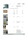
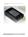
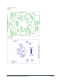
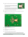
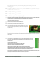
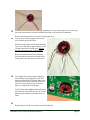
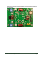
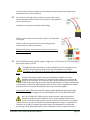
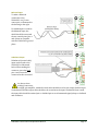
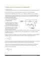
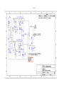
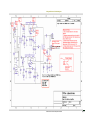
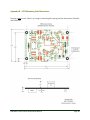
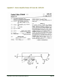
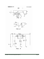
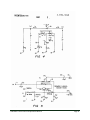
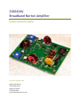
Z10042AV Broadband Norton Amplifier Assembly and Operation Manual Revised 23 October 2010 Clifton Laboratories 7236 Clifton Road Clifton, VA 20124 (703) 830 0368 www.cliftonlaboratories.com Table of Contents Model Z10042AV Broadband Norton Amplifier ......................................................................................................... 3 Trademarks and Copyright .........................................................................................................................................3 Warranty ............................................................................................................................................................................3 Safety Information .............................................................................................................................................................. 4 General Information and Specifications .................................................................................................................... 4 Description ........................................................................................................................................................................5 Specifications ....................................................................................................................................................................7 Assembly ................................................................................................................................................................................ 8 Parts Provided..................................................................................................................................................................8 Errata: ............................................................................................................................................................................... 11 Overview of Installing Surface Mount Parts ..................................................................................................... 11 Component Location .................................................................................................................................................. 14 Assembly Order ............................................................................................................................................................ 15 Post Construction Adjustment and Checkout .................................................................................................. 23 Input and Output Connections ............................................................................................................................... 26 Schematic and Theory of Operation and Troubleshooting .................................................................................. 30 Theory of Operation ................................................................................................................................................... 30 Schematic ........................................................................................................................................................................ 34 Voltage and Resistance Troubleshooting Data ................................................................................................ 35 Appendix A Typical Performance Data ......................................................................................................................... 36 Bandwidth ........................................................................................................................................................................... 36 Appendix B – PCB Mounting Hole Dimensions ......................................................................................................... 38 Appendix C – Norton Amplifier Patent, US Patent No. 3,891,934 ..................................................................... 39 Appendix D Manual Backdating ...................................................................................................................................... 45 Z10042AV Construction and Operations Manual Page 1 Applicability of Manual This manual applies to the Z10042AV printed circuit board revision 1.0 and later. The circuit board revision is silk screened on the PCB, just below the model number. Z10042AV Construction and Operations Manual Page 2 Model Z10042AV Broadband Norton Amplifier Revised 23 October 2010 (c) 2010 Jack R. Smith d/b/a/ Clifton Laboratories. Trademarks and Copyright Material in this document copyrighted © 2010 Clifton Laboratories. All rights reserved. It is provided to allow the Z10042AV purchasers to maintain their equipment and such other purposes as may not be prohibited by law. Warranty This warranty is effective as of the date of first consumer purchase. What is covered: During the ninety (90) days after date of purchase, Clifton Laboratories will correct any defects in the Z10042AV due to defective parts or workmanship (if purchased as an assembled unit) free of charge (post-paid). You must send the unit at your expense to Clifton Laboratories, but we will pay return shipping. Clifton Laboratories’ warranty does not extend to defects caused by your incorrect assembly or use of unauthorized parts or materials or construction practices. What is not covered: If the Z10042AV is purchased as a kit, this warranty does not cover correction of assembly errors or misalignment; repair of damage caused by misuse, negligence, or builder modifications; or any performance malfunctions involving non-Clifton Laboratories accessory equipment. The use of acid-core solder, water-soluble flux solder, or any corrosive or conductive flux or solvent will void this warranty in its entirety. Damage to the Z10042AV or equipment connected to it caused by lightning strikes is not covered under the warranty. Whether purchased as an assembled unit or as a kit, also not covered is reimbursement for loss of use, inconvenience, customer assembly or alignment time, or cost of unauthorized service. Limitation of incidental or consequential damages: This warranty does not extend to nonClifton Laboratories equipment or components used in conjunction with our products. Any such repair or replacement is the responsibility of the customer. Clifton Laboratories will not be liable for any special, indirect, incidental or consequential damages, including but not limited to any loss of business or profits. Under no circumstances is Clifton Laboratories liable for damage to your equipment connected to the Z10042AV resulting from use of the Z10042AV, whether in accordance with the instructions in this Manual or otherwise. Z10042AV Construction and Operations Manual Page 3 Safety Information The Z10042AV operates with a user-supplied DC power supply of 13 to 15 Volts at 100 to 120 mA. The Z10042AV, although designed as a low signal level preamplifier, is capable of RF output power approaching the 1 watt level. This output power is capable of damaging receivers or the receiver section of a transceiver or test equipment. It is the user’s responsibility to ensure that the Z10042AV is properly connected to whatever devices it will be used with. The Z10042AV has no replaceable fuses; rather a self-resetting polyfuse limits short circuit current to approximately 200 mA. The Z10042AV is designed to be used only with receive-type power levels. It should not be used with transmitting equipment. The Z10042AV’s maximum permitted input RF power is 100 mW (+20 dBm). Power in excess of this level may damage the Z10042AV or equipment connected to it, or both. In addition, since the Z10042AV has appreciable gain, output power levels sufficient to damage connected equipment may occur with input signal levels well below +20 dBm. Although the Z10042AV contains protective measures, all of these protection measures assume that the Z10042AV is properly grounded and that good engineering practices have been used in its installation and construction of the ground system. The Z10042AV is not intended to survive a direct lightning strike to an antenna connected to its input, whether powered up or not. However, the protective measures incorporated into the Z10042AV’s design should aid in reducing damage. Z10042AV Construction and Operations Manual Page 4 General Information and Specifications Description The term “Norton Amplifiers” refers to a class of transformer feedback amplifiers developed by Dr. David Norton and described in his US Patent No. 3,891,934, granted June 24, 1975 and now in the public domain. (A copy of Dr. Norton’s patent is Appendix C to this Manual.) A Norton amplifier permits the distortion reducing benefits of negative feedback to be applied without impairing the amplifier’s noise figure. Hence, Norton amplifiers are also known as “noiseless feedback” amplifiers. The Z10042AV is a broadband (25 KHz to 20 MHz) Norton-style amplifier providing 11 dB gain (other gain values are possible) with very high 3rd order and 2nd order intermodulation intercepts, IP3 and IP2, respectively, with a noise figure of approximately 2 dB. The Z10042AV is designed for either indoor or outdoor use, with DC power supplied through either separate connections or duplexed over the output coaxial cable. Optional indoor and outdoor die cast enclosures are available for the Z10042AV. The Z10042AV is derived from the Norton Amplifier developed by Dr. Dallas Lankford and described in his publication Common Base Transformer Feedback Norton Amplifiers, dated 8 June 1994, revised 21 May 2007, available at http://www.kongsfjord.no/dl/Amplifiers/Common%20Base%20Transformer%20Feedback%20N orton%20Amplifiers.pdf. The Z10042AV modifies Dr. Lankford’s design in several respects: Automatic input disconnect upon DC power removal along with over-voltage gas trap protection Over voltage and reverse voltage protection on the DC Power. DC power either separately or duplex power. Optional balanced or unbalanced input. Shunt fed to reduce effect of DC saturation of T2 and T4 Component values selected to extend lower -3 dB point to approximately 30 KHz. Clifton Laboratories also offers the Z1203A DC power injector usable with the Z10042AV to provide DC power over the output coaxial cable. This is useful for remote mounted amplifiers. The Z10042AV is available as a kit, including a double sided, silk screened solder masked printed circuit boards and all electronic parts or as an assembled and tested printed circuit board. Options include an indoor enclosure with BNC connectors or an outdoor weatherproof die cast enclosure with a choice of BNC, UHF or Type N connectors. Typical kit construction time is three to five hours depending on your work practices. The kit is suitable for relatively inexperienced builders, although Clifton Laboratories does not recommend it to purchasers who have never built an electronic kit before. Also, if you have never wound a toroid inductor or transformer, you might wish to ask an experienced builder to show you how it’s done. Z10042AV Construction and Operations Manual Page 5 The Z10042AV is generally electrically similar to the Z10042A, but has a revised printed circuit board layout to accommodate components required for low frequency extension. In addition, a few of the Z10042A’s through-hole components are replaced with surface mount equivalents in the Z10042AV layout. Other than frequency response, the Z10042AV’s performance matches the Z10042A. The differences in performance, design and construction are: Feedback transformers T2 and T4 wound with 2:22:8 turns instead of 1:11:4. This change is required to increase magnetizing inductance to support operation below 100 KHz. Upper -3 dB point reduced to 20 MHz, mostly a consequence of increased capacitance in T2 and T4 from doubling the number of turns. RF chokes L1-L4 increased in value to improve low frequency response. L2 and L4 relocated to bottom board surface for improved clearance. Reverse polarity protection diode D1 replaced with surface mount diode. Overload protection resettable fuse F1 replaced with surface mount version Spark gaps SA1 and SA2 replaced with surface mount version DC power feed and duplex power jumper consolidated into single connector and circuit revised so that DC power is always fed through L5, to reduce possible noise riding on power feed. DC power/power mode J3 now male connector for improved safety. (DC power supplied with matching female connector which avoids inadvertent short circuits.) RF choke L5 replaced with surface mount version. General PCB cleanup, with added jumper and connector information appearing on silk screen. Z10042AV Construction and Operations Manual Page 6 Specifications Parameter PCB Dimensions Value 3.50” x 2.50” x 0.75” vertical clearance required. (88.9mm x 63.5mm x 19mm). Four mounting holes for 4-40 screws provided, template in Appendix B. Maximum: 15V Minimum: 13.8V [may not meet specifications below this voltage. See Appendix D for performance versus supply voltage considerations.] Negative to ground, typical DC current 60-100 mA depending on bias adjustment. DC Power Required As an option, a reduced power version of the Z10042AV is available, with approximately 25 mA, usable down to 12V input. 2nd and 3rd order intermodulation performance is degraded with this option; noise figure is improved over normal idle current. Maximum RF Power Input Test Conditions 3 dB Bandwidth 2nd and 3rd Order Intermodulation Intercept Gain 1 dB Gain Compression Noise Figure Input VSWR Common Mode Rejection in Balanced Input Mode Do not exceed 100 milliwatts (+20 dBm). IP3 performance specifications are based upon -10 dBm signal input; performance not warranted at greater input levels. Performance data is for a 2:22:8 turns ratio design, 13.8 VDC after adjusting balance trimpots for minimum 2nd harmonic distortion. Unless otherwise indicated, performance measurements are made with direct DC power, not duplexed. Figures stated as “typical” are not warranted. 30 KHz – 20 MHz. Measured with 3 and 4 MHz input tones, adjusted for 0 dBm output from the Z10042AV. Protocol as discussed later in this manual. Intercepts are output referenced. OIP2: +80 dBm (typically > +90 dBm) OIP3: +45 dBm (typically +46 to +48 dBm) 11 dB nominal at 1 MHz. +19 dBm input. 2.5 dB maximum 10-30 MHz. Typically 2 dB or less at 10 MHz. When terminated with 50 ohm load, input VSWR is less than 2:1 over the range 300 KHz – 30 MHz, and is typically below 1.5:1 over this range. Typically 50 dB at 1 MHz, decreases with increasing frequency. Z10042AV Construction and Operations Manual Page 7 Assembly Parts Provided Before starting your build, please take a moment and inventory the parts provided against the list below. The ruler is marked in decimal (tenths) inches. One inch is 25.4mm and 0.1 inch is 2.54mm. (Some older photos use a ruler marked in fractions of an inch, such as 1/16th.) Many parts in this kit are not marked and can easily be confused. Parts are provided in individually labeled paper envelopes. Please keep parts in the associated envelope when not being installed. A note on how component values are identified in this manual This document follows the international practice of using the value multiplier to indicate the decimal point. Thus, a 1.0µF capacitor is identified as 1µ0 and a 10,000 ohm resistor is identified as 10K0. Photograph Qty ID 5 C2, C4, C7,C10, C18, 7 C3, C6, C11, C14, C15, C16, C17 Same as above Same as above 4 C20,C21,C22, C23 Same as above 2 1 C5, C8 C19 Z10042AV Construction and Operations Manual Description and Comments 1u0 X7R 25V, 1206 size surface mount ceramic capacitors. 2u2 X7R 25V, 1206 size surface mount ceramic capacitors. 10pF, C0G 50V, 1206 size surface mount ceramic capacitors 1000pF, C0G 50V, 1206 size surface mount ceramic capacitors 10uF/25V 105°C aluminum electrolytic capacitor. Component Marking None None None None 10 EHA Page 8 Photograph Qty ID Description and Comments Component Marking D1 Silicon diode, 1A or greater, 50V or greater. Typically a S1A part S1A 1 F1 200 mA Raychem “polyfuse” PTC varistor, surface mount 1206 size. C 2 FB1,FB3 Surface mount ferrite bead None 1 2 [3place] 1 [4place] J1, J2 and input for J3. 1 K1 J1: 4-place J2: 3-place 0.1-inch header sockets None J3: 4 place 0.1-inch header pins G6H-2F-DC12 double pole, double throw 12V surface mount relay G6H-2F12VDC L1 & L3 2m2 RF choke (shielded) 225D 2 L2 & L4 3m3 RF choke (shielded) 335D 1 L5 1m0 RF choke (shielded) 105J 2 Z10042AV Construction and Operations Manual Page 9 Photograph Qty 2 ID Description and Comments NPN transistor, UHF, type NE85634, SOT-89 package Q1, Q2 Component Marking RE ¼ watt, 1% 1206 Surface Mount Resistors 2 R1,R6 560R 49R9 5600 2 R4,R12 2 R10, R5 R2, R7, R9,R11 1K50 1501 10R0 10R0 2 R3, R8 100R Trim-pot 101 1 RV1 14mm dia. 18V overvoltage MOV 180M 2 SA1, SA2 4 11 Z10042AV Construction and Operations Manual J4 49R9 Spark gap 90V Total of 11 pins supplied. Pins are 0.1 inch spaced, 0.025 inch square gold flashed. 4 pins to mate with J1; 3 pins to mate with J2 and None Page 10 Photograph Qty 4 1 ID Component Marking T1,T2,T3, T4 0.5 inch diameter ferrite cores; relative permeability 5K, builder to wind. None PCB Printed circuit board. Identified as Z10042AV Z10042AV and revision number None 1 length #24 wire (64 inches/1.625m) red; 1 length #24 wire (12 inches/480mm) green. None 2 lengths #26 wire None 2 inches (50mm) foam tape None None None Description and Comments 4 pins for J3. No. 24 AWG magnet wire, use for T2 and T4. (The two lengths will be different color; usually the long wire will be red and the short green, but this may be reversed depending upon wire stocks.) No. 26 AWG magnet wire, use for T1 and T3. One length red, one length green. Length of ¼ inch (6mm) wide, double sided foam tape None None None Errata: None known for revision 1.0 Overview of Installing Surface Mount Parts 1. You may wish to apply a sparing amount of liquid flux to pads before soldering. Clifton Laboratories uses MG Chemical flux, part number 835100ML (also available as a flux pen, part number 835-P.) Both products are available from Mouser and other suppliers. To apply liquid flux, a wooden toothpick may be used or the flux can be dispensed from a needle oiler. (If using the flux pen, wipe it across pads before soldering.) MG Chemicals 835 flux leaves a distinct residue. The residue will not damage the board but if desired, it may be removed with flux remover or 91% isopropyl alcohol available locally. Z10042AV Construction and Operations Manual Page 11 2. If the component has one pad that is a ground, lightly tin the non-ground pad. If neither pad is a ground connection, tin either one of the pads. 3. Using forceps or a very light touch with long nose pliers, slide the component into place while heating the tinned pad. Check that the component is more or less centered on the pads and remove the soldering iron when centered. Too much pressure will crack these parts so use a light touch. 4. Solder the other pad. Touch up the first pad if necessary. 5. Although the Z10042AV’s ground pads use “thermal relief” it may still be difficult to make with a small soldering pencil, as the large foil area requires more heat capacity than a normal floating pad. Z10042AV Construction and Operations Manual Page 12 The image below shows a Z10042AV installed in the optional enclosure. (The label is for a Z1002A amplifier.) Z10042AV Construction and Operations Manual Page 13 Component Location TopV iew Bottom View Z10042AV Construction and Operations Manual Page 14 Assembly Order The Z10042AV is a relatively simple kit. The most complex part is winding the transformers, and even this is not difficult. The assembly order starts with the bottom surface. Install 1u0 capacitors at 3 places: C10, C18 & C2 Install 2u2 capacitors at 3 places: C14, C15, C16 & C6 Install 10pF capacitors at 4 places: C20, C21, C22 & C23 Install 1000pF capacitors at 2 places: C5, C8 Install C19, a 10uF electrolytic capacitor marked 10. This is a polarized part and must be installed with the correct orientation. Negative is indicated with black stripe on the capacitor body. C19 may be difficult to properly solder as its leads are largely below the base insulator. Before soldering, tin C9’s positive lead. Apply a small amount of solder to C9’s PCB pad. While heating the positive pad with the soldering iron, hold C19 in place and apply a small amount of pressure with your fingers or forceps. After soldering the positive pad, verify it is properly attached; C19 should not move under light pressure. Then solder the negative terminal. Install L2 and L4, 3m3 RF chokes, marked 335D. The choke orientation is defined by a small dot on the choke and a corresponding dot on the printed circuit board silk screen. Orient L2 and L4 so that their dots match the silk screen dot. (The photo shows the top mounted chokes of a different value, but with the same dot marks used at L2 and L4.) L2 and L4 mount on pads that are only slightly larger than the component, so carefully align L2 and L4 before soldering. Hold the choke in place with pressure from the top (wooden spring clothespin or small clamp) and solder one pad. Allow the solder to cool, remove the clamp and solder the remaining pad. Z10042AV Construction and Operations Manual Page 15 Install K1, a double pole, double throw relay, marked G6H2F. K1 orientation should follow the photograph at the right; the black strip on the relay body is next to the wide white band on K1’s PCB outline. When soldering K1 in place, tin one corner pad and slide K1 into place whilst keeping the solder molten. Align K1’s pins with the pads and remove the soldering iron. Then solder the remaining pins. Install R4 and R12, 49.9 ohm resistors, marked 49R9. This completes the bottom assembly. Check your work for missing parts and poor solder joints. The completed bottom surface is shown below. Top Surface Components Install 1u0 capacitors (no marking) at 2 places: C4 & C7 Install 2u2 capacitors (no marking) at 3 places: C3, C11 & C17 Install Q1 and Q2, NE85634 transistors, marked RE. To install Q1 and Q2, Apply a small bit of solder to one outside pad. Hold the transistor in place with tweezers and apply heat to the top of the pin, melting the solder on the pad Z10042AV Construction and Operations Manual Page 16 beneath the pin. Solder the remaining two pins in place and reflow the tacked pin. Then solder the collector tab in place. Install 10R0 resistors, marked 10R0, at 4 places: R2, R7, R9 & R11 Install ferrite beads (unmarked) in 2 places: FB1 & FB3. Install 560R resistors (marked 5600) in 2 places: R1 & R6 Install 1K50 resistors (marked 1501) in 2 places: R5 & R10 Install 2m2 inductors (marked 225) at 2 places. L1 & L3 The choke orientation is defined by a small dot on the choke and a corresponding dot on the printed circuit board silk screen. Orient L1 and L3 so that their dots match the silk screen dot. L1 and L3 mount on pads that are only slightly larger than the component, so carefully align L1 and L3 before soldering. Hold the choke in place with pressure from the top (wooden spring clothespin or small clamp) and solder one pad. Allow the solder to cool, remove the clamp and solder the remaining pad. Install D1, the reverse polarity protection diode. This will be an S1x series device, marked S1x where x is a letter identifying the maximum reverse voltage. The Z10042AV usually ships with a 50V diode, identified as an S1A. Observe polarity when installing the diode; the diode body is marked with a bar at one end. Install the diode with this bar at the pad identified with the silk screened bar. D1’s pad is sized for machine soldering and is a bit short for hand assembly. When installing the diode, tin the pad identified with the bar and slide the diode forward with the soldering iron on the pad until the opposite pad is exposed slightly at the other end (ground pad) of the diode. Solder the ground pad. Install F1 (a 200 mA polyfuse, marked C). Install L5, a 1m0 RF choke, marked 105J. The pads are only slightly larger than the choke body, so carefully align L5. Hold it in place with pressure from the top (spring clothespin or a small clamp). Hold the soldering iron tip at a 45 degree angle to the pad/component joint and feed solder in while slowly moving the iron back and forth along the length of the pad until the solder Z10042AV Construction and Operations Manual Page 17 flows. Allow the pad to cool, remove the clamp and repeat the solder process at the remaining pad. Install RV1, the MOV over-voltage protector, marked 180M. RV1 is not polarized and may be installed in either orientation. Install R3, a 100R trimpot, marked 101. Install R8, a 100R trimpot, marked 101. Install the three-pin header socket (female) at J2. Install SA1 and SA2,spark gaps, marked either 90V plus a date code or EC75 plus a date code. SA1 and SA2 are not polarized and may be installed in either orientation. Center SA1 and SA2 on the pads. Install a four-pin header socket (female) at J1 Install a three-pin header socket (female) at J2 Locate the header pin (male) strip and break or cut a 4-pin section from the strip. Install at J3. (The short side goes into the pad holes.) Except for the four transformers, all components should be installed on the PCB’s top surface at this stage. Locate the No. 26 AWG magnet wire. (It is the smaller diameter of the two wire sizes.) One length of green insulated wire is provided and one of red insulated wire. Cut four lengths of the wire: Two pieces green, each 18 inches (450 mm) long. Two pieces red, each 18 inches (450 mm) long. Take one piece of red wire and one piece of green wire and twist approximately 80 turns. Repeat for the second pair of red and green wires. (A variable speed drill, running slow speed, speeds up the twisting process.) At this point, you should have two twisted wire sections, each approximately 18 inches (450 mm) long, each twisted pair with one red and one green wire. Z10042AV Construction and Operations Manual Page 18 Wind the twisted wire 18 turns onto one of the ferrite cores. (Photo shows 10 turns wound.) To fit 18 turns onto the core, the turns must be closely spaced. As a reminder, a turn is counted when the wire passes through the hole in the core. Insert one end of the twisted pair approximately one inch (25 mm) through the core. Wind 18 turns. The windings will occupy most of the core perimeter. Cut the excess wire to provide approximately one inch (25mm) length. Repeat for the second transformer. Congratulations. You have completed winding two bifilar broadband transformers, T1 and T3. Locate the PCB and look at the silk screen outline for T1 and T3. Note that each has four pads, comprised of three round pads and one square pad, oriented as shown in the drawing. The green wires connect to the two round pads on one side and the red wires connect to the one square and one round pad on the opposite side. [This is not critical and one can interchange the green and red leads, but troubleshooting will be easier if all the Z10042AV’s are built the same way.] Un-twist the pigtails so that you have four separated wires. Remove the insulation and tin the four wires. Note: The red and green wire supplied is “solderable” and the insulation will melt if heated with a blob of molten solder. This heating and tinning must be done before the transformers are installed in the PCB. The wire leads should be formed as illustrated in the photo to the right. Cut a length of foam tape approximately 3/8ths of an inch long (9mm) and apply it to the PCB within the T1 outline. Make sure that tape does not block the pad holes, and trim if necessary. Remove the protective paper from the tape. Install T1 as shown in the drawing and photograph. A common error in installing T1 and T3 (as well as T2 and T4) is that the insulation is not fully removed from the wire due to insufficient heating during the tinning process. Z10042AV Construction and Operations Manual Page 19 Repeat the process for T3 and install The remaining step is to wind T2 and T4, the matching and feedback transformers. These transformers should be wound as identical as possible and must be phased (wound) as described below or else you will build an oscillator instead of an amplifier. If you carefully follow the instructions in this manual, your transformers will work the first time. Before winding T2 and T4, take a moment to read the installation steps and study the drawing and photographs. This manual describes transformers resulting in 11 dB nominal gain, with a 2:22:8 winding ratio. Other winding ratios are possible with different gain as described elsewhere in this manual. In the context of drawing below, this configuration is N=22, M=8. Cut two lengths of #24 AWG magnet wire, each length 32 inches (810 mm) long. This wire will be wound 30 turns on a ferrite core, as illustrated at the right. The letters C…F on the drawing correspond to T2 and T4’s PCB pads. Before winding the transformers, take a moment and look at the PCB outline for T2 and T4. Start by threading the wire through the core with approximately one inch (25 mm) projecting from the core. This short starting end is C in the drawing. Wind 22 turns (N) following the orientation shown in the drawing. Note the direction of winding. (I’m left handed and this is how I wind a toroid. And, more importantly, the sense of winding A-B, which is defined by the PCB layout, is based upon following the winding direction illustrated in the drawing.) When completed with all 30 turns, the winding will occupy 80 to 85% of the core perimeter. In order for all 30 turns to fit, turns must be wound tightly against each other. As a reminder, a turn is counted when the wire passes through the hole in the core. After winding the 22nd turn, extend it approximately one inch (25 mm) and double it back. (The doubled wire will become ends D and E). Wind 8 more turns (M), ending at end F. Trim the F wire to be approximately one inch (25 mm) long. The photo below shows a transformer at this stage. Z10042AV Construction and Operations Manual Page 20 Trim the two free ends (C and F) to approximately 1 inch (25mm) long. Do not cut the loop yet as the transformer is easiest to handle if the loop is cut just before installation. Remove insulation and tin all 4 leads, including the loop. Cut a 6 inch (150mm) length of the second color (usually green) #24 wire. Wind two turns (these will be leads A and B) on the core, and trim to approximately 1 inch (25mm) extensions on both ends. Wind in the same direction as the 22:8 windings. Remove insulation and tin the two leads. Form the leads to match the printed circuit board pads. Leave the loop un-cut for now. Cut a length of foam tape approximately ½ inch (12mm) long and apply it to the PCB within the within the T2 outline. Make sure that tape does not block the pad holes, and trim if necessary. Remove the protective paper covering from the foam tape. Cut T2’s loop and straighten the leads. Insert the leads into T2 pad holes A, B, C, D, E and F, following the drawing, and solder these six leads. Repeat this process for T4 with the second transformer. Z10042AV Construction and Operations Manual Page 21 At this point, all components should be installed and your Z10042AV should resemble the one shown below. Z10042AV Construction and Operations Manual Page 22 Post Construction Adjustment and Checkout Before powering up the Z10042AV, take a moment to make resistance checks and pre-set R3 and R8. With an ohmmeter measure and adjust R3 and R8 to 50± 5 ohms. (Both measuring points are with respect to ground, with the negative lead of the ohmmeter to ground.) R3: Measuring point is junction of R3 and R2, as illustrated to the right. R8: Measuring point is junction of R8 and R7 as illustrated to the right. Z10042AV Construction and Operations Manual Page 23 You may wish to make a complete set of resistance measurements as developed in the maintenance section of this manual. If you have not already done so, make up a power cable using a three-pin header socket. Positive to the center pin and negative to the two outside pins. Insulate the connections with heat shrink tubing. The DC power connector mates with J3, pins 2-4 as illustrated at the right. J3 pins 2 and 4 are ground so the DC power plug may be connected to J3 in either orientation. When the DC power connector is properly inserted, J3, pin 1 will be unconnected. The Z10042AV will work with DC supply voltages up to 15V and down to 12V. Performance data is based upon 13.8V DC. The high performance transistors in the Z10042AV are not as resistant to overvoltage as the through-hole parts used in the Z10040B Norton Amplifier. Accordingly, do not exceed 13.8V supply unless you know exactly what you are doing. If a laboratory power supply with current limiting is available, set it for a maximum short circuit current of 175 mA and set the voltage to 0V. Connect the supply to the Z10042AV at J3 using the cable constructed above and bring up the voltage slowly whilst observing the current. With R3 and R8 set for 50 ohms, the maximum current observed should be approximately 100-110 mA at 13.8V. If significant deviations from this value are observed, immediately remove power and investigate. Adjusting R3 and R8. With the normal DC supply voltage applied through J3 preferably with a laboratory power supply with current limiting set to 175 mA, adjust R3 and R8. Note: If you adjust R3 or R8 to the zero ohms extreme, it may be possible to damage components in the Z10042AV. Some current limiting is built into the circuit, via the decoupling resistors and the resistance of the collector and emitter chokes. However, in order to provide the maximum adjustment range to compensate for variations in Q1 and Q2, complete protection against mis-adjustment is not possible. Accordingly, when adjusting R3 and/or R8, it is imperative that you observe the total Z10042AV Construction and Operations Manual Page 24 current being drawn by the amplifier, and, if possible, use a power supply with current limiting set to 175 mA. Heatsinking of Q1 and Q2 is limited to that provided by the printed circuit board. Hence Q1 and Q2’s current must be limited to reasonable levels. Under no circumstances should Q1 or Q2 be biased to draw more than 60 mA each. Clifton Laboratories recommends setting the idle emitter current to a nominal value of 37.5 mA (35 to 40 mA range) per transistor. Of course, if the idle current balance is adjusted for optimum OIP2 performance the two amplifier sections will likely have slightly different idle current values. To measure the current through Q1 and Q2, measure the voltage drop across R2 and R7, 10 ohm resistors. The emitter current (in mA) through the transistor is 1000 x V/10.0 where V is the drop across R2 or R7 in volts, 1000 is to convert the result to mA and 10.0 is the resistance of R2 and R7. For the recommended 37.5 mA idle current, the voltage drop across R2 and R7 should be 0.375 volts nominal and in the range between 0.350V and 0.400V. Alternative 1: If you do not have the ability to measure 3rd order and 2nd order intermodulation products, adjust R3 and R8 such that Q1 and Q2 have substantially equal emitter currents of approximately 37.5 mA each, using the method above. Alternative 2: Adjust R3 and R8 for best 3rd and 2nd order intermodulation performance using the test equipment configuration you normally use for these measurements. During the adjustment process do not exceed 60 mA in either Q1 or Q2 as it is possible to damage components with over-current. As a simplification, the absolute current through Q1 and Q2 determines the 3rd order intercept, and balance between Q1 and Q2 determines the 2nd order intercept. Thus, operating with Q1 and Q2 around 40 mA each will have somewhat better 3rd order intercept performance than where Q1 and Q2 operate around 20 mA each. Adjusting Q1 or Q2’s current slightly up or down from absolute equality is almost always necessary to optimize 2nd order intercept. In addition, noise figure degrades with idle current over 10-15 mA. There is no unique idle current setting that simultaneous optimizes noise figure and 2nd and 3rd order intermodulation intercepts. Clifton Laboratories does not recommend and is not responsible for damage to the Z10042AV if the emitter current is set to exceed 60 mA per transistor. 37.5 mA is a reasonable compromise that balances noise figure and intermodulation performance and should be the target in the absence of good reason for a different current setting. A bias adjustment service for kit builders not equipped to measure IP2 and IP3 is available. Contact Clifton Laboratories for details. Z10042AV Construction and Operations Manual Page 25 Input and Output Connections RF output connection is made to the Z10042AV with a 3-pin header at J2. Since the outside pins are always ground, either orientation is permitted. Input to the Z10042AV is made with a 4-pin header at J1 and may be configured for either balanced or unbalanced input. DC power and local power / duplex power is made through a 4-pin connector, J3. Note on Coaxial Cable and Header Pins Header pins of the type used in the Z10042AV are suitable for small diameter coaxial cable, such as RG174 (0.1 inch / 2.5mm diameter). Since the Z10042A is normally installed in an enclosure, a short jumper cable made from RG-174, or RG178 is used between the enclosure’s coaxial connectors and the Z10042AV’s J1 and J2. Clifton Laboratories makes coaxial cable connections to three pin headers as illustrated in the photo below (RG-174 is illustrated). Tin the solder ends of a 3-pin connector (the short ends). Remove approximately 5/8th inch (15mm) of jacket from the cable. Comb the cable braid into individual wires and separate into two roughly equal groups. Twist each group together and tin the ends. Don’t apply excessive heat at it is easy to melt RG-174’s center conductor insulation. Remove approximately 1/8th inch of insulation from the center conductor and tin. Slip a short length of heat shrink tubing over the center conductor. Solder the center conductor to the center pin, working quickly to avoid melting the RG-174’s center insulation. Slide the shrink tubing over the joint and apply heat to shrink. Form the two braid extensions as illustrated and solder to the outside pins. For a neater appearance, a length of ¼ inch (6mm) shrink tubing can be applied over the exposed braid, but will limit flexibility of the joint. Z10042AV Construction and Operations Manual Page 26 Balanced Input To make a balanced connection to the Z10042AV, use J1’s two center pins, as illustrated in the drawing to the right. If a shielded pair is used for the balanced input, the shield should be connected the two outside pins (pins 1 and 4) that are common with the Z10042AV’s ground plane. to Unbalanced Input Unbalanced (coaxial cable) input can be made to the Z10042AV as illustrated below. When making the connector, note that both pins 1 and 3 must be connected to the coax braid. As always when making connections to a high gain amplifier, shielded coaxial cable should be used on the output (and the input if unbalanced) and the output cable should not be routed near the input. If balanced input is used, the input cable should be twisted pair or shielded pair to avoid unwanted signal pickup or feedback and oscillation. Z10042AV Construction and Operations Manual Page 27 Unbalanced Output The Z10042AV’s output is unbalanced only. Connection should be made as illustrated in the illustration at the right. Duplex Power Jumper The Z10042AV can be powered by two methods: 1. Separate DC power connection to J3, as described in the post construction checkout portion of this manual, repeated at the right. When power is provided directly, J3, pin 1 is unused. 2. DC power may be provided over the output connector. This is known as ‘duplex power’ because the DC power is duplexed with the RF signal. Duplex power requires a suitable coupler to inject DC and separate the RF signal. Clifton Laboratories Z1203 DC Coupler is suitable for this purpose. To enable duplex power, construct a jumper between the two outside pins of the 3-pin socket. Plug the socket into J3 pins 1-3. When properly installed, J3, pin 4 will be unused. Z10042AV Construction and Operations Manual Page 28 This completes the assembly and verification of your Z10042AV Norton Amplifier. Z10042AV Construction and Operations Manual Page 29 Schematic and Theory of Operation and Troubleshooting Theory of Operation The Z10042AV Norton amplifier consists of two identical amplifier sections arranged in push-pull. The discussion below uses component designations for the section associated with Q1. Each section is a common base (also known as “grounded base”) amplifier. As such, essentially identical signal currents flow through all three sections of T2 and T1’s secondary winding. Gain is achieved in the grounded base amplifier because the collector load, represented by T2’s n and m windings operating as an autotransformer has greater impedance than the emitter input, and hence power gain results. The figure at the right is a simplified view of an amplifier section, with all DC biasing and blocking components removed so that we may concentrate on the signal flow. The transformer turns ratios are shown as 1:n:m, but this does not mean the emitter feedback winding must have only one turn. Rather, it is the ratio of turns that is important, so that if the emitter winding has, for example, two turns, then the number of turns in windings n and m should also be doubled. Consider windings n and m and assume a load of impedance Z is connected from output to ground. Windings n and m form an auto-transformer with Q1’s collector seeing an impedance of: nm ZC ZO m 2 Since the same signal current flows through the emitter and collector (neglecting base current), the gain of the common base amplifier is proportional Zc or n and m in this relationship. The transformer turns ratios should not be arbitrarily selected, if the full benefits of the Norton amplifier are to be realized. From Patent No. 3,891,934, the following equation governs the transformer turns relationship: R n m 2 S m 1 RL Z10042AV Construction and Operations Manual Page 30 ( ) Where RS is the source (input) impedance RL is the load (output) impedance n and m are the transformer winding ratios, normalized to an emitter winding with one turn. In our case, we wish the input and output impedances to be equal, and hence RS/RL = 1. Thus the turns relationship is simplified to: n = m2-m-1 The amplifier’s transducer gain1 is stated as: Again, since our normal operation is with equal input and output impedances, the transducer gain Gt is simply m2. Winding Ratio 1:n:m 1:1:2 1:5:3 1:11:4 1:19:5 1:29:6 Transducer Gain (dB) 6.0 9.5 12.0 14.0 15.6 These figures are theoretical and the actual realizable gain is typically a dB or so less. In order to extend the low frequency response in the Z10042AV, the windings should be doubled; for example, 2:22:8 instead of 1:11:4. One significant advantage of the Norton amplifier is that the input impedance automatically tracks the output impedance. Thus, if terminated into a 50 ohm load, the input impedance is 50 ohms. If the output impedance is changed to 75 ohms, the input impedance becomes 75 ohms. (This relationship is again not perfect, but it is reasonably good with less than a 2:1 VSWR over the range 300 KHz – 30 MHz when measured in a 50 ohm system.) DC power may be provided to the Z10042AV via two feed points. First, direct DC power over J3. Secondly, adding a jumper at connector J3 permits DC power to be duplex fed over the coaxial cable transmission line carrying the amplifier’s output. Of course, an appropriate DC power injector, such 1 Transducer gain is defined as: “the ratio of the power delivered by a network to a load (PdL) to the power available from the source (Pas). Transducer gain is a function of the source and load reflection coefficients and the network sparameters.” http://www.maurymw.com/support/faqs/faqs/faq9.html Z10042AV Construction and Operations Manual Page 31 as Clifton Laboratories model Z1203A, will be required and the power source that is used should be selected to have low noise at the frequencies of interest. Over current protection is provided by F1, a 200 mA positive temperature coefficient “polyfuse.” Should the amplifier draw more than 200 mA, F1 will heat and switch to a high resistance state, thereby limiting the current drawn by the power source. So long as the voltage remains applied, F1 will remain in the high resistance state. Over voltage protection is provided by RV1, an 18V DC (nominal) bipolar metal oxide varistor. The primary purpose of RV1 is to limit damage to the DC power source, should a nearby lightning strike or other incident induce a greater than normal voltage on the DC power line. Although RV1 is rated to begin clamping at 18V (1.0 mA clamp current at 18V), the actual onset voltage may be 20% above this figure and the clamping voltage may rise as high as 36V at 50A clamping current. Hence, even with RV1 in place and functioning properly, excessive over voltage may still occur if the disturbing event is sufficiently energetic. (The ROV14-180M device used in the Z10042AV is rated at a one-time 1,000A clamp or two-times 500A clamp. However, at 1000A, the expected clamping voltage is 80V.) Reverse voltage protection is provided by D1, an S1x series surface mount diode connected to be forward biased if the input polarity reverses. This causes two things to happen. First, the maximum voltage across the DC power distribution circuitry will be limited to approximately 1V by D1. Secondly, fuse F1 will enter into high resistance mode by virtue of the over current. Of course, a sufficiently robust power supply connected with reverse polarity may destroy D1 before F1 can enter high resistance mode. The Z10042AV’s input is through a bifilar wound, broadband transformer, T1. Both of T1’s primary terminals are brought out to J1 through K1’s contacts so that either balanced or unbalanced input may be used. Balanced input signals are applied across T1’s primary, which remains floating with respect to ground. If unbalanced input is used, one of T1’s primary terminals is connected to ground through appropriate jumper settings at J1, or via the ground connection modification discussed in the assembly section of this manual. Ferrite beads FB1 and FB3, along with C22 and C23 prevent VHF/UHF parasitic oscillations. (The NE85634 transistors have appreciable gain above 5 GHz.) DC power is supplied to Q1 and Q2 through RF chokes L2 and L4, with T2 and T4 output sections being AC coupled by blocking capacitors C4 and C7. There is thus no DC current flowing in T2 and T4’s windings, except for the emitter current through the one turn input winding. Removing DC current from T2 and T4 from the majority of the windings reduces core saturation and improves low frequency performance. The Z10042AV’s input circuit is protected in two ways. First, when DC power is removed from the Z10042AV, relay K1 removes the input connection and connects it to ground through R4 and R12, 49R9 ohm resistors. (If desired, the user may replace R4 and R12 with wire jumpers to the input when power is removed.) Secondly, SA1 and SA2, “gas trap” or spark protector devices are always connected across the Z10042AV’s input connector. Although SA1 and SA2 limit the voltage for fast Z10042AV Construction and Operations Manual Page 32 rise time pulses, their break over voltage may be several hundred volts. The primary purpose of SA1 and SA2 is to limit the voltage that might otherwise be coupled over the coaxial transmission line and, secondarily, to provide some protection to the Z10040’s components. When the input is configured as unbalanced, only one of SA1 and SA2 is operational. In balanced mode, SA1 and SA2 are connected between the two balanced inputs and the Z10042AV’s common ground point. Likewise in balanced mode, when the Z10042AV is unpowered, R4 and R12 are connected across the balanced input to the Z10042AV’s common ground point. All of these protection measures assume that the Z10042AV is properly grounded and that good engineering practices have been used in its installation and construction of the ground system. The Z10042AV is not intended to survive a direct lightning strike to an antenna connected to its input, whether powered up or not. However, the protective measures incorporated into the Z10042AV’s design should aid in reducing damage, particularly where the strike is not directly to the antenna system. Z10042AV Construction and Operations Manual Page 33 Schematic Voltage and Resistance Troubleshooting Data Z10042AV Construction and Operations Manual Page 35 Appendix A Typical Performance Data Except for common mode rejection, the data presented below is taken from one Z10042AV amplifier. While it is believed representative of Z10042AV amplifiers, due to component tolerance, assembly practices and test setup, the performance level seen in these measurements should be regarded as typical and is not guaranteed. Unless otherwise specifically noted, the data is taken with unbalanced input. Bandwidth Test Conditions: Direct DC feed. Z10042AV Construction and Operations Manual Page 37 Appendix B – PCB Mounting Hole Dimensions Drawing is not to scale. There is no change in mounting hole spacing and size between the Z10042A and Z10042AV. Z10042AV Construction and Operations Manual Page 38 Appendix C – Norton Amplifier Patent, US Patent No. 3,891,934 Z10042AV Construction and Operations Manual Page 39 Z10042AV Construction and Operations Manual Page 40 Z10042AV Construction and Operations Manual Page 41 Z10042AV Construction and Operations Manual Page 42 Z10042AV Construction and Operations Manual Page 43 Z10042AV Construction and Operations Manual Page 44 Appendix D Manual Backdating There are no manual backdating pages. Z10042AV Construction and Operations Manual Page 45