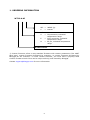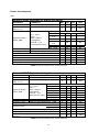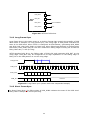
1
WT32 D a t a S h e e t V e r s i o n 1 . 1 W e d n e s d a y , S e p t e m b e r 0 3 , 2 0 0 8 Copyright © 2000-2008 Bluegiga Technologies All rights reserved. Bluegiga Technologies assumes no responsibility for any errors, which may appear in this manual. Furthermore, Bluegiga Technologies reserves the right to alter the hardware, software, and/or specifications detailed herein at any time without notice, and does not make any commitment to update the information contained herein. Bluegiga Technologies’ products are not authorized for use as critical components in life support devices or systems. The iWRAP and WRAP THOR are registered trademarks of Bluegiga Technologies. The Bluetooth trademark and logo are registered trademarks and are owned by the Bluetooth SIG, Inc. All other trademarks listed herein are owned by their respective owners. VERSION HISTORY Version number: Updates / Changes: 1.1 Bluetooth and FCC qualification IDs added 1.0 Soldering recommendations added. Layout guide fixed. Details at VREG_ENA. Operating temperature range fixed. 0.992 New images added 0.991 Missing pin added to recommended land pattern design 0.99 Microphone biasing recommendation fixed. Voltage regulator enable pin description added. Some small fixes. Layout guidelines for the audio traces added. 0.98 Version history added. Microphone biasing recommendations specified. Package information added. Pinout AIO0 and AIO1 fixed. 0.97 0.98 VREG_ENA pin added to the production version of the module Layout recommendations added Fixed cross references 2 Contents: 1. Ordering Information ................................................................................... 9 2. Block Diagram and Descriptions ................................................................. 10 3. Electrical Characteristics ............................................................................ 12 3.1 Radio Characteristics – Basic Data Rate ........................................................ 17 3.2 Radio Characteristics – Enhanced Data Rate .................................................. 18 4. WT32 Pin Description ................................................................................. 19 4.1 5. Device Terminal Functions .......................................................................... 20 Power Control ............................................................................................ 26 5.1 Power Supply Configuration ........................................................................ 26 5.2 Voltage Regulator Enable Pin....................................................................... 26 5.3 Battery Charger ........................................................................................ 27 5.4 RESET ..................................................................................................... 28 6. Serial Interfaces......................................................................................... 30 6.1 UART Interface.......................................................................................... 30 6.1.1 UART Configuration While RESET is Active ............................................... 32 6.1.2 UART Bypass Mode............................................................................... 32 6.2 USB Interface ........................................................................................... 33 6.2.1 USB Pull-Up Resistor ............................................................................ 33 6.2.2 Self Powered Mode ............................................................................... 33 6.2.3 Bus Powered Mode ............................................................................... 34 6.2.4 Suspend Current.................................................................................. 35 6.2.5 Detach and Wake-Up Signaling .............................................................. 35 6.2.6 USB Driver .......................................................................................... 36 6.2.7 USB 1.1 Compliance ............................................................................. 36 6.2.8 USB 2.0 Compatibility........................................................................... 36 6.3 7. 7.1 SPI Interface ............................................................................................ 37 Audio Interfaces......................................................................................... 38 Audio Interface ......................................................................................... 38 3 7.1.1 7.2 Audio Input and Output ........................................................................ 38 Stereo Audio CODEC Interface..................................................................... 39 7.2.1 ADC ................................................................................................... 40 7.2.2 DAC ................................................................................................... 41 7.2.3 IEC 60958 Interface ............................................................................. 42 7.2.4 Microphone Input ................................................................................. 43 7.2.5 Line Input ........................................................................................... 45 7.2.6 Output Stage....................................................................................... 46 7.3 Digital Audio Interface (I2S) ........................................................................ 48 7.4 PCM Interface ........................................................................................... 51 7.4.1 PCM Interface Master/Slave................................................................... 51 7.4.2 Long Frame Sync ................................................................................. 52 7.4.3 Short Frame Sync ................................................................................ 52 7.4.4 Multi Slot Operation.............................................................................. 53 7.4.5 GCI Interface ...................................................................................... 53 7.4.6 Slots and Sample Formats..................................................................... 54 7.4.7 Additional Features .............................................................................. 55 7.4.8 PCM CLK and SYNC Generation .............................................................. 55 7.4.9 PCM Configuration................................................................................ 55 8. I/O Parallel Ports ....................................................................................... 57 9. Software Stacks ......................................................................................... 58 9.1 iWRAP Stack ............................................................................................. 58 9.2 RFCOMM Stack.......................................................................................... 59 9.3 VM Stack.................................................................................................. 60 10. Enhanced Data Rate ................................................................................... 62 10.1 Enhanced Data Rate Baseband............................................................... 62 10.2 Enhanced Data Rate ∏/4 DQPSK ............................................................ 62 10.3 8DQPSK.............................................................................................. 63 11. Layout and Soldering Considerations ......................................................... 64 4 11.1 Soldering Recommendations.................................................................. 64 11.2 Layout Guidelines................................................................................. 64 11.2.1 Audio Layout .................................................................................... 64 11.2.2 Antenna Design ................................................................................ 64 12. WT32 Physical Dimensions ......................................................................... 66 13. Package...................................................................................................... 67 14. Certifications .............................................................................................. 69 14.1 Bluetooth............................................................................................ 69 14.2 FCC.................................................................................................... 70 14.3 CE ..................................................................................................... 71 14.4 Industry Canada (IC)............................................................................ 71 15. RoHS Statement with a List of Banned Materials ........................................ 72 16. Contact Information ................................................................................... 73 5 Terms & Abbreviations Term or Abbreviation: Explanation: A2DP Advanced Audio Distribution Profile AAC Advanced Audio Coding AVRCP Audio/Video Remote Control Profile Bluetooth Set of technologies providing audio and data transfer over shortrange radio connections CE Conformité Européene DFU Device Firmware Upgrade DSP Digital Signal Processing EDR Enhanced Data Rate FCC Federal Communications Commission HCI Host Controller Interface HFP Hands-Free Profile HID Human Interface Device IC Integrated Circuit iWRAP Interface for WRAP MP3 MPEG-1 Audio Layer OPP Object Push Profile PCB Printed Circuit Board 6 PCM Pulse Code Modulation RoHS The Restriction of Hazardous Substances in Electrical and Electronic Equipment Directive (2002/95/EC) SBC Sub Band Codec SPI Serial Peripheral Interface SPP Serial Port Profile UART Universal Asynchronous Transmitter Receiver USB Universal Serial Bus VM Virtual Machine VoIP Voice over Internet Protocol WRAP Wireless Remote Access Platform 7 WT32 Bluetooth® Audio Module DESCRIPTION: FEATURES: WT32 is the latest generation of Bluetooth modules. It provides highest level of integration with integrated 2.4GHz radio, DSP, battery charger, stereo codec, and antenna ready to hit mono and stereo audio applications. WT32 is also ready to support the latest Bluetooth 2.1 standard. The embedded DSP core allows enhancement of the product with features such as advanced audio decoding (MP3, AAC, AAC+), echo cancellation, noise reduction, and data manipulation. Bluegiga’s flexible iWRAP firmware enables device manufacturers to easily add wireless, secure, and standardbased Bluetooth connectivity into new or existing applications with very limited development and manufacturing effort. WT32 is Bluetooth End Product, CE and FCC certified meaning that OEMs do not need to apply any additional certifications. APPLICATIONS: High quality wireless stereo headsets Wireless mono headsets Wireless speakers USB multimedia dongles MP3 players VoIP handsets Hands-free car kits 8 Plug n’ Play Bluetooth Solution for Mono and Stereo Audio Solutions Integrated DSP, Stereo Codec, and Battery Charger Integrated Antenna and W.FL Connector Bluetooth 2.0 Compliant and Bluetooth 2.1 Ready Bluetooth End Product, CE and FCC Qualified Class 2 - Range up to 30 Meters Industrial Temperature Range from -40C to +85C Low Power Consumption iWRAP™ Firmware for Controlling Connections and Configuring Settings Supported Bluetooth Profiles: A2DP, AVRCP, HFP, HFP-AG, SPP, OPP and HID 1. ORDERING INFORMATION WT32-A-AI Fimrware AI3 = iWRAP 3.0 C = custom *) HW version A = Chip antenna, industrial temperature range E = W.FL connector, industrial temperature range N = RF pin, industrial temperature range Product series *) Custom firmware refers to any standard firmware with custom parameters (like UART baud rate), custom firmware developed by customer, or custom firmware developed by Bluegiga for the customer. To order custom firmware, you must have a properly filled Custom Firmware Order Form and a unique ordering code issued by Bluegiga. Contact [email protected] for more information. 9 2. BLOCK DIAGRAM AND DESCRIPTIONS Flash BC05-MM UART/USB RAM Antenna 2.4 GHz Radio Balanced filtter Baseband DSP PIO I/O Audio In/Out MCU PCM/I2S/SPDIF Kalimba DSP SPI XTAL Reset circuitry Figure 1: Block diagram of WT32 BC05-MM The BlueCore05-MM is a single-chip radio and baseband IC for Bluetooth 2.4GHz systems. It provides a fully compliant Bluetooth system to v2.0+EDR of the specification for data and voice. BlueCore05-MM contains the Kalimba DSP co-processor with double the MIPS of BlueCore03-MM, supporting enhanced audio applications. BlueCore05-MM integrates a 16bit stereo codec and it has a fully differential audio interface with a low noise microphone bias. Crystal The crystal oscillates at 26MHz. Flash Flash memory is used for storing the Bluetooth protocol stack and Virtual Machine applications. It can also be used as an optional external RAM for memory-intensive applications. Balanced Filter Combined balun and filter changes the balanced input/output signal of the module to unbalanced signal of the antenna. The filter is a band pass filter (ISM band). Antenna WT32 uses ceramic chip antenna with high dielectric constant, which makes the antenna very insensitive to surrounding environment and thus gives high design freedom around the antenna. 10 USB The USB interface is a full speed Universal Serial Bus (USB) interface for communicating with other compatible digital devices. WT32 acts as a USB peripheral, responding to requests from a Master host controller such as a Personal Computer (PC). Synchronous Serial Interface This interface is a synchronous serial port interface (SPI) for interfacing with other digital devices. The SPI port can be used for system debugging. It can also be used for programming the Flash memory. UART This interface is a standard Universal Asynchronous Receiver Transmitter (UART) interface for communicating with other serial devices. PCM / I2S / SPDIF Interface This interface is a bi-directional serial programmable audio interface supporting PCM, I2S and SPDIF formats. Audio Interface The audio interface of WT32 has fully differential inputs and outputs and a microphone bias output. A high-quality stereo audio Bluetooth application can be implemented with minimum amount of external components. Programmable I/O WT32 has a total of 10 digital programmable I/O terminals. These are controlled by the firmware running on the device. Reset WT32 has a reset circuitry that is used to reset the module in the startup to ensure proper operation of the flash memory. Alternatively, the reset can be externally driven by using a WT32 reset pin. 802.11 Coexistence Interface Dedicated hardware is provided to implement a variety of coexistence schemes. Channel skipping AFH (Adaptive Frequency Hopping), priority signaling, channel signaling, and host passing of channel instructions are all supported. The features are configured in firmware. Since the details of some methods are proprietary (e.g. Intel WCS), please contact Bluegiga Technologies for details. 11 3. ELECTRICAL CHARACTERISTICS Absolute maximum ratings Storage temperature Operating temperature VDD_IO VDD_BAT VDD_CHG Terminal voltages Output current from PIOs Min -40 -30 -0.4 -0.4 -0.4 -0.4 Max 85 85 3.6 4.4 6.5 Vdd + 0,4 TBD Unit °C °C V V V V mA The module should not continuously run under these conditions. Exposure to absolute maximum rating conditions for extended periods of time may affect reliability and cause permanent damage to the device. Table 1: Absolute maximum ratings Recommended operating conditions Min -40 1.7 2.5 0 0 Operating temperature VDD_IO VDD_BAT VDD_CHG Terminal voltages Table 2: Recommended operating conditions 12 Max 85 3.6 4.4 6.5 Vdd Unit °C V V V V Terminal characteristics Min Typ Max Unit VIL input logic level low -0.4 - 0.25xVDD V VIH input logic level high 0.625xVDD - Vdd + 0.3 V VOL output logic level low 0 - 0.125 V VOH output logic level high Reset terminal 0.75xVDD - VDD V 0.64 0.85 1.5 V I/O voltage levels VTH,res threshold voltage RIRES input resistance 220 k CIRES input capacitance Input and tri-state current with Strong pull-up Strong pull-down Weak pull-up Weak pull-down I/O pad leakage current LED driver pad Off current 220 nF -100 10 -5 0.2 -1 -40 40 -1 1 0 -10 100 -0.2 5 1 - 1 2 On resistance (VPAD < 0.5 V) - 20 33 On resistance, pad enabled by battery charger (VPAD < 0.5 V) - 20 50 Table 3: Terminal characteristics 13 Battery charger Battery charger Min VDD_CHG 4.5 Charging mode (VDD_BAT rising to 4.2 V) Supply current (a) Maximum setting Battery trickle charge current (b) (c) Minimum setting Headroom > 0.7 V Maximum battery (e) fast charge current (d) (c) Headroom = 0.3 V Maximum battery Headroom > 0.7 V fast charge current Headroom = 0.3 V (d) (c) Typ - Max 6.5 Unit V 4.5 14 4 6 - mA mA mA 140 - mA 120 40 - mA mA 35 - mA Trickle charge voltage threshold Float voltage (with correct trim value set), VFLOAT(f) Float voltage trim step size (f) - 2.9 - V 4.17 4.2 4.23 V - 50 - mV 20 % 2 200 mA μA mV - V - V - V - V 2 0 mA μA Battery charge termination current, as a 5 10 percentage of the fast charge current Standby Mode (BAT_P falling from 4.2V) Supply current (a) 1.5 Battery current -5 Battery recharge hysteresis (g) 100 Shutdown Mode (VDD_CHG too low or disabled by firmware) VDD_CHG underVDD_CHG rising 3.9 voltage VDD_CHG falling 3.7 threshold VDD_CHG - BAT_P VDD_CHG rising 0.22 lockout VDD_CHG falling 0.17 threshold Supply current 1.5 Battery current -1 - (a) Current into VDD_CHG - does not include current delivered to battery (I VDD_CHG - I BAT_P) (b) BAT_P < Float voltage (c) Charge current can be set in 16 equally spaced steps (d) Trickle charge threshold < BAT_P < Float voltage (e) Where headroom = VDD_CHG - BAT_P (f) Float voltage can be adjusted in 15 steps. Trim setting is determined in production test and must be loaded into the battery charger by firmware during boot-up sequence (g) Hysteresis of (VFLOAT - BAT_P) for charging to restart Table 4: Battery charger characteristics 14 Power Consumption TBD Stereo CODEC Analogue to Digital Converter Parameter Resolution Conditions Input Sample Rate, Fsample Fsample 8 kHz fin = 1kHz 11.025 B/W = kHz 20Hz→20kHz Signal to Noise 16 kHz Ratio, SNR A-Weighted 22.050 THD+N < 1% kHz 150mVpk-pk input 32 kHz 44.1 kHz Digital Gain Digital Gain Resolution = 1/32dB Analogue Gain Analogue Gain Resolution = 3dB Input full scale at maximum gain (differential) Input full scale at minimum gain (differential) 3dB Bandwidth Microphone mode input impedance THD+N (microphone input) @ 30mV rms input Min - Typ - Max 16 Unit Bits 8 - 44.1 kHz - 82 - dB - 81 - dB - 80 - dB - 79 - dB -24 -3 - 79 78 4 800 20 6.0 0.04 21.5 42 - dB dB dB dB mV rms mV rms kHz kΩ % Table 5: Stereo CODEC ADC characteristics Stereo CODEC Digital to Analog Converter Parameter Resolution Conditions Input Sample Rate, Fsample Fsample 8 kHz 11.025 kHz Signal to Noise 16 kHz Ratio, SNR 22.050 kHz 32 kHz 44.1 kHz Digital Gain Digital Gain Resolution = 1/32dB Analogue Gain Analogue Gain Resolution = 3dB Output voltage full scale swing (differential) Resistive Allowed Load Capacitive THD+N 100kΩ load THD+N 16Ω load SNR (Load = 16Ω, 0dBFS input relative to digital silence) fin = 1kHz B/W = 20Hz→20kHz A-Weighted THD+N < 1% 150mVpk-pk input Min - Typ - Max 16 Unit Bits 8 - 48 kHz -24 0 16(8) - 95 95 95 95 95 95 750 - 21.5 -21 OC 500 0.01 0.1 dB dB dB dB dB dB dB dB mV rms Ω pF % % - 95 - dB Table 6: Stereo CODEC DAC characteristics 15 Radio characteristics and general specifications Operating frequency range Specification Note (2400 ... 2483,5) MHz ISM Band Lower quard band 2 MHz Upper quard band 3,5 MHz Carrier frequency 2402 MHz ... 2480 MHz Modulation method Hopping Maximum data rate GFSK (1 Mbps) ∏/4 DQPSK (2Mbps) 8DQPSK (3Mbps) 1600 hops/s, 1 MHz channel space GFSK: Asynchronous, 723.2 kbps / 57.6 kbps Synchronous: 433.9 kbps / 433.9 kbps ∏/4 DQPSK: Asynchronous, 1448.5 kbps / 115.2 kbps Synchronous: 869.7 kbps / 869.7 kbps 8DQPSK: Asynchronous, 2178.1 kbps / 177.2 kbps Synchronous: 1306.9 kbps / 1306.9 kbps Receiving signal range TBD Receiver IF frequency Transmission power RF input impedance Compliance USB specification f = 2402 + k, k = 0...78 Typical condition 1.5 MHz Min Max Center frequency TBD TBD 50 Bluetooth specification, version 2.1 + EDR USB specification, version 1.1 (USB 2.0 compliant) Table 7: Radio characteristics and general specifications 16 3.1 Radio Characteristics – Basic Data Rate Transmitter radio characteristics TBD Receiver radio characteristics TBD 17 3.2 Radio Characteristics – Enhanced Data Rate Transmitter radio characteristics TBD Receiver radio characteristics TBD 18 4. WT32 PIN DESCRIPTION RF RFTP VREG_ENA DGND DGND DGND AIO0 AIO1 PIO0 PIO1 PIO2 PIO3 USB_DUSB_D+ PIO9 PIO10 UART_RXD UART_TXD VDD_IO 50 1 17 31 AUDIO_OUT_P_LEFT AUDIO_OUT_N_LEFT AGND AUDIO_OUT_P_RIGHT AUDIO_OUT_N_RIGHT AUDIO_IN_N_LEFT AUDIO_IN_P_LEFT AGND AUDIO_IN_N_RIGHT AUDIO_IN_P_RIGHT MIC_BIAS AGND VDD_CHG VDD_BAT LED0 SPI_MOSI SPI_MISO SPI_CLK SPI_NCSB DGND PCM_CLK PCM_SYNC PCM_OUT PCM_IN PIO4 PIO5 PIO6 PIO7 PIO8 UART_NCTS UART_NRTS RESET DGND Figure 2: WT32 connection diagram (top view) NOTE: VREG_ANA pin is only available with the production version of the module. With engineering samples the VREG_ENA is internally connected to VDD_BAT. DEVICE TERMINALS 1 2 3 4 5 6 7 8 9 10 11 12 13 14 15 16 17 VREG_ENA DGND DGND DGND AIO0 AIO1 PIO0 PIO1 PIO2 PIO3 USB_DN USB_DP PIO9 PIO10 RXD TXD VDD_IO 19 18 19 20 21 22 23 24 25 26 27 28 29 30 31 32 33 34 35 36 37 38 39 40 41 42 43 44 45 46 47 48 49 50 RFTP DGND RESET RTS# CTS# PIO8 PIO7 PIO6 PIO5 PIO4 PCM_IN PCM_OUT PCM_SYNC PCM_CLK DGND SPI_CS# SPI_CLK SPI_MISO SPI_MOSI LED0 VDD_BAT VDD_CHG AGND MIC_BIAS AUDIO_IN _P_RIGHT AUDIO_IN _N_RIGHT AGND AUDIO_IN _P_LEFT AUDIO_IN_N_LEFT AUDIO_OUT _N_RIGHT AUDIO_OUT _P_RIGHT AGND AUDIO_OUT_N_LEFT AUDIO_OUT_P_LEFT RF test point Table 8: WT32 device terminals 4.1 Device Terminal Functions DGND Connect digital GND pins to the ground plane of the PCB. AGND Ground for the audio signals. AGND and DGND are internally combined in WT32. Use solid ground plane for AGND and keep AGND and DGND planes separated. VDD_IO Supply voltage connection for the digital I/Os of the module. Supply voltage at this pin can vary between 1.8 V and 3.3 V. Output voltage swing at the digital terminals of WT32 is 0 to VDD_IO. 20 VDD_BAT Input for an internal 1.8 V switched mode regulator combined with output of the internal battery charger. See chapter 5.3 for detailed description for the charger. When not powered from a battery, VDD_IO and VDD_BAT can be combined to a single 3.3 V supply voltage. VREG_ENA Enable pin for the internal 1,8 V regulator. This pin is only available with production version. With the engineering samples VREG_ENA is internally connected to VDD_BAT. VDD_CHG Charger input voltage. The charger will start operating when voltage to this pin is applied. When the charger is not used, this pin should be left floating. See chapter 5.3 for detailed description of the charger. RES The RESET pin is an active high reset and is internally filtered using the internal low frequency clock oscillator. A reset will be performed between 1.5 and 4.0ms following RESET being active. It is recommended that RESET be applied for a period greater than 5ms. WT32 has an internal reset circuitry, which keeps the reset pin active until supply voltage has reached stability in the start up. This ensures that supply for the flash memory inside the WT32 will reach stability before BC4 chip fetches instructions from it. Schematic of the reset circuitry is shown in figure 3. Rising supply voltage charges the capacitor, which will activate the reset of WT32. The capacitor discharges through 220 k resistor, which eventually deactivates the reset. Time constant of the RC circuitry is set in a way that the supply voltage is safely stabilized before the reset deactivates. Pull-up or pull-down resistor should not be connected to the reset pin to ensure proper start up of WT32. If the reset pin of WT32 is in use, the designer should verify that WT32 remains in reset during a start-up until all supply voltages have stabilized. Figure 3: WT32 internal reset circuitry See chapter 4 for detailed description of reset. 21 PIO0 – PIO10 Programmable digital I/O lines. All PIO lines can be configured through software to have either weak or strong pull-ups or pull-downs. Configuration for each PIO line depends on the application. See section 10 “I/O parallel ports” for detailed descriptions for each terminal. Default configuration for all of the PIO lines is input with weak internal pull-up. AIO0 – AIO1 AIOs can be used to monitor analogue voltages such as a temperature sensor for the battery charger. AIOs can also be configured to be used as digital I/Os. The voltage level at these pins is 0 V to 1,5 V. UART_NRTS A CMOS output with a weak internal pull-up. This pin can be used to implement RS232 hardware flow control where RTS (request to send) is an active low indicator. The UART interface requires an external RS232 transceiver chip. UART_NCTS A CMOS input with a weak internal pull-down. This pin can be used to implement RS232 hardware flow control where CTS (clear to send) is an active low indicator. The UART interface requires an external RS232 transceiver chip. UART_RXD A CMOS input with a weak internal pull-down. RXD is used to implement UART data transfer from another device to WT32. The UART interface requires an external RS232 transceiver chip. UART_TXD A CMOS output with a weak internal pull-up. TXD is used to implement UART data transfer from WT32 to another device. The UART interface requires external RS232 transceiver chip. 22 PCM_OUT A CMOS output with a weak internal pull-down. Used in the PCM (pulse code modulation) interface to transmit digitized audio. The PCM interface is shared with the I2S interface. PCM_IN A CMOS input with a weak internal pull-down. Used in the PCM interface to receive digitized audio. The PCM interface is shared with the I2S interface. PCM_CLK A bi-directional synchronous data clock signal pin with a weak internal pull-down. PCMC is used in the PCM interface to transmit or receive the CLK signal. When configured as a master, WT32 generates the clock signal for the PCM interface. When configured as a slave, the PCMC is an input and receives the clock signal from another device. The PCM interface is shared with the I2S interface. PCM_SYNC A bi-directional synchronous data strobe with a weak internal pull-down. When configured as a master, WT32 generates the SYNC signal for the PCM interface. When configured as a slave, the PCMS is an input and receives the SYNC signal from another device. The PCM interface is shared with the I2S interface. USB_D+ A bi-directional USB data line with a selectable internal 1.5 k pull-up implemented as a current source (compliant with USB specification v1.2) An external series resistor is required to match the connection to the characteristic impedance of the USB cable. USB_DA bi -directional USB data line. An external series resistor is required to match the connection to the characteristic impedance of the USB cable. SPI_NCSB A CMOS input with a weak internal pull-down. Active low chip select for SPI (serial peripheral interface). SPI_CLK A CMOS input for the SPI clock signal with a weak internal pull-down. WT32 is the slave and receives the clock signal from the device operating as a master. SPI_MISO An SPI data output with a weak internal pull-down. SPI_MOSI An SPI data input with a weak internal pull-down. RF This pin can be used when not using a chip antenna or w.fl connector of the module. 23 AUDIO_IN_P_RIGHT and AUDIO_IN_N_RIGHT Right channel audio inputs. This dual audio input can be configured to be either singleended or fully differential and programmed for either microphone or line input. Route differential pairs close to each other and use a solid dedicated audio ground plane for the audio signals. Audio inputs are sensitive to ESD strikes and thus it is recommended to use ESD clamping diodes at the audio input terminals. Audio signals internal to WT32 use 1.5 V supply and thus a voltage divider has to be placed to create 1.5 V reference for the ESD clamping diodes. A capacitor placed next to the voltage divider will short high frequency ESD strikes to a solid ground plane and thus prevent damage to the module. The voltage divider can be common for all audio input signals and the capacitor should be placed as close to the diodes as possible. VDD R1 BAT54S or equivalent 1V5 C Audio_In_xxx R2 DGND Figure 4: Recommended input implementation for audio AUDIO_IN_P_LEFT and AUDIO_IN_N_LEFT Left channel audio input. ESD protection and layout considerations similar to right channel audio should be used. AUDIO_OUT_P_RIGHT and AUDIO_OUT_N_RIGHT Right channel audio output. The audio output lines should be routed differentially to either the speakers or to the output amplifier, depending on whether or not a single-ended signal is required. Use low impedance ground plane dedicated for the audio signals. AUDIO_OUT_P_LEFT and AUDIO_OUT_N_LEFT Left channel audio output. The same guidelines apply to this section as discussed previously. MIC_BIAS Bias voltage output for a microphone. Use the same layout guidelines as discussed previously with other audio signals. LED0 WT32 includes a pad dedicated to driving LED indicators. This terminal may be controlled by firmware and it can also be set by the battery charger. The terminal is an open-drain output, so the LED must be connected from a positive supply rail to the pad in series with a current limiting resistor. 24 It is recommended that the LED pad is operated with a pad voltage below 0.5V. In this case, the pad can be thought of as a resistor, RON. The resistance together with the external series resistor will set the current, ILED, in the LED. Value for the external series resistance can be calculated from the Equation 1 R LED VDD V F RON I LED Equation 1: LED series resistor Where VF is the forward voltage drop of the LED, ILED is the forward current of the LED and RON is the on resistance (typically 20 Ω) of the LED driver. 25 5. POWER CONTROL 5.1 Power Supply Configuration WT32 contains an internal battery charger and a switch mode regulator that is mainly used for internal blocks of the module. The module can be powered from a single 3.3 V supply provided that VDD_CHG is floating. Alternatively the module can be powered from a battery connected to VDD_BAT and using an external regulator for VDD_IO. 1.8 V to 3.3 V supply voltage for VDD_IO can be used to give desired signal levels for the digital interfaces of the module. USB, however, requires 3.3 V for proper operation and thus, when USB is in use, 3.3 V for VDD_IO is mandatory. AIO pins of the module use 1.8 V from the internal regulator and thus voltage level with these pins is within 0 V and 1.8 V. AIO VDD_CHG In Battery Charger Out VDD_BAT VREG_ENA Switch mode 1,8 V regulator Audio RF Flash PIO VDD_IO USB UART PCM Figure 5: Power supply configuration of WT32 5.2 Voltage Regulator Enable Pin The regulator enable pin VREG_ENA is used to enable WT32. VREG_ENA enables the onchip switched mode regulator. VREG_ENA is active high, with a logic threshold of around 1V, and it has weak pull-down. It can tolerate voltages up to 4.9V, so it may be connected directly to a battery to enable the device. VREG_ENA can be configured with iWRAP to either latch on/off the internal regulators at the rising edge of the input voltage, or to latch the regulators on at the rising edge and shut down the regulators at the falling edge. Following figure shows an example of how to to implement a power on/off button using the latch feature. See iWRAP user guide for the details on configuration. 26 Figure 6: Example of how to make a power on/off button using latch feature of the internal regulators In figure 6 the internal regulators are latched on at the rising edge, i.e when pressing SW1. One of the PIOs is configured to power hold thus keeping the external regulator on until shut down by pressing SW1 again. 5.3 Battery Charger The battery charger is a constant current / constant voltage charger circuit, and is suitable for lithium ion/polymer batteries only. It shares a connection to the battery terminal, VDD_BAT, with the switch-mode regulator. The charger is initially calibrated by Bluegiga Technologies to have Vfloat = 4.2 V. The constant current level can be varied to allow charging of different capacity batteries. The charger enters various states of operation as it charges a battery. These are shown below: Off: entered when the charger is disconnected. Trickle Charge: entered when the battery voltage is below 2.9V. 27 Fast Charge - Constant Current: entered when the battery voltage is above 2.9V. Fast Charge - Constant Voltage: entered when the battery has reached Vfloat, the charger switches mode to maintain the cell voltage at Vfloat voltage by adjusting the constant charge current. Standby: this is the state when the battery is fully charged and no charging takes place. When a voltage is applied to the charger input terminal VDD_CHG, and the battery is not fully charged, the charger will operate and a LED connected to the terminal LED0 will illuminate. By default, until the firmware is running, the LED will pulse at a low-duty cycle to minimize current consumption. The battery charger circuitry auto-detects the presence of a power source, allowing the firmware to detect, using an internal status bit, when the charger is powered. Therefore, when the charger supply is not connected to VDD_CHG, the terminal must be left open circuit. The VDD_CHG pin, when not connected, must be allowed to float and not be pulled to a power rail. When the battery charger is not enabled, this pin may float to a low undefined voltage. Any DC connection will increase current consumption of the device. Capacitive components such as diodes, FETs, and ESD protection, may be connected. The battery charger is designed to operate with a permanently connected battery. If the application permits the charger input to be connected while the battery is disconnected, the VDD_BAT pin voltage may become unstable. This, in turn, may cause damage to the internal switch-mode regulator. Connecting a 470μF capacitor to VDD_BAT limits these oscillations thus preventing damage. WARNING: Use good consideration for battery safety. Do not charge with too much current. Do not charge when the temperature is above 60°C or below 0°C. WT32 is initially calibrated to stop charging when battery voltage is at 4.2 V. Do not try to charge batteries above 4.2 V. Do not short circuit the battery or discharge below 1.5 V. 5.4 RESET WT32 may be reset from several sources: reset pin, power on reset, a UART break character or through software configured watchdog timer. The power on reset occurs when the VDD_CORE supply falls below typically 1.26V and is released when VDD_CORE rises above typically 1.31V. At reset, the digital I/O pins are set to inputs for bi-directional pins and outputs are tri-state. The pull-down state is shown in Table 9. The chip status after a reset is as follows: Warm Reset: data rate and RAM data remain available Cold Reset(10): data rate and RAM data are not available Table 9 shows the pin states of WT32 on reset. Pull-up (PU) and pull-down (PD) default to weak values unless specified otherwise. Pin Name / Group USB_D+ USB_D- I/O Type Digital bi-directional Digital bi-directional 28 State on Reset N/A N/A UART_RX UART_CTS UART_TX UART_RTS SPI_MOSI SPI_CLK SPI_CS# SPI_MISO PCM_IN PCM_CLK PCM_SYNC PCM_OUT PIO[10:0] Digital input with PD Digital input with PD Digital bi-directional with PU Digital bi-directional with PU Digital input with PD Digital input with PD Digital input with PU Digital tri-state output with PD Digital input with PD Digital bi-directional with PD Digital bi-directional with PD Digital tri-state output with PD Digital bi-directional with PU/PD Table 9: Pin states on reset 29 PD PD PU PU PD PD PU PD PD PD PD PD PD 6. SERIAL INTERFACES 6.1 UART Interface WT32 Universal Asynchronous Receiver Transmitter (UART) interface provides a simple mechanism for communicating with other serial devices using the RS232 standard. The UART interface of WT32 uses voltage levels from 0 to VDD_IO and thus an external transceiver IC is required to meet the voltage level specifications of RS232. UART_TX WT32 UART_RX UART_RTS UART_CTS Figure 7: WT32 UART interface Four signals are used to implement the UART function, as shown in Figure 7. When WT32 is connected to another digital device, UART_RX and UART_TX transfer data between the two devices. The remaining two signals, UART_CTS and UART_RTS, can be used to implement RS232 hardware flow control where both are active low indicators. DTR, DSR and DCD signals can be implemented by using PIO terminals of WT32. All UART connections are implemented by using CMOS technology and have signaling levels of 0V and VDD_IO. In order to communicate with the UART at its maximum data rate using a standard PC, an accelerated serial port adapter card is required for the PC. Parameter Baud rate Minimum Maximum Flow control Parity Number of stop bits Bits per channel Possible values 1200 baud (≤2%Error) 9600 baud (≤1%Error) 3.0Mbaud (≤1%Error) RTS/CTS, none None, Odd, Even 1 or 2 8 Table 10: Possible UART settings 30 The UART interface is capable of resetting WT32 upon reception of a break signal. A Break is identified by a continuous logic low (0V) on the UART_RX terminal, as shown in Figure 8. If tBRK is longer than the value, defined by the PS Key PSKEY_HOST_IO_UART_RESET_TIMEOUT, (0x1a4), a reset will occur. This feature allows a host to initialize the system to a known state. Also, WT32 can emit a Break character that may be used to wake the Host. Since UART_RX terminal includes a weak internal pull-down, it cannot be left open unless disabling UART interface using PS_KEY settings. If UART is not disabled, a pull-up resistor has to be connected to UART_RX. The UART interface requires an external RS232 transceiver, which usually includes the required pull-up. tBRK UART_RX Figure 8: Break signal Table 11 shows a list of commonly used Baud rates and their associated values for the Persistent Store Key PSKEY_UART_BAUDRATE (0x204). There is no requirement to use these standard values. Any Baud rate within the supported range can be set in the Persistent Store Key according to the formula in Equation below. Baud Rate = PSKEY_UART_BAUD_RATE 0.004096 Equation 2: Baud rate calculation formula Baud rate 1200 2400 4800 9600 19200 38400 57600 76800 115200 230400 460800 921600 1382400 1843200 2765800 Persistent store values Hex Dec 0x0005 5 0x000a 10 0x0014 20 0x0027 39 0x004f 79 0x009d 157 0x00ec 263 0x013b 315 0x01d8 472 0x03b0 944 0x075f 1887 0x0ebf 3775 0x161e 5662 0x1d7e 7550 0x2c3d 11325 Table 11: UART baud rates and error values 31 Error 1.73% 1.73% 1.73% -0.82% 0.45% -0.18% 0.03% 0.14% 0.03% 0.03% -0.02% 0.00% -0.01% 0.00% 0.00% 6.1.1 UART Configuration While RESET is Active The UART interface for WT32 while the chip is being held in reset is tri-state. This will allow the user to daisy chain devices onto the physical UART bus. The constraint on this method is that any devices connected to this bus must tri-state when a WT32 reset is deasserted and the firmware begins to run. 6.1.2 UART Bypass Mode Alternatively, for devices that do not tri-state the UART bus, the UART bypass mode on WT32 can be used. The default state of WT32 after reset is de-asserted, this is for the host UART bus to be connected to the WT32 UART, thereby allowing communication to WT32 via the UART. In order to apply the UART bypass mode, a BCCMD command will be issued to WT32. Upon this, WT32 will switch the bypass to PIO[7:4] as shown in Figure 9. Once the bypass mode has been invoked, WT32 will enter the deep sleep state indefinitely. In order to re-establish communication with WT32, the chip must be reset so that the default configuration takes effect. It is important for the host to ensure a clean Bluetooth disconnection of any active links before the bypass mode is invoked. Therefore, it is not possible to have active Bluetooth links while operating the bypass mode. The current consumption for a device in UART Bypass Mode is equal to the values quoted for a device in standby mode. RESET RXD Host CTS processor RTS TXD Test interface UART_TX PIO4 UART_RTS PIO5 UART_CTS PIO6 UART_RX PIO7 UART WTxx WT12 Figure 9: UART bypass mode 32 TX RTS Another device CTS RX 6.2 USB Interface WT32 USB devices contain a full speed (12Mbits/s) USB interface that is capable of driving a USB cable directly. No external USB transceiver is required. To match the connection to the characteristic impedance of the USB cable, series resistors must be included to both of the signal lines. These should be of 1% tolerance and the value required may vary between 0 and 20 ohm with 10 ohm being nominal. The resistors should be placed close to the USB pins of the module in order to avoid reflections. Internally, the module has 22ohm resistors in series. The total input impedance seen by the cable is affected by the IC characteristics, track layout and the connector. The cable impedance is approximately 40 ohms. The device operates as a USB peripheral, responding to requests from a master host controller such as a PC. Both the OHCI and the UHCI standards are supported. The set of USB endpoints implemented can behave as specified in the USB section of the Bluetooth v2.0 + EDR specification or alternatively can appear as a set of endpoints appropriate to USB audio devices such as speakers. As USB is a Master/Slave oriented system (in common with other USB peripherals), WT32 only supports the USB Slave operation. 6.2.1 USB Pull-Up Resistor WT32 features an internal USB pull-up resistor. This pulls the USB_DP pin weakly high when WT32 is ready to enumerate. It signals to the PC that it is a full speed (12Mbit/s) USB device. The USB internal pull-up is implemented as a current source, and is compliant with Section 7.1.5 of the USB specification v1.2. The internal pull-up pulls USB_D+ high to at least 2.8V when loaded with a 15k +/-5% pull-down resistor (in the hub/host). This presents a Thevenin resistance to the host of at least 900. Alternatively, an external 1.5k pull-up resistor can be placed between a PIO line and D+ on the USB cable. The firmware must be alerted as to which mode is used by setting PS Key PSKEY_USB_PIO_PULLUP appropriately. The default setting uses the internal pull-up resistor. 6.2.2 Self Powered Mode In self powered mode, the circuit is powered from its own power supply and not from the VBUS (5V) line of the USB cable. It only draws a small leakage current (below 0.5mA) from VBUS on the USB cable. This is the easier mode which to design for, as the design is not limited by the power that can be drawn from the USB hub or root port. However, it requires that VBUS be connected to WT32 via a voltage divider (Rvb1 and Rvb2), so that WT32 can detect when VBUS is powered up. The voltage divider is essential to drop the 5V voltage at the VBUS to 3.3V expected at the USB interface of WT32. WT32 will not pull USB_DP high when VBUS is off. Self powered USB designs (powered from a battery or PSU) must ensure that a PIO line is allocated for USB pull-up purposes. A 1.5K 5% pull-up resistor between USB_DP and the selected PIO line should be fitted to the design. Failure to fit this resistor may result in the design failing to be USB compliant in the self powered mode. The internal pull-up in WT32 is only suitable for bus powered USB devices, such as dongles. 33 PIO R =1.5k USB_D+ WT12 WT32 USB_DUSB_ON Rvb1 Rvb2 Figure 10: USB in self powered mode The terminal marked USB_ON can be any free PIO pin. The PIO pin selected must be registered by setting PSKEY_USB_PIO_VBUS to the corresponding pin number. In self powered mode, PSKEY_USB_PIO_PULLUP must be set to match with the PIO selected. Note: USB_ON is shared with WT32 PIO terminals (PIO2-PIO7). 6.2.3 Bus Powered Mode In bus powered mode, the application circuit draws its current from the 5V VBUS supply on the USB cable. WT32 negotiates with the PC during the USB enumeration stage about how much current it is allowed to consume. For WT32 Bluetooth applications, it is recommended that the regulator used to derive 3.3V from VBUS is rated at 100mA average current and should be able to handle peaks of 120mA without fold back or limiting. In bus powered mode, WT32 requests 100mA during enumeration. When selecting a regulator, be aware that VBUS may go as low as 4.4V. The inrush current (when charging the reservoir and supply decoupling capacitors) is limited by the USB specification (see USB specification v1.1, Section 7.2.4.1). Some applications may require soft start circuitry to limit inrush current if more than 10pF is present between VBUS and GND. The 5V VBUS line emerging from a PC is often electrically noisy. As well as regulation down to 3.3V, applications should include careful filtering of the 5V line to attenuate noise that is above the voltage regulator bandwidth. In bus powered mode, PSKEY_USB_PIO_PULLUP must be set to 16 for internal pull-up (default configuration in WT32). 34 USB_D+ WT12 WT32 USB_DUSB_ON VBUS GND Voltage regulator Figure 11: USB in bus powered mode 6.2.4 Suspend Current All USB devices must permit the USB controller to place them in a USB Suspend mode. While in USB Suspend, bus powered devices must not draw more than 0.5mA from USB VBUS (self powered devices may draw more than 0.5mA from their own supply). This current draw requirement prevents operation of the radio by bus powered devices during USB Suspend. The voltage regulator circuit itself should only draw a small quiescent current (typically less than 100uA) to ensure adherence to the suspend current requirement of the USB specification. This is not normally a problem with modern regulators. Ensure that external LEDs and/or amplifiers can be turned off by WT32. The entire circuit must be able to enter the suspend mode. (For more details on USB Suspend, see separate CSR documentation). 6.2.5 Detach and Wake-Up Signaling WT32 can provide out-of-band signaling to a host controller by using the control lines called ‘USB_DETACH’ and ‘USB_WAKE_UP’. These are outside the USB specification (no wires exist for them inside the USB cable), but can be useful when embedding WT32 into a circuit where no external USB is visible to the user. Both control lines are shared with PIO pins and can be assigned to any PIO pin by setting the PS Keys PSKEY_USB_PIO_DETACH and PSKEY_USB_PIO_WAKEUP to the selected PIO number. USB_DETACH is an input that, when asserted high, causes WT32 to put USB_D- and USB_D+ in high impedance state and turns off the pull-up resistor on D+. This detaches the device from the bus and is logically equivalent to unplugging the device. When USB_DETACH is taken low, WT32 will connect back to USB and await enumeration by the USB host. USB_WAKE_UP is an active high output (used only when USB_DETACH is active) to wake up the host and allow USB communication to recommence. It replaces the function of the software USB WAKE_UP message (which runs over the USB cable), and cannot be sent while WT32 is effectively disconnected from the bus. 35 10ms max 10ms max USB_DETACH 10ms max No max USB_WAKE_UP Port_Imbedance USB_DPUSB_DN USB_PULL_UP Disconnected Figure 12: USB_DETACH and USB_WAKE_UP Signal 6.2.6 USB Driver A USB Bluetooth device driver is required to provide a software interface between WT32 and Bluetooth software running on the host computer. Suitable drivers are available from www.bluegiga.com/techforum/. 6.2.7 USB 1.1 Compliance WT32 is qualified to the USB specification v1.1, details of which are available from http://www.usb.org. The specification contains valuable information on aspects such as PCB track impedance, supply inrush current and product labeling. Although WT32 meets the USB specification, Bluegiga Technologies cannot guarantee that an application circuit designed around the module is USB compliant. The choice of application circuit, component choice and PCB layout all affect USB signal quality and electrical characteristics. The information in this document is intended as a guide and should be read in association with the USB specification, with particular attention being given to Chapter 7. Independent USB qualification must be sought before an application is deemed USB compliant and can bear the USB logo. Such qualification can be obtained from a USB plug fest or from an independent USB test house. Terminals USB_D+ and USB_D- adhere to the USB specification 2.0 (Chapter 7) electrical requirements. 6.2.8 USB 2.0 Compatibility WT32 is compatible with USB v2.0 host controllers; under these circumstances the two ends agree the mutually acceptable rate of 12Mbits/s according to the USB v2.0 specification. 36 6.3 SPI Interface The synchronous serial port interface (SPI) is for interfacing with other digital devices. The SPI port can be used for system debugging. It can also be used for programming the Flash memory. SPI interface is connected by using the MOSI, MISO, CSB and CLK pins. SPI interface can not be used for any application purposes. 37 7. AUDIO INTERFACES 7.1 Audio Interface The audio interface circuit consists of: Stereo audio CODEC Dual audio inputs and outputs A configurable PCM, I2S or SPDIF interface Figure 13 outlines the functional blocks of the interface. The CODEC supports stereo playback and recording of audio signals at multiple sample rates with a resolution of 16bit. The ADC and the DAC of the CODEC each contain two independent channels. Any ADC or DAC channel can be run at its own independent sample rate. Figure 13: Audio interface The interface for the digital audio bus shares the same pins as the PCM CODEC interface described in section 6.3, which means that each of the audio buses are mutually exclusive in their usage. Table 12 lists these alternative functions. PCM Interface PCM_OUT PCM_IN PCM_SYNC PCM_CLK SPDIF Interface SPDIF_OUT SPDIF_IN I2S Interface SD_OUT SD_IN WS SCK Table 12: Alternative functions of the digital audio bus interface on the PCM interface 7.1.1 Audio Input and Output The audio input circuitry consists of a dual audio input that can be configured to be either single-ended or fully differential and programmed for either microphone or line input. It has an analogue and digital programmable gain stage for optimisation of different microphones. Audio signals are very sensitive to noise caused by the Bluetooth radio and it is highly recommended to always use fully differential signals. The audio output circuitry consists of a dual differential class A-B output stage. 38 7.2 Stereo Audio CODEC Interface The main features of the interface are: Stereo and mono analogue input for voice band and audio band Stereo and mono analogue output for voice band and audio band Support for stereo digital audio bus standards such as I2S Support for IEC-60958 standard stereo digital audio bus standards, e.g. S/PDIF and AES3/EBU Support for PCM interfaces including PCM master CODECs that require an external system clock Figure 14: Stereo CODEC audio input and output stages The stereo audio CODEC uses a fully differential architecture in the analogue signal path, which results in low noise sensitivity and good power supply rejection while effectively doubling the signal amplitude. It operates from a single power-supply of 1.5V and uses a minimum of external components. 39 7.2.1 ADC The ADC consists of two second-order Sigma Delta converters allowing two separate channels that are identical in functionality, as shown in Figure 14. Each ADC supports the following sample rates: 8kHz 11.025kHz 16kHz 22.05kHz 24kHz 32kHz 44.1kHz The ADC contains two gain stages for each channel, an analogue and a digital gain stage. The digital gain stage has a programmable selection value in the range of 0 to 15 with the associated ADC gain settings summarised in Table 13. There is also a high resolution digital gain mode that allows the gain to be changed in 1/32dB steps. Please contact Bluegiga Technologies for more information. ADC Digital Gain Setting (dB) 0 3.5 6 9.5 12 15.5 18 21.5 -24 -20.5 -18 -14.5 -12 -8.5 -6 -2.5 Gain SelectionValue 0 1 2 3 4 5 6 7 8 9 10 11 12 13 14 15 Table 13: ADC digital gain rate selection The ADC analogue amplifier is a two-stage amplifier. The first stage of the analogue amplifier is responsible for selecting the correct gain for either microphone input or line input and, therefore, has two gain settings, one for the microphone and one for the line input. See section 6.2.5 and section 6.2.6 for details on the microphone and line inputs, respectively. In simple terms, the first stage amplifier has a selectable 24dB gain stage for the microphone and this creates the dual programmable gain required for the microphone or the line input. The equivalent block diagram for the two stages is shown in Figure 15. 40 Figure 15: ADC analogue amplifier block diagram The second stage of the analogue amplifier shown in Figure 15 has a programmable gain with seven individual 3dB steps. In simple terms, by combining the 24dB gain selection of the microphone input with the seven individual 3dB gain steps, the overall range of the analogue amplifier is approximately -3dB to 42dB in 3dB steps. The overall gain control of the ADC is controlled by a VM function. See iWRAP user guide how to set the gain using iWRAP commands. 7.2.2 DAC The DAC consists of two third-order Sigma Delta converters allowing two separate channels that are identical in functionality as shown in Figure 14. Each DAC supports the following samples rates: 8kHz 11.025kHz 16kHz 22.050kHz 24kHz 32kHz 44.1kHz 48kHz See the iWRAP user guide how to set the sampling rate using iWRAP commands. The default setting for A2DP is 44.1 kHz and for HFP 8 kHz. The DAC contains two gain stages for each channel: a digital and an analogue gain stage. The digital gain stage has a programmable selection value in the range of 0 to 15 with associated DAC gain settings. This is summarised in Table 14. There is also a high resolution digital gain mode that allows the gain to be changed in 1/32dB steps. Please contact Bluegiga Technologies for more information. Gain Selection Value 0 1 2 ADC Digital Gain Setting (dB) 0 3.5 6 41 3 4 5 6 7 8 9 10 11 12 13 14 15 9.5 12 15.5 18 21.5 -24 -20.5 -18 -14.5 -12 -8.5 -6 -2.5 Table 14: DAC digital gain rate selection The DAC analogue amplifier has a programmable gain with seven individual 3dB steps. The overall gain control of the DAC is controlled by a VM function. This setting is a combined function of the digital and analogue amplifier settings, therefore, for a 1V rms nominal digital output signal from the digital gain stage of the DAC, the following approximate output values of the analogue amplifier of the DAC can be expected: Analogue Gain Setting 7 6 5 4 3 2 1 0 DAC Gain Setting (dB) 3 0 -3 -6 -9 -12 -15 -18 Table 15: DAC analogue gain rate selection 7.2.3 IEC 60958 Interface The IEC 60958 interface is a digital audio interface that uses bi-phase coding to minimize the DC content of the transmitted signal and allows the receiver to decode the clock information from the transmitted signal. The IEC 60958 specification is based on the two industry standards AES/EBU and the Sony and Philips interface specification SPDIF. The interface is compatible with IEC 60958-1, IEC 60958-3 and IEC 60958-4. The SPDIF interface signals are SPDIF_IN and SPDIF_OUT and are shared on the PCM interface pins. The input and output stages of the SPDIF pins can interface either to a 75Ω Coaxial cable with an RCA connector, see Figure 16, or there is an option to use an optical link that uses Toslink optical components, see Figure 17. 42 Figure 16: Example circuit for SPDIF interface (Co-Axial) Figure 17: Example circuit for SPDIF interface (Optical) 7.2.4 Microphone Input The audio-input is intended for use from 1μA@94dB SPL to about 10μA@94dB SPL. With biasing resistors R1 and R2 equal to 1kΩ, this requires microphones with sensitivity between about –40dBV and –60dBV. The MIC_BIAS is like any voltage regulator and requires a minimum load to maintain regulation. The MIC_BIAS will maintain regulation within the limits 0.2 - 1.53 mA depending on the bias current setting. This means that if a microphone that sits below these limits is used, the microphone output must be pre-loaded with a large value resistor to ground. MIC_BIAS line either bee used to directly drive bias current for the microphone, or as an enable signal for an external biasing regulator. The default setting for the bias current in WT32 is 0.2 mA and it is recommended to use an external low noise biasing regulator for the best noise performance. The recommended microphone biasing circuitry is shown in the figure 18. 43 2V7 regulator OUT R1 IN VDD_BAT EN MIC_BIAS C1 MIC_A_P C3 MIC C2 MIC_A_N C4 R2 Figure 18: Recommended microphone biasing (left channel shown) The input impedance at AUDIO_IN_N_LEFT, AUDIO_IN_P_LEFT, AUDIO_IN_N_RIGHT and AUDIO_IN_P_RIGHT is typically 6.0kΩ. C1 and C2 should be 150nF if bass roll-off is required to limit wind noise on the microphone. R1 sets the microphone load impedance and is normally in a range of 1 to 2 kΩ. R2, C3 and C4 improve the supply rejection by decoupling supply noise from the microphone. Values should be selected as required. R1 may be connected to a convenient supply, in which case the bias network is permanently enabled, or to the output of the biasing regulator which may be configured to provide bias only when the microphone is required. The microphone bias provides a 4-bit programmable output voltage with a 4-bit programmable output current, shown in Table 16 and 17. Output Step 0 1 2 3 4 5 6 7 8 9 10 11 12 Typical Voltage Level (V) 1.71 1.76 1.82 1.87 1.95 2.02 2.10 2.18 2.32 2.43 2.56 2.69 2.9 44 13 14 15 3.08 3.33 3.57 Table 16: Voltage Output Step Output Step 0 1 2 3 4 5 6 7 8 9 10 11 12 13 14 15 Typical Current (mA) 0.199 0.284 0.336 0.419 0.478 0.529 0.613 0.672 0.754 0.809 0.862 0.948 1.004 1.091 1.142 1.229 Table 17: Current Output Step 7.2.5 Line Input If the input analogue gain is set to less than 21dB, WT32 automatically selects line input mode. In line input mode, the first stage of the amplifier is automatically disabled, providing additional power saving. In line input mode, the input impedance varies from 6kΩ-30kΩ, depending on the volume setting. Figure 19 and Figure 20 show two circuits for line input operation and show connections for either differential or single-ended inputs. Figure 19: Differential input (left channel shown) 45 Figure 20: Single ended input (left channel shown) 7.2.6 Output Stage The output digital circuitry converts the signal from 16-bit per sample, linear PCM of variable sampling frequency to a 2Mbits/s 5-bit multi-bit bit stream, which is fed into the analogue output circuitry. The output circuit is comprised of a digital to analogue converter with gain setting and an output amplifier. Its class AB output stage is capable of driving a signal on both channels of up to 2V pk-pk differential into a load of 16Ω. The output is available as a differential signal between AUDIO_OUT_N_LEFT and AUDIO_OUT_P_LEFT for the left channel, as Figure 20 shows; and between AUDIO_OUT_N_RIGHT and AUDIO_OUT_P_RIGHT for the right channel. The output is capable of driving a speaker directly if its impedance is at least 8Ω at reduced output swing and if only one channel is connected or an external regulator is used. Figure 21: Speaker output (left channel shown) The analogue gain of the output stage is controlled by a 3-bit programmable resistive divider, which sets the gain in steps of approximately 3dB. The multi-bit bit stream from the digital circuitry is low pass filtered by a third order filter with a pole at 20kHz. The signal is then amplified in the fully differential output stage, which has a gain bandwidth of typically 1MHz. 7.2.6.1 Mono Operation Mono operation is a single-channel operation of the stereo CODEC. The left channel represents the single mono channel for audio in and audio out. In mono operation, the right channel is an auxilliary mono channel that may be used in dual mono channel operation. See section 6.2 for an important note on stereo and mono definitions. With single mono, the power consumption can be reduced by disabling the other channel. 7.2.6.2 Side Tone In some applications, it is necessary to implement a side tone. This involves feeding an attenuated version of the microphone signal to the earpiece. The BlueCore5.Multimedia 46 External CODEC contains a side tone circuitry to do this. The side tone hardware is configured through the following PS Keys: PSKEY_SIDE_TONE_ENABLE PSKEY_SIDE_TONE_GAIN PSKEY_SIDE_TONE_AFTER_ADC PSKEY_SIDE_TONE_AFTER_DAC 7.2.6.3 Integrated Digital Filter TBA 47 7.3 Digital Audio Interface (I2S) The digital audio interface supports the industry standard formats for I2S, left-justified (LJ) or right-justified(RJ). The interface shares the same pins as the PCM interface, which means that each audio bus is mutually exclusive in its usage. Table 18 lists these alternative functions. Figure 22 shows the timing diagram. PCM Interface PCM_OUT PCM_IN PCM_SYNC PCM_CLK I2S Interface SD_OUT SD_IN WS SCK Table 18: Alternative Functions of the Digital Audio Bus Interface on the PCM Interface Table 19 describes the values for the PS Key (PSKEY_DIGITAL_AUDIO_CONFIG) that is used to set-up the digital audio interface. For example, to configure an I2S interface with 16-bit SD data set PSKEY_DIGITAL_CONFIG to 0x0406. Bit D[0] Mask 0x0001 Name CONFIG_JUSTIFY_FORMAT D[1] 0x0002 CONFIG_LEFT_JUSTIFY_DELAY D[2] 0x0004 CONFIG_CHANNEL_POLARITY D[3] 0x0008 CONFIG_AUDIO_ATTEN_EN D[7:4] 0x00F0 CONFIG_AUDIO_ATTEN D[9:8] 0x0300 CONFIG_JUSTIFY_RESOLUTION D[10] 0x0400 CONFIG_16_BIT_CROP_EN Description 0 for left justified, 1 for right justified For left justified formats: 0 is MSB of SD data occurs in the first SCLK period following WS transition. 1 is MSB of SD data occurs in the second SCLK period. For 0, SD data is left channel when WS is high. For 1 SD data is right channel. For 0, 17 bit SD data is rounded down to 16 bits. For 1, the audio attenuation defined in CONFIG_AUDIO_ATTEN is applied over 24 bits with saturated rounding. Requires CONFIG_16_BIT_CROP_EN to be 0. Attenuation in 6 dB steps. Resolution of data on SD_IN, 00=16 bit, 01=20 bit, 10=24 bit, 11=Reserved. This is required for right justified format and with left justified LSB first. For 0, 17 bit SD_IN data is rounded down to 16 bits. For 1 only the most significant 16 bits of data are received. Table 19: PSKEY_DIGITAL_AUDIO_CONFIG 48 Figure 22: Digital audio interface modes The internal representation of audio samples within BlueCore5.Multimedia External is 16bit and data on SD_OUT is limited to 16-bit per channel. Symbol - Parameter SCK Frequency WS Frequency Min - Typ - Max 6.2 96 Unit MHz kHz tch SCK high time 80 - - ns tcl SCK low time 80 - - ns topd SCK to SD_OUT delay - - 20 ns tssu WS to SCK set-up time 20 - - ns tsh WS to SCK hold time SD_IN to SCK set-up time SD_IN to SCK hold time 20 - - ns 20 - - ns 20 - - ns tisu tih Table 20: Digital audio interface slave timing 49 Figure 23: Digital audio interface slave timing Symbol - Parameter SCK Frequency WS Frequency Min - Typ - Max 6.2 96 Unit MHz kHz topd SCK to SD_OUT delay - - 20 ns tspd SCK to WS delay - - - ns tisu SD_IN to SCK set-up time 20 - - ns tih SD_IN to SCK hold time 20 - - ns Table 21: Digital audio interface master timing Figure 24: Digital audio interface master timing 50 7.4 PCM Interface Pulse Code Modulation (PCM) is a standard method used to digitize audio (particularly voice) patterns for transmission over digital communication channels. Through its PCM interface, WT32 has hardware support for continual transmission and reception of PCM data, thus reducing processor overhead for wireless headset applications. WT32 offers a bi directional digital audio interface that routes directly into the baseband layer of the onchip firmware. It does not pass through the HCI protocol layer. Hardware on WT32 allows the data to be sent to and received from a SCO connection. Up to three SCO connections can be supported by the PCM interface at a time. WT32 can operate as the PCM interface Master generating an output clock of 128, 256 or 512kHz. When configured as PCM interface slave, it can operate with an input clock up to 2048kHz. WT32 is compatible with a variety of clock formats, including Long Frame Sync, Short Frame Sync and GCI timing environments. WT32 supports 13 or 16-bit linear, 8-bit -law or A-law companded sample formats at 8ksamples/s and can receive and transmit on any selection of three of the first four slots following PCM_SYNC. The PCM configuration options are enabled by setting the PS Key PS KEY_PCM_CONFIG32 (0x1b3). WT32 interfaces directly to PCM audio devices including the following: Qualcomm MSM 3000 series and MSM 5000 series CDMA baseband devices OKI MSM7705 four channel A-law and -law CODEC Motorola MC145481 8-bit A-law and -law CODEC Motorola MC145483 13-bit linear CODEC STW 5093 and 5094 14-bit linear CODECs WT32 is also compatible with the Motorola SSI™ interface 7.4.1 PCM Interface Master/Slave When configured as the Master of the PCM interface, WT32 generates PCM_CLK and PCM_SYNC. PCM_OUT WT12 PCM_IN WTxx 128/256/512 kHz PCM_CLK PCM_SYNC 8kHz Figure 25: WT32 as PCM master When configured as the Slave of the PCM interface, WT32 accepts PCM_CLK and PCM_SYNC. PCM_CLK rates up to 2048kHz are accepted. 51 PCM_OUT WT12 PCM_IN WTxx Up to 2048kHz PCM_CLK PCM_SYNC 8kHz Figure 26: WT32 as PCM slave 7.4.2 Long Frame Sync Long Frame Sync is the name given to a clocking format that controls the transfer of PCM data words or samples. In Long Frame Sync, the rising edge of PCM_SYNC indicates the start of the PCM word. When WT32 is configured as PCM Master, generating PCM_SYNC and PCM_CLK, then PCM_SYNC is 8-bits long. When BlueCore4-External is configured as PCM Slave, PCM_SYNC may be from two consecutive falling edges of PCM_CLK to half the PCM_SYNC rate, i.e. 62.5s long. WT32 samples PCM_IN on the falling edge of PCM_CLK and transmits PCM_OUT on the rising edge. PCM_OUT may be configured to be high impedance on the falling edge of PCM_CLK in the LSB position or on the rising edge. PCM_SYNC PCM_CLK PCM_OUT PCM_IN undefined 1 2 3 4 5 6 7 8 1 2 3 4 5 6 7 8 undefined Figure 27: Long frame sync (shown with 8-bit companded sample) 7.4.3 Short Frame Sync In Short Frame Sync, the falling edge of PCM_SYNC indicates the start of the PCM word. PCM_SYNC is always one clock cycle long. 52 PCM_SYNC PCM_CLK PCM_OUT PCM_IN undefined 1 2 3 4 5 6 7 8 9 10 11 12 13 14 15 16 1 2 3 4 5 6 7 8 9 10 11 12 13 14 15 16 undefined Figure 28: Short frame sync (shown with 16-bit companded sample) As with Long Frame Sync, WT32 samples PCM_IN on the falling edge of PCM_CLK and transmits PCM_OUT on the rising edge. PCM_OUT may be configured to be high impedance on the falling edge of PCM_CLK in the LSB position or on the rising edge. 7.4.4 Multi Slot Operation More than one SCO connection over the PCM interface is supported using multiple slots. Up to three SCO connections can be carried over any of the first four slots. SHORT_PCM_SYNC OR LONG_PCM_SYNC PCM_CLK PCM_OUT PCM_IN undefined 1 2 3 4 5 6 7 8 1 2 3 4 5 6 7 8 undefined Figure 29: Multi slot operation with two slots and 8-bit companded samples 7.4.5 GCI Interface WT32 is compatible with the General Circuit Interface, a standard synchronous 2B+D ISDN timing interface. The two 64Kbps B channels can be accessed when this mode is configured. 53 PCM_SYNC PCM_CLK PCM_OUT PCM_IN undefined 1 2 3 4 5 6 7 1 2 3 4 5 6 7 8 8 1 2 3 4 5 6 7 8 1 2 3 4 5 6 7 8 undefined Figure 30: GCI interface The start of frame is indicated by the rising edge of PCM_SYNC and runs at 8kHz. With WT32 in Slave mode, the frequency of PCM_CLK can be up to 4.096MHz. 7.4.6 Slots and Sample Formats WT32 can receive and transmit on any selection of the first four slots following each sync pulse. Slot durations can be either 8 or 16 clock cycles. Durations of 8 clock cycles may only be used with 8-bit sample formats. Durations of 16 clocks may be used with 8, 13 or 16-bit sample formats. WT32 supports 13-bit linear, 16-bit linear and 8-bit -law or A-law sample formats. The sample rate is 8ksamples/s. The bit order may be little or big Endian. When 16-bit slots are used, the 3 or 8 unused bits in each slot may be filled with sign extension, padded with zeros or a programmable 3-bit audio attenuation compatible with some Motorola CODECs. Sign extension PCM_OUT 1 2 3 4 5 6 7 8 9 10 11 12 13 14 15 16 8-bit sample Figure 31: 16-bit slot with 8-bit companded sample and sign extension selected 8-bit sample PCM_OUT 1 2 3 4 5 6 7 8 9 10 11 12 13 14 15 16 Zeros padding Figure 32: 16-bit slot with 8-bit companded sample and zeros padding selected 3-bit sign extension PCM_OUT 1 2 3 4 5 6 7 8 9 10 11 12 13 14 15 16 13-bit sample Figure 33: 16-bit slot with 13-bit linear sample and sign extension selected 54 13-bit sample PCM_OUT 1 2 3 4 5 6 7 8 9 10 11 12 13 14 15 16 Audio gain Figure 34: 16-bit slot with 13-bit linear sample and audio gain selected 7.4.7 Additional Features WT32 has a mute facility that forces PCM_OUT to be 0. In Master mode, PCM_SYNC may also be forced to 0 while keeping PCM_CLK running, which some CODECS use to control power down. 7.4.8 PCM CLK and SYNC Generation WT32 has two methods of generating PCM_CLK and PCM_SYNC in master mode. The first is generating these signals by Direct Digital Synthesis (DDS) from BlueCore5 Multimedia External internal 4MHz clock. Using this mode limits PCM_CLK to 128, 256 or 512kHz and PCM_SYNC to 8kHz. The second is generating PCM_CLK and PCM_SYNC by DDS from an internal 48MHz clock (which allows a greater range of frequencies to be generated with low jitter, but consumes more power). The second method is selected by setting bit 48M_PCM_CLK_GEN_EN in PSKEY_PCM_CONFIG32. When in this mode and with long frame sync, the length of PCM_SYNC can be either 8 or 16 cycles of PCM_CLK, determined by LONG_LENGTH_SYNC_EN in PSKEY_PCM_CONFIG32. Equation 3 describes PCM_CLK frequency when being generated using the internal 48MHz clock: Equation 3: PCM_CLK frequency when being generated using the internal 48 MHz clock The frequency of PCM_SYNC relative to PCM_CLK can be set using Equation 4 Equation 4: PCM_SYNC frequency relative to PCM_CLK CNT_RATE, CNT_LIMIT and SYNC_LIMIT are set using PSKEY_PCM_LOW_JITTER_CONFIG. As an example, to generate PCM_CLK at 512kHz with PCM_SYNC at 8kHz, set PSKEY_PCM_LOW_JITTER_CONFIG to 0x08080177. 7.4.9 PCM Configuration The PCM configuration is set by using two PS Keys, PSKEY_PCM_CONFIG32 and PSKEY_PCM_LOW_JITTER_CONFIG. The following tables detail these PS Keys. The default for PSKEY_PCM_CONFIG32 key is 0x00800000, i.e. first slot following sync is active, 13-bit linear voice format, long frame sync and interface master generating 256kHz PCM_CLK from 4MHz internal clock with no tri-stating of PCM_OUT. PSKEY_PCM_LOW_JITTER_CONFIG is described in Table 23. 55 Name Bit position Description - 0 Set to 0 SLAVE MODE EN 1 0 selects Master mode with internal generation of PCM_CLK and PCM_SYNC. 1 selects Slave mode requiring externally generated PCM_CLK and PCM_SYNC. This should be set to 1 if 48M_PCM_CLK_GEN_EN (bit 11) is set. SHORT SYNC EN 2 0 selects long frame sync (rising edge indicates start of frame), 1 selects short frame sync (falling edge indicates start of frame). - 3 Set to 0 SIGN EXTENDED EN 4 0 selects padding of 8 or 13-bit voice sample into a 16- bit slot by inserting extra LSBs, 1 selects sign extension. W hen padding is selected with 3-bit voice sample, the 3 padding bits are the audio gain setting; with 8-bit samples the 8 padding bits are zeroes. LSB FIRST EN 5 0 transmits and receives voice samples MSB first, 1 uses LSB first. TX TRISTATE EN 6 0 drives PCM_OUT continuously, 1 tri-states PCM_OUT immediately after the falling edge of PCM_CLK in the last bit of an active slot, assuming the next slot is not active. TX TRISTATE RISING EDGE EN 7 0 tristates PCM_OUT immediately after the falling edge of PCM_CLK in the last bit of an active slot, assuming the next slot is also not active. 1 tristates PCM_OUT after the rising edge of PCM_CLK. SYNC SUPPRESS EN 8 0 enables PCM_SYNC output when m aster, 1 suppresses PCM_SYNC w hilst keeping PCM_CLK running. Some CODECS utilize this to enter a low power state. GCI MODE EN 9 1 enables GCI mode. MUTE EN 10 1 forces PCM_OU T to 0. 48M PCM CLK GEN EN 11 0 sets PCM_CLK and PCM_SYNC generation via DDS from internal 4 MHz clock, as for BlueCore4-External. 1 sets PCM_CLK and PCM_SYNC generation via DDS from internal 48 MHz clock. LONG LENGTH SYNC EN 12 0 sets PCM_SYNC length to 8 PCM_CLK cycles and 1 sets length to 16 PCM_CLK cycles. Only applies for long fram e sync and w ith 48M_PCM_CLK_GEN_EN set to 1. - [20:16] Set to 0b00000. MASTER CLK RATE [22:21] Selects 128 (0b01), 256 (0b00), 512 (0b10) kHz PCM_CLK frequency when master and 48M_PCM_CLK_GEN_EN (bit 11) is low. Table 22: PSKEY_PCM_CONFIG32 description Name CNT LIMIT CNT RATE SYNC LIMIT Bit position [12:0] [23:16] [31:24] Description Sets PCM_CLK counter limit Sets PCM_CLK count rate. Sets PCM_SYNC division relative to PCM_CLK. Table 23: PSKEY_PCM_LOW_JITTER_CONFIG Description 56 8. I/O PARALLEL PORTS The Parallel Input Output (PIO) Port is a general-purpose I/O interface to WT32. The port consists of eleven programmable, bi-directional I/O lines, PIO[10:0]. Programmable I/O lines can be accessed either through an embedded application running on WT32 or through private channel or manufacturer-specific HCI commands. All PIO lines are configured as inputs with weak pull downs at reset. PIO[2] / USB_PULL_UP (1) The function depends on whether WT32 is a USB or UART capable version. On UART versions, this terminal is a programmable I/O. On USB versions, it can drive a pull-up resistor on USB_D+. For applications using external RAM, this terminal may be programmed for chip select. PIO[3] / USB_WAKE_UP (1) On UART versions of WT32, this terminal is a programmable I/O. On USB versions, its function is selected by setting the Persistent Store Key PSKEY_USB_PIO_WAKEUP (0x2cf) either as a programmable I/O or as a USB_WAKE_UP function. PIO[4] / USB_ON (1) On UART versions of WT32, this terminal is a programmable I/O. On USB versions, the USB_ON function is also selectable. PIO[5] / USB_DETACH (1) On UART versions of WT32, this terminal is a programmable I/O. On USB versions, the USB_DETACH function is also selectable. PIO[6] / CLK_REQ Function is determined by Persistent Store Keys. Using PSKEY_CLOCK_REQUEST_ENABLE, (0x246) this terminal can be configured to be low when WT32 is in deep sleep and high when a clock is required. The clock must be supplied within 4ms of the rising edge of PIO[6] to avoid losing timing accuracy in certain Bluetooth operating modes. PIO[7] Programmable I/O terminal. PIO[8] Programmable I/O terminal. PIO[9] Programmable I/O terminal. PIO[10] Programmable I/O terminal. 57 9. SOFTWARE STACKS WT32 is supplied with Bluetooth v2.0 + EDR compliant stack firmware, which runs on the internal RISC microcontroller. The WT32 software architecture allows Bluetooth processing and the application program to be shared in different ways between the internal RISC microcontroller and an external host processor (if any). The upper layers of the Bluetooth stack (above HCI) can be run either on-chip or on the host processor. 9.1 iWRAP Stack iWRAP RFCOMM SDP L2CAP HCI LM LC 48kB RAM UART Host Host I/O I/O PCM Baseband MCU Radio PCM I/O Figure 35: iWRAP Stack In figure 35 above, the iWRAP software solution is described. In this version of the stack firmware shown, no host processor is required to run the Bluetooth protocol stack. All software layers, including application software, run on the internal RISC processor in a protected user software execution environment known as a Virtual Machine (VM). The host processor interfaces to iWRAP software through one or more of the physical interfaces, which are also shown in the figure 35. The most common interfacing is done through the UART interface using the ASCII commands supported by the iWRAP software. With these ASCII commands, the user can access Bluetooth functionality without paying any attention to the complexity, which lies in the Bluetooth protocol stack. The user may write application code to run on the host processor to control iWRAP software by using ASCII commands and to develop Bluetooth powered applications. 58 Notes: More details of iWRAP software and its features can be found from iWRAP User Guide, which can be downloaded from www.bluegiga.com. 9.2 RFCOMM Stack RFCOMM SDP L2CAP HCI LM LC 48kB RAM Baseband MCU USB Host I/O UART Host Radio I/O PCM I/O PCM Figure 36: WRAP THOR RFCOMM stack In the version of the firmware shown in Figure 37, the upper layers of the Bluetooth stack up to RFCOMM are run on-chip. This reduces host-side software and hardware requirements at the expense of some of the power and flexibility of the HCI only stack. Features of RFCOMM Stack Interfaces to Host: RFCOMM, an RS-232 serial cable emulation protocol SDP, a service database look-up protocol Connectivity: Maximum number of active slaves: 3 Maximum number of simultaneous active ACL connections: 3 Maximum number of simultaneous active SCO connections: 3 Data Rate: up to 350kbps1 Security: 59 Full support for all Bluetooth security features up to and including strong (128-bit) encryption. Power Saving: Full support for all Bluetooth power saving modes (Park, Sniff and Hold). Data Integrity: CQDDR increases the effective data rate in noisy environments. RSSI used to minimize interference to other radio devices using the ISM band. Notes: The data rate is with respect to WT32 with basic data rate packets. 9.3 VM Stack VM Application Software RFCOMM SDP L2CAP HCI LM LC 48kB RAM Baseband MCU USB Host I/O UART Host Radio I/O PCM I/O PCM Figure 37: WRAP THOR VM Stack The version of the stack firmware shown in figure 38 requires no host processor (but can use a host processor for debugging etc.). All software layers, including application software, run on the internal RISC processor in a protected user software execution environment known as a Virtual Machine (VM). The user may write custom application code to run on the BlueCore VM using BlueLab™ software development kit (SDK) supplied with the Casira development kit, available 60 separately from Bluegiga or directly form CSR. This code will then execute alongside the main WRAP THOR firmware. The user is able to make calls to the WRAP THOR firmware for various operations. WRAP THOR firmware is not equal to iWRAP firmware, which on the contrary does not allow users to run their own firmware in the module. The execution environment is structured so that the user application does not adversely affect the main software routines, thus ensuring that the Bluetooth stack software component does not need re-qualification when the application is changed. Using the VM and the BlueLab SDK, the user is able to develop applications such as a cordless headset or other profiles without the requirement of a host controller. BlueLab is supplied with example code including a full implementation of the headset profile. Notes: Sample applications to control PIO lines can also be written with BlueLab SDK and the VM for the HCI stack. Software Development WT32 Evaluation Kits are available to allow the evaluation of the WT32 hardware and software as well as a CSR BlueLab toolkit for developing on-chip and host software. 61 10. ENHANCED DATA RATE EDR has been introduced to provide 2x and optionally 3x data rates with minimal disruption to higher layers of the Bluetooth stack. CSR supports both of the new data rates, with WT32. WT32 is compliant with revision v2.0.E.2 of the specification. 10.1 Enhanced Data Rate Baseband At the baseband level, EDR uses the same 1.6kHz slot rate as basic data rate and therefore the packets can be 1, 3, or 5 slots long as per the basic data rate. Where EDR differs from the basic data rate is that in the same 1MHz symbol rate, 2 or 3 bits are used per symbol, compared to 1bit per symbol used by the basic data rate. To achieve the increase in number of bits symbol, two new modulation schemes have been introduced as summarized in Table 24 presented below and the modulation schemes are explained in the further sections. Scheme Basic data rate Enhanced data rate Enhanced data rate Bits per symbol 1 2 3 Modulation GFSK P/4 DQPSK 8DPSK (optional) Table 24: Data rate schemes Although the EDR uses new packets, link establishment and management are unchanged and still use Basic Rate packets. 10.2 Enhanced Data Rate ∏/4 DQPSK 4-state Differential Phase Shift Keying 2 bits determine phase shift between consecutive symbols 2 bits determine phase shift between consecutive symbols ∏/4 rotation avoids phase shift of ∏, which would cause large amplitude variation Raised Cosine pulse shaping filter to further reduce side band emissions Bit pattern 00 01 10 11 Phase shift Table 25: 2 bits determine phase shift between consecutive symbols 62 10.3 8DQPSK 8-state Differential Phase-Shift Keying Three bits determine phase shift between consecutive symbols. Bit pattern Phase shift Table 26: 3 bits determine phase shift between consecutive symbols Figure 38: 8DQPSK 63 11. LAYOUT AND SOLDERING CONSIDERATIONS 11.1 Soldering Recommendations WT32 is compatible with industrial standard reflow profile for Pb-free solders. The reflow profile used is dependent on the thermal mass of the entire populated PCB, heat transfer efficiency of the oven and particular type of solder paste used. Consult the datasheet of particular solder paste for profile configurations. Bluegiga Technologies will give following recommendations for soldering the module to ensure reliable solder joint and operation of the module after soldering. Since the profile used is process and layout dependent, the optimum profile should be studied case by case. Thus following recommendation should be taken as a starting point guide. o Refer to technical configurations documentations of particular solder paste for profile o Avoid using more than one flow. o Reliability of the solder joint and self-alignment of the component are dependent on the solder volume. Minimum of 150m stencil thickness is recommended. o Aperture size of the stencil should be 1:1 with the pad size. A low residue, “no clean” solder paste should be used due to low mounted height of the component 11.2 Layout Guidelines 11.2.1 Audio Layout Route audio lines as differential pairs. The positive and negative signals should run parallel and close to each other until they are converted to single-ended signals. Use dedicated audio ground plane for entire audio section. 11.2.2 Antenna Design Do not place GND plane or any metal directly under the chip antenna of WT32. To avoid any excess parasitic capacitance in the antenna feed line caused by the RF test pin on the bottom side of the module, the area underneath the RF test pin should also be left free from copper. The chip antenna of WT32 requires GND planes as shown in the figure 39. The module should not be placed closer than 7 mm from a PCB corner and the module should be placed to an edge of the PCB. Any metal in close proximity of the antenna will have an effect on the antenna performance. Thus any metal should be placed as far from the antenna as possible. The antenna of WT32 is high dielectric chip antenna and any surrounding dielectric material has only minor effect (< 20 MHz) on the resonant frequency. Avoid placing vias or any bare copper under the module. Since the module has several vias on the bottom side, any via or bare copper under the module can cause a short circuit. Vias under the module are shown in the figure 40. 64 Figure 39: Recommended layout for the ground planes around the module. Figure 40: Bottom side layout of the module. Any via in the module can cause a short if placed directly above bare copper on a PCB. 65 12. WT32 PHYSICAL DIMENSIONS Figure 41: Recommended PCB land pattern Figure 42: WT32 footprint 66 13. PACKAGE Figure 43: Carrier tape appearance and dimensions 67 Figure 44: Reel appearance and dimensions 68 14. CERTIFICATIONS WT32 is compliant to the following specifications. 14.1 Bluetooth WT32 module is Bluetooth qualified and listed as an end product. If not modified in any way, it is a complete Bluetooth entity, containing software and hardware functionality as well as the whole RF-part including the antenna. This practically translates to that if the module is used without modification of any kind, it does not need any Bluetooth approval work. If changes are made in the parameter set, added profiles or in the antenna design, it is required to be submitted to a BQB (Bluetooth Qualification Body) for evaluation on what needs to be tested. With HCI firmware WT32 will not meet the requirements of end product qualification. WT32 is Bluetooth compliant to the following specifications RF as defined in Part A of the Bluetooth specification v2.0+EDR, Vol.2 Core System Package [Controller volume] (Class 1 operation) with all optional and mandatory features supported. BB as defined in Part B of the Bluetooth specification v2.0+EDR, Vol.2 Core System Package [Controller volume], and specified in the covered functionality of the Software Integrated Component (Bluetooth ID: TBA) LM as defined in Part C of the Bluetooth specification v2.0+EDR, Vol.2 Core System Package [Controller volume], and specified in the covered functionality of the Software Integrated Component (Bluetooth ID: TBA) L2CAP as defined in Part A of the Bluetooth specification v2.0+EDR, Vol.3 Core System Package [Controller volume], and specified in the covered functionality of the Software Integrated Component (Bluetooth ID: TBA) SDP as defined in Part B of the Bluetooth specification v2.0+EDR, Vol.3 Core System Package [Controller volume], and specified in the covered functionality of the Software Integrated Component (Bluetooth ID: TBA) RFCOMM as defined in PART F:1 of the Bluetooth Core Specification v1.1 and specified in the covered functionality of the Software Integrated Component (Bluetooth ID: TBA). Generic Access GAP as defined in PART C of the Bluetooth Core Specification v2.0+EDR, Vol.3 Core Systems Package [Host Volume], and specified in the covered functionality of the Software Integrated Component (Bluetooth ID: TBA). Serial Port Profile (SPP) as defined in PART K:5 of the Bluetooth Profile Specification v1.1, and specified in the covered functionality of the Software Integrated Component (Bluetooth ID: TBA). Bluetooth EL: https://www.bluetooth.org/tpg/EPL_Detail.cfm?ProductID=6102 Bluetooth QDID: B014372 69 14.2 FCC Federal Communications Commission (FCC) Statement 15.21 You are cautioned that changes or modifications not expressly approved by the part responsible for compliance could void the user’s authority to operate the equipment. 15.105(b) This equipment has been tested and found to comply with the limits for a Class B digital device, pursuant to part 15 of the FCC rules. These limits are designed to provide reasonable protection against harmful interference in a residential installation. This equipment generates, uses and can radiate radio frequency energy and, if not installed and used in accordance with the instructions, may cause harmful interference to radio communications. However, there is no guarantee that interference will not occur in a particular installation. If this equipment does cause harmful interference to radio or television reception, which can be determined by turning the equipment off and on, the user is encouraged to try to correct the interference by one or more of the following measures: Reorient or relocate the receiving antenna. Increase the separation between the equipment and receiver. Connect the equipment into an outlet on a circuit different from that to which the receiver is connected. Consult the dealer or an experienced radio/TV technician for help. Operation is subject to the following two conditions: This device may not cause interference and This device must accept any interference, including interference that may cause undesired operation of the device. FCC RF Radiation Exposure Statement: This equipment complies with FCC radiation exposure limits set forth for an uncontrolled environment. End users must follow the specific operating instructions for satisfying RF exposure compliance. This transmitter must not be co-located or operating in conjunction with any other antenna or transmitter. Note: The end product shall has the words “Contains Transmitter Module FCC ID: TBA” WT32-A/EC ID: QOQWT32AE 70 14.3 CE WT32 meets the requirements of the standards below and hence fulfills the requirements of EMC Directive 89/336/EEC as amended by Directives 92/31/EEC and 93/68/EEC within CE marking requirement. Electromagnetic emission EN 301 489-17 V.1.2.1 o EN 55022:1998+A o EN 55022:2000+A3 o EN 55022:2003 Class B o EN 61000-3-2:2001 o EN 61000-3-3:1995 A1:2001 o EN 61000-4-3:2002 o EN 61000-4-4:1995 A1:2000 o EN 61000-4-5:1995 A1:2000 o EN 61000-4-6:1996 A1:2000 o EN 61000-4-11:1994 A1:2000 ETSI EN 300.328 V1.6.1:2004 14.4 Industry Canada (IC) WT32 meets Industry Canada’s procedural and specification requirements for certification. Industry Canada ID: TBA 71 15. ROHS STATEMENT WITH A LIST OF BANNED MATERIALS WT32 meets the requirements of Directive 2002/95/EC of the European Parliament and of the Council on the Restriction of Hazardous Substance (RoHS) The following banned substances are not present in WT32, which is compliant with RoHS: Cadmium Lead Mercury Hexavalent chromium PBB (Polybrominated Bi-Phenyl) PBDE (Polybrominated Diphenyl Ether) 72 16. CONTACT INFORMATION Sales: [email protected] Technical support: [email protected] http://techforum.bluegiga.com Orders: [email protected] Head Office / Finland: Phone: Fax: +358-9-4355 060 +358-9-4355 0660 Street Address: Sinikalliontie 11 02630 ESPOO FINLAND Postal address: P.O. BOX 120 02631 ESPOO, FINLAND Sales Office / USA: Phone: (781) 556-1039 Street address: Bluegiga Technologies, Inc. 99 Derby Street, Suite 200 Hingham, MA 02043 73