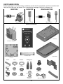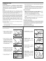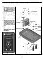
1
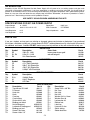
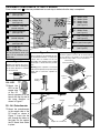
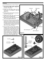
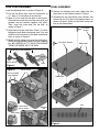
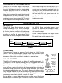
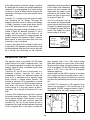
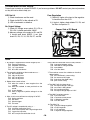
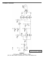
POWER SUPPLY KIT
MODEL XP-15K
Instruction & Assembly Manual
ELENCO
Copyright © 2012, 1991 by ELENCO® All rights reserved.
®
Revised 2012
REV-P
No part of this book shall be reproduced by any means; electronic, photocopying, or otherwise without written permission from the publisher.
753015
INTRODUCTION
Assembly of your XP-15K Regulated Variable Power Supply Kit will prove to be an exciting project and give much
satisfaction and personal achievement. If you have experience in soldering and wiring technique, you should have no
problem in the assembly of this kit. Care must be given to identifying the proper components and in good soldering habits.
Above all, take your time and follow the easy step-by-step instructions. Remember, “An ounce of prevention is worth a
pound of cure”. Avoid making mistakes and no problems will occur.
USE SAFETY GOGGLES WHEN ASSEMBLING THIS KIT!!
SPECIFICATIONS FOR XP-15K POWER SUPPLY
Output Voltage
Output Current
Load Regulation
Line Regulation
0 - 15VDC
0.3A @ 12V, 0.2A @ 15V
Ripple Max.
Short Protection
Output Impedance
0.1V
0.1V
0.01V rms
IC THERMO
0.3Ω
PARTS LIST
If you are a student, and any parts are missing or damaged, please see instructor or bookstore. If you purchased
this kit from a distributor, catalog, etc., please contact ELENCO® (address/phone/e-mail is at the back of this manual)
for additional assistance, if needed. DO NOT contact your place of purchase as they will not be able to help you.
RESISTORS
Qty.
r1
r2
r1
Symbol
R2
R1, R4
R3
Description
150Ω 5% 1/4W
2.2kΩ 5% 1/4W
2kΩ Potentiometer
Color Code
brown-green-brown-gold
red-red-red-gold
Part #
131500
142200
192421
CAPACITORS
Qty.
r1
r1
r1
r1
Symbol
C2
C4
C3
C1
Description
4.7μF 50V Electrolytic
220μF 16V Electrolytic
470μF 35V Electrolytic
2,200μF 35V Electrolytic
Part #
264747
282244
284746
292226
SEMICONDUCTORS
Qty.
r8
r1
r1
Symbol
D1-8
U1
D9
Description
1N4001 Diode
LM317 Regulator
LED Red
Part #
314001
330317
350002
MISCELLANEOUS
Qty.
r1
r1
r1
r1
r1
r1
r1
r1
r2
r2
r1
r4
r1
Description
Transformer YD-1485
PC board
Heat sink
Knob
Case top
Case bottom
Strain relief 2-wire
Binding post black
Nut binding post
Lockwasher binding post
Binding post red
Screw 2.8 x 8mm
Screw 4-40 x 1/4”
Qty.
r2
r1
r1
r2
r1
r4
r2
r4
r1
r1
r 2”
r1
Part #
440111
510002
615009
622009
623061
623062
624002
625031
625031HN
625031LW
625032
641102
641430
-1-
Description
Screw 6-32 x 3/8” Blk
Nut 7mm
Nut 4-40
Nut 6-32
Washer flat 8 x 14mm
Washer fiber #6
Lockwasher #6
Rubber foot
Label top
Line cord 2 wire
Shrink tubing
Solder lead-free
Part #
641652
644101
644400
644600
645101
645602
646600
662015
723071
862100
890120
9LF99
PARTS VERIFICATION
Before beginning the assembly process, familiarize yourself with the components and this instruction book.
Verify that all of the parts are present. This is best done by checking off the parts in the parts list.
RESISTORS
CAPACITOR
Carbon film
SEMICONDUCTORS
Diode
2kΩ Potentiometer
Electrolytic (radial)
LM317 Regulator
LED
MISCELLANEOUS
Case top
Transformer YD-1485
Label
Lead-free solder
Case bottom
PC Board
Screws
2.8 x 8mm
Nuts
Washers
7mm
Flat
8 x 14mm
Binding posts
Knob
Black
4-40 x 1/4”
Red
Heat sink
4-40
Rubber foot
Fiber #6
Binding post nut
6-32 x 3/8”
black
6-32
Lockwasher #6
Binding post
lockwasher
-2-
Strain relief 2-wire
Shrink tubing
CONSTRUCTION
Introduction
• Turn off iron when not in use or reduce temperature setting when
using a soldering station.
The most important factor in assembling your XP-15K Regulated
Variable Power Supply Kit is good soldering techniques. Using the
proper soldering iron is of prime importance. A small pencil type
soldering iron of 25 - 40 watts is recommended. The tip of the iron
must be kept clean at all times and well-tinned.
• Tips should be cleaned frequently to remove oxidation before it becomes
impossible to remove. Use Dry Tip Cleaner (Elenco® #SH-1025) or Tip
Cleaner (Elenco® #TTC1). If you use a sponge to clean your tip, then use
distilled water (tap water has impurities that accelerate corrosion).
Solder
Safety Procedures
For many years leaded solder was the most common type of solder
used by the electronics industry, but it is now being replaced by leadfree solder for health reasons. This kit contains lead-free solder, which
contains 99.3% tin, 0.7% copper, and has a rosin-flux core.
• Always wear safety glasses or safety goggles to
protect your eyes when working with tools or
soldering iron, and during all phases of testing.
• Be sure there is adequate ventilation when soldering.
Lead-free solder is different from lead solder: It has a higher melting
point than lead solder, so you need higher temperature for the solder to
flow properly. Recommended tip temperature is approximately 700OF;
higher temperatures improve solder flow but accelerate tip decay. An
increase in soldering time may be required to achieve good results.
Soldering iron tips wear out faster since lead-free solders are more
corrosive and the higher soldering temperatures accelerate corrosion,
so proper tip care is important. The solder joint finish will look slightly
duller with lead-free solders.
'
• Locate soldering iron in an area where you do not have to go around
it or reach over it. Keep it in a safe area away from the reach of
children.
• Do not hold solder in your mouth. Solder is a toxic substance.
Wash hands thoroughly after handling solder.
Assemble Components
In all of the following assembly steps, the components must be installed
on the top side of the PC board unless otherwise indicated. The top
legend shows where each component goes. The leads pass through the
corresponding holes in the board and are soldered on the foil side.
Use only rosin core solder.
Use these procedures to increase the life of your soldering iron tip when
using lead-free solder:
• Keep the iron tinned at all times.
• Use the correct tip size for best heat transfer. The conical tip is the
most commonly used.
DO NOT USE ACID CORE SOLDER!
What Good Soldering Looks Like
Types of Poor Soldering Connections
A good solder connection should be bright, shiny, smooth, and uniformly
flowed over all surfaces.
Soldering Iron
1. Solder all components from the
copper foil side only. Push the
soldering iron tip against both the
lead and the circuit board foil.
Rosin
Component Lead
1. Insufficient heat - the solder will
not flow onto the lead as shown.
Foil
Soldering iron positioned
incorrectly.
Circuit Board
2. Apply a small amount of solder to
the iron tip. This allows the heat to
leave the iron and onto the foil.
Immediately apply solder to the
opposite side of the connection,
away from the iron. Allow the
heated component and the circuit
foil to melt the solder.
3. Allow the solder to flow around
the connection. Then, remove
the solder and the iron and let the
connection cool. The solder
should have flowed smoothly and
not lump around the wire lead.
Soldering Iron
2. Insufficient solder - let the
solder flow over the connection
until it is covered.
Use just enough solder to cover
the connection.
Solder
Foil
Solder
Gap
Component Lead
Solder
3. Excessive solder - could make
connections that you did not
intend to between adjacent foil
areas or terminals.
Soldering Iron
Solder
Foil
4. Solder bridges - occur when
solder runs between circuit paths
and creates a short circuit. This is
usually caused by using too much
solder.
To correct this, simply drag your
soldering iron across the solder
bridge as shown.
4. Here is what a good solder
connection looks like.
-3-
Soldering Iron
Foil
Drag
MOUNTING THE TRANSFORMER & BINDING POSTS
r Peel the backing off of the label
and place it onto the case top,
while carefully lining up the
holes as shown in Figure A.
The label should fit snug within
the indentation in the case.
r Install the binding posts with
the colors in the order as
shown in Figure B. Insert the
post into the hole and fasten it
with the nut and lockwasher.
Tighten down the nut with
pliers.
r Install the transformer as shown
in Figure B. Use a 6-32 x 3/8”
screw, #6 lockwasher, 6-32 nut,
and two #6 fiber washers on
each side to fasten in place as
shown.
r Cut the red wires on the
transformer off close to the
transformer.
6-32 Nut
#6 Lockwasher
#6 Fiber washer
#6 Lockwasher
#6 Fiber washer
Cut these two
wires (red)
#6 Fiber washer
Transformer
Binding
post nuts
#6 Fiber washer
These wires will be used on
the PC board.
Binding post
lockwashers
Case top
6-32 x 3/8”
Screws
Red binding post
Black binding post
Figure B
Figure A
-4-
ASSEMBLE COMPONENTS TO THE PC BOARD
Place a check mark
in the box provided next to each step to indicate that the step is completed.
C4 - 220μF Electrolytic
(see Figure D)
D4
D3
D2
D1
D5 - 1N4001 Diode
D6 - 1N4001 Diode
(see Figure C)
R4 - 2.2kΩ 5% 1/4W Res.
(red-red-red-gold)
-
1N4001 Diode
1N4001 Diode
1N4001 Diode
1N4001 Diode
(see Figure C)
C3 - 470μF Electrolytic
(see Figure D)
D8 - 1N4001 Diode
D7 - 1N4001 Diode
(see Figure C)
R1 - 2.2kΩ 5% 1/4W Res.
(red-red-red-gold)
C1 - 2,200μF Electrolytic Cap.
(see Figure D)
C2 - 4.7μF Electrolytic
(see Figure D)
R2 - 150Ω 5% 1/4W Res.
(brown-green-brown-gold)
P4 - 3” Red wire
P5 - 3” Red wire
Cut two 3” wires from the cutoff red transformer wires and
strip 1/4” of insulation off of
each side.
Figure C
Diodes have polarity. Be sure to
mount them with the band going
in the same direction as marked
on the PC board.
U1 - LM317 Regulator
(see Figure E)
Figure D
Figure E
These capacitors are polarized. Be sure
to mount them with the “+” lead in the
correct hole as marked on the PC
board. Also, the negative lead of a radial
electrolytic is shorter than the positive
one.
Mount the regulator as shown, with the metal backing in
the same direction as the marking on the PC board. Attach
the heat sink using a 4-40 x ¼” screw and 4-40 nut.
Warning: If the capacitor is connected
with incorrect polarity it may heat up and
either leak or cause the capacitor to
explode.
Band
D9 - LED
Flat
side
r Mount the
LED to the
copper side
(+)
of the PC (–)
board, spaced 3/8” off the
board, with the flat side in
the same direction as
shown in Figure F.
Metal backing
PC board marking
1/4”
Heat sink
4-40 x ¼”
Screw
Polarity
marking
(–)
(+)
4-40 Nut
Figure F
LED
Flat side
Long lead (+)
Flat side
Short lead (–)
R3 - 2kΩ Potentiometer
2kΩ Potentiometer
3/8”
r Mount the potentiometer
to the copper side of the
PC board as shown in
Figure F. Insert the the
pins through the holes so
the body sits flat against
the PC board, then solder
in place.
Copper side of PC board
-5-
WIRING
Install the following wires as shown in Figure G.
r Cut the blue and both yellow transformer
wires so that they are 4”. Strip 1/4”
insulation off the ends.
Blue wire
Yellow wires
r Solder one of the yellow wires from the
transformer to PC Board P1 and the
other to P3.
r Solder the blue wire from the transformer
to the PC board hole P2.
r Solder the red wire from the P5 to the
end of the the red binding post.
r Solder the red wire from the P4 to the
end of the the black binding post.
r Install the PC Board into case by lining
up the shaft of the pot and the LED with
the holes in the case, and then pressing
PC board into place. Flip the case around
and install the 8 x 14mm flat washer and
7mm nut as shown in Figure H.
r Turn the shaft on the pot fully counterclockwise. Push the knob onto the shaft
so that the line on the knob lines up with
the end of the circle on the front panel as
shown in Figure I. If the knob is loose on
the pot shaft, insert a screwdriver in to
the slot and expand the slot slightly. If the
knob has a set screw, tighten the set
screw located on the side of the knob.
Red wires
Black binding post
Red binding post
Figure G
Line on
knob
7mm Nut
Flat head
screwdriver
blade
8 x 14mm
Flat washer
Knob
Pot shaft
Figure H
Figure I
-6-
LINE CORD ASSEMBLY
FINAL ASSEMBLY
Install the following wires as shown in Figure K.
r Remove the backing from each rubber foot and
place them in the locations shown in Figure L.
r Cut the two black wires from the transformer to
1½”. Strip ¼” of insulation off of each wire.
r Assemble the top and bottom case sections and
fasten with four 2.8 x 8mm self-tapping screws as
shown in Figure L. Make sure the slots on the side
line up with one another.
r Feed 2” of line cord into the hole of the chassis.
Place the line cord in the slot of the strain relief and
squeeze the two sections together with pliers.
Then, insert the strain relief into the hole, as
shown in Figure J.
2.8 x 8mm
Screws
r Separate the two line cord wires. Place 1” of shrink
tubing over each black transformer wire. Twist and
solder the line cord wires to the black transformer
wires as shown in Figure K.
r Slide the shrink tubing up to cover the solder joints.
Shrink the tubing with the heat from your soldering
iron. BE CAREFUL NOT TO TOUCH THE SHRINK
TUBING OR WIRES WITH THE IRON.
2.8 x 8mm Screws
Rubber feet
Case top in this direction
Strain relief
Pliers
Figure J
Figure K
Shrink tubing
Twist and solder
wires together
Bend wires
over as shown
Rubber feet
Slot
Soldering
iron
Slide tubing
Figure L
-7-
TESTING THE XP-15K POWER SUPPLY
Testing the XP-15K Power Supply is very simple.
Before applying power to the unit, be sure that all of
the wiring and soldering is firm. If so, obtain a digital
voltmeter. Apply power to the XP-15K and vary the
voltage control knob.
Set the output voltage to 15 volts and place a 75Ω 5
watt resistor across the output terminals. Again, the
output should not change by more than 0.1 volts. In
making these tests, the voltmeter leads should be
clipped directly to the output terminals and not to
the load leads. This is to prevent errors due to
voltage drop in the load leads.
Next, short the output of the supply. It should turn off
and recover when the short is removed. If you have
a 4.7Ω 1 watt resistor, set the voltage to 1.4 volts
and place is across the output terminals. The output
of the supply should not change more than 0.1 volts.
Should any of these tests fail, refer to the
troubleshooting guide.
CIRCUIT DESCRIPTION
INTRODUCTION
The XP-15K Power Supply features an output
voltage variable from 0 to 15V at 0.3 ampere
maximum current. The voltage is regulated to within
0.1V when going from no load to full load. Varying
the input AC voltage from 110 to 130V will have
practically no effect on the output voltage. This is
because of the specially designed IC circuit used in
120VAC
Input
Transformer
120V to 18V
18VAC
the XP-15K. Severe overloading or even short
circuiting the output will not damage the supply.
Special turn-off circuits in the IC sense the overload
and turn off the output.
Figure 1 shows a simplified circuit diagram of the
power supply. It consists of a power transformer, a
DC rectifier stage and the regulator stage.
AC to DC
Converter
20VDC
Voltage
Regulator
Simplified diagram of positive power supply
0 - 15V
Regulated
Output
Figure 1
TRANSFORMER
The transformer T1 serves two purposes. First, it reduces the 120VAC input to
18VAC to allow the proper voltage to enter the rectifier stage. Second, it isolates
the power supply output from the 120VAC line. This prevents the user from
dangerous voltage shock should they be standing in a grounded area.
Voltage Waveform for Supply
A) Transformer
Winding AB
B) Transformer
Winding BC
AC to DC CONVERTER
The AC to DC converter consists of diodes D1 and D3 and capacitor C1.
Transformer T1 has two secondary windings which are 180 degrees out of phase.
The AC output of each winding is shown in Figure 2A and 2B.
Diodes are semiconductor devices that allow current to flow in one direction. The
arrow in Figure 3 points to the direction that the current will flow. Only when the
transformer voltage is positive will current flow through the diodes. Figure 3 shows
the simplest possible rectifier circuit. This circuit is known as a half wave rectifier.
Here, the diode conducts only half the time when the AC wave is positive as shown
in Figure 2C. Use of this circuit is simple but inefficient. The big gap between cycles
requires much more filtering to obtain a smooth DC voltage.
By the addition of a second diode and transformer winding, we can fill in the gap
between cycles as shown in Figure 4. This circuit is called full wave rectification.
-8-
C) Output of
diode D1.
D) Output of
diode D3.
E) Total of diodes
D1 & D3.
20V
F) Output of capacitor C1
Ripple depends on load
current (expanded).
Figure 2
Each diode conducts when the voltage is positive.
By adding the two outputs, the voltage presented to
capacitor C1 is more complete, thus, easier to filter,
as shown in Figure 2F. When used in 60 cycles AC
input power, the output of a full wave rectifier will be
120 cycles.
depending on the current drawn
by the output load. Remember,
current only flows through the
diode when the anode is more
positive than the cathode. Thus,
current will flow in short bursts
as shown in Figure 5C.
Capacitor C1 is used to store the current charges,
thus smoothing the DC voltage. The larger the
capacitor, the more current is stored. In this design,
a 2,200μF capacitor is used, which allows about 2
volts of AC ripple when one half amp is drawn.
D1
C1
Half Wave Rectifier
Figure 3
The DC load current may be
one ampere, but the peak diode
current may be three times that.
Therefore, the diode rating must
be sufficient to handle the peak
current. The 1N4001 has a peak
current rating of 10 amps.
In practice, the current through the diodes is not as
shown in Figure 2E. Because capacitor C1 has a
charge after the first cycle, the diode will not
conduct until the positive AC voltage exceeds the
positive voltage in the capacitor. Figure 5 shows a
better picture of what the current flow looks like,
assuming no loss in the diode.
D1
D3
C1
20V
Peak
A) Transformer
Winding
Full Wave Rectifier
20V
B) Voltage C1
Figure 4
C) Current
through diodes
It takes a few cycles for the voltage to build up on
the capacitor. This depends on the resistance of the
winding and diode. After the initial start-up, there will
be a charge and discharge on the capacitor
Figure 5
REGULATOR CIRCUIT
The regulator circuit in the Model XP-15K Power
Supply consists of a LM317 integrated circuit. This
IC is specially designed to perform the regulation
function. Figure 6 shows a simplified circuit of how
the LM317 IC works.
goes negative. Now, if the 1.25V output voltage
goes down because of current drain at the output,
the base of Q2 will drop, forcing the collector voltage
of Q2 to go higher. This will bring the output voltage
back to 1.25V. This is the basis of all negative
feedback regulators.
Transistors Q1 and Q2 form a circuit known as a
differential amplifier. Transistor Q1’s base is
connected to a stable 1.5V reference voltage. The
base of Q2 is connected to the regulator output
circuit through a voltage divider network. The
collector of transistor Q2 is connected to a current
source. This basically is a PNP transistor biased to
draw about 1mA current. Transistor Q2 sees the
current source as a very high resistor of about 1
meg ohms. Thus, the gain of transistor Q2 is very
high.
Transistor Q5 is called the pass transistor. It controls
the current reaching the output. Transistors Q3 and
Q4 are emitter followers. Their function is to raise
the impedance of the pass transistor. Note that
transistor Q2, Q3, Q4, Q5 and resistor R1 form a
closed loop. Also, note that the feedback to the base
of Q2 is negative, that is, the output at emitter Q5
Another feature of the LM317 regulator is to protect
the IC against overload and output shorts. If the IC
is overloaded, the junction will overheat. A transistor
will sense this overheating and shut down transistor
Q5.
The LM317 IC is basically a 1.25V regulator. To be
able to vary the output 0 - 15V, we stack the IC on
the negative 1.25VDC voltage as shown in Figure 7.
When R3 equals 0, the output voltage is 0 volts.
Current
Source
Equalized
to 1 Meg.
Q5
Q3
1.25V
Output
0V - 15V
LM-317
R1
R2
Q4
Q2
1.5V
R3
R2
Q1
–DC
Divider
Figure 6
-9-
Figure 7
TROUBLESHOOTING GUIDE
Consult your instructor or contact ELENCO® if you have any problems. DO NOT contact your place of purchase
as they will not be able to help you.
LED Not Lit
Poor Regulation
1) Check transformer and line cord.
1) Check AC ripple at the input of the regulator.
It should be less than 2.5V.
2) Check for 20VDC at the cathode of D1.
2) If ripple is higher, check diodes D1, D3, and
the filter of capacitor C1.
3) LED in backwards or defective.
No Output Voltage
1) Check AC voltage across points P1 & P2 or
P2 & P3. It should read about 18VAC.
Copper Side of PC Board
2) Measure voltage at the output of D1 and D3.
It should read about 20VDC. If not, then
check D1, D3, C1, U1, R2, R3, D7, and D8.
QUIZ
1. AC voltage is supplied to the rectifier stages by the . . .
r A. step up transformer.
r B. step down transformer.
r C. 1 to 1 transformer.
r D. AC to DC transformer.
6. An inefficient rectification circuit usually contains . . .
r A. large gaps between cycles.
r B. twice the AC voltage needed.
r C. more diodes.
r D. all of the above.
2. The secondary windings of the transformer are . . .
r A. 90O out of phase.
r B. 180O out of phase.
r C. 270O out of phase.
r D. 320O out of phase.
7. The maximum current that a diode can handle is
determined by . . .
r A. the transformer’s current rating.
r B. the amount of AC ripple.
r C. three times the diode rating.
r D. peak current rating.
3. Diodes allow current to flow . . .
r A. when the anode is more negative than the
cathode.
r B. when the cathode is more positive than the
anode.
r C. in one direction.
r D. when a negative or positive voltage is on the
anode.
8. The LM317 will shut down when . . .
r A. the output voltage is too high.
r B. no current is being drawn.
r C. the junction overheats.
r D. the output voltage drops to 1.25V.
9. The LM317 regulator contains . . .
r A. a pass transistor.
r B. a constant current source.
r C. a differential amplifier.
r D. all of the above.
4. What circuit is more efficient for rectifying AC to DC?
r A. Hartley oscillator.
r B. Half wave.
r C. Schmitt trigger.
r D. Full wave.
10. The LM317 is . . .
r A. a positive voltage regulator.
r B. a 6.25V regulator.
r C. a 2.5V regulator.
r D. a negative voltage regulator.
5. The DC voltage is smoothed by using a . . .
r A. half-wave rectification circuit.
r B. small value capacitor with a high voltage value.
r C. Large value capacitor.
r D. 90O out of phase rectification circuit.
-10-
SCHEMATIC DIAGRAM
REV-A
Answers: 1. B, 2. B, 3. C, 4. D, 5. C,
6. D, 7. D, 8. C, 9. D, 10. A
ELENCO®
150 Carpenter Avenue • Wheeling, IL 60090
(847) 541-3800 • Website: www.elenco.com • e-mail: [email protected]