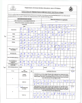
1
October
H8S and H8/300H
1 6 - B i t
M i c r o c o n t r o l l e r s
2 1 - 0 1 8 F
1999
INDEX
H8S and H8/300H
Introduction
2
CPU
5
Instruction set
Addressing
Low power modes
Exceptions and interrupts
6
7
8
9
1 6 - B i t
M i c r o c o n t r o l l e r s
Memory
Peripherals
Bus State Controller (BSC)
Direct Memory Access
Control (DMAC)
Data Transfer Controller
(DTC)
Timer
Timing Pattern Controller
(TPC) and Programmable
Pulse Generator (PPG)
Serial Communication
Interface (SCI)
10
12
14
15
16
20
21
Smart Card Interface
28
Analog to Digital Converter
(ADC) and Digital to Analog
Converter (DAC)
29
Controller Area Network
30
Notes
1. This document may, wholly or partially, be subject to change without notice.
2. All rights are reserved: No one is permitted to reproduce or duplicate, in any form, the whole or part of
this document without Hitachi’s permission.
3. Hitachi will not be held responsible for any damage to the user that may result from accidents or any other
reasons during operation of the user’s unit according to this document.
4. Circuitry and other examples described herein are meant merely to indicate the characteristics and
performance of Hitachi’s semiconductor products. Hitachi assumes no responsibility for any intellectual
property claims or other problems that may result from applications based on the examples described
herein.
5. No license is granted by implication or otherwise under any patents or other rights of any third party or
Hitachi, Ltd.
6. MEDICAL APPLICATIONS: Hitachi’s products are not authorised for use in MEDICAL
APPLICATIONS without the written consent of the appropriate officer of Hitachi’s sales company. Such
use includes, but is not limited to, use in life support systems. Buyers of Hitachi’s products are requested to
notify the relevant Hitachi sales offices when planning to use the products in MEDICAL APPLICATIONS.
Memory Type and Size
22
H8S and H8/300H
Selector Guide
23
In Brief
27
Example Block Diagrams
31
Ordering Information
and Packages
37
Tools
43
Third Party Tools
46
Related Literature/Internet/
CD-ROM/Application notes
47
1
W e l c o m e
T o
Hitachi’s 16-bit microcontroller families
customers, H8/300H is an excellent
H8S and H8/300H.
example where this policy has worked
for our customers and Hitachi.
Hitachi is the second biggest supplier of
In continuation of this policy H8S is
16-bit microcontrollers to the European
Hitachi’s answer to our customers request
market (according to Dataquest), as well
for more performance and lower power
as the third for 4-bit, sixth for 8-bit and
consumption at better cost/performance
number 2 for 32-bit RISC
ratios. Hitachi also added larger
microcontrollers (the latter on a world-
memories and improved the peripherals
wide basis).
to allow single-chip systems, where
previously several components have been
At Hitachi Europe we think that this
necessary. Switching such a multi-chip
success is driven by our strong
system to a single-chip system can
commitment to be a leading force in the
drastically reduce radiation, in today’s
microcontroller marketplace and our
electronic industry a very important
belief that we must listen to our
concern.
customer’s requirements and then meet
these. As H8/300H is the result of
H8S
combining many years of experience of
Hitachi with the experience of our
H8/300H
•
•
•
•
•
•
•
•
50ns cycle time
16/32-bit CPU
16MByte address space
TPU, PPG, ADC, DAC
DMAC, DTC, SCI, WDT
subclock, CAN
•
•
•
•
50ns cycle time
16/32-bit CPU
16MByte address space
FRT, TMR, ADC, DAC, PWM
IRDA, DTC, SCI, WDT
100ns cycle time
16/32-bit CPU
16MByte address space
ITU, TPC, DMAC, ADC, DAC
SCI, WDT
H8/300
•
•
•
•
125ns cycle time
8/16-bit CPU
64K address space
FRT, ADC, DAC, SCI, WDT
H8S/21xx
H8/300L
•
•
•
•
FRT
ITU
TPU
TMR
PPG
DMAC
DTC
ADC
DAC
SCI
WDT
PWM
IRDA
TPC
CAN
2
16-bit Timer
16-bit Timer x 5
16-bit Timer x 6
8-bit Timer x 3
Programmable Pulse Generator
Direct Memory Access
Data Transfer Controller
A/D Converter
D/A Converter
Serial I/O
Watchdog Timer
14-bit Pulse Width Modulation
Infrared Interface
Timing Pattern Controller
Controller Area Network
250ns cycle time
8/16-bit CPU
Sub-Clock (32KHz)
LCD Drive, Timers, ADC
Serial
H8
OVERALL
Figure 1
ROADMAP
The European electronics industry
produces and ships over 20 million H8
From a statistics point of view, every day
demands full service and support.
microcontrollers every month, in a vast
2 customers decide to use a 16-bit
Hitachi, responded by setting up a
range of advanced packaging and
microcontroller made by Hitachi.
European engineering and tool design
temperature options.
Usually our customer’s product
subsidiary 12 years ago: Hitachi
Microsystems Europe (HMSE) based in
H8S offers up to 25 native MIPS peak
development will continue to proliferate
Maidenhead (UK).
performance (resulting in almost 10
over the years. For those customers who
HMSE provides our customers with
Dhrystone MIPS), the peripherals and
may need more performance than 16-bit
locally designed and supported tools
the memory options (for example
microcontrollers can offer, it is good to
ranging from low cost evaluation boards
H8S/2238F with 256KB Flash and 16K
know that Hitachi is an industry leader
to fully featured real time emulators
RAM) to make it an industry standard in
in 32-bit RISC microcontrollers as well.
based on IBM-compatible PC’s at a very
telecommunications and very successful
Hitachi’s SH1 and SH2 RISC
competitive price. Software ranges from
in industrial (e. g. motor control,
microcontroller families offer 10 MIPS
Assembler, an ANSI C-Compiler via a
vending machines, security systems) and
or more (Dhrystone), as well as similar or
C-level debugger to MakeApp, a tool
emerging consumer applications like new
in some cases even the same peripherals
that sets up peripherals and creates driver
electronic video cameras, still cameras
and memory options up to 256K Flash
routines on the click of a mouse.
and advanced car radios. Just recently
and 10K RAM. Please order Hitachi’s
H8S and H8/300H have also enjoyed
SH RISC microcontroller shortform to
H8S and H8/300H are part of Hitachi’s
much success in automotive applications,
get a detailed introduction!
software compatible H8 product range,
as CAN is now available on-chip and in
which covers a performance range from
the rapidly growing field of smart-card
400ns to 40ns cycle time, whilst
appliances, because many derivatives
increasing word length from 8 to 16 bit
include one or more ISO7816-compliant
and memory space from 64KB to 16MB.
serial interfaces.
This product range offers an industry
leading mix of memory options
(including many flash derivatives),
peripherals and performance/power
SH2
•
•
•
•
32-bit RISC CPU
33 MIPS/5V
17 MIPS/3V
ITU, TPC, DMAC, MAC
ADC, SCI
• Motor control and
automotive ASSP
consumption, all of this being software
compatible for protection of our
customer’s software investment. Hitachi
SH1
•
•
•
•
32-bit RISC CPU
20 MIPS/5V
12 MIPS/3V
ITU, TPC, DMAC, MAC
ADC, SCI
H8/300H
H8S
Figure 2
3
H 8 S
R o a d m a p
Performance/ Memory/ Integration
H8S+CAN (F)*
H8S/2655 series
up to 128K/4K
Multiply-Accumulate
H8S/2633 series (F)*
up to 256K/16K
Multiply-Accumulate
H8S/267x series (F)*
up to 256K/8K
Multiply-Accumulate
20MHz at 5V
25MHz at 3.3V
33MHz at 3.3V
H8S/2357 series (F)
up to 128K/8K
H8S/2345 series (F)
up to 128K/4K
H8S/232x series (F)
up to 256K/8K
20MHz at 5V
20MHz at 5V
25MHz at 3.3V
H8S/2246 series
up to 128K/8K
low power
H8S/2238 series (F)
up to 256K/16K
low power/32KHz SC
20MHz at 5V
13MHz at 3V
H8S/212x series (F)
up to 128K/4K
64 pin package
H8S/213x series (F)
up to 128K/4K
80 pin package
H8S/214x series (F)
up to 128K/4K
100 pin package
20MHz at 5V
20MHz at 5V
20MHz at 5V
H8S/26xx
highest
performance
H8S/23xx
general
purpose
H8S/22xx
lowest power
large memory
H8S/21xx
lowest cost
* Under development (F) FLASH version available Note: most 5V derivatives are also available in 3V/10MHz or 3V/13MHz
Performance/ Memory/ Integration
H 8 / 3 0 0 H
R o a d m a p
H8/300H
3rd generation
large memory
H8/3022 series (F)*
up to 256K/8K
low voltage operation
H8/3052 series (F)*
512K/8K
big memory option
18MHz at 3V
18MHz at 3V
H8/3042 series
up to 64K/2K
small memory option
H8/3048 series (F)
up to 128K/4K
high integration
H8/306x series (F)
up to 128K/4K
2nd generation
16MHz at 5V
16MHz at 5V
20MHz at 5V
H8/3032 series
up to 64K/2K
small memory option
H8/3035 series
up to 256K/4K
big memory option
H8/3039 series (F)
up to 128K/4K
16MHz at 5V
18MHz at 5V
18MHz at 5V
H8/3001, 2, 3 series
512Byte RAM
80, 100, 112 pin
H8/3004, 6 series
2K RAM
80, 100 pin
Up to 20MHz at 5V
H8/3005, 7 series
4K RAM
80, 100 pin
16MHz at 5V
H8/304x, 6x
general
purpose
H8/303x
low cost
with ROM
H8/300x
low cost
ROM-LESS
Up to 20MHz at 5V
* Under development (F) FLASH version available Note: most 5V derivatives are also available in 3V/8MHz or 3V/10MHz
4
Figure 3
C P U
All H8 share a common CPU
Being general purpose there is no
In addition to the general purpose
architecture, a general purpose register
restriction placed on how each register is
registers there are two control registers, a
architecture that allows efficient
used, thus they can be used for pointer
Condition Code Register (CCR) and a
execution of software written in C and
or data operations. The architecture also
Program Counter (PC). The CCR is an
produces dense code. A good code
allows any of the data addressing modes
8-bit wide register which contains all the
density is important to reduce the
to be used in conjunction with any
CPU flags such as overflow, zero and
amount of memory needed, which in
register.
carry as well as the interrupt flags. The
turn results in a lower system cost and
carry flag also doubles as a bit
helps to avoid external memory. As
This rich set of general purpose
accumulator when the bit manipulation
shown below in figure 5 the 8-bit H8
registers provides the compiler writer
operations are used.
families have 16-bit wide registers and
with ample opportunities to optimise
the 16-bit families have 32-bit wide
the code generated by the compiler.
The H8/300H CPU offers a H8/300
registers, all of which can also be used
Local variables can be optimised into
compatible mode which allows
partially (for example in bytes). H8S
registers wherever possible, thus
straightforward reuse of existing H8/300
adds an extended Condition Code
reducing the number of bytes of code
software. This mode is available in
Register (EXR) to allow improved
needed to manipulate them. Also,
H8/3032, H8/3042 and µCBIC
interrupt control and H8S/2655 adds a
because each register can be used as an
products.
Multiply-Accumulate Unit (MAC) to
accumulator, index register or address
boost performance in DSP-type
pointer, the address arithmetic which
applications.
must be performed by the compiler can
be done very effectively. Register ER7
Furthermore H8S executes basic
is used as a stack pointer, so all accesses
instructions in only one clock cycle, half
to stack based data can be performed
as many as H8/300H.
very fast.
H8S
15
H8/300H
15
H8/300
H8/300L
15
7
0
R0
R1
R2
R3
R4
R5
R6
R7
31
ER0
ER1
ER2
ER3
ER4
ER5
ER6
ER7
7
0
R0
R1
R2
R3
R4
R5
R6
R7
31
ER0
ER1
ER2
ER3
ER4
ER5
ER6
ER7
7
15
0
PC
15
23
CCR
0
15
23
PC
EXR
CCR
PC
EXR
CCR
EXR
R0
R1
R2
R3
R4
R5
R6
R7
31
MAC
0
23
0
MAC
Sign
Sign
ded
Exten
26xx
/
n H8S
MAC o
only
ded
Exten
MAC
Figure 5
5
I n s t r u c t i o n
S e t
H8/300H has an instruction set which
Function
Instruction
suits the combined needs of HLL
Data transfer
MOV, PUSH, POP, MOVTPE, MOVFPE, LDM, STM
programming and embedded applications.
Arithmetic
ADD, SUB, ADDX, SUBX, INC, DEC, ADDS, SUBS,
It comprises of 62 instructions, with an
operations
DAA, DAS, MULXU, DIVXU, MULXS, DIVXS, CMP,
emphasis on arithmetic instructions,
NEG, EXTS, EXTU, TAS, MAC, LDMAC, STMAC,
address manipulation and bit processing.
CLRMAC
More than half of all instructions have an
Logic operations
AND, OR, XOR, NOT
instruction length of only 2 Bytes making
Shift operations
SHAL, SHAR, SHLL, SHLR, ROTL, ROTR, ROTXL, ROTXR
very compact code. H8S extends the
Bit manipulation BSET, BCLR, BNOT, BTST, BAND, BIAND, BOR, BIOR
instruction set to 69 instructions. BOLD
instructions are new on H8S.
BXOR, BIXOR, BLD, BILD, BST, BIST
Branch
Bcc, JMP, BSR, JSR, RTS
System control
TRAPA, RTE, SLEEP, LDC, STC, ANDC, ORC, XORC, NOP
In comparison with the H8/300 CPU
most of the data transfer, logical, shift and
and multiplication of 16 x 16-bit data
Operation
H8S
H8/300H
arithmetic instructions are improved to
and division of 32 / 16-bit data.
Add 32bit
50ns
125ns
handle 16 and 32-bit data. New
Multiplication and division are both
operands
instructions added to the H8/300H
available as signed and unsigned
AND 32 bit
50ns
125ns
include signed multiplication, sign
operations, which eliminate the need for
operands
extension, 16-bit branch instructions and
time consuming library calls. The table
multiply/divide
200ns/
875ns
a software trap instruction.
below gives a guide to the execution
16bit operands
650ns
speed of various arithmetic instructions
(32bit result, signed)
H8S further improves the instruction set
with a clock of 16MHz (H8/300H) and
by adding STM (store multiple) and
20MHz (H8S).
LDM (load multiple). These instructions
allow to evacuate multiple registers on to
the stack, thus drastically shortening the
time if compared with multiple PUSH
and POP. For example, pushing 4
Instruction: BTST R1L, R1H
R1L points to a bit position within R1H
registers onto the stack takes 40 states on
H8/300H and only 11 on H8S. Also
improved are some bit manipulations (to
include 16/32-bit absolute addressing)
R1L
and shift operations to support 2-bit
7
0
0
0
0
0
1
0
1
=5
shifts. H8S/2655 also adds instructions to
support the Multiply-Accumulate-Unit.
Arithmetic
Instr uctions
In order to perform complex algorithms
R1H
0
0
1
0
0
0
0
0
bit # 5
such as digital filtering, H8S and
H8/300H are equipped with powerful
arithmetic instructions, including
addition and subtraction on 32-bit data
6
Z
in CCR
Figure 6
Pr ocessing
A d d r e s s i n g
In microcontroller applications it is often
To support large memory systems, the
available addressing modes. Supporting
necessary to manipulate data on a bit by
linear address space of the H8/300H and
both, array and stack data types, the CPU
bit basis. A good example would be
the H8S CPU core allows direct access
has indirect addressing with either
where an I/O pin needs to be set to
to every address in the whole 16MByte
postincrement or predecrement. These
switch on a lamp or a solenoid. To meet
address space via 24-bit address pointers.
modes support byte, word and long word
this demand H8S and H8/300H have 14
The linear address space means there is
data (±1,2 and 4) as shown in figure 7.
separate bit processing instructions which
no need to set up page registers and
allow the programmer to manipulate bit
there are also no limitations on the size
Three absolute addressing modes are
data very easily.
of code modules or data arrays and
provided using 8, 16 or 24-bit absolute
structures.
addresses. Using the 24-bit address the
Bit
It is also possible to perform boolean
algebra on bit data using the carry flag of
the CCR register as a bit accumulator. In
a microcontroller application it is often
entire 16MBytes address space is
Addr essing
accessible. The 8 and 16-bit absolute
Modes
address modes assume that the upper
byte or word of the address is H’FFFF or
necessary to perform a branch depending
on the values of two bit flags located in
RAM or I/O ports. Using the boolean
operations provided by H8S and
H8/300H the first bit can be loaded into
the carry flag. Then a bitwise logical
operation can be executed using the
second bit. This sequence would then be
followed by a branch depending on the
value of the carry flag.
Another feature of the H8S and H8/300H
bit processing capability is its ability to
access bits indirectly, using the value from
a general purpose register as a bit pointer.
This mechanism is shown in figure 6 and
is useful for scanning a byte for set or
cleared bits.
Softwar e
Another way a CPU architecture can
H’FF respectively. This allows for the
support the efficiency of the compiler is
efficient address specification for the on-
by providing a full set of powerful and
chip I/O area and RAM areas which are
flexible addressing modes. To ensure that
both placed at the top of the address
the compiler is as efficient as possible the
map. These shortened addresses save
H8S and H8/300H CPU’s provide eight
significant amounts of code when these
addressing modes as shown in the table.
areas are accessed.
Each instruction can use a subset of the
Register direct
Register indirect
Register indirect
with displacement
Register indirect with post-increment/
Register indirect with pre-decrement
Absolute address
Immediate
PC-relative
Memory indirect
Rn
@ ERn
@ (d: 16, E R n)
@ (d: 24, E R n)
@ E R n +, @ - E R n
@ a a : 8, @ a a : 16, @ a a : 24
# x x : 8, # x x : 16, # x x : 32
@ (d : 8, PC), @ (d : 16, PC)
@@ a a : 8
Inter r upt
The TRAPA instruction has been
Register indirect with post-increment or pre-decrement
*Register indirect with post-increment @ERn+
31
implemented in the H8S and H8/300H
op
31
Register contents
op
reg
Operand Size Added Value
call to an error handling routine.
0
0
calls to often used sub-routines such as
TRAPA instruction can also be used as a
23
1, 2 or 4
*Register indirect with pre-increment @ERn
used to implement fast, space efficient
schedulers and other O/S routines. The
0
reg
routine via one of four exception vectors
(TRAPA 0 - 3). This operation can be
23
Register contents
CPU. This instruction implements a
software interrupt, jumping to a service
0
Byte
Word
Longword
1
2
4
1, 2 or 4
Figure 7
7
L o w
P o w e r
In today’s electronics industry, low power
consumption is an ever increasing
concern for many engineers. Beyond
Current
dissipation (mA)
Conditions:
15
HD6472246
typ. Sample
10Mhz/3.0V
Ta=25°C
Singlechip mode
obvious reasons like longer battery life
for example in mobile phones, notebooks
and electronic cameras, there are many
10
Active mode
more reasons why low power is
Sleep mode
paramount:
• Some applications have legal
Values based on sample
measurements, values not
guaranteed
5
restrictions on power consumption
like gas meters (to avoid a spark
causing an explosion), electricity
0
Icc-ope. Sleep
All
Mode
module
DTC
Stop
TPU
Stop
TMR
Stop
A/D
Stop
SCi0
Stop
SCi1
Stop
SCi2
Stop
TMR
All
only module
Operate Stop
Figure 8
metering to avoid unnecessary loading
of the mains network or fixed
telecommunication equipment that is
proportion. A H8S/2246 for example
powered off the line
will only draw appr. 4mA (typical) at
• other applications can draw much
current under normal conditions but
have to run of a battery when mains
operating.
• The CPU can be stopped (sleep
fails, e. g. security systems and cash
mode), with all the registers and
registers
memory contents being retained.
• Some car electronics must keep up a
Peripherals continue to operate and
0. 3mA
TPU stop
9mA
TMR stop
2mA
DAC stop
2. 2mA
ADC stop
2mA
each SCI stop
2mA
Sample data (not guaranteed), typical, at 5V /20MHz
for a H8S/2355
minimum level of activity while a car
any interrupt will wake up the CPU
is parked, nevertheless the car battery
instantly. Sleep mode reduces power
case of H8/300H clock gearing
must not be flat when the car is to be
consumption by about one third.
effects the entire chip, so reduction
used again
• Just like the CPU can be stopped at
will be almost proportional, in case of
• and last but not least, low power goes
times of low activity, some H8/300H
H8S clock gearing effects only bus
hand in hand with low radiation!
and all H8S derivatives allow to stop
masters (CPU, DMA, DTC) to avoid
peripheral modules. For example,
reprogramming of e. g. timers. The
effect is shown in Figure 9.
Numerous measures have been taken to
while the ADC is not needed the
allow H8/300H and H8S to meet all
software simply clears the
these demands:
corresponding bit in the module stop
32KHz subclock, which allows to
• All derivatives are available in low
register. Figure 8 shows how much
run the CPU, the 8-bit timers and the
voltage versions as well (except
current is saved per module for a
watchdogs at 32KHz (‘subactive’), or
H8/3039). Low voltage operation not
H8S/2355 and also shows a curve for
just the 8-bit timers and watchdogs
only significantly reduces power
H8S/2246 with one module after the
(‘subsleep’) or finally the watchdogs
consumption, but also allows battery
other being turned off. The lower
only (‘watch mode’). In watch mode
operation with a smaller number of
curve shows the same, if the CPU is
a periodical interrupt, which is
cells and reduces radiation drastically,
brought into sleep as well.
generated from the subclock at a rate
especially where external busses have to
be used.
• Beyond the possibility to run
• Some H8S derivatives also feature a
of once per second for example,
H8/H8S off a slower clock statically,
wakes up the CPU. The CPU then
some H8/300H and all H8S offer the
checks system status (e. g. key
clock, down to 2MHz. Power
ability to dynamically reduce the
pressed?) and then activates other
consumption will drop almost in
clock internally (‘clock gearing’). In
modules or returns to sleep, as
• All derivatives can be run off a slower
8
3V and at 2MHz with all the modules
DTC stop
required. Hence, very low average
As an example for such a combination,
power consumption can be achieved,
let’s assume the DTC would be used to
even with a real time clock being
move results of ADC conversions from
implemented in software.
the ADC to a RAM buffer (e. g. 64
• If no activity is required, but RAM
Byte). The CPU does not need to
contents must be retained, H8/H8S
process the data before acquisition of all
microcontrollers can be brought into
data has finished. This scenario would
standby. In this mode the oscillator is
allow to turn off all the modules, except
stopped and power consumption
the ADC and the DTC, and put the
drops to leakage current levels
CPU into sleep during acquisition.
(0. 01µA, typical at room
The resulting current would be only
temperature). Two modes are
appr. 3mA at 10MHz and 3V Vcc.
provided, software standby which
After acquisition of all 64 Byte has
allows to retain IO ports and
ended, an interrupt wakes up the CPU
hardware standby, which only retains
to process the data. While doing so the
RAM. RAM retention voltage is
software may choose to activate other
only 2V.
peripheral modules as required.
Please note that power consumption in
Some of these methods can be combined
this scenario could be further reduced if
to achieve outstanding average power
10MHz clock gives more performance
consumption values, while allowing high
then needed. Typical Icc between 2mA
performance operation at times of high
and 3mA are possible.
activity.
Figure 9
Ta=R.T.
80
70
5.5V, 20MHz
Current consumption (mA)
60
50
40
30
20
3.0V, 10MHz
10
0
ø/8
ø/4
ø/2
ø
Clock
Values based on sample measurements, values not guaranteed
9
E x c e p t i o n s
a n d
I n t e r r u p t
C o n t r o l l e r
Trap
instr uction
exceptions
(TRAPA)
priority interrupt sources, which are
capable of interrupting a low priority
ISR which is already running. The
These exceptions start when a TRAPA
priority of individual interrupt sources
instruction is executed in program
is programmed in a number of
execution state. The TRAPA instruction
interrupt priority registers (IPR).
H8/300H and H8S feature a
has four vectors as specified by its
sophisticated interrupt system, that allows
argument. This exception can be used as
Inter r upt
to respond quickly to asynchronous
an efficient mechanism for calling
contr oller
events. The worst case interrupt response
operating system functions, as it takes
on
time is 2. 6µs for H8/300H (at 16MHz)
only 2 Byte to execute a TRAPA
and 1. 5µs for H8S (at 20MHz).
instruction, compared to 4 Byte for a
The interrupt controllers within the H8S
Because almost every interrupt source
BSR and 8 Byte for a JSR.
family differ, depending on the particular
has its own vector, the interrupt service
H8S
H8S series. H8S/2655 has an interrupt
routine can immediately start to do some
Inter r upt
controller that provides four modes
useful work, instead of polling status flags
Contr oller
(0...3) and the other series provide a
to find the cause of the interrupt.
on
subset.
H8/300H
If two or more exceptions occur
• Mode
0
simultaneously, they are accepted and
The H8/300H interrupt controller can
processed in order of priority. Software
be operated in two modes, either
This mode provides the mechanism
interrupts (‘Trap’) are accepted at all
maintaining compatibility with the
known from H8/300. Acceptance is
times, in the program execution state.
standard H8/300 interrupt controller, or
solely controlled by the I-bit.
in a more advanced mode.
• Mode
Interrupts are handled as follows:
• The PC and the CCR are pushed
onto the stack
• H8/300
compatible
1
In this mode acceptance is controlled
mode
by I and UI, thus providing functional
• The interrupt mask bits are updated
In this mode the acceptance of
compatibility with H8/300H.
• A vector address corresponding to the
maskable interrupts is controlled by the
• Mode
2
exception source is generated, and
I-bit in the CCR. If I is set, then all
program execution starts from that
interrupts are disabled (except NMI)
This mode provides an 8-level
address
and if I is cleared then all interrupts are
priority mechanism controlled by bits
enabled. When an interrupt is
I0. . I2 in the EXR register. Priorities
Exter nal
inter r upts
accepted, the controller automatically
for each interrupt source can be
(NMI
IRQ)
sets the I-bit, thus disabling any other
programmed in a set of IPR registers.
and
maskable interrupts for the duration of
H8/300H and H8S have several external
the interrupt service routine (ISR),
interrupts, including one non-maskable-
unless it is cleared by the users code.
interrupt (NMI). NMI can be
programmed to be activated on either
10
• Mode
3
This mode combines mode 1 and 2,
effectively providing up to 9 levels of
• H8/300H
advanced
priority.
the rising or the falling edge. Interrupt
mode
request pins (IRQ) can be programmed
To increase the power of the interrupt
H8S/265x derivatives can use modes
to recognise either a low level or a low
controller, an extra interrupt status bit
0. . 4, H8S/263x, H8S/23xx, H8S/223x
going edge on H8/300H, and on H8S
is included in the condition code
and 222x can use modes 0 and 2, and
can be programmed to recognise a low
register, known as the UI or User
H8S/224x and 21xx can use modes 0
level, a rising or a falling edge or both
Interrupt bit. This extended operation
and 1.
edges.
allows the user to specify raised
M e m o r y
F L A S H
consumption of Hitachi’s microcontrollers,
• USER Mode
such a redesign will often immediately
User mode is not entered via reset. It
eliminate radiation problems. At the
is fundamentally just like normal
A traditional strength of Hitachi’s
same time costly shielding measures may
operation, but with Flash
microcontrollers are the large integrated
become unnecessary, thus lowering
programming enabled via the mode
memories and the advanced memory
system cost and board space requirements
(usually FWE) pins.
technology.
will become less.
In user mode, an external trigger
Already for many years, it has been an
Other benefits of large integrated
a piece of code into RAM. Program
important strategy to provide
memory and especially of on-chip Flash
execution then jumps to this code.
microcontrollers with high-speed, on-
memory are:
The Flash can then be reprogrammed
chip Flash memory to the European
• end of line programming allows
under the control of the user’s
event causes the user software to copy
market, always at the leading edge of this
industry trend. This technology is now
offered in its third generation, providing
flexibility in the software until
application, using all the resources of
shipment
the chip (i. e. downloading the new
• allows easy and fast update in the field
code does not necessarily have to use
larger memory sizes and single-voltage
without the need to open the
a serial interface, but could use any
programming. Hitachi is currently
equipment
other resource). This mode is
shipping over 4M Flash microcontrollers
per month.
• allows software updates even remotely,
• fast response to changing customer
A table in the middle of this brochure
shows Hitachi’s 16-bit microcontrollers
by ROM and RAM size, including 16
on-chip Flash derivatives. Please use the
table to select the devices which meet
your memory requirements.
intended for Flash memory updates.
e. g. via modem/phone line
requirements
• non volatile storage of data and
parameters
• full availability of all ports, if external
• PROM Mode
All H8/H8S Flash derivatives can also
be programmed using general purpose
programming equipment, i. e. in the
same way OTP’s are programmed.
busses can be avoided
• full speed operation, often impossible
or expensive if external memory is
Hundreds of customers worldwide have
used
taken advantage of our flash based
microcontrollers in their designs, about
Flash
pr ogramming
one third in industrial and automotive
applications, approximately one fourth
• BOOT Mode
each in consumer and office automation
Boot mode is entered if the mode
and the remainder in telecommunications.
pins of a H8/H8S are in a certain
state after reset. In boot mode
Integrating large and flexible memories
program execution starts from a
has numerous benefits for our customers,
hidden ROM. The software in this
some of which are becoming crucial in
ROM initialises one of the serial
today’s demanding electronics industry.
interfaces, downloads another piece of
For example: Switching an older
software (available from Hitachi, if
microcontroller design, which uses
desired), which then allows to
external memory and peripherals, to a
(re)programme the Flash memory.
single-chip design, will drastically reduce
Boot mode can be used to supply a
radiation, because the address and data
blank (i. e. new) Flash device with a
busses are a major source of radiation in
software, even when the device is
a system. Together with the low power
already soldered onto the PCB.
11
B u s
S t a t e
C o n t r o l l e r
As one of the key reasons for using the
( B S C )
• DRAM access protocol for one area
executes slow external write accesses
H8S and H8/300H is the 16MBytes
on 300H (=2Mbytes) and for 4 areas
independently (on H8S/26xx and on
linear address space, it will often be used
on H8S (=8Mbytes)(not on all
some H8S/23xx derivatives) and the
in a system with a large amount of
devices)
improvement of read access time by
external memory. Consequently, H8S
moving the clock edge that latches the
and H8/300H are supported by a
Bus State Controller
powerful bus state controller (BSC) that
(BSC) on H8S
read data to the end of the bus cycle.
DRAM
allows external memory and/or
inter face
peripherals to be connected with no (in
One of the major advantages of H8S over
some rare cases with little) glue logic.
H8/300H is its basic instruction
Areas two to five can be set to interface
Also, the BSC helps to get the maximum
execution within a single clock cycle, that
directly to DRAM on on H8S/26xx and
performance out of any external devices,
is only 50ns at 20MHz clock if executed
on some H8S/23xx derivatives, allowing
for example by avoiding address decode
from internal memory. In order to
up to 8MB of DRAM to be connected
delays, where on-chip chip-select
minimise the negative impact on
without any glue logic. The BSC
generation is used.
performance when going off chip, every
handles the address multiplexing (8,9 or
effort has been made to create a BSC
10 bits), the timing and allows to use fast
The BSC divides the memory space into
with a maximum of throughput and
page mode. DRAM with CAS-before-
8 areas. For each of these areas a number
flexibility.
RAS (CBR) or self-refresh are
supported. For CBR refresh mode the
of attributes is selectable, for example:
Major enhancements include support for
BSC provides an independent refresh
fast-page mode DRAM (on H8S/26xx
counter, so that no other timers have to
• the number of wait states
and on some H8S/23xx derivatives),
be used.
• the bus width (8/16-bit)
burst mode ROM, a write buffer that
• the wait mode (automatic insertion or
hardware protocol)
Ø
Address bus
Data Bus
tACC
Ø
Address bus
Data Bus
tACC
Improved Access Time
Figure 10
12
Impr oved
access
r ead
timing
state internal processing continues as long
as there is no external access.The
internal bus master, wishing to access the
In order to give external devices a
external bus during bus release state, may
maximum of time to drive the required
use the BREQO signal to indicate to the
data onto the bus, the read access edge
external master that the bus ownership
that latches the data, has been moved to
should be given back. The external bus
the end of the cycle. Therefore read
master should respond by dropping
access time is improved by approximately
BREQ. BREQO can also be used to
one quarter, compared with H8/300H.
signal that a refresh cycle for a DRAM is
Figures 10 & 11 illustrate this effect for
pending.
several frequencies.
Write
data
buf fer
Improved Access Time
On H8S/26xx and on some H8S/23xx
derivatives, a write data buffer is
200ns
provided. This feature allows the CPU
H8S
to continue internal processing, while the
BSC takes care of slow write accesses
independently. Figure 12 shows an
example of the timing when the write
data buffer is used. When this function is
100ns
50ns
H8/300H
activated, if an external write or DMA
10
single address mode transfer continues for
2 states or longer, and there is an internal
12
16
20
MHz
Figure 11
access next, only an external write is
executed in the first state. But from the
next state onward an internal access is
On-chip memory read
Internal I/O register read
executed in parallel with the external
External write cycle
access, rather than waiting until it ends.
T1
Bus
T2
TW
TW
T3
r elease
Internal address bus
On all H8S devices a mechanism is
provided to allow external bus masters to
Internal memory
Internal I/O register address
Internal read signal
obtain external bus ownership.
To request ownership an external master
A23 to A0
External address
must drive the BREQ pin low. After the
BREQ pins has been sampled low by the
H8S, the address bus, data bus and the
bus control pins are placed in a high
CSn
External
space
write
HWR, LWR
impedance state and the Bus
Acknowledge (BACK) signal is asserted
to signal to the external master that the
D15 to D0
Figure 12
bus is now available. During bus release
13
D i r e c t M e m o r y A c c e s s
C o n t r o l l e r ( D M A C )
In a system with a high performance
Some of the major improvements on
performed between any area of the full
CPU and with large memory, a Direct
H8S are:
16MBytes address space. This mode
Memory Access Controller will
• A special transfer mode has been
allows either a single transfer to occur
significantly increase system performance.
added, single address mode, where
per request (‘normal mode’), or for a
Instead of wasting CPU performance to
both resources must be external and
block of data to be moved (‘block
move data between peripherals and
data is transferred in fly-by fashion for
transfer mode’). In ‘normal mode’ and
memory, virtually all of the CPU
fastest transfer speed.
with ‘auto-request’ enabled, the DMAC
performance can be used for calculations,
can be set up in a burst mode, taking
• More transfer request sources, e. g.
while the DMA handles the data
A/D conversion end interrupt and at
over the bus from the processor until all
transfers.
least 2 SCI can request a transfer
the transfers are complete, or in a cycle
steal mode where the processor and the
If combined with other peripherals, such
Shor t
Addr ess
Mode
DMAC share the bus.
as timers, SCI’s or the real time outputs
of the TPC/PPG, entire autonomous
In this mode either the source or
Single
subsystems can be built, for example to
destination address is limited to only 8
mode
drive stepper motors or to communicate
bits (H8/300H) or 16 bits (H8S), with
with LCD modules or keyboards with
the upper bits being automatically set to
Figure 13 illustrates the new single
hardly any CPU intervention.
logic ‘1’. This allows to access the
address mode. In single address mode a
internal IO registers. The other address
transfer of data is carried out directly
As H8S almost triples the CPU
is 24 bits wide, so that the entire
between the data busses of two external
performance of H8/300H, the DMAC on
memory space is accessible.
devices, e. g. an external peripheral and
H8S has improvements over the H8/300H
Within short address mode there is ‘IO
DRAM. The advantage is the speed of
DMAC, in order to keep CPU and
mode’ (called sequential mode on H8S),
the transfer, because the data is moved in
DMAC performance in a good balance.
where the full address can be
a single cycle without a temporary
But let us first have a look at the common
automatically incremented or
storage. Either the source or the
features:
decremented, ‘idle mode’ with the full
destination must be a device which can
address being fixed and ‘repeat mode’,
be accessed with a strobe alone, using the
which allows cyclic data buffers to be
DACK pin. The address bus is used to
(used for transfers between internal
automatically transferred. Cyclic data
access the other resource.
IO and memory)*
buffers are useful for many applications,
• 4 channels in short address mode
• 2 channels in full address mode (used
for transfers between memory and
• Byte or word transfer selectable
(H8S)
e. g. to output a control pattern for a
stepper motor.
memory, or between external IO and
memory)
Full
Addr ess
Mode
RD
HWR, LWR
A23 to A0
Address bus
• address increment, decrement or fixed
• DMA transfer request possible by
(Read)
memory transfers the full
timer, SCI0 and external request,
address mode can be
depending on mode
used. Here, the source
• Interrupt request possible after each
External
memory
To perform memory to
H8S/2655
D15 to D0
(high impedance)
Data bus
selectable, depending on mode
addr ess
(Write)
and destination addresses
transfer or after specified number of
are 24-bits wide each,
transfers
and therefore memory to
memory transfer can be
External
device
DACK
* 8 channels on H8/3003
Figure 13
14
D a t a
T r a n s f e r
C o n t r o l l e r
( D T C )
Analysis of many applications that use a
the block, thus practically eliminating the
takes 3 cycles and the actual data transfers
DMAC has shown that a substantial part
overhead penalty.
take 2 cycles (minimum).
maximum speed of data transfers. These
Also, a single trigger can request multiple
The DTC could be seen as a DMAC
applications use a DMAC mainly to
transfers (chain mode).
with only a single channel implemented
reduce CPU overhead, allowing the
This feature could, for example, be used
in hardware. The registers for the
CPU to use its performance for
to move the result of an analogue-to-
destination and source address, for the
calculations.
digital conversion to a circular buffer in
transfer mode and the transfer count
RAM, followed by automatic
actually exist only once. However, these
Therefore Hitachi conceived another
reprogramming of the ADC to perform
registers are loaded with the information
peripheral to autonomously handle data
other conversions. If the tasks given to
to be used for a particular transfer from
transfers, the Data Transfer Controller
the ADC are stored in a table in ROM,
RAM. That means that the structure of
(DTC). The DTC puts emphasise on
which is then used by the DTC in a
the DTC registers is mirrored in a special
offloading the CPU from data transfer
round-robbing scheme, while the
DTC RAM as many times as the
tasks, while providing a maximum of
conversion results are stored in a
designer has chosen to implement
flexibility. Unlike a DMAC the DTC can
corresponding number of circular buffers
transfer channels. Each transfer can be
handle a very large number of transfer
in RAM, the DTC and the ADC could
specified to be byte- or word-wide,
channels and transfers can be requested by
perform a large set of completely
source and destination addresses can both
almost any peripheral that can request an
different tasks without any CPU
be 24-bits wide (i. e. cover the full
interrupt as well as by software. On the
intervention whatsoever.
address range). Source and destination
other hand a DTC transfer is
Figure 14 shows the timing of such a
addresses can be either incremented or
approximately 5 times slower than a DMA
chain transfer. Please note that one cycle
decremented (by 1 or 2), or can be fixed.
transfer (1000ns as opposed to 200ns at
of phi is only 50ns at 20MHz. As can be
A CPU interrupt can be requested for
20MHz, assuming e. g. source is a
seen, the DTC vector is read after a
the interrupt that triggered the DTC
peripheral and destination memory). In
transfer request in only one cycle, each
transfer, either after each transfer or after
block transfer mode the DTC overhead is
move of the transfer information
the specified number of transfers have
divided by the number of transfers within
between DTC RAM and DTC registers
been performed.
of these applications do not require the
Figure 14
ø
DTC activation
request
DTC
request
Data transfer
Data transfer
Read Write
Read Write
Vector read
Address
Transfer
information
read
Transfer
Transfer
information information
write
read
Transfer
information
write
15
T i m e r
One of the most important peripherals
used. Hence, more money then is being
the triggering of a DMA channel.
on any microcontroller is the timer unit.
spent on more powerful
Channels 3 and 4 allow to produce a
Timers have many uses in electronic
microcontrollers, could be saved on
pulse with duration down to one
systems. They trigger the task switch of
external devices, assembly cost, board
clock cycle (62. 5ns at 16MHz).
real time operating systems, update
space, power supply and on reduced
software real time clocks, control AC, DC
counter measures against radiation. In
or stepper motors, check validity of
particular, electronic systems which
The ITU provides up to 10 channels
external signals (‘timeout’), count pulses
currently use 8-bit microcontrollers
of input capture. In this mode the
for example from phase quadrature
should be reconsidered under these
timer can be set up so that a transition
encoders and much more. Timers can
aspects!
on an input pin causes the value
even act as accurate digital-to-analog
currently in the count register to be
converters (DAC), if used as pulse-width-
Integrated
modulator (PWM).
Unit
T imer
(ITU)
In order to accommodate all these
transferred into a capture register, thus
time stamping that particular event.
The ITU can be set to capture rising
applications, Hitachi has developed 2
The ITU consists of five separate 16-bit
edges, falling edges and either of
powerful and flexible timer units for
timer channels, each of which can be
these. If required the timer unit can
their 16-bit microcontrollers, as well as
clocked from an internal derivative of the
also clear the timer when the
several special-function timers, for
system clock (ø, ø/2, ø/4 and ø/8) or
programmed external event occurs.
example separate PWM timers, watch
from an external pin. If the ø clock
The two buffer registers (BRA and
dog timers (WDT), low-power support
option is selected, then the minimum
BRB) provided in timer channels 3
timers, etc. These two timer units are the
resolution of the timer is 62. 5ns (ø =
and 4 can be used to buffer input
ITU on H8/300H, a 5-channel 16-bit
16MHz). The standard timer functions
time stamps. This allows events which
timer unit with up to 10 input
provided by the ITU include ten general
occur very close to each other to be
capture/output compare (IC/OC) and
registers (GR), which can be used as
time stamped using one capture pin.
the TPU on H8S, a 6-channel 16-bit
output compares or input captures. A
This feature can also be used to
timer unit with up to 16 IC/OC.
further four 16-bit buffer registers (BR)
measure the width of an incoming
An exception are the H8S/21xx devices.
reduce the overhead placed on the CPU
pulse, by programming the capture
H8S/21xx is aimed on very cost sensitive
when servicing the timer block.
input to be triggered on both the
application, where the advanced timer
functionality of the ITU/TPU is either
16
• Input Capture Functions
rising and falling edges.
• Output Compare Functions
By using input captures to measure
not needed or can be handled by the
To create output waveforms or timed
the timing of external signals, very
high performance H8S CPU instead.
interrupts, the ITU provides up to 10
accurate measurements of variables
H8S/21xx has a 16-bit Free-Running-
output compare registers. The output
such as frequency can be taken. The
Timer (FRT) with 4 IC and 2 OC and 3
compares work by producing an
user can be sure that the accuracy of
timers with 8-bit. A separate 14-bit
output of a pre-programmed level
the measurement is not compromised
PWM and 2 WDT (one with 32KHz
and/or an interrupt when the value
by interrupt response time, as it is
subclock) are also provided.
in the counter matches the value
entirely a hardware driven facility.
stored in one of the output compare
It is also possible to initiate DMA
Together with the large integrated
registers. The events that can be
transfers when an input capture event
memories and the other peripherals,
initiated by these compare matches
occurs. This allows time stamps to be
these powerful timers are aimed at
are transitions on an output pin (to
automatically placed in memory via
making single-chip systems possible,
high, to low or toggle), a CPU
the DMA controller, without needing
where previously microncontrollers with
interrupt (used for software timing
to interrupt the CPU.
additional external devices had to be
functions), clearing the counter and
• Timer Synchronisation
To allow timer channels in the ITU
The table below shows the PWM frequencies which can be obtained versus
device clock speed and output resolution.
possible to set up two or more timers
PWM
Res.
14-bit
16
MHz
976. 5 Hz
12
MHz
732. 7 Hz
10
MHz
610 Hz
8
MHz
488 Hz
6
MHz
365 Hz
so that they are simultaneously
12-bit
3. 9 KHz
2. 9 KHz
2. 4 KHz
2 KHz
1. 5 KHz
written to via software and cleared by
10-bit
15. 6 KHz
11. 7 KHz
9. 7 KHz
7. 8 KHz
5. 8 KHz
compare matches or input captures.
9-bit
31. 2 KHz
23. 4 KHz
19. 5 KHz
15. 6 KHz
11. 7 KHz
When timer channels are put into this
8-bit
62. 4 KHz
46. 9 KHz
39 KHz
31. 3 KHz
23. 4 KHz
mode then their input and output
7-bit
124. 8 KHz
93. 8 KHz
78 KHz
62. 5 KHz
46. 8 KHz
to be used in synchronisation, it is
events are also synchronised.
• Standard PWM Mode
TCNT3 value
Each timer channel can be
GRA3
programmed to produce a single
GRB3
phase PWM output. Thus the ITU
GRA4
can output up to five separate
GRB4
channels of PWM. In this mode
H'0000
Counter cleared at compare match with GRA3
Time
GRA controls the time when the pin
goes high, and GRB when the pin
goes low. Either GRA or GRB can
be set to clear the counter, thus
setting the frequency of the WM
TIOCA3
TIOCB3
TIOCA4
output.
TOCXA4
• AC Motor Control Outputs
To provide the PWM signals required
to drive AC machines, the ITU
provides two further PWM modes:
Complementary 6-phase PWM and
TIOCB4
TOCXB4
Figure 15
Reset Synchronised 6-phase PWM
(shown in Figure 15). The main
By utilising the phase counting mode
This facility removes the requirement for
differences between these two modes
on the ITU, TCNT2 will count up
extra hardware or interrupt handlers for
are the transition points for the
or down depending on the phase
position monitoring. In this mode the
outputs and the provision of dead
of the incoming signals. Therefore,
comparators of channel 2 can also be
time between the phase outputs.
the value of TCNT2 will reflect the
used to generate interrupts, for example
positional changes experienced by the
when a certain position is reached.
• Phase Counting Mode
encoder.
This mode finds use in servo control
systems, where the position and speed
feedback comes from a 2- phase
TCNT2 value
quadrature encoder. In this type of
Counting up
Counting down
encoder the waveforms output change
their phase relationship depending on
Time
the direction of motion, as shown in
Figure 16
TCLKB
TCLKA
Figure 16
17
Modified
H8/306x,
and
ITU
on
H8/3006
set the duty.
reset
However, as the ITU puts more emphasis
on motor control and similar
H8/3007
applications, the TPU does not support
The ITU on H8/306x, H8/3006 and
‘Reset synchronized 6-phase PWM
H8/3007 are modified to be more
mode’ and ‘Complementary 6-phase
flexible. Channels 3 and 4 can be split
PWM mode’.
16-bit timer
• Channel 1 can also be used to count
channel 0 compare matches
These 8-bit timers can also be used to
keep up a minimum level of timer
into 4 timer channels (8-bit) instead of 2
timer channels (16-bit). However, this
16-bit
Fr ee
modified ITU does not have the special
T imer
(FR T)
Running
functionality in times of low activity of
the overall system. The result is lowest
power consumption on one hand,
AC motor control modes
(Complementary 6-phase PWM and
The main timer unit of H8S/21xx is the
because the TPU can be switched off in
Reset Synchronised 6-phase PWM). The
16-bit Free Running Timer (FRT), with
that situation, but a minimum of timer
buffering facility has also been removed.
2 OC and 4 IC. The input capture
activity on the other hand. The 8-bit
facility can also be operated in buffered
timer could be used to update a software
mode, with only 2 IC available in this
real time clock, for example, or scan a
case.
keyboard, so that the system can return
Input clock can be selected from 3
to full activity when a key has been
The TPU is similar to the ITU, yet even
internal clocks and an external clock,
pressed.
more powerful and flexible. It is found
which also allows event counting. The
on all H8S devices, with the H8S/224x
FRT unit features one independent
Enhanced
and the H8S/222x devices having only
interrupt for each IC, OC and one on
timers
half of a TPU implemented.
overflow.
T imer
Pulse
Unit
(TPU)
channels with a total of 16 Timer
on
8-bit
H8S/21xx
H8S/21xx derivatives feature a similar 8
The TPU comprises six 16-bit timer
8-bit
timers
bit timer module as described in the
previous paragraph. However, it has a
General Registers (TGR), each of which
can act either as an output compare or
The H8S/2655-series, H8S/2355 and 53,
third 8-bit timer channel TMRY, which
an input capture function. Some TGR’s
H8S/224x, H8S/234x and H8S/21xx all
has similar functionality like TMR0 and
can also act as buffer registers to reduce
have an additional 8-bit timer module
TMR1, but no output pin that is under
the interrupt load that is put onto the
with two channels (TMR0 and TMR1).
control of the compare match facility.
CPU.
Each channel has two time constant
For each channel one out of eight input
registers (TCORA and TCORB) that
clocks can be selected in software.
are constantly compared with the
Possible sources are internal clocks,
counter value to detect compare
H8S/21xx is equipped with a two
external clock pins or overflow of other
matches. The 8-bit timer module can
channel PWM timer, intended for use as
timers, the latter effectively providing a
perform a variety of functions, including
a digital-to-analog converter. It is based
method to cascade two 16-bit timers to
pulse output with an arbitrary duty cycle
on a 14-bit counter, thus enabling low-
form 32-bit timers.
or counting events on an external pin.
ripple, 14-bit resolution analog signals to
14
bit
PWM
phase counting the TPU provides four.
The 8-bit timer module has the
Also, the TPU allows to trigger an A/D
following features:
Watchdog
conversion and can trigger data transfers
• Selection of internal clock phi/8,
(WDT)
by the Data transfer controller (DTC).
phi/64, phi/8192 or an external clock
The TPU allows to generate a 15-phase
input.
PWM signal, by using one TGR as the
cycle register and the other 15 TGR’s to
timer
be generated.
While the ITU provides one channel for
18
• Cascading of both channels to form a
• Selection of counter clear sources:
compare match A or B, or external
on
T imer
H8/300H
Often, a watchdog timer is a very
important feature in any embedded
application. It is used to ensure that any
“mishap’ in the system (such as a noise
seconds. This WDT can request an
induced software crash) is rectified as
interrupt, reset or NMI. If an interrupt
quickly as possible.
is requested this WDT is useful to update
The principle behind a watchdog timer
a software real time clock. For this
is very simple - a counter is constantly
usage, every peripheral module on the
counting upwards, and correctly
device is turned off and the CPU is
operating software ensures that this
brought into sleep mode. Then the
counter never overflows by continuously
WDT wakes up the CPU every second,
resetting the count. If the software
for example, the CPU updates the the
crashes and the counter overflows, the
software real time clock registers (usually
watchdog “barks” and sends some
kept in RAM) and goes to sleep again, if
stimulus to the microcontroller (normally
no other activity is pending.
a reset) to restart system operations in a
controlled manner.
All H8/300H devices are equipped with
a timer, which can be used either as a
watchdog or as an interval timer. Its
‘bark’ is a reset if it is used as a watchdog.
If used as interval timer, each overflow
generates an interrupt.
Watchdog
(WDT)
on
T imer
H8S
The WDT on H8S has some
improvements over the WDT on
H8/300H.
It has an WDTOVF-pin that can signal
the watchdog overflow to the outside
world. It can select much slower clock
sources up to phi/131072, which allows
up to 1. 68s (at 20MHz) for the software
to reset the watchdog before overflow.
Watchdog
T imer
(WDT)
operating
on
32KHz
subclock
On some H8S derivatives a second WDT
is implemented, which is operating off a
32KHz subclock. This subclock can be
divided by 2 to 256 before it is used as
counter input clock. Hence, the final
overflow rate can be as low as 32KHz
divided by 256x256 = once every two
19
T i m i n g P a t t e r n C o n t r o l l e r ( T P C )
P r o g r a m m a b l e P u l s e G e n e r a t o r ( P P G )
These peripherals allow to generate
Stepper
Motor
between new patterns being output to
digital output signals in synchronisation
Contr ol
with
allow acceleration and deceleration of the
with a timer pulse, so that one could look
TPC
at them as ‘real time outputs’. Such a
Figure 17 shows how stepper motor
timer-driven digital output system allows
control can be performed using the ITU,
When the TPC, ITU and DMAC are
to generate a continuous stream of data
TPC and DMAC . In this example a
working together, the acceleration and
that appears on the pins precisely in the
two phase stepper motor is being driven,
deceleration phases, as well as the steady
intervals that the timer is programmed to,
using complementary transistors. It is
speed phase can be controlled with
without any ‘jitter’ that would be caused
therefore necessary to provide a dead
minimal CPU overhead. The CPU only
by e. g. interrupt latencies in a system
time between the switching of the phases
needs to get involved when a transition
where an interrupt service routine drives
to eliminate any short circuit conditions
from one phase to another is made. This
the pins. Also the TPC and PPG allow to
between the high side and low side
is achieved by using a second memory to
do this without any CPU intervention, if
drivers.
I/O DMA channel to reload the timer
the
motor as shown by the velocity profile.
used together with DMA.
The TPC and PPG provide registers
called the ‘Next Data Register’. The data
in these registers will be transferred under
compare register
Memory
after each new
pattern has been
output pattern
data table
DMA
Channel O
ITU
timer control to the ‘Port Data Registers’
DMAC can take the
OCRA
Clock
DMA
Channel O
(i. e. to the pins). The CPU, the DMA
or the DTC (where applicable) then have
output. Again the
OCRB
step pulse period
data table
time until the next ‘timer tick’ to copy
DMA
Channel O
DMA
Channel 1
the next value from a data table in
memory to the ‘Next Data Register’.
Data flow
trigger
next step period data
TPC
from a table of values
pins motor
control
pulses
stored in the
memory of the
OCRA hosts Non-Overlap time
OCRB holds step pulse time
system. Therefore,
This mechanism works independently for
four groups of four pins each, so that a
20
by providing a table
Figure 17
of increasing or decreasing values the
total of 16 pins can be driven in that way.
Using compare matches from the ITU to
motor can be decelerated or accelerated
The TPC and the PPG are first of all
stimulate the DMAC, new pattern data is
with no CPU intervention (Figure 18).
intended to drive stepper motors (up to
provided to the TPC. This pattern data
four) with only very little CPU
represents the next phase drive pattern
intervention required. However, they can
required, and is stored in a memory table.
be used in many different ways as well. It
The DMAC uses its memory to I/O
is quite easy, for example, to generate a
function to transfer this data on each
serial data stream if an additional serial
compare match. The TPC also uses the
interface is required. It is even possible to
stimulus from the ITU to transfer the
drive an LCD module without using any
contents of the NDR to the port. Using
LCD timing controller, thus eliminating a
a TPC mode where transitions on the
entire peripheral chip in a microcontroller
port from 0 to 1 (i. e. switching on a
system that is to be connected to an LCD
phase) are only made on compare match
module. Such an application is described
A, a dead time, equal to the value in
in Hitachi’s application note No. 55
GRA, is inserted.
The difference between the H8/300H TPC
(using Hitachi’s SH microcontroller).
When controlling a stepper motor,
and the H8S PPG is mainly the addition of
Hitachi’s application note No. 56 shows
providing the phase patterns onto the
the bit inversion to each output.
how to set up such a TPC/ITU/DMA
port pins is only part of the story. It is
Also, the PPG is supported by the H8S
system using MakeApp.
also necessary to modify the time
DMA as well as the DTC.
Motor velocity profile
Revolutions
CPU intervention required
Acceleration
Deceleration
Figure 18
Dif fer ences
between
H8/300H
TPC
H8S
and
PPG
S e r i a l
C o m m u n i c a t i o n s
This form of communication has many
uses in microcontroller applications, such
I n t e r f a c e
( S C I )
H8/300H
H8S
H8S/21xx
H8/3048 series
Yes
No
as inter-device communications,
Smart card interface
(ISO 7816)
diagnostics, host communication or as an
Multi-processor mode
Yes
Yes
Yes
interface to peripherals. All of Hitachi’s
IIC
No
H8S/2238
H8S/21x7, 8
SCI, even though most have two or
IrDA
No
more. The SCI’s on H8/300H and H8S
LSB/MSB-first selectable*
No
Yes
Yes
can operate in asynchronous (‘UART’)
No. of SCI with
1
min. 2
No
or synchronous mode.
DMA support
No
Yes
H8S/21x7, 8
H8S/2633
16-bit microcontrollers have at least one
DTC support
They have independent baud rate
H8S/2633
Yes
* This feature allows to connect SPI compliant peripherals in most cases.
generators, so that none of the general
purpose timers is used up to generate
transmit/receive clocks, and external
20MHz for H8/300H and over 4Mbit/s
to the data transmitted. This bit is used
clocking is also possible. They are double
at 25MHz for H8S.
to differentiate between data frames and
address frames. Thus, any frame sent
buffered to allow ‘back-to-back’
transmission. Break detection is possible
The H8S and the H8/300H serial ports
from the master with the MPB set to
by reading the RxD pin level after a
also support multiprocessor
one can be used to activate the required
framing error has been detected.
communications using a master slave
slave.
To allow efficient SCI service by
configuration in addition to the standard
Slave devices on this network will only
interrupt service routines each SCI is
modes.
produce a receive interrupt when a frame
is received with the MPB set, so the
provided with 4 different interrupts, each
with its own interrupt vector. These are
In this mode, communication between
interrupt handler can check the address
transmit-data-empty, transmit-end,
devices is performed using an additional
which has been transmitted.
receive-data-full and receive error.
multiprocessor bit (MPB) which is added
Receive data errors are trapped using
three error conditions -overflow, framing
Figure 19
and parity. These three errors are
indicated via one interrupt vector and
Transmitting
station
three status flags in the serial status
register.
Serial transmission line
Some other capabilities vary from family
to family, as shown in the table.
The maximum bit rate in asynchronous
operation is 625kbit/s at 20MHz for
Serial
data
Receiving
station A
Receiving
station B
Receiving
station C
Receiving
station D
(ID= 01)
(ID= 02)
(ID= 03)
(ID= 04)
H'01
H8/300H and 781kbit/s at 25MHz for
(MPB= 1)
H'AA
(MPB= 0)
H8S, using the internal BRR. Using
external clocks the values for
asynchronous mode are half of that. For
synchronous operation with external
ID transmission cycle=
receiving station
specification
Data transmission cycle=
Data transmission to
receiving station specified by ID
Legend MPB: Multiprocessor bit
clock the bit rate is 3.33Mbit/s at
21
M e m o r y
H
H
ROM-LESS or pseudo ROM-LESS(*)
OTP and Mask
(UD) Under Development
22
T y p e
H
H
a n d
S i z e
Mask-ROM
Flash and Mask (H8S/2623,33 Flash only)
H 8 S
a n d
H 8 / 3 0 0 H
S e l e c t o r
(UD) Under Development
Vcc/Clock
Memory
Device
H8/3001
H8/3002
H8/3003
H8/3004,5
H8/3006,7
H8/3020,1,2 (UD)
ROM (byte)
-
-
-
-
-
128,192,256k
RAM (byte)
512
512
512
2,4k
2,4k
4,4,8k
-
-
-
-
-
HD64F3022
Vcc (V) / clock (MHz)
4.5-5.5/16
4.5-5.5/16
4.5-5.5/16
4.5-5.5/16
4.5-5.5/20
3.0-3.6/18
(During Operation)
3.0-5.5/13
3.0-5.5/10
3.0-5.5/10
4.5-5.5/18
3.0-5.5/13
2.7-5.5/8
2.7-5.5/8
2.7-5.5/8
3.0-5.5/10
2.7-5.5/10
OTP (HD647…) or FLASH (HD64F…)
2.7-5.5/8
Vcc=3.0-3.6
Flash Programming Voltage (V)
8/16
8/16
8/16
8
8/16
8
5
5
5
5
3
5
10 IC/OC
10 IC/OC
10 IC/OC
10 IC/OC
6 IC/OC
10 IC/OC
8-bit timer
-
-
-
-
4 with 2 IC / 4 OC
-
Watchdog timer
-
1
1
1
1
1
14-bit PWM (channel)
-
-
-
-
-
-
Memory to/from I/O
-
4
8
-
4
-
Memory to Memory
-
2
4
-
2
-
DTC
-
-
-
-
-
-
SCI (async/sync channels)
1
2
2
1
3
2
Smart card i/f (channels)
-
-
-
-
3
2
IIC (channels)
-
-
-
-
-
-
IrDA (channels)
-
-
-
-
-
-
CAN V2.0B (channels)
-
-
-
-
-
-
10-bit ADC (channels)
4
8
8
8
8
8
8-bit DAC (channels)
-
-
-
-
2
-
TPC (bit) / PPG (bit)
12
16
16
-
16
15
Refresh controller /DRAM interface
-
Yes
Yes
-
Yes
-
Chip select pins
-
4
8
-
8
-
Internal
20
30
34
21
36
25
External
4
7
9
6
7
5
32
46
58
32
79
63
Data book
21-092
21-078
21-033A
21-106
21-117
TBA
Package
FP-80A
FP-100B
FP-112
FP-80A
FP-100B
FP-80A
TFP-80C
TFP-100B
TFP-120
TFP-80C
TFP-100B
TFP-80C
External data bus (bit)
ITU / TPU / FRT (16-bit timer)
Other Features
Analog
Serial
Communication
Bus Master
Timer
no of input capture/output compare
DMAC (channels)
Interrupts
I/O pins (incl. input only pins)
Others
23
** For availability of mask ROM versions, please contact your Hitachi sales office or authorized distributor
G u i d e
H8/3030,1,2
H8/3033,4,5
H8/3036,7,8,9
H8/3040,1,2
H8/3044,5,7,8
H8/3052 (UD)
H8/3060,1,2
H8/3065,6,7
H8S/2120,2,3,4,6,7,8**
16,32,64k
128,192,256k
16,32,64,128k
32,48,64k
32,64,98,128k
512k
64,96,128K
64,96,128K
32,64,128,96,32,64,128k
512,1k,2k
4k
512,1,2,4k
2k
2,2,4,4k
8k
2,4,4k
2,4,4k
2,2,4,4,2,2,4k
HD6473032
HD6473035
HD64F3039
HD6473042
HD6473048
HD64F3052
HD64F3062
HD64F3067
HD64F2128
3.0-5.5/18
4.5-5.5/20
4.5-5.5/20
4.5-5.5/20
HD64F3048
4.5-5.5/16
4.5-5.5/18
4.5-5.5/18
4.5-5.5/16
4.5-5.5/16
3.0-5.5/10
3.0-5.5/10
3.0-5.5/10
3.0-5.5/10
3.15-5.5/13*
3.0-5.5/13
3.0-5.5/13
2.7-5.5/10*
2.7-5.5/8
2.7-5.5/8
2.7-5.5/8*
2.7-5.5/8
2.7-5.5/8
2.7-5.5/8*
2.7-5.5/8*
(* mask only)
(* mask only)
(* mask/OTP only)
(* mask only)
(* mask only)
Vcc=3.0-3.6 or 4.5-5.5
Vpp=12V
Vcc=3.0-3.6
Vcc=3.0-3.6 or 4.5-5.5
Vcc=3.0-3.6 or 4.5-5.5
Vcc=4.5-5.5
8
8
8
8/16
8/16
8/16
8/16
8/16
8
5
5
5
5
5
5
3
3
1
10 IC/OC
10 IC/OC
10 IC/OC
10 IC/OC
10 IC/OC
10 IC/OC
6 IC/OC
6 IC/OC
4 IC / 2 OC
-
-
-
-
-
-
4 with 2 IC / 4 OC
4 with 2 IC / 4 OC
3 on 2120,2,3,4
4 on 2126,7,8
1
1
1
1
1
1
1
1
2
-
-
-
-
-
-
-
-
2 on 2126,7,8
-
-
-
4
4
4
-
4
-
-
-
-
2
2
2
-
2
-
-
-
-
-
-
-
-
-
1 on 2126,7,8
1
1
2
2
2
2
2
3
2
-
-
1
-
1
2
2
3
-
-
-
-
-
-
-
-
-
2 on 2126, 7, 8
-
-
-
-
-
-
-
-
-
-
-
-
-
-
-
-
-
-
8
8
8
8
8
8
8
8
8
-
-
-
2
2
2
2
2
-
16
16
15
16
16
16
16
16
-
-
-
-
Yes
Yes
Yes
-
Yes
-
-
-
-
4
8
8
8
8
-
21
21
25
30
30
30
27
36
29 (33 on 2126,7,8)
6
6
5
7
7
7
7
7
4
63
63
63
78
78
78
79
79
51
3040x00 pseudo
3044x00 pseudo
ADC 16ch x6bit mode
ROM-less avail.
ROM-less avail.
subclock mode
21-093
21-111
21-114
21-036
21-095A
TBA
21-116
21-115
18-016
FP-80A
FP-80A
FP-80A
FP-100B
FP-100B
FP-100B
FP-100B
FP-100B
DP-64S
TFP-80C
TFP-80C
TFP-80C
TFP-100B
TFP-100B
TFP-100B
TFP-100B
TFP-100B
FP-64A, TFP-80C
k
H8S/2130,2,3,4,7,8**
H8S/2142,3,4,7,8**
H8S/2223,5,7
H8S/2233,5,7
H8S/2238
H8S/2240,1,2,3,4,5,6
H8S/2310,2
H8S/2322,3,7,8
H8S/2340,1,3,5
32,64,96,128,64,128k
64,96,128,64,128k
64,128,128k
64,128,128k
256k
0,32,32,64,64,128,128k
-
0,32,128,256k
0,32,64,128k
2,2,4,4,2,4k
2,4,4,2,4k
4,4,16k
4,4,16k
16k
4,4,8,4,8,4,8k
2,8k
8k
2,2,2,4k
HD64F2138 (128k)
HD64F2148 (128k)
HD6472237
HD6472237
HD64F2238
HD6472246
-
HD64F2328
HD6472345
HD64F2134 (128k)
HD64F2144 (128k)
HD64F2132 (64k)
HD64F2142 (64k)
4.5-5.5/20
4.5-5.5/20
2.7-3.6/13
2.7-3.6/13*
2.7-5.5/13
4.5-5.5/20
2.7-3.6/20
2.7-3.6/20
4.5-5.5/20
4.5
2.7-5.5/10 Mask
2.7-5.5/10 Mask
2.2-3.6/6*
2.2-3.6/6*
2.2-3.6/6*
2.7-5.5/13*
3.0-3.6/25
3.0-3.6/25
2.7-5.5/10*
2.7
3.0-5.5/10 Flash
3.0-5.5/10 Flash
(* mask only)
2.7-3.6/10
(* mask only)
2.7-5.5/10
0
HD64F2345
(* mask only)
(*mask/OTP only)
(* mask only)
Vcc=3.0-3.6 or 4.5-5.5
Vcc=3.0-3.6 or 4.5-5.5
Vcc=2.7-3.6
Vcc=4.5-5.5
8
8/16
8/16
8/16
8/16
8/16
8/16
8/16
8/16
1
1
3
6
6
3
6
6
6
4 IC / 2 OC
4 IC / 2 OC
8 IC/OC
16 IC/OC
16 IC/OC
8 IC/OC
16 IC/OC
16 IC/OC
16 IC/OC
3 on 2130,2,3,4
3 on 2142,3,4
2 with 2 OC
2 with 2 OC
4 with 4 OC
2 with 2 OC
2 with 2 OC
2 with 2 OC
2 with 2 OC
4 on 2137,8
4 on 2147,8
2
2
2
2
2
1
1
1
1
2
2
-
-
-
-
-
-
-
-
-
-
-
-
-
-
4
-
-
-
-
-
-
-
-
2
-
1 on 2137,8
1 on 2147,8
Yes
Yes
Yes
Yes
Yes
Yes
Yes
3
3
3
4
4
3
2
3
2
-
-
3
4
4
3
2
3
2
2 on 2137, 8
2 on 2147, 8
-
-
2
-
-
-
-
1
1
-
-
-
-
-
-
-
-
-
-
-
-
-
-
-
-
8
8
8
8
8
4
8
8
8
2
2
-
2
2
-
2
2
2
-
-
-
-
-
-
-
16
-
-
-
-
-
-
-
-
Yes
-
-
-
8
8
8
8
8
8
4
31 (43 on 2137,8)
34 (46 on 2147,8)
36
53
53
34
43
52
37
9
9
9
9
9
9
9
9
9
66
82
82
82
82
79
79
95
79
32KHz subclock
internal step down
2242x00 pseudo
32KHz subclock
ROM-less avail.
ADC 16ch x6bit mode
H8S
Vcc=2.7-5.5 or 2.7-3.6
ADC 16ch x6bit mode 32KHz subclock
16
subclock mode
subclock mode
18-018
18-017
18-012
18-012
18-020
18-004
TBA
18-021/22
18-010
1
FP-80A
FP-100B
FP-100A, FP-100B
FP-100A, FP-100B
FP-100A, FP-100B
FP-100B
FP-100A
FP-128
FP-100A, FP-100B
F
TFP-80C
TFP-100B
TFP-100B
TFP-100B
TFP-100B
TFP-100B
TFP-100B
TFP-120
TFP-100B, TFP-100G
TF
TFP-100G
TFP-100G
TFP-100G
S/2350,1
Device
H8S/2352,7
H8S/2623, H8S/2626
H8S/2633**
H8S/2653,5
64,128k
0,128k
256k
256k
64,128k
ROM (byte)
2k
2,4k
8k
12k
16k
4k
RAM (byte)
-
HD6472355
HD6472357
HD64F2623
HD64F2633
HD6472655
OTP (HD647…) or FLASH (HD64F…)
HD64F2357
HD64F2626
4.5-5.5/20
4.5-5.5/20
3.0-3.6/20 (Vcc)
3.0-3.6/25 (Vcc)
4.5-5.5/20
Vcc (V) / clock (MHz)
7-5.5/10
2.7-5.5/10
2.7-5.5/10*
4.5-5.5/20(PVcc)
4.5-5.5/25(PVcc)
2.7-5.5/10
(During Operation)
Vcc=3.0-3.6 or 4.5-5.5
Vcc=3.0-3.6
Vcc=3.0-3.6
Vcc/Clock
5-5.5/20
Memory
H8S/2353,5
0,64k
3.0-5.5/13 Flash
(*mask/OTP only)
Flash Programming Voltage (V)
8/16
8/16
8/16
8/16
8/16
8/16
6
6
6
6
6
6
6 IC/OC
16 IC/OC
16 IC/OC
16 IC/OC
16 IC/OC
16 IC/OC
-
2 with 2 OC
2 with 2 OC
-
4 with 4 OC
2 with 2 OC
1
1
1
1
2
1
Watchdog timer
-
-
-
-
4
-
14-bit PWM (channel)
4
-
4
-
4
4
DMAC (channels)
2
-
2
-
2
2
Memory to Memory
Yes
Yes
Yes
Yes
Yes
Yes
2
3
3
3
5
3
SCI (async/sync channels)
2
3
3
3
5
3
Smart card i/f (channels)
-
-
-
-
2
-
IIC (channels)
-
-
-
-
1
-
IrDA (channels)
-
-
-
1
-
-
CAN V2.0B (channels)
8
8
8
16
16
8
10-bit ADC (channels)
2
2
2
-
4
2
8-bit DAC (channels)
16
-
16
8
8
16
TPC (bit) / PPG (bit)
Yes
-
Yes
-
Yes
Yes
Refresh controller /DRAM interface
8
8
8
-
8
8
Chip select pins
42
41
52
47
72
52
Interrupts
9
9
9
7
9
9
95
95
95
70
89
95
PLL clock
PLL clock
2655x00 pseudo
H8S/2626: 32KHz
32KHZ subclock
ROM-less avail.
External data bus (bit)
ITU / TPU / FRT (16-bit timer)
no of input capture/output compare
I/O pins (incl. input only pins)
Others
TBA
TBA
18-001B
P-128
FP-128
FP-128
FP-100B
FP-128
FP-128
FP-120
TFP-120
TFP-120
TFP-120
TFP-120
Data book
Package
Other Features
External
Serial
Communication Analog
18-011
Internal
Bus Master
18-005
Memory to/from I/O
DTC
subclock
8-006
Timer
8-bit timer
I n
B r i e f
In this brochure an overview is given as
•
Very powerful and sophisticated
in the industry for many years to come.
to why H8S and H8/300H give you the
peripherals designed to reduce CPU
The road map points towards:
technical benefits that are demanded by
overhead and hence to increase system
•
today’s applications.The purpose is to
performance
give you enough insight into the features
•
of the H8S and H8/300H family to see
33MHz at 3.3V H8S devices by the
second half of 2000
•
High memory and peripheral
more large memory variants (up to
512K Flash) within year 2000
integration to allow single-chip
•
how you can benefit from the
systems, where previously multi-chip
performance, the rich set of peripherals
systems were necessary. Switching
technology, as price is decreasing to
and the memory options available.To
from multi-chip to single-chip will
fall from OTP levels towards mask
summarise this:
drastically reduce radiation, board
•
High performance CPU with
language software development
•
•
and by adding 32kHz subclock
usage of all pins as ports instead of
architecture tailored for high level
further decrease in power
consumption by shifting Vcc to 2.2V
space requirements and enables the
•
high-speed Flash as a standard ROM
•
using them as busses.
future peripherals including 2x
Full European technical and tool
CAN-derivatives, high-current
Industry leading low power, low
support provided by Hitachi
stepper motor drivers, on-chip
voltage options
Microsystems Europe (HMSE) in
LCDC and much more. As an
Memory line up from 16K to 256K
Maidenhead (UK)
example the road map below shows
•
ROM and 512Byte to 16K RAM,
There is a strong road map that underlines
Hitachi’s 16-bit microcontrollers
including many Flash versions up to
Hitachi’s commitment to H8 as an
with integrated CAN.
256K Flash
architecture that will be a dominant player
H8S & CAN derivatives
Dashboard applications.
Under development.
H8S/2646F
128KB/4KB
1 x HCAN
+ LCDC
General purpose/Industrial
ABS, EPAS, suspension,
clutch etc...
Under development.
H8S/2626F
H8S/2636F
256KB/12KB
1 x HCAN
+ subclock
128KB/4KB
2 x HCAN
Body electronics,
EPAS, etc
Planned.
H8S/261xF
H8S/2623F
256KB/12KB
1 x HCAN
QFP-100
128KB/4KB
1 x HCAN
QFP-128
QFP-144
QFP-80
27
Smar t
car d
time normally used as stop bits,
thus putting the smart card’s reset under
inter face
ISO7816-3 implements an error bit.
host software control.
mode
That means, that a low level on the
Also, a general purpose IO of the host is
(SIM)
RxD/TxD line at a particular position
used to control a MOSFET that turns on
In this mode the SCI conforms to a sub-
after the data bits has to be recognised
and off the power to the smart card. In
set ISO7816-3. This standard is used to
by the transmit side as an error in
banking applications another MOSFET
communicate with so called smart cards,
reception on the receive side. The
may be used to power a card ejection
which are frequently used in banking
transmitting side shall respond by
mechanism.
applications (electronic money), GSM
retransmitting the last data. The SCI in
H8/3048 and first-generation H8S
phones and many other applications like
SIM mode also supports direct and
products have the following limitations:
building entry control or for ‘loyalty
inverse convention as set out by ISO
1) The only available speed of the SIM
cards’. Because these applications are
7816-3.
expected to grow very rapidly in the
The physical interface between the host
2) There is no support for the so called
next few years, Hitachi has equipped all
and the smart card comprises the
H8S devices with SCI’s that can be set to
RxD/TxD pins tied together and then
protocol T=1“
”
Latest H8S products add 3 new speeds
SIM mode.
connected to the I/O pin of the smart
(clock/32, 64 and 256) and support for
According to ISO 7816-3, the
card, a clock that must be provided to
communication used is asynchronous,
the smart card and initially has to be 372
T=1“.These are the H8S series
”
H8S/222x, H8S/223x, H8S/231x,
half-duplex (i. e. only either the host or
times the baudrate and a reset signal.
H8S/232x, H8S/263x and all future H8S
the smart card transmits at a time) and
Reset is not tied to the reset pin of the
products.
with even parity always. Also, after
host microcontroller, but is connected to
transmission of the data and within the
a general purpose IO pin of the host,
is the default value of clock/372 and
Vcc
Figure 20
TxD0
I/O
Data Line
RxD0
SCK0
Px (Port)
CLK
Clock Line
Reset Line
H8S
Vcc
I/O
RST
Vcc
MOSFET
IC card
28
A n a l o g u e
t o
D i g i t a l
In many microcontroller based systems,
High
speed
some way of measuring analogue
H8S/2655
C o n v e r t e r
ADC
on
electrical values is necessary. With this in
( A D C )
• Simultaneous sampling operation
allows the two S&H to sample
simultaneously. An important feature
mind, all members of the H8S and
On H8S/2655 Hitachi has implemented
in some applications, e. g. where at
H8/300H families are equipped with a
a new high speed ADC, capable of
least 2 out of the 3 phases of a 3-
10-bit A/D converter, in most cases with
sustaining a conversion rate of 1 million
phase mains have to be observed.
an 8 (up to 16) channel analog
samples per second. This is achieved by
multiplexer to allow numerous signals to
using two sample and hold (S&H)
software, an external pin or the on-
be processed easily. The converter works
circuits which are used interleaved, i. e.
chip timers
using a successive approximation
while S&H A is sampling, S&H B is
algorithm and conversions take 138 states
being converted.
(or 8. 6µs if ø - 16MHz, respectively 6.
• Conversion can be triggered by
Digital
to
Conver ter
Analogue
(DAC)
7µs at 20MHz in case of H8S). A sample
But not only is this new ADC faster , but
and hold circuit is used to ensure that
it has also new features to make it more
The H8/304x derivatives within
once a conversion begins, a change of
flexible.
H8/300H and most H8S derivatives
the input value will not be reflected in a
These new features include:
feature a two channel, 8-bit resolution
different conversion result. A conversion
• 8 A/D data registers to store the
Digital-to-Analog-Converter (DAC).
can be initiated by software or by means
results of each channel individually
The conversion time is 10µs with a 20pF
of an external trigger input, and in some
• Enhanced conversion modes, created
load and the output voltage range is 0V
devices by the timer unit. At the end of
by combining ‘select’ (one channel) or
to Vref. The outputs can be maintained
the conversion an interrupt may be
‘group’ (more than one) with ‘single’
during software standby.
requested.
(one shot conversion) or ‘scan’
(continuous conversion).
As well as being able to perform single
conversion (single mode, where only one
• Select single mode: one shot
Both channels can be enabled or disabled
independently. Once a channel is
conversion of one channel
enabled, the corresponding pin becomes
• Select scan mode: continuous
an analog output pin and the data in the
converter can also be used to scan up to
conversion of one channel
D/A data register (DADR) is output at
four channels (scan mode). To support
• Group single mode: one shot
the pin after the D/A conversion time
this mode of operation, four A/D result
conversion of a number of
has elapsed. The pin remains in that state
registers (ADDRA to D) are provided.
channels
until DADR is written to again or until
channel is converted), the A/D
Once the scan mode is selected, each
channel specified is converted
sequentially with the conversion value
being stored in the appropriate result
• Group scan mode: continuous
conversion of a number of
the D/A channel or the complete DAC
is disabled.
channels
• Buffer operation allows to store results
register. This mode of operation allows
in FIFO-fashion in the ADDR
the user software to sample the current
registers. Double or quadruple
analogue value of an input by simply
buffering can be selected.
The voltage at the D/A output pin can
be calculated as DADR contents x Vref.
256
reading the appropriate data register.
29
C o n t r o l l e r
A r e a
N e t w o r k
C A N
The HCAN module (Hitachi CAN)*
likelihood of such a case increases in
Hitachi’s HCAN module implements the
complies to version 2.0B (Full CAN) as
proportion to the length of the message.
CAN standard by adding sophisticated
defined by Bosch. Additionally, an
Also, short messages keep latency low.
features, which allows usage in even the
independent institute has tested the
Depending on the actual baudrate
most demanding automotive applications
HCAN module for compliance with the
chosen, the length of the network can
like engine management. It features:
standard. CAN (Controller Area
vary between approximately 40m and
Network) has become a widespread
1000m (also depending on the
standard in the European automotive
transceivers chosen).
industry, because it provides very reliable,
CAN allows broadcasting or
high-speed, low-latency serial
multicasting, i.e. sending messages to all
communication for harsh and
or some nodes at a time, hence allows
electromagnetically polluted
synchronisation of the activities of several
environments.Therefore CAN has begun
nodes.
to penetrate also industrial applications,
A key feature of CAN is the
where these features are important.
prioritisation of messages that allows
CAN is a non-return to zero (NRZ), bit
important messages to gain access to the
stuffing protocol for message-orientated
physical bus with very short latency.
serial communication via two wires, at
CAN also allow arbitration of multiple
speeds of up to 1Mbit/s. Each message
messages that are trying to occupy the
Special emphasis was put on good real
contains up to 8 Byte of user data. Using
bus simultaneously. The arbitration
time capabilities. An internal state
these short messages is important in
mechanism will inherently grant access
machine sorts the messages by priority to
harsh environments, where disruption or
to the bus for the highest priority
avoid the inherent priority-inversion
noise could destroy a message, as the
message.
problem.
• 15 programmable receive/transmit
buffers
• 1 receive-only buffer with local
acceptance filtering (LAFM)
• internal priority sorting to avoid
priority inversion
• flexible interrupt structure to keep
CPU load to a minimum
• sleep-mode and auto wake-up, if
CAN bus is active
• DMA support for mailbox 0 to
reduce CPU overhead
Peripheral data bus
Peripheral address bus
HCAN
MBI
Message buffer
Mailboxes
Message control
Message data
MC0–MC15, MD0–MD15
LAFM
MPI
Microprocessor interface
CPU interface
Control register
Status register
* For a complete Roadmap of H8 microcontrollers with HCAN please refer to page 27.
30
(CDLC)
CAN
Data Link Controller
Bosch CAN 2.0Bactive
Tx buffer
HTxD
Rx buffer
HRxD
P37/D7
P36/D6
P35/D5
P34/D4
P33/D3
P32/D2
P31/D1
P30/D0
H 8 / 3 0 3 9
VCC
VCC
VSS
VSS
VSS
Lowest cost H8/300H with Flash
Port 3
Address bus
Data bus (upper)
MD2
MD1
MD0
EXTAL
XTAL
ø
STBY
RES
RESO/FWE*
NMI
Port 5
Port 2
Port 8
Port 1
Serial
communication
interface
(SCI) x 2 channels
Programmable
timing pattern
controller (TPC)
P17/A7
P16/A6
P15/A5
P14/A4
P13/A3
P12/A2
P11/A1
P10/A0
P95/SCK1/IRQ5
P94/SCK0/IRQ4
P93/RxD1
P92/RxD0
P91/TxD1
P90/TxD0
A/D converter
Port A
Port 7
PA7/TP7/TIOCB2/A20
PA6/TP6/TIOCA2/A21
PA5/TP5/TIOCB1/A22
PA4/TP4/TIOCA1/A23
PA3/TP3/TIOCB0/TCLKD
PA2/TP2/TIOCA0/TCLKC
PA1/TP1/TCLKB
PA0/TP0/TCLKA
P77/AN7
P76/AN6
P75/AN5
P74/AN4
P73/AN3
P72/AN2
P71/AN1
P70/AN0
Port B
PB7/TP15/ADTRG
PB5/TP13/TOCXB4
PB4/TP12/TOCXA4
PB3/TP11/TIOCB4
PB2/TP10/TIOCA4
PB1/TP9/TIOCB3
PB0/TP8/TIOCA3
P27/A15
P26/A14
P25/A13
P24/A12
P23/A11
P22/A10
P21/A9
P20/A8
Watchdog
timer
(WDT)
16-bit
integrated
timer unit
(ITU)
Note:
* Masked ROM : RESO
Flash memory: FWE
P53/A19
P52/A18
P51/A17
P50/A16
Port 9
Interrupt
controller
ROM
(Flash memory,
masked ROM)
RAM
P81/IRQ1
P80/IRQ0
Bus
controller
Clock osc.
H8/300H CPU
AVCC
AVSS
P65/WR
P64/RD
P63/AS
P60/WAIT
Data bus (lower)
Port 6
■ ROM 16k-128k, RAM 512Byte4k, 128K Flash
■ 18MHz clock yields 111ns min.
instruction
■ pin compatible with other
H8/303x, but with 2x SCI
■ popular ITU timer unit with AC
motor drive modes
■ Ideal for many industrial
applications
P40 /D0
P41 /D1
P42 /D2
P43 /D3
P44 /D4
P45 /D5
P46 /D6
P47 /D7
P30 /D8
P31 /D9
P32 /D10
P33 /D11
P34 /D12
P35 /D13
P36 /D14
P37 /D15
VSS
VSS
VSS
VSS
VSS
VSS
VCC
P53 /A 19
Port 5
Data bus (lower)
MD
0
P52 /A 18
P51 /A 17
P50 /A 16
EXTAL
P27 /A 15
Clock pulse
generator
STBY
RES
FWE*/RESO
P26 /A 14
H8/300H CPU
P25 /A 13
Port 2
XTAL
NMI
LWR/P66
DMA controller
(DMAC)
HWR/P65
RD/P64
AS/P63
ROM
(mask ROM or
flash memory)
P23 /A 11
P21 /A 9
P20 /A 8
P17 /A 7
P16 /A 6
P15 /A 5
Port 1
BACK/P62
P24 /A 12
P22 /A 10
Bus controller
Interrupt controller
φ/P67
BREQ/P61
WAIT/P60
P14 /A 4
P13 /A 3
P12 /A 2
RAM
P11 /A 1
CS0/P84
ADTRG/CS1/IRQ3/P83
CS2/IRQ2/P82
CS3/IRQ1/P81
P10 /A 0
Watchdog timer
(WDT)
16-bit timer unit
RFSH/IRQ0/P80
Serial communication
interface
(SCI) × 3 channels
8-bit timer unit
P95 /SCK 1 /IRQ 5
Programmable
timing pattern
controller (TPC)
P94 /SCK 0 /IRQ 4
Port 9
A/D converter
D/A converter
P93 /RxD1
P92 /RxD0
P91 /TxD 1
P90 /TxD 0
AN0/P70
AN1/P71
AN2/P72
AN3/P73
AN4/P74
AN5/P75
DA0/AN6/P76
DA1/AN7/P77
VREF
AVSS
AVCC
TEND0/TCLKA/TP0/PA0
TEND1/TCLKB/TP1/PA1
Port 7
TCLKC/TIOCA0/TP2/PA2
A23/TIOCA1/TP4/PA4
A22/TIOCB1/TP5/PA5
A21/TIOCA2/TP6/PA6
A20/TIOCB2/TP7/PA7
CS7/TMO0/TP8/PB0
CS5/TMO2/TP10/PB2
Port A
CS6/DREQ0/TMIO1/TP9/PB1
CS4/DREQ1/TMIO3/TP11/PB3
Port B
TCLKD/TIOCB0/TP3/PA3
Note:
*Functions as RESO in the mask
ROM versions and as FWE in the
flash memory version.
UCAS/TP12/PB4
■
Data bus (upper)
MD
1
SCK2/LCAS/TP13/PB5
■
MD
2
Port 6
■
Port 4
Address bus
Port 8
■
Port 3
TxD2/TP14/PB6
■
nearly pin compatible with
H8/3048
single voltage Flash requires no
Vpp
20MHz clock for 20% higher
performance
now 3x USART, modified timers
without AC motor drive modes
Lower cost variant H8/3062
without DMA and with 2x SCI
please refer to application note
APPS/072/1.0
RxD2/TP15/PB7
■
VCC
Enhanced successor of popular
H8/3048
VCC
H 8 / 3 0 6 7
31
VCC
VCC
VSS
VSS
VSS
H 8 S / 2 1 3 4
NMI
STBY
P97/WAIT
P96/ø/EXCL
H8S/2000 CPU
Interrupt
controller
P95/AS/IOS
P94/HWR
P27/A15
P26/A14
Port 2
MD1
MD0
Bus controller
EXTAL
Internal data bus
Clock pulse generator
RES
XTAL
Port 9
P93/RD
P92/IRQ0
P91/IRQ1
P90/LWR/IRQ2/ADTRG
P63/FTIB/CIN3/KIN3
P62/FTIA/CIN2/KIN2/TMIY
RAM
Port 6
P65/FTID/CIN5/KIN5
P64/FTIC/CIN4/KIN4
P13/A3
P12/A2
P11/A1
P10/A0
P37/D15
P36/D14
Port 3
14-bit PWM
Port 4
P47/PWX1
P46/PWX0
P43/TMCI1
P42/TMRI0/SCK2
P15/A5
P14/A4
16-bit FRT
P61/FTOA/CIN1/KIN1
P60/FTCI/CIN0/KIN0
P45/TMRI1
P44/TMO1
P23/A11
P22/A10
P17/A7
P16/A6
WDT0, WDT1
P67/CIN7/KIN7/IRQ7
P66/FTOB/CIN6/KIN6/IRQ6
P25/A13
P24/A12
P21/A9
P20/A8
ROM
Port 1
■ high performance CPU delivering
6 MIPS Dhrystone
■ 64k/128K single voltage Flash,
2K/4K RAM and several ROM
sizes
■ IrDA compliant infra red
interface
■ subclock mode
■ also version with IIC, DTC and
enhanced timers (H8S/2138)
■ nearly pin compatible with
H8/3337 series
Internal address bus
Very low cost H8S device in 80-pin
package
8-bit timer x 3ch
(TMR0, TMR1, TMRY)
P35/D13
P34/D12
P33/D11
P32/D10
P31/D9
P30/D8
10-bit A/D
P41/TMO0/RxD2/IrRxD
P40/TMCI0/TxD2/IrTxD
SCI x 3ch
8-bit D/A
P50/TxD0
Port 5
(IrDA x 1ch)
P52/SCK0
P51/RxD0
Port 8
P77/AN7/DA1
P76/AN6/DA0
P75/AN5
P74/AN4
P73/AN3
P72/AN2
P71/AN1
P70/AN0
AVCC
AVSS
VCC
VCC
VCC
VSS
VSS
VSS
VSS
VSS
P86/IRQ5/SCK1
P85/IRQ4/RxD1
P84/IRQ3/TxD1
P83
P82
P81
P80
Port 7
H 8 S / 2 1 4 4
H8S/2000 CPU
P97/WAIT
Interrupt
P96/ø/EXCL
controller
Port A
PA0/A16/KIN8/CIN8
P27/A15
P26/A14
Port 9
P95/AS/IOS
P94/HWR
P93/RD
P92/IRQ0
Port 1
P90/LWR/IRQ2/ADTRG
P67/CIN7/KIN7/IRQ7
RAM
16-bit FRT
P37/D15
P36/D14
P35/D13
Port 3
14-bit PWM
P47/PWX1
Port 4
P46/PWX0
P45/TMRI1
8-bit timer x 3ch
(TMR0, TMR1, TMRY)
PB7/D7
PB6/D6
PB5/D5
Port 5
8-bit D/A
PB4/D4
PB3/D3
PB2/D2
PB1/D1
PB0/D0
P77/AN7/DA1
P76/AN6/DA0
P75/AN5
P74/AN4
P73/AN3
P72/AN2
P71/AN1
P70/AN0
Port 7
AVref
AVCC
AVSS
P86/IRQ5/SCK1
P85/IRQ4/RxD1
P84/IRQ3/TxD1
P83
P82
P81
P80
Port 8
32
Port B
SCI x 3ch
(IrDA x 1ch)
P51/RxD0
P50/TxD0
P34/D12
P33/D11
P32/D10
P31/D9
P30/D8
10-bit A/D
P41/TMO0/RxD2/IrRxD
P40/TMCI0/TxD2/IrTxD
P52/SCK0
P14/A4
P13/A3
P12/A2
P11/A1
P10/A0
P61/FTOA/CIN1/KIN1
P60/FTCI/CIN0/KIN0
P44/TMO1
P43/TMCI1
P42/TMRI0/SCK2
P24/A12
P23/A11
P22/A10
P21/A9
P17/A7
P16/A6
P15/A5
WDT0, WDT1
P63/FTIB/CIN3/KIN3
P62/FTIA/CIN2/KIN2/TMIY
P25/A13
P20/A8
ROM
P91/IRQ1
P66/FTOB/CIN6/KIN6/IRQ6
P65/FTID/CIN5/KIN5
P64/FTIC/CIN4/KIN4
PA7/A23/KIN15/CIN15
PA6/A22/KIN14/CIN14
PA5/A21/KIN13/CIN13
PA4/A20/KIN12/CIN12
PA3/A19/KIN11/CIN11
PA2/A18/KIN10/CIN10
PA1/A17/KIN9/CIN9
Port 2
NMI
STBY
RESO
Bus controller
MD1
MD0
Internal data bus
Clock pulse generator
RES
XTAL
EXTAL
Port 6
■ high performance CPU delivering
6 MIPS Dhrystone
■ 64k/128K single voltage Flash,
2K/4K RAM and several ROM
sizes
■ IrDA compliant infra red
interface
■ subclock mode
■ also version with IIC, DTC and
enhanced timers (H8S/2148)
■ nearly pin compatible with
H8/3437 series
Internal address bus
Very low cost H8S device in 100-pin
package
Port A
Port B
PB7/ A15/TIOCB5
PB6/ A14/TIOCA5
PB5/ A13/TIOCB4
PB4/ A12/TIOCA4
PB3 / A11/TIOCD3
PB2/ A10/TIOCC3
PB1/ A9/TIOCB3
PB0/ A8/TIOCA3
Port C
PC7/ A7
PC6/ A6
PC5/ A5
PC4/ A4
PC3/ A3
PC2/ A2
PC1/ A1
PC0/ A0
Port 3
P36
P35/ SCK1/IRQ5
P34/ RxD1
P33/ TxD1
P32/ SCK0/IRQ4
P31/ RxD0
P30/ TxD0
P97/ DA1
P96/DA0
Interrupt controller
WDT1
(subclock
operation)
Port F
SCI (4 channels)
RAM
D/A converter (2 channels)
Port A
8-bit timer (4 channels)
ROM
Port F
PF7 /ø
PF6 / AS
PF5 / RD
PF4 / HWR
PF3 / LWR/ADTRG/IRQ3
PF2 / WAIT
PF1 / BACK/BUZZ
PF0 / BREQ/IRQ2
WDT1
(subclock
operation)
Port B
WDT0
PB7 /A15/TIOCB5
PB6 /A14/TIOCA5
PB5 /A13/TIOCB4
PB4 /A12/TIOCA4
PB3 / A11/TIOCD3
PB2 /A10/TIOCC3
PB1 /A9/TIOCB3
PB0 /A8/TIOCA3
Port C
PC break controller
(2 channels)
PA3 /A19/SCK2
PA2 /A18/RxD2
PA1 /A17/TxD2
PA0 /A16
PC7 /A7
PC6 /A6
PC5 /A5
PC4 /A4
PC3 /A3
PC2 /A2
PC1 /A1
PC0 /A0
Port 3
DTC
Peripheral data bus
Interrupt controller
Peripheral address bus
Internal data bus
H8S/2000 CPU
Bus controller
System
Subclock
clock pulse clock pulse
generator
generator
P47/ AN7
P46/ AN6
P45/ AN5
P44/ AN4
P43/ AN3
P42/ AN2
P41/ AN1
P40/ AN0
PE7 / D7
PE6 / D6
PE5 / D5
PE4 / D4
PE3 / D3
PE2 / D2
PE1 / D1
PE0 / D0
Port E
Internal address bus
Port D
3rd Generation 256K Flash, 16K
RAM, low power H8S
MD2
MD1
MD0
EXTAL
XTAL
OSC1
OSC2
STBY
RES
NMI
FWE
Port 4
Vref
AVCC
AVSS
Port 7
PD7 / D15
PD6 / D14
PD5 / D13
PD4 / D12
PD3 / D11
PD2 / D10
PD1 / D9
PD0 / D8
Port 1
P70/TMRI01/ TMCI01/CS4
P71/ CS5
P72/ TMO0/ CS6
P73/ TMO1/ CS7
P74/ MRES
P75/ SCK3
P76/ RxD3
P77/ TxD3
A/D converter (8 channels)
P36
P35 /SCK1/SCL0/IRQ5
P34 /RxD1/SDA0
P33 /TxD1/SCL1
P32 /SCK0/SDA1/IRQ4
P31 /RxD0
P30 /TxD0
Port 9
TPU (6 channels)
CVCC
VCC
VSS
VSS
H 8 S / 2 2 3 8
8-bit timer (2 channels)
P10/ TIOCA0/A20
P11/ TIOCB0/A21
P12/ TIOCC0/ TCLKA/A22
P13/ TIOCD0/ TCLKB/A23
P14/ TIOCA1/IRQ0
P15/ TIOCB1/ TCLKC
P16/ TIOCA2/IRQ1
P17/ TIOCB2/ TCLKD
PG4/CS0
PG3/CS1
PG2/CS2
PG1/CS3/IRQ7
PG0/IRQ6
ROM
Port G
PF7/ø
PF6/AS
PF5/RD
PF4/HWR
PF3/LWR/ADTRG/IRQ3
PF2/WAIT
PF1/BACK/BUZZ
PF0/BREQ/IRQ2
Peripheral address bus
Peripheral data bus
DTC
PC break controller
(2 channels)
WDT0
P97 /DA1
P96 /DA0
SCI (4 channels)
I2C bus interface
[option]
RAM
D/A converter (2 channels)
TPU (6 channels)
Port 4
P47 /AN7
P46 /AN6
P45 /AN5
P44 /AN4
P43 /AN3
P42 /AN2
P41 /AN1
P40 /AN0
Port 7
Vref
AVCC
AVSS
Port 1
P70 / T M R I 0 1 / T M C I 0 1 /CS4
P71 / T M R I 2 3 / T M C I 2 3 / CS5
P72 /TMO0/ CS6
P73 /TMO1/ CS7
P74 / T M O 2 /MRES
P75 / T M O 3 /SCK3
P76 /RxD3
P77 /TxD3
A/D converter (8 channels)
P10 /TIOCA0 /A20
P11 /TIOCB0 /A21
P12 /TIOCC0 / TCLKA/A22
P13 /TIOCD0 / TCLKB/A23
P14 /TIOCA1/IRQ0
P15 /TIOCB1 /TCLKC
P16 /TIOCA2/IRQ1
P17 /TIOCB2/TCLKD
PG4 / CS0
PG3 / CS1
PG2 / CS2
PG1 / CS3/IRQ7
PG0 / IRQ6
Port G
■ nearly pin compatible with
H8S/2237 series
■ advanced on-chip power supply
for 3 to 5V operation
■ very low power consumption and
excellent power management
■ large RAM to avoid using
external busses
■ low cost mask derivatives
(H8S/222x), available in 2.2V
Bus controller
H8S/2000 CPU
PA3/ A19/SCK2
PA2/ A18/RxD2
PA1/ A17/TxD2
PA0/ A16
Port 9
PE7/ D7
PE6/ D6
PE5/ D5
PE4/ D4
PE3/ D3
PE2/ D2
PE1/ D1
PE0/ D0
Port E
Internal address bus
MD2
MD1
MD0
EXTAL
XTAL
OSC1
OSC2
STBY
RES
NMI
FWE
System
Subclock
clock pulse clock pulse
generator
generator
■ power consumption as low as
14mA (typ.) at 3V/10MHz
■ excellent power management,
incl. 32KHz subclock
■ large RAM to avoid using
external busses
■ 4 USART (SCI), supporting a
subset of ISO7816-3
■ pin compatible low cost variant
H8S/222x
■ mask derivatives available down
to 2.2V operation
Port D
Internal data bus
Super low power, low voltage H8S
with large RAM
PD7/ D15
PD6/ D14
PD5/ D13
PD4/ D12
PD3/ D11
PD2/ D10
PD1/ D9
PD0/ D8
VCC
VCC
VSS
VSS
H 8 S / 2 2 3 7
33
Port A
Port B
Port C
ROM*
PB7 /A15
PB6 /A14
PB5 /A13
PB4 /A12
PB3 / A11
PB2 /A10
PB1 /A9
PB0 /A8
PC7 /A7
PC6 /A6
PC5 /A5
PC4 /A4
PC3 /A3
PC2 /A2
PC1 /A1
PC0 /A0
Port 3
DTC
PA3 / A19
PA2 / A18
PA1 / A17
PA0 / A16
P35 /SCK1/IRQ5
P34 /SCK0/IRQ4
P33 /RxD1
P32 /RxD0
P31 /TxD1
P30 /TxD0
Port 5
Peripheral data bus
Interrupt controller
Peripheral address bus
H8S/2000 CPU
Bus conbtroller
PE7 /D7
PE6 /D6
PE5 /D5
PE4 /D4
PE3 /D3
PE2 /D2
PE1 /D1
PE0 /D0
Port E
Interanal address bus
Port D
Internal data bus
MD2
MD1
MD0
EXTAL
XTAL
STBY
RES
WDTOVF
NMI
Clock pulse
generator
■ 32k to 128K ROM, 4k or 8K
RAM
■ very popular, low cost
H8S/2240 ROM-less device
■ 3x SCI, 3x 16-bit timer with 8
IC/OC, DTC, etc.
■ 3V and 5V operation
■ ideal for many industrial and
telecom applications
VCC
VCC
VCC
VSS
VSS
VSS
VSS
VSS
VSS
General purpose, low power, low
cost H8S
PD7 /D15
PD6 /D14
PD5 /D13
PD4 /D12
PD3 /D11
PD2 /D10
PD1 /D9
PD0 /D8
H 8 S / 2 2 4 5
P50 /TxD2
P51 /RxD2
P52 /SCK2
P53
WDT
Port F
8-bit timer
SCI (3 channels)
TPU
A/D converter
Port 4
P43 /AN3
P42 /AN2
P41 /AN1
P40 /AN0
Port 2
Vref
AVCC
AVSS
Port 1
P20
P21
P22 /TMRI0
P23 /TMCI0
P24 /TMRI1
P25 /TMCI1
P26 /TMO0
P27 /TMO1
Note:
* There is no ROM
in the H8S/2240.
P10 /TIOCA0/A20
P11 /TIOCB0/A21
P12 /TIOCC0/TCLKA/A22
P13 /TIOCD0/TCLKB/A23
P14 /TIOCA1
P15 /TIOCB1/TCLKC
P16 /TIOCA2
P17 /TIOCB2/TCLKD
PG4 / CS0
PG3 / CS1
PG2 / CS2
PG1 / CS3/IRQ7
PG0 / ADTRG/ IRQ6
RAM
Port G
PF7 / ø
PF6 / AS
PF5 / RD
PF4 / HWR
PF3 / LWR/IRQ3
PF2 / WAIT / BREQO/IRQ2
PF1 / BACK/IRQ1
PF0 / BREQ/IRQ0
DTC
PF7 /ø
PF6 /AS
PF5 /RD
PF4 /HWR
PF3 /LWR/IRQ3
PF2 /WAIT/IRQ2
PF1 /BACK/IRQ1
PF0 /BREQ/IRQ0
Port
F
PG4 /CS0
PG3 /CS1
PG2 /CS2
PG1 /CS3/IRQ7
PG0 /ADTRG/IRQ6
Port
G
ROM
Peripheral address bus
Interrupt controller
Peripheral data bus
H8S/2000 CPU
Bus controller
PE7 /D7
PE6 /D6
PE5 /D5
PE4 /D4
PE3 /D3
PE2 /D2
PE1 /D1
PE0 /D0
Port E
Internal address bus
Port D
Internal data bus
MD2
MD1
MD0
EXTAL
XTAL
STBY
RES
WDTOVF
NMI
Clock pulse
generator
■ very popular 100-pin, single volt
age Flash device
■ 6x 16-bit timer, 2x 8-bit timer,
DTC, etc.
■ ADC as well as DAC
■ very small TFP-100G package
(14x14mm incl. pins)
VCC
VCC
VCC
VSS
VSS
VSS
VSS
VSS
VSS
General purpose H8S with 128K
Flash, 4K RAM option
PD7 /D15
PD6 /D14
PD5 /D13
PD4 /D12
PD3 /D11
PD2 /D10
PD1 /D9
PD0 /D8
H 8 S / 2 3 4 5
PA3 /A19
PA2 /A18
PA1 /A17
PA0 /A16
Port
B
PB7 /A15
PB6 /A14
PB5 /A13
PB4 /A12
PB3 / A11
PB2 /A10
PB1 /A9
PB0 /A8
Port
C
PC7 /A7
PC6 /A6
PC5 /A5
PC4 /A4
PC3 /A3
PC2 /A2
PC1 /A1
PC0 /A0
Port
3
P35 /SCK1/IRQ5
P34 /SCK0/IRQ4
P33 /RxD1
P32 /RxD0
P31 /TxD1
P30 /TxD0
WDT
RAM
8-bit timer
SCI (2 channels)
TPU
D/A converter
P20 /TIOCA3
P21 /TIOCB3
P22 /TIOCC3/TMRI0
P23 /TIOCD3/TMCI0
P24 /TIOCA4/TMRI1
P25 /TIOCB4/TMCI1
P26 /TIOCA5/TMO0
P27 /TIOCB5/TMO1
Port 4
P47 /AN7/DA1
P46 /AN6/DA0
P45 /AN5
P44 /AN4
P43 /AN3
P42 /AN2
P41 /AN1
P40 /AN0
Port 2
Vref
AVCC
AVSS
Port 1
P10 /TIOCA0/A 20
P11 /TIOCB0/A 21
P12 /TIOCC0/TCLKA/A22
P13 /TIOCD0/TCLKB/A23
P14 /TIOCA1
P15 /TIOCB1/TCLKC
P16 /TIOCA2
P17 /TIOCB2/TCLKD
A/D converter
34
Port
A
Port
F
PG4 / CS0
PG3 / CS1
PG2 / CS2
PG1 / CS3
PG0 / CAS
Port
G
Peripheral data bus
PF7 /ø
PF6 /AS
PF5 /RD
PF4 / HWR
PF3 / LWR
PF2 /LCAS/WAIT/BREQO
PF1 / BACK
PF0 / BREQ
DTC
DMAC
ROM
Port
A
PA7 / A23 / IRQ7
PA6 / A22 / IRQ6
PA5 / A21 / IRQ5
PA4 / A20 / IRQ4
PA3 / A19
PA2 / A18
PA1 / A17
PA0 / A16
Port
B
PB7 / A15
PB6 / A14
PB5 / A13
PB4 / A12
PB3 / A11
PB2 / A10
PB1 / A9
PB0 / A8
Port
C
PC7 / A7
PC6 / A6
PC5 / A5
PC4 / A4
PC3 / A3
PC2 / A2
PC1 / A1
PC0 / A0
Port
3
P35 / SCK1
P34 / SCK0
P33 / RxD1
P32 / RxD0
P31 / TxD1
P30 / TxD0
Port
5
P50 / TxD2
P51 / RxD2
P52 / SCK2
P53 / ADTRG
Port
A
PA7 / A23 /IRQ7
PA6 / A22 /IRQ6
PA5 / A21 /IRQ5
PA4 / A20 /IRQ4
PA3 / A19
PA2 / A18
PA1 / A17
PA0 / A16
Port
B
PB7 / A15
PB6 / A14
PB5 / A13
PB4 / A12
PB3 / A11
PB2 / A10
PB1 / A9
PB0 / A8
Port
C
PC7 / A7
PC6 / A6
PC5 / A5
PC4 / A4
PC3 / A3
PC2 / A2
PC1 / A1
PC0 / A0
Port
3
P35 / SCK1
P34 / SCK0
P33 / RxD1
P32 / RxD0
P31 / TxD1
P30 / TxD0
Port
5
P53 / ADTRG/IRQ7/WAIT/BREQO
P52 / SCK2/IRQ6
P51 / RxD2/IRQ5
P50 / TxD2/IRQ4
Peripheral address bus
Interrupt controller
Internal data bus
H8S/2600 CPU
Bus controller
PE7 /D7
PE6 /D6
PE5 /D5
PE4 /D4
PE3 /D3
PE2 /D2
PE1 /D1
PE0 /D0
Port E
Internal address bus
Clock pulse
generator
MD2
MD1
MD0
EXTAL
XTAL
STBY
RES
WDTOVF (FWE)*
NMI
Port D
WDT
RAM
8-bit timer
SCI (3 channels)
TPU
D/A converter
A/D converter
Port 1
Port 2
Port 4
Vref
AVCC
AVSS
Note: *The FWE pin applies to the
F-ZTAT version only. The WDTOVF
pin function is not available in the
F-ZTAT version.
PPG
P47 / AN7 / DA1
P46 / AN6 / DA0
P45 / AN5
P44 / AN4
P43 / AN3
P42 / AN2
P41 / AN1
P40 / AN0
Port
6
P20 / PO0 / TIOCA3
P21 / PO1 / TIOCB3
P22 / PO2 / TIOCC3 / TMRI0
P23 / PO3 / TIOCD3 / TMCI0
P24 / PO4 / TIOCA4 / TMRI1
P25 / PO5 / TIOCB4 / TMCI1
P26 / PO6 / TIOCA5 / TMO0
P27 / PO7 / TIOCB5 / TMO1
P67 / CS7 / IRQ3
P66 / CS6 / IRQ2
P65 / IRQ1
P64 / IRQ0
P63 / TEND1
P62 / DREQ1
P61 / TEND0 / CS5
P60 / DREQ0 / CS4
P10 / PO8 / TIOCA0 / DACK0
P11 / PO9 / TIOCB0 / DACK1
P12 / PO10 / TIOCC0 / TCLKA
P13 / PO11 / TIOCD0 / TCLKB
P14 / PO12 / TIOCA1
P15 / PO13 / TIOCB1 / TCLKC
P16 / PO14 / TIOCA2
P17 / PO15 / TIOCB2 / TCLKD
■ high performance CPU delivering
6 MIPS Dhrystone
■ very popular 120/128 pin,
single voltage Flash device
■ full set of peripherals, all one
could ask for!
■ abundant IO port resources due
to high pin count
■ very small TFP-120 package
(16x16mm incl. pins)
VCC
VCC
VCC
VCC
VCC
VSS
VSS
VSS
VSS
VSS
VSS
VSS
VSS
General purpose H8S with 128k
Flash, 8K RAM option
PD7 /D15
PD6 /D14
PD5 /D13
PD4 /D12
PD3 /D11
PD2 /D10
PD1 /D9
PD0 /D8
H 8 S / 2 3 5 7
Port
F
PG4 / CS0
PG3 / CS1
PG2 / CS2
PG1 / CS3
PG0 / CAS
Port
G
DMAC
ROM
WDT
2
RAM*
TPU
D/A converter
and this pin is the FWE pin.
ROMless version.
A/D converter
Port 1
Port 2
Port 4
P47 /AN7 / DA1
P46 /AN6 / DA0
P45 /AN5
P44 /AN4
P43 /AN3
P42 /AN2
P41 /AN1
P40 /AN0
WDTOVF pin function is not available,
PPG
Vref
AVCC
AVSS
Port
6
Notes: 1. In the F-ZTAT version, the
2. ROM is not supported in the
8-bit timer
SCI (3 channels)
P27 / PO7 /TIOCB5 /TMO1
P26 / PO6 /TIOCA5 /TMO0
P25 / PO5 /TIOCB4 /TMCI1
P24 / PO4 /TIOCA4 /TMRI1
P23 / PO3 / TIOCD3 /TMCI0
P22 / PO2 / TIOCC3 /TMRI0
P21 /PO1 /TIOCB3
P20 /PO0 /TIOCA3
P67 / CS7 / IRQ3
P66 / CS6 / IRQ2
P65 / IRQ1
P64 / IRQ0
P63 / TEND1
P62 / DREQ1
P61 / TEND0 / CS5
P60 / DREQ0 / CS4
Peripheral address bus
PF7 / ø
PF6 / AS
PF5 / RD
PF4 / HWR
PF3 / LWR
PF2 /LCAS/WAIT/BREQO
PF1 / BACK
PF0 / BREQ
DTC
Peripheral data bus
Interrupt controller
Internal data bus
H8S/2000 CPU
Bus controller
PE7 / D7
PE6 / D6
PE5 / D5
PE4 / D4
PE3 / D3
PE2 / D2
PE1 / D1
PE0 / D0
Port E
Internal address bus
Clock pulse
generator
MD2
MD1
MD0
EXTAL
XTAL
STBY
RES
WDTOVF (FWE)*1
NMI
Port D
P17 /PO15 /TIOCB2 /TCLKD
P16 / PO14 / TIOCA2
P15 /PO13 /TIOCB1 /TCLKC
P14 / PO12 / TIOCA1
P13 /PO11 /TIOCD0 /TCLKB
P12 /PO10 /TIOCC0 /TCLKA
P11 /PO9 / TIOCB0 / DACK1
P10 /PO8 / TIOCA0 / DACK0
■ pin compatible with
H8S/2357, but 3V/25MHz
operation
■ performance increase to 8
MIPS Dhrystone
■ Full set of peripherals, all one
could ask for!
■ abundant IO port resources
due to high pin count
■ very small TFP-120 package
(16x16mm incl. pins)
VCC
VCC
VCC
VCC
VCC
VSS
VSS
VSS
VSS
VSS
VSS
VSS
VSS
3rd Generation, 256K Flash
memory H8S
PD7 / D15
PD6 / D14
PD5 / D13
PD4 / D12
PD3 / D11
PD2 / D10
PD1 / D9
PD0 / D8
H 8 S / 2 3 2 8
35
PD7 / D15
PD6 / D14
PD5 / D13
PD4 / D12
PD3 / D11
PD2 / D10
PD1 / D9
PD0 / D8
PE7 /D7
PE6 /D6
PE5 /D5
PE4 /D4
PE3 /D3
PE2 /D2
PE1 /D1
PE0 /D0
PVCC1
PVCC2
VCC
VCC
VSS
VSS
VSS
VSS
VSS
VSS
H 8 S / 2 6 3 3
Port D
Port E
Port A
Port B
Port C
Peripheral address bus
SCI x 5 channels
(IrDA x 1channel)
I2C bus interface
(option)
14-bit PWM timer
TPU
P37 /TxD4
P36 /RxD4
P35 /SCK1/SCK4/SCL0/IRQ5
P34 /RxD1/SDA0
P33 /TxD1/SCL1
P32 /SCK0/SDA1/IRQ4
P31 /RxD0/IrRxD
P30 /TxD0/IrTxD
P97 /AN15
P96 /AN14
P95 /AN13
P94 /AN12
P93 /AN11
P92 /AN10
P91 /AN9
P90 /AN8
D/A converter
PPG
A/D converter
PE7/D7
PE6/D6
PE5/D5
PE4/D4
PE3/D3
PE2/D2
PE1/D1
PE0/D0
PVCC1
PVCC2
PVCC3
PVCC4
VCC
VCC
VSS
VSS
VSS
VSS
VSS
H 8 S / 2 6 2 3
P47 /AN7/DA1
P46 /AN6/DA0
P45 /AN5
P44 /AN4
P43 /AN3
P42 /AN2
P41 /AN1
P40 /AN0
Applies to the H8S/2633 only.
The FWE pin is used only
in the flash memory version.
PD7/D15
PD6/D14
PD5/D13
PD4/D12
PD3/D11
PD2/D10
PD1/D9
PD0/D8
Vref
AVCC
AVSS
Port 4
P10 /PO8/TIOCA0 /DACK0/A20
P11 /PO9/TIOCB0 /DACK1/A21
P12 /PO10/TIOCC0 /TCLKA/A22
P13 /PO11/TIOCD0 /TCLKB/A23
P14 /PO12/TIOCA1/IRQ0
P15 /PO13/TIOCB1 /TCLKC
P16 /PO14/TIOCA2/PWM2/IRQ1
P17 /PO15/TIOCB2 /PWM3/TCLKD
1.
2.
Bus controller
Internal address bus
Internal data bus
WDT x 2 channels
PC7 /A7/PWM1
PC6 /A6/PWM0
PC5 /A5
PC4 /A4
PC3 /A3
PC2 /A2
PC1 /A1
PC0 /A0
8bit timer x 4 channels
RAM
Port 1
Notes:
Peripheral data bus
Port F
DMAC
ROM
(Mask ROM,
flash memory*1)
PB7 /A15/TIOCB5
PB6 /A14/TIOCA5
PB5 /A13/TIOCB4
PB4 /A12/TIOCA4
PB3 / A11/TIOCD3
PB2 / A10/TIOCC3
PB1 /A9/TIOCB3
PB0 /A8/TIOCA3
Port 3
P77 / T x D 3
P76 / R x D 3
P75 /TMO3/SCK3
P74 /TMO2/MRES
P73 /TMO1/TEND1/CS7
P72 /TMO0/TEND0/CS6/SYNCI
P71 /TMR23/TMC23/DREQ1/CS5
P70 /TMR01/TMC01/DREQ0/CS4
PC break controller
(2 channels)
PA3 /A19/SCK2
PA2 /A18/RxD2
PA1 /A17/TxD2
PA0 /A16
Port 9
PG4 /CS0
PG3 /CS1
PG2 /CS2
PG1 /CS3/OE/IRQ7
PG0 /CAS /IRQ6
DTC
Port G
PF7 /ø
PF6 /AS/LCAS
PF5 /RD
PF4 /HWR
PF3 /LWR/ADTRG/IRQ3
PF2 /LCAS /WAIT /BREQO
PF1 /BACK/BUZZ
PF0 /BREQ/IRQ2
H8S/2600 CPU
Interrupt controller
Port 7
■ 25MHz with MultiplyAccumulate hardware (MAC)
■ Delivers almost 10 MIPS
Dhrystone
■ 3rd generation 256K Flash and
16K RAM
■ Very large set of peripherals,
incl. 5x SCI, IIC, IrDA, etc.
■ Separate power supply for IO
ports, for 5V tolerance
PLL
MD2
MD1
MD0
OSC2
OSC1
EXTAL
XTAL
PLLVCC
PLLCAP
PLLVSS
STBY
RES
WDTOVF
NMI
FWE*2
Clock pulse
generator
Super high integration H8S
Port D
Port E
Port A
Port B
ROM
(Mask ROM,
flash memory*1)
PB7/A15/TIOCB5
PB6/A14/TIOCA5
PB5/A13/TIOCB4
PB4/A12/TIOCA4
PB3/A11/TIOCD3
PB2/A10/TIOCC3
PB1/A9/TIOCB3
PB0/A8/TIOCA3
Port C
PC break controller
(2 channels)
PA5
PA4
PA3/A19/SCK2
PA2/A18/RxD2
PA1/A17/TxD2
PA0/A16
PC7/A7
PC6/A6
PC5/A5/SCK1/IRQ5
PC4/A4/RxD1
PC3/A3/TxD1
PC2/A2/SCK0/IRQ4
PC1/A1/RxD0
PC0/A0/TxD0
Port 9
DTC
Peripheral address bus
Bus controller
Interrupt controller
Internal address bus
Internal data bus
H8S/2600 CPU
Peripheral data bus
PF7/ø
PF6/AS
PF5/RD
PF4/HWR
PF3/LWR/ADTRG/IRQ3
PF2/WAIT/BREQO
PF1/BACK
PF0/BREQ/IRQ2
PLL
MD2
MD1
MD0
EXTAL
XTAL
PLLVCC
PLLCAP
PLLVSS
STBY
RES
WDTOVF
NMI
FWE*2
Port F
■ 20MHz with MultiplyAccumulate harware (MAC)
■ 3rd generation 256K Flash and
12K RAM
■ sophisticated CAN V2.0B
module
■ Excellent peripherals mix
incl. 16ch ADC, 3x SCI, DTC,
etc.
■ Separate power supply for IO
ports, for 5V tolerance
Clock pulse
generator
H8S with integrated CAN V2.0B
P97/AN15
P96/AN14
P95/AN13
P94/AN12
P93 / AN11
P92 / AN10
P91 / AN9
P90 / AN8
WDT x 1 channel
RAM
SCI x 3 channels
PPG
HCAN x 1 channel
A/D converter
36
Port 4
HRxD
HTxD
Vref
AVCC
AVSS
P17/PO15/TIOCB2/TCLKD
P16/PO14/TIOCA2/IRQ1
P15/PO13/TIOCB1/TCLKC
P14/PO12/TIOCA1/IRQ0
P13/PO11/TIOCD0/TCLKB/A23
P12/PO10/TIOCC0/TCLKA/A22
P11/PO9/TIOCB0/A21
P10/PO8/TIOCA0/A20
Port 1
P47/ AN7
P46/ AN6
P45/ AN5
P44/ AN4
P43/ AN3
P42/ AN2
P41/ AN1
P40/ AN0
TPU
O r d e r i n g
I n f o r m a t i o n
The following tables show the available derivatives for each series within the H8/300H and H8S families.To build the actual part
name append the desired clock rate to the part name’s body.
Example: HD6413001F16 = H8/3001 in FP-80A package, 5V (±10%), 16MHz.
For details (tolerance) of the operating voltage range, please refer to the selector guide in the middle of this brochure.
H8/3006 and H8/3007 (ROM-less)
H8/3001 (ROM-less)
Body
Package suffix
Package/Voltage/Temp.
available clock
Body
Package suffix
Package/Voltage/Temp.
available clock
HD6413001
F
TF
VF
VTF
FI
TFI
VFI
VTFI
FJ
FP-80A/5V
TFP-80C/5V
FP-80A/low
TFP-80C/low
FP-80A/5V/-40°C..85°C
TFP-80C/5V/-40°C..85°C
FP-80A/low/-40°C..85°C
TFP-80C/low/-40°C..85°C
FP-80A/5V/-40°C..85°C
16
16
8,13
8,13
16
16
8,13
8,13
16
HD6413006
HD6413007
F
TE
VF
VTE
VF
VTE
FI
TEI
VFI
VTEI
VFI
VTEI
FJ
FP-100B/5V
TFP-100B/5V
FP-100B/low
TFP-100B/low
FP-100B/low
TFP-100B/low
FP-100B/5V/-40°C..85°C
TFP-100B/5V/-40°C..85°C
FP-100B/low/-40°C..85°C
TFP-100B/low/-40°C..85°C
FP-100B/low/-40°C..85°C
TFP-100B/low/-40°C..85°C
FP-100B/5V/-40°C..85°C
20
20
13
13
10
10
20
20
13
13
10
10
20
Body
Package suffix
Package/Voltage/Temp.
available clock
HD6473032
F
TF
VF
VTF
FI
TFI
VFI
VTFI
FJ
FP-80A/5V
TFP-80C/5V
FP-80A/low
TFP-80C/low
FP-80A/5V/-40°C..85°C
TFP-80C/5V/-40°C..85°C
FP-80A/low/-40°C..85°C
TFP-80C/low/-40°C..85°C
FP-80A/5V/-40°C..85°C
16
16
8,10
8,10
16
16
8,10
8,10
16
Body
Package suffix
Package/Voltage/Temp.
available clock
HD6473035
F
TE
VF
VTE
FI
TEI
VFI
VTEI
FJ
FP-80A/5V
TFP-80C/5V
FP-80A/low
TFP-80C/low
FP-80A/5V/-40°C..85°C
TFP-80C/5V/-40°C..85°C
FP-80A/low/-40°C..85°C
TFP-80C/low/-40°C..85°C
FP-80A/5V/-40°C..85°C
18
18
8,10
8,10
18
18
8,10
8,10
18
H8/3002 (ROM-less)
Body
Package suffix
Package/Voltage/Temp.
available clock
HD6413002
F
TF
VF
VTF
FI
TFI
VFI
VTFI
FJ
FP-100B/5V
TFP-100B/5V
FP-100B/low
TFP-100B/low
FP-100B/5V/-40°C..85°C
TFP-100B/5V/-40°C..85°C
FP-100B/low/-40°C..85°C
TFP-100B/low/-40°C..85°C
FP-100B/5V/-40°C..85°C
16
16
8,10
8,10
16
16
8,10
8,10
16
H8/3032 (OTP)
H8/3003 (ROM-less)
Body
Package suffix
Package/Voltage/Temp.
available clock
HD6413003
RF
RTE
TF
TTE
RVF
RVTE
TVF
TVTE
RFI
RTEI
TFI
TTEI
RVFI
RVTEI
TVFI
TVTEI
RFJ
TFJ
FP-112/5V
TFP-120/5V
FP-112/5V
TFP-120/5V
FP-112/low
TFP-120/low
FP-112/low
TFP-120/low
FP-112/5V/-40°C..85°C
TFP-120/5V/-40°C..85°C
FP-112/5V/-40°C..85°C
TFP-120/5V/-40°C..85°C
FP-112/low/-40°C..85°C
TFP-120/low/-40°C..85°C
FP-112/low/-40°C..85°C
TFP-120/low/-40°C..85°C
FP-112/5V/-40°C..85°C
FP-112/5V/-40°C..85°C
16
16
16
16
8,10
8,10
8,10
8,10
16
16
16
16
8,10
8,10
8,10
8,10
16
16
H8/3035 (OTP)
H8/3039 (Flash)
Body
Package suffix
Package/Voltage/Temp.
available clock
HD64F3039
F
TE
VF
VTE
FI
TEI
VFI
VTEI
FJ
FP-80A/5V
TFP-80C/5V
FP-80A/low
TFP-80C/low
FP-80A/5V/-40°C..85°C
TFP-80C/5V/-40°C..85°C
FP-80A/low/-40°C..85°C
TFP-80C/low/-40°C..85°C
FP-80A/5V/-40°C..85°C
18
18
10
10
18
18
10
10
18
Body
Package suffix
Package/Voltage/Temp.
available clock
HD6473042S
F
TF
VF
VTF
FI
TFI
VFI
VTFI
FJ
FP-100B/5V
TFP-100B/5V
FP-100B/low
TFP-100B/low
FP-100B/5V/-40°C..85°C
TFP-100B/5V/-40°C..85°C
FP-100B/low/-40°C..85°C
TFP-100B/low/-40°C..85°C
FP-100B/5V/-40°C..85°C
16
16
8,10
8,10
16
16
8,10
8,10
16
Note: For H8/3003 derivatives with a package suffix starting ‘R’, a crystal with
double frequency is required, because of an internal divider by 2.
H8/3004 and H8/3005 (ROM-less)
Body
Package suffix
Package/Voltage/Temp.
available clock
HD6413004
HD6413005
F
TE
VF
VTE
FI
TEI
VFI
VTEI
FJ
FP-80A/5V
TFP-80C/5V
FP-80A/low
TFP-80C/low
FP-80A/5V/-40°C..85°C
TFP-80C/5V/-40°C..85°C
FP-80A/low/-40°C..85°C
TFP-80C/low/-40°C..85°C
FP-80A/5V/-40°C..85°C
16,18
16,18
8,10
8,10
16,18
16,18
8,10
8,10
16,18
H8/3042 (OTP)
37
H 8 S O r d e r i n g
I n f o r m a t i o n
H8S/2128 (Flash)
H8/3048 (OTP)
Body
Package suffix
Package/Voltage/Temp.
available clock
Body
Package suffix
Package/Voltage
HD6473048S
F
TF
VF
VTF
FI
TFI
VFI
VTFI
FJ
FP-100B/5V
TFP-100B/5V
FP-100B/low
TFP-100B/low
FP-100B/5V/-40°C..85°C
TFP-100B/5V/-40°C..85°C
FP-100B/low/-40°C..85°C
TFP-100B/low/-40°C..85°C
FP-100B/5V/-40°C..85°C
16
16
8,13
8,13
16
16
8,13
8,13
16
HD64F2128
FA20
PS20
TF20
VFA10
VPS10
VTF10
FP-64A/5V
DP-64S/5V
TFP-80C/5V
FP-64A/low
DP-64S/low
TFP-80C/low
H8/3048 (Flash)
Body
Package suffix
Package/Voltage/Temp.
available clock
HD64F3048
F
TF
VF
VTF
FI
TFI
VFI
VTFI
FJ
FP-100B/5V
TFP-100B/5V
FP-100B/low
TFP-100B/low
FP-100B/5V/-40°C..85°C
TFP-100B/5V/-40°C..85°C
FP-100B/low/-40°C..85°C
TFP-100B/low/-40°C..85°C
FP-100B/5V/-40°C..85°C
16
16
8
8
16
16
8
8
16
H8S/2132 and H8S/2134 (Flash)
Body
Package suffix
Package/Voltage/Temp.
HD64F2132
HD64F2134
FA20
TF20
VFA10
VTF10
FA20J
TF20I
FP-80A/5V
TFP-80C/5V
FP-80A/low
TFP-80C/low
FP-80A/5V/-40°C..85°C
TFP-80C/5V/-40°C..85°C
H8S/2138 (Flash)
Body
Package suffix
Package/Voltage
HD64F2138
FA20
TF20
VFA10
VTF10
FP-80A/5V
TFP-80C/5V
FP-80A/low
TFP-80C/low
H8/3062 and H8/3067 (Flash)
Body
Package suffix
Package/Voltage/Temp.
available clock
HD64F3062R
HD64F3067R
F
TE
VF
VTE
FI
TEI
VFI
VTEI
FJ
FP-100B/5V
TFP-100B/5V
FP-100B/low
TFP-100B/low
FP-100B/5V/-40°C..85°C
TFP-100B/5V/-40°C..85°C
FP-100B/low/-40°C..85°C
TFP-100B/low/-40°C..85°C
FP-100B/5V/-40°C..85°C
20
20
13
13
20
20
13
13
20
H8S/2142 and H8S/2144 (Flash)
Body
Package suffix
Package/Voltage/Temp.
HD64F2142
HD64F2144
FA20
TE20
VFA10
VTE10
FA20J
TE20I
FP-100B/5V
TFP-100B/5V
FP-100B/low
TFP-100B/low
FP-100B/5V/-40°C..85°C
TFP-100B/5V/-40°C..85°C
H8S/2148 (Flash)
H8/3040 (pseudo ROM-less version)
Body
Vcc/clock suffix
Package suffix
Package/Temp.
HD6433040S
A,
A,
A,
A,
A,
00F
00TF
00FI
00TFI
00FJ
FP-100B
TFP-100B
FP-100B/-40°C..85°C
TFP-100B/-40°C..85°C
FP-100B/-40°C..85°C
P,
P,
P,
P,
P
T,
T,
T,
T,
V
V
V
V
Vcc/clock suffix:
A
P
T
V
16MHz/5V
17MHz/5V
10MHz/3.0..5.5V
8MHz/2.7..5.5V
Body
Package suffix
Package/Voltage
HD64F2148
FA20
TE20
VFA10
VTE10
FP-100B/5V
TFP-100B/5V
FP-100B/low
TFP-100B/low
Body
Package suffix
Package/Voltage/Temp.
HD6472237
F10
FA10
TE10
TF10
F10I
FA10I
TE10I
TF10I
FP-100A/low
FP-100B/low
TFP-100B/low
TFP-100G/low
FP-100A/low/-40°C..85°C
FP-100B/low/-40°C..85°C
TFP-100B/low/-40°C..85°C
TFP-100G/low/-40°C..85°C
H8S/2237 (OTP)
H8/3044 (pseudo ROM-less version)
Body
Vcc/clock suffix
Package suffix
Package/Temp.
HD6433044S
A,
A,
A,
A,
A,
00F
00TF
00FI
00TFI
00FJ
FP-100B
TFP-100B
FP-100B/-40°C..85°C
TFP-100B/-40°C..85°C
FP-100B/-40°C..85°C
M,
M,
M,
M,
M
S,
S,
S,
S,
V
V
V
V
H8S/2238 (Flash)
Body
Package suffix
Package/Voltage/Temp.
HD64F2238
F13
FA13
TE13
TF13
F13I
FA13I
TE13I
TF13I
FP-100A/low
FP-100B/low
TFP-100B/low
TFP-100G/low
FP-100A/low/-40°C..85°C
FP-100B/low/-40°C..85°C
TFP-100B/low/-40°C..85°C
TFP-100G/low/-40°C..85°C
Vcc/clock suffix:
A
M
S
V
16MHz/5V
18MHz/5V
13MHz/3.15..5.5V
8MHz/2.7..5.5V
H8S/2240 (ROM-less)
38
Body
Package suffix
Package/Voltage/Temp.
HD6412240
FA20
TE20
FA13
TE13
FA10
TE10
FA20I
TE20I
FA13I
TE13I
FA10I
TE10I
FP-100B/5V
TFP-100B/5V
FP-100B/low
TFP-100B/low
FP-100B/low
TFP-100B/low
FP-100B/5V/-40°C..85°C
TFP-100B/5V/-40°C..85°C
FP-100B/low/-40°C..85°C
TFP-100B/low/-40°C..85°C
FP-100B/low/-40°C..85°C
TFP-100B/low/-40°C..85°C
H8S/2242 (pseudo ROM-less version)
Body
Vcc/clock suffix Package suffix
HD6432242
A,M,K
H8S/2355 (OTP)
Package/Temp.
00FA
FP-100B
00TE
TFP-100B
00FAI
FP-100B/-40°C..85°C
00TEI
TFP-100B/-40°C..85°C
Vcc/clock suffix: A=5V/20MHz, M=low/13MHz, K=low/10MHz
Body
Package/clock suffix
Package/Voltage/Temp.
HD6472355
F20
TE20
F10
TE10
F20I
TE20I
F10I
TE10I
FP-128/5V
TFP-120/5V
FP-128/low
TFP-120/low
FP-128/5V/-40°C..85°C
TFP-120/5V/-40°C..85°C
FP-128/low/-40°C..85°C
TFP-120/low/-40°C..85°C
Body
Package/clock suffix
Package/Voltage/Temp.
HD6472357
F20
TE20
F13
TE13
F10
TE10
F20I
TE20I
F13I
TE13I
F10I
TE10I
FP-128/5V
TFP-120/5V
FP-128/low
TFP-120/low
FP-128/low
TFP-120/low
FP-128/5V/-40°C..85°C
TFP-120/5V/-40°C..85°C
FP-128/low/-40°C..85°C
TFP-120/low/-40°C..85°C
FP-128/low/-40°C..85°C
TFP-120/low/-40°C..85°C
H8S/2246 (OTP)
Body
Package/clock suffix
Package/Voltage/Temp.
HD6472246
FA20
TE20
FA10
TE10
FA20I
TE20I
FA10I
TE10I
FP-100B/5V
TFP-100B/5V
FP-100B/low
TFP-100B/low
FP-100B/5V/-40°C..85°C
TFP-100B/5V/-40°C..85°C
FP-100B/low/-40°C..85°C
TFP-100B/low/-40°C..85°C
H8S/2357 (OTP)
H8S/2322 (ROM-less) and H8S/2328 (Flash)
Body
Package/clock suffix
Package/Voltage/Temp.
HD6412322
HD64F2328
VF20
VTE20
VF25
VTE25
VF20I
VTE20I
VF25I
VTE25I
FP-128/low
TFP-120/low
FP-128/low
TFP-120/low
FP-128/low/-40°C..85°C
TFP-120/low/-40°C..85°C
FP-128/low/-40°C..85°C
TFP-120/low/-40°C..85°C
H8S/2357 (Flash)
Body
Package/clock suffix
Package/Voltage/Temp.
HD64F2357
F20
TE20
VF13
VTE13
F20I
TE20I
VF13I
VTE13I
FP-128/5V
TFP-120/5V
FP-128/low
TFP-120/low
FP-128/5V/-40°C..85°C
TFP-120/5V/-40°C..85°C
FP-128/low/-40°C..85°C
TFP-120/low/-40°C..85°C
H8S/2340 (ROM-less)
Body
Package/clock suffix
Package/Voltage/Temp.
HD6412340
F20
FA20
TE20
TF20
F10
FA10
TE10
TF10
F20I
FA20I
TE20I
TF20I
F10I
FA10I
TE10I
TF10I
FP-100A/5V
FP-100B/5V
TFP-100B/5V
TFP-100G/5V
FP-100A/low
FP-100B/low
TFP-100B/low
TFP-100G/low
FP-100A/5V/-40°C..85°C
FP-100B/5V/-40°C..85°C
TFP-100B/5V/-40°C..85°C
TFP-100G/5V/-40°C..85°C
FP-100A/low/-40°C..85°C
FP-100B/low/-40°C..85°C
TFP-100B/low/-40°C..85°C
TFP-100G/low/-40°C..85°C
H8S/2623 (Flash)
Body
Package/clock suffix
Package/Voltage/Temp.
HD64F2623
FA20J
FP-100B/low/-40°C..85°C
H8S/2633 (Flash)
Body
Package/clock suffix
Package/Voltage/Temp.
HD64F2633
F25
TE25
F25I
TE25I
FP-128/low
TFP-120/low
FP-128/low/-40°C..85°C
TFP-120/low/-40°C..85°C
Body
Package/clock suffix
Package/Voltage/Temp.
HD6472655R
F
TE
VF
VTE
FI
TEI
VFI
VTEI
FP-128/5V
TFP-120/5V
FP-128/low
TFP-120/low
FP-128/5V/-40°C..85°C
TFP-120/5V/-40°C..85°C
FP-128/low/-40°C..85°C
TFP-120/low/-40°C..85°C
H8S/2655 (OTP)
H8S/2345 (Flash)
Body
Package/clock suffix
Package/Voltage
HD64F2345
F20
FA20
TE20
TF20
FP-100A/5V
FP-100B/5V
TFP-100B/5V
TFP-100G/5V
H8S/2350 (ROM-less)
Body
Package/clock suffix
Package/Voltage/Temp.
HD6412350
F20
TE20
F10
TE10
F20I
TE20I
F10I
TE10I
FP-128/5V
TFP-120/5V
FP-128/low
TFP-120/low
FP-128/5V/-40°C..85°C
TFP-120/5V/-40°C..85°C
FP-128/low/-40°C..85°C
TFP-120/low/-40°C..85°C
H8S/2655 (pseudo ROM-less version)
Body
Package/clock suffix
HD6432655A00 F
TE
FI
TEI
Package/Voltage/Temp.
FP-128/5V
TFP-120/5V
FP-128/5V/-40°C..85°C
TFP-120/5V/-40°C..85°C
H8S/2352 (ROM-less)
Body
Package/clock suffix
Package/Voltage/Temp.
HD6412352
F20
TE20
F13
TE13
F10
TE10
F20I
TE20I
F13I
TE13I
F10I
TE10I
FP-128/5V
TFP-120/5V
FP-128/low
TFP-120/low
FP-128/low
TFP-120/low
FP-128/5V/-40°C..85°C
TFP-120/5V/-40°C..85°C
FP-128/low/-40°C..85°C
TFP-120/low/-40°C..85°C
FP-128/low/-40°C..85°C
TFP-120/low/-40°C..85°C
39
O r d e r i n g
Naming
r ule
H8/300H
I n f o r m a t i o n
for
mask
ROM
a n d
P a c k a g e s
x 14mm) in standard spec. xx will be
standard ROM-less commercial criteria
determined after ROM code submission.
apply (e. g. minimum order quantity).
par ts
The part names comply with the
Naming
HD643 + device body+ revision +
H8S
r ule
mask
for
ROM
par ts
masked ROM naming rule (please see
above).
code/speed + ROM code + package
+ temperature
HD643 + device body+ revision +
Microcontrollers for wide
device body
4-digit code of desired
code/speed + ROM code + package
temperature range (WTR)
H8/300H derivative, e. g.
+ temperature
All of Hitachi’s microcontrollers are
3042 for H8/3042
device body
revision
S for mask revision or
omitted, for new
inquiries always use ‘S’
The standard temperature range is
2653 for H8S/2653
-20°C. . 75°C and is not indicated in the
package suffix.
B for mask revision
2-digit number assigned
-40°C. . 85°C (I and J-spec)
to mask after customer
to mask after customer
Hitachi offers two specifications for -
code submission
code submission
40°C. . 85°C. These are indicated in the
2-digit number assigned
ROM code
A
20MHz/5V
package suffix by I and J. I-spec has a
F. . H 12MHz/5V
K
10MHz/2. 7. . 5. 5V
wider temperature range compared with
K,L
10MHz/5V
L
16MHz/4. 0. . 5. 5V
standard spec, but has the same reliability.
M
18MHz/5V
M 13MHz/2. 7
J-spec has improved reliability compared
P
17MHz/5V
(or 3. 0). . 5. 5V
with standard spec. Hitachi recommends
S
13MHz/3.15
When the “ROM code” overflows
to use J-spec for critical applications,
. . . 5. 5V
(>99) the “code/speed” digit advances, e.
particularly in industrial and automotive
10MHz/3. 0
g. from A99 to B00.
applications.
(or 3. 15V)
package
. . . 5. 5V
F
QFP
20mm x 14mm
-40°C. . 105°C (JE-spec)
FA
QFP
14mm x 14mm
JE-spec has the same reliability as J-spec
TE
TQFP 14mm x 14mm
but extends the operating temperature
When the “ROM code” overflows
TF
TQFP 12mm x 12mm
range to 105°C. This should - for
(>99) the “code/speed” digit advances, e.
temperature
code/speed
A. . E 16MHz/5V
T,U
V,W 8MHz/2. 7
. . 5. 5V
code/speed
I, J -40°C. . 85°C
example - be used in critical applications
g. from A99 to B00.
(J-spec has special
for automotive safety.
package
reliability)
F
QFP
14mm x 14mm
JE -40°C. . 105°C
-40°C. . 125°C (K-spec)
(except H8/3003)
K
K-spec further extends the temperature
FP
QFP
TF
TQFP 14mm x 14mm
-40°C. . 125°C
range to 125°C and also improves
14mm x 20mm
Example: HD6432357AxxFI is a mask
reliability over JE-spec. We recommend
ROM H8S/2357, with 20MHz/5V in
this for important safety features in the
-40°C. . 85°C
FP-128 package (20mm x 14mm) in I-
automotive market, where the product is
(J-spec has special reliability)
spec. xx will be determined after ROM
installed e. g. near the engine.
JE
-40°C. . 105°C
code submission.
K
-40°C. . 125°C
temperature
I, J
40
available in several temperature ranges.
revision (2653 only)
(where applicable)
ROM code
4-digit code of desired
H8S derivative, e. g.
If you require JE- or K-spec, please
Example: HD6433032SMxxF is a mask
Pseudo ROM-less derivatives
contact your Hitachi sales office or
ROM H8/3032S (mask revision), with
These devices are mask ROM H8/300H
authorized distributor.
18MHz/5V in FP-80A package (14mm
or H8S with a blank ROM, for which
P a c k a g e s
Unit: mm
24.8 ± 0.4
Unit: mm
22.0 ± 0.2
20
20
80
51
65
0.20 +0.10
–0.20
0.15
0.5
0.75
0° – 10°
1.2 ± 0.2
0.10
Dimension including the plating thickness
Base material dimension
0.17 ± 0.05
0.15 ± 0.04
2.70
0.10 M
3.15 Max
0.22 ± 0.05
0.20 ± 0.04
2.4
0.83
+0.15
–0.10
0.58
39
38
1.0
0.75
0° – 10°
0.5 ± 0.2
0.10
2.70
M
0.17 ± 0.05
0.15 ± 0.04
0.13
128
1
30
3.10 Max
1
0.32 ± 0.08
0.30 ± 0.06
14
31
16.0 ± 0.2
100
64
103
0.65
50
14
18.8 ± 0.4
102
81
Dimension including the plating thickness
Base material dimension
FP-100A
FP-128
Unit: mm
Unit: mm
16.0 ± 0.3
16.0 ± 0.2
14
14
51
75
0.10
Dimension including the plating thickness
Base material dimension
FP-100B
0.5
1
0.22 ± 0.05
0.20 ± 0.04
1.0
26
25
0.08 M
1.0
0° – 8°
0.10
0.5 ± 0.2
0.17 ± 0.05
0.15 ± 0.04
0.17 ± 0.05
0.15 ± 0.04
3.05 Max
2.70
0.08 M
1.0
100
1.00
26
25
0.12 +0.13
–0.12
1
0.22 ± 0.05
0.20 ± 0.04
50
16.0 ± 0.2
0.5
100
51
76
1.20 Max
50
16.0 ± 0.3
76
0.10 ± 0.10
75
1.0
0° – 8°
0.5 ± 0.1
Dimension including the plating thickness
Base material dimension
TFP-100B
41
P a c k a g e s
Unit: mm
16.0 ± 0.2
14
90
61
60
0.4
16.0 ± 0.2
91
120
0.10
0.17 ± 0.05
0.15 ± 0.04
1.00
0.07 M
1.2
1.20 Max
31
30
0.10 ± 0.10
1
0.17 ± 0.05
0.15 ± 0.04
1.0
0° – 8°
0.5 ± 0.1
Dimension including the plating thickness
Base material dimension
TFP-120
TFP-80C
FP-80A
TFP-100G
42
T o o l s *
Emulators
Hitachi provides fully-featured incircuit, real-time emulators for all of its
devices, at a very competitive
price/performance ratio.
The first-generation H8/300H devices
are supported by PCE’s (PC based
emulators). These feature:
• zero-wait, real-time, in-circuit
emulation up to 16MHz
• soft- and hardware breakpoints
• trace buffer for address, data, transfer
Good tools are paramount to the
• evaluation board in a metal case (CE
type, interrupt mask and user probes
successful development of a
marked), containing H8/H8S
• 3V and 5V support (were appropriate)
microcontroller based application. The
microcontroller, external SRAM, 2
• emulator control via HDI software,
trend to greater system integration and
serial ports, LED’s, RESET and NMI
featuring the same GUI like HDI-M
the increased complexity of new designs
push buttons and headers to access all
on the Evaluation boards
has demanded that high quality,
microcontroller signals
• .... and much more
professional support tools are available for
• serial cable
H8S as well as the second-generation
all stages of the design process. Hitachi
• HDI-M monitor software
H8/300H devices are supported by
has chosen not only to follow the market
• GNU and in most cases IAR C-
Hitachi’s new highly sophisticated E6000
trend, but to develop support tools which
Compiler software (IAR Compiler in
emulator. While remaining low cost,
are powerful, highly integrated,
evaluation version)
E6000 provides a wealth of state-of-the-
innovative and simple to use, and thus to
• Tutorials, installation manual incl.
art features that allow design engineers to
provide it’s customers with market
Circuit diagrams, device manuals and
quickly get their system up and running:
leading development tools.
all the software manuals in electronic
• zero-wait, real-time, in-circuit
emulation up to 40MHz
format
Evaluation
boar ds
• For evaluation boards using Flash
microcontrollers, also Hitachi’s Flash
Hitachi provides a full set of quality, low
programming software is included.
cost Evaluation boards for its 16-bit
These Evaluation boards are available for
microcontrollers. These can be used to:
the following microcontrollers
benchmarks
• develop software, while the hardware
engineers use emulators
• build prototypes of a system quickly.
Each kit contains everything an engineer
needs to get started (only a power supply
is needed in addition):
*For a detailed description of our tools order
literature number 17-001
on a ‘Complex event system’ (CES)
that allows event sequencing
• trace buffer for address, data, transfer
type, interrupt mask and user probes,
featuring acquisition filtering
• evaluate suitability of the device for
an application, e. g. to run
• soft- and hardware breakpoints based
Device family
Evaluation
Board
H8/3048F (also H8/304x)
EVB3048F
H8/3067F (also H8/3062F)
EVB3067F
H8S/2144F (also H8S/2134F) EVB2144F
H8S/2655
EVB2655
• timing/performance analysis with a
resolution as low as 20ns
• 3V and 5V support (were appropriate)
• emulator control via HDI software,
featuring the same GUI like HDI-M
on the Evaluation boards
H8S/2357F (also other 23xx) EVB2357F
H8S/2633F
EVB2633F
H8S/2623F
EVB2623F
43
C-Compiler/Hitachi
spent on learning how to operate the
Workbench
tool is short, errors in usage are reduced
and the project is kept under tight
Hitachi’s C-Compiler is designed to
control.
exercise close control over the hardware
Features of the HWB are:
of the microcontroller, for example using
• split screen viewing
in-line function calls, or by allowing
• multiple edit windows open at one
interrupt service routines being written
• context sensitive coloration
optimising for the H8/H8S families, with
• bookmarks, templates, brace matching
and much more...
All of Hitachi’s emulators can also be
the ability to select optimisation for
bought together wit a full kit of software,
speed or code size.
including Assembler, C-Compiler, HDI
It is being operated under a user-friendly,
the location causing a compilation
debugger and MakeApp (see below).
project oriented Windows 95 GUI, called
error, displaying a button to jump
These popular kits are listed below, please
Hitachi Workbench (HWB). Therefore
from one error to the next, if there
inquire with Hitachi or your authorised
engineers can quickly concentrate on
Hitachi distributor if you require the
writing their software instead of trying to
emulator hardware (incl. HDI) only.
make the Compiler work. The time
Device families
Emulator kit
H8/3001, 2,3,4,5
S5-3003
H8/3032, 3042
Family
Series
H8/300H H8/3001
H8/3048, 3052
S6-3048
H8/3048-series
S5-3048F
H8/306x, 3039
S6-3067
H8S/21xx
S6-2148R
• automatic placement of the cursor at
are several errors.
• Graphical configuration of Compiler
and Linker options
The following table lists the target cables for each family/package.
Footprint
Header*
FP-80A1
PHB300HQ80A1
TFP-80C1
PHB300HT80C1
H8/3030,1,2,3,4,5
FP-80A2
PHB300HQ80A2
TFP-80C2
PHB300HT80C2
H8/3004,5
FP-80A3
PHB300HQ80A3
TFP-80C3
PHB300HT80C3
H8S/265x, 234x,5x, 224x S6-2655/4
H8S/231x, 2x
S6-2338**
H8/3002, H8/3040,1,2, H8/3044,7,8 FP-100B,TFP-100B
PHB300HQ100B
H8S/233x, 223x
S6-2633**
H8/3003
PHB300HQ112
H8S/262x
S6-2623**
H8/3036,7,8,9
FP-80A
EHB3039Q80A
H8/306x, 3006, 7
FP-100B,TFP-100B
EHB3067Q100B
H8S/212x
DP-64S
EHB2128D64S
FP-64A
EHB2128Q64A
H8S/213x
FP-80A
EHB2138Q80A
TFP-80C
EHB2138T80C
** available in 1Q00
H8S
Please note that these kits do not contain
the target cables, which are needed to
connect the emulator to your target
FP-112
hardware, because each emulator supports
H8S/214x
FP-100B,TFP-100B
EHB2148Q100B
many devices of various packages and pin
H8S/223x
FP-100B,TFP-100B
EHB2238Q100B
TFP-100G
EHB2238T100G
H8S/224x
FP-100B,TFP-100B
EHB2200Q100B
H8S/232x
FP-128
EHB2328Q128
TFP-120
EHB2328T120
H8S/234x
FP-100B,TFP-100B
EHB2345Q100B
H8S/235x, H8S/265x
FP-128
EHB2600Q128
TFP-120
EHB2600T120
FP-100B
EHB2623Q100B
outs.
H8S/2623
H8S/2633
*Note: PHB - are for PCE emulators
EHB - are for E6000 emulators
44
time
directly in ‘C’. It is also highly
FP-128
EHB2633Q128
TFP-120
EHB2633T120
HDI
Debugger
MakeApp
FLASH
pr ogramming
softwar e
(FDT)
HDI is Hitachi’s debugging interface
MakeApp is a visual development tool,
used for all development tools ranging
which automatically creates device dri-
Hitachi provides free Windows software
from evaluation boards to emulators.
vers for all the on-chip peripherals. It
which conveniently supports
This enables engineers to move
provides a point and click mechanism to
programming its Flash microcontrollers.
painlessly from one platform to the
configure all of the peripherals and then
The software provides the following
next, without having to learn another
to generate well tested and documented
functions (excerpt):
user interface.
‘C’ source code.
• Blank check
HDI is a C-source-level debugger, that
Each peripheral is presented to the user
• Read flash memory
allows to display ‘C’ code and for
to configure, dialogues are clear and
• Program flash memory (with verify)
example single-step through it or to
provide the user with selections rather
• Erase flash memory
set breakpoints on C-statements. The
than edit boxes.
The software is designed to operate with
corresponding assembler code can be
MakeApp also checks for resource
Hitachi’s programming boards (supplied
displayed as well, or the C statements
conflicts, ensuring that there will be no
with the evaluation boards) or with
can be shown interleaved with
problem when several pieces of code are
customers hardware. The boot kernel
assembler.
integrated into one.
(the part of the software which is
HDI allows to display CPU registers,
Advanced drivers, for example a DMA
downloaded into the H8) is supplied as
control registers, memory, variables,
transfer triggered by a timer, can be
‘C’ source code, to allow customization.
etc.
created with a few simple mouse strokes.
Control over the hardware is exercised
The ‘C’ source code files created can be
via convenient menus using for
easily included in HWB projects.
example radio buttons for mutually
exclusive options, thus reducing usage
errors.
45
T h i r d
T o o l s
P a r t y
Thir d
Par ty
Operating
Thir d
Systems
Par ty
Emulators
Third party operating systems that support H8/300H and H8S are available
H8/300H and H8S are being supported
from ATI and TECSI. Both companies
by several renowned third party emulator
offer modern real time operating systems
manufacturers. These are:
that feature a compact memory footprint
Te c s i , 1 8 , p l a c e d e s R e f l e t s ,
92975 Paris La Defense Cedex;
Te l : + 3 3 1 4 7 7 8 6 7 6 7
Fax: +33 1 47 78 67 68
E-mail [email protected]
of only a few Kbyte of memory and a
fast interrupt response in the order of
only 20µs.
Please find the contact details below:
EPROM
Pr ogrammers
In order to program H8/H8S OTP and
Flash devices EPROM programmers and
UK: 01256 811998
email: [email protected]
programming adapters are required.
These are available from the following
companies:
Germany: 08233/32681
email: ashling.ger@t_online.de
France: (1) 46 66 27 50
email: ash-fr@world_net.sct.fr
Rest of Europe: 353 61 334466
email: [email protected]
Lauterbach Datentechnik GmbH,
F i c h t e n s t r. 2 7 ,
D - 8 5 6 4 9 H o f o l d i n g , G e r m a n y.
Te l : + 4 9 ( 0 8 1 0 4 ) - 8 9 4 3 - 0
Fax: +49 (08104)-8943-30
E-mail: [email protected]
www:
h t t p : / / w w w. l a u t e r b a c h . c o m
Accelerated Technology
I N C O R P O R AT E D
Contact: +44-1280-700262
Information can be found on the
WWW at
h t t p : / / w w w. a t i n u c l e u s . c o m
Dataman
Geof f Gibson (UK)
Phone: +44 152 766 632
Fax: +44 152 764 487
geof [email protected]
Contact: +44-1489-574040
Michelle Anderson (USA)
Te l : + 1 3 3 4 6 6 1 5 7 7 0
Fax: +1 334 661 5788
[email protected]
Contact: +44-1300-320719
Lloyd Research
Minato Electronics Inc
Contact: +44-181 953 9292
MPQ
Contact: +44-1666-825666
SMS Holdings
Contact: +49-7521-97280
Stag Micro-systems
Contact: +44-1707-332148
Michel Genard (France)
Phone: +33 160 924 111
Fax: +33 169 290 919
Udo Nuelle (Germany)
Phone: +49 5143 93543
Fax: +49 5143 93544
46
Data I/O
Related
Literatur e
Inter net
/
/
Hitachi
CD-ROM
CD-ROM
‘Hitachi
Electr onic
Components
Shortforms for Hitachi
Databook
Microcontroller
Literature no.
‘H8/300 & H8/300L’
21-017
16-008
This CD-ROM is available free of
charge from Hitachi or our authorized
Hitachi’s single chip, low power H8 family
distributors.
Please ring ++49-(0)89-99180-128 to
‘Microcontrollers support tools’
17-001
‘Integrated Systems LSI’
02-038
‘LCD controllers/drivers’
06-003
‘SuperH RISC engine’
19-017
order your copy or send a fax to ++49(0)89-99180-265.
It contains appr. 20. 000 pages of
Hitachi documentation about
microcontrollers, memories and packages.
This includes the actual hardware
manuals for almost all our
microcontrollers, as well as application
notes, programming manuals and
overviews.
Data
books
Literatur e
no.
A powerful selection tool allows you to
run a selection to find out which Hitachi
microcontrollers are suitable for your
H8/3001
21-092
H8/3002
21-078
H8/3003
21-033
H8/3004 and 3005
21-106
Inter net
H8/3032 series
21-093
access
H8/3035 series
21-111
H8/3048 series
21-095
Under Hitachi’s Electronic Components
H8/3067F series
21-115
Group (ECG) homepage (address URL:
H8/3062F series
21-116
www. hitachi-eu.com/micro) you can
Programming manual
21-032
access detailed technical product
H8S/2655 series
18-001
information about Hitachi’s
H8S/2245 series
18-004
microcontrollers, memory, displays, ASIC,
H8S/2237,2227 series
18-012
discretes & power modules and
H8S/2238F
18-020
H8S/2345 series
18-010
H8S/2350 series
18-006
H8S/2357F series
18-011
H8S/2328 series
18-021, 022
H8S/212x series
18-016
over Hitachi’s European Microcontroller
H8S/213x series
18-018
development tools with a short
H8S/214x series
18-017
description, the package contents and the
H8S technical Q&A
18-007
ordering information (part names).
Programming manual
18-003
application. The CD-ROM is usable
under Windows and Macintosh.
/
WWW
optoelectronic components. For
memory and microcontroller products
each user can download complete data
sheets and application notes in PDF
format.
You will also find a complete overview
47
The application notes listed are available for Hitachi’s 16-bit microcontrollers. You will find them on our
CD-ROM as well as on Hitachi’s web-site (address URL: http://www. hitachi-eu. com/hel/ecg/index. htm).
Please note that most of these application notes are easily modified to be used on H8S.
Application
Notes
No.
DMA request and Transfer time on H8/300H
Apps/012/1.0
Interfacing various bit-size DRAMS to the H8/300H
Apps/013/1.0
Add. the damping resistor to the osc. line of the H8/3003
Apps/014/1.0
Enabling DMA end-of-transfer interrupts on the H8/300H
Apps/015/1.0
Multiplexed I/O Functions on the H8/3003 & H8/304x
Apps/016/1.0
H8/300H Instruction Timing
Apps/017/1.0
H8-3042 Framework Program
Apps/032/1.1
300H ITU Configuration Example 1
Apps/033/1.0
H8/300H Software UART implem. using 2 Timer and 2 DMA channels
Apps/036/1.0
SPI simulation using Synch. Comm. Interface of the 300H
Apps/037/1.0
H8/300H Bootloader
Apps/042/1.0
H8/300H DMAC Example
Apps/044/1.0
H/300H DMAC-Serial Communication Example
Apps/045/1.0
H8/300H CS0 During Software Standby
Apps/047/2.1
LCD character module control using H8/300H
Apps/048/1.1
Producing Optimised C for 300/300H Controllers
Apps/049/1.1
Access Speed on the H8/300H
Apps/050/1.2
MakeApp + output patterns with the TPC, ITU and DMAC of the H8/3003
Apps/056/1.0
Interfacing the H8/3334, 3048 and the HD44780 LCD driver
Apps/059/1.0
Interfacing the H8 300H to the LCM EVB
Apps/062/1.0
Connecting an external power supply to the PCE300H
Apps/065/1.0
Current Dissipation of H8/3003 measured using the EVB3003
Apps/066/1.0
Using QFP sockets and Hitachi Emulators
Apps/067/1.0
Interfacing the H8 and the HD66712 LCD driver
Apps/068/1.0
Dhrystone performance H8, H8S, SH
Apps/073/1.0
Generating H8S code with GNU compiler V97RIA
Apps/079/1.0
Understanding the H8 Series Instruction Prefetch
Apps/082/1.0
Key Matrix on H8S/21xx
Apps/083/1.0
48
http://www.hitachi-eu.com/hel/ecg/
Hitachi Europe Ltd
Hitachi Europe GmbH
Electronic Components Group
Electronics Components Group
Nissei Sangyo GmbH*
(Northern Europe)
Continental Europe
Headquarters:
Sales Offices:
Dorncher Str. 3, D-85622 Feldkirchen
Whitebrook Park, Lower Cookham Road,
Germany
Tel:
Maidenhead, Berkshire SL6 8YA UK
Dornacher Str. 3; D-85622 Feldkirchen
Tel:
(Local) (01628) 585000
Postfach 2 01: D-85619 Feldkirchen
(INT) (+44) 1628 585000
Tel:
Nissei Sangyo GmbH (Deutschland)
Germany
Fax:
(Local) (01628) 585160
(INT) (+44) 1628 585160
(Local) (0 89) 9 91 30 0
(INT) (+49) 89 9 91 30 0
Fax: (Local) (0 89) 9 29 11 85
(Local) (0 89) 9 91 80 0
(INT) (+49) 89 9 29 11 85
(INT) (+49) 89 99 1800
Fax: (Local) (0 89) 9 29 30 00
(INT) (+49) 89 929 3000
Sales Offices:
Kurfurstendamm 115b
D-10711 Berlin
Tel: (+49) 30 89 36 81-0
Denmark
North Germany/Benelux
Egebækvej 98, 2850 Nærum
Am Seestern 18; D40547 Dusseldorf
Tel: (+45) 45 80 77 11
Postfach 11 05 36; D-40505 Dusseldorf
Hungary
Fax: (+45) 45 80 77 54
Tel: (+49) 02 11 52 83-0
East-West Business Center; Rakoczi UT 1-3
Fax: (+49) 02 11 52 83-7 79
H-1088 Budapest
Finland
Fax: (+49) 30 8 91 10 31
Tel: (+36-1) 2 66 66 58.
Tap House Tapiolan Keskustorni 11 krs
Central Germany
02100 Espoo.
Friedrich-List-Str. 42;
Tel: (+358) 9 455 2488
D-70771 Leinfelden-Echterdingen
Spain
Fax: (+358) 9 455 2152
Tel: (+49) 7 11 9 90 85-5
Gran Via Carlos III, 101 1°;
Fax : (+49) 7 11 9 90 85-99
E-08028 Barcelona
Norway
Fax: (+36-1) 2 66 - 49 27
Tel: (+34) 34 90 - 78 01
P.O.Box 153, Østre Strandvei 4B,
South Germany/Austria
N-3482 Tofte
Dornacher Str. 3;D-85622 Feldkirchen
Fax: (+34) 33 39 - 78 39
Tel: (+47) 32 79 51 11
Tel: (+49) 089 9 91 80.
Nissei Sangyo France S.A.R.L.*
Fax: (+47) 32 79 52 30
Fax: (+49) 089 9 91 80-266
France
Sweden
Italy
F-78140 Velizy Cedex
Haukadalsgaten 10, Box 1062,
Via Tommaso Gulli, 39 1-20147, Milano
Tel: (+33) 1 30 70 69 70
S-16421 Kista, Stockholm
Tel: (+39) 2 48 78 61
Fax: (+33) 1 34 65 77 28
Tel: (+46) 85 62 712 00
Fax: (+39) 2 48 78 63 91
Immeuble Ariene; 18 rue Grange Dame Rose
Fax: (+46) 87 51 50 73
Nissei Sangyo Co. Ltd.* United Kingdom
Via F.D’Ovidio, 1-00135 Roma
Whitebrook Park, Lower Cookham Road,
Eire
Tel: (+39) 6 82 00 18 24
Maidenhead, Berkshire SL6 8YA
Odeon House, Eyre Square
Fax: (+39) 6 82 00 18 25
Tel:
(Local) (01628) 585000
Tel: (+353) 91 56 20 20
South Africa
Fax:
(Local) (01628) 585160
Fax: (+353) 91 56 20 14
7th Floor, Nedbank Gardens, 33 Bath Avenue,
Galway, Eire
(INT) (+44) 1628 585000
(INT) (+44) 1628 585160
Rosebank 2196 (Jb)
France
Tel: (+27) 11 44 290 80
*Nissei Sangyo GmbH, Nissei Sangyo
Hitachi Europe (France) S.A.
Fax: (+27) 11 442 9745
France S.A.R.L. and Nissei Sangyo Co. Ltd. are
18, rue Grange Dame Rose, B.P 134
subsidiaries of Hitachi
F-78148 Veliz Cedex, France
Spain
Tel: (+33) 1 34 63 05 00.
c/Bunganvilla , 5; E-28036 Madrid
Fax: (+33) 1 34 65 34 31
Tel: (+34) 91 7 67 27 82, - 92
Fax: (+34) 91 3 83 85 11
The vital component