1
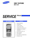
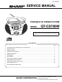
QT-CD700W
SERVICE MANUAL
PORTABLE CD STEREO SYSTEM
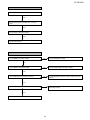
MIC
PAUSE
STOP/EJECT
F.FWD
REWIND
PLAY
RANDOM
RECORD
PLAY/
PAUSE
STOP
POWER
FM ST
MODEL
QT-CD700W
UP/
F.FORWARD
DOWN/
F.REVERSE
PROGRAM
REPEAT
• In the interests of user-safety the set should be restored to its
original condition and only parts identical to those specified be
used.
CONTENTS
Page
AC POWER SUPPLY CORD AND AC PLUG ADAPTOR ................................................................................................ 2
SPECIFICATIONS ............................................................................................................................................................ 3
NAMES OF PARTS .......................................................................................................................................................... 4
FITTING OF DIAL POINTER ........................................................................................................................................... 5
OPERATION MANUAL..................................................................................................................................................... 6
DISASSEMBLY................................................................................................................................................................. 7
ADJUSTMENT................................................................................................................................................................. 10
NOTES ON SCHEMATIC DIAGRAM .............................................................................................................................. 15
WAVEFORMS OF CD CIRCUITS ................................................................................................................................... 22
TROUBLESHOOTING (CD SECTION) ........................................................................................................................... 24
FUNCTION TABLE OF IC ............................................................................................................................................... 29
PARTS GUIDE/EXPLODED VIEW
SHARP CORPORATION
This document has been published to be used
for after sales service only.
The contents are subject to change without notice.
QT-CD700W
SAFETY PRECAUTION FOR SERVICE MANUAL
z
This product is classified as a CLASS 1 LASER PRODUCT.
z
WARNINGS:
The AEL (Accessible Emission Level) of Laser Power Output for this model is specified to be lower than
Class I Requirements. However, the following precautions must be observed during servicing to protect
your eyes against exposure to the Laser beam.
(1) When the cabinet has been removed, the power is turned on without a compact disc, and the Pickup
is on a position outer than the lead-in position, the Laser will light for several seconds to detect a
disc. So not look into the Pickup Lens.
(2) The Laser Power Output of the Pickup inside the unit and replacement service parts have already
been adjusted prior to shipping.
(3) No adjustment to the Laser Power should be attempted when replacing or servicing the Pickup.
(4) Under no circumstances look directly into the Pickup Lens at any time.
(5) CAUTION - Use of controls or adjustment, or performance of procedures other than those specified
herein may result in hazardous radiation exposure.
AC POWER SUPPLY CORD AND AC PLUG ADAPTOR
92L24801600292
92L26803000010
92L24801800222
2
92L2680212512A
QT-CD700W
CHAPTER .
FOR A COMPLETE DESCRIPTION OF THE OPERATION OF THIS UNIT, PLEASE REFER
TO THE OPERATION MANUAL.
SPECIFICATIONS
QT-CD700W
■
General
Power source
AC 110-127/220-240 V, 50/60 Hz
DC 12 V ["C" size (UM/SUM-2, R14) battery x 8 ]
Power consumption
12 W
Output power
PMPO: 32 W (AC operation, 10% T.H.D)
RMS: 4 W (2 W + 2 W) (DC operation, 10% T.H.D)
Speakers
77 mm (8 Ω) full range x 2
piezo x 2
Dimensions
Width: 295 mm (11-5/8")
Height: 153 mm (6")
Depth: 213 mm (8 - 3/8")
Weight
2.1 kg (4.6 lbs) without batteries
■
Compact disc player
Type
Compact disc
Signal readout
Non-contact, 3-beam semiconductor laser pickup
Audio channels
2
Filter
8 time over sampling digital filter
D/A converter
1-bit D/A converter
Wow and flutter
Unmeasurable (less than 0.001% W. peak)
■
Radio
Frequency range
■
FM: 88 - 108 MHz
AM: 526.5 - 1,606.5 kHz
Tape recorder
Frequency response
60 - 12,000 Hz (Normal tape)
Signal/noise ratio
40 dB
Wow and flutter
0.3% (WRMS)
Motor
DC 9 V electric governor
Bias system
AC bias
Erase system
Magnet erase
Specifications for this model are subject to change without prior notice.
3
QT-CD700W
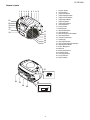
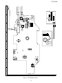
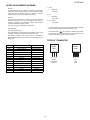
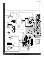
Names of parts
1 2
3 4 5
6 7 8 9
21
20
19
18
17
16
10
11
12
13
14
15
27
A
B
BEAT CUT
22
25
23
24
26
VOLTAGE SELECTOR
110V127V
220V240V
4
1.
2.
3.
4.
5.
6.
7.
8.
9.
10.
11.
12.
13.
14.
15.
16.
17.
18.
19.
20.
21.
22.
Function Switch
Volume Control
(Tape) Pause Button
(Tape) Stop/Eject Button
(Tape) F.Forward Button
(Tape) Rewind Button
(Tape) Play Button
(Tape) Record Button
CD Compartment
Tuning Control
Band Selector
(CD) Random Button
(CD) Stop Button
(CD) Track Up/F.Forward Button
(CD) Repeat Button
Cassette Compartment
LCD Display
(CD) Program Button
(CD) Track Down/F.Reverse Button
(CD) Play/Pause Button
Built In Microphone
FM Aerial
23.
24.
25.
26.
27.
Battery Compartment
Earphone socket
AC Voltage Selector
AC Input Socket
Beat Cut Switch
QT-CD700W
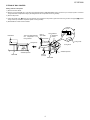
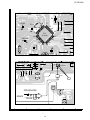
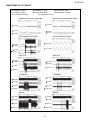
FITTING OF DIAL POINTER
Setting method of dial pointer
1) Remove the front cabinet.
2) Remove 3 pcs screws (S06) φ3 x 10 PA from tuning bracket (bottom of PWB board/pattern side), and remove 1 pc screw (S14) φ2.6 x 10 PH from
tuning bracket/CD compartment’s flange (with fitting between CD compartment and tuning bracket).
3) Remove dial pointer.
4) Insert dial pointer from A direction to tuning bracket, then engages the dial pointer’s guide hook into tuning control’s slot properly B. (Ensure
tuning control’s pin located on adjustment portion of tuning bracket.)
5) Reassemble the screws and front cabinet.
Pointer
Dial Pointer
Tuning Bracket
(S14)×1
φ2.6×10PH
This screw fitting between
CD compartment and
tuning bracket.
Adjustment
Portion
Dial Pointer
Tuning Knob
Tuning Knob
Tuning Knob
A
Variable Capacitor
Main PWB
B
Variable Capacitor
(S06)×3
φ3×10PA
Main PWB
5
QT-CD700W
OPERATION MANUAL
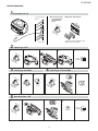
1 Preparation for use
■ Turning the power
ON and setting to
the STAND-BY
mode
AC110-127/220-240 V,
50/60 Hz
TA
PE
(ST
■ Operation with batteries
AN
D-B
Y)
CD
FU
NC RADIO
TIO
N
To AC INPUT
● 8 "C" size batteries (UM/SUM-2, R14)
● Batteries are not included.
To an AC socket
2 Listening to a CD
1
2
TA
PE
(ST
AN
D-B
3
4
5
Y)
PLAY/
PAUSE
CD
FU
NC RADIO
TIO
N
4 Listening to a Cassetteape
T
3 Listening to the Radio
1
2
TA
PE
(ST
AN
D- B
3
2
TA
P
Y)
AM
CD
FM
E(
ST
AN
1
2
D-B
3
Y)
CD
FM
FU
NC RADIO
TIO
N
ST
5 Recording from a CD
PE
(ST
AN
D-B
ING
N
TU
FU
NC RADIO
TIO
N
TA
1
3
PLAY
4
5
Y)
RECORD
CD
FU
NC RADIO
TIO
N
6
PLAY/
PAUSE
QT-CD700W
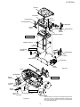
DISASSEMBLY
Caution On Disassembly
Follow the below-mentioned notes when disassembling the unit and reassembling, to keep it safe and
ensure excellent performance:
1. Take cassette tape and compact disc out of the unit.
2. Be sure to remove the power supply plug from the wall outlet before starting to disassemble the unit.
3. Take off nylon bands or wire holders where they need to be removed when disassembling the unit.
After servicing the unit, be sure to rearrange the leads where they were before disassembling.
4. Take sufficient care on static electricity of integraged circuits and other circuits when servicing.
STEP
REMOVAL
PROCEDURE
FIGURE
1
Rear Cabinet
Screw.....S08x5
Screw.....S06x2
5-1
2
Front Cabinet
Screw.....S06x2
Screw.....S06x4
5-1
3
Main PCB ASS'Y
Screw.....S06x7
Screw.....S02x1
Screw.....S15x1
6-1
4
CD Control PCB ASS'Y
Screw....S04x6
5-2
5
Tape Mechanism
Screw....S06x4
5-2
6
R/P PCB ASS'Y
Screw.....S06x2
5-2
7
CD Mechanism
Screw.....S11x4
6-1
8
Power PCB ASS'Y
Screw.....S02x1
6-2
CD Door
Front
Cabinet
(S06)×2
φ3×10PA
(S08)×2
φ3×14PA
Rear
Cabinet
R/P PCB ASS'Y
Figure 5-1
TAPE MECHANISM
(S06)×2
φ3×10PA
(S06)×4
φ3×10PA
OPEN CASSETTE HOLDER
S04X6
CD CONTROL PCB ASS'Y
Figure 5-2
7
QT-CD700W
CD DOOR
TOP CABINET
(S14)X1
φ2.6X10PH
FUNCTION KNOB
FUNCTION KNOB BKT
BAND KNOB
(S05)X1
φ3X8mm
(S12)X1
φ3X8PA
BAND KNOB BKT
(S05)X1
φ3X8PWH
DOOR LATCH SWITCH
CD MECHANISM
RUBBER CUSHION X4
(S11)X4
φ2.6X12PWA
VOLUME KNOB
BRACKET
MAIN PCB ASS'Y
TUNING BRACKET
(S02)X1
φ2.6X5PH
(S15)X1
M3X8PH (BLACK)
TUNING KNOB
(S06)X7
φ3X10PA
HANDLE
Figure 6-1
(S03)X1
φ3X8PH
TRANSFORMER
BATTERY DOOR
(S09)X2
φ3X20PWH
AC POWER
SOCKET (S06)X2
φ3X10mm
(S13)X2
φ3X12PA
S06X2
POWER PCB ASS'Y
AC VOLTAGE SELECTOR
AC VOLTAGE
SELECTOR COVER
NOTE:
After removing the connector for the optical pickup from the
connector, wrap the conductive aluminium foil around the
front end of connector remove to protect the optical pickup
from electrostatic damage.
Figure 6-2
8
QT-CD700W
The wire arrangement of AC Input Socket, Voltage Selector & Power Transformer.
Screw
VOLTAGE
SELECTOR
11
screw
(S13)x2 φ3x12PA
wire
Black
Left
Terminal
Re
POWER
TRANSFORMER
dw
ire
ire
screw
w
ed
2 R
Left
Terminal
1
3
re
Right terminal
1
4
022 0V
24
wi
AC INPUT
SOCKET
Right Terminal
ue
Bl
screw
(S06)x2 φ3x10PA
Center Terminal
V
27
1
0-
ire
ck w
Bla
To
Batterry
To PWB Board
(Power)
(S09) X 2
φ3x20PWH
* Please follow the instruction of wire arrangement, to service or reinstall these critical parts.
1
BLACK WIRE
Connecting from Power Transformer (black wire) to AC Input Socket (left terminal).
2
RED WIRE
Connecting from AC Input Socket (right terminal) to Voltage Selector (center terminal).
3
RED WIRE
Connecting from Power Transformer (red wire) to Voltage Selector (left terminal).
4
BLUE WIRE
Connecting from Power Transformer (blue wire) to Voltage Selector (right terminal).
9
QT-CD700W
ADJUSTMENT
TUNER SECTION
fL : Low-range frequency
fL : High-range frequency
MECHANISM SECTION
Torque
Specified Value
Play: TW-2412
Over: 80g
FM IF /RF
Torque Check
Torque Meter
Specified Value
Play TW-2111
30 to 60g.cm
Fast Forward
Rewing: TW-2231
55 to 140g.cm
55 to 140g.cm
Specified Value/
Adjusting Point
Test Stage
fL : L301
FM
Band Coverage fL : C2
fL : 90 MHz: L303
fH: 106.0 MHz: C1
FM Tracking
Head Azimuth
Torque
AM IF /RF
Output: Speaker terminal
CN6 Load resistance: 8 ohms
Specified Value/
Adjusting Point
Test Stage
Tape Speed
Test Tape Adjusting
point
Specified
AM IF
Instrument
Connection
Variable
Output: Speaker
Resistor in 3.000±90Hz Terminal CN6
MOTOR.
Load resistance:
M601
8 Ohms
Tape Section
Instrument
Connection
Input: Antena
Output: Pin 18
of IC1
T303
AM
Band Coverage
fL: T301
fL: C4
AM Tracking
fL: 600KHz ANT
fL: 1400KHz C3
Input: Antenna
Output: Speaker
Terminal CN6 Load
resistance: 8 ohms
Playback Amplifier Sensitivity Check
Position of each switch or control
Volume control
Function switch
Max
Tape/Stand-by
Adjustment point
Specified Value
Instrument
Connection
80KHz ± 6KHz
Pin 1 CN103
T101
Input: Antenna
Output: Speaker
Terminal (CN6
Load resistance:
8 ohms
Specified Value
MT-114
MTT-111
Instrument
Connection
10
Test Tape
Specified Value
Instrument Connection
MTT-118
1.5V ± 3dB
Speaker Terminal
(Load resistance: 8 ohms)
VR1
SW1
SW3
1
2
IC201A
18
13
FH
24
1
SW4
FM TRACKING
FL
IC1
12
T303
AM BAR
AM ANTENNA
L303
C1
C3
PVC1
3
11
D
MOTOR
M601
E
4
Figuer 11 ADJUSTMENT POINTS
5
BIAS OSC
t101
IC101
CN103
1 2 3 4
FL
FH
FM BAND
COVERAGE
L301
C2
C4
T301
B
AM IF
ANT
C
FM-ANT
A
FH
FL
FH
FL
AM COVERAGE
AM TRACKING
FM ROD ANTENNA
QT-CD700W
SW2
TAPE LEAF SW
WH
WH
RD
BK
TAPE
MECHANISM
Variable resistor
in motor
CN1
F
IC3
PHONE
G
H
6
QT-CD700W
CD SECTION
Since this CD system incorporates the following automatic adjustment function, when the pickup is replaced, it is not necessary tp readjust it.
Since this CD unit does not need adjustment, the combination of PWB and laser pickup unit is not restricted.
TEST MODE
Start
While holding down the “Stop” and “RANDOM” button simultaneously, move the FUNCTION switch to “CD”.
Note
1. When the CD DOOR switch is in the OFF position, i.e. CD DOOR is opened, the unit is now in test mode. Press the “UP/
F.FORWARD” and “DOWN/F.REVERSE” buttons to move the pickup back and forth.
2. The LCD display should be the same as it is for normal CD operations.
Operation
Pressing the “UP/F.FORWARD” button will move the pickup outward.
Pressing the “DOWN/F.REVERSE” button will move the pickup inward.
LCD MODE
Start
Display
After connecting the 10kohm resistor between IC201A 13 pin and GND, holding down the “Stop” and “RANDOM” button
simultaneously and move the FUNCTION switch to “CD”.
1 ALL
PROG
RNDM
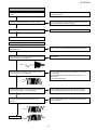
LASER LIGHTING CONFIRMATION
1. Remove the front cabinet according to the disassembly method.
2. Short the TP of the Figure 13-1 to turn on the CD DOOR switch (SW810).
3. While holding down the "Stop" and "RANDOM" button simultaneously, move the FUNCTION switch to "CD".
4. Open the CD DOOR and press the PLAY button. The laser lights up for a few seconds. (During this time, the pickup lens moves up and down and
adjusts the focus to check if there is a disc or not.)
PREPARATION FOR LASER LIGHT UP
1. Before the laser light up, CD DOOR switch (SW810) terminals have to be short with the solder. Resistor of 330ohm is put from 13 PIN of IC201A,
and you must connect it to GND of PWB. (Refer to PWB of Figure 13-1.)
12
QT-CD700W
Q502
C610
A
D4
C108A
C104
13
10
GND
5
B
1
22
26
32
P19
IC201A
64
CN124A
17
16
59
C
38
42
54
48
49
C126A
B
C
E
D
Q1
D3
E
5
6
7
8
CN8
D2
9 10 11 12
D505
C525
CN503A
1 2
CN5
D506
CD DOOR
C515
E C B
C
C133A
B C E
4
33
B C E
Q4
RD
F
2
CN5A
TP
BK
1
B C E
Q5
CN502B
1 2
OPEN/CLOSE
G
S4
PLAY
SW810
C5O4A
CD LID
H
1
2
3
4
Figure 13-1
13
5
6
QT-CD700W
SETTING METHOD FOR LASER LIGHT UP
1. In power OFF state, set the Function switch to ON, keeping to be pressed the "Stop" and "RANDOM" button at same time.
After CD initialize finish, The CD TEST mode is set, and the LCD indicate to the total tracks of the disc .
Release the PLAY button.
The CD TEST mode is set when the LCD indicate to "1".
Then out the above circuit.
2. In above TEST mode state, press once the PLAY button.
The laser is light up when LCD indicate to "CD".
SETTING FOR MAXIMUM LASER POWER
1. In above laser light up state, adjust the variable resistor (VR1A) on pickup PWB to maximum laser power.
Maximum laser power: Rotate the variable resistor (VR1A) to clockwise.
Pickup unit
Variable resistor
VR1A
Note:
The TEST mode is cleared by power OFF.
14
QT-CD700W
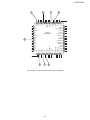
NOTES ON SCHEMATIC DIAGRAM
•
1. Tuner
Resistor:
(
To differentiate the units of resistors, such symbol as K and M are
used: the symbol K means 1000 ohm and the symbol M means
1000 kohm and the resistor without any symbol is ohm-type
resistor. Besides, the one with “Fusible” is a fuse type.
•
): AM mode
: FM mode
2. CD
(
Capacitor:
): Stop state
: Play mode
To indicate the unit of capacitor, a symbol P is used: this symbol P
means pico-farad and the unit of the capacitor without such a
symbol is microfarad. As to electrolytic capacitor, the expression
“capacitance/withstand voltage” is used.
3. Deck section
: Stop state
(CH), (TH), (RH), (UJ): Temperature compensation
(ML): Mylar type
•
Schematic diagram and wiring side of P.W.Board for this model are
subject to change for improvement without prior notice.
•
Parts marked with “
” are important for maintaining the safety
of the set. Be sure to replace these parts with specified ones for
maintaining the safety and performance of the set.
(P.P.): Polypropylene type
•
Schematic diagram and Wiring Side of P.W.Board for this model
are subject to change for improvement without prior notice.
•
The indicated voltage in each section is the one measured by
Digital Multimeter between such a section and the chassis with no
signal given.
TYPES OF TRANSISTOR
REF NO.
DESCRIPTION
SW2
Record/Playback
POSITION
Rec P. B
SW1
Function selector
Radio-Tape CD
SW4
Band selector
FM. ST-FM-AM
SW3
Beat cancel
A-B
SW601
Tape man
OFF-ON
SW651
Voltage selector
AC220-240V
SW702
Pickup in
S4
S3
S1
DOWN/F.REVERSE
OFF-ON
S2
UP/F.FORWARD
OFF-ON
S6
Repeat
OFF-ON
S5
Program
OFF-ON
S7
Random
OFF-ON
FRONT
VIEW
FRONT
VIEW
AC110-127V
E C B
E B
Play/Pause
OFF-ON
Stop
OFF-ON
2SA933
DTA124ESA
2SB1237
15
9014
9015
8050
C
QT-CD700W
C322
4.7u
R302
180K
C
R103
R105
560
R104
560
E
TAPE
CN103A
R
C130
1u
C129
182M
RP-HEAD
2K2
C127
182M
CN503B
1
2
3
C122
22U
4
C128
100u
5
12
12
11
11
10
10
9
9
8
8
7
7
6
6
5
5
4
4
3
3
2
2
1
1
P
R77
10K
R126
47
C110
222(M)
G
R120
47K
T101
PL1004
C135
562(M)
R
CN7A
2
1
1
2
SW3
3
1
2
C320
SW1-D
CD-RCH
3K9
3K9
562
R307
R306
C200
562
C100
4V3
D1
Q501
9014
R-CH
FUNCTION
SELECTOR
SW502
R127
10K
R111
10K
0.68V
R119
10
PIN
2
3
VOLTAGE(V) 1.89 0.03 1.94
4
0
5
6
7
R20
TAPE LEAF
SWITCH
22
0.68V
Q101
9014
1
CD
CN15A
0V
Q102
9014
8
0V
C103
203
M
C136
100u/25V
9
0.01 7.06 2.01 0.03 1.91
R/P PWB-A2
M501
TAPE MOTOR
H
NOTES ON SCHEMATIC DIAGRAM can be found on page 6-1.
2
R506
10K
P
CN15
0.1V
0.6V
R118
100
0.1V
0.1V
AC BIAS
BEAT CUT SWITCH
1
R505
100K
R141
2K2
IC101 BA3308
CN7B
203
0V
R125
5k6
100K
C134
223(M)
C133
182(M)
RADIO
TAPE
CD
9
C123
333(M)
R17
4.75V
C105 203
BIAS COIL
R507
10K
R101
100
RECORDING
BIAS OSCILATOR
Q103 8050D
C106 100u
C143
180P
P
R
R113
15K
0.23V
8
P
R
F
D3
1N4148
D5
1N4148
Q502
9014
RADIO-RCH
C126
47u
R128
470K
E-HEAD
C4
470U
FUNCTION
SELECTOR
0.21V
R78
10K
7
C124
120K
C142
200p
C125
1u
C101
203
R
R
104
103M
0.1U
SW4
FM
ST
R314
CC5
103M
SW1-C
CD-LCH
0V
R
6.12V
L-CH
RADIO
TAPE
CD
CN503A
6
C124
1u
R310
100
RADIO-LCH
REC-SYN
L
C141 200p
R121
120K
C132
1u
P
CN103
82K
R140
IC101
REC/P.B.
R117 EQUALISER AMP
C131 5k6
BA3308
47u
R122
47
L
R3
10
C3
203
Q2
9014
82K
R102
C108
333(M)
P
R
C109
222(M)
C2
100U
C317
D102
1N4148
R129
15K
D
R12
220
R304
330
100u
C102
100U
C318
R108
1K
D103
1N4148
C120
1u
FM DETECTION
0V
2
R311
330
C327
203
0V
1
2
10.7M
CF303
5.43V
3K3
1
R110
47K
R107
CN14
R309
10K
C306
1u
AM IF
R112
2K2
C121
47U
IC101
BA3308
CN14A
FMSTFMST+
FM IF
AM IF
CF2
CF3
455K 10.7M
T303
R325
47k
MIC
R315
AM
300
C325
33P
D302
1N4148
R109
2K2
R308
10K
U1
88-108
C328
33P
D301
1N4148
C312
(4.28V)4.52V
103M
24
IC1
TA2111
FM BAND BASS
FILTER
C309
(3.5V)3.95V
13
23
12
(4.3V)4.52V
12
11
(4.28V)4.52V
14
(4.28V)4.52V
(2.75V)3V
0
15
(4.28V)4.53V
21
22
16
(0.19V)1.36V
20
0
10
19
(4.17V)4.52V
9
10
17
(3.4V)3.84V
8
9
7
IC1
FM/AM IF MPX.
TA2111N
18
(0.9V)1.1V
8
18
C307
1u
7
(3.7V)4.5V
C304 4P
(0.7V)0.7V
6
19
(3.47V)4.52V
17
20
(4.28V)4.52V
16
(0.6V)0.5V
C305
0.1U
C303
1U
6
15
(3.5V)4.49V
5
5
(0.48V)1.37V
4
22
3
21
(1.25V)1.26V
4
14
23
0
VC1B
3
2
VC1A C301
25P
2
(1.25V)1.24V
C316
130P
R312
4K7
C323
104
13
24
VOLTAGE(V)
(0.8)0V
1
B
FM ANTENNA
pin
no
1
VC1D
C302
25P
C321
C324
203
IC1 TA2111N
pin
no VOLTAGE(V)
R11
4.7
203
VC1C
A
T301
L301
FM OSC 2T5/5MM AM OSC
11
L303
FM ANT 3T5/4.5MM
AM BAR
ANTENNA
MAIN PWB-A1
3
4
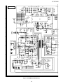
Figure 15 SCHEMATIC DIAGRAM (1/4)
16
5
6
QT-CD700W
FM SIGNAL
AM SIGNAL
H
C717
14.0
C5
220U
L201
2
7.20
3
13.85
4
0
5
0.52
SPK402
R : 8 OHM
0
7
0
8
0.51
9
10
7.20
13.85
11
7.2
12
14.7
LED 2
CN502B
1
1
2
2
VOLTAGE SELECTOR
SW651
FUSE 1
T1.25AL 250V
T501
8.0V
CD+8V
14.5V
R413
56K
D9A
1N4001
D8
1N4001
7
6.72V
D403
1N4148
4.99V
4.32V
Q406
9014
R411
5K1
D7
1N4001
Q407
9014
4.48V
4.32V
D10
1N4148
8.0V
R410
2K7
AC/DC SELECTOR
150
D772
14.2V
AC INPUT
AC INPUT SOCKET
AC100-127V/
220-240V
60/50HZ
BATTERY
DC 12V
UM-2 / SIZE "C" / R14 × 8
R517
4K7
560
POWER
TRANSFORMER
1N4001
REGULATOR
Q408
POWER LED
R42
R40
POWER PWB-A4
D202
1N4001
D504
6V8
1
110V
9.9V
2
R514
560
C522
100u
VOLTAGE(V)
D203
1N4001
CN501B
C518 C516
203 100u
C519
203
PIN NO
CN502A
2
SPK401
L : 8 OHM
CB2
22U
IC3 YD8227
R503
2K2
1
CB1
22U
S0651
C6
100U
1
CN6A
SPK404
14.0V
C8
203
CN501A
PHONE 1
SPK403
6
D503
1N4148
R515
100
D505
1N4148
CN6
C513
470u
D204
1N4001
6.85
AMUTE
D506
1N4148
C526
10U
Q3
9014
HEADPHONES
L2
C205
203
9.1V
180
SPEAKERS
203
10U
10U
C525
C515
6.22V
R5
4.7
0V
FUNCTION
SELECTOR
SW1-A
RADIO
TAPE
CD
Q504
8050
180
R602
L1
14.3V
9.85V
R504
47K
1
C204
203
Q503
9015
SW1-B
FUNCTION
SELECTOR
R601
CN6A
IC3
POWER AMP
YD8227
C512
104(M)
R8
47K
RADIO
TAPE
CD
R505
100K
4.7
47U
C509
120
D6
1N4148
D2
1N4148
2
C510
100u
R7
1K
R2
47K
D3
1N4148
D5
1N4148
3
14.5V
6.16V
6.12V
12
D9
1N4001
C401
104M
R2
1K
C4
470U
4
C507
10U
VR1B
Q2
9014
R501
C402
470P
R401
3K
R
R9
1k
5
C503
1u
102(M)
C520
1u
L3
11
C202
203
6
0.14V
0V
10
IC3
YD8227
C504
R22
10k
R510
12K
310
00
9
0V
Q6
9014
5.43V
8
C506
100u
220V
7
RECORD SIGNAL
C203
203
0.17
PLAYBACK SIGNAL
C514
470u
R6
C502
1u
0V
C524
1000U/25V
C201
2200U/25V
R23
10k
C403
104M
RADIO-RCH
Q7
9014
CD SIGNAL
C508
100U
C7
100UF/25V
562
C200
3K9
3K9
R307
R306
R403
3K
R502
L
47U
R10
VR1A 1k
RADIO-LCH
C511
104(M)
C505
C404
470P
C501
102(M)
120
C521
1u
R511
12K
R412
390
R414
180K
8
D402
5V1
9
10
Figure 16 SCHEMATIC DIAGRAM (2/4)
17
11
12
QT-CD700W
C123A
C1
1UF/50
A
C107
104
R3B
100K
C108A
100UF
R2B
100K
R4B
47K
R1B
3.3M
RFRPRFM
150P
TZCRFM
C121A
2200P
C12
10
27K
4 VBIAS
Tack Coil
47K
56K
C103A
GND
9
9
10
10
11
11
12
12
13
13
14
14
15
15
16
16
R112A
150K
FE
103
R101A
91
MD
R113
0
T-
CC
C
13 LD
14 ASY
15 AV
C115 104
16 PC0
VDD
T+
F-
C114
0.22UF/50V
R129A OPEN
D
SE
11 BTC
12 PD
C111A 104
C113
R114
3.3UF/50V 470
F+
470P 10 PKC
C110A 104
LD
VR
C109A
30 SEGB/COM1
R107A
R111A
P
9 FE0
29 SEGA/COM0
F
47K
47K
8 FEN
28 LON
8
C
R106A
R108A
P03
7 AGND1
C112
120P
27 CLK88
8
B
56K
47K
26 ADC1/KEY
7
A
R110A
R109A
25 ADC0/GAIN_SEL
6
7
D
24 CLVOUT
5
6
6 6
E
23 SDOUT
5
COM
22 SDIN
4
21 TDOUT
4
20 JUMP0
3
19 FDOUT
2
3
18 AGND2
Fouse Coil
1
2
IC201A
BU24530-9A
5 E
17 FC0
C
1
DGND 51
LDAC0 53
RDAC0 55
AGND3 56
PWC/W
3 BD
VREF
AVDD3 52
C126A
1UF/50V
2 AC
PICKUP UNIT
RFRPRFM 57
1 AVDD1
SC 59
RF
R104A
1K
TE0 60
2.38V
C102A
470UF/10
C125A
682
C104
100UF/10
TZCRFM 58
C105A
104
1.81V
1UF/50V
TEN 61
Q101A
2SA933
C124A
R103A
100K
EQ0 64
3.11V
C101A
100UF/10
R121A
L101A
10uH
R105A
4.7
RF1 63
R102A
4.7
R122A
75K
C122A
100P
VCDAC 54
0.61V
Q1
2SC1740S
0V
CAGC 62
VDD
B
TP3
TE
0V
CN1
TP6
C130A
104
C118 R119
10U 4.7K
R117A
390K
E
C117
104
R118A
33K
TDOUT
R116
6K8
R115 18K
JUMP0
C503A
R130
3K3
R125A
8K2
F
M
1
M
3
2
4
5
LIMIT SWITCH
6
CD MOTOR PWB-B
R507A
1
R508A
SP+
SPSM+
104
SMMSW
GND
R124A
4K7
C608
4.7UF/50V
SW702
1
CN2
R126A 0
CNP803
M702
SPINDLE
MOTOR
M701
SLED
MOTOR
R506A
1.64
16
5.65
1.64
17
3.16
4
0.77
18
2.67
5
5.77
19
1.64
6
3.32
20
1.64
7
2.19
0
21
22
6.40
8
9
10
0
23
1.64
0
24
1.63
11
2.82
1.64
12
13
3.04
25
26
0
27
2.92
14
1.56
28
0
R604
10K
C609
0PIN- 15
RSTT 16
13 PGND
14 0POUT
V03- 17
IN3 19
V03+ 18
11 V02+
12 V02-
VCC 21
VCC 22
IN3' 20
9 IN2'
8 REGGND
7 /MUTE
IN4 25
IN4' 24
BIAS 23
6 REGOUT
5 REGB
V04+ 26
V04- 27
4 RESET
R602A
0
6.40
7.14V
3.30V
7.77V
2.96
C135
H
1
PGND 28
R603
10K
2
104
3
Q601
2SB1237 137A
C138A 104 104
C603
470U/10V
4
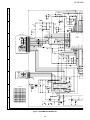
Figure 17 SCHEMATIC DIAGRAM (3/4)
18
R605
10K
15
3.21
3
R601A
47K
0
2
1
IC601 BA5826FP
10 IN2
PIN NO VOLTAGE(V) PIN NO VOLTAGE(V)
G
C607
104
3 VIN1
C602
104
2 V01+
L5
26uH
1 V01-
IC601 BA5826FP
C71 104
C54
470U/10V
CD+8V
C606
470U/10V
C601 470U/10V
C605
47UF/10
0V
VDD
C604
104
5
R19
10K
2.15V
Q602
9014
R18
10K
0V
6
1N
QT-CD700W
C127A
100UF/10
R301A
3K
C132A
15P
15P
C126A
1UF/50V
VDD
C131A
CD-LCH
R305A
560
PWC/W_REMOTE 46
R503A
E
C
2
1
IC201A BU24530-9A
PIN NO VOLTAGE(V) PIN NO VOLTAGE(V) PIN NO VOLTAGE(V)
1K
P11/SYNC 45
R16
0
P10/PLAY 44
A
-0.8V
3
R24
1K
R505A
10K
104
C502A
L202
100uH
C133A
100UF/10
104
C134A
DVDD 48
RESETB 47
Q301
DTA124ESA
C138
104
AMUTE
3.27V
B
R128A
220
X1 49
X0 50
DGND 51
LDAC0 53
AVDD3 52
RDAC0 55
C305A
4.7UF/50V
CN8
3.29V
R120A 1M
VCDAC 54
R303A
2K7
C301A
560P
X1
16.9344M
R306A
560
C304A
560P
4.7
P03/PRO_LED 43
P01/LID 41
P00/INNER 40
SEG6/AMUTE 39
R529
R531
CCOM1/SEG5 38
COM0/SEG4 37
0
0
R15
10K
0V
SEGG/2 35
SEGF/1 34
Q4
9014
R14
0.66V 10K
SEGE/0 33
SEGD/COM3
Q5
9014
0V
32
R540
OPEN
R541
OPEN
R542
OPEN
R543
OPEN
R545
470K
R546
470K
R547
470K
-0.8V
0V
31 SEGC/COM2
30 SEGB/COM1
29 SEGA/COM0
28 LON
27 CLK88
SEG./3 36
1
3.32
25
1.82
49
1.61
2
1.72
26
3.32
50
1.56
3
1.72
27
1.66
51
0
4
1.66
28
3.39
52
3.32
5
1.71
29
1.49
53
1.66
6
1.67
1.71
30
1.46
54
7
0
31
1.46
55
0
8
1.66
32
1.46
56
1.85
9
10
1.66
1.60
1.65
C505A
104
P02/MMUTE 42
26 ADC1/KEY
CD-RCH
C303A
560P
C128A
104
C302A
560P
R1
C306
4.7UF/50V
R304A
2K7
R302A
3K
2.58
33
34
1.60
57
58
11
1.03
35
1.63
59
1.66
12
13
0.20
1.63
1.54
60
61
1.67
2.27
36
37
14
1.67
38
1.57
62
0.77
15
3.33
39
3.29
63
1.66
16
1.66
40
3.30
64
1.62
17
1.53
41
0.94
18
0
42
0.06
19
20
1.63
43
44
3.30
0.65
21
1.65
45
0
22
23
1.67
0.02
1.67
46
47
24
1.64
48
3.32
R13
10K
0.42
0.77
3.31
3.32
CN5
REC-SYN
CN5A
2
2
1
1
SW810
LEAF SW
OPEN/CLOSE
FMST-
104
1
1
2
2
3
3
4
R506A
10K
4
R507A
10K
CN9A
1K8
C508A
COM3
SEG0
SEG1
SEG2
SEG3
SEG4
SEG5
4
5
6
7
8
9
10
R513A
3.3K
COM2
3
MAIN PWB-A1
R514A
4K7
COM1
2
CN4A
R515A
10K
COM0
1
R512A
2K7
104
5
CN9B
R511A
1K8
R508A
5
A04
A06 9
A05 10
6
A08 7
A07 8
A09
A02 4
A03 5
CN4B
A00 2
A01 3
1
CN4B
LED1
C503A
FM ST
FMST+
S4
PLAY
S7
RANDOM
S3
STOP
S2
FF
S1
FB
S6
REPEAT
A09
CD CONTROL PWB-A3
10
A08
A07
9
A05
A06
8
7
6
A04
A03
5
A01
A02
4
3
2
1
A00
S5
PROG
0 0
LCD 1
LCD DISPLAY
9
K
D4
1N4148
7
8
9
10
Figure 18 SCHEMATIC DIAGRAM (4/4)
19
11
12
QT-CD700W
A
RD
B
BK
PHONE1
RD
BATTERY
AC INPUT SOCKET
Q6
E C B
Q3
C516
WH
SPK402
R-CH
D504
D503
Q503
B C E
C520
C507
BK
SPEAKERS
BK
Q7
Q504
RD
MIC
B C E
E C B
C403
C401
E
7 8 9
C
E
C
B
BK
CB2
C511
C513
C509
C503
T501
POWER
TRANSFORMER
BK
SPK404
C514
CN501A
1
IC3
C6
RD
C510
5 6
CB1
VOLTAGE SELECT
SPK403
AC220-240V AC110-127V
C5
4
SPK401
L-CH
AC-1
L7
C524
CN6A
RD
BK
BK
WH
L6
BAT+
AC22
AC11
C512
1 2 3
D9
D
RD BK
2
VCC+
1 2 3 4
AC1
1 2 3 4
10 11 12
C205
1
CN501B
C203
D203
C202
CN6
L1
D205
D204
C204
SW651
WH
WH
J73
BK
RD
VCC
2
CC4
C201
FUSE
WH
D202
RD
T1.25AL 250V
C
L3
GND3
GND1
C717
AC-2
BAT-
L2
SO651
C521
RD
1
CN14A
VR1
2
G
D7
TAPE
CN14
SW502
C134
WH
C121
D102
Q103
1
2
3
4
3
4
2
3
4
5
6
7
8
9 10 11 12
BR
BK
WH
GY
VI
BL
GR
YL
OR
RD
BR
BK
1
VCCL.SW PL B+GND PR PR RL MUTE
9 10 11 12
8
7
6
CN503B
5
R20
C106
B C E
RD
4
C126
C135
WH
TAPE
MOTOR
Q101
3
2
SW2
G
C122
B C E
1
1
2
CN7B
C131
C136 GND
4
1
CN7A
POWER LED
C108
C128
3
4
T101
SW1
C102
C132
2
3
C110
C133
1 2 3 4 5 6 7 8 9
1
2
TAPE LEAF SW
C124
Q102
B C E
2
C127
CN103
1
BK
RD
C130
C109
CN103A
RD
BK
BK
WH
2
C120
C125
F
C123
WH
D103
RECORD/PLAYBACK
HEAD
RD
1
C129
IC101
BK
CN503A
CN15
BK
CN15A
2
BK
RD
WH
WH
1
M501
H
1
2
3
4
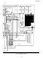
Figure 19 WIRING DIAGRAM OF P.W.BOARD (1/2)
20
5
6
CN50
QT-CD700W
CD MECHANISM DECK
PICKUP UNIT
SPINDLE MOTOR
M702
SW702
PICKUP IN
CNP803
CN2
3
4
CN2
Q601
2 3 4
1
2
3
4
GREEN
BL
BLUE
VI
VIOLET
GY
GRAY
WH
WHITE
FM-ANT
6
FM-ANT1
B C E
E C B Q505A
C114
C113
E C B Q503A
Q502A
C610
Q408
IC3
CF303
1 2 3
D4
5
C1
Q101A
B C E
D403
Q501
B C E
E C B
GND
D7
1
C526
C507
Q502
D3
2
3
4
5
6
7
8
D505
CN503A
L303
PVC1
L301
C313 CC5
C307
SW4
Q301
1
2
CN8
CN9A
1 2 3
1 2 3 4 5
1 2 3 4 5 6 7 8 9 10
KEY
CD DOOR
C305
Q2
B C E
CN4A
C4
C525
CN502A
CN5
D506
VC3
C315
B C E
C127A
D2
9 10 11 12
VC4
1 2 3 4 5 6 7 8 9 10 CN4B
B C E
Q4
1 2
1
RD
B C E
Q5
2
CN5A
CN9B
1 2 3 4
BR
POWER LED
CN502B
5
1 2 3
1 2
POWER
LED2
S4
PLAY
SW810
S7
RANDOM
FM.ST
LED1
S3
STOP
CN9B
C5O4A
CD LID
INFRARED RECEIVER
S1
REV
LCD1
S5
PROG
SEG2
SEG1
SEG0
COM3
COM2
COM1
COM0
1 2 3
SEG5
SEG4
SEG3
REM
COM0
COM1
COM2
COM3
SEG5
SEG4
SEG3
SEG2
SEG1
SEG0
RD
CN12
OPEN/CLOSE
1 2
BK
CN503B
BLACK1
C133A
X101
C308A
CT3
48
C306
C101A C305A
D5
D6 D8 D9A
49
Q1
D402
B C E
C515
D504
Q503
38
42
54
VC1
CT4
13 14 15 16 17 18 19 20 21 22 23 24
SEG2
SEG1
SEG0
COM3
COM2
COM1
COM0
Q407
C B
59
B
C
E
C318
33
SEG5
SEG4
SEG3
E C B
32
C126A
504
CN124A
L101A
IC1
P19
IC201A
BK
C522
26
1
CN1
Q7
C322
12 11 10 9 8 7 6 5 4 3 2 1
22
64
TC1
C2
VC2
D1
17
10
D10
B C E
C516
U1
TC2
RD
OR
YL
GR
Q406
16
C104
L202
E C B
C502
T303
C303
C108A
C102A
5 6
7 8 9
4
C508
C505
1
2
3
B C E
B C E
C506
1
2
3
T301
1
2
3
C316
Q504A
C608
CF3
C603
CF2
C118
C150
C514
1 2 3
10 11 12
ANT
Q602
16
17
C524
B C E
8
23
L5
2
C606
CN501A
C511
1
C7
C5
R
K
WH
GY
VI
L
GR
YL
OR
RD
R
K
YELLOW
GR
C54
C512
3
5
D301
1
7
C605
28
L3
CN7A
CN6
ORANGER
YL
FM ROD ANTENNA
5 6
2
24
1
RED
OR
D302
C601A
B C E
L2
BROWN
RD
GND
INNER
SLSL+
SPSP-
SW3
VI
BL
YL
1 2
BLACK
BR
OR
RD
BR
M701
SLED MOTOR
BK
1 2 3 4 5 6 7 8 9 10
S2
F.F
GND
PLAY
KEY
FMST
FMST
1
2
3
4
5
CN4B
S6
REPEAT
7
8
9
10
Figure 20 WIRING DIAGRAM OF P.W.BOARD (2/2)
21
11
12
QT-CD700W
WAVEFORMS OF CD CIRCUIT
RF: PIN64 OF IC 201A
FE: PIN9 OF IC 201A
CH_R: PIN55 OF IC 201A
TE: PIN60 OF IC 201A
TD: PIN21 OF IC 201A
FD: PIN19 OF IC 201A
SLED: PIN23 OF IC 201A
CH_L:PIN53 OF IC 201A
NO DISC FOCUS SEARCH (POWER ON)
1
RF PIN64
1
FE PIN9
2
3
NO DISC FOCUS SEARCH (DOOR CLOSE)
RF PIN64
2
3
FD PIN19
FE PIN9
FD PIN19
TCD-782 TNO-02 PLAY BACK
FOCUS SEARCH_TOC READ
5
CH_R PIN55
6
CH_L PIN53
1
RF PIN64
4 TE PIN60
2
FE PIN9
3 FD PIN 19
STOP-PLAY
1
4
STOP-PLAY
RF PIN64
TE PIN60
1
RF PIN64
FE PIN9
2
7
TD PIN21
3
8
FD PIN19
SLED PIN23
F FORWARD
F FORWARD
1
8
1
RF PIN64
4
TE PIN60
7
TD PIN21
RF PIN64
2
3
8
SLED PIN23
FE PIN9
FD PIN19
SLED PIN23
REVIEW
8
1
RF PIN64
4
TE PIN60
7
TD PIN21
SLED PIN23
REVIEW
1
RF PIN64
2
3
8
FE PIN9
FD PIN19
SLED PIN23
22
QT-CD700W
X1 49
X0 50
DVDD 48
RESETB 47
PWC/W_REMOTE 46
3 BD
4 VBIAS
P11/SYNC 45
IC201A
BU24530-9A
5 E
6 6
P10/PLAY 44
P03/PRO_LED 43
P02/MMUTE 42
7 AGND1
8 FEN
P01/LID 41
9 FE0
P00/INNER 40
10 PKC
SEG6/AMUTE 39
11 BTC
CCOM1/SEG5 38
COM0/SEG4 37
3
7
SEGG/2 35
SEGF/1 34
SEGE/0 33
SEGD/COM3
32
31 SEGC/COM2
30 SEGB/COM1
29 SEGA/COM0
28 LON
SEG./3 36
27 CLK88
24 CLVOUT
23 SDOUT
22 SDIN
21 TDOUT
20 JUMP0
16 PC0
19 FDOUT
15 AV
18 AGND2
14 ASY
26 ADC1/KEY
13 LD
25 ADC0/GAIN_SEL
12 PD
17 FC0
2
DGND 51
LDAC0 53
AVDD3 52
RDAC0 55
AGND3 56
6
VCDAC 54
2 AC
RFRPRFM 57
SC 59
5
TZCRFM 58
TEN 61
CAGC 62
EQ0 64
RF1 63
1 AVDD1
TE0 60
4
1
8
The numbers 1 to 8 are waveform numbers shown in pages 22.
23
QT-CD700W
TROUBLESHOOTING (CD SECTION)
When the CD does not function
The CD section may not operate when the objective lens of the optical pickup is dirty. Clean the objective lens, and check the playback operation.
When this section does not operate even after the above step is taken, check the following items.
Remove the cabinet and follow the trouble shooting instructions.
“Track skipping and/or no TOC (Table Of Contents) may be caused by build up of dust other foreign matter on the laser pickup lens. Before attempting
any adjustment make certain that the lens is clean. If not, clean it as mentioned below.”
Turn the power off.
Gently clean the lens with a lens cleaning tissue and a small amount of isopropyl alcohol.
Do not touch the lens with the bare hand.
HOW TO USE
1. Using the brush in the cleaner cap, apply 1 or 2 drops of the cleaning fluid to the
brush on the CD cleaner disc which has the mark ▲ next to it.
Cleaning fluid
2. Place the CD cleaner disc onto the CD disc tray with the brush side down, then
press the play button.
3. You will hear music for about 20 seconds and the CD player will automatically stop.
If it continuous to turn, press the stop button.
CAUTION
The CD lens cleaner should be effective for 30-50 operations, however if the brushes
become worn out earlier then please the cleaner disc.
If the CD cleaner brushes become very wet then wipe off any excess fluid with a soft
cloth.
Do not drink the cleaner fluid or allow it to come in contact with the eyes. In the
event of this happening then drink and / or rinse with clean water and seek medical
advice.
The CD cleaner disc must not be used on car CD players or on computer CD-ROM
drives.
All rights reserved. Unauthorized duplicating, broadcasting and renting this product
is prohibited by law.
24
Cleaner disc
Parts code:
UDSKA0004AFZZ
QT-CD700W
* The CD function will not work.
The CD operating keys don't work.
Yes
Check the power supply, 16.93 MHz clock , and reset
terminal.
Yes
Check the pickup-in limit switch position.
Yes
Check the Focus system.
* Laser failure
IC +3.3V applied to the emitter of Q601.
NO
Check the PWB pattern or Q601.
NO
Check the peripheral parts of IC 601 and Q601.
NO
Check the PWB pattern between collector of Q601 and pin 48
of IC201A.
NO
Check the peripheral parts of IC 201A. If it is normal, the
optical pickup is faulty.
Yes
IC +3.3V applied to the collector of Q601.
Yes
IC +3.3V applied to the pin 48 (VDD) of IC 201A?
Yes
Is approx. 2.38V applied to the collector of Q101A?
Yes
Check CN1. If it is normal, the optical pickup is faulty.
25
QT-CD700W
* Focus failure
Does the optical pickup move up and down when the disc is
removed?
Check as stated in item "FOCUS SERVO SAWTOOTH WAVE
FAILURE"
Yes
Is the following waveform output at the pin 8 (FEN) of IC101A
when the disc is set?
Check the periphery of IC101A and CN1. Is it normal?
No
Yes
Yes
PIN 8
(FEN)
The optical pickup is faulty.
IC101A is faultly.
* Focus servo sawtooth wave fallure.
Is sawtooh wave output to the pin 19 (FDOUT) of IC101A ?
No
IC101A is faultly.
Yes
1.5~2.5 sec
Is +8V applied to the pins 21 and 22 (VCC) of IC601?
No
Check the PWB pattern of IC601.
Yes
Is sawtooth wave obtained between pins 17 and 18 of IC601?
Yes
No
Check the PWB pattern of IC601.
1.5~2.5 sec
Is sawtooth wave obtained between pins 3 and 4 of CN1? (as
shown above)
No
Yes
CN1 connection failure or optical pickup failure.
26
Check the PWB pattern between CN1 and IC601.
QT-CD700W
* Spindle motor
IC101A when the function is changed to "PLAY" from
"STOP"?
Check the procedure in "HE ERROR".
If OK. IC101A is faulty.
Yes
Check the PWB pattern between pin 24 (CLVOUT) of IC101A and
pins 5 and 6 of IC601. If OK. IC601 is faulty.
Is above wave obtained between pins 1 and 2 of IC601?
No
Yes
Is above wave obtained between pins 5 and 6 of CN2?
Yes
Check the PWB pattern between CN2 and IC601.
No
CN2 connection failure of optical pickup failure.
* Track search failure
Does the slide motor run in UP/DOWN state when the CD
TEST MODE is set?
Check as stated in item "SLIDE MOTOR OPERATION FAILURE".
No
Yes
Is the following wave output to the pin 21 (TDOUT) of IC101A
during track search in normal playback?
Yes
IC101Afailure.
No
TDOUT
Is the following wave output to the pin 60 (TEO) of IC101A
during track search in normal playback?
Check the PWB pattern between pin 21 (TDOUT) of IC101A and
pin 15 of IC601.
Check the PWB pattern between pins 26 and 27 of IC601 and
Optical pickup.
If OK. Optical pickup failure.
No
Yes
TEO
TEN
Is the above wave output to the pins 61(TEN) and 60(TEO) of
IC101A during track search in normal playback?
Check the PWB pattern between pin 60 (TEO) of IC101A and
pins 61 (TEN) and 60 (TEO) of IC101A. If OK. IC101A failure.
No
Yes
Is the following wave output to the pin 57 (RFRPRFM) and 58
(TLCRFM) of IC101A2 during track search in normal
playback?
Check the PWB pattern between pin 63 (RFI) and pin 64 (EQO).
If ok. IC101A failure.
No
Yes
TLCRFM
Normal.
RFRPRFM
27
QT-CD700W
* Slide motor operation failure.
Is following slide feed signal output the pin 23 (SDOUT) of
IC101A when UP/DOWN key is pressed after the CD TEST
MODE is set?
IC101A is faulty.
No
Yes
FF
REW
SDOUT
Is following slide feed signal input the pins 12 and 13 IC601
when UP/DOWN key is pressed after the CD TEST MODE
is set?
No
Check the PWB pattern between pin 23 of IC101A and pins
12 and 13 of IC601.
Yes
FF
REW
SL
Is slide feed signal output the pins 1 and 2 of IC601?
No
Check the peripheral parts of IC601. If OK, IC601 is faulty.
Yes
Is slide feed voltage applied between both terminals of
slide motor?
No
Check the CN2.
Yes
Check the CD mechanism (periphery of slide motor). If the
slide motor does not run when DC2.0V is applied to both
terminals of slide motor, the slide motor is faulty.
* Slide servo failure.
Is following slide signal output the pin 23 (SD OUT) of
IC101A during playback?
No
Yes
SD OUT
Normal.
28
IC101A is faulty.
QT-CD700W
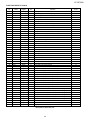
FUNCTION TABLE OF IC201A
Terminal
No.
Terminal
Name
Analog/
Digital
I/O
Function
Equivalent
circuit
1
AVDDI
Analog
-
Analog power terminal for RF system
-
2
AC
Analog
I
A+C voltage input terminal from pickup
1
3
BD
Analog
I
B+D voltage input terminal from pickup
1
4
VBIAS
Analog
O
Bias level (VDD/2) output terminal
2
5
E
Analog
I
E voltage input terminal from pickup
1
6
F
Analog
I
F voltage input terminal from pickup
1
7
AGND1
Analog
-
GND terminal for RF system analog
-
8
FEN
Analog
I
Focus error to amplifier feedback input terminal
3
9
FEO
Analog
O
Focus error output terminal
3
10
PKC
Analog
O
RF signal peak detector capacity connecting terminal
4
11
BTC
Analog
O
RF signal bottom detector capacity connecting terminal
5
12
PD
Analog
I
APC photo detector input terminal
6
13
LD
Analog
O
APC laser drive output terminal
6
14
ASY
Analog
I
C-fitted terminal for comparator slice for asymmetric correction
7
15
AVDD2
Analog
-
Servo system analog power terminal
-
16
PCO
Analog
O
PLL PCO output terminal
8
8
17
FCO
Analog
O
PLL FCO-DAC output
18
AGND2
Analog
-
Servo system analog GND terminal
-
19
FDOUT
Analog
O
Focus drive output
9
20
JUMPO
Analog
O
Tracking jump pluse output terminal
9
21
TDOUT
Analog
O
Tracking drive output terminal
9
22
SDIN
Analog
I
Sled signal input terminal
10
23
SDOUT
Analog
O
sled drive output terminal
9
24
CLVOUT
Analog
O
CLV drive output terminal
9
25
ADC0
Analog
I
Analog data input / 1-bit input terminal
11
26
ADC1
Analog
I
Analog data input / 1-bit input terminal
11
27
CLK88
Digital
O
Clock output terminal for driver IC
12
28
LON
Digital
O
Laser ON control output terminal
12
29
P20/COM0
Digital
I/O
4-bit parallel output port / LCD common output terminal
11
30
P21/COM1
Digital
I/O
4-bit parallel output port / LCD common output terminal
11
31
P22/COM2
Digital
I/O
4-bit parallel output port / LCD common output terminal
11
32
P23/COM3
Digital
I/O
4-bit parallel output port / LCD common output terminal
11
33
SEG0
Digital
O
4-bit parallel output port / LCD segment output terminal
11
34
SEG1
Digital
O
4-bit parallel output port / LCD segment output terminal
11
35
SEG2
Digital
O
4-bit parallel output port / LCD segment output terminal
11
36
SEG3
Digital
O
4-bit parallel output port / LCD segment output terminal
11
37
SEG4
Digital
O
2-bit parallel output port / LCD segment output terminal
11
38
SEG5
Digital
O
2-bit parallel output port / LCD segment output terminal
11
39
SEG6
Digital
O
1-bit output port / LCD segment output terminal
11
40
P00
Digital
I/O
4-bit parallel inout orontput terminal (Open Drain output type)
11
41
P01
Digital
I/O
4-bit parallel inout orontput terminal (Open Drain output type)
11
42
P02
Digital
I/O
4-bit parallel inout orontput terminal (Open Drain output type)
11
43
P03
Digital
I/O
4-bit parallel inout orontput terminal (Open Drain output type)
11
44
P10
Digital
I/O
2-bit parallel inout orontput terminal (Open Drain output type)
11
45
P11
Digital
I/O
2-bit parallel inout orontput terminal (Open Drain output type)
11
46
PWC/W
Digital
I
Pulse input / General 1-bit input terminal
11
47
RESETB
Digital
I
System reset terminal ("L"
13
48
DVDD
Digital
-
Digital power terminal
reset condition)
Description of Terminals (1/2)
29
-
QT-CD700W
Terminal
No.
Terminal
Name
Analog/
Digital
I/O
Function
Equivalent
circuit
49
XI
Digital
I
X'tal 16.9344MHz connecting (input) terminal
14
50
XO
Digital
-
X'tal 16.9344MHz connecting terminal
14
51
DGND
Digital
-
Digital GND terminal
52
AVDD3
Digital
O
Audio system analog power terminal
53
LDACO
Analog
O
Audio Lch output terminal
15
54
VCDAC
Analog
O
Audio system reference voltage output terminal
15
55
RDACO
Analog
O
Audio Rch output terminal
15
56
AGND3
Analog
-
Audio system analog GND terminal
57
RFRORFM
Analog
O
C-fitted terminal for RFRP/#2 output terminal for RF test monitor
16
58
TZCRFM
Analog
O
C-fitted terminal for TZX/ #1 output terminal for RF test monitor
17
18
-
-
59
SC
Analog
I
Scratch depth adjust resistor connecting terminal
60
TEI
Analog
O
Tracking error output terminal
3
61
TEN
Analog
I
Tracking erro to amplifier feedback input terminal
3
62
CAGC
Analog
I
C-fitted terminal for constant at RFAGC
19
63
RFI
Analog
I
RF output capacity combined data re-input terminal
20
64
EQO
Analog
O
After-RF-equalizer output terminal
20
Description of Terminals (2/2)
30
QT-CD700W
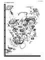
PARTS GUIDE
PORTABLE CD STEREO SYSTEM
MODEL
QT-CD700W
CONTENTS
"HOW TO ORDER REPLACEMENT PARTS"
To have your order filled promptly and correctly, please furnish the
following information.
1. MODEL NUMBER
2. REF. No.
3. PART NO.
4. DESCRIPTION
For U.S.A. only
Contact your nearest SHARP Parts Distributor to order.
For location of SHARP Parts Distributor,
Please call Toll-Free;
1-800-BE-SHARP
MARK: SPARE PARTS-DELIVERY SECTION
Explanation of capacitors/resistors parts codes
Capacitors
Resistors
VCC ....................... Ceramic type
VCK ........................ Ceramic type
VCT ........................ Semiconductor type
VC
MF ............... Cylindrical type (without lead wire)
VC
MN ............... Cylindrical type (without lead wire)
VC TV ................ Square type (without lead wire)
VC TQ ............... Square type (without lead wire)
VC CY ............... Square type (without lead wire)
VC CZ ............... Square type (without lead wire)
J .. The 13th character represents capacity difference.
VC
("J" ±5%, "K" ±10%, "M" ±20%, "N" ±30%,
"C" ±0.25 pF, "D" ±0.5 pF, "Z" +80-20%.)
VRD ....................... Carbon-film type
VRS ........................ Carbon-film type
VRN ....................... Metal-film type
VR
MF ............... Cylindrical type (without lead wire)
VR
MN ............... Cylindrical type (without lead wire)
VR TV ................ Square type (without lead wire)
VR TQ ............... Square type (without lead wire)
VR CY ............... Square type (without lead wire)
VR CZ ............... Square type (without lead wire)
J .. The 13th character represents error.
VR
("J" ±5%, "F" ±1%, "D" ±0.5%.)
● ●
● ●
● ●
● ●
● ●
● ●
● ● ● ● ● ● ● ● ● ●
If there are no indications for the electrolytic capacitors, error is ±20%.
● ●
● ●
● ●
● ●
● ●
● ●
● ● ● ● ● ● ● ● ● ●
If there are no indications for other parts, the resistors are ±5%
carbon-film type.
Parts marked with " " are important for maintaining the safety of the set. Be sure to replace these
parts with specified ones for maintaining the safety and performance of the set.
SHARP CORPORATION
This document has been published to be used
for after sales service only.
The contents are subject to change without notice.
QT-CD700W
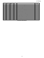
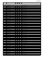
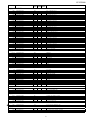
NO.
PARTS CODE
PRICE NEW PART
RANK MARK RANK
DESCRIPTION
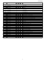
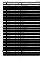
[1] CAPACITORS
C1
C3
C4
C5
C6
C7
C8
C54
C71
C100,C200
C101,C103
C101A
C102,C106
C102A
C103A
C104
C105
C105A,C107
C108A
C109,C110
C109A
C110A
C111A
C112
C113
C114
C115,C117
C118
C120
C121,C122
C121A
C122A
C123,C108
C123A
C124,C125
C124A
C125A
C126,C131
C126A
C127,C129
C127A,2,
C128
C128A
C130,C132
C130A
C131A,C132A
C133
C133A
C134
C134A
C135
C135A
C136
C137A
C138
C138A
C141,C142
C143
C201
C202-C205
C301A-C304A
C302,C301
C303
C304
C305
C305A,C306A
C306,C307
C309
C312
C314
C315
C316
C317,C321
C318
C320
C322
C323
C324,C327
C328,C325
C401
C402,C404
C403
C501
C502
C502A
92L27500105070
92L27100203008
92L27500107020
92L27500227040
92L27500107040
92L27500107050
92L27100203008
92L27500477020
92L27100104106
92L27100562106
92L27100203008
92L27500107020
92L27500107020
92L27500477020
92L27100103106
92L27500107020
92L27100203008
92L27100104106
92L27500107020
92L27600222220
92L27100471106
92L27100104106
92L27100104106
92L27100121106
92L27500335070
92L27500224070
92L27100104106
92L27500106040
92L27500105070
92L27500476020
92L27100222106
92L27100101106
92L27600333220
92L27100151106
92L27500105070
92L27500105070
92L27100682106
92L27500476020
92L27500105070
92L27600182220
92L27500107020
92L27500107020
92L27100104106
92L27500105070
92L27100104106
92L27100150106
92L27600182220
92L27500107020
92L27600223220
92L27100104106
92L27600562220
92L27100104106
92L27500227040
92L27100104106
92L27100104106
92L27100104106
92L27100201506
92L27100181508
92L27500228050
92L27000203630
92L27100561106
92L27100250506
92L27500105070
92L27100030506
92L27500104070
92L27500475070
92L27500105070
92L27100103106
92L27100103106
92L27100301106
92L27500104070
92L27700131200
92L27100203008
92L27500107020
92L27100104106
92L27500475070
92L27100104106
92L27100203008
92L27100330506
92L27600104220
92L27100471106
92L27600104220
92L27100102106
92L27500105070
92L27100104106
AB
AC
AB
AB
AB
AB
AC
AF
AH
AB
AC
AB
AB
AF
AC
AB
AC
AH
AB
AB
AC
AH
AH
AB
AB
AB
AH
AD
AB
AB
AB
AB
AC
AB
AB
AB
AB
AB
AB
AB
AB
AB
AH
AB
AH
AB
AB
AB
AB
AH
AB
AH
AB
AH
AH
AH
AB
AB
AF
AB
AC
AB
AB
AB
AB
AC
AB
AC
AC
AB
AB
AD
AC
AB
AH
AC
AH
AC
AB
AC
AC
AC
AB
AB
AH
1UF +/-20% 50V 5 X 11
0.02uF 0805 +80% -20% 50V
100UF +/-20% 10V 5 X 11
220UF ±20% 16V 6.3 X 11
100UF ±20% 16V 5 X 11
100UF +/-20% 25V 6.3 X 11
0.02uF 0805 +80% -20% 50V
470UF +/-20% 10V 8 X 12
0.1UF 0603 +/-10% 25V
5600PF +/-10% 0603 50V
0.02uF 0805 +80% -20% 50V
100UF +/-20% 10V 5 X 11
100UF +/-20% 10V 5 X 11
470UF +/-20% 10V 8 X 12
0.01UF 0603 +/-10% 50V/25V
100UF +/-20% 10V 5 X 11
0.02uF 0805 +80% -20% 50V
0.1UF 0603 +/-10% 25V
100UF +/-20% 10V 5 X 11
0.0022UF ± 10% 100V
470PF 0603 +/-10% 50V
0.1UF 0603 +/-10% 25V
0.1UF 0603 +/-10% 25V
120P 0603 +/-10% 50V
3.3UF ±20% 50V 5 X 11
0.22UF ±20% 50V 5 X 11
0.1UF 0603 +/-10% 25V
10UF ±20% 16V 5 x 11
1UF +/-20% 50V 5 X 11
47UF +/-20% 10V 5 X 11
0.0022UF 0603 +/-10% 50V/25V
100PF +/-10% 0603 50V
0.033UF 100V +/-10%
150P +/-10% 0603
1UF +/-20% 50V 5 X 11
1UF +/-20% 50V 5 X 11
0.0068UF 0603 +/-10% 50V
47UF +/-20% 10V 5 X 11
1UF +/-20% 50V 5 X 11
0.0018UF +/-10% 100V
100UF +/-20% 10V 5 X 11
100UF +/-20% 10V 5 X 11
0.1UF 0603 +/-10% 25V
1UF +/-20% 50V 5 X 11
0.1UF 0603 +/-10% 25V
15P 0603 +/-10% 50V
0.0018UF +/-10% 100V
100UF +/-20% 10V 5 X 11
0.022UF +/- 20% 100V
0.1UF 0603 +/-10% 25V
0.0056UF +/-10% 100V
0.1UF 0603 +/-10% 25V
220UF ±20% 16V 6.3 X 11
0.1UF 0603 +/-10% 25V
0.1UF 0603 +/-10% 25V
0.1UF 0603 +/-10% 25V
200P +/-5% 0603
180P +/-5% 0805
2200UF ±20% 25V 13 X 25
0.02UF+80%-20%50V 5.5x2.5
560PF 0603 +/-10% 50V
25PF 0603 +/-5% 50V
1UF +/-20% 50V 5 X 11
3PF 0603 +/-5% 50V
0.1UF +/-20% 50V 5 X 11
4.7UF +/-20% 50V 5 X 11
1UF +/-20% 50V 5 X 11
0.01UF 0603 +/-10% 50V/25V
0.01UF 0603 +/-10% 50V/25V
300PF +/-10% 50V
0.1UF +/-20% 50V 5 X 11
130PF +/-5% 50V
0.02uF 0805 +80% -20% 50V
100UF +/-20% 10V 5 X 11
0.1UF 0603 +/-10% 25V
4.7UF +/-20% 50V 5 X 11
0.1UF 0603 +/-10% 25V
0.02uF 0805 +80% -20% 50V
33PF 0603 +/-5%
0.1UF +/-10% 100V
470PF 0603 +/-10% 50V
0.1UF +/-10% 100V
0.001UF 0603 +/-10% 50V
1UF +/-20% 50V 5 X 11
0.1UF 0603 +/-10% 25V
1
QT-CD700W
NO.
PARTS CODE
PRICE NEW PART
RANK MARK RANK
DESCRIPTION
[1] CAPACITORS
C503
C503A
C504
C505
C505A
C506
C507
C508
C508A
C509
C510
C511,C512
C513,C514
C515
C516
C518,C519
C520,C521
C522
C524
C525
C526
C601A
C602
C603
C604
C605
C606
C607
C608
C717
CB1,CB2
CC5
92L27500105070
92L27100104106
92L27100102106
92L27500476040
92L27100104106
92L27500107040
92L27500106040
92L27500107040
92L27100104106
92L27500476040
92L27500107040
92L27600104220
92L27500477020
92L27500106040
92L27500107040
92L27100203008
92L27500105070
92L27500107020
92L27500108050
92L27500106040
92L27500225070
92L27500477020
92L27100104106
92L27500477020
92L27100104106
92L27500476040
92L27500227020
92L27100104106
92L27500475070
92L27600103220
92L27540226040
92L27600103220
AB
AH
AB
AC
AH
AB
AD
AB
AH
AC
AB
AC
AF
AD
AB
AC
AB
AB
AE
AD
AB
AF
AH
AF
AH
AC
AC
AH
AC
AB
AC
AB
1UF +/-20% 50V 5 X 11
0.1UF 0603 +/-10% 25V
0.001UF 0603 +/-10% 50V
47UF ±20% 16V 5 X 11
0.1UF 0603 +/-10% 25V
100UF ±20% 16V 5 X 11
10UF ±20% 16V 5 x 11
100UF ±20% 16V 5 X 11
0.1UF 0603 +/-10% 25V
47UF ±20% 16V 5 X 11
100UF ±20% 16V 5 X 11
0.1UF +/-10% 100V
470UF +/-20% 10V 8 X 12
10UF ±20% 16V 5 x 11
100UF ±20% 16V 5 X 11
0.02uF 0805 +80% -20% 50V
1UF +/-20% 50V 5 X 11
100UF +/-20% 10V 5 X 11
1000UF +/- 20% 25V 10X 20
10UF ±20% 16V 5 x 11
2.2UF +/-20% 50V 5 X 11
470UF +/-20% 10V 8 X 12
0.1UF 0603 +/-10% 25V
470UF +/-20% 10V 8 X 12
0.1UF 0603 +/-10% 25V
47UF ±20% 16V 5 X 11
220UF +/-20% 10V 6.3 X 11
0.1UF 0603 +/-10% 25V
4.7UF +/-20% 50V 5 X 11
0.01UF +/-10% 100V
22UF +/-20% 16V 5x11mm "NP"
0.01UF +/-10% 100V
AB
AB
AD
AC
AD
AB
AE
AB
AC
AC
AE
AB
PSS9014C
PSS9014C
LOW SIGNAL 2SA933ASR
ZQT8050D
DTA124ESA
PSS9014C
B772
PSS9014C
9015C EBC
8050C
2SB1237Q
PSS9014C
AC
AB
AB
AB
AB
AB
AB
AB
AB
AC
AB
AC
AB
4.3V 1/2W
IN-4148
IN-4001 RECTIFIER
IN-4001 RECTIFIER
IN-4001 RECTIFIER
IN-4148
IN-4148
IN-4001 RECTIFIER
IN-4148
5.1V 1/2W ( A )
IN-4148
6.8V 1/2W
IN-4148
AC
AC
AD
AG
SFU455B MURATA
CDA 10.7MHz RED TDK
CDA 10.7 MHz RED
88-108MHz GFMB3 SE
AF
AD
AC
AB
AB
15uHX0.5 TC-150M-0.5A-5032
16uHx2 TC-160M-1065
10uH
5.0 X 2.5T 0.8mm CW
4.5 X 3.5 T 0.8mm CW
92L29547041100
AX
EI-41 119V/230V XDB4126-320
92L30470125110
92L30400020511
92L29607222140
AE
AD
AD
10 X 10mm PL10-04 AC BIAS
10 X 10mm ML10-37B RED AM OSC
10X10mm YELLOW 460KHz TF10-22 AM IF
[2] TRANSISTORS
Q1-Q7
Q101,Q102
Q101A
Q103
Q301
Q406,Q407
Q408
Q501,Q502
Q503
Q504
Q601
Q602
92L2830901403A
92L2830901403A
92L28300933000
92L28318050000
92L28300124100
92L2830901403A
92L28300772010
92L2830901403A
92L28309015030
92L28308050030
92L28301237000
92L2830901403A
[3] DIODES
D1
D2-D6
D7,D8
D9
D9A
D10
D102,D103
D202-D204
D301,D302
D402
D403,D503
D504
D505,D506
92L28200430010
92L28104148000
92L28104001300
92L28104001300
92L28104001300
92L28104148000
92L28104148000
92L28104001300
92L28104148000
92L28200510010
92L28104148000
92L28200680010
92L28104148000
[4] FILTERS
CF2
CF3
CF303
U1
92L27204553230
92L27201075132
92L27201075122
92L27310205031
[5] COILS
L1-L3
L5
L101A,L202
L301
L303
92L29435150000
92L29435160000
92L29430100000
92L30050021080
92L30045031080
[6] TRANSFORMERS
!
T501
[7] IFT
T101
T301
T303
2
QT-CD700W
NO.
PARTS CODE
PRICE NEW PART
RANK MARK RANK
DESCRIPTION
[8] INTEGRATED CIRCUITS
IC1
IC3
IC101
IC201A
IC601
92L28402111001
92L28408227020
92L28403308000
92L28424530000
92L28405826000
AN
AK
AH
BA
AM
TA2111N HaiWei
YD8227 HDIP12
BA3308
BU24530-9A
BA5826FP
AE
16.93MHz MIDAS
AA
AA
AE
AE
AC
AF
AB
AC
AB
AE
AC
AB
AB
AD
AB
AE
AB
AB
AD
AB
AA
AC
AG
AC
AE
AK
AC
AC
AF
AG
AG
AV
AV
AE
AE
AG
AE
AE
AE
AF
AG
#26L=180mmBLACK
#26L=180mm RED
16 PIN WAFER, P=1.0mm
6 PIN HOUSING WIRE, #30 UL1007 110mm 1H
10 PIN WAFER, P=2.0 PH-10P
10 PIN GREY WIRE, L=160mm P=2.0mm 1H
2 PIN WAFER, P=2mm PH-2A YELLOW
UL 1007 #26 L=120mm P=2.0mm
4 PIN WAFER, P=2.0mm PH-4A BLACK
#26 L=(220×2+380×2) UL 1007 P=2.0mm
2 PIN HOUSING WIRE, UL1007#26 180mm 1HP=2.0mm
2 PIN WAFER, P=2mm PH-2A BLACK
5 PIN WAFER, P=2mm S2M-5W SHS
5 PIN HOUSING WIRE, UL1007 #26 150mm P=2
2 PIN WAFER, PITCH 2.5mm XH-2A GREEN
#28 L=253mm
4 PIN WAFER, P=2.5mm XH-4A RED
4 PIN WAFER, PITCH 2.5mm C-XH-4W
2 PIN HOUSING WIRE, #22 UL1007 220mm P=2.5mm
2PIN WAFER, PITCH 2.5mm S11-2W
2 PIN WAFER, P=2mm PH-2A RED
2 PIN HOUSING WIRE, UL1007#26 180mm 1HP=2.0mm
12 PIN HOUSING WIRE, #26 L=150mm P=2.5mm 1H
12 PIN WAFER, P=2.5mm SNR
1.25A 250V 5X20mm W/"CCEE"
SDT-DA672-RP-1
3mm GREEN
3mm RED DR-304
9.7 x 6.7mm CZN15E-623 DONGRI
SLIDE SWITCH, 3.5MM DAIICHI EJS-5-0735G-01
AC INPUT SOCKET, VDE PSE27
SPEAKER 77mm 8 OHM 3W YD78-82-3W-8
SPEAKER 77mm 8 OHM 3W YD78-82-3W-8
PIEZO φ18mm
PIEZO φ18mm
SLIDE SWITCH, 2P3T SS4304RG120 TRAVEL:3mm
PUSH SWITCH, 6P2T PS6205N
SLIDE SWITCH, SKG-12F04-G9-NA TRAVEL:3mm
SLIDE SWITCH, 2P3T SS2356PG140 TRAVEL:3mm
VOLTAGE SELECTOR, 1P2T SSV-12-8700S AC250V VDE
1P2T DLS-02-1
[9] VIBRATOR
X101
92L23400209000
[10] OTHER CIRCUITRY PARTS
!
!
!
!
B "- "
BATT "+"
CN1
CN2
CN4A
CN4A
CN5
CN5A
CN6
CN6A
CN7A
CN7B
CN9A
CN9A
CN14
CN14A
CN15
CN103
CN501
CN501B
CN502A
CN502B
CN503A
CN503B
F101
LCD1
LED1
LED2
MIC
PHONE1
SO651
SPK101
SPK102
SPK403
SPK404
SW1
SW2
SW3
SW4
SW651
SW810
92L33326181010
92L33326181012
92L33616100100
92L33517110060
92L33610210020
92L33500161110
92L33602210104
92L33526121142
92L33604210109
92L33526381194
92L33526181192
92L33602210109
92L33605210100
92L33526150050
92L33625010025
92L33428253152
92L33625010412
92L33625010420
92L33522221102
92L33625010021
92L33602210102
92L33526181122
92L33526151120
92L33612310000
92L32305125251
92L34207040000
92L24609060131
92L24600050130
92L28700100021
92L26400125551
92L25800125000
92L30308303077
92L30308303077
92L29300180000
92L29300180000
92L29143120100
92L29162000002
92L29112090230
92L29123140100
92L29112150100
92L29103600012
3
QT-CD700W
[11] CABINET PARTS
S03
29
A
28
31
27
S10
24
32
33
34
B
30
25
23
35
26
S06
S08
21
26
39
S14
C
S12
36
41
22
17
42
40
38
D
S09 PCB-A2
47 49
51
46 48 50
S05
52
S05
57
53
45
S06
S06
S06
43
S01
E
S02
17
S13
19
14
9
18
S06
54
S07
10
44
S11
PCB-A4
55
16
37
13 15
S04
56
PCB-A3
8
S15
12
7
11
6
S06
8
PCB-A1
9
59
F
S07
10
20
58
58
3
G
2
4
5
S06
1
H
Note: Only the unit and consumale parts are supplied as parts supply for the Tape mechanism.
1
2
3
4
4
5
6
QT-CD700W
NO.
PARTS CODE
PRICE NEW PART
RANK MARK RANK
DESCRIPTION
[11] CABINET PARTS
1
2
3
4
5
6
7
8
9
10
11
12
13
14
15
16
17
18
19
20
21
22
23
24
25
26
27
28
29
30
31
32
33
34
35
36
37
38
39
40
41
42
43
44
45
46
47
48
49
50
51
52
53
54
55
56
57
58
59
S01
S02
S03
S04
S05
S06
S07
S08
S09
S10
S11
S12
S13
S14
S15
92L90007041300
92L62618070010
92L54108070000
92L62629060010
92L80439060010
92L90007041000
92L80237040011
92L62678070010
92L30308303077
92L62688070010
92L34207040000
92L62637040010
92L22507041000
92L54033133000
92L62657040010
92L15107041010
92L80257040013
92L62647040010
92L62708070010
92L13812030110
92L29547041100
92L62007040101
92L54027041010
92L54017041010
92L54003406010
92L54007041010
92L90007041200
92L16407040010
92L30209040001
92L63008070022
92L60107040013
92L60709080010
92L29009020011
92L62678028010
92L47707600050
92L62608070010
92L80227040010
92L62617040010
92L54118070000
92L90007041100
92L80247040011
92L62627040010
92L60739080020
92L1380902020C
92L1380902010C
92L80138070019
92L80158070019
92L80148070019
92L80118070019
92L80128070019
92L80108070019
92L5600904010B
92L25800125000
92L14100150000
92L29112150100
92L15117041010
92L15607041010
92L29300180000
92L1380100K000
92L13020030412
92L13026050112
92L13030080012
92L13120060011
92L13130080027
92L13130100011
92L13130100031
92L13130140011
92L13130200027
92L13126080142
92L13126120021
92L13130080011
92L13130120011
92L13126100012
92L13030080112
AQ
AF
AC
AC
AB
BB
AD
AD
AV
AD
AK
AD
BA
AC
AB
AE
AD
AD
AC
AD
AX
AX
AE
AE
AC
AG
AM
AE
AM
AC
AP
AC
AD
AD
AD
AQ
AD
AD
AD
AM
AC
AD
AD
AD
AD
AC
AC
AC
AC
AC
AC
BF
AG
AC
AF
AE
AE
AE
AC
AA
AA
AA
AB
AB
AA
AB
AB
AC
AA
AC
AA
AA
AA
AA
CASSETTE DOOR ASSEMBLY
CASSETTE DOOR BRACKET
CASSETTE DOOR SPRING
DAMPER GEAR BRACKET
DAMPER GEAR
FRONT CABINET ASSEMBLY (Without Mic Cushion)
VOLUME KNOB
SPEAKER CLIP (L)
SPEAKER (SPK101,SPK102)
SPEAKER CLIP (R)
LCD DISPLAY
LCD BRACKET
TAPE MECHANISM
RECORD SPRING PLATE
VOLUME KNOB BRACKET
HEAT SINK ,
TUNING KNOB
TUNING BRACKET
POINTER
RUBBER FOOT
POWER TRANSFORMER (T501)
BACK CABINET
SPRING BATTERY +/SPRING BATTERY ''-''
SPRING BATTERY ''+''
SPRING BATTERY ''+/-''
BATTERY DOOR ASSY
ANT. SOLDERING LUG
ROD ANTENNA
HANDLE
CD DOOR
MAGNET COVER
CD MAGNET
MAGNET BRACKET
FELT
CD DOOR BRACKET
FUNCTION KNOB
FUNCTION KNOB BRACKET
CD DOOR SPRING
DOOR LATCH SWITCH ASSY
BAND KNOB
BAND KNOB BRACKET
DUST COVER
RUBBER CUSHION
RUBBER CUSHION
PAUSE KNOB
STOP KNOB
F.FWD KNOB
REWIND KNOB
PLAY KNOB
RECORD KNOB
CD MECHANISM
AC INPUT SOCKET (SO651)
COVER VOLTAGE SELECTOR
VOLTAGE SELECTOR (SW651)
HEAT SINK
METAL PLATE
PIEZO (SPK403,SPK404)
MIC CUSHION
MACHINE SCREW, ∅2 X 3PH
MACHINE SCREW, ∅2.6 X 5PH
MACHINE SCREW, ∅3 X 8PH
TAPPING SCREW, ∅2 X 6PA
TAPPING SCREW, ∅3 X 8PWH
TAPPING SCREW, ∅3 X 10PA
TAPPING SCREW, ∅3 X 10BA
TAPPING SCREW, ∅3 X 14PA
TAPPING SCREW, ∅3 X 20PWH
TAPPING SCREW, ∅2.6 X 8KH
TAPPING SCREW, ∅2.6 X 12PWA
TAPPING SCREW, ∅3 X 8PA
TAPPING SCREW, ∅3 X 12PA
TAPPING SCREW, ∅2.6 X 10PH
MACHINE SCREW, M3 X 8PH (BLACK)
[12] ACCESSORIES / PACKING PARTS
!
!
1
2
3
4
5
6
7
8
92L24801800222
92L2680212512A
92L19207041010
92L20107041010
92L20307041020
92L20317041010
92L20607041010
92L13508070010
AY
AN
AV
AG
AD
AD
AK
AH
AC POWER SUPPLY CORD (round pin)
AC PLUG ADAPTOR (Flat)
PACKING CASE
OPERATION MANUAL (ENGLISH /SPANISH)
SPECIFICATION LABEL (LAG)
CAUTION LABEL
CARTON BOX
POLYFOAM (L)
5
QT-CD700W
NO.
PARTS CODE
PRICE NEW PART
RANK MARK RANK
DESCRIPTION
[12] ACCESSORIES / PACKING PARTS
9
10
11
92L13508070020
92L20707041010
92L19407041010
AH
AC
AC
POLYFOAM (R)
PICK UP PROTECTIVE CARD
POLYBAG (SET)
[13] P.C.B. ASSEMBLY (Not Replacement Item)
PCB-A1
PCB-A3
PCB-A4
PCB-B2
92L23707041S00
92L23707041S10
92L23707041S30
92L23707041S20
MAIN PCB ASS’Y
CD CONTROL PCB ASS’Y
POWER PCB ASS’Y
R/D PCB ASS’Y
6
QT-CD700W
COPYRIGHT
©
2004 BY SHARP CORPORATION
ALL RIGHTS RESERVED.
No part of this publication may be reproduced,
stored in a retrieval system, or transmitted in
any from or by any means, electronic, mechanical,
photocopying, recording, or otherwise, without
prior written permission of the publisher.
7
SHARP CORPORATION
Printed in Malaysia