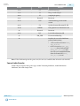
1
Altera High-Definition Multimedia
Interface IP Core User Guide
Subscribe
Send Feedback
UG-HDMI
2015.05.04
101 Innovation Drive
San Jose, CA 95134
www.altera.com
TOC-2
Contents
HDMI Quick Reference.......................................................................................1-1
HDMI Overview.................................................................................................. 2-1
Resource Utilization.................................................................................................................................... 2-4
HDMI Getting Started.........................................................................................3-1
Installing and Licensing IP Cores.............................................................................................................. 3-1
OpenCore Plus IP Evaluation.................................................................................................................... 3-2
Specifying IP Core Parameters and Options............................................................................................3-2
HDMI Source.......................................................................................................4-1
Source Functional Description.................................................................................................................. 4-1
Source TMDS/TERC4 Encoder..................................................................................................... 4-2
Source Video Resampler................................................................................................................. 4-2
Source Window of Opportunity Generator................................................................................. 4-3
Source Auxiliary Packet Encoder...................................................................................................4-4
Source Auxiliary Packet Generators..............................................................................................4-5
Source Auxiliary Data Path Multiplexers..................................................................................... 4-5
Source Auxiliary Control Port....................................................................................................... 4-5
Source Audio Encoder.....................................................................................................................4-9
Source Parameters..................................................................................................................................... 4-10
Source Interfaces........................................................................................................................................ 4-11
Source Clock Tree......................................................................................................................................4-15
HDMI Sink...........................................................................................................5-1
Sink Functional Description.......................................................................................................................5-1
Sink Channel Word Alignment and Deskew...............................................................................5-2
Sink TMDS/TERC4 Decoder......................................................................................................... 5-3
Sink Video Resampler..................................................................................................................... 5-4
Sink Auxiliary Decoder................................................................................................................... 5-4
Sink Auxiliary Packet Capture....................................................................................................... 5-5
Sink Auxiliary Data Port................................................................................................................. 5-8
Sink Audio Decoding.................................................................................................................... 5-11
Sink Parameters..........................................................................................................................................5-11
Sink Interfaces............................................................................................................................................ 5-12
Avalon-MM SCDC Management Interface............................................................................... 5-17
Sink Clock Tree.......................................................................................................................................... 5-17
HDMI Hardware Demonstration....................................................................... 6-1
Altera Corporation
TOC-3
HDMI Hardware Demonstration Requirements.................................................................................... 6-2
Transceiver and Clocking Configuration................................................................................................. 6-6
Software Process Flow............................................................................................................................... 6-10
Demonstration Walkthrough...................................................................................................................6-12
Set Up the Hardware..................................................................................................................... 6-12
Copy the Design Files....................................................................................................................6-12
Build the Design.............................................................................................................................6-12
View the Results............................................................................................................................. 6-13
HDMI Simulation Example................................................................................ 7-1
Simulation Walkthrough............................................................................................................................ 7-2
Additional Information for High-Definition Multimedia Interface User
Guide............................................................................................................... A-1
Document Revision History for HDMI User Guide..............................................................................A-1
Altera Corporation
1
HDMI Quick Reference
2015.05.04
UG-HDMI
Send Feedback
Subscribe
The Altera High-Definition Multimedia Interface (HDMI) IP core provides support for next-generation
video display interface technology.
Release Information
Version
15.0
Release
May 2015
Ordering Code
IP-HDMI
Product ID
0121
Vendor ID
6AF7
Core Features
• Conforms to the High-Definition Multimedia
Interface (HDMI) specification version 2.0
• Supports transmitter and receiver on a single
device transceiver quad
• Supports pixel frequency up to 594 MHz
• Supports RGB and YCbCr color modes
• Accepts standard H-SYNC, V-SYNC, data enable,
RGB video format, and YCbCr video format
• Supports 2-channel audio
• Supports 1, 2, or 4 symbols per clock
Typical Application
• Interfaces within a PC and monitor
• External display connections, including interfaces
between a PC and monitor or projector, between
a PC and TV, or between a device such as a DVD
player and TV display
Device Family
Supports Arria 10 (preliminary), Arria V, and Stratix
V FPGA devices
Design Tools
• Quartus II software for IP design instantiation
and compilation
• TimeQuest Timing Analyzer in the Quartus II
software for timing analysis
• ModelSim-Altera/SE software for design
simulation
IP Core Information
© 2015 Altera Corporation. All rights reserved. ALTERA, ARRIA, CYCLONE, ENPIRION, MAX, MEGACORE, NIOS, QUARTUS and STRATIX words and logos are
trademarks of Altera Corporation and registered in the U.S. Patent and Trademark Office and in other countries. All other words and logos identified as
trademarks or service marks are the property of their respective holders as described at www.altera.com/common/legal.html. Altera warrants performance
of its semiconductor products to current specifications in accordance with Altera's standard warranty, but reserves the right to make changes to any
products and services at any time without notice. Altera assumes no responsibility or liability arising out of the application or use of any information,
product, or service described herein except as expressly agreed to in writing by Altera. Altera customers are advised to obtain the latest version of device
specifications before relying on any published information and before placing orders for products or services.
www.altera.com
101 Innovation Drive, San Jose, CA 95134
ISO
9001:2008
Registered
2
HDMI Overview
2015.05.04
UG-HDMI
Subscribe
Send Feedback
The Altera High-Definition Multimedia Interface (HDMI) IP core provides support for next generation
video display interface technology.
The HDMI standard specifies a digital communications interface for use in both internal and external
connections:
• Internal connections—interface within a PC and monitor
• External display connections—interface between a PC and monitor or projector, between a PC and
TV, or between a device such a DVD player and TV display.
The HDMI system architecture consists of sinks and sources. A device may have one or more HDMI
inputs and outputs.
The HDMI cable and connectors carry four differential pairs that make up the Transition Minimized
Differential Signaling (TMDS) data and clock channels. You can use these channels to carry video, audio,
and auxiliary data.
The HDMI also carries a Video Electronics Standards Association (VESA) Display Data Channel (DDC)
and Status and Control Data Channel (SCDC). The DDC configures and exchanges status between a
single source and a single sink. The source uses the DDC to read the sink's Enhanced Extended Display
Identification Data (E-EDID) to discover the sink's configuration and capabilities. The SCDC supports
the sink's read requests.
The optional Consumer Electronics Control (CEC) protocol provides high-level control functions
between various audio visual products in your environment.
The optional HDMI Ethernet and Audio Return Channel (HEAC) provides Ethernet compatible data
networking between connected devices and an audio return channel in the opposite direction of TMDS.
The HEAC also uses Hot-Plug Detect (HPD) line for signal transmission.
© 2015 Altera Corporation. All rights reserved. ALTERA, ARRIA, CYCLONE, ENPIRION, MAX, MEGACORE, NIOS, QUARTUS and STRATIX words and logos are
trademarks of Altera Corporation and registered in the U.S. Patent and Trademark Office and in other countries. All other words and logos identified as
trademarks or service marks are the property of their respective holders as described at www.altera.com/common/legal.html. Altera warrants performance
of its semiconductor products to current specifications in accordance with Altera's standard warranty, but reserves the right to make changes to any
products and services at any time without notice. Altera assumes no responsibility or liability arising out of the application or use of any information,
product, or service described herein except as expressly agreed to in writing by Altera. Altera customers are advised to obtain the latest version of device
specifications before relying on any published information and before placing orders for products or services.
www.altera.com
101 Innovation Drive, San Jose, CA 95134
ISO
9001:2008
Registered
2-2
UG-HDMI
2015.05.04
HDMI Overview
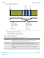
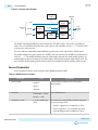
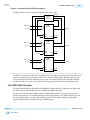
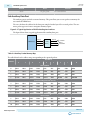
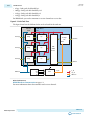
Figure 2-1: Altera HDMI Block Diagram
The figure below illustrates the blocks in the Altera HDMI IP core.
HDMI IP Core
TDMS Channel 0
Video
Video
TDMS Channel 1
Audio
HDMI
Transmitter
TDMS Channel 2
Audio
HDMI
Receiver
TDMS Clock Channel
Control/Status
Control/Status
Status and Control Data Channel (SCDC)
Display Data Channel (DDC)
CEC
HEAC
Detect
CEC Line
Utility Line
HPD Line
EDID ROM
CEC
HEAC
High/Low
Based on TMDS encoding, the HDMI protocol allows the transmission of both audio and video data
between source and sink devices.
An HDMI interface consists of three color channels accompanied by a single clock channel. You can use
each color line to transfer both individual RGB colors and auxiliary data.
The receiver uses the TMDS clock as a frequency reference for data recovery on the three TMDS data
channels. This clock typically runs at the video pixel rate.
TMDS encoding is based on an 8-bit to 10-bit algorithm. This protocol attempts to minimize data channel
transmission and yet maintain sufficient bandwidth so that a sink device can lock reliably to the data
stream.
Altera Corporation
HDMI Overview
Send Feedback
UG-HDMI
2015.05.04
HDMI Overview
2-3
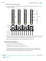
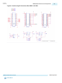
Figure 2-2: HDMI Video Stream Data
Video
Guard
Band
Video
Preamble
Data Island
Preamble
Active Video
Active
Aux/Audio
Data Island
Guard
Band
Video
Guard
Band
Active Video
vid_de
aux_de
Video Guard Band
Case (TMDS Channel Number):
0:q_out[9:0] = 10’b1011001100;
1:q_out[9:0] = 10’b0100110011;
2:q_out[9:0] = 10’b1011001100;
endcase
Data Island Guard Band
Case (TMDS Channel Number):
0:q_out[9:0] = 10’bxxxxxxxxxx;
1:q_out[9:0] = 10’b0100110011;
2:q_out[9:0] = 10’b0100110011;
endcase
Video Preamble
{c3, c2, c1, c0} = 4’b0001
Data Island Preamble
{c3, c2, c1, c0} = 4’b0101
The figure above illustrates two data streams:
• Data stream in green—transports color data
• Data stream in dark blue—transports auxiliary data
Table 2-1: Video Data and Auxiliary Data
The table below describes the function of the video data and auxiliary data.
Data
Description
Video data
• Packed representation of the video pixels clocked at the source pixel clock.
• Encoded using the TMDS 8-bit to 10-bit algorithm.
Auxiliary data
• Transfers audio data together with a range of auxiliary data packets.
• Sink devices use auxiliary data packets to correctly reconstruct video and audio
data.
• Encoded using the TMDS Error Reduction Coding–4 bits (TERC4) encoding
algorithm.
HDMI Overview
Send Feedback
Altera Corporation
2-4
UG-HDMI
2015.05.04
Resource Utilization
Each data stream section is preceded with guard bands and pre-ambles. These allow for accurate synchro‐
nization with received data streams.
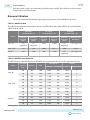
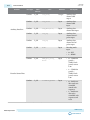
Resource Utilization
The resource utilization data indicates typical expected performance for the HDMI IP core device.
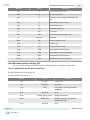
Table 2-2: HDMI Data Rate
The table lists the minimum and maximum data rates for FPGA fabric and standard RX/TX PCS, and PCS/PMA
widths of 10, 20, and 40.
Devices
RX/TX PCS,
RX/TX PCS,
RX/TX PCS,
PCS/PMA Width = 10
PCS/PMA Width = 20
PCS/PMA Width = 40
Minimum
Data Rate
(Mbps)
Maximum
Data Rate
(Mbps)
Minimum
Data Rate
(Mbps)
Maximum
Data Rate
(Mbps)
Minimum
Data Rate
(Mbps)
Maximum Data
Rate (Mbps)
Not
Supported
Not
Supported
1,000
12,000
Not
Supported
Not Supported
Arria V GX
611
1,875
1,000
3,276.8
1,000
6,553.6
Stratix V
600
5,800
600
11,400
Not
Supported
Not Supported
Arria 10
Table 2-3: HDMI Resource Utilization
The table lists the performance data for the HDMI IP core targeting Arria 10, Arria V GX, and Stratix V devices.
Device
Arria 10
Arria V GX
Stratix V
Altera Corporation
Transceiver
Interface
(bits)
Direction
ALMs
20
RX
20
Logic Registers
Memory
Primary
Secondary
Bits
M10K or M20K
1,602
3,031
343
7,488
9
TX
1,807
3,092
266
5,298
6
10
RX
1,167
2,520
249
4,800
7
20
RX
1,675
3,072
322
7,488
9
40
RX
2,493
4,216
472
12,864
16
10
TX
1,413
2,213
202
4,964
5
20
TX
1,882
3,059
251
5,298
6
40
TX
2,664
3,966
367
6,902
10
10
RX
1,201
2,479
249
4,800
7
20
RX
1,664
2,966
425
7,488
9
10
TX
1,341
2,235
177
4,520
4
20
TX
1,867
3,075
249
5,298
6
HDMI Overview
Send Feedback
HDMI Getting Started
3
2015.05.04
UG-HDMI
Subscribe
Send Feedback
This chapter provides a general overview of the Altera IP core design flow to help you quickly get started
with the HDMI IP core. The Altera IP Library is installed as part of the Quartus II installation process.
You can select and parameterize any Altera IP core from the library. Altera provides an integrated
parameter editor that allows you to customize the HDMI IP core to support a wide variety of applications.
The parameter editor guides you through the setting of parameter values and selection of optional ports.
Installing and Licensing IP Cores
The Quartus II software includes the Altera IP Library. The library provides many useful IP core
functions for production use without additional license. You can fully evaluate any licensed Altera IP core
in simulation and in hardware until you are satisfied with its functionality and performance. The HDMI
IP core is part of the Altera MegaCore IP Library, which is distributed with the Quartus II software and
downloadable from the Altera web site.
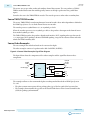
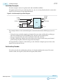
Figure 3-1: HDMI Installation Path
Installation directory
ip - Contains the Altera IP Library
altera - Contains the Altera IP Library source code
altera_hdmi - Contains the HDMI IP core files
Note: The default IP installation directory on Windows is <drive>:\altera\<version number>; on Linux it is
<home directory>/altera/ <version number>.
After you purchase a license for the HDMI IP core, you can request a license file from the Altera's
licensing site and install it on your computer. When you request a license file, Altera emails you a
license.dat file. If you do not have Internet access, contact your local Altera representative.
Related Information
• Altera Licensing Site
• Altera Software Installation and Licensing Manual
© 2015 Altera Corporation. All rights reserved. ALTERA, ARRIA, CYCLONE, ENPIRION, MAX, MEGACORE, NIOS, QUARTUS and STRATIX words and logos are
trademarks of Altera Corporation and registered in the U.S. Patent and Trademark Office and in other countries. All other words and logos identified as
trademarks or service marks are the property of their respective holders as described at www.altera.com/common/legal.html. Altera warrants performance
of its semiconductor products to current specifications in accordance with Altera's standard warranty, but reserves the right to make changes to any
products and services at any time without notice. Altera assumes no responsibility or liability arising out of the application or use of any information,
product, or service described herein except as expressly agreed to in writing by Altera. Altera customers are advised to obtain the latest version of device
specifications before relying on any published information and before placing orders for products or services.
www.altera.com
101 Innovation Drive, San Jose, CA 95134
ISO
9001:2008
Registered
3-2
OpenCore Plus IP Evaluation
UG-HDMI
2015.05.04
OpenCore Plus IP Evaluation
Altera's free OpenCore® Plus feature allows you to evaluate licensed MegaCore® IP cores in simulation
and hardware before purchase. You need only purchase a license for MegaCore IP cores if you decide to
take your design to production. OpenCore Plus supports the following evaluations:
•
•
•
•
Simulate the behavior of a licensed IP core in your system.
Verify the functionality, size, and speed of the IP core quickly and easily.
Generate time-limited device programming files for designs that include IP cores.
Program a device with your IP core and verify your design in hardware.
OpenCore Plus evaluation supports the following two operation modes:
• Untethered—run the design containing the licensed IP for a limited time.
• Tethered—run the design containing the licensed IP for a longer time or indefinitely. This requires a
connection between your board and the host computer.
Note: All IP cores that use OpenCore Plus time out simultaneously when any IP core in the design times
out.
Specifying IP Core Parameters and Options
Follow these steps to specify the HDMI IP core parameters and options.
1. Create a Quartus II project using the New Project Wizard available from the File menu.
2. On the Tools menu, click IP Catalog.
3. Under Installed IP, double-click Library > Interface > Protocols > Audio&Video > HDMI.
The parameter editor appears.
4. Specify a top-level name for your custom IP variation. This name identifies the IP core variation files
in your project. If prompted, also specify the targeted Altera device family and output file HDL
preference. Click OK.
5. Specify parameters and options in the HDMI parameter editor:
6.
7.
8.
9.
Altera Corporation
• Optionally select preset parameter values. Presets specify all initial parameter values for specific
applications (where provided).
• Specify parameters defining the IP core functionality, port configurations, and device-specific
features.
• Specify options for generation of a timing netlist, simulation model, testbench, or example design
(where applicable).
• Specify options for processing the IP core files in other EDA tools.
Click Generate to generate the IP core and supporting files, including simulation models.
Click Close when file generation completes.
Click Finish.
If you generate the HDMI IP core instance in a Quartus II project, you are prompted to add Quartus II
IP File (.qip) and Quartus II Simulation IP File (.sip) to the current Quartus II project.
HDMI Getting Started
Send Feedback
4
HDMI Source
2015.05.04
UG-HDMI
Send Feedback
Subscribe
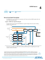
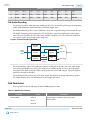
Source Functional Description
The HDMI source core provides direct connection to the Transceiver Native PHY through a 10-bit, 20bit, or 40-bit parallel data path.
Figure 4-1: HDMI Source Signal Flow Diagram
The figure below shows the flow of the HDMI source signals. The figure shows the various clocking
domains used within the core.
mode
vid_clk
Video Data
Port
Video
Input
Video
Resampler
V-SYNC
WOP
Generator
TMDS/TERC4
Encoder
TMDS Data
CC
color-depth
Multiplexer
Auxiliary Control
Port
Override
GCP
Default
GCP
Auxiliary Packet
Generator
Override
AV
Default AV
Infoframe
Auxiliary Packet
Generator
Override
VSI
Default VSI
Infoframe
Auxiliary Packet
Generator
Clock Domains
pp
aux_de
audio_clk
vid_clk
ls_clk
Multiplexer
Auxiliary
Data Port
1
Audio Port
Audio
Encoder
Auxiliary Packet
Generator
Auxiliary
Packet Encoder
The source core provides four 10-bit, 20-bit or 40-bit parallel data paths corresponding to the 3 color
channels and the clock channel.
© 2015 Altera Corporation. All rights reserved. ALTERA, ARRIA, CYCLONE, ENPIRION, MAX, MEGACORE, NIOS, QUARTUS and STRATIX words and logos are
trademarks of Altera Corporation and registered in the U.S. Patent and Trademark Office and in other countries. All other words and logos identified as
trademarks or service marks are the property of their respective holders as described at www.altera.com/common/legal.html. Altera warrants performance
of its semiconductor products to current specifications in accordance with Altera's standard warranty, but reserves the right to make changes to any
products and services at any time without notice. Altera assumes no responsibility or liability arising out of the application or use of any information,
product, or service described herein except as expressly agreed to in writing by Altera. Altera customers are advised to obtain the latest version of device
specifications before relying on any published information and before placing orders for products or services.
www.altera.com
101 Innovation Drive, San Jose, CA 95134
ISO
9001:2008
Registered
4-2
UG-HDMI
2015.05.04
Source TMDS/TERC4 Encoder
The source core accepts video, audio, and auxiliary channel data streams. The core produces a TMDS/
TERC4 encoded data stream that would typically connect to the high-speed transceiver parallel data
inputs.
Central to the core is the TMDS/TERC4 encoder. The encoder processes either video or auxiliary data.
Source TMDS/TERC4 Encoder
The source TMDS/TERC4 encoder implements 8-bit to 10-bit and 4-bit to 10-bit algorithms as defined in
the HDMI Specification Ver.2.0. Each channel has its own encoder.
The encoder processes symbol data at 1, 2, or 4 symbols per clock.
When the encoder operates in 2 or 4 symbols per clock, it also produces the output in the form of two or
four encoded symbols per clock.
The TMDS/TERC4 encoder also produces digital visual interface (DVI) signaling when you deassert the
mode input signal. DVI signaling is identical to HDMI signaling, except for the absence of data and video
islands and TERC4 auxiliary data.
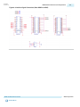
Source Video Resampler
The core resamples the video data based on the current color depth.
The video resampler consists of a gearbox and a dual-clock FIFO (DCFIFO).
Figure 4-2: Source Video Resampler Signal Flow Diagram
The figure below shows the components of the video resampler and the signal flow between these
components.
H-SYNC
V-SYNC
de
Pixel Data [bpp:0]
1
vid_clk
data
q
Gearbox
DCFIFO
wr
wrclk
Resampled
H-SYNC
V-SYNC
de
Pixel Data [7:0]
rd
rdclk
Phase
Counter
pp
bpp
ls_clk
The resampler adheres to the recommended phase encoding method described in HDMI Specification
Ver.1.4b.
• The phase counter must register the last packing-phase (pp) of the last pixel of the last active line.
• The resampler then transmits the pp value to the attached sink device in the General Control Packet
(GCP) for packing synchronization.
Altera Corporation
HDMI Source
Send Feedback
UG-HDMI
2015.05.04
Source Window of Opportunity Generator
4-3
Figure 4-3: Source Pixel Data Input Format RGB/YCbCr 4:4:4
The figure below shows the RGB color space pixel bit-field mappings.
24 bpp RGB/YCBCr444 (8 bpc)
30 bpp RGB/YCBCr444 (10 bpc)
36 bpp RGB/YCBCr444 (12 bpc)
48 bpp RGB/YCBCr444 (16 bpc)
47
32
31
16
15
vid_data[47:0]
0
Figure 4-4: Source Pixel Data Input Format YCbCr 4:2:2—12 bpc
The figure below shows the YCbCr color space pixel bit-field mappings.
Y[11:4]
47
Cb/Cr[11:4]
40
31
Cb/Cr[3:0]
24
15
Y[3:0]
12
11
8
vid_data[47:0]
The output from the resampler is a fixed 16 bits per color. When the resampler operates in lower color
depths, the low order bits are zero.
Source Window of Opportunity Generator
The source Window of Opportunity (WOP) generator creates valid data islands within the blanking
regions.
The WOP generator must generate a leading region sufficient enough to hold at least 12 symbol clocks
and a trailing region of at least 2 symbol clocks.
The WOP generator must also have an integral number of auxiliary packet cycles: 24 clocks when
processing in 1-symbol mode, 12 clocks when processing in 2-symbol mode, and 6 clocks when
processing in 4-symbol mode.
Figure 4-5: Typical Window of Opportunity
The figure below shows a typical output from the WOP generator.
Data Island
Guard Band
Data Island
Video
Guard Band
ls_clk
de
H-SYNC
wop
HDMI Source
Send Feedback
Altera Corporation
4-4
UG-HDMI
2015.05.04
Source Auxiliary Packet Encoder
The output from the WOP generator is an aux_de signal propagated backwards through the auxiliary
signal path to provide backpressure.
Based on the HDMI Specification Ver.1.4b requirements, you cannot send more than 9 auxiliary (AUX)
packets consecutively during a blanking region. The WOP generator deasserts the data enable line on
every tenth AUX packet to comply with this requirement.
Source Auxiliary Packet Encoder
Auxiliary packets are encoded by the source auxiliary packet encoder.
The auxiliary packets originate from a number of sources, which are multiplexed into the auxiliary packet
encoder in a round-robin schedule. The auxiliary packet encoder converts a standard stream into the
channel data format required by the TERC4 encoder.
The source propagates the WOP signal backwards through the stream ready signal.
The auxiliary packet encoder also calculates and inserts the Bose-Chaudhuri-Hocquenghem (BCH) error
correction code.
Figure 4-6: Auxiliary Packet Encoder Input
The figure below shows the auxiliary packet encoder input from a 72-bit input data.
Phase 0
Phase 1
Phase 2
Phase 3
PB24
PB26
0
PB21
PB23
PB25
PB27
PB15
PB17
PB19
0
PB14
PB16
PB18
PB20
PB8
PB10
PB12
0
PB7
PB9
PB11
PB13
PB1
PB3
PB5
0
PB0
PB2
PB4
PB6
HB1
HB2
0
Phase 1
Phase 2
Phase 3
PB22
Input Data
Byte[8]
HB0
Byte[0]
BCH Block 3
BCH Block 2
BCH Block 1
BCH Block 0
Startofpacket
Endofpacket
Ready
Phase 0
Clock
Cycle 1 Symbol
0
-
-
8
-
-
16
-
-
24
Cycle 2 Symbol
0
-
-
4
-
-
8
-
-
12
Cycle 4 Symbol
0
-
-
2
-
-
4
-
-
6
Altera Corporation
HDMI Source
Send Feedback
UG-HDMI
2015.05.04
Source Auxiliary Packet Generators
4-5
The encoder assumes the data valid input will remain asserted for the duration of a packet to complete. A
packet is always 24 clocks (in 1-symbol mode), 12 clocks (in 2-symbol mode), or 6 clocks (in 4-symbol
mode).
The encoder creates a NULL auxiliary packet if it doesn't detect a start-of-packet at the beginning of a
packet boundary. In this case, you can consider the output of the encoder as a stream of NULL packets
unless a valid packet is available.
Figure 4-7: Typical Auxiliary Packet Stream During Blanking Interval
The figure below shows a typical auxiliary packet stream in 1-symbol per clock mode, where 0 denotes a
null packet.
Ninth Packet
Skipped
wop
Auxiliary Packet
Clock Cycle
0
0
0
23
47
0
71
0
AVI
0
AI VSI
0
0
0
.......
AVI = Auxiliary Video Infoframe
AI = Audio Information Infoframe
VSI = Vendor Specific Infoframe
Source Auxiliary Packet Generators
The source core uses various auxiliary packet generators. The packet generators convert the packet field
inputs to the auxiliary packet stream format.
The packet generator propagates backpressure from the output ready signal to the input ready signal. The
generator asserts the input valid signal when a packet is ready to be transmitted. The input valid signal
remains asserted until the generator receives a ready acknowledgment.
Source Auxiliary Data Path Multiplexers
The auxiliary data path multiplexers provide paths for the various auxiliary packet generators.
The various auxiliary packet generators traverse a multiplexed routing path to the auxiliary packet
encoder. The multiplexers obey a round-robin schedule and propagate backpressure.
Source Auxiliary Control Port
To simplify the user logic, the source core has control ports to send the most common auxiliary control
packets.
These packets are: General Control Packet, Auxiliary Video Information (AVI) InfoFrame, HDMI
Vendor Specific InfoFrame (VSI), and Audio InfoFrame.
The core sends the default values in the auxiliary packets. The default values allow the core to send video
data compatible with the HDMI Specification Ver.1.4b with minimum description.
You can also override the generators using the customized input values. The override values replace the
default values when the input checksum is non-zero.
HDMI Source
Send Feedback
Altera Corporation
4-6
UG-HDMI
2015.05.04
Source General Control Packet
The core sends the auxiliary control packets on the active edge of the V-SYNC signal to ensure that the
packets are sent once per field.
Source General Control Packet
Table 4-1: Source General Control Packet Input Fields
The table below lists the bit-fields for the Source General Control Packet port.
Bit Field
Name
Color
Depth
(CD)
gcp[3:0]
Comment
CD3
CD2
CD1
CD0
0
0
0
0
Color depth not
indicated
0
0
0
1
Reserved
0
0
1
0
Reserved
0
0
1
1
Reserved
0
1
0
0
24 bpp
0
1
0
1
30 bpp (1)
0
1
1
0
36 bpp (1)
0
1
1
1
48 bpp (1)
1
1
1
1
Reserved
gcp[4]
Set_
AVMUTE
Refer to HDMI Specification Ver.1.4b.
gcp[5]
Clear_
AVMUTE
Refer to HDMI Specification Ver.1.4b.
Color depth (24 bpp
only)
All other fields for the source GCP are calculated automatically inside the core.
Source Auxiliary Video Information (AVI) InfoFrame
The HDMI core produces the captured AVI InfoFrame to simplify user applications.
Table 4-2: Auxiliary Video Information (AVI) InfoFrame
The table below lists the bit-fields for the AVI InfoFrame port bundle.
The signal bundle is clocked by ls_clk.
(1)
Bit-field
Name
7:0
Checksum
9:8
S
Comment
Checksum
Scan information
Will be supported in a future release.
Altera Corporation
HDMI Source
Send Feedback
UG-HDMI
2015.05.04
Source HDMI Vendor Specific InfoFrame (VSI)
Bit-field
Name
11:10
B
Bar info data valid
12
A0
Active information present
14:13
Y
RGB or YCbCr indicator
15
Reserved
19:16
R
Active format aspect ratio
21:20
M
Picture aspect ratio
23:22
C
Colorimetry (for example: ITU BT.601, BT.
709)
25:24
SC
Non-uniform picture scaling
27:26
Q
Quantization range
30:28
EC
Extended colorimetry
31
ITC
IT content
38:32
VIC
Video format identification code
39
Reserved
43:40
PR
Picture repetition factor
45:44
CN
Content type
47:46
YQ
YCC quantization range
63:48
ETB
Line number of end of top bar
79:64
SBB
Line number of start of bottom bar
95:80
ELB
Pixel number of end of left bar
111:96
SRB
Pixel number of start of right bar
112
4-7
Comment
Returns 0
Returns 0
Disables the core of the InfoFrame packets
from inserting.
• 1: The core does not insert info_
avi[111:0].
• 0: The core inserts info_avi[111:0]
when checksum field (info_avi[7:0]) is
non-zero. The core sends default values
when checksum field (info_avi[7:0]) is
zero.
Source HDMI Vendor Specific InfoFrame (VSI)
The core transmits a HDMI Vendor Specific InfoFrame once per field.
HDMI Source
Send Feedback
Altera Corporation
4-8
UG-HDMI
2015.05.04
Source Audio InfoFrame (AI)
Table 4-3: HDMI Vendor Specific InfoFrame Bit-Fields
The table below lists the bit-fields for VSI.
The signal bundle is clocked by ls_clk.
Bit-field
Name
4:0
Length
12:5
Checksum
36:13
IEEE
41:37
Reserved
44:42
HDMI_Video_Format
52:45
HDMI_VIC
57:53
Reserved
60:58
3D_Ext_Data
61
Comment
Length = Nv
Checksum
24-bit IEEE registration identified
(0×000C03)
All 0
HDMI video format
HDMI proprietary video format
identification code
All 0
3D extended data
Disables the core of the InfoFrame
packets from inserting.
• 1: The core does not insert info_
vsi[60:0].
• 0: The core inserts info_
vsi[60:0] when checksum field
(info_vsi[12:5]) is non-zero.
The core sends default values
when checksum field (info_
vsi[12:5]) is zero.
Note: If the checksum input to the port is zero, the core uses a default value of zero for each bit-field.
Source Audio InfoFrame (AI)
The core transmits an Audio InfoFrame once per field.
Table 4-4: Source Audio InfoFrame Bundle Bit-Fields
The table below lists the signal bit-fields.
The signal bundle is clocked by ls_clk.
Altera Corporation
Bit-field
Name
7:0
Checksum
10:8
CC
11
Reserved
Comment
Checksum
Channel count
Returns 0
HDMI Source
Send Feedback
UG-HDMI
2015.05.04
Source Audio Encoder
Bit-field
Name
15:12
CT
Audio format type
17:16
SS
Bits per audio sample
20:18
SF
Sampling frequency
23:21
Reserved
31:24
CXT
Audio format type of the audio
stream
39:32
CA
Speaker location allocation FL, FR
41:40
LFEPBL
LFE playback level information, dB
42
Reserved
Returns 0
46:43
LSV
47
DM_INH
48
4-9
Comment
Returns 0
Level shift information, dB
Down-mix inhibit flag
Disables the core of the InfoFrame
packets from inserting.
• 1: The core does not insert audio_
info_ai[47:0].
• 0: The core inserts audio_info_
ai[47:0] when checksum field
(audio_info_ai[7:0]) is nonzero. The core sends default values
when checksum field (audio_
info_ai[7:0]) is zero.
Note: If the checksum input to the port is zero, the core uses a default value of zero for each bit-field.
Source Audio Encoder
Audio transport requires three packet types: Audio Timestamp InfoFrame, Audio Information
InfoFrame, and Audio Sample Data.
HDMI Source
Send Feedback
Altera Corporation
4-10
UG-HDMI
2015.05.04
Source Parameters
Figure 4-8: Source Audio Encoder
Timestamp
Scheduler
Auxiliary Packet
Generator
CTS, N
Audio Data
Port
Multiplexer
Default AI
Override AI
V-SYNC
Auxiliary Packet
Generator
1
DCFIFO
Audio Input
Audio
Packetizer
Audio
Auxiliary
Stream
Auxiliary Packet
Generator
The Audio Timestamp InfoFrame packet contains the CTS and N values. You need to provide these
values. The core schedules this packet to be sent every ms. The scheduler uses the ls_clk and CTS value
to determine a 1-ms interval.
The core sends the Audio Information InfoFrame packet on the active edge of the V-SYNC signal.
The Audio Sample Data packet queues on a DCFIFO. The core also uses the DCFIFO to synchronize its
clock to ls_clk. The Audio Packetizer packs the audio sample data into the Audio Sample packets. An
Audio Sample packet can contain up to 4 audio samples, based on the required audio sample clock. The
core sends the Audio Sample packets whenever there is an available slot in the auxiliary packet stream.
Source Parameters
You set parameters for the source using the Altera HDMI parameter editor.
Table 4-5: HDMI Source Parameters
Parameter
Device family
Value
Stratix V
Arria V
Description
Targeted device family; matches the project
device family.
Arria 10
Direction
Transmitter = Source
Select HDMI source.
Receiver = Sink
Symbols per clock
1, 2, or 4 symbols per
clock
Determines how many TMDS symbols and pixels
are processed per clock.
• Stratix V supports 1 or 2 symbols per clock
• Arria V supports 1, 2, or 4 symbols per clock
• Arria 10 supports only 2 symbols per clock
Altera Corporation
HDMI Source
Send Feedback
UG-HDMI
2015.05.04
Source Interfaces
Parameter
Value
Support auxiliary
Description
Determines if auxiliary channel encoding is
included.
0 = No AUX
1 = AUX
Support deep color
4-11
0 = No deep color
Determines if the core can encode deep color
formats.
1 = Deep color
To enable this parameter, you must also enable
the Support auxiliary parameter.
Note: This parameter is not supported for
15.0 release. The parameter always sets
to 0.
Support audio
Support 8-channel audio
0 = No audio
Determines if the core can encode audio data.
1 = Audio
To enable this parameter, you must also enable
the Support auxiliary parameter.
0 = No
Determines if the core can support up to 8 audio
channels. Enable this parameter if you want to
support more than the default 2 audio channels.
1 = Yes
To enable this parameter, you must also enable
the Support audio parameter.
Note: This parameter is not supported for
15.0 release. The parameter always sets
to 0.
Source Interfaces
The table lists the source's port interfaces.
Table 4-6: Source Interfaces
N is the number of symbols per clock.
Interface
Reset
HDMI Source
Send Feedback
Port Type
Reset
Clock
Domain
N/A
Port
reset
Direction
Input
Description
Main asynchro‐
nous reset input.
Altera Corporation
4-12
UG-HDMI
2015.05.04
Source Interfaces
Interface
Port Type
Clock
Clock
Domain
N/A
Port
ls_clk
Direction
Input
Description
Link speed clock
input.
8/8 (1x), 10/8
(1.25x), 12/8 (1.5x),
or 16/8 (2x) times
the vid_clk
according to color
depth.
This signal
connects to the
transceiver output
clock.
Clock
Clock
N/A
vid_clk
Input
Video data clock
input.
• 1 symbol per
clock mode =
video pixel
clock
• 2 symbols per
clock mode =
half the pixel
clock
• 4 symbols per
clock mode =
quarter the pixel
clock
Clock
Altera Corporation
N/A
audio_clk
Input
Audio clock input.
HDMI Source
Send Feedback
UG-HDMI
2015.05.04
Source Interfaces
Interface
Port Type
Conduit
Clock
Domain
vid_clk
Port
vid_data[N*48-1:0]
Direction
Input
HDMI Source
Send Feedback
Description
Video 48-bit pixel
data input port.
• In 2 symbols per
clock (N=2)
mode, this port
accepts two 48bit pixels per
clock.
• In 4 symbols per
clock (N=4)
mode, this port
accepts four 48bit pixels per
clock.
Video Data Port
TMDS Data Port
4-13
Conduit
vid_clk
vid_de[N-1:0]
Input
Video data enable
input that indicates
active picture
region.
Conduit
vid_clk
vid_hsync[N-1:0]
Input
Video horizontal
sync input.
Conduit
vid_clk
vid_vsync[N-1:0]
Input
Video vertical sync
input.
Conduit
ls_clk
out_b[10*N-1:0]
Output
TMDS encoded
blue channel
output.
Conduit
ls_clk
out_r[10*N-1:0]
Output
TMDS encoded red
channel output.
Conduit
ls_clk
out_g[10*N-1:0]
Output
TMDS encoded
green channel
output.
Conduit
ls_clk
out_c[10*N-1:0]
Output
TMDS encoded
clock channel
output.
Altera Corporation
4-14
UG-HDMI
2015.05.04
Source Interfaces
Interface
Auxiliary Data Port
Port Type
Clock
Domain
Port
Direction
Description
Conduit
ls_clk
aux_ready
Output
Auxiliary data
channel valid
output.
Conduit
ls_clk
aux_valid
Input
Auxiliary data
channel valid
input.
Conduit
ls_clk
aux_data[71:0]
Input
Auxiliary data
channel data input.
Conduit
ls_clk
aux_sop
Input
Auxiliary data
channel start-ofpacket input.
Conduit
ls_clk
aux_eop
Input
Auxiliary data
channel end-ofpacket input.
Conduit
ls_clk
mode
Input
Encoding mode
input.
• 0 = DVI
• 1 = HDMI
Conduit
ls_clk
Conduit
ls_clk
TMDS_Bit_clock_
Ratio
Input
• 0 = (TMDS bit
period) /
(TMDS clock
period) ratio is
1/10
• 1 = (TMDS bit
period) /
(TMDS clock
period) ratio is
1/40
Input
• 0 = Sink device
does not detect
scrambled
control code
sequences
• 1 = Sink device
detects the
scrambled code
sequences and
resets
Encoder Control Port
Altera Corporation
Scrambler_Enable
HDMI Source
Send Feedback
UG-HDMI
2015.05.04
Source Clock Tree
Interface
Audio Port
Port Type
Clock
Domain
Port
Direction
4-15
Description
Conduit
audio_clk
audio_CTS[21:0]
Input
Audio CTS value
input.
Conduit
audio_clk
audio_N[21:0]
Input
Audio N value
input.
Conduit
audio_clk
Input
Audio data input.
Conduit
audio_clk
audio_
data[32*(2+6*M)1:0]
audio_de[2+6*M1:0]
M is 1 when you
enable support for
8-channel audio.
Otherwise it is 0.
Input
Audio data valid
input.
M is 1 when you
enable support for
8-channel audio.
Otherwise it is 0.
Auxiliary Control Port
Conduit
audio_clk
Input
Audio mute input.
Conduit
audio_clk
Input
Audio InfoFrame
input bundle input.
Conduit
ls_clk
gcp[5:0]
Input
General Control
Packet.
Conduit
ls_clk
gcp_Set_AVMute
Input
General Control
Packet mute input.
Conduit
ls_clk
gcp_Clear_AVMute
Input
General Control
Packet clear input.
Conduit
ls_clk
info_avi[112:0]
Input
Auxiliary Video
Information
InfoFrame input.
Conduit
ls_clk
info_vsi[61:0]
Input
Vendor Specific
Information
InfoFrame input.
audio_mute
audio_info_
ai[48:0]
Source Clock Tree
The source uses various clocks.
HDMI Source
Send Feedback
Altera Corporation
4-16
UG-HDMI
2015.05.04
Source Clock Tree
Figure 4-9: Source Clock Tree
The figure shows how the different clocks connect in the source core.
Transceiver
Block
HDMI Source Core
ls_clk
vid_clk
WRCLK
Pixel Data
RDCLK
Resampler
FIFO
WRCLK RDCLK
Sync
HSSI[0]
Channel[0]
WRCLK RDCLK
Sync
HSSI[1]
Channel[1]
Sync
HSSI[2]
Channel[2]
WRCLK RDCLK
Sync
HSSI[3]
TMDS Clock
Switch
Transceiver
PLL
TMDS
(TERC4)
Encoder
WRCLK
RDCLK
AUX Data
GPLL
vid_clk
x1.0
x1.25
x1.5
x2.0
bpp
ls_clk
vid_clk
The pixel data clocks into the core at the pixel clock (vid_clk). This same clock derives the required link
speed clock (ls_clk), which is used to drive the transceiver phase-locked loop (PLL) input. The ls_clk
depends on the color bits per pixel (bpp).
For HDMI source, you must instantiate 4 transmitter channels: 3 channels to transmit data and 1 channel
to transmit clock information.
You must connect the core ls_clk to the transceiver clock output, which performs the TMDS and TERC4
encoding. The auxiliary data clocks into the core at the ls_clk rate.
Related Information
HDMI Hardware Demonstration on page 6-1
For more information about the transmitter and receiver channels.
Altera Corporation
HDMI Source
Send Feedback
HDMI Sink
5
2015.05.04
UG-HDMI
Send Feedback
Subscribe
Sink Functional Description
The HDMI sink core provides direct connection to the Transceiver Native PHY through a 10-bit, 20-bit,
or 40-bit parallel data path.
Figure 5-1: HDMI Sink Signal Flow Diagram
The figure below shows the flow of the HDMI sink signals. The figure shows the various clocking domains
used within the core.
mode
Word Alignment and Channel Deskew
TMDS
Data
Bitslip
Word
Align
Deskew
reset
TMDS TERC4
Decoder
Video
Data
AUX
Data
vid_clk
Video
Resample
Video Data
Video
Data Port
Color Depth, pp
Capture GCP
GCP
Capture AVI
AVI Infoframe
Capture AI
AI Infoframe
Auxiliary
Decoder
AUX Data Port
Auxiliary
Memory Encoder
Clock Domains
ls_clk[2:0]
vid_clk[0]
ls_clk[0]
Control
Packet Ports
Audio
Decoder
Auxiliary
Memory Interface
Audio
Data Port
Auxiliary
Packet Capture
The sink core provides three 10-bit, 20-bit, or 40-bit data input paths corresponding to the color channels.
The sink core clocks the three 10-bit, 20-bit, or 40-bit channels from the transceiver outputs using the
respective transceiver clock outputs.
• Blue channel: 0
• Red channel: 1
• Green channel: 2
© 2015 Altera Corporation. All rights reserved. ALTERA, ARRIA, CYCLONE, ENPIRION, MAX, MEGACORE, NIOS, QUARTUS and STRATIX words and logos are
trademarks of Altera Corporation and registered in the U.S. Patent and Trademark Office and in other countries. All other words and logos identified as
trademarks or service marks are the property of their respective holders as described at www.altera.com/common/legal.html. Altera warrants performance
of its semiconductor products to current specifications in accordance with Altera's standard warranty, but reserves the right to make changes to any
products and services at any time without notice. Altera assumes no responsibility or liability arising out of the application or use of any information,
product, or service described herein except as expressly agreed to in writing by Altera. Altera customers are advised to obtain the latest version of device
specifications before relying on any published information and before placing orders for products or services.
www.altera.com
101 Innovation Drive, San Jose, CA 95134
ISO
9001:2008
Registered
5-2
Sink Channel Word Alignment and Deskew
UG-HDMI
2015.05.04
Sink Channel Word Alignment and Deskew
The input stage of the sink is responsible for synchronizing the incoming parallel data channels correctly.
The synchronization is split to two stages: word alignment and channel deskew.
Word alignment
• Correctly aligns the incoming parallel data to word boundaries using
bit-slip technique.
• TMDS encoding does not guarantee unique control codes, but the core
can still use the sequence of continuous symbols found in data and
video preambles to align.
• The alignment algorithm searches for 12 consecutive 0×54 or 0×ab
corresponding to the data and video preambles.
Note: The preambles are also present in digital video interface
(DVI) coding.
• The alignment logic asserts a marker indicator when the 12 consecu‐
tive signals are detected.
• Similarly, the logic infers alignment loss when 8K symbol clocks elapse
without a single marker assertion.
Channel deskew
Altera Corporation
• When the data channels are aligned, the core then attempts to deskew
each channel.
• The sink core deskews at the rising edge of the marker insertion.
• For every correct deskewed lane, the marker insertion will appear in all
three TMDS encoded streams.
• The sink core deskews using three dual-clock FIFOs.
• The dual-clock FIFOs also synchronize all three data streams to the
blue channel clock to be used later throughout the decoder core.
HDMI Sink
Send Feedback
UG-HDMI
2015.05.04
Sink TMDS/TERC4 Decoder
5-3
Figure 5-2: Channel Deskew DCFIFO Arrangement
The figure below shows the signal flow diagram of the deskew logic.
marker[2]
marker[1]
marker[0]
Alignment
Detection
DCFIFO
Channel 0
marker_in[0]
data_in[0]
data[0]
ls_clk[0]
rdreq
wrclk
rdclk
ls_clk[0]
DCFIFO
Channel 1
marker_in[1]
data_in[1]
data[1]
ls_clk[1]
rdreq
wrclk
rdclk
ls_clk[0]
DCFIFO
Channel 2
marker_in[2]
data_in[2]
data[2]
ls_clk[2]
rdreq
wrclk
rdclk
ls_clk[0]
The FIFO read signal of the channels is normally asserted. The sink core deasserts a particular FIFO read
signal if a marker appears at its output and not in the other two FIFO outputs. By deasserting, the sink
core stalls the data stream for sufficient cycles to remove the channel skew. If any of the FIFO channels
overflow, the sink core asserts a reset signal which propagates backwards to the word alignment logic.
Sink TMDS/TERC4 Decoder
The sink TMDS/TERC4 decoder follows the HDMI/DVI specification. The video data is encoded using
the TMDS algorithm and auxiliary data is encoded using TERC4 algorithm.
The sink core feeds the aligned channels into the TMDS/TERC4 decoder. You can parameterize the
decoder to operate in 1, 2, or 4 TMDS symbols per clock. If you choose 2 or 4 TMDS symbols per clock,
the decoder will produce 2 or 4 decoded symbols per clock. The decoded symbols per clock output
supports high pixel clock resolutions on low-end FPGA devices.
HDMI Sink
Send Feedback
Altera Corporation
5-4
UG-HDMI
2015.05.04
Sink Video Resampler
Sink Video Resampler
The video resampler consists of a gearbox and a dual-clock FIFO (DCFIFO).
The gearbox converts 8 bit-per-second (bps) data to 8-, 10-, 12- or 16-bps data based on the current color
depth. The GCP conveys the color depth information.
Figure 5-3: Sink Resampler Signal Flow Diagram
H-SYNC
V-SYNC
de
Pixel Data [7:0]
data
q
Gearbox
Resampled
H-SYNC
V-SYNC
de
Pixel Data [bpp:0]
DCFIFO
pp
bpp
ls_clk
Phase
Counter
wr
wrclk
rd
rdwrclk
1
vid_clk
The resampler adheres to the recommended phase count method described in HDMI Specification Ver.
1.4b.
• To keep the source and sink resamples synchronized, the source must send the phase-packing (pp)
value to the sink during the vertical blanking phase, using the general control packet.
• The pp corresponds to the phase of the last pixel in the last active video line.
• The phase-counter logic compares its own pp value to the pp value received in the general control
packet and slips the phase count if the two pp values do not agree.
The output from the resampler is a fixed 16 bits per color. When the resampler operates in lower color
depths, the low order bits are zero.
Sink Auxiliary Decoder
The sink core decodes the auxiliary data path into a 72-bit wide standard packet stream. The stream
contains a valid, start-of-packet (SOP) and end-of-packet (EOP) marker.
Altera Corporation
HDMI Sink
Send Feedback
UG-HDMI
2015.05.04
Sink Auxiliary Packet Capture
5-5
Figure 5-4: Auxiliary Data Stream Signal
The figure below shows the relationship between the data bit-field and its clock cycle based on 1-, 2-, or 4symbol per clock mode.
Phase 0
Phase 1
Phase 2
Phase 3
PB24
PB26
BCH3
PB21
PB23
PB25
PB27
PB15
PB17
PB19
BCH2
PB14
PB16
PB18
PB20
PB8
PB10
PB12
BCH1
PB7
PB9
PB11
PB13
PB1
PB3
PB5
BCH0
PB0
PB2
PB4
PB6
HB1
HB2
0
Phase 1
Phase 2
Phase 3
PB22
Byte[8]
HB0
Byte[0]
BCH Block 3
BCH Block 2
BCH Block 1
Output Data
BCH Block 0
Startofpacket
Endofpacket
Valid
Phase 0
Clock
Cycle 1 Symbol
0
-
-
8
-
-
16
-
-
24
Cycle 2 Symbol
0
-
-
4
-
-
8
-
-
12
Cycle 4 Symbol
0
-
-
2
-
-
4
-
-
6
The data output at EOP contains the received BCH error correcting code. The sink core does not perform
any error correction within the core. The auxiliary data is available outside the core.
Note: You can find the bit-field nomenclature in the HDMI Specification Ver.2.0.
Sink Auxiliary Packet Capture
The auxiliary streams transfer auxiliary packets.
The auxiliary packets can carry 15 different packet types.
The module produces 4 valid signals to simplify the user logic.
To simplify user applications and minimize external logic, the HDMI core captures 3 different packet
types and decodes the audio sample data. These packets are: General Control Packet, Auxiliary Video
Information (AVI) InfoFrame, and HDMI Vendor Specific InfoFrame (VSI).
HDMI Sink
Send Feedback
Altera Corporation
5-6
UG-HDMI
2015.05.04
Sink General Control Packet
Sink General Control Packet
Table 5-1: General Control Packet Input Fields
Bit Field
Name
Comment
CD3
CD2
CD1
CD0
0
0
0
0
Color depth not
indicated
0
0
0
1
Reserved
0
0
1
0
Reserved
0
0
1
1
Reserved
0
1
0
0
24 bpp
0
1
0
1
30 bpp (2)
0
1
1
0
36 bpp (2)
0
1
1
1
48 bpp (2)
1
1
1
1
Reserved
Color Depth
(CD)
gcp[3:0]
gcp[4]
Set_
AVMUTE
Refer to HDMI Specification Ver.1.4b
gcp[5]
Clear_
AVMUTE
Refer to HDMI Specification Ver.1.4b
Color depth
Sink Auxiliary Video Information (AVI) InfoFrame Bit-Fields
The HDMI core produces AVI InfoFrame to simplify user applications.
Table 5-2: Auxiliary Video Information (AVI) InfoFrame
The table below lists the bit-fields for the AVI InfoFrame port bundle.
The signal bundle is clocked by ls_clk.
(2)
Bit-field
Name
Comment
7:0
Checksum
9:8
S
Scan information
11:10
B
Bar info data valid
12
A0
Active information present
14:13
Y
RGB or YCbCr indicator
15
Reserved
Checksum
Returns 0
Will be supported in a future release.
Altera Corporation
HDMI Sink
Send Feedback
UG-HDMI
2015.05.04
Sink HDMI Vendor Specific InfoFrame (VSI)
Bit-field
Name
19:16
R
Active format aspect ratio
21:20
M
Picture aspect ratio
23:22
C
Colorimetry (for example: ITU BT.601, BT.
709)
25:24
SC
Non-uniform picture scaling
27:26
Q
Quantization range
30:28
EC
Extended colorimetry
31
ITC
IT content
38:32
VIC
Video format identification code
39
Reserved
43:40
PR
Picture repetition factor
45:44
CN
Content type
47:46
YQ
YCC quantization range
63;48
ETB
Line number of end of top bar
79:64
SBB
Line number of start of bottom bar
95:80
ELB
Pixel number of end of left bar
111:96
SRB
Pixel number of start of right bar
5-7
Comment
Returns 0
Sink HDMI Vendor Specific InfoFrame (VSI)
The core produces the captured HDMI Vendor Specific InfoFrame to simplify user applications.
Table 5-3: HDMI Vendor Specific InfoFrame Bit-Fields
The table below lists the bit-fields for VSI.
The signal bundle is clocked by ls_clk.
HDMI Sink
Send Feedback
Bit-field
Name
4:0
Length
12:5
Checksum
36:13
IEEE
41:37
Reserved
44:42
HDMI_Video_Format
52:45
HDMI_VIC
57:53
Reserved
Comment
Length = Nv
Checksum
24-bit IEEE registration identified
(0x000C03)
All 0
HDMI video format
HDMI proprietary video format
identification code
All 0
Altera Corporation
5-8
UG-HDMI
2015.05.04
Sink Auxiliary Data Port
Bit-field
Name
60:58
3D_Ext_Data
Comment
3D extended data
Sink Auxiliary Data Port
The auxiliary port is attached to external memory. This port allows you to write packets to memory for
use outside the HDMI core.
The core calculates the address for the data port using the header byte of the received packet. The core
writes packet types 0–15 into a contiguous memory region.
Figure 5-5: Typical Application of AUX Packet Register Interface
The figure below shows a typical application of the auxiliary data port.
HDMI Sink Core
data[71:0]
addr[5:0]
wr
On-Chip
Memory
data[71:8]
addr[5:0]
rd
From 64 bit
Nios II
Avalon-MM
Table 5-4: Auxiliary Packet Memory Map
The table below lists the address map corresponding to the captured packets.
Address
Byte Offset
8
7
6
5
4
3
2
1
0
NULL PACKET
0
PB22
PB21
PB15
PB14
PB8
PB7
PB1
PB0
HB0
1
PB24
PB23
PB17
PB16
PB10
PB9
PB3
PB2
HB1
2
PB26
PB25
PB19
PB18
PB12
PB11
PB5
PB4
HB2
3
BCH3
PB27
BCH2
PB20
BCH1
PB13
BCH0
PB6
HBCH0
Audio Clock Regeneration (N/CTS)
4
PB22
PB21
PB15
PB14
PB8
PB7
PB1
PB0
HB0
5
PB24
PB23
PB17
PB16
PB10
PB9
PB3
PB2
HB1
6
PB26
PB25
PB19
PB18
PB12
PB11
PB5
PB4
HB2
7
BCH3
PB27
BCH2
PB20
BCH1
PB13
BCH0
PB6
HBCH0
Audio Sample
8
PB22
PB21
PB15
PB14
PB8
PB7
PB1
PB0
HB0
9
PB24
PB23
PB17
PB16
PB10
PB9
PB3
PB2
HB1
10
PB26
PB25
PB19
PB18
PB12
PB11
PB5
PB4
HB2
Altera Corporation
HDMI Sink
Send Feedback
UG-HDMI
2015.05.04
Sink Auxiliary Data Port
5-9
Audio Sample
11
BCH3
PB27
BCH2
PB20
BCH1
PB13
BCH0
PB6
HBCH0
General Control
12
PB22
PB21
PB15
PB14
PB8
PB7
PB1
PB0
HB0
13
PB24
PB23
PB17
PB16
PB10
PB9
PB3
PB2
HB1
14
PB26
PB25
PB19
PB18
PB12
PB11
PB5
PB4
HB2
15
BCH3
PB27
BCH2
PB20
BCH1
PB13
BCH0
PB6
HBCH0
ACP Packet
16
PB22
PB21
PB15
PB14
PB8
PB7
PB1
PB0
HB0
17
PB24
PB23
PB17
PB16
PB10
PB9
PB3
PB2
HB1
18
PB26
PB25
PB19
PB18
PB12
PB11
PB5
PB4
HB2
19
BCH3
PB27
BCH2
PB20
BCH1
PB13
BCH0
PB6
HBCH0
ISRC1 Packet
20
PB22
PB21
PB15
PB14
PB8
PB7
PB1
PB0
HB0
21
PB24
PB23
PB17
PB16
PB10
PB9
PB3
PB2
HB1
22
PB26
PB25
PB19
PB18
PB12
PB11
PB5
PB4
HB2
23
BCH3
PB27
BCH2
PB20
BCH1
PB13
BCH0
PB6
HBCH0
ISRC2 Packet
24
PB22
PB21
PB15
PB14
PB8
PB7
PB1
PB0
HB0
25
PB24
PB23
PB17
PB16
PB10
PB9
PB3
PB2
HB1
26
PB26
PB25
PB19
PB18
PB12
PB11
PB5
PB4
HB2
27
BCH3
PB27
BCH2
PB20
BCH1
PB13
BCH0
PB6
HBCH0
One Bit Audio Sample Packet 5.3.9
28
PB22
PB21
PB15
PB14
PB8
PB7
PB1
PB0
HB0
29
PB24
PB23
PB17
PB16
PB10
PB9
PB3
PB2
HB1
30
PB26
PB25
PB19
PB18
PB12
PB11
PB5
PB4
HB2
31
BCH3
PB27
BCH2
PB20
BCH1
PB13
BCH0
PB6
HBCH0
DST Audio Packet
32
PB22
PB21
PB15
PB14
PB8
PB7
PB1
PB0
HB0
33
PB24
PB23
PB17
PB16
PB10
PB9
PB3
PB2
HB1
34
PB26
PB25
PB19
PB18
PB12
PB11
PB5
PB4
HB2
35
BCH3
PB27
BCH2
PB20
BCH1
PB13
BCH0
PB6
HBCH0
HDMI Sink
Send Feedback
Altera Corporation
5-10
UG-HDMI
2015.05.04
Sink Auxiliary Data Port
High Bitrate (HBR) Audio Stream Packet
36
PB22
PB21
PB15
PB14
PB8
PB7
PB1
PB0
HB0
37
PB24
PB23
PB17
PB16
PB10
PB9
PB3
PB2
HB1
38
PB26
PB25
PB19
PB18
PB12
PB11
PB5
PB4
HB2
39
BCH3
PB27
BCH2
PB20
BCH1
PB13
BCH0
PB6
HBCH0
Gamut Metadata Packet
40
PB22
PB21
PB15
PB14
PB8
PB7
PB1
PB0
HB0
41
PB24
PB23
PB17
PB16
PB10
PB9
PB3
PB2
HB1
42
PB26
PB25
PB19
PB18
PB12
PB11
PB5
PB4
HB2
43
BCH3
PB27
BCH2
PB20
BCH1
PB13
BCH0
PB6
HBCH0
Vendor-Specific InfoFrame
44
PB22
PB21
PB15
PB14
PB8
PB7
PB1
PB0
HB0
45
PB24
PB23
PB17
PB16
PB10
PB9
PB3
PB2
HB1
46
PB26
PB25
PB19
PB18
PB12
PB11
PB5
PB4
HB2
47
BCH3
PB27
BCH2
PB20
BCH1
PB13
BCH0
PB6
HBCH0
AVI InfoFrame
48
PB22
PB21
PB15
PB14
PB8
PB7
PB1
PB0
HB0
49
PB24
PB23
PB17
PB16
PB10
PB9
PB3
PB2
HB1
50
PB26
PB25
PB19
PB18
PB12
PB11
PB5
PB4
HB2
51
BCH3
PB27
BCH2
PB20
BCH1
PB13
BCH0
PB6
HBCH0
Source Product Descriptor InfoFrame
52
PB22
PB21
PB15
PB14
PB8
PB7
PB1
PB0
HB0
53
PB24
PB23
PB17
PB16
PB10
PB9
PB3
PB2
HB1
54
PB26
PB25
PB19
PB18
PB12
PB11
PB5
PB4
HB2
55
BCH3
PB27
BCH2
PB20
BCH1
PB13
BCH0
PB6
HBCH0
Audio InfoFrame
56
PB22
PB21
PB15
PB14
PB8
PB7
PB1
PB0
HB0
57
PB24
PB23
PB17
PB16
PB10
PB9
PB3
PB2
HB1
58
PB26
PB25
PB19
PB18
PB12
PB11
PB5
PB4
HB2
59
BCH3
PB27
BCH2
PB20
BCH1
PB13
BCH0
PB6
HBCH0
PB1
PB0
HB0
MPEG Source InfoFrame
60
Altera Corporation
PB22
PB21
PB15
PB14
PB8
PB7
HDMI Sink
Send Feedback
UG-HDMI
2015.05.04
Sink Audio Decoding
5-11
MPEG Source InfoFrame
61
PB24
PB23
PB17
PB16
PB10
PB9
PB3
PB2
HB1
62
PB26
PB25
PB19
PB18
PB12
PB11
PB5
PB4
HB2
63
BCH3
PB27
BCH2
PB20
BCH1
PB13
BCH0
PB6
HBCH0
Sink Audio Decoding
The sink core sends the audio data using auxiliary packets. You can use three packet types in transporting
audio: Audio InfoFrame, Audio Timestamp, and Audio Sample Data.
The Audio InfoFrame packet is not used within the core but it is captured and presented outside the core.
The Audio Timestamp packet transmits the CTS and N values required to synthesize the audio sample
clock. The core also makes the CTS and N values available outside the core. The audio clock synthesizer
uses a phase-counter to recover the audio sample rate.
Figure 5-6: Audio Decoder Signal Flow
Capture Audio
InfoFrame
AI InfoFrame
CTS, N
Auxiliary
Stream
Packets
Capture Audio
Timestamp
Audio
Depacketizer
Audio Clock
Synthesizer
Valid
Audio
Sample
wr
data
FIFO
Audio Valid
Audio Data
rd
q
Audio LPCM
The output from the audio clock synthesizer generates a valid pulse at the same rate as the audio sample
clock used in the HDMI source device. This valid pulse is available outside the core as an audio sample
valid signal. This signal reads from a FIFO, which governs the rate of audio samples. The audio depacke‐
tizer drives the input to the FIFO.
The audio depacketizer extracts the 32-bit audio sample data from the incoming Audio Sample packets.
The Audio Sample packets can hold from one to four sample data values.
Sink Parameters
You set parameters for the sink using the Altera HDMI parameter editor.
Table 5-5: HDMI Sink Parameters
Parameter
Device family
Value
Stratix V
Arria V
Description
Targeted device family; matches the project
device family.
Arria 10
HDMI Sink
Send Feedback
Altera Corporation
5-12
UG-HDMI
2015.05.04
Sink Interfaces
Parameter
Direction
Value
Transmitter = Source
Description
Select HDMI sink.
Receiver = Sink
Symbols per clock
1, 2, or 4 symbols per
clock
Determines how many TMDS symbols and pixels
are processed per clock.
• Stratix V supports 1 or 2 symbols per clock
• Arria V supports 1, 2, or 4 symbols per clock
• Arria 10 supports only 2 symbols per clock
Support auxiliary
0 = No AUX
1 = AUX
Support deep color
0 = No deep color
1 = Deep color
Determines if auxiliary channel encoding is
included.
Determines if the core can encode deep color
formats.
To enable this parameter, you must also enable
the Support auxiliary parameter.
Note: This parameter is not supported for
15.0 release. The parameter will always
set to 0.
Support audio
Support 8-channel audio
0 = No audio
Determines if the core can encode audio data.
1 = Audio
To enable this parameter, you must also enable
the Support auxiliary parameter.
0 = No
Determines if the core can support up to 8 audio
channels. Enable this parameter if you want to
support more than the default 2 audio channels.
1 = Yes
To enable this parameter, you must also enable
the Support audio parameter.
Note: This parameter is not supported for
15.0 release. The parameter will always
set to 0.
Sink Interfaces
The table lists the sink's port interfaces.
Altera Corporation
HDMI Sink
Send Feedback
UG-HDMI
2015.05.04
Sink Interfaces
5-13
Table 5-6: Sink Interfaces
N is the number of symbols per clock.
Interface
Reset
Port Type
Reset
Clock
Domain
N/A
Port
reset
Direction
Input
Description
Main asynchro‐
nous reset input.
Note: Resetting
the input
will reset
the
SCDC
register.
Clock
Clock
N/A
ls_clk[2:0]
Input
Link speed clock
input.
These clocks
correspond to the
in_r, in_g, and
in_b TMDS
encoded data
inputs.
Clock
N/A
vid_clk
Input
Video data clock
input.
Typically, 8/8, 8/10,
8/12, 8/16 times the
ls_clk according
to color depth (see
General Control
Packet output).
HDMI Sink
Send Feedback
Altera Corporation
5-14
UG-HDMI
2015.05.04
Sink Interfaces
Interface
Port Type
Conduit
Clock
Domain
vid_clk
Port
vid_data[N*48-1:0]
Direction
Output
Description
Video 48-bit pixel
data output port.
In 2 symbols per
clock (N=2) mode,
this port produces
two 48-bit pixels
per clock.
In 4 symbols per
clock (N=4) mode,
this port produces
four 48-bit pixels
per clock.
Video Data Port
Conduit
vid_clk
vid_de[N-1:0]
Output
Video data enable
output that
indicates active
picture region.
Conduit
vid_clk
vid_hsync[N-1:0]
Output
Video horizontal
sync output.
Conduit
vid_clk
vid_vsync[N-1:0]
Output
Video vertical sync
output.
Conduit
vid_clk
locked[2:0]
Output
Indicates that the
HDMI sink core is
locked to the
TMDS signals.
Each bit represents
a color channel.
Altera Corporation
HDMI Sink
Send Feedback
UG-HDMI
2015.05.04
Sink Interfaces
Interface
TMDS Data Port
Port Type
Clock
Domain
Port
Direction
5-15
Description
Conduit
ls_clk[0]
in_b[N*10-1:0]
Input
TMDS encoded
blue channel input.
Conduit
ls_clk[1]
in_r[N*10-1:0]
Input
TMDS encoded red
channel input.
Conduit
ls_clk[2]
in_g[N*10-1:0]
Input
TMDS encoded
green channel
input.
Conduit
ls_clk[2:0] in_lock[2:0]
Input
Ready signal from
the transceiver
reset controller that
indicates the
transceivers are
locked.
Each bit represents
a color channel.
Auxiliary Data Port
Decoder Control Port
HDMI Sink
Send Feedback
Conduit
ls_clk[0]
aux_valid
Output
Auxiliary data
channel valid
output.
Conduit
ls_clk[0]
aux_data[71:0]
Output
Auxiliary data
channel data
output.
Conduit
ls_clk[0]
aux_sop
Output
Auxiliary data
channel start-ofpacket input.
Conduit
ls_clk[0]
aux_eop
Output
Auxiliary data
channel end-ofpacket output.
Conduit
ls_clk[0]
Output
• 0 = (TMDS bit
period) /
(TMDS clock
period) ratio is
1/10
• 1 = (TMDS bit
period) /
(TMDS clock
period) ratio is
1/40
TMDS_Bit_clock_
Ratio
Altera Corporation
5-16
UG-HDMI
2015.05.04
Sink Interfaces
Interface
Port Type
Clock
Domain
Port
Direction
Description
Conduit
ls_clk[0]
audio_CTS[21:0]
Output
Audio CTS value
output.
Conduit
ls_clk[0]
audio_N[21:0]
Output
Audio N value
output.
Conduit
ls_clk[0]
Output
Audio data output.
audio_
data[32*(2+6*M)1:0]
M is 1 when you
enable support for
8-channel audio.
Otherwise it is 0.
Audio Port
Conduit
ls_clk[0]
audio_valid[2+6*M1:0]
Output
Audio data valid
output.
M is 1 when you
enable support for
8-channel audio.
Otherwise it is 0.
Auxiliary Memory
Interface
Altera Corporation
Conduit
ls_clk[0]
Input
Audio infoFrame
input bundle.
Conduit
ls_clk[0]
aux_pkt_addr[5:0]
Output
Auxiliary packet
memory buffer
address output.
Conduit
ls_clk[0]
aux_pkt_data[71:0]
Output
Auxiliary packet
memory buffer
data output.
Conduit
ls_clk[0]
aux_pkt_wr
Output
Auxiliary packet
memory buffer
write strobe output.
audio_info_
ai[47:0]
HDMI Sink
Send Feedback
UG-HDMI
2015.05.04
Avalon-MM SCDC Management Interface
Interface
Auxiliary Control Port
Port Type
Clock
Domain
Port
Direction
5-17
Description
Conduit
ls_clk[0]
gcp[5:0]
Output
General Control
Packet output.
Conduit
ls_clk[0]
gcp_Set_AVMute
Output
General Control
Packet mute
output.
Conduit
ls_clk[0]
gcp_Clear_AVMute
Output
General Control
Packet clear output.
Conduit
ls_clk[0]
info_avi[111:0]
Output
Auxiliary Video
Information
InfoFrame output.
Conduit
ls_clk[0]
info_vsi[60:0]
Output
Vendor Specific
Information
InfoFrame output.
Avalon-MM SCDC Management Interface
Table 5-7: Avalon-MM Status and Control Data Channel (SCDC) Management Interface Signals
The table lists the Avalon Memory-Mapped (Avalon-MM) Status and Control Data Channel (SCDC)
Management interface signals.
Signal
Direction
Description
scdc_i2c_clk
Input
Avalon-MM clock input.
scdc_i2c_addr[7:0]
Input
8-bit Avalon-MM address.
scdc_i2c_r
Input
Read signal.
scdc_i2c_rdata[31:0]
Output
Output data.
scdc_i2c_w
Input
Write signal.
scdc_i2c_wdata[31:0]
Input
Input data.
For more information about SCDC, refer to the HDMI 2.0 Specification Section 10.4 (Status and Control
Data Channel).
Sink Clock Tree
The sink core uses different clocks.
The logic clocks the transceiver data into the core using the three CDR clocks: (ls_clk[2:0]).
The TMDS and TERC4 decoding is done at the link-speed clock. The sink then resamples the pixel data
and presents the data at the output of the core at the video pixel clock (vid_clk).
The pixel data clock depends on the video format used (within HDMI specification).
HDMI Sink
Send Feedback
Altera Corporation
5-18
UG-HDMI
2015.05.04
Sink Clock Tree
•
•
•
•
8-bpp—link speed clock divided by 1
10-bpp—link speed clock divided by 1.25
12-bpp—link speed clock divided by 1.5
16-bpp—link speed clock divided by 2
For HDMI sink, you need to instantiate 3 receiver channels to receive data.
Figure 5-7: Sink Clock Tree
The figure shows how the different clocks can be selected for the sink core.
Transceiver
Block
Channel[0]
HDMI Sink Core
ls_clk[0]
WRCLK
WRCLK RDCLK
Sync
HSSI[0]
Resampler
FIFO
RDCLK
ls_clk[1]
Channel[1]
WRCLK RDCLK
Sync
HSSI[1]
Video Data
TMDS
(TERC4)
Decoder
ls_clk[2]
WRCLK
Channel[2]
HSSI[2]
RDCLK
Sync
AUX Data
bpp
GPLL
TMDS Clock
/1.0
/1.25
/1.5
/2.0
Switch
vid_clk
ls_clk
vid_clk
TMDS clock
Related Information
HDMI Hardware Demonstration on page 6-1
For more information about the transmitter and receiver channels.
Altera Corporation
HDMI Sink
Send Feedback
6
HDMI Hardware Demonstration
2015.05.04
UG-HDMI
Subscribe
Send Feedback
The Altera High-Definition Multimedia Interface (HDMI) hardware demonstration allows you to
evaluate the functionality of the HDMI IP core and provides a starting point for you to create your own
design.
The demonstration runs on both Arria V GX starter board and Stratix V GX development board.
• For HDMI 2.0 design, use Bitec HDMI 2.0 HSMC daughter card revision 1.
• For HDMI 1.4b design, use Bitec HDMI 1.4b HSMC daughter card revision 2.
The designs perform a direct pass-through for a standard HDMI video stream.
Note: If you want to use another board or daughter card, check the schematics and change the pin
assignments accordingly.
The HDMI 1.4b design also instantiates the following Video and Image Processing (VIP) Suite IP cores:
• Clocked Video Input (CVI)
• Clocked Video Output (CVO)
• Frame Buffer
The HDMI 2.0 desgin replaces the CVI, CVO and Frame Buffer IP cores with a FIFO buffer between the
receiver and transmitter paths.
© 2015 Altera Corporation. All rights reserved. ALTERA, ARRIA, CYCLONE, ENPIRION, MAX, MEGACORE, NIOS, QUARTUS and STRATIX words and logos are
trademarks of Altera Corporation and registered in the U.S. Patent and Trademark Office and in other countries. All other words and logos identified as
trademarks or service marks are the property of their respective holders as described at www.altera.com/common/legal.html. Altera warrants performance
of its semiconductor products to current specifications in accordance with Altera's standard warranty, but reserves the right to make changes to any
products and services at any time without notice. Altera assumes no responsibility or liability arising out of the application or use of any information,
product, or service described herein except as expressly agreed to in writing by Altera. Altera customers are advised to obtain the latest version of device
specifications before relying on any published information and before placing orders for products or services.
www.altera.com
101 Innovation Drive, San Jose, CA 95134
ISO
9001:2008
Registered
6-2
UG-HDMI
2015.05.04
HDMI Hardware Demonstration Requirements
Figure 6-1: HDMI Hardware Demonstration Block Diagram
The figure below shows a high level block diagram of the demonstration.
HDMI RX Group Logic
Reconfiguration Management
State Machine
Altera Transceiver
Reconfiguration
HDMI TX Group Logic
ALTPLL
Reconfiguration (TX)
ALTPLL
Reconfiguration (RX)
Watchdog
Timer
Nios II
GPLL (TX)
GPLL (RX)
CVI
GXB (RX)
Data
Control
Clock
HDMI (RX) Top
Frame Buffer
CVO
VIP Pass-through Qsys System
HDMI (TX) Top
GXB (TX)
ALTPLL
(SYS_PLL)
Note: The Arria V GX design has an additional SYS_PLL component to generate clock supply to the
transceiver PLL and the HDMI PLL.
HDMI Hardware Demonstration Requirements
The HDMI demonstration requires an Altera FPGA board and supporting hardware.
• Arria V GX FPGA Starter Kit or Stratix V GX FPGA Development Kit
• Bitec HDMI 2.0 HSMC daughter card version 1 (for HDMI 2.0 design) or Bitec HDMI 1.4b HSMC
daughter card version 2 (for HDMI 1.4b design)
• PC with a HDMI output
• Monitor with a HDMI input
• 2 HDMI cables
• A cable to connect the graphics card to the Bitec daughter card RX connector.
• A cable to connect the Bitec daughter card TX connector to the monitor.
Note: Altera recommends that you test the PC and monitor first by connecting the PC directly to the
monitor. This ensures all the drivers are installed correctly.
The Bitec HDMI HSMC daughter card is designed to allow the Arria V GX or Stratix V GX FPGA device
to interface with the HDMI source and sink devices.
The following figures illustrate schematic diagram of the Bitec HDMI 1.4b and HSMC Bitec HDMI 2.0
HSMC daughter cards.
Altera Corporation
HDMI Hardware Demonstration
Send Feedback
UG-HDMI
2015.05.04
HDMI Hardware Demonstration Requirements
6-3
Figure 6-2: Interface Signal Connections (Bitec HDMI 1.4b HSMC)
HDMI Hardware Demonstration
Send Feedback
Altera Corporation
6-4
UG-HDMI
2015.05.04
HDMI Hardware Demonstration Requirements
Figure 6-3: Adaptive Cable Equalizer and Level Shifter (Bitec HDMI 1.4b HSMC)
Altera Corporation
HDMI Hardware Demonstration
Send Feedback
UG-HDMI
2015.05.04
HDMI Hardware Demonstration Requirements
6-5
Figure 6-4: Interface Signal Connections (Bitec HDMI 2.0 HSMC)
HDMI Hardware Demonstration
Send Feedback
Altera Corporation
6-6
Transceiver and Clocking Configuration
UG-HDMI
2015.05.04
Figure 6-5: Adaptive Cable Equalizer and Level Shifter (Bitec HDMI 2.0 HSMC)
Related Information
• Arria V GX Starter Kit User Guide
• Stratix V GX FPGA Development Kit User Guide
Transceiver and Clocking Configuration
The Arria V demonstration uses 2 symbols per clock for HDMI 1.4b design and 4 symbols per clock for
HDMI 2.0 design. The Stratix V demonstration uses 2 symbols per clock for HDMI 1.4b and 2.0 designs.
Altera Corporation
HDMI Hardware Demonstration
Send Feedback
UG-HDMI
2015.05.04
Transceiver and Clocking Configuration
6-7
Table 6-1: Tranceiver Configuration Settings
Parameters
Settings
Receiver
Transmitter
Datapath Options
Enable TX datapath
Off
On
Enable RX datapath
On
Off
Enable standard PCS
On
On
3
4
On
On
Number of data channels
Enable simplified data
interface
RX PMA
Data rate
3000 Mbps
—
Enable CDR dynamic
reconfiguration
On
—
Number of CDR reference
clocks
2(3)
—
Selected CDR reference
clock
0
—
Selected CDR reference
clock frequency
300 MHz
—
PPM detector threshold
1000 PPM
—
Enable rx_pma_clkout port
On
—
Enable rx_is_lockedtodata
port
On
—
Enable rx_is_lockedtoref
port
On
—
Enable rx_set_locktodata
and rx_set_locktoref ports
On
—
TX PMA
(3)
Data rate
—
3000 Mbps
TX local clock division
factor
—
1
Enable TX PLL dynamic
reconfiguration
—
On
The IP core only requires one CDR reference clock. Due to limitation in the Bitec HDMI 2.0 HSMC
daughter card, set the number of reference clocks to 2.
HDMI Hardware Demonstration
Send Feedback
Altera Corporation
6-8
UG-HDMI
2015.05.04
Transceiver and Clocking Configuration
TX PMA
Number of TX PLLs
—
1
Main TX PLL logical index
—
0
PPM detector threshold
—
1000 PPM
Number of TX PLL
reference clocks
—
1
TX PLL 0
PLL type
—
CMU
Reference clock frequency
—
300
Selected clock network
—
xN
Standard PCS
Standard PCS protocol
mode
Basic
Basic
Standard PCS / PMA
interface width
• 10 (for 1 symbol per clock)
• 20 (for 2 or 4 symbols per
clock)
• 10 (for 1 symbol per clock)
• 20 (for 2 or 4 symbols per clock)
Enable RX/TX byte
deserializer
• On (for 4 symbols per
clock)
• Off (for 1 or 2 symbols per
clock)
• On (for 4 symbols per clock)
• Off (for 1 or 2 symbols per clock)
Table 6-2: Interfaces
The table below describes the connections for the receiver and transmitter interfaces. For descriptions of the
transceiver signals, refer to the Native PHY Common Interfaces table in the Altera Transceiver PHY IP Core User
Guide.
Signal
Direction
Connection
Receiver Interfaces
rx_analogreset
Input
Connect to the transceiver reset controller.
rx_digitalreset
Input
Connect to the transceiver reset controller.
rx_cdr_refclk
Input
Connect bit 0 to the intended TMDS clock or a generic PLL
output.
Note: If you connect bit 0 to a generic PLL output, you
must connect bit 1 to a clock pin to work around
the limitations of the Bitec HDMI 2.0 HSMC
daughter card.
rx_pma_clkout
Altera Corporation
Output
Leave unconnected.
HDMI Hardware Demonstration
Send Feedback
UG-HDMI
2015.05.04
Transceiver and Clocking Configuration
Signal
Direction
6-9
Connection
Receiver Interfaces
rx_serial_data
Input
Connect to the HDMI TMDS data channel.
• Bit 0: Blue channel
• Bit 1: Green channel
• Bit 2: Red channel
rx_set_locktodata
Input
Always assign to 1.
rx_set_locktoref
Input
• Assert for oversampling cases
• Deassert for non-oversampling cases
rx_is_lockedtoref
Output
Connect to the transceiver reset controller.
rx_is_lockedtodata
Output
Connect to the transceiver reset controller.
Input
Connect to the clock used to clock the RX PCS and core
logic. These ports are normally connected to the rx_std_
clkout signal.
rx_std_clkout
Output
Connect to the rx_std_coreclkin signal in the receiver.
rx_cal_busy
Output
Connect to the transceiver reset controller.
rx_std_coreclkin
Input
Connect to the transceiver configuration controller.
reconfig_from_xcvr
Output
Connect to the transceiver configuration controller.
rx_parallel_data
Output
Connect to the HDMI RX core. Perform data mapping
according to the color depth.
Output
Leave unconnected.
reconfig_to_xcvr
unused_rx_parallel_
data
Transmitter Interfaces
pll_powerdown
Input
Connect to the transceiver reset controller.
tx_analogreset
Input
Connect to the transceiver reset controller.
tx_digitalreset
Input
Connect to the transceiver reset controller.
tx_pll_refclk
Input
tx_serial_data
Output
Connected to the HDMI TMDS data and clock channel.
•
•
•
•
pll_locked
HDMI Hardware Demonstration
Send Feedback
Output
Bit 0: TMDS clock channel
Bit 1: Blue channel
Bit 2: Green channel
Bit 3: Red channel
Connect to the transceiver reset controller
Altera Corporation
6-10
UG-HDMI
2015.05.04
Software Process Flow
Transmitter Interfaces
tx_std_coreclkin
Input
Connect to the clock that previously clocks the TX PCS and
core logic. This port is normally connected to the rx_std_
clkout signal.
tx_std_clkout
Output
Connect to the tx_std_coreclkin signal in the
transmitter.
tx_cal_busy
Output
Connect to the transceiver reset controller.
reconfig_to_xcvr
reconfig_from_xcvr
tx_parallel_data
unused_tx_parallel_
data
Input
Connect to the transceiver configuration controller.
Output
Connect to the transceiver configuration controller.
Input
Connect to the HDMI RX core. Perform data mapping
according to the color depth
Input
Leave unconnected.
Related Information
Altera Transceiver PHY IP Core User Guide
For more information about the Native PHY common interfaces transceiver signals.
Software Process Flow
The HDMI demonstration also includes a software process flow.
The software in the HDMI demonstration controls the following operations:
•
•
•
•
Transmitter and TX PLL reconfiguration
Transmitter reset sequence
Writing SCDC register in the HDMI sink.
Video and image processing IP cores—Clocked Video Input, Clocked Video Output and Frame Buffer
(only for HDMI 1.4b design)
The Nios II processor polls for the incoming clock frequency change and the TMDS_Bit_clock_Ratio
port.
Altera Corporation
HDMI Hardware Demonstration
Send Feedback
UG-HDMI
2015.05.04
Software Process Flow
6-11
Figure 6-6: Software Process for PLL, Transmitter, or TX PLL Reconfiguration
The figure below shows the software process flow.
Note: The Clocked Video Input, Clocked Video Output, and Frame Buffer IP cores are only used in the
HDMI 1.4 demonstration design,
Oversampling
required?
No
Yes
Perform TX Channel
Reconfiguration
Perform Oversampling
Perform TX PLL
Reconfiguration
Hold HDMI
TX Core in Reset
*Hold CVI, CVO,
and Frame Buffer
IP Cores in Reset
Reset TX Transceiver
Start
Watchdog Timer
Video Format
Change in CVI and CVO
IP Cores Required?
No
Yes
Data Rate/
Frequency Different than
Previous Value?
No
Change Video Format
in CVI and CVO IP Cores
Yes
HDMI Hardware Demonstration
Send Feedback
Perform GPLL
Reconfiguration
Release Reset to CVI,
CVO, and Frame Buffer
IP Cores
Reset GPLL
Release
Watchdog Timer
Altera Corporation
6-12
UG-HDMI
2015.05.04
Demonstration Walkthrough
Demonstration Walkthrough
Setting up and running the HDMI hardware demonstration consists of four stages.
You can use the Altera-provided scripts to automate these stages.
1.
2.
3.
4.
Set up the hardware.
Copy the design files to your working directory.
Build and download the design.
Power up the HDMI monitor and view the results.
Set Up the Hardware
The first stage of the demonstration is to set up the hardware.
To set up the hardware for the demonstration:
1. Connect the Bitec daughter card to the Arria V GX starter board or Stratix V GX FPGA development
board.
2. Connect the board to your PC using a USB cable.
Note: The Arria V GX FPGA starter board and the Stratix V GX FPGA development board have an
On-Board USB-Blaster™ II connection. If your version of the board does not have this
connection, you can use an external USB-Blaster cable.
3. Connect an HDMI cable from the HDMI RX on the Bitec HSMC daughter card, and leave the other
end unconnected.
4. Connect another HDMI cable from the HDMI TX on the Bitec HSMC daughter card to a HDMI
monitor.
Copy the Design Files
After you set up the hardware, you copy the design files.
Copy the hardware demonstration files from one of the following paths to your working directory:
• Arria V
• HDMI 1.4 demonstration: <IP root directory>/altera/altera_hdmi/hw_demo/av_sk
• HDMI 2.0 demonstration: <IP root directory>/altera/altera_hdmi/hw_demo/av_sk_hdmi2
• Stratix V
• HDMI 1.4 demonstration: <IP root directory>/altera/altera_hdmi/hw_demo/sv
• HDMI 2.0 demonstration: <IP root directory>/altera/altera_hdmi/hw_demo/sv_hdmi2
Build the Design
After you copy the design files, you can build the design.
You can use a Tcl script to build and compile the FPGA design.
1. Open a Nios II Command Shell.
2. Change the directory to your working directory.
3. Type the command and enter.
source runall.tcl
Altera Corporation
HDMI Hardware Demonstration
Send Feedback
UG-HDMI
2015.05.04
View the Results
6-13
This script executes the following commands:
•
•
•
•
•
•
•
Generate IP catalog files
Generate the Qsys system
Create a Quartus II project
Create a software work space and build it
Compile the Quartus II project
Run Analysis & Synthesis to generate a post-map netlist for DDR assignments
Perform a full compile
Note: If you are a Linux user, you will get a message cygpath: command not found. You can safely
ignore this message; the script will proceed to generate the next commands.
View the Results
At the end of the demonstration, you will be able to view the results on the HDMI monitor.
To view the results of the demonstration, follow these steps:
1. Power up the development board.
2. Type the following command to download the Software Object File (.sof) to the FPGA.
nios2-configure-sof hdmi_demo_example_av.sof (Arria V GX)
or
nios2-configure-sof hdmi_demo_example_sv.sof (Stratix V GX)
3. Connect the unconnected end of the HDMI cable to a video source.
4. Power up the HDMI monitor (if you haven't done so).
The design displays the output of your video source (PC).
5. Open the graphic card control utility (if you are using a PC as source).
You will see the words BITEC_HDMI_4K on the screen. Using the control panel, you can switch between
the various video resolutions. This demonstration allows 640×480p60, 720×480p60, 1280×720p60,
1920×1080p60, 3840×2160p24, and 3840×2160p60 (for HDMI 2.0 design only).
Guidelines
• If you do not see visible output on the monitor, try unplugging the cable from your source and plug it
back again (hot-plug detection). Make sure that USER_LED0, USER_LED1 and USER_LED2 on the board
are illuminated; indicating HDMI RX core has locked correctly.
• Pressing CPU_RST triggers reset to the whole design while USER_LED3 and USER_LED7 are indicating
oversampling mode is enabled in RX and TX HDMI core respectively.
• USER_LED4, USER_LED5, and USER_LED6 are indicating the status of DDR3 in the design.
• USER_LED4 indicates DDR3 initialization has completed
• USER_LED5 indicates DDR3 calibration is successful
• USER_LED6 indicates DDR3 calibration has failed
If you see USER_LED6 illuminating, in the Nios II command shell, type cpu_reset to reset the system.
HDMI Hardware Demonstration
Send Feedback
Altera Corporation
7
HDMI Simulation Example
2015.05.04
UG-HDMI
Subscribe
Send Feedback
The Altera HDMI simulation example evaluates the functionality of the HDMI IP core and provides a
starting point for you to create your own simulation.
This simulation example targets the Modelsim SE simulator. The simulation covers the following core
features:
•
•
•
•
IEC-60958 audio format
Standard H/V/DE/RGB input video format
Support for 4 symbols per clock
Support for HDMI 2.0 scrambled operation
Figure 7-1: HDMI Testbench
CRC
Check
Video TPG
Audio Sample Gen
CRC
Check
HDMI TX
(4 Symbols/Clock)
HDMI RX
(4 Symbols/Clock)
Video data
SCDC
Control
Aux Sample Gen
The Test Pattern Generator (TPG) provides the video stimulus. The IP core stimulates the HDMI TX core
using an audio packet generator and aux packet generator. The output from the HDMI TX core drives the
HDMI RX core.
The IP core requires a memory-mapped master stimulus to operate the testbench for HDMI 2.0
scrambling. This stimulus implements the activity normally seen across the I2C DDC channel. At this
point, the IP core asserts the scramble enable bit in the SCDC registers.
© 2015 Altera Corporation. All rights reserved. ALTERA, ARRIA, CYCLONE, ENPIRION, MAX, MEGACORE, NIOS, QUARTUS and STRATIX words and logos are
trademarks of Altera Corporation and registered in the U.S. Patent and Trademark Office and in other countries. All other words and logos identified as
trademarks or service marks are the property of their respective holders as described at www.altera.com/common/legal.html. Altera warrants performance
of its semiconductor products to current specifications in accordance with Altera's standard warranty, but reserves the right to make changes to any
products and services at any time without notice. Altera assumes no responsibility or liability arising out of the application or use of any information,
product, or service described herein except as expressly agreed to in writing by Altera. Altera customers are advised to obtain the latest version of device
specifications before relying on any published information and before placing orders for products or services.
www.altera.com
101 Innovation Drive, San Jose, CA 95134
ISO
9001:2008
Registered
7-2
UG-HDMI
2015.05.04
Simulation Walkthrough
The testbench implements CRC checking on the input and output video. The testbench checks the CRC
value of the transmitted data against the CRC calculated in the received video data. The testbench
performs the checking after detecting 4 stable V-SYNC signals from the receiver.
Simulation Walkthrough
Setting up and running the HDMI simulation example consists of two steps.
1. Copy the simulation files from <IP root directory>/altera/altera_hdmi/sim_example to your working
directory.
2. Generate the IP simulation files and scripts, compile, and simulate.
a. Open your command prompt.
b. Type the command below and enter.
sh runall.sh
This script executes the following commands:
Altera Corporation
HDMI Simulation Example
Send Feedback
UG-HDMI
2015.05.04
Simulation Walkthrough
7-3
Command
Generate the simulation files for the
HDMI cores.
• ip-generate --project-directory=./ --componentfile=./hdmi_rx_single.qsys --output-directory=./
hdmi_rx_single/sim/ --file-set=SIM_VERILOG -report-file=sopcinfo:./hdmi_rx_single.sopcinfo -report-file=html:./hdmi_rx_single.html -report-file=spd:./hdmi_rx_single/sim/hdmi_rx_
single.spd --report-file=qip:./hdmi_rx_single/
sim/hdmi_rx_single.qip
• ip-generate --project-directory=./ --componentfile=./hdmi_rx_double.qsys --output-directory=./
hdmi_rx_double/sim/ --file-set=SIM_VERILOG -report-file=sopcinfo:./hdmi_rx_double.sopcinfo -report-file=html:./hdmi_rx_double.html -report-file=spd:./hdmi_rx_double/sim/hdmi_rx_
double.spd --report-file=qip:./hdmi_rx_double/
sim/hdmi_rx_double.qip
• ip-generate --project-directory=./ --componentfile=./hdmi_tx_single.qsys --output-directory=./
hdmi_tx_single/sim/ --file-set=SIM_VERILOG -report-file=sopcinfo:./hdmi_tx_single.sopcinfo -report-file=html:./hdmi_tx_single.html -report-file=spd:./hdmi_tx_single/sim/hdmi_tx_
single.spd --report-file=qip:./hdmi_tx_single/
sim/hdmi_tx_single.qip
• ip-generate --project-directory=./ --componentfile=./hdmi_tx_double.qsys --output-directory=./
hdmi_tx_double/sim/ --file-set=SIM_VERILOG -report-file=sopcinfo:./hdmi_tx_double.sopcinfo -report-file=html:./hdmi_tx_double.html -report-file=spd:./hdmi_tx_double/sim/hdmi_tx_
double.spd --report-file=qip:./hdmi_tx_double/
sim/hdmi_tx_double.qip
Merge the four resulting msim_setup.tcl
scripts to create a single mentor/msim_
setup.tcl script.
Compile and simulate the design in the
ModelSim software.
ip-make-simscript --spd=./hdmi_tx_single/sim/hdmi_
tx_single.spd --spd=./hdmi_tx_double/sim/hdmi_tx_
double.spd --spd=./hdmi_rx_single/sim/hdmi_rx_
single.spd --spd=./hdmi_rx_double/sim/hdmi_rx_
double.spd
vsim -c -do msim_hdmi.tcl
Generate the simulation files for the
HDMI cores.
Merge the resulting msim_setup.tcl scripts
to create a single mentor/msim_setup.tcl
script.
HDMI Simulation Example
Send Feedback
Altera Corporation
7-4
Simulation Walkthrough
UG-HDMI
2015.05.04
Command
Compile and simulate the design in the
ModelSim software.
Example successful result:
# Resolution =
# Resolution =
127 RX CRC = ee33 TX CRC =ee33
# Simulation finished
Altera Corporation
HDMI Simulation Example
Send Feedback
A
Additional Information for High-Definition
Multimedia Interface User Guide
2015.05.04
UG-HDMI
Subscribe
Send Feedback
Document Revision History for HDMI User Guide
Date
May 2015
Version
2015.05.04
Changes
• Updated the HDMI IP core resource utilization table with 15.0
information.
• Added information about 4 symbols per clock mode.
• Added information about Status and Control Data Channel (SCDC)
for HDMI specification version 2.0.
• Added the following interface ports for HDMI source:
• TMDS_Bit_clock_Ratio
• Scrambler_Enable
• Added the TMDS_Bit_clock_Ratio interface port for HDMI sink.
• Updated the HDMI hardware demonstration design with HDMI 2.0
information.
• Added software process flow for the HDMI hardware demonstration.
December
2014
2014.12.15
Initial release.
© 2015 Altera Corporation. All rights reserved. ALTERA, ARRIA, CYCLONE, ENPIRION, MAX, MEGACORE, NIOS, QUARTUS and STRATIX words and logos are
trademarks of Altera Corporation and registered in the U.S. Patent and Trademark Office and in other countries. All other words and logos identified as
trademarks or service marks are the property of their respective holders as described at www.altera.com/common/legal.html. Altera warrants performance
of its semiconductor products to current specifications in accordance with Altera's standard warranty, but reserves the right to make changes to any
products and services at any time without notice. Altera assumes no responsibility or liability arising out of the application or use of any information,
product, or service described herein except as expressly agreed to in writing by Altera. Altera customers are advised to obtain the latest version of device
specifications before relying on any published information and before placing orders for products or services.
www.altera.com
101 Innovation Drive, San Jose, CA 95134
ISO
9001:2008
Registered