1
CD6000K/N1B/T1B
/N1G/T1G
CD Player
REMARK : This service manual explains the electrical differences between the
CD6000K/N1B/T1B/N1G/T1G (KI version) and CD6000F/N1B/T1B/N1G/T1G
(OSE version).
All other information is described in the service manual of the model
CD6000F/N1B/T1B/N1G/T1G (Code number : 3120 785 00060). The dispatch of
the parts for after sales service has to be referred to these service manuals, with
the first priority.
For this reason, please use these service manuals with referring to the model
CD6000 OSE service manual without fail.
The CD6000 KI is equal to the CD6000 OSE except the following electrical
changes (mechanical changes are not listed):
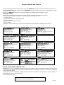
Main PCB
Position No.
2131, 2132
2115, 2116,
2223,2224,
2225,2226
2311, 2312,
2316, 2317
5110
3249, 3250,
3251,3252,
3711, 3712,
3713, 3714
Service code
9965 000 08117
4822 124 80123
Description
3300uF 25V
220uF 16V Silmic
4822 124 80958
470uF 16V Silmic
4822 146 10377
--
230V Transformer
Short circuited
R
CD6000 KI
Printed in The Netherlands
255W855020 ACT
3120 785 22570
First Issue:2001.04
CD6000 KI
Service
Manual
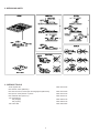
Transformer Connections
Below the color coding and the connections for the transformer wires are given.
Yellow
Green
9161
12.7 V
9162
14.7 V
Red
9163
9164
14.7 V
8.3 V
Yellow
9165
0V
Blue
Orange
9166
9167
8.3 V
0V
Brown
9168
3.4 V
Grey
Violet
Pink
0V
9158
Black
Orange
230 V
9159
White
R
CD6000 /N1B, /N1G, /T1B, /K1B, /K1G
CD6000F /N1B, /N1G, /T1B, /U1B, /F1B, /F1N
CD Player
CD6000
CD6000OSE
TABLE OF CONTENTS
1.
TECHNICAL SPECIFICATIONS .................................................................................. 1
2.
SERVICING HINTS ...................................................................................................... 2
3.
SERVICINE TOOLS ..................................................................................................... 2
4.
SERVICE MODE .......................................................................................................... 4
5.
MICROPROCESSOR AND IC DATA ........................................................................... 5
6.
BLOCK DIAGRAM ........................................................................................................ 7
7.
WIRING DIAGRAM ...................................................................................................... 9
8.
SCHEMATIC DIAGRAM AND PARTS LOCATION ................................................... 11
9.
EXPLODED VIEW AND PARTS LIST ....................................................................... 30
10.
ELECTRICAL PARTS LIST ........................................................................................ 34
Please use this service manual with referring to the user guide (D.F.U) without fail.
- CD6000 / CD6000OSE Printed in Japan
255W855010 AO
3120 785 00060
First Issue:1999.06
CD6000
Service
Manual
SERVICE BULLETIN
Circulation:
Date:
10-May-01
Page:
1/1
Model: CD6000/CD6000OSE
REF.NB
MZ01-013
Subject:
Application:
x for information
customer complaint in
case of service
mandatory
...................
Correction of parts code number and description
(POS. NO 5).
Service Manual
Int.ref:
[PHENOMENON]
The part number and description for POS.NO 5 mentioned on page 33 of the service
manual (255W855010, 3120 785 00060) are incorrect.
CD LOADER EXPLODED VIEW (page 33)
POS.
NO
5
VERS.
COLOR
PART NO.
(FOR PCS)
4822 402 61412
DESCRIPTION
BRACKET, STEEL
[CORRECTION]
The correct spare parts code number and description are;
POS.
NO
5
VERS.
COLOR
PART NO.
(FOR PCS)
4822 401 11709
DESCRIPTION
DISC CLAMP VAM1201 ONLY
Approved by H. Tamura
Written by K. Ono
SERVICE BULLETIN
Circulation:
Date:
16-Mar-01
Page:
1/1
Model:
CD6000,CD6000OSE
REF.NB
MZ01-004
Subject:
Application:
x for information
customer complaint in
case of service
mandatory
...................
SV00xxxxxxxxxx
XE00xxxxxxxxxx
XE01xxxxxxxxxx
XE02xxxxxxxxxx
Change of CD mechanism and CD loader
Int.ref:
[PHENOMENON]
CD mechanism and CD loader (with Disc clamper) was changed as follows.
Service code
SV00
XE00
XE01
XE02
CD
mechanism
VAM1201/01
VAM1202/02
VAM1201/11
VAM1201/11
Clumper
(color)
GRAY
BLACK
GRAY
GRAY
CD
loader
L1260/41
L1260/61
L1260/41
L1260/45
[SOLUTION]
When replace the CDmechanism with the new one as repair, please remark the service modification
code and refer to the following details.
1. In case of service modification code SV00, XE01, XE02
Replace the CD mechanism with the new one VAM1201/11 (4822 691 10615, 356K304500) only.
2. In case of service modification code XE00
Replace both the CD mechanism and the disc clamper with the new ones VAM1201/11 (4822 691
10615, 356K304500), disc clamper <GRAY> (4822 401 11709, 305K005600).
Approved by H. Tamura
Written by K. Ono
SERVICE BULLETIN
Circulation:
x for information
customer complaint in
case of service
mandatory
...................
Application:
SV00xxxxxxxxxx
XE00xxxxxxxxxx
and
XE01xxxxxxxxxx
Date:
16-Mar-01
Page:
1/1
Model:
CD6000,CD6000OSE
REF.NB
MZ01-003
Subject:
Problem with the function "DELETE PROGRAMMING".
Problem with the emphasis CD playback.
Int.ref:
[PHENOMENON]
Problem with the function "DELETE PROGRAMMING".
When playing back the CD in "DELETE PROGRAMMING" mode. If only one track is deleted,
then the next track and all following tracks will not be played back.
In case of several tracks are deleted, then it will be repeated to first track after playing back last
track.
Problem with the emphasis CD play back.
When playback several emphasis CD's continuously.
The second emphasis CD is played back without de-emphasis after the first emphasis CD has
played back.
[SOLUTION]
Replace the microprocessor 7600 with the improved one <uPD7806GF-098-3BA> (9965 000 06337,
HU255WN03F). The improved one is available with above code numbers.
[REMARK]
This improvement has been done in the production line after the service modification code number
“XE02” and later. The lot number and the service modification code are mentioned in the serial
number label on the rear panel. (ex. XE02 xxxxxxxxxx)
This service bulletin is the revised one (MZ00-009).
Please replace the service bulletin MZ00-009 with this one.
Approved by H. Tamura
Written by K. Ono
SERVICE BULLETIN
Circulation:
x for information
customer complaint
in case of service
mandatory
...................
Application:
SV00xxxxxxxxxx
and
XE00xxxxxxxxxx
Date:
10-Aug-00
Page:
1/1
Model:
CD6000,CD6000OSE
REF.NB
MZ00-009
Subject:
Problem with the function "DELETE PROGRAMMING".
Problem with the emphasis CD playback.
Int.ref:
[PHENOMENON]
Problem with the function "DELETE PROGRAMMING".
When playing back the CD in "DELETE PROGRAMMING" mode. If only one track is deleted,
then the next track and all following tracks will not be played back.
In case of several tracks are deleted, this phenomenon will not be appeared.
Problem with the emphasis CD play back.
When playback several emphasis CD's continuously.
The second emphasis CD is played back without de-emphasis after the first emphasis CD has
played back.
[SOLUTION]
Replace the microprocessor 7600 with the improved one <uPD7806GF-098-3BA> (9965 000 06337,
HU255WN03F). The improved one is available with above code numbers.
[REMARK]
This improvement has been done in the production line after the service modification code number
“XE01” and later. The lot number and the service modification code are mentioned in the serial
number label on the rear panel. (ex. XE01 xxxxxxxxxx)
Approved by Y. Okabe
Written by H. Tamura
SERVICE
BULLETIN
Circulation:
Date:
13-Jun-2003
Page:
1/1
Model: CD6000
REF.NBR: MZ00-007 Rev
Subject:
Application:
x for information
customer complaint
in case of service
mandatory
Recorded CD-R disc can not be played back
See below
Int.ref:
[ PHENOMENON]
Recorded CD-R disc can not be played back very few.
[REASONS]
CD player can not detect the CD-R disc.
[SOLUTION]
Add the capacitor <10pF 50V NP0 0805> (5322 122 32448, DD91100300) to the position 2509 on the HF AMP
PCB.
[REMARKS]
<Revision>
This solution has already been applied in the production after the serial number as below and later.
CD6000/N2G
CD6000F/N2G
CD6000L/N1G
CD6000F/N2B
CD6000L/N1B
CD6000L/T1B
CD6000/K2G
XE040312006992 and later.
XE040313008949 and later.
XE040312006383 and later.
XE040313009836 and later.
XE040312006273 and later.
XE040312003101 and later.
XE040316001063 and later.
Approved by S.Nagao
Written by
WQ-19 2 817/additional rule3 (1st Issue 2003-03-19)
SERVICE BULLETIN
Circulation:
x for information
customer complaint
in case of service
mandatory
...................
Date:
10-Aug-00
Page:
1/1
Model:
CD6000,CD6000OSE
REF.NB
MZ00-007
Subject:
Application:
Recorded CD-R disc can not be playback.
All
Int.ref:
[PHENOMENON]
Recorded CD-R disc can not be played back very few.
[REASON]
CD-R disc can not be detected by CD player.
[SOLUTION]
Add the capacitor <10pF 50V NP0 0805> (5322 122 32448, DD91100300) to the position 2509 on the
HF AMP PCB.
[REMARK]
This modification has to applied for product which has above mentioned phenomenon only.
Then this modification will be not applied at production.
Approved by Y. Okabe
Written by H. Tamura
MARANTZ DESIGN AND SERVICE
Using superior design and selected high grade components, MARANTZ company has created the ultimate in stereo sound.
Only original MARANTZ parts can insure that your MARANTZ product will continue to perform to the specifications for which
it is famous.
Parts for your MARANTZ equipment are generally available to our National Marantz Subsidiary or Agent.
ORDERING PARTS :
Parts can be ordered either by mail or by Fax.. In both cases, the correct part number has to be specified.
The following information must be supplied to eliminate delays in processing your order :
1. Complete address
2. Complete part numbers and quantities required
3. Description of parts
4. Model number for which part is required
5. Way of shipment
6. Signature : any order form or Fax. must be signed, otherwise such part order will be considered as null and void.
USA
EUROPE / TRADING
MARANTZ EUROPE B.V.
P.O.BOX 80002, BUILDING SFF2
5600 JB EINDHOVEN
THE NETHERLANDS
PHONE : +31 - 40 - 2732241
FAX
: +31 - 40 - 2735578
MARANTZ AMERICA, INC.
INC
440 MEDINAH ROAD
ROSELLE, ILLINOIS 60172
USA
PHONE : 630 - 307 - 3100
FAX
: 630 - 307 - 2687
AMERICAS
SUPERSCOPE TECHNOLOGIES, INC.
MARANTZ PROFESSIONAL PRODUCTS
2640 WHITE OAK CIRCLE, SUITE A
AURORA, ILLINOIS 60504 USA
PHONE : 630 - 820 - 4800
FAX
: 630 - 820 - 8103
NEW ZEALAND
SCAN AUDIO PTY. LTD.
8C PIERMARK DRIVE, ALBANY.
NORTH SHORE, AUCKLAND.
NEW ZEALAND
PHONE : +64 - 9444 - 4710
FAX
: +64 - 9444 - 1346
CANADA
LENBROOK INDUSTRIES LIMITED
633 GRANITE COURT,
PICKERING, ONTARIO L1W 3K1
CANADA
PHONE : 905 - 831 - 6333
FAX
: 905 - 831 - 6936
THAILAND
AUSTRALIA
SCAN AUDIO PTY. LTD.
52 CROWN STREET, RICHMOND 3121
VICTORIA
AUSTRALIA
PHONE : +61 - 3 - 9429 - 2199
FAX
: +61 - 3 - 9429 - 9309
BRAZIL
MARANTZ BRAZIL
CAIXA POSTAL 21462
CEP 04698-970
SAO PAULO, SP, BRAZIL
PHONE : 0800 - 123123(Discagem Direta Gratuita)
FAX
: +55 11 534. 8988
MRZ STANDARD CO.,LTD
746 - 754 MAHACHAI ROAD.,
WANGBURAPAPIROM, PHRANAKORN,
BANGKOK, 10200 THAILAND
PHONE : +66 - 2 - 222 9181
FAX
: +66 - 2 - 224 6795
TAIWAN
PAI- YUING CO., LTD.
6 TH FL NO, 148 SUNG KIANG ROAD,
TAIPEI, 10429, TAIWAN R.O.C.
PHONE : +886 - 2 - 25221304
FAX
: +886 - 2 - 25630415
JAPAN Technical
MARANTZ JAPAN, INC.
35- 1, 7- CHOME, SAGAMIONO
SAGAMIHARA - SHI, KANAGAWA
JAPAN 228-8505
PHONE : +81 42 748 1013
FAX
: +81 42 748 9190
SINGAPORE
WO KEE HONG (S) PTE LTD
WO KEE HONG CENTRE
NO.23, LORONG 8, TOA PAYOH
SINGAPORE 319257
PHONE : +65 2544555
FAX
: +65 2502213
MALAYSIA
WO KEE HONG ELECTRONICS SDN. BHD.
NO. 102 JALAN SS 21/35, DAMANSARA
UTAMA, 47400 PETALING JAYA
SELANGOR DARUL EHSAN, MALAYSIA
PHONE : +60 3 - 7184666
FAX
: +60 3 - 7173828
KOREA
MK ENTERPRISES LTD.
ROOM 604/605, ELECTRO-OFFICETEL, 16-58,
3GA, HANGANG-RO, YONGSAN-KU, SEOUL
KOREA
PHONE : +822 - 3232 - 155
FAX
: +822 - 3232 - 154
SHOCK, FIRE HAZARD SERVICE TEST :
CAUTION : After servicing this appliance and prior to returning to customer, measure the resistance between either primary AC
cord connector pins ( with unit NOT connected to AC mains and its Power switch ON ), and the face or Front Panel of product and
controls and chassis bottom.
Any resistance measurement less than 1 Megohms should cause unit to be repaired or corrected before AC power is applied, and
verified before it is return to the user/customer.
Ref. UL Standard No. 1492.
In case of difficulties, do not hesitate to contact the Technical
Department at above mentioned address.
990521A.O
1. TECHNICAL SPECIFICATIONS
Audio Characteristics
Channels ........................................................ 2 channels
Sampling frequency (CD mode) ....................... 44.1 kHz
Quantization ................................... 16-bit linear/channel
Error correction .. Cross-interleave read solomon code (CIRC)
D/A conversion ................................. 1-bit linear/channel
Wow & flutter ..................................... Precision of quartz
Optical Readout System
Laser ........................................... AIGaAs semiconductor
Wavelength ......................................................... 780 nm
Frequency Characteristics
Frequency range ....................................... 5 Hz - 20 kHz
Dynamic range .................................................... 98 dB
S/N ratio ............................................................ 110 dB
Channel separation (1 kHz) .............................. 103 dB
THD (1 kHz) ..................................................... 0.0025 %
Analog output
Output level (cinch JACKS) ...................... 2.0 V RMS
Output impedance .................................... 250 ohms
Digital output
Output level (cinch JACK) ............ 0.5 Vp-p/75 ohms
Output level (optical JACK) ......................... -19 dBm
Power Supply
Power requirement
/K version ............................ 110 / 220V AC 50/60 Hz
/N,/T version ..................................... 230V AC 50 Hz
/U version .......................................... 120V AC 60 Hz
Power Consumption ............................................. 13 W
Cabinet, etc.
Dimensions
Width .............................................................. 440mm
Height .............................................................. 86mm
Depth ............................................................. 312mm
Netweight (CD6000) .............................................. 4.1 kg
Netweight (CD6000F) ........................................... 5.6 kg
Operating temperatures ........................... +5
~ +35
Operating humidity ................. 5 % ~ 90 % (without dew)
Accessories
Remote control unit (RC6000CD) ................................. 1
AAA (R03) Batteries ...................................................... 2
Stereo audio cable with cinch pins ............................... 1
Remote cable with cinch pin ......................................... 1
Improvement may result in changes in specifications and
design without notice.
1
2. SERVICING HINTS
3. SERVICE TOOLS
Audio signals disc
Disc without errors (SBC444)+
Disc with DO errors, black spots and fingerprints (SBC444A)
Disc (65 min 1kHz) without no pause
Max. diameter disc (58.0 mm)
Torx screwdrivers
Set (straight)
Set (square)
13th order filter
2
4822 397 30184
4822 397 30245
4822 397 30155
4822 397 60141
4822 395 50145
4822 395 50132
4822 395 30204
ESD
WARNING
All ICs and many other semiconductors are susceptible to
electrostatic discharges (ESD). Careless handling during
repair can reduce life drastically.
When repairing, make sure that you are connected with the
same potential as the mass of the set via a wristband with
resistance. Keep components and tools at this potential.
WAARSCHUWING
Alle IC´s en vele andere halfgeleiders zijn gevoelig voor
electrostatische ontladingen (ESD).
Onzorgvuldig behandelen tijdens reparatie kan de levensduur
drastisch doen vermindern. Zorg ervoor dat u tijdens reparatie
via een polsband met weerstand verbonden bent met hetzelfde
potentiaal als de massa van het apparaat.
Houd componenten en hulpmiddelen ook op ditzelfde potentiaal.
ATTENTION
AVVERTIMENTO
Tous les IC et beaucoup d´autres semi-conducteurs sont
sensibles aux décharges statiques (ESD). Leur longévite
pourrait être considérablement écourtée par le fait qu´aucune
précaution nést prise à leur manipulation.
Lors de réparations, s´assurer de bien être relié au même
potentiel que la masse de l´appareil et enfileer le bracelet
serti d´une résistance de sécurité.
Veiller à ce que les composants ainsi que les outils que l´on
utilise soient également à ce potentiel.
WARNUNG
Alle ICs und viele andere Halbleiter sind empfindlich
gegenüber elektrostatischen Entladungen (ESD).
Unsorgfältige Behandlung im Reparaturfall kann die
Lebensdauer drastisch reduzieren.
Sorgen Sie dafür, daß sie im Reparaturfall über ein Pulsarmband mit Widerstand mit dem Massepotential des
Gerätes verbunden sind.
Halten Sie Bauteile und Hilfsmittel ebenfalls auf diesem
Potential.
Tutti IC e parecchi semi-conduttori sono sensibili alle scariche
statiche (ESD).
La loro longevità potrebbe essere fortemente ridatta in caso di
non osservazione della più grande cauzione alla loro
manipolazione. Durante le riparationi occorre quindi essere
collegato allo stesso potenziale che quello della massa
delápparecchio tramite un braccialetto a resistenza.
Assicurarsi che i componenti e anche gli utensili con quali si
lavora siano anche a questo potenziale.
AVAILABLE ESD PROTECTION EQUIPMENT :
anti-static table mat
large 1200x650x1.25mm
small 600x650x1.25mm
4822 466 10953
4822 466 10958
anti-static wristband
4822 395 10223
connection box (3 press stud connections, 1M )
4822 320 11307
extendible cable (2m, 2M , to connect wristband to connection box)
4822 320 11305
connecting cable (3m, 2M , to connect table mat to connection box) 4822 320 11306
earth cable (1M , to connect any product to mat or to connection box) 4822 320 11308
KIT ESD3 (combining all 6 prior products - small table mat)
4822 310 10671
wristband tester
4822 344 13999
AVAILABLE JIG for FR980
Extension PCB and wire kit
4822 395 10815
SAFETY
Safety regulations require that the set be restored to its
original condition and that parts which are identical with
those specified be used.
Safety components are marked by the symbol
Veiligheidsbepalingen vereisen, dat het apparaat in zijn
oorspronkeliijke toestand wordt teruggebracht en dat
onderdelen, identiek aan de gespecificeerde, worden toegepast.
De Veiligheidsonderdelen zijn aangeduid met het symbool
Les normes de sécurité exigent que l`appareil soit remis
à l`état d`origine et que soient utilisées les pièces de
rechange identiques à celles spécifiées.
Les composants de sécurité sont marqués
Le norme di sicurezza estigono che l´apparecchio venga
rimesso nelle condizioni originali e che siano utilizzati i
pezzi di ricambiago identici a quelli specificati.
Componenty di sicurezza sono marcati con
DANGER: Invisible laser radiation when open.
AVOID DIRECT EXPOSURE TO BEAM.
Varning !
Osynlig laserstrålning när apparaten är öppnad och
spärren är urkopplad. Betrakta ej strålen.
After servicing and before returning the set to customer
perform a leakage current measurement test from all
exposed metal parts to earth ground, to assure no
shock hazard exists.
The leakage current must not exceed 0.5mA.
Bei jeder Reparatur sind die geltenden Sicherheitsvorschriften zu beachten. Der Originalzustand des Gerätes
darf nicht verändert werden. Für Reparaturen sind Originalersatzteile zu verwenden.
Sicherheitsbauteile sind durch das Symbol
markiert.
CLASS 1
LASER PRODUCT
Advarsel !
Varoitus !
Usynlig laserstråling ved åbning når sikkerhedsafbrydere
er ude af funktion. Undgå udsaettelse for stråling.
Avatussa laitteessa ja suojalukituksen ohitettaessa olet alttiina
näkymättömälle laserisäteilylle. Älä katso säteeseen !
"Pour votre sécurite, ces documents doivent être utilisés par
des spécialistes agréés, seuls habilités à réparer votre
appareil en panne".
3
4. SERVICE MODE
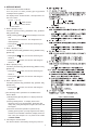
1. How to enter into the Service Mode
Turn the power on while pressing [PLAY]+[OPEN/
CLOSE] buttons together.
The display shows “model number”, “microprocessor version” and “mode”.
CD60:10P00
Mode number
Microprocessor version
Model number
2. Mode 0 (display “P 00”)
Condition: [FOCUS OFF], [SPINDLE OFF], [RADIAL
OFF], [MUTE ON]
• While pressing [NEXT
] button,the sledge moves out
side.
And, release from this button. The sledge return to
neutral position.
• Press [NEXT
] button, the function will change to
“Mode 1”.
3. Mode 1 (display “P 01”)
Condition: [FOCUS ON], [SPINDLE OFF], [RADIAL OFF],
[MUTE ON]
• Press [NEXT
] button, the function will change to
“Mode 2”.
• Press [PREV
] button, the function will change to
“Mode 0”.
4. Mode 2 (display “P 02”)
Condition: [FOCUS ON], [SPINDLE ON], [RADIAL OFF],
[MUTE ON]
• Press [NEXT
] button, the function will change to
“Mode 3”.
• Press [PREV
] button, the function will change to
“Mode 1”.
5. Mode 3 (display “P 03”)
Condition: [FOCUS ON], [SPINDLE ON], [RADIAL ON],
[MUTE OFF]
• Press [PREV
] button, the function will change to
“Mode 2”.
The following button operations are available at the
Service Mode.
1) While pressing [STOP] button, FL display shows all
segments.
2) Press [PAUSE] button. FL display shows each
segments one by one automatically. (Segments test
mode) And, press [PAUSE] button again, this mode will
be stopped.
3) The same as Normal operation is performed by
pressing [PLAY] button. (Except segments test mode.)
However if some default is detected, display shows an
error code. (For example: “Err 10”) Refer to the “Table
1 ERROR CODE”.
6. Canceling the Service Mode
The Service Mode is canceled by turning the power off.
Table 1 ERROR CODE
Error Code
4
Error
Err 02
FOCUS Error
Err 07
SUB CODE Error
Err 08
T. O. C. Error
Err 09
DECODER Error
Err 10
RADIAL Error
Err 11, 12
SLEDGE Error
Err 13
SPINDLE Error
Err 16 ~ 20
SEARCH Error
Err 30
DOOR Error
Err 31
TRAY Error
Err 32 ~ 47
BUTTON INPUT Error
5. MICROPROCESSOR AND IC DATA
PIN
1
2
3
4
5
6
7
8
9
10
11
12
13
14
15
16
17
18
19
20
21
22
23
24
25
26
27
28
29
30
31
32
33
34
35
36
37
38
39
40
41
42
43
44
45
46
47
48
49
50
51
52
53
54
55
56
57
58
59
60
61
62
63
64
SYMBOL
VSSA1
VDDA1
D1
D2
D3
VRL
D4
R1
R2
IrefT
VRH
VSSA2
SELPLL
ISLICE
HFIN
VSSA3
HFREF
Iref
VDDA2
TEST1
CRIN
CROUT
TEST2
CL16
CL11
RA
FO
SL
TEST3
VDDD1(P)
DOBM
VSSD1
MOTO1
MOTO2
SBSY
SFSY
RCK
SUB
VSSD2
V5
V4
V3
KILL
EF
DATA
WCLK
VDDD2(P)
SCLK
VSSD3
CL4
SDA
SCL
RAB
SILD
n.c.
VSSD4
RESET
STATUS
VDDD3(C)
C2FAIL
CFLG
V1
V2
LDON
DESCRIPTION
PIN
*analog ground 1
* analog supply voltage 1
unipolar current input (central diode signal input)
unipolar current input (central diode signal input)
unipolar current input (central diode signal input)
reference voltage input for ADC
unipolar current input (central diode signal input)
unipolar current input (satellite diode signal input)
unipolar current input (satellite diode signal input)
current reference output for ADC calibration
reference voltage output from ADC
* analog ground 2
selects whether internal clock multiplier PLL is used
current feedback output from data slicer
comparator signal input
* analog ground 3
comparator common mode input
reference current output pin (nominally 0.5VDD )
* analog supply voltage 2
test control input 1; this pin should be tied LOW
crystal/resonator input
crystal/resonator output
test control input 2; this pin should be tied LOW
16.9344 MHz system clock output
11.2896 or 5.6448 MHz clock output (3-state)
radial actuator output
focus actuator output
sledge control output
test control input 3; this pin should be tied LOW
* digital supply voltage 1 for periphery
bi-phase mark output (externally buffered; 3-state)
* digital ground 1
motor output 1; versatile (3-state)
motor output 2; versatile (3-state)
subcode block sync output (3-state)
subcode frame sync output (3-state)
subcode clock input
P-to-W subcode output bits (3-state)
* digital ground 2
versatile output pin 5
versatile output pin 4
versatile output pin 3 (open-drain)
kill output (programmable; open-drain)
C2 error flag; output only defined in CD ROM modes and 1fs modes (3-state)
serial data output (3-state)
word clock output (3-state)
* digital supply voltage 2 for periphery
serial bit clock output (3-state)
* digital ground 3
4.2336 MHz microcontroller clock output
microcontroller interface data I/O line (open-drain output)
microcontroller interface clock line input
microcontroller interface R/W and load control line input (4-wire bus mode)
microcontroller interface R/W and load control line input (4-wire-bus mode)
not connected
* digital ground 4
power-on reset input (active LOW)
servo interrupt request line/decoder status register output (open-drain)
* digital supply voltage 3 for core
indication of correction failure output (open-drain)
correction flag output (open-drain)
versatile input pin 1
versatile input pin 2
laser drive on output (open-drain)
SYMBOL I/O
EXCK
SBSO
SCOR
WFCK
MCK
XMODE
GND
I/O
I
I
I
I
I
8
TEST
I
9
SW1
I
10
SW2
I
11
12
13
14
SCLK
SRDT
DOSY
VDD
I
O
O
1
2
3
4
5
6
7
O4
O6
O3
O1
O5
O2
LDON
8
9
VDDL
RFE
10
11
12
13
14
RF
HG
LS
CL
ADJ
15
GND
16
17
18
19
20
21
22
23
24
LO
MI
VDD
I2
I5
I1
I3
I6
I4
PIN
1
2
3
4
5
6
7
8
9
10
11
12
13
14
15
16
7602 LC89170M
1
2
3
4
5
6
7
SYMBOL
DESCRIPTION
output of diode current amplifier 4
output of diode current amplifier 6
output of diode current amplifier 3
output of diode current amplifier 1
output of diode current amplifier 5
output of diode current amplifier 2
control pin for switching the laser
ON and OFF
laser supply voltage
equalized output voltage of sum
signal of amplifiers 1 to 4
unequalized output
control pin for gain switch
control pin for speed switch
external capacitor
reference input normally
connected to ground via a resistor
0 V supply; substrate connection
(ground)
current output to the laser diode
laser monitor diode input
amplifier supply voltage
photo detector input 2 (central)
photo detector input 5 (satellite)
photo detector input 1 (central)
photo detector input 3 (central)
photo detector input 6 (satellite)
photo detector input 4 (central)
7401/7402/7403 TDA7073A
Note : All supply pins must be connected to the same external power supply voltage.
PIN
7600 PD78076 MAIN
7500 TDA1302T
7405 SAA7372GP
FUNCTION
Subcode interface shift clock input and output
Subcode interface data Input
Subcode interface block synchronization Input
Subcode interface frame synchronization Input
Clock input (16.9344 MHz)
System reset and low power mode
Ground
Test pin (Must be connected to ground in normal
operation.)
EXCK I/O setting (L: clock output, H: clock input)
EXCK clock output pulse width selection (L: double
speed support, H: normal speed)
Command interface shift clock input
Command interface data output
Command interface readout enable output
Power supply
5
SYMBOL
IN1IN1+
n.c.
n.c.
VP
IN2+
IN2n.c.
OUT2+
GND2
n.c.
OUT2OUT1GND1
n.c.
OUT1+
DESCRIPTION
negative input 1
positive input 1
not connected
not connected
positive supply voltage
positive input 2
negative input 2
not connected
positive output 2
ground 2
not connected
negative output 2
negative output 1
ground 1
not connected
positive output 1
Pin No.
1
2
3
4
5
6
7
8
9
10
11
12
13
14
15
16
17
18
19
20
21
22
23
24
25
26
27
28
29
30
31
32
33
34
35
36
37
38
39
40
41
42
43
44
45
46
47
48
49
50
51
52
53
54
55
56
57
58
59
60
61
62
63
64
65
66
67
68
69
70
71
72
73
74
75
76
77
78
79
80
81
82
83
84
85
86
87
88
89
90
91
92
93
94
95
96
97
98
99
100
Port Name
OPEN
OPEN
OPTCNT
OPEN
OPEN
OPEN
OPEN
OPEN
GND
5MHz XTAL
5MHz XTAL
+5MP
REST
RC5I
DQSTN
CD7RN
SILDN
RAB7N
OPEN
OPEN
+5MP
+5MP
KEY0
KEY1
KEY2
KEY3
KEY4
KEY5
KEY6
KEY7
GND
DACDAT
RSTDD
+5MP
STBD
SIOD
CLKD
GND
SIDT
OPEN
CLKT
DACSTR
DACRST
OPEN
SDA
SCL
A0
A1
A2
A3
A4
A5
A6
A7
AD0
AD1
AD2
AD3
AD4
AD5
AD6
AD7
A8
A9
A10
A11
A12
A13
OPEN
OPEN
OPEN
OPEN
OPEN
OPEN
OPEN
RDN
WRN
OPEN
OPEN
RC5KILL
RC5OUT
TRAYM
OPEN
OPEN
OPEN
OPEN
CDRWO
SLSWN
OPEN
TRISN
OPEN
OPEN
OPEN
OPEN
OPEN
OPEN
OPEN
OPEN
Function
P120
P121
P122
P123
P124
P125
P126
P127
IC
X2
X1
Vdd
XT2
XT1
RESET
INTP0
INTP1
P02
P03
P04
P05
P06
Avdd
Avref0
ANI0
ANI1
ANI2
ANI3
ANI4
ANI5
ANI6
ANI7
Avss
P130
P131
Avref
P70
SO2
SCK2
Vss
SI1
SO1
SCK1
P23
P24
SB0
SB1
SCK0
A0
A1
A2
A3
A4
A5
A6
A7
D0
D1
D2
D3
D4
D5
D6
D7
A8
A9
A10
A11
A12
A13
Vss
A14
A15
P60
P61
P62
P63
RD
WR
P66
P67
P100
TO6
P102
P103
P30
P31
P32
P33
P34
P35
P36
P37
P90
P91
P93
P94
P95
P95
P96
7800 PD780204 DISPLAY
In/Out
Out
Out
In
In
In
In
Out
Out
In
In
In
Out
Out
Out
In
In
In
In
In
In
In
In
In
In
Active
High
Low
High
High
Low
Low
Low
Low
Low
Low
Low
Level
Level
Level
Level
In/Out
Out
Out
Out
Out
In
Out
Out
Out
Low
Low
In/Out
Out
Out
Out
Out
Out
Out
Out
Out
Out
In/Out
In/Out
In/Out
In/Out
In/Out
In/Out
In/Out
In/Out
Out
Out
Out
Out
Out
Out
Out
Out
Out
Out
Out
Out
Out
Out
Out
Out
Out
Out
In
In
In
In
In
In
In
In
Out
Out
Out
Out
Out
Out
Low
Low
High
High
Low
Low
Low
Low
To/From
----7318/7400
----------GND
5600
5600
+5MP
OPEN
+5MP
7603
6600
7602
7405
7405
7405
----+5VD
+5VD
Tact Switch
Tact Switch
Tact Switch
Tact Switch
GND
GND
GND
GND
GND
7311/7312
7800
+5MP
7800
7800
7800
GND
7602
--7602
7311/7312
7311/7312
--7405
7405
7601
7601
7601
7601
7601
7601
7601
7601
7601
7601
7601
7601
7601
7601
7601
7601
7601
7601
7601
7601
7601
7601
--------------7601
7601
----7605
7605/7316
7403
--------7500
VAM1201
--TRAY
-----------------
Description
Control signal a front digital output's power
Clock out(5MHz)
Clock in(5MHz)
Power supply +5V
Reset signal input
Input remote control signal
Request signal to read datas from 7602
CD7 Reset signal
Strobe signal for servo part of 7405
Strobe signal for servo part of 7405
Key Sensor
Key Sensor
Key Sensor
Key Sensor
Key Sensor(RESERVED)
Key Sensor(RESERVED)
Key Sensor(RESERVED)
Key Sensor(RESERVED)
Serial data signal for 7311/7312
Reset signal for 7800
Strobe signal for 7800
Serial data for 7800
Serial clock for 7800
Serial data signal from 7602
Serial clock signal from 7602
Serial data's Strobe signal for 7311/7312
Reset signal for 7311/7312
Serial data signal for 7405.
Serial clock signal for 7405
Adress signal for 7601
Adress signal for 7601
Adress signal for 7601
Adress signal for 7601
Adress signal for 7601
Adress signal for 7601
Adress signal for 7601
Adress signal for 7601
Data signal for 7601
Data signal for 7601
Data signal for 7601
Data signal for 7601
Data signal for 7601
Data signal for 7601
Data signal for 7601
Data signal for 7601
Adress signal for 7601
Adress signal for 7601
Adress signal for 7601
Adress signal for 7601
Adress signal for 7601
Adress signal for 7601
Read signal for 7601
Write signal for 7601
Cancell RC5 from IR sensor during output RC5
Syncrorecoding signal output
Tray motor control signal
In case of CD-RW disc,Gain up RF signal
Sledge detect switch (LOW : in end)
Tray in/out detect switch (LOW : in end)
Pin No.
1
2
3
4
5
6
7
8
9
10
11
12
13
14
15
16
17
18
19
20
21
22
23
24
25
26
27
28
29
30
31
32
33
34
35
36
37
38
39
40
41
42
43
44
45
46
47
48
49
50
51
52
53
54
55
56
57
58
59
60
61
62
63
64
65
66
67
68
69
70
71
72
73
74
75
76
77
78
79
80
81
82
83
84
85
86
87
88
89
90
91
92
93
94
95
96
97
98
99
100
6
Port Name
+5C
OPEN
OPEN
OPEN
OPEN
OPEN
OPEN
OPEN
OPEN
RESD
5MHz X’tal
5MHz X’tal
GND
OPEN
OPEN
+5C
OPEN
OPEN
OPEN
OPEN
OPEN
CLKD
OPEN
SIOD
GND
OPEN
OPEN
OPEN
OPEN
OPEN
OPEN
OPEN
OPEN
OPEN
GND
OPEN
OPEN
OPEN
STBD
GND
OPEN
OPEN
OPEN
SSEL
CSEL
+5VD
S40
S39
S38
S37
S36
S35
S34
S33
S32
S31
S30
S29
S28
S27
S26
S25
S24
S23
S22
S21
S20
S19
S18
S17
S16
S15
S14
S13
S12
S11
S10
S9
-VFT
S8
S7
S6
S5
S4
S3
S2
S1
G13
G12
G11
G10
G9
G8
G7
G6
G5
G4
G3
G2
G1
Function
Vdd
P37
P36/BUZ
P35/PCL
P34/TI2
P33/TI1
P32/TO2
P31/TO1
P30/TO0
RESET
X2
X1
IC
XT2
P04/XT1
Vdd
P27/SCK0
P26/SO0/SB1
P25/SI0/SB0
P24/BUSY
P23/STB
P22/SCK1
P21/SO1
P20/SI1
Avss
P17/ANI7
P16/ANI6
P15/ANI5
P14/ANI4
P13/ANI3
P12/ANI2
P11/ANI1
P10/ANI0
Avdd
Avref
P03/INTP3
P02/INTP2
P01/INTP1
P00/INTP0/TI0
Vss
P74
P73
P72
P71
P70
Vdd
P127/FIP52
P126/FIP51
P125/FIP50
P124/FIP49
P123/FIP48
P122/FIP47
P121/FIP46
P120/FIP45
P117/FIP44
P116/FIP43
P115/FIP42
P114/FIP41
P113/FIP40
P112/FIP39
P111/FIP38
P110/FIP37
P107/FIP36
P106/FIP35
P105/FIP34
P104/FIP33
P103/FIP32
P102/FIP31
P101/FIP30
P100/FIP29
P97/FIP28
P96/FIP27
P95/FIP26
P94/FIP25
P93/FIP24
P92/FIP23
P91/FIP22
P90/FIP21
Vload
P87/FIP20
P86/FIP19
P85/FIP18
P84/FIP17
P83/FIP16
P82/FIP15
P81/FIP14
P80/FIP13
FIP12
FIP11
FIP10
FIP9
FIP8
FIP7
FIP6
FIP5
FIP4
FIP3
FIP2
FIP1
FIP0
To/From
+5C
----------------7600
5800
5800
GND
----+5C
--------------7600
GND
------------------GND
------7600
GND
------+5C
GND
+5VD
FL
FL
FL
FL
FL
FL
FL
FL
FL
FL
FL
FL
FL
FL
FL
FL
FL
FL
FL
FL
FL
FL
FL
FL
FL
FL
FL
FL
FL
FL
FL
FL
-VFTD
FL
FL
FL
FL
FL
FL
FL
FL
FL
FL
FL
FL
FL
FL
FL
FL
FL
FL
FL
FL
FL
Description
Active
LED On/Off
LED On/Off
LED On/Off
LED On/Off
LED On/Off
LED On/Off
LED On/Off
LED On/Off
Low
Low
Low
Low
Low
Low
Low
Low
Scroll rule select (HIGH : CD6000)
Character select (LOW : CD6000)
Segment output
Segment output
Segment output
Segment output
Segment output
Segment output
Segment output
Segment output
Segment output
Segment output
Segment output
Segment output
Segment output
Segment output
Segment output
Segment output
Segment output
Segment output
Segment output
Segment output
Segment output
Segment output
Segment output
Segment output
Segment output
Segment output
Segment output
Segment output
Segment output
Segment output
Segment output
Segment output
Segment output
Segment output
Segment output
Segment output
Segment output
Segment output
Segment output
Gird output or Segment output
Gird output or Segment output
Gird output or Segment output
Gird output or Segment output
Gird output or Segment output
Gird output or Segment output
Gird output or Segment output
Gird output or Segment output
Gird output or Segment output
Gird output or Segment output
Gird output or Segment output
Gird output or Segment output
Gird output
Gird output
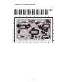
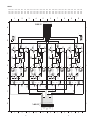
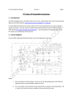
6. BLOCK DIAGRAM
DIODE AMP &
LASER SUPPLY
TDA 1302T
(DALAS)
SIGMADELTA DAC
WITH 8X FIR
FILTER
H.D.A.M.
CIRCUIT
LOADER 1210/41
DIGITAL SERVO
RESET
CIRCUIT
SERVO DRIVER
TDA 7073A
SERVO DRIVER
TDA 7073A
SERVO DRIVER
TDA 7073A
C.D. DECODER
SAA 7372
L/R
SEPARATING
LOGIC
CIRCUIT
INTERFACE
MUTING CIRCUIT
CONTROLLER &
CD6000 : use
NJM2114D X 2
CD6000 OSE : use
H.D.A.M X 4CH
SIGMADELTA DAC
WITH 8X FIR
FILTER
H.D.A.M.
CIRCUIT
CD TEXT
DECODER
LC89170M
5 MHz
RESONATOR
µP
32kX8 SRAM
uPD43256BGU
uPD78076
MAIN CPU
POWER
SUPPLY
MAINS
+TRAFO
FTD
RC5 BUFFER
CIRCUIT
5 MHz
RESONATOR
IR-EYE
GP1U28XP
µP
uPD780204
DISPLAY DRIVER
7
KEY MATRIX
8
HEADPHONE
OUT
2.0V
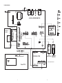
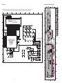
7. WIRING DIAGRAM
TRAFO
AUDIO AMPLIFIER PCB
VAM
HF Amp
PCB
HDAM PCB
12p ZIF FFC
CD Mecha
L1210/41
(OSE version only)
CONTROL PCB
Optical Out
Headphone Jack
(F/K version only) (Beige = GL)
(Black = BL)
* PROVISION ON LAYOUT
Front PCB
9
10
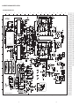
8. SCHEMATIC DIAGRAM AND PARTS LOCATION
AUDIO AMPLIFIER PCB AF PART
1
2
3
4
5
6
7
8
9
10
11
12
13
14
15
16
17
A
A
2217
N,T,F,K ONLY
VF
LAST UPDATED ON 23 MAR 99 (912.2)
3
4
5
11
VF
VF
VFTD
10K
3121
470u
2711
+5.0V
3241
470u
2223
22R
10K
3259
A
2K2
2227 100p
100K
A
D
L-CH
AUDIO-OUT
R-CH
3256
100R
100u
3268
7234
A
7232
A
BC557B
7316
4K7
RC5OUT
+5D
6315
1N4148
2228 100p
2346
5
6
1
2
EXT
GD
INT
2
22K
1
A
3344
47K
7
4
47p
0.0V
RC-5 IN/OUT
+0.8V
YKC21-3046
1312
1311
1
2
EH-B
TO 1805
K
3
3341
FOPT
4K7
3342
22R
FRONT OPT OUT
D
0.0V
D
L
VF
7
J
3
0.0V
5313
50R
OPCNT
I
2342
D
+5.0V
7317
BC547B
BC557B
7318
3260
8
47K
3347
RC5IN
+5D
3
3274
2SC2878
3266
12K
15K
RC INT/EXT SW
+5.0V 3348
2K2
2K2
A
HEADPHONE OUT
3343
-12V
RCINTER
+5D
2343
0.0V
0.0V
68R
3278
R-CH
1
22R
68R 0.0V
3276
1315
SSSU
TO 1803
22K
3282
100K
6
3272
2SC2878
GD
GD
L-CH
4
A
3
3270
H
3
1214 EH-B
0.0V
7231
OPTICAL OUT
DRIVER
2344
2K2
100n
2K2
1
3350
100n
68R 0.0V
3277
10u
68R 0.0V
3275
7233
A
7235-B
NJM4556AD
7
1314
2 GP1F32T
22R
DOBM
0.0V
8
100n
10u
2347
3351
270R
2SC2878
G
5312
+5D
22R
3271
2
5
8
2345
GD
2341
2SC2878
3265
12K
3280
YKC21-3394
1313
100n
3353
GD
COAXIAL OUT
2
6
7
2348
560R
-12V
1
10R
50R
3269
3267
100R
3
3352
4
1
100p
22R
+12V
A
H/P-R-OUT
E
F
3349
0.0V
A
2
100R
2
A
5311
7CHA
3345
3281
100K
7235-A
NJM4556AD
1
100K
2K2
A
A
0.0V
A
2229
3264
2K2
3262
A
A
A
7124
BC547B
22R
2SC2878
7230
H/P-R-OUT
10K
220u
22R
8
-12V
+12V
-11.6V
3258
3248
2222
2220
470u
2226
2SJ74
7226
A
YKC21-3337
1211
3273
3
A
+11.6V
100u
3254
100R
2SC2878
7228
470u
2224
22R
3244
100R
3240
2216
3238
1K
6218
220u
A
A
3124
A
22R
3242
6214
+10.4V
6216
1N4148 1N4148
1K
3230
3228
33K
3236
-10.8V
6220
1N4148
2212
2214
68R
3279
4
PMUT
22K
3263
2225
6217
470u
2K2
3261
A
3346
1N4148
3247
150p
22R
3239
100R
2215
3237
1K
6215
1N4148 1N4148
1K
3229
6212
1N4148 1N4148
3226
120R
120R
3224
3214
10K
390p
POWN
D
22R
+12V
H/P-L-OUT
D
BZX79-C5V6 6122
6121
+4.4V
10K
7123
BC547B
C
A
2SC2878
7229
+4.3V
-12V
3324
2230
2
22K
3257
3
-10.8V
150p
470u
100p
0.0V 22R
+5.0V
3123 +4.5V
BC557B
7122
3243
6211
6213
1N4148 1N4148
+10.4V
3235
1N4148
-10.8V 6219
33K
3225
68R
3227
2213
100p
10K
3219
470u
3m3
3K3
10K
3116
47K
10u
BC557B
7121
3120
100R
-10.2V
4 -12V
3125 0.0V
BZX79-C4V7 -26.0V 47K
6
120R
3223
10K
47u
47u
2121
2122
4m7
2119
2125
3115
1m
2123
2127
7120
-26.0V BC547B
VFTD 6127
2211
390p
22R
3713
-12V-R
2714
22R
3714
2722
3722
120p
12K
220u
-12V-L
-12V-L
-12V-R
470u
To HDAM
10K
3738
2712
3721
120p
2721
2720
3720
120p
12K
To HDAM
10K
3734
+1.4V
10K
2713
2719
12K
3719
120p
3723
10K
12K
47R
VF VF
120R
470u
47n
220u
10K
2323
3727
3729
10K
2117
2118
VFTD
-26.0V
BC557B
7314
-12V
D
0.0V
3122
1N4003
0.0V
3252
100R
+4.4V
7118
BC547B
D
+5S
+5S
47K
6125
2129
2SA970
7220
68R
-11.6V
100K
+5D
-21.0V
3119
100u
6123
4n7
2128
2
47n
7119
L7918
7
BZX79-C8V2
47u
0V
3234
-10.5V
-11.1V
2
1
7117
BC547B
D
VF2
A
7222
2SC2240
18K
A
7224
2SK170
3
A
3246
7216
S
0004
S
7116
BC547B
VF1
4
100u
3
1M
D
-21.0V
8
1
0.0V
A
+10.3V
1N4148
3113
D
7212
2SK369BL
4
2
+4.3V
+12V
D
D
4R7
6128
D
2126
2
4
1
1K
+9.6V
6126
1113
SDDL
1
2
L
6120
6119
D
3111
7214
1
A
2SA970
7218 3232
68R
3323
+5S
3114
1u
9
6118
5
1112
1N4003
U ONLY
2133 220u
K
3725
10K
2725
2724
3732
11
3
1N4003
1N4003
9113
3
6124
U ONLY
1N4003
9111
9112
1
2
4
5
6
1111
SDKGA
12
2
+10.9V
3222
A
0002
+5.0V
+10.1V
100R
2SC2878
7227
+12V
22R
288K109020
LMUT
Z
6115
6117
1N4003
18K
0005
15K
7115
L7805
3255
-12V
3250
100p
100K
1
2SJ74
7225
3253
A
3
47K
7313
+3.7V
S
T
1N4003
10K
+5.0V
+5.0V
A
RMUT
+5Z
7114
L7805
1N4003 6116
VALUE
13
110V
47n
T630MA
1115
10
B2P3-VH
-11.6V
1N4003
VALUE
T630MA
220V
10K
1N4148
-12V
K ONLY
14
110V
A
1215
+12V
3216
10K
3319 +4.4V
1N4148
A
9112 F,U ONLY
J
2313
2311
47n
2319
3735
10K
100p
2114
470u
47n
2112
1N4003
1N4003
9111 F,U,K ONLY
220V
6313
0.0V
3117
47n
2113
6113
1114
5110
LKILL
0.0V
5314
0.0V
2
POWN
3321
47K
7113
L7805
H/P-L-OUT
LMUT
2SC2240
10K
+11.6V
220u
3251
+11.6V
3218
6314
6114
9113 N,T ONLY
A
1N4148
RKILL
2221
2219
-10.2V
+3.7V
+12V
7112
-15.3V L7912
2132
A
220u
22R
+10.9V
2SK369BL
BC557B
3320
0V
0V
1212
TKC-A
0.0V
3322
1N4003
0V
Z
-10.8V
22R
2218
3212
1
6311
PMUT
0.0V
-11.6V
3712
A
A
1N4148
T
I
A
7111
2131,2
OSE ONLY L7812CP
1N4003
+15.3V 2131
6112
230V
Z
+5Z
4R7
3245
0.0V
RMUT
-R
6312
6111
-11.1V
B
22R
2113,4
6000 ONLY
2111
120V
100V
240V
+0.8V
3314
2SA970
7219
68R
-10.5V
-12V
Z
Z
H
+12V-L
+12V-R
0.0V
15
3233
1
A
A
16
A
22R
3220
DVSS
+L
+12V-R
A
A
7223
2SK170
3
A
A
A
10K
RSTN
17
3
2
7221
2SC2240
7215
A
4
+12V
1
NJM2114D
8 7712-A
2120
5110 U ONLY
DVDD
A
2116
47n
5110 F ONLY
AVDD1
MLEN
+5Z
20
19
18
-12V-R
2
470u
14
A
MCK
12K
47n
13
LO
+12V-L
+12V-L
CD6000 ONLY
+0.8V
18K
1
3711
7
+12V-R
+12V-R
A
6
CD6000 ONLY
5
8 NJM2114D
5
7712-B
GND
7
4
GND
6
3
4 -12V-R
+R
A
2
2716 120p
3716
21
3221
A
8
12K
3718
2318
2316
12
DACSTR
MDT
22
2326
5110 N,T ONLY
SCL
LON
AVSS1
D1
11
DACRST
Z
BCK1
5
2718 120p
4
2124
D
9120
G
10
A
9119
S
9
DOR
100p
A
7
7711-B
8 NJM2114D
A
23
3112
22K
D
AVDD2
LRC1
BCLK02
DACDAT
AVDD3
24
470u
D
9118
RON
MCOM
25
2726
2115
9117
VF
MUTE1
8
2324
7
3318 10K 8
A
RO
AVSS2
SM5872BS
WCLK02
D
7312
MUTE0
27
26
470u
Z
XVDD
AVDD4
CKO
6
+5Z
XVSS
CKSL
+1.4V
3
7 +0.8V
28
3736
2
Z
XT1
10K
XTO
-R2
+R2
+1.4V
47n
1
D
9181
6 +0.8V
3118
47R
CD7
10K 3726 -R1
47n
A
GD
A
Z
+5G
A
9115
5 +0.8V
3730
Z
CLKOUT3
5
T
47n
3336
470R
9114
+5G
U500
4 +0.8V
10K 3724 +R1
DOL
Z
3 +0.8V
10K 3733+L2
+1.4V
4R7
3335 470R
3316 10K 4
+5G
3312
2
10K 3731-L2
2322
+5Z
BCLK01
CD6000 ONLY 6
100p
+5G
Z
1
12
-L
11
GND
10
GND
9
2717 120p
4
-12V-L
TKC-A
1213
+1.4V
Z
Z
12K
+L1
-L1
+1.4V
3334 470R
+5Z
F
4R7
10K
WCLK01
3313
3217
0.0V 10K
A
12K
3717
+0.8V
68R
22R
288K109020
0003
A
2SA970
7217 3231
0.0V 2SK369BL
7211
2SC2240
3715
2723
470u
47n
Z
Z
BCLK1
+1.4V
Z
+5Z
Z
+10.9V
7213
-12V-L
4
+1.4V
15
2325
DIN
Z
2
A
100p
10K
MODE2
VDD3
DVSS
V
A
7711-A
NJM2114D
1
2715 120p
16
+5G
11
9
10
DINV
SEL24-32
8
7
VSS2
VSS3
6
5
VDD1
4
1
VDD2
VSS15
DVDD
RSTN 5.0
+0.8V
8
17
AVDD1
MLEN 5.0 V
3
A
2320
VSS4
MODE1
DOL
VDD10
SONY-12S
WCLKI
LO
+12V-L
A
1m
BCLK01
VSS14
18
1m
VSS5
19
3728
VDD4
TC160G11AU
VSS13
20
470u
VDD9
13
V
5.0 V
18K
CD6000 ONLY
21
AVSS1
MCK
3215
10K
-12V
+5Z
22
470u
WCLK01
7315
LON
A
10K
VSS12
BCK1
3211
+10.9V
2SK369BL
23
2315
2317
VSS8
VSS6
12 13 14 15 16 17 18 19 20 21 22
24
23
DOR
25
BCLK02
27
26
VDD6
WCLK02
28
VSS9
30
29
VDD7
CKOUT1
32
31
CKOUT2
VSS10
CKOUT3
XTOUT
VSS1
E
VSS7
3
+5G
0.0 V DIN
XTIN
AVDD2
MDT 0.0
12
DACSTR
LRC1
D1
11
DACRST
14
VDD5
VDD8
BCLKI
WCLK1
2331 100n
+5G
VSS11
2
+5G
44 43 42 41 40 39 38 37 36 35 34
D
3325 1M
3326 220R
33
SCL
Z
RON
AVDD3
Z
24
AVSS2
MCOM
Z
4R7
0.0V
47n
10
DACDAT
RO
MUTE1
+5Z
26
25
3737
DOR
BCLK02
3333
470R
3332
9
DOL
7311
47n
47n
2328
2327
+5G
+5G
470R
CLKOUT3
7
WCLK01
BCLK01
AVDD4
SM5872BS
3317 10K 8
470R
3331 WCLK02
C
3330 100R
Z
Z
+5Z
XVDD
CKSL
MUTE0
2
1
5
Z
Z
XVSS
CKO
6
3328 470R
Z
3
3315 10K 4
Z
10p
10p
2329
AT-49
16M9344
5310
2330
B
Z
+5Z
+5G
4R7
27
2314
2312
3327
+5Z
220u
CLKOUT1
1216
35022
XT1
2321
XTO
2
3311
28
3213
CLKOUT3
1
3249
100p
+11.6V
AF Part
+12V
8
9
10
11
12
13
14
15
12
16
17
0002 I8
0003 B12
0004 I8
0005 E12
1111 J2
1112 K3
1113 K3
1114 I6
1115 J6
1211 E16
1212 E9
1213 D7
1214 H14
1215 C16
1216 B2
1311 K11
1312 J16
1313 G16
1314 H16
1315 I16
2111 H5
2112 I5
2113 H6
2114 I6
2115 H6
2116 I6
2117 I6
2118 J6
2119 J7
2120 H8
2121 I8
2122 J8
2123 J6
2124 K7
2125 K7
2126 L5
2127 L6
2128 K3
2129 L5
2131 H6
2132 H6
2133 L5
2211 B10
2212 F10
2213 C10
2214 G10
2215 C13
2216 G13
2217 A13
2218 E13
2219 C14
2220 F14
2221 C14
2222 F14
2223 B13
2224 E13
2225 C13
2226 G13
2227 D16
2228 E16
2229 I10
2230 J10
2311 B7
2312 E5
2313 B7
2314 E5
2315 D5
2316 G7
2317 D5
2318 G7
2319 B6
2320 F6
2321 C6
2322 G6
2323 C7
2324 G7
2325 D4
2326 G4
2327 B3
2328 B3
2329 C1
2330 C2
2331 E1
2341 I15
2342 J16
2343 J16
2344 H16
2345 G15
2346 G16
2347 G15
2348 G15
2711 D9
2712 E9
2713 C9
2714 F9
2715 C8
2716 E8
2717 D8
2718 F8
2719 C8
2720 E8
2721 D8
2722 F8
2723 C6
2724 E6
2725 D6
2726 F6
3111 J6
3112 K6
3113 J7
3114 J7
3115 J7
3116 J8
3117 J8
3118 K6
3119 K6
3120 L7
3121 L7
3122 L7
3123 K8
3124 K8
3125 K9
3211 B10
3212 E10
3213 B10
3214 E10
3215 B10
3216 E10
3217 C10
3218 G10
3219 C10
3220 G10
3221 C10
3222 G10
3223 B10
3224 E10
3225 B10
3226 E10
3227 C10
3228 G10
3229 C11
3230 G11
3231 B12
3232 F12
3233 B12
3234 F12
3235 C12
3236 F12
3237 C12
3238 G12
3239 C13
3240 F13
3241 B13
3242 F13
3243 C13
3244 F13
3245 C13
3246 F13
3247 C14
3248 F14
3249 A14
3250 E14
3251 D14
3252 G14
3253 C15
3254 E15
3255 C15
3256 E15
3257 C16
3258 E16
3259 D16
3260 E16
3261 D15
3262 E15
3263 D15
3264 E15
3265 I11
3266 J11
3267 H12
3268 J12
3269 H12
3270 I12
3271 H13
3272 I13
3273 H14
3274 I14
3275 H12
3276 I12
3277 H13
3278 I13
3279 H11
3280 I11
3281 H11
3282 I11
3311 A7
3312 D5
3313 D5
3314 G7
3315 B4
3316 F4
3317 C4
3318 F4
3319 G9
3320 H9
3321 G9
3322 H9
3323 H10
3324 H10
3325 D1
3326 D1
3327 B3
3328 C2
3330 C2
3331 C3
3332 C3
3333 C3
3334 D4
3335 E4
3336 E4
3341 K10
3342 K10
3343 J15
3344 J15
3345 J15
3346 J15
3347 I14
3348 I14
3349 I15
3350 H16
3351 H15
3352 G16
3353 G15
3711 D10
3712 D10
3713 C9
3714 F9
3715 C8
3716 E8
3717 C8
3718 F8
3719 C7
3720 E7
3721 D7
3722 F7
3723 D7
3724 D6
3725 D6
3726 E6
3727 C6
3728 E6
3729 C6
3730 E6
3731 D6
3732 E6
3733 D6
3734 E6
3735 D6
3736 F6
3737 D6
3738 F6
5110 J4
5310 B2
5311 F15
5312 H16
5313 K11
5314 H8
6111 H5
6112 H5
6113 H5
6114 I5
6115 I6
6116 J6
6117 J6
6118 J6
6119 K6
6120 K6
6121 K8
6122 J8
6123 L5
6124 J5
6125 K5
6126 L6
6127 L6
6128 J7
6211 B12
6212 E12
6213 B12
6214 E12
6215 C12
6216 G12
6217 D12
6218 G12
6219 C11
6220 F11
6311 G8
6312 H8
6313 G8
6314 H8
6315 J15
7111 H6
7112 H6
7113 H7
7114 I7
7115 I7
7116 J7
7117 K7
7118 J8
7119 K6
7120 L6
7121 L7
7122 K7
7123 L8
7124 K9
7211 B10
7212 F10
7213 B11
7214 F11
7215 C10
7216 G10
7217 B11
7218 F11
7219 B12
7220 F12
7221 C12
7222 F12
7223 B13
7224 E13
7225 C13
7226 G13
7227 C14
7228 E14
7229 D15
7230 E15
7231 H13
7232 J13
7233 H13
7234 J13
7235-A H12
7235-B I12
7311 B5
7312 F5
7313 G9
7314 H9
7315 D3
7316 I15
7317 J15
7318 K11
7711-A C8
7711-B D8
7712-A F8
7712-B E8
9111 J3
9112 J3
9113 J3
9114 F3
9115 F3
9117 F3
9118 G3
9119 G3
9120 G3
9181 F3
U500 F2
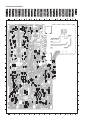
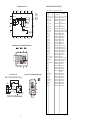
AUDIO AMPLIFIER PCB COMPONENT SIDE VIEW
13
14
AUDIO AMPLIFIER PCB COPPER SIDE VIEW
15
16
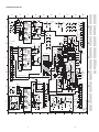
AUDIO AMPLIFIER PCB SERVO PART
1
2
3
TRAYM
1401
CD7
12K
2
3
Provision
TDA7073
3 TRAY-
16
4
+5.0V
NC
3
7
NC
7
10
74HC00D
S
+5.0V
0.0V
+5.0V
-
9
NC 8
D
S
S
S
REF
+2.5V
SILD
RAB
DOBM
9
SCL
+5NAND
10
SDA
+5.0V
11
TO FRONT PCB
THRU CONTROL
D
D1
0.0V D2
0.0V D3
0.0V D4
0.0V
4.8V
FRONT END
VERSATILE PINS
INTERFACE
INTERFACE
12
OPCNT
+5.0V
13
7400-D
OPCNT
D
TKC-A
To 1601 on Control PCB
74HC00D
74HC00D
7
D
8
7
TKC-A
44
NC
7400-B
6
74HC00D
3450
FOPT
100R
7
D
D
D
2
3
17
4
5
6
7
8
SCOR
11
WFCK
9
RCINTER
8
RC5
7
RC5OUT
6
RC5IN
5
SBSO
+5.0V
4
0.0V
DACSTR
3
+5.0V
DAC
DACRST
18
F
2
1
To 1603 on Control PCB 1303
9
E
EXCK
DACDAT
Dated: 23 Mar 99 (912.2)
1
0.0V
12
10
14
4
DIN
To I2S Decoder
on Sheet 1
48
46
45
0.0V
0.0V
to muting circuit
+5.0V
to front optical out
BCLK1
WCLK1
3420 470R
31
LKILL
+5NAND
5
9
7400-C
NC
D
DOBM
3422 470R
3421 470R
43
RKILL
To dig. out
circuitry
on Sheet 1
60
KILL
62 63 42 41 40
+5.0V
11 10
OUTPUT STAGES
+5.0V
MICRO-
57
3461 470R
47u
R2
0.0V R1
0.0V
3402 22K
3401 22K
100n
2409
4.8V
14
14
PEAK
DETECT
DECODER
CD6000K & CD6000OSE F Only
12
3423 47R
61
NC
PROCESSOR
SUBCODE
PROCESSOR
+5NAND
EBU_GND
FLAGS
PROCESSOR
CDTEXT{SCOR,WFCK,SBSO,EXCK}
8
2420 100p
55
ADDRESSER
NC NC
7
1403
NC
ERROR
AUDIO
35
36
38
37
58
3419 470R
EXCK
CD7R
6
3403 22K
3404 22K
2410 22n
3417 470R
WFCK
3418 470R
7405
CORRECTOR
CD7
+5.0V
3444 1K
7400-A
+
2443 47n
2
S
5
3416 470R
SCOR
MOTO2
34
RAM
L
MOTO1
MOTOR
CONTROL
SRAM
+5B 3455 22K
L
NC
SBSO
4
6
+2.5V
11
S
5
2442
47u
100n
47u
2423
D
D
1
DDV
12
2440
47u
NC
S
2441
3446
4R7
3
NC OUT1-
14
2424
NC
13
+5NAND
F
D
2
+
S
CD6000K &
CD6000OSE F Only
+5.0V
7403
+5.0V
3459 1K
TRAYSW
+5S
+5S
22n
+5D
NC
14
3443
15
XH-B +2.5V
1
-
47n
2439
NC
TRAY+
470R
4
+5.0V
3445 1K
+5.0V
1
2499
2
3460
E
1
47n
+2.5V
100K
2407 47n
PLL
C
LDON
33
DIGITAL
DEMODULATOR
1
1300
SL
64
SAA7372
EFM
TEST
B
CLKOUT1
FO
PROCESSOR
INTERFACE
-21.0V
RA
27
28
PART
CD7
13
21
22
24
NC 25
NC
50
2
EBU
SERIAL DATA
INTERFACE INTERFACE
CLKOUT1
3411
CONTROL
100p
1
1217
1217 CWAS for U1B only
1402
2401
47u
1K
470p
3410
2417 47p
CDCTRL{SILD,RAB,SCL,SDA}
2415 220p
2413 220p
2414 220p
2411 220p
47n
2416 220p
47n
3456 12K
1K2
4n7
3436
2.5V
2432
22R
35022
CDRWO
2408 1n
2
FUNCTION
2422
L
0.0V 1
CD7
L
PROC.
MICRO
TIMING
2
LDGU{HF,O6R2,O5R1,O1R,O2D1,O3D2}
Fr I2S Decoder
on Sheet 1
20
23
29
100R
O3D2
LDON
15
17
14
18
3
3949 56 30 47 59
CONTROL
-21.0V
4
TEX
2406 47n +5B
CD7
-26.0V
5
VF1
2405 47n +5B CD7
CD7
PRE-
7
6
VF2
5403
VREF
GENERATOR
52
51
53
54
100p
3
RA+
11
VF
VFTD
CD7
CD7
1 12 16 2 19
ADC
8
5402
CD7
DA L
6 3 4 5 7 10
3449
O2D1
TRACK
DA
8
9
2421
4
2.5V
R2
R1
D4
D3
D2
D1
L
9
D
CD7
DA
3406 470R
SCL
3405 470R
SDA
0.0V
3407 470R0.0V
RAB
3408 470R 0.0V
SILD
2444 47p
3409 22K
HF
O1R
8
+5B
DA DA DA DA DA DA
3427 10K
5
NC
ADC{D1,D2,D3,D4,R1,R2}
CD7
+5B
A
10
+5D
DA
2404 47n
CD7
330K
SCL
3426 10K
O5R1
9
2403 47n
3400
DA
CD7
O2D13429 10K
0.0V
6
-
10
S
U402
L
+5.0V
11
CD7
5401
+5A
CD7
REF
10K
D
2402 47n
L
4403
O3D2 3428 10K
0.0V
O6R2
7
L
12
+5D
U401
CD7
VF
CD7
to DAC on Sh 1
3441
D
DAC
SLSW
CD7
4409
4402
4410
12K
S
U400
DA
+5A
TEX
O1R
0.0V
7
+
NC
RA
3415
D
RC5
+4.8V
4405
4404
3424 10K
0.0V
L
11
2.5V
4R7
CD7
EBU_GND
O6R2
0.0V
8
6
3435
2437
+5A
9
DDV
12
RA-
FO
+5S
5
DA
S
10K
3
NC 4
OUT1-
S
2435
4.8V
FO-
2.5V
1K
CDRWO
10
NC
13
2433
2438
HF
11
2
+
470p
4n7
3440
2.4V
7402
FOCUS
2436
L
3442
12
NC
14
To 1602 on Control PCB
TKC-A
4401
SL
REF
100n
L
3437
14
FO+
1
-
15
2434
FO-
16
100n
15
TDA7073
22R
RA+
ACTU{RA-,RA+,FO+,FO-}
16
13
10
SERVO{LDON,MOTO1,MOTO2,RA,FO,SL}
L
FO+
RA-
2400
100n
2426
2427
3432
1K
3414 12K
REF
17
+5.0V
CD7
SLIDE
FE-BT-VK-N
+5.0V
D
10K
2412 220p
8
To 1500 on HFAmp PCB
C
100n
S
NC
+5.0V
O5R1
-
9
+2.5V
9
4406
+5B
+5D
4.8V
MOTO2
3425 10K
10
3451
CD7
+5S
SERVO{LDON,MOTO1,MOTO2,RA,FO,SL}
7
4R7
100n
NC
3458 S
2.5V
6
2431
11
+
1K
12
3457
22R
3462
1400
+5.0V
MOTO1
100n
BXXB-XH
NC
4
5
DDV
100n
2445
6
NC
+5A
+5D
2428
OUT1-
+2.5V
8
REF
2429
13
3
2.5V
2425
100n
+
100n
7401
14
4
+4.6V (Laser On)
3452
3413 12K
2
2430
NC
15
5
1
-
3
+2.5V
7
3412 12K
TURNTABLE
TDA7073
16
22R
3430
2
+2.5V
6
SLSW
2446
S
1
B
5
100n
AF Amp PCB - servo part
A
4
+5.0V
DC voltages
measured in
play mode
10
V
1217 D6
1300 B10
1303 F10
1400 A1
1401 E2
1402 E1
1403 F5
2400 A6
2401 A7
2402 B8
2403 B8
2404 B9
2405 B9
2406 B9
2407 C9
2408 D6
2409 D7
2410 D7
2411 C5
2412 C5
2413 C5
2414 C5
2415 C5
2416 C6
2417 D7
2420 D9
2421 F7
2422 F8
2423 F1
2424 F1
2425 A2
2426 A4
2427 A4
2428 A4
2429 A4
2430 B4
2431 B4
2432 C4
2433 B4
2434 C2
2435 D2
2436 C4
2437 C4
2438 C4
2439 F4
2440 F4
2441 F4
2442 F4
2443 F4
2444 C7
2445 A2
2446 A2
2499 E5
3400 B7
3401 C7
3402 C7
3403 C7
3404 C7
3405 C7
3406 C7
3407 C7
3408 C7
3409 C7
3410 D6
3411 D7
3412 A4
3413 A4
3414 A4
3415 C4
3416 D7
3417 E7
3418 E7
3419 E7
3420 D9
3421 D9
3422 D9
3423 D9
3424 D5
3425 D5
3426 D5
3427 D5
3428 D5
3429 D6
3430 A2
3432 A4
3435 C4
3436 C4
3437 B2
3440 C4
3441 C4
3442 C2
3443 F4
3444 F4
3445 F4
3446 F1
3449 F7
3450 F8
3451 A7
3452 A5
3455 D7
3456 B4
3457 B4
3458 A4
3459 E4
3460 E4
3461 B10
3462 B2
4401 A6
4402 B6
4403 B6
4404 B6
4405 A8
4406 A8
4409 A8
4410 B6
5401 B9
5402 B9
5403 B9
7400-A F1
7400-B F8
7400-C F7
7400-D F6
7401 A3
7402 C3
7403 F3
7405 D9
U400 A9
U401 A9
U402 A9
CONTROL PCB
1600 D9
1601 E1
1602 A1
1603 C9
2600 E4
2601 D3
2602 D3
2603 F6
2604 A5
2605 A5
2606 E4
3600 B6
3601 A8
3602 A8
3603 D4
3604 D4
3606 E5
3607 E4
3609 E6
3611 C1
3616 C3
3617 C3
3618 C3
3619 C2
3612 C1
3613 C1
3614 C1
3615 C3
1
3620 E3
3621 E2
3622 E2
3625 E8
2
3626 E8
3627 E8
3628 D8
3635 D8
3637 D8
3638 D8
3639 D8
3649 C7
3650 C7
3651 C7
3652 B7
3653 B7
3
3654 C7
3655 C6
3656 C6
3657 C6
3662 C6
3663 C6
3664 C6
3665 C6
3658 C6
3659 C6
3660 C6
3661 C6
4
3666 C6
3667 C6
3668 C6
3669 C5
3670 B5
3671 B5
3672 A5
3689 D4
5
3690 E4
4600 F6
4601 F8
4602 F8
4603 F8
4604 E8
4605 F7
4606 F7
4607 F7
4608 E7
5600 E5
6600 B7
6
6601 A7
6602 A6
6603 E9
6604 D8
7600 D6
7601 B3
7602 C2
7603 E6
7
7604 B8
7605 B7
7606 E2
8
9
To AFAmp PCB (1300)
CD7T{EXCK,SBSO,SCOR,WFCK,CKOUT1}
CKOUT1
RDN WRN
+5.0V
0.0V
+5.0V
F
+5.0V
TRAYSW
6
CD7R
7
SILD
8
RAB
9
SCL
10
SDA
+5.0V
4R7
D
V
DC voltages
measured in
play mode
D
D
+5D
3602 10K
7604
2SC2240
A(0)
A(1)
100R 3650
DACDAT
100R 3651
100R 3649
+5.0V
DAC{DACDAT,DACRST,DACSTR}
3639 CLKD
1600
KEY0
3637 STBD
KEY1
3635 RSTDD
KEY2
KEY3
5600
CSTCC
5M
GND
D
1
KEY1
KEY0
100R 3625
RSTD
STBD
SIOD
CLKD
FR
+5D
3
D
RESET
4600
4604
CD7
4607
+5.0V
D
TEX
D
4606
D
4605
+5IR
3
19
4
5
6
7
8
20
7
8
9
E
11
+5.0V
VF
16
17
VF2
18
VFTD
M
-21.0V
-21.0V
-26.0V
FE-BT-VK-N
Note: GND jumpers used to minimize digital loops to reduce emission.
2
6
15
VF1
VF
D
0.0V
5
14
IRFR
4601
L
D
0.0V
13
RC5
D
4
0.0V
RC5
4602
DAC
3
12
+5IR
FR
4603
D
Last Update: 23 Mar 99 (912.2)
D
1 0.0V
2
10
D
D
TO92 with Reversed Pin Numbers
+5D
OPCNT
KEY3
KEY2
4608
C
To FR PCB (1802)
(thru 1-to-n FFC)
+5D
2
VCC
MN13811
RESET
+5.0V
DAC
1603
3638 SIOD
100R 3626
7603
DACSTR
1 DACRST
100R 3627
CD7
1
3601 100R
+5.0V
6600
1N4148
1N4148
6601
A(2)
A(3)
100R 3652
A(4)
A(11)
A(10)
A(9)
A(8)
DQ(7)
DQ(6)
DQ(5)
DQ(4)
DQ(3)
DQ(2)
DQ(1)
DQ(0)
A(7)
A(6)
A(5)
3668
3667
3666
3665
3664
3663
3662
3661
3660
3659
3658
3657
3656
3655
3654
100R
100R
100R
100R
100R
100R
100R
100R
100R
100R
100R
100R
100R
100R
100R
A(12)
100R 3670A(13)
1M
6 RC5OUT
5 RC5IN
DACDAT
2
CD7{RAB,SILD,SDA,SCL}
3606
+5MP
+5D
RC5
7
3
RESET
3607
B
8 RCINTER
1N4148
10K
0.0V
SBSO
9
+5.0V
CDRST
12
TKC-A
10 EXCK
6603
22K
10K
CD7{RAB,SILD,SDA,SCL}
11
+5.0V
4
100R 3628
D
+5MP
4u7
+5.0V
5
11 WFCK
3621
7606
BC847B
CDRWO
+5MP
CD7{RAB,SILD,SDA,SCL}
+5.0V
4
D
CDTEXT{SIDT,CLKT,DQST}
47n
+5.0V
1 2 3 4 5 6 7 8 9 10 11 12 13 14 15 16 17 18 19 20 21 22 23 24 25 26 27 28 2930
4K7
47u
2606
E
Provision
M
Provision
L
2600
3
TRAYM
NC
3690
+5D
3620
2
3622
+2.5V 1
+5D
100R 3669
+5.0V
+5D
To AFAmp PCB (1403)
1601
+5D
LOADER{CDRWO,SLSW,TRAYM,TRAYSW}
SCOR
IRFR
6604
TEX
12
1N4148
TEX
D
8
TEST
LC89170M
To AFAmp PCB (1303)
TKC-A 0.0V
0.0V
D
TIMING & SYNC
PROTECTION
100K
GND
UPD78076
7600
3609
7
36894K7
+5.0V
CDRWO
SLSW
+5.0V
TRAYSW
+5.0V
SW1 9
0.0V
0.0V
0.0V
0.0V
6 XMODE
A
+5.0V
50
49
SCL
48
SDA
47
OPEN
46
DACRST
45
DACSTR
44
CLKT
43
42 OPEN
SIDT
41
40
100R
39
38
100R
37
+5MP 100R
36
35
34
100R
33
32
DACDAT
31
NC
NC
SW2 10 3618 470R
2603
5 MCK
CKOUT1
CLKT
NC
NC
NC
NC
SILD
RAB
CRC
CHECK
SIDT
+5.0V
0.0V
SCLK 11 3617 470R
+5.0V
4 WFCK
82
83
84
85
86
87
88
89
90
91 NC
92
93 NC
94 NC
95 NC
96 NC
97 NC
98 NC
99 OPEN
100
OPEN
470R
+2.5V
TRAYM
NC
NC
NC
NC
NC
NC
3611
WFCK
CPU
DQST
3616 470R
INTERF SRDT 12
NC
NC
NC
NC
NC
3 SCOR
NC
470R
NC
3612
SCOR
NC
2 SBSO
22K 3604
470R
+5D
+5.0V
80 79 78 77 76 75 74 73 72 71 70 69 68 67 66 65 64 63 62 61 60 59 58 57 56 55 54 53 52 51
NC 81
22K 3603
3613
SBSO
14
VDD
7602 DQSY
13 3615 470R
32 x 8
2 PORT
RAM
2602 47n
1 EXCK
+5D
2601 47u
EXCK
C
RC5KILL
4R7
2604
2605
47u
47n
+5.0V
3619
3614 470R
7605
2SC2240
3600
RESET
RC5IN
DQST
CDRST
9 A1
A(1)
+5.0V SLSW
CD7T{EXCK,SBSO,SCOR,WFCK,CKOUT1}
D
A(0:14)
12
TKC-A
3672
A0
8 A2
D
A(0:14)
+5D
1N4148
+5D
22K
VCC 28
A(2)
6 A4
A(4)
A(3) 7 A3
5 A5
A(5)
A(6) 4 A6
3 A7
A(7)
I|O1 11 DQ(0)
DQ(7)
I|O2 12 DQ(1)
I|O3 13 DQ(2)
I|O4 15 DQ(3)
I|O5 16 DQ(4)
I|O6 17 DQ(5)
I|O7 18 DQ(6)
I|O8 19
20
25 A8
A(8)
4R7
100R 3653
+5.0V
24 A9
A12
2
6602
100R 3671 A(14)
11
A(9)
CD7
A(12)
10
A(14)
B
D
+5D
A13
D
9
A(13) 26
VF
8
7601uPD43256BGU
14
GND
RC5OUT RCINTER
RC5IN
+5.0V
A(0) 10
VFTD -26.0V
7
1 A14
6
CS_
VF2 -21.0V
A11
5
OE_
VF1 -21.0V
D
WE_
4
22
CD7
DQ(0:7)
A10
3
A(11) 23
A
TEX
+5.0V
DQ(0:7)
+5.0V
2
27
1
A(10) 21
1602
9
F
CONTROL PCB COMPONENT SIDE VIEW
21
HDAM PCB COMPONENT SIDE VIEW
22
HDAM PCB
3759 C9
3760 C3
3761 C6
3762 C1
3755 C10
3756 C5
3757 C8
3758 C3
3751 C10
3752 C5
3753 C8
3754 C3
1
3763 C9
3764 C3
3765 C6
3766 C1
2
3767 D10
3768 D5
3769 D7
3770 D2
3771 D10
3772 D5
3773 D7
3774 D2
3
3791 E9
3792 E4
3793 E7
3794 E1
3787 E10
3788 E4
3789 E7
3790 E2
3783 E9
3784 E4
3785 E7
3786 E1
3779 E9
3780 E3
3781 E6
3782 E1
3775 D9
3776 D4
3777 D7
3778 D1
4
5
6
7
-L1
+L1
-L2
+R1
+L2
-R1
-R2
+R2
7759 C9
7760 C4
7761 C6
7762 C1
7763 D10
7764 D5
7765 D7
7766 D2
8
7779 E9
7780 E3
7781 E6
7782 E1
7775 E10
7776 E5
7777 E8
7778 E2
7771 E9
7772 E4
7773 E7
7774 E1
7767 E10
7768 E4
7769 E7
7770 E2
9
10
1
2
3
4
5
6
7
To MAIN 1213
8
7755 C10
7756 C4
7757 C7
7758 C2
7751 B10
7752 B4
7753 B7
7754 B2
6763 D9
6764 D3
6765 D6
6766 D1
6755 D10
6756 D5
6757 D8
6758 D2
6751 C9
6752 C4
6753 C7
6754 C1
1751
TKC-A
2751 E9
2752 E4
2753 E6
2754 E1
0003 B10
0004 B1
1751 A6
1752 G5
A
BAS216
22R
2SK369BL
68R
A
0003
288K109020
3771
68R
BC847B
150p
3791
3787
22R
22R
E
7775
22R
3783
100R
2SK170
3789
2751
2SJ74
3793
BAV99
7771
3779
1K
7767
BC857B
BAV99
6755
33K
3773
68R
BC847B
BAV99
7779
22R
6763
7777
22R
6757
C
D
3775
2SK170
3788
150p
2SJ74
3792
3785
120R
3767 7763
BC857B
7755
BAS216
3769 7765
BC857B
6751
1K
100R
3751
3755
3763
2753
2SK369BL
7751
2SC2873
7759
2SK369BL
7757
68R
120R
7773
3781
1K
A
150p
2SK369BL
7753
2SC2873
7761
2SK369BL
2SK369BL
7752
BC847B
3784
100R
3757
B
120R
6753
33K
7781
22R
2752
2SJ74
22R
7780
3790
7778
3794
A
7770
BC857B
150p
BAV99
7772
7774
3786
100R
BAV99
7776
BAV99
6765
3772
BAV99
3759
3777
6756
33K
2SK170
6764
3774
68R
BC847B
6758
3780
1K
2SK170
7782
E
2754
2SJ74
A
3782
1K
BAS216
1K
3776
33K
BAV99
3765
68R
3778
6766
6752
68R
D
68R
68R
BAS216
1K
3756
120R
3753
120R
7769
BC857B
3764
BC857B
6754
68R
1K
3770 7766
3766
68R
3761
7768
BC857B
C
3758
120R
3752
120R
3768 7764
BC857B
7758
2SK369BL
68R
3760
7756
7754
2SK369BL
4
3
2
0004
288K109020
3754
120R
2SC2873
7760
3762
2SC2873
7762
3
4
B
A
2
1
1
A
A
F
G
To MAIN 1212
A
10
11
A
9
8
7
6
A
5
A
4
12
-12V-L
6
-L
GND
GND
+12V-L
+L
+12V-R
-R
5
GND
23
4
GND
3
+R
2
3
G
-12V-R
1
2
TKC-A
1752
1
F
7
8
9
24
10
FRONT PCB COMPONENT SIDE VIEW
FRONT PCB
1801 B2
1802 F9
1880 B5
1881 B6
1882 B7
1883 C5
1884 C6
1885 C7
1886 C5
1887 C6
1888 C7
1889 D5
1
2808 F7
2809 C1
2810 D4
2805 E7
2806 E7
2807 F7
2811 E1
2813 E6
2814 F2
2
3813 D7
3814 D7
3815 D7
3
3816 E6
3817 E7
3818 F7
3821 E2
3822 D4
3823 D4
3824 E2
3825 E8
3880 B6
4
3881 B7
3882 B7
3883 B7
3884 C6
3885 C7
3886 C7
5
3887 C7
3888 C6
3889 C7
4880 F5
4881 E5
4882 E5
4883 E7
5800 F3
7800 D3
6
7801 E6
7
8
9
G(1)
G(2)
G(3)
G(4)
G(5)
G(6)
G(7)
G(8)
G(9)
G(10)
G(11)
G(12)
G(13)
G(1:13)
3810 C7
3811 C7
3812 D6
VF2
VF1
A
98 97
94 93 92 91 90 89 88 87 86 85 84 83 82 81 80 79 78 77 76 75 74 73 72 71 70 69 68 67 66 65 64 63 62 61 60 59 58 57 56 55 54
A
51 50
180113-ST-35G
823921045390
48 49
3886
6K8
1887
2K2
1888
2K2
3888
3889
3810
6K8
2K2
2K2
3822
47n
10K
+5C
3812
3813
3814
6K8
2K2
2K2
CONTROL{RSTD,STBD,SIOD,CLKD}
D
2813
SIOD
IR
47u
+5C
4882
CLKD
4883
4R7
FR
FR
4881
D
2
7801
VSUPPLY
5800
4880
OUT
D
3
IR
DC voltages
measured in
play mode
4
25
5
6
3825
D
16
14
D
13
12
11
E
10
IRFR
IR
6
VF
4
5
VF2
VF1
F
3
2
1
VFTD
VF
7
8
7
100R
100R
4
IR
+5IR
IR
IR
VF
Last update : 23 Mar 99 (912.2)
3
17
9
3818
1
GND
F
2
SIOD
3816
FR
1
STBD
+5D
D
V
KEY3
18
15
2808 47n
D
KEY2
RSTD
VF
CSTCC
KEY1
D
CONTROL{RSTD,STBD,SIOD,CLKD}
RSTD
100n
D
2814
3821 1M
10K
3824
47n
2811
+5C
CLKD
E
FE-ST-VK-N
KEY0
D
STBD
1 2 3 4 5 6 7 8 9 10 11 12 13 14 15 16 17 18 19 20 21 22 23 24 25 26 27 28 2930
D
To MAIN PCB (1600)
D
D
47n
UPD780208
1889
C
D
2806
10u
7800
P(37)
P(38)
P(39)
P(40)
2810
uPD780204
50
49
48
47
46
CSEL 45
SSEL 44
43
42
41
40
39
38
37
36
35
34
33
32
31
2805
P(8)
81
82
83
84
85
86
87
88
89
90
91
92
93
94
95
96
97
98
99
100
D
To Main uP
3885
4K7
3884
4K7
2K2
3887
3882
2K2
1885
B
4K7
3881
6K8
1884
3811
3880
47n
D
80 79 78 77 76 75 74 73 72 71 70 69 68 67 66 65 64 63 62 61 60 59 58 57 56 55 54 53 52 51
3823
VF
P(7)
P(6)
P(5)
P(4)
P(3)
P(2)
P(1)
G(13)
G(12)
G(11)
G(10)
G(9)
G(8)
G(7)
G(6)
G(5)
G(4)
G(3)
G(2)
G(1)
1886
100K
C
47n 2809
VFTD
1882
P(9)
P(10)
P(11)
P(12)
P(13)
P(14)
P(15)
P(16)
P(17)
P(18)
P(19)
P(20)
P(21)
P(22)
P(23)
P(24)
P(25)
P(26)
P(27)
P(28)
P(29)
P(30)
P(31)
P(32)
P(33)
P(34)
P(35)
P(36)
1883
P(1:40)
1881
3815 4K7
P(1)
P(2)
P(3)
P(4)
P(5)
P(6)
P(7)
P(8)
P(9)
P(10)
P(11)
P(12)
P(13)
P(14)
P(15)
P(16)
P(17)
P(18)
P(19)
P(20)
P(21)
P(22)
P(23)
P(24)
P(25)
P(26)
P(27)
P(28)
P(29)
P(30)
P(31)
P(32)
P(33)
P(34)
P(35)
P(36)
P(37)
P(38)
P(39)
P(40)
1880
3883
+5D
VF1
VF2
2807
B
5 6 7 8 9 10 11 12 13 14 15 16 17 18 19 20 21 22 23 24 25 26 27 28 29 30 31 32 33 34 35 36 37 38 39 40 41 42 43 44 45
3817 10K
1 2
1802
8
9
26
HF AMP PCB
HF AMP PCB COMPONENT SIDE VIEW
1
2
3
4
1501
560p 2501
12
0.0V 23 I6
6
11
O5 5
20 I5
A
O6R2
0.0V
10
O5R1
5
9
24 I4
8
O4 1
4
L
7
MI
6
5
L
2
B
1
19 I2
O1 4
1
FO+
L
11 HG
{RA+,RA-,FO+,FO-}
RW
+5L
FOFO+
L
L
L
4.5V (Play)
0.0V (Stop)
RW
L
7
+5L
C
HF AMP PCB COPPER SIDE VIEW
IREF
14 ADJ
ON/
OFF
VGAP
LDON 7
4.6V (Play)
13
2502 1n
0.0V (Stop)
LDON
C
L
L
12
O5R1
O1R
14
O2D1
15
O3D2
L
LDON
FE-BT-VK-N
1
NC
3503 22R PC74HCU04D
O6R2
13
VCC
1A
2 1Y
11
7404
2.3V (Play)
2.4V (Stop)
2A
4 2Y
3A
6 3Y
5A
10 5Y
NC
6A
12 6Y
NC
L
5
4A
8 4Y
NC
L
3
NC
4500
2506
* *
D
3505
15K
9
11
4.8V (stop)
4.6V (Play)
13
GND
+5L
7
*3502
4.8V (stop)
4.6V (Play)
+5A
E
4R7
L
*
3504
2509
9500
10p
* = PROVISION
22K
LAST UPDATE : 23 Mar 99 (912.2)
1
0u47
+5L
18p
10
14
{LDON,O2D1,O5R1,O1R,O3D2,O6R2}
2510
+5A
3588
*100R
3501 10K
4.6V (Play)
9
17
NC
HF
8
16
VDDL 8
LO 16 47n 2504
2508 47n
2507
47u
6
RF 10
TDA1302T
+1.4V
3500 100K
5
7500
L
2503 47n
4
VRFE
0.92V (Play)
17 MI
RA+
B
RFE 9
12 LS
NC
47u
2
+5L
SUPPLY GND 15 4.6V (Play)
2505
1
O1R
VDD 18
0.0V
RA-
3
E
O2D1
RA-
1500
D
O2 6
2
21 I1
FO-
5597-NAPB
C
O3D2
3
0.0V
RA+
A
L
L
0.0V
4
3
1n5 2500
O3 3
22 I3
LO
L
O6 2
1500 C1
1501 A1
2500 A4
2501 A4
2502 D3
2503 C2
2504 C4
2505 C2
2506 D4
2507 D2
2508 D2
2509 E2
2510 D4
3500 D2
3501 D3
3502 E4
3503 E1
3504 E2
3505 E4
3588 D3
4500 D3
7404 D2
7500 C2
9500 E4
2
27
3
4
28
9. EXPLODED VIEW AND PARTS LIST
HEADPHONE JACK PCB
1
2
3
4
5
6
DIPMATE
A
A
B
100n
2803
470p
1
2802
2801
2
470p
3
1800
Stoko wire to chasis
C
1
2
3
83 B1
1800 B5
1804 C3
2801 B2
2802 B3
2803 B4
B
CHASIS C
4
5
HEADPHONE JACK PCB COMPONENT SIDE VIEW
OPTICAL OUT PCB
OPTICAL OUT PCB COMPONENT SIDE VIEW
1805 = CWAS 03EH/OP 100mm
2812 100n
85
1
1
2
3
3960 68R
EBU_GND
DIPMATE
2
EBU_GND
7802
VERS.
COLOR
POS.
NO
100
100
100
F/N,F/T,F/U BLK
F/N GLD
F/F BLK
100
F/F GLD
100
100
100
100
101
102
102
103
104
104
105
105
106
106
107
107
108
108
109
111
112
112
121
122
133
134
135
140
356
/N/T BLK
/N GLD
/K BLK
/K GLD
387
387
387
387
1003
1003
1003
1003
1003
/N/T,F/N,F/T
F/U
F/F
/K
/N,F/N
/T,F/T
/K
F/U
F/F
HLJ1540
83
1804
RT-01T
(VERS. :VERSION, U:U.S.A., F:JAPAN, K:FAR EAST, **:EUROPE)
BLK
GLD
BLK
GLD
BLK
GLD
BLK
GLD
BLK
GLD
BLK
GLD
F/N,F/T,F/U,F/F
F/F,/K BLK
F/F/K GLD
/N/T,F/N,F/T,F/U
PART NO.
(FOR PCS)
DESCRIPTION
4822 459 05335 AL FRONT CD6000 OSE BL
4822 459 05336 AL FRONT CD6000 OSE GL
3139 117 88420 AL FRONT CD6000 OSE
B W/OPT
3139 117 88460 AL FRONT CD6000 OSE
N W/OPT
4822 459 05324 AL FRONT CD6000 BL
4822 459 05328 AL FRONT CD6000 GL
3139 117 88410 AL FRONT CD6000 BL W/OPT
3139 117 88450 AL FRONT CD6000 GL W/OPT
4822 454 11825 BADGE MARANTZ
4822 459 05325 CABINET FRONT BLK
4822 459 05334 CABINET FRONT GL
4822 450 10684 WINDOW DISPLAY
4822 442 01888 COVER TRAY BLK
4822 442 01926 COVER TRAY GLD
3139 117 89170 BADGE DISC BLK
3139 117 87910 BADGE DISC GLD
4822 410 12497 BUTTON SET PLAY BLK
4822 410 12549 BUTTON SET PLAY GLD
4822 410 12498 BUTTON SET OP/CL BLK
4822 410 12551 BUTTON SET OP/CL GLD
4822 410 12499 BUTTON POWER BLK
4822 410 12552 BUTTON POWER GLD
4822 402 11357 LEVER POWER
4822 454 13476 BADGE OSE
3139 114 66110 CAP OPTICAL FRONT BLK
3139 114 67440 CAP OPTICAL FRONT GLD
4822 462 42129 FOOT GLD FRONT
4822 462 42131 FOOT GLD REAR
4822 532 60948 BUSH, PLASTIC
4822 402 10386 BRACKET, PLASTIC
4822 401 11808 WIRE CLAMPER
4822 691 10803 CD LOADER 1210/41
4822 219 10748 REMOTE CONTROL
RC07111/02
4822 736 17083 USER GUIDE for /N, /T
4822 736 17119 USER GUIDE for /U
3139 116 19000 USER GUIDE for /F
3139 119 19010 USER GUIDE for /K
4822 321 10809 MAINS CORD for /N
4822 321 11509 MAINS CORD for /T
4822 321 11139 MAINS CORD for /K
4822 321 11464 MAINS CORD for /U
4822 321 11349 MAINS CORD for /F
DRIVER
EBU_GND 3 GP1F32T
Optical Out Breakaway
29
30
31
32
10. ELECTRICAL PARTS LIST
CD LOADER EXPLODED VIEW
POS.
NO
VERS.
COLOR
1112
1113
1114
1115
1211
1212 F/N,F/T,F/U,F/F
1213 F/N,F/T,F/U,F/F
1300
1303
1312
1314
1315
1402
1403
1907
1909
(VERS. :VERSION, U:U.S.A., F:JAPAN, K:FAR EAST, **:EUROPE)
POS.
NO
2
3
4
5
6
7
8
9
10
11
14
15
16
17
18
20
36
37
38
39
40
41
42
VERS.
COLOR
PART NO.
(FOR PCS)
4822 444 50679
4822 464 50895
4822 444 60816
4822 402 61412
4822 325 50215
4822 325 50215
4822 325 50215
4822 325 50215
4822 276 13979
4822 361 21492
4822 528 11268
4822 528 81464
4822 535 93319
4822 535 93319
4822 358 31168
4822 691 10615
4822 325 80511
4822 325 80511
4822 325 80511
4822 325 80511
4822 325 60379
4822 325 60379
4822 325 60379
(VERS. :VERSION, U:U.S.A., F:JAPAN, K:FAR EAST, **:EUROPE)
(VERS. :VERSION, U:U.S.A., F:JAPAN, K:FAR EAST, **:EUROPE)
DESCRIPTION
TRAY, PLASTIC
CHASSIS, PLASTIC
COVER, PLASTIC
BRACKET, STEEL
GROMMET, RUBBER
GROMMET, RUBBER
GROMMET, RUBBER
GROMMET, RUBBER
SWITCH, OTHERS
MOTOR DC <=37.5W
PULLEY, PLASTIC
TOOTHED WHEEL
SPINDLE
SPINDLE
BELT, DRIVING
CD MECHA VAM1201
STOPPER, PLASTIC
STOPPER, PLASTIC
STOPPER, PLASTIC
STOPPER, PLASTIC
GROMMET, RUBBER
GROMMET, RUBBER
GROMMET, RUBBER
33
2111
2112
2113
2114
2115
2116
2117
2118
2119
2120
2121
2122
2123
2124
2125
2126
2127
2128
2129
2131
2132
2133
2211
2212
2213
2214
2215
2216
2217
2218
2219
2220
2221
2222
2223
2224
2225
2226
2227
2228
2229
2230
2311
2312
2313
2314
PART NO.
(FOR PCS)
4822 265 20723
4822 276 14113
4822 071 56301
4822 071 56301
4822 265 11626
4822 265 11627
4822 265 11634
4822 265 11627
4822 265 11627
4822 267 41009
4822 130 10845
4822 277 11883
4822 267 10871
4822 265 11627
4822 320 12726
4822 320 12727
4822 126 12785
4822 126 12785
/N/T/K
4822 124 12429
/N/T/K
4822 124 12429
4822 124 20695
4822 124 20695
4822 126 12785
4822 126 12785
4822 124 41458
4822 124 40433
4822 124 40433
4822 124 12431
F/U
4822 124 81144
4822 124 21913
5322 124 21731
/N/T/K,F/N,F/T,F/U,F/F 4822 124 12432
4822 124 12433
4822 126 14084
4822 124 12432
F/N,F/T,F/U,F/F
4822 124 12441
F/N,F/T,F/U,F/F
4822 124 12441
F/U
4822 121 10524
4822 121 10524
4822 121 10872
4822 121 10872
4822 122 33849
4822 122 33849
4822 121 10872
4822 121 10872
4822 124 12434
4822 124 12434
4822 124 12434
4822 124 12434
4822 124 20695
4822 124 20695
4822 124 20695
4822 124 20695
4822 122 33195
4822 122 33195
4822 124 40207
4822 124 40207
4822 124 20695
4822 124 20695
4822 126 13751
4822 126 13751
VERS.
COLOR
POS.
NO
DESCRIPTION
AUDIO AMPLIFIER
CIRCUIT BOARD
CONN.B2P3-VH
POWER SWITCH 1P 4A/32A
FUSE 19372(630MA)
FUSE 19372(630MA)
CINCH SOCKET AUDIO OUT
CONN. 12P REV. ENTRY
CONN. 8P
CONN. 12P REV. ENTRY
CONN. 12P REV. ENTRY
MTZJ2.0B
GP1F32T OPT
SWITCH SLIDE 2P 2POS
CONN.17POL. FEM.
CONN. 12P REV. ENTRY
FLEX FOIL 18P - 120MM
FLEX FOIL 17P - 120MM
2315
2316
2317
2318
2319
2320
2321
2322
2323
2324
2325
2326
2327
2328
2329
2330
2331
2341
2342
2343
2344
2345
2346
2347
2348
2400
2401
2402
2403
2404
2405
2406
2407
2408
2409
2410
2411
2412
2413
2414
2415
2416
2417
2420
2421
2422
2423
2424
2425
2426
2427
2428
2429
2430
2431
2432
2433
2434
2435
2436
2437
2438
2439
2440
2441
47NF Y5VTUB 50V
47NF Y5VTUB 50V
470 F 20% 35V
470 F 20% 35V
470 F 50% 16V
470 F 50% 16V
47NF Y5VTUB 50V
47NF Y5VTUB 50V
4700 F 20% 16V
47 F 20% 25V
47 F 20% 25V
3300 F 20% 6.3V
1000 F 16V
1 F 20% 63V
10 F 20% 50V
100 F 20% 50V
47 F 20% 35V
4.7NF 20% 250V
100 F 20% 50V
1000 F 20% 35V
1000 F 20% 35V
220 F
390pF 2.5% 100V
390pF 2.5% 100V
100pF 5% 100V
100pF 5% 100V
150pF 10%Y5P 50V
150pF 10%Y5P 50V
100pF 5% 100V
100pF 5% 100V
220 F 20% 16V
220 F 20% 16V
220 F 20% 16V
220 F 20% 16V
470 F 50% 16V
470 F 50% 16V
470 F 50% 16V
470 F 50% 16V
100pF 10% 50V
100pF 10% 50V
100 F 20% 25V
100 F 20% 25V
470 F 50% 16V
470 F 50% 16V
47NF 10% X7R 63V
47NF 10% X7R 63V
34
/K,F/F
/K,F/F
/K,F/F
/K,F/F
PART NO.
(FOR PCS)
DESCRIPTION
4822 126 13751
4822 124 20695
4822 124 20695
4822 126 13751
4822 126 12785
4822 126 12785
4822 126 12785
4822 126 12785
4822 124 12434
4822 124 12434
4822 126 13751
4822 126 13751
4822 124 12022
4822 126 12785
4822 122 33847
4822 122 33847
4822 126 14585
5322 124 21731
4822 122 33848
4822 126 12882
4822 126 12882
4822 126 12882
4822 126 12882
5322 124 21731
5322 122 32531
4822 124 40433
4822 124 40433
4822 126 13751
4822 126 13751
4822 126 13751
4822 126 13751
4822 126 13751
4822 126 13751
5322 126 10511
4822 126 13838
5322 122 32654
4822 122 10466
4822 122 10466
4822 122 10466
4822 122 10466
4822 122 10466
4822 122 10466
4822 126 13692
5322 122 32531
5322 122 32531
5322 122 32531
4822 126 13838
4822 124 40433
4822 126 14585
4822 126 14585
4822 126 14585
4822 126 13751
4822 126 14585
4822 126 14585
4822 126 14585
5322 126 10223
5322 122 32268
4822 126 14585
4822 126 14585
5322 126 10223
5322 122 32268
4822 126 13751
4822 126 13751
4822 124 40433
5322 122 32654
47NF 10% X7R 63V
470 F 50% 16V
470 F 50% 16V
47NF 10% X7R 63V
47NF Y5VTUB 50V
47NF Y5VTUB 50V
47NF Y5VTUB 50V
47NF Y5VTUB 50V
220 F 20% 16V
220 F 20% 16V
47NF 10% X7R 63V
47NF 10% X7R 63V
220 F 20% 25V
47NF Y5VTUB 50V
10pF 5% NP0 50V
10pF 5% NP0 50V
100NF 10% X7R 0805 50V
10 F 20% 50V
47pF 5% SL 50V
100NF +80-20% 50V
100NF +80-20% 50V
100NF +80-20% 50V
100NF +80-20% 50V
10 F 20% 50V
100pF 5% NP0 50V
47UF 20% 25V
47UF 20% 25V
47NF 10% X7R 63V
47NF 10% X7R 63V
47NF 10% X7R 63V
47NF 10% X7R 63V
47NF 10% X7R 63V
47NF 10% X7R 63V
1NF 5% NP0 50V
100NF Y5V 0805 50V P80M20
22NF 10% X7R 63V
220pF 10% 50V
220pF 10% 50V
220pF 10% 50V
220pF 10% 50V
220pF 10% 50V
220pF 10% 50V
47pF 1% NP0 63V
100pF 5% NP0 50V
100pF 5% NP0 50V
100pF 5% NP0 50V
100NF Y5V 0805 50V P80M20
47 F 20% 25V
100NF 10% X7R 0805 50V
100NF 10% X7R 0805 50V
100NF 10% X7R 0805 50V
47NF 10% X7R 63V
100NF 10% X7R 0805 50V
100NF 10% X7R 0805 50V
100NF 10% X7R 0805 50V
4.7NF 10%X7R 63V
470pF 10% 50V
100NF 10% X7R 0805 50V
100NF 10% X7R 0805 50V
4.7NF 10%X7R 63V
470pF 10% 50V
47NF 10% X7R 63V
47NF 10% X7R 63V
47 F 20% 25V
22NF 10% X7R 63V
(VERS. :VERSION, U:U.S.A., F:JAPAN, K:FAR EAST, **:EUROPE)
(VERS. :VERSION, U:U.S.A., F:JAPAN, K:FAR EAST, **:EUROPE)
POS.
NO
VERS.
COLOR
PART NO.
(FOR PCS)
POS.
NO
DESCRIPTION
2442
2443
2444
2445
2446
2499
2711
2712
2713
2714
2715
2716
2717
2718
2719
2720
2721
2722
2723
2724
2725
2726
4822 124 40433
4822 126 13751
4822 126 13692
4822 126 14585
4822 126 14585
4822 126 13751
4822 124 20695
4822 124 20695
4822 124 20695
4822 124 20695
4822 121 10873
4822 121 10873
4822 121 10873
4822 121 10873
4822 121 10873
4822 121 10873
4822 121 10873
4822 121 10873
4822 121 10872
4822 121 10872
4822 121 10872
4822 121 10872
47 F 20% 25V
47NF 10% X7R 63V
47pF 1% NP0 63V
100NF 10% X7R 0805 50V
100NF 10% X7R 0805 50V
47NF 10% X7R 63V
470 F 50% 16V
470 F 50% 16V
470 F 50% 16V
470 F 50% 16V
120pF 5% 100V
120pF 5% 100V
120pF 5% 100V
120pF 5% 100V
120pF 5% 100V
120pF 5% 100V
120pF 5% 100V
120pF 5% 100V
100pF 5% 100V
100pF 5% 100V
100pF 5% 100V
100pF 5% 100V
3111
3112
3113
3114
3115
3116
3117
3118
3119
3120
3121
3122
3123
3124
3125
3211
3212
3213
3214
3215
3216
3217
3218
3219
3220
3221
3222
3223
3224
3225
3226
3227
3228
3229
3230
3231
3232
3233
3234
3235
3236
3237
4822 051 10102
4822 051 20223
4822 051 20105
4822 052 10478
4822 117 10834
4822 117 10833
4822 051 20332
4822 051 20479
4822 051 20479
4822 117 10833
4822 117 10834
4822 117 10834
4822 117 10833
4822 116 52257
4822 051 20223
4822 117 10833
4822 117 10833
4822 117 10833
4822 117 10833
4822 117 10965
4822 117 10965
4822 117 10833
4822 117 10833
4822 117 10833
4822 117 10833
4822 117 10965
4822 117 10965
4822 051 20121
4822 051 20121
4822 051 20121
4822 051 20121
4822 117 12521
4822 117 12521
4822 051 10102
4822 051 10102
4822 117 12521
4822 117 12521
4822 117 12521
4822 117 12521
4822 051 20333
4822 051 20333
4822 051 10102
1K00 2% 0.25W
22K00 5% 0.1W
1M00 5% 0.1W
4R70 5% 0.33W
47K 1% 0.1W
10K 1% 0.1W
3K30 5% 0.1W
47R00 5% 0.1W
47R00 5% 0.1W
10K 1% 0.1W
47K 1% 0.1W
47K 1% 0.1W
10K 1% 0.1W
22K 5% 0.5W
22K00 5% 0.1W
10K 1% 0.1W
10K 1% 0.1W
10K 1% 0.1W
10K 1% 0.1W
18K 1% 0.1W
18K 1% 0.1W
10K 1% 0.1W
10K 1% 0.1W
10K 1% 0.1W
10K 1% 0.1W
18K 1% 0.1W
18K 1% 0.1W
120R00 5% 0.1W
120R00 5% 0.1W
120R00 5% 0.1W
120R00 5% 0.1W
68R 1% 0.1W
68R 1% 0.1W
1K00 2% 0.25W
1K00 2% 0.25W
68R 1% 0.1W
68R 1% 0.1W
68R 1% 0.1W
68R 1% 0.1W
33K00 5% 0.1W
33K00 5% 0.1W
1K00 2% 0.25W
3238
3239
3240
3241
3242
3243
3244
3245
3246
3247
3248
3249
3250
3251
3252
3253
3254
3255
3256
3257
3258
3259
3260
3261
3262
3263
3264
3265
3266
3267
3268
3269
3270
3271
3272
3273
3274
3275
3276
3277
3278
3279
3280
3281
3282
3311
3312
3313
3314
3315
3316
3317
3318
3319
3320
3321
3322
3323
3324
3325
3326
3327
3328
3330
3331
35
VERS.
COLOR
PART NO.
(FOR PCS)
4822 051 10102
4822 051 20101
4822 051 20101
4822 051 20229
4822 051 20229
4822 051 20229
4822 051 20229
4822 051 20229
4822 051 20229
4822 117 10833
4822 117 10833
4822 053 10229
4822 053 10229
4822 053 10229
4822 053 10229
4822 051 20101
4822 051 20101
4822 051 20101
4822 051 20101
4822 051 20229
4822 051 20229
4822 117 10837
4822 117 10837
4822 117 11449
4822 117 11449
4822 117 11449
4822 117 11449
4822 117 11383
4822 117 11383
4822 116 83933
4822 116 83933
4822 117 12521
4822 117 12521
4822 117 12521
4822 117 12521
4822 051 20229
4822 051 20229
4822 117 11449
4822 117 11449
4822 117 11449
4822 117 11449
4822 051 20101
4822 051 20101
4822 117 10837
4822 117 10837
4822 052 10478
4822 052 10478
4822 052 10478
4822 052 10478
4822 117 10833
4822 117 10833
4822 117 10833
4822 117 10833
4822 117 10834
4822 117 10834
4822 117 10833
4822 117 10833
4822 117 10837
4822 117 10837
4822 051 20105
4822 117 11503
4822 052 10478
4822 051 20471
4822 051 20101
4822 051 20471
DESCRIPTION
1K00 2% 0.25W
100R00 5% 0.1W
100R00 5% 0.1W
22R00 5% 0.1W
22R00 5% 0.1W
22R00 5% 0.1W
22R00 5% 0.1W
22R00 5% 0.1W
22R00 5% 0.1W
10K 1% 0.1W
10K 1% 0.1W
22R00 5% 1W
22R00 5% 1W
22R00 5% 1W
22R00 5% 1W
100R00 5% 0.1W
100R00 5% 0.1W
100R00 5% 0.1W
100R00 5% 0.1W
22R00 5% 0.1W
22R00 5% 0.1W
100K 1% 0.1W
100K 1% 0.1W
2K2 1% 0.1W
2K2 1% 0.1W
2K2 1% 0.1W
2K2 1% 0.1W
12K 1% 0.1W
12K 1% 0.1W
15K 1% 0.1W
15K 1% 0.1W
68R 1% 0.1W
68R 1% 0.1W
68R 1% 0.1W
68R 1% 0.1W
22R00 5% 0.1W
22R00 5% 0.1W
2K2 1% 0.1W
2K2 1% 0.1W
2K2 1% 0.1W
2K2 1% 0.1W
100R00 5% 0.1W
100R00 5% 0.1W
100K 1% 0.1W
100K 1% 0.1W
4R70 5% 0.33W
4R70 5% 0.33W
4R70 5% 0.33W
4R70 5% 0.33W
10K 1% 0.1W
10K 1% 0.1W
10K 1% 0.1W
10K 1% 0.1W
47K 1% 0.1W
47K 1% 0.1W
10K 1% 0.1W
10K 1% 0.1W
100K 1% 0.1W
100K 1% 0.1W
1M00 5% 0.1W
220R 1% 0.1W
4R70 5% 0.33W
470R00 5% 0.1W
100R00 5% 0.1W
470R00 5% 0.1W
(VERS. :VERSION, U:U.S.A., F:JAPAN, K:FAR EAST, **:EUROPE)
(VERS. :VERSION, U:U.S.A., F:JAPAN, K:FAR EAST, **:EUROPE)
VERS.
COLOR
POS.
NO
3332
3333
3334
3335
3336
3341
3342
3343
3344
3345
3346
3347
3348
3349
3350
3351
3352
3353
3400
3401
3402
3403
3404
3405
3406
3407
3408
3409
3410
3411
3412
3413
3414
3415
3416
3417
3418
3419
3420
3421
3422
3423
3424
3425
3426
3427
3428
3429
3430
3432
3435
3436
3437
3440
3441
3442
3443
3444
3445
3446
3449
3450
3451
3452
3455
/K,F/F
/K,F/F
/K,F/F
/K,F/F
/K,F/F
PART NO.
(FOR PCS)
4822 051 20471
4822 051 20471
4822 051 20471
4822 051 20471
4822 051 20471
4822 051 20472
4822 051 20229
4822 051 20229
4822 117 10834
4822 051 20223
4822 051 20223
4822 051 20472
4822 117 10834
4822 051 20101
4822 051 20229
4822 117 11504
4822 051 20109
4822 051 20561
4822 050 12704
4822 116 52257
4822 116 52257
4822 116 52257
4822 116 52257
4822 051 20471
4822 051 20471
4822 051 20471
4822 051 20471
4822 051 20223
4822 050 11002
4822 117 10837
4822 117 11383
4822 117 11383
4822 117 11383
4822 116 52238
4822 051 20471
4822 051 20471
4822 051 20471
4822 051 20471
4822 051 20471
4822 051 20471
4822 051 20471
4822 051 20479
4822 117 10833
4822 117 10833
4822 117 10833
4822 117 10833
4822 117 10833
4822 117 10833
4822 051 20229
4822 051 10102
4822 117 10833
4822 051 20122
4822 051 20229
4822 051 10102
4822 117 10833
4822 051 20229
4822 051 20471
4822 051 10102
4822 051 10102
4822 052 10478
4822 051 20101
4822 051 20101
4822 052 10478
4822 052 10478
4822 116 52257
POS.
NO
DESCRIPTION
470R00 5% 0.1W
470R00 5% 0.1W
470R00 5% 0.1W
470R00 5% 0.1W
470R00 5% 0.1W
4K70 5% 0.1W
22R00 5% 0.1W
22R00 5% 0.1W
47K 1% 0.1W
22K00 5% 0.1W
22K00 5% 0.1W
4K70 5% 0.1W
47K 1% 0.1W
100R00 5% 0.1W
22R00 5% 0.1W
270R 1% 0.1W
10R00 5% 0.1W
560R00 5% 0.1W
270K00 1% 0.4W
22K 5% 0.5W
22K 5% 0.5W
22K 5% 0.5W
22K 5% 0.5W
470R00 5% 0.1W
470R00 5% 0.1W
470R00 5% 0.1W
470R00 5% 0.1W
22K00 5% 0.1W
1K00 1% 0.4W
100K 1% 0.1W
12K 1% 0.1W
12K 1% 0.1W
12K 1% 0.1W
12K 5% 0.5W
470R00 5% 0.1W
470R00 5% 0.1W
470R00 5% 0.1W
470R00 5% 0.1W
470R00 5% 0.1W
470R00 5% 0.1W
470R00 5% 0.1W
47R00 5% 0.1W
10K 1% 0.1W
10K 1% 0.1W
10K 1% 0.1W
10K 1% 0.1W
10K 1% 0.1W
10K 1% 0.1W
22R00 5% 0.1W
1K00 2% 0.25W
10K 1% 0.1W
1K20 5% 0.1W
22R00 5% 0.1W
1K00 2% 0.25W
10K 1% 0.1W
22R00 5% 0.1W
470R00 5% 0.1W
1K00 2% 0.25W
1K00 2% 0.25W
4R70 5% 0.33W
100R00 5% 0.1W
100R00 5% 0.1W
4R70 5% 0.33W
4R70 5% 0.33W
22K 5% 0.5W
36
VERS.
COLOR
PART NO.
(FOR PCS)
DESCRIPTION
3456
3457
3458
3459
3460
3461
3462
3711
3712
3713
3714
3715
3716
3717
3718
3719
3720
3721
3722
3723
3724
3725
3726
3727
3728
3729
3730
3731
3732
3733
3734
3735
3736
3737
3738
4822 117 11383
4822 051 10102
4822 117 10833
4822 050 11002
4822 117 11383
4822 051 20471
4822 051 20229
4822 053 10229
4822 053 10229
4822 053 10229
4822 053 10229
4822 117 11383
4822 117 11383
4822 117 11383
4822 117 11383
4822 117 11383
4822 117 11383
4822 117 11383
4822 117 11383
4822 117 10833
4822 117 10833
4822 117 10833
4822 117 10833
4822 117 10833
4822 117 10833
4822 117 10833
4822 117 10833
4822 117 10833
4822 117 10833
4822 117 10833
4822 117 10833
4822 117 10833
4822 117 10833
4822 117 10833
4822 117 10833
12K 1% 0.1W
1K00 2% 0.25W
10K 1% 0.1W
1K00 1% 0.4W
12K 1% 0.1W
470R00 5% 0.1W
22R00 5% 0.1W
22R00 5% 1W
22R00 5% 1W
22R00 5% 1W
22R00 5% 1W
12K 1% 0.1W
12K 1% 0.1W
12K 1% 0.1W
12K 1% 0.1W
12K 1% 0.1W
12K 1% 0.1W
12K 1% 0.1W
12K 1% 0.1W
10K 1% 0.1W
10K 1% 0.1W
10K 1% 0.1W
10K 1% 0.1W
10K 1% 0.1W
10K 1% 0.1W
10K 1% 0.1W
10K 1% 0.1W
10K 1% 0.1W
10K 1% 0.1W
10K 1% 0.1W
10K 1% 0.1W
10K 1% 0.1W
10K 1% 0.1W
10K 1% 0.1W
10K 1% 0.1W
4111
4112
4211
4212
4213
4214
4215
4216
4401
4402
4403
4404
4405
4406
4407
4408
4409
4410
4411
4412
4413
4414
4415
4416
4417
4418
4419
4420
4421
4822 051 20008
4822 051 20008
4822 051 20008
4822 051 20008
4822 051 20008
4822 051 20008
4822 051 20008
4822 051 20008
4822 051 20008
4822 051 20008
4822 051 20008
4822 051 20008
4822 051 20008
4822 051 20008
4822 051 20008
4822 051 20008
4822 051 20008
4822 051 20008
4822 051 20008
4822 051 20008
4822 051 20008
4822 051 20008
4822 051 20008
4822 051 20008
4822 051 20008
4822 051 20008
4822 051 20008
4822 051 20008
4822 051 20008
0R00 JUMP. (0805)
0R00 JUMP. (0805)
0R00 JUMP. (0805)
0R00 JUMP. (0805)
0R00 JUMP. (0805)
0R00 JUMP. (0805)
0R00 JUMP. (0805)
0R00 JUMP. (0805)
0R00 JUMP. (0805)
0R00 JUMP. (0805)
0R00 JUMP. (0805)
0R00 JUMP. (0805)
0R00 JUMP. (0805)
0R00 JUMP. (0805)
0R00 JUMP. (0805)
0R00 JUMP. (0805)
0R00 JUMP. (0805)
0R00 JUMP. (0805)
0R00 JUMP. (0805)
0R00 JUMP. (0805)
0R00 JUMP. (0805)
0R00 JUMP. (0805)
0R00 JUMP. (0805)
0R00 JUMP. (0805)
0R00 JUMP. (0805)
0R00 JUMP. (0805)
0R00 JUMP. (0805)
0R00 JUMP. (0805)
0R00 JUMP. (0805)
(VERS. :VERSION, U:U.S.A., F:JAPAN, K:FAR EAST, **:EUROPE)
(VERS. :VERSION, U:U.S.A., F:JAPAN, K:FAR EAST, **:EUROPE)
VERS.
COLOR
POS.
NO
4422
4423
4424
4425
4426
4427
4428
4429
4430
4432
4433
4434
4435
4511
4512
4513
4514
4515
4516
4517
4518
4519
4520
4521
4522
4523
4524
4525
4588
5110
5110
5110
5110
5110
5310
5311
5312
5313
5314
5401
5402
5403
PART NO.
(FOR PCS)
4822 051 20008
4822 051 20008
4822 051 20008
4822 051 20008
4822 051 20008
4822 051 20008
4822 051 20008
4822 051 20008
4822 051 20008
4822 051 20008
4822 051 20008
4822 051 20008
4822 051 20008
4822 051 20008
4822 051 20008
4822 051 20008
4822 051 20008
4822 051 20008
4822 051 20008
4822 051 20008
4822 051 20008
4822 051 20008
4822 051 20008
4822 051 20008
4822 051 20008
4822 051 20008
4822 051 20008
4822 051 20008
4822 051 20008
F/N,F/T
F/U
F/F
/N/T
/K
/K,F/F
POS.
NO
DESCRIPTION
0R00 JUMP. (0805)
0R00 JUMP. (0805)
0R00 JUMP. (0805)
0R00 JUMP. (0805)
0R00 JUMP. (0805)
0R00 JUMP. (0805)
0R00 JUMP. (0805)
0R00 JUMP. (0805)
0R00 JUMP. (0805)
0R00 JUMP. (0805)
0R00 JUMP. (0805)
0R00 JUMP. (0805)
0R00 JUMP. (0805)
0R00 JUMP. (0805)
0R00 JUMP. (0805)
0R00 JUMP. (0805)
0R00 JUMP. (0805)
0R00 JUMP. (0805)
0R00 JUMP. (0805)
0R00 JUMP. (0805)
0R00 JUMP. (0805)
0R00 JUMP. (0805)
0R00 JUMP. (0805)
0R00 JUMP. (0805)
0R00 JUMP. (0805)
0R00 JUMP. (0805)
0R00 JUMP. (0805)
0R00 JUMP. (0805)
0R00 JUMP. (0805)
4822 146 11187 MAINS TRANSF. 230V
4822 146 11185 MAINS TRANSF. 120V
MAINS TRANSF. 100V
4822 146 11178 MAINS TRANSF. 230V
MAINS TRANSF. 110V/220V
4822 242 11053 16.9344MHz
4822 157 70601 100UH (920927085A)
4822 526 10704 BEAD. FERRITE 100MHz
4822 526 10704 BEAD. FERRITE 100MHz
4822 526 10704 BEAD. FERRITE 100MHz
4822 526 10704 BEAD. FERRITE 100MHz
4822 526 10704 BEAD. FERRITE 100MHz
4822 526 10704 BEAD. FERRITE 100MHz
6111
4822 130 31878 1N4003G
6112
4822 130 31878 1N4003G
6113
4822 130 31878 1N4003G
6114
4822 130 31878 1N4003G
6115
4822 130 31878 1N4003G
6116
4822 130 31878 1N4003G
6117
4822 130 31878 1N4003G
6118
4822 130 31878 1N4003G
6119
4822 130 31878 1N4003G
6120
4822 130 31878 1N4003G
6123 /N/T/K,F/N,F/T,F/U,F/F 4822 130 31878 1N4003G
6124 F/U
4822 130 31878 1N4003G
6125
4822 130 31878 1N4003G
6121
4822 130 34174 BZX79-B4V7
6122
4822 130 30621 1N4148
6126
4822 130 34174 BZX79-B4V7
6127
4822 130 34174 BZX79-B4V7
6128
4822 130 30621 1N4148
6211
4822 130 30621 1N4148
6212
4822 130 30621 1N4148
6213
4822 130 30621 1N4148
37
VERS.
COLOR
PART NO.
(FOR PCS)
DESCRIPTION
6214
6215
6216
6217
6218
6219
6220
6311
6312
6313
6314
6315
4822 130 30621
4822 130 30621
4822 130 30621
4822 130 30621
4822 130 30621
4822 130 30621
4822 130 30621
4822 130 30621
4822 130 30621
4822 130 30621
4822 130 30621
4822 130 30621
1N4148
1N4148
1N4148
1N4148
1N4148
1N4148
1N4148
1N4148
1N4148
1N4148
1N4148
1N4148
7111
7112
7113
7114
7115
7116
7117
7118
7119
7120
7121
7122
7123
7124
7211
7212
7213
7214
7215
7216
7217
7218
7219
7220
7221
7222
7223
7224
7225
7226
7227
7228
7229
7230
7231
7232
7233
7234
7235
7311
7312
7313
7314
7315
7316
7317
7318 /K,F/F
7400 /K,F/F
7401
7402
7403
7405
4822 209 33575
4822 209 73492
4822 209 80817
4822 209 80817
4822 209 80817
4822 130 40959
4822 130 40959
4822 130 40959
4822 209 17525
4822 130 40959
4822 130 44568
4822 130 44568
4822 130 40959
4822 130 40959
4822 130 42839
4822 130 42839
4822 130 42839
4822 130 42839
4822 130 43233
4822 130 43233
4822 130 42949
4822 130 42949
4822 130 42949
4822 130 42949
4822 130 43233
4822 130 43233
5322 130 41844
5322 130 41844
4822 130 11658
4822 130 11658
4822 130 43818
4822 130 43818
4822 130 43818
4822 130 43818
4822 130 43818
4822 130 43818
4822 130 43818
4822 130 43818
4822 209 82362
4822 209 32762
4822 209 32762
4822 130 44568
4822 130 44568
4822 209 17526
4822 130 44568
4822 130 40959
4822 130 44568
L7812CP
L7912CV
L7805CV
L7805CV
L7805CV
BC547B
BC547B
BC547B
L7918CP
BC547B
BC557B
BC557B
BC547B
BC547B
2SK369BL
2SK369BL
2SK369BL
2SK369BL
2SC2240GR
2SC2240GR
2SA970GR
2SA970GR
2SA970GR
2SA970GR
2SC2240GR
2SC2240GR
2SK170BL
2SK170BL
2SJ74BL
2SJ74BL
2SC2878
2SC2878
2SC2878
2SC2878
2SC2878
2SC2878
2SC2878
2SC2878
NJM4556D
SM5872BS
SM5872BS
BC557B
BC557B
TC160G11AU-1305
BC557B
BC547B
BC557B
74HC00
TDA7073A/N2
TDA7073A/N2
TDA7073A/N2
SAA7372GP/M1
4822 209 32852
4822 209 32852
4822 209 32852
4822 209 90341
(VERS. :VERSION, U:U.S.A., F:JAPAN, K:FAR EAST, **:EUROPE)
(VERS. :VERSION, U:U.S.A., F:JAPAN, K:FAR EAST, **:EUROPE)
POS.
NO
7711 /N/T/K
7712 /N/T/K
VERS.
COLOR
PART NO.
(FOR PCS)
4822 209 31153 NJM2114D
4822 209 31153 NJM2114D
1601
1602
1603
CONTROL CIRCUIT BOARD
4822 265 11185 18FE-BT-VK-N TOP
ENTRY TYPE
4822 267 11051 SOCKET 12P
4822 267 11051 SOCKET 12P
4822 267 11051 SOCKET 12P
2600
2601
2602
2603
2604
2605
2606
4822 124 40433
4822 124 40433
4822 126 13751
4822 124 40769
4822 124 40433
4822 126 13751
4822 126 13751
47 F 20% 25V
47 F 20% 25V
47NF 10% X7R 63V
4.7 F 20% 100V
47 F 20% 25V
47NF 10% X7R 63V
47NF 10% X7R 63V
3600
3601
3602
3603
3604
3606
3607
3609
3611
3612
3613
3614
3615
3616
3617
3618
3619
3620
3621
3622
3625
3626
3627
3628
3635
3637
3638
3639
3649
3650
3651
3652
3653
3654
3655
3656
3657
3658
3659
3660
3661
3662
3663
3664
3665
3666
3667
4822 051 20223
4822 116 52175
4822 050 21003
4822 051 20223
4822 051 20223
4822 051 20105
4822 052 10478
4822 117 10837
4822 051 20471
4822 051 20471
4822 051 20471
4822 051 20471
4822 051 20471
4822 051 20471
4822 051 20471
4822 051 20471
4822 052 10478
4822 117 10833
4822 117 10833
4822 051 20223
4822 051 20101
4822 051 20101
4822 051 20101
4822 051 20101
4822 051 20101
4822 051 20101
4822 051 20101
4822 051 20101
4822 051 20101
4822 051 20101
4822 051 20101
4822 051 20101
4822 051 20101
4822 051 20101
4822 051 20101
4822 051 20101
4822 051 20101
4822 051 20101
4822 051 20101
4822 051 20101
4822 051 20101
4822 051 20101
4822 051 20101
4822 051 20101
4822 051 20101
4822 051 20101
4822 051 20101
22K00 5% 0.1W
100E 5% 0.5W
10K00 1% 0.6W
22K00 5% 0.1W
22K00 5% 0.1W
1M00 5% 0.1W
4R70 5% 0.33W
100K 1% 0.1W
470R00 5% 0.1W
470R00 5% 0.1W
470R00 5% 0.1W
470R00 5% 0.1W
470R00 5% 0.1W
470R00 5% 0.1W
470R00 5% 0.1W
470R00 5% 0.1W
4R70 5% 0.33W
10K 1% 0.1W
10K 1% 0.1W
22K00 5% 0.1W
100R00 5% 0.1W
100R00 5% 0.1W
100R00 5% 0.1W
100R00 5% 0.1W
100R00 5% 0.1W
100R00 5% 0.1W
100R00 5% 0.1W
100R00 5% 0.1W
100R00 5% 0.1W
100R00 5% 0.1W
100R00 5% 0.1W
100R00 5% 0.1W
100R00 5% 0.1W
100R00 5% 0.1W
100R00 5% 0.1W
100R00 5% 0.1W
100R00 5% 0.1W
100R00 5% 0.1W
100R00 5% 0.1W
100R00 5% 0.1W
100R00 5% 0.1W
100R00 5% 0.1W
100R00 5% 0.1W
100R00 5% 0.1W
100R00 5% 0.1W
100R00 5% 0.1W
100R00 5% 0.1W
1600
POS.
NO
DESCRIPTION
38
VERS.
COLOR
PART NO.
(FOR PCS)
DESCRIPTION
3668
3669
3670
3671
3672
3689
3690
4822 051 20101
4822 051 20101
4822 051 20101
4822 051 20101
4822 052 10478
4822 051 20472
4822 051 20472
100R00 5% 0.1W
100R00 5% 0.1W
100R00 5% 0.1W
100R00 5% 0.1W
4R70 5% 0.33W
4K70 5% 0.1W
4K70 5% 0.1W
4600
4604
4606
4607
4822 051 20008
4822 051 20008
4822 051 20008
4822 051 20008
0R00 JUMP. (0805)
0R00 JUMP. (0805)
0R00 JUMP. (0805)
0R00 JUMP. (0805)
5600
4822 242 10992 CSTCC5.00MG
6600
6601
6602
6603
6604
4822 130 30621
4822 130 30621
4822 130 30621
4822 130 30621
4822 130 30621
1N4148
1N4148
1N4148
1N4148
1N4148
7600
7601
7602
7603
7604
7605
7606
4822 209 17527
4822 209 17528
4822 209 16143
4822 209 17529
4822 130 43233
4822 130 43233
5322 130 60159
PD78076GF-078-3BA
PD43256BGU-70LL
LC89170M
MN13811-R
2SC2240GR
2SC2240GR
BC846B
1751 F/N,F/T,F/U,F/F
1752 F/N,F/T,F/U,F/F
HDAM CIRCUIT BOARD
4822 265 11635 CONN. 8P
4822 267 11051 SOCKET 12P
2751
2752
2753
2754
F/N,F/T,F/U,F/F
F/N,F/T,F/U,F/F
F/N,F/T,F/U,F/F
F/N,F/T,F/U,F/F
5322 122 33538
5322 122 33538
5322 122 33538
5322 122 33538
150pF 2% NP0 63V
150pF 2% NP0 63V
150pF 2% NP0 63V
150pF 2% NP0 63V
3751
3752
3753
3754
3755
3756
3757
3758
3759
3760
3761
3762
3763
3764
3765
3766
3767
3768
3769
3770
3771
3772
3773
3774
3775
3776
3777
F/N,F/T,F/U,F/F
F/N,F/T,F/U,F/F
F/N,F/T,F/U,F/F
F/N,F/T,F/U,F/F
F/N,F/T,F/U,F/F
F/N,F/T,F/U,F/F
F/N,F/T,F/U,F/F
F/N,F/T,F/U,F/F
F/N,F/T,F/U,F/F
F/N,F/T,F/U,F/F
F/N,F/T,F/U,F/F
F/N,F/T,F/U,F/F
F/N,F/T,F/U,F/F
F/N,F/T,F/U,F/F
F/N,F/T,F/U,F/F
F/N,F/T,F/U,F/F
F/N,F/T,F/U,F/F
F/N,F/T,F/U,F/F
F/N,F/T,F/U,F/F
F/N,F/T,F/U,F/F
F/N,F/T,F/U,F/F
F/N,F/T,F/U,F/F
F/N,F/T,F/U,F/F
F/N,F/T,F/U,F/F
F/N,F/T,F/U,F/F
F/N,F/T,F/U,F/F
F/N,F/T,F/U,F/F
4822 051 20121
4822 051 20121
4822 051 20121
4822 051 20121
4822 051 20121
4822 051 20121
4822 051 20121
4822 051 20121
4822 117 12521
4822 117 12521
4822 117 12521
4822 117 12521
4822 051 10102
4822 051 10102
4822 051 10102
4822 051 10102
4822 117 12521
4822 117 12521
4822 117 12521
4822 117 12521
4822 117 12521
4822 117 12521
4822 117 12521
4822 117 12521
4822 051 20333
4822 051 20333
4822 051 20333
120R00 5% 0.1W
120R00 5% 0.1W
120R00 5% 0.1W
120R00 5% 0.1W
120R00 5% 0.1W
120R00 5% 0.1W
120R00 5% 0.1W
120R00 5% 0.1W
68R 1% 0.1W
68R 1% 0.1W
68R 1% 0.1W
68R 1% 0.1W
1K00 2% 0.25W
1K00 2% 0.25W
1K00 2% 0.25W
1K00 2% 0.25W
68R 1% 0.1W
68R 1% 0.1W
68R 1% 0.1W
68R 1% 0.1W
68R 1% 0.1W
68R 1% 0.1W
68R 1% 0.1W
68R 1% 0.1W
33K00 5% 0.1W
33K00 5% 0.1W
33K00 5% 0.1W
(VERS. :VERSION, U:U.S.A., F:JAPAN, K:FAR EAST, **:EUROPE)
(VERS. :VERSION, U:U.S.A., F:JAPAN, K:FAR EAST, **:EUROPE)
POS.
NO
VERS.
COLOR
PART NO.
(FOR PCS)
POS.
NO
DESCRIPTION
3778
3779
3780
3781
3782
3783
3784
3785
3786
3787
3788
3789
3790
3791
3792
3793
3794
F/N,F/T,F/U,F/F
F/N,F/T,F/U,F/F
F/N,F/T,F/U,F/F
F/N,F/T,F/U,F/F
F/N,F/T,F/U,F/F
F/N,F/T,F/U,F/F
F/N,F/T,F/U,F/F
F/N,F/T,F/U,F/F
F/N,F/T,F/U,F/F
F/N,F/T,F/U,F/F
F/N,F/T,F/U,F/F
F/N,F/T,F/U,F/F
F/N,F/T,F/U,F/F
F/N,F/T,F/U,F/F
F/N,F/T,F/U,F/F
F/N,F/T,F/U,F/F
F/N,F/T,F/U,F/F
4822 051 20333
4822 051 10102
4822 051 10102
4822 051 10102
4822 051 10102
4822 051 20101
4822 051 20101
4822 051 20101
4822 051 20101
4822 051 20229
4822 051 20229
4822 051 20229
4822 051 20229
4822 051 20229
4822 051 20229
4822 051 20229
4822 051 20229
33K00 5% 0.1W
1K00 2% 0.25W
1K00 2% 0.25W
1K00 2% 0.25W
1K00 2% 0.25W
100R00 5% 0.1W
100R00 5% 0.1W
100R00 5% 0.1W
100R00 5% 0.1W
22R00 5% 0.1W
22R00 5% 0.1W
22R00 5% 0.1W
22R00 5% 0.1W
22R00 5% 0.1W
22R00 5% 0.1W
22R00 5% 0.1W
22R00 5% 0.1W
6751
6752
6753
6754
6755
6756
6757
6758
6763
6764
6765
6766
F/N,F/T,F/U,F/F
F/N,F/T,F/U,F/F
F/N,F/T,F/U,F/F
F/N,F/T,F/U,F/F
F/N,F/T,F/U,F/F
F/N,F/T,F/U,F/F
F/N,F/T,F/U,F/F
F/N,F/T,F/U,F/F
F/N,F/T,F/U,F/F
F/N,F/T,F/U,F/F
F/N,F/T,F/U,F/F
F/N,F/T,F/U,F/F
4822 130 83757
4822 130 83757
4822 130 83757
4822 130 83757
5322 130 34337
5322 130 34337
5322 130 34337
5322 130 34337
5322 130 34337
5322 130 34337
5322 130 34337
5322 130 34337
BAS216
BAS216
BAS216
BAS216
BAV99
BAV99
BAV99
BAV99
BAV99
BAV99
BAV99
BAV99
7751
7752
7753
7754
7755
7756
7757
7758
7759
7760
7761
7762
7763
7764
7765
7766
7767
7768
7769
7770
7771
7772
7773
7774
7775
7776
7777
7778
7779
7780
7781
7782
F/N,F/T,F/U,F/F
F/N,F/T,F/U,F/F
F/N,F/T,F/U,F/F
F/N,F/T,F/U,F/F
F/N,F/T,F/U,F/F
F/N,F/T,F/U,F/F
F/N,F/T,F/U,F/F
F/N,F/T,F/U,F/F
F/N,F/T,F/U,F/F
F/N,F/T,F/U,F/F
F/N,F/T,F/U,F/F
F/N,F/T,F/U,F/F
F/N,F/T,F/U,F/F
F/N,F/T,F/U,F/F
F/N,F/T,F/U,F/F
F/N,F/T,F/U,F/F
F/N,F/T,F/U,F/F
F/N,F/T,F/U,F/F
F/N,F/T,F/U,F/F
F/N,F/T,F/U,F/F
F/N,F/T,F/U,F/F
F/N,F/T,F/U,F/F
F/N,F/T,F/U,F/F
F/N,F/T,F/U,F/F
F/N,F/T,F/U,F/F
F/N,F/T,F/U,F/F
F/N,F/T,F/U,F/F
F/N,F/T,F/U,F/F
F/N,F/T,F/U,F/F
F/N,F/T,F/U,F/F
F/N,F/T,F/U,F/F
F/N,F/T,F/U,F/F
4822 130 42839
4822 130 42839
4822 130 42839
4822 130 42839
4822 130 42839
4822 130 42839
4822 130 42839
4822 130 42839
4822 130 10252
4822 130 10252
4822 130 10252
4822 130 10252
4822 130 11661
4822 130 11661
4822 130 11661
4822 130 11661
4822 130 11661
4822 130 11661
4822 130 11661
4822 130 11661
4822 130 11662
4822 130 11662
4822 130 11662
4822 130 11662
5322 130 41844
5322 130 41844
5322 130 41844
5322 130 41844
4822 130 11658
4822 130 11658
4822 130 11658
4822 130 11658
2SK369BL
2SK369BL
2SK369BL
2SK369BL
2SK369BL
2SK369BL
2SK369BL
2SK369BL
2SC2873Y
2SC2873Y
2SC2873Y
2SC2873Y
2SA1312BL
2SA1312BL
2SA1312BL
2SA1312BL
2SA1312BL
2SA1312BL
2SA1312BL
2SA1312BL
2SC3324BL
2SC3324BL
2SC3324BL
2SC3324BL
2SK170BL
2SK170BL
2SK170BL
2SK170BL
2SJ74BL
2SJ74BL
2SJ74BL
2SJ74BL
PART NO.
(FOR PCS)
DESCRIPTION
1880
1881
1882
1883
1884
1885
1886
1887
1888
1889
FRONT CIRCUIT BOARD
4822 135 00292 13-ST-35G
4822 265 11184 18FE-ST-VK-N SIDE
ENTRY TYPE
4822 276 13775 SWITCH
4822 276 13775 SWITCH
4822 276 13775 SWITCH
4822 276 13775 SWITCH
4822 276 13775 SWITCH
4822 276 13775 SWITCH
4822 276 13775 SWITCH
4822 276 13775 SWITCH
4822 276 13775 SWITCH
4822 276 13775 SWITCH
2805
2806
2807
2808
2809
2810
2811
2813
2814
4822 126 13751
4822 124 21732
4822 126 13751
4822 126 13751
4822 126 13751
4822 126 13751
4822 126 13751
4822 124 80231
4822 126 13838
47NF 10% X7R 63V
10 F 20% 25V
47NF 10% X7R 63V
47NF 10% X7R 63V
47NF 10% X7R 63V
47NF 10% X7R 63V
47NF 10% X7R 63V
47 F 20% 16V
100NF Y5V 0805 50V P80M20
3810
3811
3812
3813
3814
3815
3816
3817
3818
3821
3822
3823
3824
3825
3880
3881
3882
3883
3884
3885
3886
3887
3888
3889
4822 117 11449
4822 051 20472
4822 117 11507
4822 117 11449
4822 117 11449
4822 051 20472
4822 052 10478
4822 117 10833
4822 051 20101
4822 051 20105
4822 117 10833
4822 117 10837
4822 117 10833
4822 116 52175
4822 117 11507
4822 117 11449
4822 117 11449
4822 051 20472
4822 117 11507
4822 117 11449
4822 117 11449
4822 051 20472
4822 117 11507
4822 117 11449
2K2 1% 0.1W
4K70 5% 0.1W
6K8 1% 0.1W
2K2 1% 0.1W
2K2 1% 0.1W
4K70 5% 0.1W
4R70 5% 0.33W
10K 1% 0.1W
100R00 5% 0.1W
1M00 5% 0.1W
10K 1% 0.1W
100K 1% 0.1W
10K 1% 0.1W
100E 5% 0.5W
6K8 1% 0.1W
2K2 1% 0.1W
2K2 1% 0.1W
4K70 5% 0.1W
6K8 1% 0.1W
2K2 1% 0.1W
2K2 1% 0.1W
4K70 5% 0.1W
6K8 1% 0.1W
2K2 1% 0.1W
4880
4881
4882
4883
4822 051 20008
4822 051 20008
4822 051 20008
4822 051 20008
0R00 JUMP. (0805)
0R00 JUMP. (0805)
0R00 JUMP. (0805)
0R00 JUMP. (0805)
5800
4822 242 10992 CSTCC5.00MG
7800
7801
4822 209 17531 µPD780204GF-048-3BA
4822 130 10165 GP1U28XP
1801
1802
39
VERS.
COLOR
(VERS. :VERSION, U:U.S.A., F:JAPAN, K:FAR EAST, **:EUROPE)
(VERS. :VERSION, U:U.S.A., F:JAPAN, K:FAR EAST, **:EUROPE)
POS.
NO
VERS.
COLOR
PART NO.
(FOR PCS)
POS.
NO
DESCRIPTION
1500
1501
HF AMP CIRCUIT BOARD
4822 267 10871 CONN.17POL. FEM.
4822 267 51453 CONN. 39-51-3123 (12P)
2500
2501
2502
2503
2504
2505
2506
2507
2508
5322 122 31865
5322 116 80853
5322 122 31647
4822 126 13751
4822 126 13751
4822 124 40433
4822 124 12435
4822 124 40433
4822 126 13751
1.5NF 10% X7R 63V
560pF 5% NP0 63V
1NF 10% X7R 63V
47NF 10% X7R 63V
47NF 10% X7R 63V
47 F 20% 25V
0.47UF 20% 50V
47 F 20% 25V
47NF 10% X7R 63V
3500
3501
3503
3504
4822 117 10837
4822 117 10833
4822 051 20229
4822 051 20223
100K 1% 0.1W
10K 1% 0.1W
22R00 5% 0.1W
22K00 5% 0.1W
4500
4822 051 20008 0R00 JUMP. (0805)
7404
7500
5322 209 11517 PC74HCU04T
4822 209 12636 TDA1320T/N1
1800 BLK
1800 GLD
HEADPHONE JACK
CIRCUIT BOARD
4822 267 31453 HEADPHONES JACK
4822 265 11062 HEADPHONES JACK
2801
2802
2803
5322 122 34099 470pF 10% X7R 63V
5322 122 34099 470pF 10% X7R 63V
4822 126 12882 100NF +80-20% 50V
2812
3960
7802
OPTICAL OUT
CIRCUIT BOARD
4822 126 13838 100NF Y5V 0805 50V P80M20
4822 117 12521 68R 1% 0.1W
4822 130 10845 GP1F32T OPT
40
VERS.
COLOR
PART NO.
(FOR PCS)
DESCRIPTION