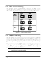
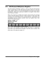
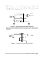
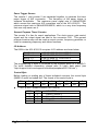
1
NuDAQ® ACL-8316/8312 16/12-bit High Performance DAS Cards with 1K FIFO User’s Guide Recycled Paper ©Copyright 1996~2000 ADLINK Technology Inc. All Rights Reserved. Manual Rev. 2.50: November 9, 2000 Product no: 50-11016-100 The information in this document is subject to change without prior notice in order to improve reliability, design and function and does not represent a commitment on the part of the manufacturer. In no event will the manufacturer be liable for direct, indirect, special, incidental, or consequential damages arising out of the use or inability to use the product or documentation, even if advised of the possibility of such damages. This document contains proprietary information protected by copyright. All rights are reserved. No part of this manual may be reproduced by any mechanical, electronic, or other means in any form without prior written permission of the manufacturer. Trademarks NuDAQ® is registered trademark of ADLINK Technology Inc.. Other product names mentioned herein are used for identification purposes only and may be trademarks and/or registered trademarks of their respective companies. Getting service from ADLINK Customer Satisfaction is always the most important thing for ADLINK Tech Inc. If you need any help or service, please contact us and get it. ADLINK Technology Inc. http://www.adlink.com.tw http://www.adlinktechnology.com Sales & Service [email protected] Technical NuDAQ [email protected] Support NuDAM [email protected] NuIPC [email protected] NuPRO [email protected] Software [email protected] TEL +886-2-82265877 FAX +886-2-82265717 Address 9F, No. 166, Jian Yi Road, Chungho City, Taipei, 235 Taiwan, R.O.C. Web Site Please inform or FAX us of your detailed information for a prompt, satisfactory and constant service. Detailed Company Information Company/Organization Contact Person E-mail Address Address Country TEL FAX Web Site Questions Product Model Environment to Use Challenge Description Suggestions for ADLINK OS Computer Brand M/B : CPU : Chipset : BIOS : Video Card : Network Interface Card : Other : Table of Contents Chapter 1 Introduction ..................................................... 1 1.1 1.2 1.3 1.4 Features .................................................................................3 Applications............................................................................3 Specifications.........................................................................4 Software Support ...................................................................6 1.4.1 1.4.2 Programming Library...........................................................6 LabView Driver....................................................................6 Chapter 2 Installation ....................................................... 7 2.1 2.2 2.3 2.4 2.5 2.6 2.7 What You Have......................................................................7 Unpacking ..............................................................................7 ACL-8316/12's Layout ...........................................................8 Jumper and DIP Switch Description ......................................9 Base Address Setting ............................................................9 Analog Input Channel Configuration....................................11 Analog Output Channel Setting ...........................................11 2.7.1 2.7.2 2.8 2.9 2.10 2.11 2.12 Channel Output Range Setting ........................................ 11 Output Mode Setting ........................................................ 12 DMA Channel Setting ..........................................................14 IRQ Level Setting.................................................................14 Clock Source Setting ...........................................................15 Connectors Pin Assignment ................................................16 Daughter Board Connection ................................................19 2.12.1 2.12.2 2.12.3 2.12.4 2.12.5 Connect with ACLD-8125................................................. 19 Connect with ACLD-9137................................................. 19 Connect with ACLD-9182................................................. 19 Connect with ACLD-9185................................................. 19 Connect with ACLD-9188/9138........................................ 19 Chapter 3 Registers Format .......................................... 20 3.1 3.2 3.3 3.4 3.5 3.6 3.7 3.8 I/O Port Address ..................................................................20 A/D Data Registers ..............................................................21 FIFO Enable Register ..........................................................22 Gain Control Register ..........................................................22 A/D Channel Multiplexer Register........................................23 Interrupt Source Control Register ........................................24 AD Mode Control Register ...................................................25 A/D Status Register .............................................................26 Table of Contents • i 3.9 3.10 3.11 3.12 3.13 3.14 Clear Interrupt Register........................................................27 Software A/D Trigger Register.............................................27 DA Data Registers ...............................................................27 DA Mode Control Register ...................................................28 Digital I/O register ................................................................29 Internal Timer/Counter Register ..........................................29 Chapter 4 Operation Theorem ....................................... 30 4.1 A/D Conversion....................................................................30 4.1.1 4.1.2 4.1.3 4.1.4 4.1.5 4.1.6 4.2 4.3 4.4 4.5 A/D Conversion Procedure............................................... 31 A/D Signal Source Control ............................................... 31 A/D Trigger Sources Control ............................................ 35 A/D Data Buffering ........................................................... 36 A/D Data Transfer Modes................................................. 37 A/D Data Format .............................................................. 39 Interrupt System...................................................................41 D/A Conversion....................................................................42 Digital Input and Output .......................................................44 Timer/Counter Operation .....................................................45 Chapter 5 C/C++ Library ................................................ 48 5.1 5.2 5.3 5.4 5.5 5.6 5.7 5.8 5.9 5.10 5.11 5.12 5.13 5.14 5.15 5.16 5.17 5.18 5.19 5.20 Installation ............................................................................48 Software Utility .....................................................................49 Programming Guide.............................................................49 _8316_Initial.........................................................................50 _8316_Switch_Card_No......................................................50 _8316_DI..............................................................................51 _8316_DI _Channel .............................................................51 _8316_DO............................................................................52 _8316_DO_Channel ............................................................52 _8316_DA_Set_Mode..........................................................53 _8316_DA ............................................................................54 _8316_AD_Set_Channel .....................................................54 _8316_AD_Range ...............................................................55 _8316_AD_Set_Mode..........................................................56 _8316_AD_Set_Autoscan ...................................................56 _8316_AD_Set_FIFO ..........................................................57 _8316_AD_Set_INT_Source ...............................................57 _8316_CLR_IRQ .................................................................58 _8316_AD_Soft_Trig ...........................................................58 _8316_AD_Read_FIFO .......................................................59 ii • Table of Contents 5.21 5.22 5.23 5.24 5.25 5.26 5.27 5.28 5.29 5.30 5.31 _8316_AD_Aquire................................................................59 _8316_AD_DMA_Start ........................................................60 _8316_AD_DMA_Status......................................................61 _8316_AD_DMA_Stop.........................................................62 _8316_AD_INT_Start...........................................................62 _8316_AD_INT_Status ........................................................64 _8316_AD_INT_Stop...........................................................64 _8316_AD_Timer.................................................................65 _8316_TIMER_Start ............................................................65 _8316_TIMER_Read ...........................................................66 _8316_TIMER_Stop ............................................................66 Chapter 6 Calibration & Utilities.................................... 67 6.1 6.2 6.3 6.4 What do you need................................................................67 VR Assignment ....................................................................68 A/D Adjustment ....................................................................68 D/A Adjustment ....................................................................68 6.4.1 6.4.2 DA Channel 1 Calibration................................................. 68 DA Channel 2 Calibration................................................. 69 Warranty Policy .............................................................. 70 Table of Contents • iii How to Use This Guide This manual is designed to help you use the ACL-8316/12. The manual describes how to modify various settings on the ACL-8316/12 card to meet your requirements. It is divided into six chapters: Chapter 1: "Introduction", gives an overview of the product features, applications, and specifications. Chapter 2: "Installation", describes how to install the ACL-8316/12. The layout of ACL-8316/12 is shown, the switch setting for base address, and jumper setting for analog input channel configuration, output channel configuration, clock source for timer/counter, interrupt level and DMA channel are specified. The connectors' pin assignment and daughter board connection are also described here. Chapter 3: "Registers format", describes the details of register format and structure of the ACL-8316/12, this information is very important for the programmers who want to control the hardware by low-level programming. Chapter 4: "Operation Theorem", describes how to operate the ACL8316/12. The A/D, D/A, DIO and timer/counter functions are introduced. Also, some programming concepts are specified. Chapter 5: "C/C++ library", describes high-level programming interface in C/C++ language. It helps programmer to control ACL8316/12 in high level language style. Chapter 6: "Calibration", describes how to calibrate the ACL-8316/12 for accurate measurement. 1 Introduction The ACL-8316/12 series DAS cards are high resolution and high performance data acquisition card based on the 16-bit PC/ISA Bus architecture. Both ACL-8316 and ACL-8312 share a common architecture and core features making each card is ideal for data logging and signal analysis applications. The ACL-8316/12 series features continuous, high speed, gap-free data acquisition under Windows or DOS environments. An on-board FIFO buffer and 16-bit DMA data transfer allows the acquisition of large amounts of data without losing data. The channel auto-scanning lets a high speed acquisition in a sequential order to select channel. An lite(L) version of ACL-8316/12 are offered for the customer who does not need any D/A analog output channels. It lets customers do not waste any extra money to buy unnecessary source. The system block diagram is shown on next page for further reference. Introduction • 1 2 • Introduction REF 0 IN < < . . . [Analog Input] CH 15 CH 1 CH 2 CH 0 REF 1 IN GND D/A 1 OUT GND D/A 0 OUT MUX SCAN CONTROL B U S I N T E R N A L DATA BUFFER DMA SELECT 5, 6, 7 DACK DRQ EXT.CLK Figure 1.1 ACL -8316/12 BLOCK DIAGRAM INTERRUPT IRQ SELECT TRIG LOGIC 16 BIT DIGITAL INPUT REGISTER EXTERNAL TRIG SOFTWARE TRIG PACER TRIG DO 15 . . . DO 1 DO 0 DI 15 . . . DI 0 DI 1 [Digital I/O] TO PACER TRIG OUT 0 16 BIT DIGITAL INPUT REGISTER < CONTROL LOGIC EOC 16 BIT COUNTER #2 16 BIT COUNTER #1 16 BIT COUNTER #0 INTERNAL BUS INPUT BUFFER 16/12 Bit A/D Converter (ADS7805/4) FR/2 2MHz 4 MHz OSC. 16-bit PC/AT BUS 1Kx16 FIFO +12V GAIN SELECT DC/DC CONVERTER -15 AMP +15 I/O PORT DECODER D/A #1 12 BIT MULITIPLYING D/A 16 channel > Single-ended or 8 channel Differentail Analog Multiplexer > > ADS-2813 D/A #0 12 BIT MULITIPLYING D/A 1.1 Features The ACL-8316/12 high performance and high resolution Data Acquisition Card provides the following advanced features: 16-bit PC/ISA Bus 16-bit or 12-bit analog input resolution On-board A/D FIFO memory for 1K Auto-scanning channel selection Up to 100 kHz A/D sampling rates 16 single-ended or 8 differential analog input channels Bipolar or Unipolar input signals Programmable gain of x1, x2, x4, x8 On-chip sample & hold Two 12-bit monolithic multiplying analog output channels (optional) 16 digital input / output channels 3 independent programmable 16-bit down counter Three A/D trigger modes: software trigger, programmable pacer trigger, and external pulse trigger. z Integral DC-to-DC converter for stable analog power source z 37-pin D-type connector z Compact size: half-size PCB z z z z z z z z z z z z z 1.2 Applications z z z z z z z Industrial and laboratory ON/OFF control Energy management Annunciation 16 TTL/DTL compatible digital input channels Security controller Product test Period and pulse width measurement Introduction • 3 1.3 Specifications Analog Input (A/D) z Converter: ADS7805 or equivalent for ACL-8316 ADS7804 or equivalent for ACL-8312 z Resolution: 16-bit ( ACL-8316), 12-bit ( ACL-8312) z ADconverter type: successive approximation type z Number of channels: 16 single-ended or 8 differential z Conversion Time: 8 µ sec z Maximum sampling rate: 100KHz multiplexing z Input Range: (programmable) Bipolar: ± 10V, ± 5V, ±2.5V, ±1.25V z Data format: Two‘s complement data output z On-board Memory: 1K words FIFO, half and full ready interrupt z Over-voltage protection: Continuous ± 35V maximum z Accuracy: GAIN = 1 0.01% of FSR ±1 LSB GAIN = 2, 4 0.02% of FSR ±1 LSB GAIN = 8 0.04% of FSR ±1 LSB z Input impedance: 10 MΩ z AD trigger modes: Software, Pacer, and External trigger z Data Transfer: Software polling, EOC Interrupt, FIFO polling, FIFO half-full interrupt, DMA transfer Analog Output (D/A) z z z z z z z z z z Converter: DAC2813 or equivalent, monolithic multiplying Resolution: 12-bit Number of channels: 2 Output Range: (jumper selectable) Bipolar: -10V ~ +10V Unipolar: 0V ~ +10V Control Mode: Double buffered mode or Transparency Mode Data Format: Binary format or Binary format Settling Time: 4.5µ sec(typical), 6µ sec ( max.) Linearity: ±1/2 bit LSB(Max.) ±1/4 bit LSB(typical) Output driving: ±5mA (min.) Output Impedance: 0.2 Ω 4 • Introduction Digital I/O ( DIO) z Channel: 16 TTL compatible inputs and outputs z Input Voltage: Low: Min. 0V ; Max. 0.8V High: Min. +2.0V z Input Load: Low: +0.5V @ -0.2mA max. High: +2.7V @+20mA max. Output Voltage: Low: Min. 0V ; Max. 0.4V High: Min. +2.4V z Driving Capacity: Low: Max. +0.5V at 8.0mA (Sink) High: Min. 2.7V at 0.4mA (Source) Programmable Counter z Device: 82C54 z A/D pacer: 32-bit timer( two 16-bit counter cascaded together) with a 2MHz time base z Counter: One 16-bit counter with a 2MHz time base or external timer clock z Pacer Output: 0.00046 Hz ~ 100K Hz General Specifications I/O Base Address: 16 consecutive address location Connector: 37-pin D-type connector, and two 20-pin ribbon connectors IRQ Level: 3, 5, 6, 7, 9, 11, 12, 15 DMA Level: 5, 6, and 7 Operating Temperature: 0° C ~ 55° C Storage Temperature: -20° C ~ 80° C Humidity: 5 ~ 95%, non-condensing Power Consumption: +5 V @ 400 mA typical +12V @ 260 mA typical z PCB Dimension: Half-sized 163mm(L) X 123mm(H) z z z z z z z z Introduction • 5 1.4 Software Support 1.4.1 Programming Library For the customers who are writing their own programs, we provide MS-DOS Borland C/C++ programming library. ACLS-DLL2 is the Development Kit for NuDAQ ISA-Bus Cards with Analog I/O, windows 3.1/95(98)/NT. ACLS-DLL2 can be used for many programming environments, such as VC++, VB, Delphi. ACLS-DLL2 is included in the ADLINK CD. It need license. 1.4.2 LabView Driver The ACLS-LVIEW includes the ACL-8316/8312’s Vis, which is used to interface with NI’s LabView software package. The ACLS-LVIEW supports Windows-95(98)/NT. ACLS-LVIEW is included in the ADLINK CD. It need license. 6 • Introduction 2 Installation This chapter describes how to install the ACL-8316/12. At first, the contents in the package and unpacking information that you should care about are described. The jumpers and switches setting for the ACL-8316/12's base address, analog input channel configuration, interrupt IRQ level, analog output configuration are also specified. 2.1 What You Have In addition to this User's Manual, the package includes the following items: z ACL-8316/12 Enhanced Multi-function Data Acquisition Card z ADLINK CD If any of these items is missing or damaged, contact the dealer from whom you purchased the product. Save the shipping materials and carton in case you want to ship or store the product in the future. 2.2 Unpacking Your ACL-8316/12 card contains sensitive electronic components that can be easily damaged by static electricity. The card should be done on a grounded anti-static mat. The operator should be wearing an anti-static wristband, grounded at the same point as the antistatic mat. Inspect the card module carton for obvious damage. Shipping and handling may cause damage to your module. Be sure there are no shipping and handing damages on the module before processing. Installation • 7 After opening the card module carton, extract the system module and place it only on a grounded anti-static surface component side up. Again inspect the module for damage. Press down on all the socketed IC's to make sure that they are properly seated. Do this only with the module place on a firm flat surface. Note: DO NOT APPLY POWER TO THE CARD IF IT HAS BEEN DAMAGED. You are now ready to install your ACL-8316/12. 2.3 ACL-8316/12's Layout Figure 2.1 PCB Layout of the ACL-8316/12 8 • Installation 2.4 Jumper and DIP Switch Description You can change the ACL-8316/12's channels and the base address by setting jumpers and DIP switches on the card. The card's jumpers and switches are preset at the factory. You can change the jumper settings for your own applications. A jumper switch is closed (sometimes referred to as "shorted") with the plastic cap inserted over two pins of the jumper. A jumper is open with the plastic cap inserted over one or no pin(s) of the jumper. 2.5 Base Address Setting The ACL-8316/12 requires 16 consecutive address locations in the I/O address space. The base address of the ACL-8316/12 is restricted by the following conditions. 1. The base address must within the range Hex 200 to Hex 3FF. 2. The base address should not conflict with any PC reserved I/O address. 3. The base address must not conflict with any add-on card on your own PC. Please check your PC before installing the ACL-8316/12. The base address of registers in ACL-8316/12 is selected by an 5 positions DIP switch SW1. The default setting of base address is set to be HEX 220. All possible base address combinations are listed as Table 2.1. You may modify the base address if the address HEX 220 has been occupied by another add-on card. SW1 : Base Address = Hex 220 ON DIP 1 A( 8 7 2 3 6 4 5 5 4) Figure 2.2 Default Base Address Setting Installation • 9 I/O port Address(Hex) 200-20F 1 A8 ON A9 -- 210-21F 220-22F (default) 230-23F : 300-30F : 3F0-3FF 2 A7 ON 3 A6 ON 4 A5 ON 5 A4 ON (1) (0) (0) (0) (0) (0) -- ON ON ON ON OFF (1) (0) (0) (0) (0) (1) -- ON ON ON OFF ON (1) (0) (0) (0) (1) (0) -- ON ON ON OFF OFF (1) (0) (0) (0) (1) (1) -- OFF ON ON ON ON (1) (1) (0) (0) (0) (0) -- OFF OFF OFF OFF OFF (1) (1) (1) (1) (1) (1) Table 2.1 Possible Base Address Combinations A0, ..., A9 is corresponding to PC Bus address lines A9 is fixed as “1”. How to define the base address for the ACL-8112 ? The DIP1 to DIP5 in the switch SW1 are one to one corresponding to the PC AT-bus address line A8 to A4. A9 is always 1 and A0~A3 are always 0. If you want to change the base address, you can only change the values of A8 to A4 (the shadow area of below table). The following table is an example, which shows you how to define the base address as Hex 220 Base Address: Hex 220 2 1 A9 2 0 A8 10 • Installation 0 A7 0 A6 0 1 A5 0 A4 0 A3 0 A2 0 A1 0 A0 2.6 Analog Input Channel Configuration The ACL-8316/12 offer 16 single-ended or 8 differential analog input channels. The jumper JP7 controls the analog input channel configuration. The settings of JP7 is specified as following illustration. JP7 SING Single-ended Input (default setting) DIFF JP7 SING Differential Input DIFF Figure 2.3 Analog Input Channels Configuration 2.7 Analog Output Channel Setting 2.7.1 Channel Output Range Setting The ACL-8316/12‘s analog outputs are generated by a very powerful D/A converter B.B. DAC2813. It can be configured either bipolar (+10V ~ -10V) or unipolar (0V ~ 10V) output. The jumper JP5 and JP6 are used to set D/A CH1 and D/A CH2 individually. Installation • 11 D/A CH1 Output -10V~+10V Bipolar (Default) D/A CH1 Output 0V~10V Unipolar JP5 BI1 UP1 JP5 UP1 BI1 Figure 2.4 D/A CH1 Output Range setting D/A CH2 Output -10V~+10V Bipolar (Default) D/A CH2 Output 0V~10V Unipolar JP6 BI2 UP2 JP6 BI2 UP2 Figure 2.5 D/A CH2 Output Range setting 2.7.2 Output Mode Setting The ACL-8316/12 consists of two independently addressable latched in two ranks for each D/A converter. The first rank consists of one 12-bit input latch which can be loaded from the PC bus. The input latch holds data temporarily before it is load into the second latch, the D/A latch. This double buffered organization permits simultaneously update of all D/As. On the other hands, if you do not need to latch D/A output by double buffered mode. The transparency mode can driver the D/A output immediately without waiting for the second latch. The configuration for either double buffered mode or transparent mode is set by jumper JP8 and is shown on Figure 2.6 below. 12 • Installation Transprant (default d tti ) JP1 Double mod B ff d JP1 D B T P D B T P Figure 2.6 D/A Output Mode Setting Installation • 13 2.8 DMA Channel Setting The A/D data transfer of ACL-8316/12 is designed with DMA transfer capability. The setting of DMA channel 5, 6 or 7 is controlled by the jumpers JP1 and JP2. The possible settings are illustrated in the Figure 2.7 below. DMA 5 (Default) DACK JP1 7 6 5 DMA 6 DACK JP1 7 6 5 DACK JP1 DRQ JP2 7 6 5 DRQ JP2 7 6 5 DRQ JP2 DMA 7 7 6 5 7 6 5 Figure 2.7 DMA Channel Setting 2.9 IRQ Level Setting The ACL-8316/12 can connect to any one of the interrupt lines of the PC I/O channel. The interrupt line is selected by the jumper JP3. If you wish to use the interrupt capability of ACL-8316/12, you must select an interrupt level and place the jumper in the appropriate position to enable the particular interrupt line. The default interrupt level is IRQ15, which is selected by placing the jumper on the pins in row number 10. Figure 2.8 shows the default interrupt jumper setting IRQ5. You only remove the jumper from IRQ15 to other new pins, if you want to change to another IRQ level. Note: Be aware that there is no other add-on card shares the same interrupt level at the same system. 14 • Installation Figure 2.8 IRQ Level Setting 2.10 Clock Source Setting The 8254 programmable interval timer is used in the ACL-8316/12. It provides 3 independent channels of 16-bit programmable down counters. The input of counter 2 is connected to a precision 2MHz oscillator for internal pacer. The input of counter 1 is cascaded from the output of counter 2. The channel 0 is free for user's applications. There are two selections for the clock source of channel 0: the internal 2MHz clock or the external clock signal from connector CN3 pin 37. The setting of clock is shown as Figure 2.9. JP4 Internal Clock Source : 2MHz (default setting) INTCLK EXTCLK JP4 External Clock Source ( Pin-37 of CN3) INTCLK EXTCLK Figure 2.9 Timer's Clock Source Setting Installation • 15 2.11 Connectors Pin Assignment The ACL-8316/12 comes equipped with two 20-pin insulation displacement connectors - CN1 and CN2 and one 37-pin D-type connector - CN3. The CN1 and CN2 are located on board and CN3 located at the rear plate. CN1 is used for digital signal output, CN2 for digital signal input, CN3 for analog input, analog output and timer/counter's signals. The pin assignment of each connector is illustrated in Figure 2.10~2.12. z CN1: Digital Signal Output (DO 0 ~ 15) DO 0 DO 2 DO 4 DO 6 DO 8 DO 10 DO 12 DO 14 GND +5V CN1 1 2 3 4 5 6 7 8 9 10 11 12 13 14 15 16 17 18 19 20 DO 1 DO 3 DO 5 DO 7 DO 9 DO 11 DO 13 DO 15 GND + 12V Figure 2.10 Pin Assignment of CN1 z CN2: Digital Signal input (DI 0 ~ 15) DI 0 DI 2 DI 4 DI 6 DI 8 DI 10 DI 12 DI 14 GND +5V 1 3 5 7 9 11 13 15 17 19 2 4 6 8 10 12 14 16 18 20 DI 1 DI 3 DI 5 DI 7 DI 9 DI 11 DI 13 DI 15 GND + 12V CN2 Figure 2.11 Pin Assignment of CN2 Legend: DI n: Digital output signal channel n DO n: Digital input signal channel n GND: Digital ground 16 • Installation z CN 3: Analog Input/Output & Counter/Timer ( for single-ended connection) CN3 AI0 AI1 AI2 AI3 AI4 AI5 AI6 AI7 A.GND A.GND V.REF +12V A.GND D.GND COUT0 ExtTrg N/C +5V 1 2 3 4 5 6 7 8 9 10 11 12 13 14 15 16 17 18 19 20 21 22 23 24 25 26 27 28 29 30 31 32 33 34 35 36 37 AI8 AI9 AI10 AI11 AI12 AI13 AI14 AI15 A.GND A.GND AO1 AO2 GATE0 GATE N/C ExtCLK Figure 2.12a Pin Assignment of CN3 z CN 3: Analog Input/Output & Counter/Timer ( for differential connection) CN3 AIH0 AIH1 AIH2 AIH3 AIH4 AIH5 AIH6 AIH7 A.GND A.GND V.REF +12V A.GND D.GND COUT0 ExtTrg N/C +5V 1 2 3 4 5 6 7 8 9 10 11 12 13 14 15 16 17 18 19 20 21 22 23 24 25 26 27 28 29 30 31 32 33 34 35 36 37 AIL0 AIL1 AIL2 AIL3 AIL4 AIL5 AIL6 AIL7 A.GND A.GND AO1 AO2 GATE0 GATE N/C ExtCLK Figure 2.12b Pin Assignment of CN3 Installation • 17 Legend: Ain : Analog Input Channel n ( single-ended) AIHn : Analog High Input Channel n ( differential) AILn : Analog Low Input Channel n ( differential) ExtRef n : External Reference Voltage for D/A CH n Aon : Analog Output Channel n ExtCLK : External Clock Input ExtTrig : External Trigger Signal CLK : Clock input for 8254 GATE : Gate input for 8254 COUT n : Signal output of Counter n V.ERF : Voltage Reference A.GND : Analog Ground GND : Ground 18 • Installation 2.12 Daughter Board Connection The ACL-8316/12 can be connected with five different daughter boards, ACLD-8125, ACLD-9137, 9182, 9185, and 9188. The functionality and connections are specified as follows. 2.12.1 Connect with ACLD-8125 The ACLD-8125 has a 37-pin D-sub connector, which can connect with ACL8316/12HG through 37-pin assemble cable. The most outstanding feature of this daughter board is a CJC ( cold junction compensation) circuit on board. 2.12.2 Connect with ACLD-9137 The ACLD-9137 is a direct connector for the card which is equipped with 37pin D-sub connector. This board provides a simple way for connection. It is very suitable for the simple applications that do not need complex signal condition before the A/D conversion is performed. 2.12.3 Connect with ACLD-9182 The ACLD-9182 is a 16 channel isolated digital input board. This board is connected with CN1 of ACL-8316/12 via 20-pin flat cable. The advantage of board is an 500Vdc isolation voltage is provided, and it can protect your PC system from damage when an abnormal input signal is occurred. 2.12.4 Connect with ACLD-9185 The ACLD-9185 is a 16 channel SPDT relay output board. This board is connected with CN2 of ACL-8316/12 via 20-pin flat cable. by using this board, you can control outside device through the digital output signals. 2.12.5 Connect with ACLD-9188/9138 ACLD-9188 and ACLD-9138 are two general purpose terminal boards for all the card which comes equipped with 37-pin D-sub connector. ACLD-9188 is big size and uses Barrier-strip terminal block. The ACLD-9138 is compact size and uses screw-clamp terminal block. Installation • 19 3 Registers Format The detailed description of the ACL-8316/12‘s register format is specified in this chapter. This information is quite useful for the programmer who wish to handle the ACL-8316/12 card by low-level program. 3.1 I/O Port Address The ACL-8316 requires 16 consecutive addresses in the PC I/O address space. Table 3.1 shows the I/O address of each register with respect to the base address. The function of each register will be introduced in the following sections. Location Base + 0 Base + 1 Base + 2 Base + 3 Base + 4 Base + 5 Base + 6 Base + 7 Base + 8 Base + 9 Base + 10 Base + 11 Base + 12 Base + 13 Base + 14 Base + 15 Read Counter 0 Counter 1 Counter 2 Counter Status A/D Data -A/D Data (FIFO) -A/D Channel and Status Clear Interrupt Request Software A/D trigger Interrupt Source Setting A/D Mode Setting D/A Mode and FIFO setting DI (0...16) -- Write Counter 0 Counter 1 Counter 2 Counter Control D/A Channel #1 -D/A Channel #2 -FIFO Enable Gain Control Channel MUX Interrupt Source Control A/D Mode Control D/A Mode Control DO (0...16) -- Table 3.1. I/O address map of the ACL-8316/12 20 • Registers Format Note: The ACL-8316/12 includes both 8 bits & 16 bits I/O ports. The AD Data, DA channels, and digital I/O ports are 16 bits port. All the others are 8 bits I/O port. The 16-bit I/O data ( A/D, D/A and DIO) have to access via 16-bit I/O operation. 3.2 A/D Data Registers The value of AD data register is directly read from AD converter which address is base address + 4. The A/D data is updated whenever AD is triggered. The AD FIFO data is read from FIFO chips which address is base address + 6, however, the AD data read from FIFO may be not in ‘real time’. The FIFO data should be read with FIFO control. The AD FIFO port is enable only after the FF_ENA bit in A/D mode control register is set.( refer to section 4.3) Address : BASE + 4 and BASE + 6 Attribute: read only Data Format: (1) ACL-8312 (using 12 bits ADC) Bit 15 14 13 12 11 10 9 8 AD11 AD10 AD9 AD8 AD7 AD6 AD5 AD4 Bit 7 6 5 4 3 2 1 0 AD3 AD2 AD1 AD0 0 0 0 0 AD11 .. AD0: Analog to digital data. AD11 is Most Significant Bit of the 12 bits digits and AD0 is Least Significant Bit. (2) ACL-8316 (using 16 bits ADC) Bit 15 14 13 12 11 10 9 8 AD15 AD14 AD13 AD12 AD11 AD10 AD9 AD8 Bit 7 6 5 4 3 2 1 0 AD7 AD6 AD5 AD4 AD3 AD2 AD1 AD0 AD15 .. AD0: Analog to digital data. AD15 is Most Significant Bit of the 16 bits digits, and AD0 is Least Significant Bit. Note: The 12 bits of A/D data of ACL-8312 are located on the 12 MSBs and the 4 LSB is zero alwayse. Users can consider the ACL-8312, which is of only 12 bit resolution, is the special case of the ACL8316. Registers Format • 21 3.3 FIFO Enable Register The FF_ENA bit directly control FIFO memory. Clear FF_ENA bit to ‘0’ can always reset the FIFO and any read operation to the A/D FIFO port will get value ‘0’. Set FF_ENA bit to ‘1’ can enable the FIFO. Note that FF_ENA status can be read back from Base+13. Address : BASE + 8 Attribute: write only Data Format: Bit 7 6 5 4 X X X X FF_ENA: FIFO Enable Control 0: FIFO Disable 1: FIFO Enable 3.4 3 X 2 X 1 X 0 FF_ ENA Gain Control Register The gain control register is used to adjust the analog input ranges for A/D channels. Table 4.2 shows the relationship between the register data, gain value and the A/D input range. Address : BASE + 9 Attribute: write only Data Format: Bit 7 X G1 0 0 1 1 22 • Registers Format 6 X G0 0 1 0 1 5 X 4 X Gain 1 2 4 8 3 X 2 X 1 G1 A/D input Range - 10V ~ +10V - 5V ~ +5V - 2.5V ~ +2.5V - 1.25V ~ +1.25V 0 G0 3.5 A/D Channel Multiplexer Register The A/D channel multiplexer register is used to select the A/D channel under normal mode, or the stop channel number under the auto-scan mode. Refer to section 3.7 to find the definition of the auto-scan control bit ‘ASCAN’. When auto scanning is disabled, the register values select the AD channel number. When auto scanning is enabled, the register values set the stop channel number while the starting channel is from channel 0. After every A/D conversion, the A/D channel to be selected will be increased by one automatically until the channel number reach this register value, then channel 0 is selected again. Address : BASE + 10 Attribute: write only Data Format: Bit 7 6 5 4 3 2 1 0 X X X X CS3 CS2 CS1 CS0 CS3 ... CS0: Stop multiplexer channel number. Note that as the hardware jumpers set the ACL-8316/12 to differential input mode, only 8 channels are available. The CS3 value is useless. The initial value of the channel number is 0. Registers Format • 23 3.6 Interrupt Source Control Register The interrupt source of ACL-8316 is controlled by both of this register and the A/D mode control register. The DMAEAN bit in A/D mode control register will decide the interrupt source, too. This register values can be read back on the same port. Address : BASE + 11 Attribute: read and write Data Format: Bit 7 X 6 X 5 X 4 X 3 X 2 X 1 IS1 0 IS0 When DMAENA is set (DMA enable), interrupt must come from TC (terminal count) signal to indicate DMA transfer ending. However, when the DMAENA is cleared (DMA disable), the interrupt source is set as following table. IS1 0 0 1 1 IS0 0 1 0 1 Interrupt Sources A/D EOC External interrupt source (1) Internal Pacer Interrupt FIFO half full (2) Note(1) The external AD trigger signal can be used as external interrupt source under this mode. Note(2) The FIFO half full interrupt and DMA can not be run concurrently. But the FIFO can still be read even the DMA is enable. 24 • Registers Format 3.7 AD Mode Control Register The A/D mode control register is used to select A/D data transfer mode A/D trigger source, and A/D channel selection. Address : BASE + 12 Attribute: read and write Data Format: Bit 7 X 6 X 5 X 4 X 3 DMAENA 2 EXTINT 1 ITSSEL 0 ACSCN ♦ A/D Data Transfer control • DMAENA: 0: Software data polling ( DMA is disabled) 1: DMA data transfer ♦ A/D Trigger Source • EXTINT: External or Internal trigger source 0: Internal A/D trigger Source ( trigger source is from ITSSEL) 1: External A/D trigger Source ( trigger source is from Ext_Trg of CN3) • ITSSEL: Internal Trigger source type 0: Internal software A/D trigger 1: Internal pacer A/D trigger ♦ A/D Channel Control • ASCAN 0: Auto Channel Scan Disable 1: Auto Channel Scan Enable Registers Format • 25 3.8 A/D Status Register Address : BASE + 8 Attribute: read only Data Format: Bit 7 6 5 4 3 2 1 0 AD_BUSY FF-FF FF_HF FF_EF CNH CN2 CN1 CN0 • CNH and CN2~CN0 These bits are used to feedback the channel number to be selected. When the ACL-8316/12 is set to be differential mode. CNH will be 1 always. When the A/D mode is in auto scan mode, the channel number will be increased by one automatically. • FF_EF 0: FIFO is empty 1: FIFO is not empty • FF_HF 0: FIFO is half full 1: FIFO is not half full • FF_FF 0: FIFO is full 1: FIFO is not full Above 3 bits are FIFO relative flags which are used to indicate the FIFO status. These status can be used to read A/D FIFO data by software polling without the help of hardware. • AD_BUSY 0: A/D converter is busy, i.e. A/D conversion is not completed 1: A/D converter is not busy, i.e. A/D conversion is completed 26 • Registers Format 3.9 Clear Interrupt Register To read this port can generate clear interrupt signal. No matter which interrupt source is used, the clear interrupt register must be read to allow next interrupt. Address : BASE + 9 Attribute: read only Data Format: Bit 7 X 6 X 5 X 4 X 3 X 2 X 1 X 0 X 3.10 Software A/D Trigger Register To read this port can generate A/D trigger signal if the AD mode control register is set to use internal software A/D trigger source. Address : BASE + 10 Attribute: read only Data Format: Bit 7 X 6 X 5 X 4 X 3 X 2 X 1 X 0 X 3.11 DA Data Registers There are two DA channels in ACL-8316. The address Base + 4 is DA channel 1 and the address Base +6 is DA channel 2. DA11 is Most Significant Bit, and DA0 is Least Significant Bit. The lowest 4 bits of this register is don‘t cared. Users can consider the DA data values as 16-bits with the lowest 4 bits are truncated. Therefore, result in 12-bits resolution although the DA data value is in the range from 0 to 65535. Address : BASE + 4 and BASE+6 Attribute: write only Data Format: Bit 15 14 13 12 11 DA11 DA10 DA9 DA8 DA7 Bit 7 6 5 4 3 DA3 DA2 DA1 DA0 X DA11 ... DA0: Digital to analog data value. 10 DA6 2 X 9 DA5 1 X 8 DA4 0 X Registers Format • 27 3.12 DA Mode Control Register Address : BASE + 13 Attribute: write Data Format: Bit 7 6 5 X X X Address : BASE + 13 Attribute: read Data Format: Bit 7 X 6 X 5 X 4 X 4 X 3 X 3 FF_ENA 2 X 1 DA_FMT 2 STYP 1 DA_FMT 0 DA_MD1 0 DA_MD1 The D/A operation and D/A data format are controlled by this register and the jumper JP8. The lower two bits are programmable and can be read back too. Another two bits, the FIFO enable (FF_ENA) bit and the A/D signal type (STYP) bit, are read only. These two DA channels are set as transparency mode or double buffer mode by DA_MD1 bit and jumper JP8 setting. The versatile operation functions are shown as following table. The default setting of the JP8 is TP and initial state of DA_MD1 is 0 too. Therefore, the DA channels are default set as transparency mode. However, if user want to default set double buffered mode when system power on, he can set JP8 to ‘DB’ externally. Even if the power on state is double buffer mode, the users still can set DA_MD1 to 1 to change the DA channels to transparency mode. JP8 Status (hardware) 0 0 1 1 DA_MD1 (software) 0 1 0 1 DAs Control Mode Transparency mode Double buffer mode Double buffer mode Transparency mode DA_FMT: 0: DA data value is in two‘s complement mode which the same as AD. 1: DA data value is in binary mode. FF_ENA: 0: means FIFO is reset 1: means FIFO is enable. STYP: 0: A/D signal sources are differential input. 1: A/D signal sources are signal ended. 28 • Registers Format 3.13 Digital I/O register There are 16 digital input channels and 16 digital output channels are provided by the ACL-8312/16. The address Base + 14 and Base + 15 are used for both digital input and digital output control. Address : BASE + 14 & BASE + 15 Attribute: read only Data Format: Bit Bit 15 DI15 7 DI7 14 DI14 6 DI6 13 DI13 5 DI5 12 DI12 4 DI4 11 DI11 3 DI3 10 DI10 2 DI2 9 DI9 1 DI1 8 DI8 0 DI0 11 DO11 3 DO3 10 DO10 2 DO2 9 DO9 1 DO1 8 DO8 0 DO0 Address : BASE + 14 & BASE + 15 Attribute: write only Data Format: Bit Bit 15 DO15 7 DO7 14 DO14 6 DO6 13 DO13 5 DO5 12 DO12 4 DO4 3.14 Internal Timer/Counter Register Two counters of 8254 are used for periodically triggering the A/D conversion, the remainder is free for user’s applications. The 8254 occupies 4 I/O address locations in the ACL-8316/12 as shown blow. Users can refer to Tundra’s or Intel's data sheet (“http://www.tundra.com” or “http://support.intel.com/support/controllers/peripheral/231164.htm”) for a fully description of the 8254 features. Condensed information is specified in section 4.5 Timer/Counter Operation. Address : BASE + 0 ~ BASE + 3 Attribute: read / write Data Format: Base + 0 Base + 1 Base + 2 Base + 3 Counter 0 Register ( R/W) Counter 1 Register ( R/W) Counter 2 Register ( R/W) 8254 CONTROL BYTE( W) Registers Format • 29 4 Operation Theorem The operation theorem of the functions on ACL-8316/12 card is described in this chapter. The functions include the A/D conversion, D/A conversion, digital I/O and counter/timer. The operation theorem can help you to understand how to manipulate and to program the ACL-8316/12. 4.1 A/D Conversion Before programming the ACL-8316/12 to perform the A/D conversion, you should understand the following issues: z z z z z z z A/D conversion procedure A/D signal source control A/D trigger source control A/D data buffering A/D data transfer mode Interrupt System (refer to section 4.2) A/D data format 30 • Operation Theorem 4.1.1 A/D Conversion Procedure For using the A/D converter, users must know about the property of the signal to be measured at first. The users can decide which channels to be used and connect the signals to the ACL-8316. Refer to the ‘Signal Connection’ (Section 2.11). In addition, users should define and control the A/D signal sources, including the A/D channel, A/D gain, and A/D signal types. Please refer to section 4.1.2. for A/D signal source control. After deciding the A/D signal source, the user must decides how to trigger the A/D conversion and define / control the trigger source. The A/D converter will start to convert the signal to a digital value when a trigger signal is rising. The ACL-8316 provides three trigger modes, refer to section 4.1.3 for details. At the ending of A/D conversion, the A/D data is stored in A/D data register and in the FIFO if FIFO is enable. This issue stands as A/D data buffering. Please refer to section 4.1.4. The A/D data should be transferred into PC's memory for further using or processing. The data can be either read by I/O instruction which is handled directly by software or transferred to memory by the DMA controller. Please refer to section 4.1.5 to obtain ideas about the multi-configurations for A/D data transferring. To process A/D data, programmer should know about the A/D data format. Refer to section 4.1.6 for details. 4.1.2 A/D Signal Source Control To control the A/D signal source, three concepts should be understood. That is signal type, signal channel and signal range. Signal Type The A/D signal sources of ACL-8316 could be single ended (SE) or differential input (DI) type. The signal type is selected by external jumper (JP7). The setting can be read back through the D/A format register. ACL-8316/12 provides 16 single-ended or 8 differential analog input channels. The analog signal can be converted to digital value by the A/D converter. To avoid ground loops and get more accuracy measurement of A/D conversion, it is quite important to understand the signal source type and how to choose the analog input modes: signal-ended and differential. The ACL-8316/12 offers jumpers to select 16 single-ended or 8 different analog inputs. Single-ended Mode: The single-ended mode has only one input relative to ground and it suitable for connecting with the floating signal source. The floating source means it does not have any connection to ground. The following figure shows the Operation Theorem • 31 single-ended connection. Note that when more than two floating sources are connected, the sources must be with common ground. AIN Floating Signal Source Input Opertiona Amplifie ... To A/D V2 V1 n = 0, ..., 15 AGND Figure 4.1.1 Floating source and single-ended Differential input mode The differential input mode provides two inputs that respond to the difference signal between them. If the signal source has one side connected to local ground, the differential mode can be used for reducing ground loop. Figure 4.1.2 shows the connection of the differential input mode. However, even if the signal source is local grounded, the single-ended still can be used when the Vcm ( Common Mode Voltage) is very small and the effect of ground loop can be negated. n = 0, ..., 8 To A/D AIHn Groun Signal Sourc + - AILn GN Vcm = VG1 - VG2 VG1 VG2 Figure 4.1.2 Ground source and differential input 32 • Operation Theorem A differential mode must be used when the signal source is differential. A differential source means the ends of the signal are not grounded. To avoid the danger of high voltage between the local ground of signal and the ground of the PC system, a shorted ground path must be connected. Figure 4.1.3 shows the connection of differential source. n = 0, ..., 8 To A/D AIHn Differentia Signal Sourc + - AILn GN Vcm = VG1 - VG2 VG1 VG2 Figure 4.1.3 Differential source and differential input If your signal source is both floating and local ground, you should use the differential mode, and the floating signal source should be connected as the Figure 4.1.4. n = 0, ..., 8 Floatin Signal Sourc AIHn High To A/D AILn Low GN Figure 4.1.4 Floating source and differential input Operation Theorem • 33 Signal Channel There are 16 channels in SE mode and 8 channels in DI mode. There are two ways to control the channel number. The first is the software programming and the second is the auto channel scanning, which is controlled by the ASCAN bit in AD mode control register. As ASCAN is cleared (0), the value of AD channel MUX register defines the channel to be selected. Only one channel can be selected in one moment. As ASCAN is set (1), the value in AD channel MUX register define the ending channel number of auto-scanning operation. Under auto scan mode, the channel is scanning from channel 0 to the ending channel. Whenever a trigger signal is rising, the channel number to be selected will increase automatically. For example, if the ending channel number is 3, the auto channel scanning sequence is 0,1,2,3,0,1,2... , until the ASCAN bit to be cleared. The current A/D channel number could be read back from the A/D status register. Refer to section 4.8 for the register format of the A/D status register. Signal Range The proper signal range is important for data acquisition. The input signal may be saturated if the A/D gain is too large. The resolution of data may be not enough if the signal is small and gain is not enough. The maximum A/D signal range of ACL-8316 is +/- 10 volts when the A/D gain value is 1. The A/D gain control register controls the maximum signal input range. The signal gain is programmable with 4 levels (1,2,4,8). The signal range of the 16 channels will be identity all the time even if the channel number is scanning. The available signal polarity on ACL-8316 is only bipolar but no unipolar configuration. However, the bipolar input range still covers the unipolar applications. Therefore, ACL-8316 is suitable for full range of applications. 34 • Operation Theorem 4.1.3 A/D Trigger Sources Control The A/D conversion is started by trigger signal. There are total three trigger sources in the ACL-8316. One is External trigger source and two are Internal trigger sources. The trigger source is programmable by the A/D mode control register. Please refer to section 3.7 for details of the register. The different trigger conditions are specified as following: Software trigger (EXTINT=0, ITSSEL=0) The trigger source is generated and fully controlled by software under this mode. That is, the A/D conversion is started by reading the software trigger register (BASE+12). Software trigger mode is suitable for low speed applications. However, it is difficult to control the fixed A/D conversion rate except generating trigger in a timer interrupt service routine with a fixed trigger rate. Timer Pacer Trigger (EXTINT=0, ITSSEL=1) An on-board timer / counter chip 8254 is used to provide an internal trigger source for A/D conversion at a fixed rate. Two counters of the 8254 chip are cascaded together to generate trigger pulse with precise period. Please refer to section 3.4 for 8254 architecture. This mode is ideal for high speed A/D conversion. It's recommend to use this mode if your applications need a fixed and precise A/D sampling rate. External Trigger (EXTINT=1) Through the pin-17 of CN3 (ExtTrig), the A/D conversion is triggered when a rising edge of external signal is occurred. The conversion rate under this mode is more flexible than the previous two modes, because the users can handle the external signal by outside devices. The external trigger can combine with the DMA transfer, interrupt data transfer, or even program polling data transfer. Generally, the interrupt data transfer is more often used when external trigger mode is used. Operation Theorem • 35 4.1.4 A/D Data Buffering On the ACL-8316, the AD data will store in the A/D data register. While A/D conversion, the register keeps the previous conversion result. The data will be updated when the end of the conversion. The A/D data register can keep the newest conversion data until the ending of the next conversion. The A/D data register can store only one data and the data can be real time operated. The A/D data can also be buffered in the FIFO memory when the FIFO is enable. But it is not suitable to use FIFO if the application needs real-time A/D data operation. The FIFO size on ACL-8316 is 1K samples. If the sampling rate is 100 kHz, the FIFO can buffer 10 ms analog signal. After the FIFO is full, the lasting coming data will be lost. The software must read out the FIFO data before it becomes full. 36 • Operation Theorem 4.1.5 A/D Data Transfer Modes The A/D data must be transferred to CPU for processing. On the ACL-8316, many AD data transfer modes can be used. Note that there are only two kinds of operation can transfer AD data from port into PC's memory. The data can be either read by I/O instruction (‘inport’ in terms of C language), which is handled directly by software, or transferred to memory by the DMA controller. Combing with programming the AD mode control register and the interrupt source control register, the ACL-8316 provides the following transfer modes: Software Data Read It is very simple to read A/D data through the A/D data register. Usually, this mode is used combining with software trigger mode. Because of the A/D conversion time will not excess 10µs on ACL-8316, after software triggering, the software can just wait for 10µs then A/D data will be available in the A/D data register. The software can read the data simply by using the inport instruction. Software Data Polling In this mode, A/D data is also read through the A/D data register but check the AD_BUSY bit. After the A/D conversion triggering, the software can poll the AD_BUSY bit in the A/D status register until AD_BUSY becomes to high level. The newest A/D data is stored in the A/D data register now, then the software can read data simply by using the inport instruction. Software Data Polling from FIFO The A/D data can also be read from FIFO buffer if FIFO is enable. In this mode, the A/D data is read from FIFO after check the FF_EF bit of the A/D status register. As the FF_EF is set (1), the FIFO is not empty and to read A/D value through the FIFO register is available. EOC Interrupt Transfer By properly programming the interrupt control register, the ACL-8316 provides end of conversion (EOC) interrupt. It is useful to combine the EOC interrupt transfer with the timer pacer trigger. The data transfer is essentially asynchronous with the control software under this mode. Users must set the IRQ level by hardware jumper as installing. Please refer section 2.x for IRQ jumper setting. After the A/D conversion completing, a hardware interrupt will be inserted and its corresponding ISR (Interrupt Service Routine) will be invoked and executed. The converted data can be transferred by the ISR program. Operation Theorem • 37 FIFO Half-Full Interrupt Transfer By properly programming the interrupt control register, the ACL-8316 provides FIFO half-full interrupt. As the FIFO is enable and be half-full, an interrupt is inserted and the corresponding ISR will be invoked. The ISR can read at least 512 sampling data because of the FIFO size is 1K sample. This mode can tolerate more time delay and it is interrupt driven, therefore, it is very suitable for Windows applications. The maximum 100 kHz sampling rate can be also applied under this mode for high speed applications. DMA Transfer As the DMAENA bit of the A/D mode control register is set, the DMA (Direct Memory Access) mode is enable and the interrupt resource will be occupied by the terminal counting (TC) signal of the DMA controller. The DMA allows data to be transferred directly from A/D data register to the PC memory at the fastest possible rate without using any CPU time. The A/D data is automatically transferred to PC's memory after conversion is complete. The DMA transfer mode is very complex to program. It is recommended to use the high level program library to operate this card. If you wish to program the software which can handle the DMA data transfer, please refer to more information about 8237 DMA controller. 38 • Operation Theorem 4.1.6 A/D Data Format The A/D data read either from A/D data port or the FIFO port is in the two‘s complement format. As the A/D gain is 1, the A/D signal range is roughly +10V ~ -10V bipolar. In ACL-8316, 16 bits A/D data is available. The relationship between the voltage and the value is shown in the following table: A/D Data (Hex) 7FFF 4000 0001 0000 FFFF C000 8001 8000 Decimal Value +32767 +16384 1 0 -1 -16384 -32767 -32768 Voltage (Volts) +10.00000 +5.00015 +0.00031 0.00000 -0.00031 -5.00015 -10.00000 -10.00031 Note: The decimal value of the A/D data is in the same sign with the bipolar voltage. Therefore, the sign extension conversion is not necessary. The A/D data format of 12 bits ACL-8312 is compatible with the 16 bits ACL8316. Only the 4 LSB of the 16 bits A/D data are truncated to zero. Therefore the software is compatible for the two cards. The relationship between the voltage and the value is shown in the following table: A/D Data (Hex) 7FF 0 400 0 001 0 000 0 FFF 0 C00 0 801 0 800 0 Decimal Value +32752 +16384 +16 0 -16 -16384 -32752 -32768 Voltage (Volts) +10.0000 +5.0024 +0.0049 0.0000 -0.0049 -5.0024 -10.0000 -10.0049 The formula between the A/D data and the analog value is Voltage = AD _ data × 1 10 × K gain Operation Theorem • 39 where the gain is the value of the A/D gain control register. The K is a coefficient. For ACL-8316, K=32767; for ACL-8312, K=32752=2047x16. 40 • Operation Theorem 4.2 Interrupt System The interrupt system of the ACL-8316/12 is very flexible for many applications. There are four plus one (4+1) programmable interrupt sources. The interrupt signal can be routed one of the 10 IRQ channels by jumper setting. The following diagram shows interrupt system. FIFO Half-Full Int. interrupt lines AT Bus Timer Interrupt Jumper EOC Interrupt DMA Enab le Signal Programmabl Multiplexer External Interrupt DMA Terminal Count Figure 4.2 The illustration of Interrupt System The 4 programmable interrupt source is the external interrupt, end of conversion (EOC) interrupt, 8254 timer interrupt and the FIFO half-full interrupt. The additional one is the DMA terminal counter (TC) interrupt. As the DMA is enable, the only one possible interrupt source is the DMA TC interrupt because the DMA programming must use this interrupt to set the DMA controller. However, if the DMA is disable, the other 4 signal can be selectable by program, Sometimes the interrupt signal may be used by combining with the data transfer. For example, the EOC interrupt and the FIFO half-full interrupt can startup an ISR to read data, please refer to section 4.1.5 for data transferring. However, as the A/D data is read by software FIFO polling, the interrupt can be reserved to be used as emergency interrupt, which comes from external, or timer interrupt, which comes directly from the 8254 timer interrupt. The interrupt signal is routed to one of the ten IRQ levels: 3, 4, 5, 6, 7, 9, 10, 11, 12, 15. The jumper (JP3) sets the IRQ channels. To disable the interrupt, just remove the jumper and put the jumper to the ‘NC’ position. Operation Theorem • 41 4.3 D/A Conversion The ACL-8316/12 has two unipolar analog output channels. To make the D/A output connections from the appropriate D/A output, please refer Figure 4.3. -5 or -10 INT or Ext Pin-30 ( AO0) Pin-32 ( AO1) To D/A Ref D/A + Pin-14 ( A.GND) Analog GND Figure 4.3 Connection of Analog Output Connection The operation of D/A conversion is much more simple than A/D operation. You only need to write digital values into the D/A data registers and the corresponding voltage will be output from the AO1 or AO2. Refer to section 4.11 for information about the D/A data register and section 4.12 for control the D/A data format. The mathematical relationship between the digital number DAn and the output voltage is formulated as following: Vout = −Vref × DAn 4096 where the Vref is the reference voltage, the Vout is the output voltage, and the DAn is the digital value in D/A data registers. Because of the D/A channels use the 16 bits data bus, the digits can write to DAC by only one outport instruction. Digital Input Binary Format FFF hex 800 hex 7FF hex 000 hex 1LSB 42 • Operation Theorem Analog Output Unipolar 0 to 10V +9.9976V +5.0000V +4.9976V 0.0000V 2.44mV Bipolar -10V to 10V +9.9951V 0.0000V -0.0049V -10.0000V 4.88mV Note that the two D/A channels could be in double buffered mode or in the transparency mode. In the transparency mode, the operation of the two D/A channels are independent. The analog out signal will real-time response the digital value written into the DACs. However, in the double buffered, the digital value of each channels is double buffered. That means the analog out signal of both the two channels will response the digital value only when channel #2 is written and the analog signal update in the same time. The benefit the double buffered mode is that the power on voltage of the analog output is controllable. It will be 0 volts. However, the power on voltage of the analog output can not be guaranteed in transparency mode. The default setting of the DA channels is the double buffered mode. However, the user can change it to transparency mode after power on. Please refer the section 3.12 for the DA output mode control. Operation Theorem • 43 4.4 Digital Input and Output The ACL-8316/12 provides 16 digital input and 16 digital output channels through the connector CN1 and CN2 on board. The digital I/O signal are fully TTL/DTL compatible. The detailed digital I/O signal specification can be referred in section 1.3. 74LS244 Digital Digital Output 74LS373 From TTL Signal To TTL Devices Digital GND ACL-8112 Outside Device Figure 4.4 Digital I/O Connection The D/A of ACL-8316 is an optional module, users can purchase it according to the requirement of the applications. The D/A output range of the ACL8316 is fixed bipolar -10V ~ +10V. It can cover both unipolar and bipolar applications. To program digital I/O operation is fairly straight forward. The digital input operation is just to read data from the corresponding registers, and the digital output operation is to write data to the corresponding registers. The digital I/O registers‘ format are shown in section 3.9. Note that the DIO data channel can only be read or written in form of 8 bits together. It is impossible to access individual bit channel. 44 • Operation Theorem 4.5 Timer/Counter Operation The ACL-8316/12 has an 8254 programmable interval timer/counter on board. It offers 3 independent 16-bit programmable down counters; counter 1 and counter 2 are cascaded together for A/D timer pacer trigger of A/D conversion, counter 0 is free for your applications. Figure 4.5 shows the 8254 timer/counter connection. CN3 Pin-37 EXT 8254 Timer/Counter INT Counter 0 CLK0 GATE0 CN3 Pin-33 OUT0 CN3 Pin-16 OUT1 Timer Pacer Vcc Counter 1 CN3 Pin-34 2MHz Oscillator CLK1 GATE1 Counter 2 CLK2 GATE2 OUT2 Figure 4.5 Block Diagram of 8254 Timer/Counter The clock source of counter 0 can be internal or external, while it’s gate can be controlled externally and the output is send to the connector CN3. As to counter 1 and counter 2, the gates are internally pulled high and still can be controlled externally. All clock sources and outputs of counter 1 and counter 2 are internally fixed and can’t be accessed via any connector. All the timer/counter signals are TTL compatible. The 8254 Timer / Counter Chip The Intel (NEC) 8254 contains three independent, programmable, multi-mode 16 bit counter/timers. The three independent 16 bit counters can be clocked at rates from DC to 5 MHz. Each counter can be individually programmed with 6 different operating modes by appropriately formatted control words. The most commonly uses for the 8254 in microprocessor based system are: z programmable baud rate generator z event counter z binary rate multiplier z real-time clock z digital one-shot z motor control For more information about the 8254, please refer to the Intel’s website (http://support.intel.com/support/controllers/peripheral/231164.htm). Operation Theorem • 45 Pacer Trigger Source The counter 1 and counter 2 are cascaded together to generate the timer pacer trigger of A/D conversion. The frequency of the pacer trigger is software controllable. The maximum pacer signal rate is 2MHz/4=500K which excess the maximum A/D conversion rate of the ACL-8316/12. The minimum signal rate is 2MHz/65535/65535, which is a very slow frequency that user may never use it. General Purpose Timer/ Counter The counter 0 is free for users' applications. The clock source, gate control signal and the output signal are sent to the connector CN3. This general purpose timer/counter can be used as event counter, frequency generator or used for measuring frequency and others functions. I/O Address The 8254 in the ACL-8316/12 occupies 4 I/O address as shown below. BASE + 0 BASE + 1 BASE + 2 BASE + 3 LSB OR MSB OF COUNTER 0 LSB OR MSB OF COUNTER 1 LSB OR MSB OF COUNTER 2 CONTROL BYTE The programming of 8254 is controlled by the registers BASE+0 to BASE+3. For more detailed information, please refer to Intel's data sheet (see “http://support.intel.com/support/controllers/peripheral/231164.htm”). Control Byte Before loading or reading any of these individual counters, the control byte (BASE+3) must be loaded first. The format of the control byte is: Bit z 7 SC1 6 SC0 5 RL1 4 RL0 3 M2 SC1 & SC0 - Select Counter ( Bit7 & Bit 6) SC1 0 0 1 1 SC0 0 1 0 1 46 • Operation Theorem COUNTER Select Counter 0 Select Counter 1 Select Counter 2 ILLEGAL 2 M1 1 M0 0 BCD RL1 & RL0 - Select Read/Load operation ( Bit 5 & Bit 4) z RL1 0 0 1 1 RL0 0 1 0 1 OPERATION COUNTER LATCH FOR STABLE READ READ/LOAD LSB ONLY READ/LOAD MSB ONLY READ/LOAD LSB FIRST, THEN MSB M2, M1 & M0 - Select Operating Mode ( Bit 3, Bit 2, & Bit 1) z M2 0 0 x x 1 1 M1 0 0 1 1 0 0 M0 0 1 0 1 0 1 MODE 0 1 2 3 4 5 BCD - Select Binary/BCD Counting ( Bit 0) z 0 1 Note 16-BITS BINARY COUNTER BINARY CODED DECIMAL (BCD) COUNTER (4 DIGITAL) The count of the binary counter is from 0 up to 65,535 and the count of the BCD counter is from 0 up to 9,999 Mode Definitions In 8254, six operating modes can be selected. They are: z z z z z z Mode 0: Interrupt on Terminal Count Mode 1: Programmable One-Shot. Mode 2: Rate Generator. Mode 3: Square Wave Rate Generator. Mode 4: Software Triggered Strobe. Mode 5: Hardware Triggered Strobe. All detailed descriptions of these modes are written in Intel's data sheet (“http://support.intel.com/support/controllers/peripheral/231164.htm”). Operation Theorem • 47 5 C/C++ Library This chapter describes the DOS software library, which is free supplied. The DOS library software includes a utility program, C language library, and some demonstration programs, which can help you reduce the programming work. To program in Windows environment, please use ACLS-DLL2. The function reference manual of ACLS-DLL2 is included in the ADLINK CD. It needs license. 5.1 Installation To install the DOS library software and utilities, please follow the following installation procedures: 1. Put ADLINK CD into the appropriate CD-ROM drive. 2. Type the following commands to change to the card’s directory (X indicates the CD-ROM drive): X:\>CD \NuDAQISA\7120 3. Execute the setup batch program to install the software: 4. X:\NuDAQISA\7120>SETUP 48 • C/C++ Library 5.2 Software Utility The ACL-8316/12‘s Utility includes System Configuration, Calibration, and Functional Testing. This utility software is designed by menu-driven based on windowing environment. Not only the text messages are shown for operating guidance, but also has the graphic to indicate you how to set right hardware configuration Running the 8316UTIL.EXE After finishing the installation, you can execute the utility by typing as follows: C> CD \ADLINK\8316\DOS\UTIL C> 8316UTIL the following diagram will be displayed on you screen. 5.3 Programming Guide There are 28 function calls are provided by the C Language Library, all the functions of ACL-8316/12 are covered by this library, its capabilities include A/D conversion, D/A conversion, Digital Input and Output, etc. Data Types We defined some data types in 8316.H. These data types are used by ACL8316 library. We suggest you to use these data types in your application programs. The following table shows the data type names and their ranges. Type Name U8 I16 U16 I32 Description 8-bit ASCII character 16-bit signed integer 16-bit unsigned integer 32-bit signed integer U32 F32 32-bit unsigned integer 32-bit single-precision floating-point 64-bit double-precision floating-point Boolean logic value F64 Boolean Range 0 to 255 -32768 to 32767 0 to 65535 -2147483648 to 2147483647 0 to 4294967295 -3.402823E38 to 3.402823E38 -1.797683134862315E308 to 1.797683134862315E309 TRUE, FALSE C/C++ Library • 49 5.4 _8316_Initial @ Description An ACL-8316/12 card is initialized according to the card number and the corresponding base address. Every ACL-8316/12 Multi-Function Data Acquisition Card have to be initialized by this function before calling other functions. @ Syntax I16 _8316_Initial( U8 card_number,U16 base_addresss ) @ Argument card_number: the card number to be initialized, up to three cards can be initialized, the card number must be CARD_1, CARD_2 or CARD_3. base_address: the I/O port base address of the card, the default address on the hardware setting is Hex 220. @ Return Code ERR_NoError, ERR_InvalidBoardNumber, ERR_BaseAddressError 5.5 _8316_Switch_Card_No @ Description This function is used when more than one ACL-8316/12 cards on your system. After initialized more than one ACL-8316/12 card, this function is used to select which card is active currently. Note: In this library, only three ACL-8316/12 can be initialized. The reason is only three DMA channels are supported in the card. @ Syntax int _8316_Switch_Card_No( U8 card_number ) @ Argument card_number: the card number to be initialized, only three cards can be initialized, the card number must be CARD_1, CARD_2 or CARD_3. @ Return Code ERR_NoError, ERR_InvalidBoardNumber, ERR_BoardNoIni 50 • C/C++ Library 5.6 _8316_DI @ Description This function is used to read data from digital input port. There are 16-bit digital inputs on the ACL-8316/12. The digital input status can be accessed by this function directly. @ Syntax I16 _8316_DI( U16 *data ) @ Argument data: return value from digital port. @ Return Code ERR_NoError, ERR_BoardNoInit @ Example See Demo Program 'DI_DEMO.C' 5.7 _8316_DI _Channel @ Description This function is used to read data from digital input channels (bit). There are 16 digital input channels on the ACL-8316/12. When performs this function, the digital input port is read and the value of the corresponding channel is returned. * channel means each bit of digital input ports. @ Syntax I16 _8316_DI( U8 di_ch_no, Boolean *data ) @ Argument di_ch_no: the DI channel number, the value has to be set from 0 to 15. data: return value, either 0 or 1. @ Return Code ERR_NoError, ERR_BoardNoInit, ERR_InvalidDIChannel C/C++ Library • 51 5.8 _8316_DO @ Description This function is used to write data to digital output port. There are 16 digital outputs on the ACL-8316/12. You can control the digital outputs by this function directly. @ Syntax I16 _8316_DO( U16 data ) @ Argument data: value will be written to digital output port @ Return Code ERR_NoError, ERR_BoardNoInit 5.9 _8316_DO_Channel @ Description This function is used to write data to digital channel. There are 16 digital outputs on the ACL-8316/12. You can control each digital output channel by this function directly. After performing this function, the output status of the special digital output channel will be changed to the do_data you specified. * channel means each bit of digital input ports. @ Syntax I16 _8316_DO_Channel( U8 do_ch_no, Boolean do_data ) @ Argument do_ch_no: the DO channel number, the value has to be set from 0 to 15. do_data: value will be written to digital output port @ Return Code ERR_NoError, ERR_BoardNoInit, ERR_InvalidDOChannel 52 • C/C++ Library 5.10 _8316_DA_Set_Mode @ Description This function is used to configure the D/A output mode . There are four modes can be set when the D/A output is used. 1. DA_MODE_0: Transparency and Binary data format 2. DA_MODE_1: Transparency and Two‘s complement format 3. DA_MODE_2: double buffered and Binary data format 4. DA_MODE_3: double buffered and Two‘s complement format Digital Input Binary Format Digital Input 2‘s complement FFF hex 800 hex 7FF hex 000 hex 1LSB 7FFhex 000 hex FFF hex 800 hex 1 LSB @ Syntax I16 Analog Output Unipolar Bipolar 0 to 10V -10V to 10V +9.9976V +9.9951V +5.0000V 0.0000V +4.9976V -0.0049V 0.0000V -10.0000V 2.44mV 4.88mV _8316_DA_Set_Mode( U8 da_mode ) @ Argument da_mode: D/A mode DA_MODE_0: Transparency and Binary data format DA_MODE_1: Transparency and Two‘s complement format DA_MODE_2: double buffered and Binary data format DA_MODE_3: double buffered and Two‘s complement format @ Return Code ERR_NoError, ERR_BoardNoInit, ERR_InvalidDAChannel C/C++ Library • 53 5.11 _8316_DA @ Description This function is used to write data to D/A converters. There are two Digital-to-Analog conversion channels on the ACL-8316/12. The resolution of each channel is 12-bit; its data format can be binary or two‘s complement format. Which data format is used for this function, depends on the setting of function _8316_DA_Set_Mode(). @ Syntax I16 _8316_DA( U8 da_ch_no, I16 da_data ) @ Argument da_ch_no: D/A channel number, DA_CH_1 or DA_CH_2. da_data: D/A converted value, the data format of complement are shown as the table below: Digital Input Binary Format Digital Input 2‘s complement FFF hex 800 hex 7FF hex 000 hex 1LSB 7FFhex 000 hex FFF hex 800 hex 1 LSB binary and 2‘s Analog Output Unipolar Bipolar 0 to 10V -10V to 10V +9.9976V +9.9951V +5.0000V 0.0000V +4.9976V -0.0049V 0.0000V -10.0000V 2.44mV 4.88mV @ Return Code ERR_NoError, ERR_BoardNoInit, ERR_InvalidDAChannel 5.12 _8316_AD_Set_Channel @ Description This function is used to set AD channel by means of writing data to the multiplexer scan channel register. There are 16 single-ended or 8 differential A/D channels in ACL-8316/12, so the channel number should be set either 0~15 or 0~7. The initial state is channel 0 which is a default setting by the ACL-8316/12 hardware configuration. @ Syntax I16 _8316_AD_Set_Channel( U8 ad_ch_no ) 54 • C/C++ Library @ Argument ad_ch_no: channel number to perform AD conversion for single-ended mode: channel no. is from 0-15 for differential mode: channel no. is from 0-7 @ Return Code ERR_NoError, ERR_BoardNoInit, ERR_InvalidADChannel 5.13 _8316_AD_Range @ Description This function is used to set the A/D analog input range by means of writing data to the A/D range control register. For ACL-8316/12 card, the gain values only support 1, 2, 4, 8 four levels. The relationship between analog input voltage ranges and gains are specified by table below: AD_INPUT AD_B_10_V AD_B_5_V AD_B_2_5_V AD_B_1_25_V @ Syntax I16 GAIN 1 2 4 8 Input Range ±10V ±5V ±2.5V ±1.25V _8316_AD_Set_Range(U8 ad_range ) @ Argument U8 ad_range: the programmable range of A/D conversion,the possible value are: AD_B_10_V, AD_B_5_V, AD_B_2_5_V, and AD_B_1_25_V @ Return Code ERR_NoError, ERR_BoardNoInit, ERR_AD_InvalidGain C/C++ Library • 55 5.14 _8316_AD_Set_Mode @ Description This function is used to set the A/D trigger source, A/D channel selection and A/D data transfer mode by means of writing data to the AD Mode Control Register (refer to section 4.7). The hardware initial state of the ACL-8316/12 is set as internal software trigger with program polling data transfer. For more detailed A/D mode description, please refer to section 4.1 A/D conversion. @ Syntax I16 _8316_AD_Set_Mode(U8 ad_mode ) @ Argument ad_mode: AD Mode control value @ Return Code ERR_NoError 5.15 _8316_AD_Set_Autoscan @ Description This function is used to set automatic hardware channel scan to be enable or disable. If the ACL-8316/12 is set as enable mode, then the A/D channel can be converted automatically, that is, the hardware will automatically decrement until channel 0. And then, it will go back to channel which is set by _8316_AD_Set_Channle and wrap back to zero again. For example, the channel is set as 4, the A/D conversion sequence will be 4,3,2,1,0,4,3,2,1,0,4,3,2,1,0…… If the auto_scan is set as disable, the channel will be kept as single channel only, such as channel 4. @ Syntax I16 _8316_AD_Autoscan( Boolean flag ) @ Argument flag: ‘1’ Enable the autoscan ‘0’ Disable the autoscan @ Return Code ERR_NoError, ERR_BoardNoInit 56 • C/C++ Library 5.16 _8316_AD_Set_FIFO @ Description This function is used to enable the FIFO on the ACL-8312/15. As the FIFO is enabled, all A/D converted data are stored into the FIFO. The size of A/D FIFO is 1 K words on-board. @ Syntax I16 _8316_AD_Set_FIFO( Boolean flag ) @ Argument None @ Return Code ERR_NoError, ERR_BoardNoInit 5.17 _8316_AD_Set_INT_Source @ Description Four interrupt sources can be used to trigger the interrupt: INTSRC_EXTERNAL: the interrupt is trigger by external source through pin-17 of CN3 ( ExtTrg signal) INTSRC_EOC: interrupt is triggered when an EOC ( A/D converter‘s end of conversion)is asserted. INTSRC_INTERNAL: interrupt is triggered by internal timer pacer INTSRC_FIFO_HF: interrupt is triggered by FIFO half ready signal. The details of interrupt source selection can be referred form section 4.2 Interrupt system. @ Syntax I16 _8316_AD_Set_INT_Source( U8 int_src ) @ Argument int_src: interrupt trigger source, INTSRC_EXTERNAL, INTSRC_EOC, INTSRC_INTERNAL, INTSRC_FIFO_HF @ Return Code ERR_NoError, ERR_BoardNoInit C/C++ Library • 57 5.18 _8316_CLR_IRQ @ Description This function is used to clear interrupt request which requested by the ACL-8316/12. If you use interrupt to transfer A/D converted data, you should use this function to clear interrupt request status, otherwise no new coming interrupt will be generated. @ Syntax I16 _8316_CLR_IRQ( void ) @ Argument None @ Return Code ERR_NoError 5.19 _8316_AD_Soft_Trig @ Description This function is used to trigger the A/D conversion by software. When the function is called, a trigger pulse will be generated and the converted data will be stored in the base address Base +4 and Base +5, and can be retrieved by function _8316_AD_Aquire(). Please refer to section 4.11. @ Syntax I16 _8316_AD_Soft_Trig( void ) @ Argument None @ Return Code ERR_NoError, ERR_BoardNoInit 58 • C/C++ Library 5.20 _8316_AD_Read_FIFO @ Description This function is used to get the AD conversion data which are stored in the FIFO. This function is useful when the FIFO is enabled and converted A/D data already saved in it. @ Syntax I16 _8316_AD_Read_FIFO( I16 *ad_data ) @ Argument ad_data: 16 or 12 bits A/D converted value. The data format can be referred from section 4.1.5 for details @ Return Code ERR_NoError, ERR_BoardNoInit 5.21 _8316_AD_Aquire @ Description This function is used to poll the AD conversion data. It will trigger the AD conversion, and read the 16-bit or 12-bit A/D data until the data is ready ('data ready' bit becomes low). @ Syntax I16 _8316_AD_Aquire( I16 *ad_data ) @ Argument ad_data: The data format can be referred from section 4.1.6. for details @ Return Code ERR_NoError, ERR_BoardNoInit, ERR_AD_AquireTimeOut C/C++ Library • 59 5.22 _8316_AD_DMA_Start @ Description The function will perform A/D conversion N times with DMA data transfer by using the pacer trigger ( internal timer trigger). It will take place in the background which will not stop until the Nth conversion has completed or your program executes _8316_AD_DMA_Stop() function to stop the process. After executing this function, it is necessary to check the status of the operation by using the function _8316_AD_DMA_Status(). @ Syntax I16 _8316_DMA_Start( U8 trig_src, Boolean auto_scan, U8 ad_ch_no, U8 ad_range, U8 dma_ch_no, U8 irq_no, U16 dma_count, I16 *ad_buf) @ Argument trig_src: Trigger source for DMA data transfer DMA_MODE_0: Internal timer pacer trigger DMA_MODE_1: External Trigger ( Ext_Trg) auto_scan: 0: auto-scan is disabled 1: auto-scan is enabled ad_ch_no: A/D channel number * If the auto_scan is enabled, the A/D channel selection sequence is: 0, 1, 2, 3, ...[ad_ch_no], 0, 1, 2, 3, ...[ad_ch_no], ....... * If the auto_ch_no is disabled, only the [ad_ch_no] will be converted. ad_range: A/D analog input range, the possible values are: ad_range AD_B_10_V AD_B_5_V AD_B_2_5_V AD_B_1_25_V GAIN 1 2 4 8 Input Range ±10V ±5V ±2.5V ±1.25V dma_ch_no: DMA channel number, DMA_CH_5, DMA_CH_6 or DMA_CH_7 Note: Make sure your hardware configuration is set to right DMA channel. 60 • C/C++ Library irq_ch_no: IRQ channel number, used to stop DMA Note: Make sure your hardware configuration is set to right IRQ interrupt level. dma_count: the number of A/D conversion ad_buf: the start address of the memory buffer to store the AD data, the buffer size must be larger than the number of AD conversion. @ Return Code ERR_NoError, ERR_BoardNoInit, ERR_InvalidADChannel, ERR_AD_InvalidGain, ERR_InvalidDMAChannel, ERR_InvalidIRQChannel, ERR_InvalidTrigSrc @ Example See Demo Program 'AD_DEMO3.C' 5.23 _8316_AD_DMA_Status @ Description Since the _8316_AD_DMA_Start function is executed in background, you can issue the function _8316_AD_DMA_Status to check its operation status. @ Syntax I16 _8316_AD_DMA_Status( U8 *status , U16 *count ) @ Argument status: status of the DMA data transfer 0: AD DMA is not completed 1: AD DMA is completed count: the number of A/D data which has been transferred. @ Return Code ERR_NoError, ERR_BoardNoInit, ERR_AD_DMANotSet @ Example See Demo Program 'AD_DEMO3.C' C/C++ Library • 61 5.24 _8316_AD_DMA_Stop @ Description This function is used to stop the DMA data transferring. After executing this function, the internal A/D trigger is disable and the A/D timer ( timer #1 and #2) is stopped. The function returns the number of the data which has been transferred, no matter if the A/D DMA data transfer is stopped by this function or by the DMA terminal count ISR. @ Syntax I16 _8316_AD_DMA_Stop( U16 *count ) @ Argument count: the number of A/D converted data which has been transferred. @ Return Code ERR_NoError, ERR_BoardNoInit, ERR_AD_DMANotSet @ Example See Demo Program 'AD_DEMO3.C' 5.25 _8316_AD_INT_Start @ Description The function will perform A/D conversion N times with interrupt data transfer by using pacer trigger. It takes place in the background which will not stop until the Nth conversion has completed or your program executes _8316_AD_INT_Stop() function to stop the process. After executing this function, it is necessary to check the status of the operation by using the function _8316_AD_INT_Status(). @ Syntax I16 _8316_INT_Start( U8 int_mode, Boolean auto_scan, U8 ad_ch_no, U8 ad_range, U8 irq_no, U16 int_count, I16 *ad_buf) 62 • C/C++ Library @ Argument int_mode: A/D conversion by interrupt data transfer INT_MODE_0: Internal timer pacer trigger A/D conversion, EOC( end of conversion ) trigger interrupt, and get A/D converted data through I/O port. INT_MODE_1: Internal timer pacer trigger A/D conversion, FIFO_HF( FIFO half full ready ) trigger interrupt, and get 512 A/D converted data through I/O port. INT_MODE_2: External Trigger A/D conversion , and EOC( end of conversion ) trigger interrupt, and get A/D converted data through I/O port. INT_MODE_3: External trigger A/D conversion, FIFO_HF( FIFO half full ready ) trigger interrupt, and get 512 A/D converted data through I/O port. auto_scan: 0: auto-scan is disabled 1: auto-scan is enabled ad_ch_no: A/D channel number ad_range: A/D analog input range, the possible values are: ad_range AD_B_10_V AD_B_5_V AD_B_2_5_V AD_B_1_25_V GAIN 1 2 4 8 Input Range ±10V ±5V ±2.5V ±1.25V irq_ch_no: IRQ channel number, used to stop DMA Note: Make sure your hardware configuration is set to right IRQ interrupt level. int_count: the number of A/D conversion ad_buf: the start address of the memory buffer to store the AD data, the buffer size must large than the number of AD conversion. @ Return Code ERR_NoError, ERR_BoardNoInit , ERR_InvalidADChannel ERR_AD_InvalidGain, ERR_InvalidIRQChannel, ERR_InvalidTimerValue @ Example See Demo Program 'AD_DEMO2.C' C/C++ Library • 63 5.26 _8316_AD_INT_Status @ Description Since the _8316_AD_INT_Start() function is executed in background, you can issue the function _8316_AD_INT_Status to check the status of interrupt operation. @ Syntax I16 _8316_AD_INT_Status( U8 *status, U16 *count ) @ Argument status: status of the INT data transfer 0: A/D INT is completed 1: A/D INT is not completed count: current conversion count number. @ Return Code ERR_NoError, ERR_BoardNoInit @ Example See Demo Program 'AD_DEMO2.C' 5.27 _8316_AD_INT_Stop @ Description This function is used to stop the interrupt data transfer function. After executing this function, the internal AD trigger is disabled and the AD timer is stopped. The function returns the number of data which has been transferred, no matter whether the AD interrupt data transfer is stopped by this function. @ Syntax I16 _8316_AD_INT_Stop( U16 *count ) @ Argument count: the number of A/D data which has been transferred. @ Return Code ERR_NoError, ERR_BoardNoInit @ Example See Demo Program 'AD_DEMO2.C' 64 • C/C++ Library 5.28 _8316_AD_Timer @ Description This function is used to setup the Timer #1 and Timer #2. Timer #1 & #2 are used as frequency divider for generating constant A/D sampling rate dedicatedly. It is possible to stop the pacer trigger by setting any one of the dividers as 0. Because the AD conversion rate is limited due to the conversion time of the AD converter, the highest sampling rate of the ACL-8316/12 can not exceed 100 kHz. The multiplication of the dividers must be larger than 20. @ Syntax I16 _8316_AD_Timer( U16 c1 , U16 c2 ) @ Argument c1: frequency divider of timer #1 c2: frequency divider of timer #2, Note: the A/D sampling rate is equal to: 2MHz / (c1 * c2), when c1 = 0 or c2 = 0, the pacer trigger will be stopped. @ Return Code ERR_NoError, ERR_BoardNoInit, ERR_InvalidTimerValue 5.29 _8316_TIMER_Start @ Description The Timer #0 on the ACL-8316/12 can be freely programmed by the users. This function is used to program the Timer #0. This timer can be used as frequency generator if internal clock is used. It also can be used as event counter if external clock is used. All the 8253 mode is available. @ Syntax I16 _8316_TIMER_Start( U8 timer_mode, U16 c0 ) @ Argument timer_mode: the 8253 timer mode, the possible values are: TIMER_MODE0, TIMER_MODE1, TIMER_MODE2, TIMER_MODE3, TIMER_MODE4, TIMER_MODE5. c0: the counter value of timer @ Return Code ERR_NoError,ERR_BoardNoInit, ERR_InvalidTimerMode ERR_InvalidTimerValue C/C++ Library • 65 5.30 _8316_TIMER_Read @ Description This function is used to read the counter value of the Timer #0. @ Syntax I16 _8316_TIMER_Read( U16 *counter_value ) @ Argument counter_value: the counter value of the Timer #0 @ Return Code ERR_NoError, ERR_BoardNoInit @ Example See Demo Program 'TMR_DEMO.C' 5.31 _8316_TIMER_Stop @ Description This function is used to stop the timer operation. The timer is set to the 'One-shot' mode with counter value ' 0 '. That is, the clock output signal will be set to high after executing this function. @ Syntax I16 _8316_TIMER_Stop( U16 *counter_value ) @ Argument counter_value: the current counter value of the Timer #0 @ Return Code ERR_NoError, ERR_BoardNoInit @ Example See Demo Program 'TMR_DEMO.C' 66 • C/C++ Library 6 Calibration & Utilities In data acquisition process, how to calibrate your measurement devices to maintain its accuracy is very important. Users can calibrate the analog input and analog output channels under the users' operating environment for optimizing the accuracy. This chapter will guide you to calibrate your ACL8316/12 to an accuracy condition. 6.1 What do you need Before calibrating your ACL-8316/12 card, you should prepare some equipment’s for the calibration: z Calibration program: Once the program is executed, it will guide you to complete the calibration. This program is included in the delivered package. z A 5 1/2 digit multimeter ( 6 1/2 is recommended) z A voltage calibrator or a very stable and noise free DC voltage generator. Calibration & Utilities • 67 6.2 VR Assignment There are five variable resistors (VR) on the ACL-8316/12 board to allow you making accurate adjustment on A/D and D/A channels. The function of each VR is specified as Table 6.1. VR1 VR2 VR3 VR4 VR5 VR6 VR7 A/D bipolar offset adjustment A/D full scale adjustment D/A channel 1 full scale adjustment D/A channel 1 offset adjustment D/A channel 2 full scale adjustment D/A channel 2 offset adjustment A/D programmable amplifier offset adjustment Table 6.1 Function of VRs 6.3 A/D Adjustment 1. Set the analog input range as: +/- 10V, i.e. the gain = 1 2. Short the A/D channel 0 ( pin 1 of CN3) to ground(GND), and connect the TP1(+) and TP2(-) with your DVM. Trim the variable resister VR7 to obtain a value as close as possible to 0V. 3. Applied a +0V input signal to A/D channel 0, and trim the VR1 to obtain reading between 0 to 1. 4. Applied a +10V input signal to A/D channel 1, and trim the VR2 to obtain reading between 2046~2047 (8312) or 32766~32767 (8316). 5. Repeat step 3 and step 4, adjust VR2 and VR1. 6.4 D/A Adjustment 6.4.1 DA Channel 1 Calibration 1. 2. 3. 4. 5. 6. Set JP5 to BI1 (Bipolar for DA Channel 1). Connect VDM (+) to CN3.AO1 pin-30 and VDM(-) to CN3.GND pin-29. Set DA1 output to 0x8000 Trim the variable resister VR4 to obtain -10.005V reading in the DVM. Set DA1 output to 0x7FF0 Trim the variable resister VR3 to obtain +10V reading in the DVM. 68 • Calibration & Utilities 6.4.2 DA Channel 2 Calibration 1. 2. 3. 4. 5. 6. Set JP6 to BI1 (Bipolar for DA Channel 2). Connect VDM (+) to CN3.AO2 pin-32 and VDM(-) to CN3.GND pin-29. Set DA2 output to 0x8000 Trim the variable resister VR6 to obtain -10.005V reading in the DVM. Set DA2 output to 0x7FF0 Trim the variable resister VR5 to obtain +10V reading in the DVM. A calibration utility is supported in the software diskette which is included in the product package. The detailed calibration procedures and description can be found in the utility. Users only need to run the software calibration utility and follow the procedures. You will get the accurate measure data. Calibration & Utilities • 69 Warranty Policy Thank you for choosing ADLINK. To understand your rights and enjoy all the after-sales services we offer, please read the following carefully. 1. Before using ADLINK’s products please read the user manual and follow the instructions exactly. When sending in damaged products for repair, please attach an RMA application form which can be downloaded from: http://rma.adlinktech.com/policy/. 2. All ADLINK products come with a limited two-year warranty, one year for products bought in China. 3. • The warranty period starts on the day the product is shipped from ADLINK’s factory. • Peripherals and third-party products not manufactured by ADLINK will be covered by the original manufacturers' warranty. • For products containing storage devices (hard drives, flash cards, etc.), please back up your data before sending them for repair. ADLINK is not responsible for any loss of data. • Please ensure the use of properly licensed software with our systems. ADLINK does not condone the use of pirated software and will not service systems using such software. ADLINK will not be held legally responsible for products shipped with unlicensed software installed by the user. • For general repairs, please do not include peripheral accessories. If peripherals need to be included, be certain to specify which items you sent on the RMA Request & Confirmation Form. ADLINK is not responsible for items not listed on the RMA Request & Confirmation Form. Our repair service is not covered by ADLINK's guarantee in the following situations: • Damage caused by not following instructions in the User's Manual. • Damage caused by carelessness on the user's part during product transportation. • Damage caused by fire, earthquakes, floods, lightening, pollution, other acts of God, and/or incorrect usage of voltage transformers. • Damage caused by inappropriate storage environments such as with high temperatures, high humidity, or volatile chemicals. 70 • Warranty Policy 4. • Damage caused by leakage of battery fluid during or after change of batteries by customer/user. • Damage from improper repair by unauthorized ADLINK technicians. • Products with altered and/or damaged serial numbers are not entitled to our service. • This warranty is not transferable or extendible. • Other categories not protected under our warranty. Customers are responsible for all fees necessary to transport damaged products to ADLINK. For further questions, please e-mail our FAE staff: [email protected] Warranty Policy • 71