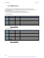
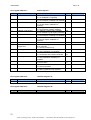
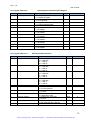
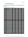
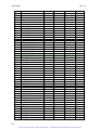
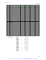
1
Artisan Technology Group is your source for quality
new and certified-used/pre-owned equipment
• FAST SHIPPING AND
DELIVERY
• TENS OF THOUSANDS OF
IN-STOCK ITEMS
• EQUIPMENT DEMOS
• HUNDREDS OF
MANUFACTURERS
SUPPORTED
• LEASING/MONTHLY
RENTALS
• ITAR CERTIFIED
SECURE ASSET SOLUTIONS
SERVICE CENTER REPAIRS
Experienced engineers and technicians on staff
at our full-service, in-house repair center
WE BUY USED EQUIPMENT
Sell your excess, underutilized, and idle used equipment
We also offer credit for buy-backs and trade-ins
www.artisantg.com/WeBuyEquipment
InstraView REMOTE INSPECTION
LOOKING FOR MORE INFORMATION?
Visit us on the web at www.artisantg.com for more
information on price quotations, drivers, technical
specifications, manuals, and documentation
SM
Remotely inspect equipment before purchasing with
our interactive website at www.instraview.com
Contact us: (888) 88-SOURCE | [email protected] | www.artisantg.com
USER'S GUIDE
VSBC-6862
VME Single Board Computer with
PowerQUICC II processor
Revision 1.43
3105
ACTIS Computer
www.actis-computer.com
[email protected]
Artisan Technology Group - Quality Instrumentation ... Guaranteed | (888) 88-SOURCE | www.artisantg.com
VSBC-6862
Rev 1.43
2
Artisan Technology Group - Quality Instrumentation ... Guaranteed | (888) 88-SOURCE | www.artisantg.com
Rev. 1.43
User's Guide
Table of contents
1
1.1.
1.2.
1.3.
1.4.
1.5.
2
2.1.
2.2.
2.3.
2.4.
2.5.
2.6.
2.7.
2.8.
2.9.
2.10.
2.11.
2.12.
2.13.
3
3.1.
3.2.
3.3.
3.4.
3.5.
3.6.
3.7.
3.8.
3.9.
3.10.
3.11.
3.12.
3.13.
3.14.
3.15.
3.16.
3.17.
4
Product description _________________________________________________________ 7
Introduction _____________________________________________________________ 7
Features _______________________________________________________________ 8
Photograph _____________________________________________________________ 9
Block diagram __________________________________________________________ 10
Component location _____________________________________________________ 11
Peripherals description _____________________________________________________ 13
FLASH memory ________________________________________________________
SDRAM memory ________________________________________________________
SRAM memory _________________________________________________________
Real Time Clock with SRAM memory ________________________________________
IP modules ____________________________________________________________
Board registers _________________________________________________________
VME interface __________________________________________________________
I2C EEPROM __________________________________________________________
Fast Ethernet ports ______________________________________________________
SMC1 and SMC2 serial ports ______________________________________________
SCC multi-protocols serial ports ____________________________________________
I2C interface ___________________________________________________________
LED displays ___________________________________________________________
13
13
14
14
14
15
15
17
17
17
18
19
19
Connectors & jumpers______________________________________________________ 21
Push Button: BP1 _______________________________________________________
Rotary switch: SW1______________________________________________________
IP module strobes, header J1 ______________________________________________
Jumper: J2 ____________________________________________________________
Jumper: J3 ____________________________________________________________
Jumpers: J4, J5, J6, J7 ___________________________________________________
Jumper: J8 ____________________________________________________________
Two RS-232 terminal ports, and I2C bus: P13, P4 ______________________________
Four multi-protocols serial ports P7,P8,P9, P10 ________________________________
Two Fast Ethernet ports, connectors P11, P12 ________________________________
IEEE-1149.1 interface, connector P3 ________________________________________
VME bus, P1 connector __________________________________________________
VME bus, P2 connector __________________________________________________
Four IP module logic interface, connectors P3A, P4A, P5A, P6A___________________
Four IP module I/O signals, connectors P3C, P4C, P5C, P6C _____________________
Real time clock battery, circuit U5___________________________________________
Fuses protection ________________________________________________________
23
23
24
25
26
27
28
29
31
33
34
35
36
38
39
40
41
Software description _______________________________________________________ 43
4.1.
Introduction ____________________________________________________________
4.2.
FLASH memory ________________________________________________________
4.2.1. FLASH initialization____________________________________________________
4.2.2. FLASH Programming __________________________________________________
4.2.3. FLASH chip erase ____________________________________________________
4.2.4. FLASH sector erase ___________________________________________________
43
44
44
45
46
46
3
Artisan Technology Group - Quality Instrumentation ... Guaranteed | (888) 88-SOURCE | www.artisantg.com
VSBC-6862
Rev 1.43
4.2.5. FLASH sector protection: option on request_________________________________
4.3.
SDRAM memory ________________________________________________________
4.3.1. SDRAM initialization ___________________________________________________
4.4.
SRAM memory _________________________________________________________
4.5.
Real Time Clock with SRAM memory ________________________________________
4.5.1. RTC registers read operation ____________________________________________
4.5.2. RTC registers write operation ____________________________________________
4.6.
IP modules ____________________________________________________________
4.6.1. Memory spaces ______________________________________________________
4.6.2. Registers ___________________________________________________________
4.6.3. Interrupt functions _____________________________________________________
4.6.4. DMA functions _______________________________________________________
4.7.
VME operations ________________________________________________________
4.7.1. Jumpers ____________________________________________________________
4.7.2. Registers ___________________________________________________________
4.7.3. VME master _________________________________________________________
4.7.4. VME slave __________________________________________________________
4.7.5. VME interrupter ______________________________________________________
4.7.6. VME interrupt handler__________________________________________________
4.7.7. VME Mailbox ________________________________________________________
4.7.8. VME system controller _________________________________________________
4.7.9. Specific features for VME _______________________________________________
4.7.10.
General remarks for VME_____________________________________________
4.8.
Serial I2C EEPROM _____________________________________________________
4.9.
Fast Ethernet ports ______________________________________________________
4.9.1. Transceivers description________________________________________________
4.9.2. MPC-8260 I/O ports ___________________________________________________
4.9.3. Transceivers operations ________________________________________________
4.10.
SMC1 and SMC2 serial ports ______________________________________________
4.10.1.
MPC-8260 I/O ports _________________________________________________
4.10.2.
ACTIS Console Cable _______________________________________________
4.11.
SCC serial ports ________________________________________________________
4.11.1.
RS-232 option _____________________________________________________
4.11.2.
RS-422/RS-485/V.35 option___________________________________________
4.11.3.
ACTIS Serial Cable _________________________________________________
4.11.4.
MPC-8260 I/O ports _________________________________________________
4.12.
I2C interface ___________________________________________________________
4.13.
Auxiliary LEDs__________________________________________________________
5
5.1.
5.2.
5.3.
5.4.
5.5.
5.6.
5.7.
6
6.1.
6.2.
6.3.
6.4.
6.5.
6.6.
6.7.
47
48
48
50
51
52
52
54
57
57
58
59
61
61
61
62
64
66
66
66
67
67
67
68
69
69
70
71
75
75
75
76
76
77
78
79
80
80
Summary of board resources ________________________________________________ 81
Chip Select ____________________________________________________________
Local Board registers ____________________________________________________
Interrupt sources ________________________________________________________
Reset sources __________________________________________________________
Power description _______________________________________________________
Power consumption _____________________________________________________
MPC-8260 I/O ports assignment____________________________________________
81
81
82
82
84
84
85
Board initialization _________________________________________________________ 89
Clock configuration ______________________________________________________
Reset Word ____________________________________________________________
MPC-8260 internal registers _______________________________________________
MPC-8260 I/O ports _____________________________________________________
Chip select ____________________________________________________________
Serial EEPROM ________________________________________________________
Boot code _____________________________________________________________
4
Artisan Technology Group - Quality Instrumentation ... Guaranteed | (888) 88-SOURCE | www.artisantg.com
89
90
91
93
96
96
98
Rev. 1.43
User's Guide
7
8
9
Registers definition ________________________________________________________ 99
Characteristics __________________________________________________________ 111
Physical board definition ___________________________________________________ 113
9.1.
9.2.
10
PCB dimensions _______________________________________________________ 113
Front panel ___________________________________________________________ 114
Software available ___________________________________________________ 115
10.1.
Debug tools___________________________________________________________
10.2.
ECMON______________________________________________________________
10.2.1.
Command description ______________________________________________
10.2.2.
Advanced information_______________________________________________
10.2.3.
Typical example ___________________________________________________
10.3.
VxWorks _____________________________________________________________
10.4.
Linux ________________________________________________________________
10.5.
Other ________________________________________________________________
11
11.1.
11.2.
11.3.
12
13
14
15
Hardware available ___________________________________________________ 121
List of ACTIS's IP modules _______________________________________________ 121
List of ACTIS's 6U transition modules_______________________________________ 123
List of ACTIS's 6U VME boards ___________________________________________ 123
Technical support ____________________________________________________ 125
Ordering information __________________________________________________ 127
OEM Warranty ______________________________________________________ 129
Appendix___________________________________________________________ 131
15.1.
Application examples with the VSBC-6862___________________________________
15.1.1.
Example A: Application with VME boards _______________________________
15.1.2.
Example B: Application with non-VME boards ____________________________
15.1.3.
Example C: Application in stand-alone__________________________________
16
115
115
116
119
120
120
120
120
131
131
132
133
Index______________________________________________________________ 135
5
Artisan Technology Group - Quality Instrumentation ... Guaranteed | (888) 88-SOURCE | www.artisantg.com
VSBC-6862
Rev 1.43
List of figures
Figure 1: Photograph............................................................................................................................... 9
Figure 2: Block diagram......................................................................................................................... 10
Figure 3: Component location ............................................................................................................... 11
Figure 4: Connectors and jumpers location........................................................................................... 22
Figure 5: Push button location............................................................................................................... 23
Figure 6: Rotary switch location ............................................................................................................ 23
Figure 7: Jumper J1 location ................................................................................................................ 24
Figure 8: Jumper J2 location ................................................................................................................. 25
Figure 9: Jumper J3 location ................................................................................................................. 26
Figure 10: Communication ports jumpers in RS-232 mode .................................................................. 27
Figure 11: Communication ports jumpers example............................................................................... 27
Figure 12: Jumper J8 location ............................................................................................................... 28
Figure 13: Connector P13 pinout .......................................................................................................... 29
Figure 14: Connector P4 pinout ............................................................................................................ 30
Figure 15: Communication ports pinout ................................................................................................ 31
Figure 16: Termination resistor networks example ............................................................................... 32
Figure 17: Fast Ethernet ports pinout.................................................................................................... 33
Figure 18: JTAG port pinout .................................................................................................................. 34
Figure 19: Real Time Clock battery....................................................................................................... 40
Figure 20: VME slave window ............................................................................................................... 65
Figure 21: Reset scheme ...................................................................................................................... 83
Figure 22: PCB dimensions................................................................................................................. 113
Figure 23: Front panel ......................................................................................................................... 114
Figure 24: Application example with VME boards............................................................................... 131
Figure 25: Application example with non-VME boards ....................................................................... 132
Figure 26: Application example in stand-alone ................................................................................... 133
For up to date documentation, please refer also to our web site at http://www.actis-computer.com .
While efforts have been made to ensure the accuracy of this document, and although the information contained in
this document is believed to be correct, ACTIS Computer S.A. can not be held responsible for any error or for any
resulting consequential losses. ACTIS Computer S.A may change or improve the specifications of its products at
any time without prior notification.
Total or partial reproduction of this document or any kinds is not allowed without the written authorization of
ACTIS Computer.
Licenses and trademarks
All licenses and trademarks are property of their respective owners.
This manual is copyrighted, all rights reserved. It may not be copied, photocopied, translated, or reduced to any
electronic medium or machine-readable form without ACTIS Computer prior permission.
© ACTIS Computer, 2000-2005
6
Artisan Technology Group - Quality Instrumentation ... Guaranteed | (888) 88-SOURCE | www.artisantg.com
Rev. 1.43
User's Guide
1
Product description
1.1. Introduction
Today industrial applications are growing in telecom market due to the demand of networked
architecture. This method offers great advantage where complex processes are handled and where
real time tasks are the critical features.
The VSBC-6862 combines the best possibilities with its flexible industrial interface and its wide range
of communications ports.
This single board computer is built around a communication-oriented processor: The PowerQUICC II
(MPC-8260) is a member of the PowerPC family of MOTOROLA semiconductors division. This
processor provides a very efficient architecture with two RISC processors built in the same chip: a
PowerPC core controls all host system operations, and a dedicated RISC processor for the
communication part.
The MPC-8260 integrates two main components, the embedded PowerPC core and the
Communications Processor Module (CPM). This dual-processor architecture is more efficient than
traditional architectures because the CPM offloads peripheral tasks from the embedded PowerPC
core.
This single board computer, in 6U form factor, is VME bus master and slave designed as a flexible
solution for communication applications. The VSBC-6862 is designed to offer a very open architecture
through two Fast Ethernet ports, four multi-protocol communication ports, and two RS-232 serial ports.
An other advantage is the flexible I/Os extension, which is implemented through the four VITA-4
standard IP Module slots supporting high performance 16-bit modules at up to 8 MHz clock with DMA
capabilities. These four slots offer to the user the possibility to customize its system very easily with
these cost saving modules.
The combination of the PowerPC core and the CPM dedicated RISC processor, along with the
versatility and performance of the MPC-8260 I/Os provides customers with an enormous potential in
developing networking and communications products while significantly reducing time-to-market
development stages.
7
Artisan Technology Group - Quality Instrumentation ... Guaranteed | (888) 88-SOURCE | www.artisantg.com
VSBC-6862
Rev 1.43
1.2. Features
This board has been designed to integrate the most required functions, including several Fast
Ethernet ports, communication ports, and the flexibility of four IP modules slots for easy user's
customization.
•
Designed with Motorola PowerQUICC II processor
•
A 32-bit EC603 ™ processor core rated at 280.0 MIPS at
200 MHz (Dhrystone 2.1)
•
Dedicated 32-bit RISC processor for communication
protocol handling (CPM)
•
Up to 128 MByte of SDRAM memory with burst
capabilities, 64 bit data bus width
•
8 or 16 MByte of Flash memory for non-volatile
information, divided on two bootables banks, one bank
dual-port with the VME bus
•
1 MByte of SRAM memory dual-port with the VME bus
Non-volatile operation through the VME stand-by signal
•
A separate real time clock device with 32 kByte of battery
backed-up SRAM
Dual-port with the VME bus
•
8 kbit I2C EEPROM for board and user configuration
•
Two Fast Ethernet 100Base-TX/10Base-T interfaces with
auto-negotiation capability
•
Four HDLC serial ports selectable between RS-232 /
RS-422 / RS-485 or V.35
•
Two RS-232 serial ports
•
I2C bus for local extensions
•
JTAG port for debug
•
VME master, slave, system controller interface
•
Four IP Modules slots, compatible with the
ANSI/VITA-4 1995 specification, support for 8 MHz
clock with DMA capabilities
8
Artisan Technology Group - Quality Instrumentation ... Guaranteed | (888) 88-SOURCE | www.artisantg.com
Rev. 1.43
User's Guide
1.3. Photograph
Figure 1: Photograph
The VMEbus Technology logo is a Trademark of the VMEbus International Trade Association.
9
Artisan Technology Group - Quality Instrumentation ... Guaranteed | (888) 88-SOURCE | www.artisantg.com
VSBC-6862
Rev 1.43
1.4. Block diagram
The VSBC-6862 architecture is divided in four main sections:
The CPU
This is the heart of the board, it is the MPC-8260 'PowerQUICC II' with a bus speed of 66MHz, CPM
speed of 133MHz and Core speed of 133 or 200MHz.
The memory section
This section includes the 128 MByte SDRAM on a 64-bit bus, the two 8 MByte Flash memory banks
on a 32-bit bus, the 1 MByte SRAM memory, and the battery backed-up RTC with SRAM.
The internal logic section including the IP carrier and the VME interface
This section handles all internal board logic like board registers, plus the handling of IP modules and
VME functions.
The I/O section
This section is the external part of the PowerQUICC II I/O ports; it contains the two RS-232 ports, the
four serial ports, and the two Fast Ethernet ports.
Fast Ethernet A
Fast Ethernet B
I2C EEPROM
Serial Multiprotocol A
Serial Multiprotocol B
MPC-8260
Serial Multiprotocol C
Serial Multiprotocol D
RS-232 A
PLD
RS-232 B
IP slot A
SDRAM
IP slot B
128MB
IP slot C
IP slot D
Flash
8MB
Flash
8MB
Bank 0
Bank1
SRAM
1MB
VME interface
VME backed-up
RTC
32kB SRAM
Battery backed-up
Figure 2: Block diagram
10
Artisan Technology Group - Quality Instrumentation ... Guaranteed | (888) 88-SOURCE | www.artisantg.com
Rev. 1.43
User's Guide
1.5. Component location
Figure 3: Component location
11
Artisan Technology Group - Quality Instrumentation ... Guaranteed | (888) 88-SOURCE | www.artisantg.com
VSBC-6862
Rev 1.43
Please note that on the VSBC-6862, some locations are not populated.
This was done either to avoid problems of component availability, either for debug purposes.
From the user side, its totally transparent, nothing has to be modified.
For special uses that need a precise component implementation, please contact ACTIS.
12
Artisan Technology Group - Quality Instrumentation ... Guaranteed | (888) 88-SOURCE | www.artisantg.com
Rev. 1.43
User's Guide
2
Peripherals description
The VSBC-6862 offers a wide choice of on-board peripheral or bus interface, which makes this board
very versatile. Most of these peripherals comes either directly from the processor interface, like the
serial ports, or from other interface unit, like the real time clock calendar.
The following sections will describe these peripheral features.
2.1. FLASH memory
Two banks of 4 or 8 MBytes Flash memory devices are available, for a total of 8 or 16 MBytes Flash.
Each Flash bank is formed by a group of two 16-bit devices, which provide a resulting 32-bit bus
interface for efficient instruction program storage.
Each bank is controlled by the Chip Select 0 (CS0) or Chip Select 2 (CS2) signal.
The Flash memory bank connected to the Chip Select 0 is the boot device. This bank must contain
both ResetWord used by the PowerQUICC II configuration and the boot code.
The VSBC-6862 provides a 'Bootbank' jumper to provide the ability to invert the CS0 and CS2 signals,
thus inverting the bootable Flash memory bank.
One Flash memory bank is also shared with the VME bus. This permits an external master to
reprogram the VSBC-6862 Firmware or use this memory as non-volatile device.
This device is command set compatible with JEDEC standard E2PROMs.
Commands are written to the command register using standard microprocessor write timings. Register
contents serve as input to an internal state-machine, which controls the erase and programming
circuitry.
2.2. SDRAM memory
This memory is handled by the powerful SDRAM timing machine contained in the MPC-8260.
The Chip Select 1 is used to control this memory.
The SDRAM machine provides an interface to synchronous DRAMs, using SDRAM pipelining, bank
interleaving, and back-to-back page mode to achieve the highest performance. This controller
supports directly all the SDRAM possibilities, like pipelining and interleaving.
The VSBC-6862 is supplied with 128 MBytes SDRAM on-board, organized with four 16 Mbitsx16
devices.
The 64 bits wide data bus is directly connected on the 60x bus of the MPC-8260 to achieve the best
performance.
13
Artisan Technology Group - Quality Instrumentation ... Guaranteed | (888) 88-SOURCE | www.artisantg.com
VSBC-6862
Rev 1.43
2.3. SRAM memory
1 MBytes of SRAM memory are provided on-board, this memory is controlled with the Chip Select 9.
This memory is shared between the PowerQUICC II and the VME bus.
It is organized in memory width of 32 bits.
A special function is provided for memory saving with the usage of the Stand-By power signal from the
VME bus. When the Board Power is shutdown, the SRAM memory will switch its power lines to the
VME Stand-By power signal.
2.4. Real Time Clock with SRAM memory
The VSBC-6862 includes a real time clock device, with as an additional feature, a battery backed 32
kbyte SRAM. This device is controlled by the Chip Select 3.
Its 32 kbyte SRAM provides flexible user data storage with retention capability by its SNAPHAT
battery pack. This device is connected on an 8 bits wide data path.
This device provides also functions like Alarm, Battery Test, and Watchdog function.
The RTC data are accessible like SRAM Bytes.
This device is also accessible from the VME bus.
Note:
The SNAPHAT housing plugged on the M48T37V contains both battery and crystal.
Thus, for the minimum frequency error, the user has to calibrate the RTC in case of
battery replacement.
2.5. IP modules
The VSBC-6862 provides four IP module slots, which are compliant with the ANSI/VITA 4-1995.
It provides support for 8 MHz type as well as DMA modules.
The IP interface offers an architecture for I/O extension through inexpensive mezzanine modules for
various categories like:
•
•
•
Digital and analog functions
Serial communication controllers
Network and fieldbus interfaces
This interface gives the possibility to easily customize the VSBC-6862.
This IP bus interface is implemented on the VSBC-6862 through a specific CPLD, which provides the
interface between the PowerQUICC II processor and the four IP module slots.
For overall information, please consult the Appendix: List of main ACTIS IP modules.
A choice of IP modules and transition modules from ACTIS Computer is
available on our web site:
www.actis-computer.com
14
Artisan Technology Group - Quality Instrumentation ... Guaranteed | (888) 88-SOURCE | www.artisantg.com
Rev. 1.43
User's Guide
The IP interface uses two processor chip selects to address all IP module spaces.
The Chip Select 4 is used to control the IP I/O, ID, and INT spaces.
The Chip Select 5 is used to control the IP memory spaces.
Each IP slot has is own set of registers to have the four IP slots fully independent.
The VSBC-6862 supports the two IRQ available on the IP modules.
Each IP slot has an own IRQ level attributed to the MPC-8260. If the both IRQ are active at the same
time on an IP module, the VSBC-6862 handles the IP IRQ 0 first, and then IP IRQ 1.
The IP DMA channels are controlled by the IDMA channels, with IP Slot A controlled by IDMA1, Slot B
controlled by IDMA2, Slot C controlled by IDMA3 and Slot D controlled by IDMA4
2.6. Board registers
The VSBC-6862 contains several registers for board features.
These registers are mapped in the same Chip Select 4 than the IP ID and I/O spaces.
These features can be divided in three functions:
•
•
•
General board functions
Two registers are used to generate Reset on the board and to read the rotary
switch value.
IP functions
Each of the four IP slot owns his set of registers to define and use IP modules.
VME functions
Each VME window owns his set of registers to define and use
the VME bus.
2.7. VME interface
There is a VME master, slave, interrupter, interrupt-handler and system controller modules.
Each module can be considered as an independent module.
Some functions are controlled by jumpers for the VME module, as for Slot1function or Reset
utilization.
The VME master A32/A24/A16/D32/D16/D8
Two windows are available to access the VME bus.
They are controlled by the chip selects CS6 and CS7.
The release modes are selectable between ROR and RWD modes.
The VME slave A24/A16/D32/D16/D8
Two windows are available from VME bus:
An A16 window to access VME registers, including mailbox
An A24 window to access the VSBC-6862 memory spaces.
15
Artisan Technology Group - Quality Instrumentation ... Guaranteed | (888) 88-SOURCE | www.artisantg.com
VSBC-6862
Rev 1.43
The VME interrupter I(1-7)
The interrupter is able to generate any VME IRQ level and send a user-defined vector.
The VME interrupt-handler IH(1-7)
This interrupt-handler is able to recognize all IRQ VME levels.
All levels can be masked with the VHM register.
When an IRQ is coming from the VME side, an IRQ1 is sent to the MPC-8260.
The user can then read the IRQ levels active in the VHIL register.
Depending of the IRQ level to be acknowledged, the user can read the vector in the corresponding
offset in the VHV register.
When reading the vector, the interrupt acknowledge cycle is initiated.
The VME system controller.
This function can be enabled or disabled with the Slot1 jumper.
When the system controller is enabled, the VSBC-6862 provides the following functions:
VME arbiter: SGL, PRI, or RRS depending of the VAM register.
VME bus monitor: BTO(30)
IACK daisy-chain driver.
16 MHz system clock generator.
16
Artisan Technology Group - Quality Instrumentation ... Guaranteed | (888) 88-SOURCE | www.artisantg.com
Rev. 1.43
User's Guide
2.8. I2C EEPROM
8 kbits of non-volatile memory is provided on the I2C bus.
This memory is used for board internal configuration (for example to store physical Fast Ethernet
addresses) and can also be used for user purposes.
2.9. Fast Ethernet ports
The two Fast Ethernet interfaces come directly from the MPC-8260 processor.
The physical layer is achieved with on-board fast Ethernet transceivers from SMSC: the LAN83C183.
The SMSC-LAN83C183 provides all of the IEEE 802.3u 100Base-TX and ISO802.3 10Base-T
Physical Layer (PHY) functions needed for workstations, bridge, router, and switch applications. It can
operate as a 100Mbps only device, or as a dual speed 10/100Mbps device with built-in autonegotiation possibility for speed selection. The SMSC-LAN83C183 supports the standard Media
Independent Interface (MII) for glueless interface with 10/100 Ethernet Media Access Controllers
(MAC).
The built-in IEEE 802.3u Auto-Negotiation feature automatically selects internal 10Base-T or
100Base-TX, full or half-duplex, as a result of negotiation between the station and its link partner.
The SMSC-LAN83C183 supports half and full-duplex operation at both 10Mbps and 100Mbps speeds.
It complies with ANSI X3T9 TP-PMD and includes MLT-3 Encoder/Decoder and Stream Cipher
scrambler/ de-scrambler functions for 100Base-TX.The SMSC-LAN83C183 supports Category 5
Unshielded Twisted Pair and Type 1 Shielded Twisted Pair wiring. The on-chip Serial Management
Interface features the Basic and Extended registers set. The 4B/5B Encoder and Decoder are also
included.
An on-board transformer provides a direct connection for a 10Base-T and 100Base-TX interface
2.10.SMC1 and SMC2 serial ports
The VSBC-6862 offers two RS-232 serial ports.
One of these general-purpose serial ports is available on the front panel RJ-45 connector, the other
one is available on an internal connector.
These serial ports can be typically used as system console ports.
Note that this type of port has no hardware flow control capability.
17
Artisan Technology Group - Quality Instrumentation ... Guaranteed | (888) 88-SOURCE | www.artisantg.com
VSBC-6862
Rev 1.43
2.11.SCC multi-protocols serial ports
The VSBC-6862 offers four independent serial ports.
In synchronous mode, all four ports have independents RX clock signals, but only SCC1 and SCC2
have TX Clocks signals.
These ports are directly controlled by the Serial Communication Controllers (SCC) included in the
PowerQUICC II. These SCC includes functions like support of many protocols like UART and HDLC, it
contains also FIFO buffers: 32 byte deep, and many more powerful options.
All the four ports are available on four Sub-D-HD-15 connectors on front panel.
The interface level of these ports can be RS-232/RS-422/RS-485 or V.35.
Switching between these options can be done through the 'serial mode' jumpers.
The serial ports 1 and 2 have an added function: they can be internally used to synchronize the
internal Baud Rate Generators (BRG) with external clock signals.
Note that due to pin multiplexing in the PowerQUICC II, the Transmit Clock for the serial port 4 can't
be used in same time with the IP slot B DMA channel. The user must use either DMA on IP B, either
Transmit Clock on serial port 4.
RS-232 mode
These VSBC-6862 ports are in a standard RS-232 mode.
The following signals are controlled by the PowerQUICC II:
TxD, RxD, TxC, RxC, CTS, RTS, and DCD
All ports support hardware handshaking and synchronous functions.
DSR signals are pulled-up to VCC to indicate that the board is powered-up.
RS-422/RS-485/V.35 modes
These VSBC-6862 ports are compatible with these three modes.
The following signals are controlled by the PowerQUICC II:
TxD, RxD, TxC, RxC in differential mode for RS-422, RS-485 and V.35
CTS, RTS and DCD
in RS-232 mode for V.35
Note:
As described above, the VSBC-6862 did not provides all defined signals for V.35, it provides
all 'transmission signals' but not for example, the loopback or ring indicator signals.
All ports support full and half-duplex mode, and supports also synchronous operations.
The internal I/O ports dedicated to RTS is connected to the internal data transmit enable signal.
This permits to determine the function for half or full-duplex modes as:
Full-duplex:
configure RTS always active
Half-duplex:
configure RTS as normal RTS
The PowerQUICC II has also the possibility to disable his receiver while emitting (see bit DRT in
register PSMR).
Each port has its own network resistors.
These resistors are on sockets. ACTIS choose to implement manual network resistors to keep the RS485 network always working, independently of the power state of the VSBC-6862.
These resistors network are to be installed only when the corresponding serial port is at one of both
ends of the RS-485 network cable.
18
Artisan Technology Group - Quality Instrumentation ... Guaranteed | (888) 88-SOURCE | www.artisantg.com
Rev. 1.43
User's Guide
2.12.I2C interface
The VSBC-6862 provides an I2C interface bus for on-board serial EEPROM accesses and user
purposes.
The board provides external accesses to this bus through an internal connector.
2.13.LED displays
The VSBC-6862 allows monitoring for a wide range of board activities, these status are available for
user check on the front panel.
The Power and Access LEDs functions are hardware fixed.
The Fast Ethernet LEDs can be reconfigured by setting the corresponding parameters in the
transceivers. The configuration of these LEDs is described in the Fast Ethernet transceiver
description.
The two Auxiliary LEDs are user defined with PowerQUICC II I/O ports. They are intended to provide
the user a flexible meaning to signal states on the front panel. These indicators have to be handled by
the user.
These two LEDs are active low.
The following table provides the relation between the front panel LED's and their corresponding
condition sources.
LED reference
Power OK
Access
Auxiliary 0
Auxiliary 1
Fast Ethernet 1 Link
Fast Ethernet 1 Activity
Fast Ethernet 2 Link
Fast Ethernet 2 Activity
Source
5V power ok and 5V IP ok
Internal logic (SDRAM, Reset, Slave)
MPC-8260 I/O port C24
MPC-8260 I/O port C30
SMSC-83C183 1, signal LED3
SMSC-83C183 1, signal LED2
SMSC-83C183 2, signal LED3
SMSC-83C183 2, signal LED2
Ref
D1
D5
P13
P13
P12
P12
P11
P11
Color
Green
Yellow
Yellow
Green
Green
Yellow
Green
Yellow
The 'Power' Led blinking can typically indicate a problem on an IP module. This LED indicates the
power state after the protecting fuses.
The 'Access' Led indicates:
- the Reset state
- an local access to SDRAM
- an slave access to the board
19
Artisan Technology Group - Quality Instrumentation ... Guaranteed | (888) 88-SOURCE | www.artisantg.com
VSBC-6862
Rev 1.43
20
Artisan Technology Group - Quality Instrumentation ... Guaranteed | (888) 88-SOURCE | www.artisantg.com
Rev. 1.43
User's Guide
3
Connectors & jumpers
This chapter will describe all connectors and jumpers on the VSBC-6862.
One of specificity of this board is that the four IP slots occupy most of the board's surface. And it is not
possible to locate connector or jumpers on this area.
In spite of this fact, ACTIS placed the connectors and jumpers in a very straightforward location.
The connectors are numbered upwards: the first connectors for IP, serial ports and Fast Ethernet ports
are in the bottom of the board.
Behind each serial port, are the corresponding termination resistors and jumpers.
Pin numbering convention
The pin numbering is indicated on the 'jumpers and connectors location', on the next page.
- The jumpers have pin 1 indicated by a triangle on the corresponding corner.
For example:
- The connectors and network resistors have pin 1 indicated with a square on the corresponding side.
Example for network resistor:
21
Artisan Technology Group - Quality Instrumentation ... Guaranteed | (888) 88-SOURCE | www.artisantg.com
VSBC-6862
Rev 1.43
Locations
Figure 4: Connectors and jumpers location
22
Artisan Technology Group - Quality Instrumentation ... Guaranteed | (888) 88-SOURCE | www.artisantg.com
Rev. 1.43
User's Guide
3.1. Push Button: BP1
In the front panel, the push button generates a Power-On Reset to the board.
This button is debounced.
Figure 5: Push button location
Before SN:10135, the Push Button was generating a Hardware Reset instead of
Power-On Reset.
3.2. Rotary switch: SW1
The eight position rotary switch is a facility provided for user purposes.
This switch can be used, for example, to select the board working modes.
It can be read with the SWPR register.
Figure 6: Rotary switch location
23
Artisan Technology Group - Quality Instrumentation ... Guaranteed | (888) 88-SOURCE | www.artisantg.com
VSBC-6862
Rev 1.43
3.3. IP module strobes, header J1
For IP module operations, an optional "STROBE" signal is provided for each IP module sockets. This
signal is provided for general purpose use, the J1 header allows the selection for both signals with the
following assignment.
The VSBC-6862 has internals pull-ups connected to these Strobe signals.
Jumpers permit to access or connect pull-downs to these signals.
These jumpers are located near P2
Figure 7: Jumper J1 location
The pins are assigned as follows:
Pin
1
2
3
4
5
6
7
8
Signal
Strobe A
GND
Strobe B
GND
Strobe C
GND
Strobe D
GND
Description
Strobe for IP slot A
Ground
Strobe for IP slot B
Ground
Strobe for IP slot C
Ground
Strobe for IP slot D
Ground
For more details about the strobe signals use, please refer to the ANSI/VITA-4 1995 specification.
24
Artisan Technology Group - Quality Instrumentation ... Guaranteed | (888) 88-SOURCE | www.artisantg.com
Rev. 1.43
User's Guide
3.4. Jumper: J2
A jumper with six positions provides some basic functions.
Figure 8: Jumper J2 location
Position 1
Description:
BootBank1
Description
Unplugged
Plugged-in
The board boots on the Flash memory bank 0
The board boots on the Flash memory bank 1
This jumper is used to define which Flash memory bank is the boot bank.
The VSBC-6862 as two Flash memory banks.
The usage of this jumper allows the user to reverse the bootable bank.
This function will be very helpful to test new software versions during software
debugging.
This provides the facility to come back with the previous software version
loaded in the other bank.
Position 2
Description:
ResetConf
Factory setting
Description
Unplugged
Plugged-in
X
The RSTCONF pin is at GND: normal operation
The RSTCONF pin is at VCC
This jumper is used to force the PowerQUICC II to use the default ResetWord.
The main usage of this jumper is to boot the board for the first time, before the Flash
memory is loaded with the ResetWord.
The board must not function more than few minutes using the default ResetWord.
This is due to the internal clocks sets a little bit higher than normal with default values.
For more information, please consult the MPC-8260 User's manual.
For normal operation, this jumper must never be plugged-in.
Position 3
Description:
Power On Reset
Factory setting
Description
Unplugged
Plugged-in
X
No external Power-On reset: normal operation
External Power-On Reset
This jumper provides the ability to generate an external power-on Reset on the board.
This input is internally debounced, it doesn't need external debouncing logic.
25
Artisan Technology Group - Quality Instrumentation ... Guaranteed | (888) 88-SOURCE | www.artisantg.com
VSBC-6862
Rev 1.43
Position 4
Description:
VME Reset Out
Factory seting
Description
Unplugged
Plugged-in
X
Board is not authorized to generate a VME Reset
Board in Slot1 mode is authorized to generate a VME Reset
When this jumper is plugged, if the board is in Slot1 mode, it will generate a VME
Reset when the board is under Hardware Reset.
Position 5
Description:
VME Reset In
Factory setting
Description
Unplugged
Plugged-in
X
VME Reset is not connected to board Reset
VME Reset generates a board Reset when not in Slot1 mode
When this jumper is plugged, if the board is not in Slot1 mode, a VME Reset will
generate a board Hardware Reset.
Position 6
Description:
VME Slot1 function
Factory setting
Description
Unplugged
Plugged-in
X
The VME Slot1 functions are disabled
The VME Slot1 functions are enabled
This jumper defines if the Slot1 function for VME bus is enabled or disabled.
When the Slot1 function is enabled, the board activates the functions to be the
VME System Controller: Arbiter, Clock generation, Daisy-Chain Handling, Bus
timer
Activate the Slot1 function only if the VSBC-6862 is physically installed in the first
VME Slot.
Warning
3.5. Jumper: J3
This jumper is only used for debug purpose.
Figure 9: Jumper J3 location
It must not be connected without explicit instruction from ACTIS Computer.
Warning
26
Artisan Technology Group - Quality Instrumentation ... Guaranteed | (888) 88-SOURCE | www.artisantg.com
Rev. 1.43
User's Guide
3.6. Jumpers: J4, J5, J6, J7
This are the 'serial mode' jumpers, they have six position.
They permits to select the mode used for the corresponding serial port.
All the six positions of these jumpers must be either all in RS-232 position, either all in RS-485
position.
They are located near its corresponding serial ports:
Figure 10: Communication ports jumpers in RS-232 mode
J4 correspond to serial port SCC1, J5 correspond to serial port SCC2
J6 correspond to serial port SCC3, J7 correspond to serial port SCC4
For RS-232 protocols, set all six jumpers in RS-232 position: 1-2, 4-5, 7-8, 10-11, 13-14, 16-17
For RS-422, RS485 or V.35, set all six jumpers in RS-485 position: 2-3, 5-6, 8-9, 11-12, 14-15, 17-18
Example for ports 1 & 2 in RS-485 mode and ports 3 & 4 in RS-232 mode:
Figure 11: Communication ports jumpers example
ALL six jumpers must always be in the same position, other configuration can
damage the board.
Warning
27
Artisan Technology Group - Quality Instrumentation ... Guaranteed | (888) 88-SOURCE | www.artisantg.com
VSBC-6862
Rev 1.43
3.7. Jumper: J8
This jumper sets the base address for the A16 slave window. This window contains all registers
accessible from an external VME master.
A jumper plugged represents an address line in the state '0', with:
position 1:
position 2:
position 3:
position 4:
position 5:
VME address A11
VME address A12
VME address A13
VME address A14
VME address A15
Example:
Figure 12: Jumper J8 location
This configuration indicates a A16 window base address of $F800.
28
Artisan Technology Group - Quality Instrumentation ... Guaranteed | (888) 88-SOURCE | www.artisantg.com
Rev. 1.43
User's Guide
3.8. Two RS-232 terminal ports, and I2C bus: P13, P4
These serial ports are provided for general purpose application, its interface levels comply with the
RS-232 specification. In most environments, these interfaces will be used as a console port for board
configuration and monitoring functions.
These ports are handled by the SMC1 and SMC2 functions of the PowerQUICC II processor.
P13 is available on the front panel with an RJ-45 connector defined as following:
8
7
6
5 4
3
2
1
Figure 13: Connector P13 pinout
Pin
1
2
3
4
5
6
7
8
Signal
n.u.
n.u.
GND
TxD1
RxD1
GND
n.u.
n.u.
Description
Not used
Not used
Ground
Transmit data SMC1
Receive data SMC1
Ground
Not used
Not used
This connector accepts standard RJ45 8-pin plug connector.
29
Artisan Technology Group - Quality Instrumentation ... Guaranteed | (888) 88-SOURCE | www.artisantg.com
VSBC-6862
Rev 1.43
The second serial port is available in an internal connector shared with the I2C bus.
P4 contains the signals for the SMC2, power lines for user purposes (max 500mA, fused), and the I2C
bus extension.
This connector is available on-board through a HE-10 connector defined as following:
2
4
6
8
10
1
3
5
7
9
Figure 14: Connector P4 pinout
Pin
1
2
3
4
5
6
7
8
9
10
Signal
n.u.
3.3V
5V
n.u.
GND
GND
I2CSCL
I2CSDA
TXD2
RXD2
Description
Not used
3.3 V, 500mA fuse
5.0 V, 500mA fuse
Not used
GND
GND
I2C bus SCL
I2C bus SDA
Transmit data SMC2
Receive data SMC2
This connector accepts standard DIN41651 10-pin female plug connector.
30
Artisan Technology Group - Quality Instrumentation ... Guaranteed | (888) 88-SOURCE | www.artisantg.com
Rev. 1.43
User's Guide
3.9. Four multi-protocols serial ports P7,P8,P9, P10
These four serial ports are provided for user applications
These four ports are available in the front panel on four HD-15 connectors with:
Port SCC1: connector P7
Port SCC2: connector P8
Port SCC3: connector P9
Port SCC4: connector P10
All signals on these connectors are in full-duplex mode.
For Half-duplex mode, please connect externally RX and TX.
Figure 15: Communication ports pinout
Pin
1
2
3
4
5
6
7
8
9
10
11
12
13
14
15
Signal
GND
TxD+
TxDTxC+
TxCRTS
GND
CTS
DTR
DCD
RxCRxC+
RxDRxD+
DSR
Direction
--Out
Out
Out
Out
Out
--In
Out
In
In
In
In
In
Out
Description for RS-232 option
Shield
Transmit Data
n.u.
Transmit Clock
n.u.
Request To Send
Ground
Clear To Send
Data Terminal Ready
Data Carrier Detect
n.u.
Receive Clock
n.u.
Receive Data
Data Set Ready: pulled-up
Description for RS-422/485/V.35 option
Shield
Transmit Data+
Transmit DataTransmit Clock +
Transmit Clock Request To Send
Ground
Clear To Send
Data Terminal Ready
Data Carrier Detect
Receive Clock Receive Clock +
Receive DataReceive Data+
Data Set Ready: pulled-up
This connector accepts standard HD-15 SubD type plug.
Note:
In RS-232 mode, all 'n.u.' pins are physically connected to the corresponding RS-485 function,
thus, the RS-232 device must not use or connect these pins.
31
Artisan Technology Group - Quality Instrumentation ... Guaranteed | (888) 88-SOURCE | www.artisantg.com
VSBC-6862
Rev 1.43
Termination network resistors
When the RS-422/RS-485/V.35 is chosen, the VSBC-6862 is provided with removable network
resistors.
Each resistor network is located as:
RZ34, RZ35:
RZ36, RZ37:
RZ38, RZ39:
RZ40, RZ41:
port SCC 1
port SCC 2
port SCC 3
port SCC 4
Note that the pins 1 of these removable networks are in opposed side than the already soldered
resistor network.
Figure 16: Termination resistor networks example
32
Artisan Technology Group - Quality Instrumentation ... Guaranteed | (888) 88-SOURCE | www.artisantg.com
Rev. 1.43
User's Guide
3.10.Two Fast Ethernet ports, connectors P11, P12
For LAN based applications, two fast Ethernet connections are available for twisted-pair interface
which is compliant for both 100Base-TX and 10Base-T specification described below.
The PHY part of the BSBC-6862 is based on the SMSC83C183 transceiver.
Front panel, connector Fast Ethernet 1 = connector P12, corresponds to FCC2.
Front panel, connector Fast Ethernet 2 = connector P11, corresponds to FCC1.
8 7
6
5 4 3
2
1
Figure 17: Fast Ethernet ports pinout
Pin
1
2
3
4
5
6
7
8
Signal
TxD+
TxDRxD+
n.u.
n.u.
RxDn.u.
n.u.
Description
Transmit data positive output
Transmit data negative output
Receive data positive input
Not used
Not used
Receive data negative input
Not used
Not used
This connector accepts standard RJ45 8-pin plug connector.
The green LED is connected to the SMSC-LAN83183 LED_3 pin, which can indicate 100Mb/s link.
The yellow LED is connected to the SMSC-LAN83183 LED_2 pin, which can indicate activity.
33
Artisan Technology Group - Quality Instrumentation ... Guaranteed | (888) 88-SOURCE | www.artisantg.com
VSBC-6862
Rev 1.43
3.11.IEEE-1149.1 interface, connector P3
The MPC-8260 provides a dedicated user-accessible test access port (TAP) that is fully compatible
with the IEEE 1149.1 Standard Test Access Port and Boundary Scan Architecture. Problems
associated with testing high-density circuit boards have led to development of this standard under the
sponsorship of the Test Technology Committee of IEEE and the Joint Test Action Group (JTAG). The
MPC-8260 implementation supports circuit-board test strategies based on this standard.
This connector definition complies with the industry standard definition for its assignment.
2
4
6
8
10
12
14
16
1
3
5
7
9
11
13
15
Figure 18: JTAG port pinout
Pin
1
2
3
4
5
6
7
8
9
10
11
12
13
14
15
16
Signal
TDO
3.3V
TDI
/TRST
/QREQ
+3.3V
TCK
n.u.
TMS
n.u.
/SRESET
GND
/HRESET
n.u.
/CKSTP_OUT
GND
Description
Serial output data
3.3V, max 0.3 mA
Serial input data
Scan chain logic reset
Quiescent request
+3.3 V power supply, max 100 mA
Serial clock
Not used
Mode select
Not used
Software reset
Ground
Hardware reset
Not used, used as connector 'key'
Checkstop output
Ground
This connector accepts standard DIN41651 16-pin female plug connector.
34
Artisan Technology Group - Quality Instrumentation ... Guaranteed | (888) 88-SOURCE | www.artisantg.com
Rev. 1.43
User's Guide
3.12.VME bus, P1 connector
Row A
Pin
Signal
Row B
Pin
Signal
Row C
Pin
Signal
A1
D0
B1
/BBSY
C1
D8
A2
D1
B2
/BCLR
C2
D9
A3
D2
B3
/ACFAIL
C3
D10
A4
D3
B4
/BG0IN
C4
D11
A5
D4
B5
/BG0OUT
C5
D12
A6
D5
B6
/BG1IN
C6
D13
A7
D6
B7
/BG1OUT
C7
D14
A8
D7
B8
/BG2IN
C8
D15
A9
GND
B9
/BG2OUT
C9
GND
A10
SYSCLK
B10
/BG3IN
C10
/SYSFAIL
A11
GND
B11
/BG3OUT
C11
/BERR
A12
/DS1
B12
/BR0
C12
/SYSRESET
A13
/DS0
B13
/BR1
C13
/LWORD
A14
/WRITE
B14
/BR2
C14
AM5
A15
GND
B15
/BR3
C15
A23
A16
/DTACK
B16
AM0
C16
A22
A17
GND
B17
AM1
C17
A21
A18
/AS
B18
AM2
C18
A20
A19
GND
B19
AM3
C19
A19
A20
/IACK
B20
GND
C20
A18
A21
/IACKIN
B21
-
C21
A17
A22
/IACKOUT
B22
-
C22
A16
A23
AM4
B23
GND
C23
A15
A24
A7
B24
/IRQ7
C24
A14
A25
A6
B25
/IRQ6
C25
A13
A26
A5
B26
/IRQ5
C26
A12
A27
A4
B27
/IRQ4
C27
A11
A28
A3
B28
/IRQ3
C28
A10
A29
A2
B29
/IRQ2
C29
A9
A30
A1
B30
/IRQ1
C30
A8
A31
-12 V
B31
A32
+5 V
B32
+5V STDBY C31
+5 V
C32
+12 V
+5 V
This connector is compliant with the DIN-41612 specification.
35
Artisan Technology Group - Quality Instrumentation ... Guaranteed | (888) 88-SOURCE | www.artisantg.com
VSBC-6862
Rev 1.43
3.13.VME bus, P2 connector
This connector has its VME user's pins attributed to the IP I/O slot D
Row A
Pin
Signal
Row B
Pin
Signal
Row C
Pin
Signal
A1
IP D, I/O 2
B1
+5 V
C1
IP D, I/O 1
A2
IP D, I/O 4
B2
GND
C2
IP D, I/O 3
A3
IP D, I/O 6
B3
-
C3
IP D, I/O 5
A4
IP D, I/O 8
B4
A24
C4
IP D, I/O 7
A5
IP D, I/O 10
B5
A25
C5
IP D, I/O 9
A6
IP D, I/O 12
B6
A26
C6
IP D, I/O 11
A7
IP D, I/O 14
B7
A27
C7
IP D, I/O 13
A8
IP D, I/O 16
B8
A28
C8
IP D, I/O 15
A9
IP D, I/O 18
B9
A29
C9
IP D, I/O 17
A10
IP D, I/O 20
B10
A30
C10
IP D, I/O 19
A11
IP D, I/O 22
B11
A31
C11
IP D, I/O 21
A12
IP D, I/O 24
B12
GND
C12
IP D, I/O 23
A13
IP D, I/O 26
B13
+5 V
C13
IP D, I/O 25
A14
IP D, I/O 28
B14
D16
C14
IP D, I/O 27
A15
IP D, I/O 30
B15
D17
C15
IP D, I/O 29
A16
IP D, I/O 32
B16
D18
C16
IP D, I/O 31
A17
IP D, I/O 34
B17
D19
C17
IP D, I/O 33
A18
IP D, I/O 36
B18
D20
C18
IP D, I/O 35
A19
IP D, I/O 38
B19
D21
C19
IP D, I/O 37
A20
IP D, I/O 40
B20
D22
C20
IP D, I/O 39
A21
IP D, I/O 42
B21
D23
C21
IP D, I/O 41
A22
IP D, I/O 44
B22
GND
C22
IP D, I/O 43
A23
IP D, I/O 46
B23
D24
C23
IP D, I/O 45
A24
IP D, I/O 48
B24
D25
C24
IP D, I/O 47
A25
IP D, I/O 50
B25
D26
C25
IP D, I/O 49
A26
-
B26
D27
C26
-
A27
-
B27
D28
C27
-
A28
-
B28
D29
C28
-
A29
-
B29
D30
C29
-
A30
-
B30
D31
C30
-
A31
-
B31
GND
C31
-
A32
TM 5 V
B32
+5 V
C32
TM 5 V
36
Artisan Technology Group - Quality Instrumentation ... Guaranteed | (888) 88-SOURCE | www.artisantg.com
Rev. 1.43
User's Guide
Signal
+5 V
+12 V
-12 V
GND
+5 V STDBY
TM 5 V
Description
Main power supply
Power used for IP module slots and Flash protection feature
Power used for IP module slots
Ground
Power supply furnished by an non-interruptible power source
5 V provided by the VSBC-6862 to an optional transition module. Fuse protected
This connector is compliant with the DIN-41612 specification.
37
Artisan Technology Group - Quality Instrumentation ... Guaranteed | (888) 88-SOURCE | www.artisantg.com
VSBC-6862
Rev 1.43
3.14.Four IP module logic interface, connectors P3A,
P4A, P5A, P6A
For input/output extensions, the VSBC-6862 board provides a four slot IP module interface. This bus
interface complies with the ANSI/VITA-4 1995 specification and handles 16-bit wide modules and
supports 8 MHz mode.
These slots are assigned as:
connector P6A: IP slot A
connector P5A: IP slot B
connector P4A: IP slot C
connector P3A: IP slot D
The following table gives the connectors assignment which refers to the VITA-4 specification.
Pin
1
2
3
4
5
6
7
8
9
10
11
12
13
14
15
16
17
18
19
20
21
22
23
24
25
Signal
GND
CLK
/RESET
D0
D1
D2
D3
D4
D5
D6
D7
D8
D9
D10
D11
D12
D13
D14
D15
/BS0
/BS1
- 12 V
+ 12 V
+5V
GND
Pin
26
27
28
29
30
31
32
33
34
35
36
37
38
39
40
41
42
43
44
45
46
47
48
49
50
Signal
GND
5V
R/W
/IDSEL
/DMAREQ0
/MEMSEL
/DMAREQ1
/INTSEL
/DMACK
/IOSEL
reserved
A1
/DMAEND
A2
/ERROR
A3
/INTREQ0
A4
/INTREQ1
A5
/STROBE
A6
/ACK
reserved
GND
38
Artisan Technology Group - Quality Instrumentation ... Guaranteed | (888) 88-SOURCE | www.artisantg.com
Rev. 1.43
User's Guide
3.15.Four IP module I/O signals, connectors P3C, P4C,
P5C, P6C
The four IP modules slots present on the VSBC-6862 have their I/O connections available on four high
density connectors. They are connectors from Hirose (Ref: HIF6A-50PA-1,27DSA). The
corresponding Hirose cable connector reference is: HIF6-50D-1,27R.
These connectors are assigned as:
connector P6C: IP slot A
connector P5C: IP slot B
connector P4C: IP slot C
connector P3C: IP slot D
These connectors are pin to pin wired (1 to 1, 2 to 2, ...., 49 to 49 and 50 to 50) with the IP modules IO
connectors (P3B to P3C, P4B to P4C, ...).
Note that the IP module slot D I/O pins are also connected to the VME connector P2.
The connector assignment provides the straight connection from the IP module
I/O connector with ACTIS cable set reference CAB-85B.
Pin
Signal
Pin
Signal
1
I/OD 1
2
I/OD 2
3
I/OD 3
4
I/OD 4
5
I/OD 5
6
I/OD 6
7
I/OD 7
8
I/OD 8
9
I/OD 9
10
I/OD 10
11
I/OD 11
12
I/OD 12
13
I/OD 13
14
I/OD 14
15
I/OD 15
16
I/OD 16
17
I/OD 17
18
I/OD 18
19
I/OD 19
20
I/OD 20
21
I/OD 21
22
I/OD 22
23
I/OD 23
24
I/OD 24
25
I/OD 25
26
I/OD 26
27
I/OD 27
28
I/OD 28
29
I/OD 29
30
I/OD 30
31
I/OD 31
32
I/OD 32
33
I/OD 33
34
I/OD 34
35
I/OD 35
36
I/OD 36
37
I/OD 37
38
I/OD 38
39
I/OD 39
40
I/OD 40
41
I/OD 41
42
I/OD 42
43
I/OD 43
44
I/OD 44
45
I/OD 45
46
I/OD 46
47
I/OD 47
48
I/OD 48
49
I/OD 49
50
I/OD 50
These connector are compliant with the Hirose HIF6 series, it provides a 50-pin
arrangement organized for a dual 25-pin flat cable
39
Artisan Technology Group - Quality Instrumentation ... Guaranteed | (888) 88-SOURCE | www.artisantg.com
VSBC-6862
Rev 1.43
3.16. Real time clock battery, circuit U5
The VSBC-6862 provides a real time clock for calendar function. This device includes also a 32 kByte
SRAM with battery backed capability.
It also include an on-chip watchdog that can be used as board's Watchdog.
The battery used by this part is a Lithium type and is designed for user replacement.
For this operation, caution must be taken in order to avoid hardware damage
Warning
Please use the following instructions for the battery replacement:
1) Turn the main power supply off.
2) Remove the used battery located on the U5 position, refer to the next figure for assembly
details.
3) Plug the new battery pack into the U5 location, refer to the next figure for assembly details.
Figure 19: Real Time Clock battery
Replacement battery pack part reference:
ST Microelectronics part number: M4T28-BR12SH1
40
Artisan Technology Group - Quality Instrumentation ... Guaranteed | (888) 88-SOURCE | www.artisantg.com
Rev. 1.43
User's Guide
3.17. Fuses protection
The VSBC-6862 offers a flexible I/O extension facility through its quad IP module interface. Therefore
some cautions must be taken to avoid hardware damage in case of short circuit.
This function is handled by a set of on-board fuses.
These fuses are thermal controlled, when a short-circuit arise, the fuse will automatically break the
circuit. When it will be cold, it becomes again normal.
Fuse
F16
F15
F11
F12
F3
F10
F4
F9
F1
F2
F13
Intensity
2A
2A
2A
2A
2A
2A
2A
2A
500mA
500mA
2A
Power supply
IP module A, +5 V
IP module B, +5 V
IP module C, +5 V
IP module D, +5 V
IP module A/B, +12 V
IP module C/D, +12 V
IP module A/B, -12 V
IP module C/D, -12 V
RS-232/I2C jumper P4, pin 3: 5V
RS-232/I2C jumper P4, pin 2: 3.3V
VME connector P2, pin A32 and C32: 5V out for TM
41
Artisan Technology Group - Quality Instrumentation ... Guaranteed | (888) 88-SOURCE | www.artisantg.com
VSBC-6862
Rev 1.43
42
Artisan Technology Group - Quality Instrumentation ... Guaranteed | (888) 88-SOURCE | www.artisantg.com
Rev. 1.43
User's Guide
4
Software description
4.1. Introduction
The PowerQUICC II includes a very versatile and powerful memory controller.
This controller permits to define by software the base memory for each chip select, thus to define the
memory map.
The memory controller is composed of three internal machines:
-
The general purpose chip select machine: GPCM provides signal generation for
local resources: SRAM and FLASH memory, and Real Time Clock.
-
The synchronous DRAM machine provide signal generation for SDRAM devices.
This internal machine supports many special features for SDRAM.
-
The user programmable machines: UPM can be programmed by the user through
an internal array to provide specific patterns on signals. These UPMs are used to
control the IP and VME devices.
The error generation is mainly handled with the internal bus monitor included in the 8260. See the
SYPCR register and bus monitor description in the 8260 User's manual.
Here follows the description of all used chip select on the VSBC-6862:
Chip Select
CS0
CS1
CS2
CS3
CS4
CS5
CS6
CS7
CS9
Port size (bits)
32
64
32
8
16
16
8, 16, 32
8, 16, 32
32
Device
Flash bank 0: boot device 0
SDRAM
Flash Bank 1: boot device 1
Real Time Clock and SRAM
IP ID, I/O + Board registers
IP Mem
VME window A
VME window B
SRAM
Size
8 MBytes
128 MBytes
8 MBytes
32 kBytes
32 kBytes
32 MBytes
64 MBytes
64 MBytes
1 MBytes
In addition, the PowerQUICC II provides many internal peripherals as Fast Ethernet controllers, serial
controllers, etc...
These peripherals are internally handled by the MPC-8260 and the control signals are directly
connected to the external transceivers.
43
Artisan Technology Group - Quality Instrumentation ... Guaranteed | (888) 88-SOURCE | www.artisantg.com
VSBC-6862
Rev 1.43
4.2. FLASH memory
Two banks of Flash devices are available.
Each bank is 4 or 8 MBytes wide for a total of 8 or 16 MBytes Flash.
The GPCM is used to control the Flash memory.
Each bank is controlled by the Chip Select 0 (CS0) or Chip Select 2 (CS2) signal.
The Flash memory has boot capability in accordance with the 'Bootbank' jumper setting.
The granularity is 16 bits, it means that the minimum size accessible in the Flash memory is two bytes.
This device is command set compatible with JEDEC standard E2PROMs.
Commands are written to the command register using standard microprocessor write timings. Register
contents serve as input to an internal state-machine which controls the erase and programming
circuitry.
This Chip Select (CS0) is the Boot Chip Select, it is connected to a Flash memory bank.
When the power goes to ON, the Flash memory bank connected to this chip select must contain the
Reset initialization Word for the PowerQUICC II, and is boot code. If the Reset Word is not valid, the
board can be started with a default Reset initialization Word using the 'Resetconf' jumper on J2.
For more convenience, we have added the possibility to switch the Flash memory bank 0 and the
bank 1 between CS0 and CS2, thus inverting the bootable bank.
This is done by manipulating the 'BootBank1' jumper.
The bootable Flash memory bank is also accessible from the VME bus. See the VME slave chapter
for more information.
4.2.1. FLASH initialization
Typical Base Register:
Bit
0-16
17-18
19-20
21-22
23
24-26
27
28-29
30
31
Field
BA
Reserved
PS
DECC
WP
MS
EMEMC
ATOM
DR
V
->
BR0
Value
$xxxxb
00
11
00
0
000
0
00
0
1
=
Function
Base address:
user defined
--Port size:
32 bits
Data error correction:
off
Write protect:
off
Machine select:
GPCM on 60x bus
External mem cntrl enable:
off
Atomic operation:
off
Data pipelining:
no
Valid bit:
on
$xxxx 1801
44
Artisan Technology Group - Quality Instrumentation ... Guaranteed | (888) 88-SOURCE | www.artisantg.com
Rev. 1.43
User's Guide
Typical Option Register:
Bit
0-16
17-18
19
20
21-22
23
24-27
28
29
30
31
Field
AM
Reserved
BCTLD
CSNT
ACS
Reserved
SCY
SETA
TRLX
EHTR
Reserved
->
OR0
Value
$FFC0 0
00
0
0
00
0
0110
1
0
0
0
=
Function
Address mask:
for 4 MBytes
--Buffer control:
on
Chip select negation time:
normal
Address to CS setup:
0
--Cycle length:
6
External access termination:
external
Timing relaxed:
off
Extended hold time:
off
---
$FFC0 0068
This example is for a 8MByte VSBC-6862. There is two 4MByte Flash memory banks.
This Chip Select is connected to the second bank of Flash memory, depending of the 'BootBnk'
jumper. The GPCM is used to control the Flash memory.
As this chip select controls the same device as CS0, it will have the same register values:
Typical Base Register:
->
BR2
=
$zzzz 1801
Typical Option Register:
->
OR2
=
$FFC0 0068
Once these Chip Select registers are configured, access to the Flash memory can be done.
The Flash memory recognize the standard JEDEC commands, these commands will be described
below.
4.2.2. FLASH Programming
The device is programmed by executing the program command sequence. This will invoke the
Embedded Program Algorithm, which is an internal algorithm that automatically setup the program
pulse widths and verifies proper cell margin. Each sector can be programmed and verified in less than
0.5 seconds.
The program sequence is the following:
Sequence
1
2
3
4
Address
Base + $555
Base + $2AA
Base + $555
Address
Data
$AAAA
$5555
$A0A0
Data: 16 bits
45
Artisan Technology Group - Quality Instrumentation ... Guaranteed | (888) 88-SOURCE | www.artisantg.com
VSBC-6862
Rev 1.43
4.2.3. FLASH chip erase
Chip erase operation is accomplished by executing the erase command sequence. This will invoke the
Embedded Erase Algorithm, which is an internal algorithm that automatically programs the array if it is
not already programmed before executing the erase operation. During erase, the device automatically
defines the erase pulse widths and verifies proper cell margin.
The chip erase sequence is the following:
Sequence
1
2
3
4
5
6
Address
Base + $555
Base + $2AA
Base + $555
Base + $555
Base + $2AA
Base + $555
Data
$AAAA
$5555
$8080
$AAAA
$5555
$1010
Note that after executing this command, it is important to wait until completion.
Read cycles on Flash indicates the current state of the Flash, while read results are not equal to
$FFFF, the chip erase cycle is not finished. This command can last up to 2 minutes.
4.2.4. FLASH sector erase
This device features sector erase architecture. The sector erase mode allows for sectors of memory to
be erased and reprogrammed without affecting other sectors. A sector is typically erased and verified
within 1 second. (if already completely programmed)
The sector erase sequence is the following:
Sequence
1
2
3
4
5
6
Address
Base + $555
Base + $2AA
Base + $555
Base + $555
Base + $2AA
Sector Address
Data
$AAAA
$5555
$8080
$AAAA
$5555
$3030
Note that depending of the Flash device installed, the sector's organisation can be different.
The following table gives the different types of Flash that can be installed.
Flash type
1
2
3
4
Manufacturer
Reference
Manufacturer code
Device code
AMD
FUJITSU
TOSHIBA
AMD
FUJITSU
TOSHIBA
ST
AMD
FUJITSU
TOSHIBA
ST
AMD
FUJITSU
AM29DL324B
MBM29DL324B
TC58FVB321
AM29LV160B
MBM29LV160B
TC58FVB160
M29W160BB
AM29LV160T
MBM29LV160T
TC58FVT160
M29W160BT
AM29DL164B
MBM29DL164B
0001
0004
0098
0001
0004
0098
0020
0001
0004
0098
0020
0001
0004
225f
225f
009c
2249
2249
0043
2249
22c4
22c4
00c2
22c4
2235
2235
46
Artisan Technology Group - Quality Instrumentation ... Guaranteed | (888) 88-SOURCE | www.artisantg.com
Rev. 1.43
User's Guide
With Flash type organization as:
Sector
0
1
2
3
4
5
6
7
8
9
10
11
12
13
14
15
16
17
18
19
20
21
22
23
24
25
26
27
28
29
30
31
32
33
34
35
36
37
38
39
40
41
42
43
45
46
47
48
49
50
51
52
53
54
55
56
57
58
59
60
61
62
63
64
65
66
67
68
69
70
Size for type 1
8 kword
8 kword
8 kword
8 kword
8 kword
8 kword
8 kword
8 kword
64 kword
64 kword
64 kword
64 kword
64 kword
64 kword
64 kword
64 kword
64 kword
64 kword
64 kword
64 kword
64 kword
64 kword
64 kword
64 kword
64 kword
64 kword
64 kword
64 kword
64 kword
64 kword
64 kword
64 kword
64 kword
64 kword
64 kword
64 kword
64 kword
64 kword
64 kword
64 kword
64 kword
64 kword
64 kword
64 kword
64 kword
64 kword
64 kword
64 kword
64 kword
64 kword
64 kword
64 kword
64 kword
64 kword
64 kword
64 kword
64 kword
64 kword
64 kword
64 kword
64 kword
64 kword
64 kword
64 kword
64 kword
64 kword
64 kword
64 kword
64 kword
64 kword
Size for type 2
16 kword
8 kword
8 kword
32 kword
64 kword
64 kword
64 kword
64 kword
64 kword
64 kword
64 kword
64 kword
64 kword
64 kword
64 kword
64 kword
64 kword
64 kword
64 kword
64 kword
64 kword
64 kword
64 kword
64 kword
64 kword
64 kword
64 kword
64 kword
64 kword
64 kword
64 kword
64 kword
64 kword
64 kword
64 kword
-----------------------------------------------------------------------
Size for type 3
8 kword
8 kword
8 kword
8 kword
8 kword
8 kword
8 kword
8 kword
64 kword
64 kword
64 kword
64 kword
64 kword
64 kword
64 kword
64 kword
64 kword
64 kword
64 kword
64 kword
64 kword
64 kword
64 kword
64 kword
64 kword
64 kword
64 kword
64 kword
64 kword
64 kword
64 kword
64 kword
64 kword
64 kword
64 kword
64 kword
64 kword
64 kword
64 kword
---------------------------------------------------------------
Size for type 4
64 kword
64 kword
64 kword
64 kword
64 kword
64 kword
64 kword
64 kword
64 kword
64 kword
64 kword
64 kword
64 kword
64 kword
64 kword
64 kword
64 kword
64 kword
64 kword
64 kword
64 kword
64 kword
64 kword
64 kword
64 kword
64 kword
64 kword
64 kword
64 kword
64 kword
64 kword
32 kword
8 kword
8 kword
16 kword
-----------------------------------------------------------------------
Remark: the sector size is specified in words (16-bit) because the Flash granularity is 16-bit on the
data bus.
4.2.5. FLASH sector protection: option on request
The VSBC-6862 can also provides the possibility to protect or enable sectors writing.
To implement this feature, the board has the capability to supply 12V on the Flash Reset pin. This
voltage is supplied on both banks.
This function is accessible with the FLPROT bit in the BSCR register.
47
Artisan Technology Group - Quality Instrumentation ... Guaranteed | (888) 88-SOURCE | www.artisantg.com
VSBC-6862
Rev 1.43
4.3. SDRAM memory
This memory is handled by the powerful SDRAM timing machine contained in the MPC-8260.
The SDRAM machine provides an interface to synchronous DRAMs, using SDRAM pipelining, bank
interleaving, and back-to-back page mode to achieve the highest performance. This controller
supports directly all the SDRAM possibilities, like pipelining and interleaving.
The VSBC-6862 is supplied with 128 MBytes SDRAM on-board, organized with four 16Mbitsx16
devices.
The 64 bits wide data bus is directly connected on the 60x bus of the MPC-8260 to achieve the best
performance.
The SDRAM is controlled by the Chip Select 1 signal.
4.3.1. SDRAM initialization
This device have specific operation for initialization, both SDRAM machine and SDRAM devices have
to be set-up.
The SDRAM machine is configured with its own set of registers as OR1, BR1, PSDMR.
The SDRAM device is configured by accessing the PSDMR register in a specific manner.
Here follows the full description to initialize the SDRAM devices:
-
Configure MPTPR: timer prescaler
Configure PSRT: refresh timer prescaler
Configure OR1
Configure BR1
With PSDMR, issue a PRECHARGE-ALL-BANKS command
"
issue eight CBR REFRESH commands
"
issue a MODE-SET command to initialize the mode register with the
below recommended value
The SDRAM can now be used as normal memory
-
With:
Typical Base Register:
Bit
0-16
17-18
19-20
21-22
23
24-26
27
28-29
30
31
Field
BA
Reserved
PS
DECC
WP
MS
EMEMC
ATOM
DR
V
->
BR1
Value
$xxxxb
00
00
00
0
010
0
00
0
1
=
Function
Base address:
user defined
--Port size:
64 bits
Data error correction:
off
Write protect:
off
Machine select:
SDRAM on 60x bus
External mem cntrl enable:
off
Atomic operation:
off
Data pipelining:
no
Valid bit:
on
$xxxx 0041
48
Artisan Technology Group - Quality Instrumentation ... Guaranteed | (888) 88-SOURCE | www.artisantg.com
Rev. 1.43
User's Guide
Typical Option Register:
Bit
0-16
17-18
19-22
23-25
26
27
28-31
Field
AM
BPD
ROWST
NUMR
PMSEL
IBID
Reserved
Value
$FE00 0
01
0111
011
0
0
0000
Address mask:
Bank per device:
Row start address bit:
Number of Row lines:
Page mode select:
Int. bank interleaving:
---
->
OR1
=
$FE00 2EC0
For 32 MB version
->
OR1
=
$F800 2B00
For 128 MB version
Function
for 32 MBytes
4
A7
12
normal
enable
Typical 60x SDRAM Mode Register:
Bit
0
1
2-4
5-7
8-10
11-13
14-16
17-19
20-22
23
24-25
26-27
28
29
30-31
Field
PBI
RFEN
OP
SDAM
BSMA
A10
RFRC
PRETOACT
ACTTORW
BL
LDOTOPRE
WRC
EAMUX
BUFCMD
CL
Value
1
1
000
010
010
010
100
010
010
0
01
10
0
0
10
Function
Page based interleaving:
yes
Refresh enable:
yes
SDRAM operation:
normal
Address mux size:
MPCA18 -> (SDA28)
Bank select address lines:
not used
A10 control:
A8
Refresh recovery:
4 clocks
Precharge to activate interval: 2 clocks
Activate to Read/Write interval: 2 clocks
Burst length:
for 64 bits
Last data out to precharge:
-1 clock
Write recovery time:
2 clock
External address multiplexing: disabled
External buffers:
no
CAS latency:
2
->
PSDMR =
$C24A 2462
For 32 MB version
->
PSDMR =
$C32E 2462
For 128 MB version
Typical 60x bus-assigned Refresh Timer Register:
Bit
0-7
Field
Value
00111110
PSRT
->
PSRT
=
Function
Refresh timer period
$1F
Typical Memory Periodic Timer Pre-scaler Register:
Bit
0-7
8-15
Field
Value
00100000
00000000
PTP
Reserved
->
MPTPR
=
Function
Refresh timers prescaler
---
$2000
These settings configure the refresh period to 15.5 µs.
49
Artisan Technology Group - Quality Instrumentation ... Guaranteed | (888) 88-SOURCE | www.artisantg.com
VSBC-6862
Rev 1.43
4.4. SRAM memory
The VSBC-6862 includes 1 MByte SRAM for fast exchanges with external VME masters.
With its backup capability with the VME Stand-By power line, this memory can be also useful to
backup critical data.
This memory is handled with the GPCM through the Chip Select 9.
It is organized with two 16 bits wide chips to achieve a data width of 32 bits.
Typical Base Register:
Bit
0-16
17-18
19-20
21-22
23
24-26
27
28-29
30
31
Field
BA
Reserved
PS
DECC
WP
MS
EMEMC
ATOM
DR
V
->
BR9
Value
$xxxxb
00
11
00
0
000
0
00
0
1
=
Function
Base address:
user defined
--Port size:
32 bits
Data error correction:
off
Write protect:
off
Machine select:
GPCM on 60x bus
External mem cntrl enable:
off
Atomic operation:
off
Data pipelining:
no
Valid bit:
on
$xxxx 1801
Typical Option Register:
Bit
0-16
17-18
19
20
21-22
23
24-27
28
29
30
31
Field
AM
Reserved
BCTLD
CSNT
ACS
Reserved
SCY
SETA
TRLX
EHTR
Reserved
->
OR9
Value
$FFF0 0
00
0
0
00
0
0110
1
0
0
0
=
Function
Address mask:
for 1 MBytes
--Buffer control:
on
Chip select negation time:
normal
Address to CS setup:
0
--Cycle length:
6
External access termination:
external
Timing relaxed:
off
Extended hold time:
off
---
$FFF0 0068
50
Artisan Technology Group - Quality Instrumentation ... Guaranteed | (888) 88-SOURCE | www.artisantg.com
Rev. 1.43
User's Guide
4.5. Real Time Clock with SRAM memory
The VSBC-6862 includes a real time clock device, with as an additional feature, a battery backed
32 kByte SRAM.
This 32 kByte SRAM provides a flexible user data storage with retention capability by its SNAPHAT
battery pack. This device is connected on an 8 bits wide data path.
This device provides also functions like Alarm, Battery Test, and Watchdog function.
The GPCM is used to control the Real Time Clock and the battery backed SRAM.
The RTC data are mapped in the SRAM memory map.
The RTC is also accessible from VME bus.
Typical Base Register:
Bit
0-16
17-18
19-20
21-22
23
24-26
27
28-29
30
31
Field
BA
Reserved
PS
DECC
WP
MS
EMEMC
ATOM
DR
V
->
BR3
Value
$xxxxb
00
01
00
0
000
0
00
0
1
=
Function
Base address:
user defined
--Port size:
8 bits
Data error correction:
off
Write protect:
off
Machine select:
GPCM on 60x bus
External mem cntrl enable:
off
Atomic operation:
off
Data pipelining:
no
Valid bit:
on
$xxxx 0801
Typical Option Register:
Bit
0-16
17-18
19
20
21-22
23
24-27
28
29
30
31
Field
AM
Reserved
BCTLD
CSNT
ACS
Reserved
SCY
SETA
TRLX
EHTR
Reserved
->
OR3
Value
$FFFF 1
00
0
0
00
0
0111
1
0
0
0
=
Function
Address mask:
for 32 kBytes
--Buffer control:
on
Chip select negation time:
normal
Address to CS setup:
0
--Cycle length:
7
External access termination:
external
Timing relaxed:
off
Extended hold time:
off
---
$FFFF 8078
51
Artisan Technology Group - Quality Instrumentation ... Guaranteed | (888) 88-SOURCE | www.artisantg.com
VSBC-6862
Rev 1.43
48T37V partial register map is:
Base +
$7FFF
$7FFE
$7FFD
$7FFC
$7FFB
$7FFA
$7FF9
$7FF8
$7FF7
$7FF6
$7FF5
$7FF4
$7FF3
$7FF2
$7FF1
$7FF0
With:
D7
0
0
0
0
0
ST
W
WDS
AFE
RPT4
RPT3
RPT2
RPT1
WDF
D6
D5
D4
10 Years
0
0
10M.
0
10 Date
FT
0
0
0
10 Hours
10 Minutes
10 Seconds
R
S
BMB4 BMB3 BMB2
0
ABE
0
0
Alarm 10 Date
0
Alarm 10 Hours
Alarm 10 Minutes
Alarm 10 Second
1000 Years
AF
Z
BL
S = sign bit
FT = Frequency Test bit
R = Read Bit
W = Write Bit
ST = Stop Bit
0 = Must be set to ’0’
Z = ’0’ and are Read only
WDS = Watchdog Steering Bit
WDF = Watchdog Flag
D3
D2
D1
Year
Month
Date
0
Day
Hours
Minutes
Seconds
Calibration
BMB1 BMB0
RB1
0
0
0
Alarm Date
Alarm Hours
Alarm Minutes
Alarm Seconds
100 Years
Z
Z
Z
D0
RB0
0
Z
Function (Range) BCD format
Year (00-99)
Month (01-12)
Date (01-31)
Century/Day (0-1/01-07)
Hour (00-23)
Minutes (00-59)
Seconds (00-59)
Control
Watchdog
Interrupts
Alarm Date (01-31)
Alarm Hours (00-23)
Alarm Minutes (00-59)
Alarm Seconds (00-59)
Century
Flags
AF = Alarm Flag
BL = Battery Low Flag
WDS = Watchdog Steering Bit
BMB0-BMB4 = Watchdog Multiplier Bits
RB0-RB1 = Watchdog Resolution Bits
AFE = Alarm Flag Enable
ABE = Alarm in Battery Back-up Mode Enable
RPT1-RPT4 = Alarm Repeat Mode Bits
4.5.1. RTC registers read operation
The RTC registers are continuously updated by the device.
Updates to the RTC registers should be halted before clock data is read to prevent reading data in
transition.
Because the registers are only copy of the clock counters, updating the registers can be halted without
disturbing the clock itself. Updating is halted when a ’1’ is written to the READ bit, D6 in the Control
Register 7FF8h. As long as a ’1’ remains in that position, updating is halted. After a halt is issued, the
registers reflect the count; that is, the day, date, and the time that was current at the moment the halt
command was issued. All of the RTC registers are updated simultaneously. A halt will not interrupt an
update in progress. Updating is within a second after the bit is reset to a ’0’.
4.5.2. RTC registers write operation
Bit D7 of the Control Register 7FF8h is the WRITE bit. Setting the WRITE bit to a ’1’, like the READ
bit, halts updates to the RTC registers. The user can then load them with the correct day, date, and
time data in 24 hour BCD format. Resetting the WRITE bit to a ’0’ then transfers the values of all time
registers 7FF9h-7FFFh to the actual RTC counters and allows normal operation to resume. After the
WRITE bit is reset, the next clock update will occur in approximately one second.
See the ST Microelectronics Application Note AN923 "TIMEKEEPER rolling into
the 21st century" on the ST Web site for information on Century Rollover.
52
Artisan Technology Group - Quality Instrumentation ... Guaranteed | (888) 88-SOURCE | www.artisantg.com
Rev. 1.43
User's Guide
The Watchdog can be activated by setting the RTC's Watchdog register (internal offset $7ff7) with the
desired time-out value.
When the Watchdog is active, it decrement its internal counter until 0. To reload the counter, you can
either write again the RTC's watchdog register, either toggling the RTCWDI pin. (connected to the
8260's I/O PD12)
If the Watchdog counter reachs zero, the M48T37V generate an interrupt to its IRQ pin.
This pin is connected on two devices: the 8260 I/O port C5 and the programmable logic. This permits
to use the Watchdog in two manners:
A) The Watchdog pin is directly connected to the 8260's port C5, this pin has for special feature to be
able to generate an IRQ to the core.
B) For a more securised application, it is possible to connect, using a register, the Watchdog pin to the
Board's Power-On Reset signal. This is made writing the value $1 in the SRESR register. Once
activated, this connection can not be disabled until next Power-On Reset. In this case, when the
Watchdog's counter reachs zero, the VSBC-6862 will be completely Resetted.
The connection of the IRQ signal to the 8260 permits also to use the Alarm feature contained in the
M48T37V.
The following table gives the connection to MPC-8260 I/O ports.
MPC-8260
Function
I/O
RTC
PC5
PD12
PC5
PD12
Warning
Warning
I/O
Signal
I
O
RTCIRQ
RTCWDI
Peripheral function
Description
IRQ from RTC
Watchdog to RTC
Before the 'connection' of the Watchdog signal to the Power-On Reset with the
SRESR register, please clear the internal RTC's Watchdog register to avoid
unintended Reset.
The SNAPHAT housing plugged on the M48T37V contains both battery and
crystal. Thus, for the minimum frequency error, the user has to calibrate the
RTC after each battery replacement.
For detailed software setup, please refer to the corresponding ST Microelectronics
M48T37V datasheet and application notes.
53
Artisan Technology Group - Quality Instrumentation ... Guaranteed | (888) 88-SOURCE | www.artisantg.com
VSBC-6862
Rev 1.43
4.6. IP modules
The VSBC-6862 board provides four IP module slots, which are compliant with the ANSI/VITA 4-1995,
except the clock timing. (see the following Warning) It provides support for 8 MHz type and DMA
modules.
The IP interface offers a flexible architecture for I/O extension through inexpensive mezzanine
modules for different applications like:
•
•
•
•
•
•
Digital and analog functions
Serial communication controllers
Network and fieldbus interfaces
Graphic display
Transducer conditioning
Etc...
These interfaces give the possibility to easily customize the VSBC-6862.
This IP bus is implemented on the VSBC-6862 through a specific CPLD, which provides the interface
between the PowerQUICC II processor and the four IP module slots.
Warning
To avoid internal resynchronizations, the IP clock has been defined as derived from
the bus clock (66MHz). This permits the logic to be more efficient in terms of speed.
Thus, the IP clock is not VITA-4 compliant, the 8MHz is in fact 8.333 MHz.
This configuration has been successfully tested with our IP modules. However, this
can cause problems with some IP modules that use the IP clock to synchronize with
other boards.
Two solutions are possible:
1) Select another clock source on the IP clock (if possible)
2) Request a clock modification to ACTIS Computer. The bus clock will be
replaced by a 64MHz clock. The IP clock are correct, but the board will run
at 128MHz instead of 133MHz or 192MHz instead of 200MHz.
Some ratios for communication port can also be adjusted
A choice of IP modules and transition modules from ACTIS Computer is
available on our web site:
www.actis-computer.com
54
Artisan Technology Group - Quality Instrumentation ... Guaranteed | (888) 88-SOURCE | www.artisantg.com
Rev. 1.43
User's Guide
The IP interface uses two processor chip selects to cover all IP module spaces.
The I/O, ID, and INT spaces are controlled by the Chip Select 4.
The memory space is controlled by the Chip Select 5.
Chip Select 4 configuration
Typical Base Register:
Bit
0-16
17-18
19-20
21-22
23
24-26
27
28-29
30
31
Field
BA
Reserved
PS
DECC
WP
MS
EMEMC
ATOM
DR
V
->
BR4
Value
$xxxxb
00
10
00
0
100
0
00
0
1
=
Function
Base address:
user defined
--Port size:
16 bits
Data error correction:
off
Write protect:
off
Machine select:
UPM A
External mem cntrl enable:
off
Atomic operation:
off
Data pipelining:
no
Valid bit:
on
$xxxx 1081
Typical Option Register:
Bit
0-16
17-18
19
20-22
23
24-28
29-30
31
Field
AM
Reserved
BCTLD
Reserved
Burst inhibit
Reserved
EHTR
Reserved
->
OR4
Value
$FFFF 1
00
0
000
1
00000
00
0
=
Address mask:
--Buffer control:
--Burst disabled
--No idle clock inserted
---
Function
for 32 kBytes
on
$FFFF 8100
Chip Select 5 configuration
Typical Base Register:
Bit
0-16
17-18
19-20
21-22
23
24-26
27
28-29
30
31
Field
BA
Reserved
PS
DECC
WP
MS
EMEMC
ATOM
DR
V
->
BR5
Value
$xxxxb
00
10
00
0
101
0
00
0
1
=
Function
Base address:
user defined
--Port size:
16 bits
Data error correction:
off
Write protect:
off
Machine select:
UPM B
External mem cntrl enable:
off
Atomic operation:
off
Data pipelining:
no
Valid bit:
on
$xxxx 10A1
55
Artisan Technology Group - Quality Instrumentation ... Guaranteed | (888) 88-SOURCE | www.artisantg.com
VSBC-6862
Rev 1.43
Typical Option Register:
Bit
0-16
17-18
19
20-22
23
24-28
29-30
31
Field
AM
Reserved
BCTLD
Reserved
Burst inhibit
Reserved
EHTR
Reserved
->
OR5
Value
$FE00 0
00
0
000
1
00000
00
0
=
Address mask:
--Buffer control:
--Burst disabled
--No idle clock inserted
---
Function
for 32 MBytes
on
$FE00 0100
Both UPM A and UPM B must be loaded with the following values:
UPM's RAM address
Single Read Access
0x0
0x1
0x2
0x3
Single Write Access
0x18
0x19
0x1A
0x1B
Exception cycle
0x3C
Value
0x00fcec00
0x00fcfc40
0x00fcfc40
0x11fdec05
0x00fccc00
0x00fcfc40
0x00fcfc40
0x11fdec05
0xffffcc01
These values define the needed patterns for the memory controller signals.
The Wait Mechanism is defined in this definition to accomodate the unprevisible acknowledge time for
the VME and IP cycles.
This UPM Ram must be loaded as described in the MPC8260 Reference Manual, Memory Controller
chapter. This will be resumed as:
Description
Set the Base Register
Set the Option Register
Set the MxMR to write at offset 0 for Single Read
Set the MDR with the value to write
Make an access in the corresponding Chip Select space (write UPM RAM)
Set the MDR with the next value (the MxMR is auto-incremented)
Access the CSx memory space
(Continue for all Single Read UPM Words)
Set the MxMR to write at offset 18 for Single Write
Set the MDR with the value to write
Make an access in the corresponding UPM space to load the UPM RAM
Set the MDR with the next value (the MxMR is auto-incremented)
Access the CSx memory space
(Continue for all Single Write UPM Words)
Set the MxMR to write at offset 3C for Exception cycle
Set the MDR with the value
Access the CSx memory space
Set the MxMR in normal mode
Example
*BR4=0xfa001081
*OR4=0xffff8100
*MAMR=0x10040000
*MDR=0x00fcec00
*CS4=0
*MDR=0x00fcfc40
*CS4=0
...
*MAMR=0x10040018
*MDR=0x00fccc00
*CS4=0
*MDR=0x00fcfc40
*CS4=0
...
*MAMR=0x1004003C
*MDR=0xffffcc01
*CS4=0
*MAMR=0x00040000
56
Artisan Technology Group - Quality Instrumentation ... Guaranteed | (888) 88-SOURCE | www.artisantg.com
Rev. 1.43
User's Guide
4.6.1. Memory spaces
Partial Chip Select 4 memory map:
Offset
$000 - $07e
$080 - $0fe
$100 - $17e
$180 - $1fe
$200 - $27e
$280 - $2fe
$300 - $37e
$380 - $3fe
Description
IP module A: IO zone
IP module A: ID zone
IP module B: IO zone
IP module B: ID zone
IP module C: IO zone
IP module C: ID zone
IP module D: IO zone
IP module D: ID zone
Chip Select 5 memory map:
Offset
$000'0000 - $07f'ffff
$080'0000 - $0ff'ffff
$100'0000 - $17f'ffff
$180'0000 - $1ff'ffff
Description
IP module A MEM space
IP module B MEM space
IP module C MEM space
IP module D MEM space
4.6.2. Registers
The VSBC-6862 contains registers to configure the IP slots operations.
All IP slot has is own set of registers to have the four IP slots fully independent.
These registers are controlled by the Chip Select 4.
For detailed register description, please see the chapter Register Description.
Partial Chip Select 4 memory map:
Offset
$401
$403
$481
$501
$503
$581
$601
$603
$681
$701
$703
$781
Name
IPGCRA
IPDCRA
IPIVRA
IPGCRB
IPDCRB
IPIVRB
IPGCRC
IPDCRC
IPIVRC
IPGCRD
IPDCRD
IPIVRD
Mode
RW
RW
RO
RW
RW
RO
RW
RW
RO
RW
RW
RO
Description
IP A General Configuration Register
IP A DMA Configuration Register
IP A Interrupt Vector
IP B General Configuration Register
IP B DMA Configuration Register
IP B Interrupt Vector
IP C General Configuration Register
IP C DMA Configuration Register
IP C Interrupt Vector
IP D General Configuration Register
IP D DMA Configuration Register
IP D Interrupt Vector
57
Artisan Technology Group - Quality Instrumentation ... Guaranteed | (888) 88-SOURCE | www.artisantg.com
VSBC-6862
Rev 1.43
With:
The GCRx registers allow configuration of the IP module main capabilities, as following:
ENIRQ bit:
When set, it enables interrupt request to the processor. Both interrupt
sources, of the IP slot, are controlled with ENIRQ.
After system reset, all interrupt sources are disabled.
IPF5V bit:
Indicates the 5V status on the IP slots.
4.6.3. Interrupt functions
Each IP slot is able to provide up to two interrupt sources. In order to acknowledge these requests, an
interrupt acknowledge cycle was generated by the host processor on the common type like the 68k
family. Since that the PowerPC no more handles this type of bus access, the VSBC-6862's internal
logic provides specific function in order for ensuring interrupt acknowledge compatibility. The process
becomes as follows.
1)
2)
3)
4)
5)
An interrupt request is generated by the IP module.
If the <GCRx.ENIRQ> bit is set, an interrupt is generated on the processor.
The processor goes in interrupt exception.
The processor must generate a read cycle to the IVRx register.
This action starts an interrupt acknowledge cycle (with activation of the /INTSEL
signal) on the IP module and the interrupt vector result is showed on the IVRx
register.
The level to be acknowledged on the IP module is automatically selected.
If both IP IRQ are active, the IP IRQ 0 is acknowledged first.
The IVRx registers contains the 8-bit interrupt vector provided by the IP module during the interrupt
acknowledge cycle.
58
Artisan Technology Group - Quality Instrumentation ... Guaranteed | (888) 88-SOURCE | www.artisantg.com
Rev. 1.43
User's Guide
4.6.4. DMA functions
The DMA is controlled by the IDMA channels of the MPC-8260.
The DCR registers set-up the DMA channels configuration, as following:
ENDMA bit:
It enables the DMA request to the PowerQUICC II processor, in accordance
with the S0 bit definition.
After system reset, all DMA request sources are disabled.
When this bit is set, the Transmit Clock line for the serial port 4 is not
accessible.
S0 bit:
It allows selection between both DMA channels (/DREQ[1:0]) present on the
IP slot.
The DMA channels are controlled by the IDMA channels, with IP Slot A controlled by IDMA1, Slot B
controlled by IDMA2, Slot C controlled by IDMA3
The DMA signals are assigned on the PowerQUICC II as the following table:
I/O
DMA
PC0
PC1
PA0
PA5
PD6
PC3
PA2
PA3
PC22
PC2
PA1
PA4
MPC-8260
Function
IDMA1: DREQ
IDMA2: DREQ
IDMA3: DREQ
IDMA4: DREQ
IDMA1: DACK
IDMA2: DACK
IDMA3: DACK
IDMA4: DACK
IDMA1: DONE
IDMA2: DONE
IDMA3: DONE
IDMA4: DONE
I/O
Signal
I
I
I
I
I
I
I
I
I/O
I/O
I/O
I/O
DMARQ1
DMARQ2
DMARQ3
DMARQ4
DMACK1
DMACK2
DMACK3
DMACK4
DMADONE1
DMADONE2
DMADONE3
DMADONE4
Peripheral function
Description
IDMA request 1
IDMA request 2
IDMA request 3
IDMA request 4
IDMA acknowledge 1
IDMA acknowledge 2
IDMA acknowledge 3
IDMA acknowledge 4
IDMA done 1
IDMA done 2
IDMA done 3
IDMA done 4
59
Artisan Technology Group - Quality Instrumentation ... Guaranteed | (888) 88-SOURCE | www.artisantg.com
VSBC-6862
Rev 1.43
Board control registers
The VSBC-6862 contains some registers for general board features.
They are mapped in the Chip Select 4 memory map and VME slave A16 memory map as:
Local Offset
$1001
$1011
VME offset
$9
---
Name
SRESR
SWPR
Mode
WO
RO
Description
Software Reset Register
Switch Position Register
With:
The SRESR register
This register permits to generate by software, Reset signals to the board.
Resets can be initiated to the MPC8260, board peripherals, and Flash memory.
It permits also to 'connect' the external RTC's Watchdog to the Power-On Reset.
Please refer to the 'Registers Description' chapter for detailed information.
The SWPR register
Reading this registers allows to read the status of the eight position switch.
The position is coded on three bits.
60
Artisan Technology Group - Quality Instrumentation ... Guaranteed | (888) 88-SOURCE | www.artisantg.com
Rev. 1.43
User's Guide
4.7. VME operations
The VSBC-6862 includes also modules to handle VME operations.
There is VME master, slave, interrupter, interrupt-handler and system controller modules.
Each module can be considered as an independent module.
The next chapters will describe these modules.
4.7.1. Jumpers
Some functions are controlled by jumpers for the VME module.
The first jumpers block controls generic master purposes:
The main function is to set the SLOT1 function that activates the VME controller when the
VSBC-6862 is plugged in the slot1.
See jumper 'Slot1' description.
The other functions are for Reset operations between VME and the VSBC-6862. These
functions are described in the above corresponding chapter.
See jumpers 'Sysresetin' and 'Sysresetout' description.
The second jumpers block sets the base address of the slave VME registers.
See the 'Jumper 8' description
4.7.2. Registers
The VSBC-6862 contains registers to configure the VME operations.
These registers are controlled by the Chip Select 4.
Partial Chip Select 4 memory map and VME A16 slave map:
CS4 Offset
$1051
$1053
$1055
$1057
$105b
$105d
$1061
$1063
$1065
$1067
$1069
$106b
$106d
$1071-$107f
Slave offset
----------------$1
--$3
$5
$7
---
Name
VMBA
VAM
VMBMA
VMBMB
VMAMA
VMAMB
VHIL
VHM
VSMAIL
VINTER
VSBA24
VSWA24
VIVEC
VHV
Mode
RW
RW
RW
RW
RW
RW
RO
RW
WO
WO
RW
RW
RW
RO
Description
VME Master: Bus access
VME Arbiter: Mode
VME Master: A32 Base address for window A
VME Master: A32 Base address for window B
VME Master: Address Modifier for window A
VME Master: Address Modifier for window B
VME interrupt Handler: Incoming interrupt Level
VME interrupt Handler: Mask register
VME Slave Mailbox register
VME Interrupter command register
VME Slave Base A24 register
VME Slave Window A24 management register
VME Interrupter Vector register
VME interrupt Handler: Vector register
For detailed description, please consult the Register Definition chapter.
61
Artisan Technology Group - Quality Instrumentation ... Guaranteed | (888) 88-SOURCE | www.artisantg.com
VSBC-6862
Rev 1.43
4.7.3. VME master
The VSBC-6862 is VME master A32/A24/A16/D32/D16/D8
The VME master can use two windows to access the VME bus.
They are controlled by the UPM, with the chip selects CS6 and CS7.
All VME chip select takes a CPU space of 64 MBytes.
The selection for A16, A24 and A32 modes are made by accessing different offsets in the chip select
memory:
Offset
$000'0000-$1ff'ffff
$200'0000-$2ff'ffff
$300'0000-$300'ffff
VME Zone
A32
A24
A16
Size
32 MBytes
16 MBytes
64 kBytes
For A16 and A24 modes, all VME memory map is directly available.
For A32 mode, the VMBMx registers define the seven high order bits for A32 VME addresses.
Thus, the VME 32MBytes windows can be moved in all A32 memory space: 4GBytes.
Depending of the offset accessed, the AM5 to AM3 are automatically set with the corresponding value
to indicate the address mode used.
The AM0 to AM2 bits are user definable with the VMAMx registers.
The selection for D8, D16, and D32 are made dynamically with the software. A byte access generates
automatically a VME D8 access, a word access a D16 access, and a long word access a D32 access.
It is possible to restrict the maximum size of the VME access modifying the BaseRegister[Port Size]
bits.
D16 and D32 accesses are only allowed on even addresses
Typical Base Register:
Bit
0-16
17-18
19-20
21-22
23
24-26
27
28-29
30
31
Field
BA
Reserved
PS
DECC
WP
MS
EMEMC
ATOM
DR
V
->
BR6-7 =
Value
$xxxxb
00
11
00
0
110
0
00
0
1
Function
Base address:
user defined
--Port size:
32 bits, user defined
Data error correction:
off
Write protect:
off
Machine select:
UPM C
External mem cntrl enable:
off
Atomic operation:
off
Data pipelining:
no
Valid bit:
on
$xxxx 18c1
62
Artisan Technology Group - Quality Instrumentation ... Guaranteed | (888) 88-SOURCE | www.artisantg.com
Rev. 1.43
User's Guide
Typical Option Register:
Bit
0-16
17-18
19
20-22
23
24-28
29-30
31
Field
AM
Reserved
BCTLD
Reserved
Burst inhibit
Reserved
EHTR
Reserved
->
Value
$FC00 0
00
0
000
1
00000
01
0
OR6-7 =
Address mask:
--Buffer control:
--Burst disabled
--One idle clock inserted
---
Function
for 64 MBytes
on
$FC00 0102
The UPM C must also be defined. The definition is the same as for the UPM A and UPM B described
in the IP modules chapter.
The two VME windows have the same VME request level.
(see the VMBA register description)
For the VME master, the release mode is selectable between ROR and RWD modes with the VMBA
register.
-
ROR mode:
Release On Request, the VSBC-6862 keeps the bus until an VME Bus Clear
signal is coming. This mode permits the VSBC-6868 to access the VME bus
without having to request the bus, thus, accelerates the bus access.
-
RWD mode:
Release When Done, the VSBC-6866 releases the VME bus after each
access.
The VME Master also includes a 'pseudo-RMW' cycle to facilitate the usage of sharable memory.
It is called 'pseudo-RMW' cycle because it does not comply with the VME standard 'RMW' definition,
but it can achieve the same result. This function is available through the VSBA24[VME_RMW] bit.
In fact, when the 'pseudo-RMW' cycle is active, the VME Master do not release the BBSY and AS
signals. This permits to keep the bus to our exclusive usage.
The normal usage of this function is as:
- Activation of the 'pseudo-RMW' cycle function
- Make VME master cycles, please limit the number of these cycles to a minimum amount
- Deactivation of the 'pseudo-RMW' cycle function
Warning
The 'pseudo-RMW' cycle is not time-limited. If the bus as not been released
between either the VME bus timeout, either the local slave's timeout, it will
create respectively either VME bus errors for the other VME masters, either
local bus error on the slave. Thus please use the minimum VME cycles
between the activation and the deactivation of this function.
If a VME bus error occurs on a 'pseudo-RMW' cycle, the VME bus is released and
the 'pseudo-RMW' cycle is also deactivated to avoid bus lockout.
63
Artisan Technology Group - Quality Instrumentation ... Guaranteed | (888) 88-SOURCE | www.artisantg.com
VSBC-6862
Rev 1.43
4.7.4. VME slave
The VSBC-6862 is slave A16/A24/D32/D16/D8.
The board contains an independent slave module. This module doesn't need the local processor to be
initialized to be active.
From VME, many zones are accessible:
The VME slave registers
The Flash memory bank 0
The SRAM memory
The Real Time Clock device
Accessing one of these zone at the same time from VME and local processor will naturally start an
internal arbitration between these two masters and keep the 'loosing' master in a wait state while the
'winning' master can use the zone.
It’s to be noticed that an external VME access to one of these zones (VSBC-6862 slave access), will
not block the local processor with the SDRAM, IP modules, or communication ports. For example, the
MPC-8260 can access the SDRAM at the same time an external VME master accesses the local
SRAM. Moreover, an external master can access the VSBC-6862, while it is not initialized. All slave
functions are independent of the MPC-8260 state.
These zones are divided in two windows:
The A16 window
This window contains all VME registers.
This windows occupies 2kBytes.
Its base address is defined with 5 jumpers, for detailed information, please see J8 description.
VME slave register memory map:
Offset
$1
$3
$5
$7
$9
Name
VSMAIL
VSBA24
VSWA24
VIVEC
SRESR
Mode
RW
RW
RW
RW
WO
Description
VME Slave Mailbox
VME Slave Base Window Address
VME Slave Window A24 management
VME Interrupter Vector
VME Software Reset Register
Access
D8/D16
D8/D16
D8/D16
D8/D16
D8/D16
For more flexibility, these registers are also accessible from the MPC-8620. This implies that for each
register, the user must choose to initialize the register either from VME, either from local processor to
avoid accesses at the same time by both sides.
64
Artisan Technology Group - Quality Instrumentation ... Guaranteed | (888) 88-SOURCE | www.artisantg.com
Rev. 1.43
User's Guide
The A24 window
This window contains Flash, SRAM, and RTC zones.
This window occupies 1 MBytes and must be enabled with the VSBA24[WinA24On] bit before
use.
Its base address into the VME A24 space is defined with the VSBA24 register.
The Flash, SRAM, or RTC are accessed depending on the offset in this window as:
VME Offset
$0'0000-$7'ffff
$8'0000-$b'ffff
$c'0000-$c'7fff
Device
SRAM memory
Flash memory
RTC device
Size
512 kBytes
256 kBytes
32 kBytes
Access
D8/D16/D32
D16/D32
D8
Except for the RTC device, this window doesn’t include all memory map for Flash and SRAM memory.
The VSWA24 register is used to complete the high order local addresses for these two devices.
SRAM: 1MB
VSWA24[SRAx]
VSBA24
VME A24 space
16MB
Flash bank: 8MB
VSWA24[FLAx]
512kB
256kB
32kB
VSBC-6862
slave window
1MB
RTC: 32kB
Figure 20: VME slave window
The bootable Flash memory bank 0 is 8 MBytes, the VME slave window for Flash is 256 kBytes.
32 positions are needed to cover all Flash memory map. This is done using the VSWA24 register, bits
FLA18-FLA22. These bits are the respective high order addresses sent to the local Flash memory.
It’s to be noticed that the Flash memory is not accessible in D8 mode from VME. A D8 access will
always select 16 bits on the Flash memory.
When the J2[BootBank1] jumper is plugged-in, the VME bus can access the non-bootable Flash
memory bank, otherwise it can access the bootable Flash memory bank.
The SRAM memory is 1 MBytes, the VME slave window for SRAM is 512 kBytes.
2 positions are needed to cover this memory map. This is done using the VSWA24 register, bit
SRA19.
65
Artisan Technology Group - Quality Instrumentation ... Guaranteed | (888) 88-SOURCE | www.artisantg.com
VSBC-6862
Rev 1.43
The VMEA24 Slave window accepts the 'pseudo-RMW' cycles as described on the VME master
chapter.
We also implement a function to have an local exclusive access to the shared memory. This is useful
to keep the memory coherency by avoiding an external VME access between two critical local access.
This function is called 'local_RMW' cycle, and is available through the BSCR[local_rmw] bit.
It has to be used as:
- Activation the 'local-RMW' cycle function
- Make some local cycles, please limit the number of these cycle to a minimum amount
- Deactivation of the 'local-RMW' cycle function
Warning
The 'local-RMW' cycle is not time-limited. If function is not released before the
VME bus timeout, and an external VME master is waiting on this VME slave
Window, it will create an VME bus error. Thus please use the minimum number
of cycles between the activation and the deactivation of this function.
In case of Bus Error, the 'local-RMW' cycle is not automatically deactivated. We
advice that the Software Exception routine include the deactivation of the 'localRMW' function.
4.7.5. VME interrupter
The VSBC-6862 can send any interrupt level to the VME bus with its interrupter I(1-7) D08(O) ROAK.
Before generating this interrupt, the interrupt level and the vector must be defined with the VIVEC
register.
The corresponding interrupt signal is activated when writing any value to the VINTER register.
This interrupt stay active until interrupt-handler treats this interrupt. For debug purposes, this interrupt
can be locally deactivated using the SRESR register.
When an interrupt-acknowledge is detected, the vector is returned, and the interrupt is deactivated.
4.7.6. VME interrupt handler
The VSBC-6862 is VME interrupt-handler IH(1-7) D08(O).
This interrupt-handler is able to recognize all IRQ VME levels.
All levels can be masked with the VHM register.
When an IRQ is coming from the VME side, an IRQ1 is sent to the MPC-8260.
The user can then read the IRQ levels active in the VHIL register.
Depending on the IRQ level to be acknowledged, the user can read the vector in the corresponding
offset in the VHV register.
When reading the vector, the interrupt acknowledge cycle is initiated.
4.7.7. VME Mailbox
The VSBC-6862 provides a single Mailbox system. From the VME side, it is composed of a single
register: VSMAIL.
Before using this function, the VSBA24[MailOn] bit must be set to unmask the local IRQ.
When an external master writes to this register, an IRQ6 is sent to the PowerQUICC II.
To clear this IRQ, the PowerQUICC II must write any value to the VSMAIL register.
66
Artisan Technology Group - Quality Instrumentation ... Guaranteed | (888) 88-SOURCE | www.artisantg.com
Rev. 1.43
User's Guide
4.7.8. VME system controller
The VSBC-6862 can work as a system controller.
This function can be enabled or disabled with the Slot1 jumper.
When the system controller feature is enabled, the VSBC-6862 provides the following functions:
•
VME arbiter: SGL, PRI or RRS depending of the VAM register.
- In SGL mode: Single Level, the arbiter uses only the BusRequest3 signal from VME.
and activates only the BusGrant3 signal. The board with the higher
relative priority is the nearest to slot1.
- In PRI mode: Prioritized, the arbiter uses the BusRequest3 as higher priority and
BusRequest0 as lower priority.
If a master with higher priority requests the bus, a BCLR is generated.
- In RRS mode: Round Robin Select, the level of the priority of the request lines
change in a circular manner. For example: If the Arbiter granted the
bus to a Requester with level 2, the next most higher level is the level
1, with all other level shifted respectively in the level priority.
•
VME bus monitor: BTO(30)
The BERR signal is activated if DS0 or DS1 stays actives more than 30 us.
•
IACK daisy-chain driver.
•
16 MHz system clock generator.
4.7.9. Specific features for VME
Jumpers can modify the links between VME reset and VSBC-6862 reset as:
When the VME_Reset_In jumper is plugged, and if the board is not in Slot1 mode, a VME Reset will
generate a board Hardware Reset.
Otherwise, the VME Reset has no effect on the VSBC-6862.
When the VME_Reset_Out jumper is plugged, if the board is in Slot1 mode, it will generate a VME
Reset when the board is under Hardware Reset.
Otherwise, the VME Reset is not generated by the VSBC-6862.
4.7.10.
General remarks for VME
Please keep in mind that the configuration of the VME master release mode with the VME arbiter
mode have influence in the system performance.
Both parameters have to be set in a global system logic.
For example: If two boards are used as master ROR on the same level, with a PRI arbiter; the first
master will keep the bus while the second will never have an access... The solution is to change the
release mode to RWD, or change the arbiter to RRS and have the masters with two different request
level.
The VME bus numbers its bits 31 to 0 from msb to lsb (little-endian), while the
MPC-8260 numbers its bits from 0 to 31 msb to lsb (big-endian).
67
Artisan Technology Group - Quality Instrumentation ... Guaranteed | (888) 88-SOURCE | www.artisantg.com
VSBC-6862
Rev 1.43
4.8. Serial I2C EEPROM
8 kbits of non-volatile memory is provided on the I2C bus.
This memory can be used for board initialization and user purposes, they will generally contains some
boards specific information like physical Ethernet addresses.
Please see the chapter Board initialization for more details .
The chip used is a M24C08 and is configured at address 0xb '1 0 1 0 0 x x r/!w' and occupies four
addresses on I2C bus.
68
Artisan Technology Group - Quality Instrumentation ... Guaranteed | (888) 88-SOURCE | www.artisantg.com
Rev. 1.43
User's Guide
4.9. Fast Ethernet ports
4.9.1. Transceivers description
The two fast Ethernet interfaces come directly from the MPC-8260 processor. The physical layer is
achieved with on-board fast Ethernet transceivers.
The SMSC-LAN83C183 provides all of the IEEE 802.3u 100Base-TX and ISO802.3 10Base-T
Physical Layer (PHY) functions needed for workstations, bridge, router, and switch applications. It can
operate as a 100Mbps only device, or as a dual speed 10/100Mbps device with built-in autonegotiation possibility for speed selection. The SMSC-LAN83C183 supports the standard Media
Independent Interface (MII) for glueless interface with 10/100 Ethernet Media Access Controllers
(MAC).
The built-in IEEE 802.3u Auto-Negotiation feature automatically selects internal 10Base-T or
100Base-TX, full or half-duplex, as a result of negotiation between the station and its link partner.
The SMSC-LAN83C183 supports half and full-duplex operation at both 10Mbps and 100Mbps speeds.
It complies with ANSI X3T9 TP-PMD and includes MLT-3 Encoder/Decoder and Stream Cipher
scrambler/ de-scrambler functions for 100Base-TX.The SMSC-LAN83C183 supports Category 5
Unshielded Twisted Pair and Type 1 Shielded Twisted Pair wiring. The on-chip Serial Management
Interface features the Basic and Extended registers set. The 4B/5B Encoder and Decoder are also
included.
An on-board transformer provides a direct connection for a 10Base-T and 100Base-TX interface
Specific hardware configuration as defined by the VSBC-6862 is like the following:
Fast Ethernet Port 1
PHY address:
Speed select:
Auto-negotiation:
Duplex:
$1
100 Mbps
enabled
full
Fast Ethernet Port 2
PHY address:
Speed select:
Auto-negotiation:
Duplex:
$1
100 Mbps
enabled
full
Note that these default values (expected PHY address) can be changed at any time through the serial
management interface.
It's to be noted that the two Fast Ethernet PHY have the same address. Each transceiver is connected
on an independent MII channel.
69
Artisan Technology Group - Quality Instrumentation ... Guaranteed | (888) 88-SOURCE | www.artisantg.com
VSBC-6862
Rev 1.43
4.9.2. MPC-8260 I/O ports
The following table gives the connection to MPC-8260 I/O ports.
MPC-8260
I/O
Function
Fast Ethernet port 1
MII_MDC
PB6
MII_MDIO
PB7
MII_CRS
PB26
MII_COL
PB27
MII_TX_EN
PB29
CLK13
PC19
MII_TX_ER
PB31
MII_TXD3
PB25
MII_TXD2
PB24
MII_TXD1
PB23
MII_TXD0
PB22
MII_RX_DV
PB30
CLK14
PC18
MII_RX_ER
PB28
MII_RXD3
PB18
MII_RXD2
PB19
MII_RXD1
PB20
MII_RXD0
PB21
MII_IRQ2
PC4
Fast Ethernet port 2
MII_MDC
PB4
MII_MDIO
PB5
MII_CRS
PA30
MII_COL
PA31
MII_TX_EN
PA28
CLK11
PC21
MII_TX_ER
PA29
MII_TXD3
PA21
MII_TXD2
PA20
MII_TXD1
PA19
MII_TXD0
PA18
MII_RX_DV
PA27
CLK12
PC20
MII_RX_ER
PA26
MII_RXD3
PA14
MII_RXD2
PA15
MII_RXD1
PD16
MII_RXD0
PD17
MII_IRQ1
PC6
Peripheral function
Description
I/O
Signal
O
O
I
I
O
O
I
O
O
O
O
I
I
I
I
I
I
I
I
ECMDC
MIIMDIO
MIICRS
MIICOL
MIITXEN
MII_TX_CLK
ECTXER
ECTXD3
ECTXD2
ECTXD1
ECTXD0
ECRXDV
MII_RX_CLK
ECRXER
ECRXD3
ECRXD2
ECRXD1
ECRXD0
MII_IRQ2
data clock
data
carrier sense
collision
transmission enable
transmission clock
transmit error
transmit data
transmit data
transmit data
transmit data
receive valid data
receive clock
receive error
receive data
receive data
receive data
receive data
irq
O
O
I
I
O
O
I
O
O
O
O
I
I
I
I
I
I
I
I
ECMDC
MIIMDIO
MIICRS
MIICOL
MIITXEN
MII_TX_CLK
ECTXER
ECTXD3
ECTXD2
ECTXD1
ECTXD0
ECRXDV
MII_RX_CLK
ECRXER
ECRXD3
ECRXD2
ECRXD1
ECRXD0
MII_IRQ1
data clock
data
carrier sense
collision
transmission enable
transmission clock
transmit error
transmit data
transmit data
transmit data
transmit data
receive valid data
receive clock
receive error
receive data
receive data
receive data
receive data
irq
70
Artisan Technology Group - Quality Instrumentation ... Guaranteed | (888) 88-SOURCE | www.artisantg.com
Rev. 1.43
User's Guide
4.9.3. Transceivers operations
Each transceiver has many registers to handle Fast Ethernet operation.
These registers are accessed with set of command on the MII bus.
Commands must use a serial format starting with an idle pattern that is a series of at least 32 1's of
data, with clock pulses having at least 400ns period.
The frame then starts with 0101 for a Write, or 0110 for Read,
The next 5 bits are PHY address.
The next 5 bits are register address select bits.
The next 1 bit is a turnaround bit which is not an actual register bit but extra time to switch MDIO from
write to read if necessary.
The final 16 bits are the register data. They are then sent, most significant bit first.
Data are TTL positive logic, and are set by the master near to the negative transition of the clock and
sampled on the positive clock edge. Data are returned from the slave up to 300ns after the positive
edge of the clock, and can be sampled by the master just before it sets the clock high for the
subsequent pulse.
It is recommended that all the procedures listed below should start with the following two step
sequence, especially during initialization time:
- Reset PHY by writing 8000h to PHY register 0.
- Poll bit 15 (Reset) in PHY register 0 until it is 0 for the reset completion. Timeout and report
failure if it takes longer than 0.5 seconds.
Static 10BaseT Half duplex configuration:
1. Write 0000h to PHY register 0.
2. Set the duplex configuration of the MAC accordingly.
Static 100BaseTX Full duplex configuration:
1. Write 2100h to PHY register 0.
2. Set the duplex configuration of the MAC accordingly.
Here follows the description of the most used registers.
PHY register address 0:
Bit
NAME
15
Reset
14
Loopback
13
Speed select
12
Auto negotiation
11
Power down
10
MII disable
9
Restart auto negotiation
8
Duplex mode
7
Collision Test
6:0
Reserved
Control Register
DESCRIPTION
1 = reset all register bits to defaults
0 = normal
1 = loopback mode enabled
0 = normal
1 = 100Mb/s
0 = 10Mb/s
1 = auto negotiation enabled
0 = normal
1 = power down active
0 = normal
1 = MII interface disabled
0 = normal operation
1 = restart auto negotiation
0 = normal
1 = Full duplex mode
0 = Half duplex mode
1 = enable COL signal test
0 = normal
Reserved
R/W
R/W,
SC
R/W
DEFAULT
0
R/W
1
R/W
1
R/W
0
R/W
0
R/W,
SC
R/W
0
R/W
0
R/W
0
0
0
71
Artisan Technology Group - Quality Instrumentation ... Guaranteed | (888) 88-SOURCE | www.artisantg.com
VSBC-6862
Rev 1.43
PHY register address 1:
15
Bit
NAME
100BASE-T4
14
100BASE-TX full duplex
13
100BASE-TX half duplex
12
10Mb/s full duplex
11
10BASE-T half duplex
10
100Base-T2 full duplex
9
100Base-T2 half duplex
8 :7
6
Reserved
MF Preambule
suppression
5
Auto negotiation compl.
4
Remote fault
3
Auto negotiation ability
2
Link status
1
Jabber detect
0
Extended capability
PHY register address 2:
Bit
15:0
NAME
OUI
PHY register address 3:
Bit
15:0
NAME
OUI/Device ID
Status Register
DESCRIPTION
1 = 100BASE-T4 capability
0 = no 100BASE-T4 capability
1 = full duplex 100BASE-TX capability
0 = No full duplex 100BASE-TX capability
1 = half duplex 100BASE-TX capability
0 = no half duplex 100BASE-TX
capability
1 = full duplex 10Mb/s capability
0 = No full duplex 10Mb/s capability
1 = 10BASE-T (half duplex) capability
0 = No 10BASE-T (half duplex) capability
1 = full duplex 100BASE-T2 capability
0 = No full duplex 100BASE-T2 capability
1 = half duplex 100BASE-T2 capability
0 = No half duplex 100BASE-T2
capability
Reserved
1 = accept management frames with
short preamble
0 = normal preamble only
1 = auto negotiation process complete
0 = auto negotiation not complete
1 = Remote fault condition detected
0 = No Remote fault condition detected
1 = auto negotiation capability available
0 = auto negotiation capability not
available
1 = link is up
0 = link is down
1 = Jabber condition detected
0 = Normal operation
1 = extended register capabilities
0 = basic register set only registers)
R/W
RO
0
DEFAULT
RO
1
RO
1
RO
1
RO
1
RO
0
RO
0
RO
RO
0
0
RO
0
RO
LH
RO
0
1
RO
LL
RO
0
0
RO
1
R/W
RO
DEFAULT
$xxxx
R/W
RO
DEFAULT
$xxxx
Identifier Register #1
DESCRIPTION
SMSC OUI bits
Identifier Register #2
DESCRIPTION
next SMSC OUI bits and device code
72
Artisan Technology Group - Quality Instrumentation ... Guaranteed | (888) 88-SOURCE | www.artisantg.com
Rev. 1.43
User's Guide
PHY register address 4:
15
Bit
NAME
Next Page
14
Acknowledge
13
Remote fault
12:10
9
Reserved
T4
8
TX_FDX
7
TX_HDX
6
10_FDX
5
10_HDX
4:1
0
Reserved
CSMA 802.3 capable
PHY register address 17:
Auto-Negotiation Advertisement Register
DESCRIPTION
1 = additional link code word pages
0 = no additional pages
1 = received ANeg Word recognized
0 = not recognized
1 = ANeg remote fault detected
0 = no remote fault detected
Reserved
1 = capable of 100Base-T4
0 = not capable
1 = capable of 100Base-TX Full-Duplex
0 = not capable
1 = capable of 100Base-TX Half-Duplex
0 = not capable
1 = capable of 10Base-T Full-Duplex
0 = not capable
1 = capable of 10Base-T Half-Duplex
0 = not capable
Reserved
1 = capable of 802.3 CSMA operation
0 = not capable
R/W
RO
0
DEFAULT
RO
0
R/W
0
R/W
R/W
0
0
R/W
1
R/W
1
R/W
1
R/W
1
RO
RO
0
1
Structure and Bit definition
Bit
15, 14
NAME
Programmable LED output 3
13,12
Programmable LED output 2
11, 10
Programmable LED output 1
9,8
Programmable LED output 0
7,6
5
LED function
Auto-polarity disable
4
Jabber disable
3
Multiple register access
2
Interrupt scheme
1
R/J configuration
0
Reserved
DESCRIPTION
11 = normal
10 = LED blink
01 = LED on
00 = LED off
11 = normal
10 = LED blink
01 = LED on
00 = LED off
11 = normal
10 = LED blink
01 = LED on
00 = LED off
11 = normal
10 = LED blink
01 = LED on
00 = LED off
See table 'LED function' below
1 = MII interface disabled
0 = normal operation
1 = restart auto negotiation
0 = normal
1 = Full duplex mode
0 = Half duplex mode
1 = enable COL signal test
0 = normal
1 = RX_EN/nJAM pin is nJAM
0 = RX_EN/nJAM pin is RX_EN
Reserved, must be 0
R/W
R/W
DEFAULT
11
R/W
11
R/W
11
R/W
11
R/W
R/W
00
0
R/W
0
R/W
0
R/W
0
R/W
0
R/W
0
73
Artisan Technology Group - Quality Instrumentation ... Guaranteed | (888) 88-SOURCE | www.artisantg.com
VSBC-6862
Rev 1.43
LED Function:
Bits 7, 6
11
10
01
00
Description for PHY register 17, bits 7 and 6
LED_5
Receive Activity
LED_4
Transmit Activity
LED_3
LED_2
LED_1
LED_0
Link
Collision
Full Duplex
10 Mb/s
10 Mb/s
Receive Activity
Transmit Activity
Link
Activity
Full Duplex
Receive Activity
Transmit Activity
Link + Activity
Collision
Full Duplex
10 Mb/s
Receive Activity
Transmit Activity
Link 100Mb/s
Activity
Full Duplex
Link 10 Mb/s
The RJ-45 green LED for the link indication is connected to the LED_3 signal.
The RJ-45 yellow LED for the activity indication is connected to the LED_2 signal.
NOTE: All unnamed or unused register locations will return 0 values when accessed.
KEY: LL = latch low until read, LH = latch high until read, R/W = read/write, RO = read only, SC = self-clearing.
For detailed software setup, please refer to the SMSC-LAN83C183 datasheet and
application notes.
74
Artisan Technology Group - Quality Instrumentation ... Guaranteed | (888) 88-SOURCE | www.artisantg.com
Rev. 1.43
User's Guide
4.10.SMC1 and SMC2 serial ports
One of these general-purpose serial ports is available on the front panel RJ-45 connector.
The other one is available on an internal connector.
These serial ports can be typically uses as system console ports.
Note that this type of port has no hardware flow control capability.
4.10.1.
MPC-8260 I/O ports
The following table gives its connection to MPC-8260T I/O ports.
I/O
SMC1
PD9
PD8
SMC2
PA9
PA8
MPC-8260
Function
I/O
Signal
Peripheral function
Description
SMTXD1
SMRXD1
O
I
TxD
RxD
Transmit data
Receive data
SMTXD2
SMRXD2
O
I
TxD
RxD
Transmit data
Receive data
For related software setup, please refer to the corresponding Motorola MPC8260 user's manual and application notes.
4.10.2.
ACTIS Console Cable
ACTIS can provide a serial cable for this Console port. Its reference is CAB-RJ45-DB9.
This DTE cable connects the VSBC-6862's Console port (SMC) to a standard PC serial port in RS-232
with software handshake.
Connectors:
Length:
Pinout:
RJ-45 8-pin male
Sub-D 9-pin female
1.8m
Pin function
on Sub-D 9 side
Not connected
Not connected
Not connected
RxD
TxD
Ground
Not connected
Not connected
Sub-D 9, 2 rows,
female
------2
3
5
-----
Pin function
on RJ-45 side
Not connected
Not connected
Not connected
TxD
RxD
Ground
Not connected
Not connected
RJ-45
1
2
3
4
5
6
7
8
75
Artisan Technology Group - Quality Instrumentation ... Guaranteed | (888) 88-SOURCE | www.artisantg.com
VSBC-6862
Rev 1.43
4.11.SCC serial ports
The VSBC-6862 offers four independent serial ports.
In synchronous mode, all four ports have independents RX clock signals, but only SCC1 and SCC2
have TX Clocks signals.
These ports are directly controlled by the Serial Communication Controllers (SCC) included in the
PowerQUICC II. These SCC includes functions like support of many protocols like UART and HDLC, it
contains also FIFO buffers: 32-byte deep, and many more powerful options.
All the four ports are available on four Sub-D-HD-15 connectors on front panel.
The protocols of these ports can be either RS-232, either RS-422/RS-485/V.35.
Switching between these two option can be done through the 'protocolx' jumpers.
The serial ports 1 and 3 have an added function: they can be internally used to synchronize the
internal Baud Rate Generators (BRG) with external clock signal.
4.11.1.
RS-232 option
These VSBC-6862 ports are in an standard RS-232 mode.
The following signals are controlled by the PowerQUICC II:
TxD, RxD, TxC, RxC, CTS, RTS, and DCD
All ports support hardware handshaking functions.
DSR signals are pulled-up to VCC to indicate that the board is powered-up.
In DCE mode (to connect a modem), the recommended cable pinout is:
Pin function
Shield
Transmit Data
Receive Data
Request To Send
Clear To Send
Data Set Ready
Ground
Data Carrier Detect
Transmit Clock
Receive Clock
Data Terminal Ready
Sub-D 15, 3 rows, male
1
2
14
6
8
15
7
10
4
12
9
Sub-D 25, 2 rows, male
1
2
3
4
5
6
7
8
15
17
20
76
Artisan Technology Group - Quality Instrumentation ... Guaranteed | (888) 88-SOURCE | www.artisantg.com
Rev. 1.43
User's Guide
4.11.2.
RS-422/RS-485/V.35 option
These VSBC-6862 ports are compatible with these three modes.
The following signals are controlled by the PowerQUICC II:
TxD, RxD, TxC, RxC in differential mode
CTS, RTS and DCD
in RS-232 mode for V.35
As described above, the VSBC-6862 did not provides all defined signals for
V.35, it provides all 'transmission signals' but not for example, the loopback or
ring indicator signals.
All ports support full and half-duplex mode, and two ports supports also support full synchronous
operations.
The internal I/O ports dedicated to RTS is connected to the internal data transmit enable signal.
This permits to determine the function for half or full-duplex modes as:
Full-duplex:
configure RTS always active
Half-duplex:
configure RTS as normal RTS
The PowerQUICC II has also the possibility to disable his receiver while emitting (see bit DRT in
register PSMR).
Each port has its own resistor network.
These resistors are on sockets. ACTIS choose to implement manual resistor networks to keep the RS485 network always working, independently of the power state of the VSBC-6862.
These resistor networks are to be installed only when the corresponding serial port is at one of both
ends of the RS-485 network cable.
In DCE mode (to connect a modem), the recommended cable pinout is:
Pin function
Shield
Transmit Data+
Receive Data+
Request To Send
Clear To Send
Data Set Ready
Ground
Data Carrier Detect
Receive ClockTransmit ClockTransmit DataTransmit Clock+
Receive DataReceive Clock+
Data Terminal Ready
Sub-D 15, 3 rows, male
1
2
14
6
8
15
7
10
11
5
3
4
13
12
9
Sub-D 25, 2 rows, male
1
2
3
4
5
6
7
8
9
12
14
15
16
17
20
77
Artisan Technology Group - Quality Instrumentation ... Guaranteed | (888) 88-SOURCE | www.artisantg.com
VSBC-6862
Rev 1.43
4.11.3.
ACTIS Serial Cable
ACTIS can provide a serial cable for these multi-protocol serial ports. Its reference is CAB-V6862SCC-01. This cable connects the VSBC-6862 multi-protocols serial ports (SCC) in RS-232/RS422/RS-485/V.35 mode to a DCE equipment, for example a modem.
Connectors:
Length:
Pinout:
Sub-D high-density 15-pin male width max: 31,3mm
Sub-D 25-pin male
1.8m
Pin function
RS-232/V.35
Shield / Shield
TxD / TxD+
RxD / RxD+
RTS / RTS
CTS / CTS
DSR / DSR
GND / GND
DCD / DCD
Not used / RxCNot connected
Not connected
Not used / TxCNot connected
Not used / TxDTxC / TxC+
Not used / RxDRxC / RxC+
Not connected
Not connected
DTR / DTR
Not connected
Not connected
Not connected
Not connected
Not connected
Sub-D 15, 3 rows, male
Sub-D 25, 2 rows, male
1
2
14
6
8
15
7
10
11
----5
--3
4
13
12
----9
-----------
1
2
3
4
5
6
7
8
9
10
11
12
13
14
15
16
17
18
19
20
21
22
23
24
25
78
Artisan Technology Group - Quality Instrumentation ... Guaranteed | (888) 88-SOURCE | www.artisantg.com
Rev. 1.43
User's Guide
4.11.4.
MPC-8260 I/O ports
The following table gives the connection to MPC-8260 I/O ports.
I/O
SCC1
PD30
PD31
PD29
PC15
PA22
PC14
PC31
PC29
SCC2
PB12
PB15
PD26
PC13
PA23
PC12
PD17
PC28
SCC3
PB8
PB14
PD23
PC11
PA24
PC10
PC27
PC25
SCC4
PD21
PD22
PD20
PC9
PA25
PC8
PD10
PC26
MPC-8260
Function
Peripheral function
Description
I/O
Signal
TXD1
RXD1
RTS1
CTS1
PA22
CD1
BRG1
CLK3
O
I
O
I
O
I
O
I
TxD
RxD
RTS
CTS
DTR
DCD
TxC
RxC
Transmit data
Receive data
Request to send
Clear to send
Data terminal ready
Data carrier detect
Transmit clock
Receive clock
TXD2
RXD2
RTS2
CTS2
PA23
CD2
BRG2
CLK4
O
I
O
I
O
I
O
I
TxD
RxD
RTS
CTS
DTR
DCD
TxC
RxC
Transmit data
Receive data
Request to send
Clear to send
Data terminal ready
Data carrier detect
Transmit clock
Receive clock
TXD3
RXD3
RTS3
CTS3
PA24
CD3
BRG3
CLK7
O
I
O
I
O
I
O
I
TxD
RxD
RTS
CTS
DTR
DCD
TxC
RxC
Transmit data
Receive data
Request to send
Clear to send
Data terminal ready
Data carrier detect
Transmit clock
Receive clock
TXD4
RXD4
RTS4
CTS4
PA25
CD4
BRG4
CLK6
O
I
O
I
O
I
O
I
TxD
RxD
RTS
CTS
DTR
DCD
TxC
RxC
Transmit data
Receive data
Request to send
Clear to send
Data terminal ready
Data carrier detect
Transmit clock
Receive clock
For related software setup, please refer to the corresponding Motorola MPC8260 user's manual and application notes.
79
Artisan Technology Group - Quality Instrumentation ... Guaranteed | (888) 88-SOURCE | www.artisantg.com
VSBC-6862
Rev 1.43
4.12.I2C interface
The VSBC-6862 provides an I2C interface bus for on-board serial EEPROM accesses and user
purposes.
For example, this non-volatile memory store the Ethernet addresses for the two Fast Ethernet ports.
The serial EEPROM is placed at I2C address 0xb '1 0 1 0 0 x x r/!w'
It occupies four addresses.
All other addresses can be used for external add-on peripherals. The I2C interface is present on the
P4 connector.
The following table gives its connection to MPC-8260 I/O ports.
I/O
I2C
PD14
PD15
MPC-8260
Function
I/O
Signal
Peripheral function
Description
I2CSCL
I2CSDA
O
I/O
I2CSCL
I2CSDA
clock
data
For related software setup, please refer to the corresponding Motorola MPC8260 user's manual and application notes.
4.13.Auxiliary LEDs
The VSBC-6862 provides two auxiliary LEDs, controlled by the PowerQUICC II I/O port.
The following table gives its connection to MPC-8260 I/O ports.
I/O
Auxiliary LEDs
PC24
PC30
MPC-8260
Function
PC24
PC30
Peripheral function
Description
I/O
Signal
O
O
LED_AUX0
LED_AUX1
These LEDs are located on the P1, RJ-45 connector:
Auxiliary LED 0
Auxiliary LED 1
LED_AUX0 is the yellow LED
LED_AUX1 is the green LED
80
Artisan Technology Group - Quality Instrumentation ... Guaranteed | (888) 88-SOURCE | www.artisantg.com
Rev. 1.43
User's Guide
5
Summary of board resources
5.1. Chip Select
Chip Select
CS0
CS1
CS2
CS3
CS4
CS5
CS6
CS7
CS9
Port size (bits)
32
64
32
8
16
16
8, 16, 32
8, 16, 32
32
Device
Flash bank 0: boot device 0
SDRAM
Flash Bank 1: boot device 1
Real Time Clock and SRAM
IP ID, I/O + Board registers
IP Mem
VME window A
VME window B
SRAM
Size
8 MBytes
128 MBytes
8 MBytes
32 kBytes
32 kBytes
32 MBytes
64 MBytes
64 MBytes
1 MBytes
5.2. Local Board registers
Local Offset
$401
$403
$481
$501
$503
$581
$601
$603
$681
$701
$703
$781
$1001
$1011
$1021
$1051
$1053
$1055
$1057
$105b
$105d
$1061
$1063
$1065
$1067
$1069
$106b
$106d
VME offset
------------------------$9
--------------------$1
--$3
$5
$7
Name
IPGCRA
IPDCRA
IPIVRA
IPGCRB
IPDCRB
IPIVRB
IPGCRC
IPDCRC
IPIVRC
IPGCRD
IPDCRD
IPIVRD
SRESR
SWPR
BSCR
VMBA
VAM
VMBMA
VMBMB
VMAMA
VMAMB
VHIL
VHM
VSMAIL
VINTER
VSBA24
VSWA24
VIVEC
Mode
RW
RW
RO
RW
RW
RO
RW
RW
RO
RW
RW
RO
WO
RO
RW
RW
RW
RW
RW
RW
RW
RO
RW
WO
WO
RW
RW
RW
Description
IP A General Configuration Register
IP A DMA Configuration Register
IP A Interrupt Vector
IP B General Configuration Register
IP B DMA Configuration Register
IP B Interrupt Vector
IP C General Configuration Register
IP C DMA Configuration Register
IP C Interrupt Vector
IP D General Configuration Register
IP D DMA Configuration Register
IP D Interrupt Vector
Software Reset Register
Switch Position Register
Board special configuration register
VME Master: Bus access
VME Arbiter: Mode
VME Master: A32 Base address for window A
VME Master: A32 Base address for window B
VME Master: Address Modifier for window A
VME Master: Address Modifier for window B
VME interrupt Handler: Incoming interrupt Level
VME interrupt Handler: Mask register
VME Slave Mailbox register
VME Interrupter command register
VME Slave Base Window A24 register
VME Slave Window management register
VME Interrupter Vector register
81
Artisan Technology Group - Quality Instrumentation ... Guaranteed | (888) 88-SOURCE | www.artisantg.com
VSBC-6862
With:
Rev 1.43
Local offset:
VME offset:
Mode:
offset from local CS4
offset from VME A16 slave window, defined with J8
RW=Read/Write, RO=Read only, WO=Write only
5.3. Interrupt sources
Interrupt
IRQ0
IRQ1
IRQ2
IRQ3
IRQ4
IRQ5
IRQ6
IRQ7
Source
not used
VME interrupt-handler
IP module D
IP module C
IP module B
IP module A
VME mailbox
not used
The two Ethernet controllers have each one interrupt request line.
These lines are connected on the PowerQUICC II I/O ports as:
Fast Ethernet controller 1:
I/O port C6
Fast Ethernet controller 2:
I/O port C4
The Real Time Clock is also able to generate an IRQ. This line is connected as:
RTC IRQ
:
I/O port C5
All these MPC-8260 I/O ports are able to generate IRQ to the CPU.
5.4. Reset sources
The PowerQUICC II has three external Reset sources:
The Power-On Reset: PORESET
The Hardware Reset: HRESET
The Software Reset:
SRESET
input only
input/output
input/output
open-collector
open-drain
For a complete description of the Reset signals, please see the MPC-8260
user's manual.
82
Artisan Technology Group - Quality Instrumentation ... Guaranteed | (888) 88-SOURCE | www.artisantg.com
Rev. 1.43
User's Guide
The VSBC-6862 uses these reset signals with an equivalent circuitry than following:
Figure 21: Reset scheme
The PORESET can be generated by:
- the VSBC-6862's power monitor (MAX700)
- the RTC's watchdog, depending of the SRESR register settings
- the push-button on front panel
- an external jumper
- a specific write operation in register of programmable logic
and is sent to:
- the PowerQUICC II
- the programmable logic
- the VME bus when board in not in slot 1 and specific jumper is installed
The HRESET can be generated by:
- a specific write operation in register of programmable logic
- the P3 connector
and is sent to:
- the PowerQUICC II
- all board's devices excepted the programmable logic and Flash devices
- the VME bus when board is in slot 1 and specific jumped is installed
The SRESET can be generated by:
- a specific write operation in register of programmable logic
- the P3 connector
and is sent to:
- the PowerQUICC II
The Flash memory is connected to his own Reset line commanded by the
SRESR register. This memory is not connected to any other Reset signal.
83
Artisan Technology Group - Quality Instrumentation ... Guaranteed | (888) 88-SOURCE | www.artisantg.com
VSBC-6862
Rev 1.43
5.5. Power description
For the majority of the applications, the VSBC-6862 uses only the +5V power supply.
Internally, many modules use 3.3V, and the MPC-8260 use also 2.5 or 2.0V.
The internal 3.3V, and 2.5V or 2.0V voltages are generated on-board.
An internal power fail monitor generates a Power-On Reset signal when the +3.3V line fall below
2.97V.
The +12V is used for special protection feature on Flash memory (optional) and some IP modules.
The -12V is only used by some IP modules.
The +5V STDBY is used for the backup of the SRAM memory. (1MByte)
This line need 0.15 mA when the board is powered-on, and 0.5 mA when the board is powered-off.
All IP modules power lines are filtered, and fuse protected.
A power fail logic monitors if the +5V voltages are present on the IP slots.
If one of these voltages is not detected, the PowerLed on front panel is then OFF.
You have to check the cause of the problem and make the relevant correction.
5.6. Power consumption
This chapter will discuss of VSBC-6862 power consumption without IP modules.
Each IP module can consume 5V, +12V and/or -12V.
Device
MPC 8260 @ 200MHz
Programmable logic: 2 x Lattice
Flash memory
SDRAM
SRAM
Fast Ethernet transceivers
Communication port transceivers
Real Time Clock
VME and internal buffers
Oscillators
LEDs
Total
Consumption 3.3V
900
1100
200
500
100
300
400
60
500
30
64
Consumption 5V
---------
4154
200
------200
-----
For the 200MHz version:
Total estimated power
=
4.154 x 3.3 + 0.200 x 5 =
Typical measured power, running ECMon, no activity = 1.8 x 5 =
14.7 W
9W
84
Artisan Technology Group - Quality Instrumentation ... Guaranteed | (888) 88-SOURCE | www.artisantg.com
Rev. 1.43
User's Guide
5.7. MPC-8260 I/O ports assignment
The MPC-8260 processor provides four I/O ports (A, B, C and D) which have the abilities for handling
several hardware functions like serial communication interfaces, DMA control handling and general
purpose I/Os.
I/O
SMC1
PD9
PD8
SMC2
PA9
PA8
SCC1
PD30
PD31
PD29
PC15
PA22
PC14
PC31
PC29
SCC2
PB12
PB15
PD26
PC13
PA23
PC12
PD17
PC28
SCC3
PB8
PB14
PD23
PC11
PA24
PC10
PC27
PC25
SCC4
PD21
PD22
PD20
PC9
PA25
PC8
MPC-8260
Function
I/O
Signal
Peripheral function
Description
SMTXD1
SMRXD1
O
I
TxD
RxD
Transmit data
Receive data
SMTXD2
SMRXD2
O
I
TxD
RxD
Transmit data
Receive data
TXD1
RXD1
RTS1
CTS1
PA22
CD1
BRG1
CLK3
O
I
O
I
O
I
O
I
TxD
RxD
RTS
CTS
DTR
DCD
TxC
RxC
Transmit data
Receive data
Request to send
Clear to send
Data terminal ready
Data carrier detect
Transmit clock
Receive clock
TXD2
RXD2
RTS2
CTS2
PA23
CD2
BRG2
CLK4
O
I
O
I
O
I
O
I
TxD
RxD
RTS
CTS
DTR
DCD
TxC
RxC
Transmit data
Receive data
Request to send
Clear to send
Data terminal ready
Data carrier detect
Transmit clock
Receive clock
TXD3
RXD3
RTS3
CTS3
PA24
CD3
BRG3
CLK7
O
I
O
I
O
I
O
I
TxD
RxD
RTS
CTS
DTR
DCD
TxC
RxC
Transmit data
Receive data
Request to send
Clear to send
Data terminal ready
Data carrier detect
Transmit clock
Receive clock
TXD4
RXD4
RTS4
CTS4
PA25
CD4
O
I
O
I
O
I
TxD
RxD
RTS
CTS
DTR
DCD
Transmit data
Receive data
Request to send
Clear to send
Data terminal ready
Data carrier detect
85
Artisan Technology Group - Quality Instrumentation ... Guaranteed | (888) 88-SOURCE | www.artisantg.com
VSBC-6862
Rev 1.43
BRG4
PD10
CLK6
PC26
Fast Ethernet port 1
MII_MDC
PB6
MII_MDIO
PB7
MII_CRS
PB26
MII_COL
PB27
MII_TX_EN
PB29
CLK13
PC19
MII_TX_ER
PB31
MII_TXD3
PB25
MII_TXD2
PB24
MII_TXD1
PB23
MII_TXD0
PB22
MII_RX_DV
PB30
CLK14
PC18
MII_RX_ER
PB28
MII_RXD3
PB18
MII_RXD2
PB19
MII_RXD1
PB20
MII_RXD0
PB21
IRQ2
PC4
Fast Ethernet port 2
MII_MDC
PB4
MII_MDIO
PB5
MII_CRS
PA30
MII_COL
PA31
MII_TX_EN
PA28
CLK11
PC21
MII_TX_ER
PA29
MII_TXD3
PA21
MII_TXD2
PA20
MII_TXD1
PA19
MII_TXD0
PA18
MII_RX_DV
PA27
CLK12
PC20
MII_RX_ER
PA26
MII_RXD3
PA14
MII_RXD2
PA15
MII_RXD1
PA16
MII_RXD0
PA17
IRQ1
PC6
I2C (on SEM)
PD14
PD15
I2CSCL
I2CSDA
DMA
PC0
PC1
PA0
IDMA1: DREQ
IDMA2: DREQ
IDMA3: DREQ
O
I
TxC
RxC
Transmit clock
Receive clock
O
I/O
I
I
O
I
O
O
O
O
O
I
I
I
I
I
I
I
I
ECMDC
MIIMDIO
MIICRS
MIICOL
MIITXEN
MII_TX_CLK
ECTXER
ECTXD3
ECTXD2
ECTXD1
ECTXD0
ECRXDV
MII_RX_CLK
ECRXER
ECRXD3
ECRXD2
ECRXD1
ECRXD0
IRQ
data clock
data
carrier sense
collision
transmission enable
transmission clock
transmit error
transmit data
transmit data
transmit data
transmit data
receive valid data
receive clock
receive error
receive data
receive data
receive data
receive data
irq
O
I/O
I2CSCL
I2CSDA
clock
data
DMARQ1
DMARQ2
DMARQ3
IDMA request
IDMA request
IDMA request
I
I
I
86
Artisan Technology Group - Quality Instrumentation ... Guaranteed | (888) 88-SOURCE | www.artisantg.com
Rev. 1.43
User's Guide
PA5
PD6
PC3
PA2
PA3
PC22
PC2
PA1
PA4
IDMA4: DREQ
IDMA1: DACK
IDMA2: DACK
IDMA3: DACK
IDMA4: DACK
IDMA1: DONE
IDMA2: DONE
IDMA3: DONE
IDMA4: DONE
I
I
I
I
I
I/O
I/O
I/O
I/O
DMARQ4
DMACK1
DMACK2
DMACK3
DMACK4
DMADONE1
DMADONE2
DMADONE3
DMADONE4
IDMA request
IDMA acknowledge
IDMA acknowledge
IDMA acknowledge
IDMA acknowledge
IDMA done
IDMA done
IDMA done
IDMA done
RTC
PD12
PC5
PD12
PC5
O
I
RTC_WDI
RTC_IRQ
Watchdog signal to RTC
IRQ from RTC
Auxiliary LEDs
PC24
PC30
PC24
PC30
O
O
LED_AUX0
LED_AUX1
Auxiliary LED 0
Auxiliary LED 1
Reserved
PA10
PA11
PA12
PA13
PA10
PA11
PA12
PA13
O
O
I
O
Clock
Data In
Data Out
Mode
Reserved
Reserved
Reserved
Reserved
87
Artisan Technology Group - Quality Instrumentation ... Guaranteed | (888) 88-SOURCE | www.artisantg.com
VSBC-6862
Rev 1.43
88
Artisan Technology Group - Quality Instrumentation ... Guaranteed | (888) 88-SOURCE | www.artisantg.com
Rev. 1.43
User's Guide
6
Board initialization
The VSBC-6862 must set up the specific hardware organization for the PowerQUICC II processor.
This setup must be completed on software initialization to ensure an adequate operation.
Three steps are needed to initialize the board:
1)
ResetWord configuration
2)
8260 internals registers configuration
3)
8260 internals registers board dependants and board registers configuration
The first step configures the 8260 low level functions like clocks configuration and pins multiplexing.
The ResetWord is loaded by the 8260 from the boot Flash memory bank.
When the ResetWord is invalid in Flash memory, the VSBC-6862 must be started with the ResetConf
jumper plugged-in in order to use the 8260 default ResetWord, and then the ResetWord can be
programmed in the Flash memory through the JTAG port.
The ResetWord is stored in the first addresses in the Flash memory and can be modified like any data
in Flash memory. This step is described below.
The second step configures the main 8260 functions like bus modes.
This is done writing internal registers in the 8260. The base address is defined by the ISB bits in the
ResetWord. This base address can be modified later using the ISB bits in the IMMR register. This step
is described below.
The third step is to configure the VSBC-6862 specific registers for purposes like memory control and
pin multiplexing.
This is done programming registers with the values specified in this manual. These registers are
described above in the corresponding peripherals chapters.
In the following descriptions, bold values are to be respected in order to obtain
the board working correctly.
6.1. Clock configuration
The main clock is a 66 MHz crystal controlled oscillator. It is used for the external bus.
The PowerQUICC II uses this external bus frequency to create two internal clocks. One for the CPM
and the other for the core. Internally, two multiplication factors are used to generated these internal
clocks. To define these multiplication factors, two values called MODCK are to be fixed.
The first MODCK[1-3] bits are fixed by defining the levels on the corresponding pins. These pins are
factory defined at 101 or 111 depending on the processor speed mounted.
The next MODCK_H bits are contained in the Reset Word (see below). ACTIS defined these bits at
0101.
It sets the CPM frequency at 133 MHz and the core frequency at 133 or 200 MHz, depending of the
board version.
89
Artisan Technology Group - Quality Instrumentation ... Guaranteed | (888) 88-SOURCE | www.artisantg.com
VSBC-6862
Rev 1.43
6.2. Reset Word
The ResetWord is a 32 bits field read by the PowerQUICC II during Power-On sequence. This word
set several important options for the hardware operations.
The Reset Word must be located in the bootable device, on the VSBC-6862, it will be in the Flash
memory bank, at offset 0.
For the VSBC-6862, the ResetWord is recommended as:
Bit
0
1
2
3
4-5
6
7
8-9
10-11
12
13-15
16
17
18-19
20-21
22-23
24-25
26
27
28-31
Field
EARB
EXMC
CDIS
EBM
BPS
CIP
ISPS
L2CPC
DPPC
Reserved
ISB
BMS
BBD
MMR
LBPC
APPC
CS10PC
Reserved
Reserved
MODCK_H
Value
0
0
0
0
11
1
0
10
00
0
111
1
0
00
00
10
00
0
0
0101
Function
Arbitration:
internal
Memory controller:
internal
Core:
active
Bus mode:
MPC-8260 mode
Boot port size:
32 bits
Exceptions addresses:
$000n nnnn
Internal space port size:
not used
Pin mux:
BADDR
Pin mux:
IRQ
--Internal space address start:
$FFF0 0000
BR0[BA] for boot:
$0000 0000
Pin mux:
DBB
All external bus master:
not used
Local bus pins as:
local bus
Pin mux:
BNKSEL
Pin mux:
CS10
----Clock configuration: bus 66, CPM 133, core 133 or 200
Then the Reset Word mapping in Flash memory is :
Byte 0, address $0000 = $0E
Byte 1, address $0008 = $87
Byte 2, address $0010 = $82
Byte 3, address $0018 = $05
If the two banks contains an invalid ResetWord, the ResetConf jumper (J2) can
force the PowerQUICC II to uses his default ResetWord.
The ResetWord is then programmed through the JTAG port.
Some JTAG tools may need the CheckStop signal on the JTAG connector.
In this case, due to the 8260 pin multiplexing, the ResetWord must be modified
with DPPC = 10 while using the JTAG tool.
For normal board use, keep the value 00.
Warning
The MODCK_H bits must be set to the described value.
If other values are set, the internal speeds can be higher than expected by the
processor, and then it will heat more than acceptable thus can be destroyed.
90
Artisan Technology Group - Quality Instrumentation ... Guaranteed | (888) 88-SOURCE | www.artisantg.com
Rev. 1.43
User's Guide
6.3. MPC-8260 internal registers
The MPC-8260 contains some registers to configure for correct operations.
Here follows the specific configuration of these registers for the VSBC-6862:
Internal Memory Map Register:
IMMR
This register set the memory map for the MPC-8260 internal registers.
Bit
0-14
15
16-23
24-31
Field
ISB
Reserved
Partnum
Masknum
Typical value: IMMR
Value
$XXXY
0
$00
$xx
=
Function
Internal space base:
user defined
--Part number, read only:
$00 = MPC-8260
Mask number, read only:
mask number
$XXXX0000
Bus Configuration Register:
BCR
This register configures various features on the PQII, and is mainly already defined by the ResetWord.
Bit
0
1-3
4
5-7
8
9
10-11
12
13
14
15
16-18
19-20
21
22-26
27
28-31
Field
EBM
APD
L2C
L2D
PLDP
EAV
Reserved
ETM
LETM
EPAR
LEPAR
NPQM
Reserved
EXDD
Reserved
ISPS
Reserved
Typical value: BCR
Value
0
0
0
00
0
0
00
0
0
0
0
0
00
0
00000
0
0000
Function
External bus mode:
single MPC8260 mode
Address phase delay:
0
Secondary cache:
no
L2 cache hit delay:
0
Pipeline max. depth:
0
Enable address visibility:
no
--Extended transfer mode:
disabled
Local bus extended mode:
disabled
Even parity:
no
Local bus even parity: no
Non PQII master:
no
--Ext. master delay disable:
no
--Int. space port size:
64 bits
---
= $00000000
60x bus Arbiter Configuration Register:
PPC_ACR
This register defines the arbiter modes and parked master for the 60x bus. These bits are already
defined in the ResetWord.
Bit
0-1
2
3
4-7
Field
Reserved
DBGD
EARB
PRKM
Typical value: PPC_ACR
Value
00
0
0
0000
=
Function
--Data bus grant delay:
External arbitration:
Parking master:
DBG asserted with TS
internal
CPM high level
$00
91
Artisan Technology Group - Quality Instrumentation ... Guaranteed | (888) 88-SOURCE | www.artisantg.com
VSBC-6862
Rev 1.43
SIU Module Configuration Register:
SIUMCR
This register contains bits that configure various features in the SIU module.
Bit
0
1
2
3
4-5
6-7
8-9
10-11
12-13
14-15
16-17
18
19-31
Field
BBD
ESE
PBSE
CDIS
DPPC
L2CPC
LBPC
APPC
CS10PC
BCTLC
MMR
LBPSE
Reserved
Value
0
1
0
0
00
10
00
10
00
00
00
0
0000000000000
Typical value: SIUMCR =
Function
Bus busy disable:
pin is DBB
External snoop enable:
pin is GBL
Parity byte select enable:
disable, pin as GPL4
Core disable:
core enabled
Data parity pin config:
pins are IRQ
L2 cache pin config:
pins are BADDR
Local bus pin config:
pins are local bus
Address pin parity config:
pin are BNKSEL
Chip select 10 config:
pin is CS10
Buffer control BCTLx pins cfg: BCTL0 = /Read
Mask masters request:
no mask
Local bus parity byte select:
disabled
---
$42200000
System Protection Control Register:
SYPCR
This register controls the system monitors, software watchdog, and bus monitor timing.
SYPCR can be read at any time but can be written only once after system reset.
Bit
0-15
16-23
24
25
26-28
29
30
31
Field
SWTC
BMT
PBME
LBME
Reserved
SWE
SWRI
SWP
Value
$FFFF
11111111
1
0
000
0
0
0
Typical value: SYPCR =
Function
Software watchdog timer count
Bus monitor timing:
60x bus monitor enable:
local bus monitor enable:
--Software watchdog enable:
Software watchdog reset/interrupt
Software watchdog prescaler
30us
enabled
disabled
disabled
$FFFFFF80
All reserved fields in the above registers should be cleared when writing.
92
Artisan Technology Group - Quality Instrumentation ... Guaranteed | (888) 88-SOURCE | www.artisantg.com
Rev. 1.43
User's Guide
6.4. MPC-8260 I/O ports
The PowerQUICC II contains 120 I/O pins that are used for communication ports and general purpose
I/Os. Many different functions are multiplexed on I/O pins, and need to be defined depending on the
board configuration.
For the VSBC-6862, the I/O pins have to be defined as:
I/O
PA0
PA1
PA2
PA3
PA4
PA5
PA6
PA7
PA8
PA9
PA10
PA11
PA12
PA13
PA14
PA15
PA16
PA17
PA18
PA19
PA20
PA21
PA22
PA23
PA24
PA25
PA26
PA27
PA28
PA29
PA30
PA31
I/O
PB4
PB5
PB6
PB7
PB8
PB9
PB10
PB11
Function
IDMA3_DREQ
IDMA3_DONE
IDMA3_DACK
IDMA4_DACK
IDMA4_DONE
IDMA4_DREQ
not used
not used
SMC2_RXD
SMC2_TXD
Rsrv1_CK
Rsrv2_IN
Rsrv3_OUT
Rsrv4_MOD
FCC1_MII_RXD3
FCC1_MII_RXD2
FCC1_MII_RXD1
FCC1_MII_RXD0
FCC1_MII_TXD0
FCC1_MII_TXD1
FCC1_MII_TXD2
FCC1_MII_TXD3
SCC1_DTR
SCC2_DTR
SCC3_DTR
SCC4_DTR
FCC1_MII_RX_ER
FCC1_MII_RX_DV
FCC1_MII_TX_EN
FCC1_MII_TX_ER
FCC1_MII_CRS
FCC1_MII_COL
Function
FCC1_MII_MDC
FCC1_MII_MDIO
FCC2_MII_MDC
FCC2_MII_MDIO
SCC3_TXD
not used
not used
not used
PPARA
1
1
1
1
1
1
0
0
1
1
0
0
0
0
1
1
1
1
1
1
1
1
0
0
0
0
1
1
1
1
1
1
PPARB
0
0
0
0
1
0
0
0
PDIRA
0
0
1
1
0
0
1
1
0
1
1
1
0
1
0
0
0
0
1
1
1
1
1
1
1
1
0
0
1
1
0
0
PDIRB
0
0/1
0
0/1
1
1
1
1
PODRA
0
1
0
0
1
0
0
0
0
0
0
0
0
0
0
0
0
0
0
0
0
0
0
0
0
0
0
0
0
0
0
0
PODRB
0
0
0
0
0
0
0
0
PSORA
1
1
1
1
1
1
0
0
0
0
0
0
0
0
0
0
0
0
0
0
0
0
0
0
0
0
1
1
1
1
1
1
PSORB
0
0
0
0
1
0
0
0
93
Artisan Technology Group - Quality Instrumentation ... Guaranteed | (888) 88-SOURCE | www.artisantg.com
VSBC-6862
PB12
PB13
PB14
PB15
PB16
PB17
PB18
PB19
PB20
PB21
PB22
PB23
PB24
PB25
PB26
PB27
PB28
PB29
PB30
PB31
I/O
PC0
PC1
PC2
PC3
PC4
PC5
PC6
PC7
PC8
PC9
PC10
PC11
PC12
PC13
PC14
PC15
PC16
PC17
PC18
PC19
PC20
PC21
PC22
PC23
PC24
PC25
PC26
PC27
PC28
PC29
Rev 1.43
SCC2_TXD
not used
SCC3_RXD
SCC2_RXD
not used
not used
FCC2_MII_RXD3
FCC2_MII_RXD2
FCC2_MII_RXD1
FCC2_MII_RXD0
FCC2_MII_TXD0
FCC2_MII_TXD1
FCC2_MII_TXD2
FCC2_MII_TXD3
FCC2_MII_CRS
FCC2_MII_COL
FCC2_MII_RX_ER
FCC2_MII_TX_EN
FCC2_MII_RX_DV
FCC2_MII_TX_ER
Function
IDMA1_DREQ
IDMA2_DREQ
IDMA2_DONE
IDMA2_DACK
FCC2_IRQ2
RTC_IRQ
FCC1_IRQ1
not used
SCC4_CD
SCC4_CTS
SCC3_CD
SCC3_CTS
SCC2_CD
SCC2_CTS
SCC1_CD
SCC1_CTS
not used
not used
FCC2_RXCLK
FCC2_TXCLK
FCC1_RXCLK
FCC1_TXCLK
IDMA1_DONE
not used
LED_AUX0
SCC3_RXCLK
SCC4_RXCLK
SCC3_TXCLK
SCC2_RXCLK
SCC1_RXCLK
1
0
1
1
0
0
1
1
1
1
1
1
1
1
1
1
1
1
1
1
PPARC
1
1
1
1
0
0
0
0
1
1
1
1
1
1
1
1
0
0
1
1
1
1
1
0
0
1
1
1
1
1
1
1
0
0
1
1
0
0
0
0
1
1
1
1
0
0
0
1
0
1
PDIRC
0
0
0
1
0
0
0
1
0
0
0
0
0
0
0
0
1
1
0
0
0
0
0
1
1
0
0
1
0
0
0
0
0
0
0
0
0
0
0
0
0
0
0
0
0
0
0
0
0
0
PODRC
0
1
1
0
0
0
0
0
0
0
0
0
0
0
0
0
0
0
0
0
0
0
1
0
0
0
0
0
0
0
1
0
0
0
0
0
0
0
0
0
0
0
0
0
0
0
0
1
0
0
PSORC
0
0
1
1
0
0
0
0
0
0
0
0
0
0
0
0
0
0
0
0
0
0
1
0
0
0
0
1
0
0
94
Artisan Technology Group - Quality Instrumentation ... Guaranteed | (888) 88-SOURCE | www.artisantg.com
Rev. 1.43
User's Guide
PC30
PC31
I/O
PD4
PD5
PD6
PD7
PD8
PD9
PD10
PD11
PD12
PD13
PD14
PD15
PD16
PD17
PD18
PD19
PD20
PD21
PD22
PD23
PD24
PD25
PD26
PD27
PD28
PD29
PD30
PD31
LED_AUX1
SCC1_TXCLK
Function
not used
not used
IDMA1_DACK
not used not used
SMC1_RXD
SMC1_TXD
SCC4_TXCLK
not used
RTC_WDI
not used
I2C_SCL
I2C_SDA
not used
SCC2_TXCLK
not used
not used
SCC4_RTS
SCC4_TXD
SCC4_RXD
SCC3_RTS
not used
not used
SCC2_RTS
not used
not used
SCC1_RTS
SCC1_TXD
SCC1_RXD
Typical values:
PPARA
PDIRA
PODRA
PSORA
PPARB
PDIRB
PODRB
PSORB
PPARC
PDIRC
PODRC
PSORC
PPARD
PDIRD
PODRD
PSORD
0
1
PPARD
0
0
1
0
1
1
1
0
0
0
1
1
0
1
0
0
1
1
1
1
0
0
1
0
0
1
1
1
=
=
=
=
=
=
=
=
=
=
=
=
=
=
=
=
1
1
PDIRD
1
1
1
1
0
1
1
1
1
1
0
0
1
1
1
1
1
1
0
1
1
1
1
1
1
1
1
0
0
0
PODRD
0
0
0
0
0
0
0
0
0
0
1
1
0
0
0
0
0
0
0
0
0
0
0
0
0
0
0
0
0
0
PSORD
0
0
1
0
0
0
1
0
0
0
1
1
0
0
0
0
0
0
0
0
0
0
0
0
0
0
1
0
$FCC3FC3F
$33743FCC
$48000000
$FC00003F
$008B3FFF
$0FFCC3C5
$00000000
$00880004
$F0FF3E7D
$1100C193
$60000200
$30000210
$02E34F27
$0F7CFDFE
$00030000
$02230002
95
Artisan Technology Group - Quality Instrumentation ... Guaranteed | (888) 88-SOURCE | www.artisantg.com
VSBC-6862
Rev 1.43
6.5. Chip select
Before accessing a internal peripheral, the corresponding chip select must be initialized.
The description of all chip select initializations are described in the Software description.
It's important to note the order in which OR0 and BR0 are programmed. When coming out of reset and
CS0 is the global chip select, OR0 MUST be programmed AFTER BR0. In all other cases BRx would
be programmed after ORx.
Note that for SDRAM, some registers are to be programmed in addition to the chip select. These
registers initialization are described in the corresponding chapter.
6.6. Serial EEPROM
The VSBC-6862 provides one on-board serial EEPROM on the I2C bus which handle most of the
configuration attributes.
General Information Format
Field
Magic Cookie
Size of EEPROM
Reserved
Date
Options
Offset
$00
$08
$0A
$0E
$10
Size
8
2
4
2
240 max
Values
$41 $43 $54 $49 $53 $00 $00 $00 ("ACTIS")
$01 $00
$00 $00 $00 $00
YY MM (BCD Format)
XX
Options may be fixed length or variable length. All options begin with a tag octet, which uniquely
identifies the option (values 128 to 254 are reserved for user). Fixed-length options without data
consist of only a tag octet. Only options 0 and 255 are fixed length. All other options are variablelength with a length octet following the tag octet. The value of the length octet does not include the two
octets specifying the tag and length. The length octet is followed by "length" octets of data. In the case
of some variable-length options the length field is a constant but must still be specified.
Pad Option
The pad option can be used to cause subsequent fields to align on word boundaries.
The code for the pad option is 0, and its length is 1 octet.
E.g.: $00
End Option
The end option marks the end of valid information in the vendor field. Subsequent octets
should be filled with pad options.
The code for the end option is 255, and its length is 1 octet.
E.g.: $FF
Product Identifier Option (optional)
This option specifies the name of the product (ASCII terminated by a zero byte).
The code for this option is 1, and its minimum length is 1.
E.g.: $01 $0E 'V' 'S' 'B' 'C' '-' '6' '8' '6' '2' '/' '0' '0' '0' $00
Factory Identifier Option (optional)
This option specifies the name of the product in factory (ASCII terminated by a zero byte).
The code for this option is 2, and its minimum length is 1.
E.g.: $02 $02 '?' $00
96
Artisan Technology Group - Quality Instrumentation ... Guaranteed | (888) 88-SOURCE | www.artisantg.com
Rev. 1.43
User's Guide
Serial Number Option (optional)
This option specifies the serial number of the product (ASCII terminated by a zero byte).
The code for this option is 3, and its minimum length is 1.
E.g.: $03 $06 'P' 'R' 'O' 'T' 'O' $00
Revision Option (optional)
This option specifies the revision / version of the board.
The code for this option is 8, and its length is 2 (Revision/Edition).
E.g.: $08 $02 $01 $00
MPU Type Option (optional)
This option specifies the name of the processor (ASCII terminated by a zero byte).
The code for this option is 32, and its minimum length is 1.
E.g.: $20 $0B 'P' 'P' 'C' '8' '6' '0' 'T' '-' '4' '0' $00
MPU Clock Speed Option
This option specifies the output clock speed in hertz (4 Bytes, MSB first).
The code for this option is 33, and its length is 4.
E.g.: $21 $04 $02 $62 $5A $00
Dynamic RAM Option
This option specifies the dynamic RAM configuration (binary code which can prevent use of
SDRAM).
E.g.: $30 $04 $3F $8A $04 $06
Static RAM Option (optional)
This option specifies the static RAM configuration (binary code).
The code for this option is 52, and its length is 4.
E.g.: $34 $04 $00 $12 $E3 $00
EPROM Option (optional)
This option specifies the EPROM configuration (binary code).
The code for this option is 56, and its length is 4.
E.g.: $38 $04 $04 $2E $51 $0F
Flash Memory Option (optional)
This option specifies the Flash memory configuration (binary code).
The code for this option is 60, and its length is 4.
E.g.: $3C $04 $00 $71 $58 $5A
IP Interface Option (optional)
This option specifies the IP interface configuration (binary code).
The code for this option is 64, and its length is 4.
E.g.: $40 $04 $00 $00 $05 $03
VME Interface Option (optional)
This option specifies the VME interface configuration (binary code).
The code for this option is 66, and its length is 4.
E.g.: $42 $04 $00 $00 $00 $00
Ethernet Address #1 Option (optional, first Ethernet devices)
This option specifies the first Ethernet address (6 Bytes, MSB first).
The code for this option is 112, and its length is 6.
E.g.: $70 $06 $00 $20 $15 $00 $00 $00
Ethernet Address #2 Option (optional, second Ethernet devices)
This option specifies the second Ethernet address (6 Bytes, MSB first).
The code for this option is 113, and its length is 6.
E.g.: $71 $06 $00 $20 $15 $00 $00 $01
97
Artisan Technology Group - Quality Instrumentation ... Guaranteed | (888) 88-SOURCE | www.artisantg.com
VSBC-6862
Rev 1.43
6.7. Boot code
The boot code is mapped as standard PowerPC map.
The exception table is located from offset $0100 to $2FFF.
With the offset $0100 corresponding to the System Reset Exception.
Thus the boot code will start at the offset $0100 of the bootable Flash memory bank.
The addresses below $0100 are reserved for the PowerQUICC II reset configuration.
By default, the VSBC-6862 is provided with one Flash memory bank factory loaded with the ECMon
debugger.
Detailed information can be found in the Annex, chapter ECMon.
If ECMon is not needed , all addresses above $0100 thus are available for user purposes: main code,
user data, etc...
Please see the PowerPC EC603 user's manual for more information.
98
Artisan Technology Group - Quality Instrumentation ... Guaranteed | (888) 88-SOURCE | www.artisantg.com
Rev. 1.43
User's Guide
7
Registers definition
IPGCRA
CS4 + $401
IP General Configuration Register A
RW
IPGCRB
CS4 + $501
IP General Configuration Register B
RW
IPGCRC
CS4 + $601
IP General Configuration Register C
RW
IPGCRD
CS4 + $701
IP General Configuration Register D
RW
These registers permit to configure general purposes for IP slot x.
Value
Default
D8
D9
D10
D11
D12
D13
D14
D15
x
x
x
x
x
x
x
x
x
x
PF5V
0
ENIRQ
0
x
x
With:
ENIRQ
0
1
Enable IRQ
Interrupt from IP to processor are disabled
Interrupt from IP to processor are enabled
PF5V
0
1
Note:
Power Fail on IP 5V
5V is present on IP slots
5V is not present on IP slots, check fuses
This bit is read only
99
Artisan Technology Group - Quality Instrumentation ... Guaranteed | (888) 88-SOURCE | www.artisantg.com
VSBC-6862
Rev 1.43
IPDCRA
CS4 + $403
IP DMA Configuration Register A
RW
IPDCRB
CS4 + $503
IP DMA Configuration Register B
RW
IPDCRC
CS4 + $603
IP DMA Configuration Register C
RW
IPDCRD
CS4 + $703
IP DMA Configuration Register D
RW
These register permits to configure the DMA access for IP slot x.
Value
Default
D8
D9
D10
D11
D12
D13
D14
D15
x
x
x
x
x
x
x
x
x
x
x
x
ENDMA
0
DMASRC
0
With:
ENDMA
0
1
DMASRC
0
1
Enable DMA
DMA for IP x is disabled
DMA for IP x is enabled
DMA Source
DMA source is IP x DREQ0
DMA source is IP x DREQ1
When ENDMA in the register IPDCRB is set, the Transmit Clock line for the
serial port 4 is not accessible.
100
Artisan Technology Group - Quality Instrumentation ... Guaranteed | (888) 88-SOURCE | www.artisantg.com
Rev. 1.43
User's Guide
IPIVRA
CS4 + $481
IP Interrupt Vector Register A
RO
IPIVRB
CS4 + $581
IP Interrupt Vector Register B
RO
IPIVRC
CS4 + $681
IP Interrupt Vector Register C
RO
IPIVRD
CS4 + $781
IP Interrupt Vector Register D
RO
These registers permit to acknowledge the IRQ for IP slot x.
Value
Default
With:
D8
D9
D10
D11
D12
D13
D14
D15
V7
0
V6
0
V5
0
V4
0
V3
0
V2
0
V1
0
V0
0
V[7:0]: This 8-bit value represents the interrupt vector provided by the IP
module during the interrupt acknowledge cycle.
101
Artisan Technology Group - Quality Instrumentation ... Guaranteed | (888) 88-SOURCE | www.artisantg.com
VSBC-6862
Rev 1.43
SRESR
Software Reset Register
CS4 + $1001
VME slave + $9
WO
This register permits to perform Software or Hardware Reset by software
Value
Default
D8
D9
D10
D11
D12
D13
D14
D15
x
x
x
x
x
x
x
x
R0
0
R1
0
R2
0
R3
0
Writing this register with the value $1 'connects' the RTC's Watchdog pin to the Power-On Reset
Writing this register with the value $3 generates a Reset on Flash Devices
Writing this register with the value $6 generates a Hardware Reset on board.
Writing this register with the value $9 generates a Software Reset on board.
Writing this register with the value $A resets the VME interrupter. The VME interrupt is deactivated.
Writing this register with the value $C generates a Power-On Reset on board.
All reset commands, except for the Flash, are automatically cleared after
completion.
The Reset for the Flash memory stays active until its corresponding bits are
cleared by software.
SWPR
CS4 + $1011
Switch Position Register
RO
This register permits to read the state of the external rotary switch
Value
Default
D8
D9
D10
D11
D12
D13
D14
D15
x
x
x
x
x
x
x
x
x
x
RC2
0
RC1
0
RC0
0
With:
RC0, RC1, RC2:
position binary coded of the eight position switch
102
Artisan Technology Group - Quality Instrumentation ... Guaranteed | (888) 88-SOURCE | www.artisantg.com
Rev. 1.43
User's Guide
BSCR
CS4 + $1021
Board Special Configuration Register
RW
This register permits to access the protection purpose of the Flash memory.
This option is available on request.
Value
Default
D8
D9
D10
D11
D12
D13
D14
D15
FLPROT
0
x
x
Local_rmw
0
x
x
x
x
x
x
x
x
x
x
With:
FLPROT
0
Normal operation
Put 12V on the Flash memory Reset pin to protect/unprotect sectors,
please see Flash memory datasheet
1
Local_rmw
0
1
Warning
Release Mode
Local Read-Modify-Write cycle on shared memory
Normal operation, the Flash, RTC and SRAM are shared
Local exclusive access: the Flash, RTC and SRAM are accessible only
by the 8260.
The 'local-RMW' cycle is not time-limited. If the function is not released before
the VME bus timeout, and an external VME master is waiting on this VME slave
Window, this will create an VME bus error. Thus please use the minimum
number of cycles between the activation and the deactivation of this function.
103
Artisan Technology Group - Quality Instrumentation ... Guaranteed | (888) 88-SOURCE | www.artisantg.com
VSBC-6862
VMBA
CS4 + $1051
Rev 1.43
VME Master Bus Access
RW
This register permits to select the mode for VME bus access and release
Value
Default
D8
D9
D10
D11
D12
D13
D14
D15
RM
1
RL1
1
RL0
1
x
x
x
x
x
x
x
x
x
x
With:
RL1
RL0
0
0
1
1
0
1
0
1
RM
Release Mode
0
1
VAM
CS4 + $1053
Request Level
Bus Request 0
Bus Request 1
Bus Request 2
Bus Request 3
Release On Request
Release When Done
VME Arbiter Mode
RW
This register permits to select the arbiter mode when board is in Slot1 mode
Value
Default
D8
VAM1
0
D9
VAM0
1
D10
x
x
D11
x
x
D12
x
x
D13
x
x
D14
x
x
D15
x
x
With:
VAM1
VAM0
0
0
1
1
0
1
0
1
Arbiter Mode
SGL: Single Level, only level 3 arbitration
PRI: Priority, the level 3 is as the higher priority
RRS: Round-Robin: the levels rotates between lines
reserved
Please modify this register when no activity on the bus.
Modifying Arbiter Mode when activity in VME bus may cause erratic results.
104
Artisan Technology Group - Quality Instrumentation ... Guaranteed | (888) 88-SOURCE | www.artisantg.com
Rev. 1.43
User's Guide
VMBMA
CS4 + $1055
VME Master: A32 Base address for window A
RW
VMBMB
CS4 + $1057
VME Master: A32 Base address for window B
RW
These register permit to complete the high order address for accesses in A32 mode.
D8
D9
D10
D11
D12
D13
D14
D15
Value
Default
x
x
VA31
0
VA30
0
VA29
0
VA28
0
VA27
0
VA26
0
VA25
0
With:
VA31: VME address A31
..
VA25: VME address A25
VMAMA
CS4 + $105b
VME Master: AM for window A
RW
VMAMB
CS4 + $105d
VME Master: AM for window B
RW
These registers permit to complement the Address Modifiers (AM) for VME accesses and define the
Data mode for VME access.
Value
Default
With:
D8
x
x
AM2:
..
AM0:
D9
x
x
D10
AM2
0
D11
AM1
0
D12
AM0
1
D13
x
x
D14
x
x
D15
x
x
VME address modifier 2
VME address modifier 0
By default, the AM codes corresponds to non-privileged access.
For supervisor access, AM codes have to be modified from 0 0 1 to 1 0 1.
105
Artisan Technology Group - Quality Instrumentation ... Guaranteed | (888) 88-SOURCE | www.artisantg.com
VSBC-6862
VHIL
CS4 + $1061
Rev 1.43
VME interrupt Handler: Interrupt Level
RO
This register indicates the current VME interrupt level to acknowledge by reading the
corresponding VHV register.
D8
D9
D10
D11
D12
D13
D14
D15
Value
Default
x
x
IRQ7
x
IRQ6
x
IRQ5
x
IRQ4
x
IRQ3
x
IRQ2
x
IRQ1
x
With:
IRQ1:
...
IRQ7:
VME interrupt request level 1
...
VME interrupt request level 7
This register always indicates the current VME IRQ Level, even masked
interrupts.
VHM
CS4 + $1063
VME interrupt Handler Mask
RW
This register is used to mask incoming interrupt requests coming from VME bus.
Value
Default
D8
D9
D10
D11
D12
D13
D14
D15
x
x
M7
1
M6
1
M5
1
M4
1
M3
1
M2
1
M1
1
With:
Mx
0
1
Interrupt Mask
IRQx is enabled
IRQx is masked
When an IRQ is masked:
- no local IRQ is generated to the MPC8260.
- reading the corresponding VHV register does not acknowledge the VME IRQ
106
Artisan Technology Group - Quality Instrumentation ... Guaranteed | (888) 88-SOURCE | www.artisantg.com
Rev. 1.43
User's Guide
VHV
VME Interrupter Vector
CS4 + $1073 to CS4 + $107f
RO
When accessed, this register acknowledges the corresponding VME interrupt as:
VME IRQ to acknowledge
VHV address
1
2
3
4
5
6
7
CS4 + $1072
CS4 + $1074
CS4 + $1076
CS4 + $1078
CS4 + $107a
CS4 + $107c
CS4 + $107e
Value:
Value
Default
With:
D8
D9
D10
D11
D12
D13
D14
D15
V7
x
V6
x
V5
x
V4
x
V3
x
V2
x
V1
x
V0
x
V0-V7: Vector
Reading this register initiates a Interrupt Acknowledge cycle only if
corresponding interrupt is not masked.
Reading this register when no IRQ is pending, is not allowed
VINTER
CS4 + $1067
VME Interrupter command register
WO
This register generates the corresponding VME IRQ.
8260
Value
Default
D8
D9
D10
D11
D12
D13
D14
D15
x
x
x
x
x
x
x
x
x
x
x
x
x
x
x
x
Writing any value to this register will generate an IRQ to the VME bus.
The IRQ level is defined by the VIVEC[ILx] bits described above in this chapter.
The IRQ is automatically cleared when the interrupt acknowledge cycle is completed.
For debug purposes, the SRESR register can be used to manually clear this interrupt.
107
Artisan Technology Group - Quality Instrumentation ... Guaranteed | (888) 88-SOURCE | www.artisantg.com
VSBC-6862
Rev 1.43
VIVEC
VME Interrupter Vector
CS4 + $106d
VME slave + 7
RW
This register contains IRQ level and the vector sent by the VME interrupter.
8260
VME
Value
Default
With:
D8
D7
D9
D6
D10
D5
D11
D4
D12
D3
D13
D2
D14
D1
D15
D0
IL2
0
IL1
0
IL0
0
Vec4
0
Vec3
0
Vec2
0
Vec1
0
Vec0
0
IL2-IL0:
Vec4-Vec0:
IRQ level coded on 3 bits. IRQ level = 0 implies that no IRQ will be
sent when writing the VINTER register
Low order bits of the vector sent by the interrupter during interruptacknowledge cycle. High order bits are IRQ level acknowledged
coded on 3 bits.
This register is accessible from both VME bus and local processor.
The user must choose that this register is accessed by either VME either local
processor, but never both at the same time.
Warning
VSMAIL
VME Slave Mailbox
CS4 + $1065
VME slave + 1
WO
This register implements a single mailbox.
8260
VME
Value
Default
D8
D7
D9
D6
D10
D5
D11
D4
D12
D3
D13
D2
D14
D1
D15
D0
x
x
x
x
x
x
x
x
x
x
x
x
x
x
x
x
When an external VME master writes any value in this register, and the VSBA24[MailOn] bit is set, an
IRQ6 is sent to the MPC-8260.
To clear this interrupt, the MPC-8260 must write any value to this register.
108
Artisan Technology Group - Quality Instrumentation ... Guaranteed | (888) 88-SOURCE | www.artisantg.com
Rev. 1.43
User's Guide
VSBA24
VME Slave Base Window A24
CS4 + $1069
VME slave + 3
RW
This register sets the VME base address for the visible A24 memory window.
8260
VME
Value
Default
D8
D7
D9
D6
D10
D5
D11
D4
D12
D3
D13
D2
D14
D1
D15
D0
WinA24On
0
MailOn
0
VME_rmw
x
x
x
A23
0
A22
0
A21
0
A20
0
With:
A23
A22
A21
A20
VME Slave Base Address
0
0
0
0
0
0
0
0
1
1
1
1
1
1
1
1
0
0
0
0
1
1
1
1
0
0
0
0
1
1
1
1
0
0
1
1
0
0
1
1
0
0
1
1
0
0
1
1
0
1
0
1
0
1
0
1
0
1
0
1
0
1
0
1
$00'0000
$10'0000
$20'0000
$30'0000
$40'0000
$50'0000
$60'0000
$70'0000
$80'0000
$90'0000
$A0'0000
$B0'0000
$C0'0000
$D0'0000
$E0'0000
$F0'0000
WinA24On
0
1
MailOn
0
1
Warning
Warning
Activation of the A24 Window
The VME A24 slave window is inactive
The VME A24 slave window is active
Activation of the Mailbox function
An access to the Mailbox did not generates an IRQ
An access to the Mailbox generates an local IRQ
VME_rmw
Activation of the 'pseudo RMW' cycles
0
1
normal VME accesses
'pseudo-RMW' VME accesses: BBSY and AS will not
be released
This register is accessible from both VME bus and local processor.
The user must choose that this register is accessed by either VME either local
processor, but never both at the same time.
The 'pseudo-RMW' cycle is not time-limited. If the bus has not been released
between either the VME bus timeout, either the local slave's timeout, it will create
respectively either VME bus errors for the other VME masters, either local bus error
on the slave. Thus please use the minimum VME cycles between the activation and
the deactivation of this function.
109
Artisan Technology Group - Quality Instrumentation ... Guaranteed | (888) 88-SOURCE | www.artisantg.com
VSBC-6862
Rev 1.43
VSWA24
VME Slave Window A24 management
CS4 + $106b
VME slave + 5
RW
This register contains the local offsets for the VME A24 window.
8260
VME
Value
Default
With:
D8
D7
D9
D6
D10
D5
D11
D4
D12
D3
D13
D2
D14
D1
D15
D0
x
x
SRA19
0
x
x
FLA22
0
FLA21
0
FLA20
0
FLA19
0
FLA18
0
SRA19:
corresponding high order local address for SRAM memory.
FLA18-FLA22: corresponding high order local addresses for Flash memory.
Warning
This register is accessible from both VME bus and local processor.
The user must choose that this register is accessed by either VME either local
processor, but never both at the same time.
___________________________________________________________________
Conventions:
x:
WO:
RO:
RW:
not used, undefined
write only
read only
read and write
110
Artisan Technology Group - Quality Instrumentation ... Guaranteed | (888) 88-SOURCE | www.artisantg.com
Rev. 1.43
User's Guide
8
Characteristics
Electrical characteristics
PARAMETER
POWER SUPPLY
+5 V (VDD)
+12 V
-12 V
Input voltage
Operating Power supply current
Icc+5V (without IP modules)
Icc+12V (only used by IP modules and Flash protection)
Icc-12V (only used by IP modules)
MIN
TYP
MAX
UNITS
4.5 V
10.8
-13.2
GND-0.3
-
5.5
13.2
-10.8
VDD+0.3
V
V
V
V
-
1800
TBD
---
-
mA
mA
mA
Environmental characteristics
PARAMETER
Operating
Temperature
Altitude
Humidity (NC)
Vibration
Non-Operating
Temperature
Altitude
Humidity (NC)
Vibration
MAX
0° C to +70° C
forced air cooling exit air
5,000 m
10% to 80%
2 Gs RMS,
20–2000 Hz Random
–40° C to +100° C
15,000 m
10% to 90%
6 Gs RMS,
20–2000 Hz Random
Mechanical characteristics
PARAMETER
Height
Depth
Front Panel Height
Width
Max. Comp, Height
MAX
233.4 mm (9.2 in.)
160.0 mm (6.3 in.)
261.8 mm (10.3 in.)
19.8 mm (0.8 in.)
13.7 mm (0.54 in.)
General characteristics
PARAMETER
MTBF calculated with 90% confidence
MAX
160,000 hours
111
Artisan Technology Group - Quality Instrumentation ... Guaranteed | (888) 88-SOURCE | www.artisantg.com
VSBC-6862
Rev 1.43
Performance issues
The VSBC-6862 has been designed for providing efficient performance with peripheral connected
around the PowerQUICC II processor.
The following table provides the respective wait states that should be expected for each access type.
Conditions: MPC-8260 @ 200 MHz
Access
FLASH
Read cycle single beat
SDRAM
Read cycle single beat
Write cycle single beat
Read cycle burst (4 transfers)
Write cycle burst (4 transfers)
IP module, 8 MHz mode, memory space
Read cycle single beat
Write cycle single beat
IP module, 8 MHz mode, other spaces
Read cycle single beat
Write cycle single beat
Board registers
Read cycle single beat
Write cycle single beat
Number of cycles
TBD
TBD
TBD
TBD
TBD
TBD
TBD
TBD
TBD
TBD
TBD
112
Artisan Technology Group - Quality Instrumentation ... Guaranteed | (888) 88-SOURCE | www.artisantg.com
Rev. 1.43
User's Guide
9
Physical board definition
9.1. PCB dimensions
1.7mm
160mm
Figure 22: PCB dimensions
113
Artisan Technology Group - Quality Instrumentation ... Guaranteed | (888) 88-SOURCE | www.artisantg.com
VSBC-6862
Rev 1.43
9.2. Front panel
Figure 23: Front panel
114
Artisan Technology Group - Quality Instrumentation ... Guaranteed | (888) 88-SOURCE | www.artisantg.com
Rev. 1.43
User's Guide
10
Software available
Thanks to ECRIN Automatismes, many software packages are already
available for the VSBC-6862. ECRIN is our sister company and work
together with ACTIS to provide full solution to our customers.
All software requests can be directly addressed at ECRIN. (see chapter
Technical support)
10.1.Debug tools
Many debug tools are available for debugging.
These tools use the JTAG port of the 8260 to access low level resources.
Please refer to the Motorola's web page for the 8260 to find a list of third-party products.
However, a monitor is already installed on the VSBC-6862.
This monitor can also be used for debug purposes, see next chapter.
10.2.ECMON
The VSBC-6862 is provided with an pre-loaded monitor in Flash memory.
This monitor is a courtesy from ECRIN Automatismes, and this free version will not be supported by
ECRIN Automatismes.
An extended version is also available at ECRIN Automatismes, which can provide more functions like
auto-boot facilities.
This monitor will permit to directly load and execute user's programs without need of third-party tools.
The monitor provides the following main functions:
- memory read, write, fill
- serial load
- flash utilities
- real time device management
To access this monitor, connect a terminal to the front panel Console connector: P13.
The terminal must be set to the following parameters:
speed
data bits
stop bits
parity
handshake
9600 bit/s
8
1
none
none
When the VSBC-6862 boot, the following message will comes:
VSBC-6862 System Boot Vx.y
Copyright 2000 by ECRIN Automatismes.
115
Artisan Technology Group - Quality Instrumentation ... Guaranteed | (888) 88-SOURCE | www.artisantg.com
VSBC-6862
Rev 1.43
The boot time is less then 1 second.
Then, when typing the 'Return' key, the 'ECMon>' prompt will be displayed.
The default radix for all commands is hexadecimal.
You can use an explicit prefix to specify the radix as:
hexadecimal
decimal
binary
ASCII
0x
0d
0b
'
The last command can be recalled typing the 'Control-A' sequence.
The command line can be erased typing the 'Control-X' sequence.
10.2.1.
Command description
All current commands are described here in alphabetic order.
Some commands can be added or modified after releasing this manual and can be found and
explained with the on-line ECMon's help menu.
env
Function :
Syntax :
Options :
Create, modify or remove environment variable
env [ <name> [ <value> ] ]
<name>
- name of environment variable
<value>
- value of environment variable
eflash
Function :
Syntax :
Options :
Erase flash memory
eflash <address> [ <count> ]
<address>
- starting address
<count>
- memory size to erase
help
Function:
Syntax :
Options :
Display help
help { <keyword> }
<keyword>
- to get help on specified command
Without parameter, displays the general help menu.
With the parameter command name, display the specific command help.
116
Artisan Technology Group - Quality Instrumentation ... Guaranteed | (888) 88-SOURCE | www.artisantg.com
Rev. 1.43
User's Guide
i2c
Function :
Syntax :
Options :
Read or write data from/to an I2C device
i2c <device> <offset> <count> <address>
<device> - I2C device address
<odd value> to read
<even value> to write
<offset> - starting I2C memory offset
<count> - number of data items to copy
<address> - local memory address
go
Function :
Syntax :
Options :
Execute user program
go <address>
<address>
- external routine entry
mcb, mcw, mcl
Function :
Syntax :
Options :
Copy the contents of memory to another
mcb <source> <count> <destination>
<source>
- starting source address
<count>
- number of data items to copy
<destination> - starting destination address
mcb uses a byte-value
mcw uses a short-value
mcl uses a long value
mdb, mdw, mdl
Function :
Syntax :
Options :
Displays the contents of memory (byte-value)
mdb <address> [ <count> ]
<address>
- starting address
<count>
- number of data items to display
(default is 0x0100)
mdb uses a byte-value
mdw uses a short-value
mdl uses a long value
mfb, mfw, mfl
Function :
Syntax :
Options :
Fill the memory with a specific data (byte-value)
mfb <address> <count> <value>
<address>
- starting address
<count>
- number of data items to fill
<value>
- value of specific data
mfb uses a byte-value
mfw uses a short-value
mfl uses a long value
117
Artisan Technology Group - Quality Instrumentation ... Guaranteed | (888) 88-SOURCE | www.artisantg.com
VSBC-6862
Rev 1.43
mmap
Function :
Syntax :
Display memory map
mmap
mmb, mmw, mml
Function :
Syntax :
Options :
Modify the contents of memory (byte-value)
mmb <address> [ { <value> | <keyword> } ]
<address>
- starting address
<value>
- data items
<keyword>
- '+' to go on next address
- '-' to go on previous address
- '.' to exit
mmb uses a byte-value
mmw uses a short-value
mml uses a long value
mii
Function :
Syntax :
Options :
Read or write a PHY register
mii <device> <register> [ <value> ]
<device> - Fast-Ethernet device
- '0' for port 1
- '10' for port 2
<register> - PHY register
<value> - value of PHY register
nload
Function :
Syntax :
Options :
Load binary from TFTP server
nload [<device>[<offset>[<filename><host>[<client>[<gateway>[<netmask>] ] ] ] ] ] ]
<device> - Ethernet device
- '0' for port 1
- '10' for port 2
<offset> - loading offset
<filename> - file name to load
<host> - host IP address
<client> - client IP address
<gateway> - gateway IP address
<netmask> - network mask
nping
Function :
Syntax :
Options :
Ping a host on the network
nping <device> <host> [ <client> [ <gateway> [ <netmask> ] ] ]
<device> - Ethernet device
- '0' for port 1
- '10' for port 2
<host> - host IP address
<client> - client IP address
<gateway> - gateway IP address
<netmask> - network mask
118
Artisan Technology Group - Quality Instrumentation ... Guaranteed | (888) 88-SOURCE | www.artisantg.com
Rev. 1.43
User's Guide
pflash
Function :
Syntax :
Options :
Program flash memory
pflash <source> <count> <destination>
<source>
- starting source address
<count>
- number of bytes to program
<destination> - starting destination address
reset
Function :
Syntax :
Provide an hardware reset
reset
sload
Function :
Syntax :
Options :
Load binary from serial port
sload [ <device> [ <offset> ] ]
<device>
- loading device and protocol
- '0' to download binary without protocol
- '1' to download Motorola S-Record (default)
<offset>
- loading offset
time
Function :
Syntax :
Options :
Get or set the time-keeper
time [ <date & time> ]
<date & time> - time-keeper value (YYYYMMDDHHMMSS)
vpd
Function : Display the Vital Product Data
Syntax : vpd
10.2.2.
Advanced information
Preliminary information.
This chapter will describe the resources used for the monitor.
If the user will use ECMon with his application, he must care not to modify the following resources
used internally by ECMon:
Mapping:
IMMR
internal DPRAM
internal DPRAM
CS0
CS1
CS2
CS3
CS4
CS5
CS6
CS7
CS9
Baud Rate Generator used for SMC1:
0xFFF00000
0x0000-0100 SMC1 variables for console port
0x1000-1200 ECMon's variables
0xFE000000
0x00000000
0xFC000000
0xFA100000
0xFA000000
0xC0000000
0xD0000000
0xE0000000
0xFB000000
BRG7
Flash 0
First 128k used for ECMon
SDRAM
Flash 1
RTC
Internal registers & IP ID+IO
IP mem
VME master 1
VME master 2
SRAM
119
Artisan Technology Group - Quality Instrumentation ... Guaranteed | (888) 88-SOURCE | www.artisantg.com
VSBC-6862
Rev 1.43
10.2.3.
Typical example
The following example will describe the procedure to use the second Flash memory bank as user's
boot device:
Assuming the new software in this example is less than 64k. (=hexadecimal 10000)
sload 0 fb000000
Load the SRAM with the new software
(Send the file in ASCII mode with an text upload utility)
eflash fc000000 10000
Erase the second Flash memory bank
pflash fb000000 10000 fc000000
Programm the second Flash bank with the values
from SRAM
Then the user can invert the 'BootBnk' jumper and reset the board to boot on the new software.
In case of problem, the user can come back in the previous state inverting again the 'BootBnk' jumper
and resetting the board.
If the Window's Hyperterminal is used to load the ASCII file to the VSBC-6862,
please set the Line delay to 10ms in the Properties, Configuration, ASCII
configuration menu.
10.3.VxWorks
VxWorks is now available for the VSBC-6862.
Please contact ECRIN Automatismes for more information.
10.4.Linux
Linux is available for the VSBC-6862.
Please contact ECRIN Automatismes for more information.
10.5.Other
For other software, ECRIN Automatismes can probably help you.
Please contact ECRIN Automatismes.
120
Artisan Technology Group - Quality Instrumentation ... Guaranteed | (888) 88-SOURCE | www.artisantg.com
Rev. 1.43
User's Guide
11
Hardware available
One of the main advantage of the VSBC-6862 is his versatility. Through its
IP and/or VME slots, the VSBC-6862 can be used in quantities of
purposes.
Here follows the customization possibilites with ACTIS's modules:
11.1.List of ACTIS's IP modules
The VSBC-6862 can expand his functions by the mean of the IP modules.
Up to four IP modules can be plugged on this board.
A choice of these modules is available by ACTIS Computer, and the most used are described above.
Reference
Description
ADA-08
8 single ended (or 4 differential) channels, 12-bit A/D Converter ±10 V, 140
KSample/sec, burst mode, 8 channels 12-bit D/A Converter ± 10 V, 35 µs settling
time, with calibration table, two 8-bit TTL ports with 4-bit handshaking, and two
16-bit timers
ADC-08
8 channels 12-bit, Analog/Digital Converter ±5V, ±10V, 0-10V, 140 KSample/sec,
burst mode, level monitoring, watchdog
ADC-16
16 channels 12-bit, Analog/Digital Converter ±5V, ±10V, 0-10V, programmable
amplifier x1, x10, x100, 140 KSample/sec
DAC-08B
8 channels 14-bit, Digital/Analog Converter ±5V, ±10V, 0-10V, 35 µs settling time,
with calibration table
CIO-32
Quad channels 8-bit port (with handshake) TTL Input/Output Interface (total 40 TTL
I/O lines) and six 16-bit timers
INP-16
16 Isolated Digital Input (5 mA @ 12V, 10 mA @ 24V), three 16-bit timers, 2500 V
isolation, flexible pattern-recognition, interrupt generation
LAN-10B
LAN-10B Ethernet™ Controller with on-board 64 KBytes SRAM buffer
(sophisticated buffer management improve performance over traditional solutions)
including transition module with 10BASE-T (RJ45 for twisted pair), and AUI
port
LAN-12A
Arcnet ® Controller with 2 KBytes SRAM buffer, automatic ID selection, up to 2.5
Mbits/sec. Transition module for LAN-12A with coax and RJ-45 included
121
Artisan Technology Group - Quality Instrumentation ... Guaranteed | (888) 88-SOURCE | www.artisantg.com
VSBC-6862
Rev 1.43
LAN-15
MIL-STD-1553 Bus controller (BC), Remote terminal (RT), and Bus monitor (MT)
with 64K x 16 bit of RAM (to support complex MT or BC applications), compatible
with other IP using the DDC ACE controller
LAN-200
Fast Ethernet™ IEEE802.3u Controller with on-board 128 KBytes Fast SRAM
buffer, 8 and 32 MHz compatible, DMA transferts supported, on-board 10BASE-T
and 100BASE-TX transceivers. Price include LN-200 transition module
OUT-16
16 Isolated Digital Output (12-24V) up to 100 mA output current, three 16-bit timers,
2500 V isolation, differential output for active low or high signal
RDC-20/2x
Two channels resolver/synchro-resolver to digital converter, 10 to 16-bit resolution,
2 V RMS, 50 Hz to 10 KHz excitation, Master/Vernier, Coarse/Fine, Gimbal
assembly, include transition module
SCC-04AC
Quad RS232 Serial Interface, Sync. up to 2 MBaud, Async. up to 38.4 KBaud, 8
Bytes Rx FIFO, 4 Bytes Tx FIFO, Z85230 enhanced controller, include TxClk &
RxClk signals
SCC-04B
Quad RS422 and RS485 Serial Interface, Sync. up to 2 MBaud, Async. up to 38.4
KBaud, 8 Bytes Rx FIFO, 4 Bytes Tx FIFO, Z85230 enhanced controller
SCC-04TTL
Quad TTL Serial Interface with Data, Clock and modem control signals. Sync. up to
2 MBaud, Async. up to 38.4 KBaud, 8 Bytes Rx FIFO, 4 Bytes Tx FIFO, Z85230
enhanced controller
SCC-08A
Octal RS232 Async Serial Interface (SC26C198) up to 115.2 KBaud, 16 Bytes
FIFO on each transmit & receive channel
SCC-08B
Octal RS422 and RS485 Async Serial Interface (SC26C198) up to 460.8 KBaud,
16 Bytes FIFO on each transmit & receive channel
UCC-08A
Octal RS232 Synchronous up to 10 Mbit/sec., Asynchrone Serial Interface up to
115.2 KBit/sec., 64 Bytes FIFO on each transmit & receive channels
UCC-08B
Octal RS422 and RS485 Synchronous up to 10 Mbit/sec., Asynchrone Serial
Interface up to 2 Mbit/sec., 64 Bytes FIFO on each transmit & receive channels
122
Artisan Technology Group - Quality Instrumentation ... Guaranteed | (888) 88-SOURCE | www.artisantg.com
Rev. 1.43
User's Guide
11.2.List of ACTIS's 6U transition modules
The IP modules provides many functions, some of these functions need special connectors or lot of
I/O ports.
ACTIS provide transition modules for all its IP modules and cables to provide professional connectors
on front panels.
A choice of ACTIS transition modules is described above.
Reference
Description
IO-32
Terminal Block with LED for 32 singles wires for 2 INP-16, OUT-16 (New version
with Light Pipes), I/O connectors included.
IO-40
Terminal block for 40 single wires, and +5V/GND, for 2 ADC or 2 DAC, I/O
connectors included.
IO-50
Universal Transition Module with terminal block for 50 singles wires (for all I/O IP
modules), I/O connectors included.
SC-08D
Octal RJ-45 8-pin connector, with terminations for RS-422/485, for one SCC-08 A
& B or one UCC-08 A & B
SC-08DB
Octal DB-25 connector, with jumpers for DTE & DCE mode and terminations for
RS-422/485, compatible with one SCC-08 A & B or one UCC-08 A & B
WARNING !! require 8 TE
11.3.List of ACTIS's 6U VME boards
The VSBC-6862 can communicate through the VME bus.
The following VME board can further expand the VSBC-6862 possibilities:
Reference
VIPC-400
Description
Slave Quad IP Module Carrier, supporting all IP spaces, 8 or 32MHz
123
Artisan Technology Group - Quality Instrumentation ... Guaranteed | (888) 88-SOURCE | www.artisantg.com
VSBC-6862
Rev 1.43
124
Artisan Technology Group - Quality Instrumentation ... Guaranteed | (888) 88-SOURCE | www.artisantg.com
Rev. 1.43
User's Guide
12
Technical support
Should you encounter any trouble during installation or hardware operation of
your VSBC-6862, please contact our Technical support:
• Email : [email protected]
In order to solve your problem as quickly as possible, please check and note the following beforehand:
• VSBC-6862 serial number.
• Model name and number of PC Card and IP module.
• OS version such as OS-9, pSOS, VxWorks, etc.
• Software driver and application revisions.
• Date of purchase and name of your distributor.
For software support, please contact our sister company ECRIN
Automatismes which supply BSP and IP driver for ACTIS Computer products:
• Phone : +33 476 92-2000 • Fax : +33 476 08-0318 • Email :
[email protected]
125
Artisan Technology Group - Quality Instrumentation ... Guaranteed | (888) 88-SOURCE | www.artisantg.com
VSBC-6862
Rev 1.43
126
Artisan Technology Group - Quality Instrumentation ... Guaranteed | (888) 88-SOURCE | www.artisantg.com
Rev. 1.43
User's Guide
13
Ordering information
VSBC-6862/200-128-16
VME board with MPC-8260 @ 200 MHz
128 MBytes SDRAM, 16 MBytes Flash memory, and four serial ports
VSBC-6862/200-128-EK
Engineering Kit VSBC-6862, contains documentation, support CD-ROM, four IP
cables, four multi-protocol serial cables.
CAB-RJ45-DB9
Adaptor cable with RJ-45 and DB-9 female in RS-232, DTE mode
CAB-V6862-SCC-01
Adaptor cable with DB-15 high density male and DB-25 male in RS-232/RS-422/RS485/V.35, DCE mode
CAB-85B
85 cm adaptor cable between 50 pin high density IP carrier connector and standard
50 pin DIN 41651 connector on transition module.
127
Artisan Technology Group - Quality Instrumentation ... Guaranteed | (888) 88-SOURCE | www.artisantg.com
VSBC-6862
Rev 1.43
128
Artisan Technology Group - Quality Instrumentation ... Guaranteed | (888) 88-SOURCE | www.artisantg.com
Rev. 1.43
User's Guide
14
OEM Warranty
ACTIS Computer, warrants your VSBC-6862 board against any defect in material and workmanship,
under normal use, for a period of three years from the date of purchase. In the event this product is
found to be defective within the warranty period, ACTIS Computer will, at its option, repair or replace
the defective single board computer.
This warranty is void if:
a) The board was operated or stored under condition of abnormal use or maintenance.
b) The board is repaired, modified or altered, unless such repair, modification or alteration is
expressly authorized in writing by ACTIS Computer.
c) The board was subject to abuse neglect, lighting strike, electrical fault, improper packaging or
accident.
d) The board was installed improperly.
e) The serial number of the board is defaced or missing.
ACTIS Computer will not, under circumstances, be liable for direct, special or consequential damages
such as, but not limited to, damage or loss of property or equipment, loss of profits or revenues, cost
of replacement goods, or expense or inconvenience caused by service interruptions. Under no
circumstances will any person be entitled to any sum greater than the purchase price paid for the
board.
To obtain warranty service, you should first contact the vendor from whom you purchased the ACTIS
VSBC-6862 board. You may be asked to furnish proof of purchase to confirm the board is still under
warranty.
All ACTIS VSBC-6862 board returned to ACTIS Computer or its authorized distributor must be
securely packaged and shipped postage prepaid.
129
Artisan Technology Group - Quality Instrumentation ... Guaranteed | (888) 88-SOURCE | www.artisantg.com
VSBC-6862
Rev 1.43
130
Artisan Technology Group - Quality Instrumentation ... Guaranteed | (888) 88-SOURCE | www.artisantg.com
Rev. 1.43
User's Guide
15
Appendix
15.1.Application examples with the VSBC-6862
15.1.1.
Example A: Application with VME boards
This example represents the VSBC-6862 used in a standard VME rack with other VME boards and
transition modules. In this configuration, the VSBC-6862 is VME master and can also be configured in
system controller mode to arbiter the bus access for other masters.
Figure 24: Application example with VME boards
Digital TM
VIPC-400 with
external I/Os or
internal I/Os
Serial TM
Analog TM
131
Artisan Technology Group - Quality Instrumentation ... Guaranteed | (888) 88-SOURCE | www.artisantg.com
VSBC-6862
15.1.2.
Rev 1.43
Example B: Application with non-VME boards
The SBC-6860 is a single board computer, VME bus tolerant from ACTIS. This board provides two
PC-Cards slots, one ISDN port, one multi-protocol serial port, two IP slots, and more...
In this example, the VSBC-6862 with its two Fast Ethernet ports can access other boards without
usage of the VME bus, using a Fast Ethernet port to controls the specific peripherals of the SBC-6860,
its second Fast Ethernet port can be used to connect other systems. Naturally, the VSBC-6862 can
use the VME bus to access other VME boards.
Figure 25: Application example with non-VME boards
SBC-6860: Standalone
communication controller
132
Artisan Technology Group - Quality Instrumentation ... Guaranteed | (888) 88-SOURCE | www.artisantg.com
Rev. 1.43
User's Guide
15.1.3.
Example C: Application in stand-alone
The VSBC-6862 can be used in stand-alone mode.
The following picture illustrates the VSBC-6862 equipped with four UCC-08A/B IP modules, which
provides each eight synchronous or asynchronous serial ports. For more convenience, we added four
SC-08DB transition modules to have standard DB-25 connections on front panel.
This single board system provides 32 synchronous or asynchronous serial ports, four multi-protocols
communication ports, and two Fast Ethernet ports.
Figure 26: Application example in stand-alone
Up to 36 Synch/Asynch comm
ports from only ONE VME board !
133
Artisan Technology Group - Quality Instrumentation ... Guaranteed | (888) 88-SOURCE | www.artisantg.com
VSBC-6862
Rev 1.43
134
Artisan Technology Group - Quality Instrumentation ... Guaranteed | (888) 88-SOURCE | www.artisantg.com
Rev. 1.43
User's Guide
16
Index
Board configuration
jumpers .............................................................................................................................................. 25
software description ........................................................................................................................... 60
Board initialization ................................................................................................................................. 89
Chip select map..................................................................................................................................... 81
Component location............................................................................................................................... 11
Connectors location............................................................................................................................... 22
EEPROM
overview............................................................................................................................................. 17
software description ........................................................................................................................... 68
Fast Ethernet
connectors ......................................................................................................................................... 33
overview............................................................................................................................................. 17
software description ........................................................................................................................... 69
Flash
overview............................................................................................................................................. 13
software description ........................................................................................................................... 44
Fuses
description.......................................................................................................................................... 41
I2C
connector ........................................................................................................................................... 30
overview............................................................................................................................................. 19
software description ........................................................................................................................... 80
Interrupt sources.................................................................................................................................... 82
IP modules
ACTIS............................................................................................................................................... 121
connector for logic interface............................................................................................................... 38
I/O connector ..................................................................................................................................... 39
I/O connector on VME........................................................................................................................ 36
overview............................................................................................................................................. 14
software description ........................................................................................................................... 54
JTAG
connector ........................................................................................................................................... 34
LED
overview............................................................................................................................................. 19
software description ........................................................................................................................... 80
Photograph .............................................................................................................................................. 9
Power description .................................................................................................................................. 84
Processor I/O ports map........................................................................................................................ 85
Push button ........................................................................................................................................... 23
Registers description ............................................................................................................................. 99
Registers map ....................................................................................................................................... 81
Reset sources........................................................................................................................................ 82
Rotary switch ......................................................................................................................................... 23
RTC
battery ................................................................................................................................................ 40
overview............................................................................................................................................. 14
software description ........................................................................................................................... 51
SCC
connectors ......................................................................................................................................... 31
135
Artisan Technology Group - Quality Instrumentation ... Guaranteed | (888) 88-SOURCE | www.artisantg.com
VSBC-6862
Rev 1.43
jumpers .............................................................................................................................................. 27
overview............................................................................................................................................. 18
software description ........................................................................................................................... 76
Termination resistors ......................................................................................................................... 32
SDRAM
overview............................................................................................................................................. 13
software description ........................................................................................................................... 48
SMC
connector 1 ........................................................................................................................................ 29
connector 2 ........................................................................................................................................ 30
overview............................................................................................................................................. 17
software description ........................................................................................................................... 75
SRAM
overview............................................................................................................................................. 14
software description ........................................................................................................................... 51
Termination resistors ............................................................................................................................. 18
VME
connector P1...................................................................................................................................... 35
connector P2...................................................................................................................................... 36
overview............................................................................................................................................. 15
software description ........................................................................................................................... 61
136
Artisan Technology Group - Quality Instrumentation ... Guaranteed | (888) 88-SOURCE | www.artisantg.com
Artisan Technology Group is your source for quality
new and certified-used/pre-owned equipment
• FAST SHIPPING AND
DELIVERY
• TENS OF THOUSANDS OF
IN-STOCK ITEMS
• EQUIPMENT DEMOS
• HUNDREDS OF
MANUFACTURERS
SUPPORTED
• LEASING/MONTHLY
RENTALS
• ITAR CERTIFIED
SECURE ASSET SOLUTIONS
SERVICE CENTER REPAIRS
Experienced engineers and technicians on staff
at our full-service, in-house repair center
WE BUY USED EQUIPMENT
Sell your excess, underutilized, and idle used equipment
We also offer credit for buy-backs and trade-ins
www.artisantg.com/WeBuyEquipment
InstraView REMOTE INSPECTION
LOOKING FOR MORE INFORMATION?
Visit us on the web at www.artisantg.com for more
information on price quotations, drivers, technical
specifications, manuals, and documentation
SM
Remotely inspect equipment before purchasing with
our interactive website at www.instraview.com
Contact us: (888) 88-SOURCE | [email protected] | www.artisantg.com