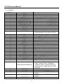
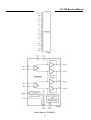
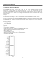
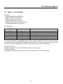
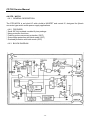
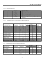
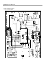
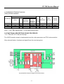
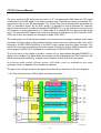
1
S/M No.TCP780FEF0
Service Manual
CHASSIS : CP-780
MODEL : DUB-2850GB
DUB-2850
DUB-2850K
Caution
: In this Manual, some parts can be changed for improving. their
performance without notice in the parts list. So, if you need the
latest parts information, please refer to PPL(Parts Price List)in
Service Information Center.
NOV. 2005
CP-780 Service Manual
CONTENTS
1 MAIN FEATURES
1.1 SPECIFICATIONS
1.2 CHANNEL/FREQUENCY TABLE
2 SAFETY INSTRUCTION
3 ALIGNMENT INSTRUCTIONS
3.1 MICROCONTROLLER CONFIGURATION : SERVICE MODE
3.2 SERVICE MODE NAVIGATION
3.3 MICROCONTROLLER CONFIGURATION : OPTION BITS
3.4 OPTION 1
3.5 OPTION 2
3.6 NVM default setting
3.7 TV SET ALIGNMENT
3.8 OAD(Over air download)
4 IC DESCRIPTION
4.1 UOC III Series
4.2 TDA8946J (STEREO AUDIO AMPLIFIER)
4.3 TDA8358J (VERTICAL AMPLIFIER)
4.4 TDA6108AJF (VIDEO AMPLIFIER)
4.5 2WC16-16KB (EEPROM)
4.6 STR-W6754
4.7 Pnx 8314
4.8 UDA 1334 BTS (audio DAC)
4.9 CI MAX
4.10 M29W320ET(Flash Memory)
4.11 K4S281632D(SDRAM)
5 CIRCUIT DESCRIPTION
5.1 BLOCK DIAGRAM
5.2 FUNCTIONAL DESCRIPTION OF VIDEO PROCESSOR
5.3 GENERAL DESCRIPTION OF THE TV SOUND OF SOUND PROCESSOR
5.4 FUNCTIONAL DESCRIPTION PROCESSOR
3
3
5
7
8
8
8
8
9
9
10
12
13
14
14
24
26
28
29
30
32
34
35
38
39
40
40
41
49
51
6 SERVICE PARTS LIST
7 SCHEMATIC DIAGRAM
8 PRINTED CIRCUIT BOARD
9 EXPLODED VIEW
56
65
70
78
-2-
CP-780 Service Manual
DOCUMENT HISTORY
VERSION
V1.00
DATE
22/10/05
COMMENTS
Creation of document (Author BD MIN) for project CP-780 50Hz iDTV.
1 MAIN FEATURES
1.1 SPECIFICATIONS
1.1.1 GENERAL
Transmission
standard
COFDM
DVB standard
TV standard
Colour system
Tuner
AV
Sound system
Power consumption
Sound Output Power
Speaker
Teletext system
Aerial input
Channel coverage
Tuning system
Visual screen size
Channel indication
Program Selection
Aux. terminal
Picture compression
standard
MPEG2
Voice compression
standard
MPEG Audio
PAL - SECAM B/G D/K, PAL I/I, SECAM L/L’
PAL, SECAM
PAL, SECAM, PAL 60, NTSC M, NTSC 4.43
NICAM B/G, I, D/K, L,
FM 2Carrier B/G, D/K
95W
7W x 2 (at 60% mod, 10%THD)
12W 8 ohm x2
10 pages memory FASTEXT (FLOF or TOP)
75 ohm unbalanced
Off-air channels, S-cable channels and hyperband
frequency synthesiser tuning system
66cm
On Screen Display
100 programmes
EURO-SCART 1 : Audio / Video In and Out, R/G/B
In, Slow and Fast switching.
EURO-SCART 2 : Audio / Video In and Out, SVHS In.
SPDIF : jack on rear of cabinet(Digital channel output)
AV3 : Audio-Video Jack on side of cabinet.
SVHS3 (option) : Jack on side of cabinet sound
input common with AV3.
Headphone jack on side of cabinet
Remote Control
R-52N20
PCMCIA
CI slot (on rear of cabinet)
1.1.2 EURO-SCART 1 (21 Pin)
Pin
1
2
3
4
5
6
7
8
Signal Description
Audio Output Right
Audio Input Right
Audio Output Left
Audio Earth
Blue Earth
Audio Input Left
Blue Input
Matching value
0.5 Vrms, Impedance < 1 k , ( RF 54% Mod )
0.5 Vrms, Impedance > 10 k
0.5 Vrms, Impedance < 1 k , ( RF 54% Mod )
Slow Switching
TV : 0 to 2V, AV 16/9:4.5 to 7V, AV 4/3 : 9.5 to 12V, Impedance > 10 k
0.5 Vrms, Impedance > 10 k
0.7 Vpp 0.1V, Impedance 75
-3-
CP-780 Service Manual
1.1.3 EURO-SCART 2 (21Pin)
-4-
CP-780 Service Manual
1.2 CHANNEL/FREQUENCY TABLE
CHANNEL
C01
C02
C03
C04
C05
C06
C07
C08
C09
C10
C11
C12
C13
C14
C15
C16
C17
C18
C19
C20
C21
C22
C23
C24
C25
C26
C27
C28
C29
C30
C31
C32
C33
C34
C35
C36
C37
C38
C39
C40
C41
C42
C43
C44
C45
C46
C47
C48
C49
C50
C51
C52
C53
C54
C55
C56
C57
C58
EUROPE CCIR
46.25
48.25
55.25
62.25
175.25
182.25
189.25
196.25
203.25
210.25
217.25
224.25
53.75
82.25
183.75
192.25
201.25
471.25
479.25
487.25
495.25
503.25
511.25
519.25
527.25
535.25
543.25
551.25
559.25
567.25
575.25
583.25
591.25
599.25
607.25
615.25
623.25
631.25
639.25
647.25
655.25
663.25
671.25
679.25
687.25
695.25
703.25
711.25
719.25
727.25
735.25
743.25
751.25
759.25
767.25
FRANCE
55.75 (L )
60.5 (L )
63.75 (L )
176.00
184.00
192.00
200.00
208.00
216.00
189.25 (LUX)
69.25 (L )
76.25 (L )
83.25 (L )
90.25
97.25
471.25
479.25
487.25
495.25
503.25
511.25 5
519.25
527.25
535.25
543.25
551.25
559.25
567.25
575.25
583.25
591.25
599.25
607.25
615.25
623.25
631.25
639.25
647.25
655.25
663.25
671.25
679.25
687.25
695.25
703.25
711.25
719.25
727.25
735.25
743.25
751.25
759.25
767.25
-5-
GB(IRELAND)
45.75
53.75
61.75
175.25
183.25
191.25
199.25
207.25
215.25
223.25
231.25
239.25
247.25
49.75
57.75
65.75
77.75
85.75
471.25
4 79.25
487.25
495.25
503.25
11.25
519.25
527.25
535.25
543.25
551.25
559.25
567.25
575.25
583.25
591.25
599.25
607.25
615.25
623.25
631.25
639.25
647.25
655.25
663.25
671.25
679.25
687.25
695.25
703.25
711.25
719.25
727.25
735.25
743.25
751.25
759.25
767.25
EAST OIRT
49.75
59.25
77.25
85.25
93.25
175.25
183.25
191.25
199.25
207.25
215.25
223.25
471.25
479.25
487.25
495.25
503.25
511.25
519.25
527.25
535.25
543.25
551.25
559.25
567.25
575.25
583.25
591.25
599.25
607.25
615.25
623.25
631.25
639.25
647.25
655.25
663.25
671.25
679.25
687.25
695.25
703.25
711.25
719.25
727.25
735.25
743.25
751.25
759.25
767.25
CP-780 Service Manual
CHANNEL
C59
C60
C61
C62
C63
C64
C65
C66
C67
C68
C69
C70
C71
C72
C73
C74
C75
C76
C77
S01
S02
S03
S04
S05
S06
S07
S08
S09
S10
S11
S12
S13
S14
S15
S16
EUROPE CCIR
775.25
783.25
791.25
799.25
807.25
815.25
823.25
831.25
839.25
847.25
855.25
863.25
69.25
76.25
83.25
90.25
97.25
59.25
93.25
105.25
112.25
119.25
126.25
133.25
140.25
147.25
154.25
161.25
168.25
231.25
238.25
245.25
252.25
259.25
266.25
FRANCE
775.25
783.25
791.25
799.25
807.25
815.25
823.25
831.25
839.25
847.25
855.25
863.25
104.75
116.75
128.75
140.75
152.75
164.75
176.75
188.75
200.75
212.75
224.75
236.75
248.75
260.75
272.75
284.75
GB(IRELAND)
775.25
783.25
791.25
799.25
807.25
815.25
823.25
831.25
839.25
847.25
855.25
863.25
103.25
111.25
119.25
127.25
135.25
143.25
151.25
159.25
167.25
255.25
263.25
271.25
279.25
EAST OIRT
775.25
783.25
791.25
799.25
807.25
815.25
823.25
831.25
839.25
847.25
855.25
863.25
105.25
112.25
119.25
126.25
133.25
140.25
147.25
154.25
161.25
168.25
231.25
238.25
245.25
252.25
259.25
266.25
S17
S18
S19
S20
S21
S22
S23
S24
S25
S26
S27
S28
S29
S30
S31
S32
S33
S34
S35
S36
S37
S38
S39
S40
S41
273.25
280.25
287.25
294.25
303.25
311.25
319.25
327.25
335.25
343.25
351.25
359.25
367.25
375.25
383.25
391.25
399.25
407.25
415.25
423.25
431.25
439.25
447.25
455.25
463.25
296.75
136.00
160.00
303.25
311.25
319.25
327.25
335.25
343.25
351.25
359.25
367.25
375.25
383.25
391.25
399.25
407.25
415.25
423.25
431.25
439.25
447.25
455.25
463.25
287.25
295.25
303.25
311.25
319.25
327.25
335.25
343.25
351.25
359.25
367.25
375.25
383.25
391.25
399.25
407.25
415.25
423.25
431.25
439.25
447.25
455.25
463.25
273.25
280.25
287.25
294.25
303.25
311.25
319.25
327.25
335.25
343.25
351.25
359.25
367.25
375.25
383.25
391.25
399.25
407.25
415.25
423.25
431.25
439.25
447.25
455.25
463.25
-6-
CP-780 Service Manual
2 SAFETY INSTRUCTION
WARNING: Only competent service personnel may carry out work involving the testing or repair
of this equipment.
X-RAY RADIATION PRECAUTION
1. Excessive high voltage can produce potentially hazardous X-RAY RADIATION. To avoid
such hazards, the high voltage must not exceed the specified limit. The nominal value of the
high voltage of this receiver is 28-30 KV at max beam current. The high voltage must not,
under any circumstances, exceed 33 KV. Each time a receiver requires servicing, the high
voltage should be checked. It is important to use an accurate and reliable high voltage
meter.
2. The only source of X-RAY Radiation in this TV receiver is the picture tube. For continued XRAY RADIATION protection, the replacement tube must be exactly the same type tube as
specified in the parts list.
SAFETY PRECAUTION
Potentials of high voltage are present when this receiver is operating. Operation of the receiver
outside the cabinet or with the back board removed involves a shock hazard from the receiver.
Servicing should not be attempted by anyone who is not thoroughly familiar with the
precautions necessary when working on high voltage equipment.
Discharge the high potential of the picture tube before handling the tube. The picture tube is
highly evacuated and if broken, glass fragments will be violently expelled.
If any Fuse in this TV receiver is blown, replace it with the FUSE specified in the Replacement
Parts List.
When replacing a high wattage resistor (metal oxide film resistor) in the circuit board, keep the
resistor 10 mm away from circuit board.
Keep wires away from high voltage or high temperature components.
This receiver must operate under AC 220 - 240 volts, 50 Hz. NEVER connect to a DC supply or
any other voltage or frequency.
PRODUCT SAFETY NOTICE
Many electrical and mechanical parts in this equipment have special safety-related
characteristics. These characteristics are often passed unnoticed by a visual inspection and the
X-RAY RADIATION protection afforded by them cannot necessarily be obtained by using
replacement components rated for higher voltage, wattage, etc. Replacement parts which have
these special safety characteristics are identified in this manual and its supplements, electrical
components having such features are identified by designated symbol on the parts list. Before
replacing any of these components, read the parts list in this manual carefully. The use of
substitutes replacement parts which do not have the same safety characteristics as specified in
the parts list may create X-RAY Radiation.
-7-
CP-780 Service Manual
3 ALIGNMENT INSTRUCTIONS
3.1 MICROCONTROLLER CONFIGURATION : SERVICE MODE
To switch the TV set into service mode please see instruction below.
1 - Select PR. number 91
2 - Adjust sharpness to minimum and exit all menus.
3 - Within 2 seconds press the key sequence : RED - GREEN - menu
The software version is displayed beside the word Service, e.g. “SERVICE V0.22”.
To exit SERVICE menu press menu key or Stand By key.
3.2 SERVICE MODE NAVIGATION
Pr Up/Down remote keys : cycle through the service items available.
Vol -/+ remote keys
: Dec./Increment the values within range - Cycle trough option bits.
OK key
: Toggle bits in option byte
Order
1
2
3
4
5
6
7
8
9
10
11
12
13
14
15
16
17
18
19
20
21
22
Item
HOR CEN
RED GAIN
GRN GAIN
BLUE GAIN
RED BIAS
GRN BIAS
AGC LEVEL
G2-SCREEN
OPTION1
OPTION2
AVL
PARABOLA
HOR WIDTH
CORNER T
CORNER B
HOR. PARAL
V.LINEAR
V.SLOPE
EW TRAPEZ
S CORRECT
VERT CENT
VERT SIZE
Default setting
39
32
32
32
32
32
NO ADJUSTMENT
0001 1001
0010 1111
20
50
39
39
25
36
25
22
43
24
3.3 MICROCONTROLLER CONFIGURATION : OPTION BITS
There are two option bytes available (16 bits in all). These option bits are available from Service
mode. First find the OPTION1/OPTION2/OPTION3 control, and then use the Volume PLUS/MINUS
buttons on the remote control keypad to locate the bits, and OK key to toggle them. The table
below shows the two option bytes available;
-8-
CP-780 Service Manual
3.4OPTION1
B7
B6
B5
TOP FASTEXT TUBE
1 Teletext (FLOF)
4:3
OFF
OFF
0
TOP FASTEXT
Teletext (FLOF) TUBE
16:9
ON
ON
3.5 OPTION2
B7
B6
1
Fixed to
‘0’
0
Fixed to
‘0’
B5
Nu Must
be Set to
1 for
Future
compati
bility
B4
VAI bit set
to 1 in
SECAM L
B3
Dolby
Virtual
OFF
B2
SVHS3
disabled
VAI bit set
to 0 in
SECAM L
Dolby
Virtual
ON
SVHS3
enabled
B4
B3
5 keys
Iacal
keyboard
7 keys
Iacal
keyboard
B2
Fixed to ‘0’
Full
ATSS
Basic
ATSS
B1
B0
TUNER OPTIONS
00=PHILIPS
01=Not used
10=Alps
11=Parstnic(DW)
B1
PAT&
TAT
Enabled
PAT&
TAT
Disabled
B0
n.u.
Must be set
to 1 for
future
compatibility
- OPTION SETTING BY MODEL
CHASSIS
MODEL
OPTION
BIT[b7...b0]
DW[hex]
REMARKS
CP-780
DUB-2850GB
I 0001 1001
II 0010 1111
19
2F
OPTION “b1,b0” Depends on Tuner
-9-
CP-780 Service Manual
3.6 NVM default setting
The purpose of this message, when you change a virgin EEPROM, is to allow to modify the
NVM DATA to desired values.
1 - Introduction :
The NVM default values are fixed for the user, but for flexibility in service, these data are stored
in NVM and can be changed when the TV set is in a special mode call NVM EDITOR . This
mode can only be access from FACTORY mode.
2 - Entering into FACTORY mode.
To switch the TV set into FACTORY mode, use the factory remote control, and press on SVC
key. The factory menu will appear on the screen, showing FACTORY , plus other relevant
information like software version and date.
WARNING : When in FACTORY mode you should not press any key other than the keys
described in the procedure below. Unwanted key stroke could misadjust the TV set.
3 - Entering into NVM EDITOR mode.
To switch the TV set into NVM EDITOR mode, use the user remote control, and press on
PICTURE/OK key. The NVM EDITOR window will appear on the screen. This mode allow
you to access all data stored in NVM. The current NVM address is given in column ADDR. in
both DECimal and HEXadecimal format. The column DATA gives the value contained at
selected address in both DECimal and HEXadecimal format.
4 - Navigation in NVM EDITOR mode.
Use Program Up/Down keys to select the desired address. Use Volume Up/Down keys to
change the data at selected address. You must press PICTURE/OK key to store value after
modification.
The data can be adjusted between 0 and 63.
5 - Exit NVM EDITOR mode.
To switch the TV set back into FACTORY mode, use the user remote control, and press on
MENU key.
The factory menu will appear on the screen, showing FACTORY .
6 - Exit FACTORY mode.
To exit FACTORY mode, use the factory remote control, and press on SVC key.
The factory menu will disappear from the screen.
-10-
CP-780 Service Manual
NVM DATA CHANGE LIST
No
1
2
3
4
5
6
7
8
9
10
11
12
13
14
15
16
17
18
19
20
21
22
23
24
25
26
27
28
29
30
31
32
33
34
35
36
37
38
39
Register Name
OCP_THRESHOLD
DCXO
AGC_PHILIPS
AGC_NC
AGC_ALPS
AGC_PARTSNIC
AGC_PHILIPS_START
AGC_NC_START
AGC_ALPS_START
AGC_PARTSNIC_START
AVLLEV
Nor1_Bright
Nor1_contrast
Nor1_Colour
Nor1_Sharpness
Nor1_Tint
Nor1_JVC_Bri
Nor1_JVC_Cont
Nor1_JVC_Colour
Nor1_JVC_Sharp
Nor2_Bright
Nor2_Contrast
Nor2_Colour
Nor2_Sharpness
Nor2_Tint
PresetGainRGB
PresetGainRGB
PresetGainRGB
Cathode_Drive
Y_delay_PAL_BG
Y_delay_SECAM_BG
Y_delay_PAL_DK
Y_delay_SCM_DK
Y_delay_PAL_I
Y_delay_SECAM
Y_delay_SECAM-L
Y_delay_AV
G2_Bright
G2_Contrast
Address
0x58F
0x590
0x5C1
0x5C2
0x5C3
0x5C4
0x5C5
0x5C6
0x5C7
0x5C8
0x621
0x64A
0x64B
0x64C
0x64D
0x64E
0x64F
0x650
0x651
0x652
0x653
0x654
0x655
0x656
0x657
0x673
0x674
0x675
0x67B
0x686
0x687
0x688
0x689
0x68A
0x68B
0x68C
0x68D
0x68E
0x68F
-11-
(hex)
Default
0x91
0x4E
0xAB
0xAB
0xB6
0xB6
0x16
0x16
0x16
0x16
0x5
0x23
0x2E
0x1C
0x23
0x20
0x2D
0x2A
0x1B
0x23
0x28
0x13
0x19
0x1B
0x20
0x2A
0x2A
0x2A
0x1
0x5
0x8
0x5
0x5
0x7
0x5
0x8
0xA
0x1A
0x42
CP-780
DUB-2850GB
<<<0x04
<<<0x00
<<<<<<<<<<<<<<<<<<<<<<<<<<<<<3D
77
CP-780 Service Manual
3.7 TV SET ALIGNMENT
3.7.1 G2 ALIGNMENT
- Tune a colour bar pattern.
- Find the G2 - SCREEN item in service mode.
- Adjust screen volume ( on FBT ) to bring the cursor to central position : green.
3.7.2 WHITE BALANCE
- Select a dark picture and adjust RED BIAS and GRN BIAS to the desired colour temperature.
- Select a bright picture and adjust RED, GRN and BLUE GAIN to the desired colour temperature.
3.7.3 FOCUS
Adjust the Focus volume ( on FBT ) to have the best resolution on screen.
3.7.4 VERTICAL GEOMETRY
Adjust V. LINEAR (linearity), S CORRECT (S. Correction), VERT SIZE (Vertical amplitude), VERT CENT (vertical
centring) to compensate for vertical distortion.
3.7.5 HORIZONTAL PICTURE CENTRING
Adjust HOR CEN (Horizontal centre) to have the picture in the centre of the screen.
3.7.6 EAST / WEST CORRECTION
Adjust the PARABOLA, HOR WIDTH, CORNER, HOR PARAL, EW TRAPEZ, to compensate for geometrical
distortion.
HOR PARAL
-12-
CP-780 Service Manual
PARABOLA
HOR WIDTH
adjust for 93% overscan.
EW TRAPEZ
CORNER B & CORNER T
3.8 OAD (Over Air Download)
3.8.1 Concept of OAD
OAD is the function for updating software of IDTV(Integrated Digital TV) or DSTB (Digital Set-Top
Box) from outer source.
3.8.2 Object of OAD
Sometimes IDTV or DSTB may need a newer software for technical or system problems after sale,
so through OAD function, IDTV or DSTB may be updated automatically at each user’s home.
3.8.3 OAD on CP-780
CP-780 performs OAD automatically when being on ST-BY mode. But CP-780 can’t supply power
to digital part to search s/w on ST-BY mode. To solve this, CP-780 is worked as below.
a. power off by remote control on Analog mode : go directly to ST-BY mode. In this case, power
consumption : 1.5w / AC 230V.
b. power off by remote control on Digital mode
- go to video mute (raster off) and stay about 3~5 minute to search S/W. In this case, power
Consumption is 52W / AC 230V
- After finishing searching s/w, TV set go to ST-BY mode. (1.5W / AC 230V) If turn off TV before
TV complete searching s/w, TV set will perform it again.
- If TV set find a new s/w to update, a update message will be shown on the screen when the
user turn on TV.
- CP-780 performs this process once a day.
- If the user doesn’t want OAD search, the user can press R/C button for 2~3 sec to go directly to
ST-BY mode.
3.8.4 Algorithm of OAD
Digital stream has a date/time information. CP-780 stores a date info at NVM. UOC brings date
info from digital stream and compares it with NVM data. If those two are different from each other,
TV set performs OAD and store a date info at NVM.If those two are the same, go directly to ST-BY
mode. Through this algorithm, CP-780 perform OAD search once a day.
-13-
CP-780 Service Manual
4 IC DESCRIPTION
4.1 UOC/// Series
The UOC series combines the functions of a Video Signal Processor(VSP) together with a FLASH embedded
TEXT/Control/Graphics m-Controller(TCG m-Controller) and US Closed Caption decoder. In addition the following
functions can be added:
- Adaptive digital(4H/2H) PAL/NTSC combfilter
- Teletext decoder with 10page text memory
- Multi- standard stereo decoder
- BTSC stereo decoder
- Digital sound processing circuit
- Digital video processing circutt
4.1.1 IC MARKING AND VERSION
Chassis
CP-780
IC marking
OSD languages
ENGLISH, WELSH
GEALIC
ATSS countries
Australia,, Belgium,
Switzerland, Czech
Republic, Germany,
Denmark, Spain,
France, Finland, GB,
Greece, Hungary, Italy,
Ireland, Norway,
Netherlands, Portugal,
Poland, Sweden,
Slovak Republic,
Others
-14-
Text
PAN-EUROPEAN
LATIN, CYRILLIC,
GREEK.
CP-780 Service Manual
4.1.2 BLOCK DIAGRAM
-15-
CP-780 Service Manual
4.1.3. PINNING
QFP 128pin
1
2
3
4
5
6
7
8
9
10
11
12
13
Symbol
VSSP2
VSSC4
VDDC4
VDDA3(3.3V)
VREF_POS_LSL
VREF_NEG_LSL+HPL
VREF_POS_LSR+HPR
VREF_NEG_HPL+HPR
VREF_POS_HPR
XTALIN
XTALOUT
VSSA1
VGUARD/SWIO
14
15
16
17
18
19
20
21
22
23
24
25
26
27
28
29
30
31
32
33
DECDIG
VP1
PH2LF
PH1LF
GND1
SECPLL
DECBG
EWD/AVL (1)
VDRB
VDRA
VIFIN1
VIFIN2
VSC
IREF
GNDIF
SIFIN1/DVBIN1 (2)
SIFIN2/DVBIN2 (2)
AGCOUT
EHTO
AVL/SWO/SSIF/ REFO/REFIN (2)
34
35
36
AUDIOIN5L
AUDIOIN5R
AUDOUTSL
37
AUDOUTSR
38
DECSDEM
-16-
Short Description
Ground
Ground
digital supply to SDACs (1.8V)
supply (3.3 V)
positive reference voltage SDAC (3.3 V)
negative reference voltage SDAC (0 V)
positive reference voltage SDAC (3.3 V)
negative reference voltage SDAC (0 V)
positive reference voltage SDAC (3.3 V)
crystal oscillator input
crystal oscillator output
Ground
V-guard input / I/O switch (e.g. 4 mA current
sinking capability for direct drive of LEDs)
decoupling digital supply
1st supply voltage TV-processor (+5 V)
phase-2 filter
phase-1 filter
ground 1 for TV-processor
SECAM PLL decoupling
bandgap decoupling
East-West drive output or AVL capacitor
vertical drive B output
vertical drive A output
IF input 1
IF input 2
vertical sawtooth capacitor
reference current input
ground connection for IF amplifier
SIF input 1 / DVB input 1
SIF input 2 / DVB input 2
tuner AGC output
EHT/overvoltage protection input
Automatic Volume Levelling / switch
output / sound IF input / subcarrier
reference output / external reference
signal input for I signal mixer for DVB
operation
audio-5 input (left signal)
audio-5 input (right signal)
audio output for SCART/CINCH (left
signal)
audio output for SCART/CINCH (right
signal)
decoupling sound demodulator
CP-780 Service Manual
QFP 128pin
39
Symbol
QSSO/AMOUT/AUDEEM (2)
40
41
42
GND2
PLLIF
SIFAGC/DVBAGC (2)
43
DVBO/IFVO/FMRO (2)
44
DVBO/FMRO (2)
45
46
47
48
VCC8V
AGC2SIF
VP2
IFVO/SVO/CVBSI (2)
49
50
51
52
53
54
55
56
57
58
59
60
AUDIOIN4L
AUDIOIN4R
CVBS4/Y4
C4
AUDIOIN2L
AUDIOIN2R
CVBS2/Y2
AUDIOIN3L
AUDIOIN3R
CVBS3/Y3
C2/C3
AUDOUTLSL
61
AUDOUTLSR
62
AUDOUTHPL
63
AUDOUTHPR
64
65
66
CVBSO/PIP
SVM
FBISO/CSY
67
68
69
70
HOUT
VSScomb
VDDcomb
VIN (R/PRIN2/CX)
71
UIN (B/PBIN2)
72
YIN (G/YIN2/CVBS-Yx)
-17-
Short Description
QSS intercarrier output / AM output /
deemphasis (front-end audio out)
ground 2 for TV processor
IF-PLL loop filter
AGC sound IF / internal-external AGC for
DVB applications
Digital Video Broadcast output / IF video
output / FM radio output
Digital Video Broadcast output / FM radio
output
8 Volt supply for audio switches
AGC capacitor second sound IF
2nd supply voltage TV processor (+5 V)
IF video output / selected CVBS output /
CVBS input
audio-4 input (left signal)
audio-4 input (right signal)
CVBS4/Y4 input
chroma-4 input
audio 2 input (left signal)
audio 2 input (right signal)
CVBS2/Y2 input
audio 3 input (left signal)
audio 3 input (right signal)
CVBS3/Y3 input
chroma-2/3 input
audio output for audio power amplifier
(left signal)
audio output for audio power amplifier
(right signal)
audio output for headphone channel (left
signal)
audio output for headphone channel (right
signal)
CVBS / PIP output
scan velocity modulation output
flyback input/sandcastle output or
composite H/V timing output
horizontal output
ground connection for comb filter
supply voltage for comb filter (5 V)
V-input for YUV interface (2nd R input /
PR input or CX input)
U-input for YUV interface (2nd B input /
PB input)
Y-input for YUV interface (2nd G input / Y
input or CVBS/YX input))
CP-780 Service Manual
QFP 128pin
73
74
75
Symbol
YSYNC
YOUT
UOUT(INSSW2)
76
VOUT(SWO1)
77
78
79
80
81
82
83
84
85
86
87
88
INSSW3
R/PRIN3
G/YIN3
B/PBIN3
GND3
VP3
BCLIN
BLKIN
RO
GO
BO
VDDA1
89
90
91
92
93
94
95
96
97
VREFAD_NEG
VREFAD_POS
VREFAD
GNDA
VDDA(1.8)
VDDA2(3.3)
VSSadc
VDDadc(1.8)
INT0/P0.5
98
99
100
101
102
103
104
105
106
107
108
109
110
111
112
113
114
P1.0/INT1
P1.1/T0
VDDC2
VSSC2
P0.4/I2SWS
P0.3/I2SCLK
P0.2/I2SDO2
P0.1/I2SDO1
P0.0/I2SDI1/O
P1.3/T1
P1.6/SCL
P1.7/SDA
VDDP(3.3V)
P2.0/TPWM
P2.1/PWM0
P2.2/PWM1
P2.3/PWM2
Short Description
Y-input for sync separator
Y-output (for YUV interface)
U-output for YUV interface (2nd RGB /
YPBPR insertion input)
V-output for YUV interface (general
purpose switch output)
3rd RGB / YPBPR insertion input
3rd R input / PR input
3rd G input / Y input
3rd B input / PB input
ground 3 for TV-processor
3rd supply for TV processor
beam current limiter input
black current input
Red output
Green output
Blue output
analog supply for TCG m-Controller and
digital supply for TV-processor (+3.3 V)
negative reference voltage (0 V)
positive reference voltage (3.3 V)
reference voltage for audio ADCs (3.3/2 V)
Ground
analogue supply for audio ADCs (1.8 V)
supply voltage SDAC (3.3 V)
ground for on-chip temperature sensor
supply voltage video ADC
external interrupt 0 or port 0.5 (4 mA current sinking
capability for direct drive of LEDs)
port 1.0 or external interrupt 1
port 1.1 or Counter/Timer 0 input
digital supply to core (1.8 V)
Ground
port 0.4 or I2S word select
port 0.3 or I2S clock
port 0.2 or I2S digital output 2
port 0.1 or I2S digital output 1
port 0.0 or I2S digital input 1 or I2S digital output
port 1.3 or Counter/Timer 1 input
port 1.6 or I2C-bus clock line
port 1.7 or I2C-bus data line
supply to periphery and on-chip voltage regulator (3.3 V)
port 2.0 or Tuning PWM output
port 2.1 or PWM0 output
port 2.2 or PWM1 output
port 2.3 or PWM2 output
-18-
CP-780 Service Manual
QFP 128pin
115
116
117
118
119
120
121
122
123
124
125
126
127
128
Symbol
P3.0/ADC0
P3.1/ADC1
VDDC1
DECV1V8
P3.2/ADC2
P3.3/ADC3
VSSC/P
P2.4/PWM3
P2.5/PWM4
VDDC3
VSSC3
P1.2/INT2
P1.4/RX
P1.5/TX
Short Description
port 3.0 or ADC0 input
port 3.1 or ADC1 input
digital supply to core (+1.8 V)
decoupling 1.8 V supply
port 3.2 or ADC2 input
port 3.3 or ADC3 input
digital ground for m-Controller core and periphery
port 2.4 or PWM3 output
port 2.5 or PWM4 output
digital supply to core (1.8V)
Ground
port 1.2 or external interrupt 2
port 1.4 or UART bus
Port 1.5 or UART bus
4.1.4 FEATURES
Analogue Video Processing (all versions)
Multi-standard vision IF circuit with alignment-free PLL demodulator
Internal (switchable) time-constant for the IF-AGC circuit
Switchable group delay correction and sound trap (with switchable centre frequency) for the
demodulated CVBS signal
DVB/VSB IF circuit for preprocessing of digital TV signals.
Video switch with 3 external CVBS inputs and a CVBS output. All CVBS inputs can be used
as Y-input for Y/C signals. However, only 2 Y/C sources can be selected because the circuit
has 2 chroma inputs. It is possible to add an additional CVBS(Y)/C input (CVBS/YX and CX)
when the YUV interface and the RGB/YPRPB input are not needed.
Automatic Y/C signal detector
Adaptive digital (4H/2H) PAL/NTSC comb filter for optimum separation of the luminance and
the chrominance signal.
Integrated luminance delay line with adjustable delay time
Picture improvement features with peaking (with switchable centre frequency, depeaking,
variable positive/negative peak ratio, variable pre-/overshoot ratio and video dependent
coring), dynamic skin tone control, gamma control and blue- and black stretching. All
features are available for CVBS, Y/C and RGB/YPBPR signals.
Switchable DC transfer ratio for the luminance signal
Only one reference (24.576 MHz) crystal required for the TCG m-Controller, digital sound
processor, Teletext and the colour decoder
Multi-standard colour decoder with automatic search system and various forced mode
possibilities
Internal base-band delay line
Indication of the Signal-to-Noise ratio of the incoming CVBS signal
Linear RGB/YPBPR input with fast insertion.
YUV interface. When this feature is not required some pins can be used as additional RGB/YPBPR
input. It is also possible to use these pins for additional CVBS (or Y/C) input (CVBS/YX and CX).
-19-
CP-780 Service Manual
Tint control for external RGB/YPBPR signals
Scan Velocity Modulation output. The SVM circuit is active for all the incoming CVBS, Y/C
and RGB/YPBPR signals. The SVM function can also be used during the display of teletext
pages.
RGB control circuit with Continuous Cathode Calibration , white point and black level offset adjustment so that the colour temperature of the dark and the light parts of the screen
can be chosen independently.
Contrast reduction possibility during mixed-mode of OSD and Text signals
Adjustable wide blanking of the RGB outputs
Horizontal synchronization with two control loops and alignment-free horizontal oscillator
Vertical count-down circuit
Vertical driver optimized for DC-coupled vertical output stages
Horizontal and vertical geometry processing with horizontal parallelogram and bow
correction and horizontal and vertical zoom
Low-power start-up of the horizontal drive circuit
Analogue video processing (stereo versions)
The low-pass filtered mixed down I signal is available via a single ended or balanced
output stage.
Analogue video processing (mono versions)
The low-pass filtered mixed down I signal is available via a single ended output stage
Digital Video Processing (some versions)
Double Window mode applications. It is possible to display a video and a text window or 2
text windows in parallel.
Linear and non-linear horizontal scaling of the video signal to be displayed.
Sound Demodulation (all versions)
Separate SIF (Sound IF) input for single reference QSS (Quasi Split Sound) demodulation.
AM demodulator without extra reference circuit
The mono intercarrier sound circuit has a selective FM-PLL demodulator which can be
switched to the different FM sound frequencies (4.5/5.5/6.0/6.5 MHz). The quality of this
system is such that the external band-pass filters can be omitted. In the stereo versions of
UOCIII the use of this demodulator is optional for special applications. Normally the FM
demodulators of the stereo demodulator/decoder part are used (see below).
The FM-PLL demodulator can be set to centre frequencies of 4.72/5.74 MHz so that a
second sound channel can be demodulated. In such an application it is necessary that an
external bandpass filter is inserted.
The vision IF and mono intercarrier sound circuit can be used for the demodulation of FM
radio signals. With an external FM tuner also signals with an IF frequency of 10.7 MHz can
be demodulated.
Switch to select between 2nd SIF from QSS demodulation or external FM (SSIF)
Audio Interfaces and switching (stereo versions with Audio DSP)
Audio switch circuit with 4 stereo inputs, a stereo output for SCART/CINCH, 1 stereo output
for HEADPHONE. The headphone channel has an analogue volume control circuit for the L
and R channel. Finally 1 stereo SPEAKER output with digital controls.
AVL (Automatic Volume Levelling) circuit for the headphone channel.
Digital input crossbar switch for all digital signal sources and destinations
-20-
CP-780 Service Manual
Digital output crossbar for exchange of channel processing functionality
Digital audio input interface (stereo I2S input interface)
Digital audio output interface (stereo I2S output interface)
Audio interfaces and switching (AV stereo versions without Audio DSP)
Audio switch circuit with 4 stereo inputs, a stereo output for SCART/CINCH and a stereo
SPEAKER output with analogue volume control.
Analogue mono AVL circuit at left audio channel
Audio interfaces and switching (mono versions)
Audio switch circuit with 4 external audio (mono) inputs and a volume controlled output
AVL circuit
Stereo Demodulator and Decoder (full stereo versions)
Demodulator and Decoder Easy Programming (DDEP)
Auto standard detection (ASD)
Static Standard Selection (SSS)
DQPSK demodulation for different standards, simultaneously with 1-channel FM
demodulation
NICAM decoding (B/G, I, D/K and L standard)
Two-carrier multistandard FM demodulation (B/G, D/K and M standard)
Decoding for three analog multi-channel systems (A2, A2+ and A2*) and satellite sound
Adaptive de-emphasis for satellite FM
Optional AM demodulation for system L, simultaneously with NICAM
Identification A2 systems (B/G, D/K and M standard) with different identification time
constants
FM pilot carrier present detector
Monitor selection for FM/AM DC values and signals, with peak and quasi peak detection
option
BTSC MPX decoder
SAP decoder
dbx noise reduction (4)
Japan (EIAJ) decoder
FM radio decoder
Soft-mute for DEMDEC outputs DEC, MONO and SAP
FM overmodulation adaptation option to avoid clipping and distortion
Audio Multi Channel Decoder (stereo versions with Audio DSP)
Dolby Pro Logic (DPL) (1)
Five channel processing for Main Left and Right, Subwoofer, Centre and Surround. To
exploit this feature an external DAC is required.
Volume and tone control for loudspeakers (stereo versions with Audio DSP)
Automatic Volume Level (AVL) control
Smooth volume control
Master volume control
Soft-mute
Loudness
Bass, Treble
Dynamic Bass Boost (DBB) (2)
-21-
CP-780 Service Manual
Dynamic Virtual Bass (DVB) (3)
BBE Sound processing (4)
Graphic equalizer
Processed or non processed subwoofer
Programmable beeper
Reflection and delay for loudspeaker channels (stereo versions with Audio DSP)
(Option) Dolby Pro Logic Delay (1).0
Pseudo hall/matrix function
Psycho acoustic spatial algorithms, downmix and split in loudspeaker channels (stereo
versions with Audio DSP)
Extended Pseudo Stereo (EPS) (5)
Extended Spatial Stereo (ESS) (6)
Virtual Dolby Surround (VDS 422,423) (1)
SRS 3D and SRS TruSurround (4)
RDS/RBDS
Demodulation of the European Radio Data system (RDS) or the USA Radio Broadcast Data
System (RBDS) signal
RDS and RBDS block detection
Error detection and correction
Fast block synchronisation
Synchronisation control (flywheel)
Mode control for RDS/RBDS processing
Different RDS/RBDS block information output modes
m-Controller
80C51 m-controller core standard instruction set and timing
0.4883 ms machine cycle
maximum of 256k x 8-bit flash programmable ROM
maximum of 8k x 8-bit Auxiliary RAM
12-level Interrupt controller for individual enable/disable with two level priority
Two 16-bit Timer/Counter registers
One 24-bit Timer (16-bit timer with 8-bit Pre-scaler)
WatchDog timer
Auxiliary RAM page pointer
16-bit Data pointer
Stand-by, Idle and Power Down modes
24 general I/O
14 bits PWM for Voltage Synthesis Tuning
8-bit A/D converter with 4 multiplexed inputs
5 PWM (6-bits) outputs for analogue control functions
Remote Control Pre-processor (RCP)
Universal Asynchronous Receiver Transmitter (UART)
Data Capture
Text memory up to 10 pages
Inventory of transmitted Teletext pages stored in the Transmitted Page Table (TPT) and
-22-
CP-780 Service Manual
Subtitle Page Table (SPT)
Data Capture for US Closed Caption
Data Capture for 525/625 line WST, VPS (PDC system A) and Wide Screen Signalling
(WSS) bit decoding
Automatic selection between 525 WST/625 WST
Automatic selection between 625 WST/VPS on line 16 of VBI
Real-time capture and decoding for WST Teletext in Hardware, to enable optimized mprocessor throughput
Automatic detection of FASTEXT transmission
Real-time packet 26 engine in Hardware for processing accented, G2 and G3 characters
Signal quality detector for video and WST/VPS data types
Comprehensive teletext language coverage
Vertical Blanking Interval (VBI) data capture of WST data
Display
Teletext and Enhanced OSD modes
Features of level 1.5 WST and US Close Caption
50Hz/60Hz display timing modes
Two page operation for 16:9 screens
Serial and Parallel Display Attributes
Single/Double/Quadruple Width and Height for characters
Smoothing capability of both Double Size, Double Width & Double Height characters
Scrolling of display region
Variable flash rate controlled by software
Soft colours using CLUT with 4096 colour palette
Globally selectable scan lines per row (9/10/13/16/) and character matrix [12x9, 12x10,
12x13, 12x16, 16x18, (VxH)]
Fringing (Shadow) selectable from N-S-E-W direction
Fringe colour selectable
Contrast reduction of defined area
Cursor
Special Graphics Characters with two planes, allowing four colours per character
64 software redefinable On-Screen display characters
4 WST Character sets (G0/G2) in single device (e.g. Latin, Cyrillic, Greek, Arabic)
G1 Mosaic graphics, Limited G3 Line drawing characters
WST Character sets and Closed Caption Character set in single device
SVM for Text
-23-
CP-780 Service Manual
4.2 TDA8946J STEREO AUDIO AMPLIFIER
The TDA8946J is a dual-channel audio power amplifier with an output power of 2x15W at an 8
load and a 18V supply. The circuit contains two Bridges Tied Load(BTL) amplifiers with an
all-NPN output stage and standby/mute logic. The TDA8946J comes in a 17-pin DIL-bentSIL(DBS) power package.
4.2.1 FEATURES
* Few external components
* Fixed gain
* Standby and mute mode
* No on/off switching plops
* Low standby current
* High supply voltage ripple rejection
* Outputs short-circuit protected to ground, supply and across the load
* Thermally protected
Pin description
Pin
1
2
3
4
5
6
7
8
9
10
11
12
Symbol
OUT1GND1
Vcc1
OUT1+
n.c.
IN1+
n.c.
IN1IN2MODE
SVR
IN2+
Description
negative loudspeaker terminal 1
ground channel 1
supply voltage channel 1
positive loudspeaker terminal 1
not connected
positive input1
not connected
negative input1
negative input2
mode selection input
half supply voltage decoupling (ripple rejection)
positive input2
-24-
CP-780 Service Manual
Block diagram TDA8946J
-25-
CP-780 Service Manual
4.3 TDA8358J VERTICAL AMPLIFIER
The TDA8358J are power circuit for use in 90 and 110 colour deflection systems for field
frequencies of 25 to 200Hz field frequencies, and for 4:3 and 16/9 picture tubes. The IC
contains a vertical deflection output circuit, operating as a high efficiency class G system. The
full bridge output circuit allows DC coupling of the deflection coil in combination with single
positive supply
voltages.
The east-west output stage is able to supply the sink current for a diode modulator circuit.
The IC is constructed in a Low Voltage DMOS(LVDMOS) process that combines bipolar, CMOS
and DMOS devices. DMOS transistors are used in the output stage because of the absence of
second breakdown.
4.3.1 TDA8358J
Features :
* Few external components
* Highly efficient fully DC-coupled vertical bridge output circuit
* Vertical flyback switch with short rise and fal times
* Built-in guard circuit
* Thermal protection circuit
* Improved EMC performance due to differential inputs
* East-west output stage
-26-
CP-780 Service Manual
Pinning
Pin
1
2
3
4
5
6
7
8
9
10
11
12
13
Symbol
INA
INB
VP
OUTB
INEW
VGND
EWGND
OUTEW
VFB
OUTA
GUARD
FEEDB
COMP
Description
Positeve vertical input
Negative vertical input
Supply voltage
Vertical output voltage B
East-west input voltage
Vertical ground
East-west ground
East-west output voltage
Flyback supply voltage
Vertical output voltage A
Guard output voltage
Input measuring resistor
Input compensation current
Block diagram TDA8358J
-27-
CP-780 Service Manual
4.4 TDA6108AJF
4.4.1 Features
-Typical bandwidth of 9.0MHz for an output signal of 60V (p-p)
-High slew rate of 1310V/us up and -1850V/us down
-No external components required
-Very simple application
-Single supply voltage of 200V
-Internal reference voltage of 2.5V
-Fixed gain of 81
-Black-Current Stabilization (BCS) circuit with voltage window from 1.5 to 6V
and current window from 100Ua to -10Ma
-Thermal protection
4.4.2
Pin description
Pin
Symbol
Description
1
Vi(1)
inverting input1
2
Vi(2)
inverting input2
3
Vi(3)
inverting input3
4
GND
ground(fin)
5
lom
black current measurement output
6
VDD
supply voltage
7
Voc(3)
Cathode output3
8
Voc(2)
cathode output2
9
Voc(1)
cathode output1
Vi(1)
1
Vi(2)
2
Vi(3)
3
GND
4
Iom
5
VDD
6
Voc(3)
7
Voc(2)
8
Voc(1)
9
TDA6108JF
Fig.2 Pin configuration
-28-
CP-780 Service Manual
4.5
24WC16 - 16 KB EEPROM
Features :
* 16 Kbit serial I2C bus EEPROM
* 400KHz I2C Bus Compatible
* supply voltage : 1.8 V to 6.0 V
* Low Power CMOS Technology
* 1 Million Erase/Write cycles (minimum)
* 100 year data retention (minimum)
Pin description
Pin No.
1, 2, 3
5
6
7
8
4
Name
A0, A1, A2
SDA
SCL
WP
Vcc
Vss
Description
Device address - not used
Serial Data/Address Input/Output
Serial clock
Write control
Supply voltage
Ground
The memory device is compatible with the I2C memory standard. This is a two wire serial
interface that uses a bi-directional data bus and serial clock. The memory carries a built-in 4-bit
unique device type identifier code (1010) in accordance with the I2C bus definition.
Serial Clock (SCL)
The SCL input is used to strobe all data in and out of the memory.
Serial Data (SDA)
The SDA pin is bi-directional, and is used to transfer data in or out of the memory.
-29-
CP-780 Service Manual
4.6 STR - W6754
4.6.1 GENERAL DESCRIPTION
The STR-W6754 is an hybrid IC with a build-in MOSFET and control IC, designed for flyback
converter type switch mode power supply applications.
4.6.2 FEATURES
* Small SIP fully isolated moulded 6 pins package
* Many protection functions :
* Pulse-by-pulse overcurrent protection (OCP)
* Overvoltage protection with latch mode (OVP)
* Overload protection with latch mode (OLP)
4.6.3 BLOCK DIAGRAM
-30-
CP-780 Service Manual
4.6.4
PIN DESCRIPTION
Terminal No.
1
3
4
5
6
7
4.6.5
DESCRIPTION
Drain terminal
Source/ Ground terminal
Power supply terminal
Delay at Overload/ Soft start set up terminal
Feedback terminal
Overcurrent Protection Input/ Bottom Detection
terminal
CONTROL PART - ELECTRICAL CHARACTERISTICS
DESCRIPTION
Operation start voltage
Operation stop voltage
Circuit current in operation
Circ. current in non-operation
Maximum on time
Minimum on time
O.C.P./B.D. terminal
threshold voltage 1
O.C.P./B.D. terminal
threshold voltage 2
O.C.P./F.B. terminal
outflow current
OVP operation voltage
Latch circuit holding current
Latch circuit release voltage
4.6.6
SYMBOL
D
S/GND
VCC
SS/OLP
FB
OCP/BD
TERMINAL
4-3
4-3
4-3
4-3
1-3
1-3
7-3
SYMBOL
VCC (on)
VCC (off)
ICC (on)
ICC (off)
TON (max)
TON (min)
VOCPBD(TH1)
MIN.
16.3
8.8
27.5
0.4
0.28
RATING
TYPE
18.2
9.7
32.5
0.8
0.40
MAX
19.9
10.6
6
100
39.0
1.2
0.52
UNIT
V
V
mA
A
s
s
V
7-3
VOCPBD(TH2)
0.67
0.80
0.93
V
7-3
IOCPBD
-250
-100
-40
A
4-3
4-3
4-3
VCC (OVP)
ICC (H)
VCC (Loff)
25.5
6.0
27.7
45
7.2
29.9
140
8.5
V
A
V
MOSFET ELECTRICAL CHARACTERISTICS
DESCRIPTION
Drain-to-source break
down voltage
Drain leakage current
On-resistance
Switching time
Thermal resistance
TERMINAL
1-3
SYMBOL
VDSS
1-3
1-3
1-3
-
IDSS
RDS (on)
tf
ch-F
-31-
RATING
MIN. TYPE MAX
650
-
-
300
0.96
400
1.6
UNIT
V
A
ns
C/W
o
CP-780 Service Manual
4.7 pnx831x
4.7.1 pin list by numbers
#
NAME
#
NAME
#
NAME
#
NAME
1
TMS
53
MIU_DATA[7]
105
MIU_ADDR[24]
157
AVDD_PLL
2
3
TRST
TCK
54
55
MIU_DATA[14]
MIU_DATA[6]
106
107
MIU_MASK[0]
MIU_MASK[1]
158
159
XTAL_IN
XTAL_OUT
4
RESETN
56
MIU_DATA[13]
108
MIU_WEN
160
AVSS_PLL
5
SYS_RESETN
57
MIU_DATA[5]
109
MIU_RDY
161
VDDP
6
7
SCL0
SDA0
58
59
MIU_DATA[12]
MIU_DATA[4]
110
111
MIU_RDY
VDDP
162
163
VSSP
B
8
SCL1
60
VDDP
112
VSSP
164
AVDD_2
9
SDA1
61
62
VSSP
MIU_DATA[11]
113
114
SDRAM_DATA[0]
SDRAM_DATA[1]
165
166
G/Y
IDUMP_2
63
64
65
66
67
68
MIU_DATA[3]
MIU_DATA[10]
MIU_DATA[2]
MIU_DATA[9]
MIU_DATA[1]
MIU_DATA[8]
115
116
117
118
119
120
SDRAM_DATA[2]
SDRAM_DATA[3]
SDRAM_DATA[4]
SDRAM_DATA[5]
VDDC
VSSC
167
168
169
170
171
R/C
CVBS/Y
AVDD_1
Y/CVBS
IDUMP_1
172
C/CVBS
69
MIU_DATA[0]
121
SDRAM_DATA[6]
173
VREF
70
71
72
MIU_OE_N
MIU_CS_N[3]
MIU_CS_N[2]
122
123
124
SDRAM_DATA[7]
SDRAM_DATA[15]
SDRAM_DATA[14]
174
175
176
21 TS_DATA[1]
73
MIU_CS_N[1]
125
SDRAM_DATA[13]
177
22 TS_DATA[2]
74
MIU_CS_N[0]
126
SDRAM_DATA[12]
178
23 TS_DATA[3]
75
MIU_ADDR[0]
127
SDRAM_DATA[11]
179
24
25
26
27
28
29
30
TS_DATA[4]
TS_DATA[5]
TS_DATA[6]
TS_DATA[7]
TS_VAL
TS_STROBE
TS_SYNC
76
77
78
79
80
81
82
VDDP
VSSP
VDDC
VSSC
MIU_ADDR[1]
MIU_ADDR[2]
MIU_ADDR[3]
128
129
130
131
132
133
134
SDRAM_DATA[10]
SDRAM_DATA[9]
VDDP
VSSP
SDRAM_DATA[8]
DQM[1]
VDDC
180
181
182
183
184
185
186
RSET
AVDD_0
PIO19/ITU_OUT[0]/
BOOT[0]
PIO20/ITU_OUT[1]/
BOOT[1]
PIO21/ITU_OUT[2]/
BOOT[2]
PIO22/ITU_OUT[3]/
BOOT[3]
PIO23/ITU_OUT[4]
PIO24/ITU_OUT[5]
PIO25/ITU_OUT[6]
PIO26/ITU_OUT[7]
PIO27/ITU_CLOCKZ
PIO2/OWM/VS
DSU_CLK
31
32
33
34
35
36
37
38
39
40
41
42
43
44
45
46
47
48
49
50
51
52
PIO0/IR_IN
PIO1/IR_OUT
PIO3/VPP
PIO4/C4
PIO5/C8
SC0_DA
SC0_CMDVCC
SC0_RST
SC0_OFF
SCO_CCK
VDDC
VSSC
VDDP
VSSP
PIO6/SC1_DA
MIU_ADDR[4]
MIU_ADDR[5]
MIU_ADDR[6]
MIU_ADDR[7]
MIU_ADDR[8]
MIU_ADDR[9]
MIU_ADDR[10]
MIU_ADDR[11]
MIU_ADDR[12]
MIU_ADDR[13]
MIU_ADDR[14]
VDDP
VSSP
MIU_ADDR[15]
MIU_ADDR[16]
MIU_ADDR[17]
MIU_ADDR[18]
MIU_ADDR[19]
MIU_ADDR[20]
MIU_ADDR[21]
MIU_ADDR[22]
MIU_ADDR[23]
135
136
137
138
139
140
141
142
143
144
145
146
147
148
149
150
151
152
153
154
155
156
VSSC
HSCKB
CKE
DQM[0]
WE
CAS
RAS
SDRAM_ADDR[12]
SDRAM_ADDR[11]
SDRAM_ADDR[9]
SDRAM_ADDR[8]
SDRAM_ADDR[7]
SDRAM_ADDR[6]
SDRAM_ADDR[5]
SDRAM_ADDR[4]
SDRAM_ADDR[13]
SDRAM_ADDR[14]
SDRAM_ADDR[10]
SDRAM_ADDR[0]
SDRAM_ADDR[1]
SDRAM_ADDR[2]
SDRAM_ADDR[3]
187
188
189
190
191
192
193
194
195
196
197
198
199
200
201
202
203
204
205
206
207
208
DSU_TPC1
PCST0[2]
PCST0[1]
VDDP
VDDC
VSSC
VSSP
PCST0[0]
PCST1[2]
PCST1[1]
PCST1[0]
USB_OVRCUR
USB_PWR
USB_DP
USB_DM
SD_OUT
SCK_OUT
WS_OUT
FSCLK
SPDIF
TDO/DSU_TPC0
TDI
10 VDDP
11 VSSP
12
13
14
15
16
17
18
19
20
PIO11/CTS0
PIO12/RTS0
PIO13/RX0
PIO14/TX0
PIO15/DCD0
PLL_OUT
PIO16/DTR0/
VCXO_CLOCK
PIO17/RX1
PIO18/TX1
TS_DATA[0]
83
84
85
86
87
88
89
90
91
92
93
94
95
96
97
PIO7/SC1_CMDVCC 98
PIO8/SC1_RST
99
PIO9/SC1_CCK 100
PIO10/SC1_CCK 101
MIU_BAA
102
MIU_CLK
103
MIU_DATA[15] 104
-32-
CP-780 Service Manual
4.7.2 Features
General features
-Targeted to provide a low cost solution for Set Top Box technology
-Comprehensive driver software and development tool support
-3.3 V and 1.2V power supplies
-Philips CMOS 0.12m process technology
-SQFP208 package
CPU related features
The pnx831x includes an embedded 32-bit MIPS RISC-based CPU which have the following
main features:
-32-bit PR1910 core operating at 120 MHz.
-MIPS-II ISA and MIPS16 instruction set
-Unified 8K Byte Instruction/Data cache
-4K Byte deeply embedded memory.
-Two 32-bit timers with compare and enable
-One 32 -bit watchdog timer with compare and a watchdog interrupt
-Copy-back store policy, write on allocate
-Debug Support Unit (DSU) with Enhanced JTAG interface version 2.0
DMA features
Thepnx831x has an integrated 4-channel high performance DMAC ontroller engine that can
Be used to perform a variety of tasks in the system.
-supports 4 DMA channels allowing transfer from any memory location or peripherals to any
memory location. The arbitration mechanism between the 4 channels is round-robin.
-Buffered mode DMA with a 16-byte data buffer.
-Transfer type programmable for source and target buffer (Byte, Half-word, Word, 4-Word
burst).
-Support for IO (non-incrementing addresses) source and/or destination.
-Configurable throttle support with throttle sizes ranging from 16 to 112 bytes.
-Integrated CRC Engine to perform CRC of MPEG section data as a post-process after the
section data has been collected into a memory queue.The CRCpolynomial is fixed and
is based on the 32-bit CRCdecoder model described in the Annex B of ISO/IEC 13818-1
specification.
Memory and bus interfaces
The pnx831x has two external buses:
-16-bit SDRAM memory interface which supports a scalable frequency up to 133 MHz. (64 Mbit,
128 Mbit, 256 Mbit)
-16-bit memory and peripheral interface to connect ROM, NOR Flash and various peripherals.
Peripheral interfaces
The pnx831x has many embedded peripheral units which have the following physical
interfaces:
-Two UART (RS-232) data ports: one with six wires for modem support and one with two wires
-Two I2C master / slave transceivers, supporting the standard (100 Kbit/s) and fast (400 Kbit/s)
-33-
CP-780 Service Manual
I2C bus modes.
-Two smart-card reader interfaces sharing the same UART ISO-7816 compatible.
-One Integrated Conditional Access Module interface (ICAM compliant) shared with a standard
smart-card interface.
-Infrared receive and transmit interfaces (IR-capture & IR-blaster)
-A general purpose port of up to 28bits available when the associated peripheral function is not
used in the application
-One USB1.1 host controller
Interrupt interface
-Sixteen external interrupt inputs shared with PIO lines.
4.8 UDA1334BTS audio DAC
4.8.1 PINNING
Notes
1. 5V tolerant is only supported if the power supply voltage is between 2.7 and 3.6V. For lower
Power supply voltages this is maximum 3.3V tolerant.
2. Because of test issues these pads are not 5V tolerant and they should be at power supply
Voltage level or at a maximum of 0.5V that level.
-34-
CP-780 Service Manual
4.8.2 Features
General
-1.8 to 3.6V power supply voltage
-Integrated digital filter plus DAC
-Automatic system clock versus sample rate detection
-Low power consumption
-Supports sample frequencies from 8 to100kHz
-No analog post filtering required for DAC
-Slave mede only applications
-Easy application
-SSOP16 package.
Multiple format data interface
-I2S-bus and LSB-justified format compatible
-1fs input data rate.
DAC digital features
-Digital de-emphasis for 44.1kHz sampling frequency
-Mute function.
Advanced audio configuration
-High linearity, wide dynamic range and low distortion.
-Standby or sleep mode in which the DAC is powered down.
PLLsystem clock generation
-Integrated low jitter PLL for use in applications in which there is digital audio data present but
the system cannot provide an audio related system clock. This mode is called audio mode
-The PLL can generate 25648kHz and 38448kHz from a 27MHz input clock. This mode is
called video mode
4.9 CI MAX
4.9.1 Features
Module Interface
-2 full independent module capability
-Common Interface Standard compliart
DVB_CI (CENELEC EN-50221)
NRSS-B (SCTE IS-679 Part B)
DAVIC v1.2 (CA0 interface)
-Memory PCMCIA compliance (R2)
8-bit data access
26-bit address Memory card
-Attribute Memory access (CIS, Tupple)
-35-
CP-780 Service Manual
-High speed capability
Up to 20Mbits/s on command interface
Up to 100Mbits/s on Transport Stream
-Polling and interrupt modes
-Hot insertion (Automatic and Reset VCC handling)
-3.3V or 5V I/O buffers
PQFP 128package
-Universal Control Signal Generator (UCSG)
PC Card control signals generation
Supprots powerPC, ARM, ST20, 68xxx, TMS, LSI 64008, TC81220F,
IDTR3041 host microprocessors
-12C port
CIMAXTM Set-up
Slot selection
Cascade mode management (up to 4 CIMAXTM)
-Chip Select bank and interrupt facilities
-3.3V or 5V I/O buffers
Digital Video Stream Interface
-MPEG
Transport Stream compliant
-3.3V or 5V I/O buffer for direct interface with FEC and DEMUX ICs
-36-
CP-780 Service Manual
4.9.2 Pinning
-37-
CP-780 Service Manual
4.10 M29W320ET (Flash Memory)
4.10.1 Features
-SUPPLY VOLTAGE
Vcc = 2.7V to 3.6V for Program, Erase and Read
Vpp = 12V for Fast Program (optional)
-ACCESS TIME: 70, 90ns
-PROGRAMMING TIME
10 s per Byte/Word typical
-67 MEMORY BLOCKS
1 Boot Block (Top or Bottom Location)
2 Parameter and 64 Main Blocks
-PROGRAM/ERASE CONTROLLER
Embedded Byte/Word Program algorithms
-ERASE SUSPEND and RESUME MODES
Read and Program another Block during Erase Suspend
-UNLOCK BYPASS PROGRAM COMMAND
Faster Production/Batch Programming
-Vpp/WP PIN for FAST PROGRAM and WRITE PROTECT
-TEMPORARY BLOCK UNPROTECTION MODE
-COMMON FLASH INTERFACE
64bit Security Code
-LOW POWER CONSUMPTION
Standby and Automatic Standby
-100,000 Program/Erase Cycles per Block
- Electronic Signature
Manufacturer Code : 0020h
Top Device Code M29W320ET : 22Cah
4.10.2 Logic diagram and signal name
-38-
CP-780 Service Manual
4.11 K4S281632D (SDRAM)
4.11.1 Features
-JEDEC standard 3.3V power supply
-LVTTL compatible with multiplexed address
-Four banks operation
-MRS cycle with address key programs
CAS latency (2 & 3)
Burst length (1, 2, 4, 8 & Full page)
Burst type (Sequential & Interleave)
-All inputs are sampled at the positive going edge of the system clock.
-Burst read single-bit write operation
-DQM for masking
-Auto & self refresh
-64ms refresh period (4K cycle)
4.11.2 Pin function
-39-
CP-780 Service Manual
5 CIRCUIT DESCRIPTION
5.1 BLOCK DIAGRAM
-40-
CP-780 Service Manual
5.2 FUNCTIONAL DESCRIPTION OF VIDEO PROCESSOR
5.2.1 Vision IF amplifier
The vision IF amplifier can demodulate signals with positive and negative modulation. The PLL
demodulator is completely alignment-free.
The VCO of the PLL circuit is internal and the frequency is fixed to the required value by using
the clock frequency of the TCG u-Controller as a reference. The setting of the various
frequencies (e.g. 38, 38.9, 45.75 and 58.75MHz) can be made via the control bits IFA-IFC in
subaddress 2FH. Because of the internal VCO the IF circuit has a high immunity to EMC
interferences.
The output of the AFC detector can be read from output byte o4H and has a resolution of
7bit(25kHz per step). By means of this information a fast tuning algorithm can be designed.
The IC contains a group delay correction circuit which can be switched between the BG and a
uncompensated group delay response characteristic. This hasthe advantage that in multistandard receivers no compromise has to be made for the choice of the SAW filter. This group
delay correction is realised for the demodulated CVBS output signal. The IC contains in addition
a sound trap circuit with a switchable centre frequency.
5.2.2 QSS sound circuit
The sound IF amplifier is similar to the vision IF amplifier and has an external AGC decoupling
capacitor.
The single reference QSS mixer is realised by a multiplier. In this multiplier the SIF signal is
converted to the intercarrier frequency by mixing it with the regenerated picture carrier from the
VCO. The mixer output signal is supplied to the output via a high-pass filter for attenuation of
the residual video signals. With this system a high performance hi-fi stereo sound processing
can be achieved.
The AM sound demodulator is realised by a multiplier. The modulated sound IF signal is
multiplied in phase with the limited SIF signal. The demodulator output signal is supplied to the
output via a low-pass filter for attenuation of the carrier harmonics.
Switching between the QSS output and AM output is made by means of the AM bit in
subaddress 33H.
5.2.3 FM demodulator
The FM demodulator is realised as narrow-band PLL with internal loop filter, which provides the
necessary selectivity without using an external band-pass filter. To obtain a good selectivity a
linear phase detector and a constant input signal amplitude are required. For this reason the
intercarrier signal is internally supplied to the demodulator via a gain controlled amplifier and
AGC circuit. To improve the selectivity an internal bandpass filter is connected in front of the
PLL circuit.
-41-
CP-780 Service Manual
The nominal frequency of the demodulator is tuned to the required frequency (4.5/5.5/6.0/6.5
MHz) by means of a calibration circuit which uses the clock frequency of the TCG(1)-Controller
as a reference. It is also possible to frequencies of 4.72 and 5.74Mhz so that a second sound
channel can be demodulated. In the latter application an external bandpass filter has to be
applied to obtain sufficient selectivity (the sound input can be activated by means of the setting
of CMB2-CMB0 bits in subaddress 4AH). The setting to the wanted frequency is realised by
means of the control bits FMA, FMB and FMC in the control bit 33H.
From the output status bytes it can be read whether the PLL frequency is inside or outside the
window and whether the PLL is in lock or not. With this information it is possible to make an
automatic search system for the incoming sound frequency. This can be realised by means of a
software loop which switches the demodulator to the various frequencies and then select the
frequency on which a lock condition has been found.
The amplitude deemphasis output signal changed with 6dB by means of the AGN bit. In this
way output signal differences between the 4.5 MHz standard (frequency deviation25 kHz) and
the other standards (frequency deviation50 kHz) can be compensated.
5.2.4 Audio input selector and volume control
5.2.4.1 STEREO AND AV STEREO VERSIONS
The audio input selector circuit has 4 external stereo inputs, a stereo output for SCART/CINCH
and stereo outputs for headphone and audio power amplifiers. The selection is made with the
bits SAS2/0, SO2/0 and HPO2/0. AV stereo versions without Audio DSP have no headphone
output. The input signal selection for the volume controlled audio outputs is realised by the
HPO2/0 bits.
The gain from an external audio input to each of the (non-controlled) analogue output is 0 or
+6dB(controlled by the DSG bit). A supply voltage of 5V allows input and output amplitude of
1VRMS full scale, as required to comply with the SCART specification, the audio supply voltage
must be 8V. In that case the gain of the audio amplifier must be doubled. This can be realised
with the DSG bit in subaddress 32H.
The circuit contains an analogue stereo volume control circuit with a control range of about
70dB. This volume control circuit is used for the headphone channel (stereo versions with Audio
DSP) or for the main channel (AV stereo versions without Audio DSP). The analogue control
circuit also contains an Automatic Volume Levelling(AVL) function. When this function is
activated it stabilises the audio output signal to a certain level so that big fluctuations of the
output power are prevented.
5.2.4.2 MONO VERSIONS
The audio input selector circuit has 4 inputs for mono signals. The selection is made with the
HPO2/0 bits.
The circuit contains an analogue volume control circuit with a control range of about 70dB and
an AVL circuit.
-42-
CP-780 Service Manual
5.2.5 CVBS and Y/C input signal selection
5.2.5.1 ALL VERSIONS
The ICs have 3 inputs for external CVBS signals. All CVBS inputs can be used as Y input for
the insertion of Y/C signals. However, the CVBS(Y)2 input has to be combined with the C3
input. It is possible to add and extra CVBS(Y/C) input via the pins which are intended to be
used for YUV interface (or RGB/YPrPb input). The selection of this additional CVBS(Y/C) input
is made via the YC bit.
The function of the IFVO/SVO/CVBSI pin is determined by the SVO1/SVO0 bits. When used as
output a selection can be made between the IF video output signal or the selected CVBS signal
(monitor out). This pin can also be used as additional CVBS input. This signal is inserted in
front of the group delay / sound trap circuit. It is also possible to use the group delay and sound
trap circuit for the CVBS2 signal (via the CV2 bit).
For the CVBS(Y/C) inputs the circuit can detect whether a CVBS or Y/C signal is present on the
input. The result can be read from the status register (YCD bit in subaddress 03H) and this
information can be used to put the input switch in the right position (by means of the INA-IND
bits in subaddress 38H). The Y/C detector is only active for the CVBS(Y)3/C3, CVBS(Y)4/C4
and CVBS(Y)x/Cx inputs. It is not active for the CVBS(Y)2/C3 input.
The video ident circuit can be connected to all video input signals. This ident circuit is
independent of the synchronisation and can be used to switch the synchronisation and can be
used to switch the presence of a video signal (via the VID bit). In this way a very stable OSD
can be realised. The result of the video ident circuit can be read from the output bit SID
(subaddress 00).
5.2.6 Synchronisation circuit
The IC contains separator circuits for the horizontal and vertical sync pulses. To obtain an
accurate timing of the displayed picture the input signal of the sync separator is not derived
from the various CVBS/Y or RGB/YPrPb inputs but from the YOUT pin. For this reason the
YOUT pin must be capacitively coupled to the YSYNC pin. The delay between the various
inputs and the YOUT signal can have rather large differences (e.g. comb filter active or not). By
choosing the YOUT signal as input signal for the sync separator these delays have no effect on
the picture position. Only for RGB signals without sync on green the input of the sync separator
has to be connected to one of the CVBS inputs. This selection is made by means of the SYS
bit.
The horizontal drive signal is obtained from an internal VCO which is running at a frequency of
25 MHz. This oscillator is stabilised to this frequency by using the clock signal coming from the
reference oscillator of the TCG -Controller.
To obtain a stable On-Screen-Display (OSD) under all conditions it is important that the first
control loop is switched off or set to low gain when no signal is available at the input. The input
signal condition is detected by the video identification circuit. The video identification circuit can
automatically switch first control loop to a low gain when no input signal is available. This mode
-43-
CP-780 Service Manual
is obtained when the VID bit is set to 0 . When the VID bit is 1 the mode of the first control
loop can be switched by means of the FOA/FOB or POC bits.
For a good performance during normal TV reception (display of the front-end signal) various
connections are active between the vision IF amplifier and the synchronisation circuit (e.g.
gating pulses for the AGC detector and noise gating of the sync separator). These connections
are not allowed when external video signals are displayed. The switching of these connections
can be coupled to the input signal selection bits (INA-IND). This mode is obtained when the
VDXEN bit is 0 . Due to the input signal selector configuration it is possible that the internal
CVBS signal is available on one of the other CVBS inputs. In this condition the connections
between the vision IF amplifier and the synchronisation circuit can be switched on and off by
means of the VDX bit. The VDXEN bit must be set to 1 for this mode.
The vertical synchronisation is realised by means of a divider circuit.
5.2.7 Horizontal and vertical drive
The horizontal drive is switched on and off via the soft start/stop procedure. The soft start
function is realised by means of variation of the TON of the horizontal drive pulses. During the
soft-stop period the horizontal output frequency is doubled resulting in a reduction of the EHT
so that the picture tube capacitance can easily be discharged. In addition the horizontal drive
circuit has a low-power start-up function.
The vertical ramp generator needs an external resistor and capacitor. For the vertical drive a
differential output current is available. The outputs must be DC coupled to the vertical output
stage.
The IC has the following geometry control functions:
* Vertical amplitude
* Vertical slope
* S-correction
* Vertical shift
* Vertical zoom
* Vertical scroll
* Vertical linearity correction. When required the linearity setting for the upper and lower part of
the screen can have a different setting.
* Horizontal shift
* EW width
* EW parabola width
* EW upper and lower corner parabola correction
* EW trapezium correction
* Horizontal parallelogram and bow correction.
When the East-West geometry function is not required (e.g. for 90 picture tubes) the EW output
pin can be used for the connection of the AVL capacitor. This function is chosen by means of
the AVLE bit.
-44-
CP-780 Service Manual
5.2.8 Chroma, luminance and feature processing
Some versions contain a 4H/2H(2D) adaptive PAL/NTSC comb filter. The comb filter is
automatically activated when standard CVBS signals are received. A signal is considered as
standard signal when a PAL or NTSC signal is identified and when the vertical divider is in
the modes standard narrow window or standard TV norm . For non-standard signals and for
SECAM signals the comb filter is bypassed and the signal is filtered by means of bandpass and
trap filters.
The chroma band-pass and trap circuits (including the SECAM cloche filter) are realised by
means of internal filters and are tuned to the right frequency by comparing the tuning frequency
with the reference frequency of the colour decoder.
The circuit contains the following picture improvement features:
* Peaking control circuit. The peaking function can be activated for all incoming CVBS, Y/C and
RGB/YPrPb signals. Various parameters of the peaking circuit can be adapted by means of the
I2C-bus. The main parameters are:
- Peaking centre frequency (via the PF1/PF0 bits in subaddress 19H).
- Ratio of positive and negative peaks (via the RPO1/RPO0 bits in subaddress 47H). The peaks
in the direction white are the positive peaks.
- Ratio of pre- and after shoots (via the RPA1/RPA0 bits in subaddress 47H).
* Video dependent coring in the peaking circuit. The coring can be activated only in the low-light
parts of the screen. This effectively reduces noise while having maximum peaking in the bright
parts of the picture.
* Black stretch. This function corrects the black level for incoming signals which have a
difference between the black level and the blanking level. The amount of stretching (A-A in Fig.
72) and the minimum required back ground to activate the stretching can be set by means of
the I2C-bus (BSD/AAS in subaddress 45H).
* Gamma control. When this function is active the transfer characteristic of the luminance
amplifier is made non-linear. The control curve can be adapted by means of I2C-bus settings
(see Fig. 74). It is possible to make the gamma control function dependent on the picture
content (Average Picture Level, APL). The effect is illustrated in Fig. 75. Previously this function
was mentioned under the name white stretch function .
* Blue-stretch. This circuit is intended to shift colour near white with sufficient contrast values
towards more blue to obtain a brighter impression of the picture.
* Dynamic skin tone (flesh) control. This function is realised in the YUV domain by detecting the
colours near to the skin tone.
* Scan-Velocity modulation output. Also the SVM function can be activated for all incoming
CVBS, Y/C and RGB/YPrPb signals. The delay between the RGB output signals and the SVM
output signal can be adjusted (by means of the SVM2-SVM0 bits in subaddress 48H) so that an
optimum picture performance can be obtained. Furthermore a coring function can be activated.
It is possible to generate Scan Velocity Modulation drive signals during the display of full
screen teletext (not in mixed mode). Another feature is that the SVM output signal can be
made dependent on the horizontal position on the screen (parabola on the SVM output).
-45-
CP-780 Service Manual
5.2.9 Colour decoder
The ICs decode PAL, NTSC and SECAM signals. The PAL/NTSC decoder does not need
external reference crystals but has an internal clock generator which is stabilised to the required
frequency by using the clock signal from the reference oscillator of the TCG u -Controller.
Under bad-signal conditions (e.g. VCR-playback n feature mode), it may occur that the colour
killer is activated although the colour PLL is still in lock. When this killing action is not wanted it
is possible to overrule the colour killer by forcing the colour decoder to the required standard
and to activate the FCO-bit (Forced Colour On) in subaddress3CH. The sensitivity of the colour
decoder for PAL and NTSC can be increased by means of the setting of the CHSE1/CHSE0
bits in subaddress 3CH.
The Automatic Colour Limiting (ACL) circuit (switchable via the ACL bit in subaddress 3BH)
prevents that oversaturation occurs when signals with a high chroma-to-burst ratio are received.
The ACL circuit is designed such that it only reduces the chroma signal and not the burst signal.
This has the advantage that the colour sensitivity is not affected by this function.
The SECAM decoder contains an auto-calibrating PLL demodulator which has two references,
viz: the divided reference frequency (obtained from the-Controller) which is used to tune the
PLL to the desired free-running frequency and the bandgap reference to obtain the correct
absolute value of the output signal. The VCO of the PLL is calibrated during each vertical
blanking period, when the IC is in search or SECAM mode. The frequency offset of the B-Y
demodulator can be reduced by means of the SBO1/SBO0 bits in subaddress 3CH.
The base-band delay line is integrated. In devices without CVBS comb filter this delay line is
also active during NTSC to obtain a good suppression of cross colour effects. The demodulated
colour difference signals are internally supplied to the delay line. The baseband comb filter can
be switched off by means of the BPS bit (subaddress 3CH).
The subcarrier output is combined with a 3-level output switch (0 V, 2.1 V and 4.5 V). The
output level and the availability of the subcarrier signal is controlled by the CMB2-CMB0 bits.
5.2.10 RGB output circuit
In the RGB control circuit the signal is controlled on contrast, brightness and saturation. The IC
has a YUV interface so that additional picture improvement ICs can be applied. To compensate
signal delays in the external YUV path the clamp pulse in the control circuit can be shifted by
means of the CLD bit in subaddress 44H. When the YUV interface is not required some of the
pins can be used for the insertion of RGB/YPrPb signals or as additional CVBS(Y)/C input.
When the YUV interface is not used one of the pins (VOUT) is transferred to general purpose
output switch (SWO1). The IC has also a YUV interface to the digital die. Via this loop digital
features like double window are added.
A tint control is available for the base-band U/V signals. For this reason this tint control can be
activated for all colour standards. The signals for OSD and text are internally supplied to the
control circuit. The output signal has an amplitude of about 1.2V black-to-white at nominal input
-46-
CP-780 Service Manual
signals and nominal settings of the various controls.
To obtain an accurate biasing of the picture tube the Continuous Cathode Calibration system
has been included in these ICs. The system is slightly adapted compared with the previous
circuits. In the new configuration the cut-off level of the picture tube is controlled with a
continuous loop whereas the correction of the amplitude of the output signals is realised by
means of a digital loop. As a consequence the current measurement can be controlled from
the-Processor. The value of the highcurrent intheCCCloopcanbechosenviatheSLG0 and SLG1
bits (subaddresses 42H and 46H). The gain control in the 3 RGB channels is realised by means
of 7-bit DACs. The total gain control range is6 dB. The change in amplitude at the cathodes of
the picture tube for one LSB is about 1.1 Vp-p. The setting of the control DAC is determined by
the following registers:
* The white point setting of the R, G and B channel in subaddress 20H to 22H. This register has
a resolution of 6 bits and the control range in output signal amplitude is +/-3 dB.
* The cathode drive setting (CL3-CL0 in subaddress 42H). This setting is valid for all channels,
there solution is 4 bits and the control range is +/-3 dB.
* The gain setting of the R, G and B channel. During switch on this register is loaded with the
preset gain setting of subaddress 23H to 25H and when necessary it will be adapted by the
CCC control loop. These registers have a resolution of 7 bits. The control of the gain setting is
illustrated in table below.
WPR(GB)
0
CL
0
CCC-gain B6
R(GB)-gain B6
B5
B3
B5
B5
B4
B2
B4
B4
B3
B1
B3
B3
B2
B0
B2
B2
B1
0
B1
B1
B0
0
B0
B0
Max 64
Max 60
Max 126
Max 126
The setting of the gain registers of the 3 channels can be stored during switch off and can be
loaded again during switch-on so that the drive conditions are maintained.
When required the operation of the CCC system can be changed into a one-point black current
system. The switching between the 2 possibilities is realised by means of the EGL bit (EGL = 0)
in subaddress 42H. When used asone-point control loop the system will control the black level
of the RGB output signals to the low reference current and not on the cut off point of the
cathode. In this way spreads in the picture tube characteristics will not be taken into account. In
this condition the settings of the white point control registers (subaddress 20H-22H) and the
cathode drive level bits (CL3 - CL0 in subaddress 42H) are added to the settings of the RGB
preset gain registers (subaddress 23H - 25H).
A black level off-set can be made with respect to the level which is generated by the black
current stabilization system. In this way different colour temperatures can be obtained for the
bright and the dark part of the picture. The black level control is active on the Red and the
Green output signal. It is also possible to control the black level of the Blue and the Green
output signal (OFB bit = 1).
In the Vg2 adjustment mode (AVG=1) the black current stabilization system checks the output
level of the 3 channels and indicates whether the black level of the highest output is in a certain
-47-
CP-780 Service Manual
window(WBC-bit) or below or above this window (HBC-bit). This indication can be read from the
status byte 01 and can be used for automatic adjustment of the Vg2 voltage during the
production of the TV receiver. During this test the vertical scan remains active so that the
indication of the 2 bits can be made visible on the TV screen.
The control circuit contains a beam current limiting circuit and a peak white limiting circuit. The
control is realised by means of a reduction of the contrast and brightness control settings. The
way of control (first contrast and then brightness or contrast and brightness in parallel) can be
chosen by means of the CBS bit (subaddress 44H). The peak white level is adjustable via the
I2C-bus.
To prevent that the peak white limiting circuit reacts on the high frequency content of the video
signal a low-pass filter is inserted in front of the peak detector. The circuit also contains a softclipper which prevents that the high frequency peaks in the output signal become too high. The
difference between the peak white limiting level and the soft clipping level is adjustable via the
I2C-bus in a few steps.
During switch-off of the TV receiver a fixed beam current is generated by the black current
control circuit. This current ensures that the picture tube capacitance is discharged. During the
switch-off period the vertical deflection can be placed in an overscan position so that the
discharge is not visible on the screen.
A wide blanking pulse can be activated in the RGB outputs by means of the HBL bit in
subaddress 43H. The timing of this blanking can be adjusted by means of the bits WBF/R bits
in subaddress 26H.
5.2.11 I2C-BUS USER INTERFACE DESCRIPTION
The UOC III series is fully controlled via the I2C-bus. Control is exercised by writing data to one
or more internal registers. Status information can be read from a set of info registers to enable
the controlling microcontroller determine whether any action is required. The device has an I2Cbus slave transceiver, in accordance with the fast-mode specification, with a maximum speed of
400 kbits/s. Information concerning the I2C-bus can be found in brochure I2C-bus and how to
use it (order number 939839340011). To avoid conflicts in a real application with other ICs
providing similar or complementary functions, there are two possible slave addresses available
which can be selected by the SVM pin(pin 65).
Possible slave address
SVM PIN
Scavem application
Tied 5 volts
SLAVE ADDRESS A6 TO A0
1000101
1000111
The device will not respond to a generalcall on the I2C-bus, i.e. when a slave address of
0000000 is sent by a master.
Write registers
Each address of the address space (see below) can only be written.
-48-
CP-780 Service Manual
Correct operation is not guaranteed if registers in the range $FB to $FF will be addressed!
Read registers
The output registers of the TV processor are only available via auto-increment mode, no
address can be used and all registers must be read.
5.3 GENERAL DESCRIPTION OF THE TV SOUND OF SOUND PROCESSOR
The TV Sound Processor is a digital TV sound processor for analogue multi-channel sound
systems in TV sets. It is based on a 24 bit DSP and designed to support several applications.
A new easy-to-use control concept was implemented for easiest configuration programming of
the very complex functionality of the TV Sound Processor. Pre-defined setups are available for
all implemented sound processing modes. Aloud speaker switching concept allows it to adapt
the pre-defined setups to the specific loudspeaker application. The built-in intelligence for predefined standards and Auto Standard Detection (ASD) allows an easy setup of the demodulator
and decoder part.
The control concept for the audio processor is based on the following new features:
* Pre-defined setups for the sound processing modes like Dolby(r) Pro Logic(r) and Virtual
Dolby(r) Surround (422, 423)
* Flexible configuration of audio outputs to the loudspeaker configuration with an additional
output crossbar
* Master volume function
The control concept for the demodulator and decoder (DEMDEC) is based on the following new
features:
* Easy demodulator setup for all implemented standards with Demodulator and Decoder Easy
Programming (DDEP) for a pre-selected standard or combined with Auto Standard Detection
(ASD) for automatic detection of a transmitted standard
* Automatic decoder configuration and signal routing depending on the selected or detected
standard
* FM overmodulation adaptation option to avoid clipping and distortion
5.3.1 Supported standards
The multistandard capability of the TV Sound Processor covers all terrestrial TV sound
standards, FM Radio and satellite FM.
The AM sound of L/L standard is normally demodulated in the 1st sound IF. The resulting AF
signal has to been tered into the mono audio input of the TV Sound Processor. A second
possibility is to use the AM demodulator in the DEMDEC part, however this may result in limited
performance.
Korea has a stereo sound system similar to Europe. It is supported by the TV Sound Processor.
Differences include deviation, modulation contents and identification. It is based on M standard.
Other features of the DEMDEC are:
-49-
CP-780 Service Manual
* M/BTSC and N standards supported
* M/Japan (EIAJ) supported
* FM Radio stereo decoding
* Alignment-free, fully digital system
* For BTSC full dbx(r) performance
* SAP demodulation (without dbx(r)) simultaneously with stereo decoding, or mono plus SAP
with dbx(r)
* Line/pilot frequency selectable from 15.734 kHz and 15.625 kHz (or automatic detection / auto
search)
* High selectivity for pilot detection, high robustness against high-frequent audio components
* Pilot lock indicator
* SAP detector
* Separate noise detectors for stereo and SAP with adjustable threshold levels, hysteresis, and
automute function
An overview of the supported standards and sound systems and their key parameters is given
in the following tables.
The analogue multi-channel sound systems (A2, A2+ and A2*) are sometimes also named 2CS
(2 carrier systems).
ANALOG 2-CARRIER SYSTEMS
[Table] Frequency modulation
STANDARD
SOUND
SYSTEM
M
M
B/G
I
D/K(1)
D/K(2)
D/K(3)
Mono
A2+
A2
Mono
A2*
A2*
A2*
CARRIER
FREQUENCY
(MHz)
4.5
4.5/4.724
5.5/5.742
6.0
6.5/6.258
6.5/6.742
6.5/5.742
FM DEVIATION(kHz)
NOM./MAX./OVER
15/25/50
15/25/50
27/50/80
27/50/80
27/50/80
27/50/80
27/50/80
MODULATION
SC1
Mono
1/2(L+R)
1/2(L+R)
mono
1/2(L+R)
1/2(L+R)
1/2(L+R)
BANDWIDTH/
DE-EMPHASIS
SC2
(kHz/us)
15/75
1/2(L+R) 15/75(Korea)
R
15/50
15/50
R
15/50
R
15/50
R
15/50
[Table] Identification for A2 systems
PARAMETER
Pilot frequency
Stereo identification frequency
Dual identification frequency
AM modulation depth
A2/A2*
54.6875kHz = 3.5 x line freq.
117.5 Hz = line freq / 133
274.1 Hz = line freq / 57
50%
-50-
A2+ (KOREA)
55.0699 kHz = 3.5 x line freq.
149.9 Hz = line freq / 105
276.0 Hz = line freq / 57
50%
CP-780 Service Manual
2-CARRIERSYSTEMSWITHNICAM
[Table] NICAM standards
SC1
STANDARD
B/G
I
D/K
L
FREQUENCY TYPE
(MHz)
5.5
6.0
6.5
6.5
FM
FM
FM
AM
MODULATION
DEVIATION SC2
DEINDEX(%)
(kHz)
(MHz) EMPAHSIS
NOM./MAX. NAM./MAX. NICAM
/OVER
27/50/80
5.85
J17
27/50/80
6.552
J17
27/50/80
5.85
J17
54/100
5.85
J17
ROLLOFF (%)
NICAM
CODING
40
100
40
40
Note1
Note1
Note1
Note1
Note 1. See EBU specification or equivalent specification.
5.4 FUNCTIONAL DESCRIPTION SOUND PROCESSOR
5.4.1 The UOC III TV Sound Concept
The UOCIII sound concept is implemented over the video processor and TCG-microcontroller.
Only relevant blocks, functions and signal flows for sound are given.
-51-
CP-780 Service Manual
The tuner receives a RF signal and converts it to IF. Via appropriate SAW filters the SIF signal
is delivered to the QSS stage of the video processor and if channels according to standard L/L
are received also to the AM demodulator. The Quasi Split Sound demodulation generates the
SSIF or intercarrier signal. By the SSIF switch it is possible to choose between the internally
derived intercarrier and an external second SIF(2NDSIFEXT), e.g. an intercarrier coming from a
PIP frontend. In other applications a 10.7MHz radio IF or satellite FM may be connected to this
input. The selected SSIF passes some anti alias filtering, is amplified in an AGC amplifier (SSIF
AGC) and is then converted from analogue to digital (SSIF ADC).
The audio signal out of the AM demodulator is connected to the analogue crossbar at the video
processor. All other inputs to this multiplexer/audio switch come from external, either from a PIP
frontend or SCART/CINCH(AUDINx) or the DAC output signals from the digital controller. The
audio AD converters are digitising the audio signals foreseen for further digital processing. One
stereo output (AUDOUTS) is available for connections to SCART/CINCH sockets.
The sound part on the digital controller consists of the demodulator/decoder(DEMDEC), a
digital input crossbar, the digital audio processing for the loudspeaker and DAC channels, the
I2S processing and interfacing, a digital output crossbar as well as the DA conversion.
An auxiliary audio control (volume control, AUX audio contr.) is available on the video
processor. Here it is applied to the headphone channel.
The part of the concept located in the digital controller will be described in the next chapters.
5.4.2 Functional Overview Of the digital controller sound part
-52-
CP-780 Service Manual
The digital controller sound part consists of the SSIFADC, audio ADCs, DEMDEC HW, the
sound DSP core, audio DACs and I2S interface hardware as shown in fig below. The DEMDEC
part of the Sound DSP is used for the decoder and partly demodulator tasks. The AUDIO part
provides the sound features, from the level adjust unit up to the output crossbar. Audio DACs
and I2S hardware are converting the processed signals to analogue or digital audio.
The SSIF signal is applied to the SSIF ADC for conversion and is then fed to the DEMDEC
hardware processing mainly for demodulation but also some decoding tasks. Remaining
decoding is done in the DEMDEC block of the Sound DSP. The DEMDEC processing will be
described in the next chapter.
The audio signals (AUD ADC IN) from the analogue crossbar pass the audio ADC and are fed
directly into the AUDIO part of the Sound DSP like the I2S signals, which is coming from I2S
processing hardware. After level adjust all signals from the DEMDEC and the I2S input are
available at the digital input crossbar. A special input is provided for the Noise/Silence
Generator needed for Dolby(r) Pro Logic(r) processing.
In standard TV applications the main channel signal(L,R) will be connected to the DAC2 for
reproduction at the speakers. With multichannel signals centre, surround or subwoofer
channels may be passed to the I2S outputs where external DACs may be applied. By this it is
possible to build Dolby Normal/Wide, Dolby Phantom Centre or Dolby 3 Stereo set-ups and
also a VDS423 application.
5.4.3 Demodulator and decoder
INTRODUCTION
The TV sound processor provides an easy-to-use programming interface and built-in
intelligence for the demodulator and decoder part.
The sound demodulator is able to search for sound carriers and react to transmission mode
changes autonomously, without interaction of the micro controller software.
It is possible for a typical terrestrial TV application to setup the entire demodulator with
transmission of few control words.
The control interface still allows access to every detail, called demodulator expert mode, for
special applications such as satellite TV, more elaborated search algorithms etc.
The new TV Sound Processor Demodulator and Decoder Easy Programming(DDEP) interface
provides three possible approaches to setup the demodulator and decoder parts:
* Auto Standard Detection (ASD)
* Static Standard Selection (SSS)
* Demodulator and Decoder Expert Mode (DDXM)
-53-
CP-780 Service Manual
MIXER
The digitized 2nd SIF input signal is fed to the mixers, which mix one or both input sound
carriers down to zero IF. The mixer frequency is derived by the standard setting (Easy
Programming) or in the Demodulator and Decoder Expert Mode (DDXM) by a 24-bit control
word for each carrier. For NICAM demodulation, a feedback signal is added to the control word
of the second carrier mixer to establish a carrier-frequency loop.
FM AND AM DEMODULATION
An FM or AM input signal is fed via a band-limiting filter to a one of two demodulators that can
be used for either FM or AM demodulation. Four filters with different bandwidth are available.
The output signal of the first demodulator can be used for further demodulation of multiplex
signals used in the BTSC, EIAJ and FM Radio standards.
FM IDENTIFICATION
The identification of the FM sound mode is performed by AM synchronous demodulation of the
pilot signal and narrow-band detection of the identification frequencies. The result is available
via the control bus interface. A selection can be made for three different modes that represent
different trade-offs between speed and reliability of identification. The mode is set by DDEP (for
FM two-carrier standards) or via expert mode. DDEP also performs automatic FM de-matrix
control in dependence on the identification.
FM/AM DECODING
A high-pass filter suppresses DC offsets from the FM/AM demodulators due to carrier
frequency offsets and supplies the monitor/peak function with DC values and an un-filtered
signal, e.g. for the purpose of carrier detection.
The audio bandwidth is approx. 15 kHz.
The de-emphasis function offers fixed settings for the supported standards (50s, 60s, 75s and
J17).
A matrix performs the de-matrixing of the A2 stereo, dual and mono signals to obtain the left (L)
and right (R) or language A and B signals.
FM PILOT CARRIER PRESENT DETECTOR
The TV Sound Processor provides FM A2 standard pilot carrier detection.
NICAM DEMODULATION
The NICAM signal is transmitted via DQPSK modulation at a bit rate of 728kBit/s. The NICAM
demodulator performs DQPSK demodulation and feeds the resulting bit stream and clock signal
to the NICAM decoder.
-54-
CP-780 Service Manual
A timing loop controls the sample rate conversion circuitry to lock the sampling rate to the
symbol timing of the NICAM data.
NICAM DECODER
The NICAM decoder performs all decoding functions in accordance with theEBU NICAM 728
specification. After locking to the frame alignment word, the data is de scrambled by applying
the defined pseudo-random binary sequence; the NICAM decoder will then synchronize to the
periodic frame flag bitC0.
The status of the NICAM decoder can be read out from the NICAM status register by the user
(see the control-bus register description). The OSB bit indicates that the decoder has locked to
the NICAM data. The VDSP bit indicates that the decoder has locked to the NICAM data and
that the data is valid sound data. The C4 bit indicates that the sound conveyed by the FM mono
channel is identical to the sound conveyed by the NICAM channel. The error byte contains the
number of sound sample errors, resulting from parity checking, that occurred in the past 128ms
period. The Bit Error Rate (BER) can be calculated using the following equation;
During NICAM mode a switchable J17 de-emphasis is supplied.
NICAM AUTO-MUTE
If the Auto Standard Detection (ASD) or the Static Standard Detection (SSS) feature is
activated the following auto mute function is in effect.
If NICAM B/G, I, D/K is received, the auto-mute is enabled and the signal quality becomes poor,
the built-in control automatically switches the output signal (DEC output) to FM channel 1. The
automatic switching depends on the NICAM bit error rate. The auto-mute function can be
disabled via the control bus.
This function is enabled by setting bit NIC_AMUTE to 0. Upper and lower error limits may be
defined by writing appropriate values to the corresponding control bits (NICLOERRLIM and
NICUPERRLIM). When the number of errors in a 128 ms period exceeds the upper error limit
the auto-mute function will switch the output sound from NICAM to whatever sound is on the
first sound carrier(FM or AM). When the error count is smaller than the lower error limit the
NICAM sound is restored.
The auto-mute function can be disabled by setting bit NIC_AMUTE to 1. In this condition clicks
become audible when the error count increases; the user will hear a signal of degrading quality.
For NICAM L applications, it is recommended to demodulate AM sound in the first sound IF.
The demodulated AM is provided by the internal IF processor. For applications with external IF
processing the external demodulated AM signal can be connected to the SCART/Mono input of
the TV Sound Processor. By setting the EXTAM bit, the auto-mute function will switch to the
audio ADC input signal named EXTAM instead of switching to the first sound carrier. The ADC
source selector should be set to internal AM mono signal or to the external SCART/mono input,
where the AM sound signal should be connected.
-55-
CP-780 Service Manual
6. SERVICE PART LIST
LOC
PART CODE
ZZ100
ZZ110
00010
M821
ZZ120
M211
M211D
M211E
ZZ130
10
M801
M811
M822
ZZ131
ZZ132
ZZ140
M211A
M211B
M211C
M211D
M361
M361A
M541
M561
M681
M682
P402A
PA601
SP01
SP01A
V901
V901A
V901B
ZZ200
M201
M481
M481A
M551
M781
ZZ220
C402
C404
C408
C430
C440
C499
C801
C802
C805
C806
C808
C812
C813
C814
D403
D404
D707
D809
D810
D820
D832
D833
D860
00001
0000A
0000B
F801
I301
48B5552N20
PTACPWG100
4850Q00910
4858213803
PTBCSHG100
4852174411
4857817630
4857817612
PTPKCPG100
6520010100
4858058900
485819C400
4858215601
58G0000159
48519A5510
PTCACAG100
7172401612
7172401612
7172401612
7178301012
4853634911
7172401612
4855415800
48556174SD
4856812001
4856816300
4850706N24
4850704S30
48A8309300
4856013600
4859644760
4856215402
4856017351
PTFMSJG100
4852091911
4854870811
4856717900
4855555400
4857818703
PTPWMSG100
CMYH3C602H
CMYH3C722H
CMYE2G274J
CCXR3D681K
CMXE2G243J
CEYD1H689W
CL1UC3474M
CL1UC3474M
CEYD2G221D
CCXR3A102K
CMYF2J154J
CH1BFE332M
CEXF2E101V
CEXF2E101V
DDGP30L—DRGP30J—4858900002
DRL4A015—
DRL4A015—
DRGP30J—DRGP30J—DRGP30J—PTEASW6900
DFMLG12S—
4857026900
7174300811
5FSCB4022R
PTB2SW8215
PART NAME
TRANSMITTER REMOCON
ACCESSORY AS
BATTERY
BAG INSTRUCTION
COVER BACK AS
COVER BACK
CLOTH BLACK
CLOTH BLACK
PACKING AS
STAPLE PIN
BOX CARTON
PAD
BAG P.E
COIL DEGAUSSING
CRT GROUND NET
CABINET AS
SCREW TAPPTITE
SCREW TAPPTITE
SCREW TAPPTITE
SCREW TAPPTITE
TERMINAL ANT
SCREW TAPPTITE
SPEC PLATE
MARK BRAND
TIE CABLE
CLAMP WIRE
CONNECTOR
CONNECTOR
SPEAKER SYSTEM
SCREW SPKR FIX
CRT
WASHER RUBBER
SCREW CRT FIX
MASK FRONT AS
MASK FRONT
BUTTON POWER
SPRING
DECO SENSOR
CLOTH BLACK
PCB POWER MANUAL AS
C MYLAR
C MYLAR
C MYLAR
C CERA
C MYLAR
C ELECTRO
C LINE ACROSS
C LINE ACROSS
C ELECTRO
C CERA
C MYLAR
C CERA AC
C ELECTRO
C ELECTRO
DIODE
DIODE
HOLDER LED ASSY
DIODE
DIODE
DIODE
DIODE
DIODE
HEAT SINK AS
DIODE
HEAT SINK
SCREW TAPPTITE
FUSE CERA
HEAT SINK ASS`Y
DESCRIPTION
R-52N20 (AAA)
DUB-2850DT
R03/NN
L.D.P.E TO.05X250X400(+20)
DUB-2850DT
HIPS GY
FELT 400X20X0.7
FELT 250X20X0.7
DUB-2850DT
AUTO W65
DW-3
EPS 2850
PE FOAM t0.5x1600x1270
DC-28FW2
2801H-1015-2P
DUB-2850DT
TT2 TRS 4X16 MFZN BK
TT2 TRS 4X16 MFZN BK
TT2 TRS 4X16 MFZN BK
TT2 WAS 3X10 MFZN BK
HIPS GY
TT2 TRS 4X16 MFZN BK
150ART P/E FILM (C/TV)
SILVER DIA-CUTTING
NYLON66 DA100
NYLON 6 (V0)
YFSH500-06+YH396V+ULW=500
YH025-04+YRT205+ULW700600
SS-58126F04
SWRM+SECC
W66ERF112X013
CR T2.0
6X32 L120 RD
DUB-2850DT
HIPS GY
HIPS GY
SWPA T0.5
GPPS MILKY
FELT 300X15XT1.0
DUB-2850DT
1.6KV BUP 6000PF H
1.6KV BUP 7200PF H
400V PU 0.27MF J
2KV R 680PF K 125C
400V PU 0.024MF J (TP)
50V RHD 6.8MF (16X35.5)
0.47MF 1J(UCVSNDF/SV)+Q/O
0.47MF 1J(UCVSNDF/SV)+Q/O
400V FHS 220MF (25X40)
HIKR 1KV 1000PF K 125C
630V MPP 0.15MF J
4.0KV 3300PF M SD AC250V
250V RSS 100MF 18X35.5
250V RSS 100MF 18X35.5
DGP30L
RGP30J DO-201AD 600V 3A
LH-3P
RL4A-015-308
RL4A-015-308
RGP30J DO-201AD 600V 3A
RGP30J DO-201AD 600V 3A
RGP30J DO-201AD 600V 3A
DFMLG12S— + 7174300811
FML-G12S
AL EX
TT2 RND 3X8 MFZN
SEMKO F4AH 4A 250V MF51
1TDA8358J- + 7174301011
REMARK
LOC
PART CODE
00001
0000A
0000B
I602
00001
0000A
0000B
I703
I801
00001
0000A
0000B
I804
I806
I820
I822
00001
0000A
0000B
I823
00001
0000A
0000B
I824
00001
0000A
0000B
JP801
L401
L402
LF801
LF802
P402
P501
P502
P801
PA503
PA506
Q401
00001
0000A
0000B
R801
R803
R845
SW801
T401
T402
T801
Y801
ZZ200
C315
C412
C415
C604
C823
C824
C825
C840
C861
ZZ200
E01
E02
E03
E04
E05
E06
E07
1TDA8358J4857028215
7174301011
PTA2SW8233
1TDA8946J4857028233
7174301011
1TS0P1238W
PTB2SW7923
1STRW67544857027923
7174301011
1LTV817C—
1DP142——
1LD1117V50
PTIBSW6900
1K78R08—4857026900
7174300811
PTUASW6900
1LD1117V33
4857026900
7174300811
PTNBSW6900
1LD1117V50
4857026900
7174300811
4850K01200
58H0000071
58C7070085
5PLF24A3—
58C0000155
4859240120
4859235820
4859235520
4859905110
4850705S03
4850703S17
PTN2SW4500
T2SD2578—
4857024500
7174300811
DDC7R0M290
RX10T339JS
RS02Z120JS
5S40101143
50D19A1—50H0000299
50M5345C85SC0101003
PTPWJ0G100
CEXF2A470V
CEXF2C339V
CEXF2E330V
CEXF1E102V
CEXF1E471V
CEXF1C332V
CEXF1C332V
CEXF1C222V
CEXF1E102C
PTPWJBG100
4856310300
4856310300
4856310300
4856310300
4856310300
4856310300
4856310300
-56-
PART NAME
IC VERTICAL
HEAT SINK
SCREW TAPPTITE
HEAT SINK ASS`Y
IC AUDIO AMP
HEAT SINK
SCREW TAPPTITE
IC PREAMP
HEAT SINK ASS`Y
IC POWER
HEAT SINK
SCREW TAPPTITE
IC PHOTO COUPLER
IC ERROR AMP
IC REGULATOR
HEAT SINK AS
IC REGULATOR
HEAT SINK
SCREW TAPPTITE
HEAT SINK ASS’Y
IC REGULATOR
HEAT SINK
SCREW TAPPTITE
HEAT SINK AS
IC REGULATOR
HEAT SINK
SCREW TAPPTITE
CORE FERRITE
COIL H-LINEARITY
COIL CHOKE
FILTER LINE
COIL CHOKE PFC
CONN WAFER
CONN WAFER
CONN WAFER
CORD POWER AS
CONNECTOR
CONNECTOR
HEAT SINK ASS`Y
TR HORI
HEAT SINK
SCREW TAPPTITE
POSISTOR
R CEMENT
R M-OXIDE FILM
SW POWER PUSH
TRANS DRIVE
FBT
TRANS SMPS
SW RELAY
PCB POWER ODD SHAPE (RHU)AS
C ELECTRO
C ELECTRO
C ELECTRO
C ELECTRO
C ELECTRO
C ELECTRO
C ELECTRO
C ELECTRO
C ELECTRO
PCB POWER M-10 AS
EYE LET
EYE LET
EYE LET
EYE LET
EYE LET
EYE LET
EYE LET
DESCRIPTION
TDA8358J
AL EX
TT2 RND 3X10 MFZN
1TDA8946J- + 7174301011
TDA8946J
AL EX BK
TT2 RND 3X10 MFZN
TS0P1238WI1
1STRW6754- + 7174301011
STR-W6754
AL EX
TT2 RND 3X10 MFZN
LTV-817C
DP142
LD1117AV50 5.0V 2% TO-220
1K78R08—- + 7174300811
KIA78R08API
AL EX
TT2 RND 3X8 MFZN
1LD1117V33 + 7174300811
LD1117AV33 3.3V 2% TO-220
AL EX
TT2 RND 3X8 MFZN
1LD1117V50 + 7174300811
LD1117AV50 5.0V 2% TO-220
AL EX
TT2 RND 3X8 MFZN
BNF-27
TRL-350D
TLN-3062A
LF-24A3
CPC-311A
YFW500-06
YW025-15
YW025-12
CW3222/240V 5A+HOUS=2200
YH025-05+YBNH250+ULW=300
YH025-03+YBNH250+ULW=100
T2SD2578— + 7174300811
2SD2578
AL EX B/K
TT2 RND 3X8 MFZN
ECPCD7R0M290
10W 3.3 OHM J TRIPOD SMALL
2W 12 OHM J SMALL
PS3-22SP (P.C.B)
TD-19A1
BSC29-0177B
TSM-5345C8
DG12D1-0(M)-II 1C-1P
DUB-2850DT
100V RSS 47MF (10X16) TP
160V RSS 3.3MF (8X16) TP
250V RSS 33MF (13X25) TP
25V RSS 1000MF (13X20) TP
25V 470MF 10X12.5
16V RSS 3300MF (16X25) TP
16V RSS 3300MF (16X25) TP
16V RSS 2200MF (13X25) TP
25V RUS 1000MF (13X20) TP
DUB-2850DT
BSR T0.2 (R1.6)
BSR T0.2 (R1.6)
BSR T0.2 (R1.6)
BSR T0.2 (R1.6)
BSR T0.2 (R1.6)
BSR T0.2 (R1.6)
BSR T0.2 (R1.6)
REMARK
CP-780 Service Manual
LOC
PART CODE
E08
E09
E10
E11
E12
E13
E14
E15
E16
E17
E18
E19
E20
E21
E22
E23
E24
E25
E26
E27
E28
E29
E30
E31
E32
E33
E34
E35
E36
E37
E38
E41
E42
E43
E44
E45
E46
E47
E48
E49
E50
E51
E52
E53
E54
E55
E56
E57
E58
E70
P601
P602
P801A
P801B
P803A
P803B
P902
R398
R399
R406
R806
R819
ZZ200
C305
C313
C320
C350
C351
4856310300
4856310300
4856310300
4856310300
4856310300
4856310300
4856310300
4856310300
4856310300
4856310300
4856310300
4856310300
4856310300
4856310300
4856310300
4856310300
4856310300
4856310300
4856310300
4856310300
4856310300
4856310300
4856310600
4856310600
4856310600
4856310600
4856310600
4856310600
4856310600
4856310600
4856310600
4856310600
4856310600
4856310600
4856310600
4856310600
4856310600
4856310600
4856310600
4856310600
4856310600
4856310600
4856310600
4856310600
4856310600
4856310600
4856310600
4856310600
4856310600
4856310300
485923172S
485923202S
4857417500
4857417500
4857417500
4857417500
485923182S
RS02Z129JS
RS02Z120JS
RS02Z471JS
RS02Z228JS
RS02Z568JS
PTPWJRG100
CEXF1E221V
CMXM2A104J
CBXF1H104Z
CMXM2A473J
CMXM2A473J
PART NAME
EYE LET
EYE LET
EYE LET
EYE LET
EYE LET
EYE LET
EYE LET
EYE LET
EYE LET
EYE LET
EYE LET
EYE LET
EYE LET
EYE LET
EYE LET
EYE LET
EYE LET
EYE LET
EYE LET
EYE LET
EYE LET
EYE LET
EYE LET
EYE LET
EYE LET
EYE LET
EYE LET
EYE LET
EYE LET
EYE LET
EYE LET
EYE LET
EYE LET
EYE LET
EYE LET
EYE LET
EYE LET
EYE LET
EYE LET
EYE LET
EYE LET
EYE LET
EYE LET
EYE LET
EYE LET
EYE LET
EYE LET
EYE LET
EYE LET
EYE LET
CONN WAFER
CONN WAFER
TERM PIN
TERM PIN
TERM PIN
TERM PIN
CONN WAFER
R M-OXIDE FILM
R M-OXIDE FILM
R M-OXIDE FILM
R M-OXIDE FILM
R M-OXIDE FILM
PCB POWER RADIAL AS
C ELECTRO
C MYLAR
C CERA SEMI
C MYLAR
C MYLAR
DESCRIPTION
BSR T0.2 (R1.6)
BSR T0.2 (R1.6)
BSR T0.2 (R1.6)
BSR T0.2 (R1.6)
BSR T0.2 (R1.6)
BSR T0.2 (R1.6)
BSR T0.2 (R1.6)
BSR T0.2 (R1.6)
BSR T0.2 (R1.6)
BSR T0.2 (R1.6)
BSR T0.2 (R1.6)
BSR T0.2 (R1.6)
BSR T0.2 (R1.6)
BSR T0.2 (R1.6)
BSR T0.2 (R1.6)
BSR T0.2 (R1.6)
BSR T0.2 (R1.6)
BSR T0.2 (R1.6)
BSR T0.2 (R1.6)
BSR T0.2 (R1.6)
BSR T0.2 (R1.6)
BSR T0.2 (R1.6)
BSR T0.2 (R2.3)
BSR T0.2 (R2.3)
BSR T0.2 (R2.3)
BSR T0.2 (R2.3)
BSR T0.2 (R2.3)
BSR T0.2 (R2.3)
BSR T0.2 (R2.3)
BSR T0.2 (R2.3)
BSR T0.2 (R2.3)
BSR T0.2 (R2.3)
BSR T0.2 (R2.3)
BSR T0.2 (R2.3)
BSR T0.2 (R2.3)
BSR T0.2 (R2.3)
BSR T0.2 (R2.3)
BSR T0.2 (R2.3)
BSR T0.2 (R2.3)
BSR T0.2 (R2.3)
BSR T0.2 (R2.3)
BSR T0.2 (R2.3)
BSR T0.2 (R2.3)
BSR T0.2 (R2.3)
BSR T0.2 (R2.3)
BSR T0.2 (R2.3)
BSR T0.2 (R2.3)
BSR T0.2 (R2.3)
BSR T0.2 (R2.3)
BSR T0.2 (R1.6)
YW025-04 (STICK)
YW025-07 (STICK)
DA-IB0214(D2.3/DY PIN)
DA-IB0214(D2.3/DY PIN)
DA-IB0214(D2.3/DY PIN)
DA-IB0214(D2.3/DY PIN)
YW025-05 (STICK)
2W 1.2 OHM J SMALL
2W 12 OHM J SMALL
2W 470 OHM J SMALL
2W 0.22 OHM J SMALL
2W 0.56 OHM J SMALL
DUB-2850DT
25V RSS 220MF (8X11.5) TP
100V 0.1MF J (TP)
50V F 0.1MF Z (TAPPING)
100V 0.047MF J (TP)
100V 0.047MF J (TP)
REMARK
LOC
PART CODE
C370
C401
C414
C418
C420
C421
C431
C602
C603
C625
C660
C661
C662
C665
C666
C667
C668
C669
C701
C803
C804
C807
C810
C811
C820
C821
C822
C830
C831
C833
C834
C835
C844
C862
C863
C864
C866
C888
F801A
F801B
L802
Q402
Q601
Q602
Q701
Q702
Q807
Q809
Q810
Q812
R415
R450
R451
R822
R824
ZZ200
A001
C809
D313
D405
D407
D408
D410
D411
D414
D450
D520
D521
CCXF1H473Z
CEXF1H101V
CMXM2A104J
CCXB1H102K
CCXB2H222K
CCXF1H473Z
CMXB2G472J
CEXF1E470V
CEXF1H228V
CEXF1H479V
CEXF1H100V
CMXM2A224J
CMXM2A224J
CCXB1H472K
CBXF1H104Z
CCXB1H472K
CMXM2A224J
CMXM2A224J
CEXF1C101V
CCXF3A472Z
CCXF3A472Z
CEXF1H109V
CEXF1H100V
CMXM2A473J
CCXR3A471K
CCXB3A471K
CCXB3A471K
CEXF1H479V
CEXF1H330V
CCXB1H821K
CCXF1H103Z
CEXF1E470V
CEXF1E101V
CEXF1E101V
CEXF1C101V
CEXF1C101V
CCXB3A471K
CEXF1H470V
4857415001
4857415001
58C0000142
T2SD1207TT2SC5343YT2SA1980YT2SC5343YT2SA1980YTKSA1013YT2SC5343YT2SC5343YTKTC3203YRN02B102JS
RN02B473JS
RN02B473JS
RN02B360JS
RN02B360JS
PTPWJAG100
4859816311
CCZB1H102K
D1N4937G—
D1N4937G—
DRGP15J—DRGP15J—D1N4004S—
D1N4004S—
D1N4004S—
D1N4937G—
D1N4148—D1N4148—-
-57-
PART NAME
C CERA
C ELECTRO
C MYLAR
C CERA
C CERA
C CERA
C MYLAR
C ELECTRO
C ELECTRO
C ELECTRO
C ELECTRO
C MYLAR
C MYLAR
C CERA
C CERA SEMI
C CERA
C MYLAR
C MYLAR
C ELECTRO
C CERA
C CERA
C ELECTRO
C ELECTRO
C MYLAR
C CERA
C CERA
C CERA
C ELECTRO
C ELECTRO
C CERA
C CERA
C ELECTRO
C ELECTRO
C ELECTRO
C ELECTRO
C ELECTRO
C CERA
C ELECTRO
CLIP FUSE
CLIP FUSE
COIL CHOKE
TR
TR
TR
TR
TR
TR
TR
TR
TR
R METAL FILM
R METAL FILM
R METAL FILM
R METAL FILM
R METAL FILM
PCB POWER AXIAL AS
PCB POWER
C CERA
DIODE
DIODE
DIODE
DIODE
DIODE
DIODE
DIODE
DIODE
DIODE
DIODE
DESCRIPTION
50V F 0.047MF Z (TAPPING)
50V RSS 100MF (8X11.5) TP
100V 0.1MF J (TP)
50V B 1000PF K (TAPPING)
500V B 2200PF K (TAPPING)
50V F 0.047MF Z (TAPPING)
400V EU 4700PF J (TP)
RSS 25V 47MF 5X11 P5.0 TA
50V RSS 0.22MF (5X11) TP
50V RSS 4.7MF (5X11) TP
50V RSS 10MF (5X11) TP
100V 0.22MF J
100V 0.22MF J
50V B 4700PF K (TAPPING)
50V F 0.1MF Z (TAPPING)
50V B 4700PF K (TAPPING)
100V 0.22MF J
100V 0.22MF J
16V RSS 100MF (6.3X11) TP
1KV F 4700PF Z (T)
1KV F 4700PF Z (T)
50V RSS 1MF (5X11) TP
50V RSS 10MF (5X11) TP
100V 0.047MF J (TP)
1KV R 470PF K 125C
1KV B 470PF K (T)
1KV B 470PF K (T)
50V RSS 4.7MF (5X11) TP
50V RSS 33MF (6.3X11) TP
50V B 820PF K (TAPPING)
50V F 0.01MF Z (TAPPING)
RSS 25V 47MF 5X11 P5.0 TA
25V RSS 100MF (6.3X11) TP
25V RSS 100MF (6.3X11) TP
16V RSS 100MF (6.3X11) TP
16V RSS 100MF (6.3X11) TP
1KV B 470PF K (T)
50V RSS 47MF (6.3X11) TP
PFC5000-0702
PFC5000-0702
ELC 0809 940K
2SD1207-T (TAPPING)
2SC5343Y
2SA1980Y
2SC5343Y
2SA1980Y
KSA1013Y (TP)
2SC5343Y
2SC5343Y
KTC3203-Y
2W 1K OHM J SMALL
2W 47K OHM J SMALL
2W 47K OHM J SMALL
2W 36 OHM J SMALL
2W 36 OHM J SMALL
DUB-2850DT
330X246 G1B
50V B 1000PF K (AXIAL)
1N4937G (TAPPING)
1N4937G (TAPPING)
RGP15J DO-204AC 600V 1.5A
RGP15J DO-204AC 600V 1.5A
1N4004S
1N4004S
1N4004S
1N4937G (TAPPING)
1N4148 (TAPPING)
1N4148 (TAPPING)
REMARK
CP-780 Service Manual
LOC
D601
D602
D603
D701
D801
D802
D803
D804
D805
D806
D807
D808
D811
D824
D825
D826
D830
D831
J003
J004
J005
J006
J007
J008
J009
J010
J011
J012
J013
J014
J015
J016
J017
J018
J019
J020
J021
J022
J023
J024
J025
J026
J027
J028
J029
J030
J031
J032
J033
J034
J035
J036
J037
J038
J039
J040
J041
J042
J043
J044
J045
J046
J047
J048
J049
J050
J051
J052
PART CODE
PART NAME
D1N4148—D1N4148—D1N4148—DUZ5R6BM—
DLT2A05G—
DLT2A05G—
DLT2A05G—
DLT2A05G—
D1N4148—D1N4937G—
D1N4937G—
DUZ6R8BM—
DUZ5R1BM—
DUZ5R1BM—
D1N4148—85801060GY
D1N4937G—
D1N4937G—
85801060GY
85801060GY
85801060GY
85801060GY
85801060GY
85801060GY
85801060GY
85801060GY
85801060GY
85801060GY
85801060GY
85801060GY
85801060GY
85801060GY
85801060GY
85801060GY
85801060GY
85801060GY
85801060GY
85801060GY
85801060GY
85801060GY
85801060GY
85801060GY
85801060GY
85801060GY
85801060GY
85801060GY
85801060GY
85801060GY
85801060GY
85801060GY
85801060GY
85801060GY
85801060GY
85801060GY
85801060GY
85801060GY
85801060GY
85801060GY
85801060GY
85801060GY
85801060GY
85801060GY
85801060GY
85801060GY
85801060GY
85801060GY
85801060GY
85801060GY
DIODE
DIODE
DIODE
DIODE ZENER
DIODE
DIODE
DIODE
DIODE
DIODE
DIODE
DIODE
DIODE ZENER
DIODE ZENER
DIODE ZENER
DIODE
WIRE COPPER
DIODE
DIODE
WIRE COPPER
WIRE COPPER
WIRE COPPER
WIRE COPPER
WIRE COPPER
WIRE COPPER
WIRE COPPER
WIRE COPPER
WIRE COPPER
WIRE COPPER
WIRE COPPER
WIRE COPPER
WIRE COPPER
WIRE COPPER
WIRE COPPER
WIRE COPPER
WIRE COPPER
WIRE COPPER
WIRE COPPER
WIRE COPPER
WIRE COPPER
WIRE COPPER
WIRE COPPER
WIRE COPPER
WIRE COPPER
WIRE COPPER
WIRE COPPER
WIRE COPPER
WIRE COPPER
WIRE COPPER
WIRE COPPER
WIRE COPPER
WIRE COPPER
WIRE COPPER
WIRE COPPER
WIRE COPPER
WIRE COPPER
WIRE COPPER
WIRE COPPER
WIRE COPPER
WIRE COPPER
WIRE COPPER
WIRE COPPER
WIRE COPPER
WIRE COPPER
WIRE COPPER
WIRE COPPER
WIRE COPPER
WIRE COPPER
WIRE COPPER
DESCRIPTION
1N4148 (TAPPING)
1N4148 (TAPPING)
1N4148 (TAPPING)
UZ-5.6BM
LT2A05G (TP)
LT2A05G (TP)
LT2A05G (TP)
LT2A05G (TP)
1N4148 (TAPPING)
1N4937G (TAPPING)
1N4937G (TAPPING)
UZ-6.8BM
UZ-5.1BM
UZ-5.1BM
1N4148 (TAPPING)
1/0.6 TIN COATING
1N4937G (TAPPING)
1N4937G (TAPPING)
1/0.6 TIN COATING
1/0.6 TIN COATING
1/0.6 TIN COATING
1/0.6 TIN COATING
1/0.6 TIN COATING
1/0.6 TIN COATING
1/0.6 TIN COATING
1/0.6 TIN COATING
1/0.6 TIN COATING
1/0.6 TIN COATING
1/0.6 TIN COATING
1/0.6 TIN COATING
1/0.6 TIN COATING
1/0.6 TIN COATING
1/0.6 TIN COATING
1/0.6 TIN COATING
1/0.6 TIN COATING
1/0.6 TIN COATING
1/0.6 TIN COATING
1/0.6 TIN COATING
1/0.6 TIN COATING
1/0.6 TIN COATING
1/0.6 TIN COATING
1/0.6 TIN COATING
1/0.6 TIN COATING
1/0.6 TIN COATING
1/0.6 TIN COATING
1/0.6 TIN COATING
1/0.6 TIN COATING
1/0.6 TIN COATING
1/0.6 TIN COATING
1/0.6 TIN COATING
1/0.6 TIN COATING
1/0.6 TIN COATING
1/0.6 TIN COATING
1/0.6 TIN COATING
1/0.6 TIN COATING
1/0.6 TIN COATING
1/0.6 TIN COATING
1/0.6 TIN COATING
1/0.6 TIN COATING
1/0.6 TIN COATING
1/0.6 TIN COATING
1/0.6 TIN COATING
1/0.6 TIN COATING
1/0.6 TIN COATING
1/0.6 TIN COATING
1/0.6 TIN COATING
1/0.6 TIN COATING
1/0.6 TIN COATING
REMARK
LOC
J055
J056
J058
J059
J060
J061
J062
J063
J064
J065
J066
J067
J068
J069
J070
J071
J072
J073
J074
J076
J077
J078
J079
L350
L351
L650
L701
L801
L803
R310
R311
R331
R340
R350
R351
R370
R394
R395
R396
R397
R400
R401
R402
R403
R404
R405
R407
R420
R422
R423
R601
R602
R610
R611
R612
R650
R660
R661
R662
R701
R702
R703
R704
R705
R802
R804
R805
R807
-58-
PART CODE
85801060GY
85801060GY
85801060GY
85801060GY
85801060GY
85801060GY
85801060GY
85801060GY
85801060GY
85801060GY
85801060GY
85801060GY
85801060GY
85801060GY
85801060GY
85801060GY
85801060GY
85801060GY
85801060GY
85801060GY
85801060GY
85801060GY
85801060GY
5CPZ109M04
5CPZ109M04
5MC0000100
5CPZ560K02
5MC0000100
5MC0000100
RD-AZ471JRD-AZ471JRD-2Z201JRD-4Z473JRN-AZ2201F
RN-AZ2201F
RD-4Z159JRD-AZ272JRD-4Z394JRD-AZ103JRD-AZ823JRD-4Z204JRD-4Z272JRD-4Z220JRD-4Z102JRD-4Z399JRD-4Z102JRD-4Z182JRD-4Z103JRD-4Z102JRD-4Z472JRD-AZ152JRD-AZ104JRD-AZ432JRD-AZ563JRD-AZ103JRD-AZ363JRD-AZ363JRD-AZ682JRD-AZ682JRD-AZ101JRD-AZ181JRD-AZ102JRD-AZ102JRD-AZ472JRC-2Z824KP
RD-2Z100JRD-2Z104JRD-4Z221J-
PART NAME
WIRE COPPER
WIRE COPPER
WIRE COPPER
WIRE COPPER
WIRE COPPER
WIRE COPPER
WIRE COPPER
WIRE COPPER
WIRE COPPER
WIRE COPPER
WIRE COPPER
WIRE COPPER
WIRE COPPER
WIRE COPPER
WIRE COPPER
WIRE COPPER
WIRE COPPER
WIRE COPPER
WIRE COPPER
WIRE COPPER
WIRE COPPER
WIRE COPPER
WIRE COPPER
COIL PEAKING
COIL PEAKING
COIL BEAD
COIL PEAKING
COIL BEAD
COIL BEAD
R CARBON FILM
R CARBON FILM
R CARBON FILM
R CARBON FILM
R METAL FILM
R METAL FILM
R CARBON FILM
R CARBON FILM
R CARBON FILM
R CARBON FILM
R CARBON FILM
R CARBON FILM
R CARBON FILM
R CARBON FILM
R CARBON FILM
R CARBON FILM
R CARBON FILM
R CARBON FILM
R CARBON FILM
R CARBON FILM
R CARBON FILM
R CARBON FILM
R CARBON FILM
R CARBON FILM
R CARBON FILM
R CARBON FILM
R CARBON FILM
R CARBON FILM
R CARBON FILM
R CARBON FILM
R CARBON FILM
R CARBON FILM
R CARBON FILM
R CARBON FILM
R CARBON FILM
R CARBON COMP
R CARBON FILM
R CARBON FILM
R CARBON FILM
DESCRIPTION
1/0.6 TIN COATING
1/0.6 TIN COATING
1/0.6 TIN COATING
1/0.6 TIN COATING
1/0.6 TIN COATING
1/0.6 TIN COATING
1/0.6 TIN COATING
1/0.6 TIN COATING
1/0.6 TIN COATING
1/0.6 TIN COATING
1/0.6 TIN COATING
1/0.6 TIN COATING
1/0.6 TIN COATING
1/0.6 TIN COATING
1/0.6 TIN COATING
1/0.6 TIN COATING
1/0.6 TIN COATING
1/0.6 TIN COATING
1/0.6 TIN COATING
1/0.6 TIN COATING
1/0.6 TIN COATING
1/0.6 TIN COATING
1/0.6 TIN COATING
1UH 10.5MM M (LAL04TB)
1UH 10.5MM M (LAL04TB)
HC-3550
56UH K (AXIAL 3.5MM)
HC-3550
HC-3550
1/6 470 OHM J
1/6 470 OHM J
1/2 200 OHM J
1/4 47K OHM J
1/6 2.2K OHM F
1/6 2.2K OHM F
1/4 1.5 OHM J
1/6 2.7K OHM J
1/4 390K OHM J
1/6 10K OHM J
1/6 82K OHM J
1/4 200K OHM J
1/4 2.7K OHM J
1/4 22 OHM J
1/4 1K OHM J
1/4 3.9 OHM J
1/4 1K OHM J
1/4 1.8K OHM J
1/4 10K OHM J
1/4 1K OHM J
1/4 4.7K OHM J
1/6 1.5K OHM J
1/6 100K OHM J
1/6 4.3K OHM J
1/6 56K OHM J
1/6 10K OHM J
1/6 36K OHM J
1/6 36K OHM J
1/6 6.8K OHM J
1/6 6.8K OHM J
1/6 100 OHM J
1/6 180 OHM J
1/6 1K OHM J
1/6 1K OHM J
1/6 4.7K OHM J
1/2 820K OHM K
1/2 10 OHM J
1/2 100K OHM J
1/4 220 OHM J
REMARK
CP-780 Service Manual
LOC
PART CODE
R808
R809
R810
R811
R817
R820
R821
R823
R827
R828
R829
R830
R831
R832
R833
R834
R840
R841
R843
R850
R870
ZZ230
M231
M231A
M491
M491A
ZZ240
JPA01
JPA03
JPA07
PA505
PA603
ZZ200
ZZ200
ZZ200
CH01
CH04
RH05
RH07
SW705
SW706
SW707
SW708
SW709
Z601
Z602
Z603
Z604
ZZ200
A001
DC01
DC02
DC03
DC04
DC05
R730
R731
R732
R733
RC13
ZZ250
C903
C925
I901
00001
0000A
0000B
P903
RD-4Z182JRD-4Z102JRD-4Z220JRC-2Z565KP
RD-AZ473JRD-4Z363JRD-AZ563J85801060GY
RD-AZ103JRD-4Z153JRD-AZ103JRD-AZ101JRD-AZ472JRD-AZ473JRD-2Z105JRD-4Z470JRD-4Z472J85801060GY
85801060GY
85801060GY
RD-2Z181JPTPNPWG100
4852332311
7172401612
4854962911
7178301211
PTUNMSG100
4859105240
4859105450
4859105340
4850710S24
4850707S03
PTUNJ0G100
PTUNJBG100
PTUNJRG100
CEXF1H479V
CEXF1H479V
RN01B300JS
RD-2Z300J
5S50101Z90
5S50101Z90
5S50101Z90
5S50101Z90
5S50101Z90
5PXF1B471M
5PXF1B471M
5PXF1B471M
5PXF1B471M
PTUNJAG100
4859833514
DUZ5R6BM—
DUZ5R6BM—
DUZ5R6BM—
DUZ5R6BM—
DUZ5R6BM—
RD-AZ471JRD-AZ331JRD-AZ221JRD-AZ181JRD-AZ750JPTCPMSG100
CMXM2E104K
CCYB3D102K
PTF3SW1100
1DA6108AJF
4857031100
7174300811
4859238620
PART NAME
R CARBON FILM
R CARBON FILM
R CARBON FILM
R CARBON COMP
R CARBON FILM
R CARBON FILM
R CARBON FILM
WIRE COPPER
R CARBON FILM
R CARBON FILM
R CARBON FILM
R CARBON FILM
R CARBON FILM
R CARBON FILM
R CARBON FILM
R CARBON FILM
R CARBON FILM
WIRE COPPER
WIRE COPPER
WIRE COPPER
R CARBON FILM
PANEL AS
PANEL AV
SCREW TAPPTITE
BUTTON CH
SCREW TAPTITE
PCB UNION MANUAL AS
JACK PHONE
JACK PIN BOARD
JACK S-VHS
CONNECTOR
CONNECTOR
PCB UNION RHU AS
PCB UNION M-10 AS
PCB UNION RADIAL AS
C ELECTRO
C ELECTRO
R METAL FILM
C CARBON FILM
SW TACT
SW TACT
SW TACT
SW TACT
SW TACT
FILTER EMI
FILTER EMI
FILTER EMI
FILTER EMI
PCB UNION AXIAL AS
PCB CONTROL
DIODE ZENER
DIODE ZENER
DIODE ZENER
DIODE ZENER
DIODE ZENER
R CARBON FILM
R CARBON FILM
R CARBON FILM
R CARBON FILM
R CARBON FILM
PCB CRT MANUAL AS
C MYLAR
C CERA
HEAT SINK ASS’Y
IC VIDEO AMP
HEAT SINK
SCREW TAPPTITE
CONN WAFER
DESCRIPTION
1/4 1.8K OHM J
1/4 1K OHM J
1/4 22 OHM J
1/2 5.6M OHM K
1/6 47K OHM J
1/4 36K OHM J
1/6 56K OHM J
1/0.6 TIN COATING
1/6 10K OHM J
1/4 15K OHM J
1/6 10K OHM J
1/6 100 OHM J
1/6 4.7K OHM J
1/6 47K OHM J
1/2 1M OHM J
1/4 47 OHM J
1/4 4.7K OHM J
1/0.6 TIN COATING
1/0.6 TIN COATING
1/0.6 TIN COATING
1/2 180 OHM J
DUB-2850DT
HIPS GY
TT2 TRS 4X16 MFZN BK
HIPS GY
TT2 WAS 3X12 MFZN
DUB-2850DT
LGT1516-0100
YSC03P-4120-9S
DSW-10 (STRAIGHT)
YH025-10+YBNH250-10+ULW=600
YH025-07+YST025+ULW=600
DUB-2850DT
DUB-2850DT
DUB-2850DT
50V RSS 4.7MF (5X11) TP
50V RSS 4.7MF (5X11) TP
1W 30 OHM J SMALL
1/2 30 OHM J
THVV502GDA
THVV502GDA
THVV502GDA
THVV502GDA
THVV502GDA
CFI 06 B 1H 470PF
CFI 06 B 1H 470PF
CFI 06 B 1H 470PF
CFI 06 B 1H 470PF
DUB-2850DT
246X246 G1B
UZ-5.6BM
UZ-5.6BM
UZ-5.6BM
UZ-5.6BM
UZ-5.6BM
1/6 470 OHM J
1/6 330 OHM J
1/6 220 OHM J
1/6 180 OHM J
1/6 75 OHM J
DUB-2850DT
250V 0.1MF K
2KV B 1000PF K
1DA6108AJF + 7174300811
TDA6108AJF
A1050P-H24 T2.0
TT2 RND 3X8 MFZN
YPW500-02
REMARK
LOC
PART CODE
PA901
PA902
SCT1
ZZ200
C904
C905
ZZ200
R919
R920
ZZ200
C951
G921
G922
G923
G924
G925
ZZ200
A001
D905
D906
D907
D908
D909
D910
D911
JW1
R901
R902
R903
R905
R906
R907
R909
R910
R911
R912
R913
R914
R921
R951
ZZ290
I502
ICD07
ICD16
00001
0000A
0000B
ICD17
ICD18
00001
0000A
0000B
ICD19
00001
0000A
0000B
ICD20
JP03
JPA01
LD202
LD211
LD216
LD217
P505
PA501
PA502
PD107
PI01
4850706S02
4850705S04
4859303530
PTCPJ0G100
CEXF2E479V
CEXF2E100V
PTCPJBG100
RS02Z209JS
RS02Z189JS
PTCPJRG100
CCXB1H561K
4SG0DX0001
4SG0DX0001
4SG0DX0001
4SG0DX0001
4SG0DX0001
PTCPJAG100
4859830913
D1N4004S—
D1N4004S—
D1N4004S—
DLT2A05G—
85801060GY
85801060GY
85801060GY
85801060GY
RD-AZ221JRD-AZ221JRD-AZ221JRD-AZ101JRD-AZ101JRD-AZ101JRD-2Z102JRD-2Z102JRD-2Z102J85801060GY
RD-2Z105JRD-2Z102JRD-2Z100JRD-AZ561JPTMPMSG100
124LC16B1B
14C64WBN6PTU2SW6902
1K1A78R33A
4857026902
7174300811
1K78R018P1
PTX2SW6902
1K1A317P14857026902
7174300811
PTM2SW6902
1K78R05—4857026902
7174300811
1K78R05—4859111450
4859101480
58C0000120
58C0000120
58C0000120
58C0000120
4859235320
4850715N09
4950712005
4859201260
4859200440
-59-
PART NAME
CONNECTOR
CONNECTOR
SOCKET CRT
PCB CRT ODD SHAPE AS
C ELECTRO
C ELECTRO
PCB CRT M-10 AS
R M-OXIDE FILM
R M-OXIDE FILM
PCB CRT RADIAL AS
C CERA
SPARK GAP
SPARK GAP
SPARK GAP
SPARK GAP
SPARK GAP
PCB CRT AXIAL AS
PCB CRT
DIODE
DIODE
DIODE
DIODE
WIRE COPPER
WIRE COPPER
WIRE COPPER
WIRE COPPER
R CARBON FILM
R CARBON FILM
R CARBON FILM
R CARBON FILM
R CARBON FILM
R CARBON FILM
R CARBON FILM
R CARBON FILM
R CARBON FILM
WIRE COPPER
R CARBON FILM
R CARBON FILM
R CARBON FILM
R CARBON FILM
PCB MAIN MANUAL AS
IC MEMORY
IC EEPROM
HEAT SINK ASS`Y
IC REGULATOR
HEAT SINK
SCREW TAPPTITE
IC REGULATOR
HEAT SINK ASS`Y
IC REGULATOR
HEAT SINK
SCREW TAPPTITE
HEAT SINK ASS`Y
IC REGULATOR
HEAT SINK
SCREW TAPPTITE
IC REGULATOR
JACK PIN BOARD
JACK SCART
COIL CHOKE
COIL CHOKE
COIL CHOKE
COIL CHOKE
CONN WAFER
CONNECTOR
CONNECTOR
CONN D-SUB
CONN PCMCIA
DESCRIPTION
YH025-06+YBNH025-06+ULW=400
YH025-05+YBNH250+ULW=400
PCS629-03C
DUB-2850DT
250V RSS 4.7MF (10X16)TP
250V RSS 10MF (10X20) TP
DUB-2850DT
2W 2 OHM J SMALL
2W 1.8 0HM J SMALL
DUB-2850DT
50V B 560PF K (TAPPING)
SSG-102-A1(1.0KV) TAP
SSG-102-A1(1.0KV) TAP
SSG-102-A1(1.0KV) TAP
SSG-102-A1(1.0KV) TAP
SSG-102-A1(1.0KV) TAP
DUB-2850DT
246X246 G1B
1N4004S
1N4004S
1N4004S
LT2A05G (TP)
1/0.6 TIN COATING
1/0.6 TIN COATING
1/0.6 TIN COATING
1/0.6 TIN COATING
1/6 220 OHM J
1/6 220 OHM J
1/6 220 OHM J
1/6 100 OHM J
1/6 100 OHM J
1/6 100 OHM J
1/2 1K OHM J
1/2 1K OHM J
1/2 1K OHM J
1/0.6 TIN COATING
1/2 1M OHM J
1/2 1K OHM J
1/2 10 OHM J
1/6 560 OHM J
DUB-2850DT
24LC16B1B
M24C64-WBN6
1K1A78R33A + 7174300811
K1A78R33AP1 3.3V 1.0A TO-220
AL EX BK
TT2 RND 3X8 MFZN
KIA78R018PI
1K1A317P1- + 7174300811
K1A317PI
AL EX BK
TT2 RND 3X8 MFZN
1K78R05—- + 7174300811
KIA78R05API
AL EX BK
TT2 RND 3X8 MFZN
KIA78R05API
YSC03P-5120-L
DSAM-0020
CH-100Q
CH-100Q
CH-100Q
CH-100Q
YW025-10
YH025-15+YBNH250-15+ULW=100
YH025-12+YST250+ULW=100
A02-DB9F-NS
PC68PRA5513XZ
REMARK
CP-780 Service Manual
LOC
PART CODE
SW100
UD001
X501
Z101
Z102
ZZ200
CC503
CC504
CC511
CC512
CC514
CC518
CC521
CC522
CC523
CC528
CC532
CC533
CC541
CC544
CC546
CC555
CC556
CC558
CC559
CC568
CC575
CC578
CC579
CC589
CC590
CCA02
CCA04
CCA05
CCA06
CCD01
CCD02
CCD03
CCD04
CCD05
CCD06
CCD07
CCD08
CCD09
CCD10
CCD11
CCD12
CCD13
CCD14
CCD18
CCD19
CCD20
CCD22
CCD23
CCD24
CCD25
CCD26
CCD27
CCD28
CCD54
CCD55
CCD58
CCD61
CCD62
CCD63
CCD65
CCD66
CCD67
5S50101Z90
4859700550
5XJ24R576E
5PK3953M—
5PK9650M—
PTMPJ2G100
HCBK102KBA
HCBK102KBA
HCBK102KBA
HCFK104ZBA
HCBK102KBA
HCFK104ZBA
HCBK222KBA
HCFK104ZBA
HCBK102KBA
HCBK223KBA
HCBK102KBA
HCBK102KBA
HCFK104ZBA
HCFK104ZBA
HCFK104ZBA
HCBK102KBA
HCBK102KBA
HCFK104ZBA
HCFK104ZBA
HCFK104ZBA
HCBK102KBA
HCFK104ZBA
HCBK102KBA
HCBK472KBA
HCFK104ZBA
HCQK101JBA
HCQK101JBA
HCQK101JBA
HCQK101JBA
HCFK104ZBA
HCFK104ZBA
HCFK104ZBA
HCFK104ZBA
HCFK104ZBA
HCFK104ZBA
HCFK104ZBA
HCFK104ZBA
HCFK104ZBA
HCFK104ZBA
HCFK104ZBA
HCFK104ZBA
HCFK104ZBA
HCFK104ZBA
HCFK104ZBA
HCFK104ZBA
HCFK104ZBA
HCFK104ZBA
HCFK104ZBA
HCFK104ZBA
HCFK104ZBA
HCFK104ZBA
HCFK104ZBA
HCFK104ZBA
HCFK104ZBA
HCFK104ZBA
HCQK100JBA
HCFK104ZBA
HCFK104ZBA
HCFK104ZBA
HCQK330JBA
HCFK104ZBA
HCFK104ZBA
PART NAME
SW TACT
TUNER DIGITAL
CRYSTAL QUARTZ
FILTER SAW
FILTER SAW
PCB MAIN CHIP MOUNT B AS
C CHIP CERA
C CHIP CERA
C CHIP CERA
C CHIP CERA
C CHIP CERA
C CHIP CERA
C CHIP CERA
C CHIP CERA
C CHIP CERA
C CHIP CERA
C CHIP CERA
C CHIP CERA
C CHIP CERA
C CHIP CERA
C CHIP CERA
C CHIP CERA
C CHIP CERA
C CHIP CERA
C CHIP CERA
C CHIP CERA
C CHIP CERA
C CHIP CERA
C CHIP CERA
C CHIP CERA
C CHIP CERA
C CHIP CERA
C CHIP CERA
C CHIP CERA
C CHIP CERA
C CHIP CERA
C CHIP CERA
C CHIP CERA
C CHIP CERA
C CHIP CERA
C CHIP CERA
C CHIP CERA
C CHIP CERA
C CHIP CERA
C CHIP CERA
C CHIP CERA
C CHIP CERA
C CHIP CERA
C CHIP CERA
C CHIP CERA
C CHIP CERA
C CHIP CERA
C CHIP CERA
C CHIP CERA
C CHIP CERA
C CHIP CERA
C CHIP CERA
C CHIP CERA
C CHIP CERA
C CHIP CERA
C CHIP CERA
C CHIP CERA
C CHIP CERA
C CHIP CERA
C CHIP CERA
C CHIP CERA
C CHIP CERA
C CHIP CERA
DESCRIPTION
THVV502GDA
TD1316S/IVP (VERT/DIN)
HC-49/S 24.576MHZ 30PPM
K3953M
K9650M
DUB-2850DT
50V X7R 1000PF K 1608
50V X7R 1000PF K 1608
50V X7R 1000PF K 1608
50V Y5V 0.1MF Z 1608
50V X7R 1000PF K 1608
50V Y5V 0.1MF Z 1608
50V X7R 2200PF K 1608
50V Y5V 0.1MF Z 1608
50V X7R 1000PF K 1608
50V X7R 0.022MF K 1608
50V X7R 1000PF K 1608
50V X7R 1000PF K 1608
50V Y5V 0.1MF Z 1608
50V Y5V 0.1MF Z 1608
50V Y5V 0.1MF Z 1608
50V X7R 1000PF K 1608
50V X7R 1000PF K 1608
50V Y5V 0.1MF Z 1608
50V Y5V 0.1MF Z 1608
50V Y5V 0.1MF Z 1608
50V X7R 1000PF K 1608
50V Y5V 0.1MF Z 1608
50V X7R 1000PF K 1608
50V X7R 4700PF K 1608
50V Y5V 0.1MF Z 1608
50V CH 100PF J 1608
50V CH 100PF J 1608
50V CH 100PF J 1608
50V CH 100PF J 1608
50V Y5V 0.1MF Z 1608
50V Y5V 0.1MF Z 1608
50V Y5V 0.1MF Z 1608
50V Y5V 0.1MF Z 1608
50V Y5V 0.1MF Z 1608
50V Y5V 0.1MF Z 1608
50V Y5V 0.1MF Z 1608
50V Y5V 0.1MF Z 1608
50V Y5V 0.1MF Z 1608
50V Y5V 0.1MF Z 1608
50V Y5V 0.1MF Z 1608
50V Y5V 0.1MF Z 1608
50V Y5V 0.1MF Z 1608
50V Y5V 0.1MF Z 1608
50V Y5V 0.1MF Z 1608
50V Y5V 0.1MF Z 1608
50V Y5V 0.1MF Z 1608
50V Y5V 0.1MF Z 1608
50V Y5V 0.1MF Z 1608
50V Y5V 0.1MF Z 1608
50V Y5V 0.1MF Z 1608
50V Y5V 0.1MF Z 1608
50V Y5V 0.1MF Z 1608
50V Y5V 0.1MF Z 1608
50V Y5V 0.1MF Z 1608
50V Y5V 0.1MF Z 1608
50V CH 10PF J 1608
50V Y5V 0.1MF Z 1608
50V Y5V 0.1MF Z 1608
50V Y5V 0.1MF Z 1608
50V CH 33PF J 1608
50V Y5V 0.1MF Z 1608
50V Y5V 0.1MF Z 1608
REMARK
LOC
PART CODE
PART NAME
CCD68
CCD69
CCD70
CCD76
CCD77
CCE06
CCE07
CCE08
CCE09
CCE10
CCE15
CCE17
CCE28
CCE29
CCE30
QC501
QC502
QC503
QC504
RC501
RC502
RC503
RC517
RC518
RC560
RC568
RC569
RC574
RC575
RC582
RC583
RC584
RC585
RC586
RC587
RC588
RCA07
RCA12
RCA13
RCA14
RCA15
RCA18
RCA23
RCA24
RCA25
RCD15
RCD17
RCD22
RCD28
RCD31
RCD46
RCD48
RCD49
RCD65
RCD66
RCD88
RCD92
RCE03
RCE56
RCE59
RCE60
RCE61
RCE62
RCE63
RCE64
RCE67
RCE71
RCE72
HCFK104ZBA
HCFK104ZBA
HCFK104ZBA
HCFK104ZBA
HCFK104ZBA
HCFK104ZBA
HCFK104ZBA
HCFK104ZBA
HCFK104ZBA
HCBK102KBA
HCFK104ZBA
HCFK104ZBA
HCFK104ZBA
HCFK104ZBA
HCFK104ZBA
T2SC2412KB
T2SA1037KB
T2SC2412KB
T2SA1037KB
HRFT332JBA
HRFT332JBA
HRFT102JBA
HRFT101JBA
HRFT101JBA
HRFT222JBA
HRFT103JBA
HRFT103JBA
HRFT103JBA
HRFT103JBA
HRFT101JBA
HRFT101JBA
HRFT101JBA
HRFT101JBA
HRFT101JBA
HRFT101JBA
HRFT102FBA
HRFT332JBA
HRFT102FBA
HRFT222JBA
HRFT220JBA
HRFT750JBA
HRFT332JBA
HRFT220JBA
HRFT222JBA
HRFT102JBA
HRFT103JBA
HRFT103JBA
HRFT103JBA
HRFT103JBA
HRFT103JBA
HRFT102FBA
HRFT122JBA
HRFT103JBA
HRFT471JBA
HRFT103FBA
HRFT104JBA
HRFT104JBA
HRFT103JBA
HRFT103JBA
HRFT470JBA
HRFT470JBA
HRFT470JBA
HRFT103JBA
HRFT103JBA
HRFT103JBA
HRFT103JBA
HRFT103JBA
HRFT103JBA
C CHIP CERA
C CHIP CERA
C CHIP CERA
C CHIP CERA
C CHIP CERA
C CHIP CERA
C CHIP CERA
C CHIP CERA
C CHIP CERA
C CHIP CERA
C CHIP CERA
C CHIP CERA
C CHIP CERA
C CHIP CERA
C CHIP CERA
TR CHIP
TR CHIP
TR CHIP
TR CHIP
R CHIP
R CHIP
R CHIP
R CHIP
R CHIP
R CHIP
R CHIP
R CHIP
R CHIP
R CHIP
R CHIP
R CHIP
R CHIP
R CHIP
R CHIP
R CHIP
R CHIP
R CHIP
R CHIP
R CHIP
R CHIP
R CHIP
R CHIP
R CHIP
R CHIP
R CHIP
R CHIP
R CHIP
R CHIP
R CHIP
R CHIP
R CHIP
R CHIP
R CHIP
R CHIP
R CHIP
R CHIP
R CHIP
R CHIP
R CHIP
R CHIP
R CHIP
R CHIP
R CHIP
R CHIP
R CHIP
R CHIP
R CHIP
R CHIP
-60-
DESCRIPTION
50V Y5V 0.1MF Z 1608
50V Y5V 0.1MF Z 1608
50V Y5V 0.1MF Z 1608
50V Y5V 0.1MF Z 1608
50V Y5V 0.1MF Z 1608
50V Y5V 0.1MF Z 1608
50V Y5V 0.1MF Z 1608
50V Y5V 0.1MF Z 1608
50V Y5V 0.1MF Z 1608
50V X7R 1000PF K 1608
50V Y5V 0.1MF Z 1608
50V Y5V 0.1MF Z 1608
50V Y5V 0.1MF Z 1608
50V Y5V 0.1MF Z 1608
50V Y5V 0.1MF Z 1608
2SC2412K-T146-BR
2SA1037AKT146-R
2SC2412K-T146-BR
2SA1037AKT146-R
1/10 3.3K OHM J 1608
1/10 3.3K OHM J 1608
1/10 1K OHM J 1608
1/10 100 OHM J 1608
1/10 100 OHM J 1608
1/10 2.2K OHM J 1608
1/10 10K OHM J 1608
1/10 10K OHM J 1608
1/10 10K OHM J 1608
1/10 10K OHM J 1608
1/10 100 OHM J 1608
1/10 100 OHM J 1608
1/10 100 OHM J 1608
1/10 100 OHM J 1608
1/10 100 OHM J 1608
1/10 100 OHM J 1608
1/10 1K OHM F 1608
1/10 3.3K OHM J 1608
1/10 1K OHM F 1608
1/10 2.2K OHM J 1608
1/10 22 OHM J 1608
1/10 75 OHM J 1608
1/10 3.3K OHM J 1608
1/10 22 OHM J 1608
1/10 2.2K OHM J 1608
1/10 1K OHM J 1608
1/10 10K OHM J 1608
1/10 10K OHM J 1608
1/10 10K OHM J 1608
1/10 10K OHM J 1608
1/10 10K OHM J 1608
1/10 1K OHM F 1608
1/10 1.2K OHM J 1608
1/10 10K OHM J 1608
1/10 470 OHM J 1608
1/10 10K OHM F 1608
1/10 100K OHM J 1608
1/10 100K OHM J 1608
1/10 10K OHM J 1608
1/10 10K OHM J 1608
1/10 47 OHM J 1608
1/10 47 OHM J 1608
1/10 47 OHM J 1608
1/10 10K OHM J 1608
1/10 10K OHM J 1608
1/10 10K OHM J 1608
1/10 10K OHM J 1608
1/10 10K OHM J 1608
1/10 10K OHM J 1608
REMARK
CP-780 Service Manual
LOC
PART CODE
RCE73
RCE74
RCE76
RCE78
RCE79
RCE80
RCE83
RCE84
RCE85
RCE86
RCE87
RCE88
RCE89
RCE90
RCE91
RCE96
RCE97
RCE99
RCX12
RCX13
RCX47
RCX59
RCX62
ZZ200
CD211
CD214
CD216
CD217
CD218
ZZ200
P503
P506
P701
P901
RCX14
RCX15
RCX16
RCX17
RCX21
RCX22
ZZ200
C102
C106
C122
C501
C502
C505
C507
C508
C509
C510
C513
C515
C516
C517
C519
C520
C524
C525
C526
C527
C529
C534
C535
C536
C537
C538
C539
HRFT470JBA
HRFT470JBA
HRFT470JBA
HRFT470JBA
HRFT470JBA
HRFT470JBA
HRFT470JBA
HRFT470JBA
HRFT470JBA
HRFT470JBA
HRFT470JBA
HRFT470JBA
HRFT470JBA
HRFT470JBA
HRFT470JBA
HRFT103JBA
HRFT472JBA
HRFT330JBA
HRFT103JBA
HRFT103JBA
HRFT103JBA
HRFT000-BA
HRFT000-BA
PTMPJ0G100
CEXF1C471V
CEXF1C471V
CEXF1C471V
CEXF1C471V
CEXF1C471V
PTMPJBG100
485923182S
485923162S
485923172S
485923192S
RS02Z100JS
RS02Z399JS
RS02Z479JS
RS02Z689JS
RS02Z479JS
RS02Z479JS
PTMPJRG100
CEXF1E470V
CEXF1H470V
CEXF1H100V
CEXF1C470V
CEXF1C470V
CMXL1J224J
CMXL1J224J
CEXF1C470V
CMXL1J224J
CEXF1E101V
CMXL1J224J
CMXL1J224J
CMXL1J224J
CEXF1C101V
CMXL1J224J
CEXF1H229V
CMXM2A682J
CEXF1H109V
CMXL1J224J
CEXF1H100V
CMXL1J154J
CEXF1H229V
CMXL1J474J
CMXL1J474J
CEXF1H229V
CEXF1H229V
CMXM2A332J
PART NAME
R CHIP
R CHIP
R CHIP
R CHIP
R CHIP
R CHIP
R CHIP
R CHIP
R CHIP
R CHIP
R CHIP
R CHIP
R CHIP
R CHIP
R CHIP
R CHIP
R CHIP
R CHIP
R CHIP
R CHIP
R CHIP
R CHIP
R CHIP
PCB MAIN (RHU) AS
C ELECTRO
C ELECTRO
C ELECTRO
C ELECTRO
C ELECTRO
PCB MAIN M-10 AS
CONN WAFER
CONN WAFER
CONN WAFER
CONN WAFER
R M-OXIDE FILM
R M-OXIDE FILM
R M-OXIDE FILM
R M-OXIDE FILM
R M-OXIDE FILM
R M-OXIDE FILM
PCB MAIN RADIAL AS
C ELECTRO
C ELECTRO
C ELECTRO
C ELECTRO
C ELECTRO
C MYLAR
C MYLAR
C ELECTRO
C MYLAR
C ELECTRO
C MYLAR
C MYLAR
C MYLAR
C ELECTRO
C MYLAR
C ELECTRO
C MYLAR
C ELECTRO
C MYLAR
C ELECTRO
C MYLAR
C ELECTRO
C MYLAR
C MYLAR
C ELECTRO
C ELECTRO
C MYLAR
DESCRIPTION
1/10 47 OHM J 1608
1/10 47 OHM J 1608
1/10 47 OHM J 1608
1/10 47 OHM J 1608
1/10 47 OHM J 1608
1/10 47 OHM J 1608
1/10 47 OHM J 1608
1/10 47 OHM J 1608
1/10 47 OHM J 1608
1/10 47 OHM J 1608
1/10 47 OHM J 1608
1/10 47 OHM J 1608
1/10 47 OHM J 1608
1/10 47 OHM J 1608
1/10 47 OHM J 1608
1/10 10K OHM J 1608
1/10 4.7K OHM J 1608
1/10 33 OHM J 1608
1/10 10K OHM J 1608
1/10 10K OHM J 1608
1/10 10K OHM J 1608
1/10 0 OHM 1608
1/10 0 OHM 1608
DUB-2850DT
16V RSS 470MF (8X12)TP
16V RSS 470MF (8X12)TP
16V RSS 470MF (8X12)TP
16V RSS 470MF (8X12)TP
16V RSS 470MF (8X12)TP
DUB-2850DT
YW025-05 (STICK)
YW025-03 (STICK)
YW025-04 (STICK)
YW025-06 (STICK)
2W 10 OHM J SMALL
2W 3.9 OHM J SMALL
2W 4.7 OHM J SMALL
2W 6.8 OHM J SMALL
2W 4.7 OHM J SMALL
2W 4.7 OHM J SMALL
DUB-2850DT
RSS 25V 47MF 5X11 P5.0 TA
50V RSS 47MF (6.3X11) TP
50V RSS 10MF (5X11) TP
16V RSS 47MF (5X11) TP
16V RSS 47MF (5X11) TP
63V MEU 0.22MF J (TP)
63V MEU 0.22MF J (TP)
16V RSS 47MF (5X11) TP
63V MEU 0.22MF J (TP)
25V RSS 100MF (6.3X11) TP
63V MEU 0.22MF J (TP)
63V MEU 0.22MF J (TP)
63V MEU 0.22MF J (TP)
16V RSS 100MF (6.3X11) TP
63V MEU 0.22MF J (TP)
50V RSS 2.2MF (5X11) TP
100V 6800PF J (TP)
50V RSS 1MF (5X11) TP
63V MEU 0.22MF J (TP)
50V RSS 10MF (5X11) TP
63V MEU 0.15MF J
50V RSS 2.2MF (5X11) TP
63V MEU 0.47MF J
63V MEU 0.47MF J
50V RSS 2.2MF (5X11) TP
50V RSS 2.2MF (5X11) TP
100V 3300PF J (TP)
REMARK
LOC
PART CODE
C540
C542
C543
C545
C547
C548
C549
C552
C553
C554
C560
C561
C563
C567
C569
C574
C576
C577
C581
C593
C594
C595
CD101
CD102
CD103
CD104
CD105
CD106
CD107
CD108
CD110
CD111
CD200
CD201
CD202
CD203
CD204
CD205
CD206
CD207
CD208
CD209
CD210
CD212
CD213
CD215
CD301
CD302
CD303
CD304
ICD06
Q513
Q514
Q515
Q813
Q814
Q815
Q816
Z605
Z606
Z607
Z608
Z609
Z610
Z611
Z612
Z614
ZZ200
CMXE2A473J
CEXF1H100V
CEXF1H229V
CEXF1H229V
CEXF1H100V
CEXF1H100V
CMXL1J474J
CMXL1J474J
CMXL1J474J
CMXL1J474J
CEXF1H229V
CEXF1H229V
CEXF1H100V
CEXF1H100V
CEXF1E470V
CMXL1J224J
CMXL1J224J
CEXF1C101V
CMXL1J224J
CMXL1J474J
CMXL1J474J
CMXL1J105J
CEXF1H100V
CEXF1H100V
CEXF1H100V
CEXF1H100V
CEXF1H100V
CEXF1H100V
CEXF1H100V
CEXF1H100V
CEXF1H100V
CEXF1H100V
CEXF1C101V
CEXF1C471V
CEXF1C470V
CEXF1C470V
CEXF1H109V
CEXF1C470V
CEXF1C470V
CEXF1C470V
CEXF1H109V
CEXF1C471V
CEXF1C101V
CEXF1C101V
CEXF1C101V
CEXF1C101V
CEXF1H100V
CEXF1H100V
CEXF1H100V
CEXF1H100V
1K1A7029AP
T2SA1980YTH2N7000—
TH2N7000—
T2SA1980YT2SC5343YT2SA1980YT2SC5343Y5PXF1B471M
5PXF1B471M
5PXF1B471M
5PXF1B471M
5PXF1B471M
5PXF1B471M
5PXF1B471M
5PXF1B471M
5PXF1B471M
PTMPJAG100
-61-
PART NAME
C MYLAR
C ELECTRO
C ELECTRO
C ELECTRO
C ELECTRO
C ELECTRO
C MYLAR
C MYLAR
C MYLAR
C MYLAR
C ELECTRO
C ELECTRO
C ELECTRO
C ELECTRO
C ELECTRO
C MYLAR
C MYLAR
C ELECTRO
C MYLAR
C MYLAR
C MYLAR
C MYLAR
C ELECTRO
C ELECTRO
C ELECTRO
C ELECTRO
C ELECTRO
C ELECTRO
C ELECTRO
C ELECTRO
C ELECTRO
C ELECTRO
C ELECTRO
C ELECTRO
C ELECTRO
C ELECTRO
C ELECTRO
C ELECTRO
C ELECTRO
C ELECTRO
C ELECTRO
C ELECTRO
C ELECTRO
C ELECTRO
C ELECTRO
C ELECTRO
C ELECTRO
C ELECTRO
C ELECTRO
C ELECTRO
IC RESET
TR
FET
FET
TR
TR
TR
TR
FILTER EMI
FILTER EMI
FILTER EMI
FILTER EMI
FILTER EMI
FILTER EMI
FILTER EMI
FILTER EMI
FILTER EMI
PCB MAIN AXIAL AS
DESCRIPTION
100V PU 0.047MF J
50V RSS 10MF (5X11) TP
50V RSS 2.2MF (5X11) TP
50V RSS 2.2MF (5X11) TP
50V RSS 10MF (5X11) TP
50V RSS 10MF (5X11) TP
63V MEU 0.47MF J
63V MEU 0.47MF J
63V MEU 0.47MF J
63V MEU 0.47MF J
50V RSS 2.2MF (5X11) TP
50V RSS 2.2MF (5X11) TP
50V RSS 10MF (5X11) TP
50V RSS 10MF (5X11) TP
RSS 25V 47MF 5X11 P5.0 TA
63V MEU 0.22MF J (TP)
63V MEU 0.22MF J (TP)
16V RSS 100MF (6.3X11) TP
63V MEU 0.22MF J (TP)
63V MEU 0.47MF J
63V MEU 0.47MF J
63V MEU 1MF J
50V RSS 10MF (5X11) TP
50V RSS 10MF (5X11) TP
50V RSS 10MF (5X11) TP
50V RSS 10MF (5X11) TP
50V RSS 10MF (5X11) TP
50V RSS 10MF (5X11) TP
50V RSS 10MF (5X11) TP
50V RSS 10MF (5X11) TP
50V RSS 10MF (5X11) TP
50V RSS 10MF (5X11) TP
16V RSS 100MF (6.3X11) TP
16V RSS 470MF (8X12)TP
16V RSS 47MF (5X11) TP
16V RSS 47MF (5X11) TP
50V RSS 1MF (5X11) TP
16V RSS 47MF (5X11) TP
16V RSS 47MF (5X11) TP
16V RSS 47MF (5X11) TP
50V RSS 1MF (5X11) TP
16V RSS 470MF (8X12)TP
16V RSS 100MF (6.3X11) TP
16V RSS 100MF (6.3X11) TP
16V RSS 100MF (6.3X11) TP
16V RSS 100MF (6.3X11) TP
50V RSS 10MF (5X11) TP
50V RSS 10MF (5X11) TP
50V RSS 10MF (5X11) TP
50V RSS 10MF (5X11) TP
KIA7029AP
2SA1980Y
H2N7000
H2N7000
2SA1980Y
2SC5343Y
2SA1980Y
2SC5343Y
CFI 06 B 1H 470PF
CFI 06 B 1H 470PF
CFI 06 B 1H 470PF
CFI 06 B 1H 470PF
CFI 06 B 1H 470PF
CFI 06 B 1H 470PF
CFI 06 B 1H 470PF
CFI 06 B 1H 470PF
CFI 06 B 1H 470PF
DUB-2850DT
REMARK
CP-780 Service Manual
LOC
PART CODE
PART NAME
C564
C565
C566
C580
C583
D101
D102
D501
D503
D504
D522
D523
DA01
DA02
DA03
DA04
DA06
DA08
DA09
DA10
DA11
DA13
DA14
DA15
DA20
DD101
L101
L505
L506
L507
L508
L509
L510
L512
L513
L514
L515
L516
L517
L518
L519
L523
LA02
LD101
LD102
LD103
LD104
LD105
LD106
LD108
LD110
LD204
LD205
LD206
LD208
LD209
LD212
LD213
LD214
LD215
LD301
LD302
LD303
LD304
LD305
R500
R504
R505
CBZF1H104Z
CBZF1H104Z
CBZF1H104Z
CBZF1H104Z
CCZB1H103K
D1N4148—DBA282——
D1N4148—DUZ3R9B—DUZ5R6BM—
DUZ3R9B—DUZ3R9B—D1N4148—DUZ5R6BM—
D1N4148—DUZ5R6BM—
DUZ5R6BM—
DUZ5R6BM—
DUZ5R6BM—
DUZ5R6BM—
DUZ5R6BM—
DUZ5R6BM—
DUZ5R6BM—
DUZ5R6BM—
DUZ5R6BM—
DUZ5R1BM—
5CPZ100K02
5CPZ479K02
5CPZ479K02
5CPZ479K02
5CPZ479K02
5CPZ479K02
5CPZ479K02
5CPZ479K02
5CPZ479K02
5CPZ100K02
5CPZ100K02
5CPZ479K02
5CPZ479K02
5CPZ479K02
5CPZ479K02
5CPZ479K02
5MC0000100
5MC0000100
5MC0000100
5MC0000100
5MC0000100
5MC0000100
5MC0000100
5MC0000100
5MC0000100
5MC0000100
5MC0000100
5CPZ229M02
85801060GY
85801060GY
85801060GY
85801060GY
5MC0000100
5MC0000100
5MC0000100
5MC0000100
5MC0000100
5MC0000100
5MC0000100
RD-AZ101JRD-AZ472JRD-AZ101J-
C CERA SEMI
C CERA SEMI
C CERA SEMI
C CERA SEMI
C CERA
DIODE
DIODE
DIODE
DIODE ZENER
DIODE ZENER
DIODE ZENER
DIODE ZENER
DIODE
DIODE ZENER
DIODE
DIODE ZENER
DIODE ZENER
DIODE ZENER
DIODE ZENER
DIODE ZENER
DIODE ZENER
DIODE ZENER
DIODE ZENER
DIODE ZENER
DIODE ZENER
DIODE ZENER
COIL PEAKING
COIL PEAKING
COIL PEAKING
COIL PEAKING
COIL PEAKING
COIL PEAKING
COIL PEAKING
COIL PEAKING
COIL PEAKING
COIL PEAKING
COIL PEAKING
COIL PEAKING
COIL PEAKING
COIL PEAKING
COIL PEAKING
COIL PEAKING
COIL BEAD
COIL BEAD
COIL BEAD
COIL BEAD
COIL BEAD
COIL BEAD
COIL BEAD
COIL BEAD
COIL BEAD
COIL BEAD
COIL BEAD
COIL PEAKING
WIRE COPPER
WIRE COPPER
WIRE COPPER
WIRE COPPER
COIL BEAD
COIL BEAD
COIL BEAD
COIL BEAD
COIL BEAD
COIL BEAD
COIL BEAD
R CARBON FILM
R CARBON FILM
R CARBON FILM
DESCRIPTION
50V F 0.1MF Z
50V F 0.1MF Z
50V F 0.1MF Z
50V F 0.1MF Z
HIKB 50V 0.01MF K AXIAL
1N4148 (TAPPING)
BA282
1N4148 (TAPPING)
UZ-3.9B
UZ-5.6BM
UZ-3.9B
UZ-3.9B
1N4148 (TAPPING)
UZ-5.6BM
1N4148 (TAPPING)
UZ-5.6BM
UZ-5.6BM
UZ-5.6BM
UZ-5.6BM
UZ-5.6BM
UZ-5.6BM
UZ-5.6BM
UZ-5.6BM
UZ-5.6BM
UZ-5.6BM
UZ-5.1BM
10UH K (AXIAL 3.5MM)
4.7UH K (AXIAL 3.5MM)
4.7UH K (AXIAL 3.5MM)
4.7UH K (AXIAL 3.5MM)
4.7UH K (AXIAL 3.5MM)
4.7UH K (AXIAL 3.5MM)
4.7UH K (AXIAL 3.5MM)
4.7UH K (AXIAL 3.5MM)
4.7UH K (AXIAL 3.5MM)
10UH K (AXIAL 3.5MM)
10UH K (AXIAL 3.5MM)
4.7UH K (AXIAL 3.5MM)
4.7UH K (AXIAL 3.5MM)
4.7UH K (AXIAL 3.5MM)
4.7UH K (AXIAL 3.5MM)
4.7UH K (AXIAL 3.5MM)
HC-3550
HC-3550
HC-3550
HC-3550
HC-3550
HC-3550
HC-3550
HC-3550
HC-3550
HC-3550
HC-3550
2.2UH M (AXIAL 3.5MM)
1/0.6 TIN COATING
1/0.6 TIN COATING
1/0.6 TIN COATING
1/0.6 TIN COATING
HC-3550
HC-3550
HC-3550
HC-3550
HC-3550
HC-3550
HC-3550
1/6 100 OHM J
1/6 4.7K OHM J
1/6 100 OHM J
REMARK
LOC
PART CODE
PART NAME
DESCRIPTION
R506
R507
R508
R510
R511
R512
R513
R514
R515
R516
R519
R527
R528
R529
R538
R539
R540
R541
R551
R579
R580
R581
R589
R590
R594
R595
R598
R599
R720
R812
R813
R814
R815
RA05
RA16
RA17
RA29
ZZ200
A001
CC103
CC104
CC123
CC530
CC531
CC550
CC551
CC557
CC587
CC591
CC592
CCA01
CCA03
CCA10
CCA28
CCD16
CCD17
CCD21
CCD32
CCD33
CCD34
CCD38
CCD39
CCD40
CCD41
CCD42
CCD49
CCD50
CCD53
RD-AZ103JRD-AZ332JRD-AZ332JRD-AZ103JRD-AZ103JRD-AZ101JRD-AZ101JRD-AZ101JRD-AZ101JRD-AZ153JRD-AZ102JRD-AZ101JRD-AZ101JRD-AZ101JRD-AZ101JRD-AZ471JRD-AZ471JRN-AZ3902F
RD-AZ823JRD-AZ101JRD-AZ123JRD-AZ101JRD-AZ102JRD-AZ334JRD-AZ103JRD-AZ103JRD-AZ182JRD-AZ224JRD-AZ122JRD-4Z473JRD-4Z473JRD-AZ472JRD-AZ472JRD-AZ103JRD-AZ750JRD-AZ103JRD-AZ101JPTMPJ1G100
4859811693
HCBK102KBA
HCBK102KBA
HCFK103ZBA
HCQK101JBA
HCFK103ZBA
HCFK103ZBA
HCFK104ZBA
HCFK104ZBA
HCBK102KBA
HCFK104ZBA
HCFK103ZBA
HCQK101JBA
HCQK101JBA
HCBK102KBA
HCBK102KBA
HCFK104ZBA
HCBK332KBA
HCFK104ZBA
HCFK104ZBA
HCFK104ZBA
HCFK104ZBA
HCFK104ZBA
HCFK104ZBA
HCFK104ZBA
HCFK104ZBA
HCFK104ZBA
HCFK104ZBA
HCFF474ZBA
HCFK104ZBA
R CARBON FILM
R CARBON FILM
R CARBON FILM
R CARBON FILM
R CARBON FILM
R CARBON FILM
R CARBON FILM
R CARBON FILM
R CARBON FILM
R CARBON FILM
R CARBON FILM
R CARBON FILM
R CARBON FILM
R CARBON FILM
R CARBON FILM
R CARBON FILM
R CARBON FILM
R METAL FILM
R CARBON FILM
R CARBON FILM
R CARBON FILM
R CARBON FILM
R CARBON FILM
R CARBON FILM
R CARBON FILM
R CARBON FILM
R CARBON FILM
R CARBON FILM
R CARBON FILM
R CARBON FILM
R CARBON FILM
R CARBON FILM
R CARBON FILM
R CARBON FILM
R CARBON FILM
R CARBON FILM
R CARBON FILM
1/6 10K OHM J
1/6 3.3K OHM J
1/6 3.3K OHM J
1/6 10K OHM J
1/6 10K OHM J
1/6 100 OHM J
1/6 100 OHM J
1/6 100 OHM J
1/6 100 OHM J
1/6 15K OHM J
1/6 1K OHM J
1/6 100 OHM J
1/6 100 OHM J
1/6 100 OHM J
1/6 100 OHM J
1/6 470 OHM J
1/6 470 OHM J
1/6 39K OHM F
1/6 82K OHM J
1/6 100 OHM J
1/6 12K OHM J
1/6 100 OHM J
1/6 1K OHM J
1/6 330K OHM J
1/6 10K OHM J
1/6 10K OHM J
1/6 1.8K OHM J
1/6 220K OHM J
1/6 1.2K OHM J
1/4 47K OHM J
1/4 47K OHM J
1/6 4.7K OHM J
1/6 4.7K OHM J
1/6 10K OHM J
1/6 75 OHM J
1/6 10K OHM J
1/6 100 OHM J
DUB-2850DT
246X263.5 G2V
50V X7R 1000PF K 1608
50V X7R 1000PF K 1608
50V Y5V 0.01MF Z 1608
50V CH 100PF J 1608
50V Y5V 0.01MF Z 1608
50V Y5V 0.01MF Z 1608
50V Y5V 0.1MF Z 1608
50V Y5V 0.1MF Z 1608
50V X7R 1000PF K 1608
50V Y5V 0.1MF Z 1608
50V Y5V 0.01MF Z 1608
50V CH 100PF J 1608
50V CH 100PF J 1608
50V X7R 1000PF K 1608
50V X7R 1000PF K 1608
50V Y5V 0.1MF Z 1608
50V X7R 3300PF K 1608
50V Y5V 0.1MF Z 1608
50V Y5V 0.1MF Z 1608
50V Y5V 0.1MF Z 1608
50V Y5V 0.1MF Z 1608
50V Y5V 0.1MF Z 1608
50V Y5V 0.1MF Z 1608
50V Y5V 0.1MF Z 1608
50V Y5V 0.1MF Z 1608
50V Y5V 0.1MF Z 1608
50V Y5V 0.1MF Z 1608
Y5V 16V 0.47MF Z 1608
50V Y5V 0.1MF Z 1608
-62-
PCB MAIN CHIP MOUNT A AS
PCB MAIN
C CHIP CERA
C CHIP CERA
C CHIP CERA
C CHIP CERA
C CHIP CERA
C CHIP CERA
C CHIP CERA
C CHIP CERA
C CHIP CERA
C CHIP CERA
C CHIP CERA
C CHIP CERA
C CHIP CERA
C CHIP CERA
C CHIP CERA
C CHIP CERA
C CHIP CERA
C CHIP CERA
C CHIP CERA
C CHIP CERA
C CHIP CERA
C CHIP CERA
C CHIP CERA
C CHIP CERA
C CHIP CERA
C CHIP CERA
C CHIP CERA
C CHIP CERA
C CHIP CERA
REMARK
CP-780 Service Manual
LOC
CCD56
CCD57
CCD60
CCD64
CCD71
CCD72
CCD73
CCD86
CCD87
CCD88
CCD89
CCD90
CCD91
CCD92
CCD93
CCD94
CCE03
CCE04
CCE05
CCE11
CCE12
CCE13
CCE14
CCE16
CCE18
CCE19
CCE20
CCE21
CCE22
CCE23
CCE24
CCE25
CCE26
CCE27
CCE40
CCE41
CCE77
I501
ICD01
ICD02
ICD04
ICD05
ICD10
ICD11
ICD12
ICD13
ICD15
ICD30
ICD31
ICD32
ICD33
ICD34
QC120
QC508
QD102
QD200
QD201
QD202
QD203
RC103
RC104
RC105
RC114
RC115
RC120
RC131
RC537
RC542
PART CODE
HCFK104ZBA
HCFK104ZBA
HCFK104ZBA
HCQK330JBA
HCFK104ZBA
HCFK104ZBA
HCQK391JBA
HCFK105ZBA
HCQK101JBA
HCBK472KBA
HCFK105ZBA
HCFK105ZBA
HCQK101JBA
HCBK472KBA
HCFK104ZBA
HCFK104ZBA
HCQK220JBA
HCQK220JBA
HCFK105ZBA
HCFK104ZBA
HCFK104ZBA
HCFK104ZBA
HCQK101JBA
HCFK104ZBA
HCFK104ZBA
HCFK104ZBA
HCFK104ZBA
HCFK104ZBA
HCFK104ZBA
HCFK104ZBA
HCFK104ZBA
HCFK104ZBA
HCFK104ZBA
HCQK101JBA
HCQK220JBA
HCQK101JBA
HCFK104ZBA
121HN1F01Q
1NX8314HSQ
1S281632DD
1320ET70NQ
1ST232CD-Q
1HEF4053BD
1C1GU04GWD
1C1GU04GWD
110046AHTD
1A1334BTSD
1C1MAXSP20Q
1ST890BDRC
1VC573ADBD
1VC573ADBD
1C245APW-D
T2SC2412KB
T2SC2412KB
T2SC2412KB
T2SC2412KB
T2SA1037KB
T2SC2412KB
T2SA1037KB
HRFT123JBA
HRFT683JBA
HRFT103JBA
HRFT473JBA
HRFT101JBA
HRFT101JBA
HRFT472JBA
HRFT183JBA
HRFT682JBA
PART NAME
C CHIP CERA
C CHIP CERA
C CHIP CERA
C CHIP CERA
C CHIP CERA
C CHIP CERA
C CHIP CERA
C CHIP CERA
C CHIP CERA
C CHIP CERA
C CHIP CERA
C CHIP CERA
C CHIP CERA
C CHIP CERA
C CHIP CERA
C CHIP CERA
C CHIP CERA
C CHIP CERA
C CHIP CERA
C CHIP CERA
C CHIP CERA
C CHIP CERA
C CHIP CERA
C CHIP CERA
C CHIP CERA
C CHIP CERA
C CHIP CERA
C CHIP CERA
C CHIP CERA
C CHIP CERA
C CHIP CERA
C CHIP CERA
C CHIP CERA
C CHIP CERA
C CHIP CERA
C CHIP CERA
C CHIP CERA
IC CHIP MICOM FLASH
IC CHIP MEDIA PROCESOR
IC CHIP SDRAM
IC CHIP FLASH MEMORY
IC CHIP DRIVE
IC CHIP
IC CHIP INVERTER
IC CHIP INVERTER
IC CHIP CHANNEL DECODER
IC CHIP AUDIO DAC
IC CHIP
IC CHIP CURRENT SWITCH
IC CHIP LATCH
IC CHIP LATCH
IC CHIP TRANSCEIVER
TR CHIP
TR CHIP
TR CHIP
TR CHIP
TR CHIP
TR CHIP
TR CHIP
R CHIP
R CHIP
R CHIP
R CHIP
R CHIP
R CHIP
R CHIP
R CHIP
R CHIP
DESCRIPTION
50V Y5V 0.1MF Z 1608
50V Y5V 0.1MF Z 1608
50V Y5V 0.1MF Z 1608
50V CH 33PF J 1608
50V Y5V 0.1MF Z 1608
50V Y5V 0.1MF Z 1608
50V CH 390PF J 1608
50V Y5V 1MF Z 1608
50V CH 100PF J 1608
50V X7R 4700PF K 1608
50V Y5V 1MF Z 1608
50V Y5V 1MF Z 1608
50V CH 100PF J 1608
50V X7R 4700PF K 1608
50V Y5V 0.1MF Z 1608
50V Y5V 0.1MF Z 1608
50V CH 22PF J 1608
50V CH 22PF J 1608
50V Y5V 1MF Z 1608
50V Y5V 0.1MF Z 1608
50V Y5V 0.1MF Z 1608
50V Y5V 0.1MF Z 1608
50V CH 100PF J 1608
50V Y5V 0.1MF Z 1608
50V Y5V 0.1MF Z 1608
50V Y5V 0.1MF Z 1608
50V Y5V 0.1MF Z 1608
50V Y5V 0.1MF Z 1608
50V Y5V 0.1MF Z 1608
50V Y5V 0.1MF Z 1608
50V Y5V 0.1MF Z 1608
50V Y5V 0.1MF Z 1608
50V Y5V 0.1MF Z 1608
50V CH 100PF J 1608
50V CH 22PF J 1608
50V CH 100PF J 1608
50V Y5V 0.1MF Z 1608
TDA12021H/NIF01
PNX8314HS
K4S281632F-UC75
M29W320ET70N6E
ST232CD
HEF4053B
74AHC1GU04GW
74AHC1GU04GW
TDA10046AHT
UDA1334BTS
CIMAX-SP2
ST890BDR
74LVC573ADB
74LVC573ADB
74LVC245APW
2SC2412K-T146-BR
2SC2412K-T146-BR
2SC2412K-T146-BR
2SC2412K-T146-BR
2SA1037AKT146-R
2SC2412K-T146-BR
2SA1037AKT146-R
1/10 12K OHM J 1608
1/10 68K OHM J 1608
1/10 10K OHM J 1608
1/10 47K OHM J 1608
1/10 100 OHM J 1608
1/10 100 OHM J 1608
1/10 4.7K OHM J 1608
1/10 18K OHM J 1608
1/10 6.8K OHM J 1608
REMARK
LOC
PART CODE
PART NAME
RC543
RC544
RC545
RC546
RC547
RC552
RC553
RC554
RC555
RC556
RC557
RC558
RC559
RC561
RC562
RC563
RC564
RC565
RC566
RC567
RC571
RC572
RC573
RC592
RC593
RCA02
RCA03
RCA04
RCA06
RCA08
RCA09
RCA10
RCA11
RCA16
RCA19
RCA32
RCA35
RCD02
RCD03
RCD05
RCD06
RCD07
RCD08
RCD09
RCD10
RCD11
RCD12
RCD13
RCD14
RCD20
RCD21
RCD23
RCD24
RCD25
RCD26
RCD27
RCD29
RCD30
RCD32
RCD33
RCD34
RCD35
RCD45
RCD50
RCD51
RCD52
RCD53
RCD59
HRFT222JBA
HRFT222JBA
HRFT473JBA
HRFT681JBA
HRFT563JBA
HRFT103JBA
HRFT103JBA
HRFT103JBA
HRFT103JBA
HRFT101JBA
HRFT101JBA
HRFT152JBA
HRFT222JBA
HRFT101JBA
HRFT101JBA
HRFT101JBA
HRFT101JBA
HRFT154JBA
HRFT103JBA
HRFT103JBA
HRFT102JBA
HRFT103JBA
HRFT103JBA
HRFT103JBA
HRFT103JBA
HRFT101JBA
HRFT101JBA
HRFT101JBA
HRFT750JBA
HRFT750JBA
HRFT750JBA
HRFT680JBA
HRFT750JBA
HRFT750JBA
HRFT750JBA
HRFT680JBA
HRFT750JBA
HRFT103JBA
HRFT101JBA
HRFT103JBA
HRFT101JBA
HRFT103JBA
HRFT102FBA
HRFT103JBA
HRFT103JBA
HRFT103JBA
HRFT103JBA
HRFT103JBA
HRFT103JBA
HRFT103JBA
HRFT103JBA
HRFT220JBA
HRFT220JBA
HRFT220JBA
HRFT220JBA
HRFT101JBA
HRFT101JBA
HRFT101JBA
HRTS8E330J
HRTS8E330J
HRTS8E330J
HRTS8E330J
HRFT332JBA
HRFT103JBA
HRFT332JBA
HRFT101JBA
HRFT101JBA
HRFT102FBA
R CHIP
R CHIP
R CHIP
R CHIP
R CHIP
R CHIP
R CHIP
R CHIP
R CHIP
R CHIP
R CHIP
R CHIP
R CHIP
R CHIP
R CHIP
R CHIP
R CHIP
R CHIP
R CHIP
R CHIP
R CHIP
R CHIP
R CHIP
R CHIP
R CHIP
R CHIP
R CHIP
R CHIP
R CHIP
R CHIP
R CHIP
R CHIP
R CHIP
R CHIP
R CHIP
R CHIP
R CHIP
R CHIP
R CHIP
R CHIP
R CHIP
R CHIP
R CHIP
R CHIP
R CHIP
R CHIP
R CHIP
R CHIP
R CHIP
R CHIP
R CHIP
R CHIP
R CHIP
R CHIP
R CHIP
R CHIP
R CHIP
R CHIP
R CHIP ARRAY
R CHIP ARRAY
R CHIP ARRAY
R CHIP ARRAY
R CHIP
R CHIP
R CHIP
R CHIP
R CHIP
R CHIP
-63-
DESCRIPTION
1/10 2.2K OHM J 1608
1/10 2.2K OHM J 1608
1/10 47K OHM J 1608
1/10 680 OHM J 1608
1/10 56K OHM J 1608
1/10 10K OHM J 1608
1/10 10K OHM J 1608
1/10 10K OHM J 1608
1/10 10K OHM J 1608
1/10 100 OHM J 1608
1/10 100 OHM J 1608
1/10 1.5K OHM J 1608
1/10 2.2K OHM J 1608
1/10 100 OHM J 1608
1/10 100 OHM J 1608
1/10 100 OHM J 1608
1/10 100 OHM J 1608
1/10 150K OHM J 1608
1/10 10K OHM J 1608
1/10 10K OHM J 1608
1/10 1K OHM J 1608
1/10 10K OHM J 1608
1/10 10K OHM J 1608
1/10 10K OHM J 1608
1/10 10K OHM J 1608
1/10 100 OHM J 1608
1/10 100 OHM J 1608
1/10 100 OHM J 1608
1/10 75 OHM J 1608
1/10 75 OHM J 1608
1/10 75 OHM J 1608
1/10 68 OHM J 1608
1/10 75 OHM J 1608
1/10 75 OHM J 1608
1/10 75 OHM J 1608
1/10 68 OHM J 1608
1/10 75 OHM J 1608
1/10 10K OHM J 1608
1/10 100 OHM J 1608
1/10 10K OHM J 1608
1/10 100 OHM J 1608
1/10 10K OHM J 1608
1/10 1K OHM F 1608
1/10 10K OHM J 1608
1/10 10K OHM J 1608
1/10 10K OHM J 1608
1/10 10K OHM J 1608
1/10 10K OHM J 1608
1/10 10K OHM J 1608
1/10 10K OHM J 1608
1/10 10K OHM J 1608
1/10 22 OHM J 1608
1/10 22 OHM J 1608
1/10 22 OHM J 1608
1/10 22 OHM J 1608
1/10 100 OHM J 1608
1/10 100 OHM J 1608
1/10 100 OHM J 1608
1/16 8P 33 OHM J 3216
1/16 8P 33 OHM J 3216
1/16 8P 33 OHM J 3216
1/16 8P 33 OHM J 3216
1/10 3.3K OHM J 1608
1/10 10K OHM J 1608
1/10 3.3K OHM J 1608
1/10 100 OHM J 1608
1/10 100 OHM J 1608
1/10 1K OHM F 1608
REMARK
CP-780 Service Manual
LOC
PART CODE
PART NAME
RCD60
RCD61
RCD62
RCD63
RCD67
RCD68
RCD74
RCD80
RCD82
RCD83
RCD84
RCD85
RCD86
RCD87
RCD89
RCD90
RCD93
RCD94
RCD95
RCD96
RCD97
RCD98
RCD99
RCE01
RCE02
RCE06
RCE07
RCE08
RCE09
RCE10
RCE11
RCE12
RCE13
RCE14
RCE15
RCE16
RCE17
RCE19
RCE20
RCE21
RCE22
RCE23
RCE24
RCE25
RCE26
RCE27
RCE28
RCE29
RCE30
RCE31
RCE32
RCE33
RCE34
RCE50
RCE51
RCE52
RCE57
RCE58
RCE65
RCE66
RCE68
RCE69
RCE70
RCE77
RCE81
RCE82
RCE92
RCE93
HRFT102FBA
HRFT102FBA
HRFT181JBA
HRFT680JBA
HRTS8E330J
HRFT332JBA
HRFT103JBA
HRFT472JBA
HRFT684JBA
HRFT220JBA
HRFT220JBA
HRFT102JBA
HRFT472JBA
HRFT224JBA
HRFT472JBA
HRFT104JBA
HRFT101JBA
HRFT101JBA
HRFT101JBA
HRFT101JBA
HRFT103JBA
HRFT272JBA
HRFT272JBA
HRFT330JBA
HRFT330JBA
HRFT331JBA
HRFT391JBA
HRFT684JBA
HRFT224JBA
HRFT331JBA
HRFT331JBA
HRFT221JBA
HRTS8E330J
HRTS8E330J
HRTS8E330J
HRFT750JBA
HRFT360JBA
HRFT360JBA
HRFT102JBA
HRFT683JBA
HRFT821JBA
HRFT152JBA
HRFT333JBA
HRFT102JBA
HRFT683JBA
HRFT102JBA
HRFT821JBA
HRFT333JBA
HRFT821JBA
HRFT102JBA
HRFT152JBA
HRFT229JBA
HRFT229JBA
HRFT821JBA
HRFT750JBA
HRFT750JBA
HRFT103JBA
HRFT202JBA
HRFT101JBA
HRFT101JBA
HRTS8E330J
HRTS8E330J
HRTS8E330J
HRTS8E470J
HRFT103JBA
HRFT103JBA
HRFT103JBA
HRFT103JBA
R CHIP
R CHIP
R CHIP
R CHIP
R CHIP ARRAY
R CHIP
R CHIP
R CHIP
R CHIP
R CHIP
R CHIP
R CHIP
R CHIP
R CHIP
R CHIP
R CHIP
R CHIP
R CHIP
R CHIP
R CHIP
R CHIP
R CHIP
R CHIP
R CHIP
R CHIP
R CHIP
R CHIP
R CHIP
R CHIP
R CHIP
R CHIP
R CHIP
R CHIP ARRAY
R CHIP ARRAY
R CHIP ARRAY
R CHIP
R CHIP
R CHIP
R CHIP
R CHIP
R CHIP
R CHIP
R CHIP
R CHIP
R CHIP
R CHIP
R CHIP
R CHIP
R CHIP
R CHIP
R CHIP
R CHIP
R CHIP
R CHIP
R CHIP
R CHIP
R CHIP
R CHIP
R CHIP
R CHIP
R CHIP ARRAY
R CHIP ARRAY
R CHIP ARRAY
R CHIP ARRAY
R CHIP
R CHIP
R CHIP
R CHIP
DESCRIPTION
1/10 1K OHM F 1608
1/10 1K OHM F 1608
1/10 180 OHM J 1608
1/10 68 OHM J 1608
1/16 8P 33 OHM J 3216
1/10 3.3K OHM J 1608
1/10 10K OHM J 1608
1/10 4.7K OHM J 1608
1/10 680K OHM J 1608
1/10 22 OHM J 1608
1/10 22 OHM J 1608
1/10 1K OHM J 1608
1/10 4.7K OHM J 1608
1/10 220K OHM J 1608
1/10 4.7K OHM J 1608
1/10 100K OHM J 1608
1/10 100 OHM J 1608
1/10 100 OHM J 1608
1/10 100 OHM J 1608
1/10 100 OHM J 1608
1/10 10K OHM J 1608
1/10 2.7K OHM J 1608
1/10 2.7K OHM J 1608
1/10 33 OHM J 1608
1/10 33 OHM J 1608
1/10 330 OHM J 1608
1/10 390 OHM J 1608
1/10 680K OHM J 1608
1/10 220K OHM J 1608
1/10 330 OHM J 1608
1/10 330 OHM J 1608
1/10 220 OHM J 1608
1/16 8P 33 OHM J 3216
1/16 8P 33 OHM J 3216
1/16 8P 33 OHM J 3216
1/10 75 OHM J 1608
1/10 36 OHM J 1608
1/10 36 OHM J 1608
1/10 1K OHM J 1608
1/10 68K OHM J 1608
1/10 820 OHM J 1608
1/10 1.5K OHM J 1608
1/10 33K OHM J 1608
1/10 1K OHM J 1608
1/10 68K OHM J 1608
1/10 1K OHM J 1608
1/10 820 OHM J 1608
1/10 33K OHM J 1608
1/10 820 OHM J 1608
1/10 1K OHM J 1608
1/10 1.5K OHM J 1608
1/10 2.2 OHM J 1608
1/10 2.2 OHM J 1608
1/10 820 OHM J 1608
1/10 75 OHM J 1608
1/10 75 OHM J 1608
1/10 10K OHM J 1608
1/10 2K OHM J 1608
1/10 100 OHM J 1608
1/10 100 OHM J 1608
1/16 8P 33 OHM J 3216
1/16 8P 33 OHM J 3216
1/16 8P 33 OHM J 3216
1/16 8P 47 OHM J 3216
1/10 10K OHM J 1608
1/10 10K OHM J 1608
1/10 10K OHM J 1608
1/10 10K OHM J 1608
REMARK
LOC
PART CODE
RCE94
RCE95
RCE98
RCX10
RCX11
RCX19
RCX20
RCX30
RCX32
RCX33
RCX34
RCX35
RCX42
RCX43
RCX46
RCX60
RCX65
RCX67
XD104
HRFT330JBA
HRFT330JBA
HRTS8E330J
HRTS8E330J
HRFT330JBA
HRFT750JBA
HRFT000-BA
HRFT000-BA
HRFT000-BA
HRFT330JBA
HRFT000-BA
HRFT000-BA
HRFT000-BA
HRFT000-BA
HRFT000-BA
HRFT000-BA
HRFT000-BA
HRFT000-BA
5Z27R000TF
-64-
PART NAME
R CHIP
R CHIP
R CHIP ARRAY
R CHIP ARRAY
R CHIP
R CHIP
R CHIP
R CHIP
R CHIP
R CHIP
R CHIP
R CHIP
R CHIP
R CHIP
R CHIP
R CHIP
R CHIP
R CHIP
CRYSTAL OSCILLATOR
DESCRIPTION
1/10 33 OHM J 1608
1/10 33 OHM J 1608
1/16 8P 33 OHM J 3216
1/16 8P 33 OHM J 3216
1/10 33 OHM J 1608
1/10 75 OHM J 1608
1/10 0 OHM 1608
1/10 0 OHM 1608
1/10 0 OHM 1608
1/10 33 OHM J 1608
1/10 0 OHM 1608
1/10 0 OHM 1608
1/10 0 OHM 1608
1/10 0 OHM 1608
1/10 0 OHM 1608
1/10 0 OHM 1608
1/10 0 OHM 1608
1/10 0 OHM 1608
4P 27.000MHZ 50PPM (BMS-873R)
REMARK
7. SCHEMATIC DIAGRAM
65
SCHEMATIC DIAGRAM
66
SCHEMATIC DIAGRAM
67
SCHEMATIC DIAGRAM
68
SCHEMATIC DIAGRAM
69
8. PRINTED CIRCULT BOARD
70
PRINTED CIRCULT BOARD
71
PRINTED CIRCULT BOARD
72
PRINTED CIRCULT BOARD
73
PRINTED CIRCULT BOARD
74
PRINTED CIRCULT BOARD
75
PRINTED CIRCULT BOARD
76
PRINTED CIRCULT BOARD
77
9. EXPLODED VIEW
78
DAEWOO ELECTRONICS CORP.
686, AHYEON-DONG, MAPO-GU,
SEOUL, KOREA.
C.P.O. BOX 8003 SEOUL KOREA
PRINTED DATE : NOV. 2005