1
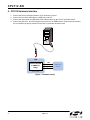
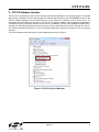
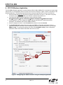
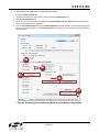
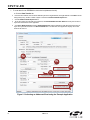
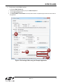
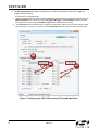
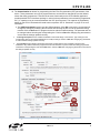
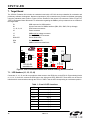
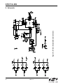
C P 2 11 2 - E K CP211 2 E VALUATION K I T U SER ’ S G UIDE 1. Kit Contents The CP2112 Evaluation Kit contains the following items: CP2112 Evaluation Board USB Cable DVD Quick Start Guide 2. Relevant Documentation Application notes can be found on the Interface Application Notes page for all fixed-function devices: www.silabs.com/interface-appnotes. AN721: CP210x/CP211x Device Customization Guide — Customize the VID, PID, serial number, and other parameters stored in the CP2112 one-time programmable ROM. AN496: CP2112 HID-to-SMBus API Specification — Provides function descriptions and examples for all of the PC software functions that control the CP2112. AN495: CP2112 Interface Specification — Describes the HID report format for CP2112 devices. 3. Software Setup The Software Development Kit (SDK) for the CP2112 kit is included on the kit DVD. The latest version of this installer can also be downloaded from the www.silabs.com/cp2112ek website. This package includes: Device Customization Utility Documentation — data sheet, application notes, user’s guide, quick start guide, etc. HidSmbusExample — Example software utilizing the CP2112 API interface described in AN496. Library — repackaged HID DLL and CP2112 API DLL The Windows installer should launch automatically after inserting the DVD. For Mac and Linux, browse to the appropriate directory on the DVD to install the software package. Follow the instructions to install the SDK to the system. The CP2112 is an HID device, so a driver does not need to be installed on most operating systems. Rev. 0.3 7/13 Copyright © 2013 by Silicon Laboratories CP2112-EK CP2112-EK 4. CP2112 Hardware Interface 1. Connect the CP2112 evaluation board to a PC as shown in Figure 1. 2. Connect one end of the USB cable to a USB Port on the PC. 3. Connect the other end of the USB cable to the USB connector on the CP2112 evaluation board. 4. Connect the SDA, SCL, and Ground pins on the CP2112 to an SMBus device. External pull-up resistors are not needed if the pull-up resistors on the CP2112 evaluation board are used. USB SCL CP2112 HID USB to SMBus/I2C Bridge SDA ground SMBus/I2C Device CP2112 EK Figure 1. Hardware Setup 2 Rev. 0.3 CP2112-EK 5. CP2112 Software Interface The CP2112 is an HID device that uses the standard HID functions available in the operating system. To facilitate this process in Windows, Silicon Labs packaged the standard HID functions into the SLABHIDDevice DLL in the CP2112 software package. The HID report structure for the CP2112 is customized for the device and is not compatible with other HID report structures, like a mouse or keyboard. AN495, “CP2112 Interface Specification” describes the custom HID report structure for the CP2112, and AN496, “CP2112 HID-to-SMBus API Specification” describes the API software functions that can be used to read or write data and control the CP2112 from the PC. The software application described in “6. CP2112 Windows Application” provides an example of how to use these functions. The CP2112 appears as an HID device in Device Manager as shown in Figure 2. Figure 2. CP2112 in Device Manager Rev. 0.3 3 CP2112-EK 6. CP2112 Windows Application The HID SMBus Example application uses the Windows CP2112 HID-to-SMBus DLL to transmit and receive data with the CP2112. The application also has access to the CP2112’s GPIO pins. Figure 3 shows a screenshot of the Windows Application. The following steps describe how to start the application and use some of its features. 1. Ensure that the hardware is connected to a Windows PC as shown in Figure 1. If the device is properly connected, the red SUSPEND LED on the CP2112 evaluation board will turn on. 2. Launch the Hid SMBus Example application, which is found by clicking StartAll ProgramsSilicon LaboratoriesCP2112 Evaluation KitHidSmbus Example. 3. In this application, you can configure the SMBus settings and GPIO pins, customize the device descriptors, and read/write data over the SMBus interface. 4. Select the appropriate device in the Connection drop down box and click Connect. 5. The Configuration tab enables setting and getting the SMBus configuration parameters. To set a parameter, modify the value that is in the corresponding text box or check/uncheck a box and click Set SMBus Config. To verify that the settings took effect, click Get SMBus Config. These configuration parameters reset to their default values when the CP2112 is reset. 4 5 Figure 3. Configuring the SMBus Interface using the Example Application 4 Rev. 0.3 CP2112-EK 6. To read data from an SMBus device (non-addressed mode): a. Click the Data Transfer tab. a. b. Enter the slave address and the number of bytes to read in the Read Request box. Click the Read Request button. c. To see the number of bytes that were read back, click Get Read/Write Transfer Status and verify the number of bytes read at the bottom of the application. d. Next, click Force Read Response and then Get Read Response until the application reads back the total number of bytes. The bytes will be shown in the Received Data field. The status of the CP2112 will be shown at the bottom of the application. 6a 6b 6c 6e 6d Figure 4. Performing a Non-Addressed Read using the Example Application Rev. 0.3 5 CP2112-EK 7. To read data from an EEPROM or similar device (addressed mode): a. Click the Data Transfer tab. e. f. Enter the slave address, the number of address bytes in the target address, the target address of the SMBus device being read (in hex), and the number of bytes to read in the Addressed Read Request box. Click the Address Read Request button. g. To see the number of bytes that were read back, click Get Read/Write Transfer Status and verify the number of bytes read at the bottom of the application. h. Click Force Read Response and then Get Read Response until the application reads back the total number of bytes. The bytes will be shown in the Received Data field. The status bar of the application displays the current status of the CP2112. 7a 7b 7c 7e 7d Figure 5. Performing an Addressed Read using the Example Application 6 Rev. 0.3 CP2112-EK 8. To write data over the SMBus interface: a. Click the Data Transfer tab. i. j. k. Enter the Slave address and data (in hex) in the Write Request box. Click the Write Request button. Click Get Read/Write Transfer Status and verify that the transfer completed using the status bar at the bottom of the application. 8a 8c 8b 8d Figure 6. Performing a Write using the Example Application Rev. 0.3 7 CP2112-EK 9. The Pin Configuration tab enables configuration of the GPIO and special functions (TX Toggle, RX Toggle, and Clock Output). a. Click the Pin Configuration tab. l. GPIO pins toggle between Input/Ouput and Open-Drain/Push-Pull by clicking the corresponding GPIO boxes in the GPIO Configuration area. Check the boxes for TX Toggle, RX Toggle, and Clock Output to enable the special functionality on these pins. Click the Set GPIO Config button to update the device settings. m. The Latch Values section enables writing or reading the GPIO latches. Clicking the box next the GPIO pins listed will scroll through 1, 0, and X for a don’t care. Click the Write Latch button to change the state of the GPIO latch. 9a 9b 9c Figure 7. Configuring the CP2112 Pins using the Example Application 8 Rev. 0.3 CP2112-EK 10. The Customization tab allows for programming the One-Time-Programmable (OTP) parameters of the device. These parameters can only be programmed once and cannot be changed back to their default values after being programmed. This tab has the same functionality as the CP2112SetIDs application provided with the CP2112 software package. In order for these parameters to be sucessfully programmed, a 4.7 µF capacitor must be connected between the VPP pin and ground. This capacitor is populated by default on the CP2112 Evaluation Kit board has this capacitor. See "8. Schematic" on page 12 for more information. a. The USB Customization section sets the USB parameters. Click Get to retrieve the current settings. Change the settings by modifying the text boxes and checking the box next to the parameter being modified. Click the Set button to program the device with the modified settings. The parameter will not be changed without checking the corresponding box. Perform a Get after changing any parameters to ensure that the settings updated correctly. n. The String Descriptors section enables modification of the serial strings in the CP2112. Type a string into the corresponding text box and click the Set button to modify the strings. Perform a Get after changing any parameters to ensure that the settings updated correctly. o. The Lock Byte section displays which fields have been programmed and can lock fields to prevent future modification. Any field that has been programmed will not be checked. To prevent a field from being programmed, uncheck the corresponding box and click the Set button. Perform a Get after changing any parameters to ensure that the settings updated correctly. 10a 10c 10b Figure 8. Customizing a CP2112 Device using the Example Application Rev. 0.3 9 CP2112-EK 7. Target Board The CP2112 Evaluation Kit includes an evaluation board with a CP2112 device pre-installed for evaluation and preliminary software development. Numerous input/output (I/O) connections are provided to facilitate prototyping using the evaluation board. Refer to Figure 9 for the locations of the various I/O connectors. Refer to Figure 10, “CP2112 Evaluation Board Schematic” for information regarding the SMBus pull-up resistors that are located on the target board. P1 USB connector for USB interface H1 Access Connector for SMBus interface (SDA, SCL, GND, Pull-Up Voltage) J1, J2, J3, J4 GPIO access connectors J6 Power connector J7 SMBus pull-up voltage connector J8 Red SUSPEND LED connector DS0–DS7 Green GPIO LEDs DS8 Red SUSPEND LED TB1 SMBus interface terminal block J4 J3 GND EXT_PU CP2112 J2 DS3 DS2 EXT_PU J1 CP2112-EK www.silabs.com DS1 DS0 J7 SMBUS PU_V VIO VDD +3V NET A SDA SCL P1 DS8 U1 DS5 DS4 H1 EXT_PU GND SUSPEND VIO SILICON LABS TB1 J8 DS7 DS6 J6 Figure 9. CP2112 Evaluation Board with Default Shorting Blocks Installed 7.1. LED Headers (J1, J2, J3, J4) Connectors J1, J2, J3, and J4 are provided to allow access to the GPIO pins on the CP2112. Place shorting blocks on J1, J2, J3, and J4 to connect the GPIO pins to the eight green LEDs, DS0–DS7. These LEDs can be used to indicate active communications through the CP2112. Table 1 lists the LED corresponding to each header position. Table 1. J2 and J3 LED Locations 10 LED Pins DS0 J1[3:4] DS1 J1[1:2] DS2 J2[3:4] DS3 J2[1:2] DS4 J3[3:4] DS5 J3[1:2] DS6 J4[3:4] DS7 J4[1:2] Rev. 0.3 CP2112-EK 7.2. Universal Serial Bus (USB) Interface (P1) A Universal Serial Bus (USB) connector (P1) is provided to facilitate connections to the USB interface on the CP2112. See Table 2 for the USB pin definitions. Table 2. USB Connector Pin Descriptions Pin # Description 1 VBUS 2 D- 3 D+ 4 GND (Ground) 7.3. SMBus Signals (TB1, H1) The SMBus interface terminal block and access headers are included to easily interace SMBus devices to the evaluation board. The terminal block can be used to connect wires to the board, and the access connectors can be used to connect scope probes to the SMBus interface for debugging. The signals that are accessible through these two connectors are SDA, SCL, GND, and the external pull-up voltage signal. 7.4. VDD and VIO Power Connector (J6) This header (J6) is included on the evaluation board to provide several power options. The following describes the function of each pin: Pins 1–2: Connect CP2112 VIO input (pin 5) to CP2112 VDD (Pin 6). Remove the shorting block to power VIO from an external source. Pins 3–4: Connects the main +3 V net to the CP2112 VDD (Pin 6). The main +3 V net powers the other components (eight green LEDs) on the board. 7.5. SMBus Pull-Up Voltage Connector (J7) This header (J7) is included on the evaluation board to provide power options for SMBus pull-up voltage. The following describes the function of each pin: J7[1:2]: Connects CP2112 VIO pin (Pin 5) to the 4.7 k pull-up resistors located on the evaluation board. J7[2:3]: Connects the External Pull-Up signal from TB1 (Pin 4) to the 4.7 kpull-up resistors on the evaluation board. 7.6. SUSPEND LED Connector (J8) The J8 header is used to connect the CP2112 SUSPEND pin (Pin 17) to the DS8 red LED. When the LED is on, the device has enumerated with the PC operating normally. When the LED is off, the device has not yet enumerated or is in the USB Suspend state. Rev. 0.3 11 Figure 10. CP2112 Evaluation Board Schematic CP2112-EK 8. Schematic 12 Rev. 0.3 CP2112-EK DOCUMENT CHANGE LIST Revision 0.1 to Revision 0.2 Updated Figure 1. Updated "6. CP2112 Windows Application" on page 4. Instructions and figures from updated PC application. Updated Figure 10 on page 12. Revision 0.2 to Revision 0.3 13 Updated “1. Kit Contents” to change CD-ROM to DVD. Added “2. Relevant Documentation” and “5. CP2112 Software Interface”. Updated “3. Software Setup” to point to the drivers on the website. Updated Figure 1. Updated the instructions and figures in “6. CP2112 Windows Application”. Rev. 0.3 CP2112-EK CONTACT INFORMATION Silicon Laboratories Inc. 400 West Cesar Chavez Austin, TX 78701 Tel: 1+(512) 416-8500 Fax: 1+(512) 416-9669 Toll Free: 1+(877) 444-3032 Please visit the Silicon Labs Technical Support web page: https://www.silabs.com/support/pages/contacttechnicalsupport.aspx and register to submit a technical support request. Patent Notice Silicon Labs invests in research and development to help our customers differentiate in the market with innovative low-power, small size, analogintensive mixed-signal solutions. Silicon Labs' extensive patent portfolio is a testament to our unique approach and world-class engineering team. The information in this document is believed to be accurate in all respects at the time of publication but is subject to change without notice. Silicon Laboratories assumes no responsibility for errors and omissions, and disclaims responsibility for any consequences resulting from the use of information included herein. Additionally, Silicon Laboratories assumes no responsibility for the functioning of undescribed features or parameters. Silicon Laboratories reserves the right to make changes without further notice. Silicon Laboratories makes no warranty, representation or guarantee regarding the suitability of its products for any particular purpose, nor does Silicon Laboratories assume any liability arising out of the application or use of any product or circuit, and specifically disclaims any and all liability, including without limitation consequential or incidental damages. Silicon Laboratories products are not designed, intended, or authorized for use in applications intended to support or sustain life, or for any other application in which the failure of the Silicon Laboratories product could create a situation where personal injury or death may occur. Should Buyer purchase or use Silicon Laboratories products for any such unintended or unauthorized application, Buyer shall indemnify and hold Silicon Laboratories harmless against all claims and damages. Silicon Laboratories and Silicon Labs are trademarks of Silicon Laboratories Inc. Other products or brandnames mentioned herein are trademarks or registered trademarks of their respective holders. 14 Rev. 0.3