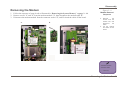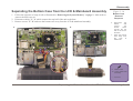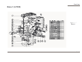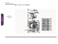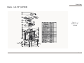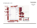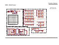
1
Preface
LCD Computer
LP300
Service Manual
Preface
I
Preface
Notice
The company reserves the right to revise this publication or to change its contents without notice. Information contained
herein is for reference only and does not constitute a commitment on the part of the manufacturer or any subsequent vendor. They assume no responsibility or liability for any errors or inaccuracies that may appear in this publication nor are
they in anyway responsible for any loss or damage resulting from the use (or misuse) of this publication.
This publication and any accompanying software may not, in whole or in part, be reproduced, translated, transmitted or
reduced to any machine readable form without prior consent from the vendor, manufacturer or creators of this publication, except for copies kept by the user for backup purposes.
Preface
Brand and product names mentioned in this publication may or may not be copyrights and/or registered trademarks of
their respective companies. They are mentioned for identification purposes only and are not intended as an endorsement
of that product or its manufacturer.
Version 1.0
March 2002
Trademarks
Intel® and Pentium® are registered trademarks of Intel Corporation.
Windows® is a registered trademark of Microsoft Corporation.
Other brand and product names are trademarks and./or registered trademarks of their respective companies.
II
Preface
About this Manual
This manual is intended for service personnel who have completed sufficient training to undertake the maintenance and
inspection of personal computers.
It is organized to allow you to look up basic information for servicing and/or upgrading components of the LCD PC. The
following information is included:
Chapter 1, Introduction, provides general information about the location of system elements and their specifications.
Chapter 2, Disassembly, provides step-by-step instructions for disassembling parts and subsystems.
Appendix A, Part Lists
Appendix B, Schematic Diagrams
Appendix C, Switches
Appendix D, Updating the FLASH ROM BIOS
Preface
Related Documents
You may also need to consult the following manual for additional information:
User’s Manual on CD
This describes the LCD PC’s features and the procedures for operating the computer and its ROM-based setup program.
It also describes the installation and operation of the utility programs provided with the LCD PC.
III
Preface
Preface
IV
Preface
Contents
Notice ..................................................................................................................... II
About this Manual .................................................................................................III
Introduction ........................................................... 1-1
Preface
Overview ............................................................................................................. 1-1
System Specifications ......................................................................................... 1-2
Processor ............................................................................................................. 1-2
Core Logic ........................................................................................................... 1-2
Structure .............................................................................................................. 1-2
Security ................................................................................................................ 1-2
Memory ............................................................................................................... 1-2
BIOS .................................................................................................................... 1-2
LCD ..................................................................................................................... 1-2
Display ................................................................................................................. 1-3
Storage ................................................................................................................. 1-3
Audio ................................................................................................................... 1-3
PC Card Sockets .................................................................................................. 1-3
Interface ............................................................................................................... 1-4
Communication ................................................................................................... 1-4
Power Management ............................................................................................. 1-4
Power ................................................................................................................... 1-4
Indicators ............................................................................................................. 1-4
Environmental Spec ............................................................................................ 1-4
Physical Dimensions ........................................................................................... 1-5
Weight ................................................................................................................. 1-5
Optional ............................................................................................................... 1-5
External Locator - Top View .............................................................................. 1-6
External Locator - Left & Right Side Views ...................................................... 1-7
External Locator - Right Side & Bottom Views ................................................. 1-8
Mainboard Overview - Top ................................................................................. 1-9
V
Preface
Key Parts ............................................................................................................ 1-9
Mainboard Overview - Bottom ......................................................................... 1-10
Key Parts ........................................................................................................... 1-10
Mainboard Overview - Top ............................................................................... 1-11
Cable Connectors and Switches ........................................................................ 1-11
Disassembly ............................................................ 2-1
Preface
Overview ............................................................................................................. 2-1
Maintenance Tools .............................................................................................. 2-2
Connections ......................................................................................................... 2-2
Maintenance Precautions .................................................................................... 2-3
Cleaning ...............................................................................................................2-3
Disassembly Steps ............................................................................................... 2-4
Removing the Hard Disk Drive Assembly ........................................................ 2-10
Removing the CD Devices ................................................................................ 2-11
Removing the RF Module ................................................................................. 2-12
Removing the System Memory ......................................................................... 2-13
Removing the CPU ........................................................................................... 2-17
Removing the Modem ....................................................................................... 2-19
Removing the Floppy Disk Drive Assembly .................................................... 2-20
Removing the Wireless LAN Module ............................................................... 2-21
Removing the I/O Bracket ................................................................................ 2-22
Removing the Rear Bracket .............................................................................. 2-22
Removing the Inverter Board ............................................................................ 2-23
Removing the Mainboard .................................................................................. 2-24
Separating the Bottom Case from the LCD & Mainboard Assembly ............... 2-25
Removing the LCD ........................................................................................... 2-26
Removing the LED Board ................................................................................. 2-27
Removing the Base Cover ................................................................................. 2-28
Removing the Speaker Units ............................................................................. 2-29
Removing the Bridge Board .............................................................................. 2-29
Removing the CD Device Base Brackets .......................................................... 2-30
VI
Preface
Removing the USB Board ................................................................................. 2-30
Removing the Power Supply Unit ..................................................................... 2-31
Part Lists ............................................................... A-1
Preface
Part List Illustration Location .............................................................................A-2
Base-1 (LP300) ...................................................................................................A-3
Back - Acer 17” (LP300) ....................................................................................A-4
Back - LG 18” (LP300) .......................................................................................A-5
LCD Front (LP300) .............................................................................................A-6
Floppy Disk Drive (LP300) ................................................................................A-7
Hard Disk Drive (LP300) ...................................................................................A-8
CD-ROM Drive (LP300) ....................................................................................A-9
DVD-ROM Drive (LP300) ...............................................................................A-10
CD-RW Drive (LP300) .....................................................................................A-11
Schematic Diagrams ..............................................B-1
System Block Diagram .......................................................................................B-3
Clock Generator ..................................................................................................B-4
DRCG Panel Type ...............................................................................................B-5
CPU (P4 mPGA 478) - 1 of 2 .............................................................................B-6
CPU (P4 mPGA478) - 2 of 2 ..............................................................................B-7
MCH (CPU, HUB, AGP) - 1 of 2 .......................................................................B-8
MCH (RDRAM, PCI) - 2 of 2 ............................................................................B-9
RAMBUS A,B ..................................................................................................B-10
CPU Decoupling ...............................................................................................B-11
ATI Mobility M6 - 1 of 3 ..................................................................................B-12
ATI Mobility M6 - 2 0f 3 ..................................................................................B-13
ATI Mobility M6 - 3 0f 3 ..................................................................................B-14
VRAM Terminator ............................................................................................B-15
Z3, LVDS ..........................................................................................................B-16
Micro-P, LCD PWR ..........................................................................................B-17
ICH2 - 1 of 2 .....................................................................................................B-18
VII
Preface
Preface
ICH2 - 2 of 2 .....................................................................................................B-19
Audio Codec, AMP ...........................................................................................B-20
IDE, PCI Reset ..................................................................................................B-21
PCMCIA 1394 ..................................................................................................B-22
1394 PHY, PCMCIA Ejecter ............................................................................B-23
LAN 8139C .......................................................................................................B-24
Super I/O ...........................................................................................................B-25
USB, Bluetooth .................................................................................................B-26
LPT, IR/RF ........................................................................................................B-27
Mini PCI, MDC .................................................................................................B-28
Power - 1 of 2 ....................................................................................................B-29
Power - 2 of 2 ....................................................................................................B-30
SSC, VGA Power ..............................................................................................B-31
VRAM DDR - 1 of 2 .........................................................................................B-32
VRAM DDR - 2 of 2 .........................................................................................B-33
Video In .............................................................................................................B-34
External USB Board ..........................................................................................B-35
LED Board ........................................................................................................B-36
Inverter Board - Page 1 of 2 ..............................................................................B-37
Inverter Board - Page 2 of 2 ..............................................................................B-38
Switches.................................................................. C-1
Updating the FLASH ROM BIOS ...................... D-1
VIII
Introduction
1: Introduction
Overview
This manual covers the information you need to service or upgrade the LP300 LCD computer. Information about operating the computer (e.g. getting started, and the Setup utility) is in the User’s Manual. Information about drivers (e.g.
VGA & audio) is also found in User’s Manual. That manual is shipped with the computer.
Operating systems (e.g. DOS, Windows 9x, Windows NT 4.0, Windows 2000, Windows XP, OS/2 Warp, UNIX, etc.) have
their own manuals as do application software (e.g. word processing and database programs). If you have questions about
those programs, you should consult those manuals.
1.Introduction
The LP300 LCD computer is designed to be upgradeable. See “Disassembly” on page 2 - 1 for a detailed description of
the upgrade procedures for each specific component. Please note the warning and safety information indicated by the
“” symbol.
The balance of this chapter reviews the computer’s technical specifications and features.
Overview 1 - 1
Introduction
System Specifications
Processor
• Intel® Pentium® 4 (400MHz System Bus) - 1.4 ~ 2.0+GHz
• Supporting mPGA478 Processor Package
Core Logic
1.Introduction
• Intel® 850
MCH = 82850
ICH-2 = 82801BA
Structure
• Fully PC 2001 Compliant
• ACPI 2.0 Compliant
Security
• BIOS password
Memory Module
Warning
There must be a memory module present in
both DIMM sockets to
make sure the computer will boot up. The
memory modules must
be the same size and
specification. The options are listed in the
table below.
Memory
• Two DIMM sockets supporting PC800 RDRAM
• DRAM upgradeable to 1GB (128/256/512MB RDRAM modules)
BIOS
• 2MB Flash ROM Phoenix BIOS
• Supports Plug and Play, ACPI 2.0
LCD
• 17”/18.1" SXGA 1280 * 1024 LCD Panel
1 - 2 System Specifications
Introduction
Display
• ATI M6-P Integrated AGP™ 4X
• Integrated 128-bit 2D/3D Graphics Accelerator
Advanced HW Acceleration for DVD Playback (Motion Compensation engine and IDCT)
Fully DirectX 8 Compliant Graphics Engine
• External memory of 32MB or 64MB of DDR SGRAM on board (factory option)
• Dual-View Display Monitor
Storage
1.Introduction
• One 3.5” 1.44MB 3-mode FDD (slim type)
• One 3.5” HDD
• Two slim storage bays for CD Devices
Device Bay Right: Changeable with CD-ROM/CD-RW/DVD/Combo drive
Device Bay Left: Changeable with CD-ROM/CD-RW/DVD/Dummy or RF module
Audio
• AC97’ 2.2 compatible
• Two Built-In speakers (3W)
• Three audio jacks for headphone-out, line-in, and microphone-in
PC Card Sockets
• Supports two Type II or one Type III PCMCIA slots
• Integrated IEEE 1394a controller
System Specifications 1 - 3
Introduction
Interface
1.Introduction
•
•
•
•
•
•
•
•
•
One parallel port
One D-sub 15-pin CRT port compliant DC1.1
Four USB ports
One IEEE 1394 port
One RJ-45 jack for 100M/10M Ethernet LAN
One RJ-11 port for Modem
One Video-in for TV-tuner (Optional TV-tuner)
One S-Video connector
One SPDIF out port
Communication
• 802.11b Wireless LAN (Optional)
• One RJ-11 port for Modem
• One RJ-45 port for 10/100Mbps Ethernet
Power Management
• ACPI v1.0 Compliant
Power
• Internal switching power supply
• Full range AC adapter - AC in 90~264V, 160W
Indicators
• LED indicators (HDD/FDD activity, status indicators)
Environmental Spec
• Temperature
• Operating: 5ºC ~ 35ºC
• Non-Operating: -10ºC ~ 60ºC
1 - 4 System Specifications
Relative Humidity
Operating: 20% ~ 80%
Non-Operating: 10% ~ 90%
Introduction
Physical Dimensions
• 460mm (H) * 448 mm (W) * 220mm (D)
Weight
• 13.9Kg w/o Bay 2 device installed
Optional
• IR Keyboard
• Wireless LAN Module
• RF Module for wireless Keyboard / Mouse
1.Introduction
System Specifications 1 - 5
Introduction
External Locator - Top View
Figure 1 - 1
1.Introduction
Top View
1.
2.
3.
4.
5.
6.
LCD Panel
Power Button
Set Button
Scroll Buttons
Infrared Receiver
LED Status Indicators
7. Device Bay Left
(for CD/CD-RW/
DVD device/RF
module or
Dummy Bay)
8. Device Bay Right
(for CD/CD-RW/
DVD/Combo
drive)
9. Speakers
1
5
3
6
7
9
1 - 6 External Locator - Top View
8
9
4
4
2
Introduction
External Locator - Left & Right Side Views
Figure 1 - 2
Left & Right Views
Right
Left
11
10
1
9
8
7
6
2
4
5
3
External Locator - Left & Right Side Views 1 - 7
1.Introduction
1. Floppy Disk Drive
2. Hard Disk Drive
Bay
3. AC Power-In
4. Dual USB Ports
5. Kensington Lock
Slot
6. Headphone-Out
Jack
7. Line-In Jack
8. Microphone-In
Jack
9. Volume Control
Knob
10.PC Card Eject
Buttons
11.Dual PC Card
Slots
Introduction
External Locator - Right Side & Bottom Views
Figure 1 - 3
1.Introduction
Right Side
1. Video-In Port
2. S/PDIF Out Port
3. RJ-11 Phone
Jack
4. RJ-45 LAN Jack
5. Dual USB Ports
6. Unpowered IEEE 1394 Port
7. Printer/Parallel
Port
8. External Monitor
(CRT) Port
9. S-Video
Connector
10.Vents
10
9
1 2 3 4
5 6
7
10
1 - 8 External Locator - Right Side & Bottom Views
8
Introduction
Mainboard Overview - Top
Figure 1 - 4
Mainboard
Overview - Top
Key Parts
Key Parts
9
9
11
4
1
6
7
3
10
8
5
Mainboard Overview - Top 1 - 9
1.Introduction
2
1. CPU Socket (no
CPU Installed)
2. Northbridge Intel
MCH 82850 615
OLGA
3. Southbridge Intel
ICH-2 82801 BA
360 EBGA
4. VGA - ATI
Mobility M6-P
5. W83627HF-AM
Super I/O Controller
6. PCMCIA
7. W49V002FAP
Firmware Hub
8. CMOS Battery
9. On-Board Video
Memory
10.2 * DIMM
Sockets
11.Clock Generator
Introduction
Figure 1 - 5
1.Introduction
Mainboard
Overview - Bottom
Key Parts
Mainboard Overview - Bottom
Key Parts
1. AC97 MDC
Module
2. SAA7114 A/D
(Analog to Digital)
3. Micro-P (OSD)
W78E62BP
4. 1394a Integrated
Cardbus
Controller
5. RTL8139C LAN
Controller
6. ALC201 - AC 97
Audio Codec
7. TSB41AB1 1394 PHY
8. TH63LVDM83A LVDS
8
1
4
6
5
7
1 - 10 Mainboard Overview - Bottom
3
2
Introduction
Mainboard Overview - Top
Figure 1 - 6
Cable Connectors and Switches
1
2
3
14
13
5
6
12
7
8
9
10
11
Mainboard Overview - Top 1 - 11
1.Introduction
4
Mainboard Top
Cable Connectors
& Switches
1. CN1(12V LCD
Cable)
2. CN2 (3V or 5V
LCD Cable)
3. CN3 (Modem
Module)
4. CN5 (Wireless
Lan Module)
5. CN11 (PCMCIA
Module)
6. CN14 (Audio
Cable)
7. CN15 (Modem
Cable)
8. CN29 (Inverter
Board)
9. CN19 (Bridge
Board Cable)
10.CN17 (System
Fan Cable)
11.CN28 (FDD
Cable)
12.CN29 (LED
Board)
13.CN8 (CPU Fan
Cable)
14.SW1 (DIP Switch
- “Settings” on
page C - 2)
1.Introduction
Introduction
1 - 12
Disassembly
2: Disassembly
Overview
This chapter provides step-by-step instructions for disassembling parts and subsystems. When it comes to reassembly,
reverse the procedures (unless otherwise indicated).
We suggest you completely review any procedure before you take the computer apart.
Component Parts
To make the disassembly process easier each section may have a box in the page margin. Information contained under
the figure # will give a synopsis of the sequence of procedures involved in the disassembly procedure. A box with a lists the relevant parts you will have after the disassembly process is complete. Note: The parts listed will be for the disassembly procedure listed ONLY, and not any previous disassembly step(s) required. Refer to the part list for the previous disassembly procedure. The amount of screws you should be left with will be listed here also.
5
Information
A box with a 5 will provide any possible helpful information. A box with a contains warnings.
Examples of these types of boxes are shown in the sidebar.
Warning
Overview 2 - 1
2.Disassembly
Procedures such as upgrading/replacing the RAM, CD device and hard disk are included in the User’s Manual but are
repeated here for your convenience.
Disassembly
NOTE: ALL DISASSEMBLY PROCEDURES ASSUME THAT THE SYSTEM IS TURNED OFF, DISCONNECTED FROM ANY POWER SUPPLY, AND THAT ALLL PERIPHERAL CABLES ARE DISCONNECTED (INCLUDING TELEPHONE LINES AND NETWORK CABLES).
Maintenance Tools
The following tools are recommended when working on the notebook PC:
2.Disassembly
•
•
•
•
•
•
M3 Philips-head screwdriver
M2.5 Philips-head screwdriver (magnetized)*
M2 Philips-head screwdriver
Small flat-head screwdriver
Pair of needle-nose pliers
Anti-static wrist-strap
Connections
Connections within the computer are one of four types:
2 - 2 Overview
Locking collar sockets for ribbon connectors
To release these connectors, use a small flat-head screwdriver to
gently pry the locking collar away from its base. When replacing the connection, make sure the connector is oriented in the
same way. The pin1 side is usually not indicated.
Pressure sockets for multi-wire connectors
To release this connector type, grasp it at its head and gently
rock it from side to side as you pull it out. Do not pull on the
wires themselves. When replacing the connection, do not try to
force it. The socket only fits one way.
Pressure sockets for ribbon connectors
To release these connectors, use a small pair of needle-nose pliers to gently lift the connector away from its socket. When replacing the connection, make sure the connector is oriented in
the same way. The pin1 side is usually not indicated.
Board-to-board or multi-pin sockets
To separate the boards, gently rock them from side to side as
you pull them apart. If the connection is very tight, use a small
flat-head screwdriver - use just enough force to start.
Disassembly
Maintenance Precautions
The following precautions are a reminder. To avoid personal injury or damage to the computer while performing a removal and/or replacement job, take the following precautions:
2.Disassembly
1. Don't drop it. Perform your repairs and/or upgrades on a stable surface. If the computer falls, the case and other
components could be damaged.
2. Don't overheat it. Note the proximity of any heating elements. Keep the computer out of direct sunlight.
3. Avoid interference. Note the proximity of any high capacity transformers, electric motors, and other strong magnetic fields. These can hinder proper performance and damage components and/or data. You should also monitor
the position of magnetized tools (i.e. screwdrivers).
4. Keep it dry. This is an electrical appliance. If water or any other liquid gets into it, the computer could be badly damaged.
5. Be careful with power. Avoid accidental shocks, discharges or explosions.
• Before removing or servicing any part from the computer, turn the computer off and detach any power supplies.
• When you want to unplug the power cord or any cable/wire, be sure to disconnect it by the plug head. Do not pull on the
wire.
6. Peripherals – Turn off and detach any peripherals.
7. Beware of static discharge. ICs, such as the CPU and main support chips, are vulnerable to static electricity.
Before handling any part in the computer, discharge any static electricity inside the computer. When handling a
printed circuit board, do not use gloves or other materials which allow static electricity buildup. We suggest that you
use an anti-static wrist strap instead.
8. Beware of corrosion. As you perform your job, avoid touching any connector leads. Even the cleanest hands produce oils which can attract corrosive elements.
9. Keep your work environment clean. Tobacco smoke, dust or other air-born particulate matter is often attracted to
charged surfaces, reducing performance.
10.Keep track of the components. When removing or replacing any part, be careful not to leave small parts, such as
screws, loose inside the computer.
Cleaning
Do not apply cleaner directly to the computer, use a soft clean cloth.
Do not use volatile (petroleum distillates) or abrasive cleaners on any part of the computer.
Overview 2 - 3
Disassembly
Disassembly Steps
The following lists the disassembly steps, and on which page to find the related information. PLEASE PERFORM THE
DISASSEMBLY STEPS IN THE ORDER INDICATED.
To remove the hard disk drive assembly:
1.Remove the hard disk drive assembly
page 2 - 10
To remove the CD device(s):
2.Disassembly
1.Remove the CD Device
page 2 - 11
To remove the RF module:
1.Remove the RF module
Memory Module
Warning
There must be a memory module present in
both DIMM sockets to
make sure the computer will boot up. The
memory modules must
be the same size and
specification. The options are listed in the
table below.
2 - 4 Disassembly Steps
page 2 - 12
To remove the system memory:
1.Remove the LCD hinge cover
2.Remove the IDE shielding plate
3.Remove the LCD back cover
4.Remove the LCD shielding plate
5.Remove the system memory
page 2 - 14
page 2 - 14
page 2 - 15
page 2 - 16
page 2 - 16
To remove the CPU:
1.1.Remove the LCD hinge cover
2.Remove the IDE shielding plate
3.Remove the LCD back cover
4.Remove the LCD shielding plate
5.Remove the CPU
page 2 - 14
page 2 - 14
page 2 - 15
page 2 - 16
page 2 - 17
Disassembly
To remove the modem:
1.Remove the LCD hinge cover
2.Remove the IDE shielding plate
3.Remove the LCD back cover
4.Remove the LCD shielding plate
5.Remove the modem
page 2 - 14
page 2 - 14
page 2 - 15
page 2 - 16
page 2 - 19
To remove the floppy disk drive assembly:
page 2 - 14
page 2 - 14
page 2 - 15
page 2 - 16
page 2 - 20
2.Disassembly
1.Remove the LCD hinge cover
2.Remove the IDE shielding plate
3.Remove the LCD back cover
4.Remove the LCD shielding plate
5.Remove the FDD
To remove the optional wireless LAN module:
1.Remove the LCD hinge cover
2.Remove the IDE shielding plate
3.Remove the LCD back cover
4.Remove the LCD shielding plate
5.Remove the Wireless LAN module
page 2 - 14
page 2 - 14
page 2 - 15
page 2 - 16
page 2 - 21
To remove the inverter board:
1.Remove the LCD hinge cover
2.Remove the IDE shielding plate
3.Remove the LCD back cover
4.Remove the LCD shielding plate
5.Remove the inverter board
page 2 - 14
page 2 - 14
page 2 - 15
page 2 - 16
page 2 - 23
Disassembly Steps 2 - 5
Disassembly
To remove the mainboard:
2.Disassembly
1.Remove the LCD hinge cover
2.Remove the IDE shielding plate
3.Remove the LCD back cover
4.Remove the LCD shielding plate
5.Remove the system memory
6.Remove the CPU
7.Remove the modem
8.Remove the optional wireless LAN module
9.Remove the I/O bracket
10.Remove the rear bracket
11.Remove the inverter board
12.Remove the mainboard
2 - 6 Disassembly Steps
page 2 - 14
page 2 - 14
page 2 - 15
page 2 - 16
page 2 - 13
page 2 - 17
page 2 - 19
page 2 - 21
page 2 - 22
page 2 - 22
page 2 - 23
page 2 - 24
Disassembly
To remove the LCD/LED board:
page 2 - 14
page 2 - 14
page 2 - 15
page 2 - 16
page 2 - 13
page 2 - 17
page 2 - 19
page 2 - 21
page 2 - 22
page 2 - 22
page 2 - 23
page 2 - 24
page 2 - 26
page 2 - 27
2.Disassembly
1.Remove the LCD hinge cover
2.Remove the IDE shielding plate
3.Remove the LCD back cover
4.Remove the LCD shielding plate
5.Remove the system memory
6.Remove the CPU
7.Remove the modem
8.Remove the optional wireless LAN module
9.Remove the I/O bracket
10.Remove the rear bracket
11.Remove the inverter board
12.Remove the mainboard
13.Remove the LCD
14.Remove the LED board
To remove the base cover:
1.Remove the LCD hinge cover
2.Remove the IDE shielding plate
3.Remove the LCD back cover
4.Separate the bottom case from the LCD etc.
5.Remove the base cover
page 2 - 14
page 2 - 14
page 2 - 15
page 2 - 25
page 2 - 28
Disassembly Steps 2 - 7
Disassembly
To remove the speaker units:
1.Remove the LCD hinge cover
2.Remove the IDE shielding plate
3.Remove the LCD back cover
4.Separate the bottom case from the LCD etc.
5.Remove the base cover
6.Remove the speaker units
page 2 - 14
page 2 - 14
page 2 - 15
page 2 - 25
page 2 - 28
page 2 - 29
To remove the bridge board:
2.Disassembly
1.Remove the LCD hinge cover
2.Remove the IDE shielding plate
3.Remove the LCD back cover
4.Separate the bottom case from the LCD etc.
5.Remove the base cover
6.Remove the speaker units
7.Remove the bridge board
page 2 - 14
page 2 - 14
page 2 - 15
page 2 - 25
page 2 - 28
page 2 - 29
page 2 - 29
To remove the CD device base brackets:
1.Remove the LCD hinge cover
2.Remove the IDE shielding plate
3.Remove the LCD back cover
4.Separate the bottom case from the LCD etc.
5.Remove the base cover
6.Remove the speaker units
7.Remove the bridge board
8.Remove the CD device base brackets
2 - 8 Disassembly Steps
page 2 - 14
page 2 - 14
page 2 - 15
page 2 - 25
page 2 - 28
page 2 - 29
page 2 - 29
page 2 - 30
Disassembly
To remove the USB board:
1.Remove the LCD hinge cover
2.Remove the IDE shielding plate
3.Remove the LCD back cover
4.Separate the bottom case from the LCD etc.
5.Remove the base cover
6.Remove the speaker units
7.Remove the bridge board
8.Remove the CD device base brackets
9.Remove the USB board
page 2 - 14
page 2 - 14
page 2 - 15
page 2 - 25
page 2 - 28
page 2 - 29
page 2 - 29
page 2 - 30
page 2 - 30
2.Disassembly
To remove the power supply unit:
1.Remove the LCD hinge cover
2.Remove the IDE shielding plate
3.Remove the LCD back cover
5.Separate the bottom case from the LCD etc.
6.Remove the base cover
7.Remove the speaker units
8.Remove the bridge board
9.Remove the CD device base brackets
10.Remove the power supply unit
page 2 - 14
page 2 - 14
page 2 - 15
page 2 - 25
page 2 - 28
page 2 - 29
page 2 - 29
page 2 - 30
page 2 - 31
Disassembly Steps 2 - 9
Disassembly
Figure 2 - 1
Hard Disk
Removal
Sequence
a.
b.
2.Disassembly
c.
d.
Remove
the
screw from the
HDD Bay.
Pull the HDD
assembly out.
Disconnect
the
IDE and power
cables.
Remove
the
screws from the
assembly
and
slide the hard disk
out of the case.
Removing the Hard Disk Drive Assembly
1. Turn off the computer and turn it around so that you may comfortably access the left side..
2. Remove screw "2" from the HDD Bay "1" (Figure 2 - 1a).
3. Carefully pull the HDD Assembly out from the bay (Figure 2 - 1b) and disconnect the IDE cable "3", and power
cable "4" (Figure 2 - 1c).
4. Remove screws "5 "- "8" from the assembly, and slide the hard disk "9" out of the case "10".
.
1
10
2
7
b.
a.
8
9
6
3
5
9. HDD case
10. HDD
4
• 5 Screws
c.
2 - 10 Removing the Hard Disk Drive Assembly
d.
Disassembly
Removing the CD Devices
Figure 2 - 2
1. Turn off the computer and pull the LCD up and forward to allow easier access to the latches “1” & “2”.
2. Slide the latches to unlock the drives and hold in place as you pull the drive out of the bay (the left bay latch slides
to the right. the right bay to the right).
3. Pull the CD-device(s) "3" out of the bay(s).
CD Device
Removal
Sequence
a.
b.
a.
Slide the latch and
hold in place.
Pull the drive out
of the bay.
b.
a.
2.Disassembly
1
3
b.
2
1
3.
CD device(s)
Removing the CD Devices 2 - 11
Disassembly
Figure 2 - 3
RF Module
Removal
Sequence
a.
b.
2.Disassembly
c.
d.
e.
f.
Slide the latch and
hold in place.
Pull the module
case out of the
bay.
Remove the three
screws from the
case cover.
Remove the case
cover.
If there is an RF
module in the
case remove the
screws.
Remove
the
cable. and RF
module.
Removing the RF Module
1. Turn off the computer and pull the LCD up and forward to allow easier access to the latch "1".
2. Slide the latch to unlock the module case and hold in place as you pull the case out of the bay (the left bay latch
slides to the right).
3. Pull the RF module "2" case out of the bay.
4. Turn the case over and remove screws "3" - "5", then remove the case cover "6".
5. If there is an RF module "7" into the case, remove screws at positions "8" and "9" and disconnect cable "10".
a.
b.
c.
3
4
1
2
5
d.
e.
f.
2.
7.
RF module case
Optional
RF
module
• 5 screws (if module is included)
10
6
9
7
8
2 - 12 Removing the RF Module
Disassembly
Removing the System Memory
The computer can accommodate up to 1GB of memory in two DIMM sockets. It supports 128/256/512MB modules of
PC800 RDRAM specification.
Memory Module
Warning
Socket 1
Socket 2
Total RAM
128MB
128MB
256MB
256MB
256MB
512MB
512MB
512MB
1024MB
Table 2 - 1
RAM Options
Removing the System Memory 2 - 13
2.Disassembly
There must be a memory module present in
both DIMM sockets to
make sure the computer will boot up. The
memory modules must
be the same size and
specification. The options are listed in the
table below.
Disassembly
Figure 2 - 4
Memory Removal
Sequence
a.
b.
c.
2.Disassembly
d.
Remove
the
screw from the
LCD hinge cover.
Slide off the LCD
hinge cover.
Remove the IDE
shielding
plate
screws.
Ease the IDE
shielding plate out
of the computer.
1. Turn off the computer and place it with its LCD display facing down on a clean, dry, level surface.
2. Remove screw "1" (Figure 2 - 4a) from the rear of the computer and slide the LCD hinge cover "2" (Figure 2 - 4b)
up towards the top of the computer and remove it.
3. Remove screws "3" and "4" (Figure 2 - 4c) from the IDE shielding plate "5" (Figure 2 - 4d) and carefully ease the
IDE shielding plate out of the computer.
a.
c.
1
4
3
d.
1.
2.
b.
LCD hinge cover
IDE
shielding
plate
2
2 - 14 Removing the System Memory
5
Disassembly
4. Remove screws "1"-"10" (Figure 2 - 5) from the rear of the LCD back cover "11" (Figure 2 - 5).
5. Carefully ease the LCD back cover up from the main unit and disconnect the fan cable (see Fan Cable note below)
from the mainboard at point "12" (Figure 2 - 5).
6. Disconnect the audio cable "13" (Figure 2 - 5) from the inside of the case.
a.
3
2
1
Figure 2 - 5
Memory Removal
Sequence
(Cont..)
4
11
b.
5
10
c.
13
d.
9
8
7
6
Fan Cable
11. LCD back cover
• 10 Screws
Later models will not include the fan cable, and therefore this step may be ignored.
Removing the System Memory 2 - 15
2.Disassembly
12
Remove
the
screws from the
LCD back cover.
Ease up the back
cover
and
disconnect the fan
and audio cables,
then lift the back
cover away
Remove
the
screws from the
back of the LCD
shielding plate.
Slide the shielding
plate forward and
lift away from the
main assembly.
The
memory
socket will now be
visible.
Disassembly
Figure 2 - 6
Memory Removal
Sequence
(Cont.)
a.
2.Disassembly
b.
c.
d.
d.
Remove
the
screws from the
back of the LCD
shielding plate.
Slide the shielding
plate forward and
lift away from the
main assembly.
The
memory
socket(s) will now
be visible
Pull the latches to
release
the
module(s).
Remove
the
memory
module(s).
7.
8.
9.
10.
11.
With the cables disconnected, lift the LCD back cover case away.
Remove screws "1"-"3" (Figure 2 - 5ab) from the LCD shielding plate.
Slide the LCD shielding plate "4" forward and lift it up and away from the main assembly.
The memory sockets will now be visible at point "18" (Figure 2 - 5d) on the mainboard
For each module you want to replace, gently pull the two latches toward the sides of the socket to release the module.
12. Remove the memory module(s).
a.
4
1
c.
4. LCD
plate
b.
2
shielding
• 3 screws
2 - 16 Removing the System Memory
3
d.
Disassembly
Removing the CPU
Figure 2 - 7
1. Follow the sequence of steps 1 to 9 as illustrated in “Removing the System Memory” on page 2 - 14 to reveal the
CPU heat sink and fan unit "1" in Figure 2 - 7a.
2. Release the latches from the top of the CPU heat sink and fan unit as indicated in Figure 2 - 7a, then remove the
power cable "4" from the board and lift the fan unit away.
3. Release the heat sink as indicated in Figure 2 - 7c., and remove it.
a.
CPU Removal
Sequence
a.
b.
b.
2
3
1
c.
1
Caution
4
The heat sink, and
CPU area in general,
contains parts which
are subject to high
temperatures - Please
allow the area time to
cool before removing
these parts.
d.
c.
5
1. CPU Fan Unit
5. Heat Sink
Removing the CPU 2 - 17
2.Disassembly
b.
Release
the
latches from the
top of the CPU
heat sink and fan
unit.
Remove
the
power cable and
lift the fan unit
away
Release the heat
sink.
Remove the heat
sink.
Disassembly
Figure 2 - 8
CPU Removal
Sequence
(Cont.)
a.
Lift the latch to
unlock the CPU.
Lift the CPU out of
the socket.
a.
2.Disassembly
b.
4. Lift latch "1" in the direction indicated in Figure 2 - 8a to unlock the CPU.
5. Carefully (it may be hot) lift the CPU up out of the socket.
6. When re-inserting the CPU pay careful attention to the pin alignment, it will fit only one way (don’t force it!).
1
b.
2
2. CPU
2 - 18 Removing the CPU
Disassembly
Removing the Modem
Figure 2 - 9
1. Follow the sequence of steps 1 to 9 as illustrated in “Removing the System Memory” on page 2 - 14.
2. Remove screws "1" and "2" from the modem module "3", then disconnect the modem cable "4".
3. Disconnect the modem module from the connector socket "5", and lift it and the cable off the board.
a.
Modem Removal
Sequence
a.
b.
b.
1
Remove
the
screws from the
modem unit, and
disconnect
the
cable.
Lift the modem
and cable off the
board.
3
2.Disassembly
2
a.
5
b.
4
3.Modem module
4.Modem cable
• 2 Screws
Removing the Modem 2 - 19
Disassembly
Figure 2 - 10
Floppy Disk
Drive Assembly
Removal
Sequence
a.
b.
Disconnect
the
FDD ribbon cable.
Remove
the
screws from the
FDD assembly.
Removing the Floppy Disk Drive Assembly
1. Follow the sequence of steps 1 to 9 as illustrated in “Removing the System Memory” on page 2 - 14, in order to
remove the back case etc.
2. Carefully disconnect the floppy disk drive ribbon cable "1" in Figure 2 - 10a
3. Remove screws "4"-"5 "(Figure 2 - 10a) from the floppy disk drive assembly.
4. Lift the floppy disk drive assembly "6" off the board.
a.
2.Disassembly
b.
1
2
3
6
4
6. FDD Assembly
• 4 Screws
2 - 20 Removing the Floppy Disk Drive Assembly
5
Disassembly
Removing the Wireless LAN Module
Figure 2 - 11
1. Follow the sequence of steps 1 to 9 as illustrated in “Removing the System Memory” on page 2 - 14, in order to
remove the back case etc.
2. Ease the wireless LAN module "1" slowly up and away from the mainboard.
Wireless LAN
Module Removal
Sequence
a.
b.
a.
1
b.
c.
Locate
the
wireless
LAN
module.
Ease the module
up.
Lift the module
away from the
mainboard.
2.Disassembly
1
c.
1. Wireless LAN
module
Removing the Wireless LAN Module 2 - 21
Disassembly
Figure 2 - 12
I/O Bracket
Removal
Sequence
a.
b.
Remove
the
screws, from the I/
O bracket.
Lift the I/O bracket
up
off
the
mainboard.
Removing the I/O Bracket
1. Follow the sequence of steps 1 to 9 as illustrated in “Removing the System Memory” on page 2 - 14, in order to
remove the back case etc.
2. Remove the standard screws "1"-"4" (Figure 2 - 12a), and use long-nosed pliers to remove the connector type
screws "5"-"8".
3. Lift the I/O bracket "9" up off the mainboard.
4
a.
b.
3
2.Disassembly
1
5
6
7
9
8
2
9. I/O bracket
• 8 screws
Figure 2 - 13
Rear Bracket
Removal
Sequence
a.
b.
Remove
the
screws, from the
rear bracket.
Ease the rear
bracket up off the
mainboard.
Removing the Rear Bracket
1. Follow the sequence of steps 1 to 9 as illustrated in “Removing the System Memory” on page 2 - 14 in order to
remove the back case etc.
2. Remove screws "1"-"3" (Figure 2 - 13a).
3. Carefully ease the I/O bracket "4" up off the mainboard.
a.
b.
1
2
4
4. Rear bracket
• 3 screws
2 - 22 Removing the I/O Bracket
b.
3
Disassembly
Removing the Inverter Board
Figure 2 - 14
1. Follow the sequence of steps 1 to 9 as illustrated in “Removing the System Memory” on page 2 - 14 in order to
remove the back case etc.
2. Remove screws "1"-"5" from the inverter board shielding plate, and lift out the shielding plate "6".
3. Disconnect the two connectors "7" and "8" from the inverter board, then elevate the inverter board slightly and pull
it in the direction of the arrow (Figure 2 - 14c) to release it from the connector "9" on the mainboard.
4. Lift the inverter board "10" up and out from the mainboard.
Inverter Board
Removal
Sequence
a.
b.
a.
1
c.
b.
2
5
9
c.
d.
4
d.
7
10
8
6.
Inverter
board
shielding plate
10. Inverter board
• 5 screws
Removing the Inverter Board 2 - 23
2.Disassembly
6
3
Remove
the
screws from the
shielding plate.
Lift
out
the
shielding plate.
Disconnect
the
two connectors,
elevate
the
inverter
board
slightly,
and
carefully pull in the
direction of the
arrow.
Lift the inverter
board up and out
from
the
mainboard.
Disassembly
Figure 2 - 15
Rear Bracket
Removal
Sequence
a.
2.Disassembly
b.
c.
Disconnect
the
cables
which
connect the top
half of the unit to
the base.
Remove
the
screws
and
connecting
cables.
Lift the mainboard
up from the LCD
bracket.
Removing the Mainboard
1. Follow the sequence of steps 1 to 9 as illustrated in “Removing the System Memory” on page 2 - 14 in order to
remove the back case etc.
2. Disconnect cables "1"-"4" which connect the top half of the unit to the base.
3. Remove the standard screws "5"-"11" and the connector type screws "12"-"13" (lift away the small bracket "14").
4. Disconnect cables "15"-"18" and lift the mainboard "19" up from the LCD bracket.
a.
b.
16
13
7
8
12
9
5
6
10
17
2
1
4
a.
14
c.
14. Bracket
19. Mainboard
• 9 screws
2 - 24 Removing the Mainboard
11
15
3
19
18
Disassembly
Separating the Bottom Case from the LCD & Mainboard Assembly
1. Follow the sequence of steps 1 to 9 as illustrated in “Removing the System Memory” on page 2 - 14 in order to
remove the back case etc.
2. Disconnect cables "1"-"4" which connect the top half of the unit to the base.
3. Remove screws "5"-"8" and ease the bottom case away from the LCD & mainboard assembly.
a.
Figure 2 - 16
Bottom Case
Removal
Sequence
a.
b.
10
c.
1
3
4
5
7
6
8
9
9. Bottom case
10. LCD & mainboard
assembly
• 4 screws
Separating the Bottom Case from the LCD & Mainboard Assembly 2 - 25
2.Disassembly
2
Disconnect
the
cables,
and
remove
the
screws
which
connect the top
half of the unit to
the base.
Ease the bottom
case away from
the
LCD
&
mainboard.
Disassembly
Figure 2 - 17
LCD
Removal
Sequence
a.
2.Disassembly
b.
c.
d.
Remove
the
screws from the
LCD bracket and
disconnect
the
inverter cables.
Separate the LCD
bracket from the
front of the case.
Remove
the
screws from the
LCD.
Lift the LCD away
from the bracket.
Removing the LCD
1. Follow the sequence of steps 1 to 9 as illustrated in “Removing the System Memory” on page 2 - 14 in order to
remove the back case etc.
2. Follow the instructions in “Separating the Bottom Case from the LCD & Mainboard Assembly” on page 2 25.
3. Remove screws "1"-"4" from the back of the LCD bracket, and disconnect the inverter cables "5"-"6" (if you
haven’t already done so).
4. Carefully separate the LCD bracket from the front of the case "7".
5. Remove screws "8"-"11" from the LCD "12" and lift it away from the bracket "13" (pay careful attention to the
inverter cables easing them through the hole at point "14").
2
1
a.
b.
1
7
3
5
6
8
4
9
7. Front case
12. LCD
13. LCD bracket
• 8 screws
2 - 26 Removing the LCD
12
13
11
10
14
Disassembly
Removing the LED Board
Figure 2 - 18
1. Follow the sequence of steps 1 to 9 as illustrated in “Removing the System Memory” on page 2 - 14 in order to
remove the back case etc.
2. Follow the instructions in “Separating the Bottom Case from the LCD & Mainboard Assembly” on page 2 25.
3. Separate the front case from the LCD as illustrated in “Removing the LCD” on page 2 - 26.
4. Remove screws "1"-"3" and lift the LED board "4" and cable out from the front of the case.
a.
a.
b.
b.
1
LED Board
Removal
Sequence
Remove
the
screws from the
LED board.
Lift the board out
from the front of
the case.
2
2.Disassembly
3
4
c.
4. LED board
• 3 screws
Removing the LED Board 2 - 27
Disassembly
Figure 2 - 19
Base Cover
Removal
Sequence
a.
2.Disassembly
c.
d.
Remove the CD
drives, hard disk
and separate the
bottom case from
the
LCD
&
mainboard
assembly
Remove
the
screws from the
base.
Lift the cover up
from the bottom
unit.
Removing the Base Cover
1. Remove the CD drives as illustrated in “Removing the CD Devices” on page 2 - 11 (incl. RF Module page 2 - 12).
2. Remove the HDD drive as illustrated in “Removing the Hard Disk Drive Assembly” on page 2 - 10.
3. Follow the sequence of steps 1 to 9 as illustrated in “Removing the System Memory” on page 2 - 14 in order to
remove the back case etc.
4. Follow the instructions in “Separating the Bottom Case from the LCD & Mainboard Assembly” on page 2 25.
5. Remove screws "1"-"9" from the base unit.
6. Lift the base cover "10" off the bottom of the unt.
a.
b.
1
c.
10. Base cover module
10
2 - 28 Removing the Base Cover
3
9
8
• 9 Screws
2
7
6
5
4
Disassembly
Removing the Speaker Units
Figure 2 - 20
1. Follow the instructions to remove the base cover (“Removing the Base Cover” on page 2 - 28).
2. Remove screws "1"-"8" and disconnect the speaker cables "9"-"10", then remove the speaker units "11"-"12".
Speaker Unit
Removal
Sequence
a.
b.
9
a.
10
b.
2
5
7
11
4
3
8
6
11. Speaker units
• 8 screws
Removing the Bridge Board
1.
2.
3.
4.
12
Follow the instructions to remove the base cover (“Removing the Base Cover” on page 2 - 28).
Disconnect the speaker cables "9"-"10" (Figure 2 - 20a) above.
Remove screws "1"-"3" and disconnect cables "3"-"6".
Lift the bridge board "7" up off the base unit.
a.
b.
1
Figure 2 - 21
Bridge Board
Removal
Sequence
a.
3
6
b.
4
5
2
7
Remove
screws
disconnect
cables.
Remove
bridge board.
the
and
the
the
7. Bridge board
• 3 screws
Removing the Speaker Units 2 - 29
2.Disassembly
1
Remove
the
screws from the
speaker units and
disconnect
the
cables.
Remove
the
speaker units.
Disassembly
Figure 2 - 22
CD Device Base
Bracket
Removal
Sequence
a.
2.Disassembly
b.
Removing the CD Device Base Brackets
1. Follow the instructions to remove the bridge board (“Removing the Bridge Board” on page 2 - 29).
2. Remove screws "1"-"8" and lift away the CD device base brackets.
.
a.
Remove
the
screws from the
base brackets.
Remove the base
brackets.
b.
1
2
4
3
5
6
7
8
8
8. 2 * Base brackets
• 8 screws
Figure 2 - 23
USB Board
Removal
Sequence
a.
b.
Remove
the
screws from the
USB board, and
disconnect
the
cable.
Remove the USB
board.
Removing the USB Board
1. Follow the instructions to remove the bridge board (“Removing the Bridge Board” on page 2 - 29).
2. Remove screws "1"-"3" (you may have already removed screw "3" as part of the process of removing the bridge
board).
3. Disconnect the cable at point "4", then remove the USB board "5".
a.
b.
4
3
5. USB board
• 3 screws
2 - 30 Removing the CD Device Base Brackets
2
1
8
5
Disassembly
Removing the Power Supply Unit
Figure 2 - 24
1. Follow the instructions to remove the bridge board (“Removing the Bridge Board” on page 2 - 29).
2. Follow the instructions to remove CD device base brackets (“Removing the CD Device Base Brackets” on page 2
- 30).
3. Remove screws "1"-"6" and lift the power supply "7" off the base bracket.
a.
a.
b.
b.
1
Power Supply
Removal
Sequence
2
Remove
the
screws from the
power supply unit.
Remove
the
power supply unit.
7. Power supply unit
6
• 6 screws
5
7
4
3
Removing the Power Supply Unit 2 - 31
2.Disassembly
2.Disassembly
Disassembly
2 - 32
Part Lists
Appendix A:Part Lists
This appendix breaks down the LCD PC’s construction into a series of illustrations. The component part numbers are
indicated in the tables opposite the drawings.
Note: This section indicates the manufacturer’s part numbers. Your organization may use a different system, so be sure
to cross-check any relevant documentation.
Note: Some assemblies may have parts in common (especially screws). However, the part lists DO NOT indicate the
total number of duplicated parts used.
Part Lists
Note: Be sure to check any update notices. The parts shown in these illustrations are appropriate for the system at the
time of publication. Over the product life, some parts may be improved or re-configured, resulting in new part numbers.
A - 1
Part Lists
Part List Illustration Location
The following table indicates where to find the appropriate part list illustration.
Table 1 - 1
Part Lists
Part List Illustration
Location
A-2
Part
Page #
Base-1
page 1 - 3
Back Acer17"
page 1 - 4
Back LG 18"
page 1 - 5
LCD Front
page 1 - 6
Floppy Disk Drive
page 1 - 7
Hard Disk Drive
page 1 - 8
CD-ROM Drive
page 1 - 9
DVD-ROM Drive
page 1 - 10
CD-RW Drive
page 1 - 11
Part Lists
Base-1 (LP300)
Figure 1 - 1
Part Lists
Base-1
A - 3
Part Lists
Back - Acer 17” (LP300)
Part Lists
Figure 1 - 2
Back Acer 17”
(LP300)
A-4
Part Lists
Back - LG 18” (LP300)
Figure 1 - 3
A - 5
Part Lists
Back LG 18”
(LP300)
Part Lists
LCD Front (LP300)
Part Lists
Figure 1 - 4
LCD Front (LP300)
A-6
Part Lists
Floppy Disk Drive (LP300)
Figure 1 - 5
A - 7
Part Lists
Floppy Disk Drive
(LP300)
Part Lists
Hard Disk Drive (LP300)
Part Lists
Figure 1 - 6
Hard Disk Drive
(LP300)
A-8
Part Lists
CD-ROM Drive (LP300)
Figure 1 - 7
A - 9
Part Lists
CD-ROM Drive
(LP300)
Part Lists
DVD-ROM Drive (LP300)
Part Lists
Figure 1 - 8
DVD-ROM Drive
(LP300)
A - 10
Part Lists
CD-RW Drive (LP300)
Figure 1 - 9
A - 11
Part Lists
CD-RW Drive
(LP300)
Part Lists
Part Lists
A - 12
Schematic Diagrams
Appendix B:Schematic Diagrams
This appendix has circuit diagrams of the systems PCB’s:
Part No. of the Latest Version
System Board
External USB Board
LED Board
Inverter Board
71-P3000-004A
71-P3003-002
71-P3004-004
71-P300R-005
Schematic Diagrams
Printed Circuit Board
B - 1
Schematic Diagrams
The following table indicates where to find the appropriate schematic diagram.
Table 1 - 1
Schematic Diagrams
Schematic Diagram
B-2
Diagram - Page
Diagram - Page
System Block Diagram - Page B - 3
IDE, PCI Reset - Page B - 21
Clock Generator - Page B - 4
PCMCIA 1394 - Page B - 22
DRCG - Panel Type - Page B - 5
1394 PHY, PCMCIA Ejecter - Page B - 23
CPU (P4 mPGA478) 1 of 2 - Page B - 6
LAN 8139C - Page B - 24
CPU (P4 mPGA478) 2 of 2 - Page B - 7
Super I/O - Page B - 25
MCH (CPU, HUB, AGP) 1 of 2 - Page B - 8
USB, Bluetooth - Page B - 26
MCH (RDRAM, PCI) 2 of 2 - Page B - 9
LPT, IR/RF - Page B - 27
RAMBUS A,B - Page B - 10
Mini PCI, MDC - Page B - 28
CPU Decoupling - Page B - 11
Power 1 of 2 - Page B - 29
ATI Mobility M6 1 of 3 - Page B - 12
Power 2 of 2 - Page B - 30
ATI Mobility M6 2 0f 3 - Page B - 13
SSC, VGA Power - Page B - 31
ATI Mobility M6 3 of 3 - Page B - 14
VRAM DDR 1 of 2 - Page B - 32
VRAM Terminator - Page B - 15
VRAM DDR 2 of 2 - Page B - 33
Z3, LVDS - Page B - 16
Video In - Page B - 34
Micro-P, LCD PWR - Page B - 17
EXT USB Board - Page B - 35
ICH2 1 of 2 - Page B - 18
LED Board - Page B - 36
ICH2 2 of 2 - Page B - 19
Inverter Board 1 of 2 - Page B - 37
Audio Codec, AMP - Page B - 20
Inverter Board Page 2 of 2 - Page B - 38
Schematic Diagrams
System Block Diagram
POWER
System Block Diagram
LCD
PANEL
P.11
P.11
mPGA 478
DDR
SGRAM
2 * 14MHz
+1.8V
2 * CLKREF
+1.5V
Intel
P.29,30
+1.8VSB
BUSCLKC
DRCG
AGP Bus
P.13
RIMM 1
P.7
IDE 1
ATA-66/100
Intel
AC'97 Bus
AC'97 MDC
P.26
PCI Bus
82801BA
360 EBGA
MODULE
( South Bridge )
AC'97 Bus
P.15,16
USB 3
P.31
P.18
CARDBUS
Integrated
1394a
PCI4451
LPC Bus
USB 2
EXT.
P.23
1394 PHY
TSB41AB1
INT.
P.20
SUPER I/O
RJ-45
W83627HF
P.21
P.25
MINI-PCI
P.25
P.19
P.22
RJ-11
IDE 2
ATA-66/100
P.18
USB 1
USB 4
P.23
RIMM 2
P.7
ICH-2
P.21
VIDEO-IN
P.27
IDE Bus
PCI Bus
LAN
RTL8139C
P.15
EXTERNAL
POWER
DRDRAM Memory - Bus
P.5,6
W78E62BP
REGULATOR
P.27
P.2
( North Bridge )
P.9,10
Micro-P
( OSD )
VRM
P.26,27
82850
615 OLGA
Mobility
M6-P
SCALER
ZURAC 3
+5VSB
P.16
Schematic Diagrams
VGA
TTL 24bit
MCH
Intel
+5V
+3V
BUSCLKC
BUSCLKT
R.G.B.
+12V
DRCG
BUSCLKT
HOST Bus
TTL 48bit
TTL 24bit
TV-OUT
+3VSB
P.1
P.3,4
DDR
VideoRAM Bus
P.13
V_CORE
+2.5V
Pentium 4 processor
( 32,64 MB )
RTC
RTCVCC
CLOCK
Generator
2 * 48MHz
4 * 66MHz
LVDS
THC63LVDM83A
P.31
4 * CPUCLKT
10 * PCICLK
CRT
2 Channel
LVDS
A/D
SAA7114
4 * CPUCLKC
Sheet 1 of 32
System Block
Diagram
PARALLEL
P.24
FLOPPY
P.22
IR/RF
KB/MOUSE
P.22
Firmware
HUB
W49V002FAP
P.23
AC'97
Audio Codec
ALC201
P.17
PCMCIA
Slot * 2
P.20
1394
PORT
P.20
P.14,23,24
MIC
EARPHONE
LINE IN
Phone Jack board Phone Jack board Phone Jack board
Mainboard (71-P3000-004A) B - 3
Schematic Diagrams
Clock Generator
Sheet 2 of 32
CLK GEN
SDATA
PCICLK6
PCICLK7/FS2
SCLK
PCICLK8/FS3
Z0102
1
R45
Z0101
2
5
0
X1
PCICLK9/SEL100/133
2 33
12
PCICLK3
R320 1
2 33
14
PCICLK4
R315 1
2 33
15
PCICLK5
R316 1
2 33
17
PCICLK6
18
FS2
R36
1
2 10K
20
FS3
R306 1
2 10K
21
SEL100/133
R308 1
R307 1
2 *R
2 470
ICH2PCLK
FWHCLK
[15]
LANPCLK
CBPCLK
[19]
MINIPCICLK
SIOPCLK
T490
C499
10P
C500
10P
C498 1
2 *C
+3VCLK
C501
10P
C502
10P
C503
1
PCICLK5
2 33
R314 1
10P
C504
10P
2
PCICLK4
2 33
R313 1
PCICLK2
1
PCICLK3
R312 1
PCICLK1
11
2
PCICLK2
PCICLK0
9
1
52
[7,15,22] SMBCLK
PCICLK1
8
2
23
[7,15,22] SMBDATA
PCICLK0
1
2 4.7K
VDD1
VDD2
VDD3
VDD4
VDD5
VDD6
VDD7
VDD8
VDD9
VDD10
VDD11
2
2 4.7K
R309 1
0.5" MAX
U7
4
10
16
22
27
29
36
38
43
49
56
1
R322 1
0_1206
2
+3V
2
1
+3V
1
2
+3VCLK
L10
+3V
Z0103
2
1
C73
Y1
14.318MHZ
[15]
1
2 33
FS1
26
R67
1
2 33
3VMREF_B 54
R64
1
2 33
3VMREF
55
R65
R68
R58
1
1
1
2 33
2 33
2 33
3V66_3
3V66_2
3V66_1
3V66_0
35
34
31
30
3VMREF_B
CPUCLKC0
CPUCLKC1
CPUCLKC2
CPUCLKC3
3VMREF
3V66_3
3V66_2
3V66_1
3V66_0
C532
10P
28
[16,23,26] SUSB#
Z0104
39
PD#
IREF
ICS9250-37
1
42
45
48
51
CPUCLKT0
CPUCLKT1
CPUCLKT2
CPUCLKT3
R60
R61
R63
41
44
47
50
CPUCLKC0
CPUCLKC1
CPUCLKC2
CPUCLKC3
R59
R66
R62
1
1
1
2 33
2 33
2 33
1
1
1
2 33
2 33
2 33
CPUCLK
ITPCLK
MCHCLK
[4]
[4]
[5]
T1
CPUCLK# [4]
ITPCLK# [4]
MCHCLK# [5]
T2
0-0.2 inches
GND1
GND2
GND3
GND4
GND5
GND6
GND7
GND8
GND9
GND10
GND11
2
2
10P
CPUCLKT0
CPUCLKT1
CPUCLKT2
CPUCLKT3
FS1/48MHZ_1
R57
1
7
13
19
24
32
33
37
40
46
53
R to Node:
0.2" MAX
Node to chip:
12" MAX
1
R318
FS0/48MHZ_0
R335
R339
R338
R334
R336
R337
51_1%
51_1%
51_1%
51_1%
51_1%
51_1%
2
25
1
FS0
2
2 33
1
1
2
C533
1
1
1
2
ICH14CLK
0.5" MAX
R321
T3
10P
2 33
1
MCH66IN
ICH66CLK
ATI66CLK
C530
R319 1
2
[9]
MSEL1
1
[5]
MSEL0
3
2
CLKREF1
2
1
[2]
MULTSEL1REF1
2
SIO48MHZ
CLKREF2
MULTSEL0/REF0
*C
ICH48CLK
[2]
X2
5P
1
*C
1
10P
1
1
10P
6
C90
2
5P
C529
2
C531
2
C507
2
C506
2
2
1
1
CLOCK NOTICE:
Spacing to other traces: 25mils
Line width: 7.0mils
475_1%
2
Iref=2.32mA
FS0
FS1
R311 1
2 10K
R666 1
2 10K
R695 1
2 *10K
R696 1
2 *10K
R697 1
2 *10K
R698 1
2 *10K
R39
2 10K
R665 1
2 10K
1
+3VCLK
MSEL1
MSEL0
0.1U_X7R
C95
1
C94
0.1U_X7R
C96
0.1U_X7R
2
0.1U_X7R
1
C98
2
0.1U_X7R
1
C97
2
0.1U_X7R
1
1
C93
2
0.1U_X7R
2
C92
2
4.7U/10V
1
1
C69
2
2
10U/10V
2
C89
1
1
+3VCLK
FS1 FS0
0
1
CPU
PCI
3V66
100.00
33.33
66.67
+3VCLK
B - 4 Mainboard (71-P3000-004A)
0.1U_X7R
C62
1
C59
0.1U_X7R
C61
0.1U_X7R
2
0.1U_X7R
1
1
C60
2
0.1U_X7R
2
C57
2
2
0.1U_X7R
1
1
C99
2
C64
0.1U_X7R
2
0.1U_X7R
1
1
1
+3V
C58
2
Schematic Diagrams
LOW FOR 100MHZ OPERATION
[3,10,11,13,14,26,27,28,31]
+3VCLK
Schematic Diagrams
DRCG Panel Type
PCICLK7/FS2
SCLK
PCICLK8/FS3
1
R45
Z0102
2
Z0101
5
2
Z0103
6
0
X1
PCICLK9/SEL100/133
X2
MULT SEL0/REF0
2 33
R313 1
2 33
PCICLK2
R314 1
2 33
12
PCICLK3
R320 1
2 33
14
PCICLK4
R315 1
2 33
MINIPCICLK
15
PCICLK5
R316 1
2 33
SIOPCLK
17
PCICLK6
18
FS2
20
FS3
21
SEL100/133
2
MSEL0
3
MSEL1
ICH2PCLK
FWHCLK [15]
LANPCLK
CBPCLK
[19]
T 490
R36
1
2 10K
R306 1
C499
C500
C501
C502
1
PCICLK5
R312 1
PCICLK1
11
1
PCICLK4
PCICLK0
9
C503
C504
2 10K
10P
R308 1
R307 1
2 *R
2 470
+3VCLK
10P
10P
10P
10P
10P
2
PCICLK6
PCICLK3
8
1
52
[7,15,22] SMBCLK
SDAT A
PCICLK2
2
23
[7,15,22] SMBDAT A
PCICLK1
1
2 4.7K
PCICLK0
2
R309 1
VDD1
VDD2
VDD3
VDD4
VDD5
VDD6
VDD7
VDD8
VDD9
VDD10
VDD11
1
2 4.7K
0.5" MAX
U7
4
10
16
22
27
29
36
38
43
49
56
2
R322 1
0_1206
1
+3V
2
2
+3V
1
2
+3VCLK
L10
+3V
Sheet 3 of 32
DRCG - Panel Type
1
5P
C529
[5]
MCH66IN
ICH66CLK
AT I66CLK
R65
R68
R58
1
1
1
2 33
2 33
2 33
1
1
3V66_3
3V66_2
3V66_1
3V66_0
35
34
31
30
CPUCLKC0
CPUCLKC1
CPUCLKC2
CPUCLKC3
3VMREF
3V66_3
3V66_2
3V66_1
3V66_0
10P
28
[16,23,26] SUSB#
Z0104
39
PD#
IREF
CPUCLKT 0
CPUCLKT 1
CPUCLKT 2
CPUCLKT 3
R60
R61
R63
CPUCLKC0
CPUCLKC1
CPUCLKC2
CPUCLKC3
R59
R66
R62
2 33
2 33
2 33
1
1
1
2 33
2 33
2 33
CPUCLK
IT PCLK
MCHCLK
[4]
[4]
[5]
CPUCLK# [4]
IT PCLK# [4]
MCHCLK# [5]
T2
0-0.2 inches
R to Node:
0.2" MAX
Node to chip:
12" MAX
R335
R339
R338
R334
R336
R337
51_1%
51_1%
51_1%
51_1%
51_1%
51_1%
CLOCK NOTICE:
Spacing to other traces: 25mils
Line width: 7.0mils
ICS9250-37
1
1
1
1
T1
1
7
13
19
24
32
33
37
40
46
53
GND1
GND2
GND3
GND4
GND5
GND6
GND7
GND8
GND9
GND10
GND11
C532
2
2
10P
55
Schematic Diagrams
T3
C533
3VMREF
1
2 33
41
44
47
50
2
1
42
45
48
51
1
R64
3VMREF_B
2
CLKREF1
CPUCLKT 0
CPUCLKT 1
CPUCLKT 2
CPUCLKT 3
FS1/48MHZ_1
1
[2]
FS0/48MHZ_0
2
3VMREF_B 54
1
26
2 33
2
25
FS1
1
1
FS0
2 33
1
2 33
1
R67
1
2 *C
2
1
R318
CLKREF2
2
C498 1
0.5" MAX
R321
[2]
10P
ICH14CLK [15]
2
SIO48MHZ
C530
2 33
5P
*C
ICH48CLK
[9]
MULT SEL1REF1
R319 1
1
1
*C
1
10P
1
10P
C90
2
C531
Y1
14.318MHZ
2
C507
2
2
2
2
C506
C73
1
LOW FOR 100MHZ OPERATION
1
R57
2
475_1%
Iref=2.32mA
FS0
FS1
R311 1
2 10K
R695 1
2 *10K
R697 1
2 *10K
R39
2 10K
1
MSEL1
+3VCLK
MSEL0
R666 1
2 10K
R696 1
2 *10K
R698 1
2 *10K
R665 1
2 10K
+3VCLK
0.1U_X7R
C94
0.1U_X7R
1
1
C98
C95
0.1U_X7R
C96
FS1 FS0
0.1U_X7R
2
0.1U_X7R
1
1
C97
2
0.1U_X7R
2
1
C93
2
2
2
0.1U_X7R
2
C92
1
C69
4.7U/10V
2
10U/10V
2
C89
1
1
1
+3VCLK
0
1
CPU
PCI
3V66
100.00
33.33
66.67
+3VCLK
0.1U_X7R
1
C59
C62
0.1U_X7R
[3,10,11,13,14,26,27,28,31]
C61
0.1U_X7R
2
0.1U_X7R
1
1
C60
2
0.1U_X7R
2
1
C57
2
2
2
0.1U_X7R
2
C99
1
C64
0.1U_X7R
2
0.1U_X7R
1
1
1
+3V
C58
+1.8V
+3V
2
15
14
2
0.1U_X7R
0.1U_X7R
C730
1
1
C748
10U/10V
18
Manufacturer
R142 1
2 39
LM181E04
SAMSUNG
HYUNDAI
LTM170E4-L01
HT17E11-100
20
Z0207
R143 1
2 39
19
4
8
5
17
21
Z0208
DRCG1_CT M#
X
CHI MEI
M170E1/M170E4
ACER
L170E3-1(M170EN04)
OFF
OFF
OFF
OFF
ON
OFF
OFF
ON
OFF
OFF
OFF
OFF
ON
ON
OFF
OFF
OFF
OFF
ON
OFF
OFF
ON
OFF
1
PCLK/M
SYNCLK/N
SW1-1 SW1-2 SW1-3 SW1-4
LG
10U/10V
UNIPAC
Z0206
Model name
C784
2
1
C749
2
0.1U_X7R
2
1
1
1
1
C236
2
0.1U_X7R
R482
PD#
51_1%
REFCLK
BUSCLKT
MULT I0
MULT I1
NC
GND1
GND2
GND3
GNDOUT 1
GNDOUT 2
FS0
FS1
FS2
C790
Z0209
T4
*4.7P
ON
Other setting for LG panel default.
C785 1
2 0.1U_X7R
+5V
R481
JITTER
REDUCTION
51_1%
SW1 must on the TOP side
RN55
8P4RX4.7K
2
24
23
13
C240
4
3
2
1
12
MULT 0
MULT 1
0.1U_X7R
2
6
7
SUSB#
C241
16
22
1
CLKREF1
3
9
1
CHA_HCLK
CHA_RCLK
BUSCLKC
1
2
[5]
[5]
[1]
BUSCLK_ST OP#
VDDOUT 1
VDDOUT 2
2
VDDREF
VDDPD
VDD1
VDD2
11
Z0201
2
4.7K
2
R459
0.1U_X7R
2
1
1
U13
10
C750
ICS9212-03
5
6
7
8
DRCG1_CT M
1 2 3 4
ON
SW1
5
6
7
8
4
3
2
1
LCDID3
LCDID2
LCDID1
LCDID0
HDS404-2E
+1.8V
+3V
2
12
MULT 0
MULT 1
15
14
2
24
23
13
0.1U_X7R
C745
0.1U_X7R
C744
1
1
C747
10U/10V
C782
PANEL TYPE SELECT
10U/10V
2
0.1U_X7R
1
C746
2
0.1U_X7R
1
C242
2
0.1U_X7R
1
1
1
C243
2
3
9
16
22
Z0215
R146 1
2 39
20
Z0216
R147 1
2 39
19
4
8
5
17
21
Z0217
18
DRCG2_CT M#
1
PCLK/M
SYNCLK/N
R480
PD#
51_1%
REFCLK
BUSCLKT
MULT I0
MULT I1
NC
GND1
GND2
GND3
GNDOUT 1
GNDOUT 2
FS0
FS1
FS2
C789
2
MULT 0
MULT 1
1
*4.7P
1
SUSB#
CLKREF2
BUSCLKC
1
6
7
CHB_HCLK
CHB_RCLK
VDDOUT 1
VDDOUT 2
Z0218 C783 1
T5
2 0.1U_X7R
R479
JITTER
REDUCTION
51_1%
2
[16]
[16]
BUSCLK_ST OP#
2
[5]
[5]
[16,23,26] SUSB#
[1]
11
2
VDDREF
VDDPD
VDD1
VDD2
Z0210
2
4.7K
2
R455
0.1U_X7R
2
1
1
U14
10
C736
ICS9212-03
DRCG2_CT M
PLL DIVIDER SELECTION AND PLL VALUES(PLLCLK=REFCLK*A/B)
MULT0 MULT1 A
0
0
4
0
1
6
1
0
16
1
1
8
B
1
1
3
1
PLLCLK(REFCLK=50MHZ)
200
300
266.7
400
PLLCLK(REFCLK=66.6MHZ)
266.4
399.6
355.2
532.8
+3V
R667 1
2 4.7K
MULT 0
R668 1
2 4.7K
MULT 1
Note : MULT[0..1]
850Chipset supports 400MHZ(PC800) and
300MHZ(PC600) RAMBUS operation only.
BYPASS AND TEST MODE SELECTION
MODE
Normal
Bypass
Test
FS0 FS1 FS2
0
0
0
1
0
0
1
1
0
BUSCLK
PACLK
PLLCLK
REFCLK
BUSCLKB
PACLKB
PLLCLKB
REFCLK
+1.8V
[27,28]
+3V
[3,10,11,13,14,26,27,28,31]
+5V
[11,14,15,26,27,28]
Mainboard (71-P3000-004A) B - 5
Schematic Diagrams
CPU (P4 mPGA 478) - 1 of 2
Sheet 4 of 32
CPU (P4 mPGA478)
1 of 2
+1.8V
+3V
2
2
CLKREF1
15
14
1
OFF
OFF
OFF
OFF
LTM170E4-L01
HT17E11-100
ON
OFF
OFF
ON
OFF
OFF
OFF
OFF
2 39
DRCG1_CTM#
ON
ON
OFF
OFF
CHI MEI
M170E1/M170E4
OFF
OFF
ON
OFF
ACER
L170E3-1(M170EN04)
X
ON
OFF
ON
OFF
1
R142 1
SW1-1 SW1-2 SW1-3 SW1-4
LM181E04
SAMSUNG
HYUNDAI
UNIPAC
Z0206
Model name
LG
10U/10V
16
22
18
Manufacturer
C784
2
10U/10V
2
2
2
1
1
1
1
1
1
C730
R482
PD#
51_1%
REFCLK
BUSCLKT
MULTI0
MULTI1
NC
GND1
GND2
GND3
GNDOUT1
GNDOUT2
FS0
FS1
FS2
20
Z0207
19
4
8
5
17
21
Z0208
R143 1
2 39
C790
*4.7P
Z0209
T4
Other setting for LG panel default.
JITTER
REDUCTION
C785 1
2 0.1U_X7R
+5V
R481
51_1%
SW1 must on the TOP side
RN55
8P4RX4.7K
2
24
23
13
0.1U_X7R
PCLK/M
SYNCLK/N
ICS9212-03
5
6
7
8
DRCG1_CTM
ON
1 2 3 4
SW1
5
6
7
8
4
3
2
1
HDS404-2E
+1.8V
+3V
2
[1]
[16]
[16]
SUSB#
12
MULT0
MULT1
15
14
2
CLKREF2
MULT0
MULT1
0.1U_X7R
C745
0.1U_X7R
C744
1
C747
10U/10V
C782
PANEL TYPE SELECT
10U/10V
2
0.1U_X7R
1
C746
1
1
1
1
0.1U_X7R
16
22
Z0215
R146 1
2 39
DRCG2_CTM#
1
18
PCLK/M
SYNCLK/N
R480
PD#
51_1%
REFCLK
BUSCLKT
MULTI0
MULTI1
NC
GND1
GND2
GND3
GNDOUT1
GNDOUT2
FS0
FS1
FS2
20
Z0216
19
4
8
5
17
21
Z0217
R147 1
2 39
C789
*4.7P
Z0218
T5
JITTER
REDUCTION
C783 1
2 0.1U_X7R
R479
51_1%
2
24
23
13
C242
2
[16,23,26] SUSB#
BUSCLKC
0.1U_X7R
1
CHB_HCLK
CHB_RCLK
VDDOUT1
VDDOUT2
BUSCLK_STOP#
C243
1
[5]
[5]
6
7
3
9
2
11
Z0210
1
2
VDD1
VDD2
2
VDDREF
2
VDDPD
2
4.7K
2
R455
0.1U_X7R
1
10
C736
2
1
1
U14
2
Schematic Diagrams
MULT0
MULT1
0.1U_X7R
C748
4
3
2
1
[1]
BUSCLKC
0.1U_X7R
C749
2
12
SUSB#
BUSCLK_STOP#
0.1U_X7R
C236
1
6
7
0.1U_X7R
C240
1
11
CHA_HCLK
CHA_RCLK
3
9
C241
2
Z0201
[5]
[5]
VDDOUT1
VDDOUT2
1
2
VDD1
VDD2
4.7K
2
0.1U_X7R
VDDREF
VDDPD
2
R459
2
1
1
U13
10
C750
ICS9212-03
DRCG2_CTM
PLL DIVIDER SELECTION AND PLL VALUES(PLLCLK=REFCLK*A/B)
MULT0 MULT1 A
0
0
4
0
1
6
1
0
16
1
1
8
B
1
1
3
1
PLLCLK(REFCLK=50MHZ)
200
300
266.7
400
PLLCLK(REFCLK=66.6MHZ)
266.4
399.6
355.2
532.8
+3V
R667 1
2 4.7K
MULT0
R668 1
2 4.7K
MULT1
Note : MULT[0..1]
850Chipset supports 400MHZ(PC800) and
300MHZ(PC600) RAMBUS operation only.
BYPASS AND TEST MODE SELECTION
MODE
Normal
Bypass
Test
B - 6 Mainboard (71-P3000-004A)
FS0 FS1 FS2
0
0
0
1
0
0
1
1
0
BUSCLK
PACLK
PLLCLK
REFCLK
BUSCLKB
PACLKB
PLLCLKB
REFCLK
+1.8V
[27,28]
+3V
[3,10,11,13,14,26,27,28,31]
+5V
[11,14,15,26,27,28]
LCDID3
LCDID2
LCDID1
LCDID0
Schematic Diagrams
CPU (P4 mPGA478) - 2 of 2
R114 1
GTLREF1
2 49.9_1%
1
C162
220P
2
1U/6.3V_X7R
C181
AA6/
AA21
220P
C162/
C161
2
R113 1
1.5" Max
F6/
F20
R112/
R111
C181/
C180
C192/
C191
VCORE
IERR#
R388
2
1 62_1%
FERR#
R452
2
1 62_1%
GTLREF0
2 49.9_1%
BR0#
R423
2
1 51_1%
C191
PROCHOT#
R444
2
1 62_1%
220P
CPUPWRGD
R88
2
1 300_1%
THERMTRIP#
R135
2
1 62_1%
1
C161
220P
2
2
1U/6.3V_X7R
2
100_1%
C180
2
R111
1
1
1
VCORE
1.5" Max
2
C192
2
100_1%
1
1
R112
GTLREF1/
GTLREF0
R114/
R113
1
VCORE
VCORE
LAYOUT NOTICE:
GTLREF0, GTLREF1 1.5inches max.
GTLREF GENERATION CIRCUITS
Sheet 5 of 32
CPU (P4 mPGA478)
2 of 2
2 1_0805
Z0403 L14
1
2
4.7UH_0805
Z0401
AE23
R74
1
2 1_0805
Z0404 L15
1
2
4.7UH_0805
Z0402
AD20
2 33U/10V_C
1
2
ITPCLK
ITPCLK#
[5]
[5]
[5]
[5]
HDBI3#
HDBI2#
HDBI1#
HDBI0#
[5]
[5]
[15]
[15]
[1]
[1]
R406
R410
2
2
[5]
[5]
[5]
[5]
[5]
[5]
[5]
[5]
R133 2
VSSA
Z0405
33U/10V_C
HADSTB1#
HADSTB0#
AC26
AD26
V21
P26
G25
E21
DBR#
E5
D1
NMI
INTR
AF23
AF22
CPUCLK#
CPUCLK
1 51_1%
1 51_1%
COMP1
COMP0
P1
L24
W23
P23
J23
F21
W22
R22
K22
E22
HDSTBP3#
HDSTBP2#
HDSTBP1#
HDSTBP0#
HDSTBN3#
HDSTBN2#
HDSTBN1#
HDSTBN0#
1 *R
R5
L5
AE25
Z0406
Z0407
A5
A4
E11
E13
E15
E17
E19
E23
E26
E4
E7
E9
F10
F12
F14
F16
F18
F2
F22
F25
F5
F8
G21
G24
G3
ITP_CLK0
ITP_CLK1
DB#3
DB#2
DB#1
DB#0
ADSTB1
ADSTB0
DBRESET
LINT1
LINT0
BCLK1
BCLK0
COMP1
COMP0
STBP3
STBP2
STBP1
STBP0
STBN3
STBN2
STBN1
STBN0
VCC_SENSE
VSS_SENSE
VSS
VSS
VSS
VSS
VSS
VSS
VSS
VSS
VSS
VSS
VSS
VSS
VSS
VSS
VSS
VSS
VSS
VSS
VSS
VSS
VSS
VSS
VSS
AA21
F20
AA6
F6
IERR
MCERR
FERR
STPCLK
BINIT
INIT
RSP
DBSY
DRDY
TRDY
ADS
LOCK
BR0
BNR
HIT
HITM
BPRI
DEFER
TCK
TDI
TMS
TRST
TDO
PROCHOT
IGNNE
SMI
A20M
SLP
PWRGOOD
RESET
THERMDA
THERMDC
THERMTRIP
BSEL0
BSEL1
AP0
AP1
VCCVID
VCCVIDPRG
VSS
VSS
VSS
VSS
VSS
VSS
VSS
VSS
VSS
VSS
VSS
VSS
VSS
VSS
VSS
VSS
VSS
VSS
VSS
VSS
VSS
VSS
VSS
VSS
VSS
VSS
VSS
VSS
CP2
[1]
[1]
AD22
VCCA
G6
J2
J22
J25
J5
K21
K24
K3
K6
L1
L23
L26
L4
M2
M22
M25
M5
N21
N24
N3
N6
P2
P22
P25
P5
R1
R23
R26
+
1
+
CP1
VCCIOPLL
GTLREF0
GTLREF2
GTLREF1
GTLREF3
1
C25
C5
C7
C9
D10
D12
D14
D16
D18
D20
D21
D24
D3
D6
D8
E1
C22
U11B
R73
VSS
VSS
VSS
VSS
VSS
VSS
VSS
VSS
VSS
VSS
VSS
VSS
VSS
VSS
VSS
VSS
VSS
VCORE
AC3
V6
B6
Y4
AA3
W5
AB2
H5
H2
J6
G1
G4
H6
G2
F3
E3
D2
E2
D4
C1
F7
E6
D5
C3
B2
B5
C6
AB26
AB23
AB25
IERR#
Z0408
FERR#
Z0409
Z0410
BR0#
TCK
TDI
TMS
TRST#
TDO
PROCHOT#
CPUPWRGD
HCPURST#
VCORE
T290
FERR#
[15]
HSTPCLK# [15]
T291
INIT#
[15]
T292
DBSY#
[5]
HDRDY# [5]
HTRDY# [5]
ADS#
[5]
HLOCK# [5]
BR0#
[5]
BNR#
[5]
HIT#
[5]
HITM#
[5]
BPRI#
[5]
DEFER# [5]
IGNNE#
[15]
SMI#
[15]
A20M#
[15]
CPUSLP# [15]
CPUPWRGD
HCPURST# [5]
B3
C4
A2
THERMDA [22]
THERMDN [22]
AD6
AD5
THERMTRIP#
Z0412
Z0413
AC1
V5
Z0414
Z0415
AF4
AF3
Z0416
T293
T294
TDI
R438
2
1 150_1%
TMS
R435
2
1 39
HCPURST#
R99
2
1 51_1%
TDO
R134
2
1 75
DBR#
R89
2
1 150_1%
TCK
R449
2
1 27
TRST#
R451
2
1 680
LAYOUT NOTICE:
THERMDA,THERMDN:
10 mils width and spacing of 10 mils is recommand.
Parallel connect to U18(W83627HF)
T295
T296
VCCVID
T297
VCCVID=
1.2V 40mA
AF3 is reserved pin
VSS
VSS
VSS
VSS
VSS
VSS
VSS
VSS
VSS
VSS
VSS
VSS
VSS
VSS
VSS
VSS
VSS
VSS
VSS
VSS
VSS
Y5
Y25
Y22
Y2
W6
W3
W24
W21
V4
V26
V23
V1
U5
U25
U22
U2
T6
T3
T24
T21
R4
VCORE
[15,26]
NORTHWOOD478
Mainboard (71-P3000-004A) B - 7
Schematic Diagrams
CPU SIGNAL TERMINATION
CLOSE TO CPU
Schematic Diagrams
MCH (CPU, HUB, AGP) - 1 of 2
Sheet 6 of 32
MCH
(CPU, HUB, AGP)
1 of 2
HADSTB0#
HADSTB1#
T7
Y8
[4]
[4]
[4]
[4]
HDSTBP0#
HDSTBP1#
HDSTBP2#
HDSTBP3#
H7
L5
N7
T4
[4]
[4]
[4]
[4]
HDSTBN0#
HDSTBN1#
HDSTBN2#
HDSTBN3#
J6
K4
N6
R6
[4]
[4]
[4]
[4]
[4]
[4]
[4]
[4]
[4]
[4]
[4]
[4]
ADS#
BNR#
BPRI#
BR0#
HCPURST#
DBSY#
DEFER#
HIT#
HITM#
HLOCK#
HTRDY#
HDRDY#
AE6
AF10
AB10
AB11
AC8
AF8
Y10
AA11
AC10
AD9
AA9
AE10
[4]
[4]
[4]
[4]
HDBI0#
HDBI1#
HDBI2#
HDBI3#
L8
L7
R8
U8
[4]
[4]
Y11
AB9
AE9
HRS0#
HRS1#
HRS2#
[3]
[3]
[3]
[3]
[3]
Y4
U9
V5
AC2
V6
HREQ0#
HREQ1#
HREQ2#
HREQ3#
HREQ4#
T24
T25
T26
T27
T28
Z0501
Z0502
Z0503
Z0504
Z0505
L22
M21
D12
C11
V11
B - 8 Mainboard (71-P3000-004A)
0.1U_X7R
1
C222
0.1U_X7R
C299
0.1U_X7R
2
C307
2
2
0.1U_X7R
2
C934
1
1
1
1
2
0.1U_X7R
1
C933
0.1U_X7R
C946
0.1U_X7R
2
C819
2
0.1U_X7R
2
C225
1
1
1
0.1U_X7R
2
2
2
C305
C732
10U/10V
2
10U/10V
2
2
1
1
1
1
1
2
10U/10V
2
10U/10V
C642
10U/10V
1
C673
C625
10U/10V
C581
10U/10V
2
C688
2
CHA_HCLK [2]
CHA_RCLK [2]
1
VCORE
MCH66IN [1]
E21
E20
C735
2
MCH66IN
10U/10V
10U/10V
CHA_HCLKOUT
CHA_RCLKOUT
C267
1
V16
10U/10V
2
66IN
CLK/RESET
C252
1
CPU
C734
10U/10V
MCHCLK [1]
MCHCLK# [1]
1
W9
W10
2
BCLK0
BCLK1
+-10mils
RSTIN#
TESTIN#
AF11
AE11
R85
Z0506
1
22U/10V
2 *4.7K
C314
22U/10V
1
1
1
C155
C591
22U/10V
C592
22U/10V
2
CLOSE MCH
2
CHB_HCLK [2]
CHB_RCLK [2]
SYSPCIRST# [15]
2
D5
E5
2
CHB_HCLKOUT
CHB_RCLKOUT
1
+1.5V
+1.5V
FOR DEBUG ONLY
Hub
Interface
HLA_STB
HLA_STB#
HDSTBN0#
HDSTBN1#
HDSTBN2#
HDSTBN3#
AGP
DBI0#
DBI1#
DBI2#
DBI3#
RS0#
RS1#
RS2#
HREQ0#
HREQ1#
HREQ2#
HREQ3#
HREQ4#
RESERVED
RESERVED
RESERVED
RESERVED
RESERVED
C21
B22
HL_STB [15]
HL_STB# [15]
HL[0..10]
HL_A0
HL_A1
HL_A2
HL_A3
HL_A4
HL_A5
HL_A6
HL_A7
HL_A8
HL_A9
HL_A10
HDSTBP0#
HDSTBP1#
HDSTBP2#
HDSTBP3#
ADS#
BNR#
BPRI#
BR0#
CPURST#
DBSY#
DEFER#
HIT#
HITM#
HLOCK#
HTRDY#
DRDY#
C931
0.1U_X7R
1
HADSTB0#
HADSTB1#
C935
2
HA3#
HA4#
HA5#
HA6#
HA7#
HA8#
HA9#
HA10#
HA11#
HA12#
HA13#
HA14#
HA15#
HA16#
HA17#
HA18#
HA19#
HA20#
HA21#
HA22#
HA23#
HA24#
HA25#
HA26#
HA27#
HA28#
HA29#
HA30#
HA31#
1
1
C908
2
HD0
HD1
HD2
HD3
HD4
HD5
HD6
HD7
HD8
HD9
HD10
HD11
HD12
HD13
HD14
HD15
HD16
HD17
HD18
HD19
HD20
HD21
HD22
HD23
HD24
HD25
HD26
HD27
HD28
HD29
HD30
HD31
HD32
HD33
HD34
HD35
HD36
HD37
HD38
HD39
HD40
HD41
HD42
HD43
HD44
HD45
HD46
HD47
HD48
HD49
HD50
HD51
HD52
HD53
HD54
HD55
HD56
HD57
HD58
HD59
HD60
HD61
HD62
HD63
AA5
Y5
AE1
AB3
AA3
AB4
AD2
AB6
AD5
W6
V8
W7
AF1
U7
AA6
AE3
AD6
AC5
AF5
AF2
AE4
AC4
Y7
AA8
AF4
AB7
AC7
AD3
AD8
A4
G8
B1
G7
G6
B2
A3
H8
B4
F5
C3
E4
G4
J8
C2
D4
H5
D3
H4
K6
F3
J5
G3
E2
D1
H2
J2
F2
M5
K3
J3
E1
K1
L2
L4
N4
J1
M2
M3
L1
P4
N3
P2
N1
P1
P5
R2
R3
T3
U5
R5
T6
T1
U4
U2
V3
W4
Y1
Y2
AA2
AC1
W3
U1
AB1
U10A
HA3
HA4
HA5
HA6
HA7
HA8
HA9
HA10
HA11
HA12
HA13
HA14
HA15
HA16
HA17
HA18
HA19
HA20
HA21
HA22
HA23
HA24
HA25
HA26
HA27
HA28
HA29
HA30
HA31
0.1U_X7R
+1.8V
HD0#
HD1#
HD2#
HD3#
HD4#
HD5#
HD6#
HD7#
HD8#
HD9#
HD10#
HD11#
HD12#
HD13#
HD14#
HD15#
HD16#
HD17#
HD18#
HD19#
HD20#
HD21#
HD22#
HD23#
HD24#
HD25#
HD26#
HD27#
HD28#
HD29#
HD30#
HD31#
HD32#
HD33#
HD34#
HD35#
HD36#
HD37#
HD38#
HD39#
HD40#
HD41#
HD42#
HD43#
HD44#
HD45#
HD46#
HD47#
HD48#
HD49#
HD50#
HD51#
HD52#
HD53#
HD54#
HD55#
HD56#
HD57#
HD58#
HD59#
HD60#
HD61#
HD62#
HD63#
HA[0..31]
C936
0.1U_X7R
0.1U_X7R
AF24
U24 VSS1
T24 VSS2
N24 VSS3
M24 VSS4
K24 VSS5
F24 VSS6
C24 VSS7
AB23 VSS8
AA23 VSS9
V23 VSS10
T23 VSS11
N23 VSS12
L23 VSS13
J23 VSS14
G23 VSS15
AD22 VSS16
W22 VSS17
U22 VSS18
R22 VSS19
P22 VSS20
M22 VSS21
K22 VSS22
H22 VSS23
F22 VSS24
C22 VSS25
V21 VSS26
T21 VSS27
N21 VSS28
L21 VSS29
J21 VSS30
G21 VSS31
AE20 VSS32
AD20 VSS33
AB20 VSS34
W20 VSS35
U20 VSS36
R20 VSS37
P20 VSS38
M20 VSS39
K20 VSS40
H20 VSS41
F20 VSS42
D20 VSS43
Y19 VSS44
V19 VSS45
T19 VSS46
N19 VSS47
L19 VSS48
J19 VSS49
G19 VSS50
E19 VSS51
C19 VSS52
A19 VSS53
AC18 VSS54
U18 VSS55
T18 VSS56
R18 VSS57
P18 VSS58
N18 VSS59
M18 VSS60
L18 VSS61
K18 VSS62
J18 VSS63
H18 VSS64
G18 VSS65
F18 VSS66
D18 VSS67
B18 VSS68
V17 VSS69
VSS70
Schematic Diagrams
[3]
HA[0..31]
C220
+1.8V
HD[0..63]
HD[0..63]
0.1U_X7R
1
[3]
C937
2
2
10U/10V
2
C306
1
1
1
+1.8V
AD_STB0
AD_STB0#
AD_STB1
AD_STB1#
SB_STB
SB_STB#
C23
B24
A24
A23
A22
A21
B21
A20
C20
D22
D21
HL[0..10]
MCH66IN
AD_STB0
AD_STB0#
AD_STB0 [9]
AD_STB0# [9]
AB16
AB15
AD_STB1
AD_STB1#
AD_STB1 [9]
AD_STB1# [9]
AD13
AC13
SB_STB
SB_STB#
RBF#
WBF#
AF12
AE12
AD12
R351 1
2 *R
SB_STB [9]
SB_STB# [9]
ST[0..2]
VRBF#
AA12
WBF#
[6,9]
[6,9]
[6,9]
[6,9]
[6,9]
GFRAME#
GTRDY#
GIRDY#
GDEVSEL#
GSTOP#
[9]
[9]
[6,9]
GREQ#
GGNT#
GPAR
[9]
ST0
ST1
ST2
AC12
WBF#
VRBF#
[9]
SBA0
SBA1
SBA2
SBA3
SBA4
SBA5
SBA6
SBA7
SBA[0..7]
[9]
NC
NC
SBA[0..7]
W18
V18
2 *C
SBA0
SBA1
SBA2
SBA3
SBA4
SBA5
SBA6
SBA7
CN36
Z0507
Z0508
T29
T30
850(MCH)
VCORE
[15,26]
+1.8V
[27,28]
+1.5V
[9,27,28]
1
1
1
1
1
1
1
1
1
1
1
1
1
1
1
1
+1.5V
2 10K
2
2
2
2
2
2
2
2
2
2
2
2
2
2
2
2
10K
10K
10K
10K
10K
10K
10K
10K
*10K
10K
10K
10K
10K
10K
10K
10K
R: 4K~16K,
Recommand 8.2k.
AB12
Y12
W12
AF13
AE13
AB13
AA13
Y13
AF14
R349 1
R367
R368
R352
R353
R84
R361
VRBF#
R362
PIPE#
R360
R350
R83
AD_STB0 R369
AD_STB1 R366
R363
SB_STB
AD_STB0# R82
AD_STB1# R365
SB_STB# R364
PIPE#
PIPE#
Z0509 C129 1
TRACE Keep to less than 0.1"
(AGP 1X:0.5", 2X/4X: 0.1")
AC23
AC22
ST[0..2]
ST0
ST1
ST2
[15]
HL0
HL1
HL2
HL3
HL4
HL5
HL6
HL7
HL8
HL9
HL10
CN37
¥ü¦° / A019-194-02-240
¥ü¦° / A019-194-02-240
850 HEAT SINK HOOK
850 HEAT SINK HOOK
Schematic Diagrams
MCH (RDRAM, PCI) - 2 of 2
Sheet 7 of 32
MCH (RDRAM, PCI)
2 of 2
1
VCORE
1
HDVREF, HAVREF, CCVREF:
2/3 VCORE (+-2%)
0.01U_X7R
0.01U_X7R
1
R126
C205
C206
C207
150_1%
0.1U_X7R
0.1U_X7R
0.1U_X7R
HLREF_A: 1/2 +1.8V (+-2%)
1
1
1
1 2
2
2
2
1
1
2
HSWNG: 1/3 VCORE (+-2%)
+HUBREF_A
VCORE
HLRCOMP_A R128 1
R86 1
GRCOMP
2 40.2_1%
2 40.2_1%
AF7
M6
HRCOMP0
HRCOMP1
R341 1
R411 1
2 20.5_1%
2 20.5_1%
2
850(MCH)
VCORE
[15,26]
+1.5V
[9,27,28]
+1.8V
[27,28]
+HUBREF_A
1
1
1
1
1
2
0.01U_X7R
1
+1.8V
0.1U_X7R
0.1U_X7R
0.1U_X7R
0.1U_X7R
2
0.1U_X7R
2
C703
2
C704
2
C689
2
C604
2 150_1%
L47
0_1206
C702
1
1
1
1
1
1
1
1
+1.8V
C812
0.1U_X7R
0.1U_X7R
1
1
1
1
0.1U_X7R
C810
0.1U_X7R
2
C300
0.1U_X7R
2
C820
0.1U_X7R
2
C907
0.1U_X7R
2
C227
0.1U_X7R
2
C221
1
1
1
1
VCORE
C173
C197
0.1U_X7R
0.1U_X7R
0.1U_X7R
1
1
1
2
C589
0.1U_X7R
2
C176
0.1U_X7R
2
C172
2
C160
C619
0.1U_X7R
0.1U_X7R
0.1U_X7R
1
1
1
2
C152
0.1U_X7R
2
C200
0.1U_X7R
2
C154
C156
C644
C158
0.1U_X7R
0.1U_X7R
0.1U_X7R
0.1U_X7R
2
C678
0.1U_X7R
2
C612
2
AD10
AF9
Y9
R9
N9
L9
J9
G9
AB8
K8
V7
M7
AF6
Y6
P6
H6
AB5
T5
K5
AD4
V4
M4
F4
AF3
Y3
P3
H3
B3
AB2
V2
T2
K2
D2
AD1
M1
F1
1
1
VTT1
VTT2
VTT3
VTT4
VTT5
VTT6
VTT7
VTT8
VTT9
VTT10
VTT11
VTT12
VTT13
VTT14
VTT15
VTT16
VTT17
VTT18
VTT19
VTT20
VTT21
VTT22
VTT23
VTT24
VTT25
VTT26
VTT27
VTT28
VTT29
VTT30
VTT31
VTT32
VTT33
VTT34
VTT35
VTT36
1
VTT
2
U10D
2
C932
0.1U_X7R
2
C945
0.1U_X7R
2
C938
0.1U_X7R
2
C811
0.1U_X7R
2
C298
0.1U_X7R
2
C226
0.1U_X7R
2
C930
1
VSS176
VSS177
VSS178
VSS179
VSS180
VSS181
VSS182
VSS183
VSS184
VSS185
VSS186
VSS187
VSS188
VSS189
VSS190
VSS191
VSS192
VSS193
VSS194
VSS195
VSS196
VSS197
VSS198
VSS199
VSS200
R347 1
C679
2
VCC1.8
0.01U_X7R
HSWNG: 1.5" MAX
1
VDDQ
C583
301_1%
HSWNG
VREF_MCH
2
G_FRAME#
G_IRDY#
G_TRDY#
G_STOP#
G_DEVSEL#
G_REQ#
G_GNT#
G_PAR
T22
N22
J22
J20
R19
P19
C16
F15
F14
C13
E9
C9
B23
B20
R17
P17
L17
K17
R16
P16
L16
K16
V15
U15
T15
N15
M15
J15
H15
U14
T14
N14
M14
J14
H14
R13
P13
L13
K13
R12
P12
L12
K12
U11
T11
N11
M11
J11
H11
U10
T10
N10
M10
J10
H10
W8
R355
2
GRCOMP: 10 mils wide
and 0.5" length max.
W15
1
1
1
D23
D24
W13
+1.8V_RAC
+1.8V_RAC1
+1.8V_RAC2
+1.8V_RAC3
+1.8V_RAC4
+1.8V_RAC5
+1.8V_RAC6
+1.8V_RAC7
+1.8V_RAC8
+1.8V_RAC9
+1.8V_RAC10
+1.8V_RAC11
+1.8V_RAC12
VCC1.8_1
VCC1.8_2
VCC1.8_3
VCC1.8_4
VCC1.8_5
VCC1.8_6
VCC1.8_7
VCC1.8_8
VCC1.8_9
VCC1.8_10
VCC1.8_11
VCC1.8_12
VCC1.8_13
VCC1.8_14
VCC1.8_15
VCC1.8_16
VCC1.8_17
VCC1.8_18
VCC1.8_19
VCC1.8_20
VCC1.8_21
VCC1.8_22
VCC1.8_23
VCC1.8_24
VCC1.8_25
VCC1.8_26
VCC1.8_27
VCC1.8_28
VCC1.8_29
VCC1.8_30
VCC1.8_31
VCC1.8_32
VCC1.8_33
VCC1.8_34
VCC1.8_35
VCC1.8_36
VCC1.8_37
VCC1.8_38
VCC1.8_39
VCC1.8_40
VCC1.8_41
VCC1.8_42
VCC1.8_43
VCC1.8_44
2
1
0.1U_X7R
2
W17
W14
AE7
P7
0.1U_X7R
1
150_1%
0.1U_X7R
1
C204
C224
0.1U_X7R
1
R127
C223
C193
C184
C648
C168
C635
0.1U_X7R
0.1U_X7R
0.1U_X7R
0.1U_X7R
0.1U_X7R
2
HSWNG0
HSWNG1
Z0602
+VREFRMBA
C660
2
HRCOMP0
HRCOMP1
D15
D14
2 100
C659
2
GREF_0
GREF_1
HLREF_A
HLRCOMP_A
GRCOMP
P21
R21
2
+1.8V
2
1
CHB_REF0
CHB_REF1
+VREFRMBB
2
0.1U_X7R
R409 1
2 100
1
C133
0.1U_X7R
+VREFRMBA, +VREFRMBB trace:10mils
Z0601
AD7
2
C315
0.1U_X7R
N8
V10
1
C316
0.1U_X7R
2
C128
0.1U_X7R
0.01U_X7R
2
1
1
C126
U6
L6
E6
C6
A6
AE5
W5
N5
G5
AA4
R4
J4
C4
AC3
U3
L3
E3
AE2
W2
N2
G2
A2
AA1
R1
C1
C570
0.01U_X7R
2
0.1U_X7R
C584
0.01U_X7R
1
C559
0.1U_X7R
C605
100_1%
2
CHA_REF0
CHA_REF1
G_C/BE0
G_C/BE1
G_C/BE2
G_C/BE3
VDDQ1
VDDQ2
VDDQ3
VDDQ4
VDDQ5
VDDQ6
VDDQ7
VDDQ8
VDDQ9
VDDQ10
VDDQ11
VDDQ12
VDDQ13
VDDQ14
VDDQ15
VDDQ16
R348
2
C134
0.1U_X7R
2
C130
0.1U_X7R
2
C153
0.1U_X7R
2
C151
+HUBREF_A
C542
49.9_1%
1
1
1
1
2
0.1U_X7R
B_RMBR1_CMD [7,18]
B_RMBR1_SCK [7,18]
B_RMBR1_SIN [7]
Layout Notice:
GND:22 mils
Spacing:6 mils
Trace width(clock):
14 mils
Spacing:6 mils
Trace width(clock#):
14 mils
Spacing:6 mils
GND:22 mils
R342
2
1
1
C137
0.1U_X7R
2
C135
0.1U_X7R
2
B_RMBR1_CTM [7]
B_RMBR1_CTM# [7]
B_RMBR1_CFM [7]
B_RMBR1_CFM# [7]
1
C127
0.1U_X7R
2
C136
0.1U_X7R
AC24
AE23
Y23
AB22
AC21
Y21
AE19
AD19
AA19
AE17
AB17
AD15
AC15
AA15
Y15
V13
1.5" MAX
K7
M8
P8
T8
R136 1
CCVREF
2
850(MCH)
C560
1
AC6
A7
B7
D7
F7
J7
R7
AA7
A8
C8
E8
B_RMBR1_RQ5
B_RMBR1_RQ6
B_RMBR1_RQ7
+1.5V
2
A15
B15
B14
A14
C5
A5
B5
B_RMBR1_RQ[0..7] [7]
1
F12
B12
E13
B_RMBR1_RQ0
B_RMBR1_RQ1
B_RMBR1_RQ2
B_RMBR1_RQ3
B_RMBR1_RQ4
AB19
Y18
Y20
AF19
AC19
AC11
AD11
AF20
GFRAME#
GIRDY#
GTRDY#
GSTOP#
GDEVSEL#
GREQ#
GGNT#
GPAR
1
A9
D10
B10
E11
A11
HAVREF0
HAVREF1
G_AD6
G_AD7
G_AD8
G_AD9
G_AD10
G_AD11
G_AD12
G_AD13
G_AD14
G_AD15
G_AD16
G_AD17
G_AD18
G_AD19
G_AD20
G_AD21
G_AD22
G_AD23
G_AD24
G_AD25
G_AD26
G_AD27
G_AD28
G_AD29
G_AD30
G_AD31
B_RMBR1_B[0..8] [7]
B_RMBR1_RQ[0..7]
2
B_RMBR1_B[0..8]
1
B_RMBR1_B0
B_RMBR1_B1
B_RMBR1_B2
B_RMBR1_B3
B_RMBR1_B4
B_RMBR1_B5
B_RMBR1_B6
B_RMBR1_B7
B_RMBR1_B8
[5,9]
[5,9]
[5,9]
[5,9]
[5,9]
[9]
[9]
[5,9]
2
F10
B8
D8
D6
F8
B6
C7
F6
E7
AE22
AC20
AA18
AF17
AGP/PCI Voltage
Signals Reference
HDVREF0
G_AD0
/
HDVREF1
G_AD1
G_AD2
PLL HDVREF2
HDVREF3
G_AD3
G_AD4
Power
G_AD5
G_SWNG
B_RMBR1_A[0..8] [7]
1
B_RMBR1_A0
B_RMBR1_A1
B_RMBR1_A2
B_RMBR1_A3
B_RMBR1_A4
B_RMBR1_A5
B_RMBR1_A6
B_RMBR1_A7
B_RMBR1_A8
G_C/BE0
G_C/BE1
G_C/BE2
G_C/BE3
G_C/BE[0..3]
G_C/BE[0..3]
2
D17
E16
B17
F17
A18
E18
C18
D19
B19
[9]
2
VSS175
VSS174
VSS173
VSS172
VSS171
VSS170
VSS169
VSS168
VSS167
VSS166
VSS165
B_RMBR1_A[0..8]
1
CTM_B
CTM_B#
CFM_B
CFM_B#
CMD_B
SCK_B
SIO_B
A_RMBR1_CTM [7]
A_RMBR1_CTM# [7]
A_RMBR1_CFM [7]
A_RMBR1_CFM# [7]
A_RMBR1_CMD [7,18]
A_RMBR1_SCK [7,18]
A_RMBR1_SIN [7]
2
RQ_B5
RQ_B6
RQ_B7
R24
R23
P23
P24
E22
E24
E23
1
RQ_B0
RQ_B1
RQ_B2
RQ_B3
RQ_B4
A_RMBR1_RQ5
A_RMBR1_RQ6
A_RMBR1_RQ7
2
DQB_B0
DQB_B1
DQB_B2
DQB_B3
DQB_B4
DQB_B5
DQB_B6
DQB_B7
DQB_B8
M19
M23
N20
A_RMBR1_RQ[0..7] [7]
AB24
Y24
AD24
AA22
AD23
AA24
AF23
AE24
AF22
AA21
Y22
AD21
AE21
AF21
AB21
AA20
AB18
AD18
AE18
AF18
Y17
AA17
AC17
AD17
AE16
AF16
AE15
AF15
Y14
AA14
AC14
AD14
1
DQA_B0
DQA_B1
DQA_B2
DQA_B3
DQA_B4
DQA_B5
DQA_B6
DQA_B7
DQA_B8
A_RMBR1_RQ0
A_RMBR1_RQ1
A_RMBR1_RQ2
A_RMBR1_RQ3
A_RMBR1_RQ4
A_RMBR1_RQ[0..7]
A_RMBR1_B[0..8] [7]
G_AD0
G_AD1
G_AD2
G_AD3
G_AD4
G_AD5
G_AD6
G_AD7
G_AD8
G_AD9
G_AD10
G_AD11
G_AD12
G_AD13
G_AD14
G_AD15
G_AD16
G_AD17
G_AD18
G_AD19
G_AD20
G_AD21
G_AD22
G_AD23
G_AD24
G_AD25
G_AD26
G_AD27
G_AD28
G_AD29
G_AD30
G_AD31
1 2
RDRAM B
J24
K21
K23
L20
L24
A_RMBR1_B[0..8]
G_AD[0..31]
G_AD[0..31]
2
CTM_A
CTM_A#
CFM_A
CFM_A#
CMD_A
SCK_A
SIO_A
A_RMBR1_B0
A_RMBR1_B1
A_RMBR1_B2
A_RMBR1_B3
A_RMBR1_B4
A_RMBR1_B5
A_RMBR1_B6
A_RMBR1_B7
A_RMBR1_B8
[9]
1
RQ_A5
RQ_A6
RQ_A7
K19
H23
H21
F21
H19
F23
G22
F19
G20
A_RMBR1_A[0..8] [7]
2
RQ_A0
RQ_A1
RQ_A2
RQ_A3
RQ_A4
A_RMBR1_A0
A_RMBR1_A1
A_RMBR1_A2
A_RMBR1_A3
A_RMBR1_A4
A_RMBR1_A5
A_RMBR1_A6
A_RMBR1_A7
A_RMBR1_A8
1
DQB_A0
DQB_A1
DQB_A2
DQB_A3
DQB_A4
DQB_A5
DQB_A6
DQB_A7
DQB_A8
U21
T20
U23
U19
V22
V20
W23
W19
W21
2
DQA_A0
DQA_A1
DQA_A2
DQA_A3
DQA_A4
DQA_A5
DQA_A6
DQA_A7
DQA_A8
1
RDRAM A
2
VSS71
VSS72
VSS73
VSS74
VSS75
VSS76
VSS77
VSS78
VSS79
VSS80
VSS81
VSS82
VSS83
VSS84
VSS85
VSS86
VSS87
VSS88
VSS89
VSS90
VSS91
VSS92
VSS93
VSS94
VSS95
VSS96
VSS97
VSS98
VSS99
VSS100
VSS101
VSS102
VSS103
VSS104
VSS105
VSS106
VSS107
VSS108
VSS109
VSS110
VSS111
VSS112
VSS113
VSS114
VSS115
VSS116
VSS117
VSS118
VSS119
VSS120
VSS121
VSS122
VSS123
VSS124
VSS125
VSS126
VSS127
VSS128
VSS129
VSS130
VSS131
VSS132
VSS133
VSS134
VSS135
VSS136
VSS137
VSS138
VSS139
VSS140
VSS141
VSS142
VSS143
VSS144
VSS145
VSS146
VSS147
VSS148
VSS149
VSS150
VSS151
VSS152
VSS153
VSS154
VSS155
VSS156
VSS157
VSS158
VSS159
VSS160
VSS161
VSS162
VSS163
VSS164
A_RMBR1_A[0..8]
+MCH_GTLREF
850(MCH)
+VREFRMBA
+VREFRMBB
VREF_MCH [28]
Mainboard (71-P3000-004A) B - 9
Schematic Diagrams
U17
T17
N17
M17
J17
H17
G17
E17
C17
A17
AD16
AC16
AA16
Y16
W16
U16
T16
N16
M16
J16
H16
G16
F16
D16
B16
A16
R15
P15
L15
K15
G15
E15
C15
AE14
AB14
V14
R14
P14
L14
K14
G14
E14
C14
U13
T13
N13
M13
J13
H13
G13
F13
D13
B13
A13
V12
U12
T12
N12
M12
J12
H12
G12
E12
C12
A12
W11
R11
P11
L11
K11
G11
F11
D11
B11
AA10
R10
P10
L10
K10
G10
E10
C10
A10
AC9
V9
T9
P9
M9
K9
H9
F9
D9
B9
AE8
U10C
2
U10B
Schematic Diagrams
RAMBUS A,B
Sheet 8 of 32
RAMBUS A,B
RAMBUS A
B - 10 Mainboard (71-P3000-004A)
0.1U_X7R
C302
0.1U_X7R
C304
0.1U_X7R
C303
0.1U_X7R
2
0.1U_X7R
C301
1
+1.8V
C308
+2.5V
C797
C251
2
0.1U_X7R
C250
0.1U_X7R
C798
0.1U_X7R
C799
VREF1
VREF2
SVDD1
SVDD2
VCMOS1
VCMOS2
VCMOS3
VCMOS4
VDD1
VDD2
VDD3
VDD4
VDD5
VDD6
VDD7
VDD8
RAMBUS B
1
2
1
1
2
2
2
1
1
2
1
2
C247
2
R589
91_1%
91_1%
1
R520
R159
91_1%
91_1%
1
+VREFRMBB
C313
C312
0.1U_X7R
0.1U_X7R
0.1U_X7R
C823
0.1U_X7R
C822
R158
39
39
+1.8V
[27,28]
C925
10U/10V
0.1U_X7R
C821
0.1U_X7R
+2.5V
[13,26,27,28]
+3V
[3,10,11,13,14,26,27,28,31]
+3VSB
[14,27]
+VREFRMBA
+2.5V
C269
0.1U_X7R
C268
0.1U_X7R
C270
0.1U_X7R
C264
0.1U_X7R
1
R521
39
+1.8V
C939
2
2
1
R590
39
+VREFRMBB
2
+3V
R196
2
+3V
1
2 10K
SMBCLK [1,15,22]
SMBDATA [1,15,22]
(0 0 1)
2
2
R575 1
SWP#
SMBCLK
SMBDATA
C309
2
0.1U_X7R
RSCK_A
RCMD_A
RSCK_B
RCMD_B
1
B_RMBR2_SO
C249
1
C909
1
1
R197
0.1U_X7R
0.1U_X7R
A41
B41
A42
B42
A54
B54
A58
B58
+1.8V
[6]
1
B_RMBR1_RQ[0..7]
B_RMBR1_SCK [6]
B_RMBR1_CMD [6]
B_RMBR1_SIN [6]
C940
C248
0.1U_X7R
+1.8V
B_RMBR1_RQ[0..7]
A56
B56
A35
B35
A37
B37
267_1%
1
B_RMBR1_RQ0
B_RMBR1_RQ1
B_RMBR1_RQ2
B_RMBR1_RQ3
B_RMBR1_RQ4
B_RMBR1_RQ5
B_RMBR1_RQ6
B_RMBR1_RQ7
A51
B51
R495
0.1U_X7R
+VREFRMBA trace:10mils wide
B_RMBR1_CFM [6]
B_RMBR1_CFM# [6]
B_RMBR1_CTM [6]
B_RMBR1_CTM# [6]
A34
B34
A57
A53
A55
B53
B55
B57
C843
2
0.1U_X7R
2
[6]
1
1
B_RMBR1_B[0..8]
1
B_RMBR1_B[0..8]
B10
B12
A14
A12
B36
A36
75_1%
+VREFRMBA
0.1U_X7R
RIMM2
[6]
2
B_RMBR1_B0
B_RMBR1_B1
B_RMBR1_B2
B_RMBR1_B3
B_RMBR1_B4
B_RMBR1_B5
B_RMBR1_B6
B_RMBR1_B7
B_RMBR1_B8
B_RMBR1_A[0..8]
1
B24
A26
B26
A28
B28
A30
B30
A32
B32
R494
B_RMBR1_A[0..8]
2
B_RMBR1_A0
B_RMBR1_A1
B_RMBR1_A2
B_RMBR1_A3
B_RMBR1_A4
B_RMBR1_A5
B_RMBR1_A6
B_RMBR1_A7
B_RMBR1_A8
0.1U_X7R
FOXCONN AR09211-S1
0.1U_X7R
+1.8V
2
C827
10U/10V
1
A41
B41
A42
B42
A54
B54
A58
B58
0.1U_X7R
1
A35
B35
A37
B37
C265
2
0.1U_X7R
C263
+1.8V
1
C266
267_1%
+VREFRMBB trace:10mils wide
28_1%
28_1%
28_1%
28_1%
28_1%
28_1%
28_1%
28_1%
2
+VREFRMBA
A56
B56
2
A51
B51
1
+3V
0
SWP
SCL
SDA
SA0
SA1
SA2
R523
0.1U_X7R
2
(0 0 0)
SIN
SOUT
A10
B8
A8
B6
A6
B4
A4
B2
A2
2
2
2
2
2
2
2
2
1
SWP#
SMBCLK
SMBDATA
1
A57
A53
A55
B53
B55
B57
LSCK
LCMD
RSCK_B
RCMD_B
1
1
1
1
1
1
1
1
2
10K
R584
R203
R583
R204
R582
R205
R581
R206
1
R195
2 10K
C262
2 0.1U_X7R
2
R524 1
2
Z0731
C261
DRCG2_CTM
DRCG2_CTM#
Z0751
Z0752
Z0753
Z0754
Z0755
Z0756
Z0757
Z0758
A59
B59
A24
B22
A22
B20
A20
B18
A18
B16
C294 1
1
A_RMBR1_SCK [6]
A_RMBR1_CMD [6]
A_RMBR1_SIN [6]
A69
B71
A71
B73
A73
B75
A75
B77
2 28_1% Z0750
2 28_1%
R208 1
R207 1
2
A34
B34
B83 B_LCFM
B81 B_LCFMN
A79
A81
1
1
+3VSB
LCOL0
LCOL1
LCOL2
LCOL3
LCOL4
LROW0
LROW1
LROW2
75_1%
0.1U_X7R
2
[6]
R522
+VREFRMBB
+1.8V
1
A_RMBR1_RQ[0..7]
28_1%
28_1%
28_1%
28_1%
28_1%
28_1%
28_1%
28_1%
28_1%
2
A_RMBR1_RQ[0..7]
2
2
2
2
2
2
2
2
2
1
A_RMBR1_RQ0
A_RMBR1_RQ1
A_RMBR1_RQ2
A_RMBR1_RQ3
A_RMBR1_RQ4
A_RMBR1_RQ5
A_RMBR1_RQ6
A_RMBR1_RQ7
LCFM
LCFMN
LCTM
LCTMN
1
1
1
1
1
1
1
1
1
+1.8V
2
A_RMBR1_CFM [6]
A_RMBR1_CFM# [6]
A_RMBR1_CTM [6]
A_RMBR1_CTM# [6]
LDQB0
LDQB1
LDQB2
LDQB3
LDQB4
LDQB5
LDQB6
LDQB7
LDQB8
R202
R585
R201
R586
R200
R587
R199
R588
R198
1
[6]
LDQA0
LDQA1
LDQA2
LDQA3
LDQA4
LDQA5
LDQA6
LDQA7
LDQA8
Z0741
Z0742
Z0743
Z0744
Z0745
Z0746
Z0747
Z0748
Z0749
+1.8V
2
B10
B12
A14
A12
A_RMBR1_B[0..8]
RSCK
RCMD
B69
A67
B67
A65
B65
A63
B63
A61
B61
1
A_RMBR1_B[0..8]
[6]
RCOL0
RCOL1
RCOL2
RCOL3
RCOL4
RROW0
RROW1
RROW2
28_1%
28_1%
28_1%
28_1%
28_1%
28_1%
28_1%
28_1%
28_1%
2
A_RMBR1_A[0..8]
GND1
GND2
GND3
GND4
GND5
GND6
GND7
GND8
GND9
GND10
GND11
GND12
GND13
GND14
GND15
GND16
GND17
GND18
GND19
GND20
GND21
GND22
GND23
GND24
GND25
GND26
GND27
GND28
GND29
GND30
GND31
GND32
GND33
GND34
GND35
GND36
GND37
GND38
GND39
GND40
GND41
GND42
GND43
GND44
GND45
GND46
GND47
GND48
GND49
GND50
GND51
GND52
GND53
GND54
GND55
GND56
GND57
GND58
GND59
GND60
GND61
GND62
GND63
GND64
GND65
GND66
GND67
GND68
GND69
GND70
GND71
GND72
2
2
2
2
2
2
2
2
2
1
A_RMBR1_B0
A_RMBR1_B1
A_RMBR1_B2
A_RMBR1_B3
A_RMBR1_B4
A_RMBR1_B5
A_RMBR1_B6
A_RMBR1_B7
A_RMBR1_B8
A_RMBR1_A[0..8]
A1
B1
A3
B3
A5
B5
A7
B7
A9
B9
A11
B11
A13
B13
A15
B15
A17
B17
A19
B19
A21
B21
A23
B23
A25
B25
A27
B27
A29
B29
A31
B31
A33
B33
A39
B39
A52
B52
A60
B60
A62
B62
A64
B64
A66
B66
A68
B68
A70
B70
A72
B72
A74
B74
A76
B76
A78
B78
A80
B80
A82
B82
A84
B84
A86
B86
A88
B88
A90
B90
A92
B92
1
1
1
1
1
1
1
1
1
2
B24
A26
B26
A28
B28
A30
B30
A32
B32
+1.8V
R580
R209
R579
R210
R578
R211
R577
R212
R576
1
A_RMBR1_A0
A_RMBR1_A1
A_RMBR1_A2
A_RMBR1_A3
A_RMBR1_A4
A_RMBR1_A5
A_RMBR1_A6
A_RMBR1_A7
A_RMBR1_A8
28_1%
28_1%
28_1%
28_1%
28_1%
28_1%
28_1%
28_1%
RCFM
RCFMN
RCTM
RCTMN
Z0732
Z0733
Z0734
Z0735
Z0736
Z0737
Z0738
Z0739
Z0740
2
A10
B8
A8
B6
A6
B4
A4
B2
A2
2
2
2
2
2
2
2
2
RDQB0
RDQB1
RDQB2
RDQB3
RDQB4
RDQB5
RDQB6
RDQB7
RDQB8
A83
B85
A85
B87
A87
B89
A89
B91
A91
1
RSCK_A
RCMD_A
1
1
1
1
1
1
1
1
RDQA0
RDQA1
RDQA2
RDQA3
RDQA4
RDQA5
RDQA6
RDQA7
RDQA8
2
2 0.1U_X7R
RSRV1
RSRV2
RSRV3
RSRV4
RSRV5
RSRV6
RSRV7
RSRV8
RSRV9
RSRV10
RSRV11
RSRV12
RSRV13
RSRV14
RSRV15
RSRV16
RSRV17
RSRV18
RSRV19
RSRV20
RSRV21
RSRV22
RSRV23
RSRV24
1
A59
B59
R164
R514
R165
R513
R166
R512
R167
R511
0.1U_X7R
FOXCONN AR09211-S1
RIMM1
C842 1
B14
A16
A38
B38
A40
B40
A77
B79
A43
B43
A44
B44
A45
B45
A46
B46
A47
B47
A48
B48
A49
B49
A50
B50
2
Z0721
Z0722
Z0723
Z0724
Z0725
Z0726
Z0727
Z0728
B36
A36
Z0730
DRCG1_CTM
DRCG1_CTM#
A69
B71
A71
B73
A73
B75
A75
B77
A24
B22
A22
B20
A20
B18
A18
B16
2 28_1%
2 28_1%
2
VDD1
VDD2
VDD3
VDD4
VDD5
VDD6
VDD7
VDD8
R509 1
R510 1
2
VCMOS1
VCMOS2
VCMOS3
VCMOS4
B83 A_LCFM
B81 A_LCFMN
A79
A81
+1.8V
1
VREF1
VREF2
SVDD1
SVDD2
28_1%
28_1%
28_1%
28_1%
28_1%
28_1%
28_1%
28_1%
28_1%
2
SWP
SCL
SDA
SA0
SA1
SA2
2
2
2
2
2
2
2
2
2
1
SIN
SOUT
1
1
1
1
1
1
1
1
1
2
LSCK
LCMD
R515
R163
R516
R162
R517
R161
R518
R160
R519
1
LCOL0
LCOL1
LCOL2
LCOL3
LCOL4
LROW0
LROW1
LROW2
Z0710
Z0711
Z0712
Z0713
Z0714
Z0715
Z0716
Z0717
Z0718
+1.8V
2
LCFM
LCFMN
LCTM
LCTMN
B69
A67
B67
A65
B65
A63
B63
A61
B61
1
LDQB0
LDQB1
LDQB2
LDQB3
LDQB4
LDQB5
LDQB6
LDQB7
LDQB8
28_1%
28_1%
28_1%
28_1%
28_1%
28_1%
28_1%
28_1%
28_1%
2
LDQA0
LDQA1
LDQA2
LDQA3
LDQA4
LDQA5
LDQA6
LDQA7
LDQA8
2
2
2
2
2
2
2
2
2
1
RSCK
RCMD
1
1
1
1
1
1
1
1
1
2
RCOL0
RCOL1
RCOL2
RCOL3
RCOL4
RROW0
RROW1
RROW2
R168
R508
R169
R507
R170
R506
R171
R505
R172
1
RCFM
RCFMN
RCTM
RCTMN
Z0701
Z0702
Z0703
Z0704
Z0705
Z0706
Z0707
Z0708
Z0709
1
RDQB0
RDQB1
RDQB2
RDQB3
RDQB4
RDQB5
RDQB6
RDQB7
RDQB8
A83
B85
A85
B87
A87
B89
A89
B91
A91
2
GND1
GND2
GND3
GND4
GND5
GND6
GND7
GND8
GND9
GND10
GND11
GND12
GND13
GND14
GND15
GND16
GND17
GND18
GND19
GND20
GND21
GND22
GND23
GND24
GND25
GND26
GND27
GND28
GND29
GND30
GND31
GND32
GND33
GND34
GND35
GND36
GND37
GND38
GND39
GND40
GND41
GND42
GND43
GND44
GND45
GND46
GND47
GND48
GND49
GND50
GND51
GND52
GND53
GND54
GND55
GND56
GND57
GND58
GND59
GND60
GND61
GND62
GND63
GND64
GND65
GND66
GND67
GND68
GND69
GND70
GND71
GND72
RDQA0
RDQA1
RDQA2
RDQA3
RDQA4
RDQA5
RDQA6
RDQA7
RDQA8
1
A1
B1
A3
B3
A5
B5
A7
B7
A9
B9
A11
B11
A13
B13
A15
B15
A17
B17
A19
B19
A21
B21
A23
B23
A25
B25
A27
B27
A29
B29
A31
B31
A33
B33
A39
B39
A52
B52
A60
B60
A62
B62
A64
B64
A66
B66
A68
B68
A70
B70
A72
B72
A74
B74
A76
B76
A78
B78
A80
B80
A82
B82
A84
B84
A86
B86
A88
B88
A90
B90
A92
B92
CN12
RSRV1
RSRV2
RSRV3
RSRV4
RSRV5
RSRV6
RSRV7
RSRV8
RSRV9
RSRV10
RSRV11
RSRV12
RSRV13
RSRV14
RSRV15
RSRV16
RSRV17
RSRV18
RSRV19
RSRV20
RSRV21
RSRV22
RSRV23
RSRV24
2
Schematic Diagrams
CN10
B14
A16
A38
B38
A40
B40
A77
B79
A43
B43
A44
B44
A45
B45
A46
B46
A47
B47
A48
B48
A49
B49
A50
B50
Schematic Diagrams
CPU Decoupling
Sheet 9 of 32
CPU Decoupling
CLOSE TO RAMBUS A
+ CP15
1
1
+ CP14
+ CP16
+ CP17
*150U/6.3V_D
*150U/6.3V_D
*150U/6.3V_D
POSCAP
POSCAP
POSCAP
2
*150U/6.3V_D
POSCAP
2
10U/10V
1
C237
2
10U/10V
1
C922
2
10U/10V
1
C259
2
1U/6.3V_X7R
1
C770
2
1U/6.3V_X7R
1
C256
2
0.1U_X7R
1
C914
2
0.1U_X7R
1
C813
2
0.1U_X7R
1
1
C814
2
0.1U_X7R
2
C816
2
0.1U_X7R
1
1
C817
2
2
0.1U_X7R
2
C815
1
1
+1.8V
+ CP5
1
+ CP7
1
+ CP6
1
1
+ CP4
+ CP3
+ CE1
*150U/6.3V_D
150U/6.3V_D
750U/4V
POSCAP
POSCAP
10PHY*13
2
150U/6.3V_D
POSCAP
2
150U/6.3V_D
POSCAP
2
150U/6.3V_D
POSCAP
2
10U/10V
1
C260
2
10U/10V
1
C257
2
10U/10V
1
C258
2
1U/6.3V_X7R
1
C771
2
1U/6.3V_X7R
1
C255
2
0.1U_X7R
1
C801
2
0.1U_X7R
1
C804
2
0.1U_X7R
1
1
C805
2
0.1U_X7R
2
C802
2
0.1U_X7R
1
1
C800
2
2
0.1U_X7R
2
C913
1
1
+2.5V
CLOSE TO RAMBUS B
+ CP19
1
1
+ CP18
+ CP20
+ CP21
*150U/6.3V_D
*150U/6.3V_D
*150U/6.3V_D
POSCAP
POSCAP
POSCAP
POSCAP
2
*150U/6.3V_D
2
10U/10V
1
C297
2
10U/10V
1
C923
2
10U/10V
1
C929
2
1U/6.3V_X7R
1
C253
2
1U/6.3V_X7R
1
C254
2
0.1U_X7R
1
C917
2
0.1U_X7R
1
1
C941
2
0.1U_X7R
2
C942
2
0.1U_X7R
1
1
C943
2
0.1U_X7R
2
C818
2
2
0.1U_X7R
1
1
C944
+ CP8
1
+ CP12
1
+ CP10
1
1
+ CP9
+ CP11
+ CE2
150U/6.3V_D
*150U/6.3V_D
750U/4V
POSCAP
POSCAP
POSCAP
10PHY*13
2
150U/6.3V_D
2
*150U/6.3V_D
POSCAP
2
*150U/6.3V_D
POSCAP
2
10U/10V
1
C926
2
10U/10V
1
C927
2
10U/10V
1
C928
2
1U/6.3V_X7R
1
C824
2
1U/6.3V_X7R
1
C806
2
0.1U_X7R
1
C912
2
0.1U_X7R
1
C796
2
0.1U_X7R
1
1
C915
2
0.1U_X7R
2
C803
2
0.1U_X7R
1
1
C246
2
2
0.1U_X7R
2
C916
1
1
+2.5V
Put the cap in the processor cavity
Put the cap on the North side of the processor
1U/6.3V_X7R
1
C216
C215
1U/6.3V_X7R
C213
1U/6.3V_X7R
2
1U/6.3V_X7R
1
C718
2
1U/6.3V_X7R
1
C717
1U/6.3V_X7R
2
1
C716
2
1U/6.3V_X7R
1
C721
2
1U/6.3V_X7R
1
C719
2
1U/6.3V_X7R
1
C720
2
1U/6.3V_X7R
1
C722
2
10U/10V
1
C755
2
10U/10V
1
C185
2
10U/10V
1
1
C520
2
10U/10V
2
C521
2
10U/10V
1
1
C522
2
2
10U/10V
2
C523
1
1
VCORE
BACK SIDE CPU DECOUPING
VCORE
C232
1
C229
1
C230
1
C231
1
C165
C233
10U/10V
10U/10V
10U/10V
10U/10V
2
2
10U/10V
2
10U/10V
2
10U/10V
1
C167
2
10U/10V
1
C124
2
10U/10V
1
C752
2
10U/10V
1
C751
2
10U/10V
1
C753
2
10U/10V
1
C754
2
10U/10V
1
1
C187
2
10U/10V
2
C757
2
10U/10V
1
1
C756
2
2
10U/10V
2
C234
1
1
VCORE
VCORE
C106
1
C108
1
C122
1
C120
1
C725
C235
1U/6.3V_X7R
10U/10V
10U/10V
10U/10V
2
2
10U/10V
2
10U/10V
2
1U/6.3V_X7R
1
C595
2
1U/6.3V_X7R
1
C594
2
1U/6.3V_X7R
1
C724
2
1U/6.3V_X7R
1
C146
2
1U/6.3V_X7R
1
C596
2
1U/6.3V_X7R
1
C143
2
1U/6.3V_X7R
1
C144
2
1U/6.3V_X7R
1
C598
2
1U/6.3V_X7R
1
1
C597
2
1U/6.3V_X7R
2
1
C599
2
2
1U/6.3V_X7R
2
1
1
VCORE
C212
1
C104
10U/10V
C100
10U/10V
2
10U/10V
2
2
1
10U/10V
2
10U/10V
C116
C119
C118
10U/10V
2
C117
1
1
10U/10V
2
10U/10V
C519
2
C166
1
1
10U/10V
2
2
10U/10V
C186
2
C524
1
1
10U/10V
1
C102
2
1
VCORE
1
VCORE
Put the cap on the South side of the processor
1U/6.3V_X7R
C214
1
C217
1U/6.3V_X7R
2
1U/6.3V_X7R
1
C218
2
1U/6.3V_X7R
1
C142
2
1U/6.3V_X7R
1
C138
2
1U/6.3V_X7R
1
C139
2
1U/6.3V_X7R
1
C140
2
1U/6.3V_X7R
1
1
C211
2
2
2
1U/6.3V_X7R
2
C723
1
1
VCORE
C219
1U/6.3V_X7R
VCORE
[15,26]
+1.8V
[27,28]
+2.5V
[13,26,27,28]
Mainboard (71-P3000-004A) B - 11
Schematic Diagrams
1
+1.8V
Schematic Diagrams
ATI Mobility M6 - 1 of 3
Sheet 10 of 32
ATI Mobility M6
1 of 3
VVREF
[29,30]
VCORE1.8 [10]
+3V
[3,10,11,13,14,26,27,28,31]
VDDR_MEM2.5
µ¥ªø
1
R103
1K_1%
SAPCE : 10 mil
VMD[0..63] [12]
25 mils
1
2
VMD0
VMD1
VMD2
VMD3
VMD4
VMD5
VMD6
VMD7
VMD8
VMD9
VMD10
VMD11
VMD12
VMD13
VMD14
VMD15
VMD16
VMD17
VMD18
VMD19
VMD20
VMD21
VMD22
VMD23
VMD24
VMD25
VMD26
VMD27
VMD28
VMD29
VMD30
VMD31
VMD32
VMD33
VMD34
VMD35
VMD36
VMD37
VMD38
VMD39
VMD40
VMD41
VMD42
VMD43
VMD44
VMD45
VMD46
VMD47
VMD48
VMD49
VMD50
VMD51
VMD52
VMD53
VMD54
VMD55
VMD56
VMD57
VMD58
VMD59
VMD60
VMD61
VMD62
VMD63
VVREF
R104
1K_1%
1
DATA : 5 mil
C157
[6]
[5,6]
[5,6]
[5,6]
[5,6]
[5,6]
[5,6]
[5,6]
[5,6]
G_C/BE[0..3]
R80
R81
R370
R359
R72
GFRAME#
GIRDY#
GTRDY#
GSTOP#
GDEVSEL#
GREQ#
GGNT#
GPAR
INTD#
1
1
1
1
1
2
2
2
2
2
0
0
0
0
0
G_C/BE0
G_C/BE1
G_C/BE2
G_C/BE3
F23
J25
L25
N23
GFRAME
GIRDY
GTRDY
GSTOP
GDEVSEL
K25
K26
K24
J24
J26
AA25
Y24
J23
AA24
W24
Z0901
2
10K
1
R102
+1.5V
D24
C26
D25
D26
E23
E25
E24
E26
F26
G23
G25
G24
G26
H24
H26
H25
L23
L26
L24
M26
M24
N25
M25
N26
P23
P26
P24
R25
R24
R26
T23
T25
AA23
PCIRSTNS#
[1]
AA26
ATI66CLK
2
C623
[5]
[5]
AD_STB0
AD_STB0#
[5]
[5]
AD_STB1
AD_STB1#
[5]
[5]
SB_STB
SB_STB#
1
*C
2 0
2 0
2
*R
Z0909
Z0910
F25
F24
R377 1
R376 1
2 0
2 0
Z0911
Z0912
P25
N24
R382 1
R381 1
[5]
Z0913
Z0914
2 0
2 0
ST0
ST1
ST2
ST[0..2]
[5]
[5]
1
R106
V25
U25
Y26
Y23
Y25
W26
VRBF#
R101
R100
R98
R387
R96
R380
R87
R95
1
1
1
1
1
1
1
1
2
2
2
2
2
2
2
2
0
0
0
0
0
0
0
0
GSBA0
GSBA1
GSBA2
GSBA3
GSBA4
GSBA5
GSBA6
GSBA7
Z0903
1
47_1%
VREF_AGP
2
R69
B - 12 Mainboard (71-P3000-004A)
A0
A1
A2
A3
A4
A5
A6
A7
A8
A9
A10
A11
A12
A13
CS0#
CS1#
W25
V24
V26
V23
U26
U24
T26
T24
C25
B26
1
100K
A22
D21
A16
C15
F2
G1
N2
N3
VDQM#0
VDQM#1
VDQM#2
VDQM#3
VDQM#4
VDQM#5
VDQM#6
VDQM#7
B13
A13
C12
B12
A12
D11
C11
B11
A11
C10
B10
A10
D9
C9
VA0
VA1
VA2
VA3
VA4
VA5
VA6
VA7
VA8
VA9
VA10
VA11
VA12
VA13
B9
B8
VCS0#A
VCS1#A
CLOSE TO Mobility M6-P
VMA[0..13] [12,29,30]
1
2
3
4
8
7
6
5
1
2
3
4
8
7
6
5
VA3
VA2
VA1
VA0
VA7
VA6
VA5
VA4
VA11
VA10
VA9
VA8
VCS0#A
VCS1#A
VA12
VA13
8
7
6
5
1
2
3
4
8
7
6
5
1
2
3
4
FRAME#
IRDY#
TRDY#
STOP#
DEVSEL#
REQ#
GNT#
PAR
INTA#
SERR#
RAS#
CAS#
WE#
CKE
CLK0
CLK0#
RST#
PCICLK
AD_STB0
AD_STB0#
CLKFB
AD_STB1
AD_STB1#
VREF
SB_STB
SB_STB#
MEMVMODE
ST0
ST1
ST2
RN52
8P4RX0
RN30
8P4RX0
RN53
8P4RX0
AGPTEST
AGPREF
VCS0#
VCS1#
[12,29]
[12,30]
VMA12
VMA13
STP_AGP#
A19
B19
D18
C18
J4
K1
K2
K3
Z0915
Z0916
Z0917
VQS0
[12]
VQS4
[12]
VQS0,VQS4:
Trace width:5 mils
Space: >=15 mils
T298
T299
T300
Z0918
Z0919
Z0920
T301
T302
T303
CLOSE TO Mobility M6-P
A9
C8
GRAS#
GCAS#
R323 1
R325 1
2 0
2 0
D8
GWE#
R326 1
2 0
A8
GCKE
R324 1
2 0
A6
B6
GCLK0
GCLK0#
R54
R55
1
1
2 0
2 0
A4
B4
GCLK1
GCLK1#
R53
R52
1
1
2 0
2 0
Z0921
B3
AGP_BUSY#
Power
Management
SUS_STAT#
NC1
NC2
NC3
NC4
VVREF
Z0922 R107 1
GSTP_AGP#
R110 1
2 20K
AB26
GAGP_BUSY# R109 1
2 20K
AE25
GSUS_STAT#
2 20K
MOBILITY M6-P
Z0905
Z0906
Z0907
Z0908
T32
T33
T34
T35
R119 1
[12,29,30]
[12,29,30]
VCLK0
VCLK0#
[12,29,30]
[12,29,30]
VCLK1
VCLK1#
[12,29,30]
[12,29,30]
GND
2 4.7K
[12,29,30]
[12,29,30]
VCKE
7
mils
AB25
A5
A7
B5
B7
VWE#
T304
T2
T1
VRAS#
VCAS#
< 0.4"
RBF#
SBA0
SBA1
SBA2
SBA3
SBA4
SBA5
SBA6
SBA7/IDSEL
VMA3
VMA2
VMA1
VMA0
VMA7
VMA6
VMA5
VMA4
VMA11
VMA10
VMA9
VMA8
VCS0#
VCS1#
RN31
8P4RX0
< 0.4"
QS0
QS1
QS2
QS3
QS4
QS5
QS6
QS7
C/BE0#
C/BE1#
C/BE2#
C/BE3#
A1
B2
C3
C4
D3
D4
D5
E4
E5
F5
K10
K11
K12
K13
K14
K15
K16
K17
L10
L11
L12
L13
L14
L15
L16
L17
M10
M11
M12
M13
M14
M15
M16
M17
N10
N11
N12
N13
N14
N15
N16
N17
P10
P11
P12
P13
P14
P15
P16
P17
2
R71
VDQM#[0..7]
DQM0#
DQM1#
DQM2#
DQM3#
DQM4#
DQM5#
DQM6#
DQM7#
AGP
/
PCI
HOST
BUS
SBA[0..7]
SBA0
SBA1
SBA2
SBA3
SBA4
SBA5
SBA6
SBA7
2
A26
B25
A25
A24
B23
A23
C22
B22
C21
B21
A21
D20
C20
B20
A20
C19
B18
A18
C17
B17
A17
D16
C16
B16
B15
A15
D14
C14
B14
A14
D13
C13
B1
C1
C2
D1
D2
E1
E2
F1
G2
G3
H1
H2
H3
J1
J2
J3
L1
L2
L3
L4
M1
M2
M3
N1
N4
P1
P2
P3
P4
R1
R2
R3
MEMORY
CLK1
CLK1#
R354 1
R346 1
Z0902
AD0
AD1
AD2
AD3
AD4
AD5
AD6
AD7
AD8
AD9
AD10
AD11
AD12
AD13
AD14
AD15
AD16
AD17
AD18
AD19
AD20
AD21
AD22
AD23
AD24
AD25
AD26
AD27
AD28
AD29
AD30
AD31
DQ0
DQ1
DQ2
DQ3
DQ4
DQ5
DQ6
DQ7
DQ8
DQ9
DQ10
DQ11
DQ12
DQ13
DQ14
DQ15
DQ16
DQ17
DQ18
DQ19
DQ20
DQ21
DQ22
DQ23
DQ24
DQ25
DQ26
DQ27
DQ28
DQ29
DQ30
DQ31
DQ32
DQ33
DQ34
DQ35
DQ36
DQ37
DQ38
DQ39
DQ40
DQ41
DQ42
DQ43
DQ44
DQ45
DQ46
DQ47
DQ48
DQ49
DQ50
DQ51
DQ52
DQ53
DQ54
DQ55
DQ56
DQ57
DQ58
DQ59
DQ60
DQ61
DQ62
DQ63
U8A
G_AD0
G_AD1
G_AD2
G_AD3
G_AD4
G_AD5
G_AD6
G_AD7
G_AD8
G_AD9
G_AD10
G_AD11
G_AD12
G_AD13
G_AD14
G_AD15
G_AD16
G_AD17
G_AD18
G_AD19
G_AD20
G_AD21
G_AD22
G_AD23
G_AD24
G_AD25
G_AD26
G_AD27
G_AD28
G_AD29
G_AD30
G_AD31
GND1
GND2
GND3
GND4
GND5
GND6
GND7
GND8
GND9
GND10
GND11
GND12
GND13
GND14
GND15
GND16
GND17
GND18
GND19
GND20
GND21
GND22
GND23
GND24
GND25
GND26
GND27
GND28
GND29
GND30
GND31
GND32
GND33
GND34
GND35
GND36
GND37
GND38
GND39
GND40
GND41
GND42
GND43
GND44
GND45
GND46
GND47
GND48
GND49
GND50
Schematic Diagrams
G_AD[0..31]
2
0.1U_X7R
[6]
7
mils
VCLK
VCORE1.8
+3V
7
mils
7
mils
VCLK#
7
mils
GND
Schematic Diagrams
ATI Mobility M6 - 2 0f 3
R669 1
VDD_PNLPLL1.8
2 10K
Sheet 11 of 32
ATI Mobility M6
2 0f 3
VDDR3.3
VDD_PNLIO1.8
MXTALIN
VDD_DAC1.8
AE15
1
R399
[28]
R403 1
2 33
T60
T61
T62
T63
T64
T65
T66
T67
T68
T69
T70
T71
T72
T73
Y3
SSCOUT AE7
Z1008
Y2
Z1009
Y1
Z1010
W3
Z1011
W2
Z1012
W1
Z1013
V4
Z1014
V3
Z1015
V2
Z1016
V1
Z1017
U3
Z1018
U2
Z1019
U1
Z1020
T4
Z1021
T3
AF26 Z1022
XTALOUT
AF25
XTALIN
AD7 Z1040
AD6 Z1041
AC7 Z1042
LTGIO0
LTGIO1
LTGIO2/HPD2
AC18
AD17
AD18
AF17
AE17
AD21 Z1039
AC20 Z1037
AD20 Z1038
AC19
AD19
TXVSSR1
TXVSSR2
TXVSSR3
TXVDDR1
TXVDDR2
TPVSS
TPVDD
HPD
A2VDDQ
A2VSSQ
TEST Interface
ROM Interface
TESTEN
ROMCS#
LVDS
Interface
DIGON
TXOUT_U0N
TXOUT_U0P
TXOUT_U1N
TXOUT_U1P
TXOUT_U2N
TXOUT_U2P
TXOUT_U3N
TXOUT_U3P
TXCLK_UN
TXCLK_UP
DIGON
R395 1
2 *R
AD11
AC11
AE11
AF11
AD12
AC12
AD13
AE13
AE12
AF12
Z1047
Z1048
Z1049
Z1050
Z1051
Z1052
Z1053
Z1054
Z1055
Z1056
R21
R20
R19
R18
R17
R16
R13
R12
R15
R14
1
1
1
1
1
1
1
1
1
1
2
2
2
2
2
2
2
2
2
2
*R
*R
*R
*R
*R
*R
*R
*R
*R
*R
AC8
AD8
AC9
AD9
AE8
AF8
AC10
AD10
AE9
AF9
Z1057
Z1058
Z1059
Z1060
Z1061
Z1062
Z1063
Z1064
Z1065
Z1066
R31
R30
R29
R28
R27
R26
R23
R22
R25
R24
1
1
1
1
1
1
1
1
1
1
2
2
2
2
2
2
2
2
2
2
*R
*R
*R
*R
*R
*R
*R
*R
*R
*R
CLOSE TO LCD CONNECTOR
BACKLIT#
PANELPWR#
E0E0+
E1E1+
E2E2+
E3E3+
ECLKECLK+
SSIN
SSOUT
External
SSC
TXOUT_L0N
TXOUT_L0P
TXOUT_L1N
TXOUT_L1P
TXOUT_L2N
TXOUT_L2P
TXOUT_L3N
TXOUT_L3P
TXCLK_LN
TXCLK_LP
GPIO0
GPIO1
GPIO2
GPIO
GPIO3
O0O0+
O1O1+
O2O2+
O3O3+
OCLKOCLK+
GPIO4
GPIO5
+3V
GPIO6
GPIO7
LPVDD
AE10
GPIO8
VDD_PNLPLL1.8
GPIO9
LPVSS
GPIO11
LVDDR1
LVDDR2
AF10
C657
10K
R117
121_1%
MXTALIN
VDD_PNLIO1.8
C177
R433
CLOSE TO Mobility M6-P
10U/10V
AC13
AD14
GPIO12
GPIO13
C645
0.1U_X7R
GPIO10
10 mil
1
Y2
2 Z1023 3
2
C182
R118
10U/10V
150_1%
OUT
VCC
GND
EN
4
1
Z1024
C685
27MHZ_OSC
LVSSR1
LVSSR2
AB13
AC14
0.1U_X7R
0.1U_X7R
MOBILITY M6-P
0.1U_X7R
C615
0.1U_X7R
C579
1
C617
0.1U_X7R
C580
0.1U_X7R
2
0.1U_X7R
1
C577
2
10U/10V
1
C618
2
10U/10V
1
C610
1
VCORE1.8
1
SSOUT
AC6
AE6
SSIN
2
[28]
2 TESTEN
1K
Z1007
T57
A2VSSN1
A2VSSN2
AB10
CLOSE TO Mobility M6-P
1
AD15
T V
/
CRT2
A2VDD
2 *R
2
AC15
AC16
Panel
Control
R108 1
1
AD16
VDD_DAC2.5
R2SET
BLON#
[13]
2
AE16
AB9
ZR[0..7]
1
2 845_1% R2SET
BLON#
IAVSYNC [13,14]
IAHSYNC [13,14]
IADE
IACLK
[13]
2
R120 1
CRT2DDCCLK
CRT2DDCDATA
Y4
AA1
AA2
AA3
1
AF6
AF7
DDC2CLK
DDC2DATA
ZV_LCDCNTL0/LCD_VSYNC
ZV_LCDCNTL1/LCD_HSYNC
ZV_LCDCNTL2/LCD_DE
ZV_LCDCNTL3/LCD_CLK
ZR0
ZR1
ZR2
ZR3
ZR4
ZR5
ZR6
ZR7
ZG[0..7]
2
Z1004
Z1005
Z1006
ZV_LCDDATA21/R5
ZV_LCDDATA22/R6
ZV_LCDDATA23/R7
Y_G
C_R
COMP_B
H2SYNC
V2SYNC
ZR[0..7]
AE3
AF4
AE4
AD4
AF5
AE5
AD5
AC5
1
T51
T52
AF15
AF16
AF14
AE14
AF13
2
[14]
[14]
2
75
TV-AY
TV-AC
AVSSN
AVSSQ
1
1
R121
[11]
[11]
AVDD
[13]
2
AD22
AC21
ZV Port
/
External ZV_LCDDATA16/R0
ZV_LCDDATA17/R1
TMDS
ZV_LCDDATA18/R2
ZV_LCDDATA19/R3
Interface ZV_LCDDATA20/R4
CRT
RSET
ZG0
ZG1
ZG2
ZG3
ZG4
ZG5
ZG6
ZG7
1
VDD_DAC1.8
AUXWIN
ZG[0..7]
AD1
AD2
AD3
AE1
AE2
AF1
AF2
AF3
ZB[0..7]
+3V
[1,2,3,7,9,11,13,14,15,16,17,18,19,20,21,22,23,24,25,28,29,30]
VDD_PNLIO1.8 [28]
VDD_PNLPLL1.8 [28]
VDDR3.3 [28]
VCORE1.8 [9,28]
VDD_DAC1.8 [28]
VDD_DAC2.5 [28]
Mainboard (71-P3000-004A) B - 13
Schematic Diagrams
AE22
AD23
ZV_LCDDATA8/G0
ZV_LCDDATA9/G1
ZV_LCDDATA10/G2
ZV_LCDDATA11/G3
ZV_LCDDATA12/G4
ZV_LCDDATA13/G5
ZV_LCDDATA14/G6
ZV_LCDDATA15/G7
ZB0
ZB1
ZB2
ZB3
ZB4
ZB5
ZB6
ZB7
2
AC22
2 499_1% RSET
LCD CRYSTAL
GPIO
TMDS Interface
VGADDCDATA
VGADDCCLK
AA4
AB1
AB2
AB3
AB4
AC1
AC2
AC3
1
Z1003
2 10K
R116 1
MONID0
MONID1
ZB[0..7]
ZV_LCDDATA0/B0
ZV_LCDDATA1/B1
ZV_LCDDATA2/B2
ZV_LCDDATA3/B3
ZV_LCDDATA4/B4
ZV_LCDDATA5/B5
ZV_LCDDATA6/B6
ZV_LCDDATA7/B7
2
R115 1
+3V
AC26
AC25
DVIDDCDATA
DVIDDCCLK
AD24
AD25
AUXWIN
SIGNAL:SPACE=5 mils:7 mils
GND51
GND52
GND53
GND54
GND55
GND56
GND57
GND58
GND59
GND60
GND61
GND62
GND63
GND64
GND65
GND66
GND67
GND68
GND69
GND70
GND71
GND72
GND73
GND74
MONID0
MONID1
DDCDATA
DDCCLK
T305
R10
R11
R12
R13
R14
R15
R16
R17
T10
T11
T12
T13
T14
T15
T16
T17
U10
U11
U12
U13
U14
U15
U16
U17
[11]
[11]
[11]
[11]
R
G
B
HSYNC
VSYNC
T47 T48
E10
E12 VDDC1
E15 VDDC2
E17 VDDC3
E19 VDDC4
E8 VDDC5
H22 VDDC6
H5 VDDC7
K22 VDDC8
K5 VDDC9
M22 VDDC10
M5 VDDC11
R22 VDDC12
R5 VDDC13
U22 VDDC14
U5 VDDC15
W22 VDDC16
W5 VDDC17
AB11 VDDC18
AB12 VDDC19
AB14 VDDC20
AB17 VDDC21
AB19 VDDC22
AB7 VDDC23
AB8 VDDC24
VCCD25
AF24
AF23
AF22
AE24
AE23
R
G
B
HSYNC
VSYNC
2
[11]
[11]
[11]
[11]
[11]
TX0P
TX0M
TX1P
TX1M
TX2P
TX2M
TXCP
TXCM
U8B
2
VDDR3.3
T37 T39
T41 T43
T36 T38 T40 T42
T44 T45
Z1039
2 *10K
AF19 Z1029
AE19 Z1030
AF20 Z1031
AE20 Z1032
AF21 Z1033
AE21 Z1034
AF18 Z1035
AE18 Z1036
R670 1
Schematic Diagrams
ATI Mobility M6 - 3 0f 3
Sheet 12 of 32
ATI Mobility M6
3 of 3
1
2
2
1
D Z1101 L68
1
Z1103
Z1104
2 100
2 100
C999
1
G
2
R258 1
R257 1
DDCCLK
DDCDATA
C357
2 BK1608HS121
2
2
33P
+5V
1
Z1106
2 BK1608HS121
1
2 BK1608HS121
L66
1
2 BK1608HS121
L65
1
2 BK1608HS121
Z1107
Z1108
Z1109
2 100
2 100
Z1110
Z1111
Z1112
1
1.1A
POLY_SW
Z1113
L70
BK2125LL121
AC
FOXCONN ZDADA1-10B0
1
C1032
C1017
C1000
33P
0.01U_X7R
2
21-12X10-305
4.7U/10V
2
33P
2
5P
1
C1033
1
1
C1029
PINGND1,GND2=GND
5P
2
A
C1030
5P
2
A
C1031
2
DA204U
1
D20
DA204U
2
D21
DA204U
C
D7
75
C
R649
75
C
R651
75
1
CRT
R650
2
2
AC
2
R
1
[10]
L67
2
G
1
B
[10]
A
[10]
R652 1
R253 1
MONID0
MONID1
AC
10U/10V
1
C390
2
2
0.1U_X7R
[10]
[10]
1
C438
1
1
VDDR_MEM2.5
F3
2
Z1105
D Z1102 L69
1
G
Q30
2N7002
S
HSYNC
8
15
7
14
6
13
5
12
4
11
3
10
2
9
1
VDDR_MEM2.5 [9,12,28,29,30]
+5V
CN2
O0O0+
O1O1+
O2O2+
LCD I/F & POWER
VDDR3.3
CN1
[28]
LCD12V
C616
1
[14]
C646
10U/10V
E1E1+
2
0.1U_X7R
LCD12V
HIROSE DF13-6P-1.25H
LCD POWER
E2E2+
ECLKECLK+
E3E3+
A
C
A
C
+5V
R7
+12V
VDD_PLL1.8 [28]
[10]
TV-AY
75
10U/10V
10U/10V
2
AC
AC
1
2
PIN 25 , 26
2
TV-AC
CN16
Z1115
4
3
75
C970
1
C
R217
47P
2
2
1
1
B - 14 Mainboard (71-P3000-004A)
C558
2 *R
R5
2
1 *R
2 10K
PWRSEL
Z1118
Z1119
LCDVCC
[14]
LCDVCC
JST SM(30)B-SRDS-G
1
2
[10]
VDD_MCLK
0.1U_X7R
1
C320
180P
L57
BK1608HS121
1
2
VDD_MCLK
C132
47P
C543
MOBILITY M6-P
R6
Z1114
C319
1
G
Y
G
2
180P
2
1
1
0.1U_X7R
C969
2
VDD_MEMPLL1.8 [28]
C5
+3V
D17
DA204U
LVDS
R218
C113
D18
DA204U
1
10U/10V
2
2
L56
BK1608HS121
1
2
C675
1
1
C636
1
[14]
VDD_PLL1.8
1
2
3
4
5
6
7
8
9
10
11
12
13
14
15
16
17
18
19
20
21
22
23
24
25
26
27
28
29
30
OCLKOCLK+
O3O3+
E0E0+
1
2
3
4
5
6
VDDR3.3
2
VDDRH
2K
2
1
1
2
[10]
A2
A3
R642
2K
CN27
VDD_MEMPLL1.8
MPVSS
R254
2K
33P
1
MPVDD
[10]
[10]
Q29
2N7002
S
VSYNC
R248
+5V
AE26
AD26
+5V
10U/10V
0.1U_X7R
AVSS
C535
[10]
1
PVDD
T5
U4
V5
W4
Y5
AA5
AB15
AB16
AB18
AB20
AB21
AB22
AB5
AB6
AC17
AC23
AC24
AC4
0.1U_X7R
1
VDDR3_1
VDDR3_2
VDDR3_3
VDDR3_4
VDDR3_5
VDDR3_6
VDDR3_7
VDDR3_8
VDDR3_9
VDDR3_10
VDDR3_11
VDDR3_12
VDDR3_13
VDDR3_14
VDDR3_15
VDDR3_16
VDDR3_17
VDDR3_18
B24
C23
C6
C7
D10
D12
D15
D17
D19
D22
D6
D7
E11
E13
E14
E16
E18
E20
E21
E3
E6
E7
E9
F3
F4
G4
G5
H4
J5
K4
L5
M4
N5
P5
R4
VDDP1.5
C582
2
VDDR1_1
VDDR1_2
VDDR1_3
VDDR1_4
VDDR1_5
VDDR1_6
VDDR1_7
VDDR1_8
VDDR1_9
VDDR1_10
VDDR1_11
VDDR1_12
VDDR1_13
VDDR1_14
VDDR1_15
VDDR1_16
VDDR1_17
VDDR1_18
VDDR1_19
VDDR1_20
VDDR1_21
VDDR1_22
VDDR1_23
VDDR1_24
VDDR1_25
VDDR1_26
VDDR1_27
VDDR1_28
VDDR1_29
VDDR1_30
VDDR1_31
VDDR1_32
VDDR1_33
VDDR1_34
VDDR1_35
C24
D23
E22
F22
G22
H23
J22
K23
L22
M23
N22
P22
R23
T22
U23
V22
W23
Y22
AA22
AB23
AB24
2
Schematic Diagrams
VDDP1
VDDP2
VDDP3
VDDP4
VDDP5
VDDP6
VDDP7
VDDP8
VDDP9
VDDP10
VDDP11
VDDP12
VDDP13
VDDP14
VDDP15
VDDP16
VDDP17
VDDP18
VDDP19
VDDP20
VDDP21
[28]
1
1
+5V
VDDP1.5
U8C
OCTEK MDD-04VT2
S-VIDEO
SHORT
OPEN
LCDVCC
3.3V
5V
PIN 27
LOW or OPEN
HIGH
VESA
LDI
RGB TO LVDS MAPPING
Like Samsung LTM170E4-L01 Like Hyundai HT18E22-100
Schematic Diagrams
VRAM Terminator
Sheet 13 of 32
VRAM Terminator
VDDR_MEM2.5
VTT
C484
VTT
1
[28]
2
[9,11] VDDR_MEM2.5
C491
*0.1U_X7R
2
1
2
PLACE AT MID POINT(BETWEEN VGA AND MEMORY)
RN48
*8P4RX56
RN34
*8P4RX56
2
RN49
*8P4RX56
1
*0.1U_X7R
RN50
*8P4RX56
2
1
RN51
*8P4RX56
1
2
*0.1U_X7R
2
RN32
*8P4RX56
1
*0.1U_X7R
RN29
*8P4RX56
2
RN22
*8P4RX56
1
2
*0.1U_X7R
2
*0.1U_X7R
RN21
*8P4RX56
RN28
*8P4RX56
2
*0.1U_X7R
RN20
*8P4RX56
RN27
*8P4RX56
*0.1U_X7R
RN19
*8P4RX56
1
C67
*0.1U_X7R
*0.1U_X7R
RN45
*8P4RX56
C66
*0.1U_X7R
RN23
*8P4RX56
2
*0.1U_X7R
1
C84
C488
2
VTT
2
4
3
2
1
8
7
6
5
1
RN24
*8P4RX56
5
6
7
8
1
2
3
4
1
RN44
*8P4RX56
2
VMD[0..63]
4
3
2
1
5
6
7
8
1
2
3
4
8
7
6
5
5
6
7
8
4
3
2
1
5
6
7
8
1
2
3
4
4
3
2
1
8
7
6
5
4
3
2
1
4
3
2
1
1
2
3
4
4
3
2
1
4
3
2
1
4
3
2
1
5
6
7
8
1
2
3
4
DMD[0..63]
VMD0
VMD1
VMD2
VMD3
VMD4
VMD5
VMD6
VMD7
VMD8
VMD9
VMD10
VMD11
VMD12
VMD13
VMD14
VMD15
VMD16
VMD17
VMD18
VMD19
VMD20
VMD21
VMD22
VMD23
VMD24
VMD25
VMD26
VMD27
VMD28
VMD29
VMD30
VMD31
VMD32
VMD33
VMD34
VMD35
VMD36
VMD37
VMD38
VMD39
VMD40
VMD41
VMD42
VMD43
VMD44
VMD45
VMD46
VMD47
VMD48
VMD49
VMD50
VMD51
VMD52
VMD53
VMD54
VMD55
VMD56
VMD57
VMD58
VMD59
VMD60
VMD61
VMD62
VMD63
VDQM#0
VDQM#1
VDQM#2
VDQM#3
VDQM#4
VDQM#5
VDQM#6
VDQM#7
VMD0
VMD1
VMD2
VMD3
VMD4
VMD5
VMD6
VMD7
VMD8
VMD9
VMD10
VMD11
VMD12
VMD13
VMD14
VMD15
VMD16
VMD17
VMD18
VMD19
VMD20
VMD21
VMD22
VMD23
VMD24
VMD25
VMD26
VMD27
VMD28
VMD29
VMD30
VMD31
VMD32
VMD33
VMD34
VMD35
VMD36
VMD37
VMD38
VMD39
VMD40
VMD41
VMD42
VMD43
VMD44
VMD45
VMD46
VMD47
VMD48
VMD49
VMD50
VMD51
VMD52
VMD53
VMD54
VMD55
VMD56
VMD57
VMD58
VMD59
VMD60
VMD61
VMD62
VMD63
VDQM#0
VDQM#1
VDQM#2
VDQM#3
VDQM#7
VDQM#5
VDQM#6
VDQM#4
5
6
7
8
5
6
7
8
1
2
3
4
1
2
3
4
5
6
7
8
5
6
7
8
1
2
3
4
1
2
3
4
4
3
2
1
4
3
2
1
8
7
6
5
5
6
7
8
1
2
3
4
4
3
2
1
5
6
7
8
5
6
7
8
1
2
3
4
1
2
3
4
4
3
2
1
4
3
2
1
8
7
6
5
8
7
6
5
4
3
2
1
4
3
2
1
8
7
6
5
8
7
6
5
5
6
7
8
5
6
7
8
1
2
3
4
4
3
2
1
8
7
6
5
5
6
7
8
4
3
2
1
4
3
2
1
8
7
6
5
8
7
6
5
RN8
8P4RX33
RN7
8P4RX33
RN15
8P4RX33
RN16
8P4RX33
RN6
8P4RX33
RN5
8P4RX33
RN17
8P4RX33
RN18
8P4RX33
RN13
8P4RX33
RN12
8P4RX33
RN4
8P4RX33
RN3
8P4RX33
RN11
8P4RX33
RN10
8P4RX33
RN1
8P4RX33
RN2
8P4RX33
RN14
8P4RX33
RN9
8P4RX33
DMD0
DMD1
DMD2
DMD3
DMD4
DMD5
DMD6
DMD7
DMD8
DMD9
DMD10
DMD11
DMD12
DMD13
DMD14
DMD15
DMD16
DMD17
DMD18
DMD19
DMD20
DMD21
DMD22
DMD23
DMD24
DMD25
DMD26
DMD27
DMD28
DMD29
DMD30
DMD31
DMD32
DMD33
DMD34
DMD35
DMD36
DMD37
DMD38
DMD39
DMD40
DMD41
DMD42
DMD43
DMD44
DMD45
DMD46
DMD47
DMD48
DMD49
DMD50
DMD51
DMD52
DMD53
DMD54
DMD55
DMD56
DMD57
DMD58
DMD59
DMD60
DMD61
DMD62
DMD63
DDQM#0
DDQM#1
DDQM#2
DDQM#3
DDQM#7
DDQM#5
DDQM#6
DDQM#4
[29,30]
DAMPING RESISTORS
CLOSE TO VIDEO MEMORY
VCS0#
VCS1#
C495
1
RN47
*8P4RX56
C492
*0.1U_X7R
RN46
*8P4RX56
2
RN25
*8P4RX56
C86
*0.1U_X7R
RN26
*8P4RX56
2
*0.1U_X7R
1
C487
1
2
1
*0.1U_X7R
1
2
3
4
1
2
3
4
8
7
6
5
8
7
6
5
VDQM#[0..7]
VQS0
VQS4
8
7
6
5
8
7
6
5
1
2
3
4
1
2
3
4
VQS0
VQS4
R56 1
R327 1
2 33
2 33
DDQM#[0..7]
DQS0
[29,30]
DQS4
[29,30]
VCS0#
VCS1#
VMA12
VMA13
VMA7
VMA6
VMA5
VMA4
VMA11
VMA10
VMA9
VMA8
VMA3
VMA2
VMA1
VMA0
C41
*10U/10V
[9]
VMA[0..13]
2
2
[9]
[9]
1
VRAS#
VCKE
VCAS#
VWE#
VCLK1#
VCLK1
VCLK0
VCLK0#
VCS0#
VCS1#
C85
2
1
*0.1U_X7R
[9]
[9]
[9]
[9]
[9]
[9]
[9]
[9]
[9]
[9]
C88
1
2
1
*0.1U_X7R
C493
C511
1
2
1
*0.1U_X7R
C483
C87
RN54
*8P4RX56
*0.1U_X7R
C485
C496
1
2
1
*0.1U_X7R
C489
C490
RN33
*8P4RX56
*0.1U_X7R
C91
C510
5
6
7
8
4
3
2
1
8
7
6
5
1
2
3
4
4
3
2
1
5
6
7
8
4
3
2
1
8
7
6
5
5
6
7
8
1
2
3
4
5
6
7
8
5
6
7
8
8
7
6
5
5
6
7
8
5
6
7
8
5
6
7
8
4
3
2
1
8
7
6
5
Schematic Diagrams
2
1
*0.1U_X7R
C486
C494
1
*0.1U_X7R
TERMINATOR
[9]
RN35
*8P4RX56
Mainboard (71-P3000-004A) B - 15
Schematic Diagrams
Z3, LVDS
Sheet 14 of 32
Z3, LVDS
V-INB7
V-INB6
V-INB5
V-INB4
V-INB3
V-INB2
V-INB1
V-INB0
151
152
153
154
156
157
158
159
Port
Graphics
Panel
Input
Interface
Port A
Port A
PAGRN7
PAGRN6
PAGRN5
PAGRN4
PAGRN3
PAGRN2
PAGRN1
PAGRN0
PABLU7
PABLU6
PABLU5
PABLU4
PABLU3
PABLU2
PABLU1
PABLU0
GA7
GA6
GA5
GA4
GA3
GA2
GA1
GA0
73
72
71
70
69
68
67
66
BA7
BA6
BA5
BA4
BA3
BA2
BA1
BA0
59
58
57
56
46
45
44
43
RB7
RB6
RB5
RB4
RB3
RB2
RB1
RB0
42
39
38
37
36
35
34
33
GB7
GB6
GB5
GB4
GB3
GB2
GB1
GB0
31
30
29
28
27
26
25
24
BB7
BB6
BB5
BB4
BB3
BB2
BB1
BB0
61
64
62
LCD-VS
LCD-HS
LCD-ON
54
LCDPACLK
53
LCDPBCLK
130
PCLKIN
BA2
BA3
BA4
BA5
LCD-HS
LCD-VS
LCD-ON
20
22
23
24
27
28
30
RA6
RA7
GA6
GA7
BA6
BA7
50
2
8
10
16
18
25
31
TBTB+
TC0
TC1
TC2
TC3
TC4
TC5
TC6
TCTC+
TD0
TD1
TD2
TD3
TD4
TD5
TD6
TDTD+
1
1
2
10U/10V
2
1
2
34
44
TATA+
TB0
TB1
TB2
TB3
TB4
TB5
TB6
0.1U_X7R
U26
PLLVCC
1
9
26
6
7
11
12
14
15
19
VCC
VCC
VCC
GA1
GA2
GA3
GA4
GA5
BA0
BA1
TA0
TA1
TA2
TA3
TA4
TA5
TA6
LVDSVCC
51
52
54
55
56
3
4
LCLKIN
TATA+
TBTB+
TCTC+
TDTD+
TCLKTCLK+
48
47
46
45
42
41
38
37
40
39
Z1315
Z1316
Z1317
Z1318
Z1319
Z1320
Z1321
Z1322
Z1323
Z1324
17
CLKSEL
32
LVDSPD#
R276
R277
R278
R279
R280
R281
R284
R285
R282
R283
1
1
1
1
1
1
1
1
1
1
2
2
2
2
2
2
2
2
2
2
0
0
0
0
0
0
0
0
0
0
O0O0+
O1O1+
O2O2+
O3O3+
OCLKOCLK+
R/F
PDWN
LVDSGND
LVDSGND
LVDSGND
PLLGND
PLLGND
GND
GND
GND
GND
GND
CLK IN
43
36
49
33
35
10 mil
5
13
21
29
53
LVDSPD#
R331 1
2 *R
LCDPACLK
LCLKIN
R332 1
2 0
LCDPBCLK
LVDSPD#
R379 1
2 *10K
LCD-HS
R328 1
2 0
CLKSEL
R32
1
2 0
Graphics
PBBLU7
PBBLU6
PBBLU5
PBBLU4
PBBLU3
PBBLU2
PBBLU1
PBBLU0
Input
Port B
Testing
PVSYNC
PHSYNC
PDE
Power and Ground
1
49
50
51
XO
VSSPP
VSSAP
VSS3
VSS3
VSS3
VSS3
VSS3
VSS3
VSS3
VSS3
VSS3
VSS3
14
40
55
65
80
94
108
120
126
160
1
VSS2
41
VSS2
81
121 VSS2
VSS2
VDD3
VDD3
VDD3
VDD3
VDD3
VDD3
VDD3
VDD2
VDD2
VDD2
VDD2
VDD2
VDD2
PCLKIN
XI
1
C515
0.1U_X7R
2
0.1U_X7R
C624
0.1U_X7R
2
C517
1
1
C621
0.1U_X7R
2
0.1U_X7R
2
C576
1
1
C569
0.1U_X7R
2
0.1U_X7R
2
C607
1
1
C512
0.1U_X7R
2
2
0.1U_X7R
Z1338
2
C609
1
1
1
C518
1
L39
0_1206
C622
2
51
52
54
55
56
3
4
GB1
GB2
GB3
GB4
GB5
BB0
BB1
6
7
11
12
14
15
19
BB2
BB3
BB4
BB5
LCD-HS
LCD-VS
LCD-ON
20
22
23
24
27
28
30
RB6
RB7
GB6
GB7
BB6
BB7
50
2
8
10
16
18
25
+3V
LCLKIN
31
TA0
TA1
TA2
TA3
TA4
TA5
TA6
TATA+
TB0
TB1
TB2
TB3
TB4
TB5
TB6
TBTB+
TC0
TC1
TC2
TC3
TC4
TC5
TC6
TCTC+
TD0
TD1
TD2
TD3
TD4
TD5
TD6
TDTD+
R33
1
2 *R
+3V
34
R/F
PDWN
LVDSGND
LVDSGND
LVDSGND
CLK IN
Z14MOUT
[30]
1
C65
CLKSEL
10U/10V
CLOCK
TRIGGERING
2
0.1U_X7R
HIGH
Rising Edge
( Default )
48
47
46
45
42
41
38
37
40
39
Z1326
Z1327
Z1328
Z1329
Z1330
Z1331
Z1332
Z1333
Z1334
Z1335
R286
R287
R288
R289
R290
R291
R294
R295
R292
R293
1
1
1
1
1
1
1
1
1
1
2
2
2
2
2
2
2
2
2
2
0
0
0
0
0
0
0
0
0
0
PLLGND
PLLGND
GND
GND
GND
GND
GND
17
CLKSEL
32
LVDSPD#
43
36
49
33
35
5
13
21
29
53
16mA
LMCOUNT
+3V
LOW
Falling Edge
U27
TATA+
TBTB+
TCTC+
TDTD+
TCLKTCLK+
THC63LVDM83A
10U/10V
C53
2
0.1U_X7R
44
1
9
26
RB0
RB1
RB2
RB3
RB4
RB5
GB0
C52
2
0.1U_X7R
1
1
C68
2
0.1U_X7R
Z14MIN
B - 16 Mainboard (71-P3000-004A)
1
1
C472
T0911SXH
0.1U_X7R
0.1U_X7R
2
7 mils
48
Z1336
Z1337
10U/10V
10U/10V
2
2
0.1U_X7R
C513
7
32
47
63
87
113
155
52
1
1
C514
20
60
74
100
128
141
0_0805
2
L36
0_1206
VDDAP
PBCLK
L35
C11
VCC
VCC
VCC
Port B
1
1
*C
1
*C
1
*C
1
*C
1
*C
1
*C
1
*C
1
*C
1
*C
1
*C
AP
SP
Interface
2
0_0805
PLLVCC
IBBLU7/UV7
IBBLU6/UV6
IBBLU5/UV5
IBBLU4/UV4
IBBLU3/UV3
IBBLU2/UV2
IBBLU1/UV1
IBBLU0/UV0
Panel
PBGRN7
PBGRN6
PBGRN5
PBGRN4
PBGRN3
PBGRN2
PBGRN1
PBGRN0
Z1325
8mA
+3V
L8
2
IBGRN7/YUVPLLC2
IBGRN6/YUVVS
IBGRN5/YUVHS
IBGRN4
IBGRN3
IBGRN2/VREF
IBGRN1/HREF
IBGRN0/CREF
+3V
1
PBRED7
PBRED6
PBRED5
PBRED4
PBRED3
PBRED2
PBRED1
PBRED0
2
ZURAC
IBRED7/Y7
IBRED6/Y6
IBRED5/Y5
IBRED4/Y4
IBRED3/Y3
IBRED2/Y2
IBRED1/Y1
IBRED0/Y0
PACLK
1
84
83
82
79
78
77
76
75
+3V
C56
2
C430
2
C429
2
C432
2
C431
2
C428
2
C427
2
C426
2
C425
2
C424
2
C423
2
3
+2.5V
2
1
T80
T81
T82
T83
T84
T85
T86
T87
T79
T78
Z1305
22
21
19
18
17
16
15
13
23
150
131
132
4
5
6
8
9
10
11
12
Interface
RA7
RA6
RA5
RA4
RA3
RA2
RA1
RA0
RA0
RA1
RA2
RA3
RA4
RA5
GA0
LVDSVCC
V-ING4
V-INB[0..7]
1
2
2
2
Overlay
93
92
91
90
89
88
86
85
0.1U_X7R
C54
THC63LVDM83A
V-ING[0..7]
C508
0.1U_X7R
C55
1
*C
1
*C
1
*C
1
*C
1
*C
1
*C
1
*C
1
*C
1
*C
1
*C
142
143
144
145
146
147
148
149
C50
2
C420
2
C419
2
C422
2
C421
2
C418
2
C417
2
C416
2
C415
2
C414
2
C413
V-ING7
V-ING6
V-ING5
V-ING4
V-ING3
V-ING2
V-ING1
V-ING0
OHS
OVS
OVFB
OVI
OVB
OVG
OVR
OVCLK
PWM
133
134
135
136
137
138
139
140
IABLU7
IABLU6
IABLU5
IABLU4
IABLU3
IABLU2
IABLU1
IABLU0
VGAHS
INTN
RSTN
DE
CSYNC
SDA
SCL
POWERDN
V-INR7
V-INR6
V-INR5
V-INR4
V-INR3
V-INR2
V-INR1
V-INR0
IACLK
YUVLLC/IBCLK
114
115
116
117
118
119
122
123
V-INR[0..7]
T494
[31]
ZB7
ZB6
ZB5
ZB4
ZB3
ZB2
ZB1
ZB0
IAGRN7
IAGRN6
IAGRN5
IAGRN4
IAGRN3
IAGRN2
IAGRN1
IAGRN0
Host
U29
PARED7
PARED6
PARED5
PARED4
PARED3
PARED2
PARED1
PARED0
1
[31]
104
105
106
107
109
110
111
112
0.1U_X7R
2
[31]
ZB[0..7]
ZG7
ZG6
ZG5
ZG4
ZG3
ZG2
ZG1
ZG0
IARED7
IARED6
IARED5
IARED4
IARED3
IARED2
IARED1
IARED0
COAST
RGHS
1
[10]
95
96
97
98
99
101
102
103
IAVSYNC
IAHSYNC
124
125
ZG[0..7]
2
Schematic Diagrams
[10]
ZR7
ZR6
ZR5
ZR4
ZR3
ZR2
ZR1
ZR0
C72
SIGNAL:SPACE=5 mils:7 mils
ZPWM
Z1304
1
0_0805
C48
Z1313
Z1312
Z1311
Z1310
Z1309
Z1308
Z1307
Z1306
ZR[0..7]
R400
0
127 Z1302
129 Z1303
1
*R
CLAMP
ZACLK
2
Z1314
+3V
10U/10V
R398
[10]
L9
ZACLK trace length
= PCLKIN trace length
7 mils
2
PCLKIN
1
ZACLK
2 *R
1
2 0
R720 1
2
[14]
[14]
[10]
[10]
7 mils
R719 1
ZSCL
ZSDA
IADE
ZRST#
uINT#
IAHSYNC
IAVSYNC
CLKB
T88
[14]
[14,31]
Z1301
IACLK
7 mils
E0E0+
E1E1+
E2E2+
E3E3+
ECLKECLK+
Schematic Diagrams
Micro-P, LCD PWR
C647
0.1U_X7R
2
+5V
+5V
CLOSE TO Mobility M6-P
CLOSE TO Micro Controller
VSS
C573
R419
4.7K
0.1U_X7R
RF_ES4
RF_ES5
RF_ES6
1
2
1
2
LCDID0
LCDID1
LCDID2
NC
NC
NC
GND
+5V
CN4
VCC
VCLK
SCL
SDA
EVCLK
Z1417
Z1418
CLOSE ASAP
+5V
T320
T445
+5V
+12V
2A
C1042
+5V
C1038
1
R259
2
4.7K
1
R654
2
Z1430
4.7K
1
R671
BACKLIT2#
2
*4.7K
6
Z1401 1
R727
ZPWM
2
LVDSPD#
0
1
R261
2
620
Z1429
1
R262
2
4.7K
Z1434
1
R260
Q15
2N3904
2
D
2
D
Z1424
[11]
G
PWRSEL
C281
N
N
2
700mA
8
7
6 Z1426
5
D1
D1
D2
D2
U20
4A
Z1431 1
2
3
4
2
S1
G1
S2
G2
+5V
N
N
4A
8
7
6
5
D1
D1
D2
D2
+5V
SI9936DY
+12V
0.1U_X7R
+3V
SI9936DY
Q18
2N7002
2
C283
S1
G1
S2
G2
G
Q19
2N7002
R302
1U_0805
1M
1
Z1425 1
2
3
4
PWRSW#
S
2
33
S
1
R183
U21
700mA
Z1423
C366
1U_0805
E
47K
+5V
2
BRIGHT
2
1
1
1
7
R305
47K
1
PWRSWIN#
+12V
R303
R546
22K
[22]
+12V
+3VSB
1
+3V
2
100
*R
2
R397
R396
R394
R407
R408
R356
R357
R378
R672
INVERTER CON
B
R673
+5V
PLASTRON QPOCZ-10-K-024-M
1
5
U19C
74LVC14
10U/10V
2
+5V
2
*0
C
1
R726
2
14
R389
5.6K
1
1
03-78624-J10A(Recorded)
MLVDSPD#
82K
C1037
2
[16]
1
2
3
4
5
6
7
8
9
10
0.1U_X7R
ION/OFF
R655
Q31
2N3904
E
2
86-27144-001 (Socket)
0.1U_X7R
B
+3V
RF_ES1
RF_ES2
RF_ES3
RF_ES4
RF_ES5
RF_ES6
ZRST#
ZSCL
ZSDA
BACKLIT#
PANELPWR#
VIDEOEN#
BACKLIT2#
CN29
C1040
1
BACKLIT#
BACKLIT#
C1041
*10U/16V
ADJUST2#
T325
1
2 RN57
3 8P4RX4.7K
4
1 4.7K
1 4.7K
2 *4.7K
2 4.7K
2 4.7K
2 10K
2 10K
2 10K
2 10K
ZSDA
4
*ACES 85205-0400
*10U/16V
22U/10V
8
7
6
5
2
2
1
1
1
1
1
1
1
2
22
T324T322
uCRESET
ZSCL
3
DEBUG & FLASH PORT
W78E62BP-40
2
2
4A
+12V
1A
CN9
LCDVCC
4A
[11]
C278
1
47K
2
D
47K
Z1432
1
2
3
4
S1
G1
S2
G2
N
P
8
7
6
5
D1
D1
D2
D2
LCD12V
1A
[11]
LCD12V
10U/10V
C383
10U/16V
1K
C382
1
C9
1
C441
10U/16V
C388
0.1U_X7R
2
10U/10V
2
C372
1
15-09939-7B0
Q16
2N7002
2
G
Q17
2N7002
1
PANELPWR# G
2
PANELPWR#
1
CEM9939A
1
SCROLED# [23]
CAPLED# [23]
NUMLED# [23]
RF_LED# [23]
IRKDATA [24]
IRKCLK
[24]
IRMDATA [24]
IRMCLK
[24]
Z1433
U22
2
Z1436
Z1437
T481
T483
T485
T486
T487
S
PWRSW#
Z1448
MENU#
ADJUST1#
ADJUST2#
Z1438
Z1439
Z1440
Z1441
Z1442
SCROLED#
CAPLED#
NUMLED#
RF_LED#
R275
2
Z1435
Z1419
R304
+5V
*C
To LED Board
SCROLED#
R674 1
2 10K
CAPLED#
R675 1
2 10K
NUMLED#
R676 1
2 10K
RF_LED#
R677 1
2 10K
1
JST SM(30)B-SRDS-G
C1052
*10U/16V
2
2
*C
HDFDLED#
T482
T484
PWRLED#
T491
2
1
1
C277
2
1
C275
[24]
[22]
IRRX
IRTX
D
4.7K
2
4
6
8
10
12
14
16
18
20
22
24
26
28
30
S
R544
4.7K
2
R543
4.7K
2
R540
*C
2
1
1
1
1
LCDVCC
1
3
5
7
9
11
13
15
17
19
21
23
25
27
29
2
1
0.1U_X7R
1
8
7
6
5
*AT24C21-2.5_DIP
LCDID3
VIDEOEN# [31]
ZSCL
ZSDA
2
2
R405
100
U52
1
2
3
4
22P
C631
C652
R416
4.7K
+5V
22P
1
24C08
1
1
2
VDD
Z1411
Z1412
R417
100
1
XTAL2
32
33
35
+5V
R404
100
Z1427
Z1428
2
PSEN
ALE
EA
C681
DDC2CLK
DDC2DATA
2
2
8
7
6
5
VCC
WP
SCL
SDA
1
XTAL1
PANELPWR#
BACKLIT#
LCDID0
LCDID1
LCDID2
MLVDSPD#
LCDID3
VIDEOEN#
AT24C21-2.5_SO8
1
1
1
RST
Z1415 23
Z1416 34
Z1413 1
12
Y5 12MHZ
1
1
C572
Z1408 20
24
25
26
27
28
29
30
31
Z1417
Z1418
A0
A1
A2
GND
2
10
Z1407 21
2
1M
A8/P2.0
A9/P2.1
A10/P2.2
A11/P2.3
A12/P2.4
A13/P2.5
A14/P2.6
A15/P2.7
T306
T308
1
2
3
4
C
uCRESET
1
R358
P3.0/RXD
P3.1/TXD
P3.2/INT0
P3.3/INT1
P3.4/T0
P3.5/T1
P3.6/WR
P3.7/RD
Z1409
Z1410
MENU#
ADJUST1#
ADJUST2#
RF_ES4
RF_ES5
RF_ES6
R418
100
EVCLK
1
11
13
14
15
16
17
DDC2CLK 18
DDC2DATA 19
43
42
41
40
39
38
37
36
8
7
6
5
2
[13]
[10]
[10]
[22]
[10]
[10]
ZRXD
ZTXD
uINT#
IAVSYNC
IAHSYNC
ZRTS#
DDC2CLK
DDC2DATA
U30
AD0/P0.0
AD1/P0.1
AD2/P0.2
AD3/P0.3
AD4/P0.4
AD5/P0.5
AD6/P0.6
AD7/P0.7
VCC
VCLK
SCL
SDA
Mainboard (71-P3000-004A) B - 17
Schematic Diagrams
[13]
ZSCL
ZSDA
RF_ES1
RF_ES2
RF_ES3
ZRST#
P1.0/T2
T1.1/T2EX
P1.2
P1.3
P1.4
P1.5
P1.6
P1.7
NC
NC
NC
GND
2
[13,31]
[13,31]
EVCLK
ZSCL
ZSDA
RF_ES1
RF_ES2
RF_ES3
ZRST#
2
3
4
5
6
7
8
9
P4.0/NC
P4.1/NC
P4.2/INT3
P4.3/INT2
LMCOUNT
1
2
3
4
U32
1
44
U12
1
1
2
+5V
Sheet 15 of 32
Micro-P, LCD PWR
Schematic Diagrams
ICH2 - 1 of 2
410mA
300mA
C794
0.1U_X7R
2
2
0.1U_X7R
2
T139
T140
AD0
AD1
AD2
AD3
AD4
AD5
AD6
AD7
AD8
AD9
AD10
AD11
AD12
AD13
AD14
AD15
AD16
AD17
AD18
AD19
AD20
AD21
AD22
AD23
AD24
AD25
AD26
AD27
AD28
AD29
AD30
AD31
LAD[0..3]
B - 18 Mainboard (71-P3000-004A)
PME#
R680 1
1
2
CLK66
+3VSB
C
D3
Z1543
2 15P
ICH14CLK [1]
ICH48CLK
+RTCVCC
ICH66CLK
R187
R186
R453
*R
*R
*R
2
22M
Z1522
2
*C
Z1544
C726
R733
*C
2.4M
2
+3V
2 *10M ICH2RTX1
C896 1
2 0.047U
C897 1
2 0.1U_X7R
+RTCBATVCC
C765
300mA
0.1U_X7R
C792
0.1U_X7R
0.1U_X7R
C733
10U/10V
C758
0.1U_X7R
2
0.1U_X7R
C780
1
1
1
0.1U_X7R
C837
2
0.1U_X7R
C674
2
C731
C210
10U/10V
410mA
+3V
C769
0.1U_X7R
C779
0.1U_X7R
C838
0.1U_X7R
82801BA(ICH2)
+5V
+1.8V
R732
82801BA(ICH2)
C289
A
F01J2E
1
E14
E15
E16
E17
E18
F18
G18
H18
J18
P18
R18
R5
T5
U5
V5
V6
V7
V8
Z1544
A
F01J2E
C788
0.1U_X7R
C809
0.1U_X7R
C662
C831
1
C286 1
D10
D2
K19
L19
P5
V9
E5
C
D14
2
VCC3_3
VCC3_3
VCC3_3
VCC3_3
VCC3_3
VCC3_3
VCC3_3
VCC3_3
VCC3_3
VCC3_3
VCC3_3
VCC3_3
VCC3_3
VCC3_3
VCC3_3
VCC3_3
VCC3_3
VCC3_3
2 15P
T21
Z1542
2
1U_0805
1
K2
M20
2
1K
1
C885
2
PIN3,4=GND
D4
C290
1
1
10M
Z1521
3
6 2
Y3
32.768KHZ
P20
Z1520
4
1
1
R559
V19
0.1U_X7R
0.1U_X7R
C781
0.1U_X7R
2
CLK48
+5VSB
2
0.1U_X7R
C705
1
OTHER
CLOCK
2
0
0.1U_X7R
C791
0.1U_X7R
2
CLK14
HUBREF
2 *22K
R184
M19
2
PME#
D12
D13
1
HL11
HL_STB
HL_STB#
HLCOMP
VCC1_8
VCC1_8
VCC1_8
VCC1_8
VCC1_8
VCC1_8
VCC1_8
+3VSB
ICH2RTX2
*C
[21,22,25]
V_CPU_IO1
V_CPU_IO2
+RTCVCC
+3VSB
15-00001-1D0
2
RTX2
T22
2 15K
2
0.1U_X7R
C284 1
U22
FWHINIT#
2
0.1U_X7R
1
R180
1
2 8.2K
2 8.2K
1
HLCOMP:
10mils wide, 0.5" trace
1
C825
2
2 22K
Z1517 R545 1
Z1518 R552 1
1
HLCOMP
1
1
Z1516 R591 1
U19
V20
2
2
R470 40.2_1%
1
C898
T19
2
*22P
5
Q37
PUMX1
1
RTX1
1K
1
C276
VBIAS
R555 1
ICH2RTX1
REAL
TIME
CLOCK
R471
Z1507
U16D
V5REF1
V5REF2
+3VSB
PC_BEEP
2 10K
[1]
T151
T152
4.7K
R566 1
R181 1
Z1538 1
C244
R475
2
SMLINK0
SMLINK1
D7
D8 VSS1
D9 VSS2
E6 VSS3
E7 VSS4
E8 VSS5
E9 VSS6
J10 VSS7
J11 VSS8
J12 VSS9
J13 VSS10
J14 VSS11
VSS12
J9
K1 VSS13
K10 VSS14
K11 VSS15
K12 VSS16
K13 VSS17
K14 VSS18
K9 VSS19
L10 VSS20
L11 VSS21
A1 VSS22
A10 VSS23
A2 VSS24
A21 VSS25
A22 VSS26
AA1 VSS27
AA2 VSS28
AA21 VSS29
AA22 VSS30
AB1 VSS31
AB2 VSS32
AB21 VSS33
AB22 VSS34
B1 VSS35
B10 VSS36
B2 VSS37
B21 VSS38
B22 VSS39
B3 VSS40
B9 VSS41
VSS42
1
+1.8V
2 *22K
T153
2
*0
1
B4
+HUBREF_A
INTRUDER#
HUB
INTERFACE
1
R150
2
HL_STB
HL_STB#
MiniPCI,Cardbus
MiniPCI,Z3,8051
LAN, 1394
Cardbus, Mobility P6
SMBDATA [1,7,22]
SMBCLK [1,7,22]
N22
2 10K
FWHCLK
2
Z1541
INTA#:
INTB#:
INTC#:
INTD#:
8P4RX2.7K
R174 1
2
Z1545
4.7K
VCORE
V5REF_SUS
Z1514
Z1515
R153 1
T148
2
A6
A7
A3
1
R492
[25]
[25]
[21]
+3V
IRQ14
IRQ15
AA16
AB16
Z1513
PULL-DN FOR
FWH INTERFACE
Z1537
1
C5
HL0
HL1
HL2
HL3
HL4
HL5
HL6
HL7
HL8
HL9
HL10
INIT#
INTA#
INTB#
INTC#
INTD#
4
3
2
1
RN58
F21
C16
AA12
U20
FWHINIT#
29
2
[5]
[5]
Z1505
5
6
7
8
T20
Z1536
24
+3V
1
RTCRST#
22
T141
T143
T144
T146
+3V
LANLINK
APICCLK
LFRAME#
2
2 10K
2 10K
2 10K
1
R474 1
+1.8V
Z1512
23
04-05W1R-371
Level Shifting for
INIT# to the FWH
2
REQ0#:
REQ1#: LAN
REQ2#: Cardbus
REQ3#: MiniPCI
REQ4#:
A4
B5
A5
B6
B7
A8
B8
A9
C8
C6
C7
N21
M4
Z1532
Z1533
Z1534
Z1535
+12V
KBRST#
[22]
A20GATE [22]
CPUPWRGD
SERIRQ
[16,19,22,25]
AB17
FS0
TP0(BATLOW#)
HL0
HL1
HL2
HL3
HL4
HL5
HL6
HL7
HL8
HL9
HL10
A13
PCIRST#
1
SMBDATA
SMBCLK
APICD1
APICD0
HL[0..10]
HL[0..10]
R491 1
R496 1
Z1509
Z1510
Z1511
18
19
20
21
Z1539
Z1540
1
SMBus
SPKR
N20
A20M#
[4]
CPUSLP# [4]
FERR#
[4]
IGNNE#
[4]
INIT#
[4]
INTR
[4]
NMI
[4]
SMI#
[4]
HSTPCLK# [4]
INIT#
P1
P2
P3
N4
N3
N2
N1
LAD0
LAD1
LAD2
LAD3
1
27
NC1
NC2
1
GNTA#/GPIO16
GNTB#/GNT5#/GPIO17
GND1
GND2
GND3
2
N19
P22
16
26
28
13
14
15
17
31
R/C#(CLK)
1
Z1503
Z1504
RESET#
2
2 10K
2 10K
IC
W49V002FAP
REQA#/GPIO0
REQB#/REQ5#/GPIO1
SMBALERT#/GPIO11
R504 1
R193 1
10K
RY/BY#
OE#(INIT#)
2
IRQ14
IRQ15
10K
WE#(FWH4)
A6(FGPI0)
A7(FGPI1)
A8(FGPI2)
A9(FGPI3)
A10(FGPI4)
1
T279
T489
L2
L4
PIRQH#
6
5
4
3
30
DQ4(RSVD)
DQ5(RSVD)
DQ6(RSVD)
DQ7(RSVD)
A4(TBL#)
A5(WP#)
2
Z1546
Z1547
GNT0#
GNT1#
GNT2#
GNT3#
GNT4#
8
7
A0(ID0)
A1(ID1)
A2(ID2)
A3(ID3)
1
M3
L3
REQA#
REQB#
PIRQA#
PIRQB#
PIRQC#
PIRQD#
PIRQE#
PIRQF#/GPIO3
PIRQG#/GPIO4
10K
1
Z1549
SERIRQ
INTERRUPT
INTERFACE
REQ0#
REQ1#
REQ2#
REQ3#
REQ4#
Z1527
Z1528
DQ0(FWH0)
DQ1(FWH1)
DQ2(FWH2)
DQ3(FWH3)
VCC1
VCC2
T150
1 2
[21]
[19]
[25]
M2
M1
R4
T2
R1
PCICLK
R151
2
Z1548
T277
GNT1#
GNT2#
GNT3#
T278
CPUPWRGD
D11
A12
R22
A11
C12
C11
B11
B12
C10
B13
C13
R139
2
R2
R3
T1
AB10
P4
REQ0#
REQ1#
REQ2#
REQ3#
REQ4#
PME#
LDRQ0#
Z1506
12
11
10
9
2
1
[16]
[16,21]
[16,19]
[16,25]
PCIRST#
Y13
W13
Z1523
Z1524
Z1525
Z1526
Z1529
Z1530
Z1531
R138
2
ICH2PCLK
A20M#
CPUSLP#
FERR#
IGNNE#
INIT#
INTR
NMI
SMI#
STPCLK#
RCIN#
A20GATE
CPU
LFRAME# [22]
1
2
Z1502 Y15
0
W11
ICH2PCLK
LDRQ0#
LDRQ1#
LFRAME#
2
1
R528
PME#
DEVSEL#
FRAME#
IRDY#
TRDY#
STOP#
PAR
PERR#
PLOCK#
SERR#
LPC
AB11
1
AA15
SYSPCIRST#
PCI INTERFACE
C/BE0#
C/BE1#
C/BE2#
C/BE3#
LFRAME#/FWH4
LAD0
LAD1
LAD2
LAD3
1
AB7
V3
W8
V4
W1
W2
Y7
AA7
W7
[16,19,21,25] DEVSEL#
[16,19,21,25] FRAME#
[16,19,21,25] IRDY#
[16,19,21,25] TRDY#
[16,19,21,25] STOP#
[19,21,25]
PAR
[16,19,21,25] PERR#
[16]
PLOCK#
SERR#
[5,18,22]
AA3
AB6
Y8
AA9
[22]
PD33-66DET
SD33-66DET
Y12
W12
AB13
AB12
1
C/BE0#
C/BE1#
C/BE2#
C/BE3#
C/BE0#
C/BE1#
C/BE2#
C/BE3#
LAD0/FWH0
LAD1/FWH1
LAD2/FWH2
LAD3/FWH3
2
AD0
AD1
AD2
AD3
AD4
AD5
AD6
AD7
AD8
AD9
AD10
AD11
AD12
AD13
AD14
AD15
AD16
AD17
AD18
AD19
AD20
AD21
AD22
AD23
AD24
AD25
AD26
AD27
AD28
AD29
AD30
AD31
Schematic Diagrams
[19,21,25]
[19,21,25]
[19,21,25]
[19,21,25]
LAD[0..3]
U16A
2
*C
U15
25
32
2
AA4
AB4
Y4
W5
W4
Y5
AB3
AA5
AB5
Y3
W6
W3
Y6
Y2
AA6
Y1
V2
AA8
V1
AB8
U4
W9
U3
Y9
U2
AB9
U1
W10
T4
Y10
T3
AA10
1
C245
2 T142
10K
2
10K
1
R678
1
R679
+3V
C795
0.1U_X7R
T138
[19,21,25] AD[0..31]
Z1501
[5]
1
C238
0.1U_X7R
2
C239
10U/10V
1
1
1
C775
2
*R
AD22: LAN
AD23: Cardbus
AD24: MiniPCI
2
1
R152
+3V
1
+3V
[3,10,11,13,14,26,27,28,31]
+1.8V
[27,28]
+5VSB
[27]
+3VSB
[14,27]
+RTCVCC [22]
+RTCBATVCC
+HUBREF_A
ICH2PCLK
2
Sheet 16 of 32
ICH2
1 of 2
Schematic Diagrams
ICH2 - 2 of 2
R490 1
U16C
2 10K
Sheet 17 of 32
ICH2
2 of 2
+3V
SLP_S3#
THRM#
Power
SLP_S3#
Management SLP_S5#
and
PWROK
GPIO
PWRBTN#
RI#
RSTRSM#
SUS_STAT#/LPCPD#
SUSCLK
AA13
THRM#
R681 1
[22]
W16
C
D23
AB18
Z1647
R20
PWROK
R173 1
2 0
PWROK
SUSB#
[1,2,18]
RI#
[19]
R21
Z1615
AA18
Z1654
T440
1
2 0
SUSCLK
LAN_RXD0
LAN_RXD1
LAN_RXD2
[22]
RTC CIRCUIT
+3V
+3V
D15
AB15
W15
R493 1
AB14
AA14
Z1657
Z1655
Z1649
+3VSB
627PME# [22]
T457
T488
T442
C918
2 10K
D14
V21
Z1651
Z1627
R154 1
2 0
L1
W19
Y20
Y21
W20
2
1K
Z1653
PIDE
CN13
KORYO CR2032
2
2
+3V
MULT0
[2]
1
1
0.1U_X7R
C830
0.1U_X7R
C847
10U/10V
C715
10U/10V
1
C886
C887
10U/10V
10U/10V
SIDE
C774
10U/10V
2
0.1U_X7R
2
2
C778
2
C841
1
+3V
+RTCVCC
4uA
H5
J5
0.1U_X7R
C834
5mA
C714
10U/10V
2
0.1U_X7R
C826
1
1
1
0.1U_X7R
C840
2
0.1U_X7R
C727
2
0.1U_X7R
C768
2
C767
1
1
1
+1.8VSB
SDA0
SDA1
SDA2
10
RP3
9
8
7
6
10P8RX10K
RP4
+3V
INTC#
INTD#
REQB#
REQA#
9
8
7
6
10P8RX10K
[15,19,21,25] DEVSEL#
[15,19,21,25] IRDY#
Z1644
Z1645
1
2
3
4
RP5
9
8
7
6
10P8RX10K
1
C713
10U/10V
2
0.1U_X7R
C860
SDCS1#
SDCS3#
SDDREQ
SDDACK#
SDIOR#
SDIOW#
SIORDY
15mA
10U/10V
+3V
Z1643
Z1632
Z1633
Z1634
F3
F2
F1
Z1635
Z1636
Z1637
H2
Z1638
K4
J3
K3
J4
Z1639
Z1640
Z1641
Z1642
T156
T157
T159
T160
T161
T162
T163
T164
T165
T167
T169
H19
H22
J19
J22
K21
L20
M21
M22
L22
L21
K22
K20
J21
J20
H21
H20
PPDD0
PPDD1
PPDD2
PPDD3
PPDD4
PPDD5
PPDD6
PPDD7
PPDD8
PPDD9
PPDD10
PPDD11
PPDD12
PPDD13
PPDD14
PPDD15
[18]
[18]
[18]
[18]
[18]
[18]
[18]
[18]
[18]
[18]
[18]
[18]
[18]
[18]
[18]
[18]
E21
E19
G22
F22
G19
G21
G20
PPDA0
PPDA1
PPDA2
[18]
[18]
PPDCS1# [18]
PPDCS3#
PDDREQ
PPDDACK# [18]
PPDIOR# [18]
PPDIOW# [18]
PPIORDY
D18
B19
D19
A20
C20
C21
D22
E20
D21
C22
D20
B20
C19
A19
C18
A18
SSDD0
SSDD1
SSDD2
SSDD3
SSDD4
SSDD5
SSDD6
SSDD7
SSDD8
SSDD9
SSDD10
SSDD11
SSDD12
SSDD13
SSDD14
SSDD15
[18]
[18]
[18]
[18]
[18]
[18]
[18]
[18]
[18]
[18]
[18]
[18]
[18]
[18]
[18]
[18]
A16
D16
B16
C15
D15
B18
B17
D17
C17
A17
SSDA0
SSDA1
SSDA2
[18]
[18]
SSDCS1# [18]
SSDCS3#
SDDREQ
SSDDACK# [18]
SSDIOR# [18]
SSDIOW# [18]
SSIORDY
[15]
[15,19,21,25]
+3V
RI#
F20
F19
E22
82801BA(ICH2)
PLOCK#
TRDY#
SERR#
10
[21]
C853
0.1U_X7R
2
C728
1
1
1
0.1U_X7R
10
1
2
3
4
[15,19,21,25] FRAME#
[15]
REQ2#
[15]
REQ0#
[15]
REQ1#
1
2
3
4
C921
2
0.1U_X7R
2
C839
2
2
0.1U_X7R
1
1
C856
2
C793
0.1U_X7R
2
0.1U_X7R
1
1
1
C766
82801BA(ICH2)
REQ4#
[25]
INTB#
[25]
INTA#
[15,19,22,25] SERIRQ
SDD0
SDD1
SDD2
SDD3
SDD4
SDD5
SDD6
SDD7
SDD8
SDD9
SDD10
SDD11
SDD12
SDD13
SDD14
SDD15
+3VSB
T18
U18
V18
V17
G2
G1
H1
T155
10U/10V
F5
G5
2
VCCSUS3_3
VCCSUS3_3
VCCSUS3_3
VCCSUS3_3
Z1631
0.1U_X7R
(ICH2-M)
VCCSUS3_3(VCCLAN3_3)
VCCSUS3_3(VCCLAN3_3)
AC97CLK
G3
2
0.1U_X7R
C884
2
[23]
[23]
0.1U_X7R
C835
2
USB3+
USB3-
0.1U_X7R
1
[23]
[23]
C836
2
[23]
[23]
USB2+
USB2-
C787
2
USB1+
USB1-
C729
1
AB20
AA20
[23]
[23]
2
W18
Y19
USB0+
USB0-
1
+3V
AB19
AA19
V14
V15
V16
PDD0
PDD1
PDD2
PDD3
PDD4
PDD5
PDD6
PDD7
PDD8
PDD9
PDD10
PDD11
PDD12
PDD13
PDD14
PDD15
PDCS1#
PDCS3#
PDDREQ
PDDACK#
PDIOR#
PDIOW#
PIORDY
OC2#
W17
Y18
U21
EE_CS
EE_SHCLK
EE_DIN
EE_DOUT
PDA0
PDA1
PDA2
OC1#
2
VCCSUS1_8
VCCSUS1_8
VCCSUS1_8
1
R600
MUTE
(ICH2-M)
VCCSUS1_8(VCCLAN1_8)
VCCSUS1_8(VCCLAN1_8)
R19
T187
0.1U_X7R
VCCRTC
A
SS12
2
USBP3P
USBP3N
R483 1
1
USBP2P
USBP2N
C
D29
T463
T464
Z1625
2
USBP1P
USBP1N
Z1613
Z1614
A15
Y11
1
USBP0P
USBP0N
A
*RB751V
1U_0805
[2]
1
USB
C
D16
BACKLIT2# [14]
2
OC0#
OC1#
OC2#
OC3#
MULT1
1
GPIO21(C3_STAT#)
2 0
1
GPIO19(SLP_S1#)
GPIO24(CLKRUN#)
R682 1
B14
A14
+3V
+RTCBATVCC
+RTCVCC
2
GPIO18(STP_PCI#)
GPIO6(AGPBUSY#)
Z1616
EEPROM
*RB751V
1
GPIO23(GMUXSEL#)
VSS43
VSS44
VSS45
VSS46
VSS47
VSS48
VSS49
VSS50
VSS51
VSS52
VSS53
VSS54
VSS55
VSS56
VSS57
VSS58
VSS59
VSS60
VSS61
VSS62
VSS63
VSS64
VSS65
VSS66
VSS67
VSS68
VSS69
VSS70
VSS71
C14
: 06-00012-061
SS12
T493
2 10K
(ICH2-M)
GPIO20(STP_CPU#)
SS12
D28
1
Z1656
2 10K
2 10K
A
W14
R484 1
R497 1
A
Z1618
Z1619
LAN_RSTSYNC
RB751V : 06-00751-051
RSMRST#
AA11
Y14
1
GPIO27
GPIO28
Y16
C
GPIO13
GPIO25
GPIO22(CPUPERF#)
C2
C3
C4
C9
D3
D5
D6
L12
L13
L14
L9
M10
M11
M12
M13
M14
M9
N10
N11
N12
N13
N14
N9
P10
P11
P12
P13
P14
P9
LAN_TXD0
LAN_TXD1
LAN_TXD2
POWERGOOD
C
GPIO12
B15
2
N/A1
N/A2
N/A3
N/A4
N/A5
N/A6
N/A7
N/A8
N/A9
N/A10
N/A11
N/A12
LAN_CLK
LAN
Y17
1
GPIO7
GPIO8
2 *8.2K
AC97RST#
AC97SYNC
AC97DO
AC97DI0
AC97DI1 [25]
REQ3#
[15]
STOP#
PERR#
[15,19,21,25]
[15,19,21,25]
+3V
[3,10,11,13,14,26,27,28,31]
+1.8VSB [27]
+3VSB
[14,27]
+RTCVCC [22]
+RTCBATVCC
Mainboard (71-P3000-004A) B - 19
Schematic Diagrams
RSM_POWROK(LAN_PWROK#)
V22
P19
P21
Y22
W22
PWRBTN# [22]
RI#
+3VSB
VRMPWRGD(VGATE)
C1
D1
E1
E2
E3
E4
F4
G4
H3
H4
J1
J2
AC_RST#
AC_SYNC
AC_SDOUT
AC_SDIN0
AC_SDIN1
[22]
(ICH2-M)
Z1601
Z1602
Z1603
Z1604
Z1605
Z1606
Z1607
Z1608
Z1609
Z1610
Z1611
Z1612
AC97
[22]
R721
T166
T168
T170
T171
T172
T173
T175
T176
T177
T178
T179
T180
R550 1
U16B
+3V
AC_BIT_CLK
W21
AA17
SUSC#
[18,22]
2 10K
A
F01J2E
Schematic Diagrams
Audio Codec, AMP
Sheet 18 of 32
Audio Codec, AMP
R263
L72
MLB-160808-012A-N2
2
1
Z1771 1
201SPDIFOUT
+5V
2
1
1
2
R684
1
*R
2
3
2
27
Z1709
Z1710
Z1711
Z1712
29
30
31
32
1000P
1000P
1U/6.3V_X7R
1U/6.3V_X7R ALC201
1
2
MONO_OUT
0.01U
1
R503
2
10K
PCMSPK# [19]
+3V
C
627BEEP [22]
7
1K
+5V
B Z1757
C875 1
2 0.22U
14
15
Z1723
Z1724
C872 1
C877 1
2 0.22U
2 0.22U
AGND
Z1720
16
17
Z1725
Z1726
C878 1
C881 1
2 0.22U
2 0.22U
18
19
20
Z1727
Z1730
Z1731
C893 1
C902 1
C904 1
2 1U_0805
2 1U_0805
2 1U_0805
Z1734
MIC1
C924 1
2 0.22U
AGND
1
R547
2
1K
1
R551
2
1K
14
74HCT86
12
6
Z1763
13
MODEMSPK [25]
U39B
74HCT86
4
Z1758 11
5
7
Z1718
Z1719
U39D
14
Q23
DTC114EUA
7
AGND
12
13
AGND
AGND
21
22
23
24
LINE_IN_L
LINE_IN_R
35
36
LINE_OUT_L
LINE_OUT_R
39
41
37
R592
R565
R558
47K
47K
47K
AGND
Z1769
Z1770
Z1735
R562
R573
R574
Z1728
Z1755
Z1732
C954 1
2 0.22U
1
1
1
2 1K
2 1K
2 1K
Z1729
Z1756
Z1733
L23
L25
L24
1
1
1
2 0
2 0
2 0
CD_L
CD_G
CD_R
AGND
Z1736
1
R560
2
1K
MONO_OUT
R563
ALC201
220K
2
0.01U
2
100K
+5V
E
LNLVL_OUT_L
LNLVL_OUT_R
02-00201-IQ1
2200P
YMF753
2
L55
2200P
14
7
AFILTL
AFILTR
VRADDA
3DCAP
2
2
LINE_OUT_L
LINE_OUT_R
2
0.1U_X7R
1
R478
74HCT86
1 Z1714
U39A
3
2 20K Z1721
2
LINE_IN_L
LINE_IN_R
4
7
C952
2
C951
2
C950
MIC1
MIC2
VREF
0.1U_X7R
1
Z1708
SDATA_OUT
BIT_CLK
SDATA_IN
SYNC
RESET#
1
1
1
1
CD_L
CD_GND
CD_R
AVSS1
AVSS2
5
6
8
10
11
BITCLK
C955
2
AGND
VIDEO_L
VIDEO_R
XTL_IN
XTL_OUT
26
42
AC97DO
1
*0.1U_X7R
AVDD1
AVDD2
VSS1
VSS2
0
2
C949
10U/10V
AUX_L
AUX_R
2
1
R548
AC97DI0
AC97SYNC
AC97RST#
C959
PC_BEEP
PHONE
PC_BEEP
1
C777
1
Z1705
Z1706
2
Z1707
1
22P
2
C869
DVDD1
DVDD2
R549
1M
R502
1
Y6
24.576MHZ
C828
2
1
25
38
R501 1
Z1717
U42
TEST2
TEST3
TEST4
TEST5
TEST6
1
9
Z1704
2
2
0.1U_X7R
AGND
1
22P
1
2
C870
C948
0.1U_X7R
2
10U/10V
2
10U/10V
C903
Z1722
2
28
33
34
40
48
C829
5600P
NC
NC
NC
NC
NC
C961
2
1
1
1
1
C947
1
1K
1
1
Z1703
1
0.01U_X7R
Z1764
2
1
Z1702
0.01U_X7R
2
C953
R489
1
2
2
2
2
2
C966
AGND
1
0.1U_X7R
Z1765
Z1766
Z1767
Z1768
C873
0.1U_X7R
43
44
45
46
47
C874
10U/10V
U39C
74HCT86
9
8
2
2
1
1
1
1
C855
C844
10
TV_GND
+A5V
2
+A5V
0.1U_X7R
AGND
*0_1206
1
2
AGND
AGND
0_1206
+A12V
AGND
L48
C871
0.1U_X7R
AC97CLK
C863
MODEMCLK
0.1U_X7R
16
AGND
Z1745
U47
1
R570
Z1738
2
4.7K
1
C974
R529 1
2 22
R525 1
2 22
BITCLK
Z1737
2
1U_0805
Z1739
5
-INV1
1
C900
2
0.1U_X7R
OUT1
OUT1
7
8
1
AGND
+A5V
L50
Z1747
2
1
100U/16V_D
2
SPEAKER_L [23]
1
R541
0_0805
2
0_1206
SVRR
1
R611
2
Z1746
+5V
VP
1
R615
1
AMP_L
2
1K
CT6
+
2
10U/16V
1
C865
2
10U/16V
2
C868
1
1
2
0_0805
1
1
2
Z1748
Z1749
Z1750
Z1751
T189
T190
T191
T192
U41
1
4
C859
1
C973
2
1U_0805
19
Z1742
17
3K
13
14
M/SS
2
47K
Z1752
1
L49
Z1753
2
100U/16V_D
1
R569
2
1K
1
2
1U_0805
SPEAKER_R [23]
1
R567
C905
0
10U/16V
Z1754
1
C899
2
0.1U_X7R
C
Z1743
MUTE
1
R553
2 Z1744
10K
AGND
+A5V
CN14
1
2
3
4
5
6
7
8
9
10
11
12
13
LINE_OUT_R
LINE_OUT_L
MIC1
LINE_IN_R
LINE_IN_L
AMP_R
AMP_L
ACES 85205-1300
E
B - 20 Mainboard (71-P3000-004A)
GND
GND
GND
GND
GND
8
7
6
5
AGND
AGND
Reserved
AGND
¦P200S
TPA1517
B
Q25
2N3904
V_out
ENABLE
C866
C867
C864
0.1U_X7R
0.1U_X7R
10U/10V
*AMC7630
2
2
AGND
2
3
0_0805
1
+A12V
OUT2
OUT2
1
9
10
11
12
20
AGND
1
R568
CT5
-INV2
GND
PGND
GND
GND
PGND
GND
R614
Z1740
2
Z1741
2
4.7K
+
1
R613
1
AMP_R
V_in
1
3
6
15
18
2
SGND
1
AGND
1
2
2
4
2
NC
NC
NC
NC
22U/10V
AGND
1
C960
2
3K
2
Schematic Diagrams
2
0
2 0_1206
R542
+12V
1
L31
100P
2
0.1U_X7R
+5V
1
C1051
753SPDIFOUT
R526 1
CN23
HCH JR010137WN
SPDIF
C906
+3V
2
Z1713
0_1206
14
1 Z1701
0
1
19-31001-194
2
R571
+A5V
AGND
AUDIO BOARD
STRAIGHT
+3V
+5V
+12V
[3,10,11,13,14,26,27,28,31]
[11,14,15,26,27,28]
[11,14,15,26,27]
AGND
Schematic Diagrams
IDE, PCI Reset
Sheet 19 of 32
IDE, PCI Reset
PD33-66DET
SD33-66DET
U19F
13
12
Z1812
T472
74LVC14
C332
1
R731
2
10K
+3V
2
*R
2
0
1
Z1805
2
74LVC14
3
2
Z1806
4
1
R624
2
33
PHDRESET#
1
R632
2
33
SHDRESET#
1
4
3
9
6
Z1819
2
2
Z1825
1
R625
74LVC14
C330
0.1U_X7R
7
1
R730
1
R734
Z1821
HDDLED#
PCIRSTNS#
14
+3V
PCIRST#
8
Z1820
5
10
U55A
*74LVC32
U55B
*74LVC32
U55C
*74LVC32
7
+3V
2
4.7K
14
2
4.7K
1
R233
T475
+3V
7
1
R234
SSIORDY
T474
+3V
14
PPIORDY
T473
+3V
U19B
7
+3V
14
2
10K
U19A
7
1
R237
10K
2
*0
1
1
R685
R686
R401
10K
47K
*10K
10K
[16]
[16]
[16]
[24]
PPDA1
PPDA0
PPDCS1#
HDDLED#
1
PHDIRQ14
HDDLED#
SYSPCIRST#
1
R711
PCIRST#
2
0
4
Z1803
13
12
SYSPCIRST#
[15] SYSPCIRST#
11
10
C1043
1
[16,23,26] SUSB#
Z1814
14
D1
CLK1
Q1
PR1
Q1
5
Z1824
6
Z1822
9
Z1804
12
8
Z1823
T477 13
1
R710
T476
PCIRST#
2
*0
PCIRST#
+3V
14
[16]
[16]
[16]
[16]
[16]
[16]
[16]
[16]
VCC
CLR2
Q2
D2
Q2
PR2
GND
PCIRSTNS#
11
PCIRSTNS#
U55D
*74LVC32
CLK2
7
7
2
3
PPDD8
PPDD9
PPDD10
PPDD11
PPDD12
PPDD13
PPDD14
PPDD15
1
PPIORDY
2
4
6
8
10
12
14
16
18
20
22
24
26
28
30
32
34
36
38
40
CLR1
01-07432-Q70
74LVC74
C643
Z1815
0.1U_X7R
PD33-66DET
PPDA2
PPDCS3#
0.1U_X7R
2
[16]
1
3
5
7
9
11
13
15
17
19
21
23
25
27
29
31
33
35
37
39
2
[16]
[16]
PDDREQ
PPDIOW#
PPDIOR#
PPIORDY
PPDDACK#
PHDRESET#
PPDD7
PCIRSTNS#
2
0
2
2
2
Z1802
IDE1
PPDD7
PPDD6
PPDD5
PPDD4
PPDD3
PPDD2
PPDD1
PPDD0
1
R709
0.1U_X7R
U9
1
[16]
[16]
[16]
[16]
[16]
[16]
[16]
[16]
Z1804
C171
PHDIRQ14
2
IRQ14
+3V
R700
SHDIRQ15
2
0
2
0
2
1
R236
1
R238
IRQ15
1
1
+3V
WIESON 2120C055-05
HDD CON
Z1816
C
D26
Z1807
A
F01J2E
PWROK
C
D27
A
F01J2E
6
3
SCK
G
Q39
2N7002
Z1818
SD33-66DET
SSDA2
SSDCS3#
15-27002-7B2
5
CMD
2
Q40
PUMX1
CD-ROM
+5VSB
+3VSB
+3V
MCH
15-27002-7B0-A
[6] B_RMBR1_SCK
[6] B_RMBR1_CMD
WIESON 2120-40SF1BW
18 mils
width
1
SLP_S3#
[22]
175 mils length
Q38 1/2
Q40 1/2
Z1809
4
[16]
175 mils length
1
1K
4
1
R702
1K
D 2
R701
Q38
PUMX1
2
6
SSDA1
SSDA0
SSDCS1#
SHDIRQ15
Z1817
5
3
[16]
[16]
[16]
SSIORDY
[16]
[16]
[16]
[16]
[16]
[16]
[16]
[16]
S
[16]
SDDREQ
SSDIOW#
SSDIOR#
SSIORDY
SSDDACK#
[16]
[16]
SSDD8
SSDD9
SSDD10
SSDD11
SSDD12
SSDD13
SSDD14
SSDD15
[6] A_RMBR1_CMD
[6] A_RMBR1_SCK
+5VSB
1
SSDD7
SSDD6
SSDD5
SSDD4
SSDD3
SSDD2
SSDD1
SSDD0
2
4
6
8
10
12
14
16
18
20
22
24
26
28
30
32
34
36
38
40
2
[16]
[16]
[16]
[16]
[16]
[16]
[16]
[16]
1
3
5
7
9
11
13
15
17
19
21
23
25
27
29
31
33
35
37
39
+3VSB
CLOSE TO 850 MCH
IDE2
SHDRESET#
SSDD7
15-00001-1D0(Philips) Q38 2/2
5 mils RAMBUS
width SOCKET
Q40 2/2
15-00000-1D0(ROHM)
[27]
[14,27]
[3,10,11,13,14,26,27,28,31]
Mainboard (71-P3000-004A) B - 21
Schematic Diagrams
SHDIRQ15
R235
10K
+3V
+3V
IDE Reset Signal
+3V
1
2
10K
14
1
R239
R240
0.047U
PLACE CLOSE TO
CONNECTOR PIN
Close to IDE CONNECTOR
PHDIRQ14
C331
7
7
2
0.047U
2
T471
Z1810
1
10
74LVC14
2
11
1
1
U19E
1
14
+3V
14
+3V
DESIGN NOTE:
SERIES RESISTORS INTEGRATED INTO ICH:
VALUES VARY BETWEEN 18.7OHMS-30.2OHMS
Schematic Diagrams
PCMCIA 1394
T209
T210
T211
T212
T213
T214
T215
Z1928
Z1929
Z1930
Z1931
Z1932
Z1933
Z1934
N1
N2
V4
W4
V3
W3
V2
[15,21,25] C/BE0#
[15,21,25] C/BE1#
[15,21,25] C/BE2#
[15,21,25] C/BE3#
Z1912
Z1913
Z1914
Z1915
Z1916
Z1917
Z1918
Z1919
Z1920
Z1921
Z1922
Z1923
Z1924
Z1925
Z1926
Z1927
AD31
AD30
AD29
AD28
AD27
AD26
AD25
AD24
AD23
AD22
AD21
AD20
AD19
AD18
AD17
AD16
AD15
AD14
AD13
AD12
AD11
AD10
AD9
AD8
AD7
AD6
AD5
AD4
AD3
AD2
AD1
AD0
[15,21,25] AD[0..31]
N4
N5
N6
P2
P4
P5
P6
R1
R2
T1
R4
U1
T2
V1
U2
W2
T193
T194
T195
T196
T197
T198
T199
T200
T201
T202
T203
T204
T205
T206
T207
T208
Sheet 20 of 32
PCMCIA 1394
2 0
GRST#
F8
L4
K1
H6
A_CCD1#
A_CCD2#
A_CVS1
A_CVS2
1
0.1U_X7R
0.1U_X7R
0.1U_X7R
+3V
1
C711
C851
C848
C772
C854
0.1U_X7R
0.1U_X7R
0.1U_X7R
0.1U_X7R
0.1U_X7R
10U/10V
B_CCD1#
B_CCD2#
B_CVS1
B_CVS2
[20]
[20]
[20]
[20]
2
C712
J19
D10
B11
A14
ZV_HREF
ZV_VSYNC
ZV_PCLK
ZV_SDATA
ZV_LRCLK
ZV_MCLK
ZV_SCLK
B_CCD1#
B_CCD2#
B_CVS1
B_CVS2
C763
2
C776
2
1
+3V
C762
1
A11
D14
E1
E6
E19
J14
P1
P15
T5
V10
V13
VCC3.3
VCC3.3
VCC3.3
VCC3.3
VCC3.3
VCC3.3
VCC3.3
VCC3.3
VCC3.3
VCC3.3
VCC3.3
A_CCD1#
A_CCD2#
A_CVS1
A_CVS2
+VCC_A
0.1U_X7R
+VCC_B
+3V
1
[20]
[20]
[20]
[20]
N18
W13
VCCP
VCCP
4.7K
[16]
C786
B12
F18
2
Z1937
Z1938
R487
S-24C02
RI#
2 43K
1
1394SCL
1394SDA
R466 1
2
2
Z1909
VCC
2 10K
2 0
1
4.7K
VCCA
VCCA
VCCA
GND
PCM_LATCH [20]
PCM_DATA [20]
PCM_CLOCK [20]
B6
F1
K5
VCCB
VCCB
GND
GND
GND
GND
GND
GND
GND
GND
GND
GND
GND
GND
GND
TESTNC1
TESTNC2
PCMSPK# [17]
+3V
R465 1
R472 1
Z1935
2
8
7
6
5
R488
4.7K
2
VCC
NC
SCL
SDA
R485
*4.7K
1
A0
A1
A2
VSS
R486
2
U36
W12
V14
T7
T4
N16
M2
G19
G1
F12
D8
C1
A16
A3
C3
K16
R11
W11
V11
T11
PME#/RI_OUT#
LATCH
DATA
CLOCK
1
1
1
1
1
C773 0.1U_X7R
T10
R10
SPKROUT#
SUSPEND#
MFUNC0
MFUNC1
MFUNC2
MFUNC3
MFUNC4
MFUNC5
MFUNC6
IDSEL/MFUNC7
Z1910
+3V
2
SCL
SDA
PHY_CLK [20]
PHY_LREQ [20]
PHY_LINKON [20]
PHY_LPS [20]
2
2 100
V9
W9
W10
P10
P9
R9
T9
W5
R5
N19
PHY_CTL0 [20]
PHY_CTL1 [20]
T6
R6
P7
V5
PHY_CLK
PHY_LREQ
LINKON
LPS
[20]
[20]
[20]
[20]
[20]
[20]
[20]
[20]
1
AD23 R448 1
Z1902
Z1903
Z1904
Z1905
Z1906
Z1907
Z1908
W6
V6
PHY_CTL0
PHY_CTL1
2
1
RN59
2
8P4RX10K 3
4
+3V
1394SCL
1394SDA
0
*R
*R
0
0
1394 lINK
1
2
2
2
2
2
8
7
6
5
ZV Port
PHY_D0
PHY_D1
PHY_D2
PHY_D3
PHY_D4
PHY_D5
PHY_D6
PHY_D7
2
1
1
1
1
1
PCI Interface
R7
V7
W7
P8
W8
V8
T8
R8
PHY_DATA0
PHY_DATA1
PHY_DATA2
PHY_DATA3
PHY_DATA4
PHY_DATA5
PHY_DATA6
PHY_DATA7
1
R462
R457
R454
R456
R467
INTA#
INTB#
INTC#
INTD#
CBPCLK
IRQSER
G_RST#
PRST#
CLKRUN#
PAR
PERR#
SERR#
GNT#
REQ#
STOP#
TRDY#
IRDY#
DEVSEL#
FRAME#
PCLK
2
[25]
[25]
[21]
2
[20]
[20]
[20]
[20]
A_CC/BE0#
A_CC/BE1#
A_CC/BE2#
A_CC/BE3#
[20] A_CAD[0..31]
A_CAD[0..31]
+VCC_A
+VCC_B
[3,10,11,13,14,26,27,28,31]
2 0
B_CCLK
R469 1
B_CC/BE3#
B_CC/BE2#
B_CC/BE1#
B_CC/BE0#
[20]
[20]
[20]
[20]
B_CAD[0..31] [20]
2 47K
C710
[20]
B_CFRAME# [20]
B_CDEVSEL# [20]
B_CIRDY# [20]
B_CTRDY# [20]
B_CSTOP# [20]
B_CREQ# [20]
B_CGNT# [20]
B_CSERR# [20]
B_CPERR# [20]
B_CBLOCK# [20]
B_CPAR [20]
B_CRST# [20]
B_CCLKRUN# [20]
B_CINT# [20]
B_CSTSCHG [20]
B_CAUDIO [20]
B_RSVD/D2 [20]
B_RSVD/D14 [20]
B_RSVD/A18 [20]
PCI4451
B_CAD[0..31]
+3V
B - 22 Mainboard (71-P3000-004A)
G16
D19 B_CC/BE0#
E15 B_CC/BE1#
A12 B_CC/BE2#
B_CC/BE3#
B SLOT
B_CAD0
B_CAD1
B_CAD2
B_CAD3
B_CAD4
B_CAD5
B_CAD6
B_CAD7
B_CAD8
B_CAD9
B_CAD10
B_CAD11
B_CAD12
B_CAD13
B_CAD14
B_CAD15
B_CAD16
B_CAD17
B_CAD18
B_CAD19
B_CAD20
B_CAD21
B_CAD22
B_CAD23
B_CAD24
B_CAD25
B_CAD26
B_CAD27
B_CAD28
B_CAD29
B_CAD30
B_CAD31
2 47K
A SLOT
A17 Z1936 R461 1
D15
A18
B16
B17
B19
A13
B18
F11
C18
D16
C19
F13
B10
E11
A10
F10
D9
H15
D18
10U/10V
2
B_CCLK
B_CFRAME#
B_CDEVSEL#
B_CIRDY#
B_CTRDY#
B_CSTOP#
B_CREQ#
B_CGNT#
B_CSERR#
B_CPERR#
B_CBLOCK#
B_CPAR
B_CRST#
B_CLKRUN#
B_CINT#
B_CSTSCHG
B_CAUDIO
B_RSVD/D2
B_RSVD/D14
B_RSVD/A18
J18
J15
J16
H19
H14
H16
H18
G13
G18
G15
G14
F19
F15
F16
E18
F14
E16
A15
B15
E14
B14
E13
B13
D13
D12
E12
D11
E10
F9
A9
B9
E9
R477 1
A_CCLK
A_CFRAME#
A_CDEVSEL#
A_CIRDY#
A_CTRDY#
A_CSTOP#
A_CREQ#
A_CGNT#
A_CSERR#
A_CPERR#
A_CBLOCK#
A_CPAR
A_CRST#
A_CLKRUN#
A_CINT#
A_CSTSCHG
A_CAUDIO
A_RSVD/D2
A_RSVD/D14
A_RSVD/A18
A_CC/BE0#
A_CC/BE1#
A_CC/BE2#
A_CC/BE3#
+VCC_A
E2
F2
E5
F4
F5
D2
J4
E4
K4
D1
C2
B1
H2
L2
K2
L1
L6
M5
E7
B2
B_CAD0
B_CAD1
B_CAD2
B_CAD3
B_CAD4
B_CAD5
B_CAD6
B_CAD7
B_CAD8
B_CAD9
B_CAD10
B_CAD11
B_CAD12
B_CAD13
B_CAD14
B_CAD15
B_CAD16
B_CAD17
B_CAD18
B_CAD19
B_CAD20
B_CAD21
B_CAD22
B_CAD23
B_CAD24
B_CAD25
B_CAD26
B_CAD27
B_CAD28
B_CAD29
B_CAD30
B_CAD31
Z1911
A_CAD0
A_CAD1
A_CAD2
A_CAD3
A_CAD4
A_CAD5
A_CAD6
A_CAD7
A_CAD8
A_CAD9
A_CAD10
A_CAD11
A_CAD12
A_CAD13
A_CAD14
A_CAD15
A_CAD16
A_CAD17
A_CAD18
A_CAD19
A_CAD20
A_CAD21
A_CAD22
A_CAD23
A_CAD24
A_CAD25
A_CAD26
A_CAD27
A_CAD28
A_CAD29
A_CAD30
A_CAD31
2 0
[20] A_CFRAME#
[20] A_CDEVSEL#
[20]
A_CIRDY#
[20] A_CTRDY#
[20]
A_CSTOP#
[20]
A_CREQ#
[20]
A_CGNT#
[20] A_CSERR#
[20] A_CPERR#
[20] A_CBLOCK#
[20]
A_CPAR
[20]
A_CRST#
[20] A_CCLKRUN#
[20]
A_CINT#
[20] A_CSTSCHG
[20]
A_CAUDIO
[20] A_RSVD/D2
[20] A_RSVD/D14
[20] A_RSVD/A18
A8
E8
B8
A7
G7
D7
B7
F7
A6
F6
A5
B5
A4
D5
D4
B4
B3
G5
G2
G4
H1
H4
H5
J1
J5
J6
K6
L5
M6
M1
M4
N7
R530 1
A_CCLK
A_CAD0
A_CAD1
A_CAD2
A_CAD3
A_CAD4
A_CAD5
A_CAD6
A_CAD7
A_CAD8
A_CAD9
A_CAD10
A_CAD11
A_CAD12
A_CAD13
A_CAD14
A_CAD15
A_CAD16
A_CAD17
A_CAD18
A_CAD19
A_CAD20
A_CAD21
A_CAD22
A_CAD23
A_CAD24
A_CAD25
A_CAD26
A_CAD27
A_CAD28
A_CAD29
A_CAD30
A_CAD31
[20]
D6
A2
G6
J2
Schematic Diagrams
2
PCIRSTNS#
[21,25] CLKRUN#
[15,21,25]
PAR
[15,16,21,25] PERR#
SERR#
[15]
GNT2#
[15]
REQ2#
[15,16,21,25] STOP#
[15,16,21,25] TRDY#
[15,16,21,25] IRDY#
[15,16,21,25] DEVSEL#
[15,16,21,25] FRAME#
[1]
CBPCLK
P12
P11
K19
K18
V17
V18
W18
K14
L14
V19
U18
T19
U19
T18
K15
ZV_Y0
ZV_Y1
ZV_Y2
ZV_Y3
ZV_Y4
ZV_Y5
ZV_Y6
ZV_Y7
ZV_UV0
ZV_UV1
ZV_UV2
ZV_UV3
ZV_UV4
ZV_UV5
ZV_UV6
ZV_UV7
10K
AD31
AD30
AD29
AD28
AD27
AD26
AD25
AD24
AD23
AD22
AD21
AD20
AD19
AD18
AD17
AD16
AD15
AD14
AD13
AD12
AD11
AD10
AD9
AD8
AD7
AD6
AD5
AD4
AD3
AD2
AD1
AD0
[15,16,22,25] SERIRQ
C/BE3#
C/BE2#
C/BE1#
C/BE0#
1
U38
R447
1
2
3
4
L15
L18
L19
L16
M15
M16
M18
M19
N15
N14
P18
P19
P16
R18
R19
R15
W17
V16
W16
T15
V15
W15
P14
R14
W14
P13
R13
T13
N13
R12
T12
V12
R464 1
M14
R16
T16
T14
CBPCLK
+VCC_B
Schematic Diagrams
1394 PHY, PCMCIA Ejecter
Sheet 21 of 32
1394 PHY, PCMCIA
Ejecter
+3V
R219 1
[19]
[19]
[19]
[19]
[19]
[19]
[19]
[19]
[19]
[19]
C/KLON
LPS
2 2.7K
1
Z2005 2
4
5
6
7
8
9
10
11
12
13
2 10
PHY_CTL0
PHY_CTL1
PHY_D0
PHY_D1
PHY_D2
PHY_D3
PHY_D4
PHY_D5
PHY_D6
PHY_D7
Power Class Setting
PC0-PC2
(0,0,1): 15W
LREQ
SYSCLK
CTL0
CTL1
D0
D1
D2
D3
D4
D5
D6
D7
20
21
22
+3V
PC0
PC1
PC2
C327
R610
0.1U_X7R
1K
2
2
1
1
Z2006 53
Z2007 14
32
33
39
48
49
50
FILTER0
FILTER1
RESET
PD
SE
SM
AGND1
AGND2
AGND3
AGND4
AGND5
AGND6
PLLGND1
PLLGND2
28
29
Z2012
Z2013
3
17
18
63
64
R244
R616
0
1K
TSB41AB1
1
R607
2
10K
+3V
1
[19] PHY_LINKON
2
+VPP_A
VPP1
VPP2
A38
A37
C846
C850
Z2032
Z2033
Z2034
Z2035
GND
GND
GND
GND
GND
GND
GND
GND
CTRDY#-A22
CFRAME#-A23
CAD17-A24
CAD19-25
CVS2-VS2
CRST#-RESET
CSERR#-WAIT#
CREQ#-INPACK#
CC/BE#3-REG#
CAUDIO#-BVD2
CSTSCHG-STSCHG#
CAD28-D8
CAD30-D9
CAD31-D10
CCD2#-CD2#
A1
A2
A12
A25
A42
A55
A71
A72
B40
B42
B44
B46
B49
B51
B53
B55
B57
B59
B62
B64
B66
B68
B70
[19] B_CTRDY#
[19] B_CFRAME#
[19]
B_CAD17
[19]
B_CAD19
[19]
B_CVS2
[19]
B_CRST#
[19] B_CSERR#
[19]
B_CREQ#
[19] B_CC/BE3#
[19]
B_CAUDIO
[19] B_CSTSCHG
[19]
B_CAD28
[19]
B_CAD30
[19]
B_CAD31
[19]
B_CCD2#
CCLK-A16
CIRDY#-A15
CC/BE#2-A12
CAD18-A7
CAD20-A6
CAD21-A5
CAD22-A4
CAD23-A3
CAD24-A2
CAD25-A1
CAD26-A0
CAD27-D0
CAD29-D1
RSVD-D2
CLKRUN#-WP
1
B39
B41
B43
B45
B47
B50
B52
B54
B56
B58
B60
B63
B65
B67
B69
B3
B5
B7
B9
B11
B13
B15
B17
B20
B22
B24
B26
B28
B30
B33
[19]
B_CCD1#
B_CAD2
0.01U_X7R [19]
[19]
B_CAD4
[19]
B_CAD6
[19] B_RSVD/D14
[19]
B_CAD8
[19]
B_CAD10
[19]
B_CVS1
[19]
B_CAD13
[19]
B_CAD15
[19]
B_CAD16
[19] B_RSVD/A18
[19] B_CBLOCK#
[19]
B_CSTOP#
[19] B_CDEVSEL#
0.1U_X7R
1
2
3
4
B_CCLK
C857
0.1U_X7R
2
[19]
B_CCLK
B_CIRDY#
0.01U_X7R [19]
[19] B_CC/BE2#
[19]
B_CAD18
[19]
B_CAD20
[19]
B_CAD21
[19]
B_CAD22
[19]
B_CAD23
[19]
B_CAD24
[19]
B_CAD25
[19]
B_CAD26
[19]
B_CAD27
[19]
B_CAD29
[19] B_RSVD/D2
[19] B_CCLKRUN#
1
C858
2
C862
0.1U_X7R
CCD1#-CD1#
CAD2-D11
CAD4-D12
CAD6-D13
RSVD-D14
CAD8-D15
CAD10-CE2#
CVS1-VS1
CAD13-IORD#
CAD15-IOWR#
CAD16-A17
RSVD-A18
CBLOCK#-A19
CSTOP#-A20
CDEVSEL#-A21
A40
A43
A45
A47
A49
A51
A53
A56
A58
A60
A62
A64
A66
A68
A70
[19] A_CTRDY#
[19] A_CFRAME#
[19]
A_CAD17
[19]
A_CAD19
[19]
A_CVS2
[19]
A_CRST#
[19] A_CSERR#
[19]
A_CREQ#
[19] A_CC/BE3#
[19]
A_CAUDIO
[19] A_CSTSCHG
[19]
A_CAD28
[19]
A_CAD30
[19]
A_CAD31
[19]
A_CCD2#
1394AGND
CCLK-A16
CIRDY#-A15
CC/BE#2-A12
CAD18-A7
CAD20-A6
CAD21-A5
CAD22-A4
CAD23-A3
CAD24-A2
CAD25-A1
CAD26-A0
CAD27-D0
CAD29-D1
RSVD-D2
CLKRUN#-WP
A3
A5
A7
A9
A11
A14
A16
A18
A20
A22
A24
A27
A29
A31
A33
[19]
A_CCD1#
[19]
A_CAD2
[19]
A_CAD4
[19]
A_CAD6
[19] A_RSVD/D14
[19]
A_CAD8
[19]
A_CAD10
[19]
A_CVS1
[19]
A_CAD13
[19]
A_CAD15
[19]
A_CAD16
[19] A_RSVD/A18
[19] A_CBLOCK#
[19]
A_CSTOP#
[19] A_CDEVSEL#
2 0.1U_X7R
A39
A41
A44
A46
A48
A50
A52
A54
A57
A59
A61
A63
A65
A67
A69
1
2
Z2010 C326 1
Z2011
A_CCLK
[19]
A_CCLK
[19]
A_CIRDY#
[19] A_CC/BE2#
[19]
A_CAD18
[19]
A_CAD20
[19]
A_CAD21
[19]
A_CAD22
[19]
A_CAD23
[19]
A_CAD24
[19]
A_CAD25
[19]
A_CAD26
[19]
A_CAD27
[19]
A_CAD29
[19] A_RSVD/D2
[19] A_CCLKRUN#
2
1
1
54
55
57
58
CNA
GND
DGND
DGND4
DGND5
+12V
TPBTAS0
TPA0+
TPA0TPB0+
TPB0-
38
37
36
35
34
TPBTAS0
TPA0+
TPA0TPB0+
TPB0-
+3V
B35
B36
C861
0.01U_X7R
+VPP_B
VPP1
VPP2
B38
B37
CCD1#-CD1#
CAD2-D11
CAD4-D12
CAD6-D13
RSVD-D14
CAD8-D15
CAD10-CE2#
CVS1-VS1
CAD13-IORD#
CAD15-IOWR#
CAD16-A17
RSVD-A18
CBLOCK#-A19
CSTOP#-A20
CDEVSEL#-A21
1
R609 1
2
4.7K
2
390K
+VCC_B
VCC
VCC
C849
0.1U_X7R
2
PHY_LPS
PHY_LREQ
PHY_CLK
47
46
45
44
43
NC
NC
NC
NC
NC
Z2008 1
R617
Z2009 1
R226
Z2026
Z2027
Z2028
Z2029
Z2030
CAD0-D3
CAD1-D4
CAD3-D5
CAD5-D6
CAD7-D7
CC/BE#0-CE1#
CAD9-A10
CAD11-OE#
CAD12-A11
CAD14-A9
CC/BE#1-A8
CPAR-A10
CPERR#-A14
CGNT#-WE#
CINT#-REQ#
1
[19]
[19]
[19]
19
15
24
A35
A36
B4
B6
B8
B10
B12
B14
B16
B19
B21
B23
B25
B27
B29
B32
B34
B_CAD0
B_CAD1
B_CAD3
B_CAD5
B_CAD7
B_CC/BE0#
B_CAD9
B_CAD11
B_CAD12
B_CAD14
B_CC/BE1#
B_CPAR
B_CPERR#
B_CGNT#
B_CINT#
2
C/KLON
23
ISO
CPS
X0
X1
+VCC_A
VCC
VCC
1
2
1
12P
R0
R1
Z2003 60
Z2004 59
[19]
[19]
[19]
[19]
[19]
[19]
[19]
[19]
[19]
[19]
[19]
[19]
[19]
[19]
[19]
C845
0.01U_X7R
CTRDY#-A22
CFRAME#-A23
CAD17-A24
CAD19-25
CVS2-VS2
CRST#-RESET
CSERR#-WAIT#
CREQ#-INPACK#
CC/BE#3-REG#
CAUDIO#-BVD2
CSTSCHG-STSCHG#
CAD28-D8
CAD30-D9
CAD31-D10
CCD2#-CD2#
GND
GND
GND
GND
GND
GND
GND
GND
B1
B2
B18
B31
B48
B61
B71
B72
C/KLON
1
R608
2
1K
1
R606
2
*10K
BERG 62310-001
R638
0_1206
BERG 62310-001
CARDBUS-A
1394AGND
CARDBUS-B
C361
C992
R643
270P
5.1K
2
2
2
1U_0805
C356
2
0.01U_X7R
2
1000P
1
C833
2
*C
2
10U/10V
1
2
30
5V
5V
5V
AVPP
8
+VPP_A
C739
+3V
2
10U/16V
2
1
C832
*C
C738
2
1
+VCC_A
0.1U_X7R
10U/16V
C350
9
10
11
7
24
C742
12V
12V
BVCC
BVCC
BVCC
20
21
22
+VCC_B
0.1U_X7R
C807
[3,10,11,13,14,26,27,28,31]
+5V
[11,14,15,26,27,28]
+12V
[11,14,15,26,27]
+VCC_A
10U/10V
+VCC_B
1000P
T216
+3V
[19] PCM_DATA
[19] PCM_CLOCK
[19] PCM_LATCH
T220
PCIRSTNS#
T223
Z2017
Z2018
Z2019
29
19
3
4
5
6
14
18
MODE
STBY#
DATA
CLOCK
LATCH
RESET
RESET#
OC#
BVPP
NC
NC
NC
NC
NC
GND
23
13
25
26
27
28
+VPP_B
Z2020
Z2021
Z2022
Z2023
Z2024
T217
T218
T219
T221
T222
1
2
1
1
1
C993
0.01U_X7R
2
20-B2920-203
2
1M
Z2014
AVCC
AVCC
AVCC
C808
10U/16V
2
C362
C740
2
R653
2
2
2
2
TPBTAS0
1
1
2
1
Z2016
1
56.2_1%
FOXCONN UF0161C-V2
1394 CON
C760
+12V
1
56.2_1%
TPATPA+
GND
GND shielding
GND shielding
GND shielding
GND shielding
C741
10U/10V
2
GND1
GND2
GND3
GND4
3.3V
3.3V
3.3V
0.1U_X7R
+5V
1
1
56.2_1%
R644
5
6
BUSPOWER
15
16
17
1
CN18
TPBTPB+
1
56.2_1%
R645
3
4
1
10U/10V
1
R646
1
1
1
1
R647
8 B07 B0+
6
5 A0A0+
SJ2012H-241
C759
2
24-20028-003
1
2
3
4
TPA0TPA0+
C737
10U/16V
U53
TPB0TPB0+
+3V
1
1U_0805
C371
1
C370
2
0.1U_X7R
1
C369
2
0.1U_X7R
1
1
1
C368
2
R657 *0_0805
R658 *0_0805
R659 *0_0805
R660 *0_0805
U37
Z2015
2
B0B0+
A0A0+
C
10QS06
2
2
2
2
2
D22
2
1
1
1
1
A
1A/60V
2
TPB0TPB0+
TPA0TPA0+
Z2025
2
1.1A
POLY_SW
1
F5
+12V
1
A_CCLK
B_CCLK
12
ENE2206
Mainboard (71-P3000-004A) B - 23
Schematic Diagrams
2
C324
TESTM
0.01U_X7R
CN11B
CAD0-D3
CAD1-D4
CAD3-D5
CAD5-D6
CAD7-D7
CC/BE#0-CE1#
CAD9-A10
CAD11-OE#
CAD12-A11
CAD14-A9
CC/BE#1-A8
CPAR-A10
CPERR#-A14
CGNT#-WE#
CINT#-REQ#
2
27
40
Z2002 41
C345
A4
A6
A8
A10
A13
A15
A17
A19
A21
A23
A26
A28
A30
A32
A34
A_CAD0
A_CAD1
A_CAD3
A_CAD5
A_CAD7
A_CC/BE0#
A_CAD9
A_CAD11
A_CAD12
A_CAD14
A_CC/BE1#
A_CPAR
A_CPERR#
A_CGNT#
A_CINT#
1
2
6.34K_1%
C325
0.1U_X7R
25
26
61
62
1
1
R227
Y7
24.576MHZ
56
DVDD1
DVDD2
DVDD3
DVDD4
2
1
12P
1
2
C972
1M_1%
16
NC
PLLVDD
2
R223
AVDD1
AVDD2
AVDD3
AVDD4
AVDD5
1
2 Z2001
2
1
1394AGND
2
2
U49
0.1U_X7R
30
31
42
51
52
0.01U_X7R
Z2031
1
C990
0.1U_X7R
2
2
0.01U_X7R
C335
2
C334
0.01U_X7R
2
1
1
1
0.1U_X7R
C989
[19]
[19]
[19]
[19]
[19]
[19]
[19]
[19]
[19]
[19]
[19]
[19]
[19]
[19]
[19]
2
C317
1
C321
2
1
1
CN11A
+3V
Schematic Diagrams
LAN 8139C
Sheet 22 of 32
LAN 8139C
0.1U_X7R
1
C965
C920
+ CP13
0.1U_X7R
+3VSB
LANLINK
R557
1
2 100
Z2101
[19,25] CLKRUN#
[15,16,19,25] DEVSEL#
[15,16,19,25] FRAME#
[15]
GNT1#
[15]
REQ1#
[15,16,19,25] IRDY#
[15,16,19,25] TRDY#
[15,16,19,25] PERR#
SERR#
[15,16,19,25] STOP#
[15,19,25]
PAR
[15,16,19] INTC#
1
+3V
3
75
19
15
117
118
16
17
21
22
20
23
114
115
PCIRSTNS#
R605
36
24
14
2
T252
Z2102
83
1K
2
[15,22,25]
76
PME#
1
Z2103
116
LANPCLK
10K
2
R596
2
*R
1
Z2104
C963
2
*C
B - 24 Mainboard (71-P3000-004A)
92
Z2107
91
Z2108
R222
0
*R
U54
U51
LF-H80P
1
2
3
4
2
2
2
Z2142
6
7
8
CT
TX+
TX-
CT
TD+
TD-
11
10
9
Z2147
Z2148
Z2149
R661
R662
R663
R664
8
7
6
5
CN21
SJ2012H-241
C322
0.1U_X7R
Z2143
Z2161
Z2162
12
13
NC
NC
NC
NC
Z2150
Z2151
Z2152
Y8
C323
EECS
MA02/EESK
MA01/EEDI
MA00/EEDO
MD0
MD1
MD2
MD3
MD4
MD5
MD6
MD7
ROMCS#
OE#
WE#
LWAKE/CSTSCHG
GND(RTSET)
RTT3
RTT2
Z2160
2
Z2159
71
R249
R250
75_0805
75_0805
75_0805
75_0805
27P
C991
1000P/2KV_1206
2
Z2144
07-1022C-7B0
C979
0.1U_X7R
1
R598
T235
T236
T237
T238
T239
2
5.6K
+3VSB
LANVDD
U44
50
49
48
47
108
107
105
104
103
102
101
100
1
2
3
4
EECS
EESK
EEDI
EEDO
Z2128
Z2129
Z2130
Z2131
Z2132
Z2133
Z2134
Z2135
T242
T243
T244
T245
T246
T247
T248
T249
110
88
89
Z2136
Z2137
Z2138
T250
T251
T253
84
Z2139
82
81
Z2140
Z2141
RTL8139C
1
R220
CS
SK
DI
DO
2
2
2
2
1
49.9_1%_0805
2
T226
T227
T228
T229
T230
T231
T232
T233
Z2155
R619
49.9_1%_0805
2
Z2114
Z2115
Z2116
Z2117
Z2118
Z2119
Z2120
Z2121
Z2122
Z2123
Z2124
Z2125
Z2126
Z2127
R620
27P
1
70
69
68
67
66
65
64
63
61
60
57
53
52
51
C977
1
1
1
25MHZ
C976
2
MA16
MA15
MA14
MA13
MA12
MA11
MA10
MA09
MA08
MA07
MA06/9356SEL
MA05
MA04
MA03
94
VCC
NC
NC
GND
8
7
6
5
Z2145
Z2146
T240
T241
GND
GND
GND
GND
RJ-45
R229
2
NC
Z2112
1 1
XTALSEL#(NC)
78
1
2
3
4
5
6
7
8
GND1
GND2
GND3
GND4
FOXCONN 96212-A88
R228
0.1U_X7R
2
X2
Z2154
Z2163
Z2164
4
5
2
2
X1
2
0
1
2
3
1
Z2113
1
R618
RD+
RDCT
1
Z2111
RX+
RXCT
1
Z2110
79
16
15
14
1
86
1
Z2109
1
RXIN-
87
*0_0805
*0_0805
*0_0805
*0_0805
Z2167
Z2166
Z2165
R221
33P
2
2
2
2
Z2168
C980
2
49.9_1%_0805
1
1
1
1
1
R622
49.9_1%_0805
2
RXIN+
RST#
CLK
R621
33P
1
1
1
1
Z2153
IDSEL
CLKRUN#
DEVSEL#
FRAME#
GNT#
REQ#
IRDY#
TRDY#
PERR#
SERR#
STOP#
PAR
INTA#
ISOLATE#
C978
2
TXD-
C/BE0#
C/BE1#
C/BE2#
C/BE3#
PME#
LANVDD
LANVDD
1
99
98
97
54
LED0
LED1
LED2
1
12
25
35
46
58
59
72
73
77
90
96
106
109
119
VDD
VDD
VDD
VDD
VDD
VDD
VDD
VDD(NC)
VDD(NC)
VDD
VDD
VDD
VDD
VDD
VDD
VREF(NC)
TXD+
1
R604
95
SS12
C
T224
T225
1
AD22
C/BE0#
C/BE1#
C/BE2#
C/BE3#
AD0
AD1
AD2
AD3
AD4
AD5
AD6
AD7
AD8
AD9
AD10
AD11
AD12
AD13
AD14
AD15
AD16
AD17
AD18
AD19
AD20
AD21
AD22
AD23
AD24
AD25
AD26
AD27
AD28
AD29
AD30
AD31
D31
A
C956
0.1U_X7R
2
[15,19,25] C/BE0#
[15,19,25] C/BE1#
[15,19,25] C/BE2#
[15,19,25] C/BE3#
45
44
43
42
41
39
38
37
34
33
32
31
29
28
27
26
13
11
10
9
8
6
5
4
128
127
126
125
123
122
121
120
GND
GND
GND
GND
GND
GND
GND(NC)
GND
GND
GND
RTSET(GND)
GND
GND
GND
GND
GND
AD0
AD1
AD2
AD3
AD4
AD5
AD6
AD7
AD8
AD9
AD10
AD11
AD12
AD13
AD14
AD15
AD16
AD17
AD18
AD19
AD20
AD21
AD22
AD23
AD24
AD25
AD26
AD27
AD28
AD29
AD30
AD31
7
18
30
40
55
56
62
71
74
80
85
93
111
112
113
124
Schematic Diagrams
Z2105
Z2106
U46
SS12
C
24-20028-003
Z2158
Z2156
Z2157
+3V
[15,19,25] AD[0..31]
D30
A
47U/6.3V_D
2
0.1U_X7R
1
C883
2
2
2
0.1U_X7R
2
C882
1
1
C971
1000P
2
1000P
2
C318
1
1
1
LANVDD
93C46
2
1.8K
T254
T255
+3V
[3,10,11,13,14,26,27,28,31]
+3VSB
[14,27]
Schematic Diagrams
Super I/O
2
0.1U_X7R
C271
C310
0.1U_X7R
0.1U_X7R
FDD PULL UP RESISTORS
+5V
Sheet 23 of 32
Super I/O
+5V
C311
1
C272
1
L20
0_0805
Z2201
0.1U_X7R
2
2 0
1
2 *R
R708 1
+3V
2
R593 1
1
PME#
627PME#
Z2212
2
[15,21,25]
[16]
2
1
1
+5V
DRVSEL0#
R594 1
2 10K
INDEX#
R595 1
2 10K
C365
0.1U_X7R
2
THERMDN
CN28
119
120
121
122
123
124
125
126
127
128
R687
0_0805
2
1
20
55
86
117
THERMDN
+5VSB
Parallel
Port
FANPWM1
FANPWM2
FANIO1
FANIO2
FANIO3
MSI/GP20
MSO/IRQIN0
GPSA2/GP17
GPSB2/GP16
GPY1/GP15
GPY2/P16/GP14
GPX2/P15/GP13
GPX1/P14/GP12
GPSB1/P13/GP11
GPSA1/P12/GP10
VSS
VSS
VSS
VSS
SLCT
PE
BUSY
ACK#
SLIN#
INIT#
ERR#
AFD#
STB#
Game Port
Midi Port
GPIO
GND
AGND
SCL/GP21
SDA/GP22
PLED/GP23
WDTO/GP24
IRRX/GP25
IRTX/GP26
SLP_SX#/GP30
PWRCTL#/GP31
PWROK/GP32
RSMRST#/GP33
CIRRX/GP34
SUSLED/GP35
42
41
40
39
38
37
36
35
C 2
1
2
2
2
2
8
7
6
5
1
2
3
4
1
1
2
2
1
2
FDD CON
FAN CIRCUIT
+FANVCC
+5V
2
4.7K
1
R157
2 Z2242
1K_1206
1
R499
R463
*R
4.7K
1
R498
PWMOUT2
D13
*1N4148
A
Q10
2SB1198K
2
[24]
R500
B
2
4.7K
1
1
R155
E
Z2241
C
+5V
2
Z2240 B
510
Q11
2N3904
31
32
33
34
43
44
45
46
47
LPTSLCT
LPTPE
LPTBUSY
LPTACK#
LPTSLCTIN# [24]
LPTINIT# [24]
LPTERROR#
LPTAFD# [24]
LPTSTROBE# [24]
FANIN2
Z2243
3
2
1
MOLEX 5046-03A
+CT3
CPU FAN
Z2259
PWR_ON#
PWROK
RSMRST#
Z2234
100U/10V_DIP
PHY6.3X11
20-03400-103
+FANVCC
Z2247 1
R224
+5V
2
4.7K
R628
4.7K
SMBCLK [1,7,15]
SMBDATA [1,7,15]
T353
T354
IRRX
IRTX
Z2229
Z2230
CN8
+5V
1
R627
PWMOUT1
2 Z2246
510
1
R225
2 Z2248 B
1K_1206
Q14
2N3906
B
Q28
2N3904
PWROK
[16,18]
RSMRST#
T357
PWRLED# [14]
1
R703
0
1
R704
2
*0
2
SUSC#
[16]
SLP_S3#
[16]
2 1K
R728 1
2 10K
PSIN
E
R535 1
+3V
R630
R626
*R
4.7K
+CT4
VCORE
+1.8V
+3V
+3VSB
+5V
+5VSB
+12V
Q33
B
DTA114EUA
C1057
1
2
0.1U/50V
D19
*1N4148
100U/10V_DIP
PHY6.3X11
FANIN1
Z2249
CN17
3
2
1
MOLEX 5045-03A
SYSTEM FAN
+1.8V
+12V
THERMDN
2 10K
R537 1
2 10K
R538 1
2 10K
R176 1
2 28K_1%
R175 2
1 10K_1%
R729 1
2 22K
VCOREA
RSMRST#
R533 1
2 2.2K
+3.3VIN
PWRBTN#
R532 1
2 4.7K
+1.8VIN
+12VIN
SUSC#
R534 1
2 4.7K
PWR_ON
1
+3V
R539 1
C1044
0.1U_X7R
+3VSB
R214 1
2 *R
Z2244
C957 1
2 *C
SIO48MHZ R213 1
2 *R
Z2245
C958 1
2 *C
SIOPCLK
[15,26]
[27,28]
[3,10,11,13,14,26,27,28,31]
[14,27]
[11,14,15,26,27,28]
[27]
[11,14,15,26,27]
2
VCORE
C
B
E
ACES 88203-2600
W83627HF
PWROK
Q12
DTC114EUA
HDSEL#
47P
RN66
8P4RX10K +5V
T342
DRVSEL0#
T343
LPTD0
LPTD1
LPTD2
LPTD3
LPTD4
LPTD5
LPTD6
LPTD7
92
91
90
89
88
87
73
72
71
70
69
64
47P
RDATA#
21-92A00-126
10K
PWRSWIN#
47P
WRPRT#
C889
+5VSB
R179
[14]
1
1
1
1
2
T341
47P
8
7
6
5
1
93
CTSB# 1
DSRB# 2
DCDB# 3
4
RIB#
+5V
C890
+5V
INDEX#
+5V
DRVSEL0#
+5V
DSKCHG#
Z2236
Z2237
Z2238
MTR0#
Z2239
DIR#
DRVDEN0
STEP#
GND
WDATA#
GND
WGATE#
GND
TRK0#
GND
WRPRT#
GND
RDATA#
GND
HDSEL#
A1
A2
A3
A4
A5
A6
A7
A8
A9
A10
A11
A12
A13
A14
A15
A16
A17
A18
A19
A20
A21
A22
A23
A24
A25
A26
C
113
112
111
Z2207
Z2208
Z2254
Z2255
Z2256
Z2209
Z2210
Z2211
Z2257
Z2258
T345
T346
T465
T466
T467
T350
T351
T352
T468
T469
BEEP
PD0
PD1
PD2
PD3
PD4
PD5
PD6
PD7
4.7K
C891
A
T344
2
C892
[24]
[24]
[24]
[24]
1
FANIN1
FANIN2
Z2206
THERMDN
R177 1
LPTD[0..7]
VID0
VID1
VID2
VID3
VID4
TRK0#
MDATA
MCLK
KDATA
KCLK
2
116
115
T336
[14]
2 0
2 0
2 0
2 0
1
PWMOUT1
PWMOUT2
DRVDEN0
DRVDEN1
INDEX#
MTR0#
DRVSEL1#
DRVSEL0#
MTR1#
DIR#
STEP#
WDATA#
WGATE#
TRK0#
WRPRT#
RDATA#
HDSEL#
DSKCHG#
ZRTS#
ZTXD
ZRXD
1
1
1
1
2
118
627BEEP
1
2
3
4
5
6
7
8
9
10
11
13
14
15
16
17
CTSB#
DSRB#
L54
L53
L52
L51
MSDATA
MSCLK
KBDATA
KBCLK
C
VID0
VID1
VID2
VID3
VID4
Hardware
Monitor
OVT#
8P4RX10K
1
110
109
108
107
106
VTIN1
VTIN2
VTIN3
WGATE#
+5V
2
[3]
[3]
[3]
[3]
[3]
[17]
THERMDN
105
FDD
4.7K
E
Z2253
THRM#
VCOREB
VCOREA
VREF
2
C
T462
104
103
102
DRVDEN0
DRVDEN1
INDEX#
MOA#
DSB#
DSA#
MOB#
DIR#
STEP#
WD#
WE#
TRAK0#
WP#
RDATA#
HEAD#
DSKCHG#
DCDB#
RIB#
WDATA#
RN37
R185 1
T331
T332
Z2224
KEYBOARD,MOUSE
1
T461
1
[16]
2
THERMDN
Z2205
Z2252
99
100
101
-5VIN
-12VIN
+12VIN
+3.3VIN
+5V
2
2 30K_1%
94
95
96
98
T273
T326
T327
T328
T329
T330
78
79
80
81
82
83
84
85
DSKCHG#
Z2236
Z2237
Z2238
MTR0#
Z2239
DIR#
DRVDEN0
STEP#
T270
T271
T272
C
Z2250
Z2251
CASEOPEN#
0.1U_X7R
+5VSB
Z2213
Z2214
Z2215
Z2216
Z2217
Z2218
Z2219
Z2220
1
2
3
4
5
6
7
8
9
10
11
12
13
14
15
16
17
18
19
20
21
22
23
24
25
26
DRVSEL0#
E
T459
T460
+12VIN
+3.3VIN
+1.8VIN
VCOREA
76
ACPI
0.1U_X7R
C
Z2204
PSIN
PSOUT#
VBAT
CTSB#
DSRB#
RTSB#
DTRB#
SINB
SOUTB
DCDB#
RIB#
0.1U_X7R
C285
E
T340
68
67
74
KBC
49
50
51
52
53
54
56
57
0.1U_X7R
C273
1
PWRBTN#
+RTCVCC
PSIN
PWRBTN#
Serial
Port
MDAT
MCLK
KDAT
KCLK
KBRST
GA20M
KBLOCK#
61
10U/10V
C911
2
Z2202
66
65
63
62
60
59
58
10U/10V
C288
INDEX#
1
T458
3300P
VSB
CTSA#
DSRA#
RTSA#
DTRA#
SINA
SOUTA
DCDA#
RIA#
12
48
77
114
C282
8
7
6
5
8P4RX10K
2
MSDATA
MSCLK
KBDATA
KBCLK
THERMDA
C279
[4]
SUSCLK
2
*0
R182 1
[4]
Z2260
VCC
VCC
VCC
VCC
VCC
LPC
CLKIN
PME#
PCICLK
LDRQ#
SERIRQ
LFRAME#
LRESET#
SUSCLKIN
0
KBRST#
A20GATE
[16]
18
19
21
22
23
29
30
75
C291
1
2
3
4
RN39
Mainboard (71-P3000-004A) B - 25
Schematic Diagrams
PCIRSTNS#
[15]
[15]
[16] 2
1
R722
1
R723
[15] SYSPCIRST#
SIO48MHZ
Z2201
SIOPCLK
LDRQ0#
LAD0
LAD1
LAD2
LAD3
1
SIOPCLK
LDRQ0#
[15,16,19,25] SERIRQ
[15]
LFRAME#
27
26
25
24
97
28
2
SIO48MHZ
LAD0
LAD1
LAD2
LAD3
AVCC
VCC3V
1
LAD[0..3]
2
[15]
+5V
U18
LAD[0..3]
TRK0#
WRPRT#
RDATA#
DSKCHG#
Schematic Diagrams
USB, Bluetooth
Sheet 24 of 32
USB, Bluetooth
CD_L
CD_R
CD_G
[17] SPEAKER_L
+12V
2
1M
50mils
P
D
D
D
4
C985
R629
1000P
560K
Q41
2N7002
C1024
P0+
P0-
C1034
5
6
SI3457DV
G
SUSB#
D
10U/10V
0.1U_0805
RF_ES1
RF_ES2
RF_ES3
RF_ES4
RF_ES5
RF_ES6
IR/RF#
[24]
SCROLED# [14]
CAPLED# [14]
NUMLED# [14]
RF_LED# [14]
RFKDATA [24]
RFKCLK [24]
RFMDATA [24]
RFMCLK [24]
2
4
6
8
10
12
14
16
18
20
22
24
26
28
30
HIROSE DF13-30DP-1.25V
CLOSE TO CN19
To Bridge Board
50mil
S
[1,2,18]
S
G
2
1
P1+
P1Z2319
2
FBMJ3216HS800
2
D
2
1
L64
1
3
5
7
9
11
13
15
17
19
21
23
25
27
29
2
3
1
2
100K
2
470K
2
Z2318 1
R725
1
R635
OC1#
1
U58
1
+5V
Z2317 1
R724
Z2312
2
1.5A
POLY_SW
1
F4
1
FAN POWER CONTROL
[17] SPEAKER_R
+FANVCC
Z2301
2
1.5A
POLY_SW
R232
1000P
560K
2
1
470KL63
CLOSE TO CN19
C339
C340
Z2302
0.1U_0805
C1056
0.01U_X7R
2
10U/10V
2
POSCAP
2
150U/6.3V_D
2
*150U/6.3V_D
POSCAP
CN24
1
P1-
15K
15K
C287
Z2306
C292
R636
R637
47P
15K
15K
2
FCM1608C221
2
FCM1608C221
Z2303
2
Z2305
3
C342
1
R191
1
L62
1
L61
Z2304
1
USB2+
2
15
2
15
1
[16]
1
R192
1
R190
1
R189
47P
USB2-
1
C901
[16]
1
1
P1+
4
C341
2
5
6
7
15K
2
C344
1
R216
15K
22P
C343
22P
+12V
1
+3V
R437
U33
2
2
+5V
Z2310
R434
*10K
RFMCLK
RFMDATA
D
D
G
S
*SI3456DV
30mil
5
4
G
2
BTPWRON#
1
F1
Z2311
C701
*0.1U_X7R
*ACES 87814-1271
Q20
*2N7002
S
RF MODULE
3
6
C700
*4.7U_0805
2
RFKCLK
RFKDATA
D
1
2
3
4
5
6
D
2
7
8
9
10
11
12
1
CN7
D
1
1
*100K
1
+3V
B - 26 Mainboard (71-P3000-004A)
GND
2
*750mA
POLY_SW
VCC
2DATA2DATA+
GND
FOXCONN UB0112C-T1
RF MODULE
T492
1DATA+
Z2309
2
R215
47P
8
Z2307
1
1
C968
2
2
Z2314
2
FCM1608C221
2
FCM1608C221
2
C964
1
L60
1
L59
Z2313
2
USB3+
2
15
2
15
1
[16]
1
R601
1
R599
1
USB3-
1
[16]
47P
IR/RF#
Z2316
1DATA-
22P
2
2
2
22P
2
2
2
2
47P
CLOSE TO ICH2
40mil
VCC
2
47P
2
15
2
15
1
C880
1
1
R564
1
R561
1
USB1USB1+
+ CP23
2
CLOSE TO ICH2
[16]
+ CP22
2
2
CLOSE TO CN24
[16]
60mils(MIN)
2
FBMJ3216HS800
1
C329
2
2
1
R231
OC2#
1
15K
1
R188
15K
1
R194
47P
1
C888
1
1
F2
+5V
P0+
2
2
47P
P0-
1
C895
2
15
2
15
1
1
R556
1
R572
1
USB0+
1
USB0-
[16]
1
[16]
2
Schematic Diagrams
CN19
60mils(MIN)
+3V
[3,10,11,13,14,26,27,28,31]
+5V
[11,14,15,26,27,28]
+12V
[11,14,15,26,27]
+BT3V
USB
Schematic Diagrams
LPT, IR/RF
Sheet 25 of 32
LPT, IR/RF
D6
Z2401 10
1
2
3
4
9
8
7
6
CN26
10P8RX4.7K
C1010
LPD4
LPD5
1
C1001
1
C1011
1
1
1
1
C1012
C1009
180P
180P
LPD7
2
180P
2
180P
2
180P
2
180P
2
2
2
180P
10P8RX4.7K
LPACK#
LPBUSY
L30
LPSTROBE#
LPACK#
LPBUSY
LPPE
LPSLCT
LPAFD#
LPERROR#
LPINIT#
LPSLCTIN#
0
L26
BK32164S121
180P
180P
180P
C997
180P
C996
1
C1003
180P
LPPE
LPSLCT
GND1
GND2
FOXCONN DT01311-PA3
LPT1
21-12200-025
C1004
180P
2
180P
C998
1
C1005
1
C1006
2
180P
2
2
180P
C1007
2
C1008
1
L29
BK32164S121
2
2
8
7
6
5
8
7
6
5
1
1
1
2
3
4
1
2
3
4
2
Z2410
Z2411
Z2412
Z2413
Z2414
Z2415
Z2416
Z2417
Z2418
33
1
1
2
3
4
1
2
3
4
C1013
LPD6
180P
R640
1
RN43
8P4RX33
1
8
7
6
5
8
7
6
5
C1002
2
RN40
8P4RX33
2
C1014
*4.7K
RP1
R247
L27
BK32164S121
1
1
2
3
4
LPD0
LPD1
LPD2
LPD3
LPD4
LPD5
LPD6
LPD7
L28
BK32164S121
10
9
8
7
6
[22] LPTSTROBE#
LPTACK#
LPTBUSY
LPTPE
LPTSLCT
[22]
LPTAFD#
LPTERROR#
[22]
LPTINIT#
[22] LPTSLCTIN#
8
7
6
5
8
7
6
5
+5V
1
1
+3V
2
14
10K
1
3
2
MDATA
5
+3V
8
14
6
11
Z2419
8
7
7
U19D
74LVC14
12
2
IRMCLK
T479
Z2422
T480
[14]
+5V
2Z
14
IR MOUSE
2Y
3
IRMDATA [14]
4
6
2E
5
3Y
3Z
9
RFMCLK
U45B
74HCT08
[23]
RF MOUSE
3E
4Y
4Z
10
RFMDATA [23]
+5V
4E
GND
VCC
14
+5V
1
9
1Z
1E
7
4
1Y
14
13
[22]
Z2421
7
U17
1
MCLK
T478
U45A
74HCT08
IR/RF#
[22]
Z2420
2
DEFAULT IS IR DEVICE
74HCT4066
9
C274
8
10
0.1U_X7R
7
2
U45C
74HCT08
U40
[22]
KDATA
4
5
8
6
11
12
7
1Y
1Z
2
IRKCLK
[14]
IRKDATA
[14]
+5V
14
1
13
IR KEYBOARD
1E
2Y
2Z
3
DRVSEL0#
[18]
2E
3Y
3Z
9
RFKCLK
[23]
HDDLED#
12
11
13
HDFDLED#
[14]
U45D
74HCT08
7
KCLK
RF KEYBOARD
3E
4Y
4Z
10
RFKDATA [23]
4E
GND
VCC
14
+5V
1
[22]
74HCT4066
C852
0.1U_X7R
+3V
[3,10,11,13,14,26,27,28,31]
+5V
[11,14,15,26,27,28]
2
[23]
C962
0.1U_X7R
R633
Mainboard (71-P3000-004A) B - 27
Schematic Diagrams
RN41
8P4RX33
1
2
3
4
1
2
3
4
1
Z2402
Z2403
Z2404
Z2405
Z2406
Z2407
Z2408
Z2409
1
14
2
15
3
16
4
17
5
18
6
19
7
20
8
21
9
22
10
23
11
24
12
25
13
LPSTROBE#
LPAFD#
LPD0
LPERROR#
LPD1
LPINIT#
LPD2
LPSLCTIN#
LPD3
2
LPTD0
LPTD1
LPTD2
LPTD3
LPTD4
LPTD5
LPTD6
LPTD7
2
RN42
8P4RX33
1
8
2
7
3
6
4
5
1
8
2
7
3
6
4
5
LPTD[0..7]
1
RP2
[22]
1
C
1N4148
2
A
1
+5V
Schematic Diagrams
Mini PCI, MDC
Sheet 26 of 32
Mini PCI, MDC
CN5
AD27
AD25
Z2546
2
[15,19,21] C/BE3#
[15,19,21] AD23
[15,19,21]
[15,19,21]
AD21
AD19
1
Z2501
C692
[15,19,21] AD17
[15,19,21] C/BE2#
[15,16,19,21] IRDY#
2
*C
[19,21] CLKRUN#
SERR#
[15,16,19,21] PERR#
[15,19,21] C/BE1#
[15,19,21] AD14
[15,19,21]
[15,19,21]
AD12
AD10
[15,19,21]
[15,19,21]
AD8
AD7
[15,19,21]
AD5
[15,19,21]
AD3
[15,19,21]
AD1
Z2531
+5V
[16]
MODEMSPK
1
[17]
MODEMSPK
AC97SYNC
AC97DI1
MODEMCLK
R440 1
MONO_OUT
R439
AC97SYNC
AC97DI1
MODEMCLK
CODEC_ID1#
Z2502
2 *R
MONO_OUT
AGND
Z2532
*R
+5V
Z2547
AD24
Z2504
[15]
PME#
[15,21,22]
AD30
[15,19,21]
AD28
AD26
AD24
[15,19,21]
[15,19,21]
[15,19,21]
R422 1
Z2505 R413 1
AC97DO
CODEC_ID0#
AC97RST#
Z2549
1
2
[15,16,19,21]
[15,16,19,21]
[15,16,19,21]
AD15
AD13
AD11
[15,19,21]
[15,19,21]
[15,19,21]
AD9
C/BE0#
[15,19,21]
[15,19,21]
AD6
AD4
AD2
AD0
[15,19,21]
[15,19,21]
[15,19,21]
[15,19,21]
H4
2
3
4
5
9
8
7
6
2
3
4
5
2
2
2
1
1
1
1
2
1
1
1
C693
C691
C668
C690
0.1U_X7R
0.1U_X7R
0.1U_X7R
0.1U_X7R
0.1U_X7R
2
2
2
2
C669
C666
C663
0.1U_X7R
0.1U_X7R
0.1U_X7R
9
8
7
6
2
3
4
5
MTH315D111
2
3
4
5
9
8
7
6
2
3
4
5
MTH315D111
H6
2
3
4
5
9
8
7
6
1
1
MTH409D158
2
3
4
5
[15,16,19,22]
2
3
4
5
9
8
7
6
2
3
4
5
1
MTH409D158
2
3
4
5
1
2
3
4
5
1
1
MTH315D111
1
9
8
7
6
MTH409D158
H18
9
8
7
6
2
3
4
5
H15
9
8
7
6
1
2
3
4
5
1
2 *R
MTH315D158
MTH354D111
MTH354D111
MTH354D111
MTH354D158
AC97RST#
MODEMSPK
2 0
M6
AGND
M25
M3
M22
M17
M27
R706 1
R707 1
2 *R
2 0
+3V
+3VSB
M-MARK1
CODEC_ID0#
R415 1
2 *R
CODEC_ID1#
R441 1
2 *R
M38
+3V
M-MARK1
M23
M26
M7
+5V
M-MARK1
+3V
M-MARK1
M-MARK1
M4
M-MARK1
M18
M-MARK1
M40
M-MARK1
M12
M-MARK1
MODEMSPK
Z2518
M-MARK1
M-MARK1
M-MARK1
M2
M-MARK1
M19
M-MARK1
M-MARK1
M-MARK1
M-MARK1
H19
H1
C158D158 C158D158
+3V
H2
H20
C158D158 C158D158
[3,10,11,13,14,26,27,28,31]
+3VSB
[14,27]
+5V
[11,14,15,26,27,28]
M-MARK1
M15
M-MARK1
M-MARK1
M30
M-MARK1
M31
M-MARK1
M28
M-MARK1
M33
M35
M-MARK1
M36
M-MARK1
M34
M-MARK1
AC97SYNC
AC97DI1
Z2521
MODEMCLK
M13
M-MARK1
M29
M-MARK1
M10
M39
Z2519
Z2520
AMP C-1376035
MDC CONNECTOR
3-179373-0C
M-MARK1
M20
M-MARK1
M9
M-MARK1
M-MARK1
M21
M-MARK1
M37
M1
M16
2
4
6
8
10
12
14
16
18
20
22
24
26
28
30
M14
M5
M-MARK1
M8
CN3
M32
M-MARK1
9
8
7
6
1
H14
2
3
4
5
MTH409D158
2
3
4
5
2
3
4
5
MTH315D111
9
8
7
6
H16
9
8
7
6
H11
9
8
7
6
1
H13
H17
9
8
7
6
1
H10
9
8
7
6
1
MTH315D111
H8
H3
SERIRQ
9
8
7
6
MTH315D111
H7
MTH315D111
H9
1
M-MARK1
+3V +3VSB
B - 28 Mainboard (71-P3000-004A)
C667
H12
1
M-MARK1
AGND
1
1
3
M11
AC97DO
AC97RST#
2
2
3
H5
1
AC97DO
M24
1
3
5
7
9
11
13
15
17
19
21
23
25
27
29
0.1U_X7R
AD24
2 100
ZUBAIR 20151-310
Z2513
Z2514
Z2515
Z2516
Z2517
C695
0.1U_X7R
RJ-11
FRAME#
TRDY#
STOP#
TYPE III MINI PCI
MONO_OUT
C670
Yzmtex 4701-640M101S
[15,19,21]
[15,19,21]
[15,19,21]
[15,19,21]
[15,19,21]
Z2506 R443 1
Z2533
Z2550
0.1U_X7R
CN20
AD22
AD20
PAR
AD18
AD16
2 *R
C694
0.1U_X7R
+3VSB
Z2509
Z2510
DEVSEL# [15,16,19,21]
Z2548
Z2512 R414 1
C696
0
0
GNT3#
1
1
+3V
L21
2
L22
PCIRSTNS#
2
Schematic Diagrams
*R
MODEM CON
+3V
+3VSB
0.1U_X7R
1
AD31
AD29
[15,19,21]
[15,19,21]
2 *R
2 0
C665
+5V
ACES 85205-0300
[15,16,19]
R420 1
R421 1
Z2511
1
2
3
2
[15,19,21]
[15,19,21]
1
R442
INTA#
+5V
Z2534
C664
0.1U_X7R
CN15
Z2507
Z2545
Z2508
1
REQ3#
+3V
2
[15]
Z2543
Z2542
Z2541
Z2540
Z2539
Z2538
Z2537
1
MINIPCICLK
Z2544
4
6
8
10
12
14
16
18
20
22
24
26
28
30
32
34
36
38
40
42
44
46
48
50
52
54
56
58
60
62
64
66
68
70
72
74
76
78
80
82
84
86
88
90
92
94
96
98
100
102
104
106
108
110
112
114
116
118
120
122
124
2
Z2530
+3V
2
1
INTB#
TIP
RING
KEY
KEY
8PMJ-1
8PMJ-3
8PMJ-2
8PMJ-6
8PMJ-4
8PMJ-7
8PMJ-5
8PMJ-8
LED2_YELP
LED1_GRNP
LED2_YELN
LED1_GRNN
RSVD
CHSGND
5V
INTB#
INTA#
3.3V
RSVD
RSVD
3.3VAUX
GND
RST#
CLK
3.3V
GND
GNT#
REQ#
GND
3.3V
PME#
AD31
RSVD
AD29
AD30
GND
3.3V
AD27
AD28
AD25
AD26
RSVD
AD24
C/BE3#
IDSEL
AD23
GND
GND
AD22
AD21
AD20
AD19
PAR
GND
AD18
AD17
AD16
C/BE2#
GND
IRDY#
FRAME#
3.3V
TRDY#
CLKRUN#
STOP#
SERR#
3.3V
GND
DEVSEL#
PERR#
GND
C/BE1#
AD15
AD14
AD13
GND
AD11
AD12
GND
AD10
AD9
GND
C/BE0#
AD8
3.3V
AD7
AD6
3.3V
AD4
AD5
AD2
RSVD
AD0
AD3
RSVD_WIP
5V
RSVD_WIP
AD1
GND
GND
M66EN
AC_SYNC
AC_SDATA_OUT
AC_SDATA_IN
AC_CODEC_ID0#
AC_BIT_CLK
AC_RESET#
AC_CODEC_ID1#
RSVD
MOD_AUDIO_MON
GND
AUDIO_GND
SYS_AUDIO_IN
SYS_AUDIO_OUT
SYS_AUDIO_OUT GNDSYS_AUDIO_IN GND
AUDIO_GND
AUDIO_GND
MPCIACT#
RSVD
VCC5VA
3.3VAUX
1
3
5
7
9
11
13
15
17
19
21
23
25
27
29
31
33
35
37
39
41
43
45
47
49
51
53
55
57
59
61
63
65
67
69
71
73
75
77
79
81
83
85
87
89
91
93
95
97
99
101
103
105
107
109
111
113
115
117
119
121
123
2
1
Z2523
Z2524
Z2525
Z2526
Z2527
Z2528
Z2529
2
[15,16,19]
Z2522
M-MARK1
M-MARK1
M-MARK1
9
8
7
6
Schematic Diagrams
Power - 1 of 2
2
R4
S1
1
10K
1
Z2617
Q3
SUB70N03
1U_0805
+
1
UGATE
PHASE
LGATE
1
8
Z2632
5
Z2634
1
R1
2
Z2635
G
Q4
SUB70N03
2
1
2
1 Z2644
*C_0805
2
C451
1
1
2
2
2
1
1
2
1
2
2
1
1
3300U/6.3V
1
3300U/6.3V
1
3300U/6.3V
1
1
3300U/6.3V
1
+
750U/4V
10PHY*13
1
C83
2
C80
C79
+ C76
3300U/6.3V
2
2
+ C82
1
+ C81
VS2
VARISTOR
750U/4V
10PHY*13
R43
0
2
4.7K
2
R44
*R
+3V
CLOSE TO CPU
1
1
D
8
2
VCCVID
-
U57
1
Z2646 G
Q34
*2N7002
U56A
*LM358
5
Z2652
1
Vin
Vout
+5V
4
*1K,1%
+
1
2
PG
C1049
1
2
+3V
R689 10_0805
C1046
3
EN
0.1U_X7R
MIC5248
2
C1048
R691
4
D
C1047
1
1
1
1
2
VRM-EN
2
3
S
Z2647
R690
GND
*1.05K,1%
1 2
750U/4V
10PHY*13
1
R688
1K
+2.5V
6
-
D 2
Q35
2N7002
02-05248-3C0
Z2650
7
U56B
*LM358
Z2649
1
R693
Z2650
2
*10K
[3,4,5,6,8,15,22]
+12V
[11,14,15,17,20,22,23]
+5V
[2,11,14,15,17,20,22,23,24,25,28]
+3V
[1,2,3,7,9,11,13,14,15,16,17,18,19,20,21,22,23,24,25,28,29,30]
+2.5V
[7,8,13,28]
[1,2,18]
VCCVID
2
1
G
Q36
2N7002
C1050
R705
0
S
Z2648
+
1
5
SUSB#
G
VCORE
4
*1.5K,1%
*IN5817_SMD
A
Z2651
S
8
D25
C
10U/10V
2
2
1
R692
10U/10V
2
0.1U_X7R
+12V
1 2
+ C75
+12V
C1045
*0.1U_0805
+
R301 *R_0805
Z2607
+2.5V
0.1U_0805
2
1
R11
1
D10
SS54
2
C376
1U_0805
Z2626
R694
1
L7
1.1UH
A
1
1
R34
0_0805
G
2 Z2633
0_0805
2
BOOT
PVCC
VCC
PWM
GND
HIP6601
VCORE
0.1U_0805
C410
2
2
2
R51
0
U3
2
Z2640 7
Z2641 6
Z2625 3
4
C
0
2
C381
1U/50V
1U_0805
C71
*C
+
C78
Q1
SUB70N03
+
1
Z2623
R269
R50
*R
+
VIN3
+5V
1
2
Z2622
C375
2
2
+12V
1
*0
C77
2
1
0
+
1
1
2 Z2606 1
1
2
R737
2
R272
+12V
+
2
0.01U_X7R
2
0.1U/50V
2
1000U/16V
2
1000U/16V
+
Z2605
2
1K
1
1
R41
0.1U_0805
C6
1 Z2643
*C_0805
1
C380
1
C434
1
C35
1
C2
D
Z2604
2
2
C450
3300U/6.3V
2
2
4.7K
470K
*C
2
2
1
C63
+5V
1
R10
1
R299 *R_0805
D S
5600P
2
0.1U_0805
C436
70A
2
1
1U_1206
C5
VCORE
2
D8
SS54
S
15K
C373
1U_0805
Z2621
R49
2
2
Z2630
G
Q5
SUB70N03
A
SGND
C70
1
R38
0_0805
2
SGND
2 Z2603 1
C409
L5
1.1UH
1
1
Z2631
G
2 Z2629
0_0805
3300U/6.3V
5
1
R2
2
Z2620
C74
LGATE
1
8
1
UGATE
PHASE
HIP6601
R40
1U_1206
2
1
9
BOOT
PVCC
VCC
PWM
GND
VIN3
1
2
Z2638 7
Z2639 6
Z2619 3
4
Z2645
C408
1U/50V
U1
2
1UH
2
0.01U_X7R
2
0.1U/50V
2
1000U/16V
2
1000U/16V
+
C384
2
0
154K_1%
*1K,1%
2
*1U_0805
2
1
2
A
Z2616
R264
VIN2
1
L1
1 Z2642
*C_0805
1
C378
1
C433
1
C3
1
C36
C379
VIN2
1
+5V
D
1
Z2615
+12V
1
*0
2
R300 *R_0805
2
4.7K
0
2
1
2
C452
C
FB
VSEN
1
R9
1
2
R736
2
R266
+12V
VIN1
2
1UH
+12V
1
D9
SS54
D S
7
10
R42
VCC
PGOOD
PWM1
PWM2
PWM3
PWM4
ISEN1
ISEN2
ISEN3
ISEN4
2Z2601
G
Q6
SUB70N03
1000U/16V
2
1UH
1
L2
L6
1.1UH
S
1
Z2602
VID4
VID3
VID2
VID1
VID0
FS/DIS
COMP
1
R48
0_0805
G
2 Z2627
0_0805
C
2
1
VRM-EN
20
19
15
14
11
18
16
13
12
17
2
1
2
3
4
5
8
6
GND
VID4
VID3
VID2
VID1
VID0
Z2613
1
R3
2
2
2
C374
1U_0805
Z2614
SGND
2
[3]
[3]
[3]
[3]
[3]
5
Z2610
HIP6601
10U/10V
SGND
LGATE
1
8
1000U/16V
1
L3
Mainboard (71-P3000-004A) B - 29
Schematic Diagrams
U6
HIP6301
UGATE
PHASE
1
1
C12
VS1
VARISTOR
BOOT
PVCC
VCC
PWM
GND
D S
U2
2
Z2636 7
Z2637 6
Z2612 3
4
S
0
+ C13
C1
1U/50V
1U_0805
+5V
1000U/16V
+ C14
2
Q2
SUB70N03
Z2609
1000U/16V
1
C387
2
R265
1U_1206
+ C354
2
1
Z2608
VIN1
1
+5V
+ C51
2
+12V
1
*0
2
0
C42
2
1
+12V
1
2
0.01U_X7R
2
0.1U/50V
2
1000U/16V
2
1000U/16V
+
2
R735
2
R268
1
C377
1
C435
1
C37
1
C4
POWERGOOD
1
2
SHORT
SGND
19-40001-003
+3V
0
+
R8
1
1
2
D
1
Sheet 27 of 32
Power
1 of 2
Schematic Diagrams
Power - 2 of 2
Sheet 28 of 32
Power
2 of 2
+5V
+5V
1
1
C170
C163
C169
0.01U_X7R
0.1U_X7R
2
0.1U_X7R
2
0.01U_X7R
1UH_5X7
2
1UH_5X7
2
C164
L16
0.01U_X7R
1
0.1U_X7R
2
2
2
0.01U_X7R
1
1
L18
0.1U_X7R
2
C196
1
C194
1
C201
1
C198
1
1
1
+12V +3V
2
C641
10K
Z2733
D
1
2
C280
+
Q13
SUD40N03
Z2708
Z2709
19
VAUX
DRIVE3
FB1
COMP1
2
+ C293
*R
13
Z2732
2
2
220U/4V_D
2
2
0.1U_X7R
2.2K
10
2
10
2
2
10
0.22U
S2
1
+5V
R428
0
R386
360K
2
2
1
PGND
PGND
PGND
C355
+5V
+3V
1
2
+3VSB
J5
Vo
VIN
5
Z2730 2
4
Z2731
C910
+1.8VSB
U35
Si9183-1.8
5
J4
Z2728 2
4
Z2729
1
C707
1
VS4
VARISTOR
1
BP
C708
2
0.1U_X7R
2
4.7U/10V
2
2
1U_0805
2
2
SD
1
C209
GND
1
C208
3
2
Vo
VIN
4.7U/10V
2
0.1U_X7R
4.7U/10V
1
VS8
VARISTOR
C919
2
C984
C1028
1000P
1
1
BP
1
GND
SD
1U_0805
2
2
3
C296
2
1000P
1
1
C1027
0.01U_X7R
2
0.1U_X7R
2
C295
2
2
0.01U_X7R
+5VSB
1
1
1
[2,5,6,7,8,15,22,28]
U43
Si9183-3.3
1
1
C988
1
C987
1
1
C986
0.1U_X7R
2
[11,14,15,17,20,22,23]
+1.8V
+5VSB
JOPEN
B - 30 Mainboard (71-P3000-004A)
[1,2,3,7,9,11,13,14,15,16,17,18,19,20,21,22,23,24,25,28,29,30]
+12V
620U/6.3V
1
4.7U/10V
+3V
+ C179
0.1U_X7R
2
4.7U/10V
C1026
[2,11,14,15,17,20,22,23,24,25,28]
2
1
2
2
620U/6.3V
C1023
2
2
+ C178
+5V
C1022
[15,18,22]
+5V
JOPEN
1
ALEX 9359-20P
ATX POWER
1000U/6.3V
+3V
0.1U_X7R
0.1U_X7R
+5V
[16]
+5VSB
1
2
C1025
1
1
0.01U_X7R
2
0.1U_X7R
2
2
1
1
1
PWR_ON
C1055
+ C352
1000U/6.3V
1
2
3
4
5
6
7
8
9
10
20
19
18
17
16
15
14
13
12
11
+5VSB
100U/10V_DIP
PHY6.3X11
[7,14,15,16,18,21,22,25]
1
1
+ C353
C1054
+5V
10U/16V
CN25
+C1053
[7,8,13,28]
+3VSB
2
10U/16V
2
1000P
2
0.01U_X7R
2
2
0.1U/50V
+2.5V
+1.8VSB
2
1
1
1
1
C995
2
CLOSS
PGND
C677
2
2
C627
20K
2
1K
PGND
C358
VS3
VARISTOR
2
2
S
R384
1
+12V
C1015
JOPEN_6A
+ C148
3300U/6.3V
Z2723
2
R427
1
R425
1
1
R424
PGND
C1016
1
1
+
1
1
6.8UH
1
5.1K
J1
2
0.22U
R430
51K
2
R431
C628
10P
1
2
R385
2 Z2725 1
0.01U_X7R
R426
0
HIP6020
1
1
L12
R383
SS54
+2.5V
6A
Z2721
2
D S
1
C629
Z2734
Z2726
Z2735
Z2736
Z2737
Z2727
Z2714
+3V
D11
1
1
VSEN4
Z2724
20
7
6
5
4
3
12
*C_0805
2
2
C110
3300U/6.3V
Z2722
21
1
DRIVE4
14
R392
GND
C894
0
17
1
1
VS6
VARISTOR
Z2740 15
2
R554
FAULT/RT
1
1
Z2710
2
JOPEN_1A
1
VID0
VID1
VID2
VID3
VID4
SS
S
J3
1
+1.5V
1
22
G
220U/4V_D
2 Z2719 G
0_0805
Q7
SUD40N03
Z2718 1
R70
24
VSEN3
2
2
VSEN1
16
18
25
A
1
PGND
PGND
1A
VSEN2
SELECT
+3V
PGND
+1.5V
LGATE1
10
11
*R_0805
C150
2 Z2739 1
Z2720
*C_0805
Z2707
*0.1U_1206
D
R97
1
G
1
0_0805
2 Z2717
2
*R_0805
Q32
SR1040S
C632
1U_1206
1
R123 1K
1
2
3300U/6.3V
C585
2
R105
1
Z2716
C
8
PGOOD
VCC
Q8
SUD40N03
23
27
26
620U/6.3V
1
2
S
OCSET1
UGATE1
PHASE1
+ C159
1K
2
+ C202
0.1U_X7R
R122
4.99K_1%
[5,6,9,28]
OCSET2
UGATE2
PHASE2
R391
1
Z2715
U31
2
C706
2
2
3300U/6.3V
1
+ C228
1
3
VS5
VARISTOR
6.8UH
2
JOPEN_5A
Z2705
2
28
C676
1000P
1
2
R429
1K Z2702
1
2
9
R131
0_0805
Z2704 1
G
2 Z2703 1
2
R458
C764
1
2 Z2738 1
2
D
Q9
SUD40N03
1
C633
0.1U_X7R
2
2
0.1U_X7R
L19
Z2706
2
1
1
620U/6.3V
5A
1
Schematic Diagrams
J2
1
2
+1.8V
2
1U_1206
2
*0.1U_1206
1000P
2
2
C626
1
2
Z2741
1
1
1U/50V
1
VS7
VARISTOR
C698
2
+ C203
2
C709
1
1
C699
1
1
2
Z2701
1
1
2
R436
Schematic Diagrams
SSC, VGA Power
+1.8V L41
0_1206
1
2
CENTER
+-0.7
CENTER
+-0.8
CENTER
+-1.1
CENTER
+-1.4
1
1
2
2
2
1
1
1
2
2
0.1U_X7R
1
2
2
2
2
1
1
1
VDD_PNLPLL1.8
2
C672
0.01U_X7R
30mA
VDD_PNLPLL1.8 [10]
C656
22U/10V
C655
22U/10V
1
1
1
1
2
2
2
1
0.01U_X7R
C638
0.1U_X7R
C634
0.01U_X7R
700mA
1
1
C566
2
0.1U_X7R
C565
Mobility M6-P POWER PLANE
0.01U_X7R
CLOSE TO Mobility M6-P
2
1
0.1U_X7R
2
22U/10V
C578
+-0.5
VDD_DAC2.5
POWER DOWN
+1.5V L37
0_0805
1
2
VDDP1.5
VDDP1.5
1
C112
1
C534
C613
[11]
C544
2
0.01U_X7R
22U/10V
2
TEST
CENTER
30mA
C174
1
1
1
0.1U_X7R
2
0.1U_X7R
C651
22U/10V
0.1U_X7R
0.01U_X7R
2
TEST
M
1
22U/10V
C188
2
0
1
1
22U/10V
C654
2
22U/10V
DEFAULT
C687
1
VDD_DAC2.5 [10]
C183
2
1
1
100mA
2
1
L17
0_1206
1
1
+-2.5
100mA
2
+3V
VDDR3.3
30mA
2
0.01U_X7R
VDDR3.3
C620
C649
1
1
0.1U_X7R
L42
0_0805
1
C567
1
C611
[10,11]
C175
22U/10V
2
2
22U/10V
0.1U_X7R
0.01U_X7R
2
0.1U_X7R
C587
2
22U/10V
C568
1
22U/10V
C114
2
2
22U/10V
C571
2
C131
1
VDD_MCLK
1
KEY : 0 = Connect to GND
M = Unconnect ( floating )
1 = Connect directly to VDD
1
1
VDD_MCLK
1
L13
0_1206
-
2
1
22U/10V
1
M
POSCAP
C590
2
1
M
1
1
M
+-0.35
1
1
150U/6.3V_D
-
CENTER
CENTER
C575
2
0
0.1U_X7R
0.1U_X7R
C540
VDDR_MEM2.5 [9,11]
+ C149
1
M
1
M
22U/10V
C640
22U/10V
C546
L43
0_0805
150mA
2
L34
0_1206
2
0
1
1
1
0
1
22U/10V
C671
VDDR_MEM2.5
2
1
22U/10V
C682
2
5
POWER DOWN
C683
C111
L33
0_1206
1
1
0
C684
+2.5V
2
DOWN
22U/10V
VDD_PNLIO1.8 [10]
2
0
VDD_PNLIO1.8
20mA
2
+0.5 , -3
1
0.01U_X7R
VDD_MEMPLL1.8 [11]
C536
1
+0.5 , -2.5
DOWN CENTER
0.01U_X7R
2
+0.5 , -1.5
DOWN
C639
2
DOWN CENTER
1
C650
VDD_MEMPLL1.8
1
0
M
0
0.1U_X7R
2
M
0
M
1
22U/10V
C190
2
1
0
0.1U_X7R
L46
0_0805
1
1
2
1.25
C637
1
0.8
DOWN
1
C653
L11
0_0805
150mA
2
M
1
DOWN
0
0.1U_X7R
1
0
0
C189
2
0
22U/10V
1
0.6
C199
2
Spread %
DOWN
22U/10V
2
22U/10V
1
Spread Direction
0
C658
2
C686
1
1
Pin 6
0
0
22U/10V
VDD_DAC1.8 [10]
2
Pin 7
0
0
1
VDD_DAC1.8
1
Pin 8
1
0.01U_X7R
VDD_PLL1.8 [11]
C195
TERMINATOR VOLTAGE
REFERENCE VOLTAGE
+1.5V
[12]
C538
0.1U_X7R
R297
13
C442
COMP
FB
*2.7K_1%
R76
1K_1%
82
R75
PGND
PGND
PGND
11
2
*150U/6.3V_D
*150U/6.3V_D
POSCAP
POSCAP
*0.01U_X7R *20K_1%
R296
GND
*MAX1623EAP
0.1U_X7R
470P_X7R
R298
2
15
17
19
+ C509
VREF_MCH [6]
C561
*270K
2
*4.7U_1206
+ C497
82
2
330
2
1
C443
C386
1
Z2814
2
Z2813
9
1
12
1
REF
TOFF
2
VCC
C562
1
2 Z1205
1
R79
2
SHDN
1
14
VREF_AGP
R78
1K_1%
1
7
2
2
Z2810
*10U/10V
1
R77
0.01U_X7R
*470P
*0.1U_X7R
470P_X7R
C563
1 2
VTT
1
Z2812
1.5A
1
10
2
*3.3uH
2
C385
2 Z2809
1
L4
2
1
FBSEL
Z2811
PLACE AT MID POINT
( BETWEEN 850 AND
Mobility M6-P )
2
C440
1
1
2
8
1
3
5
16
18
20
1 2
*10
LX
LX
LX
LX
LX
LX
C564
2 Z1204
2
IN
IN
IN
2
*100U/16V_D
2
2
4
6
+ CT1
1
1
1
U23
R267
1
1
VTT
1
PLACE AT MID POINT OF VTT POWER PLANE
+5V
Mainboard (71-P3000-004A) B - 31
Schematic Diagrams
S0
M
0.1U_X7R
C586
2
+3V
S1
0
0.1U_X7R
C574
L45
0_0805
1
SD
0
22U/10V
C614
Z2801
2 0.01U_X7R
DOWN CENTER
22U/10V
2
POSCAP
C608
2
1
VDD
C680 1
M
1
C630
2
GND
5
MK1707
+3V
+ CT2
30mA
2
2
[10]
1
2
SSIN
2
33
1
2
2
R432 1
Z2808
150U/6.3V_D
LEE
3
4
1
CLK
2
SD
S0
S1
1
8
6
7
Z2805
Z2806
Z2807
2
0
*R
0
*R
*R
*R
2
2
1
2
1
2
1
VDD_PLL1.8
L44
0_0805
1.2A
VCORE1.8 [10]
1
1
2
1
2
1
2
L40
0_1206
2
R124
R129
R446
R445
R125
R130
ICLK
+1.8V
VCORE1.8
2
2
1
SSOUT
1
1
U34
1
CLOSE TO Mobility M6-P
1
ATi SPREAD SPECTRUM CONTROLLER
[10]
Sheet 29 of 32
SSC, VGA Power
Schematic Diagrams
VRAM DDR - 1 of 2
[9]
Install
16MB
2Mbit x 32
0, 1
32MB
2Mbit x 32
0, 1, 2, 3
32MB
4Mbit x 32
0, 1
64MB
4Mbit x 32
0, 1, 2, 3
U5
C457
2
1
0.1U_X7R
C458
2
T372
T374
T376
T378
T380
0.1U_X7R
Close to each VREF pin
[9]
[9]
[9]
[9]
25 mils
VCS0#
VRAS#
VCAS#
VWE#
VMA0
VMA1
VMA2
VMA3
VMA4
VMA5
VMA6
VMA7
VMA8
VMA9
VMA10
31
32
33
34
47
48
49
50
51
45
36
VMA12
VMA13
30
29
VMA11
Z2901
Z2902
Z2903
Z2904
Z2905
Z2906
Z2907
Z2908
Z2909
Z2910
Z2911
Z2912
37
38
39
40
41
42
43
44
52
87
88
89
90
91
VCS0#
VRAS#
VCAS#
VWE#
28
27
26
25
58
VCLK0
1
[9]
R47
120
VCLK0#
[9]
VCKE
[12,30]
DQS0
DDQM#0
DDQM#1
DDQM#2
DDQM#3
23
56
24
57
VCLK0
VCLK0#
VCKE
55
54
53
94
Z2913
93
T382
16
46
66
85
DQ0
DQ1
DQ2
DQ3
DQ4
DQ5
DQ6
DQ7
DQ8
DQ9
DQ10
DQ11
DQ12
DQ13
DQ14
DQ15
DQ16
DQ17
DQ18
DQ19
DQ20
DQ21
DQ22
DQ23
DQ24
DQ25
DQ26
DQ27
DQ28
DQ29
DQ30
DQ31
A0
A1
A2
A3
A4
A5
A6
A7
A8/AP
A9
A10
BA1
BA0
NC/A11
NC
NC
NC
NC
NC
NC
NC
NC/MCL
NC
NC
NC
NC
NC
0
CS
RAS
CAS
WE
VDDQ
VDDQ
VDDQ
VDDQ
VDDQ
VDDQ
VDDQ
VDDQ
VDDQ
VDDQ
VDD
VDD
VDD
VDD
VREF
DM0
DM1
DM2
DM3
CK
CK
CKE
VSSQ
VSSQ
VSSQ
VSSQ
VSSQ
VSSQ
VSSQ
VSSQ
VSSQ
DQS
NC/RFU
VSS
VSS
VSS
VSS
U4
97
98
100
1
3
4
6
7
60
61
63
64
68
69
71
72
9
10
12
13
17
18
20
21
74
75
77
78
80
81
83
84
DMD0
DMD1
DMD2
DMD3
DMD4
DMD5
DMD6
DMD7
DMD8
DMD9
DMD10
DMD11
DMD12
DMD13
DMD14
DMD15
DMD16
DMD17
DMD18
DMD19
DMD20
DMD21
DMD22
DMD23
DMD24
DMD25
DMD26
DMD27
DMD28
DMD29
DMD30
DMD31
2
8
14
22
59
67
73
79
86
95
15
35
65
96
T359
T361
T363
T365
T367
T369
T371
VVREF
1
VDDR_MEM2.5
C463
2
1
0.1U_X7R
C464
2
T373
T375
T377
T379
T381
0.1U_X7R
VMA0
VMA1
VMA2
VMA3
VMA4
VMA5
VMA6
VMA7
VMA8
VMA9
VMA10
31
32
33
34
47
48
49
50
51
45
36
VMA12
VMA13
30
29
VMA11
Z2914
Z2915
Z2916
Z2917
Z2918
Z2919
Z2920
Z2921
Z2922
Z2923
Z2924
Z2925
37
38
39
40
41
42
43
44
52
87
88
89
90
91
VCS0#
VRAS#
VCAS#
VWE#
28
27
26
25
NC/A11
NC
NC
NC
NC
NC
NC
NC
NC/MCL
NC
NC
NC
NC
NC
1
CS
RAS
CAS
WE
58
[9]
VCLK1
R46
120
MEM_VDD
[9]
VCLK1#
5
11
19
62
70
76
82
92
99
[12,30]
DDQM#5
DDQM#6
DDQM#7
DDQM#4
23
56
24
57
VCLK1
VCLK1#
VCKE
55
54
53
DM0
DM1
DM2
DM3
CK
CK
CKE
94
DQS4
Z2926
NC/RFU
16
46
66
85
VSS
VSS
VSS
VSS
+3V
R273 1
2 0_1206
R274 1
2 *0_1206
DMD43
DMD42
DMD41
DMD40
DMD44
DMD45
DMD46
DMD47
DMD55
DMD54
DMD53
DMD52
DMD48
DMD49
DMD50
DMD51
DMD60
DMD61
DMD62
DMD63
DMD56
DMD57
DMD58
DMD59
DMD39
DMD38
DMD37
DMD36
DMD35
DMD34
DMD33
DMD32
2
8
14
22
59
67
73
79
86
95
15
35
65
96
VDDR_MEM2.5
MEM_VDD
5
11
19
62
70
76
82
92
99
MEM_VDD
VDDR_MEM2.5
0,2
C467
C45
1
C444
1
C437
1
C392
1
C453
1
1
1
1
C541
C466
MEM_VDD
VGA
0.1U_X7R
2
0.1U_X7R
2
0.1U_X7R
2
0.01U_X7R
2
0.01U_X7R
2
2
2
0.01U_X7R
0.01U_X7R
1
C395
0.1U_X7R
C40
0.1U_X7R
2
1
C454
2
C39
0.01U_X7R
2
2
10U/10V
1
+3V
[3,10,11,13,14,26,27,28,31]
VDDR_MEM2.5 [9,11]
MEM_VDD
VVREF
[9]
0.01U_X7R
1
C403
0.1U_X7R
C38
0.1U_X7R
2
1
C43
2
1
C461
0.01U_X7R
2
2
10U/10V
2
1
C49
C399
2
MEM_VDD
TRACE LENGTH : A = B
TRACE LENGTH : a = b = c = d
1
1
1,3
1
d
10U/10V
2
10U/10V
0.1U_X7R
C439
0.1U_X7R
2
0.1U_X7R
2
0.01U_X7R
2
0.01U_X7R
2
0.01U_X7R
2
10U/10V
VRAM
c
C400
1
C405
1
C470
1
C46
1
C462
1
1
C471
2
10U/10V
2
B
C8
HYUNDAI HY58DU663222 = 2.5V VDD, 2.5V VDDQ
VDDR_MEM2.5
A
1
SELECT MEMORY VDD POWER
SAMSUNG K4D263238M-QC50 = 3.3V VDD, 2.5V VDDQ
B - 32 Mainboard (71-P3000-004A)
97
98
100
1
3
4
6
7
60
61
63
64
68
69
71
72
9
10
12
13
17
18
20
21
74
75
77
78
80
81
83
84
K4D263238M-QC50
a
b
VSSQ
VSSQ
VSSQ
VSSQ
VSSQ
VSSQ
VSSQ
VSSQ
VSSQ
DQS
93
DQ0
DQ1
DQ2
DQ3
DQ4
DQ5
DQ6
DQ7
DQ8
DQ9
DQ10
DQ11
DQ12
DQ13
DQ14
DQ15
DQ16
DQ17
DQ18
DQ19
DQ20
DQ21
DQ22
DQ23
DQ24
DQ25
DQ26
DQ27
DQ28
DQ29
DQ30
DQ31
VDDQ
VDDQ
VDDQ
VDDQ
VDDQ
VDDQ
VDDQ
VDDQ
VDDQ
VDDQ
VDD
VDD
VDD
VDD
VREF
T383
VDDR_MEM2.5
VCLK0#,1#
BA1
BA0
VDDR_MEM2.5
K4D263238M-QC50
VCLK0,1
A0
A1
A2
A3
A4
A5
A6
A7
A8/AP
A9
A10
1
[9]
2
Schematic Diagrams
T358
T360
T362
T364
T366
T368
T370
VVREF
1
DMD[0..63]
DDQM#[0..7]
DDQM#[0..7]
MA11 FOR 4Mbit x 32 DDR MEMORY
VDDR_MEM2.5
VMA[0..13]
VMA[0..13]
[12,30] DMD[0..63]
2
Type
1
Size
2
Sheet 30 of 32
VRAM DDR
1 of 2
Schematic Diagrams
VRAM DDR - 2 of 2
Sheet 31 of 32
VRAM DDR
2 of 2
VMA[0..13]
VMA[0..13]
DMD[0..63]
[12,29] DMD[0..63]
DDQM#[0..7]
U24
58
VCLK0
1
[9]
[9]
DDQM#3
DDQM#2
DDQM#1
DDQM#0
23
56
24
57
VCKE
55
54
53
2
R270
120
VCLK0#
[9]
VCKE
[12,29]
DQS0
DM0
DM1
DM2
DM3
CK
CK
CKE
94
Z3013
DQS
93
NC/RFU
T408
16
46
66
85
2
8
14
22
59
67
73
79
86
95
15
35
65
96
VDDQ
VDDQ
VDDQ
VDDQ
VDDQ
VDDQ
VDDQ
VDDQ
VDDQ
VDDQ
VDD
VDD
VDD
VDD
VREF
VSS
VSS
VSS
VSS
0.1U_X7R
C407
2
0.1U_X7R
VCS1#
VRAS#
VCAS#
VWE#
28
27
26
25
[9]
VCLK1
R271
120
MEM_VDD
[9]
DDQM#4
DDQM#7
DDQM#6
DDQM#5
23
56
24
57
VCLK1#
VCKE
55
54
53
[12,29]
Z3026
ZURAC 3 CLOCK SPREAD SPECTRUM
*0
Z3028
Z3029
10M
1
14.318MHZ
8
7
5
4
0.01U_X7R
C401
0.1U_X7R
C402
0.1U_X7R
C44
0.1U_X7R
1
1
C446
0.01U_X7R
C404
0.01U_X7R
C460
0.1U_X7R
C449
0.1U_X7R
Z3030
Z3031
R344
*0
C539
*0.1U_X7R
2
2
2
R333 2
C445
2
VDD
SR0
SSON
VSS
2
1 22P
0.01U_X7R
*0
*P2010
*0
Z14MOUT
XIN/CLK
MODout
XOUT
FS0
R330
1
C516 2
1
6
2
3
2
1
1
2
2
Z3027
R340
C469
1
2
U28
C411
10U/10V
L38
2
*0
Y4
0.01U_X7R
2
R345 1
0
1 22P
C465
2
1
R329
R343
C545 2
5
11
19
62
70
76
82
92
99
+3V
1
+3V
1
Z14MIN
1
[13]
MEM_VDD
MEM_VDD
+3V
CLOSE TO T9011SXH
VSS
VSS
VSS
VSS
2
10U/10V
1
C7
2
10U/10V
1
C412
2
0.1U_X7R
1
C394
2
0.1U_X7R
1
C448
2
0.01U_X7R
1
C455
2
0.01U_X7R
1
C447
2
10U/10V
1
C10
2
0.1U_X7R
1
C391
NC/RFU
VDDR_MEM2.5
VDDR_MEM2.5
2
0.1U_X7R
VSSQ
VSSQ
VSSQ
VSSQ
VSSQ
VSSQ
VSSQ
VSSQ
VSSQ
DQS
93
2
8
14
22
59
67
73
79
86
95
15
35
65
96
*K4D263238M-QC50
1
1
C456
CK
CK
CKE
16
46
66
85
2
0.1U_X7R
2
C47
0.01U_X7R
1
1
C396
2
0.01U_X7R
2
1
C459
2
0.01U_X7R
2
C393
2
2
10U/10V
DM0
DM1
DM2
DM3
T409
MEM_VDD
1
1
1
1
2
C389
VDDQ
VDDQ
VDDQ
VDDQ
VDDQ
VDDQ
VDDQ
VDDQ
VDDQ
VDDQ
VDD
VDD
VDD
VDD
VREF
94
DQS4
*K4D263238M-QC50
10U/10V
CS
RAS
CAS
WE
58
VDDR_MEM2.5
C468
3
VDDR_MEM2.5
5
11
19
62
70
76
82
92
99
VSSQ
VSSQ
VSSQ
VSSQ
VSSQ
VSSQ
VSSQ
VSSQ
VSSQ
T399
T401
T403
T405
T407
Z3021
Z3022
Z3023
Z3024
Z3025
1
CS
RAS
CAS
WE
1
NC/A11
NC
NC
NC
NC
NC
NC
NC
NC/MCL
NC
NC
NC
NC
NC
DMD32
DMD33
DMD34
DMD35
DMD36
DMD37
DMD38
DMD39
DMD59
DMD58
DMD57
DMD56
DMD63
DMD62
DMD61
DMD60
DMD51
DMD50
DMD49
DMD48
DMD52
DMD53
DMD54
DMD55
DMD47
DMD46
DMD45
DMD44
DMD40
DMD41
DMD42
DMD43
2
28
27
26
25
C406
2
BA1
BA0
1
VCS1#
VRAS#
VCAS#
VWE#
1
37
38
39
40
41
42
43
44
52
87
88
89
90
91
97
98
100
1
3
4
6
7
60
61
63
64
68
69
71
72
9
10
12
13
17
18
20
21
74
75
77
78
80
81
83
84
2
VCS1#
VRAS#
VCAS#
VWE#
VDDR_MEM2.5
30
29
VMA11
Z3014
Z3015
Z3016
Z3017
Z3018
Z3019
Z3020
DQ0
DQ1
DQ2
DQ3
DQ4
DQ5
DQ6
DQ7
DQ8
DQ9
DQ10
DQ11
DQ12
DQ13
DQ14
DQ15
DQ16
DQ17
DQ18
DQ19
DQ20
DQ21
DQ22
DQ23
DQ24
DQ25
DQ26
DQ27
DQ28
DQ29
DQ30
DQ31
1
[9]
[9]
[9]
[9]
2
T385
T387
T389
T391
T393
T395
T397
VVREF
VMA12
VMA13
A0
A1
A2
A3
A4
A5
A6
A7
A8/AP
A9
A10
2
T398
T400
T402
T404
T406
NC/A11
NC
NC
NC
NC
NC
NC
NC
NC/MCL
NC
NC
NC
NC
NC
31
32
33
34
47
48
49
50
51
45
36
1
0.1U_X7R
BA1
BA0
VMA0
VMA1
VMA2
VMA3
VMA4
VMA5
VMA6
VMA7
VMA8
VMA9
VMA10
1
0.1U_X7R
Z3008
Z3009
Z3010
Z3011
Z3012
37
38
39
40
41
42
43
44
52
87
88
89
90
91
DMD31
DMD30
DMD29
DMD28
DMD27
DMD26
DMD25
DMD24
DMD23
DMD22
DMD21
DMD20
DMD19
DMD18
DMD17
DMD16
DMD15
DMD14
DMD13
DMD12
DMD11
DMD10
DMD9
DMD8
DMD7
DMD6
DMD5
DMD4
DMD3
DMD2
DMD1
DMD0
2
C398
2
1
30
29
VMA11
Z3001
Z3002
Z3003
Z3004
Z3005
Z3006
Z3007
U25
97
98
100
1
3
4
6
7
60
61
63
64
68
69
71
72
9
10
12
13
17
18
20
21
74
75
77
78
80
81
83
84
DQ0
DQ1
DQ2
DQ3
DQ4
DQ5
DQ6
DQ7
DQ8
DQ9
DQ10
DQ11
DQ12
DQ13
DQ14
DQ15
DQ16
DQ17
DQ18
DQ19
DQ20
DQ21
DQ22
DQ23
DQ24
DQ25
DQ26
DQ27
DQ28
DQ29
DQ30
DQ31
1
C397
2
VMA12
VMA13
A0
A1
A2
A3
A4
A5
A6
A7
A8/AP
A9
A10
2
1
VDDR_MEM2.5
31
32
33
34
47
48
49
50
51
45
36
+3V
[3,10,11,13,14,26,27,28,31]
VDDR_MEM2.5
[9,11]
MEM_VDD
VVREF
[9]
1 0
Mainboard (71-P3000-004A) B - 33
Schematic Diagrams
T384
T386
T388
T390
T392
T394
T396
VVREF
VMA0
VMA1
VMA2
VMA3
VMA4
VMA5
VMA6
VMA7
VMA8
VMA9
VMA10
1
DDQM#[0..7]
2
[9]
Schematic Diagrams
Video In
Sheet 32 of 32
Video In
Z3126
2 0.047U
R256 1
2 0
Z3127
1
R648
1
1
C351 1
2
CN22
HCH JR010137YN
VIDEO IN
56
10P
+3VD
Z3128
2
18
R255
2
2
+3VA
C994
1
VIDEO-IN
T414
+3VD
T417
T419
C
C
*1N4148
D4
*1N4148
VG6
VG5
R230 1
R243 1
T422
T426
2 0
2 0
T429
T430
T431
99
Z3112
3
Z3113
Z3114
97
98
Z3115
42
Z3116
Z3117
Z3118
Z3119
Z3120
Z3121
80
91
92
94
95
96
100
76
26
50
38
63
88
24
9
15
21
CE
TMS
XPD7
XPD6
XPD5
XPD4
XPD3
XPD2
XPD1
XPD0
TDI
TRSTN
TCK
ITRDY
TD0
AOUT
XTOUT
RTS0
RTS1
RESON
IGP0
IGP1
LLC
LLC2
XTRI
XRV
XRH
XCLK
XDQ
XRDY
VSSE
VSSE
VSSE
VSSE
VSSI
VSSI
VSSI
AMCLK
ASCLK
ALRCLK
AMXCLK
VSSA0
VSSA2
VSSA1
AGND
ICLK
IDQ
ITRI
IGPV
IGPH
7
44
73
74
77
78
79
Z3156
Z3157
Z3158
Z3159
Z3160
Z3161
1
V-GND
Z3124
+3VD
R242
37
39
40
41
45
46
47
52
53
Z3139
Z3140
Z3141
Z3142
Z3143
Z3144
LLC
1
2
3
4
5
6
7
8
V-INB7
V-INB6
V-INB5
V-INB4
V-INB3
V-INB2
V-INB1
V-INB0
V-INB[0..7]
[13]
[13]
T413
T415
T416
T418
T420
T421
T423
T424
T425
T427
T428
SIGNAL:SPACE=5 mils:7 mils
R251 1
R245 1
R639 1
2 *R
2 0
2 0
VG1
VG3
VG2
T432
T433
T434
R641 1
Z3145 R252 1
Z3146
Z3147
Z3148
2 22
2 *R
CLKB
VG7
T435
T436
T437
R623 1
Z3152
Z3153
R603 1
R602 1
2 0
V-ING[0..7]
*C
T438
Z3149
Z3150
Z3151
C336
VG0
T439
2 *R
2 0
VG6
VG1
VG7
VG6
VG5
VG3
VG2
VG1
VG0
Z3154
RN65
8P4RX22
RN63
8P4RX22
1
2
3
4
1
2
3
4
V-ING7
V-ING6
V-ING5
V-ING3
V-ING2
V-ING1
V-ING0
Z3155
8
7
6
5
8
7
6
5
T450
SAA7114
R612
[13]
V-ING0-CREF
V-ING1-HREF
V-ING2-VREF
V-ING3-FIELD
V-ING5-HS
V-ING6-VS
V-ING7-LLC2
*R
1
C349
2
0.1U_X7R
Y9
2
2
22
4
34
35
30
48
49
28
29
RN64
8P4RX22
Z3129
Z3130
Z3131
Z3132
Z3133
Z3134
Z3135
Z3136
Z3137
Z3138
8
7
6
5
4
3
2
1
T449
10K
1
81
82
84
85
86
87
89
90
RN60
8P4RX22
V-INR7
V-INR6
V-INR5
V-INR4
V-INR3
V-INR2
V-INR1
V-INR0
2
A
A
Z3111
T412
D5
RTCO
RN61
8P4RX22
1
2
3
4
1
2
3
4
1
27
HPD7
HPD6
HPD5
HPD4
HPD3
HPD2
HPD1
HPD0
8
7
6
5
8
7
6
5
1
36
VIDEOEN#
HPD7
HPD6
HPD5
HPD4
HPD3
HPD2
HPD1
HPD0
SDA
SCL
64
65
66
67
69
70
71
72
RN62
8P4RX22
2
Z3110
T411
[14]
AI23
AI24
AI2D
VXSS
32
31
IPD7
IPD6
IPD5
IPD4
IPD3
IPD2
IPD1
IPD0
VXDD
Z3108
Z3109
AI21
AI22
XTL
ZSDA
ZSCL
2 100
2 100
12
10
13
54
55
56
57
59
60
61
62
8
[13,14]
[14]
R241 1
R246 1
Z3105
Z3106
VIDEO-IN
Z3107
V-INR[0..7]
IPD7
IPD6
IPD5
IPD4
IPD3
IPD2
IPD1
IPD0
5
Schematic Diagrams
T448
AI1D
AI11
AI12
6
1 0.047U
16
14
Z3125
1 0.047U
C363 2
19
20
18
Z3104
93
83
68
58
43
33
25
1
51
75
C1035 2
Z3103
Z3102
T447
VDDI
VDDI
VDDI
VDDI
VDDI
VDDI
VDDE
VDDE
VDDE
VDDE
1 0.047U
VDDA0
VDDA1
VDDA2
1 0.047U
C1036 2
U50
NC
NC
NC
NC
NC
NC
C367 2
Z3101
XTLI
1 0.047U
23
17
11
V-GND
C1039 2
4
Z3122 1
C333
VCC
EN
OUT
GND
T451
3
+3VD
+3VD
2
24.576MHZ_OSC
0.1U_X7R
2
+3V
+3VD
2
1
0.1U_X7R
2
2
0.1U_X7R
C1019
C1018
0.1U_X7R
2
C1020
1
1
C359
0.1U_X7R
2
0.1U_X7R
2
22U/10V
C360
1
1
1
V-GND
C364
V-GND
B - 34 Mainboard (71-P3000-004A)
1
0_1206
2
0.1U_X7R
2
0.1U_X7R
C346
L71
1
2
C338
1
1
0.1U_X7R
2
0.1U_X7R
C1021
2
C983
1
1
0.1U_X7R
2
0.1U_X7R
C981
2
C328
1
1
0.1U_X7R
2
2
0.1U_X7R
C975
2
C347
1
1
C337
0.1U_X7R
2
0.1U_X7R
2
2
22U/10V
C348
1
1
+3V
C982
L32
0_0805
+3VA
0_1206
2
1
+3V
L58
1
[1,2,3,7,9,11,13,14,15,16,17,18,19,20,21,22,23,24,25,28,29,30]
Schematic Diagrams
External USB Board
Sheet 1 of 1
EXT USB Board
CN1
1
2
3
CN2
P0-
R1
120(0603)
P0+
R2
120(0603)
USB-PLUG
V+_OUT
3DATA3DATA+
4
V+_OUT
4DATA-
7
P1-
R3
120(0603)
P1+
R4
120(0603)
GND
GND
GND
GND
6
4DATA+
9
10
11
12
8
EXT-USB
V+_OUT1
DATA_L1
DATA_H1
GND
V+_OUT2
DATA_L2
DATA_H2
GND
C1
C2
C3
C4
C5
C6
33pf
33pf
33pf
33pf
330U
C
LAYOUT ¶¶§Ç©Mª`·N¨Æ¶µ
1:P0+/- trace width 9 mil ,¦Ówidth :space¬°1:1¨Ã¥]GND
©Mµ¥ªø
2:P1+/- trace width 9 mil ,¦Ówidth :space ¬°1:1¨Ã¥]GND
©Mµ¥ªø
3:¨C±øPower Line trace width 60 mil ¥H¤W
4:GND ¾Q¦a®É¬°¥þ³¡,¤£¥i¥Îºôª¬
5:LAYOUT ¥Î¨â¼hªO
External USB Board (71-P3003-002) B - 35
Schematic Diagrams
5
1
2
3
4
5
6
7
8
Schematic Diagrams
LED Board
Sheet 1 of 1
LED Board
IRMDATA
C1
2
R1
1
2
1
2
1
+5V
1
+5V
+5V
47P
C2
1
2
10K
C3
2
IRMCLOCK
R2
+5V
0.1u
47P
10K
C8
RD
WR
PSEN
ALE/P
TXD
RXD
P4.0
P4.1
P4.2
P4.3
1 2
3.3u_0805
16
R13
VSS
13
12
26
27
7
5
17
28
39
6
1
1
470
R8
470
+5V
+5V
R11
A 2
A 2
Z007
D5
NUM-LED
RF/IR-LED
C
D4
CAPS-LED
C
D3
SCR-LED
C
D2
FD/HD-LED
C
D1
R12
U2
22K
Z001
Z006
DEVICE-LED#
S-LED#
C-LED#
N-LED#
RF/IR-LED#
Z013
R10
Z005
Z004
C
IR-LED#
A 2
A 2
Z003
IR-NUM#
IR-CAPS#
IR-SCR#
0
1
R7
470
A 2
+5V
10K
1
P1.0
P1.1
P1.2
P1.3
P1.4
P1.5
P1.6
P1.7
18
19
20
21
22
23
24
25
R6
470
3
390
VISHAY TSOP1738SF1
OUT
IN
2
Z002
2
1
+5V
40
41
42
43
44
1
2
3
P2.0
P2.1
P2.2
P2.3
P2.4
P2.5
P2.6
P2.7
INT0
INT1
T0
T1
R5
470
C10
1
47P
RESET
47P
+ C9
C11
47u / 16V_D
WINBOND_W78LE812F-24
200P
2
8
9
10
11
1
1
2
C7
4
2
2
1
IRMDATA
IRKDATA
IRKCLOCK
IRMCLOCK
R4
IRKCLOCK
R9
1
CON
2
47P
Z010
0.1u
10K
+5V
1
C13
0.1u
2
2
0.1u
C14
10u/16V_1206
2
C12
1
1
2
1
+5V
+5V
C15
+5V
2
2
0.1u
R14
CN1
SW1
2
PWRSW#
4
D2
G2
IR-CAPS#
1 G-LED Z011
S1
G1
3
5
74HCT08
SW3
2
5
4
3
1
+5V
2
5
4
3
ADJUST1
RF-LED#
ADJUST2
ADJUST1#
ADJUST2#
8
IR-LED#
11
IR-NUM#
10
2
5
4
3
MENU
MENU#
H5
C315D118
H1
C158D71
H2
C158D71
H3
C315D118
H4
C315D118
M1
M2
M3
ACES 85204-1000
TO M/B
M-MARK1
B - 36 LED Board (71-P3000-004)
13
74HCT08
7
1
M-MARK1
U3D
12
RF/IR-LED#
74HCT08
SW4
CN2
NUM-LED#
9
7
TO M/B
+5V
U3C
14
SW2
1
SCR-LED#
CAPS-LED#
NUM-LED#
RF-LED#
IRKDATA
IRKCLOCK
IRMDATA
IRMCLOCK
S-LED#
5
HCH PTS-021-G
ACES 85204-1500
1
2
3
4
5
6
7
8
9
10
IR-SCR#
2
74HCT08
S2
6
MENU#
ADJUST1#
ADJUST2#
D1
6
7
PWR-LED#
PWR-LED#
PWRSW#
U3B
4
C-LED#
3
7
DEVICE-LED#
SCR-LED#
1
CAPS-LED#
14
1
2
3
4
5
6
7
8
9
10
11
12
13
14
15
U3A
14
470
14
+5V
1
Schematic Diagrams
X2
C5
2
+5V
1
14
1
10K
1
Z009
Y1
2
2
C6
R3
1
47P
1
1
11MHz
37
36
35
34
33
32
31
30
2
Z008
P0.0
P0.1
P0.2
P0.3
P0.4
P0.5
P0.6
P0.7
EA/VP
VDD
X1
1
C4
2
U1
29
38
15
1
IRKDATA
M-MARK1
N-LED#
Schematic Diagrams
Inverter Board - Page 1 of 2
2
4
6
8
10
+
+
+
+
+
C24
0.01u
C25
o.1u
1
8
2
7
3
6
N_B
600_0805
C1
0.01u
R3
R2
C2
o.1u
C6
C7
C3
330u/16V
R1
J2
P_A
CON
4
22P3KV_1808 OP1
R5
4,5
U2
C9
0.1U
2N3904
600_0805
R6
C11
1
2
3
D1
5.6V
2V5
C13
0.01U
C14
C15
2.2U
R45
1.0M
0.47U
4
5
0.1U
6
7
FB
8
C17
0.01u
ENA
NDRV_B
SST
PDRV_A
VDD
REF
ADJ
PDRV_C
600_0805
0.033U
6
T1
PDR_A
2
1
3
6
4
5
V2
CR1
BAV99L
P_C
13
C12 220P
J3
R7 53.6k
12
R8
TPC8401
1
2
3
4
100k
11
3
10
CR2
BAV99L
R44 0_R_0805
PDR_C
CON4
NDR_D
9
R9
100k
C18
1500P
L2
C10
1,2
14
GNDA
NDRV_D
24:2000
1.0U
15
RT
CMP
7
NDR_B
CT
FB
8
2
N_D
16
2
Vcc
CTIMR
OZ970/SOIC-16
U3
R10
FB
R11 0_1808
V1
180K1%
J4
R12
100k
Q3
2N3906
1
Q4
2N7002
4,5
OP2
C19
7
1
2
CON2
22P3KV_1808
24:2000
2
L4
1,2
3
1
R14 10k
Q5
2N7002
2
0805
C20
1N4148
1
0.1U
R13
1M
2
D2 1N4148
1
FB1
V2
6
600_0805
CR3
T2
2
BAV99L
1
OP1
C21
0.22u 10%
0805
1
R16
2
D5
2
1N4148
1
FB2
VIN
51K
C22
2N7002
R19 10k
D4 1N4148
2
1
VIN
3
3
R15
1.0M
Q6
R17
D3
2
R18
10k
open
VIN
3
OP2
0_R
R20
1.0M
Vcc
C23
0.22u 10%
0805
VIN
Vcc
Vcc
R29
51k
Vcc
R26
33k
Q9
R30
51k
R27
33k
2N3904
R24
33k
2N3904
N_B
Q13
NDR_B
2N3904
1,2,3,4
5,6,7,8
9
10
+12V
GND
ENA
BRIGHT
R21 10k
Q20
2N3904
PDR_A
2N3904
R22 10k
Q21
P_C
Q18
Q14
2N3906
2N3904
PDR_C
R23 10k
Q19
Q16
NDR_D
Q15
2N3906
2N3904
R39 10k
Q22
2N3904
2N3906
Q23
2N3904
Q12
2N3906
Q11
2N3904
N_D
Q8
Q17
R28
33k
2N3904
P_A
R25
51k
R31
51k
Q10
R32 470
FB1
2N3904
C38
0.01u
C36
0.01u
C37
0.01u
R33
560
C32
0.01u
Inverter Board (71-P300R-005) B - 37
Schematic Diagrams
C16
OVP
TPC8401
1
3
60.4K
Q1
7
1
600_0805
L5
10K
5
Vcc
R4
33.0K
1
2
C8
65K
20.0K
VIN
L1
R40
33.0K
CON2
0_1808
V1
OZ970
+
+
+
+
+
L7
F1 FUSE
J1
1
3
5
7
9
Sheet 1 of 2
Inverter Board 1 of 2
2.2U/6.3V
U1
Schematic Diagrams
Inverter Board - Page 2 of 2
Sheet 2 of 2
Inverter Board Page 2
of 2
U4
5A
VIN
2.2U/6.3V
1
8
2
7
3
6
2.2U/6.3V
N_B
C26
C29
0.01u
C30
0.1u
C31
330u/16V
R34 0_1808
C27
J6
P_A
OP11
4
5
V11
U5
1A
C33
4,5
1
8
2
7
3
6
600_0805
1
2
3
4
5
6
7
8
9
1
2
3
4
5
6
7
8
9
CON9
CON9
CON9
CON9
P_C
4
5
TPC8401
R35 0_1808
V11
1A
4,5
C34
7
22P3KV_1808
24:2000
Vcc
FB
1,2
6
T5
1
V22
1A
Q2
2N7002
1
3
2
R37 10k
Q24
2N7002
2
D7
2
1N4148
1
OP11
R38
1.0M
C35
0.22u 10%
0805
R42 470
FB2
R43
560
B - 38 Inverter Board (71-P300R-005))
1
1A
V22
3
1
2
3
4
5
6
7
8
9
R36
100k
2
BAV99L
H4
1
2
3
4
5
6
7
8
9
3
Schematic Diagrams
H3
CR5
6
1,2
T4
H2
L6
22P3KV_1808
24:2000
N_D
H1
CON4
7
TPC8401
1
2
3
4
BIOS Update
Appendix C:Switches
This appendix is about the system’s switch settings.
Figure 1 - 1
Mainboard Switch
Location
1. SW1
1
Switches
C - 1
BIOS Update
Settings
Switch SW 1 LCD Type Switch
Switches
LCD Type
SW1-1
SW1-2
SW1-3
LG 18"
OFF
OFF
OFF
CHI MEI 17"
OFF
OFF
ON
ACER 17"
ON
OFF
ON
Display Scaler Signal
ZURAC 3
C-2
SW1-4
OLD (Date code: Before 0145)
OFF
NEW (Date code: After 0145)
ON
BIOS Update
Appendix D:Updating the FLASH ROM BIOS
To update the FLASH ROM BIOS you must:
•
•
•
•
•
Using your web browser go to www.clevo.com.tw
Choose Download from the menu bar at the top of the page.
In the Download Driver section select the model of your computer (LP300 series) and the driver type (BIOS).
Select GO.
Click on LP300xxx.zip. to download the BIOS files
BIOS Update
1.
2.
3.
4.
5.
Download the BIOS update from the web site.
Unzip the files onto a bootable Floppy Disk.
Reboot your computer from the FDD.
Use the flash tools to update the flash BIOS.
Restart the computer booting from the HDD.
Unzip the file you have just downloaded on to a bootable floppy disk.
(The files you should see on this disk are: PLATFORM.BIN, PHLASH.EXE & LP300.XXX)
With the bootable floppy disk containing the BIOS files in your Floppy Drive, restart the computer.
As the computer boots from the floppy disk:
1. Make sure you are not loading any memory management programs such as HIMEM by holding the F8 key as you
see the message “Starting MS-DOS”. You will then be prompted to give “Y” or “N” responses to the programs
being loaded by DOS. Choose “N” for any memory management programs.
2. You should now be at the DOS prompt: DISK A:\>
3. If you have chosen to extract the zipped files to the floppy disk (A:) type the following command at the DOS
prompt:
Phlash LP300.XXX
4. Remove the floppy disk from the drive.
Your notebook is now running normally with the updated BIOS.
D - 1