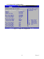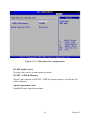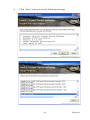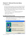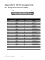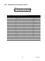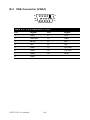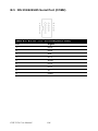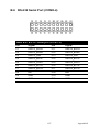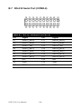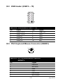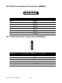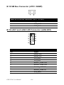
1
PCE-5124
LGA775 Intel® Core™ 2 Quad / Core™ 2
Duo Processor-based 800/1066/1333
MHz FSB PICMG 1.3 Single Host Board
with PCIe / DDR2 / Dual GbE LAN
User Manual
Copyright
This document is copyrighted, 2008, by Advantech Co., Ltd. All rights
are reserved. Advantech Co., Ltd. reserves the right to make improvements to the products described in this manual at any time without notice.
No part of this manual may be reproduced, copied, translated or transmitted in any form or by any means without the prior written permission of
Advantech Co., Ltd. Information provided in this manual is intended to
be accurate and reliable. However, Advantech Co., Ltd. assumes no
responsibility for its use, nor for any infringements upon the rights of
third parties which may result from its use.
Acknowledgements
• AMIBIOS is a trademark of American Megatrends Inc.
• IBM and PC are trademarks of International Business Machines Corporation.
• Intel, CoreTM 2 Quad, CoreTM 2 Duo are trademarks of Intel Corporation.
• WinBond is a trademark of Winbond Corporation.
• All other product names or trademarks are the properties of their
respective owners.
Part No. 2002512400 1st Edition
April 2008
PCE-5124 User Manual
ii
A Message to the Customer
Advantech Customer Services
Each and every Advantech product is built to the most exacting specifications to ensure reliable performance in the harsh and demanding conditions typical of industrial environments. Whether your new Advantech
equipment is destined for the laboratory or the factory floor, you can be
assured that your product will provide the reliability and ease of operation
for which the name Advantech has come to be known.
Your satisfaction is our primary concern. Here is a guide to Advantech’s
customer services. To ensure you get the full benefit of our services,
please follow the instructions below carefully.
Technical Support
We want you to get the maximum performance from your products. So if
you run into technical difficulties, we are here to help. For the most frequently asked questions, you can easily find answers in your product documentation. These answers are normally a lot more detailed than the ones
we can give over the phone.
So please consult this manual first. If you still cannot find the answer,
gather all the information or questions that apply to your problem, and
with the product close at hand, call your dealer. Our dealers are well
trained and ready to give you the support you need to get the most from
your Advantech products. In fact, most problems reported are minor and
are able to be easily solved over the phone.
In addition, free technical support is available from Advantech engineers
every business day. We are always ready to give advice on application
requirements or specific information on the installation and operation of
any of our products.
iii
Certifications
This device complies with the requirements in part 15 of the FCC rules:
Operation is subject to the following two conditions:
• This device may not cause harmful interference
• This device must accept any interference received, including interference that may cause undesired operation
This equipment has been tested and found to comply with the limits for a
Class A digital device, pursuant to Part 15 of the FCC Rules. These limits
are designed to provide reasonable protection against harmful interference when the equipment is operated in a commercial environment. This
equipment generates, uses, and can radiate radio frequency energy and, if
not installed and used in accordance with the instruction manual, may
cause harmful interference to radio communications. Operation of this
device in a residential area is likely to cause harmful interference in
which case the user will be required to correct the interference at his/her
own expense. The user is advised that any equipment changes or modifications not expressly approved by the party responsible for compliance
would void the compliance to FCC regulations and therefore, the user's
authority to operate the equipment.
Caution!
There is a danger of a new battery exploding if
it is incorrectly installed. Do not attempt to
recharge, force open, or heat the battery.
Replace the battery only with the same or
equivalent type recommended by the manufacturer. Discard used batteries according to the
manufacturer’s instructions.
PCE-5124 User Manual
iv
Memory Compatibility
Table 1.1: PCE-5124 Memory Tested for Compatibility
Brand
Size Speed Type ECC
Vendor Advantech
Memory
PN
PN
512 DDR
DDR2 N
MB 2 667
78.91G
N/A
92.420
ELPIDA E5108AG-6E-E
(64x8)
1
GB
78.01G
N/A
92.420
ELPIDA E5108AGBG6E-E (64x8)
DDR
DDR2 N
2 667
512 DDR
DDR2 N
MB 2 667
TS64M 96D2SEC K4T51083QC
LQ64V 512M667N
ZCE6 (64x8)
N-TR
6J
512 DDR
DDR2 N
MB 2 667
TS64M 96D2Micron 5XB32D9DCL
LQ64V 512M667N
(64x8)
N-TR
6J
Transcend 1
GB
DDR
DDR2 N
2 667
TS2QN 96D2SEC K4T51083QE
J23450 1G667NNZCE6 (64x8)
TR
-6S
2
GB
DDR
DDR2 N
2 667
TS256
MLQ64 N/A
V6U
Micron 7HE12 D9HNL
(128x8)
1
GB
DDR
DDR2 N
2 800
TS128
MLQ64 N/A
V8J
ProMOS
V59C1512804QBF25
(64x8)
2
GB
DDR
DDR2 N
2 667
TS256
MLQ64 N/A
V6U
SAMSUNG
K4T1G084QA-ZCE6
(128x8)
1
GB
DDR
DDR2 N
2 667
N/A
N/A
ELPIDA E5108AGBG6E-E (64x8)
1
GB
DDR
DDR2 N
2 800
N/A
N/A
ELPIDA E5108AHSE8E-E (64x8)
2
GB
DDR
DDR2 N
2 667
KVR66
7D2N5/ N/A
2G
Micron 7KE12 D9HNL
(128x8)
1
GB
DDR
DDR2 N
2 800
KVR80
0D2N5/ N/A
1G
ELPIDA E5108AHSE8E-E (64x8)
DSL
Kingston
Network Feature Comparison
Table 1.2: PCE-5124 comparison table
LAN/Model
PCE-5124G2
PCE-5124VG
LAN1: Intel 82566DM
Yes
Yes
LAN2: Intel 82573V
Yes
No
v
Product Warranty
Advantech warrants to you, the original purchaser, that each of its products will be free from defects in materials and workmanship for two years
from the date of purchase.
This warranty does not apply to any products which have been repaired or
altered by persons other than repair personnel authorized by Advantech,
or which have been subject to misuse, abuse, accident or improper installation. Advantech assumes no liability under the terms of this warranty as
a consequence of such events.
If an Advantech product is defective, it will be repaired or replaced at no
charge during the warranty period. For out-of-warranty repairs, you will
be billed according to the cost of replacement materials, service time and
freight. Please consult your dealer for more details.
If you think you have a defective product, follow these steps:
1.
Collect all the information about the problem encountered. (For
example, type of PC, CPU speed, Advantech products used, other
hardware and software used, etc.) Note anything abnormal and list
any on-screen messages you get when the problem occurs.
2.
Call your dealer and describe the problem. Please have your manual, product, and any helpful information readily available.
3.
If your product is diagnosed as defective, obtain an RMA (return
material authorization) number from your dealer. This allows us to
process your return more quickly.
4.
Carefully pack the defective product, a fully-completed Repair and
Replacement Order Card and a photocopy proof of purchase date
(such as your sales receipt) in a shippable container. A product
returned without proof of the purchase date is not eligible for warranty service.
5.
Write the RMA number visibly on the outside of the package and
ship it prepaid to your dealer.
PCE-5124 User Manual
vi
Initial Inspection
Before you begin installing your motherboard, please make sure that the
following materials have been shipped:
•
1 PCE-5124 PICMG 1.3 Single Host Board
•
1 PCE-5124 startup manual
P/N: 2002512410
•
1 CD with utility
P/N: 2062512400
•
1 FDD cable
P/N: 1700340640
•
1 User note for full-sized CPU card
P/N: 2002721020
•
2 Serial ATA HDD data cable
P/N: 1700003194
•
2 Serial ATA HDD power cable
P/N: 1703150102
•
1 COM + printer ports cable kit
P/N: 1701260305
•
1 4-port USB cable kit
P/N: 1700008461
•
Keyboard and mouse Y cable
P/N: 1700060202
•
1 jumper package
P/N: 9689000068
•
1 warranty card
P/N: 2190000902
If any of these items are missing or damaged, contact your distributor or
sales representative immediately. We have carefully inspected the PCE5124 mechanically and electrically before shipment. It should be free of
marks and scratches and in perfect working order upon receipt. As you
unpack the PCE-5124, check it for signs of shipping damage. (For example, damaged box, scratches, dents, etc.) If it is damaged or it fails to meet
the specifications, notify our service department or your local sales representative immediately. Also notify the carrier. Retain the shipping carton
and packing material for inspection by the carrier. After inspection, we
will make arrangements to repair or replace the unit.
vii
PCE-5124 User Manual
viii
Contents
Chapter
1 Hardware Configuration .................................2
1.1
1.2
1.3
Introduction ....................................................................... 2
Features & Benifits ........................................................... 3
Specifications .................................................................... 4
1.3.1
1.3.2
1.3.3
1.3.4
1.3.5
1.3.6
1.3.7
1.4
System............................................................................. 4
Memory........................................................................... 4
Input/Output.................................................................... 5
Graphics .......................................................................... 5
Ethernet LAN.................................................................. 5
Industrial features ........................................................... 5
Mechanical and environmental specifications................ 6
Jumpers and Connectors.................................................... 6
Table 1.1:Jumper list....................................................... 6
Table 1.2:Connector list.................................................. 7
1.5
Board Layout: Jumper and Connector Locations.............. 9
1.6
PCE-5124 Block Diagram............................................... 10
1.7
1.8
Safety Precautions .......................................................... 11
Jumper Settings ............................................................... 12
Figure 1.1:Jumper and connector locations .................... 9
Figure 1.2:PCE-5124 block diagram ............................ 10
1.8.1
1.8.2
1.8.3
1.8.4
1.9
1.10
1.11
1.12
Chapter
How to set jumpers ....................................................... 12
CMOS clear (CMOS1) ................................................. 12
Table 1.3:CMOS (CMOS1).......................................... 12
Watchdog timer output (JWDT1) ................................. 14
Table 1.4:Watchdog timer output (JWDT1)................. 14
COM2 RS-232/422/485 mode selector (JESTCOM2) . 16
Figure 1.3: COM2 RS-232/422/485 jumper setting ..... 16
Table 1.6:COM2 RS-232/422/485 mode selector ........ 16
Table 1.5: H/W monitor alarm (JOBS1)....................... 16
System Memory .............................................................. 18
Memory Installation Procedures ..................................... 19
Cache Memory ................................................................ 19
Processor Installation .......................... 19
2 Connecting Peripherals .................................22
2.1
2.2
2.3
2.4
2.5
2.6
Introduction ..................................................................... 22
Floppy Drive Connector (FDD1) .................................... 23
Parallel Port (LPT1) ........................................................ 24
USB Ports (USB12, USB34, USB56, USB78) ............... 25
VGA Connector (VGA1) ................................................ 26
Serial Ports (COM1, COM2, COM3-4 & COM5-6) ...... 27
ix
Table of Contents
2.7
2.8
2.9
PS/2 Keyboard and Mouse Connector (KBMS1) ........... 29
CPU Fan Connector (CPUFAN1) ................................... 30
Front Panel Connectors (JFP1, JFP2 & JFP3) ................ 31
2.9.1
2.9.2
2.9.3
2.9.4
2.9.5
Power LED and keyboard lock (JFP3) ......................... 31
Table 2.1:PS/2 or ATX power supply LED status........ 32
External speaker (JFP2) ................................................ 32
Reset connector (JFP1) ................................................. 32
HDD LED connector (JFP2)......................................... 32
ATX soft power switch (JFP1) ..................................... 32
2.10
2.11
H/W Monitor Alarm (JOBS1)......................................... 33
LAN Ports (LAN1 & LAN2) .......................................... 34
2.12
2.13
2.14
2.15
High Definition Audio Module Interface........................ 35
GPIO Header (GPIO1) .................................................... 36
Case Open Connector (JCASE1) .................................... 37
Front Panel LAN Indicator Connector (LANLED1) ...... 38
2.16
Serial ATA Interface (SATA1~SATA6) ........................ 39
Table 2.2:LAN LED indicator ...................................... 34
Table 2.3:Front Panel LAN Indicator Connector ......... 38
Chapter
3 AMI BIOS Setup ............................................42
Figure 3.1:Setup program initial screen........................ 42
3.1
Entering Setup ................................................................. 43
3.2
Main Setup ...................................................................... 44
Figure 3.2:Press Del to run Setup ................................. 43
3.2.1
3.3
Advanced BIOS Features Setup...................................... 45
3.3.1
3.3.2
3.3.3
3.3.4
3.3.5
3.4
Figure 3.3:Main setup screen........................................ 44
System time / System date ............................................ 44
Figure 3.4:Advanced BIOS features setup screen ........ 45
CPU configuration ........................................................ 46
Figure 3.5:CPU configuration setting........................... 46
IDE configuration ......................................................... 48
Figure 3.6:IDE configuration........................................ 48
Super I/O configuration ................................................ 49
Figure 3.7:Super I/O configuration............................... 49
Hardware health function.............................................. 51
Figure 3.8:Hardware health configuration.................... 51
APM configuration ....................................................... 52
Figure 3.9:APM configuration...................................... 52
Figure 3.10:Configure remote access type and parameters
................................................................... 53
PCI/PNP Setup ................................................................ 54
3.4.1
3.4.2
3.4.3
PCE-5124 User Manual
Figure 3.11:PCI/PNP setup........................................... 54
Clear NVRAM.............................................................. 54
Plug and play O/S ......................................................... 54
PCI latency timer .......................................................... 55
x
3.4.4
3.4.5
3.4.6
3.4.7
3.4.8
3.5
Allocate IRQ to PCI VGA ............................................ 55
Palette snooping............................................................ 55
PCI IDE BusMaster ...................................................... 55
Off board PCI/ISA IDE card ........................................ 55
IRQ................................................................................ 55
Boot Setup Utility............................................................ 56
Figure 3.12:Boot setup utility ....................................... 56
Figure 3.13:Boot setting configuration......................... 57
3.6
Security Setup ................................................................. 58
3.7
Advanced Chipset Settings.............................................. 59
Figure 3.14:Password configuration ............................. 58
Figure 3.15:Advanced Chipset Settings........................ 59
Figure 3.16:North bridge configuration........................ 60
Figure 3.17:Video function configuration .................... 61
Figure 3.18:South bridge configuration........................ 62
3.8
Exit Option ...................................................................... 63
3.8.1
3.8.2
3.8.3
3.8.4
Chapter
4 Chipset Software Install Utility.....................66
4.1
4.2
4.3
Chapter
Introduction ..................................................................... 78
Windows XP Driver Setup.............................................. 78
Using the OBS Hardware Doctor Utility ........................ 80
7 LAN Configuration ........................................84
7.1
7.2
7.3
7.4
Chapter
Introduction ..................................................................... 72
Windows XP Driver Setup.............................................. 72
6 Onboard Security Setup ................................78
6.1
6.2
6.3
Chapter
Before you Begin ............................................................ 66
Introduction ..................................................................... 66
Windows XP Driver Setup.............................................. 67
5 VGA Setup ......................................................72
5.1
5.2
Chapter
Figure 3.19:Exit option ................................................. 63
Save changes and exit ................................................... 63
Discard changes and exit .............................................. 64
Load optimal defaults ................................................... 64
Load fail-Safe defaults.................................................. 64
Introduction ..................................................................... 84
Features ........................................................................... 84
Installation....................................................................... 84
Win XP Driver Setup (LAN) .......................................... 85
8 SATA RAID Setup .........................................90
8.1
8.2
Introduction ..................................................................... 90
SATA RAID Driver and Utility Setup............................ 90
Appendix A Programming the Watchdog Timer .............92
xi
Table of Contents
A.1
Introduction ..................................................................... 92
A.1.1
A.1.2
A.1.3
Watchdog timer overview............................................. 92
Programming the watchdog timer................................. 92
Table A.1:Watchdog timer registers............................. 94
Example program.......................................................... 95
Appendix B I/O Pin Assignments.....................................102
B.1
Floppy Drive Connector (FDD1) .................................. 102
B.2
Parallel Port Connector (LPT1)..................................... 103
B.3
VGA Connector (VGA1) .............................................. 104
B.4
RS-232 Serial Port (COM1).......................................... 105
B.5
RS 232/422/485 Serial Port (COM2) ............................ 106
B.6
RS-232 Serial Port (COM3-4)....................................... 107
B.7
RS-232 Serial Port (COM5-6)....................................... 108
B.8
USB Header (USB12 ~ 78) ........................................... 109
B.9
PS/2 Keyboard/Mouse Connector (KBMS1)................ 109
Table B.1:Floppy drive connector (FDD1)................. 102
Table B.2:Parallel port connector (LPT1) .................. 103
Table B.3:VGA connector (VGA1)............................ 104
Table B.4:RS-232 serial port (COM1) ....................... 105
Table B.5:RS-232 / 422 / 485 serial port (COM2) ..... 106
Table B.6:RS-232 serial port (COM3-4) .................... 107
Table B.7:RS-232 serial port (COM5-6) .................... 108
Table B.8:USB Header (USB12 ~ 78)........................ 109
Table B.9:PS/2 keyboard/mouse connector
(KBMS1) ................................................... 109
B.10
External Keyboard Connector (KBMS2)...................... 110
B.11
CPU Fan Power Connector (CPUFAN1)...................... 110
B.12
Power LED and Keyboard Lock Connector (JFP3 /
PWR_LED & KEY LOCK) .......................................... 111
Table B.10:External keyboard connector (KBMS2) .. 110
Table B.11: CPU fan power connector (CPUFAN1) . 110
Table B.12:Power LED and keyboard lock connector
(JFP3 / PWR_LED & KEY LOCK)......... 111
B.13
External Speaker Connector (JFP2 / SPEAKER) ......... 111
Table B.13:External speaker connector (JFP2 / SPEAKER) ........................................................... 111
B.14
Reset Connector (JFP1 / RESET) ................................. 112
B.15
HDD LED (JFP2 / HDDLED) ...................................... 112
B.16
ATX Soft Power Switch (JFP1 / PWR_SW) ................ 113
Table B.14:Reset connector (JFP1 / RESET)............. 112
Table B.15:HDD LED (JFP2 / HDDLED)................. 112
Table B.16:ATX soft power switch
(JFP1 / PWR_SW).................................... 113
PCE-5124 User Manual
xii
B.17
Hi-definition Audio Link Connector (HDAUD1) ........ 113
Table B.17:Hi-definition audio link connector
(HDAUD1)............................................... 113
B.18
SM Bus Connector (JFP2 / SNMP)............................... 114
B.19
LAN1 and LAN2 LED Connector (LANLED1)........... 114
Table B.18:SM bus connector (JFP2 / SNMP)........... 114
Table B.19:LAN1 and LAN2 LED connector
(LANLED1) ............................................. 114
B.20
GPIO Header (GPIO1) .................................................. 115
B.21
System I/O Ports............................................................ 116
B.22
DMA Channel Assignments.......................................... 117
B.23
Interrupt Assignments ................................................... 118
B.24
1st MB Memory Map.................................................... 118
B.25
PCI Bus Map ................................................................. 119
Table B.20:GPIO header (GPIO1).............................. 115
Table B.21:System I/O ports ...................................... 116
Table B.22:DMA channel assignments ...................... 117
Table B.23:Interrupt assignments ............................... 118
Table B.24:1st MB memory map ............................... 118
Table B.25:PCI bus map............................................. 119
Appendix C Programming GPIO.....................................122
C.1
Supported GPIO Register.............................................. 122
C.1.1
C.1.2
GPIO registers............................................................. 122
GPIO example program-1........................................... 123
xiii
Table of Contents
PCE-5124 User Manual
xiv
CHAPTER
1
Hardware Configuration
1
Chapter 1
Chapter 1 Hardware Configuration
1.1 Introduction
PCE-5124 is a PICMG 1.3 form-factor single host board which is
designed with Intel Q35 plus ICH9DO platform for industrial applications that need high computing power and strong I/O capability.
PCE-5124 supports 45nm and 65nm manufacture technology Intel®
CoreTM 2 Duo, CoreTM 2 Quad, Pentium® Dual-Core and Celeron® 400
sequence processors with FSB up to 1333MHz and DDR2 667/800MHz
SDRAM up to 8GB. By supporting advanced computing technology,
PCE-5124 is suitable for computing power hungry industrial applications.
PCE-5124 performs excellent graphic processing capability by it's
embedded Intel® Graphics Media Accelerator 3100 with shared memory
up to 256MB. PCE-5124 can provide strong 2D/3D graphic processing
power without an add-on graphic card, it saves user extra cost, power
consumption and thermal design effort caused by an add-on graphic card.
PCE-5124 also has rich I/O interfaces, it's 6 SATA2 ports can support
software RAID 0, 1, 10, 5 to be a cost-effective data reliability solution,
the 6 on-board serial ports (COM ports) allows PCE-5124 to meet various
industrial control applications. With 1 PCI-E x 16 and 4 PCI-E x 1 lanes
go down to the backplane, PCE-5124 can expand various expansion slots
such as PCI, PCI-X and PCI-E slots with various backplanes.
With outstanding performance and exceptional features, PCE-5124 is the
very advanced computing platform for today's and tomorrow's up-andcoming industrial applications.
PCE-5124 User Manual
2
1.2 Features & Benifits
Features
Supporting Intel® Core
Benefits
TM
2 Quad
/ CoreTM 2 Duo / Pentium® Dualcore/ Celeron® 400 Series processors
Support Intel’s most advanced 45-nm and
65-nm manufacture technology, multi-core
processors that are with high performance
and low power consumption (U65W), suitable for applications that need strong
computing power and high reliability.
One PCI Express X 16 and Four X
1 to backplane
PCIe x 16 can support the most powerful
graphic cards for intense 3D graphic computing. 4 PCIe x 1 lanes can be flexibly
configured as various kinds of expansion
slots on the back plane for I/O card usage.
6 on-board SATA 2 ports supporting S/W RAID 0,1,5,10
A cost-saving solution to data storage protection and reliability.
Dual Gigabit Ethernet LAN via
dedicated PCI Express X1 ports
Providing high throughputs for heavy loading networking applications.
Six serial ports, 1 of RS232/422/
485, 5 of RS232.
Multi COM ports for automations such as
machine control, factory applications,
...etc.
3
Chapter 1
1.3 Specifications
1.3.1 System
• CPU: Intel Core 2 Quad / Core 2 Duo / Pentium Dual-core / Celeron
400 Sequence Processors with 800 / 1066 / 1333 MHz FSB.
• L2 Cache: Core 2 Quad: Maximum 12 MB
Core 2 Duo: Maximum 6 MB
Pentium Dual-core: Maximum 1 MB
Celeron 400: Maximum 512 MB
• BIOS: AMI SPI BIOS (32 Mb SPI)
• System Chipset: Q35 GMCH plus ICH9DO ICH
• SATA hard disk drive interface: Six onboard SATA2 connectors with
data transmission rates of up to 300 MB/s. These interfaces can be
enabled/disabled in the BIOS.
Note:
PCE-5124 does NOT support PATA(IDE) interface.
• Floppy disk drive interface: Supports one floppy disk drive, 5¼" (360
KB and 1.2 MB) or 3½" (720 KB, 1.44 MB). These interfaces can be
enabled/disabled in the BIOS.
1.3.2 Memory
• RAM: Up to 8 GB in four 240-pin DIMM sockets. Supports dual-channel DDR2 667 / 800 MHz SDRAM.
PCE-5124 User Manual
4
1.3.3 Input/Output
• PCI express lanes: One PCI-E x 16 and four PCI-E x 1 lanes to the
backplane.
• PCI bus: Four PCI masters to the backplane, 32-bit, 33 MHz PCI 2.2
compliant.
• Enhanced parallel port: This EPP/SPP/ECP port can be configured to
LPT1, LPT2, LPT3 or disabled. A standard DB-25 female connector
provided.
• Serial ports: Six serial ports, Five ones are of RS 232 and one is of RS232 / 422 / 485.
• PS/2 keyboard and mouse connector: One 6-pin mini-DIN connectors
is located on the mounting bracket for easy connection to a PS/2 keyboard and mouse via the Y-cable included in the package.
• USB port: Supports up to twelve USB 2.0 ports with transmission rate
up to 480 Mbps. 8 ports are on the CPU card and 4 ports are on the
backplane.
1.3.4 Graphics
• Controller: Intel® Graphics Media Accelerator 3100 embedded in the
GMCH.
• Display memory: Dynamically shared system memory up to 256 MB.
• CRT: Up to 2048 x 1536 resolution, 400 MHz RAMDAC.
• PCI express x16 slot on the backplane: An external graphic card can
be installed in the PCI-E x 16 slot for stronger 2D/3D graphic capability.
1.3.5 Ethernet LAN
• Supporting single/dual 10/100/1000Base-T Ethernet port(s) via the
dedicated PCI Express x1 bus which provides 500 MB/s data transmission rate.
• Controller:
LAN 1: Intel 82566DM (G2 version or VG version)
LAN 2: Intel 82573V (G2 Version)
1.3.6 Industrial features
• Watchdog timer: Can generate a system reset or IRQ11. The watchdog
timer is programmable, with each unit equal to one second or one
minute (255 levels).
5
Chapter 1
1.3.7 Mechanical and environmental specifications
• Operating temperature: 0 ~ 60° C (32 ~ 140° F, Depending on CPU)
• Storage temperature: -20 ~ 70° C (-4 ~ 158° F)
• Humidity: 20 ~ 95% non-condensing
• Power supply voltage: +3.3 V, +5 V, ±12 V
• Power consumption: Maximum: +5 V at 2.4 A, +3.3V at 3 A, +12 V
CPU: Intel Core 2 Quad Desktop Processor Q6200; Memory: 4 DDR2
800 MHz 1 GB DIMMs
Voltage
+12 V
+5 V
+3.3 V
Current
6.78 A
4.06 A 2.72 A
+5 VSB
-12 V
0.43 A
0
-5 V
0
• Board size: 338.58 mm (L) x 126.39 mm (W) (13.3" x 4.98")
• Board weight: 0.490 kg
1.4 Jumpers and Connectors
Connectors on the PCE-5124 single host board link it to external devices
such as hard disk drives and a keyboard. In addition, the board has a number of jumpers used to configure your system for your application.
The tables below list the function of each of the board jumpers and connectors. Later sections in this chapter give instructions on setting jumpers. Chapter 2 gives instructions for connecting external devices to your
motherboard.
Table 1.1: Jumper list
Label
Function
CMOS1
CMOS clear
JWDT1
Watchdog Reset
JOBS1
HW Monitor Alarm
PCE-5124 User Manual
6
Table 1.2: Connector list
Label
Function
FDD1
FDD connector
LPT1
Parallel port, Parallel port x 1, supports SPP/EPP/
ECP mode
LAN1
GbE LAN1 / Intel 82566DM
LAN2
GbE LAN2 / Intel 82573V
VGA1
VGA connector
KBMS1
PS/2 keyboard and mouse connector
KBMS2
External keyboard/mouse connector
COM1
Serial port: COM1; RS-232 (Box Header)
COM2
Serial port: COM2; RS-232 / 422 / 485
(G2 version: 9-pin Box Header; VG version: 9-pin
D-Sub)
COM3-4
Serial port: COM3; RS-232 (20-pin Box Header)
COM5-6
Serial port: COM4; RS-232 (20-pin Box Header)
JSETCOM2
COM2 RS-232/422/485 mode selection
JIR1
Infrared connector
JFP3
(Keyboard
Lock and
Power LED)
Suspend: Fast flash (ATX/AT)
Power
LED
System On: ON (ATX/AT)
System Off: OFF (AT)
System Off: Slow flash (ATX)
JFP2
External speaker / SATA HDD LED connector
JFP1
Power Switch / Reset connector
JCASE1
Case Open
CPUFAN1
CPU FAN connector (4-pin)
LANLED1
LAN1/2 LED extension connector
HDAUD1
Connector for HD audio extension module
USB12
USB port 1, 2
USB34
USB port 3, 4
USB56
USB port 5, 6
USB78
USB port 7, 8
SATA1
Serial ATA1
SATA2
Serial ATA2
SATA3
Serial ATA3
7
Chapter 1
Table 1.2: Connector list
Label
Function
SATA4
Serial ATA4
SATA5
Serial ATA5
SATA6
Serial ATA7
SP1
Buzzer
CPU1
CPU Socket
DIMMA1
Memory connector channel A
DIMMA2
Memory connector channel A
DIMMB1
Memory connector channel B
DIMMB2
Memory connector channel B
GPIO1
GPIO pin header (SMD pitch-2.0 mm)
PCE-5124 User Manual
8
1.5 Board Layout: Jumper and Connector Locations
CPUFAN1
CPUSOCKET
JFP1
JFP2
JFP3
DIMMA1
DIMMA2
DIMMB1
DIMMB2
CMOS1
HDAUD1
JCASE1
GPIO1
COM2
SATA1
USB12
FDD1
LPT1
COM56
COM34
JWDT1
J1R1
JOBS1
KBMS2
USB78
KBMS1
VGA1
LAN1 LAN2 COM1
LANLED1
JSETCOM2 SATA6
Figure 1.1: Jumper and connector locations
9
Chapter 1
1.6 PCE-5124 Block Diagram
TM
Core 2 Duo
Processor
800/1066/1333
MHz FSB
Channel A
On-board D-Sub
DDRII 667/800
CRT Output
Q35 GMCH
DDRII 667/800
PCIe x 16 Slot On
The Backplane
Channel B
Direct Media Interface
6 SATA2
Ports
300 MB/s
GLCI/PCI-Express*1
G-LAN1 :
Intel 82566
1 PCI-Express*1
G-LAN2 :
Intel 82573
HD
ALC 888
Codec
8 USB
Ports
2 GB/S bandwidth
ICH9 DO
USB 2.0/1.1
4 USB
PCI-Express*1
PCI-Express*1
PCI-Express*1
Connector C
LPC
SPI
BIOS
32 bit/33 MHz
PCI Bus
Super IO
Winbond
W83627HG
Figure 1.2: PCE-5124 block diagram
PCE-5124 User Manual
Connector A
PCI-Express*1
Ports
10
Connector D
1.7 Safety Precautions
Warning!
Always completely disconnect the power cord
from your chassis whenever you work with the
hardware. Do not make connections while the
power is on. Sensitive electronic components
can be damaged by sudden power surges. Only
experienced electronics personnel should open
the PC chassis.
Caution!
Always ground yourself to remove any static
charge before touching the motherboard. Modern electronic devices are very sensitive to
static electric charges. As a safety precaution,
use a grounding wrist strap at all times. Place
all electronic components on a static-dissipative
surface or in a static-shielded bag when they
are not in the chassis.
Caution!
The computer is provided with a battery-powered Real-time Clock. There is a danger of
explosion if battery is incorrectly replaced.
Replace only with same or equivalent type recommended by the manufacturer. Discard used
batteries according to manufacturer's instructions.
Caution!
There is a danger of a new battery exploding if
it is incorrectly installed. Do not attempt to
recharge, force open or heat the battery.
Replace the battery only with the same or
equivalent type recommended by the manufacturer. Discard used batteries according to the
manufacturer’s instructions.
11
Chapter 1
1.8 Jumper Settings
This section provides instructions on how to configure your motherboard
by setting the jumpers. It also includes the motherboard’s default settings
and your options for each jumper.
1.8.1 How to set jumpers
You can configure your motherboard to match the needs of your application by setting the jumpers. A jumper is a metal bridge that closes an electrical circuit. It consists of two metal pins and a small metal clip (often
protected by a plastic cover) that slides over the pins to connect them. To
“close” (or turn ON) a jumper, you connect the pins with the clip. To
“open” (or turn OFF) a jumper, you remove the clip. Sometimes a jumper
consists of a set of three pins, labeled 1, 2 and 3. In this case you connect
either pins 1 and 2, or 2 and 3. A pair of needle-nose pliers may be useful
when setting jumpers.
1.8.2 CMOS clear (CMOS1)
The PCE-5124 CPU card contains a jumper that can erase CMOS data
and reset the system BIOS information. Normally this jumper should be
set with pins 1-2 closed. If you want to reset the CMOS data, set J1 to 2-3
closed for just a few seconds, and then move the jumper back to 1-2
closed. This procedure will reset the CMOS to its default setting.
Table 1.3: CMOS (CMOS1)
Function
Jumper Setting
* Keep CMOS data
1-2 closed
Clear CMOS data
2-3 closed
* default setting
PCE-5124 User Manual
12
CMOS1
13
Chapter 1
1.8.3 Watchdog timer output (JWDT1)
The PCE-5124 contains a watchdog timer that will reset the CPU or send
a signal to IRQ11 in the event the CPU stops processing. This feature
means the PCE-5124 will recover from a software failure or an EMI
problem. The J2 jumper settings control the outcome of what the computer will do in the event the watchdog timer is tripped.
Table 1.4: Watchdog timer output (JWDT1)
Function
Jumper Setting
IRQ11
1
1-2 closed
* Reset
1
2-3 closed
*default setting
Note:
The interrupt output of the watchdog timer is a
low level signal. It will be held low until the
watchdog timer is reset.
PCE-5124 User Manual
14
JIR1
JOBS1
JWDT1
15
Chapter 1
Table 1.5: H/W monitor alarm (JOBS1)
Function
Jumper Setting
AT Mode
1
1-2 closed
ATX Mode
1
2-3 closed
(JOBS1) is a 2-pin connector for setting enable/disable alarm
while the on-board security event acts.
1.8.4 COM2 RS-232/422/485 mode selector (JESTCOM2)
Users can use JESTCOM2 to select among RS-232/422/485 modes for
COM2. The default setting is RS-232.
Figure 1.3: COM2 RS-232/422/485 jumper setting
Table 1.6: COM2 RS-232/422/485 mode selector
Function
Jumper Setting
RS-232
(5-6) + (7-9) + (8-10) + (13-15) + (14-16) closed
RS-422
(3-4) + (9-11) + (10-12) + (15-17) + (16-18) closed
RS-485
(1-2) + (9-11) + (10-12) + (15-17) + (16-18) closed
PCE-5124 User Manual
16
COM1
COM5-6
COM3-4 JSETCOM2
COM2
17
Chapter 1
1.9 System Memory
The PCE-5124 has four sockets for 240-pin dual inline memory modules
(DIMMs) in two memory channels.
All these sockets use 1.8 V unbuffered double data rate synchronous
DRAMs (DDR SDRAM). They are available in capacities of 256 MB,
512 MB, 1024 MB and 2 GB. The sockets can be filled in any combination with DIMMs of any size, giving a total memory size between 256
MB and 8 GB.
The PCE-5124 can accept DDR2 SDRAM memory chips without parity.
Also note that the PCE-5124 accepts DDR2 667/800 MHz SDRAM, and
DDR2 SDRAM. The PCE-5124 does NOT support ECC (error checking
and correction).
Note:
Because PCE-5124 supports Intel® Active
Management Technology 3.0 (iAMT 3.0) function, some capacity of system memory will be
taken for iAMT 3.0 usage. Please see detailed
description below.
• If both channels are occupied in the system are of the same size
(DIMMA1+DIMMB1 = DIMMA2 +
DIMMB2) then Intel AMT takes 32MB.
• If ch0 not equal ch1 (DIMMA1+DIMMB1 ≠
DIMMA2 + DIMMB2) then memory is
configured in interleaved+stacked mode
and Intel AMT takes only 16MB from
CH0.
• If no ch0 memory is used, then Intel AMT
would not function, then it does not
occupy any memory size.
Beside iAMT 3.0, due to PC architecture limitation, the memory capacity recognized by the
BIOS may be different from that is physically
installed in the DIMM slots.
PCE-5124 User Manual
18
1.10 Memory Installation Procedures
To install DIMMs, first make sure the two handles of the DIMM socket
are in the “open” position. i.e. the handles lean outward. Slowly slide the
DIMM module along the plastic guides on both ends of the socket. Then
press the DIMM module right down into the socket, until you hear a
click. This is when the two handles have automatically locked the memory module into the correct position of the DIMM socket. To remove the
memory module, just push both handles outward, and the memory module will be ejected by the mechanism in the socket.
Note:
Because PCE-5124 supports Intel Active Management Technology 3.0 (iAMT3.0) which utilizes some memory space of channel 0, it's
suggested that the user should not leave channel 0 DIMM slots (DIMMA1 and DIMMA2)
empty, or it may cause some system abnormality.
1.11 Cache Memory
Those CPUs supported by PCE-5124 have 12 MB, 8MB, 6 MB, 4MB,
3MB, 2MB, 1 MB, 512KB L2 cache memory sizes.
1.12 Processor Installation
Warning!
Without a fan or heat sink, the CPU will overheat and cause damage to both the CPU and
the single board computer. To install a CPU,
first turn off your system.
The PCE-5124 is designed for Intel® LGA 775 socket CPUs.
19
Chapter 1
Step 1. Pull the bar beside the CPU socket outward and lift it.
Step 2. Align the triangular marking on the processor with the cut edge of
the socket.
Step 3. Put the back socket cap and press down the bar to fix it.
PCE-5124 User Manual
20
CHAPTER
2
Connecting
Peripherals
21
Chapter 2
Chapter 2 Connecting Peripherals
2.1 Introduction
You can access most of the connectors from the top of the board as it is
being installed in the chassis. If you have a number of cards installed, you
may need to partially remove the card to make all the connections.
PCE-5124 User Manual
22
2.2 Floppy Drive Connector (FDD1)
LPT1
FDD1
You can attach up to two floppy disk drives to the PCE-5124's onboard
controller. You can use 3.5" (720 KB, 1.44 MB) drives.
The motherboard comes with a 34-pin daisy-chain drive connector cable.
On one end of the cable is a 34-pin flat-cable connector. On the other end
are two sets of 34-pin flat-cable connector (usually used for 3.5" drives).
The set on the end (after the twist in the cable) connects to the A: floppy
drive. The set in the middle connects to the B: floppy drive.
23
Chapter 2
2.3 Parallel Port (LPT1)
LPT1
FDD1
The parallel port is normally used to connect the motherboard to a printer.
The PCE-5124 includes an onboard parallel port, accessed through a 26pin flat-cable connector, LPT1.
PCE-5124 User Manual
24
2.4 USB Ports (USB12, USB34, USB56, USB78)
The PCE-5124 provides up to eight USB (Universal Serial Bus) ports
with complete Plug & Play and hot swap support for up to 127 external
devices. These USB ports comply with USB Specification Rev. 2.0, support transmission rates up to 480 Mbps and are fuse protected. The USB
interface can be disabled in the system BIOS setup.
USB12
USB78
25
Chapter 2
2.5 VGA Connector (VGA1)
VGA1
The PCE-5124 includes a VGA interface that can drive conventional
CRT displays. VGA1 is a standard 15-pin D-SUB connector commonly
used for VGA. Pin assignments for VGA1 are detailed in Appendix B.
PCE-5124 User Manual
26
2.6 Serial Ports (COM1, COM2, COM3-4 & COM5-6)
COM5-6
COM3-4
COM1
JESTCOM2
COM2
27
Chapter 2
The PCE-5124 offers six serial ports. The user can use JSETCOM2 to
select among RS-232/422/485 modes for COM2. These ports can connect
to serial devices, such as a mouse or a printer, or to a communications
network.
The IRQ and address ranges for both ports are fixed. However, if you
want to disable the port or change these parameters later, you can do this
in the system BIOS setup.
Different devices implement the RS-232/422/485 standards in different
ways. If you are having problems with a serial device, be sure to check
the pin assignments for the connector.
Note
There are two kinds of dual COM cable kits for
PCE-5124 COM port pin headers, if you need
to use more serial ports, you may purchase
them from Advantech.
PCE-5124 User Manual
1.
1701092300: 2.54 mm-pitch dualCOM port cable kit for COM 1-2
2.
1700008762: 2.00 mm-pitch dualCOM port cable kit for COM 3-4 and
COM 5-6
28
2.7 PS/2 Keyboard and Mouse Connector (KBMS1)
KBMS2
KBMS1
Two on-board 6-pin mini-DIN connectors (KBMS1) provide connection
to PS/2 keyboard and mouse by the Y-cable (1700060202) in the package.
The on-board KBMS2 pin header provide connection the the front panel
PS/2 keybaord and mouse connector of the chassis.
29
Chapter 2
2.8 CPU Fan Connector (CPUFAN1)
This connector supports cooling fans of 500 mA (6 W) or less.
CPUFAN1
PCE-5124 User Manual
30
2.9 Front Panel Connectors (JFP1, JFP2 & JFP3)
There are several external switches to monitor and control the PCE-5124.
JFP1~3
2.9.1 Power LED and keyboard lock (JFP3)
JFP3 is a 5-pin connector for the power LED. Refer to Appendix B for
detailed information on the pin assignments. If a PS/2 or ATX power supply is used, the system’s power LED status will be as indicated below:
31
Chapter 2
Table 2.1: PS/2 or ATX power supply LED status
Power mode
LED (PS/2 power)
LED (ATX power)
System On
On
On
System Suspend
Fast flashes
Fast flashes
System Off
Off
Slow flashes
2.9.2 External speaker (JFP2)
JFP2 is a 4-pin connector for an external speaker. The PCE-5124 provides
an onboard buzzer as an alternative to an external speaker. To enable the
buzzer, set pins 5 and 7 as closed.
2.9.3 Reset connector (JFP1)
Many computer cases offer the convenience of a reset button. Connect the
wire from the reset button.
2.9.4 HDD LED connector (JFP2)
You can connect an LED to connector JFP2 to indicate when the HDD is
active.
2.9.5 ATX soft power switch (JFP1)
If your computer case is equipped with an ATX power supply, you should
connect the power on/off button on your computer case to JFP1. This
connection enables you to turn your computer on and off.
PCE-5124 User Manual
32
2.10 H/W Monitor Alarm (JOBS1)
JIR1
JOBS1
JWDT1
Close: Enable OBS Alarm
Open: Disable OBS Alarm
33
Chapter 2
2.11 LAN Ports (LAN1 & LAN2)
LAN1 LAN2
The PCE-5124 is equipped with one or two high-performance 1000 Mbps
Ethernet LANs. They are supported by all major network operating systems. The RJ-45 jacks on the rear plate provide convenient connectivity.
Table 2.2: LAN LED indicator
Lan mode
Lan Indicator
1 Gbps Link on
LED1 Green on
100 Mbps Link on
LED1 Orange on
Active
LED2 Green flash
PCE-5124 User Manual
34
2.12 High Definition Audio Module Interface
HDAUD1
This HDAUD1 pin header is the connection interface to Advantech's 7.1
channel high definition audio module.
Note:
Advantech 7.1 channel high definition audio
module ordering information.
P/N: PCA-AUDIO-HDA1E
35
Chapter 2
2.13 GPIO Header (GPIO1)
GPIO1
Provides 14-Pins pin header for Digital I/O usage. Refer to Appendix B
for detailed information on the pin assignments and programming guide
in Appendix C.
PCE-5124 User Manual
36
2.14 Case Open Connector (JCASE1)
JCASE1
The 2-pin case open connector is for chassis with a case open sensor.
While opening the case, the buzzer on motherboard will beep.
37
Chapter 2
2.15 Front Panel LAN Indicator Connector (LANLED1)
Table 2.3: Front Panel LAN Indicator Connector
LAN Mode
Indicator
G-LAN Link ON
Green ON
G-LAN Active
Green Flash
G-LAN Link Off
Green OFF
LANLED1
PCE-5124 User Manual
38
2.16 Serial ATA Interface (SATA1~SATA6)
SATA1
SATA6
The PCE-5124 features high performance serial ATA interfaces (up to
300 MB/s) those eases cabling to hard drives or CD/DVD drives with thin
and long cables.
These six on-board SATA ports can be configured as RAID 0, 1, 10, 5.
Please see the detailed BIOS setting instruction of this in Chapter 3.
39
Chapter 2
CHAPTER
3
AMI BIOS Setup
41
Chapter 3
Chapter 3 AMI BIOS Setup
AMIBIOS has been integrated into many motherboards for over a decade.
In the past, people often referred to the AMIBIOS setup menu as BIOS,
BIOS setup or CMOS setup.
With the AMIBIOS Setup program, you can modify BIOS settings and
control the special features of your computer. The Setup program uses a
number of menus for making changes and turning the special features on
or off. This chapter describes the basic navigation of the PCE-5124 setup
screens.
Figure 3.1: Setup program initial screen
AMI’s BIOS ROM has a built-in Setup program that allows users to modify the basic system configuration. This type of information is stored in
battery-backed up CMOS so it retains the Setup information when the
power is turned off.
PCE-5124 User Manual
42
3.1 Entering Setup
Turn on the computer and check for the “patch” code. If there is a number
assigned to the patch code, it means that the BIOS supports your CPU. If
there is no number assigned to the patch code, please contact an Advantech application engineer to obtain an up-to-date patch code file. This will
ensure that your CPU’s system status is valid. After ensuring that you
have a number assigned to the patch code, press <DEL> and you will
immediately be allowed to enter Setup.
Figure 3.2: Press Del to run Setup
43
Chapter 3
3.2 Main Setup
When you first enter the BIOS Setup Utility, you will enter the Main
setup screen. You can always return to the Main setup screen by selecting
the Main tab. There are two Main Setup options. They are described in
this section. The Main BIOS Setup screen is shown below.
Figure 3.3: Main setup screen
The Main BIOS setup screen has two main frames. The left frame displays all the options that can be configured. Grayed-out options cannot be
configured; options in blue can be. The right frame displays the key legend.
Above the key legend is an area reserved for a text message. When an
option is selected in the left frame, it is highlighted in white. Often a text
message will accompany it.
3.2.1 System time / System date
Use this option to change the system time and date. Highlight System
Time or System Date using the <Arrow> keys. Enter new values through
the keyboard. Press the <Tab> key or the <Arrow> keys to move between
fields. The date must be entered in MM/DD/YY format. The time must be
entered in HH:MM:SS format.
PCE-5124 User Manual
44
3.3 Advanced BIOS Features Setup
Select the Advanced tab from the PCE-5124 setup screen to enter the
Advanced BIOS Setup screen. You can select any of the items in the left
frame of the screen, such as CPU Configuration, to go to the sub menu for
that item. You can display an Advanced BIOS Setup option by highlighting it using the <Arrow> keys. All Advanced BIOS Setup options are
described in this section. The Advanced BIOS Setup screens is shown
below. The sub menus are described on the following pages.
Figure 3.4: Advanced BIOS features setup screen
45
Chapter 3
3.3.1 CPU configuration
Figure 3.5: CPU configuration setting
C1E Support
Intel® CPU Enhanced Halt (C1E) function, a function to save CPU
power consumption in system halt state. When enabled, the CPU speed
and voltage will be reduced during system halt state to save power consumption. You may choose to enable or disable it.
Hardware Prefetcher
Hardware Prefetcher is a technique that fetches instructions and/or data
from memory into the CPU cache memory well before the CPU needs it,
so that it can improve the load-to-use latency. You may choose to enable
or disable it.
Adjacent Cache Line Prefetch
The Adjacent Cache-Line Prefetch mechanism, like automatic hardware
prefetch, operates without programmer intervention. When enabled
through the BIOS, two 64-byte cache lines are fetched into a 128-byte
sector, regardless of whether the additional cache line has been requested
or not. You may choose to enable or disable it.
PCE-5124 User Manual
46
Max CPUID Value Limit
This is disabled for Windows XP.
Intel(R) Virtualization Technology
This feature is used to enable or disable the Intel Virtualization Technology (IVT) extension. It allows multiple operating systems to run simultaneously on the same system. It does this by creating virtual machines,
each running its own x86 operating system.
Execute Disable Bit
This item specifies the Execute Disable Bit Feature. The settings are
Enabled and Disabled. The Optimal and Fail-Safe default setting is
Enabled. If Disabled is selected, the BIOS forces the XD feature flag to
always return to 0.
Core Multi-Processing
When this option disabled, BIOS disables one execution core.
PECI
You may choose to disable or enable the Platform Environment Control
Interface function.
47
Chapter 3
3.3.2 IDE configuration
Figure 3.6: IDE configuration
AHCI Configuration
AHCI is a new interface specification that allows the SATA controller
driver to support advanced features. While entering setup, BIOS auto
detects the presence of AHCI devices. This displays the status of auto
detection of AHCI devices.
PCE-5124 User Manual
48
3.3.3 Super I/O configuration
Figure 3.7: Super I/O configuration
49
Chapter 3
OnBoard Floppy Controller
This option allows the BIOS to Enable or Disable the floppy controller.
Floppy A
Select the type of floppy drive connected to the system. We suggest you
disable the floppy while installing Windows Vista without a floppy drive.
Floppy B
Select the type of floppy drive connected to the system.
Serial Port1 Address
This option configures serial port 1 base addresses.
Serial Port2 Address
This option configures serial port 2 base addresses.
Serial port2 Mode
This option configures serial port 2 mode.
Serial Port 3/4/5/6 Address
This option configures serial port 3/4 base addresses.
Serial Port 3/4/5/6 IRQ
This option configures serial port 3/4 base IRQ.
Parallel Port Address
This configures parallel port base addresses. The following options are
also available:
• Parallel Port Mode
• Parallel Port IRQ
PCE-5124 User Manual
50
3.3.4 Hardware health function
Figure 3.8: Hardware health configuration.
Hardware health function
Enable/Disable the onboard hardware monitor controller. If this option is
enabled, the BIOS and OBS utility can get the system board’s health
information from hardware monitor controller.
Chassis Intrusion
Enable/Disable the Chassis Intrusion monitoring function. When the case
is opened, the buzzer beeps.
Hardware health event monitoring
When the Hardware Health Function is enabled, the BIOS will display
hardware health information.
CPU warning temperature
Use this to set the CPU warning temperature threshold. When the system
reaches the warning temperature, the buzzer will beep.
51
Chapter 3
3.3.5 APM configuration
Figure 3.9: APM configuration
Power Management/APM
Enable or disable APM.
Video Power Down Mode
Set the Video Power Down mode to the Suspend or Standby mode.
Hard Disk Power Down Mode
Set Power Down Hard Disk mode to Suspend or Standby mode.
Suspend Time Out
Enter Suspend after the specified time.
Throttle Slow Clock Ratio
Select the duty cycle in throttle mode.
Keyboard & PS/2 Mouse
When you set this to Monitor, you can monitor the PS/2 keyboard and
mouse ports.
Power Button Mode
PCE-5124 User Manual
52
Power on, off or enter suspend mode when the power button is pressed.
The following options are also available.
• Resume On Ring: Disable/Enable RI wake event.
• Resume On LAN: Disable/Enable LAN PME wake event.
• Resume On RTC Alarm: Disable/Enable RTC wake event.
Figure 3.10: Configure remote access type and parameters
Remote Access
You can disable or enable the BIOS remote access feature here. This
function is used to redirect the console from the serial port. The Optimal
and Fail-Safe default setting is Disabled.
53
Chapter 3
3.4 PCI/PNP Setup
Select the PCI/PnP tab from the PCE-5124 setup screen to enter the Plug
and Play BIOS Setup screen. You can display a Plug and Play BIOS
Setup option by highlighting it using the <Arrow> keys. All Plug and
Play BIOS Setup options are described in this section. The Plug and Play
BIOS Setup screen is shown below.
Figure 3.11: PCI/PNP setup
3.4.1 Clear NVRAM
Set this value to force the BIOS to clear the Non-Volatile Random Access
Memory (NVRAM). The Optimal and Fail-Safe default setting is No.
3.4.2 Plug and play O/S
Set this value to allow the system to modify the settings for Plug and Play
operating system support. The Optimal and Fail-Safe default setting is
No.
PCE-5124 User Manual
54
3.4.3 PCI latency timer
Use this to adjust the PCI Latency Timer. This option sets the latency of
all PCI devices on the PCI bus. The Optimal and Fail-Safe default setting
is 64.
3.4.4 Allocate IRQ to PCI VGA
Set this value to allow or stop the system from giving the VGA adapter
card an interrupt address. The Optimal and Fail-Safe default setting is
Yes.
3.4.5 Palette snooping
Set this value to allow the system to modify the Palette Snooping settings.
The Optimal and Fail-Safe default setting is Disabled.
3.4.6 PCI IDE BusMaster
Set this value to allow or prevent the use of PCI IDE Busmastering. The
Optimal and Fail-Safe default setting is Disabled.
3.4.7 Off board PCI/ISA IDE card
Set this value to allow an add-on PCI/ISA IDE card to be selected. The
Optimal and Fail-Safe default setting is Auto.
3.4.8 IRQ
IRQ[3,4,5,7,9,10,11,14,15]:
• Available: Specified IRQ is available to be used by PCI/PnP devices.
• Reserved: Specified IRQ is reserved for use by Legacy ISA devices.
DMA Channel [0,1,3,5,6,7]:
• Available: Specified DMA is available to be used by PCI/PnP devices.
• Reserved: Specified DMA is reserved for use by legacy ISA devices.
• Reserved Memory Size: Size of memory block to reserve for legacy
ISA devices.
55
Chapter 3
3.5 Boot Setup Utility
Figure 3.12: Boot setup utility
PCE-5124 User Manual
56
Figure 3.13: Boot setting configuration
The following options are available:
• Quick Boot: Allows the BIOS to skip certain tests while booting. This
will decrease the time needed to boot the system.
• Quiet Boot: If this option is set to Disabled, the BIOS displays normal
POST messages. If Enabled, an OEM Logo is shown instead of POST
messages.
• Bootup Num-Lock: Select the Power-on state for Numlock.
• Wait For ‘F1’ If Error: Wait for the F1 key to be pressed if an error
occurs.
• Hit ‘DEL’ Message Display: Displays “Press DEL to run Setup” in
POST.
57
Chapter 3
3.6 Security Setup
Figure 3.14: Password configuration
Select Security Setup from the AIMB-556 Setup main BIOS setup menu.
All Security Setup options, such as password protection and virus protection are described in this section. To access the sub menu for the following items, select the item and press <Enter>:
• Change Supervisor Password
• Boot sector Virus protection: The boot sector virus protection will
warn if any program tries to write to the boot sector.
PCE-5124 User Manual
58
3.7 Advanced Chipset Settings
Figure 3.15: Advanced Chipset Settings
59
Chapter 3
Figure 3.16: North bridge configuration
The following options are available:
• Boots Graphic Adapter Priority: Select which graphics controller to
use as the primary boot device.
• Internal Graphics Mode Select: Select the amount of system memory
used by the Internal graphics device.
• PEG Port: Auto or Disabled.
• PEG Force x1: Enabled or Disabled.
PCE-5124 User Manual
60
Figure 3.17: Video function configuration
DVMT model select
Displays the active system memory mode.
DVMT / FIXED Memory
Specify the amount of DVMT / FIXED system memory to allocate for
video memory.
Spread spectrum clock
Enable/Disable spread spectrum.
61
Chapter 3
Figure 3.18: South bridge configuration
The following options are available:
• USB Functions: Disabled, 2 USB Ports, 4 USB Ports, 6 USB Ports or
8 USB Ports.
• USB 2.0 Controller: Enables or disables the USB 2.0 controller.
• GbE Controller: Enables or disables the GbE controller.
• GbE LAN boot: Enables or disables GbE LAN boot.
• LAN2 Controller: Enables or disables the LAN2 controller.
• HDA Controller: Enables or disables the HDA controller.
• SMBUS Controller: Enables or disables the SMBUS controller.
PCE-5124 User Manual
62
3.8 Exit Option
Figure 3.19: Exit option
3.8.1 Save changes and exit
When you have completed system configuration, select this option to
save your changes, exit BIOS setup and reboot the computer so the new
system configuration parameters can take effect.
1.
Select Exit Saving Changes from the Exit menu and press <Enter>.
The following message appears:
Save Configuration Changes and Exit Now?
[Ok] [Cancel]
2.
Select Ok or Cancel.
63
Chapter 3
3.8.2 Discard changes and exit
Select this option to quit Setup without making any permanent changes to
the system configuration.
1.
Select Exit Discarding Changes from the Exit menu and press
<Enter>. The following message appears:
Discard Changes and Exit Setup Now?
[Ok] [Cancel]
2.
Select Ok to discard changes and exit.
Discard Changes
3.
Select Discard Changes from the Exit menu and press <Enter>.
3.8.3 Load optimal defaults
The AIMB-556 automatically configures all setup items to optimal settings when you select this option. Optimal Defaults are designed for maximum system performance, but may not work best for all computer
applications. In particular, do not use the Optimal Defaults if your computer is experiencing system configuration problems. Select Load Optimal Defaults from the Exit menu and press <Enter>.
3.8.4 Load fail-Safe defaults
The AIMB-556 automatically configures all setup options to fail-safe settings when you select this option. Fail-Safe Defaults are designed for
maximum system stability, but not maximum performance. Select FailSafe Defaults if your computer is experiencing system configuration
problems.
1.
Select Load Fail-Safe Defaults from the Exit menu and press
<Enter>. The following message appears:
Load Fail-Safe Defaults?
[OK] [Cancel]
2.
Select OK to load Fail-Safe defaults.
PCE-5124 User Manual
64
CHAPTER
4
Chipset Software
Installation Utility
65
Chapter 4
Chapter 4 Chipset Software Install Utility
4.1 Before you Begin
To facilitate the installation of the enhanced display drivers and utility
software, read the instructions in this chapter carefully. The drivers for
the PCE-5124 are located on the software installation CD. The Intel
Chipset Software Installation Utility is not required on any systems running Windows NT 4.0. Updates are provided via Service Packs from
Microsoft.
Note:
The files on the software installation CD are
compressed. Do not attempt to install the drivers by copying the files manually. You must use
the supplied SETUP program to install the drivers.
Before you begin, it is important to note that most display drivers need to
have the relevant software application already installed in the system
prior to installing the enhanced display drivers. In addition, many of the
installation procedures assume that you are familiar with both the relevant software applications and operating system commands. Review the
relevant operating system commands and the pertinent sections of your
application software’s user manual before performing the installation.
4.2 Introduction
The Intel Chipset Software Installation (CSI) utility installs the Windows
INF files that outline to the operating system how the chipset components
will be configured. This is needed for the proper functioning of the following features:
• Core PCI and ISAPNP Services
• PCIe Support
• SATA Storage Support
• USB Support
PCA-6194 User Manual
66
• Identification of Intel (R) Chipset Components in the Device Manager
Note:
This utility is used for the following versions of
Windows, and it has to be installed before
installing all the other drivers:
•
Microsoft Windows Vista
•
Microsoft Windows Vista x64 Edition*
•
Microsoft Windows XP Professional x64
Edition
•
Microsoft Windows XP professional with
Service Pack 2
•
Microsoft Windows 2000 with Service Pack
4
4.3 Windows XP Driver Setup
1.
Insert the driver CD into your system’s CD-ROM drive. Select the
folder “Intel INF” then click “infinst_autol.exe”. A message pops
up telling you to install the CSI utility before other device drivers.
Windows XP is used as an example in the following steps.
2.
Click “Next” when you see the following message.
67
Chapter 4
3.
Click “Yes” when you see the following message.
PCA-6194 User Manual
68
4.
Click “Next” when you see the following message.
69
Chapter 4
5.
When the following message appears, click “Finish” to complete
the installation and restart Windows.
CHAPTER
5
VGA Setup
71
Chapter 5
Chapter 5 VGA Setup
5.1 Introduction
The Intel Q35 integrated graphics controller provides an analog display
port. You need to install the VGA driver to enable the function.
The Intel Q35 integrated graphics controller includes the following features.
• Graphics Media Accelerator 3100: Incorporating the latest Microsoft
DirectX 10 support capabilities, the Intel GMA 3100 GPU allows software developers to create lifelike environments and characters. Dual
independent display, enhanced display modes for widescreen flat panels, and optimized 3D support deliver an intense and realistic visual
experience without requiring a separate graphics card.
5.2 Windows XP Driver Setup
Note:
Before installing this driver, make sure the CSI
utility has been installed in your system. See
Chapter 4 for information on installing the CSI
utility.
Insert the driver CD into your system’s CD-ROM drive. Select the folder
“VGA” then click the proper VGA driver for the OS. Windows XP is
used as an example in the following steps.
PCE-5124 User Manual
72
1.
Click “Next” to continue the installation.
2.
You will see a welcome window. Please click “Yes” to continue the
installation. .
73
Chapter 5
3.
Click “Finish” to complete the installation and restart the computer
now or later.
PCE-5124 User Manual
74
75
Chapter 5
CHAPTER
6
Onboard Security
Setup
77
Chapter 6
Chapter 6 Onboard Security Setup
6.1 Introduction
The PCE-5124's hardware monitor is based on the Winbond W83627HG
chip. Onboard security (OBS) functions monitor key hardware to help
you maintain system stability and durability. The PCE-5124 can monitor
five sets of positive system voltages, two sets of system negative voltages, CPU cooling fan speed, and CPU temperature. The positive system
voltages that can be monitored include:
• CPU core voltage: 1.3 ~ 3.3 V, according to Intel specifications.
• Transmission voltage from CPU to chipset: typically 1.8 V.
• Chipset voltage: typically 3.3 V.
• Main voltage: +5 V, +12 V.
6.2 Windows XP Driver Setup
1.
Insert the driver CD into your system’s CD-ROM drive. Selecting
the folder “OBS” then click the “setup.exe”. Windows XP is used
as an example in the following steps.
2.
Click “Next” when you see the following message.
PCE-5124 User Manual
78
3.
Click “Next” when you see the following message.
4.
Click “Next” when you see the following message..
79
Chapter 6
5.
Click “Finish” when you see the following message.
6.3 Using the OBS Hardware Doctor Utility
After completing the setup, all the OBS functions are permanently
enabled. When a monitored reading exceeds safe limits, a warning message will be displayed and an error beep will sound to attract your attention.
OBS Hardware Doctor will show an icon on the right side of the bottom
window bar. This icon is the “Terminate and Stay Resident” (TSR) icon.
It will permanently remain in the bottom window bar, and will activate
warning signals when triggered by the onboard security system.
You can view or change values for various OBS settings by following
these steps.
From Windows desktop, click on “Start” and select “Programs”, select
“Win bond HWDoctor” and click “HWDOCTOR”. It is recommended
that you load the default values for all the OBS settings. However, if
desired, you can establish new conditions for voltage, fan speed and temperature.
PCE-5124 User Manual
80
81
Chapter 6
PCE-5124 User Manual
82
CHAPTER
7
LAN Configuration
83
Chapter 7
Chapter 7 LAN Configuration
7.1 Introduction
The PCE-5124 has a single/dual Gigabit Ethernet LAN interface (Intel
82566DM and 82573V) that is connected to a dedicated PCIe x1 link to
eliminating network bottlenecks by offering a bandwidth of up to 500
MB/s.
7.2 Features
• Integrated 10/100/1000Base-T transceiver
• 10/100/1000Base-T triple-speed MAC
• High-speed RISC core with 24-KB cache
• On-chip voltage regulation
• Wake-on-LAN (WOL) support
• PCIe x1 host interface
7.3 Installation
Note:
Before installing the LAN drivers, make sure the
CSI utility has been installed on your system.
See Chapter 4 for information on installing the
CSI utility.
The integrated PCE-5124 Intel gigabit Ethernet controller supports all
major network operating systems. However, the installation procedure
varies with different operating systems. In the following sections, refer to
the one that provides the driver setup procedure for the operating system
you are using.
PCE-5124 User Manual
84
7.4 Win XP Driver Setup (LAN)
1.
Insert the driver CD into your system’s CD-ROM drive. Selecting
the folder “LAN” then click the proper LAN driver for the OS.
Windows XP is used as an example in the following steps.
2.
You will see a welcome window. Click “Next” to continue the
installation.
85
Chapter 7
3.
Click “Install Driver” to start the installation procedure.
4.
Click “Yes” to continue the installation.
PCE-5124 User Manual
86
5.
Select “I accept the terms in the license agreement” and click
“Next” to continue.
6.
Select “Complete” and click “Next” to continue.
87
Chapter 7
7.
Click “Install” to begin the installation.
8.
Click “Finish” to complete the installation.
PCE-5124 User Manual
88
CHAPTER
8
SATA RAID Setup
89
Chapter 8
Chapter 8 SATA RAID Setup
8.1 Introduction
To support demanding disk I/O, Intel ICH9DO chipset integrates six
Serial ATA controllers with software RAID 0, 1, 5, 10 capabilities.
RAID 0 stripping increases the storage performance and is designed to
speed up data transfer rates for disk-intensive applications.
RAID 1 mirroring protects valuable data that might be lost in the event of
a hard drive failure.
RAID 5 array contains three or more hard drives where the data is divided
into manageable blocks called strips. Parity is a mathematical method for
recreating data that was lost from a single drive, which increases fault-tolerance. The data and parity are striped across all the hard drives in the
array. The parity is striped in a rotating sequence to reduce bottlenecks
associated with the parity calculations.
RAID 10 array uses four hard drives to create a combination of RAID
levels 0 and 1. The data is striped across a two-drive array forming the
RAID 0 component. Each of the drives in the RAID 0 array is then mirrored by a RAID 1 component.
8.2 SATA RAID Driver and Utility Setup
Note:
For the detail installation guide of SATA RAID
driver & utility please check the User Guide in
the driver CD. Path: \RAID\Manual
Note:
Before you install the Intel(R) Matrix Storage
Manager Please read the "readme.txt" which is
in the folder “RAID”.
The driver is in the CD’s “RAID” folder.You may go to the directory of
the CD and follow Intel's installation guide to install the driver and Utility.
PCE-5124 User Manual
90
Appendix
A
Programming the
Watchdog Timer
91
Appendix A
Appendix A Programming the Watchdog
Timer
A.1 Introduction
The PCE-5124’s watchdog timer can be used to monitor system software
operation and take corrective action if the software fails to function
within the programmed period. This section describes the operation of the
watchdog timer and how to program it.
A.1.1 Watchdog timer overview
The watchdog timer is built in to the W83627HG super I/O controller. It
provides the following user programmable functions:
• Can be enabled and disabled by user’s program
• Timer can be set from 1 to 255 seconds or 1 to 255 minutes
• Generates an interrupt or reset signal if the software fails to reset the
timer before time-out
A.1.2 Programming the watchdog timer
The I/O port address of the watchdog timer is 2E (hex) and 2F (hex). 2E
(hex) is the address port. 2F (hex) is the data port. You must first write an
address value into address port 2E (hex), then write/read data to/from the
assigned register through data port 2F (hex).
PCE-5124 User Manual
92
Unlock W83627HG
Select register of
watchdog timer
Enable the function of
the watchdog timer
Use the function of
the watchdog timer
Lock W83627HG
93
Appendix A
Table A.1: Watchdog timer registers
Address of
register (2E)
Attribute
Read/
Write
Value (2F)& description
87 (hex)
-----
Write this address to I/O address port 2E
(hex) twice to unlock the W83627HG
07 (hex)
write
Write 08 (hex) to select register of watchdog timer.
30 (hex)
write
Write 01 (hex) to enable the function of the
watchdog timer. Disabled is set as default.
F5 (hex)
write
Set seconds or minutes as units for the
timer. Write 0 to bit 3: set second as counting unit. [default]. Write 1 to bit 3: set minutes as counting unit
F6 (hex)
write
0: stop timer [default]
01~FF (hex): The amount of the count, in
seconds or minutes, depends on the value
set in register F5 (hex). This number
decides how long the watchdog timer waits
for strobe before generating an interrupt or
reset signal. Writing a new value to this
register can reset the timer to count with
the new value.
F7 (hex)
read/
write
Bit 6: Write 1 to enable keyboard to reset
the timer, 0 to disable.[default]
Bit 5: Write 1 to generate a timeout signal
immediately and automatically return to 0.
[default=0]
Bit 4: Read status of watchdog timer, 1
means timer is “timeout”.
AA (hex)
-----
Write this address to I/O port 2E (hex) to
lock the watchdog timer 2.
PCE-5124 User Manual
94
A.1.3 Example program
1.
Enable watchdog timer and set 10 sec. as timeout interval
;----------------------------------------------------------Mov dx,2eh
; Unlock W83627HG
Mov al,87h
Out dx,al
Out dx,al
;----------------------------------------------------------Mov al,07h
; Select registers of watchdog timer
Out dx,al
Inc
dx
Mov al,08h
Out dx,al
;----------------------------------------------------------Dec dx
; Enable the function of watchdog timer
Mov al,30h
Out dx,al
Inc
dx
Mov al,01h
Out dx,al
;----------------------------------------------------------Dec dx
; Set second as counting unit
Mov al,0f5h
Out dx,al
Inc
dx
In
al,dx
And al,not 08h
Out dx,al
;----------------------------------------------------------Dec dx
; Set timeout interval as 10 seconds and start counting
Mov al,0f6h
Out dx,al
95
Appendix A
Inc
dx
Mov al,10
Out dx,al
;----------------------------------------------------------Dec dx
; Lock W83627HG
Mov al,0aah
Out dx,al
2.
Enable watchdog timer and set 5 minutes as timeout interval
;----------------------------------------------------------Mov dx,2eh
; Unlock W83627HG
Mov al,87h
Out dx,al
Out dx,al
;----------------------------------------------------------Mov al,07h
; Select registers of watchdog timer
Out dx,al
Inc
dx
Mov al,08h
Out dx,al
;----------------------------------------------------------Dec dx
; Enable the function of watchdog timer
Mov al,30h
Out dx,al
Inc
dx
Mov al,01h
Out dx,al
;----------------------------------------------------------Dec dx
; Set minute as counting unit
Mov al,0f5h
Out dx,al
Inc
dx
PCE-5124 User Manual
96
In
al,dx
Or al,08h
Out dx,al
;----------------------------------------------------------Dec dx
; Set timeout interval as 5 minutes and start counting
Mov al,0f6h
Out dx,al
Inc
dx
Mov al,5
Out dx,al
;----------------------------------------------------------Dec dx
; Lock W83627HG
Mov al,0aah
Out dx,al
3.
Enable watchdog timer to be reset by mouse
;----------------------------------------------------------Mov dx,2eh
; Unlock W83627HG
Mov al,87h
Out dx,al
Out dx,al
;----------------------------------------------------------Mov al,07h
; Select registers of watchdog timer
Out dx,al
Inc
dx
Mov al,08h
Out dx,al
;----------------------------------------------------------Dec dx
; Enable the function of watchdog timer
Mov al,30h
Out dx,al
Inc
dx
97
Appendix A
Mov al,01h
Out dx,al
;----------------------------------------------------------Dec dx
; Enable watchdog timer to be reset by mouse
Mov al,0f7h
Out dx,al
Inc
dx
In
al,dx
Or al,80h
Out dx,al
;----------------------------------------------------------Dec dx
; Lock W83627HG
Mov al,0aah
Out dx,al
4.
Enable watchdog timer to be reset by keyboard
;----------------------------------------------------------Mov dx,2eh
; Unlock W83627HG
Mov al,87h
Out dx,al
Out dx,al
;----------------------------------------------------------Mov al,07h
; Select registers of watchdog timer
Out dx,al
Inc
dx
Mov al,08h
Out dx,al
;----------------------------------------------------------Dec dx
; Enable the function of watchdog timer
Mov al,30h
Out dx,al
Inc
dx
PCE-5124 User Manual
98
Mov al,01h
Out dx,al
;----------------------------------------------------------Dec dx
; Enable watchdog timer to be strobed reset by keyboard
Mov al,0f7h
Out dx,al
Inc
dx
In
al,dx
Or al,40h
Out dx,al
;----------------------------------------------------------Dec dx
; Lock W83627HG
Mov al,0aah
Out dx,al
5.
Generate a time-out signal without timer counting
;----------------------------------------------------------Mov dx,2eh
; Unlock W83627HG
Mov al,87h
Out dx,al
Out dx,al
;----------------------------------------------------------Mov al,07h
; Select registers of watchdog timer
Out dx,al
Inc
dx
Mov al,08h
Out dx,al
;----------------------------------------------------------Dec dx
; Enable the function of watchdog timer
Mov al,30h
Out dx,al
Inc
dx
99
Appendix A
Mov al,01h
Out dx,al
;----------------------------------------------------------Dec dx
; Generate a time-out signal
Mov al,0f7h
Out dx,al
Inc
dx
In
al,dx
;Write 1 to bit 5 of F7 register
Or al,20h
Out dx,al
;----------------------------------------------------------Dec dx
; Lock W83627HG
Mov al,0aah
Out dx,al
PCE-5124 User Manual
100
Appendix
B
I/O Pin Assignments
101
Appendix B
Appendix B I/O Pin Assignments
B.1 Floppy Drive Connector (FDD1)
33 31
3 1
34 32
4 2
Table B.1: Floppy drive connector (FDD1)
Pin
Signal
Pin
Signal
1
GND
2
FDHDIN*
3
GND
4
N/C
5
N/C
6
FDEDIN*
7
GND
8
INDEX*
9
GND
10
MOTOR 0*
11
GND
12
DRIVE SELECT 1*
13
GND
14
DRIVE SELECT 0*
15
GND
16
MOTOR 1*
17
GND
18
DIRECTION*
19
GND
20
STEP*
21
GND
22
WRITE DATA*
23
GND
24
WRITE GATE*
25
GND
26
TRACK 0*
27
GND
28
WRITE PROTECT*
29
GND
30
READ DATA*
31
GND
32
HEAD SELECT*
33
GND
34
DISK CHANGE*
* low active
PCE-5124 User Manual
102
B.2 Parallel Port Connector (LPT1)
25 23
3 1
26 24
4 2
Table B.2: Parallel port connector (LPT1)
Pin
Signal
Pin
Signal
1
STROBE*
2
AUTOFD*
3
D0
4
ERR
5
D1
6
INIT*
7
D2
8
SLCTINI*
9
D3
10
GND
11
D4
12
GND
13
D5
14
GND
15
D6
16
GND
17
D7
18
GND
19
ACK*
20
GND
21
BUSY
22
GND
23
PE
24
GND
25
SLCT
26
N/C
* low active
103
Appendix B
B.3 VGA Connector (VGA1)
5
1
10
6
15
11
Table B.3: VGA connector (VGA1)
Pin
Signal
Pin
Signal
1
RED
9
VCC
2
GREEN
10
GND
3
BLUE
11
N/C
4
N/C
12
SDT
5
GND
13
H-SYNC
6
GND
14
V-SYNC
7
GND
15
SCK
8
GND
PCE-5124 User Manual
104
B.4 RS-232 Serial Port (COM1)
9 7 5 3 1
8 6 4 2
Table B.4: RS-232 serial port (COM1)
Pin
Signal
1
DCD
2
DSR
3
RXD
4
RTS
5
TXD
6
CTS
7
DTR
8
RI
9
GND
10
N/A
105
Appendix B
B.5 RS 232/422/485 Serial Port (COM2)
Table B.5: RS-232 / 422 / 485 serial port (COM2)
Pin
Signal
1
DCD
2
DSR
3
SIN
4
RTS
5
SOUT
6
CTS
7
DTR
8
RI
9
GND
PCE-5124 User Manual
106
B.6 RS-232 Serial Port (COM3-4)
Table B.6: RS-232 serial port (COM3-4)
Pin
Signal
Pin
Signal
P1
UART3_#DCD
P11
UART4_#DCD
P2
UART3_#DSR
P12
UART4_#DSR
P3
UART3_SIN
P13
UART4_SIN
P4
UART3_#RTS
P14
UART4_#RTS
P5
UART3_SOUT
P15
UART4_SOUT
P6
UART3_#CTS
P16
UART4_#CTS
P7
UART3_#DTR
P17
UART4_#DTR
P8
RIC
P18
RID
P9
GND
P19
GND
P10
GND
P20
GND
107
Appendix B
B.7 RS-232 Serial Port (COM5-6)
Table B.7: RS-232 serial port (COM5-6)
Pin
Signal
Pin
Signal
P1
UART5_#DCD
P11
UART6_#DCD
P2
UART5_#DSR
P12
UART6_#DSR
P3
UART5_SIN
P13
UART6_SIN
P4
UART5_#RTS
P14
UART6_#RTS
P5
UART5_SOUT
P15
UART6_SOUT
P6
UART5_#CTS
P16
UART6_#CTS
P7
UART5_#DTR
P17
UART6_#DTR
P8
RIC
P18
RID
P9
GND
P19
GND
P10
GND
P20
GND
PCE-5124 User Manual
108
B.8 USB Header (USB12 ~ 78)
Table B.8: USB Header (USB12 ~ 78)
Pin
Signal
Pin
Signal
1
USB0_VCC5
6
USB1_D+
2
USB1_VCC5
7
GND
3
USB0_D-
8
GND
4
USB1_D-
9
GND
5
USB0_D+
10
Key
B.9 PS/2 Keyboard/Mouse Connector (KBMS1)
6
5
4
3
2
1
Table B.9: PS/2 keyboard/mouse connector
(KBMS1)
Pin
Signal
1
KB DATA
2
MS DATA
3
GND
4
VCC
5
KB CLOCK
6
MS CLOCK
109
Appendix B
B.10 External Keyboard Connector (KBMS2)
6
5
4
3
2
1
Table B.10:External keyboard connector (KBMS2)
Pin
Signal
1
KBCLK
2
KBDAT
3
MSDAT
4
GND
5
MSVCC
6
MSCLK
B.11 CPU Fan Power Connector (CPUFAN1)
1
2
3
4
Table B.11: CPU fan power connector (CPUFAN1)
Pin
Signal
1
GND
2
+12V
3
Detect
4
FANPWM
PCE-5124 User Manual
110
B.12 Power LED and Keyboard Lock Connector (JFP3 /
PWR_LED & KEY LOCK)
Table B.12:Power LED and keyboard lock connector (JFP3 /
PWR_LED & KEY LOCK)
Pin
Signal
1
LED power (+5 V)
2
NC
3
GND
4
KEYLOCK#
5
GND
B.13 External Speaker Connector (JFP2 / SPEAKER)
Table B.13:External speaker connector (JFP2 / SPEAKER)
Pin
Signal
1
SPK+
2
NC
3
SPK_IN
4
SPK-
111
Appendix B
B.14 Reset Connector (JFP1 / RESET)
Table B.14:Reset connector (JFP1 / RESET)
Pin
Signal
1
RESET #
2
GND
B.15 HDD LED (JFP2 / HDDLED)
Table B.15:HDD LED (JFP2 / HDDLED)
Pin
Signal
1
IDE LED+
2
IDE LED-
PCE-5124 User Manual
112
B.16 ATX Soft Power Switch (JFP1 / PWR_SW)
Table B.16:ATX soft power switch
(JFP1 / PWR_SW)
Pin
Signal
1
5VSB
2
PWR-BTN
B.17 Hi-definition Audio Link Connector (HDAUD1)
Table B.17:Hi-definition audio link connector (HDAUD1)
Pin
Signal
Pin
Signal
1
ACZ_VCC
2
GND
3
ACZ_SYNC
4
ACZ_BITCLK
5
ACZ_SDOUT
6
ACZ_SDIN0
7
ACZ_SDIN1
8
-ACZ_RST
9
ACZ_12V
10
GND
11
GND
12
N/C
113
Appendix B
B.18 SM Bus Connector (JFP2 / SNMP)
Table B.18:SM bus connector (JFP2 / SNMP)
Pin
Signal
1
SMB_DATA
2
SMB_CLK
B.19 LAN1 and LAN2 LED Connector (LANLED1)
1
3
5
7
9
2
4
6
8
Table B.19:LAN1 and LAN2 LED connector (LANLED1)
Pin
Signal
1
#LAN1_ACT
2
#LAN2_ACT
3
V33_AUX
4
V33_AUX
5
#LAN1_LINK1000
6
#LAN2_LINK1000
7
#LAN1_LINK100
8
#LAN2_LINK100
9
V33_AUX
PCE-5124 User Manual
114
B.20 GPIO Header (GPIO1)
1
3
5
7
9
11
13
2
4
6
8
10
12
14
Table B.20: GPIO header (GPIO1)
Pin
Signal
1
GPIO_1
2
GPIO_5
3
VCC_GPIO
4
GND
5
GPIO_2
6
GPIO_6
7
GND
8
GND
9
GPIO_3
10
GPIO_7
11
GND
12
GND
13
GPIO_4
14
GPIO_8
115
Appendix B
B.21 System I/O Ports
Table B.21:System I/O ports
Addr. range (Hex) Device
000-01F
DMA controller
020-021
Interrupt controller 1, master
022-023
Chipset address
040-05F
8254 timer
060-06F
8042 (keyboard controller)
070-07F
Real-time clock, non-maskable interrupt (NMI) mask
080-09F
DMA page register
0A0-0BF
Interrupt controller 2
0C0-0DF
DMA controller
0F0
Clear math co-processor
0F1
Reset math co-processor
0F8-0FF
Math co-processor
200-207
Game I/O
290-297
On-board hardware monitor
2F8-2FF
Serial port 2
378-37F
Parallel printer port 1 (LPT2)
3B0-3BF
Intel(R) Q35 Express Chipset Family
3C0-3CF
Intel(R) Q35 Express Chipset Family
3D0-3DF
Color/graphics monitor adapter
3F0-3F7
Diskette controller
3F8-3FF
Serial port 1
2F8-2FF
Serial port 2
400-41F
SM bus controller
480-4BF
CPU card resource
400-4D1
CPU card resource
4E0-4E7
Serial port 6
4E8-4EF
Serial port 4
4F0-4F7
Serial port 5
4F8-4FF
Serial port 3
PCE-5124 User Manual
116
800-87F
Power management
B.22 DMA Channel Assignments
Table B.22:DMA channel assignments
Channel
Signal
0
Available
1
Available
2
Floppy disk (8-bit transfer)
3
Available
4
Cascade for DMA controller 1
5
Available
6
Available
7
Available
117
Appendix B
B.23 Interrupt Assignments
Table B.23:Interrupt assignments
Priority
Interrupt#
Interrupt source
1
NMI
Parity error detected
2
IRQ0
Interval timer
3
IRQ1
Keyboard
-
IRQ2
Interrupt from controller 2 (cascade)
4
IRQ8
Real-time clock
5
IRQ9
Cascaded to INT 0A (IRQ 2)
6
IRQ10
Serial Port 4, 6
7
IRQ11
Serial Port 3, 5
8
IRQ12
PS/2 mouse
9
IRQ13
INT from co-processor
10
IRQ14
Primary IDE Channel
11
IRQ15
Secondary IDE Channel
12
IRQ3
Serial communication port 2
13
IRQ4
Serial communication port 1
14
IRQ5
NA
15
IRQ6
NA
16
IRQ7
Parallel port 1 (print port)
B.24 1st MB Memory Map
Table B.24:1st MB memory map
Addr. range (Hex)
Device
E0000h - FFFFFh
BIOS
CC000h - DFFFFh
Unused
C0000h - CBFFFh
VGA BIOS
A0000h - BFFFFh
Video Memory
00000h - 9FFFFh
Base memory
PCE-5124 User Manual
118
B.25 PCI Bus Map
Table B.25:PCI bus map
Signal
IDSEL
INT# pin
GNT
REQ
PCI slot 1
AD31
INT B,C,D,A
GNT A
REQ A
PCI slot 2
AD30
INT C, D, A, B
GNT B
REQ B
PCI slot 3
AD29
INT D,A,B,C
GNT C
REQ C
PCI slot 4
AD28
INT A, B, C, D
GNT D
REQ D
119
Appendix B
PCE-5124 User Manual
120
Appendix
C
Programming the
GPIO
121
Appendix C
Appendix C Programming GPIO
C.1 Supported GPIO Register
Below are the detailed descriptions of the GPIO addresses and programming sample.
C.1.1 GPIO registers
CRF0 (GP10-GP17 I/O selection register. Default 0xFF)
When set to a '1', respective GPIO port is programmed as an input port.
When set to a '0', respective GPIO port is programmed as an output port.
CRF1 (GP10-GP17 data register. Default 0x00)
If a port is programmed to be an output port, then its respective bit can be
read/written.
If a port is programmed to be an input port, then its respective bit can
only be read.
CRF2 (GP10-GP17 inversion register. Default 0x00)
When set to a '1', the incoming/outgoing port value is inverted.
When set to a '0', the incoming/outgoing port value is the same as in data
register.
Extended Function Index Registers (EFIRs)
The EFIRs are write-only registers with port address 2Eh or 4Eh on PC/
AT systems.
Extended Function Data Registers (EFDRs)
The EFDRs are read/write registers with port address 2Fh or 4Fh on PC/
AT systems.
PCE-5124 User Manual
122
C.1.2 GPIO example program-1
-----------------------------------------------Enter the extended function mode, interruptible double-write
-----------------------------------------------MOV DX,4EH
MOV AL,87H
OUT DX,AL
OUT DX,AL
--------------------------------------------------------------Configurate logical device 7(GP10~GP17), configuration register
CRF0,CRF1,CRF2
--------------------------------------------------------------MOV DX,4EH
MOV AL,07H ; Point to Logical Device Number Reg.
OUT DX,AL
MOV DX,4FH
MOV AL,07H ; Select logical device 7
OUT DX,AL ;
MOV DX,4EH
MOV AL,F0
OUT DX,AL
MOV DX,4FH
MOV AL,00H ; 01:Input 00:output for GP10~GP17
OUT DX,AL
MOV DX,4EH
MOV AL,F2H ;
OUT DX,AL
MOV DX,4FH
MOV AL,00H
;Set GPIO is normal not inverter
OUT DX,AL;
MOV DX,4EH
MOV AL,F1H
123
Appendix C
OUT DX,AL
MOV DX,4FH
MOV AL,??H ; Put the output value into AL
OUT DX,AL
-----------------------------------------Exit extended function mode |
-----------------------------------------MOV DX,4EH
MOV AL,AAH
OUT DX,AL
PCE-5124 User Manual
124