1
REJ09B0019-0120
R8C/10 Group
16
Hardware Manual
RENESAS 16-BIT SINGLE-CHIP MICROCOMPUTER
M16C FAMILY / R8C /Tiny SERIES
All information contained in these materials, including products and product specifications,
represents information on the product at the time of publication and is subject to change by
Renesas Technology Corp. without notice. Please review the latest information published
by Renesas Technology Corp. through various means, including the Renesas Technology
Corp. website (http://www.renesas.com).
Rev. 1.20
Revision date: Jan 27, 2006
www.renesas.com
Keep safety first in your circuit designs!
1.
Renesas Technology Corp. puts the maximum effort into making semiconductor products
better and more reliable, but there is always the possibility that trouble may occur with
them. Trouble with semiconductors may lead to personal injury, fire or property damage.
Remember to give due consideration to safety when making your circuit designs, with appropriate measures such as (i) placement of substitutive, auxiliary circuits, (ii) use of nonflammable material or (iii) prevention against any malfunction or mishap.
Notes regarding these materials
1.
2.
3.
4.
5.
6.
7.
8.
These materials are intended as a reference to assist our customers in the selection of the
Renesas Technology Corp. product best suited to the customer's application; they do not
convey any license under any intellectual property rights, or any other rights, belonging to
Renesas Technology Corp. or a third party.
Renesas Technology Corp. assumes no responsibility for any damage, or infringement of
any third-party's rights, originating in the use of any product data, diagrams, charts, programs, algorithms, or circuit application examples contained in these materials.
All information contained in these materials, including product data, diagrams, charts, programs and algorithms represents information on products at the time of publication of these
materials, and are subject to change by Renesas Technology Corp. without notice due to
product improvements or other reasons. It is therefore recommended that customers contact Renesas Technology Corp. or an authorized Renesas Technology Corp. product distributor for the latest product information before purchasing a product listed herein.
The information described here may contain technical inaccuracies or typographical errors.
Renesas Technology Corp. assumes no responsibility for any damage, liability, or other
loss rising from these inaccuracies or errors.
Please also pay attention to information published by Renesas Technology Corp. by various means, including the Renesas Technology Corp. Semiconductor home page (http://
www.renesas.com).
When using any or all of the information contained in these materials, including product
data, diagrams, charts, programs, and algorithms, please be sure to evaluate all information as a total system before making a final decision on the applicability of the information
and products. Renesas Technology Corp. assumes no responsibility for any damage, liability or other loss resulting from the information contained herein.
Renesas Technology Corp. semiconductors are not designed or manufactured for use in a
device or system that is used under circumstances in which human life is potentially at
stake. Please contact Renesas Technology Corp. or an authorized Renesas Technology
Corp. product distributor when considering the use of a product contained herein for any
specific purposes, such as apparatus or systems for transportation, vehicular, medical,
aerospace, nuclear, or undersea repeater use.
The prior written approval of Renesas Technology Corp. is necessary to reprint or reproduce in whole or in part these materials.
If these products or technologies are subject to the Japanese export control restrictions,
they must be exported under a license from the Japanese government and cannot be imported into a country other than the approved destination.
Any diversion or reexport contrary to the export control laws and regulations of Japan and/
or the country of destination is prohibited.
Please contact Renesas Technology Corp. for further details on these materials or the
products contained therein.
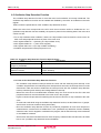
How to Use This Manual
1.
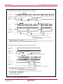
Introduction
This hardware manual provides detailed information on the R8C/10 Group of microcomputers.
Users are expected to have basic knowledge of electric circuits, logical circuits and microcomputers.
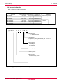
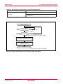
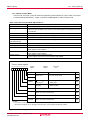
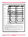
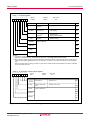
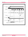
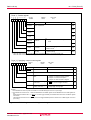
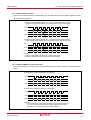
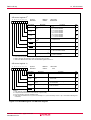
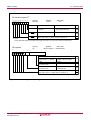
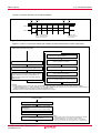
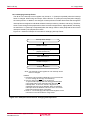
2.
Register Diagram
The symbols, and descriptions, used for bit function in each register are shown below.
*1
XXX register
b7
b6
b5
b4
b3
b2
0
b1
b0
Symbol
XXX
Address
XXX
Bit symbol
XXX0
Bit Name
XXX Bit
XXX1
(b2)
(b3)
XXX4
After reset
00h
*5
Function
RW
1 0: XXX
0 1: XXX
1 0: Avoid this setting
1 1: XXX
RW
RW
Nothing is assigned.
When write, should set to "0". When read, its content is indeterminate.
*3
Reserved Bit
Must set to “0”
RW
XXX Bit
Function varies depending on each
operation mode
RW
XXX5
WO
XXX6
RW
XXX7
XXX Bit
*2
b1 b0
0: XXX
1: XXX
*4
RO
*1
Blank:Set to “0” or “1” according to the application
0: Set to “0”
1: Set to “1”
X: Nothing is assigned
*2
RW: Read and write
RO: Read only
WO: Write only
−: Nothing is assigned
*3
•Reserved bit
Reserved bit. Set to specified value.
*4
•Nothing is assigned
Nothing is assigned to the bit concerned. As the bit may be use for future functions,
set to “0” when writing to this bit.
•Do not set to this value
The operation is not guaranteed when a value is set.
•Function varies depending on mode of operation
Bit function varies depending on peripheral function mode.
Refer to respective register for each mode.
*5
Follow the text in each manual for binary and hexadecimal notations.
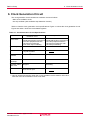
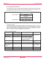
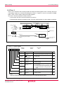
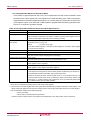
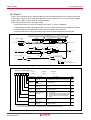
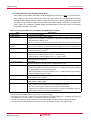
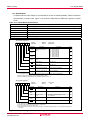
3.
M16C Family Documents
The following documents were prepared for the M16C family. (1)
Document
Contents
Short Sheet
Hardware overview
Data Sheet
Hardware overview and electrical characteristics
Hardware Manual
Hardware specifications (pin assignments, memory maps, peripheral
specifications, electrical characteristics, timing charts).
*Refer to the application note for how to use peripheral functions.
Detailed description of assembly instructions and microcomputer
performance of each instruction
Software Manual
Application Note
• Usage and application examples of peripheral functions
• Sample programs
• Introduction to the basic functions in the M16C family
• Programming method with Assembly and C languages
RENESAS TECHNICAL UPDATE
Preliminary report about the specification of a product, a document,
etc.
NOTES:
1. Before using this material, please visit the our website to verify that this is the most updated
document available.
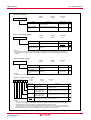
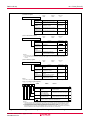
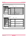
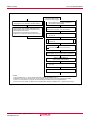
Table of Contents
SFR Page Reference
Chapter 1. Overview ............................................................. 1
1.1
1.2
1.3
1.4
1.5
1.6
Applications ................................................................................................................... 1
Performance Overview .................................................................................................. 2
Block Diagram ............................................................................................................... 3
Product Information ...................................................................................................... 4
Pin Assignments ............................................................................................................ 5
Pin Description .............................................................................................................. 6
Chapter 2. Central Processing Unit (CPU) ......................... 7
2.1 Data Registers (R0, R1, R2 and R3 ) ............................................................................. 7
2.2 AddressRegisters (A0 and A1) ...................................................................................... 8
2.3 Frame Base Register( FB ) ............................................................................................. 8
2.4 Interrupt Table Register (INTB )..................................................................................... 8
2.5 Program Counter (PC ) ................................................................................................... 8
2.6 User Stack Pointer (USP ) and Interrupt Stack Pointer (ISP )..................................... 8
2.7 Static Base Register (SB ) ............................................................................................. 8
2.8 Flag Register (FLG ) ....................................................................................................... 8
2.8.1 Carry Flag ( C Flag ) ................................................................................................................................ 8
2.8.2 Debug Flag ( D Flag ) .............................................................................................................................. 8
2.8.3 Zero Flag ( Z Flag ) .................................................................................................................................. 8
2.8.4 Sign Flag ( S Flag ) .................................................................................................................................. 8
2.8.5 Register Bank Select Flag ( B Flag ) ..................................................................................................... 8
2.8.6 Overflow Flag ( O Flag) ........................................................................................................................... 8
2.8.7 Interrupt Enable Flag ( I Flag ) ............................................................................................................... 8
2.8.8 Stack Pointer Select Flag ( U Flag ) ....................................................................................................... 8
2.8.9 Processor Interrupt Priority Level ( IPL ) .............................................................................................. 8
2.8.10 Reserved Area ....................................................................................................................................... 8
Chapter 3. Memory ............................................................... 9
Chapter 4. Special Function Registers (SFR) .................. 10
Chapter 5. Reset .................................................................. 14
5.1 Hardware Reset ............................................................................................................ 14
5.2 Software Reset .............................................................................................................. 14
5.3 Watchdog Timer Reset ................................................................................................. 14
Chapter 6. Clock Generation Circuit.................................. 17
6.1 Main Clock ..................................................................................................................... 21
6.2 On-Chip Oscillator Clock ............................................................................................. 22
A-1
6.3 CPU Clock and Peripheral Function Clock ................................................................ 23
6.3.1 CPU Clock .............................................................................................................................................. 23
6.3.2 Peripheral Function Clock (f1, f2, f8, f32, fAD, f1SIO, f8SIO, f32SIO) ....................................................... 23
6.3.3 fRING and fRING128 ................................................................................................................................................................... 23
6.4 Power Control ............................................................................................................... 24
6.4.1 Normal Operation Mode ....................................................................................................................... 24
6.4.2 Wait Mode .............................................................................................................................................. 25
6.4.3 Stop Mode .............................................................................................................................................. 26
6.5 Oscillation Stop Detection Function ........................................................................... 28
6.5.1 How to Use Oscillation Stop Detection Function .............................................................................. 28
Chapter 7. Protection .......................................................... 30
Chapter 8. Processor Mode ................................................ 31
8.1 Types of Processor Mode ............................................................................................ 31
Chapter 9. Bus ..................................................................... 32
Chapter 10. Interrupt ........................................................... 33
10.1 Interrupt Overview ...................................................................................................... 33
10.1.1 Type of Interrupts ................................................................................................................................ 33
10.1.2 Software Interrupts ............................................................................................................................. 34
10.1.3 Hardware Interrupts ............................................................................................................................ 35
10.1.4 Interrupts and Interrupt Vector .......................................................................................................... 36
10.1.5 Interrupt Control ................................................................................................................................. 38
______
10.2 INT Interrupt ................................................................................................................ 46
________
10.2.1 INT0 Interrupt ...................................................................................................................................... 46
_______
10.2.2 INT0 Input Filter ................................................................................................................................... 47
______
______
10.2.3 INT1 Interrupt and INT2 Interrupt ...................................................................................................... 48
______
10.2.4 INT3 Interrupt ...................................................................................................................................... 49
10.3 Key Input Interrupt ..................................................................................................... 50
10.4 Address Match Interrupt ............................................................................................ 51
Chapter 11. Watchdog Timer .............................................. 53
Chapter 12. Timers .............................................................. 55
12.1 Timer X ........................................................................................................................... 56
12.1.1 Timer Mode .......................................................................................................................................... 58
12.1.2 Pulse Output Mode ............................................................................................................................. 59
12.1.3 Event Counter Mode ........................................................................................................................... 60
12.1.4 Pulse Width Measurement Mode ....................................................................................................... 61
12.1.5 Pulse Period Measurement Mode ..................................................................................................... 63
12.2 Timer Y ........................................................................................................................... 65
12.2.1 Timer Mode .......................................................................................................................................... 68
12.2.2 Programmable Waveform Generation Mode .................................................................................... 70
12.3 Timer Z ........................................................................................................................... 73
12.3.1 Timer Mode .......................................................................................................................................... 76
12.3.2 Programmable Waveform Generation Mode .................................................................................... 78
A-2
12.3.3 Programmable One-shot Generation Mode ...................................................................................... 80
12.3.4 Programmable Wait One-shot Generation Mode ............................................................................. 83
12.4 Timer C ........................................................................................................................ 86
Chapter 13. Serial Interface ................................................ 89
13.1 Clock Synchronous Serial I/O Mode ......................................................................... 94
13.1.1 Polarity Select Function ..................................................................................................................... 97
13.1.2 LSB First/MSB First Select Function ................................................................................................ 97
13.1.3 Continuous Receive Mode ................................................................................................................. 98
13.2 Clock Asynchronous Serial I/O (UART) Mode ......................................................... 99
13.2.1 TxD10/RxD1 Select Function (UART1) ............................................................................................ 102
13.2.2 TxD11 Select Function (UART1) ...................................................................................................... 102
13.2.3 Bit Rate .............................................................................................................................................. 103
Chapter 14. A/D Converter................................................ 104
14.1 One-shot Mode ......................................................................................................... 108
14.2 Repeat Mode ............................................................................................................. 109
14.3 Sample & Hold .......................................................................................................... 110
14.4 A/D conversion cycles ........................................................................................... 110
14.5 Internal Equivalent Circuit of Analog Input ........................................................... 111
14.6 Inflow Current Bypass Circuit ................................................................................ 112
14.7 Output Impedance of Sensor under A/D Conversion........................................... 113
Chapter 15. Programmable I/O Ports .............................. 115
15. 1 Description ............................................................................................................... 115
15.1.1 Port Pi Direction Register (PDi Register, i = 0, 1, 3, 4) ................................................................... 115
15.1.2 Port Pi Register (Pi Register, i = 0 to 4)........................................................................................... 115
15.1.3 Pull-up Control Register 0, Pull-up Control Register 1 (PUR0 and PUR1 Registers) ................. 115
15.1.4 Port P1 Drive Capacity Control Register (DRR Register) .............................................................. 115
15.2 Port setting ................................................................................................................ 122
15.3 Unassigned Pin Handling ........................................................................................ 128
Chapter 16. Electrical Characteristics ............................. 129
Chapter 17. Flash Memory Version ................................. 140
17.1 Overview .................................................................................................................... 140
17.2 Memory Map .............................................................................................................. 141
17.3 Functions To Prevent Flash Memory from Rewriting............................................ 142
17.3.1 ID Code Check Function .................................................................................................................. 142
17.4 CPU Rewrite Mode .................................................................................................... 143
17.4.1 EW0 Mode .......................................................................................................................................... 144
17.4.2 EW1 Mode .......................................................................................................................................... 144
17.4.3 Software Commands ........................................................................................................................ 150
17.4.4 Status Register .................................................................................................................................. 154
17.4.5 Full Status Check .............................................................................................................................. 155
17.5 Standard Serial I/O Mode ......................................................................................... 157
17.5.1 ID Code Check Function .................................................................................................................. 157
A-3
Chapter 18. On-chip Debugger ........................................ 161
18.1 Address Match Interrupt .......................................................................................... 161
18.2 Single Step Interrupt ................................................................................................ 161
18.3 UART1 ........................................................................................................................ 161
18.4 BRK Instrucstion ...................................................................................................... 161
Chapter 19. Usage Notes .................................................. 162
19.1 Stop Mode and Wait Mode ....................................................................................... 162
19.1.1 Stop Mode .......................................................................................................................................... 162
19.1.2 Wait Mode .......................................................................................................................................... 162
19.2 Interrupts ................................................................................................................... 163
19.2.1 Reading Address 0000016 ............................................................................................................................................ 163
19.2.2 SP Setting .......................................................................................................................................... 163
19.2.3 External Interrupt and Key Input Interrupt ..................................................................................... 163
19.2.4 Watchdog Timer Interrupt ................................................................................................................ 163
19.2.5 Changing Interrupt Factor ................................................................................................................ 164
19.2.6 Changing Interrupt Control Register .............................................................................................. 165
19.3 Clock Generation Circuit ......................................................................................... 166
19.3.1 Oscillation Stop Detection Function ............................................................................................... 166
19.3.2 Oscillation Circuit Constants ........................................................................................................... 166
19.4 Timers ........................................................................................................................ 167
19.3.1 Timers X, Y and Z .............................................................................................................................. 167
19.3.2 Timer X ............................................................................................................................................... 167
19.3.3 Timer Y ............................................................................................................................................... 167
19.3.4 Timer Z ............................................................................................................................................... 167
19.3.5 Timer C ............................................................................................................................................... 167
19.5 Serial Interface .......................................................................................................... 168
19.6 A/D Converter............................................................................................................ 169
19.7 Flash Memory Version ............................................................................................. 170
19.7.1 CPU Rewrite Mode ............................................................................................................................ 170
19.8 Noise .......................................................................................................................... 173
Chapter 20. Usage Notes for On-chip Debugger ............ 174
Appendix 1 Package Dimensions .................................... 175
Appendix 2 Connecting Examples for Serial Writer and
On-chip Debugging Emulator .......................................... 176
Appendix 3 Example of Oscillation Evaluation Circuit .. 178
Register Index ................................................................... 179
A-4
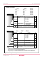
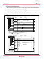
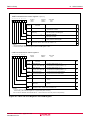
SFR Page Reference
Address
Register
Symbol Page
000016
Address
004016
000116
004116
000216
004216
000516
000616
000716
PM0
PM1
CM0
CM1
31
31
19
19
004416
Address match interrupt enable register AIER
Protect register
PRCR
52
30
004916
Oscillation stop detection register
Watchdog timer reset register
Watchdog timer start register
Watchdog timer control register
Address match interrupt register 0
20
54
54
54
52
004C16
Processor mode register 0
Processor mode register 1
System clock control register 0
System clock control register 1
004516
004616
004716
004816
000816
000916
000A16
004A16
004B16
000B16
000C16
000D16
000E16
000F16
001016
OCD
WDTR
WDTS
WDC
RMAD0
004D16
004E16
005116
005216
001316
005316
RMAD1
005416
52
001516
005516
001616
005616
001716
005716
001816
005816
001916
005916
001A16
005A16
001B16
005B16
001C16
005C16
005D16
001D16
001E16
INT0 input filter select register
INT0F
KUPIC
ADIC
39
39
UART0 transmit interrupt control register
UART0 receive interrupt control register
UART1 transmit interrupt control register
UART1 receive interrupt control register
INT2 interrupt control register
Timer X interrupt control register
Timer Y interrupt control register
Timer Z interrupt control register
INT1 interrupt control register
INT3 interrupt control register
Timer C interrupt control register
S0TIC
S0RIC
S1TIC
S1RIC
INT2IC
TXIC
TYIC
TZIC
INT1IC
INT3IC
TCIC
39
39
39
39
39
39
39
39
39
39
39
INT0 interrupt control register
INT0IC
39
005016
001216
Address match interrupt register 1
Key input interrupt control register
AD conversion interrupt control register
004F16
001116
001416
Symbol Page
004316
000316
000416
Register
005E16
46
001F16
005F16
002016
006016
002116
006116
002216
006216
002316
006316
002416
006416
002516
006516
002616
006616
002716
006716
002816
006816
002916
006916
002A16
006A16
002B16
006B16
002C16
006C16
002D16
006D16
002E16
006E16
002F16
006F16
003016
007016
003116
007116
003216
007216
003316
007316
003416
007416
003516
007516
003616
007616
003716
007716
003816
007816
003916
007916
003A16
007A16
003B16
007B16
003C16
007C16
003D16
007D16
003E16
007E16
003F16
007F16
Blank columns are all reserved space. No use is allowed.
B-1
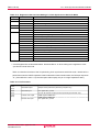
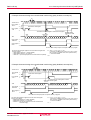
SFR Page Reference
Address
008016
008116
008216
008316
008416
008516
008616
008716
Symbol Page
TYZMR 65/73
PREY
66
TYSC
66
TYPR
66
Timer Y, Z waveform output control register PUM 67/75
Prescaler Z register
PREZ
74
Timer Z secondary register
TZSC
74
Timer Z primary register
TZPR
74
Register
Timer Y, Z mode register
Prescaler Y register
Timer Y secondary register
Timer Y primary register
00C016
008C16
008D16
008E16
00C316
00C416
00C516
00C616
00C716
00C816
00C916
Timer Y, Z output control register
Timer X mode register
Prescaler X register
Timer X register register
Timer count source setting register
TYZOC 66/74
TXMR 56
PREX 57
TX
57
TCSS
57
00CA16
00CB16
00CC16
00CD16
00CE16
00CF16
008F16
009016
Timer C register
TC
87
00D016
009116
00D116
009216
00D216
009316
00D316
009416
00D416
009516
00D516
009616
External input enable register
INTEN
46
00D616
00D716
009716
009816
Key input enable register
KIEN
50
Timer C control register 0
Timer C control register 1
Capture register
TCC0
TCC1
TM0
87
87
87
009B16
009C16
00DC16
00DE16
00DF16
UART0 transmit/receive mode register
UART0 bit rate generator
UART0 transmit buffer register
U0MR
U0BRG
U0TB
92
91
91
U0C0
U0C1
U0RB
92
93
91
U1MR
U1BRG
U1TB
92
91
91
00E016
00E116
00E216
00A316
00A416
00E316
00A516
UART0 transmit/receive control register 0
UART0 transmit/receive control register 1
00A616
UART0 receive buffer register
00E516
UART1 transmit/receive mode register
00A916
UART1 bit rate register
UART1 transmit buffer register
00E816
Port P3 register
P3
120
Port P3 direction register
Port P4 register
PD3
P4
120
120
00EA16
Port P4 direction register
PD4
120
00EB16
UART1 receive buffer register
U1C0
U1C1
U1RB
92
93
91
UART transmit/receive control register 2
UCON
93
00AD16
UART1 transmit/receive control register 0
UART1 transmit/receive control register 1
00AE16
00EC16
00ED16
00EE16
00AF16
00B016
120
120
120
120
00E916
00AB16
00AC16
P0
P1
PD0
PD1
00E616
00E716
00A816
Port P0 register
Port P1 register
Port P0 direction register
Port P1 direction register
00E416
00A716
00AA16
ADCON0 106
ADCON1 106
00DB16
00DD16
00A216
AD control register 0
AD control register 1
00DA16
009E16
00A116
ADCON2 107
00D916
009D16
009F16
00A016
AD control register 2
00D816
009916
009A16
Symbol Page
AD
107
00C216
008916
008B16
AD register
00C116
008816
008A16
Register
Address
00EF16
00F016
00B116
00F116
00B216
00F216
00B316
00F316
00B416
00F416
00B516
00F516
00B616
00F616
00B716
00F716
00B816
00F816
00B916
00F916
00BA16
03FA16
00BB16
00FB16
00BC16
00FC16
00BD16
00FD16
00BE16
00FE16
00BF16
00FF16
Pull-up control register 0
PUR0
Pull-up control register 1
PUR1
Port P1 drive capacity control register DRR
121
121
121
Flash memory control register 4
FMR4
147
Flash memory control register 1
FMR1
147
Flash memory control register 0
FMR0
146
Blank columns are all reserved space. No use is allowed.
01B316
01B416
01B516
01B616
01B716
B-2
R8C/10 Group
SINGLE-CHIP 16-BIT CMOS MICROCOMPUTER
REJ09B0019-0120
Rev.1.20
Jan 27, 2006
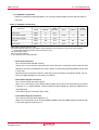
1. Overview
This MCU is built using the high-performance silicon gate CMOS process using a R8C/Tiny Series CPU
core and is packaged in a 32-pin plastic molded LQFP. This MCU operates using sophisticated instructions
featuring a high level of instruction efficiency. With 1M bytes of address space, it is capable of executing
instructions at high speed.
1.1 Applications
Electric household appliance, office equipment, housing equipment (sensor, security), general industrial
equipment, audio, etc.
Rev.1.20 Jan 27, 2006
REJ09B0019-0120
page 1 of 180
R8C/10 Group
1. Overview
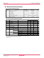
1.2 Performance Overview
Table 1.1. lists the performance outline of this MCU.
Table 1.1 Performance outline
Item
Performance
CPU
Number of basic instructions 89 instructions
Minimum instruction execution time 62.5 ns (f(XIN) = 16 MHZ, VCC = 3.0 to 5.5 V)
100 ns (f(XIN) = 10 MHZ, VCC = 2.7 to 5.5 V)
Operating mode
Single-chip
Address space
1M bytes
Memory capacity
See Table 1.2 “Product List”
Peripheral
Port
Input/Output: 22 (including LED drive port), Input: 2
function
LED drive port
I/O port: 8
Timer
Timer X: 8 bits x 1 channel, Timer Y: 8 bits x 1 channel,
Timer Z: 8 bits x 1 channel
(Each timer equipped with 8-bit prescaler)
Timer C: 16 bits x 1 channel
(Input capture circuit)
Serial interface
•1 channel
Clock synchronous, UART
•1 channel
UART
A/D converter
10-bit A/D converter: 1 circuit, 8 channels
Watchdog timer
15 bits x 1 (with prescaler)
Interrupt
Internal: 9 factors, External: 5 factors,
Software: 4 factors, Priority level: 7 levels
Clock generation circuit
2 circuits
•Main clock generation circuit (Equipped with a built-in
feedback resistor)
•On-chip oscillator
Oscillation stop detection function Main clock oscillation stop detection function
Electrical
Supply voltage
VCC = 3.0 to 5.5 V (f(XIN) = 16 MHZ)
characteristics
VCC = 2.7 to 5.5 V (f(XIN) = 10 MHZ)
Power consumption
Typ. 8mA (VCC = 5.0 V, (f(XIN) = 16MHZ)
Typ. 5mA (VCC = 3.0 V, (f(XIN) = 10MHZ)
Typ. 35µA (VCC = 3.0 V, Wait mode, Peripheral clock off)
Typ. 0.7µA (VCC = 3.0 V, Stop mode)
Flash memory Program/erase supply voltage VCC = 2.7 to 5.5 V
Program/erase endurance
100 times
Operating ambient temperature
-20 to 85 °C
-40 to 85 °C (D-version)
Package
32-pin plastic mold LQFP
Rev.1.20 Jan 27, 2006
REJ09B0019-0120
page 2 of 180
R8C/10 Group
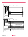
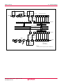
1. Overview
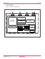
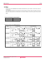
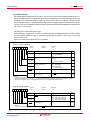
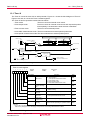
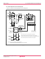
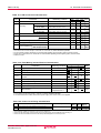
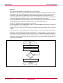
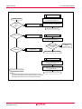
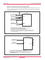
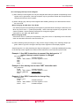
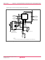
1.3 Block Diagram
Figure 1.1 shows this MCU block diagram.
8
8
I/O port
Port P0
1
5
Port P3
Port P1
2
Port P4
Peripheral functions
Timer
Timer X (8 bits)
Timer Y (8 bits)
Timer Z (8 bits)
Timer C (16 bits)
A/D converter
(10 bits ✕ 8 channels)
System clock generator
UART or Clock synchronous
serial I/O
(8 bits ✕ 1 channel)
XIN-XOUT
On-chip oscillator
UART
(8 bits ✕ 1 channel)
Memory
R8C/Tiny Series CPU core
Watchdog timer
(15 bits)
R0H
R1H
R0L
R1L
R2
R3
SB
(1)
RAM
(2)
ISP
INTB
A0
A1
FB
ROM
USP
PC
FLG
Multiplier
NOTES:
1. ROM size depends on MCU type.
2. RAM size depends on MCU type.
Figure 1.1 Block Diagram
Rev.1.20 Jan 27, 2006
REJ09B0019-0120
page 3 of 180
R8C/10 Group
1. Overview
1.4 Product Information
Table 1.2 lists the product inforamation.
Table 1.2 Product Information
As of January 2006
ROM capacity
RAM capacity
R5F21102FP
8K bytes
512 bytes
PLQP0032GB-A
R5F21103FP
12K bytes
768 bytes
PLQP0032GB-A
R5F21104FP
16K bytes
1K bytes
PLQP0032GB-A
R5F21102DFP
8K bytes
512 bytes
PLQP0032GB-A
R5F21103DFP
12K bytes
768 bytes
PLQP0032GB-A
R5F21104DFP
16K bytes
1K bytes
PLQP0032GB-A
Type No.
Type No. R 5 F
Remarks
Package type
Flash memory version
D version
21 10 4 D FP
Package type:
FP : PLQP0032GB-A
Classification:
D: Operating ambient temperature –40 °C to 85 °C
No symbol: Operating ambient temperature –20 °C to 85 °C
ROM capacity:
2 : 8 KBytes.
3 : 12 KBytes.
4 : 16 KBytes.
R8C/10 group
R8C/Tiny series
Memory type:
F: Flash memory version
Renesas MCU
Renesas semiconductors
Figure 1.2 Type No., Memory Size, and Package
Rev.1.20 Jan 27, 2006
REJ09B0019-0120
page 4 of 180
R8C/10 Group
1. Overview
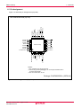
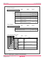
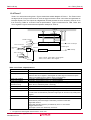
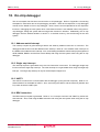
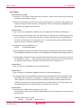
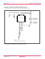
1.5 Pin Assignment
Figure 1.3 shows the pin Assignments (top view).
P33/INT3/TCIN
P30/CNTR0
AVSS
P31/TZOUT
AVCC/VREF
P32/INT2/CNTR1
P07/AN0
I VC C
PIN CONFIGURATION (top view)
24 23 22 21 20 19 18 17
P06/AN1
P05/AN2
P04/AN3
MODE
P03/AN4
P02/AN5
P01/AN6
P00/AN7/TxD11
25
26
27
28
29
30
31
32
R8C/10 Group
16
15
14
13
12
11
10
9
P45/INT0
P10/KI0
P11/KI1
P12/KI2
P13/KI3
P14/TxD0
P15/RxD0
P16/CLK0
RESET
XOUT/P47 (1)
VSS
XIN/P46
VC C
P17/INT1/CNTR0
P37/TxD10/RxD1
CNVSS
1 2 3 4 5 6 7 8
NOTES:
1. P47 functions only as an input port.
2. When using On-chip debugger, do not use pins P00/AN7/TxD11
and P37/TxD10/RxD1.
3. Do not connect IVcc to Vcc.
Package: PLQP0032GB-A (32P6U-A)
Figure 1.3 Pin Assignments (Top View)
Rev.1.20 Jan 27, 2006
REJ09B0019-0120
page 5 of 180
R8C/10 Group
1. Overview
1.6 Pin Description
Table 1.3 shows the pin description
Table 1.3 Pin description
Signal name
Power supply
input
IVcc
Pin name
Vcc,
Vss
IVcc
Analog power
supply input
AVcc,
AVss
Reset input
CNVss
MODE
Main clock input
RESET
CNVss
MODE
XIN
I/O type
I
O
I
Power supply input pins for A/D converter. Connect the
AVcc pin to Vcc. Connect the AVss pin to Vss. Connect a
capacitor between pins AVcc and AVss.
I
I
I
I
Input “L” on this pin resets the MCU.
Connect this pin to Vss via a resistor.(1)
Connect this pin to Vcc via a resistor.
These pins are provided for the main clock generating circuit I/O. Connect a ceramic resonator or a crystal oscillator between the XIN and XOUT pins. To use
an externally derived clock, input it to the XIN pin and
leave
the XOUT pin open.
______
INT interrupt input pins.
Key input interrupt pins.
Timer X I/O pin
Timer X output pin
Timer Y I/O pin
Timer Z output pin
Timer C input pin
Transfer clock I/O pin.
Serial data input pins.
Serial data output pins.
___________
Main clock output XOUT
_____
_______
O
_______
INT interrupt input INT
0 to_____
INT3
_____
Key input interrupt KI0 to KI3
Timer X
CNTR0
____________
CNTR0
Timer Y
CNTR1
Timer Z
TZOUT
Timer C
TCIN
Serial interface
CLK0
RxD0, RxD1
TxD0, TxD10,
TxD11
Reference voltage VREF
input
A/D converter
AN0 to AN7
I/O port
P00 to P07,
P10 to P17,
P30 to P33, P37,
P45
I
I
I/O
O
I/O
O
I
I/O
I
O
Input port
I
P46, P47
Function
Apply 2.7 V to 5.5 V to the Vcc pin. Apply 0 V to the
Vss pin.
This pin is to stabilize internal power supply.
Connect this pin to Vss via a capacitor (0.1 µF).
Do not connect to Vcc.
I
I
I/O
Reference voltage input pin for A/D converter. Connect the VREF pin to Vcc.
Analog input pins for A/D converter
These are 8-bit CMOS I/O ports. Each port has an I/O
select direction register, allowing each pin in that port
to be directed for input or output individually.
Any port set to input can select whether to use a pullup resistor or not by program.
P10 to P17 also function as LED drive ports.
Port for input-only.
NOTES :
1. Refer to "19.8 Noise" for the connecting reference resistor value.
Rev.1.20 Jan 27, 2006
REJ09B0019-0120
page 6 of 180
R8C/10 Group
2. Central Processing Unit (CPU)
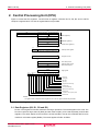
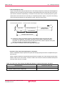
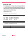
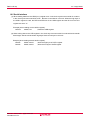
2. Central Processing Unit (CPU)
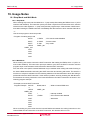
Figure 2.1 shows the CPU registers. The CPU has 13 registers. Of these, R0, R1, R2, R3, A0, A1 and FB
comprise a register bank. Two sets of register banks are provided.
b31
b15
b8 b7
b0
R2
R0H (high-order of R0)
R0L (high-order of R0)
R3
R1H (high-order of R1)
R1L (high-order of R1)
R2
Data registers(1)
R3
A0
b19
A1
Address registers(1)
FB
Frame base registers(1)
b15
b0
INTBH
INTBL
Interrupt table register
The 4-high order bits of INTB are INTBH and
the 16-low bits of INTB are INTBL.
b19
b0
PC
Program counter
b15
b0
USP
User stack pointer
ISP
Interrupt stack pointer
SB
Static base register
b15
b0
FLG
b15
b8
IPL
b7
U I
Flag register
b0
O B S Z D C
Carry flag
Debug flag
Zero flag
Sign flag
Register bank select flag
Overflow flag
Interrupt enable flag
Stack pointer select flag
Reserved bit
Processor interrupt priority level
Reserved bit
NOTES:
1. A regist er bank co mpr ises t hese regist ers. Two set s of r eg ist er banks are prov ided
Figure 2.1 CPU Register
2.1 Data Registers (R0, R1, R2 and R3)
R0 is a 16-bit register for transfer, arithmetic and logic operations. The same applies to R1 to R3. The
R0 can be split into high-order bit (R0H) and low-order bit (R0L) to be used separately as 8-bit data
registers. The same applies to R1H and R1L as R0H and R0L. R2 can be combined with R0 to be
used as a 32-bit data register (R2R0). The same applies to R3R1 as R2R0.
Rev.1.20 Jan 27, 2006
REJ09B0019-0120
page 7 of 180
R8C/10 Group
2. Central Processing Unit (CPU)
2.2 Address Registers (A0 and A1)
A0 is a 16-bit register for address register indirect addressing and address register relative addressing. They also are used for transfer, arithmetic and logic operations. The same applies to A1 as A0. A0
can be combined with A0 to be used as a 32-bit address register (A1A0).
2.3 Frame Base Register (FB)
FB is a 16-bit register for FB relative addressing.
2.4 Interrupt Table Register (INTB)
INTB is a 20-bit register indicates the start address of an interrupt vector table.
2.5 Program Counter (PC)
PC, 20 bits wide, indicates the address of an instruction to be executed.
2.6 User Stack Pointer (USP) and Interrupt Stack Pointer (ISP)
The stack pointer (SP), USP and ISP, are 16 bits wide each. The U flag of FLG is used to switch
between USP and ISP.
2.7 Static Base Register (SB)
SB is a 16-bit register for SB relative addressing.
2.8 Flag Register (FLG)
FLG is a 11-bit register indicating the CPU state.
2.8.1 Carry Flag (C)
The C flag retains a carry, borrow, or shift-out bit that has occurred in the arithmetic logic unit.
2.8.2 Debug Flag (D)
The D flag is for debug only. Set to “0”.
2.8.3 Zero Flag (Z)
The Z flag is set to “1” when an arithmetic operation resulted in 0; otherwise, “0”.
2.8.4 Sign Flag (S)
The S flag is set to “1” when an arithmetic operation resulted in a negative value; otherwise, “0”.
2.8.5 Register Bank Select Flag (B)
The register bank 0 is selected when the B flag is “0”. The register bank 1 is selected when this flag
is set to “1”.
2.8.6 Overflow Flag (O)
The O flag is set to “1” when the operation resulted in an overflow; otherwise, “0”.
2.8.7 Interrupt Enable Flag (I)
The I flag enables a maskable interrupt.
An interrupt is disabled when the I flag is set to “0”, and are enabled when the I flag is set to “1”. The
I flag is set to “0” when an interrupt request is acknowledged.
2.8.8 Stack Pointer Select Flag (U)
ISP is selected when the U flag is set to “0”, USP is selected when the U flag is set to “1”.
The U flag is set to “0” when a hardware interrupt request is acknowledged or the INT instruction of
software interrupt numbers 0 to 31 is executed.
2.8.9 Processor Interrupt Priority Level (IPL)
IPL, 3 bits wide, assigns processor interrupt priority levels from level 0 to level 7.
If a requested interrupt has greater priority than IPL, the interrupt is enabled.
2.8.10 Reserved Bit
When write to this bit, set to “0”. When read, its content is indeterminate.
Rev.1.20 Jan 27, 2006
REJ09B0019-0120
page 8 of 180
R8C/10 Group
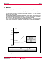
3. Memory
3. Memory
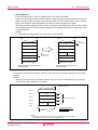
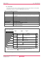
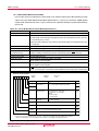
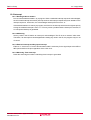
Figure 3.1 is a memory map of this MCU. This MCU provides 1-Mbyte address space from addresses
0000016 to FFFFF16.
The internal ROM is allocated lower addresses beginning with address 0FFFF16. For example, a 16Kbyte internal ROM is allocated addresses from 0C00016 to 0FFFF16.
The fixed interrupt vector table is allocated addresses 0FFDC16 to 0FFFF16. They store the starting
address of each interrupt routine.
The internal RAM is allocated higher addresses beginning with address 0040016. For example, a 1-Kbyte
internal RAM is allocated addresses 0040016 to 007FF16. The internal RAM is used not only for storing
data, but for calling subroutines and stacks when interrupt request is acknowledged.
Special function registers (SFR) are allocated addresses 0000016 to 002FF16. The peripheral function
control registers are located them. All addresses, which have nothing allocated within the SFR, are reserved area and cannot be accessed by users.
0000016
SFR
(See Chapter 4 for details.)
002FF16
0040016
Internal RAM
0XXXX16
0FFDC16
Undefined instruction
Overflow
BRK instruction
Address match
Single step
Watchdog timer•Oscillation stop detection
0YYYY16
Internal ROM
0FFFF16
0FFFF16
(Reserved)
(Reserved)
Reset
Expansion area
FFFFF16
NOTES :
1. Blank spaces are reserved. No access is allowed.
Type name
Internal ROM
Address 0YYYY16
Size
Internal RAM
Address 0XXXX16
Size
R5F21104FP, R5F21104DFP
16K bytes
0C00016
1K bytes
R5F21103FP, R5F21103DFP
12K bytes
0D00016
768 bytes
006FF16
R5F21102FP, R5F21102DFP
8K bytes
0E00016
512 bytes
005FF16
Figure 3.1 Memory Map
Rev.1.20 Jan 27, 2006
REJ09B0019-0120
page 9 of 180
007FF16
R8C/10 Group
4. Special Function Register (SFR)
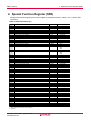
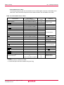
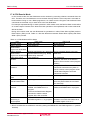
4. Special Function Register (SFR)
SFR(Special Function Register) is the control register of peripheral functions. Tables 4.1 to 4.4 list the SFR
information
Table 4.1 SFR Information(1)(1)
Register
Address
Symbol
After reset
000016
000116
000216
000316
000416
000516
000616
000716
Processor mode register 0
Processor mode register 1
System clock control register 0
System clock control register 1
PM0
PM1
CM0
CM1
XXXX0X002
00XXX0X02
011010002
001000002
Address match interrupt enable register
Protect register
AIER
PRCR
XXXXXX002
00XXX0002
Oscillation stop detection register
Watchdog timer reset register
Watchdog timer start register
Watchdog timer control register
Address match interrupt register 0
OCD
WDTR
WDTS
WDC
RMAD0
000001002
X X1 6
XX16
000111112
0016
0016
X016
Address match interrupt register 1
RMAD1
0016
0016
X016
INT0 input filter select register
INT0F
XXXXX0002
000816
000916
000A16
000B16
000C16
000D16
000E16
000F16
001016
001116
001216
001316
001416
001516
001616
001716
001816
001916
001A16
001B16
001C16
001D16
001E16
001F16
002016
002116
002216
002316
002416
002516
002616
002716
002816
002916
002A16
002B16
002C16
002D16
002E16
002F16
003016
003116
003216
003316
003416
003516
003616
003716
003816
003916
003A16
003B16
003C16
003D16
003E16
003F16
NOTES:
1. Blank spaces are reserved. No access is allowed.
X : Undefined
Rev.1.20 Jan 27, 2006
REJ09B0019-0120
page 10 of 180
R8C/10 Group
4. Special Function Register (SFR)
Table 4.2 SFR Information(2)(1)
Register
Symbol
After reset
Key input interrupt control register
AD conversion interrupt control register
KUPIC
ADIC
XXXXX0002
XXXXX0002
UART0 transmit interrupt control register
UART0 receive interrupt control register
UART1 transmit interrupt control register
UART1 receive interrupt control register
INT2 interrupt control register
Timer X interrupt control register
Timer Y interrupt control register
Timer Z interrupt control register
INT1 interrupt control register
INT3 interrupt control register
Timer C interrupt control register
S0TIC
S0RIC
S1TIC
S1RIC
INT2IC
TXIC
TYIC
TZIC
INT1IC
INT3IC
TCIC
XXXXX0002
XXXXX0002
XXXXX0002
XXXXX0002
XXXXX0002
XXXXX0002
XXXXX0002
XXXXX0002
XXXXX0002
XXXXX0002
XXXXX0002
INT0 interrupt control register
INT0IC
XX00X0002
Address
004016
004116
004216
004316
004416
004516
004616
004716
004816
004916
004A16
004B16
004C16
004D16
004E16
004F16
005016
005116
005216
005316
005416
005516
005616
005716
005816
005916
005A16
005B16
005C16
005D16
005E16
005F16
006016
006116
006216
006316
006416
006516
006616
006716
006816
006916
006A16
006B16
006C16
006D16
006E16
006F16
007016
007116
007216
007316
007416
007516
007616
007716
007816
007916
007A16
007B16
007C16
007D16
007E16
007F16
NOTES :
1. Blank spaces are reserved. No access is allowed.
X : Undefined
Rev.1.20 Jan 27, 2006
REJ09B0019-0120
page 11 of 180
R8C/10 Group
4. Special Function Register (SFR)
Table 4.3 SFR Information(3)(1)
Address
008016
008116
008216
008316
008416
008516
008616
008716
Register
Timer Y, Z mode register
Prescaler Y register
Timer Y secondary register
Timer Y primary register
Timer Y, Z waveform output control register
Prescaler Z register
Timer Z secondary register
Timer Z primary register
Symbol
TYZMR
PREY
TYSC
TYPR
PUM
PREZ
TZSC
TZPR
After reset
0016
FF16
FF16
FF16
0016
FF16
FF16
FF16
Timer Y, Z output control register
Timer X mode register
Prescaler X register
Timer X register
Count source set register
TYZOC
TXMR
PREX
TX
TCSS
0016
0016
FF16
FF16
0016
Timer C register
TC
0016
0016
External input enable register
INTEN
0016
Key input enable register
KIEN
0016
Timer C control register 0
Timer C control register 1
Capture register
TCC0
TCC1
TM0
0016
0016
0016
0016
UART0 transmit/receive mode register
U0MR
U0BRG
U0TB
0016
XX16
XX16
XX16
000010002
000000102
XX16
XX16
0016
XX16
XX16
XX16
000010002
000000102
XX16
XX16
0016
008816
008916
008A16
008B16
008C16
008D16
008E16
008F16
009016
009116
009216
009316
009416
009516
009616
009716
009816
009916
009A16
009B16
009C16
009D16
009E16
009F16
00A016
00A116
00A216
UART0 bit rate generator
UART0 transmit buffer register
00A316
00A516
UART0 transmit/receive control register 0
UART0 transmit/receive control register 1
00A616
UART0 receive buffer register
00A416
U0C0
U0C1
U0RB
00A716
00A816
UART1 transmit/receive mode register
00A916
UART1 bit rate generator
UART1 transmit buffer register
00AA16
U1MR
U1BRG
U1TB
00AB16
00AD16
UART1 transmit/receive control register 0
UART1 transmit/receive control register 1
00AE16
UART1 receive buffer register
U1C0
U1C1
U1RB
UART transmit/receive control register 2
UCON
00AC16
00AF16
00B016
00B116
00B216
00B316
00B416
00B516
00B616
00B716
00B816
00B916
00BA16
00BB16
00BC16
00BD16
00BE16
00BF16
NOTES:
1. Blank spaces are reserved. No access is allowed.
X : Undefined
Rev.1.20 Jan 27, 2006
REJ09B0019-0120
page 12 of 180
R8C/10 Group
4. Special Function Register (SFR)
Table 4.4 SFR Information(4)(1)
Register
Address
00C016
AD register
Symbol
AD
After reset
XXXXXXXX2
XXXXXXXX2
AD control register 2
ADCON2
0016
AD control register 0
AD control register 1
ADCON0
ADCON1
00000XXX2
0016
Port P0 register
Port P1 register
Port P0 direction register
Port P1 direction register
P0
P1
PD0
PD1
XX16
XX16
0016
0016
Port P3 register
P3
XX16
Port P3 direction register
Port P4 register
PD3
P4
0016
XX16
Port P4 direction register
PD4
0016
Pull-up control register 0
Pull-up control register 1
Port P1 drive capacity control register
PUR0
PUR1
DRR
00XX00002
XXXXXX0X2
0016
Flash memory control register 4
FMR4
010000002
Flash memory control register 1
FMR1
0100XX0X2
Flash memory control register 0
FMR0
000000012
00C116
00C216
00C316
00C416
00C516
00C616
00C716
00C816
00C916
00CA16
00CB16
00CC16
00CD16
00CE16
00CF16
00D016
00D116
00D216
00D316
00D416
00D516
00D616
00D716
00D816
00D916
00DA16
00DB16
00DC16
00DD16
00DE16
00DF16
00E016
00E116
00E216
00E316
00E416
00E516
00E616
00E716
00E816
00E916
00EA16
00EB16
00EC16
00ED16
00EE16
00EF16
00F016
00F116
00F216
00F316
00F416
00F516
00F616
00F716
00F816
00F916
03FA16
00FB16
00FC16
00FD16
00FE16
00FF16
01B316
01B416
01B516
01B616
01B716
NOTES:
1. Blank columns, 010016 to 01B216 and 01B816 to 02FF16 are all reserved. No access is allowed.
X : Undefined
Rev.1.20 Jan 27, 2006
REJ09B0019-0120
page 13 of 180
R8C/10 Group
5. Reset
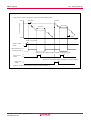
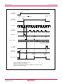
5. Reset
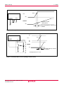
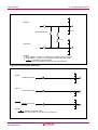
There are three types of resets: a hardware reset, a software reset, and an watchdog timer reset.
5.1 Hardware Reset
____________
____________
A reset is applied using the RESET pin. When an “L” signal is applied to the RESET pin while
the power supply voltage is within the recommended operating condition, the pins are initial____________
ized (see Table 5.1 “Pin Status When RESET Pin Level is 'L'”). When the input level at the
____________
RESET pin is released from “L” to “H”, the CPU and SFR are initialized, and the program is
executed starting from the address indicated by the reset vector. Figure 5.1 shows the CPU
register status after reset and figure 5.2 shows the reset sequence. After reset, the on-chip
oscillator clock divided by 8 is automatically selected for the CPU. The internal RAM is not
____________
initialized. If the RESET pin is pulled “L” while writing to the internal RAM, the internal RAM
becomes indeterminate. Figures 5.3 to 5.4 show the reset circuit example. Refer to Chapter 4,
“Special Function Register (SFR)” for the status of SFR after reset.
• When the power supply is stable
____________
(1) Apply an “L” signal to the RESET pin.
(2) Wait for 500 µs (1/fRING ✕ 20).
____________
(3) Apply an “H” signal to the RESET pin.
• Power on
____________
(1) Apply an “L” signal to the RESET pin.
(2) Let the power supply voltage increase until it meets the recommended operating condition.
(3) Wait td(P-R) or more until the internal power supply stabilizes.
(4) Wait for 500 µs (1/fRING ✕ 20).
____________
(5) Apply an “H” signal to the RESET pin.
____________
Table 5.1 Pin Status When RESET Pin Level is “L”
Status
Pin name
CNVSS = VSS
P0
Input port
P1
Input port
P30 to P33, P37
Input port
P45 to P47
Input port
5.2 Software Reset
When the PM03 bit in the PM0 register is set to “1” (microcomputer reset), the microcomputer has its
pins, CPU, and SFR initialized. Then the program is executed starting from the address indicated by
the reset vector. After reset, the on-chip oscillator clock divided by 8 is automatically selected for the
CPU.
5.3 Watchdog Timer Reset
Where the PM12 bit in the PM1 register is “1” (reset when watchdog timer underflows), the microcomputer initializes its pins, CPU and SFR if the watchdog timer underflows. Then the program is executed starting from the address indicated by the reset vector. After reset, the on-chip oscillator clock
divided by 8 is automatically selected for the CPU.
Rev.1.20 Jan 27, 2006
REJ09B0019-0120
page 14 of 180
R8C/10 Group
5. Reset
b15
b0
000016
Data register(R0)
000016
Data register(R1)
000016
Data register(R2)
000016
Data register(R3)
000016
000016
Address register(A0)
Address register(A1)
000016
Frame base register(FB)
b19
b0
0000016
Interrupt table register(INTB)
Content of addresses 0FFFE16 to 0FFFC16
b15
Program counter(PC)
b0
000016
User stack pointer(USP)
000016
Interrupt stack pointer(ISP)
000016
Static base register(SB)
b15
b0
Flag register(FLG)
000016
AAAAAAAAAA
AAAA
AAA
AAA
b15
b8
IPL
b7
U I
b0
O B S Z D C
Figure 5.1 CPU Register Status After Reset
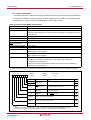
fRING
More than 20 cycles are needed (1)
Internal on-chip
oscillation
Flash memory activated time
(CPU clock ✕ 64 cycles)
CPU clock ✕ 28cycles
CPU clock
0FFFE16
0FFFC16
Address
(Internal address signal)
0FFFD16
NOTES:
1. This shows hardware reset
Figure 5.2 Reset Sequence
Rev.1.20 Jan 27, 2006
REJ09B0019-0120
page 15 of 180
Content of reset vector
R8C/10 Group
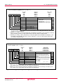
5. Reset
2.7V
VCC
0V
RESET
VCC
RESET
Equal to or less
than 0.2VCC
0V
More than td(P-R) + 500 µs are
needed.
Figure 5.3 Example Reset Circuit
5V
2.7V
VCC
RESET
VCC
Supply voltage
detection circuit
0V
5V
RESET
0V
More than td(P-R) + 500 µs
are needed.
Example when VCC = 5V.
Figure 5.4 Example Reset Circuit (Voltage Check Circuit)
Rev.1.20 Jan 27, 2006
REJ09B0019-0120
page 16 of 180
R8C/10 Group
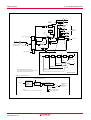
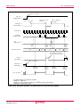
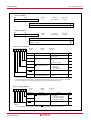
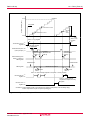
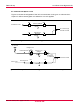
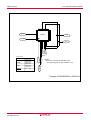
6. Clock Generation Circuit
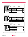
6. Clock Generation Circuit
The clock generation circuit contains two oscillator circuits as follows:
• Main clock oscillation circuit
• On-chip oscillator (with oscillation stop detection function)
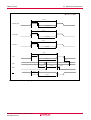
Table 6.1 lists the clock generation circuit specifications. Figure 6.1 shows the clock generation circuit.
Figures 6.2 and 6.3 show the clock-related registers.
Table 6.1 Clock Generation Circuit Specifications
Main clock
oscillation circuit
• CPU clock source
Use of clock
• Peripheral function clock source
• CPU and peripheral function
clock sources when the
main clock stops oscillating
Clock frequency 0 to 16 MHz
Item
On-chip oscillator
• CPU clock source
• Peripheral function clock source
• CPU and peripheral function
clock sources when the main
clock stops oscillating
About 125 kHz
Usable oscillator
• Ceramic resonator
• Crystal oscillator
Pins to connect
oscillator
XIN, XOUT(1)
Oscillation starts
and stops
Present
Present
Oscillator status
after reset
Stopped
Oscillating
Other
Externally derived
clock can be input
(Note 1)
NOTES:
1. Can be used as P46 and P47 when the on-chip oscillator clock is used for CPU clock
while the main clock oscillation circuit is not used.
Rev.1.20 Jan 27, 2006
REJ09B0019-0120
page 17 of 180
R8C/10 Group
6. Clock Generation Circuit
fRING
fRING128
On-chip
oscillator
clock
1/128
f1
f1SIO
On-chip
oscillator
CM14
fAD
f2
Oscillation
stop
detection
f8SIO
OCD2=1
Main
clock
f32
e
CM10=1(Stop mode)
S Q
a
XIN
XOUT
R
RESET
Peripheral
function clock
f8
c
b
Divider
f32SIO
d
CPU clock
OCD2=0
CM13
CM05
Interrupt request level
judgment output
CM02
S Q
R
WAIT instruction
R
e
1/2
a
c
b
1/2
1/2
1/2
1/2
CM06=0
CM17 to CM16=112
CM06=1
d
CM06=0
CM17 to CM16=102
CM06=0
CM17 to CM16=012
CM02, CM05, CM06: Bits in CM0 register
CM10, CM13, CM14, CM16, CM17: Bits in CM1 register
OCD0, OCD1, OCD2: Bits in OCD register
CM06=0
CM17 to CM16=002
Details of divider
Oscillation stop detection circuit
Forcible discharge when OCD0(1)
Main clock
Pulse generation
circuit for clock
edge detection
and charge,
discharge control
circuit
Charge,
discharge
circuit
OCD1(1)
NOTES:
1. Set the same value to the OCD1 bit and OCD0 bit.
Figure 6.1 Clock Generation Circuit
Rev.1.20 Jan 27, 2006
REJ09B0019-0120
page 18 of 180
Oscillation stop
detection interrupt
generation circuit
Watchdog
timer
interrupt
OCD2 bit switch signal
CM14 bit switch signal
Oscillation stop
detection,
Watchdog timer
interrupt
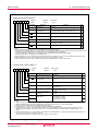
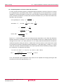
6. Clock Generation Circuit
R8C/10 Group
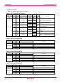
System clock control register 0(1)
b7
b6
b5
0
b4
b3
b2
0 1
b1
b0
0 0
Symbol
CM0
Address
000616
Bit symbol
(b1-b0)
CM02
After reset
6816
Bit name
Function
RW
Reserved bit
Set to “0”
WAIT peripheral function
clock stop bit
0 : Do not stop peripheral function clock in wait mode
1 : Stop peripheral function clock in wait mode
RW
Reserved bit
Set to “1”
RW
Reserved bit
Set to “0”
RW
(b3)
(b4)
RW
CM05
Main clock (XIN-XOUT)stop 0 : On
bit(2, 4)
1 : Off(3)
RW
CM06
CPU clock division select
bit 0(5)
0 : CM16 and CM17 valid
1 : Divide-by-8 mode
RW
Reserved bit
Set to “0”
(b7)
RW
NOTES:
1. Set the PRC0 bit of PRCR register to “1” (write enable) before writing to this register.
2. The CM05 bit is provided to stop the main clock when the on-chip oscillator mode is selected. This bit cannot be used for detection as to
whether the main clock stopped or not. To stop the main clock, the following setting is required:
(1) Set the OCD0 and OCD1 bits in the OCD register to “002” (disabling oscillation stop detection function).
(2) Set the OCD2 bit to “1” (selecting on-chip oscillator clock).
3. Set the CM05 bit to “1” (main clock stops) and the CM13 bit in the CM1 register to “1” (XIN-XOUT pin) when the external clock is input.
4. When the CM05 bit is set to “1” (main clock stop), P46 and P47 can be used as input ports.
5. When entering stop mode from high or middle speed mode, the CM06 bit is set to “1” (divide-by-8 mode).
System clock control register 1(1)
b7
b6
b5
b4
b3
b2
b1
0
0
b0
Symbol
CM1
Bit symbol
Address
000716
After reset
2016
Bit name
Function
RW
CM10
All clock stop control bit(4)
0 : Clock on
1 : All clocks off (stop mode)
RW
(b1)
Reserved bit
Set to “0”
RW
(b2)
Reserved bit
Set to “0”
RW
CM13
Port XIN-XOUT switch bit
0 : Input port P46, P47
1 : XIN-XOUT pin
RW
CM14
On-chip oscillation stop bit 0 : On-chip oscillator on
1 : On-chip oscillator off(5)
RW
CM15
XIN-XOUT drive capacity
select bit(2)
0 : LOW
1 : HIGH
RW
CM16
Main clock division
select bit 1(3)
0 0 : No division mode
0 1 : Division by 2 mode
1 0 : Division by 4 mode
1 1 : Division by 16 mode
b7 b6
CM17
RW
RW
NOTES:
1. Write to this register after setting the PRC0 bit of PRCR register to “1” (write enable).
2. When entering stop mode from high or middle speed mode, the CM15 bit is set to “1” (drive capacity high).
3. Effective when the CM06 bit is “0” (CM16 and CM17 bits enable).
4. If the CM10 bit is “1” (stop mode), the internal feedback resistor becomes ineffective.
5. The CM14 bit can be set to “1” (on-chip oscillator off) if the OCD2 bit=0 (selecting main clock). When the OCD2 bit is set to “1”
(selecting on-chip oscillator clock), the CM14 bit is set to “0” (on-chip oscillator on). This bit remains unchanged when “1” is
written.
6. When the CM10 bit is set to “1” (stop mode) or the CM05 bit in the CM0 register to “1” (main clock stops) and the CM13 bit is set
to “1” (XIN-XOUT pin), the XOUT(P47) pin is held “H”.
When the CM13 bit is set to “0” (input port P46, P47), the P47 is in input state.
Figure 6.2 CM0 Register and CM1 Register
Rev.1.20 Jan 27, 2006
REJ09B0019-0120
page 19 of 180
R8C/10 Group
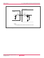
6. Clock Generation Circuit
Oscillation stop detection register(1)
b7
b6
b5
b4
b3
b2
b1
b0
0 0 0 0
Symbol
OCD
Bit symbol
OCD0
Address
000C16
Bit name
Oscillation stop
detection enable bit
OCD1
OCD2
System clock select bit(6)
OCD3
Clock monitor bit(3, 5)
(b7-b4)
After reset
0416
Reserved bit
Function
RW
b1 b0
0 0: The function is disabled(4)
0 1: Avoid this setting
1 0: Avoid this setting
1 1: The function is enabled(7)
RW
0: Select main clock(7)
RW
1: Select on-chip oscillator clock(2)
0: Main clock on
RO
1: Main clock off
Set to "0"
RW
NOTES:
1. Set the PRC0 bit in the PRCR register to “1” (write enable) before rewriting this register.
2. The OCD2 bit is set to “1” (selecting on-chip oscillator clock) automatically if a main clock oscillation stop
is detected while the OCD1 to OCD0 bits are set to “112” (oscillation stop detection function disabled). If
the OCD3 bit is set to “1” (main clock stop), the OCD2 bit remains unchanged when trying to write “0”
(selecting main clock).
3. The OCD3 bit is enabled when the OCD1 to OCD0 bits are set to “112” (oscillation stop detection function
enabled).
4. The OCD1 to OCD0 bits must be set to “002” (oscillation stop detection function disabled) before entering
stop mode or on-chip oscillator mode (main clock stops).
5. The OCD3 bit remains set to “0” (main clock on) if the OCD1 to OCD0 bits are set to “002”.
6. The CM14 bit goes to “0” (on-chip oscillator on) if the OCD2 bit is set to “1” (selecting on-chip oscillator
clock).
7. Refer to Figure 6.6 “switching clock source from on-chip oscillator to main clock” for the switching
procedure when the main clock re-oscillates after detecting an oscillation stop.
Figure 6.3 OCD Register
Rev.1.20 Jan 27, 2006
REJ09B0019-0120
page 20 of 180
R8C/10 Group
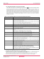
6.1 Main Clock
The following describes the clocks generated by the clock generation circuit.
6.1 Main Clock
This clock is supplied by a main clock oscillation circuit. This clock is used as the clock source for the CPU
and peripheral function clocks. The main clock oscillator circuit is configured by connecting a resonator
between the XIN and XOUT pins. The main clock oscillator circuit contains a feedback resistor, which is
disconnected from the oscillator circuit during stop mode in order to reduce the amount of power consumed in the chip. The main clock oscillator circuit may also be configured by feeding an externally
generated clock to the XIN pin. Figure 6.4 shows examples of main clock connection circuit.
During reset and after reset, the main clock is turned off.
The main clock starts oscillating when the CM05 bit in the CM0 register is set to “0” (main clock on) after
setting the CM13 bit in the CM1 register to “1” (XIN- XOUT pin).
To use the main clock for the CPU clock, set the OCD2 bit in the OCD register to “0” (selecting main clock)
after the main clock becomes oscillating stably.
The power consumption can be reduced by setting the CM05 bit in the CM0 register to “1” (main clock off)
if the OCD2 bit is set to “1” (selecting on-chip oscillator clock).
Note that if an externally generated clock is fed into the XIN pin, the main clock cannot be turned off by
setting the CM05 bit to “1”. If necessary, use an external circuit to turn off the clock.
During stop mode, all clocks including the main clock are turned off. Refer to Section 6.3, “Power Control.”
Microcomputer
Microcomputer
(Built-in feedback resistor)
(Built-in feedback resistor)
XIN
XIN
XOUT
XOUT
Open
(Note 1)
Rd
Externally derived clock
C IN
COUT
Vcc
Vss
NOTES:
1. Insert a damping resistor if required. The resistance will vary depending on the oscillator and the oscillation drive
capacity setting. Use the value recommended by the maker of the oscillator.
When the oscillation drive capacity is set to low, check that oscillation is stable. Also, if the oscillator manufacturer's
data sheet specifies that a feedback resistor be added external to the chip, insert a feedback resistor between XIN
and XOUT following the instruction.
Figure 6.4 Examples of Main Clock Connection Circuit
Rev.1.20 Jan 27, 2006
REJ09B0019-0120
page 21 of 180
R8C/10 Group
6.2 On-chip Oscillator Clock
6.2 On-Chip Oscillator Clock
This clock, approximately 125 kHz, is supplied by the on-chip oscillator. This clock is used as the clock
source for the CPU clock, peripheral function clock, fRING, and fRING128.
After reset, the on-chip oscillator clock divided by 8 is selected for the CPU clock.
To use the main clock for the CPU clock, set the OCD2 in the OCD register to “0” (selecting main clock)
after the main clock becomes oscillating stably. If the main clock stops oscillating when the OCD1 to
OCD0 bits in the OCD register is “112” (oscillation stop detection function enabled), the on-chip oscillator
automatically starts operating, supplying the necessary clock for the microcomputer.
The frequency of the on-chip oscillator varies depending on the supply voltage and the operation ambient
temperature. The application products must be designed with sufficient margin for the frequency change.
Rev.1.20 Jan 27, 2006
REJ09B0019-0120
page 22 of 180
R8C/10 Group
6.3 CPU Clock and Peripheral Function Clock
6.3 CPU Clock and Peripheral Function Clock
There are two types of clocks: CPU clock to operate the CPU and peripheral function clock to operate the
peripheral functions. Also refer to “Figure 6.1 Clock Generating Circuit”.
6.3.1 CPU Clock
This is an operating clock for the CPU and watchdog timer.
The clock source for the CPU clock can be chosen to be the main clock or on-chip oscillator clock.
The selected clock source can be divided by 1 (undivided), 2, 4, 8 or 16 to produce the CPU clock. Use
the CM06 bit in the CM0 register and the CM17 to CM16 bits in the CM1 register to select the divideby-n value.
After reset, the on-chip oscillator clock divided by 8 provides the CPU clock.
Note that when entering stop mode from high or middle speed mode, the CM06 bit is set to “1” (divideby-8 mode).
6.3.2 Peripheral Function Clock (f1, f2, f8, f32, fAD, f1SIO, f8SIO, f32SIO)
These are operating clocks for the peripheral functions.
Of these, fi (i=1, 2, 8, 32) is derived from the main clock or on-chip oscillator clock by dividing them by
i. The clock fi is used for timers X, Y, Z and C.
The clock fjSIO (j=1, 8, 32) is derived from the main clock or on-chip oscillator clock by dividing them by
j. The clock fjSIO is used for serial interface.
The fAD clock is produced from the main clock is used for the A/D converter.
When the WAIT instruction is executed after setting the CM02 bit in the CM0 register to “1” (peripheral
function clock turned off during wait mode), the clocks fi, fjSIO, and fAD are turned off.
6.3.3 fRING and fRING128
These are operating clocks for the peripheral functions.
The fRING runs at the same frequency as the on-chip oscillator, and can be used as the source for the
timer Y. The fRING128 is derived from the fRING by dividing it by 128, and can used for the timer C.
When the WAIT instruction is executed, the clocks fRING and fRING128 are not turned off.
Rev.1.20 Jan 27, 2006
REJ09B0019-0120
page 23 of 180
R8C/10 Group
6.4 Power Control
6.4 Power Control
There are three power control modes. All modes other than wait and stop modes are referred to as
normal operation mode.
6.4.1 Normal Operation Mode
Normal operation mode is further classified into three modes.
In normal operation mode, because the CPU clock and the peripheral function clocks both are on, the
CPU and the peripheral functions are operating. Power control is exercised by controlling the CPU
clock frequency. The higher the CPU clock frequency, the greater the processing capability. The lower
the CPU clock frequency, the smaller the power consumption in the chip. If the unnecessary oscillator
circuits are turned off, the power consumption is further reduced.
Before the clock sources for the CPU clock can be switched over, the new clock source to which
switched must be oscillating stably. If the new clock source is the main clock, allow a sufficient wait
time in a program until it becomes oscillating stably.
• High-speed Mode
The main clock divided by 1 undivided provides the CPU clock. If the CM14 bit is set to “0” (on-chip
oscillator on), the fRING is used as the count source for timer Y.
• Medium-speed Mode
The main clock divided by 2, 4, 8 or 16 provides the CPU clock. If the CM14 bit is set to “0” (on-chip
oscillator on), the fRING is used as the count source for timer Y.
• On-Chip Oscillator Mode
The on-chip oscillator clock divided by 1 (undivided), 2, 4, 8 or 16 provides the CPU clock. The onchip oscillator clock is also the clock source for the peripheral function clocks.
Table 6.2 Setting Clock Related Bit and Modes
OCD register
CM1 register
Modes
CM13
OCD2
CM17, CM16
High-speed mode
0
002
1
1
Mediumdivided by 2
0
012
speed
divided by 4
0
102
1
mode
divided by 8
1
0
divided by 16
0
112
1
On-chip
oscillator
mode
no division
divided by 2
divided by 4
divided by 8
divided by 16
Rev.1.20 Jan 27, 2006
REJ09B0019-0120
page 24 of 180
1
1
1
1
1
002
012
102
112
CM0 register
CM06
CM05
0
0
0
0
0
0
1
0
0
0
0
0
0
1
0
0 or 1
0 or 1
0 or 1
0 or 1
0 or 1
6.4 Power Control
R8C/10 Group
6.4.2 Wait Mode
In wait mode, the CPU clock is turned off, so are the CPU and the watchdog timer because both are
operated by the CPU clock. Because the main clock and on-chip oscillator clock both are on, the
peripheral functions using these clocks keep operating.
• Peripheral Function Clock Stop Function
If the CM02 bit is “1” (peripheral function clocks turned off during wait mode), the f1, f2, f8, f32, f1SIO,
f8SIO, f32SIO, and fAD clocks are turned off when in wait mode, with the power consumption reduced
that much.
• Entering Wait Mode
The microcomputer is placed into wait mode by executing the WAIT instruction.
• Pin Status During Wait Mode
The status before wait mode is retained.
• Exiting Wait Mode
The microcomputer is moved out of wait mode by a hardware reset or peripheral function interrupt.
When using a hardware reset to exit wait mode, set the ILVL2 to ILVL0 bits for the peripheral function
interrupts to “0002” (interrupts disabled) before executing the WAIT instruction.
The peripheral function interrupts are affected by the CM02 bit. If CM02 bit is “0” (peripheral function
clocks not turned off during wait mode), all peripheral function interrupts can be used to exit wait
mode. If CM02 bit is “1” (peripheral function clocks turned off during wait mode), the peripheral
functions using the peripheral function clocks stop operating, so that only the peripheral functions
clocked by external signals can be used to exit wait mode.
Table 6. 3 lists the interrupts to exit wait mode and the usage conditions.
When using a peripheral function interrupt to exit wait mode, set up the following before executing
the WAIT instruction.
1. In the ILVL2 to ILVL0 bits in the interrupt control register, set the interrupt priority level of the
peripheral function interrupt to be used to exit wait mode.
Also, for all of the peripheral function interrupts not used to exit wait mode, set the ILVL2 to ILVL0
bits to “0002” (interrupt disable).
2. Set the I flag to “1”.
3. Enable the peripheral function whose interrupt is to be used to exit wait mode.
In this case, when an interrupt request is generated and the CPU clock is thereby turned on, an
interrupt sequence is executed.
The CPU clock turned on when exiting wait mode by a peripheral function interrupt is the same CPU
clock that was on when the WAIT instruction was executed.
Table 6.3 Interrupts to Exit Wait Mode and Usage Conditions
Interrupt
CM02=0
CM02=1
Serial interface interrupt
Can be used when operating with internal
or external clock
Can be used when operating with external clock
Can be used
Key input interrupt
Can be used
A/D conversion interrupt
Can be used in one-shot mode
Timer X interrupt
Can be used in all modes
Can be used in event counter mode
Timer Y interrupt
Can be used in all modes
Can be used when counting inputs from CNTR1 pin
in timer mode
Timer Z interrupt
Can be used in all modes
(Do not use)
Timer C interrupt
Can be used in all modes
(Do not use)
INT interrupt
Can be used
Can be used (INT0 and INT3 can be used if there
is no filter.
Voltage detection interrupt
Can be used
Can be used
Oscillation stop detection
interrupt
Can be used
Rev.1.20 Jan 27, 2006
REJ09B0019-0120
page 25 of 180
(Do not use)
(Do not use)
R8C/10 Group
6.4 Power Control
6.4.3 Stop Mode
In stop mode, all oscillator circuits are turned off, so are the CPU clock and the peripheral function
clocks. Therefore, the CPU and the peripheral functions clocked by these clocks stop operating. The
least amount of power is consumed in this mode. If the voltage applied to Vcc pin is VRAM or more, the
internal RAM is retained.
However, the peripheral functions clocked by external signals keep operating. The following interrupts
can be used to exit stop mode.
• Key interrupt
______
______
______
• INT0 to INT2 interrupts (INT0 can be used only when there is no filter.)
• Timer X interrupt (when counting external pulses in event counter mode)
• Timer Y interrupt (when counting inputs from CNTR1 pin in timer mode)
• Serial interface interrupt (when external clock is selected)
• Entering Stop Mode
The microcomputer is placed into stop mode by setting the CM10 bit of CM1 register to “1” (all clocks
turned off). At the same time, the CM06 bit of CM0 register is set to “1” (divide-by-8 mode) and the
CM15 bit of CM10 register is set to “1” (main clock oscillator circuit drive capacity high).
Before entering stop mode, set the OCD1 to OCD0 bits to “002” (oscillation stop detection function
disable).
• Pin Status in Stop Mode
The status before wait mode is retained.
However, the XOUT(P47) pin is held “H” when the CM13 bit in the CM1 register is set to “1” (XIN-XOUT
pin). The P47(XOUT) is in input state when the CM13 bit is set to “0” (input port P46, P47).
• Exiting Stop Mode
The microcomputer is moved out of stop mode by a hardware reset or peripheral function interrupt.
When using a hardware reset to exit stop mode, set the ILVL2 to ILVL0 bits for the peripheral function
interrupts to “0002” (interrupts disabled) before setting the CM10 bit to “1”.
When using a peripheral function interrupt to exit stop mode, set up the following before setting the
CM10 bit to “1”.
1. In the ILVL2 to ILVL0 bits in the interrupt control register, set the interrupt priority level of the
peripheral function interrupt to be used to exit stop mode.
Also, for all of the peripheral function interrupts not used to exit stop mode, set the ILVL2 to ILVL0
bits to “0002”.
2. Set the I flag to “1”.
3. Enable the peripheral function whose interrupt is to be used to exit stop mode.
In this case, when an interrupt request is generated and the CPU clock is thereby turned on, an
interrupt sequence is executed.
The main clock divided by 8 of the clock which is used right before stop mode is used for the CPU
clock when exiting stop mode by a peripheral function interrupt.
Rev.1.20 Jan 27, 2006
REJ09B0019-0120
page 26 of 180
R8C/10 Group
6.4 Power Control
Figure 6.5 shows the state transition of Power control
Reset
There are five power control modes.
(1) High-speed mode
(2) Middle-speed mode
(3) On-chip oscillator mode
(4) Wait mode
(5) Stop mode
CM13=1, CM05=0,
OCD2=0
CM14=0, OCD2=1
On-chip Oscillator
Mode
OCD2=1
CM14=0
High-speed Mode,
Middle-speed mode
OCD2=0
CM05=0
CM13=1
Interrupt
WAIT Instruction
Wait Mode
CM05: Bit in CM0 register
CM10, CM13, CM14: Bit in CM1 register
OCD2: Bit in OCD register
Interrupt
Stop Mode
Figure 6.5 State Transition of Power Control
Rev.1.20 Jan 27, 2006
REJ09B0019-0120
page 27 of 180
CM10=1
(All clocks stop)
6.5 Oscillation Stop Detection Function
R8C/10 Group
6.5 Oscillation Stop Detection Function
The oscillation stop detection function is such that main clock oscillation circuit stop is detected. The
oscillation stop detection function can be enabled and disabled by the OCD1 to OCD0 bits in the OCD
register.
Table 6.4 lists the specifications of the oscillation stop detection function.
Where the main clock corresponds to the CPU clock source and the OCD1 to OCD0 bits are “112”
(oscillation stop detection function enabled), the system is placed in the following state if the main clock
comes to a halt:
• The on-chip oscillator starts oscillation, and the on-chip oscillator clock becomes the clock source for
CPU clock and peripheral functions in place of the main clock
• OCD register OCD2 bit = 1 (selecting on-chip oscillator clock)
• OCD register OCD3 bit = 1 (main clock stopped)
• CM1 register CM14 bit = 0 (on-chip oscillator oscillating)
• Oscillation stop detection interrupt request occurs
Table 6.4 Oscillation Stop Detection Function Specifications
Item
Specification
Oscillation stop detectable clock and
f(XIN) ≥ 2 MHz
frequency bandwidth
Enabling condition for oscillation stop Set OCD1 to OCD0 bits to “112” (oscillation stop detection
detection function
function enabled)
Operation at oscillation stop detection Oscillation stop detection interrupt occurs
6.5.1 How to Use Oscillation Stop Detection Function
• The oscillation stop detection interrupt shares the vector with the watchdog timer interrupt. If the
oscillation stop detection and watchdog timer interrupts both are used, the interrupt factor must be
determined. Table 6.5 shows to determine the interrupt factor with the oscillation stop detection
interrupt, watchdog timer interrupt and voltage detection interrupt.
• Where the main clock re-oscillated after oscillation stop, the clock source for the CPU clock and
peripheral functions must be switched to the main clock in the program.
Figure 6.6 shows the procedure for switching the clock source from the on-chip oscillator to the main
clock.
• To enter wait mode while using the oscillation stop detection function, set the CM02 bit to “0” (peripheral function clocks not turned off during wait mode).
• Since the oscillation stop detection function is provided in preparation for main clock stop due to
external factors, set the OCD1 to OCD0 bits to “002” (oscillation stop detection function disabled)
where the main clock is stopped or oscillated in the program, that is where the stop mode is selected
or the CM05 bit is altered.
• This function cannot be used when the main clock frequency is below 2 MHz. Set the OCD1 to OCD0
bits to “002” (oscillation stop detection function disabled).
Rev.1.20 Jan 27, 2006
REJ09B0019-0120
page 28 of 180
R8C/10 Group
6.5 Oscillation Stop Detection Function
Table 6.5 Determination of Interrupt Factor of Oscillation Stop Detection
Generated Interrupt Factor
Bit showing interrupt factor
Oscillation stop detection
(a) The OCD3 bit in the OCD register = 1
( (a) or (b) )
(b) The OCD1 to OCD0 bits in the OCD register = 112 and the
OCD2 bit = 1
Switch to Main clock
Verify OCD3 bit
1(main clock stop)
0(main clock oscillating)
Determine several times
Determine several times that the main clock is supplied
Set OCD1 to OCD0 bits to 002
(oscillation stop detection function disabled)
Set OCD2 bit to 0
(selecting main clock)
End
OCD3 to OCD0 bits: Bits in OCD register
Figure 6.6 Switching Clock Source From On-Chip Oscillator to Main Clock
Rev.1.20 Jan 27, 2006
REJ09B0019-0120
page 29 of 180
R8C/10 Group
7. Protection
7. Protection
In the event that a program runs out of control, this function protects the important registers so that they
will not be rewritten easily. Figure 7.1 shows the PRCR register. The following lists the registers protected
by the PRCR register.
• Registers protected by PRC0 bit: CM0, CM1, and OCD registers
• Registers protected by PRC1 bit: PM0 and PM1 registers
• Registers protected by PRC2 bit: PD0 register
Set the PRC2 bit to “1” (write enabled) and then write to any address, and the PRC2 bit will be set to “0”
(write protected). The registers protected by the PRC2 bit should be changed in the next instruction after
setting the PRC2 bit to “1”. Make sure no interrupts will occur between the instruction in which the PRC2
bit is set to “1” and the next instruction. The PRC0 and PRC1 bits are not automatically set to “0” by writing
to any address. They can only be set to “0” in a program.
Protect register
b7
b6
b5
b4
0
0 0
b3
b2
b1
b0
Symbol
PRCR
Bit symbol
PRC0
Address
000A16
Bit name
Protect bit 0
After reset
00XXX0002
Function
Enable write to CM0, CM1, OCD
registers
0 : Write protected
1 : Write enabled
PRC1
Protect bit 1
RW
RW
Enable write to PM0, PM1
registers
0 : Write protected
1 : Write enabled
RW
Enable write to PD0 register
PRC2
(b5-b3)
Protect bit 2
Reserved bit
Reserved bit
0 : Write protected
1 : Write enabled1
When write, must set to "0"
RW
RW
When read, its content is “0”.
RO
NOTES:
1. The PRC2 bit is set to “0” by writing to any address after setting it to “1”. Other bits are not set to “0”
by writing to any address, and must therefore be set to “0” in a program.
(b7-b6)
Figure 7.1 PRCR Register
Rev.1.20 Jan 27, 2006
REJ09B0019-0120
page 30 of 180
R8C/10 Group
8. Processor Mode
8. Processor Mode
8.1 Types of Processor Mode
The processor mode is single-chip mode. Table 8.1 shows the features of the processor mode. Figure 8.1
shows the PM0 and PM1 register.
Table 8.1 Features of Processor Mode
Access space
Processor mode
Single-chip mode
SFR, internal RAM, internal ROM
Pins which are assigned I/O ports
All pins are I/O ports or peripheral
function I/O pins
Processor mode register 0(1)
b7
b6
b5
b4
b3
b2
b1
b0
0 0 0
Symbol
PM0
Address
000416
Bit symbol
After reset
0016
Bit name
Reserved bit
Function
Must set to “0”
(b1-b0)
(b2)
PM03
(b7-b4)
RW
RW
Nothing is assigned. When write, set to “0”. When read, its
content is indeterminate.
Software reset bit
Setting this bit to “1” resets the
microcomputer. When read, its
content is “0”.
RW
Nothing is assigned. When write, set to “0”. When read, its
content is 0.
NOTES:
1. Set the PRC1 bit in the PRCR register to "1" (write enable) before writing to this register.
Processor mode register 1(1)
b7
b6
b5
b4
b3
0
b2
b1
b0
0
0
Symbol
PM1
Address
000516
Bit symbol
After reset
0016
Bit name
Function
(b0)
Reserved bit
Set to “0”
RW
(b1)
Reserved bit
Set to “0”
RW
0 : Watchdog timer interrupt
1 : Watchdog timer reset(2)
PM12
WDT interrupt/reset
switch bit
(b6-b3)
Nothing is assigned. When write, set to “0”. When read, its
content is 0.
Set to “0”
Reserved bit
(b7)
NOTES:
1. Set the PRC1 bit in the PRCR register to "1" (write enable) before writing to this register.
2. PM12 bit is set to “1” by writing a “1” in a program. (Writing a “0” has no effect.)
Figure 8.1 PM0 Register and PM1 Register
Rev.1.20 Jan 27, 2006
REJ09B0019-0120
RW
page 31 of 180
RW
RW
R8C/10 Group
9. Bus
9. Bus
During access, the ROM/RAM and the SFR have different bus cycles. Table 9.1 shows bus cycles for
access space.
The ROM/RAM and SFR are connected to the CPU through an 8-bit bus. When accessing in word (16
bits) units, these spaces are accessed twice in 8-bit units. Table 9.2 shows bus cycles in each access
space.
Table 9.1 Bus Cycles for Access Space
Access space
Bus cycle
SFR/Data flash
2 CPU clock cycles
Program ROM/RAM 1 CPU clock cycles
Table 9.2 Access Unit and Bus Operation
Space
Even address
byte access
CPU clock
CPU clock
Address
Data
Address
Data
Odd address
word access
Address
Odd
Data
CPU clock
Address
Data
Rev.1.20 Jan 27, 2006
REJ09B0019-0120
page 32 of 180
Data
Data
Odd
Data
CPU clock
Even
Data
Even+1
Data
CPU clock
Address
Data
Even
CPU clock
CPU clock
Data
Even address
word access
Address
Even
Data
Odd address
byte access
Program ROM/RAM
SFR, Data flash
Address
Data
Even+1
Even
Data
Data
CPU clock
Odd
Data
Odd+1
Data
Address
Data
Odd
Data
Odd+1
Data
R8C/10 Group
10.1 Interrupt Overview
10. Interrupt
10.1 Interrupt Overview
10.1.1 Type of Interrupts
Figure 10.1 shows types of interrupts.
Hardware
Interrupt
Software
(Non-maskable interrupt)
Undefined instruction (UND instruction)
Overflow (INTO instruction)
BRK instruction
INT instruction
Watchdog timer
Oscillation stop detection
Special
Single step(2)
(Non-maskable interrupt)
Address match
Peripheral function(1)
(Maskable interrupt)
NOTES:
1. Peripheral function interrupts are generated by the peripheral functions built in the microcomputer system.
2. Avoid using this interrupt because this is a dedicated interrupt for development support tools only.
Figure 10.1 Interrupts
• Maskable Interrupt: An interrupt which can be enabled (disabled) by the interrupt enable flag (I flag) or
whose interrupt priority can be changed by priority level.
• Non-maskable Interrupt: An interrupt which cannot be enabled (disabled) by the interrupt enable flag
(I flag) or whose interrupt priority cannot be changed by priority level.
Rev.1.20 Jan 27, 2006
REJ09B0019-0120
page 33 of 180
10.1 Interrupt Overview
R8C/10 Group
10.1.2 Software Interrupts
A software interrupt occurs when executing certain instructions. Software interrupts are nonmaskable interrupts.
• Undefined Instruction Interrupt
An undefined instruction interrupt occurs when executing the UND instruction.
• Overflow Interrupt
An overflow interrupt occurs when executing the INTO instruction with the O flag set to “1” (the
operation resulted in an overflow). The following are instructions whose O flag changes by arithmetic:
ABS, ADC, ADCF, ADD, CMP, DIV, DIVU, DIVX, NEG, RMPA, SBB, SHA, SUB
• BRK Interrupt
A BRK interrupt occurs when executing the BRK instruction.
• INT Instruction Interrupt
An INT instruction interrupt occurs when executing the INT instruction. Software interrupt numbers 0
to 63 can be specified for the INT instruction. Because software interrupt numbers 4 to 31 are assigned to peripheral function interrupts, the same interrupt routine as for peripheral function interrupts can be executed by executing the INT instruction.
In software interrupt numbers 0 to 31, the U flag is saved to the stack during instruction execution
and is cleared to “0” (ISP selected) before executing an interrupt sequence. The U flag is restored
from the stack when returning from the interrupt routine. In software interrupt numbers 32 to 63, the
U flag does not change state during instruction execution, and the SP then selected is used.
Rev.1.20 Jan 27, 2006
REJ09B0019-0120
page 34 of 180
10.1 Interrupt Overview
R8C/10 Group
10.1.3 Hardware Interrupts
Hardware interrupts are classified into two types — special interrupts and peripheral function interrupts.
(1) Special Interrupts
Special interrupts are non-maskable interrupts.
• Watchdog Timer Interrupt
Generated by the watchdog timer. Once a watchdog timer interrupt is generated, be sure to initialize
the watchdog timer. For details about the watchdog timer, refer to Chapter 11, “Watchdog Timer.”
• Oscillation Stop Detection Interrupt
Generated by the oscillation stop detection function. For details about the oscillation stop detection
function, refer to Chapter 6, “Clock Generation Circuit.”
• Single-step Interrupt
Do not normally use this interrupt because it is provided exclusively for use by development support
tools.
• Address Match Interrupt
An address match interrupt is generated immediately before executing the instruction at the address
indicated by the RMAD0 to RMAD1 register that corresponds to one of the AIER register's AIER0 or
AIER1 bit which is "1" (address match interrupt enabled). For details about the address match interrupt, refer to Section 10.4, “Address Match Interrupt.”
(2) Peripheral Function Interrupts
Peripheral function interrupts are maskable interrupts and generated by the microcomputer's internal
functions. The interrupt factors for peripheral function interrupts are listed in Table 10.2.
“Relocatable Vector Tables”. For details about the peripheral functions, refer to the description of
each peripheral function in this manual.
Rev.1.20 Jan 27, 2006
REJ09B0019-0120
page 35 of 180
R8C/10 Group
10.1 Interrupt Overview
10.1.4 Interrupts and Interrupt Vector
One interrupt vector consists of 4 bytes. Set the start address of each interrupt routine in the respective interrupt vectors. When an interrupt request is accepted, the CPU branches to the address set in
the corresponding interrupt vector. Figure 10.2 shows the interrupt vector.
AAAAAAAA
AAAAAAAA
AAAAAAAA
AAAAAAAA
AAAAAAAA
MSB
Vector address (L)
LSB
Low address
Mid address
Vector address (H)
0000
High address
0000
0000
Figure 10.2 Interrupt Vector
• Fixed Vector Tables
The fixed vector tables are allocated to the addresses from 0FFDC16 to 0FFFF16. Table 10.1
lists the fixed vector tables. In the flash memory version of microcomputer, the vector addresses (H) of fixed vectors are used by the ID code check function. For details, refer to Section 17.3, “Functions to Prevent Flash Memory from Rewriting.”
Table 10.1 Fixed Vector Tables
Interrupt factor
Vector addresses
Remarks
Address (L) to address (H)
Undefined instruction 0FFDC16 to 0FFDF16
Interrupt on UND instruction
Overflow
0FFE016 to 0FFE316
Interrupt on INTO instruction
If the contents of address
BRK instruction
0FFE416 to 0FFE716
0FFE716 is FF16, program execution starts from the address
shown by the vector in the
relocatable vector table.
Address match
0FFE816 to 0FFEB16
Reference
R8C/Tiny series
software manual
10.4 Address match
interrupt
Single step(1)
0FFEC16 to 0FFEF16
Watchdog timer,
0FFF016 to 0FFF316
11.Watchdog timer,
oscillation stop
6. Clock generation
detection
circuit
(Reserved)
0FFF416 to 0FFF716
(Reserved)
0FFF816 to 0FFFB16
Reset
0FFFC16 to 0FFFF16
5. Reset
NOTES:
1. Do not normally use this interrupt because it is provided exclusively for use by development support tools.
Rev.1.20 Jan 27, 2006
REJ09B0019-0120
page 36 of 180
R8C/10 Group
10.1 Interrupt Overview
• Relocatable Vector Tables
The 256 bytes beginning with the start address set in the INTB register comprise a relocatable vector
table area. Table 10.2 lists interrupts and vector tables located in the relocatable vector table.
Table 10.2 Relocatable Vector Tables
Interrupt factor
BRK instruction(2)
Vector address(1)
Address (L) to address (H)
+0 to +3 (000016 to 000316)
Software interrupt
number
0
Reference
R8C/Tiny Series
software manual
1 to 12
(Reserved)
Key input
+52 to +55 (003416 to 003716)
13
10.3 Key input interrupt
A/D Conversion
+56 to +59 (003816 to 003B16)
14
14. A/D converter
15, 16
(Reserved)
UART0 transmit
+68 to +71 (004416 to 004716)
17
UART0 receive
+72 to +75 (004816 to 004B16)
18
UART1 transmit
+76 to +79 (004C16 to 004F16)
19
UART1 receive
+80 to +83 (005016 to 005316)
20
INT2
+84 to +87 (005416 to 005716)
21
10.2.3 INT2 interrupt
Timer X
+88 to +91 (005816 to 005B16)
22
12.1 Timer X
Timer Y
+92 to +95 (005C16 to 005F16)
23
12.2 Timer Y
Timer Z
+96 to +99 (006016 to 006316)
24
12.3 Timer Z
INT1
+100 to +103 (006416 to 006716)
25
12.2.3 INT1 interrupt
INT3
+104 to +107 (006816 to 006B16)
26
12.2.4 INT3 interrupt
Timer C
+108 to +111 (006C16 to 006F16)
27
12.4 Timer C
(Reserved)
28
+116 to +119 (007416 to 007716)
INT0
29
(Reserved)
30
(Reserved)
31
+128 to +131 (008016 to 008316)
Software interrupt(2)
to
+252 to +255 (00FC16 to 00FF16)
NOTES:
1. Address relative to address in INTB.
2. These interrupts cannot be disabled using the I flag.
Rev.1.20 Jan 27, 2006
REJ09B0019-0120
page 37 of 180
13. Serial interface
32
to
63
10.2.1 INT0 interrupt
R8C/Tiny Series
software manual
R8C/10 Group
10.1 Interrupt Overview
10.1.5 Interrupt Control
The following describes how to enable/disable the maskable interrupts, and how to set the priority in
which order they are accepted. What is explained here does not apply to nonmaskable interrupts.
Use the FLG register’s I flag, IPL, and each interrupt control register's ILVL2 to ILVL0 bits to enable/
disable the maskable interrupts. Whether an interrupt is requested is indicated by the IR bit in each
interrupt control register.
Figure 10.3 shows the interrupt control registers.
Rev.1.20 Jan 27, 2006
REJ09B0019-0120
page 38 of 180
R8C/10 Group
10.1 Interrupt Overview
Interrupt control register(2)
b7
b6
b5
b4
b3
b2
b1
b0
Symbol
KUPIC
ADIC
S0TIC, S1TIC
S0RIC, S1RIC
INT2IC
TXIC
TYIC
TZIC
INT1IC
INT3IC
TCIC
Bit symbol
ILVL0
Address
004D16
004E16
005116, 005316
005216, 005416
005516
005616
005716
005816
005916
005A16
005B16
Bit name
Interrupt priority level
select bit
ILVL1
ILVL2
Interrupt request bit
IR
(b7-b4)
b7
b6
b5
b4
b3
b2
b1
b0
Bit symbol
ILVL0
Address
005D16
ILVL2
POL
(b5)
(b7-b6)
b2 b1 b0
000:
001:
010:
011:
100:
101:
110:
111:
Level 0 (interrupt disabled)
Level 1
Level 2
Level 3
Level 4
Level 5
Level 6
Level 7
0 : Interrupt not requested
1 : Interrupt requested
RW
RW
RW
RW
RW(1)
After reset
XX00X0002
Bit name
Interrupt priority level
select bit
ILVL1
IR
Function
Nothing is assigned.
When write, set to “0”. When read, its content is indeterminate.
Symbol
INT0IC
0
After reset
XXXXX0002
XXXXX0002
XXXXX0002
XXXXX0002
XXXXX0002
XXXXX0002
XXXXX0002
XXXXX0002
XXXXX0002
XXXXX0002
XXXXX0002
Function
RW
0 0 0 : Level 0 (interrupt disabled)
0 0 1 : Level 1
0 1 0 : Level 2
0 1 1 : Level 3
1 0 0 : Level 4
1 0 1 : Level 5
1 1 0 : Level 6
1 1 1 : Level 7
RW
b2 b1 b0
RW
RW
Interrupt request bit
0: Interrupt not requested
1: Interrupt requested
Polarity select bit(3, 4)
0 : Selects falling edge
1 : Selects rising edge
RW
Reserved bit
Set to “0”
RW
RW(1)
Nothing is assigned.
When write, set to “0”. When read, its content is indeterminate.
NOTES:
1. Only "0" can be written to the IR bit. (Do not write "1").
2. To rewrite the interrupt control register, do so at a point that does not generate the interrupt request for that register.
Refer to the paragraph 19.2.6 “Changing Interrupt Control Registers” .
3. If the INTOPL bit in the INTEN register is set to “1” (both edges), set the POL bit to "0 " (selecting falling edge).
4. The IR bit may be set to “1” (interrupt requested) when the POL bit is rewritten. Refer to the paragraph 19.2.5
“Changing Interrupt Factor” .
Figure 10.3 Interrupt Control Registers
Rev.1.20 Jan 27, 2006
REJ09B0019-0120
page 39 of 180
R8C/10 Group
10.1 Interrupt Overview
• I Flag
The I flag enables or disables the maskable interrupt. Setting the I flag to “1” (enabled) enables the
maskable interrupt. Setting the I flag to “0” (disabled) disables all maskable interrupts.
• IR Bit
The IR bit is set to “1” (interrupt requested) when an interrupt request is generated. Then, when the
interrupt request is accepted and the CPU branches to the corresponding interrupt vector, the IR bit
is cleared to “0” (= interrupt not requested).
The IR bit can be cleared to “0” in a program. Note that do not write “1” to this bit.
• ILVL2 to ILVL0 Bits and IPL
Interrupt priority levels can be set using the ILVL2 to ILVL0 bits.
Table 10.3 shows the settings of interrupt priority levels and Table 10.4 shows the interrupt priority
levels enabled by the IPL.
The following are conditions under which an interrupt is accepted:
· I flag = 1
· IR bit = 1
· interrupt priority level > IPL
The I flag, IR bit, ILVL2 to ILVL0 bits and IPL are independent of each other. In no case do they affect
one another.
Table 10.3 Settings of Interrupt Priority Levels
ILVL2 to ILVL0 bits
Interrupt priority
level
0002
Level 0 (interrupt disabled)
0012
Level 1
0102
Priority
order
Table 10.4 Interrupt Priority Levels Enabled
by IPL
IPL
Enabled interrupt priority levels
0002
Interrupt levels 1 and above are enabled
0012
Interrupt levels 2 and above are enabled
Level 2
0102
Interrupt levels 3 and above are enabled
0112
Level 3
0112
Interrupt levels 4 and above are enabled
1002
Level 4
1002
Interrupt levels 5 and above are enabled
1012
Level 5
1012
Interrupt levels 6 and above are enabled
1102
Level 6
1102
Interrupt levels 7 and above are enabled
1112
Level 7
1112
All maskable interrupts are disabled
Rev.1.20 Jan 27, 2006
REJ09B0019-0120
page 40 of 180
Lowest
Highest
R8C/10 Group
10.1 Interrupt Overview
• Interrupt Sequence
An interrupt sequence — what are performed over a period from the instant an interrupt is accepted
to the instant the interrupt routine is executed — is described here.
If an interrupt occurs during execution of an instruction, the processor determines its priority when
the execution of the instruction is completed, and transfers control to the interrupt sequence from the
next cycle. If an interrupt occurs during execution of either the SMOVB, SMOVF, SSTR or RMPA
instruction, the processor temporarily suspends the instruction being executed, and transfers control
to the interrupt sequence.
The CPU behavior during the interrupt sequence is described below. Figure 10.4 shows time required for executing the interrupt sequence.
(1) The CPU gets interrupt information (interrupt number and interrupt request priority level) by reading the address 0000016. Then it clears the IR bit for the corresponding interrupt to “0” (interrupt
not requested).
(2) The FLG register immediately before entering the interrupt sequence is saved to the CPU internal
temporary register(1).
(3) The I, D and U flags in the FLG register become as follows:
The I flag is cleared to “0” (interrupts disabled).
The D flag is cleared to “0” (single-step interrupt disabled).
The U flag is cleared to “0” (ISP selected).
However, the U flag does not change state if an INT instruction for software interrupt numbers 32 to
63 is executed.
(4) The CPU’s internal temporary register(1) is saved to the stack.
(5) The PC is saved to the stack.
(6) The interrupt priority level of the accepted interrupt is set in the IPL.
(7) The start address of the relevant interrupt routine set in the interrupt vector is stored in the PC.
After the interrupt sequence is completed, the processor resumes executing instructions from the start
address of the interrupt routine.
NOTES:
1. This register cannot be used by user.
1
2
3
4
5
6
7
8
9
10
11
12
13
14
15
16
17
18
19
20
CPU clock
Address bus
Address
000016
Indeterminate
SP-2 SP-1 SP-4
SP-2
contents
Data bus
Interrupt
information
SP-3
VEC
VEC+2
PC
VEC
contents
SP-4
contents
SP-3
contents
Indeterminate
VEC+1
VEC+1
contents
VEC+2
contents
SP-1
contents
RD
Indeterminate
WR
The indeterminate state depends on the instruction queue buffer. A read cycle occurs when the instruction queue buffer is ready
to accept instructions.
Figure 10.4 Time Required for Executing Interrupt Sequence
Rev.1.20 Jan 27, 2006
REJ09B0019-0120
page 41 of 180
R8C/10 Group
10.1 Interrupt Overview
• Interrupt Response Time
Figure 10.5 shows the interrupt response time. The interrupt response or interrupt acknowledge time
denotes a time from when an interrupt request is generated till when the first instruction in the interrupt routine is executed. Specifically, it consists of a time from when an interrupt request is generated till when the instruction then executing is completed (see #a in Figure 10.5) and a time during
which the interrupt sequence is executed (20 cycles, see #b in Figure 10.5).
Interrupt request generated
Interrupt request acknowledged
Time
Instruction
(a)
Interrupt sequence
Instruction in
interrupt routine
20 cycles (b)
Interrupt response time
(a) A time from when an interrupt request is generated till when the instruction then
executing is completed. The length of this time varies with the instruction being
executed. The DIVX instruction requires the longest time, which is equal to 30 cycles
(without wait state, the divisor being a register).
(b) 21 cycles for address match and single-step interrupts.
Figure 10.5 Interrupt Response Time
• Variation of IPL when Interrupt Request is Accepted
When a maskable interrupt request is accepted, the interrupt priority level of the accepted interrupt is
set in the IPL.
When a software interrupt or special interrupt request is accepted, one of the interrupt priority levels
listed in Table 10.5 is set in the IPL. Shown in Table 10.5 are the IPL values of software and special
interrupts when they are accepted.
Table 10.5 IPL Level That Is Set to IPL When A Software or Special Interrupt Is Accepted
Interrupt factors
Watchdog timer, oscillation stop detection
Software, address match, single-step
Rev.1.20 Jan 27, 2006
REJ09B0019-0120
page 42 of 180
Level that is set to IPL
7
Not changed
10.1 Interrupt Overview
R8C/10 Group
• Saving Registers
In the interrupt sequence, the FLG register and PC are saved to the stack.
At this time, the 4 high-order bits in the PC and the 4 high-order (IPL) and 8 low-order bits in the FLG
register, 16 bits in total, are saved to the stack first. Next, the 16 low-order bits in the PC are saved.
Figure 10.6 shows the stack status before and after an interrupt request is accepted.
The other necessary registers must be saved in a program at the beginning of the interrupt routine.
The PUSHM instruction can save several registers in the register bank being currently used(1) with
a single instruction.
NOTES:
1. Selectable from registers R0, R1, R2, R3, A0, A1, SB, and FB.
Address
MSB
Stack
m–4
m–4
PCL
m–3
m–3
PCM
m–2
m–2
FLG L
Stack
Address
MSB
LSB
m–1
LSB
m–1
m
Content of previous stack
m+1
Content of previous stack
[SP]
SPvalue before
interrupt occurs
Stack status before interrupt request
is acknowledged
FLG H
[SP]
New SP value
PCH
m
Content of previous stack
m+1
Content of previous stack
Stack status after interrupt request
is acknowledged
Figure 10.6 Stack Status Before and After Acceptance of Interrupt Request
The registers are saved in four steps, 8 bits at a time. Figure 10.7 shows the operation of the saving
registers.
NOTES:
1. When any INT instruction in software numbers 32 to 63 has been executed, this is the SP indicated by the U flag. Otherwise, it is the ISP.
Stack
Address
Sequence in which order
registers are saved
[SP] – 5
[SP] – 4
PCL
(3 )
[SP] – 3
PCM
(4 )
[SP] – 2
FLGL
(1 )
[SP] – 1
FLGH
PCH
Saved, 8 bits at a time
(2 )
[SP]
Finished saving registers
in four operations.
NOTES:
1. [SP] denotes the initial value of the SP when interrupt request is acknowledged.
After registers are saved, the SP content is [SP] minus 4.
Figure 10.7 Operation of Saving Register
Rev.1.20 Jan 27, 2006
REJ09B0019-0120
page 43 of 180
R8C/10 Group
10.1 Interrupt Overview
• Returning from an Interrupt Routine
The FLG register and PC in the state in which they were immediately before entering the interrupt
sequence are restored from the stack by executing the REIT instruction at the end of the interrupt
routine. Thereafter the CPU returns to the program which was being executed before accepting the
interrupt request.
Return the other registers saved by a program within the interrupt routine using the POPM or similar
instruction before executing the REIT instruction.
• Interrupt Priority
If two or more interrupt requests are generated while executing one instruction, the interrupt request
that has the highest priority is accepted.
For maskable interrupts (peripheral functions), any desired priority level can be selected using the
ILVL2 to ILVL0 bits. However, if two or more maskable interrupts have the same priority level, their
interrupt priority is resolved by hardware, with the highest priority interrupt accepted.
The watchdog timer and other special interrupts have their priority levels set in hardware. Figure 10.8
shows the Hardware Interrupt Priority.
Software interrupts are not affected by the interrupt priority. If an instruction is executed, control
branches invariably to the interrupt routine.
Reset > WDT/Oscillation stop detection > Peripheral function > Single step > Address match
Figure 10.8 Hardware Interrupt Priority
Rev.1.20 Jan 27, 2006
REJ09B0019-0120
page 44 of 180
R8C/10 Group
10.1 Interrupt Overview
• Interrupt Priority Resolution Circuit
The interrupt priority resolution circuit is used to select the interrupt with the highest priority among
those requested.
Figure 10.9 shows the Interrupts Priority Select Circuit.
Priority level of each interrupt
Highest
INT3
Timer Z
Timer X
INT0
Timer C
INT1
Timer Y
UART1 reception
Priority of peripheral function interrupts
(if priority levels are same)
UART0 reception
A/D conversion
INT2
UART1 transmission
UART0 transmission
Key input interrupt
IPL
Lowest
Interrupt request level
resolution output signal
I flag
Address match
Watchdog timer
Oscillation stop detection
Figure 10.9 Interrupts Priority Select Circuit
Rev.1.20 Jan 27, 2006
REJ09B0019-0120
page 45 of 180
Interrupt
request
accepted
R8C/10 Group
10.2 INT Interrupt
______
10.2 INT Interrupt
________
10.2.1 INT0 Interrupt
_______
INT0 interrupt is triggered by an INT0 input. When using INT0 interrupts, the INT0EN bit in the INTEN
register must be set to “1” (enabling). The edge polarity is selected using the INT0PL bit in the INTEN
register and the POL bit in the INT0IC register.
Inputs can be passed through a digital filter with three different sampling clocks.
_______
The INT0 pin is shared with the external trigger input pin of Timer Z.
Figure 10.10 shows the INTEN and INT0F registers.
External input enable register
b7
b6
b5
b4
b3
b2
0
0
0 0
0
0
b1
b0
Symbol
INTEN
Bit symbol
Address
009616
After reset
0016
Bit name
Function
RW
INT0EN
INT0 input enable bit(1)
0 : Disabled
1 : Enabled
RW
INT0PL
INT0 input polarity select bit(2)
0 : One edge
1 : Both edges
RW
Reserved bit
Set to “0”
RW
(b7-b2)
NOTES:
1. This bit must be set while the INT0STG bit in the PUM register is set to “0” (one-shot trigger disabled).
2. When setting the INT0PL bit to “1” (selecting both edges), the POL bit in the INT0IC must be set to “0”
(selecting falling edge).
3. The IR bit in the INT0IC register may be set to “1” (interrupt requested) when the INT0PL bit is rewritten.
Refer to the paragraph 19.2.5 “Changing Interrupt Factor” in the Usage Notes Reference Book.
INT0 input filter select register
b7
b6
b5
b4
b3
b2
b1
b0
0
Symbol
INT0F
Bit symbol
INT0F0
Address
001E16
(b7-b3)
INT0 input filter select bit
Reserved bit
page 46 of 180
RW
0 : No filter
1 : Filter with f1 sampling
0 : Filter with f8 sampling
1 : Filter with f32 sampling
RW
b1 b0
0
0
1
1
Set to “0”
Nothing is assigned.
When write, set to “0”. If read, it content is indeterminate.
Figure 10.10 INTEN Register and INT0F Register
Rev.1.20 Jan 27, 2006
REJ09B0019-0120
Function
Bit name
INT0F1
(b2)
After reset
XXXXX0002
RW
RW
R8C/10 Group
10.2 INT Interrupt
_______
10.2.2 INT0 Input Filter
_______
The INT0 input has a digital filter which can be sampled by one of three sampling clocks. The sampling
clock is selected using the INT0F1 to INT0F0 bits in the INT0F register. The IR bit in the INT0IC
register is set to “1” (interrupt requested) when the sampled input level matches three times. When the
INT0F1 to INT0F0 bits are set to “012”, “102”, or “112”, the P4_5 bit in the P4 register indicates the
filtered value.
_____
Figure 10.11 shows the INT0 input filter configuration. Figure 10.12 shows an operation example of
_____
INT0 input filter.
INT0F1 to INT0F0
=012
f1
f8
f32
=102
Sampling clock
=112
INT0EN
INT0
Digital filter
(input level
matches 3x)
Port P45
direction
register
Other than
INT0F1 to INT0F0
=002
INT0 interrupt
=002
P4_5 bit
INT0F0, INT0F1: Bits in INT0F register
INT0EN: Bit in INTEN register
______
Figure 10.11 INT0 Input Filter
P45 input
Sampling
timing
P4_5 in
P4 register
IR bit in
INT0IC register
This is an operation example when the INT0F1 to INT0F0 bits in the
INT0F register is set to “012”, “102”, or “112” (passing digital filter).
______
Figure 10.12 Operation Example of INT0 Input Filter
Rev.1.20 Jan 27, 2006
REJ09B0019-0120
page 47 of 180
Set to “0” in program
R8C/10 Group
10.2 INT Interrupt
______
______
10.2.3 INT1 Interrupt and INT2 Interrupt
______
______
INT1 interrupts are triggered by INT1 inputs. The edge polarity is selected with the R0EDG bit in the
______
TXMR register. The INT1 pin is shared with the CNTR0 pin.
______
______
INT2 interrupts are triggered by INT2 inputs. The edge polarity is selected with the R1EDG bit in the
______
TYZMR register. The INT2 pin is shared with the CNTR1 pin.
______
_____
Figure 10.13 shows the TXMR and TYZMR registers when using INT1 and INT2 interrupts.
Timer X mode register
b7 b6 b5 b4 b3 b2 b1 b0
0 0 0 0
0 0
Symbol
TXMR
Bit symbol
TXMOD0
Address
008B16
After reset
0016
Function
Bit name
Operation mode
select bit 0, 1
RW
b1 b0
0 0 : Timer mode or pulse period
measurement mode(3)
TXMOD1
RW
RW
R0EDG
INT1/CNTR0 polarity 0 : Rising edge
switching bit(1, 2)
1 : Falling edge
RW
TXS
Timer X count
start flag
RW
TXOCNT
Set to "0" in timer mode
TXMOD2
Operation mode
select bit 2
TXEDG
Set to "0" in timer mode
RW
TXUND
Set to "0" in timer mode
RW
0 : Stops counting
1 : Starts counting
RW
0 : Other than pulse period measurement
mode(3)
RW
NOTES:
1. The IR bit in the INT1IC may be set to “1” (interrupt requested) when the R0EDG bit is rewritten. Refer to the
paragraph 19.2.5 “Changing Interrupt Factor” in the Usage Notes Reference Book.
2. This bit is used to select the polarity of INT1 interrupt in timer mode.
3. When using INT1 interrupts, should select timer mode.
Timer Y, Z mode register
b7 b6 b5 b4 b3 b2 b1 b0
0
Symbol
TYZMR
Address
008016
Bit symbol
Bit name
TYMOD0
Timer Y operation
mode bit
After reset
0016
Function
RW
0 : Timer mode(1)
RW
R1EDG
INT2/CNTR1 polarity 0 : Rising edge
1 : Falling edge
switching bit(2)
RW
TYWC
Timer Y write
control bit
Function varies
depending on the operation mode
RW
TYS
Timer Y count
start flag
0 : Stops counting
1 : Starts counting
RW
TZMOD0
Timer Z-related bit
RW
TZMOD1
RW
TZW C
RW
TZS
RW
NOTES:
1. When using INT2 interrupts, must set to timer mode.
2. The IR bit in the INT2IC may be set to “1” (interrupt requested) when the R1EDG bit is rewritten.
Refer to the paragraph 19.2.5 “Changing Interrupt Factor” in the Usage Notes Reference Book.
______
______
Figure 10.13 TXMR Register and TYZMR Register when INT1 and INT2 Interrupt Used
Rev.1.20 Jan 27, 2006
REJ09B0019-0120
page 48 of 180
R8C/10 Group
10.2 INT Interrupt
______
10.2.4 INT3 Interrupt
_____
______
INT3 interrupts are triggered by INT3 inputs. The TCC07 bit in the TCC0 register should be se to “0”
______
_______
(INT3). The INT3 input has a digital filter which can be sampled by one of three sampling clocks. The
sampling clock is selected using the TCC11 to TCC10 bits in the TCC1 register. The IR bit in the
INT3IC register is set to “1” (interrupt requested) when the sampled input level matches three times.
The P3_3 bit in the P3 register indicates the previous value before filtering regardless of values set in
the TCC11 to TCC10 bits.
_______
The INT3 pin is shared with the TCIN pin.
_____
When setting the TCC07 bit to “1” (fRING128), INT3 interrupts are triggered by fRING128 clock. The IR
bit in the INT3IC register is set to “1” (interrupt requested) every fRING128 clock cycle or every half
fRING128 clock cycle.
Figure 10.14 shows the TCC0 and TCC1 registers.
Timer C control register 0
b7 b6 b5 b4 b3 b2 b1 b0
0 0
Symbol
TC C 0
Bit symbol
Address
009A16
Capture control bit
TCC01
Timer C count source select
bit(1)
TCC02
INT3 interrupt/capture input
polarity select bit(1, 2)
TCC04
(b6-b5)
TCC07
Function
Bit name
TCC00
TCC03
After reset
0016
reserved bit
INT3 interrupt/capture input
switching bit(1, 2)
0 : Capture disabled
1 : Capture enabled
RW
RW
b2 b1
0 0 : f1
0 1 : f8
1 0 : f3 2
1 1 : Avoid this setting
RW
RW
b4 b3
0 0 : Rising edge
0 1 : Falling edge
1 0 : Both edges
1 1 : Avoid this setting
RW
Set to "0"
RW
0 : INT3
1 : fRING128
RW
RW
NOTES:
1. Modify this bit when the TCC00 bit is set to “0” (count stops).
2. The IR bit in the INT3IC may be set to “1” (interrupt requested) when the TCC03, TCC04, or TCC07 bit is rewritten.
Refer to the paragraph 19.2.5 “Changing Interrupt Factor” in the Usage Notes Reference Book.
Timer C control register 1
b7 b6 b5 b4 b3 b2 b1 b0
0
0
0
0
0
0
Symbol
TC C 1
Bit symbol
TCC10
Address
009B16
Function
Bit name
INT3 input filter select bit(1)
TCC11
(b7-b2)
After reset
0016
Reserved bit
b1 b0
0
0
1
1
0 : No filter
1 : Filter with f1 sampling
0 : Filter with f8 sampling
1 : Filter with f32 sampling
Set to "0"
NOTES:
1. Input is recognized only when the same value from INT3 pin is sampled three times in succession.
Figure 10.14 TCC0 Register and TCC1 Register
Rev.1.20 Jan 27, 2006
REJ09B0019-0120
page 49 of 180
RW
RW
RW
RW
R8C/10 Group
10.3 Key Input Interrupt
10.3 Key Input Interrupt
_____
_____
A key input interrupt is generated on an input edge of any of the K10 to K13 pins. Key input interrupts can
_____
be used as a key-on wakeup function to exit wait or stop mode. KIi input can be enabled or disabled
selecting with the KIiEN (i=0 to 3) bit in the KIEN register. The edge polarity can be rising edge or falling
_____
edge selecting with the KIiPL bit in the KIEN register. Note, however, that while input on any KIi pin which
has had the KIiPL bit set to “0” (falling edge) is pulled low, inputs on all other pins of the port are not
_____
detected as interrupts. Similarly, while input on any KIi pin which has had the KIiPL bit set to “1” (rising
edge) is pulled high, inputs on all other pins of the port are not detected as interrupts.
Figure 10.15 shows a block diagram of the key input interrupt.
PU02 bit in PUR0 register
KUPIC register
Pull-up
transistor
PD1_3 bit in PD1 register
KI3EN bit
PD1_3 bit
KI3PL=0
KI3
KI3PL=1
Pull-up
transistor
KI2EN bit
PD1_2 bit
KI2PL=0
Key input interrupt
request
Interrupt control circuit
KI2
KI2PL=1
KI1EN bit
Pull-up
transistor
PD1_1 bit
KI1PL=0
KI0EN, KI1EN, KI2EN, KI3EN,
KI0PL, KI1PL, KI2PL, KI3PL: Bits in KIEN register
PD1_0, PD1_1, PD1_2, PD1_3: Bits in PD1 register
KI1
KI1PL=1
KI0EN bit
Pull-up
transistor
PD1_0 bit
KI0PL=0
KI0
KI0PL=1
Figure 10.15 Key Input Interrupt
Key input enable register
b7
b6
b5
b4
b3
b2
b1
b0
Symbol
KIEN
Bit symbol
Address
009816
Bit name
After reset
0016
Function
RW
KI0EN
KI0 input enable bit
0 : Disabled
1 : Enabled
RW
KI0PL
KI0 input polarity select bit
0 : Falling edge
1 : Rising edges
RW
KI1EN
KI1 input enable bit
0 : Disabled
1 : Enabled
RW
KI1PL
KI1 input polarity select bit
0 : Falling edge
1 : Rising edges
RW
KI2EN
KI2 input enable bit
0 : Disabled
1 : Enabled
RW
KI2PL
KI2 input polarity select bit
0 : Falling edge
1 : Rising edges
RW
KI3EN
KI3 input enable bit
0 : Disabled
1 : Enabled
RW
KI3PL
KI3 input polarity select bit
0 : Falling edge
1 : Rising edges
RW
NOTES:
1. The IR bit in the KUPIC register may be set to “1” (interrupt requested) when the KIEN register is rewritten.
Refer to the paragraph 19.2.5 “Changing Interrupt Factor” in the Usage Notes Reference Book.
Figure 10.16 KIEN Register
Rev.1.20 Jan 27, 2006
REJ09B0019-0120
page 50 of 180
R8C/10 Group
10.4 Address Match Interrupt
10.4 Address Match Interrupt
An address match interrupt is generated immediately before executing the instruction at the address
indicated by the RMADi register (i=0, 1). Set the start address of any instruction in the RMADi register.
Use the AIER0 and AIER1 bits in the AIER register to enable or disable the interrupt. Note that the
address match interrupt is unaffected by the I flag and IPL.
The value of the PC that is saved to the stack when an address match interrupt is acknowledged varies
depending on the instruction at the address indicated by the RMAD i register (see the paragraph “register
saving” for the value of the PC). Not appropriate return address is pushed on the stack. There are two
ways to return from the address match interrupt as follows:
• Change the content of the stack and use a REIT instruction.
• Use an instruction such as POP to restore the stack as it was before an interrupt request was acknowledged. And then use a jump instruction.
Table 10.6 lists the value of the PC that is saved to the stack when an address match interrupt is acknowledged.
Figure 10.17 shows the AIER, and RMAD1 to RMAD0 registers.
Table 10.6 Value of PC Saved to Stack when Address Match Interrupt Acknowledged
Address indicated by RMADi register (i=0,1)
PC value saved(1)
• 16-bit operation code instruction
Address indicated by
• Instruction shown below among 8-bit operation code instructions
RMADi register + 2
ADD.B:S #IMM8,dest SUB.B:S #IMM8,dest AND.B:S #IMM8,dest
OR.B:S
#IMM8,dest MOV.B:S #IMM8,dest STZ.B:S #IMM8,dest
STNZ.B:S #IMM8,dest STZX.B:S #IMM81,#IMM82,dest
CMP.B:S #IMM8,dest PUSHM src
POPM dest
JMPS
#IMM8
JSRS
#IMM8
MOV.B:S #IMM,dest (However, dest = A0 or A1)
• Instructions other than the above
Address indicated by
RMADi register + 1
NOTES:
1. See the paragraph “saving registers” for the PC value saved.
Table 10.7 Relationship Between Address Match Interrupt Factors and Associated Registers
Address match interrupt factors
Address match interrupt 0
Address match interrupt 1
Rev.1.20 Jan 27, 2006
REJ09B0019-0120
page 51 of 180
Address match interrupt enable bit Address match interrupt register
AIER0
RMAD0
AIER1
RMAD1
R8C/10 Group
10.4 Address Match Interrupt
Address match interrupt enable register
b7
b6
b5
b4
b3
b2
b1
b0
Symbol
AIER
Address
000916
After reset
XXXXXX002
AAAAAAAAAAAAAA
AAAAAAAAAAAAAA
AAAAAAAAAAAAAA
Bit symbol
Function
RW
AIER0
Address match interrupt 0
enable bit
Bit name
0 : Interrupt disabled
1 : Interrupt enabled
RW
AIER1
Address match interrupt 1
enable bit
0 : Interrupt disabled
1 : Interrupt enabled
RW
(b7-b2)
Nothing is assigned.
When write, set to “0”.
When read, their contents are indeterminate.
Address match interrupt register i (i = 0, 1)
(b23)
b7
(b19)
b3
(b16)(b15)
b0 b7
(b8)
b0 b7
b0
Symbol
RMAD0
RMAD1
Address
001216 to 001016
001616 to 001416
Function
Address setting register for address match interrupt
(b7-b4)
Rev.1.20 Jan 27, 2006
REJ09B0019-0120
page 52 of 180
Setting range
RW
0000016 to FFFFF16
RW
Nothing is assigned. When write, set to “0”.
When read, its content is indeterminate.
Figure 10.17 AIER Register and RMAD0 to RMAD1 Registers
After reset
X0000016
X0000016
R8C/10 Group
11. Watchdog Timer
11. Watchdog Timer
The watchdog timer is the function of detecting when the program is out of control. Therefore, we recommend using the watchdog timer to improve reliability of a system. The watchdog timer contains a 15-bit
counter which counts down the clock derived by dividing the CPU clock using the prescaler. Whether to
generate a watchdog timer interrupt request or apply a watchdog timer reset as an operation to be performed when the watchdog timer underflows after reaching the terminal count can be selected using the
PM12 bit in the PM1 register. The PM12 bit can only be set to “1” (reset). Once this bit is set to “1”, it
cannot be set to “0” (watchdog timer interrupt) in a program. Refer to Section 5.3, “Watchdog Timer
Reset” for details.
The divide-by-N value for the prescaler can be chosen to be 16 or 128 with the WDC7 bit in the WDC
register. The period of watchdog timer can be calculated as given below. The period of watchdog timer is,
however, subject to an error due to the prescaler.
Watchdog timer period =
Prescaler dividing (16 or 128) X Watchdog timer count (32768)
CPU clock
For example, when CPU clock = 16 MHz and the divide-by-N value for the prescaler= 16, the watchdog
timer period is approx. 32.8 ms.
Note that the watchdog timer and the prescaler both are inactive after reset, so that the watchdog timer is
activated to start counting by writing to the WDTS register. After that, the watchdog timer is initialized by
writing to the WDTR register and the counting continues.
In stop mode and wait mode, the watchdog timer and prescaler are stopped. Counting is resumed from
the held value when the modes or state are released.
Figure 11.1 shows the block diagram of the watchdog timer. Figure 11.2 shows the watchdog timerrelated registers.
Prescaler
1/16
PM12 = 0
Watchdog timer
interrupt request
WDC7 = 0
Watchdog timer
1/128
CPU clock
WDC7 = 1
PM12 = 1
Watchdog
timer Reset
Write to WDTR register
Internal
reset
signal
Figure 11.1 Watchdog Timer Block Diagram
Rev.1.20 Jan 27, 2006
REJ09B0019-0120
page 53 of 180
Set to
“7FFF16”
R8C/10 Group
11. Watchdog Timer
Watchdog timer control register
b7
b6
b5
b4
b3
b2
b1
b0
Symbol
WDC
0 0
Bit symbol
Address
000F16
After reset
000111112
Bit name
Function
RW
High-order bit of watchdog timer
RO
(b5)
Reserved bit
Must set to “0”
RW
(b6)
Reserved bit
Must set to “0”
RW
Prescaler select bit
0 : Divided by 16
1 : Divided by 128
RW
(b4-b0)
W D C7
Watchdog timer reset register
b7
b0
Symbol
WDTR
Address
000D16
After reset
Indeterminate
Function
The watchdog is initialized after a write instruction to this register.
The watchdog timer value is always initialized to “7FFF16” regardless of
whatever value is written.
RW
WO
Watchdog timer start register
b7
b0
Symbol
WDTS
Address
000E16
After reset
Indeterminate
Function
The watchdog timer starts counting after a write instruction to this register.
Figure 11.2 WDC Register, WDTR Register, and WDTS Register
Rev.1.20 Jan 27, 2006
REJ09B0019-0120
page 54 of 180
RW
WO
R8C/10 Group
12. Timers
12. Timers
The microcomputer has three 8-bit timers and one 16-bit timer. The three 8-bit timers are Timer X, Timer Y,
and Timer Z and each one has an 8-bit prescaler. The 16-bit timer is Timer C and has a capture. All these
timers function independently. The count source for each timer is the operating clock that regulates the
timing of timer operations such as counting and reloading.
Table 12.1 lists functional comparison.
Table 12.1 Functional Comparison
Item
Configuration
Timer X
8-bit timer
with 8-bit
prescaler
Down
•f1
•f2
•f8
•f32
Count
Count source
Function
Timer mode
Pulse output mode
Event counter mode
Pulse width
measurement mode
Pulse period
measurement mode
Programmable waveform
generation mode
Programmable one-shot
generation mode
Programmable wait
one-shot generation mode
Capture
Input pin
Output pin
Related interrupt
Timer stop
provided
provided
provided
Timer Y
8-bit timer
with 8-bit
prescaler
Down
•f1
•f8
•fRING
•Input from
CNTR1 pin
provided
not provided
provided(1)
Timer Z
8-bit timer
with 8-bit
prescaler
Down
•f1
•f2
•f8
•Timer Y
underflow
provided
not provided
not provided
not provided
not provided
not provided
provided
not provided
not provided
not provided
provided
not provided
not provided
not provided
not provided
provided
provided
not provided
not provided
not provided
provided
not provided
not provided
not provided
CNTR0
CNTR0
CNTR0
Timer X int
INT1 int
provided
not provided
not provided
CNTR1
provided
not provided
INT0
not provided
provided
TCIN
CNTR1
Timer Y int
INT2 int
provided
TZOUT
Timer Z int
INT0 int
provided
not provided
Timer C int
INT3 int
provided
NOTES:
1. Select the input from the CNTR1 pin as a count source of timer mode.
Rev.1.20 Jan 27, 2006
REJ09B0019-0120
page 55 of 180
Timer C
16-bit timer
Up
•f1
•f8
•f32
12.1 Timer (Timer X)
R8C/10 Group
12.1 Timer X
The Timer X is an 8-bit timer with an 8-bit prescaler. Figure 12.1 shows the block diagram of Timer X.
Figures 12.2 and 12.3 show the Timer X-related registers.
The Timer X has five operation modes listed as follows:
• Timer mode:
The timer counts an internal count source.
• Pulse output mode:
The timer counts an internal count source and outputs the pulses
whose polarity is inverted at the timer the timer underflows.
• Event counter mode:
The timer counts external pulses.
• Pulse width measurement mode: The timer measures an external pulse's pulse width.
• Pulse period measurement mode:The timer measures an external pulse's period.
Data bus
TXCK1 to TXCK0
= 002
f1
=012
f8
f32 =102
=112
f2
Reload register
TXMOD1 to TXMOD0
=002 or 012
Reload register
=112
Counter
Counter
PREX register
=102
Timer X interrupt
TX register
TXS bit
INT1/CNTR0
Polarity
switching
INT1 interrupt
TXMOD1 to TXMOD0 bits=012
R0EDG =1
Q
Toggle flip-flop CK
Q
CLR
R0EDG=0
TXOCNT bit
Write to TX register
CNTR0
TXMOD1 to TXMOD0 bits=012
Figure 12.1 Timer X Block Diagram
Timer X mode register
Symbol
TXMR
b7 b6 b5 b4 b3 b2 b1 b0
Bit symbol
TXMOD0
Address
008B16
TXS
Function
Bit name
Operation mode
select bit 0, 1
TXMOD1
R0EDG
After reset
0016
INT1/CNTR0
polarity switching
bit(1)
Timer X count
start flag
0 0 : Timer mode or
pulse period measurement mode
0 1 : Pulse output mode
1 0 : Event counter mode
1 1 : Pulse width measurement mode
RW
Function varies with each operation mode
RW
0 : Stops counting
1 : Starts counting
RW
RW
TXOCNT
P30/CNTR0
select bit
Function varies with each operation mode
RW
TXMOD2
Operation mode
select bit 2
0 : Except in pulse period measurement mode
1 : Pulse period measurement mode
RW
TXEDG
Active edge
reception flag
Function varies depending on operation mode.
RW
TXUND
Timer X under
flow flag
Function varies depending on operation mode.
RW
NOTES:
1. The IR bit in the INT1IC register may be set to “1” (interrupt requested) when the R0EDG bit is rewritten.
Refer to the paragraph 19.2.5 “Changing Interrupt Factor” in the Usage Notes Reference Book.
Figure 12.2 TXMR Register
Rev.1.20 Jan 27, 2006
REJ09B0019-0120
RW
b1 b0
page 56 of 180
R8C/10 Group
12.1 Timer (Timer X)
Prescaler X Register
b7
Symbol
PREX
b0
Address
008C16
After reset
FF16
Setting range
RW
0016 to FF16
RW
0016 to FF16
RW
0016 to FF16
RW
Pulse width of externally input
Pulse width
measurement mode pulses is measured
(Internal count source is counted)
0016 to FF16
RW
Pulse period of externally input
Pulse period
measurement mode pulses is measured
(Internal count source is counted)
0016 to FF16
RW
Function
Mode
Timer mode
Internal count source is counted
Pulse output mode
Internal count source is counted
Event counter mode Externally input pulses are counted
Timer X Register
b7
b0
Symbol
TX
Address
008D16
Function
Underflow of Prescaler X is counted
After reset
FF16
Setting range
RW
0016 to FF16
RW
Timer count source setting register
b7 b6 b5 b4 b3 b2 b1 b0
0
0
Symbol
TCSS
Bit symbol
TXCK0
Address
008E16
Bit name
Timer X count source
select bit(1)
TXCK1
TYCK0
Timer Y count source
select bit(1)
TYCK1
TZCK0
Timer Z count source
select bit(1)
TZCK1
Reserved bit
(b7-b6)
After reset
0016
Function
RW
b1 b0
0 0 : f1
0 1 : f8
1 0 : f32
1 1 : f2
RW
RW
b3 b2
0 0 : f1
0 1 : f8
1 0 : fRING
1 1 : Selects input from CNTR1 pin
RW
RW
b5 b4
RW
0 0 : f1
0 1 : f8
1 0 : Selects Timer Y underflow
1 1 : f2
RW
Must be set to “0”
RW
NOTES:
1. Avoid switching a count source, while a counter is in progress. Timer counter must be stopped before switching a count
source.
Figure 12.3 PREX Register, TX Register, and TCSS Register
Rev.1.20 Jan 27, 2006
REJ09B0019-0120
page 57 of 180
12.1 Timer (Timer X)
R8C/10 Group
12.1.1 Timer Mode
In this mode, the timer counts an internally generated count source (See “Table 12.2 Timer Mode
Specifications”). Figure 12.4 shows the TXMR register in timer mode.
Table 12.2 Timer Mode Specifications
Item
Specification
Count source
f1, f2, f8, f32
Count operation
• Down-count
• When the timer underflows, the contents in the reload register is reloaded and the count
Divide ratio
is continued
1/(n+1)(m+1)
Count start condition
Count stop condition
Write “1” (count start) to TXS bit in TXMR register
Write “0” (count stop) to TXS bit in TXMR register
n: set value of PREX register, m: set value of TX register
Interrupt request generation timing When Timer X underflows [Timer X interruption]
INT1/CNTR0 pin function
Programmable I/O port, or INT1 interrupt input
CNTR0 pin function
Read from timer
Programmable I/O port
Count value can be read by reading TX register
Write to timer
Same applies to PREX register.
Value written to TX register is written to both reload register and counter.
Same applies to PREX register.
Timer X mode register
b7 b6 b5 b4 b3 b2 b1 b0
0 0 0 0
0 0
Symbol
TXMR
Bit symbol
TXMOD0
Address
008B16
After reset
0016
Function
Bit name
Operation mode
select bit 0, 1
0 0 : Timer mode or pulse period
measurement mode
TXMOD1
RW
RW
R0EDG
INT1/CNTR0 polarity 0 : Rising edge
switching bit(1, 2)
1 : Falling edge
RW
TXS
Timer X count
start flag
RW
TXOCNT
Set to "0" in timer mode
RW
TXMOD2
Operation mode
select bit 2
RW
TXEDG
Set to "0" in timer mode
RW
TXUND
Set to "0" in timer mode
RW
0 : Stops counting
1 : Starts counting
0 : Other than pulse period measurement mode
NOTES:
1. The IR bit in the INT1IC register may be set to “1” (interrupt requested) when the R0EDG bit is rewritten.
Refer to the paragraph 19.2.5 “Changing Interrupt Factor” in the Usage Notes Reference Book.
2. This bit is used to select the polarity of INT1 interrupt in timer mode.
Figure 12.4 TXMR Register in Timer Mode
Rev.1.20 Jan 27, 2006
REJ09B0019-0120
RW
b1 b0
page 58 of 180
R8C/10 Group
12.1 Timer (Timer X)
12.1.2 Pulse Output Mode
In this mode, the timer counts an internally generated count source, and outputs from the CNTR0 pin
a pulse whose polarity is inverted each time the timer underflows (See “Table 12.3 Pulse Output mode
Specifications”). Figure 12.5 shows TXMR register in pulse output mode.
Table 12.3 Pulse Output Mode Specifications
Item
Count source
Count operation
Specification
f1, f2, f8, f32
• Down-count
• When the timer underflows, the contents in the reload register is reloaded and the count
is continued
Divide ratio
Count start condition
1/(n+1)(m+1)
n: set value of PREX register, m: set value of TX register
Write “1” (count start) to TXS bit in TXMR register
Count stop condition
Interrupt request
Write “0” (count stop) to TXS bit in TXMR register
• When Timer X underflows [Timer X interruption]
generation timing
INT1/CNTR0 pin function
Pulse output
CNTR0 pin function
Read from timer
Programmable I/O port or inverted output of CNTR0
Count value can be read by reading TX register.
Write to timer
Same applies to PREX register.
Value written to TX register is written to both reload register and counter.
Select function
Same applies to PREX register.
_____
• INT1/CNTR0 polarity switching function
Polarity level at starting of pulse output can be selected with R0EDG bit(1)
• Inverted pulse output function
___________
The inverted pulse of CNTR0 output polarity can be output from the CNTR0 pin
(selected by the TXOCNT bit)
NOTES:
1. The level of the output pulse becomes the level when the pulse output starts when the TX register is written to.
Timer X mode register
b7 b6 b5 b4 b3 b2 b1 b0
0 0 0
0 1
Symbol
TXMR
Bit symbol
TXMOD0
TXMOD1
R0EDG
TXS
TXOCNT
Address
008B16
After reset
0016
Function
RW
0 1 : Pulse output mode
RW
Bit name
Operation mode
select bit 0, 1
b1 b0
RW
INT1/CNTR0 polarity 0: CNTR0 output starts at "H"
1: CNTR0 output starts at "L"
switching bit(1)
RW
Timer X count
start flag
0 : Stops counting
1 : Starts counting
RW
P30/CNTR0
select bit
0 : Port P30
1 : CNTR0 output
RW
TXMOD2
Set to "0" in pulse output mode
RW
TXEDG
Set to "0" in pulse output mode
RW
TXUND
Set to "0" in pulse output mode
RW
NOTES:
1. The IR bit in the INT1IC register may be set to “1” (interrupt requested) when the R0EDG bit is rewritten.
Refer to the paragraph 19.2.5 “Changing Interrupt Factor” in the Usage Notes Reference Book.
Figure 12.5 TXMR Register in Pulse Output Mode
Rev.1.20 Jan 27, 2006
REJ09B0019-0120
page 59 of 180
12.1 Timer (Timer X)
R8C/10 Group
12.1.3 Event Counter Mode
_____
In this mode, the timer counts an external signal fed to INT1/CNTR0 pin (See “Table 12.4 Event
Counter Mode Specifications”). Figure 12.6 shows TXMR register in event counter mode.
Table 12.4 Event Counter Mode Specifications
Item
Specification
Count source
External signals fed to CNTR0 pin (Active edge is selected by program)
Count operation
• Down count
• When the timer underflows, the contents in the reload register is reloaded and the count
Divide ratio
is continued
1/(n+1)(m+1)
Count start condition
Count stop condition
Write “1” (count start) to TXS bit in TXMR register
Write “0” (count stop) to TXS bit in TXMR register
Interrupt request
generation timing
• When Timer X underflows [Timer X interrupt]
INT1/CNTR0 pin function
CNTR0 pin function
Count source input (INT1 interrupt input)
Programmable I/O port
Read from timer
Count value can be read by reading TX register
Same applies to PREX register.
Write to timer
Value written to TX register is written to both reload register and counter.
Same applies to PREX register.
Select function
• INT1/CNTR0 polarity switching function
Active edge of count source can be selected with R0EDG.
n: set value of PREX register, m: set value of TX register
_______
_____
Timer X mode register
b7 b6 b5 b4 b3 b2 b1 b0
0 0 0 0
1 0
Symbol
TXMR
Bit symbol
TXMOD0
Address
008B16
After reset
0016
Function
Bit name
Operation mode
select bit 0, 1
1 0 : Event counter mode
TXMOD1
RW
RW
R0EDG
INT1/CNTR0 polarity 0 : Rising edge
switching bit(1)
1 : Falling edge
RW
TXS
Timer X count
start flag
RW
TXOCNT
Set to "0" in event counter mode
RW
TXMOD2
Set to "0" in event counter mode
RW
TXEDG
Set to "0" in event counter mode
RW
TXUND
Set to "0" in event counter mode
RW
0 : Stops counting
1 : Starts counting
NOTES:
1. The IR bit in the INT1IC register may be set to “1” (interrupt requested) when the R0EDG bit is rewritten.
Refer to the paragraph 19.2.5 “Changing Interrupt Factor” in the Usage Notes Reference Book.
Figure 12.6 TXMR Register in Event Counter Mode
Rev.1.20 Jan 27, 2006
REJ09B0019-0120
RW
b1 b0
page 60 of 180
12.1 Timer (Timer X)
R8C/10 Group
12.1.4 Pulse Width Measurement Mode
_____
In this mode, the timer measures the pulse width of an external signal fed to INT1/CNTR0 pin (See
“Table 12.5 Pulse Width Measurement Mode Specifications”). Figure 12.7 shows the TXMR register
in pulse width measurement mode. Figure 12.8 shows an operation example in pulse width measurement mode.
Table 12.5 Pulse Width Measurement Mode Specifications
Item
Specification
Count source
f1, f2, f8, f32
Count operation
• Down-count
• Continuously counts the selected signal only when the measurement pulse is "H" level,
or conversely only "L" level.
• When the timer underflows, the contents in the reload register is reloaded and the count
Count start condition
is continued
Write “1” (count start) to TXS bit in TXMR register
Count stop condition
Interrupt request
Write “0” (count stop) to TXS bit in TXMR register
• When Timer X underflows [Timer X interruption]
generation timing
INT1/CNTR0 pin function
• Rising or falling of CNTR0 input (end of measurement period) [INT1 interrupt]
Measurement pulse input
CNTR0 pin function
Read from timer
Programmable I/O port
Count value can be read by reading TX register
Write to timer
Same applies to PREX register.
Value written to TX register is written to both reload register and counter.
Select function
Same applies to PREX register.
• INT1/CNTR0 polarity switching function
“H” or “L” level duration can be selected with R0EDG bit as the input pulse measurement
Timer X mode register
b7 b6 b5 b4 b3 b2 b1 b0
0 0 0 0
1 1
Symbol
TXMR
Bit symbol
TXMOD0
Address
008B16
After reset
0016
Function
RW
1 1 : Pulse width measurement mode
RW
Bit name
Operation mode
select bit 0, 1
b1 b0
TXMOD1
RW
R0EDG
INT1/CNTR0 polarity [CNTR0]
0 : Measures “H” level width
switching bit(1)
1 : Measures “L” level width
[INT1]
0 : Rising edge
1 : Falling edge
TXS
Timer X count
start flag
TXOCNT
Set to "0" in pulse width measurement mode
RW
TXMOD2
Set to "0" in pulse width measurement mode
RW
TXEDG
Set to "0" in pulse width measurement mode
RW
TXUND
Set to "0" in pulse width measurement mode
RW
0 : Stops counting
1 : Starts counting
NOTES:
1. IThe IR bit in the INT1IC register may be set to “1” (interrupt requested) when the R0EDG bit is rewritten.
Refer to the paragraph 19.2.5 “Changing Interrupt Factor” in the Usage Notes Reference Book.
Figure 12.7 TXMR Register in Pulse Width Measurement Mode
Rev.1.20 Jan 27, 2006
REJ09B0019-0120
page 61 of 180
RW
RW
R8C/10 Group
12.1 Timer (Timer X)
n = high-level: the contents of TX register, low-level: the contents of PREX register
FFFF16
Count start
Underflow
Counter contents (hex)
n
Count stop
Count stop
Count restart
000016
Time
Set to "1" by program
TXS bit in TXMR
register
“1”
“0”
Measurement pulse “H”
(CNTR0 pin input) “L”
Cleared to “0” when interrupt request is accepted, or cleared by program
IR bit in INT1IC
register
“1”
“0”
Cleared to “0” when interrupt request is accepted, or cleared by program
IR bit in TXIC
register
“1”
“0”
Conditions: "H" level width of measurement pulse is measured. (R0EDG=1)
Figure 12.8 Operation Example in Pulse Width Measurement Mode
Rev.1.20 Jan 27, 2006
REJ09B0019-0120
page 62 of 180
R8C/10 Group
12.1 Timer (Timer X)
12.1.5 Pulse Period Measurement Mode
In this mode, the timer measures the pulse period of an external signal fed to INT1/CNTR0 pin (See
“Table 12.6 Pulse Period Measurement Mode Specifications”). Figure 12.9 shows the TXMR register
in pulse period measurement mode. Figure 12.10 shows an operation example in pulse period measurement mode.
Table 12.6 Pulse Period Measurement Mode Specifications
Item
Specification
Count source
f1, f2, f8, f32
Count operation
• Down-count
• After an active edge of measurement pulse is input, contents in the read-out buffer is
retained in the first underflow of prescaler X. Then the timer X reloads contents in the
reload register in the second underflow of prescaler X and continues counting.
Count start condition
Count stop condition
Write “1” (count start) to TXS bit in TXMR register
Write “0” (count stop) to TXS bit in TXMR register
Interrupt request
generation timing
• When Timer X underflows or reloads [Timer X interrupt]
• Rising or falling of CNTR0 input (end of measurement period) [INT1 interrupt]
INT1/CNTR0 pin function
CNTR0 pin function
Measurement pulse input(1) (INT1 interrupt input)
Programmable I/O port
Read from timer
Contents in the read-out buffer can be read by reading TX register. The value retained in
the read-out buffer is released by reading TX register.
Write to timer
Value written to TX register is written to both reload register and counter.
Same applies to PREX register.
Select function
• INT1/CNTR0 polarity switching function
Measurement period of input pulse can be selected with R0EDG bit.
_______
NOTES:
1. The period of input pulse must be longer than twice the period of prescaler X. Longer pulse for H width and L width than the
prescaler X period must be input. If shorter pulse than the period is input to the CNTR0 pin, the input may be disabled.
Timer X mode register
b7 b6 b5 b4 b3 b2 b1 b0
1 0
0 0
Symbol
TXMR
Bit symbol
TXMOD0
TXMOD1
Address
008B16
After reset
0016
Function
Bit name
Operation mode
select bit 0, 1
b1 b0
0 0 : Timer mode or pulse period
measurement mode
RW
INT1/CNTR0
polarity
switching bit(1)
[CNTR0]
0: Measures a measurement pulse from one
rising edge to the next rising edge
1: Measures a measurement pulse from one
falling edge to the next falling edge
[INT1]
0: Rising edge
1: Falling edge
TXS
Timer X count
start flag
0 : Stops counting
1 : Starts counting
TXOCNT
Set to “0” in pulse period measurement mode
RW
TXMOD2
Operation mode
select bit 2
Active edge
judgment flag
Timer X
underflow flag
R0EDG
TXEDG(2)
TXUND(2)
RW
1 : Pulse period measurement mode
RW
RW
0 : No under flow
1 : Under flow found
RW
Figure 12.9 TXMR Register in Pulse Period Measurement Mode
page 63 of 180
RW
0 : No active edge
1 : Active edge found
NOTES:
1. The IR bit in the INT1IC register may be set to “1” (interrupt requested) when the R0EDG bit is rewritten.
Refer to the paragraph 19.2.5 “Changing Interrupt Factor” in the Usage Notes Reference Book.
2. This bit is set to “0” by writing “0” in a program. (It remains unchanged even if writing “1”)
Rev.1.20 Jan 27, 2006
REJ09B0019-0120
RW
RW
R8C/10 Group
12.1 Timer (Timer X)
Underflow signal
of prescaler X
Set to "1" by program
TXS bit in
TXMR register
“1”
“0”
Starts counting
CNTR0 pin
input
“1”
“0”
Timer X
contents
Timer X
reloads
Timer X
reloads
0F16
0E16 0F16 0E16 0D16 0C16 0B16 0A16 0916 0816 0F16 0E16 0D16
TXEDG bit in
TXMR register
Retained
Retained
0F16
0E16
(2)
“1”
“0”
0116 0016 0F16 0E16
(7)
(7)
Contents of
read-out buffer1
Timer X
reloads
0A16 0916
0816
Timer X read
(3)
(2)
0116 0016 0F16 0E16
0D16
Timer X read
(3)
Cleared to "0" by program
(4)
TXUND bit in
TXMR register
(6)
“1”
“0”
Cleared to "0" by program
IR bit in TXIC
register
(5)
“1”
“0”
Cleared to “0” when interrupt request is accepted, or cleared by program
IR bit in INT1IC
register
“1”
“0”
Cleared to “0” when interrupt request is accepted, or cleared by program
Conditions: A period from one rising edge to the next rising edge of measurement pulse is measured (R0EDG=0)
with TX register initial value=0F16.
NOTES:
1. The contents of the read-out buffer can be read when the TX register is read in pulse period measurement mode.
2. After an active edge of measurement pulse is input, the TXEDG bit in the TXMR register is set to "1" (active edge found)
when the prescaler X underflows for the second time.
3. The TX register should be read before the next active edge is input after the TXEDG bit is set to "1" (active edge found).
The contents in the read-out buffer is retained until the TX register is read. If the TX register is not read before the next
active edge is input, the measured result of the previous period is retained.
4. When set to "0" by program, use a MOV instruction to write "0" to the TXEDG in the TXMR register. At the same time,
write "1" to the TXUND bit.
5. When set to "0" by program, use a MOV instruction to write "0" to the TXUND in the TXMR register. At the same time,
write "1" to the TXEDG bit.
6. The TXUND and TXEDG bits are both set to "1" if the timer underflows and reloads on an active edge simultaneously. In
this case, the validity of the TXUND bit should be determined by the contents of the read-out buffer.
7. If the CNTR0 active edge is input, when the prescaler X underflow signal is "H" level, its count value is the one of the
read buffer. If "L" level, the following count value is the one of the read buffer.
Figure 12.10 Operation Example in Pulse Period Measurement Mode
Rev.1.20 Jan 27, 2006
REJ09B0019-0120
page 64 of 180
R8C/10 Group
12.2 Timer (Timer Y)
12.2 Timer Y
Timer Y is an 8-bit timer with an 8-bit prescaler and has two reload registers-Timer Y Primary and Timer
Y Secondary. Figure 12.11 shows a block diagram of Timer Y. Figures 12.12 to 12.14 show the TYZMR,
PREY, TYSC, TYPR, TYZOC, PUM, and YCSS registers.
The Timer Y has two operation modes as follows:
• Timer mode: The timer counts an internal count source.
• Programmable waveform generation mode: The timer outputs pulses of a given width successively.
Peripheral data bus
TYSC register
Reload register
Reload register
Reload register
TYCK1 to TYCK0
=002
f1
=012
f8
=102
fRING
=112
Counter
Counter
Timer Y interrupt
TYPR register
PREY register
TYS=1
INT2 interrupt
Polarity
switching
TYOPL=1
TYMOD0=1
Q
TYOCNT=0
INT2/CNTR1
P3_2 bit in P3 register
TYOPL=0
Q
Toggle
flip-flop
CLR
TYOCNT=1
CK
Write to TYZMR register
TYMOD0 bit=1
Figure 12.11 Timer Y Block Diagram
Timer Y, Z mode register
b7 b6 b5 b4 b3 b2 b1 b0
Symbol
TYZMR
Bit symbol
Address
008016
After reset
0016
Function
Bit name
0 : Timer mode
1 : Programmable waveform generation mode
RW
TYMOD0
Timer Y operation
mode bit
R1EDG
INT2/CNTR1 polarity 0 : Rising edge
1 : Falling edge
switching bit(1)
TYWC
Timer Y write
control bit
Function varies depending on the operation
mode
RW
TYS
Timer Y count
start flag
0 : Stops counting
1 : Starts counting
RW
TZMOD0
Timer Z operation
mode bit
0 0 : Timer mode
0 1 : Programmable waveform generation mode
1 0 : Programmable one-shot generation mode
1 1 : Programmable wait one-shot generation
mode
RW
RW
b5 b4
TZMOD1
RW
TZW C
Timer Z write
control bit
Function varies depending on the operation
mode
RW
TZS
Timer Z count
start flag
0 : Stops counting
1 : Starts counting
RW
NOTES:
1. The IR bit in the INT2IC register may be set to “1” (interrupt requested) when the R1EDG bit is rewritten.
Refer to the paragraph 19.2.5 “Changing Interrupt Factor” in the Usage Notes Reference Book.
Figure 12.12 TYZMR Register
Rev.1.20 Jan 27, 2006
REJ09B0019-0120
RW
page 65 of 180
R8C/10 Group
12.2 Timer (Timer Y)
Prescaler Y register
Symbol
PREY
b0
b7
Address
008116
Function
After reset
FF16
Setting range
RW
Internal count source or CNTR1
input is counted
0016 to FF16
RW
Programmable
Internal count source is counted
waveform generation
mode
0016 to FF16
RW
Mode
Timer mode
Timer Y secondary register
Symbol
TYSC
b0
b7
Address
008216
Function
Mode
After reset
FF1 6
Setting range
RW
0016 to FF16
WO(2)
Disabled
Timer mode
Programmable
Underflow of Prescaler Y is
waveform generation
counted(1)
mode
NOTES:
1. The values of TYPR register and TYSC register are reloaded to the counter alternately for counting.
2. The count value can be read out by reading the TYPR register even when the secondary period is being
counted.
Timer Y primary register
b0
b7
Symbol
TYPR
Address
008316
Function
After reset
FF16
Setting range
RW
Underflow of Prescaler Y is
counted
0016 to FF16
RW
Programmable
Underflow of Prescaler Y is
waveform generation
counted(1)
mode
0016 to FF16
RW
Mode
Timer mode
NOTES:
1. The values of TYPR register and TYSC register are reloaded to the counter alternately for counting.
Timer Y, Z output control register(3)
b7 b6 b5 b4 b3 b2 b1 b0
Symbol
TYZOC
Bit symbol
Address
008A16
Bit name
After reset
0016
Function
RW
TZOS
Timer Z one-shot
start bit(1)
0 : Stops one-shot
1 : Starts one-shot
RW
TYOCNT
Timer Y programmable
waveform generation
output switching bit(2)
0 : Outputs programmable waveform
1 : Outputs the value of P32 port register
RW
Timer Z programmable
waveform generation
output switching bit(2)
0 : Outputs programmable waveform
1 : Outputs the value of P31 port register
RW
TZOCNT
(b7-b3)
Nothing is assigned.
When write, set to "0". When read, its content is "0".
NOTES:
1. This bit is set to "0" when the output of one-shot waveform is completed. The TZOS bit should be set to "0" if the
one-shot waveform output is terminated by setting the TZS bit in the TYZMR to "0" during the waveform output.
2. This bit is enabled only when operating in programmable waveform generation mode.
3. If executing an instruction which changes this register when the TZOS bit is “1” (during the count), the TZOS is
automatically set to “0” when the count completes while the instruction is executed. If this causes some problems,
execute an instruction which changes this register when the TZOS bit is “0” (one shot stop).
Figure 12.13 PREY Register, TYSC Register, TYPR Register, and TYZOC Register
Rev.1.20 Jan 27, 2006
REJ09B0019-0120
page 66 of 180
R8C/10 Group
12.2 Timer (Timer Y)
Timer Y, Z waveform output control register
b7 b6 b5 b4 b3 b2 b1 b0
0 0 0 0
Symbol
PUM
Address
008416
Bit symbol
After reset
0016
Bit name
Function
RW
Reserved bit
Must set to “0”
TYOPL
Timer Y output level
latch
Function varies depending on the operation mode RW
TZOPL
Timer Z output level
latch
Function varies depending on the operation mode
INOSTG
INT0 pin one-shot trigger 0 : INT0 pin one-shot trigger invalid
1 : INT0 pin one-shot trigger valid
control bit(2)
(Timer Z)
RW
INT0 pin one-shot trigger
0 : Edge trigger at falling edge
polarity select bit(1)
1 : Edge trigger at rising edge
(Timer Z)
RW
(b3-b0)
INOSEG
RW
RW
NOTES:
1. The INOSEG bit is valid only when the INT0PL bit in the INTEN register is "0" (one-edge).
2. The INOSGT bit must be set to "1" after the INT0EN bit in the INTEN register and the INOSEG bit in the PUM register
are set.
Timer count source setting register
b7 b6 b5 b4 b3 b2 b1 b0
0
0
Symbol
TCSS
Bit symbol
TXCK0
Address
008E16
Bit name
Timer X count source
select bit(1)
TXCK1
TYCK0
Timer Y count source
select bit(1)
TYCK1
TZCK0
After reset
0016
Timer Z count source
select bit(1)
TZCK1
Reserved bit
(b7-b6)
Function
RW
b1 b0
0 0 : f1
0 1 : f8
1 0 : f32
1 1 : f2
RW
RW
b3 b2
0 0 : f1
0 1 : f8
1 0 : fRING
1 1 : Selects input from CNTR1 pin
RW
RW
b5 b4
RW
0 0 : f1
0 1 : f8
1 0 : Selects Timer Y underflow
1 1 : f2
RW
Must be set to “0”
RW
NOTES:
1. Avoid switching a count source, while a counter is in progress. Timer counter must be stopped before switching a count
source.
Figure 12.14 PUM Register and TCSS Register
Rev.1.20 Jan 27, 2006
REJ09B0019-0120
page 67 of 180
R8C/10 Group
12.2 Timer (Timer Y)
12.2.1 Timer Mode
In this mode, the timer counts an internally generated count source (see “Table 12.7 Timer Mode
Specifications”). An external signal input to the CNTR1 pin can be counted. The TYSC register is
unused in timer mode. Figure 12.15 shows the TYZMR and PUM registers in timer mode.
Table 12.7 Timer Mode Specifications
Item
Specification
Count source
f1, f8, fRING, external signal fed to CNTR1 pin
Count operation
• Down-count
• When the timer underflows, it reloads the reload register contents before continuing
counting (When the Timer Y underflows, the contents of the Timer Y primary reload
register is reloaded.)
Divide ratio
Count start condition
1/(n+1)(m+1)
n: set value in PREY register, m: set value in TYPR register
Write “1” (count start) to TYS bit in TYZMR register
Count stop condition
Interrupt request
Write “0” (count stop) to TYS bit in TYZMR register
• When Timer Y underflows [Timer Y interrupt]
generation timing
INT2/CNTR1 pin function
Programmable I/O port, count source input or INT2 interrupt input
_______
• When the TYCK1 to TYCK0 bits in the TCSS register are set to “00b”, “01b” or “10b”
_______
(Timer Y count source is f1, f8 or fRING), programmable I/O port or INT2 interrupt input
• When the TYCK1 to TYCK0 bits are set to “11b” (Timer Y count source is CNTR1
_______
input), count source input (INT2 interrupt input)
Read from timer
Count value can be read out by reading TYPR register.
Same applies to PREY register.
Write to timer(1)
Value written to TYPR register is written to both reload register and counter or written to
only reload register. Selected by program.
Select function
Same applies to PREY register.
• Event counter function
When setting TYCK1 to TYCK0 bits to “112”, an external signal fed to CNTR1 pin is
counted.
_______
• INT2/CNTR1 switching bit
Active edge of count source is selected by R1EDG bit.
NOTES:
1. The IR bit in the TYIC register is set to "1" (interrupt requested) if you write to the TYPR or PREY register while both
of the following conditions are met.
Conditions:
• TYWC bit in TYZMR register is "0" (write to reload register and counter simultaneously)
• TYS bit is "1" (count start)
To write to the TYPR or PREY register in the above state, disable interrupts before writing.
Rev.1.20 Jan 27, 2006
REJ09B0019-0120
page 68 of 180
R8C/10 Group
12.2 Timer (Timer Y)
Timer Y, Z mode register
b7 b6 b5 b4 b3 b2 b1 b0
0
Symbol
TYZMR
Address
008016
Bit symbol
Bit name
TYMOD0
Timer Y operation
mode bit
After reset
0016
Function
0 : Timer mode
R1EDG
INT2/CNTR1 polarity 0 : Rising edge
1 : Falling edge
switching bit(1)
TYWC
Timer Y write
control bit(2)
TYS
Timer Y count
start flag
TZMOD0
RW
RW
RW
0 : Write to reload register and counter
simultaneously
1 : Write to reload register
0 : Stops counting
1 : Starts counting
Timer Z-related bit
RW
RW
RW
TZMOD1
RW
TZW C
RW
TZS
RW
NOTES:
1. The IR bit in the INT2IC register may be set to “1” (interrupt requested) when the R1EDG bit is rewritten.
Refer to the paragraph 19.2.5 “Changing Interrupt Factor” in the Usage Notes Reference Book.
2. When TYS bit=1 (starts counting), the value set in the TYWC bit is valid. If TYWC bit=0, the timer Y count value is
written to both reload register and counter. If TYWC bit=1, the timer Y count value is written to the reload register
only.
When TYS bit=0 (stops counting), the timer Y count value is written to both reload register and counter regardless
of how the TYWC bit is set.
Timer Y, Z waveform output control register
b7 b6 b5 b4 b3 b2 b1 b0
0
0
0
0
Symbol
PUM
Bit symbol
Address
008416
After reset
0016
Bit name
Function
Reserved bit
Must set to “0”
TYOPL
Timer Y output level
latch
Invalid in timer mode
TZOPL
Timer Z-related bits
(b3-b0)
RW
RW
RW
RW
INOSTG
INOSEG
Figure 12.15 TYZMR Register and PUM Register in Timer Mode
Rev.1.20 Jan 27, 2006
REJ09B0019-0120
page 69 of 180
RW
RW
R8C/10 Group
12.2 Timer (Timer Y)
12.2.2 Programmable Waveform Generation Mode
In this mode, an signal output from the TYOUT pin is inverted each time the counter underflows, while
the values in the TYPR register and TYSC register are counted alternately (see “Table 12.8 Programmable Waveform Generation Mode Specifications”). A counting starts by counting the set value in the
TYPR register. Figure 12.16 shows the TYZMR register in programmable waveform generation mode.
Figure 12.17 shows the operation example.
Table 12.8 Programmable Waveform Generation Mode Specifications
Item
Specification
Count source
Count operation
f1, f8, fRING
• Down count
• When the timer underflows, it reloads the contents of primary reload register and secondary reload register alternately before continuing counting.
Output waveform width
and period
Primary period
: (n+1)(m+1)/fi
Secondary period : (n+1)(p+1)/fi
Period
: (n+1){(m+1)+(p+1)}/fi
n: set value in PREY register, m: set value in TYPR register, p: set value in TYSC register
fi : Count source frequency
Write “1” (count start) to TYS bit in TYZMR register
Count start condition
Count stop condition
Write “0” (count stop) to TYS bit in TYZMR register
Interrupt request generation timing In half of count source, after timer Y underflows during secondary period (at the same
INT2/CNTR1 pin functions
time as the CNTR, output change) [Timer Y interrupt]
Pulse output
Read from timer
Use timer mode when using this pin as a programmable I/O port.
Count value can be read out by reading TYPR register.
Write to timer
Same applies to PREY register(1).
Value written to TYPR register is written to only reload register.
Select function
Same applies to TYSC register and PREY register(2).
• Output level latch select function
_____
The output level during primary and secondary periods is selected by the TYOPL bit.
• Programmable waveform generation output switching function
When the TYOCNT bit in the TYZOC register is set to “0”, the output from TYOUT is
inverted synchronously when Timer Y underflows during the secondary period. And
when set to “1”, a value in the P3_2 bit is output from TYOUT synchronously when Timer
Y underflows during the secondary period(3).
NOTES:
1. Even when counting the secondary period, read out the TYPR register.
2. The set value in the TYPR register and TYSC register are made effective by writing a value to the TYPR register. The
written values are reflected to the waveform output from the next primary period after writing to the TYPR register.
3. The TYOCNTbit is enabled in the following timings
• When count starts
• When Timer Y interrupt request is generated
Therefore, pulse is output from the next primary period depending on the setting value of the TYOCNT bit.
Rev.1.20 Jan 27, 2006
REJ09B0019-0120
page 70 of 180
R8C/10 Group
12.2 Timer (Timer Y)
Timer Y, Z mode register
b7 b6 b5 b4 b3 b2 b1 b0
1
1
Symbol
TYZMR
Address
008016
Bit symbol
Bit name
TYMOD0
Timer Y operation
mode bit
After reset
0016
Function
1 : Programmable waveform generation mode
R1EDG
INT2/CNTR1 polarity Disabled in programmable waveform
generation mode
switching bit(1, 3)
TYWC
Timer Y write
control bit
TYS
Timer Y count
start flag
TZMOD0
RW
RW
RW
Set to “1” in programmable waveform generation RW
mode(2)
0 : Stops counting
1 : Starts counting
RW
Timer Z-related bit
RW
TZMOD1
RW
TZW C
RW
TZS
RW
NOTES:
1. The IR bit in the INT2IC register may be set to “1” (interrupt requested) when the R1EDG bit is rewritten.
Refer to the paragraph 19.2.5 “Changing Interrupt Factor” in the Usage Notes Reference Book.
2. When TYS bit= 1 (starts counting), the timer Y count value is written to the reload register only.
When TYS bit=0 (stops counting), the timer Y count value is written to both reload register and counter.
3. The INT2 interrupt request is not generated when the TYMOD0 bit is set to “1” (programmable waveform
generation mode).
Timer Y, Z waveform output control register
b7 b6 b5 b4 b3 b2 b1 b0
0 0 0 0
Symbol
PUM
Bit symbol
(b3-b0)
TYOPL
TZOPL
INOSTG
INOSEG
Address
008416
After reset
0016
Bit name
Reserved bit
Timer Y output level
latch
Timer Z-related bits
Function
Must set to “0”
0 : Outputs "H" for primary period
Outputs "L" for secondary period
Outputs "L" when the timer is stopped
1 : Outputs "L" for primary period
Outputs "H" for secondary period
Outputs "H" when the timer is stopped
RW
RW
RW
RW
RW
RW
Figure 12.16 TYZMR Register and PUM Register in Programmable Waveform Generation Mode
Rev.1.20 Jan 27, 2006
REJ09B0019-0120
page 71 of 180
R8C/10 Group
12.2 Timer (Timer Y)
Set to "1" by program
"1"
TYS bit in TYZMR
register "0"
Count starts
Count source
Prescaler Y
underflow signal
Timer Y
secondary
reloads
0116
Contents of Timer Y
0016
0216
Timer Y
primary
reloads
0116
0016
0116
0016
Set to "0" when interrupt request is
accepted, or set by program
IR bit in TYIC "1"
register
"0"
Set to "0" by program
TYOPL bit in PUM
register
"1"
"0"
Waveform output
started
CNTR1 pin output
Waveform output
inverted
Waveform output
inverted
"H"
"L"
Primary period
Secondary period
Primary period
Conditions: PREY=0116, TYPR=0116, TYSC=0216
TYZOC register TYOCNT bit = 0
Figure 12.17 Timer Y Operation Example in Programmable Waveform Generation Mode
Rev.1.20 Jan 27, 2006
REJ09B0019-0120
page 72 of 180
0216
R8C/10 Group
12.3 Timer (Timer Z)
12.3 Timer Z
Timer Z is an 8-bit timer with an 8-bit prescaler and has two reload registers-Timer Z Primary and Timer
Z Secondary. Figure 12.18 shows a block diagram of Timer Z. Figures 12.19 to 12.21 show the TYZMR,
PREZ, TZSC, TZPR, TYZOC, PUM, and TCSS registers.
Timer Z has the following four operation modes.
• Timer mode: The timer counts an internal count source or Timer Y underflow.
• Programmable waveform generation mode: The timer outputs pulses of a given width successively.
• Programmable one-shot generation mode: The timer outputs one-shot pulse.
• Programmable wait one-shot generation mode: The timer outputs delayed one-shot pulse.
Data bus
TZSC register
Reload register
TZCK1 to TZCK0
=002
f1
=012
f8
=102
Timer Y underflow
=112
f2
Reload register
Reload register
Counter
Counter
PREZ register
TZPR register
Timer Z interrupt
TZMOD1 to TZMOD0=102, 112
TZS
TZOS
Digital
filter
INT0
INT0 interrupt
Input polarity selected to be
one edge or both edges
Polarity
select
INOSEG
INT0PL
INT0EN
TZMOD1 to TZMOD0=012, 102, 112
TZOPL=1
TZOCNT=0
Q
TZOUT
Toggle flip-flop
Q
P3_1 bit in P3 register
TZOPL=0
CK
CLR
TZOCNT=1
Write to TYZMR register
TZMOD1 to TZMOD0 bits=012, 102, 112
Figure 12.18 Timer Z Block Diagram
Timer Y, Z mode register
b7 b6 b5 b4 b3 b2 b1 b0
Symbol
TYZMR
Bit symbol
Address
008016
After reset
0016
Function
Bit name
0 : Timer mode
1 : Programmable waveform generation mode
RW
TYMOD0
Timer Y operation
mode bit
R1EDG
INT2/CNTR1 polarity 0 : Rising edge
1 : Falling edge
switching bit(1)
TYWC
Timer Y write
control bit
Function varies depending on the operation
mode
RW
TYS
Timer Y count
start flag
0 : Stops counting
1 : Starts counting
RW
RW
RW
b5 b4
TZMOD0
Timer Z operation
mode bit
TZMOD1
0 0 : Timer mode
0 1 : Programmable waveform generation mode
1 0 : Programmable one-shot generation mode
1 1 : Programmable wait one-shot generation
mode
RW
TZW C
Timer Z write
control bit
Function varies depending on the operation
mode
RW
TZS
Timer Z count
start flag
0 : Stops counting
1 : Starts counting
RW
NOTES:
1. The IR bit in the INT2IC register may be set to “1” (interrupt requested) when the R1EDG bit is rewritten.
Refer to the paragraph 19.2.5 “Changing Interrupt Factor” in the Usage Notes Reference Book.
Figure 12.19 TYZMR Register
Rev.1.20 Jan 27, 2006
REJ09B0019-0120
RW
page 73 of 180
R8C/10 Group
12.3 Timer (Timer Z)
Prescaler Z register
b7
Symbol
PREZ
b0
Mode
Address
008516
Function
After reset
FF16
Setting range
RW
Timer mode
Internal count source or Timer Y
underflow is counted
0016 to FF16
RW
Programmable
waveform
generation mode
Internal count source or Timer Y
underflow is counted
0016 to FF16
RW
Programmable
one-shot
generation mode
Internal count source or Timer Y
underflow is counted
0016 to FF16
RW
0016 to FF16
RW
Programmable wait Internal count source or Timer Y
one-shot generation underflow is counted
mode
Timer Z Secondary register
b7
Symbol
TZSC
b0
Mode
Address
008616
Function
Timer mode
Invalid
Programmable
waveform
generation mode
Underflow of
Prescaler Z is counted(1)
Programmable
one-shot
generation mode
Invalid
Programmable wait Underflow of Prescaler Z is
one-shot generation counted
(One-shot width is counted)
mode
After reset
FF16
Setting range
RW
0016 to FF16
WO(2)
0016 to FF16
WO
NOTES:
1. Each value in the TZPR register and TZSC register is reloaded to the counter alternately for counting.
2. The count value can be read out by reading the TZSC register even when the secondary period is being
counted.
Timer Z Primary register
b7
Symbol
TZPR
b0
Mode
Address
008716
Function
After reset
FF16
Setting range
RW
Timer mode
Underflow of Prescaler Z is
counted
0016 to FF16
RW
Programmable
waveform
generation mode
Underflow of
Prescaler Z is counted(1)
0016 to FF16
RW
Programmable
one-shot
generation mode
Underflow of Prescaler Z is
counted
(One-shot width is counted)
0016 to FF16
RW
0016 to FF16
RW
Programmable wait Underflow of Prescaler Z is
one-shot generation counted
(Wait period is counted)
mode
NOTES:
1. Each value in the TZPR register and TZSC register is reloaded to the counter alternately for counting.
Timer Y, Z output control register(3)
b7 b6 b5 b4 b3 b2 b1 b0
Symbol
TYZOC
Bit symbol
Address
008A16
Bit name
After reset
0016
Function
RW
TZOS
Timer Z one-shot
start bit(1)
0 : Stops one-shot
1 : Starts one-shot
RW
TYOCNT
Timer Y programmable
waveform generation
output switching bit(2)
0 : Outputs programmable waveform
1 : Outputs the value of P32 port register
RW
Timer Z programmable
waveform generation
output switching bit(2)
0 : Outputs programmable waveform
1 : Outputs the value of P31 port register
RW
TZOCNT
(b7-b3)
Nothing is assigned.
When write, set to "0". When read, its content is "0".
NOTES:
1. This bit is set to "0" when the output of one-shot waveform is completed. The TZOS bit should be set to "0" if the
one-shot waveform output is terminated by setting the TZS bit in the TYZMR to "0" during the waveform output.
2. This bit is enabled only when operating in programmable waveform generation mode.
3. If executing an instruction which changes this register when the TZOS bit is “1” (during the count), the TZOS is
automatically set to “0” when the count completes while the instruction is executed. If this causes some problems,
execute an instruction which changes this register when the TZOS bit is “0” (one shot stop).
Figure 12.20 PREZ Register, TZSC Register, TZPR Register, and TYZOC Register
Rev.1.20 Jan 27, 2006
REJ09B0019-0120
page 74 of 180
R8C/10 Group
12.3 Timer (Timer Z)
Timer Y, Z waveform output control register
b7 b6 b5 b4 b3 b2 b1 b0
0 0 0 0
Symbol
PUM
Address
008416
Bit symbol
After reset
0016
Bit name
Function
RW
Reserved bit
Set to “0”
TYOPL
Timer Y output level
latch
Function varies depending on the operation mode RW
TZOPL
Timer Z output level
latch
Function varies depending on the operation mode
INOSTG
INT0 pin one-shot trigger 0 : INT0 pin one-shot trigger invalid
1 : INT0 pin one-shot trigger valid
control bit(2)
(Timer Z)
RW
INT0 pin one-shot trigger
0 : Edge trigger at falling edge
polarity select bit(1)
1 : Edge trigger at rising edge
(Timer Z)
RW
(b3-b0)
INOSEG
RW
RW
NOTES:
1. The INOSEG bit is valid only when the INT0PL bit in the INTEN register is "0" (one-edge).
2. The INOSGT bit must be set to "1" after the INT0EN bit in the INTEN register and the INOSEG bit in the PUM register
are set.
Timer count source setting register
b7 b6 b5 b4 b3 b2 b1 b0
0
0
Symbol
TCSS
Bit symbol
TXCK0
Address
008E16
Bit name
Timer X count source
select bit(1)
TXCK1
TYCK0
Timer Y count source
select bit(1)
TYCK1
TZCK0
After reset
0016
Timer Z count source
select bit(1)
TZCK1
Reserved bit
(b7-b6)
Function
RW
b1 b0
0 0 : f1
0 1 : f8
1 0 : f32
1 1 : f2
RW
RW
b3 b2
0 0 : f1
0 1 : f8
1 0 : fRING
1 1 : Selects input from CNTR1 pin
RW
RW
b5 b4
RW
0 0 : f1
0 1 : f8
1 0 : Selects Timer Y underflow
1 1 : f2
RW
Must be set to “0”
RW
NOTES:
1. Avoid switching a count source, while a counter is in progress. Timer counter must be stopped before switching a count
source.
Figure 12.21 PUM Register and TCSS Register
Rev.1.20 Jan 27, 2006
REJ09B0019-0120
page 75 of 180
R8C/10 Group
12.3 Timer (Timer Z)
12.3.1 Timer Mode
In this mode, the timer counts an internally generated count source or Timer Y underflow (see “Table
12.9 Timer Mode Specifications”). The Timer Z secondary is unused in timer mode. Figure 12.22
shows the TYZMR register and PUM register in timer mode.
Table 12.9 Timer Mode Specifications
Item
Specification
Count source
f1, f2, f8, Timer Y underflow
Count operation
• Down-count
• When the timer underflows, it reloads the reload register contents before continuing
counting (When the Timer Z underflows, the contents of the Timer Z primary reload
register is reloaded.)
Divide ratio
Count start condition
1/(n+1)(m+1)
n: set value in PREZ register, m: set value in TZPR register
Write “1” (count start) to TZS bit in TYZMR register
Count stop condition
Interrupt request
Write “0” (count stop) to TZS bit in TYZMR register
• When Timer Z underflows [Timer Z interrupt]
generation timing
TZOUT pin function
Programmable I/O port
INT0 pin function
Read from timer
Programmable I/O port, or INT0 interrupt input
Count value can be read out by reading TZPR register.
Write to timer(1)
Same applies to PREZ register.
Value written to TZPR register is written to both reload register and counter or written to
_______
reload register only. Selected by program.
Same applies to PREZ register.
NOTES:
1. The IR bit in the TZIC register is set to "1" (interrupt requested) if you write to the TZPR or PREZ register while both
of the following conditions are met.
<Conditions>
• TZWC bit in TYZMR register is set to "0" (write to reload register and counter simultaneously)
• TZS bit in TYZMR register is set to "1" (count start)
To write to the TZPR or PREZ register in the above state, disable interrupts before the writing.
Rev.1.20 Jan 27, 2006
REJ09B0019-0120
page 76 of 180
R8C/10 Group
12.3 Timer (Timer Z)
Timer Y, Z mode register
b7 b6 b5 b4 b3 b2 b1 b0
0 0
Symbol
TYZMR
Address
008016
Bit symbol
Bit name
TYMOD0
Timer Y-related bit
After reset
0016
Function
RW
RW
R1EDG
RW
TYWC
RW
TYS
RW
b5 b4
TZMOD0
Timer Z operation
mode bit
RW
0 0 : Timer mode
TZMOD1
RW
TZW C
Timer Z write
control bit(1)
0 : Write to reload register and counter
1 : Write to reload register only
RW
TZS
Timer Z count
start flag
0 : Stops counting
1 : Starts counting
RW
NOTES:
1. When TZS bit=1 (starts counting), the value set in the TZWC bit is valid. If TZWC bit=0, the timer Z count value is
written to both reload register and counter. If TZWC bit=1, the timer Z count value is written to the reload register
only.
When TZS bit=0 (stops counting), the timer Z count value is written to both reload register and counter regardless of
how the TZWC bit is set.
Timer Y, Z waveform output control register
b7 b6 b5 b4 b3 b2 b1 b0
0 0 0
0 0 0 0
Symbol
PUM
Bit symbol
(b3-b0)
Address
008416
After reset
0016
Bit name
Reserved bit
Function
Must set to “0”
TYOPL
Timer Y-related bit
TZOPL
Timer Z output level
latch
Must set to “0” in timer mode
INOSTG
INT0 pin one-shot
trigger control bit
Must set to “0” in timer mode
INOSEG
INT0 pin one-shot trigger Must set to “0” in timer mode
polarity select bit
page 77 of 180
RW
RW
Figure 12.22 TYZMR Register and PUM Register in Timer Mode
Rev.1.20 Jan 27, 2006
REJ09B0019-0120
RW
RW
RW
RW
12.3 Timer (Timer Z)
R8C/10 Group
12.3.2 Programmable Waveform Generation Mode
In this mode, an signal output from the TZOUT pin is inverted each time the counter underflows, while
the values in the TZPR register and TZSC register are counted alternately (see “Table 12.10 Programmable Waveform Generation Mode Specifications”). A counting starts by counting the value set in the
TZPR register. Figure 12.23 shows TYZMR and PUM registers in this mode. The Timer Z operates in
the same way as the Timer Y in this mode. See Figure 12.17 (Timer Y operation example in programmable waveform generation mode ).
Table 12.10 Programmable Waveform Generation Mode Specifications
Item
Specification
Count source
Count operation
f1, f2, f8, Timer Y underflow
• Down-count
• When the timer underflows, it reloads the contents of primary reload register and sec-
Output waveform width
and period
ondary reload register alternately before continuing counting.
Primary period
: (n+1)(m+1)/fi
Secondary period : (n+1)(p+1)/fi
: (n+1){(m+1)+(p+1)}/fi
Period
fi : Count source frequency
n: Set value in PREZ register, m: Set value in TZPR register, p: Set value in TZSC register
Count start condition
Count stop condition
Write “1” (count start) to the TZS bit in the TYZMR register
Write “0” (count stop) to the TZS bit in the TYZMR register
Interrupt request generation timing In half of count source, after timer Z underflows during secondary period (at the same
time as the TZout output change) [Timer Z interrupt]
TZOUT pin function
Pulse output
Use timer mode when using this pin as a programmable I/O port.
_____
INT0 pin functions
Read from timer
Programmable I/O port, or INT0 interrupt input
Count value can be read out by reading TZPR register.
Write to timer
Same applies to PREZ register(1).
Value written to TZPR register is written to reload register only.
Select function
Same applies to TZSC register and PREZ register(2).
• Output level latch select function
The output level during primary and secondary periods is selected by the TZOPL bit.
• Programmable waveform generation output switching function
The output from TZOUT is inverted synchronously when Timer Z underflows by setting
the TZOCNT bit in the TYZOC register to “0”. A value in the P3_1 bit is output from the
TZOUT by setting to “1”(3).
NOTES:
1. Even when counting the secondary period, read out the TZPR register.
2. The set value in the TZPR register and TZSC register are made effective by writing a value to the TZPR register. The
set values are reflected to the waveform output beginning with the next primary period after writing to the Timer Z
primary register.
3. The TZOCNTbit is enabled in the following timings
• When count starts
• When Timer Z interrupt request is generated
Therefore, pulse is output from the next primary period depending on the setting value of the TZOCNT bit.
Rev.1.20 Jan 27, 2006
REJ09B0019-0120
page 78 of 180
R8C/10 Group
12.3 Timer (Timer Z)
Timer Y, Z mode register
b7 b6 b5 b4 b3 b2 b1 b0
1 0 1
Symbol
TYZMR
Address
008016
Bit symbol
Bit name
TYMOD0
Timer Y-related bit
After reset
0016
Function
RW
RW
R1EDG
RW
TYWC
RW
TYS
RW
b5 b4
TZMOD0
Timer Z operation
mode bit
0 1 : Programmable waveform generation mode
TZMOD1
RW
RW
TZW C
Timer Z write
control bit
Set to "1" in programmable waveform generation
mode(1)
RW
TZS
Timer Z count
start flag
0 : Stops counting
1 : Starts counting
RW
NOTES:
1. When TZS bit=1(starts counting), the timer Y count vaue is written to the reload register only.
When TZS bit=0(stops counting), the timer Y count value is written to both reload register and counter.
Timer Y, Z waveform output control register
b7 b6 b5 b4 b3 b2 b1 b0
0 0
0 0
0 0
Symbol
PUM
Bit symbol
(b3-b0)
Address
008416
After reset
0016
Bit name
Reserved bit
TYOPL
Timer Y-related bit
TZOPL
Timer Z output level
latch
Function
Must set to “0”
RW
RW
RW
0 : Outputs "H" for primary period
Outputs "L" for secondary period
Outputs "L" when the timer is stopped
1 : Outputs "L" for primary period
Outputs "H" for secondary period
Outputs "H" when the timer is stopped
RW
INOSTG
INT0 pin one-shot trigger
control bit
Must set to “0” in programmable waveform
generation mode
RW
INOSEG
INT0 pin one-shot trigger
polarity select bit
Must set to “0” in programmable waveform
generation mode
RW
Figure 12.23 TYZMR Register and PUM Register in Programmable Waveform Generation Mode
Rev.1.20 Jan 27, 2006
REJ09B0019-0120
page 79 of 180
R8C/10 Group
12.3 Timer (Timer Z)
12.3.3 Programmable One-shot Generation Mode
In this mode, upon program command or external trigger input (input to the INT0 pin), the microcomputer outputs the one-shot pulse from the TZOUT pin (see “Table 12.11 Programmable One-shot
Generation Mode Specifications”). When a trigger occurs, the timer starts operating from the point
only once for a given period equal to the set value in the TZPR register. The TZSC is unused in this
mode. Figure 12.24 shows the TYZMR register and PUM register in this mode. Figure 12.25 shows
an operation example in this mode.
Table 12.11 Programmable One-shot Generation Mode Specifications
Item
Specification
Count source
Count operation
f1, f2, f8, Timer Y underflow
• Downcounts set value in TZPR register
• When the timer underflows, it reloads the contents of reload register before completing
counting and the TZOS bit is “0”.
One-shot pulse output
• When a count stops, the timer reloads the contents of the reload register before it stops.
(n+1)(m+1)/fi
duration
Count start condition
fi : count source frequency, n: set value in PREZ register, m: set value in TZPR register
• Set TZOS bit in TYZOC register to “1” (start one-shot)(1)
Count stop condition
• Input active trigger to INT0 pin(2)
• When reloading is completed after count value was set to "0016"
• When TZS bit in TYZMR register is set to “0” (stop counting)
• When TZOS bit in TYZOC register is set to “0” (stop one-shot)
Interrupt request generation timing In half cycles of count source, after the timer underflows (at the same time as the TZout
output ends) [Timer Z interrupt]
TZOUT pin function
Pulse output
Use timer mode when using this pin as a programmable I/O port.
_______
INT0 pin function
_______
Programmable I/O port, INT0 interrupt input or external trigger input
_______
• When the INOSTG bit in the PUM register is set to “0” (INT0 one-shot trigger disabled)
_______
Programmable I/O port or INT0 interrupt input
_______
• When the INOSTG bit in the PUM register is set to “1” (INT0 one-shot trigger enabled)
_______
Read from timer
external trigger (INT0 interrupt input)
Count value can be read out by reading TZPR register.
Write to timer
Same applies to PREZ register.
Value written to TZPR register is written to reload register only (3).
Select function
Same applies to PREZ register.
• Output level latch select function
Output level for one-shot pulse waveform is selected by TZOPL bit.
_______
• INT0 pin one-shot trigger control function and polarity select function
_______
Trigger input from INT0 pin can be set to active or inactive by INOSTG bit. Also, an
active trigger's polarity can be selected by INOSEG bit.
NOTES:
1. The TZS bit in the TYZMR register must be set to "1" (start counting).
2. The TZS bit must be set to "1" (start counting), the INT0EN bit in the INTEN register to "1" (enabling INT0 input), and
the INOSTG bit in the PUM register to "1" (enabling INT0 one-shot trigger).
_______
Although the trigger input during counting cannot be acknowledged, the INT0 interrupt request is generated.
3. The set values are reflected beginning with the next one-shot pulse after writing to the TZPR register.
Rev.1.20 Jan 27, 2006
REJ09B0019-0120
page 80 of 180
R8C/10 Group
12.3 Timer (Timer Z)
Timer Y, Z mode register
b7 b6 b5 b4 b3 b2 b1 b0
1 1 0
Symbol
TYZMR
Address
008016
Bit symbol
Bit name
TYMOD0
Timer Y-related bit
After reset
0016
Function
RW
RW
R1EDG
RW
TYWC
RW
TYS
RW
b5 b4
TZMOD0
Timer Z operation
mode bit
1 0 : Programmable one-shot generation mode
TZMOD1
TZWC
RW
RW
Timer Z write
control bit
Set to "1" in programmable one-shot generation
mode(1)
Timer Z count
0 : Stops counting
TZS
start flag
1 : Starts counting
NOTES:
1. When the TZS bit is set to “1”(count starts), the count value is written to the reload register only.
When the TZS bit is set to “0”(count stops), the count value is written to both the reload register and counter.
RW
RW
Timer Y, Z waveform output control register
b7 b6 b5 b4 b3 b2 b1 b0
0 0
0 0
Symbol
PUM
Bit symbol
(b3-b0)
Address
008416
After reset
0016
Bit name
Reserved bit
TYOPL
Timer Y-related bit
TZOPL
Timer Z output level
latch
Function
Must set to “0”
RW
RW
RW
0 : Outputs "H" level one-shot pulse.
Outputs "L" when the timer is stopped.
1 : Outputs "L" level one-shot pulse
Outputs "H" when the timer is stopped.
RW
INOSTG
INT0 pin one-shot trigger 0 : INT0 pin one-shot trigger disabled
control bit(2)
1 : INT0 pin one-shot trigger enabled(2)
RW
INOSEG
INT0 pin one-shot trigger
polarity select bit(1)
RW
0 : Edge trigger at falling edge
1 : Edge trigger at rising edge
NOTES:
1. The INOSEG bit is valid only when the INT0PL bit in the INTEN register is set to "0" (one-edge).
2. The INOSGT bit must be set to “1” after the INT0EN bit in the INTEN register and the INOSEG bit in the PUM register are
set.
When setting the INOSTG bit to "1" (INT0 pin one-shot trigger enabled), the INT0F0 and INT0F1 bits in the INT0F register
must be set.
The INOSTG bit must be set to “0” (INT0 pin one-shot trigger disabled) after the TZS bit in the TYZMR register is set to “0”
(count stop).
Figure 12.24 TYZMR Register and PUM Register in Programmable One-shot Generation Mode
Rev.1.20 Jan 27, 2006
REJ09B0019-0120
page 81 of 180
R8C/10 Group
12.3 Timer (Timer Z)
Set to “1” by program
TZS bit in “1”
TYZMR register “0”
Set to “1” by program
Set to “0” when count
completes
Set to “1” by INT0 pin
input trigger
TZOS bit in “1”
TYZOC register
“0”
Count source
Prescaler Z
underflow signal
INT0 pin input
“1”
“0”
Count
starts
0116
Contents of Timer Z
Timer Z
primary
reload
0016
Count
starts
Timer Z
primary
reload
0016
0116
0116
Set to “0” when interrupt request
is acknowledged or by program
IR bit in “1”
TZIC register
“0”
Set to “1” by program
TZOPL bit in
PUM register
“1”
“0”
Waveform
output starts
Waveform
output
completes
Waveform
output starts
“H”
TZOUT pin output
“L”
The above applies to the following conditions;
PREZ=0116, TZPR=0116
TZOPL bit in PUM register=0, INOSTG bit= 1(INT0 one-shot trigger enabled)
INOSEG bit= 1(rising edge trigger)
Figure 12.25 Operation Example in Programmable One-shot Generation Mode
Rev.1.20 Jan 27, 2006
REJ09B0019-0120
page 82 of 180
Waveform
output
completes
R8C/10 Group
12.3 Timer (Timer Z)
12.3.4 Programmable Wait One-shot Generation Mode
In this mode, upon program or external trigger input (input to the INT0 pin), the microcomputer outputs
the one-shot pulse from the TZOUT pin after waiting for a given length of time (see “Table 12.12
Programmable Wait One-shot Generation Mode Specifications”). When a trigger occurs, from this
point, the timer starts outputting pulses only once for a given length of time equal to the set value in the
TZSC register after waiting for a given length of time equal to the set value in the TZPR register.
Figure 12.26 shows the TYZMR and PUM registers in this mode. Figure 12.27 shows an operation
example in this mode.
Table 12.12 Programmable Wait One-shot Generation Mode Specifications
Item
Specification
Count source
Count operation
f1, f2, f8, Timer Y underflow
• Downcounts set value in Timer Z primary
• When a counting of TZPR register underflows, the timer reloads the contents of TZSC
register before continuing counting.
• When a counting of TZSC register underflows, the timer reloads the contents of TZPR
register before completing counting and the TZOS bit is “0”.
Wait time
• When a count stops, the timer reloads the contents of the reload register before it stops.
(n+1)(m+1)/fi
n: set value in PREZ register, m: set value in TZPR register
One-shot pulse output time (n+1)(p+1)/fi
n : set value in PREZ, p: set value in TZSC register
Count start condition
• Set TZOS bit in TYZOC register to “1” (start one-shot)(1)
_______
Count stop condition
• Input active trigger to INT0 pin(2)
• When reloading is completed after count value at counting TZSC register was set to
"0016"
• When TZS bit in TYZMR register is set to “0” (stop counting)
• When TZOS bit in TYZOC register is set to “0” (stop one-shot)
Interrupt request generation timing In half cycles of count source, after count value at counting TZSC register is set "0016" (at
TZOUT pin function
_______
INT0 pin function
the same time as the TZout output change) [Timer Z interrupt]
Pulse output
Use timer mode when using this pin as a programmable I/O port.
_______
Programmable I/O port, INT0 interrupt input or external trigger input
_______
• When the INOSTG bit in the PUM register is set to “0” (INT0 one-shot trigger disabled)
_______
Programmable I/O port or INT0 interrupt input
_______
• When the INOSTG bit in the PUM register is set to “1” (INT0 one-shot trigger enabled)
_______
external trigger (INT0 interrupt input)
Read from timer
Count value can be read out by reading TZPR register.
Same applies to PREZ register.
Write to timer
Value written to TZPR register and PREZ register are written to reload register only (3).
Same applies to TZSC register.
Select function
• Output level latch select function
Output level for one-shot pulse waveform is selected by TZOPL bit.
_______
• INT0 pin one-shot trigger control function and polarity select function
_______
Trigger input from INT0 pin can be set to active or inactive by INOSTG bit. Also, an
active trigger's polarity can be selected by INOSEG bit.
NOTES:
1. The TZS bit in the TYZMR register must be set to "1" (start counting).
2. The TZS bit must be set to "1" (start counting), the INT0EN bit in the INTEN register to "1" (enabling INT0 input), and
the INOSTG bit in the PUM register to "1" (enabling INT0 one-shot trigger)
_______
Although the trigger input during counting cannot be acknowledged, the INT0 interrupt request is generated.
3. The set values are reflected beginning with the next one-shot pulse after writing to the TZPR register.
Rev.1.20 Jan 27, 2006
REJ09B0019-0120
page 83 of 180
R8C/10 Group
12.3 Timer (Timer Z)
Timer Y, Z mode register
b7 b6 b5 b4 b3 b2 b1 b0
1 1 1
Symbol
TYZMR
Address
008016
Bit symbol
Bit name
TYMOD0
Timer Y-related bit
After reset
0016
Function
RW
RW
R1EDG
RW
TYWC
RW
TYS
RW
b5 b4
TZMOD0
Timer Z operation
mode bit
1 1 : Programmable wait one-shot generation
mode
TZMOD1
TZWC
RW
RW
Timer Z write
control bit
Must set to "1" in programmable wait one-shot
generation mode1
Timer Z count
0 : Stops counting
TZS
start flag
1 : Starts counting
NOTES:
1. When the TZS bit is set to “1”(count starts), the count value is written to the reload register only.
When the TZS bit is set to “0”(count stops), the count value is written to boththe reload register and counter.
RW
RW
Timer Y, Z waveform output control register
b7 b6 b5 b4 b3 b2 b1 b0
0 0
0 0
Symbol
PUM
Bit symbol
(b3-b0)
Address
008416
After reset
0016
Bit name
Reserved bit
TYOPL
Timer Y-related bit
TZOPL
Timer Z output level
latch
Function
Must set to “0”
RW
RW
RW
0 : Outputs "H" level one-shot pulse.
Outputs "L" when the timer is stopped.
1 : Outputs "L" level one-shot pulse
Outputs "H" when the timer is stopped.
RW
INOSTG
INT0 pin one-shot trigger 0 : INT0 pin one-shot trigger disabled
control bit(2)
1 : INT0 pin one-shot trigger enabled(2)
RW
INOSEG
INT0 pin one-shot trigger
polarity select bit(1)
RW
0 : Edge trigger at falling edge
1 : Edge trigger at rising edge
NOTES:
1. The INOSEG bit is valid only when the INT0PL bit in the INTEN register is set to "0" (one-edge).
2. The INOSGT bit must be set to “1” after the INT0EN bit in the INTEN register and the INOSEG bit in the PUM register are
set.
When setting the INOSTG bit to "1" (INT0 pin one-shot trigger enabled), the INT0F0 and INT0F1 bits in the INT0F register
must be set.
The INOSTG bit must be set to “0” (INT0 pin one-shot trigger disabled) after the TZS bit in the TYZMR register is set to “0”
(count stop).
Figure 12.26 TYZMR Register and PUM Register in Programmable Wait One-shot Generation Mode
Rev.1.20 Jan 27, 2006
REJ09B0019-0120
page 84 of 180
R8C/10 Group
12.3 Timer (Timer Z)
Set to “1” by program
TZS bit in “1”
TYZMR register
“0”
Set to “0” when count
completes
Set to “1” by program or “1” by INT0 pin input
trigger
TZOS bit in
TYZOC register
“1”
“0”
Count source
Prescaler Z
underflow signal
INT0 input pin
“1”
“0”
Timer Z
secondary
reload
Count
starts
0116
Contents of Timer Z
0016
0216
Timer Z
primary
reload
0116
0016
0116
Set to “0” when interrupt request
is acknowledged or by program
IR bit in
TZIC register
“1”
“0”
Set to “0” by program
TZOPL bit in
PUM register
“1”
“0”
Wait starts
Waveform
output starts
Waveform
output
completes
“H”
TZOUT pin output
“L”
The above applies to the following conditions;
PREZ=0116, TZPR=0116, TZSC=0216
TZOPL bit in PUM register=0, INOSTG bit=1(INT0 one-shot trigger enabled)
INOSEG bit=1(rising edge trigger)
Figure 12.27 Operation Example in Programmable Wait One-shot Generation Mode
Rev.1.20 Jan 27, 2006
REJ09B0019-0120
page 85 of 180
R8C/10 Group
12.4 Timer (Timer C)
12.4 Timer C
Timer C is a 16-bit free-running timer. Figure 12.28 shows a block diagram of Timer C. The Timer C uses
an edge input to TCIN pin or the fRING128 clock as trigger to latch the timer count value and generates an
interrupt request. The TCIN input has a digital filter and this prevents an error caused by noise or so on
from occurring. Table 12.13 shows Timer C specifications. Figure 12.29 shows TC, TM0, TCC0, and
TCC1 registers. Figure 12.30 shows an operation example of Timer C.
Data bus
Lower 8 bits
Upper 8 bits
TM0 register
TCC02 to TCC01
=002
f1
=012
f8
=102
f32
TCC11 to TCC10
=002
INT3/TCIN
Other than 002
TCC11 to TCC10
=012
f1
=102
f8
=112
f32
Digital
filter
Upper 8 bits
Lower 8 bits
Counter
TC register
Timer C interrupt
Transfer signal
TCC07=0
Edge detection
INT3 interrupt
TCC07=1
Sampling
clock
TCC01, TCC02, TCC07: Bits in TCC0 register
TCC10, TCC11: Bits in TCC1 register
fRING128
Figure 12.28 Timer C Block Diagram
Table 12.13 Timer C Specifications
Item
Specification
Count source
f1, f8, f32
Count operation
• Count up
• Transfer value in TC register to TM0 register at active edge of measurement pulse
Count start condition
• Value in TC register is set to “000016” when a counting stops
TCC00 bit in TCC0 register is set to “1” (capture enabled)
Count stop condition
Interrupt request
TCC00 bit in TCC0 register is set to “0” (capture disabled)
_____
• When active edge of measurement pulse is input [INT3 interrupt]
______
generation timing
INT3/TCIN pin function
• When Time C underflows [Timer C interrupt]
Programmable I/O or measurement pulse input
Counter value reset timing
Read from timer(1)
When TCC00 bit in TCC0 register is set to “0” (capture disabled)
• Counter value can be read out by reading TC register.
• Counter value at measurement pulse active edge input can be read out by reading TM0
register.
Write to timer
Select function
Write to TC register and TM0 register is disabled
_____
• INT3/TCIN switching function
Measurement pulse active edge is selected by TCC03 to TCC04 bits
• Digital filter function
Digital filter sampling frequency is selected by TCC11 to TCC10 bits
• Trigger select function
TCIN input or fRING128 is selected by TCC07 bit.
NOTES:
1. TC register and TM0 register must be read in 16-bit units.
Rev.1.20 Jan 27, 2006
REJ09B0019-0120
page 86 of 180
R8C/10 Group
12.4 Timer (Timer C)
Timer C register
(b15)
b7
(b8)
b0 b7
Symbol
TC
b0
Address
009116-009016
After reset
000016
Function
RW
Internal count source is counted
RO
Capture register
(b8)
b0 b7
(b15)
b7
Symbol
TM0
b0
Address
009D16-009C16
After reset
000016
Function
RW
When active edge of measurement pulse is input, the counter value of
Timer C is stored
RO
Timer C control register 0
b7 b6 b5 b4 b3 b2 b1 b0
0 0
Symbol
TC C 0
Bit symbol
Address
009A16
Timer C count start bit
TCC01
Timer C count source select
bit(1)
TCC02
TCC04
(b6-b5)
TCC07
Function
Bit name
TCC00
TCC03
After reset
0016
INT3 interrupt and
capture input polarity select
bit(1, 2)
reserved bit
INT3 interrupt and
capture input switching bit(1, 2)
0 : Count stops
1 : Count starts
RW
RW
b2 b1
0 0 : f1
0 1 : f8
1 0 : f3 2
1 1 : Avoid this setting
RW
RW
b4 b3
0 0 : Rising edge
0 1 : Falling edge
1 0 : Both edges
1 1 : Avoid this setting
RW
Set to "0"
RW
0 : INT3
1 : fRING128
RW
RW
NOTES:
1. Change this bit when TCC00 bit is set to “0” (count stop).
2. The IR bit in the INT3IC may be set to “1” (interrupt requested) when the TCC03, TCC04, or TCC07 bit is rewritten.
Refer to the paragraph 19.2.5 “Changing Interrupt Factor” in the Usage Notes Reference Book.
Timer C control register 1
b7 b6 b5 b4 b3 b2 b1 b0
0
0
0
0
0
0
Symbol
TC C 1
Bit symbol
TCC10
Address
009B16
Function
Bit name
INT3 input filter select bit(1)
TCC11
(b7-b2)
After reset
0016
Reserved bit
b1 b0
0
0
1
1
0 : No filter
1 : Filter with f1 sampling
0 : Filter with f8 sampling
1 : Filter with f32 sampling
Set to "0"
NOTES:
1. Input is recognized only when the same value from INT3 pin is sampled three times in succession.
Figure 12.29 TC Register, TM0 Register, TCC0 Register, and TCC1 Register
Rev.1.20 Jan 27, 2006
REJ09B0019-0120
page 87 of 180
RW
RW
RW
RW
12.4 Timer (Timer C)
R8C/10 Group
Overflow
Counter contents (hex)
FFFF16
Count start
Measurement value 2
Measurement value 1
Measurement
value 3
000016
Time
Set to "0" by
program
Set to "1" by program
TCC00 bit in TCC0 “1”
register “0”
The delay caused
by digital filter
Measurement pulse “H”
(TCIN pin input) “L”
Transmit
Transmit
(Measurement (Measurement
value 1)
value 2)
Transmit
(Measurement
value 3)
Transmit timing from
Timer C counter to
TM0 register
Indeterminate
Indeterminate
TM0 register
Measurement value 2
Measurement
value 1
Measurement
value 3
Set to “0” when interrupt request is accepted, or set by program
IR bit in INT3IC “1”
register “0”
Set to “0” when interrupt
request is accepted, or set by
program
IR bit in TCIC “1”
register “0”
Conditions: TCC0 register TCC04 to TCC03 bits=012 (capture input polarity is set for falling edge),
TCC07=0 (INT3/TCIN input as capture input trigger)
Figure 12.30 Operation Example of Timer C
Rev.1.20 Jan 27, 2006
REJ09B0019-0120
page 88 of 180
R8C/10 Group
13. Serial Interface
13. Serial Interface
Serial interface is configured with two channels: UART0 to UART1. UART0 and UART1 each have an
exclusive timer to generate a transfer clock, so they operate independently of each other.
Figure 13.1 shows a block diagram of UARTi (i=0, 1). Figure 13.2 shows a block diagram of the UARTi
transmit/receive.
UART0 has two modes: clock synchronous serial I/O mode, and clock asynchronous serial I/O mode (UART
mode).
UART1 has only one mode, clock asynchronous serial I/O mode (UART mode).
Figures 13.3 to 13.5 show the UARTi-related registers.
f1SIO
Main clock or on-chip oscillator clock
1/8
f8SIO
1/4
f32SIO
(UART0)
RxD0
TxD0
1/16
Clock synchronous
type
CLK1 to CLK0=002
f1SIO
=012
f8SIO
f32SIO =102
Internal
UART reception
Reception
control circuit
Receive
clock
U0BRG register
1/(n0+1)
1/16
UART transmission
Clock synchronous
type
External
Transmission control
circuit
Transmit
clock
Transmit/
receive
unit
Clock synchronous type
(when internal clock is selected)
1/2
Clock synchronous type
(when internal clock is selected)
CLK0
CKDIR=0
Clock synchronous type
CKDIR=1
(when external clock is selected)
CLK
polarity
reversing
circuit
(UART1)
TXD1EN
RxD1
TxD10
UART reception
1/16
CLK1 to CLK0=002
f1SIO =012
f8SIO
f32SIO =102
Internal
Reception
control circuit
U1BRG
register
UART transmission
1/(n1+1)
1/16
Transmission
control circuit
Reception
control circuit
Transmit/
receive
unit
TXD1SEL=1
TxD11
TXD1SEL=0
Transmission
control circuit
To P00
Figure 13.1 UARTi (i=0, 1) Block Diagram
Rev.1.20 Jan 27, 2006
REJ09B0019-0120
page 89 of 180
R8C/10 Group
13. Serial InterfaceI
Clock
synchronous
type
PRYE=0 Clock
synchronous
PAR
type
disabled
1SP
RxDi
SP
SP
UART (7 bits)
UART (8 bits)
UARTi receive register
UART (7 bits)
PAR
UART
PAR
enabled
PRYE=1
2SP
UART (9 bits)
Clock
synchronous type
UART (8 bits)
UART (9 bits)
0
0
0
0
0
0
0
D8
D7
D6
D5
D4
D3
D2
D1
D0
D1
D0
UiRB register
MSB/LSB conversion circuit
Data bus high-order bits
Data bus low-order bits
MSB/LSB conversion circuit
D7
D8
D6
D5
D4
D3
D2
UiTB register
UART (8 bits)
UART (9 bits)
PRYE=1
PAR
enabled
2SP
SP
SP
UART (9 bits)
UART
Clock
synchronous
type
TxDi
PAR
1SP
PAR
Clock
disabled synchronous
PRYE=0 type
“0”
UART (7 bits)
UART (8 bits)
Clock
synchronous type
UART (7 bits)
UARTi transmit register
i=0, 1
SP: Stop bit
PAR: Parity bit
NOTES:
1. Clock synchronous type is provide in UART0 only.
Figure 13.2 UARTi Transmit/Receive Unit
Rev.1.20 Jan 27, 2006
REJ09B0019-0120
page 90 of 180
R8C/10 Group
13. Serial Interface
UARTi transmit buffer register(1, 2) (i=0, 1)
(b15)
b7
(b8)
b0 b7
b0
Symbol
U0TB
U1TB
Address
00A316-00A216
00AB16-00AA16
Bit
symbol
(b8-b0)
(b15-b9)
After reset
Indeterminate
Indeterminate
Function
RW
WO
Transmit data
Nothing is assigned.
When write, set to “0”. When read, its content is indeterminate.
NOTES:
1. When transfer data length is 9-bit long, write high-byte first then low-byte.
2. Use MOV instruction to write to this register.
UARTi receive buffer register(1) (i=0, 1)
(b15)
b7
(b8)
b0 b7
b0
Bit
symbol
Symbol
U0RB
U1RB
Address
00A716-00A616
00AF16-00AE16
Function
Bit name
(b7-b0)
(b8)
(b11-b9)
After reset
Indeterminate
Indeterminate
RW
Receive data (D7 to D0)
RO
Receive data (D8)
RO
Nothing is assigned.
When write, set to “0”. When read, its content is indeterminate.
0 : No overrun error
1 : Overrun error found
OER
Overrun error flag(2)
FER
Framing error flag(2)
0 : No framing error
1 : Framing error found
RO
PER
Parity error flag(2)
0 : No parity error
1 : Parity error found
RO
SUM
Error sum flag(2)
0 : No error
1 : Error found
RO
RO
NOTES:
1. Read out the UiRB register in 16-bit unit.
2. All of the SUM, PER, FER and OER bits are set to “0” (no error) when the SMD2 to SMD0 bits in the UiMR register are set to “0002” (serial interface
disabled) or the RE bit in the UiC1 register is set to “0” (reception disabled). The SUM bit is set to “0” (no error) when all of the PER, FER and OER
bits are set to “0” (no error).
The PER and FER bits are set to “0” even when the higher byte of the UiRB register is read.
UARTi bit rate register(1, 2, 3) (i=0, 1)
b7
b0
Symbol
U0BRG
U1BRG
Address
00A116
00A916
After reset
Indeterminate
Indeterminate
Function
Assuming that set value = n, UiBRG divides the count source
by n + 1
Setting range
RW
0016 to FF16
WO
NOTES:
1. Write to this register while serial interface is neither transmitting nor receiving.
2. Use MOV instruction to write to this register.
3. After setting the CLK0 to CLK1 bits of the UiC0 register, write to the UiBRG register.
Figure 13.3 U0TB and U1TB Registers, U0RB and U1RB Registers, and U0BRG and U1BRG Registers
Rev.1.20 Jan 27, 2006
REJ09B0019-0120
page 91 of 180
R8C/10 Group
13. Serial InterfaceI
UARTi transmit/receive mode register (i=0, 1)
b7
b6
b5
b4
b3
b2
b1
b0
Symbol
U0MR
U1MR
0
Bit
symbol
SMD0
Address
00A016
00A816
After reset
0016
0016
Function
Bit name
RW
b2 b1 b0
Serial interface mode
select bit(2)
RW
SMD2
0 0 0 : Serial interface disabled
0 0 1 : Clock synchronous serial I/O mode
1 0 0 : UART mode transfer data 7 bits long
1 0 1 : UART mode transfer data 8 bits long
1 1 0 : UART mode transfer data 9 bits long
Do not set except above
CKDIR Internal/external clock
select bit(3)
0 : Internal clock
1 : External clock(1)
RW
STPS
Stop bit length select bit
0 : 1 stop bit
1 : 2 stop bits
RW
PRY
Odd/even parity select bit Effective when PRYE = 1
0 : Odd parity
1 : Even parity
SMD1
PRYE
0 : Parity disabled
1 : Parity enabled
Parity enable bit
RW
RW
RW
RW
Set to “0”
Reserved bit
(b7)
NOTES:
1. Must set the P1_6 bit in the PD1 register to “0” (input).
2. For the U1MR register, the SMD2 to SMD0 bits must not be set except the followings: “0002”, “1002”, “1012”, or “1102”.
3. Must set the CKDIR bit to “0” (internal clock) in UART1.
RW
UARTi transmit/receive control register 0 (i=0, 1)
b7
b6
b5
b4
b3
b2
b1
b0
Symbol
U0C0
U1C0
0
Bit
symbol
CLK0
Address
00A416
00AC16
After reset
0816
0816
Function
Bit name
BRG count source
select bit(1)
CLK1
b1 b0
0 0 : f1SIO is selected
0 1 : f8SIO is selected
1 0 : f32SIO is selected
1 1 : Avoid this setting
Reserved bit
Set to “0”
Transmit register empty
flag
0 : Data present in transmit register (during transmission)
1 : No data present in transmit register
(transmission completed)
(b2)
TXEPT
RW
RW
RW
RO
(b4)
Nothing is assigned.
When write, set to “0”. When read, its content is indeterminate.
NCH
Data output select bit
0 : TxDi pin is a pin of CMOS output
1 : TxDi pin is a pin of N-channel open-drain output
RW
CKPOL
CLK polarity select bit
0 : Transmit data is output at falling edge of transfer clock
and receive data is input at rising edge
1 : Transmit data is output at rising edge of transfer clock
and receive data is input at falling edge
RW
0 : LSB first
1 : MSB first
RW
UFORM Transfer format select bit
NOTES:
1. If the BRG count source is switched, set the UiBRG register again.
Figure 13.4 U0MR and U1MR Registers and U0C0 and U1C0 Registers
Rev.1.20 Jan 27, 2006
REJ09B0019-0120
RW
page 92 of 180
R8C/10 Group
13. Serial Interface
UARTi transmit/receive control register 1 (i=0, 1)
b7
b6
b5
b4
b3
b2
b1
b0
Symbol
U0C1
U1C1
Bit
symbol
Address
00A516
00AD16
After reset
0216
0216
Function
Bit name
RW
TE
Transmit enable bit
0 : Transmission disabled
1 : Transmission enabled
RW
TI
Transmit buffer
empty flag
0 : Data present in UiTB register
1 : No data present in UiTB register
RO
RE
Receive enable bit(1)
0 : Reception disabled
1 : Reception enabled
RW
RI
Receive complete flag(2)
0 : No data present in UiRB register
1 : Data present in UiRB register
RO
(b7-b4)
Nothing is assigned.
When write, set “0”. When read, its content is “0”.
NOTES:
1. As for the UART1, set the TXD1EN bit in the UCON register before setting this bit to reception enabled.
2. The RI bit is set to "0" when the higher byte of the UiRB register is read.
UART transmit/receive control register 2
b7
b6
b5
b4
b3
0
0
b2
b1
b0
Symbol
UCON
Bit
symbol
Address
00B016
After reset
0016
Function
Bit name
U0IRS
UART0 transmit
interrupt cause select bit
0 : Transmit buffer empty (Tl = 1)
1 : Transmission completed (TXEPT = 1)
RW
U1IRS
UART1 transmit
interrupt cause select bit
0 : Transmit buffer empty (Tl = 1)
1 : Transmission completed (TXEPT = 1)
RW
U0RRM
UART0 continuous
receive mode enable bit
0 : Continuous receive mode disabled
1 : Continuous receive mode enable
RW
(b4-b3)
Reserved bit
Must set to “0”
RW
TXD1SEL Port TxD11 switching bit(2) 0 : I/O port P00
1 : TxD11
RW
TXD1EN
(b7)
TxD10/RxD1
select bit(2)
0 : RxD1
1 : TxD10
Nothing is assigned.
When write, set “0”. When read, its content is “0”.
NOTES:
1. For P37, select “0” (RxD1) for data receive, and “1” (TxD10) for data transfer.
Set the PD3_7 bit in the PD3 register to “0” (input mode) when receiving.
2. Do not set the TXD1SEL and TXD1EN bits to “1” at the same time since they function independently.
Figure 13.5 U0C1 and U1C1 Registers and UCON Register
Rev.1.20 Jan 27, 2006
REJ09B0019-0120
RW
page 93 of 180
RW
R8C/10 Group
13.1 Clock Synchronous Serial I/O Mode
13.1 Clock Synchronous Serial I/O Mode
The clock synchronous serial I/O mode uses a transfer clock to transmit and receive data. This mode can
be selected with UART0. Table 13.1 lists the specifications of the clock synchronous serial I/O mode.
Table 13.2 lists the registers used in clock synchronous serial I/O mode and the register values set.
Table 13.1 Clock Synchronous Serial I/O Mode Specifications
Item
Specification
Transfer data format
• Transfer data length: 8 bits
Transfer clock
• CKDIR bit in U0MR register is set to “0” (internal clock): fi/(2(n+1))
fi=f1SIO, f8SIO, f32SIO
n=setting value in UiBRG register: 0016 to FF16
Transmission start condition
• CKDIR bit is set to “1” (external clock ): input from CLK0 pin
• Before transmission can start, the following requirements must be met(1)
_
_
Reception start condition
• Before reception can start, the following requirements must be met(1)
_ RE bit in U0C1 register is set to “1” (reception enabled)
_
_
Interrupt request
generation timing
TE bit in U0C1 register is set to “1” (transmission enabled)
TI bit in U0C1 register is set to “0” (data present in U0TB register)
TE bit in U0C1 register is set to “1” (transmission enabled)
TI bit in U0C1 register is set to “0” (data present in the U0TB register)
• For transmission, one of the following conditions can be selected
U0IRS bit is set to “0” (transmit buffer empty): when transferring data from
_
_
U0TB register to UART0 transmit register (at start of transmission)
U0IRS bit is set to “1” (transfer completed): when serial interface finished sending
data from UARTi transmit register
• For reception
When transferring data from the UART0 receive register to the U0RB register (at
completion of reception)
Error detection
Select function
• Overrun error(2)
This error occurs if serial interface started receiving the next data before reading the
U0RB register and received the 7th bit of the next data
• CLK polarity selection
Transfer data I/O can be chosen to occur synchronously with the rising or
the falling edge of the transfer clock
• LSB first, MSB first selection
Whether to start sending/receiving data beginning with bit 0 or beginning with bit 7
can be selected
• Continuous receive mode selection
Reception is enabled immediately by reading the U0RB register
NOTES:
1. When an external clock is selected, the conditions must be met while if the U0C0 register 0 CKPOL bit
= 0 (transmit data output at the falling edge and the receive data taken in at the rising edge of the
transfer clock), the external clock is in the high state; if the CKPOL bit in the U0C0 register is set to “1”
(transmit data output at the rising edge and the receive data taken in at the falling edge of the transfer
clock), the external clock is in the low state.
2. If an overrun error occurs, the value of U0RB register will be indeterminate. The IR bit of S0RIC register
does not change.
Rev.1.20 Jan 27, 2006
REJ09B0019-0120
page 94 of 180
R8C/10 Group
13.1 Clock Synchronous Serial I/O Mode
Table 13. 2 Registers to Be Used and Settings in Clock Synchronous Serial I/O Mode
Register
U0TB
U0RB
Bit
Function
0 to 7
Set transmission data
0 to 7
Reception data can be read
OER
Overrun error flag
U0BRG
0 to 7
Set a bit rate
U0MR
SMD2 to SMD0
Set to “0012”
CKDIR
Select the internal clock or external clock
U0C0
CLK1 to CLK0
Select the count source for the U0BRG register
TXEPT
Transmit register empty flag
NCH
Select TxD0 pin output mode
U0C1
UCON
CKPOL
Select the transfer clock polarity
UFORM
Select the LSB first or MSB first
TE
Set this bit to “1” to enable transmission/reception
TI
Transmit buffer empty flag
RE
Set this bit to “1” to enable reception
RI
Reception complete flag
U0IRS
Select the source of UART0 transmit interrupt
U0RRM
Set this bit to “1” to use continuous receive mode
TXDISEL
Set to “0”
TXDIEN
Set to “0”
NOTES:
1. Not all register bits are described above. Set those bits to “0” when writing to the registers in clock
synchronous serial I/O mode.
Table 13.3 lists the functions of the I/O pins during clock synchronous serial I/O mode. Note that for a
period from when the UART0 operation mode is selected to when transfer starts, the TxD0 pin outputs an
“H”. (If the NCH bit is set to “1”(N-channel open-drain output), this pin is in high-impedance state.)
Table 13.3 Pin Functions
Pin name
Function
Method of selection
TxD0
(P14)
Serial data output
(Outputs dummy data when performing reception only)
RxD0
(P15)
Serial data input
PD1 register PD1_5 bit=0
(P15 can be used as an input port when performing transmission only)
CLK0
(P16)
Transfer clock output
U0MR register CKDIR bit=0
Transfer clock input
U0MR register CKDIR bit=1
PD1 register PD1_6 bit=0
Rev.1.20 Jan 27, 2006
REJ09B0019-0120
page 95 of 180
R8C/10 Group
13.1 Clock Synchronous Serial I/O Mode
• Example of transmit timing (when internal clock is selected)
Tc
Transfer clock
U0C1 register “1”
TE bit
“0”
Write data to U0TB register
U0C1 register “1”
TI bit
“0”
Transferred from U0TB register to UART0 transmit register
TCLK
Stopped pulsing because the TE bit = 0
CLK0
TxD0
D0 D1 D2 D3 D4 D5 D6 D7 D0 D1 D2 D3 D4 D5 D6 D7
D0 D1 D2 D3 D4 D5 D6 D7
U0C0 register “1”
TXEPT bit
“0”
S0TIC register “1”
IR bit
“0”
Set to “0” when interrupt request is accepted, or set by a program
Tc = TCLK = 2(n + 1) / fi
fi: frequency of U0BRG count source (f1SIO, f8SIO, f32SIO)
n: value set to U0BRG register
The above timing diagram applies to the case where the register bits are set as follows:
• U0MR register CKDIR bit = 0 (internal clock)
• U0C0 register CKPOL bit = 0 (transmit data output at the falling edge and receive data taken in at the rising edge of the transfer clock)
• U0IRS bit = 0 (an interrupt request occurs when the transmit buffer becomes empty):
• Example of receive timing (when external clock is selected)
“1”
U0C1 register
RE bit
“0”
U0C1 register
TE bit
“0”
“1”
Write dummy data to U0TB register
“1”
U0C1 register
TI bit
“0”
Transferred from U0TB register to UART0 transmit register
1 / fEXT
CLK0
Receive data is taken in
D0 D1 D2 D3 D4 D5 D6 D7
RxD0
U0C1 register
RI bit
“1”
S0RIC register
IR bit
“1”
Transferred from UART0 receive register
to U0RB register
D0 D1 D2
D3 D4 D5
Read out from U0RB register
“0”
“0”
Set to “0” when interrupt request is accepted, or set by a program
The above timing diagram applies to the case where the register bits are set as follows:
• U0MR register CKDIR bit = 1 (external clock)
• U0C0 register CKPOL bit = 0 (transmit data output at the falling edge and receive
data taken in at the rising edge of the transfer clock)
Make sure the following conditions are met when input to the CLK0 pin before receiving data is high:
• U0C1 register TE bit = 1 (transmit enabled)
• U0C1 register RE bit = 1 (receive enabled)
• Write dummy data to the U0TB register
fEXT: frequency of external clock
Figure 13.6 Transmit and Receive Operation
Rev.1.20 Jan 27, 2006
REJ09B0019-0120
page 96 of 180
R8C/10 Group
13.1 Clock Synchronous Serial I/O Mode
13.1.1 Polarity Select Function
Figure 13.7 shows the polarity of the transfer clock. Use the CKPOL bit in the U0C0 register to select
the transfer clock polarity.
(1) When the U0C0 register CKPOL bit = 0 (transmit data output at the falling
edge and the receive data taken in at the rising edge of the transfer clock)
CLK0(1)
TX D 0
D0
D1
D2
D3
D4
D5
D6
D7
RX D0
D0
D1
D2
D3
D4
D5
D6
D7
(2) When the U0C0 register CKPOL bit = 1 (transmit data output at the rising
edge and the receive data taken in at the falling edge of the transfer clock)
CLK0(2)
TX D 0
D0
D1
D2
D3
D4
D5
D6
D7
RX D0
D0
D1
D2
D3
D4
D5
D6
D7
NOTES:
1. When not transferring, the CLK0 pin outputs a high signal.
2. When not transferring, the CLK0 pin outputs a low signal.
Figure 13.7 Transfer Clock Polarity
13.1.2 LSB First/MSB First Select Function
Figure 13.8 shows the transfer format. Use the UFORM bit in the U0C0 register to select the transfer
format.
(1) When U0C0 register UFORM bit = 0 (LSB first)
CLK0
TX D 0
D0
D1
D2
D3
D4
D5
D6
D7
RX D0
D0
D1
D2
D3
D4
D5
D6
D7
(2) When U0C0 register UFORM bit = 1 (MSB first)
CLK0
TX D 0
D7
D6
D5
D4
D3
D2
D1
D0
RX D0
D7
D6
D5
D4
D3
D2
D1
D0
NOTES:
1. This applies to the case where the CKPOL bit in the U0C0 register is
set to “0” (transmit data output at the falling edge and the receive
data taken in at the rising edge of the transfer clock).
Figure 13.8 Transfer Format
Rev.1.20 Jan 27, 2006
REJ09B0019-0120
page 97 of 180
R8C/10 Group
13.1 Clock Synchronous Serial I/O Mode
13.1.3 Continuous Receive Mode
The unit is configured to continuous receive mode by setting the U0RRM bit in the UCON register to
“1” (enabling continuous receive mode). In this mode, reading the U0RB register sets the TI bit in the
U0C1 register to “0”(data in the U0TB register). When the U0RRM bit is set to “1”, do not write dummy
data to tge U0TB register in a program.
Rev.1.20 Jan 27, 2006
REJ09B0019-0120
page 98 of 180
R8C/10 Group
13.2 Clock Asynchronous Serial I/O (UART) Mode
13.2 Clock Asynchronous Serial I/O (UART) Mode
The UART mode allows transmitting and receiving data after setting the desired bit rate and transfer data
format. Tables 13.4 lists the specifications of the UART mode. Table 13.5 lists the registers and settings
for UART mode.
Table 13.4 UART Mode Specifications
Item
Transfer data format
Transfer clock
Transmission start condition
Reception start condition
Interrupt request
generation timing
Error detection
Select function
Specification
• Character bit (transfer data): selectable from 7, 8 or 9 bits
• Start bit: 1 bit
• Parity bit: selectable from odd, even, or none
• Stop bit: selectable from 1 or 2 bits
• UiMR(i=0, 1) register CKDIR bit = 0 (internal clock) : fj/(16(n+1))
fj=f1SIO, f8SIO, f32SIO n=setting value in UiBRG register: 0016 to FF16
• CKDIR bit = “1” (external clock) : fEXT/(16(n+1))
fEXT: input from CLKi pin n=setting value in UiBRG register: 0016 to FF16
• Before transmission can start, the following requirements must be met
_ TE bit in UiC1 register= 1 (transmission enabled)
_ TI bit in UiC1 register = 0 (data present in UiTB register)
• Before reception can start, the following requirements must be met
_ RE bit in UiC1 register= 1 (reception enabled)
_ Start bit detection
• For transmission, one of the following conditions can be selected
_ UiIRS bit = 0 (transmit buffer empty): when transferring data from UiTB register to
UARTi transmit register (at start of transmission)
_ UiIRS bit =1 (transfer completed): when serial interface finished sending data from
UARTi transmit register
• For reception
When transferring data from UARTi receive register to UiRB register (at completion
of reception)
• Overrun error(1)
This error occurs if serial interface started receiving the next data before reading
UiRB register and received the bit one before the last stop bit of the next data
• Framing error
This error occurs when the number of stop bits set is not detected
• Parity error
This error occurs when if parity is enabled, the number of 1’s in parity and character
bits does not match the number of 1’s set
• Error sum flag
This flag is set (= 1) when any of the overrun, framing, and parity errors is encountered
• TXD10, RXD1 selection (UART)
P37 pin can be used as RxD1 pin or TxD10 pin in UART1. Select by a program.
• TxD11 pin selection (UART1)
P00 pin can be used as TxD11 pin in UART1 or port P00. Select by a program.
NOTES:
1. If an overrun error occurs, the value of U0RB register will be indeterminate. The IR bit in the S0RIC register does
not change.
Rev.1.20 Jan 27, 2006
REJ09B0019-0120
page 99 of 180
R8C/10 Group
13.2 Clock Asynchronous Serial I/O (UART) Mode
Table 13.5 Registers to Be Used and Settings in UART Mode
Register
Bit
Function
UiTB
0 to 8
Set transmission data(1)
UiRB
0 to 8
Reception data can be read(1)
OER,FER,PER,SUM Error flag
UiBRG
0 to 7
Set a bit rate
UiMR
SMD2 to SMD0
Set these bits to ‘1002’ when transfer data is 7 bits long
Set these bits to ‘1012’ when transfer data is 8 bits long
Set these bits to ‘1102’ when transfer data is 9 bits long
UiC0
CKDIR
Select the internal clock or external clock(2)
STPS
Select the stop bit
PRY, PRYE
Select whether parity is included and whether odd or even
CLK0, CLK1
Select the count source for the UiBRG register
TXEPT
Transmit register empty flag
NCH
Select TxDi pin output mode
CKPOL
Set to “0”
UFORM
LSB first or MSB first can be selected when transfer data is 8 bits long. Set this
bit to “0” when transfer data is 7 or 9 bits long.
UiC1
UCON
TE
Set this bit to “1” to enable transmission
TI
Transmit buffer empty flag
RE
Set this bit to “1” to enable reception
RI
Reception complete flag
U0IRS, U1IRS
Select the source of UART0/UART1 transmit interrupt
U0RRM
Set to “0”
TXD1SEL
Select output pin for UART1 transfer data
TXD1EN
Select TxD10 or RxD1 to be used
NOTES:
1. The bits used for transmit/receive data are as follows: Bit 0 to bit 6 when transfer data is 7 bits long; bit 0
to bit 7 when transfer data is 8 bits long; bit 0 to bit 8 when transfer data is 9 bits long.
2. An external clock can be selected in UART0 only.
Table 13.6 lists the functions of the input/output pins during UART mode. Note that for a period from when
the UARTi operation mode is selected to when transfer starts, the TxDi pin outputs an “H”. (If the NCH bit
is set to “1”(N-channel open-drain output), this pin is in high-impedance state.)
Table 13.6 I/O Pin Functions in UART Mode
Pin name
Function
Method of selection
TxD0 (P14)
Serial data output
(Cannot be used as a port when performing reception only)
RxD0 (P15)
Serial data input
PD1 register PD1_5 bit=0
(Can be used as an input port when performing transmission only)
CLK0 (P16)
Programmable I/O port
U0MR register CKDIR bit=0
Transfer clock input
U0MR register CKDIR bit=1
PD1 register PD1_6 bit=0
Serial data output
TXD1EN=1
Serial data input
TXD1EN=0, PD3 register PD3_7 bit=0
Serial data output
Serial data output, TXD1SEL=1
TxD10/RxD1
(P37)
TxD11 (P00)
Rev.1.20 Jan 27, 2006
REJ09B0019-0120
page 100 of 180
R8C/10 Group
13.2 Clock Asynchronous Serial I/O (UART) Mode
• Example of transmit timing when transfer data is 8 bits long (parity enabled, one stop bit)
Tc
Transfer clock
UiC1 register “1”
TE bit
Write data to UiTB register
“0”
UiC1 register “1”
TI bit
“0”
Transferred from UiTB register to UARTi transmit register
Start
bit
TxDi
Stopped pulsing
because the TE bit
= “0”
Parity Stop
bit bit
ST D0 D1 D2 D3 D4 D5 D6 D7
P
SP ST D0 D1 D2 D3 D4 D5 D6 D7
P SP
ST D0 D1
UiC0 register “1”
TXEPT bit
“0”
SiTIC register “1”
IR bit
“0”
Set to “0” when interrupt request is accepted, or set by a program
Tc = 16 (n + 1) / fj or 16 (n + 1) / fEXT
The above timing diagram applies to the case where the register bits
fj: frequency of UiBRG count source (f1SIO, f8SIO, f32SIO)
are set as follows:
• UiMR register PRYE bit = 1 (parity enabled)
fEXT: frequency of UiBRG count source (external clock)
• UiMR register STPS bit = 0 (1 stop bit)
n: value set to UiBRG
• UiIRS bit = 1 (an interrupt request occurs when transmit completed): i: 0, 1
• Example of transmit timing when transfer data is 9 bits long (parity disabled, two stop bits)
Tc
Transfer clock
UiC1 register “1”
TE bit
Write data to UiTB register
“0”
UiC1 register “1”
TI bit
“0”
Transferred from UiTB register to UARTi
Stop Stop transmit register
bit bit
Start
bit
TxDi
ST D0 D1 D2 D3 D4 D5 D6 D7 D8 SP SP
ST D0 D1 D2 D3 D4 D5 D6 D7 D8 SPSP
ST D0 D1
UiC0 register “1”
TXEPT bit
“0”
SiRIC register “1”
IR bit
“0”
Set to “0” when interrupt request is accepted, or set by a program
The above timing diagram applies to the case where the register
bits are set as follows:
• UiMR register PRYE bit = 0 (parity disabled)
• UiMR register STPS bit = 1 (2 stop bits)
• UiIRS bit = 0 (an interrupt request occurs when transmit buffer
becomes empty)
Figure 13.9 Transmit Operation
Rev.1.20 Jan 27, 2006
REJ09B0019-0120
page 101 of 180
Tc = 16 (n + 1) / fj or 16 (n + 1) / fEXT
fj: frequency of UiBRG count source (f1SIO, f8SIO, f32SIO)
fEXT: frequency of UiBRG count source (external clock)
n: value set to UiBRG
i: 0, 1
R8C/10 Group
13.2 Clock Asynchronous Serial I/O (UART) Mode
• Example of receive timing when transfer data is 8 bits long (parity disabled, one stop bit)
UiBRG output
UiC1 register
RE bit
“1”
“0”
Stop bit
Start bit
RxDi
D0
D1
D7
Sampled “L”
Receive data taken in
Transfer clock
UiC1 register
RI bit
Reception triggered when transfer clock
“1” is generated by falling edge of start bit
“0”
SiRIC register
IR bit
“1”
“0”
Transferred from UARTi receive
register to UiRB register
Set to “0” when interrupt request is accepted, or set by a program
The above timing diagram applies to the case where the register bits are set as follows:
• UiMR register PRYE bit = 0 (parity disabled)
• UiMR register STPS bit = 0 (1 stop bit)
i = 0, 1
(GA 13 UM60)
Figure 13.10 Receive Operation
13.2.1 TxD10/RxD1 Select Function (UART1)
P37 can be used as TxD10 output pin or RxD1 input pin by selecting with the TXD1EN bit in the UCON
register. P37 is used as TxD10 output pin if the TXD1EN bit is set to “1” (TxD10) and used as RxD1
input pin if set to “0” (RxD1).
13.2.2 TxD11 Select Function (UART1)
P00 can be used as TxD11 output pin or a port by selecting with the TXD1SEL bit in the UCON register.
P00 is used as TxD11 output pin if the TXD1SEL bit is set to “1” (TxD11) and used as an I/O port if set
to “0” (P00).
Rev.1.20 Jan 27, 2006
REJ09B0019-0120
page 102 of 180
R8C/10 Group
13.2 Clock Asynchronous Serial I/O (UART) Mode
13.2.3 Bit Rate
Divided-by-16 of frequency by the UiBRG (i=0 to 1) register in UART mode is a bit rate.
<UART Mode>
• When selecting internal clock
Setting value to the UiBRG register =
fj
Bit Rate ✕ 16
–1
fj : Count source frequency of the UiBRG register (f1SIO, f8SIO and f32SIO)
• When selecting external clock
Setting value to the UiBRG register =
fEXT
Bit Rate ✕ 16
–1
fEXT : Count source frequency of the UiBRG register (external clock)
Figure 13.11 Calculation Formula of UiBRG (i=0 to 1) Register Setting Value
Table 13.7 Bit Rate Setting Example in UART Mode
Bit Rate
(bps)
1200
2400
4800
9600
14400
19200
28800
31250
38400
51200
BRG
Count Source
f8
f8
f8
f1
f1
f1
f1
f1
f1
f1
Rev.1.20 Jan 27, 2006
REJ09B0019-0120
System Clock = 16MHz
BRG Setting Value Actual Time(bps) Error(%)
103 (6716)
1201.92
0.16
51 (3316)
2403.85
0.16
25 (1916)
4807.69
0.16
103 (6716)
9615.38
0.16
68 (4416)
14492.75
0.64
51 (3316)
19230.77
0.16
34 (2216)
28571.43
–0.79
31 (1F16)
31250.00
0.00
25 (1916)
38461.54
0.16
19 (1316)
50000.00
–2.34
page 103 of 180
System Clock = 8MHz
BRG Setting Value Actual Time(bps) Error(%)
51 (3316)
1201.92
0.16
25 (1916)
2403.85
0.16
12 (0C16)
4807.69
0.16
51 (3316)
9615.38
0.16
34 (2216)
14285.71
–0.79
25 (1916)
19230.77
0.16
16 (1016)
29411.76
2.12
15 (0F16)
31250.00
0.00
12 (0C16)
38461.54
0.16
9 (0916)
50000.00
–2.34
R8C/10 Group
14. A/D Converter
14. A/D Converter
The A/D converter consists of one 10-bit successive approximation A/D converter circuit with a capacitive
coupling amplifier. The analog inputs share the pins with P00 to P07. Therefore, when using these pins,
make sure the corresponding port direction bits are set to “0” (input mode).
When not using the A/D converter, set the VCUT bit to “0” (Vref unconnected), so that no current will flow
from the VREF pin into the resistor ladder, helping to reduce the power consumption of the chip.
The result of A/D conversion is stored in the AD register.
Table 14.1 shows the performance of the A/D converter. Figure 14.1 shows a block diagram of the A/D
converter, and Figures 14.2 and 14.3 show the A/D converter-related registers.
Table 14.1 Performance of A/D converter
Item
Performance
Method of A/D conversion Successive approximation (capacitive coupling amplifier)
Analog input voltage(1)
0V to Vref
(2)
Operating clock φAD
AVCC = 5V fAD, divide-by-2 of fAD, divide-by-4 of fAD
AVCC = 3V divide-by-2 of fAD, divide-by-4 of fAD
Resolution
8-bit or 10-bit (selectable)
Integral nonlinearity error AVCC = Vref = 5V
• 8-bit resolution ±2LSB
• 10-bit resolution ±3LSB
AVcc = Vref = 3.3V
• 8-bit resolution ±2LSB
• 10-bit resolution ±5LSB
Operating modes
One-shot mode and repeat mode(3)
Analog input pins
8 pins (AN0 to AN7)
A/D conversion start condition ADST bit in ADCON0 register is set to “1” (A/D conversion starts)
Conversion speed per pin • Without sample and hold function
8-bit resolution: 49 φAD cycles, 10-bit resolution: 59 φAD cycles
• With sample and hold function
8-bit resolution: 28 φAD cycles, 10-bit resolution: 33 φAD cycles
NOTES:
1. Does not depend on use of sample and hold function.
2. The frequency of φAD must be 10 MHz or less.
When AVcc is less than 4.2V, φAD must be fAD/2 or less by dividing fAD.
Without sample and hold function, the φAD frequency should be 250 kHz or more.
With the sample and hold function, the φAD frequency should be 1 MHz or more.
3. In repeat mode, only 8-bit mode can be used.
Rev.1.20 Jan 27, 2006
REJ09B0019-0120
page 104 of 180
R8C/10 Group
14. A/D Converter
CKS1=1
φAD
CKS0=1
fAD
1/2
1/2
CKS0=0
AVSS
VCUT=1
CKS1=0
A/D conversion rate
selection
Resistor ladder
VREF
VCUT=0
Successive conversion register
ADCON0
AD register
Vcom
Decoder
Data bus
VIN
P07/AN0
P06/AN1
P05/AN2
P04/AN3
P03/AN4
P02/AN5
P01/AN6
P00/AN7
CH2,CH1,CH0=0002
CH2,CH1,CH0=0012
CH2,CH1,CH0=0102
CH2,CH1,CH0=0112
CH2,CH1,CH0=1002
CH2,CH1,CH0=1012
CH2,CH1,CH0=1102
CH2,CH1,CH0=1112
CH0 to CH2: Bits in ADCON0 register
Figure 14.1 A/D Converter Block Diagram
Rev.1.20 Jan 27, 2006
REJ09B0019-0120
page 105 of 180
Comparator
14. A/D Converter
R8C/10 Group
AD control register 0(1)
Symbol
ADCON0
b7 b6 b5 b4 b3 b2 b1 b0
0 0
Bit symbol
Address
00D616
After reset
00000XXX2
Bit name
Function
RW
b2 b1 b0
CH0
Analog input pin select
bit(2)
0 0 0 : AN0 is selected
0 0 1 : AN1 is selected
0 1 0 : AN2 is selected
0 1 1 : AN3 is selected
1 0 0 : AN4 is selected
1 0 1 : AN5 is selected
1 1 0 : AN6 is selected
1 1 1 : AN7 is selected
CH1
CH2
RW
RW
RW
AD operation mode select
bit 0(2)
0 : One-shot mode
1 : Repeat mode
RW
Reserved bit
Set to “0”
RW
Reserved bit
Set to “0”
ADST
A/D conversion start flag
0 : A/D conversion disabled
1 : A/D conversion started
RW
CKS0
Frequency select bit 0(3)
0 : fAD/4 is selected
1 : fAD/2 is selected
RW
MD
(b4)
(b5)
RW
NOTES:
1. If the ADCON register is rewritten during A/D conversion, the conversion result is indeterminate.
2. When changing A/D operation mode, set analog input pin again.
3. This bit is valid when the CKS1 bit in the ADCON1 register is set to “0”.
AD control register 1(1)
b7 b6 b5 b4 b3 b2 b1 b0
0 0
0 0 0
Symbol
ADCON1
Bit symbol
Address
00D716
After reset
0016
Bit name
Function
RW
Reserved bit
Set to “0”
BITS
8/10-bit mode select
bit(2)
0 : 8-bit mode
1 : 10-bit mode
RW
CKS1
Frequency select
bit 1(3)
0 : CKS0 bit in ADCON0 register is valid
1 : fAD is selected
RW
VCUT
Vref connect bit(4)
0 : Vref not connected
1 : Vref connected
RW
Reserved bit
Set to “0”
(b2-b0)
RW
RW
NOTES:
1. If the ADCON1 register is rewritten during A/D conversion, the conversion result is indeterminate.
2. In repeat mode, the BITS bit must be set to “0” (8-bit mode).
3. The φAD frequency must be 10 MHz or less.
4. If the VCUT bit is reset from “0” (Vref unconnected) to “1” (Vref connected), wait for 1 µs or more before starting A/D
conversion.
(b6-b7)
Figure 14.2 ADCON0 Register and ADCON1 Register
Rev.1.20 Jan 27, 2006
REJ09B0019-0120
page 106 of 180
14. A/D Converter
R8C/10 Group
AD control register 2(1)
b7 b6 b5 b4 b3 b2 b1 b0
0 0 0
Symbol
Address
After reset
ADCON2
00D416
0016
Bit symbol
SMP
(b3-b1)
(b7-b4)
Bit name
Function
0 : Without sample and hold
1 : With sample and hold
AD conversion method
select bit
Reserved bit
Set to “0”
RW
RW
RW
Nothing is assigned.
When write, write “0”. When read, its content is “0”.
NOTES:
1. If the ADCON2 register is rewritten during A/D conversion, the conversion result is indeterminate.
Symbol
AD register
(b15)
b7
Address
00C116-00C016
AD
(b8)
b0 b7
After reset
Indeterminate
b0
Function
When BITS bit in ADCON1
register is set to “1” (10-bit
mode)
When BITS bit in ADCON1
register is set to “0” (8-bit
mode)
8 low-order bits of A/D
conversion result
A/D conversion result
2 high-order bits of A/D
conversion result
When read, its content is
indeterminate.
Nothing is assigned.
When write, set to “0”. When read, its content is “0”.
Figure 14.3 ADCON2 Register and AD Register
Rev.1.20 Jan 27, 2006
REJ09B0019-0120
page 107 of 180
RW
RO
RO
R8C/10 Group
14.1 One-shot Mode
14.1 One-shot Mode
In one-shot mode, the input voltage on one selected pin is A/D converted once. Table 14.2 lists the
specifications of one-shot mode. Figure 14.4 shows the ADCON0 and ADCON1 registers in one-shot
mode.
Table 14.2 One-shot Mode Specifications
Item
Specification
Function
Input voltage on one pin selected by CH2 to CH0 bits is A/D converted once.
Start condition
Set ADST bit to “1”
Stop condition
• Completion of A/D conversion (ADST bit is set to “0”)
• Set ADST bit to “0”
Interrupt request generation timing End of A/D conversion
Input pin
One of AN0 to AN7, as selected
Reading of result of A/D converter Read AD register
AD control register 0(1)
Symbol
ADCON0
b7 b6 b5 b4 b3 b2 b1 b0
0 0 0
Bit symbol
Address
00D616
After reset
00000XXX2
Bit name
Function
RW
b2 b1 b0
CH0
Analog input pin select
bit(2)
0 0 0 : AN0 is selected
0 0 1 : AN1 is selected
0 1 0 : AN2 is selected
0 1 1 : AN3 is selected
1 0 0 : AN4 is selected
1 0 1 : AN5 is selected
1 1 0 : AN6 is selected
1 1 1 : AN71 is selected
CH1
CH2
MD
(b4)
(b5)
ADST
AD operation mode select
bit(2)
0 : One-shot mode
Reserved bit
Must set to “0”
Reserved bit
Must set to “0”
A/D conversion start flag
0 : A/D conversion disabled
1 : A/D conversion started
0 : fAD/4 is selected
Frequency select bit 0(3)
CKS0
1 : fAD/2 is selected
NOTES:
1. If the ADCON0 register is rewritten during A/D conversion, the conversion result is indeterminate.
2. When changing A/D operation mode, set analog input pin again.
3. This bit is valid when the CKS1 bit in the ADCON1 register is set to “0”.
RW
RW
RW
RW
RW
RW
RW
RW
AD control register 1(1)
b7 b6 b5 b4 b3 b2 b1 b0
0 0 1
0 0 0
Symbol
ADCON1
Bit symbol
Address
00D716
After reset
0016
Bit name
Function
RW
Reserved bit
Must set to “0”
BITS
8/10-bit mode select
bit
0 : 8-bit mode
1 : 10-bit mode
RW
CKS1
Frequency select
bit 1(2)
0 : CKS0 bit in ADCON0 register is valid
1 : fAD is selected
RW
VCUT
Vref connect bit(3)
1 : Vref connected
(b2-b0)
RW
RW
Reserved bit
Must set to “0”
RW
(b6-b7)
NOTES:
1. If the ADCON1 register is rewritten during A/D conversion, the conversion result is indeterminate.
2. The φAD frequency must be 10 MHz or less.
3. If the VCUT bit is reset from “0” (Vref unconnected) to “1” (Vref connected), wait for 1 µs or more before starting A/D
conversion.
Figure 14.4 ADCON0 Register and ADCON1 Registers in One-shot Mode
Rev.1.20 Jan 27, 2006
REJ09B0019-0120
page 108 of 180
R8C/10 Group
14.2 Repeat Mode
14.2 Repeat Mode
In repeat mode, the input voltage on one selected pin is A/D converted repeatedly. Table 14.3 lists the
specifications of repeat mode. Figure 14.5 shows the ADCON0 and ADCON1 registers in repeat
mode.
Table 14.3 Repeat Mode Specifications
Item
Specification
Function
Input voltage on one pin selected by CH2 to CH0 bits is A/D converted repeatedly
Start condition
Set ADST bit to “1”
Stop condition
Set ADST bit to “0”
Interrupt request generation timing None generated
Input pin
One of AN0 to AN7, as selected
Reading of result of A/D converter Read AD register
AD control register 0(1)
Symbol
ADCON0
b7 b6 b5 b4 b3 b2 b1 b0
0 0 1
Bit symbol
Address
00D616
After reset
00000XXX2
Bit name
Function
RW
b2 b1 b0
CH0
Analog input pin select
bit(2)
0 0 0 : AN0 is selected
0 0 1 : AN1 is selected
0 1 0 : AN2 is selected
0 1 1 : AN3 is selected
1 0 0 : AN4 is selected
1 0 1 : AN5 is selected
1 1 0 : AN6 is selected
1 1 1 : AN7 is selected
CH1
CH2
RW
RW
RW
AD operation mode select
bit(2)
1 : Repeat mode
Reserved bit
Must set to “0”
Reserved bit
Must set to “0”
ADST
A/D conversion start flag
0 : A/D conversion disabled
1 : A/D conversion started
RW
CKS0
Frequency select bit 0(3)
0 : fAD/4 is selected
1 : fAD/2 is selected
RW
MD
(b4)
(b5)
RW
RW
RW
NOTES:
1. If the ADCON0 register is rewritten during A/D conversion, the conversion result is indeterminate.
2. When changing A/D operation mode, set analog input pin again.
3. This bit is valid when the CKS1 bit in the ADCON1 register is set to “0”.
AD control register 1(1)
b7 b6 b5 b4 b3 b2 b1 b0
0 0 1
0 0 0 0
Symbol
ADCON1
Bit symbol
Address
00D716
After reset
0016
Bit name
Function
RW
Reserved bit
Must set to “0”
BITS
8/10-bit mode select
bit(2)
0 : 8-bit mode
RW
CKS1
Frequency select
bit 1(3)
0 : CKS0 bit in ADCON0 register is valid
1 : fAD is selected
RW
VCUT
Vref connect bit(4)
1 : Vref connected
(b2-b0)
Reserved bit
RW
RW
Must set to “0”
RW
(b6-b7)
NOTES:
1. If the ADCON1 register is rewritten during A/D conversion, the conversion result is indeterminate.
2. In repeat mode, the BITS bit must be set to “0” (8-bit mode).
3. The φAD frequency must be 10 MHz or less.
4. If the VCUT bit is reset from “0” (Vref unconnected) to “1” (Vref connected), wait for 1 µs or more before starting A/D
conversion.
Figure 14.5 ADCON0 Register and ADCON1 Register in Repeat Mode
Rev.1.20 Jan 27, 2006
REJ09B0019-0120
page 109 of 180
R8C/10 Group
14.3 Sample & Hold/14.4 A/D conversion cycles
14.3 Sample and Hold
If the SMP bit in the ADCON2 register is set to “1” (with sample-and-hold), the conversion speed per
pin is increased to 28 ØAD cycles for 8-bit resolution or 33 ØAD cycles for 10-bit resolution. Sampleand-hold is effective in all operation modes. Select whether or not to use the sample-and-hold function
before starting A/D conversion.
When performing the A/D conversion, charge the comparator capacitor inside the microcomputer.
Figure 14.6 shows the A/D conversion timing diagram.
Sample & Hold
disabled
Conversion time at the 1st bit
Sampling time
4φ AD cycle
at the 2nd bit
Comparison
time
Sampling time
2.5φ AD cycle
Comparison
time
Sampling time
2.5φ AD cycle
Comparison
time
* Repeat until conversion ends
Sample & Hold
enabled
Conversion time at the 1st bit
at the 2nd bit
Sampling time
4φ AD cycle
Comparison Comparison
time
time
Comparison
time
* Repeat until conversion ends
Figure 14.6 A/D Conversion Timing Diagram
14.4 A/D conversion cycles
Figure 14.7 shows the A/D conversion cycles.
Conversion time
at the 1st bit
A/D conversion mode
Conversion time at the
2nd bit and the follows
Conversion
time
Sampling
time
Comparison
time
Sampling
time
End process
Comparison
End process
time
Without sample & hold
8 bits
49 φ AD
4 φ AD
2.0 φ AD
2.5 φ AD
2.5 φ AD
8.0 φ AD
Without sample & hold
10 bits
59 φ AD
4 φ AD
2.0 φ AD
2.5 φ AD
2.5 φ AD
8.0 φ AD
With sample & hold
8 bits
28 φ AD
4 φ AD
2.5 φ AD
0.0 φ AD
2.5 φ AD
4.0 φ AD
With sample & hold
10 bits
33 φ AD
4 φ AD
2.5 φ AD
0.0 φ AD
2.5 φ AD
4.0 φ AD
Figure 14.7 A/D Conversion Cycles
Rev.1.20 Jan 27, 2006
REJ09B0019-0120
page 110 of 180
R8C/10 Group
14.5 Internal Equivalent Circuit of Analog Input
14.5 Internal Equivalent Circuit of Analog Input
Figure 14.8 shows the internal equivalent circuit of analog input.
VCC
VCC VSS
AVCC
ON resistor
ON resistor
approx. 0.6kΩ
approx. 2kΩ Wiring resistor
C = Approx.1.5pF
approx. 0.2kΩ
Analog input voltage
AMP
Parasitic
diode
AN0
SW1
SW2
Parasitic
diode
VIN
Sampling
control signal
i ladder-type i ladder-type
switches
wiring resistors
(i = 10)
(i = 10)
VSS
i =10
ON resistor
approx. 5kΩ
SW3
SW4
AVSS
ON resistor
approx. 2kΩ Wiring resistor
Chopper-type
amplifier
approx. 0.2kΩ
ANi
SW1
b2 b1 b0
Reference control
signal
A/D control register 0
A/D successive
conversion register
Vref
VREF
Resistor
ladder
SW2 Comparison voltage
ON resistor
approx. 0.6kΩ
AVSS
A/D conversion
interrupt request
Comparison reference voltage (Vref) generator
Sampling
Comparison
Connect to
SW1 conducts only on the ports selected for analog input.
SW2 and SW3 are open when A/D conversion is not in progress;
their status varies as shown by the waveforms in the diagrams on the left.
Control signal
for SW2
Connect to
SW4 conducts only when A/D conversion is not in progress.
Connect to
Control signal
for SW3
Connect to
Warning: Use only as a standard for designing this data.
Mass production may cause some changes in device characteristics.
Figure 14.8 Internal Equivalent Circuit to Analog Input
Rev.1.20 Jan 27, 2006
REJ09B0019-0120
page 111 of 180
R8C/10 Group
14.6 Inflow Current Bypass Circuit
14.6 Inflow Current Bypass Circuit
Figure 14.9 shows the configuration of the inflow current bypass circuit, figure 14.10 shows the example of an inflow current bypass circuit where VCC or more is applied.
OFF
OFF
Fixed to GND level
Unselected channel
ON
To the internal logic
of the A/D Converter
ON
External input
latched into
ON
Selected channel
OFF
Figure 14.9 Configuration of the Inflow Current Bypass Circuit
VCC or more
Leakage current
generated
Unselected channel
OFF
Leakage current
generated
OFF
ON
Unaffected
by leakage
Sensor input
Selected channel
ON
To the internal logic
of the A/D Converter
ON
OFF
Figure 14.10 Example of an Inflow Current Bypass Circuit where VCC or More is Applied
Rev.1.20 Jan 27, 2006
REJ09B0019-0120
page 112 of 180
R8C/10 Group
14.7 Output Impedance of Sensor under A/D Conversion
14.7 Output Impedance of Sensor under A/D Conversion
To carry out A/D conversion properly, charging the internal capacitor C shown in Figure 14.11 has to
be completed within a specified period of time. T (sampling time) as the specified time. Let output
impedance of sensor equivalent circuit be R0, microcomputer’s internal resistance be R, precision
(error) of the A/D converter be X, and the A/D converter’s resolution be Y (Y is 1024 in the 10-bit mode,
and 256 in the 8-bit mode).
1
–
VC is generally VC = VIN {1 – e
And when t = T,
VC=VIN –
e
–
–
Hence, R0 = –
1
1
C (R0 +R)
T
C • ln
X
Y
}
X
X
VIN = VIN(1 –
)
Y
Y
T
C (R0 + R)
t
C (R0 + R)
=
T = ln
X
Y
X
Y
–R
Figure 14.11 shows analog input pin and external sensor equivalent circuit. When the difference
between VIN and VC becomes 0.1 LSB, we find impedance R0 when voltage between pins VC
changes from 0 to VIN – (0.1/1024) VIN in time T. (0.1/1024) means that A/D precision drop due to
insufficient capacitor charge is held to 0.1 LSB at time of A/D conversion in the 10-bit mode. Actual
error however is the value of absolute precision added to 0.1 LSB. When f(XIN) = 10 MHz, T = 0.25 µs
in the A/D conversion mode with sample & hold. Output impedance R0 for sufficiently charging capacitor C within time T is determined as follows.
T = 0.25 µs, R = 2.8 kΩ, C = 1.5 pF, X = 0.1, and Y = 1024 . Hence,
0.25 X 10 –6
R0 = –
6.0 X 10
–12
• ln
0.1
– 2.8 X 10³
7.3 X 10³
1024
Thus, the allowable output impedance of the sensor circuit capable of thoroughly driving the A/D
converter turns out to be approximately 7.3 kΩ.
Rev.1.20 Jan 27, 2006
REJ09B0019-0120
page 113 of 180
R8C/10 Group
14.7 Output Impedance of Sensor under A/D Conversion
Microcomputer
Sensor equivalent
circuit
R0
R (2.8 kΩ)
VIN
C (6 pF)
VC
NOTE:
1. The capacity of the terminal is assumed to be 4.5 pF.
Figure 14.11 Analog Input Pin and External Sensor Equivalent Circuit
Rev.1.20 Jan 27, 2006
REJ09B0019-0120
page 114 of 180
R8C/10 Group
15. Programmable I/O Ports
15. Programmable I/O Ports
15. 1 Description
The programmable input/output ports (hereafter referred to as “I/O ports”) consist of 22 lines P0, P1, P30
to P33, P37, and P45. Each port can be set for input or output every line by using a direction register, and
can also be chosen to be or not be pulled high every 4 lines. The port P1 allows the drive capacity of its Nchannel output transistor to be set as necessary. The port P1 can be used as LED drive port if the drive
capacity is set to “HIGH”.
P46 and P47 can be used as an input only port if the main clock oscillation circuit is not used.
Figures 15.1 to 15.4 show the I/O ports. Figure 15.5 shows the I/O pins.
Each pin functions as an I/O port or a peripheral function input/output.
For details on how to set peripheral functions, refer to each functional description in this manual. If any pin
is used as a peripheral function input, set the direction bit for that pin to “0” (input mode). Any pin used as
an output pin for peripheral functions is directed for output no matter how the corresponding direction bit
is set.
15.1.1 Port Pi Direction Register (PDi Register, i = 0, 1, 3, 4)
Figure 15.6 shows the PDi register.
This register selects whether the I/O port is to be used for input or output. The bits in this register
correspond one for one to each port.
15.1.2 Port Pi Register (Pi Register, i = 0 to 4)
Figure 15.7 shows the Pi register.
Data I/O to and from external devices are accomplished by reading and writing to the Pi register. The
Pi register consists of a port latch to hold the output data and a circuit to read the pin status. For ports
set for input mode, the input level of the pin can be read by reading the corresponding Pi register, and
data can be written to the port latch by writing to the Pi register.
For ports set for output mode, the port latch can be read by reading the corresponding Pi register, and
data can be written to the port latch by writing to the Pi register. The data written to the port latch is
output from the pin. The bits in the Pi register correspond one for one to each port.
15.1.3 Pull-up Control Register 0, Pull-up Control Register 1 (PUR0 and PUR1 Registers)
Figure 15.8 shows the PUR0 and PUR1 registers.
The PUR0 and PUR1 register bits can be used to select whether or not to pull the corresponding port
high in 4 bit units. The port chosen to be pulled high has a pull-up resistor connected to it when the
direction bit is set for input mode.
15.1.4 Port P1 Drive Capacity Control Register (DRR Register)
Figure 15.8 shows the DRR register.
The DRR register is used to control the drive capacity of the port P1 N-channel output transistor. The
bits in this register correspond one for one to each port.
Rev.1.20 Jan 27, 2006
REJ09B0019-0120
page 115 of 180
R8C/10 Group
15. Programmable I/O Ports
P00 to P07
Pull-up selection
Direction
register
Data bus
Port latch
(Note 1)
A/D input
P10 to P13, P15
Pull-up selection
Direction
register
Data bus
Port latch
(Note 1)
Select
drive
capacity
Input to respective peripheral functions
P14
Pull-up selection
Direction
register
"1"
Output
Data bus
Port latch
(Note 1)
Select
drive
capacity
NOTES:
1.
symbolizes a parasitic diode.
Make sure the input voltage on each pin will not exceed Vcc.
Figure 15.1 Programmable I/O Ports (1)
Rev.1.20 Jan 27, 2006
REJ09B0019-0120
page 116 of 180
R8C/10 Group
15. Programmable I/O Ports
P16, P17
Pull-up selection
Direction
register
"1"
Output
Port latch
Data bus
(Note 1)
Select
drive
capacity
Input to respective peripheral functions
P30, P31
Pull-up selection
Direction
register
"1"
Output
Data bus
Port latch
(Note 1)
NOTES:
1.
symbolizes a parasitic diode.
Make sure the input voltage on each pin will not exceed Vcc.
Figure 15.2 Programmable I/O Ports (2)
Rev.1.20 Jan 27, 2006
REJ09B0019-0120
page 117 of 180
R8C/10 Group
15. Programmable I/O Ports
P32, P37
Pull-up selection
Direction
register
"1"
Output
Data bus
Port latch
(Note 1)
Input to respective peripheral functions
P33
Pull-up selection
Direction
register
Data bus
Port latch
(Note 1)
Input to respective peripheral functions
Digital
filter
Pull-up selection
P45
Direction
register
Data bus
Port latch
(Note 1)
Input to respective peripheral functions
Digital
filter
NOTES:
1.
symbolizes a parasitic diode.
Make sure the input voltage on each pin will not exceed Vcc.
Figure 15.3 Programmable I/O Ports (3)
Rev.1.20 Jan 27, 2006
REJ09B0019-0120
page 118 of 180
R8C/10 Group
15. Programmable I/O Ports
P46/XIN
Data bus
(Note 3)
Clocked inverter(1)
(Note 2)
P47/XOUT
Data bus
NOTES:
1. When CM05=1, CM10=1, or CM13=0, the clocked inverter is cutoff.
2. When CM10=1 or CM13=0, the feedback resistor is unconnected.
3.
symbolizes a parasitic diode.
Make sure the input voltage on each pin will not exceed Vcc.
Figure 15.4 Programmable I/O Port (4)
MODE
MODE signal input
(Note 1)
CNVSS
CNVSS signal input
(Note 1)
RESET
RESET signal input
(Note 1)
NOTES:
1.
symbolizes a parasitic diode.
Make sure the input voltage on each pin will not exceed Vcc.
Figure 15.5 I/O Pins
Rev.1.20 Jan 27, 2006
REJ09B0019-0120
page 119 of 180
R8C/10 Group
15. Programmable I/O Ports
Port Pi direction register (i=0, 1, 3, 4)(1, 2, 3)
b7
b6
b5
b4
b3
b2
b1
Symbol
P D0
P D1
P D3
P D4
b0
Address
00E216
00E316
00E716
00EA16
Bit symbol
Bit name
PDi_0
Port Pi0 direction bit
PDi_1
Port Pi1 direction bit
PDi_2
Port Pi2 direction bit
PDi_3
Port Pi3 direction bit
PDi_4
Port Pi4 direction bit
PDi_5
Port Pi5 direction bit
PDi_6
Port Pi6 direction bit
PDi_7
Port Pi7 direction bit
After reset
0016
0016
0016
0016
Function
0 : Input mode
(Functions as an input port)
1 : Output mode
(Functions as an output port)
RW
RW
RW
RW
RW
RW
RW
RW
RW
NOTES:
1. The PD0 register must be written to by the next instruction after setting the PRC2 bit in the PRCR
register to “1” (write enabled).
2. Bits PD3_4 to PD3_6 in the PD3 register are unavailable on this MCU. If it is necessary to set bits
PD3_4 to PD3_6, set to “0” (input mode). When read, the content is indeterminate.
3. Bits PD4_0 to PD4_4, PD4_6 and PD4_7 in the PD4 register are unavailable on this MCU. If it is
necessary to set bits PD4_0 to PD4_4, PD4_6 and PD4_7, set to “0” (input mode). When read,
the content is indeterminate.
Figure 15.6 PD0 Register, PD1 Register, PD3 Register, and PD4 Register
Port Pi register (i=0, 1, 3, 4)(1, 2)
b7
b6
b5
b4
b3
b2
b1
b0
Symbol
P0
P1
P3
P4
Bit symbol
Address
00E016
00E116
00E516
00E816
After reset
Indeterminate
Indeterminate
Indeterminate
Indeterminate
Bit name
Pi_0
Port Pi0 bit
Pi_1
Port Pi1 bit
Pi_2
Port Pi2 bit
Pi_3
Port Pi3 bit
Pi_4
Port Pi4 bit
Pi_5
Port Pi5 bit
Pi_6
Port Pi6 bit
Pi_7
Port Pi7 bit
Function
The pin level on any I/O port which is
set for input mode can be read by
reading the corresponding bit in this
register.
The pin level on any I/O port which is
set for output mode can be controlled
by writing to the corresponding bit in
this register
0 : “L” level
1 : “H” level
(i = 0, 1, 3, 4)
RW
RW
RW
RW
RW
RW
RW
RW
RW
NOTES:
1. Bits P3_4 to P3_6 in the P3 register are unavailable on this MCU. If it is necessary to set bits P3_4 to
P3_6, set to “0” (“L” level). When read, the content is indeterminate.
2. Bits P4_0 to P4_4 in the P4 register are unavailable on this MCU. If it is necessary to set bits P4_0 to
P4_4, set to “0” (“L” level). When read, the content is indeterminate.
Figure 15.7 P0 Register, P1 Register, P3 Register, and P4 Register
Rev.1.20 Jan 27, 2006
REJ09B0019-0120
page 120 of 180
R8C/10 Group
15. Programmable I/O Ports
Pull-up control register 0
b7
b6
b5
b4
b3
b2
b1
b0
Symbol
PUR0
Address
00FC16
Bit symbol
Bit name
After reset
00XX00002
Function
PU00
P00 to P03 pull-up(1)
PU01
P04 to P07 pull-up(1)
PU02
P10 to P13 pull-up(1)
PU03
P14 to P17 pull-up(1)
(b5-b4)
Nothing is assigned.
When write, set to “0”. When read, its content is indeterminate.
PU06
P30 to P33 pull-up(1)
PU07
P37 pull-up(1)
0 : Not pulled up
1 : Pulled up(1)
0 : Not pulled up
1 : Pulled up(1)
RW
RW
RW
RW
RW
RW
RW
NOTES:
1. The pin for which this bit is “1” (pulled up) and the direction bit is “0” (input mode) is pulled up.
Pull-up control register 1
b7
b6
b5
b4
b3
b2
b1
b0
Symbol
PUR1
Address
00FD16
Bit symbol
Bit name
After reset
XXXXXX0X2
Function
RW
Nothing is assigned.
When write, set to “0”. When read, its content is indeterminate.
(b0)
0 : Not pulled up
1 : Pulled up(1)
PU11
P45 pull-up(1)
(b7-b2)
Nothing is assigned.
When write, set to “0”. When read, its content is indeterminate.
RW
NOTES:
1. The P45 pin for which the PU11 bit is “1” (pulled up) and the PD4_5 bit is “0” (input mode) is pulled high.
Port P1 drive capacity control register
b7
b6
b5
b4
b3
b2
b1
b0
Symbol
DRR
Bit symbol
Address
00FE16
Bit name
DRR0
P10 drive capacity
DRR 1
P11 drive capacity
DRR 2
P12 drive capacity
DRR 3
P13 drive capacity
DRR 4
P14 drive capacity
DRR 5
P15 drive capacity
DRR 6
P16 drive capacity
DRR7
P17 drive capacity
Figure 15.8 PUR0 Register, PUR1 Register, and DRR Register
Rev.1.20 Jan 27, 2006
REJ09B0019-0120
page 121 of 180
After reset
0016
Function
RW
Set P1 N-channel output transistor RW
drive capacity
RW
0 : LOW
RW
1 : HIGH
RW
RW
RW
RW
RW
R8C/10 Group
15. Programmable I/O Ports
15.2 Port setting
Table 15.1 to Table 15.23 list the port setting.
Table 15.1 Port P00/AN7/TXD11 Setting
Register
Bit
PD0
PUR0
PD0_0 PU00
0
0
0
1
0
0
1
X
X
X
X
0
Setting value
ADCON0
UCON
U1MR
SMD2,
CH2, CH1, CH0 TXD1SEL
SMD0
X
002
XXX
0
XX
X
002
XXX
0
XX
X
002
1112
0
XX
X
002
XXX
0
XX
1X
XXX
1
X1
1X
XXX
1
X1
U1C0
Function
NCH
X
Input port (not pulled up)
X
Input port (pulled up)
X
A/D input (AN7)
X
Output port
0
TXD11
1
TXD11, N-channel open output
X: “0” or “1”
Table 15.2 Port P01/AN6 Setting
Register
Bit
PD0 PUR0
PD0_1 PU00
0
0
0
1
Setting value
0
0
1
X
ADCON0
CH2, CH1, CH0
XXX
XXX
1102
XXX
Function
Input port (not pulled up)
Input port (pulled up)
A/D input (AN6)
Output port
X: “0” or “1”
Table 15.3 Port P02/AN5 Setting
Register
Bit
PD0 PUR0
PD0_2 PU00
0
0
0
1
Setting value
0
0
1
X
ADCON0
CH2, CH1, CH0
XXX
XXX
1012
XXX
Function
Input port (not pulled up)
Input port (pulled up)
A/D input (AN5)
Output port
X: “0” or “1”
Table 15.4 Port P03/AN4 Setting
Register
Bit
Setting value
PD0 PUR0
PD0_3 PU00
0
0
0
0
1
1
0
X
X: “0” or “1”
Rev.1.20 Jan 27, 2006
REJ09B0019-0120
page 122 of 180
ADCON0
CH2, CH1, CH0
XXX
XXX
1002
XXX
Function
Input port (not pulled up)
Input port (pulled up)
A/D input (AN4)
Output port
R8C/10 Group
15. Programmable I/O Ports
Table 15.5 Port P04/AN3 Setting
Register
Bit
PD0 PUR0
ADCON0
PD0_4 PU01 CH2, CH1, CH0
0
0
XXX
0
1
XXX
Setting value
0
0
0112
1
X
XXX
Function
Input port (not pulled up)
Input port (pulled up)
A/D input (AN3)
Output port
X: “0” or “1”
Table 15.6 Port P05/AN2 setting
Register
Bit
PD0 PUR0
ADCON0
PD0_5 PU01 CH2, CH1, CH0
0
0
XXX
0
1
XXX
Setting value
0
0
0102
1
X
XXX
Function
Input port (not pulled up)
Input port (pulled up)
A/D input (AN2)
Output port
X: “0” or “1”
Table 15.7 Port P06/AN1 Setting
Register
Bit
PD0 PUR0
ADCON0
PD0_6 PU01 CH2, CH1, CH0
0
0
XXX
0
1
XXX
Setting value
0
0
0012
1
X
XXX
Function
Input port (not pulled up)
Input port (pulled up)
A/D input (AN1)
Output port
X: “0” or “1”
Table 15.8 Port P07/AN0 Setting
Register
Bit
PD0 PUR0
ADCON0
PD0_7 PU01 CH2, CH1, CH0
0
0
XXX
0
1
XXX
Setting value
0
0
0002
1
X
XXX
X: “0” or “1”
Rev.1.20 Jan 27, 2006
REJ09B0019-0120
page 123 of 180
Function
Input port (not pulled up)
Input port (pulled up)
A/D input (AN0)
Output port
R8C/10 Group
15. Programmable I/O Ports
_____
Table 15.9 Port P10/KI0 Setting
Register
Bit
PD1 PUR0 DRR KIEN
P1
PD1_0 PU02 DRR0 KI0EN P1_0
0
0
X
X
X
0
1
X
X
X
Setting value
0
0
X
1
X
1
X
0
X
X
1
X
1
X
X
Function
Input port (not pulled up)
Input port (pulled up)
_____
KI0 input
Output port
Output port (High drive)
X: “0” or “1”
_____
Table 15.10 Port P11/KI1 Setting
Register
Bit
PD1 PUR0 DRR KIEN
P1
PD1_1 PU02 DRR1 KI1EN P1_1
0
0
X
X
X
0
1
X
X
X
Setting value
0
0
X
1
X
1
1
X
X
0
1
X
X
X
X
Function
Input port (not pulled up)
Input port (pulled up)
_____
KI1 input
Output port
Output port (High drive)
X: “0” or “1”
_____
Table 15.11 Port P12/KI2 Setting
Register
Bit
PD1 PUR0 DRR KIEN
P1
PD1_2 PU02 DRR2 KI2EN P1_2
0
0
X
X
X
0
1
X
X
X
Setting value
0
0
X
1
X
1
X
0
X
X
1
X
1
X
X
Function
Input port (not pulled up)
Input port (pulled up)
_____
KI2 input
Output port
Output port (High drive)
X: “0” or “1”
_____
Table 15.12 Port P13/KI3 Setting
Register
Bit
PD1 PUR0 DRR KIEN
PD1_3 PU02 DRR3 KI3EN
0
0
X
X
0
1
X
X
Setting value
0
0
X
1
1
X
0
X
1
X
1
X
X: “0” or “1”
Rev.1.20 Jan 27, 2006
REJ09B0019-0120
page 124 of 180
Function
Input port (not pulled up)
Input port (pulled up)
_____
KI3 input
Output port
Output port (High drive)
R8C/10 Group
15. Programmable I/O Ports
Table 15.13 Port P14/TXD0 Setting
Register
Bit
PD1 PUR0 DRR
U0MR
U0C0
Function
PD1_4 PU03 DRR4 SMD2, SMD0 NCH
0
0
X
002
X
Input port (not pulled up)
0
1
X
002
X
Input port (pulled up)
1
X
0
002
X
Output port
1
X
1
002
X
Output port (High drive)
X1
X
X
0
0
TXD0 output, CMOS output
1X
Setting value
X1
X
X
1
0
TXD0 output, CMOS output (High drive)
1X
X1
X
X
0
1
TXD0 output, N-channel open output
1X
X1
X
X
1
1
TXD0 output, N-channel open output (High drive)
1X
X: “0” or “1”
Table 15.14 Port P15/RXD0 Setting
Register
Bit
PD1 PUR0 DRR
PD1_5 PU03 DRR5
0
0
X
Input port (not pulled up)
0
1
X
Input port (pulled up)
Setting value
0
0
X
RXD0 input
1
X
0
Output port
1
X
1
Output port (High drive)
Function
X: “0” or “1”
Table 15.15 Port P16/CLK0 Setting
Register
Bit
PD1 PUR0 DRR
U0MR
PD1_6 PU03 DRR6 SMD2, SMD0, CKDIR
0
0
X
Other than 0102
0
1
X
Other than 0102
0
0
X
XX1
Setting value
1
X
0
Other than 0102
1
X
1
Other than 0102
X
X
0
0102
X
X
1
0102
X: “0” or “1”
Rev.1.20 Jan 27, 2006
REJ09B0019-0120
page 125 of 180
Function
Input port (not pulled up)
Input port (pulled up)
CLK0 (external clock) input
Output port
Output port (High drive)
CLK0 (internal clock) output
CLK0 (internal clock) output (High drive)
R8C/10 Group
15. Programmable I/O Ports
_______
Table 15.16 Port P17/INT1/CNTR0 Setting
Register
Bit
PD1 PUR0 DRR
TXMR
PD1_7 PU03 DRR5 TXMOD1, TXMOD0
0
0
X
Other than 012
0
1
X
Other than 012
0
0
X
Other than 012
Setting value
1
X
0
Other than 012
1
X
1
Other than 012
X
X
0
012
X
X
1
012
Function
Input port (not pulled up)
Input port (pulled up)
_______
CNTR0/INT1 input
Output port
Output port (High drive)
CNTR0 output
CNTR0 (High drive)
X: “0” or “1”
____________
Table 15.17 Port P30/CNTR0 Setting
Register
Bit
PD3 PUR0 TXMR
P3
PD3_0 PU06 TXOCNT P3_0
0
0
0
X
0
1
0
X
Setting value
1
X
0
X
X
X
1
X
Function
Input port (not pulled up)
Input port (pulled up)
Output port
____________
CNTR0 output
X: “0” or “1”
Table 15.18 Port P31/TZOUT Setting
Register
Bit
PD3 PUR0
TYZMR
TYZOC
P3
PD3_1 PU06 TZMOD1, TZMOD0 TZOCNT P3_1
002
X
0
0
X
012
1
002
X
0
1
X
012
1
Setting value
002
X
1
X
X
012
1
1X
X
X
X
X
012
0
Function
Input port (not pulled up)
Input port (pulled up)
Output port
TZOUT output
X: “0” or “1”
_______
Table 15.19 Port P32/INT2/CNTR1 Setting
Register
Bit
PD3 PUR0 TYZMR TYZOC
P3
PD3_2 PU06 TYMOD1 TZOCNT P3_2
0
0
0
1
X
0
1
0
1
X
Setting value
0
0
0
1
X
1
X
0
1
X
X
X
1
0
X
X: “0” or “1”
Rev.1.20 Jan 27, 2006
REJ09B0019-0120
page 126 of 180
Function
Input port (not pulled up)
Input port (pulled up)
_______
CNTR1/INT2 input
Output port
CNTR1 output
R8C/10 Group
15. Programmable I/O Ports
_______
Table 15.20 Port P33/INT3/TCIN Setting
Register
Bit
PD3 PUR0
PD3_3 PU06
0
0
Input port (not pulled up)
0
1
Input port (pulled up)
_______
Setting value
0
0
TCIN/INT3 input
1
X
Output port
Function
X: “0” or “1”
Table 15.21 Port P37/TXD10/RXD1 Setting
Register
Bit
PD3 PUR0 UCON
U1MR
PD3_7 PU07 TXD1EN SMD2, SMD0
0
0
X
002
0
1
X
002
1X
0
0
0
X1
Setting value
1
X
X
002
1X
X
X
1
X1
1X
X
X
1
X1
U1C0
Function
NCH
X
Input port (not pulled up)
X
Input port (pulled up)
X
RXD1
X
Output port
0
TXD0 output, CMOS output
1
TXD10 output, N-channel open output
X: “0” or “1”
_______
Table 15.22 Port P45/INT0 Setting
Register
Bit
PD4 PUR1 INTEN
PD4_5 PU11 INT0EN
0
0
0
Input port (not pulled up)
0
1
0
Input port (pulled up)
_______
Setting value
0
0
1
INT0 input
1
X
X
Output port
Function
X: “0” or “1”
Table 15.23 Port XIN/P46, XOUT/P47 Setting
Register
Bit
Setting value
CM1
CM1
CM0
Circuit specification
Oscillation Feedback
CM13 CM10 CM05
buffer
resistance
1
1
1
OFF
OFF
1
0
1
OFF
ON
1
1
0
0
0
X
1
0
X
OFF
ON
OFF
ON
ON
OFF
X: “0” or “1”
Rev.1.20 Jan 27, 2006
REJ09B0019-0120
page 127 of 180
Function
XIN-XOUT oscillatoin stop
External input to XIN pin, “H” output from
XOUT pin
XIN-XOUT oscillatoin stop
XIN-XOUT oscillatoin
Input port
R8C/10 Group
15. Programmable I/O Ports
15.3 Unassigned Pin Handling
Table 15.24 lists the handling of unassigned pins.
Table 15.24 Unassigned Pin Handling
Pin name
Connection
Ports P0, P1, P30 to
P33, P37,P45
•After setting for input mode, connect every pin to VSS via a resistor(pull-down)
or connect every pin to VCC via a resistor(pull-up)
•Set to output mode and leave these pins open(1, 2)
Ports P46, P47
Connect to VCC via resistor (pull-up)(2)
AVCC, VREF
Connect to VCC
AVSS
Connect to VSS
NOTES:
1. When these ports are set for output mode and left open, they remain input mode until they are set for
output mode by a program. The voltage level of these pins may be unstable and the power supply
current may increase for the time the ports remain input mode.
The content of the direction registers may change due to noise or runaway caused by noise. In order to
enhance program reliability, set the direction registers periodically by a program.
2. Connect these unassigned pins to the microcomputer using the shortest wire length (within 2 cm)
possible.
Microcomputer
Port P0, P1,
P30 to P33, P37, P45
(Input mode)
:
:
(Input mode)
(Output mode)
Port P46, P47
AVCC/VREF
AVSS
Figure 15.9 Unassigned Pin Handling
Rev.1.20 Jan 27, 2006
REJ09B0019-0120
page 128 of 180
:
:
Open
R8C/10 Group
16. Electrical Characteristics
16. Electrical Characteristics
Table 16.1 Absolute Maximum Ratings
Condition
Rated value
Unit
VCC
Symbol
Supply voltage
Parameter
VCC=AVCC
-0.3 to 6.5
V
AVCC
Analog supply voltage
VCC=AVCC
-0.3 to 6.5
V
VI
Input voltage
-0.3 to VCC+0.3
V
VO
Output voltage
-0.3 to VCC+0.3
V
Pd
Power dissipation
300
mW
Topr
Operating ambient temperature
-20 to 85 / -40 to 85 (D version)
C
Tstg
Storage temperature
Topr=25 C
C
-65 to 150
Table 16.2 Recommended Operating Conditions
Symbol
Parameter
VC C
AVcc
Supply voltage
Analog supply voltage
Vss
Supply voltage
Conditions
Min.
Standard
Typ.
2.7
Max.
5.5
VCC(3)
0
Unit
V
V
V
V
AVss
Analog supply voltage
VIH
"H" input voltage
0.8VCC
VCC
VIL
"L" input voltage
0
0.2VCC
V
-60.0
mA
-10.0
mA
- 5 .0
mA
60
mA
I OH (peak)
Sum of all pins' IOH
"H" peak all
output currents (peak)
"H" peak output current
I OH (avg)
"H" average output current
I OL (sum)
Sum of all pins' IOL
"L" peak all
output currents (peak)
"L" peak output Except P10 to P17
current
P10 to P17
I OH (sum)
I OL (peak)
I OL (avg)
f (XIN)
"L" average
output current
0
Drive capacity HIGH
Drive capacity LOW
Except P10 to P17
P10 to P17
Drive capacity HIGH
Drive capacity LOW
Main clock input oscillation frequency 3.0V ≤ Vcc ≤ 5.5V
2.7V ≤ Vcc < 3.0V
0
0
NOTES:
1. VCC = AVCC = 2.7 to 5.5V at Topr = -20 to 85 °C / -40 to 85 °C, unless otherwise specified.
2. The typical values when average output current is 100ms.
3. Hold Vcc=AVcc.
Rev.1.20 Jan 27, 2006
REJ09B0019-0120
page 129 of 180
V
10
mA
30
mA
10
mA
5
15
5
16
10
mA
mA
mA
MHz
MHz
R8C/10 Group
16. Electrical Characteristics
Table 16.3 A/D Conversion Characteristics
Symbol
Parameter
–
Resolution
–
Absolute
accuracy
Standard
Unit
Min. Typ. Max.
Measuring condition
Vref =VCC
10
Bit
10 bit mode
øAD=10 MHz, Vref=Vcc=5.0V
±3
LSB
8 bit mode
øAD=10 MHz, Vref=Vcc=5.0V
±2
LSB
10 bit mode
øAD=10 MHz, Vref=Vcc=3.3V(3)
±5
LSB
8 bit mode
øAD=10 MHz, Vref=Vcc=3.3V(3)
±2
LSB
kΩ
VREF=VCC
RLADDER Ladder resistance
Conversion time
tCONV
10
10 bit mode øAD=10 MHz, Vref=Vcc=5.0V
8 bit mode øAD=10 MHz, Vref=Vcc=5.0V
VIA
V
VCC(4)
0
A/D operating
Without sample & hold
clock frequency(2) With sample & hold
–
µs
µs
3.3
2.8
Reference voltage
Analog input voltage
VREF
40
Vref
V
0.25
10
MHz
1.0
10
MHz
NOTES:
1. VCC=AVCC=2.7 to 5.5V at Topr = -20 to 85 °C / -40 to 85 °C, unless otherwise specified.
2. If fAD exceeds 10 MHz, divide the fAD and hold A/D operating clock frequency (ØAD) 10 MHz or below.
3. If the AVcc is less than 4.2V, divide the fAD and hold A/D operating clock frequency (ØAD) fAD/2 or below.
4. Hold Vcc=Vref.
Table 16.4 Flash Memory Version Electrical Characteristics
Symbol
Parameter
–
Program/erase endurance
–
Byte program time
–
Block erase time
td(SR-ES)
Measuring condition
Standard
Min.
Typ.
Unit
Max
times
100
50
0.4
Time delay from suspend request until erase
suspend
400
µs
9
s
8
ms
ms
–
Erase Suspend Request Interval
10
–
Program, Erase voltage
2.7
5.5
V
–
Read voltage
2.7
5.5
V
–
Program, Erase temperature
0
60
°C
–
Data hold time(2)
Ambient
temperature=55 °C
20
year
NOTES:
1. VCC1=AVcc=2.7 to 5.5V at Topr = 0 to 60 °C, unless otherwise specified.
2. The data hold time includes time that the power supply is off or the clock is not supplied.
Table 16.5 Power Circuit Timing Characteristics
Symbol
Parameter
td(P-R)
Time for internal power supply stabilization during powering-on(2)
td(R-S)
STOP release time(3)
Measuring condition
NOTES:
1. The measuring condition is Vcc=AVcc=2.7 to 5.5 V and Topr=25 °C.
2. This shows the waiting time until the internal power supply generating circuit is stabilized during powering-on.
3. This shows the time until BCLK starts from the interrupt acknowledgement to cancel stop mode.
Rev.1.20 Jan 27, 2006
REJ09B0019-0120
page 130 of 180
Min.
1
Standard
Typ.
Max.
Unit
2000
µs
150
µs
R8C/10 Group
16. Electrical Characteristics
P0
P1
30pF
P2
P3
P4
Figure 16.1 Port P0 to P4 measurement circuit
Erase-suspend request
(interrupt request)
FMR46
td(SR-ES)
Figure 16.2 Time delay from Suspend Request until Erase Suspend
Rev.1.20 Jan 27, 2006
REJ09B0019-0120
page 131 of 180
R8C/10 Group
16. Electrical Characteristics
Table 16.6 Electrical Characteristics (1)
[Vcc=5V]
Measuring condition
Parameter
Symbol
"H" output voltage
Except XOUT
IOH=-5mA
IOH=-200µA
XOUT
Drive capacity HIGH
Drive capacity LOW
VOH
"L" output voltage
IOH=-1 mA
IOH=-500µA
Standard
Typ.
Max.
VCC-2.0
VCC-0.3
VCC-2.0
VCC-2.0
Unit
VCC
VCC
VCC
VCC
V
V
2.0
V
V
V
Except P10 to P17, XOUT
IOL= 5 mA
IOL= 200 µA
0.45
V
P10 to P17
Drive capacity HIGH
IOL= 15 mA
2.0
Drive capacity LOW
IOL= 5 mA
2.0
V
V
Drive capacity LOW
IOL= 200 µA
0.45
V
Drive capacity HIGH
Drive capacity LOW
IOL= 1 mA
IOL=500µA
2.0
V
2.0
V
1.0
V
VOL
XOUT
INTo, INT1, INT2, INT3, KI0, KI1,
KI2, KI3, CNTR0, CNTR1, TCIN,
RxD0, RxD1, P45
0.2
VT+-VT-
Hysteresis
IIH
"H" input current
VI=5V
IIL
"L" input current
VI=0V
RPULLUP
Pull-up resistance
VI=0V
RfXIN
Feedback resistance
fRING
VRAM
RAM retention voltage
0.2
RESET
30
XIN
40
At stop mode
NOTES:
1. Referenced to VCC=AVCC=4.2 to 5.5V at Topr = -20 to 85 °C / -40 to 85 °C, f(XIN)=20MHz unless otherwise specified.
page 132 of 180
50
2.2
V
5.0
µA
-5.0
µA
167
2.0
125
kΩ
MΩ
1.0
On-chip oscillator frequency
Rev.1.20 Jan 27, 2006
REJ09B0019-0120
Min.
250
kHz
V
R8C/10 Group
16. Electrical Characteristics
Table 16.7 Electrical Characteristics (2)
Symbol
[Vcc=5V]
Measuring condition
Parameter
5
mA
XIN=16 MHz (square wave)
On-chip oscillator on=125 kHz
Division by 8
3
mA
XIN=10 MHz (square wave)
On-chip oscillator on=125 kHz
Division by 8
2
mA
On-chip
oscillator mode
Main clock off
On-chip oscillator on=125 kHz
Division by 8
470
900
µA
Wait mode
Main clock off
On-chip oscillator on=125 kHz
When a WAIT instruction is executed(1)
Peripheral clock operation
40
80
µA
Main clock off
On-chip oscillator on=125 kHz
When a WAIT instruction is executed(1)
Peripheral clock off
38
76
µA
Main clock off, Topr = 25 °C
On-chip oscillator off
CM10="1"
Peripheral clock off
0.8
3 .0
µA
Wait mode
Stop mode
NOTES:
1. Timer Y is operated with timer mode.
2. Referenced to VCC = AVCC = 4.2 to 5.5V at Topr = -20 to 85 °C / -40 to 85 °C, f(XIN)=20MHz unless otherwise specified.
page 133 of 180
Unit
XIN=10 MHz (square wave)
On-chip oscillator on=125 kHz
No division
Medium-speed
mode
Rev.1.20 Jan 27, 2006
REJ09B0019-0120
Max.
8
Power supply current
(VCC=3.3 to 5.5V)
In single-chip mode, the output
pins are open and other pins
are VSS
Standard
Typ.
XIN=16 MHz (square wave)
On-chip oscillator on=125 kHz
No division
High-speed
mode
ICC
Min.
14
mA
R8C/10 Group
16. Electrical Characteristics
Timing requirements (Unless otherwise noted: VCC = 5V, VSS = 0V at Topr = 25 °C) [VCC=5V]
Table 16.8 XIN input
Symbol
tC(XIN)
tWH(XIN)
tWL(XIN)
Parameter
XIN input cycle time
XIN input HIGH pulse width
XIN input LOW pulse width
Standard
Min.
Max.
62.5
–
30
–
30
–
Unit
Standard
Min.
Max.
100
–
40
–
40
–
Unit
Standard
Max.
Min.
400(1)
–
200(2)
–
200(2)
–
Unit
ns
ns
ns
________
Table 16.9 CNTR0 input, CNTR1 input, INT2 input
Symbol
Parameter
tC(CNTR0)
tWH(CNTR0)
tWL(CNTR0)
CNTR0 input cycle time
CNTR0 input HIGH pulse width
CNTR0 input LOW pulse width
ns
ns
ns
________
Table 16.10 TCIN input, INT3 input
Symbol
tC(TCIN)
tWH(TCIN)
tWL(TCIN)
Parameter
TCIN input cycle time
TCIN input HIGH pulse width
TCIN input LOW pulse width
ns
ns
ns
NOTES:
1. When using the Timer C capture function, adjust the cycle time above ( 1/ Timer C count source
frequency x 3).
2. When using the Timer C capture function, adjust the pulse width above ( 1/ Timer C count source
frequency x 1.5).
Table 16.11 Serial Interface
Symbol
tC(CK)
tW(CKH)
tW(CKL)
td(C-Q)
th(C-Q)
tsu(D-C)
th(C-D)
Parameter
CLKi input cycle time
CLKi input HIGH pulse width
CLKi input LOW pulse width
TxDi output delay time
TxDi hold time
RxDi input setup time
RxDi input hold time
Standard
Min.
Max.
200
–
100
–
100
–
80
–
0
–
35
–
90
–
Unit
Standard
Max.
Min.
250(1)
–
250(2)
–
Unit
ns
ns
ns
ns
ns
ns
ns
________
Table 16.12 External interrupt INT0 input
Symbol
Parameter
tW(INH)
tW(INL)
________
INT0
input HIGH pulse width
________
INT0 input LOW pulse width
ns
ns
NOTES:
________
________
1. When selecting the digital filter by the INT0 input filter select bit, use the INT0 input HIGH pulse width
to the greater value,either ( 1/ digital filter
clock frequency x 3) or the minimum
value of standard.
________
________
2. When selecting the digital filter by the INT0 input filter select bit, use the INT0 input LOW pusle width
to the greater value,either ( 1/ digital filter clock frequency x 3) or the minimum value of standard.
Rev.1.20 Jan 27, 2006
REJ09B0019-0120
page 134 of 180
R8C/10 Group
16. Electrical Characteristics
VCC = 5V
tc(CNTR0)
tWH(CNTR0)
CNTR0 input
tWL(CNTR0)
tc(TCIN)
tWH(TCIN)
TCIN input
tWL(TCIN)
tc(XIN)
tWH(XIN)
XIN input
tWL(XIN)
tc(CK)
tW(CKH)
CLKi
tW(CKL)
th(C-Q)
TxDi
td(C-Q)
tsu(D-C)
RxDi
tW(INL)
INTi
tW(INH)
Figure 16.3 Vcc=5V timing diagram
Rev.1.20 Jan 27, 2006
REJ09B0019-0120
page 135 of 180
th(C-D)
R8C/10 Group
16. Electrical Characteristics
Table 16.13 Electrical Characteristics (3)
Symbol
[Vcc=3V]
Measuring condition
Parameter
"H" output voltage
VOH
"L" output voltage
VOL
Except XOUT
IOH=-1mA
XOUT
Drive capacity HIGH
Drive capacity LOW
Except P10 to P17, XOUT
IOL= 1 mA
P10 to P17
Drive capacity HIGH
XOUT
Drive capacity HIGH
Drive capacity LOW
Drive capacity LOW
VT+-VT-
Hysteresis
II H
"H" input current
IOH=-0.1 mA
IOH=-50 µA
VCC-0.5
VCC-0.5
"L" input current
VI=0V
Pull-up resistance
Feedback resistance
VI=0V
V
V
V
V
0.5
V
IOL= 0.1 mA
IOL=50 µ A
0 .5
0 .5
V
V
0 .2
0 .8
V
0.2
1 .8
V
4.0
µA
-4.0
µA
66
160
500
kΩ
250
MΩ
kHz
3.0
On-chip oscillator frequency
40
At stop mode
NOTES:
1. Referenced to VCC=AVCC=2.7 to 3.3V at Topr = -20 to 85 °C / -40 to 85 °C, f(XIN)=10MHz unless otherwise specified.
page 136 of 180
V
0 .5
XIN
RAM retention voltage
Unit
0 .5
VI=3V
II L
Rev.1.20 Jan 27, 2006
REJ09B0019-0120
VC C
VCC
VC C
IOL= 2 mA
IOL= 1 mA
INTo, INT1, INT2, INT3, KI0, KI1,
KI2, KI3, CNTR0, CNTR1, TCIN,
RxD0, RxD1, P45
RPULLUP
VRAM
Standard
Typ.
Max.
VCC-0.5
RESET
RfXIN
fRING
Min.
2 .0
125
V
R8C/10 Group
16. Electrical Characteristics
Table 16.14 Electrical Characteristics (4)
Symbol
[Vcc=3V]
Measuring condition
Parameter
5
XIN=16 MHz (square wave)
On-chip oscillator on=125 kHz
Division by 8
2 .5
XIN=10 MHz (square wave)
On-chip oscillator on=125 kHz
Division by 8
1 .6
On-chip
oscillator mode
Main clock off
On-chip oscillator on=125 kHz
Division by 8
420
800
µA
Wait mode
Main clock off
On-chip oscillator on=125 kHz
When a WAIT instruction is executed(1)
Peripheral clock operation
37
74
µA
Wait mode
Main clock off
On-chip oscillator on=125 kHz
When a WAIT instruction is executed(1)
Peripheral clock off
35
70
µA
Stop mode
Main clock off, Topr = 25 °C
On-chip oscillator off
CM10="1"
Peripheral clock off
0 .7
3.0
µA
NOTES:
1. Timer Y is operated with timer mode.
2. Referenced to VCC=AVCC=2.7 to 3.3V at Topr = -20 to 85 °C / -40 to 85 °C, f(XIN)=10MHz unless otherwise specified.
page 137 of 180
Unit
7
Power supply current
(VCC1=2.7 to 3.3V)
Rev.1.20 Jan 27, 2006
REJ09B0019-0120
Max.
XIN=10 MHz (square wave)
On-chip oscillator on=125 kHz
No division
Medium-speed
mode
In single-chip mode, the output
pins are open and other pins
are VSS
Standard
Typ.
XIN=16 MHz (square wave)
On-chip oscillator on=125 kHz
No division
High-speed
mode
ICC
Min.
12
mA
mA
mA
mA
R8C/10 Group
16. Electrical Characteristics
Timing requirements (Unless otherwise noted: VCC = 3V, VSS = 0V at Topr = 25 °C) [VCC=3V]
Table 16.15 XIN input
Symbol
tC(XIN)
tWH(XIN)
tWL(XIN)
Parameter
XIN input cycle time
XIN input HIGH pulse width
XIN input LOW pulse width
Standard
Min.
Max.
100
–
40
–
40
–
Unit
Standard
Min.
Max.
300
–
120
–
120
–
Unit
Standard
Min.
Max.
1200(1)
–
600(2)
–
600(2)
–
Unit
ns
ns
ns
________
Table 16.16 CNTR0 input, CNTR1 input, INT2 input
Symbol
Parameter
tC(CNTR0)
tWH(CNTR0)
tWL(CNTR0)
CNTR0 input cycle time
CNTR0 input HIGH pulse width
CNTR0 input LOW pulse width
ns
ns
ns
________
Table 16.17 TCIN input, INT3 input
Symbol
Parameter
tC(TCIN)
TCIN input cycle time
tWH(TCIN)
TCIN input HIGH pulse width
tWL(TCIN)
TCIN input LOW pulse width
NOTES:
1. When using the Timer C capture function, adjust the cycle time above ( 1/ Timer C count
frequency x 3).
2. When using the Timer C capture function, adjust the pulse width above ( 1/ Timer C count
frequency x 1.5).
Table 16.18 Serial Interface
Symbol
tC(CK)
tW(CKH)
tW(CKL)
td(C-Q)
th(C-Q)
tsu(D-C)
th(C-D)
Parameter
CLKi input cycle time
CLKi input HIGH pulse width
CLKi input LOW pulse width
TxDi output delay time
TxDi hold time
RxDi input setup time
RxDi input hold time
ns
ns
ns
source
source
Standard
Min.
Max.
300
–
150
–
150
–
160
–
0
–
55
–
90
–
Unit
Standard
Min.
Max.
380(1)
–
380(2)
–
Unit
ns
ns
ns
ns
ns
ns
ns
________
Table 16.19 External interrupt INT0 input
Symbol
Parameter
tW(INH)
tW(INL)
________
INT0
input HIGH pulse width
________
INT0 input LOW pulse width
ns
ns
NOTES:
________
________
1. When selecting the digital filter by the INT0 input filter select bit, use the INT0 input HIGH pulse width
to the greater value,either ( 1/ digital filter
clock frequency x 3) or the minimum
value of standard.
________
________
2. When selecting the digital filter by the INT0 input filter select bit, use the INT0 input LOW pusle width
to the greater value,either ( 1/ digital filter clock frequency x 3) or the minimum value of standard.
Rev.1.20 Jan 27, 2006
REJ09B0019-0120
page 138 of 180
R8C/10 Group
16. Electrical Characteristics
VCC = 3V
tc(CNTR0)
tWH(CNTR0)
CNTR0 input
tWL(CNTR0)
tc(TCIN)
tWH(TCIN)
TCIN input
tWL(TCIN)
tc(XIN)
tWH(XIN)
XIN input
tWL(XIN)
tc(CK)
tW(CKH)
CLKi
tW(CKL)
th(C-Q)
TxDi
td(C-Q)
tsu(D-C)
RxDi
tW(INL)
INTi
tW(INH)
Figure 16.4 Vcc=3V timing diagram
Rev.1.20 Jan 27, 2006
REJ09B0019-0120
page 139 of 180
th(C-D)
R8C/10 Group
17. Memory Map
17. Flash Memory Version
17.1 Overview
The flash memory version has two modes—CPU rewrite and standard serial I/O—in which its flash
memory can be operated on.
Table 17.1 outlines the performance of flash memory version (see “Table 1.1 Performance” for the items
not listed on Table 17.1).
Table 17.1 Flash Memory Version Performance
Item
Specification
Flash memory operating mode
2 modes (CPU rewrite and standard serial I/O)
Erase block
See “Figure 17.1. Flash Memory Block Diagram”
Method for program
In units of byte
Method for erasure
Block erase
Program, erase control method
Program and erase controlled by software command
Protect method
Blocks 0 and 1 protected by block 0, 1 program enable bit
Number of commands
5 commands
Number of program and erasure
100 times
ROM code protection
Standard serial I/O mode is supported.
Table 17.2 Flash Memory Rewrite Modes
Flash memory
CPU rewrite mode
rewrite mode
Function
User ROM area is rewritten by executing
software commands from the CPU.
EW0 mode: Can be rewritten in any area
other than the flash memory
EW1 mode: Can be rewritten in the flash
memory
Areas which User ROM area
can be rewritten
Operation
Single chip mode
mode
ROM
None
programmer
Rev.1.20 Jan 27, 2006
REJ09B0019-0120
page 140 of 180
Standard serial I/O mode
User ROM area is rewritten by using a
dedicated serial programmer.
Standard serial I/O mode 1
: Clock synchronous serial I/O
Standard serial I/O mode 2
: UART
User ROM area
Boot mode
Serial programmer
R8C/10 Group
17. Flash Memory Version
17.2 Memory Map
The ROM in the flash memory version is separated between a user ROM area and a boot ROM area
(reserved area). Figure 17.1 shows the block diagram of flash memory.
The user ROM area is divided into several blocks. The user ROM area can be rewritten in CPU rewrite
and standard serial I/O modes. Block 1 and Block 0 are enabled for rewrite in CPU rewrite mode by
setting the FMR02 bit in the FMR0 register to “1” (rewrite enabled).
The rewrite program for standard serial I/O mode is stored in the boot ROM area before shipment. The
boot ROM area and the user ROM area share the same address, but have an another memory.
16 Kbytes ROM Product
0C00016
12 Kbytes ROM Product
Block 1 : 8 Kbytes(1)
0D00016
Block 1 : 4 Kbytes(1)
0DFFF16
0E00016
0DFFF16
0E00016
Block 0 : 8 Kbytes(1)
0FFFF16
8 Kbytes ROM Product
Block 0 : 8 Kbytes(1)
0FFFF16
User ROM area
0E00016
0E00016
0FFFF16
User ROM area
8 Kbytes
Block 0 : 8 Kbytes(1)
0FFFF16
User ROM area
Boot ROM area
(reserved area)(2)
NOTES:
1. When setting the FMR02 bit in the FMR0 register to “1” (rewrite enabled) and the FMR15 bit in the FMR1 register to “0” (rewrite enabled), the Block 0
is rewritable. When setting the FMR16 bit to “0” (rewrite enabled), the Block 1 is rewritable (only for CPU rewrite mode).
2. This area is to store the boot program provided by Renesas Technology.
Figure 17.1 Flash Memory Block Diagram
Rev.1.20 Jan 27, 2006
REJ09B0019-0120
page 141 of 180
17.3 Functions to Prevent Flash Memory from Rewriting
R8C/10 Group
17.3 Functions To Prevent Flash Memory from Rewriting
To prevent the flash memory from being read or rewritten easily, standard serial I/O mode has an ID code
check function.
17.3.1 ID Code Check Function
Use this function in standard serial I/O mode. Unless the flash memory is blank, the ID codes sent
from the programmer and the ID codes written in the flash memory are compared to see if they match.
If the ID codes do not match, the commands sent from the programmer are not accepted. The ID code
consists of 8-bit data, the areas of which, beginning with the first byte, are 00FFDF16, 00FFE316,
00FFEB16, 00FFEF16, 00FFF316, 00FFF716, and 00FFFB16. Prepare a program in which the ID
codes are preset at these addresses and write it in the flash memory.
Address
00FFDF16 to 00FFDC16 ID1
00FFE316 to 00FFE016
ID2
Undefined instruction vector
Overflow vector
BRK instruction vector
00FFE716 to 00FFE416
00FFEB16 to 00FFE816
ID3
Address match vector
00FFEF16 to 00FFEC16
ID4
Single step vector
00FFF316 to 00FFF016
ID5
Oscillation stop detection/
watchdog timer vector/
00FFF716 to 00FFF416
ID6
(Reserved)
00FFFB16 to 00FFF816
ID7
(Reserved)
00FFFF16 to 00FFFC16
(Note 1)
Reset vector
4 bytes
NOTES:
1. When write to address 00FFFF16, write “FF16”.
Figure 17.2 Address for ID Code Stored
Rev.1.20 Jan 27, 2006
REJ09B0019-0120
page 142 of 180
17.4 CPU Rewrite Mode
R8C/10 Group
17.4 CPU Rewrite Mode
In CPU rewrite mode, the user ROM area can be rewritten by executing software commands from the
CPU. Therefore, the user ROM area can be rewritten directly while the microcomputer is mounted onboard without having to use a ROM programmer, etc. Make sure the Program and the Block Erase
commands are executed only on each block in the user ROM area.
For interrupts requested during an erase operation in CPU rewrite mode, the R8C/10 flash module offers
an `erase-suspend` feature which allow the erase operation to be suspended, and access made available to the flash.
During CPU rewrite mode, the user ROM area be operated on in either Erase Write 0 (EW0) mode or
Erase Write 1 (EW1) mode. Table 17.3 lists the differences between Erase Write 0 (EW0) and Erase
Write 1 (EW1) modes.
Table 17.3 EW0 Mode and EW1 Mode
Item
EW0 mode
Operation mode
Single chip mode
Areas in which a
User ROM area
rewrite control
program can be located
Areas in which a
Must be transferred to any area other
rewrite control
than the flash memory (e.g., RAM)
program can be executed before being executed
Areas which can be
User ROM area
rewritten
Software command
limitations
None
Modes after Program or
Erase
CPU status during Auto
Write and Auto Erase
Read Status Register mode
Flash memory status
detection
Operating
EW1 mode
Single chip mode
User ROM area
Can be executed directly in the user
ROM area
User ROM area
However, this does not include the
block in which a rewrite control program
exists(1)
• Program, Block Erase command
Cannot be executed on any block in
which a rewrite control program exists
• Read Status Register command
Cannot be executed
Read Array mode
Hold state (I/O ports retain the state in
which they were before the command
was executed)
Read the FMR0 register FMR00,
FMR06, and FMR07 bits in a program
• Read the FMR0 register FMR00,
FMR06, and FMR07 bits in a
program
• Execute the Read Status Register
command to read the status
register SR7, SR5, and SR4.
Set the FMR40 and FMR41 bits in
When an interrupt which is set for
the FMR4 register to “1” by program. enabled occurs while the FMR40 bit in
the FMR4 register is set to “1”.
Conditions for
transferring to
erase-suspend
NOTES:
1. Block 1 and Block 0 are enabled for rewrite by setting the FMR02 bit in the FMR0 register to “1” (rewrite
enabled).
Rev.1.20 Jan 27, 2006
REJ09B0019-0120
page 143 of 180
17.4 CPU Rewrite Mode
R8C/10 Group
17.4.1 EW0 Mode
The microcomputer is placed in CPU rewrite mode by setting the FMR01 bit in the FMR0 register to “1”
(CPU rewrite mode enabled), ready to accept commands. In this case, because the FMR1 register's
FMR11 bit = 0, EW0 mode is selected.
Use software commands to control program and erase operations. Read the FMR0 register or status
register to check the status of program or erase operation at completion.
When moving to an erase-suspend during auto-erase, set the FMR40 bit to “1” (erase-suspend enabled ) and the FMR41 bit to “1” (erase-suspend requested). Make sure that the FMR46 bit is set to “1”
(enables reading) before accessing the user ROM space. The auto-erase operation resumes by setting the FMR41 bit to “0” (erase restart).
17.4.2 EW1 Mode
EW1 mode is selected by setting FMR11 bit to “1” (EW1 mode) after setting the FMR01 bit to “1” (CPU
rewrite mode enabled).
Read the FMR0 register to check the status of program or erase operation at completion. Avoid executing software commands of Read Status register in EW1 mode.
To enable the erase-suspend function, the Block Erase command should be executed after setting the
FMR40 bit to “1” (erase-suspend enabled). An interrupt to request an erase-suspend must be in enabled state. After passing td(SR-ES) since the block erase command is executed, an interrupt request
can be acknowledged.
The FMR41 bit is automatically set to “1” (erase-suspend requested) if the auto-erase operation is
halted by an interrupt request. If the erase operation is not completed (FMR00 bit is “0”) when the
interrupt routine is ended, the Block Erase command should be executed again by setting the FMR41
bit to “0” (erase restart).
Rev.1.20 Jan 27, 2006
REJ09B0019-0120
page 144 of 180
17.4 CPU Rewrite Mode
R8C/10 Group
Figure 17.3 shows the FMR0 register. Figure 17.4 shows the FMR1 and FMR4 registers.
• FMR00 Bit
This bit indicates the operating status of the flash memory. The bit is “0” during programming, erasing, or erase-suspend mode; otherwise, the bit is “1”.
• FMR01 Bit
The microcomputer is made ready to accept commands by setting the FMR01 bit to “1” (CPU rewrite
mode).
• FMR02 Bit
The Block1 and Block0 do not accept the Program and Block Erase commands if the FMR02 bit is
set to “0” (rewrite disabled).
• FMSTP Bit
This bit is provided for initializing the flash memory control circuits, as well as for reducing the amount
of current consumed in the flash memory. The flash memory is disabled against access by setting
the FMSTP bit to “1”. Therefore, the FMSTP bit must be written to by a program in other than the
flash memory.
In the following cases, set the FMSTP bit to “1”:
• When flash memory access resulted in an error while erasing or programming in EW0 mode
(FMR00 bit not reset to “1” (ready))
• When entering on-chip oscillator mode (main clock stop).
Figure 17.6 shows a flow chart to be followed before and after entering on-chip oscillator mode (main
clock stop).
Note that when going to stop or wait mode while the CPU rewrite mode is disabled, the FMR0
register does not need to be set because the power for the flash memory is automatically turned off
and is turned back on again after returning from stop or wait mode.
• FMR06 Bit
This is a read-only bit indicating the status of auto program operation. The bit is set to “1” when a
program error occurs; otherwise, it is cleared to “0”. For details, refer to the description of the full
status check.
• FMR07 Bit
This is a read-only bit indicating the status of auto erase operation. The bit is set to “1” when an erase
error occurs; otherwise, it is set to “0”. For details, refer to the description of "17.4.5 Full status
check".
• FMR11 Bit
Setting this bit to “1” (EW1 mode) places the microcomputer in EW1 mode.
• FMR40 bit
The erase-suspend function is enabled by setting the FMR40 bit to “1” (valid).
• FMR41 bit
In EW0 mode, the flash module goes to erase-suspend mode when the FMR41 bit is set to “1”. In
EW1 mode, the FMR41 bit is automatically set to “1” (erase-suspend requested) when an enabled
interrupt occurred, and then the flash module goes to erase-suspend mode.
The auto-erase operation restarts when the FMR41 bit is set to “0” (erase restart).
• FMR46 bit
The FMR46 bit is set to “0”(disables reading) during auto-erase execution and set to “1”(enables
reading) during erase-suspend mode. Do not access to the flash memory when this bit is set to “0”.
Rev.1.20 Jan 27, 2006
REJ09B0019-0120
page 145 of 180
17.4 CPU Rewrite Mode
R8C/10 Group
Flash memory control register 0
b7 b6 b5 b4 b3 b2 b1 b0
Symbol
Address
After reset
FM R 0
01B716
000000012
0 0
Bit symbol
Bit name
Function
RW
FMR00
RY/BY status flag
0: Busy (being written or erased)
1: Ready
FMR01
CPU rewrite mode select
bit(1, 6)
0: Disable CPU rewrite mode
1: Enable CPU rewrite mode
RW
Block1, 0 rewrite enable
bit(2, 6)
0: Rewrite disabled
1: Rewrite enabled
RW
Flash memory stop bit(3, 5, 6)
0: Enable flash memory operation
1: Stop flash memory operation
(placed in low power mode,
flash memory initialized)
RW
Reserved bit
Set to “0”
RW
FMR06
Program status flag(4)
0: Terminated normally
1: Terminated in error
RO
FMR07
Erase status flag(4)
0: Terminated normally
1: Terminated in error
FMR02
FMSTP
(b5-b4)
RO
RO
NOTES:
1. To set this bit to “1”, write “0” and then “1” in succession. Make sure no interrupts will occur before
writing “1” after writing “0”.
Set the microcomputer in read array mode before writing “0” to this bit.
2. To set this bit to “1”, write “0” and then “1” in succession when the FMR01 bit = 1. Make sure no
interrupts will occur before writing “1” after writing “0”.
3. Write to this bit from a program in other than the flash memory.
4. This flag is set to “0” by executing the Clear Status command.
5. Effective when the FMR01 bit = 1 (CPU rewrite mode). If the FMR01 bit = 0, although the FMSTP bit
can be set to “1” by writing “1”, the flash memory is neither placed in low power mode nor initialized.
6. Use the bit process instruction to set the FMR01, FMR02 and FMSTP bits (Refer to “R8C/Tiny Series
Software Manual”.
Figure 17.3 FMR0 Register
Rev.1.20 Jan 27, 2006
REJ09B0019-0120
page 146 of 180
17.4 CPU Rewrite Mode
R8C/10 Group
Flash memory control register 1
b7 b6 b5 b4 b3 b2 b1 b0
0
0
Symbol
Address
After reset
FM R 1
01B516
0100XX0X2
0
Bit name
Bit symbol
Reserved bit
(b0)
Function
RW
When read, its content is
indeterminate.
0: EW0 mode
1: EW1 mode
RW
RO
FMR11
EW1 mode select bit(1)
(b3-b2)
Reserved bit
When read, its content is
indeterminate.
RO
(b5-b4)
Reserved bit
Set to “0”
RW
Set to “0”
RW
(b6)
Nothing is assigned.
When write, set to “0”.
(b7)
Reserved bit
NOTES:
1. To set this bit to “1”, write “0” and then “1” in succession when the FMR01 bit = 1. Make sure no
interrupts will occur before writing “1” after writing “0”.
The FMR01 and FMR11 bits both are set to “0” by setting the FMR01 bit to “0”.
Flash memory control register 4
b7 b6 b5 b4 b3 b2 b1 b0
0
0
0 0
Symbol
Address
After reset
FM R 4
01B316
010000002
0
Bit symbol
Bit name
Function
RW
FMR40
Erase-suspend function
enable bit(1)
0: Invalid
1: Valid
RW
FMR41
Erase-suspend request bit(2)
0: Erase restart
1: Erase-suspend request
RW
Reserved bit
Set to “0”
Read status flag
0: Disable reading
1: Enable reading
(b5-b2)
FMR46
RO
RO
Reserved bit
Set to “0”
(b7)
RW
NOTES:
1. To set this bit to “1”, write “0” and then “1” in succession. Make sure no interrupts will occur before
writing “1” after writing “0”.
2. This bit is valid only when the FMR40 bit is set to “1” (valid) and can only be written before ending an
erase after issuing an erase command. Other than this period, this bit is set to “0”.
In EW0 mode, this bit can be set to “0” and “1” by program.
In EW1 mode, this bit is automatically set to “1” if a maskable interrupt occurs during an erase operation
while the FMR40 bit is set to “1”. This bit can not be set to “1” by program. (Can be set to “0”.)
Figure 17.4 FMR1 and FMR4
Rev.1.20 Jan 27, 2006
REJ09B0019-0120
page 147 of 180
17.4 CPU Rewrite Mode
R8C/10 Group
Figures 17.5 shows the timing on suspend operation.
Erase
Starts
Erase
Suspends
Erase
Starts
During Erase
Erase
Ends
During Erase
FMR00
FMR46
Check that the FMR00 bit is
set to “0”, and that the erase
operation has not ended.
Check the status,
and that the program
ends normally.
Figure 17.5 Timing on Suspend Operation
Figures 17.6 and 17.7 show the setting and resetting of EW0 mode and EW1 mode, respectively.
EW0 mode operation procedure
Rewrite control program
Set the FMR01 bit by writing “0” and then “1”
(CPU rewrite mode enabled)(2)
Execute software commands
Set CM0 and CM1 registers(1)
Transfer a CPU rewrite mode based rewrite control
program to any area other than the flash memory
Execute the Read Array command(3)
Jump to the rewrite control program which has been
transferred to any area other than the flash memory
(The subsequent processing is executed by the
rewrite control program in any area other than the
flash memory)
Write “0” to the FMR01 bit
(CPU rewrite mode disabled)
Jump to a specified address in the flash memory
NOTES:
1. Select 5 MHz or less for CPU clock using the CM06 bit in the CM0 register and the CM17 to CM16 bits in the CM1 register.
2. To set the FMR01 bit to “1”, write “0” and then “1” in succession. Make sure no interrupts will occur before writing “1” after writing “0”.
Write to the FMR01 bit from a program in other than the flash memory.
3. Disables the CPU rewrite mode after executing the Read Array command.
Figure 17.6 Setting and Resetting of EW0 Mode
EW1 mode operation procedure
Program in ROM
Set CM0 and CM1 registers(1)
Set the FMR01 bit by writing “0” and then “1” (CPU rewrite
mode enabled)(2)
Set the FMR11 bit by writing “0” and then “1” (EW1 mode)
Execute software commands
Write “0” to the FMR01 bit
(CPU rewrite mode disabled)
Figure 17.7 Setting and Resetting of EW1 Mode
Rev.1.20 Jan 27, 2006
REJ09B0019-0120
page 148 of 180
NOTES:
1. Select 5 MHz or less for CPU clock using the CM06 bit in the CM0
register and the CM17 to CM16 bits in the CM1 register.
2. To set the FMR01 bit to “1”, write “0” and then “1” in succession.
Make sure no interrupts will occur before writing “1” after writing “0”.
17.4 CPU Rewrite Mode
R8C/10 Group
On-chip oscillator mode
(main clock stop) program
Transfer an on-chip oscillator mode (main clock
stop)program to any area other the flash memory
Jump to the on-chip oscillator mode (main clock
stop) program which has been transferred to any
area other the flash memory.
(The subsequent processing is executed by a
program in any area other than the flash memory.)
Set the FMR01 bit by writing “0” and then “1”
(CPU rewrite mode enabled)
Set the FMSTP bit to “1”
(flash memory stopped. Low power state)(1)
Switch the clock source for CPU clock.
Turn XIN off
Process of on-chip oscillator mode (main
clock stop)
Turn main clock on wait until oscillation stabilizes
switch the clock source for CPU clock(2)
Set the FMSTP bit to “0” (flash memory operation)(4)
Write “0” to the FMR01 bit
(CPU rewrite mode disabled)
Wait until the flash memory circuit stabilizes
(15 µs)(3)
Jump to a specified address in the flash memory
NOTES:
1. Set the FMR01 bit to “1” (CPU rewrite mode) before setting the FMSTP bit to “1” .
2. Before the clock source for CPU clock can be changed, the clock to which to be changed must be stable.
3. Insert a 15 µs wait time in a program. Avoid accessing to the flash memory during this wait time.
4. Ensure 10 µs until setting “0” (flash memory operates) after setting the FMSTP bit to “1” (flash memory stops).
Figure 17.8 Process to Reduce Power Consumption in On-Chip Oscillator Mode (Main Clock Stop)
Rev.1.20 Jan 27, 2006
REJ09B0019-0120
page 149 of 180
17.4 CPU Rewrite Mode
R8C/10 Group
17.4.3 Software Commands
Software commands are described below. The command code and data must be read and written in
8-bit units.
Table 17.4 Software Commands
First bus cycle
Command
Second bus cycle
Mode
Address
Data
(D7 to D0)
Mode
Address
Data
(D7 to D0)
Read array
Write
X
FF16
Read status register
Write
X
7016
Read
X
SRD
Clear status register
Write
X
5016
Program
Write
WA
4016
Write
WA
WD
Block erase
Write
X
2016
Write
BA
D016
SRD: Status register data (D7 to D0)
WA: Write address (Make sure the address value specified in the the first bus cycle is the same address
as the write address specified in the second bus cycle.)
WD: Write data (8 bits)
BA: Given block address
X: Any address in the user ROM area
• Read Array Command
This command reads the flash memory.
Writing ‘FF16’ in the first bus cycle places the microcomputer in read array mode. Enter the read
address in the next or subsequent bus cycles, and the content of the specified address can be read
in 8-bit units.
Because the microcomputer remains in read array mode until another command is written, the contents of multiple addresses can be read in succession.
• Read Status Register Command
This command reads the status register.
Write ‘7016’ in the first bus cycle, and the status register can be read in the second bus cycle. (Refer
to Section 17.4.4, “Status Register.”) When reading the status register too, specify an address in the
user ROM area.
Avoid executing this command in EW1 mode.
• Clear Status Register Command
This command sets the status register to “0”.
Write ‘5016’ in the first bus cycle, and the FMR06 to FMR07 bits in the FMR0 register and SR4 to SR5
in the status register will be set to “0”.
Rev.1.20 Jan 27, 2006
REJ09B0019-0120
page 150 of 180
17.4 CPU Rewrite Mode
R8C/10 Group
• Program
This command writes data to the flash memory in one byte units.
Write ‘4016’ in the first bus cycle and write data to the write address in the second bus cycle, and an
auto program operation (data program and verify) will start. Make sure the address value specified in
the first bus cycle is the same address as the write address specified in the second bus cycle.
Check the FMR00 bit in the FMR0 register to see if auto programming has finished. The FMR00 bit
is “0” during auto programming and set to “1” when auto programming is completed.
Check the FMR06 bit in the FMR0 register after auto programming has finished, and the result of
auto programming can be known. (Refer to Section 17.4.5, “Full Status Check.”)
Writing over already programmed addresses is inhibited.
When the FMR02 bit in the FMR0 register is set to “0” (rewrite disabled), the Program command on
the Block0 and Block1 is not accepted.
In EW1 mode, do not execute this command on any address at which the rewrite control program is
located.
In EW0 mode, the microcomputer goes to read status register mode at the same time auto programming starts, making it possible to read the status register. The status register bit 7 (SR7) is set to “0”
at the same time auto programming starts, and set back to “1” when auto programming finishes. In
this case, the microcomputer remains in read status register mode until a read array command is
written next. The result of auto programming can be known by reading the status register after auto
programming has finished.
Start
Write the command code ‘4016’ to
the write address
Write data to the write address
FMR00=1?
YES
Full status check
Program
completed
Figure 17.9 Program Flow Chart
Rev.1.20 Jan 27, 2006
REJ09B0019-0120
page 151 of 180
NO
17.4 CPU Rewrite Mode
R8C/10 Group
• Block Erase
Write ‘2016’ in the first bus cycle and write ‘D016’ to the given address of a block in the second bus
cycle, and an auto erase operation (erase and verify) will start.
Check the FMR00 bit in the FMR0 register to see if auto erasing has finished.
The FMR00 bit is “0” during auto erasing and set to “1” when auto erasing is completed.
Check the FMR07 bit in the FMR0 register after auto erasing has finished, and the result of auto
erasing can be known. (Refer to Section 17.4.5, “Full Status Check.”)
When the FMR02 bit in the FMR0 register is set to “0” (rewrite disabled), the Block Erase command
on the Block0 and Block1 is not accepted.
Figure 17.10 shows an example of a block erase flowchart when the erase-suspend function is not
used. Figure 17.11 shows an example of a block erase flowchart when the erase-suspend function is
used.
In EW1 mode, do not execute this command on any address at which the rewrite control program is
located.
In EW0 mode, the microcomputer goes to read status register mode at the same time auto erasing
starts, making it possible to read the status register. The status register bit 7 (SR7) is cleared to “0” at
the same time auto erasing starts, and set back to “1” when auto erasing finishes. In this case, the
microcomputer remains in read status register mode until the Read Array command is written next.
Start
Write the command code ‘2016’
Write ‘D016’ to the given block
address
FMR00=1?
NO
YES
Full status check
Block erase completed
Figure 17.10 Block Erase Flow Chart (When Not Using Erase-suspend Function)
Rev.1.20 Jan 27, 2006
REJ09B0019-0120
page 152 of 180
17.4 CPU Rewrite Mode
R8C/10 Group
<EW0 Mode>
Start
Interrupt(1, 2)
FMR40=1
FMR40=1
Write the command code ‘2016’
Write ‘D016’ to the
any block address
FMR46=1?
NO
YES
Access to flash memory
NO
FMR00=1?
FMR41=0
YES
Full status check
REIT
Block erase completed
<EW1 Mode>
Start
Interrupt(2)
FMR40=1
Access to flash memory
Write the command code ‘2016’
REIT
Write ‘D016’ to the
any block address
FMR41=0
FMR00=1?
NO
YES
Full status check
Block erase completed
NOTES:
1. In EW0 mode, interrupt vector table for an interrupt used should be located in the RAM space.
2. td(SR-ES) is needed after an interrupt request is generated before being acknowledged.
The interrupt to enter an erase-suspend should be in interrupt enabled status.
Figure 17.11 Block Erase Command (When Using Erase-suspend Function)
Rev.1.20 Jan 27, 2006
REJ09B0019-0120
page 153 of 180
17.4 CPU Rewrite Mode
R8C/10 Group
17.4.4 Status Register
The status register indicates the operating status of the flash memory and whether an erase or programming operation terminated normally or in error. The status of the status register can be known by
reading the FMR00, FMR06, and FMR07 bits in the FMR0 register.
Table 17.5 lists the status register.
In EW0 mode, the status register can be read in the following cases:
(1) When a given address in the user ROM area is read after writing the Read Status Register command
(2) When a given address in the user ROM area is read after executing the Program or Block Erase
command but before executing the Read Array command.
• Sequence Status (SR7 and FMR00 Bits )
The sequence status indicates the operating status of the flash memory. SR7 = 0 (busy) during auto
programming and auto erase, and is set to “1” (ready) at the same time the operation finishes.
• Erase Status (SR5 and FMR07 Bits)
Refer to Section 17.4.5, “Full Status Check.”
• Program Status (SR4 and FMR06 Bits)
Refer to Section 17.4.5, “Full Status Check.”
Table 17.5 Status Register
Status
register
bit
SR7 (D7)
FMR0
register
bit
FMR00
SR6 (D6)
"0"
"1"
Value
after
reset
Busy
Ready
1
-
-
Contents
Status name
Sequencer status
Reserved
SR5 (D5)
FMR07
Erase status
Terminated normally
Terminated in error
0
SR4 (D4)
FMR06
Program status
Terminated normally
Terminated in error
0
SR3 (D3)
Reserved
-
-
SR2 (D2)
Reserved
-
-
SR1 (D1)
Reserved
-
-
SR0 (D0)
Reserved
-
-
• D7 to D0: Indicates the data bus which is read out when the Read Status Register command is executed.
• The FMR07 bit (SR5) and FMR06 bit (SR4) are set to “0” by executing the Clear Status Register command.
• When the FMR07 bit (SR5) or FMR06 bit (SR4) = 1, the Program and Block Erase commands are not
accepted.
Rev.1.20 Jan 27, 2006
REJ09B0019-0120
page 154 of 180
17.4 CPU Rewrite Mode
R8C/10 Group
17.4.5 Full Status Check
When an error occurs, the FMR06 to FMR07 bits in the FMR0 register are set to “1”, indicating occurrence of each specific error. Therefore, execution results can be verified by checking these status bits
(full status check). Table 17.6 lists errors and FMR0 register status. Figure 17.12 shows a full status
check flowchart and the action to be taken when each error occurs.
Table 17.6 Errors and FMR0 Register Status
FRM00 register
(status register)
status
FMR07
FMR06
(SR5)
(SR4)
1
1
1
0
0
1
Error
Error occurrence condition
Command
• When any command is not written correctly
sequence error • When invalid data was written other than those that can be written in the second bus cycle of the Block Erase command (i.e.,
other than ‘D016’ or ‘FF16’)(1)
•When executing the program command or block erase command
while rewriting is disabled using the FMR02 bit in the FMR0 register, the FMR15 or FMR16 bit in the FMR1 register.
• When inputting and erasing the address in which the Flash
memory is not allocated during the erase command input.
• When executing to erase the block which disables rewriting during the erase command input.
• When inputting and writing the address in which the Flash
memory is not allocated during the write command input.
• When executing to write the block which disables rewriting during
the write command input.
Erase error
• When the Block Erase command was executed but not automatically erased correctly
Program error • When the Program command was executed but not automatically
programmed correctly.
NOTES:
1. Writing ‘FF16’ in the second bus cycle of these commands places the microcomputer in read array
mode, and the command code written in the first bus cycle is nullified.
Rev.1.20 Jan 27, 2006
REJ09B0019-0120
page 155 of 180
17.4 CPU Rewrite Mode
R8C/10 Group
Command sequence error
Full status check
FMR06 =1
and
FMR07=1?
Execute the clear status register command
(set these status flags to 0)
Yes
Check if command is properly input
Command sequence error
Re-execute the command
No
FMR07=0?
Yes
Erase error
Erase error
Execute the clear status register command
(set these status flags to 0)
No
Erase command
re-execution times
≤ 3 times?
FMR06=0?
Yes
Program error
No
Yes
Re-execute block erase command
No
Program error
Execute the clear status register command
(set these status flags to 0)
Full status check completed
Specify the other address besides the
write address where the error occurs for
the program address (1)
NOTES:
1. To rewrite to the address where the program error occurs,
check if the full status check is complete normally and write to
the address after the block erase command is executed.
Re-execute program command
Figure 17.12 Full Status Check and Handling Procedure for Each Error
Rev.1.20 Jan 27, 2006
REJ09B0019-0120
page 156 of 180
Block targeting for
erasure
cannot be used
R8C/10 Group
17.5 Standard Serial I/O Mode
17.5 Standard Serial I/O Mode
In standard serial I/O mode, the user ROM area can be rewritten while the microcomputer is mounted onboard by using a serial programmer suitable for this microcomputer. Standard serial I/O mode has standard serial I/O mode 1 of the clock synchronous serial and standard serial I/O mode 2 of the clock
asynchronous serial. Refer to "Appendix 2 Connecting Examples for Serial Writer and On-chip Debugging Emulator". For more information about serial programmers, contact the manufacturer of your serial
programmer. For details on how to use, refer to the user’s manual included with your serial programmer.
Table 17.7 lists pin functions (flash memory standard serial input/output mode). Figures 17.13 to 17.15
show pin connections for standard serial I/O mode.
17.5.1 ID Code Check Function
This function determines whether the ID codes sent from the serial programmer and those written in
the flash memory match (refer to Section 17.3, “Functions to Prevent Flash Memory from Rewriting”).
Rev.1.20 Jan 27, 2006
REJ09B0019-0120
page 157 of 180
R8C/10 Group
17.5 Standard Serial I/O Mode
Table 17.7 Pin Functions (Flash Memory Standard Serial I/O Mode)
Name
P in
VCC,VSS
RESET
Apply the voltage guaranteed for Program and Erase to Vcc pin and
0V to Vss pin.
Power input
IVCC
IVCC
Reset input
Description
I/O
Connect capacitor (0.1 µF) to Vss.
I
I
Reset input pin.
Connect a ceramic resonator or crystal oscillator between XIN and
XOUT pins in standard serial I/O mode 2. When using the main clock in standard serial I/O
mode 1, connect a ceramic resonator or crystal oscillator between XIN and XOUT pins. When
not using the main clock in standard serial I/O mode 1, connect this pin to Vcc via a resistor
(pull-up).
P46/XIN
P46 input/Clock input
P47/XOUT
P47 input/Clock output
AVCC, AVSS
Analog power supply input
I
Connect AVss to Vss and AVcc to Vcc, respectively.
VREF
Reference voltage input
I
Enter the reference voltage for AD from this pin.
P01 to P07
Input port P0
I
Input "H" or "L" level signal or open.
P10 to P17
Input port P1
I
Input "H" or "L" level signal or open.
P30 to P33
Input port P3
I
Input "H" or "L" level signal or open.
P 45
Input port P4
I
Input "H" or "L" level signal or open.
P 00
TxD output
O
Serial data output pin
MODE
MODE
I/O
Standard serial I/O mode 1: connect to flash programmer
Standard serial I/O mode 2: Input "L".
CNVSS
CNVSS
I/O
Standard serial I/O mode 1: connect to flash programmer
Standard serial I/O mode 2: Input "L".
P37
RxD input
Rev.1.20 Jan 27, 2006
REJ09B0019-0120
page 158 of 180
I/O
I
Serial data input pin
R8C/10 Group
17.5 Standard Serial I/O Mode
24 23 22 21 20 19 18 17
25
26
27
MODE
16
15
14
28
29
30
R8C/10
31
32
TxD
13
12
11
Vss
10
9
1 2 3 4 5 6 7 8
Vcc
MODE
RxD
Voltage from
programmer
RESET
Vss -->Vcc
R xD
CNVss
Value
Voltage from
programmer
Voltage from
programmer
NOTES:
1. No need to connect an oscillation circuit
when operating with on-chip oscillator clock.
CNVss
Mode Setting
Signal
RESET
Connect
oscillator
circuit(1)
Package: PLQP0032GB-A (32P6U-A)
Figure 17.13 Pin Connections for Standard Serial I/O Mode
Rev.1.20 Jan 27, 2006
REJ09B0019-0120
page 159 of 180
R8C/10 Group
17.5 Standard Serial I/O Mode
• Example of Circuit Application in the Standard Serial I/O Mode
Figures 17.14 and 17.15 show examples of circuit application in standard serial I/O mode 1 and
mode 2, respectively. Refer to the serial programmer manual of your programmer to handle pins
controlled by the programmer.
Microcomputer
MODE
I/O
MODE
CNVss input
CNVss
TxD
Data output
RxD
Data input
Reset input
RESET
User reset
signal
(1) Control pins and external circuitry will vary according to programmer.
For more information, see the programmer manual.
(2) In this example, modes are switched between single-chip mode and
standard serial I/O mode by connecting a programmer.
(3) When operating with an on-chip oscillator clock, connecting the oscillation circuit is
not necessary. Refer to "Appendix figure 2.1 Connecting Examples with USB
Flash Writer (M3A-0665)".
Figure 17.14 Circuit Application in Standard Serial I/O Mode 1
Microcomputer
CNVss
Data output
TxD
Data input
RxD
MODE
(1) In this example, modes are switched between single-chip mode and standard
serial I/O mode by controlling the MODE input with a switch.
(2) Connecting the oscillation is necessary. Set the main clock frequency 1MHz to
20 MHz. Refer to "Appendix 2.2 Connecting examples with M16C Flash
Starter (M3A-0806)".
Figure 17.15 Circuit Application in Standard Serial I/O Mode 2
Rev.1.20 Jan 27, 2006
REJ09B0019-0120
page 160 of 180
R8C/11 Group
18. On-chip Debugger
18. On-chip debugger
The microcomputer has functions to execute the on-chip debugger. Refer to "Appendix 2 Connecting
examples for serial writer and on-chip debugging emulator". Refer to the respective on-chip debugger
manual for the details of the on-chip debugger. Next, here are some explanations for the respective
functions. Debugging the user system which uses these functions is not available. When using the onchip debugger, design the system without using these functions in advance. Additionally, the on-chip
debugger uses the address 0C00016 to 0C7FF16 of the flash memory, thus avoid using for the user
system.
18.1 Address match interrupt
The interrupt request is generated right before the arbitrary address instruction is executed. The
debugger break function uses the address match interrupt. Refer to "10.4 Address match interrupt" for
the details of the address match interrupt. Also, avoid setting the address match interrupt (the registers of
AIER, RMAD0, RMAD1 and the fixed vector tables) with using the user system when using the on-chip
debugger.
18.2 Single step interrupt
The interrupt request is generated every time one instruction is executed. The debugger single step
function uses the single step interrupt. The other interrupt is not generated when using the single step
interrupt. The single step interrupt is only for the developed support tool.
18.3 UART1
The UART1 is used for the communication with the debugger (or the personal computer). Refer to "13.
Serial Interface" for the details of UART1. Also, avoid using the UART1 and the functions (P00/AN7 and
P37) which share the UART1 pins.
18.4 BRK instruction
The BRK interrupt request is generated. Refer to "10.1 Interrupt overview" and "R8C/Tiny series software manual". Also, avoid using the BRK instruction with using the user system when using the on-chip
debugger.
Rev.1.20 Jan 27, 2006
REJ09B0019-0120
page 161 of 180
R8C/10 Group
19. Usage Notes
19. Usage Notes
19.1 Stop Mode and Wait Mode
19.1.1 Stop Mode
When entering stop mode, set the CM10 bit to “1” (stop mode) after setting the FMR01 bit to “0” (CPU
rewrite mode disabled). The instruction queue pre-reads 4 bytes from the instruction which sets the
CM10 bit in the CM1 register to “1” (stop mode) and the program stops. Insert at least 4 NOP instructions after inserting the JMP.B instruction immediately after the instruction which sets the CM10 bit to
“1”.
Use the next program to enter stop mode.
• Program of entering stop mode
BCLR
BSET
BSET
JMP.B
1, FMR0
; CPU rewrite mode disabled
0, PRCR
; Protect exited
0, CM1
; Stop mode
LABEL_001
LABEL_001:
NOP
NOP
NOP
NOP
19.1.2 Wait Mode
When entering wait mode, execute the WAIT instruction after setting the FMR01 bit to “0” (CPU rewrite mode disabled). The instruction queue pre-reads 4 bytes from the WAIT instruction and the
program stops. Insert at least 4 NOP instructions after the WAIT instruction.
Also, the value in the specific internal RAM area may be rewritten when exiting wait mode if writing to
the interna RAM area before executing the WAIT instruction and entering wait mode. The area for a
maximum of 3 bytes is rewirtten from the following address of the internal RAM in which the writing is
performed before the WAIT instruction. If this causes a problem, avoid by inserting the JMP.B instruction between the writing instruction to the internal RAM area and WAIT instruction as shown in the
following program example.
• Example to execute WAIT instruction
Program Example MOV.B
#055h,0601h
; Write to internal RAM area
•••
JMP.B
LABEL_001
LABEL_001 :
FSET
I
; Interrupt enabled
BCLR
1,FMR0
; CPU rewrite mode disabled
WAIT
; Wait mode
NOP
NOP
NOP
NOP
When accessing any area other than the internal RAM area between the writing instruction to the
internal RAM area and execution of the WAIT instruction, this situation will not occur.
Rev.1.20 Jan 27, 2006
REJ09B0019-0120
page 162 of 180
R8C/10 Group
19. Usage Notes
19.2 Interrupt
19.2.1 Reading Address 0000016
Do not read the address 0000016 by a program. When a maskable interrupt request is acknowledged,
the CPU reads interrupt information (interrupt number and interrupt request level) from 0000016 in the
interrupt sequence. At this time, the acknowledged interrupt IR bit is set to “0”.
If the address 0000016 is read by a program, the IR bit for the interrupt which has the highest priority
among the enabled interrupts is set to “0”. This may cause a problem that the interrupt is canceled, or
an unexpected interrupt is generated.
19.2.2 SP Setting
Set any value in the SP before an interrupt is acknowledged. The SP is set to “000016” after reset.
Therefore, if an interrupt is acknowledged before setting any value in the SP, the program may run out
of control.
19.2.3 External Interrupt and Key Input Interrupt
________
Either an “L” level or an ”H” level of at least 250ns width is necessary for the signal input to the INT0 to
________
_____
_____
INT3 pins and KI0 to KI3 pins regardless of the CPU clock.
19.2.4 Watchdog Timer Interrupt
Reset the watchdog timer after a watchdog timer interrupt is generated.
Rev.1.20 Jan 27, 2006
REJ09B0019-0120
page 163 of 180
R8C/10 Group
19. Usage Notes
19.2.5 Changing Interrupt Factor
The IR bit in the interrupt control register may be set to “1” (interrupt requested) when the interrupt
factor is changed. When using an interrupt, set the IR bit to “0” (interrupt not request) after changing
the interrupt factor. In addition, the changes of interrupt factors include all elements that change the
interrupt factors assigned to individual software interrupt numbers, polarities, and timing. Therefore,
when a mode change of the peripheral functions involves interrupt factors, edge polarities, and timing,
set the IR bit to “0” (interrupt not requested) after the change. Refer to each peripheral function for the
interrupts caused by the peripheral functions.
Figure 19.1 shows an Example of Procedure for Changing Interrupt Factor.
Interrupt factor change
Disable Interrupt(2, 3)
Change interrupt factor (including mode of
peripheral functions)
Set IR bit to “0” (interrupt not requested) using
MOV instruction(3)
Enable interrupt(2, 3)
Change completed
• IR bit: The interrupt control register bit of an interrupt whose
factor is changed
NOTES:
1. Execute the above setting individually. Do not execute two
or more settings at once (by one instruction).
2. Use the I flag for the INTi (i=0 to 3) interrupt.
To prevent interrupt requests from being generated when
using peripheral function interrupts other than the INTi
interrupt factor. In this case, use the I flag when all
maskable interrupts can be disabled. When all maskable
interrupts cannot be disabled, use the ILVL0 to ILVL2 bits
of the interrupt whose factor is changed.
3. Refer to “19.2.6 Changing Interrupt Control Register” for the
instructions to be used and their usage notes.
Figure 19.1 Example of Procedure for Changing Interrupt Factor
Rev.1.20 Jan 27, 2006
REJ09B0019-0120
page 164 of 180
R8C/10 Group
19. Usage Notes
19.2.6 Changing Interrupt Control Register
(1) Each interrupt control register can only be changed while interrupt requests corresponding to that
register are not generated. If interrupt requests may be generated, disable the interrupts before
changing the interrupt control register.
(2) When changing any interrupt control register after disabling interrupts, be careful with the instruction to be used.
When Changing Any Bit Other Than IR Bit
If an interrupt request corresponding to that register is generated while executing the instruction, the
IR bit may not be set to “1” (interrupt requested), and the interrupt request may be ignored. If this
causes a problem, use the following instructions to change the register.
Instructions to use: AND, OR, BCLR, BSET
When Changing IR Bit
If the IR bit is set to “0” (interrupt not requested), it may not be set to “0” depending on the instruction
used. Use the MOV instruction to set the IR bit to “0”.
(3) When disabling interrupts using the I flag, set the I flag according to the following sample programs. Refer to (2) for the change of interrupt control registers in the sample programs.
Sample programs 1 to 3 are preventing the I flag from being set to “1” (interrupt enabled) before writing
to the interrupt control registers for reasons of the internal bus or the instruction queue buffer.
Example 1: Use NOP instructions to prevent I flag being set to “1”
before interrupt control register is changed
INT_SWITCH1:
FCLR
I
; Disable interrupts
AND.B #00H, 0056H ; Set TXIC register to “0016”
NOP
NOP
FSET
I
; Enable interrupts
Example 2: Use dummy read to have FSET instruction wait
INT_SWITCH2:
FCLR
I
AND.B #00H, 0056H
MOV.W MEM, R0
FSET
I
; Disable interrupts
; Set TXIC register to “0016”
; Dummy read
; Enable interrupts
Example 3: Use POPC instruction to change I flag
INT_SWITCH3:
PUSHC FLG
FCLR
I
; Disable interrupts
AND.B #00H, 0056H ; Set TXIC register to “0016”
POPC FLG
; Enable interrupts
Rev.1.20 Jan 27, 2006
REJ09B0019-0120
page 165 of 180
R8C/10 Group
19. Usage Notes
19.3 Clock Generation Circuit
19.3.1 Oscillation Stop Detection Function
Since the oscillation stop detection function cannot be used if the main clock frequency is below
2MHz, set the OCD1 to OCD0 bits to “002” (oscillation stop detection function disabled).
19.3.2 Oscillation Circuit Constants
Ask the maker of the oscillator to specify the best oscillation circuit constants on your system.
Rev.1.20 Jan 27, 2006
REJ09B0019-0120
page 166 of 180
R8C/10 Group
19. Usage Notes
19.4 Timers
19.4.1 Timers X, Y and Z
(1) Timers X, Y and Z stop counting after reset. Therefore, a value must be set to these timers and
prescalers before starting counting.
(2) Even if the prescalers and timers are read out simultaneously in 16-bit units, these registers are
read byte-by-byte in the microcomputer. Consequently, the timer value may be updated during the
period these two registers are being read.
19.4.2 Timer X
(1) Do not rewrite the TXMOD0 to TXMOD1 bits, the TXMOD2 bit and TXS bit simultaneously.
(2) In pulse period measurement mode, the TXEDG bit and TXUND bit in the TXMR register can be
set to “0” by writing “0” to these bits in a program. However, these bits remain unchanged when “1”
is written. To set one flag to “0” in a program, write "1" to the other flag by using the MOV instruction.
(This prevents any unintended changes of flag.)
Example (when setting TXEDG bit to “0”):
MOV.B
#10XXXXXXB,008BH
(3) When changing to pulse period measurement mode from other mode, the contents of the TXEDG bit
and TXUND bit are indeterminate. Write "0" to the TXEDG bit and TXUND bit before starting counting.
(4) The prescaler X underflow which is generated for the first time after the count start may cause that
the TXEDG bit is set to “1”. When using the pulse period measurement mode, leave more than
two periods of the prescaler X right after count starts and set the TXEDG bit to “0”.
19.4.3 Timer Y
(1) Do not rewrite the TYMOD0 and TYS bits simultaneously.
19.4.4 Timer Z
(1) Do not rewrite the TZMOD0 to TZMOD1 bits and the TZS bit simultaneously.
(2) In programmable one-shot generation mode and programmable wait one-shot generation mode,
when setting the TZS bit in the TC register to “0” (stops counting) or setting the TZOS bit in the
TZOC register to “0” (stops one-shot), the timer reloads the value of reload register and stops.
Therefore, the timer count value should be read out in programmable one-shot generation mode
and programmable wait one-shot generation mode before the timer stops.
19.4.5 Timer C
(1) Access the TC, TM0 and TM1 registers in 16-bit units.
This prevents the timer value from being updated between the low-order byte and high-order byte
are being read.
Example (when Timer C is read):
MOV.W
0090H,R0 ; Read out timer C
Rev.1.20 Jan 27, 2006
REJ09B0019-0120
page 167 of 180
R8C/10 Group
19. Usage Notes
19.5 Serial Interface
(1) When reading data from the UiRB (i=0,1) register even in the clock asynchronous serial I/O mode or
in the clock synchronous serial I/O mode. Be sure to read data in 16-bit unit. When the high-byte of
the UiRB register is read, the PER and FER bits of the UiRB register and the RI bit of the UiC1
register are set to "0".
Example (when reading receive buffer register):
MOV.W
00A6H, R0
; Read the U0RB register
(2) When writing data to the UiTB register in the clock asynchronous serial I/O mode with 9-bit transfer
data length, data should be written high-byte first then low-byte in 8-bit unit.
Example (when reading transmit buffer register):
MOV.B
#XXH, 00A3H
; Write the high-byte of U0TB register
MOV.B
#XXH, 00A2H
; Write the low-byte of U0TB register
Rev.1.20 Jan 27, 2006
REJ09B0019-0120
page 168 of 180
R8C/10 Group
19. Usage Notes
19.6 A/D Converter
(1) When writing to each bit but except bit 6 in the ADCON0 register, each bit in the ADCON1 register, or
the SMP bit in the ADCON2 register, A/D conversion must be stopped (before a trigger occurs).
When the VCUT bit in the ADCON1 register is changed from “0” (VREF not connected) to “1” (VREF
connected), wait at least 1 µs before starting A/D conversion.
(2) When changing AD operation mode, select an analog input pin again.
(3) In one-shot mode, A/D conversion must be completed before reading the AD register. The IR bit in
the ADIC register or the ADST bit in the ADCON0 register can indicates whether the A/D conversion
is completed or not.
(4) In repeat mode, the undivided main clock must be used for the CPU clock.
(5) If A/D conversion is forcibly terminated while in progress by setting the ADST bit in the ADCON0
register to “0” (A/D conversion halted), the conversion result of the A/D converter is indeterminate. If
the ADST bit is set to “0” in a program, ignore the value of AD register.
(6) A 0.1 µF capacitor should be connected between the AVcc/VREF pin and AVss pin.
Rev.1.20 Jan 27, 2006
REJ09B0019-0120
page 169 of 180
R8C/10 Group
19. Usage Notes
19.7 Flash Memory Version
19.7.1 CPU Rewrite Mode
● Operation Speed
Before entering CPU rewrite mode (EW0 mode, EW1 mode), select 5MHz or below for the CPU clock
using the CM06 bit in the CM0 register and the CM16 to CM17 bits in the CM1 register.
● Instructions Diabled Against Use
The following instructions cannot be used in EW0 mode because the flash memory internal data is
referenced: UND, INTO and BRK instructions.
● How to Access
Write “0” to the corresponding bits before writing “1” when setting the FMR01, FMR02, and FMR11
bits to ”1”. Do not generate an interrupt between writing “0” and “1”.
● Rewriting User ROM Area
In EW0 mode, if the power supply voltage drops while rewriting any block in which the rewrite control
program is stored, the flash memory may not be able to be rewritten because the rewrite control
program cannot be rewritten correctly. In this case, use stnadard serial I/O mode.
● Reset Flash Memory
Since the CPU stops and cannot return when setting the FMSTP bit in the FMR0 register to “1” (flash
memory stops) during erase suspend in EW1 mode, do not set the FMSTP bit to “1”.
● Entering Stop Mode or Wait Mode
Do not enter stop mode or wait mode during erase-suspend.
Rev.1.20 Jan 27, 2006
REJ09B0019-0120
page 170 of 180
R8C/10 Group
19. Usage Notes
● Interrupt
Table 19.1 list the Interrupt in EW0 Mode and Table 19.2 lists the Interrupt in EW1 Mode.
Table 19.1 Interrupt in EW0 Mode
Mode
EW0
Status
During automatic erasing
When maskable
interrupt request is
acknowledged
Any interrupt can be
used by allocating a
vector to RAM
Automatic
writing
When watchdog timer, oscillation stop detection, and
voltage detection interrupt request are acknowledged
Once an interrupt request is acknowledged, the autoprogramming or auto-erasing is forcibly stoped and
resets the flash memory. An interrupt process starts
after the fixed period and the flash memory restarts.
Since the block during the auto-erasing or the address
during the auto-programming is forcibly stopped, the
normal value may not be read. Execute the auto-erasing again and ensure the auto-erasing is completed
normally.
Since the watchdog timer does not stop during the
command operation, the interrupt request may be
generated. Reset the watchdogi timer regularly.
NOTES:
1. Do not use the address match interrupt while the command is executed because the vector of the
address match interrupt is allocated on ROM.
2. Do not use the non-maskable interrupt while Block 0 is automatically erased because the fixed bector is
allocated Block 0.
Rev.1.20 Jan 27, 2006
REJ09B0019-0120
page 171 of 180
R8C/10 Group
19. Usage Notes
Table 19.2 Interrupt in EW1 Mode
Mode
EW1
Status
During automatic erasing
(erase-suspend function is enabled)
During automatic erasing
(erase-suspend function is disabled)
Auto programming
When maskable interrupt
request is acknowledged
The auto-erasing is suspended and the interrupt process is executed. The autoerasing can be restarted by
setting the FMR41 bit in the
FMR4 register to “0” (erase
restart) after the interrupt
process completes
The auto-erasing has a priority and the interrupt request
acknowledgement is waited.
The interrupt process is executed after the auto-erasing
completes
The auto-programming has a
priority and the interrupt request acknowledgement is
waited. The interrupt process
is executed after the autoprogramming completes
When watchdog timer, oscillation stop detection and
voltage detection interrupt request area acknowledged
Once an interrupt request is acknowledged,
the auto-programming or auto-erasing is forcibly stopped and resets the flash memory. An
interrupt process starts after the fixed period
and the flash memory restarts. Since the block
during the auto-erasing or the address during
the auto-programming is forcibly stopped, the
normal value may not be read. Execute the
auto-erasing again and ensure the auto-erasing is competed normally. Since the watchdog
timer does not stop during the command operation, the interrupt request may be generated. Reset the watchdog timer regularly using
the erase-suspend function.
NOTES:
1. Do not use the address match interrupt while the command is executed because the vector of the
address match interrupt is allocated on ROM.
2. Do not use the non-maskable interrupt while Block 0 is automatically erased because the fixed bector is
allocated Block 0.
Rev.1.20 Jan 27, 2006
REJ09B0019-0120
page 172 of 180
R8C/10 Group
19. Usage Notes
19.8 Noise
(1) Bypass Capacitor between VCC and VSS Pins
Insert a bypass capacitor (at least 0.1 µF) between VCC and VSS pins as the countermeasures against
noise and latch-up. The connecting wires must be the shortest and widest possible.
(2) Port Control Registers Data Read Error
During severe noise testing, mainly power supply system noise, and introduction of external noise, the
data of port related registers may changed. As a firmware countermeasure, it is recommended to
periodically reset the port registers, port direction registers and pull-up control registers. However, you
should fully examine before introducing the reset routine as conflicts may be created between this
reset routine and interrupt routines (i. e. ports are switched during interrupts).
(3) CNVss Pin Wiring
In order to improve the pin tolerance to noise, insert a pull down resistance (about 5 kΩ) between
CNVss and Vss, and placed as close as possible to the CNVss pin.
Rev.1.20 Jan 27, 2006
REJ09B0019-0120
page 173 of 180
R8C/10 Group
20. Usage Notes for On-chip Debugger
20. Usage notes for on-chip debugger
When using the on-chip debugger to develop the R8C/10 group program and debug,
pay the following attention.
(1) Do not use P00/AN7/TxD11 pin and P37/TxD10/RxD1 pin.
(2) When write in the PD3 register (00E716 address), set bit 7 to "0".
(3) Do not access the related serial interface 1 register.
(4) Do not use from OC00016 address to OC7FF16 address because the on-chip debugger uses these
addresses.
(5) Do not set the address match interrupt (the registers of AIER, RMAD0, RMAD1 and the fixed
vector tables) in a user system.
(6) Do not use the BRK instruction in a user system.
(7) Do not set the b5 to “0” by a user program since the on-chip debugger uses after setting the b5 in
the FMR0 register to “1”.
(8) The stack pointer with upto 8 bytes is used during the user program break. Therefore, save space
of 8 bytes for the stack area.
Connecting and using the on-chip debugger has some peculiar restrictions. Refer to each on-chip
debugger manual for on-chip debugger details.
Rev.1.20 Jan 27, 2006
REJ09B0019-0120
page 174 of 180
R8C/10 Group
Appendix 1. Package Dimensions
Appendix 1. Package Dimensions
JEITA Package Code
P-LQFP32-7x7-0.80
RENESAS Code
PLQP0032GB-A
Previous Code
32P6U-A
MASS[Typ.]
0.2g
HD
*1
D
24
17
NOTE)
1. DIMENSIONS "*1" AND "*2"
DO NOT INCLUDE MOLD FLASH.
2. DIMENSION "*3" DOES NOT
INCLUDE TRIM OFFSET.
16
25
bp
c
c1
HE
*2
E
b1
Reference
Symbol
9
1
ZE
Terminal cross section
32
8
ZD
c
A
A1
F
A2
Index mark
L
D
E
A2
HD
HE
A
A1
bp
b1
c
c1
L1
y
e
Rev.1.20 Jan 27, 2006
REJ09B0019-0120
page 175 of 180
*3
Detail F
bp
x
e
x
y
ZD
ZE
L
L1
Dimension in Millimeters
Min Nom Max
6.9 7.0 7.1
6.9 7.0 7.1
1.4
8.8 9.0 9.2
8.8 9.0 9.2
1.7
0.1 0.2
0
0.32 0.37 0.42
0.35
0.09 0.145 0.20
0.125
0°
8°
0.8
0.20
0.10
0.7
0.7
0.3 0.5 0.7
1.0
Appendix 2. Connecting Examples for Serial Writer and On-chip Debugging Emulator
R8C/10 Group
Appendix 2. Connecting examples for serial writer and on-chip debugging emulator
Appendix figure. 2.1 shows connecting examples with USB Flash Writer and appendix figure 2.2
shows connecting examples with M16C Flash Starter.
24 23 22 21 20 19 18 17
33 kΩ
MODE
TxD
25
26
27
28
29
30
31
32
16
15
14
13
12
11
R8C/10
Vss
10
9
1 2 3 4 5 6 7 8
10
T xD
Vcc
7
8
V ss
RESET
Connect
oscillator
circuit(1)
3 CNVss
4
RxD
1 Vcc
MODE 2
RxD
USB Flash Writer
(M3A-0665)
CNVss
User reset signal
NOTES:
1. No need to connect an oscillation circuit when operating with
on-chip oscillator clock.
Appendix figure 2.1 Connecting examples with USB Flash Writer (M3A-0665)
24 23 22 21 20 19 18 17
25
26
27
28
29
30
31
32
MODE
TxD
16
15
14
13
12
11
10
9
R8C/10
1 2 3 4 5 6 7 8
Vss
Vcc
10
TxD
7
Vss
Connet
oscillator
circuit(1)
4
RxD
1
RxD
CNVss
M16C Flash Starter
(M3A-0806)
RESET
Vcc
NOTES:
1. Need to connect the oscillator circuit, even when
operating with the on-chip oscillator clock.
Appendix figure 2.2 Connecting examples with M16C Flash Starter (M3A-0806)
Rev.1.20 Jan 27, 2006
REJ09B0019-0120
page 176 of 180
Appendix 2. Connecting Examples for Serial Writer and On-chip Debugging Emulator
R8C/10 Group
Appendix figure 2.3 shows connecting examples with emulator E7.
24 23 22 21 20 19 18 17
25
26
27
28
29
30
31
32
MODE
TxD
R8C/10
16
15
14
13
12
11
10
9
Vss
1 2 3 4 5 6 7 8
14
13
RESET
12
11
RxD
10
8
7 MODE
6
5
4
TxD
Connect
oscillator
circuit(1)
1
2
V ss
CNVss
User reset signal
CNVss
Emulator E7
(HS0007TCU01H)
RxD
Vcc
Vcc
NOTES:
1. No need to connect an oscillation circuit when operating with on-chip oscillator clock.
Figure 2.3 Connecting examples with emulator E7 (HS0007TCU01H )
Rev.1.20 Jan 27, 2006
REJ09B0019-0120
page 177 of 180
R8C/10 Group
Appendix 3. Package Dimensions
Appendix 3. Example of Oscillation Evaluation Circuit
Appendix Figure 3.1 shows the Example of Oscillation Evaluation Circuit.
24 23 22 21 20 19 18 17
0.1µF
25
26
27
28
R8C/10 Group
16
15
14
13
29
30
12
11
31
32
10
9
1
2 3 4 5 6 7 8
RESET
Connect
oscillation
circuit
NOTES:
1. Set a program before evaluating.
Appendix figure 3.1 Example of Oscillation Evaluation Circuit
Rev.1.20 Jan 27, 2006
REJ09B0019-0120
page 178 of 180
Vss
Vcc
R8C/10 Group
Register Index
Register Index
A
AD 107
ADCON0 106, 108, 109
ADCON1 106, 108, 109
ADCON2 107
ADIC 39
AIER 52
C
CM0 19
CM1 19
PD4 120
PM0 31
PM1 31
PRCR 30
PREX 57
PREY 66
PREZ 74
PUM 67, 69, 71, 75, 77, 79, 81, 84
PUR0 121
PUR1 121
R
D
DRR 121
RMAD0 52
RMAD1 52
F
S
FMR0 146
FMR1 147
FMR4 147
S0RIC
S0TIC
S1RIC
S1TIC
I
INT0F
INT0IC
INT1IC
INT2IC
INT3IC
INTEN
T
46
39
39
39
39
46
TC 87
TCC0 49, 87
TCC1 49, 87
TCIC 39
TCSS 57, 67, 75
TM0 87
TX 57
TXIC 39
TXMR 48, 56, 58, 59, 60, 61, 63
TYIC 39
TYPR 66
TYSC 66
TYZMR 48, 65, 69, 71, 73, 77, 79, 81, 84
TYZOC 66, 74
TZIC 39
TZPR 74
K
KIEN 50
KUPIC 39
O
OCD 20
P
P0 120
P1 120
P3 120
P4 120
PD0 120
PD1 120
PD3 120
Rev.1.20 Jan 27, 2006
REJ09B0019-0120
39
39
39
39
page 179 of 180
R8C/10 Group
TZSC
Register Index
74
U
U0BRG 91
U0C0 92
U0C1 93
U0MR 92
U0RB 91
U0TB 91
U1BRG 91
U1C0 92
U1C1 93
U1MR 92
U1RB 91
U1TB 91
UCON 93
W
WDC 54
WDTR 54
WDTS 54
Rev.1.20 Jan 27, 2006
REJ09B0019-0120
page 180 of 180
R8C/10 Group Hardware Manual
REVISION HISTORY
Rev.
Date
Description
Summary
Page
0.91 Sep 8, 2003
0.92 Nov 5, 2003
–
First edition issued
2
Table1.1 Add on Power Consumption
Internal : Revise 10 sources to 9 sources
4
Table 1.2 Delete **
6
Table1.3
CNVss and MODE : Delete (5 kΩ)
CNVss : Add NOTES 1
Analog power supply input : Add one sentence
Reference voltage input : Add one sentence
14
Section 5.1 Add one sentence
Section 5.2 Add one sentence
Delete sentences
Section 5.3 Add one sentence
Delet sentecnes
19
Figure 6.2
22
Section 6.2 Revise 100 kHz to 125 kHz
26
Section 6.4.3 is revised
30
Table 6.5
49
Table 10.13 Revise “Function of the TYWC bit in the TYZMR” to “Function varies
depending on the operation mode”
54
Figure 11.1 is revised
57
Figure 12.1
Delete
62
Table 12.5
Select function is revised
65
Figure 12.10 Add NOTE 7 and revise 0D16 to 0E16
Revise some parts in Figure
66
Figure 12.11 Delete
67
Figure 12.13 TYPR, NOTES 1 : Revise PYSC register to TYSC register
TYZOC, NOTES 1 : Revise TYS bit to TZS bit
Add NOTE 3
74
Figure 12.18 Delete
75
Figure 12.20 TYZOC, NOTE 1 : Revise TYS bit to TZS bit
Add NOTE 3
81
Table 12.11 revised
Revise “on-chip oscillator” to “on-chip oscillator clock” on NOTES 2, CMO
Delete “watchdog timer”
of CLR
of CLR
of CLR
C-1
R8C/10 Group Hardware Manual
REVISION HISTORY
Rev.
Date
Description
Summary
Page
0.92 Nov 5, 2003
84
Table 12.12 revised
87
Figure 12.28 Add “Sampling clock”
101
Table 13.5
110
Section 14.3 Add under the sixth line
Add Figure 14.6
116
Figure 15.6
Figure 15.7
Add bit “CKPOL”, “Set to “0””
NOTES 2 and 3 : Revise its content is “0” to its content is indetermi
nate
NOTES 1 and 2 : Revise its content is “0” to its content is indetermi
nate
119
Table 16.2
120
Table 16.3 Delete Tsamp
Revise Table 16.4
121
Add Figure 16.1
Add Figure 16.2
123
Table16.7 Revise on-chip oscillator 100 kHz to 125 kHz
High-speed mode, Medium-speed mode : Revise XIN = 5 MHz to XIN = 10 MHz
124
Add Table 16.8 to 16.12
Table 16.10 Revise NOTES 1 and 2
125
Revise Figure 16.2 to 16.3
126
Table 16.13
Revise fRING-S to fRING
Revise “Low-spped on-chip oscillator frequency” to “On-chip oscillator fre
quency”
NOTES 1 : Revise f(BCLK) = 5 MHz to 10 MHz
127
Table 16.14
On-chip oscillator : Revise 100 kHz to 125 kHz
High-speed mode, Medium-speed mode : Revise XIN = 5 MHz to
10MHz
128
Add Table 16.15 to 16.19
Table 16.17 Revise NOTES 1 and 2
129
Add Figure 16.3
130
Table 17.1
Delete Data Retention
131
Section 17.2
Add under the eighth line
137
Figure 17.4 FMR1, bit 6 : Delete “When read, its content is indeterminate”
Revise RO to
Delete NOTES 3 and 4
C-2
R8C/10 Group Hardware Manual
REVISION HISTORY
Rev.
Date
0.92 Nov 5, 2003
Section 17.5
Description
Summary
Add sentences
148
Table 17.7
Revise P46/XIN and P47/XOUT
150
Figure 17.13
Figure 17.14
Add NOTES 3
Add NOTES 2
155
Section 19.3.2 Add (1) and (4)
Add Section 19.3.3 (1)
Revise 19.3.3 Timer Z to 19.3.4 Timer ZSection 19.3.3 Add (1)
161
Section 20
Page
147
0.93 Feb 18, 2004 147- 150
1.00 Sep 24, 2004 all pages
2
5
6
9
10-13
12
22
25
26
29
47
49
50
51
54
57
60
61
62
64
69
71
72
74
Add (5) and (6)
Add sentences
Add 4 pages
Words standardized (on-chip oscillator, serial interface, A/D)
Table 1.1 revised
Figure 1.3, NOTES 3 added
Table 1.3 revised
Figure 3.1, NOTES added
One body sentence in chapter 4 added; Titles of Table 4.1 to 4.4 added
Table 4.3 revised ; Table 4.4 revised
Figure 6.2 revised (CM0 and CM1)
Table 6.3, Timer Z and Timer C interrupt added
6.4.3 Stop Mode, in “Pin Status in Stop Mode”, one sentence added
One sentence in 6.5.1 moves to Chapter 19
One body sentence in 10.2.1 added
One body sentence in 10.2.3 added
One body sentence in 10.2.4 added
Figure 10.15 revised
Figure 11.1 revised
Line 4 in 12.1 revised
Table 12.3 revised
Table 12.4 revised
Figure 12.7 revised
Table 12.6 revised; Figure 12.9 revised
Table 12.7 revised
Table 12.8 revised, NOTES revised
Figure 12.16 revised
5 line in 12.3 revised ; Figure 12.18 revised
C-3
R8C/10 Group Hardware Manual
REVISION HISTORY
Rev.
Date
Description
Summary
Page
1.00 Sep 24, 2004
Table 12.9 revised
Table 12.10 revised, NOTES revised
Table 12.11 revised, NOTES revised
Figure 12.25 revised
Table 12.12 revised, NOTES revised
Figure 12.27 revised
Figure 12.29 revised
Figure 13.2 revised
13.1.3 revised
Figure 13.10 revised
Figure numbers in 15.1.1, 15.1.2, 15.1.3 and 15.1.4 revised
Table 15.1 revised
Table 16.2 revised
Table 16.3 revised
Table 16.4 revised
Table 16.6 revised
122
Table 16.7 revised
123
Table 16.8 revised
124
Table 16.12 revised
Table 16.13 revised
126
Table 16.14 revised
127
Table 16.15 revised
128
Table 16.17 revised
Table 16.19 revised
Line 2 and 8 in 17.4.2 revised
134
FMR46 bit revised
135
Figure 17.3 revised
136
Figure 17.4 revised (FMR4)
137
Figure 17.7 revised ; Figure title revised
139
Table 17.4 revised
140
Figure 17.9 revised
142
Figure 17.10 revised
143
Table 17.6 revised
145
152-163 Compositions in Chapter 19 modified ;19.3 added ; 19.4.5 revised ; 19.7 revised
(7) in Chapter 20 added
164
Appendix 3 added
168
169-170 Page numbers in Register Index revised
77
79
81
83
84
86
88
91
99
103
111
118
119
120
C-4
R8C/10 Group Hardware Manual
REVISION HISTORY
Rev.
Date
Description
Summary
Page
1.10 Apr.27.2005
4
5
10
12
14
15
17
19
21
23
24
27
28
54
63
80
83
87
100
103
110
111
112
114
115
116
120-125
126
128
130
134
138
146
149
151
157
159
164
165
167
168
172
173
Table 1.2, Figure 1.2 package name revised
Figure 1.3 package name revised
Table 4.1 revised
Table 4.3 revised
5.1 partly revised
Figure 5.2 partly revised
Table 6.1 partly added
Figure 6.2 partly revised
6.1 partly revised
6.3.1 partly deleted
6.4.1 partly revised
Figure 6.5 revised
Figure 6.6 deleted
Figure 11.2 partly revised
Figure 12.9 partly revised
Table 12.11 partly revised
Table 12.12 partly revised
Figure12.29 partly revised
Table 13.6 partly revised
13.2.3 Bit Rate added
Figure 14.6 partly revised
14.4 added
14.5 added
14.6 added
Figure 15.1 revised
Figure 15.2 revised
Figure 15.3 revised
15.2 added
Table15.24 partly revised
Figure 15.9 added
Table 16.3 partly revised
Table 16.4 partly added
Table 16.5 partly revised
Table 16.6 partly revised
Table 16.13 partly revised
Figure 17.1 revised
Figure 17.5 added
•Program partly revised
Figure 17.11 partly added
Figure 17.13 package name revised
18.1 partly revised
19.3.2 added
19.4.4 partly revised
19.6 partly revised
19.7.1 partly added
20 partly revised
Package Dimensions revised
C-5
R8C/10 Group Hardware Manual
REVISION HISTORY
Rev.
Date
1.20 Jan.27.2006
Description
Page
Summary
2
3
4
Table 1.1 Performance outline revised
Figure 1.1 Block diagram partly revised
1.4 Product Information, title of Table 1.2
“Product List” → “Product Informaton” revised
Figure 1.2 Type No., Memory Size, and Package partly revised
Table 1.3 Pin description revised
2 Central Processing Unit (CPU) revised
Figure 2.1 CPU register revised
Table 4.1 SFR Information(1) NOTES:1 revised
Table 4.2 SFR Information(2) NOTES:1 revised
Table 4.3 SFR Information(3);
008116: “Prescaler Y” → “Prescaler Y Register”
008216: “Timer Y Secondary” → “Timer Y Secondary Register”
008316: “Timer Y Primary” → “Timer Y Primary Register”
008516: “Prescaler Z” → “Prescaler Z Register”
008616: “Timer Z Secondary” → “Timer Z Secondary Register”
008716: “Timer Z Primary” → “Timer Z Primary Register”
008C16: “Prescaler X” → “Prescaler X Register” revised
NOTES:1 revised
Table 4.4 SFR Information(4) NOTES:1 revised
Figure 5.2 Reset Sequence; “72cycles” → “64cycles” revised
6 Clock Generation Circuit;
“(oscillation stop detect function)” → “(oscillation stop detection function)” revised
Table 6.1 Clock Generation Circuit Specifications NOTES: 2 deleted
Figure 6.3 OCD Register NOTES: 3 partly deleted
6.2.1 On-Chip Oscillator Clock;
“The application products ... to accommodate the frequency range.” →
“The application products ... for the frequency change.” revised
Table 6.2 Setting Clock Related Bit and Modes CM13 added
6.5.1 How to Use Oscillation Stop Detection Function:
“This function cannot ... is below 2 MHz.” added
Table 9.1 Bus Cycles for Access Space, Table 9.2 Access Unit and Bus Operation;
“SFR” → “SFR, Data flash”,
ROM/RAM” → “Program ROM/RAM” revised
Table 10.2 Relocatable Vector Tables; “A/D” → “A/D Conversion” revised
Figure 10.9 Interrupts Priority Select Circuit NOTES: 1 deleted
Figure 12.1 Timer X Block Diagram; “Peripheral data bus” → “Data bus” revised
Table 12.3 Pulse Output Mode Specifications NOTES: 1 added
Figure 12.18 Timer Z Block Diagram; “Peripheral data bus” → “Data bus” revised
Figure 13.3 U0TB to U1TB Registers, U0RB and U1RB Registers, and U0BRG and
U1BRG Registers;
UARTi transmit buffer register (i=0, 1) revised
UARTi bit rate register (i=0, 1); NOTES: 3 added
Figure 13.4 U0MR to U1MR Registers and U0C0 and U1C0 Registers;
UARTi transmit/receive control register 0 (i=0, 1); NOTES: 1 added
Figure 13.5 U0C1 and U1C1 Registers and UCON Register;
UART transmit/receive control register 2; NOTES: 2 added
Table 13.5 Registers to Be Used and Settings in UART Mode;
UiBRG: “–” → “0 to 7” revised
Figure 14.1 A/D Converter Block Diagram “Vref” → “Vcom” revised
6
7-8
10
11
12
13
15
17
20
22
24
28
32
37
45
56
59
73
91
92
93
100
105
C-6
R8C/10 Group Hardware Manual
REVISION HISTORY
Rev.
Date
1.20 Jan.27.2006
Description
Page
Summary
113
116
117
118
119
127
14.7 Output Impedance of Sensor under A/D Conversion added
Figure 15.1 Programmable I/O Ports (1); NOTES: 1 added
Figure 15.2 Programmable I/O Ports (2); NOTES: 1 added
Figure 15.3 Programmable I/O Ports (3); NOTES: 1 added
Figure 15.4 Programmable
I/O Ports (4); NOTES: 3 added
_______
Table 15.20 Port P33/INT
3/TCIN Setting; Bit: “PD3_1” → “PD3_3”
_______
Table 15.22 Port P45/INT0 Setting; Bit: “PD3_3” → “PD4_5”
Table 15.23 Port XIN/P46, XOUT/P47 Setting;
Setting value: External input to XIN pin, “H” output from XOUT pin;
CM1: “1” → “0”, CM0: “0” → “1”, Feedback resistance: “OFF” → “ON”
Table 16.2 Recommended Operating Conditions; NOTES: 1, 2, 3 revised
Table 16.3 A/D Conversion Characteristics;
“A/D operation clock frequency” → “A/D operating clock frequency” revised
NOTES: 1, 2, 3, 4 revised
Table 16.4 Flash Memory (Program ROM) Electrical Characteristics;
“Data retention duration” → “Data hold time” revised
“Topr” → “Ambient temperature” revised
NOTES: 2 added
Measuring condition of byte program time and block erase time deleted
Table 16.6 Electrical Characteristics (1) [VCC=5V];
“P10 to P17 Except XOUT” → “Except P10 to P17, XOUT” revised
Table 16.7 Electrical Characteristics (2) [VCC=5V]
NOTES: 1, 2 revised
Measuring condition: Stop mode “Topr = 25 °C” added
Table 16.13 Electrical Characteristics (3) [VCC=3V]
“P10 to P17 Except XOUT” → “Except P10 to P17, XOUT” revised
Table 16.14 Electrical Characteristics (4) [VCC=3V]
NOTES: 1, 2 revised
Measuring condition: Stop mode “Topr = 25 °C” added
Figure 17.4 FMR1 and FMR4;
Flash memory control register 4 NOTES: 2 “Other than this period, this bit is set to
“0”.” revised
Figure 17.11 Block Erase Command (When Using Erase-suspend Function);
“Write ‘D016’ to the uppermost block address” →
“Write ‘D016’ to the any block address” revised
Figure 17.12 Full Status Check and Handling Procedure for Each Error revised
Table 17.7 Pin Functions (Flash Memory Standard Serial I/O Mode);
____________
RESET: revised
19.1.1 Stop Mode
“Use the next program to enter stop mode.” added
“• Example of entering stop mode” → “• Program of entering stop mode”
“Program Example” deleted
19.3.1 Oscillation Stop Detection Function
“Since the oscillation stop ... is 2 MHz or below, ...” →
“Since the oscillation stop ... is below 2 MHz, ...” revised
Appendix figure 2.2 Connecting examples with M16C Flash Starter (M3A-0806);
Pulled up added
NOTES: 1 revised
129
130
132
133
136
137
147
153
156
158
162
166
176
C-7
RENESAS 16-BIT SINGLE-CHIP MICROCOMPUTER
HARDWARE MANUAL
R8C/10 Group
Publication Data :
Rev.0.93 Feb 18, 2004
Rev.1.20 Jan 27, 2006
Published by : Sales Strategic Planning Div.
Renesas Technology Corp.
© 2006. Renesas Technology Corp., All rights reserved. Printed in Japan.
R8C/10 Group
Hardware Manual
2-6-2, Ote-machi, Chiyoda-ku, Tokyo, 100-0004, Japan