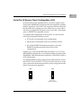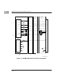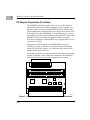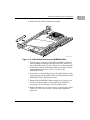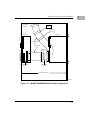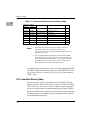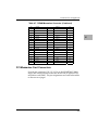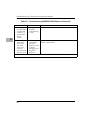
1
MVME2600 Series
Single Board Computer
Installation and Use
V2600A/IH2
Notice
While reasonable efforts have been made to assure the accuracy of this document,
Motorola, Inc. assumes no liability resulting from any omissions in this document,
or from the use of the information obtained therein. Motorola reserves the right to
revise this document and to make changes from time to time in the content hereof
without obligation of Motorola to notify any person of such revision or changes.
No part of this material may be reproduced or copied in any tangible medium, or
stored in a retrieval system, or transmitted in any form, or by any means, radio,
electronic, mechanical, photocopying, recording or facsimile, or otherwise,
without the prior written permission of Motorola, Inc.
It is possible that this publication may contain reference to, or information about
Motorola products (machines and programs), programming, or services that are
not announced in your country. Such references or information must not be
construed to mean that Motorola intends to announce such Motorola products,
programming, or services in your country.
Restricted Rights Legend
If the documentation contained herein is supplied, directly or indirectly, to the U.S.
Government, the following notice shall apply unless otherwise agreed to in
writing by Motorola, Inc.
Use, duplication, or disclosure by the Government is subject to restrictions as set
forth in subparagraph (c)(1)(ii) of the Rights in Technical Data and Computer
Software clause at DFARS 252.227-7013.
Motorola, Inc.
Computer Group
2900 South Diablo Way
Tempe, Arizona 85282
Preface
The MVME2600 Series Single Board Computer Installation and Use manual provides
general information, hardware preparation and installation instructions, operating
instructions, a functional description, and various types of interfacing information
for the MVME2603/MVME2604 family of Single Board Computers.The
information in this manual applies to the following MVME2603/MVME2604
models.
MVME2603-1121A
MVME2603-1131A
MVME2603-1141A
MVME2603-1191A
MVME2603-2121A
MVME2603-2131A
MVME2603-2141A
MVME2603-2191A
MVME2604-1021A
MVME2604-1031A
MVME2604-1041A
MVME2604-1091A
MVME2604-1121A
MVME2604-1131A
MVME2604-1141A
MVME2604-1191A
MVME2604-2021A
MVME2604-2031A
MVME2604-2041A
MVME2604-2091A
MVME2604-2121A
MVME2604-2131A
MVME2604-2141A
MVME2604-2191A
This manual is intended for anyone who wants to supply OEM systems, add
capability to an existing compatible system, or work in a lab environment for
experimental purposes. A basic knowledge of computers and digital logic is
assumed.
After using this manual, you may wish to become familiar with the publications
listed in the Related Documentation section in Appendix A of this manual.
Motorola¨ and the Motorola symbol are registered trademarks of Motorola, Inc.
AIXª is a trademark of IBM Corp.
PowerPCª is a trademark of IBM Corp. and is used by Motorola with permission.
All other products mentioned in this document are trademarks or registered
trademarks of their respective holders.
© Copyright Motorola 1998
All Rights Reserved
Printed in the United States of America
May 1998
Safety Summary
Safety Depends On You
The following general safety precautions must be observed during all phases of operation, service, and
repair of this equipment. Failure to comply with these precautions or with speciÞc warnings elsewhere in
this manual violates safety standards of design, manufacture, and intended use of the equipment.
Motorola, Inc. assumes no liability for the customer's failure to comply with these requirements.
The safety precautions listed below represent warnings of certain dangers of which Motorola is aware. You,
as the user of the product, should follow these warnings and all other safety precautions necessary for the
safe operation of the equipment in your operating environment.
Ground the Instrument.
To minimize shock hazard, the equipment chassis and enclosure must be connected to an electrical ground.
The equipment is supplied with a three-conductor AC power cable. The power cable must be plugged into
an approved three-contact electrical outlet. The power jack and mating plug of the power cable must meet
International Electrotechnical Commission (IEC) safety standards.
Do Not Operate in an Explosive Atmosphere.
Do not operate the equipment in the presence of ßammable gases or fumes. Operation of any electrical
equipment in such an environment constitutes a deÞnite safety hazard.
Keep Away From Live Circuits.
Operating personnel must not remove equipment covers. Only Factory Authorized Service Personnel or
other qualiÞed maintenance personnel may remove equipment covers for internal subassembly or
component replacement or any internal adjustment. Do not replace components with power cable
connected. Under certain conditions, dangerous voltages may exist even with the power cable removed. To
avoid injuries, always disconnect power and discharge circuits before touching them.
Do Not Service or Adjust Alone.
Do not attempt internal service or adjustment unless another person capable of rendering Þrst aid and
resuscitation is present.
Use Caution When Exposing or Handling the CRT.
Breakage of the Cathode-Ray Tube (CRT) causes a high-velocity scattering of glass fragments (implosion).
To prevent CRT implosion, avoid rough handling or jarring of the equipment. Handling of the CRT should
be done only by qualiÞed maintenance personnel using approved safety mask and gloves.
Do Not Substitute Parts or Modify Equipment.
Because of the danger of introducing additional hazards, do not install substitute parts or perform any
unauthorized modiÞcation of the equipment. Contact your local Motorola representative for service and
repair to ensure that safety features are maintained.
Dangerous Procedure Warnings.
Warnings, such as the example below, precede potentially dangerous procedures throughout this manual.
Instructions contained in the warnings must be followed. You should also employ all other safety
precautions which you deem necessary for the operation of the equipment in your operating environment.
!
WARNING
Dangerous voltages, capable of causing death, are
present in this equipment. Use extreme caution when
handling, testing, and adjusting.
All Motorola PWBs (printed wiring boards) are manufactured by UL-recognized
manufacturers, with a ßammability rating of 94V-0.
!
WARNING
This equipment generates, uses, and can radiate electromagnetic energy. It may cause or be susceptible to
electro-magnetic interference (EMI) if not installed and
used in a cabinet with adequate EMI protection.
If any modifications are made to the product, the
modifier assumes responsibility for radio frequency
interference issues. Changes or modifications not
expressly approved by Motorola Computer Group
could void the userÕs authority to operate the
equipment.
European Notice: Board products with the CE marking comply with the
EMC Directive (89/336/EEC). Compliance with this directive implies
conformity to the following European Norms:
EN55022 (CISPR 22) Radio Frequency Interference
EN50082-1 (IEC801-2, IEC801-3, IEEC801-4) Electromagnetic
Immunity
This board product was tested in a representative system to show
compliance with the above mentioned requirements. A proper installation
in a CE-marked system will maintain the required EMC/safety
performance.
For minimum RF emissions, it is essential that you implement the
following conditions:
1. Install shielded cables on all external I/O ports.
2. Connect conductive chassis rails to earth ground to provide a path for
connecting shields to earth ground.
3. Tighten all front panel screws.
Contents
Chapter 1
Hardware Preparation and Installation
Introduction ..........................................................................................................1-1
Equipment Required............................................................................................1-3
Overview of Startup Procedure .........................................................................1-4
Unpacking Instructions .......................................................................................1-5
Hardware ConÞguration.....................................................................................1-5
MVME2603/2604 Base Board Preparation .......................................................1-6
Cache Mode Control (J3) ..............................................................................1-7
Flash Bank Selection (J10).............................................................................1-7
Serial Port 4 Receive Clock ConÞguration (J16) ........................................1-9
Serial Port 4 Transmit Clock ConÞguration (J17) .................................... 1-11
Serial Port 4 Transmit Clock Receiver Buffer Control (J20) ...................1-12
Serial Port 3 Transmit Clock ConÞguration (J18) ....................................1-13
System Controller Selection (J22) ..............................................................1-14
Remote Status and Control.........................................................................1-14
MVME712M Transition Module Preparation ................................................1-15
Serial Ports 1-4 DCE/DTE ConÞguration ................................................1-17
Serial Port 4 Clock ConÞguration..............................................................1-17
P2 Adapter Preparation ..............................................................................1-24
MVME761 Transition Module Preparation ....................................................1-25
Serial Ports 1 and 2 ......................................................................................1-27
ConÞguration of Serial Ports 3 and 4........................................................1-27
P2 Adapter Preparation (Three-Row) .......................................................1-32
P2 Adapter Preparation (Five-Row)..........................................................1-34
Hardware Installation........................................................................................1-35
ESD Precautions...........................................................................................1-35
RAM200 Memory Mezzanine Installation .....................................................1-36
PMC Module Installation..................................................................................1-38
PMC Carrier Board Installation .......................................................................1-40
MVME2603/2604 VMEmodule Installation...................................................1-42
MVME712M Transition Module Installation .................................................1-44
MVME761 Transition Module Installation .....................................................1-48
System Considerations ......................................................................................1-50
MVME2603/2604 VMEmodule .................................................................1-52
vii
Chapter 2
Operating Instructions
Introduction .......................................................................................................... 2-1
Applying Power ................................................................................................... 2-1
ABORT Switch (S1) ....................................................................................... 2-2
RESET Switch (S2) ......................................................................................... 2-3
Front Panel Indicators (DS1 - DS6) ............................................................. 2-4
Memory Maps ...................................................................................................... 2-5
Processor Memory Map................................................................................ 2-5
Default Processor Memory Map 2-5
PCI Local Bus Memory Map........................................................................ 2-6
VMEbus Memory Map ................................................................................. 2-7
Programming Considerations ............................................................................ 2-7
PCI Arbitration .............................................................................................. 2-9
Interrupt Handling...................................................................................... 2-10
DMA Channels............................................................................................. 2-12
Sources of Reset ........................................................................................... 2-12
Endian Issues ............................................................................................... 2-13
Processor/Memory Domain 2-14
PCI Domain 2-14
VMEbus Domain 2-15
Chapter 3
Functional Description
Introduction .......................................................................................................... 3-1
Features ................................................................................................................. 3-1
General Description............................................................................................. 3-3
Block Diagram ...................................................................................................... 3-5
SCSI Interface ................................................................................................. 3-6
SCSI Termination 3-6
Ethernet Interface .......................................................................................... 3-7
PCI Mezzanine Interface .............................................................................. 3-8
VMEbus Interface .......................................................................................... 3-9
ISA Super I/O Device (ISASIO) .................................................................. 3-9
Asynchronous Serial Ports 3-11
Parallel Port 3-11
Disk Drive Controller 3-12
Keyboard and Mouse Interface 3-12
PCI-ISA Bridge (PIB) Controller................................................................ 3-12
viii
Real-Time Clock/NVRAM/Timer Function ...........................................3-13
Programmable Timers.................................................................................3-14
Interval Timers 3-14
16-Bit Timers 3-15
Serial Communications Interface ..............................................................3-15
Z8536 CIO Device 3-16
Base Module Feature Register ...................................................................3-16
P2 Signal Multiplexing................................................................................3-17
ABORT Switch (S1)......................................................................................3-18
RESET Switch (S2) .......................................................................................3-19
Front Panel Indicators (DS1 - DS6)............................................................3-19
Polyswitches (Resettable Fuses) ................................................................3-20
I/O Power ............................................................................................. 3-20
Speaker Control............................................................................................3-21
PM603/604 Processor..................................................................................3-21
Flash Memory ....................................................................................... 3-22
RAM200 Memory Module .........................................................................3-23
MVME712M Transition Module................................................................3-23
MVME761 Transition Module....................................................................3-24
Serial Interface Modules 3-25
Chapter 4
Connector Pin Assignments
MVME2603/2604 Connectors ............................................................................4-1
Common Connectors ...........................................................................................4-3
LED Mezzanine Connector J1 ......................................................................4-3
Debug Connector J2.......................................................................................4-3
Floppy/LED Connector J4 ...........................................................................4-7
PCI Expansion Connector J5 ........................................................................4-8
Keyboard and Mouse Connectors J6, J8 ...................................................4-10
DRAM Mezzanine Connector J7 ...............................................................4-10
PCI Mezzanine Card Connectors ..............................................................4-13
VMEbus Connector P1................................................................................4-15
MVME712M-Compatible Versions ..................................................................4-17
VMEbus Connector P2 (MVME712M I/O Mode) ..................................4-17
SCSI Connector (MVME712M I/O Mode)...............................................4-17
Serial Ports 1-4 (MVME712M I/O Mode) ................................................4-20
Parallel Connector (MVME712M I/O Mode)..........................................4-21
Ethernet AUI Connector .............................................................................4-22
ix
MVME761-Compatible Versions ..................................................................... 4-23
VMEbus Connector P2 (MVME761 I/O Mode)...................................... 4-23
Serial Ports 1 and 2 (MVME761 I/O Mode) ............................................ 4-25
Serial Ports 3 and 4 (MVME761 I/O Mode) ............................................ 4-26
Parallel Connector (MVME761 I/O Mode) ............................................. 4-27
Ethernet 10Base-T/100Base-TX Connector.............................................. 4-28
Chapter 5
PPCBug
Overview............................................................................................................... 5-1
Memory Requirements ................................................................................. 5-2
PPCBug Implementation.............................................................................. 5-2
Using the Debugger............................................................................................. 5-3
Debugger Commands................................................................................... 5-4
Diagnostic Tests ............................................................................................. 5-8
Chapter 6
CNFG and ENV Commands
Overview............................................................................................................... 6-1
CNFG - ConÞgure Board Information Block ................................................... 6-2
ENV - Set Environment....................................................................................... 6-3
ConÞguring the PPCBug Parameters ......................................................... 6-3
ConÞguring the VMEbus Interface........................................................... 6-12
Motorola Computer Group Documents .......................................................... A-1
ManufacturersÕ Documents ............................................................................... A-2
Related SpeciÞcations......................................................................................... A-6
Appendix B Specifications
SpeciÞcations ........................................................................................................B-1
Cooling Requirements.........................................................................................B-2
FCC Compliance ..................................................................................................B-3
Appendix C Serial Interconnections
Introduction ......................................................................................................... C-1
EIA-232-D Connections...................................................................................... C-2
Interface Characteristics .............................................................................. C-4
EIA-530 Connections .......................................................................................... C-5
x
Interface Characteristics............................................................................... C-8
Proper Grounding ............................................................................................... C-9
Appendix D Troubleshooting CPU Boards: Solving Startup Problems
Introduction .........................................................................................................D-1
Glossary
Abbreviations, Acronyms, and Terms to Know........................................... GL-1
xi
xii
Figures
Figure 1-1. MVME2603/2604 Base Board Block Diagram.............................1-2
Figure 1-2. MVME2603/2604 Switches, Headers, Connectors, Fuses,
LEDs
..........................................................................................................1-10
Figure 1-3. MVME712M Connector and Header Locations ........................1-16
Figure 1-4. J15 Clock Line ConÞguration.......................................................1-17
Figure 1-5. MVME712M Serial Port 1 DCE/DTE ConÞguration ...............1-18
Figure 1-6. MVME712M Serial Port 2 DCE/DTE ConÞguration ...............1-19
Figure 1-7. MVME712M Serial Port 3 DCE ConÞguration..........................1-20
Figure 1-8. MVME712M Serial Port 3 DTE ConÞguration ..........................1-21
Figure 1-9. MVME712M Serial Port 4 DCE ConÞguration..........................1-22
Figure 1-10. MVME712M Serial Port 4 DTE ConÞguration.........................1-23
Figure 1-11. MVME712M P2 Adapter Component Placement ....................1-24
Figure 1-12. MVME761 Connector and Header Locations...........................1-26
Figure 1-13. MVME761 Serial Ports 1 and 2 (DCE Only) .............................1-29
Figure 1-14. MVME761 Serial Ports 3 and 4 DCE ConÞguration................1-30
Figure 1-15. MVME761 Serial Ports 3 and 4 DTE ConÞguration ................1-31
Figure 1-16. MVME761 P2 Adapter (Three-Row) Component Placement 1-33
Figure 1-17. MVME761 P2 Adapter (Five-Row) Component Placement...1-34
Figure 1-18. RAM200 Placement on MVME2603/2604 ................................1-37
Figure 1-19. PMC Module Placement on MVME2603/2604........................1-39
Figure 1-20. PMC Carrier Board Placement on MVME2603/2604 .............1-41
Figure 1-21. MVME712M/MVME2603/2604 Cable Connections ..............1-47
Figure 1-22. MVME761/MVME2603/2604 Cable Connections ..................1-49
Figure 2-1. PPCBug System Startup..................................................................2-2
Figure 2-2. VMEbus Master Mapping ..............................................................2-8
Figure 2-3. MVME2603/MVME2604 Interrupt Architecture ...................... 2-11
Figure 3-1. MVME2603/2604 Block Diagram .................................................3-5
xiii
xiv
Tables
Table 1-1. VMEmodule/Transition Module Correspondence .......................1-3
Table 1-2. Startup Overview ...............................................................................1-4
Table 1-3. MVME712M Port/Jumper Correspondence ................................1-17
Table 2-1. Processor Default View of the Memory Map .................................2-6
Table 2-2. PCI Arbitration Assignments............................................................2-9
Table 2-3. IBC DMA Channel Assignments....................................................2-12
Table 2-4. Classes of Reset and Effectiveness .................................................2-13
Table 3-1. MVME2603/2604 Features................................................................3-1
Table 3-2. P2 Multiplexing Sequence...............................................................3-18
Table 3-3. Fuse Assignments.............................................................................3-20
Table 3-4. SIM Type IdentiÞcation ...................................................................3-25
Table 4-1. LED Mezzanine Connector ...............................................................4-3
Table 4-2. Debug Connector................................................................................4-4
Table 4-3. Floppy/LED Connector.....................................................................4-7
Table 4-4. PCI Expansion Connector .................................................................4-8
Table 4-5. Keyboard Connector ........................................................................4-10
Table 4-6. Mouse Connector..............................................................................4-10
Table 4-7. DRAM Mezzanine Connector ........................................................ 4-11
Table 4-8. PCI Mezzanine Card Connector.....................................................4-14
Table 4-8. PCI Mezzanine Card Connector (Continued) ..............................4-15
Table 4-9. VMEbus Connector P1.....................................................................4-16
Table 4-10. VMEbus Connector P2 (MVME712M I/O Mode) .....................4-18
Table 4-11. SCSI Connector (MVME712M) .....................................................4-19
Table 4-12. Serial ConnectionsÑMVME712M Ports 1-4...............................4-20
Table 4-13. Parallel I/O Connector (MVME712M)........................................4-21
Table 4-14. Ethernet AUI Connector (MVME712M)......................................4-22
Table 4-15. VMEbus Connector P2 (MVME761 I/O Mode).........................4-24
Table 4-16. Serial ConnectionsÑPorts 1 and 2 (MVME761).........................4-25
Table 4-17. Serial ConnectionsÑPorts 3 and 4 (MVME761).........................4-26
Table 4-18. Parallel I/O Connector (MVME761)............................................4-27
Table 4-19. Ethernet 10Base-T/100Base-TX Connector (MVME761) ..........4-28
Table 5-1. Debugger Commands........................................................................5-4
xv
Table 5-2. Diagnostic Test Groups...................................................................... 5-8
Table A-1. Motorola Computer Group Documents ....................................... A-1
Table A-2. ManufacturersÕ Documents ............................................................ A-2
Table A-3. Related SpeciÞcations ...................................................................... A-6
Table B-1. MVME2603/2604 SpeciÞcations......................................................B-1
Table C-1. EIA-232-D Interconnect Signals...................................................... C-3
Table C-2. EIA-232-D Interface Transmitter Characteristics ......................... C-4
Table C-3. EIA-232-D Interface Receiver Characteristics .............................. C-5
Table C-4. MVME761 EIA-530 Interconnect Signals ...................................... C-6
Table C-5. EIA-530 Interface Transmitter Characteristics.............................. C-8
Table C-6. EIA-530 Interface Receiver Characteristics................................... C-9
Table D-1. Troubleshooting MVME2603/2604 Boards .................................. D-1
xvi
1Hardware Preparation and
Installation
1
Introduction
This manual provides general information, hardware preparation
and installation instructions, operating instructions, and a
functional description of the MVME2603/2604 family of Single
Board Computers.
The MVME2603/2604 is a single-slot VMEmodule equipped with a
PowerPCª Series microprocessor. The MVME2603 is equipped
with a PowerPC 603 microprocessor; the MVME2604 has a
PowerPC 604 microprocessor. 256KB L2 cache (level 2 secondary
cache memory) is available as an option on all versions.
The complete MVME2603/2604 consists of the base board plus:
❏
An ECC DRAM module (RAM200) for memory
❏
An optional PCI mezzanine card (PMC) for additional
versatility
❏
An optional carrier board for additional PCI expansion
The block diagram in Figure 1-1 illustrates the architecture of the
MVME2603/2604 base board.
1-1
Introduction
66MHz MPC604 PROCESSOR BUS
DEBUG CONNECTOR
L2 CACHE
256K
PROCESSOR
MPC603/604
PHB & MPIC
RAVEN ASIC
MEMORY EXPANSION CONNECTORS
FLASH
4MB or 8MB
FLASH
1MB
SYSTEM
REGISTERS
MEMORY CONTROLLER
FALCON CHIPSET
PCI EXPANSION
CLOCK
GENERATOR
64-BIT PMC SLOT
33MHz 32/64-BIT PCI LOCAL BUS
FLOPPY & LED
PIB
W83C553
ISA
REGISTERS
ETHERNET
DEC21140
SCSI
53C825A
VME BRIDGE
UNIVERSE
BUFFERS
RTC/NVRAM/WD
MK48T59
KBD
ISA BUS
AUI/10BT/100BTX
FRONT PANEL
ESCC
85230
CIO
Z8536
SERIAL
PARALLEL
SUPER I/O
PC87308
MOUSE
PMC FRONT I/O SLOT
1
712/761 P2 I/O OPTIONS
VME P2
VME P1
11536.00 9611
Figure 1-1. MVME2603/2604 Base Board Block Diagram
1-2
Hardware Preparation and Installation
Equipment Required
The following equipment is required to complete an MVME2603/
2604 system:
❏
VME system enclosure
❏
System console terminal
❏
Operating system (and/or application software)
❏
Disk drives (and/or other I/O) and controllers
❏
Transition module (MVME712M or MVME761) and
connecting cables
MVME2603/2604 VMEmodules are factory-configured for I/O
handling via either MVME712M or MVME761 transition modules.
The following table shows the relationship between MVME2603/
2604 model numbers and the applicable transition module.
Table 1-1. VMEmodule/Transition Module Correspondence
MVME761-Compatible Models
MVME2603-1121A
MVME2603-1131A
MVME2603-1141A
MVME2603-1151A
MVME2603-1161A
MVME2604-1121A
MVME2604-1131A
MVME2604-1141A
MVME2604-1151A
MVME2604-1161A
!
Caution
!
Caution
MVME712-Compatible Models
MVME2603-2121A
MVME2603-2131A
MVME2603-2141A
MVME2603-2151A
MVME2603-2161A
MVME2604-2121A
MVME2604-2131A
MVME2604-2141A
MVME2604-2151A
MVME2604-2161A
MVME2600-1XXX (MVME761-compatible models) will
be damaged if they are mistakenly connected to the
MVME712 family of boards instead of the correct
MVME761 transition modules.
MVME2600-2XXX (MVME712-compatible models) will
be damaged if they are mistakenly connected to the
MVME761 transition modules instead of the correct
MVME712 family of boards.
1-3
1
1
Overview of Startup Procedure
In models of the MVME2603/2604 that are configured for
MVME712M I/O mode, the pin assignments of VMEbus connector
P2 are fully compatible with other transition modules of the
MVME712 series. In MVME761-compatible models, certain signals
are multiplexed through P2 for additional I/O capacity. Refer to P2
Signal Multiplexing in Chapter 3 for details.
Overview of Startup Procedure
The following table lists the things you will need to do before you
can use this board and tells where to find the information you need
to perform each step. Be sure to read this entire chapter, including
all Caution and Warning notes, before you begin.
Table 1-2. Startup Overview
What you need to do...
Refer to...
On page...
Unpack the hardware.
Unpacking Instructions
ConÞgure the hardware by
setting jumpers on the boards
and transition modules.
MVME2603/2604 Base Board Preparation and
MVME712M Transition Module Preparation or
MVME761 Transition Module Preparation
Ensure memory mezzanines
are properly installed on the
base board.
RAM200 Memory Mezzanine Installation
1-33
Install the MVME2603/2604
VMEmodule in the chassis.
MVME2603/2604 VMEmodule Installation
1-35
Install the transition module in MVME712M Transition Module Installation or
the chassis.
MVME761 Transition Module Installation
1-5
1-6 and
1-15 or 1-25
1-38
or 1-41
Connect a console terminal.
System Considerations, MVME2603/2604
VMEmodule
1-46
Connect any other equipment
you will be using.
Connector Pin Assignments
4-1
Power up the system.
Applying Power
2-1
Troubleshooting CPU Boards ; Solving Start-Up
Problems
D-1
1-4
For more information on optional devices and
equipment, refer to the documentation provided
with the equipment.
Hardware Preparation and Installation
Table 1-2. Startup Overview (Continued)
What you need to do...
Note that the debugger
initializes the MVME2603/
2604.
Refer to...
On page...
Using the Debugger
5-3
You may also wish to obtain the PPCBug
Firmware Package UserÕs Manual, listed in
Appendix A, Related Documentation.
A-1
Initialize the system clock.
Using the Debugger, Debugger Commands, the
SET command
5-6
Examine and/or change
environmental parameters.
CNFG and ENV Commands
Program the board as needed
for your applications.
MVME2600 Series Single Board Computer
ProgrammerÕs Reference Guide, listed in Appendix
A, Related Documentation.
6-2
and/or 6-3
A-1
Unpacking Instructions
Note
If the shipping carton is damaged upon receipt, request
that the carrier's agent be present during the unpacking
and inspection of the equipment.
Unpack the equipment from the shipping carton. Refer to the
packing list and verify that all items are present. Save the packing
material for storing and reshipping of equipment.
!
Avoid touching areas of integrated circuitry; static
discharge can damage circuits.
Caution
Hardware Configuration
To produce the desired configuration and ensure proper operation
of the MVME2603/2604, you may need to carry out certain
hardware modifications before installing the module.
1-5
1
1
MVME2603/2604 Base Board Preparation
The MVME2603/2604 provides software control over most options:
by setting bits in control registers after installing the module in a
system, you can modify its configuration. (The MVME2603/2604
control registers are described in Chapter 3, and/or in the
MVME2600 Series Single Board Computer Programmer's Reference
Guide as listed under Related Documentation in Appendix A.)
Some options, however, are not software-programmable. Such
options are controlled through manual installation or removal of
header jumpers or interface modules on the base board or the
associated transition module.
MVME2603/2604 Base Board Preparation
Figure 1-2 illustrates the placement of the switches, jumper
headers, connectors, and LED indicators on the MVME2603/2604.
Manually configurable items on the base board include:
❏
Cache mode control (J3)
❏
Flash bank selection (J10)
❏
Serial Port 4 receive clock configuration (J16)
❏
Serial Port 4 transmit clock configuration (J17)
❏
Serial Port 4 transmit clock receiver buffer control (J20)
❏
Serial Port 3 transmit clock configuration (J18)
❏
System controller selection (J22)
In conjunction with the serial port settings on the base board, serial
ports on the associated MVME712M or MVME761 transition
module are also manually configurable. For a discussion of the
configurable items on the transition module, refer in this chapter to
the sections entitled MVME712M Transition Module Preparation,
MVME761 Transition Module Preparation, or to the respective userÕs
manuals for the transition modules (listed in the Related
Documentation appendix) as necessary.
1-6
Hardware Preparation and Installation
The MVME2603/2604 is factory tested and shipped with the
configurations described in the following sections. The
MVME2603/2604Õs required and factory-installed debug monitor,
PPCBug, operates with those factory settings.
Cache Mode Control (J3)
256KB of L2 cache memory is available on the MVME2603/2604. L2
cache operation is transparent to users, but its write-through mode
is configurable via header J3 on older boards. On newer
MVME2603/2604 boards, header J3 is not provided. With a jumper
installed on J3, cache write-through is under CPU control. With the
jumper removed, cache write-through occurs in all cases.
J3
2
J3
1
Cache Write-Through under CPU Control
2
1
Cache Write-Through Always
(factory configuration)
Flash Bank Selection (J10)
The MVME2603/2604 base board has provision for 1MB of 16-bit
Flash memory. The RAM200 memory mezzanine accommodates
4MB or 8MB of additional 64-bit Flash memory.
The Flash memory is organized in either one or two banks, each
bank either 16 or 64 bits wide. Both banks contain the onboard
debugger, PPCBug.
1-7
1
1
MVME2603/2604 Base Board Preparation
To enable Flash bank A (4MB or 8MB of firmware resident on
soldered-in devices on the RAM200 mezzanine), place a jumper
across header J10 pins 1 and 2. To enable Flash bank B (1MB of
firmware located in sockets on the base board), place a jumper
across header J10 pins 2 and 3.
J10
J10
3
3
2
2
1
1
Flash Bank A Enabled (4MB/8MB, Soldered)
(factory configuration)
1-8
Flash Bank B Enabled (1MB, Sockets)
Hardware Preparation and Installation
Serial Port 4 Receive Clock Configuration (J16)
In synchronous serial communications, you can configure Serial
Port 4 on the MVME2603/2604 to use the clock signals provided by
the RxC signal line. On MVME712M-compatible versions of the base
board, header J16 configures port 4 to either drive or receive RxC.
The factory configuration has port 4 set to receive RxC. J16 remains
open on MVME761-compatible versions.
To complete the configuration of Serial Port 4, you must set the
following configuration headers as well:
❏
J17 (Serial Port 4 transmit clock configuration)
❏
J20 (Serial Port 4 transmit clock receiver buffer control)
❏
J15 on the MVME712M transition module or J3 on the
MVME761 transition module (Serial Port 4 clock
configuration)
Figures 1-8/1-9 (for the MVME712M) and Figures 1-14/1-15 (for
the MVME761) diagram the overall jumper settings required on the
MVME2603/2604 and transition module for a Serial Port 4 DCE or
DTE configuration.
For additional details on the configuration of those headers, refer to
the MVME712M or MVME761 Transition Module sections or to the
userÕs manual for the transition module you are using (listed in the
Related Documentation appendix).
J16
J16
3
3
2
2
1
1
Drive RxC
Receive RxC
(factory configuration)
1-9
1
MVME2603/2604 Base Board Preparation
1
2
1
P1
J4
1
2
26
27
FUS
A1
B1
C1
D1
RST
BFL
FLOPPY/LED
A32
B32
C32
D32
XU1
J7
6
J5
5
XU2
J6
4 2 1 3
KEYBOARD
6
J8
4 2 1 3
5
MOUSE
A1
B1
C1
D1
2
1
J12
J11
P2
J9
2
1
1
2
16
15
J14
J13
64
A32
B32
C32
D32
64
J22
J20
J18
J17
J16
J23
J15
11517.00 9608
J10
2
1
2
1
PCI MEZZANINE CARD
1-10
CHS
J3
J2
J1
25
24
49
50
ABT
CPU
PCI
SYS
Figure 1-2. MVME2603/2604 Switches, Headers, Connectors, Fuses, LEDs
Hardware Preparation and Installation
Serial Port 4 Transmit Clock Configuration (J17)
In synchronous serial communications, you can configure Serial
Port 4 on the MVME2603/2604 to use the clock signals provided by
the TxC signal line. Header J17 configures port 4 to either drive or
receive TxC. The factory configuration has port 4 set to receive TxC.
To complete the configuration of Serial Port 4, you must set the
following configuration headers as well:
❏
J16 (Serial Port 4 receive clock configuration)
❏
J20 (Serial Port 4 transmit clock receiver buffer control)
❏
J15 on the MVME712M transition module or J3 on the
MVME761 transition module (Serial Port 4 clock
configuration)
Figures 1-8/1-9 (for the MVME712M) and Figures 1-14/1-15 (for
the MVME761) diagram the overall jumper settings required on the
MVME2603/2604 and transition module for a Serial Port 4 DCE or
DTE configuration.
For additional details on the configuration of those headers, refer to
the MVME712M or MVME761 Transition Module sections or to the
userÕs manual for the transition module you are using (listed in the
Related Documentation appendix).
J17
J17
3
3
2
2
1
1
Drive TxC
Receive TxC
(factory configuration)
1-11
1
1
MVME2603/2604 Base Board Preparation
Serial Port 4 Transmit Clock Receiver Buffer Control (J20)
As described in other sections, a complete configuration of Serial
Port 4 requires that you set the following jumper headers on the
MVME2603/2604 or the transition module:
❏
J16 (Serial Port 4 receive clock configuration) on
MVME712M-compatible versions of the base board
❏
J17 (Serial Port 4 transmit clock configuration)
❏
J20 (Serial Port 4 transmit clock receiver buffer control) on
MVME712M-compatible versions of the base board
❏
J15 on the MVME712M transition module or J3 on the
MVME761 (Serial Port 4 clock configuration)
A transmit clock receiver buffer (controlled by header J20) is
associated with Serial Port 4. Installing a jumper on J20 enables the
buffer. Removing the jumper disables the buffer. The factory
configuration has the Serial Port 4 buffer enabled.
J20 remains open on MVME761-compatible versions. On
MVME712M-compatible versions, J20 is set in tandem with J17 to
configure the Serial Port 4 transmit clock. If one deviates from the
factory configuration, so must the other. Figures 1-8/1-9 (for the
MVME712M) and Figures 1-14/1-15 (for the MVME761) diagram
the overall jumper settings required on the MVME2603/2604 and
transition module for a Serial Port 4 DCE or DTE configuration.
For additional details on the configuration of those headers, refer to
the MVME712M or MVME761 Transition Module sections or to the
userÕs manual for the transition module you are using (listed in the
Related Documentation appendix).
1-12
J20
J20
2
2
1
1
Buffer Enabled
(factory configuration)
Buffer Disabled
Hardware Preparation and Installation
Serial Port 3 Transmit Clock Configuration (J18)
In synchronous serial communications using the MVME761
transition module, you can configure Serial Port 3 on the
MVME2603/2604 to use the clock signals provided by the TxC
signal line. On MVME761-compatible versions of the base board,
header J18 configures port 3 to either drive or receive TxC. The
factory configuration has port 3 set to receive TxC. J18 remains open
on MVME712M-compatible versions.
To complete the configuration of Serial Port 3, you must set J2 on
the MVME761 transition module (Serial Port 3 clock configuration)
as well.
Figures 1-6/1-7 (for the MVME712M) and Figures 1-14/1-15 (for
the MVME761) diagram the overall jumper settings required on the
MVME2603/2604 and transition module for a Serial Port 3 DCE or
DTE configuration.
For additional details on the configuration of the MVME761
headers, refer to the MVME761 Transition Module section or to the
userÕs manual for the module (listed in the Related Documentation
appendix).
J18
J18
3
3
2
2
1
1
Drive TxC
Receive TxC
(factory configuration)
1-13
1
1
MVME2603/2604 Base Board Preparation
System Controller Selection (J22)
The MVME2603/2604 is factory-configured as a VMEbus system
controller by jumper header J22. If you select the ÔÔautomaticÕÕ
system controller function by placing a jumper on J22 pins 2 and 3,
the MVME2603/2604 determines whether it is the system controller
by its position on the bus. If the board is in the first slot from the left,
it configures itself as the system controller. If the MVME2603/2604
is not to be system controller under any circumstances, place the
jumper on J22 pins 1 and 2. When the board is functioning as system
controller, the SCON LED is turned on.
J22
J22
J22
3
3
3
2
2
2
1
1
1
Not System Controller
Auto System Controller
(factory configuration)
System Controller
Remote Status and Control
The MVME2603/2604 front panel LEDs and switches are mounted
on a removable mezzanine board. Removing the LED mezzanine
makes the mezzanine connector (J1, a keyed double-row 14-pin
connector) available for service as a remote status and control
connector. In this application, J1 can be connected to a usersupplied external cable to carry the Reset and Abort signals and the
LED lines to a control panel located apart from the
MVME2603/2604. Maximum cable length is 15 feet.
Table 4-1 lists the pin numbers and signal mnemonics for J1.
1-14
Hardware Preparation and Installation
MVME712M Transition Module Preparation
The MVME712M transition module (Figure 1-3) and P2 adapter
board are used in conjunction with the following models of the
MVME2603/2604 base board:
MVME2603-2121A
MVME2603-2131A
MVME2603-2141A
MVME2603-2151A
MVME2603-2161A
MVME2604-2121A
MVME2604-2131A
MVME2604-2141A
MVME2604-2151A
MVME2604-2161A
The features of the MVME712M include:
❏
A parallel printer port
❏
An Ethernet interface supporting AUI connections
❏
One synchronous/asynchronous, and three asynchronous
only, EIA-232-D multiprotocol serial ports
❏
An SCSI interface (via P2 adapter) for connection to both
internal and external devices
❏
Socket-mounted SCSI terminating resistors for end-of-cable
or middle-of-cable configurations
❏
Provision for modem connection
❏
Green LED for SCSI terminator power; yellow LED for
Ethernet transceiver power
The features of the P2 adapter board include:
❏
A 50-pin connector for SCSI cabling to the MVME712M
and/or to other SCSI devices
❏
Socket-mounted SCSI terminating resistors for end-of-cable
or middle-of-cable configurations
❏
Fused SCSI teminator power developed from the +5Vdc
present at connector P2
❏
A 64-pin DIN connector to interface the EIA-232-D, parallel,
SCSI, and Ethernet signals to the MVME712M
1-15
1
MVME712M Transition Module Preparation
1
MVME712M
J14
J20
1
2
19
20
J17
1
J19
J21
14
J11
13
6
DS1
8
15
DS2
J6
ETHERNET
SCSI
INTERFACE
PRIMARY SIDE
13
14
14 2
J18
13 1
13 1
14 2
14 2
J16
13 1
14 2
14 2
J13
12
11
J8
J10
1
14
1
14
13 1
14 2
13 1
J15 2
1
13
25
13
25
2
J1
13 1
1
14
1
14
1
2
1
J7
J9
SERIAL PORT 2 / TTY01
13
25
13
25
SERIAL PORT 1 / CONSOLE
SERIAL PORT 4
R50
C2
J2
1
C3
8
A32
C32
1
J4
2
1 R51
50
J3
8
49
C1
8
49
R49
2
1
50
18
36
1
19
1
A1
C1
1
9
PRINTER
J5
1-16
SERIAL PORT 3
cb228 9212
Figure 1-3. MVME712M Connector and Header Locations
Hardware Preparation and Installation
Serial Ports 1-4 DCE/DTE Configuration
Serial ports 1 through 4 are configurable as modems (DCE) for
connection to terminals, or as terminals (DTE) for connection to
modems. The MVME712M is shipped with the serial ports
configured for DTE operation. Serial port DCE/DTE configuration
is accomplished by positioning jumpers on one of two headers per
port. The following table lists the serial ports with their
corresponding jumper headers.
Table 1-3. MVME712M Port/Jumper Correspondence
Serial Port
Board
Connector
Panel Connector
Jumper
Header
Port 1
J7
SERIAL PORT 1/ CONSOLE
J1/J11
Port 2
J8
SERIAL PORT 2/ TTY
J16/J17
Port 3
J9
SERIAL PORT 3
J13/J14
Port 4
J10
SERIAL PORT 4
J18/J19
The next six figures illustrate the MVME2603/2604 base board and
MVME712M transition module with the interconnections and
jumper settings for DCE/DTE configuration on each serial port.
Serial Port 4 Clock Configuration
Port 4 can be configured via J15 (Figure 1-4) to use the TrxC4 and
RtxC4 signal lines. Part of the configuration is done with headers
J16, J17, and J20 on the MVME2603/2604 (Figures 1-9 and 1-10).
J15
1
3
5
7
9
11
TRXC4 TO PORT 4 PIN 15
RTXC4 TO PORT 4 PIN 24
TRXC4 TO PORT 4 PIN 17
RTXC4 TO PORT 4 PIN 17
TRXC4 TO PORT 4 PIN 24
RTXC4 TO PORT 4 PIN 15
Figure 1-4. J15 Clock Line Configuration
1-17
1
1
MVME712M Transition Module Preparation
MVME2603/2604
P2 ADAPTER
BOARD
64-PIN
CABLE
MVME712M
MODULE
DB9
PC87308
RXD
SOUT1
CTS
RTS1#
DTR1#
NC
DCD
+12V
3
5
8
TXD
SIN1
2
DCE
RTS
CTS1#
4
DSR
DCD1#
6
+12V
GND
DSR1#
R11#
7
+5V
11551.00 9609 (1-8)
MVME2603/2604
P2 ADAPTER
BOARD
64-PIN
CABLE
MVME712M
MODULE
DB9
PC87308
TXD
SOUT1
RTS
RTS1#
DTR1#
NC
+12V
DTR
2
4
20
RXD
SIN1
3
DTE
CTS
CTS1#
5
DCD1#
GND
DSR1#
R11#
7
+5V
11551.00 9609 (2-8)
Figure 1-5. MVME712M Serial Port 1 DCE/DTE Configuration
1-18
Hardware Preparation and Installation
MVME2603/2604
P2 ADAPTER
BOARD
64-PIN
CABLE
MVME712M
MODULE
DB9
PC87308
RXD
SOUT2
CTS
RTS2#
DCD
DTR2#
3
5
8
TXD
SIN2
2
DCE
RTS
CTS2#
4
DTR
DCD2#
20
DSR2#
R12#
DSR
+12V
GND
+5V
6
7
11551.00 9609 (3-8)
MVME2603/2604
P2 ADAPTER
BOARD
64-PIN
CABLE
MVME712M
MODULE
DB9
PC87308
TXD
SOUT2
RTS
RTS2#
DTR
DTR2#
2
4
20
RXD
SIN2
DTE
3
CTS
CTS2#
5
DCD
DCD2#
8
DSR2#
R12#
+5V
GND
7
11551.00 9609 (4-8)
Figure 1-6. MVME712M Serial Port 2 DCE/DTE Configuration
1-19
1
1
MVME712M Transition Module Preparation
P2
ADAPTER
MVME2603/2604
Z85230
64-PIN
CABLE
MVME712M
MODULE
DB9
RXD
TXDA
CTS
RTSA#
3
5
DTR
DCDA#
20
TXD
RXDA
2
RTS
CTSA#
4
TRXCA#
+5V
RTXCA#
+5V
DCE
Z8536
DCD
DTR3#
8
LLB3#
+5V
RLB3#
+5V
DSR3#
R13#
+5V
+12V
DSR
6
GND
TM3#
7
+5V
NOTE : J18 OPEN
11551.00 9609 (5-8)
Figure 1-7. MVME712M Serial Port 3 DCE Configuration
1-20
Hardware Preparation and Installation
P2
ADAPTER
MVME2603/2604
Z85230
64-PIN
CABLE
MVME712M
MODULE
DB25
TXD
TXDA
RTS
RTSA#
DCD
DCDA#
2
4
8
RXD
RXDA
3
CTS
CTSA#
DTE
5
TRXCA#
+5V
RTXCA#
+5V
Z8536
DTR
DTR3#
LLB3#
+5V
RLB3#
+5V
20
DSR3#
R13#
+5V
TM3#
+5V
GND
7
NOTE : J18 OPEN
11551.00 9609 (6-8)
Figure 1-8. MVME712M Serial Port 3 DTE Configuration
1-21
1
1
MVME712M Transition Module Preparation
P2
ADAPTER
MVME2603/2604
Z85230
64-PIN
CABLE
MVME712M
MODULE
DB25
RXD
TXDB
CTS
RTSB#
3
5
DTR
DCDB#
20
TXD
RXDB
2
RTS
CTSB#
4
J17
TXCI
RXCI
TXCO
J20
J16
15
17
24
TRXCB
RTXCB
DCE
Z8536
DCD
DTR4#
LLB4#
+5V
RLB4#
+5V
8
DSR4#
R14#
+5V
+12V
DSR
6
GND
TM4#
7
+5V
NOTE : J20 OPEN
J16 1-2
J17 1-2
11551.00 9609 (7-8)
Figure 1-9. MVME712M Serial Port 4 DCE Configuration
1-22
Hardware Preparation and Installation
P2
ADAPTER
MVME2603/2604
Z85230
64-PIN
CABLE
MVME712M
MODULE
DB25
TXD
TXDB
RTS
RTSB#
DCD
DCDB#
2
4
8
RXD
RXDB
3
CTS
CTSB#
5
J17
TXCI
RXCI
TXCO
J20
J16
15
17
24
TRXCB
RTXCB
DTE
Z8536
DCD
DTR4#
LLB4#
+5V
RLB4#
+5V
20
DSR4#
R14#
+5V
TM4#
+5V
GND
7
NOTE : J20 1-2
J16 2-3
J17 2-3
11551.00 9609 (8-8)
Figure 1-10. MVME712M Serial Port 4 DTE Configuration
1-23
1
1
1Hardware Preparation and Installation
0
P2 Adapter Preparation
Preparation of the P2 adapter for the MVME712M consists of
removing or installing the SCSI terminating resistors. Figure 1-11
illustrates the location of the resistors, fuse, and connectors.
For further information on the preparation of the transition module
and the P2 adapter, refer to the userÕs manual for the MVME712M
(listed in the Related Documentation appendix) as necessary.
J2
A1
B1
C1
A32
B32
C32
J3
2
50
1
49
1
R1
C1
R2
C2
1
2
R3
C3
F1
CR1
C32
B32
A32
C1
B1
A1
P2
cb211 9212
Figure 1-11. MVME712M P2 Adapter Component Placement
1-24
Hardware Preparation and Installation
MVME761 Transition Module Preparation
The MVME761 transition module (Figure 1-12) and P2 adapter
board are used in conjunction with the following models of the
MVME2603/2604 base board:
MVME2603-1121A
MVME2603-1131A
MVME2603-1141A
MVME2603-1151A
MVME2603-1161A
MVME2604-1121A
MVME2604-1131A
MVME2604-1141A
MVME2604-1151A
MVME2604-1161A
The features of the MVME761 include:
❏
A parallel printer port (IEEE 1284-I compliant)
❏
An Ethernet interface supporting 10Base-T/100Base-TX
connections
❏
Two EIA-232-D asynchronous serial ports (identified as COM1
and COM2 on the front panel)
❏
Two synchronous serial ports (SERIAL 3 and SERIAL 4 on the
front panel), configurable for EIA-232-D, EIA-530, V.35, or
X.21 protocols
❏
Two 60-pin Serial Interface Module (SIM) connectors, used
on configuring serial ports 3 and 4
The features of the P2 adapter board for the MVME761 include:
❏
A 50-pin connector for SCSI cabling to SCSI devices
❏
Jumper-selectable SCSI terminating resistors
❏
Fused SCSI teminator power developed from the +5Vdc
present at connector P2
❏
A 64-pin 3M connector to the MVME761
1-25
1
1
MVME761 Transition Module Preparation
MVME
761-001
COM1
J5
COM2
J6 DTE
1
DCE
J2
3
SERIAL 3
60
J1
59
2
1
J7
SERIAL
60
J12
59
2
1
J8
DTE
DCE
J3
1
3
PARALLEL
J4
P2
10/100 BASET
J9
1910 9609
Figure 1-12. MVME761 Connector and Header Locations
1-26
Hardware Preparation and Installation
Serial Ports 1 and 2
On MVME761-compatible models of the MVME2603/2604 base
board, the asynchronous serial ports (Serial Ports 1 and 2) are
configured permanently as data circuit-terminating equipment
(DCE). The port configuration is illustrated in Figure 1-14.
Configuration of Serial Ports 3 and 4
The synchronous serial ports, Serial Port 3 and Serial Port 4, are
configurable through a combination of serial interface module
(SIM) selection and jumper settings. The following table lists the
SIM connectors and jumper headers corresponding to each of the
synchronous serial ports.
Synchronous
Port
Board
Connector
SIM
Connector
Jumper
Header
Port 3
J7
J1
J2
Port 4
J8
J12
J3
Port 3 is routed to board connector J7. Port 4 is available at board
connector J8. Eight serial interface modules are available:
❏
EIA-232-D (DCE and DTE)
❏
EIA-530 (DCE and DTE)
❏
V.35 (DCE and DTE)
❏
X.21 (DCE and DTE)
You can configure Serial Ports 3 and 4 for any of the above serial
protocols by installing the appropriate serial interface module and
setting the corresponding jumper. SIMs can be ordered separately
as required.
1-27
1
1
MVME761 Transition Module Preparation
Headers J2 and J3 are used to configure Serial Port 3 and Serial Port
4, respectively, in tandem with SIM selection. With the jumper in
position 1-2, the port is configured as a DTE. With the jumper in
position 2-3, the port is configured as a DCE. The jumper setting of the
port should match the configuration of the corresponding SIM module.
J2
J2
Serial Port 3 jumper settings
1
2
3
1
2
DCE
DTE
J3
J3
3
Serial Port 4 jumper settings
1
2
DCE
3
1
2
3
DTE
When installing the SIM modules, note that the headers are keyed
for proper orientation.
For further information on the preparation of the transition
module, refer to the userÕs manual for the MVME761 (listed in the
Related Documentation appendix) as necessary.
The next three figures illustrate the MVME2603/2604 base board
and MVME761 transition module with the interconnections and
jumper settings for DCE/DTE configuration on each serial port.
1-28
Hardware Preparation and Installation
MVME761
MVME2603/2604
DB9
DCE
SOUT1
3
RTS1#
7
DTR1#
4
SIN1
2
CTS1#
8
DSR1#
6
DCD1#
1
RI1#
9
PC87308
SOUT2
RTS2#
DTR2#
SIN2
CTS2#
P2/P2MX
COM1
5
3
7
4
2
8
DSR2#
6
DCD2#
1
RI2#
9
COM2
5
DB9
11552.00 9609 (1-3)
Figure 1-13. MVME761 Serial Ports 1 and 2 (DCE Only)
1-29
1
1
MVME761 Transition Module Preparation
MVME761
MVME3600 SERIES
Z85230 SCC
EIA232-DCE SIM
HD26
TXD
3
RTS#
5
RXD
2
CTS#
4
DCD#
20
J2/J3
J15
TRXC
3
2
3
2
1
1
15
17
24
RTXC
P2/P2MX
DCE
Z8536 CIO
DTR#
8
LLB#
25
RLB#
22
DSR#
6
RI#
21
TM#
18
7
11552.00 9802 (2-5)
Figure 1-14. MVME761 Serial Ports 3 and 4 DCE Configuration
1-30
Hardware Preparation and Installation
MVME2603/2604 SERIES
MVME761
Z85230 SCC
EIA232-DTE SIM
HD26
TXD
2
RTS#
4
RXD
3
CTS#
5
DCD#
8
J15
TRXC
J2/J3
3
2
3
1
1
24
2
15
17
RTXC
P2/P2MX
DTE
Z8536 CIO
DTR#
20
LLB#
18
RLB#
21
DSR#
6
RI#
22
TM#
25
7
11552.00 9802 (4-5)
Figure 1-15. MVME761 Serial Ports 3 and 4 DTE Configuration
1-31
1
1
MVME761 Transition Module Preparation
P2 Adapter Preparation (Three-Row)
The P2 adapter for the MVME761 transition module routes the
synchronous and asynchronous serial, parallel, and Ethernet
signals to the MVME761. The P2 adapter also has a 50-pin female
connector (J2) that carries 8-bit SCSI signals from the
MVME2603/2604. To run SCSI devices, you may install an
additional transition module that is equipped with a SCSI port,
such as the MVME712B.
Preparation of the P2 adapter for the MVME761 consists of
installing a jumper on header J1 to enable the SCSI terminating
resistors if necessary. Figure 1-16 illustrates the location of the
jumper header, resistors, fuse, and connectors.
1-32
J1
J1
2
2
1
1
SCSI Enabled
(factory configuration)
SCSI Disabled
Hardware Preparation and Installation
For further information on the preparation of the transition module
and the P2 adapter, refer to the userÕs manual for the MVME761
(listed in the Related Documentation appendix) as necessary.
50
49
J2 2
1
J3
2
1
64
63
C1
1
J1
25
1
R1
9
C5
C6
C4
+
17
C3
C7
R2
U1
C
B
A
C2
CR1
U2
+
32
C
B
A
P1
1933 9610
Figure 1-16. MVME761 P2 Adapter (Three-Row) Component Placement
1-33
1
1
MVME761 Transition Module Preparation
P2 Adapter Preparation (Five-Row)
The MVME761 transition module uses a five-row P2 adapter to
transfer the synchronous and asynchronous serial, parallel, and
Ethernet signals to and from the MVME2600 series VMEmodule.
The P2 adapter has a 68-pin female connector (J1) that carries 16-bit
SCSI signals from the MVME2600. (To run SCSI devices, you may
install an optional front panel extension, MVME761EXT, next to the
MVME761. The panel extension supplies both 8- and 16-bit
SCSI.)The P2 adapter for the MVME761 also supports PMC I/O via
connectors J3 and J4.
Preparation of the P2 adapter for the MVME761 consists of
installing a jumper on header J5 to enable the SCSI terminating
resistors if necessary. Figure 1-16.1 illustrates the location of the
jumper header and connectors.
For further information on the preparation of the transition module
and the P2 adapter, refer to the userÕs manual for the MVME761
(listed in the Related Documentation appendix) as necessary.
J1
1
J3
33
2
1
64
63
2
1
64
63
J5
J4
25
1
1
U1
9
C8
+
U2
17
U3
25
C9
9
R4
17
+
1
D
C
B
A
Z
CR1
32
D
C
B
A
Z
P1
1999 9701
Figure 1-17. MVME761 P2 Adapter (Five-Row) Component Placement
1-34
Hardware Preparation and Installation
Hardware Installation
The following sections discuss the placement of mezzanine cards
on the MVME2603/2604 base board, the installation of the
complete MVME2603/2604 VMEmodule assembly and transition
module into a VME chassis, and the system considerations relevant
to the installation. Before installing the MVME2603/2604, ensure
that the serial ports and all header jumpers are configured as
desired.
In most cases, the mezzanine cardsÑthe RAM200 ECC DRAM
module, the optional PCI mezzanine (if applicable), and the
optional carrier board for additional PCI expansion (if
applicable)Ñare already in place on the MVME2603/2604. The
user-configurable jumpers are accessible with the mezzanines
installed.
Should it be necessary to install mezzanines on the base board, refer
to the following sections for a brief description of the installation
procedure.
ESD Precautions
Use ESD
Wrist Strap
Motorola strongly recommends that you use an antistatic wrist strap
and a conductive foam pad when installing or upgrading a system.
Electronic components, such as disk drives, computer boards, and
memory modules, can be extremely sensitive to ESD. After removing
the component from the system or its protective wrapper, place the
component flat on a grounded, static-free surface (and in the case of a
board, component side up). Do not slide the component over any
surface.
If an ESD station is not available, you can avoid damage resulting from
ESD by wearing an antistatic wrist strap (available at electronics stores)
that is attached to an unpainted metal part of the system chassis.
1-35
1
1
RAM200 Memory Mezzanine Installation
RAM200 Memory Mezzanine Installation
The RAM200 DRAM mezzanine mounts on top of the
MVME2603/2604 base board. To upgrade or install a RAM200
mezzanine, refer to Figure 1-18 and proceed as follows:
1. Attach an ESD strap to your wrist. Attach the other end of the
ESD strap to the chassis as a ground. The ESD strap must be
secured to your wrist and to ground throughout the
procedure.
2. Perform an operating system shutdown. Turn the AC or DC
power off and remove the AC cord or DC power lines from
the system. Remove chassis or system cover(s) as necessary
for access to the VMEmodules.
!
Inserting or removing modules with power applied
may result in damage to module components.
Caution
!
Warning
Dangerous voltages, capable of causing death, are
present in this equipment. Use extreme caution when
handling, testing, and adjusting.
3. Carefully remove the MVME2603/2604 from its VMEbus
card slot and lay it flat, with connectors P1 and P2 facing you.
!
Caution
1-36
Avoid touching areas of integrated circuitry; static
discharge can damage these circuits.
Hardware Preparation and Installation
4. Place the RAM200 mezzanine module on top of the base
board. Connector J9 on the underside of the RAM200 should
connect smoothly with the corresponding connector J7 on the
MVME2603/2604.
11661.00 9611 (2-3)
Figure 1-18. RAM200 Placement on MVME2603/2604
5. Insert the four short Phillips screws through the holes at the
corners of the RAM200, into the standoffs on the
MVME2603/2604. Tighten the screws.
6. Reinstall the MVME2603/2604 assembly in its proper card
slot. Be sure the module is well seated in the backplane
connectors. Do not damage or bend connector pins.
7. Replace the chassis or system cover(s), reconnect the system
to the AC or DC power source, and turn the equipment
power on.
1-37
1
1
PMC Module Installation
PMC Module Installation
PCI mezzanine card (PMC) modules mount beside the RAM200
mezzanine on top of the MVME2603/2604 base board. To install a
PMC module, refer to Figure 1-19 and proceed as follows:
1. Attach an ESD strap to your wrist. Attach the other end of the
ESD strap to the chassis as a ground. The ESD strap must be
secured to your wrist and to ground throughout the
procedure.
2. Perform an operating system shutdown. Turn the AC or DC
power off and remove the AC cord or DC power lines from
the system. Remove chassis or system cover(s) as necessary
for access to the VMEmodules.
!
Inserting or removing modules with power applied
may result in damage to module components.
Caution
!
Warning
Dangerous voltages, capable of causing death, are
present in this equipment. Use extreme caution when
handling, testing, and adjusting.
3. Carefully remove the MVME2603/2604 from its VMEbus
card slot and lay it flat, with connectors P1 and P2 facing you.
!
Caution
1-38
Avoid touching areas of integrated circuitry; static
discharge can damage these circuits.
Hardware Preparation and Installation
4. Remove the PCI filler from the front panel.
11661.00 9611 (3-3)
Figure 1-19. PMC Module Placement on MVME2603/2604
5. Slide the edge connector of the PMC module into the front
panel opening from behind and place the PMC module on
top of the base board. The four connectors on the underside
of the PMC module should then connect smoothly with the
corresponding connectors (J11/12/13/14) on the
MVME2603/2604.
6. Insert the two short Phillips screws through the holes at the
forward corners of the PMC module, into the standoffs on the
MVME2603/2604. Tighten the screws.
7. Reinstall the MVME2603/2604 assembly in its proper card
slot. Be sure the module is well seated in the backplane
connectors. Do not damage or bend connector pins.
8. Replace the chassis or system cover(s), reconnect the system
to the AC or DC power source, and turn the equipment
power on.
1-39
1
1
PMC Carrier Board Installation
PMC Carrier Board Installation
PCI mezzanine card (PMC) carrier boards mount above the
RAM200 mezzanine and (if installed) PMC module on the
MVME2603/2604 base board. To install a PMC carrier board for
additional PCI expansion, refer to Figure 1-20 and proceed as
follows:
1. Attach an ESD strap to your wrist. Attach the other end of the
ESD strap to the chassis as a ground. The ESD strap must be
secured to your wrist and to ground throughout the
procedure.
2. Perform an operating system shutdown. Turn the AC or DC
power off and remove the AC cord or DC power lines from
the system. Remove chassis or system cover(s) as necessary
for access to the VMEmodules.
!
Inserting or removing modules with power applied
may result in damage to module components.
Caution
!
Warning
Dangerous voltages, capable of causing death, are
present in this equipment. Use extreme caution when
handling, testing, and adjusting.
3. Carefully remove the MVME2603/2604 from its VMEbus
card slot and lay it flat, with connectors P1 and P2 facing you.
!
Avoid touching areas of integrated circuitry; static
discharge can damage these circuits.
Caution
4. If PMC modules are to be installed on the carrier board,
install the modules at this point.
1-40
Hardware Preparation and Installation
11661.00 9611 (1-3)
Figure 1-20. PMC Carrier Board Placement on MVME2603/2604
5. Remove the LED module screw located at the upper front
corner of the base board. Install a short (0.394 inch) standoff
in its place.
1-41
1
1
MVME2603/2604 VMEmodule Installation
6. At the other three corners of the base board, install long (0.737
inch) standoffs.
7. Place the PMC carrier board on top of the base board. The
connector on the underside of the carrier board should
connect smoothly with the corresponding connector J5
(located between P1 and P2) on the MVME2603/2604.
8. Insert the four short Phillips screws through the holes at the
corners of the carrier board, into the standoffs on the
MVME2603/2604. Tighten the screws.
9. Reinstall the MVME2603/2604 assembly in its proper card
slot. Be sure the module is well seated in the backplane
connectors. Do not damage or bend connector pins.
10. Replace the chassis or system cover(s), reconnect the system
to the AC or DC power source, and turn the equipment
power on.
MVME2603/2604 VMEmodule Installation
With mezzanine board(s) installed and headers properly
configured, proceed as follows to install the MVME2603/2604 in
the VME chassis:
1. Attach an ESD strap to your wrist. Attach the other end of the
ESD strap to the chassis as a ground. The ESD strap must be
secured to your wrist and to ground throughout the
procedure.
2. Perform an operating system shutdown. Turn the AC or DC
power off and remove the AC cord or DC power lines from
the system. Remove chassis or system cover(s) as necessary
for access to the VMEmodules.
!
Caution
1-42
Inserting or removing modules with power applied
may result in damage to module components.
Hardware Preparation and Installation
!
Warning
Dangerous voltages, capable of causing death, are
present in this equipment. Use extreme caution when
handling, testing, and adjusting.
3. Remove the filler panel from the card slot where you are
going to install the MVME2603/2604.
Ð If you intend to use the MVME2603/2604 as system
controller, it must occupy the leftmost card slot (slot 1).
The system controller must be in slot 1 to correctly initiate
the bus-grant daisy-chain and to ensure proper operation
of the IACK daisy-chain driver.
Ð If you do not intend to use the MVME2603/2604 as system
controller, it can occupy any unused double-height card
slot.
4. Slide the MVME2603/2604 into the selected card slot. Be sure
the module is well seated in the P1 and P2 connectors on the
backplane. Do not damage or bend connector pins.
!
Avoid touching areas of integrated circuitry; static
discharge can damage these circuits
Caution
5. Secure the MVME2603/2604 in the chassis with the screws
provided, making good contact with the transverse mounting
rails to minimize RF emissions.
6. On the chassis backplane, remove the INTERRUPT
ACKNOWLEDGE (IACK) and BUS GRANT (BG) jumpers from
the header for the card slot occupied by the
MVME2603/2604.
1-43
1
1
MVME712M Transition Module Installation
Note
Some VME backplanes (e.g., those used in Motorola
ÔÔModular ChassisÕÕ systems) have an autojumpering
feature for automatic propagation of the IACK and BG
signals. Step 6 does not apply to such backplane
designs.
7. If necessary, install an MVME712M or MVME761 transition
module and cable it to the MVME2603/2604 as described in
the following sections of this document.
8. Replace the chassis or system cover(s), cable peripherals to
the panel connectors as appropriate, reconnect the system to
the AC or DC power source, and turn the equipment power on.
MVME712M Transition Module Installation
This section applies to MVME712M-compatible models of the
MVME2603/2604 VMEmodule. With the MVME2603/2604
installed, refer to Figure 1-22 and proceed as follows to install an
MVME712M transition module:
1. Attach an ESD strap to your wrist. Attach the other end of the
ESD strap to the chassis as a ground. The ESD strap must be
secured to your wrist and to ground throughout the
procedure.
2. Perform an operating system shutdown. Turn the AC or DC
power off and remove the AC cord or DC power lines from
the system. Remove chassis or system cover(s) as necessary
for access to the VMEmodules.
!
Caution
!
Caution
1-44
MVME2600-2XXX (MVME712-compatible models) will
be damaged if they are mistakenly connected to the
MVME761 transition modules instead of the correct
MVME712 family of boards.
Inserting or removing modules with power applied
may result in damage to module components.
Hardware Preparation and Installation
!
Warning
Dangerous voltages, capable of causing death, are
present in this equipment. Use extreme caution when
handling, testing, and adjusting.
3. Remove the filler panel(s) from the appropriate card slot(s) at
the front or rear of the chassis. (You may need to shift other
modules in the chassis to allow space for the MVME712M,
which has a double-wide front panel.)
4. Attach the P2 adapter board to the P2 backplane connector at
the slot occupied by the MVME2603/2604 VMEmodule.
5. Route the 64-conductor cable furnished with the MVME712M
from J2 on the P2 adapter board to J2 on the transition
module. Be sure to orient cable pin 1 with connector pin 1.
!
Avoid touching areas of integrated circuitry; static
discharge can damage these circuits
Caution
6. Secure the MVME712M in the chassis with the screws
provided, making good contact with the transverse mounting
rails to minimize RF emissions.
7. Referring to the userÕs manual for the MVME712M (listed in
the Related Documentation appendix), route the 50-conductor
cable to the internal or external SCSI devices as appropriate
to your system configuration. Be sure to orient cable pin 1
with connector pin 1.
Note
The SCSI cabling can be configured in a number of
ways to accommodate various device and system
configurations. Figure 1-22 shows a possible
configuration for use with internal SCSI devices. For
more detailed information on installing the P2 adapter
1-45
1
1
MVME712M Transition Module Installation
board and the MVME712M transition module, refer to
the userÕs manual (listed in the Related Documentation
appendix).
8. Replace the chassis or system cover(s), making sure no cables
are pinched. Cable the peripherals to the panel connectors,
reconnect the system to the AC or DC power source, and turn
the equipment power on.
Note
1-46
Not all peripheral cables are provided with the
MVME712M; you may need to fabricate or purchase
certain cables. (To minimize radiation, Motorola
recommends shielded cable for peripheral connections
where possible.)
Hardware Preparation and Installation
TERMINATORS
INSTALLED
T
SCSI
DEVICE
SCSI
DEVICE
MVME2600
MVME712M
J9
J7
P1
50-CONDUCTOR
CABLE
J10
J8
64-CONDUCTOR
CABLE
J6
J4
P2 ADAPTER
J2
J3
J3
J2
P2
P2
J5
TERMINATORS
REMOVED
TERMINATORS
INSTALLED
ENCLOSURE BOUNDARY
cb2349301
Figure 1-21. MVME712M/MVME2603/2604 Cable Connections
1-47
1
1
MVME761 Transition Module Installation
MVME761 Transition Module Installation
This section applies to MVME761-compatible models of the
MVME2603/2604 VMEmodule. With the MVME2603/2604
installed, refer to Figure 1-22 and proceed as follows to install an
MVME761 transition module:
1. Attach an ESD strap to your wrist. Attach the other end of the
ESD strap to the chassis as a ground. The ESD strap must be
secured to your wrist and to ground throughout the
procedure.
2. Perform an operating system shutdown. Turn the AC or DC
power off and remove the AC cord or DC power lines from
the system. Remove chassis or system cover(s) as necessary
for access to the VMEmodules.
!
Caution
!
MVME2600-1XXX (MVME761-compatible models) will
be damaged if they are mistakenly connected to the
MVME712 family of boards instead of the correct
MVME761 transition modules.
Inserting or removing modules with power applied
may result in damage to module components.
Caution
!
Warning
Dangerous voltages, capable of causing death, are
present in this equipment. Use extreme caution when
handling, testing, and adjusting.
3. Remove the filler panel(s) from the appropriate card slot(s) at
the front or rear of the chassis. (You may need to shift other
modules in the chassis to allow space for the cabling to the
MVME761.)
4. Attach the P2 adapter board to the P2 backplane connector at
the slot occupied by the MVME2603/2604 VMEmodule.
1-48
Hardware Preparation and Installation
MVME761-001
MVME2600/MVME3600
P1
64-CONDUCTOR
CABLE
P2 ADAPTER
J2
P2
P2
P2
J3
ENCLOSURE BOUNDARY
11635.00 9610
Figure 1-22. MVME761/MVME2603/2604 Cable Connections
5. Route the 64-conductor cable furnished with the MVME761
from J3 on the P2 adapter board to P2 on the transition
module. Be sure to orient cable pin 1 with connector pin 1.
!
Avoid touching areas of integrated circuitry; static
discharge can damage these circuits
Caution
1-49
1
1
System Considerations
6. Secure the MVME761 in the chassis with the screws
provided, making good contact with the transverse mounting
rails to minimize RF emissions.
Note
The cabling can be configured in a number of ways to
accommodate various device and system
configurations. Figure 1-22 shows one possible
configuration. For more detailed information on
installing the P2 adapter board and the MVME761
transition module, refer to the userÕs manual (listed in
the Related Documentation appendix).
7. Replace the chassis or system cover(s), making sure no cables
are pinched. Cable the peripherals to the panel connectors,
reconnect the system to the AC or DC power source, and turn
the equipment power on.
Note
Not all peripheral cables are provided with the
MVME761; you may need to fabricate or purchase
certain cables. (To minimize radiation, Motorola
recommends shielded cable for peripheral connections
where possible.)
System Considerations
The MVME2603/2604 draws power from VMEbus backplane
connectors P1 and P2. P2 is also used for the upper 16 bits of data
in 32-bit transfers, and for the upper 8 address lines in extended
addressing mode. The MVME2603/2604 may not function
properly without its main board connected to VMEbus backplane
connectors P1 and P2.
Whether the MVME2603/2604 operates as a VMEbus master or as
a VMEbus slave, it is configured for 32 bits of address and 32 bits of
data (A32/D32). However, it handles A16 or A24 devices in the
1-50
Hardware Preparation and Installation
address ranges indicated in Chapter 2. D8 and/or D16 devices in
the system must be handled by the PowerPCª processor software.
Refer to the memory maps in Chapter 2.
The MVME2603/2604 contains shared onboard DRAM (and,
optionally, secondary cache memory) whose base address is
software-selectable. Both the onboard processor and offboard
VMEbus devices see this local DRAM at base physical address
$00000000, as programmed by the firmware. This may be changed
via software to any other base address. Refer to the MVME2600
Series Single Board Computer Programmer's Reference Guide for more
information.
If the MVME2603/2604 tries to access offboard resources in a
nonexistent location and is not system controller, and if the system
does not have a global bus timeout, the MVME2603/2604 waits
forever for the VMEbus cycle to complete. This will cause the
system to lock up. There is only one situation in which the system
might lack this global bus timeout: when the MVME2603/2604 is
not the system controller and there is no global bus timeout
elsewhere in the system.
Multiple MVME2603/2604s may be installed in a single VME
chassis. In general, hardware multiprocessor features are
supported.
Other MPUs on the VMEbus can interrupt, disable, communicate
with, and determine the operational status of the processor(s). One
register of the GCSR (global control/status register) set includes
four bits that function as location monitors to allow one
MVME2603/2604 processor to broadcast a signal to any other
MVME2603/2604 processors. All eight registers are accessible
from any local processor as well as from the VMEbus.
The MVME2603/2604 VMEmodule draws +5Vdc, +12Vdc, and
Ð12Vdc power from the VMEbus backplane through connectors P1
and P2. The 3.3Vdc and the processor core voltage power is
supplied by the on-board +5Vdc.
1-51
1
1
System Considerations
MVME2603/2604 VMEmodule
The MVME2603/2604 VMEmodule furnishes +12Vdc and (in
MVME761 I/O mode) Ð12Vdc power to the transition module
through polyswitches (resettable fuses) R34 and R28 respectively.
These voltage sources power the serial port drivers and any LAN
transceivers connected to the transition module. Fused +5Vdc
power is supplied to the base boardÕs keyboard and mouse
connectors through polyswitch R30 and to the 14-pin combined
LED-mezzanine/remote-reset connector, J1. The FUS LED (DS5) on
the MVME2603/2604 front panel illuminates when all three
voltages are available.
In MVME712M I/O mode, the MVME2603/2604 supplies SCSI
terminator power through a 1A fuse (F1) located on the P2 adapter
board. If the fuse is blown, the SCSI device(s) may function
erratically or not at all. With the P2 adapter board cabled to a
transition module and with an SCSI bus connected to the transition
module, the green SCSI LED on the module illuminates when SCSI
terminator power is available. If the SCSI LED on the transition
module flickers during SCSI bus operation, check fuse F1 on the P2
adapter board.
Note
Because any device on the SCSI bus can provide the
TERMPWR signal, and because the MVME2603/2604
FUS LED monitors the status of several voltages, the
LED does not directly indicate the condition of any
single fuse. If the FUS LED flickers or goes out, check
all the fuses (polyswitches).
In MVME761 I/O mode, the MVME2603/2604 supplies SCSI
terminator power through a polyswitch (resettable fuse) located on
the P2 adapter board.
1-52
Hardware Preparation and Installation
The MVME2603/2604 base board supplies a SPEAKER_OUT signal
to the 14-pin combined LED-mezzanine/remote-reset connector,
J1. When J1 is used as a remote reset connector with the LED
mezzanine removed, the SPEAKER_OUT signal can be cabled to an
external speaker. For the pin assignments of J1, refer to Table 4-1.
On the MVME2603/2604 base board, the standard serial console
port (COM1) serves as the PPCBug debugger console port. The
firmware console should be set up as follows:
❏
Eight bits per character
❏
One stop bit per character
❏
Parity disabled (no parity)
❏
Baud rate of 9600 baud
9600 baud is the power-up default for serial ports on MVME2603/
2604 boards. After power-up you can reconfigure the baud rate if
you wish, using the PPCBug PF (Port Format) command via the
command line interface. Whatever the baud rate, some type of
hardware handshaking Ñ either XON/OFF or via the RTS/CTS
line Ñ is desirable if the system supports it.
1-53
1
1
System Considerations
1-54
2Operating Instructions
2
Introduction
This chapter supplies information for use of the MVME2603/2604
family of Single Board Computers in a system configuration. Here
you will find the power-up procedure and descriptions of the
switches and LEDs, memory maps, and software initialization.
Applying Power
After you have verified that all necessary hardware preparation has
been done, that all connections have been made correctly, and that
the installation is complete, you can power up the system. The
MPU, hardware, and firmware initialization process is performed
by the PowerPCª PPCBug power-up or system reset. The
firmware initializes the devices on the SBC module in preparation
for booting the operating system.
The firmware is shipped from the factory with an appropriate set of
defaults. In most cases there is no need to modify the firmware
configuration before you boot the operating system.
The following flowchart shows the basic initialization process that
takes place during PowerPC system startup.
For further information on PPCBug, refer to Chapter 5, PPCBug; to
Appendix D, Troubleshooting CPU Boards; or to the PPCBug
Firmware Package UserÕs Manual.
2-1
Applying Power
2
STARTUP
SYSTEM
INITIALIZATION
CONSOLE
DETECTION
RUN SELFTESTS
(IF ENABLED)
AUTOBOOT
(IF ENABLED)
OPERATING
SYSTEM
11734.00 9702
Figure 2-1. PPCBug System Startup
The MVME2603/2604 front panel has ABORT and RESET switches
and six LED (light-emitting diode) status indicators (CHS, BFL, CPU,
PCI, FUS, SYS). The switches and LEDs are mounted on an LED
mezzanine board that plugs into the base board.
ABORT Switch (S1)
When activated by software, the ABORT switch can generate an
interrupt signal from the base board to the processor at a userprogrammable level. The interrupt is normally used to abort
program execution and return control to the debugger firmware
located in the MVME2603/2604 ROM and Flash memory. The
interrupt signal reaches the processor module via ISA bus interrupt
2-2
Operating Instructions
line IRQ8∗. The signal is also available at pin PB7 of the Z8536 CIO
device, which handles various status signals, serial I/O lines, and
counters.
The interrupter connected to the ABORT switch is an edge-sensitive
circuit, filtered to remove switch bounce.
RESET Switch (S2)
The RESET switch resets all onboard devices; it also drives a
SYSRESET∗ signal if the MVME2603/2604 is the system controller.
The Universe ASIC includes both a global and a local reset driver.
When the Universe operates as the VMEbus system controller, the
reset driver provides a global system reset by asserting the VMEbus
signal SYSRESET∗. A SYSRESET∗ signal may be generated by the
RESET switch, a power-up reset, a watchdog timeout, or by a
control bit in the Miscellaneous Control Register (MISC_CTL) in the
Universe ASIC. SYSRESET∗ remains asserted for at least 200 ms, as
required by the VMEbus specification.
Similarly, the Universe ASIC supplies an input signal and a control
bit to initiate a local reset operation. By setting a control bit,
software can maintain a board in a reset state, disabling a faulty
board from participating in normal system operation. The local
reset driver is enabled even when the Universe ASIC is not system
controller. Local resets may be generated by the RESET switch, a
power-up reset, a watchdog timeout, a VMEbus SYSRESET∗, or a
control bit in the MISC_CTL register.
2-3
2
Applying Power
2
Front Panel Indicators (DS1 - DS6)
There are six LEDs on the MVME2603/2604 front panel: CHS, BFL,
CPU, PCI, FUS, and SYS.
(DS1, yellow). Checkstop; driven by the MPC603/604
status lines on the MVME2603/2604. Lights when a halt
condition from the processor is detected.
❏ CHS
(DS2, yellow). Board Failure; lights when the BRDFAIL∗
signal line is active.
❏ BFL
(DS3, green). CPU activity; lights when the DBB∗ (Data
Bus Busy) signal line on the processor bus is active.
❏ CPU
PCI activity; lights when the IRDY∗ (Initiator
Ready) signal line on the PCI bus is active. This indicates that
the PCI mezzanine (if installed) is active.
❏ PCI (DS4, green).
(DS5, green). Fuse OK; lights when +5Vdc, +12Vdc, and
Ð12Vdc power is available from the base board to the
transition module and remote devices.
❏ FUS
Note
Because the FUS LED monitors the status of several
voltages on the MVME2603/2604, it does not directly
indicate the condition of any single fuse. If the LED
flickers or goes out, check all the fuses (polyswitches).
(DS6, green). System Controller; lights when the
Universe ASIC in the MVME2603/2604 is the VMEbus
system controller.
❏ SYS
2-4
Operating Instructions
Memory Maps
2
There are three points of view for memory maps:
❏
The mapping of all resources as viewed by the processor
(MPU bus memory map)
❏
The mapping of onboard resources as viewed by PCI local
bus masters (PCI bus memory map)
❏
The mapping of onboard resources as viewed by VMEbus
masters (VMEbus memory map)
The following sections give a general description of the
MVME2603/2604 memory organization from the above three
points of view. Detailed memory maps can be found in the
MVME2600 Series Single Board Computer ProgrammerÕs Reference
Guide (part number V2600A/PG).
Processor Memory Map
The processor memory map configuration is under the control of
the Raven bridge controller ASIC and the Falcon memory controller
chip set. The Raven and Falcon devices adjust system mapping to
suit a given application via programmable map decoder registers.
At system power-up or reset, a default processor memory map
takes over.
Default Processor Memory Map
The default processor memory map that is valid at power-up or
reset remains in effect until reprogrammed for specific
applications. Table 2-1 defines the entire default map ($00000000 to
$FFFFFFFF). Table 2-2 further defines the map for the local I/O
devices (accessible through the PCI/ISA I/O Space).
2-5
Memory Maps
Table 2-1. Processor Default View of the Memory Map
2
Processor Address
Start
Size
End
DeÞnition
00000000
7FFFFFFF
2GB
Not Mapped
80000000
8001FFFF
128KB
PCI/ISA I/O Space
80020000
FEF7FFFF
2GB-16MB-640KB
Not Mapped
FEF80000
FEF8FFFF
64KB
Falcon Registers
FEF90000
FEFEFFFF
384KB
Not Mapped
FEFF0000
FEFFFFFF
64KB
Raven Registers
FF000000
FFEFFFFF
15MB
Not Mapped
FFF00000
FFFFFFFF
1MB
ROM/Flash Bank A or Bank B
Notes
1
2
Notes 1. Default map for PCI/ISA I/O space. Allows software to
determine whether the system is MPC105-based or
Falcon/Raven-based by examining either the PHB Device ID or
the CPU Type register.
2. The first 1MB of ROM/Flash bank A (soldered 4MB or 8MB
ROM/Flash) appears in this range after a reset if the rom_b_rv
control bit in the FalconÕs ROM B Base/Size register is cleared.
If the rom_b_rv control bit is set, this address range maps to
ROM/Flash bank B (socketed 1MB ROM/Flash).
For detailed processor memory maps, including suggested CHRPand PREP-compatible memory maps, refer to the MVME2600 Series
Single Board Computer ProgrammerÕs Reference Guide (part number
V2600A/PG).
PCI Local Bus Memory Map
The PCI memory map is controlled by the Raven MPU/PCI bus
bridge controller ASIC and by the Universe PCI/VME bus bridge
ASIC. The Raven and Universe devices adjust system mapping to
suit a given application via programmable map decoder registers.
No default PCI memory map exists. Resetting the system turns the
PCI map decoders off, and they must be reprogrammed in software
for the intended application.
2-6
Operating Instructions
For detailed PCI memory maps, including suggested CHRP- and
PREP-compatible memory maps, refer to the MVME2600 Series
Single Board Computer ProgrammerÕs Reference Guide (part number
V2600A/PG).
VMEbus Memory Map
The VMEbus is programmable. Like other parts of the
MVME2603/2604 memory map, the mapping of local resources as
viewed by VMEbus masters varies among applications.
The Universe PCI/VME bus bridge ASIC includes a userprogrammable map decoder for the VMEbus-to-local-bus interface.
The address translation capabilities of the Universe enable the
processor to access any range of addresses on the VMEbus.
Recommendations for VMEbus mapping, including suggested
CHRP- and PREP-compatible memory maps, can be found in the
MVME2600 Series Single Board Computer ProgrammerÕs Reference
Guide (part number V2600A/PG). The following figure shows the
overall mapping approach from the standpoint of a VMEbus
master.
Programming Considerations
Good programming practice dictates that only one MPU at a time
have control of the MVME2603/2604 control registers. Of
particular note are:
❏
Registers that modify the address map
❏
Registers that require two cycles to access
❏
VMEbus interrupt request registers
2-7
2
Programming Considerations
PROCESSOR
2
VMEBUS
PCI MEMORY
ONBOARD
MEMORY
PROGRAMMABLE
SPACE
NOTE 2
PCI MEMORY
SPACE
NOTE 1
VME A24
VME A16
NOTE 3
VME A24
VME A16
NOTE 1
PCI/ISA
MEMORY SPACE
VME A24
VME A16
PCI
I/O SPACE
VME A24
VME A16
MPC
RESOURCES
NOTES:
1. Programmable mapping done by Raven ASIC.
2. Programmable mapping performed via PCI Slave images in Universe ASIC.
3. Programmable mapping performed via Special Slave image (SLSI) in Universe ASIC.
Figure 2-2. VMEbus Master Mapping
2-8
11553.00 9609
Operating Instructions
PCI Arbitration
2
There are 7 potential PCI bus masters on the MVME2603/2604
single-board computer:
❏
Raven ASIC (MPU/PCI bus bridge controller)
❏
Winbond W83C553 PIB (PCI/ISA bus bridge controller)
❏
DECchip 21140 Ethernet controller
❏
SYM53C825A SCSI controller
❏
Universe ASIC (PCI/VME bus bridge controller)
❏
PMC Slot 1 (PCI mezzanine card)
❏
PMC Slot 2 (PCI expansion)
The Winbond W83C553 PIB device supplies the PCI arbitration
support for these seven types of devices. The PIB supports flexible
arbitration modes of fixed priority, rotating priority, and mixed
priority, as appropriate in a given application. Details on PCI
arbitration can be found in the MVME2600 Series Single Board
Computer ProgrammerÕs Reference Guide (part number V2600A/PG).
The arbitration assignments for the MVME2603/2604 are shown in
the following table.
Table 2-2. PCI Arbitration Assignments
PCI Bus Request
PIB (Internal)
CPU
Request 0
Request 1
Request 2
Request 3
Request 4
PCI Master(s)
PIB
Secondary Ethernet
Secondary SCSI
Raven ASIC
PMC Slot 2 (PCIX)
PMC Slot 1
Ethernet
SCSI
VMEbus (Universe ASIC)
2-9
Programming Considerations
2
Interrupt Handling
The Raven ASIC, which controls PHB (PCI Host Bridge)
MPU/local bus interface functions on the MVME2603/2604,
performs interrupt handling as well. Sources of interrupts may be
any of the following:
❏
The Raven ASIC itself (timer interrupts or transfer error
interrupts)
❏
The processor (processor self-interrupts)
❏
The Falcon chip set (memory error interrupts)
❏
The PCI bus (interrupts from PCI devices)
❏
The ISA bus (interrupts from ISA devices)
The following figure illustrates interrupt architecture on the
MVME2603/2604. For details on interrupt handling, refer to the
MVME2600 Series Single Board Computer ProgrammerÕs Reference
Guide (part number V2600A/PG).
2-10
Operating Instructions
2
INT
INT_
PIB
(8529 Pair)
Processor
MCP_
RavenMPIC
SERR_& PERR_
PCI Interrupts
ISA Interrupts
11559.00 9609
Figure 2-3. MVME2603/MVME2604 Interrupt Architecture
2-11
Programming Considerations
2
DMA Channels
The PIB supports seven DMA channels. Channels 0 through 3
support 8-bit DMA devices. Channels 5 through 7 are dedicated to
16-bit DMA devices. The channels are allocated as follows:
Table 2-3. IBC DMA Channel Assignments
IBC
Priority
IBC Label
1
Channel 0
2
Channel 1
Controller
DMA Assignment
Serial Port 3 Receiver (Z85230 Port A Rx)
Serial Port 3 Transmitter (Z85230 Port A Tx)
DMA1
3
Channel 2
Floppy Drive Controller
4
Channel 3
Parallel Port
5
Channel 4
Not available Ñ Cascaded from DMA1
6
Channel 5
Serial Port 4 Receiver (Z85230 Port B Rx)
DMA2
7
Channel 6
Serial Port 4 Transmitter (Z85230 Port B Tx)
8
Channel 7
Not Used
Sources of Reset
The MVME2603/2604 SBC has nine potential sources of reset:
1. Power-on reset
2. RESET switch (resets the VMEbus when the MVME2603/2604
is system controller)
3. Watchdog timer Reset function controlled by the SGSThomson MK48T559 timekeeper device (resets the VMEbus
when the MVME2603/2604 is system controller)
4. ALT_RST∗ function controlled by the Port 92 register in the
PIB (resets the VMEbus when the MVME2603/2604 is system
controller)
5. PCI/ISA I/O Reset function controlled by the Clock Divisor
register in the PIB
2-12
Operating Instructions
6. The VMEbus SYSRESET∗ signal
2
7. VMEbus Reset sources from the Universe ASIC (PCI/VME
bus bridge controller): the System Software reset, Local
Software Reset, and VME CSR Reset functions
The following table shows which devices are affected by the
various types of resets. For details on using resets, refer to the
MVME2600 Series Single Board Computer ProgrammerÕs Reference
Guide (part number V2600A/PG).
Table 2-4. Classes of Reset and Effectiveness
Device Affected
Processor
Reset Source
Raven
ASIC
Falcon
Chip Set
PCI
Devices
ISA
Devices
VMEbus
(as system
controller
Power-On reset
√
√
√
√
√
√
Reset switch
√
√
√
√
√
√
Watchdog reset
√
√
√
√
√
√
VME SYSRESET∗signal
√
√
√
√
√
√
VME System SW reset
√
√
√
√
√
√
VME Local SW reset
√
√
√
√
√
VME CSR reset
√
√
√
√
√
Hot reset (Port 92)
√
√
√
√
√
√
√
PCI/ISA reset
Endian Issues
The MVME2603/2604 supports both little-endian (e.g., Windows
NT) and big-endian (e.g., AIX) software. The PowerPC processor
and the VMEbus are inherently big-endian, while the PCI bus is
inherently little-endian. The following sections summarize how the
MVME2603/2604 handles software and hardware differences in
big- and little-endian operations. For further details on endian
considerations, refer to the MVME2600 Series Single Board Computer
ProgrammerÕs Reference Guide (part number V2600A/PG).
2-13
Programming Considerations
2
Processor/Memory Domain
The MPC603/604 processor can operate in both big-endian and
little-endian mode. However, it always treats the external
processor/memory bus as big-endian by performing address
rearrangement and reordering when running in little-endian mode.
The MPC registers in the Raven MPU/PCI bus bridge controller
ASIC and the Falcon memory controller chip set, as well as DRAM,
ROM/Flash, and system registers, always appear as big-endian.
Role of the Raven ASIC
Because the PCI bus is little-endian, the Raven performs byte
swapping in both directions (from PCI to memory and from the
processor to PCI) to maintain address invariance while
programmed to operate in big-endian mode with the processor and
the memory subsystem.
In little-endian mode, the Raven reverse-rearranges the address for
PCI-bound accesses and rearranges the address for memory-bound
accesses (from PCI). In this case, no byte swapping is done.
PCI Domain
The PCI bus is inherently little-endian. All devices connected
directly to the PCI bus operate in little-endian mode, regardless of
the mode of operation in the processorÕs domain.
PCI and SCSI
SCSI is byte-stream-oriented; the byte having the lowest address in
memory is the first one to be transferred regardless of the endian
mode. Since the Raven ASIC maintains address invariance in both
little-endian and big-endian modes, no endian issues should arise
for SCSI data. Big-endian software must still take the byteswapping effect into account when accessing the registers of the
PCI/SCSI device, however.
2-14
Operating Instructions
PCI and Ethernet
2
Ethernet is also byte-stream-oriented; the byte having the lowest
address in memory is the first one to be transferred regardless of the
endian mode. Since the Raven maintains address invariance in both
little-endian and big-endian mode, no endian issues should arise
for Ethernet data. Big-endian software must still take the byteswapping effect into account when accessing the registers of the
PCI/Ethernet device, however.
Role of the Universe ASIC
Because the PCI bus is little-endian while the VMEbus is bigendian, the Universe PCI/VME bus bridge ASIC performs byte
swapping in both directions (from PCI to VMEbus and from
VMEbus to PCI) to maintain address invariance, regardless of the
mode of operation in the processorÕs domain.
VMEbus Domain
The VMEbus is inherently big-endian. All devices connected
directly to the VMEbus must operate in big-endian mode,
regardless of the mode of operation in the processorÕs domain.
In big-endian mode, byte-swapping is performed first by the
Universe ASIC and then by the Raven. The result is transparent to
big-endian software (a desirable effect).
In little-endian mode, however, software must take the byteswapping effect of the Universe ASIC and the address reverserearranging effect of the Raven into account.
For further details on endian considerations, refer to the
MVME2600 Series Single Board Computer ProgrammerÕs Reference
Guide (part number V2600A/PG).
2-15
Programming Considerations
2
2-16
3Functional Description
3
Introduction
This chapter describes the MVME2603/2604 single-board
computer on a block diagram level. The General Description
provides an overview of the MVME2603/2604, followed by a
detailed description of several blocks of circuitry. Figure 3-1 shows
a block diagram of the overall board architecture.
Detailed descriptions of other MVME2603/2604 blocks, including
programmable registers in the ASICs and peripheral chips, can be
found in the ProgrammerÕs Reference Guide (part number
V2600A/PG). Refer to it for a functional description of the
MVME2603/2604 in greater depth.
Features
The following table summarizes the features of the
MVME2603/2604 single-board computers.
Table 3-1. MVME2603/2604 Features
Feature
Microprocessor
ECC DRAM
L2 cache memory
Flash Memory
Real-time clock
Switches
Status LEDs
Description
MPC603
processor (MVME2603-n1n1 models)
TM
MPC604 PowerPC processor (MVME2604-n1n1 models)
16MB-256MB on RAM200 module
(Optional) 256KB on base board
Two 32-pin PLCC sockets (1MB 16-bit Flash) on base board; two
banks (4MB or 8MB 64-bit Flash) on RAM200 module
8KB NVRAM with RTC and battery backup (SGS-Thomson
M48T59/T559)
RESET and ABORT
Six: CHS, BFL, CPU, PCI, FUS, and SYS
PowerPCTM
3-1
Features
Table 3-1. MVME2603/2604 Features (Continued)
Feature
3
Tick timers
Watchdog timer
Interrupts
VME I/O
Serial I/O
Parallel I/O
SCSI I/O
Ethernet I/O
PCI interface
Keyboard/mouse
interface
Floppy disk
controller
3-2
Description
Four programmable 16-bit timers (one in S82378ZB ISA bridge;
three in Z8536 CIO device)
Provided in SGS-Thomson M48T59
Software interrupt handling via Raven (PCI-MPU bridge) and
Winbond (PCI-ISA bridge) controllers
VMEbus P2 connector
MVME712M-compatible models: 3 async ports, 1 sync/async port
via P2 and transition module
MVME761-compatible models: 2 async ports, 2 sync/async ports
via P2 and transition module
MVME712M-compatible models: Centronics parallel port
(PC87308 SIO) via P2 and transition module
MVME761-compatible models: IEEE 1284 bidirectional parallel
port (PC87308 SIO) via P2 and transition module
MVME712M-compatible models: 8-bit/16-bit single-ended fast
SCSI-2 interface (SYM53C825A) via P2 and transition module
MVME761-compatible models: 8-bit/16-bit single-ended fast
SCSI-2 interface (SYM53C825A) via P2
MVME712M-compatible models: AUI connections via P2 and
transition module
MVME761-compatible models: 10Base-T/100Base-TX connections
via P2 and transition module
One IEEE P1386.1 PCI Mezzanine Card (PMC) slot; one 114-pin
Mictor connector for additional PMC carrier board
Support for keyboard and mouse input (PC87308 SIO) via front
panel
Support for ßoppy disk drive (PC87308 SIO) via front panel
connector
Functional Description
Table 3-1. MVME2603/2604 Features (Continued)
Feature
VMEbus interface
Description
VMEbus system controller functions
VMEbus-to-local-bus interface (A24/A32, D8/D16/D32/block
transfer [D8/D16/D32/D64])
Local-bus-to-VMEbus interface (A16/A24/A32, D8/D16/D32)
VMEbus interrupter
VMEbus interrupt handler
Global control/status register for interprocessor communications
DMA for fast local memory/VMEbus transfers (A16/A24/A32,
D16/D32/D64)
General Description
The MVME2603/2604 is a VMEmodule single-board computer
equipped with a PowerPCª Series microprocessor. The
MVME2603 is equipped with a PowerPC 603 microprocessor; the
MVME2604 has a PowerPC 604. 256KB L2 cache (level 2 secondary
cache memory) is available as an option on all versions.
As shown in the Features section, The MVME2603/2604 offers many
standard features desirable in a computer systemÑsuch as
synchronous and asynchronous serial ports, parallel port, boot
ROM and DRAM, SCSI, Ethernet, support for an external disk
drive, and keyboard and mouse supportÑin a single-slot VME
package. Its flexible mezzanine architecture allows relatively easy
upgrades in memory and functionality.
A key feature of the MVME2603/2604 family is the PCI (Peripheral
Component Interconnect) bus. In addition to the on-board local bus
peripherals, the PCI bus supports an industry-standard mezzanine
interface, IEEE P1386.1 PMC (PCI Mezzanine Card). PMC modules
offer a variety of possibilities for I/O expansion through FDDI
(Fiber Distributed Data Interface), ATM (Asynchronous Transfer
3-3
3
General Description
Mode), graphics, Ethernet, or SCSI ports. The base board supports
PMC front panel I/O. There is also provision for additional
expansion via a PMC carrier board.
3
3-4
Functional Description
Block Diagram
Figure 3-1 is a block diagram of the MVME2603/2604Õs overall
architecture.
3
PS/2 Floppy
Processor
L2 Cache
Parallel
Keyboard
Mouse
Async Serial
60X System Bus
ISA SIO
Sync Serial
Falcon
Dram
Falcon
ISA Local Resource Bus
FLASH
NVRAM
Raven
PIB
ISA CSR
RTC
Sys CSR
33MHz 32/64-BIT PCI Local Bus
PMC
Slot 1
PMC/PCIX
Slot 2
VME
SCSI
Ethernet
11540.00 96111 (3-3)
Figure 3-1. MVME2603/2604 Block Diagram
3-5
Block Diagram
SCSI Interface
The MVME2603/2604 VMEmodule supports mass storage
subsystems through the industry-standard SCSI bus. These
subsystems may include hard and floppy disk drives, streaming
tape drives, and other mass storage devices. The SCSI interface is
implemented using the Symbios 53C825A SCSI I/O controller at a
clock speed of 40MHz. The SCSI I/O controller connects directly to
the PCI local bus.
3
The MVME2603/2604 routes its SCSI lines through the P2
connector to the MVME712M transition module (as illustrated in
Figure 1-22). The SCSI control lines have filter networks to
minimize the effects of VMEbus signal noise at P2.
The SCSI bus is 16 bits wide in systems that support the VME64
extension (i.e., those equipped with 5-row, 160-pin VME backplane
connectors). The SCSI bus is 8 bits wide in VME systems that do not
support the extension. Refer to the MVME712M User's Manual for
the pin assignments of the SCSI connectors used on the transition
module. Refer to the Symbios 53C825A data manual for detailed
programming information.
SCSI Termination
The individual configuring the system must ensure that the SCSI
bus is properly terminated at both ends.
In MVME712M I/O mode, the MVME2603/2604 base board uses
the sockets provided for SCSI bus terminators on the P2 adapter
board used with the MVME712M. If the SCSI bus ends at the
adapter board, termination resistors must be installed there. +5Vdc
power to the SCSI bus TERMPWR signal and termination resistors is
supplied through a fuse located on the adapter board.
In MVME761 I/O mode, the P2 adapter board used with the
MVME761 has a jumper to enable/disable SCSI bus terminators.
+5Vdc power for SCSI termination is supplied through a
polyswitch located on the adapter board.
3-6
Functional Description
Ethernet Interface
The MVME2603/2604 VMEmodule uses Digital EquipmentÕs
DECchip 21140 PCI Fast Ethernet LAN controller to implement an
Ethernet interface that supports both AUI (via MVME712M) and
10Base-T/100Base-TX (via MVME761) connections. The balanced
differential transceiver lines are coupled via on-board
transformers.
The MVME2603/2604 routes its AUI and 10Base-T/100Base-TX
lines through the P2 connector to the transition module (as
illustrated in Figure 1-22 and Figure 1-22). The MVME712M front
panel has an industry-standard DB15 connector for an AUI
connection. The MVME761 supports 10Base-T/100Base-TX
connections.
Every MVME2603/2604 is assigned an Ethernet station address.
The address is $08003E2xxxxx, where xxxxx is the unique 5-nibble
number assigned to the board (i.e., every board has a different
value for xxxxx).
Each MVME2603/2604 displays its Ethernet station address on a
label attached to the base board in the PMC connector keepout area
just behind the front panel. In addition, the six bytes including the
Ethernet station address are stored in an SROM off the DECchip
Ethernet controller. That is, the value 08003E2xxxxx is stored in
SROM. At an offset of $1F2C, the upper four bytes (08003E2x) can
be read. At an offset of $1F30, the lower two bytes (xxxx) can be
read. The MVME2603/2604 debugger, PPCBug, has the capability
to retrieve or set the Ethernet station address via the CNFG
command.
If the data in SROM is lost, use the number on the label in the PMC
connector keepout area to restore it.
For the pin assignments of the transition module AUI or 10BaseT/100Base-TX connector, refer to the userÕs manual for the
MVME712M or MVME761 (listed in the Related Documentation
appendix) respectively. Refer to the BBRAM/TOD Clock memory
3-7
3
Block Diagram
map description in the MVME2600 Series Single Board Computer
Programmer's Reference Guide for detailed programming
information.
3
PCI Mezzanine Interface
A key feature of the MVME2603/2604 family is the PCI (Peripheral
Component Interconnect) bus. In addition to the on-board local bus
devices (SCSI, Ethernet, graphics, etc.), the PCI bus supports an
industry-standard mezzanine interface, IEEE P1386.1 PMC (PCI
Mezzanine Card).
PMC modules offer a variety of possibilities for I/O expansion
through FDDI (Fiber Distributed Data Interface), ATM
(Asynchronous Transfer Mode), graphics, Ethernet, or SCSI ports.
The base board supports PMC front panel and rear P2 I/O. There is
also provision for stacking a PMC carrier board on the base board
for additional expansion.
The MVME2603/2604 supports one PMC slot. Four 64-pin
connectors on the base board (J11, J12, J13, and J14) interface with
32-bit IEEE P1386.1 PMC-compatible mezzanines to add any
desirable function. The PCI Mezzanine Card slot has the following
characteristics:
Mezzanine Type
PMC (PCI Mezzanine Card)
Mezzanine Size
S1B: Single width, standard depth (75mm x
150mm) with front panel
PMC Connectors
J11 and J12 (32/64-Bit PCI with front and rear
I/O)
Signaling Voltage
Vio = 5.0Vdc
The PMC carrier board connector (J5) is a 114-pin Mictor connector.
3-8
Functional Description
Refer to Chapter 4 for the pin assignments of the PMC connectors.
For detailed programming information, refer to the PCI bus
descriptions in the MVME2603/2604 Programmer's Reference Guide
and to the user documentation for the PMC modules you intend to
use.
VMEbus Interface
The VMEbus interface is implemented with the CA91C042
ÔÔUniverseÕÕ ASIC. The Universe chip interfaces the 32/64-bit PCI
local bus to the VMEbus.
The Universe ASIC provides:
❏
The PCI-bus-to-VMEbus interface
❏
The VMEbus-to-PCI-bus interface
❏
The DMA controller functions of the local VMEbus
The Universe chip includes Universe Control and Status Registers
(UCSRs) for interprocessor communications. It can provide the
VMEbus system controller functions as well. For detailed
programming information, refer to the Universe UserÕs Manual and
to the discussions in the MVME2603/2604 Programmer's Reference
Guide.
ISA Super I/O Device (ISASIO)
The MVME2603/2604 uses a PC87308 ISASIO chip from National
Semiconductor to implement certain segments of the P2 and frontpanel I/O:
❏
Two asynchronous serial ports (COM1 and COM2) via P2
and transition module
❏
Parallel port via P2 and transition module:
Ð Centronics printer port in MVME712M-compatible
models
3-9
3
Block Diagram
Ð IEEE1284 bidirectional parallel port in MVME761compatible models
3
3-10
❏
Floppy disk drive support via drive/power connector J4
❏
Keyboard and mouse interface via circular DIN connectors J6
and J8
Functional Description
Asynchronous Serial Ports
The two asynchronous ports provided by the ISASIO device
employ TTL-level signals that are buffered through EIA-232-D
drivers and receivers and routed to the P2 connector.
3
Hardware initializes the two serial ports as COM1 and COM2 with
ISA I/O base addresses of $3F8 and $2F8 respectively. This default
configuration also assigns COM1 to PIB (PCI/ISA Bridge
Controller) interrupt request line IRQ4 and COM2 to IRQ3. You can
change the default configuration by reprogramming the ISASIO
device. For detailed programming information, refer to the PCI and
ISA bus discussions in the MVME2603/2604 Programmer's Reference
Guide and to the vendor documentation for the ISASIO device.
Parallel Port
The parallel port is a Centronics printer interface in MVME712Mcompatible models, and a full IEEE1284 bidirectional parallel port
in MVME761-compatible models. Both versions are implemented
with the ISASIO device. All parallel I/O interface signals are routed
to P2 through series damping resistors.
Hardware initializes the parallel port as PPT1 with an ISA IO base
address of $3BC. This default configuration also assigns the parallel
port to PIB (PCI/ISA Bridge Controller) interrupt request line
IRQ7. You can change the default configuration by reprogramming
the ISASIO device. For detailed programming information, refer to
the PCI and ISA bus discussions in the MVME2603/2604
Programmer's Reference Guide and to the vendor documentation for
the ISASIO device.
3-11
Block Diagram
Disk Drive Controller
The ISASIO device incorporates a PS/2-compatible low- and highdensity disk drive controller for use with an optional external disk
drive. The drive interfaces with the ISASIO controller via base
board connector J4, which relays both power and control signals.
3
The ISASIO disk drive controller is compatible with the DP8473,
765A, and N82077 devices commonly used to implement floppy
disk controllers. Software written for those devices may be used
without change to operate the ISASIO controller. The ISASIO
device may be used to support any of the following devices:
❏
31/2-inch 1.44MB floppy disk drive
❏
51/4-inch 1.2MB floppy disk drive
❏
Standard 250kbps to 2Mbps tape drive system
Keyboard and Mouse Interface
The National Semiconductor PC87308 ISASIO chip used to
implement certain segments of the P2 and front-panel I/O provides
ROM-based keyboard and mouse interface control. The front panel
of the MVME2603/2604 board has two 6-pin circular DIN
connectors for the keyboard and mouse connections.
PCI-ISA Bridge (PIB) Controller
The MVME2603/2604 uses a Winbond W83C553 bridge controller
to supply the interface between the PCI local bus and the ISA
system I/O bus (diagrammed in Figure 1-1).
3-12
Functional Description
The PIB controller provides the following functions:
❏
PCI bus arbitration for:
Ð ISA (Industry Standard Architecture) bus DMA
3
Ð The PHB (PCI Host Bridge) MPU/local bus interface
function, implemented by the Raven ASIC
Ð All on-board PCI devices
Ð The PMC (PCI Mezzanine Card) slot
❏
ISA (Industry Standard Architecture) bus arbitration for
DMA devices
❏
ISA interrupt mapping for four PCI interrupts
❏
Interrupt controller functionality to support 14 ISA interrupts
❏
Edge/level control for ISA interrupts
❏
Seven independently programmable DMA channels
❏
One 16-bit timer
❏
Three interval counters/timers
Accesses to the configuration space for the PIB (PCI/ISA Bridge)
controller are performed by way of the CONADD and CONDAT
(Configuration Address and Data) registers in the Raven bridge
controller ASIC. The registers are located at offsets $CF8 and $CFC,
respectively, from the PCI I/O base address.
Real-Time Clock/NVRAM/Timer Function
The MVME2603/2604 employs an SGS-Thomson surface-mount
M48T59/T559 RAM and clock chip to provide 8KB of non-volatile
static RAM, a real-time clock, and a watchdog timer function. This
chip supplies a clock, oscillator, crystal, power failure detection,
memory write protection, 8KB of NVRAM, and a battery in a
package consisting of two parts:
3-13
Block Diagram
3
❏
A 28-pin 330mil SO device containing the real-time clock, the
oscillator, power failure detection circuitry, timer logic, 8KB
of static RAM, and gold-plated sockets for a battery
❏
A SNAPHAT battery housing a crystal along with the battery
The SNAPHAT battery package is mounted on top of the
M48T59/T559 device. The battery housing is keyed to prevent
reverse insertion.
The clock furnishes seconds, minutes, hours, day, date, month, and
year in BCD 24-hour format. Corrections for 28-, 29- (leap year),
and 30-day months are made automatically. The clock generates no
interrupts. Although the M48T59/T559 is an 8-bit device, 8-, 16-,
and 32-bit accesses from the ISA bus to the M48T59/T559 are
supported. Refer to the MVME2603/2604 Programmer's Reference
Guide and to the M48T59/T559 data sheet for detailed
programming and battery life information.
Programmable Timers
Among the resources available to the local processor are a number
of programmable timers. Timers are incorporated into the PIB
controller and the Z8536 CIO device (diagrammed in Figure 1-1 and
Figure 3-1). They can be programmed to generate periodic
interrupts to the processor.
Interval Timers
The PCI-ISA Bridge controller has three built-in counters that are
equivalent to those found in an 82C54 programmable interval
timer. The counters are grouped into one timer unit, Timer 1, in the
PIB controller. Each counter output has a specific function:
3-14
❏
Counter 0 is associated with interrupt request line IRQ0. It
can be used for system timing functions, such as a timer
interrupt for a time-of-day function.
❏
Counter 1 generates a refresh request signal for ISA memory.
This timer is not used in the MVME2603/2604.
Functional Description
❏
Counter 2 provides the tone for the speaker output function
on the PIB controller (the SPEAKER_OUT signal which can be
cabled to an external speaker via the remote reset connector).
The interval timers use the OSC clock input as their clock source.
The MVME2603/2604 drives the OSC pin with a 14.31818MHz
clock source.
16-Bit Timers
Four 16-bit timers are available on the MVME2603/2604. The PIB
controller supplies one 16-bit timer; the Z8536 CIO device provides
the other three. For information on programming these timers, refer
to the data sheets for the W83C553 PIB controller and the Z8536
CIO device.
Serial Communications Interface
The MVME2603/2604 uses a Zilog Z85230 ESCC (Enhanced Serial
Communications Controller) to implement the two serial
communications interfaces, which are routed through P2. The
Z85230 supports synchronous (SDLC/HDLC) and asynchronous
protocols. The MVME2603/2604 hardware supports asynchronous
serial baud rates of 110B/s to 38.4KB/s.
Each interface supports the CTS, DCD, RTS, and DTR control
signals as well as the TxD and RxD transmit/receive data signals,
and TxC/RxC synchronous clock signals. Since not all modem
control lines are available in the Z85230, a Z8536 CIO is used to
provide the missing modem lines.
A PAL device performs decoding of register accesses and pseudo
interrupt acknowledge cycles for the Z85230 and the Z8536 in ISA
I/O space. The PIB controller supplies DMA support for the
Z85230.
The Z85230 receives a 10MHz clock input. The Z85230 supplies an
interrupt vector during pseudo interrupt acknowledge cycles. The
vector is modified within the Z85230 according to the interrupt
3-15
3
Block Diagram
source. Interrupt request levels are programmed via the PIB
controller. Refer to the Z85230 data sheet and to the MVME2603/
MVME2604 Programmer's Reference Guide for further information.
3
Z8536 CIO Device
The Z8536 CIO device complements the Z85230 ESCC by supplying
modem control lines not provided by the Z85230 ESCC. In addition,
the Z8536 CIO device has three independent 16-bit counters/
timers. The Z85230 receives a 5MHz clock input.
Base Module Feature Register
The Base Module Feature Register contains the details of the
MVME2603/2604 single-board computerÕs configuration. It is an 8bit read-only register register located on the base board at ISA I/O
address $0802.
Base Module Feature Register Ñ Offset $0802
BIT
SD7
SD6
SD5
SD4
SD3
SD2
SD1
FIELD Not Used SCCP∗ PMC2P∗ PMC1P∗ VMEP∗ Not Used LANP∗
OPER
R
R
R
R
R
RESET
N/A
1
N/A
N/A
N/A
3-16
SD0
SCSIP∗
R
N/A
SCCP∗
Z85230 ESCC present. If set, there is no on-board
synchronous serial support (the ESCC is not present). If
cleared, the Z85230 ESCC is installed and there is onboard support for synchronous serial communication.
PMC2P∗
PMC/PMCIX slot 2 present. If set, no PCI mezzanine
card (or PCI expansion device) is installed in PMC slot
2. If cleared, PMC/PMCIX slot 2 contains a PCI
mezzanine card (or PCI expansion device).
PMC1P∗
PMC slot 1 present. If set, no PCI mezzanine card is
installed in PMC slot 1. If cleared, PMC slot 1 contains a
PCI mezzanine card.
Functional Description
VMEP∗
VMEbus present. If set, there is no VMEbus interface. If
cleared, the VMEbus interface is supported.
LANP∗
Ethernet present. If set, no Ethernet transceiver interface
is installed. If cleared, there is on-board Ethernet
support.
SCSIP∗
SCSI present. If set, there is no on-board SCSI interface.
If cleared, on-board SCSI is supported.
P2 Signal Multiplexing
Due to the limited supply of available pins in the P2 backplane
connectors of MVME2603/2604 models that are configured for
MVME761 I/O mode, certain signals are multiplexed through
VMEbus connector P2 for additional I/O capacity.
The signals affected are synchronous I/O control signals that pass
between the base board and the MVME761 transition module. The
multiplexing is a hardware function that is entirely transparent to
software.
Four signals are involved in the P2 multiplexing function: MXDO,
MXDI, MXCLK, and MXSYNC∗.
MXDO is a time-multiplexed data output line from the main board
and MXDI is a time-multiplexed line from the MVME761 module.
MXCLK is a 10MHz bit clock for the MXDO and MXDI data lines.
MXSYNC∗ is asserted for one bit time at time slot 15 (refer to the
following table) by the MVME2603/2604 base board. The
MVME761 transition module uses MXSYNC∗ to synchronize with
the base board.
A 16-to-1 multiplexing scheme is used with MXCLKÕs 10MHz bit
rate. Sixteen time slots are defined and allocated as follows:
3-17
3
Block Diagram
Table 3-2. P2 Multiplexing Sequence
MXDO (From Base Board)
Time Slot
Signal Name
0
RTS3
1
DTR3
2
LLB3/MODSEL
3
RLB3
4
RTS4
5
DTR4
6
LLB4
7
RLB4
8
IDREQ∗
9
DTR1
10
DTR2
11
Reserved
12
Reserved
13
Reserved
14
Reserved
15
Reserved
3
MXDI (From MVME761)
Time Slot
Signal Name
0
CTS3
1
DSR3/MID1
2
DCD3
3
TM3/MID0
4
RI3
5
CTS4
6
DSR4/MID3
7
DCD4
8
TM4/MID2
9
RI4
10
RI1
11
DSR1
12
DCD1
13
RI2
14
DSR2
15
DCD2
ABORT Switch (S1)
The ABORT switch is located on the LED mezzanine. When activated
by software, the ABORT switch can generate an interrupt signal from
the base board to the processor. The interrupt is normally used to
abort program execution and return control to the debugger
firmware located in the MVME2603/2604 EPROM and Flash
memory. The interrupt signal reaches the processor module via ISA
bus interrupt line IRQ8∗ . The signal is also available at pin PB7 of
the Z8536 CIO device, which handles various status signals, serial
I/O lines, and counters.
The interrupter connected to the ABORT switch is an edge-sensitive
circuit, filtered to remove switch bounce.
3-18
Functional Description
RESET Switch (S2)
The RESET switch is located on the LED mezzanine. The RESET
switch resets all onboard devices; it also drives a SYSRESET∗ signal if
the MVME2603/2604 is the system controller.
Front Panel Indicators (DS1 - DS6)
There are six LEDs on the MVME2603/2604 front panel: CHS, BFL,
CPU, PCI, FUS, and SYS.
(DS1, yellow). Checkstop; driven by the MPC603/604
status lines on the MVME2603/2604. Lights when a halt
condition from the processor is detected.
❏ CHS
(DS2, yellow). Board Failure; lights when the BRDFAIL∗
signal line is active.
❏ BFL
(DS3, green). CPU activity; lights when the DBB∗ (Data
Bus Busy) signal line on the processor bus is active.
❏ CPU
PCI activity; lights when the IRDY∗ (Initiator
Ready) signal line on the PCI bus is active. This indicates that
the PCI mezzanine or carrier board (if installed) is active.
❏ PCI (DS4, green).
(DS5, green). Fuse OK; lights when +5Vdc, +12Vdc, and
Ð12Vdc power is available from the base board to the
transition module and remote devices.
❏ FUS
Note
Because the FUS LED monitors the status of several
voltages on the MVME2603/2604, it does not directly
indicate the condition of any single fuse. If the LED
flickers or goes out, check all the fuses (polyswitches).
(DS6, green). System Controller; lights when the
Universe ASIC in the MVME2603/2604 is the VMEbus
system controller.
❏ SYS
3-19
3
Block Diagram
Polyswitches (Resettable Fuses)
The MVME2603/2604 base board draws fused +5Vdc, +12Vdc, and
Ð12Vdc power from the VMEbus backplane through connectors P1
and P2. The 3.3Vdc and the core processor voltage power is
supplied by the on-board +5Vdc. The following table lists the fuses
with the voltages they protect.
3
Table 3-3. Fuse Assignments
Fuse
R28
R30
R34
Voltage
Ð12Vdc (used on
MVME761 versions)
+5Vdc
+12Vdc
I/O Power
The MVME2603/2604 base board furnishes +12Vdc and (in
MVME761 I/O mode) Ð12Vdc power to the transition module
through polyswitches (resettable fuses) R34 and R28 respectively.
These voltage sources power the serial port drivers and any LAN
transceivers connected to the transition module. Fused +5Vdc
power is supplied to the base boardÕs keyboard and mouse
connectors through polyswitch R30 and to the 14-pin combined
LED-mezzanine/remote-reset connector, J1. The FUS LED (DS5) on
the MVME2603/2604 front panel illuminates when all three
voltages are available.
In MVME712M I/O mode, the yellow DS1 LED on the MVME712M
also signals the availability of +12Vdc LAN power, indicating in
turn that polyswitch R34 is good. If the Ethernet transceiver fails to
operate, check polyswitch R34.
In MVME712M I/O mode, the MVME2603/2604 supplies SCSI
terminator power through a 1A fuse (F1) located on the P2 adapter
board. If the fuse is blown, the SCSI device(s) may function
erratically or not at all. With the P2 adapter board cabled to a
transition module and with an SCSI bus connected to the transition
3-20
Functional Description
module, the green SCSI LED on the module illuminates when SCSI
terminator power is available. If the SCSI LED on the transition
module flickers during SCSI bus operation, check fuse F1 on the P2
adapter board.
Note
Because any device on the SCSI bus can provide
TERMPWR, and because the FUS LED monitors the status
of several voltages, the LED does not directly indicate
the condition of any single fuse. If the LED flickers or
goes out, check all the fuses (polyswitches).
In MVME761 I/O mode, the MVME2603/2604 supplies SCSI
terminator power through a polyswitch (resettable fuse) located on
the P2 adapter board.
Speaker Control
The MVME2603/2604 base board supplies a SPEAKER_OUT signal
to the 14-pin combined LED-mezzanine/remote-reset connector,
J1. When J1 is used as a remote reset connector with the LED
mezzanine removed, the SPEAKER_OUT signal can be cabled to an
external speaker to obtain a beep tone. For the pin assignments of
J1, refer to Table 4-1.
PM603/604 Processor
At present, you have the choice of a PowerPC 603 or a PowerPC 604
processor chip with 16MB to 256MB of ECC DRAM, 256KB of level
2 cache (L2 cache), and up to 9MB of Flash memory. The L2 cache
and 1MB of 16-bit Flash memory reside on the MVME2603/ 2604
base board. The ECC DRAM and 4MB or 8MB of additional (64-bit)
Flash memory are located on the RAM200 memory mezzanine.
3-21
3
Block Diagram
The PowerPC 603 is a 64-bit processor with 32KB on-chip cache
(16KB data cache and 16KB instruction cache). The PowerPC 604 is
a 64-bit processor with 32 KB on-chip cache (16KB data cache and
16KB instruction cache).
3
The Raven bridge controller ASIC provides the bridge between the
PowerPC microprocessor bus and the PCI local bus. Electrically, the
Raven chip is a 64-bit PCI connection. Four programmable map
decoders in each direction provide flexible addressing between the
PowerPC microprocessor bus and the PCI local bus.
Flash Memory
The MVME2603/2604 base board has provision for 1MB of 16-bit
Flash memory in two 8-bit sockets. The RAM200 memory
mezzanine accommodates 4MB or 8MB of additional 64-bit Flash
memory.
The onboard monitor/debugger, PPCBug, resides in the Flash
chips. PPCBug provides functionality for:
❏
Booting the operating system
❏
Initializing after a reset
❏
Displaying and modifying configuration variables
❏
Running self-tests and diagnostics
❏
Updating firmware ROM
Under normal operation, the Flash devices are in Òread-onlyÓ
mode, their contents are pre-defined, and they are protected against
inadvertent writes due to loss of power conditions. However, for
programming purposes, programming voltage is always supplied
to the devices and the Flash contents may be modified by executing
the proper program command sequence. Refer to the third-party
data sheet and/or to the PPCBug Firmware Package UserÕs Manual for
further device-specific information on modifying Flash contents.
3-22
Functional Description
RAM200 Memory Module
The RAM200 is the ECC DRAM memory mezzanine module that
(together with an LED mezzanine and an optional PCI mezzanine
card) plugs into the base board to make a complete MVME2603 or
MVME2604 single-board computer. See Figure 1-18.
RAM200 modules of 16, 32, 64, 128, or 256MB are available for
memory expansion. The ECC DRAM is controlled by the Falcon
memory controller chip set. The Falcon ASICs perform two-way
interleaving, with double-bit error detection and single-bit error
correction.
In addition to the ECC DRAM, the RAM200 module supplies 4MB
or 8MB of additional soldered-in 64-bit Flash memory. A jumper
header (J10) tells the Falcon chip set where in memory to fetch the
board reset vector. Depending on the configuration of J10, resets
execute either from Flash memory bank A or from bank B.
MVME712M Transition Module
The MVME712M transition module (Figure 1-3) and P2 adapter
board are used in conjunction with the following models of the
MVME2603/2604 base board:
MVME2603-2121A
MVME2603-2131A
MVME2603-2141A
MVME2603-2151A
MVME2603-2161A
MVME2604-2121A
MVME2604-2131A
MVME2604-2141A
MVME2604-2151A
MVME2604-2161A
The features of the MVME712M include:
❏
A parallel printer port (via P2 adapter)
❏
An Ethernet interface supporting AUI connections (via P2
adapter)
❏
Four EIA-232-D multiprotocol serial ports (via P2 adapter)
❏
An SCSI interface (via P2 adapter) for connection to both
internal and external devices
3-23
3
Block Diagram
3
❏
Socket-mounted SCSI terminating resistors for end-of-cable
or middle-of-cable configurations
❏
Provision for modem connection
❏
Green LED for SCSI terminator power; yellow LED for
Ethernet transceiver power
The features of the P2 adapter board include:
❏
A 50-pin connector for SCSI cabling to the MVME712M
and/or to other SCSI devices
❏
Socket-mounted SCSI terminating resistors for end-of-cable
or middle-of-cable configurations
❏
Fused SCSI teminator power developed from the +5Vdc
present at connector P2
❏
A 64-pin DIN connector to interface the EIA-232-D, parallel,
SCSI, and Ethernet signals to the MVME712M
MVME761 Transition Module
The MVME761 transition module (Figure 1-12) and P2 adapter
board are used in conjunction with the following models of the
MVME2603/2604 base board:
MVME2603-1121A
MVME2603-1131A
MVME2603-1141A
MVME2603-1151A
MVME2603-1161A
MVME2604-1121A
MVME2604-1131A
MVME2604-1141A
MVME2604-1151A
MVME2604-1161A
The features of the MVME761 include:
3-24
❏
A parallel printer port (IEEE 1284-I compliant)
❏
An Ethernet interface supporting 10Base-T/100Base-TX
connections
❏
Two EIA-232-D asynchronous serial ports (identified as COM1
and COM2 on the front panel)
Functional Description
❏
Two synchronous serial ports (SERIAL 3 and SERIAL 4 on the
front panel), configurable for EIA-232-D, EIA-530, V.35, or
X.21 protocols
❏
Two 60-pin Serial Interface Module (SIM) connectors
3
Serial Interface Modules
The synchronous serial ports on the MVME761 are configurable via
serial interface modules (SIMs), used in conjunction with the
appropriate jumper settings on the transition module and base
board. The SIMs are small plug-in printed circuit boards which
contain all the circuitry needed to convert a TTL-level port to the
standard voltage levels needed by various industry-standard serial
interfaces, such as EIA-232, EIA-530, etc. SIMs are available for the
following configurations:
Table 3-4. SIM Type Identification
Model Number
Module Type
SIM232DCE
EIA-232 DCE
SIM232DTE
EIA-232 DTE
SIM530DCE
EIA-530 DCE
SIM530DTE
EIA-530 DTE
SIMV35DCE
V.35 DCE
SIMV35DTE
V.35 DTE
SIMX21DCE
X.21 DCE
SIMX21DTE
X.21 DTE
For additional information about the serial interface modules, refer
to the MVME761 UserÕs Manual (listed in the Related Documentation
appendix) as necessary.
3-25
Block Diagram
3
3-26
4Connector Pin Assignments
4
MVME2603/2604 Connectors
This chapter summarizes the pin assignments for the following
groups of interconnect signals for the MVME2603/2604:
❏
Connectors with pin assignments common to MVME712Mas well as MVME761-compatible versions of the base board
Connector
LED Mezzanine connector J1
4-1
Debug connector J2
4-2
Floppy/LED connector J4
4-3
PCI Expansion connector J5
4-4
Keyboard and Mouse connectors J6, J8
❏
Table
4-5, 4-6
DRAM Mezzanine connector J7
4-7
PCI Mezzanine connectors J11/12/13/14
4-8
VMEbus connector P1
4-9
Connectors with pin assignments specific to MVME712Mcompatible versions of the base board
Connector
Table
VMEbus connector P2
4-10
SCSI connector (at MVME712M)
4-11
Serial Ports 1-4 (at MVME712M)
4-12
Parallel I/O connector (at MVME712M)
4-13
Ethernet AUI Connector (at MVME712M)
4-14
4-1
MVME2603/2604 Connectors
❏
Connectors with pin assignments specific to MVME761compatible versions of the base board
Connector
4
Table
VMEbus connector P2
4-15
Serial Ports 1 and 2 (at MVME761)
4-16
Serial Ports 3 and 4 (at MVME761)
4-17
Parallel I/O connector (at MVME761)
4-18
Ethernet 10Base-T/100Base-TX connector
(at MVME761)
4-19
The following tables furnish pin assignments only. For detailed
descriptions of the various interconnect signals, consult the support
information documentation package for the MVME2603/2604
single-board computer or the support information sections of the
transition module documentation as necessary.
4-2
Connector Pin Assignments
Common Connectors
The following tables describe connectors used with the same pin
assignments by MVME712M- as well as MVME761-compatible
versions of the base board.
4
LED Mezzanine Connector J1
A 14-pin connector (J1 on the base board) supplies the interface
between the base board and the LED mezzanine module. On the
base board, this connector is a 2x7 header. On the LED mezzanine,
it is a 2x7 surface-mount socket strip.
Removing the LED mezzanine makes the mezzanine connector
available for service as a remote status and control connector. In
this application, J1 can be connected to a user-supplied external
cable to carry the Reset and Abort signals and the LED lines to a
control panel located apart from the MVME2603/2604. Maximum
cable length is 15 feet. The pin assignments are as follows:
Table 4-1. LED Mezzanine Connector
1
GND
RESETSW∗
2
3
No Connection
ABORTSW∗
4
5
PCILED∗
FAILLED∗
6
7
LANLED∗
STATLED∗
8
9
FUSELED∗
RUNLED∗
10
11
SBSYLED∗
SCONLED∗
12
13
+5V
SPKR
14
Debug Connector J2
A 190-pin connector (J2 on the MVME2603/2604 base board)
provides access to the processor bus (MPU bus) and some
bridge/memory controller signals. It can be used for debugging
purposes. The pin assignments are listed in the following table.
4-3
Common Connectors
Table 4-2. Debug Connector
4
4-4
1
PA0
PA1
2
3
PA2
PA3
4
5
PA4
PA5
6
7
PA6
PA7
8
9
PA8
PA9
10
11
PA10
PA11
12
13
PA12
PA13
14
15
PA14
PA15
16
17
PA16
PA17
18
19
PA18
21
GND
PA19
20
PA20
PA21
22
23
PA22
PA23
24
25
PA24
PA25
26
27
PA26
PA27
28
29
PA28
PA29
30
31
PA30
PA31
32
33
PA_PAR0
PA_PAR1
34
35
PA_PAR2
PA_PAR3
36
37
APE∗
RSRV∗
38
39
PD0
PD1
40
41
PD2
PD3
42
43
PD4
PD5
44
45
PD6
PD7
46
47
PD8
PD9
48
49
PD10
PD11
50
51
PD12
PD13
52
53
PD14
PD15
54
55
PD16
PD17
56
57
PD18
PD19
58
59
PA20
PD21
60
61
PD22
PD23
62
63
PD24
PD25
64
65
PD26
PD27
66
67
PD28
PD29
68
69
PD30
PD31
70
71
PD32
PD33
72
73
PD34
PD35
74
75
PD36
PD37
76
+5V
Connector Pin Assignments
Table 4-2. Debug Connector (Continued)
77
PD38
PD39
78
79
PD40
PD41
80
81
PD42
PD43
82
83
PD44
PD45
84
85
PD46
PD47
86
87
PD48
PD49
88
89
PA50
PD51
90
91
PD52
PD53
92
93
PD54
PD55
94
95
PD56
PD57
96
97
PD58
PD59
98
99
PD60
PD61
100
101
PD62
PD63
102
103
PDPAR0
PDPAR1
104
105
PDPAR2
PDPAR3
106
107
PDPAR4
PDPAR5
108
109
PDPAR6
PDPAR7
110
111
No Connection
No Connection
112
113
DPE∗
DBDIS∗
114
115
TT0
TSIZ0
116
117
TT1
TSIZ1
118
119
TT2
TSIZ2
120
121
TT3
TC0
122
123
TT4
TC1
124
125
CI∗
TC2
126
127
WT∗
CSE0
128
129
GLOBAL∗
CSE1
130
131
SHARED∗
DBWO∗
132
133
AACK∗
TS∗
134
135
ARTY∗
XATS∗
136
137
DRTY∗
TBST∗
138
139
TA∗
No Connection
140
141
TEA∗
No Connection
142
143
No Connection
DBG∗
144
145
No Connection
DBB∗
146
147
No Connection
ABB∗
148
149
TCLK_OUT
CPUGNT∗
150
151
L2PRSNT0∗
CPUREQ∗
152
GND
+3.3V
4
4-5
Common Connectors
Table 4-2. Debug Connector (Continued)
4
4-6
153
L2ADSC∗
IBCINT∗
154
155
L2BAA∗
MCHK∗
156
157
L2DIRTYI∗
SMI∗
158
159
L2DIRTYO∗
CKSTPI∗
160
161
L2DOE∗
CKSTPO∗
162
163
L2DWE1∗
HALTED (N/C)
164
165
L2HIT∗
TLBISYNC∗
166
167
L2TALE
TBEN
168
169
L2TALOE∗
SUSPEND∗
170
171
L2TOE∗
DRVMOD0
172
173
L2TWE∗
DRVMOD1 (N/C
174
175
L2TV
NAPRUN (N/C
176
177
L2PRSNT1∗
QREQ∗
178
179
SRESET∗
QACK∗
180
181
HRESET∗
CPUTDO
182
183
GND
CPUTDI
184
185
CPUCLK1
CPUTCK
186
187
CPUCLK2
CPUTMS
188
189
CPUCLK3
CPUTRST∗
190
GND
Connector Pin Assignments
Floppy/LED Connector J4
A 50-pin high-density connector (J4 on the base board) supplies the
interface between the base board and an optional external floppy
disk drive. In addition to the the disk drive control signals, a set of
16 lines is available to drive an external LED array. The pin
assignments are listed in the following table.
Table 4-3. Floppy/LED Connector
1
+5VF
+5VF
2
3
LEDDISP0
LEDDISP1
4
5
LEDDISP2
LEDDISP3
6
7
LEDDISP4
LEDDISP5
8
9
LEDDISP6
LEDDISP7
10
11
LEDDISP8
LEDDISP9
12
13
LEDDISP10
LEDDISP11
14
15
LEDDISP12
LEDDISP13
16
17
LEDDISP14
LEDDISP15
18
19
LEDBLNK
F_DENSEL
20
21
GND
F_MSEN0
22
23
GND
F_INDEX∗
24
25
GND
F_MTR0∗
26
27
GND
F_DR1∗
28
29
GND
F_DR0∗
30
31
GND
F_MTR1∗
32
33
GND
F_DIR∗
34
35
GND
F_STEP∗
36
37
GND
F_WDATA∗
38
39
GND
F_WGATE∗
40
41
GND
F_TRK0∗
42
43
GND
F_WP∗
44
45
GND
F_RDATA∗
46
47
GND
F_HDSEL∗
48
49
GND
F_DSKCHG∗
50
4-7
4
Common Connectors
PCI Expansion Connector J5
The MVME2603/2604 has provision for stacking a PMC carrier
board on the base board for additional PCI expansion. A 114-pin
connector (J5 on the base board) supplies the interface between the
MVME2603/2604 and the carrier board. The pin assignments are
listed in the following table.
4
Table 4-4. PCI Expansion Connector
4-8
1
+3.3V
+3.3V
2
3
PCICLK3
PMCINTA∗
4
5
GND
PMCINTB∗
6
7
PURESET∗
PMCINTC∗
8
9
HRESET∗
PMCINTD∗
10
11
PMC2DO
PHYTDO
12
13
TMS
TCK
14
15
TRST∗
PMC2P∗
16
17
PMC2GNT∗
19
+12V
21
23
PMC2REQ∗
18
Ð12V
20
PERR∗
SERR∗
22
LOCK∗
SDONE
24
25
DEVSEL∗
SBO∗
26
27
GND
GND
28
29
TRDY∗
IRDY∗
30
31
STOP∗
FRAME∗
32
33
GND
GND
34
35
ACK64∗
Reserved
36
37
REQ64∗
Reserved
38
39
PAR
PCIRST∗
40
41
CBE1∗
CBE0∗
42
43
CBE3∗
CBE2∗
44
45
AD1
AD0
46
47
AD3
AD2
48
49
AD5
AD4
50
51
AD7
AD6
52
53
AD9
AD8
54
55
AD11
AD10
56
57
AD13
AD12
58
59
AD15
AD14
60
61
AD17
AD16
62
GND
+5V
Connector Pin Assignments
Table 4-4. PCI Expansion Connector (Continued)
63
AD19
AD18
64
65
AD21
AD20
66
67
AD23
AD22
68
69
AD25
AD24
70
71
AD27
AD26
72
73
AD29
AD28
74
75
AD31
AD30
76
77
PAR64
Reserved
78
79
CBE5∗
CBE4∗
80
81
CBE7∗
CBE6∗
82
83
AD33
AD32
84
85
AD35
AD34
86
87
AD37
AD36
88
89
AD39
AD39
90
91
AD41
AD40
92
93
AD43
AD42
94
95
AD45
97
GND
AD44
96
AD47
AD46
98
99
AD49
AD48
100
101
AD51
AD50
102
103
AD53
AD52
104
105
AD55
AD54
106
107
AD57
AD56
108
109
AD59
AD58
110
111
AD61
AD60
112
113
AD63
AD62
114
4
4-9
Common Connectors
Keyboard and Mouse Connectors J6, J8
The MVME2603/2604 has two 6-pin circular DIN connectors
located on the front panel for the keyboard (J6) and mouse (J8). The
pin assignments for those connectors are listed in the following two
tables.
4
Table 4-5. Keyboard Connector
1
K_DATA
2
No Connection
3
GND
4
+5VF
5
K_CLK
6
No Connection
Table 4-6. Mouse Connector
1
M_DATA
2
No Connection
3
GND
4
+5VF
5
M_CLK
6
No Connection
DRAM Mezzanine Connector J7
A 190-pin connector (J7 on the MVME2603/2604 base board)
supplies the interface between the processor bus (MPU bus) and the
RAM200 DRAM mezzanine. The pin assignments are listed in the
following table.
4-10
Connector Pin Assignments
Table 4-7. DRAM Mezzanine Connector
1
A_RAS∗
A_CAS∗
2
3
B_RAS∗
B_CAS∗
4
5
C_RAS∗
C_CAS∗
6
7
D_RAS∗
D_CAS∗
8
9
OEL∗
OEU∗
10
11
WEL∗
WEU∗
12
13
ROMACS∗
ROMBCS∗
14
15
RAMAEN
RAMBEN
16
17
RAMCEN
EN5VPWR
18
19
RAL0
RAL1
20
21
RAL2
RAL3
22
23
RAL4
RAL5
24
25
RAL6
RAL7
26
27
RAL8
RAL9
28
29
RAL10
RAL11
30
31
RAL12
RAU0
32
33
RAU1
RAU2
34
35
RAU3
RAU4
36
37
RAU5
RAU6
38
39
RAU7
RAU8
40
41
RAU9
RAU10
42
43
RAU11
RAU12
44
45
RDL0
RDL1
46
47
RDL2
RDL3
48
49
RDL4
RDL5
50
51
RDL6
RDL7
52
53
RDL8
RDL9
54
55
RDL10
RDL11
56
57
RDL12
RDL13
58
59
RDL14
RDL15
60
61
RDL16
RDL17
62
63
RDL18
RDL19
64
65
RDL20
RDL21
66
67
RDL22
RDL23
68
69
RDL24
RDL25
70
71
RDL26
RDL27
72
73
RDL28
RDL29
74
GND
+5V
4
4-11
Common Connectors
Table 4-7. DRAM Mezzanine Connector (Continued)
4
4-12
75
RDL30
RDL31
76
77
RDL32
RDL33
78
79
RDL34
RDL35
80
81
RDL36
RDL37
82
83
RDL38
RDL39
84
85
RDL40
RDL41
86
87
RDL42
RDL43
88
89
RDL44
RDL45
90
91
RDL46
RDL47
92
93
RDL48
RDL49
94
95
RDL50
RDL51
96
97
RDL52
RDL53
98
99
RDL54
RDL55
100
101
RDL56
RDL57
102
103
RDL58
RDL59
104
105
RDL60
RDL61
106
107
RDL62
RDL63
108
109
CDL0
CDL1
110
111
CDL2
CDL3
112
113
CDL4
CDL5
114
115
CDL6
CDL7
116
117
No Connection
No Connection
118
119
RDU0
RDU1
120
121
RDU2
RDU3
122
123
RDU4
RDU5
124
125
RDU6
RDU7
126
127
RDU8
RDU9
128
129
RDU10
RDU11
130
131
RDU12
RDU13
132
133
RDU14
RDU15
134
135
RDU16
RDU17
136
137
RDU18
RDU19
138
139
RDU20
RDU21
140
141
RDU22
RDU23
142
143
RDU24
RDU25
144
145
RDU26
RDU27
146
147
RDU28
RDU39
148
149
RDU30
RDU31
150
151
RDU32
RDU33
152
GND
+3.3V
Connector Pin Assignments
Table 4-7. DRAM Mezzanine Connector (Continued)
153
RDU34
RDU35
154
155
RDU36
RDU37
156
157
RDU38
RDU39
158
159
RDU40
RDU41
160
161
RDU42
RDU43
162
163
RDU44
RDU45
164
165
RDU46
RDU47
166
167
RDU48
RDU49
168
169
RDU50
RDU51
170
171
RDU52
RDU53
172
173
RDU54
RDU55
174
175
RDU56
RDU57
176
177
RDU58
RDU59
178
179
RDU60
RDU61
180
181
RDU62
RDU63
182
183
CDU0
CDU1
184
185
CDU2
CDU3
186
187
CDU4
CDU5
188
189
CDU6
CDU7
190
GND
4
PCI Mezzanine Card Connectors
Four 64-pin connectors (J11/12/13/14 on the MVME2603/2604)
supply the interface between the base board and an optional PCI
mezzanine card (PMC). The pin assignments are listed in the tables
on the next two pages.
4-13
Common Connectors
Table 4-8. PCI Mezzanine Card Connector
J11
4
TCK
Ð12V
2
1
+12V
TRST∗
2
3
GND
PMCINTA∗
4
3
TMS
TDO
4
5
PMCINTB∗
PMCINTC∗
6
5
PMC2TDO
GND
6
7
PMC1P∗
+5V
8
7
GND
Not Used
8
9
PMCINTD∗
Not Used
10
9
Not Used
Not Used
10
GND
Not Used
12
11
Pull-up
+3.3V
12
11
4-14
J12
1
13
PCICLK4
GND
14
13
PCIRST∗
Pull-down
14
15
GND
PMC1GNT∗
16
15
+3.3V
Pull-down
16
17
PMC1REQ∗
+5V
18
17
Not Used
GND
18
19
+5V
AD31
20
19
AD30
AD29
20
21
AD28
AD27
22
21
GND
AD26
22
23
AD25
GND
24
23
AD24
+3.3V
24
25
GND
CBE3∗
26
25
IDSEL
AD23
26
27
AD22
AD21
28
27
+3.3V
AD20
28
29
AD19
+5V
30
29
AD18
GND
30
31
+5V
AD17
32
31
AD16
CBE2∗
32
33
FRAME∗
GND
34
33
GND
Not Used
34
35
GND
IRDY∗
36
35
TRDY∗
+3.3V
36
37
DEVSEL∗
+5V
38
37
GND
STOP∗
38
39
GND
LOCK∗
40
39
PERR∗
GND
40
41
SDONE∗
SBO∗
42
41
+3.3V
SERR∗
42
43
PAR
GND
44
43
CBE1∗
GND
44
45
+5V
AD15
46
45
AD14
AD13
46
47
AD12
AD11
48
47
GND
AD10
48
49
AD09
+5V
50
49
AD08
+3.3V
50
51
GND
CBE0∗
52
51
AD07
Not Used
52
53
AD06
AD05
54
53
+3.3V
Not Used
54
55
AD04
GND
56
55
Not Used
GND
56
57
+5V
AD03
58
57
Not Used
Not Used
58
59
AD02
AD01
60
59
GND
Not Used
60
61
AD00
+5V
62
61
ACK64∗
+3.3V
62
63
GND
REQ64∗
64
63
GND
Not Used
64
4
4Connector Pin Assignments
Connector Pin Assignments
Table 4-8. PCI Mezzanine Card Connector (Continued)
J13
J14
1
Not Used
GND
2
1
PMCIO0
PMCIO1
2
3
GND
CBE7∗
4
3
PMCIO2
PMCIO3
4
5
CBE6∗
CBE5∗
6
5
PMCIO4
PMCIO5
6
7
CBE4∗
GND
8
7
PMCIO6
PMCIO7
8
9
+5V
PAR64
10
9
PMCIO8
PMCIO9
10
11
AD63
AD62
12
11
PMCIO10
PMCIO11
12
13
AD61
GND
14
13
PMCIO12
PMCIO13
14
15
GND
AD60
16
15
PMCIO14
PMCIO15
16
17
AD59
AD58
18
17
PMCIO16
PMCIO17
18
19
AD57
GND
20
19
PMCIO18
PMCIO19
20
21
+5V
AD56
22
21
PMCIO20
PMCIO21
22
23
AD55
AD54
24
23
PMCIO22
PMCIO23
24
25
AD53
GND
26
25
PMCIO24
PMCIO25
26
27
GND
AD52
28
27
PMCIO26
PMCIO27
28
29
AD51
AD50
30
29
PMCIO28
PMCIO29
30
31
AD49
GND
32
31
PMCIO30
PMCIO31
32
33
GND
AD48
34
33
Not Used
Not Used
34
35
AD47
AD46
36
35
Not Used
Not Used
36
37
AD45
GND
38
37
Not Used
Not Used
38
39
+5V
AD44
40
39
Not Used
Not Used
40
41
AD43
AD42
42
41
Not Used
Not Used
42
43
AD41
GND
44
43
Not Used
Not Used
44
45
GND
AD40
46
45
Not Used
Not Used
46
47
AD39
AD38
48
47
Not Used
Not Used
48
49
AD37
GND
50
49
Not Used
Not Used
50
51
GND
AD36
52
51
Not Used
Not Used
52
53
AD35
AD34
54
53
Not Used
Not Used
54
55
AD33
GND
56
55
Not Used
Not Used
56
57
+5V
AD32
58
57
Not Used
Not Used
58
59
Not Used
Not Used
60
59
Not Used
Not Used
60
61
Not Used
GND
62
61
Not Used
Not Used
62
63
GND
Not Used
64
63
Not Used
Not Used
64
4
VMEbus Connector P1
Two 160-pin connectors (P1 and P2) supply the interface between
the base board and the VMEbus. P1 provides power and VME
signals for 24-bit addressing and 16-bit data. Its pin assignments are
set by the VMEbus specification. They are listed in Table 4-9.
4-15
MVME2603/2604 Connectors
Table 4-9. VMEbus Connector P1
Row Z
4
Row A
Row B
Row C
Row D
1
Not Used
VD0
VBBSY∗
VD8
Not Used
1
2
GND
VD1
VBCLR∗
VD9
GND
2
3
Not Used
VD2
VACFAIL∗
VD10
Not Used
3
4
GND
VD3
VBGIN0∗
VD11
Not Used
4
5
Not Used
VD4
VBGOUT0∗
VD12
Not Used
5
6
GND
VD5
VBGIN1∗
VD13
Not Used
6
7
Not Used
VD6
VBGOUT1∗
VD14
Not Used
7
8
GND
VD7
VBGIN2∗
VD15
Not Used
8
9
Not Used
GND
VBGOUT2∗
GND
VMEGAP∗
9
10
GND
VSYSCLK
VBGIN3∗
VSYSFAIL∗
VMEGA0∗
10
11
Not Used
GND
VBGOUT3∗
VBERR∗
VMEGA1∗
11
12
GND
VDS1∗
VBR0∗
VSYSRESET∗
Not Used
12
13
Not Used
VDS0∗
VBR1∗
VLWORD
VMEGA2∗
13
14
GND
VWRITE∗
VBR2∗
VAM5
Not Used
14
15
Not Used
GND
VBR3∗
VA23
VMEGA3∗
15
16
GND
VDTACK∗
VAM0
VA22
Not Used
16
17
Not Used
GND
VAM1
VA21
VMEGA4∗
17
18
GND
VAS∗
VAM2
VA20
Not Used
18
19
Not Used
GND
VAM3
VA19
Not Used
19
20
GND
VIACK∗
GND
VA18
Not Used
20
21
Not Used
VIACKIN∗
VSERCLK
VA17
Not Used
21
22
GND
VIACKOUT∗
VSERDAT
VA16
Not Used
22
23
Not Used
VAM4
GND
VA15
Not Used
23
24
GND
VA7
VIRQ7∗
VA14
Not Used
24
25
Not Used
VA6
VIRQ6∗
VA13
Not Used
25
26
GND
VA5
VIRQ5∗
VA12
Not Used
26
27
Not Used
VA4
VIRQ4∗
VA11
Not Used
27
28
GND
VA3
VIRQ3∗
VA10
Not Used
28
29
Not Used
VA2
VIRQ2∗
VA9
Not Used
29
30
GND
VA1
VIRQ1∗
VA8
Not Used
30
31
Not Used
Ð12V
+5VSTDBY
+12V
GND
31
32
GND
+5V
+5V
+5V
Not Used
32
4-16
Connector Pin Assignments
MVME712M-Compatible Versions
The following tables summarize the pin assignments of connectors
that are specific to MVME2603/2604 modules configured for use
with MVME712M transition modules.
4
VMEbus Connector P2 (MVME712M I/O Mode)
Two 160-pin connectors (P1 and P2) supply the interface between
the base board and the VMEbus. P1 provides power and VME
signals for 24-bit addressing and 16-bit data. Its pin assignments are
set by the VMEbus specification. P2 rows A, C, Z, and D provide
power and interface signals to the MVME712M transition module.
P2 row B supplies the MVME2603/2604 with power, with the
upper eight VMEbus address lines, and with an additional 16
VMEbus data lines. The pin assignments for P2 are listed in Table 410.
SCSI Connector (MVME712M I/O Mode)
The SCSI connector for the MVME2603/2604 is a 50-pin connector
located on the front panel of the MVME712M transition module.
The pin assignments for the SCSI connector are listed in Table 4-11.
4-17
MVME2603/2604 Connectors
Table 4-10. VMEbus Connector P2 (MVME712M I/O Mode)
Row Z
4
1
2
3
4
5
6
7
8
9
10
11
12
13
14
15
16
17
18
19
20
21
22
23
24
25
26
27
28
29
30
31
32
4-18
SDB8∗
GND
SDB9∗
GND
SDB10∗
GND
SDB11∗
GND
SDB12∗
GND
SDB13∗
GND
SDB14∗
GND
SDB15∗
GND
SDBP1
GND
Not Used
GND
Not Used
GND
Not Used
GND
Not Used
GND
Not Used
GND
PMCIO30
GND
PMCIO31
GND
Row A
SDB0∗
SDB1∗
SDB2∗
SDB3∗
SDB4∗
SDB5∗
SDB6∗
SDB7∗
SDBP0
SATN∗
SBSY∗
SACK∗
SRST∗
SMSG∗
SSEL∗
SCD∗
SREQ∗
SIO∗
TxD3
RxD3
RTS3
CTS3
DTR3
DCD3
TxD4
RxD4
RTS4
TRxC4
CTS4
DTR4
DCD4
RTxC4
Row B
+5V
GND
RETRY∗
VA24
VA25
VA26
VA27
VA28
VA29
VA30
VA31
GND
+5V
VD16
VD17
VD18
VD19
VD20
VD21
VD22
VD23
GND
VD24
VD25
VD26
VD27
VD28
VD29
VD30
VD31
GND
+5V
Row C
P2C1
P2C2
P2C3
P2C4
P2C5
P2C6
+12VF
PR_STB∗
PR_DATA0
PR_DATA1
PR_DATA2
PR_DATA3
PR_DATA4
PR_DATA5
PR_DATA6
PR_DATA7
PR_ACK∗
PR_BUSY
PR_PE
PR_SLCT
PR_INIT∗
PR_ERR∗
TxD1
RxD1
RTS1
CTS1
TxD2
RxD2
RTS2
CTS2
P2C31
P2C32
Row D
PMCIO0
PMCIO1
PMCIO2
PMCIO3
PMCIO4
PMCIO5
PMCIO6
PMCIO7
PMCIO8
PMCIO9
PMCIO10
PMCIO11
PMCIO12
PMCIO13
PMCIO14
PMCIO15
PMCIO16
PMCIO17
PMCIO18
PMCIO19
PMCIO20
PMCIO21
PMCIO22
PMCIO23
PMCIO24
PMCIO25
PMCIO26
PMCIO27
PMCIO28
PMCIO29
GND
Not Used
1
2
3
4
5
6
7
8
9
10
11
12
13
14
15
16
17
18
19
20
21
22
23
24
25
26
27
28
29
30
31
32
Connector Pin Assignments
Table 4-11. SCSI Connector (MVME712M)
1
GND
DB00∗
26
2
GND
DB01∗
27
3
GND
DB02∗
28
4
GND
DB03∗
29
5
GND
DB04∗
30
6
GND
DB05∗
31
7
GND
DB06∗
32
8
GND
DB07∗
33
9
GND
DBP∗
34
10
GND
GND
35
11
GND
GND
36
12
GND
GND
37
13
Reserved
TERMPWR
38
14
GND
GND
39
15
GND
GND
40
16
GND
ATN∗
41
17
GND
GND
42
18
GND
BSY∗
43
19
GND
ACK∗
44
20
GND
RST∗
45
21
GND
MSG∗
46
22
GND
SEL∗
47
23
GND
D/C∗
48
24
GND
REQ∗
49
25
GND
O/I∗
50
4
4-19
MVME2603/2604 Connectors
Serial Ports 1-4 (MVME712M I/O Mode)
For the MVME2603/2604, the interface for asynchronous ports 1
and 2 and for synchronous/asynchronous ports 3 and 4 is
implemented with four EIA-232-D DB25 connectors (J7-J10) located
on the front panel of the MVME712M transition module. The pin
assignments for serial ports 1-4 on the MVME712M are listed in the
following table.
4
Table 4-12. Serial Connections—MVME712M Ports 1-4
4-20
1
No Connection
2
ETxDn
3
ERxDn
4
ERTSn
5
ECTSn
6
EDSRn
7
GND
8
EDCDn
9
No Connection
10
No Connection
11
No Connection
12
No Connection
13
No Connection
14
No Connection
15
ERTxC (Port 4 only)
16
No Connection
17
ERRxC (Port 4 only)
18
No Connection
19
No Connection
20
EDTRn
21
No Connection
22
No Connection
23
No Connection
24
ETTxC (Port 4 only)
25
No Connection
Connector Pin Assignments
Parallel Connector (MVME712M I/O Mode)
Both versions of the base board provide parallel I/O connections.
For MVME712M-compatible base boards, the parallel interface is
implemented with a 36-pin Centronics-type socket connector
located on the MVME712M transition module. The pin assignments
are listed in the following table.
Table 4-13. Parallel I/O Connector (MVME712M)
1
PRSTB∗
GND
19
2
PRD0
GND
20
3
PRD1
GND
21
4
PRD2
GND
22
5
PRD3
GND
23
6
PRD4
GND
24
7
PRD5
GND
25
8
PRD6
GND
26
9
PRD7
GND
27
PRACK∗
GND
28
10
11
PRBSY
GND
29
12
PRPE
GND
30
13
PRSEL
INPRIME∗
31
14
No Connection
PRFAULT∗
32
15
No Connection
No Connection
33
16
GND
No Connection
34
17
No Connection
No Connection
35
18
No Connection
No Connection
36
4-21
4
MVME2603/2604 Connectors
Ethernet AUI Connector
The MVME2603/2604 provides both AUI and 10Base-T/100BaseTX LAN connections. For MVME712M-compatible base boards, the
LAN interface is an AUI connection implemented with a DB15
connector (J6) located on the MVME712M transition module. The
pin assignments are listed in the following table.
4
Table 4-14. Ethernet AUI Connector (MVME712M)
4-22
1
GND
2
C+
3
T+
4
GND
5
R+
6
GND
7
No Connection
8
No Connection
9
CÐ
10
TÐ
11
No Connection
12
RÐ
13
+12V
14
No Connection
15
No Connection
Connector Pin Assignments
MVME761-Compatible Versions
The following tables summarize the pin assignments of connectors
that are specific to MVME2603/2604 modules configured for use
with MVME761 transition modules.
4
VMEbus Connector P2 (MVME761 I/O Mode)
Two 160-pin connectors (P1 and P2) supply the interface between
the base board and the VMEbus. P1 provides power and VME
signals for 24-bit addressing and 16-bit data. Its pin assignments are
set by the VMEbus specification. P2 rows A, C, Z, and D provide
power and interface signals to the MVME761 transition module. P2
row B supplies the MVME2603/2604 with power, with the upper
eight VMEbus address lines, and with an additional 16 VMEbus
data lines. The pin assignments for P2 are listed in the following
table.
4-23
MVME2603/2604 Connectors
Table 4-15. VMEbus Connector P2 (MVME761 I/O Mode)
Row Z
4
1
2
3
4
5
6
7
8
9
10
11
12
13
14
15
16
17
18
19
20
21
22
23
24
25
26
27
28
29
30
31
32
4-24
SDB8∗
GND
SDB9∗
GND
SDB10∗
GND
SDB11∗
GND
SDB12∗
GND
SDB13∗
GND
SDB14∗
GND
SDB15∗
GND
SDBP1
GND
Not Used
GND
Not Used
GND
Not Used
GND
Not Used
GND
Not Used
GND
PMCIO30
GND
PMCIO31
GND
Row A
SDB0∗
SDB1∗
SDB2∗
SDB3∗
SDB4∗
SDB5∗
SDB6∗
SDB7∗
SDBP0
SATN∗
SBSY∗
SACK∗
SRST∗
SMSG∗
SSEL∗
SCD∗
SREQ∗
SIO∗
AFD∗
SLIN∗
TxD3
RxD3
RTxC3
TRxC3
TxD3
RxD3
RTxC4
TRxC4
Not Used
Ð12VF
MSYNC∗
MCLK
Row B
+5V
GND
RETRY∗
VA24
VA25
VA26
VA27
VA28
VA29
VA30
VA31
GND
+5V
VD16
VD17
VD18
VD19
VD20
VD21
VD22
VD23
GND
VD24
VD25
VD26
VD27
VD28
VD29
VD30
VD31
GND
+5V
Row C
RDÐ (10/100)
RD+ (10/100)
TDÐ (10/100)
TD+ (10/100)
Not Used
Not Used
+12VF
PR_STB∗
PR_DATA0
PR_DATA1
PR_DATA2
PR_DATA3
PR_DATA4
PR_DATA5
PR_DATA6
PR_DATA7
PR_ACK∗
PR_BUSY
PR_PE
PR_SLCT
PR_INIT∗
PR_ERR∗
TxD1
RxD1
RTS1
CTS1
TxD2
RxD2
RTS2
CTS2
MD0
MD1
Row D
PMCIO0
PMCIO1
PMCIO2
PMCIO3
PMCIO4
PMCIO5
PMCIO6
PMCIO7
PMCIO8
PMCIO9
PMCIO10
PMCIO11
PMCIO12
PMCIO13
PMCIO14
PMCIO15
PMCIO16
PMCIO17
PMCIO18
PMCIO19
PMCIO20
PMCIO21
PMCIO22
PMCIO23
PMCIO24
PMCIO25
PMCIO26
PMCIO27
PMCIO28
PMCIO29
GND
VPC
1
2
3
4
5
6
7
8
9
10
11
12
13
14
15
16
17
18
19
20
21
22
23
24
25
26
27
28
29
30
31
32
Connector Pin Assignments
Serial Ports 1 and 2 (MVME761 I/O Mode)
The MVME2603/2604 provides both asynchronous (ports 1 and 2)
and synchronous/asynchronous (ports 3 and 4) serial connections.
For the MVME761-compatible versions of the base board, the
asynchronous interface is implemented with a pair of DB9
connectors (COM1 and COM2) located on the MVME761 transition
module. The pin assignments are listed in the following table.
Table 4-16. Serial Connections—Ports 1 and 2 (MVME761)
1
SPnDCD
2
SPnRxD
3
SPnTxD
4
SPnDTR
5
GND
6
SPnDSR
7
SPnRTS
8
SPnCTS
9
SPnRI
4-25
4
MVME2603/2604 Connectors
Serial Ports 3 and 4 (MVME761 I/O Mode)
For MVME761-compatible versions of the base board, the
synchronous/asynchronous interface for ports 3 and 4 is
implemented with a pair of HD26 connectors (J7 and J8) located on
the front panel of the transition module. The pin assignments for
serial ports 3 and 4 are listed in the following table.
4
Table 4-17. Serial Connections—Ports 3 and 4 (MVME761)
4-26
1
No Connection
2
TXDn
3
RXDn
4
RTSn
5
CTSn
6
DSRn
7
GND
8
DCDn
9
SPn_P9
10
SPn_P10
11
SPn_P11
12
SPn_P12
13
SPn_P13
14
SPn_P14
15
TXCIn
16
SPn_P16
17
RXCIn
18
LLBn
19
SPn_P19
20
DTRn
21
RLBn
22
RIn
23
SPn_P23
24
TXCOn
25
TMn
26
No Connection
Connector Pin Assignments
Parallel Connector (MVME761 I/O Mode)
Both versions of the base board provide parallel I/O connections.
For MVME761-compatible models, the parallel interface is
implemented with an IEEE P1284 36-pin connector (J10) located on
the MVME761 transition module. The pin assignments are listed in
the following table.
Table 4-18. Parallel I/O Connector (MVME761)
1
PRBSY
GND
19
2
PRSEL
GND
20
3
PRACK∗
GND
21
4
PRFAULT∗
GND
22
5
PRPE
GND
23
6
PRD0
GND
24
7
PRD1
GND
25
8
PRD2
GND
26
9
PRD3
GND
27
10
PRD4
GND
28
11
PRD5
GND
29
12
PRD6
GND
30
13
PRD7
GND
31
14
INPRIME∗
GND
32
15
PRSTB∗
GND
33
16
SELIN∗
GND
34
17
AUTOFD∗
GND
35
18
Pull-up
No Connection
36
4-27
4
MVME2603/2604 Connectors
Ethernet 10Base-T/100Base-TX Connector
The MVME2603/2604 provides both AUI and 10Base-T/100BaseTX LAN connections. For MVME761-compatible base boards, the
LAN interface is a 10Base-T/100Base-TX connection implemented
with a standard RJ45 socket located on the MVME761 transition
module. The pin assignments are listed in the following table.
4
Table 4-19. Ethernet 10Base-T/100Base-TX Connector
(MVME761)
1
TD+
2
TDÐ
3
RD+
4
Terminated
5
Terminated
6
RDÐ
7
Terminated
8
Terminated
For detailed descriptions of the various interconnect signals,
consult the support information documentation package for the
MVME2603/2604 SBC or the support information sections of the
transition module documentation as necessary.
4-28
5PPCBug
5
Overview
The PowerPC debugger, PPCBug, is a powerful evaluation and
debugging tool for systems built around Motorola PowerPC
microcomputers. Facilities are available for loading and executing
user programs under complete operator control for system
evaluation.
The PowerPC debugger provides a high degree of functionality and
user friendliness, and yet stresses portability and ease of
maintenance. It achieves good portability and comprehensibility
because it was written entirely in the C programming language,
except where necessary to use assembler functions.
PPCBug includes commands for display and modification of
memory, breakpoint and tracing capabilities, a powerful assembler
and disassembler useful for patching programs, and a ÔÔself-test at
power-upÕÕ feature which verifies the integrity of the main CPU board.
Various PPCBug routines that handle I/O, data conversion, and
string functions are available to user programs through the System
Call handler.
PPCBug consists of three parts:
❏
A command-driven user-interactive software debugger. It is
hereafter referred to as Òthe debuggerÓ or ÒPPCBug.Ó
❏
A set of command-driven diagnostics, which is hereafter
referred to as Òthe diagnostics.Ó
❏
A user interface which accepts commands from the system
console terminal.
When using PPCBug, you will operate out of either the debugger
directory or the diagnostic directory. The debugger prompt
(PPC1-Bug or PPC1-Diag) tells you the current directory.
5-1
Overview
Because PPCBug is command-driven, it performs its various
operations in response to user commands entered at the keyboard.
The flow of control in PPCBug is described in the PPCBug Firmware
Package UserÕs Manual. When you enter a command, PPCBug
executes the command and the prompt reappears. However, if you
enter a command that causes execution of user target code (e.g.,
GO), then control may or may not return to PPCBug, depending on
the outcome of the user program.
The PPCBug is similar to previous Motorola firmware debugging
packages (e.g., MVME147Bug, MVME167Bug, MVME187Bug),
with differences due to microprocessor architectures. These are
primarily reflected in the instruction mnemonics, register displays,
addressing modes of the assembler/disassembler, and the passing
of arguments to the system calls.
5
Memory Requirements
PPCBug requires a maximum of 768KB (maybe less) of read/write
memory (i.e., DRAM). The debugger allocates this space from the
top of memory. For example, a system containing 64MB
($04000000) of read/write memory will place the PPCBug memory
page at locations $03F80000 to $03FFFFFF.
PPCBug Implementation
PPCBug is written largely in the C programming language,
providing benefits of portability and maintainability. Where
necessary, assembly language has been used in the form of
separately compiled program modules containing only assembler
code. No mixed-language modules are used.
Physically, PPCBug is contained in two socketed 32-pin PLCC
Flash devices that together provide 1MB of storage. The executable
code is checksummed at every power-on or reset firmware entry,
and the result (which includes a precalculated checksum contained
in the Flash devices), is verified against the expected checksum.
5-2
PPCBug
Using the Debugger
PPCBug is command-driven; it performs its various operations in
response to commands that you enter at the keyboard. When the
PPC1-Bug prompt appears on the screen, the debugger is ready to
accept debugger commands. When the PPC1-Diag prompt
appears on the screen, the debugger is ready to accept diagnotics
commands. To switch from one mode to the other, enter SD.
What you key in is stored in an internal buffer. Execution begins
only after you press the Return or Enter key. This allows you to
correct entry errors, if necessary, with the control characters
described in the PPCBug Firmware Package UserÕs Manual, Chapter 1.
After the debugger executes the command, the prompt reappears.
However, if the command causes execution of user target code (for
example GO) then control may or may not return to the debugger,
depending on what the user program does. For example, if a
breakpoint has been specified, then control returns to the debugger
when the breakpoint is encountered during execution of the user
program. Alternately, the user program could return to the
debugger by means of the System Call Handler routine RETURN
(described in the PPCBug Firmware Package UserÕs Manual, Chapter
5). For more about this, refer to the GD, GO, and GT command
descriptions in the PPCBug Firmware Package UserÕs Manual,
Chapter 3.
A debugger command is made up of the following parts:
❏
The command name, either uppercase or lowercase (e.g., MD
or md).
❏
Any required arguments, as specified by command.
❏
At least one space before the first argument. Precede all other
arguments with either a space or comma.
❏
One or more options. Precede an option or a string of options
with a semicolon (;). If no option is entered, the commandÕs
default option conditions are used.
5-3
5
Using the Debugger
Debugger Commands
The individual debugger commands are listed in the following
table. The commands are described in detail in the PPCBug
Firmware Package UserÕs Manual, Chapter 2.
Note
5
You can list all the available debugger commands by
entering the Help (HE) command alone. You can view
the syntax for a particular command by entering HE
and the command mnemonic, as listed below.
Table 5-1. Debugger Commands
5-4
Command
Description
AS
One Line Assembler
BC
Block of Memory Compare
BF
Block of Memory Fill
BI
Block of Memory Initialize
BM
Block of Memory Move
BR
Breakpoint Insert
NOBR
Breakpoint Delete
BS
Block of Memory Search
BV
Block of Memory Verify
CM
Concurrent Mode
NOCM
No Concurrent Mode
CNFG
ConÞgure Board Information Block
CS
Checksum
CSAR
PCI ConÞguration Space READ Access
CSAW
PCI ConÞguration Space WRITE Access
DC
Data Conversion
DMA
Block of Memory Move
DS
One Line Disassembler
DU
Dump S-Records
ECHO
Echo String
ENV
Set Environment
FORK
Fork Idle MPU at Address
PPCBug
Table 5-1. Debugger Commands (Continued)
Command
Description
FORKWR
Fork Idle MPU with Registers
GD
Go Direct (Ignore Breakpoints)
GEVBOOT
Global Environment Variable Boot
GEVDEL
Global Environment Variable Delete
GEVDUMP Global Environment Variable(s) Dump
GEVEDIT
Global Environment Variable Edit
GEVINIT
Global Environment Variable Initialization
5
GEVSHOW Global Environment Variable(s) Display
GN
Go to Next Instruction
GO
Go Execute User Program
GT
Go to Temporary Breakpoint
HE
Help
IDLE
Idle Master MPU
IOC
I/O Control for Disk
IOI
I/O Inquiry
IOP
I/O Physical (Direct Disk Access)
IOT
I/O Teach for ConÞguring Disk Controller
IRD
Idle MPU Register Display
IRM
Idle MPU Register Modify
IRS
Idle MPU Register Set
LO
Load S-Records from Host
MA
Macro DeÞne/Display
NOMA
Macro Delete
MAE
Macro Edit
MAL
Enable Macro Listing
NOMAL
Disable Macro Listing
MAR
Load Macros
MAW
Save Macros
MD, MDS
Memory Display
MENU
System Menu
MM
Memory Modify
MMD
Memory Map Diagnostic
MS
Memory Set
5-5
Using the Debugger
Table 5-1. Debugger Commands (Continued)
5
5-6
Command
Description
MW
Memory Write
NAB
Automatic Network Boot
NAP
Nap MPU
NBH
Network Boot Operating System, Halt
NBO
Network Boot Operating System
NIOC
Network I/O Control
NIOP
Network I/O Physical
NIOT
Network I/O Teach (ConÞguration)
NPING
Network Ping
OF
Offset Registers Display/Modify
PA
Printer Attach
NOPA
Printer Detach
PBOOT
Bootstrap Operating System
PF
Port Format
NOPF
Port Detach
PFLASH
Program FLASH Memory
PS
Put RTC into Power Save Mode
RB
ROMboot Enable
NORB
ROMboot Disable
RD
Register Display
REMOTE
Remote
RESET
Cold/Warm Reset
RL
Read Loop
RM
Register Modify
RS
Register Set
RUN
MPU Execution/Status
SD
Switch Directories
SET
Set Time and Date
SROM
SROM Examine/Modify
SYM
Symbol Table Attach
NOSYM
Symbol Table Detach
SYMS
Symbol Table Display/Search
T
Trace
PPCBug
Table 5-1. Debugger Commands (Continued)
!
Caution
Command
Description
TA
Terminal Attach
TIME
Display Time and Date
TM
Transparent Mode
TT
Trace to Temporary Breakpoint
VE
Verify S-Records Against Memory
VER
Revision/Version Display
WL
Write Loop
5
Although a command to allow the erasing and
reprogramming of Flash memory is available to you,
keep in mind that reprogramming any portion of Flash
memory will erase everything currently contained in
Flash, including the PPCBug debugger.
Note, however, that both banks A and B of Flash contain
the PPCBug debugger.
5-7
Using the Debugger
Diagnostic Tests
The individual diagnostic test sets are listed in the following table.
The diagnostics are described in the PPC1Bug Diagnostics Manual.
Table 5-2. Diagnostic Test Groups
5
Test Set
DEC21x40
Falcon
ISABRDGE
KBD8730x
L2CACHE
MPIC
NCR
NVRAM
PAR8730x
PCIBUS
RAM
Raven
RTC
SCC
UART
Universe
VGA543x
Description
DECchip 21x40 Ethernet Controller Tests
Falcon ECC Memory Controller Tests
PCI/ISA Bridge Tests
PC8730x Keyboard/Mouse Tests
Level 2 Cache Tests
Multiprocessor Interrupt Controller Tests
NCR 53C825/53C810 SCSI-2 I/O
Processor Tests
Nonvolatile RAM Tests
PC8730x Parallel Port Test
Generic PCI/PMC Slot Test
Random Access Memory Tests
Raven PCI Bridge Tests
Real-Time Clock Tests
Serial Communications Controller Tests
PC16550 (or PC87308) UART Tests
VMEbus to PCI Interface ASIC Tests
Video Graphics Tests
Z8536
Zilog Z8536 Counter/Timer Tests
Applicability
All boards
All boards *
All boards
All boards
All boards with L2 cache
All boards *
All boards
All boards
All boards
All boards
All boards
All boards *
All boards
All boards
All boards
All boards *
Not applicable to
MVME2600 series boards
All boards
Notes You may enter command names in either uppercase or
lowercase.
Some diagnostics depend on restart defaults that are
set up only in a particular restart mode. Refer to the
documentation on a particular diagnostic for the
correct mode.
Test Sets marked with an asterisk (*) are not available
on PPCBug release 3.1 and earlier.
5-8
6CNFG and ENV Commands
6
Overview
You can use the factory-installed debug monitor, PPCBug, to
modify certain parameters contained in the PowerPC board's NonVolatile RAM (NVRAM), also known as Battery Backed-up RAM
(BBRAM).
❏
The Board Information Block in NVRAM contains various
elements concerning operating parameters of the hardware.
Use the PPCBug command CNFG to change those
parameters.
❏
Use the PPCBug command ENV to change configurable
PPCBug parameters in NVRAM.
The CNFG and ENV commands are both described in the PPCBug
Firmware Package User's Manual (part number PPCBUGA1/UM).
Refer to that manual for general information about their use and
capabilities.
The following paragraphs present additional information about
CNFG and ENV that is specific to the PPCBug debugger, along
with the parameters that can be configured with the ENV
command.
6-1
CNFG - Configure Board Information Block
CNFG - Configure Board Information Block
Use this command to display and configure the Board Information
Block, which is resident within the NVRAM. The board
information block contains various elements detailing specific
operational parameters of the PowerPC board. The board structure
for the PowerPC board is as shown in the following example for an
MVME2600:
6
Board (PWA) Serial Number
= “MOT001673590
”
Board Identifier
= “MVME2600
”
Artwork (PWA) Identifier
= “01-w3341F01A
”
MPU Clock Speed
= “200
”
Bus Clock Speed
= “067
”
Ethernet Address
= 08003E20C983
Local SCSI Identifier
= “07”
System Serial Number
= “1463725
System Identifier
= “Motorola MVME2600”
License Identifier
= “12345678 “
”
The parameters that are quoted are left-justified character (ASCII)
strings padded with space characters, and the quotes (Ò) are
displayed to indicate the size of the string. Parameters that are not
quoted are considered data strings, and data strings are rightjustified. The data strings are padded with zeroes if the length is not
met.
The Board Information Block is factory-configured before
shipment. There is no need to modify block parameters unless the
NVRAM is corrupted.
Refer to the ProgrammerÕs Reference Guide (part number
V2600A/PG) for the actual location and other information about
the Board Information Block.
Refer to the PPCBug Firmware Package User's Manual (part number
PPCBUGA1/UM) for a description of CNFG and examples.
6-2
CNFG and ENV Commands
ENV - Set Environment
Use the ENV command to view and/or configure interactively all
PPCBug operational parameters that are kept in Non-Volatile RAM
(NVRAM).
Refer to the PPCBug Firmware Package User's Manual for a
description of the use of ENV. Additional information on registers
in the Universe ASIC that affect these parameters is contained in
your PowerPC board programmerÕs reference guide.
Listed and described below are the parameters that you can
configure using ENV. The default values shown were those in
effect when this publication went to print.
6
Configuring the PPCBug Parameters
The parameters that can be configured using ENV are:
Bug or System environment [B/S] = B?
B
Bug is the mode where no system type of
support is displayed. However, system-related
items are still available. (Default)
S
System is the standard mode of operation, and is
the default mode if NVRAM should fail. System
mode is deÞned in the PPCBug Firmware Package
User's Manual.
Field Service Menu Enable [Y/N] = N?
Y
Display the Þeld service menu.
N
Do not display the Þeld service menu. (Default)
6-3
ENV - Set Environment
Remote Start Method Switch [G/M/B/N] = B?
The Remote Start Method Switch is used when the
MVME2600/MVME3600/MVME4600 is cross-loaded from
another VME-based CPU, to start execution of the cross-loaded
program.
G
Use the Global Control and Status Register to
pass and start execution of the cross-loaded
program. This selection is not applicable to the
MVME2600/MVME3600 boards.
M
Use the Multiprocessor Control Register (MPCR)
in shared RAM to pass and start execution of the
cross-loaded program.
B
Use both the GCSR and the MPCR methods to
pass and start execution of the cross-loaded
program. (Default)
N
Do not use any Remote Start Method.
6
Probe System for Supported I/O Controllers [Y/N] = Y?
Y
Accesses will be made to the appropriate system
buses (e.g., VMEbus, local MPU bus) to
determine the presence of supported controllers.
(Default)
N
Accesses will not be made to the VMEbus to
determine the presence of supported controllers.
Auto-Initialize of NVRAM Header Enable [Y/N] = Y?
6-4
Y
NVRAM (PReP partition) header space will be
initialized automatically during board
initialization, but only if the PReP partition fails
a sanity check. (Default)
N
NVRAM header space will not be initialized
automatically during board initialization.
CNFG and ENV Commands
Network PReP-Boot Mode Enable [Y/N] = N?
Y
Enable PReP-style network booting (same boot
image from a network interface as from a mass
storage device).
N
Do not enable PReP-style network booting.
(Default)
Negate VMEbus SYSFAIL* Always [Y/N] = N?
Y
Negate the VMEbus SYSFAIL∗ signal during
board initialization.
N
Negate the VMEbus SYSFAIL∗ signal after
successful completion or entrance into the bug
command monitor. (Default)
6
Local SCSI Bus Reset on Debugger Startup [Y/N] = N?
Y
Local SCSI bus is reset on debugger setup.
N
Local SCSI bus is not reset on debugger setup.
(Default)
Local SCSI Bus Negotiations Type [A/S/N] = A?
A
Asynchronous SCSI bus negotiation. (Default)
S
Synchronous SCSI bus negotiation.
N
None.
Local SCSI Data Bus Width [W/N] = N?
W
Wide SCSI (16-bit bus).
N
Narrow SCSI (8-bit bus). (Default)
6-5
ENV - Set Environment
NVRAM Bootlist (GEV.fw-boot-path) Boot Enable [Y/N] = N?
Y
Give boot priority to devices deÞned in the fwboot-path global environment variable (GEV).
N
Do not give boot priority to devices listed in the
fw-boot-path GEV. (Default)
Note
When enabled, the GEV (Global Environment
Variable) boot takes priority over all other boots,
including Autoboot and Network Boot.
NVRAM Bootlist (GEV.fw-boot-path) Boot at power-up only [Y/N] = N?
6
Y
Give boot priority to devices deÞned in the fwboot-path GEV at power-up reset only.
N
Give power-up boot priority to devices listed in
the fw-boot-path GEV at any reset. (Default)
NVRAM Bootlist (GEV.fw-boot-path) Boot Abort Delay = 5?
The time in seconds that a boot from the NVRAM boot list will
delay before starting the boot. The purpose for the delay is to
allow you the option of stopping the boot by use of the BREAK
key. The time value is from 0-255 seconds. (Default = 5 seconds)
Auto Boot Enable [Y/N]
= N?
Y
The Autoboot function is enabled.
N
The Autoboot function is disabled. (Default)
Auto Boot at power-up only [Y/N] = N?
6-6
Y
Autoboot is attempted at power-up reset only.
N
Autoboot is attempted at any reset. (Default)
CNFG and ENV Commands
Auto Boot Scan Enable [Y/N]
= Y?
Y
If Autoboot is enabled, the Autoboot process
attempts to boot from devices speciÞed in the
scan list (e.g., FDISK/CDROM/TAPE/HDISK).
(Default)
N
If Autoboot is enabled, the Autoboot process
uses the Controller LUN and Device LUN to
boot.
Auto Boot Scan Device Type List = FDISK/CDROM/TAPE/HDISK?
This is the listing of boot devices displayed if the Autoboot Scan
option is enabled. If you modify the list, follow the format
shown above (uppercase letters, using forward slash as
separator).
Auto Boot Controller LUN
= 00?
Refer to the PPCBug Firmware Package User's Manual for a listing
of disk/tape controller modules currently supported by
PPCBug. (Default = $00)
Auto Boot Device LUN
= 00?
Refer to the PPCBug Firmware Package User's Manual for a listing
of disk/tape devices currently supported by PPCBug.
(Default = $00)
Auto Boot Partition Number = 00?
Which disk ÒpartitionÓ is to be booted, as speciÞed in the
PowerPC Reference Platform (PRP) speciÞcation. If set to zero,
the Þrmware will search the partitions in order (1, 2, 3, 4) until
it Þnds the Þrst ÒbootableÓ partition. That is then the partition
that will be booted. Other acceptable values are 1, 2, 3, or 4. In
these four cases, the partition speciÞed will be booted without
searching.
6-7
6
ENV - Set Environment
Auto Boot Abort Delay = 7?
The time in seconds that the Autoboot sequence will delay
before starting the boot. The purpose for the delay is to allow
you the option of stopping the boot by use of the BREAK key. The
time value is from 0-255 seconds. (Default = 7 seconds)
Auto Boot Default String [NULL for an empty string] = ?
You may specify a string (Þlename) which is passed on to the
code being booted. The maximum length of this string is 16
characters. (Default = null string)
6
ROM Boot Enable [Y/N] = N?
Y
The ROMboot function is enabled.
N
The ROMboot function is disabled. (Default)
ROM Boot at power-up only [Y/N] = Y?
Y
ROMboot is attempted at power-up only.
(Default)
N
ROMboot is attempted at any reset.
ROM Boot Enable search of VMEbus [Y/N] = N?
Y
VMEbus address space, in addition to the usual
areas of memory, will be searched for a
ROMboot module .
N
VMEbus address space will not be accessed by
ROMboot. (Default)
ROM Boot Abort Delay = 5?
The time in seconds that the ROMboot sequence will delay
before starting the boot. The purpose for the delay is to allow
you the option of stopping the boot by use of the BREAK key. The
time value is from 0-255 seconds. (Default = 5 seconds)
ROM Boot Direct Starting Address = FFF00000?
The Þrst location tested when PPCBug searches for a ROMboot
module. (Default = $FFF00000)
6-8
CNFG and ENV Commands
ROM Boot Direct Ending Address = FFFFFFFC?
The last location tested when PPCBug searches for a ROMboot
module. (Default = $FFFFFFFC)
Network Auto Boot Enable [Y/N] = N?
Y
The Network Auto Boot (NETboot) function is
enabled.
N
The NETboot function is disabled. (Default)
Network Auto Boot at power-up only [Y/N] = N?
Y
NETboot is attempted at power-up reset only.
N
NETboot is attempted at any reset. (Default)
6
Network Auto Boot Controller LUN = 00?
Refer to the PPCBug Firmware Package User's Manual for a listing
of network controller modules currently supported by PPCBug.
(Default = $00)
Network Auto Boot Device LUN = 00?
Refer to the PPCBug Firmware Package User's Manual for a listing
of network controller modules currently supported by PPCBug.
(Default = $00)
Network Auto Boot Abort Delay = 5?
The time in seconds that the NETboot sequence will delay
before starting the boot. The purpose for the delay is to allow
you the option of stopping the boot by use of the BREAK key. The
time value is from 0-255 seconds. (Default = 5 seconds)
Network Auto Boot Configuration Parameters Offset (NVRAM) = 00001000?
The address where the network interface conÞguration
parameters are to be saved/retained in NVRAM; these
parameters are the necessary parameters to perform an
unattended network boot. A typical offset might be $1000, but
this value is application-speciÞc. (Default = $00001000)
6-9
ENV - Set Environment
!
Caution
If you use the NIOT debugger command, these
parameters need to be saved somewhere in the offset
range $00001000 through $000016F7. The NIOT
parameters do not exceed 128 bytes in size. The setting of
this ENV pointer determines their location. If you have
used the same space for your own program information or
commands, they will be overwritten and lost.
You can relocate the network interface configuration
parameters in this space by using the ENV command to
change the Network Auto Boot Configuration Parameters
Offset from its default of $00001000 to the value you need to
be clear of your data within NVRAM.
6
Memory Size Enable [Y/N] = Y?
Y
Memory will be sized for Self Test diagnostics.
(Default)
N
Memory will not be sized for Self Test
diagnostics.
Memory Size Starting Address = 00000000?
The default Starting Address is $00000000.
Memory Size Ending Address = 02000000?
The default Ending Address is the calculated size of local
memory. If the memory start is changed from $00000000, this
value will also need to be adjusted.
DRAM Speed in NANO Seconds = 60?
The default setting for this parameter will vary depending on
the speed of the DRAM memory parts installed on the board.
The default is set to the slowest speed found on the available
banks of DRAM memory.
ROM First Access Length (0 - 31) = 10?
6-10
CNFG and ENV Commands
This is the value programmed into the MPC105 ÒROMFALÓ
Þeld (Memory Control ConÞguration Register 8: bits 23-27) to
indicate the number of clock cycles used in accessing the ROM.
The lowest allowable ROMFAL setting is $00; the highest
allowable is $1F. The value to enter depends on processor
speed; refer to your Processor/Memory Mezzanine Module UserÕs
Manual for appropriate values. The default value varies
according to the systemÕs bus clock speed.
Note
ROM First Access Length is not applicable to the
MVME2600/3600/4600. The configured value is
ignored by PPCBug.
6
ROM Next Access Length (0 - 15) = 0?
The value programmed into the MPC105 ÒROMNALÓ Þeld
(Memory Control ConÞguration Register 8: bits 28-31) to
represent wait states in access time for nibble (or burst) mode
ROM accesses. The lowest allowable ROMNAL setting is $0; the
highest allowable is $F. The value to enter depends on processor
speed; refer to your Processor/Memory Mezzanine Module UserÕs
Manual for appropriate values. The default value varies
according to the systemÕs bus clock speed.
Note
ROM Next Access Length is not applicable to the
MVME2600/MVME3600/MVME4600. The configured
value is ignored by PPCBug.
DRAM Parity Enable [On-Detection/Always/Never - O/A/N] = O?
O
DRAM parity is enabled upon detection. (Default)
A
DRAM parity is always enabled.
N
DRAM parity is never enabled.
Note
This parameter (above) also applies to enabling ECC
for DRAM.
6-11
ENV - Set Environment
L2 Cache Parity Enable [On-Detection/Always/Never - O/A/N] = O?
O
L2 Cache parity is enabled upon detection. (Default)
A
L2 Cache parity is always enabled.
N
L2 Cache parity is never enabled.
PCI Interrupts Route Control Registers (PIRQ0/1/2/3) = 0A0B0E0F?
Initializes the PIRQx (PCI Interrupts) route control registers in
the IBC (PCI/ISA bus bridge controller). The ENV parameter is
a 32-bit value that is divided by 4 to yield the values for route
control registers PIRQ0/1/2/3. The default is determined by
system type. For details on PCI/ISA interrupt assignments and
for suggested values to enter for this parameter, refer to the 8259
Interrupts section of Chapter 5 in the MVME2600 ProgrammerÕs
Reference Guide.
6
Configuring the VMEbus Interface
ENV asks the following series of questions to set up the VMEbus
interface for the MVME2300/MVME2600/MVME3600
/MVME4600 series modules. To perform this configuration, you
should have a working knowledge of the Universe ASIC as
described in the ProgrammerÕs Reference Guide.
VME3PCI Master Master Enable [Y/N] = Y?
Y
Set up and enable the VMEbus Interface.
(Default)
N
Do not set up or enable the VMEbus Interface.
PCI Slave Image 0 Control = 00000000?
The conÞgured value is written into the LSI0_CTL register of
the Universe chip.
PCI Slave Image 0 Base Address Register = 00000000?
The conÞgured value is written into the LSI0_BS register of the
Universe chip.
6-12
CNFG and ENV Commands
PCI Slave Image 0 Bound Address Register = 00000000?
The conÞgured value is written into the LSI0_BD register of the
Universe chip.
PCI Slave Image 0 Translation Offset = 00000000?
The conÞgured value is written into the LSI0_TO register of the
Universe chip.
PCI Slave Image 1 Control = C0820000?
The conÞgured value is written into the LSI1_CTL register of
the Universe chip.
6
PCI Slave Image 1 Base Address Register = 01000000?
The conÞgured value is written into the LSI1_BS register of the
Universe chip.
PCI Slave Image 1 Bound Address Register = 20000000?
The conÞgured value is written into the LSI1_BD register of the
Universe chip.
PCI Slave Image 1 Translation Offset = 00000000?
The conÞgured value is written into the LSI1_TO register of the
Universe chip.
PCI Slave Image 2 Control = C0410000?
The conÞgured value is written into the LSI2_CTL register of
the Universe chip.
PCI Slave Image 2 Base Address Register = 20000000?
The conÞgured value is written into the LSI2_BS register of the
Universe chip.
PCI Slave Image 2 Bound Address Register = 22000000?
The conÞgured value is written into the LSI2_BD register of the
Universe chip.
PCI Slave Image 2 Translation Offset = D0000000?
The conÞgured value is written into the LSI2_TO register of the
Universe chip.
6-13
ENV - Set Environment
PCI Slave Image 3 Control = C0400000?
The conÞgured value is written into the LSI3_CTL register of
the Universe chip.
PCI Slave Image 3 Base Address Register = 2FFF0000?
The conÞgured value is written into the LSI3_BS register of the
Universe chip.
PCI Slave Image 3 Bound Address Register = 30000000?
The conÞgured value is written into the LSI3_BD register of the
Universe chip.
6
PCI Slave Image 3 Translation Offset = D0000000?
The conÞgured value is written into the LSI3_TO register of the
Universe chip.
VMEbus Slave Image 0 Control = E0F20000?
The conÞgured value is written into the VSI0_CTL register of
the Universe chip.
VMEbus Slave Image 0 Base Address Register = 00000000?
The conÞgured value is written into the VSI0_BS register of the
Universe chip.
VMEbus Slave Image 0 Bound Address Register = (Local DRAM Size)?
The conÞgured value is written into the VSI0_BD register of the
Universe chip. The value is the same as the Local Memory
Found number already displayed.
VMEbus Slave Image 0 Translation Offset = 80000000?
The conÞgured value is written into the VSI0_TO register of the
Universe chip.
VMEbus Slave Image 1 Control = 00000000?
The conÞgured value is written into the VSI1_CTL register of
the Universe chip.
VMEbus Slave Image 1 Base Address Register = 00000000?
6-14
CNFG and ENV Commands
The conÞgured value is written into the VSI1_BS register of the
Universe chip.
VMEbus Slave Image 1 Bound Address Register = 00000000?
The conÞgured value is written into the VSI1_BD register of the
Universe chip.
VMEbus Slave Image 1 Translation Offset = 00000000?
The conÞgured value is written into the VSI1_TO register of the
Universe chip.
VMEbus Slave Image 2 Control = 00000000?
The conÞgured value is written into the VSI2_CTL register of
the Universe chip.
VMEbus Slave Image 2 Base Address Register = 00000000?
The conÞgured value is written into the VSI2_BS register of the
Universe chip.
VMEbus Slave Image 2 Bound Address Register = 00000000?
The conÞgured value is written into the VSI2_BD register of the
Universe chip.
VMEbus Slave Image 2 Translation Offset = 00000000?
The conÞgured value is written into the VSI2_TO register of the
Universe chip.
VMEbus Slave Image 3 Control = 00000000?
The conÞgured value is written into the VSI3_CTL register of
the Universe chip.
VMEbus Slave Image 3 Base Address Register = 00000000?
The conÞgured value is written into the VSI3_BS register of the
Universe chip.
VMEbus Slave Image 3 Bound Address Register = 00000000?
The conÞgured value is written into the VSI3_BD register of the
Universe chip.
VMEbus Slave Image 3 Translation Offset = 00000000?
6-15
6
ENV - Set Environment
The conÞgured value is written into the VSI3_TO register of the
Universe chip.
PCI Miscellaneous Register = 10000000?
The conÞgured value is written into the LMISC register of the
Universe chip.
Special PCI Slave Image Register = 00000000?
The conÞgured value is written into the SLSI register of the
Universe chip.
Master Control Register = 80C00000?
6
The conÞgured value is written into the MAST_CTL register of
the Universe chip.
Miscellaneous Control Register = 52060000?
The conÞgured value is written into the MISC_CTL register of
the Universe chip.
User AM Codes = 00000000?
The conÞgured value is written into the USER_AM register of
the Universe chip.
6-16
ARelated Documentation
A
Motorola Computer Group Documents
The publications listed below are referenced in this document. You
can purchase manuals not shipped with this product by contacting
your local Motorola sales office.
Table A-1. Motorola Computer Group Documents
Document Title
MVME2600 Series Single Board Computer Installation and Use
MVME2600 Series Single Board Computer ProgrammerÕs Reference
Guide
PPCBug Firmware Package UserÕs Manual (Parts 1 and 2)
PPC1Bug Diagnostics Manual
MVME712M Transition Module and P2 Adapter Board Installation and
Use
MVME761 Transition Module Installation and Use
Publication
Number
V2600A/IH
V2600A/PG
PPCBUGA1/UM
PPCBUGA2/UM
PPC1DIAA/UM
VME712MA/IH
VME761A/IH
Notes Although not shown in the above list, each Motorola
Computer Group manual publication number is
suffixed with characters that represent the revision
level of the document, such as Ò/xx2Ó (the second
revision of a manual); a supplement bears the same
number as the manual but has a suffix such as
Ò/xx2A1Ó (the first supplement to the second revision
of the manual).
A-1
A
ManufacturersÕ Documents
Manufacturers’ Documents
For additional information, refer to the following table for
manufacturersÕ data sheets or userÕs manuals. As an additional
help, a source for the listed document is also provided. Please note
that in many cases, the information is preliminary and the revision
levels of the documents are subject to change without notice.
Table A-2. Manufacturers’ Documents
Document Title and Source
Publication
Number
PowerPC 603TM RISC Microprocessor Technical Summary
Literature Distribution Center for Motorola
Telephone: (800) 441-2447
FAX: (602) 994-6430 or (303) 675-2150
E-mail: [email protected]
MPC603/D
PowerPC 603TM RISC Microprocessor UserÕs Manual
Literature Distribution Center for Motorola
Telephone: (800) 441-2447
FAX: (602) 994-6430 or (303) 675-2150
E-mail: [email protected]
OR
IBM Microelectronics
Mail Stop A25/862-1
PowerPC Marketing
1000 River Street
Essex Junction, Vermont 05452-4299
Telephone: 1-800-PowerPC
Telephone: 1-800-769-3772
FAX: 1-800-POWERfax
FAX: 1-800-769-3732
MPC603UM/AD
A-2
MPR603UMU-01
Related Documentation
Table A-2. Manufacturers’ Documents (Continued)
Document Title and Source
Publication
Number
PowerPC 604TM RISC Microprocessor UserÕs Manual
Literature Distribution Center for Motorola
Telephone: (800) 441-2447
FAX: (602) 994-6430 or (303) 675-2150
E-mail: [email protected]
OR
IBM Microelectronics
Mail Stop A25/862-1
PowerPC Marketing
1000 River Street
Essex Junction, Vermont 05452-4299
Telephone: 1-800-PowerPC
Telephone: 1-800-769-3772
FAX: 1-800-POWERfax
FAX: 1-800-769-3732
MPC604UM/AD
PowerPCTM Microprocessor Family: The Programming Environments
Literature Distribution Center for Motorola
Telephone: (800) 441-2447
FAX: (602) 994-6430 or (303) 675-2150
E-mail: [email protected]
OR
IBM Microelectronics
Mail Stop A25/862-1
PowerPC Marketing
1000 River Street
Essex Junction, Vermont 05452-4299
Telephone: 1-800-PowerPC
Telephone: 1-800-769-3772
FAX: 1-800-POWERfax
FAX: 1-800-769-3732
MPCFPE/AD
MPC2604GA Integrated Secondary Cache for PowerPC Microprocessors
Data Sheets
Literature Distribution Center for Motorola
Telephone: (800) 441-2447
FAX: (602) 994-6430 or (303) 675-2150
E-mail: [email protected]
MPC2604GA
MPR604UMU-01
MPRPPCFPE-01
A-3
A
A
ManufacturersÕ Documents
Table A-2. Manufacturers’ Documents (Continued)
Document Title and Source
Publication
Number
DECchip 21140 PCI Fast Ethernet LAN Controller
Hardware Reference Manual
Digital Equipment Corporation
Maynard, Massachusetts
DECchip Information Line
Telephone (United States and Canada): 1-800-332-2717
TTY (United States only): 1-800-332-2515
Telephone (outside North America): +1-508-568-6868
EC-QC0CA-TE
PC87308VUL ( Super I/OTM Enhanced Sidewinder Lite) Floppy Disk
Controller,, Keyboard Controller, Real-Time Clock, Dual UARTs,
IEEE 1284 Parallel Port, and IDE Interface
National Semiconductor Corporation
Customer Support Center (or nearest Sales OfÞce)
2900 Semiconductor Drive
P.O. Box 58090
Santa Clara, California 95052-8090
Telephone: 1-800-272-9959
PC87308VUL
MK48T59 CMOS 8K x 8 TIMEKEEPERTM SRAM Data Sheet
SGS-Thomson Microelectronics Group
Marketing Headquarters (or nearest Sales OfÞce)
1000 East Bell Road
Phoenix, Arizona 85022
Telephone: (602) 867-6100
M48T59
SYM 53CXX (was NCR 53C8XX) Family PCI-SCSI I/O Processors
Programming Guide
Symbios Logic Inc.
1731 Technology Drive, Suite 600
San Jose, California 95110
Telephone: (408) 441-1080
Hotline: 1-800-334-5454
J10931I
SCC (Serial Communications Controller) UserÕs Manual
(for Z85230 and other Zilog parts)
Zilog, Inc.
210 East Hacienda Ave., mail stop C1-0
Campbell, California 95008-6600
Telephone: (408) 370-8016
FAX: (408) 370-8056
DC-8293-02
A-4
Related Documentation
Table A-2. Manufacturers’ Documents (Continued)
Document Title and Source
Publication
Number
Z8536 CIO Counter/Timer and Parallel I/O Unit
Product SpeciÞcation and UserÕs Manual
(in Z8000® Family of Products Data Book)
Zilog, Inc.
210 East Hacienda Ave., mail stop C1-0
Campbell, California 95008-6600
Telephone: (408) 370-8016
FAX: (408) 370-8056
DC-8319-00
W83C553 Enhanced System I/O Controller with PCI Arbiter (PIB)
Winbond Electronics Corporation
Winbond Systems Laboratory
2730 Orchard Parkway
San Jose, CA 95134
Telephone: 1-408-943-6666
FAX: 1-408-943-6668
W83C553
Universe User Manual
Tundra Semiconductor Corporation
603 March Road
Kanata, ON K2K 2M5, Canada
Telephone: 1-800-267-7231
Telephone: (613) 592-1320
OR
695 High Glen Drive
San Jose, California 95133, USA
Telephone: (408) 258-3600
FAX: (408) 258-3659
Universe
(Part Number
9000000.MD303.01)
A-5
A
A
Related Specifications
Related Specifications
For additional information, refer to the following table for related
specifications. As an additional help, a source for the listed
document is also provided. Please note that in many cases, the
information is preliminary and the revision levels of the documents
are subject to change without notice.
Table A-3. Related Specifications
Document Title and Source
Publication
Number
ANSI Small Computer System Interface-2 (SCSI-2), Draft Document
Global Engineering Documents
15 Inverness Way East
Englewood, CO 80112-5704
Telephone: 1-800-854-7179
Telephone: (303) 792-2181
X3.131.1990
VME64 SpeciÞcation
VITA (VMEbus International Trade Association)
7825 E. Gelding Drive, Suite 104
Scottsdale, Arizona 85260-3415
Telephone: (602) 951-8866
FAX: (602) 951-0720
ANSI/VITA 1-1994
NOTE: An earlier version of this speciÞcation is available as:
Versatile Backplane Bus: VMEbus
Institute of Electrical and Electronics Engineers, Inc.
Publication and Sales Department
345 East 47th Street
New York, New York 10017-21633
Telephone: 1-800-678-4333
OR
Microprocessor system bus for 1 to 4 byte data
Bureau Central de la Commission Electrotechnique Internationale
3, rue de VarembŽ
Geneva, Switzerland
A-6
ANSI/IEEE
Standard 1014-1987
IEC 821 BUS
Related Documentation
Table A-3. Related Specifications (Continued)
Document Title and Source
Publication
Number
IEEE - Common Mezzanine Card SpeciÞcation (CMC)
Institute of Electrical and Electronics Engineers, Inc.
Publication and Sales Department
345 East 47th Street
New York, New York 10017-21633
Telephone: 1-800-678-4333
P1386 Draft 2.0
IEEE - PCI Mezzanine Card SpeciÞcation (PMC)
Institute of Electrical and Electronics Engineers, Inc.
Publication and Sales Department
345 East 47th Street
New York, New York 10017-21633
Telephone: 1-800-678-4333
P1386.1 Draft 2.0
Bidirectional Parallel Port Interface SpeciÞcation
Institute of Electrical and Electronics Engineers, Inc.
Publication and Sales Department
345 East 47th Street
New York, New York 10017-21633
Telephone: 1-800-678-4333
IEEE Standard 1284
Peripheral Component Interconnect (PCI) Local Bus SpeciÞcation,
Revision 2.1
PCI Special Interest Group
2575 NE Kathryn St #17
Hillsboro, OR 97124
Telephone: (800) 433-5177 (inside the U.S.)
or (503) 693-6232 (outside the U.S.)
FAX: (503) 693-8344
PCI Local Bus
SpeciÞcation
A-7
A
A
Related Specifications
Table A-3. Related Specifications (Continued)
Document Title and Source
Publication
Number
PowerPCTM Microprocessor Common Hardware Reference Platform:
A System Architecture (CHRP), Version 1.0
Literature Distribution Center for Motorola
Telephone: (800) 441-2447
FAX: (602) 994-6430 or (303) 675-2150
E-mail: [email protected]
OR
APDA, Apple Computer, Inc.
P.O. Box 319
Buffalo, NY 14207
Telephone: (800) 282-2732
FAX: (716) 871-6511
OR
IBM
1580 Route 52, Bldg. 504
Hopewell Junction, NY 12533-6531
Telephone: (800) PowerPC
OR
Morgan Kaufmann Publishers, Inc.
340 Pine Street, Sixth Floor
San Francisco, CA 94104-3205, USA
Telephone: (415) 392-2665
FAX: (415) 982-2665
TB338/D
PowerPC Reference Platform (PRP) SpeciÞcation,
Third Edition, Version 1.0, Volumes I and II
International Business Machines Corporation
Power Personal Systems Architecture
11400 Burnet Rd.
Austin, TX 78758-3493
Document/SpeciÞcation Ordering
Telephone: 1-800-PowerPC
Telephone: 1-800-769-3772
Telephone: 708-296-9332
MPR-PPC-RPU-02
A-8
MPRPPCHRP-01
ISBN 1-55860-394-8
Related Documentation
Table A-3. Related Specifications (Continued)
Document Title and Source
Publication
Number
IEEE Standard for Local Area Networks: Carrier Sense Multiple Access
with Collision Detection (CSMA/CD) Access Method and Physical Layer
SpeciÞcations
Institute of Electrical and Electronics Engineers, Inc.
Publication and Sales Department
345 East 47th Street
New York, New York 10017-21633
Telephone: 1-800-678-4333
IEEE 802.3
Information Technology - Local and Metropolitan Networks - Part 3:
Carrier Sense Multiple Access with Collision Detection (CSMA/CD)
Access Method and Physical Layer SpeciÞcations
Global Engineering Documents
15 Inverness Way East
Englewood, CO 80112-5704
Telephone: 1-800-854-7179
Telephone: (303) 792-2181
(This document can also be obtained through the national standards body of
member countries.)
ISO/IEC 8802-3
Interface Between Data Terminal Equipment and Data Circuit-Terminating
Equipment Employing Serial Binary Data Interchange (EIA-232-D)
Electronic Industries Association
Engineering Department
2001 Eye Street, N.W.
Washington, D.C. 20006
ANSI/EIA-232-D
Standard
A-9
A
A
Related Specifications
A-10
BSpecifications
B
Specifications
Table B-1 lists the general specifications for MVME2603/2604 base
boards. Subsequent sections detail cooling requirements and FCC
compliance.
A complete functional description of the MVME2603/2604 base
boards appears in Chapter 3. Specifications for the optional PCI
mezzanines can be found in the documentation for those modules.
Table B-1. MVME2603/2604 Specifications
Characteristics
Power requirements
(Excluding transition
module, keyboard,
mouse)
Operating temperature
Storage temperature
Relative humidity
Physical dimensions
Base board only
Height
Depth
Base board with front
panel and connectors
Height
Depth
Front panel width
SpeciÞcations
+5Vdc (±5%), 5A typical, 7A maximum
(MPC603 processor); 6A typical, 8A
maximum (MPC604 processor)
+12Vdc (±5%), 250mA typical, 1A
maximum
Ð12Vdc (±5%), 100mA typical, 250mA
maximum
0ûC to 55ûC entry air with forced-air
cooling (refer to Cooling Requirements
section)
Ð40ûC to +85û C
5% to 90% (non-condensing)
Double-high VMEboard
9.2 in. (233 mm)
6.3 in. (160 mm)
10.3 in. (262 mm)
7.4 in. (188 mm)
0.8 in. (20mm)
B-1
Cooling Requirements
B
Cooling Requirements
The Motorola MVME2603/2604 family of Single Board Computers
is specified, designed, and tested to operate reliably with an
incoming air temperature range from 0û to 55û C (32û to 131û F) with
forced air cooling of the entire assembly (base board and modules)
at a velocity typically achievable by using a 100 CFM axial fan.
Temperature qualification is performed in a standard Motorola
VMEsystem chassis. Twenty-five-watt load boards are inserted in
two card slots, one on each side, adjacent to the board under test, to
simulate a high power density system configuration. An assembly
of three axial fans, rated at 100 CFM per fan, is placed directly
under the VME card cage. The incoming air temperature is
measured between the fan assembly and the card cage, where the
incoming airstream first encounters the module under test. Test
software is executed as the module is subjected to ambient
temperature variations. Case temperatures of critical, high power
density integrated circuits are monitored to ensure component
vendorsÕ specifications are not exceeded.
While the exact amount of airflow required for cooling depends on
the ambient air temperature and the type, number, and location of
boards and other heat sources, adequate cooling can usually be
achieved with 10 CFM and 490 LFM flowing over the module. Less
airflow is required to cool the module in environments having
lower maximum ambients. Under more favorable thermal
conditions, it may be possible to operate the module reliably at
higher than 55û C with increased airflow. It is important to note that
there are several factors, in addition to the rated CFM of the air
mover, which determine the actual volume and speed of air flowing
over a module.
B-2
Specifications
FCC Compliance
B
The MVME2603/2604 Single Board Computer was tested in an
FCC-compliant chassis and meets the requirements for Class A
equipment. FCC compliance was achieved under the following
conditions:
❏
Shielded cables on all external I/O ports.
❏
Cable shields connected to earth ground via metal shell
connectors bonded to a conductive module front panel.
❏
Conductive chassis rails connected to earth ground. This
provides the path for connecting shields to earth ground.
❏
Front panel screws properly tightened.
For minimum RF emissions, it is essential that the conditions above
be implemented. Failure to do so could compromise the FCC
compliance of the equipment containing the module.
B-3
FCC Compliance
B
B-4
CSerial Interconnections
C
Introduction
As described in previous chapters of this manual, the
MVME2603/2604 serial communications interface has four ports.
Two of them are combined synchronous/asynchronous ports; the
other two are asynchronous only. Both synchronous and
asynchronous ports supply an EIA-232-D DCE/DTE interface via
P2 and the MVME712M transition module.
Asynchronous Serial Ports
The MVME2603/2604 uses a PC87308 ISASIO chip from National
Semiconductor to implement the two asynchronous serial ports (in
addition to the disk drive controller, parallel I/O, and
keyboard/mouse interface).
The asynchronous ports provided by the ISASIO device are routed
through P2 and the associated transition module. The TTL-level
signals from the ISASIO chip are buffered through TTL drivers and
series resistors, then routed through EIA-232-D drivers and
receivers to complete the asynchronous serial interface enroute to
the MVME712M transition module.
The MVME2603/2604 hardware supports asynchronous serial
baud rates of 110B/s to 38.4KB/s. For detailed programming
information, refer to the PCI and ISA bus discussions in the
MVME2600 Series Single Board Computer Programmer's Reference
Guide and to the vendor documentation for the ISASIO device.
Synchronous Serial Ports
The MVME2603/2604 uses a Zilog Z85230 ESCC (Enhanced Serial
Communications Controller) with a 10MHz clock to implement the
two synchronous/asynchronous serial communications ports,
which are routed through P2 to the transition module. The Z85230
C-1
EIA-232-D Connections
handles both synchronous (SDLC/HDLC) and asynchronous
protocols. The hardware supports asynchronous serial baud rates
of 110B/s to 38.4KB/s and synchronous baud rates of up to
2.5MB/s.
C
Each port supports the CTS, DCD, RTS, and DTR control signals, as
well as the TxD and RxD transmit/receive data signals and
TxC/RxC synchronous clock signals. Since not all modem control
lines are available in the Z85230, a Z8536 CIO device is used to
provide the missing modem lines.
EIA-232-D Connections
The EIA-232-D standard defines the electrical and mechanical
aspects of this serial interface. The interface employs unbalanced
(single-ended) signaling and is generally used with DB25
connectors, although other connector styles (e.g., DB9 and RJ45) are
sometimes used as well.
Table C-1 lists the standard EIA-232-D interconnections. Not all
pins listed in the table are necessary in every application.
To interpret the information correctly, remember that the EIA-232D serial interface was developed to connect a terminal to a modem.
Serial data leaves the sending device on a Transmit Data (TxD) line
and arrives at the receiving device on a Receive Data (RxD) line.
When computing equipment is interconnected without modems,
one of the units must be configured as a terminal (data terminal
equipment: DTE) and the other as a modem (data circuitterminating equipment: DCE). Since computers are normally
configured to work with terminals, they are said to be configured
as a modem in most cases.
C-2
Serial Interconnections
Table C-1. EIA-232-D Interconnect Signals
Pin
Number
Signal
Mnemonic
1
Signal Name and Description
C
Not used.
2
TxD
Transmit Data. Data to be transmitted; input to modem from terminal.
3
RxD
Receive Data. Data which is demodulated from the receive line; output from
modem to terminal.
4
RTS
Request To Send. Input to modem from terminal when required to transmit a
message. With RTS off, the modem carrier remains off. When RTS is turned on,
the modem immediately turns on the carrier.
5
CTS
Clear To Send. Output from modem to terminal to indicate that message
transmission can begin. When a modem is used, CTS follows the off-to-on
transition of RTS after a time delay.
6
DSR
Data Set Ready. Output from modem to terminal to indicate that the modem is
ready to send or receive data.
7
SG
Signal Ground. Common return line for all signals at the modem interface.
8
DCD
Data Carrier Detect. Output from modem to terminal to indicate that a valid
carrier is being received.
9-14
15
Not used.
TxC
16
17
Not used.
RxC
18, 19
20
Receive Clock. Output from terminal to modem; clocks input data from the
terminal to the modem.
Not used.
DTR
21
22
Transmit Clock (DCE). Output from modem to terminal; clocks data from the
terminal to the modem.
Data Terminal Ready. Input to modem from terminal; indicates that the terminal
is ready to send or receive data.
Not used.
RI
23
Ring Indicator. Output from modem to terminal; indicates that an incoming call
is present. The terminal causes the modem to answer the phone by carrying
DTR true while RI is active..
Not used.
24
TxC
Transmit Clock (DTE). Input to modem from terminal; same function as TxC on
pin 15.
25
BSY
Busy. Input to modem from terminal; a positive EIA signal applied to this pin
causes the modem to go off-hook and make the associated phone busy.
C-3
EIA-232-D Connections
Notes 1. A high EIA-232-D signal level is +3 to +15 volts. A low
level is −3 to −15 volts. Connecting units in parallel may
produce out-of-range voltages and is contrary to
specifications.
C
2. The EIA-232-D interface is intended to connect a terminal
to a modem. When computers are connected without
modems, one computer must be configured as a modem
and the other as a terminal.
Interface Characteristics
The EIA-232-D interface standard specifies all parameters for serial
binary data interchange between DTE and DCE devices using
unbalanced lines. EIA-232-D transmitter and receiver parameters
applicable to the MVME2603/2604 are listed in the following
tables.
Table C-2. EIA-232-D Interface Transmitter Characteristics
Parameter
Output voltage (with load resistance of 3000Ω
to 7000Ω)
Value
Minimum
±8.5
Short circuit output current (to ground or any
other interconnection cable conductor)
Output transition time (for a transition region
of -3V to +3V and with total load capacitance,
including connection cable, of less than
2500pF)
Open circuit slew rate
Unit
V
±12
Open circuit output voltage
Power-off output resistance
Maximum
±100
300
V
mA
W
2
30
µs
V/µs
The MVME2603/2604 conforms to EIA-232-D specifications. Note
that although the EIA-232-D standard recommends the use of short
interconnection cables not more than 50 feet (15m) in length, longer
C-4
Serial Interconnections
cables are permissible provided the total load capacitance
measured at the interface point and including signal terminator
does not exceed 2500pF.
C
Table C-3. EIA-232-D Interface Receiver Characteristics
Parameter
Value
Minimum
Input signal voltage
Input high threshold voltage
Input low threshold voltage
Input hysteresis
Input impedance (−15V < Vin < +15V)
Maximum
±25
V
2.25
V
0.75
V
1.0
3000
Unit
V
7000
Ω
EIA-530 Connections
The EIA-530 interface complements the EIA-232-D interface in
function. The EIA-530 standard defines the mechanical aspects of
this interface, which is used for transmission of serial binary data,
both synchronous and asynchronous. It is adaptable to balanced
(double-ended) as well as unbalanced (single-ended) signaling and
offers the possibility of higher data rates than EIA-232-D with the
same DB25 connector.
Table C-4 lists the EIA-530 interconnections that are available at
MVME761 serial ports 3 and 4 (J7 and J8 on the board surface) when
those ports are configured via serial interface modules as EIA-530
DCE or DTE ports.
C-5
EIA-530 Connections
Table C-4. MVME761 EIA-530 Interconnect Signals
Pin
Number
C
Signal
Mnemonic
1
C-6
Signal Name and Description
Not used.
2
TxD_A
Transmit Data (A). Data to be transmitted; output from DTE to DCE.
3
RxD_A
Receive Data (A). Data which is demodulated from the receive line; input from
DCE to DTE.
4
RTS_A
Request to Send (A). Output from DTE to DCE when required to transmit a
message.
5
CTS_A
Clear to Send (A). Input to DTE from DCE to indicate that message transmission
can begin.
6
DSR_A
Data Set Ready (A). Input to DTE from DCE to indicate that the DCE is ready to
send or receive data. In DCE conÞguration, always true.
7
SG
Signal Ground. Common return line for all signals.
8
DCD_A
Data Carrier Detect (A). Receive line signal detector output from DCE to DTE to
indicate that valid data is being transferred to the DTE on the RxD line.
9
RxC_B
Receive Signal Element TimingÑDCE (B). Control signal that clocks input
data.
10
DCD_B
Data Carrier Detect (B). Receive line signal detector output from DCE to DTE to
indicate that valid data is being transferred to the DTE on the RxD line.
11
TxCO_B
Transmit Signal Element TimingÑDTE (B). Control signal that clocks output
data.
12
TxC_B
Transmit Signal Element TimingÑDCE (B). Control signal that clocks input
data.
13
CTS_B
Clear to Send (B). Input to DTE from DCE to indicate that message transmission
can begin.
14
TxD_B
Transmit Data (B). Data to be transmitted; output from DTE to DCE.
15
TxC_A
Transmit Signal Element TimingÑDCE (A). Control signal that clocks input
data.
16
RxD_B
Receive Data (B). Data which is demodulated from the receive line; input from
DCE to DTE.
17
RxC_A
Receive Signal Element TimingÑDCE (A). Control signal that clocks input
data.
18
RTS_B
Request to Send (B). Output from DTE to DCE when required to transmit a
message.
19
LL_A
Local Loopback (A). Reroutes signal within local DCE. In DTE configuration,
always tied inactive and driven false. In DCE conÞguration, ignored
20
DTR_A
Data Terminal Ready (A). Output from DTE to DCE indicating that the DTE is
ready to send or receive data.
21
RL_A
Remote Loopback (A). Reroutes signal within remote DCE. In DTE
conÞguration, always tied inactive and driven false. In DCE conÞguration,
ignored.
Serial Interconnections
Table C-4. MVME761 EIA-530 Interconnect Signals (Continued)
Pin
Number
Signal
Mnemonic
Signal Name and Description
22
DSR_B
Data Set Ready (B). Input to DTE from DCE to indicate that the DCE is ready to
send or receive data. In DCE conÞguration, always true.
23
DTR_B
Data Terminal Ready (B). Output from DTE to DCE indicating that the DTE is
ready to send or receive data.
24
TxCO_A
Transmit Signal Element TimingÑDTE (A). Control signal that clocks output
data.
25
TM_A
Test Mode (A). Indicates whether the local DCE is under test. In DTE
conÞguration, ignored. In DCE conÞguration, always tied inactive and driven
false.
C-7
C
EIA-530 Connections
Interface Characteristics
In specifying parameters for serial binary data interchange between
DTE and DCE devices, the EIA-530 standard assumes the use of
balanced lines, except for the Remote Loopback, Local Loopback,
and Test Mode lines, which are single-ended. Balanced-line data
interchange is generally employed in preference to unbalanced-line
data interchange where any of the following conditions prevail:
C
❏
The interconnection cable is too long for effective unbalanced
operation.
❏
The interconnection cable is exposed to extraneous noise
sources that may cause an unwanted voltage in excess of ±1V
measured differentially between the signal conductor and
circuit ground at the load end of the cable, with a 50Ω resistor
substituted for the transmitter.
❏
It is necessary to minimize interference with other signals.
❏
Inversion of signals may be required (e.g., plus polarity
MARK to minus polarity MARK may be achieved by
inverting the cable pair).
EIA-530 interface transmitter and receiver parameters applicable to
the MVME2603/2604 are listed in the following tables.
Table C-5. EIA-530 Interface Transmitter Characteristics
Parameter
Differential output voltage (absolute, with
100Ω load)
Value
Minimum
2.0
Open circuit differential voltage output
(absolute)
Output offset voltage (with 100Ω load)
Unit
V
6.0
2.0
V
V
Short circuit output current (for any voltage
between −7V and +7V)
±180
mA
Power off output current (for any voltage
between −7V and +7V)
±100
µA
Output transition time (with 100Ω, 15pF load)
C-8
Maximum
15
ns
Serial Interconnections
Table C-6. EIA-530 Interface Receiver Characteristics
Parameter
Value
Minimum
Maximum
Differential input voltage
±12
Input offset voltage
±12
V
Differential input high threshold voltage
200
mV
−200
Differential input low threshold voltage
Input hysteresis
Input impedance (−15V < Vin < +15V)
1.0
3000
C
Unit
V
V
V
7000
Ω
Proper Grounding
An important subject to consider is the use of ground pins. There
are two pins labeled GND. Pin 7 is the signal ground and must be
connected to the distant device to complete the circuit. Pin 1 is the
chassis ground, but it must be used with care. The chassis is
connected to the power ground through the green wire in the
power cord and must be connected to be in compliance with the
electrical code.
The problem is that when units are connected to different electrical
outlets, there may be several volts of difference in ground potential.
If pin 1 of each device is interconnected with the others via cable,
several amperes of current could result. This condition may not
only be dangerous for the small wires in a typical cable, but may
also produce electrical noise that causes errors in data transmission.
That is why Table C-1 and Table C-4 show no connection for pin 1.
Normally, pin 7 (signal ground) should only be connected to the
chassis ground at one point; if several terminals are used with one
computer, the logical place for that point is at the computer. The
terminals should not have a connection between the logic ground
return and the chassis.
C-9
Proper Grounding
C
C-10
DTroubleshooting CPU Boards:
Solving Startup Problems
D
Introduction
In the event of difficulty with your CPU board, try the simple
troubleshooting steps on the following pages before calling for help
or sending the board back for repair. Some of the procedures will
return the board to the factory debugger environment. (The board
was tested under these conditions before it left the factory.) The
selftests may not run in all user-customized environments.
Table D-1. Troubleshooting MVME2603/2604 Boards
Condition
Possible Problem
Try This:
I. Nothing works,
no display on
the terminal.
A. If the FUS (or
CPU) LED is not
lit, the board
may not be
getting correct
power.
1. Make sure the system is plugged in.
2. Check that the board is securely installed in its backplane
or chassis.
3. Check that all necessary cables are connected to the board,
per this manual.
4. Check for compliance with System Considerations, per
this manual.
5. Review the Installation and Startup procedures, per this
manual. They include a step-by-step powerup routine. Try
it.
B. If the LEDs are
lit, the board
may be in the
wrong slot.
1. For VMEmodules, the CPU board should be in the Þrst
(leftmost) slot.
2. Also check that the Òsystem controllerÓ function on the
board is enabled, per this manual.
C. The Òsystem
consoleÓ
terminal may
be conÞgured
incorrectly.
ConÞgure the system console terminal per this manual.
D-1
Troubleshooting CPU Boards: Solving Startup Problems
Table D-1. Troubleshooting MVME2603/2604 Boards (Continued)
D
Condition
Possible Problem
Try This:
II. There is a
display on the
terminal, but
input from the
keyboard
and/or mouse
has no effect.
A. The keyboard or
mouse may be
connected
incorrectly.
Recheck the keyboard and/or mouse connections and
power.
B. Board jumpers
may be
conÞgured
incorrectly.
Check the board jumpers per this manual.
C. You may have
invoked ßow
control by
pressing a
HOLD or PAUSE
key, or by
typing:
<CTRL>-S
Press the HOLD or PAUSE key again.
If this does not free up the keyboard, type in:
<CTRL>-Q
III. Debug prompt
PPC1-Bug>
does not
appear at
powerup, and
the board does
not autoboot.
A. Debugger
EPROM/Flash
may be missing
1. Disconnect all power from your system.
2. Check that the proper debugger EPROM or debugger
Flash memory is installed per this manual.
3. Reconnect power.
4. Restart the system by pressing the RESET switch.??
5. If the debug prompt appears, go to step IV or step V, as
indicated. If the debug prompt does not appear, go to step
VI.
IV. Debug prompt
PPC1-Bug>
appears at
powerup, but
the board does
not autoboot.
A. The initial
debugger
environment
parameters
may be set
incorrectly.
B. The board may
need to be reset.
B. There may be
some fault in the
board hardware.
1. Start the onboard calendar clock and timer. Type:
set mmddyyhhmm <CR>
where the characters indicate the month, day, year, hour,
and minute. The date and time will be displayed.
!
Caution
Performing the next step will change
some parameters that may affect your
system operation.
(continues>)
D-2
Introduction
Table D-1. Troubleshooting MVME2603/2604 Boards (Continued)
Condition
IV. Continued
Possible Problem
Try This:
2. Type in:
env;d <CR>
This sets up the default parameters for the debugger
environment.
3. When prompted to Update Non-Volatile RAM, type in:
y <CR>
4. When prompted to Reset Local System, type in:
y <CR>
5. After clock speed is displayed, immediately (within Þve
seconds) press the Return key:
<CR>
or
BREAK
to exit to the System Menu. Then enter a 3 for ÒGo to
System DebuggerÓ and Return:
3 <CR>
Now the prompt should be:
PPC1-Diag>
6. You may need to use the cnfg command (see your board
Debugger Manual) to change clock speed and/or Ethernet
Address, and then later return to:
env <CR>
and step 3.
7. Run the selftests by typing in:
st <CR>
The tests take as much as 10 minutes, depending on RAM
size. They are complete when the prompt returns. (The
onboard selftest is a valuable tool in isolating defects.)
8. The system may indicate that it has passed all the
selftests. Or, it may indicate a test that failed. If neither
happens, enter:
de <CR>
Any errors logged should now be displayed. If there are
any errors, go to step VI. If there are no errors, go to step V.
D-3
D
Troubleshooting CPU Boards: Solving Startup Problems
Table D-1. Troubleshooting MVME2603/2604 Boards (Continued)
D
Condition
Possible Problem
Try This:
V. The debugger is
in system mode
and the board
autoboots, or
the board has
passed
selftests.
A. No apparent
problems Ñ
troubleshooting
is done.
No further troubleshooting steps are required.
VI. The board has
failed one or
more of the
tests listed
above, and
cannot be
corrected using
the steps given.
A. There may be
some fault in
the board
hardware or the
on-board
debugging and
diagnostic
Þrmware.
1. Document the problem and return the board for service.
2. Phone 1-800-222-5640.
TROUBLESHOOTING PROCEDURE COMPLETE.
D-4
Glossary
Abbreviations, Acronyms, and Terms to Know
This glossary defines some of the abbreviations, acronyms, and key terms
used in this document.
10Base-5
An Ethernet implementation in which the physical medium
is a doubly shielded, 50-ohm coaxial cable capable of
carrying data at 10 Mbps for a length of 500 meters (also
referred to as thicknet). Also known as thick Ethernet.
10Base-2
An Ethernet implementation in which the physical medium
is a single-shielded, 50-ohm RG58A/U coaxial cable capable
of carrying data at 10 Mbps for a length of 185 meters (also
referred to as AUI or thinnet). Also known as thin Ethernet.
10Base-T
An Ethernet implementation in which the physical medium
is an unshielded twisted pair (UTP) of wires capable of
carrying data at 10 Mbps for a maximum distance of 185
meters. Also known as twisted-pair Ethernet.
100Base-TX
An Ethernet implementation in which the physical medium
is an unshielded twisted pair (UTP) of wires capable of
carrying data at 100 Mbps for a maximum distance of 100
meters. Also known as fast Ethernet.
ACIA
Asynchronous Communications Interface Adapter
AIX
Advanced Interactive eXecutive (IBM version of UNIX)
architecture
The main overall design in which each individual hardware
component of the computer system is interrelated. The most
common uses of this term are 8-bit, 16-bit, or 32-bit
architectural design systems.
ASCII
American Standard Code for Information Interchange, a 7bit code used to encode alphanumeric information. In the
IBM-compatible world, this is expanded to 8 bits to encode
a total of 256 alphanumeric and control characters.
GL-1
Glossary
G
L
O
S
S
A
R
Y
ASIC
Application-Specific Integrated Circuit
AUI
Attachment Unit Interface
BBRAM
Battery Backed-up Random Access Memory
bi-endian
Having big-endian and little-endian byte ordering
capability.
big-endian
A byte-ordering method in memory where the address
n of a word corresponds to the most significant byte. In
an addressed memory word, the bytes are ordered (left
to right) 0, 1, 2, 3, with 0 being the most significant byte.
BIOS
Basic Input/Output System. The built-in program that
controls the basic functions of communications between
the processor and the I/O devices (peripherals). Also
referred to as ROM BIOS.
BitBLT
Bit Boundary BLock Transfer. A type of graphics
drawing routine that moves a rectangle of data from one
area of display memory to another. The data need not
have any particular alignment.
BLT
BLock Transfer
board
The term more commonly used to refer to a PCB
(printed circuit board). Basically, a flat board made of
nonconducting material, such as plastic or fiberglass, on
which chips and other electronic components are
mounted. Also referred to as a circuit board or card.
bpi
bits per inch
bps
bits per second
bus
The pathway used to communicate between the CPU,
memory, and various input/output devices, including
floppy drives and hard disk drives. Available in various
widths (8-, 16-, and 32-bit), with accompanying
increases in speed.
cache
A high-speed memory that resides logically between a
central processing unit (CPU) and the main memory.
This temporary memory holds the data and/or
GL-2
Glossary
instructions that the CPU is most likely to use over and over
again and avoids frequent accesses to the slower hard drive
or floppy disk drive.
CAS
Column Address Strobe. The clock signal used in dynamic
RAMs to control the input of column addresses.
CD
Compact Disc. A hard, round, flat portable storage unit that
stores information digitally.
CD-ROM
Compact Disk Read-Only Memory
CFM
Cubic Feet per Minute
CHRP
See Common Hardware Reference Platform (CHRP).
CHRP-compliant
See Common Hardware Reference Platform (CHRP).
CHRP Spec
See Common Hardware Reference Platform (CHRP).
CISC
Complex-Instruction-Set Computer. A computer whose
processor is designed to sequentially run variable-length
instructions, many of which require several clock cycles,
that perform complex tasks and thereby simplify
programming.
CODEC
COder/DECoder
Color Difference (CD)
The signals of (R-Y) and (B-Y) without the luminance (-Y)
signal. The Green signals (G-Y) can be extracted by these
two signals.
Common Hardware Reference Platform (CHRP)
A specification published by the Apple, IBM, and Motorola
which defines the devices, interfaces, and data formats that
make up a CHRP-compliant system using a PowerPC
processor.
Composite Video Signal (CVS/CVBS)
Signal that carries video picture information for color,
brightness and synchronizing signals for both horizontal
and vertical scans. Sometimes referred to as ÒBaseband
VideoÓ.
cpi
characters per inch
cpl
characters per line
GL-3
G
L
O
S
S
A
R
Y
Glossary
G
L
O
S
S
A
R
Y
CPU
Central Processing Unit. The master computer unit in a
system.
DCE
Data Circuit-terminating Equipment.
DLL
Dynamic Link Library. A set of functions that are linked to
the referencing program at the time it is loaded into
memory.
DMA
Direct Memory Access. A method by which a device may
read or write to memory directly without processor
intervention. DMA is typically used by block I/O devices.
DOS
Disk Operating System
dpi
dots per inch
DRAM
Dynamic Random Access Memory. A memory technology
that is characterized by extremely high density, low power,
and low cost. It must be more or less continuously refreshed
to avoid loss of data.
DTE
Data Terminal Equipment.
ECC
Error Correction Code
ECP
Extended Capability Port
EEPROM
Electrically Erasable Programmable Read-Only Memory. A
memory storage device that can be written repeatedly with
no special erasure fixture. EEPROMs do not lose their
contents when they are powered down.
EISA (bus)
Extended Industry Standard Architecture (bus) (IBM). An
architectural system using a 32-bit bus that allows data to be
transferred between peripherals in 32-bit chunks instead of
the 16-bit or 8-bit units that most systems use. With the
transfer of larger bits of information, the machine is able to
perform much faster than the standard ISA bus system.
EPP
Enhanced Parallel Port
EPROM
Erasable Programmable Read-Only Memory. A memory
storage device that can be written once (per erasure cycle)
and read many times.
ESCC
Enhanced Serial Communication Controller
ESD
Electro-Static Discharge/Damage
GL-4
Glossary
Ethernet
A local area network standard that uses radio frequency
signals carried by coaxial cables.
Falcon
The DRAM controller chip developed by Motorola for the
MVME2600 and MVME3600 series of boards. It is intended
to be used in sets of two to provide the necessary interface
between the Power PC60x bus and the 144-bit ECC DRAM
(system memory array) and/or ROM/Flash.
fast Ethernet
See 100Base-TX.
FDC
Floppy Disk Controller
FDDI
Fiber Distributed Data Interface. A network based on the
use of optical-fiber cable to transmit data in non-return-tozero, invert-on-1s (NRZI) format at speeds up to 100 Mbps.
FIFO
First-In, First-Out. A memory that can temporarily hold
data so that the sending device can send data faster than the
receiving device can accept it. The sending and receiving
devices typically operate asynchronously.
firmware
The program or specific software instructions that have
been more or less permanently burned into an electronic
component, such as a ROM (read-only memory) or an
EPROM (erasable programmable read-only memory).
frame
One complete television picture frame consists of 525
horizontal lines with the NTSC system. One frame consists
of two Fields.
graphics controller
On EGA and VGA, a section of circuitry that can provide
hardware assistance for graphics-drawing algorithms by
performing logical functions on data written to display
memory.
HAL
Hardware Abstraction Layer. The lower-level hardware
interface module of the Windows NT operating system. It
contains platform-specific functionality.
hardware
The term used to describe any of the physical embodiments
of a computer system, with emphasis on the electronic
circuits (the computer) and electromechanical devices
GL-5
G
L
O
S
S
A
R
Y
Glossary
(peripherals) that make up the system. A computing system
is normally spoken of as having two major components:
hardware and software.
G
L
O
S
S
A
R
Y
HCT
Hardware Conformance Test. A test used to ensure that
both hardware and software conform to the Windows NT
interface.
I/O
Input/Output
IBC
PCI/ISA Bridge Controller
IDC
Insulation Displacement Connector
IDE
Intelligent Device Expansion
IEEE
Institute of Electrical and Electronics Engineers
interlaced
A graphics system in which the even scanlines are refreshed
in one vertical cycle (field), and the odd scanlines are
refreshed in another vertical cycle. Its advantage is that the
video bandwidth is roughly half that required for a noninterlaced system of the same resolution. This results in less
costly hardware and may also make it possible to display a
resolution that would otherwise be impossible on given
hardware. The disadvantage of an interlaced system is
flicker, especially when displaying objects that are only a
few scanlines high.
IQ Signals
Similar to the color difference signals (R-Y), (B-Y) but using
different vector axis for encoding or decoding. Used by
some USA TV and IC manufacturers for color decoding.
ISA (bus)
Industry Standard Architecture (bus). The de facto
standard system bus for IBM-compatible computers until
the introduction of VESA and PCI. Used in the reference
platform specification. (IBM)
ISASIO
ISA Super Input/Output device
ISDN
Integrated Services Digital Network. A standard for
digitally transmitting video, audio, and electronic data over
public phone networks.
LAN
Local Area Network
LED
Light-Emitting Diode
GL-6
Glossary
LFM
Linear Feet per Minute
little-endian
A byte-ordering method in memory where the address n of
a word corresponds to the least significant byte. In an
addressed memory word, the bytes are ordered (left to
right) 3, 2, 1, 0, with 3 being the most significant byte.
MBLT
Multiplexed BLock Transfer
MCA (bus)
Micro Channel Architecture
MCG
Motorola Computer Group
MFM
Modified Frequency Modulation
MIDI
Musical Instrument Digital Interface. The standard format
for recording, storing, and playing digital music.
MPC
Multimedia Personal Computer
MPC601
MotorolaÕs component designation for the PowerPC 601
microprocessor.
MPC603
MotorolaÕs component designation for the PowerPC 603
microprocessor.
MPC604
MotorolaÕs component designation for the PowerPC 604
microprocessor.
MPIC
Multi-Processor Interrupt Controller
MPU
MicroProcessing Unit
MTBF
Mean Time Between Failures. A statistical term relating to
reliability as expressed in power-on hours (poh). It was
originally developed for the military and can be calculated
several different ways, yielding substantially different
results. The specification is based on a large number of
samplings in one place, running continuously, and the rate
at which failure occurs. MTBF is not representative of how
long a device or any individual component is likely to last,
nor is it a warranty, but rather an indicator of the relative
reliability of a family of products.
multisession
The ability to record additional information, such as
digitized photographs, on a CD-ROM after a prior
recording session has ended.
GL-7
G
L
O
S
S
A
R
Y
Glossary
G
L
O
S
S
A
R
Y
non-interlaced
A video system in which every pixel is refreshed during
every vertical scan. A non-interlaced system is normally
more expensive than an interlaced system of the same
resolution, and is usually said to have a more pleasing
appearance.
nonvolatile memory
A memory in which the data content is maintained whether
the power supply is connected or not.
NTSC
National Television Standards Committee (USA)
NVRAM
Non-Volatile Random Access Memory
OEM
Original Equipment Manufacturer
OMPAC
Over-Molded Pad Array Carrier
OS
Operating System. The software that manages the
computer resources, accesses files, and dispatches
programs.
OTP
One-Time Programmable
palette
The range of colors available on the screen, not necessarily
simultaneously. For VGA, this is either 16 or 256
simultaneous colors out of 262,144.
parallel port
A connector that can exchange data with an I/O device
eight bits at a time. This port is more commonly used for the
connection of a printer to a system.
PCI (local bus)
Peripheral Component Interconnect (local bus) (Intel). A
high-performance, 32-bit internal interconnect bus used for
data transfer to peripheral controller components, such as
those for audio, video, and graphics.
PCMCIA (bus)
Personal Computer Memory Card International
Association (bus). A standard external interconnect bus
which allows peripherals adhering to the standard to be
plugged in and used without further system modification.
PCI Configuration Register
PCI Host Bridge
Processor Direct Slot
PCR
PHB
PDS
physical address
GL-8
A binary address that refers to the actual location of
information stored in secondary storage.
Glossary
PIB
PCI-to-ISA Bridge
pixel
An acronym for picture element, also called a pel. A pixel is
the smallest addressable graphic on a display screen. In
RGB systems, the color of a pixel is defined by some Red
intensity, some Green intensity, and some Blue intensity.
PLL
Phase-Locked Loop
PMC
PCI Mezzanine Card
POWER
Performance Optimized With Enhanced RISC architecture
(IBM)
PowerPC™
The trademark used to describe the Performance Optimized
With Enhanced RISC microprocessor architecture for
Personal Computers developed by the IBM Corporation.
PowerPC is superscalar, which means it can handle more
than one instruction per clock cycle. Instructions can be sent
simultaneously to three types of independent execution
units (branch units, fixed-point units, and floating-point
units), where they can execute concurrently, but finish out
of order. PowerPC is used by Motorola, Inc. under license
from IBM.
PowerPC 601™
The first implementation of the PowerPC family of
microprocessors. This CPU incorporates a memory
management unit with a 256-entry buffer and a 32KB
unified (instruction and data) cache. It provides a 64-bit
data bus and a separate 32-bit address bus. PowerPC 601 is
used by Motorola, Inc. under license from IBM.
PowerPC 603™
The second implementation of the PowerPC family of
microprocessors. This CPU incorporates a memory
management unit with a 64-entry buffer and an 8KB
(instruction and data) cache. It provides a selectable 32-bit
or 64-bit data bus and a separate 32-bit address bus.
PowerPC 603 is used by Motorola, Inc. under license from
IBM.
PowerPC 604™
The third implementation of the PowerPC family of
microprocessors currently under development. PowerPC
604 is used by Motorola, Inc. under license from IBM.
GL-9
G
L
O
S
S
A
R
Y
Glossary
PowerPC Reference Platform (PRP)
A specification published by the IBM Power Personal
Systems Division which defines the devices, interfaces, and
data formats that make up a PRP-compliant system using a
PowerPC processor.
PowerStack™ RISC PC (System Board)
A PowerPC-based computer board platform developed by
the Motorola Computer Group. It supports MicrosoftÕs
Windows NT and IBMÕs AIX operating systems.
G
L
O
S
S
A
R
Y
PRP
See PowerPC Reference Platform (PRP).
PRP-compliant
See PowerPC Reference Platform (PRP).
PRP Spec
See PowerPC Reference Platform (PRP).
PROM
Programmable Read-Only Memory
PS/2
Personal System/2 (IBM)
QFP
Quad Flat Package
RAM
Random-Access Memory. The temporary memory that a
computer uses to hold the instructions and data currently
being worked with. All data in RAM is lost when the
computer is turned off.
RAS
Row Address Strobe. A clock signal used in dynamic RAMs
to control the input of the row addresses.
Raven
The PowerPC-to-PCI local bus bridge chip developed by
Motorola for the MVME2600 and MVME3600 series of
boards. It provides the necessary interface between the
PowerPC 60x bus and the PCI bus, and acts as interrupt
controller.
Reduced-Instruction-Set Computer (RISC)
A computer in which the processorÕs instruction set is
limited to constant-length instructions that can usually be
executed in a single clock cycle.
RFI
GL-10
Radio Frequency Interference
Glossary
RGB
The three separate color signals: Red, Green, and Blue.
Used with color displays, an interface that uses these three
color signals as opposed to an interface used with a
monochrome display that requires only a single signal. Both
digital and analog RGB interfaces exist.
RISC
See Reduced-Instruction-Set Computer (RISC).
ROM
Read-Only Memory
RTC
Real-Time Clock
SBC
Single Board Computer
SCSI
Small Computer Systems Interface. An industry-standard
high-speed interface primarily used for secondary storage.
The SCSI-1 implementation provides up to 5 Mbps data
transfer.
SCSI-2 (Fast/Wide)
An improvement over plain SCSI; and includes command
queuing. Fast SCSI provides 10 Mbps data transfer on an 8bit bus. Wide SCSI provides up to 40 Mbps data transfer on
a 16- or 32-bit bus.
serial port
A connector that can exchange data with an I/O device one
bit at a time. It may operate synchronously or
asynchronously, and may include start bits, stop bits, and/
or parity.
SIM
Serial Interface Module
SIMM
Single Inline Memory Module. A small circuit board with
RAM chips (normally surface mounted) that is designed to
fit into a standard slot.
SIO
Super I/O controller
SMP
Symmetric MultiProcessing. A computer architecture in
which tasks are distributed among two or more local
processors.
SMT
Surface Mount Technology. A method of mounting devices
(such as integrated circuits, resistors, capacitors, and others)
on a printed circuit board, characterized by not requiring
mounting holes. Instead, the devices are soldered to pads on
the printed circuit board. Surface-mount devices are
typically smaller than the equivalent through-hole devices.
GL-11
G
L
O
S
S
A
R
Y
Glossary
G
L
O
S
S
A
R
Y
software
The term used to describe any single program or group of
programs, languages, operating procedures, and
documentation of a computer system. A computing system
is normally spoken of as having two major components:
hardware and software. Software is the real interface
between the user and the computer.
SRAM
Static Random Access Memory
SSBLT
Source Synchronous BLock Transfer
standard(s)
A set of detailed technical guidelines used as a means of
establishing uniformity in an area of hardware or software
development.
SVGA
Super Video Graphics Array (IBM). An improved VGA
monitor standard that provides at least 256 simultaneous
colors and a screen resolution of 800 x 600 pixels.
Teletext
One-way broadcast of digital information. The digital
information is injected in the broadcast TV signal, VBI, or
full field, The transmission medium could be satellite,
microwave, cable, etc. The display medium is a regular TV
receiver.
thick Ethernet
See 10Base-5.
thin Ethernet
See 10Base-2.
twisted-pair Ethernet
See 10Base-T.
UART
Universal Asynchronous Receiver/Transmitter
Universe
Bus bridge ASIC that interfaces between the PCI bus and the
VMEbus.
UV
UltraViolet
UVGA
Ultra Video Graphics Array. An improved VGA monitor
standard that provides at least 256 simultaneous colors and
a screen resolution of 1024 x 768 pixels.
Vertical Blanking Interval (VBI)
The time it takes the beam to fly back to the top of the screen
in order to retrace the opposite field (odd or even). VBI is on
the order of 20 TV lines. Teletext information is transmitted
over 4 of these lines (lines 14-17).
GL-12
Glossary
VESA (bus)
Video Electronics Standards Association (or VL bus). An
internal interconnect standard for transferring video
information to a computer display system.
VGA
Video Graphics Array (IBM). The third and most common
monitor standard used today. It provides up to 256
simultaneous colors and a screen resolution of 640 x 480
pixels.
virtual address
A binary address issued by a CPU that indirectly refers to
the location of information in primary memory, such as
main memory. When data is copied from disk to main
memory, the physical address is changed to the virtual
address.
VL bus
See VESA Local bus (VL bus).
volatile memory
A memory in which the data content is lost when the power
supply is disconnected.
VRAM
Video (Dynamic) Random Access Memory. Memory chips
with two ports, one used for random accesses and the other
capable of serial accesses. Once the serial port has been
initialized (with a transfer cycle), it can operate
independently of the random port. This frees the random
port for CPU accesses. The result of adding the serial port is
a significantly reduced amount of interference from screen
refresh. VRAMs cost more per bit than DRAMs.
Windows NT™
The trademark representing Windows New Technology, a
computer operating system developed by the Microsoft
Corporation.
XGA
EXtended Graphics Array. An improved IBM VGA monitor
standard that provides at least 256 simultaneous colors and
a screen resolution of 1024 x 768 pixels.
Y Signal
Luminance. Parameter that determines the brightness (but
not the color) of each spot (pixel) on a CRT screen in color or
B/W systems.
GL-13
G
L
O
S
S
A
R
Y
Glossary
G
L
O
S
S
A
R
Y
GL-14
Index
A
abbreviations, acronyms, and terms to
know GL-1
Abort (interrupt) signal 3-18
abort (interrupt) signal 2-3
adapter board, P2 1-15, 1-25, 1-45, 1-48, 3-6, 3-23
adapter, P2
for MVME761 1-34
MVME712M 1-24
MVME761 1-32
ambient air temperature B-2
assembly language 5-2
Autoboot enable 6-6, 6-7
B
backplane jumpers 1-43
base board
layout 1-6
base module feature register 3-16
battery 3-14
block diagram
MVME2603/2604 3-5
board
configuration 1-5
board information block 6-2
board placement 1-43
board structure 6-2
C
cables B-3
chassis rails, grounding B-3
CNFG 6-2
commands 5-3
commands, debugger 5-4
conductive chassis rails B-3
configuration
base board 1-6
MVME712M transition module 1-15
configuration, base board serial port 1-9, 1-11,
1-12, 1-13
configuration, I/O 1-3, 1-15, 1-25
configuration, transition module serial
port 1-17, 1-27
configure
PPC1Bug parameters 6-3
VMEbus interface 6-12
Configure Board Information Block
(CNFG) 6-2
connector pin assignments 4-1
control/status registers 1-51
cooling requirements B-2
counters 3-14
D
data circuit-terminating equipment (DCE) C-2
data terminal equipment (DTE) C-2
debugger commands 5-4
debugger firmware 2-1, 3-22
debugger firmware (PPCBug) 6-1
debugger firmware, PPCBug 5-1
DECchip 21140 LAN controller 2-9, 3-7
diagnostics 5-1
test groups 5-8
disk drive
connector 4-7
controller 3-10
disk drive controller 3-12, C-1
DMA channels 2-12
DRAM
base address 1-51
DRAM speed 6-10
E
EIA-232-D
interconnections C-2
EIA-530
interconnections C-5
interface characteristics C-8
endian issues
function of Raven ASIC 2-14
function of Universe ASIC 2-15
PCI domain 2-14
IN-1
Index
processor/memory domain 2-14
VMEbus domain 2-15
ENV command 6-3
environmental parameters 6-1
ESD precautions 1-35
Ethernet 1-52, 3-20
station address 3-7
F
Falcon memory controller chip set 2-5, 2-10,
2-14, 3-23
FCC compliance B-3
feature register, base module 3-16
features
Universe ASIC 3-9
features, hardware 3-1
Flash memory 1-7, 3-22
floppy disk drive
connector 4-7
forced air cooling B-2
front panel controls 2-2, 3-19
fuses (polyswitches) 1-52, 3-19, 3-20
G
global bus timeout 1-51
ground connections C-9
H
I
N
D
E
X
keyboard/mouse 3-12, 4-10
parallel 3-11
PCI bus 3-8
SCSI 3-6
serial 3-11, 3-15, C-1
VMEbus 3-9
interrupt architecture, MVME2603/2604 2-11
interrupt signals 3-18
interrupt support 2-10
ISA bus 2-2, 2-9, 2-10, 3-11, 3-14, 3-18
ISA Super I/O device (ISASIO) 3-9
J
jumper headers
MVME2603/2604 base board 1-6
MVME712M transition module 1-17
MVME761 transition module 1-27
jumpers
J10 (Flash selection) 1-7
J16 (SP4 receive clock) 1-9
J17 (SP4 transmit clock) 1-11
J18 (SP3 transmit clock) 1-13
J20 (SP4 clock receiver buffer) 1-12
J22 (system controller) 1-14
J3 (cache mode) 1-7
jumpers, backplane 1-43
jumpers, setting 1-6, 1-14
hardware features 3-1
headers, setting 1-6, 1-14
K
I
L
I/O handling 1-3, 1-15, 1-25
IBC DMA channel assignments 2-12
installation
MVME712M transition module 1-44
MVME761 transition module 1-48
PMC carrier board 1-40
PMC module 1-38
RAM200 mezzanine 1-36
VMEmodule assembly 1-42
installation considerations 1-51
interconnect signals 4-1
interconnections, serial C-2, C-5
interface
Ethernet 3-7
L2 cache 1-1, 1-7, 3-1, 3-3
LAN transceiver 1-52, 3-20
LED mezzanine 1-14, 2-4, 3-21, 4-3
local reset (LRST) 2-3, 3-18
lowercase 5-8
IN-2
keyboard/mouse interface 3-9, 4-10
M
manufacturersÕ documents A-2
memory capacities 3-23
memory map
PCI local bus 2-6
memory maps 2-5
memory size 6-10
multiplexing function (P2) 3-17
Index
N
ROMNAL 6-11
NETboot enable 6-9
Network Auto Boot enable 6-9
Non-Volatile RAM (NVRAM) 6-1, 6-3
S
O
operating parameters 6-1
P
P2 adapter
for MVME761 1-34
MVME712M 1-24
MVME761 1-32
P2 adapter board 1-15, 1-25, 1-45, 1-48, 3-6, 3-23
P2 multiplexing 1-4
P2 multiplexing function 3-17
parallel port 1-15, 2-12, 3-2, 3-9, 3-10, 3-11, 3-23,
3-24, 4-21, 4-27
PCI bus 2-4, 2-6, 3-3, 3-8, 3-13, 3-19
PCI expansion 1-1, 1-35, 3-3, 3-8, 3-16, 4-8
PCI-ISA bridge controller (PIB)
functions 3-13
PIB controller 2-9, 3-12
pin assignments, connector 4-1
PMC expansion 3-3
polyswitches (fuses) 1-52, 3-19, 3-20
power distribution 1-51, 3-20
PPCBug 2-1, 3-22
PPCBug debugger firmware 5-1, 6-1
R
RAM200 memory module 3-23
Raven MPU/PCI bus bridge controller
ASIC 2-5, 2-9, 2-10, 2-14, 2-15, 3-13, 3-22
real-time clock 3-13
related specifications A-6
remote control/status connector 3-15
remote LED
connector 4-7
remote status/control connector 1-14, 4-3
required equipment 1-3
resetting the system 2-3, 2-12, 3-19
restart mode 5-8
RF emissions B-3
ROMboot enable 6-8, 6-11, 6-12
ROMFAL 6-11
SCSI
cabling 1-45
interface 3-6
termination 3-6
terminator power 1-52, 3-20, 3-21
SCSI bus 6-5
serial communications interface 3-15, C-1
serial interface 3-11
serial interface modules (SIMs) 3-25
serial interface parameters C-4
serial port configuration, base board 1-9, 1-11,
1-12, 1-13
serial port configuration, transition
module 1-17, 1-27
serial ports 3-9, 3-15
set environment to bug/operating system
(ENV) 6-3
SGS- Thomson MK48T559 timekeeper
device 2-12
shielded cables (see also cables) B-3
signal multiplexing, P2 1-4
sources of reset 2-12
speaker output 1-53, 3-15, 3-21
specifications, base board B-1
startup overview 1-4
Symbios 53C825A SCSI controller 3-6
Symbios SYM53C825A SCSI controller 2-9
SYSFAIL* 6-5
system controller 1-43
system controller function 2-3, 3-19
system reset signal 3-19
system startup 2-1
T
timers, programmable 3-14
transition modules 1-3, 1-15, 1-25, 3-20, 3-23
transmitters, EIA-232-D C-4
transmitters, EIA-530 C-8
troubleshooting procedures D-1
U
Universe VMEbus interface ASIC 2-3, 2-6, 2-9,
2-13, 2-15, 3-9, 3-19
IN-3
I
N
D
E
X
Index
uppercase 5-8
using the board 1-4
V
VME64 bus extension 3-6
VMEbus
address/data configurations 1-51
Universe ASIC and 3-9
VMEbus interface 6-12
W
Winbond PCI/ISA bus bridge controller 2-9,
3-12
I
N
D
E
X
IN-4