1
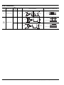
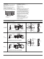
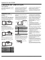
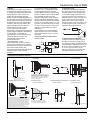
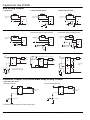
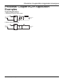
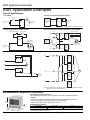
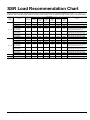
SSRs Technical Information SSR Description and Circuit Configurations Phototriac coupler Zerocrossing function Model Circuit configuration Phototriac coupler Yes APT Input terminal I/O wave form (for resistive load) Load voltage Trigger circuit Isolation type Output terminal Trigger circuit Load Output terminal Input signal ON OFF Load current Zero-crossing detector circuit AC Phototriac Phototriac coupler No APT Input terminal Load voltage Input signal ON OFF Load current SSR Isolation type Zerocrossing function Model Circuit configuration Phototransistor Yes AQ1 (2A) Trigger circuit Phototransistor coupler Input Input terminal circuit I/O wave form (for resistive load) Snubber circuit Load Triac Load voltage Output terminal Input signal ON OFF Load current Trigger circuit Phototriac coupler AQ-G AQ1 (3A, 10A) Input Input terminal circuit Snubber circuit Zero-crossing detector circuit Triac Zero-crossing detector circuit Load voltage Output terminal Input signal ON OFF Load current Input terminal Input circuit Triac Snubber circuit Yes AQ-J AQ-A Trigger circuit Phototriac coupler Load voltage Z N Output R terminal Input signal ON OFF Load current Zero-crossing detector circuit AC AQ-H Phototriac Trigger circuit Phototriac coupler Input terminal Load voltage Triac Output terminal Input signal ON OFF Load current Phototriac coupler Input Input terminal circuit Triac Snubber circuit AQ-G (AQ1)* (AQ-J)* AQ-A Trigger circuit Zero-crossing detector circuit Load voltage Output terminal Input signal ON OFF Load current Phototriac coupler AQ-H Input terminal Trigger circuit No Load voltage Triac Output terminal Input signal ON OFF Load current * AQ1, AQ-J and AQ-A random types are available by special order. ds_x61_en_ssr_technical_information: 011212D 1 SSR (continued) Circuit configuration Phototransistor coupler Phototransistor — — Input terminal Load transistor Input signal Output terminal ON OFF Load current ON Phototransistor coupler Input circuit Input signal OFF ON Output condition OFF Phototransistor — Input terminal Input circuit ON Zener diode Phototransistor coupler — 2 — Input Input terminal circuit Load transistor DC logic output AQ1 Rectifier DC I/O wave form (for resistive load) Zener diode Model A reverse connection protection diode Zerocrossing function Load transistor Isolation type Driver circuit Load Input signal Output terminal OFF ON Output condition OFF ds_x61_en_ssr_technical_information: 011212D Principle of Operation SSR Switching Characteristics 1.SSR for AC Loads (1) Zero-crossing SSR The zero-crossing SSR uses a phototransistor or phototriac coupler to isolate the input from the output (see the circuit configuration on the previous page). When the input signal is activated, the internal zero-crossing detector circuit triggers the triac to turn on as the AC load voltage crosses zero. The load current is maintained by the triac’s latching effect after the input signal is deactivated, until the triac is turned off when the load voltage crosses zero. The following describes voltage and current wave forms for different types of loads: • Resistive loads Since resistive loads cause no phase shift between the voltage and current, the triac turns on when the AC load voltage crosses zero after the input signal is activated. The SSR turns off when the AC load voltage crosses zero and the load current is turned off after the input signal is subsequently deactivated. Load voltage Input voltage SSR output voltage • Inductive loads The SSR turns on when the load voltage crosses zero after the input signal is activated. It turns off when the load current subsequently crosses zero after the input signal is deactivated. A phase difference between the voltage and current may supply a transient spike to the SSR when it is turned off. While the snubber circuit absorbs this spike, an excessively large spike may result in a dv/dt error in the SSR’s internal triac. Load voltage Input voltage • Resistive loads AC load voltage Input voltage SSR output voltage Load current 2. SSR for DC Loads The SSR for DC loads uses a phototransistor coupler to isolate the input from the output. The output immediately responds to the input, since the phototransistor coupler directly turns the output transistor ON or OFF. SSR output voltage Load current (2) Random type SSR Random type SSR uses a phototriac coupler to isolate the input from the output. When the input signal is activated, the output immediately turns on, since there is no zero-crossing detector circuit. The load current is maintained by the triac’s latching effect after the input signal is deactivated, until the AC load voltage crosses zero. Load current ds_x61_en_ssr_technical_information: 011212D 3 Terminology of Phototriac Coupler/AQ-H Term Input side Output side LED forward current IF LED reverse voltage Peak forward current LED dropout voltage VR IFP VF Repetitive peak OFF-state voltage VDRM ON-state RMS current IT(RSM) Non-repetitive surge current ITSM Peak ON-state voltage VTM Peak OFF-state current IDRM Trigger LED current IFT Holding current IH Critical rate of rise of OFF-state voltage Electrical Characteristics 4 Symbol dv/dt Zero-cross voltage VZC Turn on time Ton I/O capacitance Ciso I/O isolation resistance Riso Description Current that flows between the input terminals when the input diode is forward biased. Reverse breakdown voltage between the input terminals. Maximum instantaneous value of the forward current. Dropout voltage between the input terminals due to forward current. Maximum voltage with repeatability that can be applied continuously between the output terminals. Effective current value, based on designated conditions, that can flow continuously between output terminals. Maximum current, without repeatability, that is based on designated conditions. Normally this is expressed as the wave height value of one power frequency current sinusoidal cycle. Effective value of the voltage drop when a regulated load current flows between the output terminals when device is on. Current that flows to output when a regulated load voltage is applied between the output terminals when device is off. Current flow when LED current is augmented and output is on, when regulated power supply voltage and load has been connected between the output terminals. Load current to maintain on state after output terminals have been turned on based on designated conditions. Output terminals do not go to the on state from the off state based on designated conditions. In the zero-cross method, when input is turned on, the maximum voltage value when the output terminals turn on. Delay time until the output switches on after a designated LED current is made to flow through the input terminals. Capacitance between the input and output terminals. Resistance between terminals (input and output) when a specified voltage is applied between the input and output terminals. ds_x61_en_ssr_technical_information: 011212D Terminology of SSR Term Control voltage Input side Load side Electrical Characteristics Description Input voltage necessary for normal SSR operation under the specified temperature conditions. Threshold at which the output turns on as the control voltage is gradually increased with the Activation voltage specified voltage applied to the loaded output. Threshold at which the output turns off as the control voltage is gradually decreased with the Recovery voltage specified voltage applied to the loaded output. Input impedance Resistance of the current limiting resistor used in the SSR input side. Input line voltage Input voltage at which an input module SSR operates normally. Input current Input current at which an input module SSR operates normally. Maximum continuous current allowable across the SSR output terminals under the specified Max. load current heat dissipation and ambient temperature conditions. AC current is specified in RMS units. Output supply voltage range in which the SSR operates normally. AC voltage is specified in Load voltage RMS units. Logic supply voltage/current Supply voltage/current range in which an input module SSR operates normally. Maximum non-repetitive load current allowable under the specified heat dissipation and Non-repetitive surge current ambient temperature conditions. In general, it is given by the peak value of a single cycle of sinusoidal commercial AC current. Current that flows in the SSR output circuit when the specified supply voltage is applied to the “OFF-state” leakage current output with no control voltage applied to the input. Output voltage drop caused by a specified load current supplied to the SSR output which is “ON-state” voltage drop turned on by a specified input control voltage. AC voltage is specified in RMS units. Minimum load current at and above which the SSR operates normally under the specified Min. load current temperature conditions. AC load current is specified in RMS units. Output stage breakdown voltage Maximum voltage that can be applied across the output and ground of an input module SSR. Max. load current Maximum current allowable for the output circuit of an input module SSR. Maximum repetitive voltage which can be continuously applied across the SSR output terminals. In general, a voltage of more than 400 V AC is used for 100 V AC applications, and Repetitive peak voltage, max. more than 600 V AC for 200-250 V AC applications, to absorb supply voltage variations or on/ off surges. SSRs may turn on if a turn-off voltage with a steep rising edge is applied. This phenomenon is Critical turn-off voltage rise ratio called “dv/dt turn on.” Critical turn-off voltage rise ratio refers to the maximum turn-off voltage rise ratio at and below which the SSR remains turned off. Operate time, max. Time until the SSR output turns on after the specified control voltage is applied to the input. Time until the SSR output turns off after the specified control voltage is removed from the Release time, max. input. Resistance measured with a specified voltage applied across the input and output, or across Insulation resistance the input or output and frame ground. Maximum voltage below which no dielectric breakdown occurs when applied for 1 minute Breakdown voltage across the same test points as those used for insulation resistance testing. Functional: The device sustains no damage and meets the specifications if it is exposed to vibration with its magnitude not exceeding this threshold during transit or installation. Vibration resistance Destructive: Closed contacts of a relay remain closed for the specified time period if it is exposed to vibration with its magnitude not exceeding this threshold during operation. Functional: The device sustains no damage and meets the specifications if it is exposed to physical impact with its magnitude not exceeding this threshold during transit or installation. Shock resistance Destructive: Closed contacts of a relay remain closed for the specified time period if it is exposed to physical impact with its magnitude not exceeding this threshold during operation. Ambient temperature range over which the SSR operates normally under the specified heat Ambient temperature dissipation and load current conditions. Ambient temperature range over which an SSR can be safely stored for extended periods Storage temperature without sustaining damage or performance degradation. ds_x61_en_ssr_technical_information: 011212D 5 Cautions For Use of Phototriac Coupler/AQ-H SAFETY WARNINGS • Do not use the product under conditions that exceed the range of its specifications. It may cause overheating, smoke, or fire. • Do not touch the recharging unit while the power is on. There is a danger of electrical shock. Be sure to turn off the power when performing mounting, maintenance, or repair operations on the relay (including connecting parts such as the terminal board and socket). • Check the connection diagrams in the catalog and be sure to connect the terminals correctly. Erroneous connections could lead to unexpected operating errors, overheating, or fire. <AQ-H> MOS transistors and bipolar transistors), avoid ultrasonic cleaning if at all possible. We recommend cleaning with an organic solvent. If you cannot avoid using ultrasonic cleaning, please ensure that the following conditions are met, and check beforehand for defects. • Frequency: 27 to 29 kHz • Ultrasonic output: No greater than 0.25 W/cm2 • Cleaning time: No longer than 30 s • Cleanser used: Asahiklin AK-225 • Other: Submerge in solvent in order to prevent the PCB and elements from being contacted directly by the ultrasonic vibrations. Cautions for Use 1. Applying stress that exceeds the absolute maximum rating If the voltage and current value for any of the terminals exceeds the absolute maximum rating, internal elements will deteriorate because of the excessive voltage and current. In extreme cases, wiring may melt, or silicon P/N junctions may be destroyed. As a result, the design should ensure that the absolute maximum ratings will never be exceeded, even momentarily. 2. Derating Derating is absolutely imperative for reliable design and is an essential factor in determining product life. Therefore, be sure to amply derate the maximum rated values when designing a system. Since it is important to derate in accordance with the type of relay, conditions for use, and environment, please be sure to conduct tests using actual equipment. Also, if there is a possibility that, due to a quality problem, this product might have a great effect on human life or property, do take product liability into consideration by being sure to take even extra leeway against the maximum rated value and implement safety measures such as the construction of redundant circuits. 3. The phototriac coupler is designed solely to drive a triac. As a condition, the triac must be powered beforehand. 4. The internal IC could be damaged if a short forms between the I/O terminals while the phototriac coupler and AQ-H SSR are powered. 5. Output spike voltages 1) The figure below shows an ordinary triac drive circuit. Please add a snubber circuit or varistor, as noise/surge on the load side could damage the unit or cause malfunctions. <Phototriac coupler SOP4, DIP4> 1 4 Load 2 3 <Phototriac coupler DIP6> 1 6 Load 2 3 6 4 1 8 2 Load VL(AC) 3 6 4 5 Note: Connection of an external resister, etc., to terminal No. 5 (gate) is not necessary. 2) Clamp diode can limit spike voltages at the load side. However, long wires may cause spike voltages due to inductance. It is recommended to keep wires as short as possible to minimize inductance. 3) Output terminals may become conductive when a sudden voltage rise is applied, although the input power is not applied. This may occur even if voltage rise between terminals is less than the repetitive peak OFF-state voltage. Therefore, please perform sufficient tests with actual conditions. 4) When controlling loads using zerocross voltage types in which the voltage and current phases differ, since the triac sometimes does not turn on regardless of the input state, please conduct sufficient tests using actual equipment. 6. Recommended input current value IF = 20 mA 7. Important Notes for Mounting 1) Temperature rise in the lead portion is highly dependent on package size. If multiple different packages are mounted on the same board, please check your board beforehand in an actual product, ensuring that the temperature conditions of the phototriac coupler fall within the parameters listed. 2) If the mounting conditions exceed the conditions recommended above, strength of the resin used will decrease and inconsistencies of the thermal expansion coefficients in the component materials will increase greatly. This can cause package cracking and breakage of the bonding wires. Please contact us for consultation. 8. Cleaning The phototriac coupler and AQ-H SSR are forms an optical path by coupling a light-emitting diode (LED) and photodiode via transparent silicon resin. For this reason, unlike other directory element molded resin products (e.g., Note: Applies to unit area ultrasonic output for ultrasonic baths. 9. Transportation and storage 1) Extreme vibration during transport will warp the lead or damage the relay. Handle the outer and inner boxes with care. 2) Storage under extreme conditions will cause soldering degradation, external appearance defects, and deterioration of the performance. The following storage conditions are recommended: • Temperature: 0 to 45C 32 to 113F • Humidity: Less than 70% R.H. • Atmosphere: No harmful gases such as sulfurous acid gas, minimal dust. 3) Storage of SOP type Phototriac couplers implemented in SO packages (SOP 4-pin type) are sensitive to moisture and come in sealed moistureproof packages. Observe the following cautions on storage. • After the moisture-proof package is unsealed, use the devices as soon as possible (use within 1 month 45C 113F/70% R.H.). • If the devices are to be left in storage after the moisture-proof package has been unsealed, keep them in another moisture-proof bag containing silica gel and use within 3 months. ds_x61_en_ssr_technical_information: 011212D (2) Soldering iron method Tip temperature: 350 to 400C 662 to 752F Wattage: 30 to 60 W Soldering time: within 3 s (3) Others Check mounting conditions before using other soldering methods (DWS, VPS, hot-air, hot plate, laser, pulse heater, etc.) • The temperature profile indicates the temperature of the soldered terminal on the surface of the PC board. The ambient temperature may increase excessively. Check the temperature under mounting conditions. • When using lead-free solder we recommend one with an alloy composition of Sn3.0Ag0.5Cu. Please consult us regarding details such as soldering conditions. 10. Soldering 1) When soldering PC board terminals, keep soldering time to within 10 s at 260C 500F. 2) When soldering surface-mount terminals or SO package, the following conditions are recommended. (1) IR (Infrared reflow) soldering method T3 T2 T1 t1 t2 T1 = 150 to 180°C 302 to 356°F T2 = 230°C 446°F T3 = 250°C 482°F or less t1 = 60 to 120 s or less t2 = 30 s or less 11. The following shows the packaging format 1) Tape and reel (Phototriac coupler) Type mm inch Tape dimensions 21±0.8 .827±.031 Direction of picking Tractor feed holes 1.55±0.05 dia. 0.3±0.05 .061±.002 dia. .012±.002 SO package 4-pin type Dimensions of paper tape reel 1.75±0.1 .069±.004 7.2±0.1 .284±.004 80±1 dia. 3.150±.039 dia. 2±0.5 .079±.020 5.5±0.1 .217±.004 4.7±0.1 12±0.3 .185±.004.472±.012 Device mounted on tape 2.8±0.3 .110±.012 12±0.1 .472±.004 250±2 dia. 9.843±.079 dia. 80±1 dia. 3.150±.039 dia. 1.55±0.1 dia. .061±.004 dia. 4±0.1 .157±.004 2±0.1 .079±.004 (1) When picked from 1/2-pin side: Part No. APT❍❍❍❍SX (Shown above) (2) When picked from 3/4-pin side: Part No. APT❍❍❍❍SZ 13±0.5 dia. .512±.020 dia. 14±1.5 .551±.059 2±0.5 .079±.020 Direction of picking 0.3±0.05 .012±.002 DIP 4-pin type Tractor feed holes 1.5 ±0.1 −0 dia. .059 ±.004 dia. −0 4±0.1 .157±.004 1.75±0.1 10.2±0.1 .069±.004 .402±.004 5.5±0.1 .217±.004 5.25±0.1 .207±.004 Device mounted on tape 12±0.1 .472±.004 4.2±0.3 .165±.012 2±0.1 .079±.004 12±0.3 .472±.012 1.55±0.1 dia. .061±.004 dia. (1) When picked from 1/2-pin side: Part No. APT❍❍❍❍AX (2) When picked from 3/4-pin side: Part No. APT❍❍❍❍AZ 0.3±0.05 .012±.002 Tractor feed holes 1.5 +0.1 −0 dia. .059 +.004 dia. −0 2±0.5 .079±.020 10.1±0.1 .400±.004 1.75±0.1 .069±.004 9.2±0.1 .362±.004 Device mounted on tape 4.5±0.3 .177±.012 300±2 dia. 11.811±.079 dia. 80±1 dia. 3.150±.039 dia. Direction of picking 13±0.5 dia. .512±.020 dia. 7.5±0.1 .295±.004 DIP 6-pin type 21±0.8 .827±.031 80±1 dia. 3.150±.039 dia. 4±0.1 12±0.1 .472±.004 2±0.1 .157±.004 .079±.004 16±0.3 .630±.012 17.5±2.0 .689±.079 2±0.5 .079±.020 1.6±0.1 dia. .063±.004 dia. (1) When picked from 1/2/3-pin side: Part No. APT❍❍❍❍AX (2) When picked from 4/5/6-pin side: Part No. APT❍❍❍❍AZ ds_x61_en_ssr_technical_information: 011212D 7 mm inch Type Tape dimensions 0.35±0.05 .014±.002 Tractor feed holes 1.5+0.1 -0 dia. .059+.004 dia. -0 Dimensions of paper tape reel Direction of picking 4.0±0.1 .157±.004 1.75±0.1 .069±.004 5.25±0.1 .207±.004 11.5±0.1 .453±.004 DIP 4-pin wide terminal type 12.1±0.1 .476±.004 Device mounted on tape 3.7±0.3 .146±.012 12.0±0.1 .472±.004 2.0±0.1 .079±.004 24.0±0.3 .945±.012 1.6±0.1 dia. .063±.004 dia. (1) When picked from 1/4-pin side: Part No. APT❍❍❍❍WAY (2) When picked from 2/3-pin side: Part No. APT❍❍❍❍WAW 0.35±0.05 .014±.002 Tractor feed holes 1.5+0.1 -0 dia. .059+.004 dia. -0 Direction of picking 4.0±0.1 .157±.004 21.0±0.8 .827±.031 100±1 dia. 3.937±.039 dia. 2.0±0.5 .079±.020 100±1 dia. 3.937±.039 dia. 1.75±0.1 .069±.004 9.2±0.1 .362±.004 330±2 12.992±.079 13±0.5 dia. .512±.020 dia. 11.5±0.1 .453±.004 DIP 6-pin wide terminal type 12.1±0.1 .476±.004 Device mounted on tape 4.3±0.3 .169±.012 12.0±0.1 .472±.004 2.0±0.1 .079±.004 25.5±2.0 1.004±.079 24.0±0.3 .945±.012 1.7±0.8 .067±.031 1.6±0.1 dia. .063±.004 dia. (1) When picked from 1/6-pin side: Part No. APT❍❍❍❍WAY (2) When picked from 3/4-pin side: Part No. APT❍❍❍❍WAW 2) Tape and reel (AQ-H) mm inch Type Tape dimensions 0.3±0.05 .012±.002 Tractor feed holes 1.5 +0.1 −0 dia. .059 +.004 dia. −0 Direction of picking 4±0.1 10.1±0.1 .157±.004 .400±.004 4.5±0.3 .177±.012 1.75±0.1 .069±.004 7.5±0.1 .295±.004 16±0.3 10.2±0.1 .630±.012 .402±.004 Device mounted on tape 8-pin SMD type Dimensions of paper tape reel 12±0.1 .472±.004 2±0.1 .079±.004 2±0.5 .079±.020 300±2 dia. 11.811±.079 dia. 80±1 dia. 3.150±.039 dia. 1.55±0.1 dia. .061±.004 dia. (1) When picked from 1/2/3/4-pin side: Part No. AQH❍❍❍❍AX (Shown above) (2) When picked from 5/6/8-pin side: Part No. AQH❍❍❍❍AZ 8 21±0.8 .827±.031 80±1 dia. 3.150±.039 dia. 13±0.5 dia. .512±.020 dia. 17.5±2.0 .689±.079 2±0.5 .079±.020 ds_x61_en_ssr_technical_information: 011212D 3) Tube (1) Devices are packaged in a tube as pin No. 1 is on the stopper B side. Observe correct orientation when mounting them on PC boards. (SOP type) StopperB (green) StopperA (gray) (DIP type) Stopper B Stopper A 13. Applying stress that exceeds the absolute maximum rating If the voltage and current value for any of the terminals exceeds the absolute maximum rating, internal elements will deteriorate because of the excessive voltage and current. In extreme cases, wiring may melt, or silicon P/N junctions may be destroyed. As a result, the design should ensure that the absolute maximum ratings will never be exceeded, even momentarily. ds_x61_en_ssr_technical_information: 011212D 9 Cautions for Use of SSR Cautions for Use of SSR SAFETY WARNINGS • Do not use the product under conditions that exceed the range of its specifications. It may cause overheating, smoke, or fire. • Do not touch the recharging unit while the power is on. There is a danger of electrical shock. Be sure to turn off the power when performing mounting, maintenance, or repair operations on the relay (including connecting parts such as the terminal board and socket). • Check the connection diagrams in the catalog and be sure to connect the terminals correctly. Erroneous connections could lead to unexpected operating errors, overheating, or fire. 3. Noise and surge protection at the input side A high noise surge voltage applied to the SSR input circuit can cause malfunction or permanent damage to the device. If such a high surge is anticipated, use C or R noise absorber in the input circuit. 6. Cleaning solvents compatibility Dip cleaning with an organic solvent is recommended for removal of solder flux, dust, etc. If ultrasonic cleaning must be used, the severity of factors such as frequency, out power and cleaning solvent selected may cause loose wires and other troubles. Please make sure these conditions before use. 7. Transportation and storage 1) Extreme vibration during transport will warp the lead or damage the relay. Handle the outer and inner boxes with care. 2) Storage under extreme conditions will cause soldering degradation, external appearance defects, and deterioration of the characteristics. The following storage conditions are recommended: • Temperature: 0 to 45C 32 to 113F • Humidity: Less than 70% R.H. • Atmosphere: No harmful gasses such as sulfurous acid gas, minimal dust. 8. Others (1) If an SSR is used in close proximity to another SSR or heat-generating device, its ambient temperature may exceed the allowable level. Carefully plan SSR layout and ventilation. (2) Soldering to SSR terminals should be completed within 5 seconds at 260C. (3) Terminal connections should be made by referring to the associated wiring diagram. (4) For higher reliability, check device quality under actual operating conditions. Cautions for Use 1. Regarding output noise surge protection (1) AC Output Type A high noise surge voltage applied to the SSR load circuit can cause malfunction or permanent damage to the device. If such a high surge is anticipated, use a varistor across the SSR output. R Load Load power supply SSR Control voltage source Varistor (2) DC Output Type When the SSR is loaded with an inductive load, such as a solenoid contactor, motor, or solenoid valve, use a counter-EMF suppression diode across the load. Load Load power supply SSR 2. When used for the load less than rated An SSR may malfunction if it is used below the specified load. In such an event, use a dummy resistor in parallel with the load. R0 (dummy resistor) 4. When the input terminals are connected with reverse polarity Type If the polarity of the input control voltage is reversed AQ1, AQ-J, AQ-A, AQ-J Reversing the polarity will not cause damage to the device, due to the presence of a protection diode, but the device will not operate. AQ-H, AQ-G Reversing the polarity may cause permanent damage to the device. Take special care to avoid polarity reversal or use a protection diode in the input circuit. 5. In the case of operating voltage containing ripple If the SSR control voltage contains ripple, the peak of the ripple should not exceed the maximum rated control voltage, and the bottom of the ripple should exceed the minimum rated control voltage. Peak ripple voltage Valley ripple voltage Load 0V Load power supply SSR SSR Note: AQ-F solid-state relay output terminals are numbered (8) and (12). C Load Specifications Type AQ-G AQ-1 AQ-J AQ-A 10 All models AC output type DC output type All models All models Load current 20 mA 50 mA 5 mA 50 mA 100 mA ds_x61_en_ssr_technical_information: 011212D Cautions for Use of SSR Snubber Circuit 1. Reduce dv/dt An SSR used with an inductive load can accidentally fire due to a high load voltage rise rate (dv/dt), even though the load voltage is below the allowable level (inductive load firing). Our SSRs contain a snubber circuit designed to reduce dv/dt (except AQ-H). 2. Selecting the snubber constants 1) C selection The charging coefficient tau for C of the SSR circuit is shown in formula 1 =(RL+R) C ------------1 By setting formula 1 so that it is below dv/dt value you have: C=0.632VA/((dv/dt) (RL+R)) -----2 By setting C = 0.1 to 0.2 F, dv/dt can be controlled to between nV/s and n+V/s or lower. For the condenser, use either an MP condenser metallized polyester film. For the 100 V line, use a voltage between 250 and 400 V, and for the 200 V line, use a voltage between 400 and 600 V. 2) R selection Therefore, it is always necessary to insert a resistance R. In normal applications, for the 100 V line, have R = 10 to 100 and for the 200 V line, have R = 20 to 100 . (The allowable discharge current at turnon will differ depending on the internal elements of the SSR.) The power loss from R, written as P, caused by the discharge current and charging current from C, is shown in formula 3 below. For the 100 V line, use a power of 1/2 W, and for the 200 V line, use a power above 2 W. 2 P= C × VA × f------------ 3 2 Also, at turn-off of the SSR, a ringing circuit is formed with the capacitor C and the circuit inductance L, and a spike voltage is generated at both terminals of the SSR. The resistance R serves as a control resistance to prevent this ringing. Moreover, a good non-inductive resistance for R is required. Carbon film resistors or metal film resistors are often used. For general applications, the recommended values are C = 0.1 F and R = 20 to 100 . There are cases of resonance in the inductive load, so the appropriate care must be taken when making your selections. Inductive load RL SSR VA R Load power supply C Snubber circuit If there is no resistance R (the resistance R controls the discharge current from condenser C), at turn-on of the SSR, there will be a sharp rise in dv/dt and the high peak value discharge current will begin to flow. This may cause damage to the internal elements of the SSR. f = Power supply frequency Thermal Design SSRs used in high-reliability equipment require careful thermal design. In particular, junction temperature control has a significant effect on device function and life time. The rated load current for board-mounting SSRs is defined as the maximum current allowable at an ambient temperature of 40C (30C) and under natural cooling. If the ambient temperature exceeds the SSRs derating temperature point (20C to 40C, depending on SSR), load current derating in accordance with the load current vs temperature diagram becomes nesessary. If adjacent devices act as heat sources, the SSR should be located more than 10 mm away from those devices. SSRs with a 5 A rating or more must be used with the dedicated heat sinks listed in Table 1 or equivalents. To ensure adequate thermal conduction, apply thermal conductive compound (Toshiba silicone YG6111, TSK5303 or alternate) to the SSR’s mounting surface. For information on external heat sinks for our SSRs and their mounting method, refer to “Data and Cautions for Use for respective relay”. Table 1. Dedicated on-board heat sinks Load current to 10 A Type AQ10A2-ZT4/32V DC 10 A AQ-J (10A) 15 A AQ-A (15A), AQ-J (15A) 20 A AQ-J (25A) 25 to 40 A 25 A 40 A AQ-A (25A) AQ-J (25A) AQ-A (40A) Heat sink AQ-HS-5A AQP-HS-J10A AQP-HS-J10A (for AQ-J) AQP-HS-SJ10A (for AQ-J)* AQP-HS-SJ20A* AQP-HS-J10A AQP-HS-J10A (for AQ-J) AQP-HS-SJ10A (for AQ-J)* AQP-HS-SJ20A* AQP-HS-J10A AQP-HS-SJ10A (for AQ-J)* AQP-HS-SJ20A* AQP-HS-30/40A AQP-HS-J25A AQP-HS-J25A *It is possible to mounting on the DIN rail. Protection Circuit High-reliability SSR circuits require an adequate protection circuit, as well as careful study of the characteristics and maximum ratings of the device. 1. Over-Voltage Protection The SSR load power supply requires adequate protection against over-voltage errors from various causes. The methods of over-voltage protection include the following: (1) Use devices with a guaranteed reverse surge withstand voltage (controlled avalanche devices, etc.) (2) Suppress transient spikes Use a switching device in the secondary circuit of a transformer or use a switch with a slow opening speed. (3) Use a surge absorption circuit Use a CR surge absorber or varistor across the load power supply or SSR. Special care must be taken so power on/ off surges or external surges do not exceed the device’s rated load voltage. If a surge voltage exceeding the device’s rated voltage is anticipated, use a surge absorption device and circuit (e.g. a ZNR from Panasonic Electronic Devices Co., Ltd.). ds_x61_en_ssr_technical_information: 011212D 11 Cautions for Use of SSR Choosing the Rated Voltage of the ZNR (1) Peak supply voltage (2) Supply voltage variation (3) Degradation of ZNR characteristic (1 mA10%) (4) Tolerance of rated voltage (10%) For application to 100 V AC lines, choose a ZNR with the following rated voltage: (1) (2) (3) (4) = (1002) 1.11.11.1 = 188 (V) D T H 0.8 dia. .031 dia. 3.0 max. .118 max. W 20.0 min. .787 min. L D: 17.5 dia. max. .689 dia. max. T: 6.5 max. .256 max. H: 20.5 max. .807 max. W: 7.5±1 .298±.039 (mm inch) Example of ZNR (Panasonic Electronic Components) ERZV14D201 ERZV14D221 ERZV14D241 ERZV14D271 ERZV14D361 ERZV14D391 ERZV14D431 ERZV14D471 ERZV14D621 ERZV14D681 V1mA (V) 200 (185 to 225) 220 (198 to 242) 240 (216 to 264) 270 (247 to 303) 360 (324 to 396) 390 (351 to 429) 430 (387 to 473) 470 (423 to 517) 620 (558 to 682) 680 (612 to 748) Max. allowable circuit voltage ACrms (V) 130 140 150 175 230 250 275 300 385 420 2. Over-Current Protection An SSR circuit operated without overcurrent protection may result in damage to the device. Design the circuit so the device’s rated junction temperature is not exceeded for a continuous overload current. (e.g. Surge current into a motor or light bulb) The surge-on current rating applies to over-current errors which occur less than several tens of times during the service life of a semiconductor device. A protection coordination device is required for this rating. DC (V) 170 180 200 225 300 320 350 385 505 560 Withstanding energy Withstanding surge current Max. control voltage Max. average pulse electric power (10/1000s) (2ms) 1time V50A (V) 340 360 395 455 595 650 710 775 1,025 1,120 (W) 0.6 0.6 0.6 0.6 0.6 0.6 0.6 0.6 0.6 0.6 (J) 70 78 84 99 130 140 155 175 190 190 (J) 50 55 60 70 90 100 110 125 136 136 (A) 6,000 6,000 6,000 6,000 6,000 6,000 6,000 6,000 6,000 5,000 (8/20s) 2time (A) 5,000 5,000 5,000 5,000 4,500 4,500 4,500 4,500 4,500 4,500 Electrostatic capacitance (Reference) @1KHz (pF) 770 740 700 640 540 500 450 400 330 320 Example of executing fuse selection of over-current protection cooperation Methods of over-current protection include the following: (1) Suppressing over-currents Use a current limiting reactor in series with the load power supply. (2) Use a current shut-off device Use a current limiting fuse or circuit breaker in series with the load power supply. 1,000 Fuse cut-off current Surge ON current Types Varistor voltage 100 AQR (15A type) NHR15 (fuse 15A) NHR10 (fuse 10A) (A peak) 10 1 10 100 No. of cycles at 60Hz 1,000 Load Type Description 1. Heaters (Resistive Load) The SSR is best suited to resistive loads. Noise levels can be drastically lowered with zero-crossing switching. 2. Lamps Tungsten or halogen lamps draw a high inrush current when turned on (approximately 7 to 8 times the steadystate current for zero-crossing SSRs; approximately 9 to 12 times, in the worst case, for random type SSRs). Choose an SSR so the peak of the inrush current does not exceed 50% of the SSR surgeon current. 12 3. Solenoids AC-driven solenoid contactors or solenoid valves also draw inrush current when they are activated. Choose an SSR such that the peak of the inrush current does not exceed 50% of the SSR surgeon current. For small solenoid valves and AC relays in particular, a leakage current may cause the load to malfunction after the SSR turns off. In such an event, use a dummy resistor in parallel with the load. • Using an SSR below the Specified Load Dummy resistor Load SSR Output Load power supply ds_x61_en_ssr_technical_information: 011212D Cautions for Use of SSR 4. Motors When starting, an electric motor draws a symmetrical AC starting current some 5 to 10 times the steady-state load current, superimposed on a DC current. The starting time during which this high starting current is sustained depends on the capacities of the load and load power supply. Measure the starting current and time under the motor’s actual operating conditions and choose an SSR so the peak of the starting current does not exceed 50% of the SSR surge-on current. When the motor load is deactivated, a voltage exceeding the load supply voltage is applied to the SSR due to counter-EMF. This voltage is approximately 1.3 times the load supply voltage for induction motors, and approximately 2 times that for synchronous motors. • Reversible Motor Control When the direction of motor rotation is reversed, the transient current and time required for the reversal far exceed those required for simple starting. The reversing current and time should also be measured under actual operating conditions. 5. Capacitive Load A capacitive load (switching regulator, etc.) draws an inrush current to charge the load capacitor when the SSR turns on. Choose an SSR so the peak of the inrush current does not exceed 50% of the SSR surge-on current. A timing error of up to one cycle can occur when a switch used in series with the SSR is opened or closed. If this is a problem, use an inductor (200 to 500 H) in series to the SSR to suppress dv/dt error. For a capacitor-starting, single-phase induction motor, a capacitive discharge current appears during the reversal process. Be sure to use a current limiting resistor or reactor in series with the SSR. Also, the SSR should have a high marginal voltage rating, since a voltage twice as high as the load supply voltage develops across the SSR in the reversal process. (For reversible control on a 100 V AC line, use SSRs with a 200 V rating; for use on a 200 V AC line, contact your nearest our representative for further information.) For reversible motor control, carefully design the driver circuit so the forward and reverse SSRs do not turn on at the same time. Transistor-driven reversible motor control circuit L SSR C 6. Other Electronic Equipment In general, electronic equipment uses line filters in the primary supply circuit. The capacitors used in the line filters may cause the SSR to malfunction due to dv/ dt turn on when the equipment is turned on or off. In such an event, use an inductor (200 to 500 H) in series with the SSR to suppress dv/dt turn on. Load power supply R1 R3 R2 C1 SSR1 (for forward rotation) TR C ZNR L Flip-flop or manual switch TR R2 R3 C1 R1 SSR2 (for reverse rotation) R4 Single-phase induction motor Load Inrush Current Wave and Time (1) Incandescent Lamp Load (2) Mercury Lamp Load i/iO]3 times i i (3) Fluorescent Lamp Load i/iO]5 to 10 times io L Contacts io i io C 3 to 5 minutes Incandescent lamp Approx. 1/3 second Inrush current/rated current: i/io]10 to 15 times (4) Motor Load i/iO]5 to 10 times i 10 seconds or less (5) Solenoid Load i/iO]10 to 20 times (6) Electromagnetic Contact Load (7) Capacitive Load i/iO]3 to 10 times i/iO]20 to 40 times io Free Lock Load 0.2 to 0.5 second (for high power factor type) The discharge tube, transformer, choke coil, capacitor, etc., are combined in common discharge lamp circuits. Note that the inrush current may be 20 to 40 times, especially if the power supply impedance is low in the high power factor type. i io i io i io Steady Starting state Braking • Conditions become more harsh if plugging or inching is performed since state transitions are repeated. • When using a relay to control a DC motor and brake, the on time inrush current, steady-state current and off time brake current differ depending on whether the load to the motor is free or locked. In particular, with non-polarized relays, when using from B contact of from contact for the DC motor brake, mechanical life might be affected by the brake current. Therefore, please verify current at the actual load. 0.07 to 0.1 second Note that since inductance is great, the arc lasts longer when power is cut. The contact may become easily worn. ds_x61_en_ssr_technical_information: 011212D 1 to 2 cycles (1/60 to 1/30 seconds) 1/2 to 2 cycles (1/120 to 1/30 seconds) 13 Cautions for Use of SSR SSR Driving Circuits 1. Relay Driver 2. NPN Transistor Driver 3. PNP Transistor Driver Load Load Load power supply Load power supply SSR Vcc Load SSR Vcc Load power supply SSR Vcc Relay contacts PNP Transistor NPN Transistor 4. TTL/DTL/IC Driver 5. C-MOS/IC Driver (1) SSR fires when IC output is HIGH: (2) SSR fires when IC output is LOW: Load Load Load Load power supply SSR SSR Vcc Vcc Load power supply Load power supply Vcc TTL, DTL, IC C-MOS, IC 6. Self Sustaining Circuit Using SSR C-MOS, IC 7. Driving with a Shared Supply 8. SSRs Used in Series Vcc Vcc C SSR ZNR Load power supply SSR A Load Load SW ZNR Load power supply SSR B Load R SSR ZNR Terminal A: ON input pulse Terminal B: OFF input pulse ZNR SSR Load power supply Phototriac Coupler, AQ-H Solid State Relay Driving Circuits 1. NPN Transistor Driver 1) Phototriac Coupler 2) AQ-H Solid State Relay Vcc Vcc 1 4 2 Load 8 Load power supply Load power supply 2 3 NPN Transistor Load 3 6 NPN Transistor * Phototriac coupler and AQ-H is current driving type. 14 ds_x61_en_ssr_technical_information: 011212D Phototriac Coupler/AQ-H Application Examples Phototriac Coupler/AQ-H Application Examples Typical Applications 1. Temperature control for heater control R Triac Input power supply Heater load 4 1 C Phototriac coupler 2 R Varistor Load power supply 3 2. Airflow control for fan motors R M 8 2 Input power supply C AQ-H 3 R Varistor Load power supply 6 ds_x61_en_ssr_technical_information: 011212J 15 SSR Application Examples SSR Application Examples Typical Applications 1. Light Bulb 2. Electric Furnace Temperature Control Light bulb Control switch Control voltage source Load power supply SSR Input signal source and temperature sensor SSR Input Heater load Load power supply Load * KT Temperature Controller is available. 3. Single-Phase Induction Motor Control Control voltage source 4. Reversible Control for a Single-Phase Induction Motor Control switch Load power supply R1 R3 C1 R2 SSR SSR1 (for forward rotation) C ZNR L TR Flip-flop or manual switch Single-phase Induction motor R2 Load power supply TR C1 R3 R4 SSR2 (for reverse rotation) Single-phase induction motor R1 5. Three-Phase Induction Motor Control 6. Reversible Control for a 3-Phase Induction Motor L R (R) SSR (R) ZNR M (S) SSR2 (for reverse rotation) ZNR (T) L SSR SSR1 (for forward rotation) M (S) ZNR Control voltage source SSR2 (for reverse rotation) L R (T) SSR1 (for forward rotation) Note: Take special care in the design to ensure that both the forward and reverse SSRs do not turn on at the same time. Recommended Temperature Controllers <KT4H Temperature Controller> Our temperature controller is recommended for use with our Solid State Relays. Features • Data can be collected using the RS485 communications interface via a PLC. • Improved visibility using a negative type LCD and backlight. • Depth-wise length (chassis dimension) is 56 mm 2.205 inch. Substitute part numbers 48mm 1.890inch 56mm 2.205inch 48mm 1.890inch 16 Power supply 100 to 240 V AC Control output Relay contact Part No. AKT4H112100 *For detailed product information about temperature controllers, please refer to our website: http://industrial.panasonic.com/ac/e/ ds_x61_en_ssr_technical_information: 011212J SSR Load Recommendation Chart Please use this chart when selecting the SSR load. The values presented are for ambient temperatures of 40C 104F (30C 86F) and lower. When selected, please measure the load current waveform and use within the range of each surge current characteristic. Type of load Load voltage 110 V AC 220 V AC Max. load current Heater Solenoid bulb AQG (1A type) 1A 0.8A 0.5A AQG (2A type) 2A 1.6A 1A AQ1 (3A type) 3A 2.4A 1.5A AQ1 (10A type) AQJ (10A type) 10A 8A AQA (15A type) AQJ (15A type) 15A AQA (25A type) AQJ (25A type) 25A AQA (40A type) 40A AQG (1A type) 1A Product Triplephase motor Lamp 7W — 0.5A 50W 15W — 1A 100W 60W — 1.5A 150W 5A 200W — 5A 500W Heat sink AQP-HS-SJ10A (AQJ type) Heat sink AQP-HS-J10A, AQP-HS-SJ20A Heat sink AQ-HS-5A (AQ1 type) 12A 7.5A 300W — 7.5A 750W Heat sink AQP-HS-J10A, AQP-HS-SJ20A Heat sink AQP-HS-J10A (AQ-J type) 20A 12.5A 500W — 12.5A 1.25kW Heat sink AQP-HS-30/40A (AQ-A type) Heat sink AQP-HS-J25A (AQ-J type) 32A 20A 750W — 20A 2kW 0.8A 0.5A 15W 50W 0.5A 100W Singlephase motor Transformer Heat sink AQP-HS-J25A (AQ-A type) AQG (2A type) 2A 1.6A 1A 35W 100W 1A 200W AQ1 (3A type) 3A 2.4A 1.5A 100W 300W 1.5A 300W AQ1 (10A type) AQJ (10A type) 10A 8A 5A 400W 1kW 5A 1kW Heat sink AQP-HS-SJ10A (AQJ type) Heat sink AQP-HS-J10A, AQP-HS-SJ20A Heat sink AQ-HS-5A (AQ1 type) AQA (15A type) AQJ (15A type) 15A 12A 7.5A 600W 1.5kW 7.5A 1.5kW Heat sink AQP-HS-J10A, AQP-HS-SJ20A Heat sink AQP-HS-J10A (AQ-J type) AQA (25A type) AQJ (25A type) 25A 20A 12.5A 1kW 2.5kW 12.5A 2.5kW Heat sink AQP-HS-30/40A (AQ-A type) Heat sink AQP-HS-J25A (AQ-J type) AQA (40A type) 40A 32A 20A 1.5kW 3.7kW 20A 4kW AQ1 (2A type) 2A 1.6A 1.0A — — 1.0A — 100 V DC AQ1 (1A type) 1A 0.8A 0.5A — — 0.5A — 48 V DC Remarks ds_x61_en_ssr_technical_information: 011212D Heat sink AQP-HS-J25A (AQ-A type) 17