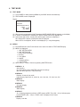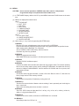
1
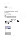
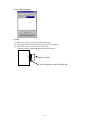
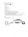
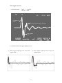
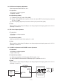
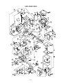
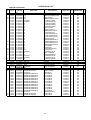
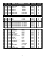
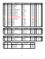
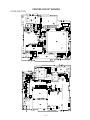
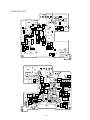
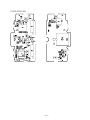
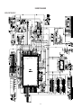
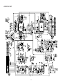
(without price)
QV-7000SX
(KX-778)
OCT. 1998
INDEX
R
Ver.1
Aug / 1999
CONTENTS
SPECIFICATIONS ....................................................................................................................................... 1
BLOCK DIAGRAM ...................................................................................................................................... 2
ADJUSTMENT ............................................................................................................................................ 3
1. Complete Unit .................................................................................................................................... 4
1-1. Loading ADJ ................................................................................................................................. 4
1-2. White balance · Sensitivity adjustment ..................................................................................... 5
1-3. Scratch compensation ................................................................................................................ 7
1-4. Flash operation and recharge operation ................................................................................... 8
1-5. Current consumption ................................................................................................................ 10
1-6. Operation check ......................................................................................................................... 10
2. D-PCB Assy ...................................................................................................................................... 11
2-1. Operation check ......................................................................................................................... 11
2-2. Clock oscillation check ............................................................................................................. 13
3. L-PCB Assy ...................................................................................................................................... 14
3-1. VCC21, VEE9 Voltage adjustment ............................................................................................ 14
3-2. VCC3, VCC5, VCC5-1, VCC5-2, VCC3-5, EVCC3 Voltage check ............................................ 14
3-3. VCC2 adjustment and VCC13, VCC7, VEE2 Voltage check ................................................... 14
3-4. VCO free run frequency adjustment ........................................................................................ 15
3-5. BL drive voltage adjustment ..................................................................................................... 15
3-6. VCOM AC adjustment and VCOM DC coarse adjustment ..................................................... 15
3-7. Brightness voltage setting and contrast adjustment ............................................................. 16
4. TEST MODE ...................................................................................................................................... 17
4-1. TEST MODE ................................................................................................................................ 17
4-2. MENU1 ........................................................................................................................................ 17
4-3. MENU2 ........................................................................................................................................ 18
DISASSEMBLY ......................................................................................................................................... 19
EXPLODED VIEW ..................................................................................................................................... 26
PARTS LIST .............................................................................................................................................. 27
PRINTED CIRCUIT BOARDS ................................................................................................................... 31
SCHEMATIC DIAGRAMS ......................................................................................................................... 34
TROUBLESHOOTING .............................................................................................................................. 37
SPECIFICATIONS
Item
Specification
Record Format
JPEG (with COMPACTFLASH memory card)
Recording Medium
COMPACTFLASH memory card
Memory Capacity/
S (1280 x 960):
88/14 minimum (500 KB per image)
F (1280 x 960):
123/19 minimum (350 KB per image)
N (1280 x 960):
206/33 minimum (200 KB per image)
File Size
E (640 x 480):
340/55 minimum (112 KB per image)
Movie (3.2 seconds):
85/13 groups minimum (5 frames per second, 1 image =4 frames x 4)
Movie (6.4 seconds):
85/13 groups minimum (10 frames per second, 1 image =16 frames x 4)
Movie (12.8 seconds):
85/13 groups minimum (5 frames per second, 1 image =16 frames x 4)
The above figures are approximations only. The actual number of images depends on image subject matter.
Values such as 85/13 indicate the number of images that can be stored on a 48MB/8MB CompactFlash card.
Image Deletion
Single image; all images in a folder; all images in memory card (with image protection)
Imaging Element
1/3-inch square pixel color CCD (Total Pixels: 1,320,000; Effective Pixels: 1,250,000)
Lens
F2.8 to 3.5 f = 5.0 to 10.0mm (equivalent to 32 to 64mm on a 35mm camera)
Zoom
2X optical zoom, 8X digital zoom (when used in combination with optical zoom)*
Focusing
Phase-difference detection system auto focus, manual focus; with macro mode and focus lock
Focus Range
(from surface of lens protection filter)
0.25m to ∞ (standard)/10cm (macro)
(10cm to ∞ with manual focus)
The above figures are approximations only.
Exposure
Light Metering:
Multi-pattern/spot metering by CCD
Exposure:
Program AE, aperture priority AE
Exposure Compensation:
–2EV to +2EV (1/4EV units)
Shutter
CCD shutter, mechanical shutter
Shutter Speed
1/4 to 1/1000 second (1 second in Night Mode)
Aperture
F2.8 to F14 automatic and manual switching
White Balance
Automatic, fixed (4 modes), manual switching
Self-timer
10 seconds, 2 seconds
Flash Modes
AUTO, ON, OFF, Red-eye reduction
Flash Range
Approximately 0.7 to 2 meters
Recording Functions
Single image; self-timer; movie; panorama; timer; title; macro; monochrome; sepia; Sports Mode; Night Mode
Monitor/Viewfinder
2.5-inch TFT, low-glare color HAST LCD (122,100 pixels)
Clock
Built-in quartz digital clock; date and time recorded with image; auto calendar up to 2049
Input/Output Terminals
DIGITAL OUT, VIDEO OUT (NTSC and PAL), AC adaptor connector
Infrared Communication
IrDA1.1; IrTran-P compliant
Power Supply
Four batteries (AA-size alkaline or lithium batteries )
Four rechargeable batteries (AA-size Ni-MH batteries (NP-H3))
AC adaptor (AD-C620)
Power Consumption
Approximately 7.2 W
Dimensions
140.5 (W) x 75 (H) x 52.5 (D) mm
Weight
Approximately 280g (9.9 oz) (excluding batteries)
Standard Accessories
(5.5" (W) x 3" (H) x 1.7" (D))
2-way shoulder/wrist strap; soft case; video cable; Owner’s manual; connection cable (Except for US);
8MB COMPACTFLASH memory (Except for US); PC Link CD-ROM (Except for US);
four LR6 alkaline batteries (Except for US);
•Image size with digital zoom is 640 x 480 pixels.
•The camera also has a lithium battery that powers its built-in clock.
—1—
BLOCK DIAGRAM
Key unit top
13-pin
C-PCB
MN3774PT
3.3V
15.0V
3.3V
-9.0V
HD49323AF
49-pin
CDS+AGC+ADC
CCD
21.0V
15.0V
3.3V
-9.0V
H1
H2
V1
V2
V3
V4
CH1A
CH3A
CH1B
CH3B
LR36685
Vdrv
3.3V
15.0V
Buffer
21.0V
Voltage
Converter
KIN0
KIN1
KIN2
KIN3
KOUT0
PACT
KOUT1
KAD
KOUT2
KSW
REC/PLAY VCC3-5
DGND
D-PCB
80-pin
SHD
SHP
CLAMP
ADCK
NC
SCK
SDI
LOAD
SUB
RSTCCD
AD0
AD1
AD2
AD3
AD4
AD5
AD6
AD7
AD8
AD9
VCC2×3
VEE9×3
VCC3-1
VCC3-3×3
AGND×7
DGND×2
AD
3.3V
3.3V
3.3V
FLASH/MASK ROM
Expansion
I/O
CF
3.3V
DCAM-101
EDO DRAM×2
RTC
Li
M
LENS-FPC
M
IrDA
CF DET
Detect switch
—2—
RGB
AF
driver
Lens
Shutter
driver
unit
IRIS
driver
GND
45-pin
VCC3-5
L-PCB
M
R
G
B
CSYNC
BLCTL
PWCTL
PW0
PW1
PW2
PW3
ADPTN
RVS
RDET
RIGHT
VMUTE
AGND×3
generator
Sensor
Comparator
Strobe Assy
KOUT1-2
VCC3-1 KIN2
KOUT2-1
RLED KIN3
GLED KOUT1-1 KOUT2-2
VCC3×6
EVCC3
VCC21×2
VEE9×2
VCC5-1(ST)×2
VCC5-2(Ir)×2
VCC5(Shutter)×3
VCC1-3
GND×8
9-pin
Key unit rear
VCC7(7.5V)
Battery
Voltage
PREN
FBN
VA
VCC5-1×2
DGND×3
Voltage
controller
VCC3-5
BLVCC
5.4V
BLVCC
BLGND
BLSW
BL unit
VEE2(-14.25V)
VCC21(21.0V)
VEE9(-9.0V)
VCC5(5.5V)
VCC3-5(3.3V)
VCC3(3.3V)
VCC5-1(5.0V)
VCC5-2(5.0V)
14-pin
CHGN
CENDN
LEVELN
SCR
IGBTN
LTTRGN
Up
Converter
VCC2(5.0V)
VCC3-5
VCC1-ST
GND
AC ADP
High voltage
RS232C
VIDEO
VCC13(12.75V)
Voltage
controller
GND
Signal
generator
3-pin
AF
Sensor
Xe Lamp
RS232C
VIDEO
IrDA
5.0V
/LSRST
/FBL
VCC3-1×2
/FLB
VCC5×3
/SCK
STATUS DGND×2
COMMANDPGND×3
MACT
CT1
PON1
SUB CPU
EEPROM
M M
SW
19-pin
ZOOM
driver
IrDA
controller
5.0V
Down
converter
Detect switch
(RDET)
IR3Y26A1
RGB I/F
REG
REG
VDD
(3.0V)
EVCC3
(3.3V)
3.0V
CM7018
Display controller
26-pin
VGH
VREFH
VGL
VREFL
GRES
GPCK
GSRT
RESET
MODE2
LCD module
CS
VCOM
NC
VBC
SRTR
SRTL
OE
CLR
HCNT
MCLK
MODE1
VSS
GOUT
BOUT
ROUT
VDD
VSH
VDD:3.0V
VREF:3.0V
VGH:12.75V
VGL:-14.25V
VSH:5.0V
ADJUSTMENT
■ Preparation
1. PC (IBM Compatible)/OS:Windows 95
2. Link cable.
3. Adjustment program
1) ADJ778F.EXE
(Program)
2) 0829.ADJ
(Data file)
3) ADJ778K.EXE
(Service compensation program)
4) DT778.EXE
(D PCB ass’y check program)
5) REF.BAY, REF.CB, REF.CR, REF.JPG, REF.Y, REFDEC.CB, REFDEC.CR, REFDEC.Y
(Saved these programs in CF card when excuting D PCB ass'y check program.Total 8 programs.)
4. AC adaptor or stabilizer.
5. Kenko light box handy 5000 (Modified in order to input DC externally)
6. Filter
ND filter (ND10, ND20 one each) Lay them together.
Color temperature converter filter (LA10, LA20 one each) Lay them together.
These filters are available in camera shops.
1) ND filter
ND10 (50 × 50)
Cosio parts code 19045436
2) ND filter
ND20 (50 × 50)
Cosio parts code 19045437
3) Color temperature coverter filter
LA10 (50 × 50)
Cosio parts code 19045438
4) Color temperature coverter filter
LA20 (50 × 50)
Cosio parts code 19045439
7. Digital oscilloscope
8. Multimeter
9. Ammeter
10. Frequency counter
11. TV (with video terminal)
12. Video cable
13. Battery (battery operation/battery cover lock)
14. PC link program (for saving user’s pictures and checking communication functions)
15. Another QV-7000SX (for IrDA)
Notes:
Normally power is supplied using AC adaptor.
When error occurs, use a voltage regulator, and supply the specified power.
To adjust D PCB ass’y and L PCB ass’y keep the case open.
—3—
1. Complete Unit
1-1. Loading ADJ
Set QV-7000SX to “PLAY” mode.
1. Preparation
• PC(IBM Compatible)/OS:Windows 95
• Link cable
• Adjustment program: ADJ778F.EXE (program)
0829.ADJ (data file)
2. Adjustment procedure
(1)
(2)
(3)
(4)
(5)
(6)
(7)
Connect QV-7000SX and PC with link cable.
Execute the adjustment software “ADJ788F” on Windows 95.
Clik “File (F)”.
Clik “Open (O)”.
Search file “0829.ADJ” and double click. (Data input to AE, CCD, TEST, Version).
Click “Data transmission”.
“Send OK” message appears.
3. Notes
(1) When replacing CAM case (CCD) be sure to execute.
(2) Continue with the adjustment (1-2. White balance · Sensitivity adjustment) white balance and
(1-3. Scratch compensation) scratch compensation.
(3) When errors occur check CAM case and D PCB ass‘y.
Link cable
Digital
terminal
PC
RS-232C port
QV-7000SX
PC display (Example)
—4—
1-2. White balance · Sensitivity adjustment
• Set QV-7000SX to “REC” mode.
• Normal Recording mode ( ).
• Light box.
Light source (viewer)
PROGRAM
No. 1
CCD RGB ADJUST
Color temperature (K) Light intensisty (cd/m2)
light source 2
light source 1
4400 ± 200
Note
No specified figure
for light intensity
50 ± 5
No. 2 CCD SENS ADJUST
No specified figure
for color temperature
1. Preparation
(1)
(2)
(3)
(4)
(5)
(6)
PC (IBM Compatible)/OS: Windows 95.
Link cable.
Adjustment program ADJ778K.EXE.
Stabilizer.
Viewer (Kenko light box handy 5000) (Modified in order to input DC externally)
Use two ND filter together, one ND10 and one ND20.
Use two color temperature converter filter together, one LA10 and one LA20.
2. Adjustment procedure
(1) Start test mode MENU2.
✻ Refer to TEST MODE on page 17 and 18.
(2) Select “CCD ADJUST”.
Press +/– to select and SHUTTER button to display “SHUT TO START”
(3) White balance adjustment.
Set the color temperature converter filters LA10 and LA20 above the light box.
(4) Set camera lens toward light source then press the shutter button.
(5) When RGB ADJ COMPLETE is displayed, the adjustment of white balance is completed.
(6) Sensitivity Adjustment.
Remove two color temperature filters from simplified viewer then set the filter so that center of
illuminance face and center of two ND filters are lined up.
(7) Set camera lens toward light source then press the shutter button.
(8) When SENS ADJ COMPLETE is displayed, the adjustment of sensitivity is completed.
Turn off the unit once.
(9) Compensation program.
Connect QV-7000SX and PC with a link cable.
Set the camera in PLAY MODE.
(10) Execute compensation program (ADJ778K) on Windows 95.
(11) Click “Replace TEST”.
(12) “Replacement Complete” is displayed.
Turn power off.
—5—
3. PC display (Example)
4. Notes
Chart
(1) Make sure light box is not directly exposed to light.
(2) Bring light box and filter and camera lens as close as possible.
(3) Operate the above procedure after loading ADJ.
Operate scratch compensation after the procedure above.
Viewer
QV-7000SX
Color temperature coverer filter/ND filter
—6—
1-3. Scratch compensation
• Set QV-7000SX to “REC” mode.
• Normal Recording mode ( ).
• Light box.
Light source (viewer)
Color temperature (K) Light intensisty (cd/m2)
light source 1
light source 2
PROGRAM
No. 3
4400 ± 200
WHITE NOISE
DETECT
50 ± 5
Note
No specified figure for
color temperature
1. Preparation
(1) AC adaptor or stabilizer.
(2) Kenko light box handy 5000.
(Modified in order to input DC externally)
(3) Filter.
ND filter one ND10, one ND20.
2. Adjustment procedure
(1) Start test mode MENU2.
✻ Refer to TEST MODE on page 17 and 18.
(2) Select 10. WHITE NOISE DETCT using +/– button.
(3) Set the ND filters ND10 and ND20 above the light box.
(4) Set camera lens toward light source then press the shutter button.
(5) When “SAVE COMPLETE” is displayed, scratch compensation is completed.
(6) Turn power off.
3. Notes
Chart
(1) Make sure light box is not directly exposed to light.
(2) Bring light box and filter and camera lens as close as possible.
(3) Operate the above procedure after white balance • sensetivity adjustment.
Viewer
QV-7000SX
ND filter
—7—
1-4. Flash operation and recharge operation
• Set QV-7000SX in “REC” mode.
• Normal Recording mode ( ).
• Apply 6.0 ± 0.1 V voltage on DC in jack.
1. Preparation
(1)
(2)
(3)
(4)
(5)
Stabilizer.
Digital oscilloscope.
Ammeter.
TV (With video terminal).
Video cable.
2. Adjustment procedure
(1)
(2)
(3)
(4)
Shoot a picture with flash OFF. (Make sure there is no flash)
Shoot a picture with flash ON and make sure it flashes once.
Shoot in red eye reduction mode and make sure it flashes twice.
Connect QV-7000SX and TV with video cable and make sure that the pictures taken in steps (2)
and (3) are not whitish, dark or erroneously colored.
(5) Make sure that the charging current is less than 1.3 A.
(6) Monitor the waveform of (1), (2) and (3) on a digital oscilloscope when flash goes on, and make
sure there are no errors comparing with the waveforms shown on the next page.
3. Notes
(1) Excuete in a dark room.
(2) Shoot a colorful object as much as possible.
Flash lens face
Monitor TV
Digital oscilloscope
Probe close to
flash lens face
QV-7000SX
TIME:1.0µ sec/DIV
VOLTS:1V/DIV (AC mode)
—8—
Flash trigger waveform
1. Normal waveform
CH1
TIME : 1 µ sec/DIV
VOLTS : 1 V/DIV
1V
1µV
757µV
UERT
First positive
pulse.
OK if second positive pulse is shown.
First negative
pulse.
ACQUIRE
NORMAL
2
AVS
1
ENVELOPE
REPET SAVE ON
ON | OFF ON | OFF
2. NG waveforms when trigger skipping occurs.
(1) When trigger skipping occurs on the first
positive pulse.
(2) When trigger skipping occurs on the first
negative pulse.
—9—
1-5. Current consumption
• Set QV-7000SX to “PLAY” mode.
1. Preparation
(1) Voltage regulator.
(2) Ammeter.
2. Adjustment procedure
(1) Current consumption (DC in = 6.0 ± 0.1 [V])
• Make sure that current consumption is less than 550 mA in PLAY mode.
• Make sure that current consumption is less than 800 mA in REC mode.
(Flash charge current is not included)
(2) Lower the voltage from 6 V as shown below then make sure the battery warning indicator changes.
DC in = 5.0 ± 0.05 [V] (one indicator is off )
DC in = 4.65 ± 0.05 [V] (two indicators are off)
1-6. Operation check
1. Preparation
(1)
(2)
(3)
(4)
(5)
(6)
(7)
(8)
Batteries.
AC adaptor.
PC (IBM compatible)/OS:Windows 95.
Link cable.
PC link program.
TV (with video teminal).
Video cable.
QV-7000SX (for checking IrDA).
2. Adjustment procedure
Perform the fallowing operations and checkings.
(1)
(2)
(3)
(4)
(5)
(6)
Battery operation, AC adaptor operation.
Switch operation.
Cover open/close operation, CF insersion/eject operation, battery cover open/close operation.
Standard/Macro switch, lens rotation, AE operation , AF operation zoom operation.
Video output, digital communication, IrDA communication.
Dust and scratches on lens.
3. Notes
(1) Make sure Video out setting are appropriate to your country.
(i.e. Japan=NTSC, England = PAL)
— 10 —
2. D-PCB Assy
2-1. Operation check
1. Preparation
• PC(IBM Compatible)/OS:Windows 95
• Link cable
• Program
DT778.EXE (D PCB ass’y check program)
REF.LZH (Extract and save in CF card to execute D PCB ass’y check program)
• AC adaptor or voltage regulator
• TV (with video terminal)
• Video cable
2. Adjustment procedure
(1) Connect QV-7000SX and PC with link cable.
(2) Start up adjustment program DT778 on MS-DOS.
(3) Check the items listed below.
• Serial communication is OK.
• Check ROM version.
• DRAM is OK.
• CF is OK.
• Voltage detection is OK (Displays High)
(VCC1-3 voltage high 6.0 ± 0.1 V, middle 4.5 ± 0.1V, low 4.0 ± 0.1 V)
• Check if each mode is OK.
1: REC/PLAY mode
2: Video jack available
3: AC adaptor jack available.
• Check JPEG compression extension
Error mode
1: Color processor error
2: JPEG Encode error
3: JPEG Decode error
(When error occures replace D PCB ass’y)
• Check each mode by turning dial of switch unit.
(Turn dial 1 step at a time, then press space key to check the mode. There are 10 modes.)
• Make sure each key works.
(Since key scanning speed is slow, key entry may not be detected. In such a case, push the key again.)
• Make sure LED goes on.
• ON/OFF operation of TFT-LCD display.
• Check clock operation.
• Wake up function of power source.
(Turns off and on automatically)
(4) After completing D PCB ass’y check program, sets the video out for each country.
(ie: JAPAN = NTSC, ENGLAND = PAL)
(5) Connect QV-7000SX and TV with video cable, and check the picture taken.
— 11 —
3. PC display (Example, subject to change)
✻✻✻✻✻✻✻✻✻✻✻✻✻✻✻✻✻✻✻✻✻✻✻✻✻✻✻✻✻✻
DT778 (KX-778 D PCB checking software) for DOSV
–––––––––––––––––––––––––––––––––––
Usage :dt778 [–-option]
option : ccd test
Corresponding model : QV-7000SX (KX-778)
Ver1.9
98/08/07
✻✻✻✻✻✻✻✻✻✻✻✻✻✻✻✻✻✻✻✻✻✻✻✻✻✻✻✻✻✻
Exits from program by <ESC> button
Serial transportation check
OK
ROM version code check
code = 01b18904
for KX-778 Ver.98090401
DRAM check
OK
Compact Flash Memory Check
OK
Battery voltage detection check
Level = HIGH
MODE detection check
PLAY MODE
VIDEO OUT plug not inserted
AC adaptor plug inserted
Lens not reversed
EEPROM Check
OK
CP2 JPEG Check
OK
Dial check (10times)
< Detect dial position by SPACE key >
CUSTOM
< Detect dial position by SPACE key >
TIMER
< Detect dial position by SPACE key >
NIGHT
< Detect dial position by SPACE key >
SPORTS
< Detect dial position by SPACE key >
NORMAL
< Detect dial position by SPACE key >
MOVIE
< Detect dial position by SPACE key >
PANORAMA
< Detect dial position by SPACE key >
TITLE
< Detect dial position by SPACE key >
MONO TONE
< Detect dial position by SPACE key >
SEPIA
Button Check
Press SHUTTER button (Interrupted by ESC button)
OK
Press SHUTTER button half way (Interrupted by ESC button)
OK
Press + button (Interrupted by ESC button)
OK
Press - button (Interrupted by ESC button)
OK
Press MENU button (Interrupted by ESC button)
OK
Press TELE button (Interrupted by ESC button)
OK
Press WIDE button (Interrupted by ESC button)
OK
Press DISP button (Interrupted by ESC button)
OK
Press SELF button (Interrupted by ESC button)
OK
Press AF button (Interrupted by ESC button)
OK
Press FLASH button (Interrupted by ESC button)
OK
LED control
< Function indicator turns on in red by SPACE key>
< Function indicator turns on in orange by SPACE key>
< Function indicator turns on in green by SPACE key>
< Function indicator turns off by SPACE key>
LCD control
< Backlight turns off by SPACE key >
< Backlight turns on by SPACE key>
Seting Time
PC : 1998/10/07 19:22:23
QV : 1998/10/07 19:22:23
Timer Check
< Automatically restart in 5 sec. >
Functions correctly
— 12 —
2-2. Clock oscillation check
• Turn power off
• Room temperature should be 25 ± 10 °C.
1. Preparation
Pedometer or frequency counter or quartz timer.
2. Adjustment procedure
Execute one of check from the followings.
(1) Pedometer: within 62 ppm.
(2) Frequency counter check point CP670 signal pad; 32.767±0.002 [KHz].
(3) After setting time turn power off. 30 minutes later check the time.
— 13 —
3. L-PCB Assy
3-1. VCC21, VEE9 Voltage adjustment
1. Preparation
• AC adaptor or voltage regulator
• Multimeter
2. Adjustment procedure
(1) Adjust VR120 so that VCC21 (CP121) is 21.0 ± 0.3 V.
(2) Adjust VR130 so that VEE9 (CP133) is –9.0 ± 0.2V.
3. Notes
When not able to adjust using AC adaptor, use voltage regulator and supply power to be VCC1-1
(CP149)=5.0 ± 0.05 V.
3-2. VCC3, VCC5, VCC5-1, VCC5-2, VCC3-5, EVCC3 Voltage check
1. Preparation
• AC adaptor or voltage regulator
• Multimeter
2. Adjustment procedure
Make sure
VCC3 (CP112)
VCC3-5 (CP147)
VCC5 (CP142)
VCC5-1 (CP137)
VCC5-2 (CP139)
EVCC3 (CP115)
=
=
=
=
=
=
3.3 + 0.2/–0.1
3.3 + 0.2/–0.1
5.5 + 0.2
5.0 + 0.15
5.0 + 0.15
3.3 + 0.1
[V]
[V]
[V]
[V]
[V]
[V]
3. Notes
When unable to adjust using AC adaptor, use voltage regulator and supply power to be VCC-1-1
(CP149) = 5.0 ± 0.05 V.
3-3. VCC2 adjustment and VCC13, VCC7, VEE2 Voltage check
1. Preparation
• AC adaptor or voltage regulator
• Multimeter
2. Adjustment procedure
Adjust VR151 so that VCC2 (CP172) = 5.0 ± 0.02 V.
Make sure
VCC7 = 6.8 ~ 8.6
[V]
VCC13 = 11.4 ~ 14.1
[V]
VEE2 = –11.0 ~ –16.5 [V]
3. Notes
When unable to adjust using AC adaptor, use voltage regulator and supply power to be VCC-1-1
(CP149) = 5.0 ± 0.05 V.
— 14 —
3-4. VCO free run frequency adjustment
Room temperature should be 20 ± 10 ºC
1. Preparation
• AC adaptor or voltage regulator
• Frequency counter
2. Adjustment procedure
(1) Connect CP733 (SYF) and CP700 (GND).
(2) Monitor CP704 (HDB) with frequency counter and adjust VR755 so that frequency becomes
15.734 ± 0.1 KHz.
(3) After completing adjustment, disconnect CP7033 (SYF) and CP700 (GND).
3. Notes
When unable to adjust using AC adaptor, use voltage regulator and supply power to be VCC-1-1
(CP149) = 5.0 ± 0.05 V.
3-5. BL drive voltage adjustment
1. Preparation
• AC adaptor or voltage regulator
• Multimeter
2. Adjustment procedure
Make sure that CP910 (BL-VCC) is within 5.4 ± 0.2V.
3. Notes
When unable to adjust using AC adaptor, use voltage regulator and supply power to be VCC-1-1
(CP149) = 5.0 ± 0.05 V.
3-6. VCOM AC adjustment and VCOM DC coarse adjustment
1. Preparation
• AC adaptor or voltage regulator
• Digital oscilloscope
2. Adjustment procedure
(1) Make sure amplitude of VCOM output (CP176) is 6.6 ± 0.3 V.
(2) Adjust VR320 so that maximum VCOM output (CP716) will be 4.8 ± 0.2 V.
3. Notes
When unable to adjust using AC adaptor, use voltage regulator and supply power to be VCC-1-1
(CP149) = 5.0 ± 0.05 V.
L-PCB VCOM
(CP716)
Power
Supply
VCC1-1
High level
4.8 [V]
0 [V]
–1.8 [V]
(CP149)
Oscilloscope
— 15 —
amplitude
6.6 [V]
QV-7000SX
3-7. Brightness voltage setting and contrast adjustment
1. Preparation
• AC adaptor or voltage regulator
• Digital oscilloscope
2. Adjustment procedure
(1)
(2)
(3)
(4)
Start up Test mode Menu1.
Select GRAY SCALE (10 step).
Trigger VB waveform (CP335) by FRP (CP346) signal to adjust as noted below.
Adjust RGB-AMP VR (VR340) so that pedestal-pedestal voltage of VB(CP335) signal is 3.5 ±
0.05 V.
(5) Adjust contrast VR (VR344) so that contrast terminal voltage (CP305) is 3.0 ± 0.05 V temporary.
(6) Adjust Bright VR (VR381) so that potential between VB (CP335) signal’s pedestal and 3 step is
2.20 ± 0.05 V.
(7) Adjust contrast VR (VR344) so that potential between VB (CP335) signal’s pedestal and 10 step
is 2.85 ± 0.05 V.
✻ Make sure that waveforms are not distorted.
3. Notes
When unable to adjust using AC adaptor, use voltage regulator and supply power to be VCC-1-1
(CP149) = 5.0 ± 0.05 V.
QV-7000SX
L-PCB
Power
Supply
VCC1-1
(CP149)
VB
(CP335)
Digital oscilloscope
Figure 3-1, 3-2
3.5 ± 0.05V
(pedestal-pedestal)
3-1
2.85V ± 0.05V
(pedestal-10 step)
3-2
— 16 —
4. TEST MODE
4-1. TEST MODE
(1) Turn POWER on while pressing MENU key and DISP button simultaneously.
(2) TEST MODE screen is displayed.
Display
TEST MODE
WHITE NOISE DATA YES (NO)
LOADER
2
ADJ. 98000829
VER. 98082901
(3) When scratch compensation is NOT complete, WHITE NOISE DATA NO appears on the display.
(4) If scratch compensation is COMPLETE, WHITE NOISE DATA YES appears on it.
(5) At the lower right corner, Loader, ADJ and Program versions are displayed.
ADJ: When ADJ is broken, 2222222222 will be displayed.
When CCD is not adjusted, ’98 will not be displayed. (i.e. only 829 appears)
4-2. MENU1
(1) Press MENU button and FLASH button at the same time while in TEST MODE display.
(2) MENU1 is displayed.
1. INIT. SETTING NTSC
2. INIT. SETTING PAL
3. GRAY SCALE(10step)
4. BLACK
5. 50% GRAY
6. WHITE
7. CROSS HATCH
8. COLOR BAR
(3) Select using +/– button. Choose by pressing SHUTTER button.
1. MENU1-1, 2
Set at factory.
On confirmation screen SHUTTER will start the settings.
(Will not delete pictures in Flash memory)
2. MENU1-3
Displays 10 step of gray scale.
Light intensity values are 16, 38 60, 82, 104, 126, 148, 170, 192, 214, 235.
3. MENU1-4
Black display.
4. MENU1-5
50% gray display.
5. MENU1-6
White display
6. MENU1-7
32 × 32 pixel grid pattern on black, or RED square at REC Thru (320 × 216) or Yellow square
at PLAY MODE (360 × 240) or 1 PIXEL mark is displayed in the center.
7. MENU1-8
Display color bar.
— 17 —
4-3. MENU2
CAUTION : Do no execute operations of MENU2 other than noted in 3. Adjustment.
Program data maybe corrupted and will be unable to use.
(1) In TEST MODE display, double click AF key then MENU button and FLASH button at the same
time.
(2) MENU2 is displayed as shown below.
page 1
1. CCD ADJUST
2. BATT. TEST
3. REC INFO.
4. SELF COPY
5. CAMERA UPDATE
6. NO COMP CAPT
7. IR TEST MASTER
8. IR TEST SLAVE
page 2
9. CP2 JPEG TEST
10. WHITE NOISE DETECT
11. BAYER CAPTURE
(3) Select using +/– key. Confirm by pressing SHUTTER button.
1. MENU2-1
Execute CCD color solid adjustment, then record it on ADJ of EEPROM.
Press shutter button by adjusting the light amount using specified filters in specified viewer.
When setting mark is displayed, it is completed.
Set QV-7000SX to REC mode Rotary switch to Normal.
Hold back any other key operation.
2. MENU2-2
Battery life measurement function.
When SHUTTER button is pressed, it will shoot pictures intervally.
3. MENU2-3
Displays FOCUS/ iris/Shutter speed
4. MENU2-4
Connect QV-700SX with each other with cable and copy program codes. The camera operating
this menu will be the master camera, and by sending its ROM data it will update the receiving
camera’s 8 Mbyte FLASH MEMORY. Connect another QV-7000SX and turn on power, then
transmission will start.
5. MENU2-5
Overwrites camera program domain. It reads a file mane Rom.bin from CF, and writes its
binary image into the Flash memory 0X1000.
6. MENU2-6
Saves without compression. Disabled by turning power off.
7. MENU2-7,8
Test the IrDA communication. Master mode is sending 1 letter repeatedly and receiving the
same letter back .
Slave mode is sending back when the letter it received.
8. MENU2-9
Test CP2, JPEG. Keep the right data file of ref.bay, ref.y, ref.cb, ref.cr, refdec.y, refdec.cb,
refdec.cr, ref.jpg beforehand in CF.
9. MENU2-10
Detects CCD’s white scratch, and stores it in EEPROM. Set to Normal.
10. MENU2-11
Saves Bayer data from CCD as it is.
— 18 —
DISASSEMBLY
1.Main
4. Unscrew tow screws (S3)in the battery holder.
screws (S3)
5. Unscrew two screws (S3) on the bottom.
1. Remove CF card.
screws (S3)
2. Unlock battery cover.
6. Rotate the CAM case and unserew one screw
(S3) on the side.
screws (S3)
3. Open battery cover and remove batteries.
7. Rotate the CAM case to the other side and
unscrew one screw (S3) on the side.
scarews (S3)
— 19 —
8. Separate the upper case and lower case.
(Easy if from CAM case side.)
CN cover will be remored.
12.Unscrew two screws (S1) fixing CAM case
and remove CN540 then take CAM case out.
screw(S1)
CN540
9. Desolder the red wire which comes from the
switch unit.
red wire
10.Remove CN150 (red wire, black wire) and
CN160 (black wire, red wire, orange wire)
CN150
CN160
11. Remove CN800 and CN580.
CN580
CN800
— 20 —
13. CAM case block, lower case block, upper
case block separated.
2. Lower case
1. Remove battery cover by turning it upward
to the right.
2. Unscrew screws (S6) and CN510 on D PCB
ass’y
5. Lower case and battery holder separated.
6. Unscrew one screw (S1) on switch unit.
screw(S6)
screw(S1)
CN510
7. Lower case and switch case separated.
3. Open CF cover and make sure not to damage
the detect switch. By pressing the CF card
eject knob with a precision screw driver
remove D PCB ass’y.
8. Unscrew one screw (S7) on lower case.
4. Lower case and D PCB ass’y separated.
screw(S7)
— 21 —
9. Remove lower case cover from lower case.
10.Lower case cover and lower case separated.
11.Lower case cover and IR cover separated.
12. Remove CF cover by bending it from lower
case.
— 22 —
13.Lower case, lower case cover, IR cover
battery cover, CF cover separated.
3. Upper case
1. Unscrew three screws (S5) on L PCB ass’y.
Remove CN920 and CN700.
5. Unscrew four screws (S5) on BL ass’y.
screw(S5)
screw(S5)
screw(S5)
CN920
CN700
screw(S5)
screw(S5)
2. Upper case and L PCB ass’y separated.
6. Upper case, TFT-LCD module, BL ass’y
separated.
3. Remove cushion.
7. Remove DP panel from upper case by pushing.
4. Unscrew two screw (S1) in the tripod screw.
8. DP panel, sheet switch ass’y, upper case
separated.
screw(S1)
— 23 —
4. CAM case
1. Remove two screws (S3) on CAM case.
5. Remove CN1, CN250, CN251.
CN250
CN251
CN1
screw(S3)
2. Remove upper case by pressing the upper
part of CAM case ass’y
6. Remove three screws (S4) and desolder red
wire on CL unit.
screw(S4)
screw(S4)
red wire
3. Unscrew one screw (S3) on L case ass’y.
7. Desolder black wire and orange wire on CL
unit.
screw(S3)
orange wire
black wire
4. Rotate L case ass’y and unscrew the other
screw (S3).
8. Unscrew (S4) on sensor.
screw(S4)
screw(S3)
— 24 —
9. Remove sensor PCB ass’y.
When assembling, make sure the wires are
inside the ribs.
12.Flash unit, CL unit, L case ass’y CAM case
separated.
10.Discharge the flash capacitor by using a
discharge tool.
flash capacitor
flash capacitor (+)
flash capacitor (-)
discharge (+)
discharge (-)
11. Remove flash unit by pressing
— 25 —
EXPLODED VIEW
S4
11
17
28
22
29
30
S3
14
13
12
S4
S3
27
18
S4
3
S3
16
33
S3
S3
32
23
S1
9
S1 ~2
E
S3
S1
S5
26
20
S8
24
S6
15
19
43
S5
S1
38
21
37
36
44
S5
31
S7
42
S3
5
39
S3
6
7
S3
25
41
8
4
S5
35
10
2
40
1
S5 ~2
34
— 26 —
S5
PARTS PRICE LIST
DIGITAL PCB ASSY
N
N
N
N
N
N
N
N
N
N
N
N
N
Item
Code No.
Parts name
Ics
20126033 LSI
20126033 LSI
20126087 LSI
20126088 LSI
21053633 IC/CMOS
21055215 IC/CMOS
21055712 IC
21056244 IC
21056244 IC
21056399 IC
21056470 IC
21056471 IC
21056472 IC
21056473 IC
21056473 IC
21056473 IC
21056479 IC
21056486 IC
21056487 IC
21056488 IC
21056489 IC
21056490 IC
21056492 IC
21056495 IC
21056526 LSI
21144676 IC/CMOS
21145857 IC
21145861 IC
22540550 IC/CMOS
22540550 IC/CMOS
71008365 IC
SWITCH
SW650 34122083 SWITCH
JACKS
JK770
30251937 JACK
JK750
35018197 JACK/MINI
TRANSISTORS
Q400
22501579 TRANSISTOR/CHIP
Q660
22510930 TRANSISTOR/CHIP
Q750
22540448 FET/CHIP
Q405
22592715 TRANSISTOR/DIGITAL
Q661
22592715 TRANSISTOR/DIGITAL
Q671
22592715 TRANSISTOR/DIGITAL
Q770
22592715 TRANSISTOR/DIGITAL
Q800
22592715 TRANSISTOR/DIGITAL
Q801
22592715 TRANSISTOR/DIGITAL
Q446
22592744 TRANSISTOR/DIGITAL
Q440
22592745 TRANSISTOR/DIGITAL
Q441
22592745 TRANSISTOR/DIGITAL
Q442
22592745 TRANSISTOR/DIGITAL
Q443
22592745 TRANSISTOR/DIGITAL
Q445
22592745 TRANSISTOR/DIGITAL
Q444
27958150 FET/CHIP
Q670
71015791 TRANSISTOR/CHIP
Q672
71015791 TRANSISTOR/CHIP
IC560
IC561
IC700
IC550
IC415
IC410
IC750
IC416
IC417
IC670
IC458
IC420
IC414
IC530
IC531
IC701
IC691
IC400
IC427
IC426
IC428
IC770
IC460
IC418
IC450
IC412
IC710
IC690
IC760
IC761
IC440
Specification
Appricable
Q PRICE CODE R
MB81V18165B50LPFTN
MB81V18165B50LPFTN
PC87109VBE
MBM29LV800TA10-021
TC7S00FU-TE85L
TC7W74FU(TE12L)
TC7S04FU(TE85L)
TC7S32FU(TE85L)
TC7S32FU(TE85L)
RS5C316A-E2
LM4041CIM3X-1.2
MSM82C55A-2GS-2K
TC74AC00FT(EL)
TC7WH125FU(TE12L)
TC7WH125FU(TE12L)
TC7WH125FU(TE12L)
RN5RL33AA-TR
S-80835ANNP-EDZ-T2
S-80843ANNP-ED7-T2
S-80847ANNP-EJB-T2
S-80839ANNP-ED3-T2
TK15405MTL
PST9330UR
TC7SL08FU(TE85L)
DCAM101E-T
TC7W04FU-TE12L
HSDL-1100#008
AD7823YRM-REEL
TC7W66FU-TE12L
TC7W66FU-TE12L
TC75S51F-(TE85L)
Common
Common
Common
Common
Common
Common
Common
Common
Common
Common
Common
Common
Common
Common
Common
Common
Common
Common
Common
Common
Common
Common
Common
Common
Common
Common
Common
Common
Common
Common
Common
1
1
1
1
1
1
1
1
1
1
1
1
1
1
1
1
1
1
1
1
1
1
1
1
1
1
1
1
1
1
1
BT
BT
BP
BX
AD
AE
AD
AC
AC
AP
AL
BC
AF
AF
AF
AF
AC
AC
AC
AC
AC
AH
AC
AD
DH
AD
BK
AX
AD
AD
AF
C
C
C
C
C
C
C
C
C
C
C
C
C
C
C
C
C
C
C
C
C
C
C
C
C
C
C
C
C
C
C
MSS-26
Common
1
AD
C
HSJ1636-011020
HSJ1169-019010
Common
Common
1
1
AE
AF
C
C
2SA1774TLR
2SB1073-R(TX)
2SK1580-T1
DTC144EETL
DTC144EETL
DTC144EETL
DTC144EETL
DTC144EETL
DTC144EETL
DTA143EETL
DTC143EETL
DTC143EETL
DTC143EETL
DTC143EETL
DTC143EETL
2SK2035(TE85L)
DTA144EETL
DTA144EETL
Common
Common
Common
Common
Common
Common
Common
Common
Common
Common
Common
Common
Common
Common
Common
Common
Common
Common
1
1
1
1
1
1
1
1
1
1
1
1
1
1
1
1
1
1
AA
AB
AC
AA
AA
AA
AA
AA
AA
AA
AA
AA
AA
AA
AA
AA
AA
AA
B
B
B
B
B
B
B
B
B
B
B
B
B
B
B
B
B
B
- 27 -
N
Item
N
N
D691
D670
D750
D751
D800
D801
N
H450
H670
H454
H452
H700
Code No.
Parts name
DIODES
23900777 DIODE/CHIP
23901183 DIODE/CHIP
23901379 DIODE/SHOTTKY
23901379 DIODE/SHOTTKY
27752079 DIODE/CHIP/MODULE
27752079 DIODE/CHIP/MODULE
OSCILLATORS
25902722 OSILLATOR
25902722 OSILLATOR
25902744 OSILLATOR
25902745 OSILLATOR
25902749 OSILLATOR
Specification
Appricable
Q PRICE CODE R
IMN10T-108
MA142WK-(TX)
MA729-(TX)
MA729-(TX)
DA227-TL
DA227-TL
Common
Common
Common
Common
Common
Common
1
1
1
1
1
1
AB
AA
AB
AB
AA
AA
C
C
C
C
C
C
SPT2A-32KHZ
SPT2A-32KHZ
CX-51F-20.0M
CX-51F-27.0M
FXO-31FL-48.0M
Common
Common
Common
Common
Common
1
1
1
1
1
AG
AG
AP
AP
AV
C
C
C
C
C
CM7018L3-T4N
RN5RG50AA-TR
RN5RL30AA-TR
RH5RH553B-T1
RN5RL33AA-TR
S-8520B33MC-ARS-T2
S-8520B33MC-ARS-T2
TK11830MTL
MB3800PFV-G-BND-EF
NJM3414AV-TE1
S-8327E50MC-EKE-T2
IR3Y26A1
TK11250BMCL
S-8327B54MC-ESI-T2
Common
Common
Common
Common
Common
Common
Common
Common
Common
Common
Common
Common
Common
Common
1
1
1
1
1
1
1
1
1
1
1
1
1
1
AY
AE
AD
AK
AC
AL
AL
AL
AP
AI
AI
BH
AE
AH
C
C
C
C
C
C
C
C
C
C
C
C
C
C
MSS-26
Common
1
AD
C
HEC3600-010120
Common
1
AD
C
2SA1774TLR
2SB1073-R(TX)
2SB1073-R(TX)
2SC4081-T106R
DTC144EETL
DTC144EETL
DTC144EETL
DTC144EETL
DTC144EETL
DTC144EETL
DTC144EETL
2SD2150-T100S
2SD2150-T100S
CPH6301-TL
CPH6301-TL
CPH6401-TL
CPH6401-TL
Common
Common
Common
Common
Common
Common
Common
Common
Common
Common
Common
Common
Common
Common
Common
Common
Common
1
1
1
1
1
1
1
1
1
1
1
1
1
1
1
1
1
AA
AB
AB
AA
AA
AA
AA
AA
AA
AA
AA
AB
AB
AE
AE
AE
AE
B
B
B
B
B
B
B
B
B
B
B
B
B
B
B
B
B
LINEAR PCB ASSY
N
N
N
N
N
N
N
Ics
20125983 LSI
21053689 IC/MOS
21054501 IC/MOS
21056478 IC
21056479 IC
21056480 IC
21056480 IC
21145607 IC
21145800 IC
21145805 IC
21145842 IC
21145846 IC
21145849 IC
21145858 IC
SWITCH
SW700 34122083 SWITCH
JACK
JK100
35016755 JACK/POWER
TRANSISTORS
Q131
22501579 TRANSISTOR/CHIP
Q120
22510930 TRANSISTOR/CHIP
Q146
22510930 TRANSISTOR/CHIP
Q100
22520637 TRANSISTOR/CHIP
Q121
22592715 TRANSISTOR/DIGITAL
Q130
22592715 TRANSISTOR/DIGITAL
Q141
22592715 TRANSISTOR/DIGITAL
Q145
22592715 TRANSISTOR/DIGITAL
Q152
22592715 TRANSISTOR/DIGITAL
Q340
22592715 TRANSISTOR/DIGITAL
Q901
22592715 TRANSISTOR/DIGITAL
Q122
22592758 TRANSISTOR/CHIP
Q155
22592758 TRANSISTOR/CHIP
Q110
27958156 FET/CHIP
Q147
27958156 FET/CHIP
Q140
27958157 FET/CHIP
Q900
27958157 FET/CHIP
IC730
IC145
IC180
IC140
IC115
IC110
IC147
IC130
IC150
IC390
IC120
IC340
IC137
IC900
- 28 -
N
Item
N
D757
D130
D162
D131
D160
D161
D163
D778
D117
D120
D140
D147
D900
D100
T155
N
N
N
N
FU101
FU103
FU104
FU102
VR151
VR120
VR130
VR381
VR755
VR340
VR344
VR320
Code No.
Parts name
DIODES
23901358 DIODE/CHIP/VARI.CAP
23901379 DIODE/SHOTTKY
23901379 DIODE/SHOTTKY
23901820 DIODE/CHIP
23901820 DIODE/CHIP
23901820 DIODE/CHIP
23901820 DIODE/CHIP
23901820 DIODE/CHIP
23901883 DIODE/SHOTTKY
23901883 DIODE/SHOTTKY
23901883 DIODE/SHOTTKY
23901883 DIODE/SHOTTKY
23901883 DIODE/SHOTTKY
28953130 DIODE/SHOTTKY
CONVERTER
30650713 CONVERTER/DC-DC
FUSES
27975612 FUSE
27975612 FUSE
27975612 FUSE
27975616 FUSE
VARIABLE RESISTORS
27751470 RESISTOR/SEMIFIXED/CHIP
27751484 RESISTOR/SEMIFIXED/CHIP
27751484 RESISTOR/SEMIFIXED/CHIP
27751484 RESISTOR/SEMIFIXED/CHIP
27751484 RESISTOR/SEMIFIXED/CHIP
27751491 RESISTOR/SEMIFIXED/CHIP
27751491 RESISTOR/SEMIFIXED/CHIP
27751827 RESISTOR/SEMIFIXED/CHIP
Specification
Appricable
Q PRICE CODE R
MA329-(TX)
MA729-(TX)
MA729-(TX)
1SS355TE-17
1SS355TE-17
1SS355TE-17
1SS355TE-17
1SS355TE-17
RB160L-40TE25
RB160L-40TE25
RB160L-40TE25
RB160L-40TE25
RB160L-40TE25
RB051L-40TE25
Common
Common
Common
Common
Common
Common
Common
Common
Common
Common
Common
Common
Common
Common
1
1
1
1
1
1
1
1
1
1
1
1
1
1
AC
AB
AB
AA
AA
AA
AA
AA
AC
AC
AC
AC
AC
AC
C
C
C
C
C
C
C
C
C
C
C
C
C
C
6CA-02
Common
1
AM
C
PI-R431001
PI-R431001
PI-R431001
PI-R43101.5
Common
Common
Common
Common
1
1
1
1
AC
AC
AC
AC
B
B
B
B
EVM-1XSX50B53
EVM-1XSX50B24
EVM-1XSX50B24
EVM-1XSX50B24
EVM-1XSX50B24
EVM-1XSX50B54
EVM-1XSX50B54
EVM-1XSX50B13
Common
Common
Common
Common
Common
Common
Common
Common
1
1
1
1
1
1
1
1
AB
AB
AB
AB
AB
AB
AB
AB
C
C
C
C
C
C
C
C
C441170-1
K341371*1
K441489-1
K441490-1
K441492-1
K341299-1
K341298-1
K440064-7
K441491-1
K441507-1
K241037*1
K140491-1
LV-027C
CO-778
K441466-1
K241032*1
K341309-1
K341310-1
K140489-1
K241035*1
COD25T2021RN
IB-VC-YO361
R340024-1
K441456-1
K241055*1
K341359*1
Common
Common
Common
Common
Common
Common
Common
Common
Common
Common
Common
Common
Common
Common
Common
Common
Common
Common
Common
Common
Common
Common
Common
Common
Common
Common
1
1
1
1
1
1
1
1
1
1
1
1
1
1
1
1
1
1
1
1
1
1
1
1
1
1
AG
AY
AA
AA
AA
AG
AD
AA
AA
AA
ET
AK
EG
CN
AD
BF
AA
AB
BM
AT
DO
BC
AD
AF
CK
DK
X
B
X
X
X
B
C
X
X
X
A
C
B
B
X
C
X
X
X
C
B
X
X
X
A
A
MAIN BODY COMPONENT
N
N
N
N
N
N
N
N
N
N
N
N
N
N
N
N
N
N
N
N
N
N
N
N
1
2
3
4
5
6
7
8
9
10
11
12
13
14
15
16
17
18
19
20
21
22
23
24
25
26
66110460
66134959
66134970
66134980
66134990
66135000
66135010
66135020
66135030
66135040
66134958
66135050
10149918
10149919
66133900
66134963
66135060
66135070
66133870
66134964
27251351
34122089
66114390
66133880
66134965
66134966
PLATE/CASIO
COVER/BATTERY
PLATE/RATING
PLATE/RATING
LABEL/CF
COVER/CF
COVER/CONSOLE
LABEL/COVER
LABEL/BATTERY
LABEL/BATTERY COVER
CAMERA UNIT
CASE/CAMERA
CCD UNIT
STROBE UNIT
CONNECTOR (CAMERA)
CASE ASSY/CAMERA
COVER/SENSOR
COVER/SENSOR
CABLE
CASE/SIDE/CAMERA
LCD
SWITCH/SHEET
NUT/TRIPOD
CABLE/FLAT
BL ASSY
PCB ASSY/LINEAR
- 29 -
N
Item
Code No.
N
N
N
N
N
N
N
N
N
N
N
N
N
N
N
27
28
29
30
31
32
33
34
35
36
37
38
39
40
41
42
66135130
66135140
66135150
66135160
66135180
66135190
66135200
30121601
38512102
34122090
66134967
66134968
66135290
66135300
66135310
38150796
66135331
66136861
66140770
35022475
35022476
58613787
51120906
58603381
58600420
58601477
58605733
66307430
58613773
19153723
N
N
N
N
N
N
E
S1
S3
S4
S5
S6
S7
S8
Parts name
CASE/UPPER
PANEL/DISPLAY
COVER/LED
BUTTON/DISPLAY
SPACER
HOOK/STRAP
HOOK/STRAP
TRANSFORMER/INVERTER
LAMP/FLUORESCENT
SWITCH UNIT
HOLDER/BATTERY
PCB ASSY/DIGITAL
CASE/LOWER
COVER/LOWER CASE
COVER/IRDA
BATTERY/LITHIUM
BATTERY/SPRING A-K778
BATTERY/SPRING B-K778
BATTERY/SPRING CB-K777
BUTTON/EJECT/CF
SHELL/EJECTOR/CF
E-RING
SCREW
SCREW
SCREW
SCREW
SCREW
SCREW
SCREW
IGBT
Specification
K140483-1
K240987-1
K441467-1
K341301-1
K441481-1
K441454-1
K441455-1
BL2.5K778
CAS-1.8JS2.5-1
IB-VC-YO355
K341370*1
K341372*1
K140484-1
K140485-1
K341303-1
CR2016-CM1
K441453A-1
K441611A-1
K441706-1
55024-0091
58624-0001
2.0 JISB2805
BT3 1.7X5 NI
PS3 1.7X4
BT3 1.7X4 NI
BT3 1.7X3.5
BT3 1.7X12 NI
K440305-1
ST1 2X2.2 NI
CT25AS-8
Appricable
Common
Common
Common
Common
Common
Common
Common
Common
Common
Common
Common
Common
Common
Common
Common
Common
Common
Common
Common
Common
Common
Common
Common
Common
Common
Common
Common
Common
Common
Common
Q PRICE CODE R
1
1
1
1
1
1
1
1
1
1
1
1
1
1
1
1
1
1
1
1
1
1
5
11
4
8
1
1
1
1
AT
AK
AA
AG
AB
AD
AD
BG
AW
CF
BB
EF
AS
AK
AA
AN
AB
AA
AB
AK
AK
AA
AA
AA
AA
AA
AA
AA
AA
AX
C
X
X
C
X
X
X
C
B
B
X
A
C
C
X
C
C
C
C
X
X
X
X
X
X
X
X
X
X
C
ACCESSARIES
N
Item
Code No.
10148773
10149920
20126146
38512103
10149958
10148962
N
N
Parts name
CABLE/VIDEO
CASE/SOFT
CARD/CF
STRAP
CD-ROM
CABLE/PC-LINK
Specification
VC-K723-FC
SC-778
SDCFB-8-200QV-T
ST-K778
CK754CCC01R
LC9F-DOS-K740
Appricable
Common
Common
Except for US
Common
Except for US
Except for US
Q PRICE CODE R
1
1
1
1
1
1
AR
AX
DH
AZ
AP
BW
X
X
X
X
X
X
ADJUSTMENT FILTER
N
Item
Code No.
19045436
19045437
19045438
19045439
Parts name
FILTER/ND
FILTER/ND
FILTER/COLOR
FILTER/COLOR
Specification
ND10(50X50)
ND20(50X50)
LA10(50X50)
LA10(50X50)
Appricable
Common
Common
Common
Common
SELES OPTION
Option Name
MEMORY CARD
MEMORY CARD
MEMORY CARD
MEMORY CARD
MEMORY CARD
Specification
CF-4X
CF-8X
CF-15X
CF-30X
CF-48X
- 30 -
Capacity
4MByte
8MByte
15MByte
30MByte
48MByte
Q PRICE CODE R
1
1
1
1
DP
DP
DP
DP
A
A
A
A
PRINTED CIRCUIT BOARDS
D-PCB (PCB-778D)
— 31 —
L-PCB (PCB-778L)
— 32 —
C-PCB (PCB-778C)
— 33 —
SCHEMATIC DIAGRAMS
D-PCB (PCB-778D) CIRCUIT
— 34 —
L-PCB (PCB-778L) CIRCUIT
— 35 —
C-PCB (PCB-778C) CIRCUIT
— 36 —
TROUBLESHOOTING
Trouble1 : Power turns off while in operation.
cause1
To prevent CF data error, the unit will automatically turn off when CF cover opens.
For product serial number 1022100 (program version 98082901) a shock to the camera (i.e. key
operation, lens rotation, etc.) may produce chattering to CF switch which may erroneously detect
that CF cover is open. To prevent this change the software.
Program to use (CF card × 1)
KX-778PROGRAM Ver. 100102
Action1 (Procedure to change software)
Note1: Use AC adaptor when changing program.
Note2: While TEST MODE is displayed, always follow the operations shown.
Others: For regular operations such as inserting or ejecting CF card, refer to owner’s manual.
(1) Error check
Insert the CF card that comes with the unit.
Turn power on, then tap the right side of the unit with finger. Make sure power turns off detecting
a shock. (Even if it dose not turn off, proceed to the next step.)
(2) Check program Ver.
Turn power on pressing DISP button and MENU key at the same time.
(TEST MODE appears on the screen.)
Only proceed when program Ver. 98082901 is displayed.
LCD display
TEST MODE
NOISE DATA YES
LOADER
2
ADJ. 98000829
VER. 98082901
➝
WHITE
Program version
(3) To rewrite program
Insert a CF card then turn power on pressing DISP button and MENU button at the same time,
then it will automatically start to rewrite program.
The power will automatically turn off in 27 seconds.
LCD display
UPDATING CAMERA
WAIT . .
— 37 —
(4) Check program Ver.
Insert CF card that comes with the unit. Then turn power on pressing DISP button and MENU
button at the same time. Make sure program version is 98100102.
Turn power off then on again and make sure recording and playing functions alright.
LCD display
TEST MODE
NOISE DATA YES
LOADER
2
ADJ. 98000829
VER. 98082901
➝
WHITE
Program version
(5) Erroneous correction check
Insert the CF card that comes with the unit. Turn power on, then tap the right side of the unit with
a finger. Make sure the unit does not turn off.
Trouble2 : Power does not turn on.
cause1. Shortcircuit.
action1. Replace fuse.
cause2. CF cover is open.
Detect switch is broken.
action2. Close memory card cover.
Replace detect switch.
cause3. No flat cable or broken flat cable between D PCB ass’y and L PCB ass’y.
action3. Replace or install flat cable.
cause4. No flat cable or broken flat cable between D PCB ass’y and switch unit.
action4. Replace or install flat cable.
Trouble3 : Video screen failure. LCD display is OK.
cause1. Setting of NTSC/PAL is incorrect.
action1. Set the video output appropriate for the TV.
After replacing D PCB ass’y always check the setting.
Trouble4 : No flash
cause1. Bad connection between D PCB ass’y and camera unit.
action1. Reconnect connectors.
cause2. Flash unit failure.
action2. Replace flash unit.
— 38 —
Trouble5 : Display shows;
CF
CF ERROR
FORMAT MENU
cause1. Error in CF data.
action1. Refer to the owner’s manual.
CF can be handled the same way as hard drive.
The actions noted below can be taken. No guarantee about the display.
(1) Set CF card to a PC using PC card adapter.
(2) Save files in the memory card.
(3) Execute scan disk program for CF card and recover the data error or format the
disk.
(4) Copy the correct file in memory card.
cause2. CF card hard error.
(Unable to format or scan disk)
action2. Replace CF card.
cause3. Connector for CF card on D PCB ass’y or circuit is broken.
action3. Replace connector or D PCB ass’y.
Trouble6 : Display shows;
SYSTEM ERROR
CALL TECH
SUPPORT
cause1. Bad connection between D PCB ass’y and camera unit.
action1. Reconnect connectors.
cause2. Erroneous EEPROM. (Dose not include CF card.)
action2. Execute check program for D PCB ass’y. If no good, replace it.
Trouble7 : Display shows;
CF
NO CARD
cause1.
action1.
cause2.
action2.
No CF card.
Insert CF card.
Connector for CF card on DA PCB ass’y or circuit is broken.
Replace connector or DA PCB ass’y.
Trouble8 : LCD dose not work, but Video is OK.
cause1. OPEN LCD connector or BL connector.
action1. Insert to connector. If broken, replace it.
— 39 —
Trouble9 : Display failure when flash is used.
cause1. Noise when flash is in operation.
action1. Refer to “Strobe operation check on page 8”.
Trouble10 : Unable to switch between REC and PLAY.
cause1. Switch unit broken or bad installation.
action1. Replace or reinstall switch unit.
Trouble11 : Wrong time
cause1. Time data error.
action1. Reset time.
cause2. Lithium battery is dead.
action2. Replace lithium battery.
cause3. Bad DA PCB ass’y.
action3. Refer to ”Clock oscillation check” on page 13.
Trouble12 : Battery consumption is fast.
cause1. Differs between manufacturers, types, temperatures, and storage time.
cause2. Current consumption is high.
action2. Check current consumption. Repair the problem.
cause3. Kept battery in the camera itself for a long time.
action3. If not planning to use the camera for a long period of time, remove batteries.
(Even when power is turned off, electricity is consumed.)
Trouble13 : When switching form PLAY to REC, display turns blue and key
operations do not work.(Also unable to turn power off.)
cause1. Bad connection between D PCB ass’y and camera unit, or broken camera unit.
action1. Reconnect connector, or replace D PCB ass’y or camera unit.
Trouble14 : Blur display.
cause1. Dirty lens.
action1. Clean lens.
cause2. Broken CL unit.
action2. Replace CL unit.
— 40 —
Ver.1 : Condition added on page 5
Correct : 1-2. White balance · Sensitivity adjustment
2. Adjustment procedure
9) Compensation program.
Connect QV-7000SX and PC with a link cable.
Set the camera in PLAY MODE.
Error :
1-2. White balance · Sensitivity adjustment
2. Adjustment procedure
9) Compensation program.
Connect QV-7000SX and PC with a link cable.
CASIO TECHNO CO.,LTD.
Overseas Service Division
Nishi-Shinjuku Kimuraya Bldg. 1F
5-25, Nishi-Shinjuku 7-Chome
Shinjuku-ku, Tokyo 160-0023, Japan