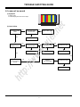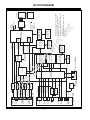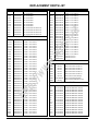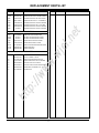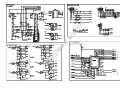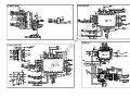
1
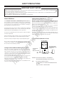
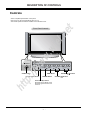
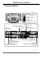
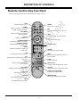
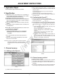
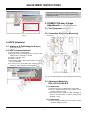
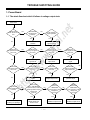
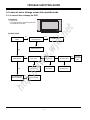
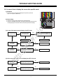
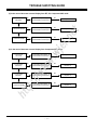
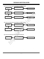
CANADA : http//biz.lgservice.com
USA
: http//www.lgservice.com
: http//lgservice.com/techsup.html
.ne
t
PLASMA TV
SERVICE MANUAL
jel
CHASSIS : RF-043A
MODEL : RU-42PX10/C RU-42PX11/H
.w
CAUTION
htt
p:
//w
ww
BEFORE SERVICING THE CHASSIS,
READ THE SAFETY PRECAUTIONS IN THIS MANUAL.
SAFETY PRECAUTIONS
IMPORTANT SAFETY NOTICE
Many electrical and mechanical parts in this chassis have special safety-related characteristics. These parts are identified by
in
the Schematic Diagram and Replacement Parts List.
It is essential that these special safety parts should be replaced with the same components as recommended in this manual to
prevent X-RADIATION, Shock, Fire, or other Hazards.
Do not modify the original design without permission of manufacturer.
.w
If any fuse (or Fusible Resistor) in this monitor is blown, replace
it with the specified.
.ne
It will also protect the receiver and it's components from being
damaged by accidental shorts of the circuitary that may be
inadvertently introduced during the service operation.
Plug the AC cord directly into the AC outlet.
Do not use a line Isolation Transformer during this check.
Connect 1.5K/10watt resistor in parallel with a 0.15uF capacitor
between a known good earth ground (Water Pipe, Conduit, etc.)
and the exposed metallic parts.
Measure the AC voltage across the resistor using AC
voltmeter with 1000 ohms/volt or more sensitivity.
Reverse plug the AC cord into the AC outlet and repeat AC
voltage measurements for each esposed metallic part. Any
voltage measured must not exceed 0.75 volt RMS which is
corresponds to 0.5mA.
In case any measurement is out of the limits sepcified, there is
possibility of shock hazard and the set must be checked and
repaired before it is returned to the customer.
jel
An lsolation Transformer should always be used during
the servicing of a receiver whose chassis is not isolated from
the AC power line. Use a transformer of adequate power rating
as this protects the technician from accidents resulting in
personal injury from electrical shocks.
t
Leakage Current Hot Check (See below Figure)
General Guidance
When replacing a high wattage resistor (Oxide Metal Film
Resistor, over 1W), keep the resistor 10mm away from PCB.
Leakage Current Hot Check circuit
ww
Keep wires away from high voltage or high temperature parts.
//w
Due to high vacuum and large surface area of picture tube,
extreme care should be used in handling the Picture Tube.
Do not lift the Picture tube by it's Neck.
Leakage Current Cold Check(Antenna Cold Check)
htt
p:
With the instrument AC plug removed from AC source,
connect an electrical jumper across the two AC plug prongs.
Place the AC switch in the on positioin, connect one lead of
ohm-meter to the AC plug prongs tied together and touch other
ohm-meter lead in turn to each exposed metallic parts such as
antenna terminals, phone jacks, etc.
If the exposed metallic part has a return path to the chassis, the
measured resistance should be between 1MΩ and 5.2MΩ.
When the exposed metal has no return path to the chassis the
reading must be infinite.
An other abnormality exists that must be corrected before the
receiver is returned to the customer.
To Instrument's
exposed
METALLIC PARTS
AC Volt-meter
Good Earth Ground
such as WATER PIPE,
CONDUIT etc.
0.15uF
1.5 Kohm/10W
CANADA: LG Electronics Canada, Inc. 550 Matheson
Boulevard East Mississauga, Ontario L4Z 4G3
USA
- 2 -
: LG Customer Interactive Center
P.O.Box 240007, 201 James Record Road Huntsville,
AL 35824
Digital TV Hotline 1-800-243-0000
TABLE OF CONTENTS
DESCRIPTION OF CONTROLS ...........................................4
SPECIFICATIONS.................................................................7
ADJUSTMENT INSTRUCTIONS ..........................................8
t
TROUBLE SHOOTING GUIDE ...........................................12
.ne
BLOCK DIAGRAM...............................................................23
EXPLODED VIEW PARTS LIST .........................................27
.w
REPLACEMENT PARTS LIST ............................................28
jel
EXPLODED VIEW...............................................................26
SCHEMATIC DIAGRAM..........................................................
htt
p:
//w
ww
PRINTED CIRCUIT BOARD ...................................................
- 3 -
DESCRIPTION OF CONTROLS
Controls
t
- This is a simplified representation of front panel.
Here shown may be somewhat different from your TV.
- This manual explains the features available on the RU-42PX10 TVs.
//w
ON/OFF
ww
.w
jel
.ne
Front Panel Controls
TV/VIDEO
htt
p:
ON/OFF Button
Remote Control Sensor
MENU
VOL
MENU Button
TV/VIDEO Button
Power Standby Indicator
Illuminates red in standby mode,
Illuminates green when the TV is
turned on.
- 4 -
CH
CHANNEL (E,
VOLUME (F,G) Buttons
D)
Buttons
DESCRIPTION OF CONTROLS
t
Connection Options
.ne
VIDEO Input
Connects the video signal from a video
device.
jel
L / MONO
A/V INPUT2
VIDEO
S-VIDEO
S-VIDEO Input
A connection available to provide better
picture quality than the video input.
.w
R AUDIO
AUDIO Input
Use to connect to hear stereo sound
from an external device.
ww
DVD/DTV Input (Component 1-2)
Connect a component video/audio
device to these jacks.
Monitor Output
Connect a second TV or Monitor.
//w
Remote Control Port
Connect your wired
remote control here.
S-Video Input
Connect S-Video out from an S-VIDEO
device to the S-VIDEO input.
COMPONENT
INPUT 2
MONITOR
OUTPUT
COMPONENT
INPUT 1
RS-232C INPUT
(CONTROL/SERVICE)
DVI INPUT
AUDIO INPUT
A/V
INPUT 1
R
RGB INPUT
htt
p:
REMOTE
CONTROL
VIDEO
L
AUDIO
R
L/MONO
AUDIO
S-VIDEO
Antenna
AC INPUT
VIDEO
Audio/Video Input 1
Connect audio/video output from an external
device to these jacks.
RGB Input/Audio Input/DVI Input
Connect the monitor output connector from
a PC to the appropriate input port.
Antenna Input
Connect cable or antenna
signals to the TV, either
directly or through your
cable box.
Power Cord Socket
This TV operates on AC power. The voltage is indicated
on the Specifications page. Never attempt to operate
the TV on DC power.
RS-232C INPUT (CONTROL/SERVICE) PORT
Connect to the RS-232C port on a PC.
- 5 -
DESCRIPTION OF CONTROLS
Remote Control Key Functions
- When using the remote control, aim it at the remote control sensor on the TV.
TVVIDEO
Selects: TV, Video 1-2, Component
1-2, RGB, and DVI input sources.
POWER
TV/VIDEO MULTIMEDIA MTS
ENTER
VOL
VOL
1
3
5
6
8
FCR
9
PIP/DW
Switches between PIP and Twin
picture modes.
htt
p:
SPLIT ZOOM
Enlarges the picture with regular ration.
NUMBER buttons
REVIEW
Tunes to the last channel viewed.
REVIEW
0
APC PIP/DW
DASP
//w
APC
Adjusts the factory preset picture according
to the room.
2
ww
4
ARC
Changes the picture format.
.w
CH
7
FCR
Use to scroll the favorite channel list.
MENU
Brings up the main menu to the screen.
CH
CAPTION
Selects CAPTION mode.
MTS
Selects the MTS sound: Mono, Stereo, or
SAP.
MENU
jel
CAPTION ARC
MULTIMEDIA
Selects: Component 1-2, RGB, and
DVI input sources.
VOLUME UP/DOWN
Increases/decreases the sound level.
CHANNEL UP/DOWN
Selects available channels found with
Auto program.
ENTER
Accepts your selection or displays the
current mode.
POWER
Turns your TV on or off.
t
MUTE
.ne
MUTE
Switches the sound on or off.
SPLIT ZOOM PIP CH + SLEEP
DASP
Selects the sound appropriate for the program's character.
SLEEP
Sets the sleep timer.
WIN.SIZE PIP CH - PIP INPUT
POSITION SWAP A.PROG
MEMORY/ERASE
PIPCH-/PIPCH+
Changes to next lower/higher PIP channel.
PIP INPUT
Selects the input source for the sub picture.
A.PROG (AUTO PROGRAM)
Searches for available channels.
WIN. SIZE
Adjusts the sub picture size.
MEMORY/ERASE
Memorizes or erases selected channel.
POSITION
Moves the sub picture in pip mode.
SWAP
Exchanges the main/sub images.
- 6 -
SPECIFICATIONS
RU-42PX10/20
RU-50PX10/20
Width (inches / mm)
48.4 / 1210
56 / 1400
Height (inches / mm)
27.6 / 701
30.4 / 761.5
Depth (inches / mm)
11.4 / 290
11.4 / 290
Weight (pounds / kg)
66 / 22.9
66 / 29.9
Resolution
852 x 480 (Dot)
1366 x 768 (Dot)
.ne
t
MODELS
AC100-240V, 50/60Hz
Television System
NTSC
Program Coverage
VHF 2 ~ 13, UHF 14 ~ 69, CATV 1 ~ 125
External Antenna Impedance
75 Ω
Color
16,770,000 (256 steps of each R, G and B)
Operating Temperature Range
32 ~ 104°F (0 ~ 40°C)
Operating Humidity Range
Less than 80%
.w
jel
Power requirement
6561 feet (2000m)
Maximum Elevation
htt
p:
//w
ww
• The specifications shown above may be changed without notice for quality improvement.
- 7 -
ADJUSTMENT INSTRUCTIONS
(2) After installing the Gprobe, [Option -> Connection Setup]
or click the icon indicated in the picture and then setup as
below the picture.
(In case of the port (second one), set to the serial port
of the connected PC.
The other only have to be set as below the picture.)
(3) After finishing inputs, click the button [OK] to complete the
connection setup.
1. Application Object
These instructions apply to the RF-043A Chassis.
2. Specification
3-2. Confirming the G-prove
.ne
t
(1) Connect Rs232 cable and then turn on the power.
If communication is correct, the message is showed like in
the left output terminal.
(2) If the message is not showed, push the [INSTART] button
of the adjust remocon twice, and change the right selection
of the [System Control -> RS-232 Host] from GProbe to
PC.
** If it is impossible to check the OSD, push the [TILT]
button of the adjust remocon.
Then, the message which is “Starting Gprove...”
comes up. From this time, communication is operated
correctly.
However, you have to push the [TILT] button again
in case of turning on Main Power.
** If you want to check again whether commnunication is
on or not, input “test” and push the Enter key on the
right input terminal. If communication is on, the
message of “Test passed.” will come up
jel
(1) Because this is not a hot chassis, it is not necessary to
use an isolation transformer. However, the use of isolation
transformer will help protect test instrument.
(2) Adjustment must be done in the correct order.
(3) The adjustment must be performed in the circumstance of
25±5°C of temperature and 65±10% of relative humidity if
there is no specific designation.
(4) The input voltage of the receiver must keep 100~220V,
50/60Hz.
(5) The receiver must be operated for about 15 minutes prior
to the adjustment.
After RGB Full white HEAT-RUN Mode, the receiver must
be operated prior to adjustment.
O Enter into HEAT-RUN MODE
1) Press the POWER ON KEY on R/C for adjustment.
2) OSD display and screen display 100% full WHITE
PATTERN.
ww
[ Set is activated HEAT-RUN without signal generator in
this mode.
[ Single color pattern(RED/BLUE/GREEN) of HEAT-RUN
mode uses to check PANEL.
.w
O
//w
Caution) If you turn on a still screen more than 20 minutes
(Especially digital pattern, cross hatch pattern), a after
image may be occur in the black level part of the
screen.
3. Channel memory
htt
p:
3-1. Setting up the G-prove
(Fig 2)
3-3. Channel memory method
(1) Click [Command -> Batch].
(2) When the window of [Batch] is showed, enter the text file
(Ch_Memory-RZ_PX10.txt) in the right blank of the File.
(3) Click the button [OK] to write CH information in the
EEPROM.
(4) It means the completion of the CH memory download that
the message of right output terminal is showed as below.
(Fig 1)
(1) Install the GProve. (GProve4.4.0.2.exe)
- 8 -
ADJUSTMENT INSTRUCTIONS
Each PCB assembly must be checked by check JIG set.
(Because power PCB Assembly damages to PDP Module,
especially be careful)
t
5. POWER PCB Assy Voltage
Adjustments (Va, Vs Voltage Adjustments)
.ne
5-1. Test Equipment : D.M.M. 1EA
5-2. Connection Diagram for Measuring
Refer to Fig 5.
jel
(Fig 3)
4. HDCP download
4-1. Setting up & Confirming the G-prove
.w
: Refer to 3-1 and 3-2.
4-2. HDCP download method
< 3501V00180A >
htt
p:
//w
ww
(1) Click [Command -> NVRAM Write]
(2) When the window of [NVRAM Write] is showed, select
“LGEKEY1.bin” to insert fill up in the File.
(3) LGEKEY1 : first KEY value
(4) Address : insert ‘0’
(5) After finishing inputs, click the button [OK] to write HDCP
key in the EEPROM.
(6) It means the end of the HDCP key download that the
message of Output terminal is showed as below.
(Fig 4)
< 3501V00182A >
(Fig 5) Connection Diagram of power adjustment for measuring
5-3. Adjustment Method for
P/No. 3501V00180A B/D
(1) Va Adjustment
1) After receiving 100% Full White Pattern, HEAT RUN.
2) Connect + terminal of D.M.M to Va pin of P805, connect
- terminal to GND pin of P805.
3) After turning RV501, voltage of D.M.M adjustment as
same as Va voltage which on lable of panel right/top
(Deviation; ±0.5V)
(2) Vs Adjustment
1) Connect + terminal of D.M.M to Vs pin of P805, connect
– terminal to GND pin of P805.
- 9 -
ADJUSTMENT INSTRUCTIONS
(2) Supply Gray Pattern (216 Level Full Size Pattern) signal
to VIDEO input. (AV2 Input 60Hz)
(Refer to Fig. 6)
(3) To adjust, stick sensor to 216 Gray Level Pattern, press
ADJ key twice(White Balance) on remote control.
For adjustment and D, E on reomte control for adjustment
mode to select Red Gain and Blue Gain, press VOL +, Key and adjust it until color coordination becomes as
below.
2) After turning RV401, voltage of D.M.M adjustment as
same as Va voltage which on label of panel right/top.
(Deviation; ±0.5V)
5-4. Adjustment Method for
P/No. 3501V00182A B/D
(1) Va Adjustment
t
1) After receiving 100% Full White Pattern, HEAT RUN.
2) Connect + terminal of D.M.M to Va pin of P805, connect
- terminal to GND pin of P805.
3) After turning RV601, voltage of D.M.M adjustment as
same as Va voltage which on lable of panel right/top
(Deviation; ±0.5V)
.ne
X; 0.283±0.003, Y; 0.297±0.003
Color Temperature; 9,300°K±500°K
(4) Exit adjustment mode using A Key.
6-1. Required Equipment
Color Analyzer (CA-100 or same product)
7-1. Pattern Equipment
PC Pattern Generator (VG828, VG854, 801GF, MSP3240A)
(16 Gray Scale Pattrtn output(RGB output Level: 0.7Vp-p)
7-2. Method of Auto RGB Color Balance
(1) Input RGB Source : 16 Gray Scale Pattern output (RGB
output Level : 0.7Vp-p)
(2) Press ADJ KEY on R/C for adjustment.
(3) Press Vol. + KEY and operate To SET.
(4) Auto-RGB OK means completed adjustment.
ww
6. Adjustment of White Balance
7. Auto RGB Color Balance
.w
1) Connect + terminal of D.M.M to Vs pin of P805, connect
– terminal to GND pin of P805.
2) After turning RV401, voltage of D.M.M adjustment as
same as Va voltage which on label of panel right/top.
(Deviation; ±0.5V)
jel
(2) Vs Adjustment
6-2. Connection Diagram of Equipment for
Measuring
216 Gray Level
Full Size Pattern
//w
8. Auto Component Color Balance
AV Signal Input
8-1. Pattern Equipment
MSP3240A or same product
(16 Gray Scale Pattern output(Component output Level:
0.7Vp-p)
60Hz
htt
p:
Window
RS-232C Serial Communication
8-2. Method of Auto RGB Color Balance
(1) Input RGB Source : Component 480p/576p 16 Gray Scale
Pattern
At this time, except Pb and Pr signal, only Y signal insert.
(2) Press ADJ KEY on R/C for adjustment.
(3) Press Vol. + KEY and operate To set.
(4) Auto-RGB OK means completed adjustment.
MSPG-2100 or
MSTG-5200
(Fig 6) White Balance Adjustment
6-3. Adjustment of White Balance
O
O
Operate the Zero-calibration of the CA-100, then stick
sensor to PDP module surface when you adjust.
For manual adjustment, it is also possible by the following
sequence.
(1) Select white pattern of heat-run mode by pressing power
on key on remote control for adjustment then operate heat
run more than 15 minutes.
(Fig 7) Auto RGB/ Component Color Balance Test Pattern
- 10 -
ADJUSTMENT INSTRUCTIONS
9. Auto Adjustment Map(RS-232C)
6) If Check Sum is not 53, repeat 3) ~ 4).
7) If Check Sum is 53, DDC data for Analog-RGB input is
completed.
RF-043A
RS232
(2) DDC Data input for Digital-RGB(DVI)
Stop bit
Parity
115200
8
1
NONE
Index Cmd1 Cmd2 Data Min Value Max Value
R Gain
j
a
00(00)
255(FF)
G Gain
j
b
00(00)
255(FF)
Protocol B Gain
Setting
R Offset
j
c
00(00)
255(FF)
j
d
00(00)
255(FF)
G Offset
j
e
00(00)
255(FF)
B Offset
j
f
00(00)
255(FF)
.w
10. DDC Data Input
10-1. Required Test Equipment
htt
p:
//w
ww
(1) A jig for adjusting PC, DDC (PC serial to D-sub
Connection equipment)
(2) S/W for writing DDC (EDID Data Write & Read)
(3) D-sub 15P Cable, D-Sub to DVI Connector (Connect to
DVI Jack)
10-2. Setting of Device
1) Connect PC Serial to DVI Cable of jig for DDC
adjustment to DVI terminal (DVI Jack).
2) Operate S/W for DDC record and select DDC data for
digital RGB in model menu.
3) Operate EDID Write command.
4) Operate EDID Read command and check whether
Check sum is D2(1page), BF(2page).
5) If Check sum is not D2(1page), BF(2page), repeat 3) ~
4).
6) If Check sum is D2(1page), BF(2page), DDC data for
Analog-RGB input is completed.
t
Data bit
.ne
Baud Rate
jel
Type
10-3. Preparation for Adjustment
(1) Set devices as above and turn the PC, jig on.
(2) Put S/W for writing DDC (EDID data Write & Read) into
operation. (operated in DOS mode.)
10-4. Sequence of Adjustment
(1) DDC Data Input for Analog-RGB
1) Put the set on the table and turn the power on.
2) Connect PC Serial to D-sub 15P Cable of jig for DDC
adjustment to RGB terminal (D-Sub 15Pin).
3) Operate S/W for DDC record and select DDC data for
Analog RGB in Model Menu.
4) Operate EDID Write command.
5) Operate EDID Read command and check whether
Check Sum is 53.
- 11 -
TROUBLE SHOOTING GUIDE
1. Power Board
1-1. The whole flowchart which it follows in voltage output state
Doesn't the
screen whole come
out?
Yes
It is identical
with Power Off
condition?
No
Is the Interface
signal operated?
Yes
1. Check the Power Off
condition.
Doesn't the
St-by 5V signal
come out?
Yes
No
Doesn't the
VSC signal Vs-ON
come out?
htt
p:
High tension
output voltage Drop
it occurs?
Yes
5. Check the VSC RL-ON
signal.
Doesn't the
Vs, Va voltage output
come out?
No
Doesn't the
VSC low pressure
output come out?
Yes
7. Check the VSC Vs-ON
signal
When remove
the Y, Z B/D Module
Input Connector, Power
Board high tension output
voltage Drop
it occurs?
Yes
4. Check the 5V Monitor
signal circuit.
Yes
No
Doesn't the
VSC signal RL-ON
come out?
No
Yes
3. Check the St-by 5V
signal circuit.
Yes
Doesn't the
5V Monitor signal
come out?
No
//w
Doesn't the
high tension output
come out?
.w
Yes
2. Check the Interface
signal condition.
ww
Doesn't the
low pressure output
come out?
Yes
jel
No
.ne
t
Start check
Yes
8. Check the Vs, Va
voltage output circuit.
No
No
When
remove the
Y B/D Module
Input Connector, output
voltage Drop
it occurs?
6. Check the VSC low
pressure output
No
When
remove the
Z B/D Module
Input Connector, output
voltage Drop
it occurs?
No
Yes
Manufacture enterprise
meaning of a passage
Yes
10. Check the Z B/D
Module Coutput circuit
9. Check the Power
Board Output high
tension circuit
- 12 -
Yes
11. Check the Y B/D
Module Coutput circuit
TROUBLE SHOOTING GUIDE
//w
ww
.w
jel
.ne
t
1-2. Sony Power Board Structure
htt
p:
T502: Vs Trans
1
2
3
T702: Va Trans
T101: St-by Trans
T103: Low Voltage Trans
- 13 -
TROUBLE SHOOTING GUIDE
//w
ww
.w
jel
.ne
t
1-3. Sanken Power Board Structure
htt
p:
T221: Vs Trans
1
2
3
T271: Va Trans
T121: St-by Trans
T201: Low Voltage Trans
- 14 -
TROUBLE SHOOTING GUIDE
2. No Power
(1) Symptom
¯
Does’t minute discharge at module.
Non does not come in into the front LED.
.ne
t
¯
(2) Check follow
No
Is plug in power cord?
Plug in power cord.
No
Is connect the Line Filter and Power
Switch Cable?
Yes
No
Replace Fuse.
//w
Is normal the Fuse(F101) on Power
Board?
Connect Cable.
ww
Yes
No
.w
Connect Cable.
Yes
Is connect the Power Switch and
Power Board Cable?
jel
Yes
htt
p:
Is connect the Power Board and 7P
of VSC Board Cable?
No
Connect Cable.
Yes
Is connect the Power Switch and
Power Board Cable?
No
Connect Cable.
Yes
After remove the cable connect to
Power Board(except the CN101
connection cable), authorizes the
AC voltage marking on manual.
When ST-BY 5V does not operate,
replace Power Board.
- 15 -
TROUBLE SHOOTING GUIDE
3. Protect Mode
(1) Symptom
After once shining, it does not discharge minutely
from module
¯ The Rely falls(The sound is audible “click”)
¯ It is converted with the color where the front LED
is red from green.
(2) Check follow
No
Is output the normality Low/High
voltage except Stand-by 5V?
Yes
No
After connecting well each connector,
the normality it operates?
Yes
No
Yes
Is normal the
Z- Board?
No
Is normal the
X- Board?
Is normal the
Ctrl Board?
No
Yes
Yes
No
Is normal the output voltage after
remove P1, 2, 3, 4, 6, 7 connector of
X-B/D?
Yes
No
Is normal the output voltage after
remove P1, 2, 101, 300, 701, 702
connector of Ctrl-B/D?
Yes
htt
p:
Yes
Is normal the Fuse(FS1, FS2) on ZB/D? (In case of open is replace)
//w
Yes
Is normal the Fuse(F52) on Y-B/D?
(In case of open is replace)
ww
Is normal the
Y- Board?
Replace Power
Board.
Replace
connector.
.w
Is normal the each
connector?
No
jel
Is normal the Power
Board?
.ne
t
¯
Is normal the output
voltage after remove
P5, P6 connector of
Y-B/D?
Is normal the output
voltage after remove
P1 connector of
Z-B/D?
Yes
Replace
Y-Board.
Yes
Replace
Z-Board.
After remove P1, P2, P3, P4 output voltage
normality: Replace Right X-B/D
After remove P6, P7 output voltage
normality: Replace Left X-B/D
Replace
X-Board.
Yes
Is normal the
VSC Board?
No
Is normal the output voltage after
remove P1000, P1200?
Yes
After remove P1000 normal operation:
Replace Analog Board
After remove P1200 normal operation:
Replace Digital Board
Yes
Is normal the
COF of X, Y, Z?
No
After crisis COF of each board, check the normality operates.
If in case normality operates, correspondence COF Fail is
replace the module.
- 16 -
TROUBLE SHOOTING GUIDE
4. No Raster
(1) Symptom
Does’t minute discharge at module.
It maintains the condition where the front LED is green.
t
¯
(2) Check follow
Is normal the Power
Board?
No
Is output the normality Low/High
voltage except Stand-by 5V?
Is normal the each
connector?
No
After connecting well each connector,
the normality it operates?
Yes
Is normal the
Z- Board?
No
Is normal the
X- Board?
Yes
Yes
Yes
No
Is normal the output voltage after
remove P1, 2, 3, 4, 6, 7 connector of
X-B/D?
Yes
No
Is normal the output voltage after
remove P1, 2, 101, 300, 701, 702
connector of Ctrl-B/D?
Yes
htt
p:
Is normal the
Ctrl Board?
Is normal the Fuse(FS1, FS2) on ZB/D? (In case of open is replace)
//w
Yes
Is normal the Fuse(F52) on Y-B/D?
(In case of open is replace)
ww
No
No
Replace
connector.
.w
Yes
Is normal the
Y- Board?
Replace Power
Board.
jel
Yes
No
.ne
¯
Is normal the output
voltage after remove
P5, P6 connector of
Y-B/D?
Is normal the output
voltage after remove
P1 connector of
Z-B/D?
Yes
Replace
Y-Board.
Yes
Replace
Z-Board.
After remove P1, P2, P3, P4 output voltage
normality: Replace Right X-B/D
After remove P6, P7 output voltage
normality: Replace Left X-B/D
Replace
X-Board.
Yes
Is normal the
VSC Board?
No
Is normal the output voltage after
remove P1000, P1200?
Yes
After remove P1000 normal operation:
Replace Analog Board
After remove P1200 normal operation:
Replace Digital Board
Yes
Is normal the
COF of X, Y, Z?
No
After crisis COF of each board, check the normality operates.
If in case normality operates, correspondence COF Fail is
replace the module.
- 17 -
TROUBLE SHOOTING GUIDE
5. In case of occur strange screen into specific mode
5-1. In case of does’t display the OSD
(1) Symptom
¯
LED is green
The minute discharge continuously becomes
accomplished from module
.ne
t
¯
(2) Check follow
No
Yes
Is the LVDS cable
connected well?
Replace cable.
jel
Is normal the LVDS
cable?
Is normal the VSC
Digital Board?
No
ww
Cable inserts well.
Yes
.w
No
Operates the Thine Yes
IC(IC1100)?
Operates the
IEP(IC500)?
Replace Thine
IC(IC1100).
Is normal the Ctrl
Board of Module?
No
Replace
IEP(IC500).
No
htt
p:
Yes
//w
No
Replace Ctrl B/D.
- 18 -
Yes
Operates the
Scaler(IC700)?
No
Replace
Scaler(IC700).
Yes
Replace
VSC Digital
B/D.
TROUBLE SHOOTING GUIDE
5-2. In case of does’t display the screen into specific mode
(1) Symptom
¯
The screen does not become the display from specific input mode
(RF, AV, Component, RGB, DVI).
Check the all input mode should become normality display.
Check the Video(Main)/Data(Sub), Video(Main)/Video(Sub) should become
normality display from the PIP mode or DW mode. (Re-Check it Swap)
(3) In case of becomes unusual display from RF mode
Is the Tuner Cable
connected well?
No
Is normal the Input voltage, IIC
Communication and CVBS output?
ww
Yes
Yes
.w
No
Is normal the Tuner?
Cable inserts well.
Yes
Is normal the Input voltage, IIC
Communication and HV sync?
No
Is normal the Input voltage, IIC
Communication and HV sync?
htt
p:
Is normal the
VPC3230?
No
//w
Is normal the
CXA2069Q?
.ne
¯
jel
¯
t
(2) Check follow
No
Replace Tuner
No
Replace IC
No
Replace IC
(4) In the case of becomes unusual display from RF, AV mode
Is normal the
CXA2069Q?
No
Is normal the Input voltage, IIC
Communication and HV sync?
No
Is normal the Input voltage, IIC
Communication and HV sync?
No
Replace IC
Yes
Is normal the
VPC3230?
No
- 19 -
Replace IC
TROUBLE SHOOTING GUIDE
(5) In the case of becomes unusual display from RF, AV, Component 480i mode
Is normal the
VPC3230?
No
Is normal the Input voltage, IIC
Communication and HV sync?
No
Is normal the Input voltage, IIC
Communication and HV sync?
No
Is normal the Input voltage, IIC
Communication and HV sync?
No
Replace IC
Yes
t
Replace IC
Yes
No
Replace IC
jel
Is normal the Scaler?
.ne
No
Is normal the S2300?
No
Yes
Is normal the
CXA2101?
No
Is normal the
M52758?
No
Is normal the Input voltage, IIC
Communication and HV sync?
htt
p:
Yes
Is normal the Input voltage, IIC
Communication and HV sync?
//w
Yes
Is normal the Input voltage, IIC
Communication and HV sync?
No
Is normal the Scaler?
No
ww
Is normal the
74LS123?
.w
(6) In the case of becomes unusual display from Component DTV mode
Is normal the Input voltage, IIC
Communication and HV sync?
- 20 -
Replace IC
No
Replace IC
No
Replace IC
No
Replace IC
TROUBLE SHOOTING GUIDE
(7) In the case of becomes unusual display from RGB DTV mode
Is normal the
CXA2101?
No
Is normal the Input voltage, IIC
Communication and HV sync?
No
Is normal the Input voltage, IIC
Communication and HV sync?
No
Is normal the Input voltage, IIC
Communication and HV sync?
No
Replace IC
Yes
Replace IC
t
No
Yes
No
Replace IC
jel
Is normal the Scaler?
.ne
Is normal the
M52758?
Is normal the
M52758?
No
.w
(8) In the case of becomes unusual display from RGB PC mode
Is normal the Input voltage, IIC
Communication and HV sync?
No
Is normal the Input voltage, IIC
Communication and HV sync?
//w
Is normal the Scaler?
ww
Yes
No
Replace IC
No
Replace IC
(8) In the case of becomes unusual display from DVI mode
No
Is normal the Input voltage, IIC
Communication and HV sync?
htt
p:
Is normal the Scaler?
- 21 -
No
Replace IC
TROUBLE SHOOTING GUIDE
6. In case of no sound
(1) Symptom
¯
LED is green
Screen display but sound is not output
t
¯
Is normal the SPK
cable?
No
Yes
Is the SPK cable
connected well?
Replace SPK cable
Cable inserts well.
No
Is the Flat cable
connected well?
Operates the IC800?
No
Cable inserts well.
Replace IC800
//w
Yes
No
htt
p:
Is normal the
RF/AV/Component
sound?
Yes
ww
No
.w
Is normal the
RGB/DVI sound?
jel
No
Yes
.ne
(2) Check follow
- 22 -
Replace
VSC Analog B/D
Yes
Operates the IC801?
No
Replace IC801
Yes
Operates the IC802?
No
Replace IC802
- 23 -
Co mp _Y
YCin4
Vin4
TU_Sub
Text _V
Main_YC
Main_V
RGB_Dat a
SDA6001
Text Processor
HYV641620
SRAM
DVI_Dat a
AM29LV160
F-ROM
t
10
24
ZHINE
Po s-t p ro c es sing Blo c k is o m it t ed .
so-c alled JEPICO, in this c ase
TMDS TX is also req uired .
So und Pro c es sing Blo c k Diag ram
is sep arat ed . .
RCA-t yp e Blo c k Diag ram is also
sep arat ed . .
AM29LV
F-ROM (1MB )
.ne
jel
HY57V64322
SDRAM ( 8MB)
IEP
TX0/ 1/ 2/ 3/ C
Disp _En
SDATA
SCLK, SLE
24
Co mp _480I/ P
Co mp
/ RGB_SW
HY5DU283222A
SDRAM ( 128MB)
DVI RX
w/ HDCP
g m 1601
Sc aler ( Malib u)
ADC
w/ PLL
YCb Cr
S2300
/
DeInt erlac er
8
.w
VPC3230 (S)
Video Decoder
Sid e - AV BOARD
Co mp _480i
CVBS S-VHS
Vin5 YCin5
CXA2069Q
SWITCH
VPC3230 (M )
Video Decoder
ww
Main_YC
Main_V
//w
M52758F
Sw it c h
RS232_RX/ TX
TX_Out
Main_Vid eo
/
24
Sub _Vid eo
/
Co mp / RGB_SW
8
Fro m Malib u
CXA_RGB
Vid eo f o r Text
CXA2101
Text
Comp DTV
Co mp _480I/ P
To Malib u
74LS123
Tuner ( S )
TU_Main
Vin3 (CVBS )
MNT OUT
Vin2 ( CVBS )
1H RGB
Tuner (M)
Analo g BOARD
Comp1
(DVD/DTV )
S-VHS
CVBS
RF
Scart 3
Scart 2
Scart 1
24LC21
RX/ TXC
24LC21
74HCT08
TV OUT
Vin1 ( CVBS)
SCL/ SDA
RX/ TX0/ 1/ 2,
SCL/ SDA
RGB H/ V
RGB DTV
RGB PC
htt
p:
ST3232C
74ACT253
RGB PC/ DTV
RX0/1,TX0/1
Dig it al BOARD
DVI
(PC/DTV)
RGB
(PC/DTV)
RS232
WIRE IR
TX
IR
BLOCK DIAGRAM
IIS
Co m p 1
- 24 -
Sid e
S-VHS
Side-CVBS
Sid e A/ V
RF
S-VHS
CVBS OUT
CVBS IN
( DVD/ DTV)
Co m p 2
( DVD/ DT V)
Y/ CIN2
VIN2
Tuner ( S)
Tuner ( M)
Y/ CIN1
MNT_OUT
VIN1
Co mp 2
Co mp
24LC21
24LC21
CXA2069Q
74HCT08
ST3232C
74ACT253
MAIN_YOUT
MAIN_VOUT
MAIN_COUT
CAB_VIN
DTV2_Co mp
LA7151M
DVD2_MAIN
DVD_MAIN
DTV_Co mp
DAC_RGB
M37136
( OTP)
RGB_24Bit
SVPORT
( 16b it)
g m1501H
SUB_COUT
SUB_YOUT
DVD2_SUB
DVD_SUB
ALT_Y2_480I_SUB
S656 8 Bit
M62320FP
( I2C Exp end er)
t
.ne
HY57V64322
SDRAM ( 8MB)
Flash ROM
512K/ 1M
TQFP 128K
DDR Memo ry
TMDS Transf er
/ Thine
M656 8 Bit
FLI2300
jel
VPC3230
( SUB)
COMB_COUT
SW CVBS/ Y
ALT_Y_480I_SUB
UPD64083
COMB_YOUT
MAIN_YOUT
ALT_Y2_480I_MAIN
VPC3230
( MAIN)
S/ DVD_Co mp
.w
CAB_Co mb
VPORT
( 24b it)
DVI
Analo g
RGB
ALT_Y_480I_MAIN
M52758FP
IC400( MUX)
ww
RGB_DTV
M52758FP
IC202( MUX)
//w
M52758FP
IC204
CXA2101
RGB PC
htt
p:
RGB DTV
IIS
HV
IIS
Tx
Analo g BOARD
DVI
( PC/ DTV)
RGB
( PC/ DTV)
RS232
WIRE IR
Di gt a l BOARD
LVDS
31PIN
ZHINE
IEP
BLOCK DIAGRAM
//w
htt
p:
t
.ne
jel
.w
ww
NOTES
- 25 -
EXPLODED VIEW
300
121
600
601
t
301
.ne
305
304
jel
120
.w
303
ww
302
200
207
202
206
//w
530
205
201
490
204
531
htt
p:
402
580
203
560
410
520
400
570
401
430
- 26 -
EXPLODED VIEW PARTS LIST
No.
Part No.
120
6401VD0013H
SPEAKER ASSEMBLY,FULL RANGE(L)
121
6401VD0013G
SPEAKER ASSEMBLY,FULL RANGE(R)
200
6348Q-E058T
PDP,42 16:9 852*480 PDP42V60000.AKLGG
6348Q-E059C
PDP,42 *42PX11H
6348Q-E058U
PDP LGERS
201
6871QCH034A
PCB ASSEMBLY,DISPLAY CTRL ASSY 42V6 NEW MCM(1222) LVDS
202
6871QDH066A
PCB ASSEMBLY,DISPLAY YDRV ASSY 42V6 YDRV TOP ASSY
203
6871QDH067A
PCB ASSEMBLY,DISPLAY YDRV ASSY 42V6 YDRV BTM ASSY
204
6871QLH034A
PCB ASSEMBLY,DISPLAY XRLT ASSY 42V6_XL(4LAYER)
205
6871QRH037A
PCB ASSEMBLY,DISPLAY XRRT ASSY 42V6_XR(4LAYER)
206
6871QYH029A
PCB ASSEMBLY,DISPLAY YSUS ASSY 42V6
207
6871QZH033A
PCB ASSEMBLY,DISPLAY ZSUS ASSY 42V6
300
3091V00684B
CABINET ASSEMBLY,RU-42PX10 STEREO RF043A NON
3091V00684E
CABINET ASSEMBLY *LGEUS
3091V00684M
CABINET ASSEMBLY,RU-42PX11(LGECI)
3091V00684S
CABINET ASSEMBLY,RU-42PX11(LGEUS)
3091V00684Z
CABINET ASSEMBLY,RU-42PX10C(LGERS)
3091V00763A
CABINET ASSEMBLY,RU-42PX11 LGEUS SKD(LGERS)
4980V01067A
SUPPORTER ASSY,AL FILTER TOP RZ-42PZ10
4980V01067D
SUPPORTER ASSY,AL FILTER TOP *42PX11H
4980V01067B
SUPPORTER ASSY,AL FILTER TOP LGERS
4980V01068A
SUPPORTER ASSY,AL FILTER BOTTOM RZ-42PX10
4980V01068D
SUPPORTER ASSY,AL FILTER BOTTOM *42PX11H
4980V01068B
SUPPORTER ASSY,AL FILTER BOT LGERS
303
4980V01069A
4980V01069B
4980V01069D
304
4980V01070A
4980V01070D
t
.ne
jel
SUPPORTER ASSY,AL FILTER RIGHT RZ-42PX10
SUPPORTER ASSY,AL FILTER RIGHT LGERS
SUPPORTER ASSY,AL FILTER RIGHT *42PX11H
SUPPORTER ASSY,AL FILTER LEFT RZ-42PX10
SUPPORTER ASSY,AL FILTER LEFT *42PX11H
SUPPORTER ASSY,AL FILTER LEFT LGERS
//w
4980V01070B
.w
302
ww
301
Description
305
3790V00709B
FILTER(MECH),LGM42-01 MITSUI 42 ETCHING MESH GLASS FILTER
400
3809V00444C
BACK COVER ASSEMBLY
3809V00444D
BACK COVER ASSEMBLY
3301V00025D
PLATE ASSEMBLY,COVER VSC TUNER RU-42PX10 PRESS
3301V00025G
PLATE ASSEMBLY,VSC TUNER LGERS
402
410
430
490
520
LGERS
htt
p:
401
3301V00023D
PLATE ASSEMBLY,AV VSC TUNER RU-42PX10
4980V01071A
SUPPORTER ASSY,AL MODULE VER. RZ-42PX10
4980V01071B
SUPPORTER ASSY,AL VERTICAL LGERS
3501V00171A
BOARD ASSEMBLY,BASE
3501V00171B
BOARD ASSEMBLY,STAND LGERS
4980V01057A
SUPPORTER,PCB EGI POWER SW. RZ-42PY20
4980V01057B
SUPPORTER,PCB EGI POWER SW LGERS
6871VMMS16A
PCB ASSEMBLY,MAIN RF043A MALIBU RU MAIN DIGITAL MANUAL
6871VSME92A
PCB ASSEMBLY,SUB PSW RF043A MAILBU
5020V00915A
BUTTON,POWER RZ-42PY20 ABS 1KEY .
5020V00915B
BUTTON,POWER LGERS
560
6871VSMS04A
PCB ASSEMBLY,SUB TUNER RF043A MALIBU RU SUB ANALOG MANUAL
570
6871VSMZ91A
PCB ASSEMBLY,SUB CONT RF043A NEW HOLDER LOC
580
3501V00182A
BOARD ASSEMBLY,POWER RZ-42PX10 RF043A SRX-89 SONY PSU
600
6871VSME91A
PCB ASSEMBLY,SUB A/V RF043A MALIBU SIDE AV
601
4811V00118B
BRACKET ASSEMBLY,DECO RU-42PX10 RF043A SIDE AV
4811V00118D
BRACKET ASSEMBLY,AV LGERS
530
531
- 27 -
REPLACEMENT PARTS LIST
LOCA. NO
CC, CX, CK, CN : Ceramic
CQ : Polyestor
CE : Electrolytic
PART NO
RD : Carbon Film
RS : Metal Oxide Film
RN : Metal Film
RF : Fusible
RUN DATE : 2004.6.11
DESCRIPTION
LOCA. NO
IC
IC100
0IMMRAL014B
IC100
0IMI623200B
IC1000
0IMCRFA010A
KA7809R 2P
IC1001
0IPRPML001A
MIC39100 3P SOT223
IC1002
0IMCRSH001A
PQ05DZ1U SHARP 5
IC1003
0ITK118100B
IC1004
0IMCRSH001A
PQ05DZ1U SHARP 5
IC101
0IMMRAL014B
AT24C02N 10SI 2.7 8P
IC102
0IMCRTI003A
SN74HCT08D 16P
IC103
0IMCRTI021A
SN74LVTH541PWR 20P
IC104
0IMCRTI021A
SN74LVTH541PWR 20P
IC1100
0IMCRTH002A
THC63LVD103 64P 10BIT
IC1100
0IMMRNE002A
UPD64083GF3BA 100 3D YC LSI
IC1101
0ISA715100D
LA7151M 10SOP R/TP AUDIO SW
IC1200
0IMCRSJ001A
SC1565IST 1.8 3P SOT223
IC1201
0IPRPML001A
MIC39100 3P SOT223
IC1202
0IMCRFA010A
KA7809R 2P
IC1300
0IMCRRH001A
BA033FP E2 3P SOP,TO252 3
IC1301
0IMCRSH001A
PQ05DZ1U SHARP 5
IC1302
0IMCRSH001A
PQ05DZ1U SHARP 5
IC1303
0IMCRRH001A
BA033FP E2 3P SOP,TO252 3
IC1304
0IMCRSJ001A
SC1565IST 1.8 3P SOT223
IC1305
0IMCRRH001A
BA033FP E2 3P SOP,TO252 3
IC1306
0IPRPML001A
MIC39100 3P SOT223
IC200
0IFA742530B
74ACT253SC 16P
IC201
0IMCRSG010A
ST3232CDR SOP16 RS232
IC202
0IMCRMI006A
M52758FP 36PIN
IC203
0IFA741230A
DM74LS123MX 16SOP
IC204
0IFA741230A
DM74LS123MX 16SOP
IC400
0ISO206900A
CXA2069Q QFP64 BK I2C BUS AV S/W
IC500
IC500
IC501
IC502
IC503
IC600
IC600
IC601
DESCRIPTION
IC800
0IMCRMN027B
MSP4440G QA C13 101
IC801
0IMMRMR023A
MX29LV800TTC 70 48PIN 8MBIT, 3.3V
IC801
0IMCRNL001A
NSP 6241B 64P DIGITAL AUDIO
IC802
0IMCRTI028C
TAS5122DCAR 56P/TSSOP R/TP 30W
IC805
0IKE704200J
KIA7042AF SOT 89 TP 4.2V
t
M62320FP 16P
TRANSISTOR
Q001
0TR387500AA
CHIP 2SC3875S(ALY) KEC
Q002
0TR387500AA
CHIP 2SC3875S(ALY) KEC
Q100
0TR830009BA
BSS83
Q100
0TR150400BA
CHIP 2SA1504S(ASY) KEC
Q1000
0TRKE80038A
KTC3552T RTK SOT 23F 50V 3A
jel
TK11840L 8P SOT23L DC DC CONVERTER
0TR830009BA
BSS83
Q101
0TR387500AA
CHIP 2SC3875S(ALY) KEC
Q102
0TR830009BA
BSS83
Q102
0TR387500AA
CHIP 2SC3875S(ALY) KEC
Q103
0TR830009BA
BSS83
Q103
0TR150400BA
CHIP 2SA1504S(ASY) KEC
Q104
0TR387500AA
CHIP 2SC3875S(ALY) KEC
Q105
0TR387500AA
CHIP 2SC3875S(ALY) KEC
Q106
0TR150400BA
CHIP 2SA1504S(ASY) KEC
Q107
0TR387500AA
CHIP 2SC3875S(ALY) KEC
Q108
0TR150400BA
CHIP 2SA1504S(ASY) KEC
Q110
0TR830009BA
BSS83
Q1100
0TR387500AA
CHIP 2SC3875S(ALY) KEC
Q1101
0TR150400BA
CHIP 2SA1504S(ASY) KEC
Q1102
0TR387500AA
CHIP 2SC3875S(ALY) KEC
Q1103
0TR150400BA
CHIP 2SA1504S(ASY) KEC
Q1104
0TR150400BA
CHIP 2SA1504S(ASY) KEC
Q1105
0TR150400BA
CHIP 2SA1504S(ASY) KEC
Q1106
0TR387500AA
CHIP 2SC3875S(ALY) KEC
Q1107
0TR387500AA
CHIP 2SC3875S(ALY) KEC
Q1108
0TR150400BA
CHIP 2SA1504S(ASY) KEC
Q1109
0TR150400BA
CHIP 2SA1504S(ASY) KEC
Q111
0TR830009BA
BSS83
Q1110
0TR150400BA
CHIP 2SA1504S(ASY) KEC
Q1111
0TR150400BA
CHIP 2SA1504S(ASY) KEC
Q1112
0TR150400BA
CHIP 2SA1504S(ASY) KEC
Q1113
0TR387500AA
CHIP 2SC3875S(ALY) KEC
Q1114
0TR387500AA
CHIP 2SC3875S(ALY) KEC
Q1115
0TR150400BA
CHIP 2SA1504S(ASY) KEC
Q1116
0TR387500AA
CHIP 2SC3875S(ALY) KEC
Q1117
0TR387500AA
CHIP 2SC3875S(ALY) KEC
Q1118
0TR387500AA
CHIP 2SC3875S(ALY) KEC
Q1119
0TR102009AG
CHIP KRC102S SOT 23
Q112
0TR830009BA
BSS83
Q113
0TR830009BA
BSS83
Q1200
0TR387500AA
CHIP 2SC3875S(ALY) KEC
.w
Q101
ww
//w
htt
p:
IC401
AT24C02N 10SI 2.7 8P
PART NO
0ISO210100B
CXA2101AQ 80P VIDEO SIGNAL
0ICTMLG018A
LGDT4410 LG IC 176P QFP TRAY IEP
0IZZVC0121A
M37136EFSP DIP 52P BK RF 043A
0IMCRTI003A
SN74HCT08D 16P
0IMCRAL006A
AT24C16AN 10SI 2.7 8P
0IKE703300E
KIA7033AF 3P SOT 89
0IMCRGN002C
FLI2300BD 208P DIGITAL VIDEO
0IMCRMI006A
M52758FP 36PIN, R/TP PLL IC
0IMMRHY033A
HY57V643220C(L)T 6 86P 64M
IC601
0IIT323000E
VPC3230D C5 80P VIDEO
IC602
0ISA715100D
LA7151M 10SOP R/TP AUDIO SW
IC700
0IPRPGN012A
GM1501HBD 416P
IC700
0IIT323000E
VPC3230D C5 80P VIDEO
IC701
0IMMRAL025A
AT24C32AN 10SI 2.7 8PIN
IC702
0IKE704200J
IC800
0IMMRHY020B
KIA7042AF SOT 89 TP 4.2V
HY5DU283222AQ 5 100P
.ne
For Capacitor & Resistors, the
charactors at 2nd and 3rd digit
in the P/No. means as follows;
- 28 -
REPLACEMENT PARTS LIST
LOCA. NO
PART NO
DESCRIPTION
LOCA. NO
PART NO
DESCRIPTION
Q1201
0TR387500AA
CHIP 2SC3875S(ALY) KEC
Q1202
0TR387500AA
CHIP 2SC3875S(ALY) KEC
Q207
0TR387500AA
CHIP 2SC3875S(ALY) KEC
Q208
0TR387500AA
CHIP 2SC3875S(ALY) KEC
D100
0DD226239AA
CHIP KDS226 SOT 23
Q209
0TR150400BA
CHIP 2SA1504S(ASY) KEC
D100
0DD226239AA
CHIP KDS226 SOT 23
Q210
0TR387500AA
CHIP 2SC3875S(ALY) KEC
D1000
0DD226239AA
CHIP KDS226 SOT 23
Q211
0TR104009AF
CHIP KRC104S SOT 23
D1001
0DD184009AA
KDS184S CHIP 85V 300MA
Q214
0TR387500AA
CHIP 2SC3875S(ALY) KEC
D1002
0DD226239AA
CHIP KDS226 SOT 23
Q215
0TR150400BA
CHIP 2SA1504S(ASY) KEC
D1003
0DD226239AA
CHIP KDS226 SOT 23
Q216
0TR104009AF
CHIP KRC104S SOT 23
D1004
0DD226239AA
CHIP KDS226 SOT 23
Q217
0TR387500AA
CHIP 2SC3875S(ALY) KEC
D101
0DD226239AA
CHIP KDS226 SOT 23
Q218
0TR387500AA
CHIP 2SC3875S(ALY) KEC
D101
0DD226239AA
CHIP KDS226 SOT 23
Q219
0TR387500AA
CHIP 2SC3875S(ALY) KEC
D102
0DD226239AA
CHIP KDS226 SOT 23
Q300
0TR387500AA
CHIP 2SC3875S(ALY) KEC
D102
0DD226239AA
CHIP KDS226 SOT 23
Q301
0TR387500AA
CHIP 2SC3875S(ALY) KEC
D103
0DD226239AA
CHIP KDS226 SOT 23
Q302
0TR387500AA
CHIP 2SC3875S(ALY) KEC
D103
0DD226239AA
CHIP KDS226 SOT 23
Q303
0TR387500AA
CHIP 2SC3875S(ALY) KEC
D104
0DD226239AA
CHIP KDS226 SOT 23
Q304
0TR387500AA
CHIP 2SC3875S(ALY) KEC
D105
0DD184009AA
KDS184S CHIP 85V 300MA
Q305
0TR387500AA
CHIP 2SC3875S(ALY) KEC
D116
0DD226239AA
CHIP KDS226 SOT 23
Q306
0TR387500AA
CHIP 2SC3875S(ALY) KEC
Q307
0TR387500AA
CHIP 2SC3875S(ALY) KEC
Q308
0TR387500AA
CHIP 2SC3875S(ALY) KEC
Q309
0TR387500AA
CHIP 2SC3875S(ALY) KEC
Q310
0TR387500AA
CHIP 2SC3875S(ALY) KEC
Q311
0TR387500AA
Q312
Q802
0TR387500AA
CHIP 2SC3875S(ALY) KEC
.w
jel
.ne
t
DIODE
0DD226239AA
CHIP KDS226 SOT 23
D118
0DD226239AA
CHIP KDS226 SOT 23
D119
0DD226239AA
CHIP KDS226 SOT 23
D120
0DD226239AA
CHIP KDS226 SOT 23
D1200
0DD226239AA
CHIP KDS226 SOT 23
CHIP 2SC3875S(ALY) KEC
D1201
0DD226239AA
CHIP KDS226 SOT 23
0TR387500AA
CHIP 2SC3875S(ALY) KEC
D1206
0DD226239AA
CHIP KDS226 SOT 23
Q313
0TR387500AA
CHIP 2SC3875S(ALY) KEC
D121
0DD226239AA
CHIP KDS226 SOT 23
Q314
0TR387500AA
CHIP 2SC3875S(ALY) KEC
D122
0DD226239AA
CHIP KDS226 SOT 23
Q315
0TR387500AA
CHIP 2SC3875S(ALY) KEC
D123
0DD226239AA
CHIP KDS226 SOT 23
Q316
0TR387500AA
CHIP 2SC3875S(ALY) KEC
D124
0DD226239AA
CHIP KDS226 SOT 23
Q317
0TR387500AA
CHIP 2SC3875S(ALY) KEC
D125
0DD226239AA
CHIP KDS226 SOT 23
Q318
0TR387500AA
CHIP 2SC3875S(ALY) KEC
D126
0DD226239AA
CHIP KDS226 SOT 23
Q319
0TR387500AA
CHIP 2SC3875S(ALY) KEC
D127
0DD226239AA
CHIP KDS226 SOT 23
Q320
0TR387500AA
CHIP 2SC3875S(ALY) KEC
D128
0DD226239AA
CHIP KDS226 SOT 23
Q321
0TR387500AA
CHIP 2SC3875S(ALY) KEC
D129
0DD226239AA
CHIP KDS226 SOT 23
0TR387500AA
CHIP 2SC3875S(ALY) KEC
D130
0DD226239AA
CHIP KDS226 SOT 23
0TR150400BA
CHIP 2SA1504S(ASY) KEC
D1300
0DD226239AA
CHIP KDS226 SOT 23
0TR387500AA
CHIP 2SC3875S(ALY) KEC
D1301
0DD226239AA
CHIP KDS226 SOT 23
0TR150400BA
CHIP 2SA1504S(ASY) KEC
D1302
0DD226239AA
CHIP KDS226 SOT 23
0TR387500AA
CHIP 2SC3875S(ALY) KEC
D1303
0DD226239AA
CHIP KDS226 SOT 23
0TR150400BA
CHIP 2SA1504S(ASY) KEC
D1304
0DD226239AA
CHIP KDS226 SOT 23
0TR387500AA
CHIP 2SC3875S(ALY) KEC
D1305
0DD226239AA
CHIP KDS226 SOT 23
0TR387500AA
CHIP 2SC3875S(ALY) KEC
D1306
0DD226239AA
CHIP KDS226 SOT 23
Q405
0TR387500AA
CHIP 2SC3875S(ALY) KEC
D131
0DD226239AA
CHIP KDS226 SOT 23
Q406
0TR387500AA
CHIP 2SC3875S(ALY) KEC
D200
0DD226239AA
CHIP KDS226 SOT 23
Q600
0TR387500AA
CHIP 2SC3875S(ALY) KEC
D201
0DD226239AA
CHIP KDS226 SOT 23
Q601
0TR387500AA
CHIP 2SC3875S(ALY) KEC
D202
0DD226239AA
CHIP KDS226 SOT 23
Q602
0TR387500AA
CHIP 2SC3875S(ALY) KEC
D203
0DD226239AA
CHIP KDS226 SOT 23
Q603
0TR387500AA
CHIP 2SC3875S(ALY) KEC
D204
0DD226239AA
CHIP KDS226 SOT 23
Q800
0TR387500AA
CHIP 2SC3875S(ALY) KEC
D205
0DD226239AA
CHIP KDS226 SOT 23
Q801
0TR387500AA
CHIP 2SC3875S(ALY) KEC
D500
0DD226239AA
CHIP KDS226 SOT 23
Q400
Q401
Q401
Q402
Q402
Q403
Q404
//w
htt
p:
Q400
ww
D117
- 29 -
REPLACEMENT PARTS LIST
LOCA. NO
PART NO
DESCRIPTION
LOCA. NO
PART NO
DESCRIPTION
0DD226239AA
CHIP KDS226 SOT 23
C1058
0CE107SF6DC
100UF MVG 16V M
D502
0DD226239AA
CHIP KDS226 SOT 23
C1059
0CE477DJ618
470UF STD 35V 20%
LD001
0DL200000CA
LED,SAM5670(DL 2LRG)
C106
0CE227VF6DC
220UF MV 16V 20%
LD1000
0DL233309AC
LED,SAM2333
C1060
0CE227VF6DC
220UF MV 16V 20%
LD1001
0DL233309AC
LED,SAM2333
C1061
0CE107SF6DC
100UF MVG 16V M
LD1002
0DL233309AC
LED,SAM2333
C1063
0CE227VF6DC
220UF MV 16V 20%
LD1003
0DL233309AC
LED,SAM2333
C1066
0CE107SF6DC
100UF MVG 16V M
LD1100
0DL233309AC
LED,SAM2333
C1067
0CE477DJ618
470UF STD 35V 20%
LD1203
0DL233309AC
LED,SAM2333
C107
0CE477SF6DC
470UF MVG 16V 20%
LD1204
0DL233309AC
LED,SAM2333
C1072
0CE107SF6DC
100UF MVG 16V M
LD1206
0DL233309AC
LED,SAM2333
C1074
0CE107SF6DC
100UF MVG 16V M
LD1207
0DL233309AC
LED,SAM2333
C1077
0CE107SF6DC
100UF MVG 16V M
LD500
0DL233309AC
LED,SAM2333
C108
0CE477SF6DC
470UF MVG 16V 20%
LD501
0DL233309AC
LED,SAM2333
C1081
0CE107SF6DC
100UF MVG 16V M
LD502
0DL233309AC
LED,SAM2333
C1083
0CE107SF6DC
100UF MVG 16V M
LD503
0DL233309AC
LED,SAM2333
C1084
0CE107SF6DC
100UF MVG 16V M
ZD100
0DR050008AA
SD05.TC SOD323 5V 5A 15A
C1087
0CE107SF6DC
100UF MVG 16V M
ZD101
0DR050008AA
SD05.TC SOD323 5V 5A 15A
C110
0CE227VF6DC
220UF MV 16V 20%
ZD102
0DR050008AA
SD05.TC SOD323 5V 5A 15A
C1108
0CE106SF6DC
10UF MVG 16V 20%
ZD103
0DR050008AA
SD05.TC SOD323 5V 5A 15A
ZD104
0DR050008AA
SD05.TC SOD323 5V 5A 15A
ZD105
0DR050008AA
SD05.TC SOD323 5V 5A 15A
ZD400
0DR050008AA
SD05.TC SOD323 5V 5A 15A
ZD401
0DR050008AA
SD05.TC SOD323 5V 5A 15A
ZD800
0DZ820009AH
ZENERS,MTZJ8.2B
.ne
jel
.w
C111
0CE475SK6DC
4.7UF MVG 50V 20%
C112
0CE477SF6DC
470UF MVG 16V 20%
C1128
0CE106SF6DC
10UF MVG 16V 20%
C1129
0CN105EJ56A
1.0UF 3216 35V 10%
C113
0CE106SF6DC
10UF MVG 16V 20%
C114
0CE474SK6DC
0.47UF MVG 50V M
C114
0CE475SK6DC
4.7UF MVG 50V 20%
C1145
0CN105EJ56A
1.0UF 3216 35V 10%
C1146
0CE106SF6DC
10UF MVG 16V 20%
C1147
0CE106SF6DC
10UF MVG 16V 20%
C1152
0CE106SF6DC
10UF MVG 16V 20%
ww
CAPACITOR
t
D501
0CE4763F618
47UF SRE 16V M
C1001
0CE107SF6DC
100UF MVG 16V M
C1002
0CE227VF6DC
220UF MV 16V 20%
C1003
0CE107SF6DC
100UF MVG 16V M
C1159
0CE476SF6DC
47UF MVG 16V M
C1004
0CE475SK6DC
4.7UF MVG 50V 20%
C1160
0CE476SF6DC
47UF MVG 16V M
C1006
0CE477SF6DC
470UF MVG 16V 20%
C120
0CE476SF6DC
47UF MVG 16V M
C1016
0CE107SF6DC
100UF MVG 16V M
C1201
0CH2103K516
10000P 50V K B
C1017
0CE107SF6DC
100UF MVG 16V M
C1202
0CE476SF6DC
47UF MVG 16V M
0CE107SF6DC
100UF MVG 16V M
C1204
0CH2103K516
10000P 50V K B
0CE474SK6DC
0.47UF MVG 50V M
C1205
0CE107SF6DC
100UF MVG 16V M
0CE475SK6DC
4.7UF MVG 50V 20%
C1206
0CE477SF6DC
470UF MVG 16V 20%
0CE107SF6DC
100UF MVG 16V M
C1207
0CH2103K516
10000P 50V K B
0CE477SF6DC
470UF MVG 16V 20%
C1209
0CH2103K516
10000P 50V K B
0CE475SK6DC
4.7UF MVG 50V 20%
C121
0CE476SF6DC
47UF MVG 16V M
0CE107SF6DC
100UF MVG 16V M
C121
0CE477SF6DC
470UF MVG 16V 20%
0CE477SF6DC
470UF MVG 16V 20%
C1211
0CE477SF6DC
470UF MVG 16V 20%
C1037
0CE477SF6DC
470UF MVG 16V 20%
C1212
0CE477SF6DC
470UF MVG 16V 20%
C104
0CE476DF618
47UF STD 16V M
C1215
0CE477SF6DC
470UF MVG 16V 20%
C1041
0CE107SF6DC
100UF MVG 16V M
C1216
0CE227VF6DC
220UF MV 16V 20%
C1042
0CE477SF6DC
470UF MVG 16V 20%
C1218
0CE477SF6DC
470UF MVG 16V 20%
C1045
0CE107SF6DC
100UF MVG 16V M
C1220
0CE227VF6DC
220UF MV 16V 20%
C1046
0CE107SF6DC
100UF MVG 16V M
C1229
0CE227VF6DC
220UF MV 16V 20%
C105
0CE476DF618
47UF STD 16V M
C1230
0CH2103K516
10000P 50V K B
C1052
0CE107SF6DC
100UF MVG 16V M
C1232
0CH2103K516
10000P 50V K B
C102
C102
C1020
C1022
C1025
C1027
C1031
htt
p:
C1018
//w
C002
- 30 -
REPLACEMENT PARTS LIST
LOCA. NO
PART NO
DESCRIPTION
LOCA. NO
PART NO
DESCRIPTION
0CE477SF6DC
470UF MVG 16V 20%
C1395
0CH2103K516
10000P 50V K B
C124
0CE107SF6DC
100UF MVG 16V M
C1397
0CH2103K516
10000P 50V K B
C1245
0CH2103K516
10000P 50V K B
C1398
0CH2103K516
10000P 50V K B
C1247
0CH2103K516
10000P 50V K B
C1400
0CE476SF6DC
47UF MVG 16V M
C1249
0CE227VF6DC
220UF MV 16V 20%
C1402
0CE476SF6DC
47UF MVG 16V M
C1250
0CE227VF6DC
220UF MV 16V 20%
C1404
0CE477SF6DC
470UF MVG 16V 20%
C1251
0CE477SF6DC
470UF MVG 16V 20%
C1408
0CH2103K516
10000P 50V K B
C1252
0CH2103K516
10000P 50V K B
C1410
0CE477SF6DC
470UF MVG 16V 20%
C1254
0CE227VF6DC
220UF MV 16V 20%
C1411
0CH2103K516
10000P 50V K B
C1256
0CE227VF6DC
220UF MV 16V 20%
C1413
0CH2103K516
10000P 50V K B
C1257
0CE227VF6DC
220UF MV 16V 20%
C1415
0CE477SF6DC
470UF MVG 16V 20%
C1258
0CH2103K516
10000P 50V K B
C1420
0CH2103K516
10000P 50V K B
C1259
0CE227VF6DC
220UF MV 16V 20%
C1424
0CH2103K516
10000P 50V K B
C1260
0CH2103K516
10000P 50V K B
C1425
0CE107SF6DC
100UF MVG 16V M
C127
0CE475SK6DC
4.7UF MVG 50V 20%
C1427
0CH2103K516
10000P 50V K B
C1271
0CH2103K516
10000P 50V K B
C207
0CH2103K516
10000P 50V K B
C1273
0CE476SF6DC
47UF MVG 16V M
C208
0CE106SF6DC
10UF MVG 16V 20%
C1274
0CE107SF6DC
100UF MVG 16V M
C209
0CE477SF6DC
470UF MVG 16V 20%
C1275
0CE107SF6DC
100UF MVG 16V M
C210
0CE106SF6DC
10UF MVG 16V 20%
C1277
0CH2103K516
10000P 50V K B
C1279
0CE107SF6DC
100UF MVG 16V M
C1304
0CH2103K516
10000P 50V K B
C1305
0CE107SF6DC
100UF MVG 16V M
C1310
0CH2103K516
10000P 50V K B
C1311
0CH2103K516
10000P 50V K B
C1313
0CH2103K516
10000P 50V K B
C1314
0CE476SF6DC
47UF MVG 16V M
C1315
0CE107SF6DC
100UF MVG 16V M
C1317
0CE107SF6DC
100UF MVG 16V M
C1331
0CE477SF6DC
470UF MVG 16V 20%
C1333
0CE477SF6DC
C1340
.w
jel
.ne
t
C1233
0CH2103K516
10000P 50V K B
C217
0CH2103K516
10000P 50V K B
C222
0CE476XFKDC
47UF MVK BP,CN 16V 20%, 20%
C222
0CE476SF6DC
47UF MVG 16V M
C223
0CE476XFKDC
47UF MVK BP,CN 16V 20%, 20%
C223
0CE476SF6DC
47UF MVG 16V M
C224
0CE476XFKDC
47UF MVK BP,CN 16V 20%, 20%
C224
0CE476SF6DC
47UF MVG 16V M
C227
0CH2103K516
10000P 50V K B
C228
0CH2103K516
10000P 50V K B
C229
0CH2103K516
10000P 50V K B
470UF MVG 16V 20%
C230
0CE107SF6DC
100UF MVG 16V M
0CH2103K516
10000P 50V K B
C251
0CE106SF6DC
10UF MVG 16V 20%
C1341
0CH2103K516
10000P 50V K B
C253
0CH2103K516
10000P 50V K B
C1342
0CH2103K516
10000P 50V K B
C254
0CN105EJ56A
1.0UF 3216 35V 10%
C1343
0CH2103K516
10000P 50V K B
C256
0CH2103K516
10000P 50V K B
0CH2103K516
10000P 50V K B
C258
0CE476SF6DC
47UF MVG 16V M
0CH2103K516
10000P 50V K B
C259
0CH2103K516
10000P 50V K B
0CE477SF6DC
470UF MVG 16V 20%
C260
0CH2103K516
10000P 50V K B
0CE477SF6DC
470UF MVG 16V 20%
C261
0CE476SF6DC
47UF MVG 16V M
0CH2103K516
10000P 50V K B
C262
0CH2103K516
10000P 50V K B
0CE107SF6DC
100UF MVG 16V M
C263
0CE476SF6DC
47UF MVG 16V M
0CE227VF6DC
220UF MV 16V 20%
C270
0CH2103K516
10000P 50V K B
0CE227VF6DC
220UF MV 16V 20%
C271
0CH2103K516
10000P 50V K B
C1371
0CH2103K516
10000P 50V K B
C272
0CE107SF6DC
100UF MVG 16V M
C1372
0CH2103K516
10000P 50V K B
C274
0CE107SF6DC
100UF MVG 16V M
C1373
0CE107SF6DC
100UF MVG 16V M
C276
0CE107SF6DC
100UF MVG 16V M
C1374
0CE476SF6DC
47UF MVG 16V M
C284
0CH2103K516
10000P 50V K B
C1384
0CE476SF6DC
47UF MVG 16V M
C285
0CH2103K516
10000P 50V K B
C1388
0CE476SF6DC
47UF MVG 16V M
C286
0CH2103K516
10000P 50V K B
C1390
0CH2103K516
10000P 50V K B
C288
0CE106SF6DC
10UF MVG 16V 20%
C1391
0CE477SF6DC
470UF MVG 16V 20%
C289
0CN105EJ56A
1.0UF 3216 35V 10%
C1345
C1353
C1355
C1359
C1362
C1366
C1368
//w
htt
p:
C1344
ww
C212
- 31 -
REPLACEMENT PARTS LIST
LOCA. NO
PART NO
DESCRIPTION
LOCA. NO
PART NO
DESCRIPTION
0CH2103K516
10000P 50V K B
C723
0CE226SF6DC
22UF MVG 16V 20%
C292
0CH2103K516
10000P 50V K B
C727
0CE106SF6DC
10UF MVG 16V 20%
C300
0CE476SF6DC
47UF MVG 16V M
C737
0CE226SF6DC
22UF MVG 16V 20%
C301
0CE476SF6DC
47UF MVG 16V M
C744
0CE226SF6DC
22UF MVG 16V 20%
C303
0CE476SF6DC
47UF MVG 16V M
C752
0CE226SF6DC
22UF MVG 16V 20%
C315
0CE476SF6DC
47UF MVG 16V M
C757
0CE226SF6DC
22UF MVG 16V 20%
C316
0CE476SF6DC
47UF MVG 16V M
C762
0CE226SF6DC
22UF MVG 16V 20%
C317
0CE476SF6DC
47UF MVG 16V M
C769
0CE226SF6DC
22UF MVG 16V 20%
C322
0CE476SF6DC
47UF MVG 16V M
C777
0CE226SF6DC
22UF MVG 16V 20%
C324
0CE476SF6DC
47UF MVG 16V M
C778
0CE226SF6DC
22UF MVG 16V 20%
C334
0CE476SF6DC
47UF MVG 16V M
C785
0CE335SK6DC
3.3UF MVG 50V 20%
C335
0CE476SF6DC
47UF MVG 16V M
C800
0CE226SF6DC
22UF MVG 16V 20%
C400
0CE227VF6DC
220UF MV 16V 20%
C801
0CE226SF6DC
22UF MVG 16V 20%
C401
0CE476SF6DC
47UF MVG 16V M
C802
0CE476SF6DC
47UF MVG 16V M
C402
0CE107SF6DC
100UF MVG 16V M
C803
0CE226VF6DC
22UF MV 16V 20%
C404
0CE227VF6DC
220UF MV 16V 20%
C812
0CE226VF6DC
22UF MV 16V 20%
C406
0CE476SF6DC
47UF MVG 16V M
C817
0CE226SF6DC
22UF MVG 16V 20%
C409
0CH2103K516
10000P 50V K B
C821
0CH2103K516
10000P 50V K B
C410
0CE107SF6DC
100UF MVG 16V M
C822
0CE107SF6DC
100UF MVG 16V M
C423
0CE105SK6DC
1UF MVG 50V M
C424
0CH2103K516
10000P 50V K B
C429
0CE107SF6DC
100UF MVG 16V M
C435
0CE107SF6DC
100UF MVG 16V M
C440
0CE106SF6DC
10UF MVG 16V 20%
C442
0CE106SF6DC
10UF MVG 16V 20%
C508
0CN105EJ56A
1.0UF 3216 35V 10%
C520
0CE476SF6DC
47UF MVG 16V M
C524
0CE476SF6DC
47UF MVG 16V M
C526
0CE107SF6DC
100UF MVG 16V M
C601
0CE107SF6DC
100UF MVG 16V M
C605
0CE476SF6DC
C607
.w
jel
.ne
t
C290
0CE335SK6DC
3.3UF MVG 50V 20%
C827
0CE107SF6DC
100UF MVG 16V M
C828
0CE106SF6DC
10UF MVG 16V 20%
C829
0CE106SF6DC
10UF MVG 16V 20%
C834
0CE107SF6DC
100UF MVG 16V M
C834
0CE106SF6DC
10UF MVG 16V 20%
C837
0CE106SF6DC
10UF MVG 16V 20%
C840
0CE106SF6DC
10UF MVG 16V 20%
C841
0CE107SF6DC
100UF MVG 16V M
C847
0CN105EJ56A
1.0UF 3216 35V 10%
C851
0CE108DH618
1000UF STD 25V M
47UF MVG 16V M
C852
0CE108DH618
1000UF STD 25V M
0CE476SF6DC
47UF MVG 16V M
C862
0CF4741L438
0.47UF D 63V 5%
C608
0CE476SF6DC
47UF MVG 16V M
C863
0CF4741L438
0.47UF D 63V 5%
C611
0CE476SF6DC
47UF MVG 16V M
C872
0CE335SK6DC
3.3UF MVG 50V 20%
C612
0CE476SF6DC
47UF MVG 16V M
C873
0CN105EJ56A
1.0UF 3216 35V 10%
0CE476SF6DC
47UF MVG 16V M
C874
0CE108DH618
1000UF STD 25V M
0CE107SF6DC
100UF MVG 16V M
R112
0CH3104K566
0.1UF 50V 10%
0CE107SF6DC
100UF MVG 16V M
R113
0CH3104K566
0.1UF 50V 10%
0CE107SF6DC
100UF MVG 16V M
0CE106SF6DC
10UF MVG 16V 20%
0CE106SF6DC
10UF MVG 16V 20%
JK103
6613V00026A
JACK ASSEMBLY,UJB 03 28A
0CE106SF6DC
10UF MVG 16V 20%
JK200
6612VJH020B
JACK,RCA PPJ122B 6P
0CE106SF6DC
10UF MVG 16V 20%
JK201
6612VJH020C
JACK,RCA PPJ122C 6P
C672
0CE106SF6DC
10UF MVG 16V 20%
JK202
6612VJH019B
JACK,RCA PPJ121B 4P
C673
0CE106SF6DC
10UF MVG 16V 20%
P101
380-068E
C674
0CE106SF6DC
10UF MVG 16V 20%
P102
6612BBBHN6A
C702
0CE107SF6DC
100UF MVG 16V M
P200
380-363G
JACK,DIN 6046B 01S
C703
0CE226SF6DC
22UF MVG 16V 20%
P201
380-068E
JACK,PHONE UEJ CV 018
C710
0CE106SF6DC
10UF MVG 16V 20%
C713
0CE106SF6DC
10UF MVG 16V 20%
C720
0CE226SF6DC
22UF MVG 16V 20%
C626
C627
C632
C634
C637
C651
C671
//w
htt
p:
C614
ww
C825
JACK
JACK,PHONE UEJ CV 018
JACK,DIN 440062
COIL
L1004
- 32 -
6140VB0004B
COIL,CHOKE 26UH
REPLACEMENT PARTS LIST
LOCA. NO
PART NO
DESCRIPTION
LOCA. NO
PART NO
DESCRIPTION
6140VB0004B
COIL,CHOKE 26UH
AR615
0RRZVTA001D
22 OHM 1 / 16 W 1608 5%
L1006
6140VB0004B
COIL,CHOKE 26UH
AR616
0RRZVTA001D
22 OHM 1 / 16 W 1608 5%
L1007
6140VB0004B
COIL,CHOKE 26UH
AR617
0RRZVTA001D
22 OHM 1 / 16 W 1608 5%
L1200
6140VB0004B
COIL,CHOKE 26UH
AR618
0RRZVTA001D
22 OHM 1 / 16 W 1608 5%
L1203
6140VB0004B
COIL,CHOKE 26UH
AR700
0RRZVTA001D
22 OHM 1 / 16 W 1608 5%
L1209
6140VB0004B
COIL,CHOKE 26UH
AR701
0RRZVTA001D
22 OHM 1 / 16 W 1608 5%
L1213
6140VB0004B
COIL,CHOKE 26UH
AR701
0RRZVTA001D
22 OHM 1 / 16 W 1608 5%
L803
6140VB0022A
COIL,CHOKE CPS 0810 GET 22UH
AR702
0RRZVTA001D
22 OHM 1 / 16 W 1608 5%
L804
6140VB0022A
COIL,CHOKE CPS 0810 GET 22UH
AR703
0RRZVTA001D
22 OHM 1 / 16 W 1608 5%
L805
6140VB0022A
COIL,CHOKE CPS 0810 GET 22UH
AR707
0RRZVTA001D
22 OHM 1 / 16 W 1608 5%
L806
6140VB0022A
COIL,CHOKE CPS 0810 GET 22UH
AR708
0RRZVTA001D
22 OHM 1 / 16 W 1608 5%
AR709
0RRZVTA001D
22 OHM 1 / 16 W 1608 5%
AR710
0RRZVTA001D
22 OHM 1 / 16 W 1608 5%
.ne
RESISTOR
t
L1005
0RRZVTA001D
22 OHM 1 / 16 W 1608 5%
AR711
0RRZVTA001D
22 OHM 1 / 16 W 1608 5%
AR1102
0RRZVTA001D
22 OHM 1 / 16 W 1608 5%
AR712
0RRZVTA001D
22 OHM 1 / 16 W 1608 5%
AR1103
0RRZVTA001D
22 OHM 1 / 16 W 1608 5%
AR713
0RRZVTA001D
22 OHM 1 / 16 W 1608 5%
AR1104
0RRZVTA001D
22 OHM 1 / 16 W 1608 5%
AR714
0RRZVTA001D
22 OHM 1 / 16 W 1608 5%
AR1105
0RRZVTA001D
22 OHM 1 / 16 W 1608 5%
AR715
0RRZVTA001D
22 OHM 1 / 16 W 1608 5%
AR1106
0RRZVTA001D
22 OHM 1 / 16 W 1608 5%
AR717
0RRZVTA001D
22 OHM 1 / 16 W 1608 5%
AR500
0RRZVTA001D
22 OHM 1 / 16 W 1608 5%
AR503
0RRZVTA001D
22 OHM 1 / 16 W 1608 5%
AR507
0RRZVTA001D
22 OHM 1 / 16 W 1608 5%
AR508
0RRZVTA001D
22 OHM 1 / 16 W 1608 5%
AR509
0RRZVTA001D
22 OHM 1 / 16 W 1608 5%
AR512
0RRZVTA001D
22 OHM 1 / 16 W 1608 5%
AR513
0RRZVTA001D
22 OHM 1 / 16 W 1608 5%
SW001
140-315A
SWITCH,TACT SKHV17910B 12V
AR520
0RRZVTA001D
22 OHM 1 / 16 W 1608 5%
SW002
140-315A
SWITCH,TACT SKHV17910B 12V
AR521
0RRZVTA001D
22 OHM 1 / 16 W 1608 5%
SW003
140-315A
SWITCH,TACT SKHV17910B 12V
AR522
0RRZVTA001D
22 OHM 1 / 16 W 1608 5%
SW004
140-315A
SWITCH,TACT SKHV17910B 12V
AR523
0RRZVTA001D
22 OHM 1 / 16 W 1608 5%
SW005
140-315A
SWITCH,TACT SKHV17910B 12V
AR524
0RRZVTA001D
22 OHM 1 / 16 W 1608 5%
SW006
140-315A
SWITCH,TACT SKHV17910B 12V
AR525
0RRZVTA001D
22 OHM 1 / 16 W 1608 5%
SW700
140-313B
SWITCH,TACT 2LEAD 160G(TA)
AR600
0RRZVTA001D
22 OHM 1 / 16 W 1608 5%
SW800
6600VM2006A
SWITCH,PUSH SDDF3PATP011
AR600
0RRZVTA001D
22 OHM 1 / 16 W 1608 5%
SW800
140-275A
AR601
0RRZVTA001D
22 OHM 1 / 16 W 1608 5%
0RRZVTA001D
22 OHM 1 / 16 W 1608 5%
0RRZVTA001D
22 OHM 1 / 16 W 1608 5%
L100
6210VC0006A
FILTER,EMC FBMH3216 HM501NT
0RRZVTA001D
22 OHM 1 / 16 W 1608 5%
L100
6210VC0006A
FILTER,EMC FBMH3216 HM501NT
0RRZVTA001D
22 OHM 1 / 16 W 1608 5%
L1000
6210VC0006A
FILTER,EMC FBMH3216 HM501NT
0RRZVTA001D
22 OHM 1 / 16 W 1608 5%
L1002
6210VC0006A
FILTER,EMC FBMH3216 HM501NT
0RRZVTA001D
22 OHM 1 / 16 W 1608 5%
L1008
6210VC0006A
FILTER,EMC FBMH3216 HM501NT
0RRZVTA001D
22 OHM 1 / 16 W 1608 5%
L1009
6210VC0006A
FILTER,EMC FBMH3216 HM501NT
0RRZVTA001D
22 OHM 1 / 16 W 1608 5%
L101
6210VC0006A
FILTER,EMC FBMH3216 HM501NT
AR607
0RRZVTA001D
22 OHM 1 / 16 W 1608 5%
L101
6210VC0006A
FILTER,EMC FBMH3216 HM501NT
AR608
0RRZVTA001D
22 OHM 1 / 16 W 1608 5%
L1010
6210VC0006A
FILTER,EMC FBMH3216 HM501NT
AR609
0RRZVTA001D
22 OHM 1 / 16 W 1608 5%
L1011
6210VC0006A
FILTER,EMC FBMH3216 HM501NT
AR610
0RRZVTA001D
22 OHM 1 / 16 W 1608 5%
L1012
6210VC0006A
FILTER,EMC FBMH3216 HM501NT
AR611
0RRZVTA001D
22 OHM 1 / 16 W 1608 5%
L1013
6210VC0006A
FILTER,EMC FBMH3216 HM501NT
AR612
0RRZVTA001D
22 OHM 1 / 16 W 1608 5%
L1014
6210VC0006A
FILTER,EMC FBMH3216 HM501NT
AR613
0RRZVTA001D
22 OHM 1 / 16 W 1608 5%
L1015
6210VC0006A
FILTER,EMC FBMH3216 HM501NT
AR614
0RRZVTA001D
22 OHM 1 / 16 W 1608 5%
L1016
6210VC0006A
FILTER,EMC FBMH3216 HM501NT
AR602
AR602
AR603
AR603
AR604
AR605
AR606
.w
AR718
0RRZVTA001D
22 OHM 1 / 16 W 1608 5%
AR719
0RRZVTA001D
22 OHM 1 / 16 W 1608 5%
R801
0RKZVTA001L
1.0M OHM 1/2 W 5%
R802
0RKZVTA001L
1.0M OHM 1/2 W 5%
ww
//w
htt
p:
AR601
jel
AR1101
SWITCH
SWITCH,PUSH JDPB21SA 30V 0.3A
FILTER & CRYSTAL
- 33 -
REPLACEMENT PARTS LIST
LOCA. NO
PART NO
DESCRIPTION
LOCA. NO
PART NO
DESCRIPTION
6210VC0006A
FILTER,EMC FBMH3216 HM501NT
L205
6210VC0006A
FILTER,EMC FBMH3216 HM501NT
L1018
6210VC0006A
FILTER,EMC FBMH3216 HM501NT
L205
6210VC0005A
FILTER,EMC BK2125 HS 750
L1019
6210VC0006A
FILTER,EMC FBMH3216 HM501NT
L206
6210VC0006A
FILTER,EMC FBMH3216 HM501NT
L102
6210VC0006A
FILTER,EMC FBMH3216 HM501NT
L206
6210VC0005A
FILTER,EMC BK2125 HS 750
L102
6210VC0006A
FILTER,EMC FBMH3216 HM501NT
L207
6210VC0006A
FILTER,EMC FBMH3216 HM501NT
L1020
6210VC0006A
FILTER,EMC FBMH3216 HM501NT
L207
6210VC0005A
FILTER,EMC BK2125 HS 750
L1021
6210VC0006A
FILTER,EMC FBMH3216 HM501NT
L208
6210VC0006A
FILTER,EMC FBMH3216 HM501NT
L103
6210VC0006A
FILTER,EMC FBMH3216 HM501NT
L208
6210VC0005A
FILTER,EMC BK2125 HS 750
L103
6210VC0006A
FILTER,EMC FBMH3216 HM501NT
L209
6210VC0005A
FILTER,EMC BK2125 HS 750
L104
6210VC0006A
FILTER,EMC FBMH3216 HM501NT
L210
6200JB8010L
FILTER,EMC MLB 201209 1000L
L105
6210VC0006A
FILTER,EMC FBMH3216 HM501NT
L211
6200JB8010L
FILTER,EMC MLB 201209 1000L
L105
6210VC0006A
FILTER,EMC FBMH3216 HM501NT
L212
6200JB8010L
FILTER,EMC MLB 201209 1000L
L106
6210VC0006A
FILTER,EMC FBMH3216 HM501NT
L213
6200JB8010L
FILTER,EMC MLB 201209 1000L
L107
6200JB8010L
FILTER,EMC MLB 201209 1000L
L214
6200JB8010L
FILTER,EMC MLB 201209 1000L
L108
6200JB8010L
FILTER,EMC MLB 201209 1000L
L214
6200JB8010L
FILTER,EMC MLB 201209 1000L
L1102
6210VC0006A
FILTER,EMC FBMH3216 HM501NT
L215
6200JB8010L
FILTER,EMC MLB 201209 1000L
L1206
6210VC0006A
FILTER,EMC FBMH3216 HM501NT
L215
6200JB8010L
FILTER,EMC MLB 201209 1000L
L1207
6210VC0006A
FILTER,EMC FBMH3216 HM501NT
L216
6200JB8010L
FILTER,EMC MLB 201209 1000L
L1210
6210VC0006A
FILTER,EMC FBMH3216 HM501NT
L216
6200JB8010L
FILTER,EMC MLB 201209 1000L
L1211
6210VC0006A
FILTER,EMC FBMH3216 HM501NT
L1216
6210VC0006A
FILTER,EMC FBMH3216 HM501NT
L1217
6210VC0006A
FILTER,EMC FBMH3216 HM501NT
L1300
6210VC0006A
FILTER,EMC FBMH3216 HM501NT
L1302
6210VC0006A
FILTER,EMC FBMH3216 HM501NT
L1307
6210VC0006A
L1310
.w
jel
.ne
t
L1017
6200JB8010L
FILTER,EMC MLB 201209 1000L
L300
6210VC0006A
FILTER,EMC FBMH3216 HM501NT
L301
6210VC0006A
FILTER,EMC FBMH3216 HM501NT
L302
6210VC0006A
FILTER,EMC FBMH3216 HM501NT
L303
6210VC0006A
FILTER,EMC FBMH3216 HM501NT
FILTER,EMC FBMH3216 HM501NT
L304
6210VC0006A
FILTER,EMC FBMH3216 HM501NT
6210VC0006A
FILTER,EMC FBMH3216 HM501NT
L305
6210VC0006A
FILTER,EMC FBMH3216 HM501NT
L1311
6210VC0006A
FILTER,EMC FBMH3216 HM501NT
L400
6210VC0006A
FILTER,EMC FBMH3216 HM501NT
L1312
6210VC0006A
FILTER,EMC FBMH3216 HM501NT
L400
6210VC0006A
FILTER,EMC FBMH3216 HM501NT
L1313
6210VC0006A
FILTER,EMC FBMH3216 HM501NT
L401
6210VC0006A
FILTER,EMC FBMH3216 HM501NT
L1314
6210VC0006A
FILTER,EMC FBMH3216 HM501NT
L401
6210VC0006A
FILTER,EMC FBMH3216 HM501NT
L1315
6210VC0006A
FILTER,EMC FBMH3216 HM501NT
L402
6210VC0006A
FILTER,EMC FBMH3216 HM501NT
L1316
6210VC0006A
FILTER,EMC FBMH3216 HM501NT
L403
6210VC0006A
FILTER,EMC FBMH3216 HM501NT
L1317
6210VC0006A
FILTER,EMC FBMH3216 HM501NT
L404
6210VC0005A
FILTER,EMC BK2125 HS 750
L1318
6210VC0006A
FILTER,EMC FBMH3216 HM501NT
L405
6210VC0005A
FILTER,EMC BK2125 HS 750
L1321
6210VC0006A
FILTER,EMC FBMH3216 HM501NT
L406
6210VC0005A
FILTER,EMC BK2125 HS 750
6210VC0006A
FILTER,EMC FBMH3216 HM501NT
L502
6210VC0006A
FILTER,EMC FBMH3216 HM501NT
6210VC0006A
FILTER,EMC FBMH3216 HM501NT
L503
6210VC0006A
FILTER,EMC FBMH3216 HM501NT
6210VC0006A
FILTER,EMC FBMH3216 HM501NT
L609
6210VC0006A
FILTER,EMC FBMH3216 HM501NT
6210VC0006A
FILTER,EMC FBMH3216 HM501NT
L610
6210VC0006A
FILTER,EMC FBMH3216 HM501NT
6210VC0006A
FILTER,EMC FBMH3216 HM501NT
L700
6210VC0006A
FILTER,EMC FBMH3216 HM501NT
6210VC0006A
FILTER,EMC FBMH3216 HM501NT
L800
6210VC0006A
FILTER,EMC FBMH3216 HM501NT
6210VC0006A
FILTER,EMC FBMH3216 HM501NT
L807
6200JB8010L
FILTER,EMC MLB 201209 1000L
6210VC0006A
FILTER,EMC FBMH3216 HM501NT
L808
6200JB8010L
FILTER,EMC MLB 201209 1000L
L1332
6210VC0006A
FILTER,EMC FBMH3216 HM501NT
LT1100
6200C000010
FILTER,B.P. H354LAI K5202
L1333
6210VC0006A
FILTER,EMC FBMH3216 HM501NT
LT1101
6200C000010
FILTER,B.P. H354LAI K5202
L200
6200JB8013L
FILTER,EMC 60 OHM TB201209U060
LT1102
6200C000009
FILTER,B.P. H354LAI K5225
L201
6210VC0006A
FILTER,EMC FBMH3216 HM501NT
LT1103
6200C000009
FILTER,B.P. H354LAI K5225
L202
6210VC0006A
FILTER,EMC FBMH3216 HM501NT
R102
6200JB8010L
FILTER,EMC MLB 201209 1000L
L203
6210VC0006A
FILTER,EMC FBMH3216 HM501NT
R103
6200JB8010L
FILTER,EMC MLB 201209 1000L
L204
6210VC0006A
FILTER,EMC FBMH3216 HM501NT
R106
6200JB8010L
FILTER,EMC MLB 201209 1000L
L204
6210VC0005A
FILTER,EMC BK2125 HS 750
R107
6200JB8010L
FILTER,EMC MLB 201209 1000L
L1325
L1326
L1327
L1328
L1329
L1330
L1331
//w
htt
p:
L1322
ww
L217
- 34 -
REPLACEMENT PARTS LIST
LOCA. NO
PART NO
DESCRIPTION
LOCA. NO
6200JB8010L
FILTER,EMC MLB 201209 1000L
X1100
6212AB2015B
RESONATOR,CRYSTAL HC 49/SM5H 20MHZ
X500
6202VDT002D
RESONATOR,CRYSTAL SX 1SMD 8.0MHZ
X600
6202VDT002J
RESONATOR,CRYSTAL SX 1 13.500000MHZ
X600
6202VDB007B
RESONATOR,CRYSTAL HC49U 20.250MHZ
X700
6202VDT002B
RESONATOR,CRYSTAL SX 1 SC14.3MHZ
X700
6202VDB007B
RESONATOR,CRYSTAL HC49U 20.250MHZ
X800
156-A02M
RESONATOR,CRYSTAL HC49U 18.432MHZ
FUSE,SLOW BLOW 10000MA 250V
F801A
430-813A
HOLDER,FUSE NON MC994C PAPING
F802A
430-813A
HOLDER,FUSE NON MC994C PAPING
6630VGA001C
CONNECTOR,D SUB 15PIN 2.29MM
P200
6630VGA004B
CONNECTOR,D SUB 9P 2.77MM
PA001
6712000002B
REMOTE CONTROLLER RECEIVER,38KHZ
TU100
6700NF0010A
TUNER,TAUM H501P
TU101
6700NF0010B
TUNER,TAFM H502P
ACCESSORIES
.w
P100
jel
0FS1002B53K
.ne
MISCELLANEOUS
F801
DESCRIPTION
t
R108
PART NO
3828VA0470D
MANUAL,OWNERS RF043A
“
3828VA0470A
MANUAL,OWNERS *LGEUS
A2
6710V00126S
REMOTE CONTROLLER,RF043A PIP
A3
6410VUH005A
POWER CORD,PS204 125V/13A 2800MM
A4
6850J00002B
CABLE,DVI D TO DVI D UL20276
A5
6850J00004A
CABLE,DVI LVDS UL20276 AWG30 500MM
A6
6866VA9001B
CONNECTOR ,D SUB 2990 9C UL 1161
A7
4810V00509A
BRACKET,WALL
htt
p:
//w
ww
A1
- 35 -
t
.ne
jel
.w
ww
//w
htt
p:
P/NO : 3828VD0179D
CANADA: LG Electronics Canada, Inc. 550 Matheson
Boulevard East Mississauga, Ontario L4Z 4G3
USA
: LG Electronics Alabama, Inc.
P.O.Box 240007, 201 James Record Road Bldg 3
Huntsville, AL 35824
Sep., 2004
Printed in Korea
//w
htt
p:
t
.ne
jel
.w
ww
//w
htt
p:
t
.ne
jel
.w
ww
//w
htt
p:
t
.ne
jel
.w
ww
//w
htt
p:
t
.ne
jel
.w
ww
MAIN (TOP)
//w
htt
p:
t
.ne
jel
.w
ww
PRINTED CIRCUIT BOARD
MAIN (BOTTOM )
POWER S/W(TOP)
//w
TUNER(BOTTOM)
htt
p:
TUNER(TOP)
ww
.w
jel
.ne
t
MAIN (TOP)
POWER S/W(BOTTOM)
SIDE A/V(TOP)
SIDE A/V(BOTTOM)
CONTROL(TOP)
CONTROL(BOTTOM)