1
Cyclone V Hard IP for PCI Express User Guide
Cyclone V Hard IP for PCI Express
User Guide
101 Innovation Drive
San Jose, CA 95134
www.altera.com
4UG-01110-1.5
Document last updated for Altera Complete Design Suite version:
Document publication date:
13.1
December 2013
Feedback Subscribe
© 2013 Altera Corporation. All rights reserved. ALTERA, ARRIA, CYCLONE, HARDCOPY, MAX, MEGACORE, NIOS, QUARTUS and STRATIX words and logos
are trademarks of Altera Corporation and registered in the U.S. Patent and Trademark Office and in other countries. All other words and logos identified as
trademarks or service marks are the property of their respective holders as described at www.altera.com/common/legal.html. Altera warrants performance of its
semiconductor products to current specifications in accordance with Altera's standard warranty, but reserves the right to make changes to any products and
services at any time without notice. Altera assumes no responsibility or liability arising out of the application or use of any information, product, or service
described herein except as expressly agreed to in writing by Altera. Altera customers are advised to obtain the latest version of device specifications before relying
on any published information and before placing orders for products or services.
December 2013
Altera Corporation
ISO
9001:2008
Registered
Cyclone V Hard IP for PCI Express
User Guide
Contents
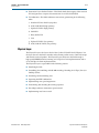
Chapter 1. Datasheet
Features . . . . . . . . . . . . . . . . . . . . . . . . . . . . . . . . . . . . . . . . . . . . . . . . . . . . . . . . . . . . . . . . . . . . . . . . . . . . . . . . 1–1
Release Information . . . . . . . . . . . . . . . . . . . . . . . . . . . . . . . . . . . . . . . . . . . . . . . . . . . . . . . . . . . . . . . . . . . . . 1–4
Device Family Support . . . . . . . . . . . . . . . . . . . . . . . . . . . . . . . . . . . . . . . . . . . . . . . . . . . . . . . . . . . . . . . . . . . 1–4
Configurations . . . . . . . . . . . . . . . . . . . . . . . . . . . . . . . . . . . . . . . . . . . . . . . . . . . . . . . . . . . . . . . . . . . . . . . . . . 1–4
Debug Features . . . . . . . . . . . . . . . . . . . . . . . . . . . . . . . . . . . . . . . . . . . . . . . . . . . . . . . . . . . . . . . . . . . . . . . . . 1–5
IP Core Verification . . . . . . . . . . . . . . . . . . . . . . . . . . . . . . . . . . . . . . . . . . . . . . . . . . . . . . . . . . . . . . . . . . . . . . 1–6
Performance and Resource Utilization . . . . . . . . . . . . . . . . . . . . . . . . . . . . . . . . . . . . . . . . . . . . . . . . . . . . . . 1–6
Recommended Speed Grades . . . . . . . . . . . . . . . . . . . . . . . . . . . . . . . . . . . . . . . . . . . . . . . . . . . . . . . . . . . . . 1–7
Chapter 2. Getting Started with the Cyclone V Hard IP for PCI Express
MegaWizard Plug-In Manager Design Flow . . . . . . . . . . . . . . . . . . . . . . . . . . . . . . . . . . . . . . . . . . . . . . . . 2–3
Customizing the Endpoint in the MegaWizard Plug-In Manager Design Flow . . . . . . . . . . . . . . . . . . 2–3
Understanding the Files Generated . . . . . . . . . . . . . . . . . . . . . . . . . . . . . . . . . . . . . . . . . . . . . . . . . . . . . . 2–6
Qsys Design Flow . . . . . . . . . . . . . . . . . . . . . . . . . . . . . . . . . . . . . . . . . . . . . . . . . . . . . . . . . . . . . . . . . . . . . . . 2–9
Generating the Testbench . . . . . . . . . . . . . . . . . . . . . . . . . . . . . . . . . . . . . . . . . . . . . . . . . . . . . . . . . . . . . 2–10
Understanding the Files Generated . . . . . . . . . . . . . . . . . . . . . . . . . . . . . . . . . . . . . . . . . . . . . . . . . . . . . 2–11
Simulating the Example Design . . . . . . . . . . . . . . . . . . . . . . . . . . . . . . . . . . . . . . . . . . . . . . . . . . . . . . . . 2–11
Understanding Channel Placement Guidelines . . . . . . . . . . . . . . . . . . . . . . . . . . . . . . . . . . . . . . . . . . . 2–14
Compiling the Design in the MegaWizard Plug-In Manager Design Flow . . . . . . . . . . . . . . . . . . . . 2–15
Compiling the Design in the Qsys Design Flow . . . . . . . . . . . . . . . . . . . . . . . . . . . . . . . . . . . . . . . . . . . . . 2–15
Modifying the Example Design . . . . . . . . . . . . . . . . . . . . . . . . . . . . . . . . . . . . . . . . . . . . . . . . . . . . . . . . . . . 2–18
Chapter 3. Getting Started with the Avalon-MM Cyclone Hard IP for PCI Express
Running Qsys . . . . . . . . . . . . . . . . . . . . . . . . . . . . . . . . . . . . . . . . . . . . . . . . . . . . . . . . . . . . . . . . . . . . . . . . . . . 3–2
Customizing the Cyclone VHard IP for PCI Express IP Core . . . . . . . . . . . . . . . . . . . . . . . . . . . . . . . . . . 3–3
Adding the Remaining Components to the Qsys System . . . . . . . . . . . . . . . . . . . . . . . . . . . . . . . . . . . . . . 3–5
Completing the Connections in Qsys . . . . . . . . . . . . . . . . . . . . . . . . . . . . . . . . . . . . . . . . . . . . . . . . . . . . . . . 3–8
Specifying Clocks and Interrupts . . . . . . . . . . . . . . . . . . . . . . . . . . . . . . . . . . . . . . . . . . . . . . . . . . . . . . . . . . 3–9
Specifying Exported Interfaces . . . . . . . . . . . . . . . . . . . . . . . . . . . . . . . . . . . . . . . . . . . . . . . . . . . . . . . . . . . . 3–9
Specifying Address Assignments . . . . . . . . . . . . . . . . . . . . . . . . . . . . . . . . . . . . . . . . . . . . . . . . . . . . . . . . . 3–10
Simulating the Example Design . . . . . . . . . . . . . . . . . . . . . . . . . . . . . . . . . . . . . . . . . . . . . . . . . . . . . . . . . . 3–10
Simulating the Single DWord Design . . . . . . . . . . . . . . . . . . . . . . . . . . . . . . . . . . . . . . . . . . . . . . . . . . . . . 3–15
Understanding Channel Placement Guidelines . . . . . . . . . . . . . . . . . . . . . . . . . . . . . . . . . . . . . . . . . . . . . 3–15
Adding Synopsis Design Constraints . . . . . . . . . . . . . . . . . . . . . . . . . . . . . . . . . . . . . . . . . . . . . . . . . . . . . . 3–16
Creating a Quartus II Project . . . . . . . . . . . . . . . . . . . . . . . . . . . . . . . . . . . . . . . . . . . . . . . . . . . . . . . . . . . . . 3–16
Compiling the Design . . . . . . . . . . . . . . . . . . . . . . . . . . . . . . . . . . . . . . . . . . . . . . . . . . . . . . . . . . . . . . . . . . . 3–17
Programming a Device . . . . . . . . . . . . . . . . . . . . . . . . . . . . . . . . . . . . . . . . . . . . . . . . . . . . . . . . . . . . . . . . . . 3–17
Chapter 4. Parameter Settings for the Cyclone V Hard IP for PCI Express
System Settings . . . . . . . . . . . . . . . . . . . . . . . . . . . . . . . . . . . . . . . . . . . . . . . . . . . . . . . . . . . . . . . . . . . . . . . . . 4–1
Port Functions . . . . . . . . . . . . . . . . . . . . . . . . . . . . . . . . . . . . . . . . . . . . . . . . . . . . . . . . . . . . . . . . . . . . . . . . . . 4–3
Parameters Shared Across All Port Functions . . . . . . . . . . . . . . . . . . . . . . . . . . . . . . . . . . . . . . . . . . . . . 4–3
Device . . . . . . . . . . . . . . . . . . . . . . . . . . . . . . . . . . . . . . . . . . . . . . . . . . . . . . . . . . . . . . . . . . . . . . . . . . . . 4–4
Error Reporting . . . . . . . . . . . . . . . . . . . . . . . . . . . . . . . . . . . . . . . . . . . . . . . . . . . . . . . . . . . . . . . . . . . . 4–5
Link . . . . . . . . . . . . . . . . . . . . . . . . . . . . . . . . . . . . . . . . . . . . . . . . . . . . . . . . . . . . . . . . . . . . . . . . . . . . . . 4–6
Slot . . . . . . . . . . . . . . . . . . . . . . . . . . . . . . . . . . . . . . . . . . . . . . . . . . . . . . . . . . . . . . . . . . . . . . . . . . . . . . . 4–6
Power Management . . . . . . . . . . . . . . . . . . . . . . . . . . . . . . . . . . . . . . . . . . . . . . . . . . . . . . . . . . . . . . . . . 4–7
December 2013
Altera Corporation
Cyclone V Hard IP for PCI Express
User Guide
Parameters Defined Separately for All Port Functions . . . . . . . . . . . . . . . . . . . . . . . . . . . . . . . . . . . . . . 4–7
Base Address Registers for Function <n> . . . . . . . . . . . . . . . . . . . . . . . . . . . . . . . . . . . . . . . . . . . . . . 4–8
Base and Limit Registers for Root Port Func <n> . . . . . . . . . . . . . . . . . . . . . . . . . . . . . . . . . . . . . . . . 4–8
Device ID Registers for Function <n> . . . . . . . . . . . . . . . . . . . . . . . . . . . . . . . . . . . . . . . . . . . . . . . . . . 4–9
PCI Express/PCI Capabilities for Func <n> . . . . . . . . . . . . . . . . . . . . . . . . . . . . . . . . . . . . . . . . . . . . 4–9
Chapter 5. Parameter Settings for the Avalon-MM Cyclone V Hard IP for PCI Express
System Settings . . . . . . . . . . . . . . . . . . . . . . . . . . . . . . . . . . . . . . . . . . . . . . . . . . . . . . . . . . . . . . . . . . . . . . . . . 5–1
Base Address Registers . . . . . . . . . . . . . . . . . . . . . . . . . . . . . . . . . . . . . . . . . . . . . . . . . . . . . . . . . . . . . . . . . . . 5–2
Device Identification Registers . . . . . . . . . . . . . . . . . . . . . . . . . . . . . . . . . . . . . . . . . . . . . . . . . . . . . . . . . . . . 5–3
PCI Express/PCI Capabilities . . . . . . . . . . . . . . . . . . . . . . . . . . . . . . . . . . . . . . . . . . . . . . . . . . . . . . . . . . . . . 5–3
Device . . . . . . . . . . . . . . . . . . . . . . . . . . . . . . . . . . . . . . . . . . . . . . . . . . . . . . . . . . . . . . . . . . . . . . . . . . . . . . . 5–4
Error Reporting . . . . . . . . . . . . . . . . . . . . . . . . . . . . . . . . . . . . . . . . . . . . . . . . . . . . . . . . . . . . . . . . . . . . . . . 5–5
Link . . . . . . . . . . . . . . . . . . . . . . . . . . . . . . . . . . . . . . . . . . . . . . . . . . . . . . . . . . . . . . . . . . . . . . . . . . . . . . . . . 5–5
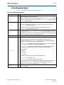
Power Management . . . . . . . . . . . . . . . . . . . . . . . . . . . . . . . . . . . . . . . . . . . . . . . . . . . . . . . . . . . . . . . . . . . 5–8
Avalon Memory-Mapped System Settings . . . . . . . . . . . . . . . . . . . . . . . . . . . . . . . . . . . . . . . . . . . . . . . . . . 5–9
Avalon to PCIe Address Translation Settings . . . . . . . . . . . . . . . . . . . . . . . . . . . . . . . . . . . . . . . . . . . . . . . 5–10
Chapter 6. IP Core Architecture
Key Interfaces . . . . . . . . . . . . . . . . . . . . . . . . . . . . . . . . . . . . . . . . . . . . . . . . . . . . . . . . . . . . . . . . . . . . . . . . . . . 6–3
Avalon-ST Interface . . . . . . . . . . . . . . . . . . . . . . . . . . . . . . . . . . . . . . . . . . . . . . . . . . . . . . . . . . . . . . . . . . . 6–3
RX Datapath . . . . . . . . . . . . . . . . . . . . . . . . . . . . . . . . . . . . . . . . . . . . . . . . . . . . . . . . . . . . . . . . . . . . . . . 6–3
TX Datapath . . . . . . . . . . . . . . . . . . . . . . . . . . . . . . . . . . . . . . . . . . . . . . . . . . . . . . . . . . . . . . . . . . . . . . . 6–3
Clocks and Reset . . . . . . . . . . . . . . . . . . . . . . . . . . . . . . . . . . . . . . . . . . . . . . . . . . . . . . . . . . . . . . . . . . . . . . 6–4
Local Management Interface (LMI Interface) . . . . . . . . . . . . . . . . . . . . . . . . . . . . . . . . . . . . . . . . . . . . . . 6–4
Transceiver Reconfiguration . . . . . . . . . . . . . . . . . . . . . . . . . . . . . . . . . . . . . . . . . . . . . . . . . . . . . . . . . . . . 6–4
Interrupts . . . . . . . . . . . . . . . . . . . . . . . . . . . . . . . . . . . . . . . . . . . . . . . . . . . . . . . . . . . . . . . . . . . . . . . . . . . . 6–5
PIPE . . . . . . . . . . . . . . . . . . . . . . . . . . . . . . . . . . . . . . . . . . . . . . . . . . . . . . . . . . . . . . . . . . . . . . . . . . . . . . . . 6–5
Protocol Layers . . . . . . . . . . . . . . . . . . . . . . . . . . . . . . . . . . . . . . . . . . . . . . . . . . . . . . . . . . . . . . . . . . . . . . . . . 6–5
Transaction Layer . . . . . . . . . . . . . . . . . . . . . . . . . . . . . . . . . . . . . . . . . . . . . . . . . . . . . . . . . . . . . . . . . . . . . 6–5
Configuration Space . . . . . . . . . . . . . . . . . . . . . . . . . . . . . . . . . . . . . . . . . . . . . . . . . . . . . . . . . . . . . . . . 6–7
Data Link Layer . . . . . . . . . . . . . . . . . . . . . . . . . . . . . . . . . . . . . . . . . . . . . . . . . . . . . . . . . . . . . . . . . . . . . . 6–7
Physical Layer . . . . . . . . . . . . . . . . . . . . . . . . . . . . . . . . . . . . . . . . . . . . . . . . . . . . . . . . . . . . . . . . . . . . . . . . 6–9
Multi-Function Support . . . . . . . . . . . . . . . . . . . . . . . . . . . . . . . . . . . . . . . . . . . . . . . . . . . . . . . . . . . . . . . . . 6–12
PCI Express Avalon-MM Bridge . . . . . . . . . . . . . . . . . . . . . . . . . . . . . . . . . . . . . . . . . . . . . . . . . . . . . . . . . . 6–12
Avalon-MM Bridge TLPs . . . . . . . . . . . . . . . . . . . . . . . . . . . . . . . . . . . . . . . . . . . . . . . . . . . . . . . . . . . . . . . . 6–14
Avalon-MM-to-PCI Express Write Requests . . . . . . . . . . . . . . . . . . . . . . . . . . . . . . . . . . . . . . . . . . . . . 6–14
Avalon-MM-to-PCI Express Upstream Read Requests . . . . . . . . . . . . . . . . . . . . . . . . . . . . . . . . . . . . 6–15
PCI Express-to-Avalon-MM Read Completions . . . . . . . . . . . . . . . . . . . . . . . . . . . . . . . . . . . . . . . . . . 6–15
PCI Express-to-Avalon-MM Downstream Write Requests . . . . . . . . . . . . . . . . . . . . . . . . . . . . . . . . . 6–15
PCI Express-to-Avalon-MM Downstream Read Requests . . . . . . . . . . . . . . . . . . . . . . . . . . . . . . . . . . 6–16
Avalon-MM-to-PCI Express Read Completions . . . . . . . . . . . . . . . . . . . . . . . . . . . . . . . . . . . . . . . . . . 6–16
PCI Express-to-Avalon-MM Address Translation for Endpoints . . . . . . . . . . . . . . . . . . . . . . . . . . . . 6–17
Minimizing BAR Sizes and the PCIe Address Space . . . . . . . . . . . . . . . . . . . . . . . . . . . . . . . . . . . . . . 6–18
Avalon-MM-to-PCI Express Address Translation Algorithm . . . . . . . . . . . . . . . . . . . . . . . . . . . . . . . 6–20
Single DWord Completer Endpoint . . . . . . . . . . . . . . . . . . . . . . . . . . . . . . . . . . . . . . . . . . . . . . . . . . . . . . . 6–22
RX Block . . . . . . . . . . . . . . . . . . . . . . . . . . . . . . . . . . . . . . . . . . . . . . . . . . . . . . . . . . . . . . . . . . . . . . . . . . . . 6–23
Avalon-MM RX Master Block . . . . . . . . . . . . . . . . . . . . . . . . . . . . . . . . . . . . . . . . . . . . . . . . . . . . . . . . . . 6–23
TX Block . . . . . . . . . . . . . . . . . . . . . . . . . . . . . . . . . . . . . . . . . . . . . . . . . . . . . . . . . . . . . . . . . . . . . . . . . . . . 6–24
Interrupt Handler Block . . . . . . . . . . . . . . . . . . . . . . . . . . . . . . . . . . . . . . . . . . . . . . . . . . . . . . . . . . . . . . 6–24
Chapter 7. IP Core Interfaces
Cyclone V Hard IP for PCI Express . . . . . . . . . . . . . . . . . . . . . . . . . . . . . . . . . . . . . . . . . . . . . . . . . . . . . . . . 7–3
Avalon-ST Packets to PCI Express TLPs . . . . . . . . . . . . . . . . . . . . . . . . . . . . . . . . . . . . . . . . . . . . . . . . . . 7–5
Avalon-ST RX Interface . . . . . . . . . . . . . . . . . . . . . . . . . . . . . . . . . . . . . . . . . . . . . . . . . . . . . . . . . . . . . . . . 7–6
Data Alignment and Timing for the 64-Bit Avalon-ST RX Interface . . . . . . . . . . . . . . . . . . . . . . . . 7–9
Data Alignment and Timing for the 128-Bit Avalon-ST RX Interface . . . . . . . . . . . . . . . . . . . . . . 7–12
Avalon-ST TX Interface . . . . . . . . . . . . . . . . . . . . . . . . . . . . . . . . . . . . . . . . . . . . . . . . . . . . . . . . . . . . . . . 7–16
Data Alignment and Timing for the 64-Bit Avalon-ST TX Interface . . . . . . . . . . . . . . . . . . . . . . . 7–19
Data Alignment and Timing for the 128-Bit Avalon-ST TX Interface . . . . . . . . . . . . . . . . . . . . . . 7–21
Root Port Mode Configuration Requests . . . . . . . . . . . . . . . . . . . . . . . . . . . . . . . . . . . . . . . . . . . . . . 7–23
ECRC Forwarding . . . . . . . . . . . . . . . . . . . . . . . . . . . . . . . . . . . . . . . . . . . . . . . . . . . . . . . . . . . . . . . . . 7–24
Clock Signals . . . . . . . . . . . . . . . . . . . . . . . . . . . . . . . . . . . . . . . . . . . . . . . . . . . . . . . . . . . . . . . . . . . . . . . . 7–24
Reset Signals . . . . . . . . . . . . . . . . . . . . . . . . . . . . . . . . . . . . . . . . . . . . . . . . . . . . . . . . . . . . . . . . . . . . . . . . 7–25
ECC Error Signals . . . . . . . . . . . . . . . . . . . . . . . . . . . . . . . . . . . . . . . . . . . . . . . . . . . . . . . . . . . . . . . . . . . . 7–28
Interrupts for Endpoints . . . . . . . . . . . . . . . . . . . . . . . . . . . . . . . . . . . . . . . . . . . . . . . . . . . . . . . . . . . . . . 7–28
Interrupts for Root Ports . . . . . . . . . . . . . . . . . . . . . . . . . . . . . . . . . . . . . . . . . . . . . . . . . . . . . . . . . . . . . . 7–29
Completion Side Band Signals . . . . . . . . . . . . . . . . . . . . . . . . . . . . . . . . . . . . . . . . . . . . . . . . . . . . . . . . . 7–29
Transaction Layer Configuration Space Signals . . . . . . . . . . . . . . . . . . . . . . . . . . . . . . . . . . . . . . . . . . 7–31
Configuration Space Register Access Timing . . . . . . . . . . . . . . . . . . . . . . . . . . . . . . . . . . . . . . . . . . 7–34
Configuration Space Register Access . . . . . . . . . . . . . . . . . . . . . . . . . . . . . . . . . . . . . . . . . . . . . . . . . 7–35
LMI Signals . . . . . . . . . . . . . . . . . . . . . . . . . . . . . . . . . . . . . . . . . . . . . . . . . . . . . . . . . . . . . . . . . . . . . . . . . 7–39
LMI Read Operation . . . . . . . . . . . . . . . . . . . . . . . . . . . . . . . . . . . . . . . . . . . . . . . . . . . . . . . . . . . . . . . 7–40
LMI Write Operation . . . . . . . . . . . . . . . . . . . . . . . . . . . . . . . . . . . . . . . . . . . . . . . . . . . . . . . . . . . . . . . 7–40
Power Management Signals . . . . . . . . . . . . . . . . . . . . . . . . . . . . . . . . . . . . . . . . . . . . . . . . . . . . . . . . . . . 7–41
Avalon-MM Hard IP for PCI Express . . . . . . . . . . . . . . . . . . . . . . . . . . . . . . . . . . . . . . . . . . . . . . . . . . . . . 7–43
32-Bit Non-Bursting Avalon-MM Control Register Access (CRA) Slave Signals . . . . . . . . . . . . . . . 7–45
RX Avalon-MM Master Signals . . . . . . . . . . . . . . . . . . . . . . . . . . . . . . . . . . . . . . . . . . . . . . . . . . . . . . . . 7–46
64- or 128-Bit Bursting TX Avalon-MM Slave Signals . . . . . . . . . . . . . . . . . . . . . . . . . . . . . . . . . . . . . 7–46
Physical Layer Interface Signals . . . . . . . . . . . . . . . . . . . . . . . . . . . . . . . . . . . . . . . . . . . . . . . . . . . . . . . . . . 7–47
Transceiver Reconfiguration . . . . . . . . . . . . . . . . . . . . . . . . . . . . . . . . . . . . . . . . . . . . . . . . . . . . . . . . . . . 7–48
Serial Interface Signals . . . . . . . . . . . . . . . . . . . . . . . . . . . . . . . . . . . . . . . . . . . . . . . . . . . . . . . . . . . . . . . . 7–48
PIPE Interface Signals . . . . . . . . . . . . . . . . . . . . . . . . . . . . . . . . . . . . . . . . . . . . . . . . . . . . . . . . . . . . . . . . 7–52
Test Signals . . . . . . . . . . . . . . . . . . . . . . . . . . . . . . . . . . . . . . . . . . . . . . . . . . . . . . . . . . . . . . . . . . . . . . . . . . . . 7–55
Chapter 8. Register Descriptions
Configuration Space Register Content . . . . . . . . . . . . . . . . . . . . . . . . . . . . . . . . . . . . . . . . . . . . . . . . . . . . . . 8–1
Altera-Defined Vendor Specific Extended Capability (VSEC) . . . . . . . . . . . . . . . . . . . . . . . . . . . . . . . . . . 8–5
PCI Express Avalon-MM Bridge Control Register Access Content . . . . . . . . . . . . . . . . . . . . . . . . . . . . . 8–10
Avalon-MM to PCI Express Interrupt Registers . . . . . . . . . . . . . . . . . . . . . . . . . . . . . . . . . . . . . . . . . . 8–12
PCI Express Mailbox Registers . . . . . . . . . . . . . . . . . . . . . . . . . . . . . . . . . . . . . . . . . . . . . . . . . . . . . . . . . 8–13
Avalon-MM-to-PCI Express Address Translation Table . . . . . . . . . . . . . . . . . . . . . . . . . . . . . . . . . . . 8–14
Root Port TLP Data Registers . . . . . . . . . . . . . . . . . . . . . . . . . . . . . . . . . . . . . . . . . . . . . . . . . . . . . . . . . . 8–16
Programming Model for Avalon-MM Root Port . . . . . . . . . . . . . . . . . . . . . . . . . . . . . . . . . . . . . . . . . . 8–17
Sending a TLP . . . . . . . . . . . . . . . . . . . . . . . . . . . . . . . . . . . . . . . . . . . . . . . . . . . . . . . . . . . . . . . . . . . . 8–19
Receiving a Completion TLP . . . . . . . . . . . . . . . . . . . . . . . . . . . . . . . . . . . . . . . . . . . . . . . . . . . . . . . . 8–19
PCI Express to Avalon-MM Interrupt Status and Enable Registers for Root Ports . . . . . . . . . . . . . 8–19
PCI Express to Avalon-MM Interrupt Status and Enable Registers for Endpoints . . . . . . . . . . . . . 8–20
Avalon-MM Mailbox Registers . . . . . . . . . . . . . . . . . . . . . . . . . . . . . . . . . . . . . . . . . . . . . . . . . . . . . . . . 8–21
Correspondence between Configuration Space Registers and the PCIe Spec 2.1 . . . . . . . . . . . . . . . . . 8–22
Chapter 9. Reset and Clocks
Reset . . . . . . . . . . . . . . . . . . . . . . . . . . . . . . . . . . . . . . . . . . . . . . . . . . . . . . . . . . . . . . . . . . . . . . . . . . . . . . . . . . 9–1
Clocks . . . . . . . . . . . . . . . . . . . . . . . . . . . . . . . . . . . . . . . . . . . . . . . . . . . . . . . . . . . . . . . . . . . . . . . . . . . . . . . . . 9–4
pclk . . . . . . . . . . . . . . . . . . . . . . . . . . . . . . . . . . . . . . . . . . . . . . . . . . . . . . . . . . . . . . . . . . . . . . . . . . . . . . . . . 9–5
coreclkout_hip . . . . . . . . . . . . . . . . . . . . . . . . . . . . . . . . . . . . . . . . . . . . . . . . . . . . . . . . . . . . . . . . . . . . . . . . 9–6
pld_clk . . . . . . . . . . . . . . . . . . . . . . . . . . . . . . . . . . . . . . . . . . . . . . . . . . . . . . . . . . . . . . . . . . . . . . . . . . . . . . 9–6
Transceiver Clock Signals . . . . . . . . . . . . . . . . . . . . . . . . . . . . . . . . . . . . . . . . . . . . . . . . . . . . . . . . . . . . . . 9–6
Chapter 10. Transaction Layer Protocol (TLP) Details
Supported Message Types . . . . . . . . . . . . . . . . . . . . . . . . . . . . . . . . . . . . . . . . . . . . . . . . . . . . . . . . . . . . . . . 10–1
Transaction Layer Routing Rules . . . . . . . . . . . . . . . . . . . . . . . . . . . . . . . . . . . . . . . . . . . . . . . . . . . . . . . . . 10–3
Receive Buffer Reordering . . . . . . . . . . . . . . . . . . . . . . . . . . . . . . . . . . . . . . . . . . . . . . . . . . . . . . . . . . . . . . . 10–4
Chapter 11. Interrupts
Interrupts for Endpoints Using the Avalon-ST Application Interface . . . . . . . . . . . . . . . . . . . . . . . . . . 11–1
MSI Interrupts . . . . . . . . . . . . . . . . . . . . . . . . . . . . . . . . . . . . . . . . . . . . . . . . . . . . . . . . . . . . . . . . . . . . . . . 11–1
MSI-X . . . . . . . . . . . . . . . . . . . . . . . . . . . . . . . . . . . . . . . . . . . . . . . . . . . . . . . . . . . . . . . . . . . . . . . . . . . . . . 11–3
Legacy Interrupts . . . . . . . . . . . . . . . . . . . . . . . . . . . . . . . . . . . . . . . . . . . . . . . . . . . . . . . . . . . . . . . . . . . . 11–4
Interrupts for Root Ports Using the Avalon-ST Interface to the Application Layer . . . . . . . . . . . . . . . 11–4
Interrupts for Endpoints Using the Avalon-MM Interface to the Application Layer . . . . . . . . . . . . . . 11–5
Enabling MSI or Legacy Interrupts . . . . . . . . . . . . . . . . . . . . . . . . . . . . . . . . . . . . . . . . . . . . . . . . . . . . . 11–7
Generation of Avalon-MM Interrupts . . . . . . . . . . . . . . . . . . . . . . . . . . . . . . . . . . . . . . . . . . . . . . . . . . . 11–7
Interrupts for End Points Using the Avalon-MM Interface with Multiple MSI/MSI-X Support . . . . 11–7
Chapter 12. Optional Features
Configuration via Protocol (CvP) . . . . . . . . . . . . . . . . . . . . . . . . . . . . . . . . . . . . . . . . . . . . . . . . . . . . . . . . . 12–1
ECRC . . . . . . . . . . . . . . . . . . . . . . . . . . . . . . . . . . . . . . . . . . . . . . . . . . . . . . . . . . . . . . . . . . . . . . . . . . . . . . . . . 12–2
ECRC on the RX Path . . . . . . . . . . . . . . . . . . . . . . . . . . . . . . . . . . . . . . . . . . . . . . . . . . . . . . . . . . . . . . . . . 12–2
ECRC on the TX Path . . . . . . . . . . . . . . . . . . . . . . . . . . . . . . . . . . . . . . . . . . . . . . . . . . . . . . . . . . . . . . . . . 12–3
Lane Initialization and Reversal . . . . . . . . . . . . . . . . . . . . . . . . . . . . . . . . . . . . . . . . . . . . . . . . . . . . . . . . . . 12–4
Chapter 13. Flow Control
Throughput of Posted Writes . . . . . . . . . . . . . . . . . . . . . . . . . . . . . . . . . . . . . . . . . . . . . . . . . . . . . . . . . . . . 13–1
Throughput of Non-Posted Reads . . . . . . . . . . . . . . . . . . . . . . . . . . . . . . . . . . . . . . . . . . . . . . . . . . . . . . . . 13–3
Chapter 14. Error Handling
Physical Layer Errors . . . . . . . . . . . . . . . . . . . . . . . . . . . . . . . . . . . . . . . . . . . . . . . . . . . . . . . . . . . . . . . . . . . 14–2
Data Link Layer Errors . . . . . . . . . . . . . . . . . . . . . . . . . . . . . . . . . . . . . . . . . . . . . . . . . . . . . . . . . . . . . . . . . . 14–2
Transaction Layer Errors . . . . . . . . . . . . . . . . . . . . . . . . . . . . . . . . . . . . . . . . . . . . . . . . . . . . . . . . . . . . . . . . 14–3
Error Reporting and Data Poisoning . . . . . . . . . . . . . . . . . . . . . . . . . . . . . . . . . . . . . . . . . . . . . . . . . . . . . . 14–5
Uncorrectable and Correctable Error Status Bits . . . . . . . . . . . . . . . . . . . . . . . . . . . . . . . . . . . . . . . . . . . . 14–6
Chapter 15. Transceiver PHY IP Reconfiguration
Chapter 16. SDC Timing Constraints
SDC Constraints for the Hard IP for PCIe . . . . . . . . . . . . . . . . . . . . . . . . . . . . . . . . . . . . . . . . . . . . . . . . . . 16–1
SDC Constraints for the Example Design . . . . . . . . . . . . . . . . . . . . . . . . . . . . . . . . . . . . . . . . . . . . . . . . . . 16–2
Chapter 17. Testbench and Design Example
Endpoint Testbench . . . . . . . . . . . . . . . . . . . . . . . . . . . . . . . . . . . . . . . . . . . . . . . . . . . . . . . . . . . . . . . . . . . . 17–2
Root Port Testbench . . . . . . . . . . . . . . . . . . . . . . . . . . . . . . . . . . . . . . . . . . . . . . . . . . . . . . . . . . . . . . . . . . . . 17–4
Chaining DMA Design Examples . . . . . . . . . . . . . . . . . . . . . . . . . . . . . . . . . . . . . . . . . . . . . . . . . . . . . . . . . 17–4
Design Example BAR/Address Map . . . . . . . . . . . . . . . . . . . . . . . . . . . . . . . . . . . . . . . . . . . . . . . . . . . 17–9
Chaining DMA Control and Status Registers . . . . . . . . . . . . . . . . . . . . . . . . . . . . . . . . . . . . . . . . . . . 17–10
Chaining DMA Descriptor Tables . . . . . . . . . . . . . . . . . . . . . . . . . . . . . . . . . . . . . . . . . . . . . . . . . . . . . 17–12
Test Driver Module . . . . . . . . . . . . . . . . . . . . . . . . . . . . . . . . . . . . . . . . . . . . . . . . . . . . . . . . . . . . . . . . . . . . 17–14
DMA Write Cycles . . . . . . . . . . . . . . . . . . . . . . . . . . . . . . . . . . . . . . . . . . . . . . . . . . . . . . . . . . . . . . . . 17–15
DMA Read Cycles . . . . . . . . . . . . . . . . . . . . . . . . . . . . . . . . . . . . . . . . . . . . . . . . . . . . . . . . . . . . . . . . 17–17
Root Port Design Example . . . . . . . . . . . . . . . . . . . . . . . . . . . . . . . . . . . . . . . . . . . . . . . . . . . . . . . . . . . . . . 17–18
Root Port BFM . . . . . . . . . . . . . . . . . . . . . . . . . . . . . . . . . . . . . . . . . . . . . . . . . . . . . . . . . . . . . . . . . . . . . . . . 17–20
BFM Memory Map . . . . . . . . . . . . . . . . . . . . . . . . . . . . . . . . . . . . . . . . . . . . . . . . . . . . . . . . . . . . . . . . . . 17–22
Configuration Space Bus and Device Numbering . . . . . . . . . . . . . . . . . . . . . . . . . . . . . . . . . . . . . . . . 17–22
Configuration of Root Port and Endpoint . . . . . . . . . . . . . . . . . . . . . . . . . . . . . . . . . . . . . . . . . . . . . . 17–22
Issuing Read and Write Transactions to the Application Layer . . . . . . . . . . . . . . . . . . . . . . . . . . . . 17–27
BFM Procedures and Functions . . . . . . . . . . . . . . . . . . . . . . . . . . . . . . . . . . . . . . . . . . . . . . . . . . . . . . . . . 17–28
BFM Read and Write Procedures . . . . . . . . . . . . . . . . . . . . . . . . . . . . . . . . . . . . . . . . . . . . . . . . . . . . . . 17–28
ebfm_barwr Procedure . . . . . . . . . . . . . . . . . . . . . . . . . . . . . . . . . . . . . . . . . . . . . . . . . . . . . . . . . . . . 17–28
ebfm_barwr_imm Procedure . . . . . . . . . . . . . . . . . . . . . . . . . . . . . . . . . . . . . . . . . . . . . . . . . . . . . . . 17–29
ebfm_barrd_wait Procedure . . . . . . . . . . . . . . . . . . . . . . . . . . . . . . . . . . . . . . . . . . . . . . . . . . . . . . . 17–30
ebfm_barrd_nowt Procedure . . . . . . . . . . . . . . . . . . . . . . . . . . . . . . . . . . . . . . . . . . . . . . . . . . . . . . . 17–30
ebfm_cfgwr_imm_wait Procedure . . . . . . . . . . . . . . . . . . . . . . . . . . . . . . . . . . . . . . . . . . . . . . . . . . 17–31
ebfm_cfgwr_imm_nowt Procedure . . . . . . . . . . . . . . . . . . . . . . . . . . . . . . . . . . . . . . . . . . . . . . . . . 17–32
ebfm_cfgrd_wait Procedure . . . . . . . . . . . . . . . . . . . . . . . . . . . . . . . . . . . . . . . . . . . . . . . . . . . . . . . . 17–33
ebfm_cfgrd_nowt Procedure . . . . . . . . . . . . . . . . . . . . . . . . . . . . . . . . . . . . . . . . . . . . . . . . . . . . . . . 17–33
BFM Configuration Procedures . . . . . . . . . . . . . . . . . . . . . . . . . . . . . . . . . . . . . . . . . . . . . . . . . . . . . . . 17–34
ebfm_cfg_rp_ep Procedure . . . . . . . . . . . . . . . . . . . . . . . . . . . . . . . . . . . . . . . . . . . . . . . . . . . . . . . . 17–34
ebfm_cfg_decode_bar Procedure . . . . . . . . . . . . . . . . . . . . . . . . . . . . . . . . . . . . . . . . . . . . . . . . . . . 17–35
BFM Shared Memory Access Procedures . . . . . . . . . . . . . . . . . . . . . . . . . . . . . . . . . . . . . . . . . . . . . . . 17–35
Shared Memory Constants . . . . . . . . . . . . . . . . . . . . . . . . . . . . . . . . . . . . . . . . . . . . . . . . . . . . . . . . . 17–35
shmem_write . . . . . . . . . . . . . . . . . . . . . . . . . . . . . . . . . . . . . . . . . . . . . . . . . . . . . . . . . . . . . . . . . . . . 17–36
shmem_read Function . . . . . . . . . . . . . . . . . . . . . . . . . . . . . . . . . . . . . . . . . . . . . . . . . . . . . . . . . . . . . 17–36
shmem_display Verilog HDL Function . . . . . . . . . . . . . . . . . . . . . . . . . . . . . . . . . . . . . . . . . . . . . . 17–36
shmem_fill Procedure . . . . . . . . . . . . . . . . . . . . . . . . . . . . . . . . . . . . . . . . . . . . . . . . . . . . . . . . . . . . . 17–37
shmem_chk_ok Function . . . . . . . . . . . . . . . . . . . . . . . . . . . . . . . . . . . . . . . . . . . . . . . . . . . . . . . . . . 17–37
BFM Log and Message Procedures . . . . . . . . . . . . . . . . . . . . . . . . . . . . . . . . . . . . . . . . . . . . . . . . . . . . 17–37
ebfm_display Verilog HDL Function . . . . . . . . . . . . . . . . . . . . . . . . . . . . . . . . . . . . . . . . . . . . . . . . 17–39
ebfm_log_stop_sim Verilog HDL Function . . . . . . . . . . . . . . . . . . . . . . . . . . . . . . . . . . . . . . . . . . . 17–39
ebfm_log_set_suppressed_msg_mask Verilog HDL Function . . . . . . . . . . . . . . . . . . . . . . . . . . . 17–39
ebfm_log_set_stop_on_msg_mask Verilog HDL Function . . . . . . . . . . . . . . . . . . . . . . . . . . . . . . 17–40
ebfm_log_open Verilog HDL Function . . . . . . . . . . . . . . . . . . . . . . . . . . . . . . . . . . . . . . . . . . . . . . 17–40
ebfm_log_close Verilog HDL Function . . . . . . . . . . . . . . . . . . . . . . . . . . . . . . . . . . . . . . . . . . . . . . 17–40
Verilog HDL Formatting Functions . . . . . . . . . . . . . . . . . . . . . . . . . . . . . . . . . . . . . . . . . . . . . . . . . . . . 17–40
himage1 . . . . . . . . . . . . . . . . . . . . . . . . . . . . . . . . . . . . . . . . . . . . . . . . . . . . . . . . . . . . . . . . . . . . . . . . . 17–41
himage2 . . . . . . . . . . . . . . . . . . . . . . . . . . . . . . . . . . . . . . . . . . . . . . . . . . . . . . . . . . . . . . . . . . . . . . . . . 17–41
himage4 . . . . . . . . . . . . . . . . . . . . . . . . . . . . . . . . . . . . . . . . . . . . . . . . . . . . . . . . . . . . . . . . . . . . . . . . . 17–41
himage8 . . . . . . . . . . . . . . . . . . . . . . . . . . . . . . . . . . . . . . . . . . . . . . . . . . . . . . . . . . . . . . . . . . . . . . . . . 17–41
himage16 . . . . . . . . . . . . . . . . . . . . . . . . . . . . . . . . . . . . . . . . . . . . . . . . . . . . . . . . . . . . . . . . . . . . . . . . 17–42
dimage1 . . . . . . . . . . . . . . . . . . . . . . . . . . . . . . . . . . . . . . . . . . . . . . . . . . . . . . . . . . . . . . . . . . . . . . . . . 17–42
dimage2 . . . . . . . . . . . . . . . . . . . . . . . . . . . . . . . . . . . . . . . . . . . . . . . . . . . . . . . . . . . . . . . . . . . . . . . . . 17–42
dimage3 . . . . . . . . . . . . . . . . . . . . . . . . . . . . . . . . . . . . . . . . . . . . . . . . . . . . . . . . . . . . . . . . . . . . . . . . . 17–43
dimage4 . . . . . . . . . . . . . . . . . . . . . . . . . . . . . . . . . . . . . . . . . . . . . . . . . . . . . . . . . . . . . . . . . . . . . . . . . 17–43
dimage5 . . . . . . . . . . . . . . . . . . . . . . . . . . . . . . . . . . . . . . . . . . . . . . . . . . . . . . . . . . . . . . . . . . . . . . . . . 17–43
dimage6 . . . . . . . . . . . . . . . . . . . . . . . . . . . . . . . . . . . . . . . . . . . . . . . . . . . . . . . . . . . . . . . . . . . . . . . . . 17–43
dimage7 . . . . . . . . . . . . . . . . . . . . . . . . . . . . . . . . . . . . . . . . . . . . . . . . . . . . . . . . . . . . . . . . . . . . . . . . . 17–44
Procedures and Functions Specific to the Chaining DMA Design Example . . . . . . . . . . . . . . . . . . 17–44
chained_dma_test Procedure . . . . . . . . . . . . . . . . . . . . . . . . . . . . . . . . . . . . . . . . . . . . . . . . . . . . . . . 17–44
dma_rd_test Procedure . . . . . . . . . . . . . . . . . . . . . . . . . . . . . . . . . . . . . . . . . . . . . . . . . . . . . . . . . . . . 17–45
dma_wr_test Procedure . . . . . . . . . . . . . . . . . . . . . . . . . . . . . . . . . . . . . . . . . . . . . . . . . . . . . . . . . . . 17–45
dma_set_rd_desc_data Procedure . . . . . . . . . . . . . . . . . . . . . . . . . . . . . . . . . . . . . . . . . . . . . . . . . . . 17–45
dma_set_wr_desc_data Procedure . . . . . . . . . . . . . . . . . . . . . . . . . . . . . . . . . . . . . . . . . . . . . . . . . . 17–45
dma_set_header Procedure . . . . . . . . . . . . . . . . . . . . . . . . . . . . . . . . . . . . . . . . . . . . . . . . . . . . . . . . 17–46
rc_mempoll Procedure . . . . . . . . . . . . . . . . . . . . . . . . . . . . . . . . . . . . . . . . . . . . . . . . . . . . . . . . . . . . 17–46
msi_poll Procedure . . . . . . . . . . . . . . . . . . . . . . . . . . . . . . . . . . . . . . . . . . . . . . . . . . . . . . . . . . . . . . . 17–47
dma_set_msi Procedure . . . . . . . . . . . . . . . . . . . . . . . . . . . . . . . . . . . . . . . . . . . . . . . . . . . . . . . . . . . 17–47
find_mem_bar Procedure . . . . . . . . . . . . . . . . . . . . . . . . . . . . . . . . . . . . . . . . . . . . . . . . . . . . . . . . . . 17–48
dma_set_rclast Procedure . . . . . . . . . . . . . . . . . . . . . . . . . . . . . . . . . . . . . . . . . . . . . . . . . . . . . . . . . . 17–48
ebfm_display_verb Procedure . . . . . . . . . . . . . . . . . . . . . . . . . . . . . . . . . . . . . . . . . . . . . . . . . . . . . . 17–48
Chapter 18. Debugging
Hardware Bring-Up Issues . . . . . . . . . . . . . . . . . . . . . . . . . . . . . . . . . . . . . . . . . . . . . . . . . . . . . . . . . . . . . . 18–1
Link Training . . . . . . . . . . . . . . . . . . . . . . . . . . . . . . . . . . . . . . . . . . . . . . . . . . . . . . . . . . . . . . . . . . . . . . . . . . 18–1
Link Hangs in L0 Due To Deassertion of tx_st_ready . . . . . . . . . . . . . . . . . . . . . . . . . . . . . . . . . . . . . . . . 18–4
Recommended Reset Sequence to Avoid Link Training Issues . . . . . . . . . . . . . . . . . . . . . . . . . . . . . . . . 18–6
Setting Up Simulation . . . . . . . . . . . . . . . . . . . . . . . . . . . . . . . . . . . . . . . . . . . . . . . . . . . . . . . . . . . . . . . . . . . 18–6
Changing Between Serial and PIPE Simulation . . . . . . . . . . . . . . . . . . . . . . . . . . . . . . . . . . . . . . . . . . . 18–6
Use the PIPE Interface for Gen1 and Gen2 Variants . . . . . . . . . . . . . . . . . . . . . . . . . . . . . . . . . . . . . . . 18–7
Reduce Counter Values for Serial Simulations . . . . . . . . . . . . . . . . . . . . . . . . . . . . . . . . . . . . . . . . . . . 18–7
Disable the Scrambler for Gen1 and Gen2 Simulations . . . . . . . . . . . . . . . . . . . . . . . . . . . . . . . . . . . . 18–7
Change between the Hard and Soft Reset Controller . . . . . . . . . . . . . . . . . . . . . . . . . . . . . . . . . . . . . . 18–8
).Use Third-Party PCIe Analyzer . . . . . . . . . . . . . . . . . . . . . . . . . . . . . . . . . . . . . . . . . . . . . . . . . . . . . . . . . 18–8
BIOS Enumeration Issues . . . . . . . . . . . . . . . . . . . . . . . . . . . . . . . . . . . . . . . . . . . . . . . . . . . . . . . . . . . . . . . . 18–8
Appendix A. Transaction Layer Packet (TLP) Header Formats
TLP Packet Format without Data Payload . . . . . . . . . . . . . . . . . . . . . . . . . . . . . . . . . . . . . . . . . . . . . . . . . A–1
TLP Packet Format with Data Payload . . . . . . . . . . . . . . . . . . . . . . . . . . . . . . . . . . . . . . . . . . . . . . . . . . . . A–3
Additional Information
Revision History . . . . . . . . . . . . . . . . . . . . . . . . . . . . . . . . . . . . . . . . . . . . . . . . . . . . . . . . . . . . . . . . . . . . . Info–1
How to Contact Altera . . . . . . . . . . . . . . . . . . . . . . . . . . . . . . . . . . . . . . . . . . . . . . . . . . . . . . . . . . . . . . . . Info–3
Typographic Conventions . . . . . . . . . . . . . . . . . . . . . . . . . . . . . . . . . . . . . . . . . . . . . . . . . . . . . . . . . . . . . Info–4
1. Datasheet
December 2013
UG-01110-1.5
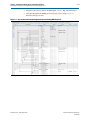
This document describes the Altera® Cyclone® Hard IP for PCI Express®. PCI Express
is a high-performance interconnect protocol for use in a variety of applications
including network adapters, storage area networks, embedded controllers, graphic
accelerator boards, and audio-video products. The PCI Express protocol is software
backwards-compatible with the earlier PCI and PCI-X protocols, but is significantly
different from its predecessors. It is a packet-based, serial, point-to-point interconnect
between two devices. The performance is scalable based on the number of lanes and
the generation that is implemented. Altera offers a configurable hard IP block in
Cyclone V devices for both Endpoints and Root Ports that complies with the PCI
Express Base Specification 2.1. Using a configurable hard IP block, rather than
programmable logic, saves significant FPGA resources. The hard IP block is available
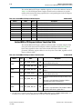
in ×1, ×2, and ×4 configurations. shows the aggregate bandwidth of a PCI Express link
for the available configurations. The protocol specifies 2.5 giga-transfers per second
for Gen1. provides bandwidths for a single transmit (TX) or receive (RX) channel, so
that the numbers double for duplex operation. Because the PCI Express protocol uses
8B/10B encoding, there is a 20% overhead which is included in the figures in .
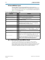
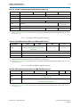
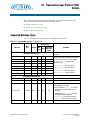
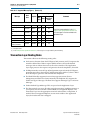
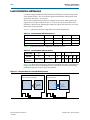
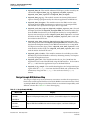
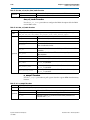
Table 1–1.
Table 1–1. PCI Express Throughput
Link Width
×1
×2
×4
PCI Express Gen1 Gbps (2.5 Gbps)
2.5
5
10
PCI Express Gen2 Gbps (5.0 Gbps)
5
10
20
f Refer to the PCI Express High Performance Reference Design for more information about
calculating bandwidth for the hard IP implementation of PCI Express in many Altera
FPGAs.
Features
The Cyclone V Hard IP for PCI Express IP supports the following key features:
December 2013
■
Complete protocol stack including the Transaction, Data Link, and Physical Layers
is hardened in the device.
■
Multi-function support for up to eight Endpoint functions.
■
Support of ×1, ×2, and ×4 Gen1 and Gen2 configurations for Root Ports and
Endpoints.
■
Dedicated 6 KByte receive buffer
■
Dedicated hard reset controller
■
MegaWizard Plug-In Manager and Qsys support using the Avalon® Streaming
(Avalon-ST) with a 64- or 128-bit interface to the Application Layer.
Altera Corporation
Cyclone V Hard IP for PCI Express
User Guide
1–2
Chapter 1: Datasheet
Features
■
Qsys support using the Avalon Memory-Mapped (Avalon-MM) with a 64- or
128-bit interface to the Application Layer
■
Extended credit allocation settings to better optimize the RX buffer space based on
application type.
■
Qsys example designs demonstrating parameterization, design modules and
connectivity.
■
Optional end-to-end cyclic redundancy code (ECRC) generation and checking and
advanced error reporting (AER) for high reliability applications.
■
Easy to use:
■
■
Easy parameterization.
■
Substantial on-chip resource savings and guaranteed timing closure.
■
Easy adoption with no license requirement.
New features in the 13.1 release
■
Added support for Gen2 Configuration via Protocol (CvP) using an .ini file.
Contact your sales representative for more information.
.The Cyclone V Hard IP for PCI Express offers different features for the variants that
use the Avalon-ST interface to the Application Layer and the variants that use an
Avalon-MM interface to the Application Layer. Variants using the Avalon-ST interface
are available in both the MegaWizard Plug-In Manager and the Qsys design flows.
Variants using the Avalon-MM interface are only available in the Qsys design flow.
Variants using the Avalon-ST interfaces offer a richer feature set; however, if you are
not familiar with the PCI Express protocol, variants using the Avalon-MM interface
may be easier to understand. A PCI Express to Avalon-MM bridge translates the PCI
Express read, write and completion TLPs into standard Avalon-MM read and write
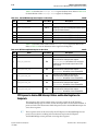
commands typically used by master and slave interfaces. Table 1–2 outlines these
differences in features between variants with Avalon-ST and Avalon-MM interfaces to
the Application Layer.
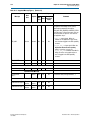
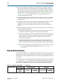
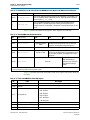
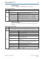
Table 1–1. Differences in Features Available Using the Avalon-MM and Avalon-ST Interfaces (Part 1 of 2)
Feature
Avalon-ST Interface
Avalon-MM Interface
MegaCore License
Free
Free
Native Endpoint
Supported
Supported
Legacy Endpoint (1)
Supported
Not Supported
Root port
Supported
Supported
Gen1
×1, ×2, ×4
×1, ×4 (2)
Gen2
×1, ×2, ×4
×1, ×4 (2)
MegaWizard Plug-In Manager design flow
Supported
Not supported
Qsys design flow
Supported
Supported
64-bit Application Layer interface
Supported
Supported
128-bit Application Layer interface
Supported
Supported
Cyclone V Hard IP for PCI Express
User Guide
December 2013 Altera Corporation
Chapter 1: Datasheet
Features
1–3
Table 1–1. Differences in Features Available Using the Avalon-MM and Avalon-ST Interfaces (Part 2 of 2)
Feature
Transaction Layer Packet Types (TLP) (3)
Avalon-ST Interface
Avalon-MM Interface
■
Memory Read Request
■
Memory Read Request
■
Memory Read Request-Locked
■
Memory Write Request
■
Memory Write Request
■
■
I/O Read Request
Configuration Read Request
(Root Port)
■
I/O Write Request
■
■
Configuration Read Request
(Root Port)
Configuration Write Request
(Root Port)
■
Message Request
■
Configuration Write Request
(Root Port)
■
Message Request with Data
Payload
■
Message Request
■
Completion without Data
■
Message Request with Data
Payload
■
Completion with Data
■
Memory Read Request (single
dword)
■
Memory Write Request (single
dword)
■
Completion without Data
■
Completion with data
■
Completion for Locked Read
without Data
Maximum payload size
128–512 bytes
128–256 bytes
Number of tags supported for non-posted
requests
32 or 64
8
62.5 MHz clock
Supported
Supported
Multi-function
Supports up to 8 functions
Supports single function only
Polarity inversion of PIPE interface signals
Supported
Supported
ECRC forwarding on RX and TX
Supported
Not supported
Expansion ROM
Supported
Not supported
Number of MSI requests
16
1, 2, 4, 8, or 16
MSI-X
Supported
Supported
Multiple MSI, MSI-X, and INTx
Not Supported
Supported
Legacy interrupts
Supported
Supported
Notes to Table 1–2:
(1) Not recommended for new designs.
(2) ×2 is supported by down training from ×4 or ×8 lanes.
(3) Refer to Appendix A, Transaction Layer Packet (TLP) Header Formats for the layout of TLP headers.
f The purpose of the Cyclone V Hard IP for PCI Express User Guide is to explain how to
use the Cyclone V Hard IP for PCI Express and not to explain the PCI Express
protocol. Although there is inevitable overlap between these two purposes, this
document should be used in conjunction with an understanding of the following PCI
Express specifications: PHY Interface for the PCI Express Architecture PCI Express 2.0 and
PCI Express Base Specification 2.1.
December 2013
Altera Corporation
Cyclone V Hard IP for PCI Express
User Guide
1–4
Chapter 1: Datasheet
Release Information
Release Information
Table 1–3 provides information about this release of the PCI Express Compiler.
Table 1–2. PCI Express Compiler Release Information
Item
Description
Version
13.1
Release Date
December 2013
Ordering Codes
Product IDs
Vendor ID
No ordering code is required
There are no encrypted files for the Cyclone V Hard IP for PCI
Express. The Product ID and Vendor ID are not required
because this IP core does not require a license.
Device Family Support
Table 1–4 shows the level of support offered by the Cyclone V Hard IP for PCI
Express.
Table 1–3. Device Family Support
Device Family
Cyclone V
Support
Final. The IP core is verified with final timing models. The
IP core meets all functional and timing requirements for
the device family and can be used in production designs.
Refer to the following user guides for other device families:
Other device families
■
IP Compiler for PCI Express User Guide
■
Arria V Hard IP for PCI Express User Guide
■
Arria V GZ Hard IP for PCI Express User Guide’
■
Stratix V Hard IP for PCI Express User Guide
■
Arria 10 Hard IP for PCI Express User Guide
Configurations
The Cyclone V Hard IP for PCI Express includes a full hard IP implementation of the
PCI Express stack including the following layers:
■
Physical (PHY)
■
Physical Media Attachment (PMA)
■
Physical Coding Sublayer (PCS)
■
Media Access Control (MAC)
■
Data Link Layer (DL)
■
Transaction Layer (TL)
Cyclone V Hard IP for PCI Express
User Guide
December 2013 Altera Corporation
Chapter 1: Datasheet
Debug Features
1–5
Optimized for Altera devices, the Cyclone V Hard IP for PCI Express supports all
memory, I/O, configuration, and message transactions. It has a highly optimized
Application Layer interface to achieve maximum effective throughput. You can
customize the Hard IP to meet your design requirements using either the
MegaWizard Plug-In Manager or the Qsys design flow.
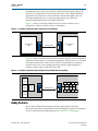
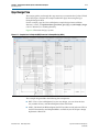
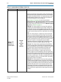
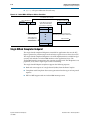
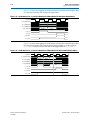
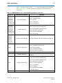
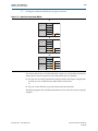
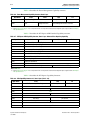
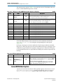
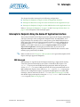
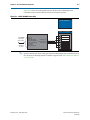
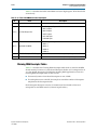
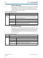
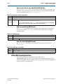
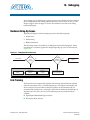
Figure 1–1 shows a PCI Express link between two Cyclone V FPGAs. One is
configured as a Root Port and the other as an Endpoint.
Figure 1–1. PCI Express Application with a Single Root Port and Endpoint
Altera FPGA
Altera FPGA
User Application
Logic
PCIe
Hard IP
PCIe
Hard IP
RP
PCI Express Link
EP
User Application
Logic
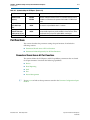
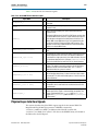
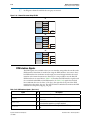
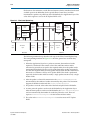
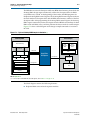
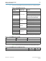
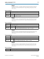
Figure 1–2 shows a PCI Express link between two Altera FPGAs. One is configured as
a Root Port and the other as a multi-function Endpoint. The FPGA serves as a custom
I/O hub for the host CPU. In the Cyclone V FPGA, each peripheral is treated as a
function with its own set of Configuration Space registers. Eight multiplexed
functions operate using a single PCI Express link.
Figure 1–2. PCI Express Application with an Endpoint Using the Multi-Function Capability
Altera FPGA
Arria V or Cyclone V FPGA
Memory
Controller
PCIe Hard
IP MultiFunction
PCIe
Hard IP
Peripheral
Controller
Host
CPU
RP
PCI Express Link
CAN
GbE
ATA
PCI
USB
SPI
GPIO
I2C
EP
Peripheral
Controller
Debug Features
The Cyclone V Hard IP for PCI Express includes debug features that allow
observation and control of the Hard IP for faster debugging of system-level problems.
For more information about debugging refer to Chapter 19, C**Debugging.
December 2013
Altera Corporation
Cyclone V Hard IP for PCI Express
User Guide
1–6
Chapter 1: Datasheet
IP Core Verification
IP Core Verification
To ensure compliance with the PCI Express specification, Altera performs extensive
validation of the Cyclone V Hard IP Core for PCI Express.
The simulation environment uses multiple testbenches that consist of
industry-standard BFMs driving the PCI Express link interface. A custom BFM
connects to the application-side interface.
Altera performs the following tests in the simulation environment:
■
Directed and pseudo random stimuli areCyclone V applied to test the Application
Layer interface, Configuration Space, and all types and sizes of TLPs.
■
Error injection tests that inject errors in the link, TLPs, and Data Link Layer
Packets (DLLPs), and check for the proper responses
■
PCI-SIG® Compliance Checklist tests that specifically test the items in the checklist
■
Random tests that test a wide range of traffic patterns
Performance and Resource Utilization
Because the Cyclone V Hard IP for PCI Express IP core is implemented in hardened
logic, it uses less than 1% of Cyclone V resources. The Avalon-MM Cyclone V Hard IP
for PCI Express includes a bridge implemented in soft logic. Table 1–5 shows the
typical expected device resource utilization for selected configurations of the
Avalon-MM Cyclone V Hard IP for PCI Express using the current version of the
Quartus II software targeting a Cyclone V (5CGXFC7D6F31C7) device. With the
exception of M10K memory blocks, the numbers of ALMs and logic registers in
Table 1–5 are rounded up to the nearest 100. Resource utilization numbers reflect
changes to the resource utilization reporting starting in the Quartus II software v12.1
release 28 nm device families and upcoming device families.
f For information about Quartus II resource utilization reporting, refer to Fitter
Resources Reports in the Quartus II Help.
Table 1–4. Performance and Resource Utilization
ALMs
Memory M10K
Logic Registers
Avalon-MM Bridge
Gen1 ×4
1250
27
1700
Gen2 ×8
2100
35
3050
Avalon-MM Interface–Burst Capable Requester/Single DWord Completer
64
1150
23
1700
128
1600
29
2550
Avalon-MM Interface-Burst Capable Completer Only
64
600
11
900
128
1350
22
2300
0
230
Avalon-MM Interface–Completer Only
64
Cyclone V Hard IP for PCI Express
User Guide
160
December 2013 Altera Corporation
Chapter 1: Datasheet
Recommended Speed Grades
1–7
Soft calibration of the transceiver module requires additional logic. The amount of
logic required depends upon the configuration.
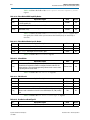
Recommended Speed Grades
Table 1–6 lists the recommended speed grades for the supported link widths and
Application Layer clock frequencies. The speed grades listed are the only speed
grades that close timing. Altera recommends setting the Quartus II Analysis &
Synthesis Settings Optimization Technique to Speed.
h For information about optimizing synthesis, refer to “Setting Up and Running Analysis
and Synthesis in Quartus II Help.
For more information about how to effect the Optimization Technique settings, refer
to Area and Timing Optimization in volume 2 of the Quartus II Handbook.
Table 1–5. Device Family Link Width Application Frequency Recommended Speed Grades
Link Speed
Link Width
×1
Gen1–2.5 Gbps
62.5
(1)
Recommended
Speed Grades
–6, -7, -8
×1
125
–6, -7, -8
×2
125
–6
×4
125
–6, -7, -8
×1
Gen2–5.0 Gbps
Application
Clock
Frequency (MHz)
62.5
(1)
,–6, -7
(2)
×1
125
–6, -7,
(2)
×2
125
,–6, -7
(2)
×4
125
–6, -7,
(2)
(2)
Notes to Table 1–6:
(1) This is a power-saving mode of operation.
(2) Final results pending characterization by Altera. Refer to the fit.rpt file generated by the Quartus II software.
f For details on installation, refer to the Altera Software Installation and Licensing Manual.
December 2013
Altera Corporation
Cyclone V Hard IP for PCI Express
User Guide
1–8
Cyclone V Hard IP for PCI Express
User Guide
Chapter 1: Datasheet
Recommended Speed Grades
December 2013 Altera Corporation
2. Getting Started with the Cyclone V
Hard IP for PCI Express
December 2013
UG-01110-1.5
This section provides step-by-step instructions to help you quickly customize,
simulate, and compile the Cyclone V Hard IP for PCI Express using either the
MegaWizard Plug-In Manager or Qsys design flow. When you install the Quartus II
software you also install the IP Library. This installation includes design examples for
Hard IP for PCI Express in <install_dir>/ip/altera/altera_pcie/
altera_pcie_hip_ast_ed/example_design/<device> directory.
1
If you have an existing Cyclone V 12.1 or older design, you must regenerate it in 13.1
before compiling with the 13.1 version of the Quartus II software.
After you install the Quartus II software for 13.1, you can copy the design examples
from the <install_dir>/ip/altera/altera_pcie/altera_pcie_hip_ast_ed/
example_design/<device> directory. This walkthrough uses the Gen1 ×4 Endpoint.
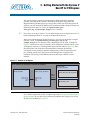
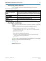
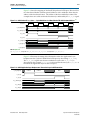
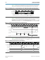
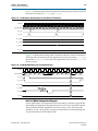
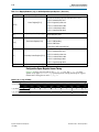
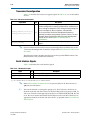
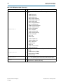
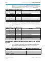
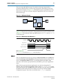
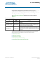
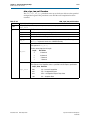
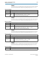
Figure 2–1 illustrates the top-level modules of the testbench in which the DUT, a Gen1
×4 Endpoint, connects to a chaining DMA engine, labeled APPS in Figure 2–1, and a
Root Port model. The Transceiver Reconfiguration Controller dynamically
reconfigures analog settings to optimize signal quality of the serial interface. The
pcie_reconfig_driver drives the Transceiver Reconfiguration Controller. The
simulation can use the parallel PHY Interface for PCI Express (PIPE) or serial
interface.
Figure 2–1. Testbench for an Endpoint
Stratix V Hard IP for PCI Express Testbench for Endpoints
Root Port Model
altpcie_tbed_sv_hwtcl.v
APPS
altpcied_sv_hwtcl.v
DUT
altpcie_sv_hip_ast_hwtcl.v
Avalon-ST TX
Avalon-ST RX
reset
status
Root Port BFM
altpcietb_bfm_rpvar_64b_x8_pipen1b
PIPE or
Serial
Interface
Avalon-ST TX
Avalon-ST RX
reset
status
Root Port Driver and Monitor
altpcietb_bfm_vc_intf
L
For a detailed explanation of this example design, refer to Chapter 18, Testbench and
Design Example. If you choose the parameters specified in this chapter, you can run
all of the tests included in Chapter 18.
December 2013
Altera Corporation
Cyclone V Hard IP for PCI Express
User Guide
2–2
Chapter 2: Getting Started with the Cyclone V Hard IP for PCI Express
The Cyclone V Hard IP for PCI Express offers exactly the same feature set in both the
MegaWizard and Qsys design flows. Consequently, your choice of design flow
depends on whether you want to integrate the Cyclone V Hard IP for PCI Express
using RTL instantiation or using Qsys, which is a system integration tool available in
the Quartus II software.
f For more information about Qsys, refer to System Design with Qsys in the Quartus II
Handbook.
h For more information about the Qsys GUI, refer to About Qsys in Quartus II Help.
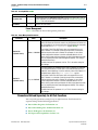
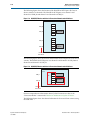
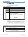
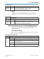
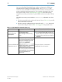
Figure 2–2 illustrates the steps necessary to customize the Cyclone V Hard IP for PCI
Express and run the example design.
Figure 2–2. MegaWizard Plug-In Manager and Qsys Design Flows
Select Design Flow
MegaWizard Plug-In
Manager Flow
Qsys Flow
Step 1
Create Quartus II Project
Customize the
Hard IP for PCIe
Step 2
Customize the
Hard IP for PCIe
Complete Qsys System
Step 3
Generate the Simulation
Model for ModelSim, NC-Sim
or VCS
Generate the Simulation
Model in Qsys
Step 4
Simulating?
Yes
Run Simulation
No
Simulating?
No
Step 5
Add Quartus IP File (.qip)
to Quartus II Project
Create Quartus II Project
Add Quartus IP File (.qip)
Step 6
Compile the Design for the
MegaWizard Design Flow
Compile the Design for the
Qsys Design Flow
Step 7
Cyclone V Hard IP for PCI Express
User Guide
Yes
Modify Example Design
to Meet Your Requirements
December 2013 Altera Corporation
Chapter 2: Getting Started with the Cyclone V Hard IP for PCI Express
MegaWizard Plug-In Manager Design Flow
2–3
MegaWizard Plug-In Manager Design Flow
This section guides you through the steps necessary to customize the Cyclone V Hard
IP for PCI Express and run the example testbench, starting with the creation of a
Quartus II project.
Follow these steps to copy the example design files and create a Quartus II project.
1. Choose Programs > Altera > Quartus II <version> (Windows Start menu) to run
the Quartus II software.
2. On the Quartus II File menu, click New, then New Quartus II Project, then OK.
3. Click Next in the New Project Wizard: Introduction (The introduction does not
display if you previously turned it off.)
4. On the Directory, Name, Top-Level Entity page, enter the following information:
a. The working directory for your project. This design example uses
<working_dir>/example_design
b. The name of the project. This design example uses pcie_de_gen1_x4_ast64.
1
The Quartus II software specifies a top-level design entity that has the same
name as the project automatically. Do not change this name.
5. Click Next to display the Add Files page.
6. Click Yes, if prompted, to create a new directory.
7. Click Next to display the Family & Device Settings page.
8. On the Family & Device Settings page, choose the following target device family
and options:
a. In the Family list, select Cyclone V(E/GX/GT/SX/SE/ST)
b. In the Devices list, select Cyclone V GX Extended Features
c. In the Available devices list, select5CGXFC7D6F31C7.
9. Click Next to close this page and display the EDA Tool Settings page.
10. From the Simulation list, select ModelSim®. From the Format list, select the HDL
language you intend to use for simulation.
11. Click Next to display the Summary page.
12. Check the Summary page to ensure that you have entered all the information
correctly.
13. Click Finish to create the Quartus II project.
Customizing the Endpoint in the MegaWizard Plug-In Manager Design
Flow
This section guides you through the process of customizing the Endpoint in the
MegaWizard Plug-In Manager design flow. It specifies the same options that are
chosen in Chapter 18, Testbench and Design Example.
Follow these steps to customize your variant in the MegaWizard Plug-In Manager:
December 2013
Altera Corporation
Cyclone V Hard IP for PCI Express
User Guide
2–4
Chapter 2: Getting Started with the Cyclone V Hard IP for PCI Express
Customizing the Endpoint in the MegaWizard Plug-In Manager Design Flow
1. On the Tools menu, click MegaWizard Plug-In Manager. The MegaWizard
Plug-In Manager appears.
2. Select Create a new custom megafunction variation and click Next.
3. In Which device family will you be using? Select the Cyclone V device family.
4. Expand the Interfaces directory under Installed Plug-Ins by clicking the + icon
left of the directory name, expand PCI Express, then click Cyclone V Hard IP for
PCI Express <version_number>
5. Select the output file type for your design. This walkthrough supports VHDL and
Verilog HDL. For this example, select Verilog HDL.
6. Specify a variation name for output files <working_dir>/example_design/
<variation name>. For this walkthrough, specify <working_dir>/example_design/
gen1_x4.
7. Click Next to open the parameter editor for the Cyclone V Hard IP for PCI
Express.
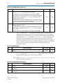
8. Specify the System Settings values listed inTable 2–1.
Table 2–1. System Settings Parameters
Parameter
Number of Lanes
Lane Rate
Port type
Application Layer interface
RX buffer credit allocation - performance for
received requests
Reference clock frequency
Use 62.5 MHz Application Layer clock for ×1
Use deprecated RX Avalon-ST data byte enable
port (rx_st_be)
Enable configuration via the PCIe link
Number of functions
1
Value
x4
Gen 1 (2.5 Gbps)
Native endpoint
Avalon-ST 64-bit
Low
100 MHz
Leave this option off
Leave this option off
Leave this option off
1
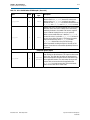
Each function shares the parameter settings on the Device, Error Reporting, Link,
Slot, and Power Management tabs. Each function has separate parameter settings for
the Base Address Registers, Base and Limit Registers for Root Ports, Device
Identification Registers, and the PCI Express/PCI Capabilities parameters. When
you click on a Func<n> tab under the Port Functions heading, the tabs automatically
reflect the Func<n> tab selected.
9. Specify the Device parameters listed in Table 2–2.
Table 2–2. Device
Parameter
Maximum payload size
Number of tags supported
Cyclone V Hard IP for PCI Express
User Guide
Value
128 bytes
32
December 2013 Altera Corporation
Chapter 2: Getting Started with the Cyclone V Hard IP for PCI Express
Customizing the Endpoint in the MegaWizard Plug-In Manager Design Flow
2–5
Table 2–2. Device
Parameter
Value
Completion timeout range
ABCD
Implement completion timeout disable
On
10. On the Error Reporting tab, leave all options off.
11. Specify the Link settings listed in Table 2–7.
Table 2–3. Link Tab
Parameter
Value
Link port number
1
Slot clock configuration
On
12. On the Slot Capabilities tab, leave the Slot register turned off.
13. Specify the Power Management parameters listed in Table 2–4.
Table 2–4. Power Management Parameters
Parameter
Value
Endpoint L0s acceptable exit latency
Maximum of 64 ns
Endpoint L1 acceptable latency
Maximum of 1 µs
14. Specify the BAR settings for Func0 listed in Table 2–5.
Table 2–5. Base Address Registers for Func0
Parameter
BAR0 Type
BAR0 Size
BAR1 Type
BAR1 Size
BAR2 Type
BAR2 Size
Value
64-bit prefetchable memory
256 MBytes - 28 bits
Disabled
N/A
32-bit non-prefetchable memory
1 KByte - 10 bits
15. You can leave Func0 BAR3 through Func
16. 0 BAR5 and the Func0 Expansion ROM Disabled.
17. Under the Base and Limit Registers heading, disable both the Input/Output and
Prefetchable memory options. (These options are for Root Ports.)
18. For the Device ID Registers for Func0, specify the values listed in the center
column of Table 2–6. The right-hand column of this table lists the value assigned to
Altera devices. You must use the Altera values to run the reference design
described in AN 456 PCI Express High Performance Reference Design. Be sure to use
your company’s values for your final product.
Table 2–6. Device ID Registers for Func0
Register Name
Vendor ID
December 2013
Altera Corporation
Value
Altera Value
0x00000000
0x00001172
Cyclone V Hard IP for PCI Express
User Guide
2–6
Chapter 2: Getting Started with the Cyclone V Hard IP for PCI Express
Customizing the Endpoint in the MegaWizard Plug-In Manager Design Flow
Table 2–6. Device ID Registers for Func0
Device ID
0x00000001
0x0000E001
Revision ID
0x00000001
0x00000001
Class Code
0x00000000
0x00FF0000
Subsystem Vendor ID
0x00000000
0x00001172
Subsystem Device ID
0x00000000
0x0000E001
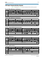
19. On the Func 0 Device tab, under PCI Express/PCI Capabilities for Func 0 turn
Function Level Reset (FLR) Off.
20. Table 2–7 lists settings for the Func0 Link tab.
Table 2–7. Link Capabilities
Parameter
Value
Data link layer active reporting
Off
Surprise down reporting
Off
21. On the Func0 MSI tab, for Number of MSI messages requested, select 4.
22. On the Func0 MSI-X tab, turn Implement MSI-X off.
23. On the Func0 Legacy Interrupt tab, select INTA.
24. Click Finish. The Generation dialog box appears.
25. Turn on Generate Example Design to generate the Endpoint, testbench, and
supporting files.
26. Click Exit.
27. Click Yes if you are prompted to add the Quartus II IP File (.qip) to the project.
The .qip is a file generated by the parameter editor contains all of the necessary
assignments and information required to process the IP core in the Quartus II
compiler. Generally, a single .qip file is generated for each IP core.
Understanding the Files Generated
Table 2–8 provides an overview of directories and files generated.
Table 2–8. Qsys Generation Output Files
Directory
Description
<working_dir>/<variant_name>/
Includes the files for synthesis
<working_dir>/<variant_name>_sim/
altera_pcie_<device>_hip_ast
Includes the simulation files.
<working_dir>/<variant_name>_example_design/
altera_pcie_<device>_hip_ast
Includes a Qsys testbench that connects the Endpoint to a chaining
DMA engine, Transceiver Reconfiguration Controller, and driver for the
Transceiver Reconfiguration Controller.
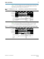
Follow these steps to generate the chaining DMA testbench from the Qsys system
design example.
1. On the Quartus II File menu, click Open.
Cyclone V Hard IP for PCI Express
User Guide
December 2013 Altera Corporation
Chapter 2: Getting Started with the Cyclone V Hard IP for PCI Express
Customizing the Endpoint in the MegaWizard Plug-In Manager Design Flow
2–7
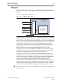
2. Navigate to the Qsys system in the altera_pcie_<device>_hip_ast subdirectory.
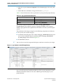
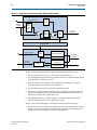
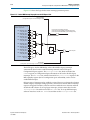
3. Click pcie_de_gen1_x4_ast64.qsys to bring up the Qsys design. Figure 2–3
illustrates this Qsys system.
Figure 2–3. Qsys System Connecting the Endpoint Variant and Chaining DMA Testbench
December 2013
Altera Corporation
Cyclone V Hard IP for PCI Express
User Guide
2–8
Chapter 2: Getting Started with the Cyclone V Hard IP for PCI Express
Customizing the Endpoint in the MegaWizard Plug-In Manager Design Flow
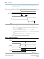
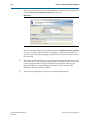
4. To display the parameters of the APPS component shown in Figure 2–3, click on it
and then select Edit from the right-mouse menu Figure 2–4. illustrates this
component. Note that the values for the following parameters match those set in
the DUT component:
■
Targeted Device Family
■
Lanes
■
Lane Rate
■
Application Clock Rate
■
Port
■
Application interface
■
Tags supported
■
Maximum payload size
■
Number of Functions
Figure 2–4. Qsys Component Representing the Chaining DMA Design Example
1
You can use this Qsys APPS component to test any Endpoint variant with
compatible values for these parameters.
5. To close the APPS component, click the X in the upper right-hand corner of the
parameter editor.
Go to “Simulating the Example Design” on page 2–11 for instructions on system
simulation.
Cyclone V Hard IP for PCI Express
User Guide
December 2013 Altera Corporation
Chapter 2: Getting Started with the Cyclone V Hard IP for PCI Express
Qsys Design Flow
2–9
Qsys Design Flow
This section guides you through the steps necessary to customize the Cyclone V Hard
IP for PCI Express and run the example testbench in Qsys. Reviewing the Qsys
Example Design for PCIe
For this example, copy the Gen1 x4 Endpoint example design from installation
directory: <install_dir>/ip/altera/altera_pcie/altera_pcie_hip_ast_ed/example_design
/<device> directory to a working directory.
Figure 2–5 illustrates this Qsys system.
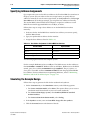
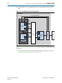
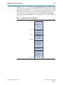
Figure 2–5. Complete Gen1 ×4 Endpoint (DUT) Connected to Example Design (APPS)
The example design includes the following four components:
December 2013
■
DUT—This is Gen1 x4 Endpoint. For your own design, you can select the data
rate, number of lanes, and either Endpoint or Root Port mode.
■
APPS—This Root Port BFM configures the DUT and drives read and write TLPs to
test DUT functionality. An Endpoint BFM is available if your PCI Express design
implements a Root Port.
Altera Corporation
Cyclone V Hard IP for PCI Express
User Guide
2–10
Chapter 2: Getting Started with the Cyclone V Hard IP for PCI Express
Qsys Design Flow
■
pcie_reconfig_driver_0—This Avalon-MM master drives the Transceiver
Reconfiguration Controller. The pcie_reconfig_driver_0 is implemented in clear
text that you can modify if your design requires different reconfiguration
functions. After you generate your Qsys system, the Verilog HDL for this
component is available as: <working_dir>/<variant_name>/testbench/
<variant_name>_tb/simulation/submodules/altpcie_reconfig_driver.sv.
■
Transceiver Reconfiguration Controller—The Transceiver Reconfiguration
Controller dynamically reconfigures analog settings to improve signal quality. For
Gen1 and Gen2 data rates, the Transceiver Reconfiguration Controller must
perform offset cancellation and PLL calibration.
Generating the Testbench
Follow these steps to generate the chaining DMA testbench:
1. On the Qsys Generation tab, specify the parameters listed in Table 2–9.
Table 2–9. Parameters to Specify on the Generation Tab in Qsys
Parameter
Value
Simulation
Create simulation model
None. (This option generates a simulation model you can include in your own
custom testbench.)
Create testbench Qsys system
Standard, BFMs for standard Avalon interfaces
Create testbench simulation model
Verilog
Synthesis
Create HDL design files for synthesis
Turn this option on
Create block symbol file (.bsf)
Turn this option on
Output Directory
Path
pcie_qsys/gen1_x4_example_design
Simulation
Leave this option blank
Testbench
(1)
pcie_qsys/gen1_x4_example_design/testbench
Synthesis
(2)
pcie_qsys/gen1_x4_example_design/synthesis
Note to Table 2–9:
(1) Qsys automatically creates this path by appending testbench to the output directory/.
(2) Qsys automatically creates this path by appending synthesis to the output directory/.
2. Click the Generate button at the bottom of the Generation tab to create the
chaining DMA testbench.
Cyclone V Hard IP for PCI Express
User Guide
December 2013 Altera Corporation
Chapter 2: Getting Started with the Cyclone V Hard IP for PCI Express
Qsys Design Flow
2–11
Understanding the Files Generated
Table 2–10 provides an overview of the files and directories Qsys generates.
Table 2–10. Qsys Generation Output Files
Directory
Description
<testbench_dir>/<variant_name>/
synthesis
includes the top-level HDL file for the Hard I for PCI Express and the .qip file that
lists all of the necessary assignments and information required to process the IP
core in the Quartus II compiler. Generally, a single .qip file is generated for each IP
core.
<testbench_dir>/<variant_name>/
synthesis/submodules
Includes the HDL files necessary for Quartus II synthesis.
<testbench_dir>/<variant_name>/
testbench/
Includes testbench subdirectories for the Aldec, Cadence and Mentor simulation
tools with the required libraries and simulation scripts.
<testbench_dir>/<variant_name>/
testbench/<cad_vendor>
Includes the HDL source files and scripts for the simulation testbench.
Simulating the Example Design
Follow these steps to compile the testbench for simulation and run the chaining DMA
testbench.
1. Start your simulation tool. This example uses the ModelSim® software.
2. From the ModelSim transcript window, in the testbench directory
(./example_design/altera_pcie_<device>_hip_ast/<variant>/testbench/mentor)
type the following commands:
a. do msim_setup.tcl r
b. h r (This is the ModelSim help command.)
c. ld_debug r (This command compiles all design files and elaborates the
top-level design without any optimization.)
d. run -all r
Example 2–1 shows a partial transcript from a successful simulation. As this transcript
illustrates, the simulation includes the following stages:
December 2013
■
Link training
■
Configuration
■
DMA reads and writes
Altera Corporation
Cyclone V Hard IP for PCI Express
User Guide
2–12
Chapter 2: Getting Started with the Cyclone V Hard IP for PCI Express
Qsys Design Flow
■
Root Port to Endpoint memory reads and writes
Example 2–1. Excerpts from Transcript of Successful Simulation Run
Time: 56000 Instance: top_chaining_testbench.ep.epmap.pll_250mhz_to_500mhz.
# Time: 0 Instance:
pcie_de_gen1_x8_ast128_tb.dut_pcie_tb.genblk1.genblk1.altpcietb_bfm_top_rp.rp.rp.nl00O
0i.Cycloneii_pll.pll1
# Note : Cyclone II PLL locked to incoming clock
# Time: 25000000 Instance:
pcie_de_gen1_x8_ast128_tb.dut_pcie_tb.genblk1.genblk1.altpcietb_bfm_top_rp.rp.rp.nl00O
0i.Cycloneii_pll.pll1
# INFO:
464 ns Completed initial configuration of Root Port.
# INFO:
3661 ns RP LTSSM State: DETECT.ACTIVE
# INFO:
3693 ns RP LTSSM State: POLLING.ACTIVE
# INFO:
3905 ns EP LTSSM State: DETECT.ACTIVE
4065 ns EP LTSSM State: POLLING.ACTIVE
# INFO:
# INFO:
6369 ns EP LTSSM State: POLLING.CONFIG
# INFO:
6461 ns RP LTSSM State: POLLING.CONFIG
# INFO:
7741 ns RP LTSSM State: CONFIG.LINKWIDTH.START
# INFO:
7969 ns EP LTSSM State: CONFIG.LINKWIDTH.START
# INFO:
8353 ns EP LTSSM State: CONFIG.LINKWIDTH.ACCEPT
8781 ns RP LTSSM State: CONFIG.LINKWIDTH.ACCEPT
# INFO:
# INFO:
9537 ns EP LTSSM State: CONFIG.LANENUM.WAIT
# INFO:
9857 ns EP LTSSM State: CONFIG.LANENUM.ACCEPT
9933 ns RP LTSSM State: CONFIG.LANENUM.ACCEPT
# INFO:
# INFO:
10189 ns RP LTSSM State: CONFIG.COMPLETE
# INFO:
10689 ns EP LTSSM State: CONFIG.COMPLETE
# INFO:
12109 ns RP LTSSM State: CONFIG.IDLE
# INFO:
13697 ns EP LTSSM State: CONFIG.IDLE
# INFO:
13889 ns EP LTSSM State: L0
# INFO:
13981 ns RP LTSSM State: L0
# INFO:
17800 ns Configuring Bus 001, Device 001, Function 00
# INFO:
17800 ns EP Read Only Configuration Registers:
# INFO:
17800 ns
Vendor ID: 1172
# INFO:
17800 ns
Device ID: E001
# INFO:
17800 ns
Revision ID: 01
# INFO:
17800 ns
Class Code: FF0000
# INFO:
17800 ns
Subsystem Vendor ID: 1172
# INFO:
17800 ns
Subsystem ID: E001
# INFO:
17800 ns
Interrupt Pin: INTA# used
# INFO:
17800 ns
# INFO:
20040 ns PCI MSI Capability Register:
20040 ns 64-Bit Address Capable: Supported
# INFO:
# INFO:
20040 ns
Messages Requested: 4
# INFO:
20040 ns
#INFO:
31208 ns EP PCI Express Link Status Register (1081):
# INFO:
31208 ns
Negotiated Link Width: x8
# INFO:
31208 ns
Slot Clock Config: System Reference Clock Used
# INFO:
33481 ns RP LTSSM State: RECOVERY.RCVRLOCK
# INFO:
34321 ns EP LTSSM State: RECOVERY.RCVRLOCK
# INFO:
34961 ns EP LTSSM State: RECOVERY.RCVRCFG
# INFO:
35161 ns RP LTSSM State: RECOVERY.RCVRCFG
# INFO:
36377 ns RP LTSSM State: RECOVERY.IDLE
# INFO:
37457 ns EP LTSSM State: RECOVERY.IDLE
# INFO:
37649 ns EP LTSSM State: L0
# INFO:
37737 ns RP LTSSM State: L0
# INFO:
39944 ns
Current Link Speed: 2.5GT/s
# INFO:
58904 ns Completed configuration of Endpoint BARs.
61288 ns --------# INFO:
# INFO:
61288 ns TASK:chained_dma_test
# INFO:
61288 ns
DMA: Read
Cyclone V Hard IP for PCI Express
User Guide
December 2013 Altera Corporation
Chapter 2: Getting Started with the Cyclone V Hard IP for PCI Express
Qsys Design Flow
2–13
Example 2–1. Excerpts from Transcript of Successful Simulation Run (continued)
# INFO:
8973 ns RP LTSSM State: CONFIG.LANENUM.WAIT
# INFO:
61288 ns --------# INFO:
61288 ns TASK:dma_rd_test
# INFO:
61288 ns --------# INFO:
61288 ns TASK:dma_set_rd_desc_data
# INFO:
61288 ns --------# INFO:
61288 ns TASK:dma_set_msi READ
# INFO:
61288 ns Message Signaled Interrupt Configuration
# INFO:
61288 ns msi_address (RC memory)= 0x07F0
63512 ns msi_control_register = 0x0084
# INFO:
# INFO:
72440 ns msi_expected = 0xB0FC
# INFO:
72440 ns msi_capabilities address = 0x0050
# INFO:
72440 ns multi_message_enable = 0x0002
# INFO:
72440 ns msi_number = 0000
# INFO:
72440 ns msi_traffic_class = 0000
# INFO:
72440 ns --------# INFO:
72440 ns TASK:dma_set_header READ
# INFO:
72440 ns Writing Descriptor header
# INFO:
72480 ns data content of the DT header
# INFO:
72480 ns
# INFO:
72480 ns Shared Memory Data Display:
# INFO:
72480 ns Address Data
# INFO:
72480 ns ------- ---# INFO:
72480 ns 00000900 00000003 00000000 00000900 CAFEFADE
# INFO:
72480 ns --------# INFO:
72480 ns TASK:dma_set_rclast
# INFO:
72480 ns Start READ DMA : RC issues MWr (RCLast=0002)
# INFO:
72496 ns --------# INFO:
72509 ns TASK:msi_poll Polling MSI Address:07F0---> Data:FADE......
# INFO:
72693 ns TASK:rcmem_poll Polling RC Address0000090C
current data
(0000FADE) expected data (00000002)
# INFO:
80693 ns TASK:rcmem_poll Polling RC Address0000090C
current data
(00000000) expected data (00000002)
# INFO:
84749 ns TASK:msi_poll Received DMA Read MSI(0000) : B0FC
# INFO:
84893 ns TASK:rcmem_poll Polling RC Address0000090C
current data
(00000002) expected data (00000002)
# INFO:
84893 ns TASK:rcmem_poll ---> Received Expected Data (00000002)
# INFO:
84901 ns --------# INFO: 84901 ns Completed DMA Read # INFO: 84901 ns TASK:chained_dma_test
# INFO:
84901 ns DMA: Write
# INFO:
84901 ns --------# INFO:
84901 ns TASK:dma_wr_test
# INFO:
84901 ns DMA: Write
# INFO:
84901 ns --------# INFO:
84901 ns TASK:dma_set_wr_desc_data
# INFO:
84901 ns --------# INFO:
84901 ns TASK:dma_set_msi WRITE
# INFO:
84901 ns Message Signaled Interrupt Configuration
84901 ns msi_address (RC memory)= 0x07F0
# INFO:
# INFO:
87109 ns msi_control_register = 0x00A5
# INFO:
96005 ns msi_expected = 0xB0FD
96005 ns
msi_capabilities address = 0x0050
# INFO:
December 2013
Altera Corporation
Cyclone V Hard IP for PCI Express
User Guide
2–14
Chapter 2: Getting Started with the Cyclone V Hard IP for PCI Express
Qsys Design Flow
Example 2-1Excerpts from Transcript of Successful Simulation Run (continued)
# INFO:
96005 ns multi_message_enable = 0x0002
# INFO:
96005 ns msi_number = 0001
# INFO:
96005 ns msi_traffic_class = 0000
# INFO:
96005 ns --------# INFO:
96005 ns TASK:dma_set_header WRITE
# INFO:
96005 ns Writing Descriptor header
# INFO:
96045 ns data content of the DT header
# INFO:
96045 ns
# INFO:
96045 ns Shared Memory Data Display:
# INFO:
96045 ns Address Data
# INFO:
96045 ns ------- ---# INFO:
96045 ns 00000800 10100003 00000000 00000800 CAFEFADE
# INFO:
96045 ns --------# INFO:
96045 ns TASK:dma_set_rclast
# INFO:
96045 ns Start WRITE DMA : RC issues MWr (RCLast=0002)
# INFO:
96061 ns --------# INFO:
96073 ns TASK:msi_poll Polling MSI Address:07F0---> Data:FADE......
# INFO:
96257 ns TASK:rcmem_poll Polling RC Address0000080C
current data
(0000FADE) expected data (00000002)
# INFO:
101457 ns TASK:rcmem_poll Polling RC Address0000080C
current data
(00000000) expected data (00000002)
# INFO:
105177 ns TASK:msi_poll Received DMA Write MSI(0000) : B0FD
# INFO:
105257 ns TASK:rcmem_poll Polling RC Address0000080C
current data
(00000002) expected data (00000002)
# INFO:
105257 ns TASK:rcmem_poll ---> Received Expected Data (00000002)
# INFO:
105265 ns --------# INFO:
105265 ns Completed DMA Write
# INFO:
105265 ns --------# INFO:
105265 ns TASK:check_dma_data
# INFO:
105265 ns Passed : 0644 identical dwords.
# INFO:
105265 ns --------# INFO:
105265 ns TASK:downstream_loop
# INFO:
107897 ns Passed: 0004 same bytes in BFM mem addr 0x00000040 and 0x00000840
# INFO:
110409 ns Passed: 0008 same bytes in BFM mem addr 0x00000040 and 0x00000840
# INFO:
113033 ns Passed: 0012 same bytes in BFM mem addr 0x00000040 and 0x00000840
# INFO:
115665 ns Passed: 0016 same bytes in BFM mem addr 0x00000040 and 0x00000840
# INFO:
118305 ns Passed: 0020 same bytes in BFM mem addr 0x00000040 and 0x00000840
# INFO:
120937 ns Passed: 0024 same bytes in BFM mem addr 0x00000040 and 0x00000840
# INFO:
123577 ns Passed: 0028 same bytes in BFM mem addr 0x00000040 and 0x00000840
# INFO:
126241 ns Passed: 0032 same bytes in BFM mem addr 0x00000040 and 0x00000840
# INFO:
128897 ns Passed: 0036 same bytes in BFM mem addr 0x00000040 and 0x00000840
# INFO:
131545 ns Passed: 0040 same bytes in BFM mem addr 0x00000040 and 0x00000840
# SUCCESS: Simulation stopped due to successful completion!
Understanding Channel Placement Guidelines
f Refer to “Channel Placement for ×1 Variants” on page 7–47 for more information
about channel placement for ×1 and ×4 variants.For more information about
Cyclone V transceivers refer to the “PCIe Supported Configurations and Placement
Guides” section in the Transceiver Protocol Configurations in Cyclone V Devices.
Cyclone V Hard IP for PCI Express
User Guide
December 2013 Altera Corporation
Chapter 2: Getting Started with the Cyclone V Hard IP for PCI Express
Compiling the Design in the Qsys Design Flow
2–15
Compiling the Design in the MegaWizard Plug-In Manager Design Flow
Before compiling the complete example design in the Quartus II software, you must
add the example design files that you generated in Qsys to your Quartus II project.
The Quartus II IP File (.qip) lists all files necessary to compile the project.
Follow these steps to add the Quartus II IP File (.qip) to the project:
1. On the Project menu, select Add/Remove Files in Project.
2. Click the browse button next the File name box and browse to the
gen1_x4_example_design/altera_pcie_sv_hip_ast/pcie_de_gen1_x4_ast64/
synthesis/ directory.
3. In the Files of type list, Click pcie_de_ge1_x4_ast64.qip and then click Open.
4. On the Add Files page, click Add, then click OK.
5. Add the Synopsys Design Constraints (SDC) shown in Example 2–2, to the
top-level design file for your Quartus II project.
Example 2–2. Synopsys Design Constraint
create_clock -period “100 MHz” -name {refclk_pci_express} {*refclk_*}
derive_pll_clocks
derive_clock_uncertainty
######################################################################
# PHY IP reconfig controller constraints
# Set reconfig_xcvr clock
# Modify to match the actual clock pin name
# used for this clock, and also changed to have the correct period set
create_clock -period "125 MHz" -name {reconfig_xcvr_clk}
{*reconfig_xcvr_clk*}
######################################################################
# HIP Soft reset controller SDC constraints
set_false_path -to
[get_registers
*altpcie_rs_serdes|fifo_err_sync_r[0]]
set_false_path -from [get_registers *sv_xcvr_pipe_native*] -to
[get_registers *altpcie_rs_serdes|*]
# Hard IP testin pins SDC constraints
set_false_path -from [get_pins -compatibilitly_mode *hip_ctrl*]
6. On the Processing menu, select Start Compilation.
Compiling the Design in the Qsys Design Flow
To compile the Qsys design example in the Quartus II software, you must create a
Quartus II project and add your Qsys files to that project.
Complete the following steps to create your Quartus II project:
1. From the Windows Start Menu, choose Programs > Altera > Quartus II 13.1 to run
the Quartus II software.
December 2013
Altera Corporation
Cyclone V Hard IP for PCI Express
User Guide
2–16
Chapter 2: Getting Started with the Cyclone V Hard IP for PCI Express
Compiling the Design in the Qsys Design Flow
2. Click the browse button next the File name box and browse to the
gen1_x4_example_design/altera_pcie_<dev>_ip_ast/pcie_de_gen1_x4_ast64/
synthesis/ directory.
3. On the Quartus II File menu, click New, then New Quartus II Project, then OK.
4. Click Next in the New Project Wizard: Introduction (The introduction does not
appear if you previously turned it off.)
5. On the Directory, Name, Top-Level Entity page, enter the following information:
a. The working directory shown is correct. You do not have to change it.
b. For the project name, click the browse buttons and select your variant name,
pcie_de_gen1_x4_ast64 then click Open.r
1
If the top-level design entity and Qsys system names are identical, the
Quartus II software treats the Qsys system as the top-level design entity.
6. Click Next to display the Add Files page.
7. Complete the following steps to add the Quartus II IP File (.qip) to the project:
a. Click the browse button. The Select File dialog box appears.
b. In the Files of type list, select IP Variation Files (*.qip).
c. Click pcie_de_gen1_x4_ast64.qip and then click Open.
d. On the Add Files page, click Add, then click OK.
8. Click Next to display the Device page.
9. On the Family & Device Settings page, choose the following target device family
and options:
a. In the Family list, select Cyclone V(E/GX/GT/SX/SE/ST)
b. In the Devices list, select Cyclone V GX Extended Features
c. In the Available devices list, select5CGXFC7D6F31C7.
10. Click Next to close this page and display the EDA Tool Settings page.
11. Click Next to display the Summary page.
12. Check the Summary page to ensure that you have entered all the information
correctly.
13. Click Finish to create the Quartus II project.
Cyclone V Hard IP for PCI Express
User Guide
December 2013 Altera Corporation
Chapter 2: Getting Started with the Cyclone V Hard IP for PCI Express
Compiling the Design in the Qsys Design Flow
2–17
14. Add the Synopsys Design Constraint (SDC) shown inExample 2–3, to the top-level
design file for your Quartus II project.
Example 2–3. Synopsys Design Constraint
create_clock -period “100 MHz” -name {refclk_pci_express} {*refclk_*}
derive_pll_clocks
derive_clock_uncertainty
######################################################################
# PHY IP reconfig controller constraints
# Set reconfig_xcvr clock
# Modify to match the actual clock pin name
# used for this clock, and also changed to have the correct period set
create_clock -period "125 MHz" -name {reconfig_xcvr_clk}
{*reconfig_xcvr_clk*}
######################################################################
# HIP Soft reset controller SDC constraints
set_false_path -to
[get_registers
*altpcie_rs_serdes|fifo_err_sync_r[0]]
set_false_path -from [get_registers *sv_xcvr_pipe_native*] -to
[get_registers *altpcie_rs_serdes|*]
# Hard IP testin pins SDC constraints
set_false_path -from [get_pins -compatibilitly_mode *hip_ctrl*]
15. To compile your design using the Quartus II software, on the Processing menu,
click Start Compilation. The Quartus II software then performs all the steps
necessary to compile your design.
December 2013
Altera Corporation
Cyclone V Hard IP for PCI Express
User Guide
2–18
Chapter 2: Getting Started with the Cyclone V Hard IP for PCI Express
Modifying the Example Design
Modifying the Example Design
To use this example design as the basis of your own design, replace the Chaining
DMA Example shown in Figure 2–6 with your own Application Layer design. Then
modify the Root Port BFM driver to generate the transactions needed to test your
Application Layer.
.
Figure 2–6. Testbench for PCI Express
PCB
Stratix V FPGA
PCB
APPS
DUT
Stratix V Hard IP for PCI Express
Transaction Layer
Data Link Layer
Chaining DMA
(User Application)
PHY MAC Layer
PHY IP Core for PCI Express
Transceiver Bank
(Unused)
(Unused)
Lane 7
Lane 6
npor
Reset
x8 PCIe Link
(Physical Layer)
TX PLL
Lane 5
Avalon-MM slave
Transceiver Bank
to and from
Embedded
Controller
S
Transceiver
Reconfiguration
Controller
Reset
(Avalon-MM
slave interface)
Cyclone V Hard IP for PCI Express
User Guide
Root
Port
BFM
Lane 4
Reconfig
to and from
Transceiver
Lane 3
Lane 2
Lane 1
TX PLL
Lane 0
December 2013 Altera Corporation
3. Getting Started with the Avalon-MM
Cyclone Hard IP for PCI Express
December 2013
UG-01110-1.5
This Qsys design example provides detailed step-by-step instructions to generate a
Qsys system. When you install the Quartus II software you also install the IP Library.
This installation includes design examples for the Avalon-MM Cyclone Hard IP for
PCI Express in the <install_dir>/ip/altera/altera_pcie/altera_pcie_cv_hip_avmm/
example_designs/ directory.
The design examples contain the following components:
■
Avalon-MM Cyclone Hard IP for PCI Express ×4 IP core
■
On-Chip memory
■
DMA controller
■
Transceiver Reconfiguration Controller
In the Qsys design flow you select the Avalon-MM Cyclone Hard IP for PCI Express
as a component. This component supports PCI Express ×1, ×4, or ×8 Endpoint
applications with bridging logic to convert PCI Express packets to Avalon-MM
transactions and vice versa. The design example included in this chapter illustrates
the use of an Endpoint with an embedded transceiver.
Figure 3–1 provides a high-level block diagram of the design example included in this
release.
Figure 3–1. Qsys Generated Endpoint
Qsys System Design for PCI Express
Avalon-MM Hard IP for PCI Express
Interconnect
On-Chip
Memory
PCI
Express
Avalon-MM
Bridge
Transaction,
Data Link,
and PHY
Layers
PCI Express
Link
DMA
Transceiver
Reconfiguration
Controller
December 2013
Altera Corporation
Cyclone V Hard IP for PCI Express
User Guide
3–2
Chapter 3: Getting Started with the Avalon-MM Cyclone Hard IP for PCI Express
Running Qsys
As Figure 3–1 illustrates, the design example transfers data between an on-chip
memory buffer located on the Avalon-MM side and a PCI Express memory buffer
located on the root complex side. The data transfer uses the DMA component which is
programmed by the PCI Express software application running on the Root Complex
processor. The example design also includes the Transceiver Reconfiguration
Controller which allows you to dynamically reconfigure transceiver settings. This
component is necessary for high performance transceiver designs.
Running Qsys
Follow these steps to launch Qsys:
1. Choose Programs > Altera > Quartus II><version_number> (Windows Start
menu) to run the Quartus II software. Alternatively, you can also use the
Quartus II Web Edition software.
2. On the Quartus II File menu, click New.
3. Select Qsys System File and click OK. Qsys appears.
4. To establish global settings, click the Project Settings tab.
5. Specify the settings in Table 3–1.
Table 3–1. Project Settings
Parameter
Value
Device family
Device
5CGXFC7D6F31C7
Clock crossing adapter type
Handshake
Limit interconnect pipeline stages to
2
Generation Id
0
f Refer to Creating a System with Qsys in volume 1 of the Quartus II Handbook for more
information about how to use Qsys, including information about the Project Settings
tab.
h For an explanation of each Qsys menu item, refer to About Qsys in Quartus II Help.
1
This example design requires that you specify the same name for the Qsys system as
for the top-level project file. However, this naming is not required for your own
design. If you want to choose a different name for the system file, you must create a
wrapper HDL file that matches the project top level name and instantiate the
generated system.
6. To add modules from the Component Library tab, under Interface Protocols in
the PCI folder, click the Avalon-MM Cyclone Hard IP for PCI Express
component, then click +Add.
Cyclone V Hard IP for PCI Express
User Guide
December 2013 Altera Corporation
Chapter 3: Getting Started with the Avalon-MM Cyclone Hard IP for PCI Express
Customizing the Cyclone VHard IP for PCI Express IP Core
3–3
Customizing the Cyclone VHard IP for PCI Express IP Core
The parameter editor uses bold headings to divide the parameters into separate
sections. You can use the scroll bar on the right to view parameters that are not
initially visible. Follow these steps to parameterize the Hard IP for PCI Express IP
core:
1. Under the System Settings heading, specify the settings in Table 3–2.
Table 3–2. System Settings
Parameter
Value
Number of lanes
×4
Lane rate
Gen1 (2.5 Gbps)
Port type
Native endpoint
RX buffer credit allocation – performance for received requests
Low
Reference clock frequency
100 MHz
Use 62.5 MHz application clock
Off
Enable configuration via the PCIe link
Off
ATX PLL
Off
2. Under the PCI Base Address Registers (Type 0 Configuration Space) heading,
specify the settings in Table 3–3.
Table 3–3. PCI Base Address Registers (Type 0 Configuration Space)
1
BAR
BAR Type
0
64-bit Prefetchable Memory
BAR Size
0
1
Not used
0
2
32 bit Non-Prefetchable
0
3–5
Not used
0
For existing Qsys Avalon-MM designs created in the Quartus II 12.0 or earlier release,
you must re-enable the BARs in 12.1.
For more information about the use of BARs to translate PCI Express addresses to
Avalon-MM addresses, refer to “PCI Express-to-Avalon-MM Address Translation
for Endpoints for 32-Bit Bridge” on page 7–20. For more information about
minimizing BAR sizes, refer to “Minimizing BAR Sizes and the PCIe Address
Space” on page 7–21.
3. For the Device Identification Registers, specify the values listed in the center
column of Table 3–4. The right-hand column of this table lists the value assigned to
Altera devices. You must use the Altera values to run the Altera testbench. Be sure
to use your company’s values for your final product.
Table 3–4. Device Identification Registers (Part 1 of 2)
December 2013
Parameter
Value
Altera Value
Vendor ID
0x00000000
0x00001172
Device ID
0x00000001
0x0000E001
Altera Corporation
Cyclone V Hard IP for PCI Express
User Guide
3–4
Chapter 3: Getting Started with the Avalon-MM Cyclone Hard IP for PCI Express
Customizing the Cyclone VHard IP for PCI Express IP Core
Table 3–4. Device Identification Registers (Part 2 of 2)
Parameter
Value
Altera Value
Revision ID
0x00000001
0x00000001
Class Code
0x00000000
0x00FF0000
Subsystem Vendor ID
0x00000000
0x00001172
Subsystem Device ID
0x00000000
0x0000E001
4. Under the PCI Express and PCI Capabilities heading, specify the settings in
Table 3–5.
Table 3–5. PCI Express and PCI Capabilities
Parameter
Value
Device
Maximum payload size
128 Bytes
Completion timeout range
ABCD
Implement completion timeout disable
Turn on this option
Error Reporting
Advanced error reporting (AER)
Turn off this option
ECRC checking
Turn off this option
ECRC generation
Turn off this option
Link
Link port number
1
Slot clock configuration
Turn on this option
MSI
Number of MSI messages requested
4
MSI-X
Implement MSI-X
Turn this option off
Power Management
Endpoint L0s acceptable latency
Maximum of 64 ns
Endpoint L1 acceptable latency
Maximum of 1 us
Cyclone V Hard IP for PCI Express
User Guide
December 2013 Altera Corporation
Chapter 3: Getting Started with the Avalon-MM Cyclone Hard IP for PCI Express
Adding the Remaining Components to the Qsys System
3–5
5. Under the Avalon-MM System Settings heading, specify the settings in Table 3–6.
Table 3–6. Avalon Memory-Mapped System Settings
Parameter
Value
Avalon-MM width
64 bits
Peripheral Mode
Requester/Completer
Single DWord Completer
Off
Control register access (CRA) Avalon-MM Slave port
On
Enable multiple MSI/MSI-X support
Off
Auto Enable PCIe Interrupt (enabled at power-on)
Off
6. Under the Avalon-MM to PCI Express Address Translation Settings, specify the
settings in Table 3–7.
Table 3–7. Avalon-MM to PCI Express Translation Settings
Parameter
Value
Number of address pages
2
Size of address pages
1 MByte - 20 bits
Refer to “Avalon-MM-to-PCI Express Address Translation Algorithm for 32-Bit
Addressing” on page 7–23 for more information about address translation.
7. Click Finish.
8. To rename the Cyclone Hard IP for PCI Express, in the Name column of the
System Contents tab, right-click on the component name, select Rename, and
type DUT r
1
Your system is not yet complete, so you can ignore any error messages generated by
Qsys at this stage.
1
Qsys displays the values for Posted header credit, Posted data credit, Non-posted
header credit, Completion header credit, and Completion data credit in the message
area. These values are computed based upon the values set for Maximum payload
size and Desired performance for received requests.
Adding the Remaining Components to the Qsys System
This section describes adding the DMA controller and on-chip memory to your
system.
1. On the Component Library tab, type the following text string in the search box:
DMA r
Qsys filters the component library and shows all components matching the text
string you entered.
2. Click DMA Controller and then click +Add. This component contains read and
write master ports and a control port slave.
December 2013
Altera Corporation
Cyclone V Hard IP for PCI Express
User Guide
3–6
Chapter 3: Getting Started with the Avalon-MM Cyclone Hard IP for PCI Express
Adding the Remaining Components to the Qsys System
3. In the DMA Controller parameter editor, specify the parameters and conditions
listed in the following table.
Table 3–8. DMA Controller Parameters
Parameter
Value
Width of the DMA length register
13
Enable burst transfers
Turn on this option
Maximum burst size
Select 128
Data transfer FIFO depth
Select 32
Construct FIFO from registers
Turn off this option
Construct FIFO from embedded memory blocks
Turn on this option
Advanced
Allowed Transactions
Turn on all options
4. Click Finish. The DMA Controller module is added to your Qsys system.
5. On the Component Library tab, type the following text string in the search box:
On Chip r
Qsys filters the component library and shows all components matching the text
string you entered.
6. Click On-Chip Memory (RAM or ROM) and then click +Add. Specify the
parameters listed in the following table.
Table 3–9. On-Chip Memory Parameters (Part 1 of 2)
Parameter
Value
Memory Type
Type
Select RAM (Writeable)
Dual-port access
Turn off this option
Single clock option
Not applicable
Read During Write Mode
Not applicable
Block type
Auto
Size
Data width
64
Total memory size
4096 Bytes
Minimize memory block usage (may impact fMAX)
Not applicable
Read latency
Slave s1 latency
1
Slave s2 latency
Not applicable
Memory initialization
Initialize memory content
Turn on this option
Enable non-default initialization file
Turn off this option
Cyclone V Hard IP for PCI Express
User Guide
December 2013 Altera Corporation
Chapter 3: Getting Started with the Avalon-MM Cyclone Hard IP for PCI Express
Adding the Remaining Components to the Qsys System
3–7
Table 3–9. On-Chip Memory Parameters (Part 2 of 2)
Parameter
Value
Enable In-System Memory Content Editor feature D
Turn off this option
Instance ID
Not required
7. Click Finish.
8. The On-chip memory component is added to your Qsys system.
9. On the File menu, click Save and type the file name ep_g1x4.qsys. You should
save your work frequently as you complete the steps in this walkthrough.
10. On the Component Library tab, type the following text string in the search box:
recon r
Qsys filters the component library and shows all components matching the text
string you entered.
11. Click Transceiver Reconfiguration Controller and then click +Add. Specify the
parameters listed in Table 3–10.
Table 3–10. Transceiver Reconfiguration Controller Parameters
Parameter
Value
Device family
Interface Bundles
Number of reconfiguration interfaces
5
Optional interface grouping
Leave this entry blank
Transceiver Calibration Functions
Enable offset cancellation
Leave this option on
Enable PLL calibration
Leave this option on
Create optional calibration status ports
Leave this option off
Analog Features
Enable Analog controls
Turn this option on
Enable EyeQ block
Leave this option off
Enable decision feedback equalizer (DFE) block
Leave this option off
Enable AEQ block
Leave this option off
Reconfiguration Features
1
December 2013
Enable channel/PLL reconfiguration
Leave this option off
Enable PLL reconfiguration support block
Leave this option off
Originally, you set the Number of reconfiguration interfaces to 5. Although you
must initially create a separate logical reconfiguration interface for each channel and
TX PLL in your design, when the Quartus II software compiles your design, it merges
logical channels. After compilation, the design has two reconfiguration interfaces, one
for the TX PLL and one for the channels; however, the number of logical channels is
still five.
Altera Corporation
Cyclone V Hard IP for PCI Express
User Guide
3–8
Chapter 3: Getting Started with the Avalon-MM Cyclone Hard IP for PCI Express
Completing the Connections in Qsys
12. Click Finish.
13. The Transceiver Reconfiguration Controller is added to your Qsys system.
f For more information about the Transceiver Reconfiguration Controller, refer to the
Transceiver Reconfiguration Controller chapter in the Altera Transceiver PHY IP Core User
Guide.
Completing the Connections in Qsys
In Qsys, hovering the mouse over the Connections column displays the potential
connection points between components, represented as dots on connecting wires. A
filled dot shows that a connection is made; an open dot shows a potential connection
point. Clicking a dot toggles the connection status. If you make a mistake, you can
select Undo from the Edit menu or type Ctrl-z.
By default, Qsys filters some interface types to simplify the image shown on the
System Contents tab. Complete these steps to display all interface types:
1. Click the Filter tool bar button.
2. In the Filter list, select All interfaces.
3. Close the Filters dialog box.
To complete the design, create the following connections:
1. Connect the pcie_sv_hip_avmm_0 Rxm_BAR0 Avalon Memory-Mapped Master port
to the onchip_memory2_0 s1 Avalon Memory-Mapped slave port using the
following procedure:
a. Click the Rxm_BAR0 port, then hover in the Connections column to display
possible connections.
b. Click the open dot at the intersection of the onchip_mem2_0 s1 port and the
pci_express_compiler Rxm_BAR0 to create a connection.
2. Repeat step 1 to make the connections listed in Table 3–11.
Table 3–11. Qsys Connections (Part 1 of 2)
Make Connection From:
To:
DUT nreset_status Reset Output
onchip_memory reset1 Avalon slave port
DUT nreset_status Reset Output
dma_0 reset Reset Input
DUT nreset_status Reset Output
alt_xcvr_reconfig_0 mgmt_rst_reset Reset Input
DUT Rxm_BAR0 Avalon Memory Mapped Master
onchip_memory s1 Avalon slave port
DUT Rxm_BAR2 Avalon Memory Mapped Master
DUT Cra Avalon Memory Mapped Slave
DUT Rxm_BAR2 Avalon Memory Mapped Master
dma_0 control_port_slave Avalon Memory Mapped
Slave
DUT RxmIrq Interrupt Receiver
dma_0 irq Interrupt Sender
DUT reconfig_to_xcvr Conduit
alt_xcvr_reconfig_0 reconfig_to_xcvr Conduit
DUT reconfig_busy Conduit
alt_xcvr_reconfig_0 reconfig_busy Conduit
DUT reconfig_from_xcvr Conduit
alt_xcvr_reconfig_0 reconfig_from_xcvr Conduit
DUT Txs Avalon Memory Mapped Slave
dma_0 read_master Avalon Memory Mapped Master
Cyclone V Hard IP for PCI Express
User Guide
December 2013 Altera Corporation
Chapter 3: Getting Started with the Avalon-MM Cyclone Hard IP for PCI Express
Specifying Clocks and Interrupts
3–9
Table 3–11. Qsys Connections (Part 2 of 2)
Make Connection From:
To:
DUT Txs Avalon Memory Mapped Slave
dma_0 write_master Avalon Memory Mapped Master
onchip_memory s1 Avalon Memory Mapped Slave
dma_0 read_master Avalon Memory Mapped Master
DUT nreset_status
onchip_memory reset1
DUT nreset_status
dma_0 reset
DUT nreset_status
clk0 clk_reset
clk_0 clk_reset
alt_xcvr_reconfig_0 mgmt_rst_reset
Specifying Clocks and Interrupts
Complete the following steps to connect the clocks and specify interrupts:
1. To connect DUT coreclkout to the onchip_memory and dma_0 clock inputs, click
in the Clock column next to the DUT coreclkout clock input. Click
onchip_memory.clk1 and dma_0.clk.
2. To connect alt_xcvr_reconfig_0 mgmt_clk_clk to clk_0 clk, click in the Clock
column next to the alt_xcvr_reconfig_0 mgmt_clk_clk clock input. Click clk_0.clk.
3. To specify the interrupt number for DMA interrupt sender, control_port_slave,
type 0 in the IRQ column next to the irq port.
4. On the File menu, click Save.
Specifying Exported Interfaces
Many interface signals in this Qsys system connect to modules outside the design.
Follow these steps to export an interface:
1. Click in the Export column.
2. First, accept the default name that appears in the Export column. Then, right-click
on the name, select Rename and type the name shown in Table 3–12.
Table 3–12. Exported Interfaces
Interface Name
December 2013
Exported Name
DUT refclk
refclk
DUT npor
npor
DUT reconfig_clk_locked
pcie_svhip_avmm_0_reconfig_clk_locked
DUT hip_serial
hip_serial
DUT hip_pipe
hip_pipe
DUT hip_ctrl
hip_ctrl
alt_xcvr_reconfig_0 reconfig_mgmt
alt_xcvr_reconfig_0_reconfig_mgmt
clk_0 clk_in
xcvr_reconfig_clk
clk_0 clk_in_reset
xcvr_reconfig_reset
Altera Corporation
Cyclone V Hard IP for PCI Express
User Guide
3–10
Chapter 3: Getting Started with the Avalon-MM Cyclone Hard IP for PCI Express
Specifying Address Assignments
Specifying Address Assignments
Qsys requires that you resolve the base addresses of all Avalon-MM slave interfaces in
the Qsys system. You can either use the auto-assign feature, or specify the base
addresses manually. To use the auto-assign feature, on the System menu, click Assign
Base Addresses. In the design example, you assign the base addresses manually.
The Avalon-MM Cyclone Hard IP for PCI Express assigns base addresses to each
BAR. The maximum supported BAR size is 4 GByte, or 32 bits.
Follow these steps to assign a base address to an Avalon-MM slave interface
manually:
1. In the row for the Avalon-MM slave interface base address you want to specify,
click the Base column.
2. Type your preferred base address for the interface.
3. Assign the base addresses listed in Table 3–13.
Table 3–13. Base Address Assignments for Avalon-MM Slave Interfaces
Interface Name
Exported Name
DUT Txs
0x00000000
DUT Cra
0x00000000
DMA control_port_slave
0x00004000
onchip_memory_0 s1
0x00200000
The following figure illustrates the complete system.
For this example BAR1:0 is 22 bits or 4 MBytes. This BAR accesses Avalon addresses
from 0x00200000– 0x00200FFF. BAR2 is 15 bits or 32 KBytes. BAR2 accesses the DMA
control_port_slave at offsets 0x00004000 through 0x0000403F. The pci_express CRA
slave port is accessible at offsets 0x0000000–0x0003FFF from the programmed BAR2
base address. For more information on optimizing BAR sizes, refer to “Minimizing
BAR Sizes and the PCIe Address Space” on page 7–21.
Simulating the Example Design
Follow these steps to generate the files for the testbench and synthesis.
1. On the Generation tab, in the Simulation section, set the following options:
a. For Create simulation model, select None. (This option allows you to create a
simulation model for inclusion in your own custom testbench.)
b. For Create testbench Qsys system, select Standard, BFMs for standard
Avalon interfaces.
c. For Create testbench simulation model, select Verilog.
2. In the Synthesis section, turn on Create HDL design files for synthesis.
3. Click the Generate button at the bottom of the tab.
Cyclone V Hard IP for PCI Express
User Guide
December 2013 Altera Corporation
Chapter 3: Getting Started with the Avalon-MM Cyclone Hard IP for PCI Express
Simulating the Example Design
3–11
4. After Qsys reports Generate Completed in the Generate progress box title, click
Close.
5. On the File menu, click Save. and type the file name ep_g1x4.qsys.
Table 3–14 lists the directories that are generated in your Quartus II project directory.
Table 3–14. Qsys System Generated Directories
Directory
Location
Qsys system
<project_dir>/ep_g1x4
Testbench
<project_dir>/ep_g1x4/testbench
Synthesis
<project_dir>/ep_g1x4/synthesis
Qsys creates a top-level testbench named <project_dir>/ep_g1x4/testbench/
ep_g1x4_tb.qsys. This testbench connects an appropriate BFM to each exported
interface. Qsys generates the required files and models to simulate your PCI Express
system.
The simulation of the design example uses the following components and software:
1
■
The system you created using Qsys
■
A testbench created by Qsys in the <project_dir>/ep_g1_x4/testbench directory. You
can view this testbench in Qsys by opening <project_dir>/ep_g1_x4/testbench/
s5_avmm_tb.qsys which shown in Figure 3–2.
■
The ModelSim software
You can also use any other supported third-party simulator to simulate your design.
Figure 3–2. Qsys Testbench for the PCI Example Design
Qsys creates IP functional simulation models for all the system components. The IP
functional simulation models are the .vo or .vho files generated by Qsys in your
project directory.
December 2013
Altera Corporation
Cyclone V Hard IP for PCI Express
User Guide
3–12
Chapter 3: Getting Started with the Avalon-MM Cyclone Hard IP for PCI Express
Simulating the Example Design
f For more information about IP functional simulation models, refer to Simulating Altera
Designs in volume 3 of the Quartus II Handbook.
Complete the following steps to run the Qsys testbench:
1. In a terminal window, change to the <project_dir>/ep_g1x4/testbench/mentor
directory.
2. Start the ModelSim simulator.
3. To run the simulation, type the following commands in a terminal window:
a. do msim_setup.tcl r
b. ld_debug r (The -debug argument stops optimizations, improving visibility
in the ModelSim waveforms.)
c. run 140000 ns r
The driver performs the following transactions with status of the transactions
displayed in the ModelSim simulation message window:
■
Various configuration accesses to the Avalon-MM Cyclone Hard IP for PCI
Express in your system after the link is initialized
■
Setup of the Address Translation Table for requests that are coming from the DMA
component
■
Setup of the DMA controller to read 512 Bytes of data from the Transaction Layer
Direct BFM’s shared memory
Cyclone V Hard IP for PCI Express
User Guide
December 2013 Altera Corporation
Chapter 3: Getting Started with the Avalon-MM Cyclone Hard IP for PCI Express
Simulating the Example Design
3–13
■
Setup of the DMA controller to write the same data back to the Transaction Layer
Direct BFM’s shared memory
■
Data comparison and report of any mismatch
Example 3–1 shows the transcript from a successful simulation run.
Example 3–1. Transcript from ModelSim Simulation of Gen1 x4 Endpoint
# 464 ns Completed initial configuration of Root Port.
# INFO:
2657 ns EP LTSSM State: DETECT.ACTIVE
# INFO:
3661 ns RP LTSSM State: DETECT.ACTIVE
# INFO:
6049 ns EP LTSSM State: POLLING.ACTIVE
# INFO:
6909 ns RP LTSSM State: POLLING.ACTIVE
9037 ns RP LTSSM State: POLLING.CONFIG
# INFO:
# INFO:
9441 ns EP LTSSM State: POLLING.CONFIG
# INFO:
10657 ns EP LTSSM State: CONFIG.LINKWIDTH.START
10829 ns RP LTSSM State: CONFIG.LINKWIDTH.START
# INFO:
# INFO:
11713 ns EP LTSSM State: CONFIG.LINKWIDTH.ACCEPT
# INFO:
12253 ns RP LTSSM State: CONFIG.LINKWIDTH.ACCEPT
12573 ns RP LTSSM State: CONFIG.LANENUM.WAIT
# INFO:
# INFO:
13505 ns EP LTSSM State: CONFIG.LANENUM.WAIT
# INFO:
13825 ns EP LTSSM State: CONFIG.LANENUM.ACCEPT
# INFO:
13853 ns RP LTSSM State: CONFIG.LANENUM.ACCEPT
# INFO:
14173 ns RP LTSSM State: CONFIG.COMPLETE
# INFO:
14721 ns EP LTSSM State: CONFIG.COMPLETE
# INFO:
16001 ns EP LTSSM State: CONFIG.IDLE
# INFO:
16093 ns RP LTSSM State: CONFIG.IDLE
# INFO:
16285 ns RP LTSSM State: L0
# INFO:
16545 ns EP LTSSM State: L0
# INFO:
19112 ns Configuring Bus 001, Device 001, Function 00
# INFO:
19112 ns
EP Read Only Configuration Registers:
# INFO:
19112 ns
Vendor ID: 0000
# INFO:
19112 ns
Device ID: 0001
# INFO:
19112 ns
Revision ID: 01
# INFO:
19112 ns
Class Code: 000000
# INFO:
19112 ns
Subsystem Vendor ID: 0000
# INFO:
19112 ns
Subsystem ID: 0000
# INFO:
19112 ns
Interrupt Pin: INTA# used
# INFO:
20584 ns PCI MSI Capability Register:
# INFO:
20584 ns 64-Bit Address Capable: Supported
# INFO:
20584 ns
Messages Requested: 4
#INFO:
28136 ns EP PCI Express Link Status Register (1041):
# INFO:
28136 ns
Negotiated Link Width: x4
28136 ns
Slot Clock Config: System Reference Clock Used
# INFO:
# INFO:
29685 ns RP LTSSM State: RECOVERY.RCVRLOCK
# INFO:
30561 ns EP LTSSM State: RECOVERY.RCVRLOCK
# INFO:
31297 ns EP LTSSM State: RECOVERY.RCVRCFG
# INFO:
31381 ns RP LTSSM State: RECOVERY.RCVRCFG
# INFO:
32661 ns RP LTSSM State: RECOVERY.IDLE
32961 ns EP LTSSM State: RECOVERY.IDLE
# INFO:
# INFO:
33153 ns EP LTSSM State: L0
# INFO:
33237 ns RP LTSSM State: L0
# INFO:
34696 ns
Current Link Speed: 2.5GT/s
INFO:
34696 ns
# INFO:
36168 ns EP PCI Express Link Control Register (0040):
# INFO:
36168 ns
Common Clock Config: System Reference Clock Used
# INFO:
36168 ns
# INFO:
37960 ns
December 2013
Altera Corporation
Cyclone V Hard IP for PCI Express
User Guide
3–14
Chapter 3: Getting Started with the Avalon-MM Cyclone Hard IP for PCI Express
Simulating the Example Design
Example 3–1. Transcript from ModelSim Simulation of Gen1 x4 Endpoint (continued)
# INFO:
# INFO:
# INFO:
# INFO:
# INFO:
# INFO:
# INFO:
# INFO:
# INFO:
# INFO:
# INFO:
# INFO:
# INFO:
# INFO:
# INFO:
# INFO:
# INFO:
# INFO:
# INFO:
# INFO:
# INFO:
# INFO:
# INFO:
# INFO:
# INFO:
# INFO:
# INFO:
# INFO:
# INFO:
# INFO:
# INFO:
# INFO:
# INFO:
# INFO:
# INFO:
# INFO:
# INFO:
# INFO:
# INFO:
# INFO:
# INFO:
# INFO:
# INFO:
# INFO:
# INFO:
# INFO:
# INFO:
# INFO:
# INFO:
# INFO:
INFO:
# INFO:
# INFO:
# INFO:
# INFO:
# INFO:
# INFO:
37960 ns EP PCI Express Capabilities Register (0002):
37960 ns
Capability Version: 2
37960 ns
Port Type: Native Endpoint
37960 ns EP PCI Express Device Capabilities Register (00008020):
37960 ns
Max Payload Supported: 128 Bytes
37960 ns
Extended Tag: Supported
37960 ns Acceptable L0s Latency: Less Than 64 ns
37960 ns Acceptable L1 Latency: Less Than 1 us
37960 ns
Attention Button: Not Present
37960 ns
Attention Indicator: Not Present
37960 ns
Power Indicator: Not Present
37960 ns EP PCI Express Link Capabilities Register (01406041):
37960 ns
Maximum Link Width: x4
37960 ns
Supported Link Speed: 2.5GT/s
37960 ns
L0s Entry: Not Supported
37960 ns
L1 Entry: Not Supported
37960 ns
L0s Exit Latency: 2 us to 4 us
37960 ns
L1 Exit Latency: Less Than 1 us
37960 ns
Port Number: 01
37960 ns Surprise Dwn Err Report: Not Supported
37960 ns DLL Link Active Report: Not Supported
37960 ns
37960 ns
EP PCI Express Device Capabilities 2 Register (0000001F):
37960 ns Completion Timeout Rnge: ABCD (50us to 64s)
39512 ns
39512 ns EP PCI Express Device Control Register (0110):
39512 ns Error Reporting Enables: 0
39512 ns
Relaxed Ordering: Enabled
39512 ns Error Reporting Enables: 0
39512 ns
Relaxed Ordering: Enabled
39512 ns
Max Payload: 128 Bytes
39512 ns
Extended Tag: Enabled
39512 ns
Max Read Request: 128 Bytes
39512 ns
39512 ns EP PCI Express Device Status Register (0000):
39512 ns
41016 ns EP PCI Express Virtual Channel Capability:
41016 ns
Virtual Channel: 1
41016 ns
Low Priority VC: 0
41016 ns
46456 ns
46456 ns BAR Address Assignments:
46456 ns BAR Size
Assigned Address Type
46456 ns --- ------------------46456 ns BAR1:0 4 MBytes 00000001 00000000 Prefetchable
46456 ns BAR2 32 KBytes
00200000 Non-Prefetchable
46456 ns BAR3 Disabled
46456 ns BAR4 Disabled
46456 ns BAR5 Disabled
46456 ns ExpROM Disabled
48408 ns
48408 ns Completed configuration of Endpoint BARs.
50008 ns Starting Target Write/Read Test.
50008 ns Target BAR = 0
50008 ns Length = 000512, Start Offset = 000000
54368 ns Target Write and Read compared okay!
54368 ns Starting DMA Read/Write Test.
Cyclone V Hard IP for PCI Express
User Guide
December 2013 Altera Corporation
Chapter 3: Getting Started with the Avalon-MM Cyclone Hard IP for PCI Express
Simulating the Single DWord Design
3–15
Example 3–1. Transcript from ModelSim Simulation of Gen1 x4 Endpoint (continued)
# INFO:
# INFO:
# INFO:
# INFO:
# INFO:
# INFO:
# INFO:
# SUCCESS:
# Break at
54368 ns Setup BAR = 2
54368 ns Length = 000512, Start Offset = 000000
60609 ns Interrupt Monitor: Interrupt INTA Asserted
60609 ns Clear Interrupt INTA
62225 ns Interrupt Monitor: Interrupt INTA Deasserted
69361 ns MSI recieved!
69361 ns DMA Read and Write compared okay!
Simulation stopped due to successful completion!
./..//ep_g1x4_tb/simulation/submodules//altpcietb_bfm_log.v line 78
Simulating the Single DWord Design
You can use the same testbench to simulate the Completer-Only single dword IP core
by changing the settings in the driver file. Complete the following steps for the
Verilog HDL design example:
1. In a terminal window, change to the <project_dir>/<variant>/testbench/
<variant>_tb/simulation/submodules directory.
2. Open altpcietb_bfm_driver_avmm.v file your text editor.
3. To enable target memory tests and specify the completer-only single dword
variant, specify the following parameters:
■
parameter RUN_TGT_MEM_TST = 1;
■
parameter RUN_DMA_MEM_TST = 0;
■
parameter AVALON_MM_LITE = 1;
4. Change to the <project_dir>/<variant>/testbench/mentor directory.
5. Start the ModelSim simulator.
6. To run the simulation, type the following commands in a terminal window:
a. do msim_setup.tcl r
b. ld_debug r (The -debug suffix stops optimizations, improving visibility in the
ModelSim waveforms.)
c. run 140000 ns r
Understanding Channel Placement Guidelines
Refer to “Channel Placement for ×1 Variants” on page 7–48 for more information
about channel placement for ×1 and ×4 variants.
f For more information about Cyclone V transceivers refer to the “PCIe Supported
Configurations and Placement Guides” section in the Transceiver Protocol
Configurations in Cyclone V Devices.
December 2013
Altera Corporation
Cyclone V Hard IP for PCI Express
User Guide
3–16
Chapter 3: Getting Started with the Avalon-MM Cyclone Hard IP for PCI Express
Adding Synopsis Design Constraints
Adding Synopsis Design Constraints
Before you can compile your design using the Quartus II software, you must add a
few Synopsys Design Constraints (SDC) to your project. Complete the following steps
to add these constraints:
1. Browse to <project_dir>/ep_g1x4/synthesis/submodules.
2. Add the constraints shown inExample 3–2 to altera_pci_express.sdc.
Example 3–2. Synopsys Design Constraints
create_clock -period “100 MHz” -name {refclk_pci_express} {*refclk_*}
create_clock -period "125 MHz" -name {reconfig_xcvr_clk}
{*reconfig_xcvr_clk*}
derive_pll_clocks
derive_clock_uncertainty
1
Because altera_pci_express.sdc is overwritten each time you regenerate your design,
you should save a copy of this file in an additional directory that the Quartus II
software does not overwrite.
Creating a Quartus II Project
You can create a new Quartus II project with the New Project Wizard, which helps
you specify the working directory for the project, assign the project name, and
designate the name of the top-level design entity. To create a new project follow these
steps:
1. On the Quartus II File menu, click New, then New Quartus II Project, then OK.
2. Click Next in the New Project Wizard: Introduction (The introduction does not
appear if you previously turned it off.)
3. On the Directory, Name, Top-Level Entity page, enter the following information:
a. For What is the working directory for this project, browse to
<project_dir>/ep_g1x4/synthesis/
b. For What is the name of this project, select ep_g1x4 from the synthesis
directory.
4. Click Next.
5. On the Add Files page, add <project_dir>/ep_g1x4/synthesis/ep_ge1_x4.qip to
your Quartus II project. This file lists all necessary files for Quartus II compilation,
including the altera_pci_express.sdc that you just modified.
6. Click Next to display the Family & Device Settings page.
7. On the Device page, choose the following target device family and options:
a. In the Family list, select Cyclone V.
b. In the Devices list, select Cyclone V GX Extended Features.
c. In the Available devices list, select 5CGXFC7D6F31C7.
8. Click Next to close this page and display the EDA Tool Settings page.
Cyclone V Hard IP for PCI Express
User Guide
December 2013 Altera Corporation
Chapter 3: Getting Started with the Avalon-MM Cyclone Hard IP for PCI Express
Compiling the Design
3–17
9. From the Simulation list, select ModelSim®. From the Format list, select the HDL
language you intend to use for simulation.
10. Click Next to display the Summary page.
11. Check the Summary page to ensure that you have entered all the information
correctly.
Compiling the Design
Follow these steps to compile your design:
1. On the Quartus II Processing menu, click Start Compilation.
2. After compilation, expand the TimeQuest Timing Analyzer folder in the
Compilation Report. Note whether the timing constraints are achieved in the
Compilation Report.
If your design does not initially meet the timing constraints, you can find the
optimal Fitter settings for your design by using the Design Space Explorer. To use
the Design Space Explorer, click Launch Design Space Explorer on the tools
menu.
Programming a Device
After you compile your design, you can program your targeted Altera device and
verify your design in hardware.
f For more information about programming Altera FPGAs, refer to Quartus II
Programmer.
December 2013
Altera Corporation
Cyclone V Hard IP for PCI Express
User Guide
3–18
Cyclone V Hard IP for PCI Express
User Guide
Chapter 3: Getting Started with the Avalon-MM Cyclone Hard IP for PCI Express
Programming a Device
December 2013 Altera Corporation
4. Parameter Settings for the Cyclone V
Hard IP for PCI Express
December 2013
UG-01110-1.5
This chapter describes the parameters which you can set using the MegaWizard
Plug-In Manager or Qsys design flow to instantiate a Cyclone V Hard IP for PCI
Express IP core. The appearance of the GUI is identical for the two design flows.
1
In the following tables, hexadecimal addresses in green are links to additional
information in the “Register Descriptions” chapter.
System Settings
The first group of settings defines the overall system. Table 4–1 describes these
settings.9
Table 4–1. System Settings for PCI Express (Part 1 of 3)
Parameter
Value
Number of Lanes
Gen1 (2.5 Gbps)Gen2
(2.5/5.0 Gbps)
Lane Rate
Native Endpoint
Root Port
Legacy Endpoint
Port type
Application Interface
December 2013
×1, ×2, ×4
64-bit Avalon-ST128bit Avalon-ST
Altera Corporation
Description
Specifies the maximum number of lanes supported.
Specifies the maximum data rate at which the link can operate.
Cyclone V GX supports Gen1 ×1 and ×4
Cyclone V GT supports Gen1 ×1 and ×4, and Gen2 ×1 and ×4
Specifies the function of the port. Altera recommends Native Endpoint
for all new Endpoint designs. Select Legacy Endpoint only when you
require I/O transaction support for compatibility.
The Endpoint stores parameters in the Type 0 Configuration Space which
is outlined in Table 8–2 on page 8–2. The Root Port stores parameters in
the Type 1 Configuration Space which is outlined n Table 8–3 on
page 8–2.
Specifies the interface between the PCI Express Transaction Layer and
the Application Layer. Refer to Table 9–2 on page 9–6 for a
comprehensive list of available link width, interface width, and frequency
combinations.
Cyclone V Hard IP for PCI Express
User Guide
4–2
Chapter 4: Parameter Settings for the Cyclone V Hard IP for PCI Express
System Settings
Table 4–1. System Settings for PCI Express (Part 2 of 3)
Parameter
Value
Description
Determines the allocation of posted header credits, posted data credits,
non-posted header credits, completion header credits, and completion
data credits in the 6 KByte RX buffer. The 5 settings allow you to adjust
the credit allocation to optimize your system. The credit allocation for
the selected setting displays in the message pane.
Refer to Chapter 13, Flow Control, for more information about
optimizing performance. The Flow Control chapter explains how the RX
credit allocation and the Maximum payload size that you choose affect
the allocation of flow control credits. You can set the Maximum payload
size parameter in Table 4–2 on page 4–4.
RX Buffer credit
allocation performance for
received requests
Cyclone V Hard IP for PCI Express
User Guide
Minimum
Low
Balanced
■
Minimum–This setting configures the minimum PCIe specification
allowed for non-posted and posted request credits, leaving most of
the RX Buffer space for received completion header and data. Select
this option for variations where application logic generates many read
requests and only infrequently receives single requests from the PCIe
link.
■
Low– This setting configures a slightly larger amount of RX Buffer
space for non-posted and posted request credits, but still dedicates
most of the space for received completion header and data. Select
this option for variations where application logic generates many read
requests and infrequently receives small bursts of requests from the
PCIe link. This option is recommended for typical endpoint
applications where most of the PCIe traffic is generated by a DMA
engine that is located in the endpoint application layer logic.
■
Balanced–This setting allocates approximately half the RX Buffer
space to received requests and the other half of the RX Buffer space
to received completions. Select this option for applications where the
received requests and received completions are roughly equal.
■
High–This setting configures most of the RX Buffer space for
received requests and allocates a slightly larger than minimum
amount of space for received completions. Select this option where
most of the PCIe requests are generated by the other end of the PCIe
link and the local application layer logic only infrequently generates a
small burst of read requests. This option is recommended for typical
root port applications where most of the PCIe traffic is generated by
DMA engines located in the endpoints.
■
Maximum–This setting configures the minimum PCIe specification
allowed amount of completion space, leaving most of the RX Buffer
space for received requests. Select this option when most of the PCIe
requests are generated by the other end of the PCIe link and the local
application layer logic never or only infrequently generates single
read requests. This option is recommended for control and status
endpoint applications that don't generate any PCIe requests of their
own and only are the target of write and read requests from the root
complex.
High
Maximum
December 2013 Altera Corporation
Chapter 4: Parameter Settings for the Cyclone V Hard IP for PCI Express
Port Functions
4–3
Table 4–1. System Settings for PCI Express (Part 3 of 3)
Parameter
Value
Reference clock
frequency
100 MHz
125 MHz
Description
The PCI Express Base Specification 2.1 requires a
100 MHz 300 ppm reference clock. The 125 MHz reference clock is
provided as a convenience for systems that include a 125 MHz clock
source.
Use 62.5 MHz
Application Layer
clock
On/Off
This mode is only available for Gen1 ×1 variants.
Use deprecated RX
Avalon-ST data byte
enable port (rx_st_be)
On/Off
When enabled the variant includes the deprecated rx_st_be signals.
The byte enable signals may not be available in future releases. Altera
recommends that you leave this option Off for new designs.
Number of functions
1–8
Specifies the number of functions that share the same link.
Port Functions
This section describes the parameter settings for port functions. It includes the
following sections:
■
Parameters Shared Across All Port Functions
■
Parameters Defined Separately for All Port Functions
Parameters Shared Across All Port Functions
This section defines the PCI Express and PCI capabilities parameters that are shared
for all port functions. It includes the following capabilities:
1
December 2013
■
Device
■
Error Reporting
■
Link
■
Slot
■
Power Management
Text in green are links to these parameters stored in the Common Configuration Space
Header.
Altera Corporation
Cyclone V Hard IP for PCI Express
User Guide
4–4
Chapter 4: Parameter Settings for the Cyclone V Hard IP for PCI Express
Port Functions
Device
Table 4–2 describes the shared device parameters.
Table 4–2. Capabilities Registers for Function <n> (Part 1 of 2)
Parameter
Possible
Values
Default
Value
Description
Device Capabilities
Maximum
payload size
128
bytes
256
bytes,
512
bytes,
128 bytes
Specifies the maximum payload size supported. This
parameter sets the read-only value of the max payload size
supported field of the Device Capabilities register (0x084) and
optimizes the IP core for this size payload. You should
optimize this setting based on your typical expected
transaction sizes.
Indicates the number of tags supported for non-posted
requests transmitted by the Application Layer. This parameter
sets the values in the Device Capabilities register (0x084) of
the PCI Express Capability Structure described in Table 8–8
on page 8–4.
Number of tags
supported
supported per
function
Completion
timeout range
32
64
ABCD
BCD
ABC
AB
B
A
None
32
The Transaction Layer tracks all outstanding completions for
non-posted requests made by the Application Layer. This
parameter configures the Transaction Layer for the maximum
number to track. The Application Layer must set the tag
values in all non-posted PCI Express headers to be less than
this value. The Application Layer can only use tag numbers
greater than 31 if configuration software sets the Extended
Tag Field Enable bit of the Device Control register.
This bit is available to the Application Layer as
cfg_devcsr[8].
Indicates device function support for the optional completion
timeout programmability mechanism. This mechanism allows
system software to modify the completion timeout value. This
field is applicable only to Root Ports and Endpoints that issue
requests on their own behalf. This parameter sets the values
in the Device Capabilities 2 register (0xA4) of the PCI
Express Capability Structure Version 2.1 described in
Table 8–8 on page 8–4. For all other functions, the value is
None. Four time value ranges are defined:
ABCD
■
Range A: 50 µs to 10 ms
■
Range B: 10 ms to 250 ms
■
Range C: 250 ms to 4 s
■
Range D: 4 s to 64 s
Bits are set to show timeout value ranges supported. 0x0000b
completion timeout programming is not supported and the
function must implement a timeout value in the range 50 s to
50 ms.
Cyclone V Hard IP for PCI Express
User Guide
December 2013 Altera Corporation
Chapter 4: Parameter Settings for the Cyclone V Hard IP for PCI Express
Port Functions
4–5
Table 4–2. Capabilities Registers for Function <n> (Part 2 of 2)
Possible
Values
Parameter
Default
Value
Description
The following encodings are used to specify the range:
Completion
timeout range
(continued)
■
0001 Range A
■
0010 Range B
■
0011 Ranges A and B
■
0110 Ranges B and C
■
0111 Ranges A, B, and C
■
1110 Ranges B, C and D
■
1111 Ranges A, B, C, and D
All other values are reserved. Altera recommends that the
completion timeout mechanism expire in no less than 10 ms.
Implement
completion
timeout disable
On/Off
On
Sets the value of the Completion Timeout field of the Device
Control 2 register (0x0A8) which is For PCI Express
version 2.0 and higher Endpoints, this option must be On. The
timeout range is selectable. When On, the core supports the
completion timeout disable mechanism via the PCI Express
Device Control Register 2. The Application Layer logic
must implement the actual completion timeout mechanism
for the required ranges.
Error Reporting
Table 4–3 describes the Advanced Error Reporting (AER) and ECRC parameters.
These parameters are supported only in single function mode.
Table 4–3. Error Reporting 0x800–0x834
Parameter
Value
Default
Value
Advanced error
reporting (AER)
On/Off
Off
When On, enables the AER capability.
Off
When On, enables ECRC checking. Sets the read-only value of the
ECRC check capable bit in the Advanced Error Capabilities
and Control Register. This parameter requires you to enable the
AER capability.
Off
When On, enables ECRC generation capability. Sets the read-only
value of the ECRC generation capable bit in the Advanced Error
Capabilities and Control Register. This parameter requires
you to enable the AER capability.
Off
When On, enables ECRC forwarding to the Application Layer. On the
Avalon-ST RX path, the incoming TLP contains the ECRC dword (1)
and the TD bit is set if an ECRC exists. On the transmit the TLP from
the Application Layer must contain the ECRC dword and have the TD
bit set.
ECRC checking
ECRC generation
ECRC forwarding
On/Off
On/Off
On/Off
Description
Note to Table 4–3:
(1) Throughout The Cyclone V Hard IP for PCI Express User Guide, the terms word, dword and qword have the same meaning that they have in the
PCI Express Base Specification Revision 2.1. A word is 16 bits, a dword is 32 bits, and a qword is 64 bits.
December 2013
Altera Corporation
Cyclone V Hard IP for PCI Express
User Guide
4–6
Chapter 4: Parameter Settings for the Cyclone V Hard IP for PCI Express
Port Functions
Link
Table 4–4 describes the Link Capabilities parameters.
Table 4–4. Link Capabilities 0x090
Parameter
Value
0x01
Link port number
Slot clock
configuration
(default
value)
On/Off
Description
Sets the read-only value of the port number field in the Link Capabilities
register. This is an 8-bit field which you can specify.
When On, indicates that the Endpoint or Root Port uses the same physical reference
clock that the system provides on the connector. When Off, the IP core uses an
independent clock regardless of the presence of a reference clock on the connector.
Slot
Table 4–12 describes the Slot Capabilities parameters.
Table 4–5. Slot Capabilities 0x094
Parameter
Use Slot register
Value
Description
On/Off
The slot capability is required for Root Ports if a slot is implemented on the port. Slot
status is recorded in the PCI Express Capabilities Register. This parameter is
only valid for Root Port variants.
Defines the characteristics of the slot. You turn this option on by selecting. The
various bits of the Slot Capability register have the following definitions:
31
19 18 17 16 15 14
7 6 5
4
3
2 1
0
Physical Slot Number
No Command Completed Support
Electromechanical Interlock Present
Slot Power Limit Scale
Slot Power Limit Value
Hot-Plug Capable
Hot-Plug Surprise
Power Indicator Present
Attention Indicator Present
MRL Sensor Present
Power Controller Present
Attention Button Present
Specifies the scale used for the Slot power limit. The following coefficients are
defined:
Slot power scale
0–3
■
0 = 1.0x
■
1 = 0.1x
■
2 = 0.01x
■
3 = 0.001x
The default value prior to hardware and firmware initialization is b’0 or 1.0x. Writes
to this register also cause the port to send the Set_Slot_Power_Limit Message.
Refer to Section 6.9 of the PCI Express Base Specification Revision 2.1 for more
information.
Cyclone V Hard IP for PCI Express
User Guide
December 2013 Altera Corporation
Chapter 4: Parameter Settings for the Cyclone V Hard IP for PCI Express
Port Functions
4–7
Table 4–5. Slot Capabilities 0x094
Parameter
Value
Description
Slot power limit
0–255
In combination with the Slot power scale value, specifies the upper limit in watts on
power supplied by the slot. Refer to Section 7.8.9 of the PCI Express Base Specification
Revision 2.1 for more information.
Slot number
0-8191
Specifies the slot number.
Power Management
Table 4–6 describes the Power Management parameters.
Table 4–6. Power Management Parameters
Parameter
Value
Description
This design parameter specifies the maximum acceptable latency that the
device can tolerate to exit the L0s state for any links between the device and
the root complex. It sets the read-only value of the Endpoint L0s acceptable
latency field of the Device Capabilities register (0x084).
The Cyclone V Hard IP for PCI Express does not support the L0s or L1
states. However, in a switched system there may be links connected to
< 64 ns – > No limit switches that have L0s and L1 enabled. This parameter is set to allow
system configuration software to read the acceptable latencies for all
devices in the system and the exit latencies for each link to determine which
links can enable Active State Power Management (ASPM). This setting is
disabled for Root Ports.
Endpoint L0s
acceptable latency
The default value of this parameter is 64 ns. This is the safest setting for
most designs.
This value indicates the acceptable latency that an Endpoint can withstand
in the transition from the L1 to L0 state. It is an indirect measure of the
Endpoint’s internal buffering. It sets the read-only value of the Endpoint L1
acceptable latency field of the Device Capabilities register.
Endpoint L1
acceptable latency
< 1 µs to > No limit
The Cyclone V Hard IP for PCI Express does not support the L0s or L1
states. However, in a switched system there may be links connected to
switches that have L0s and L1 enabled. This parameter is set to allow
system configuration software to read the acceptable latencies for all
devices in the system and the exit latencies for each link to determine which
links can enable Active State Power Management (ASPM). This setting is
disabled for Root Ports.
The default value of this parameter is 1 .µs. This is the safest setting for
most designs.
Parameters Defined Separately for All Port Functions
You can specify parameter settings for up to eight functions. Each function has
separate settings for the following parameters:
December 2013
■
Base Address Registers for Function <n>
■
Base and Limit Registers for Root Port Func <n>
■
Device ID Registers for Function <n>
■
PCI Express/PCI Capabilities for Func <n>
Altera Corporation
Cyclone V Hard IP for PCI Express
User Guide
4–8
Chapter 4: Parameter Settings for the Cyclone V Hard IP for PCI Express
Port Functions
1
When you click on a Func<n> tab, the parameter settings automatically relate to the
function currently selected.
Base Address Registers for Function <n>
Table 4–7 describes the Base Address (BAR) register parameters.
Table 4–7. Func0–Func7 BARs and Expansion ROM
Parameter
Value
Type
0x010, 0x014,
0x018, 0x01C,
0x020, 0x024
Description
If you select 64-bit prefetchable memory, 2 contiguous BARs are
combined to form a 64-bit prefetchable BAR; you must set the
higher numbered BAR to Disabled. A non-prefetchable 64-bit BAR
Disabled
is not supported because in a typical system, the Root Port Type 1
64-bit prefetchable memory
32-bit non-prefetchable memory Configuration Space sets the maximum non-prefetchable memory
window to 32-bits. The BARs can also be configured as separate
32-bit prefetchable memory
32-bit prefetchable or non-prefetchable memories.
I/O address space
The I/O address space BAR is only available for the Legacy
Endpoint.
The Endpoint and Root Port variants support the following memory
sizes:
Size
■
16 Bytes–8 EBytes
×1, ×2, ×4: 128 bytes–2 GBytes or 8 EBytes
The Legacy Endpoint supports the following I/O space BARs:
■
×1, ×2, ×4:16 bytes–4 KBytes
Expansion ROM
Disabled
4 KBytes–16 MBytes
Size
Specifies the size of the optional ROM.
Base and Limit Registers for Root Port Func <n>
If you specify a Root Port for function 0, the settings for Base and Limit Registers
required by Root Ports appear after the Base Address Register heading. These
settings are stored in the Type 1 Configuration Space for Root Ports. They are used for
TLP routing and specify the address ranges assigned to components that are
downstream of the Root Port or bridge. Function 0 is the only function that provides
the Root Port option for Port type.
f For more information, refer to the PCI-to-PCI Bridge Architecture Specification.
Table 4–8 describes the Base and Limit registers parameters.
Table 4–8. Base and Limit Registers
Parameter
Input/Output
Prefetchable memory
Cyclone V Hard IP for PCI Express
User Guide
Value
Description
Disable
16-bit I/O addressing
32-bit I/O addressing
Specifies the address widths for the IO base and IO limit
registers.
Disable
32-bit memory addressing
64-bit memory addressing
Specifies the address widths for the Prefetchable Memory
Base register and Prefetchable Memory Limit register.
December 2013 Altera Corporation
Chapter 4: Parameter Settings for the Cyclone V Hard IP for PCI Express
Port Functions
4–9
Device ID Registers for Function <n>
Table 4–9 lists the default values of the read-only Device ID registers. You can use the
parameter editor to change the values of these registers. At run time, you can change
the values of these registers using the reconfiguration block signals. For more
information, refer to “R**Hard IP Reconfiguration Interface ###if_hip_reconfig###” on
page 8–52.
Table 4–9. Device ID Registers for Function <n>
Register Name/
Offset Address
Vendor ID
0x000
Device ID
0x000
Revision ID
0x008
Class code
0x008
Subsystem
Vendor ID
Range
Default
Value
Description
16 bits
0x00000000
Sets the read-only value of the Vendor ID register. This parameter can
not be set to 0xFFFF per the PCI Express Specification.
16 bits
0x00000001
Sets the read-only value of the Device ID register.
8 bits
0x00000001
Sets the read-only value of the Revision ID register.
24 bits
0x00000000
Sets the read-only value of the Class Code register.
16 bits
0x00000000
Sets the read-only value of the Subsystem Vendor ID register. This
parameter cannot be set to 0xFFFF per the PCI Express Base
Specification 2.1. This register is available only for Endpoint designs
which require the use of the Type 0 PCI Configuration register.
16 bits
0x0000000
Sets the read-only value of the Subsystem Device ID register. This
register is only available for Endpoint designs, which require the use of
the Type 0 PCI Configuration Space.
0x02C
Subsystem
Device ID
0x02C
PCI Express/PCI Capabilities for Func <n>
The following sections describe the PCI Express and PCI Capabilities for each
function.
Device
Table 4–10 describes the Device Capabilities register parameters.
Table 4–10. Function Level Reset
Parameter
Value
Function level reset
On/Off
December 2013
Altera Corporation
Description
Turn On this option to set the Function Level Reset Capability bit in the Device
Capabilities register. This parameter applies to Endpoints only.
Cyclone V Hard IP for PCI Express
User Guide
4–10
Chapter 4: Parameter Settings for the Cyclone V Hard IP for PCI Express
Port Functions
Link
Table 4–12 describes the Link Capabilities register parameters.
Table 4–11. Link 0x090
Parameter
Value
Description
Data link layer active
reporting
On/Off
Turn On this parameter for a downstream port, if the component supports the
optional capability of reporting the DL_Active state of the Data Link Control and
Management State Machine. For a hot-plug capable downstream port (as
indicated by the Hot-Plug Capable field of the Slot Capabilities register),
this parameter must be turned On. For upstream ports and components that do
not support this optional capability, turn Off this option. This parameter is only
supported in Root Port mode.
Surprise down
reporting
On/Off
When this option is On, a downstream port supports the optional capability of
detecting and reporting the surprise down error condition. This parameter is only
supported in Root Port mode.
MSI
Table 4–12 describes the MSI Capabilities register parameters.
Table 4–12. MSI and MSI-X Capabilities –0x05C,
Parameter
MSI messages
requested
Cyclone V Hard IP for PCI Express
User Guide
Value
1, 2, 4,
8, 16
Description
Specifies the number of messages the Application Layer can request. Sets the
value of the Multiple Message Capable field of the Message Control
register, 0x050[31:16].
December 2013 Altera Corporation
Chapter 4: Parameter Settings for the Cyclone V Hard IP for PCI Express
Port Functions
4–11
MSI-X
Table 4–12 describes the MSI-X Capabilities register parameters.
Table 4–13. MSI and MSI-X Capabilities 0x068–0x06C
Parameter
Implement MSI-X
Value
On/Off
Description
When On, enables the MSI-X functionality.
Bit Range
[10:0]
System software reads this field to determine the MSI-X Table size <n>, which is
encoded as <n–1>. For example, a returned value of 2047 indicates a table size of
2048. This field is read-only. Legal range is 0–2047 (211).
Table Offset
[31:0]
Points to the base of the MSI-X Table. The lower 3 bits of the table BAR indicator
(BIR) are set to zero by software to form a 32-bit qword-aligned offset. This field is
read-only. Legal range is 0–228.
Table BAR Indicator
[2:0]
Specifies which one of a function’s BARs, located beginning at 0x10 in
Configuration Space, is used to map the MSI-X table into memory space. This field
is read-only. Legal range is 0–5.
Pending Bit Array
(PBA) Offset
[31:0]
Used as an offset from the address contained in one of the function’s Base
Address registers to point to the base of the MSI-X PBA. The lower 3 bits of the
PBA BIR are set to zero by software to form a 32-bit qword-aligned offset. This
field is read-only. Legal range is 0–228.
PBA BAR Indicator
(BIR)
[2:0]
Indicates which of a function’s Base Address registers, located beginning at 0x10
in Configuration Space, is used to map the function’s MSI-X PBA into memory
space. This field is read-only. Legal range is 0–5.
Table size
0x068[26:16]
Legacy Interrupt
Table 4–14 describes the legacy interrupt options.
Table 4–14. MSI and MSI-X Capabilities 0x050–0x05C,
Parameter
Value
Legacy Interrupt
(INTx)
INTA
INTB
INTC
INTD
None
December 2013
Altera Corporation
Description
When selected, allows you to drive legacy interrupts to the Application Layer.
Cyclone V Hard IP for PCI Express
User Guide
4–12
Cyclone V Hard IP for PCI Express
User Guide
Chapter 4: Parameter Settings for the Cyclone V Hard IP for PCI Express
Port Functions
December 2013 Altera Corporation
5. Parameter Settings for the Avalon-MM
Cyclone V Hard IP for PCI Express
December 2013
UG-01110-1.5
This chapter describes the parameters which you can set using the Qsys design flow
to instantiate an Avalon-MM Cyclone V Hard IP for PCI Express IP core.
1
In the following tables, hexadecimal addresses in green are links to additional
information in the “Register Descriptions” chapter.
System Settings
The first group of settings defines the overall system. Table 5–1 describes these
settings.
Table 5–1. System Settings for PCI Express (Part 1 of 2)
Parameter
Value
Number of Lanes
×1, ×2, ×4
Gen1 (2.5 Gbps)
Gen2 (5.0 Gbps)
Lane Rate
Native Endpoint
Port type
Root Port
Description
Specifies the maximum number of lanes supported. ×2 is currently
supported by down training from ×4.
Specifies the maximum data rate at which the link can operate.
Specifies the function of the port.
Native Endpoints store parameters in the Type 0 Configuration Space
which is outlined in Table 8–2 on page 8–2.
This setting determines the allocation of posted header credits, posted
data credits, non-posted header credits, completion header credits, and
completion data credits in the 6 KByte RX buffer. The 5 settings allow
you to adjust the credit allocation to optimize your system. The credit
allocation for the selected setting displays in the message pane.
RX Buffer credit
allocation performance for
received requests
December 2013
Altera Corporation
Minimum
Low
Balanced
Refer to Chapter 13, Flow Control, for more information about
optimizing performance. The Flow Control chapter explains how the RX
credit allocation and the Maximum payload size that you choose affect
the allocation of flow control credits. You can set the Maximum payload
size parameter in Table 5–4 on page 5–4
■
Minimum–This setting configures the minimum PCIe specification
allowed non-posted and posted request credits, leaving most of the
RX Buffer space for received completion header and data. Select this
option for variations where application logic generates many read
requests and only infrequently receives single requests from the PCIe
link.
■
Low– This setting configures a slightly larger amount of RX Buffer
space for non-posted and posted request credits, but still dedicates
most of the space for received completion header and data. Select
this option for variations where application logic generates many read
requests and infrequently receives small bursts of requests from the
PCIe link. This option is recommended for typical endpoint
applications where most of the PCIe traffic is generated by a DMA
engine that is located in the endpoint application layer logic.
High
Maximum
Cyclone V Hard IP for PCI Express
User Guide
5–2
Chapter 5: Parameter Settings for the Avalon-MM Cyclone V Hard IP for PCI Express
Base Address Registers
Table 5–1. System Settings for PCI Express (Part 2 of 2)
Parameter
Value
RX Buffer credit
allocation performance for
received requests
Description
■
Balanced–This setting allocates approximately half the RX Buffer
space to received requests and the other half of the RX Buffer space
to received completions. Select this option for variations where the
received requests and received completions are roughly equal.
■
High–This setting configures most of the RX Buffer space for
received requests and allocates a slightly larger than minimum
amount of space for received completions. Select this option when
most of the PCIe requests are generated by the other end of the PCIe
link and the local application layer logic only infrequently generates a
small burst of read requests. This option is recommended for typical
root port applications where most of the PCIe traffic is generated by
DMA engines located in the endpoints.
■
Maximum–This setting configures the minimum PCIe specification
allowed amount of completion space, leaving most of the RX Buffer
space for received requests. Select this option when most of the PCIe
requests are generated by the other end of the PCIe link and the local
Application Layer never or only infrequently generates single read
requests. This option is recommended for control and status
endpoint applications that do not generate any PCIe requests of their
own and only are the target of write and read requests from the Root
Complex.
Minimum
Low
Balanced
(continued)
High
Maximum
Reference clock
frequency
100 MHz
125 MHz
The PCI Express Base Specification 2.1 requires a
100 MHz 300 ppm reference clock. The 125 MHz reference clock is
provided as a convenience for systems that include a 125 MHz clock
source.
Use 62.5 MHz
Application Layer
clock
On/Off
This is a special power saving mode available only for Gen1 ×1 variants.
Enable configuration
via the PCIe link
On/Off
When On, the Quartus II software places the Endpoint in the location
required for configuration via protocol (CvP).
Base Address Registers
Table 5–2 describes the Base Address (BAR) register parameters.
Table 5–2. BARs and Expansion ROM
Parameter
Type
0x010, 0x014,
0x018, 0x01C,
0x020, 0x024
Size
Value
Description
If you select 64-bit prefetchable memory, 2 contiguous BARs are
combined to form a 64-bit prefetchable BAR; you must set the
64-bit prefetchable memory
higher numbered BAR to Disabled. A non-prefetchable 64-bit BAR
32-bit non-prefetchable memory is not supported because in a typical system, the Root Port Type 1
Not used
Configuration Space sets the maximum non-prefetchable memory
window to 32-bits. The BARs can also be configured as separate
32-bit non-prefetchable memories.
16 Bytes–8 EBytes
Cyclone V Hard IP for PCI Express
User Guide
Specifies the number of address bits required for address
translation. Qsys automatically calculates the BAR Size based on the
address range specified in your Qsys system. You cannot change
this value.
December 2013 Altera Corporation
Chapter 5: Parameter Settings for the Avalon-MM Cyclone V Hard IP for PCI Express
Device Identification Registers
5–3
Device Identification Registers
Table 5–3 lists the default values of the read-only Device ID registers. You can edit
these values in the GUI. At run time, you can change the values of these registers
using the reconfiguration block signals. For more information, refer to “R**Hard IP
Reconfiguration Interface ###if_hip_reconfig###” on page 8–52.
Table 5–3. Device ID Registers for Function <n>
Register Name/
Offset Address
Vendor ID
0x000
Device ID
0x000
Revision ID
0x008
Class code
0x008
Subsystem
Vendor ID
Range
Default
Value
Description
16 bits
0x00000000
Sets the read-only value of the Vendor ID register. This parameter can
not be set to 0xFFFF per the PCI Express Specification.
16 bits
0x00000001
Sets the read-only value of the Device ID register.
8 bits
0x00000001
Sets the read-only value of the Revision ID register.
24 bits
0x00000000
Sets the read-only value of the Class Code register.
16 bits
0x00000000
Sets the read-only value of the Subsystem Vendor ID register. This
parameter cannot be set to 0xFFFF per the PCI Express Base
Specification 2.1. This register is available only for Endpoint designs
which require the use of the Type 0 PCI Configuration register.
16 bits
0x0000000
Sets the read-only value of the Subsystem Device ID register. This
register is only available for Endpoint designs, which require the use of
the Type 0 PCI Configuration Space.
0x02C
Subsystem
Device ID
0x02C
PCI Express/PCI Capabilities
The PCI Express/PCI Capabilities tab includes the following capabilities:
December 2013
■
“Device” on page 5–4
■
“Error Reporting” on page 5–5
■
“Link” on page 5–5
■
“Power Management” on page 5–8
Altera Corporation
Cyclone V Hard IP for PCI Express
User Guide
5–4
Chapter 5: Parameter Settings for the Avalon-MM Cyclone V Hard IP for PCI Express
PCI Express/PCI Capabilities
Device
Table 5–4 describes the device parameters.
1
Some of these parameters are stored in the Common Configuration Space Header.
Text in green are links to these parameters stored in the Common Configuration Space
Header.
Table 5–4. Capabilities Registers for Function <n> (Part 1 of 2)
Parameter
Possible
Values
Default
Value
Description
Device Capabilities
Maximum
payload size
0x084
128 bytes
256 bytes
128 bytes
Specifies the maximum payload size supported. This
parameter sets the read-only value of the max payload size
supported field of the Device Capabilities register (0x084[2:0])
and optimizes the IP core for this size payload. You should
optimize this setting based on your typical expected
transaction sizes.
Indicates device function support for the optional completion
timeout programmability mechanism. This mechanism allows
system software to modify the completion timeout value. This
field is applicable only to Root Ports and Endpoints that issue
requests on their own behalf. Completion timeouts are
specified and enabled in the Device Control 2 register (0x0A8)
of the PCI Express Capability Structure Version 2.0 described
in Table 8–8 on page 8–4. For all other functions this field is
reserved and must be hardwired to 0x0000b. Four time value
ranges are defined:
Completion
timeout range
ABCD
BCD
ABC
AB
B
A
None
ABCD
■
Range A: 50 µs to 10 ms
■
Range B: 10 ms to 250 ms
■
Range C: 250 ms to 4 s
■
Range D: 4 s to 64 s
Bits are set to show timeout value ranges supported. 0x0000b
completion timeout programming is not supported and the
function must implement a timeout value in the range 50 s to
50 ms.
The following encodings are used to specify the range:
Cyclone V Hard IP for PCI Express
User Guide
■
0001 Range A
■
0010 Range B
■
0011 Ranges A and B
■
0110 Ranges B and C
■
0111 Ranges A, B, and C
■
1110 Ranges B, C and D
■
1111 Ranges A, B, C, and D
December 2013 Altera Corporation
Chapter 5: Parameter Settings for the Avalon-MM Cyclone V Hard IP for PCI Express
PCI Express/PCI Capabilities
5–5
Table 5–4. Capabilities Registers for Function <n> (Part 2 of 2)
Possible
Values
Parameter
Default
Value
Completion
timeout range
All other values are reserved. Altera recommends that the
completion timeout mechanism expire in no less than 10 ms.
(continued)
Implement
completion
timeout
disable
Description
On/Off
On
0x0A8
For PCI Express version 2.0 and higher Endpoints, this option
must be On. The timeout range is selectable. When On, the
core supports the completion timeout disable mechanism via
the PCI Express Device Control Register 2. The
Application Layer logic must implement the actual completion
timeout mechanism for the required ranges.
Error Reporting
Table 5–5 describes the Advanced Error Reporting (AER) and ECRC parameters.
Table 5–5. Error Reporting 0x800–0x834
Parameter
Value
Default
Value
Advanced error
reporting (AER)
On/Off
Off
When On, enables the AER capability.
Off
When On, enables ECRC checking. Sets the read-only value of the
ECRC check capable bit in the Advanced Error Capabilities
and Control Register. This parameter requires you to enable the
AER capability.
Off
When On, enables ECRC generation capability. Sets the read-only
value of the ECRC generation capable bit in the Advanced Error
Capabilities and Control Register. This parameter requires
you to enable the AER capability.
ECRC checking
ECRC generation
On/Off
On/Off
Description
Note to Table 5–5:
(1) Throughout The Cyclone V Hard IP for PCI Express User Guide, the terms word, dword and qword have the same meaning that they have in the
PCI Express Base Specification Revision 2.1 or 3.0. A word is 16 bits, a dword is 32 bits, and a qword is 64 bits.
Link
Table 5–6 describes the Link Capabilities parameters.
Table 5–6. Link Capabilities 0x090
Parameter
Link port number
Slot clock
configuration
December 2013
Value
0x01
(Default
value)
On/Off
Altera Corporation
Description
Sets the read-only value of the port number field in the Link Capabilities
register. This is an 8-bit field which you can specify.
When On, indicates that the Endpoint or Root Port uses the same physical reference
clock that the system provides on the connector. When Off, the IP core uses an
independent clock regardless of the presence of a reference clock on the connector.
Cyclone V Hard IP for PCI Express
User Guide
5–6
Chapter 5: Parameter Settings for the Avalon-MM Cyclone V Hard IP for PCI Express
PCI Express/PCI Capabilities
MSI
Table 5–7 describes the MSI Capabilities register parameters.
Table 5–7. MSI and MSI-X Capabilities –0x05C,
Parameter
MSI messages
requested
Cyclone V Hard IP for PCI Express
User Guide
Value
1, 2, 4,
8, 16
Description
Specifies the number of messages the Application Layer can request. Sets the
value of the Multiple Message Capable field of the Message Control
register, 0x050[31:16].
December 2013 Altera Corporation
Chapter 5: Parameter Settings for the Avalon-MM Cyclone V Hard IP for PCI Express
PCI Express/PCI Capabilities
5–7
MSI-X
Table 5–7 describes the MSI-X Capabilities register parameters.
Table 5–8. MSI and MSI-X Capabilities 0x068–0x06C
Parameter
Implement MSI-X
Value
On/Off
Description
When On, enables the MSI-X functionality.
Bit Range
[10:0]
System software reads this field to determine the MSI-X Table size <n>, which is
encoded as <n–1>. For example, a returned value of 2047 indicates a table size of
2048. This field is read-only. Legal range is 0–2047 (211).
Table Offset
[31:0]
Points to the base of the MSI-X Table. The lower 3 bits of the table BAR indicator
(BIR) are set to zero by software to form a 32-bit qword-aligned offset. This field is
read-only. Legal range is 0–228.
Table BAR Indicator
[2:0]
Specifies which one of a function’s BARs, located beginning at 0x10 in
Configuration Space, is used to map the MSI-X table into memory space. This field
is read-only. Legal range is 0–5.
Pending Bit Array
(PBA) Offset
[31:0]
Used as an offset from the address contained in one of the function’s Base
Address registers to point to the base of the MSI-X PBA. The lower 3 bits of the
PBA BIR are set to zero by software to form a 32-bit qword-aligned offset. This
field is read-only. Legal range is 0–228.
PBA BAR Indicator
(BIR)
[2:0]
Indicates which of a function’s Base Address registers, located beginning at 0x10
in Configuration Space, is used to map the function’s MSI-X PBA into memory
space. This field is read-only. Legal range is 0–5.
Table size
0x068[26:16]
December 2013
Altera Corporation
Cyclone V Hard IP for PCI Express
User Guide
5–8
Chapter 5: Parameter Settings for the Avalon-MM Cyclone V Hard IP for PCI Express
PCI Express/PCI Capabilities
Power Management
Table 5–9 describes the Power Management parameters.
Table 5–9. Power Management Parameters
Parameter
Value
Description
This design parameter specifies the maximum acceptable latency that the
device can tolerate to exit the L0s state for any links between the device and
the root complex. It sets the read-only value of the Endpoint L0s acceptable
latency field of the Device Capabilities register (0x084).
Endpoint L0s
acceptable latency
The Cyclone V Hard IP for PCI Express does not support the L0s or L1
states. However, in a switched system there may be links connected to
< 64 ns – > No limit switches that have L0s and L1 enabled. This parameter is set to allow
system configuration software to read the acceptable latencies for all
devices in the system and the exit latencies for each link to determine which
links can enable Active State Power Management (ASPM). This setting is
disabled for Root Ports.
The default value of this parameter is 64 ns. This is the safest setting for
most designs.
This value indicates the acceptable latency that an Endpoint can withstand
in the transition from the L1 to L0 state. It is an indirect measure of the
Endpoint’s internal buffering. It sets the read-only value of the Endpoint L1
acceptable latency field of the Device Capabilities register.
Endpoint L1
acceptable latency
< 1 µs to > No limit
The Cyclone V Hard IP for PCI Express does not support the L0s or L1
states. However, in a switched system there may be links connected to
switches that have L0s and L1 enabled. This parameter is set to allow
system configuration software to read the acceptable latencies for all
devices in the system and the exit latencies for each link to determine which
links can enable Active State Power Management (ASPM). This setting is
disabled for Root Ports.
The default value of this parameter is 1 µs. This is the safest setting for
most designs.
Cyclone V Hard IP for PCI Express
User Guide
December 2013 Altera Corporation
Chapter 5: Parameter Settings for the Avalon-MM Cyclone V Hard IP for PCI Express
Avalon Memory-Mapped System Settings
5–9
Avalon Memory-Mapped System Settings
Table 5–10 lists the Avalon-MM system parameter registers.
Table 5–10. Avalon Memory-Mapped System Settings
Parameter
Value
Avalon-MM data
width
64-bit
128-bit
Description
Specifies the interface width between the PCI Express Transaction Layer
and the Application Layer. Refer to Table 9–2 on page 9–6 for a
comprehensive list of available link width, interface width, and frequency
combinations.
Specifies whether the Avalon-MM Cyclone V Hard IP for PCI Express is
capable of sending requests to the upstream PCI Express devices.
Peripheral Mode
Requester/Completer,
Completer-Only
Requester/Completer—In this mode, the Hard IP can send request
packets on the PCI Express TX link and receive request packets on the
PCI Express RX link.
Completer-Only—In this mode, the Hard IP can receive requests, but
cannot initiate upstream requests. However, it can transmit completion
packets on the PCI Express TX link. This mode removes the Avalon-MM
TX slave port and thereby reduces logic utilization.
Single DW completer
Control Register
Access (CRA)
Avalon-MM slave
port
Enable multiple
MSI/MSI-X support
Auto Enable PCIe
interrupt (enabled at
power-on)
December 2013
Altera Corporation
On/Off
This is a non-pipelined version of Completer-Only mode. At any time, only
a single request can be outstanding. Single dword completer uses fewer
resources than Completer-Only. This variant is targeted for systems that
require simple read and write register accesses from a host CPU. If you
select this option, the width of the data for RXM BAR masters is always 32
bits, regardless of the Avalon-MM width.
On/Off
Allows read and write access to bridge registers from the interconnect
fabric using a specialized slave port. This option is required for
Requester/Completer variants and optional for Completer-Only variants.
Enabling this option allows read and write access to bridge registers. This
option is not available for the Single dword completer.
On/Off
When you turn this option On, the core includes top-level MSI and MSI-X
interfaces that you can use to implement a Customer Interrupt Handler for
MSI and MSI-X interrupts. For more information about the Custom
Interrupt Handler, refer to Interrupts for End Points Using the Avalon-MM
Interface with Multiple MSI/MSI-X Support.
On/Off
Turning on this option enables the Avalon-MM Cyclone V Hard IP for PCI
Express interrupt register at power-up. Turning off this option disables the
interrupt register at power-up. The setting does not affect run-time
configuration of the interrupt enable register.
Cyclone V Hard IP for PCI Express
User Guide
5–10
Chapter 5: Parameter Settings for the Avalon-MM Cyclone V Hard IP for PCI Express
Avalon to PCIe Address Translation Settings
Avalon to PCIe Address Translation Settings
Table 5–11 lists the Avalon-MM PCI Express address translation parameter registers.
Table 5–11. Avalon Memory-Mapped System Settings
Parameter
Number of address
pages
Size of address
pages
Value
Description
1,2,4,8,16,32,64,
128,256,512
Specifies the number of pages required to translate Avalon-MM addresses
to PCI Express addresses before a request packet is sent to the Transaction
Layer. Each of the 512 possible entries corresponds to a base address of
the PCI Express memory segment of a specific size.
4 KByte –4 GBytes
Cyclone V Hard IP for PCI Express
User Guide
Specifies the size of each memory segment. Each memory segment must
be the same size. Refer to “Avalon-MM-to-PCI Express Address Translation
Algorithm” on page 6–20 for more information about address translation.
December 2013 Altera Corporation
6. IP Core Architecture
December 2013
UG-01110-1.5
This chapter describes the architecture of the Cyclone V Hard IP for PCI Express. The
Cyclone V Hard IP for PCI Express implements the complete PCI Express protocol
stack as defined in the PCI Express Base Specification 2.1. The protocol stack includes
the following layers:
■
Transaction Layer—The Transaction Layer contains the Configuration Space, the RX
and TX channels, the RX buffer, and flow control credits.
■
Data Link Layer—The Data Link Layer, located between the Physical Layer and the
Transaction Layer, manages packet transmission and maintains data integrity at
the link level. Specifically, the Data Link Layer performs the following tasks:
■
■
Manages transmission and reception of Data Link Layer Packets (DLLPs)
■
Generates all transmission cyclical redundancy code (CRC) values and checks
all CRCs during reception
■
Manages the retry buffer and retry mechanism according to received
ACK/NAK Data Link Layer packets
■
Initializes the flow control mechanism for DLLPs and routes flow control
credits to and from the Transaction Layer
Physical Layer—The Physical Layer initializes the speed, lane numbering, and lane
width of the PCI Express link according to packets received from the link and
directives received from higher layers.
Figure 6–1 provides a high-level block diagram of the CycloneV Hard IP for PCI
Express.
Figure 6–1. Cyclone V Hard IP for PCI Express with Avalon-ST Interface
Clock & Reset
Selection
PHY IP Core for
PCI Express (PIPE)
Hard IP for PCI Express
Physical Layer
(Transceivers)
Transaction Layer (TL)
PIPE
PMA
PHYMAC
PCS
Clock
Domain
Crossing
(CDC)
Data
Link
Layer
(DLL)
RX Buffer
Configuration
Space
Avalon-ST TX
Application
Layer
Avalon-ST RX
Side Band
Local
Management
Interface (LMI)
December 2013
Altera Corporation
Cyclone V Hard IP for PCI Express
User Guide
6–2
Chapter 6: IP Core Architecture
As Figure 6–1 illustrates, an Avalon-ST interface provides access to the Application
Layer which can be either 64 or 128 bits. Table 6–1 provides the Application Layer
clock frequencies.
Table 6–1. Application Layer Clock Frequencies
Lanes
Gen1
Gen2
×1
125 MHz @ 64 bits or
62.5 MHz @ 64 bits
125 MHz @ 64 bits
×2
125 MHz @ 64 bits
125 MHz @ 64 bits
×4
125 MHz @ 64 bits
125 MHz @ 128 bits
The following interfaces provide access to the Application Layer’s Configuration
Space Registers:
■
The LMI interface
■
For Root Ports, you can also access the Configuration Space Registers with a
Configuration Type TLP using the Avalon-ST interface. A Type 0 Configuration
TLP is used to access the Root Port Configuration Space Registers, and a Type 1
Configuration TLP is used to access the Configuration Space Registers of
downstream components, typically Endpoints on the other side of the link.
The Hard IP includes dedicated clock domain crossing logic (CDC) between the
PHYMAC and Data Link Layers.
This chapter provides an overview of the architecture of the Cyclone V Hard IP for
PCI Express. It includes the following sections:
■
Key Interfaces
■
Protocol Layers
■
Multi-Function Support
■
PCI Express Avalon-MM Bridge
■
Avalon-MM Bridge TLPs
■
Single DWord Completer Endpoint
Cyclone V Hard IP for PCI Express
User Guide
December 2013 Altera Corporation
Chapter 6: IP Core Architecture
Key Interfaces
6–3
Key Interfaces
If you select the Cyclone V Hard IP for PCI Express, your design includes an
Avalon-ST interface to the Application Layer. If you select the Avalon-MM Cyclone V
Hard IP for PCI Express, your design includes an Avalon-MM interface to the
Application Layer. The following sections introduce the interfaces shown in
Figure 6–2.
.
Figure 6–2.
Altera FPGA
Hard IP for PCI Express
PHY IP Core for
PCI Express (PIPE)
Avalon-ST
Clocks and Reset
PIPE Interface
LMI
Transceiver
Reconfiguration
PCS
PMA
Interrupts
Avalon-ST Interface
An Avalon-ST interface connects the Application Layer and the Transaction Layer.
This is a point-to-point, streaming interface designed for high throughput
applications. The Avalon-ST interface includes the RX and TX datapaths.
f For more information about the Avalon-ST interface, including timing diagrams, refer
to the Avalon Interface Specifications.
RX Datapath
The RX datapath transports data from the Transaction Layer to the Application
Layer’s Avalon-ST interface. Masking of non-posted requests is partially supported.
Refer to the description of the rx_st_mask signal for further information about
masking. For more information about the RX datapath, refer to “Avalon-ST RX
Interface” on page 7–5.
TX Datapath
The TX datapath transports data from the Application Layer's Avalon-ST interface to
the Transaction Layer. The Hard IP provides credit information to the Application
Layer for posted headers, posted data, non-posted headers, non-posted data,
completion headers and completion data.
The Application Layer may track credits consumed and use the credit limit
information to calculate the number of credits available. However, to enforce the PCI
Express Flow Control (FC) protocol, the Hard IP also checks the available credits
before sending a request to the link, and if the Application Layer violates the available
credits for a TLP it transmits, the Hard IP blocks that TLP and all future TLPs until
December 2013
Altera Corporation
Cyclone V Hard IP for PCI Express
User Guide
6–4
Chapter 6: IP Core Architecture
Key Interfaces
credits become available. By tracking the credit consumed information and
calculating the credits available, the Application Layer can optimize performance by
selecting for transmission only the TLPs that have credits available. for more
information about the signals in this interface, refer to “Avalon-ST TX Interface” on
page 7–15 Avalon-MM Interface
In Qsys, the Cyclone V Hard IP for PCI Express is available with either an Avalon-ST
interface or an Avalon-MM interface to the Application Layer. When you select the
Avalon-MM Cyclone V Hard IP for PCI Express, an Avalon-MM bridge module
connects the PCI Express link to the system interconnect fabric. If you are not familiar
with the PCI Express protocol, variants using the Avalon-MM interface may be easier
to understand. A PCI Express to Avalon-MM bridge translates the PCI Express read,
write and completion TLPs into standard Avalon-MM read and write commands
typically used by master and slave interfaces. The PCI Express to Avalon-MM bridge
also translates Avalon-MM read, write and read data commands to PCI Express read,
write and completion TLPs.
Clocks and Reset
The PCI Express Base Specification requires an input reference clock, which is called
refclk in this design. Although the PCI Express Base Specification stipulates that the
frequency of this clock be 100 MHz, the Hard IP also accepts a 125 MHz reference
clock as a convenience. You can specify the frequency of your input reference clock
using the parameter editor under the System Settings heading.
The PCI Express Base Specification 2.1, requires the following three reset types:
■
cold reset—A hardware mechanism for setting or returning all port states to the
initial conditions following the application of power.
■
warm reset—A hardware mechanism for setting or returning all port states to the
initial conditions without cycling the supplied power.
■
hot reset —A reset propagated across a PCIe link using a Physical Layer
mechanism.
The PCI Express Base Specification also requires a system configuration time of 100 ms.
To meet this specification, the Cyclone V Hard IP for PCI Express includes an
embedded hard reset controller. For more information about clocks and reset, refer to
the “Clock Signals” on page 7–23 and “Reset Signals” on page 7–24.
Local Management Interface (LMI Interface)
The LMI bus provides access to the PCI Express Configuration Space in the
Transaction Layer. For information about the LMI interface, refer to “LMI Signals” on
page 7–38.
Cyclone V Hard IP for PCI Express
User Guide
December 2013 Altera Corporation
Chapter 6: IP Core Architecture
Protocol Layers
6–5
Transceiver Reconfiguration
The transceiver reconfiguration interface allows you to dynamically reconfigure the
values of analog settings in the PMA block of the transceiver. Dynamic
reconfiguration is necessary to compensate for process variations. The Altera
Transceiver Reconfiguration Controller IP core provides access to these analog
settings. This component is included in the example designs in the
<install_dir>/ip/altera/altera_pcie/altera_pcie_hip_ast_ed/
example_design directory. For more information about the transceiver
reconfiguration interface, refer to “Transceiver Reconfiguration” on page 7–47.
Interrupts
The Cyclone V Hard IP for PCI Express offers three interrupt mechanisms:
■
Message Signaled Interrupts (MSI)— MSI uses the Transaction Layer's
request-acknowledge handshaking protocol to implement interrupts. The MSI
Capability structure is stored in the Configuration Space and is programmable
using Configuration Space accesses.
■
MSI-X—The Transaction Layer generates MSI-X messages which are single dword
memory writes. In contrast to the MSI capability structure, which contains all of
the control and status information for the interrupt vectors, the MSI-X Capability
structure points to an MSI-X table structure and MSI-X PBA structure which are
stored in memory.
■
Legacy interrupts—The app_int_sts input port controls legacy interrupt
generation. When app_int_sts is asserted, the Hard IP generates an
Assert_INT<n> message TLP. For more detailed information about interrupts,
refer to “Interrupt Signals for Endpoints” on page 7–27.
PIPE
The PIPE interface implements the Intel-designed PIPE interface specification. You
can use this parallel interface to speed simulation; however, you cannot use the PIPE
interface in actual hardware. The Gen1 and Gen2 simulation models support pipe and
serial simulation.
Protocol Layers
This section describes the Transaction Layer, Data Link Layer, and Physical Layer in
more detail.
Transaction Layer
The Transaction Layer is located between the Application Layer and the Data Link
Layer. It generates and receives Transaction Layer Packets.
Figure 6–3 illustrates the Transaction Layer. As Figure 6–3 illustrates, the Transaction
Layer includes three sub-blocks: the TX datapath, the Configuration Space, and the
RX datapath.
December 2013
Altera Corporation
Cyclone V Hard IP for PCI Express
User Guide
6–6
Chapter 6: IP Core Architecture
Protocol Layers
Figure 6–3. Architecture of the Transaction Layer: Dedicated Receive Buffer
Transaction Layer TX Datapath
to Application Layer
Avalon-ST
TX Data
TX Flow
Control
Width
Adapter
( <256
bits)
Packet
Alignment
TX
Control
TLPs to
Data Link Layer
Configuration Requests
Configuration Space
Transaction Layer RX Datapath
Avalon-ST RX Data
RX
Control
RX Buffer
Posted & Completion
RX Transaction
Layer Packet
Non-Posted
Avalon-ST
RX Control
Transaction Layer
Packet FIFO
Reordering
Flow Control Update
Tracing a transaction through the RX datapath includes the following steps:
1. The Transaction Layer receives a TLP from the Data Link Layer.
2. The Configuration Space determines whether the TLP is well formed and directs
the packet based on traffic class (TC).
3. TLPs are stored in a specific part of the RX buffer depending on the type of
transaction (posted, non-posted, and completion).
4. The TLP FIFO block stores the address of the buffered TLP.
5. The receive reordering block reorders the queue of TLPs as needed, fetches the
address of the highest priority TLP from the TLP FIFO block, and initiates the
transfer of the TLP to the Application Layer.
6. When ECRC generation and forwarding are enabled, the Transaction Layer
forwards the ECRC dword to the Application Layer.
Tracing a transaction through the TX datapath involves the following steps:
1. The Transaction Layer informs the Application Layer that sufficient flow control
credits exist for a particular type of transaction using the TX credit signals. The
Application Layer may choose to ignore this information.
Cyclone V Hard IP for PCI Express
User Guide
December 2013 Altera Corporation
Chapter 6: IP Core Architecture
Protocol Layers
6–7
2. The Application Layer requests permission to transmit a TLP. The Application
Layer must provide the transaction and must be prepared to provide the entire
data payload in consecutive cycles.
3. The Transaction Layer verifies that sufficient flow control credits exist and
acknowledges or postpones the request.
4. The Transaction Layer forwards the TLP to the Data Link Layer.
Configuration Space
The Configuration Space implements the following Configuration Space Registers
and associated functions:
■
Header Type 0 Configuration Space for Endpoints
■
Header Type 1 Configuration Space for Root Ports
■
MSI Capability Structure
■
MSI-X Capability Structure
■
PCI Power Management Capability Structure
■
PCI Express Capability Structure
■
SSID / SSVID Capability Structure
■
Virtual Channel Capability Structure
■
Advance Error Reporting Capability Structure
The Configuration Space also generates all messages (PME#, INT, error, slot power
limit), MSI requests, and completion packets from configuration requests that flow in
the direction of the root complex, except slot power limit messages, which are
generated by a downstream port. All such transactions are dependent upon the
content of the PCI Express Configuration Space as described in the PCI Express Base
Specification Revision 2.1.
Refer To “Configuration Space Register Content” on page 8–1 or Chapter 7 in the PCI
Express Base Specification 2.1 for the complete content of these registers.
Data Link Layer
The Data Link Layer is located between the Transaction Layer and the Physical Layer.
It maintains packet integrity and communicates (by DLL packet transmission) at the
PCI Express link level (as opposed to component communication by TLP
transmission in the interconnect fabric).
The DLL implements the following functions:
■
December 2013
Link management through the reception and transmission of DLL packets (DLLP),
which are used for the following functions:
■
For power management of DLLP reception and transmission
■
To transmit and receive ACK/NACK packets
■
Data integrity through generation and checking of CRCs for TLPs and DLLPs
■
TLP retransmission in case of NAK DLLP reception using the retry buffer
Altera Corporation
Cyclone V Hard IP for PCI Express
User Guide
6–8
Chapter 6: IP Core Architecture
Protocol Layers
■
Management of the retry buffer
■
Link retraining requests in case of error through the Link Training and Status State
Machine (LTSSM) of the Physical Layer
Figure 6–4 illustrates the architecture of the DLL.
Figure 6–4. Data Link Layer
To Physical Layer
To Transaction Layer
Tx Transaction Layer
Packet Description & Data
Tx Arbitration
Transaction Layer
Packet Generator
Retry Buffer
Tx Packets
DLLP
Generator
TX Datapath
Ack/Nack
Packets
Configuration Space
Tx Flow Control Credits
Rx Flow Control Credits
Power
Management
Function
Data Link Control
and Management
State Machine
DLLP
Checker
Transaction Layer
Packet Checker
Control
& Status
RX Datapath
Rx Packets
Rx Transation Layer
Packet Description & Data
The DLL has the following sub-blocks:
■
Data Link Control and Management State Machine—This state machine is
synchronized with the Physical Layer’s LTSSM state machine and also connects to
the Configuration Space Registers. It initializes the link and flow control credits
and reports status to the Configuration Space.
■
Data Link Layer Packet Generator and Checker—This block is associated with the
DLLP’s 16-bit CRC and maintains the integrity of transmitted packets.
■
Transaction Layer Packet Generator—This block generates transmit packets,
generating a sequence number and a 32-bit CRC (LCRC). The packets are also sent
to the retry buffer for internal storage. In retry mode, the TLP generator receives
the packets from the retry buffer and generates the CRC for the transmit packet.
■
Retry Buffer—The retry buffer stores TLPs and retransmits all unacknowledged
packets in the case of NAK DLLP reception. For ACK DLLP reception, the retry
buffer discards all acknowledged packets.
■
ACK/NAK Packets—The ACK/NAK block handles ACK/NAK DLLPs and
generates the sequence number of transmitted packets.
Cyclone V Hard IP for PCI Express
User Guide
December 2013 Altera Corporation
Chapter 6: IP Core Architecture
Protocol Layers
6–9
■
Transaction Layer Packet Checker—This block checks the integrity of the received
TLP and generates a request for transmission of an ACK/NAK DLLP.
■
TX Arbitration—This block arbitrates transactions, prioritizing in the following
order:
a. Initialize FC Data Link Layer packet
b. ACK/NAK DLLP (high priority)
c. Update FC DLLP (high priority)
d. PM DLLP
e. Retry buffer TLP
f. TLP
g. Update FC DLLP (low priority)
h. ACK/NAK FC DLLP (low priority)
Physical Layer
The Physical Layer is the lowest level of the Cyclone V Hard IP for PCI Express. It is
the layer closest to the link. It encodes and transmits packets across a link and accepts
and decodes received packets. The Physical Layer connects to the link through a
high-speed SERDES interface running at 2.5 Gbps for Gen1 implementations and at
2.5 or 5.0 Gbps for Gen2 implementations.
The Physical Layer is responsible for the following actions:
December 2013
■
Initializing the link
■
Scrambling/descrambling and 8B/10B encoding/decoding of 2.5 Gbps (Gen1) or
5.0 Gbps (Gen2)
■
Serializing and deserializing data
■
Operating the PIPE 2.0 Interface
■
Implementing auto speed negotiation
■
Transmitting and decoding the training sequence
■
Providing hardware autonomous speed control
■
Implementing auto lane reversal
Altera Corporation
Cyclone V Hard IP for PCI Express
User Guide
6–10
Chapter 6: IP Core Architecture
Protocol Layers
Figure 6–5 illustrates the Physical Layer architecture.
Figure 6–5. Physical Layer
To Data Link Layer
To Link
MAC Layer
PIPE
Interface
PHY layer
Tx+ / Tx-
8B10B
Encoder
Scrambler
Device Transceiver (per Lane) with 2.5 or 5.0 Gbps SERDES & PLL
Tx Packets
Link Serial izer
Lane n
Lane 0
8B10B
Encoder
Scrambler
SKIP
Generation
Control & Status
PIPE
Emulation Logic
LTSSM
State Machine
Lane n
8B10B
Decoder
Multilane Deskew
Rx Packets
Link Serial izer
Descrambler
Elastic
Buffer
Rx MAC
Lane
Lane 0
8B10B
Decoder
Descrambler
Elastic
Buffer
Transmit
Data Path
Tx+ / Tx-
Rx+ / Rx-
Receive
Data Path
Rx+ / Rx-
Rx MAC
Lane
The Physical Layer is subdivided by the PIPE Interface Specification into two layers
(bracketed horizontally in Figure 6–5):
■
Media Access Controller (MAC) Layer—The MAC layer includes the LTSSM and
the scrambling/descrambling and multilane deskew functions.
■
PHY Layer—The PHY layer includes the 8B/10B encode/decode functions, elastic
buffering, and serialization/deserialization functions.
The Physical Layer integrates both digital and analog elements. Intel designed the
PIPE interface to separate the MAC from the PHY. The Cyclone V Hard IP for PCI
Express complies with the PIPE interface specification.
The PHYMAC block is divided in four main sub-blocks:
■
MAC Lane—Both the RX and the TX path use this block.
■
On the RX side, the block decodes the Physical Layer Packet and reports to the
LTSSM the type and number of TS1/TS2 ordered sets received.
■
On the TX side, the block multiplexes data from the DLL and the LTSTX
sub-block. It also adds lane specific information, including the lane number
and the force PAD value when the LTSSM disables the lane during
initialization.
Cyclone V Hard IP for PCI Express
User Guide
December 2013 Altera Corporation
Chapter 6: IP Core Architecture
Protocol Layers
■
■
6–11
LTSSM—This block implements the LTSSM and logic that tracks what is received
and transmitted on each lane.
■
For transmission, it interacts with each MAC lane sub-block and with the
LTSTX sub-block by asserting both global and per-lane control bits to generate
specific Physical Layer packets.
■
On the receive path, it receives the Physical Layer Packets reported by each
MAC lane sub-block. It also enables the multilane deskew block and the delay
required before the TX alignment sub-block can move to the recovery or low
power state. A higher layer can direct this block to move to the recovery,
disable, hot reset or low power states through a simple request/acknowledge
protocol. This block reports the Physical Layer status to higher layers.
LTSTX (Ordered Set and SKP Generation)—This sub-block generates the Physical
Layer Packet. It receives control signals from the LTSSM block and generates
Physical Layer Packet for each lane. It generates the same Physical Layer Packet
for all lanes and PAD symbols for the link or lane number in the corresponding
TS1/TS2 fields.
The block also handles the receiver detection operation to the PCS sub-layer by
asserting predefined PIPE signals and waiting for the result. It also generates a
SKP Ordered Set at every predefined timeslot and interacts with the TX alignment
block to prevent the insertion of a SKP Ordered Set in the middle of packet.
■
Deskew—This sub-block performs the multilane deskew function and the RX
alignment between the number of initialized lanes and the 64-bit data path.
The multilane deskew implements an eight-word FIFO for each lane to store
symbols. Each symbol includes eight data bits, one disparity bit, and one control
bit. The FIFO discards the FTS, COM, and SKP symbols and replaces PAD and
IDL with D0.0 data. When all eight FIFOs contain data, a read can occur.
When the multilane lane deskew block is first enabled, each FIFO begins writing
after the first COM is detected. If all lanes have not detected a COM symbol after
seven clock cycles, they are reset and the resynchronization process restarts, or
else the RX alignment function recreates a 64-bit data word which is sent to the
DLL.
December 2013
Altera Corporation
Cyclone V Hard IP for PCI Express
User Guide
6–12
Chapter 6: IP Core Architecture
Multi-Function Support
Multi-Function Support
The Cyclone V Hard IP for PCI Express supports up to eight functions for Endpoints.
You set up the each function under the Port Functions heading in the parameter
editor. You can configure Cyclone V devices to include both Native and Legacy
Endpoints. Each function replicates the Configuration Space Registers, including logic
for Tag Tracking and Error detection.
Because the Configuration Space is replicated for each function, some Configuration
Space Register settings may conflict. Arbitration logic resolves differences when
settings contain different values across multiple functions. The arbitration logic
implements the rules for resolving conflicts as specified in the PCI Express Base
Specification 2.1. Examples of settings that require arbitration include the following
features:
1
■
Link Control settings
■
Error detection and logging for non-function-specific errors
■
Error message collapsing
■
Maximum payload size (All functions use the largest specified maximum payload
setting.)
Altera strongly recommends that your software configure the Maximum payload size
(in the Device Control register) with the same value across all functions.
■
Interrupt message collapsing
You can access the Configuration Space Registers for the active function using the
LMI interface. In Root Port mode, you can also access the Configuration Space
Registers using a Configuration Type TLP. Refer to “Configuration Space Register
Content” on page 8–1 for more information about the Configuration Space Registers.
PCI Express Avalon-MM Bridge
In Qsys, the Cyclone V Hard IP for PCI Express is available with either an Avalon-ST
or an Avalon-MM interface to the Application Layer. When you select the Avalon-MM
Cyclone V Hard IP for PCI Express, an Avalon-MM bridge module connects the PCI
Express link to the interconnect fabric. The bridge facilitates the design of Root Ports
or Endpoints that include Qsys components.
The full-featured Avalon-MM bridge provides three possible Avalon-MM ports: a
bursting master, an optional bursting slave, and an optional non-bursting slave. The
Avalon-MM bridge comprises the following three modules:
■
TX Slave Module—This optional 64- or 128-bit bursting, Avalon-MM dynamic
addressing slave port propagates read and write requests of up to 4 KBytes in size
from the interconnect fabric to the PCI Express link. The bridge translates requests
from the interconnect fabric to PCI Express request packets.
■
RX Master Module—This 64- or 128-bit bursting Avalon-MM master port
propagates PCI Express requests, converting them to bursting read or write
requests to the interconnect fabric. If you select the Single dword variant, this is a
32-bit non-bursting master port.
Cyclone V Hard IP for PCI Express
User Guide
December 2013 Altera Corporation
Chapter 6: IP Core Architecture
PCI Express Avalon-MM Bridge
■
6–13
Control Register Access (CRA) Slave Module—This optional, 32-bit Avalon-MM
dynamic addressing slave port provides access to internal control and status
registers from upstream PCI Express devices and external Avalon-MM masters.
Implementations that use MSI or dynamic address translation require this port.
When you select the Single dword completer in the GUI for the Avalon-MM Hard IP
for PCI Express, Qsys substitutes a unpipelined, 32-bit RX master port for the 64- or
128-bit full-featured RX master port. For more information about the 32-bit RX master
refer to “Avalon-MM RX Master Block” on page 6–23.
Figure 6–6 shows the block diagram of a PCI Express Avalon-MM bridge.
Figure 6–6. PCI Express Avalon-MM Bridge
PCI Express MegaCore Function
PCI Express Avalon-MM Bridge
Avalon Clock Domain
Control Register
Access Slave
PCI Express Clock Domain
Control & Status
Reg (CSR)
Sync
MSI or
Legacy Interrupt
Generator
CRA Slave Module
Address
Translator
Physical Layer
Tx Slave Module
Data Link Layer
Avalon-MM
Tx Read
Response
PCI Express
Tx Controller
Transaction Layer
System Interconnect Fabric
Avalon-MM
Tx Slave
PCI Link
Address
Translator
Avalon-MM
Rx Master
Avalon-MM
Rx Read
Response
December 2013
Altera Corporation
PCI Express
Rx Controller
Rx Master Module
Cyclone V Hard IP for PCI Express
User Guide
6–14
Chapter 6: IP Core Architecture
Avalon-MM Bridge TLPs
The bridge has the following additional characteristics:
■
Type 0 and Type 1 vendor-defined incoming messages are discarded
■
Completion-to-a-flush request is generated, but not propagated to the interconnect
fabric
For End Points, each PCI Express base address register (BAR) in the Transaction Layer
maps to a specific, fixed Avalon-MM address range. You can use separate BARs to
map to various Avalon-MM slaves connected to the RX Master port. In contrast to
Endpoints, Root Ports do not perform any BAR matching and forwards the address to
a single RX Avalon-MM master port.
Avalon-MM Bridge TLPs
The PCI Express to Avalon-MM bridge translates the PCI Express read, write, and
completion Transaction Layer Packets (TLPs) into standard Avalon-MM read and
write commands typically used by master and slave interfaces. This PCI Express to
Avalon-MM bridge also translates Avalon-MM read, write and read data commands
to PCI Express read, write and completion TLPs. The following functions are
available:
■
Avalon-MM-to-PCI Express Write Requests
■
Avalon-MM-to-PCI Express Upstream Read Requests
■
PCI Express-to-Avalon-MM Read Completions
■
PCI Express-to-Avalon-MM Downstream Write Requests
■
PCI Express-to-Avalon-MM Downstream Read Requests
■
PCI Express-to-Avalon-MM Read Completions
■
PCI Express-to-Avalon-MM Address Translation for Endpoints
■
Avalon-MM-to-PCI Express Address Translation Algorithm
Avalon-MM-to-PCI Express Write Requests
The Avalon-MM bridge accepts Avalon-MM burst write requests with a burst size of
up to 512 Bytes at the Avalon-MM TX slave interface. The Avalon-MM bridge
converts the write requests to one or more PCI Express write packets with 32– or
64-bit addresses based on the address translation configuration, the request address,
and the maximum payload size.
The Avalon-MM write requests can start on any address in the range defined in the
PCI Express address table parameters. The bridge splits incoming burst writes that
cross a 4 KByte boundary into at least two separate PCI Express packets. The bridge
also considers the root complex requirement for maximum payload on the PCI
Express side by further segmenting the packets if needed.
The bridge requires Avalon-MM write requests with a burst count of greater than one
to adhere to the following byte enable rules:
■
The Avalon-MM byte enables must be asserted in the first qword of the burst.
■
All subsequent byte enables must be asserted until the deasserting byte enable.
Cyclone V Hard IP for PCI Express
User Guide
December 2013 Altera Corporation
Chapter 6: IP Core Architecture
Avalon-MM Bridge TLPs
■
1
6–15
The Avalon-MM byte enables may deassert, but only in the last qword of the burst.
To improve PCI Express throughput, Altera recommends using an Avalon-MM burst
master without any byte-enable restrictions.
Avalon-MM-to-PCI Express Upstream Read Requests
The PCI Express Avalon-MM bridge converts read requests from the system
interconnect fabric to PCI Express read requests with 32-bit or 64-bit addresses based
on the address translation configuration, the request address, and the maximum read
size.
The Avalon-MM TX slave interface of a PCI Express Avalon-MM bridge can receive
read requests with burst sizes of up to 512 bytes sent to any address. However, the
bridge limits read requests sent to the PCI Express link to a maximum of 256 bytes.
Additionally, the bridge must prevent each PCI Express read request packet from
crossing a 4 KByte address boundary. Therefore, the bridge may split an Avalon-MM
read request into multiple PCI Express read packets based on the address and the size
of the read request.
For Avalon-MM read requests with a burst count greater than one, all byte enables
must be asserted. There are no restrictions on byte enables for Avalon-MM read
requests with a burst count of one. An invalid Avalon-MM request can adversely
affect system functionality, resulting in a completion with the abort status set. An
example of an invalid request is one with an incorrect address.
PCI Express-to-Avalon-MM Read Completions
The PCI Express Avalon-MM bridge returns read completion packets to the initiating
Avalon-MM master in the issuing order. The bridge supports multiple and
out-of-order completion packets.
PCI Express-to-Avalon-MM Downstream Write Requests
The PCI Express Avalon-MM bridge receives PCI Express write requests. It converts
them to burst write requests before sending them to the interconnect fabric. For
Endpoints, the bridge translates the PCI Express address to the Avalon-MM address
space based on the BAR hit information and on address translation table values
configured during the IP core parameterization. For Root Ports, all requests are
forwarded to a single RX Avalon-MM master that drives them to the interconnect
fabric. Malformed write packets are dropped, and therefore do not appear on the
Avalon-MM interface.
For downstream write and read requests, if more than one byte enable is asserted, the
byte lanes must be adjacent. In addition, the byte enables must be aligned to the size
of the read or write request.
December 2013
Altera Corporation
Cyclone V Hard IP for PCI Express
User Guide
6–16
Chapter 6: IP Core Architecture
Avalon-MM Bridge TLPs
As an example, Table 6–2 lists the byte enables for 32-bit data.
Table 6–2. Valid Byte Enable Configurations
Byte Enable Value
Description
4’b1111
Write full 32 bits
4’b0011
Write the lower 2 bytes
4’b1100
Write the upper 2 bytes
4’b0001
Write byte 0 only
4’b0010
Write byte 1 only
4’b0100
Write byte 2 only
4’b1000
Write byte 3 only
In burst mode, the Cyclone V Hard IP for PCI Express supports only byte enable
values that correspond to a contiguous data burst. For the 32-bit data width example,
valid values in the first data phase are 4’b1111, 4’b1110, 4’b1100, and 4’b1000, and valid
values in the final data phase of the burst are 4’b1111, 4’b0111, 4’b0011, and 4’b0001.
Intermediate data phases in the burst can only have byte enable value 4’b1111.
PCI Express-to-Avalon-MM Downstream Read Requests
The PCI Express Avalon-MM bridge sends PCI Express read packets to the
interconnect fabric as burst reads with a maximum burst size of 512 bytes. For
Endpoints, the bridge converts the PCI Express address to the Avalon-MM address
space based on the BAR hit information and address translation lookup table values.
The RX Avalon-MM master port drives the received address to the fabric. You can set
up the Address Translation Table Configuration in the GUI. Unsupported read
requests generate a completer abort response. For more information about optimizing
BAR addresses, refer to Minimizing BAR Sizes and the PCIe Address Space.
Avalon-MM-to-PCI Express Read Completions
The PCI Express Avalon-MM bridge converts read response data from Application
Layer Avalon-MM slaves to PCI Express completion packets and sends them to the
Transaction Layer.
A single read request may produce multiple completion packets based on the
Maximum payload size and the size of the received read request. For example, if the
read is 512 bytes but the Maximum payload size 128 bytes, the bridge produces four
completion packets of 128 bytes each. The bridge does not generate out-of-order
completions. You can specify the Maximum payload size parameter on the Device
tab under the PCI Express/PCI Capabilities heading in the GUI. Refer to “PCI
Express/PCI Capabilities” on page 5–3.
Cyclone V Hard IP for PCI Express
User Guide
December 2013 Altera Corporation
Chapter 6: IP Core Architecture
Avalon-MM Bridge TLPs
6–17
PCI Express-to-Avalon-MM Address Translation for Endpoints
The PCI Express Avalon-MM Bridge translates the system-level physical addresses,
typically up to 64 bits, to the significantly smaller addresses used by the Application
Layer’s Avalon-MM slave components. You can specify up to six BARs for address
translation when you customize your Hard IP for PCI Express as described in “Base
Address Registers for Function <n>” on page 4–8. The PCI Express Avalon-MM
Bridge also translates the Application Layer addresses to system-level physical
addresses as described in “Avalon-MM-to-PCI Express Address Translation
Algorithm” on page 6–20.
Figure 6–7 provides a high-level view of address translation in both directions.
Figure 6–7. Address Translation in TX and RX Directions
Qsys Generated Endpoint with DMA Controller and On-Chip RAM
OnChip
RAM
Avalon-MM Hard IP for PCI Express
Interconnect
PCI Express Avalon-MM Bridge
Transaction,
Data Link,
and PHY
Avalon-MM-to-PCIe Address Translation
Address Translation Table Parameters
Avalon-MM
32-Bit Byte Address
S
DMA
Avalon-MM
32-Bit Byte Address
PCIe-to-Avalon-MM Address Translation
PCI Base Address Registers (BAR)
M
S
1
Number of address pages (1-512)
Size of address pages
PCIe TLP
Address
RX
PCIe
Link
PCIe TLP
Address
BAR (0-5)
BAR Type
BAR Size
= TX Avalon-MM Slave
M
TX
PCIe
Link
= RX Avalon-MM Master
When configured as a Root Port, a single RX Avalon-MM master forwards all RX TLPs
to the Qsys interconnect.
The Avalon-MM RX master module port has an 8-byte datapath in 64-bit mode and a
16-byte datapath in 128-bit mode. The Qsys interconnect fabric manages mismatched
port widths transparently.
As Memory Request TLPs are received from the PCIe link, the most significant bits are
used in the BAR matching as described in the PCI specifications. The least significant
bits not used in the BAR match process are passed unchanged as the Avalon-MM
address for that BAR's RX Master port.
For example, consider the following configuration specified using the Base Address
Registers in the GUI.
1. BAR1:0 is a 64-bit prefetchable memory that is 4KBytes -12 bits
December 2013
Altera Corporation
Cyclone V Hard IP for PCI Express
User Guide
6–18
Chapter 6: IP Core Architecture
Avalon-MM Bridge TLPs
2. System software programs BAR1:0 to have a base address of
0x00001234 56789000
3. A TLP received with address 0x00001234 56789870
4. The upper 52 bits (0x0000123456789) are used in the BAR matching process, so this
request matches.
5. The lower 12 bits, 0x870, are passed through as the Avalon address on the
Rxm_BAR0 Avalon-MM Master port. The BAR matching software replaces the
upper 20 bits of the address with the Avalon-MM base address.
Minimizing BAR Sizes and the PCIe Address Space
For designs that include multiple BARs, you may need to modify the base address
assignments auto-assigned by Qsys in order to minimize the address space that the
BARs consume. For example, consider a Qsys system with the following components:
■
Offchip_Data_Mem DDR3 (SDRAM Controller with UniPHY) controlling 256
MBytes of memory—Qsys auto-assigned a base address of 0x00000000
■
Quick_Data_Mem (On-Chip Memory (RAM or ROM)) of 4 KBytes—Qsys
auto-assigned a base address of 0x10000000
■
Instruction_Mem (On-Chip Memory (RAM or ROM)) of 64 KBytes—Qsys
auto-assigned a base address of 0x10020000
■
PCIe (Avalon-MM Cyclone V Hard IP for PCI Express)
■
■
Cra (Avalon-MM Slave)—auto assigned base address of 0x10004000
■
Rxm_BAR0 connects to Offchip_Data_Mem DDR3 avl
■
Rxm_BAR2 connects to Quick_Data_Mem s1
■
Rxm_BAR4 connects to PCIe. Cra Avalon-MM Slave
Nios2 (Nios® II Processor)
■
data_master connects to PCIe Cra, Offchip_Data_Mem DDR3 avl,
Quick_Data_Mem s1, Instruction_Mem s1, Nios2 jtag_debug_module
■
instruction_master connects to Instruction_Mem s1
Cyclone V Hard IP for PCI Express
User Guide
December 2013 Altera Corporation
Chapter 6: IP Core Architecture
Avalon-MM Bridge TLPs
6–19
Figure 6–8 illustrates this Qsys system. (Figure 6–8 uses a filter to hide the Conduit
interfaces that are not relevant in this discussion.)
Figure 6–8. Qsys System for PCI Express with Poor Address Space Utilization
Figure 6–9 illustrates the address map for this system.
Figure 6–9. Poor Address Map
The auto-assigned base addresses result in the following three large BARs:
December 2013
■
BAR0 is 28 bits. This is the optimal size because it addresses the
Offchip_Data_Mem which requires 28 address bits.
■
BAR2 is 29 bits. BAR2 addresses the Quick_Data_Mem which is 4 KBytes;. It
should only require 12 address bits; however, it is consuming 512 MBytes of
address space.
■
BAR4 is also 29 bits. BAR4 address PCIe Cra which is 16 KBytes. It should only
require 14 address bits; however, it is also consuming 512 MBytes of address space.
Altera Corporation
Cyclone V Hard IP for PCI Express
User Guide
6–20
Chapter 6: IP Core Architecture
Avalon-MM Bridge TLPs
This design is consuming 1.25GB of PCIe address space when only 276 MBytes are
actually required. The solution is to edit the address map to place the base address of
each BAR at 0x0000_0000. Figure 6–10 illustrates the optimized address map.
Figure 6–10. Optimized Address Map
h For more information about changing Qsys addresses using the Qsys address map,
refer to Address Map Tab (Qsys) in Quartus II Help.
Figure 6–11 shows the number of address bits required when the smaller memories
accessed by BAR2 and BAR4 have a base address of 0x0000_0000.
Figure 6–11. Reduced Address Bits for BAR2 and BAR4
For cases where the BAR Avalon-MM RX master port connects to more than one
Avalon-MM slave, assign the base addresses of the slaves sequentially and place the
slaves in the smallest power-of-two-sized address space possible. Doing so minimizes
the system address space used by the BAR.
Avalon-MM-to-PCI Express Address Translation Algorithm
The Avalon-MM address of a received request on the TX Slave Module port is
translated to the PCI Express address before the request packet is sent to the
Transaction Layer. You can specify up to 512 address pages and sizes ranging from
4 KByte to 4 GBytes when you customize your Avalon-MM Cyclone V Hard IP for
PCI Express as described in “Avalon to PCIe Address Translation Settings” on
page 5–10. This address translation process proceeds by replacing the MSB bits of the
Avalon-MM address with the value from a specific translation table entry; the LSB bits
remains unchanged. The number of MSBs to be replaced is calculated based on the
total address space of the upstream PCI Express devices that the Avalon-MM Hard IP
for PCI Express can access.
The address translation table contains up to 512 possible address translation entries
that you can configure. Each entry corresponds to a base address of the PCI Express
memory segment of a specific size. The segment size of each entry must be identical.
The total size of all the memory segments is used to determine the number of address
MSB bits to be replaced. In addition, each entry has a 2-bit field, Sp[1:0], that
Cyclone V Hard IP for PCI Express
User Guide
December 2013 Altera Corporation
Chapter 6: IP Core Architecture
Avalon-MM Bridge TLPs
6–21
specifies 32-bit or 64-bit PCI Express addressing for the translated address. Refer to
Figure 6–12 on page 6–22. The most significant bits of the Avalon-MM address are
used by the system interconnect fabric to select the slave port and are not available to
the slave. The next most significant bits of the Avalon-MM address index the address
translation entry to be used for the translation process of MSB replacement.
For example, if the IP core is configured with an address translation table with the
following attributes:
■
Number of Address Pages—16
■
Size of Address Pages—1 MByte
■
PCI Express Address Size—64 bits
then the values in Figure 6–12 are:
■
N = 20 (due to the 1 MByte page size)
■
Q = 16 (number of pages)
■
M = 24 (20 + 4 bit page selection)
■
P = 64
In this case, the Avalon address is interpreted as follows:
■
Bits [31:24] select the TX slave module port from among other slaves connected to
the same master by the system interconnect fabric. The decode is based on the base
addresses assigned in Qsys.
■
Bits [23:20] select the address translation table entry.
■
Bits [63:20] of the address translation table entry become PCI Express address bits
[63:20].
■
Bits [19:0] are passed through and become PCI Express address bits [19:0].
The address translation table is dynamically configured at run time. The address
translation table is implemented in memory and can be accessed through the CRA
slave module. This access mode is useful in a typical PCI Express system where
address allocation occurs after BIOS initialization.
For more information about how to access the dynamic address translation table
through the control register access slave, refer to the “Avalon-MM-to-PCI Express
Address Translation Table 0x1000–0x1FFF” on page 8–14.
Figure 6–12 depicts the Avalon-MM-to-PCI Express address translation process. The
variables in Figure 6–12 have the following meanings:
December 2013
■
N—the number of pass-through bits (BAR specific)
■
M—the number of Avalon-MM address bits
■
P—the number of PCI Express address bits (32 or 64).
■
Q—the number of translation table entries
Altera Corporation
Cyclone V Hard IP for PCI Express
User Guide
6–22
Chapter 6: IP Core Architecture
Single DWord Completer Endpoint
■
Sp[1:0]—the space indication for each entry.
Figure 6–12. Avalon-MM-to-PCI Express Address Translation
Low address bits unchanged
Avalon-MM Address
Slave Base
High
Low
Address
31
M M-1
N N-1
0
PCI Express Address
Avalon-MM-to-PCI Express
Address Translation Table
(Q entries by P-N bits wide)
PCIe Address 0
Sp0
PCIe Address 1
Sp1
High Avalon-MM Address
Bits Index table
Low
High
P-1
N N-1
0
PCI Express address from Table Entry
becomes High PCI Express address bits
Table updates from
control register port
Space Indication
PCIe Address Q-1
SpQ-1
Single DWord Completer Endpoint
The single dword completer Endpoint is intended for applications that use the PCI
Express protocol to perform simple read and write register accesses from a host CPU.
The single dword completer Endpoint is a hard IP implementation available for Qsys
systems, and includes an Avalon-MM interface to the Application Layer. The
Avalon-MM interface connection in this variation is 32 bits wide. This Endpoint is not
pipelined; at any time a single request can be outstanding.
The single dword Endpoint completer supports the following requests:
■
Read and write requests of a single dword (32 bits) from the Root Complex
■
Completion with Completer Abort status generation for other types of non-posted
requests
■
INTX or MSI support with one Avalon-MM interrupt source
Cyclone V Hard IP for PCI Express
User Guide
December 2013 Altera Corporation
Chapter 6: IP Core Architecture
Single DWord Completer Endpoint
6–23
Figure 6–13 shows Qsys system that includes a completer-only single dword
endpoint.
Figure 6–13. Qsys Design Including Completer Only Single DWord Endpoint for PCI Express
Qsys System
Completer Only Single DWord Endpoint
Qsys Component
to Host
CPU
Bridge
Avalon-MM
Slave
Avalon-MM
Avalon-MM
Master RX
RX Block
Interrupt
Handler
TX Block
Interconnect
Fabric
Avalon-MM
Slave
Avalon-MM
Hard IP
for PCIe
PCIe Link
PCI Express
Root Complex
.
.
.
As Figure 6–13 illustrates, the completer-only single dword Endpoint connects to PCI
Express Root Complex. A bridge component includes the Cyclone V Hard IP for PCI
Express TX and RX blocks, an Avalon-MM RX master, and an interrupt handler. The
bridge connects to the FPGA fabric using an Avalon-MM interface. The following
sections provide an overview of each block in the bridge.
RX Block
The RX Block control logic interfaces to the hard IP block to respond to requests from
the root complex. It supports memory reads and writes of a single dword. It generates
a completion with Completer Abort (CA) status for read requests greater than four
bytes and discards all write data without further action for write requests greater than
four bytes.
The RX block passes header information to the Avalon-MM master, which generates
the corresponding transaction to the Avalon-MM interface. The bridge accepts no
additional requests while a request is being processed. While processing a read
request, the RX block deasserts the ready signal until the TX block sends the
corresponding completion packet to the hard IP block. While processing a write
request, the RX block sends the request to the Avalon-MM interconnect fabric before
accepting the next request.
Avalon-MM RX Master Block
The 32-bit Avalon-MM master connects to the Avalon-MM interconnect fabric. It
drives read and write requests to the connected Avalon-MM slaves, performing the
required address translation. The RX master supports all legal combinations of byte
enables for both read and write requests.
December 2013
Altera Corporation
Cyclone V Hard IP for PCI Express
User Guide
6–24
Chapter 6: IP Core Architecture
Single DWord Completer Endpoint
f For more information about legal combinations of byte enables, refer to Chapter 3,
Avalon Memory-Mapped Interfaces in the Avalon Interface Specifications.
TX Block
The TX block sends completion information to the Avalon-MM Hard IP for PCI
Express which sends this information to the root complex. The TX completion block
generates a completion packet with Completer Abort (CA) status and no completion
data for unsupported requests. The TX completion block also supports the
zero-length read (flush) command.
Interrupt Handler Block
The interrupt handler implements both INTX and MSI interrupts. The msi_enable bit
in the configuration register specifies the interrupt type. The msi_enable_bit is part
of MSI message control portion in MSI Capability structure. It is bit[16] of 0x050 in the
Configuration Space registers. If the msi_enable bit is on, an MSI request is sent to the
Cyclone V Hard IP for PCI Express when received, otherwise INTX is signaled. The
interrupt handler block supports a single interrupt source, so that software may
assume the source. You can disable interrupts by leaving the interrupt signal
unconnected in the IRQ column of Qsys. When the MSI registers in the Configuration
Space of the completer only single dword Cyclone V Hard IP for PCI Express are
updated, there is a delay before this information is propagated to the Bridge module
shown in Figure 6–13. You must allow time for the Bridge module to update the MSI
register information. Under normal operation, initialization of the MSI registers
should occur substantially before any interrupt is generated. However, failure to wait
until the update completes may result in any of the following behaviors:
■
Sending a legacy interrupt instead of an MSI interrupt
■
Sending an MSI interrupt instead of a legacy interrupt
■
Loss of an interrupt request
Cyclone V Hard IP for PCI Express
User Guide
December 2013 Altera Corporation
7. IP Core Interfaces
December 2013
UG-01110-1.5
This chapter describes the signals that are part of the Cyclone V Hard IP for PCI
Express IP core. It describes the top-level signals in the following IP cores:
■
Cyclone V Hard IP for PCI Express
■
Avalon-MM Hard IP for PCI Express
Variants using the Avalon-ST interface are available in both the MegaWizard Plug-In
Manager and the Qsys design flows. Variants using the Avalon-MM interface are only
available in the Qsys design flow. Variants using the Avalon-ST interfaces offer a
richer feature set; however, if you are not familiar with the PCI Express protocol,
variants using the Avalon-MM interface may be easier to understand. The
Avalon-MM variants include a PCI Express to Avalon-MM bridge that translates the
PCI Express read, write and completion Transaction Layer Packets (TLPs) into
standard Avalon-MM read and write commands typically used by master and slave
interfaces to access memories and registers. Consequently, you do not need a detailed
understanding of the PCI Express TLPs to use the Avalon-MM variants. Refer to
“Differences in Features Available Using the Avalon-MM and Avalon-ST Interfaces”
on page 1–2 to learn about the difference in the features available for the Avalon-ST
and Avalon-MM interfaces.
Because the Cyclone V Hard IP for PCI Express offers exactly the same feature set in
the MegaWizard Plug-In Manager and Qsys design flows, your decision about which
design flow to use depends on whether you want to integrate the Cyclone V Hard IP
for PCI Express using RTL instantiation or Qsys. The Qsys system integration tool
automatically generates the interconnect logic between the IP components in your
system, saving time and effort. Refer to “MegaWizard Plug-In Manager Design Flow”
on page 2–3 and “Qsys Design Flow” on page 2–10 for a description of the steps
involved in the two design flows.
Table 7–1 lists each interface and provides a link to the subsequent sections that
describe each signal. The signals are described in the order in which they are shown in
Figure 7–3.
Table 7–1. Signal Groups in the Cyclone V Hard IP for PCI Express (Part 1 of 2)
Signal Group
Description
Logical
Avalon-ST RX
“Avalon-ST RX Interface” on page 7–6
Avalon-ST TX
“Avalon-ST TX Interface” on page 7–16
Clock
“Clock Signals” on page 7–24
Reset and link training
“Reset Signals” on page 7–25
ECC error
“ECC Error Signals” on page 7–28
Interrupt
“Interrupts for Endpoints” on page 7–28
Interrupt and global error
“Interrupts for Root Ports” on page 7–28
Configuration space
“Transaction Layer Configuration Space Signals” on page 7–31
LMI
“LMI Signals” on page 7–39
December 2013
Altera Corporation
Cyclone V Hard IP for PCI Express
User Guide
7–2
Chapter 7: IP Core Interfaces
Table 7–1. Signal Groups in the Cyclone V Hard IP for PCI Express (Part 2 of 2)
Signal Group
Description
Completion
“Completion Side Band Signals” on page 7–29
Power management
“Power Management Signals” on page 7–41
Physical and Test
Transceiver control
“Transceiver Reconfiguration” on page 7–48
Serial
“Serial Interface Signals” on page 7–48
PIPE
(1)
“PIPE Interface Signals” on page 7–52
Test
“Test Signals” on page 7–55
Note to Table 7–1:
(1) Provided for simulation only
1
When you are parameterizing your IP core, you can use the Show signals option in
the Block Diagram to see how changing the parameterization changes the top-level
signals.
Figure 7–1.
Cyclone V Hard IP for PCI Express
User Guide
December 2013 Altera Corporation
Chapter 7: IP Core Interfaces
Cyclone V Hard IP for PCI Express
7–3
Figure 7–2 illustrates this option.
Figure 7–2. Show Signal Option for the Block Diagram
Cyclone V Hard IP for PCI Express
December 2013
Altera Corporation
Cyclone V Hard IP for PCI Express
User Guide
7–4
Chapter 7: IP Core Interfaces
Cyclone V Hard IP for PCI Express
Figure 7–3 illustrates the top-level signals in Cyclone V Hard IP for PCI Express IP
core. Signal names that include <a> also exist for functions 1 to 7.
Figure 7–3. Signals in the Cyclone V Hard IP for PCI Express with Avalon-ST Interface
Cyclone V Hard IP for PCI Express, Avalon-ST Interface
Avalon-ST
RX Port
Component
Specific
Avalon-ST
Component
Specific
TX
Credit
Clocks
rx_st_data[63:0]
rx_st_sop
rx_st_eop
rx_st_ready
rx_st_valid
rx_st_err
rx_st_mask
rx_st_bar[7:0]
rx_st_be[7:0]
rx_bar_dec_func_num[2:0]
tx_st_data[63:0]
tx_st_sop
tx_st_eop
tx_st_ready
tx_st_valid
tx_st_err
tx_cred_datafccp[11:0]
tx_cred_datafcnp[11:0]
tx_cred_datafcp[11:0]
tx_cred_fchipons[5:0]
tx_cred_fcinfinite[5:0]
tx_cred_hdrfccp[7:0]
tx_cred_hdrfcnp[7:0]
tx_cred_hdrfcp[7:0]
ko_cpl_spc_header[7:0]
ko_cpl_spc_data[11:0]
refclk
pld_clk
coreclkout
Reset &
Lock Status
npor
reset_status
pin_perst
sedes_pll_locked
fixedclk_locked
pld_core_ready
pld_clk_inuse
dlup
dlup_exit
ratetiedtognd
ev128ns
ev1us
hotrst_exit
l2_exit
current_speed[1:0]
dl_ltssm[4:0]
ECC Error
derr_cor_ext_rcv0
derr_cor_ext_rcv1
derr_rpl
derr_cor_ext_rpl0
Interrupt
(Endpoint)
tl_app_msi_req
tl_app_msi_ack
tl_app_msi_tc[2:0]
tl_app_msi_num[4:0]
tl_app_msi_func[2:0]
tl_app_int<a>_sts
tl_app_int<a>_ack
tl_app_int<a>_funcnum[2:0]
Interrupts
(Root Port)
int_status[3:0]
aer_msi_num[4:0]
pex_msi_num[4:0]
serr_out
Completion
Interface
cpl_err[6:0]
cpl_pending[7:0]
cpl_err_func[2:0]
Cyclone V Hard IP for PCI Express
User Guide
tl_cfg_add[6:0]
tl_cfg_ctl[31:0]
tl_cfg_ctl_wr
tl_cfg_sts[122:0]
tl_cfg_sts_wr
tl_hpg_ctrl_er[4:0]
Transaction Layer
Configuration
lmi_dout[31:0]
lmi_rden
lmi_wren
lmi_ack
lmi_addr[14:0]
lmi_din[31:0]
pme_to_cr
pme_to_sr
pm_event
pm_event_func[2:0]
pm_data[9:0]
pm_auxpwr
LMI
Power
Managementt
reconfig_fromxcvr[<n>69-1:0]
reconfig_toxcvr[<n>45-1:0]
busy_xcvr_reconfig
Transceiver
Reconfiguration
tx_out0
rx_in0
Serial IF to PIPE
for internal PHY
x number of lanes
txdata0[7:0]
txdatak0
txdetectrx0
txelecidle0
txcompl0
rxpolarity0
powerdown0[1:0]
tx_deemph
rxdata0[7:0]
rxdatak0
rxvalid0
phystatus0
eidleinferset0[[2:0]
rxelecidle0
rxstatus0[2:0]
sim_ltssmstate[4:0]
sim_pipe_rate[1:0]
sim_pipe_pclk_in
test_in[31:0]
simu_pipe_mode
lane_act[3:0]
testin_zero
8-bit
PIPE
PIPE
Interface
for Simulation
and Hardware
Debug Using
dl_ltssm[4:0]
in SignalTap
Test
Interface
December 2013 Altera Corporation
Chapter 7: IP Core Interfaces
Cyclone V Hard IP for PCI Express
7–5
Avalon-ST Packets to PCI Express TLPs
The Hard IP for PCI Express IP Core maps Avalon-ST packets to PCI Express TLPs.
These mappings apply to all types of TLPs, including posted, non-posted, and
completion TLPs. Message TLPs use the mappings shown for four dword headers.
TLP data is always address-aligned on the Avalon-ST interface whether or not the
lower dwords of the header contains a valid address as may be the case with TLP type
message request with data payload.
Table 7–2 shows the byte ordering for TLP header and data packets.
Table 7–2. Mapping Avalon-ST Packets to PCI Express TLPs
Packet
TLP
Header0
pcie_hdr_byte0, pcie_hdr _byte1, pcie_hdr _byte2, pcie_hdr _byte3
Header1
pcie_hdr _byte4, pcie_hdr _byte5, pcie_hdr byte6, pcie_hdr _byte7
Header2
pcie_hdr _byte8, pcie_hdr _byte9, pcie_hdr _byte10, pcie_hdr _byte11
Header3
pcie_hdr _byte12, pcie_hdr _byte13, header_byte14, pcie_hdr _byte15
Data0
pcie_data_byte3, pcie_data_byte2, pcie_data_byte1, pcie_data_byte0
Data1
pcie_data_byte7, pcie_data_byte6, pcie_data_byte5, pcie_data_byte4
Data2
pcie_data_byte11, pcie_data_byte10, pcie_data_byte9, pcie_data_byte8
Data<n>
pcie_data_byte<4n+3>, pcie_data_byte<4n+2>, pcie_data_byte<4n+1>, pcie_data_byte<n>
f For additional information about the format of TLP packet headers, refer to
Appendix A, Transaction Layer Packet (TLP) Header Formats and Section 2.2.1
Common Packet Header Fields in the PCI Express Base Specification 2.1.
To facilitate the interface to 64-bit memories, the Cyclone V Hard IP for PCI Express
aligns data to the qword or 64 bits by default; consequently, if the header presents an
address that is not qword aligned, the Hard IP block shifts the data within the qword
to achieve the correct alignment. Figure 7–4 shows how an address that is not qword
aligned, 0x4, is stored in memory. The byte enables only qualify data that is being
written. This means that the byte enables are undefined for 0x0–0x3. This example
corresponds to Figure 7–5 on page 7–9. Qword alignment applies to all types of
request TLPs with data, including memory writes, configuration writes, and I/O
writes. The alignment of the request TLP depends on bit 2 of the request address. For
completion TLPs with data, alignment depends on bit 2 of the lower address field.
This bit is always 0 (aligned to qword boundary) for completion with data TLPs that
are for configuration read or I/O read requests
December 2013
Altera Corporation
Cyclone V Hard IP for PCI Express
User Guide
7–6
Chapter 7: IP Core Interfaces
Cyclone V Hard IP for PCI Express
.
Figure 7–4. Qword Alignment
PCB Memory
64 bits
.
.
.
0x18
0x10
0x8
Valid Data
Valid Data
0x0
Header
1
Addr = 0x4
The PCI Express Base Specification 2.1 states that receivers may optionally check the
address translation (AT) bits in byte 2 of the header and flag the received TLP as
malformed if AT is not equal to is 2b’00. The Cyclone V Hard IP for PCI Express IP
core does not perform this optional check.
Avalon-ST RX Interface
Table 7–3 describes the signals that comprise the Avalon-ST RX Datapath. The RX data
signal can be 64 or 128 bits.
Table 7–3. 64- or 128-Bit Avalon-ST RX Datapath (Part 1 of 4)
Signal
Width Dir
Avalon-ST
Type
Description
Receive data bus. Refer to the figures below for the mapping of
the Transaction Layer’s TLP information to rx_st_data and
examples of the timing of this interface. Note that the position
of the first payload dword depends on whether the TLP address
is qword aligned. The mapping of message TLPs is the same as
the mapping of TLPs with 4 dword headers. When using a 64bit Avalon-ST bus, the width of rx_st_data is 64. When using
a 128-bit Avalon-ST bus, the width of rx_st_data is 128.
rx_st_data
6412
8
O
data
rx_st_sop
1
O
start of
packet
Indicates that this is the first cycle of the TLP when
rx_st_valid is asserted.
rx_st_eop
1
O
end of
packet
Indicates that this is the last cycle of the TLP when
rx_st_valid is asserted.
rx_st_empty
1
O
empty
Indicates the number of empty qwords in rx_st_data. Not
used when rx_st_data is 64 bits.
When asserted, indicates that the upper qword is empty, does
not contain valid data.
Indicates that the Application Layer is ready to accept data. The
Application Layer deasserts this signal to throttle the data
stream.
rx_st_ready
1
I
ready
If rx_st_ready is asserted by the Application Layer on cycle
<n>, then <n + readyLatency> is a ready cycle, during which
the Transaction Layer may assert valid and transfer data.
The RX interface supports a readyLatency of 2 cycles.
Cyclone V Hard IP for PCI Express
User Guide
December 2013 Altera Corporation
Chapter 7: IP Core Interfaces
Cyclone V Hard IP for PCI Express
7–7
Table 7–3. 64- or 128-Bit Avalon-ST RX Datapath (Part 2 of 4)
Signal
Width Dir
1
rx_st_valid
O
Avalon-ST
Type
valid
Description
Clocks rx_st_data into the Application Layer. Deasserts
within 2 clocks of rx_st_ready deassertion and reasserts
within 2 clocks of rx_st_ready assertion if more data is
available to send. rx_st_valid can be deasserted between the
rx_st_sop and rx_st_eop even if rx_st_ready is asserted.
Indicates that there is an uncorrectable ECC error in the internal
RX buffer. Active when ECC is enabled. ECC is automatically
enabled by the Quartus II assembler. ECC corrects single-bit
errors and detects double-bit errors on a per byte basis.
1
rx_st_err
O
error
When an uncorrectable ECC error is detected, rx_st_err is
asserted for at least 1 cycle while rx_st_valid is asserted. If
the error occurs before the end of a TLP payload, the packet
may be terminated early with an rx_st_eop and with
rx_st_valid deasserted on the cycle after the eop.
Altera recommends resetting the Cyclone V Hard IP for PCI
Express IP core when an uncorrectable (double-bit) ECC error
is detected.
Component Specific Signals
1
rx_st_mask
December 2013
Altera Corporation
I
component
specific
The Application Layer asserts this signal to tell the Hard IP to
stop sending non-posted requests. This signal can be asserted
at any time. This signal does not affect non-posted requests
that have already been transferred from the Transaction Layer
to the application interface. The total number of non-posted
requests that can be transferred to the application after
rx_st_mask is asserted not more than 14 for 64-bit mode.,
and is not more than 26 for 128-bit mode.
Cyclone V Hard IP for PCI Express
User Guide
7–8
Chapter 7: IP Core Interfaces
Cyclone V Hard IP for PCI Express
Table 7–3. 64- or 128-Bit Avalon-ST RX Datapath (Part 3 of 4)
Signal
Width Dir
Avalon-ST
Type
Description
The decoded BAR bits for the TLP. Valid for MRd, MWr, IOWR, and
IORD TLPs; ignored for the completion or message TLPs. Valid
during the cycle in which rx_st_sop is asserted. Figure 7–8
illustrates the timing of this signal for 64-bit data. Figure 7–11
illustrates the timing of this signal for 128-bit data.
The following encodings are defined for Endpoints:
rx_st_bar
8
O
component
specific
■
Bit 0: BAR 0
■
Bit 1: BAR 1
■
Bit 2: Bar 2
■
Bit 3: Bar 3
■
Bit 4: Bar 4
■
Bit 5: Bar 5
■
Bit 6: Expansion ROM
■
Bit 7: Reserved
The following encodings are defined for Root Ports:
Cyclone V Hard IP for PCI Express
User Guide
■
Bit 0: BAR 0
■
Bit 1: BAR 1
■
Bit 2: Primary Bus number
■
Bit 3: Secondary Bus number
■
Bit 4: Secondary Bus number to Subordinate Bus number
window
■
Bit 5: I/O window
■
Bit 6: Non-Prefetchable window
■
Bit 7: Prefetchable window
December 2013 Altera Corporation
Chapter 7: IP Core Interfaces
Cyclone V Hard IP for PCI Express
7–9
Table 7–3. 64- or 128-Bit Avalon-ST RX Datapath (Part 4 of 4)
Signal
Width Dir
8
16
rx_st_be
Avalon-ST
Type
O
component
specific
O
component
specific
Description
Byte enables corresponding to the rx_st_data. The byte
enable signals only apply to PCI Express TLP payload fields.
When using 64-bit Avalon-ST bus, the width of rx_st_be is 8
bits. This signal is optional. You can derive the same
information by decoding the FBE and LBE fields in the TLP
header. The byte enable bits correspond to data bytes as
follows:
rx_st_data[127:120] = rx_st_be[15]
rx_st_data[119:112] = rx_st_be[14]
rx_st_data[111:104] = rx_st_be[13]
rx_st_data[103:96] = rx_st_be[12]
rx_st_data[95:88] = rx_st_be[11]
rx_st_data[87:80] = rx_st_be[10]
rx_st_data[79:72] = rx_st_be[9]
rx_st_data[71:64] = rx_st_be[8]rx_st_data[63:56]
= rx_st_be[7]
rx_st_data[55:48] = rx_st_be[6]
rx_st_data[47:40] = rx_st_be[5]
rx_st_data[39:32] = rx_st_be[4]
rx_st_data[31:24] = rx_st_be[3]
rx_st_data[23:16] = rx_st_be[2]
rx_st_data[15:8] = rx_st_be[1]
rx_st_data[7:0] = rx_st_be[0]
This signal is deprecated.
rx_bar_dec_func_num
3
Specifies which function the rx_st_bar signal applies to.
f For more information about the Avalon-ST protocol, refer to the Avalon Interface
Specifications.
Data Alignment and Timing for the 64-Bit Avalon-ST RX Interface
Figure 7–5 illustrates the mapping of Avalon-ST RX packets to PCI Express TLPs for a
three dword header with non-qword aligned addresses with a 64-bit bus. In this
example, the byte address is unaligned and ends with 0x4, causing the first data to
correspond to rx_st_data[63:32].
1
The Avalon-ST protocol, as defined in Avalon Interface Specifications, is big endian,
while the Hard IP for PCI Express packs symbols into words in little endian format.
Consequently, you cannot use the standard data format adapters available in Qsys.
Figure 7–5. 64-Bit Avalon-ST rx_st_data<n> Cycle Definition for 3-Dword Header TLP with Non-Qword Aligned Address
coreclkout
rx_st_data[63:32]
Header1
Data0
Data2
rx_st_data[31:0]
Header0
Header2
Data1
rx_st_sop
rx_st_eop
December 2013
Altera Corporation
Cyclone V Hard IP for PCI Express
User Guide
7–10
Chapter 7: IP Core Interfaces
Cyclone V Hard IP for PCI Express
Figure 7–6 illustrates the mapping of Avalon-ST RX packets to PCI Express TLPs for a
three dword header with qword aligned addresses. Note that the byte enables
indicate the first byte of data is not valid and the last dword of data has a single valid
byte.
Figure 7–6. 64-Bit Avalon-ST rx_st_data<n> Cycle Definition for 3-Dword Header TLP with Qword Aligned Address
coreclkout
rx_st_data[63:32]
Header 1
rx_st_data[31:0]
Header 0
Header2
Data1
Data3
Data0
Data2
rx_st_sop
rx_st_eop
rx_st_be[7:4]
F
1
rx_st_be[3:0]
E
F
Figure 7–7 shows the mapping of Avalon-ST RX packets to PCI Express TLPs for TLPs
for a four dword header with qword aligned addresses with a 64-bit bus.
Figure 7–7. 64-Bit Avalon-ST rx_st_data<n> Cycle Definitions for 4-Dword Header TLP with Qword Aligned Address
coreclkout
rx_st_data[63:32]
header1
header3
data1
rx_st_data[31:0]
header0
header2
data0
rx_st_sop
rx_st_eop
rx_st_be[7:4]
F
rx_st_be[3:0]
F
Cyclone V Hard IP for PCI Express
User Guide
December 2013 Altera Corporation
Chapter 7: IP Core Interfaces
Cyclone V Hard IP for PCI Express
7–11
Figure 7–8 shows the mapping of Avalon-ST RX packet to PCI Express TLPs for TLPs
for a four dword header with non-qword addresses with a 64-bit bus. Note that the
address of the first dword is 0x4. The address of the first enabled byte is 0x6. This
example shows one valid word in the first dword, as indicated by the rx_st_be signal.
Figure 7–8. 64-Bit Avalon-ST rx_st_data<n> Cycle Definitions for 4-Dword Header TLP with Non-Qword Address
(1)
coreclkout
rx_st_data[63:32]
header1
header3
rx_st_data[31:0]
header0
header2
data0
data2
data1
rx_st_sop
rx_st_eop
10
rx_st_bar[7:0]
C
rx_st_be[7:4]
F
F
rx_st_be[3:0]
Note to Figure 7–8:
(1) rx_st_be[7:4] corresponds to rx_st_data[63:32]. rx_st_be[3:0] corresponds to rx_st_data[31:0].
Figure 7–9 illustrates the timing of the RX interface when the Application Layer
backpressures the Cyclone V Hard IP for PCI Express by deasserting rx_st_ready.
The rx_st_valid signal must deassert within three cycles after rx_st_ready is
deasserted. In this example, rx_st_valid is deasserted in the next cycle. rx_st_data is
held until the Application Layer is able to accept it.
Figure 7–9. 64-Bit Application Layer Backpressures Transaction Layer for RX Transactions
rx_st_data[31:0]
header0
header2
data1
rx_st_sop
rx_st_eop
rx_st_bardec[7:0]
10
rx_st_be[7:4]
rx_st_be[3:0]
December 2013
Altera Corporation
C
F
F
Cyclone V Hard IP for PCI Express
User Guide
7–12
Chapter 7: IP Core Interfaces
Cyclone V Hard IP for PCI Express
Figure 7–10 illustrates back-to-back transmission on the 64-bit Avalon-ST RX interface
with no idle cycles between the assertion of rx_st_eop and rx_st_sop.
Figure 7–10. 64-Bit Avalon-ST Interface Back-to-Back Receive TLPs
coreclkout
rx_st_data[63:0] C. C. C. C. CCCC008347890. C. C. C. C. C. C. C. C.
C. C. C. C. C. C. C. C. C. C. C. C. C. C. C. C. C. C. C. C.
rx_st_sop
rx_st_eop
rx_st_empty
rx_st_ready
rx_st_valid
Data Alignment and Timing for the 128-Bit Avalon-ST RX Interface
Figure 7–11 shows the mapping of 128-bit Avalon-ST RX packets to PCI Express TLPs
for TLPs with a three dword header and qword aligned addresses.
Figure 7–11. 128-Bit Avalon-ST rx_st_data<n> Cycle Definition for 3-Dword Header TLP with Qword Aligned Address
coreclkout
data3
rx_st_data[127:96]
rx_st_data[95:64]
header2
data2
rx_st_data[63:32]
header1
data1
data<n>
rx_st_data[31:0]
header0
data0
data<n-1>
rx_st_bar[7:0]
01
rx_st_sop
rx_st_eop
rx_st_valid
rx_st_empty
Cyclone V Hard IP for PCI Express
User Guide
December 2013 Altera Corporation
Chapter 7: IP Core Interfaces
Cyclone V Hard IP for PCI Express
7–13
Figure 7–12 shows the mapping of 128-bit Avalon-ST RX packets to PCI Express TLPs
for TLPs with a 3 dword header and non-qword aligned addresses. In this case,
bits[127:96] represent Data0 because address[2] is set.
Figure 7–12. 128-Bit Avalon-ST rx_st_data<n> Cycle Definition for 3-Dword Header TLP with non-Qword Aligned
Address
coreclkout
rx_st_data[127:96]
Data0
Data 4
rx_st_data[95:64]
Header 2
Data 3
rx_st_data[63:32]
Header 1
Data 2
Data (n)
rx_st_data[31:0]
Header 0
Data 1
Data (n-1)
rx_st_sop
rx_st_eop
rx_st_valid
rx_st_empty
Figure 7–13 shows the mapping of 128-bit Avalon-ST RX packets to PCI Express TLPs
for a four dword header with non-qword aligned addresses. In this example,
rx_st_empty is low because the data ends in the upper 64 bits of rx_st_data.
Figure 7–13. 128-Bit Avalon-ST rx_st_data Cycle Definition for 4-Dword Header TLP with non-Qword Aligned Address
coreclkout
rx_st_data[127:96]
Header 3
Data 2
rx_st_data[95:64]
Header 2
Data 1
Data n
rx_st_data[63:32]
Header 1
Data 0
Data n-1
rx_st_data[31:0]
Header 0
Data n-2
rx_st_sop
rx_st_eop
rx_st_valid
rx_st_empty
December 2013
Altera Corporation
Cyclone V Hard IP for PCI Express
User Guide
7–14
Chapter 7: IP Core Interfaces
Cyclone V Hard IP for PCI Express
Figure 7–14 shows the mapping of 128-bit Avalon-ST RX packets to PCI Express TLPs
for a four dword header with qword aligned addresses.
Figure 7–14. 128-Bit Avalon-ST rx_st_data Cycle Definition for 4-Dword Header TLP with Qword Aligned Address
coreclkout
rx_st_data[127:96]
Header3
Data3
Data n
rx_st_data[95:64]
Header 2
Data 2
Data n-1
rx_st_data[63:32]
Header 1
Data 1
Data n-2
rx_st_data[31:0]
Header 0
Data 0
Data n-3
rx_st_sop
rx_st_eop
rx_st_valid
rx_st_empty
Figure 7–15 illustrates the timing of the RX interface when the Application Layer
backpressures the Hard IP by deasserting rx_st_ready. The rx_st_valid signal must
deassert within three cycles after rx_st_ready is deasserted. In this example,
rx_st_valid is deasserted in the next cycle.
Figure 7–15. 128-Bit Application Layer Backpressures Hard IP Transaction Layer for RX Transactions
coreclkout
rx_st_data[127:0]
4562 . . . c19a . . . 000a7896c000bc34. . 3458ce. . . 2457ce. . .
0217b . . . 134c . . .
8945 . . .
rx_st_sop
rx_st_eop
rx_st_empty
rx_st_ready
rx_st_valid
Cyclone V Hard IP for PCI Express
User Guide
December 2013 Altera Corporation
Chapter 7: IP Core Interfaces
Cyclone V Hard IP for PCI Express
7–15
Figure 7–16 illustrates back-to-back transmission on the 128-bit Avalon-ST RX
interface with no idle cycles between the assertion of rx_st_eop and rx_st_sop.
Figure 7–16. 128-Bit Avalon-ST Interface Back-to-Back Receive TLPs
coreclkout
rx_st_data[127:0]
. BB
. BB
. BB
. BB
. BB
. BB
. BB
. BB
. BB
. BB
. BB
. BB . BB
.
rx_st_sop
rx_st_eop
rx_st_empty
rx_st_ready
rx_st_valid
rx_st_err
Figure 7–17 illustrates a two-cycle packet with valid data in the lower qword
(rx_st_data[63:0]) and a one-cycle packet where the rx_st_sop and rx_st_eop occur
in the same cycle.
Figure 7–17. 128-Bit Packet Example Use of rx_st_empty and Single-Cycle Packet
coreclkout
rx_st_data[127:0]
0000090
.
1C0020000F00000001000044329CF300
1C0020000F45612CCFA2003451009...
rx_st_sop
rx_st_eop
rx_st_empty
rx_st_ready
rx_st_valid
f For a complete description of the TLP packet header formats, refer to Appendix A,
Transaction Layer Packet (TLP) Header Formats.
December 2013
Altera Corporation
Cyclone V Hard IP for PCI Express
User Guide
7–16
Chapter 7: IP Core Interfaces
Cyclone V Hard IP for PCI Express
Avalon-ST TX Interface
Table 7–4 describes the signals that comprise the Avalon-ST TX Datapath. The TX data
signal can be 64 or 128 bits.
Table 7–4. 64- or 128-Bit Avalon-ST TX Datapath (Part 1 of 4)
Signal
Width Dir
Avalon-ST
Type
Description
Data for transmission. Transmit data bus. Refer to
Figure 7–18 through Figure 7–22 for the mapping of TLP
packets to tx_st_data and examples of the timing of the
64-bit interface. Refer to Figure 7–23 through Figure 7–28
for the mapping of TLP packets to tx_st_data and
examples of the timing of the 128-bit interface.
tx_st_data
6412
8
I
data
tx_st_sop
1
I
start of
packet
Indicates first cycle of a TLP when asserted in the same
cycle with tx_st_valid.
tx_st_eop
1
I
end of
packet
Indicates last cycle of a TLP when asserted in the same
cycle with tx_st_valid.
The Application Layer must provide a properly formatted
TLP on the TX interface. The mapping of message TLPs is
the same as the mapping of Transaction Layer TLPs with 4
dword headers. The number of data cycles must be correct
for the length and address fields in the header. Issuing a
packet with an incorrect number of data cycles results in
the TX interface hanging and unable to accept further
requests.
Indicates that the Transaction Layer is ready to accept data
for transmission. The core deasserts this signal to throttle
the data stream. tx_st_ready may be asserted during
reset. The Application Layer should wait at least 2 clock
cycles after the reset is released before issuing packets on
the Avalon-ST TX interface. The reset_status signal can
also be used to monitor when the Hard IP has come out of
reset.
tx_st_ready
(1)
1
O
ready
If tx_st_ready is asserted by the Transaction Layer on
cycle <n>, then <n + readyLatency> is a ready cycle,
during which the Application Layer may assert valid and
transfer data.
When tx_st_ready, tx_st_valid and tx_st_data are
registered (the typical case), Altera recommends a
readyLatency of 2 cycles to facilitate timing closure;
however, a readyLatency of 1 cycle is possible.
Cyclone V Hard IP for PCI Express
User Guide
December 2013 Altera Corporation
Chapter 7: IP Core Interfaces
Cyclone V Hard IP for PCI Express
7–17
Table 7–4. 64- or 128-Bit Avalon-ST TX Datapath (Part 2 of 4)
Signal
tx_st_valid
(1)
Width Dir
1
I
Avalon-ST
Type
valid
Description
Clocks tx_st_data to the Hard IP when tx_st_ready is
also asserted. Between tx_st_sop and tx_st_eop,
tx_st_valid can be asserted only if tx_st_ready is
asserted. When tx_st_ready deasserts, this signal must
deassert within 1 or 2 clock cycles. When tx_st_ready
reasserts, and tx_st_data is in mid-TLP, this signal must
reassert within 2 cycles. Refer to Figure 7–21 on
page 7–20 for the timing of this signal.
To facilitate timing closure, Altera recommends that you
register both the tx_st_ready and tx_st_valid signals.
If no other delays are added to the ready-valid latency, the
resulting delay corresponds to a readyLatency of 2.
1
tx_st_empty
I
empty
Indicates the number of qwords that are empty during
cycles that contain the end of a packet. When asserted, the
empty qwords are in the high-order bits. Valid only when
tx_st_eop is asserted.
Not used when tx_st_data is 64 bits. When asserted,
indicates that the upper qword is empty, does not contain
valid data.
1
tx_st_err
I
error
Indicates an error on transmitted TLP. This signal is used to
nullify a packet. It should only be applied to posted and
completion TLPs with payload. To nullify a packet, assert
this signal for 1 cycle after the SOP and before the EOP.
When a packet is nullified, the following packet should not
be transmitted until the next clock cycle. tx_st_err is not
available for packets that are 1 or 2 cycles long. The error
signal must be asserted while the valid signal is asserted.
Component Specific Signals
tx_fifo_empty
1
O
component
When asserted high, indicates that the TX FIFO is empty.
specific
tx_cred_datafccp
12
O
component Data credit limit for transmission of completions. Each
specific credit is 16 bytes.
tx_cred_datafcnp
12
O
component Data credit limit for transmission of non-posted requests.
specific Each credit is 16 bytes.
tx_cred_datafcp
12
O
component Data credit limit for transmission of posted writes. Each
specific credit is 16 bytes.
December 2013
Altera Corporation
Cyclone V Hard IP for PCI Express
User Guide
7–18
Chapter 7: IP Core Interfaces
Cyclone V Hard IP for PCI Express
Table 7–4. 64- or 128-Bit Avalon-ST TX Datapath (Part 3 of 4)
Signal
Width Dir
Avalon-ST
Type
Description
Asserted for 1 cycle each time the Hard IP consumes a
credit. The 6 bits of this vector correspond to the following
6 types of credit types:
tx_cred_fchipcons
6
O
component
specific
■
[5]: posted headers
■
[4]: posted data
■
[3]: non-posted header
■
[2]: non-posted data
■
[1]: completion header
■
[0]: completion data
During a single cycle, the Hard IP can consume either a
single header credit or both a header and a data credit. The
Application Layer must keep track of credits consumed by
the Application Layer logic.
When asserted, indicates that the corresponding credit
type has infinite credits available and does not need to
calculate credit limits. The 6 bits of this vector correspond
to the following 6 types of credit types:
tx_cred_fc_infinite
6
O
component
specific
■
[5]: posted headers
■
[4]: posted data
■
[3]: non-posted header
■
[2]: non-posted data
■
[1]: completion header
■
[0]: completion data
tx_cred_hdrfccp
8
O
component Header credit limit for transmission of completions. Each
specific credit is 20 bytes.
tx_cred_hdrfcnp
8
O
component Header limit for transmission of non-posted requests. Each
specific credit is 20 bytes.
tx_cred_hdrfcp
8
O
component Header credit limit for transmission of posted writes. Each
specific credit is 20 bytes.
O
ko_cpl_spc_header is a static signal that indicates the
total number of completion headers that can be stored in
component the RX buffer. The Application Layer can use this signal to
specific build circuitry to prevent RX buffer overflow for completion
headers. Endpoints must advertise infinite space for
completion headers; however, RX buffer space is finite.
ko_cpl_spc_header
Cyclone V Hard IP for PCI Express
User Guide
8
December 2013 Altera Corporation
Chapter 7: IP Core Interfaces
Cyclone V Hard IP for PCI Express
7–19
Table 7–4. 64- or 128-Bit Avalon-ST TX Datapath (Part 4 of 4)
Signal
Width Dir
12
ko_cpl_spc_data
O
Avalon-ST
Type
Description
ko_cpl_spc_data is a static signal that reflects the total
number of 16 byte completion data units that can be stored
in the completion RX buffer. The total read data from all
outstanding MRd requests must be less than this value to
component
prevent RX FIFO overflow. The Application Layer can use
specific
this signal to build circuitry to prevent RX buffer overflow
for completion data. Endpoints must advertise infinite
space for completion data; however, RX buffer space is
finite.
Note to Table 7–4:
(1) To be Avalon-ST compliant, your application have a readyLatency of 1 or 2 cycles.
Data Alignment and Timing for the 64-Bit Avalon-ST TX Interface
Figure 7–18 illustrates the mapping between Avalon-ST TX packets and PCI Express
TLPs for 3 dword header TLPs with non-qword aligned addresses with a 64-bit bus.
(Figure 7–4 on page 7–6 illustrates the storage of non-qword aligned data.)
Non-qword aligned addresses occur when address[2] is set. When address[2] is set,
tx_st_data[63:32]contains Data0 and tx_st_data[31:0] contains dword header2.
Figure 7–18. 64-Bit Avalon-ST tx_st_data Cycle Definition for 3-Dword Header TLP with Non-Qword Aligned Address
coreclkout
tx_st_data[63:32]
Header1
Data0
Data2
tx_st_data[31:0]
Header0
Header2
Data1
tx_st_sop
tx_st_eop
Figure 7–19 illustrates the mapping between Avalon-ST TX packets and PCI Express
TLPs for a four dword header with qword aligned addresses with a 64-bit bus.
Figure 7–19. 64-Bit Avalon-ST tx_st_data Cycle Definition for 4-Dword TLP with Qword Aligned Address
coreclkout
tx_st_data[63:32]
Header1
Header3
Data1
tx_st_data[31:0]
Header0
Header2
Data0
tx_st_sop
tx_st_eop
December 2013
Altera Corporation
Cyclone V Hard IP for PCI Express
User Guide
7–20
Chapter 7: IP Core Interfaces
Cyclone V Hard IP for PCI Express
Figure 7–20 illustrates the mapping between Avalon-ST TX packets and PCI Express
TLPs for four dword header with non-qword aligned addresses with a 64-bit bus.
Figure 7–20. 64-Bit Avalon-ST tx_st_data Cycle Definition for TLP 4-Dword Header with Non-Qword Aligned Address
coreclkout
tx_st_data[63:32]
Header 1
Header3
tx_st_data[31:0]
Header 0
Header2
Data0
Data2
Data1
tx_st_sop
tx_st_eop
Figure 7–21 illustrates the timing of the TX interface when the Cyclone V Hard IP for
PCI Express IP core backpressures the Application Layer by deasserting tx_st_ready.
Because the readyLatency is two cycles, the Application Layer deasserts tx_st_valid
after two cycles and holds tx_st_data until two cycles after tx_st_ready is asserted.
Figure 7–21. 64-Bit Transaction Layer Backpressures the Application Layer
coreclkout
tx_st_data[63:0]..
00. . 00 .... BB.... BB ....
BBBB0306BBB0305A
.
BB .... BB ...
.
BB ...
. BB .... BB....
tx_st_sop
tx_st_eop
tx_st_ready
readyLatency
readyLatency
tx_st_valid
Figure 7–22 illustrates back-to-back transmission of 64-bit packets with no intervening
dead cycles between the assertion of tx_st_eop and tx_st_sop.
Figure 7–22. 64-Bit Back-to-Back Transmission on the TX Interface
coreclkout
tx_st_data[63:0] 01
. 00 . BB . BB . BB . BB . B
.
. BB . 01
. 00 . CC . CC . CC .
CC . CC . CC .
tx_st_sop
tx_st_eop
tx_st_ready
tx_st_valid
Cyclone V Hard IP for PCI Express
User Guide
December 2013 Altera Corporation
Chapter 7: IP Core Interfaces
Cyclone V Hard IP for PCI Express
7–21
Data Alignment and Timing for the 128-Bit Avalon-ST TX Interface
Figure 7–23 shows the mapping of 128-bit Avalon-ST TX packets to PCI Express TLPs
for a three dword header with qword aligned addresses.
Figure 7–23. 128-Bit Avalon-ST tx_st_data Cycle Definition for 3-Dword Header TLP with Qword Aligned Address
coreclkout
Data3
tx_st_data[127:96]
tx_st_data[95:64]
Header2
Data 2
tx_st_data[63:32]
Header1
Data1
Data(n)
tx_st_data[31:0]
Header0
Data0
Data(n-1)
tx_st_sop
tx_st_eop
tx_st_empty
tx_st_valid
Figure 7–24 shows the mapping of 128-bit Avalon-ST TX packets to PCI Express TLPs
for a 3 dword header with non-qword aligned addresses. It also shows tx_st_err
assertion.
Figure 7–24. 128-Bit Avalon-ST tx_st_data Cycle Definition for 3-Dword Header TLP with non-Qword Aligned Address
coreclkout
Data0
Data 4
tx_st_data[95:64]
Header 2
Data 3
tx_st_data[63:32]
Header 1
Data 2
Data (n)
tx_st_data[31:0]
Header 0
Data 1
Data (n-1)
tx_st_data[127:96]
tx_st_sop
tx_st_err
tx_st_eop
tx_st_empty
tx_st_valid
December 2013
Altera Corporation
Cyclone V Hard IP for PCI Express
User Guide
7–22
Chapter 7: IP Core Interfaces
Cyclone V Hard IP for PCI Express
Figure 7–25 shows the mapping of 128-bit Avalon-ST TX packets to PCI Express TLPs
for a four dword header TLP with qword aligned data.
Figure 7–25. 128-Bit Avalon-ST tx_st_data Cycle Definition for 4-Dword Header TLP with Qword Aligned Address
coreclkout
tx_st_data[127:96]
Header 3
Data 3
tx_st_data[95:64]
Header 2
Data 2
tx_st_data[63:32]
Header 1
Data 1
tx_st_data[31:0]
Header 0
Data 0
Data 4
tx_st_sop
tx_st_eop
tx_st_empty
tx_st_valid
Figure 7–26 shows the mapping of 128-bit Avalon-ST TX packet s to PCI Express TLPs
for a four dword header TLP with non-qword aligned addresses. In this example,
tx_st_empty is low because the data ends in the upper 64 bits of tx_st_data.
Figure 7–26. 128-Bit Avalon-ST tx_st_data Cycle Definition for 4-Dword Header TLP with non-Qword Aligned Address
coreclkout
tx_st_data[127:96]
Header 3
Data 2
tx_st_data[95:64]
Header 2
Data 1
Data n
tx_st_data[63:32]
Header 1
Data 0
Data n-1
tx_st_data[31:0]
Header 0
Data n-2
tx_st_sop
tx_st_eop
tx_st_empty
tx_st_valid
Cyclone V Hard IP for PCI Express
User Guide
December 2013 Altera Corporation
Chapter 7: IP Core Interfaces
Cyclone V Hard IP for PCI Express
7–23
Figure 7–27 illustrates back-to-back transmission of 128-bit packets with no idle cycles
between the assertion of tx_st_eop and tx_st_sop.
Figure 7–27. 128-Bit Back-to-Back Transmission on the Avalon-ST TX Interface
coreclkout
tx_st_data[127:0] .
.
.
.
.
.
.
.
.
.
.
.
.
.
.
.
.
.
.
.
.
.
.
.
.
.
.
.
.
.
.
.
.
.
.
.
.
. .
tx_st_sop
tx_st_eop
tx_st_empty
tx_st_ready
tx_st_valid
tx_st_err
Figure 7–28 illustrates the timing of the TX interface when the Cyclone V Hard IP for
PCI Express IP core backpressures the Application Layer by deasserting tx_st_ready.
Because the readyLatency is two cycles, the Application Layer deasserts tx_st_valid
after two cycles.
Figure 7–28. 128-Bit Hard IP Backpressures the Application Layer
coreclkout
tx_st_data[127:0]
000
CC...
CC...
CC... . CC...
CC...
CC...
CC...
CC...
CC...
CC...
CC...
tx_st_sop
tx_st_eop
tx_st_empty
tx_st_ready
tx_st_valid
tx_st_err
Root Port Mode Configuration Requests
If your Application Layer implements ECRC forwarding, it should not apply ECRC
forwarding to Configuration Type 0 packets that it issues on the Avalon-ST interface.
There should be no ECRC appended to the TLP, and the TD bit in the TLP header
should be set to 0. These packets are processed internally by the Hard IP block and
are not transmitted on the PCI Express link.
December 2013
Altera Corporation
Cyclone V Hard IP for PCI Express
User Guide
7–24
Chapter 7: IP Core Interfaces
Cyclone V Hard IP for PCI Express
To ensure proper operation when sending Configuration Type 0 transactions in Root
Port mode, the application should wait for the Configuration Type 0 transaction to be
transferred to the Hard IP for PCI Express Configuration Space before issuing another
packet on the Avalon-ST TX port. You can do this by waiting for the core to respond
with a completion on the Avalon-ST RX port before issuing the next Configuration
Type 0 transaction.
ECRC Forwarding
On the Avalon-ST interface, the ECRC field follows the same alignment rules as
payload data. For packets with payload, the ECRC is appended to the data as an extra
dword of payload. For packets without payload, the ECRC field follows the address
alignment as if it were a one dword payload. Depending on the address alignment,
Figure 7–7 on page 7–10 through Figure 7–14 on page 7–14 illustrate the position of
the ECRC data for RX data. Figure 7–18 on page 7–19 through Figure 7–26 on
page 7–22 illustrate the position of ECRC data for TX data. For packets with no
payload data, the ECRC corresponds to the position of Data0 in these figures.
Clock Signals
Table 7–5 describes the clock signals that comprise the clock interface.
Table 7–5. Clock Signals Hard IP Implementation
Signal
I/O
(1)
Description
Reference clock for the Cyclone V Hard IP for PCI Express. It must have the frequency
specified under the System Settings heading in the parameter editor.
If your design meets the following criteria:
refclk
I
■
It enables CvP
■
Includes an additional transceiver PHY connected to the same Transceiver Reconfiguration
Controller
then you must connect refclk to the mgmt_clk_clk signal of the Transceiver
Reconfiguration Controller and the additional transceiver PHY. In addition, if your design
includes more than one Transceiver Reconfiguration Controller on the same side of the FPGA,
they all must share the mgmt_clk_clk signal.
pld_clk
I
Clocks the Application Layer. You must drive this clock with coreclkout_hip.
coreclkout_hip
O
This is a fixed frequency clock used by the Data Link and Transaction Layers. To meet PCI
Express link bandwidth constraints, this clock has minimum frequency requirements as listed
in Table 9–2 on page 9–6.
Note to Table 7–5:
(1) Figure 9–5 on page 9–5 illustrates these clock signals.
Refer to Chapter 9, Reset and Clocks for more information about the clock interface.
Cyclone V Hard IP for PCI Express
User Guide
December 2013 Altera Corporation
Chapter 7: IP Core Interfaces
Cyclone V Hard IP for PCI Express
7–25
Reset Signals
Table 7–6 describes the reset signals.
Table 7–6. Reset and Link Training Signals (Part 1 of 3)
Signal
I/O
Description
I
Active low reset signal. It is the OR of pin_perstn and the local_rstn signal coming from
software Application Layer. If you do not drive a soft reset signal from the Application Layer,
this signal must be derived from pin_perstn. You cannot disable this signal.
reset_status
O
Active high reset status signal. When asserted, this signal indicates that the Hard IP clock is
in reset. The reset_status signal is synchronous to the pld_clk clock and is deasserted
only when the npor is deasserted and the Hard IP for PCI Express is not in reset
(reset_status_hip = 0). You should use reset_status to drive the reset of your
application.
nreset_status
O
For the Hard IP for PCI Express IP Core using the Avalon-MM interface, nreset_status is
an active low reset signal. apps_rstn, which is derived from npor or pin_perstn drives
nreset_status.
npor
Active low reset from the PCIe reset pin of the device. This reset signal is an input to the
embedded reset controller for PCI Express in Cyclone V devices. It resets the datapath and
control registers. This signal is required for CvP.
Although CvP is not supported in the current release, Altera is providing the following
information about the placement of the pin_perstn pins to facilitate advanced layout of
PCBs. Cyclone V devices have 1 or 2 instances of the Hard IP for PCI Express. Each instance
has its own pin_perstn signal.
Cyclone V devices have a nPERST pin for each available instance of the Hard IP for PCI
Express. These pins have the following locations:
I
pin_perstn
■
nPERSTL0: Top left Hard IP
■
nPERSTL1: Bottom left Hard IP and CvP blocks
For maximum use of the Cyclone V device, Altera recommends that you use the bottom left
Hard IP first. This is the only location that supports CvP over a PCIe link.
Refer to the appropriate Cyclone V device pinout for correct pin assignment for more
detailed information about these pins. The PCI Express Card Electromechanical Specification
2.0 specifies this pin to require 3.3 V. You can drive this 3.3V signal to the pin_perst pin
even if the VCCIO of the bank is not 3.3V if the following 2 conditions are met:
■
The input signal meets the VIH and VIL specification for LVTTL.
■
■
The input signal meets the overshoot specification for 100C operation as specified by the
“Maximum Allowed Overshoot and Undershoot Voltage” section in the Device Datasheet
for Cyclone V Devices in volume 1 of the Cyclone Device Handbook.
Refer to Figure 7–29 on page 7–27 for a timing diagram illustrating the use of this signal.
serdes_pll_locked
O
When asserted, indicates that the PLL that generates the coreclkout_hip clock signal is
locked. In pipe simulation mode this signal is always asserted.
pld_core_ready
I
When asserted, indicates that the Application Layer is ready for operation and is providing a
stable clock to the pld_clk input. If the coreclkout_hip Hard IP output clock is sourcing
the pld_clk Hard IP input, this input can be connected to the serdes_pll_locked output.
December 2013
Altera Corporation
Cyclone V Hard IP for PCI Express
User Guide
7–26
Chapter 7: IP Core Interfaces
Cyclone V Hard IP for PCI Express
Table 7–6. Reset and Link Training Signals (Part 2 of 3)
Signal
I/O
Description
When asserted, indicates that the Hard IP Transaction Layer is using the pld_clk as its
clock and is ready for operation with the Application Layer. For reliable operation, hold the
Application Layer in reset until pld_clk_inuse is asserted.
pld_clk_inuse
O
Do not drive data input to the Hard IP before pld_clk_inuse is asserted. pld_clk_inuse
and pld_core_ready are typically used as handshaking signals after programming the
FPGA fabric with CvP. These handshaking signals ensure a reliable Hard IP clock switchover
from an internal clock used during the CvP operation to the pld_clk Hard IP input clock.
dlup_exit
O
This signal is active for one pld_clk cycle when the IP core exits the DLCMSM DL_Up state,
indicating that the Data Link Layer has lost communication with the other end of the PCIe
link and left the Up state. This signal should cause the Application Layer to assert a global
reset. This signal is active low and otherwise remains high.
ev128ns
O
Asserted every 128 ns to create a time base aligned activity.
ev1us
O
Asserted every 1 µs to create a time base aligned activity.
hotrst_exit
O
Hot reset exit. This signal is asserted for 1 clock cycle when the LTSSM exits the hot reset
state. This signal should cause the Application Layer to assert a global reset to its logic. This
signal is active low and otherwise remains high.
l2_exit
O
L2 exit. This signal is active low and otherwise remains high. It is asserted for one cycle
(changing value from 1 to 0 and back to 1) after the LTSSM transitions from l2_idl to detect.
Indicates the current speed of the PCIe link. The following encodings are defined:
current_speed
O
Cyclone V Hard IP for PCI Express
User Guide
■
2b’00: Reserved
■
2b’01: Gen1
■
2’b10: Gen2
■
2’b11: Gen3
December 2013 Altera Corporation
Chapter 7: IP Core Interfaces
Cyclone V Hard IP for PCI Express
7–27
Table 7–6. Reset and Link Training Signals (Part 3 of 3)
Signal
I/O
Description
LTSSM state: The LTSSM state machine encoding defines the following states:
■
■
■
■
■
■
■
■
■
■
■
■
dl_ltssm[4:0]
O
■
■
■
■
■
■
■
■
■
■
■
■
■
■
■
00000: detect.quiet
00001: detect.active
00010: polling.active
00011: polling.compliance
00100: polling.configuration
00101: polling.speed
00110: config.linkwidthstart
00111: config.linkaccept
01000: config.lanenumaccept
01001: config.lanenumwait
01010: config.complete
01011: config.idle
01100: recovery.rcvlock
01101: recovery.rcvconfig
01110: recovery.idle
01111: L0
10000: disable
10001: loopback.entry
10010: loopback.active
10011: loopback.exit
10100: hot.reset
10101: L0s
10110: L1.entry
10111: L1.idle
11000: L2.idle
11001: L2.transmit.wake
11010: recovery.speed
Figure 7–29 illustrates the timing relationship between npor and the LTSSM L0 state.
Figure 7–29. 100 ms Requirement
100 ms (maximum)
npor
IO_POF_Load
PCIe_LinkTraining_Enumeration
dl_ltssm[4:0]
December 2013
Altera Corporation
detect.
detect.active polling.active
quiet
L0
Cyclone V Hard IP for PCI Express
User Guide
7–28
Chapter 7: IP Core Interfaces
Cyclone V Hard IP for PCI Express
ECC Error Signals
Table 7–7 describes the ECC error signals. When a correctable ECC error occurs, the
Cyclone V Hard IP for PCI Express recovers without any loss of information. No
Application Layer intervention is required. In the case of uncorrectable ECC error, the
data in retry buffer is cleared. Altera recommends that you reset the Hard IP for PCI
Express IP Core.
Table 7–7. ECC Error Signals for Hard IP Implementation
Signal
(1)
I/O
Description
derr_cor_ext_rcv0
O
Indicates a corrected error in the RX buffer. This signal is for debug only. It
is not valid until the RX buffer is filled with data. This is a pulse, not a level,
signal. Internally, the pulse is generated with the 250 MHz clock. A pulse
extender extends the signal so that the FPGA fabric running at 125 MHz
can capture it. Because the error was corrected by the IP core, no
Application Layer intervention is required. (2)
derr_rpl
O
Indicates an uncorrectable error in the retry buffer. This signal is for debug
only. (2)
derr_cor_ext_rpl
O
Indicates a corrected ECC error in the retry buffer. This signal is for debug
only. Because the error was corrected by the IP core, no Application Layer
intervention is required. (2)
Note to Table 7–7:
(1) The Avalon-ST rx_st_err described in Table 7–3 on page 7–6 indicates an uncorrectable error in the RX buffer.
(2) Debug signals are not rigorously verified and should only be used to observe behavior.
Interrupts for Endpoints
Table 7–8 describes the IP core’s interrupt signals for Endpoints. These signals are
level sensitive. Refer to Chapter 11, Interrupts for descriptions of all interrupt
mechanisms.
Table 7–8. Interrupt Signals for Endpoints (Part 1 of 2)
Signal
I/O
Description
app_msi_req
I
Application Layer MSI request. Assertion causes an MSI posted write TLP to be generated
based on the MSI configuration register values and the tl_app_msi_tc and app_msi_num
input ports. In Root Port mode, the core generates an MSI TLP to the Root Port over the
Avalon-ST RX interface. In this case, the header bit[127] of rx_st_data is set to 1 to
indicate that the TLP being forwarded to the Application Layer was generated in response
to an assertion of the app_msi_req pin; otherwise, bit[127] is set to 0.
app_msi_ack
O
Application Layer MSI acknowledge. This signal acknowledges the Application Layer's
request for an MSI interrupt.
app_msi_tc[2:0]
I
Application Layer MSI traffic class. This signal indicates the traffic class used to send the
MSI (unlike INTX interrupts, any traffic class can be used to send MSIs).
I
MSI number of the Application Layer. This signal provides the low order message data
bits to be sent in the message data field of MSI messages requested by tl_app_msi_req.
Only bits that are enabled by the MSI Message Control register apply. Refer to Table 7–14
on page 7–38 for more information.
app_msi_num[4:0]
Cyclone V Hard IP for PCI Express
User Guide
December 2013 Altera Corporation
Chapter 7: IP Core Interfaces
Cyclone V Hard IP for PCI Express
7–29
Table 7–8. Interrupt Signals for Endpoints (Part 2 of 2)
Signal
I/O
app_msi_func[2:0]
app_int_sts_vec[7:0]
Description
I
Indicates which function is asserting an interrupt with 0 corresponding to function 0, 1
corresponding to function 1, and so on.
I
Level active interrupt signal. Bit 0 corresponds to function 0, and so on. Drives the INTx
line for that function. The core maps this status to INT A/B/C/D according to each
function’s Interrupt_Pin register. The core internally wire-ORs the INT requests from
all sources, and generates INT MSGs on the rising/falling edges of the wire-ORed result.
The core logs the tl_app_int_sts_vec status in each functions’ PCI Status register.
Interrupts for Root Ports
Table 7–9 describes the signals available to a Root Port to handle interrupts.
Completion Side Band Signals
Table 7–9 describes the signals that comprise the completion side band signals for the
Avalon-ST interface. The Cyclone V Hard IP for PCI Express provides a completion
error interface that the Application Layer can use to report errors, such as
programming model errors. When the Application Layer detects an error, it can assert
the appropriate cpl_err bit to indicate what kind of error to log. The Hard IP sets the
appropriate status bits for the errors in the Configuration Space, and automatically
sends error messages in accordance with the PCI Express Base Specification. Note that
the Application Layer is responsible for sending the completion with the appropriate
completion status value for non-posted requests. Refer to Chapter 14, Error Handling
for information on errors that are automatically detected and handled by the Hard IP.
December 2013
Altera Corporation
Cyclone V Hard IP for PCI Express
User Guide
7–30
Chapter 7: IP Core Interfaces
Cyclone V Hard IP for PCI Express
Table 7–9. Completion Signals for the Avalon-ST Interface (Part 1 of 2)
Signal
I/O
Description
Completion error. This signal reports completion errors to the Configuration
Space. When an error occurs, the appropriate signal is asserted for one cycle.
cpl_err[6:0]
Cyclone V Hard IP for PCI Express
User Guide
I
■
cpl_err[0]: Completion timeout error with recovery. This signal should be
asserted when a master-like interface has performed a non-posted request
that never receives a corresponding completion transaction after the 50 ms
timeout period when the error is correctable. The Hard IP automatically
generates an advisory error message that is sent to the Root Complex.
■
cpl_err[1]: Completion timeout error without recovery. This signal should
be asserted when a master-like interface has performed a non-posted request
that never receives a corresponding completion transaction after the 50 ms
time-out period when the error is not correctable. The Hard IP automatically
generates a non-advisory error message that is sent to the Root Complex.
■
Completer abort error. The Application Layer asserts this signal to respond to
a non-posted request with a Completer Abort (CA) completion. The
Application Layer generates and sends a completion packet with Completer
Abort (CA) status to the requestor and then asserts this error signal to the
Hard IP. The Hard IP automatically sets the error status bits in the
Configuration Space register and sends error messages in accordance with
the PCI Express Base Specification, Rev. 2.1.
■
cpl_err[3]: Unexpected completion error. This signal must be asserted
when an Application Layer master block detects an unexpected completion
transaction. Many cases of unexpected completions are detected and reported
internally by the Transaction Layer. For a list of these cases, refer to
“Transaction Layer Errors” on page 14–3.
■
cpl_err[4]: Unsupported Request (UR) error for posted TLP. The
Application Layer asserts this signal to treat a posted request as an
Unsupported Request. The Hard IP automatically sets the error status bits in
the Configuration Space register and sends error messages in accordance
with the PCI Express Base Specification. Many cases of Unsupported
Requests are detected and reported internally by the Transaction Layer. For a
list of these cases, refer to “Transaction Layer Errors” on page 14–3.
■
cpl_err[5]: Unsupported Request error for non-posted TLP. The Application
Layer asserts this signal to respond to a non-posted request with an
Unsupported Request (UR) completion. In this case, the Application Layer
sends a completion packet with the Unsupported Request status back to the
requestor, and asserts this error signal. The Hard IP automatically sets the
error status bits in the Configuration Space Register and sends error
messages in accordance with the PCI Express Base Specification. Many
cases of Unsupported Requests are detected and reported internally by the
Transaction Layer. For a list of these cases, refer to “Transaction Layer Errors”
on page 14–3.
December 2013 Altera Corporation
Chapter 7: IP Core Interfaces
Cyclone V Hard IP for PCI Express
7–31
Table 7–9. Completion Signals for the Avalon-ST Interface (Part 2 of 2)
Signal
I/O
Description
■
cpl_err[6:0]
(continued)
cpl_err[6]: Log header. If header logging is required, this bit must be set in
every cycle in which any of cpl_err[2], cpl_err[3], cpl_err[4], or
cpl_err[5]is asserted. The Application Layer presents the header to the
Hard IP by writing the following values to the following 4 registers using LMI
before asserting cpl_err[6]:
■
lmi_addr: 12'h81C, lmi_din: err_desc_func0[127:96]
■
lmi_addr: 12'h820, lmi_din: err_desc_func0[95:64]
■
lmi_addr: 12'h824, lmi_din: err_desc_func0[63:32]
■
lmi_addr: 12'h828, lmi_din: err_desc_func0[31:0]
Refer to the “LMI Signals” on page 7–39 for more information about LMI
signalling.
Due to clock-domain synchronization circuitry, cpl_err is limited to at most 1
assertion every 8 pld_clk cycles. Whenever cpl_err is asserted,
cpl_err_func[2:0] should be updated in the same cycle.
cpl_err_func[2:0]
cpl_pending[7:0]
I
Specifies which function is requesting the cpl_err. Must be asserted when
cpl_err asserts. Due to clock-domain synchronization circuitry, cpl_err is
limited to at most 1 assertion every 8 pld_clk cycles. Whenever cpl_err is
asserted, cpl_err_func[2:0] should be updated in the same cycle.
I
Completion pending. The Application Layer must assert this signal when a
master block is waiting for completion, for example, when a transaction is
pending. This is a level sensitive input. A bit is provided for each function, where
bit 0 corresponds to function 0, and so on.
f For a description of the completion rules, the completion header format, and
completion status field values, refer to Section 2.2.9 of the PCI Express Base
Specification, Rev. 2.1.
Transaction Layer Configuration Space Signals
Table 7–10 describes the Transaction Layer Configuration Space signals.
Table 7–10. Configuration Space Signals (Hard IP Implementation) (Part 1 of 2)
Signal
Dir
tl_cfg_add[6:0]
0
Description
Address of the register that has been updated. This signal is an index indicating which
Configuration Space register information is being driven onto tl_cfg_ctl. The indexing
is defined inTable 7–12 on page 7–35.The index increments every 8 coreclkout_hip
cycles. The index consists of the following 2 pars:
■
[6:4] - indicates the function number whose information is being presented on
tl_cfg_ctl
■
[3:0] - the tl_cfg_ctl multiplexor index
tl_cfg_ctl[31:0]
0
The tl_cfg_ctl signal is multiplexed and contains the contents of the Configuration
Space registers. The information presented on this bus depends on the tl_cfg_add index
according toTable 7–12 on page 7–35.
tl_cfg_ctl_wr
0
Write signal. This signal toggles when tl_cfg_ctl has been updated (every 8 core_clk
cycles). The toggle edge marks where the tl_cfg_ctl data changes. You can use this
edge as a reference to determine when the data is safe to sample.
December 2013
Altera Corporation
Cyclone V Hard IP for PCI Express
User Guide
7–32
Chapter 7: IP Core Interfaces
Cyclone V Hard IP for PCI Express
Table 7–10. Configuration Space Signals (Hard IP Implementation) (Part 2 of 2)
Signal
Dir
Description
tl_cfg_sts[122:0]
0
Configuration status bits. This information updates every pld_clk cycle. Bits[52:0] record
status information for function0. Bits[62:53] record information for function1. Bits[72:63]
record information for function 2, and so on. Refer to Table 7–11 for a detailed description
of the status bits.
tl_cfg_sts_wr
0
Write signal. This signal toggles when tl_cfg_sts has been updated (every 8 core_clk
cycles). The toggle marks the edge where tl_cfg_sts data changes. You can use this
edge as a reference to determine when the data is safe to sample.
The tl_hpg_ctrl_er signals are only available in Root Port mode and when the Slot
Capability register is enabled. Refer to the Use Slot register parameter in Table 4–5 on
page 4–6. For Endpoint variations the tl_hpg_ctrl_er input should be hardwired to 0s.
The bits have the following meanings:
tl_hpg_ctrl_er[4:0]
Cyclone V Hard IP for PCI Express
User Guide
I
■
[0]: Attention button pressed. This signal should be asserted when the attention button
is pressed. If no attention button exists for the slot, this bit should be hardwired to 0,
and the Attention Button Present bit (bit[0]) in the Slot Capability register is set
to 0.
■
[1]: Presence detect. This signal should be asserted when a presence detect circuit
detects a presence change in the slot.
■
[2]: Manually-operated retention latch (MRL) sensor changed. This signal should be
asserted when an MRL sensor indicates that the MRL is Open. If an MRL Sensor does
not exist for the slot, this bit should be hardwired to 0, and the MRL Sensor Present bit
(bit[2]) in the Slot Capability register is to 0.
■
[3]:Power fault detected. This signal should be asserted when the power controller
detects a power fault for this slot. If this slot has no power controller, this bit should be
hardwired to 0, and the Power Controller Present bit (bit[1]) in the Slot Capability
register is set to 0.
■
[4]: Power controller status. This signal is used to set the command completed bit of
the Slot Status register. Power controller status is equal to the power controller
control signal. If this slot has no power controller, this bit should be hardwired to 0 and
the Power Controller Present bit (bit[1]) in the Slot Capability register is set to 0.
December 2013 Altera Corporation
Chapter 7: IP Core Interfaces
Cyclone V Hard IP for PCI Express
7–33
Table 7–11 describes the bits of the tl_cfg_sts bus for all eight functions. Refer to
Table 7–12 on page 7–35 for the layout of the configuration control and status
information.
Table 7–11. Mapping Between tl_cfg_sts and Configuration Space Registers (Part 1 of 2)
tl_cfg_sts
Configuration Space Register
[62:59] Func1
[72:69] Func2
[82:79] Func3
[92:89] Func4
[102:99] Func5
[112:109] Func6
[122:119] Func7
[58:54] Func1
[68:64] Func2
[78:74] Func3
[88:84] Func4
[98:94] Func5
[108:104] Func6
[118:114] Func7
[53] Func1
[63] Func2
[73] Func3
[83] Func4
[93] Func5
[103] Func6
[113] Func7
Description
Records the following errors:
Device Status Reg[3:0]
■
Bit 3: unsupported request
■
Bit 2: fatal error
■
Bit 1: non-fatal error
■
Bit 0: correctable error
Link status bits as follows:
Link Status Reg[15:11]
Secondary Status Register[8]
■
Bit 15: link autonomous bandwidth status
■
Bit 14: link bandwidth management status
■
Bit 13: Data Link Layer link active
■
Bit 12: slot clock configuration
■
Bit 11: link training
6th primary command status error bit. Master data parity error.
Records the following errors:
[52:49]
Device Status Register[3:0]
■
Bit 3: unsupported request detected
■
Bit 2: fatal error detected
■
Bit 1: non-fatal error detected
■
Bit 0: correctable error detected
[48]
Slot Status Register[8]
Data Link Layer state changed
[47]
Slot Status Register[4]
Command completed. (The hot plug controller completed a
command.)
Records the following link status information:
[46:31]
[30]
December 2013
Link Status Register[15:0]
Link Status 2 Register[0]
Altera Corporation
■
Bit 15: link autonomous bandwidth status
■
Bit 14: link bandwidth management status
■
Bit 13: Data Link Layer link active
■
Bit 12: Slot clock configuration
■
Bit 11: Link Training
■
Bit 10: Undefined
■
Bits[9:4]: Negotiated Link Width
■
Bits[3:0] Link Speed
Current de-emphasis level.
Cyclone V Hard IP for PCI Express
User Guide
7–34
Chapter 7: IP Core Interfaces
Cyclone V Hard IP for PCI Express
Table 7–11. Mapping Between tl_cfg_sts and Configuration Space Registers (Part 2 of 2)
tl_cfg_sts
Configuration Space Register
Description
Records the following 5 primary command status errors:
Status Register[15:11]
[29:25]
Secondary Status Register[8]
[24]
■
Bit 15: detected parity error
■
Bit 14: signaled system error
■
Bit 13: received master abort
■
Bit 12: received target abort
■
Bit 11: signalled target abort
Master data parity error
Records the following PME status information:
Root Status Register[17:0]
[23:6]
■
Bit 17: PME pending
■
Bit 16: PME status
■
Bits[15:0]: PME request ID[15:0]
Records the following 5 secondary command status errors:
[5:1]
Secondary Status Register[15:11]
[0]
Secondary Status Register[8]
■
Bit 15: detected parity error
■
Bit 14: received system error
■
Bit 13: received master abort
■
Bit 12: received target abort
■
Bit 11: signalled target abort
Master Data Parity Error
Configuration Space Register Access Timing
Figure 7–30 shows typical traffic on the tl_cfg_ctl bus. The tl_cfg_add index
update every eight coreclkout_hip, specifying which Configuration Space register
information is being driven onto tl_cfg_ctl.
Figure 7–30. tl_cfg_ctl Timing
coreclkout_hip
tl_cfg_add[3:0]
tl_cfg_ctl[31:0]
D
00000084
Cyclone V Hard IP for PCI Express
User Guide
E
F
00000000
0
28100000
1
08000000
2
3
00000002
December 2013 Altera Corporation
Chapter 7: IP Core Interfaces
Cyclone V Hard IP for PCI Express
7–35
Configuration Space Register Access
The tl_cfg_ctl signal is a multiplexed bus that contains the contents of
Configuration Space registers as shown in Table 7–10. Information stored in the
Configuration Space is accessed in round robin order where tl_cfg_add indicates
which register is being accessed. Table 7–12 shows the layout of configuration
information that is multiplexed on tl_cfg_ctl.
Table 7–12. Multiplexed Configuration Register Information Available on tl_cfg_ctl
Index
31:24
23:16
15:8
cfg_dev_ctrl[14:12]=
Max Read Req Size (2)
7:0
cfg_dev_ctrl2[15:0]
cfg_dev_ctrl_func<n>[15:0]
0
(1)
cfg_dev_ctrl[7:5]=
Max Payload (2)
1
16’h0000
cfg_slot_ctrl[15:0]
2
cfg_link_ctrl[15:0]
cfg_link_ctrl2[15:0]
3
8’h00
4
cfg_prm_cmd_func<n>[15:0]
cfg_sec_ctrl[15:0]
cfg_root_ctrl[7:0]
cfg_secbus[7:0]
cfg_subbus[7:0]
5
cfg_msi_addr[11:0]
cfg_io_bas[19:0]
6
cfg_msi_addr[43:32]
cfg_io_lim[19:0]
7
8h’00
cfg_np_bas[11:0]
8
cfg_pr_bas[31:0]
9
cfg_msi_addr[31:12]
A
cfg_pr_bas[43:32]
cfg_pr_lim[31:0]
B
cfg_msi_addr[63:44]
C
cfg_pr_lim[43:32]
cfg_pmcsr[31:0]
D
E
cfg_np_lim[11:0]
cfg_msixcsr[15:0]
cfg_msicsr[15:0]
6’h00,
tx_ecrcgen[25], (3)
rx_ecrccheck[24]
F
cfg_tcvcmap[23:0]
cfg_msi_data[15:0]
3’b000
cfg_busdev[12:0]
Notes to Table 7–12:
(1) Items in blue are only available for Root Ports.
(2) This field is encoded as specified in Section 7.8.4 of the PCI Express Base Specification. (3’b000–3’b101 correspond to 128–4096 bytes).
(3) rx_ecrccheck and tx_ecrcgen are bit s 24 and 25 of tl_cfg_ctl, respectively. (Other bit specifications in this table indicate the bit location
within the Configuration Space register.)
Table 7–13 describes the Configuration Space registers referred to in Table 7–10 and
Table 7–12.
Table 7–13. Configuration Space Register Descriptions (Part 1 of 4)
Register
Reference
Width
Dir
cfg_dev_ctrl_func<n>
16
O
cfg_dev_ctrl_func<n>[15:0] is Device Control
register for the PCI Express capability structure.
Table 8–7 on
page 8–4
cfg_dev_ctrl2
16
O
cft_dev_ctrl2[31:16] is Device Control register 2 for
the PCI Express capability structure.
Table 8–8 on
page 8–4
Register
December 2013
Altera Corporation
Description
Cyclone V Hard IP for PCI Express
User Guide
7–36
Chapter 7: IP Core Interfaces
Cyclone V Hard IP for PCI Express
Table 7–13. Configuration Space Register Descriptions (Part 2 of 4)
Register
cfg_slot_ctrl
cfg_link_ctrl
Width
16
16
Register
Reference
Dir
Description
O
cfg_slotcsr[15:0] is the Slot Control register of the PCI
Express capability structure. This register is only available
in Root Port mode.
Table 8–7 on
page 8–4
Table 8–8 on
page 8–4
O
cfg_link_ctrl[15:0]is the primary Link Control
register of the PCI Express capability structure.
Table 8–7 on
page 8–4
Table 8–8 on
page 8–4
cfg_link2csr[15:0]is the secondary Link Control
register of the PCI Express capability structure for Gen2
operation.
cfg_link_ctrl2
16
O
When tl_cfg_addr=2, tl_cfg_ctl returns the primary
and secondary Link Control registers,
{cfg_link_ctrl[15:0], cfg_link_ctrl2[15:0]},
the primary Link Status register contents is available on
tl_cfg_sts[46:31].
Table 8–8 on
page 8–4
For Gen1 variants, the link bandwidth notification bit is
always set to 0.
cfg_prm_cmd_func<n>
16
O
Base/Primary Command register for the PCI Configuration
Space.
Table 8–2 on
page 8–2
0x004 (Type 0)
Table 8–3 on
page 8–2
0x004 (Type 1)
Table 8–7 on
page 8–4
Table 8–8 on
page 8–4
cfg_root_ctrl
8
O
Root Control register of the PCI-Express capability. This
register is only available in Root Port mode.
cfg_sec_ctrl
16
O
Table 8–3 on
Secondary bus Control register of the PCI-Express
page 8–2
capability. This register is only available in Root Port mode.
0x01C
cfg_secbus
8
O
Secondary bus number. Available in Root Port mode.
Table 8–3 on
page 8–2
0x018
cfg_subbus
8
O
Subordinate bus number. Available in Root Port mode.
Table 8–3 on
page 8–2
0x018
cfg_msi_addr[31:0]
32
O
Maps to the lower 32 bits of the MSI address of the MSI
Capability Structure.
Table 8–4 on
page 8–3
0x050
cfg_msi_addr[63:32]
32
O
Maps to the upper 32 bits of the MSI address of the MSI
Capability Structure
Table 8–4 on
page 8–3
0x050
cfg_io_bas
20
O
The upper 20 bits of the IO limit registers of the Type1
Configuration Space. This register is only available in Root
Port mode.
Table 8–3 on
page 8–2
0x01C
Cyclone V Hard IP for PCI Express
User Guide
December 2013 Altera Corporation
Chapter 7: IP Core Interfaces
Cyclone V Hard IP for PCI Express
7–37
Table 7–13. Configuration Space Register Descriptions (Part 3 of 4)
Register
Reference
Width
Dir
Description
cfg_io_lim
20
O
The upper 20 bits of the IO limit registers of the Type1
Configuration Space. This register is only available in Root
Port mode.
Table 8–8 on
page 8–4
0x01C
cfg_np_bas
12
O
The upper 12 bits of the memory base register of the Type1
Configuration Space. This register is only available in Root
Port mode.
Table 4–7 on
page 4–8
EXP ROM
cfg_np_lim
12
O
The upper 12 bits of the memory limit register of the Type1
Configuration Space. This register is only available in Root
Port mode.
Table 4–7 on
page 4–8
EXP ROM
Register
44
cfg_pr_bas
O
The upper 44 bits of the prefetchable base registers of the
Type1 Configuration Space. This register is only available in
Root Port mode.
Table 8–3 on
page 8–2
0x024 and
Table 4–7 on
page 4–8
Prefetchable
memory
Table 8–3 on
page 8–2
0x024 and
cfg_pr_lim
44
O
The upper 44 bits of the prefetchable limit registers of the
Type1 Configuration Space. Available in Root Port mode.
cfg_pmcsr
32
O
cfg_pmcsr[31:16] is Power Management Control and
cfg_pmcsr[15:0]is the Power Management Status
register.
Table 8–6 on
page 8–4
0x07C
cfg_msix
16
O
MSI-X message control.
Table 8–5 on
page 8–3
0x068
cfg_msi
16
O
MSI message control. Refer to Table 7–14 for the fields of
this register.
Table 8–4 on
page 8–3
0x050
Table 4–7 on
page 4–8
Prefetchable
memory
Configuration traffic class (TC)/virtual channel (VC)
mapping. The Application Layer uses this signal to generate
a TLP mapped to the appropriate channel based on the
traffic class of the packet.
24
cfg_tcvcmap
December 2013
Altera Corporation
O
cfg_tcvcmap[2:0]: Mapping for TC0 (always 0).
cfg_tcvcmap[5:3]: Mapping for TC1.
cfg_tcvcmap[8:6]: Mapping for TC2.
cfg_tcvcmap[11:9]: Mapping for TC3.
cfg_tcvcmap[14:12]: Mapping for TC4.
cfg_tcvcmap[17:15]: Mapping for TC5.
cfg_tcvcmap[20:18]: Mapping for TC6.
cfg_tcvcmap[23:21]: Mapping for TC7.
—
Cyclone V Hard IP for PCI Express
User Guide
7–38
Chapter 7: IP Core Interfaces
Cyclone V Hard IP for PCI Express
Table 7–13. Configuration Space Register Descriptions (Part 4 of 4)
Register
Reference
Width
Dir
cfg_msi_data
16
O
cfg_msi_data[15:0] is message data for MSI.
Table 9–4 on
page 9–3
0x050
cfg_busdev
13
O
Bus/Device Number captured by or programmed in the
Hard IP.
Table A–5 on
page A–2
0x08
Register
Description
f Refer to the PCI Local Bus Specification for descriptions of the Control registers.
Table 7–14 describes the use of the various fields of the Configuration MSI Control
and Status Register.
Table 7–14. Configuration MSI Control Register Field Descriptions
Bit(s)
Field
Description
reserved
—
[8]
mask
capability
Per vector masking capable. This bit is hardwired to 0 because the functions do not
support the optional MSI per vector masking using the Mask_Bits and
Pending_Bits registers defined in the PCI Local Bus Specification, Rev. 3.0. Per
vector masking can be implemented using Application Layer registers.
[7]
64-bit
address
capability
[15:9]
64-bit address capable
■
1: function capable of sending a 64-bit message address
■
0: function not capable of sending a 64-bit message address
Multiple message enable: This field indicates permitted values for MSI signals. For
example, if “100” is written to this field 16 MSI signals are allocated
[6:4]
multiples
message
enable
■
000: 1 MSI allocated
■
001: 2 MSI allocated
■
010: 4 MSI allocated
■
011: 8 MSI allocated
■
100: 16 MSI allocated
■
101: 32 MSI allocated
■
110: Reserved
■
111: Reserved
Multiple message capable: This field is read by system software to determine the
number of requested MSI messages.
[3:1]
[0]
multiple
message
capable
MSI Enable
Cyclone V Hard IP for PCI Express
User Guide
■
000: 1 MSI requested
■
001: 2 MSI requested
■
010: 4 MSI requested
■
011: 8 MSI requested
■
100: 16 MSI requested
■
101: 32 MSI requested
■
110: Reserved
If set to 0, this component is not permitted to use MSI.
December 2013 Altera Corporation
Chapter 7: IP Core Interfaces
Cyclone V Hard IP for PCI Express
7–39
LMI Signals
LMI interface is used to write log error descriptor information in the TLP header log
registers. The LMI access to other registers is intended for debugging, not normal
operation.
Figure 7–31 illustrates the LMI interface.
Figure 7–31. Local Management Interface
lmi_dout
Hard IP for
PCI Express
32
lmi_ack
LMI
lmi_rden
lmi_wren
lmi_addr
12
lmi_din
32
Configuration Space
128 32-bit registers
(4 KBytes)
pld_clk
The LMI interface is synchronized to pld_clk and runs at frequencies up to 250 MHz.
The LMI address is the same as the Configuration Space address. The read and write
data are always 32 bits. The LMI interface provides the same access to Configuration
Space registers as Configuration TLP requests. Register bits have the same attributes,
(read only, read/write, and so on) for accesses from the LMI interface and from
Configuration TLP requests. For more information about the Configuration Space
signals, refer to “Transaction Layer Configuration Space Signals” on page 7–31.
When a LMI write has a timing conflict with configuration TLP access, the
configuration TLP accesses have higher priority. LMI writes are held and executed
when configuration TLP accesses are no longer pending. An acknowledge signal is
sent back to the Application Layer when the execution is complete.
All LMI reads are also held and executed when no configuration TLP requests are
pending. The LMI interface supports two operations: local read and local write. The
timing for these operations complies with the Avalon-MM protocol described in the
Avalon Interface Specifications. LMI reads can be issued at any time to obtain the
contents of any Configuration Space register. LMI write operations are not
recommended for use during normal operation. The Configuration Space registers are
written by requests received from the PCI Express link and there may be unintended
consequences of conflicting updates from the link and the LMI interface. LMI Write
operations are provided for AER header logging, and debugging purposes only.
c In Root Port mode, do not access the Configuration Space using TLPs and the LMI bus
simultaneously.
December 2013
Altera Corporation
Cyclone V Hard IP for PCI Express
User Guide
7–40
Chapter 7: IP Core Interfaces
Cyclone V Hard IP for PCI Express
Table 7–15 describes the signals that comprise the LMI interface.
Table 7–15. LMI Interface
Signal
Width
Dir
Description
lmi_dout
32
O
Data outputs
lmi_rden
1
I
Read enable input
lmi_wren
1
I
Write enable input
lmi_ack
1
O
Write execution done/read data valid
lmi_addr
15
I
Address inputs, [1:0] not used
lmi_din
32
I
Data inputs
LMI Read Operation
Figure 7–32 illustrates the read operation.
Figure 7–32. LMI Read
pld_clk
lmi_rden
lmi_addr[14:0]
lmi_dout[31:0]
lmi_ack
LMI Write Operation
Figure 7–33 illustrates the LMI write. Only writeable configuration bits are
overwritten by this operation. Read-only bits are not affected. LMI write operations
are not recommended for use during normal operation with the exception of AER
header logging.
Figure 7–33. LMI Write
coreclkout
lmi_wren
lmi_din[31:0]
lmi_addr[14:0]
lmi_ack
Cyclone V Hard IP for PCI Express
User Guide
December 2013 Altera Corporation
Chapter 7: IP Core Interfaces
Cyclone V Hard IP for PCI Express
7–41
Power Management Signals
Table 7–16 describes the power management signals.
Table 7–16. Power Management Signals
Signal
I/O
Description
Power management turn off control register.
I
pme_to_cr
Root Port—When this signal is asserted, the Root Port sends the PME_turn_off message.
Endpoint—This signal is asserted to acknowledge the PME_turn_off message by sending
pme_to_ack to the Root Port.
Power management turn off status register.
O
pme_to_sr
Root Port—This signal is asserted for 1 clock cycle when the Root Port receives the
pme_turn_off acknowledge message.
Endpoint—This signal is asserted for 1 cycle when the Endpoint receives the
PME_turn_off message from the Root Port.
Power Management Event. This signal is only available for Endpoints.
pm_event
I
The Endpoint initiates a a power_management_event message (PM_PME) that is sent to
the Root Port. If the Hard IP is in a low power state, the link exists from the low-power state
to send the message. This signal is positive edge-sensitive.
pm_event_func[2:0]
I
Specifies the function associated with a Power Management Event.
Power Management Data.
This bus indicates power consumption of the component. This bus can only be
implemented if all three bits of AUX_power (part of the Power Management Capabilities
structure) are set to 0. This bus includes the following bits:
■
pm_data[9:2]: Data Register: This register maintains a value associated with the power
consumed by the component. (Refer to the example below)
■
pm_data[1:0]: Data Scale: This register maintains the scale used to find the power
consumed by a particular component and can include the following values:
b’00: unknown
pm_data[9:0]
I
b’01: 0.1 ×
b’10: 0.01 ×
b’11: 0.001 ×
For example, the two registers might have the following values:
■
pm_data[9:2]: b’1110010 = 114
■
pm_data[1:0]: b’10, which encodes a factor of 0.01
To find the maximum power consumed by this component, multiply the data value by the
data Scale (114 × .01 = 1.14). 1.14 watts is the maximum power allocated to this
component in the power state selected by the data_select field.
pm_auxpwr
December 2013
I
Altera Corporation
Power Management Auxiliary Power: This signal can be tied to 0 because the L2 power
state is not supported.
Cyclone V Hard IP for PCI Express
User Guide
7–42
Chapter 7: IP Core Interfaces
Cyclone V Hard IP for PCI Express
Table 7–17 shows the layout of the Power Management Capabilities register.
Table 7–17. Power Management Capabilities Register
31
24
data
register
22
16
rsvd
15
14
PME_status
13 12
data_scale
9
data_select
8
7
PME_EN
2 1
rsvd
0
PM_state
Table 7–18 describes the use of the various fields of the Power Management
Capabilities register.
Table 7–18. Power Management Capabilities Register Field Descriptions
Bits
Field
[31:24]
Data register
[22:16]
reserved
Description
This field indicates in which power states a function can assert the PME# message.
—
[15]
PME_status
When set to 1, indicates that the function would normally assert the PME# message
independently of the state of the PME_en bit.
[14:13]
data_scale
This field indicates the scaling factor when interpreting the value retrieved from the data
register. This field is read-only.
[12:9]
data_select
This field indicates which data should be reported through the data register and the
data_scale field.
PME_EN
1: indicates that the function can assert PME#
0: indicates that the function cannot assert PME#
[8]6
[7:2]
—
reserved
Specifies the power management state of the operating condition being described. The
following encodings are defined:
[1:0]
PM_state
■
2b’00 D0
■
2b’01 D1
■
2b’10 D2
■
2b’11 D3
A device returns 2b’11 in this field and Aux or PME Aux in the type register to specify
the D3-Cold PM state. An encoding of 2b’11 along with any other type register value
specifies the D3-Hot state.
Figure 7–34 illustrates the behavior of pme_to_sr and pme_to_cr in an Endpoint. First,
the Hard IP receives the PME_turn_off message which causes pme_to_sr to assert.
Then, the Application Layer sends the PME_to_ack message to the Root Port by
asserting pme_to_cr.
Figure 7–34. pme_to_sr and pme_to_cr in an Endpoint IP core
hard
IP
Cyclone V Hard IP for PCI Express
User Guide
pme_to_sr
pme_to_cr
December 2013 Altera Corporation
Chapter 7: IP Core Interfaces
Avalon-MM Hard IP for PCI Express
7–43
Avalon-MM Hard IP for PCI Express
Figure 7–35 illustrates the signals of the full-featured Cyclone V Hard IP for PCI
Express using the Avalon-MM interface available in the Qsys design flow.
Figure 7–35. Signals in the Qsys Full-Featured Avalon-MM Cyclone V Hard IP for PCI Express
Avalon-MM Hard IP for PCI Express
(Full-Featured Qsys)
32-Bit
Avalon-MM
CRA
Slave Port
(Optional)
64-Bit
Avalon-MM TX
Master Port
64-Bit
Avalon-MM TX
Slave Port
Clocks
Reset &
Lock Status
December 2013
CraIrq_o
CraReadData_o[31:0]
CraWaitRequest_o
CraAddress_i[11:0]
CraByteEnable_i[3:0]
CraChipSelect_i
CraRead
CraWrite
CraWriteData_i[31:0]
RxmWrite_<n>_o
RxmAddress_<n>_o[31:0]
RxmWriteData_<n>_o[<w>-1:0]
RxmByteEnable_<n>_o[<w>-1/8:0]
RxmBurstCount_<n>_o[6 or 5:0]
RxmWaitRequest_<n>_o
RxmRead_<n>_o
RxmReadData_<n>[<w>-1:0]_i
RxmReadDataValid_<n>_i
RxmIrq[<m>:0]_i, <m> < 16
TxsChipSelect_i
TxsRead_i
TxsWrite_i
TxsWriteData[<w>-1:0]_i
TxsBusrtCount[6 or 5:0]_i
TxsAddress[<w>-1:0]_i
TxsByteEnable[<w>-1/8:0]_i
TxsReadDataValid_o
TxsReadData[<w>-1:0]_o
TxsWaitRequest_o
refclk
coreclkout _hip
npor
nreset_status
pin_perstn
Altera Corporation
reconfig_fromxcvr[<n>69-1:0]
reconfig_toxcvr[<n>45-1:0]
busy_xcvr_reconfig
reconfig_mgmt_address[6:0]
reconfig_mgmt_read
reconfig_mgmt_readdata[31:0]
reconfig_mgmt_waitrequest
reconfig_mgmt_write
reconfig_mgmt_writedata[31:0]
mgmt_rst_reset
mgmt_clk_clk
tx_out0[<n>:0]
rx_in0[<n>:0]
txdata0[7:0]
txdatak0
txdetectrx0
txelectidle0
txcompl0
rxpolarity0
powerdown0[1:0]
tx_deemph0
rxdata0[7:0]
rxdatak0
rxvalid0
phystatus0
eidleinfersel0[2:0]
rxelectidle0
rxstatus0[2:0]
sim_ltssmstate[4:0]
sim_pipe_rate0[1:0]
sim_pipe_pclk_in
txswing0
txmargin0[2:0]
test_in[31:0]
simu_mode_pipe
Transceiver
Reconfiguration
Reconfiguration
Management
Interface
1-Bit Serial
8-Bit PIPE
PIPE Interface
Simulation Only
Test
Interface
Cyclone V Hard IP for PCI Express
User Guide
7–44
Chapter 7: IP Core Interfaces
Avalon-MM Hard IP for PCI Express
Figure 7–36 illustrates the signals of a completer-only Cyclone V Hard IP for PCI
Express using the Avalon-MM interface available in the Qsys design flow. This
Endpoint can only accept requests from up-stream devices.
Figure 7–36. Signals in the Qsys Avalon-MM Completer-Only Cyclone V Hard IP for PCI Express
Hard IP for PCI Express IP Core
Completer-Only Single DWord
64-Bit
Avalon-MM TX
Master Port
RxmWrite_<n>_o
RxmAddress_<n>_o[31:0]
RxmWriteData_<n>_o[<w>-1:0]
RxmByteEnable_<n>_o[<w>-1/8:0]
RxmBurstCount_<n>_o[6 or 5:0]
RxmWaitRequest_<n>_o
RxmRead_<n>_o
RxmReadData_<n>[<w>-1:0]_i
RxmReadDataValid_<n>_i
RxmIrq[<m>:0]_i, <m> < 16
reconfig_fromxcvr[<n>69-1:0]
reconfig_toxcvr[<n>45-1:0]
busy_xcvr_reconfig
Transceiver
Reconfiguration
reconfig_mgmt_address[6:0]
reconfig_mgmt_read
reconfig_mgmt_readdata[31:0]
reconfig_mgmt_waitrequest
reconfig_mgmt_write
reconfig_mgmt_writedata[31:0]
mgmt_rst_reset
mgmt_clk_clk
Reconfiguration
Management
Interface
tx_out0[<n>:0]
rx_in0[<n>:0]
Clocks
Reset &
Lock Status
1-Bit Serial
txdata0[7:0]
txdatak0
txdetectrx0
txelectidle0
txcompl0
rxpolarity0
powerdown0[1:0]
tx_deemph0
rxdata0[7:0]
rxdatak0
rxvalid0
phystatus0
eidleinfersel0[2:0]
rxelectidle0
rxstatus0[2:0]
sim_ltssmstate[4:0]
sim_pipe_rate0[1:0]
sim_pipe_pclk_in
txswing0
txmargin0[2:0]
refclk
coreclkout_hip
npor
nreset_status
pin_perstn
8-Bit PIPE
PIPE Interface
Simulation Only
Test
Interface
test_in[31:0]
simu_mode_pipe
Table 7–19 lists the interfaces for these IP cores with links to the sections that describe
them.
Table 7–19. Signal Groups in the Avalon-MM Cyclone V Hard IP for PCI Express Variants (Part 1 of 2)
Signal Group
Full
Featured
Completer
Only Single
DWord
Description
Logical
Avalon-MM CRA Slave
v
—
“32-Bit Non-Bursting Avalon-MM Control Register Access (CRA)
Slave Signals” on page 7–45
Avalon-MM RX Master
v
v
“RX Avalon-MM Master Signals” on page 7–46
Avalon-MM TX Slave
v
—
“64- or 128-Bit Bursting TX Avalon-MM Slave Signals” on
page 7–46
Cyclone V Hard IP for PCI Express
User Guide
December 2013 Altera Corporation
Chapter 7: IP Core Interfaces
Avalon-MM Hard IP for PCI Express
7–45
Table 7–19. Signal Groups in the Avalon-MM Cyclone V Hard IP for PCI Express Variants (Part 2 of 2)
Full
Featured
Completer
Only Single
DWord
Clock
v
v
“Clock Signals” on page 7–24
Reset and Status
v
v
“Reset Signals” on page 7–25
Signal Group
Description
Physical and Test
v
Transceiver Control
v
“Transceiver Reconfiguration” on page 7–48
Serial
v
v
“Serial Interface Signals” on page 7–48
Pipe
v
v
“PIPE Interface Signals” on page 7–52
Test
v
v
“Test Signals” on page 7–55
f Variations with Avalon-MM interface implement the Avalon-MM protocol described
in the Avalon Interface Specifications. Refer to this specification for information about
the Avalon-MM protocol, including timing diagrams.
32-Bit Non-Bursting Avalon-MM Control Register Access (CRA) Slave
Signals
The optional CRA port for the full-featured IP core allows upstream PCI Express
devices and external Avalon-MM masters to access internal control and status
registers. Table 7–20 describes the CRA slave signals.
Table 7–20. Avalon-MM CRA Slave Interface Signals
Signal Name
I/O
Type
Description
CraIrq_o
O
Irq
Interrupt request. A port request for an Avalon-MM interrupt.
CraReadData_o[31:0]
O
Readdata
Read data lines.
CraWaitRequest_o
O
Waitrequest Wait request to hold off more requests.
CraAddress_i[11:0]
I
Address
An address space of 16,384 bytes is allocated for the control registers.
Avalon-MM slave addresses provide address resolution down to the
width of the slave data bus. Because all addresses are byte addresses,
this address logically goes down to bit 2. Bits 1 and 0 are 0.
CraByteEnable_i[3:0]
I
Byteenable
Byte enable.
CraChipSelect_i
I
Chipselect
Chip select signal to this slave.
CraRead
I
Read
Read enable.
CraWrite_i
I
Write
Write request.
CraWriteData_i[31:0]
I
Writedata
Write data.
December 2013
Altera Corporation
Cyclone V Hard IP for PCI Express
User Guide
7–46
Chapter 7: IP Core Interfaces
Avalon-MM Hard IP for PCI Express
RX Avalon-MM Master Signals
This Avalon-MM master port propagates PCI Express requests to the Qsys
interconnect fabric. A separate Avalon-MM master port corresponds to each BAR for
up to six BARs. For the full-featured IP core, the Avalon-MM master port propagates
requests as bursting reads or writes. Table 7–21 lists the RX Master interface signals. In
Table 7–21, <n> is the BAR number.
Table 7–21. Avalon-MM RX Master Interface Signals
Signal Name
I/O
Description
RxmWrite_<n>_o
O
Asserted by the core to request a write to an Avalon-MM slave.
RxmAddress_<n>_o[31:0]
O
The address of the Avalon-MM slave being accessed.
RxmWriteData_<n>_o[<w>-1:0]
O
RX data being written to slave. <w> = 64 or 128 for the full-featured IP
core. <w> = 32 for the completer-only IP core.
RxmByteEnable_<n>_o[15:0 or
7:0]
O
Byte enable for write data.
RxmBurstCount_<n>_o[6:0 or 5:0]
O
The burst count, measured in qwords, of the RX write or read request. The
width indicates the maximum data that can be requested. Because the
maximum data per burst is 512 bytes, RxmBurstCount is 6 bits for the
64-bit interface and 5 bits for the 128-bit interface.
RxmWaitRequest_<n>_o
I
Asserted by the external Avalon-MM slave to hold data transfer.
RxmRead_<n>_o
O
Asserted by the core to request a read.
RxmReadData_<n>_i[<w>-1:0]
I
Read data returned from Avalon-MM slave in response to a read request.
This data is sent to the IP core through the TX interface. <w> = 64 or 128
for the full-featured IP core. <w> = 32 for the completer-only IP core.
RxmReadDataValid_<n>_i
I
Asserted by the system interconnect fabric to indicate that the read data on
is valid.
Indicates an interrupt request asserted from the system interconnect fabric.
This signal is only available when the CRA port is enabled. Qsys-generated
variations have as many as 16 individual interrupt signals (<m> 15).
RxmIrq_<n>_i[<m>:0]
I
if RxmIrq_<n>_i[<m>:0] is asserted on consecutive cycles without the
deassertion of all interrupt inputs, no MSI message is sent for subsequent
interrupts. To avoid losing interrupts, software must ensure that all
interrupt sources are cleared for each MSI message received.
64- or 128-Bit Bursting TX Avalon-MM Slave Signals
This optional Avalon-MM bursting slave port propagates requests from the
interconnect fabric to the full-featured Avalon-MM Cyclone V Hard IP for PCI
Express. Requests from the interconnect fabric are translated into PCI Express request
packets. Incoming requests can be up to 512 bytes. For better performance, Altera
recommends using smaller read request size (a maximum of 512 bytes).
Cyclone V Hard IP for PCI Express
User Guide
December 2013 Altera Corporation
Chapter 7: IP Core Interfaces
Physical Layer Interface Signals
7–47
Table 7–22 lists the TX slave interface signals.
Table 7–22. Avalon-MM TX Slave Interface Signals
Signal Name
I/O
Description
TxsChipSelect_i
I
The system interconnect fabric asserts this signal to select the TX
slave port.
TxsRead_i
I
Read request asserted by the system interconnect fabric to
request a read.
Write request asserted by the system interconnect fabric to
request a write.
The Avalon-MM Cyclone V Hard IP for PCI Express requires that
the Avalon-MM master assert this signal continuously from the
first data phase through the final data phase of the burst. The
Avalon-MM master Application Layer must guarantee the data
can be passed to the interconnect fabric with no pauses. This
behavior is most easily implemented with a store and forward
buffer in the Avalon-MM master.
TxsWrite_i
I
TxsWritedata_i[63:0 or 127:0]
I
Write data sent by the external Avalon-MM master to the TX slave
port.
I
Asserted by the system interconnect fabric indicating the amount
of data requested. The count unit is the amount of data that is
transferred in a single cycle, that is, the width of the bus. Because
the maximum data per burst is 512 bytes, TxmBurstCount is 6
bits for the 64-bit interface and 5 bits for the 128-bit interface.
I
Address of the read or write request from the external Avalon-MM
master. This address translates to 64-bit or 32-bit PCI Express
addresses based on the translation table. The <w> value is
determined when the system is created.
TxsBytEnable_i[7:0 or 15:0]
I
Write byte enable for data. A burst must be continuous. Therefore
all intermediate data phases of a burst must have a byte enable
value of 0xFF. The first and final data phases of a burst can have
other valid values.
TxsReadDataValid_o
O
Asserted by the bridge to indicate that read data is valid.
TxsReadData_o[63:0 or 128:0]
O
The bridge returns the read data on this bus when the RX read
completions for the read have been received and stored in the
internal buffer.
O
Asserted by the bridge to hold off write data when running out of
buffer space. If this signal is asserted during an operation, the
master should maintain the txs_Read signal (or txs_Write
signal and txs_WriteData) stable until after txs_WaitRequest
is deasserted.
TxsBurstCount_i[6:0 or 5:0]
TxsAddress_i[<w>-1:0]
TxsWaitrequest_o
Physical Layer Interface Signals
This section describes the global PHY support signals for the internal PHY. The
MegaWizard Plug-In Manager generates a SERDES variation file,
<variation>_serdes.<v or vhd >, in addition of the Hard IP variation file,
<variation>.<v or vhd>. For Cyclone V GX devices the SERDES entity is included in
the library files for PCI Express.
December 2013
Altera Corporation
Cyclone V Hard IP for PCI Express
User Guide
7–48
Chapter 7: IP Core Interfaces
Physical Layer Interface Signals
Transceiver Reconfiguration
Table 7–23 describes the transceiver support signals. In Table 7–23, <n> is the number
of lanes.
Table 7–23. Transceiver Control Signals
Signal Name
I/O
reconfig_fromxcvr[(<n>70)-1:0]
These are the parallel transceiver dynamic reconfiguration buses.
Dynamic reconfiguration is required to compensate for variations due to
process, voltage and temperature (PVT). Among the analog settings that
you can reconfigure are: VOD, pre-emphasis, and equalization.
O
reconfig_toxcvr[(<n>46)-1:0]
I
busy_xcvr_reconfig
Description
You can use the Altera Transceiver Reconfiguration Controller to
dynamically reconfigure analog settings in Cyclone V devices. For more
information about instantiating the Altera Transceiver Reconfiguration
Controller IP core refer to Chapter 15, Transceiver PHY IP
Reconfiguration.
When asserted, indicates that the a reconfiguration operation is in
progress.
f For more information about the Transceiver Reconfiguration Controller, refer to the
“Transceiver Reconfiguration Controller” chapter in the Altera Transceiver PHY IP Core
User Guide.
The following sections describe signals for the serial or parallel PIPE interfaces. The
PIPE interface is only available for simulation.
Serial Interface Signals
Table 7–24 describes the serial interface signals.
Table 7–24. 1-Bit Interface Signals
Signal
tx_out[<n-1>:0]
rx_in[<n-1>:0]
I/O
(1)
(1)
Description
O
Transmit input. These signals are the serial outputs.
I
Receive input. These signals are the serial inputs.
Note to Table 7–24:
(1) <n> = 1 for the ×1 IP core. <n> = 2for the ×2 IP core. <n> = 4 for the ×4 IP core.
f Refer to Pin-out Files for Altera Devices for pin-out tables for all Altera devices in
.pdf, .txt, and .xls formats.
1
Transceiver channels are arranged in groups of six. For GX devices, the lowest six
channels on the left side of the device are labeled GXB_L0, the next group is GXB_L1,
and so on. Channels on the right side of the device are labeled GXB_R0, GXB_R1, and
so on. Be sure to connect the Hard IP for PCI Express on the left side of the device to
appropriate channels on the left side of the device, as specified in the Pin-out Files for
Altera Devices.
Cyclone V Hard IP for PCI Express
User Guide
December 2013 Altera Corporation
Chapter 7: IP Core Interfaces
Physical Layer Interface Signals
7–49
f
1
In all figures channels and PLLs that are gray are unused.
■
1
In all figures channels and PLLs that are gray are unused.
CycloneV devices include one or two Hard IP for PCI Express IP Cores. The following
figures illustrates the placement of the Hard IP for PCIe IP cores, transceiver banks
and channels for the CycloneV devices. Note that the bottom left IP core includes the
CvP functionality.
In the following figure, the Hard IP for PCI Express uses channel 1 and channel 2 of
GXB_L0 and channel 4 and channel 5 of GXB_L1. Devices with a single Hard IP for
PCIe IP Core only include the bottom left core.
Figure 7–1. Channel and Hard IP for PCI Express IP Core Locations in CycloneGX and GT Devices
6 Ch
GXB_L1
Ch 5
Ch 4
Ch 3
GXB_L0
Ch 2
Ch 1
Ch 0
PCIe Hard IP
PCIe Hard IP
with CvP
Transceiver
Bank Names
December 2013
Altera Corporation
Cyclone V Hard IP for PCI Express
User Guide
7–50
Chapter 7: IP Core Interfaces
Physical Layer Interface Signals
The following figure shows the location of the Hard IP for PCI Express IP Cores in
devices with 9 or 12 channels. The Hard IP for PCI Express uses channel 1 and
channel 2 of GXB_L0 and channel 1 and channel 1of GXB_L2.
Figure 7–2. GX/GT/ST/ST Devices with 9 or 12 Transceiver Channels and 2 PCIe Cores
Ch 5
GXB_L3
Ch 4
Ch 3
Ch 2
GXB_L2
Ch 1
PCIe Hard IP
Ch 0
GXB_L1
Ch 5
Ch 4
Ch 3
GXB_L0
Ch 2
Ch 1
Ch 0
PCIe Hard IP
with CvP
Transceiver
Bank Names
The following figure shows the location of the Hard IP for PCI Express IP Cores for ×4
variants. The Hard IP for PCI Express uses channel 1 and channel 2 of GXB_L0 and
channel 4 and channel 5 of GXB_L1.
Figure 7–3. GX/GT/ST/ST Devices with 9 or 12 Transceiver Channels and 2 PCIe Cores
6 Ch
GXB_L1
GXB_L0
6 Ch
Ch 5
Ch 4
Ch 3
Ch 2
Ch 1
Ch 0
PCIe Hard IP
PCIe Hard IP
Transceiver
Bank Names
For more comprehensive information about CycloneV transceivers refer to the
“Transceiver Banks” section in the Transceiver Architecture in Cyclone V Devices.
The following figures show the channel utilization for Gen1 and Gen2 variants using
the CMU PLL.
Cyclone V Hard IP for PCI Express
User Guide
December 2013 Altera Corporation
Chapter 7: IP Core Interfaces
Physical Layer Interface Signals
1
7–51
In all figures channels and PLLs that are gray are unused.
Figure 7–37. Channel Placement Using CMU PLL
[
$7;3//
&K
&K
3&,H+DUG,3
&K
$7;3//
&K
&083//
&K
&K
[
&K
$7;3//
&083//
&K
&K
$7;3//
&K
&K
3&,H+DUG,3
&K
&K
[
&K
$7;3//
$7;3//
3&,H+DUG,3
&083//
&K
&K
&K
&K
&K
&K
&K
&K
For variants that do not use all the channels in a bank, you can the other channels for
other protocols if your design meets one of the following two conditions:
■
The data rate and clock specification exactly match the PCI Express configuration
in which case you would route the CMU clock to all channels.
or
■
You can use the ATX PLL to provide clocks to the other channels.
The following figure shows channel utilization for Gen1 and Gen2 variants using the
ATX PLL.
December 2013
Altera Corporation
Cyclone V Hard IP for PCI Express
User Guide
7–52
Chapter 7: IP Core Interfaces
Physical Layer Interface Signals
1
In all figures channels and PLLs that are gray are unused.
Figure 7–38. Channel Placement Using ATX PLL
[
$7;3//
&K
&K
3&,H+DUG,3
&K
$7;3//
&K
&K
&K
&K
[
$7;3//
$7;3//
&K
&K
&K
&K
&K
&K
3&,H+DUG,3
&K
&K
[
$7;3//
$7;3//
&K
&K
3&,H+DUG,3
&K
&K
&K
&K
&K
&K
&K
&K
PIPE Interface Signals
The PIPE signals are available so that you can simulate using either the one-bit or the
PIPE interface. Simulation is much faster using the PIPE interface. You can use the 8bit PIPE interface for simulation even though your actual design includes the serial
interface to the internal transceivers. However, it is not possible to use the Hard IP
PIPE interface in an actual device. Table 7–25 describes the PIPE interface signals used
for a standard 16-bit SDR or 8-bit SDR interface. In Table 7–25, signals that include
lane number 0 also exist for lanes 1-7. In Qsys, the signals that are part of the PIPE
interface have the prefix, hip_pipe. The signals which are included to simulate the PIPE
interface have the prefix, hip_pipe_sim_pipe.
Table 7–25. PIPE Interface Signals (Part 1 of 4)
Signal
txdata0[7:0]
txdatak0
(1)
txdetectrx0
txelecidle
(1)
(1)
Cyclone V Hard IP for PCI Express
User Guide
I/O
Description
O
Transmit data <n>. This bus transmits data on lane <n>.
O
Transmit data control <n>. This signal serves as the control bit for
txdata<n>.
O
Transmit detect receive <n>. This signal tells the PHY layer to start a
receive detection operation or to begin loopback.
O
Transmit electrical idle <n>. This signal forces the TX output to electrical
idle.
December 2013 Altera Corporation
Chapter 7: IP Core Interfaces
Physical Layer Interface Signals
7–53
Table 7–25. PIPE Interface Signals (Part 2 of 4)
Signal
txcompl0
(1)
rxpolarity0
(1)
powerdown0[1:0]
(1)
tx_deemph0
rxdata0[7:0]
(1) (2)
rxdatak0[1:0]
rxvalid0
(1) (2)
(1) (2)
phystatus0
(1) (2)
I/O
Description
O
Transmit compliance <n>. This signal forces the running disparity to
negative in compliance mode (negative COM character).
O
Receive polarity <n>. This signal instructs the PHY layer to invert the
polarity of the 8B/10B receiver decoding block.
O
Power down <n>. This signal requests the PHY to change its power state
to the specified state (P0, P0s, P1, or P2).
O
Transmit de-emphasis selection. The Cyclone V Hard IP for PCI Express
sets the value for this signal based on the indication received from the
other end of the link during the Training Sequences (TS). You do not
need to change this value.
I
Receive data <n>. This bus receives data on lane <n>.
I
Receive data control <n>. This signal separates control and data
symbols.
I
Receive valid <n>. This symbol indicates symbol lock and valid data on
rxdata<n> and rxdatak<n>.
I
PHY status <n>. This signal communicates completion of several PHY
requests.
Electrical idle entry inference mechanism selection. The following
encodings are defined:
eidleinfersel0[2:0]
rxelecidle0
(1) (2)
rxstatus0[2:0]
December 2013
(1) (2)
Altera Corporation
O
■
3'b0xx: Electrical Idle Inference not required in current LTSSM state
■
3'b100: Absence of COM/SKP Ordered Set the in 128 us window for
Gen1 or Gen2
■
3'b101: Absence of TS1/TS2 Ordered Set in a 1280 UI interval for
Gen1 or Gen2
■
3'b110: Absence of Electrical Idle Exit in 2000 UI interval for Gen1 and
16000 UI interval for Gen2
■
3'b111: Absence of Electrical idle exit in 128 us window for Gen1
I
Receive electrical idle <n>. This signal forces the receive output to
electrical idle.
I
Receive status <n>. This signal encodes receive status and error codes
for the receive data stream and receiver detection.
Cyclone V Hard IP for PCI Express
User Guide
7–54
Chapter 7: IP Core Interfaces
Physical Layer Interface Signals
Table 7–25. PIPE Interface Signals (Part 3 of 4)
Signal
I/O
Description
LTSSM state: The LTSSM state machine encoding defines the following
states:
■
■
■
■
■
■
■
■
■
■
ltssmstate0[4:0]
■
O
■
■
■
■
■
■
■
■
■
■
■
■
■
00000: detect.quiet
00001: detect.active
00010: polling.active
00011: polling.compliance
00100: polling.configuration
00101: polling.speed
00110: config.linkwidthstart
00111: config.linkaccept
01000: config.lanenumaccept
01001: config.lanenumwait
01010: config.complete
01011: config.idle
01100: recovery.rcvlock
01101: recovery.rcvconfig
01110: recovery.idle
01111: L0
10000: disable
10001: loopback.entry
10010: loopback.active
10011: loopback.exit
10100: hot.reset
10101: LOs
11001: L2.transmit.wake
11010: speed.recovery
Specifies the lane rate. The 2-bit encodings have the following
meanings:
sim_pipe_rate[1:0]
O
■
2’b00: Gen1 rate (2.5 Gbps)
■
2’b01: Gen2 rate (5.0 Gbps)
■
2’b1X: Reserved.
sim_pipe_pclk_in
I
This clock is used for PIPE simulation only, and is derived from the
refclk. It is the PIPE interface clock used for PIPE mode simulation.
txswing0
O
Specifies the following TX voltage swing levels. A value of 0 specifies full
swing. A value of 1 specifies half swing.
Cyclone V Hard IP for PCI Express
User Guide
December 2013 Altera Corporation
Chapter 7: IP Core Interfaces
Test Signals
7–55
Table 7–25. PIPE Interface Signals (Part 4 of 4)
Signal
I/O
Description
Selects the TX VOD settings. The following settings are defined:
O
txmargin0[2:0]
■
3'b000: Normal operating range
■
3'b001: Full swing: 800 - 1200 mV, Half swing: 400 - 700 mV
■
3'b010: Reserved
■
3'b011: Reserved
■
3'b100: Full swing: 200 - 400 mV Half swing: 100 - 200 mV if the last
value or vendor defined
■
3'b101: Full swing: 200 - 400 mV Half swing: 100 - 200 mV
■
3'b110: Full swing: 200 - 400 mV Half swing: 100 - 200 mV
■
3'b111: Full swing: 200 - 400 mV, Half swing: 100 - 200 mV
Notes to Table 7–25:
(1) Signals that include lane number 0 also exist for lanes 1-7.
(2) These signals are for simulation only. For Quartus II software compilation, these pipe signals can be left floating.
Test Signals
The test_in bus provides run-time control and monitoring of the internal state of the
Cyclone V Hard IP for PCI Express. Table 7–26 describes the test signals.
c Altera recommends that you use the test_in signals for debug or non-critical status
monitoring purposes such as LED displays of PCIe link status. They should not be
used for design function purposes. Use of these signals will make it more difficult to
close timing on the design. The test signals have not been rigorously verified and will
not function as documented in some corner cases.
Table 7–26 describes the test_in bus signals. In Qsys these signals have the prefix,
hip_ctrl_.
Table 7–26. Test Interface Signals
Signal
(1), (2)
I/O
Description
[0]–Simulation mode. This signal can be set to 1 to accelerate
initialization by reducing the value of many initialization counters.
[4:1] Reserved. Must be set to 4’b0100.
[6:5] Compliance test mode. Disable/force compliance mode:
test_in[31:0]
simu_mode_pipe
December 2013
Altera Corporation
■
bit 0–When set, prevents the LTSSM from entering compliance
mode. Toggling this bit controls the entry and exit from the
compliance state, enabling the transmission of Gen1 and Gen2
compliance patterns.
■
bit 1–Forces compliance mode. Forces entry to compliance mode
when timeout is reached in polling.active state (and not all lanes
have detected their exit condition).
■
[31:7] Reserved.
I
O
When set to 1, the PIPE interface is in simulation mode.
Cyclone V Hard IP for PCI Express
User Guide
7–56
Chapter 7: IP Core Interfaces
Test Signals
Table 7–26. Test Interface Signals
Signal
(1), (2)
I/O
Description
Lane Active Mode: This signal indicates the number of lanes that
configured during link training. The following encodings are defined:
lane_act[3:0]
O
■
4’b0001: 1 lane
■
4’b0010: 2 lanes
■
4’b0100: 4 lanes
Notes to Table 7–26:
(1) All signals are per lane.
(2) Refer to “PIPE Interface Signals” on page 7–52 for definitions of the PIPE interface signals.
Cyclone V Hard IP for PCI Express
User Guide
December 2013 Altera Corporation
8. Register Descriptions
December 2013
UG-01110-1.5
This section describes registers that you can access the PCI Express Configuration
Space. It includes the following sections:
■
Configuration Space Register Content
■
Correspondence between Configuration Space Registers and the PCIe Spec 2.1
Configuration Space Register Content
Table 8–1 shows the PCI Compatible Configuration Space address map. The following
tables provide more details.
1
To facilitate finding additional information about these PCI and PCI Express registers,
the following tables provide the name of the corresponding section in the PCI Express
Base Specification Revision 2.1.
Table 8–1. Common Configuration Space Header
Byte Offset
Register Set
0x000:0x03C
PCI Type 0 Configuration Space Header (Refer to Table 8–2 for details) or PCI Type 1 Configuration
Space Header (Refer to Table 8–3 for details.)
0x040:0x04C
Reserved.
0x050:0x05C
MSI Capability Structure (Refer to Table 8–4 for details.)
0x060:0x064
Reserved
0x068:0x070
MSI-X Capability Structure (Refer to Table 8–5 for details.)
0x071:0x074
Reserved
0x078:0x07C
Power Management Capability Structure (Refer to Table 8–6 for details.)
0x080:0x0BC
PCI Express Capability Structure (Refer to Table 8–8 for details.)
0x0C0:0x0C4
Reserved
0x0C8-0x7FC
Reserved
0x800:0x834
Advanced error reporting (AER) (optional)
0x838:0xFFF
Reserved
0x100:0x16C
Virtual Channel Capability Structure for Function 0, Vendor Specific Extended Capability for Functions
1–7
f For comprehensive information about these registers, refer to Chapter 7 of the PCI
Express Base Specification Revision 2.1.
December 2013
Altera Corporation
Cyclone V Hard IP for PCI Express
User Guide
8–2
Chapter 8: Register Descriptions
Configuration Space Register Content
Table 8–2 describes the Type 0 Configuration settings.
1
In the following tables, the names of fields that are defined by parameters in the
parameter editor are links to the description of that parameter. These links appear as
green text.
Table 8–2. PCI Type 0 Configuration Space Header (Endpoints), Rev2.1
Byte Offset
31:24
23:16
15:8
7:0
0x000
Device ID
Vendor ID
0x004
Status
Command
0x008
Class code
0x00C
Header Type
(Port type)
0x00
0x010
Func0–Func7 BARs and Expansion ROM
0x014
Func0–Func7 BARs and Expansion ROM
0x018
Func0–Func7 BARs and Expansion ROM
0x01C
Func0–Func7 BARs and Expansion ROM
0x020
Func0–Func7 BARs and Expansion ROM
0x024
Func0–Func7 BARs and Expansion ROM
0x028
0x00
Cache Line Size
Reserved
0x02C
0x030
Revision ID
Subsystem Device ID
Subsystem Vendor ID
Expansion ROM base address
0x034
Reserved
0x038
Reserved
0x03C
Capabilities Pointer
0x00
0x00
Interrupt Pin
Interrupt Line
Note to Table 8–2:
(1) Refer to Table 8–39 on page 8–22 for a comprehensive list of correspondences between the Configuration Space registers and the PCI Express
Base Specification 2.1.
Table 8–3 describes the Type 1 Configuration settings.
Table 8–3. PCI Type 1 Configuration Space Header (Root Ports) (Part 1 of 2)
Byte Offset
31:24
23:16
15:8
7:0
0x0000
Device ID
Vendor ID
0x004
Status
Command
0x008
Class code
0x00C
BIST
Revision ID
Primary Latency
Timer
Header Type
0x010
Reserved
0x014
Reserved
0x018
Secondary Latency
Timer
Subordinate Bus
Number
0x01C
Secondary Status
0x020
Memory Limit
Cyclone V Hard IP for PCI Express
User Guide
Cache Line Size
Secondary Bus
Number
Primary Bus Number
I/O Limit
I/O Base
Memory Base
December 2013 Altera Corporation
Chapter 8: Register Descriptions
Configuration Space Register Content
8–3
Table 8–3. PCI Type 1 Configuration Space Header (Root Ports) (Part 2 of 2)
Byte Offset
31:24
0x024
23:16
15:8
Prefetchable Memory Limit
0x028
7:0
Prefetchable Memory Base
Prefetchable Base Upper 32 Bits
0x02C
Prefetchable Limit Upper 32 Bits
0x030
I/O Limit Upper 16 Bits
Capabilities
Pointer
0x034
Reserved
0x038
Expansion ROM Base Address
0x03C
I/O Base Upper 16 Bits
Bridge Control
Interrupt Pin
Interrupt Line
Note to Table 8–3:
(1) Refer to Table 8–39 on page 8–22 for a comprehensive list of correspondences between the Configuration Space registers and the PCI Express
Base Specification 2.1.
Table 8–4 describes the MSI Capability structure.
Table 8–4. MSI Capability Structure, Rev2.1 Spec: MSI Capability Structures
Byte Offsets (1)
31:24
23:16
Message Control
Configuration MSI Control Register Field
Descriptions
0x050
15:8
7:0
Next Cap Ptr
Capability ID
0x054
Message Address
0x058
Message Upper Address
0x05C
Reserved
Message Data
Note to Table 8–4:
(1) Specifies the byte offset within Cyclone V Hard IP for PCI Express IP core’s address space.
(2) Refer to Table 8–39 on page 8–22 for a comprehensive list of correspondences between the Configuration Space registers and the PCI Express
Base Specification 2.1.
Table 8–5 describes the MSI-X Capability structure.
Table 8–5. MSI-X Capability Structure, Rev2.1 Spec: MSI-X Capability Structures
Byte Offset
0x068
31:24
23:16
Message Control
15:8
Next Cap Ptr
7:3
2:0
Capability ID
MSI-X Table Offset
MSI-X Table Offset BIR
0x06C
PBA Offset
0x070
Pending Bit Array (PBA) Offset
Note to Table 8–5:
(1) Refer to Table 8–39 on page 8–22 for a comprehensive list of correspondences between the Configuration Space registers and the PCI Express
Base Specification 2.1.
December 2013
Altera Corporation
Cyclone V Hard IP for PCI Express
User Guide
8–4
Chapter 8: Register Descriptions
Configuration Space Register Content
Table 8–6 describes the Power Management Capability structure.
Table 8–6. Power Management Capability Structure, Rev2.1 Spec
Byte Offset
31:24
23:16
0x078
Capabilities Register
0x07C
Data
15:8
7:0
Next Cap PTR
PM Control/Status
Bridge Extensions
Cap ID
Power Management Status & Control
Note to Table 8–6:
(1) Refer to Table 8–39 on page 8–22 for a comprehensive list of correspondences between the Configuration Space registers and the PCI Express
Base Specification 2.1.
Table 8–7 describes the PCI Express AER Extended Capability structure.
Table 8–7. PCI Express AER Capability Structure, Rev2.1 Spec: Advanced Error Reporting Capability
Byte Offset
31:24
23:16
15:8
0x800
PCI Express Enhanced Capability Header
0x804
Uncorrectable Error Status Register
0x808
Uncorrectable Error Mask Register
0x80C
Uncorrectable Error Severity Register
0x810
Correctable Error Status Register
0x814
Correctable Error Mask Register
0x818
Advanced Error Capabilities and Control Register
0x81C
Header Log Register
0x82C
Root Error Command
0x830
Root Error Status
0x834
Error Source Identification Register
7:0
Correctable Error Source ID Register
Note to Table 8–7:
(1) Refer to Table 8–39 on page 8–22 for a comprehensive list of correspondences between the Configuration Space registers and the PCI Express
Base Specification 2.1.
Table 8–8 describes the PCI Express Capability Structure.
Table 8–8. PCIe Capability Structure 2.1, Rev2.1 Spec (Part 1 of 2)
Byte Offset
0x080
31:16
15:8
7:0
PCI Express Capabilities Register
Next Cap Pointer
PCI Express Cap ID
0x084
0x088
Device Capabilities
Device Status
0x08C
0x090
Device Control
Link
Link Status
0x094
Link Control
Slot
0x098
Slot Status
Slot Control
0x09C
Root Capabilities
Root Control
0x0A0
Root Status
0x0A4
Device Capabilities 2
Cyclone V Hard IP for PCI Express
User Guide
December 2013 Altera Corporation
Chapter 8: Register Descriptions
Altera-Defined Vendor Specific Extended Capability (VSEC)
8–5
Table 8–8. PCIe Capability Structure 2.1, Rev2.1 Spec (Part 2 of 2)
Byte Offset
31:16
0x0A8
15:8
Device Status 2
0x0AC
7:0
Device Control 2
Link Capabilities 2
0x0B0
Link Status 2
0x0B4
Link Control 2
Slot Capabilities 2
0x0B8
Slot Status 2
Slot Control 2
Note to Table 8–8:
(1) Registers not applicable to a device are reserved.
(2) Refer to Table 8–39 on page 8–22 for a comprehensive list of correspondences between the Configuration Space registers and the PCI Express
Base Specification 2.1.
Altera-Defined Vendor Specific Extended Capability (VSEC)
Table 8–9 defines the Altera-Defined Vendor Specific Extended Capability. This
extended capability structure supports Configuration via Protocol (CvP)
programming and detailed internal error reporting.
1
In Table 8–9 the text in green links to the detailed register description.
Table 8–9. Altera-Defined Vendor Specific Capability Structure
Register Name
Byte Offset
31:20
19:16
15:8
0x200
Next Capability Offset
Version
Altera-Defined VSEC Capability Header
0x204
VSEC Length
VSEC
Rev
VSEC ID
Altera-Defined Vendor Specific Header
0x208
Altera Marker
0x20C
JTAG Silicon ID DW0 JTAG Silicon ID
0x210
JTAG Silicon ID DW1 JTAG Silicon ID
0x214
JTAG Silicon ID DW2 JTAG Silicon ID
0x218
JTAG Silicon ID DW3 JTAG Silicon ID
0x21C
CvP Status
7:0
User Device or Board Type ID
0x220
CvP Mode Control
0x228
CvP Data Register
0x22C
CvP Programming Control Register
0x230
Reserved
0x234
Uncorrectable Internal Error Status Register
0x238
Uncorrectable Internal Error Mask Register
0x23C
Correctable Internal Error Status Register
0x240
Correctable Internal Error Mask Register
December 2013
Altera Corporation
Cyclone V Hard IP for PCI Express
User Guide
8–6
Chapter 8: Register Descriptions
Altera-Defined Vendor Specific Extended Capability (VSEC)
Table 8–10 defines the fields of the Vendor Specific Extended Capability Header
register.
Table 8–10. Altera-Defined VSEC Capability Header
Bits
Register Description
[15:0]
PCI Express Extended Capability ID. PCIe specification defined value
for VSEC Capability ID.
[19:16]
Version. PCIe specification defined value for VSEC version.
[31:20]
Next Capability Offset. Starting address of the next Capability Structure
implemented, if any.
Value
Access
0x000B
RO
0x1
RO
Variable
RO
Table 8–11 defines the fields of the Altera-Defined Vendor Specific register. You
can specify these fields when you instantiate the Hard IP; they are read-only at
run-time.
Table 8–11. Altera-Defined Vendor Specific Header
Bits
Register Description
Value
Access
[15:0]
VSEC ID. A user configurable VSEC ID.
User entered
RO
[19:16]
VSEC Revision. A user configurable VSEC revision.
Variable
RO
[31:20]
VSEC Length. Total length of this structure in bytes.
0x044
RO
Register Description
Value
Access
Altera Marker. This read only register is an additional marker. If you use the
standard Altera Programmer software to configure the device with CvP, this
marker provides a value that the programming software reads to ensure that it
is operating with the correct VSEC.
A Device Value
RO
Value
Access
Table 8–12 defines the Altera Marker register.
Table 8–12. Altera Marker
Bits
[31:0]
Table 8–13 defines the JTAG Silicon ID registers.
Table 8–13. JTAG Silicon ID
Bits
Register Description
[127:96]
JTAG Silicon ID DW3
TBD
RO
[95:64]
JTAG Silicon ID DW2
TBD
RO
[63:32]
JTAG Silicon ID DW1
TBD
RO
[31:0]
JTAG Silicon ID DW0 - This is the JTAG Silicon ID that CvP programming
software reads to determine to that the correct SRAM object file (.sof) is being
used.
TBD
RO
Value
Access
Variable
RO
Table 8–14 defines the User Device or Board Type ID register.
Table 8–14. User Device or Board Type ID
Bits
[15:0]
Register Description
Configurable device or board type ID to specify to CvP the correct .sof.
Cyclone V Hard IP for PCI Express
User Guide
December 2013 Altera Corporation
Chapter 8: Register Descriptions
Altera-Defined Vendor Specific Extended Capability (VSEC)
8–7
Table 8–15 defines the fields of the CvP Status register. This register allows software
to monitor the CvP status signals.
Table 8–15. CvP Status
Bits
Register Description
Reset Value
Access
0x00
RO
[15:10]
Reserved.
[9]
PLD_CORE_READY. From FPGA fabric. This status bit is provided for debug.
Variable
RO
[8]
PLD_CLK_IN_USE. From clock switch module to fabric. This status bit is
provided for debug.
Variable
RO
[7]
CVP_CONFIG_DONE. Indicates that the FPGA control block has completed the
device configuration via CvP and there were no errors.
Variable
RO
[6]
CVP_HF_RATE_SEL. Indicates if the FPGA control block interface to the
Cyclone V Hard IP for PCI Express is operating half the normal
frequency–62.5MHz, instead of full rate of 125MHz
Variable
RO
[5]
USERMODE. Indicates if the configurable FPGA fabric is in user mode.
Variable
RO
[4]
CVP_EN. Indicates if the FPGA control block has enabled CvP mode.
Variable
RO
[3]
CVP_CONFIG_ERROR. Reflects the value of this signal from the FPGA control
block, checked by software to determine if there was an error during
configuration
Variable
RO
[2]
CVP_CONFIG_READY – reflects the value of this signal from the FPGA control
block, checked by software during programming algorithm
Variable
RO
[1]
Reserved.
—
—
[0]
Reserved.
—
—
Table 8–16 defines the fields of the CvP Mode Control register which provides global
control of the CvP operation.
f Refer to Configuration via Protocol (CvP) Implementation in Altera FPGAs User Guide for
more information about using CvP.
Table 8–16. CvP Mode Control (Part 1 of 2)
Bits
Register Description
Reset Value
Access
0x0000
RO
[31:16]
Reserved.
[15:8]
CVP_NUMCLKS. Specifies the number of CvP clock cycles required for every CvP
data register write. Valid values are 0x00–0x3F, where 0x00 corresponds to 64
cycles, and 0x01-0x3F corresponds to 1 to 63 clock cycles. The upper bits are
not used, but are included in this field because they belong to the same byte
enable.
0x00
RW
[7:4]
Reserved.
0x0
RO
[2]
CVP_FULLCONFIG. Request that the FPGA control block reconfigure the entire
FPGA including the Cyclone V Hard IP for PCI Express, bring the PCIe link down.
1’b0
RW
December 2013
Altera Corporation
Cyclone V Hard IP for PCI Express
User Guide
8–8
Chapter 8: Register Descriptions
Altera-Defined Vendor Specific Extended Capability (VSEC)
Table 8–16. CvP Mode Control (Part 2 of 2)
Bits
Register Description
Reset Value
Access
1’b0
RW
1’b0
RW
HIP_CLK_SEL. Selects between PMA and fabric clock when USER_MODE = 1 and
PLD_CORE_READY = 1. The following encodings are defined:
■
1: Selects internal clock from PMA which is required for CVP_MODE
■
0: Selects the clock from soft logic fabric. This setting should only be used
when the fabric is configured in USER_MODE with a configuration file that
connects the correct clock.
[1]
To ensure that there is no clock switching during CvP, you should only change
this value when the Hard IP for PCI Express has been idle for 10 s and wait
10 s after changing this value before resuming activity.
CVP_MODE. Controls whether the HIP is in CVP_MODE or normal mode. The
following encodings are defined:
[0]
■
1: CVP_MODE is active. Signals to the FPGA control block active and all TLPs
are routed to the Configuration Space. This CVP_MODE cannot be enabled if
CVP_EN = 0.
■
0: The IP core is in normal mode and TLPs are route to the FPGA fabric.
Table 8–17 defines the CvP Data register. Programming software should write the
configuration data to this register. Every write to this register sets the data output to
the FPGA control block and generates <n> clock cycles to the FPGA control block as
specified by the CVP_NUM_CLKS field in the CvP Mode Control register. Software must
ensure that all bytes in the memory write dword are enabled. You can access this
register using configuration writes, alternatively, when in CvP mode, this register can
also be written by a memory write to any address defined by a memory space BAR for
this device. Using memory writes should allow for higher throughput than
configuration writes.
Table 8–17. CvP Data Register
Bits
[31:0]
Register Description
Reset Value
Access
Configuration data to be transferred to the FPGA control block to configure the
device.
0x00000000
RW
Table 8–18 defines the CvP Programming Control register. This register is written by
the programming software to control CvP programming.
f Refer to Configuration via Protocol (CvP) Implementation in Altera FPGAs User Guide for
more information about using CvP.
Table 8–18. CvP Programming Control Register
Bits
Register Description
Reset Value
Access
0x0000
RO
[31:2]
Reserved.
[1]
START_XFER. Sets the CvP output to the FPGA control block indicating the start
of a transfer.
1’b0
RW
[0]
CVP_CONFIG. When asserted, instructs that the FPGA control block begin a
transfer via CvP.
1’b0
RW
Cyclone V Hard IP for PCI Express
User Guide
December 2013 Altera Corporation
Chapter 8: Register Descriptions
Altera-Defined Vendor Specific Extended Capability (VSEC)
8–9
Table 8–19 defines the fields of the Uncorrectable Internal Error Status register.
This register reports the status of the internally checked errors that are uncorrectable.
When specific errors are enabled by the Uncorrectable Internal Error Mask
register, they are handled as Uncorrectable Internal Errors as defined in the PCI
Express Base Specification 3.0. This register is for debug only. It should only be used to
observe behavior, not to drive logic custom logic.
Table 8–19. Uncorrectable Internal Error Status Register
Bits
Register Description
Access
[31:12]
Reserved.
[11]
When set, indicates an RX buffer overflow condition in a posted request or Completion
RO
[10]
Reserved.
[9]
When set, indicates a parity error was detected on the Configuration Space to TX bus interface
RW1CS
[8]
When set, indicates a parity error was detected on the TX to Configuration Space bus interface
RW1CS
[7]
When set, indicates a parity error was detected in a TX TLP and the TLP is not sent.
RW1CS
[6]
When set, indicates that the Application Layer has detected an uncorrectable internal error.
RW1CS
[5]
When set, indicates a configuration error has been detected in CvP mode which is reported as
uncorrectable. This bit is set whenever a CVP_CONFIG_ERROR rises while in CVP_MODE.
RW1CS
[4]
When set, indicates a parity error was detected by the TX Data Link Layer.
RW1CS
[3]
When set, indicates a parity error has been detected on the RX to Configuration Space bus
interface.
RW1CS
[2]
When set, indicates a parity error was detected at input to the RX Buffer.
RW1CS
[1]
When set, indicates a retry buffer uncorrectable ECC error.
RW1CS
[0]
When set, indicates a RX buffer uncorrectable ECC error.
RW1CS
RW1CS
RO
Table 8–20 defines the Uncorrectable Internal Error Mask register. This register
controls which errors are forwarded as internal uncorrectable errors. With the
exception of the configuration error detected in CvP mode, all of the errors are severe
and may place the device or PCIe link in an inconsistent state. The configuration error
detected in CvP mode may be correctable depending on the design of the
programming software.
Table 8–20. Uncorrectable Internal Error Mask Register (Part 1 of 2)
Bits
Register Description
Reset Value
Access
[31:12]
Reserved.
1b’0
RO
[11]
Mask for RX buffer posted and completion overflow error.
1b’1
RWS
[10]
Reserved
1b’0
RO
[9]
Mask for parity error detected on Configuration Space to TX bus interface.
1b’1
RWS
[8]
Mask for parity error detected on the TX to Configuration Space bus interface.
1b’1
RWS
[7]
Mask for parity error detected at TX Transaction Layer error.
1b’1
RWS
[6]
Reserved
1b’0
RO
[5]
Mask for configuration errors detected in CvP mode.
1b’0
RWS
[4]
Mask for data parity errors detected during TX Data Link LCRC generation.
1b’1
RWS
[3]
Mask for data parity errors detected on the RX to Configuration Space Bus
interface.
1b’1
RWS
December 2013
Altera Corporation
Cyclone V Hard IP for PCI Express
User Guide
8–10
Chapter 8: Register Descriptions
PCI Express Avalon-MM Bridge Control Register Access Content
Table 8–20. Uncorrectable Internal Error Mask Register (Part 2 of 2)
Bits
Register Description
Reset Value
Access
[2]
Mask for data parity error detected at the input to the RX Buffer.
1b’1
RWS
[1]
Mask for the retry buffer uncorrectable ECC error.
1b’1
RWS
[0]
Mask for the RX buffer uncorrectable ECC error.
1b’1
RWS
Table 8–21 defines the Correctable Internal Error Status register. This register
reports the status of the internally checked errors that are correctable. When these
specific errors are enabled by the Correctable Internal Error Mask register, they
are forwarded as Correctable Internal Errors as defined in the PCI Express Base
Specification 3.0. This register is for debug only. It should only be used to observe
behavior, not to drive logic custom logic.
Table 8–21. Correctable Internal Error Status Register
Bits
Register Description
Reset Value
Access
[31:6]
Reserved.
0
RO
[5]
When set, indicates a configuration error has been detected in CvP mode which
is reported as correctable. This bit is set whenever a CVP_CONFIG_ERROR
occurs while in CVP_MODE.
0
RW1CS
[4:2]
Reserved.
0
RO
[1]
When set, the retry buffer correctable ECC error status indicates an error.
0
RW1CS
[0]
When set, the RX buffer correctable ECC error status indicates an error.
0
RW1CS
Table 8–22 defines the Correctable Internal Error Mask register. This register
controls which errors are forwarded as Internal Correctable Errors. This register is for
debug only.
S
Table 8–22. Correctable Internal Error Mask Register
Bits
Register Description
Reset Value
Access
[31:7]
Reserved.
0
RO
[6]
Mask for Corrected Internal Error reported by the Application Layer.
1
RWS
[5]
Mask for configuration error detected in CvP mode.
0
RWS
[4:2]
Reserved.
0
RO
[1]
Mask for retry buffer correctable ECC error.
1
RWS
[0]
Mask for RX Buffer correctable ECC error.
1
RWS
PCI Express Avalon-MM Bridge Control Register Access Content
Control and status registers in the PCI Express Avalon-MM bridge are implemented
in the CRA slave module. The control registers are accessible through the Avalon-MM
slave port of the CRA slave module. This module is optional; however, you must
include it to access the registers.
Cyclone V Hard IP for PCI Express
User Guide
December 2013 Altera Corporation
Chapter 8: Register Descriptions
PCI Express Avalon-MM Bridge Control Register Access Content
8–11
The control and status register address space is 16 KBytes. Each 4 KByte sub-region
contains a specific set of functions, which may be specific to accesses from the PCI
Express Root Complex only, from Avalon-MM processors only, or from both types of
processors. Because all accesses come across the interconnect fabric —requests from
the Avalon-MM Cyclone V Hard IP for PCI Express are routed through the
interconnect fabric— hardware does not enforce restrictions to limit individual
processor access to specific regions. However, the regions are designed to enable
straight-forward enforcement by processor software.
Table 8–23 describes the four subregions.
Table 8–23. Avalon-MM Control and Status Register Address Spaces
Address
Range
Address Space Usage
0x0000-0x0FFF
Registers typically intended for access by PCI Express processors only. This includes PCI Express
interrupt enable controls, write access to the PCI Express Avalon-MM bridge mailbox registers, and
read access to Avalon-MM-to-PCI Express mailbox registers.
0x1000-0x1FFF
Avalon-MM-to-PCI Express address translation tables. Depending on the system design these may be
accessed by PCI Express processors, Avalon-MM processors, or both.
0x2000-0x2FFF
Root Port request registers. An embedded processor, such as the Nios II processor, programs these
registers to send the data to send Configuration TLPs, I/O TLPs, single dword Memory Reads and
Write request, and receive interrupts from an Endpoint.
0x3000-0x3FFF
Registers typically intended for access by Avalon-MM processors only. These include Avalon-MM
interrupt enable controls, write access to the Avalon-MM-to-PCI Express mailbox registers, and read
access to PCI Express Avalon-MM bridge mailbox registers.
1
The data returned for a read issued to any undefined address in this range is
unpredictable.
Table 8–24 lists the complete address map for the PCI Express Avalon-MM bridge
registers.
1
In Table 8–24 the text in green links to the detailed register description.
Table 8–24. PCI Express Avalon-MM Bridge Register Map (Part 1 of 2)
Address Range
Register
0x0040
Avalon-MM to PCI Express Interrupt Status Register 0x0040
0x0050
Avalon-MM to PCI Express Interrupt Enable Register 0x0050
0x0060
Avalon-MM Interrupt Vector Register 0x0060
0x0800-0x081F
PCI Express-to-Avalon-MM Mailbox Registers 0x0800–0x081F
0x0900-0x091F
Avalon-MM-to-PCI Express Mailbox Registers 0x0900–0x091F
0x1000-0x1FFF
Avalon-MM-to-PCI Express Address Translation Table 0x1000–0x1FFF
0x2000–0x2FFF
Root Port TLP Data Registers 0x2000–0x2FFF
0x3060
Avalon-MM Interrupt Status Registers for Root Ports 0x3060
0x3060
PCI Express to Avalon-MM Interrupt Status Register for Endpoints 0x3060
0x3070
INT-X Interrupt Enable Register for Root Ports 0x3070
0x3070
INT-X Interrupt Enable Register for Endpoints 0x3070
December 2013
Altera Corporation
Cyclone V Hard IP for PCI Express
User Guide
8–12
Chapter 8: Register Descriptions
PCI Express Avalon-MM Bridge Control Register Access Content
Table 8–24. PCI Express Avalon-MM Bridge Register Map (Part 2 of 2)
Address Range
Register
0x3A00-0x3A1F
Avalon-MM-to-PCI Express Mailbox Registers 0x3A00–0x3A1F
0x3B00-0x3B1F
PCI Express-to-Avalon-MM Mailbox Registers 0x3B00–0x3B1F
Avalon-MM to PCI Express Interrupt Registers
The registers in this section contain status of various signals in the PCI Express
Avalon-MM bridge logic and allow PCI Express interrupts to be asserted when
enabled. Only Root Complexes should access these registers; however, hardware does
not prevent other Avalon-MM masters from accessing them.
Table 8–25 shows the status of all conditions that can cause a PCI Express interrupt to
be asserted.
Table 8–25. Avalon-MM to PCI Express Interrupt Status Register
Bit
Name
0x0040
Access
Description
—
—
31:24
Reserved
23
A2P_MAILBOX_INT7
RW1C
1 when the A2P_MAILBOX7 is written to
22
A2P_MAILBOX_INT6
RW1C
1 when the A2P_MAILBOX6 is written to
21
A2P_MAILBOX_INT5
RW1C
1 when the A2P_MAILBOX5 is written to
20
A2P_MAILBOX_INT4
RW1C
1 when the A2P_MAILBOX4 is written to
19
A2P_MAILBOX_INT3
RW1C
1 when the A2P_MAILBOX3 is written to
18
A2P_MAILBOX_INT2
RW1C
1 when the A2P_MAILBOX2 is written to
17
A2P_MAILBOX_INT1
RW1C
1 when the A2P_MAILBOX1 is written to
16
A2P_MAILBOX_INT0
RW1C
1 when the A2P_MAILBOX0 is written to
Current value of the Avalon-MM interrupt (IRQ) input
ports to the Avalon-MM RX master port:
[15:0]
AVL_IRQ_ASSERTED[15:0]
RO
■
0 – Avalon-MM IRQ is not being signaled.
■
1 – Avalon-MM IRQ is being signaled.
A Qsys-generated IP Compiler for PCI Express has as
many as 16 distinct IRQ input ports. Each
AVL_IRQ_ASSERTED[] bit reflects the value on the
corresponding IRQ input port.
A PCI Express interrupt can be asserted for any of the conditions registered in the
Avalon-MM to PCI Express Interrupt Status register by setting the corresponding
bits in the Avalon-MM-to-PCI Express Interrupt Enable register (Table 8–26). Either
MSI or legacy interrupts can be generated as explained in the section “Enabling MSI
or Legacy Interrupts” on page 11–7.
Cyclone V Hard IP for PCI Express
User Guide
December 2013 Altera Corporation
Chapter 8: Register Descriptions
PCI Express Avalon-MM Bridge Control Register Access Content
8–13
Table 8–26 describes the Avalon-MM to PCI Express Interrupt Enable Register.
Table 8–26. Avalon-MM to PCI Express Interrupt Enable Register
Bits
Name
0x0050
Access
Description
—
[31:25]
Reserved
—
[23:16]
A2P_MB_IRQ
RW
Enables generation of PCI Express interrupts when a
specified mailbox is written to by an external
Avalon-MM master.
RX
Enables generation of PCI Express interrupts when a
specified Avalon-MM interrupt signal is asserted. Your
Qsys system may have as many as 16 individual input
interrupt signals.
[15:0]
AVL_IRQ[15:0]
Table 8–27 describes the Avalon-MM Interrupt Vector register.
Table 8–27. Avalon-MM Interrupt Vector Register
Bits
Name
0x0060
Access
Description
[31:5]
Reserved
—
—
[4:0]
AVALON_IRQ_VECTOR
RO
Stores the interrupt vector of the system interconnect
fabric. The host software should read this register after
being interrupted and determine the servicing priority.
PCI Express Mailbox Registers
The PCI Express Root Complex typically requires write access to a set of PCI
Express-to-Avalon-MM mailbox registers and read-only access to a set of
Avalon-MM-to-PCI Express mailbox registers. Eight mailbox registers are available.
The PCI Express-to-Avalon-MM Mailbox registers are writable at the addresses
shown in Table 8–28. Writing to one of these registers causes the corresponding bit in
the Avalon-MM register to be set to a one.
Table 8–28. PCI Express-to-Avalon-MM Mailbox Registers
Address
Name
Access
0x0800–0x081F
Description
0x0800
P2A_MAILBOX0
RW
PCI Express-to-Avalon-MM Mailbox 0
0x0804
P2A_MAILBOX1
RW
PCI Express-to-Avalon-MM Mailbox 1
0x0808
P2A_MAILBOX2
RW
PCI Express-to-Avalon-MM Mailbox 2
0x080C
P2A_MAILBOX3
RW
PCI Express-to-Avalon-MM Mailbox 3
0x0810
P2A_MAILBOX4
RW
PCI Express-to-Avalon-MM Mailbox 4
0x0814
P2A_MAILBOX5
RW
PCI Express-to-Avalon-MM Mailbox 5
0x0818
P2A_MAILBOX6
RW
PCI Express-to-Avalon-MM Mailbox 6
0x081C
P2A_MAILBOX7
RW
PCI Express-to-Avalon-MM Mailbox 7
December 2013
Altera Corporation
Cyclone V Hard IP for PCI Express
User Guide
8–14
Chapter 8: Register Descriptions
PCI Express Avalon-MM Bridge Control Register Access Content
The Avalon-MM-to-PCI Express Mailbox registers are read at the addresses shown in
Table 8–29. The PCI Express Root Complex should use these addresses to read the
mailbox information after being signaled by the corresponding bits in the PCI Express
Interrupt Status register.
Table 8–29. Avalon-MM-to-PCI Express Mailbox Registers
Address
Name
0x0900–0x091F
Access
Description
0x0900
A2P_MAILBOX0
RO
Avalon-MM-to-PCI Express Mailbox 0
0x0904
A2P_MAILBOX1
RO
Avalon-MM-to-PCI Express Mailbox 1
0x0908
A2P_MAILBOX2
RO
Avalon-MM-to-PCI Express Mailbox 2
0x090C
A2P_MAILBOX3
RO
Avalon-MM-to-PCI Express Mailbox 3
0x0910
A2P_MAILBOX4
RO
Avalon-MM-to-PCI Express Mailbox 4
0x0914
A2P_MAILBOX5
RO
Avalon-MM-to-PCI Express Mailbox 5
0x0918
A2P_MAILBOX6
RO
Avalon-MM-to-PCI Express Mailbox 6
0x091C
A2P_MAILBOX7
RO
Avalon-MM-to-PCI Express Mailbox 7
Avalon-MM-to-PCI Express Address Translation Table
The Avalon-MM-to-PCI Express address translation table is writable using the CRA
slave port. Each entry in the PCI Express address translation table (Table 8–30) is 8
bytes wide, regardless of the value in the current PCI Express address width
parameter. Therefore, register addresses are always the same width, regardless of PCI
Express address width.
Table 8–30. Avalon-MM-to-PCI Express Address Translation Table
Address
Bits
Name
Access
A2P_ADDR_SPACE0
RW
Address space indication for entry 0. Refer to Table 8–31
for the definition of these bits.
[31:2]
A2P_ADDR_MAP_LO0
RW
Lower bits of Avalon-MM-to-PCI Express address map
entry 0.
[31:0]
A2P_ADDR_MAP_HI0
RW
Upper bits of Avalon-MM-to-PCI Express address map
entry 0.
[1:0]
A2P_ADDR_SPACE1
RW
Address space indication for entry 1. Refer to Table 8–31
for the definition of these bits.
0x1008
[31:2]
0x100C
Description
[1:0]
0x1000
0x1004
0x1000–0x1FFF
[31:0]
A2P_ADDR_MAP_LO1
A2P_ADDR_MAP_HI1
RW
RW
Lower bits of Avalon-MM-to-PCI Express address map
entry 1.
This entry is only implemented if number of address
translation table entries is greater than 1.
Upper bits of Avalon-MM-to-PCI Express address map
entry 1.
This entry is only implemented if the number of address
translations table entries is greater than 1.
Note to Table 8–30:
(1) These table entries are repeated for each address specified in the Number of address pages parameter. If Number of address pages is set to
the maximum of 512, 0x1FF8 contains A2P_ADDR_MAP_LO511 and 0x1FFC contains A2P_ADDR_MAP_HI511.
Cyclone V Hard IP for PCI Express
User Guide
December 2013 Altera Corporation
Chapter 8: Register Descriptions
PCI Express Avalon-MM Bridge Control Register Access Content
8–15
The format of the address space field (A2P_ADDR_SPACEn) of the address
translation table entries is shown in Table 8–31.
Table 8–31. PCI Express Avalon-MM Bridge Address Space Bit Encodings
Value
(Bits 1:0)
00
Indication
Memory Space, 32-bit PCI Express address. 32-bit header is generated.
Address bits 63:32 of the translation table entries are ignored.
01
Memory space, 64-bit PCI Express address. 64-bit address header is generated.
10
Reserved.
11
Reserved.
December 2013
Altera Corporation
Cyclone V Hard IP for PCI Express
User Guide
8–16
Chapter 8: Register Descriptions
PCI Express Avalon-MM Bridge Control Register Access Content
Root Port TLP Data Registers
The TLP data registers provide a mechanism for the Application Layer to specify data
that the Root Port uses to construct Configuration TLPs, Message TLPs, I/O TLPs,
and single dword Memory Reads and Write requests. The Root Port then drives the
TLPs on the TLP Direct Channel to access the Configuration Space, I/O space, or
Endpoint memory. Figure 8–1 illustrates these registers.
Figure 8–1. Root Port TLP Data Registers
Avalon-MM Bridge - Root-Port TLP Data Registers
RP TX
CTRL
RX_TX_CNTL
TX
CTRL
RP_TX_Reg0
32
64
RX_TX_Reg1
IRQ
Avalon-MM
Master
32
TLP Direct Channel
to Hard IP for PCIe
RP_TX_FIFO
32
Control
Register
Access
Slave
RP_RXCPL_
REG0
32
RX
CTRL
64
RP_RXCPL_FIFO
RP_RXCPL_
REG
RP_RXCPL_
STATUS
Cyclone V Hard IP for PCI Express
User Guide
32
RP CPL
CTRL
December 2013 Altera Corporation
Chapter 8: Register Descriptions
PCI Express Avalon-MM Bridge Control Register Access Content
1
8–17
The high performance TLPs implemented by Avalon-MM ports in the Avalon-MM
Bridge are also available for Root Ports. For more information about these TLPs, refer
to Avalon-MM Bridge TLPs. Table 8–32 describes the Root Port TLP data registers.
Table 8–32. Root Port TLP Data Registers
0x2000–0x2FFF
Root-Port Request Registers
Address
Bits
Name
Address Range: 0x2800-0x2018
Access
Description
0x2000
[31:0]
RP_TX_REG0
RW
Lower 32 bits of the TX TLP.
0x2004
[31:0]
RP_TX_REG1
RW
Upper 32 bits of the TX TLP.
[31:2]
0x2008
Reserved
—
[1]
RX_TX_CNTRL.SOP
RW
Write 1’b1 to specify the start of a packet.
[0]
RX_TX_CNTRL.EOP
RW
Write 1’b1 to specify the end of a packet.
[31:16]
Reserved
—
[15:8]
RP_RXCPL_STATUS
RC
[7:2]
Reserved
—
—
RC
When 1’b1, indicates that the data for a
Completion TLP is ready to be read by the
Application Layer. The Application Layer must poll
this bit to determine when a Completion TLP is
available.
RP_RXCPL_STATUS.EOP
RC
When 1’b1, indicates that the final data for a
Completion TLP is ready to be read by the
Application Layer. The Application Layer must poll
this bit to determine when the final data for a
Completion TLP is available.
[1]
0x2010
[0]
RP_RXCPL_STATUS.SOP
—
—
Specifies the number of words in the RX
completion FIFO contain valid data.
0x2014
[31:0]
RP_RXCPL_REG0
R
Lower 32 bits of a Completion TLP.
0x2018
[31:0]
RP_RXCPL_REG1
R
Upper 32 bits of a Completion TLP.
Programming Model for Avalon-MM Root Port
The Application Layer writes the Root Port TLP TX Data registers with TLP formatted
data for Configuration Read and Write Requests, Message TLPs, I/O Read and Write
Requests, or single dword Memory Read and Write Requests. The Application Layer
data must be in the appropriate TLP format with the data payload aligned to the TLP
address. Aligning the payload data to the TLP address may result in the payload data
being either aligned or unaligned to the qword. Figure 8–1 illustrates three dword
TLPs with data that is aligned and unaligned to the qword.
December 2013
Altera Corporation
Cyclone V Hard IP for PCI Express
User Guide
8–18
Chapter 8: Register Descriptions
PCI Express Avalon-MM Bridge Control Register Access Content
Figure 8–1. Layout of Data with 3 DWord Headers
Data Unaligned to
QWord Boundary
Register 1
Data Aligned to
QWord Boundary
Header 1 [63:32]
Cycle 1
Register 1
Header 1 [63:32]
Cycle 1
Register 0
Header 0 [31:0]
Register 0
Header 0 [31:0]
Register 1
Data [63:32]
Register 1
Unused, but must
be written
Register 0
Header 2 [31:0]
Register 1
Unused, but must
be written
Cycle 2
Cycle 2
Register 0
Header 2 [31:0]
Cycle 3
Register 0
Data [31:0]
Figure 8–1 illustrates four dword TLPs with data that is aligned and unaligned to the
qword.
Figure 8–2. Layout of Data with 4 DWord Headers
Data Unaligned to
QWord Boundary
Register 1
Header 1 [63:32]
Cycle 1
Register 1
Header 1 [63:32]
Cycle 1
Register 0
Header 0 [31:0]
Register 0
Header 0 [31:0]
Register 1
Header 3[63:32]
Register 1
Header 3[63:32]
Cycle 2
Cycle 2
Register 0
Header 2 [31:0]
Register 0
Header 2 [31:0]
Register 1
Data [63:32]
Register 1
Unused, but must
be written
Register 0
Unused, but must
be written
Register 0
Data [31:0]
Cycle 3
1
Data Aligned to
QWord Boundary
Cycle 3
For Root Ports, the Avalon-MM bridge does not filter Type 0 Configuration Requests
by device number. Application Layer software should filter out all requests to AvalonMM Root Port registers that are not for device 0. Application Layer software should
return an Unsupported Request Completion Status.
Cyclone V Hard IP for PCI Express
User Guide
December 2013 Altera Corporation
Chapter 8: Register Descriptions
PCI Express Avalon-MM Bridge Control Register Access Content
8–19
The TX TLP programming model scales with the data width. The Application Layer
performs the same writes for both the 64- and 128-bit interfaces. The Application
Layer can only have one outstanding non-posted request at a time. The Application
Layer must use tags 16–31 to identify non-posted requests.
Sending a TLP
The Application Layer performs the following sequence of Avalon-MM accesses to
the CRA slave port to send a Memory Write Request:
1. Write the first 32 bits of the TX TLP to RP_TX_REG0.
2. Write the next 32 bits of the TX TLP to RP_TX_REG1.
3. Write the RP_TX_CNTRL.SOP to 1’b1 to push the first two dwords of the TLP into the
Root Port TX FIFO.
4. Repeat Steps 1 and 2. The second write to RP_TX_REG1 is required, even for three
dword TLPs with aligned data.
5. If the packet is complete write RP_TX_CNTRL to 2’b10 to indicate the end of the
packet. If the packet is not complete write 2’b00 to RP_TX_CNTRL.
6. Repeat this sequence to program a complete TLP.
When the programming of the TX TLP is complete, the Avalon-MM Bridge schedules
the TLP with higher priority than TX TLPs coming from the TX slave port.
Receiving a Completion TLP
The Completion TLPs associated with the Non-Posted TX requests are stored in the
RP_RX_CPL FIFO buffer and subsequently loaded into RP_RXCPL registers. The
Application Layer performs the following sequence to retrieve the TLP.
1. Polls the RP_RXCPL_STATUS.SOP to determine when it is set to 1’b1.
2. When RP_RXCPL_STATUS.SOP = 1’b’1, reads RP_RXCPL_REG0 and RP_RXCPL_REG1 to
retrieve dword 0 and dword 1 of the Completion TLP.
3. Read the RP_RXCPL_STATUS.EOP.
a. If RP_RXCPL_STATUS.EOP = 1’b0, read RP_RXCPL_REG0 and RP_RXCPL_REG1 to
retrieve dword 2 and dword 3 of the Completion TLP, then repeat step 3.
b. If RP_RXCPL_STATUS.EOP = 1’b1, read RP_RXCPL_REG0 and RP_RXCPL_REG1 to
retrieve final dwords of TLP.
PCI Express to Avalon-MM Interrupt Status and Enable Registers for Root
Ports
The Root Port supports MSI, MSI-X and legacy (INTx) interrupts. MSI and MSI-X
interrupts are memory writes from the Endpoint to the Root Port. MSI and MSI-X
requests are forwarded to the interconnect without asserting CraIrq_o.
December 2013
Altera Corporation
Cyclone V Hard IP for PCI Express
User Guide
8–20
Chapter 8: Register Descriptions
PCI Express Avalon-MM Bridge Control Register Access Content
Table 8–33 describes the Interrupt Status register for Root Ports. Refer to Table 8–35
for the definition of the Interrupt Status register for Endpoints.
Table 8–33. Avalon-MM Interrupt Status Registers for Root Ports
Bits
Name
0x3060
Access Mode
Description
—
—
[31:5]
Reserved
[4]
RPRX_CPL_RECEIVED
RW1C
Set to 1’b1 when the Root Port has received a
Completion TLP for an outstanding Non-Posted request
from the TLP Direct channel.
[3]
INTD_RECEIVED
RW1C
The Root Port has received INTD from the Endpoint.
[2]
INTC_RECEIVED
RW1C
The Root Port has received INTC from the Endpoint.
[1]
INTB_RECEIVED
RW1C
The Root Port has received INTB from the Endpoint.
[0]
INTA_RECEIVED
RW1C
The Root Port has received INTA from the Endpoint.
Table 8–34 describes fields of the Avalon Interrupt Enable register for Root Ports.
Refer to Table 8–36 for the definition of this register for Endpoints.
Table 8–34. INT-X Interrupt Enable Register for Root Ports
Bit
Name
[31:5] Reserved
Access Mode
—
0x3070
Description
—
[4]
RPRX_CPL_RECEIVED
RW
When set to 1’b1, enables the assertion of CraIrq_o
when the Root Port Interrupt Status register
RPRX_CPL_RECEIVED bit indicates it has received a
Completion for a Non-Posted request from the TLP
Direct channel.
[3]
INTD_RECEIVED_ENA
RW
When set to 1’b1, enables the assertion of CraIrq_o
when the Root Port Interrupt Status register
INTD_RECEIVED bit indicates it has received INTD.
[2]
INTC_RECEIVED_ENA
RW
When set to 1’b1, enables the assertion of CraIrq_o
when the Root Port Interrupt Status register
INTC_RECEIVED bit indicates it has received INTC.
[1]
INTB_RECEIVED_ENA
RW
When set to 1’b1, enables the assertion of CraIrq_o
when the Root Port Interrupt Status register
INTB_RECEIVED bit indicates it has received INTB.
[0]
INTA_RECEIVED_ENA
RW
When set to 1’b1, enables the assertion of CraIrq_o
when the Root Port Interrupt Status register
INTA_RECEIVED bit indicates it has received INTA.
PCI Express to Avalon-MM Interrupt Status and Enable Registers for
Endpoints
The registers in this section contain status of various signals in the PCI Express
Avalon-MM bridge logic and allow Avalon interrupts to be asserted when enabled. A
processor local to the interconnect fabric that processes the Avalon-MM interrupts can
access these registers.
1
These registers must not be accessed by the PCI Express Avalon-MM bridge master
ports; however, there is nothing in the hardware that prevents PCI Express
Avalon-MM bridge master port from accessing these registers.
Cyclone V Hard IP for PCI Express
User Guide
December 2013 Altera Corporation
Chapter 8: Register Descriptions
PCI Express Avalon-MM Bridge Control Register Access Content
8–21
The interrupt status register (Table 8–35) records the status of all conditions that can
cause an Avalon-MM interrupt to be asserted.
Table 8–35. PCI Express to Avalon-MM Interrupt Status Register for Endpoints
Bits
Name
0x3060
Access
Description
0
ERR_PCI_WRITE_
FAILURE
RW1C
When set to 1, indicates a PCI Express write failure of. This bit can
also be cleared by writing a 1 to the same bit in the Avalon-MM to
PCI Express Interrupt Status Register.
1
ERR_PCI_READ_
FAILURE
RW1C
When set to 1, indicates the failure of a PCI Express read. This bit
can also be cleared by writing a 1 to the same bit in the Avalon-MM
to PCI Express Interrupt Status register.
[15:2]
Reserved
—
—
[16]
P2A_MAILBOX_INT0
RW1C
1 when the P2A_MAILBOX0 is written
[17]
P2A_MAILBOX_INT1
RW1C
1 when the P2A_MAILBOX1 is written
[18]
P2A_MAILBOX_INT2
RW1C
1 when the P2A_MAILBOX2 is written
[19]
P2A_MAILBOX_INT3
RW1C
1 when the P2A_MAILBOX3 is written
[20]
P2A_MAILBOX_INT4
RW1C
1 when the P2A_MAILBOX4 is written
[21]
P2A_MAILBOX_INT5
RW1C
1 when the P2A_MAILBOX5 is written
[22]
P2A_MAILBOX_INT6
RW1C
1 when the P2A_MAILBOX6 is written
[23]
P2A_MAILBOX_INT7
RW1C
1 when the P2A_MAILBOX7 is written
[31:24]
Reserved
—
—
An Avalon-MM interrupt can be asserted for any of the conditions noted in the
Avalon-MM Interrupt Status by setting the corresponding bits in the register
(Table 8–36).
PCI Express interrupts can also be enabled for all of the error conditions described.
However, it is likely that only one of the Avalon-MM or PCI Express interrupts can be
enabled for any given bit because typically a single process in either the PCI Express
or Avalon-MM domain that is responsible for handling the condition reported by the
interrupt.
Table 8–36. INT-X Interrupt Enable Register for Endpoints
Bits
Name
[31:0]
PCI Express to
Avalon-MM Interrupt
Enable
0x3070
Access
Description
RW
When set to 1, enables the interrupt for the corresponding bit in
the PCI Express to Avalon-MM Interrupt Status register
to cause the Avalon Interrupt signal (craIrq_o) to be asserted.
Only bits implemented in the PCI Express to Avalon-MM
Interrupt Status register are implemented in the Enable
register. Reserved bits cannot be set to a 1.
Avalon-MM Mailbox Registers
A processor local to the interconnect fabric typically requires write access to a set of
Avalon-MM-to-PCI Express Mailbox registers and read-only access to a set of PCI
Express-to-Avalon-MM Mailbox registers. Eight mailbox registers are available.
December 2013
Altera Corporation
Cyclone V Hard IP for PCI Express
User Guide
8–22
Chapter 8: Register Descriptions
Correspondence between Configuration Space Registers and the PCIe Spec 2.1
The Avalon-MM-to-PCI Express Mailbox registers are writable at the addresses
shown in Table 8–37. When the Avalon-MM processor writes to one of these registers
the corresponding bit in the PCI Express Interrupt Status register is set to 1.
Table 8–37. Avalon-MM-to-PCI Express Mailbox Registers
Address
Name
Access
0x3A00–0x3A1F
Description
0x3A00
A2P_MAILBOX0
RW
Avalon-MM-to-PCI Express mailbox 0
0x3A04
A2P_MAILBOX1
RW
Avalon-MM-to-PCI Express mailbox 1
0x3A08
A2P _MAILBOX2
RW
Avalon-MM-to-PCI Express mailbox 2
0x3A0C
A2P _MAILBOX3
RW
Avalon-MM-to-PCI Express mailbox 3
0x3A10
A2P _MAILBOX4
RW
Avalon-MM-to-PCI Express mailbox 4
0x3A14
A2P _MAILBOX5
RW
Avalon-MM-to-PCI Express mailbox 5
0x3A18
A2P _MAILBOX6
RW
Avalon-MM-to-PCI Express mailbox 6
0x3A1C
A2P_MAILBOX7
RW
Avalon-MM-to-PCI Express mailbox 7
The PCI Express-to-Avalon-MM Mailbox registers are read-only at the addresses
shown in Table 8–38. The Avalon-MM processor reads these registers when the
corresponding bit in the PCI Express to Avalon-MM Interrupt Status register is set
to 1.
Table 8–38. PCI Express-to-Avalon-MM Mailbox Registers
Address
Name
Access
Mode
0x3B00–0x3B1F
Description
0x3B00
P2A_MAILBOX0
RO
PCI Express-to-Avalon-MM mailbox 0.
0x3B04
P2A_MAILBOX1
RO
PCI Express-to-Avalon-MM mailbox 1
0x3B08
P2A_MAILBOX2
RO
PCI Express-to-Avalon-MM mailbox 2
0x3B0C
P2A_MAILBOX3
RO
PCI Express-to-Avalon-MM mailbox 3
0x3B10
P2A_MAILBOX4
RO
PCI Express-to-Avalon-MM mailbox 4
0x3B14
P2A_MAILBOX5
RO
PCI Express-to-Avalon-MM mailbox 5
0x3B18
P2A_MAILBOX6
RO
PCI Express-to-Avalon-MM mailbox 6
0x3B1C
P2A_MAILBOX7
RO
PCI Express-to-Avalon-MM mailbox 7
Correspondence between Configuration Space Registers and the PCIe
Spec 2.1
Table 8–39 provides a comprehensive correspondence between the Configuration
Space registers and their descriptions in the PCI Express Base Specification 2.1.
Table 8–39. Correspondence Configuration Space Registers and PCIe Base Specification Rev. 2.1 (Part 1 of 4)
Byte Address
Hard IP Configuration Space Register
Corresponding Section in PCIe Specification
Table 6-1. Common Configuration Space Header
0x000:0x03C
PCI Header Type 0 Configuration Registers
Type 0 Configuration Space Header
0x000:0x03C
PCI Header Type 1 Configuration Registers
Type 1 Configuration Space Header
0x040:0x04C
Reserved
Cyclone V Hard IP for PCI Express
User Guide
December 2013 Altera Corporation
Chapter 8: Register Descriptions
Correspondence between Configuration Space Registers and the PCIe Spec 2.1
8–23
Table 8–39. Correspondence Configuration Space Registers and PCIe Base Specification Rev. 2.1 (Part 2 of 4)
Byte Address
Hard IP Configuration Space Register
Corresponding Section in PCIe Specification
0x050:0x05C
MSI Capability Structure
MSI and MSI-X Capability Structures
0x068:0x070
MSI Capability Structure
MSI and MSI-X Capability Structures
0x070:0x074
Reserved
0x078:0x07C
Power Management Capability Structure
PCI Power Management Capability Structure
0x080:0x0B8
PCI Express Capability Structure
PCI Express Capability Structure
0x080:0x0B8
PCI Express Capability Structure
PCI Express Capability Structure
0x0B8:0x0FC
Reserved
0x094:0x0FF
Root Port
0x100:0x16C
Virtual Channel Capability Structure (Reserved)
0x170:0x17C
Reserved
0x180:0x1FC
Virtual channel arbitration table (Reserved)
VC Arbitration Table
0x200:0x23C
Port VC0 arbitration table (Reserved)
Port Arbitration Table
0x240:0x27C
Port VC1 arbitration table (Reserved)
Port Arbitration Table
0x280:0x2BC
Port VC2 arbitration table (Reserved)
Port Arbitration Table
0x2C0:0x2FC
Port VC3 arbitration table (Reserved)
Port Arbitration Table
0x300:0x33C
Port VC4 arbitration table (Reserved)
Port Arbitration Table
0x340:0x37C
Port VC5 arbitration table (Reserved)
Port Arbitration Table
0x380:0x3BC
Port VC6 arbitration table (Reserved)
Port Arbitration Table
Virtual Channel Capability
0x3C0:0x3FC
Port VC7 arbitration table (Reserved)
Port Arbitration Table
0x400:0x7FC
Reserved
PCIe spec corresponding section name
0x800:0x834
Advanced Error Reporting AER (optional)
Advanced Error Reporting Capability
0x838:0xFFF
Reserved
Table 6-2. PCI Type 0 Configuration Space Header (Endpoints), Rev2.1
0x000
Device ID Vendor ID
Type 0 Configuration Space Header
0x004
Status Command
Type 0 Configuration Space Header
0x008
Class Code Revision ID
Type 0 Configuration Space Header
0x00C
BIST Header Type Master Latency Time Cache Line
Size
Type 0 Configuration Space Header
0x010
Base Address 0
Base Address Registers (Offset 10h - 24h)
0x014
Base Address 1
Base Address Registers (Offset 10h - 24h)
0x018
Base Address 2
Base Address Registers (Offset 10h - 24h)
0x01C
Base Address 3
Base Address Registers (Offset 10h - 24h)
0x020
Base Address 4
Base Address Registers (Offset 10h - 24h)
0x024
Base Address 5
Base Address Registers (Offset 10h - 24h)
0x028
Reserved
Type 0 Configuration Space Header
0x02C
Subsystem Device ID Subsystem Vendor ID
Type 0 Configuration Space Header
0x030
Expansion ROM base address
Type 0 Configuration Space Header
0x034
Reserved Capabilities PTR
Type 0 Configuration Space Header
0x038
Reserved
Type 0 Configuration Space Header
0x03C
Max_Lat Min_Gnt Interrupt Pin Interrupt Line
Type 0 Configuration Space Header
December 2013
Altera Corporation
Cyclone V Hard IP for PCI Express
User Guide
8–24
Chapter 8: Register Descriptions
Correspondence between Configuration Space Registers and the PCIe Spec 2.1
Table 8–39. Correspondence Configuration Space Registers and PCIe Base Specification Rev. 2.1 (Part 3 of 4)
Byte Address
Hard IP Configuration Space Register
Corresponding Section in PCIe Specification
Table 6-3. PCI Type 1 Configuration Space Header (Root Ports)
0x000
Device ID Vendor ID
Type 1 Configuration Space Header
0x004
Status Command
Type 1 Configuration Space Header
0x008
Class Code Revision ID
Type 1 Configuration Space Header
0x00C
BIST Header Type Primary Latency Timer Cache
Line Size
Type 1 Configuration Space Header
0x010
Base Address 0
Base Address Registers (Offset 10h/14h)
0x014
Base Address 1
Base Address Registers (Offset 10h/14h)
0x018
Secondary Latency Timer Subordinate Bus
Number Secondary Bus Number Primary Bus
Number
Secondary Latency Timer (Offset 1Bh)/Type 1
Configuration Space Header/ /Primary Bus Number
(Offset 18h)
0x01C
Secondary Status I/O Limit I/O Base
Secondary Status Register (Offset 1Eh) / Type 1
Configuration Space Header
0x020
Memory Limit Memory Base
Type 1 Configuration Space Header
0x024
Prefetchable Memory Limit Prefetchable Memory
Base
Prefetchable Memory Base/Limit (Offset 24h)
0x028
Prefetchable Base Upper 32 Bits
Type 1 Configuration Space Header
0x02C
Prefetchable Limit Upper 32 Bits
Type 1 Configuration Space Header
0x030
I/O Limit Upper 16 Bits I/O Base Upper 16 Bits
Type 1 Configuration Space Header
0x034
Reserved Capabilities PTR
Type 1 Configuration Space Header
0x038
Expansion ROM Base Address
Type 1 Configuration Space Header
0x03C
Bridge Control Interrupt Pin Interrupt Line
Bridge Control Register (Offset 3Eh)
Table 6-4.MSI Capability Structure, Rev2.1 Spec: MSI Capability Structures
0x050
Message Control Next Cap Ptr Capability ID
MSI and MSI-X Capability Structures
0x054
Message Address
MSI and MSI-X Capability Structures
0x058
Message Upper Address
MSI and MSI-X Capability Structures
0x05C
Reserved Message Data
MSI and MSI-X Capability Structures
Table 6-5. MSI-X Capability Structure, Rev2.1 Spec: MSI-X Capability Structures
0x68
Message Control Next Cap Ptr Capability ID
MSI and MSI-X Capability Structures
0x6C
MSI-X Table Offset BIR
MSI and MSI-X Capability Structures
0x70
Pending Bit Array (PBA) Offset BIR
MSI and MSI-X Capability Structures
Table 6-6. Power Management Capability Structure, Rev2.1 Spec
0x078
Capabilities Register Next Cap PTR Cap ID
PCI Power Management Capability Structure
0x07C
Data PM Control/Status Bridge Extensions Power
Management Status & Control
PCI Power Management Capability Structure
Table 6-7 PCI Express AER Capability Structure, Rev2.1 Spec: Advanced Error Reporting Capability
0x800
PCI Express Enhanced Capability Header
Advanced Error Reporting Enhanced Capability
Header
0x804
Uncorrectable Error Status Register
Uncorrectable Error Status Register
0x808
Uncorrectable Error Mask Register
Uncorrectable Error Mask Register
Cyclone V Hard IP for PCI Express
User Guide
December 2013 Altera Corporation
Chapter 8: Register Descriptions
Correspondence between Configuration Space Registers and the PCIe Spec 2.1
8–25
Table 8–39. Correspondence Configuration Space Registers and PCIe Base Specification Rev. 2.1 (Part 4 of 4)
Byte Address
Hard IP Configuration Space Register
Corresponding Section in PCIe Specification
0x80C
Uncorrectable Error Severity Register
Uncorrectable Error Severity Register
0x810
Correctable Error Status Register
Correctable Error Status Register
0x814
Correctable Error Mask Register
Correctable Error Mask Register
0x818
Advanced Error Capabilities and Control Register
Advanced Error Capabilities and Control Register
0x81C
Header Log Register
Header Log Register
0x82C
Root Error Command
Root Error Command Register
0x830
Root Error Status
Root Error Status Register
0x834
Error Source Identification Register Correctable
Error Source ID Register
Error Source Identification Register
December 2013
Altera Corporation
Cyclone V Hard IP for PCI Express
User Guide
8–26
Cyclone V Hard IP for PCI Express
User Guide
Chapter 8: Register Descriptions
Correspondence between Configuration Space Registers and the PCIe Spec 2.1
December 2013 Altera Corporation
9. Reset and Clocks
December 2013
UG-01110-1.5
This chapter covers the functional aspects of the reset and clock circuitry for the
Cyclone V Hard IP for PCI Express. It includes the following sections:
■
Reset
■
Clocks
For descriptions of the available reset and clock signals refer to “Reset Signals” on
page 7–24 and “Clock Signals” on page 7–23.
Reset
Hard IP for PCI Express includes two types of embedded reset controllers. One reset
controller is implemented in soft logic. A second reset controller is implemented in
hard logic. Software selects the appropriate reset controller depending on the
configuration you specify. Both reset controllers reset the Hard IP for PCI Express IP
Core and provide sample reset logic in the example design. Figure 9–1 on page 9–2
provides a simplified view of the logic that implements both reset controllers.
Table 9–1 summarizes their functionality.
Table 9–1. Use of Hard and Soft Reset Controllers
Reset Controller Used
1
December 2013
Description
Hard Reset Controller
pin_perstn from the input pin of the FPGA resets the Hard IP for PCI
Express IP Core. npor is asserted if either pin_perstn or
local_rstn is asserted. Application Layer logic generates the
optional local_rstn signal. app_rstn which resets the Application
Layer logic is derived from npor. This reset controller is used for
Gen1 ES devices and Gen 1 and Gen2 production devices.
Soft Reset Controller
Either pin_perstn from the input pin of the FPGA or npor which is
derived from pin_perstn or local_rstn can reset the Hard IP for
PCI Express IP Core. Application Layer logic generates the optional
local_rstn signal. app_rstn which resets the Application Layer
logic is derived from npor. This reset controller is used for Gen2 ES
devices and Gen3 ES and production devices.
Contact Altera if you are designing with a Gen1 variant and want to use the soft reset
controller.
Altera Corporation
Cyclone V Hard IP for PCI Express
User Guide
9–2
Chapter 9: Reset and Clocks
Reset
Figure 9–1. Reset Controller
Example Design
top.v
Hard IP for PCI Express
altpcie_dev_hip_ast_hwtcl.v
altpcie_<dev>_hip_256_pipen1b.v
npor
Transceiver Hard
Reset Logic/Soft Reset
Controller
altpcie_rs_serdes.v
pin_perstn
refclk
srst
crst
rx_freqlock
rx_signaldetect
rx_pll_locked
pll_locked
tx_cal_busy
rx_cal_busy
tx_digitalrst
rx_analogrst
rx_digitalrst
altpcied_<dev>_hwtcl.sv
reset_status
Chaining
DMA
coreclkout_hip
(APPs)
pld_clk
fixed_clk
(100 or 125 MHz)
pld_clk_inuse
SERDES
Transceiver
Reconfiguration
Controller
reconfig_busy
mgmt_rst_reset
reconfig_clk
Configuration Space
Sticky Registers
l2_exit
hotrst_exit
Configuration Space
Non-Sticky Registers
dlup_exit
mgmt_rst_reset
reconfig_xcvr_clk
Datapath State
Machines of
Hard IP Core
coreclkout_hip
pcie_reconfig_
driver_0
reconfig_busy
reconfig_xcvr_rst
reconfig_xcvr_clk
Cyclone V Hard IP for PCI Express
User Guide
December 2013 Altera Corporation
Chapter 9: Reset and Clocks
Reset
9–3
Figure 9–2 illustrates the reset sequence for the Hard IP for PCI Express IP core and
the Application Layer logic.
Figure 9–2. Hard IP for PCI Express and Application Logic Rest Sequence
pin_perstn
pld_clk_inuse
serdes_pll_locked
32 cycles
crst
srst
reset_status
32 cycles
app_rstn
As Figure 9–2 illustrates, this reset sequence includes the following steps:
1. After pin_perstn or npor is released, the Hard IP soft reset controller waits for
pld_clk_inuse to be asserted.
2. csrt and srst are released 32 cycles after pld_clk_inuse is asserted.
3. The Hard IP for PCI Express deasserts the reset_status output to the Application
Layer.
4. The Application Layer deasserts app_rstn 32 cycles after reset_status is
released.
Figure 9–3 illustrates the RX transceiver reset sequence.
Figure 9–3. RX Transceiver Reset Sequence
rx_pll_locked
rx_analogreset
ltssmstate[4:0]
01
txdetectrx_loopback
pipe_phystatus
pipe_rxstatus[2:0]
3
0
rx_signaldetect
rx_freqlocked
rx_digitalreset
December 2013
Altera Corporation
Cyclone V Hard IP for PCI Express
User Guide
9–4
Chapter 9: Reset and Clocks
Clocks
As Figure 9–3 illustrates, the RX transceiver reset includes the following steps:
1. After rx_pll_locked is asserted, the LTSSM state machine transitions from the
Detect.Quiet to the Detect.Active state.
2. When the pipe_phystatus pulse is asserted and pipe_rxstatus[2:0] = 3, the
receiver detect operation has completed.
3. The LTSSM state machine transitions from the Detect.Active state to the
Polling.Active state.
4. The Hard IP for PCI Express asserts rx_digitalreset. The rx_digitalreset
signal is deasserted after rx_signaldetect is stable for a minimum of 3 ms.
Figure 9–4 illustrates the TX transceiver reset sequence.
Figure 9–4. TX Transceiver Reset Sequence
npor
127 cycles
pll_locked
npor_serdes
tx_digitalreset
As Figure 9–4 illustrates, the RX transceiver reset includes the following steps:
1. After npor is deasserted, the core deasserts the npor_serdes input to the TX
transceiver.
2. The SERDES reset controller waits for pll_locked to be stable for a minimum of
127 cycles before deasserting tx_digitalreset.
1
The Cyclone V embedded reset sequence meets the 100 ms configuration time
specified in the PCI Express Base Specification 2.1.
Clocks
In accordance with the PCI Express Base Specification 2.1, you must provide a 100 MHz
reference clock that is connected directly to the transceiver. As a convenience, you
may also use a 125 MHz input reference clock as input to the TX PLL. The output of
the transceiver drives coreclkout_hip. coreclkout_hip must be connected back to
the pld_clk input clock, possibly through a clock distribution circuit required by the
specific application.
Cyclone V Hard IP for PCI Express
User Guide
December 2013 Altera Corporation
Chapter 9: Reset and Clocks
Clocks
9–5
The Hard IP contains a clock domain crossing (CDC) synchronizer at the interface
between the PHY/MAC and the DLL layers which allows the Data Link and
Transaction Layers to run at frequencies independent of the PHY/MAC and provides
more flexibility for the user clock interface. Depending on system requirements, you
can use this additional flexibility to enhance performance by running at a higher
frequency for latency optimization or at a lower frequency to save power.
Figure 9–5 illustrates the clock domains.
Figure 9–5. Cyclone V Hard IP for PCI Express Clock Domains
top_hw.v
Transceiver
Reconfiguration
Controller
Required for CvP
mgmt_clk_clk
reconfig_busy
reconfig_fromxcvr[<n> -1:0] reconfig_toxcvr[<n> -1:0]
top.v
Hard IP for PCI Express
altpcie_a5_hwtcl.v
Reset
rs_serdes
Application
Layer
top_serdes.v
refclk
100 MHz
(or 125 MHz)
data
PHY IP
Core for
PCIe
pclk
125 or 250 MHz
(TX/RX
PCS/PMA)
reconfig_clk
100 MHz
(or 125 MHz)
PHY/MAC
Clock
Domain
Crossing
(CDC)
Data Link
and
Transaction
Layers
coreclkout
(coreclkout is derived from p_clk)
pld_clk
coreclkout_hip
(62.5 or 125 MHz)
As Figure 9–5 indicates, there are three clock domains:
■
pclk
■
coreclkout_hip
■
pld_clk
pclk
The transceiver derives pclk from the 100 MHz refclk signal that you must provide
to the device. The PCI Express Base Specification 2.1 requires that the refclk signal
frequency be 100 MHz 300 PPM; however, as a convenience, you can also use a
reference clock that is 125 MHz 300 PPM.
December 2013
Altera Corporation
Cyclone V Hard IP for PCI Express
User Guide
9–6
Chapter 9: Reset and Clocks
Clocks
For designs that transition between Gen1 and Gen2, pclk can be turned off for the
entire 1 ms timeout assigned for the PHY to change the clock rate; however, pclk
should be stable before the 1 ms timeout expires.
The CDC module implements the asynchronous clock domain crossing between the
PHY/MAC pclk domain and the Data Link Layer coreclk domain.
coreclkout_hip
The coreclkout_hip signal is derived from pclk. Table 9–2 lists frequencies for
coreclkout _hip which are a function of the link width, data rate, and the width of the
Avalon-ST bus.
Table 9–2. coreclkout_hip Values for All Parameterizations
Link Width
Max Link Rate
Avalon Interface Width
coreclkout_hip
×1
Gen1
64
125 MHz
×1
Gen1
64
×2
Gen1
64
125 MHz
×4
Gen1
64
125 MHz
×1
Gen2
64
62.5 MHz (1)
×1
Gen2
64
125 MHz
×2
Gen2
64
125 MHz
×4
Gen2
128
125 MHz
62.5 MHz
(1)
Note to Table 9–2:
(1) This mode saves power.
The frequencies and widths specified in Table 9–2 are maintained throughout
operation. If the link downtrains to a lesser link width or changes to a different
maximum link rate, it maintains the frequencies it was originally configured for as
specified in Table 9–2. (The Hard IP throttles the interface to achieve a lower
throughput.) f the link also downtrains from Gen2 to Gen1, it maintains the
frequencies from the original link width, for either Gen1 or Gen2.
pld_clk
This clock drives the Transaction Layer, Data Link Layer, part of the PHY/MAC
Layer, and the Application Layer. Ideally, the pld_clk drives all user logic in the
Application Layer, including other instances of the Cyclone V Hard IP for PCI Express
and memory interfaces. Using a single clock simplifies timing. You should derive the
pld_clk clock from the coreclkout_hip output clock pin. pld_clk does not have to be
phase locked to coreclkout_hip because the clock domain crossing logic handles this
timing issue.
Transceiver Clock Signals
As Figure 9–5 indicates, there are two clock inputs to the PHY IP Core for PCI Express
IP core transceiver.
■
refclk—You must provide this 100 MHz or 125 MHz reference clock to the
Cyclone V Hard IP for PCI Express IP core.
Cyclone V Hard IP for PCI Express
User Guide
December 2013 Altera Corporation
Chapter 9: Reset and Clocks
Clocks
■
December 2013
9–7
reconfig_clk—You must provide this 100 MHz or 125 MHz reference clock to the
transceiver PLL. You can either use the same reference clock for both the refclk
and reconfig_clk or provide separate input clocks. The PHY IP Core for PCI
Express IP core derives fixedclk used for receiver detect from reconfig_clk.
Altera Corporation
Cyclone V Hard IP for PCI Express
User Guide
9–8
Cyclone V Hard IP for PCI Express
User Guide
Chapter 9: Reset and Clocks
Clocks
December 2013 Altera Corporation
10. Transaction Layer Protocol (TLP)
Details
December 2013
UG-01110-1.5
This chapter provides detailed information about the Cyclone V Hard IP for PCI
Express. TLP handling. It includes the following sections:
■
Supported Message Types
■
Transaction Layer Routing Rules
■
Receive Buffer Reordering
Supported Message Types
Table 10–1 describes the message types supported by the Hard IP.
Table 10–1. Supported Message Types (2) (Part 1 of 3)
Generated by
Root
Port
Message
Endpoint
App
Core
Layer
Core (with
App Layer
input)
Comments
For Endpoints, only INTA messages are
generated.
INTX Mechanism Messages
Assert_INTA
Receive
Transmit
No
Yes
No
Assert_INTB
Receive
Transmit
No
No
No
Assert_INTC
Receive
Transmit
No
No
No
Assert_INTD
Receive
Transmit
No
No
No
Deassert_INTA
Receive
Transmit
No
Yes
No
Deassert_INTB
Receive
Transmit
No
No
No
Deassert_INTC
Receive
Transmit
No
No
No
Deassert_INTD
Receive
Transmit
No
No
No
For Root Port, legacy interrupts are translated
into message interrupt TLPs which triggers
the int_status[3:0] signals to the
Application Layer.
■
int_status[0]: Interrupt signal A
■
int_status[1]: Interrupt signal B
■
int_status[2]: Interrupt signal C
■
int_status[3]: Interrupt signal D
Power Management Messages
PM_Active_State_Nak
Transmit
Receive
No
Yes
No
PM_PME
Receive
Transmit
No
No
Yes
The pme_to_cr signal sends and
acknowledges this message:
PME_Turn_Off
PME_TO_Ack
December 2013
Transmit
Receive
Altera Corporation
Receive
Transmit
No
No
No
No
■
Root Port: When pme_to_cr is asserted,
the Root Port sends the PME_turn_off
message.
■
Endpoint: When pme_to_cr is asserted,
the Endpoint acknowledges the
PME_turn_off message by sending a
pme_to_ack message to the Root Port.
Yes
Yes
Cyclone V Hard IP for PCI Express
User Guide
10–2
Chapter 10: Transaction Layer Protocol (TLP) Details
Supported Message Types
Table 10–1. Supported Message Types (2) (Part 2 of 3)
Generated by
Root
Port
Message
Endpoint
App
Core
Layer
Core (with
App Layer
input)
Comments
Error Signaling Messages
In addition to detecting errors, a Root Port
also gathers and manages errors sent by
downstream components through the
ERR_COR, ERR_NONFATAL, AND ERR_FATAL
Error Messages. In Root Port mode, there are
two mechanisms to report an error event to
the Application Layer:
ERR_COR
Receive
Transmit
No
Yes
■
serr_out output signal. When set,
indicates to the Application Layer that an
error has been logged in the AER capability
structure
■
tl_aer_msi_num input signal. When the
Implement advanced error reporting
option is turned on, you can set
tl_aer_msi_num to indicate which MSI is
being sent to the root complex when an
error is logged in the AER Capability
structure.
No
ERR_NONFATAL
Receive
Transmit
No
Yes
No
ERR_FATAL
Receive
Transmit
No
Yes
No
No
No
Yes
No
Locked Transaction Message
Unlock Message
Transmit
Receive
Yes
Slot Power Limit Message
Set Slot Power
Limit (2)
Transmit
Receive
No
In Root Port mode, through software.
(2)
Vendor-defined Messages
Vendor Defined Type 0
Transmit
Receive
Transmit
Receive
Yes
No
No
Vendor Defined Type 1
Transmit
Receive
Transmit
Receive
Yes
No
No
Cyclone V Hard IP for PCI Express
User Guide
December 2013 Altera Corporation
Chapter 10: Transaction Layer Protocol (TLP) Details
Transaction Layer Routing Rules
10–3
Table 10–1. Supported Message Types (2) (Part 3 of 3)
Generated by
Root
Port
Message
Endpoint
App
Core
Layer
Core (with
App Layer
input)
Comments
Hot Plug Messages
Attention_indicator On Transmit
Receive
No
Yes
No
Attention_Indicator
Blink
Transmit
Receive
No
Yes
No
Attention_indicator_
Off
Transmit
Receive
No
Yes
No
Power_Indicator On
Transmit
Receive
No
Yes
No
Power_Indicator Blink
Transmit
Receive
No
Yes
No
Power_Indicator Off
Transmit
Receive
No
Yes
No
Attention
Button_Pressed (1)
Receive
Transmit
No
No
Yes
As per the recommendations in the PCI
Express Base Specification Revision 2.1,
these messages are not transmitted to the
Application Layer.
Notes to Table 10–1:
(1) In Endpoint mode.
(2) In the PCI Express Base Specification Revision 2.1, this message is no longer mandatory after link training.
Transaction Layer Routing Rules
Transactions adhere to the following routing rules:
December 2013
■
In the receive direction (from the PCI Express link), memory and I/O requests that
match the defined base address register (BAR) contents and vendor-defined
messages with or without data route to the receive interface. The Application
Layer logic processes the requests and generates the read completions, if needed.
■
In Endpoint mode, received Type 0 Configuration requests from the PCI Express
upstream port route to the internal Configuration Space and the Cyclone V Hard
IP for PCI Express generates and transmits the completion.
■
The Hard IP handles supported received message transactions (Power
Management and Slot Power Limit) internally. The Endpoint also supports the
Unlock and Type 1 Messages. The Root Port supports Interrupt, Type 1 and error
Messages.
■
Vendor-defined Type 0 Message TLPs are passed to the Application Layer.
■
The Transaction Layer treats all other received transactions (including memory or
I/O requests that do not match a defined BAR) as Unsupported Requests. The
Transaction Layer sets the appropriate error bits and transmits a completion, if
needed. These Unsupported Requests are not made visible to the Application
Layer; the header and data is dropped.
Altera Corporation
Cyclone V Hard IP for PCI Express
User Guide
10–4
Chapter 10: Transaction Layer Protocol (TLP) Details
Receive Buffer Reordering
■
For memory read and write request with addresses below 4 GBytes, requestors
must use the 32-bit format. The Transaction Layer interprets requests using the
64-bit format for addresses below 4 GBytes as an Unsupported Request and does
not send them to the Application Layer. If Error Messaging is enabled, an error
Message TLP is sent to the Root Port. Refer to “Errors Detected by the Transaction
Layer” on page 14–3 for a comprehensive list of TLPs the Hard IP does not
forward to the Application Layer.
■
The Transaction Layer sends all memory and I/O requests, as well as completions
generated by the Application Layer and passed to the transmit interface, to the
PCI Express link.
■
The Hard IP can generate and transmit power management, interrupt, and error
signaling messages automatically under the control of dedicated signals.
Additionally, it can generate MSI requests under the control of the dedicated
signals.
■
In Root Port mode, the Application Layer can issue Type 0 or Type 1 Configuration
TLPs on the Avalon-ST TX bus.
■
The Type 0 Configuration TLPs are only routed to the Configuration Space of
the Hard IP and are not sent downstream on the PCI Express link.
■
The Type 1 Configuration TLPs are sent downstream on the PCI Express link. If
the bus number of the Type 1 Configuration TLP matches the Secondary Bus
Number register value in the Root Port Configuration Space, the TLP is
converted to a Type 0 TLP.
■
Type 0 Configuration Requests sent to the Root Port do not filter the device
number. The Application Layer logic should filter out requests that are not to
device number 0 and return an Unsupported Request (UR) Completion Status.
f For more information on routing rules in Root Port mode, refer to “Section
7.3.3 Configuration Request Routing Rules” in the PCI Express Base
Specification 2.0.
Receive Buffer Reordering
The RX datapath implements a RX buffer reordering function that allows posted and
completion transactions to pass non-posted transactions (as allowed by PCI Express
ordering rules) when the Application Layer is unable to accept additional non-posted
transactions.
The Application Layer dynamically enables the RX buffer reordering by asserting the
rx_mask signal. The rx_mask signal blocks non-posted request transactions made to
the Application Layer interface so that only posted and completion transactions are
presented to the Application Layer. Table 10–2 lists the transaction ordering rules.
Table 10–2. Transaction Ordering Rules
Row Pass Column
(1)– (9)
Posted Request
Memory Write or
Message
Request
Cyclone V Hard IP for PCI Express
User Guide
(Part 1 of 2)
Non Posted Request
Read Request
I/O or Cfg Write
Request
Completion
Read Completion
I/O or Cfg Write
Completion
December 2013 Altera Corporation
Chapter 10: Transaction Layer Protocol (TLP) Details
Receive Buffer Reordering
Table 10–2. Transaction Ordering Rules
Spec
Posted
N (11)
N (11)
Y/N (12)
N (12)
Read Request
N
I/O or
Configuration
Write Request
Completion
Memory Write or
Message
Request
Read Completion
(Part 2 of 2)
Hard IP Spec
NonPosted
(10)
(1)– (9)
10–5
Hard IP Spec
Hard IP Spec
Hard IP
Y/N (11)
N (11)
Y/N (11)
N (11)
Y (12)
N (12)
Y (12)
N (12)
N (12)
Y/N
N
Y/N
N
Y/N
N (14)
Y/N
N
Y/N
N
Y
Y
Y
Y/N (11)
N (11)
N (12)
N (12)
Y/N
N
Y
Y
Y
Y/N
N
Y/N
N
Y
Y
Y
Y
N
Y/N
N (11)
Y/N
N
N
Y/N
N (13)
N (11)
N (11)
Y/N (12)
N (12)
Y
Y/N
N
Y
I/O or
Configuration
Write
Completion
Hard IP Spec
Notes to Table 10–2:
(1) A Memory Write or Message Request with the Relaxed Ordering Attribute bit clear (b’0) must not pass any other Memory Write or Message
Request.
(2) A Memory Write or Message Request with the Relaxed Ordering Attribute bit set (b’1) is permitted to pass any other Memory Write or Message
Request.
(3) Endpoints, Switches, and Root Complex may allow Memory Write and Message Requests to pass Completions or be blocked by Completions.
(4) Memory Write and Message Requests can pass Completions traveling in the PCI Express to PCI directions to avoid deadlock.
(5) If the Relaxed Ordering attribute is not set, then a Read Completion cannot pass a previously enqueued Memory Write or Message Request.
(6) If the Relaxed Ordering attribute is set, then a Read Completion is permitted to pass a previously enqueued Memory Write or Message Request.
(7) Read Completion associated with different Read Requests are allowed to be blocked by or to pass each other.
(8) Read Completions for Request (same Transaction ID) must return in address order.
(9) Non-posted requests cannot pass other non-posted requests.
(10) Refers to the PCI Express Base Specification 3.0.
(11) CfgRd0 can pass IORd or MRd.
(12) CfgWr0 can IORd or MRd.
(13) CfgRd0 can pass IORd or MRd.
(14) CfrWr0 can pass IOWr.
1
December 2013
MSI requests are conveyed in exactly the same manner as PCI Express memory write
requests and are indistinguishable from them in terms of flow control, ordering, and
data integrity.
Altera Corporation
Cyclone V Hard IP for PCI Express
User Guide
10–6
Cyclone V Hard IP for PCI Express
User Guide
Chapter 10: Transaction Layer Protocol (TLP) Details
Receive Buffer Reordering
December 2013 Altera Corporation
11. Interrupts
December 2013
UG-01110-1.5
This chapter describes interrupts for the following configurations:
■
Interrupts for Endpoints Using the Avalon-ST Application Interface
■
Interrupts for Root Ports Using the Avalon-ST Interface to the Application Layer
■
Interrupts for Endpoints Using the Avalon-MM Interface to the Application Layer
Refer to “Interrupts for Endpoints” on page 7–27 and “Interrupts for Root Ports” on
page 7–28 for descriptions of the interrupt signals.
Interrupts for Endpoints Using the Avalon-ST Application Interface
The Cyclone V Hard IP for PCI Express provides support for PCI Express MSI, MSI-X,
and legacy interrupts when configured in Endpoint mode. The MSI, MSI-X, and
legacy interrupts are mutually exclusive. After power up, the Hard IP block starts in
INTX mode, after which time software decides whether to switch to MSI mode by
programming the msi_enable bit of the MSI message control register (bit[16] of
0x050) to 1 or to MSI-X mode if you turn on Implement MSI-X under the PCI
Express/PCI Capabilities tab using the parameter editor. If you turn on the
Implement MSI-X option, you should implement the MSI-X table structures at the
memory space pointed to by the BARs.
f Refer to section 6.1 of PCI Express 2.1 Base Specification for a general description of PCI
Express interrupt support for Endpoints.
MSI Interrupts
MSI interrupts are signaled on the PCI Express link using a single dword memory
write TLPs generated internally by the Cyclone V Hard IP for PCI Express. The
app_msi_req input port controls MSI interrupt generation. When the input port
asserts app_msi_req, it causes a MSI posted write TLP to be generated based on the
MSI configuration register values and the app_msi_tc and app_msi_num input ports.
Software uses configuration requests to program the MSI registers. To enable MSI
interrupts, software must first set the MSI enable bit (Table 7–15 on page 7–37) and
then disable legacy interrupts by setting the Interrupt Disable which is bit 10 of the
Command register (Table 8–2 on page 8–2).
December 2013
Altera Corporation
Cyclone V Hard IP for PCI Express
User Guide
11–2
Chapter 11: Interrupts
Interrupts for Endpoints Using the Avalon-ST Application Interface
Figure 11–1 illustrates the architecture of the MSI handler block.
Figure 11–1. MSI Handler Block
app_msi_req
app_msi_ack
app_msi_tc
app_msi_num
pex_msi_num
app_int_sts
MSI Handler
Block
cfg_msicsr[15:0]
Figure 11–2 illustrates a possible implementation of the MSI handler block with a per
vector enable bit. A global Application Layer interrupt enable can also be
implemented instead of this per vector MSI.
Figure 11–2. Example Implementation of the MSI Handler Block
app_int_sts
Vector 0
app_int_en0
app_msi_req0
msi_enable & Master Enable
R/W
app_int_sts0
MSI
Arbitration
Vector 1
app_int_en1
app_msi_req
app_msi_ack
app_msi_req1
R/W
app_int_sts1
Cyclone V Hard IP for PCI Express
User Guide
December 2013 Altera Corporation
Chapter 11: Interrupts
Interrupts for Endpoints Using the Avalon-ST Application Interface
11–3
There are 32 possible MSI messages. The number of messages requested by a
particular component does not necessarily correspond to the number of messages
allocated. For example, in Figure 11–3, the Endpoint requests eight MSIs but is only
allocated two. In this case, you must design the Application Layer to use only two
allocated messages.
Figure 11–3. MSI Request Example
Root Complex
Root
Port
Endpoint
CPU
8 Requested
2 Allocated
Interrupt
Block
Interrupt Register
Figure 11–4 illustrates the interactions among MSI interrupt signals for the Root Port
in Figure 11–3. The minimum latency possible between app_msi_req and app_msi_ack
is one clock cycle.
Figure 11–4. MSI Interrupt Signals Waveform
1
2
(1)
3
4
5
6
coreclkout
app_msi_req
app_msi_tc[2:0]
valid
app_msi_num[4:0]
valid
app_msi_ack
Note to Figure 11–4:
(1) app_msi_req can extend beyond app_msi_ack before deasserting. F
MSI-X
You can enable MSI-X interrupts by turning on Implement MSI-X on the MSI-X tab
under the PCI Express/PCI Capabilities heading using the parameter editor. If you
turn on the Implement MSI-X option, you should implement the MSI-X table
structures at the memory space pointed to by the BARs as part of your Application
Layer.
MSI-X TLPs are generated by the Application Layer and sent through the TX
interface. They are single dword memory writes so that Last DW Byte Enable in the
TLP header must be set to 4b’0000. MSI-X TLPs should be sent only when enabled by
the MSI-X enable and the function mask bits in the message control for MSI-X
Configuration register. These bits are available on the tl_cfg_ctl output bus.
December 2013
Altera Corporation
Cyclone V Hard IP for PCI Express
User Guide
11–4
Chapter 11: Interrupts
Interrupts for Root Ports Using the Avalon-ST Interface to the Application Layer
f For more information about implementing the MSI-X capability structure, refer
Section 6.8.2. of the PCI Local Bus Specification, Revision 3.0.
Legacy Interrupts
Legacy interrupts are signaled on the PCI Express link using message TLPs that are
generated internally by the Cyclone V Hard IP for PCI Express IP core. The
tl_app_int_sts_vec input port controls interrupt generation. To use legacy
interrupts, you must clear the Interrupt Disable bit, which is bit 10 of the Command
register (Table 8–2 on page 8–2). Then, turn off the MSI Enable bit (Table 7–15 on
page 7–37.)
Table 11–1 describes 3 example implementations; 1 in which all 32 MSI messages are
allocated and 2 in which only 4 are allocated.
Table 11–1. MSI Messages Requested, Allocated, and Mapped
Allocated
MSI
32
4
4
System error
31
3
3
Hot plug and power management event
30
2
3
29:0
1:0
2:0
Application Layer
MSI interrupts generated for Hot Plug, Power Management Events, and System
Errors always use TC0. MSI interrupts generated by the Application Layer can use
any Traffic Class. For example, a DMA that generates an MSI at the end of a
transmission can use the same traffic control as was used to transfer data.
Interrupts for Root Ports Using the Avalon-ST Interface to the
Application Layer
In Root Port mode, the Cyclone V Hard IP for PCI Express IP core receives interrupts
through two different mechanisms:
■
MSI—Root Ports receive MSI interrupts through the Avalon-ST RX TLP of type
MWr. This is a memory mapped mechanism.
■
Legacy—Legacy interrupts are translated into TLPs of type Message Interrupt
which is sent to the Application Layer using the int_status[3:0] pins.
Normally, the Root Port services rather than sends interrupts; however, in two
circumstances the Root Port can send an interrupt to itself to record error conditions:
■
When the AER option is enabled, the aer_msi_num[4:0] signal indicates which
MSI is being sent to the root complex when an error is logged in the AER
Capability structure. This mechanism is an alternative to using the serr_out
signal. The aer_msi_num[4:0] is only used for Root Ports and you must set it to a
constant value. It cannot toggle during operation.
■
If the Root Port detects a Power Management Event, the pex_msi_num[4:0] signal
is used by Power Management or Hot Plug to determine the offset between the
base message interrupt number and the message interrupt number to send
through MSI. The user must set pex_msi_num[4:0] to a fixed value.
Cyclone V Hard IP for PCI Express
User Guide
December 2013 Altera Corporation
Chapter 11: Interrupts
Interrupts for Endpoints Using the Avalon-MM Interface to the Application Layer
11–5
The Root Error Status register reports the status of error messages. The Root Error
Status register is part of the PCI Express AER Extended Capability structure. It is
located at offset 0x830 of the Configuration Space registers.
Interrupts for Endpoints Using the Avalon-MM Interface to the
Application Layer
The PCI Express Avalon-MM bridge supports MSI or legacy interrupts. The completer
only single dword variant includes an interrupt generation module. For other variants
with the Avalon-MM interface, interrupt support requires instantiation of the CRA
slave module where the interrupt registers and control logic are implemented.
The PCI Express Avalon-MM bridge supports the Avalon-MM individual requests
interrupt scheme: multiple input signals indicate incoming interrupt requests, and
software must determine priorities for servicing simultaneous interrupts the
Avalon-MM Cyclone V Hard IP for PCI Express receives.
The RX master module port has as many as 16 Avalon-MM interrupt input signals
(RXmirq_irq[<n>:0], where <n> 16)) . Each interrupt signal indicates a distinct
interrupt source. Assertion of any of these signals, or a PCI Express mailbox register
write access, sets a bit in the PCI Express interrupt status register. Multiple bits can be
set at the same time; software determines priorities for servicing simultaneous
incoming interrupt requests. Each set bit in the PCI Express interrupt status register
generates a PCI Express interrupt, if enabled, when software determines its turn.
Software can enable the individual interrupts by writing to the“INT-X Interrupt
Enable Register for Endpoints 0x3070” on page 8–21 through the CRA slave.
When any interrupt input signal is asserted, the corresponding bit is written in the
“Avalon-MM to PCI Express Interrupt Status Register 0x0040” on page 8–12.
Software reads this register and decides priority on servicing requested interrupts.
After servicing the interrupt, software must clear the appropriate serviced interrupt
status bit and ensure that no other interrupts are pending. For interrupts caused by
“Avalon-MM to PCI Express Interrupt Status Register 0x0040” on page 8–12 mailbox
writes, the status bits should be cleared in the “Avalon-MM to PCI Express Interrupt
Status Register 0x0040” on page 8–12. For interrupts due to the incoming interrupt
signals on the Avalon-MM interface, the interrupt status should be cleared in the
Avalon-MM component that sourced the interrupt. This sequence prevents interrupt
requests from being lost during interrupt servicing.
December 2013
Altera Corporation
Cyclone V Hard IP for PCI Express
User Guide
11–6
Chapter 11: Interrupts
Interrupts for Endpoints Using the Avalon-MM Interface to the Application Layer
Figure 11–5 shows the logic for the entire interrupt generation process.
Figure 11–5. Avalon-MM Interrupt Propagation to the PCI Express Link
Interrupt Disable
(Configuration Space Command Register [10])
Avalon-MM-to-PCI-Express
Interrupt Status and Interrupt
Enable Register Bits
PCI Express Virtual INTA signalling
(When signal rises ASSERT_INTA Message Sent)
(When signal falls DEASSERT_INTA Message Sent)
A2P_MAILBOX_INT7
A2P_MB_IRQ7
A2P_MAILBOX_INT6
A2P_MB_IRQ6
A2P_MAILBOX_INT5
A2P_MB_IRQ5
A2P_MAILBOX_INT4
A2P_MB_IRQ4
A2P_MAILBOX_INT3
A2P_MB_IRQ3
A2P_MAILBOX_INT2
A2P_MB_IRQ2
SET
D
Q
A2P_MAILBOX_INT1
A2P_MB_IRQ1
A2P_MAILBOX_INT0
A2P_MB_IRQ0
Q
MSI Request
CLR
AV_IRQ_ASSERTED
AVL_IRQ
MSI Enable
(Configuration Space Message Control Register[0])
The PCI Express Avalon-MM bridge selects either MSI or legacy interrupts
automatically based on the standard interrupt controls in the PCI Express
Configuration Space registers. The Interrupt Disable bit, which is bit 10 of the
Command register (at Configuration Space offset 0x4) can be used to disable legacy
interrupts. The MSI Enable bit, which is bit 0 of the MSI Control Status register in the
MSI capability register (bit 16 at configuration space offset 0x50), can be used to
enable MSI interrupts.
Only one type of interrupt can be enabled at a time. However, to change the selection
of MSI or legacy interrupts during operation, software must ensure that no interrupt
request is dropped. Therefore, software must first enable the new selection and then
disable the old selection. To set up legacy interrupts, software must first clear the
Interrupt Disable bit and then clear the MSI enable bit. To set up MSI interrupts,
software must first set the MSI enable bit and then set the Interrupt Disable bit.
Cyclone V Hard IP for PCI Express
User Guide
December 2013 Altera Corporation
Chapter 11: Interrupts
Interrupts for End Points Using the Avalon-MM Interface with Multiple MSI/MSI-X Support
11–7
Enabling MSI or Legacy Interrupts
The PCI Express Avalon-MM bridge selects either MSI or legacy interrupts
automatically based on the standard interrupt controls in the PCI Express
Configuration Space registers. Software can write the Interrupt Disable bit, which is
bit 10 of the Command register (at Configuration Space offset 0x4) to disable legacy
interrupts. Software can write the MSI Enable bit, which is bit 0 of the MSI Control
Status register in the MSI capability register (bit 16 at configuration space offset
0x50), to enable MSI interrupts.
Software can only enable one type of interrupt at a time. However, to change the
selection of MSI or legacy interrupts during operation, software must ensure that no
interrupt request is dropped. Therefore, software must first enable the new selection
and then disable the old selection. To set up legacy interrupts, software must first
clear the Interrupt Disable bit and then clear the MSI enable bit. To set up MSI
interrupts, software must first set the MSI enable bit and then set the Interrupt
Disable bit.
Generation of Avalon-MM Interrupts
Generation of Avalon-MM interrupts requires the instantiation of the CRA slave
module where the interrupt registers and control logic are implemented. The CRA
slave port has an Avalon-MM Interrupt, CRAIrq_o, output signal. A write access to an
Avalon-MM mailbox register sets one of the P2A_MAILBOX_INT<n> bits in the “PCI
Express to Avalon-MM Interrupt Status Register for Endpoints 0x3060” on
page 8–21and asserts the, if enabled. Software can enable the interrupt by writing to
the “INT-X Interrupt Enable Register for Endpoints 0x3070” on page 8–21 through the
CRA slave. After servicing the interrupt, software must clear the appropriate serviced
interrupt status bit in the PCI-Express-to-Avalon-MM Interrupt Status register and
ensure that there is no other interrupt pending.
Interrupts for End Points Using the Avalon-MM Interface with Multiple
MSI/MSI-X Support
If you select Enable multiple MSI/MSI-X support under the Avalon-MM System
Settings banner in the GUI, the Hard IP for PCI Express exports the MSI, MSI-X, and
INTx interfaces to the Application Layer. The Application Layer must include a
Custom Interrupt Handler to send interrupts to the Root Port. You must design this
Custom Interrupt Handler. Figure 11–6 provides a an overview of the logic for the
Custom Interrupt Handler. The Custom Interrupt Handler should include hardware
to perform the following tasks:
December 2013
■
An MSI/MXI-X IRQ Avalon-MM Master port to drive MSI or MSI-X interrupts as
memory writes to the PCIe Avalon-MM Bridge.
■
A legacy interrupt signal, IntxReq_i, to drive legacy interrupts from the
MSI/MSI-X IRQ module to the Hard IP for PCI Express.
■
An MSI/MSI-X Avalon-MM Slave port to receive interrupt control and status from
the PCIe Root Port.
Altera Corporation
Cyclone V Hard IP for PCI Express
User Guide
11–8
Chapter 11: Interrupts
Interrupts for End Points Using the Avalon-MM Interface with Multiple MSI/MSI-X Support
■
An MSI-X table to store the MSI-X table entries. The PCIe Root Port sets up this
table.
Figure 11–6. Block Diagram for Custom Interrupt Handler
Qsys System
Exported MSI/MSI-X/INTX
IntxReq_i
Custom
Interrupt Handler
MSI or
MXI-X
Req
M
MSI/MSI-X IRQ
S
IRQ Cntl
& Status
S
MSI-X Table Entries
S
Table &
PBA
Qsys
Interconnects
PCIe-Avalon-MM
Bridge
M
Hard
IP for
PCIe
PCIe
Root
Port
RXM
MSI-X PBA
Refer to R**Interrupts for Endpoints ###if_irqs# for the definitions of MSI, MSI-X and
INTx buses.
1. For more information about implementing MSI or MSI-X interrupts, refer to the
PCI Local Bus Specification, Revision 2.3, MSI-X ECN.
Cyclone V Hard IP for PCI Express
User Guide
December 2013 Altera Corporation
12. Optional Features
December 2013
UG-01110-1.5
This chapter provides information on several additional topics. It includes the
following sections:
■
Configuration via Protocol (CvP)
■
ECRC
■
Lane Initialization and Reversal
Configuration via Protocol (CvP)
The Cyclone V architecture includes an option for sequencing the processes that
configure the FPGA and initialize the PCI Express link. In prior devices, a single
Program Object File (.pof) programmed the I/O ring and FPGA fabric before the PCIe
link training and enumeration began. In Cyclone V, the .pof file is divided into two
parts:
■
The I/O bitstream contains the data to program the I/O ring and the Hard IP for
PCI Express.
■
The core bitstream contains the data to program the FPGA fabric.
In Cyclone V devices, the I/O ring and PCI Express link are programmed first,
allowing the PCI Express link to reach the L0 state and begin operation
independently, before the rest of the core is programmed. After the PCI Express link is
established, it can be used to program the rest of the device. Programming the FPGA
fabric using the PCIe link is called Configuration via Protocol (CvP). Figure 12–1
shows the blocks that implement CvP.
Figure 12–1. CvP in Cyclone V Devices
Host CPU
USB Port
Download cable
Serial or
Quad Flash
Active Serial or
Active Quad
Device Configuration
Config Cntl
Block
PCIe Port
PCIe Link
used for
Configuration
via Protocol (CvP)
December 2013
Altera Corporation
Hard IP
for PCIe
Arria V or
Cyclone V Device
Cyclone V Hard IP for PCI Express
User Guide
12–2
Chapter 12: Optional Features
ECRC
CvP has the following advantages:
1
■
Provides a simpler software model for configuration. A smart host can use the
PCIe protocol and the application topology to initialize and update the FPGA
fabric.
■
Enables dynamic core updates without requiring a system power down.
■
Improves security for the proprietary core bitstream.
■
Reduces system costs by reducing the size of the flash device to store the .pof.
■
Facilitates hardware acceleration.
■
May reduce system size because a single CvP link can be used to configure
multiple FPGAs.
For Gen1 variants, you cannot use dynamic transceiver reconfiguration for the
transceiver channels in the CvP-enabled Hard IP when CvP is enabled.
f For more information about CvP, refer to Configuration via Protocol (CvP)
Implementation in Altera FPGAs User Guide and Configuring FPGAs Using an
Autonomous PCIe Core and CvP.
ECRC
ECRC ensures end-to-end data integrity for systems that require high reliability. You
can specify this option under the Error Reporting heading. The ECRC function
includes the ability to check and generate ECRC. In addition, the ECRC function can
also forward the TLP with ECRC to the RX port of the Application Layer. When using
ECRC forwarding mode, the ECRC check and generate are performed in the
Application Layer.
You must turn on Advanced error reporting (AER), ECRC checking, ECRC
generation, and ECRC forwarding under the PCI Express/PCI Capabilities page of
the parameter editor to enable this functionality.
f For more information about error handling, refer to the Error Signaling and Logging
which is Section 6.2 of the PCI Express Base Specification, Rev. 2.1.
ECRC on the RX Path
When the ECRC generation option is turned on, errors are detected when receiving
TLPs with a bad ECRC. If the ECRC generation option is turned off, no error
detection occurs. If the ECRC forwarding option is turned on, the ECRC value is
forwarded to the Application Layer with the TLP. If the ECRC forwarding option is
turned off, the ECRC value is not forwarded.
Cyclone V Hard IP for PCI Express
User Guide
December 2013 Altera Corporation
Chapter 12: Optional Features
ECRC
12–3
Table 12–1 summarizes the RX ECRC functionality for all possible conditions.
Table 12–1. ECRC Operation on RX Path
ECRC
Forwarding
ECRC
Check
Enable (1)
No
No
Yes
No
Yes
Yes
ECRC
Status
Error
none
No
Forwarded
good
No
Forwarded without its ECRC
bad
No
Forwarded without its ECRC
none
No
Forwarded
good
No
Forwarded without its ECRC
TLP Forward to Application Layer
bad
Yes
Not forwarded
none
No
Forwarded
good
No
Forwarded with its ECRC
bad
No
Forwarded with its ECRC
none
No
Forwarded
good
No
Forwarded with its ECRC
bad
Yes
Not forwarded
Note to Table 12–1:
(1) The ECRC Check Enable is in the Configuration Space Advanced Error Capabilities and Control
Register.
ECRC on the TX Path
When the ECRC generation option is on, the TX path generates ECRC. If you turn on
ECRC forwarding, the ECRC value is forwarded with the TLP. Table 12–2
summarizes the TX ECRC generation and forwarding. In this table, if TD is 1, the TLP
includes an ECRC. TD is the TL digest bit of the TL packet described in Appendix A,
Transaction Layer Packet (TLP) Header Formats.
Table 12–2. ECRC Generation and Forwarding on TX Path
ECRC
Forwarding
ECRC
Generation
Enable (2)
No
No
Yes
No
Yes
Yes
TLP on Application
Layer
(1)
TLP on Link
TD=0, without ECRC
TD=0, without ECRC
TD=1, without ECRC
TD=0, without ECRC
TD=0, without ECRC
TD=1, with ECRC
TD=1, without ECRC
TD=1, with ECRC
TD=0, without ECRC
TD=0, without ECRC
TD=1, with ECRC
TD=1, with ECRC
TD=0, without ECRC
TD=0, without ECRC
TD=1, with ECRC
TD=1, with ECRC
Comments
ECRC is generated
Core forwards the
ECRC
Notes to Table 12–2:
(1) All unspecified cases are unsupported and the behavior of the Hard IP is unknown.
(2) The ECRC Generation Enable is in the Configuration Space Advanced Error Capabilities and
Control Register.
December 2013
Altera Corporation
Cyclone V Hard IP for PCI Express
User Guide
12–4
Chapter 12: Optional Features
Lane Initialization and Reversal
Lane Initialization and Reversal
Connected components that include IP blocks for PCI Express need not support the
same number of lanes. The ×4 variations support initialization and operation with
components that have 1, 2, or 4 lanes.
The Cyclone V Hard IP for PCI Express supports lane reversal, which permits the
logical reversal of lane numbers for the ×1, ×2, and ×4. Lane reversal allows more
flexibility in board layout, reducing the number of signals that must cross over each
other when routing the PCB.
Table 12–3 summarizes the lane assignments for normal configuration.
Table 12–3. Lane Assignments without Lane Reversal
Lane Number
3
2
1
0
×4 IP core
3
2
1
0
×2 IP Core
—
—
1
0
×1 IP core
—
—
—
0
Table 12–4 summarizes the lane assignments with lane reversal.
Table 12–4. Lane Assignments with Lane Reversal
Core Config
4
Slot Size
8
Lane
assignments
7:0,6:1,5:2,4:3
1
4
2
3:0,2:1,1:2,0:3
3:0,2:1
1
8
4
2
1
3:0
7:0
3:0
1:0
0:0
Figure 12–2 illustrates a PCI Express card with ×4 IP Root Port and a ×4 Endpoint on
the top side of the PCB. Connecting the lanes without lane reversal creates routing
problems. Using lane reversal, solves the problem.
Figure 12–2. Using Lane Reversal to Solve PCB Routing Problems
No Lane Reversal
Results in PCB Routing Challenge
Endpoint
Root Port
0
1
2
3
Cyclone V Hard IP for PCI Express
User Guide
With Lane Reversal
Signals Route Easily
3
2
1
0
no lane
reversal
Endpoint
Root Port
0
1
2
3
0
1
2
3
lane
reversal
December 2013 Altera Corporation
13. Flow Control
December 2013
UG-01110-1.5
Throughput analysis requires that you understand the Flow Control Loop, shown in
“Flow Control Update Loop” on page 13–2. This chapter discusses the Flow Control
Loop and strategies to improve throughput. It covers the following topics:
■
Throughput of Posted Writes
■
Throughput of Non-Posted Reads
Throughput of Posted Writes
The throughput of posted writes is limited primarily by the Flow Control Update loop
shown in Figure 13–1. If the write requester sources the data as quickly as possible,
and the completer consumes the data as quickly as possible, then the Flow Control
Update loop may be the biggest determining factor in write throughput, after the
actual bandwidth of the link.
Figure 13–1 shows the main components of the Flow Control Update loop with two
communicating PCI Express ports:
■
Write Requester
■
Write Completer
As the PCI Express Base Specification 2.1 describes, each transmitter, the write requester
in this case, maintains a Credit Limit Register and a Credits Consumed Register.
The Credit Limit Register is the sum of all credits issued by the receiver, the write
completer in this case. The Credit Limit Register is initialized during the flow
control initialization phase of link initialization and then updated during operation by
Flow Control (FC) Update DLLPs. The Credits Consumed Register is the sum of all
credits consumed by packets transmitted. Separate Credit Limit and Credits
Consumed Registers exist for each of the six types of Flow Control:
December 2013
■
Posted Headers
■
Posted Data
■
Non-Posted Headers
■
Non-Posted Data
■
Completion Headers
■
Completion Data
Altera Corporation
Cyclone V Hard IP for PCI Express
User Guide
13–2
Chapter 13: Flow Control
Throughput of Posted Writes
Each receiver also maintains a credit allocated counter which is initialized to the total
available space in the RX buffer (for the specific Flow Control class) and then
incremented as packets are pulled out of the RX buffer by the Application Layer. The
value of this register is sent as the FC Update DLLP value.
Figure 13–1. Flow Control Update Loop
Flow
Control
Gating
Logic
(Credit
Check)
Credit
Limit
Credits
Consumed
Counter
FC
Update
DLLP
Decode
FC Update DLLP
6
FC
Update
DLLP
Generate
Credit
Allocated
Incr
5
7
4
3
1
Allow
2
Incr
Rx
Buffer
Data Packet
App
Layer
Transaction
Layer
Data Source
Data Link
Layer
Physical
Layer
PCI
Express
Link
Physical
Layer
Data Link
Layer
Transaction
Layer
Data Packet
App
Layer
Data Sink
The following numbered steps describe each step in the Flow Control Update loop.
The corresponding numbers on Figure 13–1 show the general area to which they
correspond.
1. When the Application Layer has a packet to transmit, the number of credits
required is calculated. If the current value of the credit limit minus credits
consumed is greater than or equal to the required credits, then the packet can be
transmitted immediately. However, if the credit limit minus credits consumed is
less than the required credits, then the packet must be held until the credit limit is
increased to a sufficient value by an FC Update DLLP. This check is performed
separately for the header and data credits; a single packet consumes only a single
header credit.
2. After the packet is selected for transmission the Credits Consumed Register is
incremented by the number of credits consumed by this packet. This increment
happens for both the header and data Credit Consumed Registers.
3. The packet is received at the other end of the link and placed in the RX buffer.
4. At some point the packet is read out of the RX buffer by the Application Layer.
After the entire packet is read out of the RX buffer, the Credit Allocated Register
can be incremented by the number of credits the packet has used. There are
separate Credit Allocated Registers for the header and data credits.
5. The value in the Credit Allocated Registers is used to create an FC Update
DLLP.
Cyclone V Hard IP for PCI Express
User Guide
December 2013 Altera Corporation
Chapter 13: Flow Control
Throughput of Non-Posted Reads
13–3
6. After an FC Update DLLP is created, it arbitrates for access to the PCI Express link.
The FC Update DLLPs are typically scheduled with a low priority; consequently, a
continuous stream of Application Layer TLPs or other DLLPs (such as ACKs) can
delay the FC Update DLLP for a long time. To prevent starving the attached
transmitter, FC Update DLLPs are raised to a high priority under the following
three circumstances:
a. When the last sent credit allocated counter minus the amount of received data
is less than maximum payload and the current credit allocated counter is
greater than the last sent credit counter. Essentially, this means the data sink
knows the data source has less than a full maximum payload worth of credits,
and therefore is starving.
b. When an internal timer expires from the time the last FC Update DLLP was
sent, which is configured to 30 µs to meet the PCI Express Base Specification for
resending FC Update DLLPs.
c. When the credit allocated counter minus the last sent credit allocated counter is
greater than or equal to 25% of the total credits available in the RX buffer, then
the FC Update DLLP request is raised to high priority.
After arbitrating, the FC Update DLLP that won the arbitration to be the next item
is transmitted. In the worst case, the FC Update DLLP may need to wait for a
maximum sized TLP that is currently being transmitted to complete before it can
be sent.
7. The FC Update DLLP is received back at the original write requester and the credit
limit value is updated. If packets are stalled waiting for credits, they can now be
transmitted.
1
You must keep track of the credits consumed by the Application Layer.
To allow the write requester to transmit packets continuously, the credit allocated
and the credit limit counters must be initialized with sufficient credits to allow
multiple TLPs to be transmitted while waiting for the FC Update DLLP that
corresponds to the freeing of credits from the very first TLP transmitted.
You can use the RX Buffer space allocation - Desired performance for received
requests to configure the RX buffer with enough space to meet the credit
requirements of your system.
Throughput of Non-Posted Reads
To support a high throughput for read data, you must analyze the overall delay from
the time the Application Layer issues the read request until all of the completion data
is returned. The Application Layer must be able to issue enough read requests, and
the read completer must be capable of processing these read requests quickly enough
(or at least offering enough non-posted header credits) to cover this delay.
However, much of the delay encountered in this loop is well outside the Cyclone V
Hard IP for PCI Express and is very difficult to estimate. PCI Express switches can be
inserted in this loop, which makes determining a bound on the delay more difficult.
December 2013
Altera Corporation
Cyclone V Hard IP for PCI Express
User Guide
13–4
Chapter 13: Flow Control
Throughput of Non-Posted Reads
Nevertheless, maintaining maximum throughput of completion data packets is
important. Endpoints must offer an infinite number of completion credits. Endpoints
must buffer this data in the RX buffer until the Application Layer can process it.
Because the Endpoint is no longer managing the RX buffer through the flow control
mechanism, the Application Layer must manage the RX buffer by the rate at which it
issues read requests.
To determine the appropriate settings for the amount of space to reserve for
completions in the RX buffer, you must make an assumption about the length of time
until read completions are returned. This assumption can be estimated in terms of an
additional delay, beyond the FC Update Loop Delay, as discussed in the section
“Throughput of Posted Writes” on page 13–1. The paths for the read requests and the
completions are not exactly the same as those for the posted writes and FC Updates in
the PCI Express logic. However, the delay differences are probably small compared
with the inaccuracy in the estimate of the external read to completion delays.
With multiple completions, the number of available credits for completion headers
must be larger than the completion data space divided by the maximum packet size.
Instead, the credit space for headers must be the completion data space (in bytes)
divided by 64, because this is the smallest possible read completion boundary. Setting
the RX Buffer space allocation – Desired performance for received completions to
High under the System Settings heading when specifying parameter settings
configures the RX buffer with enough space to meet this requirement. You can adjust
this setting up or down from the High setting to tailor the RX buffer size to your
delays and required performance.
You can also control the maximum amount of outstanding read request data. This
amount is limited by the number of header tag values that can be issued by the
Application Layer and by the maximum read request size that can be issued. The
number of header tag values that can be in use is also limited by the Cyclone V Hard
IP for PCI Express. You can specify 32 or 64 tags though configuration software to
restrict the Application Layer to use only 32 tags. In commercial PC systems, 32 tags
are usually sufficient to maintain optimal read throughput.
Cyclone V Hard IP for PCI Express
User Guide
December 2013 Altera Corporation
14. Error Handling
December 2013
UG-01110-1.5
Each PCI Express compliant device must implement a basic level of error
management and can optionally implement advanced error management. The Altera
Cyclone V Hard IP for PCI Express implements both basic and advanced error
reporting. Given its position and role within the fabric, error handling for a Root Port
is more complex than that of an Endpoint.
The PCI Express Base Specification 2.1 defines three types of errors, outlined in
Table 14–1.
Table 14–1. Error Classification
Type
Correctable
Uncorrectable, non-fatal
Uncorrectable, fatal
Responsible
Agent
Description
Hardware
While correctable errors may affect system performance, data integrity is
maintained.
Device software
Uncorrectable, non-fatal errors are defined as errors in which data is lost,
but system integrity is maintained. For example, the fabric may lose a
particular TLP, but it still works without problems.
System software
Errors generated by a loss of data and system failure are considered
uncorrectable and fatal. Software must determine how to handle such
errors: whether to reset the link or implement other means to minimize
the problem.
The following sections describe the errors detected by the three layers of the PCI
Express protocol and error logging. It includes the following sections:
December 2013
■
Physical Layer Errors
■
Data Link Layer Errors
■
Transaction Layer Errors
■
Error Reporting and Data Poisoning
■
Uncorrectable and Correctable Error Status Bits
Altera Corporation
Cyclone V Hard IP for PCI Express
User Guide
14–2
Chapter 14: Error Handling
Physical Layer Errors
Physical Layer Errors
Table 14–2 describes errors detected by the Physical Layer.
P
Table 14–2. Errors Detected by the Physical Layer
Error
Type
(1)
Description
This error has the following 3 potential causes:
Receive port error
■
Physical coding sublayer error when a lane is in L0 state. These errors
are reported to the Hard IP block via the per lane PIPE interface input
receive status signals, rxstatus<lane_number>[2:0] using the
following encodings:
100: 8B/10B Decode Error
101: Elastic Buffer Overflow
110: Elastic Buffer Underflow
111: Disparity Error
■
Deskew error caused by overflow of the multilane deskew FIFO.
■
Control symbol received in wrong lane.
Correctable
Note to Table 14–2:
(1) Considered optional by the PCI Express specification.
Data Link Layer Errors
Table 14–3 describes errors detected by the Data Link Layer.
Table 14–3. Errors Detected by the Data Link Layer
Error
Type
Description
Bad TLP
Correctable
This error occurs when a LCRC verification fails or when a sequence
number error occurs.
Bad DLLP
Correctable
This error occurs when a CRC verification fails.
Replay timer
Correctable
This error occurs when the replay timer times out.
Replay num rollover
Correctable
This error occurs when the replay number rolls over.
Data Link Layer protocol
Cyclone V Hard IP for PCI Express
User Guide
Uncorrectable
(fatal)
This error occurs when a sequence number specified by the Ack/Nak
block in the Data Link Layer (AckNak_Seq_Num) does not correspond to
an unacknowledged TLP. (Refer to “Data Link Layer” on page 6–8.)
December 2013 Altera Corporation
Chapter 14: Error Handling
Transaction Layer Errors
14–3
Transaction Layer Errors
Table 14–4 describes errors detected by the Transaction Layer.
Table 14–4. Errors Detected by the Transaction Layer (Part 1 of 3)
Error
Type
Description
This error occurs if a received Transaction Layer packet has the EP
poison bit set.
Uncorrectable
(non-fatal)
Poisoned TLP received
The received TLP is passed to the Application Layer and the Application
Layer logic must take appropriate action in response to the poisoned
TLP. Refer to “2.7.2.2 Rules for Use of Data Poisoning” in the PCI
Express Base Specification 2.1 for more information about poisoned
TLPs.
This error is caused by an ECRC check failing despite the fact that the
TLP is not malformed and the LCRC check is valid.
ECRC check failed
Uncorrectable
(non-fatal)
(1)
The Hard IP block handles this TLP automatically. If the TLP is a
non-posted request, the Hard IP block generates a completion with
completer abort status. In all cases the TLP is deleted in the Hard IP
block and not presented to the Application Layer.
This error occurs whenever a component receives any of the following
Unsupported Requests:
Unsupported Request for
Endpoints
Uncorrectable
(non-fatal)
■
Type 0 Configuration Requests for a non-existing function.
■
Completion transaction for which the Requester ID does not match
the bus/device.
■
Unsupported message.
■
A Type 1 Configuration Request TLP for the TLP from the PCIe link.
■
A locked memory read (MEMRDLK) on Native Endpoint.
■
A locked completion transaction.
■
A 64-bit memory transaction in which the 32 MSBs of an address are
set to 0.
■
A memory or I/O transaction for which there is no matching BAR.
■
A memory transaction when the Memory Space Enable bit (bit [1] of
the PCI Command register at Configuration Space offset 0x4) is set to
0.
■
A poisoned configuration write request (CfgWr0)
In all cases the TLP is deleted in the Hard IP block and not presented to
the Application Layer. If the TLP is a non-posted request, the Hard IP
block generates a completion with Unsupported Request status.
This error occurs whenever a component receives an Unsupported
Request including:
Unsupported Requests for
Root Port
December 2013
Uncorrectable fatal
Altera Corporation
■
Unsupported message
■
A Type 0 Configuration Request TLP
■
A 64-bit memory transaction which the 32 MSBs of an address are
set to 0.
■
A memory transaction that does not match a Windows address
Cyclone V Hard IP for PCI Express
User Guide
14–4
Chapter 14: Error Handling
Transaction Layer Errors
Table 14–4. Errors Detected by the Transaction Layer (Part 2 of 3)
Error
Type
Description
Completion timeout
Uncorrectable
(non-fatal)
This error occurs when a request originating from the Application Layer
does not generate a corresponding completion TLP within the
established time. It is the responsibility of the Application Layer logic to
provide the completion timeout mechanism. The completion timeout
should be reported from the Transaction Layer using the cpl_err[0]
signal.
(1)
Uncorrectable
(non-fatal)
The Application Layer reports this error using the cpl_err[2]signal
when it aborts receipt of a TLP.
Completer abort
This error is caused by an unexpected completion transaction. The Hard
IP block handles the following conditions:
Unexpected completion
Uncorrectable
(non-fatal)
■
The Requester ID in the completion packet does not match the
Configured ID of the Endpoint.
■
The completion packet has an invalid tag number. (Typically, the tag
used in the completion packet exceeds the number of tags specified.)
■
The completion packet has a tag that does not match an outstanding
request.
■
The completion packet for a request that was to I/O or Configuration
Space has a length greater than 1 dword.
■
The completion status is Configuration Retry Status (CRS) in
response to a request that was not to Configuration Space.
In all of the above cases, the TLP is not presented to the Application
Layer; the Hard IP block deletes it.
The Application Layer can detect and report other unexpected
completion conditions using the cpl_err[2] signal. For example, the
Application Layer can report cases where the total length of the received
successful completions do not match the original read request length.
Receiver overflow
(1)
Flow control protocol error
(FCPE) (1)
Uncorrectable
(fatal)
This error occurs when a component receives a TLP that violates the FC
credits allocated for this type of TLP. In all cases the hard IP block
deletes the TLP and it is not presented to the Application Layer.
Uncorrectable
(fatal)
This error occurs when a component does not receive update flow
control credits with the 200 s limit.
This error is caused by any of the following conditions:
Malformed TLP
Cyclone V Hard IP for PCI Express
User Guide
Uncorrectable
(fatal)
■
The data payload of a received TLP exceeds the maximum payload
size.
■
The TD field is asserted but no TLP digest exists, or a TLP digest
exists but the TD bit of the PCI Express request header packet is not
asserted.
■
A TLP violates a byte enable rule. The Hard IP block checks for this
violation, which is considered optional by the PCI Express
specifications.
■
A TLP in which the type and length fields do not correspond with
the total length of the TLP.
■
A TLP in which the combination of format and type is not specified by
the PCI Express specification.
December 2013 Altera Corporation
Chapter 14: Error Handling
Error Reporting and Data Poisoning
14–5
Table 14–4. Errors Detected by the Transaction Layer (Part 3 of 3)
Error
Type
Malformed TLP
(continued)
Description
Uncorrectable
(fatal)
■
A request specifies an address/length combination that causes a
memory space access to exceed a 4 KByte boundary. The Hard IP
block checks for this violation, which is considered optional by the
PCI Express specification.
■
Messages, such as Assert_INTX, Power Management, Error
Signaling, Unlock, and Set Power Slot Limit, must be transmitted
across the default traffic class.
The Hard IP block deletes the malformed TLP; it is not presented to the
Application Layer.
Note to Table 14–4:
(1) Considered optional by the PCI Express Base Specification Revision 2.1.
Error Reporting and Data Poisoning
How the Endpoint handles a particular error depends on the configuration registers
of the device.
f Refer to the PCI Express Base Specification 2.1 for a description of the device signaling
and logging for an Endpoint.
The Hard IP block implements data poisoning, a mechanism for indicating that the
data associated with a transaction is corrupted. Poisoned TLPs have the
error/poisoned bit of the header set to 1 and observe the following rules:
■
Received poisoned TLPs are sent to the Application Layer and status bits are
automatically updated in the Configuration Space.
■
Received poisoned Configuration Write TLPs are not written in the Configuration
Space.
■
The Configuration Space never generates a poisoned TLP; the error/poisoned bit
of the header is always set to 0.
Poisoned TLPs can also set the parity error bits in the PCI Configuration Space Status
register. Table 14–5 lists the conditions that cause parity errors.
Table 14–5. Parity Error Conditions
Status Bit
Detected parity error (status register bit 15)
Conditions
Set when any received TLP is poisoned.
This bit is set when the command register parity enable bit is set and one of
the following conditions is true:
Master data parity error (status register bit 8)
■
The poisoned bit is set during the transmission of a Write Request TLP.
■
The poisoned bit is set on a received completion TLP.
Poisoned packets received by the Hard IP block are passed to the Application Layer.
Poisoned transmit TLPs are similarly sent to the link.
December 2013
Altera Corporation
Cyclone V Hard IP for PCI Express
User Guide
14–6
Chapter 14: Error Handling
Uncorrectable and Correctable Error Status Bits
Uncorrectable and Correctable Error Status Bits
The following section is reprinted with the permission of PCI-SIG. Copyright 2010
PCI-SIGR.
Figure 14–1 illustrates the Uncorrectable Error Status register. The default value of all
the bits of this register is 0. An error status bit that is set indicates that the error
condition it represents has been detected. Software may clear the error status by
writing a 1 to the appropriate bit.
Figure 14–1. Uncorrectable Error Status Register
31
26 25 24 23 22 21 20 19 18 17 16 15 14 13 12 11
Rsvd
6
5
Rsvd
4
3
1
0
Rsvd
TLP Prefix Blocked Error Status
AtomicOp Egress Blocked Status
MC Blocked TLP Status
Uncorrectable Internal Error Status
ACS Violation Status
Unsupported Request Error Status
ECRC Error Status
Malformed TLP Status
Receiver Overflow Status
Unexpected Completion Status
Completer Abort Status
Completion Timeout Status
Flow Control Protocol Status
Poisoned TLP Status
Surprise Down Error Status
Data Link Protocol Error Status
Undefined
Figure 14–2 illustrates the Correctable Error Status register. The default value of all the
bits of this register is 0. An error status bit that is set indicates that the error condition
it represents has been detected. Software may clear the error status by writing a 1 to
the appropriate bit.0
Figure 14–2. Correctable Error Status Register
31
16 15 14 13 12 11 9
Rsvd
Rsvd
8
7
6
5
1
0
Rsvd
Header Log Overflow Status
Corrected Internal Error Status
Advisory Non-Fatal Error Status
Replay Timer Timeout Status
REPLAY_NUM Rollover Status
Bad DLLP Status
Bad TLP Status
Receiver Error Status
Cyclone V Hard IP for PCI Express
User Guide
December 2013 Altera Corporation
15. Transceiver PHY IP Reconfiguration
December 2013
UG-01110-1.5
As silicon progresses towards smaller process nodes, circuit performance is affected
more by variations due to process, voltage, and temperature (PVT). These process
variations result in analog voltages that can be offset from required ranges. You must
compensate for this variation by including the Transceiver Reconfiguration Controller
IP Core in your design. You can instantiate this component using the MegaWizard
Plug-In Manager or Qsys. It is available for Cyclone V devices and can be found in the
Interfaces/Transceiver PHY category for the MegaWizard design flow. In Qsys, you
can find the Transceiver Reconfiguration Controller in the Interface
Protocols/Transceiver PHY category. When you instantiate your Transceiver
Reconfiguration Controller IP core the Enable offset cancellation block option is On
by default. This feature is all that is required to ensure that the transceivers operate
within the required ranges, but you can choose to enable other features such as the
Enable analog/PMA reconfiguration block option if your system requires this.
Initially, the Cyclone V Hard IP for PCI Express requires a separate reconfiguration
interface for each lane and each TX PLL. It reports this number in the message pane of
its GUI. You must take note of this number so the you can enter it as a parameter in
the Transceiver Reconfiguration Controller. Figure 15–1 illustrates the messages
reported for a Gen2 ×4 variant. The variant requires five interfaces: one for each lane
and one for the TX PLL.
Figure 15–1. Number of External Reconfiguration Controller Interfaces
December 2013
Altera Corporation
Cyclone V Hard IP for PCI Express
User Guide
15–2
Chapter 15: Transceiver PHY IP Reconfiguration
When you instantiate the Transceiver Reconfiguration Controller, you must specify 5
for the Number of reconfiguration interfaces as illustrates.
Figure 15–2.
The Transceiver Reconfiguration Controller includes an Optional interface grouping
parameter. Cyclone V devices include six channels in a transceiver bank. For a ×4
variant, no special interface grouping is required because all 4 lanes and the TX PLL
fit in one bank.
1
Although you must initially create a separate logical reconfiguration interface for each
lane and TX PLL in your design, when the Quartus II software compiles your design,
it reduces original number of logical interfaces by merging them. Allowing the
Quartus II software to merge reconfiguration interfaces gives the Fitter more
flexibility in placing transceiver channels.
1
You cannot use SignalTapTM to observe the reconfiguration interfaces.
Cyclone V Hard IP for PCI Express
User Guide
December 2013 Altera Corporation
Chapter 15: Transceiver PHY IP Reconfiguration
15–3
Figure 15–3 shows the connections between the Transceiver Reconfiguration
Controller instance and the PHY IP Core for PCI Express instance.
Figure 15–3. ALTGX_RECONFIG Connectivity
Hard IP for PCI Express
PHY IP Core for PCI Express
Transceiver Reconfiguration Controller
Transceiver Bank
(Unused)
90-100MHz
Avalon-MM
Slave Interface
to and from
Embedded
Controller
mgmt_clk
mgmt_rst
mgmt_address[6:0]
mgmt_writedata[31:0]
mgmt_readdata[31:0]
mgmt_write
mgmt_read
mgmt_waitrequest
Lane 3
reconfig_toxcvr
reconfig_fromxcvr
reconfig_busy
Lane 2
Lane 1
TX PLL
Lane 0
f For more information about using the Transceiver Reconfiguration Controller, refer to
the “Transceiver Reconfiguration Controller” chapter in the Altera Transceiver PHY IP
Core User Guide.
December 2013
Altera Corporation
Cyclone V Hard IP for PCI Express
User Guide
15–4
Cyclone V Hard IP for PCI Express
User Guide
Chapter 15: Transceiver PHY IP Reconfiguration
December 2013 Altera Corporation
16. SDC Timing Constraints
You must include component-level Synopsys Design Constraints (SDC) timing
constraints for the Cyclone V Hard IP for PCI Express IP Core and system-level
constraints for your complete design. The example design that Altera describes in the
Testbench and Design Example chapter includes the constraints required for the for
Cyclone V Hard IP for PCI Express IP Core and example design. A single file,
<install_dir>/ip/altera/altera_pcie/
altera_pcie_hip_ast_ed/altpcied_sv.sdc, includes both the component-level and
system-level constraints. Example 16–1 shows altpcied_sv.sdc. This .sdc file includes
constraints for three components:
■
Cyclone V Hard IP for PCI Express IP Core
■
Transceiver Reconfiguration Controller IP Core
■
Transceiver PHY Reset Controller IP Core
Example 16–1. SDC Timing Constraints Required for the Cyclone V Hard IP for PCIe and Design Example
#
#
#
#
Constraints required for the Hard IP for PCI Express
derive_pll_clock is used to calculate all clock derived from PCIe refclk
the derive_pll_clocks and derive clock_uncertainty should only be applied
once across all of the SDC files used in a project
derive_pll_clocks -create_base_clocks
derive_clock_uncertainty
##############################################################################
# PHY IP reconfig controller constraints
# Set reconfig_xcvr clock
# this line will likely need to be modified to match the actual clock pin name
# used for this clock, and also changed to have the correct period set for the actually
used clock
create_clock -period "125 MHz" -name {reconfig_xcvr_clk} {*reconfig_xcvr_clk*}
set_false_path -from
######################################################################
# HIP Soft reset controller SDC constraints
set_false_path -to
[get_registers *altpcie_rs_serdes|fifo_err_sync_r[0]]
set_false_path -from [get_registers *sv_xcvr_pipe_native*] -to [get_registers
*altpcie_rs_serdes|*]
SDC Constraints for the Hard IP for PCIe
In Example 16–1, you should only apply the first two constraints, to derive PLL clocks
and clock uncertainty, once across all of the SDC files in your project. Differences
between Fitter timing analysis and TimeQuest timing analysis arise if these
constraints are applied more than once.
December 2013
Altera Corporation
Cyclone V Hard IP for PCI Express
User Guide
16–2
Chapter 16: SDC Timing Constraints
SDC Constraints for the Example Design
SDC Constraints for the Example Design
The Transceiver Reconfiguration Controller IP Core is included in the example design.
The .sdc file includes constraints for the Transceiver Reconfiguration Controller IP
Core. You may need to change the frequency and actual clock pin name to match your
design.
The .sdc file also specifies some false timing paths for Transceiver Reconfiguration
Controller and Transceiver PHY Reset Controller IP Cores. Be sure to include these
constraints in your .sdc file.
Cyclone V Hard IP for PCI Express
User Guide
December 2013 Altera Corporation
17. Testbench and Design Example
December 2013
UG-01110-1.5
This chapter introduces the Root Port or Endpoint design example including a
testbench, BFM, and a test driver module. You can create this design example using
the design described in Chapter 2, Getting Started with the Cyclone V Hard IP for PCI
Express.
When configured as an Endpoint variation, the testbench instantiates a design
example and a Root Port BFM, which provides the following functions:
■
A configuration routine that sets up all the basic configuration registers in the
Endpoint. This configuration allows the Endpoint application to be the target and
initiator of PCI Express transactions.
■
A Verilog HDL procedure interface to initiate PCI Express transactions to the
Endpoint.
The testbench uses a test driver module, altpcietb_bfm_driver_chaining to exercise
the chaining DMA of the design example. The test driver module displays
information from the Endpoint Configuration Space registers, so that you can
correlate to the parameters you specified using the parameter editor.
When configured as a Root Port, the testbench instantiates a Root Port design example
and an Endpoint model, which provides the following functions:
■
A configuration routine that sets up all the basic configuration registers in the Root
Port and the Endpoint BFM. This configuration allows the Endpoint application to
be the target and initiator of PCI Express transactions.
■
A Verilog HDL procedure interface to initiate PCI Express transactions to the
Endpoint BFM.
The testbench uses a test driver module, altpcietb_bfm_driver_rp, to exercise the
target memory and DMA channel in the Endpoint BFM. The test driver module
displays information from the Root Port Configuration Space registers, so that you
can correlate to the parameters you specified using the parameter editor. The
Endpoint model consists of an Endpoint variation combined with the chaining DMA
application described above.
1
The Altera testbench and Root Port or Endpoint BFM provide a simple method to do
basic testing of the Application Layer logic that interfaces to the variation. However,
the testbench and Root Port BFM are not intended to be a substitute for a full
verification environment. To thoroughly test your Application Layer, Altera suggests
that you obtain commercially available PCI Express verification IP and tools, or do
your own extensive hardware testing or both.
Your Application Layer design may need to handle at least the following scenarios
that are not possible to create with the Altera testbench and the Root Port BFM:
■
December 2013
It is unable to generate or receive Vendor Defined Messages. Some systems
generate Vendor Defined Messages and the Application Layer must be designed
to process them. The Hard IP block passes these messages on to the Application
Layer which, in most cases should ignore them.
Altera Corporation
Cyclone V Hard IP for PCI Express
User Guide
17–2
Chapter 17: Testbench and Design Example
Endpoint Testbench
■
It can only handle received read requests that are less than or equal to the
currently set Maximum payload size option specified under PCI Express/PCI
Capabilites heading under the Device tab using the parameter editor. Many
systems are capable of handling larger read requests that are then returned in
multiple completions.
■
It always returns a single completion for every read request. Some systems split
completions on every 64-byte address boundary.
■
It always returns completions in the same order the read requests were issued.
Some systems generate the completions out-of-order.
■
It is unable to generate zero-length read requests that some systems generate as
flush requests following some write transactions. The Application Layer must be
capable of generating the completions to the zero length read requests.
■
It uses fixed credit allocation.
■
It does not support parity.
■
It does not support multi-function designs.
Endpoint Testbench
After you install the Quartus II software for 11.1, you can copy any of the five example
designs from the <install_dir>/ip/altera/altera_pcie/altera_pcie_hip_ast_ed
/example_design directory. You can generate the testbench from the example design
as was shown in Chapter 2, Getting Started with the Cyclone V Hard IP for PCI
Express.
This testbench simulates up to an ×8 PCI Express link using either the PIPE interfaces
of the Root Port and Endpoints or the serial PCI Express interface. The testbench
design does not allow more than one PCI Express link to be simulated at a time.
Figure 17–1 presents a high level view of the design example.
Figure 17–1. Design Example for Endpoint Designs
Hard IP for PCI Express Testbench for Endpoints
Root Port Model
altpcie_tbed_sv_hwtcl.v
APPS
altpcied_sv_hwtcl.v
DUT
altpcie_sv_hip_ast_hwtcl.v
Avalon-ST TX
Avalon-ST RX
reset
status
Avalon-ST TX
Avalon-ST RX
reset
status
Root Port BFM
altpcietb_bfm_rpvar_64b_x4_pipen1b
PIPE or
Serial
Interface
Root Port Driver and Monitor
altpcietb_bfm_vc_intf
The top-level of the testbench instantiates four main modules:
Cyclone V Hard IP for PCI Express
User Guide
December 2013 Altera Corporation
Chapter 17: Testbench and Design Example
Root Port Testbench
17–3
■
<qsys_systemname>— This is the example Endpoint design. For more
information about this module, refer to “Chaining DMA Design Examples” on
page 17–4.
■
altpcietb_bfm_top_rp.v—This is the Root Port PCI Express BFM. For more
information about this module, refer to“Root Port BFM” on page 17–20.
■
altpcietb_pipe_phy—There are eight instances of this module, one per lane. These
modules interconnect the PIPE MAC layer interfaces of the Root Port and the
Endpoint. The module mimics the behavior of the PIPE PHY layer to both MAC
interfaces.
■
altpcietb_bfm_driver_chaining—This module drives transactions to the Root
Port BFM. This is the module that you modify to vary the transactions sent to the
example Endpoint design or your own design. For more information about this
module, refer to “Root Port Design Example” on page 17–18.
In addition, the testbench has routines that perform the following tasks:
1
■
Generates the reference clock for the Endpoint at the required frequency.
■
Provides a PCI Express reset at start up.
One parameter, serial_sim_hwtcl, in the altprice_tbed_sv_hwtcl.v file, controls
whether the testbench simulates in PIPE mode or serial mode. When is set to 0, the
simulation runs in PIPE mode; when set to 1, it runs in serial mode.
Root Port Testbench
This testbench simulates up to an ×8 PCI Express link using either the PIPE interfaces
of the Root Port and Endpoints or the serial PCI Express interface. The testbench
design does not allow more than one PCI Express link to be simulated at a time. The
top-level of the testbench instantiates four main modules:
■
<qsys_systemname>— Name of Root Port This is the example Root Port design. For
more information about this module, refer to “Root Port Design Example” on
page 17–18.
■
altpcietb_bfm_ep_example_chaining_pipen1b—This is the Endpoint PCI
Express mode described in the section “Chaining DMA Design Examples” on
page 17–4.
■
altpcietb_pipe_phy—There are eight instances of this module, one per lane. These
modules connect the PIPE MAC layer interfaces of the Root Port and the Endpoint.
The module mimics the behavior of the PIPE PHY layer to both MAC interfaces.
■
altpcietb_bfm_driver_rp—This module drives transactions to the Root Port BFM.
This is the module that you modify to vary the transactions sent to the example
Endpoint design or your own design. For more information about this module, see
“Test Driver Module” on page 17–14.
The testbench has routines that perform the following tasks:
December 2013
■
Generates the reference clock for the Endpoint at the required frequency.
■
Provides a reset at start up.
Altera Corporation
Cyclone V Hard IP for PCI Express
User Guide
17–4
Chapter 17: Testbench and Design Example
Chaining DMA Design Examples
1
One parameter, serial_sim_hwtcl, in the altprice_tbed_sv_hwtcl.v file, controls
whether the testbench simulates in PIPE mode or serial mode. When is set to 0, the
simulation runs in PIPE mode; otherwise, it runs in serial mode.
Chaining DMA Design Examples
This design examples shows how to create a chaining DMA Native Endpoint which
supports simultaneous DMA read and write transactions. The write DMA module
implements write operations from the Endpoint memory to the root complex (RC)
memory. The read DMA implements read operations from the RC memory to the
Endpoint memory.
When operating on a hardware platform, the DMA is typically controlled by a
software application running on the root complex processor. In simulation, the
generated testbench, along with this design example, provides a BFM driver module
in Verilog HDL that controls the DMA operations. Because the example relies on no
other hardware interface than the PCI Express link, you can use the design example
for the initial hardware validation of your system.
The design example includes the following two main components:
■
The Root Port variation
■
An Application Layer design example
The end point or Root Port variant is generated in the language (Verilog HDL or
VHDL) that you selected for the variation file. The testbench files are only generated
in Verilog HDL in the current release. If you choose to use VHDL for your variant, you
must have a mixed-language simulator to run this testbench.
1
The chaining DMA design example requires setting BAR 2 or BAR 3 to a minimum of
256 bytes. To run the DMA tests using MSI, you must set the Number of MSI
messages requested parameter under the PCI Express/PCI Capabilities page to at
least 2.
The chaining DMA design example uses an architecture capable of transferring a
large amount of fragmented memory without accessing the DMA registers for every
memory block. For each block of memory to be transferred, the chaining DMA design
example uses a descriptor table containing the following information:
1
■
Length of the transfer
■
Address of the source
■
Address of the destination
■
Control bits to set the handshaking behavior between the software application or
BFM driver and the chaining DMA module
The chaining DMA design example only supports dword-aligned accesses. The
chaining DMA design example does not support ECRC forwarding for Cyclone V.
Cyclone V Hard IP for PCI Express
User Guide
December 2013 Altera Corporation
Chapter 17: Testbench and Design Example
Chaining DMA Design Examples
17–5
The BFM driver writes the descriptor tables into BFM shared memory, from which the
chaining DMA design engine continuously collects the descriptor tables for DMA
read, DMA write, or both. At the beginning of the transfer, the BFM programs the
Endpoint chaining DMA control register. The chaining DMA control register indicates
the total number of descriptor tables and the BFM shared memory address of the first
descriptor table. After programming the chaining DMA control register, the chaining
DMA engine continuously fetches descriptors from the BFM shared memory for both
DMA reads and DMA writes, and then performs the data transfer for each descriptor
Figure 17–2 shows a block diagram of the design example connected to an external
RC CPU.
Figure 17–2. Top-Level Chaining DMA Example for Simulation
(1)
Root Complex
Chaining DMA
Memory
Endpoint Memory
Avalon-MM
interfaces
Avalon-ST
Data
Hard IP for
PCI Express
DMA Read
DMA Write
Write
Descriptor
Table
Read
Descriptor
Table
PCI Express
Root Port
DMA Control/Status Register
DMA Wr Cntl (0x0-4)
Configuration
CPU
DMA Rd Cntl (0x10-1C)
RC Slave
Note to Figure 17–2:
(1) For a description of the DMA write and read registers, refer to Table 17–2 on page 17–10.
The block diagram contains the following elements:
■
December 2013
Endpoint DMA write and read requester modules.
Altera Corporation
Cyclone V Hard IP for PCI Express
User Guide
17–6
Chapter 17: Testbench and Design Example
Chaining DMA Design Examples
■
The chaining DMA design example connects to the Avalon-ST interface of the
Cyclone V Hard IP for PCI Express. The connections consist of the following
interfaces:
■
The Avalon-ST RX receives TLP header and data information from the Hard IP
block
■
The Avalon-ST TX transmits TLP header and data information to the Hard IP
block
■
The Avalon-ST MSI port requests MSI interrupts from the Hard IP block
■
The sideband signal bus carries static information such as configuration
information
■
The descriptor tables of the DMA read and the DMA write are located in the BFM
shared memory.
■
A RC CPU and associated PCI Express PHY link to the Endpoint design example,
using a Root Port and a north/south bridge.
The example Endpoint design Application Layer accomplishes the following
objectives:
■
Shows you how to interface to the Cyclone V Hard IP for PCI Express using the
Avalon-ST protocol.
■
Provides a chaining DMA channel that initiates memory read and write
transactions on the PCI Express link.
■
If the ECRC forwarding functionality is enabled, provides a CRC Compiler IP core
to check the ECRC dword from the Avalon-ST RX path and to generate the ECRC
for the Avalon-ST TX path.
■
If the PCI Express reconfiguration block functionality is enabled, provides a test
that increments the Vendor ID register to demonstrate this functionality.
The following modules are included in the design example and located in the
subdirectory <qsys_systemname>/testbench/<qsys_system_name>_tb
/simulation/submodules:
■
<qsys_systemname> —This module is the top level of the example Endpoint design
that you use for simulation.
This module provides both PIPE and serial interfaces for the simulation
environment. This module has a test_in debug port. Refer to “Test Signals” on
page 7–54 which allow you to monitor and control internal states of the Hard IP.
For synthesis, the top level module is <qsys_systemname>’synthesis/submodules.
This module instantiates the top-level module and propagates only a small sub-set
of the test ports to the external I/Os. These test ports can be used in your design.
■
<variation name>.v or <variation name>.vhd— Because Altera provides five sample
parameterizations, you may have to edit one of the provided examples to create a
simulation that matches your requirements.
Cyclone V Hard IP for PCI Express
User Guide
December 2013 Altera Corporation
Chapter 17: Testbench and Design Example
Chaining DMA Design Examples
17–7
The chaining DMA design example hierarchy consists of these components:
■
■
A DMA read and a DMA write module
■
An on-chip Endpoint memory (Avalon-MM slave) which uses two Avalon-MM
interfaces for each engine
The RC slave module is used primarily for downstream transactions which target
the Endpoint on-chip buffer memory. These target memory transactions bypass
the DMA engines. In addition, the RC slave module monitors performance and
acknowledges incoming message TLPs.
Each DMA module consists of these components:
December 2013
■
Control register module—The RC programs the control register (four dwords)
to start the DMA.
■
Descriptor module—The DMA engine fetches four dword descriptors from
BFM shared memory which hosts the chaining DMA descriptor table.
■
Requester module—For a given descriptor, the DMA engine performs the
memory transfer between Endpoint memory and the BFM shared memory.
Altera Corporation
Cyclone V Hard IP for PCI Express
User Guide
17–8
Chapter 17: Testbench and Design Example
Chaining DMA Design Examples
The following modules are provided in both Verilog HDL and VHDL, and reflect each
hierarchical level:
■
altpcierd_example_app_chaining—This top level module contains the logic
related to the Avalon-ST interfaces as well as the logic related to the sideband
bus. This module is fully register bounded and can be used as an incremental
re-compile partition in the Quartus II compilation flow.
■
altpcierd_cdma_ast_rx, altpcierd_cdma_ast_rx_64,
altpcierd_cdma_ast_rx_128—These modules implement the Avalon-ST receive
port for the chaining DMA. The Avalon-ST receive port converts the Avalon-ST
interface of the IP core to the descriptor/data interface used by the chaining
DMA submodules. altpcierd_cdma_ast_rx is used with the descriptor/data IP
core (through the ICM). altpcierd_cdma_ast_rx_64 is used with the 64-bit
Avalon-ST IP core. altpcierd_cdma_ast_rx_128 is used with the 128-bit AvalonST IP core.
■
altpcierd_cdma_ast_tx, altpcierd_cdma_ast_tx_64,
altpcierd_cdma_ast_tx_128—These modules implement the Avalon-ST
transmit port for the chaining DMA. The Avalon-ST transmit port converts the
descriptor/data interface of the chaining DMA submodules to the Avalon-ST
interface of the IP core. altpcierd_cdma_ast_tx is used with the descriptor/data
IP core (through the ICM). altpcierd_cdma_ast_tx_64 is used with the 64-bit
Avalon-ST IP core. altpcierd_cdma_ast_tx_128 is used with the 128-bit AvalonST IP core.
■
altpcierd_cdma_ast_msi—This module converts MSI requests from the
chaining DMA submodules into Avalon-ST streaming data.
■
alpcierd_cdma_app_icm—This module arbitrates PCI Express packets for the
modules altpcierd_dma_dt (read or write) and altpcierd_rc_slave.
alpcierd_cdma_app_icm instantiates the Endpoint memory used for the DMA
read and write transfer.
■
altpcierd_compliance_test.v—This module provides the logic to perform CBB
via a push button.
■
altpcierd_rc_slave—This module provides the completer function for all
downstream accesses. It instantiates the altpcierd_rxtx_downstream_intf and
altpcierd_reg_access modules. Downstream requests include programming of
chaining DMA control registers, reading of DMA status registers, and direct
read and write access to the Endpoint target memory, bypassing the DMA.
■
altpcierd_rx_tx_downstream_intf—This module processes all downstream
read and write requests and handles transmission of completions. Requests
addressed to BARs 0, 1, 4, and 5 access the chaining DMA target memory
space. Requests addressed to BARs 2 and 3 access the chaining DMA control
and status register space using the altpcierd_reg_access module.
■
altpcierd_reg_access—This module provides access to all of the chaining DMA
control and status registers (BAR 2 and 3 address space). It provides address
decoding for all requests and multiplexing for completion data. All registers
are 32-bits wide. Control and status registers include the control registers in the
altpcierd_dma_prg_reg module, status registers in the
altpcierd_read_dma_requester and altpcierd_write_dma_requester modules,
as well as other miscellaneous status registers.
Cyclone V Hard IP for PCI Express
User Guide
December 2013 Altera Corporation
Chapter 17: Testbench and Design Example
Chaining DMA Design Examples
17–9
■
altpcierd_dma_dt—This module arbitrates PCI Express packets issued by the
submodules altpcierd_dma_prg_reg, altpcierd_read_dma_requester,
altpcierd_write_dma_requester and altpcierd_dma_descriptor.
■
altpcierd_dma_prg_reg—This module contains the chaining DMA control
registers which get programmed by the software application or BFM driver.
■
altpcierd_dma_descriptor—This module retrieves the DMA read or write
descriptor from the BFM shared memory, and stores it in a descriptor FIFO.
This module issues upstream PCI Express TLPs of type Mrd.
■
altpcierd_read_dma_requester, altpcierd_read_dma_requester_128—For each
descriptor located in the altpcierd_descriptor FIFO, this module transfers data
from the BFM shared memory to the Endpoint memory by issuing MRd PCI
Express transaction layer packets. altpcierd_read_dma_requester is used with
the 64-bit Avalon-ST IP core. altpcierd_read_dma_requester_128 is used with
the 128-bit Avalon-ST IP core.
■
altpcierd_write_dma_requester, altpcierd_write_dma_requester_128—For
each descriptor located in the altpcierd_descriptor FIFO, this module transfers
data from the Endpoint memory to the BFM shared memory by issuing MWr
PCI Express transaction layer packets. altpcierd_write_dma_requester is used
with the 64-bit Avalon-ST IP core. altpcierd_write_dma_requester_128 is used
with the 128-bit Avalon-ST IP core.ls
■
altpcierd_cpld_rx_buffer—This modules monitors the available space of the
RX Buffer; It prevents RX Buffer overflow by arbitrating memory read request
issued by the Application Layer.
■
altpcierd_cplerr_lmi—This module transfers the err_desc_func0 from the
Application Layer to the Hard IP block using the LMI interface. It also retimes
the cpl_err bits from the Application Layer to the Hard IP block.
■
altpcierd_tl_cfg_sample—This module demultiplexes the Configuration Space
signals from the tl_cfg_ctl bus from the Hard IP block and synchronizes this
information, along with the tl_cfg_sts bus to the user clock (pld_clk)
domain.
Design Example BAR/Address Map
The design example maps received memory transactions to either the target memory
block or the control register block based on which BAR the transaction matches. There
are multiple BARs that map to each of these blocks to maximize interoperability with
different variation files. Table 17–1 shows the mapping.
Table 17–1. Design Example BAR Map
Memory BAR
Mapping
32-bit BAR0
32-bit BAR1
Maps to 32 KByte target memory block. Use the rc_slave module to bypass the chaining DMA.
64-bit BAR1:0
32-bit BAR2
32-bit BAR3
Maps to DMA Read and DMA write control and status registers, a minimum of 256 bytes.
64-bit BAR3:2
December 2013
Altera Corporation
Cyclone V Hard IP for PCI Express
User Guide
17–10
Chapter 17: Testbench and Design Example
Chaining DMA Design Examples
Table 17–1. Design Example BAR Map
32-bit BAR4
32-bit BAR5
64-bit BAR5:4
Maps to 32 KByte target memory block. Use the rc_slave module to bypass the chaining DMA.
Expansion ROM BAR
Not implemented by design example; behavior is unpredictable.
I/O Space BAR (any)
Not implemented by design example; behavior is unpredictable.
Chaining DMA Control and Status Registers
The software application programs the chaining DMA control register located in the
Endpoint application. Table 17–2 describes the control registers which consists of four
dwords for the DMA write and four dwords for the DMA read. The DMA control
registers are read/write.
Table 17–2. Chaining DMA Control Register Definitions
Addr
(2)
Register Name
3124
(1)
2316
150
0x0
DMA Wr Cntl DW0
0x4
DMA Wr Cntl DW1
Base Address of the Write Descriptor Table (BDT) in the RC Memory–Upper DWORD
0x8
DMA Wr Cntl DW2
Base Address of the Write Descriptor Table (BDT) in the RC Memory–Lower DWORD
0xC
DMA Wr Cntl DW3
0x10 DMA Rd Cntl DW0
Control Field (refer to Table 17–3)
Reserved
Control Field (refer to Table 17–3)
Number of descriptors in descriptor table
RCLAST–Idx of last descriptor to process
Number of descriptors in descriptor table
0x14 DMA Rd Cntl DW1
Base Address of the Read Descriptor Table (BDT) in the RC Memory–Upper DWORD
0x18 DMA Rd Cntl DW2
Base Address of the Read Descriptor Table (BDT) in the RC Memory–Lower DWORD
0x1C DMA Rd Cntl DW3
Reserved
RCLAST–Idx of the last descriptor to process
Note to Table 17–2:
(1) Refer to Figure 17–2 on page 17–5 for a block diagram of the chaining DMA design example that shows these registers.
(2) This is the Endpoint byte address offset from BAR2 or BAR3.
Table 17–3 describes the control fields of the of the DMA read and DMA write control
registers.
Table 17–3. Bit Definitions for the Control Field in the DMA Write Control Register and DMA Read Control Register
Bit
Field
Description
16
Reserved
—
17
MSI_ENA
Enables interrupts of all descriptors. When 1, the Endpoint DMA module issues an
interrupt using MSI to the RC when each descriptor is completed. Your software
application or BFM driver can use this interrupt to monitor the DMA transfer status.
18
EPLAST_ENA
Enables the Endpoint DMA module to write the number of each descriptor back to
the EPLAST field in the descriptor table. Table 17–7 describes the descriptor table.
[24:20]
MSI Number
Cyclone V Hard IP for PCI Express
User Guide
When your RC reads the MSI capabilities of the Endpoint, these register bits map
to the back-end MSI signals app_msi_num [4:0]. If there is more than one MSI, the
default mapping if all the MSIs are available, is:
■
MSI 0 = Read
■
MSI 1 = Write
December 2013 Altera Corporation
Chapter 17: Testbench and Design Example
Chaining DMA Design Examples
17–11
Table 17–3. Bit Definitions for the Control Field in the DMA Write Control Register and DMA Read Control Register
Bit
[30:28]
31
Field
Description
MSI Traffic Class
When the RC application software reads the MSI capabilities of the Endpoint, this
value is assigned by default to MSI traffic class 0. These register bits map to the
back-end signal app_msi_tc[2:0].
DT RC Last Sync
When 0, the DMA engine stops transfers when the last descriptor has been
executed. When 1, the DMA engine loops infinitely restarting with the first
descriptor when the last descriptor is completed. To stop the infinite loop, set this
bit to 0.
Table 17–4 defines the DMA status registers. These registers are read only.
Table 17–4. Chaining DMA Status Register Definitions
Addr
(2)
Register Name
3124
0x20
DMA Wr Status Hi
0x24
DMA Wr Status Lo
0x28
DMA Rd Status Hi
0x2C
0x30
2316
150
For field definitions refer to Table 17–5
Target Mem Address
Width
DMA Rd Status Lo
Write DMA Performance Counter. (Clock cycles from
time DMA header programmed until last descriptor
completes, including time to fetch descriptors.)
For field definitions refer to Table 17–6
Max No. of Tags
Read DMA Performance Counter. The number of clocks
from the time the DMA header is programmed until the
last descriptor completes, including the time to fetch
descriptors.
Error Counter. Number of bad
ECRCs detected by the
Application Layer. Valid only
when ECRC forwarding is
enabled.
Reserved
Error Status
Note to Table 17–4:
(1) This is the Endpoint byte address offset from BAR2 or BAR3.
Table 17–5 describes the fields of the DMA write status register. All of these fields are
read only.
Table 17–5. Fields in the DMA Write Status High Register
Bit
Field
[31:28]
CDMA version
[27:24]
Reserved
Description
Identifies the version of the chaining DMA example design.
—
The following encodings are defined:
[23:21]
Max payload size
■
001 128 bytes
■
001 256 bytes
■
010 512 bytes
■
011 1024 bytes
■
100 2048 bytes
[20:17]
Reserved
16
Write DMA descriptor FIFO empty
Indicates that there are no more descriptors pending in the write DMA.
[15:0]
Write DMA EPLAST
Indicates the number of the last descriptor completed by the write DMA.
December 2013
Altera Corporation
—
Cyclone V Hard IP for PCI Express
User Guide
17–12
Chapter 17: Testbench and Design Example
Chaining DMA Design Examples
Table 17–6 describes the fields in the DMA read status high register. All of these fields
are read only.
Table 17–6. Fields in the DMA Read Status High Register
Bit
[31:24]
Field
Description
Reserved
—
The following encodings are defined:
[23:21]
Max Read Request Size
■
001 128 bytes
■
001 256 bytes
■
010 512 bytes
■
011 1024 bytes
■
100 2048 bytes
The following encodings are defined:
[20:17]
Negotiated Link Width
■
0001 ×1
■
0010 ×2
■
0100 ×4
■
1000 ×8
16
Read DMA Descriptor FIFO Empty
Indicates that there are no more descriptors pending in the read DMA.
[15:0]
Read DMA EPLAST
Indicates the number of the last descriptor completed by the read DMA.
Chaining DMA Descriptor Tables
Table 17–7 describes the Chaining DMA descriptor table which is stored in the BFM
shared memory. It consists of a four-dword descriptor header and a contiguous list of
<n> four-dword descriptors. The Endpoint chaining DMA application accesses the
Chaining DMA descriptor table for two reasons:
■
To iteratively retrieve four-dword descriptors to start a DMA
■
To send update status to the RP, for example to record the number of descriptors
completed to the descriptor header
Each subsequent descriptor consists of a minimum of four dwords of data and
corresponds to one DMA transfer. (A dword equals 32 bits.)
Cyclone V Hard IP for PCI Express
User Guide
December 2013 Altera Corporation
Chapter 17: Testbench and Design Example
Chaining DMA Design Examples
1
17–13
Note that the chaining DMA descriptor table should not cross a 4 KByte boundary.
Table 17–7. Chaining DMA Descriptor Table
Byte Address Offset to
Base Source
Descriptor Type
Description
0x0
Reserved
0x4
Reserved
0x8
Reserved
Descriptor Header
0xC
EPLAST - when enabled by the EPLAST_ENA bit
in the control register or descriptor, this location
records the number of the last descriptor
completed by the chaining DMA module.
0x10
Control fields, DMA length
0x14
Descriptor 0
0x18
Endpoint address
RC address upper dword
0x1C
RC address lower dword
0x20
Control fields, DMA length
0x24
Descriptor 1
0x28
0x2C
Endpoint address
RC address upper dword
RC address lower dword
...
0x ..0
Control fields, DMA length
0x ..4
Descriptor <n>
0x ..8
0x ..C
Endpoint address
RC address upper dword
RC address lower dword
Table 17–8 shows the layout of the descriptor fields following the descriptor header.
Table 17–8. Chaining DMA Descriptor Format Map
3122
21 16
Reserved
150
Control Fields (refer to Table 17–9)
DMA Length
Endpoint Address
RC Address Upper DWORD
RC Address Lower DWORD
Table 17–9 shows the layout of the control fields of the chaining DMA descriptor.
Table 17–9. Chaining DMA Descriptor Format Map (Control Fields)
2118
Reserved
December 2013
Altera Corporation
17
16
EPLAST_ENA
MSI
Cyclone V Hard IP for PCI Express
User Guide
17–14
Chapter 17: Testbench and Design Example
Test Driver Module
Each descriptor provides the hardware information on one DMA transfer. Table 17–10
describes each descriptor field.
Table 17–10. Chaining DMA Descriptor Fields
Descriptor Field
Endpoint
Access
RC Access
Endpoint Address
R
R/W
A 32-bit field that specifies the base address of the memory transfer on the
Endpoint site.
R
R/W
Specifies the upper base address of the memory transfer on the RC site.
R
R/W
Specifies the lower base address of the memory transfer on the RC site.
R
R/W
Specifies the number of DMA DWORDs to transfer.
RC Address
Upper DWORD
RC Address
Lower DWORD
DMA Length
Description
EPLAST_ENA
R
R/W
This bit is OR’d with the EPLAST_ENA bit of the control register. When
EPLAST_ENA is set, the Endpoint DMA module updates the EPLAST field of
the descriptor table with the number of the last completed descriptor, in the
form <0 – n>. (Refer to Table 17–7.)
MSI_ENA
R
R/W
This bit is OR’d with the MSI bit of the descriptor header. When this bit is set
the Endpoint DMA module sends an interrupt when the descriptor is
completed.
Test Driver Module
The BFM driver module, altpcietb_bfm_driver_chaining.v is configured to test the
chaining DMA example Endpoint design. The BFM driver module configures the
Endpoint Configuration Space registers and then tests the example Endpoint chaining
DMA channel. This file is stored in the
<working_dir>testbench/<variation_name>/simulation/submodules directory.
The BFM test driver module performs the following steps in sequence:
1. Configures the Root Port and Endpoint Configuration Spaces, which the BFM test
driver module does by calling the procedure ebfm_cfg_rp_ep, which is part of
altpcietb_bfm_configure.
2. Finds a suitable BAR to access the example Endpoint design Control Register
space. Either BARs 2 or 3 must be at least a 256-byte memory BAR to perform the
DMA channel test. The find_mem_bar procedure in the
altpcietb_bfm_driver_chaining does this.
Cyclone V Hard IP for PCI Express
User Guide
December 2013 Altera Corporation
Chapter 17: Testbench and Design Example
Test Driver Module
17–15
3. If a suitable BAR is found in the previous step, the driver performs the following
tasks:
■
DMA read—The driver programs the chaining DMA to read data from the
BFM shared memory into the Endpoint memory. The descriptor control fields
(Table 17–3) are specified so that the chaining DMA completes the following
steps to indicate transfer completion:
a. The chaining DMA writes the EPLast bit of the “Chaining DMA Descriptor
Table” on page 17–13 after finishing the data transfer for the first and last
descriptors.
b. The chaining DMA issues an MSI when the last descriptor has completed.
■
DMA write—The driver programs the chaining DMA to write the data from its
Endpoint memory back to the BFM shared memory. The descriptor control
fields (Table 17–3) are specified so that the chaining DMA completes the
following steps to indicate transfer completion:
c. The chaining DMA writes the EPLast bit of the “Chaining DMA Descriptor
Table” on page 17–13 after completing the data transfer for the first and last
descriptors.
d. The chaining DMA issues an MSI when the last descriptor has completed.
e. The data written back to BFM is checked against the data that was read from
the BFM.
f. The driver programs the chaining DMA to perform a test that demonstrates
downstream access of the chaining DMA Endpoint memory.
DMA Write Cycles
The procedure dma_wr_test used for DMA writes uses the following steps:
1. Configures the BFM shared memory. Configuration is accomplished with three
descriptor tables (Table 17–11, Table 17–12, and Table 17–13).
Table 17–11. Write Descriptor 0
Offset in BFM
Shared Memory
Value
Description
DW0
0x810
82
Transfer length in dwords and control bits as described in
Table 17–3 on page 17–10
DW1
0x814
3
Endpoint address
DW2
0x818
0
BFM shared memory data buffer 0 upper address value
DW3
0x81c
0x1800
BFM shared memory data buffer 1 lower address value
0x1800
Increment by 1 from
0x1515_0001
Data content in the BFM shared memory from address:
0x01800–0x1840
Data
Buffer 0
December 2013
Altera Corporation
Cyclone V Hard IP for PCI Express
User Guide
17–16
Chapter 17: Testbench and Design Example
Test Driver Module
Table 17–12. Write Descriptor 1
Offset in BFM
Shared Memory
Value
Description
DW0
0x820
1,024
Transfer length in dwords and control bits as described in on
page 17–14
DW1
0x824
0
Endpoint address
DW2
0x828
0
BFM shared memory data buffer 1 upper address value
DW3
0x82c
0x2800
BFM shared memory data buffer 1 lower address value
Data
Buffer 1
0x02800
Increment by 1 from
0x2525_0001
Data content in the BFM shared memory from address: 0x02800
Value
Description
Table 17–13. Write Descriptor 2
Offset in BFM
Shared Memory
DW0
0x830
644
Transfer length in dwords and control bits as described in
Table 17–3 on page 17–10
DW1
0x834
0
Endpoint address
DW2
0x838
0
BFM shared memory data buffer 2 upper address value
DW3
0x83c
0x057A0
BFM shared memory data buffer 2 lower address value
Data
Buffer 2
0x057A0
Increment by 1 from
0x3535_0001
Data content in the BFM shared memory from address: 0x057A0
2. Sets up the chaining DMA descriptor header and starts the transfer data from the
Endpoint memory to the BFM shared memory. The transfer calls the procedure
dma_set_header which writes four dwords, DW0:DW3 (Table 17–14), into the
DMA write register module.
Table 17–14. DMA Control Register Setup for DMA Write
Offset in DMA
Control Register
(BAR2)
Value
Description
DW0
0x0
3
Number of descriptors and control bits as described in Table 17–2 on
page 17–10
DW1
0x4
0
BFM shared memory descriptor table upper address value
DW2
0x8
0x800
BFM shared memory descriptor table lower address value
DW3
0xc
2
Last valid descriptor
After writing the last dword, DW3, of the descriptor header, the DMA write starts
the three subsequent data transfers.
3. Waits for the DMA write completion by polling the BFM share memory location
0x80c, where the DMA write engine is updating the value of the number of
completed descriptor. Calls the procedures rcmem_poll and msi_poll to determine
when the DMA write transfers have completed.
Cyclone V Hard IP for PCI Express
User Guide
December 2013 Altera Corporation
Chapter 17: Testbench and Design Example
Test Driver Module
17–17
DMA Read Cycles
The procedure dma_rd_test used for DMA read uses the following three steps:
1. Configures the BFM shared memory with a call to the procedure
dma_set_rd_desc_data which sets three descriptor tables (Table 17–15,
Table 17–16, and Table 17–17).
Table 17–15. Read Descriptor 0
Offset in BFM
Shared Memory
Value
Description
DW0
0x910
82
Transfer length in dwords and control bits as described in on
page 17–14
DW1
0x914
3
Endpoint address value
DW2
0x918
0
BFM shared memory data buffer 0 upper address value
DW3
0x91c
0x8DF0
BFM shared memory data buffer 0 lower address value
Data
Buffer 0
0x8DF0
Increment by 1 from
0xAAA0_0001
Data content in the BFM shared memory from address: 0x89F0
Table 17–16. Read Descriptor 1
Offset in BFM
Shared Memory
Value
Description
DW0
0x920
1,024
Transfer length in dwords and control bits as described in on
page 17–14
DW1
0x924
0
Endpoint address value
DW2
0x928
10
BFM shared memory data buffer 1 upper address value
DW3
0x92c
0x10900
BFM shared memory data buffer 1 lower address value
Data
Buffer 1
0x10900
Increment by 1 from
0xBBBB_0001
Data content in the BFM shared memory from address:
0x10900
Table 17–17. Read Descriptor 2
Offset in BFM Shared
Memory
Value
Description
DW0
0x930
644
Transfer length in dwords and control bits as described in
on page 17–14
DW1
0x934
0
Endpoint address value
DW2
0x938
0
BFM shared memory upper address value
DW3
0x93c
0x20EF0
BFM shared memory lower address value
Data
Buffer 2
0x20EF0
Increment by 1 from
0xCCCC_0001
Data content in the BFM shared memory from address:
0x20EF0
December 2013
Altera Corporation
Cyclone V Hard IP for PCI Express
User Guide
17–18
Chapter 17: Testbench and Design Example
Root Port Design Example
2. Sets up the chaining DMA descriptor header and starts the transfer data from the
BFM shared memory to the Endpoint memory by calling the procedure
dma_set_header which writes four dwords, DW0:DW3, (Table 17–18) into the
DMA read register module.
Table 17–18. DMA Control Register Setup for DMA Read
Offset in DMA Control
Registers (BAR2)
Value
Description
DW0
0x0
3
Number of descriptors and control bits as described in Table 17–2 on
page 17–10
DW1
0x14
0
BFM shared memory upper address value
DW2
0x18
0x900
BFM shared memory lower address value
DW3
0x1c
2
Last descriptor written
After writing the last dword of the Descriptor header (DW3), the DMA read starts
the three subsequent data transfers.
3. Waits for the DMA read completion by polling the BFM shared memory location
0x90c, where the DMA read engine is updating the value of the number of
completed descriptors. Calls the procedures rcmem_poll and msi_poll to
determine when the DMA read transfers have completed.
Root Port Design Example
The design example includes the following primary components:
■
Root Port variation (<qsys_systemname>.
■
Avalon-ST Interfaces (altpcietb_bfm_vc_intf_ast)—handles the transfer of TLP
requests and completions to and from the Cyclone V Hard IP for PCI Express
variation using the Avalon-ST interface.
■
Root Port BFM tasks—contains the high-level tasks called by the test driver,
low-level tasks that request PCI Express transfers from altpcietb_bfm_vc_intf_ast,
the Root Port memory space, and simulation functions such as displaying
messages and stopping simulation.
Cyclone V Hard IP for PCI Express
User Guide
December 2013 Altera Corporation
Chapter 17: Testbench and Design Example
Root Port Design Example
■
17–19
Test Driver (altpcietb_bfm_driver_rp.v)—the chaining DMA Endpoint test driver
which configures the Root Port and Endpoint for DMA transfer and checks for the
successful transfer of data. Refer to the “Test Driver Module” on page 17–14 for a
detailed description.
Figure 17–3. Root Port Design Example
altpcietb_bfm_ep_example_chaining_pipe1b.v
Root Port BFM Tasks and Shared Memory
BFM Shared Memory
(altpcietb_bfm_shmem
_common)
Test Driver
(altpcietb_bfm_
driver_rp.v)
BFM Log Interface
(altpcietb_bfm_log
_common)
BFM Read/Write Shared Request Procedures
BFM Configuration Procedures
BFM Request Interface
(altpcietb_bfm_req_intf_common)
Avalon-ST
Avalon-ST Interface
(altpcietb_bfm_vc_intf)
Root Port
Variation
(variation_name.v)
PCI Express
Link
You can use the example Root Port design for Verilog HDL simulation. All of the
modules necessary to implement the example design with the variation file are
contained in altpcietb_bfm_ep_example_chaining_pipen1b.v.
The top-level of the testbench instantiates the following key files:
December 2013
■
altlpcietb_bfm_top_ep.v— this is the Endpoint BFM. This file also instantiates the
SERDES and PIPE interface.
■
altpcietb_pipe_phy.v—used to simulate the PIPE interface.
■
altpcietb_bfm_ep_example_chaining_pipen1b.v—the top-level of the Root Port
design example that you use for simulation. This module instantiates the Root Port
variation, <variation_name>.v, and the Root Port application
altpcietb_bfm_vc_intf_<application_width>. This module provides both PIPE and
serial interfaces for the simulation environment. This module has two debug ports
named test_out_icm (which is the test_out signal from the Hard IP) and
test_in which allows you to monitor and control internal states of the Hard IP
variation. (Refer to “Test Signals” on page 7–54.)
Altera Corporation
Cyclone V Hard IP for PCI Express
User Guide
17–20
Chapter 17: Testbench and Design Example
Root Port BFM
■
altpcietb_bfm_vc_intf_ast.v—a wrapper module which instantiates either
altpcietb_vc_intf_64 or altpcietb_vc_intf_<application_width> based on the type of
Avalon-ST interface that is generated.
■
altpcietb_vc_intf__<application_width>.v—provide the interface between the
Cyclone V Hard IP for PCI Express variant and the Root Port BFM tasks. They
provide the same function as the altpcietb_bfm_vc_intf.v module, transmitting
requests and handling completions. Refer to the “Root Port BFM” on page 17–20
for a full description of this function. This version uses Avalon-ST signalling with
either a 64- or 128-bit data bus interface.
■
altpcierd_tl_cfg_sample.v—accesses Configuration Space signals from the
variant. Refer to the “Chaining DMA Design Examples” on page 17–4 for a
description of this module.
Files in subdirectory <qsys_systemname>/testbench/simulation/submodules:
■
altpcietb_bfm_ep_example_chaining_pipen1b.v—the simulation model for the
chaining DMA Endpoint.
■
altpcietb_bfm_driver_rp.v–this file contains the functions to implement the
shared memory space, PCI Express reads and writes, initialize the Configuration
Space registers, log and display simulation messages, and define global constants.
Root Port BFM
The basic Root Port BFM provides a Verilog HDL task-based interface for requesting
transactions that are issued to the PCI Express link. The Root Port BFM also handles
requests received from the PCI Express link. Figure 17–4 provides an overview of the
Root Port BFM.
Figure 17–4. Root Port BFM
Root Port BFM
BFM Shared Memory
(altpcietb_bfm_shmem
_common)
BFM Read/Write Shared Request Procedures
BFM Configuration Procedures
BFM Log Interface
(altpcietb_bfm_log
_common)
BFM Request Interface
(altpcietb_bfm_req_intf_common)
Root Port RTL Model (altpcietb_bfm_rp_top_x8_pipen1b)
IP Functional Simulation
Model of the Root
Port Interface
(altpcietb_bfm_driver_rp)
Avalon-ST Interface
(altpcietb_bfm_vc_intf)
m
Cyclone V Hard IP for PCI Express
User Guide
December 2013 Altera Corporation
Chapter 17: Testbench and Design Example
Root Port BFM
17–21
The functionality of each of the modules included in Figure 17–4 is explained below.
■
BFM shared memory (altpcietb_bfm_shmem_common Verilog HDL include
file)—The Root Port BFM is based on the BFM memory that is used for the
following purposes:
■
Storing data received with all completions from the PCI Express link.
■
Storing data received with all write transactions received from the PCI Express
link.
■
Sourcing data for all completions in response to read transactions received
from the PCI Express link.
■
Sourcing data for most write transactions issued to the PCI Express link. The
only exception is certain BFM write procedures that have a four-byte field of
write data passed in the call.
■
Storing a data structure that contains the sizes of and the values programmed
in the BARs of the Endpoint.
A set of procedures is provided to read, write, fill, and check the shared memory from
the BFM driver. For details on these procedures, see “BFM Shared Memory Access
Procedures” on page 17–35.
December 2013
■
BFM Read/Write Request Functions(altpcietb_bfm_driver_rp.v)—These
functions provide the basic BFM calls for PCI Express read and write requests. For
details on these procedures, see “BFM Read and Write Procedures” on page 17–28.
■
BFM Configuration Functions(altpcietb_bfm_driver_rp.v)—These functions
provide the BFM calls to request configuration of the PCI Express link and the
Endpoint Configuration Space registers. For details on these procedures and
functions, see “BFM Configuration Procedures” on page 17–34.
■
BFM Log Interface(altpcietb_bfm_driver_rp.v)—The BFM log functions provides
routines for writing commonly formatted messages to the simulator standard
output and optionally to a log file. It also provides controls that stop simulation on
errors. For details on these procedures, see “BFM Log and Message Procedures”
on page 17–37.
■
BFM Request Interface(altpcietb_bfm_driver_rp.v)—This interface provides the
low-level interface between the altpcietb_bfm_rdwr and
altpcietb_bfm_configure procedures or functions and the Root Port RTL Model.
This interface stores a write-protected data structure containing the sizes and the
values programmed in the BAR registers of the Endpoint, as well as, other critical
data used for internal BFM management. You do not need to access these files
directly to adapt the testbench to test your Endpoint application.
■
Avalon-ST Interfaces (altpcietb_bfm_vc_intf.v)—These interface modules handle
the Root Port interface model. They take requests from the BFM request interface
and generate the required PCI Express transactions. They handle completions
received from the PCI Express link and notify the BFM request interface when
requests are complete. Additionally, they handle any requests received from the
PCI Express link, and store or fetch data from the shared memory before
generating the required completions.
Altera Corporation
Cyclone V Hard IP for PCI Express
User Guide
17–22
Chapter 17: Testbench and Design Example
Root Port BFM
BFM Memory Map
The BFM shared memory is configured to be two MBytes. The BFM shared memory is
mapped into the first two MBytes of I/O space and also the first two MBytes of
memory space. When the Endpoint application generates an I/O or memory
transaction in this range, the BFM reads or writes the shared memory. For illustrations
of the shared memory and I/O address spaces, refer to Figure 17–5 on page 17–25 –
Figure 17–7 on page 17–27.
Configuration Space Bus and Device Numbering
The Root Port interface is assigned to be device number 0 on internal bus number 0.
The Endpoint can be assigned to be any device number on any bus number (greater
than 0) through the call to procedure ebfm_cfg_rp_ep. The specified bus number is
assigned to be the secondary bus in the Root Port Configuration Space.
Configuration of Root Port and Endpoint
Before you issue transactions to the Endpoint, you must configure the Root Port and
Endpoint Configuration Space registers. To configure these registers, call the
procedure ebfm_cfg_rp_ep, which is included in altpcietb_bfm_driver_rp.v.
The ebfm_cfg_rp_ep executes the following steps to initialize the Configuration
Space:
1. Sets the Root Port Configuration Space to enable the Root Port to send transactions
on the PCI Express link.
2. Sets the Root Port and Endpoint PCI Express Capability Device Control registers
as follows:
a. Disables Error Reporting in both the Root Port and Endpoint. BFM does not
have error handling capability.
b. Enables Relaxed Ordering in both Root Port and Endpoint.
c. Enables Extended Tags for the Endpoint, if the Endpoint has that capability.
d. Disables Phantom Functions, Aux Power PM, and No Snoop in both the Root Port
and Endpoint.
e. Sets the Max Payload Size to what the Endpoint supports because the Root Port
supports the maximum payload size.
f. Sets the Root Port Max Read Request Size to 4 KBytes because the example
Endpoint design supports breaking the read into as many completions as
necessary.
g. Sets the Endpoint Max Read Request Size equal to the Max Payload Size
because the Root Port does not support breaking the read request into multiple
completions.
Cyclone V Hard IP for PCI Express
User Guide
December 2013 Altera Corporation
Chapter 17: Testbench and Design Example
Root Port BFM
17–23
3. Assigns values to all the Endpoint BAR registers. The BAR addresses are assigned
by the algorithm outlined below.
a. I/O BARs are assigned smallest to largest starting just above the ending
address of BFM shared memory in I/O space and continuing as needed
throughout a full 32-bit I/O space. Refer to Figure 17–7 on page 17–27 for more
information.
b. The 32-bit non-prefetchable memory BARs are assigned smallest to largest,
starting just above the ending address of BFM shared memory in memory
space and continuing as needed throughout a full 32-bit memory space.
c. Assignment of the 32-bit prefetchable and 64-bit prefetchable memory BARS
are based on the value of the addr_map_4GB_limit input to the
ebfm_cfg_rp_ep. The default value of the addr_map_4GB_limit is 0.
If the addr_map_4GB_limit input to the ebfm_cfg_rp_ep is set to 0, then the
32-bit prefetchable memory BARs are assigned largest to smallest, starting at
the top of 32-bit memory space and continuing as needed down to the ending
address of the last 32-bit non-prefetchable BAR.
However, if the addr_map_4GB_limit input is set to 1, the address map is
limited to 4 GByte, the 32-bit and 64-bit prefetchable memory BARs are
assigned largest to smallest, starting at the top of the 32-bit memory space and
continuing as needed down to the ending address of the last 32-bit nonprefetchable BAR.
d. If the addr_map_4GB_limit input to the ebfm_cfg_rp_ep is set to 0, then the 64bit prefetchable memory BARs are assigned smallest to largest starting at the 4
GByte address assigning memory ascending above the 4 GByte limit
throughout the full 64-bit memory space. Refer to Figure 17–6 on page 17–26.
If the addr_map_4GB_limit input to the ebfm_cfg_rp_ep is set to 1, then the 32bit and the 64-bit prefetchable memory BARs are assigned largest to smallest
starting at the 4 GByte address and assigning memory by descending below
the 4 GByte address to addresses memory as needed down to the ending
address of the last 32-bit non-prefetchable BAR. Refer to Figure 17–5 on
page 17–25.
The above algorithm cannot always assign values to all BARs when there are a few
very large (1 GByte or greater) 32-bit BARs. Although assigning addresses to all
BARs may be possible, a more complex algorithm would be required to effectively
assign these addresses. However, such a configuration is unlikely to be useful in
real systems. If the procedure is unable to assign the BARs, it displays an error
message and stops the simulation.
4. Based on the above BAR assignments, the Root Port Configuration Space address
windows are assigned to encompass the valid BAR address ranges.
5. The Endpoint PCI control register is set to enable master transactions, memory
address decoding, and I/O address decoding.
December 2013
Altera Corporation
Cyclone V Hard IP for PCI Express
User Guide
17–24
Chapter 17: Testbench and Design Example
Root Port BFM
The ebfm_cfg_rp_ep procedure also sets up a bar_table data structure in BFM shared
memory that lists the sizes and assigned addresses of all Endpoint BARs. This area of
BFM shared memory is write-protected, which means any user write accesses to this
area cause a fatal simulation error. This data structure is then used by subsequent
BFM procedure calls to generate the full PCI Express addresses for read and write
requests to particular offsets from a BAR. This procedure allows the testbench code
that accesses the Endpoint Application Layer to be written to use offsets from a BAR
and not have to keep track of the specific addresses assigned to the BAR. Table 17–19
shows how those offsets are used.
Table 17–19. BAR Table Structure
Offset (Bytes)
Description
+0
PCI Express address in BAR0
+4
PCI Express address in BAR1
+8
PCI Express address in BAR2
+12
PCI Express address in BAR3
+16
PCI Express address in BAR4
+20
PCI Express address in BAR5
+24
PCI Express address in Expansion ROM BAR
+28
Reserved
+32
BAR0 read back value after being written with all 1’s (used to compute size)
+36
BAR1 read back value after being written with all 1’s
+40
BAR2 read back value after being written with all 1’s
+44
BAR3 read back value after being written with all 1’s
+48
BAR4 read back value after being written with all 1’s
+52
BAR5 read back value after being written with all 1’s
+56
Expansion ROM BAR read back value after being written with all 1’s
+60
Reserved
The configuration routine does not configure any advanced PCI Express capabilities
such as the AER capability.
Cyclone V Hard IP for PCI Express
User Guide
December 2013 Altera Corporation
Chapter 17: Testbench and Design Example
Root Port BFM
17–25
Besides the ebfm_cfg_rp_ep procedure inaltpcietb_bfm_driver_rp.v, routines to read
and write Endpoint Configuration Space registers directly are available in the Verilog
HDL include file. After the ebfm_cfg_rp_ep procedure is run the PCI Express I/O and
Memory Spaces have the layout as described in the following three figures. The
memory space layout is dependent on the value of the addr_map_4GB_limit input
parameter. If addr_map_4GB_limit is 1 the resulting memory space map is shown in
Figure 17–5.
Figure 17–5. Memory Space Layout—4 GByte Limit
Addr
0x0000 0000
Root Complex Shared
Memory
0x001F FF80
Configuration Scratch
Space
Used by BFM routines ,
not writable by user calls
or endpoint
0x001F FFC0
BAR Table
Used by BFM routines ,
not writable by user calls
or endpoint
0x0020 0000
Endpoint Non Prefetchable Memory
Space BARs
Assigned Smallest to
Largest
Unused
Endpoint Memory Space
BARs
(Prefetchable 32 -bit and
64-bit)
Assigned Smallest to
Largest
0xFFFF FFFF
December 2013
Altera Corporation
Cyclone V Hard IP for PCI Express
User Guide
17–26
Chapter 17: Testbench and Design Example
Root Port BFM
If addr_map_4GB_limit is 0, the resulting memory space map is shown in
Figure 17–6.
Figure 17–6. Memory Space Layout—No Limit
Addr
0x0000 0000
Root Complex Shared
Memory
0x001F FF80
0x001F FFC0
Configuration Scratch
Space
Used by BFM routines
not writable by user calls
or endpoint
BAR Table
Used by BFM routines
not writable by user calls
or endpoint
0x0020 0000
BAR size dependent
Endpoint Non Prefetchable Memory
Space BARs
Assigned Smallest to
Largest
Unused
BAR size dependent
0x0000 0001 0000 0000
Endpoint Memory Space
BARs
(Prefetchable 32 bit)
Assigned Smallest to
Largest
Endpoint Memory Space
BARs
(Prefetchable 64 bit)
Assigned Smallest to
Largest
BAR size dependent
Unused
0xFFFF FFFF FFFF FFFF
Cyclone V Hard IP for PCI Express
User Guide
December 2013 Altera Corporation
Chapter 17: Testbench and Design Example
Root Port BFM
17–27
Figure 17–7 shows the I/O address space.
Figure 17–7. I/O Address Space
Addr
0x0000 0000
Root Complex Shared
Memory
0x001F FF80
0x001F FFC0
Configuration Scratch
Space
Used by BFM routines
not writable by user calls
or endpoint
BAR Table
Used by BFM routines
not writable by user calls
or endpoint
0x0020 0000
Endpoint /O Space
BARs
Assigned Smallest to
Largest
BAR size dependent
Unused
0xFFFF FFFF
Issuing Read and Write Transactions to the Application Layer
Read and write transactions are issued to the Endpoint Application Layer by calling
one of the ebfm_bar procedures in altpcietb_bfm_driver_rp.v. The procedures and
functions listed below are available in the Verilog HDL include file
altpcietb_bfm_driver_rp.v. The complete list of available procedures and functions is
as follows:
December 2013
■
ebfm_barwr—writes data from BFM shared memory to an offset from a specific
Endpoint BAR. This procedure returns as soon as the request has been passed to
the VC interface module for transmission.
■
ebfm_barwr_imm—writes a maximum of four bytes of immediate data (passed in a
procedure call) to an offset from a specific Endpoint BAR. This procedure returns
as soon as the request has been passed to the VC interface module for
transmission.
■
ebfm_barrd_wait—reads data from an offset of a specific Endpoint BAR and stores
it in BFM shared memory. This procedure blocks waiting for the completion data
to be returned before returning control to the caller.
Altera Corporation
Cyclone V Hard IP for PCI Express
User Guide
17–28
Chapter 17: Testbench and Design Example
BFM Procedures and Functions
■
ebfm_barrd_nowt—reads data from an offset of a specific Endpoint BAR and stores
it in the BFM shared memory. This procedure returns as soon as the request has
been passed to the VC interface module for transmission, allowing subsequent
reads to be issued in the interim.
These routines take as parameters a BAR number to access the memory space and the
BFM shared memory address of the bar_table data structure that was set up by the
ebfm_cfg_rp_ep procedure. (Refer to “Configuration of Root Port and Endpoint” on
page 17–22.) Using these parameters simplifies the BFM test driver routines that
access an offset from a specific BAR and eliminates calculating the addresses assigned
to the specified BAR.
The Root Port BFM does not support accesses to Endpoint I/O space BARs.
For further details on these procedure calls, refer to the section “BFM Read and Write
Procedures” on page 17–28.
BFM Procedures and Functions
This section describes the interface to all of the BFM procedures, functions, and tasks
that the BFM driver uses to drive Endpoint application testing.
1
The last subsection describes procedures that are specific to the chaining DMA design
example.
BFM Read and Write Procedures
This section describes the procedures used to read and write data among BFM shared
memory, Endpoint BARs, and specified configuration registers.
The following procedures and functions are available in the Verilog HDL include file
altpcietb_bfm_driver.v. These procedures and functions support issuing memory and
configuration transactions on the PCI Express link.
ebfm_barwr Procedure
The ebfm_barwr procedure writes a block of data from BFM shared memory to an
offset from the specified Endpoint BAR. The length can be longer than the configured
MAXIMUM_PAYLOAD_SIZE; the procedure breaks the request up into multiple
transactions as needed. This routine returns as soon as the last transaction has been
accepted by the VC interface module.
Table 17–20. ebfm_barwr Procedure (Part 1 of 2)
Location
altpcietb_bfm_rdwr.v
Syntax
ebfm_barwr(bar_table, bar_num, pcie_offset, lcladdr, byte_len, tclass)
Arguments
bar_table
Address of the Endpoint bar_table structure in BFM shared memory. The bar_table
structure stores the address assigned to each BAR so that the driver code does not need
to be aware of the actual assigned addresses only the Application Layer specific offsets
from the BAR.
bar_num
Number of the BAR used with pcie_offset to determine PCI Express address.
pcie_offset
Address offset from the BAR base.
lcladdr
BFM shared memory address of the data to be written.
Cyclone V Hard IP for PCI Express
User Guide
December 2013 Altera Corporation
Chapter 17: Testbench and Design Example
BFM Procedures and Functions
17–29
Table 17–20. ebfm_barwr Procedure (Part 2 of 2)
byte_len
Length, in bytes, of the data written. Can be 1 to the minimum of the bytes remaining in
the BAR space or BFM shared memory.
tclass
Traffic class used for the PCI Express transaction.
ebfm_barwr_imm Procedure
The ebfm_barwr_imm procedure writes up to four bytes of data to an offset from the
specified Endpoint BAR.
Table 17–21. ebfm_barwr_imm Procedure
Location
altpcietb_bfm_driver_rp.v
Syntax
ebfm_barwr_imm(bar_table, bar_num, pcie_offset, imm_data, byte_len, tclass)
Arguments
bar_table
Address of the Endpoint bar_table structure in BFM shared memory. The bar_table
structure stores the address assigned to each BAR so that the driver code does not need
to be aware of the actual assigned addresses only the Application Layer specific offsets
from the BAR.
bar_num
Number of the BAR used with pcie_offset to determine PCI Express address.
pcie_offset
Address offset from the BAR base.
Data to be written. In Verilog HDL, this argument is reg [31:0].In both languages, the
bits written depend on the length as follows:
Length Bits Written
imm_data
December 2013
4
31 downto 0
3
23 downto 0
2
15 downto 0
1
7 downto 0
byte_len
Length of the data to be written in bytes. Maximum length is 4 bytes.
tclass
Traffic class to be used for the PCI Express transaction.
Altera Corporation
Cyclone V Hard IP for PCI Express
User Guide
17–30
Chapter 17: Testbench and Design Example
BFM Procedures and Functions
ebfm_barrd_wait Procedure
The ebfm_barrd_wait procedure reads a block of data from the offset of the specified
Endpoint BAR and stores it in BFM shared memory. The length can be longer than the
configured maximum read request size; the procedure breaks the request up into
multiple transactions as needed. This procedure waits until all of the completion data
is returned and places it in shared memory.
Table 17–22. ebfm_barrd_wait Procedure
Location
altpcietb_bfm_driver_rp.v
Syntax
ebfm_barrd_wait(bar_table, bar_num, pcie_offset, lcladdr, byte_len, tclass)
Arguments
bar_table
Address of the Endpoint bar_table structure in BFM shared memory. The
bar_table structure stores the address assigned to each BAR so that the driver code
does not need to be aware of the actual assigned addresses only the Application
Layer specific offsets from the BAR.
bar_num
Number of the BAR used with pcie_offset to determine PCI Express address.
pcie_offset
Address offset from the BAR base.
lcladdr
BFM shared memory address where the read data is stored.
byte_len
Length, in bytes, of the data to be read. Can be 1 to the minimum of the bytes
remaining in the BAR space or BFM shared memory.
tclass
Traffic class used for the PCI Express transaction.
ebfm_barrd_nowt Procedure
The ebfm_barrd_nowt procedure reads a block of data from the offset of the specified
Endpoint BAR and stores the data in BFM shared memory. The length can be longer
than the configured maximum read request size; the procedure breaks the request up
into multiple transactions as needed. This routine returns as soon as the last read
transaction has been accepted by the VC interface module, allowing subsequent reads
to be issued immediately.
Table 17–23. ebfm_barrd_nowt Procedure
Location
altpcietb_bfm_driver_rp.v
Syntax
ebfm_barrd_nowt(bar_table, bar_num, pcie_offset, lcladdr, byte_len, tclass)
Arguments
bar_table
Address of the Endpoint bar_table structure in BFM shared memory.
bar_num
Number of the BAR used with pcie_offset to determine PCI Express address.
pcie_offset
Address offset from the BAR base.
lcladdr
BFM shared memory address where the read data is stored.
byte_len
Length, in bytes, of the data to be read. Can be 1 to the minimum of the bytes
remaining in the BAR space or BFM shared memory.
tclass
Traffic Class to be used for the PCI Express transaction.
Cyclone V Hard IP for PCI Express
User Guide
December 2013 Altera Corporation
Chapter 17: Testbench and Design Example
BFM Procedures and Functions
17–31
ebfm_cfgwr_imm_wait Procedure
The ebfm_cfgwr_imm_wait procedure writes up to four bytes of data to the specified
configuration register. This procedure waits until the write completion has been
returned.
Table 17–24.
ebfm_cfgwr_imm_wait Procedure
Location
altpcietb_bfm_driver_rp.v
Syntax
ebfm_cfgwr_imm_wait(bus_num, dev_num, fnc_num, imm_regb_ad, regb_ln, imm_data,
compl_status
Arguments
bus_num
PCI Express bus number of the target device.
dev_num
PCI Express device number of the target device.
fnc_num
Function number in the target device to be accessed.
regb_ad
Byte-specific address of the register to be written.
regb_ln
Length, in bytes, of the data written. Maximum length is four bytes. The regb_ln and
the regb_ad arguments cannot cross a DWORD boundary.
Data to be written.
This argument is reg [31:0].
The bits written depend on the length:
imm_data
Length
Bits Written
4
31 downto 0
3
23 downto 0
2
5 downto 0
1
7 downto 0
This argument is reg [2:0].
This argument is the completion status as specified in the PCI Express specification:
Compl_Status Definition
compl_status
December 2013
Altera Corporation
000
SC— Successful completion
001
UR— Unsupported Request
010
CRS — Configuration Request Retry Status
100
CA — Completer Abort
Cyclone V Hard IP for PCI Express
User Guide
17–32
Chapter 17: Testbench and Design Example
BFM Procedures and Functions
ebfm_cfgwr_imm_nowt Procedure
The ebfm_cfgwr_imm_nowt procedure writes up to four bytes of data to the specified
configuration register. This procedure returns as soon as the VC interface module
accepts the transaction, allowing other writes to be issued in the interim. Use this
procedure only when successful completion status is expected.
Table 17–25. ebfm_cfgwr_imm_nowt Procedure
Location
altpcietb_bfm_driver_rp.v
Syntax
ebfm_cfgwr_imm_nowt(bus_num, dev_num, fnc_num, imm_regb_adr, regb_len, imm_data)
bus_num
PCI Express bus number of the target device.
dev_num
PCI Express device number of the target device.
fnc_num
Function number in the target device to be accessed.
regb_ad
Byte-specific address of the register to be written.
regb_ln
Length, in bytes, of the data written. Maximum length is four bytes, The regb_ln the
regb_ad arguments cannot cross a DWORD boundary.
Data to be written
Arguments
This argument is reg [31:0].
In both languages, the bits written depend on the length:
imm_data
Cyclone V Hard IP for PCI Express
User Guide
Length
Bits Written
4
[31:0]
3
[23:0]
2
[15:0]
1
[7:0]
December 2013 Altera Corporation
Chapter 17: Testbench and Design Example
BFM Procedures and Functions
17–33
ebfm_cfgrd_wait Procedure
The ebfm_cfgrd_wait procedure reads up to four bytes of data from the specified
configuration register and stores the data in BFM shared memory. This procedure
waits until the read completion has been returned.
Table 17–26. ebfm_cfgrd_wait Procedure
Location
altpcietb_bfm_driver_rp.v
Syntax
ebfm_cfgrd_wait(bus_num, dev_num, fnc_num, regb_ad, regb_ln, lcladdr, compl_status)
bus_num
PCI Express bus number of the target device.
dev_num
PCI Express device number of the target device.
fnc_num
Function number in the target device to be accessed.
regb_ad
Byte-specific address of the register to be written.
regb_ln
Length, in bytes, of the data read. Maximum length is four bytes. The regb_ln and the
regb_ad arguments cannot cross a DWORD boundary.
lcladdr
BFM shared memory address of where the read data should be placed.
Completion status for the configuration transaction.
Arguments
This argument is reg [2:0].
In both languages, this is the completion status as specified in the PCI Express
specification:
compl_status
Compl_Status Definition
000
SC— Successful completion
001
UR— Unsupported Request
010
CRS — Configuration Request Retry Status
100
CA — Completer Abort
ebfm_cfgrd_nowt Procedure
The ebfm_cfgrd_nowt procedure reads up to four bytes of data from the specified
configuration register and stores the data in the BFM shared memory. This procedure
returns as soon as the VC interface module has accepted the transaction, allowing
other reads to be issued in the interim. Use this procedure only when successful
completion status is expected and a subsequent read or write with a wait can be used
to guarantee the completion of this operation.
Table 17–27. ebfm_cfgrd_nowt Procedure
Location
altpcietb_bfm_driver_rp.v
Syntax
ebfm_cfgrd_nowt(bus_num, dev_num, fnc_num, regb_ad, regb_ln, lcladdr)
Arguments bus_num
December 2013
PCI Express bus number of the target device.
dev_num
PCI Express device number of the target device.
fnc_num
Function number in the target device to be accessed.
regb_ad
Byte-specific address of the register to be written.
regb_ln
Length, in bytes, of the data written. Maximum length is four bytes. The regb_ln and
regb_ad arguments cannot cross a DWORD boundary.
lcladdr
BFM shared memory address where the read data should be placed.
Altera Corporation
Cyclone V Hard IP for PCI Express
User Guide
17–34
Chapter 17: Testbench and Design Example
BFM Procedures and Functions
BFM Configuration Procedures
The following procedures are available in altpcietb_bfm_driver_rp.v. These
procedures support configuration of the Root Port and Endpoint Configuration Space
registers.
All Verilog HDL arguments are type integer and are input-only unless specified
otherwise.
ebfm_cfg_rp_ep Procedure
The ebfm_cfg_rp_ep procedure configures the Root Port and Endpoint Configuration
Space registers for operation. Refer to Table 17–28 for a description the arguments for
this procedure.
Table 17–28. ebfm_cfg_rp_ep Procedure
Location
altpcietb_bfm_driver_rp.v
Syntax
ebfm_cfg_rp_ep(bar_table, ep_bus_num, ep_dev_num, rp_max_rd_req_size,
display_ep_config, addr_map_4GB_limit)
Arguments
bar_table
Address of the Endpoint bar_table structure in BFM shared memory. This
routine populates the bar_table structure. The bar_table structure stores
the size of each BAR and the address values assigned to each BAR. The address
of the bar_table structure is passed to all subsequent read and write
procedure calls that access an offset from a particular BAR.
ep_bus_num
PCI Express bus number of the target device. This number can be any value
greater than 0. The Root Port uses this as its secondary bus number.
ep_dev_num
PCI Express device number of the target device. This number can be any value.
The Endpoint is automatically assigned this value when it receives its first
configuration transaction.
rp_max_rd_req_size
Maximum read request size in bytes for reads issued by the Root Port. This
parameter must be set to the maximum value supported by the Endpoint
Application Layer. If the Application Layer only supports reads of the
MAXIMUM_PAYLOAD_SIZE, then this can be set to 0 and the read request size
will be set to the maximum payload size. Valid values for this argument are 0,
128, 256, 512, 1,024, 2,048 and 4,096.
display_ep_config
When set to 1 many of the Endpoint Configuration Space registers are displayed
after they have been initialized, causing some additional reads of registers that
are not normally accessed during the configuration process such as the Device
ID and Vendor ID.
addr_map_4GB_limit
When set to 1 the address map of the simulation system will be limited to 4
GBytes. Any 64-bit BARs will be assigned below the 4 GByte limit.
Cyclone V Hard IP for PCI Express
User Guide
December 2013 Altera Corporation
Chapter 17: Testbench and Design Example
BFM Procedures and Functions
17–35
ebfm_cfg_decode_bar Procedure
The ebfm_cfg_decode_bar procedure analyzes the information in the BAR table for
the specified BAR and returns details about the BAR attributes.
Table 17–29. ebfm_cfg_decode_bar Procedure
Location
altpcietb_bfm_driver_rp.v
Syntax
ebfm_cfg_decode_bar(bar_table, bar_num, log2_size, is_mem, is_pref, is_64b)
Arguments
bar_table
Address of the Endpoint bar_table structure in BFM shared memory.
bar_num
BAR number to analyze.
log2_size
This argument is set by the procedure to the log base 2 of the size of the BAR. If the BAR is
not enabled, this argument will be set to 0.
is_mem
The procedure sets this argument to indicate if the BAR is a memory space BAR (1) or I/O
Space BAR (0).
is_pref
The procedure sets this argument to indicate if the BAR is a prefetchable BAR (1) or nonprefetchable BAR (0).
is_64b
The procedure sets this argument to indicate if the BAR is a 64-bit BAR (1) or 32-bit BAR
(0). This is set to 1 only for the lower numbered BAR of the pair.
BFM Shared Memory Access Procedures
The following procedures and functions are in the Verilog HDL include file
altpcietb_bfm_driver.v. These procedures and functions support accessing the BFM
shared memory.
Shared Memory Constants
The following constants are defined in altpcietb_bfm_driver.v. They select a data
pattern in the shmem_fill and shmem_chk_ok routines. These shared memory
constants are all Verilog HDL type integer.
Table 17–30. Constants: Verilog HDL Type INTEGER
Constant
Description
SHMEM_FILL_ZEROS
Specifies a data pattern of all zeros
SHMEM_FILL_BYTE_INC
Specifies a data pattern of incrementing 8-bit bytes (0x00, 0x01, 0x02, etc.)
SHMEM_FILL_WORD_INC
Specifies a data pattern of incrementing 16-bit words (0x0000, 0x0001, 0x0002, etc.)
SHMEM_FILL_DWORD_INC
Specifies a data pattern of incrementing 32-bit dwords (0x00000000, 0x00000001,
0x00000002, etc.)
SHMEM_FILL_QWORD_INC
Specifies a data pattern of incrementing 64-bit qwords (0x0000000000000000,
0x0000000000000001, 0x0000000000000002, etc.)
SHMEM_FILL_ONE
Specifies a data pattern of all ones
December 2013
Altera Corporation
Cyclone V Hard IP for PCI Express
User Guide
17–36
Chapter 17: Testbench and Design Example
BFM Procedures and Functions
shmem_write
The shmem_write procedure writes data to the BFM shared memory.
Table 17–31. shmem_write Verilog HDL Task
Location
altpcietb_bfm_driver_rp.v
Syntax
shmem_write(addr, data, leng)
Arguments
addr
BFM shared memory starting address for writing data
Data to write to BFM shared memory.
This parameter is implemented as a 64-bit vector. leng is 1–8 bytes. Bits 7 downto 0 are
written to the location specified by addr; bits 15 downto 8 are written to the addr+1
location, etc.
data
Length, in bytes, of data written
leng
shmem_read Function
The shmem_read function reads data to the BFM shared memory.
Table 17–32. shmem_read Function
Location
Syntax
altpcietb_bfm_driver_rp.v
data:= shmem_read(addr, leng)
Arguments addr
BFM shared memory starting address for reading data
Length, in bytes, of data read
leng
Data read from BFM shared memory.
Return
This parameter is implemented as a 64-bit vector. leng is 1- 8 bytes. If leng is less than 8
bytes, only the corresponding least significant bits of the returned data are valid.
data
Bits 7 downto 0 are read from the location specified by addr; bits 15 downto 8 are read from
the addr+1 location, etc.
shmem_display Verilog HDL Function
The shmem_display Verilog HDL function displays a block of data from the BFM
shared memory.
Table 17–33. shmem_display Verilog Function
Location
altpcietb_bfm_driver_rp.v
Syntax
Verilog HDL: dummy_return:=shmem_display(addr, leng, word_size, flag_addr, msg_type);
Arguments addr
BFM shared memory starting address for displaying data.
leng
Length, in bytes, of data to display.
word_size
Size of the words to display. Groups individual bytes into words. Valid values are 1, 2, 4, and
8.
flag_addr
Adds a <== flag to the end of the display line containing this address. Useful for marking
specific data. Set to a value greater than 2**21 (size of BFM shared memory) to suppress the
flag.
msg_type
Specifies the message type to be displayed at the beginning of each line. See “BFM Log and
Message Procedures” on page 17–37 for more information about message types. Set to one
of the constants defined in Table 17–36 on page 17–38.
Cyclone V Hard IP for PCI Express
User Guide
December 2013 Altera Corporation
Chapter 17: Testbench and Design Example
BFM Procedures and Functions
17–37
shmem_fill Procedure
The shmem_fill procedure fills a block of BFM shared memory with a specified data
pattern.
Table 17–34. shmem_fill Procedure
Location
altpcietb_bfm_driver_rp.v
Syntax
shmem_fill(addr, mode, leng, init)
Arguments addr
BFM shared memory starting address for filling data.
mode
Data pattern used for filling the data. Should be one of the constants defined in section
“Shared Memory Constants” on page 17–35.
leng
Length, in bytes, of data to fill. If the length is not a multiple of the incrementing data pattern
width, then the last data pattern is truncated to fit.
Initial data value used for incrementing data pattern modes. This argument is reg [63:0].
init
The necessary least significant bits are used for the data patterns that are smaller than 64
bits.
shmem_chk_ok Function
The shmem_chk_ok function checks a block of BFM shared memory against a specified
data pattern.
Table 17–35. shmem_chk_ok Function
Location
altpcietb_bfm_shmem.v
Syntax
result:= shmem_chk_ok(addr, mode, leng, init, display_error)
addr
BFM shared memory starting address for checking data.
mode
Data pattern used for checking the data. Should be one of the constants defined in
section “Shared Memory Constants” on page 17–35.
Arguments leng
Return
Length, in bytes, of data to check.
init
This argument is reg [63:0].The necessary least significant bits are used for the data
patterns that are smaller than 64-bits.
display_error
When set to 1, this argument displays the mis-comparing data on the simulator standard
output.
Result
Result is 1-bit.
1’b1 — Data patterns compared successfully
1’b0 — Data patterns did not compare successfully
BFM Log and Message Procedures
The following procedures and functions are available in the Verilog HDL include file
altpcietb_bfm_driver_rp.v.
These procedures provide support for displaying messages in a common format,
suppressing informational messages, and stopping simulation on specific message
types.
The following constants define the type of message and their values determine
whether a message is displayed or simulation is stopped after a specific message.
Each displayed message has a specific prefix, based on the message type in
Table 17–36.
December 2013
Altera Corporation
Cyclone V Hard IP for PCI Express
User Guide
17–38
Chapter 17: Testbench and Design Example
BFM Procedures and Functions
You can suppress the display of certain message types. The default values
determining whether a message type is displayed are defined in Table 17–36. To
change the default message display, modify the display default value with a
procedure call to ebfm_log_set_suppressed_msg_mask.
Certain message types also stop simulation after the message is displayed.
Table 17–36 shows the default value determining whether a message type stops
simulation. You can specify whether simulation stops for particular messages with the
procedure ebfm_log_set_stop_on_msg_mask.
All of these log message constants type integer.
Table 17–36. Log Messages
Constant (Message Type)
Description
Mask
Display
Bit No by Default
Simulation
Stops by
Default
Message
Prefix
EBFM_MSG_DEBUG
Specifies debug messages.
0
No
No
DEBUG:
EBFM_MSG_INFO
Specifies informational messages,
such as configuration register
values, starting and ending of
tests.
1
Yes
No
INFO:
EBFM_MSG_WARNING
Specifies warning messages, such
as tests being skipped due to the
specific configuration.
2
Yes
No
WARNING:
EBFM_MSG_ERROR_INFO
Specifies additional information for
an error. Use this message to
display preliminary information
before an error message that stops
simulation.
3
Yes
No
ERROR:
EBFM_MSG_ERROR_CONTINUE
Specifies a recoverable error that
allows simulation to continue. Use
this error for data miscompares.
4
Yes
No
ERROR:
Yes
Yes
EBFM_MSG_ERROR_FATAL
Specifies an error that stops
simulation because the error leaves
the testbench in a state where
further simulation is not possible.
N/A
Cannot
suppress
Cannot
suppress
Y
Y
EBFM_MSG_ERROR_FATAL_TB_ERR
Used for BFM test driver or Root
Port BFM fatal errors. Specifies an
error that stops simulation because
the error leaves the testbench in a
state where further simulation is
not possible. Use this error
message for errors that occur due
to a problem in the BFM test driver
module or the Root Port BFM, that
are not caused by the Endpoint
Application Layer being tested.
N/A
Cannot
suppress
Cannot
suppress
Cyclone V Hard IP for PCI Express
User Guide
FATAL:
FATAL:
December 2013 Altera Corporation
Chapter 17: Testbench and Design Example
BFM Procedures and Functions
17–39
ebfm_display Verilog HDL Function
The ebfm_display procedure or function displays a message of the specified type to
the simulation standard output and also the log file if ebfm_log_open is called.
A message can be suppressed, simulation can be stopped or both based on the default
settings of the message type and the value of the bit mask when each of the
procedures listed below is called. You can call one or both of these procedures based
on what messages you want displayed and whether or not you want simulation to
stop for specific messages.
■
When ebfm_log_set_suppressed_msg_mask is called, the display of the message
might be suppressed based on the value of the bit mask.
■
When ebfm_log_set_stop_on_msg_mask is called, the simulation can be stopped
after the message is displayed, based on the value of the bit mask.
Table 17–37. ebfm_display Procedure
Location
altpcietb_bfm_driver_rp.v
Syntax
Verilog HDL: dummy_return:=ebfm_display(msg_type, message);
Argument
msg_type
Message type for the message. Should be one of the constants defined in Table 17–36 on
page 17–38.
message
The message string is limited to a maximum of 100 characters. Also, because Verilog HDL does
not allow variable length strings, this routine strips off leading characters of 8’h00 before
displaying the message.
always 0
Applies only to the Verilog HDL routine.
Return
ebfm_log_stop_sim Verilog HDL Function
The ebfm_log_stop_sim procedure stops the simulation.
Table 17–38. ebfm_log_stop_sim
Location
altpcietb_bfm_driver_rp.v
Syntax
Verilog VHDL: return:=ebfm_log_stop_sim(success);
When set to a 1, this process stops the simulation with a message indicating successful
completion. The message is prefixed with SUCCESS:.
Argument success
Return
Otherwise, this process stops the simulation with a message indicating unsuccessful
completion. The message is prefixed with FAILURE:.
Always 0
This value applies only to the Verilog HDL function.
ebfm_log_set_suppressed_msg_mask Verilog HDL Function
The ebfm_log_set_suppressed_msg_mask procedure controls which message types
are suppressed.
Table 17–39. ebfm_log_set_suppressed_msg_mask
Location
altpcietb_bfm_driver_rp.v
Syntax
bfm_log_set_suppressed_msg_mask (msg_mask)
This argument is reg [EBFM_MSG_ERROR_CONTINUE: EBFM_MSG_DEBUG].
Argument
December 2013
msg_mask
A 1 in a specific bit position of the msg_mask causes messages of the type corresponding to
the bit position to be suppressed.
Altera Corporation
Cyclone V Hard IP for PCI Express
User Guide
17–40
Chapter 17: Testbench and Design Example
BFM Procedures and Functions
ebfm_log_set_stop_on_msg_mask Verilog HDL Function
The ebfm_log_set_stop_on_msg_mask procedure controls which message types stop
simulation. This procedure alters the default behavior of the simulation when errors
occur as described in the Table 17–36 on page 17–38.
Table 17–40. ebfm_log_set_stop_on_msg_mask
Location
altpcietb_bfm_driver_rp.v
Syntax
ebfm_log_set_stop_on_msg_mask (msg_mask)
Argument
This argument is
reg [EBFM_MSG_ERROR_CONTINUE:EBFM_MSG_DEBUG].
msg_mask
A 1 in a specific bit position of the msg_mask causes messages of the type corresponding to
the bit position to stop the simulation after the message is displayed.
ebfm_log_open Verilog HDL Function
The ebfm_log_open procedure opens a log file of the specified name. All displayed
messages are called by ebfm_display and are written to this log file as simulator
standard output.
Table 17–41. ebfm_log_open
Location
altpcietb_bfm_driver_rp.v
Syntax
ebfm_log_open (fn)
Argument
fn
This argument is type string and provides the file name of log file to be opened.
ebfm_log_close Verilog HDL Function
The ebfm_log_close procedure closes the log file opened by a previous call to
ebfm_log_open.
Table 17–42. ebfm_log_close Procedure
Location
altpcietb_bfm_driver_rp.v
Syntax
ebfm_log_close
Argument
NONE
Verilog HDL Formatting Functions
The following procedures and functions are available in the
altpcietb_bfm_driver_rp.v. This section outlines formatting functions that are only
used by Verilog HDL. All these functions take one argument of a specified length and
return a vector of a specified length.
Cyclone V Hard IP for PCI Express
User Guide
December 2013 Altera Corporation
Chapter 17: Testbench and Design Example
BFM Procedures and Functions
17–41
himage1
This function creates a one-digit hexadecimal string representation of the input
argument that can be concatenated into a larger message string and passed to
ebfm_display.
Table 17–43. himage1
Location
altpcietb_bfm_driver_rp.v
syntax
string:= himage(vec)
Argument
vec
Input data type reg with a range of 3:0.
Return range
string
Returns a 1-digit hexadecimal representation of the input argument. Return data is type
reg with a range of 8:1
himage2
This function creates a two-digit hexadecimal string representation of the input
argument that can be concatenated into a larger message string and passed to
ebfm_display.
Table 17–44. himage2
Location
altpcietb_bfm_driver_rp.v
syntax
string:= himage(vec)
Argument range
vec
Input data type reg with a range of 7:0.
Return range
string
Returns a 2-digit hexadecimal presentation of the input argument, padded with leading
0s, if they are needed. Return data is type reg with a range of 16:1
himage4
This function creates a four-digit hexadecimal string representation of the input
argument can be concatenated into a larger message string and passed to
ebfm_display.
Table 17–45. himage4
Location
altpcietb_bfm_driver_rp.v
syntax
string:= himage(vec)
Argument range
vec
Input data type reg with a range of 15:0.
Returns a four-digit hexadecimal representation of the input argument, padded with leading
0s, if they are needed. Return data is type reg with a range of 32:1.
Return range
himage8
This function creates an 8-digit hexadecimal string representation of the input
argument that can be concatenated into a larger message string and passed to
ebfm_display.
Table 17–46. himage8
Location
altpcietb_bfm_driver_rp.v
syntax
string:= himage(vec)
December 2013
Altera Corporation
Cyclone V Hard IP for PCI Express
User Guide
17–42
Chapter 17: Testbench and Design Example
BFM Procedures and Functions
Table 17–46. himage8
Argument range
vec
Input data type reg with a range of 31:0.
Return range
string
Returns an 8-digit hexadecimal representation of the input argument, padded with leading
0s, if they are needed. Return data is type reg with a range of 64:1.
himage16
This function creates a 16-digit hexadecimal string representation of the input
argument that can be concatenated into a larger message string and passed to
ebfm_display.
Table 17–47. himage16
Location
altpcietb_bfm_driver_rp.v
syntax
string:= himage(vec)
Argument range
vec
Input data type reg with a range of 63:0.
Return range
string
Returns a 16-digit hexadecimal representation of the input argument, padded with leading
0s, if they are needed. Return data is type reg with a range of 128:1.
dimage1
This function creates a one-digit decimal string representation of the input argument
that can be concatenated into a larger message string and passed to ebfm_display.
Table 17–48. dimage1
Location
altpcietb_bfm_driver_rp.v
syntax
string:= dimage(vec)
Argument range
vec
Input data type reg with a range of 31:0.
Return range
string
Returns a 1-digit decimal representation of the input argument that is padded with leading
0s if necessary. Return data is type reg with a range of 8:1.
Returns the letter U if the value cannot be represented.
dimage2
This function creates a two-digit decimal string representation of the input argument
that can be concatenated into a larger message string and passed to ebfm_display.
Table 17–49. dimage2
Location
altpcietb_bfm_driver_rp.v
syntax
string:= dimage(vec)
Argument range
vec
Input data type reg with a range of 31:0.
string
Returns a 2-digit decimal representation of the input argument that is padded with leading
0s if necessary. Return data is type reg with a range of 16:1.
Return range
Returns the letter U if the value cannot be represented.
Cyclone V Hard IP for PCI Express
User Guide
December 2013 Altera Corporation
Chapter 17: Testbench and Design Example
BFM Procedures and Functions
17–43
dimage3
This function creates a three-digit decimal string representation of the input argument
that can be concatenated into a larger message string and passed to ebfm_display.
Table 17–50. dimage3
Location
altpcietb_bfm_driver_rp.v
syntax
string:= dimage(vec)
Argument range
vec
Input data type reg with a range of 31:0.
string
Returns a 3-digit decimal representation of the input argument that is padded with leading
0s if necessary. Return data is type reg with a range of 24:1.
Return range
Returns the letter U if the value cannot be represented.
dimage4
This function creates a four-digit decimal string representation of the input argument
that can be concatenated into a larger message string and passed to ebfm_display.
Table 17–51. dimage4
Location
altpcietb_bfm_driver_rp.v
syntax
string:= dimage(vec)
Argument range
vec
Input data type reg with a range of 31:0.
Return range
string
Returns a 4-digit decimal representation of the input argument that is padded with
leading 0s if necessary. Return data is type reg with a range of 32:1.
Returns the letter U if the value cannot be represented.
dimage5
This function creates a five-digit decimal string representation of the input argument
that can be concatenated into a larger message string and passed to ebfm_display.
Table 17–52. dimage5
Location
altpcietb_bfm_driver_rp.v
syntax
string:= dimage(vec)
Argument range
vec
Input data type reg with a range of 31:0.
Return range
string
Returns a 5-digit decimal representation of the input argument that is padded with leading
0s if necessary. Return data is type reg with a range of 40:1.
Returns the letter U if the value cannot be represented.
dimage6
This function creates a six-digit decimal string representation of the input argument
that can be concatenated into a larger message string and passed to ebfm_display.
Table 17–53. dimage6
Location
altpcietb_bfm_log.v
syntax
string:= dimage(vec)
December 2013
Altera Corporation
Cyclone V Hard IP for PCI Express
User Guide
17–44
Chapter 17: Testbench and Design Example
BFM Procedures and Functions
Table 17–53. dimage6
Argument range
vec
Input data type reg with a range of 31:0.
Return range
string
Returns a 6-digit decimal representation of the input argument that is padded with leading
0s if necessary. Return data is type reg with a range of 48:1.
Returns the letter U if the value cannot be represented.
dimage7
This function creates a seven-digit decimal string representation of the input
argument that can be concatenated into a larger message string and passed to
ebfm_display.
Table 17–54. dimage7
Location
altpcietb_bfm_log.v
syntax
string:= dimage(vec)
Argument range
vec
Input data type reg with a range of 31:0.
string
Returns a 7-digit decimal representation of the input argument that is padded with
leading 0s if necessary. Return data is type reg with a range of 56:1.
Return range
Returns the letter <U> if the value cannot be represented.
Procedures and Functions Specific to the Chaining DMA Design Example
This section describes procedures that are specific to the chaining DMA design
example. These procedures are located in the Verilog HDL module file
altpcietb_bfm_driver_rp.v.
chained_dma_test Procedure
The chained_dma_test procedure is the top-level procedure that runs the chaining
DMA read and the chaining DMA write
Table 17–55. chained_dma_test Procedure
Location
altpcietb_bfm_driver_rp.v
Syntax
chained_dma_test (bar_table, bar_num, direction, use_msi, use_eplast)
Arguments
bar_table
Address of the Endpoint bar_table structure in BFM shared memory.
bar_num
BAR number to analyze.
direction
When 0 the direction is read.
When 1 the direction is write.
Use_msi
When set, the Root Port uses native PCI Express MSI to detect the DMA completion.
Use_eplast
When set, the Root Port uses BFM shared memory polling to detect the DMA completion.
Cyclone V Hard IP for PCI Express
User Guide
December 2013 Altera Corporation
Chapter 17: Testbench and Design Example
BFM Procedures and Functions
17–45
dma_rd_test Procedure
Use the dma_rd_test procedure for DMA reads from the Endpoint memory to the
BFM shared memory.
Table 17–56. dma_rd_test Procedure
Location
altpcietb_bfm_driver_rp.v
Syntax
dma_rd_test (bar_table, bar_num, use_msi, use_eplast)
Arguments
bar_table
Address of the Endpoint bar_table structure in BFM shared memory.
bar_num
BAR number to analyze.
Use_msi
When set, the Root Port uses native PCI express MSI to detect the DMA completion.
Use_eplast
When set, the Root Port uses BFM shared memory polling to detect the DMA completion.
dma_wr_test Procedure
Use the dma_wr_test procedure for DMA writes from the BFM shared memory to the
Endpoint memory.
Table 17–57. dma_wr_test Procedure
Location
altpcietb_bfm_driver_rp.v
Syntax
dma_wr_test (bar_table, bar_num, use_msi, use_eplast)
Arguments
bar_table
Address of the Endpoint bar_table structure in BFM shared memory.
bar_num
BAR number to analyze.
Use_msi
When set, the Root Port uses native PCI Express MSI to detect the DMA completion.
Use_eplast
When set, the Root Port uses BFM shared memory polling to detect the DMA completion.
dma_set_rd_desc_data Procedure
Use the dma_set_rd_desc_data procedure to configure the BFM shared memory for
the DMA read.
Table 17–58. dma_set_rd_desc_data Procedure
Location
altpcietb_bfm_driver_rp.v
Syntax
dma_set_rd_desc_data (bar_table, bar_num)
Arguments
bar_table
Address of the Endpoint bar_table structure in BFM shared memory.
bar_num
BAR number to analyze.
dma_set_wr_desc_data Procedure
Use the dma_set_wr_desc_data procedure to configure the BFM shared memory for
the DMA write.
Table 17–59. dma_set_wr_desc_data_header Procedure
Location
altpcietb_bfm_driver_rp.v
Syntax
dma_set_wr_desc_data_header (bar_table, bar_num)
December 2013
Altera Corporation
Cyclone V Hard IP for PCI Express
User Guide
17–46
Chapter 17: Testbench and Design Example
BFM Procedures and Functions
Table 17–59. dma_set_wr_desc_data_header Procedure
Arguments
bar_table
Address of the Endpoint bar_table structure in BFM shared memory.
bar_num
BAR number to analyze.
dma_set_header Procedure
Use the dma_set_header procedure to configure the DMA descriptor table for DMA
read or DMA write.
Table 17–60. dma_set_header Procedure
Location
altpcietb_bfm_driver_rp.v
Syntax
dma_set_header (bar_table, bar_num, Descriptor_size, direction, Use_msi, Use_eplast,
Bdt_msb, Bdt_lab, Msi_number, Msi_traffic_class, Multi_message_enable)
bar_table
Address of the Endpoint bar_table structure in BFM shared memory.
bar_num
BAR number to analyze.
Descriptor_size
Number of descriptor.
When 0 the direction is read.
direction
Arguments
When 1 the direction is write.
Use_msi
When set, the Root Port uses native PCI Express MSI to detect the DMA
completion.
Use_eplast
When set, the Root Port uses BFM shared memory polling to detect the
DMA completion.
Bdt_msb
BFM shared memory upper address value.
Bdt_lsb
BFM shared memory lower address value.
Msi_number
When use_msi is set, specifies the number of the MSI which is set by the
dma_set_msi procedure.
Msi_traffic_class
When use_msi is set, specifies the MSI traffic class which is set by the
dma_set_msi procedure.
Multi_message_enable
When use_msi is set, specifies the MSI traffic class which is set by the
dma_set_msi procedure.
rc_mempoll Procedure
Use the rc_mempoll procedure to poll a given dword in a given BFM shared memory
location.
Table 17–61. rc_mempoll Procedure
Location
altpcietb_bfm_driver_rp.v
Syntax
rc_mempoll (rc_addr, rc_data, rc_mask)
Arguments
rc_addr
Address of the BFM shared memory that is being polled.
rc_data
Expected data value of the that is being polled.
rc_mask
Mask that is logically ANDed with the shared memory data before it is
compared with rc_data.
Cyclone V Hard IP for PCI Express
User Guide
December 2013 Altera Corporation
Chapter 17: Testbench and Design Example
BFM Procedures and Functions
17–47
msi_poll Procedure
The msi_poll procedure tracks MSI completion from the Endpoint.
Table 17–62. msi_poll Procedure
Location
altpcietb_bfm_driver_rp.v
Syntax
msi_poll(max_number_of_msi,msi_address,msi_expected_dmawr,msi_expected_dmard,dma_wri
te,dma_read)
max_number_of_msi
Specifies the number of MSI interrupts to wait for.
msi_address
The shared memory location to which the MSI messages will be written.
msi_expected_dmawr
When dma_write is set, this specifies the expected MSI data value for the
write DMA interrupts which is set by the dma_set_msi procedure.
msi_expected_dmard
When the dma_read is set, this specifies the expected MSI data value for the
read DMA interrupts which is set by the dma_set_msi procedure.
Dma_write
When set, poll for MSI from the DMA write module.
Dma_read
When set, poll for MSI from the DMA read module.
Arguments
dma_set_msi Procedure
The dma_set_msi procedure sets PCI Express native MSI for the DMA read or the
DMA write.
Table 17–63. dma_set_msi Procedure
Location
altpcietb_bfm_driver_rp.v
Syntax
dma_set_msi(bar_table, bar_num, bus_num, dev_num, fun_num, direction, msi_address,
msi_data, msi_number, msi_traffic_class, multi_message_enable, msi_expected)
bar_table
Address of the Endpoint bar_table structure in BFM shared memory.
bar_num
BAR number to analyze.
Bus_num
Set configuration bus number.
dev_num
Set configuration device number.
Fun_num
Set configuration function number.
Direction
Arguments
December 2013
When 0 the direction is read.
When 1 the direction is write.
msi_address
Specifies the location in shared memory where the MSI message data
will be stored.
msi_data
The 16-bit message data that will be stored when an MSI message is
sent. The lower bits of the message data will be modified with the
message number as per the PCI specifications.
Msi_number
Returns the MSI number to be used for these interrupts.
Msi_traffic_class
Returns the MSI traffic class value.
Multi_message_enable
Returns the MSI multi message enable status.
msi_expected
Returns the expected MSI data value, which is msi_data modified by the
msi_number chosen.
Altera Corporation
Cyclone V Hard IP for PCI Express
User Guide
17–48
Chapter 17: Testbench and Design Example
BFM Procedures and Functions
find_mem_bar Procedure
The find_mem_bar procedure locates a BAR which satisfies a given memory space
requirement.
Table 17–64. find_mem_bar Procedure
Location
altpcietb_bfm_driver_rp.v
Syntax
Find_mem_bar(bar_table,allowed_bars,min_log2_size, sel_bar)
Arguments
bar_table
Address of the Endpoint bar_table structure in BFM shared memory
allowed_bars
One hot 6 bits BAR selection
min_log2_size
Number of bit required for the specified address space
sel_bar
BAR number to use
dma_set_rclast Procedure
The dma_set_rclast procedure starts the DMA operation by writing to the Endpoint
DMA register the value of the last descriptor to process (RCLast).
Table 17–65. dma_set_rclast Procedure
Location
altpcietb_bfm_driver_rp.v
Syntax
Dma_set_rclast(bar_table, setup_bar, dt_direction, dt_rclast)
Arguments
bar_table
Address of the Endpoint bar_table structure in BFM shared memory
setup_bar
BAR number to use
dt_direction
When 0 read, When 1 write
dt_rclast
Last descriptor number
ebfm_display_verb Procedure
The ebfm_display_verb procedure calls the procedure ebfm_display when the global
variable DISPLAY_ALL is set to 1.
Table 17–66. ebfm_display_verb Procedure
Location
altpcietb_bfm_driver_chaining.v
Syntax
ebfm_display_verb(msg_type, message)
msg_type
Arguments
message
Cyclone V Hard IP for PCI Express
User Guide
Message type for the message. Should be one of the constants
defined in Table 17–36 on page 17–38.
The message string is limited to a maximum of 100 characters. Also, because
Verilog HDL does not allow variable length strings, this routine strips off leading
characters of 8'h00 before displaying the message.
December 2013 Altera Corporation
18. Debugging
December 2013
UG-01110-1.5
As you bring up your PCI Express system, you may face a number of issues related to
FPGA configuration, link training, BIOS enumeration, data transfer, and so on. This
chapter suggests some strategies to resolve the common issues that occur during
hardware bring-up.
Hardware Bring-Up Issues
Typically, PCI Express hardware bring-up involves the following steps:
1. System reset
2. Link training
3. BIOS enumeration
The following sections, describe how to debug the hardware bring-up flow. Altera
recommends a systematic approach to diagnosing bring-up issues as illustrated in
Figure 18–1.
Figure 18–1. Debugging Link Training Issues
Does Link
Train
Correctly?
system reset
Successful
OS/BIOS
Enumeration?
Yes
No
Check PIPE
Interface
Check LTSSM
Status
Yes
Check Configuration
Space
No
Use PCIe
Analyzer
Soft Reset System to
Force Enumeration
Link Training
The Physical Layer automatically performs link training and initialization without
software intervention. This is a well-defined process to configure and initialize the
device's Physical Layer and link so that PCIe packets can be transmitted. If you
encounter link training issues, viewing the actual data in hardware should help you
determine the root cause. You can use the following tools to provide hardware
visibility:
December 2013
■
SignalTap® II Embedded Logic Analyzer
■
Third-party PCIe analyzer
Altera Corporation
Cyclone V Hard IP for PCI Express
User Guide
18–2
Chapter 18: Debugging
Link Training
You can use SignalTap II Embedded Logic Analyzer to diagnose the LTSSM state
transitions that are occurring and the PIPE interface. The ltssmstate[4:0] bus
encodes the status of LTSSM. The LTSSM state machine reflects the Physical Layer’s
progress through the link training process. For a complete description of the states
these signals encode, refer to “Reset Signals” on page 8–29. When link training
completes successfully and the link is up, the LTSSM should remain stable in the L0
state.
When link issues occur, you can monitor ltssmstate[4:0] to determine one of two
cases:
■
The link training fails before reaching the L0 state. Refer to Table 18–1 for possible
causes of the failure to reach L0.
■
The link is initially established (L0), but then stalls with tx_st_ready deasserted
for more than 100 cycles. Refer to Table 18–2 on page 18–4 for possible causes.
Table 18–1. Link Training Fails to Reach L0 (Part 1 of 3)
Possible Causes
Symptoms and Root Causes
Workarounds and Solutions
Check the following termination settings:
Link fails the Receiver
Detect sequence.
Link fails with LTSSM stuck
in Detect.Active state (1)
Cyclone V Hard IP for PCI Express
User Guide
LTSSM toggles between
Detect.Quiet(0) and Detect.Active(1)
states
This behavior may be caused by a PMA
issue if the host interrupts the Electrical
Idle state as indicated by high to low
transitions on the RxElecIdle
(rxelecidle)signal when
TxDetectRx=0 (txdetectrx0) at PIPE
interface. Check if OCT is turned off by
a Quartus Settings File (.qsf)
command. PCIe requires that OCT must
be used for proper Receiver Detect with
a value of 100 Ohm. You can debug this
issue using SignalTap II and
oscilloscope.
■
The on-chip termination (OCT) must be set to
100 ohm, with 0.1 uF capacitors on the TX pins.
■
Link partner RX pins must also have 100 ohm
termination.
For Cyclone V devices, a workaround is
implemented in the reset sequence.
December 2013 Altera Corporation
Chapter 18: Debugging
Link Training
18–3
Table 18–1. Link Training Fails to Reach L0 (Part 2 of 3)
Possible Causes
Link fails with the LTSSM
toggling between:
Detect.Quiet (0),
Detect.Active (1), and
Polling.Active (2),
or:
Detect.Quiet (0),
Detect.Active (1), and
Polling.Configuration (4)
Link fails due to unstable
rx_signaldetect
Symptoms and Root Causes
On the PIPE interface extracted from
the test_out bus, confirm that the
Hard IP for PCI Express IP Core is
transmitting valid TS1 in the
Polling.Active(2) state or TS1 and TS2
in the Polling.Configuration (4) state on
txdata0. The Root Port should be
sending either the TS1 Ordered Set or a
compliance pattern as seen on
rxdata0. These symptoms indicate
that the Root Port did not receive the
valid training Ordered Set from
Endpoint because the Endpoint
transmitted corrupted data on the link.
You can debug this issue using
SignalTap II. Refer to “PIPE Interface
Signals” on page 18–8 for a list of the
test_out bus signals.
Confirm that rx_signaldetect bus of
the active lanes is all 1’s. If all active
lanes are driving all 1’s, the LTSSM
state machine toggles between
Detect.Quiet(0), Detect.Active(1), and
Polling.Active(2) states. You can debug
this issue using SignalTap II. Refer to
“PIPE Interface Signals” on page 18–8
for a list of the test_out bus signals.
Workarounds and Solutions
The following are some of the reasons the
Endpoint might send corrupted data:
■
Signal integrity issues. Measure the TX eye and
check it against the eye opening requirements
in the PCI Express Base Specification, Rev 3.0.
Adjust the transceiver pre-emphasis and
equalization settings to open the eye.
■
Bypass the Transceiver Reconfiguration
Controller IP Core to see if the link comes up at
the expected data rate without this component.
If it does, make sure the connection to
Transceiver Reconfig Controller IP Core is
correct.
This issue may be caused by mismatches between
the expected power supply to RX side of the
receiver and the actual voltage supplied to the
FPGA from your boards. Cyclone V devices require
VCCR/VCCT to be 1.1 V. You must apply the
following command to both P and N pins of each
active channel to override the default setting of
0.85 V.
For example, for non-GT Cyclone V devices
running at the Gen1 data rate the correct pin
assignment is:
set_instance_assignment -name
XCVR_VCCE_VOLTAGE 1.1_0V –to “pin”
Substitute the pin names from your design for
“pin”. Refer to the Cyclone V Device Datasheet
for complete characterization data.
Possible causes include the following:
Link fails because the
LTSSM state machine enters
Compliance
December 2013
Altera Corporation
Confirm that the LTSSM state machine
is in Polling.Compliance(3) using
SignalTap II.
■
Setting test_in[6]=1 forces entry to
Compliance mode when a timeout is reached in
the Polling.Active state.
■
Differential pairs are incorrectly connected to
the pins of the device. For example, the
Endpoint’s TX signals are connected to the RX
pins and the Endpoint’s RX signals are to the TX
pins.
Cyclone V Hard IP for PCI Express
User Guide
18–4
Chapter 18: Debugging
Link Hangs in L0 Due To Deassertion of tx_st_ready
Table 18–1. Link Training Fails to Reach L0 (Part 3 of 3)
Possible Causes
Symptoms and Root Causes
Link fails because LTSSM
state machine unexpectedly
transitions to Recovery
A framing error is detected on the link
causing LTSSM to enter the Recovery
state.
Workarounds and Solutions
In simulation, set test_in[1]=1 to speed up
simulation. This solution only solves this problem
for simulation. For hardware, customer must set
test_in[1]=0.
Two workarounds address this issue:
Gen2 variants fail to link
when plugged into Gen3
slots
■
Modify the BIOS of the Root Port to be capable
of coming up at the Gen2 data rate. After you
implement this workaround, the slot can
support either Gen1 or Gen2 only. Using this
setting, the link will train up to Gen2.
■
If this BIOS option is not available for the Root
Port, regenerate the variant to support a
maximum data rate of Gen1. With this
configuration, the link will come up in the Gen1
data rate.
Gen2 design fails to link in Gen3 slots.
Link Hangs in L0 Due To Deassertion of tx_st_ready
There are many reasons that link may stop transmitting data. Table 18–2 lists some
possible causes.
Table 18–2. Link Hangs in L0 (Part 1 of 2)
Possible Causes
Symptoms and Root Causes
Workarounds and Solutions
Avalon-ST protocol violations include
the following errors:
■
Avalon-ST signalling
violates Avalon-ST protocol
More than one tx_st_sop per
tx_st_eop.
■
Two or more tx_st_eop’s without
a corresponding tx_st_sop.
■
rx_st_valid is not asserted with
tx_st_sop or tx_st_eop.
Add logic to detect situations where tx_st_ready
remains deasserted for more than 100 cycles. Set
post-triggering conditions to check for the
Avalon-ST signalling of last two TLPs to verify
correct tx_st_sop and tx_st_eop signalling.
These errors are applicable to both
simulation and hardware.
Incorrect payload size
Cyclone V Hard IP for PCI Express
User Guide
Determine if the length field of the last
TLP transmitted by End Point is greater
than the InitFC credit advertised by the
link partner. For simulation, refer to the
log file and simulation dump. For
hardware, use a third-party logic
analyzer trace to capture PCIe
transactions.
If the payload is greater than the initFC credit
advertised, you must either increase the InitFC of
the posted request to be greater than the max
payload size or reduce the payload size of the
requested TLP to be less than the InitFC value.
December 2013 Altera Corporation
Chapter 18: Debugging
Link Hangs in L0 Due To Deassertion of tx_st_ready
18–5
Table 18–2. Link Hangs in L0 (Part 2 of 2)
Possible Causes
Flow control credit
overflows
Symptoms and Root Causes
Workarounds and Solutions
Determine if the credit field associated
with the current TLP type in the
tx_cred bus is less than the requested
credit value. When insufficient credits
are available, the core waits for the link
partner to release the correct credit
type. Sufficient credits may be
unavailable if the link partner
increments credits more than expected,
creating a situation where the
Cyclone V Hard IP for PCI Express IP
Core credit calculation is out-of-sink
with its link partner.
Add logic to detect conditions where the
tx_st_ready signal remains deasserted for more
than 100 cycles. Set post-triggering conditions to
check the value of the tx_cred* and tx_st_*
interfaces. Add a FIFO status signal to determine if
the TXFIFO is full.
Refer to the log file to find the last good
packet transmitted on the link. Correlate
this packet with TLP sent on Avalon-ST
interface. Determine if the last TLP sent
has any of the following errors:
■
The actual payload sent does not
match the length field.
■
The byte enable signals violate rules
for byte enables as specified in the
Avalon Interface Specifications.
Malformed TLP is
transmitted
■
The format and type fields are
incorrectly specified.
■
TD field is asserted, indicating the
presence of a TLP digest (ECRC),
but the ECRC dword is not present at
the end of TLP.
■
The payload crosses a 4KByte
boundary.
Revise the Application Layer logic to correct the
error condition.
Insufficient Posted credits
released by Root Port
If a Memory Write TLP is transmitted
with a payload greater than the
maximum payload size, the Root Port
may release an incorrect posted data
credit to the End Point in simulation. As
a result, the End Point does not have
enough credits to send additional
Memory Write Requests.
Make sure Application Layer sends Memory Write
Requests with a payload less than or equal the
value specified by the maximum payload size.
Missing completion packets
or dropped packets
The RX Completion TLP might cause
the RX FIFO to overflow. Make sure that
the total outstanding read data of all
pending Memory Read Requests is
smaller than the allocated completion
credits in RX buffer.
You must ensure that the data for all outstanding
read requests does not exceed the completion
credits in the RX buffer.
f For more information about link training, refer to the “Link Training and Status State
Machine (LTSSM) Descriptions” section of PCI Express Base Specification 3.0.
December 2013
Altera Corporation
Cyclone V Hard IP for PCI Express
User Guide
18–6
Chapter 18: Debugging
Recommended Reset Sequence to Avoid Link Training Issues
f For more information about SignalTap, refer to the Design Debugging Using the
SignalTap II Embedded Logic Analyzer chapter in volume 3 of the Quartus II Handbook.
Recommended Reset Sequence to Avoid Link Training Issues
Successful link training can only occur after the FPGA is configured and the
Transceiver Reconfiguration Controller IP Core has dynamically reconfigured
SERDES analog settings to optimize signal quality. For designs using CvP, link
training occurs after configuration of the I/O ring and Hard IP for PCI Express IP
Core. Figure 9–1 on page 9–2 shows the key signals that reset, control dynamic
reconfiguration, and link training. Successful reset sequence includes the following
steps:
1. Wait until the FPGA is configured as indicated by the assertion of CONFIG_DONE
from the reconfig block controller.
2. Deassert the mgmt_rst_reset input to the Transceiver Reconfiguration Controller
IP Core.
3. Wait for tx_cal_busy and rx_cal_busy SERDES outputs to be deasserted.
4. Deassert pin_perstn to take the Hard IP for PCIe out of reset. For plug-in cards,
the minimum assertion time for pin_perstn is 100 ms. Embedded systems do not
have a minimum assertion time for pin_perstn.
5. Wait for the reset_status output to be deasserted.
6. Deassert the reset output to the Application Layer.
Setting Up Simulation
Changing the simulation parameters reduces simulation time and provides greater
visibility. Depending on the variant you are simulating, the following changes may be
useful when debugging:
■
Changing Between Serial and PIPE Simulation
■
Use the PIPE Interface for Gen1 and Gen2 Variants
■
Reduce Counter Values for Serial Simulations
■
Disable the Scrambler for Gen1 and Gen2 Simulations
Changing Between Serial and PIPE Simulation
By default, the Altera testbench runs a serial simulation. You can change between
serial and PIPE simulation by editing the top-level testbench file.
The hip_ctrl_simu_mode_pipe signal and the enable_pipe32_sim_hwtcl parameter
specify serial or PIPE simulation. When both are set to 1'b0, the simulation runs in
serial mode. When both are set to1'b1, the simulation runs in PIPE mode.
Complete the following steps to enable the 32-bit Gen3 PIPE simulation. These steps
assume that you are running the Gen1 ×4 testbench:
Cyclone V Hard IP for PCI Express
User Guide
December 2013 Altera Corporation
Chapter 18: Debugging
Setting Up Simulation
18–7
1. In the top-level testbench, which is <work_dir>/<variant>/testbench/
<variant>_tb/simulation/<variant>tb.v, change the module instantiation
parameter, hip_ctrl_simu_mode_pipe. to 1'b1 as shown:
pcie_de_gen1_x4_ast64 pcie_de_gen1_x4_ast64_inst
(.hip_ctrl_simu_mode_pipe ( 1'b1 ),
2. In the top-level HDL module for the Hard IP which is work_dir>
/<variant>/testbench/<variant>_tb/simulation/submodules/<variant>.v, change
the module instantiation parameter, enable_pipe32_sim_hwtcl. to 1'b1 as shown:
altpcie_<dev>_hip_ast_hwtcl #( .enable_pipe32_sim_hwtcl ( 1 ),
Use the PIPE Interface for Gen1 and Gen2 Variants
Running the simulation in PIPE mode reduces simulation time and provides greater
visibility. PIPE simulation is available for Gen1 and Gen2 variants in the current
release.
Complete the following steps to simulate using the PIPE interface:
1. Change to your simulation directory,
<work_dir>/<variant>/testbench/<variant>_tb/simulation
2. Open <variant>_tb.v.
3. Search for the string, serial_sim_hwtcl. Set the value of this parameter to 0 if it is
1.
4. Save <variant>_tb.v.
Reduce Counter Values for Serial Simulations
You can accelerate simulation by reducing the value of counters whose default values
are set for hardware, not simulation.
Complete the following steps to reduce counter values for simulation:
1. Open <work_dir>/<variant>/testbench/<variant>_tb/simulation/submodules/
altpcie_tbed_sv_hwtcl.v.
2. Search for the string, test_in.
3. To reduce the value of several counters, set test_in[0] = 1.
4. Save altpcie_tbed_sv_hwtcl.v.
Disable the Scrambler for Gen1 and Gen2 Simulations
The 128b/130b encoding scheme implemented by the scrambler applies a binary
polynomial to the data stream to ensure enough data transitions between 0 and 1 to
prevent clock drift. The data is decoded at the other end of the link by running the
inverse polynomial.
Complete the following steps to disable the scrambler:
1. Open <work_dir>/<variant>/testbench/<variant>_tb/simulation/submodules/
altpcie_tbed_sv_hwtcl.v.
2. Search for the string, test_in.
December 2013
Altera Corporation
Cyclone V Hard IP for PCI Express
User Guide
18–8
Chapter 18: Debugging
).Use Third-Party PCIe Analyzer
3. To disable the scrambler, set test_in[2] = 1.
4. Save altpcie_tbed_sv_hwtcl.v.
Change between the Hard and Soft Reset Controller
The Hard IP for PCI Express includes both hard and soft reset control logic. By
default, Gen1 ES and Gen1 and Gen2 production devices use the Hard Reset
Controller. Gen2 and Gen3 ES devices and Gen3 production devices use the soft reset
controller. For variants that use the hard reset controller, changing to the soft reset
controller provides greater visibility.
Complete the following steps to change to the soft reset controller:
1. Open <work_dir>/<variant>/synthesis/<variant>.v.
2. Search for the string, hip_hard_reset_hwtcl.
3. If hip_hard_reset_hwtcl = 1, the hard reset controller is active. Set
hip_hard_reset_hwtcl = 0 to change to the soft reset controller.
4. Save variant.v.
).
Use Third-Party PCIe Analyzer
A third-party logic analyzer for PCI Express records the traffic on the physical link
and decodes traffic, saving you the trouble of translating the symbols yourself. A
third-party logic analyzer can show the two-way traffic at different levels for different
requirements. For high-level diagnostics, the analyzer shows the LTSSM flows for
devices on both side of the link side-by-side. This display can help you see the link
training handshake behavior and identify where the traffic gets stuck. A traffic
analyzer can display the contents of packets so that you can verify the contents. For
complete details, refer to the third-party documentation.
BIOS Enumeration Issues
Both FPGA programming (configuration) and the initialization of a PCIe link require
time. There is some possibility that Altera FPGA including a Hard IP block for PCI
Express may not be ready when the OS/BIOS begins enumeration of the device tree.
If the FPGA is not fully programmed when the OS/BIOS begins its enumeration, the
OS does not include the Hard IP for PCI Express in its device map. To eliminate this
issue, you can do a soft reset of the system to retain the FPGA programming while
forcing the OS/BIOS to repeat its enumeration.
Cyclone V Hard IP for PCI Express
User Guide
December 2013 Altera Corporation
A. Transaction Layer Packet (TLP) Header
Formats
December 2013
UG-01110-1.5
Table A–1 through Table A–9 show the header format for TLPs without a data
payload.
TLP Packet Format without Data Payload
Table A–1. Memory Read Request, 32-Bit Addressing
+0
Byte 0
+1
+2
+3
7 6 5 4 3 2 1 0 7 6 5 4 3 2 1 0 7
6
5
0 0 0 0 0 0 0 0 0
EP
Attr
Byte 4
0 0 0 0 TD
TC
Requester ID
4
3 2 1 0 7 6 5
AT
3
Last BE
1
0
First BE
0
Address[31:2]
Byte 12
2
Length
Tag
Byte 8
4
0
Reserved
Table A–2. Memory Read Request, Locked 32-Bit Addressing
+0
+1
+2
+3
7 6 5 4 3 2 1 0 7 6 5 4 3 2 1 0 7
6
5 4 3 2 1 0 7 6 5 4 3 2 1 0
Byte 0
0 0 0 0 0 0 0 1 0 TC
EP
Attr
Byte 4
Requester ID
0 0 0 0 TD
AT
Tag
Byte 8
Length
Last BE
0 0
Address[31:2]
Byte 12
First BE
Reserved
Table A–3. Memory Read Request, 64-Bit Addressing
+0
+1
+2
7 6 5 4 3 2 1 0 7 6 5 4 3 2 1 0 7
Byte 0
0 0 1 0 0 0 0 0 0
Byte 4
TC
0 0 0 0 TD
+3
6
5 4 3 2 1 0 7 6 5 4 3 2 1 0
EP
Att
r
Requester ID
AT
Tag
Byte 8
Address[63:32]
Byte 12
Address[31:2]
Length
Last BE
First BE
0 0
\
Table A–4. Memory Read Request, Locked 64-Bit Addressing
+0
+1
+2
+3
7 6 5 4 3 2 1 0 7 6 5 4 3 2 1 0 7 6
Byte 0
0 0 1 0 0 0 0 1 0
Byte 4
TC
0 0 0 0 T
EP
5 4 3 2 1 0 7 6 5 4 3 2 1 0
Att
r
Requester ID
Tag
Byte 8
Address[63:32]
Byte 12
Address[31:2]
December 2013
Altera Corporation
AT
Length
Last BE
First BE
0 0
Cyclone V Hard IP for PCI Express
User Guide
A–2
Chapter :
TLP Packet Format without Data Payload
Table A–5. Configuration Read Request Root Port (Type 1)
+0
Byte 0
+1
+2
+3
7 6 5 4 3 2 1 0 7 6 5 4 3 2 1 0 7
6
R 0 0 0 0 1 0 1 0 0 0 0 0 0 0 0 TD
EP 0 0
Byte 4
5 4 3 2 1 0 7 6 5 4 3 2 1 0
Requester ID
Byte 8
Bus Number
0 0 0 0 0 0 0 0 0 1
0 0 0 0 First BE
Tag
Device No
Byte 12
AT
0
Func
0
0 0
Ext Reg
Register No
0 0
Reserved
Table A–6. I/O Read Request
+0
Byte 0
+1
+2
+3
7 6 5 4 3 2 1 0 7 6 5 4 3 2 1 0 7
6
0 0 0 0 0 0 1 0 0 0 0 0 0 0 0 0 TD
EP 0 0
Byte 4
5 4 3 2 1 0 7 6 5 4 3 2 1 0
Requester ID
Byte 8
AT
0 0 0 0 0 0 0 0 0 1
0 0 0 0 First BE
Tag
0 0
Address[31:2]
Byte 12
Reserved
Table A–7. Message without Data
+0
+1
+2
+3
7 6 5 4 3 2 1 0 7 6 5 4 3 2 1 0 7
6
5 4 3 2 1 0 7 6 5 4 3 2 1 0
Byte 0
r r r
0 0 1 1 0
0 TC
2 1 0
EP
0 0
Byte 4
Requester ID
0 0 0 0 TD
AT
0 0 0 0 0 0 0 0 0 0
Tag
Byte 8
Vendor defined or all zeros
Byte 12
Vendor defined or all zeros
Message Code
Notes to Table A–7:
(1) Not supported in Avalon-MM.
Table A–8. Completion without Data
+0
Byte 0
+1
+2
+3
7 6 5 4 3 2 1 0 7 6 5 4 3 2 1 0 7
6
5 4 3 2 1 0 7 6 5 4 3 2 1 0
0 0 0 0 1 0 1 0 0 TC
EP
Attr
0 0 0 0 TD
Byte 4
Completer ID
Byte 8
Requester ID
Byte 12
Status
AT
B
Length
Byte Count
0
Tag
Lower Address
Reserved
Table A–9. Completion Locked without Data
+0
Byte 0
+1
+2
+3
7 6 5 4 3 2 1 0 7 6 5 4 3 2 1 0 7
6
5 4 3 2 1 0 7 6 5 4 3 2 1 0
0 0 0 0 1 0 1 1 0
EP
Attr
TC
Byte 4
Completer ID
Byte 8
Requester ID
Byte 12
Cyclone V Hard IP for PCI Express
User Guide
0 0 0 0 TD
Status
B
Tag
AT
Length
Byte Count
0
Lower Address
Reserved
December 2013 Altera Corporation
Chapter :
TLP Packet Format with Data Payload
A–3
TLP Packet Format with Data Payload
Table A–10 through Table A–16 show the content for TLPs with a data payload.
Table A–10. Memory Write Request, 32-Bit Addressing
+0
+1
+2
+3
7 6 5 4 3 2 1 0 7 6 5 4 3 2 1 0 7
6
5 4 3 2 1 0 7 6 5 4 3 2 1 0
Byte 0
0 1 0 0 0 0 0 0 0 TC
EP
Attr
Byte 4
Requester ID
0 0 0 0 TD
Byte 8
AT
Length
Tag
Last BE
First BE
0 0
Address[31:2]
Byte 12
Reserved
Table A–11. Memory Write Request, 64-Bit Addressing
+0
Byte 0
+1
+2
+3
7 6 5 4 3 2 1 0 7 6 5 4 3 2 1 0 7
6
5 4 3 2 1 0 7 6 5 4 3 2 1 0
0 1 1 0 0 0 0 0 0
EP
Attr
Byte 4
TC
0 0 0 0 TD
Requester ID
AT
Length
Tag
Byte 8
Address[63:32]
Byte 12
Address[31:2]
Last BE
First BE
0 0
Table A–12. Configuration Write Request Root Port (Type 1)
+0
Byte 0
+1
+2
+3
7 6 5 4 3 2 1 0 7 6 5 4 3 2 1 0 7
6
5 4 3 2 1 0 7 6 5 4 3 2 1 0
R 1 0 0 0 1 0 1 0 0 0 0 0 0 0 0 TD
EP
0 0
Byte 4
Requester ID
Byte 8
Bus Number
0 0 0 0 0 0 0 0 0 1
0 0 0 0 First BE
Tag
Device No
Byte 12
AT
0
0
0 0
Ext Reg
Register No
0 0
Reserved
Table A–13. I/O Write Request
+0
Byte 0
+1
+2
+3
7 6 5 4 3 2 1 0 7 6 5 4 3 2 1 0 7
6
5 4 3 2 1 0 7 6 5 4 3 2 1 0
0 1 0 0 0 0 1 0 0 0 0 0 0 0 0 0 TD
EP
0 0
Byte 4
Requester ID
Byte 8
AT
0 0 0 0 0 0 0 0 0 1
0 0 0 0 First BE
Tag
0 0
Address[31:2]
Byte 12
Reserved
Table A–14. Completion with Data
+0
Byte 0
+1
+2
+3
7 6 5 4 3 2 1 0 7 6 5 4 3 2 1 0 7
6
5 4 3 2 1 0 7 6 5 4 3 2 1 0
0 1 0 0 1 0 1 0 0
EP
Attr
TC
Byte 4
Completer ID
Byte 8
Requester ID
Byte 12
December 2013
0 0 0 0 TD
Status
B
Tag
AT
Length
Byte Count
0
Lower Address
Reserved
Altera Corporation
Cyclone V Hard IP for PCI Express
User Guide
A–4
Chapter :
TLP Packet Format with Data Payload
Table A–15. Completion Locked with Data
+0
Byte 0
+1
+2
+3
7 6 5 4 3 2 1 0 7 6 5 4 3 2 1 0 7
6
5 4 3 2 1 0 7 6 5 4 3 2 1 0
0 1 0 0 1 0 1 1 0
EP
Attr
TC
Byte 4
Completer ID
Byte 8
Requester ID
0 0 0 0 TD
Status
AT
B
Byte Count
0
Tag
Byte 12
Length
Lower Address
Reserved
Table A–16. Message with Data
+0
+1
+2
7 6 5 4 3 2 1 0 7 6 5 4 3 2 1 0 7
Byte 0
0 1 1 1 0
r r r
0
2 1 0
Byte 4
TC
Requester ID
0 0 0 0 TD
+3
6
5 4 3 2 1 0 7 6 5 4 3 2 1 0
EP 0 0
AT
Tag
Byte 8
Vendor defined or all zeros for Slot Power Limit
Byte 12
Vendor defined or all zeros for Slots Power Limit
Length
Message Code
Notes to Table A–16:
(1) Not supported in Avalon-MM.
Cyclone V Hard IP for PCI Express
User Guide
December 2013 Altera Corporation
Additional Information
This chapter provides additional information about the document and Altera.
Revision History
The table below displays the revision history for the chapters in this User Guide.
December 2013
Altera Corporation
Cyclone V Hard IP for PCI Express
User Guide
Info–2
Revision History
Date
November 2013
May 2013
Version
Changes Made
■
Added constraints for refclk when CvP is enabled.
■
Corrected location information for nPERSTL*.
■
Corrected definition of test_in[4:1].
■
In Debugging chapter, under changing between soft and hard reset controller, changed
the file name in which the parameter hip_hard_reset_hwtcl must be set to 0 to use
the soft reset controller.
■
Added explanation of channel labeling for serial data. The Hard IP on the left side of the
device must connect to the appropriate channels on the left side of the device, and so
on.
■
Corrected connection for the Transceiver Reconfiguration Controller IP Core reset
signal, alt_xcvr_reconfig_0 mgmt_rst_reset, in the Chapter 3, Getting Started with the
Avalon-MM CycloneV Hard IP for PCI Express. This reset input connects to clk_0
clk_reset.
■
Added definition of nreset_status for variants using the Avalon-MM interface.
■
In Transaction Layer Routing Rules and Programming Model for Avalon-MM Root Port ,
added the fact that Type 0 Configuration Requests sent to the Root Port are not filtered
by the device number. Application Layer software must filter out requests for device
number greater than 0.
■
Added Recommended Reset Sequence to Avoid Link Training Issues to the Debugging
chapter.
■
Added limitation for RxmIrq_<n>_i[<m>:0] when interrupts are received on
consecutive cycles.
■
Updated timing diagram for tl_cfg_ctl.
■
Removed I/O Read Request and I/O Write Requests from TLPs supported for AvalonMM interface.
■
Added note that the dl_ltssm[4:0] interface can be used for SignalTap debugging.
■
Added restriction on the use of dynamic transceiver reconfiguration when CvP is
enabled.
■
Added instructions to change between serial and PIPE simulation in the Debugging
chapter.
■
Removed test_out bus because it does not meet timing.
■
Timing models are now final.
■
Added instructions for running the Single DWord variant.
■
Corrected definition of test_in[4:1]. This vector must be set to 4’b0100.
■
Corrected connection for mgmt_clk_clk in Figure 3-2.
■
Corrected definition of nPERSTL*. The device has 1 nPERSTL* pin for each instance of
the Hard IP for PCI Express in the device.
■
Corrected feature comparison table in Datasheet chapter. The Avalon-MM Hard IP for
PCI Express IP Core does not support legacy endpoints.
13.1
13.0
Cyclone V Hard IP for PCI Express
User Guide
SPR
December 2013 Altera Corporation
How to Contact Altera
Date
Info–3
Version
November 2012
June 2012
11.1
SPR
■
Added support for Root Ports when using the Avalon-MM Hard IP for PCI Express.
■
Add support for multiple MSI and MSI-X messages Avalon-MM Hard IP for PCI Express.
■
Corrected value of AC coupling capacitor in Table 18–1 on page 18–2. The correct value
is 0.1 uF.
■
Revised Qsys example design to include a separately instantiated Transceiver
Reconfiguration Controller IP Core and a software driver to program the Transceiver
Reconfiguration Controller.
■
Added Chapter 18, Testbench and Design Example.
■
Updated Getting started chapters to include steps to simulate using the Root Port and
Endpoint BFMs described in the Testbench and Design Example chapter.
■
Added Avalon-MM interface support with full-featured and completer-only variants.
■
Added support for VHDL simulation.
■
Added support for dynamic reconfiguration of transceiver settings.
■
Added support for legacy interrupts.
■
Added txswing and txmargin[2:0] to the PIPE interface. This interface is available
for simulation only.
■
Removed derr_cor_ext_rcv1 signal which is not used.
■
Removed currentspeed[1:0] and dlup signals from reset and status interface.
■
Corrected definition of flow control protocol error.
■
Corrected definition of cpl_err[2]. This signal only applies to non-posted requests.
■
Updated definition of app_msi_req to include the fact that in Root Port mode, the
header bit[127] of rx_st_data is set to 1 to indicate that the TLP being forwarded to
the Application Layer was generated in response to an assertion of the
app_msi_request pin; otherwise, bit[127] is set to 0.
■
Removed dlup signal. Only dlup_exit is necessary.
■
Added tl_app_int_sts_vec[7:0] which replaces app_inta–app_intd signals.
■
Corrected explanation of Type 0 and Type 1 Configuration Space TLPs in Root Port
mode in Chapter 13, Flow Control.
■
Corrected size of RX buffer. It is 6 KBytes.
■
Removed fixedclk_locked signal.
■
Changed frequency range for Transceiver Reconfiguration Controller IP Core clock from
90–100 MHz to 100–125 MHz.
■
Corrected definitions of Avalon-MM to PCI Express interrupt registers in Table 8–25 on
page 8–12 and Table 8–26 on page 8–13.
12.1
12.01
November 2011
Changes Made
First release.
How to Contact Altera
To locate the most up-to-date information about Altera products, refer to the following table.
Contact (1)
Technical support
December 2013
Altera Corporation
Contact Method
Website
Address
www.altera.com/support
Cyclone V Hard IP for PCI Express
User Guide
Info–4
Typographic Conventions
Contact (1)
Contact Method
Technical training
Product literature
Website
Email
Website
Address
www.altera.com/training
[email protected]
www.altera.com/literature
Nontechnical support (general)
Email
[email protected]
(software licensing)
Email
[email protected]
Note to Table:
(1) You can also contact your local Altera sales office or sales representative.
Typographic Conventions
The following table shows the typographic conventions this document uses.
Visual Cue
Meaning
Bold Type with Initial Capital
Letters
Indicate command names, dialog box titles, dialog box options, and other GUI
labels. For example, Save As dialog box. For GUI elements, capitalization matches
the GUI.
bold type
Indicates directory names, project names, disk drive names, file names, file name
extensions, software utility names, and GUI labels. For example, \qdesigns
directory, D: drive, and chiptrip.gdf file.
Italic Type with Initial Capital Letters
Indicate document titles. For example, Stratix IV Design Guidelines.
Indicates variables. For example, n + 1.
italic type
Variable names are enclosed in angle brackets (< >). For example, <file name> and
<project name>.pof file.
Initial Capital Letters
Indicate keyboard keys and menu names. For example, the Delete key and the
Options menu.
“Subheading Title”
Quotation marks indicate references to sections in a document and titles of
Quartus II Help topics. For example, “Typographic Conventions.”
Indicates signal, port, register, bit, block, and primitive names. For example, data1,
tdi, and input. The suffix n denotes an active-low signal. For example, resetn.
Courier type
Indicates command line commands and anything that must be typed exactly as it
appears. For example, c:\qdesigns\tutorial\chiptrip.gdf.
Also indicates sections of an actual file, such as a Report File, references to parts of
files (for example, the AHDL keyword SUBDESIGN), and logic function names (for
example, TRI).
r
An angled arrow instructs you to press the Enter key.
1., 2., 3., and
a., b., c., and so on
Numbered steps indicate a list of items when the sequence of the items is important,
such as the steps listed in a procedure.
■ ■
Bullets indicate a list of items when the sequence of the items is not important.
■
1
The hand points to information that requires special attention.
h
The question mark directs you to a software help system with related information.
f
The feet direct you to another document or website with related information.
m
The multimedia icon directs you to a related multimedia presentation.
c
A caution calls attention to a condition or possible situation that can damage or
destroy the product or your work.
Cyclone V Hard IP for PCI Express
User Guide
December 2013 Altera Corporation
Typographic Conventions
Visual Cue
Info–5
Meaning
A warning calls attention to a condition or possible situation that can cause you
injury.
w
The envelope links to the Email Subscription Management Center page of the Altera
website, where you can sign up to receive update notifications for Altera documents.
The feedback icon allows you to submit feedback to Altera about the document.
Methods for collecting feedback vary as appropriate for each document.
December 2013
Altera Corporation
Cyclone V Hard IP for PCI Express
User Guide
Info–6
Cyclone V Hard IP for PCI Express
User Guide
Typographic Conventions
December 2013 Altera Corporation