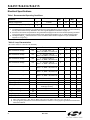
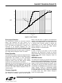
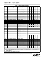
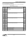
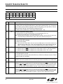
1
Si2457/Si2434/Si2415
V.90, V.34, V. 32 B I S I S O M O D E M ®
WITH
I N T E G R A T E D G L O B A L DAA
Features
Data modem formats
Integrated DAA
ITU-T, Bell
300 bps up to 56 kbps
V.21,V.22, V.29 Fast Connect
V.42, V.42bis, MNP2-5
Automatic rate negotiation
Over 5000 V Capacitive isolation
Parallel phone detect
Globally-compliant line interface
Overcurrent detection
Type I and II caller ID decode
No external ROM or RAM required
UART or parallel interface
AT command set support
27 MHz clock input
3.3 V power
Firmware upgradeable
EEPROM interface
Applications
Set-top boxes
Point-of-sale terminals
ATM terminals
Ordering Information
This data sheet is valid only for
those chipset combinations listed
on page 68.
Digital video recorder
Digital televisions
Remote monitoring
Pin Assignments
Si2457/34/15
Description
The Si2457, Si2434, and Si2415 are complete two-chip modems ranging
in speed from 56,000 bps to 14,400 bps. The ISOmodem® chipsets utilize
Silicon Laboratories’ third-generation direct access arrangement (DAA) to
provide a globally-programmable telephone line interface with an
unparalleled level of integration. By sharing the same line-side device, a
single design can be used in all countries and for all modem speeds.
Available in two small packages, these compact solutions eliminate the
need for a separate DSP, modem controller, codec, isolation transformer,
relay, opto-isolators, clocking crystal, and 2–4 wire hybrid. The
ISOmodem provides conventional data formats with connect rates of up
to 56,000 bps, full-duplex, over the Public Switched Telephone Network
(PSTN). These devices are ideal for embedded modem applications due
to their flexibility, small footprint, and minimal external component count.
RXD
TXD
CTS
RTS
DCD
ESC
RI
XTALO
PLL
Clocking
CS
WR
RD
A0
D0-D7
DCD/D4
CLKOUT/EECS/A0
3
22
ESC/D3
FSYNC/D6
4
21
VD3.3
VD3.3
5
GND
GND
6
20
19
VDA
7
18
SDI/EESD/D2
Microcontroller
DSP
DAA
Interface
To Phone
Line
AOUT
VDB
RTS/D7
8
17
RI/D1
RXD/RD
9
16
INT/DO
TXD/WR
10
15
AOUT/INT
CTS/CS
11
14
C1A
RESET
12
13
C2A
Si3018
VREG
RNG1
Data Bus
Parallel
Interface
SDO/EECLK/D5
23
C1B
C2B
RAM/ROM
Serial
Interface
INT
24
2
RX
IB
Si3018
CLKOUT
1
XTALO
QE
DCT
Functional Block Diagram
CLKIN/XTALI
CLKIN/XTALI
1
2
3
4
5
6
7
8
16
15
DCT2
14
13
DCT3
QB
12
11
QE2
10
9
VREG2
RNG2
IGND
SC
U.S. Patent #5,870,046
U.S. Patent #6,061,009
Other patents pending
ISOB
RESET
Preliminary Rev. 0.91 5/04
Copyright © 2004 by Silicon Laboratories
Si2457/Si2434/Si2415
This information applies to a product under development. Its characteristics and specifications are subject to change without notice.
Si2457/Si2434/Si2415
2
Rev. 0.91
Si2457/Si2434/Si2415
TA B L E O F C O N T E N TS
Section
Page
Electrical Specifications . . . . . . . . . . . . . . . . . . . . . . . . . . . . . . . . . . . . . . . . . . . . . . . . . . . . . .4
Typical Application Schematic . . . . . . . . . . . . . . . . . . . . . . . . . . . . . . . . . . . . . . . . . . . . . . . 10
Bill of Materials: Si2457/34/15 Chipset . . . . . . . . . . . . . . . . . . . . . . . . . . . . . . . . . . . . . . . . . 11
Functional Description . . . . . . . . . . . . . . . . . . . . . . . . . . . . . . . . . . . . . . . . . . . . . . . . . . . . . . 16
Digital Interface . . . . . . . . . . . . . . . . . . . . . . . . . . . . . . . . . . . . . . . . . . . . . . . . . . . . . . . . 16
Serial Interface . . . . . . . . . . . . . . . . . . . . . . . . . . . . . . . . . . . . . . . . . . . . . . . . . . . . . . . . . 16
Parallel Interface . . . . . . . . . . . . . . . . . . . . . . . . . . . . . . . . . . . . . . . . . . . . . . . . . . . . . . . 17
Command Mode . . . . . . . . . . . . . . . . . . . . . . . . . . . . . . . . . . . . . . . . . . . . . . . . . . . . . . . .17
Data Mode . . . . . . . . . . . . . . . . . . . . . . . . . . . . . . . . . . . . . . . . . . . . . . . . . . . . . . . . . . . . 17
Fast Connect . . . . . . . . . . . . . . . . . . . . . . . . . . . . . . . . . . . . . . . . . . . . . . . . . . . . . . . . . . 17
V.80 Synchronous Access Mode . . . . . . . . . . . . . . . . . . . . . . . . . . . . . . . . . . . . . . . . . . . 17
Clocking/Low Power Modes . . . . . . . . . . . . . . . . . . . . . . . . . . . . . . . . . . . . . . . . . . . . . . . 17
Data Compression . . . . . . . . . . . . . . . . . . . . . . . . . . . . . . . . . . . . . . . . . . . . . . . . . . . . . . 17
Error Correction . . . . . . . . . . . . . . . . . . . . . . . . . . . . . . . . . . . . . . . . . . . . . . . . . . . . . . . . 17
Wire Mode . . . . . . . . . . . . . . . . . . . . . . . . . . . . . . . . . . . . . . . . . . . . . . . . . . . . . . . . . . . . 17
Caller ID Operation . . . . . . . . . . . . . . . . . . . . . . . . . . . . . . . . . . . . . . . . . . . . . . . . . . . . . 18
Parallel Phone Detection . . . . . . . . . . . . . . . . . . . . . . . . . . . . . . . . . . . . . . . . . . . . . . . . . 18
Overcurrent Detection . . . . . . . . . . . . . . . . . . . . . . . . . . . . . . . . . . . . . . . . . . . . . . . . . . . 19
Global Operation . . . . . . . . . . . . . . . . . . . . . . . . . . . . . . . . . . . . . . . . . . . . . . . . . . . . . . .19
Firmware Upgrades . . . . . . . . . . . . . . . . . . . . . . . . . . . . . . . . . . . . . . . . . . . . . . . . . . . . . 19
Codec Interface . . . . . . . . . . . . . . . . . . . . . . . . . . . . . . . . . . . . . . . . . . . . . . . . . . . . . . . . 19
EEPROM Interface . . . . . . . . . . . . . . . . . . . . . . . . . . . . . . . . . . . . . . . . . . . . . . . . . . . . . . 19
AT Commands . . . . . . . . . . . . . . . . . . . . . . . . . . . . . . . . . . . . . . . . . . . . . . . . . . . . . . . . . 20
Extended AT Commands . . . . . . . . . . . . . . . . . . . . . . . . . . . . . . . . . . . . . . . . . . . . . . . . .28
S-Registers . . . . . . . . . . . . . . . . . . . . . . . . . . . . . . . . . . . . . . . . . . . . . . . . . . . . . . . . . . . . . . . 38
User-Access Registers (U-Registers) . . . . . . . . . . . . . . . . . . . . . . . . . . . . . . . . . . . . . . . . . . 41
Bit-Mapped U-Register Detail (defaults in bold) . . . . . . . . . . . . . . . . . . . . . . . . . . . . . . . . 47
Parallel Interface Registers . . . . . . . . . . . . . . . . . . . . . . . . . . . . . . . . . . . . . . . . . . . . . . . . . . 63
Pin Descriptions: Si2457/34/15 . . . . . . . . . . . . . . . . . . . . . . . . . . . . . . . . . . . . . . . . . . . . . . . 65
Pin Descriptions: Si3018 . . . . . . . . . . . . . . . . . . . . . . . . . . . . . . . . . . . . . . . . . . . . . . . . . . . .67
Ordering Guide . . . . . . . . . . . . . . . . . . . . . . . . . . . . . . . . . . . . . . . . . . . . . . . . . . . . . . . . . . . . 68
Package Outline: 24-Pin TSSOP . . . . . . . . . . . . . . . . . . . . . . . . . . . . . . . . . . . . . . . . . . . . . . 69
Package Outline: 16-Pin SOIC . . . . . . . . . . . . . . . . . . . . . . . . . . . . . . . . . . . . . . . . . . . . . . . . 70
Document Change List . . . . . . . . . . . . . . . . . . . . . . . . . . . . . . . . . . . . . . . . . . . . . . . . . . . . . .71
Contact Information . . . . . . . . . . . . . . . . . . . . . . . . . . . . . . . . . . . . . . . . . . . . . . . . . . . . . . . . 72
Rev. 0.91
3
Si2457/Si2434/Si2415
Electrical Specifications
Table 1. Recommended Operating Conditions
Parameter1
Symbol
Test Condition
Min2
Typ
Max2
Unit
TA
F-Grade
0
25
70
°C
3.0
3.3
3.6
V
Ambient Temperature
3
Si2457/34/15 Supply Voltage, Digital
VD
Notes:
1. The Si2457/34/15 specifications are guaranteed when the typical application circuit (including component tolerance)
and any Si2457/34/15 and any Si3018 are used. See "Typical Application Schematic" on page 10.
2. All minimum and maximum specifications are guaranteed and apply across the recommended operating conditions.
Typical values apply at nominal supply voltages and an operating temperature of 25 °C unless otherwise stated.
3. The digital supply, VD, operates from 3.0 to 3.6 V. The Si2457/34/15 interface supports 5 V logic (CLKIN/XTALI
supports 3.3 V logic only).
Table 2. Loop Characteristics
(VD = 3.0 to 3.6 V, TA = 0 to 70 °C for K-Grade)
Parameter
Symbol
DC Termination Voltage
VTR
DC Termination Voltage
VTR
DC Termination Voltage
VTR
DC Termination Voltage
VTR
DC Termination Voltage
VTR
DC Termination Voltage
VTR
DC Termination Voltage
VTR
On-Hook Leakage Current
Operating Loop Current
Operating Loop Current
DC Ring Current
ILK
ILP
ILP
Ring Detect Voltage2
Ring Detect Voltage2
Ring Frequency
Ringer Equivalence Number
VRD
VRD
FR
REN
Test Condition
1
IL = 20 mA, ILIM = 0
DCV = 00, MINI = 11, DCR = 0
IL = 120 mA, ILIM = 0
DCV = 00, MINI = 11, DCR = 0
IL = 20 mA, ILIM = 0
DCV = 11, MINI = 00, DCR = 0
IL = 120 mA, ILIM = 0
DCV = 11, MINI = 00, DCR = 0
IL = 20 mA, ILIM = 1
DCV = 11, MINI = 00, DCR = 0
IL = 60 mA, ILIM = 1
DCV = 11, MINI = 00, DCR = 0
IL = 50 mA, ILIM = 1
DCV = 11, MINI = 00, DCR = 0
VTR = –48 V
MINI = 00, ILIM = 0
MINI = 00, ILIM = 1
DC current flowing through ring
detection circuitry
RT = 0
RT = 1
Min
Typ
Max
Unit
—
—
6.0
V
9
—
—
V
—
—
7.5
V
9
—
—
V
—
—
7.5
V
40
—
—
V
—
—
40
V
—
10
10
—
—
—
—
1.5
5
120
60
3
µA
mA
mA
µA
12
18
15
—
15
21
—
—
18
25
68
0.2
VRMS
VRMS
Hz
Notes:
1. ILIM = U67, bit 9; DCV = U67, bits 3:2; MINI = U67, bits 13:12; DCR = U67, bit 7; RT = U67, bit 0.
2. The ring signal is guaranteed to not be detected below the minimum. The ring signal is guaranteed to be detected
above the maximum.
4
Rev. 0.91
Si2457/Si2434/Si2415
TIP
+
600 Ω
Si3018
IL
VTR
10 µF
–
RING
Figure 1. Test Circuit for Loop Characteristics
Table 3. DC Characteristics, VD = 3.0 to 3.6 V
(VD = 3.0 to 3.6 V, TA = 0 to 70 °C for K-Grade)
Parameter
Symbol
Test Condition
Min
Typ
Max
Unit
High Level Input Voltage
VIH
2.0
—
—
V
Low Level Input Voltage
VIL
—
—
0.8
V
High Level Output Voltage
VOH
IO = –2 mA
2.4
—
—
V
Low Level Output Voltage
VOL
IO = 2 mA
—
—
0.35
V
IL
–10
—
10
µA
RPU
50
125
200
kΩ
Input Leakage Current
Pullup Resistance Pins 3, 4, 9, 11,
15, 16, 17, 18, 23, 24
Total Supply Current*
ID
VD3.3 pin
—
26
35
mA
Total Supply Current, Powerdown*
ID
PDN = 1
—
80
—
µA
*Note: All inputs at 0 or VD. All inputs held static except clock and all outputs unloaded (Static IOUT = 0 mA).
Rev. 0.91
5
Si2457/Si2434/Si2415
Table 4. AC Characteristics
(VD = 3.0 to 3.6 V, TA = 0 to 70 °C for K-Grade, Fs = 8 kHz)
Parameter
Symbol
Sample Rate
Test Condition
Fs
Min
Typ
Max
Unit
—
8
—
kHz
Clock Input Frequency
FXTL
default
—
4.9152
—
MHz
Clock Input Frequency
FXTL
>10 kΩ resistor between pin 23
and GND
—
27
—
MHz
Receive Frequency Response
Low –3 dBFS Corner, FILT = 0
—
5
—
Hz
Receive Frequency Response
Low –3 dBFS Corner, FILT = 1
—
200
—
Hz
VFS
—
1.1
—
VPEAK
VFS
—
1.1
—
VPEAK
Transmit Full Scale Level1
Receive Full Scale
Level1,2
Dynamic Range3
DR
ILIM = 0, DCV = 11, MINI = 00
DCR = 0, IL = 100 mA
—
80
—
dB
Dynamic Range3
DR
ILIM = 0, DCV = 00, MINI = 11
DCR = 0, IL = 20 mA
—
80
—
dB
Dynamic Range3
DR
ILIM = 1, DCV = 11, MINI = 00
DCR = 0, IL = 50 mA
—
80
—
dB
Transmit Total Harmonic
Distortion4
THD
ILIM = 0, DCV = 11, MINI = 00
DCR = 0, IL = 100 mA
—
–72
—
dB
Transmit Total Harmonic
Distortion4
THD
ILIM = 0, DCV = 00, MINI = 11
DCR = 0, IL = 20 mA
—
–78
—
dB
Receive Total Harmonic
Distortion4
THD
ILIM = 0, DCV = 00, MINI = 11
DCR = 0, IL = 20 mA
—
–78
—
dB
Receive Total Harmonic
Distortion4
THD
ILIM = 1,DCV = 11, MINI=00
DCR = 0, IL = 50 mA
—
–78
—
dB
DRCID
VIN = 1 kHz, –13 dBm
—
50
—
dB
Dynamic Range (Caller ID Mode)
Notes:
1. Measured at TIP and RING with 600 Ω termination at 1 kHz, as shown in Figure 1 on page 5.
2. Receive full scale level produces –0.9 dBFS at DTX.
3. DR = 20 x log |Vin| + 20 x log (rms signal/rms noise). Applies to both transmit and receive paths. Vin = 1 kHz, –3 dBFS.
4. Vin = 1 kHz, –3 dBFS. THD = 20 x log (rms distortion/rms signal).
6
Rev. 0.91
Si2457/Si2434/Si2415
Table 5. Absolute Maximum Ratings
Parameter
Symbol
Value
Unit
DC Supply Voltage
VD
4.1
V
Input Current, Si2457/34/15 Digital Input
Pins
IIN
±10
mA
Digital Input Voltage
VIND
–0.3 to 5.3
V
CLKIN/XTALI Input Voltage
VXIND
–0.3 to (VD + 0.3)
V
TA
–10 to 100
°C
TSTG
–40 to 150
°C
Operating Temperature Range
Storage Temperature Range
Note: Permanent device damage may occur if the above absolute maximum ratings are exceeded. Functional operation
should be restricted to the conditions as specified in the operational sections of this data sheet. Exposure to absolute
maximum rating conditions for extended periods may affect device reliability.
Table 6. Switching Characteristics
(VD = 3.0 to 3.6 V, TA = 0 to 70 °C for K-Grade)
Parameter
Symbol
CLKOUT Output Clock Frequency
Min
Typ
Max
Unit
2.048
—
49.152
MHz
Baud Rate Accuracy
tBD
–1
—
1
%
Start Bit ↓ to RTS ↓
tRTH
—
1/(2 x Baud
Rate)
—
ns
CTS or RTS ↑ High to Start Bit↓
tRTS
10
—
—
ns
Stop Bit ↑ to CTS ↑
tCTH
—
—
—
ns
RESET ↓ to RESET ↑
tRS
5.0
—
—
ms
RESET ↑ to 1st AT Command
tAT
300
—
—
ms
Address Setup
tAS
15
—
—
ns
Address Hold
tAH
0
—
—
ns
WR Low Pulse Width
tWL
50
—
—
ns
tWDSU
20
—
—
ns
Write Cycle Time
tWC
120
—
—
ns
Chip Select Setup
tCSS
10
—
—
ns
Chip Select Hold
tCSH
0
—
—
ns
tRL
50
—
—
ns
tRLDD
—
—
20
ns
Data Hold
tDH
10
—
—
ns
RD High to Hi-Z Time
tDZ
—
—
30
ns
Read Cycle Time
tRC
120
—
—
ns
Write Data Setup Time
RD Low Pulse Width
RD Low to Data Driven Time
Note: All timing is referenced to the 50% level of the waveform. Input test levels are VIH = VD – 0.4 V, VIL = 0.4 V
Rev. 0.91
7
Si2457/Si2434/Si2415
UART Time for Modem Receive Path (8N1 Mode)
8-B it Data
M ode
RX
S tart
tR TS
D0
D1
D2
D3
D4
D5
D6
D7
S top
t R TH
RTS
UART Timing for Modem Transmit Path (9N1 Mode with 9th Bit Escape)
9-B it Data
M ode
TX
S tart
D0
D1
D2
D3
D4
D5
D6
D7
ESC
t R TS
t CTH
CTS
Figure 2. Asynchronous UART Serial Interface Timing Diagram
8
S top
Rev. 0.91
Si2457/Si2434/Si2415
t CSS
t CSH
t AS
t AH
CS
ADDRESS = 0 or 1
A0
t RL
t RC
RD
t DZ
t RLDD
t DH
D[7:0]
VALID DATA
VALID DATA
t RLDD
Figure 3. Parallel Interface Read Timing
t CSS
t CSH
t AS
t AH
CS
A0
ADDRESS = 0 or 1
tW L
tW C
WR
t W DSU
t DH
D[7:0]
VALID DATA
VALID DATA
Figure 4. Parallel Interface Write Timing
Rev. 0.91
9
RESET_
RTS_/D7
RXD/RD_
TXD/WR_
CTS_/CS_
CLKOUT/EECS_/A0
INT_/D0
RI_/D1
EESD/D2
EECLK/D5
DCD_/D4
ESC/D3
AOUT/INT_
D6
12
8
9
10
11
3
16
17
18
24
23
22
15
4
5
21
RESET
RTS/D7
RXD/RD
TXD/WR
CTS/CS
U1
C51
C53
C2A
C1A
XTALO
CLKIN/XTALI
CLKOUT/EECS/A0
INT/D0
RI/D1
EESD/D2
EECLK/D5
DCD/D4
ESC/D3
AOUT/INT
D6
VD3.3
VD 3.3
GND
GND
VDA
VDB
6
20
7
19
13
14
2
1
Y1
Emissions option
R13
R12
C41
C40
R9
C5
Bias
C2
C1
External crystal option
C52
1
2
C50
Bypass
C6
10
7
4
6
5
VREG2
VREG
IB
C2B
C1B
U2
RX
8
9
1
12
13
16
14
2
3
Si3018
RNG1
RNG2
QE
QE2
QB
DCT2
DCT3
DCT
IGND
15
Rev. 0.91
SC
10
C4
R1
+
11
VDD
Q5
Ring Detect/CID
R2
R11
DC Term
R10
C7
Q4
R4
R7
R8
R5
Q1
Z1
R3
Q2
Q3
C10
Hookswitch
R6
No Ground Plane In DAA Section
+
D1
C3
-
FB1
FB2
prior to PCB fabrication.
C9
C8
R15
R16
Emissions option
submit design to Silicon Labs for review
TIP
RV1
RING
Refer to AN93 for layout guidelines. Please
Si2457/Si2434/Si2415
Typical Application Schematic
Si2457/Si2434/Si2415
Bill of Materials: Si2457/34/15 Chipset
Component
Value
Supplier(s)
C1, C2
33 pF, Y2, X7R, ±20%
Panasonic, Murata, Vishay
C3
10 nF, 250 V, X7R, ±20%
Venkel, SMEC
C4
1.0 µF, 50 V, Elec/Tant, ±20%
Panasonic
C5, C6, C50, C52
0.1 µF, 16 V, X7R, ±20%
Venkel, SMEC
C7
2.7 nF, 50 V, X7R, ±20%
Venkel, SMEC
C8, C9
680 pF, Y2, X7R, ±10%
Panasonic, Murata, Vishay
0.01 µF, 16 V, X7R, ±20%
Venkel, SMEC
33 pF, 16 V, X7R, ±20%
Venkel, SMEC
C10
1
C40, C41
C51, C53
0.22 µF, 16 V, X7R, ±20%
Venkel, SMEC
D1, D22
Dual Diode, 225 mA, 300 V, CMPD2004S
Central Semiconductor
FB1, FB2
Ferrite Bead, BLM21AG601SN1
Murata
Q1, Q3
NPN, 300 V, MMBTA42
OnSemi, Fairchild
Q2
PNP, 300 V, MMBTA92
OnSemi, Fairchild
Q4, Q5
NPN, 80 V, 330 mW, MMBTA06
OnSemi, Fairchild
RV1
Sidactor, 275 V, 100 A
Teccor, Protek, ST Micro
R1
1.07 kΩ, 1/2 W, 1%
Venkel, SMEC, Panasonic
R2
150 Ω, 1/16 W, 5%
Venkel, SMEC, Panasonic
R3
3.65 kΩ, 1/2 W, 1%
Venkel, SMEC, Panasonic
R4
2.49 kΩ, 1/2 W, 1%
Venkel, SMEC, Panasonic
R5, R6
100 kΩ, 1/16 W, 5%
Venkel, SMEC, Panasonic
R7, R8
20 MΩ, 1/16 W, 5%
Venkel, SMEC, Panasonic
R9
1 MΩ, 1/16 W, 1%
Venkel, SMEC, Panasonic
R10
536 Ω, 1/4 W, 1%
Venkel, SMEC, Panasonic
73.2 Ω, 1/2 W, 1%
Venkel, SMEC, Panasonic
3
0 Ω, 1/16 W
Venkel, SMEC, Panasonic
R15, R164
0 Ω, 1/16 W
Venkel, SMEC, Panasonic
U1
Si2457/34/15
Silicon Labs
U2
Si3018
Silicon Labs
4.9152 MHz, 20 pF, 100 ppm, 150 Ω ESR
ECS Inc., Siward
Zener Diode, 43 V, 1/2 W, BZT84C43
On Semi
R11
R12, R13
1,5
Y1
Z1
Notes:
1. In STB applications, C40, C41, and Y1 can be removed by using the 27 MHz clock input feature.
2. Several diode bridge configurations are acceptable. For example, a single DF04S or four 1N4004 diodes may be
used.
3. 56 Ω, 1/16 W, 1% resistors may be substituted for R12–R13 (0 Ω) to decrease emissions.
4. Murata BLM21AG601SN1 may be substituted for R15–R16 (0 Ω) to decrease emissions.
5. To ensure compliance with ITU specifications, frequency tolerance must be less than 100 ppm including initial
accuracy, 5-year aging, 0 to 70 °C, and capacitive loading. 50 ppm initial accuracy crystals typically satisfy this
requirement.
Rev. 0.91
11
Si2457/Si2434/Si2415
Table 7. Protocol Characteristics
Item
Specification
Data Rate
56 kbps1
54.666 kbps1
53.333 kbps1
52 kbps1
50.666 kbps1
49.333 kbps1
48 kbps1
46.666 kbps1
45.333 kbps1
44 kbps1
42.666 kbps1
41.333 kbps1
40 kbps1
38.666 kbps1
37.333 kbps1
36 kbps1
34.666 kbps1
33.333 kbps1
32 kbps1
30.666 kbps1
29.333 kbps1
28 kbps1
33.6 kbps2
31.2 kbps2
28.8 kbps2
26.4 kbps2
24.0 kbps2
21.6 kbps2
19.2 kbps2
16.8 kbps2
14.4 kbps
12.0 kbps
9600 bps
7200 bps
4800 bps
2400 bps
1200 bps
300 bps
300 bps
ITU-T V.901
ITU-T V.901
ITU-T V.901
ITU-T V.901
ITU-T V.901
ITU-T V.901
ITU-T V.901
ITU-T V.901
ITU-T V.901
ITU-T V.901
ITU-T V.901
ITU-T V.901
ITU-T V.901
ITU-T V.901
ITU-T V.901
ITU-T V.901
ITU-T V.901
ITU-T V.901
ITU-T V.901
ITU-T V.901
ITU-T V.901
ITU-T V.901
ITU-T V.342
ITU-T V.342
ITU-T V.342
ITU-T V.342
ITU-T V.342
ITU-T V.342
ITU-T V.342
ITU-T V.342
ITU-T V.34 or V.32bis
ITU-T V.34 or V.32bis
ITU-T V.34, V.32bis, or V.29
ITU-T V.34 or V.32bis
ITU-T V.34 or V.32bis
ITU-T V.34 or V.22bis
ITU-T V.22bis, V.23, or Bell 212A
ITU-T V.21
Bell 103
Notes:
1. Supported on Si2457 only.
2. Supported on Si2457 and Si2434 only.
12
Rev. 0.91
Si2457/Si2434/Si2415
Table 7. Protocol Characteristics (Continued)
Item
Data Format
Bit asynchronous
Compatibility
Specification
Selectable 8, 9, 10, or 11 bits per character
ITU-T V.901, V.342, V.32bis, V.32, V.23, V.22bis,
V.22, V.21, Bell 212A, and Bell 103
Operating Mode
Switched network
Two-wire full duplex
Data Modulation
28 to 56 kbps1
2.4 to 33.6 kbps2
14.4 kbps
12.0 kbps
9600 bps
9600 bps
9600 bps
7200 bps
4800 bps
2400 bps
1200 bps
0 to 300 bps
V.90 as specified by ITU-T
V.34 as specified by ITU-T
128-level TCM/2400 Baud ±0.01%
64-level TCM/2400 Baud ±0.01%
32-level TCM/2400 Baud ±0.01%
16-level QAM/2400 Baud ±0.01%
V.29 QAM as specified by ITU-T
16-level TCM/2400 Baud ±0.01%
4-level QAM/2400 Baud ±0.01%
16-level QAM/600 Baud ±0.01%
4-level PSK/600 Baud ±0.01%
FSK 0–300 Baud ±0.01%
Answer Tone
ITU-T V.32bis, V.32, V.22bis, V.22, and
V.21 modes
Bell 212A and 103 modes
Transmit Carrier
V.901
V.342
ITU-T V.32bis
ITU-T V.32
ITU-T V.29
ITU-T V.22, V.22bis/Bell 212A
Originate mode
Answer mode
ITU-T V.21
Originate mode
Answer mode
Bell 103
Originate mode
Answer mode
2100 Hz ±3 Hz
2225 Hz ±3 Hz
As specified by ITU-T
As specified by ITU-T
1800 Hz ±0.01%
1800 Hz ±0.01%
1700 Hz±1 Hz
1200 Hz ±0.5 Hz
2400 Hz ±1 Hz
Mark (980 Hz ±12 Hz) Space (1180 Hz ±12 Hz)
Mark (1650 Hz ±12 Hz) Space (1850 Hz ±12 Hz)
Mark (1270 Hz ±12 Hz) Space (1070 Hz ±12 Hz)
Mark (2225 Hz ±12 Hz) Space (2025 Hz ±12 Hz)
Notes:
1. Supported on Si2457 only.
2. Supported on Si2457 and Si2434 only.
Rev. 0.91
13
Si2457/Si2434/Si2415
Table 7. Protocol Characteristics (Continued)
Item
Specification
Output Level
Permissive—Switched network
Receive Carrier
ITU-T V.901
ITU-T V.342
ITU-T V.32bis
ITU-T V.32
ITU-T V.29
ITU-T V.22, V.22bis/Bell 212A
Originate mode
Answer mode
ITU-T V.21
Originate mode
Answer mode
Bell 103
Originate mode
Answer mode
–9 dBm maximum
As specified by ITU-T
As specified by ITU-T
1800 Hz ±7 Hz
1800 Hz ±7 Hz
1700 Hz ±7 Hz
2400 Hz ±7 Hz
1200 Hz ±7 Hz
Mark (980 Hz ±12 Hz) Space (1180 Hz ±12 Hz)
Mark (1650 Hz ±12 Hz) Space (1850 Hz ±12 Hz)
Mark (2225 Hz ±12 Hz) Space (2025 Hz ±12 Hz)
Mark (1270 Hz ±12 Hz) Space (1070 Hz ±12 Hz)
Carrier Detect (level for ITU-T V.22bis,
V.22, V.21, 212, 103) in Switched Network
Acquisition (–43 dBm)
Release (–48 dBm)
Hysteresis
2 dBm minimum
Note: ITU-T V.901, V.342, V.32/V.32bis are echo canceling protocols that use signal quality as criteria for
maintaining connection. They also provide for self-training detection to force disconnect.
DTE Interface
EIA/TIA-232-E (ITU-T V.24/V.28/ISO 2110)
Line Equalization
Connection Options
Automatic Adaptive
Loss of Carrier in ITU-T V.22bis and lower
Phone Types
500 (rotary dial), 2500 (DTMF dial)
Dialing
Pulse and Tone
DTMF Output Level
Per Part 68
Pulse Dial Ratio
Make/Break: 39/61%
Ring Cadence
On 2 seconds; Off 4 seconds
Notes:
1. Supported on Si2457 only.
2. Supported on Si2457 and Si2434 only.
14
Rev. 0.91
Si2457/Si2434/Si2415
Table 7. Protocol Characteristics (Continued)
Item
Specification
Call Progress Monitor
BUSY
CONNECT (rate)
NO ANSWER
NO CARRIER
NO DIALTONE
OK
RING
RINGING
Notes:
1. Supported on Si2457 only.
2. Supported on Si2457 and Si2434 only.
Rev. 0.91
15
Si2457/Si2434/Si2415
Functional Description
Digital Interface
The Si2457/34/15 ISOmodem® is a complete
embedded modem chipset with integrated direct access
arrangement (DAA) that provides a programmable line
interface to meet global telephone line requirements.
Available in two small packages, this solution includes a
DSP data pump, modem controller, on-chip RAM and
ROM, codec, DAA, analog output, and 27 MHz clock
input.
The Si2457/34/15 digital I/O can communicate via either
a serial UART interface with flow control or via a parallel
8-bit interface.
The Si2457/34/15 accepts standard modem AT
commands and provides connect rates up to 56/33.6/
14.4 kbps full-duplex over the Public Switched Telephone
Network (PSTN). The Si2457/34/15 features a complete
set of modem protocols including all ITU-T standard
formats up to 56 kbps.
The ISOmodem provides numerous additional features
for embedded modem applications. The modem includes
full type I and type II caller ID detection and decoding for
global standards. Call progress monitoring is supported
through standard result codes. The modem is also
programmable to meet global settings. Because the
Si2457/34/15 ISOmodem integrates the DAA, analog
features, such as parallel phone detect, overcurrent
detection, and global PTT compliance with a single
design, are included.
This device is ideal for embedded modem applications
due to its small board space, low power consumption,
and global compliance. The Si2457/34/15 solution
includes a silicon DAA using Silicon Laboratories’
proprietary third-generation DAA technology. This highlyintegrated DAA can be programmed to meet worldwide
PTT specifications for ac termination, dc termination,
ringer impedance, and ringer threshold. In addition, the
Si2457/34/15 has been designed to meet the most
stringent worldwide requirements for out-of-band energy,
billing-tone immunity, surge immunity, and safety
requirements.
The Si2457/34/15 allows for rapid integration into existing
modem applications by providing a serial interface that
can directly communicate to either a microcontroller via a
UART interface or a PC via an RS-232 port. This
interface allows for PC evaluation of the modem
immediately upon powerup via the AT commands using
standard terminal software. The Si2457/34/15 also
provides an 8-bit parallel port.
16
Selection of a serial or parallel I/O interface is
determined by the state of AOUT/INT (Si2457/34/15,
pin 15) during the rising edge of RESET. An internal
pullup resistor forces the default state to serial mode
operation. An external 10 kΩ pulldown resistor can be
connected to AOUT/INT to force selection of parallel
mode (see Table 8). Configuration of pins 3, 4, 8–11,
15–18, and 22–24 is determined by this interface
selection.
Serial Interface
The Si2457/34/15 supports asynchronous serial
communication with data terminal equipment (DTE) at
rates up to 307.2 kbps with the standard serial UART
format. Upon powerup, the UART baud rate is
automatically detected using the autobaud feature. If a
pulldown resistor ≤ 10 kΩ is placed between D2
(Si2457/34/15, pin 18) and GND (Si2457/34/15, pin 6),
the DTE rate is set to a 19.2 kbps baud rate (see
Table 8).
The serial interface also provides a hardware pin, DCD
(data carrier detect), which remains low as long as the
ISOmodem is connected.
The INT interrupt pin can be programmed to alert the
host of changes to the interrupts listed in I/O Control 0
(U70).
Autobaud
The Si2457/34/15 includes an automatic baud rate
detection feature that allows the host to start
transmitting data at any standard DTE rate from
300 bps to 307.2 kbps. This feature is enabled by
default.
Table 8. Pulldown Selector
Mode
Serial I/O
Parallel I/O
4.9152 MHz CLK
Default
Pin 15
27 MHz CLK
Pin 23
Pin 11, 15
Autobaud
Default
19.2 kbps DTE
Pin 18
No EEPROM
Default
EEPROM
Pin 4
Rev. 0.91
N/A
N/A
Si2457/Si2434/Si2415
Parallel Interface
The parallel interface is an 8-bit data bus with a single
bit address. Figure 3 on page 9 shows the required
timing for the parallel interface.
If A0 = 0, the data bus represents a read/write to the
“Parallel Interface 0 (0x00)” register on page 63. If
A0 = 1, the data bus represents a read/write to the
“Parallel Interface 1 (0x01)” register on page 64).
Command Mode
Upon reset, the ISOmodem® is in command mode and
accepts “AT” commands. An outgoing modem call can
be made using the “ATDT#” (tone dial) or “ATDP#”
(pulse dial) command after the device is configured. If
the handshake is successful, the modem responds with
the response codes detailed in Table 13 on page 35 and
enters data mode.
Data Mode
The Si2457/34/15 ISOmodem is in data mode while it
has a telephone line connection to another modem or is
in the process of establishing a connection.
Data protocols are available to provide error correction
to improve reliability (V.42 and MNP2-4) and data
compression to increase throughput (V.42bis and
MNP5).
Each connection between two modems in data mode
begins with a handshaking sequence. During this
sequence, the modems determine the line speed, data
protocol, and related parameters for the data link.
Configuration through AT commands determines the
range of choices available to the modem during the
negotiation process.
Fast Connect
The Si2457/34/15 supports a fast connect mode of
operation to reduce the time of a connect sequence in
originate mode. The Fast Connect modes can be
enabled for V.21, V.22, Bell103, and V.29 modulations.
See “AN93: Modem Designer’s Guide” for details.
V.80 Synchronous Access Mode
The Si2457/34/15 supports a V.80 synchronous access
mode of operation, which operates with an
asynchronous DTE and a synchronous DCE. See
“AN93: Modem Designer’s Guide” for complete details.
Clocking/Low Power Modes
The Si2457/34/15 contains an on-chip phase-locked
loop (PLL) and clock generator. Using either a single
crystal or master clock input, the Si2457/34/15 can
generate all the internal clocks required to support the
featured modem protocols. Either a 27 MHz or
4.9152 MHz clock (3.3 V max input—see Table 5 on
page 7) on XTALI or a 4.9152 MHz crystal across XTALI
and XTALO form the master clock (±100 ppm max) for
the ISOmodem. This clock source is sent to an internal
PLL that generates all necessary internal system clocks
including the DSP clock. By default, the Si2457/34/15
assumes a 4.9152 MHz clock input. If a 27 MHz clock
on XTALI is used with the serial (UART) interface, a
pulldown resistor < 10 kΩ must be placed between DCD
(pin 23) and GND. If a 27 MHz clock on XTALI is used
with the parallel interface, a pulldown resistor < 10 kΩ
must be placed between CTS/CS (pin 11) and GND and
AOUT/INT and GND (see Table 8).
Using the S24 S-register, the Si2457/34/15 can be set
to automatically enter sleep mode after a preprogrammed time of inactivity with either the DTE or the
remote modem. The sleep mode is entered after (S24)
seconds have passed since the TX FIFO has been
empty. The ISOmodem remains in the sleep state until
either a 1 to 0 transition on TXD (serial mode) or a 1 to 0
transition on CS (parallel mode) occurs.
Additionally, the Si2457/34/15 may be placed in a
complete powerdown mode or wake-on-ring mode.
Complete
powerdown
is
accomplished
via
U65[13] (PDN). Once the PDN bit is written, the Si2457/
34/15 completely powers down and can only be
powered back on via the RESET pin.
A clock input may be produced on the CLKOUT pin.
See “AN93: Modem Designer’s Guide” for details.
Data Compression
The modem can achieve DTE (host-to-ISOmodem)
speeds greater than the maximum DCE (modem-tomodem) speed through the use of a data compression
protocol. The compression protocols available are the
ITU-T V.42bis and MNP5 protocols. Data compression
attempts to increase throughput by compressing the
data before actually sending it. Thus, the modem is able
to transmit more data in a given period of time.
Error Correction
The Si2457/34/15 ISOmodem can employ error
correction (reliable) protocols to ensure error-free
delivery of asynchronous data sent between the host
and the remote end. The Si2457/34/15 supports V.42
and MNP2-4 error correction protocols. V.42 (LAPM) is
most commonly used and is enabled by default.
Wire Mode
Wire mode is used to communicate with standard nonerror correcting modems. When optioned with \N3, the
Si2457/34/15 falls back to wire mode if it fails in an
attempt to negotiate a V.42 link with the remote modem.
Error correction and data compression are not active in
Rev. 0.91
17
Si2457/Si2434/Si2415
wire mode.
Caller ID Operation
The Si2457/34/15 supports full type I and type II caller
ID detection and decode. Caller ID is supported for the
US Bellcore, European ETSI, UK, and Japanese
protocols and is enabled via the +VCID, +VCDT, and
+PCW commands.
Parallel Phone Detection
The ISOmodem® is able to detect when another
telephone, modem, or other device is using the phone
line. This allows the host to avoid interrupting another
phone call when the phone line is already in use and to
intelligently handle an interruption when the ISOmodem
is using the phone line.
On-Hook Line-in-use Detection
When the ISOmodem is sharing the telephone line with
other devices, it is important that it not interrupt a call in
progress. To detect whether another device is using the
shared telephone line, the host can use the ISOmodem
to monitor the TIP-RING dc voltage with the line voltage
sense (LVS) register (U6C, bits 15:8). The LVS bits
have a resolution of 1 V per bit with an accuracy of
approximately ±10%. Bits 0 through 6 of this 8-bit
signed twos complement number indicate the value of
the line voltage, and the sign bit (bit 7) indicates the
polarity of TIP and RING. The ISOmodem can also
monitor the TIP-RING dc voltage using the LVCS
register (U79, bits 4:0). See Figure 5 on page 18. See
also the %Vn commands for automatic line-in-use
detection.
Off-Hook Intrusion Detection
When the ISOmodem is off-hook, an algorithm is
implemented in the ISOmodem to automatically monitor
the TIP-RING loop current via the LVCS register. During
the off-hook state, the LVCS register switches from
representing the TIP-RING voltage to representing the
TIP-RING current. See Figure 6 on page 19. Upon
detecting an intrusion, the ISOmodem alerts the host of
the condition via the INT pin.
30
25
20
LVC S
BITS
15
10
5
0
0 3 6
9 12 15 18 21 24 28 30 33 36 39 42 45 47 51 54 57 60 63 66 69 72 75 78 81 84 87
Loop Voltage (V)
Figure 5. Loop Voltage
18
Rev. 0.91
100
Si2457/Si2434/Si2415
Overload
30
25
CTR21 only
20
LVCS
BITS
15
10
5
0
0 3 6 9 12 15 18 21 24 27 30 33 36 39 42 45 48 51 54 57 60 63 66 69 72 75 78 81 84 87 90 93
140
Loop Current
(mA)
Figure 6. Loop Current
Overcurrent Detection
The Si2457/34/15 includes an overcurrent detection
feature that measures the loop current at a
programmable time after the Si2457/34/15 goes offhook. This allows the Si2457/34/15 to detect if it is
connected to an improper telephone line. The
overcurrent detection feature may be enabled by setting
the OCDM bit (U70, bit 11). OHT (U77, bits 8:0) sets the
delay after off-hook until the loop current is measured.
See “AN93: Modem Designer’s Guide” for details.
Global Operation
The Si2457/34/15 chipset contains an integrated silicon
direct access arrangement (Silicon DAA) that provides a
programmable line interface to meet international
telephone line interface requirements. “AN93: Modem
Designer’s Guide” gives the DAA register settings
required to meet international PTT standards.
Additionally, the user-access registers (via the AT:U and
AT:R commands) may be programmed for countryspecific settings, such as dial tone, ring, ringback, and
busy tone. See “AN93: Modem Designer’s Guide” for
complete details.
Firmware Upgrades
The Si2457/34/15 contains an on-chip program ROM
that includes the firmware required for the features
listed in this data sheet. In addition, the Si2457/34/15
contains on-chip program RAM to accommodate minor
changes to the ROM firmware. This allows Silicon Labs
to provide future firmware updates to optimize the
characteristics of new modem designs and those
already deployed in the field. See “AN93: Modem
Designer’s Guide” for complete details.
Codec Interface
In order to support a full range of voice and data
applications, the Si2457/34/15 includes an optional
serial interface that connects to an external voice codec
(Si3000). See “AN93: Modem Designer’s Guide” for
complete details.
EEPROM Interface
The Si2457/34/15 supports an optional serial peripheral
interface (SPI) bus serial EEPROM Mode 3 with a 16-bit
(8–64 kbit range) address. Upon powerup, if a pulldown
resistor ≤10 kΩ is placed between D6 (Si2457, pin 4)
and GND (see Table 8), the Si2457 attempts to detect
an EEPROM. The EEPROM is intended first for setting
custom defaults, second for automatically loading
firmware upgrades, and third to allow for user-defined
AT command macros for use in custom AT commands
or country codes. See “AN93: Modem Designer’s
Guide” for complete details.
Rev. 0.91
19
Si2457/Si2434/Si2415
AT Commands
At powerup, the Si2457/34/15 is in the AT command mode. In command mode, the modem monitors the input
(serial or parallel) checking constantly for a valid command (AT commands are described in Table 9.)
Table 9. Basic AT Command Set (Command Defaults in Bold)
Command
Action
$
Display AT command mode settings.
A
Answer incoming call
A/
Re-execute last command. This is the only command not preceded by “AT” or followed by a
<CR>.
Dial
The dial command, followed by 1 or more dial command modifiers, manually dials a phone
number:
Modifier
Function
! or &
Flash hook switch for FHT (U4F) ms (default: 500 ms)
, or <
Pause before continuing for S8 seconds (default:
2 seconds)
;
Return to AT command mode
@
Wait for silence.
G
Polarity reversal detect. By placing the “G” character in
the dial string (i.e. ATDTG1), the Si2457/34/15 will
monitor the telephone line for polarity reversals. If a
busy tone is detected, the Si2457/34/15 will report
“POLARITY REVERSAL” if a polarity reversal was
detected or “NO POLARITY REVERSAL” if a polarity
reversal was not detected. In each case, the result
code is followed by “OK”. If the S7 timeout occurs
before a busy tone is detected, the Si2457/34/15 will
report “NO CARRIER”. Polarity reversal monitoring
begins after the last digit is dialed and ends when the
busy tone is detected or S7 timeout occurs.
Dn
Note: It is not possible to establish a modem connection
when using this command.
L
P
T
W
En
Local DTE echo
E0
Disable
E1
Enable
20
Redial last number.
Pulse (rotary) dialing—pulse digits: 0, 1, 2, 3, 4, 5, 6, 7,
8, 9
Tone (DTMF) dialing—DTMF digits: *, #, A, B, C, D, 0,
1, 2, 3, 4, 5, 6, 7, 8, 9.
Wait for dial tone before continuing for S14 seconds
(default: 12 seconds). Blind dialing modes X0, X1 and
X3 do not affect the W command.
If the DOP bit (U7A, bit 7) is set, the “ATDTW” command will cause the ISOmodem® to pause dialing and
either report an “OK” if a dialtone is detected or “NO
DIALTONE” if a dial tone is not detected.
Rev. 0.91
Si2457/Si2434/Si2415
Table 9. Basic AT Command Set (Command Defaults in Bold) (Continued)
Command
Action
Hn
Hook switch.
H0
Go on-hook (hang up modem).
H1
Go off-hook.
In
Identification and checksum.
I0
Display Si2457/34/15 revision code.
B: Revision B
C: Revision C, etc.
Display Si2457/34/15 firmware revision code (numeric).
I1
I7
Display line-side revision code.
18C = Si3018 revision C
Display the ISOmodem® model number.
“2415” = Si2415
“2434” = Si2434
“2457” = Si2457
Diagnostic results 1. See “AN93: Modem Designer’s Guide” for details.
I8
Diagnostic results 2. See “AN93: Modem Designer’s Guide” for details.
Ln
Speaker volume operation
L1
Low speaker volume
L2
Medium speaker volume
L3
High speaker volume
Mn
Speaker operation (via AOUT).
M0
Speaker is always off.
M1
Speaker is on while dialing and handshaking; off in data mode.
M2
Speaker is always on.
M3
Speaker is off while dialing, on during handshaking and retraining.
On
Return to data mode from Command mode operation.
O0
Return to data mode.
O1
Return to data mode and perform a full retrain (at any speed except 300 bps).
O2
Return to data mode and perform rate renegotiation.
Qn
Response mode.
Q0
Enable result codes (see Table 13 on page 35)
Q1
Disable result codes (enable quiet mode).
R
Initiate V.23 reversal.
Sn
S-register operation (see Table 14 on page 38).
S$
List contents of all S registers.
Sn?
Display contents of S-register n.
Sn=x
Set S-register n to value x (where n and x are decimal values).
Vn
Result code type (see Table 13 on page 35).
V0
Numeric result codes.
I3
I6
Rev. 0.91
21
Si2457/Si2434/Si2415
Table 9. Basic AT Command Set (Command Defaults in Bold) (Continued)
Command
Action
V1
Verbal result codes
Xn
Call Progress Monitor (CPM)—This command controls which CPM signals are monitored
and reported to the host from the Si2457/34/15. (See Table 13 on page 35.)
Basic results; disable CPM—Blind dial (does not wait for dial tone). CONNECT message
does not include speed.
Extended results; disable CPM—Blind dial. CONNECT message includes speed.
X0
X1
X3
Extended results and detect dial tone only—Add dial tone detection to X1 mode. Does not
blind dial.
Extended results and detect busy only—Add busy tone detection to X1 mode.
X4
Extended results, full CPM—Full CPM enabled, CONNECT message includes speed.
X5
Y0
Extended results—Full CPM enabled including ringback detection. Adds ringback detection
to X4 mode.
Long space disconnect—Modem hangs up after 1.5 seconds or more of continuous space
while on-line.
Disable.
Y1
Enable.
Z
Hard Reset—This command is functionally equivalent to pulsing the RESET pin low. (See
tAT in Table 6 on page 7.)
Read from serial EEPROM.
X2
Yn
:E
:I
:M
:P
:R
:U
22
Interrupt Read—This command causes the ISOmodem® to report the lower 8 bits of the
interrupt register I/O Control 0 (U70). The CID, OCD, PPD, and RI bits also are cleared, and
the INT pin (INT bit in parallel mode) is deactivated on this read.
Write to serial EEPROM.
Program RAM Write—This command is used to upload firmware supplied by Silicon Labs to
the Si2457/34/15. The format for this command is AT:Paaaa,xxxx,yyyy,.... where aaaa is the
first address in hexadecimal and xxxx,yyyy,.... is data in hexadecimal. Only one :P command
is allowed per AT command line. No other commands can be concatenated in the :P command line. This command is only for use with special files provided by Silicon Laboratories.
Do not attempt to use this command for any other purpose.
User-Access Register Read—This command allows the user to read from the user-access
registers. (See pages 41–59.) The format is “AT:Raa”, where
aa = user-access address in hexadecimal.
The “AT:R” command causes all the U- registers to be displayed.
User-Access Register Write—This command allows the user to write to the 16-bit useraccess registers. (See page 41.) The format is “AT:Uaa,xxxx,yyyy,zzzz,...” where
aa = user-access address in hexadecimal.
xxxx = Data in hexadecimal to be written to location aa.
yyyy = Data in hexadecimal to be written to location (aa + 1).
zzzz = Data in hexadecimal to be written to location (aa + 2).
etc.
Rev. 0.91
Si2457/Si2434/Si2415
Table 9. Basic AT Command Set (Command Defaults in Bold) (Continued)
Command
Action
+DR=X
Data compression reporting.
X
Mode
0
Disabled
1
Enabled
If enabled, the intermediate result code is transmitted at the point after error control negotiation. The format of this result code is as follows:
Result code
Mode
+DR:NONE
Data compression is not in use
+DR:V42B
Rec. V.42bis is in use in both directions
+DR:V42B RD Rec. V.42bis is in use in receive direction only
+DR:V42B TD Rec. V.42bis is in use in transmit directions only
Controls V.42bis data compression function.
A
Direction
0 No compression
1 Transmit only
2 Receive only
3 Both Directions
B
Compression_negotiation
0 Do not disconnect if V.42 is not negotiated.
1 Disconnect is V.42 is not negotiated.
C
Maximum dictionary size
512
+DS Options
+DS = A
+DS = A,B
+DS = A,B,C
+DS = A,B,C,D
D
+ES Options
+ES = A
+ES = A,,C
Maximum string size
6 to 250 (28 default)
Enable synchronous access mode.
A
Specifies the mode of operation when initiating a modem connection.
D Disable synchronous assess mode.
6 Enable synchronous access mode when connection is completed and data state is
entered.
B
Specifies fallback mode of operation.
This parameter should not be used.
C
Specifies the mode of operation when answer a modem connection.
D Disable synchronous assess mode.
8 Enable synchronous access mode when connection is completed and data state is
entered.
Rev. 0.91
23
Si2457/Si2434/Si2415
Table 9. Basic AT Command Set (Command Defaults in Bold) (Continued)
Command
Action
+ESA Options
+ESA = A
+ESA = A,B
+ESA = A,B,C
+ESA = A,B,C,E
+ESA = A,B,C,E,F
+ESA = A,B,C,E,F,G
Synchronous access mode control options
A
Specifies action taken if an underrun condition occurs during transparent sub-mode.
0 Modem transmits 8-bit SYN sequences on idle.
B
Specifies action taken if an underrun condition occurs after a flag during framed submode
0 Modem transmits 8-bit HDLC flags on idle.
C
Specifies action taken if an underrun or overrun condition occurs after a non-flag during
framed sub-mode.
0 Modem transmits abort on underrun in middle of frame.
1 Modem transmits flag on underrun in middle of frame and notifies host of underrun
or
overrun.
D
Specifies V.34 half duplex operation.
This parameter should not be used.
E
Specifies CRC polynomial used while in framed sub-mode.
0 CRC generation checking disable.
1 16-bit CRC generation and checking is performed by the modem.
F
Specifies NRZI encoding and decoding.
0 NRZI encoding and decoding disabled.
G
Specifies SYN.
255
Class 1 Mode Enable for V.29 fast connect.
X
Mode
0
Off
1
Enables support for Class 1 mode for use in the V.29 fast connect mode.
Class 1 Receive Carrier for V.29 fast connect.
X
Mode
2
Transmit V.21 (980 Hz) tone for longer than 100 ms, then send answer tone
(2100/2225 Hz) for 200 ms.
95
V.29 short synchronous.
96
V.29 full synchronous.
Class 1 Transmit Carrier for V.29 fast connect.
X
Mode
2
Transmit V.21 (980 Hz) tone.
53
Same as &T4, but transmit V.29 7200 bps. Data pattern set by S40 register. AT +
FCLASS = 0 must be sent to restore the ISOmodem® to normal operation after
test.
54
Same as &T4, but transmit V.29 9600 bps. Data pattern set by S40 register. AT +
FCLASS = 0 must be sent to restore the ISOmodem to normal operation after test.
95
V.29 short synchronous.
96
V.29 full synchronous.
+FCLASS = X
+FRM = X
+FTM = X
24
Rev. 0.91
Si2457/Si2434/Si2415
Table 9. Basic AT Command Set (Command Defaults in Bold) (Continued)
Command
+GCI = X
Action
Country settings - Automatically configure all registers for a particular country.
X
Country
0
Japan
9
Australia
A
Austria
F
Belgium
16
Brazil
1B
Bulgaria
20
Canada
26
China
27
Columbia
2E
Czech Republic
31
Denmark
35
Ecuador
3C
Finland
3D
France
42
Germany
46
Greece
50
Hong Kong
51
Hungary
53
India
57
Ireland
58
Israel
59
Italy
61
South Korea
69
Luxembourg
6C
Malaysia
73
Mexico
7B
Netherlands
7E
New Zealand
82
Norway
87
Paraguay
89
Philippines
8A
Poland
8B
Portugal
9C
Singapore
9F
South Africa
A0
Spain
A5
Sweden
A6
Switzerland
B8
Russia
B4
United Kingdom
B5
United States
FE
Taiwan
Note: U-registers are configured to Silicon Laboratories’ recommended values. The +GCI command
resets the U-registers and the S7 and S6 S-registers to default values before setting countryspecific values. Changes may be made by writing individual registers after sending the AT+GCI
command. Refer to “AN93: Modem Designer’s Guide” for details.
+GCI?
List current country code setting (response is: + GCI:<setting>)
+GCI = ?
List all possible country code settings.
Rev. 0.91
25
Si2457/Si2434/Si2415
Table 9. Basic AT Command Set (Command Defaults in Bold) (Continued)
Command
+IFC Options
+IFC = A
+IFC = A,B
+ITF Options
+ITF = A
+ITF = A,B
+ITF = A,B,C
+MR = X
+MS Options
+MS = A
+MS = A,B
+MS = A,B,C
+MS = A,B,C,D
+MS = A,B,C,D,E
+MS = A,B,C,D,E,F
26
Action
Specifies the flow control to be implemented.
A
Specifies the flow control method used by the host to control data from the modem
0 None
1 Local XON/OFF flow control. Does not pass XON/XOFF character to the remote
modem.
2 Hardware flow control (RTS)
B
Specifies the flow control method used by the modem to control data from the host
0 None
1 Local XON/OFF flow control.
2 Hardware flow control (CTS).
Transmit flow control threshold.
A
Threshold above which the modem will generate a flow off signal
<0 to 511> bytes
B
Threshold below which the modem will generate a flow on signal
<0 to 511> bytes
C
Polling interval for <EM><BNUM> indicator
0 to 300 in 10 msec units.
Modulation reporting control.
X
Mode
0
Disabled
1
Enabled
If enabled, the intermediate result code is transmitted at the point during connect negotiation.
The format of this result code is as follows:
+MCR: <carrier> e.g. +MCR: V32B
+MRR: <rate>
e.g. +MRR: 14400
Modulation Selection.
A
Preferred modem carrier
V21
ITU-T V.21
V22
ITU-T V.22
V22B ITU-T V.22bis
V32
ITU-T V.32
V32B ITU-T V.32bis (default for Si2415)
V34
ITU-T V.34 (default for Si2434)
V90
ITU-T V.90 (default for Si2457)
B
Automatic modulation negotiation
0
Disabled
1
Enabled
C,D
Min TX rate/Max TX rate are optional numeric values that specify the lowest value
at which the DCE may establish a connection. If unspecified (set to 0), they are
determined by the carrier and automode settings.
E,F
Min RX rate/Max RX rate are optional numeric values which specify the highest
value at which the DCE may establish a connection. If unspecified (set to 0), they
are determined by the carrier and automode settings.
Rev. 0.91
Si2457/Si2434/Si2415
Table 9. Basic AT Command Set (Command Defaults in Bold) (Continued)
Command
+PCW = X
+VCDT = X
+VCID = X
+VCIDR?
Action
Controls the action to be taken upon detection of call waiting.
X
Mode
0
Toggle RI and collect type II Caller ID if enabled by +VCID.
1
Hang up.
2
Ignore call waiting.
Caller ID Type.
X
Mode
0
After ring only
1
Always on
2
UK
3
Japan
Caller ID Enable.
X
Mode
0
Off
1
On—formatted
2
On—raw data format
Type II caller ID information — The Si2493 will display “+VCDIR:” followed by raw caller ID
information including checksum.
Rev. 0.91
27
Si2457/Si2434/Si2415
Extended AT Commands
The extended AT commands are supported by the Si2457/34/15 and are described in Tables 10 through 12.
Table 10. Extended AT& Command Set (Command Defaults in Bold)
Command
Action
&$
Display AT& current settings.
&D0
ESC (pin 22) is not used
&D1
ESC (pin 22) escapes to command mode from data mode if also enabled by HES U70, bit 15.
&D2
ESC (pin 22) assertion during a modem connection causes the modem to go on-hook and return to
command mode.
&D3
ESC (pin 22) assertion causes ATZ command (reset and return OK result code).
&F
Restore factory default settings.
&Gn
Line connection rate limit—This command sets an upper limit on the line speed that the Si2457/34/
15 can connect. Note that the &Hn commands may limit the line speed as well (&Gn not used for
&H0 or &H1). Not all modulations support rates given by &G. Any improper setting will be ignored.
&G3
1200 bps max
&G4
2400 bps max
&G5
4.8 kbps max
&G6
7.2 kbps max
&G7
9.6 kbps max
&G8
12 kbps max
&G9
14.4 kbps max (default for Si2415)
&G10
16.8 kbps max
&G11
19.2 kbps max
&G12
21.6 kbps max
&G13
24 kbps max
&G14
26.4 kbps max
&G15
28.8 kbps max
&G16
31.2 kbps max
&G17
33.6 kbps max (default for Si2457 and Si2434)
&Hn
Switched network handshake mode—&Hn commands must be on a separate command line from
ATD, ATA, or ATO commands.
&H0
V.90 with automatic fallback (56 kbps to 300 bps) (default for Si2457)
&H1
V.90 only (56 kbps to 28 kbps)
&H2
V.34 with automatic fallback (33.6 kbps to 300 bps) (default for Si2434)
&H3
V.34 only (33.6 kbps to 2400 bps)
28
Rev. 0.91
Si2457/Si2434/Si2415
Table 10. Extended AT& Command Set (Command Defaults in Bold) (Continued)
Command
Action
&H4
ITU-T V.32bis with automatic fallback (14.4 kbps to 300 bps) (default for Si2415)
&H5
ITU-T V.32bis only (14.4 kbps to 4800 bps)
&H6
ITU-T V.22bis only (2400 bps or 1200 bps)
&H7
ITU-T V.22 only (1200 bps)
&H8
Bell 212 only (1200 bps)
&H9
Bell 103 only (300 bps)
&H10
ITU-T V.21 only (300 bps)
&H11
V.23 (1200/75 bps)
&Pn
Japan pulse dialing
&P0
Configure Si2457/34/15 for 10 pulse-per-second pulse dialing. For Japan.
&P1
Configure Si2457/34/15 for 20 pulse-per-second pulse dialing. For Japan.
&Tn
Test mode
&T0
Cancel test mode (Escape to command mode to issue AT&T0). This command will also report the
number of bit errors encountered on the previous &T4 or &T5 test.
&T2
Initiate ITU-T V.54 (ANALOOP) test. Modulation set by &H AT command. Test loop is through the
DSP (Si2457/34/15 device) only. ISOmodem® echoes data from TX pin (Register 0 in parallel
mode) back to RX pin (Register 0 in parallel mode).
&T3
Initiate ITU-T V.54 (ANALOOP) test. Modulation set by &H AT command. Test loop is through the
DSP (Si2457/34/15), DAA interface section (Si2457/34/15), DAA interface (Si3018), and analog
hybrid circuit (Si3018). ISOmodem echoes data from TX pin (Register 0 in parallel mode) back to
RX pin (Register 0 in parallel mode). Phone line termination required as in Figure 1. To test only the
link operation, the hybrid and AFE codec can be removed from the test loop by setting the DL bit
(U62, bit 1).
&T4
Initiate transmit as originating modem with automatic data generation. Modulation, data rate, and
symbol rate are set by &H, &G, and S41. Data pattern is set by the S40 register. Continues until the
ATH command is sent after an escape into command mode. Data is also demodulated as in
ANALOOP, and any bit errors are counted to be displayed after the test using &T0.
&T5
Initiate transmit as answering modem with automatic data generation. Modulation, data rate, and
symbol rate are set by &H, &G, and S41. Data pattern is set by the S40 register. Continues until the
ATH command is sent after an escape into command mode. Data is also demodulated as in
ANALOOP, and any bit errors are counted to be displayed after the test using &T0.
&T6
Compute checksum for firmware-upgradeable section of program memory. If no firmware upgrade is
installed, &T6 returns 0x4474.
&Xn
Automatic determination of telephone line type.
&X0
Abort &x1 or &x2 command.
Rev. 0.91
29
Si2457/Si2434/Si2415
Table 10. Extended AT& Command Set (Command Defaults in Bold) (Continued)
Command
Action
Automatic determination of telephone line type.
Result code: WXYZn
W:
0 = line supports DTMF dialing.
1 = line is pulse dial only.
X:
0 = line supports 20 pps dialing.
1 = line supports 10 pps dialing only.
Y:
0 = extension network present (PBX).
1 = outside line (PSTN) connected directly.
Z:
0 = continuous dialtone.
1 = make-break dialtone.
n:
0–9 (number required for outside line if Y = 0).
&X1
Note: The initial number attempted for an outside line is controlled in S51.
&X2
Same as &X1, but Y result (PBX) is not tested.
*Y2A
Produce a constant answer tone (ITU-T) and return to command mode. The answer tone continues
until the ATH command is received or the S7 timer expires.
&Z
Enter low-power wake-on-ring mode.
Table 11. Extended AT% Command Set (Command Defaults in Bold)
Command
30
Action
%$
Display AT% command settings.
%B
Report blacklist. See also S42 register.
%Cn
Data compression
%C0
Disable V.42bis and MNP5 data compression
%C1
Enable V.42bis in transmit and receive paths. If MNP is selected (\N2), then %C1 enables
MNP5 in transmit and receive paths.
%C2
Enable V.42bis in transmit path only.
%C3
Enable V.42bis in receive path only.
%On
Answer mode.
%O1
Si2457/34/15 will auto-answer a call in answer mode.
%O2
Si2457/34/15 will auto-answer a call in originate mode.
%Vn
Automatic Line Status Detection.
After the %V1 and %V2 commands are issued, the Si2457/34/15 will automatically check the telephone connection for whether or not a line is present. If a line is present, the Si2457/34/15 will automatically check if the line is already in use. Finally, the Si2457/34/15 will check line status both
before going off-hook and again before dialing. %V1 uses the fixed method, and %V2 uses the
adaptive method. %V0 (default) disables this feature.
%V0
Disable automatic line-in-use detection.
Rev. 0.91
Si2457/Si2434/Si2415
Table 11. Extended AT% Command Set (Command Defaults in Bold) (Continued)
Command
%V1
Action
Automatic Line Status Detection—Fixed Method.
Description: Before going off-hook with the ATD, ATO, or ATA commands, the Si2457/34/15 compares the line voltage (via LVCS) to registers NOLN (U83) and LIUS (U84):
Loop Voltage
0 ≤ LVCS ≤ NOLN
NOLN ≤ LVCS ≤ LIUS
LIUS ≤ LCVS
Action
Report “NO LINE” and remain on-hook.
Report “LINE IN USE” and remain on-hook.
Go off-hook and establish a modem connection.
Once the call has begun, the off-hook intrusion algorithm (described in "Off-Hook Intrusion Detection" on page 18) operates normally. In addition, the Si2457/34/15 will report “NO LINE” if the telephone line is completely disconnected. If the HOI bit (U77, bit 11) is set, “LINE IN USE” is reported
upon intrusion.
%V2
Automatic Line Status Detection—Adaptive Method.
Description: Before going off-hook with the ATD, ATO, or ATA commands, the Si2457/34/15 compares the line voltage (via LVCS) to the NLIU (U85) register:
Loop Voltage
Action
0 ≤ LVCS ≤ (0.0625 x NLIU)
Report “NO LINE” and remain on-hook.
(0.0625 x NLIU) < LVCS ≤ (0.85 x NLIU) Report “LINE IN USE” and remain on-hook.
(0.85 x NLIU) < LCVS
Go off-hook and establish a modem connection.
The NLIU register is updated every 1 ms with the minimum non-zero value of LVCS in the last
30 ms. This allows the Si2457/34/15 to eliminate errors due to 50/60 Hz interference and also adapt
to relatively slow change in the on-hook dc reference value on the telephone line. This algorithm
does not allow any non-zero values for NLIU below 0x0007. The host may also initialize NLIU prior
to issuing the %V2 command. Once the call has begun, the off-hook intrusion algorithm (described
in "Off-Hook Intrusion Detection" on page 18) operates normally. In addition, the Si2457/34/15 will
report “NO LINE” if the telephone line is completely disconnected. If the HOI (U77, bit 11) bit is set,
“LINE IN USE” is reported upon intrusion.
Rev. 0.91
31
Si2457/Si2434/Si2415
Table 12. Extended AT\ Command Set (Command Defaults in Bold)
Command
\$
Action
Display AT\ command settings.
\Bn
Character length will be automatically set in autobaud mode
\B0
6N1—six data bits, no parity, one stop bit, one start bit, eight bits total (\N0 only)1
\B1
7N1—seven data bits, no parity, one stop bit, one start bit, nine bits total (\N0 only)1
\B2
7P1—seven data bits, parity optioned by \P, one stop bit, one start bit, 10 bits total
\B3
8N1—eight data bits, no parity, one stop bit, one start bit, 10 bits total
\B5
8P1—eight data bits, parity optioned by \P, one stop bit, one start bit, 11 bits total (\N0 only)
\B6
8X1—eight data bits, one escape bit, one stop bit, one start bit, 11 bits total (enables ninth-bit
escape mode)
\Nn
Asynchronous protocol
\N0
Wire mode (no error correction, no compression)
\N2
MNP reliable mode. The Si2457/34/15 attempts to connect with the MNP protocol. If unsuccessful,
the call is dropped.
\N3
V.42 auto-reliable—The Si2457/34/15 attempts to connect with the V.42 protocol. If unsuccessful, the MNP protocol is attempted. If unsuccessful, wire mode is attempted.
\N4
V.42 (LAPM) reliable mode (or drop call)—Same as \N3 except that the Si2457/34/15 drops the call
instead of connecting in MNP or wire mode.
\N5
V.42 and MNP reliable mode—The Si2457/34/15 attempts to connect with V.42. If unsuccessful,
MNP is attempted. If MNP us unsuccessful, the call is dropped.
\Pn
Parity type will be automatically set in autobaud mode
\P0
Even
\P1
Space1
\P2
Odd
\P3
Mark1
\Qn
Modem-to-DTE flow control
\Q0
Disable all flow control—This may only be used if the DTE speed and the VF speed are guaranteed
to match throughout the call.
\Q2
Use CTS only
Notes:
1. When in autobaud mode, \B0, \B1, and \P1 will not be detected automatically. The combination of \B2 and \P3 will be
detected. This is compatible with seven data bits, no parity, two stop bits. Seven data bits, no parity, one stop bit may be
forced by sending AT\T17\B1.
2. The autobaud feature does not detect this rate.
3. Default is \T9 if a pulldown resistor is connected to pin 18; otherwise, the default is \T16. (See "Autobaud" on page 16.)
32
Rev. 0.91
Si2457/Si2434/Si2415
Table 12. Extended AT\ Command Set (Command Defaults in Bold) (Continued)
Command
Action
\Q3
Use RTS/CTS
\Q4
Use XON/XOFF flow control for modem-to-DTE interface. Does not enable modem-to-modem flow
control.
\Tn
DTE rate—Change DTE rate. When the Si2457/34/15 is configured in autobaud mode (default), \T0
through \T15 will lock the new baud rate and disable autobaud. When the ISOmodem® is not in
autobaud mode (pin 18 low on powerup), the result code “OK” is sent at the old DTE rate. Subsequent commands must be sent at the new rate.
\T0
300 bps
\T1
600 bps
\T2
1200 bps
\T3
2400 bps
\T4
4800 bps
\T5
7200 bps
\T6
9600 bps
\T7
12.0 kbps2
\T8
14.4 kbps
\T9
19.2 kbps3
\T10
38.4 kbps
\T11
57.6 kbps
\T12
115.2 kbps
\T13
230.4 kbps
\T14
245.760 kbps2
\T15
307.200 kbps
\T16
Autobaud on3
\T17
Autobaud off; lock at current baud rate.
Notes:
1. When in autobaud mode, \B0, \B1, and \P1 will not be detected automatically. The combination of \B2 and \P3 will be
detected. This is compatible with seven data bits, no parity, two stop bits. Seven data bits, no parity, one stop bit may be
forced by sending AT\T17\B1.
2. The autobaud feature does not detect this rate.
3. Default is \T9 if a pulldown resistor is connected to pin 18; otherwise, the default is \T16. (See "Autobaud" on page 16.)
Rev. 0.91
33
Si2457/Si2434/Si2415
Table 12. Extended AT\ Command Set (Command Defaults in Bold) (Continued)
Command
Action
\U
Serial mode—causes a low pulse (25 ms) on RI and DCD. INT to be the inverse of ESC. RTS to be
inverse of CTS.
Parallel mode—causes a low pulse (25 ms) on INT.
This command terminates with a RESET.
\Vn
Connect message type
\V0
Report connect message and protocol message
\V2
Report connect message only (exclude protocol message)
\V4
Report connect and protocol message with both upstream and downstream connect rates.
Notes:
1. When in autobaud mode, \B0, \B1, and \P1 will not be detected automatically. The combination of \B2 and \P3 will be
detected. This is compatible with seven data bits, no parity, two stop bits. Seven data bits, no parity, one stop bit may be
forced by sending AT\T17\B1.
2. The autobaud feature does not detect this rate.
3. Default is \T9 if a pulldown resistor is connected to pin 18; otherwise, the default is \T16. (See "Autobaud" on page 16.)
34
Rev. 0.91
Si2457/Si2434/Si2415
Table 13. Result Codes
Numeric
Meaning
Verbal Response
OK
X0
X1
X2
X3
X4
X5
X
X
X
X
X
X
0
Command was successful
1
Link established at 300 bps CONNECT
or higher
X
X
X
X
X
X
2
Incoming ring detected
RING
X
X
X
X
X
X
3
Link dropped
NO CARRIER
X
X
X
X
X
X
4
Command failed
ERROR
X
X
X
X
X
X
5
Link establish at 1200
CONNECT 1200
X
X
X
X
X
6
Dial tone not present
NO DIALTONE
X
X
7
Line busy
BUSY
X
X
X
8
Remote not answering
NO ANSWER
X
X
X
X
X
X
X
9
Ringback detected
RINGING
10
Link established at 2400
CONNECT 2400
X
X
X
X
X
X
11
Link established at 4800
CONNECT 4800
X
X
X
X
X
12
Link established at 9600
CONNECT 9600
X
X
X
X
X
1
14
Link established at 19200
CONNECT 19200
X
X
X
X
X
15
Link established at 7200
CONNECT 7200
X
X
X
X
X
16
Link established at 12000
CONNECT 12000
X
X
X
X
X
17
Link established at 14400
CONNECT 14400
X
X
X
X
X
1
18
Link established at 16800
CONNECT 16800
X
X
X
X
X
19
Link established at 21600
CONNECT 216001
X
X
X
X
X
Link established at 24000
1
X
X
X
X
X
1
X
X
X
X
X
1
20
21
Link established at 26400
CONNECT 24000
CONNECT 26400
22
Link established at 28800
CONNECT 28800
X
X
X
X
X
23
Link established at 31200
CONNECT 312001
X
X
X
X
X
24
Link established at 33600
1
CONNECT 33600
X
X
X
X
X
30
Caller ID mark detected
CIDM
X
X
X
X
X
X
31
Hookswitch flash detected
FLASH
X
X
X
X
X
X
32
UK CID State Tone Alert
Signal detected
STAS
X
X
X
X
X
X
33
Overcurrent condition
X2
X
X
X
X
X
X
40
Blacklist is full
BLACKLIST FULL (enabled
via S42 register)
X
X
X
X
X
X
41
Attempted number is black- BLACKLISTED (enabled via
listed.
S42 register)
X
X
X
X
X
X
42
No phone line present
X
X
X
X
X
X
NO LINE (enabled via %Vn
commands)
Notes:
1. This message is only supported on the Si2457 and Si2434.
2. X is the only verbal response code that does not follow the <CR><LF>Result Code<CR><LF> standard. There is no
leading <CR><LF>.
3. This message is only supported on the Si2457.
Rev. 0.91
35
Si2457/Si2434/Si2415
Table 13. Result Codes (Continued)
Numeric
Meaning
Verbal Response
X0
X1
X2
X3
X4
X5
43
Telephone line is in use
LINE IN USE (enabled via
%Vn commands)
X
X
X
X
X
X
44
A polarity reversal was
detected
POLARITY REVERSAL
(enabled via G modifier)
X
X
X
X
X
X
45
A polarity reversal was NOT NO POLARITY REVERSAL
detected
(enabled via G modifier)
X
X
X
X
X
X
52
Link established at 56000
CONNECT 560003
X
X
X
X
X
Link established at 32000
3
X
X
X
X
X
3
X
X
X
X
X
3
60
61
Link established at 48000
CONNECT 32000
CONNECT 48000
63
Link established at 28000
CONNECT 28000
X
X
X
X
X
64
Link established at 29333
CONNECT 293333
X
X
X
X
X
Link established at 30666
3
X
X
X
X
X
3
X
X
X
X
X
3
65
66
Link established at 33333
CONNECT 30666
CONNECT 33333
67
Link established at 34666
CONNECT 34666
X
X
X
X
X
68
Link established at 36000
CONNECT 360003
X
X
X
X
X
69
Link established at 37333
3
CONNECT 37333
X
X
X
X
X
70
No protocol
PROTOCOL: NONE
75
Link established at 75
CONNECT 75
77
V.42 protocol
PROTOCOL: V42
Set with \V0 command.
79
V.42bis protocol
PROTOCOL: V42bis
Set with \V0 command.
80
MNP2 protocol
PROTOCOL:
ALTERNATE, + CLASS 2
Set with \V command.
81
MNP3 protocol
PROTOCOL:
ALTERNATE, + CLASS 3
Set with \V command.
82
MNP4 protocol
PROTOCOL:
ALTERNATE, + CLASS 4
Set with \V command.
83
MNP5 protocol
PROTOCOL:
ALTERNATE, + CLASS 5
X
X
X
X
X
90
Link established at 38666
CONNECT 386663
X
X
X
X
X
91
Link established at 40000
CONNECT
400003
X
X
X
X
X
92
Link established at 41333
CONNECT 413333
X
X
X
X
X
Link established at 42666
CONNECT
426663
X
X
X
X
X
CONNECT
440003
X
X
X
X
X
453333
93
94
Link established at 44000
Set with \V0 command.
X
X
X
X
X
95
Link established at 45333
CONNECT
X
X
X
X
X
96
Link established at 46666
CONNECT 466663
X
X
X
X
X
Link established at 49333
CONNECT
493333
X
X
X
X
X
CONNECT
506663
X
X
X
X
X
CONNECT
520003
X
X
X
X
X
97
98
99
Link established at 50666
Link established at 52000
Notes:
1. This message is only supported on the Si2457 and Si2434.
2. X is the only verbal response code that does not follow the <CR><LF>Result Code<CR><LF> standard. There is no
leading <CR><LF>.
3. This message is only supported on the Si2457.
36
Rev. 0.91
Si2457/Si2434/Si2415
Table 13. Result Codes (Continued)
Numeric
100
Meaning
Link established at 53333
Verbal Response
X1
X2
X3
X4
X5
3
X0
X
X
X
X
X
3
X
X
X
X
X
X
X
X
X
X
CONNECT 53333
101
Link established at 54666
CONNECT 54666
102
DTMF dial attempted on a
pulse dial only line
UN–OBTAINABLE NUMBER
X
Notes:
1. This message is only supported on the Si2457 and Si2434.
2. X is the only verbal response code that does not follow the <CR><LF>Result Code<CR><LF> standard. There is no
leading <CR><LF>.
3. This message is only supported on the Si2457.
The connect messages shown in Table 13 are sent when link negotiation is complete.
Rev. 0.91
37
Si2457/Si2434/Si2415
S-Registers
The S command allows reading (Sn?) or writing (Sn = x) the S-registers. The S-registers store values for functions
that typically are rarely changed, such as timers or counters, and the ASCII values of control characters, such as
carriage return. Table 14 summarizes the S-register set.
Table 14. S-Register Description
Definition
S-Register
(Decimal)
Function
Default
(Decimal)
Range
Units
0
Automatic answer—Number of rings the Si2457/34/15
must detect before answering a call. 0 disables auto
answer.
0
0–255
Rings
1
Ring counter.
0
0–255
Rings
2
ESC code character.
43 (+)
0–255
ASCII
3
Carriage return character.
13 (CR)
0–255
ASCII
4
Linefeed character.
10 (LF)
0–255
ASCII
5
Backspace character.
08 (BS)
0–255
ASCII
6
Dial tone wait timer—Number of seconds the Si2457/
34/15 waits before blind dialing. Only applicable if blind
dialing is enabled (X0, X1, X3).
02
0–255
seconds
7
Carrier wait timer—Number of seconds the Si2457/34/
15 waits for carrier before timing out. This register also
sets the number of seconds the modem waits for ringback when originating a call before hanging up. This
register also sets the number of seconds the answer
tone will continue while using the AT Y2A command.
80
0–255
seconds
8
Dial pause timer for , and < dial command modifiers.
02
0–255
seconds
9
Carrier presence timer—Time after a loss of carrier
that a carrier must be detected before reactivating
DCD. S9 is referred to as “carrier loss debounce time.”
06
1–255
0.1 second
10
Carrier loss timer—Time the carrier must be lost
before the Si2457/34/15 disconnects. Setting 255 disables disconnect entirely. If S10 is less than S9, even
a momentary loss of carrier causes a disconnect.
14
1–255
0.1 second
12
Escape code guard timer—Minimum guard time
required before and after “+++” for the Si2457/34/15 to
recognize a valid escape sequence.
50
1–255
0.02 second
14
Wait for dial tone delay value (in relation to the W dial
modifier). Starts when “W” is executed in the dial
string.
12
0–255
seconds
38
*
Rev. 0.91
Si2457/Si2434/Si2415
Table 14. S-Register Description (Continued)
Definition
S-Register
(Decimal)
Function
Default
(Decimal)
Range
Units
24
Sleep Inactivity Time—Sets the time that the modem
operates in normal power mode with no activity on the
serial port, parallel port, or telephone line before entering low-power sleep mode. This feature is disabled if
the timer is set to 0.
0
0–255
seconds
30
Disconnect Activity Timer—Sets the length of time that
the modem stays online before disconnecting with no
activity on the serial port, parallel port, or telephone
line (Ring, hookswitch flash, or caller ID). This feature
is disabled if set to 0.
0
0–255
minutes
38
Hang Up Delay Time—Maximum delay between
receipt of ATH0 command and hang up. If time out
occurs before all data can be sent, the NO CARRIER
(3) result code is sent (operates in V.42 mode only).
“OK” response is sent if all data is transmitted before
timeout. S38 = 255 disables timeout and modem disconnects only if data is successfully sent or carrier is
lost.
20
0–255
seconds
40
Data Pattern—Data pattern generated during &T4 and
&T5 transmit tests.
0 = All spaces (0s)
1 = All marks (1s)
2 = Random data
0
0–2
41
V.34 symbol rate - Symbol rate for V.34 when using the
&T4 and &T5 commands.
0 = 2400
symbols/second
1 = 2743
symbols/second
2 = 2800
symbols/second
3 = 3000
symbols/second
4 = 3200
symbols/second
5 = 3429
symbols/second
A valid combination of symbol rate (S41) and data rate
(&G) must be selected.
Symbol Rate Allowable Data Rates
2400
2400–21600
2743
4800–26400
2800
4800–26400
3000
4800–28800
3200
4800–31200
3429
4800–33600
0
0–5
Rev. 0.91
39
Si2457/Si2434/Si2415
Table 14. S-Register Description (Continued)
Definition
S-Register
(Decimal)
Function
Default
(Decimal)
Range
42
Blacklisting—The Si2457/34/15 will not dial the same
number more than two times in three minutes. An
attempt to dial a third time within three minutes will
result in a “BLACKLISTED” result code. If the blacklist
memory is full, any dial to a new number will result in a
“BLACKLIST FULL” result code. Numbers are added
to the blacklist only if the modem connection fails. The
%B command will list the numbers on the blacklists.
0 = disabled
1 = enabled
0 (disabled)
0–1
43
Dial Attempts to Blacklist.
When blacklisting is enabled with S42, this value controls the number of dial attempts that will result in a
number being blacklisted.
4
0–4
—
44
Blacklist Timer.
Period during which blacklisting is active.
180
0–255
seconds
50
Minimum on-hook time—Modem will remain on-hook
for S50 seconds. Any attempt to go off-hook will be
delayed until this timer expires.
3
0–255
seconds
51
Number to start checking for an outside line on a PBX.
See &X command for details.
1
0–9
—
40
Rev. 0.91
Units
Si2457/Si2434/Si2415
User-Access Registers (U-Registers)
The :U AT command is used to write these 16-bit U-registers, and the :R command is used to read them.
U-registers are identified by a hexidecimal (hex) address.
Table 15. U-Register Description
Register
Name
Description
Default
U00
DT1A0
0x0800
U01
DT1B1
DT1 registers set the coefficients for stage 1 of the Dial Tone Detect filter.
Default is for FCC countries. See “AN93: Modem Designer’s Guide” for other
country settings.
U02
DT1B2
0x0000
U03
DT1A2
0x0000
U04
DT1A1
0x0000
U05
DT2A0
U06
DT2B1
0x6EF1
U07
DT2B2
0xC4F4
U08
DT2A2
0xC000
U09
DT2A1
0x0000
U0A
DT3A0
U0B
DT3B1
0x78B0
U0C
DT3B2
0xC305
U0D
DT3A2
0x4000
U0E
DT3A1
0xB50A
U0F
DT4A0
U10
DT4B1
0x70D2
U11
DT4B2
0xC830
U12
DT4A2
0x4000
U13
DT4A1
0x80E2
U14
DTK
U15
U16
Dial tone detect filters stage 2 biquad coefficients.
Dial tone detect filters stage 3 biquad coefficients.
Dial tone detect filters stage 4 biquad coefficients.
0x0000
0x00A0
0x00A0
0x0400
Dial tone detect filter output scaler.
0x0009
DTON
Dial tone detect ON threshold.
0x00A0
DTOF
Dial tone detect OFF threshold.
0x0070
Rev. 0.91
41
Si2457/Si2434/Si2415
Table 15. U-Register Description (Continued)
Register
Name
Description
Default
U17
BT1A0
0x0800
U18
BT1B1
BT1 registers set the coefficients for stage 1 of the Busy Tone Detect filter.
Default is for FCC countries. See “AN93: Modem Designer’s Guide” for other
country settings.
U19
BT1B2
0x0000
U1A
BT1A2
0x0000
U1B
BT1A1
0x0000
U1C
BT2A0
U1D
BT2B1
0x6EF1
U1E
BT2B2
0xC4F4
U1F
BT2A2
0xC000
U20
BT2A1
0x0000
U21
BT3A0
U22
BT3B1
0x78B0
U23
BT3B2
0xC305
U24
BT3A2
0x4000
U25
BT3A1
0xB50A
U26
BT4A0
U27
BT4B1
0x70D2
U28
BT4B2
0xC830
U29
BT4A2
0x4000
U2A
BT4A1
0x80E2
U2B
BTK
U2C
42
Busy tone detect filter stage 2 biquad coefficients.
Busy tone detect filter stage 3 biquad coefficients.
Busy tone detect filter stage 4 biquad coefficients.
0x0000
0x00A0
0x00A0
0x0400
Busy tone detect filter output scaler.
0x0009
BTON
Busy tone detect ON threshold.
0x00A0
U2D
BTOF
Busy tone detect OFF threshold.
0x0070
U2E
BMTT
Busy cadence minimum total time in seconds multiplied by 7200.
See “AN93: Modem Designer’s Guide” for details.
0x0870
U2F
BDLT
Busy cadence delta in seconds multiplied by 7200.
0x25F8
U30
BMOT
Busy cadence minimum on time in seconds multiplied by 7200.
0x0438
U31
RMTT
Ringback cadence minimum total time in seconds multiplied by 7200.
0x4650
U32
RDLT
Ringback cadence delta in seconds multiplied by 7200.
0xEF10
Rev. 0.91
Si2457/Si2434/Si2415
Table 15. U-Register Description (Continued)
Register
Name
Description
Default
U33
RMOT
Ringback cadence minimum on time in seconds multiplied by 7200.
0x1200
U34
DTWD
Window to look for dialtone in seconds multiplied by 1000.
0x1B58
U35
DMOT
Minimum dialtone on time in seconds multiplied by 7200.
0x2D00
U37
PD0
Number of pulses to dial 0.
0x000A
U38
PD1
Number of pulses to dial 1.
0x0001
U39
PD2
Number of pulses to dial 2.
0x0002
U3A
PD3
Number of pulses to dial 3.
0x0003
U3B
PD4
Number of pulses to dial 4.
0x0004
U3C
PD5
Number of pulses to dial 5.
0x0005
U3D
PD6
Number of pulses to dial 6.
0x0006
U3E
PD7
Number of pulses to dial 7.
0x0007
U3F
PD8
Number of pulses to dial 8.
0x0008
U40
PD9
Number of pulses to dial 9.
0x0009
U42
PDBT
Pulse dial break time (ms units).
0x003D
U43
PDMT
Pulse dial make time (ms units).
0x0027
U45
PDIT
Pulse dial interdigit time (ms units).
0x0320
U46
DTPL
DTMF power level—16-bit format is 0x0(H)(L)0 where H is the
(–)dBm level of the high-frequency DTMF tone and L is the (–)dBm level of
the low-frequency DTMF tone. Note that twist may be specified here.
0x09B0
U47
DTNT
DTMF on time (ms units).
0x0064
U48
DTFT
DTMF off time (ms units).
0x0064
U49
RGFH
Ring frequency high—Maximum frequency ring to be considered a valid ring.
RGFH = 2400/(maximum ring frequency).
0x0022
U4A
RGFD
Ring delta
0x007A
1
1
RGFD = 2400 Hz × ⎛ -----------------------------------------------⎞ – ⎛ ------------------------------------------------⎞
⎝ min ring freq (Hz)⎠ ⎝ max ring freq (Hz)⎠
U4B
RGMN
Ring cadence minimum ON time in seconds multiplied by 2400.
0x0258
U4C
RGNX
Ring cadence maximum total time in seconds multiplied by 2400.
0x6720
U4D
MOD1
This is a bit-mapped register.
0x0000
U4E
PRDD
Pre-dial delay-time after ATD command that modem waits to dial (ms units).
The Si2457/34/15 stays on-hook during this time.
0x0000
Rev. 0.91
43
Si2457/Si2434/Si2415
Table 15. U-Register Description (Continued)
Register
Name
U4F
FHT
U50
44
Description
Default
Flash Hook Time. Time corresponding with “!” or “&” dial modifier that the
Si2457/34/15 goes on-hook during a flash hook (ms units).
0x01F4
LCDN
Loop current debounce on time (ms units).
0x015E
U51
LCDF
Loop current debounce off time (ms units).
0x00C8
U52
XMTL
Transmit level (1 dB units)—Sets the modem data pump transmitter level.
Default level of 0 corresponds to –9.85 dBm.
Transmit level = –(9.85 + XMTL) dBm. Range = –9.85 to –48.
0x0000
U53
MOD2
This is a bit-mapped register.
0x0000
U62
DAAC1
This is a bit-mapped register.
0x0804
U63
DAAC3
This is a bit-mapped register.
U65
DAAC4
This is a bit-mapped register.
0x00E0
U66
DAAC5
This is a bit-mapped register.
0x0040
U67
ITC1
This is a bit-mapped register.
0x0008
U68
ITC2
This is a bit-mapped register.
0x0000
U6A
ITC4
This is a bit-mapped register.
N/A
U6C
LVS
This is a bit-mapped register.
0x0000
U6E
CK1
This is a bit-mapped register.
0x1F20
U6F
PTMR
This is a bit-mapped register.
0x00FF
U70
IO0
This is a bit-mapped register.
0x2700
U71
IO1
This is a bit-mapped register.
0x0000
U76
GEN1
This is a bit-mapped register.
0x3240
U77
GEN2
This is a bit-mapped register.
0x401E
U78
GEN3
This is a bit-mapped register.
0x0000
U79
GEN4
This is a bit-mapped register.
0x0000
U7A
GENA
This is a bit-mapped register.
0x0000
U83
NOLN
No-Line threshold. If %V1 is set, NOLN sets the threshold for determination of
line present vs. line not present.
0x0001
U84
LIUS
Line-in-use threshold. If %V1 is set, LIUS sets the threshold for determination
of line in use vs. line not in use.
0x0007
U85
NLIU
Line-in-use/No line threshold. If %V2 is set, NLIU sets the threshold reference
for the adaptive algorithm (see %V2).
0x0000
U86
V9AGG
V.90 rate adjustment for Japan (1333 BPS units).
0x0000
Rev. 0.91
Si2457/Si2434/Si2415
Table 15. U-Register Description (Continued)
Register
Name
Description
Default
U87
SAM
This is a bit-mapped register
0x0000
U9F
SASF
SAS frequency detection. See “AN93: Modem Designer’s Guide” for complete
details.
0x0000
UA0
SC0
SAS cadence 0. Sets the duration of the first SAS tone (ms).
0x01E0
UA1
SC1
SAS cadence 1. Sets the duration of the first SAS silence (ms).
0x0000
UA2
SC2
SAS cadence 2. Sets the duration of the second SAS tone (ms).
0x0000
UA3
SC3
SAS cadence 3. Sets the duration of the second SAS silence (ms).
0x0000
UA4
SC4
SAS cadence 4. Sets the duration of the third SAS tone (ms).
0x0000
UA5
SC5
SAS cadence 5. Sets the duration of the third SAS silence (ms).
0x0000
UA6
SC6
SAS cadence 6. Sets the duration of the fourth SAS tone (ms).
0x0000
UA7
SC7
SAS cadence 7. Sets the duration of the fourth SAS silence (ms).
0x0000
UA8
SC8
SAS cadence 8. Sets the duration of the fifth SAS tone (ms).
0x0000
UA9
SC9
SAS cadence 9. Sets the duration of the fifth SAS silence (ms).
0x0000
UAA
V29MODE This is a bit mapped register.
Rev. 0.91
0x0000
45
Si2457/Si2434/Si2415
Table 16. Bit-Mapped U-Register Summary
Reg.
Name
Bit
15
Bit
14
Bit
13
U4D
MOD1
U53
MOD2
U62
DAAC1
U63
DAAC3
U65
DAAC4
U66
DAAC5
U67
ITC1
U68
ITC2
BTE
U6A
ITC4
OVL
U6C
LVS
U6E
CK1
U6F
PTME
U70
IO0
U71
IO1
U76
GEN1
U77
GEN2
U78
GEN3
U79
GEN4
U7A
GENA
U7C
GENC
U7D
GEND
U87
SAM
TOCT
Bit
12
Bit
11
Bit
10
NHFP
NHFD
CLPD
Bit
9
Bit
8
Bit
7
FTP
SPDM
Bit
5
Bit
4
Bit
3
GT18
GT55
CTE
Bit
2
Bit
1
FOH
DL
Bit
0
REV
OHS2
LCS[7:0]
PWMG
ACT[3:0]
PDN
PDL
FDT
MINI[1:0]
ILIM
DCR
OHS
DCV[1:0]
RZ
RT
ROV
BTD
RI
DCD
LVS[7:0]
R1[4:0]
PTMR[7:0]
HES
TES
CIDM
OCDM PPDM
RIM
DCDM
CID
OCD
PPD
COMP
OHSR[7:0]
IST[3:0]
FACL
HOI
DCL[2:0]
AOC
PRT
ACL[4:0]
OHT[8:0]
IB[1:0]
IS[7:0]
LVCS[4:0]
DOP
ADD
V22HD
HDLC
RIGPO
NLM
MINT
SERM
FSMS
XMTT
V29ENA
Rev. 0.91
FAST
RIGPOEN
ATZD
UAA V29MODE
46
Bit
6
FDP
Si2457/Si2434/Si2415
Bit-Mapped U-Register Detail (defaults in bold)
U4D MOD1
Bit
D15
D14
D13
D12
D11
D10
D9
Name
TOCT
NHFP
NHFD
CLPD
CCAD
Type
R/W
R/W
R/W
R/W
R/W
D8
D7
D6
FTP SPDM
R/W
R/W
D5
D4
D3
GT18
GT55
CTE
R/W
R/W
R/W
D2
D1
D0
Reset settings = 0x0000
Bit
Name
Function
15
Reserved
14
TOCT
13
Reserved
12
NHFP
No Hook Flash Pulse.
0 = Disable.
1 = Enable.
11
NHFD
No Hook Flash Dial.
0 = Disable.
1 = Enable.
10
CLPD
Check Loop Current Before Dialing.
0 = Ignore.
1 = Check.
9
Reserved
8
FTP
7
SPDM
6
Reserved
5
GT18
1800 Hz Guard Tone Enable.
0 = Disable.
1 = Enable.
4
GT55
550 Hz Guard Tone Enable.
0 = Disable.
1 = Enable.
3
CTE
Calling Tone Enable.
0 = Disable.
1 = Enable.
2:0
Reserved
Read returns zero.
Turn Off Calling Tone.
0 = Disable.
1 = Enable.
Read returns zero.
Read returns zero.
Force Tone or Pulse.
0 = Disable.
1 = Enable.
Skip Pulse Dial Modifier.
0 = No.
1 = Yes.
Read returns zero.
Read returns zero.
Rev. 0.91
47
Si2457/Si2434/Si2415
U53 MOD2
Bit
D15
Name
REV
Type
R/W
D14
D13
D12
D11
D10
D9
D8
D7
D6
D5
D4
D3
D2
D1
D0
Reset settings = 0x0000
Bit
15
Name
REV
Function
14:0
Reserved
V.23 Reversing.
0 = Disable.
1 = Enable.
Read returns zero.
U62 DAAC1
Bit
D15
D14
D13
D12
D11
D10
D9
D8
D7
D6
D5
D4
D3
D2
D1
D0
Name
0
0
0
0
1
0
0
OHS2
0
0
0
0
0
FOH
DL
0
Type
R/W
R/W R/W
Reset settings = 0x0804
Bit
Name
15:12
Reserved
Must be set to 0.
11
Reserved
Must be set to 1.
10:9
Reserved
Must be set to 0.
8
OHS2
7:3
Reserved
2
FOH
1
DL
0
Reserved
48
Function
On-Hook Speed 2.
This bit works in combination with the OHS bit (U67, bit 6) to set the on-hook speed. The onhook speeds are measured from the time the OH bit is cleared until loop current equals zero.
OHS
OHS2Mean On-Hook Speed
0
0 Less than 0.5 ms
0
1 3 ms ±10% (meets ETSI standard)
1
X 26 ms ±10% (meets Australia spark quenching spec)
Must be set to 0.
Fast Off-Hook.
0 = Automatic Calibration Time set to 426 ms.
1 = Automatic Calibration Time set to 106 ms.
Isolation Digital Loopback (see the AT&T commands).
0 = Loopback occurs beyond the DAA interface, out to and including the analog hybrid
circuit.
1 = Enables digital loopback mode across isolation barrier only.
Must be set to 0.
Rev. 0.91
Si2457/Si2434/Si2415
U63 DAAC3
Bit
D15
D14
D13
D12
Name
D11
D10
D9
D8
D7
LCS[7:0]
D6
D5
D4
D3
D2
D1
D0
D1
D0
ACT[3:0]
Type
R/W
Reset settings = 0x0003
Bit
Name
Function
15:8
LCS[7:0]
Off-Hook Loop Current (1.1 mA/bit).
7:4
ACT[3:0]
AC Termination Select.
ACT[3:0] AC Termination
0000
Real 600 Ω
0011
220 Ω + (820 Ω || 120 nF) and 220 Ω + (820 Ω || 115 nF)
0100
370 Ω + (620 Ω || 310 nF)
1111
Global complex impedance
3:0
Reserved
Read returns 0x3.
U65 DAAC4
Bit
Name
D15
D14
D13
D12
D11
D10
D9
D8
D7
D6
PWMG PDN
Type
R/W
D5
D4
D3
D2
PDL
R/W
R/W
Reset settings = 0x00E0
Bit
Name
Function
15
Reserved
14
PWMG
13
PDN
12:8
Reserved
Read returns zero.
7:5
Reserved
Must not change in a read-modify-write.
4
PDL*
3:0
Reserved
Read returns zero.
PWM Gain.
0 = No gain.
1 = 6 dB gain applied to AOUT.
Powerdown.
Completely powerdown the Si2457/34/15 and Si3018. Once set to 1, the Si2457/34/15 must
be reset to power on.
0 = Normal.
1 = Powerdown.
Powerdown Line-Side Chip.
0 = Normal operation.
1 = Places the Si3018 in powerdown mode.
Must not change in a read-modify-write.
*Note: Typically used only for board-level debug.
Rev. 0.91
49
Si2457/Si2434/Si2415
U66 DAAC5
Bit
D15
D14
D13
D12
D11
D10
D9
D8
D7
D6
Name
FDT
Type
R
D5
Reset settings = 0x0040
Bit
Name
Function
15:7
Reserved
6
FDT*
5:4
Reserved
Read returns zero.
3:0
Reserved
Do not modify.
Read returns zero.
Frame Detect.
0 = Indicates ISOmodem has not established frame lock.
1 = Indicates ISOmodem frame lock has been established.
*Note: Typically used only for board-level debug.
50
Rev. 0.91
D4
D3
D2
D1
D0
Si2457/Si2434/Si2415
U67 ITC1
Bit
D15
D14
D13
D12 D11
D10
D9
D8
D7
D6
Name
MINI[1:0]
ILIM
DCR OHS
Type
R/W
R/W
R/W
R/W
D5
D4
D3
D2
D1
D0
DCV[1:0]
RZ
RT
R/W
R/W
R/W
Reset settings = 0x0008
Bit
Name
Function
15:14 Reserved Read returns zero.
13:12 MINI[1:0] Minimum Operational Loop Current.
Adjusts the minimum loop current at which the DAA can operate. Increasing the minimum operational loop current can improve signal headroom at a lower TIP/RING voltage.
MINI[1:0] Min Loop Current
00
10 mA
01
12 mA
10
14 mA
11
16 mA
11:10 Reserved Read returns zero
9
8
ILIM
Current Limiting Enable.
0 = Current limiting mode disabled.
1 = Current limiting mode enabled. This mode limits loop current to a maximum of 60 mA per
the TBR21 standard.
Reserved Read returns zero.
7
DCR
DC Impedance Selection.
0 = Normal dc impedance. This mode should be used for all standard
applications.
1 = 800 Ω dc termination.
6
OHS
On-Hook Speed.
This bit works in combination with the OHS2 bit (U62, bit 8) to set the on-hook speed. The onhook speeds are measured from the time the OH bit is cleared until loop current equals zero.
OHS
OHS2
Mean On-Hook Speed
0
0
Less than 0.5 ms
0
1
3 ms ±10% (meets ETSI standard)
1
X
26 ms ±10% (meets Australia spark quenching spec)
5:4
Reserved Read returns zero.
3:2
DCV[1:0] TIP/RING Voltage Adjust.
These bits adjust the voltage on the DCT pin of the line-side device, which affects the TIP/RING
voltage on the line. Low voltage countries should use a lower TIP/RING voltage. Raising the
TIP/RING voltage can improve signal headroom.
DCV[1:0] DCT Pin Voltage
00
3.1 V
01
3.2 V
10
3.35 V
11
3.5 V
Rev. 0.91
51
Si2457/Si2434/Si2415
Bit
Name
Function
1
RZ
Ringer Impedance.
0 = Maximum (high) ringer impedance.
1 = Synthesize ringer impedance. C15, R14, Z2, and Z3 must not be installed when setting this
bit. See the “Ringer Impedance” section in “AN93: Modem Designer’s Guide”.
0
RT
Ringer Threshold Select.
Used to satisfy country requirements on ring detection. Signals below the lower level does not
generate a ring detection; signals above the upper level are guaranteed to generate a ring
detection.
0 = 11 to 22 Vrms.
1 = 17 to 33 Vrms.
U68 ITC2
Bit
D15 D14 D13 D12 D11 D10
D9
D8
D7
D6
D5
D4
D3
D2
D1
D0
Name
BTE ROV BTD
Type
R/W R/W R/W
Reset settings = 0x0000
Bit
Name
15:3
Reserved
2
BTE
Billing Tone Protect Enable.
0 = Disabled.
1 = Enabled.
When set, the DAA responds automatically to a collapse of the line-derived power supply during a billing tone event. When off-hook, if BTE = 1 and BTD goes high, the dc termination is
released (800 Ω presented to line). If BTE and RIM (U70, bit 9) are set, an RI (U70, bit 1)
interrupt also occurs when BTD goes high.
1
ROV
Receive Overload.
The bit is set when the receive input (i.e., receive pin goes below ground) has an excessive
input level. This bit is cleared by writing a 0 to this location.
0 = Normal receive input level.
1 = Excessive receive input level.
0
BTD
Billing Tone Detected.
This bit is set if a billing tone is detected. This bit is cleared by writing a 0 to this location.
0 = No billing tone.
1 = Billing tone detected.
52
Function
Do not modify.
Rev. 0.91
Si2457/Si2434/Si2415
U6A ITC4
Bit
D15
D14
D13
D12
D11
D10
D9
D8
D7
D6
D5
D4
D3
D2
Name
OVL
Type
R
D1
D0
Reset settings = N/A
Bit
Name
Function
15:3
Reserved
2
OVL
1:0
Reserved
Read returns zero.
Overload Detected.
This bit has the same function as ROV, but clears itself after the overload has been removed.
See the “Billing Tone Detection” section in “AN93: Modem Designer’s Guide”. This bit is not
affected by the BTE bit.
Do not modify.
U6C LVS
Bit
D15
D14
D13
D12
Name
LVS[7:0]
Type
R
D11
D10
D9
D8
D7
D6
D5
D4
D3
D2
D1
D0
Reset settings = 0x0000
Bit
Name
Function
15:8
LVS[7:0]
Line Voltage Status.
Eight bit signed, twos complement number representing the tip-ring voltage. Each bit represents 1 V. Polarity of the voltage is represented by the MSB (sign bit).
0000_0000 = Measured voltage is < 3 V.
7:0
Reserved
Read returns zero.
Rev. 0.91
53
Si2457/Si2434/Si2415
U6E CK1
Bit
D15
D14
D13
D12
D11
D10
Name
R1[4:0]
Type
R/W
D9
D8
D7
D6
D5
D4
D5
D4
D3
D2
D1
D0
D2
D1
D0
Reset settings = 0x1F20
Bit
Name
15:13
Reserved
12:8
R1[4:0]
7:0
Reserved
Function
Do not modify.
R1 CLKOUT Divider.
See “AN93: Modem Designer’s Guide” for details.
Read returns zero.
U6F PTMR
Bit
D15
D14
D13
D12
D11
D10
D9
D8
D7
D6
D3
Name
PTMR[7:0]
Type
R/W
Reset settings = 0x00FF
Bit
Name
15:8
Reserved
7:0
PTMR[7:0] Parallel Port Receive FIFO Interrupt Timer.
See “AN93: Modem Designer’s Guide” for details.
54
Function
Do not modify
Rev. 0.91
Si2457/Si2434/Si2415
U70 IO0
Bit
D15
Name
Type
D14
D13
D12
HES
TES
CIDM OCDM PPDM
R/W
R/W
R/W
D11
R/W
D10
R/W
D9
D8
D7
RIM
DCDM
0
R/W
R/W
D6
D5
D4
D3
D2
D1
D0
CID
OCD
PPD
RI
DCD
R/W
R/W
R/W
R/W
R/W
Reset settings = 0x2700
Bit
15
14
13
12
11
10
9
8
7
6:5
4
3
2
1
0
Name
HES
Function
Hardware Escape Pin.
0 = Disable.
1 = Enable.
Reserved Read returns zero.
TES
Enable “+++” Escape.
0 = Disable.
1 = Enable.
CIDM
Caller ID Mask.
0 = Change in CID will not affect INT.
1 = A low to high transition in CID activates INT.
OCDM
Overcurrent Detect Mask.
0 = Change in OCD does not affect INT. (“X” result code is not generated in command
mode.)
1 = A low to high transition in OCD will activate INT. (“X” result code is generated in command
mode.)
PPDM
Parallel Phone Detect Mask.
0 = Change in PPD does not affect INT.
1 = A low to high transition in PPD will activate INT.
RIM
Ring Indicator.
0 = Change in RI does not affect INT.
1 = A low to high transition in RI activates INT.
DCDM
Data Carrier Detect Mask.
0 = Change in DCD does not affect INT.
1 = A high to low transition in DCD (U70, bit 0), which indicates loss of carrier, activates
INT.
Reserved Must be set to zero.
Reserved Read returns zero.
CID
Caller ID (sticky).
Caller ID preamble has been detected; data will soon follow. Clears on :I read.
OCD
Overcurrent Detect (sticky).
Overcurrent condition has occurred. Clears on :I read.
PPD
Parallel Phone Detect (sticky).
Parallel phone detected since last off-hook event. Clears on :I read.
RI
Ring Indicator.
Active high bit when the Si2457/34/15 is on-hook, indicates ring event has occurred. Clears on
:I read.
DCD
Data Carrier Detect (status).
Active high bit indicates carrier detected (equivalent to inverse of DCD pin).
Rev. 0.91
55
Si2457/Si2434/Si2415
U71 IO1
Bit
D15 D14 D13 D12 D11 D10
D9
D8
D7
D6
D5
D4
D3
D2
D1
D0
Name
COMP
PRT
Type
R/W
R/W
Reset settings = 0x0000
Bit
Name
15:5
Reserved
4
COMP
3:1
Reserved
0
PRT
Function
Read returns zero.
0 = Disables compression (PCM mode).
1 = Enables linear compression.
Read returns zero.
0 = Disables PCM mode.
1 = Enables PCM mode.
U76 GEN1
Bit
D15
D14
D13
D12
D11
Name
OHSR[6:0]
Type
R/W
D10
D9
D8
FACL
D7
D6
D5
D4
D3
D2
DCL[2:0]
ACL[4:0]
R/W
R/W
D1
D0
Reset settings = 0x3240
Bit
15:9
Name
Function
OHSR[6:0] Off-Hook Sample Rate (40 ms units).
Sets the sample rate for the off-hook intrusion algorithms (1 second default).
8
FACL
7:5
DCL[2:0]
Differential Current Level (3 mA units).
Sets the differential level between ACL and LVCS that will trigger an off-hook PPD interrupt
(default = 2).
4:0
ACL[4:0]
Absolute Current Level (3 mA units).
ACL represents the value of LVCS current when the ISOmodem® is off-hook and all parallel
phones are on-hook. If ACL = 0, it is ignored by the off-hook intrusion algorithm.The ISOmodem will also write ACL with the contents of LVCS before an intrusion and before going onhook (default = 0).
56
Force ACL.
0 = While off-hook, ACL is automatically updated with LVCS.
1 = While off-hook, ACL does not change from the value written to it while on-hook.
Rev. 0.91
Si2457/Si2434/Si2415
U77 GEN2
Bit
D15
D14
D13
D12
D11
D10
D9
D8
D7
D6
D5
D4
Name
IST[3:0]
HOI
AOC
OHT[8:0]
Type
R/W
R/W
R/W
R/W
D3
D2
D1
D0
Reset settings = 0x401E
Bit
Name
15:12
IST[3:0]
Function
Intrusion Settling Time (250 ms units).
Delay between when the ISOmodem goes off-hook and the off-hook intrusion algorithm
begins. Default is 1 s.
11
HOI
Hang-Up On Intrusion.
0 = ISOmodem will not automatically hang up when an off-hook PPD interrupt occurs.
1 = ISOmodem automatically hangs up on a PPD interrupt. If %Vn commands are set, HOI
also causes the “LINE IN USE” result code upon PPD interrupt.
10
Reserved
Read returns zero.
9
AOC
Auto Overcurrent.
0 = Disable.
1 = Enable.
Note: AOC may falsely detect an overcurrent condition in the presence of line reversals or other
transients. Therefore, this feature should not be used in applications or locations (such as
Japan) where line reversals are common or may be expected.
8:0
OHT[8:0]
Off-Hook Time (1 ms units).
Time before LVCS is checked for overcurrent condition after going off-hook (30 ms default).
Rev. 0.91
57
Si2457/Si2434/Si2415
U78 GEN3
Bit
D15
D14
D13
D12
D11
D10
D9
D8
D7
D6
D5
D4
D3
Name
IB[1:0]
IS[8:0]
Type
R/W
R/W
D2
D1
D0
Reset settings = 0x0000
Bit
Name
Function
15:14
IB[1:0]
Intrusion Blocking.
Defines the method used to block the off-hook intrusion algorithm from operation after dialing
has begun.
0 = No intrusion blocking.
1 = Intrusion disabled from start of dial to end of dial.
2 = Intrusion disabled from start of dial to IS register time-out.
3 = Intrusion disabled from start of dial to connect (“CONNECT XXX”, “NO DIALTONE”, or
“NO CARRIER”).
13:8
Reserved
7:0
IS[8:0]
58
Read returns zero.
Intrusion Suspend (500 ms units).
When IB = 2, this register sets the length of time from when dialing begins that the off-hook
intrusion algorithm is blocked (suspended) (default = 00000000b).
Rev. 0.91
Si2457/Si2434/Si2415
U79 GEN4
Bit
D15
D14
D13
D12
D11
D10
D9
D8
D7
D6
D5
D4
D3
D2
D1
Name
LVCS[4:0]
Type
R
D0
Reset settings = 0x0000
Bit
Name
Function
15:5
Reserved
4:0
LVCS[4:0] Line Voltage Current Sense.
Represents either the line voltage, loop current, or on-hook line monitor.
On-Hook Voltage Monitor (2.75 V/bit ±20%).
00000 = No line connected.
00001 = Minimum line voltage (VMIN = 3.0 V ± 0.5 V).
11111 = Maximum line voltage (87 V ± 20%).
The line voltage monitor full scale may be modified by changing R5 as follows:
VMAX = VMIN + 4.2 (10M + R5 + 1.6k)/(R5 +1.6k)/5
Off-Hook Loop Current Monitor (3 mA/bit).
00000 = No loop current.
00001 = Minimum loop current.
11110 = Maximum loop current.
11111 = Loop current is excessive (overload).
Overload > 140 mA in all modes except TBR21
Overload > 54 mA in TBR21 mode
Read returns zero.
LVCS is backward compatible with Si2456/33/14 ISOmodems. The LVCS value is absolute
and does not reflect loop polarity. See U6C (LVS)[15:8] for 1 V/bit resolution and signed twos
complement output
Rev. 0.91
59
Si2457/Si2434/Si2415
U7A GENA
Bit
D15 D14 D13 D12 D11 D10
D9
D8
D7
D6
Name
DOP ADD
Type
R/W R/W
D5
D4
D3
D2
D1
D0
V22HD HDLC FAST
R/W
R/W
R/W
Reset settings = 0x0000
Bit
Name
Function
15:8
Reserved
7
DOP
Dial or Pulse.
0 = Normal ATDTW operation
1 = Use ATDTW for Pulse/Tone Dial Detection (see also ATDW command)
6
ADD
Adaptive Dialing
1 = Enable
0 = Disable
Attempt DTMF dial, then fall back to pulse dialing if unsuccessful. First digit is dialed as
DTMF. If a dialtone is still present after two seconds, the Si2457/34/15 will redial the first digit
and remaining digits as pulse. If a dialtone is not present after two seconds, the Si2457/34/15
will dial the remaining digits as DTMF.
5:3
Reserved
2
V22HD
V.22bis Synchronous Mode.*
0 = Normal asynchronous mode.
1 = Transparent HDLC mode.
1
HDLC
Synchronous Mode.*
0 = Normal asynchronous mode.
1 = Transparent HDLC mode.
0
FAST
Fast Connect.*
0 = Normal modem handshake timing per ITU/Bellcore standards.
1 = Fast connect modem handshake timing.
Read returns to zero.
Read returns to zero.
*Note: When V22HD, HDLC, or FAST bits are set, \N0 (wire mode) must be used.
60
Rev. 0.91
Si2457/Si2434/Si2415
U7C GENC
Bit
D15 D14 D13 D12 D11 D10
D9
D8
D7
D6
D5
D4
D3
D2
D1
D0
Name
RIGPO
RIGPOEN
Type
R
R/W
Reset settings = 0x0000
Bit
Name
15:5
Reserved
4
RIGPO
3:1
Reserved
0
Function
Reads returns to zero.
RI
RI (Pin 17), follows this bit when RIGPIOEN = 1b.
Reads returns to zero.
RIGPOEN 0 = RI indicates valid ring signal. (Normal ring-indicator mode)
1 = RI (Pin 17) can be used as a general purpose output and follows U7C[4] (RIGPO).
U7D GEND
Bit
D15 D14 D13 D12 D11 D10
D9
D8
D7
D6
D5
D4
D3
D2
D1
D0
Name
NLM
ATZD
FDP
Type
R/W
R/W
R/W
Reset settings = 0x0000
Bit
Name
Function
15
Reserved
14
NLM
13:2
Reserved
1
ATZD
ATZ Disable.
0 = ATZ functions normally.
1 = Disable ATZ command.
0
FDP
FSK Data Processing.
0 = FSK data processing stops when carrier is lost.
1 = FSK data processing continued for 2 bytes after carrier is lost.
Reads returns to zero.
0 = Enables “No Loop Current” detect.
1 = Disables “No Loop Current” detect.
Reads returns to zero.
Rev. 0.91
61
Si2457/Si2434/Si2415
U87 SAM
Bit
D15 D14 D13 D12 D11
D10
D9
D8
D7
Name
MINT SERM FSMS
Type
R/W
R/W
D6
D5
D4
D3
D2
D1
D0
XMTT
R/W
R/W
Reset settings = 0x0000
Bit
Name
Function
15:11
Reserved
10
MINT
Minimal Transparency
0 = Generates two-byte <EM> transparency sequences. This option will use codes
<EM><T5> through <EM><T20>, if possible, for received data containing two back-to-back
bytes requiring transparency.
1 = Generates one-byte <EM> transparency sequences. This option will only use codes
<EM><T1> through <EM><T4> for received data.
9
SERM
Special Error Reporting Mode
0 = Ignore unrecognized in-band commands.
1 = Generate <EM><0x45> (“E” for error) in response to any unrecognized in-band commands.
8
FSMS
Framed Sub-Mode Startup
0 = Upon successful connection, enter Transport Sub-Mode. An <EM><FLAG> is
required to enter Framed Sub-Mode.
1 = Upon successful connection, immediately enter Framed Sub-Mode. The first
received <EM><err> from a successful hunt is transformed into an <EM><flag>.
7:0
XMTT
Transmitter Threshold
This value represents the number of bytes before a transmission is started.
The following values are special:
0
The same as ten. Upon receipt of ten bytes, data is transferred. The DTE must supply
a closing flag within the required time or an underrun will occur.
255
The same as infinity, e.g. never start a packet until the closing flag is received.
Reads returns to zero.
UAA V.29 Mode
Bit
D15 D14 D13 D12
D11
D10
D9
D8
D7
D6
D5
D4
D3
D2
D1
Name
V29ENA
Type
R/W
Reset settings = 0x0000
Bit
Name
15:2
Reserved
Reads returns to zero.
1
V29ENA
0 = Disables V.29.
1 = Enables V.29.
0
Reserved
Read returns zero.
62
Function
Rev. 0.91
D0
Si2457/Si2434/Si2415
Parallel Interface Registers
Parallel Interface 0 (0x00)
Bit
D7
D6
D5
D4
D3
Name
TX/RX[7:0]
Type
R/W
D2
D1
D0
Reset settings = 0x00
Bit
7:0
Name
Function
TX/RX[7:0] Parallel Interface Transmit/Receive.
This register functions similarly to the serial port TX pin on writes to the parallel port, and similarly to the serial port RX pin on reads from the parallel port.
Rev. 0.91
63
Si2457/Si2434/Si2415
Parallel Interface 1 (0x01)
Bit
D7
Name
RXF
Type
R
D6
D5
D4
TXE REM INTM
R
R
R/W
D3
INT
R
D2
D1
ESC RTS
R/W
R/W
D0
CTS
R
Reset settings = 0110_0011
Bit
Name
Function
7
RXF
Receive FIFO Almost Full (status).
0 = Receive FIFO (12 deep) contains three or more empty locations (RXF ≤ 9). The host can
clear the RXF interrupt without emptying the RX FIFO by writing a 0 to the RXF bit. This will
disable the RXF interrupt until the host has emptied the FIFO.
1 = Receive FIFO contains two or less empty locations (RXF ≥ 10).
6
TXE
Transmit FIFO Almost Empty (status).
0 = Transmit FIFO (14 deep) contains three or more characters (TXF ≥ 3).
1 = Transmit FIFO contains two or less characters (TXF ≤ 2).
Note: TXE interrupt will not trigger if the CTS bit is inactive. Therefore, the host does not need to poll
CTS while waiting for transmit FIFO to empty. TXE can be cleared by writing it to 0.
5
REM
Receive FIFO Empty.
0 = Receive FIFO has valid data.
1 = Receive FIFO empty.
Note: If the interim timer (see PTMR - U6F, bits 7:0) set by PTMR expires, it will cause an interrupt. This
interrupt will not set RXF, TXE, or INT. The interrupt handler on the host should then verify that
REM = 0 and begin to empty the receive FIFO (Parallel Interface 0 register) until REM = 1.
64
4
INTM
Interrupt Mask.
0 = In parallel mode, the INT pin is triggered by a rising edge on RXF or TXE only (default).
1 = In parallel mode, the INT pin is triggered by a rising edge on RXF, TXE, or INT.
3
INT
Interrupt.
0 = No interrupt has occurred.
1 = Indicates that an interrupt (CID, OCD, PPD, RI, or DCD from U70) has occurred. This bit
is cleared via the AT:I command.
2
ESC
Escape.
Operation of this bit in parallel mode is functionally equivalent to the ESC pin in serial mode.
1
RTS
Request-to-Send.
Operation of this bit in parallel mode is functionally equivalent to the RTS pin in serial mode.
Use of the CTS and RTS bits (as opposed to the TXE and RXF bits) allows the flow control
between the host and the ISOmodem® to operate 1 byte at a time, rather than in blocks.
0
CTS
Clear-to-Send.
Operation of this bit in parallel mode is functionally equivalent to the CTS pin in serial mode.
Use of the CTS and RTS bits (as opposed to the TXE and RXF bits) allows the flow control
between the host and the ISOmodem to operate 1 byte at a time, rather than in blocks.
Rev. 0.91
Si2457/Si2434/Si2415
Pin Descriptions: Si2457/34/15
Si2457/34/15
CLKIN/XTALI
1
24
SDO/EECLK/D5
XTALO
2
23
DCD/D4
CLKOUT/EECS/A0
3
22
ESC/D3
FSYNC/D6
4
21
VD3.3
VD3.3
5
GND
GND
6
20
19
VDA
7
18
SDI/EESD/D2
VDB
RTS/D7
8
17
RI/D1
RXD/RD
9
16
INT/DO
TXD/WR
10
15
AOUT/INT
CTS/CS
11
14
C1A
RESET
12
13
C2A
Pin #
Pin Name
Description
1
CLKIN/XTALI
Clock Input/Crystal Oscillator Pin.
This pin provides support for parallel-resonant, AT cut crystals. XTALI also acts
as an input in the event that an external clock source is used in place of a crystal.
A 4.9152 MHz crystal or 4.9152/27 MHz clock is required.
2
XTALO
Crystal Oscillator Pin.
This pin provides support for parallel-resonant AT-cut crystals. XTALO serves as
the output of the crystal amplifier.
3
CLKOUT/EECS/A0 Clock Output/EEPROM Chip Select/Address Bit 0.
Clock output in serial mode. Active low read/write enable for SPI EEPROM in
serial mode when pin 4 is pulled low during powerup. Address Enable in parallel
mode.
4
FSYNC/D6
5, 21
VD3.3
Digital Supply Voltage.
Provides the 3.3 V digital supply voltage to the Si2457/34/15.
6, 20
GND
Ground.
Connects to the system digital ground.
7,19
VDA, VDB
8
RTS/D7
Request-to-Send/Data Bit.
Request-to-send (for flow control) in serial mode. Bidirectional parallel bus data
bit 7 in parallel mode.
9
RXD/RD
Receive Data/Read Enable.
Data output to DTE RXD pin in serial mode. Active low read enable pin in parallel
mode.
Frame Sync/Data Bit.
Frame Sync output to codec in serial mode. Bidirectional parallel bus data bit 6 in
parallel mode.
Digital Rail.
Pin provides additional power supply voltage to the Si2457/34/15.
Rev. 0.91
65
Si2457/Si2434/Si2415
Pin #
Pin Name
Description
10
TXD/WR
Transmit Data/Write Enable.
Data input from DTE TXD pin in serial mode. Active low write enable pin in parallel mode.
11
CTS/CS
Clear-to-Send/Chip Select.
Active low clear-to-send (for flow control) in serial mode. Active low chip select in
parallel mode.
12
RESET
Reset Input.
An active low input that is used to reset all control registers to a defined initialized
state.
13
C2A
Isolation Capacitor 2A.
Connects to one side of the isolation capacitor, C2.
14
C1A
Isolation Capacitor 1A.
Connects to one side of the isolation capacitor, C1.
15
AOUT/INT
16
INT/D0
Interrupt Output/Data Bit.
Active low interrupt output in serial mode. Bidirectional parallel bus data bit 0 in
parallel mode.
17
RI/D1
Ring Indicator/Data Bit.
The RI on (active low) indicates the presence of an ON segment of a ring signal
on the telephone line. Bidirectional parallel bus data bit 1 in parallel mode.
18
SDI/EESD/D2
Serial Data In/EEPROM Serial Data Input/Output/Data Bit.
Serial Data In (to codec) output in serial mode. Bidirectional Input/Output to SPI
EEPROM in serial mode when pin 4 is pulled low during power up. Bidirectional
parallel bus data bit 2 in parallel mode.
22
ESC/D3
Escape/Data Bit.
Hardware escape in serial mode. Bidirectional parallel bus data bit 3 in parallel
mode.
23
DCD/D4
Carrier Detect/Data Bit.
Active low carrier detect in serial mode. Bidirectional parallel bus data bit 4 in parallel mode.
24
SDO/EECLK/D5
Serial Data Out/EEPROM Clock/Data Bit 5.
Serial Data Out (from codec) input in serial mode. Clock output for SPI EEPROM
in serial mode when pin 4 is pulled low during power up. Bidirectional parallel bus
data bit 5 in parallel mode.
66
Analog Output/Interrupt Output.
Analog output in serial mode. Active low interrupt output in parallel mode.
Rev. 0.91
Si2457/Si2434/Si2415
Pin Descriptions: Si3018
Si3018
QE
DCT
RX
IB
C1B
C2B
VREG
RNG1
1
2
3
4
5
6
7
8
16
15
DCT2
14
13
DCT3
QB
12
11
QE2
10
9
VREG2
RNG2
IGND
SC
Table 17. Si3018 Pin Descriptions
Pin #
1
Pin Name
QE
2
DCT
3
RX
4
IB
5
C1B
6
C2B
7
VREG
8
RNG1
9
RNG2
10
VREG2
11
SC
12
QE2
13
QB
14
DCT3
15
IGND
16
DCT2
Description
Transistor Emitter.
Connects to the emitter of Q3.
DC Termination.
Provides dc termination to the telephone network.
Receive Input.
Serves as the receive side input from the telephone network.
Internal Bias.
Provides a bias voltage to the device.
Isolation Capacitor 1B.
Connects to one side of isolation capacitor C1 and communicates with the Si2457/34/15.
Isolation Capacitor 2B.
Connects to one side of isolation capacitor C2 and communicates with the Si2457/34/15.
Voltage Regulator.
Connects to an external capacitor to provide bypassing for an internal power supply.
Ring 1.
Connects through a resistor to the RING lead of the telephone line. Provides the ring and
caller ID signals to the Si2457/34/15.
Ring 2.
Connects through a resistor to the TIP lead of the telephone line. Provides the ring and
caller ID signals to the Si2457/34/15.
Voltage Regulator 2.
Connects to an external capacitor to provide bypassing for an internal power supply.
SC Connection.
Enables external transistor network. Should be tied through a 0 Ω resistor to IGND.
Transistor Emitter 2.
Connects to the emitter of Q4.
Transistor Base.
Connects to the base of transistor Q4.
DC Termination 3.
Provides the dc termination to the telephone network.
Isolated Ground.
Connects to ground on the line-side interface.
DC Termination 2.
Provides dc termination to the telephone network.
Rev. 0.91
67
Si2457/Si2434/Si2415
Ordering Guide
68
Chipset
Description
Digital
Line
Temperature
Si2457
Commercial lead-free
Si2457-FT
Si3018-FS
0 to 70 °C
Si2434
Commercial lead-free
Si2434-FT
Si3018-FS
0 to 70 °C
Si2415
Commercial lead-free
Si2415-FT
Si3018-FS
0 to 70 °C
Rev. 0.91
Si2457/Si2434/Si2415
Package Outline: 24-Pin TSSOP
Figure 7 illustrates the package details for the Si2457/34/15. Table 18 lists the values for the dimensions shown in
the illustration.
ddd C B A
B
(2x)
E
H
θ
L
bbb C B A
B
A
D
A
e
A1
C
C
γ
Approximate device weight is 115.7 mg.
Figure 7. 24-Pin Thin Shrink Small Outline Package (TSSOP)
Table 18. Package Diagram Dimensions
Millimeters
Symbol
Min
Max
A
—
1.20
A1
0.05
0.15
B
0.19
0.30
C
0.09
0.20
D
7.70
7.90
E
4.30
4.50
e
0.65 BSC
H
6.40 BSC
L
0.45
0.75
θ
0°
8°
γ
0.10
bbb
0.10
ddd
0.20
Rev. 0.91
69
Si2457/Si2434/Si2415
Package Outline: 16-Pin SOIC
Figure 8 illustrates the package details for the Si3018. Table 19 lists the values for the dimensions shown in the
illustration.
16
9
h
E
bbb B
H
-B-
1
θ
8
B
L
aaa C A B
-A-
Detail F
D
-C-
C
A
A1
e
See Detail F
Seating Plane
γ
Figure 8. 16-pin Small Outline Integrated Circuit (SOIC) Package
Table 19. Package Diagram Dimensions
Symbol
A
A1
B
C
D
E
e
H
h
L
γ
θ
aaa
bbb
70
Millimeters
Min
Max
1.35
1.75
.10
.25
.33
.51
.19
.25
9.80
10.00
3.80
4.00
1.27 BSC
5.80
6.20
.25
.50
.40
1.27
0.10
0º
8º
0.25
0.25
Rev. 0.91
Si2457/Si2434/Si2415
Document Change List
Revision 0.9 to Revision 0.91
Updated CLKOUT frequency specification in Table 6
on page 7.
Update "Bill of Materials: Si2457/34/15 Chipset" on
page 11.
Added Table 8 on page 16.
Updated the following functional descriptions:
"Serial Interface" on page 16.
"Clocking/Low Power Modes" on page 17.
"Parallel Phone Detection" on page 18.
Added Figure 5, “Loop Voltage,” on page 18.
Added Figure 6, “Loop Current,” on page 19.
Updated Pin 1 and Pin 4 description on page 65.
Updated the +GCI AT command description.
Updated "Package Outline: 24-Pin TSSOP" on page
69 and "Package Outline: 16-Pin SOIC" on page 70.
Rev. 0.91
71
Si2457/Si2434/Si2415
Contact Information
Silicon Laboratories Inc.
4635 Boston Lane
Austin, TX 78735
Tel: 1+(512) 416-8500
Fax: 1+(512) 416-9669
Toll Free: 1+(877) 444-3032
Email: [email protected]
Internet: www.silabs.com
The information in this document is believed to be accurate in all respects at the time of publication but is subject to change without notice.
Silicon Laboratories assumes no responsibility for errors and omissions, and disclaims responsibility for any consequences resulting from
the use of information included herein. Additionally, Silicon Laboratories assumes no responsibility for the functioning of undescribed features
or parameters. Silicon Laboratories reserves the right to make changes without further notice. Silicon Laboratories makes no warranty, representation or guarantee regarding the suitability of its products for any particular purpose, nor does Silicon Laboratories assume any liability
arising out of the application or use of any product or circuit, and specifically disclaims any and all liability, including without limitation consequential or incidental damages. Silicon Laboratories products are not designed, intended, or authorized for use in applications intended to
support or sustain life, or for any other application in which the failure of the Silicon Laboratories product could create a situation where personal injury or death may occur. Should Buyer purchase or use Silicon Laboratories products for any such unintended or unauthorized application, Buyer shall indemnify and hold Silicon Laboratories harmless against all claims and damages.
Silicon Laboratories, Silicon Labs, and ISOmodem are registered trademarks of Silicon Laboratories Inc.
Other products or brandnames mentioned herein are trademarks or registered trademarks of their respective holders.
72
Rev. 0.91