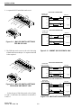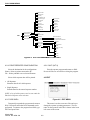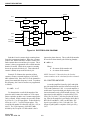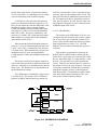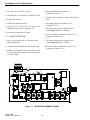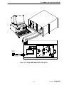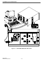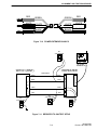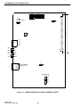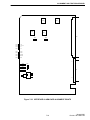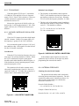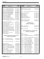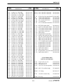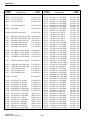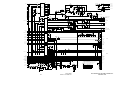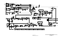
1
SUMMIT QX 2000 SERIES 800 MHz 75W-175W MULTI-NET REPEATER Models: QX-RM82, QX-RM83 Part No.: 242-2008-132/134 Seventh Printing Month 2000 Supersedes: Part No. 001-2008-103, December 1997 Part No. 001-2008-104 ??-00mwp Printed in U.S.A. SUMMIT® QX 800 MHz MULTI-NET® REPEATER PART NO. 242-2008-132/134 Copyright 1994 by the E.F. Johnson Company The E.F. Johnson Company designs and manufactures two-way radio equipment to serve a wide variety of communications needs. Johnson produces equipment for the mobile telephone and land mobile radio services which include business, industrial, government, public safety, and personal users. LAND MOBILE PRODUCT WARRANTY The manufacturer’s warranty statement for this product is available from your product supplier or from the E.F. Johnson Company, 299 Johnson Avenue, Box 1249, Waseca, MN 56093-0514. Phone (507) 835-6222. WARNING This device complies with Part 15 of the FCC rules. Operation is subject to the condition that this device does not cause harmful interference. In addition, changes or modification to this equipment not expressly approved by E. F. Johnson could void the user’s authority to operate this equipment (FCC rules, 47CFR Part 15.19). DO NOT allow the antenna to touch or come in very close proximity with the eyes, face, or any exposed body parts while the radio is transmitting. To comply with FCC RF exposure limits, DO NOT operate the transmitter of a stationary radio (base station or marine radio) when a person is within four (4) meters of the antenna. DO NOT operate the radio in explosive or flammable atmospheres. The transmitted radio energy could trigger blasting caps or cause an explosion. DO NOT operate the radio without the proper antenna installed. DO NOT allow children to operate transmitter equipped radio equipment. NOTE: The above warning list is not intended to include all hazards that may be encountered when using this radio. SAFETY INFORMATION The FCC has adopted a safety standard for human exposure to RF energy. Proper operation of this radio under normal conditions results in user exposure to RF energy below the Occupational Safety and Health Act and Federal Communication Commission limits. The information in this document is subject to change without notice. E.F. Johnson Company will not be liable for any misunderstanding due to misinformation or errors found in this document. LTR, LTR-Net, Multi-Net, Viking Head/EFJohnson Logo, Call Guard and SUMMIT are registered trademarks of E.F. Johnson Company All other company and/or product names used in this manual are trademarks and/or registered trademarks of their respective manufacturer. FCC EXPOSURE LIMITS This fixed station radio transceiver was tested by the manufacturer with an appropriate antenna in order to verify compliance with Maximum Permissible Exposure (MPE) limits set under Section 2.1091 of the FCC Rules and Regulations. The guidelines used in the evaluation are derived from Table 1 (B) titled “Limits For General Population/ Uncontrolled Exposure” which is from FCC report OET bulletin #65. Table 1 (B) FCC Limits for Maximum Permissible Exposure (MPE) (B) Limits For General Population/Uncontrolled Exposure Frequency Range (MHz) Electric Field Strength Magnetic Field Strength (E) (V/m) (H) (A/m) 0.3 - 1.34 614 1.63 1.34 - 30 824/f 2.19/f 30 - 300 27.5 0.073 300 - 1500 --1500 - 100,000 --f = Frequency in MHz*Plane-wave equivalent power density. Power Density (S) (mW/cm2) (100)* (180/f2)* 0.2 f/1500 1.0 Table 2 lists the antennas recommended for use in the VHF frequency range. Each model of this radio was tested with the appropriate antenna listed. The antenna shall be mounted to a tower and be a minimum of 10 meters above the ground at the lowest point on the antenna. The radio manufacturer has determined that the user and service personnel should remain four (4) meters in distance away from the antenna when transmitting. By maintaining this distance, these individuals are not exposed to radio frequency energy or magnetic fields in excess of the guidelines set forth in Table 1 (B). NOTE: Other antennas or installation configurations that have not been tested may not comply with FCC RF exposure limits and therefore are not recommended. Table 2 Recommended Antennas (Antenna Manufacturer - Decibel Products) Frequency Antenna Model No. 132-144 MHz 144-178 MHz DB205E DB205F TABLE OF CONTENTS 1 INTRODUCTION AND OPERATION 1.1 1.2 1.3 1.4 1.5 1.6 1.7 1.8 1.9 1.10 1.11 1.12 1.13 SCOPE OF MANUAL . . . . . . . . . . . . . . . . . . . . . . . . . . . . . . . . . . . . . . . . . . . . . . . . . . . . . . . . . . . . . . . . . . . . . . . 1-1 REPEATER IDENTIFICATION . . . . . . . . . . . . . . . . . . . . . . . . . . . . . . . . . . . . . . . . . . . . . . . . . . . . . . . . . . . . . . 1-1 MODEL NUMBER BREAKDOWN . . . . . . . . . . . . . . . . . . . . . . . . . . . . . . . . . . . . . . . . . . . . . . . . . . . . . . . . . . . 1-1 REPEATER DESCRIPTION . . . . . . . . . . . . . . . . . . . . . . . . . . . . . . . . . . . . . . . . . . . . . . . . . . . . . . . . . . . . . . . . . 1-1 MULTI-NET SIGNALING . . . . . . . . . . . . . . . . . . . . . . . . . . . . . . . . . . . . . . . . . . . . . . . . . . . . . . . . . . . . . . . . . . . 1-1 ACCESSORIES . . . . . . . . . . . . . . . . . . . . . . . . . . . . . . . . . . . . . . . . . . . . . . . . . . . . . . . . . . . . . . . . . . . . . . . . . . . . 1-2 WARRANTY . . . . . . . . . . . . . . . . . . . . . . . . . . . . . . . . . . . . . . . . . . . . . . . . . . . . . . . . . . . . . . . . . . . . . . . . . . . . . . 1-3 FACTORY CUSTOMER SERVICE . . . . . . . . . . . . . . . . . . . . . . . . . . . . . . . . . . . . . . . . . . . . . . . . . . . . . . . . . . . 1-3 FACTORY RETURNS . . . . . . . . . . . . . . . . . . . . . . . . . . . . . . . . . . . . . . . . . . . . . . . . . . . . . . . . . . . . . . . . . . . . . . 1-3 REPLACEMENT PARTS . . . . . . . . . . . . . . . . . . . . . . . . . . . . . . . . . . . . . . . . . . . . . . . . . . . . . . . . . . . . . . . . . . . . 1-4 INTERNET HOME PAGE . . . . . . . . . . . . . . . . . . . . . . . . . . . . . . . . . . . . . . . . . . . . . . . . . . . . . . . . . . . . . . . . . . . 1-4 SOFTWARE UPDATES/REVISIONS . . . . . . . . . . . . . . . . . . . . . . . . . . . . . . . . . . . . . . . . . . . . . . . . . . . . . . . . . 1-4 AREPEATER OPERATION . . . . . . . . . . . . . . . . . . . . . . . . . . . . . . . . . . . . . . . . . . . . . . . . . . . . . . . . . . . . . . . . . 1-4 MAIN PROCESSOR CARD (MPC) . . . . . . . . . . . . . . . . . . . . . . . . . . . . . . . . . . . . . . . . . . . . . . . . . . . . . . . . . . . . . 1-4 MULTI-NET AUDIO CARD (MAC) . . . . . . . . . . . . . . . . . . . . . . . . . . . . . . . . . . . . . . . . . . . . . . . . . . . . . . . . . . . . 1-6 INTERFACE ALARM CARD (IAC) . . . . . . . . . . . . . . . . . . . . . . . . . . . . . . . . . . . . . . . . . . . . . . . . . . . . . . . . . . . . 1-6 POWER SUPPLY . . . . . . . . . . . . . . . . . . . . . . . . . . . . . . . . . . . . . . . . . . . . . . . . . . . . . . . . . . . . . . . . . . . . . . . . . . . 1-7 MULTI-NET SYSTEM COMPONENTS . . . . . . . . . . . . . . . . . . . . . . . . . . . . . . . . . . . . . . . . . . . . . . . . . . . . . . . 1-7 INTRODUCTION . . . . . . . . . . . . . . . . . . . . . . . . . . . . . . . . . . . . . . . . . . . . . . . . . . . . . . . . . . . . . . . . . . . . . . . . . . . 1-7 MOBILE TRANSCEIVERS . . . . . . . . . . . . . . . . . . . . . . . . . . . . . . . . . . . . . . . . . . . . . . . . . . . . . . . . . . . . . . . . . . . 1-7 REPEATERS . . . . . . . . . . . . . . . . . . . . . . . . . . . . . . . . . . . . . . . . . . . . . . . . . . . . . . . . . . . . . . . . . . . . . . . . . . . . . . . 1-7 3000 SERIES SWITCH . . . . . . . . . . . . . . . . . . . . . . . . . . . . . . . . . . . . . . . . . . . . . . . . . . . . . . . . . . . . . . . . . . . . . . . 1-9 DISPATCH CONSOLES . . . . . . . . . . . . . . . . . . . . . . . . . . . . . . . . . . . . . . . . . . . . . . . . . . . . . . . . . . . . . . . . . . . . . . 1-9 PUBLIC SERVICE TELEPHONE NETWORK (PSTN) . . . . . . . . . . . . . . . . . . . . . . . . . . . . . . . . . . . . . . . . . . . . . 1-9 MULTI-NET OPERATION . . . . . . . . . . . . . . . . . . . . . . . . . . . . . . . . . . . . . . . . . . . . . . . . . . . . . . . . . . . . . . . . . . 1-9 HOME AND STATUS REPEATERS . . . . . . . . . . . . . . . . . . . . . . . . . . . . . . . . . . . . . . . . . . . . . . . . . . . . . . . . . . . . 1-9 MOBILE-REPEATER DATA SIGNALING . . . . . . . . . . . . . . . . . . . . . . . . . . . . . . . . . . . . . . . . . . . . . . . . . . . . . . 1-9 REPEATER DATA BUS SIGNALING . . . . . . . . . . . . . . . . . . . . . . . . . . . . . . . . . . . . . . . . . . . . . . . . . . . . . . . . . 1-10 HOME CHANNEL BACKUP . . . . . . . . . . . . . . . . . . . . . . . . . . . . . . . . . . . . . . . . . . . . . . . . . . . . . . . . . . . . . . . . . 1-10 MULTI-NET FEATURES. . . . . . . . . . . . . . . . . . . . . . . . . . . . . . . . . . . . . . . . . . . . . . . . . . . . . . . . . . . . . . . . . . . 1-11 STANDARD AND SPECIAL CALLS . . . . . . . . . . . . . . . . . . . . . . . . . . . . . . . . . . . . . . . . . . . . . . . . . . . . . . . . . . 1-11 UNIQUE ID CODES . . . . . . . . . . . . . . . . . . . . . . . . . . . . . . . . . . . . . . . . . . . . . . . . . . . . . . . . . . . . . . . . . . . . . . . . 1-12 ACCESS AND RECEIVE PRIORITY . . . . . . . . . . . . . . . . . . . . . . . . . . . . . . . . . . . . . . . . . . . . . . . . . . . . . . . . . . 1-12 ALL CALL . . . . . . . . . . . . . . . . . . . . . . . . . . . . . . . . . . . . . . . . . . . . . . . . . . . . . . . . . . . . . . . . . . . . . . . . . . . . . . . . 1-12 INTERROGATE . . . . . . . . . . . . . . . . . . . . . . . . . . . . . . . . . . . . . . . . . . . . . . . . . . . . . . . . . . . . . . . . . . . . . . . . . . . 1-12 MOBILE DISABLE . . . . . . . . . . . . . . . . . . . . . . . . . . . . . . . . . . . . . . . . . . . . . . . . . . . . . . . . . . . . . . . . . . . . . . . . . 1-13 DYNAMIC REPROGRAMMING OF GROUP 11 1-13 DYNAMIC MOVE TO NEW SYSTEM/GROUP . . . . . . . . . . . . . . . . . . . . . . . . . . . . . . . . . . . . . . . . . . . . . . . . . 1-13 ID VALIDATION . . . . . . . . . . . . . . . . . . . . . . . . . . . . . . . . . . . . . . . . . . . . . . . . . . . . . . . . . . . . . . . . . . . . . . . . . . 1-13 INTERCONNECT CALLS . . . . . . . . . . . . . . . . . . . . . . . . . . . . . . . . . . . . . . . . . . . . . . . . . . . . . . . . . . . . . . . . . . . 1-13 SYSTEM KEY . . . . . . . . . . . . . . . . . . . . . . . . . . . . . . . . . . . . . . . . . . . . . . . . . . . . . . . . . . . . . . . . . . . . . . . . . . . . . 1-13 DYNAMIC CHANNEL ASSIGNMENT . . . . . . . . . . . . . . . . . . . . . . . . . . . . . . . . . . . . . . . . . . . . . . . . . . . . . . . . 1-13 EMERGENCY CALLS . . . . . . . . . . . . . . . . . . . . . . . . . . . . . . . . . . . . . . . . . . . . . . . . . . . . . . . . . . . . . . . . . . . . . . 1-13 VOTER SYSTEM . . . . . . . . . . . . . . . . . . . . . . . . . . . . . . . . . . . . . . . . . . . . . . . . . . . . . . . . . . . . . . . . . . . . . . . . . . 1-14 1.14 1.15 1.16 1 INSTALLATION 1.1 INTRODUCTION . . . . . . . . . . . . . . . . . . . . . . . . . . . . . . . . . . . . . . . . . . . . . . . . . . . . . . . . . . . . . . . . . . . . . . . . . . 2-1 SITE PREPARATION AND ANTENNA INSTALLATION . . . . . . . . . . . . . . . . . . . . . . . . . . . . . . . . . . . . . . . . . . 2-1 ENVIRONMENT . . . . . . . . . . . . . . . . . . . . . . . . . . . . . . . . . . . . . . . . . . . . . . . . . . . . . . . . . . . . . . . . . . . . . . . . . . . 2-1 1.2 1 TABLE OF CONTENTS (CONT.) 1.3 1.4 1.5 1.6 1.7 1.8 1.9 1.10 1.11 VENTILATION . . . . . . . . . . . . . . . . . . . . . . . . . . . . . . . . . . . . . . . . . . . . . . . . . . . . . . . . . . . . . . . . . . . . . . . . . . . . 2-1 AC POWER. . . . . . . . . . . . . . . . . . . . . . . . . . . . . . . . . . . . . . . . . . . . . . . . . . . . . . . . . . . . . . . . . . . . . . . . . . . . . . . . 2-2 BATTERY BACKUP . . . . . . . . . . . . . . . . . . . . . . . . . . . . . . . . . . . . . . . . . . . . . . . . . . . . . . . . . . . . . . . . . . . . . . . . 2-2 800W POWER SUPPLY . . . . . . . . . . . . . . . . . . . . . . . . . . . . . . . . . . . . . . . . . . . . . . . . . . . . . . . . . . . . . . . . . . . . . 2-2 AC INPUT REQUIREMENTS . . . . . . . . . . . . . . . . . . . . . . . . . . . . . . . . . . . . . . . . . . . . . . . . . . . . . . . . . . . . . . . . 2-3 GROUNDING . . . . . . . . . . . . . . . . . . . . . . . . . . . . . . . . . . . . . . . . . . . . . . . . . . . . . . . . . . . . . . . . . . . . . . . . . . . . . . 2-3 RF GROUNDING . . . . . . . . . . . . . . . . . . . . . . . . . . . . . . . . . . . . . . . . . . . . . . . . . . . . . . . . . . . . . . . . . . . . . . . . . . 2-4 TELEPHONE LINE GROUNDING . . . . . . . . . . . . . . . . . . . . . . . . . . . . . . . . . . . . . . . . . . . . . . . . . . . . . . . . . . . . 2-4 PROTECTION GUIDELINES. . . . . . . . . . . . . . . . . . . . . . . . . . . . . . . . . . . . . . . . . . . . . . . . . . . . . . . . . . . . . . . . . 2-4 UNPACKING AND INSPECTION . . . . . . . . . . . . . . . . . . . . . . . . . . . . . . . . . . . . . . . . . . . . . . . . . . . . . . . . . . . . 2-5 REPEATER DATA BUS INSTALLATION . . . . . . . . . . . . . . . . . . . . . . . . . . . . . . . . . . . . . . . . . . . . . . . . . . . . . 2-6 MPC DATA BUS SWITCH SETTINGS . . . . . . . . . . . . . . . . . . . . . . . . . . . . . . . . . . . . . . . . . . . . . . . . . . . . . . . . . 2-6 MPC DATA BUS JUMPERS SETTINGS. . . . . . . . . . . . . . . . . . . . . . . . . . . . . . . . . . . . . . . . . . . . . . . . . . . . . . . . 2-6 CONNECTING RECEIVE AND TRANSMIT ANTENNAS. . . . . . . . . . . . . . . . . . . . . . . . . . . . . . . . . . . . . . . . 2-7 CONNECTING AUDIO/DATA LINK TO SWITCH. . . . . . . . . . . . . . . . . . . . . . . . . . . . . . . . . . . . . . . . . . . . . . 2-7 VOICE LINK . . . . . . . . . . . . . . . . . . . . . . . . . . . . . . . . . . . . . . . . . . . . . . . . . . . . . . . . . . . . . . . . . . . . . . . . . . . . . . 2-7 DATA LINK. . . . . . . . . . . . . . . . . . . . . . . . . . . . . . . . . . . . . . . . . . . . . . . . . . . . . . . . . . . . . . . . . . . . . . . . . . . . . . . 2-7 3 SOFTWARE 3.1 3.4 3.5 INTRODUCTION. . . . . . . . . . . . . . . . . . . . . . . . . . . . . . . . . . . . . . . . . . . . . . . . . . . . . . . . . . . . . . . . . . . . . . . . . . . 3-1 HOW TO USE THIS MANUAL . . . . . . . . . . . . . . . . . . . . . . . . . . . . . . . . . . . . . . . . . . . . . . . . . . . . . . . . . . . . . . . 3-1 GETTING STARTED . . . . . . . . . . . . . . . . . . . . . . . . . . . . . . . . . . . . . . . . . . . . . . . . . . . . . . . . . . . . . . . . . . . . . . . 3-1 COMPUTER DESCRIPTION . . . . . . . . . . . . . . . . . . . . . . . . . . . . . . . . . . . . . . . . . . . . . . . . . . . . . . . . . . . . . . . . . 3-1 EEPROM DATA STORAGE. . . . . . . . . . . . . . . . . . . . . . . . . . . . . . . . . . . . . . . . . . . . . . . . . . . . . . . . . . . . . . . . . . 3-1 COMMAND LINE OPTIONS . . . . . . . . . . . . . . . . . . . . . . . . . . . . . . . . . . . . . . . . . . . . . . . . . . . . . . . . . . . . . . . . . 3-2 COLOR OR MONOCHROME OPERATION . . . . . . . . . . . . . . . . . . . . . . . . . . . . . . . . . . . . . . . . . . . . . . . . . . . . 3-2 REPEATER PROGRAM SOFTWARE. . . . . . . . . . . . . . . . . . . . . . . . . . . . . . . . . . . . . . . . . . . . . . . . . . . . . . . . . 3-2 INSTALLING THE SOFTWARE . . . . . . . . . . . . . . . . . . . . . . . . . . . . . . . . . . . . . . . . . . . . . . . . . . . . . . . . . . . . . . 3-2 MINIMUM FREE MEMORY REQUIRED . . . . . . . . . . . . . . . . . . . . . . . . . . . . . . . . . . . . . . . . . . . . . . . . . . . . . . 3-3 REPEATER PROGRAMMER . . . . . . . . . . . . . . . . . . . . . . . . . . . . . . . . . . . . . . . . . . . . . . . . . . . . . . . . . . . . . . . . 3-3 PROGRAM FILES . . . . . . . . . . . . . . . . . . . . . . . . . . . . . . . . . . . . . . . . . . . . . . . . . . . . . . . . . . . . . . . . . . . . . . . . . . 3-3 ALIGNMENT SOFTWARE . . . . . . . . . . . . . . . . . . . . . . . . . . . . . . . . . . . . . . . . . . . . . . . . . . . . . . . . . . . . . . . . . . 3-3 HELP F1 . . . . . . . . . . . . . . . . . . . . . . . . . . . . . . . . . . . . . . . . . . . . . . . . . . . . . . . . . . . . . . . . . . . . . . . . . . . . . . . . . . 3-4 4 PULL DOWN MENUS 4.1 4.2 MENU DISPLAYS . . . . . . . . . . . . . . . . . . . . . . . . . . . . . . . . . . . . . . . . . . . . . . . . . . . . . . . . . . . . . . . . . . . . . . . . . . 4-1 FILE MENU . . . . . . . . . . . . . . . . . . . . . . . . . . . . . . . . . . . . . . . . . . . . . . . . . . . . . . . . . . . . . . . . . . . . . . . . . . . . . . . 4-1 LOAD . . . . . . . . . . . . . . . . . . . . . . . . . . . . . . . . . . . . . . . . . . . . . . . . . . . . . . . . . . . . . . . . . . . . . . . . . . . . . . . . . . . . 4-1 SAVE . . . . . . . . . . . . . . . . . . . . . . . . . . . . . . . . . . . . . . . . . . . . . . . . . . . . . . . . . . . . . . . . . . . . . . . . . . . . . . . . . . . . 4-1 SAVE AS . . . . . . . . . . . . . . . . . . . . . . . . . . . . . . . . . . . . . . . . . . . . . . . . . . . . . . . . . . . . . . . . . . . . . . . . . . . . . . . . . 4-1 PRINT REPEATER CONFIGURATION . . . . . . . . . . . . . . . . . . . . . . . . . . . . . . . . . . . . . . . . . . . . . . . . . . . . . . . . 4-2 DOS SHELL . . . . . . . . . . . . . . . . . . . . . . . . . . . . . . . . . . . . . . . . . . . . . . . . . . . . . . . . . . . . . . . . . . . . . . . . . . . . . . . 4-2 QUIT (ALT X) . . . . . . . . . . . . . . . . . . . . . . . . . . . . . . . . . . . . . . . . . . . . . . . . . . . . . . . . . . . . . . . . . . . . . . . . . . . . . 4-2 EDIT. . . . . . . . . . . . . . . . . . . . . . . . . . . . . . . . . . . . . . . . . . . . . . . . . . . . . . . . . . . . . . . . . . . . . . . . . . . . . . . . . . . . . . 4-2 SETUP PARAMETERS. . . . . . . . . . . . . . . . . . . . . . . . . . . . . . . . . . . . . . . . . . . . . . . . . . . . . . . . . . . . . . . . . . . . . . 4-3 SELECT REPEATER. . . . . . . . . . . . . . . . . . . . . . . . . . . . . . . . . . . . . . . . . . . . . . . . . . . . . . . . . . . . . . . . . . . . . . . . 4-5 ALARM CONFIGURATION . . . . . . . . . . . . . . . . . . . . . . . . . . . . . . . . . . . . . . . . . . . . . . . . . . . . . . . . . . . . . . . . . 4-5 REPEATER TYPE SELECTION. . . . . . . . . . . . . . . . . . . . . . . . . . . . . . . . . . . . . . . . . . . . . . . . . . . . . . . . . . . . . . . 4-6 DELETE REPEATER . . . . . . . . . . . . . . . . . . . . . . . . . . . . . . . . . . . . . . . . . . . . . . . . . . . . . . . . . . . . . . . . . . . . . . . 4-6 TRANSFER . . . . . . . . . . . . . . . . . . . . . . . . . . . . . . . . . . . . . . . . . . . . . . . . . . . . . . . . . . . . . . . . . . . . . . . . . . . . . . . . 4-7 WRITE SETUP PARAMETERS . . . . . . . . . . . . . . . . . . . . . . . . . . . . . . . . . . . . . . . . . . . . . . . . . . . . . . . . . . . . . . . 4-7 READ SETUP PARAMETERS . . . . . . . . . . . . . . . . . . . . . . . . . . . . . . . . . . . . . . . . . . . . . . . . . . . . . . . . . . . . . . . . 4-7 3.2 3.3 4.3 4.4 2 TABLE OF CONTENTS (CONT.) 4.5 4.6 4.7 HARDWARE . . . . . . . . . . . . . . . . . . . . . . . . . . . . . . . . . . . . . . . . . . . . . . . . . . . . . . . . . . . . . . . . . . . . . . . . . . . . . . 4-8 HSDB MONITOR . . . . . . . . . . . . . . . . . . . . . . . . . . . . . . . . . . . . . . . . . . . . . . . . . . . . . . . . . . . . . . . . . . . . . . . . . . . 4-8 RECEIVE/TRANSMIT DATA . . . . . . . . . . . . . . . . . . . . . . . . . . . . . . . . . . . . . . . . . . . . . . . . . . . . . . . . . . . . . . . . . 4-8 RF DATA . . . . . . . . . . . . . . . . . . . . . . . . . . . . . . . . . . . . . . . . . . . . . . . . . . . . . . . . . . . . . . . . . . . . . . . . . . . . . . . . . . 4-8 INPUT MONITOR. . . . . . . . . . . . . . . . . . . . . . . . . . . . . . . . . . . . . . . . . . . . . . . . . . . . . . . . . . . . . . . . . . . . . . . . . . . 4-9 REVISION/VERSION . . . . . . . . . . . . . . . . . . . . . . . . . . . . . . . . . . . . . . . . . . . . . . . . . . . . . . . . . . . . . . . . . . . . . . . . 4-9 MODE SELECT. . . . . . . . . . . . . . . . . . . . . . . . . . . . . . . . . . . . . . . . . . . . . . . . . . . . . . . . . . . . . . . . . . . . . . . . . . . . . 4-9 TEST . . . . . . . . . . . . . . . . . . . . . . . . . . . . . . . . . . . . . . . . . . . . . . . . . . . . . . . . . . . . . . . . . . . . . . . . . . . . . . . . . . . . . 4-9 POWER AMPLIFIER . . . . . . . . . . . . . . . . . . . . . . . . . . . . . . . . . . . . . . . . . . . . . . . . . . . . . . . . . . . . . . . . . . . . . . . 4-11 RECEIVER. . . . . . . . . . . . . . . . . . . . . . . . . . . . . . . . . . . . . . . . . . . . . . . . . . . . . . . . . . . . . . . . . . . . . . . . . . . . . . . . 4-11 EXCITER . . . . . . . . . . . . . . . . . . . . . . . . . . . . . . . . . . . . . . . . . . . . . . . . . . . . . . . . . . . . . . . . . . . . . . . . . . . . . . . . . 4-11 FULL REPEATER . . . . . . . . . . . . . . . . . . . . . . . . . . . . . . . . . . . . . . . . . . . . . . . . . . . . . . . . . . . . . . . . . . . . . . . . . . 4-11 SWITCH INTERFACE . . . . . . . . . . . . . . . . . . . . . . . . . . . . . . . . . . . . . . . . . . . . . . . . . . . . . . . . . . . . . . . . . . . . . . 4-11 UTILITIES . . . . . . . . . . . . . . . . . . . . . . . . . . . . . . . . . . . . . . . . . . . . . . . . . . . . . . . . . . . . . . . . . . . . . . . . . . . . . . . 4-11 COM PORT . . . . . . . . . . . . . . . . . . . . . . . . . . . . . . . . . . . . . . . . . . . . . . . . . . . . . . . . . . . . . . . . . . . . . . . . . . . . . . . 4-11 DISPLAY MODE . . . . . . . . . . . . . . . . . . . . . . . . . . . . . . . . . . . . . . . . . . . . . . . . . . . . . . . . . . . . . . . . . . . . . . . . . . 4-12 ALARM DISPLAY . . . . . . . . . . . . . . . . . . . . . . . . . . . . . . . . . . . . . . . . . . . . . . . . . . . . . . . . . . . . . . . . . . . . . . . . . 4-12 USER LEVEL . . . . . . . . . . . . . . . . . . . . . . . . . . . . . . . . . . . . . . . . . . . . . . . . . . . . . . . . . . . . . . . . . . . . . . . . . . . . . 4-12 5 REPEATER PROGRAMMING 5.1 5.2 CREATING A NEW FILE . . . . . . . . . . . . . . . . . . . . . . . . . . . . . . . . . . . . . . . . . . . . . . . . . . . . . . . . . . . . . . . . . . . 5-1 SELECT REPEATER TO EDIT . . . . . . . . . . . . . . . . . . . . . . . . . . . . . . . . . . . . . . . . . . . . . . . . . . . . . . . . . . . . . . . . 5-1 ADDING A REPEATER TO A FILE . . . . . . . . . . . . . . . . . . . . . . . . . . . . . . . . . . . . . . . . . . . . . . . . . . . . . . . . . . 5-1 6 CIRCUIT DESCRIPTION 6.1 RECEIVER . . . . . . . . . . . . . . . . . . . . . . . . . . . . . . . . . . . . . . . . . . . . . . . . . . . . . . . . . . . . . . . . . . . . . . . . . . . . . . . . INTRODUCTION . . . . . . . . . . . . . . . . . . . . . . . . . . . . . . . . . . . . . . . . . . . . . . . . . . . . . . . . . . . . . . . . . . . . . . . . . . . REGULATED VOLTAGE SUPPLIES . . . . . . . . . . . . . . . . . . . . . . . . . . . . . . . . . . . . . . . . . . . . . . . . . . . . . . . . . . . HELICAL FILTER, RF AMPLIFIER . . . . . . . . . . . . . . . . . . . . . . . . . . . . . . . . . . . . . . . . . . . . . . . . . . . . . . . . . . . . FIRST MIXER, CRYSTAL FILTER. . . . . . . . . . . . . . . . . . . . . . . . . . . . . . . . . . . . . . . . . . . . . . . . . . . . . . . . . . . . . IF AMPLIFIER, CRYSTAL FILTER . . . . . . . . . . . . . . . . . . . . . . . . . . . . . . . . . . . . . . . . . . . . . . . . . . . . . . . . . . . . SECOND MIXER/DETECTOR . . . . . . . . . . . . . . . . . . . . . . . . . . . . . . . . . . . . . . . . . . . . . . . . . . . . . . . . . . . . . . . . WIDEBAND AUDIO AMPLIFIER . . . . . . . . . . . . . . . . . . . . . . . . . . . . . . . . . . . . . . . . . . . . . . . . . . . . . . . . . . . . . RSSI AMPLIFIER . . . . . . . . . . . . . . . . . . . . . . . . . . . . . . . . . . . . . . . . . . . . . . . . . . . . . . . . . . . . . . . . . . . . . . . . . . . VCO . . . . . . . . . . . . . . . . . . . . . . . . . . . . . . . . . . . . . . . . . . . . . . . . . . . . . . . . . . . . . . . . . . . . . . . . . . . . . . . . . . . . . . ACTIVE FILTER . . . . . . . . . . . . . . . . . . . . . . . . . . . . . . . . . . . . . . . . . . . . . . . . . . . . . . . . . . . . . . . . . . . . . . . . . . . . BUFFER . . . . . . . . . . . . . . . . . . . . . . . . . . . . . . . . . . . . . . . . . . . . . . . . . . . . . . . . . . . . . . . . . . . . . . . . . . . . . . . . . . . SYNTHESIZER . . . . . . . . . . . . . . . . . . . . . . . . . . . . . . . . . . . . . . . . . . . . . . . . . . . . . . . . . . . . . . . . . . . . . . . . . . . . . BUFFER AMPLIFIER . . . . . . . . . . . . . . . . . . . . . . . . . . . . . . . . . . . . . . . . . . . . . . . . . . . . . . . . . . . . . . . . . . . . . . . . LOCK DETECT . . . . . . . . . . . . . . . . . . . . . . . . . . . . . . . . . . . . . . . . . . . . . . . . . . . . . . . . . . . . . . . . . . . . . . . . . . . . . BUFFER AMPLIFIER . . . . . . . . . . . . . . . . . . . . . . . . . . . . . . . . . . . . . . . . . . . . . . . . . . . . . . . . . . . . . . . . . . . . . . . . RF AMPLIFIERS . . . . . . . . . . . . . . . . . . . . . . . . . . . . . . . . . . . . . . . . . . . . . . . . . . . . . . . . . . . . . . . . . . . . . . . . . . . . EXCITER . . . . . . . . . . . . . . . . . . . . . . . . . . . . . . . . . . . . . . . . . . . . . . . . . . . . . . . . . . . . . . . . . . . . . . . . . . . . . . . . . VCO (A007) . . . . . . . . . . . . . . . . . . . . . . . . . . . . . . . . . . . . . . . . . . . . . . . . . . . . . . . . . . . . . . . . . . . . . . . . . . . . . . . . VCO AND TCXO FREQUENCY MODULATION . . . . . . . . . . . . . . . . . . . . . . . . . . . . . . . . . . . . . . . . . . . . . . . . . ACTIVE FILTER . . . . . . . . . . . . . . . . . . . . . . . . . . . . . . . . . . . . . . . . . . . . . . . . . . . . . . . . . . . . . . . . . . . . . . . . . . . . BUFFER . . . . . . . . . . . . . . . . . . . . . . . . . . . . . . . . . . . . . . . . . . . . . . . . . . . . . . . . . . . . . . . . . . . . . . . . . . . . . . . . . . . SYNTHESIZER . . . . . . . . . . . . . . . . . . . . . . . . . . . . . . . . . . . . . . . . . . . . . . . . . . . . . . . . . . . . . . . . . . . . . . . . . . . . . BUFFER AMPLIFIER . . . . . . . . . . . . . . . . . . . . . . . . . . . . . . . . . . . . . . . . . . . . . . . . . . . . . . . . . . . . . . . . . . . . . . . . BUFFER AMPLIFIER . . . . . . . . . . . . . . . . . . . . . . . . . . . . . . . . . . . . . . . . . . . . . . . . . . . . . . . . . . . . . . . . . . . . . . . . LOCK DETECT . . . . . . . . . . . . . . . . . . . . . . . . . . . . . . . . . . . . . . . . . . . . . . . . . . . . . . . . . . . . . . . . . . . . . . . . . . . . . BUFFER AMPLIFIER . . . . . . . . . . . . . . . . . . . . . . . . . . . . . . . . . . . . . . . . . . . . . . . . . . . . . . . . . . . . . . . . . . . . . . . . RF AMPLIFIERS . . . . . . . . . . . . . . . . . . . . . . . . . . . . . . . . . . . . . . . . . . . . . . . . . . . . . . . . . . . . . . . . . . . . . . . . . . . . 6.2 3 6-1 6-1 6-1 6-1 6-1 6-1 6-2 6-3 6-3 6-3 6-3 6-3 6-3 6-5 6-5 6-5 6-5 6-6 6-6 6-6 6-6 6-7 6-7 6-8 6-9 6-9 6-9 6-9 TABLE OF CONTENTS (CONT.) 6.3 6.4 6.5 6.6 6.7 6.8 6.9 6.10 6.11 75W POWER AMPLIFIER. . . . . . . . . . . . . . . . . . . . . . . . . . . . . . . . . . . . . . . . . . . . . . . . . . . . . . . . . . . . . . . . . . . 6-9 AMPLIFIER/PREDRIVER . . . . . . . . . . . . . . . . . . . . . . . . . . . . . . . . . . . . . . . . . . . . . . . . . . . . . . . . . . . . . . . . . . . 6-9 DRIVER . . . . . . . . . . . . . . . . . . . . . . . . . . . . . . . . . . . . . . . . . . . . . . . . . . . . . . . . . . . . . . . . . . . . . . . . . . . . . . . . . . 6-9 FINAL AMPLIFIERS . . . . . . . . . . . . . . . . . . . . . . . . . . . . . . . . . . . . . . . . . . . . . . . . . . . . . . . . . . . . . . . . . . . . . . . 6-9 POWER DETECTORS . . . . . . . . . . . . . . . . . . . . . . . . . . . . . . . . . . . . . . . . . . . . . . . . . . . . . . . . . . . . . . . . . . . . . 6-10 THERMAL SENSOR . . . . . . . . . . . . . . . . . . . . . . . . . . . . . . . . . . . . . . . . . . . . . . . . . . . . . . . . . . . . . . . . . . . . . . . 6-10 FORWARD/REVERSE POWER DETECT, CIRCULATOR, LOW-PASS FILTER . . . . . . . . . . . . . . . . . . . . . 6-10 175W POWER AMPLIFIER. . . . . . . . . . . . . . . . . . . . . . . . . . . . . . . . . . . . . . . . . . . . . . . . . . . . . . . . . . . . . . . . . 6-11 GAIN BLOCK . . . . . . . . . . . . . . . . . . . . . . . . . . . . . . . . . . . . . . . . . . . . . . . . . . . . . . . . . . . . . . . . . . . . . . . . . . . . 6-11 DRIVER . . . . . . . . . . . . . . . . . . . . . . . . . . . . . . . . . . . . . . . . . . . . . . . . . . . . . . . . . . . . . . . . . . . . . . . . . . . . . . . . . 6-11 FINAL AMPLIFIERS . . . . . . . . . . . . . . . . . . . . . . . . . . . . . . . . . . . . . . . . . . . . . . . . . . . . . . . . . . . . . . . . . . . . . . 6-11 POWER DETECTORS . . . . . . . . . . . . . . . . . . . . . . . . . . . . . . . . . . . . . . . . . . . . . . . . . . . . . . . . . . . . . . . . . . . . . 6-11 THERMAL SENSOR . . . . . . . . . . . . . . . . . . . . . . . . . . . . . . . . . . . . . . . . . . . . . . . . . . . . . . . . . . . . . . . . . . . . . . . 6-11 FORWARD/REVERSE POWER DETECT, CIRCULATOR, LOW-PASS FILTER . . . . . . . . . . . . . . . . . . . . . 6-11 RF INTERFACE BOARD . . . . . . . . . . . . . . . . . . . . . . . . . . . . . . . . . . . . . . . . . . . . . . . . . . . . . . . . . . . . . . . . . . . 6-12 POWER CONNECTOR . . . . . . . . . . . . . . . . . . . . . . . . . . . . . . . . . . . . . . . . . . . . . . . . . . . . . . . . . . . . . . . . . . . . . 6-12 SIGNAL CONNECTOR (J101) . . . . . . . . . . . . . . . . . . . . . . . . . . . . . . . . . . . . . . . . . . . . . . . . . . . . . . . . . . . . . . . 6-12 FAN CONNECTOR (J104) . . . . . . . . . . . . . . . . . . . . . . . . . . . . . . . . . . . . . . . . . . . . . . . . . . . . . . . . . . . . . . . . . . 6-14 POWER AMPLIFIER CONNECTIONS . . . . . . . . . . . . . . . . . . . . . . . . . . . . . . . . . . . . . . . . . . . . . . . . . . . . . . . . 6-15 EXCITER CONNECTOR (J102) . . . . . . . . . . . . . . . . . . . . . . . . . . . . . . . . . . . . . . . . . . . . . . . . . . . . . . . . . . . . . . 6-16 RECEIVER CONNECTOR (J103) . . . . . . . . . . . . . . . . . . . . . . . . . . . . . . . . . . . . . . . . . . . . . . . . . . . . . . . . . . . . 6-17 800W POWER SUPPLY . . . . . . . . . . . . . . . . . . . . . . . . . . . . . . . . . . . . . . . . . . . . . . . . . . . . . . . . . . . . . . . . . . . . 6-19 FILTER BOARD . . . . . . . . . . . . . . . . . . . . . . . . . . . . . . . . . . . . . . . . . . . . . . . . . . . . . . . . . . . . . . . . . . . . . . . . . . 6-19 POWER FACTOR CORRECTION . . . . . . . . . . . . . . . . . . . . . . . . . . . . . . . . . . . . . . . . . . . . . . . . . . . . . . . . . . . . 6-19 MAIN PULSE WIDTH MODULATOR . . . . . . . . . . . . . . . . . . . . . . . . . . . . . . . . . . . . . . . . . . . . . . . . . . . . . . . . 6-19 SYNCHRONIZING CIRCUITS . . . . . . . . . . . . . . . . . . . . . . . . . . . . . . . . . . . . . . . . . . . . . . . . . . . . . . . . . . . . . . 6-21 FAN AND THERMAL SHUTDOWN. . . . . . . . . . . . . . . . . . . . . . . . . . . . . . . . . . . . . . . . . . . . . . . . . . . . . . . . . . 6-21 +15V CONVERTER . . . . . . . . . . . . . . . . . . . . . . . . . . . . . . . . . . . . . . . . . . . . . . . . . . . . . . . . . . . . . . . . . . . . . . . 6-21 +5V CONVERTER . . . . . . . . . . . . . . . . . . . . . . . . . . . . . . . . . . . . . . . . . . . . . . . . . . . . . . . . . . . . . . . . . . . . . . . . 6-22 -5V CONVERTER . . . . . . . . . . . . . . . . . . . . . . . . . . . . . . . . . . . . . . . . . . . . . . . . . . . . . . . . . . . . . . . . . . . . . . . . . 6-22 POWER SUPPLY REPAIR AND ALIGNMENT . . . . . . . . . . . . . . . . . . . . . . . . . . . . . . . . . . . . . . . . . . . . . . . . . 6-22 BATTERY BACK-UP MODULE . . . . . . . . . . . . . . . . . . . . . . . . . . . . . . . . . . . . . . . . . . . . . . . . . . . . . . . . . . . . . 6-23 OPERATION . . . . . . . . . . . . . . . . . . . . . . . . . . . . . . . . . . . . . . . . . . . . . . . . . . . . . . . . . . . . . . . . . . . . . . . . . . . . . 6-23 CHARGER . . . . . . . . . . . . . . . . . . . . . . . . . . . . . . . . . . . . . . . . . . . . . . . . . . . . . . . . . . . . . . . . . . . . . . . . . . . . . . . 6-23 REVERSE BATTERY PROTECTION . . . . . . . . . . . . . . . . . . . . . . . . . . . . . . . . . . . . . . . . . . . . . . . . . . . . . . . . . 6-24 ENGAGING THE RELAY . . . . . . . . . . . . . . . . . . . . . . . . . . . . . . . . . . . . . . . . . . . . . . . . . . . . . . . . . . . . . . . . . . 6-24 OVER/UNDERVOLTAGE SHUTDOWN . . . . . . . . . . . . . . . . . . . . . . . . . . . . . . . . . . . . . . . . . . . . . . . . . . . . . . 6-24 BBM FAN CONTROL. . . . . . . . . . . . . . . . . . . . . . . . . . . . . . . . . . . . . . . . . . . . . . . . . . . . . . . . . . . . . . . . . . . . . . 6-25 CARD RACK . . . . . . . . . . . . . . . . . . . . . . . . . . . . . . . . . . . . . . . . . . . . . . . . . . . . . . . . . . . . . . . . . . . . . . . . . . . . . 6-25 EXTERNAL CONNECTOR BOARD . . . . . . . . . . . . . . . . . . . . . . . . . . . . . . . . . . . . . . . . . . . . . . . . . . . . . . . . . 6-26 MAIN PROCESSOR CARD . . . . . . . . . . . . . . . . . . . . . . . . . . . . . . . . . . . . . . . . . . . . . . . . . . . . . . . . . . . . . . . . . 6-27 INTRODUCTION . . . . . . . . . . . . . . . . . . . . . . . . . . . . . . . . . . . . . . . . . . . . . . . . . . . . . . . . . . . . . . . . . . . . . . . . . 6-27 MAIN CONTROLLER MICROPROCESSOR (U27) . . . . . . . . . . . . . . . . . . . . . . . . . . . . . . . . . . . . . . . . . . . . . . 6-27 HIGH SPEED DATA BUS MICROPROCESSOR (U13) . . . . . . . . . . . . . . . . . . . . . . . . . . . . . . . . . . . . . . . . . . . 6-28 CHIP SELECT DECODERS (U15/U4) . . . . . . . . . . . . . . . . . . . . . . . . . . . . . . . . . . . . . . . . . . . . . . . . . . . . . . . . . 6-29 P1 SIGNAL CONNECTOR . . . . . . . . . . . . . . . . . . . . . . . . . . . . . . . . . . . . . . . . . . . . . . . . . . . . . . . . . . . . . . . . . . 6-29 J1 COMPUTER CONNECTOR. . . . . . . . . . . . . . . . . . . . . . . . . . . . . . . . . . . . . . . . . . . . . . . . . . . . . . . . . . . . . . . 6-30 J2 MEMORY SELECT . . . . . . . . . . . . . . . . . . . . . . . . . . . . . . . . . . . . . . . . . . . . . . . . . . . . . . . . . . . . . . . . . . . . . 6-30 J3 BAUD RATE . . . . . . . . . . . . . . . . . . . . . . . . . . . . . . . . . . . . . . . . . . . . . . . . . . . . . . . . . . . . . . . . . . . . . . . . . . . 6-30 S2/S3 HSDB SETTINGS . . . . . . . . . . . . . . . . . . . . . . . . . . . . . . . . . . . . . . . . . . . . . . . . . . . . . . . . . . . . . . . . . . . . 6-30 J4 EPROM MEMORY LOADING . . . . . . . . . . . . . . . . . . . . . . . . . . . . . . . . . . . . . . . . . . . . . . . . . . . . . . . . . . . . 6-30 J5 HSDB SPEED . . . . . . . . . . . . . . . . . . . . . . . . . . . . . . . . . . . . . . . . . . . . . . . . . . . . . . . . . . . . . . . . . . . . . . . . . . 6-30 J6 WATCHDOG. . . . . . . . . . . . . . . . . . . . . . . . . . . . . . . . . . . . . . . . . . . . . . . . . . . . . . . . . . . . . . . . . . . . . . . . . . . 6-30 4 TABLE OF CONTENTS (CONT.) 6.12 6.13 MAIN AUDIO CARD . . . . . . . . . . . . . . . . . . . . . . . . . . . . . . . . . . . . . . . . . . . . . . . . . . . . . . . . . . . . . . . . . . . . . . INTRODUCTION . . . . . . . . . . . . . . . . . . . . . . . . . . . . . . . . . . . . . . . . . . . . . . . . . . . . . . . . . . . . . . . . . . . . . . . . . . AUDIO/DATA MICROPROCESSOR (U111) . . . . . . . . . . . . . . . . . . . . . . . . . . . . . . . . . . . . . . . . . . . . . . . . . . . . RECEIVE AUDIO . . . . . . . . . . . . . . . . . . . . . . . . . . . . . . . . . . . . . . . . . . . . . . . . . . . . . . . . . . . . . . . . . . . . . . . . . . RECEIVE SQUELCH CIRCUITRY . . . . . . . . . . . . . . . . . . . . . . . . . . . . . . . . . . . . . . . . . . . . . . . . . . . . . . . . . . . . RECEIVE DATA CIRCUITRY. . . . . . . . . . . . . . . . . . . . . . . . . . . . . . . . . . . . . . . . . . . . . . . . . . . . . . . . . . . . . . . . RECEIVE AUDIO PROCESSING . . . . . . . . . . . . . . . . . . . . . . . . . . . . . . . . . . . . . . . . . . . . . . . . . . . . . . . . . . . . . VOTER AUDIO . . . . . . . . . . . . . . . . . . . . . . . . . . . . . . . . . . . . . . . . . . . . . . . . . . . . . . . . . . . . . . . . . . . . . . . . . . . . COMPANDOR OPTION . . . . . . . . . . . . . . . . . . . . . . . . . . . . . . . . . . . . . . . . . . . . . . . . . . . . . . . . . . . . . . . . . . . . . TRANSMIT AUDIO . . . . . . . . . . . . . . . . . . . . . . . . . . . . . . . . . . . . . . . . . . . . . . . . . . . . . . . . . . . . . . . . . . . . . . . . TRANSMIT AUDIO PROCESSING . . . . . . . . . . . . . . . . . . . . . . . . . . . . . . . . . . . . . . . . . . . . . . . . . . . . . . . . . . . TRANSMIT DATA AND CWID PROCESSING. . . . . . . . . . . . . . . . . . . . . . . . . . . . . . . . . . . . . . . . . . . . . . . . . . FSK MODEM . . . . . . . . . . . . . . . . . . . . . . . . . . . . . . . . . . . . . . . . . . . . . . . . . . . . . . . . . . . . . . . . . . . . . . . . . . . . . P101 SIGNALING CONNECTOR . . . . . . . . . . . . . . . . . . . . . . . . . . . . . . . . . . . . . . . . . . . . . . . . . . . . . . . . . . . . . P100 EXTERNAL OUTPUTS. . . . . . . . . . . . . . . . . . . . . . . . . . . . . . . . . . . . . . . . . . . . . . . . . . . . . . . . . . . . . . . . . J100 A D LEVEL TEST POINT . . . . . . . . . . . . . . . . . . . . . . . . . . . . . . . . . . . . . . . . . . . . . . . . . . . . . . . . . . . . . . . J101 SPEAKER/MICROPHONE . . . . . . . . . . . . . . . . . . . . . . . . . . . . . . . . . . . . . . . . . . . . . . . . . . . . . . . . . . . . . . J102 LOCAL MICROPHONE. . . . . . . . . . . . . . . . . . . . . . . . . . . . . . . . . . . . . . . . . . . . . . . . . . . . . . . . . . . . . . . . . J103 GROUND . . . . . . . . . . . . . . . . . . . . . . . . . . . . . . . . . . . . . . . . . . . . . . . . . . . . . . . . . . . . . . . . . . . . . . . . . . . . J104 EXTERNAL SPEAKER . . . . . . . . . . . . . . . . . . . . . . . . . . . . . . . . . . . . . . . . . . . . . . . . . . . . . . . . . . . . . . . . . J105 WATCH DOG . . . . . . . . . . . . . . . . . . . . . . . . . . . . . . . . . . . . . . . . . . . . . . . . . . . . . . . . . . . . . . . . . . . . . . . . . J106 TX DATA PATH. . . . . . . . . . . . . . . . . . . . . . . . . . . . . . . . . . . . . . . . . . . . . . . . . . . . . . . . . . . . . . . . . . . . . . . A301 COMPANDOR CONNECTIONS . . . . . . . . . . . . . . . . . . . . . . . . . . . . . . . . . . . . . . . . . . . . . . . . . . . . . . . . . INTERFACE ALARM CARD . . . . . . . . . . . . . . . . . . . . . . . . . . . . . . . . . . . . . . . . . . . . . . . . . . . . . . . . . . . . . . . RELAY OUTPUTS . . . . . . . . . . . . . . . . . . . . . . . . . . . . . . . . . . . . . . . . . . . . . . . . . . . . . . . . . . . . . . . . . . . . . . . . . ISOLATED INPUTS . . . . . . . . . . . . . . . . . . . . . . . . . . . . . . . . . . . . . . . . . . . . . . . . . . . . . . . . . . . . . . . . . . . . . . . . ALARM INDICATORS . . . . . . . . . . . . . . . . . . . . . . . . . . . . . . . . . . . . . . . . . . . . . . . . . . . . . . . . . . . . . . . . . . . . . ALARM FUNCTIONS . . . . . . . . . . . . . . . . . . . . . . . . . . . . . . . . . . . . . . . . . . . . . . . . . . . . . . . . . . . . . . . . . . . . . . P500 SIGNALING CONNECTOR . . . . . . . . . . . . . . . . . . . . . . . . . . . . . . . . . . . . . . . . . . . . . . . . . . . . . . . . . . . . . P501 EXTERNAL OUTPUTS. . . . . . . . . . . . . . . . . . . . . . . . . . . . . . . . . . . . . . . . . . . . . . . . . . . . . . . . . . . . . . . . . J500 A D LEVEL TEST POINT . . . . . . . . . . . . . . . . . . . . . . . . . . . . . . . . . . . . . . . . . . . . . . . . . . . . . . . . . . . . . . . J501 GROUND . . . . . . . . . . . . . . . . . . . . . . . . . . . . . . . . . . . . . . . . . . . . . . . . . . . . . . . . . . . . . . . . . . . . . . . . . . . . J502 +15V . . . . . . . . . . . . . . . . . . . . . . . . . . . . . . . . . . . . . . . . . . . . . . . . . . . . . . . . . . . . . . . . . . . . . . . . . . . . . . . . POWER SWITCH . . . . . . . . . . . . . . . . . . . . . . . . . . . . . . . . . . . . . . . . . . . . . . . . . . . . . . . . . . . . . . . . . . . . . . . . . . J505 SQUELCH ENABLE OUTPUT . . . . . . . . . . . . . . . . . . . . . . . . . . . . . . . . . . . . . . . . . . . . . . . . . . . . . . . . . . . 6-31 6-31 6-31 6-32 6-32 6-32 6-33 6-33 6-33 6-33 6-34 6-34 6-35 6-37 6-38 6-39 6-39 6-39 6-39 6-39 6-39 6-39 6-39 6-39 6-40 6-40 6-40 6-41 6-41 6-43 6-44 6-44 6-44 6-44 6-44 6 ALIGNMENT AND TEST PROCEDURES 6.1 RECEIVER ALIGNMENT . . . . . . . . . . . . . . . . . . . . . . . . . . . . . . . . . . . . . . . . . . . . . . . . . . . . . . . . . . . . . . . . . . . PRE-TEST . . . . . . . . . . . . . . . . . . . . . . . . . . . . . . . . . . . . . . . . . . . . . . . . . . . . . . . . . . . . . . . . . . . . . . . . . . . . . . . . . VOLTAGE MEASUREMENTS . . . . . . . . . . . . . . . . . . . . . . . . . . . . . . . . . . . . . . . . . . . . . . . . . . . . . . . . . . . . . . . . PROGRAM TUNE-UP CHANNEL . . . . . . . . . . . . . . . . . . . . . . . . . . . . . . . . . . . . . . . . . . . . . . . . . . . . . . . . . . . . . TCXO FREQUENCY ADJUST . . . . . . . . . . . . . . . . . . . . . . . . . . . . . . . . . . . . . . . . . . . . . . . . . . . . . . . . . . . . . . . . VCO TEST . . . . . . . . . . . . . . . . . . . . . . . . . . . . . . . . . . . . . . . . . . . . . . . . . . . . . . . . . . . . . . . . . . . . . . . . . . . . . . . . . FRONT END ADJUSTMENTS . . . . . . . . . . . . . . . . . . . . . . . . . . . . . . . . . . . . . . . . . . . . . . . . . . . . . . . . . . . . . . . . AUDIO DISTORTION . . . . . . . . . . . . . . . . . . . . . . . . . . . . . . . . . . . . . . . . . . . . . . . . . . . . . . . . . . . . . . . . . . . . . . . EXCITER ALIGNMENT . . . . . . . . . . . . . . . . . . . . . . . . . . . . . . . . . . . . . . . . . . . . . . . . . . . . . . . . . . . . . . . . . . . . PRETEST . . . . . . . . . . . . . . . . . . . . . . . . . . . . . . . . . . . . . . . . . . . . . . . . . . . . . . . . . . . . . . . . . . . . . . . . . . . . . . . . . . VOLTAGE MEASUREMENTS . . . . . . . . . . . . . . . . . . . . . . . . . . . . . . . . . . . . . . . . . . . . . . . . . . . . . . . . . . . . . . . . PROGRAM TUNE-UP CHANNEL . . . . . . . . . . . . . . . . . . . . . . . . . . . . . . . . . . . . . . . . . . . . . . . . . . . . . . . . . . . . . VCO TEST . . . . . . . . . . . . . . . . . . . . . . . . . . . . . . . . . . . . . . . . . . . . . . . . . . . . . . . . . . . . . . . . . . . . . . . . . . . . . . . . . TCXO FREQUENCY ADJUST . . . . . . . . . . . . . . . . . . . . . . . . . . . . . . . . . . . . . . . . . . . . . . . . . . . . . . . . . . . . . . . . TRANSMIT MODULATION ADJUST . . . . . . . . . . . . . . . . . . . . . . . . . . . . . . . . . . . . . . . . . . . . . . . . . . . . . . . . . . 6.2 5 7-1 7-1 7-1 7-1 7-1 7-1 7-1 7-2 7-3 7-3 7-3 7-3 7-3 7-3 7-3 TABLE OF CONTENTS (CONT.) 6.3 6.7 6.8 6.9 75W POWER AMPLIFIER ALIGNMENT . . . . . . . . . . . . . . . . . . . . . . . . . . . . . . . . . . . . . . . . . . . . . . . . . . . . . 7-4 INTRODUCTION . . . . . . . . . . . . . . . . . . . . . . . . . . . . . . . . . . . . . . . . . . . . . . . . . . . . . . . . . . . . . . . . . . . . . . . . . . 7-4 DRIVER TUNING AND LIMIT ADJUSTMENTS . . . . . . . . . . . . . . . . . . . . . . . . . . . . . . . . . . . . . . . . . . . . . . . . 7-5 REFLECTED POWER ADJUST . . . . . . . . . . . . . . . . . . . . . . . . . . . . . . . . . . . . . . . . . . . . . . . . . . . . . . . . . . . . . . . 7-6 175W POWER AMPLIFIER ALIGNMENT . . . . . . . . . . . . . . . . . . . . . . . . . . . . . . . . . . . . . . . . . . . . . . . . . . . . 7-7 PRETEST . . . . . . . . . . . . . . . . . . . . . . . . . . . . . . . . . . . . . . . . . . . . . . . . . . . . . . . . . . . . . . . . . . . . . . . . . . . . . . . . . 7-7 POWER INPUT ADJUST . . . . . . . . . . . . . . . . . . . . . . . . . . . . . . . . . . . . . . . . . . . . . . . . . . . . . . . . . . . . . . . . . . . . 7-7 PRE-DRIVER POWER LIMIT ADJUSTMENT. . . . . . . . . . . . . . . . . . . . . . . . . . . . . . . . . . . . . . . . . . . . . . . . . . . 7-7 REFLECTED POWER ADJUST . . . . . . . . . . . . . . . . . . . . . . . . . . . . . . . . . . . . . . . . . . . . . . . . . . . . . . . . . . . . . . . 7-7 FULL REPEATER ALIGNMENT . . . . . . . . . . . . . . . . . . . . . . . . . . . . . . . . . . . . . . . . . . . . . . . . . . . . . . . . . . . . 7-14 PERFORMANCE TEST PROGRAM . . . . . . . . . . . . . . . . . . . . . . . . . . . . . . . . . . . . . . . . . . . . . . . . . . . . . . . . . . 7-14 REPEATER SETUP . . . . . . . . . . . . . . . . . . . . . . . . . . . . . . . . . . . . . . . . . . . . . . . . . . . . . . . . . . . . . . . . . . . . . . . . 7-14 TRANSMITTER TEST/ADJUSTMENTS . . . . . . . . . . . . . . . . . . . . . . . . . . . . . . . . . . . . . . . . . . . . . . . . . . . . . . 7-14 RECEIVER TESTS/ADJUSTMENT . . . . . . . . . . . . . . . . . . . . . . . . . . . . . . . . . . . . . . . . . . . . . . . . . . . . . . . . . . . 7-14 TRANSMIT AUDIO/DATA LEVEL ADJUSTMENTS . . . . . . . . . . . . . . . . . . . . . . . . . . . . . . . . . . . . . . . . . . . . 7-16 VOTER AUDIO LEVEL ADJUSTMENT . . . . . . . . . . . . . . . . . . . . . . . . . . . . . . . . . . . . . . . . . . . . . . . . . . . . . . 7-17 AUDIO/DATA LEVEL ADJUSTMENTS . . . . . . . . . . . . . . . . . . . . . . . . . . . . . . . . . . . . . . . . . . . . . . . . . . . . . . 7-17 REPEATER OPERATION. . . . . . . . . . . . . . . . . . . . . . . . . . . . . . . . . . . . . . . . . . . . . . . . . . . . . . . . . . . . . . . . . . . 7-20 SWITCH (RNT) INTERFACE . . . . . . . . . . . . . . . . . . . . . . . . . . . . . . . . . . . . . . . . . . . . . . . . . . . . . . . . . . . . . . . 7-24 REPEATER SETUP . . . . . . . . . . . . . . . . . . . . . . . . . . . . . . . . . . . . . . . . . . . . . . . . . . . . . . . . . . . . . . . . . . . . . . . . 7-24 CIM SETUP . . . . . . . . . . . . . . . . . . . . . . . . . . . . . . . . . . . . . . . . . . . . . . . . . . . . . . . . . . . . . . . . . . . . . . . . . . . . . . 7-24 DATA OVER VOICE . . . . . . . . . . . . . . . . . . . . . . . . . . . . . . . . . . . . . . . . . . . . . . . . . . . . . . . . . . . . . . . . . . . . . . 7-24 SEPARATE DATA . . . . . . . . . . . . . . . . . . . . . . . . . . . . . . . . . . . . . . . . . . . . . . . . . . . . . . . . . . . . . . . . . . . . . . . . 7-26 RS-232 . . . . . . . . . . . . . . . . . . . . . . . . . . . . . . . . . . . . . . . . . . . . . . . . . . . . . . . . . . . . . . . . . . . . . . . . . . . . . . . . . . 7-28 VISUAL CHECK . . . . . . . . . . . . . . . . . . . . . . . . . . . . . . . . . . . . . . . . . . . . . . . . . . . . . . . . . . . . . . . . . . . . . . . . . . 7-30 BATTERY REVERT TEST . . . . . . . . . . . . . . . . . . . . . . . . . . . . . . . . . . . . . . . . . . . . . . . . . . . . . . . . . . . . . . . . . 7-30 BATTERY CHARGER SECTION. . . . . . . . . . . . . . . . . . . . . . . . . . . . . . . . . . . . . . . . . . . . . . . . . . . . . . . . . . . . 7-31 8 SERVICING 8.1 INTRODUCTION. . . . . . . . . . . . . . . . . . . . . . . . . . . . . . . . . . . . . . . . . . . . . . . . . . . . . . . . . . . . . . . . . . . . . . . . . . . 8-1 PERIODIC CHECKS . . . . . . . . . . . . . . . . . . . . . . . . . . . . . . . . . . . . . . . . . . . . . . . . . . . . . . . . . . . . . . . . . . . . . . . . 8-1 SURFACE-MOUNTED COMPONENTS . . . . . . . . . . . . . . . . . . . . . . . . . . . . . . . . . . . . . . . . . . . . . . . . . . . . . . . . 8-1 SCHEMATIC DIAGRAMS AND COMPONENT LAYOUTS . . . . . . . . . . . . . . . . . . . . . . . . . . . . . . . . . . . . . . . 8-1 REPLACEMENT PARTS LIST. . . . . . . . . . . . . . . . . . . . . . . . . . . . . . . . . . . . . . . . . . . . . . . . . . . . . . . . . . . . . . . . 8-1 TCXO MODULES NOT SERVICEABLE . . . . . . . . . . . . . . . . . . . . . . . . . . . . . . . . . . . . . . . . . . . . . . . . . . . . . . . 8-1 SYNTHESIZER SERVICING . . . . . . . . . . . . . . . . . . . . . . . . . . . . . . . . . . . . . . . . . . . . . . . . . . . . . . . . . . . . . . . . 8-1 INTRODUCTION . . . . . . . . . . . . . . . . . . . . . . . . . . . . . . . . . . . . . . . . . . . . . . . . . . . . . . . . . . . . . . . . . . . . . . . . . . 8-1 TCXO MODULE . . . . . . . . . . . . . . . . . . . . . . . . . . . . . . . . . . . . . . . . . . . . . . . . . . . . . . . . . . . . . . . . . . . . . . . . . . . 8-2 VOLTAGE CONTROLLED OSCILLATOR (VCO) . . . . . . . . . . . . . . . . . . . . . . . . . . . . . . . . . . . . . . . . . . . . . . . 8-2 INTERNAL PRESCALER. . . . . . . . . . . . . . . . . . . . . . . . . . . . . . . . . . . . . . . . . . . . . . . . . . . . . . . . . . . . . . . . . . . . 8-2 CALCULATING "N " AND "A " COUNTER DIVIDE NUMBERS . . . . . . . . . . . . . . . . . . . . . . . . . . . . . . . . . . 8-3 RECEIVER SERVICING . . . . . . . . . . . . . . . . . . . . . . . . . . . . . . . . . . . . . . . . . . . . . . . . . . . . . . . . . . . . . . . . . . . . 8-3 TRANSMITTER SERVICING . . . . . . . . . . . . . . . . . . . . . . . . . . . . . . . . . . . . . . . . . . . . . . . . . . . . . . . . . . . . . . . . 8-3 POWER SUPPLY SERVICING . . . . . . . . . . . . . . . . . . . . . . . . . . . . . . . . . . . . . . . . . . . . . . . . . . . . . . . . . . . . . . . 8-3 VOLTAGE CHECKS . . . . . . . . . . . . . . . . . . . . . . . . . . . . . . . . . . . . . . . . . . . . . . . . . . . . . . . . . . . . . . . . . . . . . . . . 8-5 CHIP COMPONENT IDENTIFICATION . . . . . . . . . . . . . . . . . . . . . . . . . . . . . . . . . . . . . . . . . . . . . . . . . . . . . . 8-5 CERAMIC CHIP CAPACITORS (510-36xx-xxx) . . . . . . . . . . . . . . . . . . . . . . . . . . . . . . . . . . . . . . . . . . . . . . . . . 8-5 TANTALUM CHIP CAPACITORS (510-26xx-xxx) . . . . . . . . . . . . . . . . . . . . . . . . . . . . . . . . . . . . . . . . . . . . . . . 8-5 CHIP INDUCTORS (542-9000-xxx) . . . . . . . . . . . . . . . . . . . . . . . . . . . . . . . . . . . . . . . . . . . . . . . . . . . . . . . . . . . . 8-5 CHIP RESISTORS . . . . . . . . . . . . . . . . . . . . . . . . . . . . . . . . . . . . . . . . . . . . . . . . . . . . . . . . . . . . . . . . . . . . . . . . . . 8-5 CHIP TRANSISTORS AND DIODES . . . . . . . . . . . . . . . . . . . . . . . . . . . . . . . . . . . . . . . . . . . . . . . . . . . . . . . . . . 8-7 BERYLLIUM PRODUCT WARNING . . . . . . . . . . . . . . . . . . . . . . . . . . . . . . . . . . . . . . . . . . . . . . . . . . . . . . . . . 8-7 GRAFOIL REPLACEMENT PROCEDURE . . . . . . . . . . . . . . . . . . . . . . . . . . . . . . . . . . . . . . . . . . . . . . . . . . . . 8-7 6.4 6.5 6.6 8.2 8.3 8.4 8.5 8.6 8.7 8.8 6 TABLE OF CONTENTS (CONT.) 9 PARTS LIST 800 MHz MULTI-NET 75W REPEATER . . . . . . . . . . . . . . . . . . . . . . . . . . . . . . . . . . . . . . . . . . . . . . . . . . . . . . . . 9-1 800 MHz 75W REPEATER ASSEMBLY. . . . . . . . . . . . . . . . . . . . . . . . . . . . . . . . . . . . . . . . . . . . . . . . . . . . . . . . . 9-1 800 MHz MULTI-NET 175W REPEATER . . . . . . . . . . . . . . . . . . . . . . . . . . . . . . . . . . . . . . . . . . . . . . . . . . . . . . . 9-1 800 MHz REPEATER ASSEMBLY . . . . . . . . . . . . . . . . . . . . . . . . . . . . . . . . . . . . . . . . . . . . . . . . . . . . . . . . . . . . . 9-1 800 MHz 75W PA/RFIB ASSEMBLY . . . . . . . . . . . . . . . . . . . . . . . . . . . . . . . . . . . . . . . . . . . . . . . . . . . . . . . . . . . 9-1 800 MHz 175W PA/RFIB ASSEMBLY . . . . . . . . . . . . . . . . . . . . . . . . . . . . . . . . . . . . . . . . . . . . . . . . . . . . . . . . . . 9-2 REPEATER ENCLOSURE ASSEMBLY . . . . . . . . . . . . . . . . . . . . . . . . . . . . . . . . . . . . . . . . . . . . . . . . . . . . . . . . . 9-2 TRANSCEIVER MECHANICAL . . . . . . . . . . . . . . . . . . . . . . . . . . . . . . . . . . . . . . . . . . . . . . . . . . . . . . . . . . . . . . . 9-3 CONTROLLER BACKPLANE CARD. . . . . . . . . . . . . . . . . . . . . . . . . . . . . . . . . . . . . . . . . . . . . . . . . . . . . . . . . . . 9-3 EXTERNAL CONNECTOR BOARD. . . . . . . . . . . . . . . . . . . . . . . . . . . . . . . . . . . . . . . . . . . . . . . . . . . . . . . . . . . . 9-4 RF INTERFACE BOARD . . . . . . . . . . . . . . . . . . . . . . . . . . . . . . . . . . . . . . . . . . . . . . . . . . . . . . . . . . . . . . . . . . . . . 9-4 RECEIVER/TRANSMIT MODULE . . . . . . . . . . . . . . . . . . . . . . . . . . . . . . . . . . . . . . . . . . . . . . . . . . . . . . . . . . . . . 9-6 RECEIVE VCO . . . . . . . . . . . . . . . . . . . . . . . . . . . . . . . . . . . . . . . . . . . . . . . . . . . . . . . . . . . . . . . . . . . . . . . . . . . . . 9-7 RECEIVER. . . . . . . . . . . . . . . . . . . . . . . . . . . . . . . . . . . . . . . . . . . . . . . . . . . . . . . . . . . . . . . . . . . . . . . . . . . . . . . . . 9-7 TRANSMIT VCO . . . . . . . . . . . . . . . . . . . . . . . . . . . . . . . . . . . . . . . . . . . . . . . . . . . . . . . . . . . . . . . . . . . . . . . . . . 9-10 EXCITER . . . . . . . . . . . . . . . . . . . . . . . . . . . . . . . . . . . . . . . . . . . . . . . . . . . . . . . . . . . . . . . . . . . . . . . . . . . . . . . . . 9-11 75W POWER AMPLIFIER . . . . . . . . . . . . . . . . . . . . . . . . . . . . . . . . . . . . . . . . . . . . . . . . . . . . . . . . . . . . . . . . . . . 9-12 175W POWER AMPLIFIER . . . . . . . . . . . . . . . . . . . . . . . . . . . . . . . . . . . . . . . . . . . . . . . . . . . . . . . . . . . . . . . . . . 9-14 LOW-PASS FILTER . . . . . . . . . . . . . . . . . . . . . . . . . . . . . . . . . . . . . . . . . . . . . . . . . . . . . . . . . . . . . . . . . . . . . . . . 9-16 FORWARD/REVERSE POWER DETECTOR . . . . . . . . . . . . . . . . . . . . . . . . . . . . . . . . . . . . . . . . . . . . . . . . . . . 9-16 75W POWER AMPLIFIER MECHANICAL . . . . . . . . . . . . . . . . . . . . . . . . . . . . . . . . . . . . . . . . . . . . . . . . . . . . . 9-17 175W POWER AMPLIFIER MECHANICAL . . . . . . . . . . . . . . . . . . . . . . . . . . . . . . . . . . . . . . . . . . . . . . . . . . . . 9-17 2000 SERIES 800W REPEATER POWER SUPPLY . . . . . . . . . . . . . . . . . . . . . . . . . . . . . . . . . . . . . . . . . . . . . . . 9-18 WIREHARNESS . . . . . . . . . . . . . . . . . . . . . . . . . . . . . . . . . . . . . . . . . . . . . . . . . . . . . . . . . . . . . . . . . . . . . . . . . . . 9-18 800W POWER SUPPLY MAIN BOARD. . . . . . . . . . . . . . . . . . . . . . . . . . . . . . . . . . . . . . . . . . . . . . . . . . . . . . . . 9-18 AC FILTER BOARD . . . . . . . . . . . . . . . . . . . . . . . . . . . . . . . . . . . . . . . . . . . . . . . . . . . . . . . . . . . . . . . . . . . . . . . . 9-23 BATTERY BACK-UP . . . . . . . . . . . . . . . . . . . . . . . . . . . . . . . . . . . . . . . . . . . . . . . . . . . . . . . . . . . . . . . . . . . . . . . 9-24 THERMAL SENSOR BOARD . . . . . . . . . . . . . . . . . . . . . . . . . . . . . . . . . . . . . . . . . . . . . . . . . . . . . . . . . . . . . . . . 9-25 MAIN PROCESSOR CARD . . . . . . . . . . . . . . . . . . . . . . . . . . . . . . . . . . . . . . . . . . . . . . . . . . . . . . . . . . . . . . . . . . 9-26 MAIN AUDIO CARD . . . . . . . . . . . . . . . . . . . . . . . . . . . . . . . . . . . . . . . . . . . . . . . . . . . . . . . . . . . . . . . . . . . . . . . 9-27 INTERFACE ALARM CARD. . . . . . . . . . . . . . . . . . . . . . . . . . . . . . . . . . . . . . . . . . . . . . . . . . . . . . . . . . . . . . . . . 9-33 10 SCHEMATICS AND COMPONENT LAYOUTS 10-1 10-2 10-3 10-4 10-5 10-6 10-7 10-8 10-9 10-10 10-11 10-12 10-13 10-14 10-15 10-16 10-17 RF MODULE INTERFACE CONNECTOR. . . . . . . . . . . . . . . . . . . . . . . . . . . . . . . . . . . . . . . . . . . . . . . . . . . . . 10-1 BACKPLANE CABLE CONNECTIONS. . . . . . . . . . . . . . . . . . . . . . . . . . . . . . . . . . . . . . . . . . . . . . . . . . . . . . . 10-1 REPEATER REAR VIEW. . . . . . . . . . . . . . . . . . . . . . . . . . . . . . . . . . . . . . . . . . . . . . . . . . . . . . . . . . . . . . . . . . . 10-2 REPEATER FRONT VIEW . . . . . . . . . . . . . . . . . . . . . . . . . . . . . . . . . . . . . . . . . . . . . . . . . . . . . . . . . . . . . . . . . 10-2 REPEATER CABINET EXPLODED VIEW . . . . . . . . . . . . . . . . . . . . . . . . . . . . . . . . . . . . . . . . . . . . . . . . . . . . 10-2 INPUT/OUTPUT ALARM INTERCONNECT . . . . . . . . . . . . . . . . . . . . . . . . . . . . . . . . . . . . . . . . . . . . . . . . . . 10-3 RF INTERCONNECT . . . . . . . . . . . . . . . . . . . . . . . . . . . . . . . . . . . . . . . . . . . . . . . . . . . . . . . . . . . . . . . . . . . . . . 10-3 BACKPLANE INTERCONNECT . . . . . . . . . . . . . . . . . . . . . . . . . . . . . . . . . . . . . . . . . . . . . . . . . . . . . . . . . . . . 10-4 RECEIVE VCO . . . . . . . . . . . . . . . . . . . . . . . . . . . . . . . . . . . . . . . . . . . . . . . . . . . . . . . . . . . . . . . . . . . . . . . . . . . 10-5 TRANSMIT VCO . . . . . . . . . . . . . . . . . . . . . . . . . . . . . . . . . . . . . . . . . . . . . . . . . . . . . . . . . . . . . . . . . . . . . . . . . 10-5 RF INTERFACE BOARD COMPONENT LAYOUT . . . . . . . . . . . . . . . . . . . . . . . . . . . . . . . . . . . . . . . . . . . . . 10-6 RF INTERFACE BOARD SCHEMATIC . . . . . . . . . . . . . . . . . . . . . . . . . . . . . . . . . . . . . . . . . . . . . . . . . . . . . . . 10-7 RECEIVER COMPONENT LAYOUT . . . . . . . . . . . . . . . . . . . . . . . . . . . . . . . . . . . . . . . . . . . . . . . . . . . . . . . . . 10-8 RECEIVER SCHEMATIC . . . . . . . . . . . . . . . . . . . . . . . . . . . . . . . . . . . . . . . . . . . . . . . . . . . . . . . . . . . . . . . . . . 10-9 EXCITER COMPONENT LAYOUT . . . . . . . . . . . . . . . . . . . . . . . . . . . . . . . . . . . . . . . . . . . . . . . . . . . . . . . . . 10-10 EXCITER SCHEMATIC . . . . . . . . . . . . . . . . . . . . . . . . . . . . . . . . . . . . . . . . . . . . . . . . . . . . . . . . . . . . . . . . . . . 10-11 75W POWER AMPLIFIER COMPONENT LAYOUT . . . . . . . . . . . . . . . . . . . . . . . . . . . . . . . . . . . . . . . . . . . 10-12 7 TABLE OF CONTENTS (CONT.) 10-18 10-19 10-20 10-21 10-22 10-23 10-24 10-25 10-26 10-27 10-28 10-29 10-30 10-31 10-32 10-33 10-34 10-35 10-36 10-37 10-38 10-39 10-40 10-41 10-42 10-43 75W POWER AMPLIFIER SCHEMATIC . . . . . . . . . . . . . . . . . . . . . . . . . . . . . . . . . . . . . . . . . . . . . . . . . . . . . 175W POWER AMPLIFIER COMPONENT LAYOUT . . . . . . . . . . . . . . . . . . . . . . . . . . . . . . . . . . . . . . . . . . 175W POWER AMPLIFIER SCHEMATIC . . . . . . . . . . . . . . . . . . . . . . . . . . . . . . . . . . . . . . . . . . . . . . . . . . . . FORWARD/REVERSE POWER BOARD . . . . . . . . . . . . . . . . . . . . . . . . . . . . . . . . . . . . . . . . . . . . . . . . . . . . . MAIN PROCESSOR CARD COMPONENT LAYOUT. . . . . . . . . . . . . . . . . . . . . . . . . . . . . . . . . . . . . . . . . . . MAIN PROCESSOR CARD SCHEMATIC (1 OF 2) . . . . . . . . . . . . . . . . . . . . . . . . . . . . . . . . . . . . . . . . . . . . . MAIN PROCESSOR CARD SCHEMATIC (2 OF 2) . . . . . . . . . . . . . . . . . . . . . . . . . . . . . . . . . . . . . . . . . . . . . MAIN AUDIO CARD COMPONENT LAYOUT (COMPONENT SIDE) . . . . . . . . . . . . . . . . . . . . . . . . . . . . MAIN AUDIO CARD COMPONENT LAYOUT (OPPOSITE COMPONENT SIDE) . . . . . . . . . . . . . . . . . . MAIN AUDIO CARD SCHEMATIC (1 OF 3) . . . . . . . . . . . . . . . . . . . . . . . . . . . . . . . . . . . . . . . . . . . . . . . . . . MAIN AUDIO CARD SCHEMATIC (2 OF 3) . . . . . . . . . . . . . . . . . . . . . . . . . . . . . . . . . . . . . . . . . . . . . . . . . . MAIN AUDIO CARD SCHEMATIC (3 OF 3) . . . . . . . . . . . . . . . . . . . . . . . . . . . . . . . . . . . . . . . . . . . . . . . . . . INTERFACE ALARM CARD COMPONENT LAYOUT . . . . . . . . . . . . . . . . . . . . . . . . . . . . . . . . . . . . . . . . . INTERFACE ALARM CARD SCHEMATIC . . . . . . . . . . . . . . . . . . . . . . . . . . . . . . . . . . . . . . . . . . . . . . . . . . . BACKPLANE COMPONENT LAYOUT (CARD SIDE). . . . . . . . . . . . . . . . . . . . . . . . . . . . . . . . . . . . . . . . . . BACKPLANE COMPONENT LAYOUT (CABLE SIDE). . . . . . . . . . . . . . . . . . . . . . . . . . . . . . . . . . . . . . . . . BACKPLANE SCHEMATIC . . . . . . . . . . . . . . . . . . . . . . . . . . . . . . . . . . . . . . . . . . . . . . . . . . . . . . . . . . . . . . . 800W POWER SUPPLY COMPONENT LAYOUT (COMP SIDE VIEW) . . . . . . . . . . . . . . . . . . . . . . . . . . . 800W POWER SUPPLY COMPONENT LAYOUT (COMP SIDE) . . . . . . . . . . . . . . . . . . . . . . . . . . . . . . . . . 800W POWER SUPPLY SCHEMATIC (1 OF 2) . . . . . . . . . . . . . . . . . . . . . . . . . . . . . . . . . . . . . . . . . . . . . . . . 800W POWER SUPPLY SCHEMATIC (2 OF 2) . . . . . . . . . . . . . . . . . . . . . . . . . . . . . . . . . . . . . . . . . . . . . . . . AC FILTER BOARD . . . . . . . . . . . . . . . . . . . . . . . . . . . . . . . . . . . . . . . . . . . . . . . . . . . . . . . . . . . . . . . . . . . . . . BATTERY BACK-UP COMPONENT LAYOUT . . . . . . . . . . . . . . . . . . . . . . . . . . . . . . . . . . . . . . . . . . . . . . . BATTERY BACK-UP SCHEMATIC . . . . . . . . . . . . . . . . . . . . . . . . . . . . . . . . . . . . . . . . . . . . . . . . . . . . . . . . . POWER SUPPLY FILTER BOARD . . . . . . . . . . . . . . . . . . . . . . . . . . . . . . . . . . . . . . . . . . . . . . . . . . . . . . . . . . POWER CABLE CONNECTOR AND SCHEMATIC . . . . . . . . . . . . . . . . . . . . . . . . . . . . . . . . . . . . . . . . . . . . A 800 MHz CHANNEL FREQUENCY CHART 10-13 10-14 10-15 10-16 10-17 10-18 10-19 10-20 10-21 10-22 10-23 10-24 10-25 10-26 10-27 10-28 10-29 10-30 10-31 10-32 10-33 10-34 10-35 10-36 10-37 10-37 INDEX LIST OF FIGURES 1-1 1-2 1-3 1-1 1-2 1-3 1-4 1-5 1-6 1-7 1-8 1-9 1-10 1-11 1-12 1-13 1-14 1-15 1-16 1-17 ALARM IN TEST MODE . . . . . . . . . . . . . . . . . . . . . . . . . . . . . . . . . . . . . . . . . . . . . . . . . . . . . . . . . . . . . . . . . . . . 1-4 REPEATER CARDS . . . . . . . . . . . . . . . . . . . . . . . . . . . . . . . . . . . . . . . . . . . . . . . . . . . . . . . . . . . . . . . . . . . . . . . . 1-5 MULTI-NET SYSTEM COMPONENTS . . . . . . . . . . . . . . . . . . . . . . . . . . . . . . . . . . . . . . . . . . . . . . . . . . . . . . . . 1-8 POWER SUPPLY INSTALLATION. . . . . . . . . . . . . . . . . . . . . . . . . . . . . . . . . . . . . . . . . . . . . . . . . . . . . . . . . . . . 2-2 TEMPERATURE SENSOR CABLE . . . . . . . . . . . . . . . . . . . . . . . . . . . . . . . . . . . . . . . . . . . . . . . . . . . . . . . . . . . . 2-2 POWER CABLE CONNECTOR AND SCHEMATIC . . . . . . . . . . . . . . . . . . . . . . . . . . . . . . . . . . . . . . . . . . . . . . 2-3 RACK MOUNTED REPEATERS . . . . . . . . . . . . . . . . . . . . . . . . . . . . . . . . . . . . . . . . . . . . . . . . . . . . . . . . . . . . . . 2-5 FIVE-REPEATER COMBINING SYSTEM . . . . . . . . . . . . . . . . . . . . . . . . . . . . . . . . . . . . . . . . . . . . . . . . . . . . . . 2-6 MPC DATA BUS SWITCHES . . . . . . . . . . . . . . . . . . . . . . . . . . . . . . . . . . . . . . . . . . . . . . . . . . . . . . . . . . . . . . . . 2-6 MPC JUMPERS . . . . . . . . . . . . . . . . . . . . . . . . . . . . . . . . . . . . . . . . . . . . . . . . . . . . . . . . . . . . . . . . . . . . . . . . . . . . 2-6 ANTENNA CONNECTIONS . . . . . . . . . . . . . . . . . . . . . . . . . . . . . . . . . . . . . . . . . . . . . . . . . . . . . . . . . . . . . . . . . 2-7 TERMINAL BLOCK J2. . . . . . . . . . . . . . . . . . . . . . . . . . . . . . . . . . . . . . . . . . . . . . . . . . . . . . . . . . . . . . . . . . . . . . 2-7 MAC DIP SWITCH SETTINGS FOR 4-WIRE LINK . . . . . . . . . . . . . . . . . . . . . . . . . . . . . . . . . . . . . . . . . . . . . . 2-7 MAC DIP SWITCH SETTINGS FOR RS-232 LINK . . . . . . . . . . . . . . . . . . . . . . . . . . . . . . . . . . . . . . . . . . . . . . . 2-8 MAC DIP SWITCH SETTINGS FOR BLANK AND BURST LINK . . . . . . . . . . . . . . . . . . . . . . . . . . . . . . . . . . 2-8 SUMMIT QX VOICE/DATA LINK . . . . . . . . . . . . . . . . . . . . . . . . . . . . . . . . . . . . . . . . . . . . . . . . . . . . . . . . . . . . 2-8 MULTI-NET VOICE/DATA LINK. . . . . . . . . . . . . . . . . . . . . . . . . . . . . . . . . . . . . . . . . . . . . . . . . . . . . . . . . . . . . 2-8 SINGLE REPEATER INSTALLATION . . . . . . . . . . . . . . . . . . . . . . . . . . . . . . . . . . . . . . . . . . . . . . . . . . . . . . . . . 2-9 TWO REPEATER INSTALLATION . . . . . . . . . . . . . . . . . . . . . . . . . . . . . . . . . . . . . . . . . . . . . . . . . . . . . . . . . . . 2-9 THREE OR MORE REPEATERS INSTALLATION . . . . . . . . . . . . . . . . . . . . . . . . . . . . . . . . . . . . . . . . . . . . . . 2-10 8 TABLE OF CONTENTS (CONT.) 3-1 3-2 4-1 4-2 4-3 4-4 4-5 4-6 4-7 4-8 4-9 4-10 4-11 4-12 4-13 4-14 4-15 4-16 4-17 4-18 4-19 4-20 4-21 4-22 4-23 4-24 4-25 4-26 4-27 4-28 4-29 4-30 4-31 4-32 4-33 4-34 5-1 6-1 6-2 6-3 6-4 6-5 6-6 6-7 6-8 6-9 6-10 6-11 6-12 6-13 6-14 6-15 6-16 6-17 REPEATER TEST MENU. . . . . . . . . . . . . . . . . . . . . . . . . . . . . . . . . . . . . . . . . . . . . . . . . . . . . . . . . . . . . . . . . . . . 3-3 PROGRAMMING FLOWCHART . . . . . . . . . . . . . . . . . . . . . . . . . . . . . . . . . . . . . . . . . . . . . . . . . . . . . . . . . . . . . 3-4 FILE MENU . . . . . . . . . . . . . . . . . . . . . . . . . . . . . . . . . . . . . . . . . . . . . . . . . . . . . . . . . . . . . . . . . . . . . . . . . . . . . . . 4-1 LOAD FILE . . . . . . . . . . . . . . . . . . . . . . . . . . . . . . . . . . . . . . . . . . . . . . . . . . . . . . . . . . . . . . . . . . . . . . . . . . . . . . . 4-1 SAVE FILE . . . . . . . . . . . . . . . . . . . . . . . . . . . . . . . . . . . . . . . . . . . . . . . . . . . . . . . . . . . . . . . . . . . . . . . . . . . . . . . 4-1 EDIT PROGRAMMING FLOWCHART . . . . . . . . . . . . . . . . . . . . . . . . . . . . . . . . . . . . . . . . . . . . . . . . . . . . . . . . 4-2 EDIT MENU . . . . . . . . . . . . . . . . . . . . . . . . . . . . . . . . . . . . . . . . . . . . . . . . . . . . . . . . . . . . . . . . . . . . . . . . . . . . . . 4-2 REPEATER LIST . . . . . . . . . . . . . . . . . . . . . . . . . . . . . . . . . . . . . . . . . . . . . . . . . . . . . . . . . . . . . . . . . . . . . . . . . . 4-5 ALARM CONFIGURATION . . . . . . . . . . . . . . . . . . . . . . . . . . . . . . . . . . . . . . . . . . . . . . . . . . . . . . . . . . . . . . . . . 4-5 INPUT ALARMS. . . . . . . . . . . . . . . . . . . . . . . . . . . . . . . . . . . . . . . . . . . . . . . . . . . . . . . . . . . . . . . . . . . . . . . . . . . 4-5 OUTPUT ALARMS. . . . . . . . . . . . . . . . . . . . . . . . . . . . . . . . . . . . . . . . . . . . . . . . . . . . . . . . . . . . . . . . . . . . . . . . . 4-6 ALARM CROSS REFERENCE . . . . . . . . . . . . . . . . . . . . . . . . . . . . . . . . . . . . . . . . . . . . . . . . . . . . . . . . . . . . . . . 4-6 REPEATER TYPE SELECTION . . . . . . . . . . . . . . . . . . . . . . . . . . . . . . . . . . . . . . . . . . . . . . . . . . . . . . . . . . . . . . 4-6 DELETE REPEATER . . . . . . . . . . . . . . . . . . . . . . . . . . . . . . . . . . . . . . . . . . . . . . . . . . . . . . . . . . . . . . . . . . . . . . . 4-6 TRANSFER MENU . . . . . . . . . . . . . . . . . . . . . . . . . . . . . . . . . . . . . . . . . . . . . . . . . . . . . . . . . . . . . . . . . . . . . . . . . 4-7 WRITE SETUP PARAMETERS. . . . . . . . . . . . . . . . . . . . . . . . . . . . . . . . . . . . . . . . . . . . . . . . . . . . . . . . . . . . . . . 4-7 PROGRAM WRITE SETUP . . . . . . . . . . . . . . . . . . . . . . . . . . . . . . . . . . . . . . . . . . . . . . . . . . . . . . . . . . . . . . . . . . 4-7 READ SETUP PARAMETERS. . . . . . . . . . . . . . . . . . . . . . . . . . . . . . . . . . . . . . . . . . . . . . . . . . . . . . . . . . . . . . . . 4-7 READING SETUP . . . . . . . . . . . . . . . . . . . . . . . . . . . . . . . . . . . . . . . . . . . . . . . . . . . . . . . . . . . . . . . . . . . . . . . . . . 4-7 HARDWARE PROGRAMMING FLOWCHART . . . . . . . . . . . . . . . . . . . . . . . . . . . . . . . . . . . . . . . . . . . . . . . . . 4-7 HARDWARE MENU . . . . . . . . . . . . . . . . . . . . . . . . . . . . . . . . . . . . . . . . . . . . . . . . . . . . . . . . . . . . . . . . . . . . . . . 4-8 HSDB MONITOR . . . . . . . . . . . . . . . . . . . . . . . . . . . . . . . . . . . . . . . . . . . . . . . . . . . . . . . . . . . . . . . . . . . . . . . . . . 4-8 MOBILE TRAFFIC MONITOR . . . . . . . . . . . . . . . . . . . . . . . . . . . . . . . . . . . . . . . . . . . . . . . . . . . . . . . . . . . . . . . 4-8 RF LINE MONITOR . . . . . . . . . . . . . . . . . . . . . . . . . . . . . . . . . . . . . . . . . . . . . . . . . . . . . . . . . . . . . . . . . . . . . . . . 4-8 INPUT MONITOR. . . . . . . . . . . . . . . . . . . . . . . . . . . . . . . . . . . . . . . . . . . . . . . . . . . . . . . . . . . . . . . . . . . . . . . . . . 4-9 REVISION/VERSION . . . . . . . . . . . . . . . . . . . . . . . . . . . . . . . . . . . . . . . . . . . . . . . . . . . . . . . . . . . . . . . . . . . . . . . 4-9 MODE SELECT. . . . . . . . . . . . . . . . . . . . . . . . . . . . . . . . . . . . . . . . . . . . . . . . . . . . . . . . . . . . . . . . . . . . . . . . . . . . 4-9 TEST MENU . . . . . . . . . . . . . . . . . . . . . . . . . . . . . . . . . . . . . . . . . . . . . . . . . . . . . . . . . . . . . . . . . . . . . . . . . . . . . . 4-9 TEST PROGRAMMING FLOWCHART . . . . . . . . . . . . . . . . . . . . . . . . . . . . . . . . . . . . . . . . . . . . . . . . . . . . . . . 4-10 SWITCH INTERFACE . . . . . . . . . . . . . . . . . . . . . . . . . . . . . . . . . . . . . . . . . . . . . . . . . . . . . . . . . . . . . . . . . . . . . 4-11 DATA PATH SELECTION. . . . . . . . . . . . . . . . . . . . . . . . . . . . . . . . . . . . . . . . . . . . . . . . . . . . . . . . . . . . . . . . . . 4-11 UTILITIES MENU . . . . . . . . . . . . . . . . . . . . . . . . . . . . . . . . . . . . . . . . . . . . . . . . . . . . . . . . . . . . . . . . . . . . . . . . 4-11 COM PORT SELECTION . . . . . . . . . . . . . . . . . . . . . . . . . . . . . . . . . . . . . . . . . . . . . . . . . . . . . . . . . . . . . . . . . . . 4-11 LAPTOP INTERCONNECT . . . . . . . . . . . . . . . . . . . . . . . . . . . . . . . . . . . . . . . . . . . . . . . . . . . . . . . . . . . . . . . . . 4-12 COLOR MODE SELECTION . . . . . . . . . . . . . . . . . . . . . . . . . . . . . . . . . . . . . . . . . . . . . . . . . . . . . . . . . . . . . . . . 4-12 USER LEVEL . . . . . . . . . . . . . . . . . . . . . . . . . . . . . . . . . . . . . . . . . . . . . . . . . . . . . . . . . . . . . . . . . . . . . . . . . . . . 4-12 SETUP PARAMETERS . . . . . . . . . . . . . . . . . . . . . . . . . . . . . . . . . . . . . . . . . . . . . . . . . . . . . . . . . . . . . . . . . . . . . 5-3 RECEIVER BLOCK DIAGRAM . . . . . . . . . . . . . . . . . . . . . . . . . . . . . . . . . . . . . . . . . . . . . . . . . . . . . . . . . . . . . . 6-2 U202 BLOCK DIAGRAM. . . . . . . . . . . . . . . . . . . . . . . . . . . . . . . . . . . . . . . . . . . . . . . . . . . . . . . . . . . . . . . . . . . . 6-2 SYNTHESIZER BLOCK DIAGRAM. . . . . . . . . . . . . . . . . . . . . . . . . . . . . . . . . . . . . . . . . . . . . . . . . . . . . . . . . . . 6-4 EXCITER BLOCK DIAGRAM. . . . . . . . . . . . . . . . . . . . . . . . . . . . . . . . . . . . . . . . . . . . . . . . . . . . . . . . . . . . . . . . 6-8 75W POWER AMPLIFIER BLOCK DIAGRAM. . . . . . . . . . . . . . . . . . . . . . . . . . . . . . . . . . . . . . . . . . . . . . . . . 6-10 POWER AMPLIFIER BLOCK DIAGRAM . . . . . . . . . . . . . . . . . . . . . . . . . . . . . . . . . . . . . . . . . . . . . . . . . . . . . 6-12 RF INTERFACE BOARD BLOCK DIAGRAM. . . . . . . . . . . . . . . . . . . . . . . . . . . . . . . . . . . . . . . . . . . . . . . . . . 6-18 BLOCK DIAGRAM . . . . . . . . . . . . . . . . . . . . . . . . . . . . . . . . . . . . . . . . . . . . . . . . . . . . . . . . . . . . . . . . . . . . . . . 6-20 NO LOAD CHARGE VOLTAGE vs. TEMPERATURE . . . . . . . . . . . . . . . . . . . . . . . . . . . . . . . . . . . . . . . . . . . 6-24 BACKPLANE CABLE CONNECTIONS. . . . . . . . . . . . . . . . . . . . . . . . . . . . . . . . . . . . . . . . . . . . . . . . . . . . . . . 6-25 EXTERNAL CONNECTOR BOARD. . . . . . . . . . . . . . . . . . . . . . . . . . . . . . . . . . . . . . . . . . . . . . . . . . . . . . . . . . 6-26 U27 BLOCK DIAGRAM. . . . . . . . . . . . . . . . . . . . . . . . . . . . . . . . . . . . . . . . . . . . . . . . . . . . . . . . . . . . . . . . . . . . 6-28 MODEM BLOCK DIAGRAM . . . . . . . . . . . . . . . . . . . . . . . . . . . . . . . . . . . . . . . . . . . . . . . . . . . . . . . . . . . . . . . 6-35 FSK MODEM SWITCH SETTINGS . . . . . . . . . . . . . . . . . . . . . . . . . . . . . . . . . . . . . . . . . . . . . . . . . . . . . . . . . . 6-36 RS-232 SWITCH SETTINGS . . . . . . . . . . . . . . . . . . . . . . . . . . . . . . . . . . . . . . . . . . . . . . . . . . . . . . . . . . . . . . . . 6-36 4 I/O J1 ALARM OUTPUTS. . . . . . . . . . . . . . . . . . . . . . . . . . . . . . . . . . . . . . . . . . . . . . . . . . . . . . . . . . . . . . . . . 6-40 4 I/O J2 ALARM OUTPUTS. . . . . . . . . . . . . . . . . . . . . . . . . . . . . . . . . . . . . . . . . . . . . . . . . . . . . . . . . . . . . . . . . 6-40 9 TABLE OF CONTENTS (CONT.) 6-18 6-19 6-20 6-21 6-22 6-23 6-1 6-2 6-3 6-4 6-5 6-6 6-7 6-8 6-9 6-10 6-11 6-12 6-13 6-14 6-15 6-16 6-17 6-18 6-19 6-20 6-21 6-22 6-23 6-24 6-25 6-26 6-27 6-28 6-29 6-30 6-31 6-32 6-33 6-34 8-1 8-2 8-3 8-4 8-5 S500-S503. . . . . . . . . . . . . . . . . . . . . . . . . . . . . . . . . . . . . . . . . . . . . . . . . . . . . . . . . . . . . . . . . . . . . . . . . . . . . . . . 6-40 ALARM EXAMPLE . . . . . . . . . . . . . . . . . . . . . . . . . . . . . . . . . . . . . . . . . . . . . . . . . . . . . . . . . . . . . . . . . . . . . . . 6-41 MAIN PROCESSOR CARD BLOCK DIAGRAM . . . . . . . . . . . . . . . . . . . . . . . . . . . . . . . . . . . . . . . . . . . . . . . . 6-45 MAIN AUDIO CARD LOGIC BLOCK DIAGRAM . . . . . . . . . . . . . . . . . . . . . . . . . . . . . . . . . . . . . . . . . . . . . . 6-46 MAIN AUDIO CARD AUDIO BLOCK DIAGRAM . . . . . . . . . . . . . . . . . . . . . . . . . . . . . . . . . . . . . . . . . . . . . . 6-47 INTERFACE ALARM CARD BLOCK DIAGRAM . . . . . . . . . . . . . . . . . . . . . . . . . . . . . . . . . . . . . . . . . . . . . . 6-48 RECEIVER ALIGNMENT POINTS . . . . . . . . . . . . . . . . . . . . . . . . . . . . . . . . . . . . . . . . . . . . . . . . . . . . . . . . . . . . 7-2 EXCITER ALIGNMENT POINTS . . . . . . . . . . . . . . . . . . . . . . . . . . . . . . . . . . . . . . . . . . . . . . . . . . . . . . . . . . . . . 7-4 75W POWER AMPLIFIER ALIGNMENT POINTS . . . . . . . . . . . . . . . . . . . . . . . . . . . . . . . . . . . . . . . . . . . . . . . 7-6 175W POWER AMPLIFIER ALIGNMENT POINTS . . . . . . . . . . . . . . . . . . . . . . . . . . . . . . . . . . . . . . . . . . . . . . 7-8 RF INTERFACE BOARD ALIGNMENT POINTS . . . . . . . . . . . . . . . . . . . . . . . . . . . . . . . . . . . . . . . . . . . . . . . . 7-8 RECEIVER TEST SETUP . . . . . . . . . . . . . . . . . . . . . . . . . . . . . . . . . . . . . . . . . . . . . . . . . . . . . . . . . . . . . . . . . . . . 7-9 EXCITER TEST SETUP . . . . . . . . . . . . . . . . . . . . . . . . . . . . . . . . . . . . . . . . . . . . . . . . . . . . . . . . . . . . . . . . . . . . 7-10 75W POWER AMPLIFIER TEST SETUP . . . . . . . . . . . . . . . . . . . . . . . . . . . . . . . . . . . . . . . . . . . . . . . . . . . . . . 7-11 175W POWER AMPLIFIER TEST SETUP . . . . . . . . . . . . . . . . . . . . . . . . . . . . . . . . . . . . . . . . . . . . . . . . . . . . . 7-12 POWER EXTENDER CABLES . . . . . . . . . . . . . . . . . . . . . . . . . . . . . . . . . . . . . . . . . . . . . . . . . . . . . . . . . . . . . . 7-13 REPEATER TO CIM TEST SETUP . . . . . . . . . . . . . . . . . . . . . . . . . . . . . . . . . . . . . . . . . . . . . . . . . . . . . . . . . . . 7-13 S100 SETTING. . . . . . . . . . . . . . . . . . . . . . . . . . . . . . . . . . . . . . . . . . . . . . . . . . . . . . . . . . . . . . . . . . . . . . . . . . . . 7-18 S100/S101 SWITCH SETTINGS. . . . . . . . . . . . . . . . . . . . . . . . . . . . . . . . . . . . . . . . . . . . . . . . . . . . . . . . . . . . . . 7-18 J2 TERMINAL BLOCK (SECONDARY). . . . . . . . . . . . . . . . . . . . . . . . . . . . . . . . . . . . . . . . . . . . . . . . . . . . . . . 7-18 SWITCH SETTINGS . . . . . . . . . . . . . . . . . . . . . . . . . . . . . . . . . . . . . . . . . . . . . . . . . . . . . . . . . . . . . . . . . . . . . . . 7-19 J2 TERMINAL BLOCK. . . . . . . . . . . . . . . . . . . . . . . . . . . . . . . . . . . . . . . . . . . . . . . . . . . . . . . . . . . . . . . . . . . . . 7-19 S100/S101 RS-232 . . . . . . . . . . . . . . . . . . . . . . . . . . . . . . . . . . . . . . . . . . . . . . . . . . . . . . . . . . . . . . . . . . . . . . . . . 7-20 NEW HSDB SWITCH SETTINGS . . . . . . . . . . . . . . . . . . . . . . . . . . . . . . . . . . . . . . . . . . . . . . . . . . . . . . . . . . . . 7-20 OLD HSDB SWITCH SETTINGS . . . . . . . . . . . . . . . . . . . . . . . . . . . . . . . . . . . . . . . . . . . . . . . . . . . . . . . . . . . . 7-20 MAC ALIGNMENT POINTS . . . . . . . . . . . . . . . . . . . . . . . . . . . . . . . . . . . . . . . . . . . . . . . . . . . . . . . . . . . . . . . . 7-21 MAIN PROCESSOR CARD ALIGNMENT POINTS . . . . . . . . . . . . . . . . . . . . . . . . . . . . . . . . . . . . . . . . . . . . . 7-22 INTERFACE ALARM CARD ALIGNMENT POINTS . . . . . . . . . . . . . . . . . . . . . . . . . . . . . . . . . . . . . . . . . . . . 7-23 S100/S101 SWITCH SETTING . . . . . . . . . . . . . . . . . . . . . . . . . . . . . . . . . . . . . . . . . . . . . . . . . . . . . . . . . . . . . . . 7-24 J2 CONNECTOR . . . . . . . . . . . . . . . . . . . . . . . . . . . . . . . . . . . . . . . . . . . . . . . . . . . . . . . . . . . . . . . . . . . . . . . . . . 7-24 SUMMIT QX VOICE/DATA LINK . . . . . . . . . . . . . . . . . . . . . . . . . . . . . . . . . . . . . . . . . . . . . . . . . . . . . . . . . . . 7-25 MAC SWITCH SETTINGS . . . . . . . . . . . . . . . . . . . . . . . . . . . . . . . . . . . . . . . . . . . . . . . . . . . . . . . . . . . . . . . . . . 7-25 S100/S101 FSK DATA. . . . . . . . . . . . . . . . . . . . . . . . . . . . . . . . . . . . . . . . . . . . . . . . . . . . . . . . . . . . . . . . . . . . . . 7-28 J2 CONNECTOR . . . . . . . . . . . . . . . . . . . . . . . . . . . . . . . . . . . . . . . . . . . . . . . . . . . . . . . . . . . . . . . . . . . . . . . . . . 7-28 S100/S101 RS-232 . . . . . . . . . . . . . . . . . . . . . . . . . . . . . . . . . . . . . . . . . . . . . . . . . . . . . . . . . . . . . . . . . . . . . . . . . 7-29 BATTERY REVERT TEST SETUP . . . . . . . . . . . . . . . . . . . . . . . . . . . . . . . . . . . . . . . . . . . . . . . . . . . . . . . . . . . 7-30 BATTERY CHARGER TEST SETUP . . . . . . . . . . . . . . . . . . . . . . . . . . . . . . . . . . . . . . . . . . . . . . . . . . . . . . . . . 7-31 SWITCH (RNT) BACKPLANE WIREHARNESS . . . . . . . . . . . . . . . . . . . . . . . . . . . . . . . . . . . . . . . . . . . . . . . . 7-32 SWITCH (RNT) PUNCH BLOCK . . . . . . . . . . . . . . . . . . . . . . . . . . . . . . . . . . . . . . . . . . . . . . . . . . . . . . . . . . . . 7-33 CIM ALIGNMENT POINTS . . . . . . . . . . . . . . . . . . . . . . . . . . . . . . . . . . . . . . . . . . . . . . . . . . . . . . . . . . . . . . . . . 7-34 LOCK DETECT WAVEFORM . . . . . . . . . . . . . . . . . . . . . . . . . . . . . . . . . . . . . . . . . . . . . . . . . . . . . . . . . . . . . . . . 8-2 MODULUS CONTROL WAVEFORM. . . . . . . . . . . . . . . . . . . . . . . . . . . . . . . . . . . . . . . . . . . . . . . . . . . . . . . . . . 8-2 POWER SUPPLY FRONT VIEW . . . . . . . . . . . . . . . . . . . . . . . . . . . . . . . . . . . . . . . . . . . . . . . . . . . . . . . . . . . . . . 8-4 POWER SUPPLY FRONT VIEW . . . . . . . . . . . . . . . . . . . . . . . . . . . . . . . . . . . . . . . . . . . . . . . . . . . . . . . . . . . . . . 8-4 3-DIGIT RESISTOR . . . . . . . . . . . . . . . . . . . . . . . . . . . . . . . . . . . . . . . . . . . . . . . . . . . . . . . . . . . . . . . . . . . . . . . . 8-6 LIST OF TABLES 1-1 1-2 1-1 1-2 5-1 8-1 8-2 VIKING VX REPEATER ACCESSORIES . . . . . . . . . . . . . . . . . . . . . . . . . . . . . . . . . . . . . . . . . . . . . . . . . . . . . . .1-2 ACTIVE REPEATER ALARMS . . . . . . . . . . . . . . . . . . . . . . . . . . . . . . . . . . . . . . . . . . . . . . . . . . . . . . . . . . . . . . .1-5 OUTPUT VOLTAGES . . . . . . . . . . . . . . . . . . . . . . . . . . . . . . . . . . . . . . . . . . . . . . . . . . . . . . . . . . . . . . . . . . . . . . .2-3 OVER VOLTAGE . . . . . . . . . . . . . . . . . . . . . . . . . . . . . . . . . . . . . . . . . . . . . . . . . . . . . . . . . . . . . . . . . . . . . . . . . . .2-3 REPEATER SETUP PARAMETERS . . . . . . . . . . . . . . . . . . . . . . . . . . . . . . . . . . . . . . . . . . . . . . . . . . . . . . . . . . . .5-2 CERAMIC CHIP CAP IDENTIFICATION . . . . . . . . . . . . . . . . . . . . . . . . . . . . . . . . . . . . . . . . . . . . . . . . . . . . . . .8-6 CHIP INDUCTOR IDENTIFICATION . . . . . . . . . . . . . . . . . . . . . . . . . . . . . . . . . . . . . . . . . . . . . . . . . . . . . . . . . .8-7 10 INTRODUCTION AND OPERATION SECTION 1 INTRODUCTION AND OPERATION 1.1 SCOPE OF MANUAL 1.4 REPEATER DESCRIPTION This service manual provides installation, operation, programming, service, and alignment information for the Summit QX Repeater, Part No. 2422008-132/134. The Summit QX repeater is designed for operation in a Johnson Multi-Net system. It operates on the 800 MHz channels from 851-869 MHz (repeater transmit). The repeater receive frequencies are 45 MHz below these frequencies (806-824 MHz). Channel spacing is 25 kHz and RF power output is adjustable from 25 to 75 watts (Part No. 242-2008-132) or 75 to 175W with the high power amplifier. 1.2 REPEATER IDENTIFICATION The repeater identification number is printed on a label affixed to the inside of the repeater cabinet. The following information is contained in that number: Repeater ID Revision Letter 20XXX A Manufacture Date 24 3 Week Plant Warranty Number A 12345 Year This repeater is modular in design for ease of service. There are separate assemblies for the logic cards, receiver, exciter, power amplifier and power supply sections. This repeater is programmed with a lap top or personal computer using the repeater software, Part No. 023-9998-297. A= Waseca 1.5 MULTI-NET SIGNALING 1.3 MODEL NUMBER BREAKDOWN The repeater covered by this manual utilizes Multi-Net signaling. This signaling provides advanced features such as 8163 Unique ID codes, five levels of access priority, home channel back-up, and over-the-air mobile reprogramming. Multi-Net signaling and repeater control is provided by the Main Processor Card. The repeater connects to the RNT (Radio Network Terminal) or newer 3000 Series Switch, using a phone line or some other type of link. The RNT or Switch as referred to throughout this manaul provides overall system control (see Sections 1.14 and 5 for more information on Multi-Net equipment and features). The following breakdown shows the part number scheme used for the Summit QX. 242-200 X - X 3 X 8 = 800 MHz 9 = 900 MHz 2 = 75W 4 = 175W 3 = 25 kHz 1 = SUMMIT QX 2 = VIKING VX 3 = UNIVERSAL STATION 4 = COMMUNITY REPEATER 1-1 Month 2000 Part No. 001-2008-104 INTRODUCTION AND OPERATION 1.6 ACCESSORIES 2000 Series Service Kit- This kit includes an extender card, extender cables, TIC bias cable and programming cable. These items are used when tuning the repeater and while troubleshooting. The accessories available for the Viking VX LTR repeater are listed in Table 1-1. A brief description of some of these accessories follows. Battery Backup Option - It includes the +26V DC battery backup module that resides in the power supply and the necessary interconnect cabling to connect the repeater to the batteries (see Section 2.5). Table 1-1 VIKING VX REPEATER ACCESSORIES Accessory 1:8 Splitter Shelf - This increases the number of outputs from an OCXO drawer (see Figure 2.12). Part No. 2000 Series Service Kit1 250-2000-230 2 Battery Back-Up Option 023-2000-835 Reference Oscillator Splitter Shelf3 023-2000-924 4 Reference Oscillator Adapter Kit 023-2000-923 Redundant OCXO 561-0006-012 Companding Module 023-2000-940 3’ RG-58 BNC M-M HSDB cable 023-4406-505 6’ RG-58 BNC M-M HSDB cable 597-3001-214 Custom Frequency Programming & Setup 023-2000-100 PC Programmer PGMR Software 023-9998-459 Service Microphone 589-0015-011 50 ohm Termination HSDB 023-4406-504 Telewave Combining Systems 5-channel 115V AC6 585-1163-115 585-1163-125 5-channel 230V AC6 7 10-channel 115V AC 585-1163-110 10-channel 230V AC7 585-1163-120 Duplexer (High Power Only) 585-1157-101 RF Lightning Protector Type-N Lightning Arrestor 585-0898-001 Polyphaser™ 585-0898-005 Floor Mount 19” Open Rack*** 7’ with accessories5, setup and test 023-2000-216 5, setup and test 023-2000-217 7’ 6” with accessories 8’ with accessories5, setup and test 023-2000-218 AC Power Distribution AC Power Strip 115V AC (1 per 2 rptrs) 597-1004-010 AC Power Stirp 230V AC (1 per 2 rptrs) 023-2000-212 1 Includes: extender card, extender cables, TIC bias cable and programming cable kit. 2 +26V DC input with cable. 3 Required for more than eight channels. 4 Interface to existing systems. 5 Accessories include all mounting hardware, rack ground bar and wire to repeaters. 6 These systems use two antennas and one additional rack (combining rack is included). 7 These systems use three antennas and two additional racks (combining rack is included). Month 2000 Part No. 001-2008-104 Reference Oscillator Adapter Kit - The kit is installed in the 1:8 Splitter Shelf. The attenuator is used in 2009 repeater systems when only one OCXO drawer is available. Redundant OCXO - The OCXO (Oven Controlled Crystal Oscillator) drawer produces a stable 1.25 MHz (±0.1 PPM) reference signal for the Receiver and Exciter synthesizers. Companding Module - This enhances the receive and transmit audio when used in conjunction with the Telephone Interface Card (TIC). Three Foot Cable - This is a 3’ RG-58 coax cable with BNC male connectors for the HSDB (High Speed Data Bus). Six Foot Cable - This is a 6’ RG-58 coax cable with BNC male connectors for the HSDB (High Speed Data Bus). Custom Frequency - This is a factory frequency programming and repeater setup. PGMR 2000 Programming Software - 3.5" programming disk used to program the repeater. Service Microphone - This is a speaker and microphone combination that plugs into the MAC connectors. The microphone provides local audio and pushto-talk, while the speaker provides local audio adjusted with the volume control. 1-2 INTRODUCTION AND OPERATION 1.7 WARRANTY you. When you enter some numbers, another number is requested to further categorize the type of information you need. The warranty statement for this transceiver is available from your product supplier or from the You may also contact the Customer Service Department by mail. Please include all information that may be helpful in solving your problem. The mailing address is as follows: Warranty Department E.F. Johnson Company 299 Johnson Avenue, Box 1249, Waseca, MN 56093- 0514 E.F. Johnson Company Customer Service Department 299 Johnson Avenue P.O. Box 1249 Waseca, MN 56093-0514 This information may also be requested by phone from the Warranty Department as described in Section 1.8. The Warranty Department may also be contacted for Warranty Service Reports, claim forms, or any questions concerning warranties or warranty service by dialing (507) 835-6222. 1.9 FACTORY RETURNS 1.8 FACTORY CUSTOMER SERVICE Repair service is normally available through local authorized E.F. Johnson Land Mobile Radio Service Centers. If local service is not available, the equipment can be returned to the factory for repair. However, it is recommended that you contact the Customer Service Department before returning equipment because a service representative may be able to suggest a solution to the problem so that return of the equipment would not be necessary. The Customer Service Department of the E.F. Johnson Company provides customer assistance on technical problems and the availability of local and factory repair facilities. Regular Customer Service hours are 7:30 a.m. - 5:30 p.m. Central Time, Monday - Friday. The Customer Service Department can be reached using one of the following telephone numbers: Be sure to fill out a Factory Repair Request Form #271 for each unit to be repaired, whether it is in or out of warranty. These forms are available free of charge by calling the repair lab (see Section 1.7) or by requesting them when you send a unit in for repair. Clearly describe the difficulty experienced in the space provided and also note any prior physical damage to the equipment. Then include a form in the shipping container with each unit. Your telephone number and contact name are important because there are times when the technicians have specific questions that need to be answered in order to completely identify and repair a problem. Toll-Free: (800) 328-3911 (From within continental United States only) International: (507) 835-6911 FAX: (507) 835-6969 E-Mail: First Initial/Last [email protected] (You need to know the name of the person you want to reach. Example: [email protected].) NOTE: Emergency 24-hour technical support is also available at the 800 and preceding numbers during off hours, holidays, and weekends. When returning equipment for repair, use a PO number or some other reference number on your paperwork in case you need to call the repair lab about your unit. These numbers are referenced on the repair order and it makes it easier and faster to locate your unit in the lab. When your call is answered at E.F. Johnson Company, you will hear a brief message informing you of numbers that can be entered to reach various departments. This number may be entered during or after the message using a tone-type telephone. If you have a pulse-type telephone, wait until the message is finished and an operator will come on the line to assist Return Authorization (RA) numbers are not necessary unless you have been given one by the Field Service Department. RA numbers are required for 1-3 Month 2000 Part No. 001-2008-104 INTRODUCTION AND OPERATION 1.13.1 MAIN PROCESSOR CARD (MPC) exchange units or if the Field Service Department wants to be aware of a specific problem. If you have been given an RA number, reference this number on the Factory Repair Request Form sent with the unit. The repair lab will then contact the Field Service Department when the unit arrives. Refer to Figure 1-2. Programming Jack J1 provides input connection from the computer and the "flash memory" in the MPC. The programming information in an IBM personal computer programs the MPC directly from the serial card through interconnect cables connected to the COM1 or COM2 port. 1.10 REPLACEMENT PARTS E.F. Johnson replacement parts can be ordered directly from the Service Parts Department. To order parts by phone, dial the toll-free number as described in Section 1.7. When ordering, please supply the part number and quantity of each part ordered. E.F. Johnson dealers also need to give their account number. If there is uncertainty about the part number, include the designator (C112, for example) and the model number of the equipment the part is from. Reset S1 provides a manual reset of the Main Processor Card (MPC). A manual reset causes a complete power-up restart. Display and LEDs Each combination of DS1 display read-out and CR4/CR3 indication refers to an active alarm. See Table 1-2 for alarms and definitions. When CR1 is blinking, the MPC is operational. When CR2 is on, it indicates a high power repeater, off is low power. When CR5 is on, it indicates this is an LTR repeater, off is a Multi-Net repeater. You may also send your order by mail or FAX. The mailing address is as follows and the FAX number is shown in Section 1.7. E.F. Johnson Company Service Parts Department 299 Johnson Avenue P.O. Box 1249 Waseca, MN 56093-0514 Alarms When the Repeater is in the test mode the safety measures are disabled. Therefore, if the Repeater is keyed for an extended period with a blocked fan and the power amplifier temperature increases, thermal shutdown will not occur. There are pop-up windows that will appear in the Test mode screens to alert the user that there is an alarm and action should be taken. Refer to Figure 1-1 for an example of this type of alarm. 1.11 INTERNET HOME PAGE The E.F. Johnson Company has a home page on the World Wide Web that can be accessed for information on such things as products, systems, and regulations. The address is http://www.efjohnson.com. RF Thermal Sense Alarm Condition Exists 1.12 SOFTWARE UPDATES/REVISIONS NOTE: Safety measures are disabled All inquiries concerning updated software, its installation and revisions should be directed to the Customer Service Department (see Section 1.7). Ok Figure 1-1 ALARM IN TEST MODE 1.13 AREPEATER OPERATION Month 2000 Part No. 001-2008-104 1-4 INTRODUCTION AND OPERATION RF INTERFACE BOARD MPC MAC IAC PA EXCITER/RECEIVER Figure 1-2 REPEATER CARDS Table 1-2 ACTIVE REPEATER ALARMS Alarm No. 0 1 2 3 4 5 6 7 8 9 10 11 12 13 14 15 16 17 18 19 20 21 32 33 34 35 36 37 38 39 40 41 42 DS1 0 1 2 3 4 5 6 7 8 9 A B C D E F 0 1 2 3 4 5 0 1 2 3 4 5 6 7 8 9 A CR3 Off Off Off Off Off Off Off Off Off Off Off Off Off Off Off Off On On On On On On On On On On On On On On On On On CR4 On On On On On On On On On On On On On On On On Off Off Off Off Off Off On On On On On On On On On On On Definition Test Mode IAC input 1 Active IAC input 2 Active IAC input 3 Active IAC input 4 Active IAC input 5 Active IAC input 6 Active IAC input 7 Active IAC input 8 Active MAC Processor Alarm HSDB Processor/Cable Alarm IRDB Cable Alarm Switch (RNT)/CIM Channel Problem Alarm TIC Processor Alarm MMC Processor Alarm VNC Alarm AC Power Failure Battery Power Failure Power supply thermal sense Fan 1 current out of specification Fan 2 current out of specification IAC mismatch RF shutdown RF Half Power Mode Thermal sense in RF portion RF Finals 1-2 power out failure RF Finals 3-4 power out failure RF VSWR Failure Normal Synthesizer Tx Lock failure Normal Synthesizer Rx Lock failure HS Synthesizer Tx Lock failure HS Synthesizer Rx Lock failure RF Quarter Power Alarm 1-5 Month 2000 Part No. 001-2008-104 INTRODUCTION AND OPERATION • 1.13.2 MULTI-NET AUDIO CARD (MAC) S508 turns the power supply DC voltages on and off from the front of the repeater. Refer to Figure 1-2. • External Speaker Jack • J104 provides repeater audio output to an external speaker. The local volume control adjusts the volume level of this speaker. • Speaker/Microphone Jacks • Indicates that the CW Identification is being transmitted on the lowest-frequency repeater. The CWID is a continuous-wave (CW) transmission of the station call letters in Morse code to satisfy the station identification requirement. The CWID is programmed into the repeater memory. This indicator also is used when an alarm is transmitted with Morse code. A D Level Test Point J100 provides audio/data level output for test level checks. • • Indicates that the hang word is being transmitted by the repeater. This word is transmitted on calls in which the channel is held for the duration of the call and not just for the duration of the transmission. The hang word tells the mobiles to stay on the same channel and not re-access the system when responding to a call. 1.13.3 INTERFACE ALARM CARD (IAC) Refer to Figure 1-2. • Voltage Test Output J502 provides a test point to monitor +15V supply on the IAC. • • Ground Mobile Call Indicator Indicates that a mobile-to-repeater transmission is in progress. • A D Level Test Point J500 provides a test point to monitor audio and data levels, AC fail and thermal sensor. Month 2000 Part No. 001-2008-104 Switch Call Indicator Indicates that an Switch-to-Mobile transmission is in progress. J501 is connected to ground for test equipment when monitoring voltage test point J502. • Hang Indicator Ground J103 is connected to ground for test equipment when monitoring test point J100. • CWID Indicator Local On/Off/Volume Control R236 controls the receive audio output to J101 and J104. Turning this control clockwise past the detent applies voltage to the local audio amplifier. • Power Indicators CR501 indicates the +5V supply is at normal level and applied to the IAC. CR524 indicates the -5V supply is at normal level and applied to the IAC. CR523 indicates the +15V accessory supply is at normal level. CR525 indicates that the +15V supply is at normal level and applied to the IAC. J102 provides audio input from a microphone. J101 provides the receive audio to the speaker. • Power Supply On/Off Switch Xmit Indicator Indicates that the repeater transmitter is keyed by the logic. 1-6 INTRODUCTION AND OPERATION 1.13.4 POWER SUPPLY The following Sections provide a brief description of the Multi-Net components see Figure 1-3. The 2000 Series Repeater Power Supply is a quad output 800W supply with power factor correction. A battery back-up module, PN 023-2000-830, can be added to the power supply to provide automatic battery revert in the event of AC power failure (see Section 2.5) The Battery Back-Up module charges the batteries when AC is present at the power supply (see Section 2.4 and 8.5). 1.14.2 MOBILE TRANSCEIVERS The mobile and handheld transceivers used in a Multi-Net system must be compatible with the type of signaling in use and also the frequency range. Multi-Net transceivers can be programmed for LTR and conventional operation. However, some LTR transceivers can only be programmed for LTR and conventional operation. The main difference between Multi-Net and LTR only versions of the same model is the software in the microprocessor. 1.14 MULTI-NET SYSTEM COMPONENTS 1.14.1 INTRODUCTION The main components in a Multi-Net system are shown in Figure 1-3. A Multi-Net system can be designed to meet the requirements of almost any user. The following are Multi-Net features. • • • 1.14.3 REPEATERS With Multi-Net signaling, advanced features such as up to 8163 Unique ID codes, automatic mobile identification, home channel backup, and five levels of access priority are available. NOTE: The Summit QX does not require a separate Multi-Net logic drawer. The repeater model used in a Multi-Net system is determined by frequency range. 800 MHz systems use the Summit QX. There is one repeater for each RF channel. Users of different types of radio equipment can talk to each other. Example: a conventional mobile channel could talk to a mobile operating on a MultiNet (trunked) 800 MHz channel. • Inter-Repeater Data Communication Data communication between Multi-Net or LTR repeaters is via a high-speed data bus. This bus cable is installed in a daisy-chain manner between repeaters. If both Multi-Net and LTR repeaters are located at a site, only like types are connected together. Up to 30 Multi-Net or 20 LTR repeaters can be interconnected (see Section 2.9 for connecting the data bus). Wide area radio coverage can be provided so that a mobile could talk to another mobile that is using a repeater that may be hundreds of miles away. That repeater may be part of the same Multi-Net system or another Multi-Net system. Phone line or other types of links can be used to provide the communication path. Multi-Net systems are not restricted to a specific type of signaling. Example: an entire Multi- Net system could be designed using conventional channels which use tone- or digitally-controlled squelch. The various types of signaling can also be mixed in a system. Example: there could be ten channels using Multi-Net signaling, ten channels using LTR signaling, and ten channels using conventional signaling. Check with your Johnson representative for more information concerning the capabilities of Multi-Net systems. • 1-7 Repeater Connection To Switch The repeaters can be located at the same site as the Switch or they may be located at a site that is many miles from the Switch. A voice and data link is required between the repeaters and Switch. This link can be a direct connection, phone lines, microwave, RF transceiver, fiber optic, or some other type of link. This link is connected to the repeater terminal block on the back of the repeater. Month 2000 Part No. 001-2008-104 INTRODUCTION AND OPERATION Figure 1-3 MULTI-NET SYSTEM COMPONENTS There are three different types of links that can be selected for the data path between each repeater and the Switch. The MPC is programmed for the type of link used (see Section 2.9). The voice link routes transceiver voice to and from the Switch. The voice must be routed to the Switch when a call involves a dispatcher, telephone interconnect, or another RF channel or Multi-Net system. If the call is a mobile-to-mobile call on the same RF channel, the voice is simply repeated by the repeater (it is also routed to the Switch but is not connected to anything). The voice path input/output port interfaces with a standard 4-wire, 600 ohm phone line. The data link allows the Switch to control the repeater. With mobile-to-repeater calls, the data fed to the Switch is used to determine what routing is required for the call. On Switch-to-Mobile calls, the data fed to the repeater allows the Switch to operate the repeater like a base station. Month 2000 Part No. 001-2008-104 1-8 • A 4-wire voice-grade link can be used that is similar to the audio link. The data is then sent as tones using FSK modulation. • RS-232 serial inputs and outputs are available for direct connection or connection to a link that accepts RS-232 data. • Data can be modulated as in ’1’ and then sent over the voice path using a blank and burst technique. Only one 4-wire link is then needed between each repeater and the Switch. INTRODUCTION AND OPERATION 1.14.4 3000 SERIES SWITCH 1.15 MULTI-NET OPERATION The 3000 Series Switch (or RNT) along with the System Management Module (SMM) or newer Call Processor (CP) control the Multi-Net system. The Call Processor (or SMM) is connected to the Switch and it is an IBM PC or compatible computer running special Multi-Net software. It is used by the system manager to program and control Switch operation. The Call Processor also continuously monitors Switch operation and maintains usage information for billing purposes. Such activities as dynamic reprogramming of mobiles and disabling of lost or stolen mobiles are performed by the system manager using the CP. Multi-Net signaling allows the addition of many new enhanced operating features that are not available with LTR or conventional signaling. Multi-Net systems are described in the information which follows. For information on LTR signaling operation, refer to the LTR Application Note, Part No. 009-0001020 (revision 7 or later). 1.15.1 HOME AND STATUS REPEATERS When a mobile transceiver is programmed, it is assigned to both a "Home" and "Status" repeater. A mobile in the standby mode continuously monitors one of these repeaters for control information. This information is used to detect incoming calls, which repeater is free, the current access priority, and other information. Refer to Section 1.15.4 for more information on status repeaters, and to Section 1.16.3 for more information on access priority. A single Switch can control up to 30 repeaters. It contains one Channel Interface Module (CIM) for each repeater it controls, and one Trunk Interface Module (TIM) for each telephone line used for interconnect calls. It also contains a Dispatch Interface Module (DIM) or Intelligent Dispatch Module (IDM) for each dispatch console. Refer to the RNT Setup and Alignment Manual, Part No. 001-3039-009 or the 3000 Series Switch Setup and Alignment Manual, Part No. 001-3139-001 for more Switch/RNT information. Schematics, PC board component layouts and Parts Lists are in either RNT Service Manual, Part No. 001-3039-101 or 3000 Series Switch Service Manual, Part No. 001-3139-100. A Home repeater transmits continuous update messages when it is in use or if any of its mobiles are trunked out to another repeater. During idle times, these repeaters transmit update messages every 10 seconds. The status repeater transmits continuous update messages when any repeater at the site is in use. Therefore, a mobile just coming into service does not miss a call in progress. 1.14.5 DISPATCH CONSOLES If the repeater being monitored is not busy, it is used to make a call. Otherwise, the call may be trunked to any repeater at the site to make a call. Group ID codes 1-225 are assignable on each Home repeater for dispatch calling. Therefore, in a 10 channel system, up to 2250 different Group ID codes can be assigned. ID codes 226-254 are reserved for special calls (see Sections 1.16.1 and 1.16.2). One or more dispatch consoles can be connected to the Switch using direct connection, phone lines, or some other type of link. Depending on the capabilities of the particular console, the dispatcher can perform such functions as placing calls to specific transceivers, placing calls to other dispatchers or patching together transceivers. 1.14.6 PUBLIC SERVICE TELEPHONE NETWORK (PSTN) 1.15.2 MOBILE-REPEATER DATA SIGNALING NOTE: "Mobile" as used in this manual describes any mobile transceiver, whether hand held or mounted in a vehicle. If interconnect calls are to be placed by transceivers, the Switch is connected to the public service telephone network. The System Manager determines which can place calls and other interconnect parameters when programming the Call Processor and by the programming of each transceiver. Mobile control is accomplished by the exchange of data messages between the mobile and repeater. This data signaling can occur continuously with voice because it is at the subaudible frequency of 150 Hz. 1-9 Month 2000 Part No. 001-2008-104 INTRODUCTION AND OPERATION If a mobile is trunked to another repeater to receive a call, additional data messages are transmitted continuously by that mobile’s Home repeater, the Status repeater (see Section 1.15.4), and the repeater to which the mobile was trunked. The messages on the Home and Status repeaters tell mobiles just coming into service which repeater to switch to in order to receive the call. Messages on the repeater being used by the transceiver keep it updated on what calls are being received by other mobiles assigned to its Home repeater. Therefore, calls with a higher receive priority are not missed, even when trunked to another repeater. Therefore, no dedicated control channel is required, and all channels can be used for voice communication for maximum system efficiency. When a mobile makes a call, a data "handshake" with the repeater tells the mobile in half a second the system has been successfully accessed. It also ensures that the signal is not occurring on the wrong channel because of intermodulation. A handshake also prevents a mobile with a stronger signal from capturing a used channel. A repeater is held for only the duration of the transmission with dispatch calls, so an entire conversation consisting of several transmissions may occur on several different channels. This technique, called transmission trunking, provides maximum system efficiency because others can use the time between transmissions. Special calls, i.e. telephone, hold the repeater for the duration of the call. The sequence of data messages transmitted on a Home or Status repeater is as follows: Every third data message is the message to the mobile using that repeater. Then alternating between those messages are the messages to the other mobiles. In the case of a Home repeater, these messages are sent to its mobiles being trunked out to other repeaters. In the case of the Status repeater, messages to all other mobiles currently using the site are transmitted in addition to those messages (if mobiles have been assigned to it). For example, assume that five different transceivers are making calls. If all have Repeater 1 as their Home repeater (not very likely in actual practice), the data message order on Repeater 1 is as follows; 1 2 3 1 4 5 1 2 3 and so on. Therefore, in this case, the maximum number of data messages that occur before repeating is six. The calls that can be placed and received are determined by the ID codes programmed into the transceiver by the system operator. Therefore, other users in the system cannot eavesdrop on conversations of other groups. Although traffic can be monitored by a receiver tuned to the channels being used, that may even be difficult because of the transmission trunking just described. Repeater data bus synchronization is done distributively. Therefore, no single repeater is responsible for data bus synchronization. If any one or more repeaters at the site become inoperative, the others continue to operate normally. 1.15.3 REPEATER DATA BUS SIGNALING A high-speed serial data bus interconnects the MPCs of the repeaters at a site. Control information is exchanged between repeaters via this bus. Multi-Net repeaters utilize a logic control technique called distributive processing in which the logic in each repeater performs all the control functions on that channel. This control technique eliminates the need for a separate controller at each site. All repeaters are connected to the Switch by a separate data link as described in Section 1.14.3. 1.15.4 HOME CHANNEL BACKUP DEFINITIONS The following terms and definitions are used in this section and elsewhere in this manual. • When a repeater is in use, it places information on the data bus which includes the Home repeater number and the Group and Unique ID code of the mobile using the channel. This information is monitored by the other repeaters to determine which repeater is free and also to determine if any of their mobiles are trunked to other repeaters. Month 2000 Part No. 001-2008-104 System Normally applies to the systems selectable by the transceiver system select switch. Each selectable system can be programmed with a different Home repeater, Group ID codes, and other transceiver operating parameters. 1-10 INTRODUCTION AND OPERATION • Site which access the same site. For example; if systems 1, 3 and 4 access site 128, those systems must be programmed with the same Status channel. Mobiles normally are not assigned to the Status repeater because they would not have Home channel backup. However, if the ID codes of the Status repeater are needed, they can be assigned without any loss in system calling efficiency. A set of repeaters connected to the same high-speed data bus. • Status Repeater One repeater at each site using Multi-Net signaling is designated to transmit update information for all calls occurring at that site. This repeater is also available for voice traffic, but is normally not assigned as a Home repeater. • • Each selectable system of a mobile is programmed with Home and Status repeater channel numbers. Which repeater to monitor is determined by scanning both when transceiver power is turned on. When valid data is detected, that channel becomes the monitor channel until valid data is no longer detected or a system programmed for a different site is selected. The repeater being monitored does not affect transceiver performance. Home repeater All transceivers have one of the site repeaters assigned as their "Home" repeater. The Home repeater/Group ID information is used to identify mobiles when standard dispatch calls are placed. • Monitor Repeater • This is the repeater that a mobile is currently monitoring for update messages which may be either the mobile’s Home repeater or the site Status repeater. The monitor repeater is always used to place a call unless it is busy. When it is busy, the mobile may be trunked to any other site repeater to make the call. This repeater is selected randomly. Detecting Defective Repeaters If a repeater is defective, it is important that it is taken off the air as quickly as possible to ensure that all transceivers are receiving quality service. To detect improper operation, calls are periodically placed through a test mobile by the Call Processor. A test mobile is simply a transceiver located off-site that has attenuated power output. These calls use the Interrogate special call described in Section 1.16.5, and they are placed through each repeater in the site. This call exercises the repeater RF receive, RF transmit, and MPC circuitry. The faulty repeater may then be automatically or manually shut down by the Call Processor. INTRODUCTION If mobiles are limited to just their Home repeater to receive update information and it is inoperative, all mobiles assigned to that Home repeater are unable to place or receive calls. To prevent this, each site using Multi-Net signaling has one repeater which provides backup for all the other repeaters. This repeater is called a "Status" repeater and it transmits update messages for all calls occurring at the site. All mobiles assigned to that site can receive update messages from either the Status repeater or their Home repeater. Therefore, if a repeater fails, the transceivers assigned to that Home repeater monitor the Status repeater for update information needed to place and receive calls. • Selecting the Repeater to Monitor 1.16 MULTI-NET FEATURES 1.16.1 STANDARD AND SPECIAL CALLS There are two types of calls with Multi-Net signaling; Standard Calls and Special Calls. Group ID codes 1-225 are Standard (dispatch) calls, and Group ID codes 226-255 are Special Calls. Site Number and Status Channel Assignment As previously stated, up to 225 Group ID codes are assignable on each Home repeater. When a transceiver monitors its Home or Status repeater, it receives data messages containing a Home repeater number, Group ID, and Unique ID code (refer to Section 1.16.2). When it detects its Home repeater and a Each selectable system of a mobile is programmed with the number of the site that is accessed by that system. For proper mobile operation, the same Status channel must be programmed in all systems 1-11 Month 2000 Part No. 001-2008-104 INTRODUCTION AND OPERATION Group ID from 1-225 that it is programmed to decode, it unsquelches and the call is received. The correct Unique ID code does not need to be detected to receive a Standard Call. Standard Calls are limited to other transceivers assigned to the same Home repeater. However, each selectable system of a transceiver can be programmed with a different Home repeater to allow calls to mobiles assigned to other Home repeaters if desired. When a transceiver is programmed, a priority level (1-5) is assigned to each Group ID that is encoded (transmitted). The algorithm used by the repeater to determine the current priority is selected by programming software. If the priority level transmitted by the repeater is higher than that programmed for the selected group, a busy indication is produced and the system cannot be accessed. If a Group ID from 226-255 is received, a Special Call is indicated and the transceiver will respond according to the type of call. Special calls are used to perform many of the special Multi-Net features described in this section. Examples of Special Calls are calls to a specific transceiver (Unique ID) or Group (Directed Group). Others are Interrogate, Interconnect, and Transceiver Disable. Generally, a transceiver must decode its Unique ID code to respond to a Special Call. There is also a priority order when receiving messages if the selected system of the transceiver is programmed with two or more receive Group ID codes. This permits a call with a higher priority ID code to interrupt a call with a lower priority ID code. Receive priority occurs only with standard dispatch calls. Telephone and other special calls cannot be interrupted by standard calls. Refer to the operation section of the transceiver service manual for more information on receive priority. 1.16.2 UNIQUE ID CODES 1.16.4 ALL CALL Each transceiver is programmed with a Unique ID code in addition to Group ID codes. Unique ID codes are assigned on a system-wide basis, not on a repeater basis as with Group IDs. Up to 8163 Unique ID codes can be assigned per Switch. "All Call" is one of the special calls described earlier. This call is received by all mobiles assigned to the site because it goes out to all repeaters simultaneously and has the highest priority. Therefore, all calls in progress are dropped to receive it. An All Call message can be transmitted by the system operator or by a dispatcher that is authorized to do so. If a mobile is turned on, the only time that this message can be missed is while it is in the transmit mode. Whenever a transceiver makes a call, it always transmits its Unique ID in addition to a Group ID. Any control point equipped with a decoder and display capable of listening to that transceiver can then display the ID of that unit. This provides automatic identification of transceivers making calls. Unique IDs also permit individual mobile units to be called using the special calls described in the preceding section. Calls can also be made to individual transceivers using standard call Group IDs 1-225 if an ID is assigned to only one transceiver. 1.16.5 INTERROGATE A dispatcher with the proper authority can interrogate any mobile unit in the field. A special interrogate message is sent that contains the Unique ID code of the affected mobile. If that mobile is turned on, it will automatically transmit a message back to the dispatcher that identifies it and sends one of eight status indications which are then displayed at the dispatch point. This feature can be used for such things as determining if a transceiver is in service or assisting in the recovery of lost or stolen units. It is also used to detect defective repeaters as described in Section 1.15.4. 1.16.3 ACCESS AND RECEIVE PRIORITY The priority access feature allows users that have a greater need to communicate, access to the system first. There are 5-levels of priority, with 1 the highest priority and 5 the lowest priority. Each repeater determines the current priority level and then transmits the priority information in the data messages to the transceivers that are monitoring it. Month 2000 Part No. 001-2008-104 1-12 INTRODUCTION AND OPERATION 1.16.6 MOBILE DISABLE Group and Unique ID codes. If an unauthorized ID code is detected, a turn-off code is transmitted to the mobile or mobiles receiving the call. This effectively disables the unauthorized mobile because it cannot talk to any other mobiles. If a transceiver is lost, stolen, interfering with communications or known to be monitoring sensitive transmissions, it can be permanently disabled by the System Manager. After the mobile disable message is sent, verification returns by the transceiver indicating that it has been successfully disabled. To make the transceiver operational again, it must be brought back in and reprogrammed. 1.16.10 INTERCONNECT CALLS Mobiles may place telephone calls on the Public Service Telephone Network using the Interconnect special call. When the System Management Module detects a mobile placing an interconnect call, it checks to see if it is authorized that service, and what type of call it is making. If it is authorized, the Switch completes the connection to the PSTN. The Call Processor performs the record keeping for billing. 1.16.7 DYNAMIC REPROGRAMMING OF GROUP 11 Group 11 of each selectable system of a mobile can be dynamically reprogrammed over the air. Group 11 is the only one that can be reprogrammed over the air (it can also be programmed normally). Making only one group reprogrammable over the air prevents the transceiver from becoming inoperative if a programming error occurs because of a poor RF signal. Dynamic reprogramming is performed by the system manager. The data transmitted to the mobile includes the selectable system to be changed, the new encode and decode ID codes, and the access priority of the encode code. One use of this feature is to allow a transceiver to make or receive calls for which it was not originally programmed. 1.16.11 SYSTEM KEY The system repeaters and all mobiles are programmed with a unique System Key. The function of the System Key is to ensure that only authorized users can access a Multi-Net system. The repeater System Key is programmed at the factory, and the mobile system key is programmed into the transceiver by the system operator. The System Key is a number which is used by both the repeaters and the mobiles to encode the data stream. Unless both are programmed with the proper key, communication is not possible. The System Key used to program the mobiles is provided to the system operator by the E.F. Johnson Company. 1.16.8 DYNAMIC MOVE TO NEW SYSTEM/ GROUP The dynamic reprogramming feature described in the preceding section does not change the selected group of the transceiver. This can be done using the dynamic move to System/Group special call. The procedure is similar to that used for dynamic reprogramming. When this message is detected by the mobile, it automatically switches to the System/Group number contained in the message. One use of this feature is to make sure that mobiles are set to the correct System/ Group to receive an important "All Call" message. It can also be used along with the dynamic reprogramming command to send a special message. 1.16.12 DYNAMIC CHANNEL ASSIGNMENT When channels (repeaters) are added to a MultiNet system, mobiles do not have to be brought back in for reprogramming. The reason for this is that mobiles are informed over the air as to which channel number to use to place or receive a call. The only channel numbers programmed into the mobiles are the Home and Status channels. 1.16.9 ID VALIDATION 1.16.13 EMERGENCY CALLS ID validation is the process that ensures only the mobiles authorized service on the system, use the system. The System Management Module checks both An optional emergency switch is available on Multi-Net portables for emergency situations to quickly place calls or transmit an emergency code. 1-13 Month 2000 Part No. 001-2008-104 INTRODUCTION AND OPERATION 1.16.14 VOTER SYSTEM The portable can be programmed so that the emergency message is transmitted either automatically or manually. When automatic operation is programmed, the portable automatically transmits the programmed emergency code on the designated The Multi-Net Voter System may be used to enhance the ability to receive calls from mobiles on the fringes of the coverage area. A voter system utilizes satellite receivers located at outlying sites. When a mobile places a call, the receiver with the strongest signal is determined and then that receiver is connected to the repeater handling the call. IF a receiver with a higher RSSI is detected, it will switch to that site. System/Group until an acknowledgment is received from the dispatcher. When manual operation is programmed, the portable goes to the designated System/Group. Then when the user presses the push-to-talk switch, the system is accessed at the highest priority and a message can be transmitted. Refer to the operation section of the portable service manual for more information on emergency switch operation. Month 2000 Part No. 001-2008-104 1-14 INTRODUCTION AND OPERATION SPECIFICATIONS GENERAL* Frequency Range Dimensions AC Voltage/Frequency AC Current (Low Power) AC Current (High Power) AC Input Power (Low Power) AC Input Power (High Power) DC Current at 26.5V DC (Low Power) DC Current at 26.5V DC (High Power) Number of Channels Channel Spacing Channel Resolution Temperature Range Duty Cycle FCC Type Acceptance FCC Compliance 806-824 MHz Receive, 851-869 MHz Transmit 9.125" H x 17" W x 20.9" D 100-240V AC/50-60 Hz 0.40A (Standby), 1.7A (25W), 2.8A (75W) 0.40A (Standby), 3.8A (75W), 5.8A (175W) 45W (Standby), 199W (25W), 328W (75W) 45W (Standby), 445W (75W), 680W (175W) 5.2A (25W), 9.8A (75W) 11.5A (75W), 19.5A (175W) 1 (Synthesized, programmable) 25 kHz 12.5 kHz -30°C to +60°C (-22°F to +140°F) Continuous ATH2422008, ATH2422008-1 Parts 15, 90 RECEIVER 12 dB SINAD 20 dB Quieting Signal Displacement Bandwidth Adjacent Channel Rejection Intermodulation Rejection Spurious & Image Rejection Audio Squelch Sensitivity Audio Response Audio Distortion Local Audio Power Audio Sensitivity Hum & Noise Ratio Frequency Spread Frequency Stability 0.35 µV 0.50 µV ±2 kHz -85 dB -80 dB -90 dB 12 dB SINAD +1/-3 dB TIA Less than 3% at 0.5W/16 ohms 0.5W/16 ohms ±1.5 kHz -45 dB 6 MHz ±1 PPM -30°C to +60°C (-22°F to +140°F) TRANSMITTER RF Power Out (Low Power) RF Power Out (High Power) Spurious Emissions Harmonic Emissions Audio Deviation Multi-Net Data Deviation CWID Deviation Repeat Deviation Audio Response Audio Distortion Hum & Noise (TIA) Frequency Spread Frequency Stability Emission Designators 75W (Default setting), 25W (Variable Set Point) 175W (Default setting), 75W (Variable Set Point) -90 dBc -90 dBc ±3.5 kHz ±1 kHz ±2 kHz ±1.5 kHz +1/-3 dB TIA Less than 2% -45 dB 6 MHz ±1 PPM -30°C to +60°C (-22°F to +140°F) 14K0F3E, 16K0F3E, 14K0F3D, 16K0F3D, 14K0F1D, 16K0F1D 1-15 Month 2000 Part No. 001-2008-104 INTRODUCTION AND OPERATION Month 2000 Part No. 001-2008-104 1-16 INSTALLATION SECTION 2 INSTALLATION 2.1 INTRODUCTION NOTE: If the repeater is installed in an area that exceeds these environmental conditions, the site should be equipped with air filters to remove dust and dirt that could cause the equipment to overheat. Information in this section tells how to set up the repeater for operation in a Multi-Net system. It is assumed that the repeater has been previously aligned at the factory or as described in the alignment procedure in Section 7. When the repeaters are installed in an environment that contains small airborne particles, e.g. grain dust or salt fog, the repeater cabinets need to be sealed. A heat exchanger, i.e. air conditioner, is then required to cool the cabinets. The air conditioners must be suited for the environment. Each repeater (175W) requires >3100 BTU/hr dissipation to maintain exterior cabinet temperature. Even though each repeater is thoroughly aligned and tested at the factory, it is good practice to check performance before it is placed in service. This ensures that no damage occurred during shipment and that the repeater is otherwise operating properly. Performance testing is described in Section 7.5.1. 2.1.1 SITE PREPARATION AND ANTENNA INSTALLATION Site preparation and antenna installation are not within the scope of this manual. Basic installation requirements are discussed in the "Dealer Guide To Site Preparation", Part No. 004-8000-101. Factory installation is also available. Contact your Johnson representative for more information. 2.3 VENTILATION The following conditions should be considered when selecting a site for the Repeater. The RF modules and the power supply are equipped with fans, controlled by thermostats, that force air through the equipment for cooling. The air flow is from the front to the back of the equipment. This permits the repeaters to be stacked or rack mounted (see Figure 2-4). There are a few considerations when installing Repeaters to provide adequate air circulation. Operating Temperature • 2.2 ENVIRONMENT -30°C to +60°C (-22°F to +140°F). Humidity The repeaters should be mounted with a minimum of 6 inches clearance between the front or back of the cabinet for air flow. The power supply requires a minimum of 18 inches at the back of the repeater for removal. NOTE: Repeaters should not touch, leave a minimum of one empty screw hole (approximately 1/2") between repeaters vertically especially for bottom ventilation slots in high power repeaters. Less than 95% relative humidity at 50°C. Air Quality For equipment operating in a controlled environment with the repeaters rack mounted, the airborne particles must not exceed 30 µg/m3. For equipment operating in an uncontrolled environment with the repeaters rack mounted, the airborne particles must not exceed 100 µg/m3. 2-1 • Cabinet enclosures must provide air vents for adequate air circulation. • Temperature and humidity must be considered when several repeaters are installed at a site. This might require air conditioning the site. Month 2000 Part No. 001-2008-104 INSTALLATION 2.4 AC POWER The temperature sensor is required to adjust the charging voltage over temperature. The AC power source to the Johnson Summit QX Repeater can be 120V AC to 240V AC. Nothing need be done to the power supply for nominal 240V AC operation. However, using a 240V AC outlet requires replacement of the 120V AC power plug. A locking AC power cord is provided. B- B+ CHARGER ACTIVE SWITCH TEMP REVERSE BATTERY CHARGER ON EARTH GROUND LINE The 120V AC cord is a standard 3-wire grounded cord used with a standard AC wall outlet. The outlet must be capable of supplying a maximum of 328W (-132) or 680W (-134). With the nominal 120V AC input, the source must supply 3A for each 75W repeater or 6A for each 175W repeater and should be protected by a circuit breaker. It is recommended that all of the repeaters in a rack should not be on the same breaker in order to provide one operational repeater in the event a breaker trips. An AC surge protector is recommended for all equipment. BATTERY FAULT NEUTRAL Figure 2-1 POWER SUPPLY INSTALLATION Each repeater requires an outlet and the receiver multicouplers require one each, so for a 5-channel system, a minimum of 7 outlets is required. An additional three should be added for test equipment. The outlets must be within 3 feet of each repeater cabinet. Future system expansion should be considered when electrical work is being planned for the initial system. TEMP WHT GND BLK NEGATIVE BATTERY TERMINAL The power supply can be equipped with an optional 24V DC back-up in the event of AC power failure. Since the transmitter will remain on full power, if desired, the DC power source must have a current capability of about 15A per 75W repeater (25A per 175W repeater) or 75A for 5-75W repeaters (125A for 5-175W repeaters). The multicoupler requires another 0.5A for a total system requirement at 24V DC of 75.5A for 75W repeaters (125.5 for 175W repeaters). Figure 2-2 TEMPERATURE SENSOR CABLE 2.6 800W POWER SUPPLY The power supply has four voltage output levels (see Table 2-1). Each voltage is set to ±1% at +25°C (+77°F). The output of this supply is capable or running any 2000 series repeater. 2.5 BATTERY BACKUP Each output is overload protected such that the power supply current limits and automatically resets when the overload is removed (see Table 2-1). If the power supply is equipped with battery backup, screw lugs are provided on the front of the power supply for battery connections (see Figure 2-1). A switch is provided for charging the battery or can be off if a separate battery charger is used. A battery temperature sensor connection is also provided. The temperature sensor cable is shown in Figure 2-2. LED indicators are provided to show Reverse Battery connection, Charger On/Off and Battery Fault. Month 2000 Part No. 001-2008-104 Each output is over voltage protected such that the power supply shuts down when an over voltage condition exists, usually when a component in the supply has failed (see Table 2-2). The power supply must be manually reset by toggling the Enable Line or removing AC power for more than 10 seconds. 2-2 INSTALLATION POWER HARNESS BACKPLANE 1 4 7 2 5 8 3 6 9 J2 A +26.5V B GROUND TO RFIB +15V C 1 J2 2 3 A 4 AC FAIL IN 2 5 POWER SWITCH 1 2 4 1 3 B 7 5 8 6 9 10 6 11 7 12 THERMAL SENSOR 4 N/C 8 3 N/C 9 C 5 +15V 9 10 N/C 6 11 +5V 8 12 TO REPEATER BACKPLANE -5V 7 Figure 2-3 POWER CABLE CONNECTOR AND SCHEMATIC Power factor correction per IEC555. The Power supply has the following safety agency approvals pending: UL1950, CSA22.2-950, TUV EN60950 (IEC950) Table 2-1 OUTPUT VOLTAGES Voltage Current Wattage +26.5V 22A 583W +15V 5A 75W +5.2V 5A 26W -5V 1A 5W When the AC input voltage is below 90V AC, the maximum output power is decreased to keep the input current constant. If a battery back-up is installed, the batteries take over when the AC input voltage falls below 80V AC (dependant on power output). The AC input connector is an IEC connector equipped with a locking mechanism. Table 2-2 OVER VOLTAGE Voltage Range +26.5V +32V to +33V +15V +16V to +18V +5.2V +6V to +7V -5V -6V to -7V The operating temperature range is -30°C to +60°C (-22°F to +140°F), i.e. the same as the repeater. The fan is thermostatically controlled by the internal temperature. When the internal heatsink temperature reaches +45°C (113°F) the fan turns on. When the heatsink temperature drops below +35°C (95°F) the fan turns off. If the internal heatsink temperature reaches +90°C (+194°F) the power supply turns off until the heatsink temperature drops below +85°C (+185°F). The over-temperature shutdown and restart are automatic. 2.6.1 AC INPUT REQUIREMENTS AC Input Voltage: Line Frequency: AC In-rush: Overall Efficiency: Lightning protection: Power Factor: Brown Out Voltage: Temperature 100-240V AC 50-60 Hz 60A maximum >70% at 100V AC >80% at 240V AC 6kV for < 1ms >0.97 at full load 80V AC -30°C - +60°C (full power) 2.7 GROUNDING CAUTION PROPER SITE GROUNDING AND LIGHTNING PROTECTION ARE VERY IMPORTANT TO PREVENT PERMANENT DAMAGE TO THE REPEATER. 2-3 Month 2000 Part No. 001-2008-104 INSTALLATION Where: VP = Voltage at the output of the combiner. P = repeater output in watts As in any fixed radio installation, measures should be taken to reduce the possibility of lightning damage to the Summit QX equipment. Proper grounding eliminates shock hazard, protects against electromagnetic interference (EMI) and lightning. X= 1.05 1.09 1.13 1.17 1.20 1.30 Ground each piece of equipment separately. Do not ground one piece of equipment by connecting it to another grounded piece of equipment. A good DC ground must be found or created at the site. Rooftop site grounds can be researched through the building management or architects. Tower site grounds must be made with grounding rods. The many techniques for providing adequate grounds for towers and poles and for installing building ground bus lines are beyond the scope of this manual. Refer to National Electrical Code article 250 "Grounding Techniques," article 800 "Communications Systems" and follow local codes. VSWR= 1.10 : 1 1.20 : 1 1.30 : 1 1.40 : 1 1.50 : 1 1.86 : 1 Example: Repeater power output of 60W with a VSWR of 1.3 : 1 (for this VSWR, X = 1.13): VP = 1.414 (1.13) ( √60(50) ) VP = 1.59782 ( √60(50) ) VP = 1.59782 (54.772256) VP = 87.52 2.7.2 TELEPHONE LINE GROUNDING The ground bus should be routed to the floor area within 5 feet of the system with a runner of 6 AWG or larger solid copper wire or 8 AWG stranded copper wire. There are four types of protection suppressors for telephone lines; gas tube, silicon avalanche diode, metal oxide varistor and hybrid. The outer conductor of each coaxial transmission line at the point where it enters the building should be grounded using 6 AWG or larger solid copper wire or 8 AWG stranded wire. The hybrid protector is ideal for repeater equipment, and is strongly recommended. A hybrid suppressor combines several forms of protection not available in just one type of device. For example, a high-speed diode reacts first clamping a voltage strike within 10 ns, a heavy duty heat coil reacts next to reduce the remainder of the current surge, and a highpowered three-element gas tube fires, grounding Tip and Ring. Secondary protection (other than grounding) provides the equipment protection against line transients that result from lightning. There are two types of secondary protection, RF and telephone line. Use the same wire sizes as specified for coaxial cables for any ground connections required by the secondary protectors. 2.7.3 PROTECTION GUIDELINES 2.7.1 RF GROUNDING Follow these guidelines for grounding and lightning protection. Each repeater installation site is different; all of these may not apply. An RF protector keeps any lightning strike to the antenna feed line or tower from damaging the repeaters. Install this protection in-line with the combiner and antenna feed line. RF protectors are selected by calculating the maximum instantaneous voltage at the output of the combiner. Do this by using the following equation. VP = 1.414 (X) ( √P(50) ) Month 2000 Part No. 001-2008-104 for 2-4 • Ensure ground connections make good metal-tometal contact (grounding rod, grounding tray, metal conduit) using #6 gauge solid wire or braided wire straps. • With surge protectors, ensure that ground wires go directly to ground, not through other equipment. INSTALLATION • Run the ground wire for RF coax protectors directly to ground. • With coax protectors, ensure maximum instantaneous voltage does not exceed the rated voltage. • Do not run ground wires parallel to any other wiring (e.g. a ground wire parallel to a telephone line), except other ground wires. • Double check all equipment for good ground and that all connections are secure. 2.8 UNPACKING AND INSPECTION E.F. Johnson ships the repeater securely crated for transportation. When the repeater arrives, ensure the crates remain upright, especially if storing the crates temporarily. When unpacking the repeater, check for any visible damage or problems caused by shipping. If there is obvious damage from shipping mishaps, file claims with the carrier. If there appears to be any damage caused before shipping, file a claim with E.F. Johnson. Contact Customer Service for assistance (see Section 1.8). TX CO MB IN ER DU PL EX ER RX If everything appears undamaged, remove the repeater equipment from the crate, using normal precautions for unpacking. MU LT IC OU PO PL ER WE RS TR IP NOTE: Do not discard the packing materials. If you must return an item, use the same packing materials and methods (including static protective bags for circuit cards) to repack the equipment. You are responsible for proper repacking. E.F. Johnson cannot be responsible for damage to equipment caused by negligence. NOTE: Repeaters should not touch; leave a minimum of one empty screw hole (approximately 1/2") between repeaters vertically especially for bottom ventilation slots in high power repeaters. NOTE: Each repeater should be grounded separately by connecting a ground bus from the ground lug on the back side of the RF module to the ground bar on the rack (see Figure 2-8). Figure 2-4 RACK MOUNTED REPEATERS 2-5 Month 2000 Part No. 001-2008-104 INSTALLATION T/R ANTENNA RECEIVER 1 TRANSMITTER 1 DUPLEXER RECEIVER 2 TRANSMITTER 2 RECEIVER RECEIVER 3 TRANSMITTER BANDPASS FILTER MULTICOUPLER TRANSMITTER 3 COMBINER RECEIVER 4 TRANSMITTER 4 PREAMPLIFIER RECEIVER 5 TRANSMITTER 5 Figure 2-5 FIVE-REPEATER COMBINING SYSTEM 2.9 REPEATER DATA BUS INSTALLATION 2.9.2 MPC DATA BUS JUMPERS SETTINGS The repeaters are interconnected by a balanced line High-Speed Data Bus (HSDB) consisting of a six conductor cable. The total length of the HSDB cannot exceed 500 feet. Connect the cables in daisy-chain fashion to modular connector A5 on the back of the repeater (see Figure 2-17). A 50 ohm termination is not required for SUMMIT QX repeaters. Refer to Figure 2-8 for crystal selection and HSDB Code selections jumper placement. Jumper J5, pins 1-2 selects 11.059 MHz for Multi-Net (J5, pins 2-3 selects 12 MHz crystal for Standard LTR). The jumper on J4, pins 5-6 connects EPROM U14, pin 27 to ground for Multi-Net (J4, pins 3-4 connects EPROM U14, pin 27 (A14) to +5V for Standard LTR single-ended 5V data bus). 2.9.1 MPC DATA BUS SWITCH SETTINGS Switch settings on the MPC for the two types of installations require S2 and S3 sections to be switched as indicated in Figure 2-6. CRYSTAL SELECTION J5 1 2 3 ONLY VIKING VX REPEATERS (CENTER REPEATERS) S3 1 2 S2 4 3 ON 2 1 4 3 5 HSDB CODE SELECTION 6 7 8 ON 2 4 6 1 3 5 J4 ONLY VIKING VX END REPEATERS Figure 2-7 MPC JUMPERS S3 1 2 3 4 ON 1 2 3 4 1 2 3 4 5 6 7 8 ON Jumper J4 must be placed with the following guidelines: J4, pins 5-6 for operation with the RJ-11 to RJ-11 cable with 2008 only systems. 1 2 3 4 5 6 7 8 Figure 2-6 MPC DATA BUS SWITCHES Month 2000 Part No. 001-2008-104 2-6 INSTALLATION 2.10 CONNECTING RECEIVE AND TRANSMIT ANTENNAS 2.11 CONNECTING AUDIO/DATA LINK TO SWITCH Receive and transmit antenna connector locations are shown in Figure 2-8. Although each transmitter and receiver could be connected to a separate antenna, this is usually not done because of the large number of antennas required by a multiple repeater installation. Therefore, an antenna combining system is usually used. An example of a combining system for a five-channel system is shown in Figure 2-5. The amount of power loss introduced by a combiner depends on the type of combiner used. If it has a loss of 3 dB, power output to the antenna is reduced by half. A communication link of some type is required between the Switch and each repeater. This link allows the Switch to control the repeater and also routes audio between the Switch and repeater. Various types of links can be used, such as phone line, RF transceiver, microwave, or fiber optic. Refer to Section 1.14.3 for more information. The repeater connection point is terminal block J2 on the back panel (see Figures 2-9, 2-13 and 2-14). The information which follows describes the installation of these links. 2.11.1 VOICE LINK The voice link is always connected and it should be a standard 4-wire, 600 ohm balanced voice- grade link. It can be non-metallic, i.e. DC continuity is not required. If the repeaters and Switch are located at the same site, direct connection can be used as long as the line is less than approximately 300 feet. GROUND Connect the voice link to terminals 1-2 and 3-4 (see Figure 2-9 and 2-13). RX TX 2.11.2 DATA LINK Figure 2-8 ANTENNA CONNECTIONS One of these three methods can be used for installing the data link. NOTE: See Section 7 for Link Alignment. 1. Separate 4-wire link can be used that is similar to that used for voice. The data is then encoded by FSK and sent as tones. P1-31 P1-63 1 VOICE LINK CONNECTIONS 3 8 XA R 1 TI P D AU AC S SI + IN T + O 1 U T 2 EQ 2 C AC FA IL - 6 4 S1 00 3 2 1 ON 2 O 1 UT - O U T - IN 2 1 AC IN R T ND O U G R +1 5V EX O U 1 + IN R + +1 5V G D 1 O M TX S- E XT J2 33 ) ND SRX IO) ) UD (A ND ) + (G S SK S(F RX X + S- ) R S T X IO RX ) UD SK (A (F S+ S+ X X T T S1 4 01 3 2 1 (G C UN D IN VD AT XS R XS - B M R P1-64 SRX RO VO T TX S+ + A M 1 G IN R 4 EB P1-32 R XA TX AR IN G 2 7 5 EA TI P TX A + + FSK BLANK/BURST TO SWITCH AL AR 34 MS TX Figure 2-9 TERMINAL BLOCK J2 S+ ON K FS Figure 2-10 MAC DIP SWITCH SETTINGS FOR 4-WIRE LINK 2-7 Month 2000 Part No. 001-2008-104 INSTALLATION 2. A separate RS-232 serial link can be used. VOICE LINK CONNECTIONS SUMMIT QX REPEATER 8 7 R XS ND (G RX 6 S1 0 5 4 ) RX S+ D ) IO S1 3 2 TX J2-2 P1-32 RxA+ RxA- PRIMARY RxA RxA- 1 ON J2-3 P1-63 J2-4 P1-64 TxA+ TxA+ TxA- 01 PRIMARY TxA TxA- DATA LINK CONNECTIONS SUMMIT QX REPEATER 1 S+ P1-31 RxA+ 2 D) ) GN ( SK S(F SX R TX S+ X O) R ) DI U SK (A (F + + S S TX TX U (A 4 0 3 S- SWITCH J2-1 ON SWITCH J2-13 P1-27 J2-14 P1-28 RxS+ K FS RxS+ RxS- J2-15 P1-59 J2-16 P1-60 TxS+ Figure 2-11 MAC DIP SWITCH SETTINGS FOR RS-232 LINK SECONDARY RxA RxS- TxS+ TxS- SECONDARY TxA TxS- Figure 2-13 SUMMIT QX VOICE/DATA LINK 3. The FSK data can be sent over the voice link using a Blank and Burst technique. No separate data link is then required. 8 7 SRX ( D GN 6 5 4 ) 3 R S1 2 00 VOICE LINK CONNECTIONS REPEATER LOGIC DRAWER 3 XS O) DI U D) (A ) GN + ( SK S S(F X RX + R S- ) S TX IO RX ) UD SK (A (F + + S S TX TX 4 S1 2 1 P1-31 TB1-3 P1-32 STA1 ON TB1-4 P1-63 TB1-5 P1-64 TxA+ SRA2 ON PRIMARY TxA TxA- DATA LINK CONNECTIONS REPEATER LOGIC DRAWER SWITCH TB1-8 P1-27 TB1-9 P1-28 STD1 Figure 2-12 MAC DIP SWITCH SETTINGS FOR BLANK AND BURST LINK RxS+ STD2 SRD2 Select the type of link being used, refer to Figure 2-9 and 2-13 and make the connections to terminals 12 and 3-4. SECONDARY RxA RxS- TB1-6 P1-59 TB1-7 P1-60 SRD1 Month 2000 Part No. 001-2008-104 PRIMARY RxA RxA- SRA1 01 SWITCH RxA+ STA2 1 S+ K TX FS TB1-2 TxS+ SECONDARY TxA TxS- Figure 2-14 MULTI-NET VOICE/DATA LINK 2-8 INSTALLATION MPC SWITCHES 1 2 3 4ON S3 1 2 3 4 5 6 7 8ON S2 Figure 2-15 SINGLE REPEATER INSTALLATION MPC SWITCHES 1 2 3 4 ON S3 1 2 3 4 5 6 7 8ON S2 MPC SWITCHES 1 2 3 4ON S3 1 2 3 4 5 6 7 8ON S2 Figure 2-16 TWO REPEATER INSTALLATION 2-9 Month 2000 Part No. 001-2008-104 INSTALLATION MPC SWITCHES END REPEATER 1 2 3 4 ON 1 2 3 S3 4 5 6 7 8 7 8 7 8 ON S2 MPC SWITCHES MIDDLE REPEATERS 1 2 3 4 ON 1 2 3 S3 4 5 6 ON S2 MPC SWITCHES 1 2 S3 3 END REPEATER 4 ON 1 2 3 4 5 6 ON S2 Figure 2-17 THREE OR MORE REPEATERS INSTALLATION Month 2000 Part No. 001-2008-104 2-10 SOFTWARE SECTION 3 SOFTWARE 3.1 INTRODUCTION Follow the computer instructions for loading the disk. The MS-DOS Revision 2.0 or later operating system is needed to run the programs. The computer needs to have RS-232C capability, for example, the Serial Card in slot "COM1" or "COM2". The Johnson Summit QX Repeater Program on 3.5 inch disk, Part No. 023-9998-297, uses an IBM personal computer to program the EEPROM Memory in the Main Processor Card (MPC). To lessen the chance of programming errors and simplify operation, the program uses yes/no questions or toggles through the available responses. 3.1.3 COMPUTER DESCRIPTION The programming software is designed to run on an IBM PC or compatible computer that meet the following minimum requirements. The computer is connected directly from the serial card to the MPC. The interconnect cables used are shown in Figure 4-30. The DB-9 to 8-pin modular adapter is connected to the serial port of the computer and an interconnect cable connects the adapter to the MPC. • • • • • NOTE: These connections are for the IBM computer and may differ from an IBM compatible. In which case, consult the manuals for your computer for serial card outputs and connections. One 3.5" high density disk drive 640K of memory MS-DOS version 2.0 or higher One serial port Monochrome or color monitor and video card Although the program uses color to highlight certain areas on the screen, a monochrome (black and white) monitor or LCD laptop also provide satisfactory operation. Most video formats such as EGA and VGA are supported. A serial port is required to connect the repeater to the computer. This port is standard with most computers. 3.1.1 HOW TO USE THIS MANUAL This manual introduces the program and illustrates how to use the features. This manual is organized to easily find programming information with the Table of Contents, Index and Parameter Tables for the responses required for programming. The cables from the repeater to the computer are not included. With most computers, the adapter-tocomputer cable is a standard DB-25 M-F cable, PN 023-5800-017, (the male connector plugs into the adapter). If your computer requires a male connector, a male-to-male cable is also available, PN 023-5800016. The cable from the adapter to the repeater has a DB-9 to 8-pin connector (see Figure 4-30). Graphic reproductions of the screens are shown for reference. Adjacent to the screens are tables to provide the parameters, available responses and a brief description of the parameter. It is not the intent of this manual to teach computer operation, but to allow the user to become familiar with the available screens and the responses without having to be at the computer. 3.1.4 EEPROM DATA STORAGE 3.1.2 GETTING STARTED The data programmed into the MPC is stored by an EEPROM memory. Since this type of device is nonvolatile, data is stored indefinitely without the need for a constant power supply. A repeater can be removed from the site or even stored indefinitely without affecting programming. Since EEPROM memory is also reprogrammable, a new device is not needed if programming is changed. NOTE: Before starting you should already know how to start MS-DOS, format and make backup copies of disks, copy and delete files, and run programs. If you are unfamiliar with any of these actions, refer to the MS-DOS manual for your computer for more information (see Section 5). 3-1 Month 2000 Part No. 001-2008-104 SOFTWARE 3.1.5 COMMAND LINE OPTIONS 3.1.6 COLOR OR MONOCHROME OPERATION HELP The programming software utilizes color for a color monitor and video card. However, with LCDtype displays, this may make some information hard to read because the contrast is poor. To improve contrast, a monochrome mode can be selected in the display mode from Utilities heading. To show all options available from the command line type: /h or /?. Either ’/’ or ’-’ can be used. For example: 2000pgmr /h The options can be entered in any order. For example: 2000pgmr /d /b /c 3.2 REPEATER PROGRAM SOFTWARE 3.2.1 INSTALLING THE SOFTWARE COM PORT When you receive the programming software, make a backup copy and store the master in a safe place. Copy the distribution disks using DOS DISKCOPY command. For example, type: The Johnson programming software defaults to serial port COM1. However, if this port is already in use, the software can be reconfigured to use serial port COM2. To do this, use one of the following methods: • When running the compiled (.EXE) version, type / c2 on the command line after the program name. For example: 2000pgmr /c2 or -c2 • Select COM port from Utilities heading. DISKCOPY A: A: (single floppy drive) or DISKCOPY A: B: or C: (multi-drive systems). If you have a hard disk drive, you may want to create one or more separate directories for transceiver programming and then transfer the program disk files to those directories. To create a new directory, use the MKDIR command. For example, to create directory RADIOPRG, type: BAUD RATE The software defaults to 9600 baud, however this rate can be changed. To do this from the command line, type /bxxxx (xxxx = baud rate). For example: 2000pgmr /b or -b MKDIR \RADIOPRG. Then to make the new directory the current directory, use the CHDIR command. For example, to change to the \RADIOPRG directory, type NOTE: When the baud rate is changed on the command line the baud rate jumpers on J3 in the MPC must also be changed to the same baud rate (see Section 6.11.8). CHDIR \RADIOPRG. To copy all files from a floppy disk in drive A: to this directory, type: DEMO MODE COPY A:*.* To view the screens for Read Setup Parms and Write Setup Parms from the Transfer menu when a repeater is not connected to the computer this option is used. Normally these screens are not available without a repeater connected. To do this from the command line, type: /d or -d. If you have a single floppy drive and no hard disk drive, you need to create programming disks. The reason for this is that there is not adequate space on the backup disk(s) for storing radio files. If your computer has dual floppy disk drives, the backup disk can be placed in one drive and then the radio files stored on a disk in the second drive. For example: 2000pgmr /d Month 2000 Part No. 001-2008-104 3-2 SOFTWARE To make a programming disk, format a blank disk using FORMAT B: or FORMAT B: /S (use "/S" if it must be a bootable disk). Then copy the required program file or files to the programming disk. To do this, type COPY A:(filename.ext) B:(filename.ext). For example, to copy the file 2000pgm2.exe from drive A to drive B, type enough is available, there may be other programs that are also being loaded into conventional memory. Contact Customer Service for information on how these programs can be moved or disabled to make more space available. COPY A:2000pgm2.exe B:2000pgm2.exe When the program is loaded into the computer and executed, the menu shows the files available from the directory. The program is used to create, edit, transfer and receive the repeater and channel parameters described in Section 5. 3.3 REPEATER PROGRAMMER This procedure works for either single or dual drive computers. Refer to your computer reference manual for more information on these DOS commands. The programming software is shipped in a compressed format. The name of the compressed file is 2000pgm2.exe and it extracts the following files so the program can be used on a PC. 2000PGMR.EXE 2000PGMR.HLP TESTM8L.HLP 2000PGMR.LNF TESTM8H.LNF TESTM8L.LNF TESTM9H.LNF TESTM9L.LNF TESTT8L.LNF TESTT9L.LNF IMPORTANT The commands and displays referred to in this manual are for the IBM PC and may differ from IBM compatible. Refer to the computer’s operating system manual for command explanations. 480K 42K 2K 173K 11K 225K 11K 208K 53K 51K 3.3.1 PROGRAM FILES The files that appear in the program directory are needed for program operation. The 2000PGMR2.EXE file is self extracting which means that the files extract automatically when executed. To extract these files so the program can be used, first make the current directory the destination directory for these files. For example, to make it the \RADIOPRG directory on drive C: (if not the current directory), type C: (Return) and then CD \RADIOPRG as just described. To make it the disk in drive B:, simply type B:. Then inset the program disk in drive A: and type A:2000PGM2 (or B: 2000PRM2 if drive B: is being used). The program files are automatically extracted into the current directory or disk. Figure 3-1 REPEATER TEST MENU 3.4 ALIGNMENT SOFTWARE The software for the Summit QX repeater programs the MPC to open and close the audio/data gates necessary for the alignment selected from the Test-Full Repeater menu. Under the menu heading Test are the alignment procedures for the PA (see Section 7.3), Receiver (see Section 7.1), Exciter (see Section 7.2) and overall Full Repeater (see Section 7.5) including the MAC card (see Figure 3-1). 3.2.2 MINIMUM FREE MEMORY REQUIRED Approximately 525K of free conventional memory is required to run this program (use the CHKSK or MEM command to display the amount of free memory). If you have at least 640K of memory and not 3-3 Month 2000 Part No. 001-2008-104 SOFTWARE 3.5 HELP F1 Refer to Section 7 for alignment procedures as shown in the program, alignment points diagrams and test setup diagrams. Help screens are available for most parameters and options in this program. Whenever a parameter or options clarification is needed, press F1 and if a help screen is available it will pop-up on the screen. Press Escape <ESC> to exit the pop-up screen. HELP - F1 Load Save FILE Save As DOS Shell Quit ALT X Setup Parameters F4 Select Repeater EDIT Alarm Configuration Repeater Type Delete Repeater TRANSFER Read Setup Parms F5 Write Setup Parms F6 HSDB Monitor RX/TX Data HARDWARE RF Data TTY Terminal Revisions Mode Select PA TEST Receiver Exciter Full Rptr/Station RNT Interface Figure 3-2 PROGRAMMING FLOWCHART Month 2000 Part No. 001-2008-104 3-4 PULL DOWN MENUS SECTION 4 PULL DOWN MENUS 4.1 MENU DISPLAYS The menus available are listed at the top of the screen. Move the cursor with the arrow keys to highlight the menu name. Press Enter to view the menu and the arrow keys to scroll through the menu. Call up the highlighted selection by pressing Enter. 4.2 FILE MENU This menu manipulates new or existing files into directories and saves files to be called up at another time. Figure 4-2 LOAD FILE 4.2.2 SAVE This saves the edited version of an existing file loaded in the buffer under the same filename in the directory and deletes the old file. It loads a new file created in the Edit menu into the directory. Figure 4-1 FILE MENU 4.2.1 LOAD Load reads information from a stored file. The program requests the filename to be loaded into the buffer. The filename from a disk can be entered in the highlighted area. Then move the cursor down with the arrow key and highlight "Ok" and press Enter. To select an existing file, use the arrow keys to move down the menu list and press Enter when the highlighted filename is the file to load. Figure 4-3 SAVE FILE 4.2.3 SAVE AS Use Save As to edited a version of an existing file loaded in the buffer under a new filename or gives a new file created in the Edit menu a filename. 4-1 Month 2000 Part No. 001-2008-104 PULL DOWN MENUS Repeater Number Channel Number System Key TELCO Network Type System Priority Type Busy Hang Time Status Repeater Voter Enable Status Free Voter Baud Rate Stand-alone ID Validator Standby Repeater Local Mic ID CWID Time Test Mode ID CWID Message Paging Busy Hang Type RF Power Level Power Source Setup Parameters F4 Select Repeater EDIT Alarm Configuration Default Repeater Number Repeater Type Input Alarms Delete Repeater Output Alarms Output Type Selection Cross Reference Alarm Cross Reference Selection Input Type Selection Multi-Net Repeater Type LTR Frequency Band Universal Station Power Level 800 MHz IAC Type 800 MHz (-12.5 kHz) 900 MHz 75W 175W 8 I/O IAC 4 I/O IAC Figure 4-4 EDIT PROGRAMMING FLOWCHART 4.2.4 PRINT REPEATER CONFIGURATION 4.2.6 QUIT (ALT X) Select the destination for the configurations. Printer - Prints to printer connected to PC. File - Writes printable text to selected filename. Exits the repeater program and returns to DOS. Be sure all files are saved before exiting the program. 4.3 EDIT Select which repeater data will be printed. • All Repeaters Prints the data for all valid repeaters. • Single Repeater Print the data for the entered repeater number. NOTE: A list of valid repeaters can be seen under the Edit-Select Repeater menu selection. Figure 4-5 EDIT MENU 4.2.5 DOS SHELL Temporarily suspends the program and returns to DOS. Directories and other DOS commands can be performed. To return to the program from DOS, type EXIT and press Enter. Month 2000 Part No. 001-2008-104 This menu is used to create new files and set or change the repeater operating parameters. The filename for the repeaters in this file is shown in the lower left corner of the screen. 4-2 PULL DOWN MENUS 4.3.1 SETUP PARAMETERS • This programs the repeater parameters and options of each repeater at a site. Table 5-1 lists the parameters that are set by this screen (see Figure 5-1) and gives a brief description of each. NOTE: The parameters are shown in the lower left of the pop-up screen for reference. Each repeater determines the current system priority on its channel. The current priority is then transmitted to its mobiles with other control information. The system priority received from the Home repeater and the access priority programmed into each mobile determines if a mobile can access the system at that time. • None Repeater Number Each repeater is programmed with a repeater number from 1-30. Number selection can be arbitrary as long as each repeater is assigned a different number. However, make sure that this number agrees with the Home repeater number programmed in the mobiles and with the repeater number assigned to the CIM in the Switch. • No priority is when all mobiles have equal preference in accessing the system because priority 5 is always transmitted by the repeater. Next Channel This priority comes on line only when all channels in the system are busy. A timed sequence of access priority is stepped through when a channel does become available. Priority 1 mobiles are given immediate access, and then 0.5 second later, priority 2 mobiles are given access, and so on until 2 seconds later when priority 5 mobiles are given access. A mobile programmed with a priority number equal to or greater than the current priority status can always immediately access the system. If a second channel becomes available during the countdown sequence, all mobiles have immediate access. Channel Number Each repeater is programmed with a number of the channel that it is operating on (1-920). If the operating frequency of a repeater is changed, this channel number must also be changed. NOTE: Repeater program channel numbers 1-599 increment in 25 kHz steps. Program channel numbers 600-920 increment in 12.5 kHz steps. See Appendix A to determine the correct operating frequency. • Reserved Channel System Key The last available channel is reserved for exclusive use by Priority 1 mobiles. Therefore, when only one repeater is free, a system priority number of "1" is transmitted by the repeater. The system repeaters and all mobiles are programmed with a unique system key. The system key ensures that only authorized users can access a MultiNet system. The repeater system key is programmed at the factory, and the mobile system key is programmed into the transceiver by the system operator. The system key is a number, used by both the repeaters and the mobiles, to encode the data stream. Unless both are programmed with the proper key, communication is not possible. The system key is provided to the system operator by the E.F. Johnson Company. • System Priority Type Both Reserved And Next Channel This is a combination of the Next Channel and Reserved Channel priority schemes. When only one repeater is free, it is reserved for exclusive use by Priority 1 mobiles. When two channels are free, immediate access is given to both Priority 1 and 2 mobiles. Then, if two repeaters remain free for 0.5 second, the stepped access begins. Priority 3 mobiles are given first access, followed by Priority 4 mobiles at the 1second point, and Priority 5 mobiles at the 1.5-second point. If during this time, only one repeater is again free, stepped access halts and only Priority 1 mobiles have access. However, if a third repeater becomes available, all mobiles have immediate access. Telco Network Type CIM to repeater data signaling can be either FSK, RS-232, or FSK blank and burst. 4-3 Month 2000 Part No. 001-2008-104 PULL DOWN MENUS • • Status Repeater One repeater at a site is normally designated as a Status repeater. Besides handling calls normally, this repeater transmits call information for all other calls occurring at the site. This allows it to act as a backup for the other repeaters. Normally, no mobiles are assigned to this repeater as a Home repeater because they would not have a backup repeater. The repeater is available for voice traffic. • Standby Repeater Systems can be set up with standby repeaters that take over operation if main repeaters become inoperative. A standby repeater is set up on the same channel with the same operating parameters as the repeater it is backing up. A standby repeater is not the same as a Status repeater. • Status Free CWID Time This is the time interval between transmission of the repeater’s CWID message (Disable, 1-60 min). IMPORTANT • This option must be programmed to the same state in all repeaters in the same site. CWID Message FCC regulations require that the station call letters be transmitted periodically on the lowest- frequency repeater in the system and disabled on all the others. Morse code is used to encode these letters/ numbers for continuous-wave (CW) transmission (15 characters/numbers UPPER CASE). This option affects the availability of the Status Repeater for use as a voice channel. NOTE: The "Status Free" parameter has no effect on Sites with 5 or more repeaters and repeater operation is identical to Status Free parameter "No". • Sites with less than 5 repeaters, Parameter "No" Busy Hang Type This determines if the hang time programmed is to be used on all the calls (Full Hang) or if hang time only occurs under Busy System conditions (Conditional Hang). The Status Repeater gets FREE consideration only if a local repeater detects the Status Repeater as the only Idle repeater in the HSDB frame immediately preceding the local repeater’s HSDB transmit window. • Sites with less than 5 repeaters, Parameter "Yes" Busy Hang Time This is the delay time before the repeater stops transmitting after a call is completed (0-5 sec). The Status Repeater is available for FREE consideration with the same probability as all other repeaters on the HSDB. • • In the voter mode, the logic accepts and processes data from the voter. In the non-voter mode, data from the receiver is processed. Stand Alone Multi-Net repeaters are intended to be connected to a Switch or CIMs. The Stand Alone option determines what the repeater is to do when the link to CIM is lost. • Voter Baud Rate Voter baud rate is the selectable data rates for voter data, 2400 or 9600 baud. YES allows the repeater to remain on the HSDB and continue to handle requests for service normally. • NO causes the repeater to remove itself from the HSDB and to no longer handle requests or disable itself. Month 2000 Part No. 001-2008-104 Voter Enable ID Validator Not applicable at this time. 4-4 PULL DOWN MENUS • Local Mic ID Repeater List default Rptr 1 ------------------Rptr 30 The local microphone connected to the MAC jack is assigned a Group ID for transmitting when the local microphone PTT is active. This Group ID can be set from 1-225, 0 = disabled, the default for Test Mode is 253. This allows the repeater to operate as a base station, with or without an Switch. • Figure 4-6 REPEATER LIST Test Mode ID 4.3.3 ALARM CONFIGURATION This is the Group ID that is transmitted when the repeater is in the Test Mode. Mobiles with the same Group ID can communicate with the repeater in the Test Mode. The Group IDs are from 1-225, 0 = disabled, the default for Test Mode is 253. • This programs the input alarm (see Figure 4-8) and output alarm (see Figure 4-9) configurations and provides a cross reference screen. Paging This indicates if there is an optional paging terminal connected to the repeater. • RF Power Level Figure 4-7 ALARM CONFIGURATION This is the default power level. Enter the power level (25-75 Watts) that the repeater will use for transmit power. NOTE: Not the actual power out level. Other factors must be considered for a true power out. • Use the arrow keys to move down the list. Use the Space bar to toggle through the parameters: Disabled, Active Low, Active High, for each alarm. INPUT ALARMS Power Source There are four or eight input alarms that can be activated by external devices (see Section 6.13). These inputs can be disabled, energized or de-energized. This indicates the primary power source for the repeater (AC/DC). If AC is selected and Battery Backup is installed, the transmitter goes to half rated power (max.) when AC fails. If DC is selected and AC fails, power output is unchanged. • If the input is disabled, the input alarm line is inactive. When energized and current flow is detected, the alarm is activated. When de-energized and no current flow is detected, the alarm is activated. Simulcast Option Select "No" for regular Multi-Net installations. The special High Stability Synthesizer circuitry is absent. 4.3.2 SELECT REPEATER Select the repeater number to be programmed or edited from the pop-up menu (see Figure 4-6). Move the cursor with the arrow keys to highlight the repeater number and press Enter. Figure 4-8 INPUT ALARMS 4-5 Month 2000 Part No. 001-2008-104 PULL DOWN MENUS NOTE: More than one alarm condition can have the same output alarm (see Figure 4-10). Figure 4-9 OUTPUT ALARMS • Output Type Selection Figure 4-10 ALARM CROSS REFERENCE Select the operation of the Output Alarm. The available types are: Active Open - An active alarm opens (no contact) the output lines. Active Closed - An active alarm closes (contact) the output lines. 4.3.4 REPEATER TYPE SELECTION • Frequency Band 800 MHz 800 MHz (-12.5 kHz) 900 MHz) Power Level 75W 175W This screen (see Figure 4-11) selects the repeater type (Multi-Net signaling protocol and features), Alarm Description This is a text string (up to 15 characters) to describe the alarm. This test string is sent via Morse code if the alarm input is programmed with a Tx ID and an output is selected in the cross reference menu (see Figure 4-10). • Transmit ID Each of the 8-alarm outputs can be assigned a Group ID from 1-225 (default setting is 0 (zero) for disabled). This Group ID and the repeater number identify an active alarm. This ID is programmed into a transceiver so that when the alarm is active, the alarm description is received in Morse code. • Alarm Transmit Rate Figure 4-11 REPEATER TYPE SELECTION Sets the time interval for transmitting the alarm message (1-255 min, 0=disabled). If more than one alarm is active, this is the inter-alarm time. • 4.3.5 DELETE REPEATER Cross Reference The cross reference screen selects the output alarm that is activated by each input alarm. There are up to 48 alarms (0-47), 8 external input alarms and 40 internal alarms (see Table 1-2). There are eight output alarms. An alarm condition on any input can cause an output alarm. This screen configures which input alarm activates an output alarm. Month 2000 Part No. 001-2008-104 Figure 4-12 DELETE REPEATER 4-6 PULL DOWN MENUS 4.4 TRANSFER Programming Setup Parameters Count = 1 Figure 4-15 PROGRAM WRITE SETUP 4.4.2 READ SETUP PARAMETERS Figure 4-13 TRANSFER MENU This command reads the contents of the EEPROM memory of a repeater and loads it into a buffer. The contents of the buffer is then displayed to show the programming of the repeater. 4.4.1 WRITE SETUP PARAMETERS This command sends the contents of a file to the repeater and programs the EEPROM memory in the Main Processor Card (MPC). Read Setup Parms? Ok Cancel Program Rptr 1 Figure 4-16 READ SETUP PARAMETERS Ok Cancel Reading Setup Parameters Figure 4-14 WRITE SETUP PARAMETERS Attempting access to Repeater Figure 4-17 READING SETUP Repeater (1-30) Home UID HARDWARE HSDB Monitor GoTo UID RX/TX Data GID Home RF Data Data Received From Radio Input Monitor Data Transmitted to Radio Revisions GID Pri Stat Mode Select RF Line Monitor Time Input Alarm 3/4 Analog Monitor Normal Test Figure 4-18 HARDWARE PROGRAMMING FLOWCHART 4-7 Month 2000 Part No. 001-2008-104 PULL DOWN MENUS 4.5 HARDWARE 4.5.2 RECEIVE/TRANSMIT DATA This is an information screen used at the repeater site while the computer (laptop) is connected to the MPC in the repeater being monitored. This information is contained in the data message exchanged between the repeater and the destination user (mobile or Switch). The message contains data received from the destination and data sent to the mobile by the repeater. The repeater receives the destination’s: Unique ID, Home repeater Number, Group ID, Priority, Status and Time Stamp. This same information is sent to the destination in the update message from the repeater. The time stamp is included because messages are sent continually and this provides a reference for when a data exchange took place. Figure 4-19 HARDWARE MENU 4.5.1 HSDB MONITOR High Speed Data Bus (HSDB) connects all repeaters at a site and continually sends updates on the status of each repeater. This information screen provides a list of all repeaters at the site (1 to 30). If a repeater is not sending data, IDLE is next to the repeater number. The data sent by the repeater is used to determine the Home, GID and UID of destination (i.e. mobile or Switch) users to receive the call placed by the originator. The Home column refers to the Home repeater number of the originator, therefore the Repeater number and the Home number may not be the same number. The UID is the Unique ID used to identify the originator of special calls. The GID column refers to the Group ID of the talk group of the originator. The GoTo column shows the repeater channel all destination users switch to so they receive the call. Figure 4-21 MOBILE TRAFFIC MONITOR 4.5.3 RF DATA The A/D Monitor Screen shows the state of the lines (see Figure 4-22). These lines are being monitored by the A to D converter in the IAC. The normal values for each line are defined as follows. Figure 4-20 HSDB MONITOR Month 2000 Part No. 001-2008-104 Figure 4-22 RF LINE MONITOR 4-8 PULL DOWN MENUS Synthesizer Lock Lines Forward Power (LP) Forward Power (HP) Reflected Power Final Out Chassis Temp Wideband Audio Output LO Injection RSSI Fan Current Fan Power Supply Temp Battery Voltage Yes or No 25-75 Watts 75-175 Watts 0-6 Watts approx equal 27°C-55°C approx 200 approx 200 20-150 100-200, 0 On or Off 22°C-45°C 21V-28V Figure 4-24 REVISION/VERSION 4.5.6 MODE SELECT Values with no label are the actual A to D reading. To calculate the voltage on the line, divide the value by 51. Example: Value ÷ 51 = Volts. Any variation from the above values may indicate a problem in that area. The Mode Select screen places the repeater either in the normal mode or the test mode. In the ’Normal mode’ the repeater operates as a normal repeater. In the ’Test mode’ the repeater transmits a test word. This test word is the Test Mode ID setup in the Setup Parameters (see Section 4.3.1). While in the test mode the repeater is "busy", therefore it is important to place the repeater in ’Normal mode’ when the test mode is no longer required. 4.5.4 INPUT MONITOR The Input Monitor is displayed for analog input alarms. The screen shows the actual voltage of the input and the high/low limits. The description of the alarm entered in the Edit -> Alarm Configuration -> Input Alarms menu as well as the Input Type (Energized, De-Energized or Analog). Figure 4-25 MODE SELECT Figure 4-23 INPUT MONITOR 4.6 TEST 4.5.5 REVISION/VERSION The Revision/Version is displayed for the repeater modules. The format is R.V (revision.version) for all modules. The MPC information also includes the release date of the software and the serial number of the repeater (see Figure 4-24). Figure 4-26 TEST MENU 4-9 Month 2000 Part No. 001-2008-104 PULL DOWN MENUS Frequency Adjust Power Output Adjust All Receive Tests TCXO Frequency Adjust Audio Distortion Hum & Noise Measurement SINAD Measurement Squelch Adjust Data Level Adjust Local Speaker/Mic Desense Check PA Receiver TEST Exciter Full Rptr/Station RNT Interface Miscellaneous Tests All Test Expander Check (900 MHz) Repeater Setup Transmitter Tests All Transmit Tests Receiver Tests Audio Deviation Limit Transmit Audio/Data Repeat Audio Level Voter Audio Adjust Data Level Adjust Audio/Data Adjust Audio/Data Deviation Repeater Operation CWID Level Check Select Line Type Adjust Links Local Speaker/Mic Tx Hum & Noise Ratio Transmit Audio Distortion LTR Modem Compressor Check (900 MHz) All Audio/Data Tests Voice Audio From Repeater Voice Audio To Repeater FSK Data To Rptr (Separate Path) FSK Data To Rptr (Over Voice Path) FSK Data From RNT (Separate Path) FSK Data From Rptr (Over Voice Path) RS-232 Setup All Operational Tests New HSDB Test Old HSDB Test Handshake Test Alarm Test Spurious Check Data Over Voice (2-Wire) Separate Data (4-Wire) RS-232 Figure 4-27 TEST PROGRAMMING FLOWCHART Month 2000 Part No. 001-2008-104 4-10 PULL DOWN MENUS 4.6.1 POWER AMPLIFIER This menu selection walks through the alignment of the connection between the repeater and the associated CIM in the Switch. The alignment includes three types of lines; Voice Over Data (2-Wire), Separate Data (4-Wire) and RS-232. Refer to Section 7.6 for alignment procedure. This menu selection walks through the alignment of the PA and RF Interface Board on the computer screen. Refer to Section 7.3 or 7.4 for the PA and RFIB alignment in this manual and Figures 7-3 and 75 for an alignment points diagram and Figure 7-9 of the PA. 4.6.2 RECEIVER This menu selection walks through the alignment of the receiver on the computer screen. Refer to Section 7.1 for the receiver alignment in this manual and Figure 7-1 for an alignment points diagram and Figure 7-6 of the receiver. Figure 4-29 DATA PATH SELECTION 4.6.3 EXCITER 4.7 UTILITIES This menu selection walks through the alignment of the exciter on the computer screen. Refer to Section 7.2 for the exciter alignment and Figure 7-2 for an alignment points diagram and Figure 7-7 for a test setup of the exciter. Figure 4-30 UTILITIES MENU 4.6.4 FULL REPEATER 4.7.1 COM PORT This menu selection walks through the alignment of the entire repeater. The receiver and Exciter portions are performance tests and adjustments. The audio and data portions are level adjustments for the Main Audio Card (MAC). Refer to Figure 7-20 for an alignment points diagram for the MAC. This is the COM port used to send and receive data from the repeater MPC. An interface cable connects the repeater to the computer (see Figure 4-32). 4.6.5 SWITCH INTERFACE Figure 4-31 COM PORT SELECTION Figure 4-28 SWITCH INTERFACE 4-11 Month 2000 Part No. 001-2008-104 PULL DOWN MENUS 4.7.3 ALARM DISPLAY TO MPC This screen displays a scrolling list of alarms generated by the repeater. 4.7.4 USER LEVEL There are two levels to choose from, ’Novice’ and ’Advanced’. The novice uses prompts in the EditParameters screens when Escape or F2 keys are pressed that ask "are you sure" before the task is executed. The advanced selection performs the task without asking the question. TO LAPTOP Figure 4-32 LAPTOP INTERCONNECT 4.7.2 DISPLAY MODE This screen allows the color mode to be selected for color monitors. When using a laptop, monochrome is recommended for better resolution. Figure 4-34 USER LEVEL Figure 4-33 COLOR MODE SELECTION Month 2000 Part No. 001-2008-104 4-12 REPEATER PROGRAMMING SECTION 5 REPEATER PROGRAMMING 5.1 CREATING A NEW FILE 14.The file consists of default and repeater one under the filename of site1.dat. An example will be used to show the programming for a new file created for Site 1. 5.2 ADDING A REPEATER TO A FILE NOTE: At any point in the programming sequence, if F1 is selected, a help screen appears to explain the menu selection highlighted at that point. The example used for Site 1 will again be used to add repeaters to the filename site1.dat. 1. Highlight EDIT, press Enter. 5.1.1 SELECT REPEATER TO EDIT 2. Highlight SELECT REPEATER, press Enter. A repeater is selected to program. When no file exists with programmed repeaters, the default is selected and edited. 3. The repeater list shown for this file includes default and repeater one. These contain the same parameters with the exception that when selected for edit the programmed repeater can be overwritten and the data lost. 1. Highlight EDIT, press Enter. 2. Highlight SELECT REPEATER, press Enter. 4. Highlight DEFAULT, press Enter. 3. Default is the only repeater in this list, press Enter. 5. Highlight EDIT, press Enter. 4. Highlight EDIT, press Enter. 6. Highlight SETUP PARAMETERS, press Enter. 5. Highlight SETUP PARAMETERS, press Enter. 7. Change the repeater number and other parameters as required for this repeater, press F2. 6. The Setup Parameters screen appears (see Figure 51). Fill in the parameters for this repeater. A brief description of the parameters is in Table 5-1. Full descriptions are in Section 4.3.1. 8. Highlight EDIT, press Enter. 9. Highlight ALARM CONFIGURATION and press Enter, if alarms are to be configured. 7. Select parameters, press F2 to accept. 8. Highlight EDIT, press Enter. 9. Highlight ALARM CONFIGURATION and press Enter, if alarms are to be configured. 10.Program the Alarms to be configured (see Section 4.3.3), press F2 to accept. 10.Program the Alarms to be configured (see Section 4.3.3), press F2 to accept. 11. Highlight FILES, press Enter. 11. Highlight FILES, press Enter. 12.Highlight SAVE, press Enter. 12.Highlight SAVE, press Enter. 13.Repeater 2 is added to the ’Repeater List’ in file site1.dat. 13.Type in a valid DOS filename. For this example site1.dat is used. 5-1 Month 2000 Part No. 001-2008-104 REPEATER PROGRAMMING Table 5-1 REPEATER SETUP PARAMETERS Parameter Repeater Number Channel Number Response 1-30 1-399 System Key Telco Network Type 0-65535 Sec Dig B&B None System Priority Type Status Repeater 0=None 1=Rsv’d Chan 2=Next Chan 3=Both Rsv’d & Next Yes, No Status Free Yes, No Stand Alone Yes, No Standby Repeater Yes, No CWID Time CWID Message Busy Hang Type 0=disable, 1-60 min 15 characters/numbers 0=Conditional Hang 1=Full Hang 0-5 sec Yes, No Busy Hang Time Voter Enable Voter Baud Rate ID Validator Local MIC ID Description Each repeater is assigned a number from 1-30. Each repeater is programmed with a number of the channel that it is operating on. Assigned by E.F. Johnson Company. Data signaling type from the CIM to the repeater. FSK = AFSK secondary lines RS-232 = Digital secondary lines FSK Blank & Burst = AFSK primary lines None = Dispatch (no Switch) Each repeater determines the current system priority on its channel. One repeater at a site is a status repeater. It is usually the last repeater assigned for voice. This parameter has no effect on Sites with more than 5 repeaters and repeater operation is identical to a ’No’ response. No: Site with less than 5 repeaters. The Status Repeater gets ’Free’ consideration only if a Local repeater detects the Status Repeater as the only Idle repeater in the HSDB frame immediately preceding that Local repeater’s HSDB transmit window. Yes: Site with less than 5 repeaters. The Status Repeater is available for ’Free’ consideration with the same probability as all other repeaters on the HSDB. If the CIM link is lost; Yes allows the repeater to continue to operate normally. No disables the repeater. Repeater enabled by Switch to take over if main repeaters become inoperative. Time between CWID transmissions. Station call letters all in UPPER CASE. Determines which type of Hang. Delay time before the repeater stops transmitting. Enabled if repeater is used in a voter system. The internal receiver is not used. The baud rate of the voter data. Not applicable at this time. Group ID transmitted when the local microphone PTT is active. Group ID transmitted when the repeater is in the test mode. 2400, 9600 Yes, No 0 = transmits carrier 1-225, 253 Test Mode ID 0 = transmits carrier 1-225, 253 = default RF Power Level 25-75 / 75-160 Power level in watts for transmit power. Power Source AC, DC The type of primary power source for the repeater. Paging Yes, No Select if a paging terminal is installed. Simulcast Option Yes, No Select No for regular Multi-Net installations. NOTE: For full descriptions of all parameters refer to Section 4. Month 2000 Part No. 001-2008-104 5-2 REPEATER PROGRAMMING Figure 5-1 SETUP PARAMETERS 5-3 Month 2000 Part No. 001-2008-104 REPEATER PROGRAMMING Month 2000 Part No. 001-2008-104 5-4 CIRCUIT DESCRIPTION SECTION 6 CIRCUIT DESCRIPTION 6.1 RECEIVER microstrip on the collector of Q201 and C205/C207 match the impedance from Q201 to 3-pole helical filter L204-L206. 6.1.1 INTRODUCTION The receiver is a double conversion type with intermediate frequencies of 52.95 MHz and 450 kHz. The first injection frequency is phase locked to a temperature compensated crystal oscillator (TCXO) with a frequency stability of ±1.0 PPM from -30° to +60° C (-22° to +140° F). Two 3-pole bandpass filters in the front-end reject signals outside the receive band. Two 4-pole crystal filters and one 6-pole ceramic filter establish receiver selectivity (see block diagram Figure 6-1). 6.1.4 FIRST MIXER, CRYSTAL FILTER 6.1.2 REGULATED VOLTAGE SUPPLIES Z201 and Z202 form a two-section, four-pole filter with a center frequency of 52.95 MHz and a -3 dB bandwidth of 15 kHz. This filter attenuates adjacent channels and other signals close to the receive frequency. The filter sections are a matched pair and the dots on the cases indicate which leads connect together. Matching with Q202 is provided by C210, L209 and C270. First mixer U201 mixes the receive frequency with the first injection frequency to produce the 52.95 MHz first IF. Since low-side injection is used, the injection frequency is 52.95 MHz below the receive frequency. Matching between filter L204-L206 and the mixer is provided by L228, C208 and C372. The output of U201 is matched to Z201 at 52.95 MHz by L207, C209 and C267. The +15V DC power source is supplied by the repeater power supply. The +15V supply enters the receiver on J201, pin 1. U206 provides the +12V DC receive voltage to the RF and IF amplifiers. U210 supplies +12V DC to the first injection amplifiers. U207 supplies +12V DC to the remaining +12V DC circuits. U208 supplies +6V DC to the remaining circuits. 6.1.5 IF AMPLIFIER, CRYSTAL FILTER 6.1.3 HELICAL FILTER, RF AMPLIFIER The receive signal enters the receiver on coaxial connector A201. A helical filter consisting of L201, L202 and L203 is a three-pole bandpass filter tuned to pass only a narrow band of frequencies (806-824 MHz) to the receiver. This filter also attenuates the image and other unwanted frequencies. Q202 amplifies the 52.95 MHz IF signal to recover filter and mixer losses and improve receiver sensitivity. Biasing for Q202 is provided by R208/ R209/R210/R211/R313 and C211/C212/C213 provide RF bypass. The output of Q202 is matched to crystal filter Z203 at 52.95 MHz by C214, C293 and L211. Impedance matching between the helical filter and RF amplifier Q201 is provided by C201, C202 and a section of microstrip. Q201 amplifies the receive signal to recover filter losses and increases receiver sensitivity. Biasing for Q201 is provided by R201/R203/C203 and C204 provides RF bypass. Additional filtering of the receive signal is provided by 3-pole helical filter L204-L206. A section of Z203 and Z204 form a two-section, four-pole filter with a center frequency of 52.95 MHz and a -3 dB bandwidth of 15 kHz. This filter establishes the selectivity of the receiver by further filtering the 52.95 MHz IF. The filter sections are a matched pair and the dot on the case indicates which leads connect together. Matching with U202 is provided by C215, C216, C301, L225 and R322. 6-1 Month 2000 Part No. 001-2008-104 CIRCUIT DESCRIPTION BANDPASS FILTER A201 L201/L202/L203 RECEIVE RF IN BANDPASS FILTER RF AMP Q201 MIXER U201 L204/L205/L206 753-771 MHz QUADRATURE DETECTOR/2ND OSC RF DATA DATA RF CLK CLK U202 MULTIPLIER Q210 Q211 RF IN Q205 BPF L215 L216 52.5 MHz EN SYN LK RX LD Z205 450 kHz RSSI U203A RSSI AUDIO AMP U203B RX WB AUDIO BUFFER U209 YN CS RX Z203/Z204 52.95 MHz Y201 BUFFER 52.95 MHz 4-POLE CRYSTAL FILTER Q202 Z201/Z202 17.5 MHz TCXO PHASE DETECTOR 52.95 MHz 4-POLE 52.95 MHz IF AMP CRYSTAL FILTER Q208 Q209 F IN L223 BANDPASS L224 FILTER BUFFER VCO PD OUT A006 Q214/Q215 AMP Q216 Q217 AMP U204A TP RX INJ Figure 6-1 RECEIVER BLOCK DIAGRAM 6.1.6 SECOND MIXER/DETECTOR Biasing of Q205 is provided by R228, R227 and R229. RF choke L214 blocks the flow of RF through R229. An AC voltage divider formed by C236/C235 matches Q205 to the highpass filter. The third harmonic of the TCXO frequency is then used to drive the OSC B input at 52.5 MHz. L215, C237 and L216 form a high pass filter to attenuate frequencies below 52.95 MHz. C222 and C238 match the output of the filter to U202. As shown in Figure 6-2, U202 contains second oscillator, second mixer, limiter, detector and RSSI circuitry. The 52.95 MHz IF signal is mixed with a 52.5 MHz signal produced by TCXO Y201 and tripler Q205. The 17.5 MHz (±1 PPM) output of Y201 is fed through C231 to tripler Q205. The tripler passes the third harmonic at 52.5 MHz to the oscillator input of U202. 16 MIXER IN OSC OSC B 1 The 450 kHz second IF is then fed to ceramic filter Z205, then into the IF amplifier. The center frequency of Z205 is 450 kHz with a bandwidth of 15 kHz used to attenuate wideband noise. The limiter amplifies the 450 kHz signal 92 dB which removes any amplitude fluctuations. SQUELCH TRIGGER WITH HYSTERESIS MIXER OSC E 2 MIXER OUT 3 Vcc 4 IF IN 5 15 GROUND 14 MUTE From the limiter the signal is fed to the quadrature detector. An external phase-shift network connected to U202, pin 8, shifts the phase of one of the detector inputs 90° at 450 kHz (the other inputs are unshifted in phase). When modulation occurs, the frequency of the IF signal changes at an audio rate as does the phase of the shifted signal. The detector, which has no output with a 90° phase shift, converts the phase shift into an audio signal. Z213 is adjusted to provide maximum undistorted output from the detector. The audio signal is then fed out on U202, pin 9. 13 RSSI DECOUPLING 1 6 12 SQUELCH IN LIMITER AMP QUAD COIL 8 DEMODULATOR DECOUPLING 2 7 11 FILTER OUT AMP FILTER 10 FILTER IN AF AMP 9 AUDIO Figure 6-2 U202 BLOCK DIAGRAM Month 2000 Part No. 001-2008-104 6-2 CIRCUIT DESCRIPTION 6.1.7 WIDEBAND AUDIO AMPLIFIER and transistor current remains constant. R803 decouples the VCO output from AC ground. L803 is an RF choke; and C807, C808, C810 and C811 provide RF bypassing. U203B amplifies the detected audio and data signal. R280/R263 set the gain of the amplifier and R256/R262/R284 provide a DC reference level. C220 bypasses the 450 kHz IF signal and C240 bypasses other frequencies. The output signal is adjusted by R264 and fed to J201, pin 9. 6.1.11 BUFFER A cascode amplifier formed by Q208/Q209 provides amplification and isolation between the VCO and Synthesizer. A cascode amplifier is used because it provides high gain, high isolation and consumes only a small amount of power. The input signal to this amplifier is coupled from the VCO RF output on pin 4. DC blocking and coupling to the VCO is provided by C268 and to the buffer by C261. Bias for the amplifier is provided by R275, R279, R278 and R277. Q209 is a common-emitter amplifier and Q208 is a common-base with C260 providing RF bypass. L219 provides some filtering of the cascode output. R273 lowers the Q of L219. The output of the amplifier is coupled by C309 to U209, pin 11. 6.1.8 RSSI AMPLIFIER U202, pin 13 is an output from an internal RSSI (receive signal strength indicator) circuit which provides a current proportional to the strength of the 450 kHz IF signal. The RSSI output is buffered through U203A and the level is adjusted by R261. The DC output signal is then fed to J201, pin 7. 6.1.9 VCO The Voltage-Controlled Oscillator (VCO) is formed by Q802 circuitry and a resonator consisting of L220 in the Receiver. The adjusting screw in L220 tunes the tank circuit to the desired frequency range. The VCO oscillates in a frequency range from 753771 MHz. Biasing of Q802 is provided by R805, R806 and R807. AC voltage divider C812 and C813 initiates and maintains oscillation. C803 couples Q802 to L220 that provides the shunt inductance of the tank circuit. The shunt capacitance of the tank circuit is made primarily by C804 in series with CR802. 6.1.12 SYNTHESIZER The synthesizer inputs/outputs are shown in Figure 6-3. The synthesizer output signal is the receiver first injection frequency. This signal is produced by a VCO (voltage-controller oscillator). The oscillator frequency is controlled by a DC voltage, generated by integrating pulses from the phase detector in synthesizer chip U209. This integration is performed by the synthesizer loop filter which is made up of C805, C806 and R804 in the VCO circuitry. The VCO frequency is controlled in part by DC voltage across varactor diode CR802. As voltage across a reverse-biased varactor diode increases, its capacitance decreases. Therefore, VCO frequency increases as the control voltage increases. The control line is RF isolated from tank circuit by choke L804. The amount of frequency change produced by CR802 is controlled by series capacitor C804. Frequencies are selected by programming counters in U209 to divide by a certain number. This programming is provided through J201, pins 12, 18 and 20. The frequency stability of the synthesizer is established by the ±1.0 PPM stability of TCXO Y201. The oscillator output is stable from -30°C to +60°C (22°F to +140°F). 6.1.10 ACTIVE FILTER The VCO frequency of A006 is controlled by a DC voltage produced by integrating the phase detector output pulses of U209. The phase detector senses the phase and frequency of the two input signals (fV and fR) and causes the VCO control voltage to increase or decrease if they are not the same. When the frequencies are the same the VCO is "locked" on frequency. Q801 functions as a capacitance multiplier to provide filtering of the 12V supply to Q802. R801 and R802 provide transistor bias, and C809 provides the capacitance that is multiplied by the gain of Q801. If a noise pulse or other voltage change appears on the collector, the base voltage does not change because of C809. Therefore, the base current does not change 6-3 Month 2000 Part No. 001-2008-104 CIRCUIT DESCRIPTION DATA OUT REF in REF out CLOCK DATA IN ENABLE 20 PORT fR 13-STAGE R COUNTER OSC OR 4-STAGE DIVIDER DOUBLE-BUFFERED R REGISTER 16 BITS SHIFT REGISTER AND CONTROL LOGIC 19 16 LOGIC OUTPUT A fV 1 18 SELECT fR fV LOCK DETECT AND CONTROL C REGISTER 8 BITS 15 fR fV 17 STANDBY LOGIC 2 POR fR A REGISTER 24 BITS fV PHASE/FREQUENCY DETECTOR A AND CONTROL PHASE/FREQUENCY DETECTOR B AND CONTROL 8 6 3 4 LD OUTPUT B (OPEN-DRAIN OUTPUT) Rx PDout OR (UP) OV (DOWN) INTERNAL CONTROL 6-STAGE A COUNTER MODULUS CONTROL LOGIC INPUT AMP f in f in 11 10 12-STAGE N COUNTER 64/65 PRESCALER 13 9 TEST 2 TEST 1 Figure 6-3 SYNTHESIZER BLOCK DIAGRAM One input signal to the phase detector in U209 is the reference frequency (fR). This is the 17.5 MHz TCXO frequency divided by the R (reference) counter to the channel spacing or 12.5 kHz. through the Interface Alarm Card (IAC) and fed into the synthesizer on J201, pin 20 to Data input port U209, pin 19. Data is loaded into U209 serially on the Data input port U209, pin 19. Data is clocked into the shift registers a bit at a time by a low to high transition on the Clock input port U209, pin 18. The Clock pulses come from the MPC via the IAC to J201, pin 18. The other input to the phase detector in U209 is from the VCO frequency divided down by the "N" counter and prescaler in synthesizer U209 to 12.5 kHz. The "N" counter is programmed through the synthesizer data line on J201, pin 20. U209 is programmed so that the phase detector input (fV) is identical to the reference frequency (fR) (12.5 kHz) when the VCO is locked on the correct frequency. As previously stated, the counter divide numbers are chosen so that when the VCO is operating on the correct frequency, the VCO-derived input to the phase detector (fV) is the same frequency as the TCXOderived input (fR) which is 12.5 kHz. The synthesizer contains the R (reference), N, and A counters, phase and lock detectors and counter programming circuitry. Frequencies are selected by programming the three counters in U209 to divide by assigned numbers. The programming of these counters is performed by circuitry in the Main Processor Card (MPC), which is buffered and latched Month 2000 Part No. 001-2008-104 The fR input is produced by dividing the 17.5 MHz TCXO frequency by 1400. This division is done by the "R" counter in U209. The counter always divides by 1400 regardless of the channel number. This produces a reference frequency (fR) of 12.5 kHz. 6-4 CIRCUIT DESCRIPTION 6.1.13 BUFFER AMPLIFIER Since the VCO is on frequency (receive frequency minus 52.95 MHz) and no multiplication is used, the channel frequencies change in 12.5 kHz steps and the reference frequency (fR) is 12.5 kHz for all channels selected by this receiver. A cascode amplifier formed by Q210 and Q211 provides amplification and also isolation between the TCXO and Synthesizer U209. A cascode amplifier is used because it provides high reverse isolation. The input signal to this amplifier is from TCXO Y201. C254 provides DC blocking. Bias for the amplifier is provided by R312, R248, R249, R251 and R250. L218 is an RF choke. RF bypass is provided by C251, C252 and C253. The output of Q210/Q211 is coupled to U209 by C307. The fV input is produced by dividing the VCO frequency using the prescaler and N counter in U209. The prescaler divides by 64 or 65. The divide number of the prescaler is controlled by the N and A counters in U209. The N and A counters function as follows: both the N and A counters begin counting down from their programmed number. When the A counter reaches zero, it halts until the N counter reaches zero. Both counters then reset and the cycle repeats. The A counter is always programmed with a smaller number than the N counter. While the A counter is counting down, the prescaler divides by 65. Then when the A counter is halted, the prescaler divides by 64. 6.1.14 LOCK DETECT When the synthesizer is locked on frequency, the Lock Detect output on U209, pin 2 is a logic high voltage with very narrow negative-going pulses. Then when the synthesizer is unlocked, these pulses become much wider, the width may vary at a rate determined by the frequency difference of fV and fR. The lock detect pulses are applied to J201, pin 14 and sent to the RF Interface on J103, pin 14 for detection and sampling in the IAC. Example: Assume a receive frequency of 813.4875 MHz (channel 300). Since the VCO is 52.95 MHz below the receive frequency it must be 760.5375 MHz for channel 300. To produce this frequency, the N and A counters are programmed as follows: N = 950 6.1.15 BUFFER AMPLIFIER A cascode amplifier formed by Q214 and Q215 provides amplification and also isolation between the VCO and Receiver RF stages. A cascode amplifier is used because it provides high reverse isolation. The input signal to this amplifier is coupled from VCO A006 by C268. C268 also provides DC blocking. Bias for the amplifier is provided by R294, R311, R290, R291 and R292. L222 is an RF choke and R293 lowers the Q of the coil. RF bypass is provided by C274, C356, C310, C272, C273 and C335. The output of Q214/Q215 is matched to the Receiver RF stages by C275, C276 and two sections of microstrip. A = 43 NOTE: Section 8.2.5 describes how the N and A counter numbers can be calculated for other channels. To determine the overall divide number of the prescaler and N counter, the number of VCO output pulses required to produce one N counter output pulse can be counted. In this example, the prescaler divides by 65 for 65 x 43 or 2,795 input pulses. It then divides by 64 for 64 x (950 - 43) or 58,048 input pulses. The overall divide number K is therefore (58,048 + 2,795) or 60,843. The VCO frequency of 760.5375 MHz divided by 60,843 equals 12.5 kHz which is the fR input to the phase detector. The overall divide number K can also be determined by the following formula: K = 64N + A 6.1.16 RF AMPLIFIERS U210 provides the +12V source for these amplifiers. RF amplifier Q216 is biased by R296 and R295. C278 provides RF bypass from the DC line and R297 provides supply voltage isolation. A section of microstrip on the collector acts as an RF inductor. Q216 is matched to Q217 by C277, C263, C288 and two sections of microstrip. Where, N = N counter divide number and A = A counter divide number. 6-5 Month 2000 Part No. 001-2008-104 CIRCUIT DESCRIPTION 6.2.2 VCO AND TCXO FREQUENCY MODULATION RF amplifier/buffer Q217 is similar in design to Q216. The output of Q217 is matched to the 3 dB attenuator made up of R285/R286/R287 by two sections of microstrip and C280 provides DC blocking. L223/L224 are tuned to the receive frequency -52.95 MHz and passed to Mixer U201. This injection frequency is also coupled through C284 to U204A. CR201, R255, R254 provide DC input to U204A, pin 3. The output of U204A, pin 1 is connected to J201, pin 13 for a receive injection test point and connected to the RF Interface Board on J103, pin 13. Both the VCO and TCXO are modulated in order to achieve the required frequency response. If only the VCO was modulated, the phase detector in U403 would sense the frequency change and increase or decrease the VCO control voltage to counteract the change (at the lower audio frequencies inside the closed loop bandwidth of the synthesizer). If only the TCXO frequency was modulated, the VCO would not track the higher audio frequencies (those beyond the closed loop bandwidth of the synthesizer). However, by modulating both the VCO and TCXO a flat audio response is achieved. Potentiometers R425 and R446 balance the modulating signals. 6.2 EXCITER There are two 3.5V sources on the Exciter board; one is a reference for the modulation amplifier to the VCO, the other is for the modulation amplifier to the TCXO. 6.2.1 VCO (A007) The Voltage-Controlled Oscillator (VCO) is formed by Q802, associated circuitry and a resonator consisting of L404 in the Exciter. The screw in L404 in the Exciter tunes the tank circuit to the desired frequency range. The VCO oscillates in a frequency range from 851-869 MHz. Biasing of Q802 is provided by R805, R806 and R807. An AC voltage divider formed by C812 and C813 initiates and maintains oscillation. C803 couples Q802 to resonator L404 in the Exciter. Resonator L404 provides the shunt inductance of the tank circuit. The shunt capacitance of the tank circuit is made primarily of C804 in series with CR802. RF choke L805 completes the DC bias path to ground. The reference voltage on U402B, pin 5 is sent to buffer U407B, J401, pin 9 to RFIB connector J102, pin 9. The voltage leaves the RFIB on J101, pin 14 to J2, pin 27 on the backplane, to the bottom connectors via pin 7 and finally to the MAC on P100, pin 7. With reference to the ground on the Exciter, the 3.5V reference stability is maintained by U126B/C/D on the MAC. The 3.5V DC passes through summing amplifier U129B and transmit modulation gate U118D to P100, pin 29 (Tx MOD). P100, pin 29 is connected to backplane connector J2, pin 8 and RFIB connector J101, pin 22 to J102, pin 13. The transmit modulation and 3.5V reference enter the Exciter on J401, pin 13 and is routed to U402B, pin 6. R425 sets the TCXO modulation level. The modulation signal along with the 3.5V DC is applied to U402A, pin 2. The VCO frequency is controlled in part by DC voltage across varactor diode CR802. As voltage across a reverse-biased varactor diode increases, its capacitance decreases. Therefore, VCO frequency increases as the control voltage increases. The control line is RF isolated from tank circuit by choke L804. The amount of frequency change produced by CR802 is controlled by series capacitor C804. 6.2.3 ACTIVE FILTER Q801 functions as a capacitance multiplier to provide filtering of the 12V supply to Q802. R801 and R802 provide transistor bias, and C809 provides capacitance that is effectively multiplied by the gain of Q801. If a noise pulse or other quick voltage change appears on the collector, base voltage does not change significantly because of C809. Therefore, the base current does not change and transistor current The frequency is modulated in a similar manner. The transmit audio/data signal is applied across varactor diode CR801 to vary the VCO frequency at an audio rate. C802 in series with CR801 determine the amount of modulation produced by the audio signal. Month 2000 Part No. 001-2008-104 6-6 CIRCUIT DESCRIPTION remains constant. R803 decouples the VCO output from AC ground. L803 is an RF choke and C807, C808, C810 and C811 provide RF bypass. The synthesizer contains the R (reference), N, and A counters, phase and lock detectors and counter programming circuitry. 6.2.4 BUFFER One input signal to the phase detector in U403 is the reference frequency (fR). This frequency is the 17.5 MHz TCXO frequency divided by the reference counter to the channel spacing or 12.5 kHz. The other input signal (fV) is the VCO frequency divided by the "N" counter in U403. The counters are programmed through the synthesizer data line on J401, pin 20. Each channel is programmed by a divide number so that the phase detector input is identical to the reference frequency (fR) when the VCO is locked on the correct frequency. A cascode amplifier formed by Q406/Q407 provides amplification and also isolation between the VCO and synthesizer. A cascode amplifier is used because it provides high reverse isolation. The input signal to this amplifier is tapped from the VCO RF output. DC blocking to the VCO is provided by C441 and to the buffer by C433. Bias for the amplifier is provided by R451, R453, R454 and R455. Q407 is a common-emitter amplifier and Q406 is a commonbase with C432 providing RF bypass. L403 decouples the output from AC ground and R452 lowers the Q of L403. The amplifier is coupled by C429 and C499 to U403, pin 11. Frequencies are selected by programming the three counters in U403 to divide by assigned numbers. The programming of these counters is performed by circuitry in the Main Processor Card (MPC), buffered and latched through the Interface Alarm Card (IAC) and fed into the synthesizer on J401, pin 20 to Data input port U403, pin 19. 6.2.5 SYNTHESIZER Data is loaded into U403 serially on the Data input port U403, pin 19 when U403, pin 17 is low. Data is clocked into the shift registers a bit at a time by a low to high transition on the Clock input port U403, pin 18. The Clock pulses come from the MPC via the IAC to J401, pin 19. The synthesizer inputs/outputs are shown in Figure 6-3. The synthesizer output signal is the transmit frequency. This signal is produced by a VCO (voltage-controller oscillator) that is frequency controlled by a DC voltage produced by synthesizer chip U403. This DC voltage is filtered by a loop filter made up of C805, C806 and R804 in the VCO circuitry. As previously stated, the counter divide numbers are chosen so that when the VCO is operating on the correct frequency, the VCO-derived input to the phase detector (fV) is the same frequency as the TCXOderived input (fR). The fR input is produced by dividing the 17.5 MHz TCXO frequency by 1187. This produces a reference frequency (fR) of 12.5 kHz. Since the VCO is on frequency and no multiplication is used, the frequencies are changed in 12.5 kHz steps. The reference frequency is 12.5 kHz for all frequencies selected by this Exciter. Frequencies are selected by programming counters in U403 to divide by a certain number. This programming is provided through J401, pins 12, 19 and 20. The frequency stability of the synthesizer is established by the ±1.0 PPM stability of TCXO Y401. This oscillator is stable from -30°C to +60°C (-22°F to +140°F). The VCO frequency of A007 is controlled by a DC voltage produced by the phase detector in U403. The phase detector senses the phase and frequency of the two input signals and causes the VCO control voltage to increase or decrease if they are not the same. When the frequencies are the same, the VCO is then "locked" on frequency. The fV input is produced by dividing the VCO frequency using the prescaler and N counter in U403. The prescaler divides by 64 or 65. The divide number of the prescaler is controlled by the N and A counters in U403. The N and A counters function as follows: 6-7 Month 2000 Part No. 001-2008-104 CIRCUIT DESCRIPTION SWITCH Q405 LPTT BUFFER TCXO U402B U402A Y401 AMP BUFFER U404A U404B AMP EX MOD PHASE DETECTOR VCO A007 Q410/Q411 Q412 Q413 BUFFER BUFFER AMP AMP TO PA DATA CLK U403 Q406/Q407 U407B V REF EX SYN CS EX BUFFER SYN LK EX Q403/Q404 Figure 6-4 EXCITER BLOCK DIAGRAM Both the N and A counters begin counting down from their programmed number. When the A counter reaches zero, it halts until the N counter reaches zero. Both counters then reset and the cycle repeats. The A counter is always programmed with a smaller number than the N counter. While the A counter is counting down, the prescaler divides by 65. Then when the A counter is halted, the prescaler divides by 64. input to the phase detector. The overall divide number K can also be determined by the following formula: K = 64N + A Where, N = N counter divide number and A = A counter divide number. Example: To illustrate the operation of these counters, assume a transmit frequency of 858.4875 MHz (channel 300). Since the VCO is the channel frequency for transmit this frequency is used. To produce this frequency, the N and A counters are programmed as follows: N = 1073 NOTE: Section 8.2.5 describes how the N and A counter numbers can be calculated for other channels. 6.2.6 BUFFER AMPLIFIER A cascode amplifier formed by Q403 and Q404 provides amplification and also isolation between the TCXO and Synthesizer U403. A cascode amplifier is used because it provides high gain, high reverse isolation and consumes only a small amount of power. The input signal to this amplifier is coupled from TCXO Y401, pin 5 by C420. C420 also provides DC blocking. Bias for the amplifier is provided by R430, R431, R432, R433 and R428. L402 is an RF choke. RF bypass is provided by C416, C418 and C419. The output of Q403/Q404 is coupled to U403, pin 20 by C417. A=7 To determine the overall divide number of the prescaler and N counter, the number of VCO output pulses required to produce one N counter output pulse can be counted. In this example, the prescaler divides by 65 for 65 x 7 or 455 input pulses. It then divides by 64 for 64 x (1073 - 7) or 68,224 input pulses. The overall divide number K is therefore (68,224 + 455) or 68,679. The VCO frequency of 858.4875 MHz divided by 68,679 equals 12.5 kHz which is the fR Month 2000 Part No. 001-2008-104 6-8 CIRCUIT DESCRIPTION 6.2.7 BUFFER AMPLIFIER tion. A section of microstrip on the collector acts as an RF choke to the supply line. Q412 is matched to Q413 by C449, C451 and two sections of microstrip. A cascode amplifier formed by Q406 and Q407 provides amplification and also isolation between the VCO and Synthesizer U403. A cascode amplifier is used because it provides high gain, high isolation and consumes only a small amount of power. The input signal to this amplifier is coupled from VCO A007, pin 6 by C433. C433 also provides DC blocking. Bias for the amplifier is provided by R450, R451, R453, R454 and R455. L403 is an RF choke. RF bypass is provided by C430, C431 and C479. The output of Q406/Q407 is coupled to U403, pin 11 by a non-polarized capacitor formed by C429/C499. RF amplifier/buffer Q413 is similar in design to Q412. The collector voltage of Q413 is switched by Q405. When the Logic Push-To-Talk (LPTT) on J401, pin 11 is low Q405 turns on and conducts the 15V supply to the collector of Q405 and to Q413. The output of Q413 is matched to 50 ohms by two sections of microstrip and C465 provides DC blocking. A 3 dB attenuator follows amplifier Q413. The RF output of the Exciter is on coaxial connector J402 to the Power Amplifier. 6.2.8 LOCK DETECT 6.3 75W POWER AMPLIFIER When the synthesizer is locked on frequency, the Lock Detect output on U403, pin 2 is a high voltage with narrow negative-going pulses. When the synthesizer is unlocked, the negative-going pulses are much wider, the width may vary at a rate determined by the frequency difference of fV/fR. 6.3.1 AMPLIFIER/PREDRIVER RF input to the PA from the Exciter is through a coaxial cable and connector to WO511. C501 couples the RF to 50 ohm microstrip that connects the input to U501. U501 is a 6W amplifier/pre- driver operating in the 851-869 MHz range. The locked or unlocked condition of the synthesizer is filtered by R440/C423 and applied to J401, pin 16, then sent to the RF Interface on J102, pin 16 for detection. Power control is connected to WO505 from the RF Interface board (RFIB). RF is filtered from the control voltage line by various capacitors and inductors to U501, pin 2. This control voltage regulates the RF output of the amplifier on U501, pin 4 to approximately 5W. 6.2.9 BUFFER AMPLIFIER A cascode amplifier formed by Q410/Q411 provides amplification and also isolation between the VCO and exciter RF stages. A cascode amplifier is used because it provides high gain, high isolation and consumes only a small amount of power. The input signal to this amplifier is tapped from VCO A007, pin 4 by C441. C441 also provides DC blocking. Bias for the amplifier is provided by R464, R465, R466, R467 and R468. L406 is an RF choke and R483 lowers the Q of the coil. RF bypass is provided by C434, C442, C445, C443, C444 and C480. The output of Q410/ Q411 is matched to the Exciter RF stages by C446, R450 and two sections of microstrip. 6.3.2 DRIVER The output of U501 passes through several sections of 50 ohm microstrip and matching capacitors to the emitter of Q501. Driver Q501 is a common base amplifier with a normal output of approximately 22W. Supply voltage is RF bypassed by various capacitors and microstrip. C519, C520, C521 and microstrip match the output of the driver to 50 ohms at J501. A501 couples driver output to the input splitter of the finals. 6.3.3 FINAL AMPLIFIERS 6.2.10 RF AMPLIFIERS Q502 and Q503 are combined 60W amplifiers. The 22W RF input from J501 on the output of driver Q501 is applied to WO514 through a coaxial cable and connector. A 50 ohm microstrip connects the RF to a RF amplifier Q412 is biased by CR402, R469, R470 and R472. C448 provides RF bypass from the DC line and R471/R472 provide supply voltage isola- 6-9 Month 2000 Part No. 001-2008-104 CIRCUIT DESCRIPTION 6.3.5 THERMAL SENSOR 70.7 ohm Wilkinson splitter and then to the emitter of each common-base amplifier. The 60W outputs on the collectors of the amplifiers are combined using a Wilkinson combiner. Q502 has a half-wave transmission line on the input and Q503 has a half-wave on the output. These T-lines are used to drive the 60W amplifiers out of phase. The output of the combiner is fed from WO513 directly to the forward/reverse power detect board. Thermal protection is provided by temperature sensor U503. The operating range of the sensor is from -30° C to 100° C (-22° F to 212° F). CR505 is used to reference U503 above ground to allow the sensor to read below 0° C. Amplifier U502A sends the output of U503 through WO509 to the RF Interface Board. The RF Interface Board reduces the power amplifier to half power (via the MPC) if the temperature reading is too high and turns the fan on and off (not via the MPC). The fan is turned on at approximately 50°C and off again at 42°C. The Wilkinson splitter and combiner provide the capability to split the drive input and combine the final outputs while maintaining isolation between the two final amplifiers. The combiner consists of two quarter-wave transmission lines and a balancing resistor. During normal operation, a signal of relatively equal phase and amplitude is present on both ends of the balancing resistor. Therefore, no current flows and no power is dissipated in the balance resistor. If one final failed, the other final of a pair would continue to function. 6.3.6 FORWARD/REVERSE POWER DETECT, CIRCULATOR, LOW-PASS FILTER The power amplifier output is directly coupled to the forward/reverse power detect board via a jumper. The output then enters the circulator and exits to the low-pass filter board and the antenna jack for a minimum power output of 75W at the default setting. If an antenna is not connected, the circulator connects the output power to R685. 6.3.4 POWER DETECTORS Electromagnetic coupling is used to sample the output of each final amplifier. The RF is then fed to a rectifier to create a voltage indicative of the power output. The outputs of U504A and U502B are monitored by the repeater software through the RF Interface Board. If a final amplifier fails, the software will reduce the output power to prevent overdriving the remaining final amplifier. Forward and reverse power are electromagnetically coupled from the input and reflected ports of the circulator. R663/R680 calibrate the forward and reverse sense levels. The sensed levels are coupled to the RF Interface Board and software. LOW-PASS FILTER POWER SENSE FINAL 1 POWER RF OUTPUT U502B SPLITTER AMP / PRE-DRIVER DRIVER U501 Q501 RF IN 2 FORWARD/REVERSE POWER DETECTOR COMBINER Q502 RF LOAD Q503 POWER CONTROL THERMAL SENSOR FINAL 2 POWER CIRCULATOR AMP THERMAL SENSOR U502A U503 2 POWER SENSE U651A/B U652A/B FORWARD POWER REVERSE (REFLECTED) POWER U504A Figure 6-5 75W POWER AMPLIFIER BLOCK DIAGRAM Month 2000 Part No. 001-2008-104 6-10 CIRCUIT DESCRIPTION 6.4 175W POWER AMPLIFIER The Wilkinson combiners provide the capability to split the drive input and combine the final outputs while maintaining isolation between the final amplifiers. Each combiner consists of two quarter-wave transmission lines and a balancing resistor. During normal operation, a signal of relatively equal phase and amplitude is present on both ends of the balancing resistor. Therefore, no current flows and no power is dissipated in the resistor. If one final failed, the other final of a pair would continue to function. 6.4.1 GAIN BLOCK RF input to the PA from the Exciter is through a coaxial cable and connector to WO509. RF is directly coupled to 50 ohm microstrip that matches the input to U501. U501 is a 20W amplifier/pre- driver operating in the 851-869 MHz range. Power control is connected to WO505 from the RF Interface board (RFIB). RF is filtered from the control voltage line by various capacitors and inductors to U501, pin 2. This control voltage regulates the RF output of the amplifier on U501, pin 5 to approximately 12W (see Figure 6-6). 6.4.4 POWER DETECTORS Electromagnetic coupling is used to detect the output of each final amplifier. The detected RF is then fed to a rectifier to create a voltage output indication of the power output. The outputs are monitored by the RF Interface Board and the station software. If any of the finals fail, the software will reduce the output power to prevent overdriving the remaining final amplifier. 6.4.2 DRIVER The output of U501 passes through several sections of 50 ohm microstrip and matching capacitors to the emitter of Q502. Driver Q502 is a common base amplifier with an output of approximately 60W. Supply voltage is RF bypassed by various capacitors and microstrip. C551 and C568 match the output of the driver to the input impedance of the splitter to the final amplifiers. 6.4.5 THERMAL SENSOR Thermal protection is provided by temperature sensor U503. The operating range of the sensor is from 0 to 100° C (32° F to 212° F). Amplifier U502A sends the output of U503 to WO519 and to the RF Interface Board. The RF Interface Board reduces the power amplifier to half power (via the MPC) if the temperature reading is too high and turns the fan on and off (not via the MPC). The fan is turned on at approximately 50°C and off again at 42°C. 6.4.3 FINAL AMPLIFIERS The output of the driver is DC blocked through C552 and is connected to the first 70.7 ohm splitter with a 50 ohm microstrip. One output of the first splitter is sent directly to another 70.7 ohm splitter to feed Q703/Q704. The second output of the first splitter is connected to the splitter driving Q701/ Q702 through a half-wave 50 ohm microstrip. The 60W output of Q701/Q702 is combined through a 70.7 ohm quarterwave Wilkinson combiner and fed through a 50 ohm microstrip to the final 50 ohm combiner. 6.4.6 FORWARD/REVERSE POWER DETECT, CIRCULATOR, LOW-PASS FILTER Outputs from amplifiers Q703/Q704 are fed to the final combiner through 50 ohm microstrip that is a half-wavelength longer than the other side. The 25 ohm output impedance of the final combiner is transformed to 50 ohms through a quarter-wave, 35.35 ohm microstrip. The output of the quarter-wave transformer is fed directly into the forward power detector via W510. The power amplifier output is directly coupled to the forward/reverse power detect board via a jumper. The output then enters the circulator and exits to the low-pass filter board and the antenna jack for a power output of 175W (±7W). If an antenna is not connected, the circulator connects the output power to R685. 6-11 Month 2000 Part No. 001-2008-104 CIRCUIT DESCRIPTION POWER SENSE RF 1 SPLITTER 1/2 WAVE DELAY LINE COMBINER Q701 Q702 SPLITTER GAIN BLOCK RF IN LOW-PASS FILTER COMBINER POWER SENSE RF 2 Q501 U501 RF OUTPUT 1/4 WAVE TRANSFORMER DRIVER Q502 DIRECTIONAL COUPLER POWER CONTROL RF 3 THERMAL SENSOR RF 4 RF LOAD POWER SENSE AMP U502A CIRCULATOR U651A/B U652A/B SPLITTER THERMAL SENSOR U503 Q703 FORWARD Q704 POWER SENSE VSWR 1/2 WAVE DELAY COMBINER Figure 6-6 POWER AMPLIFIER BLOCK DIAGRAM Forward and reverse power is electromagnetically coupled to the detectors on the input and reflected ports of the circulator. R663 and R680 calibrate the forward and reverse sense levels. The sensed levels are coupled to the RF Interface Board and software. P103 +15V DC - Supply voltage to Exciter, Receiver and Power Control. 15V ±1%, 5.5A max. P104/P105 GROUND - Ground return for the RF assembly. 6.5 RF INTERFACE BOARD 6.5.2 SIGNAL CONNECTOR (J101) The RF Interface Board (RFIB) connects the Receiver, Exciter and Power Amplifier to the backplane and power supply (see Figure 6.10). This is the signal interface connector (36 pin) that connects the RFIB to the backplane connector J2 (34 pin) through cable assembly A8. The input and output connectors for the RF Interface Board are defined as follows. Pin 1 6.5.1 POWER CONNECTOR Pin 1 carries ground current between the RF Interface board and Backplane board. The power supply is connected to the RF Interface Board when the RF module is inserted into the station cabinet (see Figure 10-5). The jack portion of the connection is on the RF Interface Board, the plug portion is attached to the station cabinet. Pin 2 PC STR Pin 2 is the power Control Strobe. This is normally low until after the power control data is shifted into the power control register. Then the strobe line goes high and back to low. The clock or data lines cannot be changed until after the strobe is set. P101/P102 +26.5V DC - Supply voltage to PA. +26.5V ±1%, 12A at 75W and 25A at 175W. Month 2000 Part No. 001-2008-104 GROUND 6-12 CIRCUIT DESCRIPTION Pin 3 Pin 13 HS CS EX The Multiplexer-1 Inhibit (U105, pin 6) is a CMOS input from the Controller that inhibits (disables) the output from the RF 1 Multiplexer with a logic high. Pin 3 is not used at this time. Pin 4 GROUND Pin 4 carries ground current between the RF Interface board and Backplane board. Pins 5-6 UNUSED Pin 7 RX WBAND Pin 14 RF DATA A Pin 19 RF MUX3 INH RF DATA C Pin 21 SYN CS EX This input goes low to enable the loading of data into the exciter synthesizer chip U403. RF MUX2 INH Pin 22 TX MOD The audio from the MAC in the Controller processes a number of inputs to the station to produce the signals on this pin. This signal goes through the RFIB and then to the Exciter. A 707 mV RMS sine wave (2V P-P) at 1 kHz produces 60% of system deviation in the transmitter. The source impedance is low and the input impedance is less than 10k ohms. RF CLK The clock will control the synthesizer chip and power control circuit when loading. This pin is a TTL input from the Controller. Pin 23 Pin 12 LPTT The Logic Push-To-Talk is an open collector from the Controller. It has a sink capability of 20 mA and a maximum voltage rating of 18V. The transmitter should produce power when this pin is a logic low. The Multiplexer-2 Inhibit (U106, pin 6) is a CMOS input from the Controller that inhibits (disables) the output from the RF 2 Multiplexer with a logic high. Pin 11 UNUSED Pin 20 Data C (U105, pin 9) is the most significant bit (MSB) in the 3 multiplex chips located on the RFIB. This pin is a CMOS input from the Controller requiring a logic high for activation. Pin 10 Pins 15-18 The Multiplexer-3 Inhibit (U104, pin 6) is a CMOS input from the Controller that inhibits (disables) the output from the RF 3 Multiplexer with a logic high. Data A (U105, pin 11) is the least significant bit (LSB) in the 3 multiplex chips located on the RFIB. This pin is a CMOS input from the Controller requiring a logic high for activation. Pin 9 V REF EX This is the 3.5V reference to the Exciter TCXO. 3.5V from the Exciter is passed from J102, pin 9 to this pin and the backplane. The voltage then passes through the MAC and back to the backplane to J101, pin 22 with the TX MOD. These are connected to J102, pin 13 back to the Exciter. The wide band audio is from the receive audio demodulator U202 and goes to the MAC in the Controller card cage. The typical amplitude is 387 mV RMS (-6 dBm) and 2V DC with Standard TIA Test Modulation into the receiver. Little wave shaping is done on the receiver board other than a 31 kHz RC LPF which strips off the 450 kHz IF. Buffering is done with an op-amp. Pin 8 RF MUX1 INH GROUND HS CS RX Pin 23 carries ground current between the RFIB and Chassis Backplane. Pin 12 is not used at this time 6-13 Month 2000 Part No. 001-2008-104 CIRCUIT DESCRIPTION Pin 24 UNUSED Pin 29 SYN CS RX Pin 25 LOGIC CONTROL TO FANS This input goes low to enable the loading of data into the receiver synthesizer chip U209. Pin 25 is in parallel with the temperature sensor. Pin 30 Pin 26 RSSI RF DATA B The Data B (U105, pin 10) is the middle significant bit in the three multiplex chips located on the RFIB. This pin is a CMOS input from the Controller requiring a logic high for activation. This pin is the Receive Signal Strength Indication to the Controller. This RSSI is used for tune-up of the Receiver front-end during factory test mode. The dynamic range is 60 dB. It has an output from an opamp with the voltage going from 0.5V to 4.5V. The level has an adjustment in the Receiver. Pin 27 Pin 31 A D LEVEL Pin 31 carries ground current between the RFIB and Chassis Backplane. 20 lines (of the possible 24) of RF functions sampled are multiplexed to the Controller through this pin using three multiplex chips. Pins 32-36 • • • • • • • • • • • • • • • • • • • • GROUND RF Forward Power Sense RF Power Sense Device 1 RF Power Sense Device 2 RF Power Sense Device 3 RF Power Sense Device 4 RF Reflected Power Sense PA Temperature Transmit Audio Modulation High Stability Exciter Lock Detector Exciter Lock Detector Receiver Detector Audio Receive Signal Strength Indicator Receiver Injection Level High Stability Receive Lock Detector Receiver Lock Detector Fan Current 1 Fan Current 2 Fan 1 On Sense Power Supply Temp Battery Voltage UNUSED 6.5.3 FAN CONNECTOR (J104) The outputs to the fan connectors are 4-pin plugin terminals that supply DC voltage. The plug on the fan is a 2-pin connector. The plug-in terminals are located on the back of the RFIB. Pin 1 FAN 1 LOW Pin 1 is the ground return for Fan 1. Pin 2 FAN HI Pin 2 carries the voltage to Fan 1. The current is 1/4A nominal at 20V to 30V. This pin goes high when the PA heat sensor rises above 50°C and goes low below 45°C. Pin 3 FAN 2 LO Pin 3 is the ground return for Fan 2 in 175W repeaters. Pin 28 RF DATA Pin 4 A data pin with TTL levels from the Controller which has the dual role of loading the synthesizer chips and adjusting the power control D/A lines for proper output power. Up to four synthesizer chips and a shift-register could be connected to this pin. Month 2000 Part No. 001-2008-104 FAN HI Pin 4 carries the voltage to Fan 2 in 175W repeaters. The Voltage is 20V-30V at 1/4A nominal. Pin 4 goes high when the PA heat sensor rises above 50°C and goes low below 45°C. 6-14 CIRCUIT DESCRIPTION 6.5.4 POWER AMPLIFIER CONNECTIONS WO 122 WO 115 This capacitive feedthrough pin is a voltage source that is a function of the output power of Q701. The voltage level will be between 0V-5V and drive a 10k ohm load. This line goes through the multiplexers and A D LEVEL line to the Controller for processing. POWER SENSE This capacitive feedthrough pin is at +15V DC to the Power Detect Board. W116 +26.5V DC WO 123 This capacitive feedthrough pin is at +26.5V DC and carries the PA current, 25A nominal at 175W from P102 to the Power Amplifier board. W117 RF OUT 1 RF OUT 2 This capacitive feedthrough pin is a voltage source that is a function of the output power of Q702. The voltage level will be between 0V-5V and drive a 10k ohm load. This line goes through the multiplexers and A D LEVEL line to the Controller for processing. +26.5V DC GROUND This capacitive feedthrough pin carries ground current from P105 to the Power Amplifier board. It must be capable of carrying up to 25A. WO 124 W118 This capacitive feedthrough pin is a voltage source that is a function of the output power of Q703. The voltage level will be between 0V-5V and drive a 10k ohm load. This line goes through the multiplexers and A D LEVEL line to the Controller for processing. +15V DC This capacitive feedthrough pin connects +15V DC P103 to the PA, Exciter, and Forward/Reverse Power Detect boards. Maximum current handling is 6A (4A nominal at 175W). WO 119 NOT USED WO 120 CTRL OUT WO 125 RF OUT 4 This capacitive feedthrough pin is a voltage source that is a function of the output power of Q704. The voltage level will be between 0V-5V and drive a 10k ohm load. This line goes through the multiplexers and A D LEVEL line to the Controller for processing. WO 126 This capacitive feedthrough pin carries the output of the power control driver on the RFIB to the power control pin of the power module on the Power Amplifier board. The voltage varies from 0V-15V with current as high as 0.5A. WO 121 RF OUT 3 REFL PWR This capacitive feedthrough pin is the reflected power sense line. It is a voltage indicative of the power reflected due to a mismatch. The voltage produced typically is such that less than a 3:1 VSWR will not trigger alarms and when VSWR = 6:1 the controller reduces power. The voltage level is between 0V5V and drives a 10k ohm load. This line goes through the multiplexers and A D LEVEL line to the Controller for processing. The time to sense and reduce the power takes several seconds. FWD PWR This capacitive feedthrough pin is the forward power sense line. It is a voltage source that is a function of the output power of the Power Amplifier. The voltage level will be between 0V-5V and drive a 10k ohm load. A typical voltage of 3.9V correlates to 160W out of the PA. This line goes through the multiplexers and A D LEVEL line to the Controller for processing. WO 127 TEMP This capacitive feedthrough pin is the temperature sense line of the Power Amplifier. It will be a linearly variable function of temperature ranging from 6-15 Month 2000 Part No. 001-2008-104 CIRCUIT DESCRIPTION 0V-5V output and 0°C to +100°C (+32°F to 212°F) input when driving a 10k ohm load. The primary functions of this line are for fan on/off and PA power reduction. The fan should be turned on at 50°C and off at 45°C. The PA should have power reduced when 90°C (194°F) is reached and with absolute turn-off at 95°C (203°F). This line goes through the multiplexers and A D LEVEL line to the Controller for processing. WO147 Pin 10 GROUND Pin 11 LPTT The Logic Push-To-Talk (LPTT) is an open collector from the Controller. It has a sink capability of 20 mA nominal and a voltage rating of 18V maximum. The transmitter should produce power when this pin is a logic low. RF DETECT PRE-DRIVER Pin 12 SYN CS EX This senses power out of the pre-driver. It is used to limit the power out of the pre-driver to 0.6 dB over 175W at room temperature. The 75W repeater limits to 0.6 dB over 75W. Pin 12 is the Exciter synthesizer chip select. It allows data input to the synthesizer chip when the line is pulled to a logic low. W143 Pin 13 +26V DC The audio from the MAC in the Controller processes a number of inputs to the station per the TIA specifications to produce the signal on this pin. This signal goes through the RFIB to the Exciter. A 707 mV RMS (2V P-P) sine wave at 1 kHz provides 60% of system deviation in the transmitter. The DC voltage on the line is 3.5V ±0.1V. The source impedance should be low (output of an op-amp or analog switch < 200 ohms) and the input impedance will not be less than 10k ohms. This is the +26.5V DC source to the RFIB from P101. W144 +15V DC This is the +15V DC source to the RFIB from P103. W145 TX MOD GROUND W145 carries ground current from P104 to the RFIB. Pins 14-15 6.5.5 EXCITER CONNECTOR (J102) GROUND These pins carry ground current between the RFIB and the Exciter board. The connector from the Exciter (J401) to the RF Interface board (J102) links the Exciter to the MPC in the Controller Backplane. Pin 16 Pin 1 Pin 16 is the Exciter synthesizer lock detector output. The synthesizer is locked with a TTL logic high state. VCC1 The voltage on this pin is a fused +15V ±1%, nominal current of 0.5A. It provides current to the Exciter from the RFIB. Pins 2-8 Pin 9 Pin 17 SYN LK EX HS LK EX Pin 17 is not used at this time. GROUND +3.5V DC Pin 18 Pin 9 is the +3.5V DC TCXO reference voltage from the Exciter to the MAC. Month 2000 Part No. 001-2008-104 HS CS EX This input is not used at this time. 6-16 CIRCUIT DESCRIPTION Pin 19 RF CLK The clock controls the Exciter synthesizer when loading. The input source in the Controller is TTL with the speed determined by the synthesizer chip. There could be as many as four synthesizers and a shift register. Pin 10 UNUSED Pin 11 GROUND Pin 11 carries ground current between the RFIB and the Receiver board. Pin 12 Pin 20 SYN CS RX RF DATA Pin 12 is the Receiver synthesizer chip select. This chip is the same part as used in the Exciter. A low enables loading the Synthesizer. Pin 20 is a data pin from the Controller which has the dual role of loading the synthesizer chip and adjusting the power control D/A lines for proper output power. The data has TTL levels. Up to four synthesizer chips and a shift register could be connected to this pin. Pin 13 RX INJ This pin is the power sense for the Receiver injection. It is a linear voltage source that is a function of the injection power. The voltage level will be between 0V - 5V and be able to drive a 10k ohm load. 6.5.6 RECEIVER CONNECTOR (J103) The connector from the Receiver (J201) to the RF Interface board (J103) links the Receiver to the MPC in the Controller Backplane. Pin 14 Pin 1 Pin 14 is the main synthesizer lock detector output for the Receiver. The synthesizer is locked with a TTL logic high state. VCC1 Pin 1 is fused +15V ±1% with a nominal current of 1A provides current from the RFIB to the Receiver. Pins 2-6 Pin 7 Pin 15 SYN LK RX GROUND Pin 15 carries ground current between the RFIB and the Receiver board. UNUSED RSSI Pin 16 This pin is the Receive Signal Strength Indicator (RSSI) to the Controller. The RSSI is used for tuneup of the Receiver front-end during test mode. The dynamic range is 60 dB. Output from an op-amp with the voltage going from 0.5V to 4.5V. The level has an adjustment in the Receiver. Pin 8 UNUSED Pin 9 RX WBAND HS CS RX Pin 16 is not used at this time. Pin 17 GROUND Pin 17 carries ground current between the RFIB and the Receiver board. Pin 18 RF CLK The clock controls the Receiver synthesizers when loading. The input source in the Controller is TTL with the speed determined by the synthesizer chip. There could be as many as four synthesizers and a shift register. The receive wide band audio is from the demodulator and goes to the Main Audio Card (MAC) in the Controller card cage. The typical amplitude is 387 mV RMS (-6 dBm) and 2V DC with Standard TIA Test Modulation into the Receiver. Little wave shaping is done on the Receiver board other than a 31 kHz RC LPF which strips off the 450 kHz IF. Buffering is done with an op-amp which can drive a 10k ohm load. Pin 19 HS LK RX Pin 19 is not used at this time. 6-17 Month 2000 Part No. 001-2008-104 CIRCUIT DESCRIPTION Pin 20 RF DATA Pin 20 is a data pin from the Controller which has the dual role of loading the synthesizer chips and adjusting the power control D/A lines for proper output power. The data has TTL levels. Up to four synthesizer chips and a shift register could be connected to this pin. MUX/RES J1 PC STR 2 FORWARDRF POWER CONTROL POWER U102A POWER ADJUST Q8 Q7 U103 Q6 SER Q5 Q4 Q3 CLK Q2 Q1 OE STR Q101 U102B +26V P102 +15V COMPARATOR P105 Q111B PA PWR CNTRL MUX 3 RF DET (PRE-DRIVER) Y0 RF MUX3 INH 19 WO103 P103 P104 Q102-Q105 Q108 U104 P101 U109A FORWARD POWER U112B Y1 E Y2 A0 Y3 A1 Y4 A2 Y5 Z Y6 VREF EX 14 LPTT 20 RF MUX1 INH 13 A D LEVEL 27 Z RF DATA C 9 A2 RF DATA B 26 A1 Y0 RF DATA A 8 A0 Y2 Y7 Y1 FINAL 1 POWER U112A FINAL 2 POWER U112D FINAL 3 POWER U112C FINAL 4 POWER U109B REFLECTED POWER U109D TEMPERATURE EXCITER LPTT MUX 1 E U105 WO135 U110F VREF EX SYN LK EX HS LK EX U110E Y6 RF CLK RF DATA TX MOD 22 TX MOD STN CS EX 21 SYN CS EX HS CS EX 3 HS CS EX MUX 2 Z A2 A1 RECEIVER RX INJ Y0 U106 U110A Y1 U110B Y2 HS LK RX SYN LK RX A0 RF MUX2 INH Y7 10 E Y5 Y4 RSSI 30 RSSI RX WB AUDIO 7 RX WBAND RF DATA 28 RF DATA RF CLK 11 RF CLK SYN CS RX 29 SYN CS RX HS CS RX 12 HS CS RX J104 FAN HIGH 2 FAN 1 LOW 1 FAN HIGH 4 FAN 2 LOW 3 Q107 Q106 U108A FAN 1 BUFFER U107A FAN 2 BUFFER 5V REGULATOR +15V U101 +5V U107B Figure 6-7 RF INTERFACE BOARD BLOCK DIAGRAM Month 2000 Part No. 001-2008-104 6-18 CIRCUIT DESCRIPTION 6.6 800W POWER SUPPLY C111. The resistor network connected to CR104 charges up C106/C107 to +18Voff the line. This provides the bias voltage required to start the controller IC U102. Once the IC turns on current is being switched on L107. A small tap winding on L107 provides sustaining current to the U102. When AC is first connected it could take several seconds for C106/C107 to charge to +14V before the unit starts. WARNING This power supply contains voltage potentials greater than 400V. Considering the dangerous voltages and the complexity of the switch-mode power supply, it is strongly recommended the power supply be returned to E.F. Johnson for repair (see Section 1.8). U102 samples the input voltage through R105/ R106/R107; the input current through T103/T104/ CR146/CR108/R113/R114; and the output voltage through the divider at R127. U102 modulates the duty cycle to MOSFET Q101 such that the input current is shaped like and in phase with the input voltage. The controller has two feedback loops; a voltage loop to keep the 400V constant and a current loop to keep input current correct. Compensation for the current error amp is C120/R141/C121 on U102, pin 1. Compensation for the voltage error amp is provided by C127/C142/C126 on U102, pin 16. U102, pin 4 and associated circuitry automatically adjust the Power Factor Correction (PFC) for input voltage (100-240V AC), line frequency (50-60 Hz) and load on the power factor. 6.7 FILTER BOARD AC power is brought into the power supply through the IEC connector in the front of the power supply (see Figure 2-1). This connector is attached to the EMI filter assembly, Part No. 023-2000-820. The filter contains common mode and differential mode filtering such that the supply complies with FCC Class-A regulations. In addition to the filter components (C1, C2, L1, C3, C4, L2, C5) R1 is used to discharge the filter capacitors when AC is removed. Metal-oxide varistors (RV001/RV002) are placed across the line on the input and output of the EMI filter that clamp transients on the AC line to prevent damage to the power supply. The AC power is fused with F001 after the connector and before the filter. Replace fuse with a 15A/250V (314015) fuse. NOTE: The output voltage of the power factor section is at 400V DC. This voltage is bled off slowly. After turning off, it can take more than 5 minutes to discharge. 6.7.2 MAIN PULSE WIDTH MODULATOR At the output of the filter board is a bridge rectifier. The rectifier is heat sunk to the filter bracket through a Grafoil thermal interface pad. Filtered AC power is connected to the main board via wires W001 and W003. Filter and rectified current is brought to the main board via wires W004 and W005. The safety ground is connected from the filter board to a stud in the chassis through W002. The +26.5V output is created from a two-transistor forward converter Q116/Q118. It uses the 400V output of the power factor correction on C110/C111 for an input voltage. The same controller IC (U102) drives the +26.5V stage. This stage runs at exactly twice the power factor correction frequency and uses trailing edge modulation. The pulse width modulator uses the PFC supplied current for modulation scheme that reduces ripple current in C110/C111. 6.7.1 POWER FACTOR CORRECTION The output of the IC, U102, pin 11 is fed to a level shifting gate drive network comprised of C139, C140, T106, C136, C197, C137 and C228. Each MOSFET (Q116, Q118) of the two-transistor forward converter has a gate protection zener diode CR117, CR120 respectively. In addition, each power MOSFET has a gate turnoff network. The power factor switching frequency is set at 87.5 kHz, ±5 kHz. The average current mode boost converter is comprised of L107, Q101, CR145, C110, C111. Half of U102 is used for power factor correction. RT101/RT102 are negative temperature coefficient thermistors that limit the in-rush current to C110/ 6-19 Month 2000 Part No. 001-2008-104 Month 2000 Part No. 001-2008-104 6-20 AC SENSE AC IN DC IN T101 RT101, RT102 Q104 VCC CR110, CR111 CR101, CR102 BRIDGE RECTIFIER Figure 6-8 BLOCK DIAGRAM TEMP +5V REGULATOR SENSOR U106 U101 TO REMOTE EN Q103 Q105, Q106 U107 AMP U110A TEMP OUT U110C THERMAL SHUTDOWN T106 T105 CURRENT SENSE U115 OVERVOLTAGE SHUTDOWN U110D Q120, Q121 FAN SYNC L101 BUFFER/ HYSTERESIS FAN CONTROLLER Q114 2-TRANSISTOR HI/LO VOLTAGE FWD CONVERTER ISOLATION Q115, Q116 T106 Q117, Q118 RESISTOR LADDER T103 T104 U109 LEVEL SHIFTING GATE DRIVE ON/OFF SENSE BATT BACK-UP +6 to +18V U108 PWM OUT Q101 VOLTAGE SENSE Q108 Q107 VDC RAMP I SENSE FB PFC U102 IAC CURRENT MODE BOOST CONVERTER L107 EXT IN +26.5V DC U111 CT RAMP/ISD Q122, Q123 Q124, Q125 CT U114 VCC OUT BUCK BOOST CONVERTER Q129, Q130 Q131, Q132 BUCK CONVERTER OUT RAMP/ISD EA OUT/INV U113 CONTROLLER U104A/B Q110, Q111, Q112 +5V TO U104 U105 -5V DC OUT T109 T108 Q127 Q128 SAWTOOTH BUFFER BUCK CONVERTER OUT +15V DC +5V REG +26.5V +15V U112 VREF CONTROLLER L104 L102 +15V DC OUT UNDER VOLTAGE PROTECTION U118, Q138 U122 U117, Q133 U120 OVER VOLTAGE PROTECTION +5V DC OUT OVER VOLTAGE PROTECTION U116, Q126 U119 L103 CIRCUIT DESCRIPTION CIRCUIT DESCRIPTION 6.7.4 FAN AND THERMAL SHUTDOWN In operation, the power MOSFETs Q116, Q118 are on for approximately one-third of the period providing current to the primary side of T107. During that time CR121 is forward conducting and charging L101. When the MOSFETs are switched off, the magnetizing current of T107 continues to flow through CR118, CR119. These diodes place 400V across the transformer in opposite polarity that resets the transformer core. During the off period CR128 is free wheeling and L101 is discharging. Transformer T107 provides the isolation between the low voltage and high voltage sections. The voltage supply to the thermal measurement circuit is generated from transformer T101 and the associated bridge rectifier consisting of CR101, CR102, CR110 and CR111 and bulk storage capacitor C101. This voltage is approximately +9V when the AC voltage is at 120V AC. NOTE: This DC voltage is dependant on the input AC voltage. U106 provides a very accurate +5V required for proper operation of the temperature sense circuit. A precision temperature sensor (U101) is mounted to the +26.5V rectifier heatsink. The output of this sensor is 10 mV/°C with a ±1% accuracy. This voltage is amplified by U110A with precision resistors R183/ R184 setting the gain. The +26.5V pulse width modulator is peak current mode controlled. This type of converter requires current and voltage sense. T105, CR112, R125, R146 and C125 provide the current sense circuit. The voltage sense circuit is U109 and the associated circuitry on the isolated side of the supply. An opto-isolator is used to cross the boundary from high to low voltage sections. In the event of an over-voltage condition (>+32V) U115 and associated components turn the power supply off. This shutdown mechanism latches the power supply Off. The enable line must be turned Off for 10 seconds for the power supply to reset. T106 has a tap to provide current to the optional battery back-up (Part No. 023-3-2000830). The +26.5V is available at the high current output connector to the power supply and it also powers the +15V, +5V and -5V converters through F102. The output of gain stage U110A is fed to the computer interface via WO116 to monitor power supply temperature with the programmer. The output of U110A, pin 3 is also connected to the thermal shutdown circuit U110C, R135, R136, R137, R138 and R139. If the heatsink temperature reaches 92°C (198°F) the output of U110C, pin 8 goes high and saturates Q103. When Q103 is turned on U107 is turned off and the power supply turns off. The remote voltage is always present so when the heatsink temperature drops to 80°C (176°F) the power supply restarts. The high temperature condition would only exist if the fan was blocked or faulty. 6.7.3 SYNCHRONIZING CIRCUITS The output of U110A, pin 1 also connects to the fan controller. U110D with the associated resistors provides a means to turn the fan on/off. Transistors Q120/Q121 provide current gain and a voltage level shift to run the fan. The fan turns on when the heatsink reaches approximately 45°C (113°F) and turns off again when the temperature reaches 35°C (95°C). In normal operation the fan turns on and off. The +15V and +5V sections run at the same frequency as the +26.5V pulse width modulator. In order for a beat note not to be produced, a sync circuit is used. If two converters are not synchronized, the difference frequency may show up at an undesired location in the repeater. Divider R151/R152 samples the output of the main pulse width modulator. When Q116 and Q118 turn on, the output on U104A, pin 3 goes high. C138, R176, CR122 along with U104B creates a very narrow pulse on U104B, pin 6. Q110, Q111 and Q112 level shift and buffer this pulse. When the narrow pulse is presented to the timing capacitor of the +15V and +5V converters, the cycle terminates and a new one starts. This forces the +15V and +5V converters to run at the same frequency and is slightly delayed from the +26.5V converter. 6.7.5 +15V CONVERTER The input voltage to this "Buck" DC/DC converter is the main +26.5V output fused through F102. The bias voltage for the controller IC U112, pin 15 is provided by a +15V regulator U111. The basic buck converter consists of MOSFET Q125, Schottky diode CR126 and storage inductor L102. C165, C166, C167, L103, C169 and C170 filter the output voltage 6-21 Month 2000 Part No. 001-2008-104 CIRCUIT DESCRIPTION Over voltage is sensed using U116 as a reference and amplifier, CR129 acts as a crowbar on the output. Once the crowbar is turned on, opto-isolator U119 is activated to shutdown the power supply. The enable line must be toggled or AC voltage removed for 10 seconds to reset the power supply. and attenuate the ripple at the switching frequency (160 kHz). The capacitors are an integral part of the feedback loop. The duty cycle is approximately 60%. The +15V buck converter is peak current mode controlled. T108 samples the inductor current while MOSFET Q125 is on. The sampled current is translated to a voltage via CR127, R209 and R210. 6.7.6 +5V CONVERTER Because the MOSFET is a high-side switch, a charge pump is required to get the gate voltage above the input voltage. The charge pump operates as follows. When the output from IC U112, pin 14 is low, capacitor C162 is charged through CR124, R198, R199, R200 and Q122/Q123 are off. When U112, pin 14 goes high, the capacitor stays charged and CR124 is reverse biased. Q122/Q123 are turned on forward biasing CR125 and applying a gate-to-source voltage of approximately +12V. During this time Q124 is off. When U112, pin 14 goes low, Q124 turns on and rapidly discharges the gate capacitance. Operation of the +5V "Buck" DC/DC converter is the same as the +15V, except slop compensation is not required. Some values are different to get the 5.2V DC and current limit to 6A. The duty cycle is approximately 20%. 6.7.7 -5V CONVERTER The -5V "Buck-Boost" converter scales and inverts the voltage. This converter is free running at approximately 75 kHz. The output switch and controller are built into the 5-leg TO-220 IC U114. L105 is the storage inductor. C204, R270 and R271 close the voltage feedback loop and are set for optimum stable transient response. C208/C209 reduce output ripple. Under-voltage protection is required on this stage and works the same as the over-voltage protection of the +15V and +5V buck converters, but has opposite polarity. Resistors R231/R208 coupled with C164 provide snubbing for Schottky diode CR126. Because the +15V converter operates at greater than 50% duty cycle, slope compensation is required. Capacitor C176 is the time capacitor for this converter and R223 is the resistor that sets the charge current. A sawtooth wave is present on the high side of C176 that is buffered by Q127/Q128. The resistor divider network of R315, R227, R229 and R232 provide the correct amount of compensation for stable operation and current limiting. 6.7.8 POWER SUPPLY REPAIR AND ALIGNMENT If a power supply fails it is typically a Power MOSFET or Power Diode. In some cases the MOSFET gate may short and cause some of the driver circuits to be damaged. When replacing heat sunk components it is advisable to replace the sil-pad thermal interface material at the same time. The mounting hardware must be replaced exactly as built in the factory. The mounting screws for the power semiconductors MUST BE torqued to 4-5 in/lbs. Under torque and over torque can shorten the life of the semiconductor. The output voltage is sampled by R215, R216 and R217 and sent to the inverting side of the error amplifier internal to the controller IC on U112, pin 1. Voltage loop compensation is set by C174, C175 and R221. Sync pulse is added into the low side of C176 via C172 and R225. The free running frequency of the 15V converter (approximately 145 kHz) is set about 10% lower than the 26.5V converter. This longer duty cycle allows the sync circuit to synchronize the converter. Month 2000 Part No. 001-2008-104 The majority of the voltage and current limits are set with fixed value components in the power supply. However, the +26.5V, +15V and +5.2V supplies are adjustable. When certain components are replaced, the voltages must be adjusted. The voltages should be set at light load (i.e. repeater in the Receive mode). 6-22 CIRCUIT DESCRIPTION 6.8.2 CHARGER 1. The +26.5V supply can be adjusted with R174 when any of the following components are replaced: R173, R174, R175, U109, U108, U102, R143, R170 or R171. The charger charges the batteries when the repeater is on and switch S101 is "on". A tap off of the main transformer of the power supply through wire W104 and a +26.5V line via wire W102 are what supply the charger with the necessary voltage to charge the batteries. The tap off of the transformer is biased by the +26.5V and then filtered through L101, C105 and C119. Since the tap from the power supply is not a regulated voltage, bleeder resistors R136/ R137 dissipate some power when the batteries are fully charged. No load situation, the peak voltage of the tap is approximately 63V, is not impressed across the 50V capacitors C105/C119. During a battery charging condition the line voltage to the charger on U107, pin 2 should be about 35V. 2. The +15V supply can be adjusted with R216 when any of the following components are replaced: R215, R216, R217 or U112. 3. The +5.2V supply can be adjusted with R254 when any of the following components are replaced: R253, R254, R255 or U113. While charging batteries, if the charge voltage is varied with respect to the temperature of the batteries, the lifetime of the batteries is increased dramatically. Figure 6-9 shows the algorithm used in float charge applications for two 12V lead-acid batteries in series. Figure 6-9 shows that the charge voltage should be 27.3V DC ±0.15V at 25°C (77°F) with -55 mV/°C temperature compensation. 6.8 BATTERY BACK-UP MODULE 6.8.1 OPERATION When a battery back-up module is installed in a power supply it performs the function of running a repeater in the absence of AC voltage. When AC is present it can be used to charge a pair of lead-acid batteries in series. The charger is a temperature compensated constant voltage charger. The maximum output current from the charger is 2.2A. The charger works when AC is present and the repeater is enabled. The charger switch on the battery back-up module must be "On". The temperature compensation thermal sensor is part of 023-2000-223 battery back-up module cable assembly. An LM317M linear voltage regulator (U107) is used to create the temperature compensated charge voltage. This device is capable of delivering 2.2A of continuous current to the batteries. To create a temperature compensated voltage an op amp (U104) is used as a voltage gain device from a temperature probe attached to the batteries (part of 023-2000-223). This op amp with R148/R149 defines the slope for the algorithm of Figure 6-9. The output of the temperature compensation is attached to the adjust pin of U107. R138-R140 allow the output voltage to be set properly at a given ambient temperature. F101 is a 4A resettable fuse used to prevent thermal run away in the event of U107 failure. If the output current to the batteries exceeds 4A this fuse opens. Once the current drops below 100 mA, the fuse closes automatically. When AC is low or not applied to the 023-2000800 power supply the battery input takes over if the voltage is within range. The input voltage to the battery back-up module acts as the 26.5V supply and the other voltages in the power supply also are present, +15, +5.2 and -5V. When AC is restored, the battery back-up module disengages automatically. The change over from battery to AC or AC to battery may cause the repeater to reset, depending on battery condition and load status. NOTE: If any of the charging components are replaced, R140 needs to be adjusted to set the output (battery back-up battery terminals) voltage to 27.3V ±0.15V when temperature sensor is at 22°C (71.6°F). NOTE: When using a generator, the DC voltage must be between 23-28.5V (26.5V DC is recommended) and ripple voltage less than 1% or approximately 0.25V P-P. 6-23 Month 2000 Part No. 001-2008-104 CIRCUIT DESCRIPTION 6.8.4 ENGAGING THE RELAY Charger Voltage The main purpose of the Battery Back-Up Module (BBM) is that when the power supply loses AC line voltage, a pair of series connected 12V lead acid batteries (approximately 26.4V) or other 23-28.5V DC source will engage to the supply allowing the repeater to operate. To perform this function a voltage comparator (U101) is used to monitor the charge tap coming from the power supply. 30V -55mV/°C 27.3V 25.2V 24V -30° 0° +22° +30° A 2.5V reference voltage is supplied to the comparator from U102. The transformer tap voltage is smoothed and divided by CR114, C118, R116, R121 and R122. The values for these components were calculated so that when the AC line voltage is dropped to 70V AC, the output of the comparator turns Q103/ Q102 on which in turn engages the relay K101. The relay is capable of 30A which delivers the battery energy to the power supply via W102 with the return line being W103. Temp (°C) +60° Figure 6-9 NO LOAD CHARGE VOLTAGE vs. TEMPERATURE 6.8.3 REVERSE BATTERY PROTECTION NOTE: When AC is restored, the relay disengages and the charger automatically begins to charge the batteries. To obtain reverse battery protection a number of techniques were implemented. Q108/Q110 are arranged in a Darlington configuration to isolate the output capacitors C109-C111 from conducting in the event the batteries are connected backwards. This circuit also provides a means to turn the battery charger off in case the user wants to run the repeater off of another DC source. S101 opens the base of Q105 which turns off Q104. CR111 is a green light emitting diode (LED) located on the right hand side of the battery back-up module when looking at the front of the power supply that tells the user the charger is in charge mode and is marked "On". 6.8.5 OVER/UNDERVOLTAGE SHUTDOWN U101 is a quad comparator IC used to create the overvoltage and undervoltage shutdown circuitry. If the batteries are drained sufficiently enough such that the voltage of the batteries drops below 20.3V DC the output of the comparator goes low and turns Q102 off. By turning Q102 off the batteries are switched out of the circuit. The batteries cannot be switched back into the repeater until the voltage rises to 22.6V DC. This operation is in place to protect the repeater and the batteries. In the event the batteries are over charged, or the repeater is driven by the generator that has the voltage set too high, the relay will disengage above 30.5V DC. In order to switch the batteries back to the repeater, the voltage must drop below 29V DC. To notify the user that the batteries are connected improperly R101/CR101 are connected in series across the batteries. CR101 is a red LED that lights when the batteries are connected backwards and is located on the left hand side of the battery back-up module when looking at the front of the power supply. This LED is marked "Reverse Bat.". CR113 eliminates a path for the reverse battery current through the relay and over/under voltage protection circuitry. In an overvoltage or undervoltage situation, whether AC is present or not, the red LED (CR105) lights until the problem is rectified. This light is located on the right-hand side of the battery back-up module when looking at the front of the power supply and is marked BAT-BAD. NOTE: Exceeding -30V across the battery back-up terminals with the power supply on will destroy Q105. Month 2000 Part No. 001-2008-104 6-24 CIRCUIT DESCRIPTION 6.8.6 BBM FAN CONTROL 6.9 CARD RACK The voltage supply to the thermal measurement circuit is taken from the 26.5V DC line into the BBM. A precision temperature sensor U106 is mounted on the PC board near a screw into the BBM bracket which transfers heat to the sensor. The output of this sensor is 10 mV/°C with a ±1% accuracy. This voltage is amplified by U105 with resistors R153/R154 setting the gain. The card rack provides slots for up to eight logic cards; including Main Processor Card (MPC), Main Audio Card (MAC) and the Interface Alarm Card (IAC). The IAC has a notch in the card to accommodate a pin in Slot-8 so that no other card can be plugged into this slot. On the back of the card rack is the Backplane with plug-in connectors to the cards and cables to the RF modules, Power Supply and External Connector Board. The output of this gain stage (pin 1) is fed to another gain stage that performs as a comparator. The output (pin 7) will go high when the heatsink temperature reaches 45°C and will go low when the temperature goes below 35°C. This output is sent to the power supply through Q106 to turn the fan on and off. Refer to the component layout and schematic diagram in Section 10 for more information on the repeater backplane. Figure 6-10 BACKPLANE CABLE CONNECTIONS 6-25 Month 2000 Part No. 001-2008-104 CIRCUIT DESCRIPTION 6.10 EXTERNAL CONNECTOR BOARD The external connector board (A10) is the interface for the alarm outputs, connecting repeaters through the high speed data bus. A7 ALARMS TO CARD RACK P10 P1 EN 2 EQ TR 17 EX M CO NC SY 3+ 41 M CO 50 25 AU D + OU T + + + 2 FA IL - - - IN T - OU 2 1 OU T 1 IN V IN 2 1 33 2 AC J2 OU T 1I N +1 5V AC C A5 HIGH SPEED DATA BUS AC C EB RS SI 26 2 AL AR M 34 DA TA J2 1 DA TA S Figure 6-11 EXTERNAL CONNECTOR BOARD Month 2000 Part No. 001-2008-104 TO CARD RACK P11 SDB+ BD H 6 HS RDB+ B5 I RD + 4 I LA 3 2 T LA 1T J1 J3 IN T 1 UN D OU VO T TX E ND BA W X 6 M BR M O C IC VO VD AT E IC GR O VO RX S+ IN TX S+ D TX RX RM 13 1 4- I/0 TI P 3- 55 EA AL A M CO 54 MA J1 53 EX T MO D EX TR EQ GR 1 OU ND +1 5 IN M CO RX A+ M CO T OU TX A+ TI P 1 UT TO 49 EX M CO D TX RX STX S- M C IA 4+ 1 2 AL AR 4- MB 3- A6 REPEATER I/O TO CARD RACK J1 IN RI NG SQ RX A- 4+ TX ARI NG 3+ 1 A10 EXTERNAL CONNECTOR BOARD 6-26 2 CIRCUIT DESCRIPTION • 6.11 MAIN PROCESSOR CARD 6.11.1 INTRODUCTION The Main Processor Card (MPC) connects to the computer with repeater software to program the repeater parameters, sets and reads the alarms, handles communication between repeaters, maintains the audio gating for the MAC, handles initialization requests from cards and contains the repeater RF data for the Receiver, Exciter and CWID. 6.11.2 MAIN CONTROLLER MICROPROCESSOR (U27) This contains the main software and control over the repeater (see Figure 6-12). The main controller (U27) is a VLSI (Very Large Scale Integration) CMOS 16-bit single chip computer with an 8-bit external data bus. This processor has software compatibility with the V20 (8086/8088), faster memory access, superior interrupt processing ability, and enhanced control of internal peripherals. This ROMless processor has a variety of on-chip components including 256 bytes of RAM, serial and parallel inputs/outputs, comparator port lines and timers. Control functions for each repeater are performed by the Main Processor in the MPC installed in each repeater. The MPC contains the main software and control over the repeater via microprocessor U27 (see Figure 6-20). Information is exchanged between repeaters via a High-Speed Data Bus (HSDB) that interconnects all the MPCs. This control technique is called distributive processing and it eliminates the need for a separate system controller at each site. The HSDB processor (U13) on the MPC provides these control functions. The MPC also contains: • Flash Memory, RAM, non-volatile EEPROM. • I/O chip select to allow the addressing of data latches for Input/Output. • Read/Write selection to be sent and received on the Controller Backplane. • Clock line, data line and chip select line from the IAC to load the Receiver and Exciter synthesizers. • Serial communication circuitry and processes for the High Speed Data Bus (HSDB). • Asynchronous parallel communication to the other cards, i.e. alarm input and output circuitry. • AC Power Failure indication from the IAC. • Provides an output from the IAC to the power amplifier to control the output power. • Exciter Logic Push-To-Talk (PTT). Receiver synthesizer lock, Exciter synthesizer lock, thermal level from the power amplifier, VSWR level from the PA, forward power level, RSSI signal level, audio levels from the MAC, Receiver and Exciter from the IAC. Eight banks of registers are mapped into internal RAM below an additional 256-byte special function register (SFR) area that is used to control on-chip peripherals. Internal RAM and the SFR area are together and can be relocated anywhere in the 1Mbyte address space. This maintains compatibility with existing system memory maps. The two microprocessors and USART (U22) are reset by integrated circuit U17. Reset occurs when power is turned on, when the 5V supply drops below a threshold level or the reset switch (S1) is active. When a microprocessor is reset, several internal registers are cleared and the program is started over from the beginning. Low-voltage reset prevents improper operation resulting from low-voltage conditions. When power is turned on, the RESET output U17, pin 6 is initially high and the inverted RESET output U17, pin 5 is initially low. Once the 5V supply stabilizes, these outputs remain in these states for approximately 100 ms to ensure that reset occurs. This time delay is set by capacitor C14 connected to U17, pin 3. If the 5V supply drops below a nominal level, the RESET outputs change states and microprocessor operation is interrupted until the 5V supply returns to normal. C3 prevents fast transients on the 5V supply from causing reset. 6-27 Month 2000 Part No. 001-2008-104 CIRCUIT DESCRIPTION TxD0 RxD0 P1-6 CTS0 TxD1 RxD1 CTS1 P1-0 P1-1 P1-2 P1-3 P1-4 X1 X2 PROGRAMMABLE DMA CONTROLLER STAGINGSTAGING LATCH LATCH LC etc. ADM A19-A0 ALU PSW PC SERIAL COMMUNICATION INTERFACE PFP INC BAUD RATE GENERATOR TA TB TC INT ROM 16K BYTES INT RAM 256 BYTES GR MACRO SERVICE CHANNEL PROGRAMMABLE INTERRUPT CONTROLLER INSTRUCTION DECODER MICRO SEQUENCER MICRO ROM CLOCK BUS CONTROL LOGIC P2-0 P2-1 P2-2 P2-3 P2-4 P2-5 RESET P2-6 P2-7 P1-7 MSTB MREQ R/W IOSTB EA P1-4 QUEUE D7-D0 16-BIT TIMER P1-5 REFRQ PORT WITH COMPARATOR PORT TIME BASE CONTROLLER P0-7 VTH P0 P1 P2 PT0-PT7 Figure 6-12 U27 BLOCK DIAGRAM Microprocessor U13 is an 8052 that uses external EPROM (Erasable Programmable Read Only Memory) U14, an 8-bit device that stores the program. The microprocessor uses 2k x 8 EPROM and 64k x 8 RAM. The RAM (Random Access Memory) is used for temporary data storage. The HSDB processor is configured by the Main Processor. Manual reset can be accomplished by pressing push-button switch S1. When U17, pin 2 goes low, U17 goes into the reset sequence described. 6.11.3 HIGH SPEED DATA BUS MICROPROCESSOR (U13) The HSDB processor (U13) on the MPC provides the interface with the HSDB. It monitors data on this bus and also transmits data on to this bus when necessary. Information on this bus indicates which repeaters are in use and also which mobiles are using the system. This information is used by the repeater to encode data messages to the mobiles that are monitoring that channel. These messages also include information on which repeater is free and current system priority. Month 2000 Part No. 001-2008-104 The internal data bus of the microprocessor has four input/output ports. These ports have eight lines each, giving a total of 32 input/output lines. These ports are designated P0, P1, P2, P3. P0 is used as a data bus. Ports P1 and P2 are always used as general purpose inputs/outputs. P3 is used for specialized functions, i.e. a serial port (RxD/TxD) and interrupt (INT). 6-28 CIRCUIT DESCRIPTION The operating speed of the microprocessor is set by an 11.059 MHz clock generated by Y2. This clock frequency is divided down by an internal divider to provide a machine cycle time of 1.08 µs. Most program instructions are executed in one machine cycle and none require more than four machine cycles. Pin 15 MREQ The microprocessor U13 communicates with the main processor (U27) through U9 and U10. U9 is a Transmit FIFO (First In First Out) and U10 is a Receive FIFO. This combination makes up an asynchronous parallel-to-parallel interface to the Main Processor. Pin 16 Microprocessor U13 also calculates the current system priority for the channel. This priority is from the programming software responses and the current priority is sent to the main processor. U13 also reads repeater number and channel number information in memory. U13 also determines the current free repeater and includes that information in the data sent to the Main Processor. Pin 17-20 UNUSED Pin 21 LPTT A memory request line operates in conjunction with the Read/Write lines. These provide the ability to read from or write to the main processor memory on the MPC. MSTB A memory strobe line used during MPC main processor Read/Write operations to external memory on the MPC and other cards plugged into the backplane. The Logic Push-To-Talk is an open collector from the Controller. It has a sink capability of 20 mA and a maximum voltage rating of 18V. The transmitter should produce power when this pin is a logic low. Transmit indicator is on the IAC and is controlled independently of the LPTT. 6.11.4 CHIP SELECT DECODERS (U15/U4) Pin 22 Chip select decoder selects the peripheral chip to read from or write to. This is the RS-232 data to the Switch. The CIM receives confirmation of all requests made to the repeater and sends information the repeater receives. The data rate is 1200 baud. 6.11.5 P1 SIGNAL CONNECTOR Pin 23 The signal interface connector P1 (64 pin) that connects the Address and Data buses and control lines to the backplane connector. Pins 1-10 Pins 33-42 SWITCH (RNT) RX DATA This is the RS-232 data from the Switch. The CIM controls the repeater with restart, enable and disable, executes requests to read and write to the repeater’s memory and tells the repeater transmit code, hang or send turn-off. The data rate is 1200 baud. ADDRESS BUS This provides a path between the MPC main processor and the external memory on the MPC and the other cards in the Controller. This bus retrieves information programmed into memory for the operation of the repeater. Pins 11-14 Pins 43-46 SWITCH (RNT) TX DATA Pin 24/56 HSDB+/HSDB- This interconnects all repeaters to provide an exchange of information. This control technique is called distributive processing and eliminates a separate system controller at each site. Information on this bus indicates which repeaters are in use and also which mobiles are using the system. This information is used by the repeater to encode data messages to the mobiles that are monitoring that channel. These messages also include information on which repeater is free and current system priority. DATA BUS This provides a means of transferring data to and from the CPU on the MPC, memory storage on each card and peripheral devices in and out of the MAC and IAC. 6-29 Month 2000 Part No. 001-2008-104 CIRCUIT DESCRIPTION Pins 25-26 UNUSED 6.11.7 J2 MEMORY SELECT Pin 27/59 -5V IN J2 is jumpered to select either the Flash memory or the EPROM memory. Flash memory is ultra-fast data storage. The normal setting is pin 1 to pin 2. This is the -5V input to the MPC from the power supply via the Controller backplane. Pins 28-29 Pins 60-61 Pin 1 Pin 2 Pin 3 +5V IN 6.11.8 J3 BAUD RATE This is the +5V input to the MPC from the power supply via the Controller backplane. Pins 30/62 J3 is jumpered to select the baud rate from the computer to the MPC, these two baud rates must be the same (see Figure 6-20). The baud rate of the computer can be found from the command line by requesting /b, /h or /? (see Section 6-20). To change jumper J13: +15V IN This is the +15V input to the MPC from the power supply via the Controller backplane. Pins 31-32 Pins 63-64 GROUND Power off the station. Move P3 to the proper rate. Power on the station. This is the ground connection to the MPC from the power supply via the Controller backplane. Pin 47 6.11.9 S2/S3 HSDB SETTINGS READ Read is used with the MREQ line to read data from the main processor and external memory. Pin 48 These switches configure; the HSDB for RS-485 or single-ended 5V operation, indicate if the Summit repeaters are connected to existing repeaters or only Summit repeaters, and if the repeater is an end repeater termination. Refer to Sections 2.9 and 7.5.8. WRITE 6.11.10 J4 EPROM MEMORY LOADING Write is used with the MREQ line to write data to the main processor and external memory. Pins 49-55 Pins 57-58 +12V U25, pin 1 Vpp +5V This jumper selects EPROM memory loading for Multi-Net/LTR systems. The Multi-Net/LTR setting is pin 5 to pin 6. UNUSED 6.11.11 J5 HSDB SPEED J5 is jumpered to select the data bus speed. J5, pins 1/2 select the Multi-Speed 11.059 MHz crystal. 6.11.6 J1 COMPUTER CONNECTOR J1 is the MPC connection to the computer or modem. 6.11.12 J6 WATCHDOG Pin 1 Pin 2 Pin 3 Pin 4 This jumper enables or disables the watchdog timer for reset. Normal operating mode is P6 jumpering J6, pins 2/3. This jumper should not be moved or removed. Ground Computer Tx Computer Rx Modem DCD Month 2000 Part No. 001-2008-104 6-30 CIRCUIT DESCRIPTION 6.12 MAIN AUDIO CARD 6.12.2 AUDIO/DATA MICROPROCESSOR (U111) 6.12.1 INTRODUCTION This Audio/Data microprocessor is on the MAC card and is used to decode Multi-Net data received from the mobiles. The Multi-Net data is applied to U111, pin 8 (P1.7 input). When a word is successfully decoded the data is then sent to U161 (Tx FIFO) and transmitted on the data bus in parallel to the main processor on the MPC. This control card stores the information required to operate the routing of audio and data from the inputs of the repeater to the outputs. Data is received on the address bus from the MPC for the operations to perform. The Audio/Data microprocessor and the latches open and close gates to route a path for the audio or data. When it is time to transmit the CW Identification, the main processor on the MPC sends the identification to U111 via the data bus and U160 (Rx FIFO). The CWID is sent to the Tx Data Amplifier and Filter. The output of the filter is summed with the transmit audio and sent to the Exciter. Audio control functions for each repeater are performed by the Main Processor in the MPC. The MPC contains the software and maintains control over the repeater via microprocessor U27. The audio/data microprocessor passes received data to the main processor, and it is given the programmable parameters for the gates. U111 also uses six octal latches to provide additional input and output lines. Latch U107/U108 provide outputs which allow U111 to control various audio gates. These gates control the CWID, FSK data, and receive/transmit audio signals. Information is exchanged between the cards in the Controller Backplane via a data bus and an address bus. The address bus provides the link between the main processor and the chip and the address latches on the MAC. These latches control the octal latches that select the audio and data gates. The data bus is the link between the Main Processor and the Audio/Data Processor on the MAC. The Main Processor controls the data to the octal latches and opens and closes the gates required to route audio/data in and out of the repeater. The MAC also contains: • The audio interface between the receiver and exciter and to the external connections. • The receive audio filtering with de-emphasis. • The squelch filter and detector. • Slow decay timing circuit that controls a mute gate on the main receive audio. • A filter, DC restoration and slicer circuitry for detecting the subaudible data. • The fast squelch and data fed to the microprocessor that decodes the data and uses the squelch line as a data qualification signal. • Transmit audio filter and limiter with pre-emphasis. Latch U106 provides outputs which allow U111 to route signals to the Audio/Data Test Point by switching gates on and off. U106 also provides adjustment of the selected EEPOTs. U155-U156 allow U111 to select the EEPOT to adjust with chip select lines. These latches also provide routing of some audio/data signals through gates. U111 also decodes data from the Switch and transmits data to the Switch. In addition, it controls the FSK modem (U110), receive and transmit audio gates, receiver squelch, several front-panel indicators, and other functions. U111 encodes the data messages transmitted to mobiles monitoring that channel, and controls transmitter keying. The MAC also contains circuitry which provides amplification and filtering of the receive and transmit audio and data signals. In addition, a modem integrated circuit (U110) provides FSK encoding and decoding of data transmitted and received from the Switch. 6-31 Month 2000 Part No. 001-2008-104 CIRCUIT DESCRIPTION 6.12.3 RECEIVE AUDIO The amplified noise is then applied to a bridge rectifier. The difference between bridge rectifier outputs is applied to the inputs of U123B. The output of U123B is positive-going pulses. These pulses are applied to U123C which is a Schmitt trigger. When the input signal rises above the reference the output goes low and causes the reference voltage to decrease slightly adding hysteresis to the triggering level. This hysteresis prevents intermittent squelching when the receive signal strength is near the threshold level. The Receive Wide Band Audio (RX WBAND) signal from the Receiver is fed into the MAC on P100, pin 27. This audio signal includes; audio, Multi-Net data, and noise. The audio processing circuit provides filtering and amplification of the audio signal before it is routed to the outputs on the MAC card. A low-pass filter consisting of U121A/B attenuates frequencies above 3 kHz. This removes high-frequency noise from the audio signal. From the filter the signal is fed to amplifier U122A to increase the level before the high-pass filter to preserve adequate hum and noise ratio. The output of U123C is applied to U123D and Logic Squelch to Audio/Data Gate U159B and audio/ data processor U111. Gate U159B routes the squelch output to the Audio/Data Test Point J100. U123D functions as a timing buffer. The output of U123D is applied to Receive Squelch Active Gate U113D. When this gate is closed, the squelch circuit controls Normal Receive Gate U113B to block receive audio if no signal is present. From the audio amplifier the signal is fed to a high-pass filter consisting of U122B/C/D. This filter attenuates frequencies below 300 Hz which removes data present in the wide band audio signal. These filters are configured to act like large inductors. The signal is then fed to U163A which provides 6 dB per octave de-emphasis. 6.12.5 RECEIVE DATA CIRCUITRY The receive wide band audio signal is the unfiltered output of discriminator U202 in the Receiver. Therefore, this signal contains audio, Multi-Net data, and noise. A low-pass filter formed by U124A/B attenuates frequencies above 150 Hz by 24 dB per octave so that only the data frequencies are passed. From the filter the signal is fed to amplifier U125A. The gain of U125A is adjusted by a level control. The output of U125A can be routed through Data To Audio/Date Gate U159C and the Audio/Data Test Point J100. Audio gates U113B/C/D permit noise squelch circuit, control logic, and audio switch to control gating of the audio signal. The control signal from the noise squelch circuit is applied to U113B through U113D. When a carrier is detected, this input is high and U113B passes the signal. Programming determines the gating of audio. When audio is passed by U113B/C and U114A, the audio can be routed through other gates to various outputs (see Section 6.12.6). 6.12.4 RECEIVE SQUELCH CIRCUITRY The receive wide band audio includes audio, data and noise. The squelch circuit detects this noise to determine receive signal strength. When no carrier or a weak carrier is received, there is a large amount of noise present. Conversely, when a strong carrier is present, there is very little noise present. DC restoration circuit converts the data signal from AC floating near ground to a digital signal at levels of 0 and 4.5V. U125B/C provide the reference voltage on the inverting input of comparator U125D. Positive peak detector U125B handles the positivegoing peaks of the data signal. Negative peak detector U125C handles the negative-going peaks of the data signal. U135A is a high-pass filter which attenuates frequencies below approximately 30 kHz so that only high-frequency noise is passed. This noise is amplified by U135B and U123A. A level control adjusts the gain of amplifier U135B. The gain of U123A is partially set by a thermistor to compensate for circuit gain and noise level changes caused by temperature variations. The voltage on non-inverting input to U125D is midway between the positive- and negative-going peaks. The data input is on the non-inverting input of U125D. When the data signal rises above the reference voltage, the output goes high. Conversely, when the input voltage drops below the reference voltage, the output goes low. The receive data is then passed to audio/data processor U111. Month 2000 Part No. 001-2008-104 6-32 CIRCUIT DESCRIPTION 6.12.6 RECEIVE AUDIO PROCESSING 6.12.8 COMPANDOR OPTION The receive audio signal from the receiver is fed into the MAC on P100, pin 27. When it is a call that does not need to be routed to the Switch (i.e. most mobile-to-mobile calls utilizing only that repeater), Repeat Gate U153C is enabled and the receive audio signal is routed through Transmit Option Gate U158C to the input of the transmit audio buffer U164B to be retransmitted. Repeat Gate U153C is controlled by processor U111 through latch U107. A logic 1 on the control input causes the signal to be passed, and a logic 0 causes the signal to be blocked. The compandor option enhances the receive and transmit audio when used in conjunction with the Telephone Interface Card (TIC) in LTR systems. The filtered Receive Audio passes through the Receive Mute Gate U113C to the expander input on A301, pin 1. The expand output of A301, pin 2 is coupled to the audio outputs by U114C. The transmit comes from TX-VOICE P100, pin 32, passes through the TX Voice Gate U158A to the expander input on A301, pin 5. The compressed output of A301, pin 4 is passed to the Transmit Audio Buffer. Amplifier U166A provides amplification of the receive audio signal fed to the Switch. The gain of U166A is set so that if an RF signal is received that has a reference deviation level, the Switch receives a specified level also. No limiting occurs. 6.12.9 TRANSMIT AUDIO When the audio received from the mobile must be routed to the Switch (i.e. calls to a dispatcher or another system), receive audio gate U116B is enabled and passes the signal. PTT switch (Q101/Q102) provides local microphone Push-To-Talk (PTT) indication to U105. U105 then tells U111 via the data bus that the local microphone PTT has been activated. When the received audio must be routed to the backplane (i.e. for other cards), Receive Voice Gate U115B is enabled by processor U111/latch U108 and passes the audio signal to amplifier U120B. Receive To Backplane (RX TO BP) U115C is enabled and passes the amplified audio to the backplane. U164A amplifies the microphone audio signal to provide the correct input level to U164B. Local Microphone Mute Gate U117C is controlled by A/D processor U111/latch 106. The function of U117C is to mute the local microphone audio when the local microphone PTT switch is pressed. This prevents interference if the microphone remains live when the PTT switch is pressed. When the audio received must be routed to the external speaker or speaker/microphone, Local Audio Mute Gate U114D is enabled by U111/latch U108. The audio is passed to local audio output amplifier U132. The gain of U132 is adjusted by the local audio volume control and the on/off switch. Transmit Intercom Gate U117A is controlled by A/D processor U111/latch U157. When enabled, this gate passes local microphone audio to Main Audio Amplifier U166A and to the Main Audio To Switch output. This provides an intercom between the repeater site and Switch console operator. 6.12.7 VOTER AUDIO Buffer U164B combines the microphone audio signal from U164A with the audio signal from the Repeat Gate U153C. When used, the Receive audio from the voter receiver comes into the MAC on P100, pin 25. Amplifier U120A sets the gain of the signal and the output is routed to Voter Audio Mute Gate U115A. The gate is controlled by A/D processor U111/latch U108. If the gate is enabled, the audio goes to the Receive Mute Gate U113C and passes throughout the MAC Card. U127B/C form a high-pass filter that attenuates frequencies below 300 Hz to prevent interference with the Multi-Net data applied at U129B. 6 dB per octave pre-emphasis is provided by an RC combination before the signal is fed to U127D. 6-33 Month 2000 Part No. 001-2008-104 CIRCUIT DESCRIPTION Audio Gate U116C. This gate is also controlled by A/ D processor U111/latch U107. When audio from the Switch is to be transmitted, Transmit Audio Gate U116C is enabled and passes the signal and Repeat Gate U153C is disabled interrupting the receive audio signal. When enabled, this gate passes the Main Audio from the Switch to Transmit Option Gate U158C and on to the transmit audio buffer U164B. Limiter U127D and rectifiers form a precision limiter which prevents over modulation caused by high-level input signals. With normal input levels, the output of a bridge rectifier follows the input of the bridge. When a high-level signal is applied to the bridge, the bridge opens and the output of the bridge is limited to a specific level. The output of the limiter passes to a composite 6pole splatter filter formed by U127A, U128D and U128A separated by buffers U128B and U128C. Transmit voice from the backplane comes into the MAC on P100, pin 32. When used this signal passes to the transmit voice amplifier U130A. The output level of the amplifier is adjusted by a level control. The output of U130A is applied to another transmit voice amplifier U130B and Transmit Voice Gate U158A. U158A is controlled by A/D processor U111/ latch U107. When enabled, the gate passes the voice to Transmit Option Gate U158C and on to the transmit audio buffer U164B. Transmit Voice amplifier U130B is adjusted by a level control. The output is fed to Transmit Net Gate U153B. Gate U153B is controlled by A/D processor U111/latch U155. When enabled, this gate passes transmit voice to the FSK Modem U110. The output from U128A is fed to Normal Modulation Mute Gate U118B. This gate is controlled by A/D processor U111/latch U106. When enabled, the gate passes transmit audio to EEPOT U149. U149 is an electronically adjustable potentiometer that adjusts the gain of transmit audio amplifier U129C. The gain of U129C can only be adjusted through the software. Therefore, a computer must be attached to the MAC card when levels are set. The output of U129C is fed to summing amplifier U129B where it is combined with Multi-Net transmit data and CWID when present. The gain of audio and data are the same so unity gain is produced. The output signal is fed to the TCXO where it frequency modulates the transmit signal. 6.12.11 TRANSMIT DATA AND CWID PROCESSING 6.12.10 TRANSMIT AUDIO PROCESSING The data signal is produced by A/D processor U111 on Transmit Data and Transmit Shape outputs. The transmit shape output is normally the opposite logic level of the transmit data output when data is transmitted. However, the bit before a logic transition occurs, the transmit shape output is the same logic level as the transmit data output. This results in a logic 1 level that is slightly higher and a logic 0 that is slightly lower. This pulse shaping minimizes interference between data bits when the data is filtered by the low-pass filter. The balanced audio signal from the Switch is applied to U167A. This stage is a differential amplifier which converts the input signal to a single-ended output. The input impedance is set at 600 ohms. The output signal is applied to Transmit Audio amplifier U167B. The gain of U167B is adjusted by a level control. The output of the amplifier is connected to two gates. One is the Transmit Audio To FSK U116D. This gate is controlled by A/D processor U111/latch U107. When enabled, this gate passes the FSK blank and burst data from the Switch to the Secondary Audio from the Switch converter U131C. The data from U111 is fed to buffer U126A and Transmit Data Enable Gate U117B. Gate U117B is controlled by A/D processor U111 directly. When enabled this gate passes the data to EEPOT U151. U151 is an electronically adjustable potentiometer that adjusts the gain of transmit audio amplifier U126B. The gain of U126B can only be adjusted through the software. Therefore, a computer must be attached to the MAC card. U126B provides the required signal level at the output of the low-pass filter. A relatively stable DC bias voltage for U126C/D is required When data and audio share the same path, U131D amplifies the signal and applies it to two gates. When enabled Transmit Secondary To FSK gate U153D passes the audio to FSK Modem U110. The other gate is Data Level Test Gate U133A. When enabled U153A passes the signal to Transmit Option Gate U158C and Level Detect Gate U159A to Audio/ Data Test Point J100. The other gate is the Transmit Month 2000 Part No. 001-2008-104 6-34 CIRCUIT DESCRIPTION and off to create the Morse Code. From the tone generator the signal is fed to bandpass filter U129A. This filter passes the 800 Hz fundamental present in the signal. The output of the filter is jumpered by P106 on J106, pins 2/3 and P107 on J106, pins 4/5 to the summing amplifier and applied to gate U118D, and to the modulation input of the Exciter. because these stages are DC coupled to the transmit TCXO (see Section 6.2.2) and changes in bias voltage can cause fluctuations in the transmit frequency. U126C/D form a low-pass filter that attenuates square-wave harmonics in the data signal above 150 Hz to prevent interference with the audio band. From this filter the signal is fed to summing amplifier U129B and combined with the transmit audio signal. The output of U129B is fed to Transmit Modulation Mute Gate U118D. This gate is controlled by A/D processor U111/latch U106. When enabled, transmit audio and data are passed to the Exciter modulation input and the transmit TCXO. 6.12.12 FSK MODEM The function of the FSK Modem U109 is to convert digital data into tones that can be sent on a phone line or some other type of audio link. Modem U110 receives tones from the audio link and converts them back to digital data (see Figure 6-13). The FSK Modem is only used when connecting the repeater to an Switch. When needed the External Modulation input on P100, pin 11 is fed to External Modulation Mute Gate U118C. Gate U118C is controlled by A/D processor U111/latch U106. When enabled, this gate passes the modulation on pin 11 to the summing amplifier U129B and gate U118D to the modulation input of the Exciter. This modem is programmed to operate in the Bell 202 Main Loopback mode by the M0-M1 pins. In this mode, a space (logic 0) is represented by a 2200 Hz tone, and a mark (logic 1) is represented by a 1200 Hz tone. The same tones are used for transmit and receive. Therefore, the transmit and receive filters in the modem are set for the same frequency. This form of frequency modulation in which data is encoded by shifting the frequency of tones is called Frequency Shift Keying (FSK). The modulation is phase-continuous which means that no interruption of the waveform occurs when the frequency changes. The repeater on the lowest frequency channel in each system must periodically transmit the station call letters as a continuous-wave identification encoded by Morse Code. This identification is programmed with the Edit Parameters software. The CWID output is controlled by A/D processor U111/latch U107. This output is fed to CWID tone generator U100B/A and turns the tone generator on TRANSMIT FILTER OUTPUT BUFFER TX OUT XTAL/CLK MOD CONTROL M0 MOD CONTROL XTAL/CLK RX IN XTAL OSC CLOCK DIVIDERS M1 XTAL FSK MOD RX/TX DATA RE-TIMING TXD U109 U110 XTAL OSC CLOCK DIVIDERS RECEIVE FILTER EQUALIZER FSK DEMOD RX/TX DATA RE-TIMING RXD Figure 6-13 MODEM BLOCK DIAGRAM 6-35 Month 2000 Part No. 001-2008-104 CIRCUIT DESCRIPTION This modem operates half-duplex, therefore two are used to provide full duplex operation which is the simultaneous transmission and reception of data. The data rate is 1200 baud (bits per second). Full duplex 1200 baud operation is possible because a 4-wire line is used which provides two separate audio paths. The path is selected by programming switches S100 and S101 as shown in Figure 6-17. The level of the transmit FSK signal from U109 to the Switch is set by amplifier U165A. The output of the amplifier is routed to main audio amplifier U166A by FSK To Audio Gate U116A. This gate is controlled by A/D processor U111/latch U108. Buffer amplifier U166B converts the single-ended input to a balanced 600 ohm output. When the FSK data signal uses a different 4-wire link as the voice signal, the FSK output of U165A is applied to secondary audio amplifier U131A. Buffer amplifier U131B converts the single-ended input to a balanced 600 ohm output. 8 7 S1 6 5 D) S RX TX S+ 4 00 3 N - (G RXS O) DI ) AU ND ) ( + (G K S S (FS RX SRX S+ TX X O) R DI ) A U FSK ( S+ +( S X T TX 4 S 10 3 1 2 1 2 1 The FSK signal is also applied to FSK amplifier U165B and fed to gate U115D. Gate U115D is controlled by A/D processor U111/latch U155. When enabled the FSK signal is passed to voice amplifier U120B and Receive Voice To Backplane gate U115C to the Controller Backplane. ON ON The FSK input from the Switch is applied to differential amplifier U131C. This stage converts the balanced input to a single-ended output. The FSK signal is then applied to U131D which sets the input level on the RC input of the modem. When enabled by A/D processor U111/latch U107 the transmit Secondary To FSK gate passes the FSK signal to U110 RC input. When the FSK data signal uses the same 4-wire link as the voice signal, the signal from U167A is applied to transmit audio amplifier U167B and passed by gate U116D to U131C. K FS Figure 6-14 FSK MODEM SWITCH SETTINGS If an RS-232 link is used for data communication with the Switch (on P100, pins 22-23), the modem is not used. This type of data path is selected by programming switches S100 and S101 as shown in Figure 6-18. If an RS-232 serial data path (1200 baud) is used instead of 600 ohm 4-wire lines, the data signal completely bypasses modem U110. In this case, RS-232 driver U162B converts data to the Switch to RS-232 logic levels of -5V and -7.5V. Conversely, when data is received from the Switch, RS-232 receiver U162C converts the RS-232 logic levels to TTL levels of 0V and +5V. 8 7 6 5 S1 0 4 ) ND - (G RXS S ) IO RX UD K) (A FS + ) S +( ND S RX (G RX SSX TX I O ) R UD K) (A FS +( S+ S X T TX 4 S 1 3 2 01 1 S TX 3 0 2 1 ON The 1200 Hz carrier is constantly transmitted by the Switch modem and received by the MAC modem. In turn, the MAC modem sends a constant carrier to the Switch modem. This is used as a constant check that a completed link is established between the two modems. If the carrier does not return from the MAC, it notifies the Switch system operator that the link has been broken. ON + FS K Figure 6-15 RS-232 SWITCH SETTINGS Month 2000 Part No. 001-2008-104 6-36 CIRCUIT DESCRIPTION Pin 23 The input and output connectors for the MAC are defined as follows. SWITCH (RNT) RX DATA 6.12.13 P101 SIGNALING CONNECTOR This is the RS-232 data to the Switch. The CIM receives confirmation of all requests made to the repeater and sends information the repeater receives. The signal interface connector P101 (64 pin) connects the Address and Data buses and control lines to the backplane connector. See Figures 6-21 and 6-22. Pins 24/56 Pins 1-10 Pins 33-42 The High Speed Data Bus interconnects the SUMMIT QX repeaters. A 50 ohm termination is required if SUMMIT QX repeaters are used with existing repeaters and the interface. ADDRESS BUS This provides a path between the MPC main processor and the processor and memory of the MAC. This bus retrieves information programmed into memory for the operation of the MAC. Pins 11-14 Pins 43-46 Pins 25/57 IRDB +/- (MPC Version 13.03 or later) This bus is used to communicate Network Management commands to and from Multi-Net repeaters, Simulcast Remote Site Repeaters, and Simulcast Repeater Controllers, that participate in a Network Management System. DATA BUS This data bus provides a means of transferring data to and from the processor on the MAC with peripheral devices in the MAC. Pin 15 Each Network Management repeater site is equipped with one Message Bridge Card (MBC). The MBC serves as the access point or the IRDB for the Network Management Site computer. IRDB message can be targeted to individual repeaters. MREQ A memory request line operates in conjunction with the Read/Write lines. These provide the ability to read from or write to the processor memory. Pin 16 IRDB Message Content Network Management System: • Alarm Reports • Configuration Orders MSTB The memory strobe line is used for MAC processor Read/Write operations to external memory. Pin 17-20 UNUSED Pin 21 LPTT HSDB +/- Network Management with Simulcast: • Alarm Reports • Configuration Orders • Simulcast Calibration • SMC Communication • Site or Channel Revert Orders The Logic Push-To-Talk is not used. Pin 26 Pin 22 SWITCH (RNT) TX DATA TLA DB The Trunk Line Accounting Data Bus is used for telephone interconnect calls. This is the RS-232 data from the Switch. The CIM controls the repeater with restart, enable and disable, executes requests to read and write to the repeater’s memory, and tells the repeater transmit code, hang or send turn-off. Pin 27/59 -5V IN This is the -5V input to the MPC from the power supply via the Controller backplane. 6-37 Month 2000 Part No. 001-2008-104 CIRCUIT DESCRIPTION Pins 28-29 Pins 60-61 Pin 8 +5V IN TX DATA OUT This is the +5V input to the MPC from the power supply via the Controller backplane. This output contains trunking signaling data and CWID data when enabled at jumper J106 and used with external optional equipment. Pins 30/62 Pin 9 +15V IN This input would normally contain trunking signaling data, CWID data, and an externally summed in signal. This input is enabled at J106 and is used with external optional equipment. This is the +15V input to the MPC from the power supply via the Controller backplane. Pins 31-32 Pins 63-64 GROUND Pin 10 This is the ground connection to the MPC from the power supply via the Controller backplane. Pin 47 EXT REQ1 This input provides for external requests from optional equipment. READ Pin 11 Read is used with the MREQ line to read data from the processor and external memory. Pin 48 TX DATA IN EXT MOD This input provides for external wide band modulation of the Exciter with out any filtering. This input is not used at this time. WRITE Pins 13-14 Write is used with the MREQ line to write data to the processor and external memory. RX AUDIO+/RX AUDIO - This is the main audio output to the Switch. Pins 49-55 UNUSED Pin 58 VOTER DATA IN Pins 15-16 TX AUDIO+/TX AUDIO - This is the main audio input from the Switch. This is used in a Voter system. Data from the voter site is injected at this pin. 6.12.14 P100 EXTERNAL OUTPUTS UNUSED Pin 7 3.5V UNUSED Pin 25 VOTER AUDIO This is the audio input from the voter receivers. Connector P100 contains the audio and data outputs to the terminal block on the back of the Repeater cabinet. These outputs are connected to other external devices. The input and output connectors for the connector are defined as follows. Pins 1-6 Pins 17-24 Pin 26 UNUSED Pin 27 RX WB AUDIO The Receive Wide Band Audio from the Receiver audio demodulator through the RF Interface Board. The typical amplitude is 387 mV RMS (-6 dBm) and 2V DC with Standard TIA Test Modulation into the receiver. Pin 28 This is the 3.5V DC TCXO reference voltage from the Exciter to the MAC. Month 2000 Part No. 001-2008-104 A D LEVEL This is the Audio/Data Level output. 6-38 CIRCUIT DESCRIPTION Pin 29 6.12.21 J106 TX DATA PATH TX MOD The output of this pin is produced by audio and data inputs to the Repeater to produce the signals on this pin. This signal goes through the RFIB and then to the Exciter. Jumpers P106 and P107 connect J106, pins 1-2 and 3-4 for external options that require the Tx Data signal. Normal operation connects J106, pins 2-3 and 4-5. Pin 30 UNUSED 6.12.22 A301 COMPANDOR CONNECTIONS Pin 31 RX VOICE EP101 EP102 EP103 EP104 EP105 EP106 This is receive audio output connected to the backplane. Pin 32 TX VOICE This is transmit audio input connected to the repeat gate. Expand In Expand Out Ground Compress Out Compress IN +5V 6.13 INTERFACE ALARM CARD 6.12.15 J100 A D LEVEL TEST POINT This card utilizes the information required to operate the alarms designated in the programming of the repeater. Data is received on the address bus from the MPC for the; operation to perform, the processor and external memory, open and close relays on the outputs, and receive alarm indications on the inputs. This information is either routed to external devices or alarm outputs can be wired to alarm inputs (see Figure 4-10). This test point located on the front card edge is used during alignment to monitor audio and data. 6.12.16 J101 SPEAKER/MICROPHONE This jack is used in conjunction with J102 when a combination speaker/microphone is used during setup and testing of the repeater. The Interface Alarm Card (IAC) contains 4-input contacts and 4-output contacts. The 4- inputs can be disabled, energized or de-energized. The 4-output relays are dry contacts that have a 2A rating and can be either normally open or normally closed. 6.12.17 J102 LOCAL MICROPHONE This jack is used for a microphone to key the Exciter and inject transmit audio. 6.12.18 J103 GROUND The electromechanical relay outputs are comprised of eight SPDT (normally open) relays. The relays are all open at power-on. Data to the relay is latched by a write to the base address. This jack provides a ground connection for the MAC when monitoring the test points. 6.12.19 J104 EXTERNAL SPEAKER The IAC activates relays when alarm trigger events occur. The IAC monitors for alarm activity in the system and can set the various output relays as defined by the user during programming. When an external alarm is set it can be monitored from a remote location. Refer to Section 4.3.3 for alarm programming. This provides an external speaker connection at the repeater site for monitoring. 6.12.20 J105 WATCH DOG J105 enables or disables the watchdog timer for reset. Normal operating mode is P105 jumpering J105, pins 2/3. This jumper should not be moved or removed. 6-39 Month 2000 Part No. 001-2008-104 CIRCUIT DESCRIPTION 6.13.1 RELAY OUTPUTS The alarm relay outputs are provided via a terminal block on the back of the repeater (see Figures 6-16 and 6-17). 1 2 The alarm outputs are on the terminal block at the rear of the repeater. 1 IN + 2 IN + 1 6.13.2 ISOLATED INPUTS J2 The isolated alarm inputs are provided via a terminal block on the back of the repeater (see Figures 616 and 6-17). AC IN IN 1 OU T RM S OU T 34 Figure 6-17 4 I/O J2 ALARM OUTPUTS P500 The active low inputs can also be set for either +5V or +15V operation when a ground closure is required to provide an active alarm. +5V +5V +15V 3- 2 AL A RM IN SQ C IA 2 EQ TR 17 EX M IN CO NC SY 41 1 UT TO 49 EX M O 50 C M CO 3- AL AR M D TX T OU M CO Figure 6-18 S500-S503 M CO 54 M CO 55 I/0 13 D TX IN 6.13.3 ALARM INDICATORS RX E IC VO TX E IC ND VO BA W X 6 R B M M CO There are three forms of alarm indicators from the repeater. One form is the two red LEDs and display combination on the MPC. Refer to Table 1-2 for the combinations and definitions of the active alarms. 26 Figure 6-16 4 I/O J1 ALARM OUTPUTS Another form is the output relay to the terminal blocks at the rear of the repeater where outputs can be wired to external devices or to alarm inputs. Standard 12V/24V AC control transformer outputs can be accepted as well as DC voltages. This input voltage range is 5-24V RMS. External resistors connected in series may be used to extend the input voltage range. Month 2000 Part No. 001-2008-104 4 53 25 4- OU T 2 EN 3+ + 4 4- ON 1 3 ALARM - 4+ + - ALARM + 3+ UT 2 The isolated inputs are driven by either AC or DC signals. The active high inputs can be set by switches to be polarity sensitive, non-polarity sensitive or add a resistance in series to dissipate unused power (see Figure 6-18). 1 + 2O 2 AL A T 33 IL FA 1 OU The third form is the output relay and to transmit a 15-character description of the alarm over-the-air to a remote location. The description is sent in Morse code with a transmit ID assigned during programming. A transceiver programmed with this ID can monitor the repeater and alert the system owner when an alarm occurs. 6-40 CIRCUIT DESCRIPTION 6.13.4 ALARM FUNCTIONS The alarms can be configured in various modes to alert the system owner to conditions and hazards with the equipment and the repeater site facility. A few of the possibilities are shown in Figure 6-19. In this example the input alarm 2 of Repeater 1 is connected to the door of the building, input alarm 3 of Repeater 5 is connected to the fire alarm system, the AC fail alarm (#16 see Table 1-2) is mapped to alarm 2 output so it can be transmitted (see Figure 4-10) and the output alarm 1 of Repeater 1 is connected to the input alarm 1 of Repeater 2 and so on until the output alarm 1 is fed back to the input alarm 1 of Repeater 1. Then the RF Shutdown alarm (#32) is mapped for alarm 1 in each repeater. This configuration allows Repeater 2 to give an alarm when Repeater 1 has an RF Shutdown alarm output, etc. TRANSCEIVER AC FAIL DOOR OPEN REPEATER 1 ALARM 2 IN SECURITY DOOR ALARM 1 IN ALARM 1 OUT ALARM 1 IN REPEATER 2 ALARM 1 OUT ALARM 1 IN REPEATER 3 ALARM 1 OUT ALARM 1 IN REPEATER 4 ALARM 1 OUT ALARM 1 IN REPEATER 5 SENSOR ACTIVE The input alarms are given a 15-character description during programming and a Transmit ID. These are used when an input alarm is activated to send a Morse code message consisting of the description over the air to a monitoring transceiver programmed with this ID. ALARM 1 OUT ALARM 3 IN SMOKE DETECTOR Figure 6-19 ALARM EXAMPLE 6.13.5 P500 SIGNALING CONNECTOR There are 40 internal alarms that can be included in the output alarm configuration (see Table 1-2). These alarms can also be programmed to send an output as shown in the cross reference screen of the alarm configuration menu (see Figure 4-10). Among these alarms are the thermal sense from the PA and the AC fail alarm output on the terminal block at the rear of the repeater to activate the battery backup. The input and output connectors for the IAC are defined as follows. The signal interface connector P500 (64 pin) connects the Address and Data buses and control lines to the backplane connector. See Figure 6-23. Pins 1-4 Pins 33-36 ADDRESS BUS (A12-A19 Only) This provides a path between the MPC main processor and the latches and multiplexers of the IAC. This bus retrieves information programmed into MPC memory for the operation of the IAC. Pins 5/37 ALARM 1 IN +/ALARM 1 IN - This is an input received from a connection to an external device as a specific alert condition. Pins 6/38 ALARM 2 IN +/ALARM 2 IN - This is an input received from a connection to an external device as a specific alert condition. 6-41 Month 2000 Part No. 001-2008-104 CIRCUIT DESCRIPTION Pins 7/39 Pins 21-23 UNUSED ALARM 3 IN +/ALARM 3 IN - Pins 24/25 +15V ACCESSORY This is an input received from a connection to an external device as a specific condition. Pins 8/40 This DC supply is an output to an external device through rear connector J1. ALARM 4 IN +/ALARM 4 IN - Pins 26/58 +15V FILTERED This is an input received from a connection to an external device as a specific alert condition. Pin 9 This DC supply is an output to an external device through rear connector J1. SQUELCH ENABLE Pins 27/59 -5V IN This is an output to rear connector J1. It can be configured for inverted output, non-inverted output or logic controlled non-inverted output. Pin 10 This is the -5V input from the power supply via the Controller backplane. EXTERNAL REQ 2 Pins 28-29 +5V IN Pins 60-61 This is an input received from a connection to an external device. Pins 11-14 Pins 43-46 This is the +5V input to the MPC from the power supply via the Controller backplane. DATA BUS Pins 30/62 +15V IN This data bus provides a means of transferring data to and from the latches and multiplexers on the IAC with peripheral devices in the IAC. Pin 15 This is the +15V input to the MPC from the power supply via the Controller backplane. Pins 31-32 GROUND Pins 63-64 MREQ A memory request line operates in conjunction with the Read/Write lines. These lines read from or write to the MPC processor memory. This is the ground connection to the MPC from the power supply via the Controller backplane. Pins 16/17 UNUSED Pins 41-42 UNUSED Pin 18 SYNC IN Pin 47 READ This is an input received from a connection to an external device. Read is used with the MREQ line to read data from the MPC processor and external memory. Pins 19/51 Pin 48 ALARM 1 OUT +/ALARM 1 OUT - WRITE Write is used with the MREQ line to write data to the MPC processor and external memory. This is an output to an external device to perform a specific function. Pins 20/52 ALARM 2 OUT +/ALARM 2 OUT This is an output to an external device to perform a specific function. Month 2000 Part No. 001-2008-104 6-42 Pins 49-50 UNUSED Pins 53-55 UNUSED CIRCUIT DESCRIPTION Pin 56 Pin 9 THERMAL SENSOR This input from the AC supply is used by the AC fail output to indicate that the AC has been interrupted. The Thermal Sensor monitors the PA temperature and creates an alarm condition if the temperature exceeds the limit. Pin 10 Pin 57 AC FAIL IN SYN CS RX POWER SWITCH This is the main receiver chip select pin for the synthesizer chip. This chip is the same part as used in the Exciter. A low loads the synthesizer. Pin 57 turns the voltage from the power supply to the Repeater on and off. This pin is connected to the on/off toggle switch S508. Pin 11 UNUSED Pin 12 RF MUX 1 INH 6.13.6 P501 EXTERNAL OUTPUTS The Multiplexer-1 Inhibit (U105, pin 6) is a CMOS input from the Controller that inhibits (disables) the Multiplexer-1 output with a logic high. Connector P501 contains data and control outputs to the terminal block on the back of the Repeater cabinet. These outputs are connected to the Switch and other external devices. Pin 13 RF MUX 2 INH The input and output connectors for the connector are defined as follows. The Multiplexer-2 Inhibit (U106, pin 6) is a CMOS input from the Controller that inhibits (disables) the Multiplexer-2 output with a logic high. Pins 1/17 ALARM 3 OUT +/ALARM 3 OUT - Pin 14 Pins 2/18 ALARM 4 OUT +/ALARM 4 OUT These are outputs to external devices to perform a specific function. The Multiplexer-3 Inhibit (U104, pin 6) is a CMOS input from the Controller that inhibits (disables) the output from the RF 3 Multiplexer with a logic high. Pin 3 Pin 15 RX WBAND RF MUX 3 INH PC STR Receive Wide Band Audio from the Receiver audio demodulator through the RF Interface Board. The typical amplitude is 387 mV RMS (-6 dBm) and 2V DC with Standard TIA Test Modulation into the receiver. The Power Control Strobe is normally low until after the power control data is shifted into the power control register. Then the strobe line goes high and back to low. The clock or data lines cannot be changed until after the strobe is set. Pins 4-6 Pin 7 Pin 16 UNUSED EXT OUT 1 This is the exciter high stability synthesizer chip select. A low enables loading the high stability synthesizer loop. This pin is only used on high stability equipped units. This is an external output to rear connector J1. Pin 8 HS CS EX RF CLOCK The clock will control the synthesizer chips and power control circuit when loading. This pin is a TTL input from the Controller. Pins 19-21 6-43 UNUSED Month 2000 Part No. 001-2008-104 CIRCUIT DESCRIPTION Pin 22 Pin 31 BUF RX WBAND RF DATA C This is buffered Receive Wide Band Audio from the Receiver audio demodulator through the RF Interface Board. The typical amplitude is 387 mV RMS (6 dBm) and 5V DC with Standard TIA Test Modulation into the receiver. This is an output to the rear connector J1. Data C (U105, pin 9) is the most significant bit (MSB) in the 3 multiplex chips located on the RFIB. This pin is a CMOS input from the Controller requiring a logic high for activation. Pin 23 This is a data pin with TTL levels from the Controller which has the dual role of loading the synthesizer chips and adjusting the power control D/A lines for proper output power. Up to four synthesizer chips and a shift-register could be connected to this pin. Pin 32 AC FAIL OUT This is an indication that the AC power has been interrupted. Pin 24 UNUSED Pin 25 HS CS RX RF DATA 6.13.7 J500 A D LEVEL TEST POINT This is the receiver high stability synthesizer chip select. A low enables loading the high stability synthesizer loop. This pin is only used on high stability equipped units. Pin 26 20 lines (of the possible 24) of RF functions sampled are multiplexed to the Controller through this pin using three multiplex chips. SYN CS EX 6.13.8 J501 GROUND Pin 26 is the main Exciter Synthesizer Chip Select that allows input of data to U403 when the line is pulled to logic low. Pin 27 UNUSED Pin 28 A D LEVEL J501 is an IAC ground reference for test points. 6.13.9 J502 +15V 20 lines (of the possible 24) of RF functions sampled are multiplexed to the Controller through this pin using three multiplex chips. Pin 29 J502 is a voltage test point. 6.13.10 POWER SWITCH RF DATA A Data A (U105, pin 11) is the least significant bit (LSB) in the 3 multiplex chips located on the RFIB. This pin is a CMOS input from the Controller requiring a logic high for activation. S508 turns the power supply DC voltage on and off from the front of the IAC. 6.13.11 J505 SQUELCH ENABLE OUTPUT Pin 30 RF DATA B This output can be jumpered by P505 to J505, pins 1/2 to configure the squelch enable output for an inverted output. If P505 jumpers J505, pins 2/3 the output is non- inverted. If P505 jumpers J505, pins 3/ 4 the output is non-inverted and under the control of U503. Data B (U105, pin 10) is the middle significant bit in the 3 multiplex chips located on the RFIB. This pin is a CMOS input from the Controller requiring a logic high for activation. Month 2000 Part No. 001-2008-104 6-44 ADDRESS BUS (19:0) EPROM A0-A19 +5V A0-A14 LED DRIVER E U18 MAIN MICROPROCESSOR FLASH MEMORY PO0 U15 W D0-D7 PO1 PO2 A0-A19 A0-A16 RAM G PO3 PO4 A0-A12 PO5 READY LPTT T OUT U27 DS1 U30A/U31A U11 Q2/Q3 DISPLAY DRIVER U26 EPROM DMARQ0 B C DMAAKO TC0 RESET D DMARQ1 D0-D7 DQ0-DQ7 D0-D7 U28 FLASH A DATA BUS (7:0) U25 Vpp +5V O0 OE WE Vpp A16 CE A A17 O11 CE DE B A18 C WE U5 RST1 BALANCED Rx/Tx U17 X1 IRDB- DE U24 D R RIDB+ INT POLL TxD0 SWITCH RxD RxD0 S1 U20B O14 U20A O15 O13 RST2 X2 SWITCH TxD D RESET RES IN Y1 10 MHz TxD1 RxD1 A19 PT1 G2B U6A READ A13 PT0 U20C R/W A14 PO6 U6B WRITE PT2 B A15 READY MREQ A C T OUT U4 Y1 Y2 MREQ Y0 INTP0 INTP1 MSTB READ READ WRITE WRITE MSTB UART RD WR RxRDY TxE D0-D7 U20D D0-D7 U6C U22 MODEM DCD 4 J1 TX FIFO U16F MR U16D COMPUTER Tx 2 DIR D0-D7 RxD U2C PROCESSOR TO PROCESSOR COMMUNICATION FIFOs S1 DOR A0-A7 ADDRESS BUS (7:0) U16C TxD DOR MPC PROGRAMMING PORT 1 DIR SO U2B U2 CLOCK U6D U2A BAUD RATE J3 CP U21 S1 CS U7B Y3 DE U10 MR DE COMPUTER Rx 3 SO A0-A7 U9 U7A 76800 2 38400 19200 4 6 9600 4800 8 10 2400 1200 12 14 1 3 RST 5 7 TxC 9 RxC 11 13 RESET RST P1-1 P3-7 P3-6 ADDRESS SELECT RAM Y2 P1-0 A13 P1-2 A14 B A8-A15 A15 C EEPROM OE Y1 A U13 U32B OE DE Y0-Y3 HSDB - B HSDB + A U16B WE A8-A12 A8-A13 U1 D0-D7 U3 LOWER ADDRESS LATCH A0-A7 A0-A7 U14 A0-A7 Y0 * CS1 D0-D7 D0-D7 U8 D0-D7 P1-3 OE CEN U23 PSEN DE U30 U31 U2F R P3-1 ALE ADDRESS/DATA BUS (8:15) U2F/U31B ADDRESS BUS (7:0) P3-0 OE HIGH-SPEED DATA BUS MICROPROCESSOR U32A Y0-Y3 6-45 Month 2000 Part No. 001-2008-104 MAIN PROCESSOR BLOCK DIAGRAM FIGURE 6-20 FOLDOUT U115A VOTER AUDIO MUTE U108 U114D LOCAL AUDIO MUTE U113C RX MUTE GATE LATCHES P101 U114A RX OPTION ADDRESS LATCHES A0-A19 D1-D8 U115B RX VOICE U116B RX AUDIO U115C RX VOICE TO BACKPLANE CLK Q4 A16-A19 U116A FSK TO AUDIO A12-A15 A-D A-D Q5 U103 U133 D1 G1 Q6 U153C REPEAT Q7 U107 Q8 MREQ 15 G2 Q2 Q1 U153D TxS TO FSK U116D TxA TO FSK Q9 RX FIFO U159C DATA TO A D DATA BUS (7:0) MPC LATCH D1-D8 Q3 U116C Tx AUDIO U101F U154A U158A Tx VOICE TX FIFO U153A DATA LEVEL TEST OC P100 EXT REQ D3 LOCAL MIC PTT Q102 D4 RX FIFO D0-D7 CLK U105 U100B CWID CONTROL DE D2 S0 DOR D1 U101E U154B U160 MSTB 16 A0-A7 U159A LEVEL DETECT U106 D0-D7 MR U117C LOCAL MIC MUTE DIR U118C EXTERNAL MOD MUTE S1 TX FIFO U158C Tx OPTION D1-D8 U118B NORMAL MOD MUTE ACCRESS BUS (15:8) U118D Tx MOD MUTE AUDIO/DATA MICROPROCESSOR DIR S1 DE S0 U161 U101C U154D P3-7 MR P1-3 DOR P1-1 U151-U149 INC P3-6 U119 D0-D7 LOWER ADDRESS LATCH P1-2 Y2 A0-A7 A13 D0-D7 A8-A15 VOTER DATA IN 58 U162D U101D A14 A15 P3-0 A Q0-Q7 U102 B U17-1 +15V 30 +15V 62 Z102 U119 RESET EPROM Y1 A0-A7 D0-D7 U104 C A0-A7 CS0 U112 U156 A8-A14 C EN +9V REG U151-U149 U/D P1-0 U111 D0-D7 CLK CS1 CS2 OE CS3 ADDRESS SELECT RST ALE WO 125 D1-D8 ADDRESS/DATA BUS (7:0) U136 CS5 PSEN CS6 P1-6 U159B-8 LOGIC SQUELCH P1-7 U125D-14 RX DATA P3-2 U126A-3 TX DATA P3-3 U126A-3 TX SHAPE P3-4 U117B-8 TX DATA EN WO 126 CLK U153B Tx NET U155 U115D Rx NET CS10 CS11 U149 CS12 D1-D8 WO 127 U151 CS14 CS15 CLK U117A Tx INTERCOM U157 U113D Rx SQ ACTIVE U159B LOGIC SQ A D U159D Tx MOD A D D1-D8 U113B NORMAL Rx WO 118 WO 117 CLK Month 2000 Part No. 001-2008-104 WO 116 MAIN AUDIO CARD LOGIC BLOCK DIAGRAM FIGURE 6-21 6-46 Rx VOICE GATE LOCAL AUDIO OUTPUT AMPLIFIER U114D U132 J104 EXTERNAL SPEAKER J101 U108 P100 VOICE AMPLIFIER U115A U115B U120B U115C U108 U108 Rx NET GATE FSK AMPLIFIER U115D U165B VOTER AUDIO AMPLIFIER VOTER AUDIO MUTE U120A VOTER AUDIO 25 LOW-PASS FILTER < 3 kHz U121A/B Rx WB AUDIO 27 SPEAKER/MIC Rx VOICE GATE Rx VOICE TO BACKPLANE GATE Rx AUDIO AMPLIFIER HIGH-PASS FILTER > 300 Hz DE-EMPHASIS NORMAL RX GATE RX MUTE GATE RX OPTION GATE U122A U122B/C/D U163A U113B U113C U114A REPEAT GATE P100 31 Rx VOICE U108 U153C U155 U108 +1.25V U163B U157 U108 U157 HIGH-PASS FILTER > 30 kHz U135A NOISE AMPLIFIER U135B U123A NOISE RECTIFIER SCHMITT TRIGGER U123B U123C U113D Rx ACTIVE GATE TIMING BUFFER BUFFER U107 U114B RX OPTION U114C RX AUDIO GATE MAIN AUDIO AMPLIFIER U116B U166A BUFFER FSK TO AUDIO GATE U116B DC RESTORATION U124A/B U125A U125B/C SECONDARY AUDIO AMPLIFIER U131B 2 RxS - U131A 1 RxS + SECONDARY AUDIO TO SWITCH A301 U157 U125D MAIN AUDIO TO SWITCH 13 Rx AUDIO + U108 U159B Rx DATA AMPLIFIER 14 Rx AUDIO - U123D LOGIC SQ A-D GATE Rx DATA FILTER U166B COMPANDING OPTION U111 Rx DATA U108 DATA TO A-D GATE FSK AMPLIFIER TxD U159C U165A Tx OUT U162C TxD U109 P101 U107 23 SWITCH Tx DATA RS-232 TxS - 4 SECONDARY AUDIO FROM SWITCH U131C Tx AUDIO AMPLIFIER TxS TO FSK GATE U131D U153D TxS + 3 U107 Rx IN U110 RxD 22 SWITCH Rx DATA U162B DATA LEVEL TEST GATE U153A U107 J100 TxA + 15 Tx AUDIO AMPLIFIER U167A U167B/C LEVEL DETECT GATE U158C U159A TxA TO FSK GATE HIGH PASS FITLER MAIN AUDIO FROM SWITCH Tx OPTION GATE U167D U106 U106 U158D U107 Tx AUDIO GATE 28 A-D LEVEL Tx MOD A D GATE U116D TxA - 16 U159D Tx DATA AMPLIFIER U106 INC U157 Tx OPTION U151 U158B U116C Tx SHAPE U111 Tx OPTION GATE Tx VOICE 32 Tx NET GATE U130B U153B Tx VOICE AMPLIFIER Tx VOICE GATE U155 U130A U158A U155 CS14 U106 U/D U107 Tx VOICE AMPLIFIER A-D LEVEL TEST POINT Tx DATA ENABLE GATE U126A Tx DATA FILTER U117B U126B Tx DATA U111 U111 U126C U126D CWID TONE GENERATOR CWID FILTER U100B/A U129A J106 8 TxD OUT P106 9 TxD IN P107 Tx INTERCOM GATE U107 Tx AUDIO AMPLIFIER U117A SUMMING AMPLIFIER Tx MOD MUTE GATE U129B U118D 29 Tx MOD U106 INC U149 U157 J102 LOCAL MIC PTT U164A Tx AUDIO BUFFER U117C U164B HIGH-PASS FILTER > 300 Hz U127B/C LIMITER LPF BUFFERS LPF NORMAL MOD MUTE GATE U127D U127A U128B/C U128D/A U118B U106 Q101 6-47 Q102 U106 U/D SPLATTER FILTER LOCAL MIC MUTE GATE U155 CS12 U106 EXTERNAL MOD MUTE GATE U129C U106 U118C U106 U105 LOCAL MIC PTT Month 2000 Part No. 001-2008-104 MAIN AUDIO CARD AUDIO BLOCK DIAGRAM FIGURE 6-22 FOLDOUT P500 + S500 P500 RF INTERFACE DATA BUS (7:0) DO-D7 D0-D7 IAC ADDRESSING A16 A17 A18 A19 A B C D LED CONTROL U518 CLK A13-A19 Q4 A15 MREQ A B C G2 G1 U500 Q1 Q2 Q3 Q4 Q6 U505 MISC INPUTS Q0 D0-D7 U501 Q3 A13 A14 +5V Q1-Q8 U508 U517 OC Q7 P501 U520 Q1 RF MUX 1 INH Q2 Q3 RF MUX 2 INH RF MUX 3 INH Q4 Q5 PC STR HS CS EX Q6 Q7 STN CS EX HS CS RX Q8 STN CS RX +15V CR507 CR506 + S501 +5V CLK D3 D2 ALARM 1 IN +5V ALARM INPUTS WO 1 AC FAIL IN U510 D8 +15V CR509 CR508 ALARM 2 IN D1 O3 O2 D1 O5 O7 D2 - D6 EXT REQ 2 OC O4 O1 U521 O6 U507D J503 U513C Q1-Q8 J500 THERMAL SENSOR D3 CLK Q1 READ RD WRITE WR D0-D7 INTR U504 U506 D0-D7 Q8 Q1 Q2 RF DATA A RF DATA B Q3 Q4 RF DATA C RF DATA Q5 Q6 RF CLK AC FAIL OUT Q7 WO 2 D4 + S502 +5V U511 +15V CR511 CR510 ALARM 3 IN ANALOG LEVEL DETECTOR V IN+ RSSI O U509A U509B U507B U508E - EXT REQ 1 U519 IFA IN J504 U513B U509C U507C U507A A D LEVEL + S503 CLK Q5 Q6 +5V D1-D8 ALARM 2 OUT + - K501 Q501 Q2 ALARM 1 OUT + - K500 Q500 Q1 Q3 Q502 K502 + ALARM 3 OUT - Q4 Q503 K503 + ALARM 4 OUT - U514A U514B U503 ALARM 4 IN INVERTED NON-INVERTED U503 CONTROL NON-INVERTED Month 2000 Part No. 001-2008-104 +15V CR513 CR512 BUF RX WBAND RX WBAND Q7 U512 J505 Q504 SQUELCH EN Q505 INTERFACE ALARM CARD BLOCK DIAGRAM FIGURE 6-23 6-48 ALIGNMENT AND TEST PROCEDURES SECTION 7 ALIGNMENT AND TEST PROCEDURES 7.1 RECEIVER ALIGNMENT NOTE: The Channel Number, Channel Frequency and Synthesizer Frequency appear at the bottom of the screen. CRITICAL ADJUSTMENT 7.1.4 TCXO FREQUENCY ADJUST The TCXO must be adjusted within 5 minutes of turning the AC power on to the repeater. Do not under any circumstances try to set frequency later on in any of the tests, as TCXO frequency stability cannot then be guaranteed. 1. Place a pick-up loop (sniffer) or RF probe connected to a frequency counter near L210. 2. Set Y201 (TCXO) for the Injection Frequency ±50 Hz (Inj Freq = chnl freq - 52.95 MHz). Refer to Figure 7-1 for component locations. Refer to Figure 7-6 for equipment needed and setup diagram. 7.1.5 VCO TEST 7.1.1 PRE-TEST 1. The software programs the synthesizer for 3 MHz above the Receive Channel. 1. Preset L201, L203, L204, L206, L223 and L224 tuning screws about 1/4 inch above the top of the casting. 2. The voltage on TP2 should be < 7.5V. 3. Record the voltage on J201, pin 13 __________. 2. Preset L202 and L205 tuning screws just barely above the tightening lock nuts. 4. The software programs the synthesizer for 3 MHz below the Receive Channel. 7.1.2 VOLTAGE MEASUREMENTS 5. The voltage on TP2 should be > 2V. Apply power to the Receiver by plugging the 20-pin cable from the RF Interface Board into J201 (see Figure 7-1). 6. Record the voltage on J201, pin 13 __________. 7. If the voltages recorded in Steps 3 and 6 are not within ±0.2V, tune L224 as required to balance the voltage readings. Measure the voltages at the following pins. U206, pin 1 - +12V DC ±0.4V U207, pin 1 - +12V DC ±0.4V U208, pin 1 - +6V DC ±0.2V R309/R310 junction - +3.5V DC ±0.1V 8. The software programs the synthesizer for the Receive Channel. 7.1.6 FRONT END ADJUSTMENTS 7.1.3 PROGRAM TUNE-UP CHANNEL 1. Set the signal generator to the Receive Channel at a level sufficient to produce an output voltage on J201, pin 7 (RSSI Output). 1. Using the PC and software, program the Synthesizer for the Receive channel number. 2. Tune the VCO helical L220 for +4.5V DC ±0.05V on U209, pin 6 or TP2. 2. Tune L204, L205, L206, L201, L202, L203 and L204 for a peak voltage on J201, pin 7. Decrease the generator output level to maintain a 2-3V reading at J201, pin 7. 3. Alternately tune L223 and L224 in 1/2-turn to 1turn increments until a voltage is measured on J201, pin 13 or TP5. At that time, tune L223 for a peak, then L224 for a peak. 3. Set the generator for 100 µV into the receiver with a 1 kHz tone at ±3 kHz deviation (1000 µV at the generator with 20 dB pad gives 100 µV at the receive antenna). 4. Retune L223 and L224 for a peak at TP5. 7-1 Month 2000 Part No. 001-2008-104 ALIGNMENT AND TEST PROCEDURES 4. Tune Z213 for 2V ±0.05V on TP4. 4. The reading should be less than 3% (typically less than 1%). 5. Tune R264 for 387 mV RMS, ±5 mV RMS, on TP4. 5. Measure receive sensitivity at J101 or J104 on the MAC. 6. Repeat Steps 4 and 5. 6. The reading should be less than 0.35 µV (typically 0.25 µV). 7. Measure the distortion on TP4. 8. Tune L207, C373, L209, L211, C375 and L225 for minimum distortion <5%, (typically <3%). 7. The software programs the synthesizer for 3 MHz above the Receive Channel. 9. Repeat Step 8 then Steps 4, 5 and 6. 7.1.7 AUDIO DISTORTION 8. Receive sensitivity should be less than 0.35 µV (typically less than 0.30 µV). 1. Plug a 16 ohm load at J101 or J104 on the MAC (Main Audio Card). 9. The software programs the synthesizer for 3 MHz below the Receive Channel. 2. Connect a distortion analyzer to the 16 ohm load. 10.Receive sensitivity should be less than 0.35 µV (typically less than 0.30 µV). 3. Measure the distortion of the receive audio at J101 or J104 on the MAC with the local volume control set to 2.8V RMS. J201 2 1 20 19 TP3 9 13 R261 R264 6V TP6 TP4 R282 U206 U208 12V U207 Y201 U209 R309 3.5V 12V TP2 R310 Z213 L224 C375 L220 TP1 L225 PIN 6 L223 TP5 L211 L210 L206 L205 L204 L203 L202 L207 L209 C373 Figure 7-1 RECEIVER ALIGNMENT POINTS Month 2000 Part No. 001-2008-104 7-2 L201 ALIGNMENT AND TEST PROCEDURES 7.2 EXCITER ALIGNMENT 4. Measure the Power Output of the Exciter at J402. Reading should be +15 dBm ±0.5 dB. CRITICAL ADJUSTMENT 5. Press the space bar to unkey the Exciter. The TCXO must be adjusted within 5 minutes of turning the AC power on to the repeater. Do not under any circumstances try to set frequency later on in any of the tests, as TCXO frequency stability cannot then be guaranteed. 7.2.4 VCO TEST 1. The software programs the synthesizer for 3 MHz above the Tune-Up Channel. Refer to Figure 7-2 for component locations. Refer to Figure 7-7 for equipment needed and setup diagram. 2. Press the space bar to key the Exciter. 3. The voltage on U403, pin 6 should be < 7V. Power output should be +15 dBm ±0.5 dB. NOTE: Some adjustments will be made using the cursor "Up"/"Dn" or "PgUp"/"PgDn" keys. 4. Press the space bar to unkey the Exciter. 5. The software programs the synthesizer for 3 MHz below the Tune-Up Channel. WARNING SAFETY MEASURES ARE DISABLED IN TEST MODE. ALARMS ARE ACTIVE. HOWEVER, FEATURES SUCH AS THERMAL SHUTDOWN IN THE PA ARE DISABLED. 6. Press the space bar to key the Exciter. 7.2.1 PRETEST 8. Press the space bar to unkey the Exciter. 1. Set TCXO modulation adjust R425 fully counterclockwise. 9. The software programs the synthesizer for the Transmit Channel. 2. Connect the power meter to J402. 7.2.5 TCXO FREQUENCY ADJUST 7.2.2 VOLTAGE MEASUREMENTS 1. Connect a 10 dB pad and frequency counter to J402. Apply power to the Exciter by plugging the 20pin cable from the RF Interface Board into J401. 2. Press the space bar to key the Exciter. 7. The voltage on U403, pin 6 should be > 2.5V. Power output should be +15 dBm ±0.5 dB. 3. Tune TCXO Y401 for the Transmit Channel Frequency, ± 50 Hz. Measure the voltages at the following pins. U406, pin 1 U405, pin 1 U402, pin 1 U404, pin 7 - +12V DC ±0.4V +5V DC ±0.2V +3.5V DC ±0.1V +3.5V DC ±0.1V 4. Press the space bar to unkey the Exciter. 7.2.6 TRANSMIT MODULATION ADJUST 1. Connect a 10 dB pad and modulation analyzer to J402. 7.2.3 PROGRAM TUNE-UP CHANNEL 2. Press the "FM" and "3 kHz LPF" switches of the modulation analyzer. 1. Program the Tune-Up Channel. 2. Press the space bar to key the Exciter. 3. Inject a 1 kHz sine wave at 400 mV RMS into P100, pin 32 on the MAC. 3. Tune VCO helical L404 for 4.5V ±0.05V on U403, pin 6. 7-3 Month 2000 Part No. 001-2008-104 ALIGNMENT AND TEST PROCEDURES 15.Adjust U149 for 707 mV RMS on P100, pin 29. This waveform should be a clean sine wave. 4. Adjust U149 with "Up/Dn" and "PgUp/PgDn" keys for 707 mV RMS on P100, pin 29. This waveform should be a "clean" sine wave. 16.Press the spacebar to key the Exciter. NOTE: This test changes the Tx audio deviation limit. To correct the limit, perform adjustment per Section 7.5.5. 17.Set R446 for ±3 kHz deviation (very little adjustment should be needed). 5. Press the space bar to key the Exciter. 18.Press the spacebar to unkey the Exciter. 6. Set R446 for ±3 kHz deviation. 7. Press the space bar to unkey the Exciter. 2 1 J402 20 19 U405 R425 8. Adjust U151 with "Up/Dn" and "PgUp/PgDn" keys for a 2V P-P square wave on P100, pin 29. J401 U402 Y401 NOTE: This test changes the Tx audio deviation limit. To correct the limit, perform adjustment per Section 7.5.5. U406 9. Press the space bar to key the Exciter. 10.Set R425 for "best" square wave as observed on the modulation analyzer output to the oscilloscope. PIN 6 NOTE: Ensure that the oscilloscope is "DC" coupled and the Modulation Analyzer has the 3 kHz LPF switch set but NOT the 300 Hz HPF and 50 Hz HPF switches set. U403 U404 R446 L404 11. Press the space bar to unkey the Exciter. 12.Connect a 10 dB pad and modulation analyzer to J402. Figure 7-2 EXCITER ALIGNMENT POINTS 13.Press the "FM" and 3 kHz LPF switches of the modulation analyzer. 7.3 75W POWER AMPLIFIER ALIGNMENT 14.Inject a 1 kHz sine wave with a level of 400 mV RMS into P100, pin 32. 7.3.1 INTRODUCTION Month 2000 Part No. 001-2008-104 7-4 ALIGNMENT AND TEST PROCEDURES Refer to Figure 7-3 and 7-5 for component locations. Refer to Figure 7-8 for equipment needed and setup diagram. 1. Connect attenuator and power meter to J501. 2. Connect the: Power supply ground lead to P105 +15V DC lead to P103 +26.5V DC lead to P101 36-pin cable to J101 on the RFIB. Select "PA" from the "TEST" menu in the Repeater Programming Software. IMPORTANT NOTE 3. Set the signal generator to +15 dBm ±0.1 dB at 870 MHz. Connect the signal generator to A9. No field alignment is required. Adjustments in Sections 7.3.2 and 7.3.3 are part of a new unit production test procedures. They should only be performed as required on "out-of-warranty" and "field-repaired" units. Broken seals on R116, R663 or R680 will void the warranty! Full power control range of 25-75W is controlled by the repeater configuration parameters under the Edit-Setup Parameters menu selection. 4. Press the space bar to key the PA. 5. Set R116 on the RFIB for 22W ±1W (±0.2 dB). NOTE: Required measurement accuracy precludes the use of most "shop-quality" wattmeters for this Section. Cable and attenuator losses must be taken into account. The adjustments in Section 7.3.2 provide for proper matching for the output of Q501 and set a protective limit on the drive to the final transistors. This limit is approached only under certain unusual operating or repair conditions. However, improper adjustment may impair normal operation of the PA, especially at temperature extremes. 6. Tune C521 for maximum power. 7. Reset R116 for 22W ±1W (±0.2 dB). 8. Repeak C521. 9. Press the space bar to unkey the PA. If Q501 or U501 are replaced, only Section 7.3.2 adjustments should be performed. No other adjustments are necessary in this case. Replacement of RF components surrounding Q501 or U501 does not justify performing Section 7.3.2 adjustments. Replacement of active components within the power control circuitry of the RF Interface Board would require Section 7.3.2 adjustments. CRITICAL ADJUSTMENTS NOTE: Improper adjustment may impair normal PA operation. 10.Set the generator to +15 dBm ±0.1 dB at 860 MHz. 11. Press the space bar to key the PA. These adjustments are necessary only if repairs are made and such repairs are likely to affect the sensitivity/calibration of the forward or reverse power detectors (e.g. replacement of detector diodes CR651/ CR652 or of the entire forward/reverse power detector assembly). Replacement of components within the power control circuitry of the RF Interface Board are unlikely to affect the calibration of the power control. 12.Adjust R116 for 40W ±2W (±0.2 dB). 13.Press the space bar to unkey the PA. 14.Set the generator to +15 dBm ±0.1 dB at 850 MHz. 15.Press the space bar to key the PA. NOTE: Replacement of Q501, Q502, Q503 or U501 does not require the adjustments in this Section. 16.Adjust R116 for 40W ±2W (±0.2 dB) only if the power exceeds 40W. 7.3.2 DRIVER TUNING AND LIMIT ADJUSTMENTS 7-5 Month 2000 Part No. 001-2008-104 ALIGNMENT AND TEST PROCEDURES 2. Press the space bar to key the PA. 17.Press the space bar to unkey the PA. NOTE: This will not harm the PA. 18.Remove +26.5V DC from P101. (This eliminates possible damage if the coax ground is accidentally shorted to a live collector inductor.) 3. Adjust Reverse Power Calibration Pot R680 for equal voltages on W126 and W121 on the RFIB or for equal Forward and Reverse Power. 4. Press the space bar to unkey the PA. 19.Disconnect the attenuator and power meter from J501 and connect to Transmit Antenna Connector A8. 5. Apply "Glyptol" to R663, R680 and R116. 6. Momentarily short R171 on the RFIB. The PA fan should turn ON. 20.Connect cable A501 to J501. Ensure the cable position is midway between the drive collector feed and the adjacent input Wilkinson combiner traces on the printed circuit board. 7. Measure temperature detector voltage at W127 on the RFIB. Normal output at 25°C ambient is approximately +2.1V DC. 7.3.3 REFLECTED POWER ADJUST 1. Remove the load cable from A8. R663 R680 Q503 R509 B B C E B B R508 1 2 U501 3 B B C E B B 4 Q502 A8 B C537 Figure 7-3 75W POWER AMPLIFIER ALIGNMENT POINTS Month 2000 Part No. 001-2008-104 7-6 B C E B B Q501 ALIGNMENT AND TEST PROCEDURES 7.4 175W POWER AMPLIFIER ALIGNMENT 3. Press the space bar to unkey the PA. Refer to Figures 7-4 and 7-5 for component locations. Refer to Figure 7-6 for equipment needed and setup diagram. 4. Check that Power Out at 850 MHz and 870 MHz is within 0.25 dB (±10W) of the Power Out at 860 MHz. NOTE: No alignment is required unless the driver transistor Q502 or driver matching caps have been replaced or critical components on the power detector board have been replaced. 5. Verify that Output 1 is within 20% of Output 2 and that Output 3 is within 20% of Output 4. 6. Press the space bar to unkey the PA. 7.4.3 PRE-DRIVER POWER LIMIT ADJUSTMENT WARNING Breaking the glyptol on R663, R680 or R76 will void the warranty on the PA. 1. Press the space bar to key the PA. 7.4.1 PRETEST 2. Set a power reference of 0 dB at 175W. While monitoring the Transmit current and RF output level, use the Up arrow key to increase the power level until 1 dB above 175W (220W) is reached. Refer to Figure 7-6 for test circuit and equipment needed. CAUTION 1. Connect the: Power supply ground lead to P105 +15V DC lead to P103 +26.5V DC lead to P101 36-pin cable to J101 on the RFIB If TX current begins to increase rapidly and is not constant with time, then unkey the PA immediately and troubleshoot. 2. Connect attenuator and power meter to A8, the Transmit Antenna Connector. 3. Adjust power limit control R76 clockwise until power is limited to 0.75 dB above 175W (208W). 3. Set R663 on the Forward/Reverse Power Detect board fully counterclockwise. 4. Press the space bar to unkey the PA. NOTE: Full power (175W) is controlled by the repeater configuration parameters under the EditSetup Parameters menu selection. 4. Set R76 on the RFIB fully counterclockwise. 5. Run PC software: Test/PA. 7.4.4 REFLECTED POWER ADJUST 6. Set the generator to +15 dBm ±0.1 dB at 860 MHz. 1. Remove the load cable from A8. 7.4.2 POWER INPUT ADJUST 2. Press the space bar to key the PA. This will not harm the PA. NOTE: Required power measurement accuracy precludes the use of most "shop quality" wattmeters. Cable and attenuator loss must be taken into account. 3. Adjust Reverse Power Calibration Pot R680 for equal voltages on W126 and W121 on the RFIB or for equal Forward and Reverse Power. CRITICAL ADJUSTMENTS 1. Press the space bar to key the PA. 4. Press the space bar to unkey the PA. 2. Adjust Forward Power Calibration Pot R663 for 175W ±0.1 dB (±4W). 5. Apply glyptol to R663, R680 and R76. 7-7 Month 2000 Part No. 001-2008-104 ALIGNMENT AND TEST PROCEDURES 6. Press FN4 to turn on/off fans. Both PA fans should turn On. 7. Measure temperature detector voltage at W127 on the RFIB. Normal output at 25°C ambient is approximately +1V DC. R663 Q704 R680 R717 R716 WO510 R701 R730 Q703 Q702 R703 U501 R702 A8 Q701 Q502 Figure 7-4 175W POWER AMPLIFIER ALIGNMENT POINTS J104 R170 R171 U108 J103 J102 R150 R106 U104 WO143 J101 WO144 WO145 WO121 WO115 WO124 WO125 WO123 WO127 WO122 Figure 7-5 RF INTERFACE BOARD ALIGNMENT POINTS Month 2000 Part No. 001-2008-104 WO147 R76 WO126 7-8 WO120 ALIGNMENT AND TEST PROCEDURES AC VOLTMETER DC VOLTMETER OSCILLOSCOPE 16 OHM POWER CABLES AUDIO DISTORTION ANALYZER 36-PIN RIBBON CABLE COMMUNICATIONS SERVICE MONITOR HP 334A FREQUENCY COUNTER 20 dB RFIB J402 2 1 J401 20 19 J201 2 1 20 19 U208 U207 TP3 U405 R425 TP4 U206 Y201 3.5V TP2 TP6 Z213 U209 R309 R282 U402 R310 Y401 L220 TP1 U406 L224 C375 PIN 6 6V R261 R264 L225 L223 TP5 L211 U403 L210 L206 L205 L204 L203 L202 L201 L207 U404 R446 L209 C373 L404 Figure 7-6 RECEIVER TEST SETUP 7-9 Month 2000 Part No. 001-2008-104 ALIGNMENT AND TEST PROCEDURES AC VOLTMETER DC VOLTMETER OSCILLOSCOPE POWER CABLES MODULATION ANALYZER 36-PIN RIBBON CABLE HP 8901A 10 dB POWER METER 50 OHM DUMMY LOAD HP 436A FREQUENCY COUNTER 10 dB RFIB J402 2 1 J401 20 19 J201 2 1 20 19 U207 TP3 U405 R261 R264 R425 TP6 TP4 U206 Y201 U209 R282 U402 TP2 Z213 Y401 L220 TP1 U406 L224 L225 L223 TP5 C375 PIN 6 L211 U403 L206 L205 L204 L207 U404 R446 L209 C373 L404 Figure 7-7 EXCITER TEST SETUP Month 2000 Part No. 001-2008-104 7-10 L203 L202 L201 ALIGNMENT AND TEST PROCEDURES CR1 CR2GRN CR5YEL CR4YEL CR3RED RED DS1 J1 PROG JACK GND J103 A D LEVEL J100 S1 RESET LOCAL ON/OFF/VOL POWER CWID HANG SWITCH MOBILE XMIT R236 MIC J 102 SPKR J 101 EXT SPKR J104 TEST POINT J500 J501 GND J502 +15V R680 R663 B C B Q503 B E B 1 2 R509 POWER METER 50 OHM DUMMY LOAD HP 436A U501 3 B C B 4 B Q502 E B B B CQ501E B 40 dB THRULINE ATTENUATOR B Figure 7-8 75W POWER AMPLIFIER TEST SETUP 7-11 Month 2000 Part No. 001-2008-104 ALIGNMENT AND TEST PROCEDURES CR1 CR2GRN CR5YEL CR4YEL CR3RED RED DS1 J1 PROG J ACK GND J103 A D LEVEL J100 S1 RESET LOCAL ON/OFF/VOL POWER CWID HANG SWITCH MOBILE XMIT R236 MIC J102 SPKR J101 EXT SPKR TEST POINT J500 J104 J501 GND J502 +15V POWER METER 50 OHM DUMMY LOAD HP 436A 40 dB THRULINE ATTENUATOR COMMUNICATIONS SERVICE MONITOR RF INPUT Q704 R663 R680 R717 R716 WO510 R730 R701 Q703 U501 Q702 R703 R702 Q701 Figure 7-9 175W POWER AMPLIFIER TEST SETUP Month 2000 Part No. 001-2008-104 7-12 Q502 ALIGNMENT AND TEST PROCEDURES RED GREEN GREEN WHITE WHITE WHITE BLACK BLACK RED WHITE BLACK BLACK Figure 7-10 POWER EXTENDER CABLES AC VOLTMETER RF SIGNAL GENERATOR WITCH (RNT) REPEATER RXA+ RXA+ RXA- RXA- TXS+ TXS+ C I M J11 RECEIVER LINK LINES M A C J100 J103 TXS- AC VOLTMETER TXSAC VOLTMETER AC VOLTMETER Figure 7-11 REPEATER TO CIM TEST SETUP 7-13 Month 2000 Part No. 001-2008-104 ALIGNMENT AND TEST PROCEDURES 7.5 FULL REPEATER ALIGNMENT 4. Press the space bar to key the repeater. 7.5.1 PERFORMANCE TEST PROGRAM 5. Check the frequency of the transmitted signal. The frequency should be ±50 Hz of the channel frequency. 1. Select the TEST - FULL REPEATER - ALL TEST and press Enter. 6. Adjust the frequency with Y401 (TCXO) on the Exciter (see Section 7.2.5). 7.5.2 REPEATER SETUP 7. Press the space bar to unkey the repeater. The Summit QX repeater has been pretested at the factory, therefore only performance tests are required to check the repeater. Refer to test setup diagrams for equipment and cabling diagram. Transmitter Output Power Adjustment 1. Press the space bar to key the repeater. Turn on the repeater power supply switch (S508) in the IAC or engage the locking lever (see Figure 722). 2. Check the transmit output power. The power can be adjusted from the computer using the cursor Up/Dn and PgUp/PgDn keys. The test equipment should be calibrated for ±2W. The operating code has been programmed at the factory. The parameters are programmed into the MPC. If these parameters have changed or are incorrect, exit this test and reprogram the repeater. 3. Press the space bar to unkey the repeater. 7.5.4 RECEIVER TESTS/ADJUSTMENT It may be necessary to remove the RF assembly from the chassis and connect via extension cables for some of the tests or adjustments. NOTE: If this is a voting repeater, it is not equipped with a receiver. NOTE: All audio generators and audio voltmeters are unbalanced unless specifically stated otherwise. Receiver TCXO Frequency Adjustment CRITICAL ADJUSTMENT 7.5.3 TRANSMITTER TEST/ADJUSTMENTS The TCXO must be adjusted within 5 minutes of turning the AC power on to the repeater. Do not under any circumstances try to set frequency later on in any of the tests, as TCXO frequency stability cannot then be guaranteed. Transmit Mode 1. Press the space bar to key the repeater. 2. The Transmit LED on the IAC should turn on to indicate the repeater is transmitting (see Figure 722). 1. Check the receiver injection frequency by using a "sniffer" pickup loop, or RF probe connected to a suitable frequency counter placed near L210 in the Receiver (see Section 7.1.4). 3. Press the space bar to unkey the repeater. 2. Adjust Y201 (TCXO) on the Receiver to within ±50 Hz of the channel frequency. Transmit TCXO Frequency Adjustment CRITICAL ADJUSTMENT Receiver Audio Distortion Measurement The TCXO must be adjusted within 5 minutes of turning the AC power on to the repeater. Do not under any circumstances try to set frequency later on in any of the tests, as TCXO frequency stability cannot then be guaranteed. Month 2000 Part No. 001-2008-104 1. Adjust the RF generator for 100 µV into the receiver with a 1 kHz tone at ±3 kHz deviation. 2. Insert test cables into J100/J103 on the MAC and connect to an AC voltmeter. 7-14 ALIGNMENT AND TEST PROCEDURES 6. Increase the RF generator output until the Receiver unsquelches. Reading should be ≤ 10 dB SINAD. 3. Adjust R237 for 0 dBm (775 mV RMS). 4. Connect a 16 ohm load and distortion analyzer to J101 or J104 of the MAC. 5. Adjust R236 for 2.8V RMS and measure the distortion. Distortion should be < 3%. Receiver Data Level Adjustment Receiver Hum and Noise Measurement 1. Adjust the RF generator for 100 µV into the receiver with a 100 Hz tone at ±1 kHz. 1. Adjust the RF generator for 100 µV into the receiver with a 1 kHz tone at ±3 kHz. 2. Insert test cables into J100/J103 on the MAC and connect to an AC voltmeter. 2. Connect a 16 ohm load and distortion analyzer to J101 or J104 of the MAC. 3. Adjust R235 to achieve 340 mV RMS. 3. Adjust R236 for 2.8V RMS. Local Speaker/Microphone Check 4. Remove modulation from the RF generator. The measured level must be ≤ -45 dB. 1. Adjust the RF generator for 100 µV into the receiver with a 1 kHz tone at ±3 kHz. Receiver SINAD Measurement 2. Plug a Speaker/Microphone into J101/J102 of the MAC. 1. Adjust the RF generator for 100 µV into the receiver with a 1 kHz tone at ±3 kHz. 3. Adjust R236 until the 1 kHz tone is heard. 2. Connect a 16 ohm load and distortion analyzer to J101 or J104 of the MAC. Receiver Desense Check 3. Adjust R236 for 2.8V RMS. 1. Adjust the RF generator for 100 µV into the receiver with a 1 kHz tone at ±3 kHz. 4. Re-adjust RF level for 12 dB SINAD. 12 dB SINAD reading should be ≤ 0.35 µV. 2. Connect a 16 ohm load and distortion analyzer to J101 or J104 of the MAC. Receiver Squelch Adjustment 1. Adjust the RF generator for 100 µV into the receiver with a 1 kHz tone at ±3 kHz. 3. Adjust R236 for 2.8V RMS. 4. Re-adjust the RF generator output for 12 dB SINAD. 2. Connect a 16 ohm load and distortion analyzer to J101 or J104 of the MAC. 5. Press the space bar to key the transmitter. 3. Adjust R236 for 2.8V RMS. 6. SINAD should not degrade more than 1 dB or to no less than 11 dB SINAD. 4. Set the RF generator output for 5 dB SINAD. 7. Press the space bar to unkey the transmitter. 5. Adjust R234 on the MAC so the Receiver just squelches. 7-15 Month 2000 Part No. 001-2008-104 ALIGNMENT AND TEST PROCEDURES Receiver Miscellaneous Tests (Optional) Repeat Audio Level Adjustment Several additional tests may be performed on the Repeater Receiver as listed below: • Signal Displacement Bandwidth • Adjacent Channel Rejection • Offset Channel Selectivity • Intermodulation Rejection • Spurious Rejection • Audio Response • Audio Sensitivity NOTE: Audio Deviation Limit Adjustment must be completed before this test. 2. Press the space bar to key the transmitter. Perform the Test desired using the appropriate RF Generators, modulation frequencies, levels, RS-232 levels and test probes following the latest TIA document measurement procedures. 3. Adjust R237 on the MAC to achieve ±1.5 kHz (±100 Hz) transmit deviation ( ±1.2 kHz for NPSPAC). Be sure the Modulation Analyzer LPF switch is set to 3 kHz. 7.5.5 TRANSMIT AUDIO/DATA LEVEL ADJUSTMENTS 4. Press the space bar to unkey the transmitter. 1. Adjust the RF generator for 100 µV into the receiver with a 1 kHz tone at ±1.5 kHz dev. ( ±1.2 kHz for NPSPAC). Be sure the Modulation Analyzer LPF switch is set to 3 kHz. 5. Connect an AC voltmeter to J103 and P100, pin 31 (RX_VOICE). NOTE: All audio generators and audio voltmeters are unbalanced unless specifically stated otherwise. 6. Adjust R238 for -3 dBm (548 mV RMS). Audio Deviation Limit Adjustment 7. Remove the RF generator from the Receiver. 1. Apply a 1 kHz tone at -3 dBm (548 mV RMS) to P100, pin 32 of the MAC. Data Level Adjustment 2. Insert test cables into J100/J103 and connect to an AC voltmeter. 1. Set modulation analyzer LPF switch to 3 kHz. Press the space bar to key the transmitter. 3. Press the space bar to key the transmitter. 4. Adjust R305 for 0 dBm (775 mV RMS). 2. Adjust U151 with the PgUp/PgDn and CurUp/ CurDn keys to achieve ±1 kHz (±100 Hz) transmit deviation. 5. Press the space bar to unkey the transmitter. 3. Press the space bar to unkey the transmitter. 6. Apply a 1 kHz tone at +7 dBm (1.73V RMS) to P100, pin 32 of the MAC. (Set modulation analyzer LPF to 3 kHz.) Audio/Data Deviation Check 1. Apply a 1 kHz tone at +7 dBm (1.73V RMS) to P100, pin 32 of the MAC. Set modulation analyzer LPF to 3 kHz. 7. Press the space bar to key the transmitter. 8. Adjust U149 with the PgUp/PgDn and CurUp/ CurDn keys to set the maximum allowed deviation at ±3.5 kHz (±200 Hz) ( ±2.5 kHz for NPSPAC). 2. Press the space bar to key the transmitter. 3. Measured deviation should be ±4.5 kHz ( ±200 Hz) ( ±3.5 kHz NPSPAC). 9. Press the space bar to unkey the transmitter. 4. Press the space bar to unkey the transmitter. 10.Remove the signal from P100, pin 32. 5. Disconnect all cables. Month 2000 Part No. 001-2008-104 7-16 ALIGNMENT AND TEST PROCEDURES 2. Apply -11.7 dBm at 1 kHz to P100, pin 32 of the MAC. CWID Level Check 1. Set modulation analyzer LPF switch to 3 kHz. Press the space bar to key the transmitter. 3. Press the space bar to key the transmitter. 2. Deviation should be 1.5 kHz to 2.5 kHz. 4. Adjust audio level to produce ±1 kHz dev. 3. Press the space bar to unkey the transmitter. 5. On the modulation analyzer select: 300 Hz 3 kHz 750 µs de-emphasis Local Speaker/Microphone Check 1. Plug a Speaker/Microphone into J101/J102 of the MAC. Set modulation analyzer LPF switch to 3 kHz. 6. Distortion should be < 2 kHz. 7.5.6 VOTER AUDIO LEVEL ADJUSTMENT 2. Press the microphone PTT and say "four" loudly into the microphone. NOTE: Use an unbalanced audio voltmeter. 3. Deviation should be ±3 to ±3.5 kHz ( ±2 to ±2.5 kHz for NPSPAC). 1. Inject a 1 kHz tone at -12 dBm (194 mV RMS) into J2, pin 17. This tone represents ±1.5 kHz deviation in the Voter Receiver. 4. Release the microphone PTT. 5. Press the space bar to unkey the transmitter. 2. Adjust R233 for a level of -6 dBm (387 mV RMS) at J100/J103 on the MAC. Transmitter Hum and Noise Ratio (Optional) 7.5.7 AUDIO/DATA LEVEL ADJUSTMENTS NOTE: An HP8901A modulation analyzer is required for this test. NOTE: Section 7.5.5 must be completed before any of the following adjustments can be made. 1. On the modulation analyzer press: 300 Hz HPF 3000 Hz LPF FM Pre-Display 750 µS Avg RMS Cal .44 dB NOTE: All audio generators and audio voltmeters are unbalanced unless specifically stated otherwise. Voice Audio From Repeater 1. Set MAC S100 and S101 to all Sections OFF. 2. Adjust the RF generator for 100 µV into the receiver with a 1 kHz tone at ±1.5 kHz dev. 2. Press the space bar to key the transmitter and measure the Hum and Noise Ratio. The reading should be < -45 dB. 3. Connect a balanced AC voltmeter with a 600 ohm input impedance between balanced lines RXA+ and RXA- on J2, located on the back of the Repeater. 3. Press the space bar to unkey the transmitter. 4. Adjust R239 on the MAC for the type of line. Transmit Audio Distortion Leased Line/Direct Connect (default) -12 dBm (194 mV RMS) 1. On the modulation analyzer select: FM 50 Hz 15 kHz Microwave/T1 (optional) -28 dBm (31 mV RMS) 7-17 Month 2000 Part No. 001-2008-104 ALIGNMENT AND TEST PROCEDURES Leased Line/Direct Connect (default) -12 dBm (194 mV RMS) Voice Audio To Repeater 1. Set MAC S100 and S101 to all Sections OFF (see Figure 7-12). Microwave/T1 (optional) -28 dBm (31 mV RMS) 8 7 6 5 D) GN XS( ) R SIO RX UD ND) A ( ) (G S+ SK S(F SRX + RX TX S ) IO RX ) UD SK (A (F + S S+ TX TX 4 S1 3 01 2 1 S+ K TX FS 3. Adjust R242 on the MAC to obtain -10 dBm (245 mV RMS) measured at J100/J103. S1 00 4 3 2 1 8 ON 7 5 S RX G -( ON S TX Figure 7-12 S100 SETTING 2. Inject a 1 kHz tone from a balanced 600 ohm source, at the level determined by the type of line used, into TXA+ and TXA- of J2 located on the back of the Repeater (see Figure 7-16). + ) ND RX S- D AU S1 6 4 00 3 2 ) IO 1 D) ( ) GN + ( S SK S(F RX X S- ) R S+ TX DIO RX ) U SK (A (F + + S S TX TX S1 4 01 3 2 1 ON ON K FS Figure 7-13 S100/S101 SWITCH SETTINGS Leased Line/Direct Connect (default) -12 dBm (194 mV RMS) 1 Microwave/T1 (optional) -28 dBm (31 mV RMS) RXS+ TXS+ 2 RXS- 3. Adjust R243 on the MAC to obtain -6 dBm (387 mV RMS) measured at J100/J103. TXS- 33 J2 34 FSK Data Level Adjustment To Repeater Separate Data Path (4-Wire) Optional Setting. Figure 7-14 J2 TERMINAL BLOCK (SECONDARY) 1. Set MAC S100 Sections 1, 4, 5, 8 OFF; 2, 3, 6, 7 ON; S101 Sections 2, 3, 4 OFF; 1 ON (see Figure 7-13). FSK Data Level Adjustment To Repeater Data over Voice (2-Wire) Default Setting. 2. Inject a 1.2 kHz tone from a balanced 600 ohm source, at the level determined by the type of line used, into TXS+ and TXS- of J2 located on the back of the Repeater (see Figure 7-14). Month 2000 Part No. 001-2008-104 1. Set MAC S100, all Sections OFF; S101 Sections 2, 3, 4 OFF; 1 ON (see Figure 7-15). 7-18 ALIGNMENT AND TEST PROCEDURES 2. Inject a 1.2 kHz tone from a balanced 600 ohm source, at the level determined by the type of line used, into TXA+ and TXA- of J2 located on the back of the Repeater (see Figure 7-16). FSK Data Level Adjustment From Repeater Separate Data Path (4-Wire) Optional Setting. 1. Set MAC S100 Sections 1, 4, 5, 8 OFF; 2, 3, 6, 7 ON; S101 Sections 2, 3, 4 OFF; 1 ON (see Figure 715). Leased Line/Direct Connect (default) -22 dBm (62 mV RMS) 2. Adjust R240 on the MAC to obtain -16 dBm (123 mV RMS) measured at J100/J103. Microwave/T1 (optional) -38 dBm (10 mV RMS) 3. Press F2 to advance to the next screen. 3. Adjust R242 on the MAC to obtain -10 dBm (245 mV RMS) measured at J100/J103. 4. Connect a balanced AC Voltmeter with a 600 ohm input impedance between balanced lines RXS+ and RXS- of J2 located on the back of the Repeater (see Figure 7-14). 8 7 SRX ND (G 6 5 4 ) RX S+ RX 4 3 S1 S- S1 2 5. Adjust R241 on the MAC for the type of line used. 3 2 O) DI 1 ) ND ) (G SK S (F + RX S- ) S TX IO RX D K) AU (FS +( + S S TX TX U (A 00 Leased Line/Direct Connect (default) -12 dBm (194 mV RMS) ON Microwave/T1 (optional) -28 dBm (31 mV RMS) 01 1 ON S+ K TX FS FSK Data Level Adjustment From Repeater Data over Voice (2-Wire) Default Setting. Figure 7-15 SWITCH SETTINGS NOTE: This adjustment can only be done after Voice Audio To Switch is completed. RXA+ 1. Set MAC S100, all Sections OFF; S101 Sections 2, 3, 4 OFF; 1 ON (see Figure 7-15). TXA+ 1 RXA- 2. Connect a balanced AC Voltmeter with a 600 ohm input impedance between balanced lines RXA+ and RXA- of J2 located on the back of the Repeater (see Figure 7-16). TXA2 33 3. Adjust R240 on the MAC for the type of line used. J2 Leased Line/Direct Connect (default) -22 dBm (62 mV RMS) 34 Microwave/T1 (optional) -38 dBm (10 mV RMS) Figure 7-16 J2 TERMINAL BLOCK 7-19 Month 2000 Part No. 001-2008-104 ALIGNMENT AND TEST PROCEDURES 4. Verify that the repeater is programmed for "Stand Alone" mode in Setup Parameters-F4 (see Section 4.3.1). RS-232 Data To And From Switch (RNT) (Optional) These are the switch settings only. 5. The repeater is now in Normal Operation mode. Verify by the MPC front panel indicators that no HSDB alarms have occurred (Alarm Number 10) see Table 1-2. 1. Set MAC S100, Sections 2, 3, 6, 7 OFF; 1, 4, 5, 8 ON (see Figure 7-17). 2. Set MAC S101, Sections 1, 3, 4 OFF; 2 ON (see Figure 7-17). Old HSDB Test 8 7 RX S TX S GN -( D) R 6 S1 0 5 4 XS 3 DI O) 2 S3 1 ) ND ) + (G S SK S (F SRX + RX TX ) S IO RX K) UD (A FS ( + S S+ TX TX 4 S1 3 01 2 1 U (A 1 0 3 4 ON 1 2 ON S2 ON + 2 3 4 5 6 7 8 ON Figure 7-19 OLD HSDB SWITCH SETTINGS K FS 1. Switch settings on the MPC for single-ended 5V (old style) operation are shown in Figure 7-19. S002 Sections 1-6 Off; 7, 8 On. S003 all sections On. Figure 7-17 S100/S101 RS-232 2. Verify that the repeater is programmed for "Stand Alone" mode in Setup Parameters-F4 (see Section 4.3.1). 7.5.8 REPEATER OPERATION New HSDB Test 3. The repeater is now in Normal Operation mode. Verify by the MPC front panel indicators that no HSDB alarms have occurred (Alarm Number 10) see Table 1-2. 1 2 3 4 ON S3 1 2 Handshake Test 3 4 5 1. Program a Multi-Net, portable or mobile for the following parameters. 6 7 S2 8 ON Multi-Net Home Repeater - Same as repeater number. System Key - Same as repeater. Status Channel - Same as repeater channel. Home Channel - Same as repeater channel. Encode ID - 1 Decode ID - 1 UID - 1 Site - 1 Figure 7-18 NEW HSDB SWITCH SETTINGS 3. Switch settings on the MPC for RS-485 (new style) operation are shown in Figure 7-18. S002 all Section On. S003 all Section Off. Month 2000 Part No. 001-2008-104 7-20 ALIGNMENT AND TEST PROCEDURES 2. The repeater is in Normal Operation mode. Alarm Test 3. Key the radio several times on the programmed System/Group. Access should occur every time. (Proper Tx/Rx antenna connections are assumed.) 1. The repeater is now in Normal Operation mode. J105 2. Verify by the MPC front panel indicators that no alarms have occurred (see Table 1-2). S101 ON 4 3 2 1 P101 S102 GND J103 SEC AUDIO TO RNT U149 R242 R241 RX NET J100 R240 A D LEVEL TEST POINT R301 TX MOD LEVEL FSK TO RNT S100 SEC AUDIO FROM RNT ON 8 7 6 MAIN AUDIO TO RNT 17 5 R239 3 TX DATA LEVEL R243 R237 NOISE LEVEL RX VOICE LEVEL TX VOICE LEVEL R305 R233 J101 J104 VOTER AUDIO LEVEL 15 TX AUDIO + 16 TX AUDIO - TX VOICE LEVEL R244 SPEAKER TX VOICE 32 RX DATA LEVEL R235 SPEAKER/MIC 13 MAIN AUDIO TO RNT RX VOICE 31 J102 P100 RX WB AUDIO 27 RX AUDIO ADJUST R234 LOCAL MIC VOTER AUDIO 25 R236 ON/OFF/VOL 1 R238 LOCAL SPKR 3 TXS+ 4 TXS- 2 MAIN AUDIO FROM RNT R100 U151 1 4 Figure 7-20 MAC ALIGNMENT POINTS 7-21 Month 2000 Part No. 001-2008-104 ALIGNMENT AND TEST PROCEDURES S3 ON S2 ON 33 12 3 4 RESET S1 1 12 3 45 67 8 J6 12 3 J5 12 3 24 6 P1 J4 1 35 1 10 DS1 5 CR1 GRN CR2 YEL CR5 YEL 64 CR4 RED CR3 RED 7A 1 2 J1 6 J2 PROGRAMMING CONNECTOR 3 21 6 8B COMPUTER I/O 12 J3 76800 38400 19200 9600 4800 2400 1200 13 14 Figure 7-21 MAIN PROCESSOR CARD ALIGNMENT POINTS Month 2000 Part No. 001-2008-104 7-22 32 ALIGNMENT AND TEST PROCEDURES 1 8 5 1 8 5 33 1 S501 4 5 4 1 8 S502 1 8 S500 S503 4 5 4 P500 J503 CR525 +15V CR523 +15V ACC CR524 -5V CR501 +5V CR503 CWID CR502 HANG CR505 SWITCH CR504 MOBILE CR500 XMIT J504 64 32 17 1 J505 1 J500 4 J501 P501 J502 S508 32 16 Figure 7-22 INTERFACE ALARM CARD ALIGNMENT POINTS 7-23 Month 2000 Part No. 001-2008-104 ALIGNMENT AND TEST PROCEDURES 7.6 SWITCH (RNT) INTERFACE RXA+ 7.6.1 REPEATER SETUP RXA- TXA+ 1 TXA- 1. Connect the repeater as shown in Figures 7-11, 7-24 and 7-25. 2 2. Adjust the repeater for the type of link used for communication back to the CIM in the Switch. The types of links used are: Leased Lines (LL), Direct Connection (DC), Microwave (MW), and T1 Interfaces (T1). 33 J2 34 3. Program the repeater for the specified parameters using the PC Programmer. Figure 7-24 J2 CONNECTOR NOTE: Assume all audio generators and voltmeters to be unbalanced unless stated otherwise. 7.6.2 CIM SETUP 7.6.3 DATA OVER VOICE 1. Adjust the CIM for the type of link used for communication back to the repeater. The types of links used are: Leased Lines (LL), Direct Connection (DC), Microwave (MW), and T1 Interfaces (T1). Refer to the latest Multi-Net Radio Network Terminal Setup and Alignment manual, Part No. 0013039-00x, for more information on the CIM alignment (see Figure 7-34). 1. Voice Audio To Switch (RNT) a. Set MAC S100, all Sections OFF, S101 all Sections OFF (see Figure 7-23). b. Connect an RF generator to the receiver. c. Adjust the RF generator for 100 µV modulated with a 1 kHz tone at ±1.5 kHz deviation. 2. Connect the link lines to the Switch and its associated CIM (see Figures 7-25). Repeater Adjustment With LL/DC Lines (Default) 8 7 6 5 D) GN XS( ) R SIO ) RX UD ND (A ) + (G S SK S (F SRX + RX TX ) S IO RX ) UD SK (A (F + S S+ TX TX 4 S1 3 01 2 1 S+ K TX FS S1 00 4 a. Connect a balanced AC voltmeter with 600 ohm input impedance between balanced lines RXA+ and RXA- of J2 located on the back of the repeater (see Figure 7-24 and 7-25). 3 2 1 ON b. Adjust R239 on the MAC for -12 dBm (194 mV RMS) (see Figure 7-20). CIM Adjustment With LL/DC Lines (Default) ON a. Connect an AC voltmeter between J11 and J13 (ground) on the CIM board (see Figure 7-34). b. Adjust R41 on the CIM for -6 dBm (387 mV RMS). Figure 7-23 S100/S101 SWITCH SETTING Month 2000 Part No. 001-2008-104 7-24 ALIGNMENT AND TEST PROCEDURES Repeater Adjustment With MW/T1 Lines (Optional) Repeater Adjustment With LL/DC Lines (Default) a. Connect a balanced AC voltmeter with 600 ohm input impedance between balanced lines RXA+ and RXA- of J2 on the back of the repeater (see Figure 7-24). a. Connect a balanced AC voltmeter between J100 and J103 on the MAC. b. Adjust R243 on the MAC for -6 dBm (387 mV RMS). b. Adjust R239 on the MAC for -28 dBm (31 mV RMS) (see Figure 7-20). CIM Adjustment With MW/T1 Lines (Optional) CIM Adjustment With MW/T1 Lines (Optional) a. Set the CIM in the Switch to generate an alignment tone (set S5 to a value of "1"). a. Connect an AC voltmeter between J11 and ground on the CIM board. b. Adjust R44 for -28 dBm (31 mV RMS) at J12. b. Adjust R41 on the CIM for -6 dBm (387 mV RMS) (see Figure 7-34). Repeater Adjustment With MW/T1 Lines (Default) VOICE LINK CONNECTIONS SUMMIT QX REPEATER SWITCH (RNT) J2-1 a. Connect a balanced AC voltmeter between J100 and J103 on the MAC. P1-31 RxA+ RxA+ J2-2 PRIMARY RxA P1-32 RxA- RxA- J2-3 b. Adjust R243 on the MAC for -6 dBm (387 mV RMS). P1-63 TxA+ TxA+ J2-4 PRIMARY TxA P1-64 TxA- TxA- 8 DATA LINK CONNECTIONS SUMMIT QX REPEATER 7 SWITCH (RNT) J2-13 P1-27 J2-14 P1-28 RxS+ RxS+ RxS- SRX SECONDARY RxA (G RxS- J2-15 P1-59 TxS+ TxS+ J2-16 SECONDARY TxA P1-60 TxS- TxS- 6 5 4 ) ND RX I UD O) 2 D) GN K) S+ -( FS S X ( X R R S- ) S+ TX DIO RX ) U SK (A (F + + S S TX TX 3 S1 2 00 3 S- (A 4 S1 1 ON 01 1 Figure 7-25 SUMMIT QX VOICE/DATA LINK S+ K TX FS ON 2. Voice Audio From Switch (RNT) Figure 7-26 MAC SWITCH SETTINGS a. Set MAC S100 all Sections OFF, S101 all Sections OFF (see Figure 7-23). 3. FSK Data Level Adjustment From Switch (RNT) CIM Adjustment With LL/DC Lines (Default) NOTE: This adjustment can only be done after 2. Voice Audio From Switch is completed. a. Set the CIM in the Switch to generate an alignment tone (set S5 to "1") (see Figure 7-34). a. Set MAC S100 all Sections OFF; S101 Sections 2, 3, 4 OFF; 1 ON (see Figure 7-26). b. Adjust R44 for -12 dBm (192 mV RMS) at J12. 7-25 Month 2000 Part No. 001-2008-104 ALIGNMENT AND TEST PROCEDURES CIM Adjustment With LL/DC Lines (Default) b. Adjust R240 on the MAC for -22 dBm (62 mV RMS) (see Figure 7-20). a. Set the CIM in the Switch to generate an alignment tone (set S5 to a value of "8"). CIM Adjustment With LL/DC Lines (Default) b. Adjust R86 for -12 dBm (194 mV RMS) at TP4. a. Connect an AC voltmeter between TP8 and ground on the associated CIM board. c. Verify -21 dBm (69 mV RMS) at J12 (see Figure 7-34). b. Adjust R102 on the CIM for -12 dBm (194 mV RMS) (see Figure 7-34). Repeater Adjustment With LL/DC Lines (Default) Repeater Adjustment With MW/T1 Lines (Optional) a. Connect a balanced AC voltmeter between J100 and J103 on the MAC. a. Connect a balanced AC voltmeter with 600 ohm input impedance between balanced lines RXA+ and RXA- of J2 located on the back of the Repeater (see Figure 7-24). b. Adjust R242 on the MAC for -10 dBm (245 mV RMS). b. Adjust R240 on the MAC for -38 dBm (10 mV RMS) (see Figure 7-20). CIM Adjustment With MW/T1 Lines (Optional) CIM Adjustment With MW/T1 Lines (Optional) a. Set the CIM in the Switch to generate an alignment tone (set S5 to a value of "8"). b. Adjust R86 for -28 dBm (31 mV RMS) at TP4. a. Connect an AC voltmeter between TP8 and ground on the associated CIM board. c. Verify -37 dBm (11 mV RMS) at J12 (see Figure 7-34). b. Adjust R102 on the CIM for -12 dBm (194 mV RMS) (see Figure 7-34). 7.6.4 SEPARATE DATA Repeater Adjustment With MW/T1 Lines (Default) 1. Voice Audio To Switch (RNT) a. Connect a balanced AC voltmeter between J100 and J103 on the MAC. a. Set MAC S100, all Sections OFF, S101 all Sections OFF (see Figure 7-23). b. Adjust R242 on the MAC for -10 dBm (245 mV RMS). b. Connect an RF generator to the receiver. 4. FSK Data Level Adjustment To Switch (RNT) c. Adjust the RF generator for 100 µV modulated with a 1 kHz tone at ±1.5 kHz deviation. NOTE: This adjustment can only be done after 1. Voice Audio To Switch is completed. Repeater Adjustment With LL/DC Lines (Default) a. Set MAC S100 all Sections OFF; S101 Sections 2, 3, 4 OFF; 1 ON (see Figure 7-26). a. Connect a balanced AC voltmeter with 600 ohm input impedance between balanced lines RXA+ and RXA- of J2 located on the back of the Repeater (see Figure 7-24 and 7-25). Repeater Adjustment With LL/DC Lines (Default) a. Connect a balanced AC voltmeter with 600 ohm input impedance between balanced lines RXA+ and RXA- of J2 located on the back of the Repeater (see Figure 7-24). Month 2000 Part No. 001-2008-104 b. Adjust R239 on the MAC for -12 dBm (194 mV RMS) (see Figure 7-20). 7-26 ALIGNMENT AND TEST PROCEDURES CIM Adjustment With LL/DC Lines (Default) CIM Adjustment With MW/T1 Lines (Optional) a. Connect an AC voltmeter between J11 and ground on the CIM (see Figure 7-34). a. Set the CIM in the Switch to generate an alignment tone (set S5 to a value of "1"). b. Adjust R41 on the CIM for -6 dBm (387 mV RMS). b. Adjust R44 for -28 dBm (31 mV RMS) at J12. Repeater Adjustment With MW/T1 Lines (Optional) Repeater Adjustment With MW/T1 Lines (Default) a. Connect a balanced AC voltmeter with 600 ohm input impedance between balanced lines RXA+ and RXA- of J2 on the back of the Repeater (see Figure 7-24). a. Connect a balanced AC voltmeter between J100 and J103 on the MAC. b. Adjust R243 on the MAC for -6 dBm (387 mV RMS). b. Adjust R239 on the MAC for -28 dBm (31 mV RMS) (see Figure 7-20). CIM Adjustment With MW/T1 Lines (Optional) 2. FSK Data Level Adjustment From Switch (RNT) a. Connect an AC voltmeter between J11 and ground on the CIM board. a. Set MAC S100, Sections 1, 4, 5, 8, OFF, 2, 3, 6, 7 ON; S101 Sections 2, 3, 4 OFF, 1 ON (see Figure 7-27). b. Adjust R41 on the CIM for -6 dBm (387 mV RMS) (see Figure 7-34). Voice Audio From Switch (RNT) CIM Adjustment With LL/DC Lines (Default) a. Set the CIM in the Switch to generate an alignment tone (set S5 to a value of "8"). a. Set MAC S100 all Sections OFF, S101 all Sections OFF (see Figure 7-23). b. Adjust R90 for -12 dBm (192 mV RMS) at TP9 (see Figure 7-34). CIM Adjustment With LL/DC Lines (Default) Repeater Adjustment With LL/DC Lines (Default) a. Set the CIM in the Switch to generate an alignment tone (set S5 to "1") (see Figure 7-34). a. Connect a balanced AC voltmeter between J100 and J103 on the MAC. b. Adjust R44 for -12 dBm (192 mV RMS) at J12. b. Adjust R242 on the MAC for -10 dBm (245 mV RMS). Repeater Adjustment With LL/DC Lines (Default) CIM Adjustment With MW/T1 Lines (Optional) a. Connect a balanced AC voltmeter between J100 and J103 on the MAC. a. Set the CIM in the Switch to generate an alignment tone (set S5 to a value of "8"). b. Adjust R243 on the MAC for -6 dBm (387 mV RMS). b. Adjust R90 for -28 dBm (31 mV RMS) at TP9. 7-27 Month 2000 Part No. 001-2008-104 ALIGNMENT AND TEST PROCEDURES Repeater Adjustment With MW/T1 Lines (Default) CIM Adjustment With LL/DC Lines (Default) a. Connect a balanced AC voltmeter between J100 and J103 on the MAC. a. Connect an AC voltmeter between TP8 and ground on the associated CIM board. b. Adjust R242 on the MAC for -10 dBm (245 mV RMS). b. Adjust R102 on the CIM for -12 dBm (194 mV RMS) (see Figure 7-34). 8 Repeater Adjustment With MW/T1 Lines (Optional) 7 5 S RX S TX + GN -( D) RX S- S1 6 O) DI ) ND ) + (G S SK S (F RX X + S- ) R S T X D IO RX ) U SK (A (F + + S S TX TX S1 4 01 3 2 1 4 00 a. Connect a balanced AC voltmeter with 600 ohm input impedance between balanced lines RXS+ and RXS- of J2 located on the back of the Repeater (see Figure 7-28). 3 2 1 U (A ON b. Adjust R241 on the MAC for -28 dBm (31 mV RMS) (see Figure 7-20). CIM Adjustment With MW/T1 Lines (Optional) a. Connect an AC voltmeter between TP8 and ground on the associated CIM board. ON K FS b. Adjust R102 on the CIM for -12 dBm (194 mV RMS) (see Figure 7-34). Figure 7-27 S100/S101 FSK DATA 3. FSK Data Level Adjustment To Switch (RNT) 1 RXS+ TXS+ 2 a. Set MAC S100, Sections 1, 4, 5, 8, OFF, 2, 3, 6, 7 ON; S101 Sections 2, 3, 4 OFF, 1 ON (see Figure 7-27). RXSTXS- 33 J2 b. Connect a balanced AC voltmeter between J100 and J103 on the MAC. 34 c. Adjust R240 on the MAC for -16 dBm (123 mV RMS). Figure 7-28 J2 CONNECTOR Repeater Adjustment With LL/DC Lines (Default) 7.6.5 RS-232 a. Connect a balanced AC voltmeter with 600 ohm input impedance between balanced lines RXS+ and RXS- of J2 located on the back of the Repeater (see Figure 7-28). 1. Voice Audio To Switch (RNT) a. Set MAC S100, all Sections OFF, S101 all Sections OFF (see Figure 7-23). b. Adjust R241 on the MAC for -12 dBm (194 mV RMS) (see Figure 7-20). b. Connect an RF generator to the Receiver. Month 2000 Part No. 001-2008-104 7-28 ALIGNMENT AND TEST PROCEDURES c. Adjust the RF generator for 100 µV modulated with a 1 kHz tone at ±1.5 kHz deviation. Repeater Adjustment With LL/DC Lines (Default) a. Connect a balanced AC voltmeter between J100 and J103 on the MAC. Repeater Adjustment With LL/DC Lines (Default) b. Adjust R243 on the MAC for -6 dBm (387 mV RMS). a. Connect a balanced AC voltmeter with 600 ohm input impedance between balanced lines RXA+ and RXA- of J2 located on the back of the Repeater (see Figure 7-24 and 7-25). CIM Adjustment With MW/T1 Lines (Optional) b. Adjust R239 on the MAC for -12 dBm (194 mV RMS) (see Figure 7-20). a. Set the CIM in the Switch to generate an alignment tone (set S5 to a value of "1"). CIM Adjustment With LL/DC Lines (Default) b. Adjust R44 for -28 dBm (31 mV RMS) at J12. a. Connect an AC voltmeter between J11 and ground on the CIM (see Figure 7-34). Repeater Adjustment With MW/T1 Lines (Default) b. Adjust R41 on the CIM for -6 dBm (387 mV RMS). a. Connect a balanced AC voltmeter between J100 and J103 on the MAC. Repeater Adjustment With MW/T1 Lines (Optional) b. Adjust R243 on the MAC for -6 dBm (387 mV RMS). a. Connect a balanced AC voltmeter with 600 ohm input impedance between balanced lines RXA+ and RXA- of J2 on the back of the Repeater (see Figure 7-24). 1. RS-232 Data To and From Switch (RNT) These are the switch settings only. b. Adjust R239 on the MAC for -28 dBm (31 mV RMS) (see Figure 7-20). a. Set MAC S100, Sections 2, 3, 6, 7 OFF; Sections 1, 4, 5, 8 ON (see Figure 7-29). CIM Adjustment With MW/T1 Lines (Optional) b. Set MAC S101, Sections 1, 3, 4 OFF; Section 2 ON (see Figure 7-29). a. Connect an AC voltmeter between J11 and ground on the CIM board. 8 7 b. Adjust R41 on the CIM for -6 dBm (387 mV RMS) (see Figure 7-34). RX S- 2. Voice Audio From Switch (RNT) a. Set MAC S100 all Sections OFF, S101 all Sections OFF (see Figure 7-23). CIM Adjustment With LL/DC Lines (Default) S TX a. Set the CIM in the Switch to generate an alignment tone (set S5 to "1") (see Figure 7-34). ND (G 6 5 S1 0 4 ) S- 0 3 R X IO ) UD D) (A ) GN + ( S SK S(F SRX X R TX S+ X O) R ) DI U SK (A (F + + S S TX TX 4 S1 3 01 2 1 2 1 ON ON + K FS Figure 7-29 S100/S101 RS-232 b. Adjust R44 for -12 dBm (192 mV RMS) at J12. 7-29 Month 2000 Part No. 001-2008-104 ALIGNMENT AND TEST PROCEDURES BASIC BOARD MODULE 023-2000-830 TEMP POWER SUPPLY I Vs1 0-35V >60W FAN CONTROL OFF ENABLE B+ ON VCHGR B- (+) (-) POWER SUPPLY Vs2 0-40V @ 3A ACTIVE LOAD Figure 7-30 BATTERY REVERT TEST SETUP 7.7 VISUAL CHECK 6. Decrease VS1 until: the relay engages the LED goes out voltage is present at the active load. 1. Make sure the heat sunk parts are not shorted to the heat-sink. This voltage will be 28V DC ±0.5V. 2. Verify all electrolytic capacitors are installed correctly. 7. Set Vs1 to 26.5V DC and turn the enable line to OFF. No voltage will be present at the active load. 3. Connect 023-2000-830 Battery Back-Up as shown in Figure 7-30. 7.8 BATTERY REVERT TEST 8. Decrease Vs1 until: the relay disengages the LED lights no voltage is present at the active load. 1. Connect the circuit as shown in Figure 7-30. 2. Turn the active load to current mode at 1A. This voltage will be 19V DC ±0.5V. 3. Turn enable to On, battery fault LED should be on. 4. Increase Vs1 until: the relay engages the voltage is present on the active load the battery fault LED is off. 9. With the enable line OFF measure current Is, it should be less than 20 mA. 10.Reverse the polarity of Vs1 Set to 26.5V DC BBM Enable ON This voltage will be 22V DC ±0.5V. 5. Increase Vs1 until: the relay disengages the LED lights no voltage is present at the active load. Reverse Battery LED will light and Is should be less than 50 mA. 11. Disconnect the test setup. This voltage will be 31V DC ±0.5V. Month 2000 Part No. 001-2008-104 7-30 ALIGNMENT AND TEST PROCEDURES LM335 BASIC BOARD MODULE 023-2000-830 FAN CONTROL TEMP 1k OFF ACTIVE LOAD B+ B- ENABLE ON VCHGR POWER SUPPLY Vs2 0-40V @ 3A (+) (-) Figure 7-31 BATTERY CHARGER TEST SETUP 7.9 BATTERY CHARGER SECTION 1. Connect Battery Backup Module as shown in Figure 7-31. 2. Set the active load to 0A and set Vs2 to 40V at 3A. 3. Adjust R140 so the voltage at the active load reads 27.55V DC ±0.1V. NOTE: The temperature sensor LM335 has to be at 22°C (room temperature). 4. Increase the active load current to 1.8A and verify voltage at the load is greater than 26V. NOTE: The fan control line will stay at 0V until the heat sink is above 50°C. 5. Set the active load current to zero, shut off Vs2 and disconnect the BBM. Glyptol R140. 7-31 Month 2000 Part No. 001-2008-104 Month 2000 Part No. 001-2008-104 2 TXS- 6 TXA- 1 5 TXA+ MB 4 MA 3 1 J8 TXS+ 2 1 J7 4 RXA- 6 RXA+ 5 EB EA 3 RXS- RXS+ VIO/GRN GRN/VIO VIO/BLU BLU/VIO YEL/BRN BRN/YEL WIRE COLORS ARE SOLID/STRIPE VIO/BRN BRN/VIO VIO/ORN ORN/VIO YEL/SLT SLT/YEL UNIT 4 2 1 J6 TXA- TXA+ 7-32 N/C J8/6 J7/6 23 48 25 50 24 49 J7/5 J8/5 YEL/GRN GRN/YEL YEL/BLU BLU/YEL BLK/BRN BRN/BLK N/C 6 5 MB 4 MA 3 TXS- TXS+ J8/4 22 47 J8/3 UNIT 3 3 2 1 J7/4 21 46 J7/3 20 45 J8/1 J8/2 RXA- 6 RXA+ 5 EB 4 EA RXS- RXS+ J5 J7/2 19 44 J7/1 J6/6 18 43 J6/5 YEL/ORN ORN/YEL BLK/SLT SLT/BLK BLK/GRN GRN/BLK J5/6 17 42 J5/5 J5/4 15 40 J6/2 14 39 12 37 J4/5 J4/6 W1 J5/2 13 38 J5/1 BLK/ORN J6/1 6 ORN/BLK RED/SLT SLT/RED RED/GRN GRN/RED J3/6 11 36 J4/4 10 35 J4/3 J3/4 9 34 J4/2 8 33 J4/1 J3/2 7 32 J3/1 BLK/BLU BLU/BLK RED/BRN BRN/RED RED/ORN ORN/RED J3/3 6 RXA+ 5 RXA- J3/5 3 2 1 J3 EB 4 EA RXS- RXS+ FEMALE CONNECTOR FOR CABLES A, B, C AND D J6/4 16 41 J5/3 TXA- 5 MB 4 TXA+ J6/3 2 1 J4 MA 3 TXS- TXS+ UNIT 2 J2/6 6 31 J2/5 2 1 J2 J1/6 5 30 J1/5 4 29 J2/3 6 5 J2/4 TXA- TXA+ MB 4 MA 3 TXS- TXS+ J1/4 3 28 J1/3 J2/2 2 27 J2/1 RED/BLU BLU/RED WHT/BRN BRN/WHT WHT/ORN ORN/WHT J1/2 1 26 J1/1 UNIT 1 2 1 J1 4 RXA- 6 RXA+ 5 EB EA 3 RXS- RXS+ WHT/SLT SLT/WHT WHT/GRN GRN/WHT WHT/BLU BLU/WHT 1 ALIGNMENT AND TEST PROCEDURES Figure 7-32 SWITCH (RNT) BACKPLANE WIREHARNESS ALIGNMENT AND TEST PROCEDURES NOT USED PIN NUMBERS 26 WHT/BLU RXS- 1 BLU/WHT RXS+ 27 WHT/ORN TXS- 2 ORN/WHT TXS+ 28 WHT/GRN EB 3 GRN/WHT EA 29 WHT/BRN MB 4 BRN/WHT MA 30 WHT/SLT RXA- 5 SLT/WHT RXA+ 31 RED/BLU TXA- 6 BLU/RED TXA+ 32 RED/ORN RXS- 7 ORN/RED RXS+ 33 RED/GRN TXS- 8 GRN/RED TXS+ 34 RED/BRN EB 9 BRN/RED EA 35 RED/SLT MB 10 SLT/RED MA 36 BLK/BLU RXA- 11 BLU/BLK RXA+ 37 BLK/ORN TXA- 12 ORN/BLK TXA+ 38 BLK/GRN RXS- 13 GRN/BLK RXS+ 39 BLK/BRN TXS- 14 BRN/BLK TXS+ 40 BLK/SLT EB 15 SLT/BLK EA 41 YEL/BLU MB 16 BLU/YEL MA 42 YEL/ORN RXA- 17 ORN/YEL RXA+ 43 YEL/GRN TXA- 18 GRN/YEL TXA+ 44 YEL/BRN RXS- 19 BRN/YEL RXS+ 45 YEL/SLT TXS- 20 SLT/YEL TXS+ 46 VIO/BLU EB 21 BLU/VIO EA 47 VIO/ORN MB 22 ORN/VIO MA 48 VIO/GRN RXA- 23 GRN/VIO RXA+ 49 VIO/BRN TXA- 24 BRN/VIO TXA+ 50 VIO/SLT 25 SLT/VIO UNIT 1 UNIT 2 25 50 24 49 23 48 22 47 21 46 20 45 19 44 18 43 17 42 16 41 15 40 14 39 13 38 12 37 11 36 10 35 9 34 8 33 7 32 6 31 5 30 4 29 3 28 2 27 1 26 MALE CONNECTOR FOR CABLES TO UNITS 1, 2, 3 AND 4 UNIT 3 UNIT 4 Figure 7-33 SWITCH (RNT) PUNCH BLOCK 7-33 Month 2000 Part No. 001-2008-104 ALIGNMENT AND TEST PROCEDURES Month 2000 Part No. 001-2008-104 J31 S2 CR401 (YEL) CR403 (RED) CR402 (GRN) CR404 J24 3 2 1 DS1 TP5 J13 33 1 J12 S5 J11 4 3 2 1 ON 7-34 Figure 7-34 CIM ALIGNMENT POINTS (GRN) 11 10 9 8 7 6 5 4 3 2 1 R41 TP3 R83 R86 TP4 R44 MON/ LINE MAIN INPUT (Rx) J1 (LINE) EQU MON/ LINE MAIN OUTPUT (Tx) J2 EQU J32 J22 J21 2 2 1 1 6 5 4 3 2 1 P33 S3 4 3 2 1 ON TP8 R102 TP9 TP6 S1 J15 21 J14 21 R90 4 3 2 1 J27 3 R80 2 1 11 10 9 8 7 6 5 4 3 2 1 4 3 2 1 ON S4 R77 P1 64 32 J36 1 ON P2 1 2 3 4 5 6 7 8 2 3 SERVICING SECTION 8 SERVICING 8.1 INTRODUCTION 8.2 SYNTHESIZER SERVICING 8.1.1 PERIODIC CHECKS 8.2.1 INTRODUCTION This repeater should be put on a regular maintenance schedule and an accurate performance record maintained. Important checks are receiver sensitivity and transmitter frequency, modulation, and power output. It is recommended that repeater performance be checked regularly even though periodic checks are not specifically required by the FCC. Synthesizer malfunctions can be caused by no VCO output, or the VCO is unlocked. The VCO can be unlocked due to a bad synthesizer chip, an incomplete synthesizer phase-lock loop, or because the synthesizer chip is programmed incorrectly. To make certain that the synthesizer chip is receiving programming data, pins 17, 18 and 19 of the chip should be monitored during programming. Pin 17 (Enable) will go from a high to a low level. Pin 18 (Clock) will go from low to high in narrow pulses. Pin 19 (Data) goes from high to low with wider data pulses. 8.1.2 SURFACE-MOUNTED COMPONENTS A large number of the components used in this repeater are the surface-mounted type. Since these components are relatively small in size and are soldered directly to the PC board, care must be used when they are replaced to prevent damage to the component or PC board. Surface-mounted components should not be reused since they may be damaged by the unsoldering process. For more information on replacing surface-mounted components, refer to the Surface-Mounted Device Handbook, Part No. 0010576-002. When the VCO is locked, the lock detect line of the synthesizer pin 2 is high with very narrow negative-going pulses. These pulses become wider when the VCO is out of lock. When this unlock condition exists either in the Exciter VCO or the Receiver VCO, it is relayed by the RF Interface board and is detected by the MPC via the RF Data lines. The MPC then does not allow the transmitter to key and the receiver cannot unsquelch. 8.1.3 SCHEMATIC DIAGRAMS AND COMPONENT LAYOUTS When the VCO is unlocked, the fR and fV inputs to the phase detector are not in phase (refer to Sections 6.1.12 and 6.2.5). The phase detector in the synthesizer then causes the VCO control voltage to go to the high or low end of its operating range (0 or 9V). This in turn causes the VCO to oscillate at the high or low end of its frequency range. Schematic diagrams and component layouts of the PC boards used in this repeater are located in Section 10. A component locator guide is also provided for both the schematic and board layouts to aid in component location. 8.1.4 REPLACEMENT PARTS LIST As shown in Figures 6-1 and 6-4 a loop is formed by the VCO, buffer, frequency input (FIN) and the phase detector output (PD OUT). Therefore, if any of these components begin to malfunction, improper signals appear throughout the loop. However, correct operation of the counters can still be verified by measuring the input and output frequencies to check the divide number. A replacement parts list containing all the parts used in this repeater is located in Section 9. Parts are listed alpha numerically according to designator. For information on ordering parts, refer to Section 1.10. 8.1.5 TCXO MODULES NOT SERVICEABLE Transmit or Receive TCXOs are not field serviceable because if a part is changed, a factory recalibration must be performed to ensure that it stays within its ±1 PPM tolerance. Proceed as follows to check the input and output signal of the synthesizer modules to determine if they are operating properly. 8-1 Month 2000 Part No. 001-2008-104 SERVICING 8.2.2 TCXO MODULE Modulus Control Signal Check the signal at TCXO, pin 5. It should be 17.5 MHz for Y201 and Y401 at a level of approximately 3V P-P. If the TCXO is defective, it is not serviceable and must be replaced with a new unit as described in Section 8.1.5. 4. The frequency of the modulus control signal on TEST 1, pin 9 should be equal to the N counter output frequency (either in or out of lock). When the VCO is in lock, this frequency should be 12.5 kHz. 5. The duty cycle of the modulus control signal determines the divide number of the prescaler. The duty cycle (T1 ÷ T2) should be as follows: Measure the signal at pin 20 (Ref In) of the synthesizer chip. It will be approximately 1V P-P. If the signal is low here, the TCXO buffer circuit may be defective. T1 ÷ T2 = A Cntr Div No ÷ N Cntr Div No T2 = 80 µs when locked. 8.2.3 VOLTAGE CONTROLLED OSCILLATOR (VCO) Check for VCO output signal with a high impedance RF voltmeter. If there is no output signal, or if the frequency is greatly off, the VCO is defective. 0V Next, monitor the signal level at pin 11 (F In) of the synthesizer chip. If the signal is less than 100 mV P-P, the VCO buffer is defective. T1 T2 10us/DIV 2V/DIV Lock Detector Figure 8-2 MODULUS CONTROL WAVEFORM When the VCO is locked on frequency, the waveform at pin 2 (Lock Det) should be as follows. When the VCO is unlocked, the negative-going pulses should be much wider than those shown in Figure 8-1. If the lock detect circuit is operating properly, check prescaler input pin 11 (F In). If the modulus control signal is not correct, the synthesizer may be defective or the logic may not be programming the correct divide number. 8.2.4 INTERNAL PRESCALER The operation of the N and A counters can be observed by monitoring pins 16 and 19. Pin 16 (fV) equals fin ÷ (64N+A) = 12.5 kHz if the synthesizer is locked. Pin 9 is the modulus control signal. Checking Prescaler Divide Number The prescaler divide number can be checked by measuring the input and output frequencies. The prescaler divide number can be calculated as follows. (A and N counter divide numbers are calculated as described in Section 8.2.5.) Prescaler Divide Number = 64 + (A Cntr Div No ÷ N Cntr Div No) 0V 50ns 80us 10us/DIV 2V/DIV Example: Channel 300 (receive) Prescaler Div No = 64 + (45 ÷ 950) = 64.0474 Figure 8-1 LOCK DETECT WAVEFORM Month 2000 Part No. 001-2008-104 8-2 SERVICING Example: Channel 300 (transmit) Measure the prescaler input frequency at fin, pin 11. Then measure the output frequency at TEST 2, pin 13 and calculate the divide number. If the VCO is not locked on frequency, the divide number should still be correct. The measured frequencies may not be exactly as calculated due to counter accuracy and resolution limitations. A Cntr Div No = (858.4875 ÷ .0125) - (1073 x 64) = 68,679 - 68,672 =7 NOTE: The counter should be connected to a high stability reference oscillator. 8.3 RECEIVER SERVICING Example: Channel 300, VCO locked on frequency To isolate a receiver problem to a defective section, start by checking the DC voltages shown in Section 6.5.6 and on the schematic diagram (Section 10). If that does not indicate the problem, perform the performance tests in Section 7.1 to isolate the problem. If the synthesizer is out of lock, the receiver is also nonfunctional because the first injection and IF signals will be incorrect. 760.5375 MHz (pin 11) ÷ 11.8746 (pin 13) = 64.0474 8.2.5 CALCULATING "N " AND "A " COUNTER DIVIDE NUMBERS "N" Counter N Counter Divide Number = Integer (VCO Freq. (MHz) ÷ 0.8) 8.4 TRANSMITTER SERVICING Example: Channel 300 (receive) To isolate a transmitter problem to a defective section, start by checking the DC voltages shown in Sections 6.5.4 and 6.5.5 and on the schematic diagram (Section 10). If that does not indicate the problem, perform the Performance Tests in Section 7.2, 7.3 and 7.4 to isolate the problem. If the synthesizer is out of lock, the Exciter is also nonfunctional because the software will not allow the repeater to transmit. VCO freq = 813.4875 - 52.95 = 760.5375 MHz N Cntr Div No = 760.5375 ÷ 0.8 = 950.67188 Integer (whole no.) of 950.67188 = 950 Example: Channel 300 (transmit) N Cntr Div No = 858.4875 ÷ 0.8 = 1073.1094 Integer (whole no.) of 1073.1094 = 1073 8.5 POWER SUPPLY SERVICING The power supply is a switch mode type with very high voltages. It is highly recommended that the power supply be returned to the factory for servicing (see Section 1.9). A parts list, schematic and component layout are provided for those customers that desire to do their own repairs (see Sections 9 and 10). "A" Counter A Counter Divide Number = (VCO freq (MHz) ÷ .0125) - (N Cntr Div No x 64) Example: Channel 300 (receive) A Cntr Div No = (760.5375 ÷ .0125) - (950 x 64) = 60,843 - 60,800 = 43 8-3 Month 2000 Part No. 001-2008-104 SERVICING AC FAIL +28V GND A +5V +15V -5V 2 4 1 7 3 5 11 8 6 12 9 10 B C GND GND +15V THERMAL SENSE ON/OFF Figure 8-3 POWER SUPPLY FRONT VIEW TEMP CHARGER + + BATTERY + - - JUMPER EARTH GROUND LINE NEUTRAL Figure 8-4 POWER SUPPLY FRONT VIEW Month 2000 Part No. 001-2008-104 8-4 SERVICING Standby Battery Jack Example: 15 pF capacitor This provides a connection point for a +24V DC standby battery. Current is drawn from the battery only when the repeater enable line is on and AC has failed, or no AC is connected. A trickle charger can be jumpered in to charge the battery when AC returns. The charger jumper is removed when a separate battery charger is used (see Figure 8-3). The standby battery connection to the power supply must be ordered installed from the factory. NOTE: A small amount (<30 mA) of current is drawn from the batteries with the repeater off. If the repeater is going to be turned off for more than one week (with good batteries connected) the fuse should be removed from the DC cable harness. American - Single Black "E" Japanese -"E1" The Japanese EIA Standard may also utilize a bar to indicate the temperature coefficient. Example: A2 - 100 pF NPO XX = NPO XX = N150 XX = N220 XX = N330 XX = N470 XX = N750 XX = X7R 8.6.2 TANTALUM CHIP CAPACITORS (51026XX-XXX) 8.5.1 VOLTAGE CHECKS Secondary voltages can be checked at the power supply connector with the power supply removed from the repeater. First the on/off line must be grounded (pin 5 to ground) then check the supply voltages (see Figure ). If voltages are absent the supply must be sent to the E.F. Johnson Company. Tantalum chip capacitor identification varies with vendor and physical size. The positive (+) end is usually indicated by a colored board or beveled edge. The value and voltage may be indicated by printing on the capacitor or by using a special code. 8.6.3 CHIP INDUCTORS (542-9000-XXX) 8.6 CHIP COMPONENT IDENTIFICATION Three colored dots are used to indicate the value of chip inductors. The two dots on the left side indicate the first and second digits of the value in nanoHenries, and the single dot on the right side indicates the multiplier (see Table 8-2). 8.6.1 CERAMIC CHIP CAPACITORS (510-36XXXXX) Ceramic chip capacitors are identified using either an American or Japanese EIA standard. The values for both standards are shown in Table 8-1. Example: Dots - Brown-Black-Red 10 nH x 100 = 1000 nH (1.0 µH) American EIA Standard The last three digits of the part number are also the value and multiplier. The multiplier digits are shown in Table 8-2. The America EIA Standard uses a single letter or number to indicate the value, and the color of this letter or number to indicate the multiplier. 8.6.4 CHIP RESISTORS Japanese EIA Standard The value of chip resistors is indicated by a number printed on the resistor. A 3-digit number is used to identify ±5% and ±10% resistors, and a 4-digit number is used to identify ±1% resistors. The Japanese EIA Standard uses a letter to indicate the value followed by a number to indicate the multiplier. 8-5 Month 2000 Part No. 001-2008-104 SERVICING The 3-digit number used to identify ±5% and ±10% resistors corresponds to the last 3-digits of the E.F. Johnson part number. This number is derived as shown. Table 8-1 CERAMIC CHIP CAP IDENTIFICATION Example: 273 27k ohm 339 3.3 ohm American EIA Standard Japanese EIA Standard First Letter/ Number Value (pF) First Letter/ Number Value (pF) A B C D E H I J K L N O R S T V W X Y Z 3 4 7 9 10 11 12 13 15 16 18 20 22 24 27 30 33 36 39 43 47 51 56 62 68 75 82 91 A B C D E F G H J K L M N P Q R S T U V W X Y Z 1.0 1.1 1.2 1.3 1.5 1.6 1.8 2.0 2.2 2.4 2.7 3.0 3.3 3.6 3.9 4.3 4.7 5.1 5.6 6.2 6.8 7.5 8.2 9.1 Color Multiplier Second Number Multiplier Some resistors with a ±1% tolerance are identified by a 4-digit number and others may not have a marking. When identified with a 4-digit number, the first three digits are the value and the fourth is the multiplier. Example: 57615.76k ohm X Value in ohms X X Multiplier 0=0 1 = 10 2 = 100 3 = 1k 4 = 10k 5 = 100k 6 = 1M 7 = 10M Orange Black Green Blue Violet Red 8 = 0.01 9 = 0.1 Figure 8-5 3-DIGIT RESISTOR Month 2000 Part No. 001-2008-104 8-6 0.1 1 10 100 1000 10,000 0 1 2 3 4 5 1 10 100 1000 10,000 100,000 SERVICING Table 8-2 CHIP INDUCTOR IDENTIFICATION Color Black Brown Red Orange Yellow Green Blue Violet Gray White 1st Digit 0 1 2 3 4 5 6 7 8 9 2nd Digit 0 1 2 3 4 5 6 7 8 9 Multiplier (Last PN Digit) 1 (7) 10 (8) 100 (9) 1000 (0) 10,000 (1) 100,000 (2) ------0.1 (6) 8.6.5 CHIP TRANSISTORS AND DIODES Surface mounted transistors and diodes are identified by a special number that is shown in a (see Table 8-2). 8.7 BERYLLIUM PRODUCT WARNING Q501, Q502, Q503, R504, R505 and R685 in the Power Amplifier contain Beryllium (BeO). Inhalation of dust or fumes may cause serious chronic lung disease. Refer to the Material Safety Data Sheets for further details. 8.8 GRAFOIL REPLACEMENT PROCEDURE When replacing a device that uses Grafoil for the thermal interface, the Grafoil must be replaced. The old Grafoil must be completely removed from the heatsink. To avoid scuffing the heatsink a plastic scraper (e.g. tuning tool) should be used to remove the old Grafoil. 8-7 Month 2000 Part No. 001-2008-104 SERVICING Month 2000 Part No. 001-2008-104 8-8 PARTS LIST SECTION 9 PARTS LIST SYMBOL NUMBER PART NUMBER DESCRIPTION SYMBOL NUMBER 800 MHz MULTI-NET 75W REPEATER PART NO. 242-2008-132 A 100 800 MHz 75W repeater assem 023-2008-232 PA001 PA002 PA003 PA004 U 110 FSK modem 7911 28-DIP W 013 AC power cord 6’ 7" 544-3988-004 800 MHz 75W REPEATER PART NO. 242-2008-232 575-1606-012 MP033 PA hold down bracket 017-2210-032 PA001 PA002 PA003 PA004 023-2000-310 023-2000-320 023-2000-350 023-2000-200 Main Processor Card assem** Main Audio Card assem** Interface Alarm Card assem** Repeater enclosure assembly W 013 AC power cord 6’ 7" 597-1001-013 800 MHz MULTI-NET 175W REPEATER PART NO. 242-2008-134 A 100 800 MHz 75W repeater assem 023-2008-234 544-3988-004 800 MHz MULTI-NET 175W REPEATER PART NO. 242-2008-234 A 003 A 006 A 010 800 MHz 175W PA/RFIB Receiver/Exciter module Power supply 023-2008-934 023-2008-832 023-2000-800 HW001 6-32 machine panhead 575-1606-012 MP033 PA hold down bracket 017-2210-032 023-2000-310 023-2000-320 023-2000-350 023-2000-200 597-1001-013 75W PA/RFIB ASSEMBLY PART NO. 023-2008-942 **Requires Application Engineering authorization to purchase. U 110 FSK modem 7911 28-DIP Main Processor Card assem** Main Audio Card assem** Interface Alarm Card assem** Repeater enclosure assembly **Requires Application Engineering authorization to purchase. A 003 800 MHz 75W PA/RFIB assem023-2008-932 A 006 Receive/Exciter Module 023-2008-832 A 010 Power Supply 023-2000-800 HW001 6-32 machine panhead PART NUMBER DESCRIPTION A 002 A 004 A 005 A 008 A 009 A 010 A 011 895 MHz circulator < 250W PA - Rx/Tx 20-cond ribbon PA - Rx/Tx 20-cond ribbon Cable assembly PA RF input coax assembly Fwd/Rev Power Detector 800 MHz LPF Rptr to Final 585-0590-005 023-2000-190 023-2000-190 416-0614-001 597-3002-031 023-2008-680 023-2008-630 C 001 C 002 C 003 C 004 C 005 C 006 C 007 C 008 C 009 C 010 C 011 C 012 C 013 C 523 C 524 C 525 C 526 C 527 C 586 C 587 1000 pF ±20% 1kV feedthru 1000 pF ±20% 1kV feedthru 1000 pF ±20% 1kV feedthru 1000 pF ±20% 1kV feedthru 1000 pF ±20% 1kV feedthru 1000 pF ±20% 1kV feedthru 1000 pF ±20% 1kV feedthru 1000 pF ±20% 1kV feedthru 1000 pF ±20% 1kV feedthru 1000 pF ±20% 1kV feedthru 1000 pF ±20% 1kV feedthru 1000 pF ±20% 1kV feedthru 1000 pF ±20% 1kV feedthru 12 pF 250V mini mica 12 pF 250V mini mica 22 pF 250V mini mica 22 pF 250V mini mica 1.3-5.4 pF ±20% vert mt 5 pF 250V mini mica 5 pF 250V mini mica 510-3149-102 510-3149-102 510-3149-102 510-3149-102 510-3149-102 510-3149-102 510-3149-102 510-3149-102 510-3149-102 510-3149-102 510-3149-102 510-3149-102 510-3149-102 510-0019-120 510-0019-120 510-0019-220 510-0019-220 187-0103-175 510-0019-509 510-0019-509 EP500 RF power detector jumper EP509 Ferrite bead SMD-1233 9-1 016-2228-015 517-2503-010 Month 2000 Part No. 001-2008-104 PARTS LIST SYMBOL NUMBER DESCRIPTION PART NUMBER SYMBOL NUMBER DESCRIPTION PART NUMBER HW003 5/8-24x0.094 hex nut NPB 560-9079-028 HW004 5/8x0.02 lockwasher int CPS 596-9119-028 HW003 5/8-24x0.094 hex nut HW004 5/8x0.02 lockwasher int 560-9079-028 596-9119-028 J 001 J 001 J 002 2-pin receptacle lock 2-pin receptacle lock 515-9032-232 515-9032-232 Q 5021 Q 7011 Q 7021 Q 7031 Q 7041 60W 800 MHz 24V MRF898 60W 800 MHz 24V MRF898 60W 800 MHz 24V MRF898 60W 800 MHz 24V MRF898 60W 800 MHz 24V MRF898 576-0004-820 576-0004-820 576-0004-820 576-0004-820 576-0004-820 R 6851 R 7011 R 7021 R 7031 R 7161 R 7171 R 7301 50 ohm 250W flange mt load 100 ohm 20W flange mount 100 ohm 20W flange mount 100 ohm 100W flange mount 100 ohm 20W flange mount 100 ohm 100W flange mount 100 ohm 100W flange mount 569-5001-003 569-5001-001 569-5001-001 569-5001-002 569-5001-001 569-5001-002 569-5001-002 U 501 20W 870 MHz power module 544-4001-127 2-pin lock receptacle #22 PA001 75W PA mechanical assem PA008 RF Interface board assembly PA009 PA assembly 515-9032-232 023-2008-742 023-2008-110 023-2008-540 Q 501* 30W 24V 900 MHz MRF-894 576-0004-821 Q 502* 60W 24V 800 MHz MRF-898 576-0004-820 Q 503* 60W 24V 800 MHz MRF-898 576-0004-820 R 508* 100 ohm 20W flange mount 569-5001-001 R 509* 100 ohm 100W flange mount 569-5001-002 R 685* 50 ohm 250W flange mt load 569-5001-003 800 MHz 175W REPEATER ASSEMBLY PART NO. 023-2008-934 A 002 A 004 A 005 A 008 A 009 A 010 A 011 895 MHz circulator <250W PA-Rx/Tx 20-cond rbn cable PA-Rx/Tx 20-cond rbn cable N-ST BK jack/conn cable PA RF input coax assembly Fwd/Rev power detect assem 800 MHz LPF assembly 585-0590-005 023-2000-190 023-2000-190 416-0614-001 597-3002-031 023-2008-680 023-2008-630 PA001 PA mechanical PA008 RF Interface board assembly PA009 800 MHz 175W PA assembly 023-2008-734 023-2008-110 023-2008-520 C 001 C 002 C 003 C 004 C 005 C 006 C 007 C 008 C 009 C 010 C 011 C 012 C 013 1000 pF ±20% 1kV feedthru 1000 pF ±20% 1kV feedthru 1000 pF ±20% 1kV feedthru 1000 pF ±20% 1kV feedthru 1000 pF ±20% 1kV feedthru 1000 pF ±20% 1kV feedthru 1000 pF ±20% 1kV feedthru 1000 pF ±20% 1kV feedthru 1000 pF ±20% 1kV feedthru 1000 pF ±20% 1kV feedthru 1000 pF ±20% 1kV feedthru 1000 pF ±20% 1kV feedthru 1000 pF ±20% 1kV feedthru EP500 Jumper REPEATER ENCLOSURE ASSEMBLY PART NO. 023-2000-200 A 004 A 005 A 006 A 007 A 008 A 009 A 010 A 011 510-3149-102 510-3149-102 510-3149-102 510-3149-102 510-3149-102 510-3149-102 510-3149-102 510-3149-102 510-3149-102 510-3149-102 510-3149-102 510-3149-102 510-3149-102 016-2228-015 Shelf power harness assembly High speed data bus harness Input/Output harness assem Alarm harness assembly RF input harness assembly Controller backplane card External connector board Power supply filter board CH017 Chassis 017-2210-080 EP001 EP002 EP010 EP011 Ferrite bd 1.122x1.125x0.543 Ferrite bd 0.687x1.125x0.375 3/8" heat shrink tubing 1/2" heat shrink tubing 517-2002-008 517-2002-009 042-0241-556 042-0241-557 HW013 HW014 HW016 HW017 HW018 6-32 machine panhead philips 6-32 machine panhead philips 8-32 machine panhead phil 10-32 machine panhead phil 6-19 panhead phil ZPS screw 575-1606-014 575-1606-012 575-1608-012 575-1610-016 575-5606-008 1 DANGER Beryllium Product. Inhalation of dust or fumes may cause serious chronic lung disease Month 2000 Part No. 001-2008-104 9-2 023-2000-165 023-2000-170 023-2000-175 023-2000-180 023-2000-185 023-2000-210 023-2000-220 023-2000-250 PARTS LIST SYMBOL NUMBER PART NUMBER DESCRIPTION HW019 6-32 machine flathead philips HW020 6-32 x 0.094 nut HW021 8-32 socket head shldr screw HW022 8 x 0.032 flat washer NPB HW023 #10 flat washer NPB HW024 1/2" cable clamp HW025 Ratcheting flat wire HW026 Floating connector shield HW027 Floating connector cushion HW029 Speed nut 0.093 stud HW030 4-40 shield screw HW031 Lens, adhesive HW032 6-32 machine panhead philips HW033 6 x 0.018 lockwasher HW036 High vinyl foot 575-8206-012 560-1106-010 575-9078-106 596-2408-012 596-1410-016 572-0001-007 572-0011-005 018-1007-028 018-1132-150 537-0002-004 575-9078-105 574-3002-115 575-1606-024 596-1106-009 574-1004-003 J 010 Banana jack assembly .166 J 011 Banana jack assembly .166 J 012 Banana jack assembly .166 108-2302-621 108-2303-621 108-2301-621 MP001 PA floating connector bracket MP012 8-32 x 1.15 spacer 0.375 MP013 Guide pin shield MP015 Chassis top cover MP017 Door lock rod MP018 Mounting ears MP019 Door lock cam MP020 Front door lens MP021 PA slide MP022 Front door MP024 Slide lock cam MP025 Card guide 4.5" MP026 PA conn floating plate MP028 Flexible grommet MP029 Flexible grommet MP030 Spacer MP031 Spacer MP032 Dowel pin guide 017-2210-099 013-1723-221 013-1723-220 017-2210-070 013-1723-225 017-2210-085 017-2210-110 032-0758-025 032-0758-015 032-0758-020 537-9007-012 574-9015-006 017-2226-020 574-0001-025 574-0001-025 013-1723-228 013-1723-229 013-1723-230 NP001Nameplate E.F. Johnson 559-5861-163 SYMBOL NUMBER DESCRIPTION HW272 6-32 pan torx ZPS 575-0006-010 HW273 6-32 machine panhead philips 575-1606-016 MP253 Transceiver deck cover F 001 F 002 F 003 4 Amp 250V submin fuse 4 Amp 250V submin fuse 1 Amp 250V submin fuse EP252 0.156 OD RF shield gasket 574-3002-036 9-3 534-0017-020 534-0017-020 534-0017-014 FH001 Fuse holder FH002 Fuse holder FH003 Fuse holder 534-0017-001 534-0017-001 534-0017-001 HW012 Polarizing key box cont 515-7109-010 J 001 J 002 515-9031-400 515-9031-400 34 pin latch ejection header 34 pin latch ejection header MP001 Round swage spacer 0.5" MP002 Round swage spacer 0.75" 312-2483-216 312-2483-224 P 001 P 002 P 003 P 004 P 005 P 006 P 007 P 008 P 009 P 010 P 011 P 012 P 013 P 014 P 015 P 016 P 017 P 018 515-7082-201 515-7082-200 515-7082-201 515-7082-200 515-7082-201 515-7082-200 515-7082-201 515-7082-200 515-7082-200 515-9031-397 515-9031-205 515-7082-201 515-7082-200 515-7082-201 515-7082-200 515-7082-201 515-7082-200 515-7082-201 64-pin DIN female straight 32-pin DIN female straight 64-pin DIN female straight 32-pin DIN female straight 64-pin DIN female straight 32-pin DIN female straight 64-pin DIN female straight 32-pin DIN female straight 32-pin DIN female straight 26-pin locking straight header 6-pin friction lock conn 64-pin DIN female straight 32-pin DIN female straight 64-pin DIN female straight 32-pin DIN female straight 64-pin DIN female straight 32-pin DIN female straight 64-pin DIN female straight PC001 PC board 015-0902-010 015-0902-015 CONTROLLER BACKPLANE CARD PART NO. 023-2000-210 TRANSCEIVER MECHANICAL PART NO. 023-2000-205 CH252 Transceiver housing PART NUMBER 035-2000-210 Month 2000 Part No. 001-2008-104 PARTS LIST SYMBOL NUMBER DESCRIPTION PART NUMBER SYMBOL NUMBER EXTERNAL CONNECTOR BOARD PART NO. 023-2000-220 HW001 6-32 ss pem fastener HW002 Polarizing key box cnt 560-9106-010 515-7109-010 J 001 J 002 J 003 J 004 J 005 515-7110-426 515-7110-434 515-9031-400 515-2006-046 515-2006-046 26-pos terminal block PC mt 34-pos terminal block PC mt 34-pos latch ejection header 8-pos modular jack 8-pos modular jack MP001 9800 insulator 018-1132-018 NP001 External connector label 559-0069-060 P 001 26-pin locking straight header 515-9031-397 P 002 8-pin straight locking header 515-9031-207 PC001 PC board 035-2000-220 POWER SUPPLY FILTER BOARD PART NO. 023-2000-250 C 001 2200 µF 35V aluminum elect C 002 2200 µF 35V aluminum elect C 003 2200 µF 35V aluminum elect 510-4075-222 510-4075-222 510-4075-222 EP020 Ferrite bead EP021 Ferrite bead 517-2002-009 517-2002-009 MP001 Round tapped swage spacer MP002 Round tapped swage spacer 312-2493-212 312-2493-212 PC001 PC board 035-2000-250 RF INTERFACE BOARD PART NO. 023-2008-110 C 101 C 102 C 103 C 104 C 105 C 107 C 108 C 109 .1 µF ±10% X7R chip 2.2 µF 20V tantalum SMD 4.7 µF 16V tantalum SMD .1 µF ±10% X7R 1206 chip 39 pF ±5% NPO 1206 chip 2.2 µF 20V tantalum SMD .018 µF ±10% X7R 0805 chip .001 µF ±5% NPO 1206 chip Month 2000 Part No. 001-2008-104 510-3606-104 510-2626-229 510-2625-479 510-3606-104 510-3602-390 510-2626-229 510-3605-183 510-3602-102 DESCRIPTION PART NUMBER C 110 C 111 C 112 C 113 C 114 C 115 C 116 C 117 C 119 C 120 C 125 C 126 C 130 C 132 C 135 C 138 C 141 C 143 C 149 C 150 .1 µF ±10% X7R 1206 chip .047 µF ±10% X7R 1206 chip 1 µF 35V tantalum SMD .047 µF ±10% X7R 1206 chip 1 µF 35V tantalum SMD .047 µF ±10% X7R 1206 chip .01 µF ±10% X7R 1206 chip 1000 µF 50V axial low temp .1 µF ±10% X7R 1206 chip .1 µF ±10% X7R 1206 chip .01 µF ±10% X7R 1206 chip .018 µF ±10% X7R 0805 chip .1 µF ±10% X7R 1206 chip .001 µF ±5% NPO 1206 chip .001 µF ±5% NPO 1206 chip .001 µF ±5% NPO 1206 chip .001 µF ±5% NPO 1206 chip .1 µF ±10% X7R 1206 chip .1 µF ±10% X7R 1206 chip .001 µF ±5% NPO 1206 chip 510-3606-104 510-3606-473 510-2628-109 510-3606-473 510-2628-109 510-3606-473 510-3606-103 510-4076-102 510-3606-104 510-3606-104 510-3606-103 510-3605-183 510-3606-104 510-3602-102 510-3602-102 510-3602-102 510-3602-102 510-3606-104 510-3606-104 510-3602-102 CR101 CR103 CR104 CR107 CR108 CR109 CR110 CR111 Switching SOT-23 3.9V zener SOT-23 5.1V zener SOT-23 5.1V zener SOT-23 5.1V zener SOT-23 5.1V zener SOT-23 5.1V zener SOT-23 Dual switching common-cath 523-1504-002 523-2016-399 523-2016-519 523-2016-519 523-2016-519 523-2016-519 523-2016-519 523-1504-022 EP101 EP102 EP103 EP104 EP105 Terminal lug 2104-06 Terminal lug 2104-06 Terminal lug 2104-06 Terminal lug 2104-06 Terminal lug 2104-06 586-0005-106 586-0005-106 586-0005-106 586-0005-106 586-0005-106 F 101 F 102 2A 250V AC sub-min 2A 250V AC sub-min 534-0017-017 534-0017-017 FH101 Fuse holder PC mount FH102 Fuse holder PC mount 534-1017-001 534-1017-001 HW105 Polarizing key box cnt 515-7109-010 HW106 Polarizing key box cnt 515-7109-010 HW247 6-32 machine panhead philips 575-1606-012 9-4 PARTS LIST SYMBOL NUMBER DESCRIPTION PART NUMBER J 101 J 102 J 103 J 104 36-pin right angle radial 20-pin straight low profile 20-pin straight low profile 4-pin right angle header 515-0511-001 515-9031-376 515-9031-376 515-9035-004 L 101 3 µH filter choke PC mount 542-5007-031 SYMBOL NUMBER R 076 R 078 R 079 R 080 R 081 R 082 R 083 R 084 R 085 R 086 R 087 R 088 R 089 R 090 R 091 R 092 R 093 R 094 R 095 R 100 R 101 R 102 R 103 R 104 R 105 R 106 R 107 R 108 R 109 R 110 R 111 R 112 R 113 R 114 R 115 R 116 R 117 R 118 R 119 R 120 R 121 R 122 R 123 R 124 R 125 R 126 R 127 MP101 PA connector mounting shield 032-0758-028 P 101 P 102 P 103 P 104 P 105 Banana plug panel mount Banana plug panel mount Banana plug panel mount Banana plug panel mount Banana plug panel mount 108-0753-001 108-0753-001 108-0753-001 108-0753-001 108-0753-001 PC100 PC board 035-2008-110 Q 101 Q 102 Q 103 Q 104 Q 105 Q 106 Q 107 Q 108 Si PNP low noise SOT-23 Si NPN SOT-23 PNP D-pak power Si NPN low noise SOT-23 Si NPN amp SOT-23 Si NPN SOT-23 PNP D-pak power Si NPN gen purp sw/amp 576-0003-657 576-0003-600 576-0002-603 576-0003-657 576-0003-658 576-0003-600 576-0002-603 576-0001-300 R 045 R 046 R 048 R 049 R 050 R 051 R 052 R 053 R 054 R 055 R 056 R 057 R 059 R 061 R 063 R 064 R 065 R 066 R 073 R 074 R 075 100 ohm ±5% 1206 SMD 100 ohm ±5% 1206 SMD 1k ohm ±5% 1206 SMD Zero ohm ±5% 1206 SMD 4.99k ohm ±1% 1206 SMD 100 ohm ±5% 1206 SMD 10k ohm ±5% 1206 SMD 10k ohm ±5% 1206 SMD 10k ohm ±5% 1206 SMD 2.7k ohm ±5% 1206 SMD 470k ohm ±5% 1206 SMD 10k ohm ±5% 1206 SMD 10k ohm ±5% 1206 SMD 43k ohm ±5% 1206 SMD 10k ohm ±5% 1206 SMD 43k ohm ±5% 1206 SMD 10k ohm ±5% 1206 SMD 43k ohm ±5% 1206 SMD 10k ohm ±5% 1206 SMD 1k ohm ±5% 1206 SMD 1k ohm ±5% 1206 SMD 569-0115-101 569-0115-101 569-0115-102 569-0115-001 569-0111-368 569-0115-101 569-0115-103 569-0115-103 569-0115-103 569-0115-272 569-0115-474 569-0115-103 569-0115-103 569-0115-433 569-0115-103 569-0115-433 569-0115-103 569-0115-433 569-0115-103 569-0115-102 569-0115-102 9-5 PART NUMBER DESCRIPTION 5k ohm single turn trimmer 270k ohm ±5% 1206 SMD 1k ohm ±1% 1206 SMD 1k ohm ±1% 1206 SMD 470 ohm ±5% 1206 SMD 270k ohm ±5% 1206 SMD 1k ohm ±1% 1206 SMD 1k ohm ±1% 1206 SMD 470 ohm ±5% 1206 SMD 270k ohm ±5% 1206 SMD 1k ohm ±1% 1206 SMD 1k ohm ±1% 1206 SMD 470 ohm ±5% 1206 SMD 270k ohm ±5% 1206 SMD 1k ohm ±1% 1206 SMD 1k ohm ±1% 1206 SMD 470 ohm ±5% 1206 SMD 5.1k ohm ±5% 1206 SMD 1k ohm ±5% 1206 SMD 100 ohm ±5% 1206 SMD 1k ohm ±5% 1206 SMD 2.7k ohm ±5% 1206 SMD 270k ohm ±5% 1206 SMD 270k ohm ±5% 1206 SMD 2.7k ohm ±5% 1206 SMD 10k ohm ±5% 1206 SMD 560 ohm ±5% 1206 SMD 2.7k ohm ±5% 1206 SMD 1k ohm ±5% 1206 SMD 5.1k ohm ±5% 1206 SMD 330 ohm ±5% 1206 SMD 1k ohm ±5% 1206 SMD 1.8k ohm ±5% 1206 SMD 1.8k ohm ±5% 1206 SMD 470 ohm ±5% 1206 SMD 470 ohm ±5% 1206 SMD 270 ohm ±5% 1206 SMD 20k ohm ±1% 1206 SMD 20k ohm ±1% 1206 SMD 10k ohm ±1% 1206 SMD 20k ohm ±1% 1206 SMD 10k ohm ±1% 1206 SMD 20k ohm ±1% 1206 SMD 10k ohm ±1% 1206 SMD 20k ohm ±1% 1206 SMD 10k ohm ±1% 1206 SMD 20k ohm ±1% 1206 SMD 562-0112-502 569-0115-274 569-0111-301 569-0111-301 569-0115-471 569-0115-274 569-0111-301 569-0111-301 569-0115-471 569-0115-274 569-0111-301 569-0111-301 569-0115-471 569-0115-274 569-0111-301 569-0111-301 569-0115-471 569-0115-512 569-0115-102 569-0115-101 569-0115-102 569-0115-272 569-0115-274 569-0115-274 569-0115-272 569-0115-103 569-0115-561 569-0115-272 569-0115-102 569-0115-512 569-0115-331 569-0115-102 569-0115-182 569-0115-182 569-0115-471 569-0115-471 569-0115-271 569-0111-430 569-0111-430 569-0111-401 569-0111-430 569-0111-401 569-0111-430 569-0111-401 569-0111-430 569-0111-401 569-0111-430 Month 2000 Part No. 001-2008-104 PARTS LIST SYMBOL NUMBER R 128 R 129 R 130 R 131 R 132 R 133 R 134 R 135 R 136 R 137 R 138 R 139 R 140 R 141 R 142 R 143 R 144 R 145 R 146 R 147 R 148 R 149 R 151 R 152 R 153 R 154 R 155 R 156 R 157 R 158 R 159 R 160 R 161 R 162 R 163 R 164 R 165 R 166 R 167 R 168 R 169 R 170 R 171 R 172 R 173 R 174 R 175 DESCRIPTION 10k ohm ±1% 1206 SMD 20k ohm ±1% 1206 SMD 10k ohm ±1% 1206 SMD 20k ohm ±1% 1206 SMD 10k ohm ±1% 1206 SMD 20k ohm ±1% 1206 SMD 20k ohm ±1% 1206 SMD 22k ohm ±5% 1206 SMD 22k ohm ±5% 1206 SMD 22k ohm ±5% 1206 SMD 22k ohm ±5% 1206 SMD 10k ohm ±5% 1206 SMD 10k ohm ±5% 1206 SMD 10k ohm ±5% 1206 SMD 10k ohm ±5% 1206 SMD 22k ohm ±5% 1206 SMD 22k ohm ±5% 1206 SMD 22k ohm ±5% 1206 SMD 22k ohm ±5% 1206 SMD 22k ohm ±5% 1206 SMD 22k ohm ±5% 1206 SMD 22k ohm ±5% 1206 SMD 10k ohm ±5% 1206 SMD 10k ohm ±5% 1206 SMD 22k ohm ±5% 1206 SMD 22k ohm ±5% 1206 SMD 22k ohm ±5% 1206 SMD 22k ohm ±5% 1206 SMD 10k ohm ±5% 1206 SMD 10k ohm ±5% 1206 SMD 10k ohm ±5% 1206 SMD 22k ohm ±5% 1206 SMD 22k ohm ±5% 1206 SMD 22k ohm ±5% 1206 SMD 22k ohm ±5% 1206 SMD 22k ohm ±5% 1206 SMD 22k ohm ±5% 1206 SMD 22k ohm ±5% 1206 SMD 1k ohm ±1% 1206 SMD 10k ohm ±5% 1206 SMD 270k ohm ±5% 1206 SMD 1k ohm ±1% 1206 SMD 511 ohm ±1% 1206 SMD 1k ohm ±5% 1206 SMD 3.3k ohm ±5% 1206 SMD 8.2k ohm ±5% 1206 SMD 8.2k ohm ±5% 1206 SMD PART NUMBER SYMBOL NUMBER 569-0111-401 569-0111-430 569-0111-401 569-0111-430 569-0111-401 569-0111-430 569-0111-430 569-0115-223 569-0115-223 569-0115-223 569-0115-223 569-0115-103 569-0115-103 569-0115-103 569-0115-103 569-0115-223 569-0115-223 569-0115-223 569-0115-223 569-0115-223 569-0115-223 569-0115-223 569-0115-103 569-0115-103 569-0115-223 569-0115-223 569-0115-223 569-0115-223 569-0115-103 569-0115-103 569-0115-103 569-0115-223 569-0115-223 569-0115-223 569-0115-223 569-0115-223 569-0115-223 569-0115-223 569-0111-301 569-0115-103 569-0115-274 569-0111-301 569-0111-269 569-0115-102 569-0115-332 569-0115-822 569-0115-822 DESCRIPTION R 176 R 177 R 178 R 179 R 180 R 181 R 182 R 183 R 184 R 185 R 186 R 187 R 188 R 189 R 190 R 191 R 192 R 193 R 194 R 197 R 198 R 199 8.2k ohm ±5% 1206 SMD 8.2k ohm ±5% 1206 SMD 8.2k ohm ±5% 1206 SMD 10k ohm ±5% 1206 SMD 10k ohm ±5% 1206 SMD 22 ohm ±5% 1206 SMD 22 ohm ±5% 1206 SMD 22 ohm ±5% 1206 SMD 22 ohm ±5% 1206 SMD 22k ohm ±5% 1206 SMD 10k ohm ±5% 1206 SMD 15k ohm ±5% 1206 SMD 22 ohm ±5% 1206 SMD 22 ohm ±5% 1206 SMD 22 ohm ±5% 1206 SMD 22 ohm ±5% 1206 SMD 22k ohm ±5% 1206 SMD 10k ohm ±5% 1206 SMD 15k ohm ±5% 1206 SMD 10k ohm ±5% 1206 SMD 10k ohm ±5% 1206 SMD 10k ohm ±5% 1206 SMD 569-0115-822 569-0115-822 569-0115-822 569-0115-103 569-0115-103 569-0115-220 569-0115-220 569-0115-220 569-0115-220 569-0115-223 569-0115-103 569-0115-153 569-0115-220 569-0115-220 569-0115-220 569-0115-220 569-0115-223 569-0115-103 569-0115-153 569-0115-103 569-0115-103 569-0115-103 U 101 U 102 U 103 U 104 U 105 U 106 U 107 U 108 U 109 U 110 U 111 U 112 +5V regulator 78L05 Dual op amp SOIC LM2904 8-bit shift register MC14094 8-chan mux 4051 8-chan mux 4051 8-chan mux 4051 Dual op amp SOIC LM2904 Dual op amp SOIC LM2904 Quad op amp SOIC LM224 Hex non-inv buffer 4050B Dual op amp SO-8 LM2904 Quad op amp SOIC LM224 544-2603-039 544-2019-004 544-3016-094 544-3016-051 544-3016-051 544-3016-051 544-2019-004 544-2019-004 544-2020-014 544-3016-050 544-2019-004 544-2020-014 RECEIVE/TRANSMIT MODULE PART NO. 023-2008-832 PA002 Transceiver mechanical PA004 800 MHz Receiver PA005 800 MHz Exciter 023-2000-205 023-2008-200 023-2008-400 HW001 HW002 HW249 HW250 560-9079-028 596-9119-028 575-1610-020 596-1410-016 5/8-24 x 0.094 hex nut NPB 5/8 x 0.02 int lockwasher CPS 10-32 mach panhead phil ZPS #10 flat washer ZPS MP200 Transceiver pad Month 2000 Part No. 001-2008-104 PART NUMBER 9-6 017-2210-105 PARTS LIST SYMBOL NUMBER PART NUMBER DESCRIPTION SYMBOL NUMBER RECEIVE VCO 800 MHz PART NO. 023-2008-800 C 803 C 804 C 805 C 806 C 807 C 808 C 809 C 810 C 811 C 812 C 813 1 pF 150V chip 2.7 pF 150V chip .47 µF 16V tantalum SMD 4.7 µF 10V tantalum SMD 27 pF ±5% NPO 0805 chip 27 pF ±5% NPO 0805 chip 15 µF 20V tantalum SMD 27 pF ±5% NPO 0805 chip 27 pF ±5% NPO 0805 chip 4.7 pF 150V chip 6.8 pF 150V chip CR802 Varactor L 803 L 804 L 805 .039 µH inductor SMD .039 µH inductor SMD .039 µH inductor SMD PC800 PC board C 207 C 208 C 209 C 210 C 211 C 212 C 213 C 214 C 215 C 216 C 217 C 218 C 219 C 220 C 221 C 222 C 231 C 232 C 233 C 234 C 235 C 236 C 237 C 238 C 240 C 251 C 252 C 253 C 254 C 255 C 256 C 257 C 258 C 259 C 260 C 261 C 262 C 263 C 264 C 266 C 267 C 268 C 269 C 270 C 272 C 273 C 274 510-3656-109 510-3656-279 510-2625-478 510-2624-479 510-3601-270 510-3601-270 510-2626-150 510-3601-270 510-3601-270 510-3656-479 510-3656-689 523-1504-915 542-9001-397 542-9001-397 542-9001-397 035-2008-800 Q 801 Q 802 Si NPN gen purp switch/amp 576-0001-300 NPN UHF low noise SOT-23 576-0003-636 R 801 R 802 R 803 R 804 R 805 R 806 R 807 10 ohm ±5% 0805 chip 3.6k ohm ±5% 0805 chip 10 ohm ±5% 0805 chip 4.7k ohm ±5% 0805 chip 5.1k ohm ±5% 0805 chip 6.2k ohm ±5% 0805 chip 180 ohm ±5% 0805 SMD 569-0105-100 569-0105-362 569-0105-100 569-0105-472 569-0105-512 569-0105-622 569-0115-181 RECEIVER PART NO. 023-2008-200 A 006 A 201 A 203 800 MHz VCO RF input coax Receiver board top shield 023-2008-800 023-2000-161 023-2000-199 C 201 C 202 C 203 C 204 C 205 C 206 6.8 pF ±5% NPO 1206 chip 6.2 pF ±5% NPO 1206 chip 4.7 µF 16V tantalum SMD 56 pF ±5% NPO 1206 chip 6.8 pF ±5% NPO 1206 chip 56 pF ±5% NPO 1206 chip 510-3602-689 510-3602-629 510-2625-479 510-3602-560 510-3602-689 510-3602-560 9-7 PART NUMBER DESCRIPTION 6.2 pF ±5% NPO 1206 chip 24 pF ±5% NPO 1206 chip 10 pF ±5% NPO 1206 chip 10 pF ±5% NPO 1206 chip .01 µF ±10% X7R chip .01 µF ±10% X7R chip 4.7 µF 16V tantalum SMD 10 pF ±5% NPO 1206 chip 6.8 pF ±5% NPO 1206 chip 3.9 pF ±5% NPO 1206 chip .1 µF ±10% X7R 1210 .001 µF ±5% NPO 1206 chip .1 µF ±10% X7R 1210 .001 µF ±5% NPO 1206 chip .1 µF ±10% X7R 1210 120 pF ±5% NPO 1206 chip 100 pF ±5% NPO 1206 chip 4.7 µF 16V tantalum SMD .01 µF ±10% X7R chip .01 µF ±10% X7R chip 220 pF ±5% NPO 1206 chip 220 pF ±5% NPO 1206 chip 5.6 pF ±5% NPO 1206 390 pF ±5% NPO 1206 4.7 µF 16V tantalum SMD .01 µF ±10% X7R 1206 chip .001 µF ±5% NPO 1206 chip .01 µF ±10% X7R 1206 chip 100 pF ±5% NPO 1206 chip .1 µF ±10% X7R 1210 .1 µF ±10% X7R 1210 .1 µF ±10% X7R 1210 27 pF ±5% NPO 1206 chip 27 pF ±5% NPO 1206 chip 27 pF ±5% NPO 1206 chip 3.3 pF ±5% NPO 1206 chip 27 pF ±5% NPO 1206 chip 5.6 pF ±5% NPO 1206 chip 27 pF ±5% NPO 1206 chip 4.7 µF 16V tantalum SMD 39 pF ±5% NPO 1206 chip 1.5 pF ±5% NPO 1206 chip 27 pF ±5% NPO 1206 chip 39 pF ±5% NPO 1206 chip 27 pF ±5% NPO 1206 chip 27 pF ±5% NPO 1206 chip 27 pF ±5% NPO 1206 chip 510-3602-629 510-3602-240 510-3602-100 510-3602-100 510-3606-103 510-3606-103 510-2625-479 510-3602-100 510-3602-689 510-3602-399 510-3607-104 510-3602-102 510-3606-104 510-3602-102 510-3606-104 510-3602-121 510-3602-101 510-2625-479 510-3606-103 510-3606-103 510-3602-221 510-3602-221 510-3602-569 510-3602-391 510-2625-479 510-3606-103 510-3602-102 510-3606-103 510-3602-101 510-3607-104 510-3607-104 510-3607-104 510-3602-270 510-3602-270 510-3602-270 510-3602-339 510-3602-270 510-3602-569 510-3602-270 510-2625-479 510-3602-390 510-3602-159 510-3602-270 510-3602-390 510-3602-270 510-3602-270 510-3602-270 Month 2000 Part No. 001-2008-104 PARTS LIST SYMBOL NUMBER C 275 C 276 C 277 C 278 C 279 C 280 C 281 C 282 C 284 C 285 C 286 C 287 C 288 C 289 C 290 C 291 C 292 C 293 C 294 C 295 C 296 C 297 C 298 C 299 C 300 C 301 C 302 C 303 C 304 C 307 C 308 C 309 C 310 C 311 C 312 C 315 C 316 C 317 C 318 C 319 C 320 C 321 C 323 C 325 C 326 C 328 C 330 DESCRIPTION 2.4 pF ±5% NPO 1206 chip 6.8 pF ±5% NPO 1206 chip 4.3 pF ±5% NPO 1206 chip 27 pF ±5% NPO 1206 chip 4.7 µF 16V tantalum SMD 12 pF ±5% NPO 1206 chip 4.7 µF 16V tantalum SMD 27 pF ±5% NPO 1206 chip 1.5 pF ±5% NPO 1206 chip .001 µF ±5% NPO 1206 chip .001 µF ±5% NPO 1206 chip 1.5 µF 25V tantalum SMD 10 pF ±5% NPO 1206 chip 4.7 µF 16V tantalum SMD .001 µF ±5% NPO 1206 chip .001 µF ±5% NPO 1206 chip 1.5 µF 25V tantalum SMD 39 pF ±5% NPO 1206 chip 4.7 µF 16V tantalum SMD .001 µF ±5% NPO 1206 chip .001 µF ±5% NPO 1206 chip 1.5 µF 25V tantalum SMD 4.7 µF 16V tantalum SMD 4.7 µF 16V tantalum SMD .001 µF ±5% NPO 1206 chip 39 pF ±5% NPO 1206 chip 27 pF ±5% NPO 1206 chip .1 µF ±10% X7R 1206 39 pF ±5% NPO 1206 chip 100 pF ±5% NPO 1206 4.7 µF 16V tantalum SMD 1 pF ±5% NPO 1206 chip 27 pF ±5% NPO 1206 chip .001 µF ±5% NPO 1206 chip .001 µF ±5% NPO 1206 chip .001 µF ±5% NPO 1206 chip .01 µF ±10% X7R 1206 .001 µF ±5% NPO 1206 chip .001 µF ±10% X7R 1206 .001 µF ±5% NPO 1206 chip .001 µF ±5% NPO 1206 chip .001 µF ±5% NPO 1206 chip .001 µF ±5% NPO 1206 chip 100 pF ±5% NPO 1206 chip 3 pF ±5% NPO 1206 chip 820 pF ±5% NPO 1206 chip 27 pF ±5% NPO 1206 chip Month 2000 Part No. 001-2008-104 PART NUMBER SYMBOL NUMBER 510-3602-249 510-3602-689 510-3602-439 510-3602-270 510-2625-479 510-3602-120 510-2625-479 510-3602-270 510-3602-159 510-3602-102 510-3602-102 510-2627-159 510-3602-100 510-2625-479 510-3602-102 510-3602-102 510-2627-159 510-3602-390 510-2625-479 510-3602-102 510-3602-102 510-2627-159 510-2625-479 510-2625-479 510-3602-102 510-3602-390 510-3602-270 510-3606-104 510-3602-390 510-3602-101 510-2625-479 510-3602-109 510-3602-270 510-3602-102 510-3602-102 510-3602-102 510-3606-103 510-3602-102 510-3606-102 510-3602-102 510-3602-102 510-3602-102 510-3602-102 510-3602-101 510-3602-309 510-3602-821 510-3602-270 9-8 DESCRIPTION PART NUMBER C 331 C 332 C 333 C 334 C 335 C 336 C 337 C 338 C 356 C 357 C 358 C 359 C 362 C 363 C 364 C 365 C 366 C 367 C 373 C 374 C 375 C 376 27 pF ±5% NPO 1206 chip 27 pF ±5% NPO 1206 chip 27 pF ±5% NPO 1206 chip 27 pF ±5% NPO 1206 chip 27 pF ±5% NPO 1206 chip 4.7 µF 16V tantalum SMD 56 pF ±5% NPO 1206 chip .01 µF ±10% X7R 1206 2 pF ±5% NPO 1206 chip 1.5 pF ±5% NPO 1206 chip 3.9 pF ±5% NPO 1206 chip 2.4 pF ±5% NPO 1206 chip 4.7 µF 16V tantalum SMD .001 µF ±5% NPO 1206 chip 1.5 µF 25V tantalum SMD 4.7 µF 16V tantalum SMD .001 µF ±5% NPO 1206 chip 27 pF ±5% NPO 1206 chip 1.5-15 pF ceramic SMD 4.7 pF ±5% NPO 1206 chip 1.5-15 pF ceramic SMD 4.7 pF ±5% NPO 1206 chip 510-3602-270 510-3602-270 510-3602-270 510-3602-270 510-3602-270 510-2625-479 510-3602-560 510-3606-103 510-3602-209 510-3602-159 510-3602-399 510-3602-249 510-2625-479 510-3602-102 510-2627-159 510-2625-479 510-3602-102 510-3602-270 512-1602-001 510-3602-479 512-1602-001 510-3602-479 CH200 CH201 CH202 CH203 3-cavity helical front end 3-cavity helical front end 2-cavity helical front end 1-cavity helical front end 015-0901-038 015-0901-038 015-0901-028 015-0901-010 CR201 CR002 CR203 CR204 Hot carrier diode SOT-23 Switching diode SOT-23 Switching diode SOT-23 Si 9.1V zener SOT-23 523-1504-016 523-1504-002 523-1504-002 523-2016-919 EP200 EP201 EP202 EP203 EP204 EP205 EP206 Crystal pin cer insulator mini Ferrite bead SMD 1206 Ferrite bead SMD 1206 Ferrite bead SMD 1206 Ferrite bead SMD 1206 Ferrite bead SMD 1206 Ferrite bead SMD 1206 010-0345-280 517-2503-002 517-2503-010 517-2503-001 517-2503-010 517-2503-001 517-2503-002 HW200 HW201 HW202 HW203 HW204 HW205 10-32 hex set screw NPB 10-32 hex set screw NPB Tension lock nut CPS 6-32 panhead Torx ZPS 4-40 panhead slot nylon Polarizing key box cnt 575-9059-032 575-9059-024 560-1810-022 575-0006-008 575-4504-008 515-7109-010 PARTS LIST SYMBOL NUMBER DESCRIPTION PART NUMBER J 201 20-pin right angle header 515-9031-375 L 201 L 202 L 203 L 204 L 205 L 206 L 207 L 209 L 210 L 211 L 212 L 213 L 214 L 215 L 216 L 218 L 219 L 220 L 221 L 222 L 223 L 224 L 225 L 226 L 227 L 228 L 229 Helical coil 2.25T helical coil Helical coil Helical coil 2.25T helical coil Helical coil 0.9 µH variable inductor 7mm 0.9 µH variable inductor 7mm 1.5T coil 22 AWG 0.9 µH variable inductor 7mm 1.5T coil 22 AWG .82 µH inductor SMD .1 µH inductor SMD .1 µH inductor SMD .1 µH inductor SMD .1 µH inductor SMD .018 µH inductor SMD 2 3/8 turn helical coil 3T 22 AWG 0.05 ID SMD air 2T 22 AWG 0.05 ID SMD air Helical coil Helical coil 0.9 µH variable inductor 7mm 3T 22 AWG 0.05 ID SMD air 3T 22 AWG 0.05 ID SMD air 3T 22 AWG 0.05 ID SMD air .82 µH inductor SMD 016-2186-201 016-2186-205 016-2186-201 016-2186-201 016-2186-205 016-2186-201 542-1012-008 542-1012-008 542-0010-015 542-1012-008 542-0010-015 542-9001-828 542-9001-108 542-9001-108 542-9001-108 542-9001-108 542-9001-187 016-2186-254 542-0015-003 542-0015-002 016-2186-201 016-2186-201 542-1012-008 542-0015-003 542-0015-003 542-0015-003 542-9001-828 MP200 MP201 MP203 MP204 Helical coil form Helical coil form Damped washer 0.125 Bottom shield 013-1627-100 013-1627-110 018-1132-152 017-2210-101 PC200 PC board 035-2008-200 Q 201 Q 202 Q 205 Q 208 Q 209 Q 210 Q 211 Q 214 Q 215 Q 216 576-0003-636 576-0003-602 576-0003-658 576-0003-636 576-0003-636 576-0003-658 576-0003-658 576-0003-636 576-0003-636 576-0003-604 NPN UHF low noise SOT-23 Si NPN RF amp SOT-23 Si NPN amp NPN UHF low noise SOT-23 NPN UHF low noise SOT-23 Si NPN amp SOT-23 Si NPN amp SOT-23 NPN UHF low noise SOT-23 NPN UHF low noise SOT-23 NPN .2-2 GHz SO-8 amp SYMBOL NUMBER 9-9 PART NUMBER DESCRIPTION Q 217 Q 218 NPN 750 mW UHF/800 MHz 576-0004-098 Si PNP low noise SOT-23 576-0003-657 R 201 R 203 R 204 R 208 R 209 R 211 R 212 R 213 R 214 R 215 R 227 R 228 R 229 R 230 R 231 R 232 R 247 R 248 R 249 R 250 R 251 R 252 R 253 R 254 R 255 R 256 R 257 R 258 R 259 R 260 R 261 R 262 R 263 R 264 R 265 R 266 R 267 R 268 R 269 R 270 R 271 R 272 R 273 R 274 10k ohm ±5% 1206 SMD 62 ohm ±5% 1206 SMD 10k ohm ±5% 1206 SMD 1.8k ohm ±5% 1206 SMD 680 ohm ±5% 1206 SMD 51 ohm ±5% 1206 SMD 100k ohm ±5% 1206 SMD 5.1k ohm ±5% 1206 SMD 51k ohm ±5% 1206 SMD 1.8k ohm ±5% 1206 SMD 10k ohm ±5% 1206 SMD 1k ohm ±5% 1206 SMD 10 ohm ±5% 1206 SMD 270 ohm ±5% 1206 SMD 10k ohm ±5% 1206 SMD 10k ohm ±5% 1206 SMD 2.2k ohm ±5% 1206 SMD 2.7k ohm ±5% 1206 SMD 3.3k ohm ±5% 1206 SMD 270 ohm ±5% 1206 SMD 3.3k ohm ±5% 1206 SMD 330k ohm ±5% 1206 SMD 6.8k ohm ±5% 1206 SMD 330k ohm ±5% 1206 SMD 27k ohm ±5% 1206 SMD 20k ohm ±5% 1206 SMD 470 ohm ±5% 1206 SMD 150 ohm ±5% 1206 SMD 10k ohm ±5% 1206 SMD Zero ohm ±10% 1206 SMD 5k ohm single turn trimmer 7.5k ohm ±5% 1206 SMD 120k ohm ±5% 1206 SMD 5k ohm single turn trimmer 1.8k ohm ±5% 1206 SMD 470 ohm ±5% 1206 SMD 294 ohm ±1% 1206 SMD 1k ohm ±1% 1206 SMD 1k ohm ±5% 1206 SMD 1k ohm ±5% 1206 SMD 910 ohm ±5% 1206 SMD 240 ohm ±5% 1206 SMD 100 ohm ±5% 1206 SMD 10 ohm ±5% 1206 SMD 569-0115-103 569-0115-620 569-0115-103 569-0115-182 569-0115-681 569-0115-510 569-0115-104 569-0115-512 569-0115-513 569-0115-182 569-0115-103 569-0115-102 569-0115-100 569-0115-271 569-0115-103 569-0115-103 569-0115-222 569-0115-272 569-0115-332 569-0115-271 569-0115-332 569-0115-334 569-0115-682 569-0115-334 569-0115-273 569-0115-203 569-0115-471 569-0115-151 569-0115-103 569-0115-001 562-0112-502 569-0115-752 569-0115-124 562-0112-502 569-0115-182 569-0115-471 569-0111-246 569-0111-301 569-0115-102 569-0115-102 569-0115-911 569-0115-241 569-0115-101 569-0115-100 Month 2000 Part No. 001-2008-104 PARTS LIST SYMBOL NUMBER R 275 R 276 R 277 R 278 R 279 R 280 R 282 R 283 R 290 R 291 R 292 R 293 R 294 R 295 R 296 R 297 R 299 R 300 R 301 R 302 R 303 R 304 R 306 R 308 R 309 R 310 R 311 R 312 R 313 R 314 R 315 R 319 R 320 R 322 R 323 DESCRIPTION 6.8k ohm ±5% 1206 SMD 47k ohm ±5% 1206 SMD 150 ohm ±5% 1206 SMD 1.6k ohm ±5% 1206 SMD 1.6k ohm ±5% 1206 SMD 100k ohm ±5% 1206 SMD 5k ohm single turn trimmer 150 ohm ±5% 1206 SMD 1.5k ohm ±5% 1206 SMD 1.3k ohm ±5% 1206 SMD 75 ohm ±5% 1206 SMD 51 ohm ±5% 1206 SMD 10 ohm ±5% 1206 SMD 470 ohm ±5% 1206 SMD 1.8k ohm ±5% 1206 SMD 100 ohm ±5% 1206 SMD 36 ohm ±5% 1206 SMD 36 ohm ±5% 1206 SMD 220 ohm ±5% 1206 SMD 220 ohm ±5% 1206 SMD 43 ohm ±5% 1206 SMD 240 ohm ±5% 1206 SMD 51 ohm ±5% 1206 SMD 22 ohm ±5% 1206 SMD 12.1k ohm ±1% 1206 SMD 4.99k ohm ±1% 1206 SMD 4.3k ohm ±5% 1206 SMD 100 ohm ±5% 1206 SMD 220 ohm ±5% 1206 SMD 220 ohm ±5% 1206 SMD 270 ohm ±5% 1206 SMD 10k ohm ±5% 1206 SMD 10k ohm ±5% 1206 SMD 560 ohm ±5% 1206 SMD 1k ohm ±5% 1206 SMD PART NUMBER SYMBOL NUMBER 569-0115-682 569-0115-473 569-0115-151 569-0115-162 569-0115-162 569-0115-104 562-0112-502 569-0115-151 569-0115-152 569-0115-132 569-0115-750 569-0115-510 569-0115-100 569-0115-471 569-0115-182 569-0115-101 569-0115-360 569-0115-360 569-0115-221 569-0115-221 569-0115-430 569-0115-241 569-0115-510 569-0115-220 569-0111-409 569-0111-368 569-0115-432 569-0115-101 569-0115-221 569-0115-221 569-0115-271 569-0115-103 569-0115-103 569-0115-561 569-0115-102 RT202 1k ohm ±5% thermistor chip 569-3013-002 TP001 TP003 TP004 TP005 TP006 Red vertical tip jack 0.08 Red vertical tip jack 0.08 Red vertical tip jack 0.08 Red vertical tip jack 0.08 Red vertical tip jack 0.08 105-2202-211 105-2202-211 105-2202-211 105-2202-211 105-2202-211 U 201 U 202 U 203 Mixer LRMS-2H 544-0007-013 FM IF MC3371D SO-16 544-2002-031 Dual op amp SOIC MC33178 544-2019-018 U 204 U 206 U 207 U 208 U 209 U 210 Op amp SO-8 MC33172D 544-2019-017 +12V regulator 78L12 SO-8 544-2603-032 +12V regulator 78L12 SO-8 544-2603-032 +5V regulator 78L05 SO-8 544-2603-039 Synthesizer MC145190F SOIC 544-3954-026 +12V regulator 78L12 SO-8 544-2603-032 Y 201 17.5 MHz crystal 1 PPM Z 201 Z 203 Z 205 Z 213 52.95 MHz 4-pole 15 kHz BW 532-0009-009 52.95 MHz 4-pole 15 kHz BW 532-0009-009 450 kHz cer filter 15 kHz BW 532-2006-032 455 kHz var inductor w/cap 542-1012-010 518-7117-500 TRANSMIT VCO 800 MHz PART NO. 023-2008-850 C 802 C 803 C 804 C 805 C 806 C 807 C 808 C 809 C 810 C 811 C 812 C 813 1.5 pF 150V chip 1 pF 150V chip 2.4 pF ±0.1 pF 150V chip .1 µF ±10% X7R chip 1 µF 16V tantalum SMD 27 pF ±5% NPO 0805 chip 27 pF ±5% NPO 0805 chip 15 µF 20V tantalum SMD 27 pF ±5% NPO 0805 chip 27 pF ±5% NPO 0805 chip 3.9 pF 150V chip 5.6 pF 150V chip 523-1504-015 523-5004-002 .039 µH inductor SMD .039 µH inductor SMD .039 µH inductor SMD 542-9001-397 542-9001-397 542-9001-397 L 803 L 804 L 805 9-10 510-3656-159 510-3656-109 510-3356-249 510-3606-104 510-2625-109 510-3601-270 510-3601-270 510-2626-150 510-3601-270 510-3601-270 510-3656-399 510-3656-569 CR801 Varactor SOT-23 105G CR802 Varactor SOT-23 hyper PC800 PC board Month 2000 Part No. 001-2008-104 PART NUMBER DESCRIPTION 035-2008-800 Q 801 Q 802 Si NPN gen purp switch/amp 576-0001-300 NPN low noise SOT-23 576-0003-636 R 801 R 802 R 803 R 804 R 805 10 ohm ±5% 0805 chip 3.6k ohm ±5% 0805 chip 100 ohm ±5% 0805 chip 12k ohm ±5% 0805 chip 5.1k ohm ±5% 0805 chip 569-0105-100 569-0105-362 569-0105-101 569-0105-123 569-0105-512 PARTS LIST SYMBOL NUMBER R 806 R 807 R 814 PART NUMBER DESCRIPTION 6.2k ohm ±5% 0805 chip 240 ohm ±5% 0805 chip 10k ohm ±5% 1206 SMD SYMBOL NUMBER 569-0105-622 569-0105-241 569-0115-103 C 461 C 462 C 463 C 464 C 465 C 466 C 467 C 469 C 470 C 471 C 472 C 474 C 475 C 476 C 479 C 480 C 481 C 482 C 483 C 484 C 485 C 496 C 497 C 498 C 499 EXCITER PART NO. 023-2008-400 A 007 800 MHz VCO 023-2008-850 C 409 C 410 C 416 C 417 C 418 C 419 C 420 C 421 C 422 C 423 C 424 C 425 C 426 C 428 C 429 C 430 C 431 C 432 C 433 C 434 C 441 C 442 C 443 C 444 C 445 C 446 C 447 C 448 C 449 C 450 C 451 C 453 C 454 C 455 C 457 C 458 C 459 C 460 .01 µF ±10% X7R chip .01 µF ±10% X7R chip .1 µF ±10% X7R 1210 .01 µF ±10% X7R 1206 chip .001 µF ±5% NPO 1206 chip .01 µF ±10% X7R chip 5.6 pF ±5% NPO 1206 chip 4.7 µF 16V tantalum SMD .1 µF ±10% X7R 1210 100 pF ±5% NPO 1206 chip .1 µF ±10% X7R 1210 .1 µF ±10% X7R 1210 4.7 µF 16V tantalum SMD 4.7 µF 16V tantalum SMD 27 pF ±5% NPO 1206 chip 27 pF ±5% NPO 1206 chip 27 pF ±5% NPO 1206 chip 27 pF ±5% NPO 1206 chip 2 pF ±5% NPO 1206 chip 27 pF ±5% NPO 1206 chip 1 pF ±5% NPO 1206 chip 27 pF ±5% NPO 1206 chip 27 pF ±5% NPO 1206 chip 27 pF ±5% NPO 1206 chip 27 pF ±5% NPO 1206 chip 39 pF ±5% NPO 1206 chip 1 µF 16V tantalum SMD 27 pF ±5% NPO 1206 chip 5.6 pF ±5% NPO 1206 chip 39 pF ±5% NPO 1206 chip 5.6 pF ±5% NPO 1206 chip 820 pF ±5% NPO 1206 chip 27 pF ±5% NPO 1206 chip .001 µF ±5% NPO 1206 chip 39 pF ±5% NPO 1206 chip 15 pF ±5% NPO 1206 chip 15 pF ±5% NPO 1206 chip 39 pF ±5% NPO 1206 chip 510-3606-103 510-3606-103 510-3607-104 510-3606-103 510-3602-102 510-3606-103 510-3602-569 510-2625-479 510-3607-104 510-3602-101 510-3607-104 510-3607-104 510-2625-479 510-2625-479 510-3602-270 510-3602-270 510-3602-270 510-3602-270 510-3602-209 510-3602-270 510-3602-109 510-3602-270 510-3602-270 510-3602-270 510-3602-270 510-3602-390 510-2625-109 510-3602-270 510-3602-569 510-3602-390 510-3602-569 510-3602-821 510-3602-270 510-3602-102 510-3602-390 510-3602-150 510-3602-150 510-3602-390 PART NUMBER DESCRIPTION 15 pF ±5% NPO 1206 chip .001 µF ±5% NPO 1206 chip 15 µF 20V tantalum SMD .01 µF ±10% X7R chip 27 pF ±5% NPO 1206 chip .001 µF ±5% NPO 1206 chip 1.5 µF 25V tantalum SMD 4.7 µF 16V tantalum SMD .001 µF ±5% NPO 1206 chip .001 µF ±5% NPO 1206 chip 1.5 µF 25V tantalum SMD 4.7 µF 16V tantalum SMD .001 µF ±5% NPO 1206 chip 4.7 µF 16V tantalum SMD 27 pF ±5% NPO 1206 chip 39 pF ±5% NPO 1206 chip 1 µF 16V tantalum SMD 27 pF ±5% NPO 1206 chip 27 pF ±5% NPO 1206 chip 27 pF ±5% NPO 1206 chip 27 pF ±5% NPO 1206 chip 15 µF 20V tantalum SMD 100 pF ±5% NPO 1206 chip 2.7 pF ±5% NPO 1206 chip 27 pF ±5% NPO 1206 chip 510-3602-150 510-3602-102 510-2633-150 510-3606-103 510-3602-270 510-3602-102 510-2627-159 510-2625-479 510-3602-102 510-3602-102 510-2627-159 510-2625-479 510-3602-102 510-2625-479 510-3602-270 510-3602-390 510-2625-109 510-3602-270 510-3602-270 510-3602-270 510-3602-270 510-2633-150 510-3602-101 510-3602-279 510-3602-270 CH400 Single helical cavity front end 015-0901-010 CR401 Si 9.1V zener SOT-23 523-2016-919 EP400 Helical core form 1.25 013-1627-104 HW400 HW401 HW402 HW403 HW404 10-32 hex set screw NPB Tension lock nut CPS 6-32 pan torx ZPS 4-40 panhead slot nylon screw Polarized key box connector 575-9059-024 560-1810-022 575-0006-008 575-4504-008 515-7109-010 J 401 J 402 20-pin right angle header Right angle PC JCM-B 515-9031-375 131-3701-301 L 402 L 403 L 404 L 406 .1 µH inductor SMD .018 µH inductor SMD 2.125T helical coil .039 µH inductor SMD 542-9001-108 542-9001-187 016-2186-207 542-9001-397 MP402 Damped washer 0.125 9-11 018-1132-152 Month 2000 Part No. 001-2008-104 PARTS LIST SYMBOL NUMBER DESCRIPTION PART NUMBER PC401 PC board 035-2008-400 Q 403 Q 404 Q 405 Q 406 Q 407 Q 410 Q 411 Q 412 Q 413 Si NPN amp Si NPN amp Si PNP switching Si NPN low noise SOT-23 Si NPN low noise SOT-23 Si NPN low noise SOT-23 Si NPN low noise SOT-23 Si NPN low noise SOT-23 NPN 750 mW UHF/800 MHz 576-0003-658 576-0003-658 576-0003-612 576-0003-636 576-0003-636 576-0003-636 576-0003-636 576-0003-636 576-0004-098 R 404 R 405 R 414 R 415 R 416 R 417 R 419 R 424 R 425 R 426 R 427 R 428 R 429 R 430 R 431 R 432 R 433 R 434 R 435 R 436 R 437 R 438 R 439 R 440 R 441 R 443 R 444 R 445 R 446 R 447 R 448 R 449 R 450 R 451 R 452 100 ohm ±5% SMD 1206 1k ohm ±5% SMD 1206 12.1k ohm ±1% SMD 1206 4.99k ohm ±1% SMD 1206 270 ohm ±5% SMD 1206 10k ohm ±5% SMD 1206 12.1k ohm ±1% SMD 1206 10k ohm ±5% SMD 1206 50k ohm single turn trimmer Zero ohm ±5% SMD 1206 62k ohm ±5% SMD 1206 10 ohm ±5% SMD 1206 4.99k ohm ±1% SMD 1206 2.7k ohm ±5% SMD 1206 3.3k ohm ±5% SMD 1206 3.3k ohm ±5% SMD 1206 270 ohm ±5% SMD 1206 294 ohm ±1% SMD 1206 1k ohm ±1% SMD 1206 100 ohm ±5% SMD 1206 100 ohm ±5% SMD 1206 10k ohm ±5% SMD 1206 1k ohm ±5% SMD 1206 1k ohm ±5% SMD 1206 47k ohm ±5% SMD 1206 36 ohm ±5% SMD 1206 10k ohm ±5% SMD 1206 100k ohm ±5% SMD 1206 50k ohm single turn trimmer 1k ohm ±5% SMD 1206 10k ohm ±5% SMD 1206 10k ohm ±5% SMD 1206 10 ohm ±5% SMD 1206 6.8k ohm ±5% SMD 1206 100 ohm ±5% SMD 1206 569-0115-101 569-0115-102 569-0111-409 569-0111-368 569-0115-271 569-0115-103 569-0111-409 569-0115-103 562-0112-503 569-0115-001 569-0115-623 569-0115-100 569-0111-368 569-0115-272 569-0115-332 569-0115-332 569-0115-271 569-0111-246 569-0111-301 569-0115-101 569-0115-101 569-0115-103 569-0115-102 569-0115-102 569-0115-473 569-0115-360 569-0115-103 569-0115-104 562-0112-503 569-0115-102 569-0115-103 569-0115-103 569-0115-100 569-0115-682 569-0115-101 Month 2000 Part No. 001-2008-104 SYMBOL NUMBER DESCRIPTION PART NUMBER R 453 R 454 R 455 R 456 R 457 R 458 R 460 R 462 R 463 R 464 R 465 R 466 R 467 R 468 R 469 R 470 R 471 R 472 R 473 R 474 R 476 R 477 R 478 R 479 R 480 R 481 R 482 R 486 R 487 R 488 1.6k ohm ±5% SMD 1206 1.6k ohm ±5% SMD 1206 150 ohm ±5% SMD 1206 470 ohm ±5% SMD 1206 36 ohm ±5% SMD 1206 47 ohm ±5% SMD 1206 10 ohm ±5% SMD 1206 10 ohm ±5% SMD 1206 100 ohm ±5% SMD 1206 5.6k ohm ±5% SMD 1206 1.2k ohm ±5% SMD 1206 1.6k ohm ±5% SMD 1206 1.6k ohm ±5% SMD 1206 150 ohm ±5% SMD 1206 3.9k ohm ±5% SMD 1206 1k ohm ±5% SMD 1206 47 ohm ±5% SMD 1206 150 ohm ±5% SMD 1206 100 ohm ±5% SMD 1206 1k ohm ±5% SMD 1206 470 ohm ±5% SMD 1206 100 ohm ±5% SMD 1206 220 ohm ±5% SMD 1206 220 ohm ±5% SMD 1206 7.5k ohm ±5% SMD 1206 1.3k ohm ±5% SMD 1206 Zero ohm ±5% SMD 1206 12.1k ohm ±1% SMD 1206 4.99k ohm ±1% SMD 1206 10k ohm ±5% SMD 1206 569-0115-162 569-0115-162 569-0115-151 569-0115-471 569-0115-360 569-0115-470 569-0115-100 569-0115-100 569-0115-101 569-0115-562 569-0115-122 569-0115-162 569-0115-162 569-0115-151 569-0115-392 569-0115-102 569-0115-470 569-0115-151 569-0115-101 569-0115-102 569-0115-471 569-0115-101 569-0115-221 569-0115-221 569-0115-752 569-0115-132 569-0115-001 569-0111-409 569-0111-368 569-0115-103 U 402 U 403 U 404 U 405 U 406 U 407 Dual op amp SO-8 2904 Synthesizer SOIC MC145190 Dual op amp SO-8 +5V regulator 78L05 SO-8 +12V regulator 78L12 SO-8 Dual op amp SO-8 544-2019-004 544-3954-026 544-2019-004 544-2603-039 544-2603-032 544-2019-004 Y 401 17.5 MHz, 1 PPM TCXO 518-7117-500 75 WATT POWER AMPLIFIER PART NO. 023-2008-540 C 501 C 502 C 503 9-12 27 pF ±5% NPO 1206 chip 1 µF 35V tantalum SMD .1 µF 35V tantalum SMD 510-3602-270 510-2628-109 510-2628-108 PARTS LIST SYMBOL NUMBER C 504 C 505 C 506 C 507 C 508 C 509 C 510 C 511 C 512 C 513 C 514 C 515 C 516 C 517 C 518 C 519 C 520 C 521 C 522 C 527 C 528 C 529 C 530 C 531 C 532 C 533 C 534 C 535 C 536 C 538 C 540 C 542 C 543 C 544 C 545 C 546 C 547 C 548 C 549 C 550 C 551 C 553 C 554 C 556 C 557 C 558 C 559 DESCRIPTION PART NUMBER SYMBOL NUMBER .018 µF ±10% X&R 0805 chip 510-3605-183 1 µF 35V tantalum SMD 510-2628-109 .018 µF ±10% X&R 0805 chip 510-3605-183 56 pF ±10% high Q SMD 510-3653-560 56 pF ±10% high Q SMD 510-3653-560 27 pF ±5% NPO 1206 chip 510-3602-270 1 µF 35V tantalum SMD 510-2628-109 56 pF ±10% high Q SMD 510-3663-560 .1 µF 35V tantalum SMD 510-2628-108 1 µF 35V tantalum SMD 510-2628-109 .018 µF ±10% X7R chip 510-3605-183 56 pF ±10% high Q SMD 510-3663-560 1 µF 35V tantalum SMD 510-2628-109 .018 µF ±10% X7R chip 510-3605-183 56 pF ±10% high Q SMD 510-3663-560 10 pF ±5% NPO 1206 chip 510-3602-100 .001 µF ±5% NPO 1206 chip 510-3602-102 .001 µF ±5% NPO 1206 chip 510-3602-102 1.5 pF high Q cube 510-3663-159 56 pF ±10% high Q SMD 510-3663-560 .018 µF ±10% X7R chip 510-3605-183 .01 µF ±10% X7R chip 510-3606-103 .001 µF ±5% NPO 1206 chip 510-3602-102 6.8 µF 35V tantalum SMD 510-2635-689 27 pF ±10% high Q SMD 510-3663-270 56 pF ±10% high Q SMD 510-3663-560 6.8 µF 35V tantalum SMD 510-2635-689 .018 µF ±10% X7R chip 510-3605-183 3.9 pF ±10% high Q SMD 510-3663-399 15 pF ±10% high Q SMD 510-3663-150 5.1 pF ±10% high Q SMD 510-3663-519 56 pF ±10% high Q SMD 510-3663-560 27 pF ±10% high Q SMD 510-3663-270 .018 µF ±10% X7R chip 510-3605-183 6.8 µF 35V tantalum SMD 510-2635-689 .001 µF ±5% NPO 1206 chip 510-3602-102 56 pF ±10% high Q SMD 510-3663-560 .018 µF ±10% X7R chip 510-3605-183 6.8 µF 35V tantalum SMD 510-2635-689 56 pF ±10% high Q SMD 510-3663-560 3.9 pF ±10% high Q SMD 510-3663-399 56 pF ±10% high Q SMD 510-3663-560 5.1 pF ±10% high Q SMD 510-3663-519 56 pF ±10% high Q SMD 510-3663-560 27 pF ±10% high Q SMD 510-3663-270 .018 µF ±10% X7R chip 510-3605-183 6.8 µF 35V tantalum SMD 510-2635-689 9-13 PART NUMBER DESCRIPTION C 560 C 561 C 562 C 563 C 564 C 565 C 567 C 568 C 569 C 570 C 571 C 572 C 573 C 574 C 575 C 576 C 577 C 578 C 579 C 580 C 581 C 582 C 583 C 584 C 585 C 588 C 589 C 594 C 595 C 596 C 597 C 598 .001 µF ±5% NPO 1206 chip 56 pF ±10% high Q SMD .018 µF ±10% X7R chip 6.8 µF 35V tantalum SMD 56 pF ±10% high Q SMD 3.9 pF ±10% high Q SMD 56 pF ±10% high Q SMD 1.5 pF ±10% high Q SMD 39 pF ±5% NPO 1206 chip .018 µF ±10% X7R chip .018 µF ±10% X7R chip 39 pF ±5% NPO 1206 chip .018 µF ±10% X7R chip .018 µF ±10% X7R chip 56 pF ±10% high Q SMD 1 µF 35V tantalum SMD 4.7 µF 16V tantalum SMD .018 µF ±10% X7R chip .001 µF ±5% NPO 1206 chip 4.7 µF 16V tantalum SMD .018 µF ±10% X7R chip 1 µF 35V tantalum SMD 39 pF ±5% NPO 1206 chip .001 µF ±5% NPO 1206 chip .018 µF ±10% X7R chip 1.5 pF ±10% high Q SMD 1.5 pF ±10% high Q SMD .001 µF ±5% NPO 1206 chip .018 µF ±10% X7R chip 1 µF 35V tantalum SMD .1 µF 35V tantalum SMD .018 µF ±10% X7R chip 510-3602-102 510-3663-560 510-3605-183 510-2635-689 510-3663-560 510-3663-399 510-3663-560 510-3663-159 510-3602-390 510-3605-183 510-3605-183 510-3602-390 510-3605-183 510-3605-183 510-3663-560 510-2628-109 510-2625-479 510-3605-183 510-3602-102 510-2625-479 510-3605-183 510-2628-109 510-3602-390 510-3602-102 510-3605-183 510-3663-159 510-3663-159 510-3602-102 510-3605-183 510-2628-109 510-2628-108 510-3605-183 CR501 CR502 CR503 CR504 CR505 CR506 Dual Schottky diode SOT-143 Dual Schottky diode SOT-143 Dual Schottky diode SOT-143 4.7V zener SOT-23 3.3V zener ±5% 3W SMT 3.3V zener ±5% 3W SMT 523-1504-033 523-1504-033 523-1504-033 523-2016-479 523-2026-339 523-2026-339 EP501 EP502 EP503 EP504 EP505 EP506 EP507 Ferrite bead SMD 1233 Ferrite bead SMD 1233 Ferrite bead SMD 1233 Ferrite bead SMD 1233 Ferrite bead SMD 1233 Ferrite bead SMD 1233 Ferrite bead SMD 1233 517-2503-010 517-2503-010 517-2503-010 517-2503-010 517-2503-010 517-2503-010 517-2503-010 Month 2000 Part No. 001-2008-104 PARTS LIST SYMBOL NUMBER DESCRIPTION PART NUMBER EP508 EP510 EP511 EP512 EP513 EP514 EP515 EP516 EP517 EP518 EP520 EP521 Ferrite bead SMD 1233 Ferrite bead SMD 1233 Ferrite bead SMD 1233 Ferrite bead SMD 1233 Ferrite bead SMD 1233 Ferrite bead SMD 1233 Ferrite bead SMD 1233 Ferrite bead SMD 1233 Ferrite bead SMD 1233 Ferrite bead SMD 1233 Ferrite bead SMD 1233 Ferrite bead SMD 1233 517-2503-010 517-2503-010 517-2503-010 517-2503-010 517-2503-010 517-2503-010 517-2503-010 517-2503-010 517-2503-010 517-2503-010 517-2503-010 517-2503-010 L 502 L 503 .01 µH inductor SMD .01 µH inductor SMD 542-9001-107 542-9001-107 PC009 PC board 68 ohm ±5% 1206 SMD 75 ohm ±5% 1206 SMD 68 ohm ±5% 1206 SMD 110 ohm ±5% 1206 SMD 1k ohm ±5% 1206 SMD 200 ohm ±5% 1206 SMD 200 ohm ±5% 1206 SMD 100 ohm ±5% 1206 SMD 200 ohm ±5% 1206 SMD 100 ohm ±5% 1206 SMD 1k ohm ±1% 1206 SMD 1k ohm ±1% 1206 SMD 3.4k ohm ±1% 1206 SMD 200 ohm ±5% 1206 SMD 100 ohm ±5% 1206 SMD 100 ohm ±5% 1206 SMD 1k ohm ±1% 1206 SMD 1k ohm ±1% 1206 SMD 3.4k ohm ±1% 1206 SMD 240 ohm ±5% 1206 SMD 56 ohm ±5% 1206 SMD 75 ohm ±5% 1206 SMD 100k ohm ±1% 1206 SMD 301k ohm ±1% 1206 SMD 470 ohm ±5% 1206 SMD 75 ohm ±5% 1206 SMD 569-0115-680 569-0115-750 569-0115-680 569-0115-111 569-0115-102 569-0115-201 569-0115-201 569-0115-101 569-0115-201 569-0115-101 569-0111-301 569-0111-301 569-0111-352 569-0115-201 569-0115-101 569-0115-101 569-0111-301 569-0111-301 569-0111-352 569-0115-241 569-0115-560 569-0115-750 569-0111-501 569-0111-547 569-0115-471 569-0115-750 U 501 U 502 U 503 U 504 6W power module 800 MHz Dual op amp 532 SO-8 Temp sensor LM35 SO-8 +5V regulator 78L05 SO-8 544-4001-047 544-2019-004 544-2032-003 544-2603-039 DESCRIPTION PART NUMBER 175 WATT POWER AMPLIFIER PART NO. 023-2008-520 C 522 C 523 C 524 C 525 C 526 C 527 C 528 C 529 C 530 C 531 C 532 C 533 C 534 C 535 C 536 C 537 C 538 C 539 C 540 C 541 C 543 C 544 C 545 C 546 C 547 C 548 C 549 C 550 C 551 C 552 C 553 C 554 C 555 C 556 C 557 C 558 C 559 C 560 C 561 C 562 C 563 C 565 C 566 C 567 C 568 C 701 035-2008-540 R 501 R 502 R 503 R 504 R 505 R 506 R 507 R 510 R 511 R 512 R 513 R 514 R 515 R 516 R 517 R 518 R 519 R 520 R 521 R 522 R 523 R 524 R 525 R 526 R 527 R 528 Month 2000 Part No. 001-2008-104 SYMBOL NUMBER 9-14 1 µF 35V tantalum SMD .018 µF ±10% X7R chip .1 µF 35V tantalum SMD 1 µF 35V tantalum SMD .018 µF ±10% X7R chip 1 µF 35V tantalum SMD 56 pF ±10% high Q cube 56 pF ±10% high Q cube 56 pF ±10% high Q cube .1 µF 35V tantalum SMD 1 µF 35V tantalum SMD .018 µF ±10% X7R chip 56 pF ±10% high Q cube 1 µF 35V tantalum SMD .018 µF ±10% X7R chip 56 pF ±10% high Q cube .1 µF 35V tantalum SMD 1 µF 35V tantalum SMD .018 µF ±10% X7R chip 4.7 pF ±10% high Q cube 56 pF ±10% high Q cube 56 pF ±10% high Q cube .018 µF ±10% X7R chip .001 µF ±5% NPO 1206 chip 6.8 µF 35V tantalum SMD 56 pF ±10% high Q cube 6.8 µF 35V tantalum SMD .018 µF ±10% X7R chip 5.1 pF 500V mica SMD 56 pF ±10% high Q cube 56 pF ±10% high Q cube 1 µF 35V tantalum SMD 4.7 µF 16V tantalum SMD 4.7 µF 16V tantalum SMD .018 µF ±10% X7R chip .001 µF ±5% NPO 1206 chip .018 µF ±10% X7R chip 1 µF 16V tantalum SMD 39 pF ±5% NPO 1206 chip .001 µF ±5% NPO 1206 chip .018 µF ±10% X7R chip 10 pF ±5% NPO 1206 chip .001 µF ±5% NPO 1206 chip .001 µF ±5% NPO 1206 chip 5.1 pF 500V mica SMD 4.7 pF ±10% high Q cube 510-2628-109 510-3605-183 510-2628-108 510-2628-109 510-3605-183 510-2628-109 510-3663-560 510-3663-560 510-3663-560 510-2628-108 510-2628-109 510-3605-183 510-3663-560 510-2628-109 510-3605-183 510-3663-560 510-2628-108 510-2628-109 510-3605-183 510-3663-479 510-3663-560 510-3663-560 510-3605-183 510-3602-102 510-2635-689 510-3663-560 510-2635-689 510-3605-183 510-0620-519 510-3663-560 510-3663-560 510-2628-109 510-2625-479 510-2625-479 510-3605-183 510-3602-102 510-3605-183 510-2625-109 510-3602-390 510-3602-102 510-3605-183 510-3602-100 510-3602-102 510-3602-102 510-0620-519 510-3663-479 PARTS LIST SYMBOL NUMBER C 703 C 704 C 705 C 706 C 707 C 708 C 709 C 710 C 711 C 712 C 713 C 715 C 716 C 717 C 718 C 719 C 720 C 721 C 722 C 723 C 724 C 725 C 726 C 727 C 728 C 729 C 730 C 731 C 733 C 734 C 735 C 736 C 737 C 738 C 739 C 740 C 741 C 742 C 743 C 745 C 746 C 747 C 748 C 749 C 750 C 751 C 752 DESCRIPTION 3.9 pF 500V mica SMD 56 pF ±10% high Q cube 56 pF ±10% high Q cube 6.8 µF 35V tantalum SMD .018 µF ±10% X7R chip 56 pF ±10% high Q cube 56 pF ±10% high Q cube .001 µF ±5% NPO 1206 chip 6.8 µF 35V tantalum SMD .018 µF ±10% X7R chip 4.7 pF ±10% high Q cube 3.9 pF 500V mica SMD 56 pF ±10% high Q cube 56 pF ±10% high Q cube 6.8 µF 35V tantalum SMD .018 µF ±10% X7R chip 56 pF ±10% high Q cube 56 pF ±10% high Q cube .001 µF ±5% NPO 1206 chip 6.8 µF 35V tantalum SMD .018 µF ±10% X7R chip 39 pF ±5% NPO 1206 chip .018 µF ±10% X7R chip .018 µF ±10% X7R chip 39 pF ±5% NPO 1206 chip .018 µF ±10% X7R chip .018 µF ±10% X7R chip 4.7 pF ±10% high Q cube 3.9 pF 500V mica SMD 56 pF ±10% high Q cube 56 pF ±10% high Q cube 6.8 µF 35V tantalum SMD .018 µF ±10% X7R chip 56 pF ±10% high Q cube 56 pF ±10% high Q cube .001 µF ±5% NPO 1206 chip 6.8 µF 35V tantalum SMD .018 µF ±10% X7R chip 4.7 pF ±10% high Q cube 3.9 pF 500V mica SMD 56 pF ±10% high Q cube 56 pF ±10% high Q cube 6.8 µF 35V tantalum SMD .018 µF ±10% X7R chip 56 pF ±10% high Q cube 56 pF ±10% high Q cube .001 µF ±5% NPO 1206 chip PART NUMBER SYMBOL NUMBER 510-0620-399 510-3663-560 510-3663-560 510-2635-689 510-3605-183 510-3663-560 510-3663-560 510-3602-102 510-2635-689 510-3605-183 510-3663-479 510-0620-399 510-3663-560 510-3663-560 510-2635-689 510-3605-183 510-3663-560 510-3663-560 510-3602-102 510-2635-689 510-3605-183 510-3602-390 510-3605-183 510-3605-183 510-3602-390 510-3605-183 510-3605-183 510-3663-479 510-0620-399 510-3663-560 510-3663-560 510-2635-689 510-3605-183 510-3663-560 510-3663-560 510-3602-102 510-2635-689 510-3605-183 510-3663-479 510-0620-399 510-3663-560 510-3663-560 510-2635-689 510-3605-183 510-3663-560 510-3663-560 510-3602-102 9-15 PART NUMBER DESCRIPTION C 753 C 754 C 755 C 756 C 757 C 758 C 759 C 760 C 761 C 762 C 763 C 764 C 766 C 767 C 768 C 771 C 772 C 773 C 774 6.8 µF 35V tantalum SMD .018 µF ±10% X7R chip 39 pF ±5% NPO 1206 chip .018 µF ±10% X7R chip .018 µF ±10% X7R chip 39 pF ±5% NPO 1206 chip .018 µF ±10% X7R chip .018 µF ±10% X7R chip 1.5 pF ±10% high Q cube 1.5 pF ±10% high Q cube 3.9 pF 500V mica SMD 3.9 pF 500V mica SMD 1.5 pF ±10% high Q cube 3.9 pF 500V mica SMD 3.9 pF 500V mica SMD 56 pF ±10% high Q cube 56 pF ±10% high Q cube 56 pF ±10% high Q cube 56 pF ±10% high Q cube 510-2635-689 510-3605-183 510-3602-390 510-3605-183 510-3605-183 510-3602-390 510-3605-183 510-3605-183 510-3663-159 510-3663-159 510-0620-399 510-0620-399 510-3663-159 510-0620-399 510-0620-399 510-3663-560 510-3663-560 510-3663-560 510-3663-560 CR501 CR701 CR702 CR703 CR704 Dual Schottky SOT-143 Dual Schottky SOT-143 Dual Schottky SOT-143 Dual Schottky SOT-143 Dual Schottky SOT-143 523-1504-033 523-1504-033 523-1504-033 523-1504-033 523-1504-033 EP502 EP503 EP504 EP505 EP506 EP507 EP508 EP509 EP510 EP511 EP513 EP701 EP702 EP703 EP704 EP705 EP706 EP707 EP708 EP709 EP710 Ferrite bead SMD 1233 Ferrite bead SMD 1233 Ferrite bead SMD 1233 Ferrite bead SMD 1233 Ferrite bead SMD 1233 Ferrite bead SMD 1233 Ferrite bead SMD 1233 Ferrite bead SMD 1233 Ferrite bead SMD 1233 Ferrite bead SMD 1233 Ferrite bead SMD 1233 Ferrite bead SMD 1233 Ferrite bead SMD 1233 Ferrite bead SMD 1233 Ferrite bead SMD 1233 Ferrite bead SMD 1233 Ferrite bead SMD 1233 Ferrite bead SMD 1233 Ferrite bead SMD 1233 Ferrite bead SMD 1233 Ferrite bead SMD 1233 517-2503-010 517-2503-010 517-2503-010 517-2503-010 517-2503-010 517-2503-010 517-2503-010 517-2503-010 517-2503-010 517-2503-010 517-2503-010 517-2503-010 517-2503-010 517-2503-010 517-2503-010 517-2503-010 517-2503-010 517-2503-010 517-2503-010 517-2503-010 517-2503-010 Month 2000 Part No. 001-2008-104 PARTS LIST SYMBOL NUMBER DESCRIPTION PART NUMBER EP711 EP712 EP713 EP714 EP715 EP716 Ferrite bead SMD 1233 Ferrite bead SMD 1233 Ferrite bead SMD 1233 Ferrite bead SMD 1233 Ferrite bead SMD 1233 Ferrite bead SMD 1233 517-2503-010 517-2503-010 517-2503-010 517-2503-010 517-2503-010 517-2503-010 L 503 L 504 .01 µH SMD .01 µH SMD 542-9001-107 542-9001-107 PC501 PC board R 510 R 511 R 512 R 513 R 514 R 515 R 517 R 519 R 520 R 521 R 528 R 529 R 531 R 532 R 704 R 705 R 706 R 707 R 708 R 709 R 710 R 711 R 712 R 713 R 714 R 715 R 718 R 719 R 720 R 721 R 722 R 723 R 724 R 725 R 726 240 ohm ±5% 1206 SMD 56 ohm ±5% 1206 SMD 75 ohm ±5% 1206 SMD 100k ohm ±1% 1206 SMD 301k ohm ±1% 1206 SMD 470 ohm ±5% 1206 SMD 110 ohm ±5% 1206 SMD 1k ohm ±5% 1206 SMD 470 ohm ±5% 1206 SMD 2.7k ohm ±5% 1206 SMD 2.7k ohm ±5% 1206 SMD 2.7k ohm ±5% 1206 SMD Zero ohm ±5% 1206 SMD Zero ohm ±5% 1206 SMD 100 ohm ±5% 1206 SMD 200 ohm ±5% 1206 SMD 100 ohm ±5% 1206 SMD 1k ohm ±1% 1206 SMD 1k ohm ±1% 1206 SMD 3.4k ohm ±1% 1206 SMD 100 ohm ±5% 1206 SMD 200 ohm ±5% 1206 SMD 100 ohm ±5% 1206 SMD 1k ohm ±1% 1206 SMD 1k ohm ±1% 1206 SMD 3.4k ohm ±1% 1206 SMD 100 ohm ±5% 1206 SMD 200 ohm ±5% 1206 SMD 100 ohm ±5% 1206 SMD 1k ohm ±1% 1206 SMD 1k ohm ±1% 1206 SMD 3.4k ohm ±1% 1206 SMD 100 ohm ±5% 1206 SMD 200 ohm ±5% 1206 SMD 100 ohm ±5% 1206 SMD Month 2000 Part No. 001-2008-104 SYMBOL NUMBER PART NUMBER DESCRIPTION R 727 1k ohm ±1% 1206 SMD R 728 1k ohm ±1% 1206 SMD R 729 3.4k ohm ±1% 1206 SMD 569-0111-301 569-0111-301 569-0111-352 U 502 Dual op amp 532 SO-8 U 503 Temp sensor LM35 SO-8 U 504 +5V regulator 78L05 SO-8 544-2019-004 544-2032-003 544-2603-039 LOW-PASS FILTER PART NO. 023-2008-630 035-2008-520 569-0115-241 569-0115-560 569-0115-750 569-0111-501 569-0111-547 569-0115-471 569-0115-111 569-0115-102 569-0115-471 569-0115-272 569-0115-272 569-0115-272 569-0115-001 569-0115-001 569-0115-101 569-0115-201 569-0115-101 569-0111-301 569-0111-301 569-0111-352 569-0115-101 569-0115-201 569-0115-101 569-0111-301 569-0111-301 569-0111-352 569-0115-101 569-0115-201 569-0115-101 569-0115-301 569-0115-301 569-0115-352 569-0115-101 569-0115-201 569-0115-201 A 625 Low pass filter assembly 023-2008-625 MP600 Low pass filter mounting plate 017-2210-098 FORWARD/REVERSE POWER DETECTOR PART NO. 023-2008-680 C 653 C 654 C 658 C 659 C 660 C 661 C 662 C 663 C 664 C 665 C 667 C 668 C 669 C 670 C 671 C 672 C 673 C 674 C 675 C 676 C 677 C 678 C 679 C 681 C 682 C 683 C 684 9-16 27 pF ±5% NPO 0805 chip 12 pF ±5% NPO 1206 chip 27 pF ±5% NPO 0805 chip .001 µF ±10% X7R 0805 chip 2.2 µF 20V tantalum SMD 4.7 µF 10V tantalum SMD 4.7 µF 10V tantalum SMD .001 µF ±10% X7R 0805 chip 27 pF ±5% NPO 0805 chip 27 pF ±5% NPO 0805 chip 27 pF ±5% NPO 0805 chip 27 pF ±5% NPO 0805 chip 27 pF ±5% NPO 0805 chip 27 pF ±5% NPO 0805 chip 27 pF ±5% NPO 0805 chip 27 pF ±5% NPO 0805 chip .001 µF ±10% X7R 0805 chip 27 pF ±5% NPO 0805 chip 27 pF ±5% NPO 0805 chip 27 pF ±5% NPO 0805 chip 27 pF ±5% NPO 0805 chip 27 pF ±5% NPO 0805 chip .001 µF ±10% X7R 0805 chip .001 µF ±10% X7R 0805 chip .001 µF ±10% X7R 0805 chip 4.7 µF 10V tantalum SMD .001 µF ±10% X7R 0805 chip 510-3601-270 510-3602-120 510-3601-270 510-3605-102 510-2626-229 510-2624-479 510-2624-479 510-3605-102 510-3601-270 510-3601-270 510-3601-270 510-3601-270 510-3601-270 510-3601-270 510-3601-270 510-3601-270 510-3605-102 510-3601-270 510-3601-270 510-3601-270 510-3601-270 510-3601-270 510-3605-102 510-3605-102 510-3605-102 510-2624-479 510-3605-102 PARTS LIST SYMBOL NUMBER DESCRIPTION PART NUMBER CR651 Dual Schottky SOT-143 CR652 Dual Schottky SOT-143 523-1504-033 523-1504-033 L 652 L 653 L 655 L 656 L 657 542-0030-004 542-9001-397 542-0030-004 542-9001-397 542-0030-004 12.5 nH inductor SMD .039 µH inductor SMD 12.5 nH inductor SMD .039 µH inductor SMD 12.5 nH inductor SMD MP651 PC board shield MP652 PC board shield MP653 Power detector mount SYMBOL NUMBER 75W POWER AMPLIFIER MECHANICAL PART NO. 023-2008-742 B 252 017-2210-086 017-2210-086 017-2210-096 R 653 R 655 R 656 R 658 R 659 R 660 R 662 R 663 R 664 R 665 R 666 R 667 R 668 R 670 R 672 R 673 R 675 R 676 R 677 R 678 R 680 R 681 R 682 R 683 R 684 R 686 R 687 R 688 R 689 160 ohm ±5% 1206 SMD Zero ohm ±5% 1206 SMD 20k ohm ±1% 1206 SMD 10k ohm ±1% 1206 SMD 10k ohm ±1% 1206 SMD 10k ohm ±1% 1206 SMD 10k ohm ±1% 1206 SMD 5k ohm top adjust SMD pot 160 ohm ±5% 1206 SMD 10k ohm ±1% 1206 SMD 10k ohm ±1% 1206 SMD 470 ohm ±5% 1206 SMD Zero ohm ±5% 1206 SMD 160 ohm ±5% 1206 SMD Zero ohm ±5% 1206 SMD 20k ohm ±1% 1206 SMD 10k ohm ±1% 1206 SMD 10k ohm ±1% 1206 SMD 10k ohm ±1% 1206 SMD 10k ohm ±1% 1206 SMD 5k ohm top adjust SMD pot 150 ohm ±5% 0805 SMD 7.5k ohm ±5% 0805 SMD 10k ohm ±5% 0805 SMD 470 ohm ±5% 0805 SMD 47 ohm ±5% 1206 SMD 240 ohm ±5% 1206 SMD 10k ohm ±1% 1206 SMD 10k ohm ±5% 1206 SMD U 651 U 652 U 653 Dual op amp SO-8 544-2019-004 Dual op amp SO-8 544-2019-004 +5V regulator LM78L05 SO-8 544-2603-039 PART NUMBER DESCRIPTION 569-0115-161 569-0115-001 569-0111-430 569-0111-401 569-0111-401 569-0111-401 569-0111-401 562-0135-502 569-0115-161 569-0111-401 569-0111-401 569-0115-471 569-0115-001 569-0115-161 569-0115-001 569-0111-430 569-0111-401 569-0111-401 569-0111-401 569-0111-401 562-0135-502 569-0105-151 569-0105-752 569-0105-103 569-0105-471 569-0115-470 569-0115-241 569-0111-401 569-0115-103 24V DC fan 3.14" sq x 1.26" 529-2002-027 EP200 6-14 ground lug 586-0007-070 HW251 HW253 HW254 HW255 HW256 HW257 HW258 HW259 HW260 HW261 HW262 HW263 HW264 HW265 HW266 HW268 HW269 6-32 panhead philips ZPS 6-32 panhead philips ZPS 1/8" cable clamp 6-32 pan torx ZPS 4-40 panhead philips ZPS 6-32 panhead philips ZPS 6-32 panhead philips ZPS 6-19 panhead philips ZPS 6-32 lockwasher int ZPS 0.26 x 0.54 grafoil flgres 0.42 x 0.995 grafoil mrf 894.25 x 0.995 grafoil mrf 0.385 x 0.88 grafoil flgres Grafoil 6W power module Grafoil circulator 10-32 HHSL Sems ZPS 0.062 x 0.85 x 5.65 poron stp 575-1606-008 575-1606-012 572-0001-001 575-0006-010 575-1604-010 575-1606-010 575-1606-016 575-5606-008 596-1206-010 018-1007-030 018-1007-032 018-1007-034 018-1007-036 018-1007-045 018-1007-042 575-9810-012 574-3002-110 MP254 MP255 MP256 MP257 MP258 MP262 MP268 MP270 M PA plate align dowel pin PA heat sink UHF PA shield PA shield, top PA shield, 1 fan, low power PA shield, high power LPF M PA stop PA shield 013-1723-216 014-0771-124 017-2210-121 017-2210-022 017-2210-025 017-2210-097 013-1723-222 017-2210-095 175W POWER AMPLIFIER MECHANICAL PART NO. 023-2008-734 B 252 9-17 24V DC fan 3.14" sq x 1.26" 529-2002-027 EP100 Balanced finger gasket EP200 6-14 ground lug 537-5001-006 586-0007-070 HW251 HW253 HW254 HW255 HW256 575-3602-006 575-1606-012 572-0001-001 575-0006-010 575-1604-010 3/16 #2 panhead sheet mtl 6-32 panhead philips ZPS 1/8" cable clamp 6-32 pan torx ZPS 4-40 panhead philips ZPS Month 2000 Part No. 001-2008-104 PARTS LIST SYMBOL NUMBER DESCRIPTION PART NUMBER HW257 6-32 panhead philips ZPS HW258 6-32 panhead philips ZPS HW259 6-19 panhead philips ZPS HW260 6-32 lockwasher int ZPS HW261 0.26 x 0.54 grafoil flgres HW262 0.42 x 0.995 grafoil mrf HW264 0.385 x 0.88 grafoil flgres HW265 Grafoil MHW-820 HW266 Grafoil circulator HW267 Grafoil MRT-898 HW268 10-32 HHSL Sems ZPS HW269 0.062 x 0.85 x 5.65 poron stp HW270 8-32 panhead phil CPS screw 575-1606-010 575-1606-016 575-5606-008 596-1206-010 018-1007-030 018-1007-032 018-1007-036 018-1007-038 018-1007-042 018-1007-033 575-9810-012 574-3002-110 575-0608-008 MP240 MP254 MP255 MP256 MP257 MP258 MP261 MP262 MP265 MP266 MP268 MP269 MP270 017-2210-038 013-1723-216 014-0771-124 017-2210-026 017-2210-022 017-2210-023 312-7483-024 017-2210-097 017-2210-034 017-2210-035 013-1723-222 017-2210-036 017-2210-095 Pa coax ground tab M PA plate align dowel pin PA heat sink High power PA shield, left PA shield, top High power PA shield, right 1/4" hex brass M/F spacer PA shield, high power LPF High power RF PC bd shield High power RF PC bd shield M PA stop Pre-driver cover shield PA shield SYMBOL NUMBER HW812 Snap rivet 0.157 dia. HW813 Connector mounting Main board assembly AC filter board assembly 023-2000-810 023-2000-820 B 800 24V DC fan 3.14” square 529-2002-012 HW800 HW801 HW802 HW803 HW804 HW805 HW806 HW808 HW809 HW810 HW811 Speed nut 10-32 x 0.375 CPS nut 6-32 x 0.094 nut 4-40 machine panhead ZPS 6-32 machine panhead ZPS 6-32 machine panhead ZPS Washer #4 shakeproof washer 6 x 0.018 lockwasher int. 3/8” cable clamp #10 split lock washer 537-0001-002 560-1110-012 560-1106-010 575-1604-010 575-1606-010 575-1606-016 596-2406-012 596-1104-008 596-1106-009 572-0001-005 596-1310-010 Month 2000 Part No. 001-2008-104 574-9015-052 515-7141-215 J 800 2-pos lock receptacle #22 wire 515-9032-262 MP801 MP802 MP803 MP804 MP805 MP806 Main enclosure Top cover Handle Strain releif Fan finger guard Filter bracket cover NP800 Nameplate holder NP801 Nameplate label 017-2210-165 017-2210-166 017-2139-202 016-2187-270 578-1000-001 017-2210-168 015-0900-406 559-5861-161 WIREHARNESS PART NO. 023-2000-803 EP001 Power socket EP002 Signal socket 515-9012-284 515-9012-291 MP001 15-pos plug 515-9012-272 800W POWER SUPPLY MAIN BOARD PART NO. 023-2000-810 2000 SERIES REPEATER POWER SUPPLY PART NO. 023-2000-800 A 801 A 803 PART NUMBER DESCRIPTION 9-18 A 002 A 802 A 803 ?? Wireharness Thermal sensor board assem 023-2000-803 023-2000-840 C 101 C 102 C 103 C 104 C 105 C 106 C 107 C 108 C 109 C 110 C 111 C 113 C 114 C 115 C 116 C 117 C 118 220 µF 25V aluminum radial .01 µF ±5% X7R 1206 220 nF ±10% X7R 1210 1 µF 35V tantalum SMD 1 µF 35V tantalum SMD 1500 µF 35Valuminum elect 1500 µF 35Valuminum elect 470 pF ±5% NPO 1206 .1 µF ±10% X7R 1206 330 µF 450V aluminum 330 µF 450V aluminum .0047 µF ±10% X7R 1206 .1 µF ±10% X7R 1206 .1 µF ±10% X7R 1206 .1 µF ±10% X7R 1206 .47 µF 16V tantalum SMD 270 pF ±5% NPO 1206 510-4225-221 510-3609-103 510-3606-224 510-2628-109 510-2628-109 510-4075-152 510-4075-152 510-3602-471 510-3609-104 510-4574-331 510-4574-331 510-3609-472 510-3609-104 510-3609-104 510-3609-104 510-2625-478 510-3602-271 PARTS LIST SYMBOL NUMBER C 119 C 120 C 121 C 122 C 123 C 124 C 125 C 126 C 127 C 128 C 129 C 131 C 132 C 133 C 134 C 135 C 136 C 137 C 138 C 139 C 140 C 141 C 142 C 143 C 144 C 145 C 146 C 147 C 148 C 149 C 150 C 152 C 153 C 154 C 156 C 159 C 160 C 161 C 162 C 163 C 164 C 165 C 166 C 167 C 168 C 169 C 170 DESCRIPTION 1 µF 35V tantalum SMD 270 pF ±5% NPO 1206 .0027 µF ±5% X7R 1206 470 pF ±5% NPO 1206 1 µF 35V tantalum SMD .1 µF ±10% X7R 1206 .0022 µF ±5% X7R 1206 .1 µF ±5% X7R 1206 .01 µF ±10% X7R 1206 6.8 µF 35V tantalum SMD .1 µF ±10% X7R 1206 .1 µF ±10% X7R 1206 1 µF 35V tantalum SMD 1 µF 35V tantalum SMD .1 µF ±5% X7R 1206 .1 µF ±5% X7R 1206 2.2 µF 16V tantalum SMD 2.2 µF 16V tantalum SMD .001 µF ±5% NPO 1206 6.8 µF 35V tantalum SMD 6.8 µF 35V tantalum SMD .1 µF ±5% X7R 1206 1 nF 600V AC double m 2700 µF 35V aluminum 2700 µF 35V aluminum 2700 µF 35V aluminum .1 µF ±5% X7R 1206 .1 µF ±5% X7R 1206 .1 µF ±5% X7R 1206 .1 µF ±5% X7R 1206 .01 µF ±5% X7R 1206 .1 µF ±5% X7R 1206 1 µF 35V tantalum SMD .1 µF ±5% X7R chip .01 µF ±5% X7R 1206 6.8 µF 35V tantalum SMD 15 µF 20V tantalum SMD .01 µF ±5% X7R 1206 .1 µF ±5% X7R 1206 2700 µF 35V aluminum .001 µF ±5% NPO 1206 1500 µF 35V aluminum 1500 µF 35V aluminum .01 µF ±5% X7R 1206 .01 µF ±5% X7R 1206 1500 µF 35V aluminum .01 µF ±5% X7R 1206 PART NUMBER SYMBOL NUMBER 510-2628-109 510-3602-271 510-3609-272 510-3602-471 510-2628-109 510-3609-104 510-3609-222 510-3609-104 510-3609-103 510-2635-689 510-3609-104 510-3609-104 510-2628-109 510-2628-109 510-3609-104 510-3609-104 510-2625-229 510-2625-229 510-3602-102 510-2635-689 510-2635-689 510-3609-104 510-1023-102 510-4075-272 510-4075-272 510-4075-272 510-3609-104 510-3609-104 510-3609-104 510-3609-104 510-3609-103 510-3609-104 510-2628-109 510-3609-104 510-3609-103 510-2635-689 510-2633-150 510-3609-103 510-3609-104 510-4075-272 510-3602-102 510-4075-152 510-4075-152 510-3609-103 510-3609-103 510-4075-152 510-3609-103 C 172 C 173 C 174 C 175 C 176 C 178 C 180 C 181 C 182 C 183 C 184 C 185 C 186 C 187 C 188 C 189 C 190 C 192 C 193 C 194 C 195 C 196 C 197 C 198 C 199 C 200 C 201 C 202 C 203 C 204 C 205 C 207 C 208 C 209 C 210 C 211 C 212 C 213 C 214 C 215 C 216 C 217 C 218 C 219 C 220 C 221 C 222 9-19 PART NUMBER DESCRIPTION .01 µF ±5% X7R 1206 .1 µF ±5% X7R 1206 2200 pF ±5% NPO 1206 .22 µF ±10% X7R 1210 .001 µF ±5% NPO 1206 1 µF 35V tantalum SMD 6.8 µF 35V tantalum SMD .01 µF ±5% X7R 1206 470 pF ±5% NPO 1206 270 pF ±5% NPO 1206 .1 µF ±5% X7R 1206 .001 µF ±5% NPO 1206 1500 µF 35V aluminum 1500 µF 35V aluminum 1500 µF 35V aluminum .01 µF ±5% X7R 1206 .01 µF ±5% X7R 1206 .1 µF ±5% X7R 1206 2200 pF ±5% NPO 1206 .22 µF ±10% X7R 1210 .01 µF ±5% X7R 1206 .001 µF ±5% NPO 1206 2.2 µF 16V tantalum SMD 1 µF 35V tantalum SMD 6.8 µF 35V tantalum SMD 6.8 µF 35V tantalum SMD .01 µF ±5% X7R 1206 470 pF ±5% NPO 1206 470 pF ±5% NPO 1206 .047 µF ±5% X7R 1206 1500 µF 35V aluminum 2200 pF ±5% NPO 1206 .1 µF ±5% X7R 1206 1500 µF 35V aluminum 2200 pF ±5% NPO 1206 .01 µF ±5% X7R 1206 .01 µF ±5% X7R 1206 .1 µF ±5% X7R 1206 .01 µF ±5% X7R 1206 .1 µF ±5% X7R 1206 .01 µF ±5% X7R 1206 .1 µF ±5% X7R 1206 .01 µF ±5% X7R 1206 .1 µF ±5% X7R 1206 .1 µF ±5% X7R 1206 .01 µF ±5% X7R 1206 .1 µF ±5% X7R 1206 510-3609-103 510-3609-104 510-3602-222 510-3606-224 510-3602-102 510-2628-109 510-2635-689 510-3609-103 510-3602-471 510-3602-271 510-3609-104 510-3602-102 510-4075-152 510-4075-152 510-4075-152 510-3609-103 510-3609-103 510-3609-104 510-3602-222 510-3606-224 510-3609-103 510-3602-102 510-2625-229 510-2628-109 510-2635-689 510-2635-689 510-3609-103 510-3602-471 510-3602-471 510-3609-473 510-4075-152 510-3602-222 510-3609-104 510-4075-152 510-3602-222 510-3609-103 510-3609-103 510-3609-104 510-3609-103 510-3609-104 510-3609-103 510-3609-104 510-3609-103 510-3609-104 510-3609-104 510-3609-103 510-3609-104 Month 2000 Part No. 001-2008-104 PARTS LIST SYMBOL NUMBER C 223 C 224 C 225 C 227 C 228 C 229 C 230 C 232 C 233 C 234 C 235 C 236 CR101 CR102 CR103 CR104 CR105 CR106 CR107 CR108 CR110 CR111 CR112 CR113 CR114 CR115 CR116 CR117 CR118 CR119 CR120 CR121 CR122 CR123 CR124 CR125 CR126 CR127 CR128 CR129 CR130 CR131 CR132 CR133 CR134 DESCRIPTION .1 µF ±5% X7R 1206 .01 µF ±5% X7R 1206 .01 µF ±5% X7R 1206 .1 µF ±5% X7R 1206 2.2 µF 16V tantalum SMD .1 µF ±5% X7R 1206 1 µF 35V tantalum SMD 6.8 µF 35V tantalum SMD .1 µF ±5% X7R 1206 .001 µF ±5% NPO 1206 .1 µF ±5% X7R 1206 .1 µF ±5% X7R 1206 Switching diode SOT-23 Switching diode SOT-23 3A ultra-fast diode 18V zener ±5% SMD 1A Schottky diode 1A Schottky diode Switching diode SOT-23 Switching diode SOT-23 Switching diode SOT-23 Switching diode SOT-23 Switch diode SOT-23 5.1V zener SOT-23 1A Schottky diode 1A Schottky diode 1A Schottky diode 18V zener SOT-23 3A ultra-fast diode 3A ultra-fast diode 18V zener SOT-23 Ultra-fast rectifier Switch diode SOT-23 1A Schottky diode 1A Schottky diode 1A Schottky diode Schottkey diode 20A Switch diode SOT-23 Ultra-fast rectifier 25A 400V SCR TO-220 1A Schottky diode 1A Schottky diode Schottkey diode 20A Switch diode SOT-23 1A Schottky diode Month 2000 Part No. 001-2008-104 PART NUMBER SYMBOL NUMBER 510-3609-104 510-3609-103 510-3609-103 510-3609-104 510-2625-229 510-3609-104 510-2628-109 510-2635-689 510-3609-104 510-3602-102 510-3609-104 510-3609-104 523-1504-002 523-1504-002 523-1507-004 523-2026-180 523-0519-031 523-0519-031 523-1504-017 523-1504-017 523-1504-002 523-1504-002 523-1504-017 523-2016-519 523-0519-031 523-0519-031 523-0519-031 523-2016-180 523-1507-004 523-1507-004 523-2016-180 523-0019-024 523-1504-017 523-0519-031 523-0519-031 523-0519-031 523-0519-030 523-1504-017 523-0019-024 523-3021-001 523-0519-031 523-0519-031 523-0519-030 523-1504-017 523-0519-031 9-20 DESCRIPTION PART NUMBER CR135 CR136 CR137 CR138 CR139 CR140 CR141 CR142 CR143 CR145 CR148 25A 400V SCR TO-220 3A ultra-fast diode Switching diode SOT-23 Switching diode SOT-23 Dual switching common cath 4.7V zener SOT-23 25A 400V SCR TO-220 Switch diode SOT-23 Switch diode SOT-23 8A 600V ultrafast diode 13V 1W zener SMT 523-3021-001 523-1507-004 523-1504-002 523-1504-002 523-1504-022 523-2016-479 523-3021-001 523-1504-017 523-1504-017 523-0019-026 523-2026-130 EP100 EP101 EP103 EP104 EP105 EP106 EP110 EP111 EP112 Ferrite bead 0.25” spade lug 0.25” spade lug 0.25” spade lug 0.25” spade lug 0.25” spade lug 0.25” spade lug 0.25” spade lug 0.25” spade lug 517-2002-008 586-3502-021 586-3502-021 586-3502-021 586-3502-021 586-3502-021 586-3502-021 586-3502-021 586-3502-021 F 102 10A 250V fastblow AGC fuse 534-0003-036 FH102 Fuse clip 534-1007-001 HW100 HW101 HW102 HW104 HW105 HW106 HW107 HW108 HW109 HW110 HW111 HW112 HW113 HW114 HW115 HW120 Cam5 x 3.795 sil-pad 0.89 x 1.37 sil-pad 1.06 x 4.73 sil-pad 0.83 x 5 Teflon spacer 0.83” Teflon spacer 1.28” Teflon spacer 4-40 3/8” hex socket CPS 6-32 3/8” socket hoodcap 6-32 machine panhead ZPS #4 x 0.046 shoulder washer #4 x 0.040 flat washer NPB #6 x 0.028 flat washer NPB #4 shakeproof washer #6 x 0.018 int lockwasher #4 spring washer TO-220 clamp 018-1007-051 018-1007-052 018-1007-053 018-1007-056 018-1007-057 018-1007-058 575-9076-122 575-9076-112 575-1606-012 596-4504-008 596-2404-008 596-2406-010 596-1104-008 596-1106-009 596-9604-009 537-9055-051 J 101 J 102 2-pin friction header 2-pin friction header 515-9031-201 515-9031-201 PARTS LIST SYMBOL NUMBER DESCRIPTION PART NUMBER L 101 L 102 L 103 L 104 L 105 L 107 15 µH 30A DC inductor 20 µH 8A DC inductor 7.5 µH 8A DC inductor 10 µH 5A DC inductor 100 µH 1A DC inductor 300 µH 17A DC inductor 542-5010-005 542-5010-006 542-5010-008 542-5010-007 542-5010-012 542-5010-015 MP100 MP101 MP102 MP105 5.7” heat sink 2.9” heat sink 5.7” heat sink TO-202 spacer 014-0771-130 014-0771-131 014-0771-133 017-2210-162 PC001 PC board 035-2000-810 Q 101 Q 102 Q 103 Q 104 Q 105 Q 106 Q 107 Q 108 Q 110 Q 111 Q 112 Q 114 Q 115 Q 116 Q 117 Q 118 Q 120 Q 121 Q 122 Q 123 Q 124 Q 125 Q 126 Q 127 Q 128 Q 129 Q 130 Q 131 Q 132 Q 133 Q 138 30A 500V N-chnl pwr module PNP switching Si NPN amp/sw SOT-23 PNP high current SOT-223 PNP switching Si NPN amp/sw SOT-23 PNP high current SOT-223 NPN high current SOT-223 Si NPN amp/sw SOT-23 Si NPN amp/sw SOT-23 Si NPN amp/sw SOT-23 PNP switching PNP high current SOT-223 14A 500V N-MOSFET PNP high current SOT-223 14A 500V N-MOSFET Si NPN amp/sw SOT-23 PNP 6A SMD MJD42C PNP high current SOT-223 N-Chnl E-MOSFET SOT-23 PNP high current SOT-223 20A 200V N-MOSFET PNP switching Si NPN amp/sw SOT-23 PNP switching PNP high current SOT-223 N-Chnl E-MOSFET SOT-23 PNP high current SOT-223 20A 200V N-MOSFET PNP switching PNP switching 576-0006-354 576-0003-612 576-0003-600 576-0006-026 576-0003-612 576-0003-600 576-0006-026 576-0006-027 576-0003-600 576-0003-600 576-0003-600 576-0003-612 576-0006-026 576-0006-351 576-0006-026 576-0006-351 576-0003-600 576-0002-603 576-0006-026 576-0006-110 576-0006-026 576-0006-352 576-0003-612 576-0003-600 576-0003-612 576-0006-026 576-0006-110 576-0006-026 576-0006-352 576-0003-612 576-0003-612 R 101 330k ohm ±5% 1206 SMD 569-0115-334 SYMBOL NUMBER R 102 R 103 R 104 R 105 R 106 R 107 R 108 R 109 R 110 R 111 R 112 R 113 R 114 R 115 R 116 R 117 R 118 R 119 R 120 R 121 R 122 R 123 R 124 R 125 R 126 R 127 R 128 R 129 R 130 R 131 R 132 R 133 R 134 R 135 R 136 R 137 R 138 R 139 R 140 R 141 R 142 R 143 R 144 R 146 R 148 R 149 R 150 9-21 PART NUMBER DESCRIPTION 330k ohm ±5% 1206 SMD 240k ohm ±5% 1206 SMD 100k ohm ±5% 1206 SMD 330k ohm ±5% 1206 SMD 330k ohm ±5% 1206 SMD 330k ohm ±5% 1206 SMD 20k ohm ±5% 2512 SMD 20k ohm ±5% 2512 SMD 20k ohm ±5% 2512 SMD 220 ohm ±5% 1206 SMD 10 ohm ±5% 1206 SMD 0.03 ohm 55W lo ind wire 0.03 ohm 55W lo ind wire 4.7k ohm ±5% 1206 SMD 36k ohm ±5% 1206 SMD 330 ohm ±5% 1206 SMD 18.2k ohm ±1% 1206 SMD 24.3k ohm ±1% 1206 SMD 20k ohm ±5% 2512 SMD 100k ohm ±1% 1206 SMD 100k ohm ±1% 1206 SMD 100k ohm ±1% 1206 SMD 100k ohm ±1% 1206 SMD 13 ohm ±5% 1206 SMD 10 ohm ±5% 1206 SMD 1.27k ohm ±1% 1206 SMD 51 ohm ±5% 2512 SMD 36k ohm ±5% 1206 SMD 100k ohm ±5% 1206 SMD 36k ohm ±5% 1206 SMD 10k ohm ±5% 1206 SMD 100k ohm ±5% 1206 SMD 20k ohm ±5% 1206 SMD 13k ohm ±1% 1206 SMD 100k ohm ±5% 1206 SMD 1M ohm ±5% 1206 SMD 2.26k ohm ±1% 1206 SMD 2.26k ohm ±1% 1206 SMD 15k ohm ±1% 1206 SMD 10k ohm ±5% 1206 SMD 560k ohm ±5% 1206 SMD 3k ohm ±5% 1206 SMD 25.5k ohm ±1% 1206 SMD 100 ohm ±5% 1206 SMD 4.7k ohm ±5% 1206 SMD 1k ohm ±5% 1206 SMD 2k ohm ±5% 1206 SMD 569-0115-334 569-0115-244 569-0115-104 569-0115-334 569-0115-334 569-0115-334 569-0175-203 569-0175-203 569-0175-203 569-0115-221 569-0115-100 569-4151-307 569-4151-307 569-0115-472 569-0115-363 569-0115-331 569-0111-426 569-0111-438 569-0175-203 569-0111-501 569-0111-501 569-0111-501 569-0111-501 569-0115-130 562-0115-100 569-0111-311 569-0175-510 569-0115-363 569-0115-104 569-0115-363 569-0115-103 569-0115-104 569-0115-203 569-0111-412 569-0115-104 569-0115-105 569-0111-335 569-0111-335 569-0111-418 569-0115-103 569-0115-564 569-0115-302 569-0111-440 569-0115-101 569-0115-472 569-0115-102 569-0115-202 Month 2000 Part No. 001-2008-104 PARTS LIST SYMBOL NUMBER R 151 R 152 R 153 R 154 R 155 R 156 R 157 R 158 R 159 R 160 R 161 R 162 R 163 R 164 R 165 R 166 R 167 R 168 R 169 R 170 R 171 R 172 R 173 R 174 R 175 R 176 R 178 R 179 R 180 R 181 R 182 R 183 R 184 R 185 R 186 R 187 R 188 R 189 R 190 R 191 R 192 R 193 R 194 R 195 R 196 R 197 R 198 DESCRIPTION 20k ohm ±5% 2512 SMD 4.7k ohm ±5% 1206 SMD 100 ohm ±5% 1206 SMD 10k ohm ±5% 1206 SMD 36k ohm ±5% 1206 SMD 1k ohm ±5% 1206 SMD 20k ohm ±5% 1206 SMD 15k ohm ±5% 1206 SMD 20 ohm ±5% 1206 SMD 470 ohm ±5% 1206 SMD 20 ohm ±5% 1206 SMD Zero ohm ±5% 1206 SMD 20 ohm ±5% 1206 SMD 470 ohm ±5% 1206 SMD 20 ohm ±5% 1206 SMD 10 ohm ±5% 2512 SMD 10 ohm ±5% 2512 SMD 10 ohm ±5% 2512 SMD 1k ohm ±5% 1206 SMD 820 ohm ±5% 1206 SMD 820 ohm ±5% 1206 SMD 100k ohm ±5% 1206 SMD 16.9k ohm ±1% 1206 SMD 1k ohm trim pot 1.8k ohm ±5% 1206 SMD 100 ohm ±5% 1206 SMD 2k ohm ±5% 1206 SMD 4.7k ohm ±5% 1206 SMD 7.5k ohm ±5% 1206 SMD 1k ohm ±5% 1206 SMD 75 ohm ±5% 1206 SMD 95.3k ohm ±1% 1206 SMD 357k ohm ±1% 1206 SMD 1k ohm ±5% 1206 SMD 10k ohm ±5% 1206 SMD 95.3k ohm ±1% 1206 SMD 10k ohm ±1% 1206 SMD 6.81k ohm ±1% 1206 SMD 1k ohm ±5% 1206 SMD 3.3k ohm ±5% 1206 SMD 8.2k ohm ±5% 1206 SMD 8.2k ohm ±5% 1206 SMD 8.2k ohm ±5% 1206 SMD 8.2k ohm ±5% 1206 SMD 8.2k ohm ±5% 1206 SMD 10k ohm ±5% 1206 SMD 18 ohm ±5% 1206 SMD Month 2000 Part No. 001-2008-104 PART NUMBER SYMBOL NUMBER 569-0175-203 569-0115-472 569-0115-101 569-0115-103 569-0115-363 569-0115-102 569-0115-203 569-0115-153 569-0115-200 569-0115-471 569-0115-200 569-0115-001 569-0115-200 569-0115-471 569-0115-200 569-0175-100 569-0175-100 569-0175-100 569-0115-102 569-0115-821 569-0115-821 569-0115-104 569-0111-423 562-0110-102 569-0115-182 569-0115-101 569-0115-202 569-0115-472 569-0115-752 569-0115-102 569-0115-750 569-0111-495 569-0111-554 569-0115-102 569-0115-103 569-0111-495 569-0111-401 569-0111-381 569-0115-102 569-0115-332 569-0115-822 569-0115-822 569-0115-822 569-0115-822 569-0115-822 569-0115-103 569-0115-180 R 199 R 200 R 201 R 202 R 203 R 204 R 205 R 206 R 207 R 208 R 209 R 210 R 211 R 212 R 213 R 214 R 215 R 216 R 217 R 218 R 219 R 220 R 221 R 222 R 223 R 224 R 225 R 226 R 227 R 228 R 229 R 230 R 231 R 232 R 233 R 234 R 235 R 236 R 237 R 238 R 240 R 241 R 242 R 243 R 244 R 245 R 246 9-22 DESCRIPTION 18 ohm ±5% 1206 SMD 18 ohm ±5% 1206 SMD 180 ohm ±5% 1206 SMD 20k ohm ±5% 1206 SMD 2k ohm ±5% 1206 SMD 2k ohm ±5% 2512 SMD 10 ohm ±5% 1206 SMD 10 ohm ±5% 1206 SMD 180 ohm ±5% 1206 SMD 51 ohm ±5% 1206 SMD 820 ohm ±5% 1206 SMD 820 ohm ±5% 1206 SMD 12.4k ohm ±1% 1206 SMD 2.26k ohm ±1% 1206 SMD 200 ohm ±5% 1206 SMD 1k ohm ±5% 1206 SMD 6.2k ohm ±5% 1206 SMD 1k ohm single turn trimmer 1.2k ohm ±5% 1206 SMD 4.7k ohm ±5% 1206 SMD 470 ohm ±5% 1206 SMD 2k ohm ±1% 1206 SMD 36k ohm ±5% 1206 SMD Zero ohm ±5% 1206 SMD 13k ohm ±5% 1206 SMD Zero ohm ±5% 1206 SMD 68 ohm ±5% 1206 SMD 24 ohm ±5% 1206 SMD 180 ohm ±5% 1206 SMD 2k ohm ±1% 1206 SMD 820 ohm ±5% 1206 SMD 100 ohm ±5% 1206 SMD 51 ohm ±5% 2512 SMD 820 ohm ±5% 1206 SMD 3.3k ohm ±5% 1206 SMD 1k ohm ±5% 1206 SMD 18 ohm ±5% 1206 SMD 18 ohm ±5% 1206 SMD 18 ohm ±5% 1206 SMD 180 ohm ±5% 1206 SMD 2k ohm ±5% 1206 SMD 2k ohm ±5% 2512 SMD 10 ohm ±5% 1206 SMD 10 ohm ±5% 1206 SMD 180 ohm ±5% 1206 SMD 51 ohm ±5% 1206 SMD 200 ohm ±5% 1206 SMD PART NUMBER 569-0115-180 569-0115-180 569-0115-181 569-0115-203 569-0115-202 569-0175-202 569-0115-100 569-0115-100 569-0115-181 569-0115-510 569-0115-821 569-0115-821 569-0111-410 569-0111-335 569-0115-201 569-0115-102 569-0115-622 562-0112-102 569-0115-122 569-0115-472 569-0115-471 569-0111-330 569-0115-363 569-0115-001 569-0115-133 569-0115-001 569-0115-680 569-0115-240 569-0115-181 569-0111-330 569-0115-821 569-0115-101 569-0175-510 569-0115-821 569-0115-332 569-0115-102 569-0115-180 569-0115-180 569-0115-180 569-0115-181 569-0115-202 569-0175-202 569-0115-100 569-0115-100 569-0115-181 569-0115-510 569-0115-201 PARTS LIST SYMBOL NUMBER R 247 R 249 R 250 R 251 R 252 R 253 R 254 R 255 R 256 R 257 R 258 R 259 R 260 R 261 R 262 R 263 R 264 R 265 R 266 R 267 R 268 R 269 R 270 R 271 R 272 R 273 R 275 R 276 R 277 R 278 R 279 R 280 R 281 R 284 R 285 R 286 R 287 R 302 R 303 R 306 R 307 R 308 R 309 R 311 R 312 R 313 R 314 R 315 DESCRIPTION 36 ohm ±5% 1206 SMD 3.4k ohm ±1% 1206 SMD 2.49k ohm ±1% 1206 SMD 200 ohm ±5% 1206 SMD 1k ohm ±5% 1206 SMD 4.7k ohm ±5% 1206 SMD 1k ohm single turn trimmer 4.3k ohm ±5% 1206 SMD 2k ohm ±1% 1206 SMD 10k ohm ±5% 1206 SMD 36k ohm ±5% 1206 SMD 13k ohm ±5% 1206 SMD 68 ohm ±5% 1206 SMD 24 ohm ±5% 1206 SMD 29.4k ohm ±1% 1206 SMD 2.49k ohm ±1% 1206 SMD 2k ohm ±1% 1206 SMD 3.3k ohm ±5% 1206 SMD 1k ohm ±5% 1206 SMD 430 ohm ±5% 1206 SMD 4.7k ohm ±5% 1206 SMD 360 ohm ±5% 1206 SMD 33k ohm ±5% 1206 SMD 3.3k ohm ±5% 1206 SMD 51 ohm ±5% 2512 SMD 1k ohm ±5% 1206 SMD 20k ohm ±5% 1206 SMD 10k ohm ±5% 1206 SMD 10k ohm ±5% 1206 SMD 10k ohm ±5% 1206 SMD 10k ohm ±5% 1206 SMD 75 ohm ±5% 1206 SMD 470k ohm ±5% 1206 SMD 3.4k ohm ±1% 1206 SMD 2.49k ohm ±1% 1206 SMD 1k ohm ±5% 1206 SMD 200 ohm ±5% 1206 SMD 20k ohm ±5% 1206 SMD 200 ohm ±5% 1206 SMD 20k ohm ±5% 1206 SMD Zero ohm ±5% 1206 SMD Zero ohm ±5% 1206 SMD Zero ohm ±5% 1206 SMD 100k ohm ±1% 1206 SMD 100k ohm ±1% 1206 SMD 100k ohm ±1% 1206 SMD 100k ohm ±1% 1206 SMD 820 ohm ±5% 1206 SMD PART NUMBER SYMBOL NUMBER 569-0115-360 569-0111-352 569-0111-339 569-0115-201 569-0115-102 569-0115-472 562-0112-102 569-0115-432 569-0111-330 569-0115-103 569-0115-363 569-0115-133 569-0115-680 569-0115-240 569-0111-446 569-0111-339 569-0111-330 569-0115-332 569-0115-102 569-0115-431 569-0115-472 569-0115-361 569-0115-333 569-0115-332 569-0175-510 569-0115-102 569-0115-203 569-0115-103 569-0115-103 569-0115-103 569-0115-103 569-0115-750 569-0115-471 569-0111-352 569-0111-339 569-0115-102 569-0115-201 569-0115-203 569-0115-201 569-0115-203 569-0115-001 569-0115-001 569-0115-001 569-0111-501 569-0111-501 569-0111-501 569-0111-501 569-0115-821 PART NUMBER DESCRIPTION RT101 8A 2.5 ohm NTC thermistor RT102 8A 2.5 ohm NTC thermistor 569-3014-001 569-3014-001 T 101 103 T 104 T 105 T 106 T 107 0.5 line freq. bias transformer 592-3041-006T 1:200 current transformer 592-3041-002 1:200 current transformer 592-3041-002 100:1 current transformer 592-3041-005 1:1 transformer 592-3041-003 4.5:1 switch mode transformer 592-3041-001 U 102 U 104 U 105 U 106 U 107 U 108 U 109 U 110 U 111 U 112 U 113 U 114 U 115 U 116 U 117 U 118 U 119 U 120 U 121 U 122 PFC/PWN combo SOIC 544-2002-035 Quad 2-in AND SOIC HC08 544-3766-008 5V regulator LM78L05ABD 544-2603-039 5V regulator LM78L05ABD 544-2603-039 Opto-isolator surface mt 544-9022-001 Opto-isolator 544-2010-005 Programmable TL431AID 544-2003-097 Quad op amp LMC660 SOIC 544-2020-020 Adj volt reg full temp LM317T 544-2003-094 PWM current mode ML4823 544-2002-034 PWM current mode ML4823 544-2002-034 5V 3A regulator power supply 544-2003-098 Programmable TL431AID 544-2003-097 Programmable TL431AID 544-2003-097 Programmable TL431AID 544-2003-097 Programmable TL431AID 544-2003-097 Opto-isolator SOIC-8 544-2010-006 Opto-isolator SOIC-8 544-2010-006 Programmable volt TL431AID 544-2010-006 Opto-isolator SOIC-8 544-2010-006 AC FILTER BOARD PART NO. 023-2000-820 C 001 C 003 C 004 C 005 .22 µF 275V AC ±2% .0022 µF ±2% Y2 .0022 µF ±2% Y2 1 µF 275V X2 class capacitor CR001 600V 35A rectifier bridge 523-4004-025 EP006 1/2” tubing 042-0241-557 F 001 534-0003-045 15A 250V ceramic body FH001 Fuse clip 9-23 510-1024-224 510-1022-222 510-1022-222 510-1024-105 534-1007-001 Month 2000 Part No. 001-2008-104 PARTS LIST SYMBOL NUMBER PART NUMBER DESCRIPTION HW001 HW002 HW003 HW004 HW005 HW007 #10 shakeproof washer 4-40 machine panhead ZPS 9/16” ID rubber grommet 10-32 machine panhead ZPS #4 whakeproof washer Heatsink Grafoil TO-15 596-1110-012 575-1604-016 574-0002-004 575-1610-016 596-1104-008 018-1007-055 J 001 AC power cord connector 515-0028-008 L 001 1 µH 10A coil L 002 4.2 µH 10A coil 542-5010-010 542-5010-009 MP001 Filter bracket 017-2210-167 PC001 PC board 035-2000-820 R 001 1M ohm ±5% 1/4W CF 569-0513-105 RV001 Metal oxide varistor RV002 Metal oxide varistor 569-3503-001 569-3503-001 W 001 W 002 W 003 W 004 W 005 023-2000-825 023-2000-826 023-2000-827 023-2000-828 023-2000-829 Wire 1 assembly Wire 2 assembly Wire 3 assembly Wire 4 assembly Wire 5 assembly SYMBOL NUMBER BATTERY BACK-UP PART NO. 023-2000-830 C 101 C 103 C 104 C 105 C 106 C 107 C 109 C 110 C 111 C 112 C 113 C 114 C 115 C 118 C 119 C 124 C 125 .01 µF ±10% X7R chip 6.8 µF 35V tantalum SMD .1 µF ±5% X7R 1206 1000 µF 50Valuminum elect .1 µF ±5% X7R 1206 .1 µF ±5% X7R 1206 .1 µF ±5% X7R 1206 6.8 µF 35V tantalum SMD 1000 µF 50Valuminum elect .1 µF ±5% X7R 1206 1 µF 35V tantalum SMD .1 µF ±5% X7R 1206 .1 µF ±5% X7R 1206 1 µF ±10% 100V polyester 220 µF 25V aluminum radial 1 µF 35V tantalum SMD .1 µF ±5% X7R 1206 Month 2000 Part No. 001-2008-104 510-3606-103 510-2635-689 510-3609-104 510-4076-102 510-3609-104 510-3609-104 510-3609-104 510-2635-689 510-4076-102 510-3609-104 510-2628-109 510-3609-104 510-3609-104 510-1031-105 510-4225-221 510-2628-109 510-3609-104 9-24 DESCRIPTION PART NUMBER C 126 C 127 C 128 C 129 C 130 C 131 C 132 C 133 C 134 .1 µF ±5% X7R 1206 .1 µF ±5% X7R 1206 .01 µF ±10% X7R 1206 .1 µF ±10% X7R 1206 .01 µF ±10% X7R 1206 .1 µF ±10% X7R 1206 .01 µF ±10% X7R 1206 .1 µF ±10% X7R 1206 .01 µF ±10% X7R 1206 510-3609-104 510-3606-104 510-3606-103 510-3606-104 510-3606-103 510-3606-104 510-3606-103 510-3606-104 510-3606-103 CR101 CR102 CR103 CR104 CR105 CR109 CR111 CR113 CR114 CR115 CR116 CR117 CR118 Red LED right angle PC mt 3A ultra-fast diode 12V zener diode 18V ±5% zener SMT Red LED right angle PC mt 8A 600V ultra-fast diode Green LED rt angle PC mt Switching diode SOT-23 3A ultra-fast diode Switching diode SOT-23 3A ultra-fast diode 13V 1W zener SMT 18V ±5% zener SMT 549-4001-035 523-1507-004 523-2016-120 523-2026-180 549-4001-035 523-0019-026 549-4001-037 523-1504-002 523-1507-004 523-1504-002 523-1507-004 523-2026-130 523-2026-180 EP100 EP101 EP102 EP103 Heat sink insulator TO-220 Copper terminal lug Copper terminal lug Copper terminal lug 574-5005-060 586-0007-072 586-0007-072 586-0007-071 F 101 4A resettable polyfuse 534-0020-001 HW100 HW101 HW102 HW103 HW104 HW105 HW106 HW107 HW108 4-40 machine panhead ZPS 6-32 machine panhead ZPS 4 x 0.04 flat washer 6 x 0.018 int lockwasher #4 shakeproof washer 10-32 machine panhead ZPS #10 shakeproof washer 4 x 0.46 shoulder washer 10-32 x 0.375 CPS 575-1604-012 575-1606-008 596-2404-008 596-1106-009 596-1104-008 575-1610-012 596-1110-012 596-4504-008 560-1110-012 J 100 2-pin lock receptacle 515-9032-232 K 101 Single pole 24V relay 567-0031-001 L 101 70 µH 3A Toroid inductor 542-5010-014 PARTS LIST SYMBOL NUMBER DESCRIPTION MP100 Bracket MP101 Terminal cover PART NUMBER SYMBOL NUMBER 017-2210-169 032-0758-050 NP100 Max input 28.5V Bat/Backup 559-5861-166 PC001 PC board 035-2000-830 Q 101 Q 102 Q 103 Q 104 Q 105 PNP high current SOT-223 PNP high current SOT-223 N-channel E-MOSFET PNP TO-220 ISO PNP high current SOT-223 576-0006-026 576-0006-026 576-0006-110 576-0002-057 576-0006-026 R 101 R 102 R 103 R 104 R 105 R 106 R 107 R 108 R 109 R 110 R 111 R 112 R 112 R 115 R 116 R 117 R 118 R 119 R 120 R 121 R 122 R 123 R 124 R 125 R 126 R 127 R 128 R 129 R 130 R 136 R 137 R 138 R 139 R 140 R 141 R 142 4.7k ohm ±5% 1206 SMD 330 ohm ±5% 1206 SMD 2k ohm ±5% 1206 SMD 2k ohm ±5% 1206 SMD 2k ohm ±5% 1206 SMD 2k ohm ±5% 2512 SMD 1k ohm ±5% 1206 SMD 2k ohm ±5% 1206 SMD 2k ohm ±5% 1206 SMD 2k ohm ±5% 1206 SMD 51 ohm ±5% 1W 2512 SMD 7.5k ohm ±1% 1206 SMD 1k ohm ±1% 1206 SMD 470 ohm ±5% 1W 2512 SMD 47 ohm ±5% 1206 SMD 3.3k ohm ±5% 1206 SMD 10.5k ohm ±1% 1206 SMD 1k ohm ±1% 1206 SMD 1k ohm ±1% 1206 SMD 62k ohm ±5% 1206 SMD 4.7k ohm ±5% 1206 SMD 10k ohm ±5% 1206 SMD 10k ohm ±5% 1206 SMD 1k ohm ±1% 1206 SMD 42.2k ohm ±1% 1206 SMD 82.5k ohm ±1% 1206 SMD 10k ohm ±5% 1206 SMD 20k ohm ±5% 1206 SMD 33k ohm ±5% 1206 SMD 3.3k ohm ±5% 2512 SMD 3.3k ohm ±5% 2512 SMD 240 ohm ±5% 2512 SMD 3.3k ohm ±5% 2512 SMD 1k ohm single turn trimmer Zero ohm ±5% 1206 SMD 10k ohm ±5% 1206 SMD 569-0115-472 569-0115-331 569-0115-202 569-0115-202 569-0115-202 569-0175-202 569-0115-102 569-0115-202 569-0115-202 569-0115-202 569-0175-510 569-0111-385 569-0111-301 569-0175-471 569-0115-470 569-0115-332 569-0111-403 569-0111-301 569-0111-301 569-0115-623 569-0115-472 569-0115-103 569-0115-103 569-0111-301 569-0111-461 569-0111-489 569-0115-103 569-0115-203 569-0115-333 569-0175-332 569-0175-332 569-0115-241 569-0175-332 562-0112-102 569-0115-001 569-0115-103 PART NUMBER DESCRIPTION R 143 R 144 R 145 R 146 R 147 R 148 R 149 R 150 R 151 R 152 R 153 R 154 R 156 R 157 R 158 R 159 R 160 R 165 2k ohm ±5% 2512 SMD 15k ohm ±5% 1206 SMD 15k ohm ±5% 1206 SMD 3.9k ohm ±5% 1206 SMD 10k ohm ±5% 1206 SMD 15k ohm ±5% 1206 SMD 82k ohm ±5% 1206 SMD 10k ohm ±5% 1206 SMD 100 ohm ±5% 1206 SMD 75 ohm ±5% 1206 SMD 100k ohm ±5% 1206 SMD 300k ohm ±5% 1206 SMD 10k ohm ±5% 1206 SMD 15k ohm ±1% 1206 SMD 1k ohm ±1% 1206 SMD 180k ohm ±5% 1206 SMD 10k ohm ±5% 1206 SMD 2k ohm ±5% 2512 SMD 569-0175-202 569-0115-153 569-0115-153 569-0115-392 569-0115-103 569-0115-153 569-0115-823 569-0115-103 569-0115-101 569-0115-750 569-0115-104 569-0115-304 569-0115-103 569-0111-301 569-0111-301 569-0115-184 569-0115-103 569-0175-202 S 101 Toggle switch on/on rt angle 583-0006-014 U 101 U 102 U 103 U 104 U 105 U 106 U 107 Quad comparator 2901 Programmable voltage reg Programmable voltage reg Dual op amp SO-8 Dual op amp SO-8 Temp sensor LM-35 SO-8 Full temp adjustable LM317T 544-2025-011 544-2003-097 544-2003-097 544-2019-004 544-2019-004 544-2032-003 544-2003-094 W 101 W 102 W 103 W 104 Green wire assembly Red wire assembly Black wire assembly Orange wire assembly 023-2000-836 023-2000-837 023-2000-838 023-2000-839 THERMAL SENSOR BOARD PART NO. 023-2000-840 9-25 A 001 Thermal sensor board assem 023-2000-841 C 001 .1 µF 10% X7R chip 510-3606-104 J 001 J 002 J 003 48 mil edge clip, short 48 mil edge clip, short 48 mil edge clip, short 515-9034-004 515-9034-004 515-9034-004 PC001 Thermal sensor board 035-2000-840 U 001 544-2032-003 Temp sensor LM-35 SO-8 Month 2000 Part No. 001-2008-104 PARTS LIST SYMBOL NUMBER PART NUMBER DESCRIPTION SYMBOL NUMBER MAIN PROCESSOR CARD PART NO. 023-2000-310 C 001 C 002 C 004 C 005 C 006 C 007 C 008 C 009 C 010 C 011 C 012 C 013 C 014 C 015 C 016 C 017 C 018 C 019 C 020 C 021 C 022 C 023 C 024 C 025 C 026 C 027 C 028 C 029 C 030 C 031 C 032 10 pF ±5% NPO 1206 chip 20 pF ±5% NPO 1206 chip .01 µF ±10% X7R chip .01 µF ±10% X7R chip .01 µF ±10% X7R chip .01 µF ±10% X7R chip 10 pF ±5% NPO 1206 chip .01 µF ±10% X7R chip .01 µF ±10% X7R chip .01 µF ±10% X7R chip .01 µF ±10% X7R chip 20 pF ±5% NPO 1206 chip 10 µF 16V tantalum SMD .01 µF ±10% X7R chip .01 µF ±10% X7R chip 47 µF 25V electrolytic radial 47 µF 25V electrolytic radial 62 pF ±5% NPO 1206 chip .1 µF ±10% X7R chip .1 µF ±10% X7R chip .1 µF ±10% X7R chip .1 µF ±10% X7R chip 10 µF 16V tantalum SMD 10 µF 16V tantalum SMD .01 µF ±10% X7R chip 10 µF 16V tantalum SMD 10 µF 16V tantalum SMD 62 pF ±5% NPO 1206 chip .01 µF ±10% X7R chip .01 µF ±10% X7R chip .01 µF ±10% X7R chip 510-3602-100 510-3602-200 510-3606-103 510-3606-103 510-3606-103 510-3606-103 510-3602-100 510-3606-103 510-3606-103 510-3606-103 510-3606-103 510-3602-200 510-2625-100 510-3606-103 510-3606-103 510-4425-470 510-4425-470 510-3602-620 510-3606-104 510-3606-104 510-3606-104 510-3606-104 510-2625-100 510-2625-100 510-3606-103 510-2625-100 510-2625-100 510-3602-620 510-3606-103 510-3606-103 510-3606-103 CR001 CR002 CR003 CR004 CR005 CR006 Green LED submin radial Yellow LED submin radial Red LED subminiature radial Red LED subminiature radial Yellow LED submin radial 4.7V zener 549-4001-122 549-4001-121 549-4001-120 549-4001-120 549-4001-121 523-2016-479 DS001 7-segment display .3" green 549-4002-020 EP001 Crystal pin insulator EP002 Crystal pin insulator EP003 Crystal pin insulator 018-1080-001 018-1080-001 018-1080-001 Month 2000 Part No. 001-2008-104 9-26 DESCRIPTION PART NUMBER EP004 Crystal pin insulator 018-1080-001 HW001 Panel fastener 537-0011-031 J 001 J 002 J 003 J 004 J 005 J 006 8-cond modular jack PC mt 3-pin single inline header 14-pin double row header 6-pin double row header 3-pin single inline header 3-pin single inline header 515-2006-040 515-7100-003 515-7101-407 515-7101-403 515-7100-003 515-7100-003 P 001 P 002 P 003 P 004 P 005 P 006 64-pin DIN male right angle 2-pos shorting socket 2-pos shorting socket 2-pos shorting socket 2-pos shorting socket 2-pos shorting socket 515-7082-101 515-5010-001 515-5010-001 515-5010-001 515-5010-001 515-5010-001 PC310 PC board 035-2000-310 Q 002 Q 003 PNP switching SOT-23 NPN gen purp SOT-23 576-0003-612 576-0001-300 R 001 R 002 R 003 R 004 R 005 R 006 R 007 R 008 R 009 R 010 R 011 R 012 R 013 R 014 R 015 R 016 R 017 R 018 R 019 R 020 R 021 R 022 R 023 R 024 10M ohm ±5% 1206 SMD 2.2k ohm ±5% 1206 SMD Zero ohm ±5% 1206 SMD 2k ohm ±5% 1206 SMD 150 ohm ±5% 1206 SMD 200 ohm ±5% 1206 SMD 1.2k ohm ±5% 1/4W CF 1.2k ohm ±5% 1/4W CF 1.2k ohm ±5% 1/4W CF 200 ohm ±5% 1206 SMD 1.2k ohm ±5% 1/4W CF 10k ohm ±5% 1206 SMD 150 ohm ±5% 1206 SMD 10k ohm ±5% 1206 SMD 10k ohm ±5% 1206 SMD 10k ohm ±5% 1206 SMD 2.2k ohm ±5% 1206 SMD 2.2k ohm ±5% 1206 SMD 2.2k ohm ±5% 1206 SMD 2.2k ohm ±5% 1206 SMD 100k ohm ±5% 1206 SMD 10k ohm ±5% 1206 SMD 4.7k ohm ±5% 1206 SMD 4.7k ohm ±5% 1206 SMD 569-0115-106 569-0115-222 569-0115-001 569-0115-202 569-0115-151 569-0115-201 569-0115-122 569-0115-122 569-0115-122 569-0115-201 569-0115-122 569-0115-103 569-0115-151 569-0115-103 569-0115-103 569-0115-103 569-0115-222 569-0115-222 569-0115-222 569-0115-222 569-0115-104 569-0115-103 569-0115-472 569-0115-472 PARTS LIST SYMBOL NUMBER DESCRIPTION PART NUMBER R 025 R 026 R 027 R 028 R 029 R 030 R 031 R 032 R 033 R 034 R 035 R 036 R 037 R 038 R 039 10k ohm ±5% 1206 SMD 10k ohm ±5% 1206 SMD 10k ohm ±5% 1206 SMD 4.7k ohm ±5% 1206 SMD 10k ohm ±5% 1206 SMD 10k ohm ±5% 1206 SMD 10k ohm ±5% 1206 SMD 1k ohm ±5% 1206 SMD 1k ohm ±5% 1206 SMD 10k ohm ±5% 1206 SMD 3.9k ohm ±5% 1206 SMD Zero ohm ±5% 1206 SMD Zero ohm ±5% 1206 SMD 20k ohm ±5% 1206 SMD 270k ohm ±5% 1206 SMD 569-0115-103 569-0115-103 569-0115-103 569-0115-472 569-0115-103 569-0115-103 569-0115-103 569-0115-102 569-0115-102 569-0115-103 569-0115-392 569-0115-001 569-0115-001 569-0115-203 569-0115-274 S 001 S 002 S 003 Push-button momentary sw 8-pos DIP switch 4-pos DIP switch 583-4005-002 583-5002-008 583-5002-004 U 001 U 002 U 003 U 004 U 005 U 006 U 007 U 008 U 009 U 010 U 011 U 012 U 013 U 014 U 015 U 016 U 017 U 018 U 019 U 020 U 021 U 022 U 023 U 024 U 025 U 026 U 027 8k x 8 CMOS static RAM 544-5001-109 Hex inverter SOIC 74HC04 544-3766-004 1 of 8 demux 74HC138 544-3766-138 1 of 8 demux 74HC138 544-3766-138 1 of 16 demux SOIC 74HC154 544-3766-154 Quad 2-input OR 74HC32 544-3766-032 Quad 2-input OR 74HC32 544-3766-032 D-latch non-inv 74HC573 544-3766-573 9 bit x 64 word FIFO DIP-28 544-3764-703 9 bit x 64 word FIFO DIP-28 544-3764-703 12V regulator TO-92 78L12 544-2003-032 12V regulator TO-92 78L12 544-2003-032 8k ROM masked DIP-40 8052 544-5010-448 HSDB Multi-Net software 023-9998-289 Hex open drain buffer SO-14 544-3716-906 Driver/receiver RS232C/v28 544-2023-014 Micro monitor SO-8 DS1232 544-2003-085 32 x 8 SCRAM SO-28 CMOS 544-5001-412 Triple line receiver 544-2023-003 Quad 2-input NAND 74HC00 544-3766-000 7-stage binary cntr SOIC 4024 544-3016-024 Prog comm intfc 82C51 544-5001-319 Differential bus xcvr 65176 544-2023-025 Differential bus xcvr 65176 544-2023-025 MPC boot code 023-9998-277 BCD 7-latch DIP-16 14495 544-3014-495 CPU v25 PLCC-84 7032 544-5002-016 SYMBOL NUMBER PART NUMBER DESCRIPTION U 028 U 029 EEPROM PLCC32R 28C64 Dual inline driver 544-5002-412 544-2023-002 X 001 X 014 X 013 X 024 X 025 X 027 10-pos right angle IC socket 28-pin IC socket 40-pin IC socket 8-pin DIP socket 32-pin IC socket 84-pos PLCC socket 515-5008-270 515-5008-018 515-5008-019 515-5008-011 515-5008-108 515-5020-100 Y 001 Y 002 Y 003 Y 004 10 MHz crystal HC-18 11.059 MHz crystal 2.4576 MHz HC-18U 12 MHz µP crystal 521-0010-000 521-0011-059 521-0002-458 521-0012-000 Z 001 Z 002 EMI suppression filter EMI suppression filter 532-3003-002 532-3003-002 MAIN AUDIO CARD PART NO. 023-2000-320 A 301 Compandor option C 100 C 101 C 102 C 103 C 104 C 105 C 106 C 107 C 108 C 109 C 110 C 111 C 112 C 113 C 114 C 115 C 116 C 117 C 118 C 119 C 120 C 121 C 122 C 123 9-27 023-2000-940 470 pF ±5% NPO 1206 chip 510-3602-471 .0022 µF ±10% X7R 1206 chip 510-3606-222 .001 µF ±2% NPO 1206 510-3616-102 .1 µF ±10% X7R chip 510-3606-104 100 pF ±2% NPO 1206 510-3616-101 .033 µF ±5% X7R 1210 510-3610-333 .068 µF ±5% X7R 1206 510-3609-683 .022 µF ±5% X7R 1206 510-3609-223 .1 µF ±5% X7R 1206 510-3609-104 .1 µF ±5% X7R 1206 510-3609-104 .022 µF ±5% X7R 1206 510-3609-223 .022 µF ±5% X7R 1206 510-3609-223 .01 µF ±5% X7R 1206 510-3609-103 100 pF ±5% NPO 1206 chip 510-3602-101 100 pF ±5% NPO 1206 chip 510-3602-101 100 pF ±5% NPO 1206 chip 510-3602-101 .001 µF ±5% NPO 1206 510-3602-102 .01 µF ±5% X7R 1206 510-3609-103 .01 µF ±5% X7R 1206 510-3609-103 .1 µF ±5% X7R 1206 510-3609-104 .1 µF ±5% X7R 1206 510-3609-104 .01 µF ±5% X7R 1206 510-3609-103 .022 µF ±5% X7R 1206 510-3609-223 .047 µF ±5% X7R 1206 510-3609-473 Month 2000 Part No. 001-2008-104 PARTS LIST SYMBOL NUMBER C 124 C 125 C 126 C 127 C 128 C 129 C 130 C 131 C 132 C 133 C 134 C 136 C 137 C 138 C 139 C 140 C 141 C 142 C 143 C 144 C 145 C 146 C 147 C 148 C 149 C 150 C 151 C 152 C 153 C 154 C 155 C 156 C 157 C 158 C 159 C 160 C 161 C 162 C 163 C 164 C 165 C 170 C 171 C 172 C 173 C 174 C 175 DESCRIPTION .0068 µF ±10% X7R chip 680 pF ±2% NPO 1206 .01 µF ±2% NPO 1206 680 pF ±2% NPO 1206 .0033 µF ±2% NPO 1206 470 pF ±2% NPO 1206 470 pF ±2% NPO 1206 .0047 µF ±5% X7R 1206 .0056 µF ±2% NPO 1206 .0047 µF ±2% NPO 1206 20 pF ±5% NPO 1206 chip 100 pF ±5% NPO 1206 100 pF ±5% NPO 1206 .1 µF ±10% X7R chip .1 µF ±10% X7R chip .1 µF ±10% X7R chip .1 µF ±10% X7R chip .01 µF ±5% X7R 1206 .022 µF ±5% X7R 1206 .047 µF ±10% X7R 1206 .0068 µF ±5% X7R 1206 390 pF ±5% NPO 1206 4700 pF ±2% NPO 1206 .01 µF ±2% NPO 1206 4700 pF ±2% NPO 1206 .022 µF ±5% X7R 1206 .1 µF ±10% X7R chip .1 µF ±10% X7R chip .1 µF ±10% X7R chip .1 µF ±10% X7R chip 2200 pF ±5% NPO 1206 chip .1 µF ±10% X7R chip 10 pF ±5% NPO 1206 chip 10 pF ±5% NPO 1206 chip .047 µF ±10% X7R chip .1 µF ±10% X7R chip .1 µF ±10% X7R chip 20 pF ±5% NPO 1206 chip 20 pF ±5% NPO 1206 chip .001 µF ±2% NPO 1206 360 pF ±5% NPO 1206 .01 µF ±10% X7R chip .01 µF ±10% X7R chip .01 µF ±10% X7R chip .01 µF ±10% X7R chip .01 µF ±10% X7R chip .01 µF ±10% X7R chip Month 2000 Part No. 001-2008-104 PART NUMBER SYMBOL NUMBER 510-3606-682 510-3616-681 510-3617-103 510-3616-681 510-3616-332 510-3616-471 510-3616-471 510-3609-472 510-3617-562 510-3616-472 510-3602-200 510-3602-101 510-3602-101 510-3606-104 510-3606-104 510-3606-104 510-3606-104 510-3609-103 510-3609-223 510-3606-473 510-3609-682 510-3602-391 510-3616-681 510-3617-103 510-3616-472 510-3609-223 510-3606-104 510-3606-104 510-3606-104 510-3606-104 510-3602-222 510-3606-104 510-3602-100 510-3602-100 510-3606-473 510-3606-104 510-3606-104 510-3602-200 510-3602-200 510-3616-102 510-3602-361 510-3606-103 510-3606-103 510-3606-103 510-3606-103 510-3606-103 510-3606-103 C 176 C 177 C 178 C 179 C 180 C 181 C 182 C 183 C 184 C 185 C 186 C 187 C 188 C 189 C 190 C 191 C 192 C 193 C 194 C 195 C 196 C 197 C 198 C 199 C 200 C 201 C 202 C 203 C 204 C 205 C 206 C 207 C 208 C 209 C 210 C 211 C 212 C 213 C 214 C 215 C 216 C 217 C 218 C 219 C 220 C 221 C 222 9-28 DESCRIPTION PART NUMBER .01 µF ±10% X7R chip .01 µF ±10% X7R chip .01 µF ±10% X7R chip .01 µF ±10% X7R chip .01 µF ±10% X7R chip .01 µF ±10% X7R chip .01 µF ±10% X7R chip .01 µF ±10% X7R chip .01 µF ±10% X7R chip .01 µF ±10% X7R chip .01 µF ±10% X7R chip .01 µF ±10% X7R chip .01 µF ±10% X7R chip .01 µF ±10% X7R chip .01 µF ±10% X7R chip .01 µF ±10% X7R chip .01 µF ±10% X7R chip .01 µF ±10% X7R chip .01 µF ±10% X7R chip .01 µF ±10% X7R chip .01 µF ±10% X7R chip .01 µF ±10% X7R chip .01 µF ±10% X7R chip .01 µF ±10% X7R chip .01 µF ±10% X7R chip .01 µF ±10% X7R chip .01 µF ±10% X7R chip .01 µF ±10% X7R chip .01 µF ±10% X7R chip .01 µF ±10% X7R chip .01 µF ±10% X7R chip 1 µF tantalum SMD .01 µF ±10% X7R chip .01 µF ±10% X7R chip .01 µF ±10% X7R chip .01 µF ±10% X7R chip .01 µF ±10% X7R chip .01 µF ±10% X7R chip .01 µF ±10% X7R chip .01 µF ±10% X7R chip .01 µF ±10% X7R chip .01 µF ±10% X7R chip .01 µF ±10% X7R chip .01 µF ±10% X7R chip .01 µF ±10% X7R chip .01 µF ±10% X7R chip .01 µF ±10% X7R chip 510-3606-103 510-3606-103 510-3606-103 510-3606-103 510-3606-103 510-3606-103 510-3606-103 510-3606-103 510-3606-103 510-3606-103 510-3606-103 510-3606-103 510-3606-103 510-3606-103 510-3606-103 510-3606-103 510-3606-103 510-3606-103 510-3606-103 510-3606-103 510-3606-103 510-3606-103 510-3606-103 510-3606-103 510-3606-103 510-3606-103 510-3606-103 510-3606-103 510-3606-103 510-3606-103 510-3606-103 510-2625-109 510-3606-103 510-3606-103 510-3606-103 510-3606-103 510-3606-103 510-3606-103 510-3606-103 510-3606-103 510-3606-103 510-3606-103 510-3606-103 510-3606-103 510-3606-103 510-3606-103 510-3606-103 PARTS LIST SYMBOL NUMBER C 223 C 224 C 225 C 226 C 227 C 228 C 229 C 230 C 231 C 232 C 233 C 234 C 235 C 236 C 237 C 238 C 239 C 240 C 241 C 242 C 243 C 244 C 245 C 246 C 247 C 248 C 249 C 251 C 254 C 255 C 256 C 257 C 258 C 262 C 263 C 264 C 265 C 266 C 267 C 268 C 269 C 270 C 271 C 272 C 273 C 276 C 277 DESCRIPTION .01 µF ±10% X7R chip .01 µF ±10% X7R chip .01 µF ±10% X7R chip .01 µF ±10% X7R chip .01 µF ±10% X7R chip .01 µF ±10% X7R chip .01 µF ±10% X7R chip .01 µF ±10% X7R chip .01 µF ±10% X7R chip .01 µF ±10% X7R chip .01 µF ±10% X7R chip .01 µF ±10% X7R chip 1 µF tantalum SMD .001 pF ±2% NPO 1206 .033 µF ±5% X7R 1210 .047 µF ±5% X7R 1206 .068 µF ±5% X7R 1206 1 µF tantalum SMD 15 µF 20V tantalum SMD 15 µF 20V tantalum SMD 10 µF 63V axial low temp 10 µF 63V axial low temp 10 µF 63V axial low temp 10 µF 63V axial low temp 1 µF tantalum SMD 10 µF 16V tantalum SMD .1 µF ±10% X7R chip 15 µF 20V tantalum SMD .1 µF ±10% X7R 1206 47 µF 10V tantalum SMD 15 µF 20V tantalum SMD 47 µF 10V tantalum SMD 47 µF 10V tantalum SMD .01 µF ±10% X7R chip .01 µF ±10% X7R chip .01 µF ±10% X7R chip .01 µF ±10% X7R chip .01 µF ±10% X7R chip 47 µF 10V tantalum SMD 47 µF 10V tantalum SMD 47 µF 10V tantalum SMD 47 µF 10V tantalum SMD .01 µF ±10% X7R chip .01 µF ±10% X7R chip .01 µF ±10% X7R chip .0022 µF ±2% NPO 1206 .0047 µF ±2% NPO 1206 PART NUMBER SYMBOL NUMBER 510-3606-103 510-3606-103 510-3606-103 510-3606-103 510-3606-103 510-3606-103 510-3606-103 510-3606-103 510-3606-103 510-3606-103 510-3606-103 510-3606-103 510-2625-109 510-3616-102 510-3610-333 510-3609-473 510-3609-683 510-2625-109 510-2626-150 510-2626-150 510-4363-100 510-4363-100 510-4363-100 510-4363-100 510-2625-109 510-2625-100 510-3606-104 510-2626-150 510-3606-104 510-2624-470 510-2626-150 510-2624-470 510-2624-470 510-3606-103 510-3606-103 510-3606-103 510-3606-103 510-3606-103 510-2624-470 510-2624-470 510-2624-470 510-2624-470 510-3606-103 510-3606-103 510-3606-103 510-3616-222 510-3616-472 9-29 PART NUMBER DESCRIPTION C 278 C 279 C 280 C 281 C 282 C 283 C 284 C 285 C 286 C 287 C 288 C 289 C 290 C 291 C 292 C 293 C 294 C 295 C 296 C 297 C 298 C 299 C 300 C 301 C 302 C 303 C 304 C 305 .0068 µF ±2% NPO 1206 .22 µF ±5% X7R 1210 .022 µF ±5% X7R 1206 820 pF ±2% NPO 1206 .1 µF ±10% X7R 1206 .1 µF ±10% X7R 1206 220 µF electrolytic axial 470 µF electrolytic axial 10 µF tantalum SMD 300 pF ±5% NPO 1206 300 pF ±5% NPO 1206 300 pF ±5% NPO 1206 300 pF ±5% NPO 1206 .1 µF ±5% X7R 1206 360 pF ±5% NPO 1206 68 pF ±5% NPO 1206 .1 µF ±5% X7R 1206 220 µF electrolytic aluminum 10 µF 16V tantalum SMD .0039 µF ±2% NPO 1206 .0033 µF ±2% NPO 1206 .01 µF ±10% X7R chip .0056 µF ±2% NPO 1210 .0047 µF ±2% NPO 1206 .0033 µF ±2% NPO 1206 .0039 µF ±2% NPO 1206 .1 µF ±10% X7R 1206 chip 10 µF tantalum SMD 510-3617-682 510-3610-224 510-3609-223 510-3616-821 510-3606-104 510-3606-104 510-4325-221 510-4316-471 510-2625-100 510-3602-301 510-3602-301 510-3602-301 510-3602-301 510-3609-104 510-3602-361 510-3602-680 510-3609-104 510-4325-221 510-2625-100 510-3616-392 510-3616-332 510-3606-103 510-3617-562 510-3616-472 510-3616-332 510-3616-392 510-3606-104 510-2625-100 CR100 CR101 CR102 CR103 CR104 CR105 CR106 CR107 CR108 CR109 CR110 CR111 CR112 CR113 CR114 CR117 CR118 CR119 Switching diode SOT-23 Dual switching diode SOT-23 Dual switching diode SOT-23 Dual switching diode SOT-23 Dual switching diode SOT-23 Dual switching diode SOT-23 Switching diode SOT-23 4.3V zener SOT-23 UHF/VHF band switch SOT UHF/VHF band switch SOT UHF/VHF band switch SOT 2.4V 1W zener 2.4V 1W zener 15V zener SOT-23 15V zener SOT-23 15V zener SOT-23 15V zener SOT-23 5.1V zener SOT-23 523-1504-002 523-1504-023 523-1504-023 523-1504-023 523-1504-023 523-1504-023 523-1504-002 523-2016-439 523-1504-012 523-1504-012 523-1504-012 523-2505-249 523-2505-249 523-2016-150 523-2016-150 523-2016-150 523-2016-150 523-2016-519 Month 2000 Part No. 001-2008-104 PARTS LIST SYMBOL NUMBER DESCRIPTION PART NUMBER CR120 5.1V zener SOT-23 523-2016-519 EP100 Crystal pin insulator 018-1080-001 HW001 HW101 HW102 HW103 Panel fastener Card inj/ext nylon pull Rivet snap 0.142 dia PC board ejector & handle 537-0011-031 537-9057-020 574-9015-050 537-9057-025 J 100 J 101 J 102 J 103 J 104 J 105 J 106 Green horizontal tip jack .080 Speaker jack 0.1 enclosed 3.6mm jack enclosed Black horiz tip jack .080 3.6mm jack enclosed 3-pin single inline header 5-pin single inline header 105-2204-105 515-2002-012 515-2001-011 105-2203-101 515-2001-011 515-7100-003 515-7100-005 MP001 Control knob 032-0792-010 P 100 P 101 P 102 PC200 515-7082-102 515-7082-101 515-5010-001 035-2000-320 32-pin DIN male right angle 64-pin DIN male right angle 2-pos shorting socket PC board Q 101 Si PNP SOT-23 2N3906 Q 102 Si NPN SOT-23 2N3904 R 101 R 102 R 103 R 104 R 105 R 106 R 107 R 108 R 109 R 110 R 111 R 112 R 113 R 114 R 115 R 116 R 117 R 118 R 119 R 120 29.4k ohm ±1% 1206 SMD 147k ohm ±1% 1206 SMD 69.8k ohm ±1% 1206 SMD 15k ohm ±1% 1206 SMD 100 ohm ±1% 1206 SMD 1.07M ohm ±1% 1206 SMD 1.07M ohm ±1% 1206 SMD 110 ohm ±1% 1206 SMD 1.07M ohm ±1% 1206 SMD 110 ohm ±1% 1206 SMD 18.2k ohm ±1% 1206 SMD 47k ohm ±5% 1206 SMD 150k ohm ±5% 1206 SMD 18k ohm ±5% 1206 SMD 47k ohm ±5% 1206 SMD 1.5k ohm ±5% 1206 SMD 6.2k ohm ±5% 1206 SMD 12k ohm ±5% 1206 SMD 47k ohm ±5% 1206 SMD 10k ohm ±5% 1206 SMD Month 2000 Part No. 001-2008-104 SYMBOL NUMBER R 121 R 122 R 123 R 124 R 125 R 126 R 127 R 128 R 129 R 130 R 131 R 132 R 133 R 134 R 135 R 136 R 137 R 138 R 139 R 140 R 141 R 142 R 143 R 144 R 145 R 150 R 151 R 152 R 153 R 154 R 155 R 156 R 157 R 158 R 159 R 160 R 161 R 162 R 163 R 164 R 165 R 166 R 167 R 168 R 169 R 170 R 171 576-0003-657 576-0003-658 569-0111-446 569-0111-517 569-0111-482 569-0111-418 569-0111-201 569-0111-604 569-0111-604 569-0111-205 569-0111-604 569-0111-205 569-0111-426 569-0115-473 569-0115-154 569-0115-183 569-0115-473 569-0115-152 569-0115-622 569-0115-123 569-0115-473 569-0115-103 9-30 DESCRIPTION 47k ohm ±5% 1206 SMD 10k ohm ±5% 1206 SMD 330k ohm ±5% 1206 SMD 1M ohm ±5% 1206 SMD 100k ohm ±5% 1206 SMD 100k ohm ±5% 1206 SMD 470k ohm ±5% 1206 SMD 100k ohm ±5% 1206 SMD 47k ohm ±5% 1206 SMD 100k ohm ±5% 1206 SMD 56k ohm ±5% 1206 SMD 56k ohm ±5% 1206 SMD 100k ohm ±5% 1206 SMD 100k ohm ±5% 1206 SMD 47k ohm ±5% 1206 SMD 10k ohm ±5% 1206 SMD 121k ohm ±1% 1206 SMD 121k ohm ±1% 1206 SMD 35.7k ohm ±1% 1206 SMD 27.4k ohm ±1% 1206 SMD 22.6k ohm ±1% 1206 SMD 17.4k ohm ±1% 1206 SMD 3.3k ohm ±5% 1206 SMD 1k ohm ±5% 1206 SMD 150k ohm ±5% 1206 SMD 86.6k ohm ±1% 1206 SMD 43.2k ohm ±1% 1206 SMD 22k ohm ±5% 1206 SMD 43k ohm ±5% 1206 SMD 43k ohm ±5% 1206 SMD 82k ohm ±5% 1206 SMD 82k ohm ±5% 1206 SMD 82k ohm ±5% 1206 SMD 82k ohm ±5% 1206 SMD 2.74k ohm ±1% 1206 SMD 1.1k ohm ±1% 1206 SMD 3.01k ohm ±1% 1206 SMD 18.2k ohm ±1% 1206 SMD 100k ohm ±5% 1206 SMD 100k ohm ±5% 1206 SMD 47k ohm ±5% 1206 SMD 56k ohm ±5% 1206 SMD 56k ohm ±5% 1206 SMD 2.2k ohm ±5% 1206 SMD 54.9k ohm ±1% 1206 SMD 1M ohm ±5% 1206 SMD 10k ohm ±5% 1206 SMD PART NUMBER 569-0115-473 569-0115-103 569-0115-334 569-0115-105 569-0115-104 569-0115-104 569-0115-474 569-0115-104 569-0115-473 569-0115-104 569-0115-563 569-0115-563 569-0115-104 569-0115-104 569-0115-473 569-0115-103 569-0111-509 569-0111-509 569-0111-454 569-0111-443 569-0111-435 569-0111-424 569-0115-332 569-0115-102 569-0115-154 569-0111-491 569-0111-462 569-0115-223 569-0115-433 569-0115-433 569-0115-823 569-0115-823 569-0115-823 569-0115-823 569-0111-343 569-0111-305 569-0111-347 569-0111-426 569-0115-104 569-0115-104 569-0115-473 569-0115-563 569-0115-563 569-0115-222 569-0111-472 569-0115-105 569-0115-103 PARTS LIST SYMBOL NUMBER R 172 R 173 R 174 R 175 R 176 R 177 R 178 R 179 R 180 R 181 R 182 R 183 R 184 R 185 R 186 R 187 R 188 R 189 R 190 R 191 R 192 R 193 R 194 R 195 R 196 R 197 R 198 R 199 R 200 R 201 R 202 R 203 R 204 R 205 R 206 R 207 R 208 R 209 R 210 R 211 R 212 R 213 R 214 R 215 R 216 R 217 R 218 DESCRIPTION 10k ohm ±5% 1206 SMD 430k ohm ±5% 1206 SMD 160k ohm ±5% 1206 SMD 4.3k ohm ±5% 1206 SMD 6.8k ohm ±5% 1206 SMD 100k ohm ±5% 1206 SMD 100k ohm ±5% 1206 SMD 300 ohm ±5% 1206 SMD 300 ohm ±5% 1206 SMD 100k ohm ±5% 1206 SMD 100k ohm ±5% 1206 SMD 300 ohm ±5% 1206 SMD 300 ohm ±5% 1206 SMD 75k ohm ±1% 1206 SMD 75k ohm ±1% 1206 SMD 75k ohm ±1% 1206 SMD 75k ohm ±1% 1206 SMD 300 ohm ±5% 1206 SMD 300 ohm ±5% 1206 SMD 75k ohm ±1% 1206 SMD 75k ohm ±1% 1206 SMD 75k ohm ±1% 1206 SMD 75k ohm ±1% 1206 SMD 300 ohm ±5% 1206 SMD 300 ohm ±5% 1206 SMD 910 ohm ±5% 1206 SMD 100k ohm ±5% 1206 SMD 10k ohm ±5% 1206 SMD 1M ohm ±5% 1206 SMD 270k ohm ±5% 1206 SMD 1M ohm ±5% 1206 SMD 620 ohm ±5% 1206 SMD 47k ohm ±5% 1206 SMD 7.5k ohm ±5% 1206 SMD 10k ohm ±5% 1206 SMD 10k ohm ±5% 1206 SMD 10k ohm ±5% 1206 SMD 10k ohm ±5% 1206 SMD 10k ohm ±5% 1206 SMD 100 ohm ±5% 1206 SMD 1k ohm ±5% 1206 SMD 5.1k ohm ±5% 1206 SMD 3.9k ohm ±5% 1206 SMD 1k ohm ±5% 1206 SMD 10k ohm ±5% 1206 SMD 100 ohm ±5% 1206 SMD 82k ohm ±5% 1206 SMD PART NUMBER SYMBOL NUMBER 569-0115-103 569-0115-434 569-0115-164 569-0115-432 569-0115-682 569-0115-104 569-0115-104 569-0115-301 569-0115-301 569-0115-104 569-0115-104 569-0115-301 569-0115-301 569-0111-485 569-0111-485 569-0111-485 569-0111-485 569-0115-301 569-0115-301 569-0111-485 569-0111-485 569-0111-485 569-0111-485 569-0115-301 569-0115-301 569-0115-911 569-0115-104 569-0115-103 569-0115-105 569-0115-274 569-0115-105 569-0115-621 569-0115-473 569-0115-752 569-0115-103 569-0115-103 569-0115-103 569-0115-103 569-0115-103 569-0115-101 569-0115-102 569-0115-512 569-0115-392 569-0115-102 569-0115-103 569-0115-101 569-0115-823 R 219 R 220 R 223 R 225 R 226 R 227 R 228 R 229 R 230 R 231 R 232 R 233 R 234 R 235 R 236 R 237 R 238 R 239 R 240 R 241 R 242 R 243 R 244 R 247 R 248 R 249 R 250 R 251 R 252 R 253 R 254 R 256 R 257 R 258 R 259 R 260 R 261 R 262 R 263 R 264 R 265 R 266 R 267 R 268 R 269 R 270 R 271 9-31 PART NUMBER DESCRIPTION 180k ohm ±5% 1206 SMD 16k ohm ±5% 1206 SMD 6.8k ohm ±5% 1206 SMD 10k ohm ±5% 1206 SMD 10k ohm ±5% 1206 SMD 10k ohm ±5% 1206 SMD 5.1k ohm ±1% 1206 SMD 1k ohm ±5% 1206 SMD 7.5k ohm ±5% 1206 SMD 10k ohm ±5% 1206 SMD 100 ohm ±5% 1/4W CF 100k ohm multi-turn pot 100k ohm multi-turn pot 100k ohm multi-turn pot 10k ohm Vol/Audio switch 100k ohm multi-turn pot 100k ohm multi-turn pot 100k ohm multi-turn pot 100k ohm multi-turn pot 100k ohm multi-turn pot 100k ohm multi-turn pot 100k ohm multi-turn pot 100k ohm multi-turn pot 54.9k ohm ±1% 1206 SMD 120k ohm ±5% 1206 SMD 36k ohm ±5% 1206 SMD 270k ohm ±5% 1206 SMD 51k ohm ±5% 1206 SMD 43k ohm ±5% 1206 SMD 390k ohm ±5% 1206 SMD 47k ohm ±5% 1206 SMD 36k ohm ±5% 1206 SMD 36k ohm ±5% 1206 SMD 2.2k ohm ±5% 1206 SMD 10k ohm ±5% 1206 SMD 36k ohm ±5% 1206 SMD 300k ohm ±5% 1206 SMD 2.2k ohm ±5% 1206 SMD 10k ohm ±5% 1206 SMD 10k ohm ±5% 1206 SMD 2.2k ohm ±5% 1206 SMD 10k ohm ±5% 1206 SMD 2.2k ohm ±5% 1206 SMD 36k ohm ±5% 1206 SMD 36k ohm ±5% 1206 SMD 39k ohm ±5% 1206 SMD 180k ohm ±5% 1206 SMD 569-0115-184 569-0115-163 569-0115-682 569-0115-103 569-0115-103 569-0115-103 569-0111-512 569-0115-102 569-0115-752 569-0115-103 569-0513-101 562-0110-104 562-0110-104 562-0110-104 562-0018-044 562-0110-104 562-0110-104 562-0110-104 562-0110-104 562-0110-104 562-0110-104 562-0110-104 562-0110-104 569-0111-472 569-0115-124 569-0115-363 569-0115-274 569-0115-513 569-0115-433 569-0115-394 569-0115-473 569-0115-363 569-0115-363 569-0115-222 569-0115-103 569-0115-363 569-0115-304 569-0115-222 569-0115-103 569-0115-103 569-0115-222 569-0115-103 569-0115-222 569-0115-363 569-0115-363 569-0115-393 569-0115-184 Month 2000 Part No. 001-2008-104 PARTS LIST SYMBOL NUMBER R 274 R 275 R 276 R 277 R 279 R 280 R 281 R 282 R 283 R 284 R 285 R 286 R 287 R 288 R 289 R 290 R 291 R 292 R 293 R 294 R 295 R 296 R 297 R 298 R 299 R 300 R 301 R 302 R 303 R 304 R 305 R 306 R 307 R 308 R 309 R 310 R 311 R 312 R 313 R 314 R 315 R 316 R 317 R 318 R 319 R 320 R 321 DESCRIPTION 36k ohm ±5% 1206 SMD 36k ohm ±5% 1206 SMD 18k ohm ±5% 1206 SMD 5.1k ohm ±5% 1206 SMD 150k ohm ±5% 1206 SMD 150k ohm ±5% 1206 SMD 1M ohm ±5% 1206 SMD 10k ohm ±5% 1206 SMD Zero ohm ±5% 1206 SMD 10k ohm ±5% 1206 SMD 2.2k ohm ±5% 1206 SMD 75k ohm ±5% 1206 SMD 100 ohm ±5% 1/4W CF 220 ohm ±5% 1206 SMD 2.2 ohm ±10% 1206 SMD 1 ohm ±10% 1206 SMD 1k ohm ±5% 1206 SMD 39 ohm ±5% 1206 SMD 6.2k ohm ±5% 1206 SMD 1k ohm ±5% 1206 SMD 10k ohm ±5% 1206 SMD 10k ohm ±5% 1206 SMD 10k ohm ±5% 1206 SMD 10k ohm ±5% 1206 SMD 10k ohm ±5% 1206 SMD 36k ohm ±5% 1206 SMD 100k ohm multi-turn pot 36k ohm ±5% 1206 SMD 240 ohm ±5% 1206 SMD 27 ohm ±5% 1206 SMD 100k ohm multi-turn pot 36k ohm ±5% 1206 SMD 36k ohm ±5% 1206 SMD 909k ohm ±1% 1206 SMD 25.5k ohm ±1% 1206 SMD Zero ohm ±10% 1206 SMD Zero ohm ±10% 1206 SMD Zero ohm ±10% 1206 SMD Zero ohm ±10% 1206 SMD 43.2k ohm ±1% 1206 SMD 86.6k ohm ±1% 1206 SMD 25.5k ohm ±1% 1206 SMD 909k ohm ±1% 1206 SMD 10k ohm ±5% 1206 SMD 10k ohm ±5% 1206 SMD 180k ohm ±5% 1206 SMD 100 ohm ±5% 1206 SMD Month 2000 Part No. 001-2008-104 PART NUMBER SYMBOL NUMBER 569-0115-363 569-0115-363 569-0115-183 569-0115-512 569-0115-154 569-0115-154 569-0115-105 569-0115-103 569-0115-001 569-0115-103 569-0115-222 569-0115-753 569-0513-101 569-0115-221 569-0115-229 569-0115-109 569-0115-102 569-0115-390 569-0115-622 569-0115-102 569-0115-103 569-0115-103 569-0115-103 569-0115-103 569-0115-103 569-0115-363 562-0110-104 569-0115-363 569-0115-241 569-0115-270 562-0110-104 569-0115-363 569-0115-363 569-0111-593 569-0111-440 569-0115-001 569-0115-001 569-0115-001 569-0115-001 569-0111-462 569-0111-491 569-0111-440 569-0111-593 569-0115-103 569-0115-103 569-0115-184 569-0115-101 9-32 DESCRIPTION PART NUMBER R 322 Zero ohm ±5% 1206 SMD R 323 Zero ohm ±5% 1206 SMD 569-0115-001 569-0115-001 RT100 10k ohm chip thermistor 569-3013-007 S 100 8-pos DIP switch S 101 4-pos DIP switch 583-5002-008 583-5002-004 U 100 U 101 U 102 U 103 U 104 U 105 U 106 U 107 U 108 U 111 U 112 U 113 U 114 U 115 U 116 U 117 U 118 U 119 U 120 U 121 U 122 U 123 U 124 U 125 U 126 U 127 U 128 U 129 U 130 U 131 U 132 U 133 U 135 U 136 U 149 U 151 U 153 U 154 U 155 544-3766-002 544-3766-004 544-3766-138 544-3766-154 544-3766-573 544-3766-573 544-3766-574 544-3766-574 544-3766-574 544-5010-448 023-9998-291 544-3003-001 544-3003-001 544-3003-001 544-3003-001 544-3003-001 544-3003-001 544-2003-085 544-2019-004 544-2019-004 544-2020-008 544-2020-008 544-2019-004 544-2020-008 544-2020-008 544-2020-008 544-2020-008 544-2020-008 544-2019-004 544-2020-008 544-2006-013 544-3766-154 544-2019-018 544-2603-042 544-0004-209 544-0004-209 544-3003-001 544-3766-032 544-3766-574 Quad 2-input NOR Hex inverter SOIC 74HC04 1 of 8 demux 74HC138 1 of 16 demux SOIC 74HC154 D-latch non-inverting SOIC D-latch non-inverting SOIC D flip flop SOIC 74HC574 D flip flop SOIC 74HC574 D flip flop SOIC 74HC574 EEPROM masked DIP-40 Main Audio Card/LTR Quad analog sw SPST SO-16 Quad analog sw SPST SO-16 Quad analog sw SPST SO-16 Quad analog sw SPST SO-16 Quad analog sw SPST SO-16 Quad analog sw SPST SO-16 Micro monitor SO-8 DS1232 Dual op amp SOIC LM2904 Dual op amp SOIC LM2904 Quad op amp SOIC MC3403 Quad op amp SOIC MC3403 Dual op amp SOIC LM2904 Quad op amp SOIC MC3404 Quad op amp SOIC MC3404 Quad op amp SOIC MC3404 Quad op amp SOIC MC3404 Quad op amp SOIC MC3404 Dual op amp SOIC LM2904 Quad op amp SOIC MC3404 Audio amp 10W TO-220 1 of 16 demux SOIC 74HC154 Dual op amp SO-8 MC33178 +5V regulator SOIC 78L08 EEPOT 100k SOIC 9C104 EEPOT 100k SOIC 9C104 Quad analog sw SPST SO-16 Quad 2-in OR SOIC 74HC32 D flip flop SOIC 74HC574 PARTS LIST SYMBOL NUMBER U 156 U 157 U 158 U 159 U 160 U 161 U 162 U 163 U 164 U 165 U 166 U 167 PART NUMBER DESCRIPTION D flip flop SOIC 74HC574 D flip flop SOIC 74HC574 Quad analog sw SOIC DG202 Quad analog sw SOIC DG202 9 bit x 64 word FIFO DIP-28 9 bit x 64 word FIFO DIP-28 Dr/Rcvr RS232C V.28 145406 Dual op amp SOIC LM2904 Dual op amp SOIC LM2904 Dual op amp SOIC LM2904 Dual op amp SO-8 MC33178 Quad op amp SOIC MC3404 SYMBOL NUMBER 544-3766-574 544-3766-574 544-3003-001 544-3003-001 544-3764-703 544-3764-703 544-2023-014 544-2019-004 544-2019-004 544-2019-004 544-2019-018 544-2020-008 X 111 40-pin IC socket X 112 28-pin IC socket 515-5008-019 515-5008-018 Y 100 2.4576 MHz crystal HC-18U Y 101 11.059 MHz crystal 521-0002-458 521-0011-059 Z 100 EMI suppression filter Z 101 EMI suppression filter Z 102 EMI suppression filter 532-3003-002 532-3003-002 532-3003-002 INTERFACE ALARM CARD PART NO. 023-2000-350 C 500 C 501 C 502 C 503 C 504 C 505 C 506 C 507 C 508 C 509 C 510 C 511 C 512 C 513 C 514 C 515 C 516 C 517 C 518 C 519 C 520 .01 µF ±10% X7R chip .015 µF ±10% X7R chip .1 µF ±10% X7R 1210 150 pF ±5% NPO 1206 chip 10 µFD 16V tantalum SMD 10 µFD 16V tantalum SMD 10 µFD 16V tantalum SMD 10 µFD 16V tantalum SMD 33 µF 10V tantalum SMD 1 µF 16V tantalum SMD 33 µF 10V tantalum SMD .01 µF ±10% X7R chip .01 µF ±10% X7R chip .01 µF ±10% X7R chip .01 µF ±10% X7R chip .01 µF ±10% X7R chip .01 µF ±10% X7R chip .01 µF ±10% X7R chip .01 µF ±10% X7R chip .01 µF ±10% X7R chip .1 µF ±10% X7R chip 510-3606-103 510-3606-153 510-3607-104 510-3602-151 510-2625-100 510-2625-100 510-2625-100 510-2625-100 510-2624-330 510-2625-109 510-2624-330 510-3606-103 510-3606-103 510-3606-103 510-3606-103 510-3606-103 510-3606-103 510-3606-103 510-3606-103 510-3606-103 510-3607-104 9-33 PART NUMBER DESCRIPTION C 521 C 522 C 523 C 524 C 525 C 526 C 527 C 528 C 529 C 530 C 531 C 532 C 533 C 534 C 535 C 536 C 537 C 538 C 539 .01 µF ±10% X7R chip 47 µF 25V electrolytic radial 47 µF 25V electrolytic radial 10 µFD 16V tantalum SMD 10 µFD 16V tantalum SMD 1 µF 16V tantalum SMD .1 µF 35V tantalum SMD .01 µF ±10% X7R chip .01 µF ±10% X7R chip 220 µF 25V aluminum radial .01 µF ±10% X7R chip 1000 µF 25V aluminum radial .01 µF ±10% X7R chip 100 pF ±5% NPO 1206 100 pF ±5% NPO 1206 .1 µF ±10% X7R 1210 .1 µF ±10% X7R 1210 .01 µF ±10% X7R chip .01 µF ±10% X7R chip 510-3606-103 510-4425-470 510-4425-470 510-2625-100 510-2625-100 510-2625-109 510-2628-108 510-3606-103 510-3606-103 510-4225-221 510-3606-103 510-4225-102 510-3606-103 510-3602-101 510-3602-101 510-3607-104 510-3607-104 510-3606-103 510-3606-103 CR500 CR501 CR502 CR503 CR504 CR505 CR506 CR507 CR508 CR509 CR510 CR511 CR512 CR513 CR522 CR523 CR524 CR525 CR526 CR527 CR528 CR529 CR530 CR531 CR532 CR533 CR534 Red LED submin radial Green LED submin radial Yellow LED submin radial Green LED submin radial Green LED submin radial Yellow LED submin radial Dual switch diode SOT-23 Dual switch diode SOT-23 Dual switch diode SOT-23 Dual switch diode SOT-23 Dual switch diode SOT-23 Dual switch diode SOT-23 Dual switch diode SOT-23 Dual switch diode SOT-23 5.1V zener SOT-23 Green LED submin radial Green LED submin radial Green LED submin radial 200V 1.5A rectifier 1N4818 5.1V zener SOT-23 5.1V zener SOT-23 15V zener SOT-23 15V zener SOT-23 15V zener SOT-23 15V zener SOT-23 15V zener SOT-23 15V zener SOT-23 549-4001-120 549-4001-122 549-4001-121 549-4001-122 549-4001-122 549-4001-121 523-1504-023 523-1504-023 523-1504-023 523-1504-023 523-1504-023 523-1504-023 523-1504-023 523-1504-023 523-2016-519 549-4001-122 549-4001-122 549-4001-122 523-0013-201 523-2016-519 523-2016-519 523-2016-150 523-2016-150 523-2016-150 523-2016-150 523-2016-150 523-2016-150 Month 2000 Part No. 001-2008-104 PARTS LIST SYMBOL NUMBER DESCRIPTION PART NUMBER CR535 4.3V zener SOT-23 CR536 15V zener SOT-23 CR537 15V zener SOT-23 523-2016-439 523-2016-150 523-2016-150 F 501 534-0017-014 1A 250V submin fuse FH501 Fuse holder 534-1017-001 HW500 Card inj/ext nylon pull 537-9057-020 J 500 J 501 J 502 J 503 J 504 J 505 Horizontal green tip jack .080 Horizontal black tip jack .080 Horizontal red tip jack .080 3-pin single inline header 3-pin single inline header 4-pin single inline header 105-2204-105 105-2203-101 105-2202-101 515-7100-003 515-7100-003 515-7100-004 K 500 K 501 K 502 K 503 12V SPDT 1A relay submin 12V SPDT 1A relay submin 12V SPDT 1A relay submin 12V SPDT 1A relay submin 567-2002-021 567-2002-021 567-2002-021 567-2002-021 L 501 3 µH filter choke PC mount 542-5007-031 P 500 P 501 P 503 P 504 P 505 64-pin DIN male right angle 32-pin DIN male right angle 2-pos shorting socket 2-pos shorting socket 2-pos shorting socket 515-7082-101 515-7082-102 515-5010-001 515-5010-001 515-5010-001 PC500 PC board 035-2000-350 Q 500 Q 501 Q 502 Q 503 Q 504 Q 505 Si NPN SOT-23 2N3904 Si NPN SOT-23 2N3904 Si NPN SOT-23 2N3904 Si NPN SOT-23 2N3904 NPN dig SOT-23F RN1404 NPN dig SOT-23F RN1404 576-0003-658 576-0003-658 576-0003-658 576-0003-658 576-0003-616 576-0003-616 R 500 R 501 R 502 R 503 R 504 R 505 R 506 R 507 4.7k ohm ±5% 1206 SMD 4.7k ohm ±5% 1206 SMD 430 ohm ±5% 1/4W CF 5.1k ohm ±5% 1206 SMD 1k ohm ±5% 1206 SMD 2k ohm ±5% 1206 SMD 1k ohm ±5% 1206 SMD 100k ohm ±5% 1206 SMD 569-0115-472 569-0115-472 569-0513-431 569-0115-512 569-0115-102 569-0115-202 569-0115-102 569-0115-104 Month 2000 Part No. 001-2008-104 SYMBOL NUMBER R 508 R 509 R 510 R 511 R 512 R 513 R 514 R 515 R 516 R 517 R 518 R 519 R 520 R 521 R 522 R 523 R 524 R 525 R 526 R 527 R 528 R 529 R 530 R 531 R 532 R 533 R 534 R 535 R 536 R 538 R 539 R 540 R 541 R 542 R 543 R 544 R 545 R 546 R 547 R 548 R 549 R 550 R 551 R 552 R 553 R 554 R 555 9-34 DESCRIPTION 10k ohm ±1% 1206 SMD 10k ohm ±1% 1206 SMD 10k ohm ±5% 1206 SMD 20k ohm ±5% 1206 SMD 10k ohm ±5% 1206 SMD 10k ohm ±5% 1206 SMD 10k ohm ±5% 1206 SMD 1k ohm ±5% 1206 SMD 2.7k ohm ±5% 1/4W CF 2.7k ohm ±5% 1/4W CF 2.7k ohm ±5% 1/4W CF 2.7k ohm ±5% 1/4W CF 2.7k ohm ±5% 1/4W CF 4.7k ohm ±5% 1206 SMD 10k ohm ±1% 1206 SMD 10k ohm ±1% 1206 SMD 4.7k ohm ±5% 1206 SMD 10k ohm ±1% 1206 SMD 10k ohm ±1% 1206 SMD 4.7k ohm ±5% 1206 SMD 1.2k ohm ±5% 1206 SMD 4.7k ohm ±5% 1206 SMD 10k ohm ±1% 1206 SMD 4.32k ohm ±1% 1206 SMD 4.7k ohm ±5% 1206 SMD 1k ohm ±5% 1206 SMD 1M ohm ±5% 1206 SMD 4.7k ohm ±5% 1206 SMD 10k ohm ±5% 1206 SMD 100k ohm ±5% 1206 SMD 100k ohm ±5% 1206 SMD 100k ohm ±5% 1206 SMD 200 ohm ±5% 1206 SMD 10k ohm ±5% 1206 SMD 10k ohm ±5% 1206 SMD 1k ohm ±5% 1206 SMD 10k ohm ±5% 1206 SMD 430 ohm ±5% 1/4W CF 430 ohm ±5% 1/4W CF 430 ohm ±5% 1/4W CF 10k ohm ±5% 1206 SMD 10k ohm ±5% 1206 SMD 10k ohm ±5% 1206 SMD 10k ohm ±5% 1206 SMD 1.2k ohm ±5% 1206 SMD 1.2k ohm ±5% 1206 SMD 1.2k ohm ±5% 1206 SMD PART NUMBER 569-0111-401 569-0111-401 569-0115-103 569-0115-203 569-0115-103 569-0115-103 569-0115-103 569-0115-102 569-0115-272 569-0115-272 569-0115-272 569-0115-272 569-0115-272 569-0115-472 569-0111-401 569-0111-401 569-0115-472 569-0111-401 569-0111-401 569-0115-472 569-0115-122 569-0115-472 569-0111-401 569-0111-362 569-0115-472 569-0115-102 569-0115-105 569-0115-472 569-0115-103 569-0115-104 569-0115-104 569-0115-104 569-0115-201 569-0115-103 569-0115-103 569-0115-102 569-0115-103 569-0513-431 569-0513-431 569-0513-431 569-0115-103 569-0115-103 569-0115-103 569-0115-103 569-0115-122 569-0115-122 569-0115-122 PARTS LIST SYMBOL NUMBER DESCRIPTION PART NUMBER R 556 R 557 R 558 R 559 R 560 R 561 R 562 R 563 R 564 R 567 R 568 R 569 R 570 R 571 R 572 R 573 R 574 R 575 R 576 R 577 R 578 10k ohm ±5% 1206 SMD 10k ohm ±5% 1206 SMD 10k ohm ±5% 1206 SMD 10k ohm ±5% 1206 SMD 10k ohm ±5% 1206 SMD 10k ohm ±5% 1206 SMD 10k ohm ±5% 1206 SMD 3.9k ohm ±5% 1206 SMD 1k ohm ±5% 1206 SMD 200 ohm ±5% 1206 SMD 200 ohm ±5% 1206 SMD 200 ohm ±5% 1206 SMD 1k ohm ±5% 1206 SMD 10k ohm ±5% 1206 SMD 16k ohm ±5% 1206 SMD 5.1k ohm ±5% 1206 SMD 51k ohm ±5% 1206 SMD 82k ohm ±5% 1206 SMD 2.7k ohm ±5% 1206 SMD 1k ohm ±5% 1206 SMD 2.7k ohm ±5% 1206 SMD 569-0115-103 569-0115-103 569-0115-103 569-0115-103 569-0115-103 569-0115-103 569-0115-103 569-0115-392 569-0115-102 569-0115-201 569-0115-201 569-0115-201 569-0115-102 569-0115-103 569-0115-163 569-0115-512 569-0115-513 569-0115-823 569-0115-272 569-0115-102 569-0115-272 S 500 S 501 S 502 S 503 S 508 4-pos recessed DIP switch 4-pos recessed DIP switch 4-pos recessed DIP switch 4-pos recessed DIP switch Toggle switch on/on rt angle 583-5002-104 583-5002-104 583-5002-104 583-5002-104 583-0006-014 SYMBOL NUMBER 9-35 DESCRIPTION PART NUMBER U 500 U 501 U 503 U 504 U 505 U 506 U 507 U 508 U 509 U 510 U 511 U 512 U 513 U 514 U 515 U 516 U 517 U 518 U 519 U 520 U 521 U 522 U 523 1 of 16 demux SOIC 74HC154 544-3766-154 1 of 16 demux SOIC 74HC154 544-3766-154 D flip flop SOIC 74HC574 544-3766-574 D flip flop SOIC 74HC574 544-3766-574 D flip flop SOIC 74HC574 544-3766-574 8-bit A/D converter 544-2031-001 Bilateral switch SOIC 4066B 544-3016-066 Hex open drain buffer SO-14 544-3716-906 Quad op amp SOIC 544-2020-008 NPN out opto isolator 4N35 544-2010-001 NPN out opto isolator 4N35 544-2010-001 NPN out opto isolator 4N35 544-2010-001 Bilateral switch SOIC 4066B 544-3016-066 Dual op amp SOIC LM2904 544-2019-004 NPN out opto isolator 4N35 544-2010-001 NPN out opto isolator 4N35 544-2010-001 Transparent latch SOIC 544-3766-573 D flip flop SOIC 74HC574 544-3766-574 Low pwr FM IF SO-16 544-2026-008 NPN out opto isolator 4N35 544-2010-001 Transparent latch SOIC 544-3766-573 +12V regulator TO-92 78L12 544-2003-032 +8V regulator 78M08 544-2003-081 Z 500 Z 501 EMI suppression filter EMI suppression filter 532-3003-002 532-3003-002 Month 2000 Part No. 001-2008-104 PARTS LIST Month 2000 Part No. 001-2008-104 9-36 SECTION 10 SCHEMATICS AND COMPONENT LAYOUTS TRANSISTORS PART NUMBER 576-0001-300 576-0002-603 576-0003-600 576-0003-602 576-0003-604 576-0003-612 576-0003-636 576-0003-657 576-0003-658 576-0004-098 576-0004-820 576-0004-821 576-0006-109 BASING NUMBER 1 2 1 1 3 1 1 1 1 3 4 4 5 IDENTIFICATION 1R 2X R2/R3 3604 2T R25 2A 1A C TOP VIEW TOP VIEW B B E C 1 E B B E 5A 2A 4E 5H A7 Y7 8E/Z1 8F/Z2 8J/Z4 8P/Z8 C C E 2 E B C B TOP VIEW VIEW DIODES 6 6 6 6 6 6 6 6 6 523-1504-002 523-1504-012 523-1504-015 523-1504-016 523-1504-023 523-2016-180 523-2016-479 523-2016-519 523-2016-629 523-2016-919 523-5004-002 C TOP VIEW E B E B 3 4 C S G D TOP VIEW A FIGURE 10-1 RF MODULE INTERFACE CONNECTOR NC 6 5 INTEGRATED CIRCUITS 6 14 16 1 40 7 9 1 6 8 39 39 50 TOP VIEW TOP 45 80 TOP TOP VIEW 40 7 VIEW VIEW 1 8 60 1 7 END VIEW 17 29 29 18 18 70 17 28 28 FIGURE 10-2 BACKPLANE CABLE CONNECITONS 10-1 Month 2000 Part No. 001-2008-104 FOLDOUT GND RX TX UNIVERSAL STATION REAR VIEW FIGURE 10-3 RF INTERFACE BOARD TPI IAC PA EXCITER/RECEIVER UNIVERSAL STATION FRONT VIEW FIGURE 10-4 UNIVERSAL STATION CABINET FIGURE 10-5 Month 2000 Part No. 001-2008-104 10-2 REAR CONNECTOR BOARD A10 RF INTERFACE (023-2008-110) BACKPLANE BACKPLANE A9 J1 J2 A5 P11 P3-P5-P7-P12 P14-P16-P18 J2 6 6 24 HSDB+ 5 5 56 HSDB- FWD/REV PWR DETECT C11 J101 A8 1 1 1 2 18 19 +15V W115 W655 PWR OUT WO 652 WO 655 C12 P9 RF MUX 3 INH 14 RF MUX 3 INH REFLECTED POWER W656 W126 ISOLATOR R685 WO 656 C13 P3-P5-P7-P12 P14-P16-P18 4 4 25 IRDB+ 3 3 57 IRDB- 7 2 20 TLA DB+ HS CS EX 16 8 1 52 TLA DB- SYN CS EX 26 PC STR 15 LPTT 21 3 2 2 4 19 20 5 3 3 6 20 21 7 4 4 8 21 22 PC STR FORWARD POWER W654 W121 PWR IN WO 651 WO 654 LPTT A8 POWER AMPLIFIER HS CS EX LOW-PASS FILTER C4 SYN CS EX +26V W501 W116 RF OUT WO 510 WO 501 C2 J2 J3 RXA+ 1 A6 1 J1 P2-P4-P6-P8 P13-P15-P17 P2-P4-P6-P8 P13-P15-P17 1 13 POWER CONTROL W505 W120 WO 505 C3 TX MOD 29 TX MOD +15V W506 W118 WO 506 C6 RXA- 2 2 2 14 WO 4 30 9 5 5 WO 101 GROUND W507 W117 WO 507 C6 TXA+ 3 3 3 15 TXA- 4 4 4 16 10 22 23 11 6 6 GROUND W508 W117 WO 508 C7 WO 1 11 WO 102 FINAL POWER 1 W515 W122 WO 515 C8 TIP 5 5 5 17 WO 3 28 12 23 24 13 7 7 14 24 25 WO 108 FINAL POWER 2 RX WBAND FINAL POWER 3 WO 109 FINAL POWER 4 W123 RX WBAND 3 RING 6 6 6 18 TIP 1 7 7 7 19 W516 WO 516 W 517 WO 517 RF INPUT WO 509 C9 RX WBAND 27 W124 C10 WO 2 24 W125 W 518 WO 518 W519 WO 519 W 521 WO 521 C5 RING 1 8 8 EA 8 20 RF DATA A 29 15 8 8 RF DATA A TEMP SENSOR GAIN BLOCK POWER W127 C1 9 9 21 RF DATA B 30 16 25 26 RF DATA B EB 10 10 10 22 RF DATA C 31 17 9 9 RF DATA C MA 11 11 11 23 A-D LEVEL 28 18 26 27 A-D LEVEL MB 12 12 12 24 RF MUX 2 INH 13 19 10 10 RF MUX 2 INH RF DATA 32 20 27 28 RF DATA RF CLOCK 8 9 W147 A-D LEVEL 26 EXCITER RXS+ 13 13 13 1 J402 J401 J102 +15V 1 +15V RXS- 14 14 14 2 21 11 11 RF CLOCK WO 128 2 WO 423 TXS+ 15 15 15 3 SYN CS RX 10 22 28 29 SYN CS RX WO 129 3 WO 429 TXS- 16 16 16 4 HS CS RX 25 23 12 12 HS CS RX WO 130 4 WO 421 VOTER AUDIO 17 17 17 25 24 29 30 RSSI WO 131 5 WO 427 EXT MODE 18 18 18 11 25 13 13 RF MUX 1 INH WO 132 6 WO 419 19 19 26 30 31 WO 133 7 WO 425 EXT REQ 1 20 20 20 27 14 14 V REF EX/WO 103 WO 134 8 WO 417 GROUND 21 21 21 28 31 32 WO 110 WO 135 / V REF EX 9 V REF EX / WO 415 GROUND 22 22 22 29 15 15 WO 104 GROUND 10 GROUND VOTER DATA IN 19 RSSI 12 RF MUX 1 INH 12 P3-P5-P7-P12 P14-P16-P18 58 10 V REF EX 7 A9 ANT IAC SLOT P1 +15V ACC 23 23 23 +15V ACC 24 24 24 RSSI 25 25 25 DUPLEXER 24 30 25 12 32 33 WO 111 LPTT TX LPTT 11 31 16 16 WO 105 SYN CS EX 12 SYN CS EX 32 33 34 WO 112 TX MOD 13 EX MOD 33 17 17 WO 106 GROUND 14 GROUND 34 34 35 WO 113 GROUND 15 GROUND 18 SYN LK EX 16 SYN LK EX 36 HS LK EX 17 HS LK EX HS CS EX 18 HS CS EX RF CLOCK 19 RF CLOCK RF DATA 20 RF DATA RX IAC SLOT P9 AC FAIL OUT 26 26 26 23 ALARM 1 IN + 27 27 27 5 ALARM 1 IN - 28 28 28 37 ALARM 2 IN + 29 29 29 6 IAC SLOT P1 FILTER BOARD A 11 POWER SUPPLY A10 ALARM 2 IN - 30 30 30 38 ALARM 1 OUT + 31 31 31 19 GROUND B ALARM 1 OUT - 32 32 32 51 +15V C A4 P104 GROUND (BLK) J403 P105 GROUND (BLK) P103 ALARM 2 OUT + 33 33 33 20 ALARM 2 OUT - 34 34 34 52 +26V +15V (WHT) A P101 +26V (RED) P102 J1 A7 P1 WO 145 / C4 A9 OCXO IN WO 144 / C2 RECEIVER WO 143 / C3 W201 J201 J103 +26V (RED) +15V 1 +15V OCXO OUT WO 32 P10 WO 136 2 GROUND 1 FAN LOW WO 137 3 WO 17 8 2 FAN HIGH WO 138 4 WO 25 ALARM 3 IN + 1 1 1 7 ALARM 3 IN - 2 2 2 39 ALARM 4 IN + 3 3 3 J104 A201 FAN ALARM 4 IN - 4 4 4 40 3 FAN LOW WO 139 5 WO 19 SQUELCH ENABLE 5 5 5 9 4 FAN HIGH WO 140 6 WO 23 IAC 41 6 6 6 41 RSSI 7 RSSI EXT REQ 2 7 7 7 10 WO 141 8 WO 21 EXT OUT 1 8 8 8 RX WBAND 9 RX WBAND COM 17 9 9 9 10 WO 27 GROUND 11 GROUND SYN CS RX 12 SYN CS RX RX INJ 13 RX INJ TP SYN LK RX 14 SYN LK RX GROUND 15 GROUND RF IN J202 OCXO IN OCXO DRAWER IAC SLOT P9 7 17 P3-P5-P7-P12 P14-P16-P18 WO 142 17 COM 49 10 10 10 49 SYNC IN 11 11 11 18 COM 50 12 12 12 50 49 18 50 WO 17 WO 16 IAC SLOT P9 ALARM 3 OUT + 13 13 13 1 HS CS RX 16 HS CS RX ALARM 3 OUT - 14 14 14 17 GROUND 17 GROUND ALARM 4 OUT + 15 15 15 2 RF CLOCK 18 RF CLOCK ALARM 4 OUT - 16 16 16 18 HS LK RX 19 HS LK RX TX DATA OUT 17 17 17 RF DATA 20 RF DATA TX DATA IN 18 18 18 COM 53 19 19 RX VOICE 20 20 20 P2-P4-P6-P8 P13-P15-P17 8 P3-P5-P7-P12 P14-P16-P18 9 RF INTERFACE FIGURE 10-7 53 31 COM 54 21 21 21 TX VOICE 22 22 22 COM 55 23 23 BUF RX WBAND 24 24 24 22 I/O 13 25 25 25 27 COMM 6 26 26 26 6 54 32 55 INPUT/OUTPUT ALARM INTERFACE FIGURE 10-6 5 6 10-3 Month 2000 Part No. 001-2008-104 FOLDOUT 21 58 32 31 64 63 27 59 30 62 29 28 61 60 24 56 25 57 20 52 19 51 26 23 22 17 49 18 50 53 54 55 48 47 16 15 46 14 45 13 44 12 43 11 42 10 41 9 40 8 39 7 38 6 37 5 36 4 35 3 34 2 33 1 -5V +15V A19 A18 A17 A16 A15 A14 A13 A12 A11 A9 A10 A8 A7 A6 A5 A4 A3 A2 A1 A0 D7 D6 D5 D4 D3 D2 D1 D0 MREQ RD MSTB WR COM 55 COM 54 COM 53 COM 50 COM 49 SYNC IN COM 17 RNT TX DATA COM 26 RNT RX DATA +15V FILTERED TLA- +15V FILTERED TLA+ IRDB- IRDB+ HSDB- +5V HSDB+ +5V +5V +5V +15V -5V +15V -5V GROUND GROUND GROUND VOTER DATA IN GROUND P3-P5-P7-P12-P14-P16-P18 LPTT P3-P5-P7-P12-P14-P16-P18 IAC SLOT P1 1 A19 33 A18 +5V 2 A17 +15V WO 13 34 A16 HSDB+ 6 FILTERED P11 3 A15 HSDB- 5 35 A14 IRDB+ 4 4 IRDB- 3 36 A12 TLA+ 2 11 D7 TLA- 1 43 D6 A13 12 D5 44 D4 13 D3 45 D2 14 D1 46 D0 15 MREQ REPEATER I/O J1 VOTER DATA IN 19 16 MSTB 47 RD 48 WR +15V ACC 23 ACC WO 17 55 COM 55 +15V WO 16 54 COM 54 +15V ACC 24 53 COM 53 ALARM 1 IN + 27 5 ALARM 1 IN - 28 37 ALARM 1 IN - ALARM 1 IN + ALARM 1 OUT + 31 19 ALARM 1 OUT + ALARM 1 OUT - 32 51 ALARM 1 OUT - ALARM 2 IN + 29 6 ALARM 2 IN - 30 38 ALARM 2 IN - ALARM 2 IN + ALARM 2 OUT + 33 20 ALARM 2 OUT + ALARM 2 OUT - 34 52 ALARM 2 OUT - AC FAIL OUT 26 P19 57 POWER SWITCH WO 1 22 P2-P4-P6-P8 P13-P15-P17 RX VOICE 31 21 TX VOICE 32 F1 SOURCE 4A +15V WO 3 30 +15V 62 +15V 56 THERMAL SENSOR WO 4 63 GROUND TX DATA OUT 8 WO 5 64 GROUND TX DATA IN 9 WO 8 31 GROUND COMM 6 6 I/O 13 5 32 GROUND WO 9 EXT REQ 1 20 10 EXT REQ 1 EXT MOD 18 WO 6 F3 SOURCE 1A -5V F2 SOURCE 4A +5V 11 EXT MOD 27 -5V 59 -5V 28 +5V RXS+ 13 1 RXS+ RXS- 14 2 RXS- WO 7 TXS+ 15 3 TXS+ WO 2 TXS- 16 4 TXS- 29 +5V 60 +5V 61 +5V RXA+ 1 13 RXA+ RXA- 2 14 RXA- TXA+ 3 15 TXA+ 50 COM 50 TXA- 4 16 TXA- 18 SYNC IN EA 9 21 EA 49 COM 49 EB 10 22 EB 17 COM 17 MA 11 23 MA 21 MB 12 24 MB 22 25 VOTER AUDIO 23 17 TIP 42 RING 6 18 RING 10 EXT REQ 2 TIP 1 7 19 TIP 1 41 IAC 41 20 RING 1 9 12 RSSI 40 ALARM 4 IN - 30 WO 4 8 28 WO 3 39 ALARM 3 IN - VOTER AUDIO 17 TIP 5 RING 1 8 RSSI 25 29 TX MOD 7 7 V REF EX 9 12 8 27 34 33 32 31 30 29 28 1 26 10 7 4 13 18 3 15 16 17 20 21 11 14 22 23 6 5 25 19 2 14 13 12 16 26 25 10 24 11 8 32 31 30 29 15 28 3 23 9 19 4 20 5 21 27 Month 2000 Part No. 001-2008-104 6 7 1 17 2 18 22 24 15 14 13 8 26 25 18 17 22 20 19 21 23 12 11 10 9 7 6 5 4 3 2 24 +15V ACCESSORY +15V 25 +15V ACCESSORY 26 +15V FILTERED +15V 58 +15V FILTERED 1 BACKPLANE INTERCONNECT FIGURE 10-8 10-4 ALARM 3 IN + ACC P10 16 ALARM 4 IN + FILTERED ALARM 3 IN + ALARM 3 IN - ALARM 4 IN + ALARM 4 IN - SQUELCH ENABLE IAC 41 EXT REQ 2 COM 17 COM 49 SYNC IN COM 50 COM 55 COM 54 COM 53 RX VOICE TX VOICE TX DATA OUT TX DATA IN I/O 13 COMM 6 EXT OUT 1 ALARM 3 OUT + ALARM 3 OUT - ALARM 4 OUT + ALARM 4 OUT - BUF RX WBAND P9 P10 J2 P9 24 BUF RX WBAND ALARM 4 OUT - ALARM 3 OUT - ALARM 3 OUT + EXT OUT 1 COMM 6 I/O 13 AC FAIL IN AC FAIL OUT RX WBAND A-D LEVEL PC STR RF DATA A RF DATA B RF DATA C RF DATA RF CLOCK WO 1 WO 2 SYN CS RX HS CS RX SYN CS EX HS CS EX RF MUX 1 INH RF MUX 2 INH RF MUX 3 INH RF MUX 3 INH RF MUX 2 INH RF MUX 1 INH HS CS EX SYN CS EX HS CS RX SYN CS RX WO 2 WO 1 RF CLOCK RF DATA RF DATA C RF DATA B RF DATA A PC STR A-D LEVEL RX WBAND LPTT V REF EX TX MOD WO 3 WO 4 RSSI RF INTERFACE J2 ALARM 4 OUT + A-D LEVEL 26 RX WBAND 27 SQELCH ENABLE NOTES: NOTES: +12V 1. RESISTORS ARE IN OHMS AND CAPACITORS IN MICROFARADS UNLESS OTHERWISE SPECIFIED. C807 27pF R801 10 Q801 1300 Q801 1300 MOD IN WO 801 C811 27pF R803 10 WO 807 RF OUT WO 802 WO 803 R805 5.1k CONTROL IN R806 6.2k C811 27pF CR801 R803 100 WO 807 RF OUT WO 806 OSCILLATOR Q802 C803 1pF WO 802 3636 C804 2.7pF C810 27pF L803 .039uH WO 806 WO 808 TO RESONATOR TAP L804 .039uH MOD IN WO 804 WO 808 C803 1pF C802 1.5pF R814 10k CAPACITIVE MULTIPLIER C809 15 WO 805 C810 27pF WO 804 + + WO 801 CAPACITIVE MULTIPLIER +12V L803 .039uH C808 27pF R802 3.6k C809 15 WO 805 C807 27pF R801 10 C808 27pF R802 3.6k +12V +12V 1. RESISTORS ARE IN OHMS AND CAPACITORS IN MICROFARADS UNLESS OTHERWISE SPECIFIED. R805 5.1k OSCILLATOR Q802 TO RESONATOR TAP 3636 C812 4.7pF L804 .039uH CONTROL IN C804 2.4pF R806 6.2k C812 3.3pF WO 803 C806 4.7uF CR802 R804 4.7k L805 .039uH C805 .1uF + + C805 .47uF C813 6.8pF C806 1uF CR802 C813 5.6pF R804 12k R807 180 L805 .022uH R807 240 C814 27pF *C814 IS PLACED ON TOP OF R807 C814* RECEIVE VCO FIGURE 10-9 10-5 TRANSMIT VCO FIGURE 10-10 Month 2000 Part No. 001-2008-104 FOLDOUT C126 R65 R64 R66 R63 20 WO145 GROUND 8 WO125 RF OUT 4 WO124 RF OUT 3 WO123 RF OUT 2 Month 2000 Part No. 001-2008-104 CR108 R137 R138 C136 R127 R129 R131 R133 E C B Q104 R114 R100 R113 R110 R94 B E C R67 R105 R103 C109 8 U102 B 5 C118 R107 C123 E B R76 C108 WO127 TEMP E R61 R115 R117 R47 4 1 5 U111 CR105 R45 R49 8 R125 16 Q102 R69 4 C106 R95 C U103 9 C124 C Q105 R116 C133 R136 R135 R123 C133 R82 R83 R121 1 8 R84 R85 R141 R108 R109 R72 R142 R104 R55 R78 C110 C115 R118 R119 R112 R111 R48 1 C135 CR101 C C130 C134 8 R88 R89 Q101 R140 Q103 E C121 CR103 C101 R70 WO122 RF OUT 1 C137 R86 CR109 14 R54 C138 E B R79 4 C143 WO115 POWER SENSE 1 R102 1 WO126 REFLECTED POWER U101 C111 R139 B R71 WO121 FORWARD POWER R87 U109 CR107 WO129 5 8 + C107 R120 R124 R132 R128 R134 R122 R130 R126 WO109 1 7 C139 C120 F101 C105 C132 C133 C141 7 R80 C131 R81 R90 C140 R91 R93 R92 U112 C142 C117 WO119 R70 R163 R164 CR110 WO 128 WO 130 WO 132 + C103 R101 R52 1 1 C125 J105 R53 19 WO 137 C122 WO WO 136 138 Q108 R199 WO WO 140 141 16 WO118 +15V WO133 2 WO 134 R60 R59 R57 16 WO 142 R51 WO144 +15V WO108 1 WO 139 C104 R198 U110 9 C119 WO102 WO101 WO135 19 WO131 1 8 R58 R151 R152 R106 R148 16 R143 R144 R159 R156 R150 R158 R157 R145 R166 9 2 14 J101 U106 9 U104 1 2 R165 R162 WO116 +26.5V R197 R161 R160 WO143 R149 + WO103 R148 1 8 R147 16 R153 L101 WO104 WO106 9 R154 F102 WO105 U105 1 8 J102 19 20 + C102 R50 R167 WO112 WO113 18 1 8 R155 CR111 R174 WO111 J103 R74 R175 B C E R176 4 R169 R73 R193 1 R168 R177 R170 R178 R179 C127 R180 5 U108 R75 E Q106 B 8 R173 R172 C128 R171 8 5 C115 R194 4 1 CR104 U107 C113 R187 R186 C112 + R184 R185 R192 R183 R182 Q107 C114 + WO110 36 R191 WO117 GROUND R190 R181 R188 4 R189 J104 1 R46 WO147 RF DET PRE-DRIVER C149 RF INTERFACE BOARD COMPONENT LAYOUT FIGURE 10-11 10-6 WO120 CTRL OUT R137 22k J101 1 STR PC STR 2 R138 22k R135 22k 2 SER R136 22k 1 Q8 11 Q7 12 3 CLK 4 Q6 13 U103 23 MC14094BD Q5 14 +5V 31 5 WO 101 6 WO 102 15 WO 104 16 WO 105 17 WO 106 24 WO 108 25 WO 109 32 WO 110 33 WO 111 34 WO 112 35 WO 113 R139 10k Q4 7 R140 10k 15 OE R142 10k R125 20k U102A 2 R95 1k 2904 1 3 R106 10k 4 Y7 R150 10k R147 10k R146 22k 2904 7 R144 22k R117 270 Q105 224 R108 2.7k + 6 224 R46 100 R81 470 CR108 5.1V U112A 1 CR107 5.1V + 3 224 C108 .018 C149 .1 DRIVE POWER SET R48 1k WO147 R93 470 Y4 1 U109B 3 Z 224 Y5 5 7 + CR110 5.1V 5 8 224 R78 270k 6 C132 .001 WO115 +15V WO123 R89 470 CR109 5.1V U112D 14 224 WO124 + 12 WO125 12 + 13 C13 W122 C7 W115 C11 RF DETECT FROM PREDRIVER FORWARD POWER RF OUT 1 POWER SENSE W123 C8 W124 C9 W125 C10 W126 C12 RF OUT 2 RF OUT 3 R87 1k R88 1k R91 1k R92 1k C1 W121 R86 270k 13 C138 .001 R90 270k 9 C141 .001 W147 R79 1k R83 1k + 10 224 R53 10k 6 U109D U112C 7 WO122 + 5 R80 1k Y3 12 9 A2 U112B R82 270k 2 C135 .001 R84 1k 14 R76 5k WO121 R85 470 224 R49 0 R45 100 5 R52 10k U104 Y6 2 7 R109 1k HEF405TBTD Y1 14 R148 22k U111B 3 + 2 +5V CR103 3.9V 1300 1 CONTROL OUT +5V R56 470k Q108 10 A1 R145 22k R114 1.8K C116 .01 C2 W120 P103 +15V IN W118 C150 .001 3658 R55 2.7k 11 A0 36 R115 470 R61 43K Y2 15 R143 22k 18 R116 470 R107 560 6 E RF MUX 3 INH 19 WO120 R110 5.1k P105 GROUND W144 C3 +15V 3600 R94 5.1k C111 .047 Y0 13 WO144 Q102 R105 2.7k + R118 20k R132 10k U109A 2 U102B 6 5 R134 20k +5V R102 2.7k + C105 39pF R130 10k R133 20k Q1 4 R101 1k R128 10k P104 GROUND C6 R113 1.8k 2603 P101 +26V IN WO145 SOURCE F101 2A +15V Q103 P102 +26V IN WO143 R112 1k Q104 R111 3657 330 R100 100 C109 .001 R126 10k C4 +26V L101 + C117 1000 +15V R103 270k R124 10k R131 20k Q2 5 CR101 R123 20k SOURCE F102 2A +26V C110 .1 R122 10k R139 20k Q3 6 R141 10k R104 270k R120 10k R121 20k R127 20k Q101 3657 R119 20k WO126 R54 10k WO127 W127 C5 RF OUT 4 REFLECTED POWER TEMPERATURE SENSOR WO 103 V REF EX 14 J102 LPPT 20 11 PTT R156 22k 6 E RF MUX1 INH 13 Y5 5 U105 R51 100 3 Z R155 22k Y4 1 9 A2 RF DATA C 9 +15V Y3 12 C120 .1 R159 10k U110F 15 Y2 15 R153 22k 11 A0 RF DATA A 8 + C102 2.2 + C107 2.2 3 U101 WO130 78L05 V OUT 1 GNDA GNDBGNDC GND 2 3 6 7 + C103 4.7 C104 .1 4 WO131 C119 .1 5 WO132 WO133 7 R57 10k 17 HS LK EX WO134 10 A1 RF DATA B 26 C101 .01 WO129 6 U110E 74HC906 12 11 Y1 14 R154 22k +5V 8 V IN R158 10k HEF405TBTD A D LEVEL 27 SOURCE R157 10k 14 2 R59 10k 16 SYN LK EX WO135 Y6 2 EXCITER 9 V REF EX WO134 Y7 4 8 Y0 +15V 1 +15V 13 TX MOD 22 13 TX MOD SYN CS EX 21 12 SYN CS EX HS CS EX 3 18 HS CS EX 19 RF CLK 3 Z R165 22k R164 22k R163 22k +5V R149 22k U106 R197 10k 15 +5V R63 10k 74HC906 2 3 4 J103 19 HS LK RX R65 10k U110B Y2 15 6 E 5 14 SYN LK RX Y0 13 R162 22k 10 14 U110A Y1 14 R166 22k R161 22k +26V R167 1k Y3 12 20 RF DATA R198 10k 11 A0 RF MUX2 INH 10 R160 22k R50 4.99k Y6 2 9 A2 HEF405TBT D 10 A1 R199 10k 13 RX INJ R73 10k Y7 4 R66 43k R64 43k Y4 1 Y5 5 RECEIVER RSSI 30 7 RSSI RX WB AUDIO 7 9 RX WBAND RF DATA 28 20 RF DATA RF CLK 11 18 RF CLK SYN CS RX 29 12 SYN CS RX HS CS RX 12 LOGIC CONTROL 25 TO FAN FAN HIGH 2 16 HS CS RX WO 109 J104 FAN CONNECTOR FAN 1 CURRENT FAN 1 BUFFER R185 22k R182 22 R181 22 R183 22 R184 22 +26V U107A 3 + FAN 1 LOW 1 + C112 1 2 2904 FAN 2 BUFFER R192 22k FAN 2 LOW 3 R189 22 R190 22 R191 22 C113 .047 U107B 5 + + C114 1 6 2904 7 R194 15k 15 1. ALL RESISOTRS ARE IN OHMS AND CAPACITORS IN MIDROFARADS UNLESS OTHERWISE SPECIFIED. R175 8.2k R179 10k Q107 R75 1k R176 8.2k 2603 FAN 2 CURRENT NOTES: 1 R187 15k FAN HIGH 4 R188 22 11 R174 8.2k R180 10k R186 10k CR104 5.1V R177 8.2k R169 270k CR111 R172 1k Q106 3600 R173 3.3k R178 8.2k U108A 2904 1 + 3 2 +5V R170 1k C115 .047 R193 10k 10-7 R74 1k R168 10k C126 .01 2. REMOVE R106 FOR STANDARD POWER UNITS (85-110W) REMOVE R150 FOR HIGH POWER UNITS ( > 150W). 3. IC NUMBER NOT SHOWN: PIN NUMBERS IC +15V +5V GND 8 4 U102 U103 16 8 U104, U105, U106 16 7,8 U107, U108, U111 8 4 U109, U112 11 4 1 8 U110 17 +15V 1 +15V WO136 2 WO137 3 WO138 4 WO139 5 WO140 6 WO141 8 WO142 10 R171 511k Month 2000 Part No. 001-2008-104 RF INTERFACE BOARD SCHEMATIC FIGURE 10-12 FOLDOUT C334 R277 R239 R223 R226 C229 Q204 R225 Q203 C226 C224 C225 R221 R291 R293 Q214 EP206 C357 R311 C275 C310 C273 R294 L220 C356 Q215 R300 L222 R296 CH203 R292 C274 C276 R295 B E A201 CH200 EP1 L203 L204 C205 L227 L228 C203 + Q218 EP201 C311 C362 + Month 2000 Part No. 001-2008-104 L226 C201 C337 L207 MP1 C202 C206 C208 L201 L202 CR202 R201 L205 R218 C268 C261 R290 C272 C303 C262 E E W03 R299 C326 C259 Q209 Q208 L219 C355 R273 C309 C360 C332 C333 C319 C320 EP202 R297 C278 C302 Q216 C R306 C263 C288 C277 R220 R219 C256 C257 C330 R272 R270 C307 + C308 R268 R298 R265 E B E C269 EP203 R217 C313 C314 R319 R269 + C299 C300 C252 C366 R250 C251 R248 R251 C258 EP12 R278 R279 C260 C335 C204 L206 3 4 E C267 5 R275 + C279 C207 L213 C374 C373 Z201 6 EP9 C312 L209 Z202 2 TP2 R274 C227 R321 EP4 CH201 L210 U201 C209 C270 1 C211 R209 C255 R247 EP2 R211 10 R276 R203 C284 U209 R267 C264 R257 E 1 EP10 EP205 C 4 11 1 R222 C305 C331 R271 20 Q201 C214 Q202 C210 R208 C212 R313 C213 + C321 C293 CR201 Z203 L229 R254 C285 C280 Q211 8 R283 C364+ EP3 1 L212 Q210 EP204 E R308 8 C376 L211 U204 L225 4 C359 C317 5 R252 R253 C375 L223 EP5 + C365 C304 Q217 C338 C301 Z204 C215 C216 C281 + TP5 R322 R323 R255 R214 R212 C218 L224 C282 R258 CH202 16 C363 5 U202 9 C220 C323 R213 C325 L218 U210 R281 C248 C253 TP1 1 8 R304 U208 L217 R242 C244 C306 C249 R243 Q207 C315 R215 C230 C228 R266 Z205 +C297 R314 C296 R302 R301 R316 C322 R245 C247 R246 C246 + C245 + C232 Q206 R240 C372 C370 C239 U211 1 R241 R312 R288 C328 R244 C250 Y201 14 1 C243 C242 C241 L208 C231 8 4 C254 R249 C340 C351 C347 15 U205 C233 R229 EP6 28 R210 C238 L216 R227 Q205 R230 C234 R228 C236 C235 L214 C240 Z213 C237 L215 C318 R282 RT201 R259 R260 5 RT202 R262 4 C219 C217 C221 C290 8 5 R224 EP7 R315 C316 EP8 C367 R263 R256 1 C289 1 CR204 4 R280 U203 1 8 R318 R231 R234 C324 C371 U206 C291 R264 R261 4 R310 R309 5 TP6 C222 8 5 C292 TP4 R232 R317 + C266 C286 + C298 R303 WO16 C295 C354 C339 C287 C352 + C294 C353 U207 WO17 WO19 TP3 C431 C342 C349 19 C348 20 1 C350 R320 WO25 WO21 WO23 C345 C344 WO27 C346 C343 J201 2 L221 R204 CR203 + C336 RECEIVER COMPONENT LAYOUT FIGURE 10-13 10-8 +12V RX R247 2.2k R203 62 + C336 4.7 C337 56pF RF AMP +12V RX CR203 +C203 4.7 Q218 3657 L201 A201 RF IN L202 L203 C206 56pF C201 6.8pF L226 L221 C204 56pF L204 R204 10k EP201 MIXER C205 6.8pF C208 24pF L228 L227 4 U201 RF LRMS-2H IF Q201 3636 C207 6.2pF 6 TO OCXO R239 51 8 C293 39pF C211 .01 R211 51 Z203 C375 1.5-5pF L211 .9uH C215 6.8pF Z204 L213 .82uH C376 4.7pF 27 WO 15 C370 27pF OSC IN PD 4 OUT 28 LOCK DET C324 100pF Q203 3658 R322 560 L225 .9uH R210 3.6k C225 C24 .01 .01 +6V 3 Vcc C230 .01 R222 3.3k TO TX W201 OCXO METER GND 16 U202 MC3371D MIXER IN R226 180 3 + C229 .01 OSC B 15 1 9 AUDIO MIXER OUT 3 Vcc IF IN 4 5 DEC 1 DEC 2 6 7 5 1 Z205 1 3 2 C217 .1 C219 .1 R213 5.1k R280 100k QUAD 8 +12V R215 RX 1.8k +6V 5 1 F IN R281 1k C306 18pF C371 27pF C329 .01 2 L 217 10uH R242 2.7k C244 .01 +12V R315 270 Q206 3658 GND R243 3.3k C248 .001 Q207 3658 C249 .01 +12V C250 100pF R309 12.1k R240 270 C256 .1 R232 10k R231 10k 18 RF CLK 18 U209 MC145190 20 C328 820pF C307 100pF C333 27pF +6V R319 R269 10k 1k R276 47k 7 17 SYN CS RX 12 R270 1k 2 SYN LK RX 14 L 218 .1uH R248 2.7k R249 3.3k CLK C252 .001 Q211 3658 Vcc 12 CR201 C236 220pF R230 270 C237 5.6pF C222 120pF L215 .1uH L216 .1uH 3 R254 330k C285 .001 + U204A 33172 1 2 TP5 13 RX INJ TP R252 330k 52.5 MHz C238 390pF R253 6.8k C234 .01 V OUT GND A GND B GND C GND 2 3 6 7 1 + C365 4.7 R251 3.3k C331 27pF R283 100 R293 51 L222 R273 100 C309 1pF L 219 .018uH R275 6.8k C258 27pF C356 2pF C310 27pF C259 27pF 11 +12V C309 3pF 2 TP2 R267 294 PD OUT V PD C272 18pF R277 150 R278 1.6k R292 75 R266 470 8 7 GND 5 GND 2 GND 1 RF OUT 4 +12V 3 SOURCE RECEIVE C312 .001 C321 .001 C290 .001 1 +C289 4.7 V OUT GND A 2 +15V U206 LM78L12 V IN GND B GND C GND 3 6 7 8 1 +15V + C287 1.5 C286 .001 SOURCE R314 220 R301 220 R302 220 6 TAP L210 C288 10pF C311 .001 L220 FREQ ADJ MOD L212 +15V VCO 753-772 MHz A006 C263 5.6pF R295 470 R300 36 C335 27pF L224 Q217 4098 +12V RX C358 3.9pF CNTL C280 12pF R265 1.8k C273 27pF R291 1.3k C334 27pF L223 R290 1.5k Q215 3636 R299 36 6 R268 1k Q209 3636 C260 27pF C261 3.3pF Q216 3604 C276 6.8pF C357 1.5pF + C281 4.7 R257 470 C277 4.3pF R296 1.8k C275 2.4pF EP206 + C279 4.7 C274 27pF Q214 3636 R279 1.6k C282 27pF EP205 C278 27pF EP203 R311 4.3k R258 100 R297 100 R294 10 +6V R274 10 F IN 11 EP204 EP202 ENABLE LOCK DET C366 .001 +12V R250 270 C257 .1 GND U210 LM78L12 V IN + C364 1.5 C363 .001 R272 240 RX C332 27pF + C308 4.7 R255 27k +12V C253 .01 C254 100pF F IN 5 R323 1k SOURCE 8 10 15 C233 .01 C235 220pF Q205 3658 R228 1k 7 C251 .01 Q208 3636 17 6 TCXO 1.0 PPM 17.5 MHz Q210 3658 DATA C325 100pF C255 .1 4 +15V +6V 8 R259 10k R312 10 C330 27pF 19 C284 1.5pF +C232 4.7 L214 .1uH C231 100pF 5 9 RX WBAND V DD REF IN RF DATA 20 RF OUT R227 10k 4.7 GNDA GNDB GNDC +6V R271 910 14 DC IN MOD R310 4.99k 3 +6V 3 Y201 2 R244 3.3k +C266 4.7 C316 .01 R264 5k R262 7.5k R229 TRIPLER 10 CR204 9.1V 3 TP1 HIGH STABILITY OPTION C324 100pF +12V TP4 + + C240 R282 5k C323 .001 C221 .1 R241 10 U203B MC3317B 7 6 R256 20k Z213 4 7 RSSI R263 120k C367 27pF +5V RT202 1k 15 N4 kllk klkl R260 0 C220 .001 R214 51k J201 R261 5k 450 kHz 4 TP3 + 13 17 N6 16 N5 U203A MC3317B 1 2 C218 .001 R212 100k WO 32 Q204 3658 U211 LMC7101 C247 56pF R245 3.9k C228 .01 R223 2.7k + C245 33 21 T/R C227 .01 R221 180 R246 1k + C246 1 C314 .01 3 R218 2.7k C226 .01 FV C241 .1 HS LK RX 19 + C301 39pF C313 .01 R225 100 R217 3.3k V 10 R234 1k R219 100 R220 100 U205 MC145151DW2 C242 .1 R316 10k WO16 C305 .01 WO 14 R C243 .1 9 +6V HS CS RX 16 R209 680 +6V R224 100 RX OCXO J201 L209 .9uH C338 .01 C216 3.9pF +6V OCXO INPUT R320 10k L213 .82 LO 1 R321 510 WO3 C374 4.7pF 52.95 MHz 4-POLE CRYSTAL FILTER C214 10pF Q202 3602 C270 39pF Z202 C373 1.5-5pF L207 .9uH IF AMP C210 10pF Z201 3 GND B GND C J202 C267 39pF 2 GND A CR202 5 R208 1.8k 52.95 MHz 4-POLE CRYSTAL FILTER C209 10pF + C213 4.7 C212 .01 R313 220 L206 + C362 4.7 R201 10k C202 6.2pF L205 C296 .001 + C297 1.5 +12V +15V U207 LM78L12 V IN +12V C303 .1 C291 .001 C269 27pF + C292 1.5 V OUT GND A GND B GND C GND 2 3 6 7 +6V U208 LM78L05 V IN V OUT GND A GND B GND C GND 2 3 6 7 R303 43 SOURCE C268 1.5pF 8 1 R304 240 + C299 4.7 C300 .001 C317 .001 C318 .001 C322 .001 + C298 4.7 1 + C294 4.7 C295 .001 C315 .001 C319 .001 C320 .001 NOTES: 1. ALL RESISTORS ARE IN OHMS AND ALL CAPACITORS IN MICROFARADS UNLES OTHERWISE SPECIFIED. 2. IC NUMBERS NOT SHOWN IC U203, U204 U211 3 10-9 PIN NUMBER +6V GND 8 4 2 5 REMOVED WHEN HIGH STABILITY OPTION IS USED. Month 2000 Part No. 001-2008-104 RECEIVER SCHEMATIC FIGURE 10-14 FOLDOUT 20 1 19 C492 R405 R407 C401 R401 C400 C416 C417 R418 EP402 EP403 R440 1 R444 R438 R436 11 C483 C482 R439 R437 C485 C484 10 R441 20 C424 C422 + C428 R429 R419 8 C423 + C421 R435 R448 Month 2000 Part No. 001-2008-104 C419 R430 R431 C497 L404 R485 C413 C429 C441 CH400 L401 R428 R423 C478 C411 C425 C479 R455 Q407 C431 R457 Q406 C433 R420 C418 R467 C444 R465 C412 R432 R433 R434 C499 C442 C445 R443 Q411 R468 C480 Q410 R462 R451 R453 L406 R463 C443 R464 C446 C432 C498 L403 C430 R452 R450 EP405 C434 C414 R421 C453 R460 R456 R422 C415 L402 1 L407 R466 R404 C475 R470 R454 C487 C490 EP401 Q401 8 4 J403 15 14 Y401 Q403 C471 C450 C481+ Q412 C447+ R469 C448 5 CR401 R402 28 + C474 U406 R480 R481 C449 C472 + 1 R461 C488 C404 C403 C426 + R471 R473 R472 R417 R426 R486 + C463 R458 C461 Q405 R424 R414 C455 C451 R411 C406+ C491 C489 R403 U403 R476 C459 R474 C409 1 Q402 E 8 R412 Q404 B C464 C408 4 C469 + C495 R488 1 8 C420 E C462 C454 C457 C460 R479 R415 R416 C410 R478 Q413 C496 + E + C476 5 U402 R487 4 C494 C493 U401 R425 4 C465 C458 C C468 + 1 EP404 E 5 5 U407 R477 C467 + R483 8 C436 C438 C470 R427 R449 C466 C405 C402 C477 WO427 WO429 R482 WO425 U405 3 42 O W 1 42 O W 9 41 O W J402 C440 C486 WO431 WO417 + C407 C437 C435 C439 C473 J401 2 5 U404 1 4 R447 R446 R445 EXCITER COMPONENT LAYOUT FIGURE 10-15 10-10 HIGH STABILITY OPTION +12V R418 10 3 Vcc C405 .001 C402 .1 F IN 1 C477 27pF 15 N4 BUFFERED OCXO IN C414 .01 C415 100pF R421 3.3k 17 N6 C413 .001 21 T/R Q402 3658 R422 3.3k R423 270 27 OSC IN C400 27pF R420 2.7k Q401 3658 16 N5 J403 L401 10nH R485 1k C412 27pF +5V C411 .1 U401 MC145151DW2 8 R C403 .1 9 V C404 .1 10 FV +5V C488 .1 J401 R488 10k R461 8.2k PD OUT 4 R411 1k R401 10k WO431 + C406 1 + C407 33 C408 56pF HS CS EX 18 SOURCE SOURCE R412 8.2K R407 1k 8 28 LD HS LK EX 17 C401 100pF 2 WO 423 3 WO 429 4 WO 421 5 WO 427 6 WO 419 R416 270 C410 .01 R427 62k WO 425 8 WO 417 R425 50k R424 10k U402B 6 + 15 + C472 1.5 +12V 1 + C474 4.7 GROUND A C GND B 2 + C426 4.7 2 MOD 7 RF OUT Y401 TCXO 1 PPM R417 10k 3 6 C475 .001 SOURCE R419 12.1k +3.5V 7 R429 4.99k + C428 4.7 SOURCE 8 C466 .001 5 + C467 1.5 R456 680 U405 78L05 V IN +5V V OUT 1 + C469 4.7 GROUND A C GND B 2 GNDA GNDB GNDC 5 + + C476 4.7 C471 .001 3 DC IN U402A 2904 1 2 +3.5V C409 .01 U406 LM7L12ACM V IN V OUT 17.5 MHz V REF R486 12.1k CR401 9.1V R426 0 3 +12V 7 +15V +12V 3 6 R487 4.99k C470 .001 7 R482 0 +15V Q405 3612 14 + C463 15 10 R480 7.5k +15V 1 + C496 15 R481 1k C454 27pF C455 .001 C462 .001 C464 .01 11 R427 62k R425 50k EX MOD 13 R427 62k U404A 2904 1 2 R449 10k U407B 2904 7 V REF EX 9 +5V 6 +3.5V V REF + 5 VCO 850-870 MHz R444 10k 6 3 + +3.5V +3.5V R436 100 C482 27pF R438 R439 10k 1k SYN CS RX 12 14 12 V DD V CC 2 LD REF IN R462 10 MOD C483 27pF C497 100pF C448 27pF L404 FREQ ADJ 2 6 6 20 C453 820pF C416 .1 L402 .1uH L406 .039uH R464 5.6k C443 27pF TAP R463 100 R465 1.2k 19 RF DATA 20 R404 1k RF OUT C444 27pF C441 1pF Q403 3636 18 RF CLK 19 CLK RX 8 +12V R434 294 GND 5 + C421 4.7 R435 1k CR22 .1 R467 1.6k 7 R441 47k C485 27pF 11 C419 .01 C465 27pF J402 Q413 4098 C451 5.6pF Q412 3636 R476 470 R478 220 R479 220 C457 30pF C460 39pF C458 15pF C459 15pF R468 150 C480 39pF C445 27pF R443 36 C480 39pF R468 150 +12V R432 3.3k R450 10 R452 100 C429 27pF NOTES: C430 27pF L403 .018uH R451 6.8k C498 2.7pF Q406 3636 C431 27pF R457 36 1. ALL RESISTORS ARE IN OHMS AND ALL CAPAICITORS IN MICROFARADS UNLESS OTHERWISE SPECIFIED. 2. IC NUMBERS NOT SHOWN: PIN NUMBER R453 1.6k C432 27pF IC U402, U404, U407 +12V GND 8 4 Q407 3636 C479 27pF 10-11 C461 15pF C432 2pF C420 5.6pF R456 470 R433 270 C499 27pF V PD F IN 431 3.3k C418 .001 Q404 3636 R469 3.9k R470 1k R466 1.6k Q411 3636 C484 27pF DATA C449 5.6pF R460 10 R477 100 R474 1k Q410 3636 R430 2.7k 10 F IN C442 27pF C446 39pF 8 R428 10 C417 .01 CNTL 7 +12V + C477 1 R473 100 5 +12V C423 100pF R405 1k C434 27pF A007 4 U403 145190 SYN LK RX 16 1 5 + R485 47 R471 47 3 C425 .1 ENABLE PD OUT R440 1k U404B 2904 7 R437 100 C424 .1 +5V + C481 1 +15V +12V R455 150 R454 1.6k Month 2000 Part No. 001-2008-104 EXCITER SCHEMATIC FIGURE 10-16 FOLDOUT WO512 C577 + 8 U504 C508 C586 B C540 E 1 3 U501 C598 2 + C597 + C596 4 C506 C505+ C504 CR506 + C516 C513 + C542 5 B Q502 C541 C C532 EP503 EP510 C538 R511 C553 C551 C569 B B C552 R512 C589 C526 Month 2000 Part No. 001-2008-104 C522 B E C524 EP505 C525 Q501 C B B C536 C588 C523 C537 B R510 EP509 R514 C570 R513 CR502 C594 EP504 R505 C520 C571 WO516A EP521 CR501 L502 R515 C518 C595 + C502 EP507 EP506 C535 C517 C550 C533 EP520 R504 C519 C548 R507 R506 C521 R508 C561 C562 EP513 C547 C549 + C539 C564 EP517 EP512 C545 + C546 C540 C534 + EP516 EP511 C543 + C563 C531 + EP515 R509 C509 + C510 CR505 B EP501 C530 C529 C528 C556 R503 EP502 C554 E C557 B C555 Q503 + C559 C565 C566 C EP514 B B C560 C558 C572 R516 R517 C587 C567 C568 WO505 EP508 R519 WO504 L503 R520 CR503 C527 C573 R518 C574 C501 WO 501 C507 R521 WO513 5 WO 502 WO511 EP518 U503 4 +C576 C581 8 1 C575 8 C511 5 + C582 + C512 C514 + C510 5 C524 R528 R502 4 + C580 1 4 CR504 1 C515 R526 C584 R525 WO 503 EP519 WO509 R522 C578 C579 R523 C585 R527 WO516 U502 WO510 C583 WO508 75W POWER AMPLIFIER COMPONENT LAYOUT FIGURE 10-17 10-12 +15V POWER CONTROL EP501 WO 505 C508 56pF EP502 C509 27pF + C510 1 + C505 1 C506 .018 C507 56pF C518 56pF +26V EP508 EP504 CR505 3.3V CR506 3.3V + C502 1 + C503 .1 + C597 .1 C598 .018 + C516 1 C504 .018 EP521 C511 56pF C514 .018 + C512 + C513 .1 1 C511 56pF C527 56pF C528 .018 C530 .001 + C531 6.8 C529 .01 EP506 1/4 C594 .001 C595 .018 Vcc VS1 R502 75 1 50 U501 BGY114E RF IN EP520 EP505 VS2 RF OUT 5 DRIVER Q501 4821 C536 3.9pF 50 R503 68 C522 1.5pF C588 1.5pF 50 C523 12pF C524 12pF C525 22pF C526 22pF C537 1.5-5pF EP509 R504 110 R506 200 C538 15pF C589 1.5pF AMPLIFIER/PRE-DRIVER WO 511 C533 56pF C522 5.6pF RF INPUT R501 68 C535 .018 C514 .018 4 3 2 R528 75 C501 27pF + C534 6.8 EP503 +15V WO 511 EP507 L502 .01uH R505 1k L503 .01uH C520 .001 CR501 C519 10pF +26V EP513 EP512 RF INPUT C521 .001 R507 2k + C549 6.8 C550 56pF +26V WO 501 C548 .018 C546 .001 EP511 + C545 6.8 C544 .018 R510 100 C543 27pF C542 56pF EP510 C547 56pF R511 200 FINAL 1 Q502 4820 +26V C553 56pF WO 502A C540 5.1pF WO 502 WO 504 C571 .018 R515 3.4k WO513 TO LPF C586 5pF C551 3.9pF C570 .018 R513 1k CR502 +26V C561 56pF WO 503 +15V R514 1k C569 39pF R512 100 FINAL POWER 1 RF 1 WO 516A R509 100 100W R508 100 20W +15V WO 512 FINALS +26V EP517 EP516 C564 + C563 56pF 6.8 C562 .018 C561 56pF C560 .001 + C559 6.8 C558 .018 EP515 EP514 C557 27pF C564 56pF FINAL 2 Q503 4820 C567 56pF C554 5.1pF C587 5pF C565 3.9pF R516 200 R517 100 C572 39pF +15V SOURCE +6.2V EP518 8 C575 56Pf U504 78L05 V IN + C576 1 GND A 2 GND B 3 V OUT GNDC GND 6 7 R523 56 1 8 R522 240 + C580 4.7 + C577 4.7 C578 .018 C579 .001 NC 2 2 NC 3 U503 LM35D 3 V IN R520 1k CR503 C573 .018 C581 .018 7 6 NC 7 NC 6 GND 4 NC 5 OUT 1 NOTES: 5 1. ALL RESISTORS ARE IN OHMS AND ALL CAPACITORS IN MICROFARADS UNLESS OTHERWISE SPECIFIED. R518 100 R519 1k + C582 1 3 + C583 39pF 2 R524 75 U502A 2904 1 R526 301k R527 470 WO 508 C574 .018 FINAL POWER 2 R521 3.4k WO 509 TEMP SENSOR C585 .018 C584 .001 R525 100k 10-13 Month 2000 Part No. 001-2008-104 75W POWER AMPLIFIER SCHEMATIC FIGURE 10-18 FOLDOUT C557 C558 R511 L501 C515 C508 C510 C513 C514+ R526 R527 C516 R529 R532 R528 R519 R520 C566 R703 R702 CR501 2 U501 3 C523 C565 C552 B L503 L504 C713 R521 E 4 C540 5 C567 EP702 +C524 + C531 + C538 EP506 C533 C530 + C532 +C539 C534 +C535 C536 EP504 C525+ EP502 C537 C531 + C527 C528 C548 1 +C522 C772 C717 WO 503 R524 R530 C550 R701 R525 EP503 WO 502A R501 R503 R508 L502 R523 R522 EP513 C502 C501 R504 C517 +C520 R510 EP507 5 C506 U504 C507 C504 1 4 C505 8 C526 C761 WO509 C503 R507 +C512 C529 EP706 C723 + R505 R509 C509 C511 EP511 C559 + C547 EP707 C719 EP708 C720 EP711 C718 + EP712 C714 Q702 C555 + R515 U502 + C549 C738 C737 + C736 + C741 C740 C742 EP713 C722 C724 C739 C721 C715 C764 C B C728 R517 C762 C541 EP705 B Q502 C542 E B EP510 C C771 C707 C708 + C706 EP701 C551 C568 B EP703 B B C701 C702 E + C711 B Q701 C710 C C712 C727 R709 WO511A R704 C704 B B C709 C725 R705 C703 R708 C716 R711 WO 504 C735 B B R715 C730 C763 R713 C729 CR701CR702 R706 R712 R714 R707 C726 U503 C545 C546 R710 C765 EP501 WO506 WO505 R718 WO512A R502 R506 C519+ +C554 C564 C544 B R730 WO520 C518 C553 C543 C766 WO521 8 EP505 B WO513A E 5 EP508 Q703 U504 5 EP509 C 1 4 WO 501 C743 B 8 5 WO 502 C732 C733 R720 C767 R721 C734 4 8 4 B B 1 C556 + R512 + C560 C743 C744 E EP512 WO519 1 R716 C755 R719 C562 C561 WO 508 C774 C748 C749 C750 + + C 753 C752 C754 C751 C745 C768 Q704 B C758 R514 EP710 R717 R722 R723 C C563 R513 4 3 W R729 C759 R728 R726 C746 R725 CR703CR704 R727 C760 WO 504A B B C757 C770 C747 R724 WO514A C756 WO510 WO507 EP714 51 51 O O 1 2 W 51 51 O O W W 6 5 51 O W W O 51 7 8 51 51 O O W W C769 EP715 EP716 C705 EP704 WO 503A Month 2000 Part No. 001-2008-104 175W POWER AMPLIFIER COMPONENT LAYOUT FIGURE 10-19 10-14 +15V POWER CONTROL EP501 WO 505 C508 56pF EP502 C509 27pF + C510 1 + C505 1 C506 .018 C507 56pF C518 56pF +26V EP508 EP504 CR505 3.3V CR506 3.3V + C502 1 + C503 .1 + C597 .1 C598 .018 + C516 1 C504 .018 EP521 C511 56pF C514 .018 + C512 + C513 .1 1 C511 56pF C527 56pF C528 .018 C530 .001 + C531 6.8 C529 .01 EP506 1/4 C594 .001 C595 .018 Vcc VS1 R502 75 1 50 U501 BGY114E RF IN EP520 EP505 VS2 RF OUT 5 DRIVER Q501 4821 C536 3.9pF 50 R503 68 C522 1.5pF C588 1.5pF 50 C523 12pF C524 12pF C525 22pF C526 22pF C537 1.5-5pF EP509 R504 110 R506 200 C538 15pF C589 1.5pF AMPLIFIER/PRE-DRIVER WO 511 C533 56pF C522 5.6pF RF INPUT R501 68 C535 .018 C514 .018 4 3 2 R528 75 C501 27pF + C534 6.8 EP503 +15V WO 511 EP507 L502 .01uH R505 1k L503 .01uH C520 .001 CR501 C519 10pF +26V EP513 EP512 RF INPUT C521 .001 R507 2k + C549 6.8 C550 56pF +26V WO 501 C548 .018 C546 .001 EP511 + C545 6.8 C544 .018 R510 100 C543 27pF C542 56pF EP510 C547 56pF R511 200 FINAL 1 Q502 4820 +26V C553 56pF WO 502A C540 5.1pF WO 502 WO 504 C571 .018 R515 3.4k WO513 TO LPF C586 5pF C551 3.9pF C570 .018 R513 1k CR502 +26V C561 56pF WO 503 +15V R514 1k C569 39pF R512 100 FINAL POWER 1 RF 1 WO 516A R509 100 100W R508 100 20W +15V WO 512 FINALS +26V EP517 EP516 C564 + C563 56pF 6.8 C562 .018 C561 56pF C560 .001 + C559 6.8 C558 .018 EP515 EP514 C557 27pF C564 56pF FINAL 2 Q503 4820 C567 56pF C554 5.1pF C587 5pF C565 3.9pF R516 200 R517 100 C572 39pF +15V SOURCE +6.2V EP518 8 C575 56Pf U504 78L05 V IN + C576 1 GND A 2 GND B 3 V OUT GNDC GND 6 7 R523 56 1 8 R522 240 + C580 4.7 + C577 4.7 C578 .018 C579 .001 NC 2 2 NC 3 U503 LM35D 3 V IN R520 1k CR503 C573 .018 C581 .018 7 6 NC 7 NC 6 GND 4 NC 5 OUT 1 NOTES: 5 1. ALL RESISTORS ARE IN OHMS AND ALL CAPACITORS IN MICROFARADS UNLESS OTHERWISE SPECIFIED. R518 100 R519 1k + C582 1 3 + C583 39pF 2 R524 75 U502A 2904 1 R526 301k R527 470 WO 508 C574 .018 FINAL POWER 2 R521 3.4k WO 509 TEMP SENSOR C585 .018 C584 .001 R525 100k 10-15 Month 2000 Part No. 001-2008-104 175W POWER AMPLIFIER SCHEMATIC FIGURE 10-20 FOLDOUT WO650 R685 WO651 WO653 L655 R670 8 C661 R677 R681 C674 R676 R676 C675 U652 1 C677 C662 5 8 WO655 C659 C665 WO656 R684 R686 WO654 C664 C681 R666 R678 4 R680 C678 R683 C682 C679 R682 R689 U653 5 C672 1 R687 c663 4 C660 5 R665 U651 4 C673 8 WO657B C683 R658 R664 R662 C671 R660 C668 R656 C654 R675 C667 R673 R667 WO657A C684 R659 C669 C670 R688 R663 L654 L656 CR651 L653 1 C658 R672 MP651 CR652 R671 MP652 L652 L651 R653 R668 C653 R655 R651 R654 L657 RF OUT WO 651 WO 650 WO 653 REFLECTIVE POWER LOAD RF POWER IN CIRCULATOR R685 50 250W L657 12.5nH 50 R651 51 2 2904 1 + 3 R664 160 C664 27pF 7 + C672 27pF R665 10k C669 27pF R660 10k C654 12pF R663 5k L654 .033uH R671 0 L653 .039 R670 160 R676 10k A C667 27pF CR651 C653 27pF A L655 12.5nH R677 10k R673 20k B BERYLLIUM PRODUCT. INHALATION OF DUST OR FUMES MAY CAUSE SERIOUS CHRONIC LUNG DISEASE. SEE MATERIAL SAFETY SHEETS FOR FURHTER DETAILS. C677 27pF C674 27pF L656 .039uH U652B 6 B CR652 C675 27pF R678 10k 2904 7 5 + R681 160 C676 27pF C670 27pF U651B 2904 R668 51 R656 20k U651A R667 470 L652 12.5nH R672 0 C668 27pF R659 10k R662 10k WO 654 R653 160 R655 0 C671 27pF FORWARD POWER SENSE L651 .033uH R654 0 DANGER 50 U652A C658 27pF C675 10k C658 10k R680 5k 3 C678 27pF 2904 7 C679 .001 C673 .001 R666 10k C682 .001 C681 .001 +6V NOTES: +6V WO 657A 1. ALL RESISTORS ARE IN OHMS, CAPACITORS IN MICROFARADS AND INDUCTORS IN MICROHENRYS UNLESS OTHERWISE SPECIFIED. + C683 4.7 C684 .001 1 C663 .001 + C662 R687 240 4.7 C661 4.7 WO 652 8 + C660 LM78L05 7 + V IN V OUT U653 6 Month 2000 Part No. 001-2008-104 R682 7.5k +15V WO 657B GND C GND A GND GND B 2.2 C659 .001 2 3 R686 470 FORWARD/REVERSE POWER BOARD FIGURE 10-21 10-16 R684 470 WO 656 2 R683 10k R689 10k R688 10k + C665 27pF REFLECTED POWER SENSE Y2 CR1 R18 R17 S1 J5 Y4 2 1 9 8 11 10 5 R9 U8 4 U23 U32 8 1 6 J4 5 4 11 1 3 1 16 10 O N 1 8 14 1 20 1 S3 4 7 8 5 R5 R13 U30 1 40 CR6 16 1 R7 R11 74 54 S2 R6 R8 8 7 Y1 75 53 U31 R26 C22 1 14 O N 15 14 1 12 13 7 8 9 8 1 8 1 R34 32 1 2 J3 1 14 1 U5 U27 84 2 1 7 8 U15 U20 J2 2 1 R25 3 1 3 8 U11 2 R23 R22 U6 7 U4 14 8 13 14 U24 1 24 15 14 5 4 32 12 28 15 11 33 C21 20 1 U3 2 U13 C25 8 9 28 R35 R27 R10 U14 14 R29 1 2 3 3 8 7 9 6 10 3 4 2 5 1 U12 U26 R39 1 15 14 1 14 1 R31 7 8 14 U21 7 R4 C29 J6 U18 1 4 5 R3 R16 1 8 U17 2 3 U25 14 1 U22 C6 R15 32 5 1 29 C16 20 21 16 1 CR2 R19 28 U1 U10 28 1 28 8 1 Y3 Z2 + C18 + C17 17 1 33 1 64 32 20 13 28 16 U28 Z1 C15 DS1 CR5 R20 1 14 15 14 U9 R28 14 C19 R1 R24 R38 CR4 R2 3 B 5 A 1 2 4 6 1 15 1 U2 7 R30 P1 FOLDOUT MAIN PROCESSOR CARD COMPONENT LAYOUT) FIGURE 10-22 Month 2000 Part No. 001-2008-104 10-17 C24 C11 C28 C8 R14 C1 C4 Q2 CR3 U7 14 8 U16 1 R21 C31 C13 C27 7 8 R33 R32 16 C26 C7 R12 C9 C2 R36 R37 C40 C30 C12 C5 9 C20 Q3 C23 C7 J1 C11 P1 50 MAIN MICROPROCESSOR +15V 51 A0 42 OPERATIONAL BLINKING A1 10 A2 41 A3 ON = HIGH POWER OFF = LOW POWER 9 ON = LTR OFF = MULTI-NET 5 A6 39 A7 A9 9 6 DQ0 13 D0 9 A1 DQ1 A1 22 11 A1 DQ1 14 D1 8 A2 DQ2 A2 23 10 A2 DQ2 15 D2 7 A3 A3 24 9 A3 DQ3 17 D3 8 A4 DQ4 A4 25 8 A4 DQ4 18 D4 5 A5 DQ5 A5 26 7 A5 DQ5 19 D5 4 A6 DQ6 A6 27 6 A6 DQ6 20 D6 5 A7 DQ7 A7 28 5 A7 DQ7 21 D7 25 A8 A8 29 27 A8 24 A9 A9 30 26 A9 21 A10 A10 31 23 A10 23 A11 A11 32 25 A11 2 A12 A12 33 4 A12 26 A13 A13 34 28 A13 A14 35 29 A14 A15 36 3 A15 A16 37 2 A16 6 PO2 U15C 5 6 7 PO3 U15B 3 ALARM 4 8 PO4 A10 37 A11 59 NM1 5 R12 10k A12 36 A13 3 EA 4 DISPLAY DRIVER ALARM DISPLAY A14 35 2 2 f A16 34 3 3 g A17 2 4 1 e A18 33 5 15 d A19 7 A15 3 DS1 1 43 CTS0 46 CTS1 U26 14495L A 5 48 DMARQ0 A18 39 A19 40 8 14 c B 6 51 32 1 9 13 b C 9 52 63 6 10 12 a D 10 54 DMARQ1 31 DMAAK0 9 R10 200 10 OE 24 R 1 45 RXD1 WE D 4 47 TXD1 7 B +15V RE 2 +5V R38 20k LPTT 21 3 READ 47 10 2 4 A7 DQ8 29 A8 28 A9 R39 270k +15V A16 23 A A19 22 B RESET A18 21 C O0 1 D0 13 D0 D1 14 D1 D2 15 D2 D3 16 D3 D4 17 D4 D5 18 D5 D6 19 D6 D7 20 D7 84 MSTB X1 78 83 R/W Y1 10 MHz X2 79 6 +5V 19 Vcc TDL 3 D2 18 D3 19 D4 20 D5 21 D6 22 D7 3 A12 CE R3 0 4 6 23 20 D OE 25 WE 31 U20A 74HC00 U20B 5 1 3 16 O14 17 O15 2 O11 13 O13 PBRST 1 5 S1 RESET RESET J6 G1 6 ST 7 2 A14 2 B Y0 15 U6-10 (2) 1 WATCHDOG A15 3 C Y1 14 U7-2 (2) RST 5 GND 4 U9-3 (2) PT1 68 U10-25 (2) U19-2 (2) TOUT 64 U30-1 (2) 18 PT2 69 G2A 4 Y2 U9-27 (2) PT0 67 +5V U4 74HC138 TD 2 C8 10pF G2B 1 A A13 3 DISABLE READY 66 60 D1 15 15 54 INTP0 18 G2 19 A19 U17 20 D0 46 G1 7 Y7 P06 11 R30 10k D0 14 24 A10 R16 10k 8 RST DQ4 13 27 A11 R15 10k 81 2 MREQ MREQ 15 DQ3 U28 28C64 DQ7 4 R31 10k A2 A6 C1 10pF 5 6 8 5 U6B WRITE 48 DQ2 IC75 75 9 8 A1 DQ6 U20C 1 DQ1 10 A5 U6-9 (2) U7-1 (2) U6A 74HC32 A0 6 41 RXD0 MSTB 16 11 IC53 53 44 TXD0 RNT RX DATA 23 22 DQ5 10 PO5 RNT TX DATA 22 G A4 R34 10k U15A 74C906 1 2 D7 7 55 58 D6 19 IC49 49 R29 10k 5 D5 18 A3 PT7 74 63 INT/POLL D4 17 8 U5 74HC154 DE 3 GND D3 16 RAM 22 +5V IRDB- 57 D2 15 CE 31 U24 SN65176B 6 A IRDB+ 25 D1 13 IC9 9 7 R9 1.2K D0 12 J2-2 (2) R14 10k 8 27 DQ3 11 PWD VTH 76 S2 R11 1.2k W 20 +5V TC0 7 +12V U18 60L256 1 A14 E Vpp 1 30 +5V CL 64 U25 28F001BX A17 38 4 h+i DQ0 A0 U27 UPD70320 8 A0 12 5 PO1 U15D R2 2.2k CR3 10 10 A0 21 4 PO0 U15E ALARM A8 38 12 11 R20 2.2k CR4 7 13 R19 2.2k CR5 EPROM FLASH MEMORY U15F R18 2.2k CR2 A4 40 A5 R17 2.2k CR1 13 DATA BUS (7:0) INTP1 CLK OUT 61 D1 14 12 D2 45 D3 13 D4 44 21 D5 12 RESET D6 43 CS HSDB- 24 S2-15 (2) SOURCE SOURCE HSDB+ 56 S2-16 (2) +15V +12V 3 +15V IN 30 3 1 Z1 +15V IN 62 C15 .01 2 + C17 47 U12 78L12 CLOCK 1 14 RxRDY 2 TxE U16F SOURCE -5V MODEM DCD 4 145406 J1 6 SOURCE 3 3 COMPUTER RX 3 19 TxD 14 1 Z2 +5V IN 61 11 U16C +5V +5V IN 28 C16 .01 2 U16D + C18 47 4 COMPUTER TX 2 3 RxD 13 52 55 D0 27 D0 D1 28 D1 D2 1 D2 D3 2 D3 D4 5 D4 D5 6 D5 D6 7 D6 D7 8 D7 U2D 9 10 U2E 11 1 J3 CP 1 2 76800 12 O0 3 4 38400 11 O1 5 6 19200 9 O2 7 8 9600 6 O3 TxC 9 9 10 4800 5 O4 RxC 25 11 12 2400 4 O5 13 14 1200 3 O6 MR 2 U21 MC14024 R1 10M R4 2k Y3 2.4575 MHz C29 62pF C19 62pF 1 +5V IN 60 53 8 J3 18 -5V IN 59 +5v IN 29 11 CLK 20 12 C1 D 49 17 WR U22 82C51 D7 11 -5V IN 27 10 13 RD C4 .01 C5 .01 C6 .01 C7 .01 C10 .01 C11 .01 C12 .01 C20 .01 C21 .01 C22 .01 C23 .01 C26 .01 C30 .01 C31 .01 C32 .01 C24 .01 C25 .01 C27 .01 C28 .01 CTS 17 DSR 22 58 49 MAIN PROCESSOR CARD SCHEMATIC (1 OF 2) FIGURE 10-23 Month 2000 Part No. 001-2008-104 10-18 U7A 74HC32 1 U6C 5 6 U20D 9 MSTB P1-16 (1) 8 10 U4-15 (1) U2C 3 2 U4-14 (1) 12 11 13 V25 DATA BUS (7:0) RX FIFO 15 TX FIFO 4 OE A0 5 D0 A1 6 D1 Q0 24 D0 A2 7 D2 Q1 23 D1 8 D3 Q2 22 U10 9 D4 74HC7030 Q3 21 D2 S1 SO 26 Q0 24 A0 A3 Q1 23 A1 A4 Q2 22 A2 A5 10 D5 Q4 20 D4 A3 A6 11 D6 Q5 19 D5 D1 Q3 21 U9 6 D1 74HC7030 Q4 20 A4 A7 12 D7 Q6 18 D6 D2 7 D2 Q5 19 A5 27 MR Q7 17 D7 D3 8 D3 Q6 18 A6 D4 9 D4 Q7 17 A7 D5 10 D5 D6 11 D6 D7 12 D7 3 DIR U27-67 (1) 27 MR U27-11 (1) D0 5 D0 3 U6D U2B 11 3 4 SD 26 U7B 12 5 13 4 6 DOR DIR 25 D3 LOWER ADDRESS LATCH U27-68 (1) D8 13 U2A 1 2 4 SI OE 15 25 DOR D8 A0 2 D0 Q0 19 D0 A1 3 D1 Q1 18 U8 4 D2 74HC573 Q2 17 D1 A2 A3 5 D3 Q3 16 D3 A4 6 D4 Q4 15 D4 A5 7 D5 Q5 14 D5 A6 8 D6 Q6 13 D6 A7 9 D7 OC Q7 12 D7 C EN 1 11 13 HSDB MICROPROCESSOR 18 3 14 4 13 R6 200 R8 1.2k 18 Y0 P1-56 (1) U32B Vcc 20 74CT244 14 Y2 A0 2 HSDB- 16 Y1 12 Y3 A1 4 10 GND A2 6 1 OE A3 8 P3-7 P1-0 1 S2 R7 1.2k P1-24 (1) HSDB+ S3 8 Vcc 5 4 16 1 7 B 8 1 15 2 6 A 2 7 5 12 1 R A0 39 PO0 P1-2 3 A1 38 PO1 A2 37 PO2 P2-0 21 A8 A3 36 PO3 A9 A4 35 PO4 P2- 22 1 P2-2 23 A10 A13 1 A A5 34 PO5 P2-3 24 A11 A14 2 B A6 33 PO6 P2-4 25 A12 A15 3 C A7 32 PO7 P2-5 26 A13 4 G2A P2-6 27 A14 5 G2B P2-7 28 A15 +5V +5V R35 3.9k U16B DE 3 15 2 22 17 P3-8 2 P1-1 +12V +5V RAM ADDRESS SELECT 14 13 Y1 Y2 U3 74HC138 Y0 G1 15 +5V A0 OE 11 IO0 A1 12 IO1 A2 A0 11 IO0 A9 24 A9 A1 12 IO1 A9 24 A9 A10 A2 13 IO2 A10 21 A10 A3 13 IO2 U1 A10 21 HM6264LP-15 15 IO3 A11 20 A11 A3 15 IO3 16 IO4 A12 A4 A11 23 U14 16 IO4 27C256A A12 2 A11 A4 A5 17 IO5 A0 10 D0 A5 17 IO5 A13 26 A13 A6 18 IO6 A1 9 D1 A6 18 IO6 A7 19 IO7 A2 8 D2 A7 19 IO7 20 A3 7 D3 D0 10 A0 A4 6 D4 D1 9 A1 A5 5 D5 D2 8 A2 A6 4 D6 D3 7 A3 A7 3 D7 D4 6 A4 D5 5 A5 D6 4 A6 D7 3 A7 CS1 26 CS2 +5V U23 65176 R40 15 EA EPROM A8 6 U13 TP8052AH2 4 P1-3 27 WE A8 25 31 A12 2 A8 25 A8 A12 J4 A14 27 CE D2 J4 1 2 3 LTR 4 5 MN 6 A14 +5V 20 OE 3 U30B 4 8 9 U31C U2F 10 13 12 D 4 11 P3-1 RST 9 22 U17-6 (1) GND RE R28 4.7k 5 3 ADDRESS BUS (7:0) 2 6 +5V ADDRESS/DATA BUS (15:8) 10 P3-0 R13 150 R5 150 PSEN 29 6 U30C 5 U31B 4 5 6 XTAL1 ALE 30 XTAL2 19 Y2 18 11.059 MHz J5 1 MULTI-SPEED 19 OE 9 Y0 7 Y1 +5V U32A 74CT244 SOURCE A0 11 Q2 3812 +15V 3 A1 13 +5V 5 Y2 A2 15 3 Y3 A3 17 R21 100k R26 10k U27-64 (1) U30A 74ACT14 1 2 R27 10k 2 +12V J2 1 C2 20pF Y4 12 MHz 1 FLASH R25 10k 2 CRYSTAL OUT 3 LTR SPEED U25-1 (1) 2 C13 20pF R24 4.7k U27-66 (1) U31A 74ACT02 2 1 3 U11 78L12 +5V R23 4.7k 3 EPROM Q3 1300 R22 10k 10-19 Month 2000 Part No. 001-2008-104 MAIN PROCESSOR CARD SCHEMATIC (2 OF 2) FIGURE 10-24 FOLDOUT WO 114 WO 115 40 14 15 U161 U112 1 10 5 8 1 1 28 1 20 15 14 21 1 R322 R323 14 15 10 11 WO 126 R302 14 R301 20 U106 J106 8 + C295 1 7 14 8 R276 CR106 1 1 U156 WO 125 8 9 1 20 CR109 CR110 CR108 1 8 U160 5 1 16 1 20 1 28 U110 C156 R199 R222 C307 12 13 1 24 10 24 1 U105 U107 + C246 R239 +C243 C237 7 R294 1 R319 1 20 + C245 20 WO WO WO WO 107 106 105 104 11 10 11 R241 C239 U122 C105 8 R237 R242 C257 + 14 1 C293 4 C173 U121 R203 U109 R319 + C158 12 13 WO WO WO 122 120 123 U162 U155 WO WO WO 121 119 124 10 11 WO 127 C249 8 4 R237 U141 5 WO 102 R240 WO WO 109 108 R261 C221 C206 WO 101 A301 R133 8 7 U125 C263 R235 1 C205 R111 8 1 C112 R112 U163 4 5 R293 C272 4 1 9 S101 5 8 WO WO128 129 WO WO131 C233 130 + C258 + C296 R304 R303 Z100 8 1 C305 + R233 R305 33 1 64 32 17 1 R269 4 U148 C190 8 1 CR113 5 32 16 C304 CR117 S100 Z102 Z101 16 +C305 C227 R238 C178 P101 P100 10-20 2 3 1 R197 28 1 10 U111 1 C184 5 U149 4 20 11 R245 U157 WO WO 116 118 WO 117 20 11 R164 3 2 5 U139 4 1 8 MAIN PROCESSOR CARD COMPONENT LAYOUT (COMPONENT SIDE) FIGURE 10-25 Month 2000 Part No. 001-2008-104 1 10 U108 R170 R169 C148 C147 C149 R270 R155 C140 R218 C160 R161 R321 C145 16 9 C144 R166 U118 C181 1 C228 R163 C143 R275 C269 + 5 4 8 1 4 U130 5 4 C306 R284 U136 WO 113 WO 112 S102 8 11 1 U119 4 5 R175 R171 R172 R160 R159 C137 R100 + C285 + C284 U132 R234 5 8 R283 J103 + C270 J100 5 4 U151 8 1 R236 J102 J101 J104 R244 CR114 R306 1 CR118 + C256 R268 C278 C157 C166 C155 R307 Y101 J105 Y100 C231 C280 C111 C217 WO WO 100 103 U131 C247 C169 1 C198 C159 C102 C234 C201 8 R200 C236 R104 C281 R253 R109 R103 R110 C104 C109 C271 C176 C106 C108 9 R105 R108 C279 R106 R107 C277 C107 C238 8 C294 C177 C276 C110 16 R252 R281 C242 + C101 R247 R102 C121 R260 C189 C241 + 5 8 R251 C262 C170 C124 R206 R205 R101 C103 R132 R129 R128 R123 R130 C122 R131 4 1 C165 C182 R162 C136 4 1 U124 U129 R167 R300 C171 14 8 C215 1 7 R165 R168 C216 R134 C186 R135 C164 R136 R250 R320 R271 C267 + U126 R287 C142 7 R274 U165 5 8 R212 R213 CR112 14 C273 R202 R282 CR111 U100 C141 R157 C150 R174 R176 1 R158 R156 R173 C146 R204 R201 C195 R232 C196 R221 R318 R278 4 24 U103 13 12 12 1 U133 R217 CR120 7 R182 C287 8 1 C290 C289 R178 5 U166 4 R196 R195 R184 R183 R257 1 8 16 1 16 1 C197 R181 1 C288 14 1 1 16 1 16 R263 R262 4 5 R297 U153 U116 CR107 C120 9 8 9 8 14 1 C229 R116 14 1 R125 R123 C113 C115 1 8 7 1 16 16 1 1 8 7 16 1 7 8 U154 U102 C199 C162 9 8 8 9 R299 5 4 U138 8 CR100 U159 U114 U101 5 C134 4 U135 8 U123 C175 R124 R216 R127 CR101 C118 R119 CR102 R122 R120 8 U147 R259 1 8 U147 5 C218 C300 R266 R316 C303 8 9 8 9 C226 C301 C302 U115 C180 U158 C219 4 C222 R265 R192 U131 R193 R194 8 R191 CR119 13 1 C172 C153 C154 5 U142 4 8 C100 C212 14 C151 U167 R190 R188 1 7 R189 R187 R315 C152 R186 R185 C214 1 C192 C191 1 14 9 8 C204 C163 + C286 C251 + C254 16 1 1 R141 14 R142 C124 U128 R151 C133 C125 C203 R149 8 9 C297 5 4 U164 R219 1 8 C200 R152 C139 R154 R153 U117 C185 R291 R288 R289 8 7 7 8 R147 20 1 1 CR105 CR104 R285 Q101 11 10 R227 R280 R279 U104 R324 C130 R137 R313 R312 R310 U127 14 CR103 R225 Q102 R254 FOLDOUT Month 2000 Part No. 001-2008-104 MAIN AUDIO CARD COMPONENT LAYOUT (OPPOSITE COMPONENT SIDE) FIGURE 10-26 10-21 R138 C211 R325 +C207 R223 R308 C232 C131 R145 C183 R326 R150 C202 R311 R148 C298 R309 R143 C183 C129 C208 C127 C128 R140 C220 R146 R139 C132 C283 R290 C230 R296 R126 + C268 R220 R226 C161 C138 C291 R292 C265 24 1 8 U137 4 8 U120 5 C292 C174 C187 R121 R230 R231 C119 R264 C209 R295 R214 R215 C264 C188 R208 R267 C210 R225 R118 R114 R117 C117 C114 R113 R282 R286 R177 C266 C223 C213 RT100 C224 R209 R258 R314 R298 + C255 R211 R210 R207 C194 R298 R298 R298 R115 R277 C193 R317 R180 R179 R298 C235+ R248 +C240 C116 R256 5 C179 D1 Q1 19 U108 3 D2 74HC573 Q2 18 D2 4 D3 Q3 17 U113C-9 (2) RX MUTE GATE D3 5 D4 Q4 16 U114A-1 (2) RX OPTION GATE D4 6 D5 Q5 15 U115B-8 (2) RX VOICE GATE D0 P101 ADDRESS LATCH 2 D1 U115A-1 (2) VOTER AUDIO MUTE GATE U114D-16 (2) LOCAL AUDIO MUTE GATE A0 42 A0 A1 10 A1 A12 23 A Q4 5 D5 7 D6 Q6 14 U116B-8 (2) RX AUDIO GATE A2 41 A2 A13 22 B U133 6 74HC574 Q5 D6 8 D7 Q7 13 U115C-9 (2) RX VOICE TO BACKPLANE A3 9 A3 A14 21 C Q6 7 D7 9 D8 Q8 12 U116A-1 (2) FSK TO AUDIO GATE A4 40 A4 A15 20 D Q7 8 A5 8 A5 A16 23 A A6 39 A6 A17 22 B A7 7 A7 A18 21 C Q2 3 RX FIFO A8 38 A8 20 D Q1 2 MPC LATCH A9 6 A9 18 G1 A10 37 A10 19 G2 A11 5 A11 A12 36 A12 4 A13 A14 35 A15 ADDRESS LATCH 11 CLK Q8 9 U103 74HC573 Q9 10 D1 2 U154A 74HC32 OC D0 19 G2 O3 O15 19 Q1 C EN 11 U105 74HC573 +5V R319 10k R209 10k R207 10k R208 10k R210 10k RX FIFO R217 100 P100 18 Q2 A14 D2 17 Q3 D8 9 WO 107 A0 3 A15 D3 16 Q4 D6 7 WO 105 A16 34 A16 D4 15 Q5 D7 8 2 A17 D5 14 Q6 D5 6 WO 106 R211 100 A17 A18 33 A18 D6 13 Q7 D4 5 A19 A19 D7 12 Q8 D2 3 1 17 4 U101 E 10 U154B 11 6 TX FIFO 4 13 U101 E 12 1 D1 A13 3 1 18 G1 5 D3 4 WO 104 CR120 5.1V LOCAL MIC PTT Q102 (2) D1 MREQ 15 15 DE 25 10 EXT REQ 1 SO 26 4 S1 U101C 6 5 U154D D3 D4 D0 A5 10 D5 Q5 19 D5 D1 Q1 19 U106 3 D2 74HC573 Q2 18 A6 11 D6 Q6 18 D6 D2 4 D3 Q3 17 U117C-9 (3) LOCAL MIC MUTE A7 12 D7 Q7 17 D7 D3 5 D4 Q4 16 U118C-9 (3) EXTERNAL MOD MUTE D4 6 D5 Q5 15 U118B-8 (3) NORMAL MOD MUTE D5 7 D6 Q6 14 U118D-16 (3) TX MOD MUTE D6 8 D7 Q7 13 INC U151-U149 (3) D7 9 D8 Q8 12 U-D U151-U149 (3) D8 13 D3 8 D3 Q0 24 A0 D0 44 D4 9 D4 Q1 23 A1 D1 38 PO-1 P2-2 23 A10 A13 1 A 12 D5 10 D5 Q2 22 A2 D2 37 PO-2 P2-3 24 A11 A14 2 B 43 D6 11 D6 Q3 21 A3 D3 36 PO-3 P2-4 25 A12 A15 3 C 11 D7 12 D7 Q4 20 A4 D4 35 PO-4 P2-5 26 A13 4 G2A 13 D8 A14 5 G2B A8 ADDRESS SELECT A9 Q5 19 A5 D5 34 PO-5 P2-6 27 32 Q6 18 A6 D6 33 PO-6 P2-7 28 A15 63 Q7 17 A7 D7 32 PO-7 XTAL 1 19 10 P3-0 Y101 11.059 MHz XTAL 2 18 U162D 11 13 Y2 14 Y1 U102 74HC138 G1 6 Z101 WO 114 WO 115 +5V 60 +5V 61 R282 10k SOURCE Z100 9 RESET U119 DS1232 3 TO L R318 10k J105 WDOG 1 P102 2 WO 108 -5V 59 ST 7 WO 109 8 D2 4 D3 Q3 17 U139-7 (3) CS 2 Q3 17 A2 D3 5 D4 Q4 16 U141-7 (3) CS 3 5 D4 Q4 16 7 A3 D3 15 A3 D4 6 D5 Q5 15 A4 6 D5 Q5 15 6 A4 D4 16 A4 D5 7 D6 Q6 14 U142-7 (3) CS 5 A5 7 D6 Q6 14 5 A5 D5 17 A5 D6 8 D7 Q7 13 U143-7 (3) CS 6 A6 8 D7 Q7 13 4 A6 D6 18 A6 D7 9 D8 Q8 12 A7 9 D8 Q8 12 3 A7 D7 19 A7 A8 25 A8 CE 20 A9 24 A9 C EN 11 +5V OC 1 C162 20pF Q1 19 U155 3 D2 74HC573 Q2 18 2 A12 D2 4 D3 Q3 17 A13 26 A13 D3 5 D4 Q4 16 U149-7 (3) CS 11 A14 27 A14 D4 6 D5 Q5 15 U149-7 (3) CS 12 D5 7 D6 Q6 14 D6 8 D7 Q7 13 U151-7 (3) CS 14 9 D8 Q8 12 CS 15 U159B-8 (2) LOGIC SQUELCH P1-7 8 U125D-14 (2) RX DATA P3-2 12 R201 (3) TX DATA 1. ALL RESISTORS ARE IN OHMS AND ALL CAPACITOR ARE IN MICROFARADS UNLESS OTHERWISE SPECIFIED. P3-3 13 R202 (3) TX SHAPE 2. IC NUMBERS NOT SHOWN P3-4 14 U117B-8 (3) TX DATA EN D7 NOTES: PIN NUMBER +9V GND 4 7 U110 2 WO 110 SOURCE U113, U114, U115, U116, U117 U118, U153, U158, U159 U120, U124, U130, U135, U164 U165, U166 +9V +15V +15V 30 +15V 62 U136 LM78L08 V OUT 1 B A C GND 7 6 2 3 8 V IN Z102 + C256 15 C231 .01 + C296 10 R303 240 R304 27 + C258 47 C233 .01 C234 .01 C262 .01 C263 .01 C227 .01 C228 .01 C271 .01 C272 .01 C273 .01 C229 .01 9, 22 13 4 8 4 U121, U163 8 4 U122, U123, U125, U126, U129 4 11 U127, U128, U131, U167 U137, U138, U139, U141, U142 U143, U147, U148, U149, U151 U162 4 16 8 U115D-16 (2) RX NET U148-7 (3) CS 10 WO 127 Q1 19 U157 3 D2 74HC573 Q2 18 D2 4 D3 Q3 17 U159B-8 (3) LOGIC SQUELCH A-D GATE D3 5 D4 Q4 16 U159D-16 (3) TX MOD A-D GATE D4 6 D5 Q5 15 R284 (3) NORMAL RX GATE D5 7 D6 Q6 14 U118A-1 (3) DIGITAL MOD MUTE GATE D6 8 D7 Q7 13 WO118 D7 9 D8 Q8 12 WO 117 2 D1 11 CLK 4 U153B-8 (3) TX NET D1 11 8 Month 2000 Part No. 001-2008-104 2 D1 11 CLK D0 -5V 3 SOURCE WO 126 11 CLK D1 P1-6 7 14 WO 125 D0 22 OE U100 U138-7 (3) CS 1 A11 23 A11 PSEN 29 +15V 2 D1 A10 21 A10 A12 IC WO 111 D0 9 A1 ALE 30 RST 5 -5V -5V 27 9 10 A0 EA 31 RESET U158C-9 (3) TX OPTION GATE 74HC04 8 EPROM C163 20pF SOURCE U159A-1 (3) LEVEL DETECT GATE 11 CLK U101D U154A 2 D1 A1 A3 13 2 P1-1 U111 P2-0 21 TP8054AH2 39 PO-0 P2-1 22 +5V 29 U100B-5 (3) CWID CONTROL 11 CLK D1 D1 12 U112 8 A2 27C256A D2 13 4 D3 DOR 25 8 Vcc1 Q8 12 U137-7 (3) CS 0 A2 7 D2 +5V 9 D8 Q1 19 U156 3 D2 74HC573 Q2 18 A1 D2 +5V U153A-1 (3) DATA LEVEL TEST GATE D7 D1 P1-2 3 45 +5V 28 Q7 13 A0 Q1 19 U104 74HC573 3 D2 Q2 18 D1 17 P3-7 4 P1-3 12 6 8 D7 D0 11 A0 14 VOTER DATA IN 58 U158A-1 (3) TX VOICE GATE D6 Q4 20 2 D1 P1-0 1 SO 26 U161 6 D1 74HC7030 MR 27 64 Q6 14 P3-6 13 D0 31 7 D6 9 D4 LOWER ADDRESS LATCH 46 11 U116C-9 (3) TX AUDIO GATE D5 A4 10 DE 15 Q5 15 D2 IRDB+ 25 5 D0 6 D5 Q3 21 4 LPTT 21 U159C-9 (3) DATA TO A-D GATE D4 Q2 22 HSDB- 56 16 Q4 16 8 D3 SI DIR 5 D4 7 D2 HSDB+ 24 9 U116D-16 (3) TXA TO FSK GATE D3 U153D-16 (3) TXS TO FSK GATE A3 3 DIR 3 Q3 17 A2 WR 48 TX FIFO 4 D3 A1 27 MR IRDB- 57 D2 U153C-9 (2) REPEAT GATE D0 5 D0 RD 47 TLA DB 26 Q1 19 U107 3 D2 74HC573 Q2 18 2 D1 Q0 24 U160 6 D1 74HC7030 Q1 23 2 MSTB 16 D1 D0 2 U117A-1 (3) TX INTERCOM GATE U113D-16 (3) RX SQUELCH ACTIVE GATE WO116 MAIN AUDIO CARD SCHEMATIC (1 OF 3) FIGURE 10-27 10-22 +5V + C295 220 RX WB AUDIO 27 R281 1M U121A 2904 1 2 - 3 + - U121B 2904 7 +1.25 V 5 + R294 1k R237 100k C239 68pF U121B 2904 7 - C104 100pF - 3 + C110 .022 C280 .022 C276 .0022 C278 .0068 C111 47k C237 .033 C277 .0047 R105 100 6 - U122B 2904 7 C238 .047 C239 .068 R108 110 C108 .1 5 + 9 U122C 2904 8 - C109 .1 10 + 1 R112 47k 13 - U122D 2904 14 2 12 + 3 R109 1.07M + R284 10k NORMAL RX U157-15 (1) 3 + U113C RX MUTE GATE 11 10 U113B NORMAL RX GATE 6 7 U163A 3303 1 - 16 U113D RX SQUELCH ACTIVE GATE 14 CR107 4.3V - U135B MC33178 7 NOISE RECTIFIER R117 6.2k R116 1.5k C117 .01 2 U123A 3303 - R118 12k 1 RT100 C118 10k .01 CR101 -5V 3 + R119 47k C120 .1 U123B 3303 6 7 COMP IN 5 A301 COMPANDING OPTION COMP OUT 4 SCHMITT TRIGGER U123C 3303 9 8 10 + R124 1M R228 5.1k R205 7.5k R206 10k -5V R131 56k + C123 .047 U124B 2904 7 6 - 5 + R132 56k R251 51k 2 C124 .0068 - 6 + 5 12 + R178 100k C289 300pF R177 10k C290 300pF U108-14 (1) RX AUDIO 2 U116A FSK TO AUDIO GATE 2 3 WO 100 (3) WO 103 (3) 5 - U166B MC33178 7 3 + R263 10k 2 U117A-3 (1) TX INTERCOM GATE C244 10 R179 300 14 RXA- R180 300 C287 300pF R181 10k 6 + 5 - U131A 3303 1 - 13 RXA + R182 100k SECONDARY AUDIO AMPLIFIER R262 R241 2.2k 100k C245 10 U131B 3303 7 C246 10 R183 300 S100 10 7 9 8 11 6 12 5 U162B 15 2 16 1 R184 300 3 + 13 R260 36k R240 100k U165A 2904 1 + LOGIC SQUELCH C159 .1 3 2 RXSSECONDARY AUDIO TO RNT 1 RXS+ Vcc 24 M0 5 RXEQ 14 6 M1 RS-232 DATA TO/FROM RNT U109 7 RXIN CLK 18 MX614TN 12 GND FSK AMPLIFIER R231 10k 11 TXOUT 13 VBIAS 2 U162C 14 3 +5V C247 1 R261 300k -5V R229 1K R135 47k + C243 10 C288 300pF R230 7.5k CR100 6 U166A MC33178 1 - U108-12 (1) FSK TO AUDIO U123D 3303 14 CR118 15V U159B-6 (3) R250 150k R235 100k R126 100k + C240 1 DATA AMPLIFIER TP DCR 3 8 R127 470k R125 100k 31 RX VOICE CR117 15V MAIN AUDIO AMPLIFIER R258 R239 2.2k 100k R259 10k C249 .1 1 EXP IN R123 330k +5V C121 .01 C122 .022 U114C R121 47k RECEIVE DATA FILTER U124A MC33178 1 U165B 2904 1 R120 10k - 10 2 C119 .1 R122 10k 5 + 2 9 11 WO101 WO102 U116B RX AUDIO GATE 6 7 P100 U108-13 (1) RX VOICE TO BACKPLANE R302 R238 36k 100k U155-18 (1) RX NET U114B R216 10k NOISE AMPLIFIER R115 R234 47k 100k R277 5.1k 5 + R129 47k 7 OPT R215 1k R130 100k 16 C305 10 9 R300 36k 6 EXP OUT 6 R128 100k R299 10k 8 7 9 U108-17 (1) 8 15 R214 3.9k - R113 150k R114 18k - U115D RX NET GATE 15 14 +5V RX OPTION U108-16 (1) +5V C116 .001 U115C RX VOICE TO BACKPLANE 10 11 U120B 2904 7 +5V - - C292 360pF U114A RX OPTION GATE 3 2 C112 .01 R111 18.2k R110 110 R107 1.07M - U135A MC33178 1 7 8 5 + HIGH-PASS FILTER > 30 kHz C115 -100pF 2 6 R289 2.2 VOICE AMPLIFIER R256 R238 36k 100k R257 36k U108-15 (1) RX VOICE RX SQ ACT U157-18 (1) C114 100pF U115B RX VOICE GATE 9 U107-19 (1) C107 .022 R106 1.07M C113 100pF U153C REPEAT GATE 11 10 U153A-2 (3) U122A 2904 1 2 C284 220 3 6 C106 .068 C294 .1 5253 390k 5 + R103 69.8k C279 .22 SOURCE 6 R102 147k C105 .033 6 R452 43k C236 .001 R104 15k R293 6.2k R232 51 2 C281 820pF C102 .001 +9V R288 220 + R247 54.9k C283 .1 + R101 29.4k C291 .1 J101 SPKR/MIC C299 .01 2 U115A VOTER AUDIO MUTE C101 .0022 C103 .1 R290 1 + 3 3 + R292 39 LOCAL AUDIO OUTPUT J104 EXTERNAL SPEAKER + - 4 + 2 C285 470 U132 TDA2003 U108-18 (1) LOCAL AUDIO MUTE GATE U108-19 (1) 1 U120A 2904 1 C254 .1 5 + C100 470pF R291 1k R236 10k 16 R248 120k R233 100k + C251 15 LOCAL AUDIO AMPLIFIER C286 10 1 + + R249 36k ON/OFF/ VOL + C235 1 P100 OTER AUDIO 25 R254 47k + U114D LOCAL AUDIO MUTE GATE 14 15 2 XTAL/CLK TXD 17 P101 R203 R200 10k 2.2k 23 RNT TX DATA +5V 22 RNT RX DATA - U125A 3303 1 5 3 + 6 +9V + + C158 10 U125B 3303 CR108 7 - + C241 15 R134 100k 10 + CR110 U125C 3303 CR109 7 9 - 12 + U125D 3303 14 R136 10k CR106 +5V R133 100k U110 MX614TN RXD 19 +5V 24 Vcc RX DATA U111-8 (1) 13 - -5V U159C-10 (3) DATA TO A-D GATE S101 5 M0 R198 10k RXAMPOUT RXIN 7 -5V C155 15pF Y100 2.4576MHz TXS+ TO S100-2 (3) R222 100k R199 100k C156 .1 U153D-14 (3) U153C-7 (3) C306 .1 1 XTAL R212 1k 8 VBIAS 13 18 CLK + C242 15 1 C307 100pF 14 RXEQ R213 5.1k 7 8 6 M1 R276 18k 2 R197 1M GND 12 2 XTAL/CLK C166 15pF TXD 17 -5V + C255 47 + C267 47 + C268 47 + C207 1 C230 .01 C186 .01 C187 .01 C188 .01 C189 .01 C190 .01 C191 .01 C192 .01 10-23 C193 .01 C194 .01 C195 .01 C196 .01 C197 .01 C198 .01 C199 .01 C200 .01 C201 .01 C202 .01 C203 .01 C204 .01 C205 .01 Month 2000 Part No. 001-2008-104 C206 .01 C264 .01 C265 .01 C266 .01 C208 .01 C209 .01 C210 .01 C211 .01 C212 .01 C213 .01 C214 .01 C215 .01 C216 .01 C217 .01 C218 .01 C229 .01 MAIN AUDIO CARD SCHEMATIC (2 OF 3) FIGURE 10-28 FOLDOUT S100-1 (2) C154 .1 S100 P100 TXS+ 3 2 15 R191 75k R196 300 ECONDARY AUDIO FROM RNT 9 - 3 14 4 13 AUDIO AMPLIFIER U131C 3303 8 R265 2.2k C153 .1 R193 75k U131D 3303 14 13 12 + R192 75k U153A DATA LEVEL TEST GATE 3 2 C156 .1 R198 100k 16 U107-18 (1) TXS TO FSK U110-5 (2) TO TX FSK J103 U153C-10 (2) REPEAT GATE COMPANDOR OPTION A301-5 1 U107-13 (1) DATA LEVEL TEST C282 .1 R286 75k U153D TXS TO FSK GATE 14 15 R264 10k R242 100k 10 + R195 300 TXS- 4 R194 75k U158C TX OPTION GATE 10 11 HIGH-PASS FILTER > 300 Hz C151 .1 R188 75k R187 75k R314 43.2k C301 .0047 TXA+ 15 MAIN AUDIO FROM RNT R190 300 U167A 3303 1 2 - C300 .0056 6 - C152 .1 C302 .0033 U167C 3303 8 R267 2.2k R243 100k R317 909k 13 - U167D 2904 14 12 + C304 .1 R307 36k TX VOICE AMPLIFIER R306 R305 36k 100k R269 36k TX VOICE 32 CR113 15V V REF EX 7 2 - CR114 15V V REF EX R268 36k R244 100k 6 - U111-13 (1) TX SHAPE U111-12 (1) TX DATA R219 180k J102 LOCAL MIC JACK C161 .1 R220 16k U164A 2904 1 2 - R285 2.2k 3 + C138 .1 R154 43k R153 43k R152 22k 6 - U164B 2904 7 C132 .0056 R151 43.2k C133 .0047 5 + 6 - U127B 2904 7 C298 .0033 R309 25.5k C297 .0039 5 + 9 - R201 270k U106-13 (1) U106-12 (1) 6 - U126B 3303 7 5 + R274 R163 36k 100k C136 100pF R165 47k C143 .022 V REF EX R160 1.1k R204 47k U157-17 (1) LOGIC SQ A-D 9 - U126C 3303 8 R167 56k C144 .047 R166 56k 10 + R221 0 12 + C136 .0068 R161 3.01k R159 2.74k U126D 3303 14 13 - R162 18.2k R168 2.2k C137 100pF R169 54.9k R173 430k R174 160k C136 .0047 C148 .01 R175 4.3k 3 + R172 10k R171 10k U129A 3303 1 2 C150 .022 R176 6.8k R322 0 J106 1 P106 +5V R308 909k 8 TX DATA OUT 2 3 P107 R323 0 4 9 TX DATA IN 5 TX AUDIO AMPLIFIER U155-15 (1) U118A DIGITAL MOD MUTE GATE 3 2 R143 3.3k U149 X9C10415 100k 7 CS R320 180k R145 150k LOWPASS FILTER C130 470pF R138 121k R137 121k 12 + 2 - BUFFERS U127A 3303 1 R310 0 C270 + 47 C232 .01 R311 0 3 + 2 - U128B 3303 1 R312 0 R313 0 3 + C126 .01 C128 .0033 9 - U128C 3303 8 R139 35.7k R140 27.4k 10 + 13 - U128D 3303 14 R141 22.6k R142 17.4k 12 + 2 - U128A 3303 1 3 + VW VL 3 5 6 C127 680pF U106-13 (1) R158 82k U106-12 (1) + R157 82k C141 .1 U118B NORMAL MOD MUTE GATE 7 6 8 U106-15 (1) NORMAL MOD MUTE C125 680pF IN 1 C U/ 2 D VH 1 U157-14 (1) LOWPASS FILTERS DIGITAL MOD MUTE LIMITER R279 150k CR105 U159B LOGIC SQ A-D GATE 6 7 8 +3.5V 8 U111-14 (1) TX DATA EN U105-5 (1) LOCAL MIC Q102 PTT 3658 +5V U111-7 (1) CR100 (2) R164 100k U157-16 (1) TX MOD A-D +5V R170 1M U127C 3303 8 CR103 13 - U126A 3303 1 10 + C131 .0047 U127D 3303 14 5 U117B TX DATA ENABLE GATE 6 7 3 + R227 10k CR112 2.4V CR111 2.4V CR104 3 VL IN 1 C U/ 2 D R225 10k Q101 3657 R226 10k R144 1k VW -5V R150 86.6k U106-17 (1) LOCAL MIC MUTE +5V CWID CONTROL U107-12 (1) HIGH-PASS FILTER > 300 Hz TX AUDIO BUFFER C139 .1 9 +5V R223 6.8k U117C LOCAL MIC MUTE GATE 10 11 2 - R202 1M CWID GENERATOR U100B U100A 5 74HC02 4 2 74HC02 1 6 3 3 U117A TX INTCOM GATE 2 VH R275 36k U155-19 (1) TX NET U116A-2 (2) U116B-7 (2) MAIN AUDIO AMP 1 U151 X9C10415 100k 7 CS U155-13 (1) C142 .01 U107-14 (1) TX VOICE U157-19 (1) TX INTCOM U107-16 (1) DATA TO A-D TX DATA AMPLIFIER 7 U158B A301-5 (2) A301-4 (2) COMPANDOR OPTION A301 1 +3.5V WO 103 16 9 8 U158A TX VOICE GATE 2 3 3 + DC RESTORATION U125A-1 (2) 8 6 WO 100 U159D TX MOD A-D GATE 15 14 U159C DATA TO A-D GATE 10 11 14 U158D OPTION U153B TX NET GATE 7 6 U130B 2904 7 5 + U130A 2904 1 16 U107-17 (1) TXA TO FSK 9 U107-15 (1) TX AUDIO TXA- 16 R185 75k U116C TX AUDIO GATE 10 11 28 A-D LEVEL R298 10k 16 15 P100 1 U106-19 (1) LEVEL DETECT +5V U106-18 (1) TX OPTION U116D TXA TO FSK GATE 15 14 R266 10k 10 + R315 86.5k R186 75k 9 9 - 5 + 3 + R189 300 U167B 3303 7 R316 25.5k C303 .0039 J100 A-D LEVEL TP U159A LEVEL DETECT GATE 2 3 R271 180k U129C 3303 8 9 - C140 .1 R321 100 - - R156 82k U118D TX MOD MUTE GATE 15 14 R155 82k R218 82k 10 + C160 .1 U118C EXTERNAL MOD MUTE GATE 10 11 9 U106-16 (1) EXT MOD MUTE C129 470pF R280 150k -5V -5V R278 0 C257 + 47 C269 + 47 C170 .01 C171 .01 C172 .01 C173 .01 C174 .01 C175 .01 C176 .01 C177 .01 C178 .01 C179 .01 C180 .01 C181 .01 C182 .01 C183 .01 C184 .01 C185 .01 C219 .01 C220 .01 Month 2000 Part No. 001-2008-104 C221 .01 C222 .01 C223 .01 29 TX MOD 16 U106-14 (1) TX MOD MUTE C146 390pF R270 39k C165 360pF U129B 3303 C224 .01 C225 .01 C226 .01 MAIN AUDIO CARD SCHEMATIC (3 OF 3) FIGURE 10-29 10-24 11 EXTERNAL MOD WO 503 WO 504 WO 505 R545 R552 C514 C515 CR535 C516 1 8 5 1 4 R547 2 3 J503 1 1 6 8 5 1 4 R546 1 4 2 J504 3 1 1 10 1 3 1 3 R536 C518 4 6 R560 WO 506 WO 510 WO 507 WO 511 6 4 1 1 2 6 7 8 5 8 9 CR531 WO 509 C531 F501 C539 8 1 3 R562 L501 6 4 R530 CR526 WO 518 Z500 Z501 C529 C533 C530 + C522 + + C523 WO WO 517 514 R531 4 C536 1 R525 5 WO 515 WO WO WO 512 516 513 F502 4 1 R548 WO 508 S501 13 14 C519 C532 + K500 10 14 R535 R527 R532 R524 R569 R555 R502 S503 S500 8 5 1 R506 CR528 C500 WO 501 C556 WO C557 502 1 9 13 6 8 2 K502 7 U520 C512 4 R561 CR527 C504 3 24 13 C513 S502 CR536 R544 14 CR533 R542 CR534 8 R519 R518 R517 R516 R520 R515 R577 R576 R578 R550 R549 R564 R538 R507 R559 R540 R539 R514 R513 CR525 CR523 CR524 CR501 CR503 CR502 CR505 CR504 CR500 R558 CR530 R521 R529 R501 R500 R522 R509 C502 R508 C510 10 C501 R503 R526 1 C509 R523 R511 C507 R505 R570 C504 C506 C520 R533 J500 C527 C538 C534 J501 S508 J502 C505 C508 U523 R537 CR513 CR512 U500 R572 U514 64 1 32 33 1 17 32 16 P500 P501 FOLDOUT INTERFACE ALARMCARD COMPONENT LAYOUT FIGURE 10-30 Month 2000 Part No. 001-2008-104 10-25 C521 R534 20 11 CR506 CR507 U504 R541 R528 R567 U518 U510 C511 C537 U505 CR508 CR509 C535 CR532 20 U512 20 11 C517 Q500 Q501 Q502 Q503 C506 11 7 1 U503 R571 CR510 CR511 U518 U506 U518 C503 12 CR537 R553 C528 R574 R573 24 CR522 20 13 1 10 1 10 11 20 11 U507 U509 R543 20 11 U518 U501 R510 R554 R568 14 8 20 11 1 7 12 U508 C526 R505 R563 CR528 R575 U522 J505 U519 C506 U521 R551 1 10 R512 1 10 Q505 Q504 P500 P500 +5V D0 46 R536 10k D1 14 D2 45 D3 13 D4 44 A16 23 A G1 18 D0 2 D1 D5 12 A17 22 B U501 G2 19 74HC154 D1 3 D2 D6 43 A18 21 C D2 4 D3 D7 11 A19 20 D D3 5 D4 D4 6 D5 D5 7 D6 D6 8 D7 A12 36 A13 D3 4 4 ADDRESS LATCH A14 35 A15 18 3 A12 A16 34 D7 G1 23 A O3 U500 74HC154 A13 22 B A14 21 C A19 A15 20 D O2 3 19 G2 O5 6 1 MREQ 15 Q2 18 U508C 6 5 Q3 17 U508A 74HC906 2 1 Q5 15 U508E 10 11 9 D8 U508D 8 9 Q4 16 1 OC Q6 2 A18 33 A17 U508B 4 3 U518 74HC574 11 CLK 19 14 R520 2.7k Q1 19 CR503 R516 2.7k CR502 R517 2.7k CR505 R519 2.7k CR504 R518 2.7k D0 2 D1 D1 3 D2 Q1 19 19 Q1 D1 18 Q2 D2 U505 Q2 18 74HC574 4 D3 Q3 17 D2 17 Q3 D7 8 D3 5 D4 D3 16 Q4 D6 7 D4 D4 15 Q5 D4 5 D5 D5 14 Q6 D5 6 D6 13 Q7 D7 CR500 C 11 EN D0 U517 74HC573 R513 10k R514 10k R559 10k R539 100k 2 14 RF MUX 3 INH 15 PC STR 6 D5 Q5 15 16 HS CS EX 7 D6 Q6 14 26 SYN CS EX D6 8 D7 Q7 13 25 HS CS RX D7 9 D8 Q8 12 10 SYN CS RX 11 CLK Q7 13 Q8 R562 10k 12 D8 D2 9 3 18 Q2 D2 17 Q3 D5 6 D3 16 Q4 D6 7 29 RF DATA 1 D4 15 Q5 D7 8 30 RF DATA B D5 14 Q6 D8 9 7 11 CLK 12 10 U507D J500 11 D0 2 D1 D1 3 D2 13 U507A D2 31 RF DATA C D6 13 Q7 D3 4 D3 5 D4 Q4 16 32 RF DATA D7 12 Q8 D4 5 D4 6 D5 Q5 15 8 RF CLOCK D5 7 D6 Q7 13 23 AC FAIL OUT D6 8 D7 Q8 12 24 WO 2 D7 9 D8 CS 1 INTR 5 VIN+ 6 4 D0 7 V IN - D2 16 D2 8 GND A D3 15 D3 10 GND D D4 14 D4 4 CLK IN D5 13 D5 D6 12 D6 R510 10k 19 CLKR 2 RD WR 48 3 WR D7 11 + C507 10 +5V IN 29 C520 .1 + C505 10 U519 SAG04AD R505 2k R570 1k 12 LIM IN IFA IN 16 C521 .01 R515 1k U509C 3403 C510 33 R574 51k 9 6 + 10 + C524 10 12 13 9 +15V F501 2A CR548 P506 1 R576 2.7k C533 .01 CR526 CR523 +15V FILTERED 26 +15V FILTERED 58 + C532 1000 D0 2 D1 D1 3 D2 D2 4 D3 D3 5 D4 D4 6 D5 D5 7 D6 SOURCE FILTERED D6 8 D7 +15V D7 C529 .01 Q5 15 U503 Q6 14 74HC574 +5V R529 4.7k Q3 17 +15V 8 14 7 2,1 3 1 R561 10k S508 K501 ALARM 1 OUT+ 19 ALARM 1 OUT- 51 14 8 1 7 2,13 R501 4.7k 9 D8 +15V 8 14 7 2,1 3 1 2 8 1 7 2 6 3 5 4 U511 4N35 CR510 7 R547 430 +5V R568 200 +15V 4 R554 1.2K 4 ALARM 3 IN - 39 ALARM 4 IN + 8 C534 100pF K503 C535 100pF R523 10k 18 Q2 Q8 12 J504 3 CR528 5.1V 5 2 P504 1 U514A LM2904 1 2 + R531 4.32k C536 .1 R556 10k WO 501 WO 512 4 WO 513 5 WO 514 6 WO 515 19 WO 516 20 WO 517 21 WO 518 27 I/O 13 6 5 18 ALARM 4 OUT- 6 R500 4.7k R522 10k R557 10k R506 1K CR513 S503 1 2 Q503 3658 R526 10k R522 10k +5V R533 1k U514B LM2904 7 6 5 + R530 10k R534 1M 1 7 2 6 3 +5V R567 200 +15V 4 R553 1.2K CR512 R546 430 ALARM 4 IN - +15V SQUELCH ENABLE OUT P505 J505 1 22 BUF RX WBAND R558 10k 40 R511 20k SQUELCH ENABLE Q504 3616 INVERTED CR531 15V C537 .1 8 5 4 U512 4N35 R537 1k R512 10k 9 CR529 15V 2 NON-INVERTED CR534 15V U503 CONTROL NONINVERTED 3 Q505 3616 CR530 15V 4 3 RX WBAND WO 502 +5V +15V R527 4.7k R535 4.7k 19 Q1 Q500 3658 +12V +15V 1 3 + C527 .1 -5V IN 59 C538 .01 CR524 U522 78L12 2 1 +8V 1 + C525 10 U523 78M08 2 +5V 3 + C526 1 C539 .01 C512 .01 C513 .01 C514 .01 C515 .01 C516 .01 C517 .01 C518 .01 C519 .01 C500 .01 NOTES: 1. ALL RESISTORS ARE IN OHMS AND ALL CAPACITORS IN MICROFARADS UNLESS OTHERWISE SPECIFIED. +15V +15V IN 30 SOURCE SOURCE OC -5V IN 27 J502 +15V IN 62 1 R560 10k +5V R532 4.7k -5V R577 1k S511 2 ALARM 4 OUT+ R578 2.7k Q501 3658 P503 2 Q7 13 6 K500 R524 4.7k 3 7 EXT REQ 1 K502 Q502 3658 +5V 6 10 J503 CR533 5.1V CR511 6 5 6 R521 4.7k +5V +15V R504 1K +5V 3 7 2,1 3 EXT REQ 2 17 ALARM 3 OUT- 8 1 RPTR ON/OFF 57 11 U513B ALARM 2 OUT+ 20 14 R564 3.9k 28 A D LEVEL CR525 ALARM 2 OUT- 52 38 CR534 15V 12 CR534 15V R571 10k Q4 16 + C530 220 ALARM 2 IN - CR533 15V WO 504 3 L501 C531 .01 4 + C508 33 11 CLK 2 +15V WO 505 1 ALARM 3 OUT+ J506 +15V ACCESSORY 24 +15V ACCESSORY 25 CR535 4.3V WO 503 11 LIM D1 REMOVE FOR EDACS OPTION REPEATER/BASE 3 ALARM 3 IN + CR501 ACCESSORY 2 6 R552 10k + C504 10 +5V IN 61 6 +5V R569 200 R555 1.2K R551 10k U513C CR533 15V U507C +12V ALARM 2 IN + R548 430 +5V R543 10k R544 1k 74HC906 8 R572 16k R550 10k 10 OC 1 14 Q6 U508E 8 37 1 MUTE IN 3 C506 + 10 Z501 7 6 R549 10k +5V +8V 10 LIM D2 3 R573 5.1k 14 IFA OUT D7 + C522 47 5 + + C509 1 U509B 3403 C528 .01 C501 .015 +5V IN 60 R575 82k R503 5.1k 15 IFA D2 SOURCE +5V +5V IN 28 RSSIO U509A 3 + 3403 1 2 5 + RD 47 1 IFA D1 D1 5 U507B R545 10k U521 74HC573 U504 Q2 18 74HC574 4 D3 Q3 17 2 1 Q1 19 ALARM 1 IN - R563 10k D1 THERMAL SENSOR 56 7 CR508 O6 1 5 3 D2 O1 2 C503 150pF 1 4 U510 4N35 1 GROUND 2 D1 1 OC U506 17 ADC0804 D1 S501 2 11 WO 1 63 R508 10k 6 5 19 Q1 C502 .1 CR509 9 AC FAIL IN DO 18 R528 1.2K 8 OC 1 D3 4 2 D1 R507 10k +15V 4 5 CR506 D0 9 VREF 3 5 +5V R541 200 +5V O4 5 R509 10k 2 6 1 OC +5V R502 430 1 7 4 U520 4N35 O7 8 20 Vcc 1 13 RF MUX 2 INH Q4 16 12 Q8 6 5 12 RF MUX 1 INH 32 +5V S500 8 31 64 CR507 P501 +5V ADDRESS LATCH ALARM 1 IN + +15V OUT Z500 + C523 47 C511 .01 Month 2000 Part No. 001-2008-104 INTERFACE ALARM CARD SCHEMATIC FIGURE 10-31 10-26 P7 P5 P3 P18 P16 1 33 1 33 1 33 1 33 1 33 P14 1 33 P12 P1 1 33 1 33 32 64 32 64 P9 F3 F2 32 64 32 64 32 64 32 64 32 64 32 64 F1 P8 P6 P4 P2 P17 P15 P13 1 17 1 17 1 17 1 17 1 17 1 17 1 17 16 32 16 32 16 32 16 32 16 32 16 32 16 32 10-27 Month 2000 Part No. 001-2008-104 1 17 16 32 BACKPLANE COMPONENT LAYOUT (CARD SIDE) FIGURE 10-32 FOLDOUT P10 1 2 25 26 WO16 WO17 P11 1 6 WO2 WO6 WO4 WO1 WO7 WO3 WO13 WO5 WO8 J2 J1 1 1 2 33 34 2 33 34 Month 2000 Part No. 001-2008-104 BACKPLANE COMPONENT LAYOUT (CABLE SIDE) FIGURE 10-33 10-28 P3, P5, P7, P12, P14, P16, P18 A19 A18 1 33 IAC SLOT P1 A19 1 33 A18 A17 2 34 A16 A17 2 34 A16 A15 3 35 A14 A15 3 35 A14 A13 A13 4 36 A12 4 36 A12 A11 5 37 A10 ALARM 1 IN + 5 37 ALARM 1 IN - A9 6 38 A8 ALARM 2 IN + 6 38 ALARM 2 IN - A7 7 39 A6 ALARM 3 IN + 7 39 ALARM 3 IN - A5 8 40 A4 ALARM 4 IN + 8 40 ALARM 4 IN - SQUELCH ENABLE IAC 41 A3 9 41 A2 9 41 A1 10 42 A0 EXT REQ 2 10 42 D7 11 43 D6 D7 11 43 D6 D5 12 44 D4 D5 12 44 D4 D3 13 45 D2 D3 13 45 D2 D1 D1 14 46 D0 14 46 D0 MREQ 15 47 RD MREQ 15 47 RD MSTB 16 48 WR MSTB 16 48 WR WO 16 SYNC IN COM 17 17 49 COM 49 COM 17 17 49 COM 49 COM 50 SYNC IN 18 50 COM 50 SYNC IN 18 50 COM 50 ALARM 1 OUT + 19 51 ALARM 1 OUT - ALARM 2 OUT + 20 52 ALARM 2 OUT - ALARM 3 IN + 1 2 ALARM 3 IN - ALARM 4 IN + 3 4 ALARM 4 IN - 5 6 IAC 41 EXT REQ 2 7 8 EXT OUT 1 9 WO 17 +15V +15V (TO GREEN CONNECTOR J1) P10 19 51 TLA+ 20 52 TLA- LPTT 21 53 COM 53 21 53 COM 53 RNT TX DATA 22 54 COM 54 22 54 COM 54 RNT RX DATA 23 55 COM 55 23 55 COM 55 5 24 56 THERMAL SENSOR WO 4 COM 17 10 COM 49 3 25 57 POWER SWITCH WO 1 SYNC IN 11 12 COM 50 26 58 +15V ALARM 3 OUT + 13 14 ALARM 3 OUT - 27 59 ALARM 4 OUT + 15 16 ALARM 4 OUT - 28 60 TX DATA OUT 17 18 TX DATA IN COM 53 19 20 RX VOICE WO 3 COM 54 21 22 TX VOICE P11 FILT 2 FILT P11 1 6 HSDB+ 24 56 HSDB- 4 IRDB+ 25 57 IRDB- COM 26 26 58 27 59 28 60 +15V SQUELCH ENABLE ACC +15V FILT -5V -5V -5V F3 1A FILT -5V WO 6 F2 4A +5V +5V +15V WO 13 29 61 30 62 31 32 +5V +5V WO 7 F1 4A 29 61 30 62 63 31 63 WO 5 COM 55 23 24 BUF RX WBAND 64 32 64 WO 8 I/O 13 25 26 COMM 6 +15V +15V +15V ALARM BUS (1-2) ALARM BUS (3-8) RF INTERFACE CONNECTOR J2 (TO GREEN CONNECTOR J2) J1 P9 P2, P4, P6, P8, P13, P15, P17 1 2 RF MUX 3 INH RXS+ 1 17 TIP ALARM 3 OUT + 1 17 ALARM 3 OUT - RXA+ 1 2 RXA- PC STR 3 4 LPTT RXS- 2 18 RING ALARM 4 OUT + 2 18 ALARM 4 OUT - TXA+ 3 4 TXA- HS CS EX 5 6 SYN CS EX TXS+ 3 19 TIP 1 RX WBAND 3 19 TIP 5 6 RING 8 TX MOD TXS- 20 RING 1 20 TIP 1 7 8 RING 1 EA 9 10 EB MA 11 12 MB 7 WO 4 9 WO 1 11 12 RX WBAND RF DATA A RF DATA C 4 4 I/O 13 5 21 EA 5 21 WO 3 COMM 6 6 22 EB COMM 6 6 22 BUF RX WBAND 13 14 WO 2 V REF EX 7 23 MA EXT OUT 1 7 23 AC FAIL OUT RXS+ 13 14 RXS- 15 16 RF DATA B TX DATA OUT 8 24 MB RF CLOCK 8 24 WO 2 TXS+ 15 16 TXS- TX DATA IN 25 VOTER AUDIO 25 HS CS RX VOTER AUDIO 17 18 EXT MOD EXT REQ 1 VOTER DATA IN 19 20 EXT REQ 1 EXT MOD 10 17 18 A-D LEVEL RF MUX 2 INH 19 20 RF DATA RF CLOCK 21 22 SYN CS RX RSSI HS CS RX 23 24 RF MUX 1 INH 25 26 V REF EX 9 WO2 AC FAIL IN 9 10 26 A-D LEVEL SYN CS RX 10 26 SYN CS EX 11 27 RX WBAND WO 1 11 27 I/O 13 21 22 RSSI 12 28 WO 3 RF MUX 1 INH 12 28 A-D LEVEL RXA+ 13 29 TX MOD RF MUX 2 INH 13 29 RF DATA A RSSI 25 26 AC FAIL OUT 27 28 RXA- 14 30 WO 4 RF MUX 3 INH 14 30 RF DATA B ALARM 1 IN + 27 28 ALARM 1 IN - 29 30 TXA+ 15 31 RX VOICE PC STR 15 31 RF DATA C ALARM 2 IN + 29 30 ALARM 2 IN - 31 32 TXA- 16 32 TX VOICE HS CS EX 16 32 RF DATA ALARM 1 OUT + 31 32 ALARM 1 OUT - ALARM 2 OUT + 33 34 ALARM 2 OUT - +15V 23 24 +15V ACC 33 34 ACC AUDIO/DATA BUS 2 AUDIO/DATA BUS 1 10-29 Month 2000 Part No. 001-2008-104 BACKPLANE SCHEMATIC FIGURE 10-34 FOLDOUT + + C187 + + R216 C209 C169 W 10 7 T108 T109 5 3 1 T101 + W115 L105 L107 C166 W109 C165 L103 + L102 W111 R254 CR129 C188 L104 EP101 W113 CR141 EP105 CR135 RV102 RT101 RT102 4 2 CR132 C186 D S G + Q132 U114 S + 2 D CR126 C163 3 G 1 U111 Q125 + C205 + R113 C106 EP103 + EP104 C101 2 1 J102 R114 2 1 J101 Q116 Q101 CR109 D 1 T105 + C107 A803 S C110 + 3 2 CR121 CR128 W116 + C143 T106 W105 T106 C111 + L101 W106 + C144 EP106 + W104 W110 W111 CR145 G F102 S Q118 S W112 D D C142 G G C145 Month 2000 Part No. 001-2008-104 800W POWER SUPPLY COMPONENT LAYOUT (COMPONENT SIDE VIEW) FIGURE 10-35 10-30 C190 R251 R252 C195 R271 R270 C204 R245 C193 C194 R258 R263 R138 CR113 R110 R302 R306 R153 R135 1 U109 5 8 U108 R230 1 2 6 5 4 C149 CR118 U103 CR117 E B C Q115 Q117 C R128 R125 E B B Q108 C114 R115 C207 R272 R127 R144 R143 C124 U102 9 R141 C120 1 16 C147 CR115 R101 R102 R140 R104 8 R106 C118 C116 +C117 +C119 R103 R107 C108 R119 5 R105 +C123 C126 C112 C130 4 CR107 C210 CR107 3 6 R312 R313 R314 R122 R123 R124 C103 C127 C121 R142 C140 + 2 C141 C146 U107 R150 C Q103 R129 B E CR138 1 R153 B C148 Q105 C R155 R132 R131 CR137 R130 R307 R146 R145 C125 E C122 R168 R311 R121 E C139 + B C113 R154 R166 R134 C Q106 R133 C219 C221 C Q107 CR114 4 Q114 C E R167 R202 B E 1 R163 R165 B +C107 R262 C135 C225 R263 R156 8 5 R274 R157 U115 C C137+ E CR112 C228+ C236 CR134 R175 R164 CR120 R126 R112 C115 R117 5 R173 8 CR147 CR123 1 R111 R151 4 R159 C136+ R161 R160 1 CR140 R109 R305 R152 R222 R108 R264 R256 C192 R118 C151 C234 R139 C201 C200 + C172 R188 C157 U113 C203 R309 R269 R219 R218 E B Q127 R189 R187 R221 C102 CR119 C138 U104 14 4 R176 CR102 CR111 C150 R172 7 C134 C154 +C153 8 5 R259 3 R182 C233 CR122 8 C133+ 7 R170 R169 E B C 1 U106 1 1 16 +C198 R261 R260 C196 1 R136 8 C155 R184 R183 + C232 R178 E B 4 R137 14 8 9 4 U118 C109 R257 R171 4 + C231 U106 Q111 C185 E C104+ B R286 +C105 S CR104 C211 R287 C C212 Q138 D G R116 C184 Q130 CR103 B R120 4 CR106 Q129 R277 R278 1 R303 CR110 C Q131 8 R276 R279 U122 CR136 E R266 R202 R158 R185 R221 5 1 C CR139 R162 R179 C Q128 C C174 U112 C229 +C230 8 B R273 R190 R191 Q120 R220 E B C173 R197 R192 R193 R194 R196 R195 R181 Q110 U104 C152 R158 R180 R228 R177 C E B Q112 B 1 16 E R224 C176 R225 R223 R226 8 C E Q121 C C177 R315 +C178 R308 C183 R229 R227 R233 C180 + C164 R208 R234 C182 C181 C131 S C175 R221 R232 9 C224 C223 G 5 5 CR131 R231 C199 + C159 + 8 8 R240 R267 R268 5 D Q123 1 CR105 C 4 U121 R285 C227 R284 C161 C132+ R204 B Q124 R238 R248 R203 C R207 E C160 + R247 E C B R242 R243 R201 CR125 CR127 C B R206 R280 C235 R279 R241 R205 CR130 R244 CR124 R209 R236 R237 R189 E CR133 R210 R235 Q122 R198 R199 R200 C162 C170 C171 R217 C191 R255 C208 R215 R239 B R250 R222 C R246 8 5 R249 4 B E Q102 CR142 CR143 1 C213 C214 CR101 1 R253 4 1 C U120 U119 4 8 E R214 5 Q133 5 8 E B U117 C Q126 1 R281 R212 C220 4 8 R211 C168 R213 U116 C167 5 C215 R216 CR116 + C128 Q104 B R148 R147 C E C129 R149 C217 C218 10-31 Month 2000 Part No. 001-2008-104 800W POWER SUPPLY COMPONENT LAYOUT (OPPOSITE COMPONENT SIDE) FIGURE 10-36 FOLDOUT 18,19,20 PRE-CONTROLLER 16,17 12,13 L107 EP105 DC INPUT (+) RED + CR106 7,8 IN RUSH CURRENT LIMITERS RT101 RT102 R117 330 11 1 9,10 EP108 150V DC BATTERY BACKUP +15V POWER FACTOR CHOKE 14,15 C104 1 + C105 1 +400V T105 + C106 1500 R116 36k CR105 CR145 R128 51 + C107 1500 + C110 330 + C111 330 R101 330k EP104 DC INPUT (-) BLACK R105 330k R102 330k R106 330k R103 240k R107 330k C103 .22 R104 100k C118 270pF R140 15k 2 IAC 4 V RMS + C117 .47 R121 3 100k R312 100k R122 100k 1 R313 100k R123 100k R314 100k R124 100k 5,6 PRI 3,4 EP109 HV GROUND BATTERY BACKUP R311 100k R108 20k R109 20k R110 20k R120 20k R302 20k R306 20k CR112 4 R125 13 SEC 2 R307 0 CR103 C114 .1 Q108 6027 R126 10 CR104 18V 400V CONTROLLER IC PFC 12 OUT R112 10 R111 220 U102 ML4841IS Q101 6354 R127 1.27k 2 ANODE A ANODE D 7 U109 3 ANODE B ANODE C 6 Q107 6026 4 NC A +2.5V NC B 5 TL431ID 1 CATHODE REF 8 R115 4.7k CR114 R175 1.8k R153 100 R113 .03 3 I SENSE C116 .1 FB 15 R146 100 RAMP2 9 16 V EAO R142 560k R170 820 C125 .0033 5 SS + C119 1 10 GND R114 .03 U108 VDC 6 R144 24.3k C122 470pF R143 3k + (25.9-27.3V) R173 16.9k C149 .1 R169 1k 1 +15V 8 VIN MAIN OUTPUT VOLTAGE SET/ FEEDBACK 1 +400V C120 270pF PRE-CONTROLLER SWITCHED PRE-CONTROLLER +15V T106 + C128 6.8 C139 6.8 C140 6.8 1 6 8 4 + + PWM 11 OUT R149 1k C129 .1 R148 4.7k CR116 Q116 6351 Q115 6026 CR117 18V CR118 C228 2.2 R163 20 R165 20 5 CR134 EP102 AC COLD INPUT (BLU) 6 CR102 CR110 CR111 18 19 20 Q117 6026 1 + C101 220 2 R133 100k C102 .01 CR113 5.1V C109 .1 R134 20k R257 10k R129 36k Q106 3600 C236 .1 +5V CR143 CR142 R275 20k CR138 CR137 U121 EP110 R155 36k R137 1M R150 2k U110C LMC550AM + 10 8 9 R154 100k C148 .1 Q103 3600 R132 100k R167 10 1 R158 15k 4 5 C138 .001 C152 .1 R136 100k Q112 3600 Q111 3600 R179 4.7k R181 1k U104B 74HC08 6 R178 2k Q110 3600 SYNC PULSE OUTPUT BUFFER CR140 CR122 SYNC PULSE WIDTH CONTROLLER +26.5V + C143 2700 + C144 2700 + C145 2700 C146 .1 C141 .1 C142 .001 CR107 WO105 +26.5V DC EXTERNAL INPUT POWER CONNECTOR R135 13k R118 18.2k C236 .1 EP111 R138 2.26k R130 100k C225 .01 +5V C234 .001 R139 2.26k R274 1k R202 20k R192 8.2k GND R156 1k R157 20k Q114 3612 SHUTDOWN OVER-VOLTAGE R277 10k EP112 GROUND BATTERY BACKUP R262 29.4k 1 CATHODE REF 8 U115 2 ANODE A ANODE D 7 R263 2.49k CGR BATTERY BACKUP C135 .1 3 ANODE B ANODE C 6 TL431ID 4 NC A NC B 5 2,3,4,5,6,7 THERMAL SENSOR SOURCE +5V 8 VIN C229 .1 +C230 1 U106 VOUT 1 LM78L05 GND 2,3,4,5,6,7 1 IN + C232 6.8 C134 .1 R180 7.5k F102 10A R168 10 WO106 TO REMOTE WO104 ENABLE R278 100k 8 REF TL431AIDCATH 1 R276 10k ON/OFF SENSE BATTERY BACKUP R279 10k C161 .01 + C133 2,3,4,5,6,7 6.8 L101 CR128 CR148 13V R131 36k Q102 3612 + C160 15 GND 1 R164 470 Q105 3612 R280 10k R166 10 CR120 18V REMOTE ENABLE POWER SUPPLY CR101 + C132 + C199 R176 100 CR121 Q118 6351 6 R152 4.7k 14 15 16 8 U104A 74HC08 1 3 2 R151 20k C207 .0022 C210 .0022 12 CR119 4 5 R272 51 3 R267 430 3 R268 4.7k EP106 67V TO BATTERY BACK-UP 1 C137 2.2 5 CR123 R161 20 U111 2 VOUT LM317T ADJ R222 0 R160 470 + U107 + 3 C147 .1 C136 2.2 C197 2.2 + Q104 6026 +15V Vcc 13 R159 20 + REF 14 EP101 VIN + C159 6.8 R141 10k AC HOT INPUT (BRN) C131 .1 U105 VOUT 1 LM78L05 +26.5V IEA0 1 CR115 +5V C124 .1 C123 1 C108 470pF C121 .0027 U104 SOURCE SOURCE 4 RAMP1 8 C126 .1 R172 100k 2 C113 .0047 R119 24.3k R171 820 6 5 RTCT 7 C127 .01 R174 1k C150 .01 C233 .1 C154 .1 C115 .1 A803 OUT 2 GND 3 WO116 TEMP OUTPUT U110A LMC550AM 3 + 1 + C153 2 R184 1 357k R182 75 R183 95.3k R193 8.2k R230 100 R185 1k R187 95.3k R186 10k C156 .01 12 + BUFFER/ HYSTERESIS U110A LMC550AM 14 R190 1k CR139 Q120 3600 13 R188 10M +5V R189 6.81k R194 8.2k R273 1k R191 3.3k R195 8.2k R196 8.2k R197 10k +26.5V SHUTDOWN DRIVE TO U119, U120, U122 (2) FAN CONTROLLER/ DRIVE Q121 3600 J201 2 FAN HIGH 1 FAN LOW J102 2 BATTERY BACKUP 1 FAN CONTROL Month 2000 Part No. 001-2008-104 800W POWER SUPPLY SCHEMATIC (1 OF 2) FIGURE 10-37 10-32 SYNC (2) APPROXIMATELY 100V PEAK +15V BUCK CONTOLLER I REF 11 U112 R233 3.3k C182 470pF R234 1k V REF 16 R228 2k NI 2 C173 .1 R220 2k 5 R T R223 13k EA OUT 3 L103 WO 115 C175 .22 C173 .0022 8 SS + C178 1 + C165 1500 + C166 1500 C167 .01 R215 6.2k + C169 1500 C170 .01 WO 107 WO 108 R221 36k HIGH CURRENT OUT +15V DC OUTPUT GROUND INV 1 R216 1k R224 0 C T 6 +15V Q127 3600 R219 470 R217 1.2k 15 Vcc C176 R225 .001 68 13 VC C181 .01 + C180 6.8 12 GND Q128 3612 C172 .01 R315 820 R218 4.7k R226 24 10 GND A RAMP 7 I SD 9 14 OUT INPUT CURRENT SENSOR T108 CR127 1 2 +26.5V CR124 + C163 2700 R209 620 3 R198 18 R200 18 Q122 6026 R199 18 R205 10 R227 180 R232 820 C183 270pF R210 620 4 R308 0 CR125 Q125 6352 R206 10 Q124 6026 R201 180 R207 51 C162 .1 R229 820 R231 180 Q123 6110 R208 51 R211 12.4k C220 .1 5 NC A SYNC PULSE (1) +15V BUCK CONTOLLER C196 .001 C T 6 5 R T R260 68 U113 R259 13k 8 SS Q126 3612 C168 .01 C195 .01 SHUTDOWN DRIVE TO U115 EA OUT 3 +5V WO 109 C194 .22 + C187 1500 C193 .0022 +C188 1500 C189 .01 R253 4.7k WO 110 R258 36k +15V 4 CR129 R213 200 4 R261 24 + C198 1 +5V DC OUTPUT +5V DC GROUND INV 1 15 Vcc 13 VC C201 .01 NC B 5 2 8 CATHODE REF 1 U116 7 ANODE A ANODE D 2 TL431ID 6 ANODE B ANODE C 3 R212 2.26k 6 1 R214 1k CR126 C164 .001 R203 2k U119 IL205A R281 470 L102 R204 2k R254 1k I REF 11 + C200 6.8 12 GND R265 3.3k R266 1k C191 .0047 C202 470pF R255 4.3k 10 GND A V REF 16 R264 2k NI 2 C192 .1 R256 2k RAMP 7 I SD 9 14 OUT C203 270pF +26.5V T109 CR130 R235 18 1 2 3 4 CR133 + C186 1500 R247 36 R237 18 Q129 6026 R236 18 R242 10 CR131 Q132 6352 R249 3.4k C222 .1 Q131 6026 R244 180 L104 R241 2k Q130 6110 U114 4 Vcc V FB 1 + C205 1500 4 CR135 TL431ID 6 ANODE B ANODE C 3 NC B C190 .01 R251 200 4 R284 3.4k CR136 L105 C208 .1 +C209 1500 C227 .1 C204 .047 MC33166T Q133 3612 8 CATHODE REF 1 U117 7 ANODE A ANODE D 2 R285 2.49k 5 2 Q138 3612 8 CATHODE REF 1 U118 7 ANODE A ANODE D 2 4 CR141 TL431ID 6 ANODE B ANODE C 3 NC B 6 1 R286 1k 5 NC A R270 33k U122 IL205A R303 200 UNDER-VOLTAGE -6V MINIMUM -5V CONVERTER OUT 2 5 2 CR132 C185 .001 COMP 5 R252 1k 5 NC A 6 1 R245 51 R240 2k +26.5V R250 2.49k U120 IL205A R246 470 OVER-VOLTAGE 6V MAXIMUM R309 0 R243 10 R238 180 C184 .1 R269 360 R287 200 4 C211 .01 WO 111 R271 3.3k -5V DC OUTPUT C212 .01 GND 3 10-33 Month 2000 Part No. 001-2008-104 800W POWER SUPPLY SCHEMATIC (2 OF 2) FIGURE 10-38 FOLDOUT L1 1.8uH F1 20A L2 8.67nH BRN AC HOT EARTH GROUND NEUTRAL RV1 C1 .22 C2 .22 C3 .0022 C4 .0022 R1 1M C5 .22 RV2 RED CR1 BLU CHASSIS GROUND BLK GRN/YEL Month 2000 Part No. 001-2008-104 AC FILTER BOARD FIGURE 10-39 10-34 WO1 AC HOT WO5 POS OUT WO3 NEUTRAL WO4 NEG OUT WO2 CHASSIS GND C131 C132 R158 B C C112 E 5 MH107 Q111 + + R144 W102 C105 C110 + 8 1 4 K101 R143 CR118 R141 EP102 Q105 R142 R152 R157 E C B U107 C107 5 R156 4 F101 W106 R159 1 U105 W103 C114 8 U106 C129 R154 C155 R153 R101 C130 R160 CR116 CR101 C126 R111 C101 U107 1 R165 2 3 R104 R102 R107 B C E R108 R112 R113 R127 R130 C104 5 R115 CR104 + C103 4 8 1 R147 R146 5 CR114 C115 R122 R148 R149 R151 R150 R145 4 R144 C125 8 1 U104 4 C107 U103 R124 W104 R137 + C124 U102 R123 C128 C127 R129 CR111 7 1 R136 C116 5 1 8 U101 R117 R128 8 R118 14 1 + R106 R121 R125 R120 5 C119 R139 R140 R119 2 C102 R126 CR115 S101 R109 R110 CR103 Q103 3 4 L101 R138 CR109 EP103 R105 Q101 CR102 B C E Q102 R103 R116 EP101 C106 CR113 CR117 + C118 C133 C134 CR105 10-35 Month 2000 Part No. 001-2008-104 BATTERY BACK-UP COMPONENT LAYOUT FIGURE 10-40 FOLDOUT BATTERY +24V F101 4A +26V HIGH CURRENT TRACE (30A) C101 .01 INPUT RECTIFIER FILTER R111 51 EP101 Q101 Q102 6026 6026 CR113 HIGH CURRENT GROUND W103 5 DC INPUT (+) + C105 + C119 220 +26.5V DC OUTPUT W102 2 R136 3.3k 1000 U107 VIN LM317M R137 3.3k V OUT BATTERY INPUT +24V DC R102 330 C106 .1 ADJ 3 R103 2k R145 15k R108 2k BATTERY TEMP SENSE DC INPUT (-) EP103 R148 15k R106 2k LM2904 7 + Q105 1000 6026 R142 10k 2 R110 2k ANODE A REF 8 REMOTE ENABLE Q103 6110 SOURCE CR111 GREEN CHARGER ACTIVE OFF LM2904 8 C115 .1 + 4 R147 10k NC A NC B 4 5 CR118 18V C107 .1 +26V 7 ANODE D +26V U104 S101 R146 3.9k ANODE B TL431ID 6 ANODE C 1 CATHODE WO 101 CHARGER DISABLE SWITCH R144 15k U103 3 R143 2k ON CR117 13V R151 100 R150 10k R109 2k BATTERY OK R105 2k + C111 +26V U104B 6 5 R104 2k 6.8 R140 1k R149 82k K101 EP102 R165 2k + C110 C109 .1 R139 3.3K +26V 6 R101 4.7k R138 240 +26V CR102 R107 1k BATTERY CHARGER OUTPUT (2.2A MAX) 2 TEMPERATURE SLOPE CR101 REVERSE BATTERY CR116 2021 1 4/3 REMOTE ENABLE ON/OFF +24V Q104 L101 +67V BATTERY SOURCE PROTECTION ON/OFF REGULATOR CR109 +24V +67V 67V INPUT WO104 U105 HEAT SINK THERMAL SENSE LM2904 8 CR114 U105A 8 + C118 1 R121 62k + 4 C112 .1 U106 NC2 OVER VOLTAGE 9 3 NC3 THERMAL SENSE CHASSIS MOUNTING STUD TO TRACE UNDER THERMAL SENSOR U106 + CR103 12V SOURCE R125 1k + C103 6.8 CR115 R130 33k AC FAIL ENABLE U101D LM2901 11 2 +2.5V CR104 18V C104 .1 R128 10k U101A + 4 GND C126 .1 +2.5V 5 + C113 NC6 4 + NC5 R154 300k 6 R152 75 1 R155 1k R156 10k R159 100k R153 100k W106 OUTPUT TO FAN 2 1 5 LM2904 C114 .1 +26V 5 R157 15k U105B + LM2904 7 6 R158 1k R160 10k MH107 R115 470 +18V R126 42.2k R112 7.5k 7 LM2901 14 R122 4.7k NC7 LM35D U101C 8 R113 1k 2 3 + VOUT 1 VIN R141 0 R117 3.3k CR105 RED BATTERY FAULT LM2901 13 R129 20k 10 +2.5V UNDERVOLTAGE R118 10.5k U101B LM2901 6 1 R119 1k 7 R120 1K + R127 82.5k +2.5V +2.5V REGULATOR SOURCE R123 10k 1 +2.5V 8 C125 .1 + C124 1 R124 10k 3 4 CATHODE ANODE A 2 U102 REF ANODE D 7 TL431ID ANODE C 6 ANODE B NC A NC B 5 REVERT SECTION CHARGER SECTION Month 2000 Part No. 001-2008-104 BATTERY BACK-UP SCHEMATIC FIGURE 10-41 10-36 TO P103 FROM A FROM B TO P105 POWER HARNESS J2 TO P102 FROM C TO P101 A B +26.5V GROUND TO RFIB C +15V 1 TO P104 2 J2 BACKPLANE 1 4 7 4 2 5 8 5 3 6 9 6 A WO5 +15V IN WO7 WO20 1 3 +15V OUT EP20 WO20A WO6 B WO8 + + +15V IN 2 C1 2200 4 7 5 8 6 9 10 11 12 3 C 2 POWER SWITCH THERMAL SENSOR 7 +15V OUT C2 2200 AC FAIL IN 8 1 4 5 +15V 3 BA GROUND WO11 WO12 9 WO13 WO14 10 WO16 WO15 11 9 GROUND +5V 6 8 -5V 12 WO18 +26V IN WO9 + C3 2200 7 WO17 +26V OUT EP21 WO21A + WO10 +26V IN WO21 POWER CABLE CONNECTOR AND SCHEMATIC FIGURE 10-43 +26V OUT C4 2200 POWER SUPPLY FILTER BOARD FIGURE 10-42 10-41 Month 2000 Part No. 001-2008-104 R FOLDOUT Month 2000 Part No. 001-2008-104 10-38 800 MHz CHANNEL FREQUENCY CHART SECTION A 800 MHz CHANNEL FREQUENCY CHART Program Channel Number FCC Channel Number Repeater Transmit Frequency Repeater Receive Frequency Program Channel Number FCC Channel Number Repeater Transmit Frequency Repeater Receive Frequency 1 2 3 4 5 6 7 8 9 10 11 12 13 14 15 16 17 18 19 20 21 22 23 24 25 26 27 28 29 30 31 32 33 34 35 36 37 38 39 40 41 42 43 44 1 2 3 4 5 6 7 8 9 10 11 12 13 14 15 16 17 18 19 20 21 22 23 24 25 26 27 28 29 30 31 32 33 34 35 36 37 38 39 40 41 42 43 44 851.0125 851.0375 851.0625 851.0875 851.1125 851.1375 851.1625 851.1875 851.2125 851.2375 851.2625 851.2875 851.3125 851.3375 851.3625 851.3875 851.4125 851.4375 851.4625 851.4875 851.5125 851.5375 851.5625 851.5875 851.6125 851.6375 851.6625 851.6875 851.7125 851.7375 851.7625 851.7875 851.8125 851.8375 851.8625 851.8875 851.9125 851.9375 851.9625 851.9875 852.0125 852.0375 852.0625 852.0875 806.0125 806.0375 806.0625 806.0875 806.1125 806.1375 806.1625 806.1875 806.2125 806.2375 806.2625 806.2875 806.3125 806.3375 806.3625 806.3875 806.4125 806.4375 806.4625 806.4875 806.5125 806.5375 806.5625 806.5875 806.6125 806.6375 806.6625 806.6875 806.7125 806.7375 806.7625 806.7875 806.8125 806.8375 806.8625 806.8875 806.9125 806.9375 806.9625 806.9875 807.0125 807.0375 807.0625 807.0875 45 46 47 48 49 50 51 52 53 54 55 56 57 58 59 60 61 62 63 64 65 66 67 68 69 70 71 72 73 74 75 76 77 78 79 80 81 82 83 84 85 86 87 88 45 46 47 48 49 50 51 52 53 54 55 56 57 58 59 60 61 62 63 64 65 66 67 68 69 70 71 72 73 74 75 76 77 78 79 80 81 82 83 84 85 86 87 88 852.1125 852.1375 852.1625 852.1875 852.2125 852.2375 852.2625 852.2875 852.3125 852.3375 852.3625 852.3875 852.4125 852.4375 852.4625 852.4875 852.5125 852.5375 852.5625 852.5875 852.6125 852.6375 852.6625 852.6875 852.7125 852.7375 852.7625 852.7875 852.8125 852.8375 852.8625 852.8875 852.9125 852.9375 852.9625 852.9875 853.0125 853.0375 853.0625 853.0875 853.1125 853.1375 853.1625 853.1875 807.1125 807.1375 807.1625 807.1875 807.2125 807.2375 807.2625 807.2875 807.3125 807.3375 807.3625 807.3875 807.4125 807.4375 807.4625 807.4875 807.5125 807.5375 807.5625 807.5875 807.6125 807.6375 807.6625 807.6875 807.7125 807.7375 807.7625 807.7875 807.8125 807.8375 807.8625 807.8875 807.9125 807.9375 807.9625 807.9875 808.0125 808.0375 808.0625 808.0875 808.1125 808.1375 808.1625 808.1875 A-1 Month 2000 Part No. 001-2008-104 800 MHz CHANNEL FREQUENCY CHART Program Channel Number FCC Channel Number Repeater Transmit Frequency Repeater Receive Frequency 89 90 91 92 93 94 95 96 97 98 99 100 101 102 103 104 105 106 107 108 109 110 111 112 113 114 115 116 117 118 119 120 121 122 123 124 125 126 127 128 129 130 131 132 133 134 89 90 91 92 93 94 95 96 97 98 99 100 101 102 103 104 105 106 107 108 109 110 111 112 113 114 115 116 117 118 119 120 121 122 123 124 125 126 127 128 129 130 131 132 133 134 853.2125 853.2375 853.2625 853.2875 853.3125 853.3375 853.3625 853.3875 853.4125 853.4375 853.4625 853.4875 853.5125 853.5375 853.5625 853.5875 853.6125 853.6375 853.6625 853.6875 853.7125 853.7375 853.7625 853.7875 853.8125 853.8375 853.8625 853.8875 853.9125 853.9375 853.9625 853.9875 854.0125 854.0375 854.0625 854.0875 854.1125 854.1375 854.1625 854.1875 854.2125 854.2375 854.2625 854.2875 854.3125 854.3375 808.2125 808.2375 808.2625 808.2875 808.3125 808.3375 808.3625 808.3875 808.4125 808.4375 808.4625 808.4875 808.5125 808.5375 808.5625 808.5875 808.6125 808.6375 808.6625 808.6875 808.7125 808.7375 808.7625 808.7875 808.8125 808.8375 808.8625 808.8875 808.9125 808.9375 808.9625 808.9875 809.0125 809.0375 809.0625 809.0875 809.1125 809.1375 809.1625 809.1875 809.2125 809.2375 809.2625 809.2875 809.3125 809.3375 Month 2000 Part No. 001-2008-104 A-2 Program Channel Number FCC Channel Number Repeater Transmit Frequency Repeater Receive Frequency 135 136 137 138 139 140 141 142 143 144 145 146 147 148 149 150 151 152 153 154 155 156 157 158 159 160 161 162 163 164 165 166 167 168 169 170 171 172 173 174 175 176 177 135 136 137 138 139 140 141 142 143 144 145 146 147 148 149 150 151 152 153 154 155 156 157 158 159 160 161 162 163 164 165 166 167 168 169 170 171 172 173 174 175 176 177 854.3625 854.3875 854.4125 854.4375 854.4625 854.4875 854.5125 854.5375 854.5625 854.5875 854.6125 854.6375 854.6625 854.6875 854.7125 854.7375 854.7625 854.7875 854.8125 854.8375 854.8625 854.8875 854.9125 854.9375 854.9625 854.9875 855.0125 855.0375 855.0625 855.0875 855.1125 855.1375 855.1625 855.1875 855.2125 855.2375 855.2625 855.2875 855.3125 855.3375 855.3625 855.3875 855.4125 809.3625 809.3875 809.4125 809.4375 809.4625 809.4875 809.5125 809.5375 809.5625 809.5875 809.6125 809.6375 809.6625 809.6875 809.7125 809.7375 809.7625 809.7875 809.8125 809.8375 809.8625 809.8875 809.9125 809.9375 809.9625 809.9875 810.0125 810.0375 810.0625 810.0875 810.1125 810.1375 810.1625 810.1875 810.2125 810.2375 810.2625 810.2875 810.3125 810.3375 810.3625 810.3875 810.4125 800 MHz CHANNEL FREQUENCY CHART Program Channel Number 178 179 180 181 182 183 184 185 186 187 188 189 190 191 192 193 194 195 196 197 198 199 200 201 202 203 204 205 206 207 208 209 210 211 212 213 214 215 216 217 218 219 220 FCC Channel Number 178 179 180 181 182 183 184 185 186 187 188 189 190 191 192 193 194 195 196 197 198 199 200 201 202 203 204 205 206 207 208 209 210 211 212 213 214 215 216 217 218 219 220 Repeater Transmit Frequency Repeater Receive Frequency Program Channel Number 855.4375 855.4625 855.4875 855.5125 855.5375 855.5625 855.5875 855.6125 855.6375 855.6625 855.6875 855.7125 855.7375 855.7625 855.7875 855.8125 855.8375 855.8625 855.8875 855.9125 855.9375 855.9625 855.9875 856.0125 856.0375 856.0625 856.0875 856.1125 856.1375 856.1625 856.1875 856.2125 856.2375 856.2625 856.2875 856.3125 856.3375 856.3625 856.3875 856.4125 856.4375 856.4625 856.4875 810.4375 810.4625 810.4875 810.5125 810.5375 810.5625 810.5875 810.6125 810.6375 810.6625 810.6875 810.7125 810.7375 810.7625 810.7875 810.8125 810.8375 810.8625 810.8875 810.9125 810.9375 810.9625 810.9875 811.0125 811.0375 811.0625 811.0875 811.1125 811.1375 811.1625 811.1875 811.2125 811.2375 811.2625 811.2875 811.3125 811.3375 811.3625 811.3875 811.4125 811.4375 811.4625 811.4875 221 222 223 224 225 226 227 228 229 230 231 232 233 234 235 236 237 238 239 240 241 242 243 244 245 246 247 249 250 251 252 253 254 255 256 257 258 259 260 261 262 263 264 A-3 FCC Channel Number 221 222 223 224 225 226 227 228 229 230 231 232 233 234 235 236 237 238 239 240 241 242 243 244 245 246 247 249 250 251 252 253 254 255 256 257 258 259 260 261 262 263 264 Repeater Transmit Frequency 856.5125 856.5375 856.5625 856.5875 856.6125 856.6375 856.6625 856.6875 856.7125 856.7375 856.7625 856.7875 856.8125 856.8375 856.8625 856.8875 856.9125 856.9375 856.9625 856.9875 857.0125 857.0375 857.0625 857.0875 857.1125 857.1375 857.1625 857.2125 857.2375 857.2625 857.2875 857.3125 857.3375 857.3625 857.3875 857.4125 857.4375 857.4625 857.4875 857.5125 857.5375 857.5625 857.5875 Repeater Receive Frequency 811.5125 811.5375 811.5625 811.5875 811.6125 811.6375 811.6625 811.6875 811.7125 811.7375 811.7625 811.7875 811.8125 811.8375 811.8625 811.8875 811.9125 811.9375 811.9625 811.9875 812.0125 812.0375 812.0625 812.0875 812.1125 812.1375 812.1625 812.2125 812.2375 812.2625 812.2875 812.3125 812.3375 812.3625 812.3875 812.4125 812.4375 812.4625 812.4875 812.5125 812.5375 812.5625 812.5875 Month 2000 Part No. 001-2008-104 800 MHz CHANNEL FREQUENCY CHART Program Channel Number 265 266 267 268 269 270 271 272 273 274 275 276 277 278 279 280 281 282 283 284 285 286 287 288 289 290 291 292 293 294 295 296 297 298 299 300 301 302 303 304 305 306 307 FCC Channel Number 265 266 267 268 269 270 271 272 273 274 275 276 277 278 279 280 281 282 283 284 285 286 287 288 289 290 291 292 293 294 295 296 297 298 299 300 301 302 303 304 305 306 307 Month 2000 Part No. 001-2008-104 Repeater Transmit Frequency Repeater Receive Frequency Program Channel Number FCC Channel Number Repeater Transmit Frequency Repeater Receive Frequency 857.6125 857.6375 857.6625 857.6875 857.7125 857.7375 857.7625 857.7875 857.8125 857.8375 857.8625 857.8875 857.9125 857.9375 857.9625 857.9875 858.0125 858.0375 858.0625 858.0875 858.1125 858.1375 858.1625 858.1875 858.2125 858.2375 858.2625 858.2875 858.3125 858.3375 858.3625 858.3875 858.4125 858.4375 858.4625 858.4875 858.5125 858.5375 858.5625 858.5875 858.6125 858.6375 858.6625 812.6125 812.6375 812.6625 812.6875 812.7125 812.7375 812.7625 812.7875 812.8125 812.8375 812.8625 812.8875 812.9125 812.9375 812.9625 812.9875 813.0125 813.0375 813.0625 813.0875 813.1125 813.1375 813.1625 813.1875 813.2125 813.2375 813.2625 813.2875 813.3125 813.3375 813.3625 813.3875 813.4125 813.4375 813.4625 813.4875 813.5125 813.5375 813.5625 813.5875 813.6125 813.6375 813.6625 308 309 310 311 312 313 314 315 316 318 319 320 321 322 323 324 325 326 327 328 329 330 331 332 333 334 335 336 337 338 339 340 341 342 343 344 345 346 347 348 349 350 351 308 309 310 311 312 313 314 315 316 318 319 320 321 322 323 324 325 326 327 328 329 330 331 332 333 334 335 336 337 338 339 340 341 342 343 344 345 346 347 348 349 350 351 858.6875 858.7125 858.7375 858.7625 858.7875 858.8125 858.8375 858.8625 858.8875 858.9375 858.9625 858.9875 859.0125 859.0375 859.0625 859.0875 859.1125 859.1375 859.1625 859.1875 859.2125 859.2375 859.2625 859.2875 859.3125 859.3375 859.3625 859.3875 859.4125 859.4375 859.4625 859.4875 859.5125 859.5375 859.5625 859.5875 859.6125 859.6375 859.6625 859.6875 859.7125 859.7375 859.7625 813.6875 813.7125 813.7375 813.7625 813.7875 813.8125 813.8375 813.8625 813.8875 813.9375 813.9625 813.9875 814.0125 814.0375 814.0625 814.0875 814.1125 814.1375 814.1625 814.1875 814.2125 814.2375 814.2625 814.2875 814.3125 814.3375 814.3625 814.3875 814.4125 814.4375 814.4625 814.4875 814.5125 814.5375 814.5625 814.5875 814.6125 814.6375 814.6625 814.6875 814.7125 814.7375 814.7625 A-4 800 MHz CHANNEL FREQUENCY CHART Program Channel Number 352 353 354 355 356 357 358 359 360 361 362 363 364 365 366 367 368 369 370 371 372 373 374 375 376 377 378 379 380 381 382 383 384 385 386 387 388 389 390 391 392 393 394 395 396 397 FCC Channel Number 352 353 354 355 356 357 358 359 360 361 362 363 364 365 366 367 368 369 370 371 372 373 374 375 376 377 378 379 380 381 382 383 384 385 386 387 388 389 390 391 392 393 394 395 396 397 Repeater Transmit Frequency Repeater Receive Frequency Program Channel Number 859.7875 859.8125 859.8375 859.8625 859.8875 859.9125 859.9375 859.9625 859.9875 860.0125 860.0375 860.0625 860.0875 860.1125 860.1375 860.1625 860.1875 860.2125 860.2375 860.2625 860.2875 860.3125 860.3375 860.3625 860.3875 860.4125 860.4375 860.4625 860.4875 860.5125 860.5375 860.5625 860.5875 860.6125 860.6375 860.6625 860.6875 860.7125 860.7375 860.7625 860.7875 860.8125 860.8375 860.8625 860.8875 860.9125 814.7875 814.8125 814.8375 814.8625 814.8875 814.9125 814.9375 814.9625 814.9875 815.0125 815.0375 815.0625 815.0875 815.1125 815.1375 815.1625 815.1875 815.2125 815.2375 815.2625 815.2875 815.3125 815.3375 815.3625 815.3875 815.4125 815.4375 815.4625 815.4875 815.5125 815.5375 815.5625 815.5875 815.6125 815.6375 815.6625 815.6875 815.7125 815.7375 815.7625 815.7875 815.8125 815.8375 815.8625 815.8875 815.9125 398 399 400 401 402 403 404 405 406 407 408 409 410 411 412 413 414 415 416 417 418 419 420 421 422 423 424 425 426 427 428 429 430 431 432 433 434 435 436 437 438 439 440 441 442 443 A-5 FCC Channel Number 398 399 400 401 402 403 404 405 406 407 408 409 410 411 412 413 414 415 416 417 418 419 420 421 422 423 424 425 426 427 428 429 430 431 432 433 434 435 436 437 438 439 440 441 442 443 Repeater Transmit Frequency 860.9375 860.9625 860.9875 861.0125 861.0375 861.0625 861.0875 861.1125 861.1375 861.1625 861.1875 861.2125 861.2375 861.2625 861.2875 861.3125 861.3375 861.3625 861.3875 861.4125 861.4375 861.4625 861.4875 861.5125 861.5375 861.5625 861.5875 861.6125 861.6375 861.6625 861.6875 861.7125 861.7375 861.7625 861.7875 861.8125 861.8375 861.8625 861.8875 861.9125 861.9375 861.9625 861.9875 862.0125 862.0375 862.0625 Repeater Receive Frequency 815.9375 815.9625 815.9875 816.0125 816.0375 816.0625 816.0875 816.1125 816.1375 816.1625 816.1875 816.2125 816.2375 816.2625 816.2875 816.3125 816.3375 816.3625 816.3875 816.4125 816.4375 816.4625 816.4875 816.5125 816.5375 816.5625 816.5875 816.6125 816.6375 816.6625 816.6875 816.7125 816.7375 816.7625 816.7875 816.8125 816.8375 816.8625 816.8875 816.9125 816.9375 816.9625 816.9875 817.0125 817.0375 817.0625 Month 2000 Part No. 001-2008-104 800 MHz CHANNEL FREQUENCY CHART Program Channel Number 444 445 446 447 448 449 450 451 452 453 454 455 456 457 458 459 460 461 462 463 464 465 466 467 468 469 470 471 472 473 474 475 476 477 478 479 480 481 482 483 484 485 486 487 488 489 FCC Channel Number 444 445 446 447 448 449 450 451 452 453 454 455 456 457 458 459 460 461 462 463 464 465 466 467 468 469 470 471 472 473 474 475 476 477 478 479 480 481 482 483 484 485 486 487 488 489 Month 2000 Part No. 001-2008-104 Repeater Transmit Frequency Repeater Receive Frequency Program Channel Number FCC Channel Number Repeater Transmit Frequency Repeater Receive Frequency 862.0875 862.1125 862.1375 862.1625 862.1875 862.2125 862.2375 862.2625 862.2875 862.3125 862.3375 862.3625 862.3875 862.4125 862.4375 862.4625 862.4875 862.5125 862.5375 862.5625 862.5875 862.6125 862.6375 862.6625 862.6875 862.7125 862.7375 862.7625 862.7875 862.8125 862.8375 862.8625 862.8875 862.9125 862.9375 862.9625 862.9875 863.0125 863.0375 863.0625 863.0875 863.1125 863.1375 863.1625 863.1875 863.2125 817.0875 817.1125 817.1375 817.1625 817.1875 817.2125 817.2375 817.2625 817.2875 817.3125 817.3375 817.3625 817.3875 817.4125 817.4375 817.4625 817.4875 817.5125 817.5375 817.5625 817.5875 817.6125 817.6375 817.6625 817.6875 817.7125 817.7375 817.7625 817.7875 817.8125 817.8375 817.8625 817.8875 817.9125 817.9375 817.9625 817.9875 818.0125 818.0375 818.0625 818.0875 818.1125 818.1375 818.1625 818.1875 818.2125 490 491 492 493 494 495 496 497 498 499 500 501 502 503 504 505 506 507 508 509 510 511 512 513 514 515 516 517 518 519 520 521 522 523 524 525 526 527 528 529 530 531 532 533 534 535 490 491 492 493 494 495 496 497 498 499 500 501 502 503 504 505 506 507 508 509 510 511 512 513 514 515 516 517 518 519 520 521 522 523 524 525 526 527 528 529 530 531 532 533 534 535 863.2375 863.2625 863.2875 863.3125 863.3375 863.3625 863.3875 863.4125 863.4375 863.4625 863.4875 863.5125 863.5375 863.5625 863.5875 863.6125 863.6375 863.6625 863.6875 863.7125 863.7375 863.7625 863.7875 863.8125 863.8375 863.8625 863.8875 863.9125 863.9375 863.9625 863.9875 864.0125 864.0375 864.0625 864.0875 864.1125 864.1375 864.1625 864.1875 864.2125 864.2375 864.2625 864.2875 864.3125 864.3375 864.3625 818.2375 818.2625 818.2875 818.3125 818.3375 818.3625 818.3875 818.4125 818.4375 818.4625 818.4875 818.5125 818.5375 818.5625 818.5875 818.6125 818.6375 818.6625 818.6875 818.7125 818.7375 818.7625 818.7875 818.8125 818.8375 818.8625 818.8875 818.9125 818.9375 818.9625 818.9875 819.0125 819.0375 819.0625 819.0875 819.1125 819.1375 819.1625 819.1875 819.2125 819.2375 819.2625 819.2875 819.3125 819.3375 819.3625 A-6 800 MHz CHANNEL FREQUENCY CHART Program Channel Number 536 537 538 539 540 541 542 543 544 545 546 547 548 549 550 551 552 553 554 555 556 557 558 559 560 561 562 563 564 565 566 567 568 569 570 571 572 573 574 575 576 577 578 579 580 581 FCC Channel Number 536 537 538 539 540 541 542 543 544 545 546 547 548 549 550 551 552 553 554 555 556 557 558 559 560 561 562 563 564 565 566 567 568 569 570 571 572 573 574 575 576 577 578 579 580 581 Repeater Transmit Frequency Repeater Receive Frequency Program Channel Number 864.3875 864.4125 864.4375 864.4625 864.4875 864.5125 864.5375 864.5625 864.5875 864.6125 864.6375 864.6625 864.6875 864.7125 864.7375 864.7625 864.7875 864.8125 864.8375 864.8625 864.8875 864.9125 864.9375 864.9625 864.9875 865.0125 865.0375 865.0625 865.0875 865.1125 865.1375 865.1625 865.1875 865.2125 865.2375 865.2625 865.2875 865.3125 865.3375 865.3625 865.3875 865.4125 865.4375 865.4625 865.4875 865.5125 819.3875 819.4125 819.4375 819.4625 819.4875 819.5125 819.5375 819.5625 819.5875 819.6125 819.6375 819.6625 819.6875 819.7125 819.7375 819.7625 819.7875 819.8125 819.8375 819.8625 819.8875 819.9125 819.9375 819.9625 819.9875 820.0125 820.0375 820.0625 820.0875 820.1125 820.1375 820.1625 820.1875 820.2125 820.2375 820.2625 820.2875 820.3125 820.3375 820.3625 820.3875 820.4125 820.4375 820.4625 820.4875 820.5125 582 583 584 585 586 587 588 589 590 591 592 593 594 595 596 597 598 599 600 601 602 603 604 605 606 607 608 609 610 611 612 613 614 615 616 617 618 619 620 621 622 623 624 625 626 627 A-7 FCC Channel Number 582 583 584 585 586 587 588 589 590 591 592 593 594 595 596 597 598 599 600 601 602 603 604 605 606 607 608 609 610 611 612 613 614 615 616 617 618 619 620 621 622 623 624 625 Repeater Transmit Frequency 865.5375 865.5625 865.5875 865.6125 865.6375 865.6625 865.6875 865.7125 865.7375 865.7625 865.7875 865.8125 865.8375 865.8625 865.8875 865.9125 865.9375 865.9625 865.9875 866.0000 866.0125 866.0250 866.0375 866.0500 866.0625 866.0750 866.0875 866.1000 866.1125 866.1250 866.1375 866.1500 866.1625 866.1750 866.1875 866.2000 866.2125 866.2250 866.2375 866.2500 866.2625 866.2750 866.2875 866.3000 866.3125 866.3250 Repeater Receive Frequency 820.5375 820.5625 820.5875 820.6125 820.6375 820.6625 820.6875 820.7125 820.7375 820.7625 820.7875 820.8125 820.8375 820.8625 820.8875 820.9125 820.9375 820.9625 820.9875 821.0000 821.0125 821.0250 821.0375 821.0500 821.0625 821.0750 821.0875 821.1000 821.1125 821.1250 821.1375 821.1500 821.1625 821.1750 821.1875 821.2000 821.2125 821.2250 821.2375 821.2500 821.2625 821.2750 821.2875 821.3000 821.3125 821.3250 Month 2000 Part No. 001-2008-104 800 MHz CHANNEL FREQUENCY CHART Program Channel Number 628 629 630 631 632 633 634 635 636 637 638 639 640 641 642 643 644 645 646 647 648 649 650 651 652 653 654 655 656 657 658 659 660 661 662 663 664 665 666 667 668 669 670 671 672 673 FCC Channel Number 626 627 628 629 630 631 632 633 634 635 636 637 638 639 640 641 642 643 644 645 646 647 648 649 650 651 652 653 654 655 656 657 658 659 660 661 662 663 664 665 666 667 668 669 Month 2000 Part No. 001-2008-104 Repeater Transmit Frequency Repeater Receive Frequency Program Channel Number FCC Channel Number Repeater Transmit Frequency Repeater Receive Frequency 866.3375 866.3500 866.3625 866.3750 866.3875 866.4000 866.4125 866.4250 866.4375 866.4500 866.4625 866.4750 866.4875 866.5000 866.5125 866.5250 866.5375 866.5500 866.5625 866.5750 866.5875 866.6000 866.6125 866.6250 866.6375 866.6500 866.6625 866.6750 866.6875 866.7000 866.7125 866.7250 866.7375 866.7500 866.7625 866.7750 866.7875 866.8000 866.8125 866.8250 866.8375 866.8500 866.8625 866.8750 866.8875 866.9000 821.3375 821.3500 821.3625 821.3750 821.3875 821.4000 821.4125 821.4250 821.4375 821.4500 821.4625 821.4750 821.4875 821.5000 821.5125 821.5250 821.5375 821.5500 821.5625 821.5750 821.5875 821.6000 821.6125 821.6250 821.6375 821.6500 821.6625 821.6750 821.6875 821.7000 821.7125 821.7250 821.7375 821.7500 821.7625 821.7750 821.7875 821.8000 821.8125 821.8250 821.8375 821.8500 821.8625 821.8750 821.8875 821.9000 674 675 676 677 678 679 680 681 682 683 684 685 686 687 688 689 690 691 692 693 694 695 696 697 698 699 700 701 702 703 704 705 706 707 708 709 710 711 712 713 714 715 716 717 718 719 670 671 672 673 674 675 676 677 678 679 680 681 682 683 684 685 686 687 688 689 690 691 692 693 694 695 696 697 698 699 700 701 702 703 704 705 706 707 708 709 710 711 712 713 866.9125 866.9250 866.9375 866.9500 866.9625 866.9750 866.9875 867.0000 867.0125 867.0250 867.0375 867.0500 867.0625 867.0750 867.0875 867.1000 867.1125 867.1250 867.1375 867.1500 867.1625 867.1750 867.1875 867.2000 867.2125 867.2250 867.2375 867.2500 867.2625 867.2750 867.2875 867.3000 867.3125 867.3250 867.3375 867.3500 867.3625 867.3750 867.3875 867.4000 867.4125 867.4250 867.4375 867.4500 867.4625 867.4750 821.9125 821.9250 821.9375 821.9500 821.9625 821.9750 821.9875 822.0000 822.0125 822.0250 822.0375 822.0500 822.0625 822.0750 822.0875 822.1000 822.1125 822.1250 822.1375 822.1500 822.1625 822.1750 822.1875 822.2000 822.2125 822.2250 822.2375 822.2500 822.2625 822.2750 822.2875 822.3000 822.3125 822.3250 822.3375 822.3500 822.3625 822.3750 822.3875 822.4000 822.4125 822.4250 822.4375 822.4500 822.4625 822.4750 A-8 800 MHz CHANNEL FREQUENCY CHART Program Channel Number 720 721 722 723 724 725 726 727 728 729 731 732 733 734 735 736 737 738 739 740 741 742 743 744 745 746 747 748 749 750 751 752 753 754 755 756 757 758 759 760 761 762 763 764 765 766 FCC Channel Number 714 715 716 717 718 719 720 721 723 724 725 726 727 728 729 730 731 732 733 734 735 736 737 738 739 740 741 742 743 744 745 746 747 748 749 750 751 752 753 754 755 756 Repeater Transmit Frequency Repeater Receive Frequency Program Channel Number 867.4875 867.5000 867.5125 867.5250 867.5375 867.5500 867.5625 867.5750 867.5875 867.6000 867.6250 867.6375 867.6500 867.6625 867.6750 867.6875 867.7000 867.7125 867.7250 867.7375 867.7500 867.7625 867.7750 867.7875 867.8000 867.8125 867.8250 867.8375 867.8500 867.8625 867.8750 867.8875 867.9000 867.9125 867.9250 867.9375 867.9500 867.9625 867.9750 867.9875 868.0000 868.0125 868.0250 868.0375 868.0500 868.0625 822.4875 822.5000 822.5125 822.5250 822.5375 822.5500 822.5625 822.5750 822.5875 822.6000 822.6250 822.6375 822.6500 822.6625 822.6750 822.6875 822.7000 822.7125 822.7250 822.7375 822.7500 822.7625 822.7750 822.7875 822.8000 822.8125 822.8250 822.8375 822.8500 822.8625 822.8750 822.8875 822.9000 822.9125 822.9250 822.9375 822.9500 822.9625 822.9750 822.9875 823.0000 823.0125 823.0250 823.0375 823.0500 823.0625 767 768 769 770 771 772 773 774 775 776 777 778 779 780 781 782 783 784 785 786 787 788 789 790 791 792 793 794 795 796 797 798 799 800 801 802 803 804 805 806 807 808 809 810 811 812 A-9 FCC Channel Number 757 758 759 760 761 762 763 764 765 766 767 768 769 770 771 772 773 774 775 776 777 778 779 780 781 782 783 784 785 786 787 788 789 790 791 792 793 794 795 796 797 798 799 800 801 802 Repeater Transmit Frequency 868.0750 868.0875 868.1000 868.1125 868.1250 868.1375 868.1500 868.1625 868.1750 868.1875 868.2000 868.2125 868.2250 868.2375 868.2500 868.2625 868.2750 868.2875 868.3000 868.3125 868.3250 868.3375 868.3500 868.3625 868.3750 868.3875 868.4000 868.4125 868.4250 868.4375 868.4500 868.4625 868.4750 868.4875 868.5000 868.5125 868.5250 868.5375 868.5500 868.5625 868.5750 868.5875 868.6000 868.6125 868.6250 868.6375 Repeater Receive Frequency 823.0750 823.0875 823.1000 823.1125 823.1250 823.1375 823.1500 823.1625 823.1750 823.1875 823.2000 823.2125 823.2250 823.2375 823.2500 823.2625 823.2750 823.2875 823.3000 823.3125 823.3250 823.3375 823.3500 823.3625 823.3750 823.3875 823.4000 823.4125 823.4250 823.4375 823.4500 823.4625 823.4750 823.4875 823.5000 823.5125 823.5250 823.5375 823.5500 823.5625 823.5750 823.5875 823.6000 823.6125 823.6250 823.6375 Month 2000 Part No. 001-2008-104 800 MHz CHANNEL FREQUENCY CHART Program Channel Number 813 814 815 816 817 818 819 820 821 822 823 824 825 826 827 828 829 830 831 832 833 834 835 836 837 838 839 840 841 842 843 844 845 846 847 848 849 850 851 852 853 854 855 856 857 858 FCC Channel Number 803 804 805 806 807 808 809 810 811 812 813 814 815 816 817 818 819 820 821 822 823 824 825 826 827 828 829 830 - Month 2000 Part No. 001-2008-104 Repeater Transmit Frequency Repeater Receive Frequency Program Channel Number 868.6500 868.6625 868.6750 868.6875 868.7000 868.7125 868.7250 868.7375 868.7500 868.7625 868.7750 868.7875 868.8000 868.8125 868.8250 868.8375 868.8500 868.8625 868.8750 868.8875 868.9000 868.9125 868.9250 868.9375 868.9500 868.9625 868.9750 868.9875 869.0000 869.0125 869.0250 869.0375 869.0500 869.0625 869.0750 869.0875 869.1000 869.1125 869.1250 869.1375 869.1500 869.1625 869.1750 869.1875 869.2000 869.2125 823.6500 823.6625 823.6750 823.6875 823.7000 823.7125 823.7250 823.7375 823.7500 823.7625 823.7750 823.7875 823.8000 823.8125 823.8250 823.8375 823.8500 823.8625 823.8750 823.8875 823.9000 823.9125 823.9250 823.9375 823.9500 823.9625 823.9750 823.9875 824.0000 824.0125 824.0250 824.0375 824.0500 824.0625 824.0750 824.0875 824.1000 824.1125 824.1250 824.1375 824.1500 824.1625 824.1750 824.1875 824.2000 824.2125 859 860 861 862 863 864 865 866 867 868 869 870 871 872 873 874 875 876 877 878 879 880 881 882 883 884 885 886 887 888 889 890 891 892 893 894 895 896 897 898 899 900 901 902 903 904 A-10 FCC Channel Number - Repeater Transmit Frequency Repeater Receive Frequency 869.2250 869.2375 869.2500 869.2625 869.2750 869.2875 869.3000 869.3125 869.3250 869.3375 869.3500 869.3625 869.3750 869.3875 869.4000 869.4125 869.4250 869.4375 869.4500 869.4625 869.4750 869.4875 869.5000 869.5125 869.5250 869.5375 869.5500 869.5625 869.5750 869.5875 869.6000 869.6125 869.6250 869.6375 869.6500 869.6625 869.6750 869.6875 869.7000 869.7125 869.7250 869.7375 869.7500 869.7625 869.7750 869.7875 824.2250 824.2375 824.2500 824.2625 824.2750 824.2875 824.3000 824.3125 824.3250 824.3375 824.3500 824.3625 824.3750 824.3875 824.4000 824.4125 824.4250 824.4375 824.4500 824.4625 824.4750 824.4875 824.5000 824.5125 824.5250 824.5375 824.5500 824.5625 824.5750 824.5875 824.6000 824.6125 824.6250 824.6375 824.6500 824.6625 824.6750 824.6875 824.7000 824.7125 824.7250 824.7375 824.7500 824.7625 824.7750 824.7875 800 MHz CHANNEL FREQUENCY CHART Program Channel Number 905 906 907 908 909 910 911 912 913 914 915 916 917 918 919 920 FCC Channel Number - Repeater Transmit Frequency Repeater Receive Frequency 869.8000 869.8125 869.8250 869.8375 869.8500 869.8625 869.8750 869.8875 869.9000 869.9125 869.9250 869.9375 869.9500 869.9625 869.9750 869.9875 824.8000 824.8125 824.8250 824.8375 824.8500 824.8625 824.8750 824.8875 824.9000 824.9125 824.9250 824.9375 824.9500 824.9625 824.9750 824.9875 A-11 Month 2000 Part No. 001-2008-104 800 MHz CHANNEL FREQUENCY CHART This page intentionally left blank. Month 2000 Part No. 001-2008-104 A-12 INDEX Symbols 1-9, 1-12, 2-6, 2-7, 3-1, 4-8 A AC Power 2-2 110V 2-2 220V 2-2 Access Priority 1-12 Accessories 1-2 External Speaker 1-2 External Speaker/Microphone 1-2 Alarm Configuration 4-5 Alarm Description 4-6 Alarm Transmit Rate 4-6 Cross Reference 4-6 Input Alarms 4-5 Output Alarm ID 4-6 Transmit ID 4-6 Alarm Description 4-6 Alarm Display 4-12 Alarm Transmit Rate 4-6 Alarms 1-4 Alignment Software 3-3 All Call 1-12 Antenna 2-7 Antenna Installation 2-1 B Battery Backup 8-4 Baud Rate 3-2 Busy Hang Time 4-4 Busy Hang Type 4-4 C Channel Interface Module 1-9 Channel Number 4-3 Color Monitor 3-2 COM Port 3-2, 4-11 Command Line Options 3-2 Baud Rate 3-2 COM Port 3-2 Demo Mode 3-2 Help 3-2 Computer Configuration 3-2 Computer Description 3-1 Cross Reference 4-6 Customer Service 1-3 CWID Message 4-4 CWID Time 4-4 D Data Link 2-7 Delete Repeater 4-6 Demo Mode 3-2 Detecting Defective Repeaters 1-11 Dispatch Consoles 1-9 Dispatch Interface Module 1-9 Display Mode 4-12 DOS Shell 4-2 Dynamic Channel Assignment 1-13 Dynamic Move to New System/Group 1-13 Dynamic Reprogramming of Group 11 1-13 E Edit Alarm Configuration 4-5 Delete Repeater 4-6 Repeater Type 4-6 Select Repeater 4-5 Setup Parameters 4-3 Edit Menu 4-2 EEPROM Data Storage 3-1 Emergency Calls 1-13 Exciter Test 4-11 F File Menu 4-1 DOS Shell 4-2 Load 4-1 Print Repeater Config 4-2 Quit (ALT X) 4-2 Save 4-1 Save As 4-1 Full Repeater Test 4-11 G Grounding 2-3 Protection Guidelines 2-4 RF 2-4 Telephone Line 2-4 Group 11 1-13 H Hardware HSDB Monitor 4-8 Mode Select 4-9 Receive Data 4-8 Revision 4-9 RF Data 4-8 Transmit Data 4-8 -1 Month 2000 Part No. 001-2008-104 Version 4-9 Help 3-2 Help F1 3-4 High Speed Data Bus 2-6, 4-8 Home Channel Backup 1-10 Home Repeater 1-11 Monitor Repeater 1-11 Site 1-11 Status Repeater 1-11 System 1-10 Home Repeater 1-9 HSDB Monitor 4-8 HSDB, see High Speed Data Bus I ID Validation 1-13 ID Validator 4-4 Input Alarms 4-5 Inspection 2-5 Installation 2-1 AC Power 2-2 Antenna 2-1 Audio/Data Link to RNT 2-7 Environment 2-1 Grounding 2-3 Inspection 2-5 Receive Antenna 2-7 Site Preparation 2-1 Transmit Antenna 2-7 Unpacking 2-5 Ventilation 2-1 Intelligent Dispatch Module 1-9 Interconnect Calls 1-13 Interface Alarm Card 1-6, 6-39 A D Level Test Point 1-6 CWID Indicator 1-6 Ground 1-6 Hang Indicator 1-6 Mobile Call Indicator 1-6 Power Indicator 1-6 Power Supply On/Off Switch 1-6 Switch Call Indicator 1-6 Voltage Test Output 1-6 Xmit Indicator 1-6 Inter-Repeater Data Communication 1-7 Interrogate 1-12 Month 2000 Part No. 001-2008-104 L Load File 4-1 Local MIC ID 4-5 M Main Audio Card 4-11, 6-31 Main Processor Card 1-4, 3-1, 6-27 Alarms 1-4 Display 1-4 Programming Jack 1-4 Reset 1-4 Menu Displays 4-1 Edit 4-2 File 4-1 Test 4-9 Mobile Data Signaling 1-9 Mobile Disable 1-13 Mobile Transceivers 1-7 Mode Select 4-9 Model Number Breakdown 1-1 Monitor Repeater Selecting Repeater 1-11 Monochrome Monitor 3-2 MPC, see Main Processor Card Multi-Net Audio Card 1-6 A D Level TP 1-6 External Speaker Jack 1-6 Ground 1-6 Local On/Off/Vol 1-6 Speaker/Mic Jacks 1-6 Multi-Net Features 1-11 Access Priority 1-12 All Call 1-12 Dynamic Channel Assignment 1-13 Emergency Calls 1-13 Group 11 1-13 ID Validation 1-13 Interconnect Calls 1-13 Interrogate 1-12 Mobile Disable 1-13 Move to Sys/Grp 1-13 Receive Priority 1-12 Special Calls 1-11 Standard Calls 1-11 System Key 1-13 Unique ID Codes 1-12 Voter System 1-14 -2 Multi-Net Operation 1-9 Home Channel Backup 1-10 Home Repeaters 1-9 Mobile Data Signaling 1-9 Repeater Data Bus Signaling 1-10 Repeater Data Signaling 1-9 Status Repeaters 1-9 Multi-Net Signaling 1-1 Multi-Net System Components 1-7 O Output Alarm ID 4-6 P Paging 4-5 Parameters, Setup 4-3 Power Amplifier Test 4-11 Power Source 4-5 Power Supply 1-7 Print Repeater Config 4-2 Priority 1-12 Access 1-12 Receive 1-12 Product Warranty 1-3 Program Files 3-3 Programming Flowchart 3-4 PSTN, see Public Service Telephone Network Public Service Telephone Network 1-9 Q Quit (ALT X) 4-2 R Radio Network Terminal 1-1, 1-9 Read Setup Parameters 4-7 Receive Data 4-8 Receive Priority 1-12 Receive, see Antenna Receiver Test 4-11 Repeater Connection To RNT 1-7 Repeater Data Bus Signaling 1-10 Repeater Data Signaling 1-9 Repeater Identification 1-1 Repeater Number 4-3 Repeater Program Software 3-2 Repeater Programmer 3-3 Repeater Type 4-6 Repeaters 1-7 Revision 4-9 RF Data 4-8 RF Power Level 4-5 RNT Interface 7-24 CIM Setup 7-24 Data Over Voice 7-24 Repeater Setup 7-24 RS-232 7-28 Separate Data 7-26 S Save As File 4-1 Save File 4-1 Secondary Protection Telephone Line 2-4 Select Repeater 4-5 Setup Parameters 4-3 Busy Hang Time 4-4 Busy Hang Type 4-4 Channel Number 4-3 CWID Message 4-4 CWID Time 4-4 ID Validator 4-4 Local MIC ID 4-5 Paging 4-5 Power Source 4-5 Repeater Number 4-3 RF Power Level 4-5 Stand Alone 4-4 Standby Repeater 4-4 Status Free 4-4 Status Repeater 4-4 System Key 4-3 System Priority Type 4-3 Telco Network Type 4-3 Test Mode ID 4-5 Voter Baud Rate 4-4 Voter Enable 4-4 Site Number Assignment 1-11 Site Preparation 2-1 Software 3-1 Alignment 3-3 Color Operation 3-2 Command Line Options 3-2 Computer Description 3-1 EEPROM Data Storage 3-1 Getting Started 3-1 Help F1 3-4 How To Use This Manual 3-1 -3 Month 2000 Part No. 001-2008-104 Installing 3-2 Monochrome Operation 3-2 Program Files 3-3 Programming Flowchart 3-4 Repeater Program 3-2 Repeater Programmer 3-3 Software Updates/Revisions 1-4 Special Calls 1-11 Stand Alone 4-4 Standard Calls 1-11 Standby Battery 8-4 Standby Repeater 4-4 Status Channel Assignment 1-11 Status Free 4-4 Status Repeater 1-9, 4-4 System Key 1-13, 4-3 System Priority Type 4-3 Both Next and Reserved Channel 4-3 Next Channel 4-3 None 4-3 Reserved Channel 4-3 T Telco Network Type 4-3 Test 4-9 Exciter 4-11 Full Repeater 4-11 Power Amplifier 4-11 Receiver 4-11 Test Mode 4-5 Transfer Read Setup Parameters 4-7 Write Setup Parameters 4-7 Transmission Trunking 1-10 Transmit Data 4-8 Transmit ID 4-6 Transmit, see Antenna Trunk Interface Module 1-9 U UID, see Unique ID Codes Unique ID Codes 1-12 Unpacking 2-5 User Level 4-12 Utilities Alarm Display 4-12 COM Port 4-11 Display Mode 4-12 Month 2000 Part No. 001-2008-104 User Level 4-12 V Ventilation 2-1 Version 4-9 Voice Link 2-7 Voter Baud Rate 4-4 Voter Enable 4-4 Voter System 1-14 W Write Setup Parameters 4-7 -4