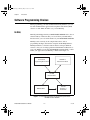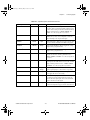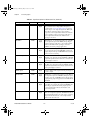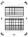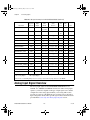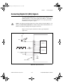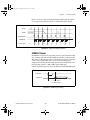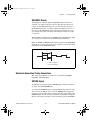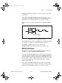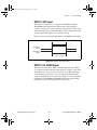
1
UM.book Page 1 Monday, May 14, 2001 10:32 AM
DAQ
NI 6034E/6035E/6036E
User Manual
Multifunction I/O Devices for PCI, PXI ™,
and CompactPCI Bus Computers
NI 6034E/6035E/6036E User Manual
May 2001 Edition
Part Number 322339B-01
UM.book Page 2 Monday, May 14, 2001 10:32 AM
Support
Worldwide Technical Support and Product Information
ni.com
National Instruments Corporate Headquarters
11500 North Mopac Expressway
Austin, Texas 78759-3504
USA Tel: 512 794 0100
Worldwide Offices
Australia 03 9879 5166, Austria 0662 45 79 90 0, Belgium 02 757 00 20, Brazil 011 284 5011,
Canada (Calgary) 403 274 9391, Canada (Montreal) 514 288 5722, Canada (Ottawa) 613 233 5949,
Canada (Québec) 514 694 8521, Canada (Toronto) 905 785 0085, China (Shanghai) 021 6555 7838,
China (ShenZhen) 0755 3904939, Denmark 45 76 26 00, Finland 09 725 725 11, France 01 48 14 24 24,
Germany 089 741 31 30, Greece 30 1 42 96 427, Hong Kong 2645 3186, India 91805275406,
Israel 03 6120092, Italy 02 413091, Japan 03 5472 2970, Korea 02 596 7456, Malaysia 603 9596711,
Mexico 5 280 7625, Netherlands 0348 433466, New Zealand 09 914 0488, Norway 32 27 73 00,
Poland 0 22 528 94 06, Portugal 351 1 726 9011, Singapore 2265886, Spain 91 640 0085,
Sweden 08 587 895 00, Switzerland 056 200 51 51, Taiwan 02 2528 7227, United Kingdom 01635 523545
For further support information, see the Technical Support Resources appendix. To comment on the
documentation, send e-mail to [email protected].
Copyright © 1999, 2001 National Instruments Corporation. All rights reserved.
UM.book Page 3 Monday, May 14, 2001 10:32 AM
Important Information
Warranty
The NI 6034E, NI 6035E, and NI 6036E devices are warranted against defects in materials and workmanship for a period of one year from the
date of shipment, as evidenced by receipts or other documentation. National Instruments will, at its option, repair or replace equipment that
proves to be defective during the warranty period. This warranty includes parts and labor.
The media on which you receive National Instruments software are warranted not to fail to execute programming instructions, due to defects
in materials and workmanship, for a period of 90 days from date of shipment, as evidenced by receipts or other documentation. National
Instruments will, at its option, repair or replace software media that do not execute programming instructions if National Instruments receives
notice of such defects during the warranty period. National Instruments does not warrant that the operation of the software shall be
uninterrupted or error free.
A Return Material Authorization (RMA) number must be obtained from the factory and clearly marked on the outside of the package before
any equipment will be accepted for warranty work. National Instruments will pay the shipping costs of returning to the owner parts which are
covered by warranty.
National Instruments believes that the information in this document is accurate. The document has been carefully reviewed for technical
accuracy. In the event that technical or typographical errors exist, National Instruments reserves the right to make changes to subsequent
editions of this document without prior notice to holders of this edition. The reader should consult National Instruments if errors are suspected.
In no event shall National Instruments be liable for any damages arising out of or related to this document or the information contained in it.
EXCEPT AS SPECIFIED HEREIN, NATIONAL INSTRUMENTS MAKES NO WARRANTIES, EXPRESS OR IMPLIED, AND SPECIFICALLY DISCLAIMS ANY WARRANTY OF
MERCHANTABILITY OR FITNESS FOR A PARTICULAR PURPOSE. CUSTOMER’S RIGHT TO RECOVER DAMAGES CAUSED BY FAULT OR NEGLIGENCE ON THE PART OF
NATIONAL INSTRUMENTS SHALL BE LIMITED TO THE AMOUNT THERETOFORE PAID BY THE CUSTOMER. NATIONAL INSTRUMENTS WILL NOT BE LIABLE FOR
DAMAGES RESULTING FROM LOSS OF DATA, PROFITS, USE OF PRODUCTS, OR INCIDENTAL OR CONSEQUENTIAL DAMAGES, EVEN IF ADVISED OF THE POSSIBILITY
THEREOF. This limitation of the liability of National Instruments will apply regardless of the form of action, whether in contract or tort, including
negligence. Any action against National Instruments must be brought within one year after the cause of action accrues. National Instruments
shall not be liable for any delay in performance due to causes beyond its reasonable control. The warranty provided herein does not cover
damages, defects, malfunctions, or service failures caused by owner’s failure to follow the National Instruments installation, operation, or
maintenance instructions; owner’s modification of the product; owner’s abuse, misuse, or negligent acts; and power failure or surges, fire,
flood, accident, actions of third parties, or other events outside reasonable control.
Copyright
Under the copyright laws, this publication may not be reproduced or transmitted in any form, electronic or mechanical, including photocopying,
recording, storing in an information retrieval system, or translating, in whole or in part, without the prior written consent of National
Instruments Corporation.
Trademarks
CVI™, DAQ-STC™, LabVIEW™, Measurement Studio™, MITE™, National Instruments™, NI™, ni.com™, NI-DAQ™, RTSI™, and SCXI™
are trademarks of National Instruments Corporation.
Product and company names mentioned herein are trademarks or trade names of their respective companies.
WARNING REGARDING USE OF NATIONAL INSTRUMENTS PRODUCTS
(1) NATIONAL INSTRUMENTS PRODUCTS ARE NOT DESIGNED WITH COMPONENTS AND TESTING FOR A LEVEL OF
RELIABILITY SUITABLE FOR USE IN OR IN CONNECTION WITH SURGICAL IMPLANTS OR AS CRITICAL COMPONENTS IN
ANY LIFE SUPPORT SYSTEMS WHOSE FAILURE TO PERFORM CAN REASONABLY BE EXPECTED TO CAUSE SIGNIFICANT
INJURY TO A HUMAN.
(2) IN ANY APPLICATION, INCLUDING THE ABOVE, RELIABILITY OF OPERATION OF THE SOFTWARE PRODUCTS CAN BE
IMPAIRED BY ADVERSE FACTORS, INCLUDING BUT NOT LIMITED TO FLUCTUATIONS IN ELECTRICAL POWER SUPPLY,
COMPUTER HARDWARE MALFUNCTIONS, COMPUTER OPERATING SYSTEM SOFTWARE FITNESS, FITNESS OF COMPILERS
AND DEVELOPMENT SOFTWARE USED TO DEVELOP AN APPLICATION, INSTALLATION ERRORS, SOFTWARE AND
HARDWARE COMPATIBILITY PROBLEMS, MALFUNCTIONS OR FAILURES OF ELECTRONIC MONITORING OR CONTROL
DEVICES, TRANSIENT FAILURES OF ELECTRONIC SYSTEMS (HARDWARE AND/OR SOFTWARE), UNANTICIPATED USES OR
MISUSES, OR ERRORS ON THE PART OF THE USER OR APPLICATIONS DESIGNER (ADVERSE FACTORS SUCH AS THESE ARE
HEREAFTER COLLECTIVELY TERMED “SYSTEM FAILURES”). ANY APPLICATION WHERE A SYSTEM FAILURE WOULD
CREATE A RISK OF HARM TO PROPERTY OR PERSONS (INCLUDING THE RISK OF BODILY INJURY AND DEATH) SHOULD
NOT BE RELIANT SOLELY UPON ONE FORM OF ELECTRONIC SYSTEM DUE TO THE RISK OF SYSTEM FAILURE. TO AVOID
DAMAGE, INJURY, OR DEATH, THE USER OR APPLICATION DESIGNER MUST TAKE REASONABLY PRUDENT STEPS TO
PROTECT AGAINST SYSTEM FAILURES, INCLUDING BUT NOT LIMITED TO BACK-UP OR SHUT DOWN MECHANISMS.
BECAUSE EACH END-USER SYSTEM IS CUSTOMIZED AND DIFFERS FROM NATIONAL INSTRUMENTS' TESTING
PLATFORMS AND BECAUSE A USER OR APPLICATION DESIGNER MAY USE NATIONAL INSTRUMENTS PRODUCTS IN
COMBINATION WITH OTHER PRODUCTS IN A MANNER NOT EVALUATED OR CONTEMPLATED BY NATIONAL
INSTRUMENTS, THE USER OR APPLICATION DESIGNER IS ULTIMATELY RESPONSIBLE FOR VERIFYING AND VALIDATING
THE SUITABILITY OF NATIONAL INSTRUMENTS PRODUCTS WHENEVER NATIONAL INSTRUMENTS PRODUCTS ARE
INCORPORATED IN A SYSTEM OR APPLICATION, INCLUDING, WITHOUT LIMITATION, THE APPROPRIATE DESIGN,
PROCESS AND SAFETY LEVEL OF SUCH SYSTEM OR APPLICATION.
UM.book Page 4 Monday, May 14, 2001 10:32 AM
Compliance
FCC/Canada Radio Frequency Interference Compliance*
Determining FCC Class
The Federal Communications Commission (FCC) has rules to protect wireless communications from interference. The FCC
places digital electronics into two classes. These classes are known as Class A (for use in industrial-commercial locations only)
or Class B (for use in residential or commercial locations). Depending on where it is operated, this product could be subject to
restrictions in the FCC rules. (In Canada, the Department of Communications (DOC), of Industry Canada, regulates wireless
interference in much the same way.)
Digital electronics emit weak signals during normal operation that can affect radio, television, or other wireless products. By
examining the product you purchased, you can determine the FCC Class and therefore which of the two FCC/DOC Warnings
apply in the following sections. (Some products may not be labeled at all for FCC; if so, the reader should then assume these are
Class A devices.)
FCC Class A products only display a simple warning statement of one paragraph in length regarding interference and undesired
operation. Most of our products are FCC Class A. The FCC rules have restrictions regarding the locations where FCC Class A
products can be operated.
FCC Class B products display either a FCC ID code, starting with the letters EXN,
or the FCC Class B compliance mark that appears as shown here on the right.
Consult the FCC web site http://www.fcc.gov for more information.
FCC/DOC Warnings
This equipment generates and uses radio frequency energy and, if not installed and used in strict accordance with the instructions
in this manual and the CE Mark Declaration of Conformity**, may cause interference to radio and television reception.
Classification requirements are the same for the Federal Communications Commission (FCC) and the Canadian Department
of Communications (DOC).
Changes or modifications not expressly approved by National Instruments could void the user’s authority to operate the
equipment under the FCC Rules.
Class A
Federal Communications Commission
This equipment has been tested and found to comply with the limits for a Class A digital device, pursuant to part 15 of the FCC
Rules. These limits are designed to provide reasonable protection against harmful interference when the equipment is operated
in a commercial environment. This equipment generates, uses, and can radiate radio frequency energy and, if not installed and
used in accordance with the instruction manual, may cause harmful interference to radio communications. Operation of this
equipment in a residential area is likely to cause harmful interference in which case the user will be required to correct
the interference at his own expense.
Canadian Department of Communications
This Class A digital apparatus meets all requirements of the Canadian Interference-Causing Equipment Regulations.
Cet appareil numérique de la classe A respecte toutes les exigences du Règlement sur le matériel brouilleur du Canada.
Class B
Federal Communications Commission
This equipment has been tested and found to comply with the limits for a Class B digital device, pursuant to part 15 of the
FCC Rules. These limits are designed to provide reasonable protection against harmful interference in a residential installation.
This equipment generates, uses and can radiate radio frequency energy and, if not installed and used in accordance with the
instructions, may cause harmful interference to radio communications. However, there is no guarantee that interference will not
occur in a particular installation. If this equipment does cause harmful interference to radio or television reception, which can
be determined by turning the equipment off and on, the user is encouraged to try to correct the interference by one or more of
the following measures:
• Reorient or relocate the receiving antenna.
• Increase the separation between the equipment and receiver.
• Connect the equipment into an outlet on a circuit different from that to which the receiver is connected.
• Consult the dealer or an experienced radio/TV technician for help.
UM.book Page 5 Monday, May 14, 2001 10:32 AM
Canadian Department of Communications
This Class B digital apparatus meets all requirements of the Canadian Interference-Causing Equipment Regulations.
Cet appareil numérique de la classe B respecte toutes les exigences du Règlement sur le matériel brouilleur du Canada.
Compliance to EU Directives
Readers in the European Union (EU) must refer to the Manufacturer's Declaration of Conformity (DoC) for information**
pertaining to the CE Mark compliance scheme. The Manufacturer includes a DoC for most every hardware product except for
those bought for OEMs, if also available from an original manufacturer that also markets in the EU, or where compliance is not
required as for electrically benign apparatus or cables.
To obtain the DoC for this product, click Declaration of Conformity at ni.com/hardref.nsf/. This website lists the DoCs
by product family. Select the appropriate product family, followed by your product, and a link to the DoC appears in Adobe
Acrobat format. Click the Acrobat icon to download or read the DoC.
* Certain exemptions may apply in the USA, see FCC Rules §15.103 Exempted devices, and §15.105(c). Also available in
sections of CFR 47.
** The CE Mark Declaration of Conformity will contain important supplementary information and instructions for the user or
installer.
UM.book Page vii Monday, May 14, 2001 10:32 AM
Contents
About This Manual
Conventions Used in This Manual.................................................................................xi
Related Documentation..................................................................................................xii
Chapter 1
Introduction
About the NI 6034E/6035E/6036E Device ...................................................................1-1
Using PXI with CompactPCI.........................................................................................1-2
What You Need to Get Started ......................................................................................1-3
Software Programming Choices ....................................................................................1-4
NI-DAQ...........................................................................................................1-4
National Instruments ADE Software...............................................................1-5
Optional Equipment .......................................................................................................1-5
Unpacking ......................................................................................................................1-6
Safety Information .........................................................................................................1-6
Chapter 2
Installing and Configuring Your NI 6034E/6035E/6036E
Installing Your Software................................................................................................2-1
Installing Your Hardware ..............................................................................................2-1
Configuring Your Hardware ..........................................................................................2-3
Chapter 3
Hardware Overview
Analog Input ..................................................................................................................3-2
Input Mode ......................................................................................................3-2
Input Range .....................................................................................................3-3
Scanning Multiple Channels............................................................................3-3
Analog Output................................................................................................................3-4
Analog Output Glitch ......................................................................................3-4
Digital I/O ......................................................................................................................3-4
Timing Signal Routing...................................................................................................3-5
Programmable Function Inputs .......................................................................3-6
Device and RTSI Clocks .................................................................................3-6
RTSI Triggers..................................................................................................3-7
© National Instruments Corporation
vii
NI 6034E/6035E/6036E User Manual
UM.book Page viii Monday, May 14, 2001 10:32 AM
Contents
Chapter 4
Connecting Signals
I/O Connector ................................................................................................................ 4-1
Analog Input Signal Overview...................................................................................... 4-6
Types of Signal Sources.................................................................................. 4-7
Floating Signal Sources .................................................................... 4-7
Ground-Referenced Signal Sources.................................................. 4-7
Analog Input Modes........................................................................................ 4-7
Connecting Your Analog Input Signals ........................................................................ 4-9
Differential Connection Considerations (DIFF Input Configuration) ............ 4-11
Differential Connections for Ground-Referenced
Signal Sources ............................................................................... 4-12
Differential Connections for Nonreferenced or Floating
Signal Sources ............................................................................... 4-13
Single-Ended Connection Considerations ...................................................... 4-15
Single-Ended Connections for Floating Signal Sources
(RSE Configuration) ...................................................................... 4-16
Single-Ended Connections for Grounded Signal Sources
(NRSE Configuration) ................................................................... 4-16
Common-Mode Signal Rejection Considerations........................................... 4-17
Connecting Your Analog Output Signals...................................................................... 4-18
Connecting Digital I/O (DIO) Signals........................................................................... 4-19
Power Connections........................................................................................................ 4-20
Connecting Timing Signals ........................................................................................... 4-20
Programmable Function Input Connections ................................................... 4-21
DAQ Timing Connections .............................................................................. 4-22
SCANCLK Signal ............................................................................ 4-23
EXTSTROBE* Signal ...................................................................... 4-24
TRIG1 Signal.................................................................................... 4-24
TRIG2 Signal.................................................................................... 4-25
STARTSCAN Signal........................................................................ 4-27
CONVERT* Signal .......................................................................... 4-29
AIGATE Signal ................................................................................ 4-30
SISOURCE Signal............................................................................ 4-31
Waveform Generation Timing Connections ................................................... 4-31
WFTRIG Signal................................................................................ 4-31
UPDATE* Signal ............................................................................. 4-32
UISOURCE Signal ........................................................................... 4-34
General-Purpose Timing Signal Connections................................................. 4-34
GPCTR0_SOURCE Signal .............................................................. 4-34
GPCTR0_GATE Signal ................................................................... 4-35
GPCTR0_OUT Signal ...................................................................... 4-36
GPCTR0_UP_DOWN Signal........................................................... 4-37
NI 6034E/6035E/6036E User Manual
viii
ni.com
UM.book Page ix Monday, May 14, 2001 10:32 AM
Contents
GPCTR1_SOURCE Signal...............................................................4-37
GPCTR1_GATE Signal....................................................................4-38
GPCTR1_OUT Signal ......................................................................4-39
GPCTR1_UP_DOWN Signal ...........................................................4-39
FREQ_OUT Signal ...........................................................................4-41
Field Wiring Considerations ..........................................................................................4-41
Chapter 5
Calibration
Loading Calibration Constants ......................................................................................5-1
Self-Calibration..............................................................................................................5-2
External Calibration .......................................................................................................5-2
Other Considerations .....................................................................................................5-3
Appendix A
Specifications
Appendix B
Custom Cabling and Optional Connectors
Appendix C
Common Questions
Appendix D
Technical Support Resources
Glossary
Index
© National Instruments Corporation
ix
NI 6034E/6035E/6036E User Manual
UM.book Page xi Monday, May 14, 2001 10:32 AM
About This Manual
The NI 6034E, NI 6035E, and NI 6036E devices are high-performance
multifunction analog, digital, and timing I/O devices for PCI, PXI, and
CompactPCI bus computers. Supported functions include analog input,
analog output, digital I/O, and timing I/O.
This manual describes the electrical and mechanical aspects of the
PCI/PXI 6034E/6035E/6036E devices from the E Series product line and
contains information concerning their operation and programming.
Conventions Used in This Manual
The following conventions are used in this manual:
<>
Angle brackets containing numbers separated by an ellipsis represent a
range of values associated with a bit or signal name—for example,
DBIO<3..0>.
♦
The ♦ symbol indicates that the text following it applies only to a specific
product, a specific operating system, or a specific software version.
»
The » symbol leads you through nested menu items and dialog box options
to a final action. The sequence File»Page Setup»Options directs you to
pull down the File menu, select the Page Setup item, and select Options
from the last dialog box.
This icon denotes a note, which alerts you to important information.
This icon denotes a caution, which advises you of precautions to take to
avoid injury, data loss, or a system crash.
bold
Bold text denotes items that you must select or click on in the software,
such as menu items and dialog box options. Bold text also denotes
parameter names.
CompactPCI
CompactPCI refers to the core specification defined by the PCI Industrial
Computer Manufacturer’s Group (PICMG).
italic
Italic text denotes variables, emphasis, a cross reference, or an introduction
to a key concept. This font also denotes text that is a placeholder for a word
or value that you must supply.
© National Instruments Corporation
xi
NI 6034E/6035E/6036E User Manual
UM.book Page xii Monday, May 14, 2001 10:32 AM
About This Manual
monospace
Text in this font denotes text or characters that you should enter from the
keyboard, sections of code, programming examples, and syntax examples.
This font is also used for the proper names of disk drives, paths, directories,
programs, subprograms, subroutines, device names, functions, operations,
variables, filenames and extensions, and code excerpts.
NI-DAQ
NI-DAQ refers to the NI-DAQ driver software for PC compatible
computers unless otherwise noted.
PC
PC refers to all PC AT series computers with PCI or PXI bus unless
otherwise noted.
platform
Text in this font denotes a specific platform and indicates that the text
following it applies only to that platform.
PXI
PXI stands for PCI eXtensions for Instrumentation. PXI is an open
specification that builds off the CompactPCI specification by adding
instrumentation-specific features.
Related Documentation
The following documents contain information you may find helpful:
•
DAQ Quick Start Guide
•
DAQ-STC Technical Reference Manual
•
National Instruments Application Note 025, Field Wiring and Noise
Considerations for Analog Signals
•
NI-DAQ User Manual for PC Compatibles
•
PCI Local Bus Specification Revision 2.2
•
PICMG CompactPCI 2.0 R2.1
•
PXI Specification Revision 2.0
NI 6034E/6035E/6036E User Manual
xii
ni.com
UM.book Page 1 Monday, May 14, 2001 10:32 AM
1
Introduction
This chapter describes the NI 6034E/6035E/6036E device, lists what you
need to get started, describes the optional software and equipment, and
explains how to unpack your NI 6034E/6035E/6036E device.
About the NI 6034E/6035E/6036E Device
Thank you for buying an NI 6034E/6035E/6036E device. The NI 6035E
features 16 channels (eight differential) of 16-bit analog input,
two channels of 12-bit analog output, a 68-pin connector, and eight lines
of digital I/O. The NI 6034E is identical to the NI 6035E, except that it does
not have analog output channels. The NI 6036E has the same features as the
NI 6035E, except that the analog output is 16 bit instead of 12 bit.
The NI 6034E/6035E/6036E device uses the NI data acquisition system
timing controller (DAQ-STC) for time-related functions. The DAQ-STC
consists of three timing groups that control analog input, analog output,
and general-purpose counter/timer functions. These groups include a total
of seven 24-bit and three 16-bit counters and a maximum timing resolution
of 50 ns. The DAQ-STC makes possible such applications as buffered pulse
generation, equivalent time sampling, and seamless changing of the
sampling rate.
With other DAQ devices, you cannot easily synchronize several
measurement functions to a common trigger or timing event. The
NI 6034E/6035E/6036E devices have the Real-Time System Integration
(RTSI) bus to solve this problem. In a PCI system, the RTSI bus consists
of the National Instruments RTSI bus interface and a ribbon cable to route
timing and trigger signals between several functions on as many as five
DAQ devices in your computer. In a PXI system, the RTSI bus consists
of the National Instruments RTSI bus interface and the PXI trigger signals
on the PXI backplane to route timing and trigger signals between several
functions on as many as seven DAQ devices in your system.
© National Instruments Corporation
1-1
NI 6034E/6035E/6036E User Manual
UM.book Page 2 Monday, May 14, 2001 10:32 AM
Chapter 1
Introduction
The NI 6034E/6035E/6036E device can interface to an SCXI system—
the instrumentation front end for plug-in DAQ devices—so that you can
acquire analog signals from thermocouples, RTDs, strain gauges, voltage
sources, and current sources. You can also acquire or generate digital
signals for communication and control.
Using PXI with CompactPCI
Using PXI-compatible products with standard CompactPCI products is
an important feature provided by PXI Specification, Revision 2.0. If you
use a PXI-compatible plug-in card in a standard CompactPCI chassis, you
are unable to use PXI-specific functions, but you can still use the basic
plug-in card functions. For example, the RTSI bus on your PXI E Series
device is available in a PXI chassis, but not in a CompactPCI chassis.
The CompactPCI specification permits vendors to develop sub-buses that
coexist with the basic PCI interface on the CompactPCI bus. Compatible
operation is not guaranteed between CompactPCI devices with different
sub-buses nor between CompactPCI devices with sub-buses and PXI.
The standard implementation for CompactPCI does not include these
sub-buses. Your PXI E Series device works in any standard CompactPCI
chassis adhering to PICMG CompactPCI 2.0 R2.1 core specification.
PXI-specific features are implemented on the J2 connector of the
CompactPCI bus. Table 1-1 lists the J2 pins used by your PXI E Series
device. Your PXI device is compatible with any Compact PCI chassis with
a sub-bus that does not drive these lines. Even if the sub-bus is capable of
driving these lines, the PXI device is still compatible as long as those pins
on the sub-bus are disabled by default and not ever enabled.
Caution
Damage can result if these lines are driven by the sub-bus.
NI 6034E/6035E/6036E User Manual
1-2
ni.com
UM.book Page 3 Monday, May 14, 2001 10:32 AM
Chapter 1
Introduction
Table 1-1. Pins Used by the PXI-6035E/6036E
PXI E Series
Signal
PXI Pin Name
PXI J2 Pin Number
RTSI<0..5>
PXI Trigger<0..5>
B16, A16, A17, A18, B18, C18
RTSI 6
PXI Star
D17
RTSI Clock
PXI Trigger 7
E16
Reserved
LBL<0..3>
C20, E20, A19, C19
Reserved
LBR<0..12>
A21, C21, D21, E21, A20,
B20, E15, A3, C3, D3, E3,
A2, B2
What You Need to Get Started
To set up and use your device, you need the following:
❑ At least one of the following devices:
–
PCI-6034E
–
PCI-6035E
–
PXI-6035E
–
PCI-6036E
–
PXI-6036E
❑ NI 6034E/6035E/6036E User Manual
❑ NI-DAQ software (for PC Compatibles or Mac OS1)
❑ One of the following software packages and documentation:
–
LabVIEW (for Windows or Mac OS2)
–
Measurement Studio (for Windows)
❑ Your computer or PXI/CompactPCI chassis and controller (hereafter
referred to as your computer)
1
2
The PCI/PXI-6036E does not support NI-DAQ for Mac OS.
The PCI/PXI-6036E does not support LabVIEW for Mac OS.
© National Instruments Corporation
1-3
NI 6034E/6035E/6036E User Manual
UM.book Page 4 Monday, May 14, 2001 10:32 AM
Chapter 1
Introduction
Software Programming Choices
When programming your National Instruments DAQ hardware, you can
use National Instruments application development environment (ADE)
software or other ADEs. In either case, you use NI-DAQ.
NI-DAQ
NI-DAQ, which shipped with your NI 6034E/6035E/6036E device, has an
extensive library of functions that you can call from your ADE. These
functions allow you to use all the features of your NI 6034E/6035E/6036E.
NI-DAQ carries out many of the complex interactions, such as
programming interrupts, between the computer and the DAQ hardware.
NI-DAQ maintains a consistent software interface among its different
versions so that you can change platforms with minimal modifications to
your code. Whether you are using LabVIEW, Measurement Studio, or other
ADEs, your application uses NI-DAQ, as illustrated in Figure 1-1.
Conventional
Programming Environment
LabVIEW or
Measurement Studio
NI-DAQ
Driver Software
DAQ Hardware
Personal
Computer or
Workstation
Figure 1-1. The Relationship Between the Programming Environment,
NI-DAQ, and Your Hardware
NI 6034E/6035E/6036E User Manual
1-4
ni.com
UM.book Page 5 Monday, May 14, 2001 10:32 AM
Chapter 1
Introduction
To download a free copy of the most recent version of NI-DAQ, click
Download Software at ni.com.
National Instruments ADE Software
LabVIEW features interactive graphics, a state-of-the-art interface,
and a powerful graphical programming language. The LabVIEW Data
Acquisition VI Library, a series of virtual instruments for using LabVIEW
with National Instruments DAQ hardware, is included with LabVIEW.
Measurement Studio, which includes LabWindows/CVI, tools for Visual
C++, and tools for Visual Basic, is a development suite that allows you
to use ANSI C, Visual C++, and Visual Basic to design your test and
measurement software. For C developers, Measurement Studio includes
LabWindows/CVI, a fully integrated ANSI C application development
environment that features interactive graphics and the LabWindows/CVI
Data Acquisition and Easy I/O libraries. For Visual Basic developers,
Measurement Studio features a set of ActiveX controls for using National
Instruments DAQ hardware. These ActiveX controls provide a high-level
programming interface for building virtual instruments. For Visual C++
developers, Measurement Studio offers a set of Visual C++ classes and
tools to integrate those classes into Visual C++ applications. The libraries,
ActiveX controls, and classes are available with Measurement Studio and
NI-DAQ.
Using LabVIEW or Measurement Studio greatly reduces the development
time for your data acquisition and control application.
Optional Equipment
NI offers a variety of products to use with your device, including cables,
connector blocks, and other accessories, as follows:
•
Cables and cable assemblies, shielded and ribbon
•
Connector blocks, shielded and unshielded screw terminals
•
RTSI bus cables (PCI only)
•
SCXI modules and accessories for isolating, amplifying, exciting, and
multiplexing signals for relays and analog output; with SCXI, you can
condition and acquire up to 3,072 channels
•
Low channel-count signal conditioning modules, devices, and
accessories, including conditioning for strain gauges and RTDs,
simultaneous sample and hold, and relays
© National Instruments Corporation
1-5
NI 6034E/6035E/6036E User Manual
UM.book Page 6 Monday, May 14, 2001 10:32 AM
Chapter 1
Introduction
For more information about these products, refer to the National
Instruments catalog at ni.com/catalog or call the sales office nearest
you.
Unpacking
Your NI 6034E/6035E/6036E device is shipped in an antistatic package
to prevent electrostatic damage to the device. Electrostatic discharge
can damage several components on the device.
Caution
Never touch the exposed pins of connectors.
To avoid such damage in handling the device, take the following
precautions:
•
Ground yourself using a grounding strap or by holding a grounded
object.
•
Touch the antistatic package to a metal part of your computer chassis
before removing the device from the package.
Remove the device from the package and inspect the device for loose
components or any sign of damage. Notify National Instruments if the
device appears damaged in any way. Do not install a damaged device into
your computer.
Store your NI 6034E/6035E/6036E device in the antistatic envelope when
not in use.
Safety Information
To meet EMC/EMI, cooling and safety compliance requirements, the
NI 6034E/6035E/6036E device must be installed in a chassis with the covers and chassis
filler panels properly installed.
Caution
NI 6034E/6035E/6036E User Manual
1-6
ni.com
UM.book Page 7 Monday, May 14, 2001 10:32 AM
Chapter 1
Introduction
Cautions Do not operate the device in an explosive atmosphere or where there may be
flammable gases or fumes.
Do not operate damaged equipment. The safety protection features built into this device
can become impaired if the device becomes damaged in any way. If the device is damaged,
turn the device off and do not use it until service-trained personnel can check its safety.
If necessary, return the device to National Instruments for service and repair to ensure that
its safety is not compromised.
Do not operate this equipment in a manner that contradicts the information specified in
this document. Misuse of this equipment could result in a shock hazard.
Do not substitute parts or modify equipment. Because of the danger of introducing
additional hazards, do not install unauthorized parts or modify the device. Return the
device to National Instruments for service and repair to ensure that its safety features
are not compromised.
You must insulate all of your signal connections to the highest voltage with which the
NI 6034E/6035E/6036E can come in contact.
Connections, including power signals to ground and vice versa, that exceed any of the
maximum signal ratings on the NI 6034E/6035E/6036E device can create a shock or fire
hazard, or can damage any or all of the boards connected to the chassis, the host computer,
and the NI 6034E/6035E/6036E device. National Instruments is not liable for any damages
or injuries resulting from incorrect signal connections.
Clean the NI 6034E/6035E/6036E device and accessories by brushing off light dust with a
soft non-metallic brush. Remove other contaminants with a stiff non-metallic brush. The
unit must be completely dry and free from contaminants before returning it to service.
© National Instruments Corporation
1-7
NI 6034E/6035E/6036E User Manual
UM.book Page 1 Monday, May 14, 2001 10:32 AM
2
Installing and Configuring
Your NI 6034E/6035E/6036E
This chapter explains how to install and configure your
NI 6034E/6035E/6036E device.
Installing Your Software
Complete the following steps in order to install your software before
installing your NI 6034E/6035E/6036E device.
1.
Install your ADE, such as LabVIEW or Measurement Studio,
according to the instructions on the CD and the release notes.
2.
Install NI-DAQ according to the instructions on the CD.
It is important to install NI-DAQ before installing your NI 6034E/6035E/6036E
device to ensure that the device is properly detected.
Note
Installing Your Hardware
Your NI 6034E/6035E/6036E device fits in any 5 V expansion slot in your
computer. However, to achieve best noise performance, leave as much
room as possible between your NI 6034E/6035E/6036E and other devices.
The following are general installation instructions, but consult your
computer user manual or technical reference manual for specific
instructions and warnings.
Follow the guidelines in your computer documentation for installing plug-in
hardware.
Note
♦
PCI-6034E/6035E/6036E
1.
Turn off and unplug your computer.
2.
Remove the cover.
3.
Make sure there are no lighted LEDs on your motherboard. If any
are lit, wait until they go out before continuing your installation.
© National Instruments Corporation
2-1
NI 6034E/6035E/6036E User Manual
UM.book Page 2 Monday, May 14, 2001 10:32 AM
Chapter 2
Installing and Configuring Your NI 6034E/6035E/6036E
Note
4.
Remove the expansion slot cover on the back panel of the computer.
5.
Ground yourself using a grounding strap or by holding a grounded
object. Follow the ESD protection precautions described in the
Unpacking section of Chapter 1, Introduction.
6.
Insert the NI 6034E/6035E/6036E device into a 5 V PCI slot. Gently
rock the device to ease it into place. It may be a tight fit, but do not
force the device into place.
7.
If required, screw the mounting bracket of the device to the back panel
rail of the computer.
8.
Replace the cover.
9.
Plug in and turn on your computer.
For proper cooling, all covers and filler panels must be installed.
The PCI-6034E/6035E/6036E is now installed.
♦
PXI-6035E/6036E
1.
Turn off and unplug your computer.
2.
Choose an unused PXI slot in your system. For maximum
performance, the NI 6035E device has an onboard DMA controller
that can only be used if the device is installed in a slot that supports
bus arbitration, or bus master cards. National Instruments recommends
installing the device in such a slot. The PXI specification requires all
slots to support bus master cards, but the CompactPCI specification
does not. If you install in a CompactPCI non-master slot, you must
disable the onboard DMA controller using software.
3.
Make sure there are no lighted LEDs on your motherboard. If any
are lit, wait until they go out before continuing your installation.
4.
Remove the filler panel for the slot you have chosen.
5.
Ground yourself using a grounding strap or by holding a grounded
object. Follow the ESD protection precautions described in the
Unpacking section of Chapter 1, Introduction.
6.
Insert the NI 6035E device into a 5 V PXI slot. Use the injector/ejector
handle to fully insert the device into the chassis.
7.
Screw the front panel of the NI 6035E device to the front
panel-mounting rail of the system.
NI 6034E/6035E/6036E User Manual
2-2
ni.com
UM.book Page 3 Monday, May 14, 2001 10:32 AM
Chapter 2
Installing and Configuring Your NI 6034E/6035E/6036E
8.
Visually verify the installation. Make sure the device is not touching
other devices or components and is fully inserted in the slot.
9.
Plug in and turn on your computer.
The PXI-6035E/6036E device is now installed.
You are now ready to configure your hardware and software.
Configuring Your Hardware
Because of the National Instruments standard architecture for data
acquisition and standard bus specifications, the NI 6034E/6035E/6036E
device is completely software-configurable. Two types of configuration
are performed on the NI 6034E/6035E/6036E device: bus-related and data
acquisition-related.
The PCI-6034E/6035E/6036E device is fully compatible with the
industry-standard PCI Local Bus Specification Revision 2.2. The
PXI-6035E/6036E device is fully compatible with the PXI Specification
Revision 2.0. These specifications allow your PCI or PXI system to
automatically perform all bus-related configurations with no user
interaction. Bus-related configuration includes setting the device base
memory address and interrupt channel.
Data acquisition-related configuration, which you must perform, includes
such settings as analog input coupling and range, and others. You can
modify these settings using NI-DAQ or ADE software, such as LabVIEW
and Measurement Studio. Refer to your software documentation for
configuration instructions. Refer to Chapter 3, Hardware Overview, for
more information about the various settings available for your device.
To configure your device in Measurement & Automation Explorer (MAX),
refer to ni.com/manuals to view either the DAQ Quick Start Guide or the
NI-DAQ User Manual for PC Compatibles, or launch MAX to access the
Measurement & Automation Explorer Help for DAQ (Help»Help Topics»
NI-DAQ).
© National Instruments Corporation
2-3
NI 6034E/6035E/6036E User Manual
UM.book Page 1 Monday, May 14, 2001 10:32 AM
3
Hardware Overview
This chapter presents an overview of the hardware functions on your
NI 6034E/6035E/6036E device.
Calibration
DACs
(8)
(8)
EEPROM
Control
Analog
Input
Muxes
Analog Mode
Multiplexer
A/D
Converter
PGIA
ADC
FIFO
Data
Generic
PCI
MINIBus
Bus
Interface MITE Interface
Address/Data
Calibration
Mux
AI Control
EEPROM
IRQ
DMA
Analog Input
Timing/Control
DMA/
Interrupt
Request
Counter/
Timing I/O
DAQ - STC
Bus
Interface
Digital I/O
Analog Output
Timing/Control
RTSI Bus
Interface
PFI/Trigger
Trigger
Interface
Timing
Digital I/O
Address
I/O Connector
Configuration
Memory
Analog
Input
Control
EEPROM
DMA
Control Interface
DAQ-STC
Bus
Interface
DAQAPE
Plug
and
Play
Analog
Output
Control
Bus
Interface
82C55
DIO
Control
AO Control
DAC0
DAC1
Calibration DACs
RTSI Connector
Not On NI 6034E
Analog Output
PCI Connector for PCI-603X, PXI Connector for PXI-6035E
Voltage
REF
Figure 3-1. NI 6034E/6035E/6036E Block Diagram
© National Instruments Corporation
3-1
NI 6034E/6035E/6036E User Manual
UM.book Page 2 Monday, May 14, 2001 10:32 AM
Chapter 3
Hardware Overview
Analog Input
The analog input (AI) section of the NI 6034E/6035E/6036E device is
software configurable. The following sections describe in detail each of
the analog input settings.
Input Mode
The NI 6034E/6035E/6036E device has three different input modes—
nonreferenced single-ended (NRSE) input, referenced single-ended (RSE)
input, and differential (DIFF) input. The single-ended input configurations
provide up to 16 channels. The DIFF input configuration provides up to
eight channels. Input modes are programmed on a per-channel basis for
multimode scanning. For example, you can configure the circuitry to scan
12 channels—four differentially-configured channels and eight
single-ended channels. Table 3-1 describes the three input configurations.
Table 3-1. Available Input Configurations
Configuration
Description
DIFF
A channel configured in DIFF mode uses two analog
input lines. One line connects to the positive input of
the programmable gain instrumentation amplifier
(PGIA) on the device, and the other connects to the
negative input of the PGIA.
RSE
A channel configured in RSE mode uses one analog
input line, which connects to the positive input of the
PGIA. The negative input of the PGIA is internally
tied to analog input ground (AIGND).
NRSE
A channel configured in NRSE mode uses one
analog input line, which connects to the positive
input of the PGIA. The negative input of the PGIA
connects to analog input sense (AISENSE).
For diagrams showing the signal paths of the three configurations, refer to
the Connecting Your Analog Input Signals section in Chapter 4,
Connecting Signals.
NI 6034E/6035E/6036E User Manual
3-2
ni.com
UM.book Page 3 Monday, May 14, 2001 10:32 AM
Chapter 3
Hardware Overview
Input Range
The NI 6034E/6035E/6036E device has a bipolar input range that changes
with the programmed gain. Each channel may be programmed with a
unique gain of 0.5, 1.0, 10, or 100 to maximize the 16-bit analog-to-digital
converter (ADC) resolution. With the proper gain setting, you can use the
full resolution of the ADC to measure the input signal. Table 3-2 shows the
input range and precision according to the gain used.
Table 3-2. Measurement Precision
Gain
Input Range
Precision*
0.5
–10 to +10 V
305.2 µV
1.0
–5 to +5 V
152.6 µV
10.0
–500 to +500 mV
15.3 µV
100.0
–50 to +50 mV
1.53 µV
* The value of 1 least significant bit (LSB) of the 16-bit ADC; that is, the voltage
increment corresponding to a change of one count in the ADC 16-bit count.
Note: See Appendix A, Specifications, for absolute maximum ratings.
Scanning Multiple Channels
The devices can scan multiple channels at the same maximum rate as their
single-channel rate; however, pay careful attention to the settling times for
each of the devices. No extra settling time is necessary between channels
as long as the gain is constant and source impedances are low. Refer to
Appendix A, Specifications, for a complete listing of settling times for each
of the devices.
When scanning among channels at various gains, the settling times may
increase. When the PGIA switches to a higher gain, the signal on the
previous channel may be well outside the new, smaller range. For instance,
suppose a 4 V signal is connected to channel 0 and a 1 mV signal is
connected to channel 1, and suppose the PGIA is programmed to apply
a gain of one to channel 0 and a gain of 100 to channel 1. When the
multiplexer switches to channel 1 and the PGIA switches to a gain of 100,
the new full-scale range is ±50 mV.
The approximately 4 V step from 4 V to 1 mV is 4,000% of the new
full-scale range. It may take as long as 100 µs for the circuitry to settle to
1 LSB after such a large transition. In general, this extra settling time is not
needed when the PGIA is switching to a lower gain.
© National Instruments Corporation
3-3
NI 6034E/6035E/6036E User Manual
UM.book Page 4 Monday, May 14, 2001 10:32 AM
Chapter 3
Hardware Overview
Settling times can also increase when scanning high-impedance signals
due to a phenomenon called charge injection, where the analog input
multiplexer injects a small amount of charge into each signal source when
that source is selected. If the impedance of the source is not low enough,
the effect of the charge—a voltage error—will not have decayed by the time
the ADC samples the signal. For this reason, keep source impedances under
1 kΩ to perform high-speed scanning.
Due to the previously described limitations of settling times resulting from
these conditions, multiple-channel scanning is not recommended unless
sampling rates are low enough or it is necessary to sample several signals
as nearly simultaneously as possible. The data is much more accurate and
channel-to-channel independent if you acquire data from each channel
independently (for example, 100 points from channel 0, then 100 points
from channel 1, then 100 points from channel 2, and so on.)
Analog Output
♦
NI 6035E and NI 6036E only
The NI 6035E device supplies two channels of 12-bit analog output voltage
at the I/O connector, and the NI 6036E device supplies two channels of
16-bit analog output voltage at the I/O connector. Each device has a fixed
bipolar output range of ±10 V. Data written to the digital-to-analog
converter (DAC) is interpreted as two’s complement.
Analog Output Glitch
In normal operation, a DAC output glitches whenever it is updated with
a new value. The glitch energy differs from code to code and appears as
distortion in the frequency spectrum.
Digital I/O
The NI 6034E/6035E/6036E device contains eight lines of digital I/O
(DIO<0..7>) for general-purpose use. You can individually
software-configure each line for either input or output. At system startup
and reset, the digital I/O ports are all high impedance.
The hardware up/down control for general-purpose counters 0 and 1 are
connected onboard to DIO6 and DIO7, respectively. Thus, you can use
DIO6 and DIO7 to control the general-purpose counters. The up/down
NI 6034E/6035E/6036E User Manual
3-4
ni.com
UM.book Page 5 Monday, May 14, 2001 10:32 AM
Chapter 3
Hardware Overview
control signals are input only and do not affect the operation of the DIO
lines.
Timing Signal Routing
The DAQ-STC chip provides a flexible interface for connecting timing
signals to other devices or external circuitry. The NI 6034E/6035E/6036E
uses the RTSI bus to interconnect timing signals between devices, and the
Programmable Function Input (PFI) pins on the I/O connector to connect
the device to external circuitry. These connections are designed to enable
the NI 6034E/6035E/6036E to both control and be controlled by other
devices and circuits.
The DAQ-STC has a total of 13 internal timing signals that can be
controlled by an external source. These timing signals can also be
controlled by signals generated internally to the DAQ-STC, and these
selections are fully software configurable. Figure 3-2 shows an example
of the signal routing multiplexer controlling the CONVERT* signal.
RTSI Trigger<0..6>
CONVERT*
PFI<0..9>
Sample Interval Counter TC
GPCTR0_OUT
Figure 3-2. CONVERT* Signal Routing
© National Instruments Corporation
3-5
NI 6034E/6035E/6036E User Manual
UM.book Page 6 Monday, May 14, 2001 10:32 AM
Chapter 3
Hardware Overview
Figure 3-2 shows that CONVERT* can be generated from a number
of sources, including the external signals RTSI<0..6> and PFI<0..9> and
the internal signals Sample Interval Counter TC and GPCTR0_OUT.
Many of these timing signals are also available as outputs on the RTSI pins,
as indicated in the RTSI Triggers section in this chapter, and on the PFI
pins, as indicated in Chapter 4, Connecting Signals.
Programmable Function Inputs
The 10 PFI pins are connected to the signal routing multiplexer for each
timing signal, and software can select any one of the PFI pins as the
external source for a given timing signal. It is important to note that any
of the PFI pins can be used as an input by any of the timing signals and that
multiple timing signals can use the same PFI simultaneously. This flexible
routing scheme reduces the need to change physical connections to the I/O
connector for different applications.
To use the PFI pins as outputs, you must use the Route Signal VI to
individually enable each of the PFI pins to output a specific internal timing
signal. For example, if you need the UPDATE* signal as an output on the
I/O connector, software must turn on the output driver for the
PFI5/UPDATE* pin.
Device and RTSI Clocks
Many functions performed by the NI 6034E/6035E/6036E require
a frequency timebase to generate the necessary timing signals for
controlling A/D conversions, DAC updates, or general-purpose signals
at the I/O connector.
The NI 6034E/6035E/6036E device can use either its internal 20 MHz
timebase or a timebase received over the RTSI bus. In addition, if you
configure the device to use the internal timebase, you can also program the
device to drive its internal timebase over the RTSI bus to another device that
is programmed to receive this timebase signal. This clock source, whether
local or from the RTSI bus, is used directly by the device as the primary
frequency source. The default configuration at startup is to use the internal
timebase without driving the RTSI bus timebase signal. This timebase is
software selectable.
NI 6034E/6035E/6036E User Manual
3-6
ni.com
UM.book Page 7 Monday, May 14, 2001 10:32 AM
Chapter 3
♦
Hardware Overview
PXI-6035E/6036E
The RTSI clock connects to other devices through the PXI trigger bus on
the PXI backplane. The RTSI clock signal uses the PXI trigger<7> line for
this connection.
RTSI Triggers
The seven RTSI trigger lines on the RTSI bus provide a very flexible
interconnection scheme for any device sharing the RTSI bus. These
bidirectional lines can drive any of eight timing signals onto the RTSI bus
and can receive any of these timing signals. This signal connection scheme
is shown in Figure 3-3 for the PCI-6034E/6035E/6036E and in Figure 3-4
for the PXI-6035E/6036E.
DAQ-STC
TRIG1
TRIG2
CONVERT*
WFTRIG
GPCTR0_SOURCE
RTSI Switch
RTSI Bus Connector
UPDATE*
Trigger
7
GPCTR0_GATE
GPCTR0_OUT
STARTSCAN
AIGATE
SISOURCE
UISOURCE
GPCTR1_SOURCE
Clock
GPCTR1_GATE
Switch
RTSI_OSC (20 MHz)
Figure 3-3. PCI RTSI Bus Signal Connection
© National Instruments Corporation
3-7
NI 6034E/6035E/6036E User Manual
UM.book Page 8 Monday, May 14, 2001 10:32 AM
Chapter 3
Hardware Overview
DAQ-STC
TRIG1
TRIG2
CONVERT*
PXI Star<6>
UPDATE*
GPCTR0_SOURCE
PXI Trigger<0..5>
RTSI Switch
PXI Bus Connector
WFTRIG
GPCTR0_GATE
GPCTR0_OUT
STARTSCAN
AIGATE
SISOURCE
UISOURCE
GPCTR1_SOURCE
GPCTR1_GATE
PXI Trigger<7>
Switch
RTSI_OSC (20 MHz)
Figure 3-4. PXI RTSI Bus Signal Connection
Refer to the Connecting Timing Signals section in Chapter 4, Connecting
Signals, for a description of the signals shown in Figures 3-3 and 3-4.
NI 6034E/6035E/6036E User Manual
3-8
ni.com
UM.book Page 1 Monday, May 14, 2001 10:32 AM
4
Connecting Signals
This chapter describes how to make input and output signal connections
to your NI 6034E/6035E/6036E device using the I/O connector.
The I/O connector for the NI 6034E/6035E/6036E device has 68 pins that
you can connect to 68-pin accessories with the SH6868 shielded cable or
the R6868 ribbon cable. You can connect your device to 50-pin signal
accessories with the SH6850 shielded cable or R6850 ribbon cable.
I/O Connector
Figure 4-1 shows the pin assignments for the 68-pin I/O connector.
Refer to Appendix B, Custom Cabling and Optional Connectors, for pin
assignments of the optional 50- and 68-pin connectors. A signal description
follows the figures.
Connections that exceed any of the maximum ratings of input or output signals
on the NI 6034E/6035E/6036E device can damage the device and the computer.
National Instruments is not liable for any damage resulting from such signal connections.
The Protection column of Table 4-2 shows the maximum input ratings for each signal.
Caution
© National Instruments Corporation
4-1
NI 6034E/6035E/6036E User Manual
UM.book Page 2 Monday, May 14, 2001 10:32 AM
Chapter 4
Connecting Signals
ACH8
ACH1
AIGND
ACH10
ACH3
AIGND
ACH4
AIGND
ACH13
ACH6
AIGND
ACH15
DAC0OUT1
DAC1OUT1
RESERVED
DIO4
DGND
DIO1
DIO6
DGND
+5 V
DGND
DGND
PFI0/TRIG1
PFI1/TRIG2
DGND
+5 V
DGND
PFI5/UPDATE*
PFI6/WFTRIG
DGND
PFI9/GPCTR0_GATE
GPCTR0_OUT
FREQ_OUT
1
34
33
32
31
30
29
28
27
26
25
24
23
22
21
20
19
18
17
16
15
14
13
12
11
10
9
8
7
6
68
67
66
65
64
63
62
61
60
59
58
57
56
55
54
53
52
51
50
49
48
47
46
45
44
43
42
41
40
5
4
3
2
1
39
38
37
36
35
ACH0
AIGND
ACH9
ACH2
AIGND
ACH11
AISENSE
ACH12
ACH5
AIGND
ACH14
ACH7
AIGND
AOGND
AOGND
DGND
DIO0
DIO5
DGND
DIO2
DIO7
DIO3
SCANCLK
EXTSTROBE*
DGND
PFI2/CONVERT*
PFI3/GPCTR1_SOURCE
PFI4/GPCTR1_GATE
GPCTR1_OUT
DGND
PFI7/STARTSCAN
PFI8/GPCTR0_SOURCE
DGND
DGND
Not available on the NI 6034E
Figure 4-1. I/O Connector Pin Assignment for the NI 6034E/6035E/6036E
NI 6034E/6035E/6036E User Manual
4-2
ni.com
UM.book Page 3 Monday, May 14, 2001 10:32 AM
Chapter 4
Connecting Signals
Table 4-1. Signal Descriptions for I/O Connector Pins
Signal Name
Reference
Direction
Description
—
—
Analog Input Ground—These pins are the reference point
for single-ended measurements in RSE configuration and
the bias current return point for differential measurements.
All three ground references—AIGND, AOGND, and
DGND—are connected together on your device.
ACH<0..15>
AIGND
Input
Analog Input Channels 0 through 15—Each channel pair,
ACH<i, i+8> (i = 0..7), can be configured as either one
differential input or two single-ended inputs.
AISENSE
AIGND
Input
Analog Input Sense—This pin serves as the reference node
for any of channels ACH<0..15> in NRSE configuration.
DAC0OUT1
AOGND
Output
Analog Channel 0 Output—This pin supplies the voltage
output of analog output channel 0.
DAC1OUT1
AOGND
Output
Analog Channel 1 Output—This pin supplies the voltage
output of analog output channel 1.
AOGND
—
—
Analog Output Ground—The analog output voltages are
referenced to this node. All three ground references—
AIGND, AOGND, and DGND—are connected together on
your device.
DGND
—
—
Digital Ground—This pin supplies the reference for the
digital signals at the I/O connector as well as the +5 VDC
supply. All three ground references—AIGND, AOGND,
and DGND—are connected together on your device.
DIO<0..7>
DGND
Input or
Output
Digital I/O signals—DIO6 and 7 can control the up/down
signal of general-purpose counters 0 and 1, respectively.
+5 V
DGND
Output
+5 VDC Source—These pins are fused for up to 1 A of
+5 V supply. The fuse is self-resetting.
SCANCLK
DGND
Output
Scan Clock—This pin pulses once for each A/D conversion
in scanning mode when enabled. The low-to-high edge
indicates when the input signal can be removed from the
input or switched to another signal.
EXTSTROBE*
DGND
Output
External Strobe—This output can be toggled under software
control to latch signals or trigger events on external devices.
AIGND
© National Instruments Corporation
4-3
NI 6034E/6035E/6036E User Manual
UM.book Page 4 Monday, May 14, 2001 10:32 AM
Chapter 4
Connecting Signals
Table 4-1. Signal Descriptions for I/O Connector Pins (Continued)
Signal Name
Reference
Direction
PFI0/TRIG1
DGND
Input
Output
PFI0/Trigger 1—As an input, this signal is one of the
Programmable Function Inputs (PFIs). PFI signals are
explained in the Connecting Timing Signals section later
in this chapter. As an output, this signal is the TRIG1 (AI
Start Trigger) signal. In posttrigger data acquisition
sequences, a low-to-high transition indicates the initiation
of the acquisition sequence. In pretrigger applications, a
low-to-high transition indicates the initiation of the
pretrigger conversions.
PFI1/TRIG2
DGND
Input
Output
PFI1/Trigger 2—As an input, this signal is one of the PFIs.
As an output, this signal is the TRIG2 (AI Stop Trigger)
signal. In pretrigger applications, a low-to-high transition
indicates the initiation of the posttrigger conversions.
TRIG2 is not used in posttrigger applications.
PFI2/CONVERT*
DGND
Input
Output
PFI2/Convert—As an input, this signal is one of the PFIs.
As an output, this signal is the CONVERT* (AI Convert)
signal. A high-to-low edge on CONVERT* indicates that an
A/D conversion is occurring.
PFI3/GPCTR1_SOURCE
DGND
Input
Output
PFI3/Counter 1 Source—As an input, this signal is one of
the PFIs. As an output, this signal is the GPCTR1_SOURCE
signal. This signal reflects the actual source connected to the
general-purpose counter 1.
PFI4/GPCTR1_GATE
DGND
Input
Output
PFI4/Counter 1 Gate—As an input, this signal is one of
the PFIs. As an output, this signal is the GPCTR1_GATE
signal. This signal reflects the actual gate signal connected
to the general-purpose counter 1.
GPCTR1_OUT
DGND
Output
Counter 1 Output—This output is from the general-purpose
counter 1 output.
PFI5/UPDATE*
DGND
Input
Output
PFI5/Update—As an input, this signal is one of the PFIs. As
an output, this signal is the UPDATE* (AO Update) signal.
A high-to-low edge on UPDATE* indicates that the analog
output primary group is being updated for the NI 6035E and
NI 6036E.
PFI6/WFTRIG
DGND
Input
Output
PFI6/Waveform Trigger—As an input, this signal is one
of the PFIs. As an output, this signal is the WFTRIG (AO
Start Trigger) signal. In timed analog output sequences,
a low-to-high transition indicates the initiation of the
waveform generation.
PFI7/STARTSCAN
DGND
Input
Output
PFI7/Start of Scan—As an input, this signal is one of the
PFIs. As an output, this signal is the STARTSCAN (AI Scan
Start) signal. This pin pulses once at the start of each analog
input scan in the interval scan. A low-to-high transition
indicates the start of the scan.
NI 6034E/6035E/6036E User Manual
Description
4-4
ni.com
UM.book Page 5 Monday, May 14, 2001 10:32 AM
Chapter 4
Connecting Signals
Table 4-1. Signal Descriptions for I/O Connector Pins (Continued)
Signal Name
Reference
Direction
Description
PFI8/GPCTR0_SOURCE
DGND
Input
Output
PFI8/Counter 0 Source—As an input, this signal is one of
the PFIs. As an output, this signal is the GPCTR0_SOURCE
signal. This signal reflects the actual source connected to the
general-purpose counter 0.
PFI9/GPCTR0_GATE
DGND
Input
Output
PFI9/Counter 0 Gate—As an input, this signal is one of
the PFIs. As an output, this signal is the GPCTR0_GATE
signal. This signal reflects the actual gate signal connected
to the general-purpose counter 0.
GPCTR0_OUT
DGND
Output
Counter 0 Output—This output is from the general-purpose
counter 0 output.
FREQ_OUT
DGND
Output
Frequency Output—This output is from the frequency
generator output.
*
Indicates that the signal is active low.
1
Not available on the NI 6034E.
Table 4-2 shows the I/O signal summary for the NI 6034E/6035E/6036E.
Table 4-2. I/O Signal Summary for the NI 6034E/6035E/6036E
Signal
Type and
Direction
Impedance
Input/
Output
Protection
(Volts)
On/Off
Source
(mA at V)
Sink
(mA
at V)
Rise
Time
(ns)
Bias
ACH<0..15>
AI
100 GΩ
in
parallel
with
100 pF
25/15
—
—
—
±200 pA
AISENSE
AI
100 GΩ
in
parallel
with
100 pF
25/15
—
—
—
±200 pA
AIGND
AO
—
—
—
—
—
—
DAC0OUT
(NI 6035E/6036E only)
AO
0.1 Ω
Short-circuit
to ground
5 at 10
5 at
–10
10
V/µs
—
DAC1OUT
(NI 6035E/6036E only)
AO
0.1 Ω
Short-circuit
to ground
5 at 10
5 at
–10
10
V/µs
—
AOGND
AO
—
—
—
—
—
—
DGND
DO
—
—
—
—
—
—
Signal Name
© National Instruments Corporation
4-5
NI 6034E/6035E/6036E User Manual
UM.book Page 6 Monday, May 14, 2001 10:32 AM
Chapter 4
Connecting Signals
Table 4-2. I/O Signal Summary for the NI 6034E/6035E/6036E (Continued)
Signal
Type and
Direction
Impedance
Input/
Output
Protection
(Volts)
On/Off
Source
(mA at V)
Sink
(mA
at V)
Rise
Time
(ns)
Bias
VCC
DO
0.1 Ω
Short-circuit
to ground
1A fused
—
—
—
DIO<0..7>
DIO
—
Vcc +0.5
13 at (Vcc –0.4)
24 at
0.4
1.1
50 kΩ pu
SCANCLK
DO
—
—
3.5 at (Vcc –0.4)
5 at 0.4
1.5
50 kΩ pu
EXTSTROBE*
DO
—
—
3.5 at (Vcc –0.4)
5 at 0.4
1.5
50 kΩ pu
PFI0/TRIG1
DIO
—
Vcc +0.5
3.5 at (Vcc –0.4)
5 at 0.4
1.5
50 kΩ pu
PFI1/TRIG2
DIO
—
Vcc +0.5
3.5 at (Vcc –0.4)
5 at 0.4
1.5
50 kΩ pu
PFI2/CONVERT*
DIO
—
Vcc +0.5
3.5 at (Vcc –0.4)
5 at 0.4
1.5
50 kΩ pu
PFI3/GPCTR1_SOURCE
DIO
—
Vcc +0.5
3.5 at (Vcc –0.4)
5 at 0.4
1.5
50 kΩ pu
PFI4/GPCTR1_GATE
DIO
—
Vcc +0.5
3.5 at (Vcc –0.4)
5 at 0.4
1.5
50 kΩ pu
GPCTR1_OUT
DO
—
—
3.5 at (Vcc –0.4)
5 at 0.4
1.5
50 kΩ pu
PFI5/UPDATE*
DIO
—
Vcc +0.5
3.5 at (Vcc –0.4)
5 at 0.4
1.5
50 kΩ pu
PFI6/WFTRIG
DIO
—
Vcc +0.5
3.5 at (Vcc –0.4)
5 at 0.4
1.5
50 kΩ pu
PFI7/STARTSCAN
DIO
—
Vcc +0.5
3.5 at (Vcc –0.4)
5 at 0.4
1.5
50 kΩ pu
PFI8/GPCTR0_SOURCE
DIO
—
Vcc +0.5
3.5 at (Vcc –0.4)
5 at 0.4
1.5
50 kΩ pu
PFI9/GPCTR0_GATE
DIO
—
Vcc +0.5
3.5 at (Vcc –0.4)
5 at 0.4
1.5
50 kΩ pu
GPCTR0_OUT
DO
—
—
3.5 at (Vcc –0.4)
5 at 0.4
1.5
50 kΩ pu
FREQ_OUT
DO
—
—
3.5 at (Vcc–0.4)
5 at 0.4
1.5
50 kΩ pu
Signal Name
AI = Analog Input
AO = Analog Output
DIO = Digital Input/Output
DO = Digital Output
pu = pullup
The tolerance on the 50 kΩ pullup resistors is very large. Actual value may range between 17 and 100 kΩ.
Analog Input Signal Overview
The analog input signals for the NI 6034E/6035E/6036E device are
ACH<0..15>, ASENSE, and AIGND. Connection of these analog input
signals to your device depends on the type of input signal source and the
configuration of the analog input channels you are using. This section
provides an overview of the different types of signal sources and analog
input configuration modes. More specific signal connection information is
provided in the Connecting Your Analog Input Signals section.
NI 6034E/6035E/6036E User Manual
4-6
ni.com
UM.book Page 7 Monday, May 14, 2001 10:32 AM
Chapter 4
Connecting Signals
Types of Signal Sources
When making signal connections, you must first determine whether the
signal sources are floating or ground-referenced. The following sections
describe these two types of signals.
Floating Signal Sources
A floating signal source is not connected in any way to the building ground
system but, rather, has an isolated ground-reference point. Some examples
of floating signal sources are outputs of transformers, thermocouples,
battery-powered devices, optical isolator outputs, and isolation amplifiers.
An instrument or device that has an isolated output is a floating signal
source. You must tie the ground reference of a floating signal to the
NI 6034E/6035E/6036E device analog input ground to establish a local
or onboard reference for the signal. Otherwise, the measured input signal
varies as the source floats out of the common-mode input range.
Ground-Referenced Signal Sources
A ground-referenced signal source is connected in some way to the
building system ground and is, therefore, already connected to a common
ground point with respect to the NI 6034E/6035E/6036E device, assuming
that the computer is plugged into the same power system. Non-isolated
outputs of instruments and devices that plug into the building power system
fall into this category.
The difference in ground potential between two instruments connected
to the same building power system is typically between 1 and 100 mV,
but it can be much higher if power distribution circuits are not properly
connected. If a grounded signal source is improperly measured, this
difference may appear as an error in the measurement. The connection
instructions for grounded signal sources are designed to eliminate this
ground potential difference from the measured signal.
Analog Input Modes
You can configure your device for one of three input modes: nonreferenced
single ended (NRSE), referenced single ended (RSE), and differential
(DIFF). With the different configurations, you can use the PGIA in
different ways. Figure 4-2 shows a diagram of your device PGIA.
© National Instruments Corporation
4-7
NI 6034E/6035E/6036E User Manual
UM.book Page 8 Monday, May 14, 2001 10:32 AM
Chapter 4
Connecting Signals
Vin+
Programmable
Gain
Instrumentation
Amplifier
+
+
PGIA
Vm
–
Vin–
Measured
Voltage
–
Vm = [Vin+ – Vin–]* Gain
Figure 4-2. Programmable Gain Instrumentation Amplifier (PGIA)
In single-ended mode (RSE and NRSE), signals connected to ACH<0..15>
are routed to the positive input of the PGIA. In differential mode, signals
connected to ACH<0..7> are routed to the positive input of the PGIA, and
signals connected to ACH<8..15> are routed to the negative input of the
PGIA.
Exceeding the differential and common-mode input ranges distorts your input
signals. Exceeding the maximum input voltage rating can damage the device and the
computer. National Instruments is not liable for any damages resulting from such signal
connections. The maximum input voltage ratings are listed in the Protection column of
Table 4-2.
Caution
In NRSE mode, the AISENSE signal is connected internally to the negative
input of the PGIA when their corresponding channels are selected. In DIFF
and RSE modes, AISENSE is left unconnected.
AIGND is an analog input common signal that is routed directly to the
ground tie point on the devices. You can use this signal for a general analog
ground tie point to your device if necessary.
The PGIA applies gain and common-mode voltage rejection and presents
high-input impedance to the analog input signals connected to your device.
Signals are routed to the positive and negative inputs of the PGIA through
NI 6034E/6035E/6036E User Manual
4-8
ni.com
UM.book Page 9 Monday, May 14, 2001 10:32 AM
Chapter 4
Connecting Signals
input multiplexers on the device. The PGIA converts two input signals to a
signal that is the difference between the two input signals multiplied by the
gain setting of the amplifier. The amplifier output voltage is referenced to
the ground for the device. Your device A/D converter (ADC) measures this
output voltage when it performs A/D conversions.
You must reference all signals to ground either at the source device or at
the device. If you have a floating source, you should reference the signal to
ground by using the RSE input mode or the DIFF input configuration with
bias resistors. To do so, refer to the Differential Connections for
Nonreferenced or Floating Signal Sources section in this chapter. If you
have a grounded source, you should not reference the signal to AIGND.
You can avoid this reference by using DIFF or NRSE input configurations.
Connecting Your Analog Input Signals
The following sections discuss the use of single-ended and differential
measurements and make recommendations for measuring both floating
and ground-referenced signal sources.
Figure 4-3 summarizes the recommended input configuration for both
types of signal sources.
© National Instruments Corporation
4-9
NI 6034E/6035E/6036E User Manual
UM.book Page 10 Monday, May 14, 2001 10:32 AM
Chapter 4
Connecting Signals
Input
Floating Signal Source
(Not Connected to Building Ground)
Input
Examples
• Underground Thermocouples
• Signal Conditioning with
Isolated Outputs
• Battery Devices
ACH(+)
+ V
1
–
Example
• Plug-in Instruments with Nonisolated
Outputs
ACH(+)
+
ACH(–)
Grounded Signal Source
+ V
1
–
–
ACH(–)
+
–
R
Differential
(DIFF)
AIGND
AIGND
See text for information on bias resistors.
Not Recommended
Single-Ended —
Ground
Referenced
(RSE)
ACH
ACH(+)
+ V
1
–
+
AIGND
+
+ V
1
–
–
–
+
Vg
–
Ground-loop losses, Vg, are added to
the measured signal.
ACH
Single-Ended —
Nonreferenced
(NRSE)
+ V
1
–
ACH
+
AISENSE
+ V
1
–
–
+
AISENSE
–
R
AIGND
AIGND
See text for information on bias resistors.
Figure 4-3. Summary of Analog Input Connections
NI 6034E/6035E/6036E User Manual
4-10
ni.com
UM.book Page 11 Monday, May 14, 2001 10:32 AM
Chapter 4
Connecting Signals
Differential Connection Considerations (DIFF Input Configuration)
A differential connection is one in which the analog input signal has its
own reference signal or signal return path. These connections are available
when the selected channel is configured in DIFF input mode. In DIFF
mode, the analog input channels are paired, with ACH<i> as the signal
input and ACH<i+8> as the signal reference. For example, ACH0 is paired
with ACH8, ACH1 is paired with ACH9, and so on. The input signal is tied
to the positive input of the PGIA, and its reference signal, or return, is tied
to the negative input of the PGIA.
When you configure a channel for differential input, each signal uses
two multiplexer inputs—one for the signal and one for its reference signal.
Therefore, with a differential configuration for every channel, up to eight
analog input channels are available.
You should use differential input connections for any channel that meets
any of the following conditions:
•
The input signal is low level (less than 1 V).
•
The leads connecting the signal to the device are greater than
10 ft (3 m).
•
The input signal requires a separate ground-reference point or return
signal.
•
The signal leads travel through noisy environments.
Differential signal connections reduce picked-up noise and increase
common-mode noise rejection. Differential signal connections also allow
input signals to float within the common-mode limits of the PGIA.
© National Instruments Corporation
4-11
NI 6034E/6035E/6036E User Manual
UM.book Page 12 Monday, May 14, 2001 10:32 AM
Chapter 4
Connecting Signals
Differential Connections for Ground-Referenced
Signal Sources
Figure 4-4 shows how to connect a ground-referenced signal source to
a channel on the device configured in DIFF input mode.
ACH+
GroundReferenced
Signal
Source
+
Vs
+
–
Programmable
Gain
Instrumentation
Amplifier
PGIA
ACH–
–
CommonMode
Noise and
Ground
Potential
Vm
+
Measured
Voltage
–
+
Vcm
–
Input Multiplexers
AISENSE
AIGND
I/O Connector
Selected Channel in DIFF Configuration
Figure 4-4. Differential Input Connections for Ground-Referenced Signals
With this type of connection, the PGIA rejects both the common-mode
noise in the signal and the ground potential difference between the signal
source and the device ground, shown as Vcm in Figure 4-4.
NI 6034E/6035E/6036E User Manual
4-12
ni.com
UM.book Page 13 Monday, May 14, 2001 10:32 AM
Chapter 4
Connecting Signals
Differential Connections for Nonreferenced or
Floating Signal Sources
Figure 4-5 shows how to connect a floating signal source to a channel
configured in DIFF input mode on the NI 6034E/6035E/6036E device.
ACH+
Floating
Signal
Source
+
Bias
Resistors
(see text)
Vs
+
–
Programmable
Gain
Instrumentation
Amplifier
PGIA
+
ACH–
–
Measured
Voltage
Vm
–
+
Bias
Current
Return
Paths
Vcm
–
Input Multiplexers
AISENSE
AIGND
I/O Connector
Selected Channel in DIFF Configuration
Figure 4-5. Differential Input Connections for Nonreferenced Signals
Figure 4-5 shows two bias resistors connected in parallel with the signal
leads of a floating signal source. If you do not use the resistors and the
source is truly floating, the source is not likely to remain within the
common-mode signal range of the PGIA. The PGIA then saturates, causing
erroneous readings.
© National Instruments Corporation
4-13
NI 6034E/6035E/6036E User Manual
UM.book Page 14 Monday, May 14, 2001 10:32 AM
Chapter 4
Connecting Signals
You must reference the source to AIGND. The easiest way is to connect
the positive side of the signal to the positive input of the PGIA and connect
the negative side of the signal to AIGND as well as to the negative input
of the PGIA, without any resistors at all. This connection works well for
DC-coupled sources with low source impedance (less than 100 Ω).
However, for larger source impedances, this connection leaves the
differential signal path significantly out of balance. Noise that couples
electrostatically onto the positive line does not couple onto the negative
line, because it is connected to ground. Hence, this noise appears as a
differential-mode signal instead of a common-mode signal, and the PGIA
does not reject it. In this case, instead of directly connecting the negative
line to AIGND, connect it to AIGND through a resistor that is about
100 times the equivalent source impedance. The resistor puts the signal
path nearly in balance, so that about the same amount of noise couples onto
both connections, yielding better rejection of electrostatically-coupled
noise. Also, this configuration does not load down the source (other than
the very high input impedance of the PGIA).
You can fully balance the signal path by connecting another resistor of the
same value between the positive input and AIGND, as shown in Figure 4-5.
This fully balanced configuration offers slightly better noise rejection but
has the disadvantage of loading the source down with the series
combination (sum) of the two resistors. If, for example, the source
impedance is 2 kΩ and each of the two resistors is 100 kΩ, the resistors load
down the source with 200 kΩ and produce a –1% gain error.
Both inputs of the PGIA require a DC path to ground in order for the PGIA
to work. If the source is AC coupled (capacitively coupled), the PGIA needs
a resistor between the positive input and AIGND. If the source has low
impedance, choose a resistor that is large enough not to significantly load
the source but small enough not to produce significant input offset voltage
as a result of input bias current (typically 100 kΩ to 1 MΩ). In this case,
you can tie the negative input directly to AIGND. If the source has high
output impedance, you should balance the signal path as previously
described using the same value resistor on both the positive and negative
inputs. You should be aware that there is some gain error from loading
down the source.
NI 6034E/6035E/6036E User Manual
4-14
ni.com
UM.book Page 15 Monday, May 14, 2001 10:32 AM
Chapter 4
Connecting Signals
Single-Ended Connection Considerations
A single-ended connection is one in which the analog input signal of the
NI 6034E/6035E/6036E device is referenced to a ground that can be shared
with other input signals. The input signal is tied to the positive input of the
PGIA, and the ground is tied to the negative input of the PGIA.
When every channel is configured for single-ended input, up to 16 analog
input channels are available.
You can use single-ended input connections for any input signal that meets
the following conditions:
•
The input signal is high level (greater than 1 V).
•
The leads connecting the signal to the device are less than 10 ft (3 m).
•
The input signal can share a common reference point with other
signals.
DIFF input connections are recommended for greater signal integrity
for any input signal that does not meet the preceding conditions.
Using your software, you can configure the channels for two different types
of single-ended connections—RSE configuration and NRSE configuration.
The RSE configuration is used for floating signal sources; in this case, the
device provides the reference ground point for the external signal. The
NRSE input configuration is used for ground-referenced signal sources. In
this case, the external signal supplies its own reference ground point, and
the NI 6034E/6035E/6036E device should not supply one.
In single-ended configurations, more electrostatic and magnetic noise
couples into the signal connections than in differential configurations.
The coupling is the result of differences in the signal path. Magnetic
coupling is proportional to the area between the two signal conductors.
Electrical coupling is a function of how much the electric field differs
between the two conductors.
© National Instruments Corporation
4-15
NI 6034E/6035E/6036E User Manual
UM.book Page 16 Monday, May 14, 2001 10:32 AM
Chapter 4
Connecting Signals
Single-Ended Connections for Floating Signal
Sources (RSE Configuration)
Figure 4-6 shows how to connect a floating signal source to a channel
configured for RSE mode on the NI 6034E/6035E/6036E device.
ACH
Floating
Signal
Source
Programmable Gain
Instrumentation Amplifier
+
+
Vs
PGIA
–
+
Input Multiplexers
–
AISENSE
Measured
Voltage
Vm
–
AIGND
I/O Connector
Selected Channel in RSE Configuration
Figure 4-6. Single-Ended Input Connections for Nonreferenced or Floating Signals
Single-Ended Connections for Grounded Signal
Sources (NRSE Configuration)
To measure a grounded signal source with a single-ended configuration,
you must configure your NI 6034E/6035E/6036E device in the NRSE input
configuration. The signal is then connected to the positive input of the
PGIA, and the signal local ground reference is connected to the negative
input of the PGIA. The ground point of the signal should, therefore, be
connected to the AISENSE pin. Any potential difference between the
device ground and the signal ground appears as a common-mode signal
at both the positive and negative inputs of the PGIA, and this difference
is rejected by the amplifier. If the input circuitry of a device were
referenced to ground in this situation, as in the RSE input configuration,
this difference in ground potentials would appear as an error in the
measured voltage.
NI 6034E/6035E/6036E User Manual
4-16
ni.com
UM.book Page 17 Monday, May 14, 2001 10:32 AM
Chapter 4
Connecting Signals
Figure 4-7 shows how to connect a grounded signal source to a channel
configured for NRSE mode on the NI 6034E/6035E/6036E device.
ACH+
I/O Connector
GroundReferenced
Signal
Source
Programmable
Gain
Instrumentation
Amplifier
+
Vs
+
–
PGIA
ACH–
–
Vm
CommonMode
Noise and
Ground
Potential
+
Measured
Voltage
–
Input Multiplexers
AISENSE
+
Vcm
AIGND
–
Selected Channel in NRSE Configuration
Figure 4-7. Single-Ended Input Connections for Ground-Referenced Signals
Common-Mode Signal Rejection Considerations
Figures 4-4 and 4-7 show connections for signal sources that are
already referenced to some ground point with respect to the
NI 6034E/6035E/6036E device. In these cases, the PGIA can reject any
voltage caused by ground potential differences between the signal source
and the device. In addition, with differential input connections, the PGIA
can reject common-mode noise pickup in the leads connecting the signal
sources to the device. The PGIA can reject common-mode signals as long
as V+in and V–in (input signals) are both within ±11 V of AIGND.
© National Instruments Corporation
4-17
NI 6034E/6035E/6036E User Manual
UM.book Page 18 Monday, May 14, 2001 10:32 AM
Chapter 4
Connecting Signals
Connecting Your Analog Output Signals
♦
NI 6035E and NI 6036E only
The analog output signals are DAC0OUT, DAC1OUT, and AOGND.
DAC0OUT and DAC1OUT are not available on the NI 6034E.
DAC0OUT is the voltage output signal for analog output channel 0.
DAC1OUT is the voltage output signal for analog output channel 1.
AOGND is the ground-referenced signal for both analog output channels
and the external reference signal.
Figure 4-8 shows how to connect analog output signals to the
NI 6035E/6036E device.
DAC0OUT
Channel 0
+
VOUT 0
Load
–
AOGND
–
VOUT 1
Load
DAC1OUT
+
Channel 1
Analog Output Channels
I/O Connector
Figure 4-8. Analog Output Connections
NI 6034E/6035E/6036E User Manual
4-18
ni.com
UM.book Page 19 Monday, May 14, 2001 10:32 AM
Chapter 4
Connecting Signals
Connecting Digital I/O (DIO) Signals
The NI 6034E/6035E/6036E device has digital I/O signals DIO<0..7> and
DGND. DIO<0..7> are the signals making up the DIO port, and DGND is
the ground-reference signal for the DIO port. You can program all lines
individually to be inputs or outputs.
Exceeding the maximum input voltage ratings, which are listed in Table 4-2, can
damage the NI 6034E/6035E/6036E device and the computer. National Instruments is not
liable for any damage resulting from such signal connections.
Caution
Figure 4-9 shows signal connections for three typical digital I/O
applications.
+5 V
LED
DIO<4..7>
TTL Signal
DIO<0..3>
+5 V
Switch
DGND
I/O Connector
Figure 4-9. Digital I/O Connections
© National Instruments Corporation
4-19
NI 6034E/6035E/6036E User Manual
UM.book Page 20 Monday, May 14, 2001 10:32 AM
Chapter 4
Connecting Signals
Figure 4-9 shows DIO<0..3> configured for digital input and DIO<4..7>
configured for digital output. Digital input applications include receiving
TTL signals and sensing external device states such as the switch state
shown in the Figure 4-9. Digital output applications include sending TTL
signals and driving external devices such as the LED shown in Figure 4-9.
Power Connections
Two pins on the I/O connector supply +5 V from the computer power
supply using a self-resetting fuse. The fuse resets automatically within
a few seconds after the overcurrent condition is removed. These pins are
referenced to DGND and can be used to power external digital circuitry.
The power rating is +4.65 to +5.25 VDC at 1 A.
Under no circumstances should you connect these +5 V power pins directly
to analog or digital ground or to any other voltage source on the NI 6034E/6035E/6036E
device or any other device. Doing so can damage the NI 6034E/6035E/6036E device
and the computer. National Instruments is not liable for damage resulting from such
a connection.
Caution
Connecting Timing Signals
Exceeding the maximum input voltage ratings, which are listed in Table 4-2, can
damage the device and the computer. National Instruments is not liable for any damage
resulting from such signal connections.
Caution
All external control over the timing of your device is routed through the
10 programmable function inputs labeled PFI<0..9>. These signals are
explained in detail in the next section, Programmable Function Input
Connections. These PFIs are bidirectional; as outputs they are not
programmable and reflect the state of many DAQ, waveform generation,
and general-purpose timing signals. There are five other dedicated outputs
for the remainder of the timing signals. As inputs, the PFI signals are
programmable and can control any DAQ, waveform generation, and
general-purpose timing signals.
The DAQ signals are explained in the DAQ Timing Connections section
later in this chapter. The Waveform Generation Timing Connections section
later in this chapter explains the waveform generation signals, and the
General-Purpose Timing Signal Connections section later in this chapter
explains the general-purpose timing signals.
NI 6034E/6035E/6036E User Manual
4-20
ni.com
UM.book Page 21 Monday, May 14, 2001 10:32 AM
Chapter 4
Connecting Signals
All digital timing connections are referenced to DGND. This reference
is demonstrated in Figure 4-10, which shows how to connect an external
TRIG1 source and an external CONVERT* source to two PFI pins on the
NI 6034E/6035E/6036E device.
PFI0/TRIG1
PFI2/CONVERT*
TRIG1
Source
CONVERT*
Source
DGND
I/O Connector
Figure 4-10. Timing I/O Connections
Programmable Function Input Connections
There are a total of 13 internal timing signals that you can externally control
from the PFI pins. The source for each of these signals is
software-selectable from any of the PFIs when you want external control.
This flexible routing scheme reduces the need to change the physical
wiring to the device I/O connector for different applications requiring
alternative wiring.
You can individually enable each of the PFI pins to output a specific
internal timing signal. For example, if you need the CONVERT* signal as
an output on the I/O connector, software can turn on the output driver for
the PFI2/CONVERT* pin. Be careful not to drive a PFI signal externally
when it is configured as an output.
© National Instruments Corporation
4-21
NI 6034E/6035E/6036E User Manual
UM.book Page 22 Monday, May 14, 2001 10:32 AM
Chapter 4
Connecting Signals
As an input, you can individually configure each PFI pin for edge or level
detection and for polarity selection, as well. You can use the polarity
selection for any of the 13 timing signals, but the edge or level detection
depends upon the particular timing signal being controlled. The detection
requirements for each timing signal are listed within the section that
discusses that individual signal.
In edge-detection mode, the minimum pulse width required is 10 ns. This
applies for both rising-edge and falling-edge polarity settings. There is no
maximum pulse-width requirement in edge-detect mode.
In level-detection mode, there are no minimum or maximum pulse-width
requirements imposed by the PFIs themselves, but there may be limits
imposed by the particular timing signal being controlled. These
requirements are listed later in this chapter.
DAQ Timing Connections
The DAQ timing signals are SCANCLK, EXTSTROBE*, TRIG1, TRIG2,
STARTSCAN, CONVERT*, AIGATE, and SISOURCE.
Posttriggered data acquisition allows you to view only data that is acquired
after a trigger event is received. A typical posttriggered DAQ sequence is
shown in Figure 4-11. Pretriggered data acquisition allows you to view data
that is acquired before the trigger of interest in addition to data acquired
after the trigger.
TRIG1
STARTSCAN
CONVERT*
Scan Counter
4
3
2
1
0
Figure 4-11. Typical Posttriggered Acquisition
NI 6034E/6035E/6036E User Manual
4-22
ni.com
UM.book Page 23 Monday, May 14, 2001 10:32 AM
Chapter 4
Connecting Signals
Figure 4-12 shows a typical pretriggered DAQ sequence. The description
for each signal shown in these figures is included later in this chapter.
TRIG1
TRIG2
Don't Care
STARTSCAN
CONVERT*
Scan Counter
3
2
1
0
2
2
2
1
0
Figure 4-12. Typical Pretriggered Acquisition
SCANCLK Signal
SCANCLK is an output-only signal that generates a pulse with the leading
edge occurring approximately 50 to 100 ns after an A/D conversion begins.
The polarity of this output is software-selectable but is typically configured
so that a low-to-high leading edge can clock external analog input
multiplexers indicating when the input signal has been sampled and can be
removed. This signal has a 400 to 500 ns pulse width and is
software-enabled. Figure 4-13 shows the timing for the SCANCLK signal.
CONVERT*
td
SCANCLK
tw
td = 50 to 100 ns
tw = 400 to 500 ns
Figure 4-13. SCANCLK Signal Timing
© National Instruments Corporation
4-23
NI 6034E/6035E/6036E User Manual
UM.book Page 24 Monday, May 14, 2001 10:32 AM
Chapter 4
Connecting Signals
EXTSTROBE* Signal
EXTSTROBE* is an output-only signal that generates either a single pulse
or a sequence of eight pulses in the hardware-strobe mode. An external
device can use this signal to latch signals or to trigger events. In the
single-pulse mode, software controls the level of the EXTSTROBE*
signal. A 10 µs and a 1.2 µs clock are available for generating a sequence
of eight pulses in the hardware-strobe mode.
Figure 4-14 shows the timing for the hardware-strobe mode
EXTSTROBE* signal.
VOH
VOL
tw
tw
tw=600 ns or 500
s
Figure 4-14. EXTSTROBE* Signal Timing
TRIG1 Signal
Any PFI pin can externally input the TRIG1 signal, which is available as
an output on the PFI0/TRIG1 pin.
Refer to Figures 4-11 and 4-12 for the relationship of TRIG1 to the DAQ
sequence.
As an input, the TRIG1 signal is configured in the edge-detection mode.
You can select any PFI pin as the source for TRIG1 and configure the
polarity selection for either rising or falling edge. The selected edge of the
TRIG1 signal starts the data acquisition sequence for both posttriggered
and pretriggered acquisitions.
As an output, the TRIG1 signal reflects the action that initiates a DAQ
sequence, even if the acquisition is being externally triggered by another
PFI. The output is an active high pulse with a pulse width of 50 to 100 ns.
This output is set to tri-state at startup.
NI 6034E/6035E/6036E User Manual
4-24
ni.com
UM.book Page 25 Monday, May 14, 2001 10:32 AM
Chapter 4
Connecting Signals
Figures 4-15 and 4-16 show the input and output timing requirements for
the TRIG1 signal.
tw
Rising-Edge
Polarity
Falling-Edge
Polarity
tw= 10 ns minimum
Figure 4-15. TRIG1 Input Signal Timing
tw
tw = 50 to 100 ns
Figure 4-16. TRIG1 Output Signal Timing
The device also uses the TRIG1 signal to initiate pretriggered DAQ
operations. In most pretriggered applications, the TRIG1 signal is
generated by a software trigger. Refer to the TRIG2 signal description for
a complete description of the use of TRIG1 and TRIG2 in a pretriggered
DAQ operation.
TRIG2 Signal
Any PFI pin can externally input the TRIG2 signal, which is available as
an output on the PFI1/TRIG2 pin. Refer to Figure 4-12 for the relationship
of TRIG2 to the DAQ sequence.
As an input, the TRIG2 signal is configured in the edge-detection mode.
You can select any PFI pin as the source for TRIG2 and configure the
polarity selection for either rising or falling edge. The selected edge of the
TRIG2 signal initiates the posttriggered phase of a pretriggered acquisition
sequence. In pretriggered mode, the TRIG1 signal initiates the data
© National Instruments Corporation
4-25
NI 6034E/6035E/6036E User Manual
UM.book Page 26 Monday, May 14, 2001 10:32 AM
Chapter 4
Connecting Signals
acquisition. The scan counter indicates the minimum number of scans
before TRIG2 can be recognized. After the scan counter decrements to
zero, it is loaded with the number of posttrigger scans to acquire while the
acquisition continues. The device ignores the TRIG2 signal if it is asserted
prior to the scan counter decrementing to zero. After the selected edge of
TRIG2 is received, the device acquires a fixed number of scans and the
acquisition stops. This mode acquires data both before and after receiving
TRIG2.
As an output, the TRIG2 signal reflects the posttrigger in a pretriggered
acquisition sequence, even if the acquisition is being externally triggered
by another PFI. The TRIG2 signal is not used in posttriggered data
acquisition. The output is an active high pulse with a pulse width of 50 to
100 ns. This output is set to tri-state at startup.
Figures 4-17 and 4-18 show the input and output timing requirements for
the TRIG2 signal.
tw
Rising-Edge
Polarity
Falling-Edge
Polarity
tw = 10 ns minimum
Figure 4-17. TRIG2 Input Signal Timing
tw
tw = 50 to 100 ns
Figure 4-18. TRIG2 Output Signal Timing
NI 6034E/6035E/6036E User Manual
4-26
ni.com
UM.book Page 27 Monday, May 14, 2001 10:32 AM
Chapter 4
Connecting Signals
STARTSCAN Signal
Any PFI pin can receive as an input the STARTSCAN signal, which is
available as an output on the PFI7/STARTSCAN pin. Refer to Figures 4-11
and 4-12 for the relationship of STARTSCAN to the DAQ sequence.
As an input, the STARTSCAN signal is configured in the edge-detection
mode. You can select any PFI pin as the source for STARTSCAN and
configure the polarity selection for either rising or falling edge. The
selected edge of the STARTSCAN signal initiates a scan. The sample
interval counter starts if you select internally triggered CONVERT*.
As an output, the STARTSCAN signal reflects the actual start pulse that
initiates a scan, even if the starts are being externally triggered by another
PFI. You have two output options. The first is an active high pulse with a
pulse width of 50 to 100 ns, which indicates the start of the scan. The
second action is an active high pulse that terminates at the start of the last
conversion in the scan, which indicates a scan in progress. STARTSCAN is
deasserted toff after the last conversion in the scan is initiated. This output is
set to tri-state at startup.
Figures 4-19 and 4-20 show the input and output timing requirements for
the STARTSCAN signal.
tw
Rising-Edge
Polarity
Falling-Edge
Polarity
tw = 10 ns minimum
Figure 4-19. STARTSCAN Input Signal Timing
© National Instruments Corporation
4-27
NI 6034E/6035E/6036E User Manual
UM.book Page 28 Monday, May 14, 2001 10:32 AM
Chapter 4
Connecting Signals
tw
STARTSCAN
tw = 50 to 100 ns
a. Start of Scan
Start Pulse
CONVERT*
STARTSCAN
toff = 10 ns minimum
toff
b. Scan in Progress, Two Conversions per Scan
Figure 4-20. STARTSCAN Output Signal Timing
The CONVERT* pulses are masked off until the device generates the
STARTSCAN signal. If you are using internally generated conversions, the
first CONVERT* appears when the onboard sample interval counter
reaches zero. If you select an external CONVERT*, the first external pulse
after STARTSCAN generates a conversion. The STARTSCAN pulses
should be separated by at least one scan period.
A counter on your NI 6034E/6035E/6036E device internally generates the
STARTSCAN signal unless you select some external source. This counter
is started by the TRIG1 signal and is stopped either by software or by the
sample counter.
Scans generated by either an internal or external STARTSCAN signal are
inhibited unless they occur within a DAQ sequence. Scans occurring within
a DAQ sequence may be gated by either the hardware (AIGATE) signal or
software command register gate.
NI 6034E/6035E/6036E User Manual
4-28
ni.com
UM.book Page 29 Monday, May 14, 2001 10:32 AM
Chapter 4
Connecting Signals
CONVERT* Signal
Any PFI pin can externally input the CONVERT* signal, which is
available as an output on the PFI2/CONVERT* pin.
Refer to Figures 4-11 and 4-12 for the relationship of CONVERT* to
the DAQ sequence.
As an input, the CONVERT* signal is configured in the edge-detection
mode. You can select any PFI pin as the source for CONVERT* and
configure the polarity selection for either rising or falling edge. The
selected edge of the CONVERT* signal initiates an A/D conversion.
The ADC switches to hold mode within 60 ns of the selected edge. This
hold-mode delay time is a function of temperature and does not vary from
one conversion to the next. CONVERT* pulses should be separated by at
least 5 µs (200 kHz sample rate).
As an output, the CONVERT* signal reflects the actual convert pulse
that is connected to the ADC, even if the conversions are being externally
generated by another PFI. The output is an active low pulse with a pulse
width of 50 to 150 ns. This output is set to tri-state at startup.
Figures 4-21 and 4-22 show the input and output timing requirements for
the CONVERT* signal.
tw
Rising-Edge
Polarity
Falling-Edge
Polarity
tw = 10 ns minimum
Figure 4-21. CONVERT* Input Signal Timing
© National Instruments Corporation
4-29
NI 6034E/6035E/6036E User Manual
UM.book Page 30 Monday, May 14, 2001 10:32 AM
Chapter 4
Connecting Signals
tw
tw = 50 to 150 ns
Figure 4-22. CONVERT* Output Signal Timing
The sample interval counter on the NI 6034E/6035E/6036E device
normally generates the CONVERT* signal unless you select some external
source. The counter is started by the STARTSCAN signal and continues to
count down and reload itself until the scan is finished. It then reloads itself
in preparation for the next STARTSCAN pulse.
A/D conversions generated by either an internal or external CONVERT*
signal are inhibited unless they occur within a DAQ sequence. Scans
occurring within a DAQ sequence may be gated by either the hardware
(AIGATE) signal or software command register gate.
AIGATE Signal
Any PFI pin can externally input the AIGATE signal, which is not
available as an output on the I/O connector. The AIGATE signal can mask
off scans in a DAQ sequence. You can configure the PFI pin you select as
the source for the AIGATE signal in either the level-detection or
edge-detection mode. You can configure the polarity selection for the
PFI pin for either active high or active low.
In the level-detection mode if AIGATE is active, the STARTSCAN signal
is masked off and no scans can occur. In the edge-detection mode, the first
active edge disables the STARTSCAN signal, and the second active edge
enables STARTSCAN.
The AIGATE signal can neither stop a scan in progress nor continue a
previously gated-off scan; in other words, once a scan has started, AIGATE
does not gate off conversions until the beginning of the next scan and,
conversely, if conversions are being gated off, AIGATE does not gate them
back on until the beginning of the next scan.
NI 6034E/6035E/6036E User Manual
4-30
ni.com
UM.book Page 31 Monday, May 14, 2001 10:32 AM
Chapter 4
Connecting Signals
SISOURCE Signal
Any PFI pin can externally input the SISOURCE signal, which is not
available as an output on the I/O connector. The onboard scan interval
counter uses the SISOURCE signal as a clock to time the generation of
the STARTSCAN signal. You must configure the PFI pin you select as
the source for the SISOURCE signal in the level-detection mode. You
can configure the polarity selection for the PFI pin for either active high
or active low.
The maximum allowed frequency is 20 MHz, with a minimum pulse width
of 23 ns high or low. There is no minimum frequency limitation.
Either the 20 MHz or 100 kHz internal timebase generates the SISOURCE
signal unless you select some external source. Figure 4-23 shows the timing
requirements for the SISOURCE signal.
tp
tw
tw
tp = 50 ns minimum
tw = 23 ns minimum
Figure 4-23. SISOURCE Signal Timing
Waveform Generation Timing Connections
The analog group defined for your device is controlled by WFTRIG,
UPDATE*, and UISOURCE.
WFTRIG Signal
Any PFI pin can externally input the WFTRIG signal, which is available as
an output on the PFI6/WFTRIG pin.
As an input, the WFTRIG signal is configured in the edge-detection mode.
You can select any PFI pin as the source for WFTRIG and configure the
polarity selection for either rising or falling edge. The selected edge of the
WFTRIG signal starts the waveform generation for the DACs. The update
interval (UI) counter is started if you select internally generated UPDATE*.
© National Instruments Corporation
4-31
NI 6034E/6035E/6036E User Manual
UM.book Page 32 Monday, May 14, 2001 10:32 AM
Chapter 4
Connecting Signals
As an output, the WFTRIG signal reflects the trigger that initiates
waveform generation, even if the waveform generation is being externally
triggered by another PFI. The output is an active high pulse with a pulse
width of 50 to 100 ns. This output is set to tri-state at startup.
Figures 4-24 and 4-25 show the input and output timing requirements for
the WFTRIG signal.
tw
Rising-Edge
Polarity
Falling-Edge
Polarity
tw = 10 ns minimum
Figure 4-24. WFTRIG Input Signal Timing
tw
tw = 50 to 100 ns
Figure 4-25. WFTRIG Output Signal Timing
UPDATE* Signal
Any PFI pin can externally input the UPDATE* signal, which is available
as an output on the PFI5/UPDATE* pin.
As an input, the UPDATE* signal is configured in the edge-detection mode.
You can select any PFI pin as the source for UPDATE* and configure the
polarity selection for either rising or falling edge. The selected edge of the
UPDATE* signal updates the outputs of the DACs. In order to use
UPDATE*, you must set the DACs to posted-update mode.
NI 6034E/6035E/6036E User Manual
4-32
ni.com
UM.book Page 33 Monday, May 14, 2001 10:32 AM
Chapter 4
Connecting Signals
As an output, the UPDATE* signal reflects the actual update pulse that is
connected to the DACs. This is true even if the updates are being externally
generated by another PFI. The output is an active low pulse with a pulse
width of 300 to 350 ns. This output is set to tri-state at startup.
Figures 4-26 and 4-27 show the input and output timing requirements for
the UPDATE* signal.
tw
Rising-Edge
Polarity
Falling-Edge
Polarity
tw = 10 ns minimum
Figure 4-26. UPDATE* Input Signal Timing
tw
tw = 300 to 350 ns
Figure 4-27. UPDATE* Output Signal Timing
The DACs are updated within 100 ns of the leading edge. Separate the
UPDATE* pulses with enough time that new data can be written to the
DAC latches.
The device UI counter normally generates the UPDATE* signal unless you
select some external source. The UI counter is started by the WFTRIG
signal and can be stopped by software or the internal Buffer Counter. D/A
conversions generated by either an internal or external UPDATE* signal do
not occur when gated by the software command register gate.
© National Instruments Corporation
4-33
NI 6034E/6035E/6036E User Manual
UM.book Page 34 Monday, May 14, 2001 10:32 AM
Chapter 4
Connecting Signals
UISOURCE Signal
Any PFI pin can externally input the UISOURCE signal, which is not
available as an output on the I/O connector. The UI counter uses the
UISOURCE signal as a clock to time the generation of the UPDATE*
signal. You must configure the PFI pin you select as the source for the
UISOURCE signal in the level-detection mode. You can configure the
polarity selection for the PFI pin for either active high or active low.
Figure 4-28 shows the timing requirements for the UISOURCE signal.
tp
tw
tw
tp = 50 ns minimum
tw = 23 ns minimum
Figure 4-28. UISOURCE Signal Timing
The maximum allowed frequency is 20 MHz, with a minimum pulse width
of 23 ns high or low. There is no minimum frequency limitation.
Either the 20 MHz or 100 kHz internal timebase normally generates the
UISOURCE signal unless you select some external source.
General-Purpose Timing Signal Connections
The general-purpose timing signals are GPCTR0_SOURCE,
GPCTR0_GATE, GPCTR0_OUT, GPCTR0_UP_DOWN,
GPCTR1_SOURCE, GPCTR1_GATE, GPCTR1_OUT,
GPCTR1_UP_DOWN, and FREQ_OUT.
GPCTR0_SOURCE Signal
Any PFI pin can externally input the GPCTR0_SOURCE signal, which is
available as an output on the PFI8/GPCTR0_SOURCE pin.
As an input, the GPCTR0_SOURCE signal is configured in the
edge-detection mode. You can select any PFI pin as the source for
NI 6034E/6035E/6036E User Manual
4-34
ni.com
UM.book Page 35 Monday, May 14, 2001 10:32 AM
Chapter 4
Connecting Signals
GPCTR0_SOURCE and configure the polarity selection for either rising
or falling edge.
As an output, the GPCTR0_SOURCE signal reflects the actual clock
connected to general-purpose counter 0, even if another PFI is externally
inputting the source clock. This output is set to tri-state at startup.
Figure 4-29 shows the timing requirements for the GPCTR0_SOURCE
signal.
tp
tw
tw
tp = 50 ns minimum
tw = 23 ns minimum
Figure 4-29. GPCTR0_SOURCE Signal Timing
The maximum allowed frequency is 20 MHz, with a minimum pulse width
of 23 ns high or low. There is no minimum frequency limitation.
The 20 MHz or 100 kHz timebase normally generates the
GPCTR0_SOURCE signal unless you select some external source.
GPCTR0_GATE Signal
Any PFI pin can externally input the GPCTR0_GATE signal, which is
available as an output on the PFI9/GPCTR0_GATE pin.
As an input, the GPCTR0_GATE signal is configured in the edge-detection
mode. You can select any PFI pin as the source for GPCTR0_GATE and
configure the polarity selection for either rising or falling edge. You can use
the gate signal in a variety of different applications to perform actions such
as starting and stopping the counter, generating interrupts, saving the
counter contents, and so on.
As an output, the GPCTR0_GATE signal reflects the actual gate signal
connected to general-purpose counter 0, even if the gate is being externally
generated by another PFI. This output is set to tri-state at startup.
© National Instruments Corporation
4-35
NI 6034E/6035E/6036E User Manual
UM.book Page 36 Monday, May 14, 2001 10:32 AM
Chapter 4
Connecting Signals
Figure 4-30 shows the timing requirements for the GPCTR0_GATE signal.
tw
Rising-Edge
Polarity
Falling-Edge
Polarity
tw = 10 ns minimum
Figure 4-30. GPCTR0_GATE Signal Timing in Edge-Detection Mode
GPCTR0_OUT Signal
This signal is available only as an output on the GPCTR0_OUT pin. The
GPCTR0_OUT signal reflects the terminal count (TC) of general-purpose
counter 0. You have two software-selectable output options—pulse on TC
and toggle output polarity on TC. The output polarity is software-selectable
for both options. This output is set to tri-state at startup. Figure 4-31 shows
the timing of the GPCTR0_OUT signal.
When using external clocking mode with correlated DIO, this pin is used as an input
for the external clock.
Note
TC
GPCTR0_SOURCE
GPCTR0_OUT
(Pulse on TC)
GPCTR0_OUT
(Toggle Output on TC)
Figure 4-31. GPCTR0_OUT Signal Timing
NI 6034E/6035E/6036E User Manual
4-36
ni.com
UM.book Page 37 Monday, May 14, 2001 10:32 AM
Chapter 4
Connecting Signals
GPCTR0_UP_DOWN Signal
This signal can be externally input on the DIO6 pin and is not available as
an output on the I/O connector. The general-purpose counter 0 counts down
when this pin is at a logic low and count up when it is at a logic high. You
can disable this input so that software can control the up-down
functionality and leave the DIO6 pin free for general use.
GPCTR1_SOURCE Signal
Any PFI pin can externally input the GPCTR1_SOURCE signal, which
is available as an output on the PFI3/GPCTR1_SOURCE pin.
As an input, the GPCTR1_SOURCE signal is configured in the
edge-detection mode. You can select any PFI pin as the source for
GPCTR1_SOURCE and configure the polarity selection for either rising
or falling edge.
As an output, the GPCTR1_SOURCE monitors the actual clock connected
to general-purpose counter 1, even if the source clock is being externally
generated by another PFI. This output is set to tri-state at startup.
Figure 4-32 shows the timing requirements for the GPCTR1_SOURCE
signal.
tp
tw
tw
tp = 50 ns minimum
tw = 23 ns minimum
Figure 4-32. GPCTR1_SOURCE Signal Timing
The maximum allowed frequency is 20 MHz, with a minimum pulse width
of 23 ns high or low. There is no minimum frequency limitation.
The 20 MHz or 100 kHz timebase normally generates the
GPCTR1_SOURCE unless you select some external source.
© National Instruments Corporation
4-37
NI 6034E/6035E/6036E User Manual
UM.book Page 38 Monday, May 14, 2001 10:32 AM
Chapter 4
Connecting Signals
GPCTR1_GATE Signal
Any PFI pin can externally input the GPCTR1_GATE signal, which
is available as an output on the PFI4/GPCTR1_GATE pin.
As an input, the GPCTR1_GATE signal is configured in edge-detection
mode. You can select any PFI pin as the source for GPCTR1_GATE and
configure the polarity selection for either rising or falling edge. You can
use the gate signal in a variety of different applications to perform such
actions as starting and stopping the counter, generating interrupts, saving
the counter contents, and so on.
As an output, the GPCTR1_GATE signal monitors the actual gate signal
connected to general-purpose counter 1, even if the gate is being externally
generated by another PFI. This output is set to tri-state at startup.
Figure 4-33 shows the timing requirements for the GPCTR1_GATE signal.
tw
Rising-Edge
Polarity
Falling-Edge
Polarity
tw = 10 ns minimum
Figure 4-33. GPCTR1_GATE Signal Timing in Edge-Detection Mode
NI 6034E/6035E/6036E User Manual
4-38
ni.com
UM.book Page 39 Monday, May 14, 2001 10:32 AM
Chapter 4
Connecting Signals
GPCTR1_OUT Signal
This signal is available only as an output on the GPCTR1_OUT pin.
The GPCTR1_OUT signal monitors the TC device general-purpose
counter 1. You have two software-selectable output options—pulse on TC
and toggle output polarity on TC. The output polarity is software selectable
for both options. This output is set to tri-state at startup.
Figure 4-34 shows the timing requirements for the GPCTR1_OUT signal.
tw
Rising-Edge
Polarity
Falling-Edge
Polarity
tw = 10 ns minimum
Figure 4-34. GPCTR1_OUT Signal Timing
GPCTR1_UP_DOWN Signal
This signal can be externally input on the DIO7 pin and is not available
as an output on the I/O connector. General-purpose counter 1 counts down
when this pin is at a logic low and counts up at a logic high. This input
can be disabled so that software can control the up-down functionality
and leave the DIO7 pin free for general use. Figure 4-35 shows the timing
requirements for the GATE and SOURCE input signals and the timing
specifications for the OUT output signals of your device.
© National Instruments Corporation
4-39
NI 6034E/6035E/6036E User Manual
UM.book Page 40 Monday, May 14, 2001 10:32 AM
Chapter 4
Connecting Signals
tsc
SOURCE
tsp
VIL
tgsu
GATE
tsp
VIH
tgh
VIH
VIL
tgw
tout
OUT
VOH
VOL
Source Clock Period
Source Pulse Width
Gate Setup Time
Gate Hold Time
Gate Pulse Width
Output Delay Time
tsc
tsp
tgsu
tgh
tgw
tout
50 ns minimum
23 ns minimum
10 ns minimum
0 ns minimum
10 ns minimum
80 ns maximum
Figure 4-35. GPCTR Timing Summary
The GATE and OUT signal transitions shown in Figure 4-35 are referenced
to the rising edge of the SOURCE signal. The assumption for this timing
diagram is that the counters are programmed to count rising edges. The
same timing diagram, but with the source signal inverted and referenced
to the falling edge of the source signal, would apply when the counter is
programmed to count falling edges.
The GATE input timing parameters are referenced to the signal at the
SOURCE input or to one of the internally generated signals on your
NI 6034E/6035E/6036E device. Figure 4-35 shows the GATE signal
referenced to the rising edge of a source signal. The gate must be valid
(either high or low) for at least 10 ns before the rising or falling edge of
a source signal for the gate to take effect at that source edge, as shown
by tgsu and tgh in Figure 4-35. The gate signal is not required to be held
after the active edge of the source signal.
If you use an internal timebase clock, the gate signal cannot be
synchronized with the clock. In this case, gates applied close to a source
edge take effect either on that source edge or on the next one. This
arrangement results in an uncertainty of one source clock period with
respect to unsynchronized gating sources.
NI 6034E/6035E/6036E User Manual
4-40
ni.com
UM.book Page 41 Monday, May 14, 2001 10:32 AM
Chapter 4
Connecting Signals
The OUT output timing parameters are referenced to the signal at the
SOURCE input or to one of the internally generated clock signals on
the NI 6034E/6035E/6036E device. Figure 4-35 shows the OUT signal
referenced to the rising edge of a source signal. Any OUT signal state
changes occur within 80 ns after the rising or falling edge of the source
signal.
FREQ_OUT Signal
This signal is available only as an output on the FREQ_OUT pin. The
device frequency generator outputs the FREQ_OUT pin. The frequency
generator is a 4-bit counter that can divide its input clock by the numbers
1 through 16. The input clock of the frequency generator is
software-selectable from the internal 10 MHz and 100 kHz timebases.
The output polarity is software-selectable. This output is set to tri-state at
startup.
Field Wiring Considerations
Environmental noise can seriously affect the accuracy of measurements
made with your device if you do not take proper care when running signal
wires between signal sources and the device. The following
recommendations apply mainly to analog input signal routing to the device,
although they also apply to signal routing in general.
Minimize noise pickup and maximize measurement accuracy by taking the
following precautions:
•
Use differential analog input connections to reject common-mode
noise.
•
Use individually shielded, twisted-pair wires to connect analog input
signals to the device. With this type of wire, the signals attached to the
CH+ and CH– inputs are twisted together and then covered with a
shield. You then connect this shield only at one point to the signal
source ground. This kind of connection is required for signals traveling
through areas with large magnetic fields or high electromagnetic
interference.
•
Route signals to the device carefully. Keep cabling away from noise
sources. The most common noise source in a computer-based data
acquisition system is the video monitor. Separate the monitor from the
analog signals as much as possible.
© National Instruments Corporation
4-41
NI 6034E/6035E/6036E User Manual
UM.book Page 42 Monday, May 14, 2001 10:32 AM
Chapter 4
Connecting Signals
The following recommendations apply for all signal connections to your
NI 6034E/6035E/6036E device:
•
Separate device signal lines from high-current or high-voltage lines.
These lines can induce currents in or voltages on the device signal lines
if they run in parallel paths at a close distance. To reduce the magnetic
coupling between lines, separate them by a reasonable distance if they
run in parallel, or run the lines at right angles to each other.
•
Do not run signal lines through conduits that also contain power lines.
•
Protect signal lines from magnetic fields caused by electric motors,
welding equipment, breakers, or transformers by running them
through special metal conduits.
For more information, refer to the application note, Field Wiring and Noise
Consideration for Analog Signals, available from National Instruments at
ni.com/appnotes.nsf.
NI 6034E/6035E/6036E User Manual
4-42
ni.com
UM.book Page 1 Monday, May 14, 2001 10:32 AM
5
Calibration
This chapter discusses the calibration procedures for the
NI 6034E/6035E/6036E device. If you are using the NI-DAQ device
driver, that software includes calibration functions for performing all of
the steps in the calibration process.
Calibration refers to the process of minimizing measurement and output
voltage errors by making small circuit adjustments. On the
NI 6034E/6035E/6036E device, these adjustments take the form of writing
values to onboard calibration DACs (CalDACs).
Some form of device calibration is required for all but the most forgiving
applications. If you do not calibrate your device, your signals and
measurements could have very large offset, gain, and linearity errors.
Three levels of calibration are available to you and described in this chapter.
The first level is the fastest, easiest, and least accurate, whereas the last
level is the slowest, most difficult, and most accurate.
Loading Calibration Constants
The NI 6034E/6035E/6036E device is factory calibrated before shipment
at approximately 25 °C to the levels indicated in Appendix A,
Specifications. The associated calibration constants—the values that were
written to the CalDACs to achieve calibration in the factory—are stored in
the onboard nonvolatile memory (EEPROM). Because the CalDACs have
no memory capability, they do not retain calibration information when the
device is unpowered. Loading calibration constants refers to the process of
loading the CalDACs with the values stored in the EEPROM. NI-DAQ
determines when loading calibration constants is necessary and does it
automatically. If you are not using NI-DAQ, you must load these values
yourself.
In the EEPROM, there is a user-modifiable calibration area in addition
to the permanent factory calibration area. The user-modifiable calibration
area allows you to load the CalDACs with values either from the original
factory calibration or from a calibration that you subsequently performed.
© National Instruments Corporation
5-1
NI 6034E/6035E/6036E User Manual
UM.book Page 2 Monday, May 14, 2001 10:32 AM
Chapter 5
Calibration
This method of calibration is not very accurate because it does not take into
account the fact that the device measurement and output voltage errors can
vary with time and temperature. It is better to self-calibrate when the device
is installed in the environment in which it is used.
Self-Calibration
The NI 6034E/6035E/6036E device can measure and correct for almost all
of its calibration-related errors without any external signal connections.
Your NI software provides a self-calibration method. This self-calibration
process, which generally takes less than two minutes, is the preferred
method of assuring accuracy in your application. Initiate self-calibration to
minimize the effects of any offset and gain drifts, particularly those due to
warmup.
Immediately after self-calibration, the only significant residual calibration
error could be gain error due to time or temperature drift of the onboard
voltage reference. This error is addressed by external calibration, which is
discussed in the following section. If you are interested primarily in relative
measurements, you can ignore a small amount of gain error, and
self-calibration should be sufficient.
External Calibration
The NI 6034E/6035E/6036E device has an onboard calibration reference
to ensure the accuracy of self-calibration. Its specifications are listed in
Appendix A, Specifications. The reference voltage is measured at the
factory and stored in the EEPROM for subsequent self-calibrations. This
voltage is stable enough for most applications, but if you are using your
device at an extreme temperature or if the onboard reference has not been
measured for a year or more, you may wish to externally calibrate your
device.
An external calibration refers to calibrating your device with a known
external reference rather than relying on the onboard reference.
Redetermining the value of the onboard reference is part of this process and
the results can be saved in the EEPROM, so you should not have to perform
an external calibration very often. You can externally calibrate your device
by calling the NI-DAQ calibration function.
To externally calibrate your device, be sure to use a very accurate external
reference. The reference should be several times more accurate than the
device itself.
NI 6034E/6035E/6036E User Manual
5-2
© National Instruments Corporation
UM.book Page 3 Monday, May 14, 2001 10:32 AM
Chapter 5
Calibration
Other Considerations
The CalDACs adjust the gain error of each analog output channel by
adjusting the value of the reference voltage supplied to that channel. This
calibration mechanism is designed to work only with the internal 10 V
reference. Thus, in general, it is not possible to calibrate the analog output
gain error when using an external reference. In this case, it is advisable to
account for the nominal gain error of the analog output channel either in
software or with external hardware. See Appendix A, Specifications, for
analog output gain error information.
© National Instruments Corporation
5-3
NI 6034E/6035E/6036E User Manual
UM.book Page 1 Monday, May 14, 2001 10:32 AM
A
Specifications
This appendix lists the specifications of the NI 6034E/6035E/6036E device.
These specifications are typical at 25 °C unless otherwise noted.
Analog Input
Input Characteristics
Number of channels ............................... 16 single-ended or 8 differential
(software-selectable per channel)
Type of ADC.......................................... Successive approximation
Resolution .............................................. 16 bits, 1 in 65,536
Sampling rate ........................................ 200 kS/s guaranteed
Input signal ranges ................................ Bipolar only
Device Gain
(Software-Selectable)
Range
0.5
±10 V
1
±5 V
10
±500 mV
100
±50 mV
Input coupling ........................................ DC
Overvoltage protection
Signal Name
© National Instruments Corporation
Powered Off
ACH<0..15>
±15 V
AISENSE
±15 V
A-1
NI 6034E/6035E/6036E User Manual
UM.book Page 2 Monday, May 14, 2001 10:32 AM
Appendix A
Specifications
FIFO buffer size......................................512 samples
Data transfers ..........................................DMA,interrupts,programmed I/O
DMA modes ...........................................Scatter-gather
(Single transfer, demand transfer)
Configuration memory size ....................512 words
Accuracy Information
Absolute Accuracy
Relative Accuracy
Noise + Quantization
(µ
µV)
Nominal
Range at
Full Scale
(V)
24 Hours
1 Year
(µ
µV)
Single Pt.
Averaged
±10
0.0646
0.0688
±1591.4
±885.0
±5
0.0146
0.0188
±806.2
±0.5
0.0646
0.0688
±0.05
0.0646
0.0688
% of Reading
Temp
Drift
(%/°C)
Absolute
Accuracy at
Full Scale
(mV)
Single Point
Averaged
±77.9
0.0010
8.553
1025.2
102.5
±442.5
±38.9
0.0005
1.787
512.6
51.26
±99.5
±53.4
±4.76
0.0010
0.448
62.73
6.27
±28.9
±26.4
±2.57
0.0010
0.066
33.80
3.380
Offset
Resolution (µ
µV)
Note: Accuracies are valid for measurements following an internal E Series calibration. Averaged numbers assume dithering and averaging of
100 single-channel readings. Measurement accuracies are listed for operational temperatures within ± 1 °C of internal calibration temperature
and ±10 °C of external or factory calibration temperature.
Transfer Characteristics
Relative accuracy....................................±1.5 LSB typ, ±3.0 LSB max
DNL ........................................................±0.5 LSB typ, ±1.0 LSB max
No missing codes....................................16 bits, guaranteed
Offset error
Pregain error after calibration..........±1.0 µV max
Pregain error before calibration.......±2.92 mV max
Postgain error after calibration ........±305 µV max
Postgain error before calibration .....±70.3 mV max
Gain error (relative to calibration reference)
After calibration (gain = 1)..............±74 ppm of reading max
Before calibration ............................±18,900 ppm of reading max
Gain ≠ 1 with gain error
adjusted to 0 at gain = 1..................±300 ppm of reading max
NI 6034E/6035E/6036E User Manual
A-2
ni.com
UM.book Page 3 Monday, May 14, 2001 10:32 AM
Appendix A
Specifications
Amplifier Characteristics
Input impedance
Normal powered on ........................ 100 GΩ in parallel with 100 pF
Powered off..................................... 820 Ω
Overload.......................................... 820 Ω
Input bias current ................................... ±200 pA
Input offset current................................. ±100 pA
CMRR (DC to 60 Hz)
Gain 0.5, 1.0.................................... 85 dB
Gain 10, 100.................................... 96 dB
Dynamic Characteristics
Bandwidth
Signal
Bandwidth
Small (–3 dB)
413 kHz
Large (1% THD)
490 kHz
Settling time for full-scale step
Gain 100.......................................... ±4 LSB, 5 µs typ
Gain 0.5, 1, 10................................. ±2 LSB, 5 µs max
System noise (LSBrms, including quantization)
Gain
LSBrms
0.5, 1.0
0.8
10
1.0
100
5.6
Crosstalk................................................. DC to 100 kHz
Adjacent channels ........................... –75 dB
Other channels ................................ ≤ –90 dB
© National Instruments Corporation
A-3
NI 6034E/6035E/6036E User Manual
UM.book Page 4 Monday, May 14, 2001 10:32 AM
Appendix A
Specifications
Stability
Recommended warm-up time.................15 min
Offset temperature coefficient
Pregain.............................................±20 µV/°C
Postgain ...........................................±175 µV/°C
Gain temperature coefficient ..................±20 ppm/°C
Analog Output
♦
NI 6035E/6036E only
Output Characteristics
Number of channels................................2 voltage
Resolution
NI 6035E .........................................12 bits, 1 in 4,096
NI 6036E .........................................16 bits, 1 in 65,536
Max update rate
DMA................................................10 kHz, system dependent
Interrupts..........................................1 kHz, system dependent
Type of DAC ..........................................Double buffered, multiplying
FIFO buffer size......................................None
Data transfers ..........................................DMA, interrupts,
programmed I/O
DMA modes ...........................................Scatter-gather
(Single transfer, demand transfer)
Accuracy Information
NI 6035E Accuracy Information
Absolute Accuracy
Nominal Range (V)
% of Reading
Offset
Temp Drift
Positive FS
Negative FS
24 Hours
90 Days
1 Year
(mV)
(%/ °C)
10
–10
0.0177
0.0197
0.0219
± 5.933
0.0005
NI 6034E/6035E/6036E User Manual
A-4
ni.com
UM.book Page 5 Monday, May 14, 2001 10:32 AM
Appendix A
Specifications
Offset
Temp Drift
NI 6036E Accuracy Information
Absolute Accuracy
Nominal Range (V)
% of Reading
Positive FS
Negative FS
24 Hours
90 Days
1 Year
(mV)
(%/ °C)
10
–10
0.0089
0.0109
0.0131
1102.94
0.0005
Transfer Characteristics
Relative accuracy (INL) after calibration
NI 6035E......................................... ±0.3 LSB typ, ±0.5 LSB max
NI 6036E......................................... ±2 LSB max
DNL after calibration
NI 6035E......................................... ±0.3 LSB typ, ±1.0 LSB max
NI 6036E......................................... ±1 LSB max
Monotonicity
NI 6035E......................................... 12 bits, guaranteed
after calibration
NI 6036E......................................... 16 bits, guaranteed
after calibration
Offset error
After calibration
NI 6035E.................................. ±1.0 mV max
NI 6036E.................................. ±372 µV max
Before calibration
NI 6035E.................................. ±200 mV max
NI 6036E.................................. ±21 mV max
Gain error (relative to internal reference)
After calibration
NI 6035E.................................. ±0.01% of output max
NI 6036E.................................. ±50 ppm
Before calibration
NI 6035E.................................. ±0.75% of output max
NI 6036E.................................. ±1100 ppm
© National Instruments Corporation
A-5
NI 6034E/6035E/6036E User Manual
UM.book Page 6 Monday, May 14, 2001 10:32 AM
Appendix A
Specifications
Voltage Output
Range ......................................................±10 V
Output coupling ......................................DC
Output impedance...................................0.1 Ω max
Current drive...........................................±5 mA max
Protection................................................Short-circuit to ground
Power-on state (steady state)
NI 6035E .........................................±200 mV
NI 6036E .........................................±21 mV
Initial power-up glitch
Magnitude
NI 6035E ..................................±1.1 V
NI 6036E ..................................±2.2 V
Duration
NI 6035E ..................................2.0 ms
NI 6036E ..................................42 µs
Power reset glitch
Magnitude
NI 6035E ..................................±2.2 V
NI 6036E ..................................±2.2 V
Duration
NI 6035E ..................................4.2 µs
NI 6036E ..................................42 µs
Dynamic Characteristics
Settling time for full-scale step
NI 6035E .........................................10 µs to ±0.5 LSB accuracy
NI 6036E .........................................5 µs to ±1 LSB accuracy
Slew rate
NI 6035E .........................................10 V/µs
NI 6036E .........................................15 V/µs
NI 6034E/6035E/6036E User Manual
A-6
ni.com
UM.book Page 7 Monday, May 14, 2001 10:32 AM
Appendix A
Specifications
Noise
NI 6035E......................................... 200 µVrms, DC to 400 kHz
NI 6036E......................................... 110 µVrms, DC to 400 kHz
Midscale transition glitch
Magnitude
NI 6035E.................................. ±12 mV
NI 6036E.................................. ±10 mV
Duration
NI 6035E.................................. 2.0 µs
NI 6036E.................................. 1.0 µs
Stability
Offset temperature coefficient
NI 6035E......................................... ±50 µV/°C
NI 6036E......................................... ±35 µV/°C
Gain temperature coefficient
NI 6035E......................................... ±25 ppm/°C
NI 6036E......................................... ±6.5 ppm/°C
Digital I/O
Number of channels ............................... 8 input/output
Compatibility ......................................... TTL/CMOS
DIO<0..7>
Digital logic levels
Level
© National Instruments Corporation
Min
Max
Input low voltage
0V
0.8 V
Input high voltage
2V
5V
Input low current (Vin = 0 V)
—
–320 µA
Input high current (Vin = 5 V)
—
10 µA
Output low voltage (IOL = 24 mA)
—
0.4 V
Output high voltage (IOH = 13 mA)
4.35 V
—
A-7
NI 6034E/6035E/6036E User Manual
UM.book Page 8 Monday, May 14, 2001 10:32 AM
Appendix A
Specifications
Power-on state.........................................Input (High-Z),
50 kΩ pull up to +5 VDC
Data transfers ..........................................Programmed I/O
Timing I/O
Number of channels................................2 up/down counter/timers,
1 frequency scaler
Resolution
Counter/timers .................................24 bits
Frequency scalers ............................4 bits
Compatibility ..........................................TTL/CMOS
Base clocks available
Counter/timers .................................20 MHz, 100 kHz
Frequency scalers ............................10 MHz, 100 kHz
Base clock accuracy................................±0.01%
Max source frequency.............................20 MHz
Min source pulse duration ......................10 ns in edge-detect mode
Min gate pulse duration ..........................10 ns in edge-detect mode
Data transfers ..........................................DMA, interrupts,
programmed I/O
DMA modes ...........................................Scatter-gather
(Single transfer, demand transfer)
Triggers
Digital Trigger
Compatibility ..........................................TTL
Response .................................................Rising or falling edge
Pulse width .............................................10 ns min
NI 6034E/6035E/6036E User Manual
A-8
ni.com
UM.book Page 9 Monday, May 14, 2001 10:32 AM
Appendix A
Specifications
RTSI
Trigger lines ........................................... 7
Calibration
Recommended warm-up time ................ 15 minutes
Interval ................................................... 1 year
External Calibration reference ............... > 6 and < 10 V
Onboard calibration reference
Level ............................................... 5.000 V (±3.5 mV)
(over full operating temperature,
actual value stored in EEPROM)
Temperature coefficient .................. ±5 ppm/°C max
Long-term stability ......................... ±15 ppm/ 1,000 h
Power Requirement
+5 VDC (±5%)....................................... 0.9 A
Note
Excludes power consumed through Vcc available at the I/O connector.
Power available at I/O connector ........... +4.65 to +5.25 VDC at 1 A
Physical
Dimensions (not including connectors)
PCI devices ..................................... 17.5 by 10.6 cm (6.9 by 4.2 in.)
PXI devices ..................................... 16.0 by 10.0 cm (6.3 by 3.9 in.)
I/O connector.......................................... 68-pin male SCSI-II type
Environmental
Operating temperature............................ 0 to 55 °C
Storage temperature ............................... –20 to 70 °C
Humidity ................................................ 10 to 90% RH, non-condensing
© National Instruments Corporation
A-9
NI 6034E/6035E/6036E User Manual
UM.book Page 10 Monday, May 14, 2001 10:32 AM
Appendix A
Specifications
♦
PXI-6035E/6036E only
Functional Shock ....................................MIL-T-28800 E Class 3
(per Section 4.5.5.4.1)
Half-sine shock pulse,
11 ms duration, 30 g peak,
30 shocks per face
Operational random vibration.................5 to 500 Hz, 0.31 grms, 3 axes
Non-operational random vibration .........5 to 500 Hz, 2.5 grms, 3 axes
Random vibration profiles were developed in accordance with MIL-T-28800E and
MIL-STD-810E Method 514. Test levels exceed those recommended in MIL-STD-810E
for Category 1, Basic Transportation.
Note
Safety
Designed in accordance with:
•
EN 61010-1:1993/A2:1995, IEC 61010-1:1990/A2:1995
•
UL 3101-1:1993, UL 3111-1:1994, UL 3121:1998
•
CAN/CSA c22.2 no. 1010.1:1992/A2:1997
Maximum altitude...................................2000 meters
Installation category ...............................I1
Pollution degree (indoor use only) .........2
Electromagnetic Compatibility
EMC/EMI ...............................................CE, C-Tick, and FCC Part 15
(Class A) Compliant
Electrical emissions ................................EN 55011 Class A at 10 m
FCC Part 15A above 1 GHz
Electrical immunity ................................Evaluated to EN 61326:1997/
A1:1998, Table 1
1
Category I refers to equipment for which measures are taken to limit transient overvoltages to a level lower than that of
local-level mains supplies, such as telecommunications and protected electronic circuits.
NI 6034E/6035E/6036E User Manual
A-10
ni.com
UM.book Page 11 Monday, May 14, 2001 10:32 AM
Appendix A
Specifications
For full EMC compliance, you must operate this device with shielded cabling. In
addition, all covers and filler panels must be installed. See the Declaration of Conformity
(DoC) for this product for any additional regulatory compliance information. To obtain the
DoC for this product, click Declaration of Conformity at ni.com/hardref.nsf/.
This Web site lists the DoCs by product family. Select the appropriate product family,
followed by your product, and a link to the DoC (in Adobe Acrobat format) appears. Click
the Acrobat icon to download or read the DoC.
Note
© National Instruments Corporation
A-11
NI 6034E/6035E/6036E User Manual
UM.book Page 1 Monday, May 14, 2001 10:32 AM
B
Custom Cabling and Optional
Connectors
This appendix describes the various cabling and connector options for the
NI 6034E/6035E/6036E device.
Custom Cabling
NI offers cables and accessories for you to prototype your application or to
use if you frequently change device interconnections.
If you want to develop your own cable, however, adhere to the following
guidelines for best results:
•
For analog input signals, use shielded twisted-pair wires for each
analog input pair for differential inputs. Tie the shield for each signal
pair to the ground reference at the source.
•
Route the analog lines separately from the digital lines.
•
When using a cable shield, use separate shields for the analog and
digital halves of the cable. Failure to do so results in noise coupling
into the analog signals from transient digital signals.
Mating connectors and a backshell kit for making custom 68-pin cables are
available from NI.
The parts in the following list are recommended for connectors that mate to
the I/O connector on the NI 6034E/6035E/6036E device:
•
Honda 68-position, solder cup, female connector
•
Honda backshell
Optional Connectors
Figure B-1 shows the pin assignments for the 68-pin E Series connector.
This connector is available when you use the SH6868 or R6868 cable
assemblies.
© National Instruments Corporation
B-1
NI 6034E/6035E/6036E User Manual
UM.book Page 2 Monday, May 14, 2001 10:32 AM
Appendix B
Custom Cabling and Optional Connectors
ACH8
ACH1
AIGND
ACH10
ACH3
AIGND
ACH4
AIGND
ACH13
ACH6
AIGND
ACH15
DAC0OUT1
DAC1OUT1
RESERVED
DIO4
DGND
DIO1
DIO6
DGND
+5 V
DGND
DGND
PFI0/TRIG1
PFI1/TRIG2
DGND
+5 V
DGND
PFI5/UPDATE*
PFI6/WFTRIG
DGND
PFI9/GPCTR0_GATE
GPCTR0_OUT
FREQ_OUT
1
34
33
32
31
30
29
28
27
26
25
24
23
22
21
20
19
18
17
16
15
14
13
12
11
10
9
8
7
6
68
67
66
65
64
63
62
61
60
59
58
57
56
55
54
53
52
51
50
49
48
47
46
45
44
43
42
41
40
5
4
3
2
1
39
38
37
36
35
ACH0
AIGND
ACH9
ACH2
AIGND
ACH11
AISENSE
ACH12
ACH5
AIGND
ACH14
ACH7
AIGND
AOGND
AOGND
DGND
DIO0
DIO5
DGND
DIO2
DIO7
DIO3
SCANCLK
EXTSTROBE*
DGND
PFI2/CONVERT*
PFI3/GPCTR1_SOURCE
PFI4/GPCTR1_GATE
GPCTR1_OUT
DGND
PFI7/STARTSCAN
PFI8/GPCTR0_SOURCE
DGND
DGND
Not available on the NI 6034E
Figure B-1. 68-Pin E Series Connector Pin Assignments
NI 6034E/6035E/6036E User Manual
B-2
ni.com
UM.book Page 3 Monday, May 14, 2001 10:32 AM
Appendix B
Custom Cabling and Optional Connectors
Figure B-2 shows the pin assignments for the 50-pin E Series connector.
This connector is available when you use the SH6850 or R6850 cable
assemblies.
PFI3/GPCTR1_SOURCE
GPCTR1_OUT
1
3
5
7
9
11
13
15
17
19
21
23
25
27
29
31
33
35
37
39
41
43
PFI6/WFTRIG
PFI8/GPCTR0_SOURCE
GPCTR0_OUT
45 46
47 48
49 50
AIGND
ACH0
ACH1
ACH2
ACH3
ACH4
ACH5
ACH6
ACH7
AISENSE
DAC1OUT1
AOGND
DIO0
DIO1
DIO2
DIO3
DGND
+5 V
EXTSTROBE*
PFI1/TRIG2
1
2
4
6
8
10
12
14
16
18
20
22
24
26
28
30
32
34
36
38
40
42
44
AIGND
ACH8
ACH9
ACH10
ACH11
ACH12
ACH13
ACH14
ACH15
DAC0OUT1
RESERVED
DGND
DIO4
DIO5
DIO6
DIO7
+5 V
SCANCLK
PFI0/TRIG1
PFI2/CONVERT*
PFI4/GPCTR1_GATE
PFI5/UPDATE*
PFI7/STARTSCAN
PFI9/GPCTR0_GATE
FREQ_OUT
Not available on the NI 6034E
Figure B-2. 50-Pin E Series Connector Pin Assignments
© National Instruments Corporation
B-3
NI 6034E/6035E/6036E User Manual
UM.book Page 1 Monday, May 14, 2001 10:32 AM
C
Common Questions
This appendix contains a list of commonly asked questions and their
answers relating to usage and special features of your
NI 6034E/6035E/6036E device.
General Information
What is the DAQ-STC?
The DAQ-STC is the system timing control application-specific
integrated circuit (ASIC) designed by NI and is the backbone of the
NI 6034E/6035E/6036E device. The DAQ-STC contains seven 24-bit
counters and three 16-bit counters. The counters are divided into the
following three groups:
•
Analog input—two 24-bit, two 16-bit counters
•
Analog output—three 24-bit, one 16-bit counters
•
General-purpose counter/timer functions—two 24-bit counters
The groups can be configured independently with timing resolutions of
50 ns or 10 µs. With the DAQ-STC, you can interconnect a wide variety of
internal timing signals to other internal blocks. The interconnection scheme
is quite flexible and completely software configurable. New capabilities
such as buffered pulse generation, equivalent time sampling, and seamless
changing of the sampling rate are possible.
What does sampling rate mean to me?
It means that this is the fastest you can acquire data on your
NI 6034E/6035E/6036E device and still achieve accurate results. For
example, these devices have a sampling rate of 200 kS/s. This sampling rate
is aggregate: one channel at 200 kS/s or two channels at 100 kS/s per
channel illustrates the relationship.
© National Instruments Corporation
C-1
NI 6034E/6035E/6036E User Manual
UM.book Page 2 Monday, May 14, 2001 10:32 AM
Appendix C
Common Questions
What type of 5 V protection does the NI 6034E/6035E/6036E device
have?
The NI 6034E/6035E/6036E device has 5 V lines equipped with a
self-resetting 1 A fuse.
Installation and Configuration
How do I set the base address for the NI 6034E/6035E/6036E device?
The base address of the NI 6034E/6035E/6036E device is assigned
automatically through the PCI/PXI bus protocol. This assignment is
completely transparent to you.
What jumpers should I be aware of when configuring my E Series
device?
The NI 6034E/6035E/6036E device is jumperless and switchless.
Which National Instruments document should I read first to get
started using DAQ software?
Your NI-DAQ or ADE release notes documentation is always the best
starting place.
What version of NI-DAQ must I have to use my
NI 6034E/6035E/6036E?
For the NI 6034E and NI 6035E devices you must have NI-DAQ
version 6.6 or higher, and for the NI 6036E device you must have NI-DAQ
version 6.9.1 or higher.
Analog Input and Output
I am using my device in differential analog input mode, and I have
connected a differential input signal, but my readings are random and
drift rapidly. What is wrong?
Check your ground reference connections. Your signal may be referenced
to a level that is considered floating with reference to the device ground
reference. Even if you are in differential mode, the signal must still be
referenced to the same ground level as the device reference. You can use
one of various methods to achieve ground reference while maintaining a
high common-mode rejection ratio (CMRR). Refer to Chapter 4,
Connecting Signals, for more information.
NI 6034E/6035E/6036E User Manual
C-2
ni.com
UM.book Page 3 Monday, May 14, 2001 10:32 AM
Appendix C
Common Questions
I am using the DACs to generate a waveform, but I discovered with a
digital oscilloscope that there are glitches on the output signal. Is this
normal?
When it switches from one voltage to another, any DAC produces glitches
due to released charges. The largest glitches occur when the most
significant bit (MSB) of the D/A code switches. You can build a lowpass
deglitching filter to remove some of these glitches, depending on the
frequency and nature of your output signal.
Can I synchronize a one-channel analog input data acquisition with a
one-channel analog output waveform generation on my
PCI-6034E/6035E/6036E device?
Yes. One way to accomplish synchronization is to use the waveform
generation timing pulses to control the analog input data acquisition. To do
this, follow steps 1 through 4 below, in addition to the usual steps for data
acquisition and waveform generation configuration.
1.
Enable the PFI5 line for output, as follows:
•
If you are using NI-DAQ, call
Select_Signal(deviceNumber, ND_PFI_5,
ND_OUT_UPDATE, ND_HIGH_TO_LOW).
•
2.
If you are using LabVIEW, call the Route Signal VI with signal
name set to PFI5 and signal source set to AO Update.
Set up data acquisition timing so that the timing signal for A/D
conversion comes from PFI5, as follows:
•
If you are using NI-DAQ, call
Select_Signal(deviceNumber, ND_IN_CONVERT,
ND_PFI_5, ND_HIGH_TO_LOW).
•
If you are using LabVIEW, call the AI Clock Config VI with clock
source code set to PFI pin, high to low, and clock source string set
to 5.
3.
Initiate analog input data acquisition, which starts only when the
analog output waveform generation starts.
4.
Initiate analog output waveform generation.
© National Instruments Corporation
C-3
NI 6034E/6035E/6036E User Manual
UM.book Page 4 Monday, May 14, 2001 10:32 AM
Appendix C
Common Questions
Timing and Digital I/O
What types of triggering can be hardware-implemented on my
NI 6034E/6035E/6036E device?
Digital triggering is hardware-supported on the NI 6034E/6035E/6036E
device.
Do the counter/timer applications that I wrote previously work with
the DAQ-STC?
If you are using NI-DAQ with LabVIEW, some of your applications drawn
using the CTR VIs do still run. However, there are many differences in the
counters between the NI 6034E/6035E/6036E device and other devices.
The counter numbers are different, timebase selections are different, and
the DAQ-STC counters are 24-bit counters (unlike the 16-bit counters on
devices without the DAQ-STC).
If you are using the NI-DAQ language interface or LabWindows/CVI, the
counter/timer applications that you wrote previously do not work with the
DAQ-STC. You must use the GPCTR functions; ICTR and CTR functions
do not work with the DAQ-STC. The GPCTR functions have the same
capabilities as the ICTR and CTR functions, plus more, but you must
rewrite the application with the GPCTR function calls.
I am using one of the general-purpose counter/timers on my device, but
I do not see the counter/timer output on the I/O connector. Why?
If you are using the NI-DAQ language interface or LabWindows/CVI, you
must configure the output line to output the signal to the I/O connector. Use
the Select_Signal function in NI-DAQ to configure the output line. By
default, all timing I/O lines except EXTSTROBE* are tri-stated.
What are the PFIs and how do I configure these lines?
PFIs are Programmable Function Inputs. These lines serve as connections
to virtually all internal timing signals.
If you are using the NI-DAQ language interface or LabWindows/CVI, use
the Select_Signal function to route internal signals to the I/O connector,
route external signals to internal timing sources, or tie internal timing
signals together.
If you are using NI-DAQ with LabVIEW and you want to connect external
signal sources to the PFI lines, you can use AI Clock Config, AI Trigger
Config, AO Clock Config, AO Trigger and Gate Config, CTR Mode
Config, and CTR Pulse Config advanced-level VIs to indicate which
NI 6034E/6035E/6036E User Manual
C-4
ni.com
UM.book Page 5 Monday, May 14, 2001 10:32 AM
Appendix C
Common Questions
function the connected signal serves. Use the Route Signal VI to enable the
PFI lines to output internal signals.
If you enable a PFI line for output, do not connect any external signal source to
it; if you do, you can damage the device, the computer, and the connected equipment.
Caution
What are the power-on states of the PFI and DIO lines on the I/O
connector?
At system power-on and reset, both the PFI and DIO lines are set to high
impedance by the hardware. This setting means that the device circuitry
is not actively driving the output either high or low. However, these lines
may have pullup or pulldown resistors connected to them as shown in
Table 4-2, I/O Signal Summary for the NI 6034E/6035E/6036E. These
resistors weakly pull the output to either a logic-high or logic-low state.
For example, DIO<0> is in the high-impedance state after power on, and
Table 4-2, I/O Signal Summary for the NI 6034E/6035E/6036E, shows the
50 kΩ pullup resistor. This pullup resistor sets the DIO<0> pin to a logic
high when the output is in a high-impedance state.
© National Instruments Corporation
C-5
NI 6034E/6035E/6036E User Manual
UM.book Page 1 Monday, May 14, 2001 10:32 AM
Technical Support Resources
D
Web Support
NI Web support is your first stop for help in solving installation,
configuration, and application problems and questions. Online
problem-solving and diagnostic resources include frequently asked
questions, knowledge bases, product-specific troubleshooting wizards,
manuals, drivers, software updates, and more. Web support is available
through the Technical Support section of ni.com.
NI Developer Zone
The NI Developer Zone at ni.com/zone is the essential resource for
building measurement and automation systems. At the NI Developer Zone,
you can easily access the latest example programs, system configurators,
tutorials, technical news, as well as a community of developers ready to
share their own techniques.
Customer Education
NI provides a number of alternatives to satisfy your training needs, from
self-paced tutorials, videos, and interactive CDs to instructor-led hands-on
courses at locations around the world. Visit the Customer Education section
of ni.com for online course schedules, syllabi, training centers, and class
registration.
System Integration
If you have time constraints, limited in-house technical resources, or other
dilemmas, you may prefer to employ consulting or system integration
services. You can rely on the expertise available through our worldwide
network of Alliance Program members. To find out more about our
Alliance system integration solutions, visit the System Integration section
of ni.com.
© National Instruments Corporation
D-1
NI 6034E/6035E/6036E User Manual
UM.book Page 2 Monday, May 14, 2001 10:32 AM
Appendix D
Technical Support Resources
Worldwide Support
NI has offices located around the world to help address your support needs.
You can access our branch office Web sites from the Worldwide Offices
section of ni.com. Branch office Web sites provide up-to-date contact
information, support phone numbers, e-mail addresses, and current events.
If you have searched the technical support resources on our Web site
and still cannot find the answers you need, contact your local office
or NI corporate. Phone numbers for our worldwide offices are listed at the
front of this manual.
NI 6034E/6035E/6036E User Manual
D-2
ni.com
UM.book Page 1 Monday, May 14, 2001 10:32 AM
Glossary
Prefix
Meanings
Value
p-
pico
10 –12
n-
nano-
10 –9
µ-
micro-
10 – 6
m-
milli-
10 –3
k-
kilo-
10 3
M-
mega-
10 6
G-
giga-
10 9
Symbols
%
percent
+
positive of, or plus
–
negative of, or minus
/
per
°
degree
Ω
ohm
A
A
amperes
A/D
analog-to-digital
AC
alternating current
ACH
analog input channel signal
© National Instruments Corporation
G-1
NI 6034E/6035E/6036E User Manual
UM.book Page 2 Monday, May 14, 2001 10:32 AM
Glossary
ADC
analog-to-digital converter—an electronic device, often an integrated
circuit, that converts an analog voltage to a digital number
AI
analog input
AIGATE
analog input gate signal
AIGND
analog input ground signal
AISENSE
analog input sense signal
ANSI
American National Standards Institute
AO
analog output
AOGND
analog output ground signal
B
bandwidth
the range of frequencies present in a signal, or the range of frequencies to
which a measuring device can respond
base address
a memory address that serves as the starting address for programmable
registers. All other addresses are located by adding to the base address.
bipolar
a signal range that includes both positive and negative values (for example,
–5 V to +5 V)
breakdown voltage
the voltage high enough to cause breakdown of optical isolation,
semiconductors, or dielectric materials. See also working voltage.
bus
the group of conductors that interconnect individual circuitry in a computer.
Typically, a bus is the expansion vehicle to which I/O or other devices are
connected. Examples of PC buses are the ISA and PCI bus.
bus master
a type of a plug-in device or controller with the ability to read and write
devices on the computer bus
C
C
Celsius
CalDAC
calibration DAC
NI 6034E/6035E/6036E User Manual
G-2
ni.com
UM.book Page 3 Monday, May 14, 2001 10:32 AM
Glossary
CH
channel—pin or wire lead to which you apply or from which you read the
analog or digital signal. Analog signals can be single-ended or differential.
For digital signals, you group channels to form ports. Ports usually consist
of either four or eight digital channels.
channel clock
the clock controlling the time interval between individual channel sampling
within a scan. Devices with simultaneous sampling do not have this clock.
CMRR
common-mode rejection ratio—a measure of an instrument’s ability to
reject interference from a common-mode signal, usually expressed in
decibels (dB)
common-mode signal
any voltage present at the instrumentation amplifier inputs with respect to
amplifier ground
CONVERT*
convert signal
counter/timer
a circuit that counts external pulses or clock pulses (timing)
crosstalk
an unwanted signal on one channel due to an input on a different channel
CTR
counter
D
D/A
digital-to-analog
DAC
digital-to-analog converter—an electronic device, often an integrated
circuit, that converts a digital number into a corresponding analog voltage
or current
DAC0OUT
analog channel 0 output signal
DAC1OUT
analog channel 1 output signal
DAQ
data acquisition—(1) collecting and measuring electrical signals from
sensors, transducers, and test probes or fixtures and inputting them to a
computer for processing; (2) collecting and measuring the same kinds of
electrical signals with A/D and/or DIO devices plugged into a computer,
and possibly generating control signals with D/A and/or DIO devices in the
same computer
dB
decibel—the unit for expressing a logarithmic measure of the ratio of
two signal levels: dB=20log10 V1/V2, for signals in volts
© National Instruments Corporation
G-3
NI 6034E/6035E/6036E User Manual
UM.book Page 4 Monday, May 14, 2001 10:32 AM
Glossary
DC
direct current
DGND
digital ground signal
DIFF
differential mode
differential input
an analog input consisting of two terminals, both of which are isolated from
computer ground, whose difference is measured
DIO
digital input/output
dithering
the addition of Gaussian noise to an analog input signal
DMA
direct memory access—a method by which data can be transferred to/from
computer memory from/to a device or memory on the bus while the
processor does something else. DMA is the fastest method of transferring
data to/from computer memory.
DNL
differential nonlinearity—a measure in least significant bit of the
worst-case deviation of code widths from their ideal value of 1 LSB
DO
digital output
driver
software that controls a specific hardware device such as a DAQ device or
a GPIB interface board
E
EEPROM
electrically erasable programmable read-only memory—ROM that can be
erased with an electrical signal and reprogrammed
EXTSTROBE
external strobe signal
NI 6034E/6035E/6036E User Manual
G-4
ni.com
UM.book Page 5 Monday, May 14, 2001 10:32 AM
Glossary
F
FIFO
first-in first-out memory buffer—the first data stored is the first data sent to
the acceptor. FIFOs are often used on DAQ devices to temporarily store
incoming or outgoing data until that data can be retrieved or output. For
example, an analog input FIFO stores the results of A/D conversions until
the data can be retrieved into system memory, a process that requires the
servicing of interrupts and often the programming of the DMA controller.
This process can take several milliseconds in some cases. During this time,
data accumulates in the FIFO for future retrieval. With a larger FIFO,
longer latencies can be tolerated. In the case of analog output, a FIFO
permits faster update rates, because the waveform data can be stored on the
FIFO ahead of time. This again reduces the effect of latencies associated
with getting the data from system memory to the DAQ device.
floating signal sources
signal sources with voltage signals that are not connected to an absolute
reference or system ground. Also called nonreferenced signal sources.
Some common example of floating signal sources are batteries,
transformers, or thermocouples.
FREQ_OUT
frequency output signal
ft
feet
G
g
grams
gain
the factor by which a signal is amplified, sometimes expressed in decibels
gain accuracy
a measure of deviation of the gain of an amplifier from the ideal gain
GATE
gate signal
glitch
an unwanted momentary deviation from a desired signal
GPCTR
general purpose counter
GPCTR0_GATE
general purpose counter 0 gate signal
GPCTR0_OUT
general purpose counter 0 output signal
GPCTR0_SOURCE
general purpose counter 0 clock source signal
© National Instruments Corporation
G-5
NI 6034E/6035E/6036E User Manual
UM.book Page 6 Monday, May 14, 2001 10:32 AM
Glossary
GPCTR0_UP_DOWN
general purpose counter 0 up down
GPCTR1_GATE
general purpose counter 1 gate signal
GPCTR1_OUT
general purpose counter 1 output signal
GPCTR1_SOURCE
general purpose counter 1 clock source signal
GPCTR1_UP_DOWN
general purpose counter 1 up down
grounded measurement
system
See referenced single-ended configuration.
H
h
hour
Hz
hertz—the number of scans read or updates written per second
I
I/O
input/output—the transfer of data to/from a computer system involving
communications channels, operator interface devices, and/or data
acquisition and control interfaces
in.
inches
INL
integral nonlinearity—a measure in LSB of the worst-case deviation from
the ideal A/D or D/A transfer characteristic of the analog I/O circuitry
input bias current
the current that flows into the inputs of a circuit
input impedance
the resistance and capacitance between the input terminals of a circuit
input offset current
the difference in the input bias currents of the two inputs of an
instrumentation amplifier
instrumentation
amplifier
a circuit whose output voltage with respect to ground is proportional to the
difference between the voltages at its two high impedance inputs
interrupt
a computer signal indicating that the CPU should suspend its current task
to service a designated activity
NI 6034E/6035E/6036E User Manual
G-6
ni.com
UM.book Page 7 Monday, May 14, 2001 10:32 AM
Glossary
IOH
current, output high
IOL
current, output low
K
k
kilo—the standard metric prefix for 1,000, or 103, used with units of
measure such as volts, hertz, and meters
kS
1,000 samples
L
LabVIEW
Laboratory Virtual Instrument Engineering Workbench—a program
development application based on the programming language G and used
commonly for test and measurement purposes
LED
light-emitting diode
library
a file containing compiled object modules, each comprised of one of more
functions, that can be linked to other object modules that make use of these
functions. NIDAQMSC.LIB is a library that contains NI-DAQ functions.
The NI-DAQ function set is broken down into object modules so that only
the object modules that are relevant to your application are linked in, while
those object modules that are not relevant are not linked.
linearity
the adherence of device response to the equation R = KS, where
R = response, S = stimulus, and K = a constant
LSB
least significant bit
M
MITE
MXI Interface to Everything—a custom ASIC designed by National
Instruments that implements the PCI bus interface. The MITE supports bus
mastering for high-speed data transfers over the PCI bus.
MSB
most significant bit
mux
multiplexer—a switching device with multiple inputs that sequentially
connects each of its inputs to its output, typically at high speeds, in order to
measure several signals with a single analog input channel
© National Instruments Corporation
G-7
NI 6034E/6035E/6036E User Manual
UM.book Page 8 Monday, May 14, 2001 10:32 AM
Glossary
N
NI-DAQ
National Instruments driver software for DAQ hardware
noise
an undesirable electrical signal—Noise comes from external sources such
as the AC power line, motors, generators, transformers, fluorescent lights,
soldering irons, CRT displays, computers, electrical storms, welders, radio
transmitters, and internal sources such as semiconductors, resistors, and
capacitors. Noise corrupts signals you are trying to send or receive.
NRSE
nonreferenced single-ended mode—All measurements are made with
respect to a common (NRSE) measurement system reference, but the
voltage at this reference can vary with respect to the measurement system
ground.
O
OUT
output pin—a counter output pin where the counter can generate various
TTL pulse waveforms
P
PCI
Peripheral Component Interconnect—a high-performance expansion bus
architecture originally developed by Intel to replace ISA and EISA. It is
achieving widespread acceptance as a standard for PCs and work-stations;
it offers a theoretical maximum transfer rate of 132 Mbytes/s.
PFI
programmable function input
PFI0/TRIG1
PFI0/trigger 1
PFI1/TRIG2
PFI1/trigger 2
PFI2/CONVERT*
PFI2/convert
PFI3/GPCTR1_
SOURCE
PFI3/general purpose counter 1 source
PFI4/GPCTR1_GATE
PFI4/general purpose counter 1 gate
PFI5/UPDATE*
PFI5/update
NI 6034E/6035E/6036E User Manual
G-8
ni.com
UM.book Page 9 Monday, May 14, 2001 10:32 AM
Glossary
PFI6/WFTRIG
PFI6/waveform trigger
PFI7/STARTSCAN
PFI7/start of scan
PFI8/GPCTR0_
SOURCE
PFI8/general purpose counter 0 source
PFI9/GPCTR0_GATE
PFI9/general purpose counter 0 gate
PGIA
programmable gain instrumentation amplifier
port
(1) a communications connection on a computer or a remote controller
(2) a digital port, consisting of four or eight lines of digital input and/or
output
ppm
parts per million
pu
pullup
Q
quantization error
the inherent uncertainty in digitizing an analog value due to the finite
resolution of the conversion process
© National Instruments Corporation
G-9
NI 6034E/6035E/6036E User Manual
UM.book Page 10 Monday, May 14, 2001 10:32 AM
Glossary
R
referenced single-ended
configuration
RSE—all measurements are made with respect to a common reference
measurement system or ground; also called a grounded measurement
system
relative accuracy
a measure in LSB of the accuracy of an ADC. It includes all non-linearity
and quantization errors. It does not include offset and gain errors of the
circuitry feeding the ADC.
resolution
the smallest signal increment that can be detected by a measurement
system. Resolution can be expressed in bits, in proportions, or in percent
of full scale. For example, a system has 12-bit resolution, one part in
4,096 resolution, and 0.0244% of full scale.
ribbon cable
a flat cable in which the wires are lined up, not bunched together
rise time
the difference in time between the 10% and 90% points of a system’s step
response
rms
root mean square—the square root of the average value of the square of the
instantaneous signal amplitude; a measure of signal amplitude
RSE
See referenced single-ended configuration
RTSI bus
real-time system integration bus—the National Instruments timing bus that
connects DAQ devices directly, for precise synchronization of functions.
For PCI devices, the connection is made by means of connectors on top of
the device. For PXI devices, the connection is made across the PXI trigger
bus.
S
s
seconds
S
samples
S/s
samples per second—used to express the rate at which a DAQ device
samples an analog signal
sample counter
the clock that counts the output of the channel clock, in other words, the
number of samples taken. On devices with simultaneous sampling, this
counter counts the output of the scan clock and hence the number of scans.
NI 6034E/6035E/6036E User Manual
G-10
ni.com
UM.book Page 11 Monday, May 14, 2001 10:32 AM
Glossary
scan
one or more analog or digital input samples. Typically, the number of input
samples in a scan is equal to the number of channels in the input group. For
example, one pulse from the scan clock produces one scan which acquires
one new sample from every analog input channel in the group.
scan clock
the clock controlling the time interval between scans.
SCXI
Signal Conditioning eXtensions for Instrumentation—the National
Instruments product line for conditioning low-level signals within an
external chassis near sensors so only high-level signals are sent to DAQ
devices in the noisy PC environment
self-calibrating
a property of a DAQ device that has an extremely stable onboard reference
and calibrates its own A/D and D/A circuits without manual adjustments by
the user
settling time
the amount of time required for a voltage to reach its final value within
specified limits
signal conditioning
the manipulation of signals to prepare them for digitizing
SISOURCE
SI counter clock signal
software trigger
a programmed event that triggers an event such as data acquisition
SOURCE
source signal
STARTSCAN
start scan signal
STC
system timing controller
T
TC
terminal count—the highest value of a counter
THD
total harmonic distortion—the ratio of the total rms signal due to harmonic
distortion to the overall rms signal, in decibel or a percentage
TRIG
trigger signal
trigger
any event that causes or starts some form of data capture
© National Instruments Corporation
G-11
NI 6034E/6035E/6036E User Manual
UM.book Page 12 Monday, May 14, 2001 10:32 AM
Glossary
TTL
transistor-transistor logic—a digital circuit composed of bipolar transistors
wired in a certain manner
two’s complement
given a number x expressed in base 2 with n digits to the left of the radix
point, the (base 2) number 2n - x
U
UI
update interval
UISOURCE
update interval counter clock signal
update
the output equivalent of a scan. One or more analog or digital output
samples. Typically, the number of output samples in an update is equal to
the number of channels in the output group. For example, one pulse from
the update clock produces one update which sends one new sample to every
analog output channel in the group.
update rate
the number of output updates per second
V
V
volts
Vcc
positive supply voltage
VDC
volts direct current
VI
virtual instrument—(1) a combination of hardware and/or software
elements, typically used with a PC, that has the functionality of a classic
stand-alone instrument (2) a LabVIEW software module (VI), which
consists of a front panel user interface and a block diagram program
VIH
volts, input high
VIL
volts, input low
Vin
volts in
Vm
measured voltage
VOH
volts, output high
NI 6034E/6035E/6036E User Manual
G-12
ni.com
UM.book Page 13 Monday, May 14, 2001 10:32 AM
Glossary
VOL
volts, output low
Vrms
volts, root mean square
W
waveform
multiple voltage readings taken at a specific sampling rate
WFTRIG
waveform generation trigger signal
working voltage
the highest voltage that should be applied to a product in normal use,
normally well under the breakdown voltage for safety margin.
See also breakdown voltage.
© National Instruments Corporation
G-13
NI 6034E/6035E/6036E User Manual
UM.book Page 1 Monday, May 14, 2001 10:32 AM
Index
Numbers
specifications
accuracy information, A-2
amplifier characteristics, A-3
dynamic characteristics, A-3
input characteristics, A-1 to A-2
stability, A-4
transfer characteristics, A-2
types of signal sources
floating signal sources, 4-7
ground-referenced signal sources, 4-7
analog input modes
available input configurations (table), 3-2
common-mode signal rejection
considerations, 4-17
differential connections
ground-referenced signal sources, 4-12
nonreferenced or floating signal
sources, 4-13 to 4-14
exceeding common-mode input ranges
(caution), 4-8
overview, 3-2, 4-7 to 4-9
PGIA, 4-7 to 4-8
recommended input connections
(figure), 4-10
single-ended connection
floating signal sources (RSE
configuration), 4-16
grounded signal sources (NRSE
configuration), 4-16 to 4-17
analog output
common questions, C-2 to C-3
glitch operation, 3-4
overview, 3-4
signal connections, 4-18
+5 V signal
description (table), 4-3
self-resetting fuse, C-2
A
ACH <0..15> signals
analog input modes, 4-8
analog input signal connections, 4-6
description (table), 4-3
I/O signal summary (table), 4-5
acquisition timing connections. See DAQ timing
connections.
AIGATE signal, 4-30
AIGND signal
analog input modes, 4-8
analog input signal connections, 4-6
description (table), 4-3
differential connections, 4-14
I/O signal summary (table), 4-5
AISENSE signal
analog input modes, 4-8
analog input signal connections, 4-6
description (table), 4-3
I/O signal summary (table), 4-5
analog input
See also analog input modes.
common questions, C-2 to C-3
input range
measurement precision (table), 3-3
overview, 3-3
scanning multiple channels, 3-3 to 3-4
signal connections, 4-9 to 4-17
signal overview, 4-6 to 4-9
© National Instruments Corporation
I-1
NI 6034E/6035E/6036E User Manual
UM.book Page 2 Monday, May 14, 2001 10:32 AM
Index
connectors. See I/O connectors.
conventions used in manual, xi to xii
CONVERT* signal
DAQ timing connections, 4-29 to 4-30
signal routing (figure), 3-5
counter/timer applications, C-4
custom cabling, B-1
customer education, D-1
specifications
accuracy information, A-4 to A-5
dynamic characteristics, A-6 to A-7
output characteristics, A-4
stability, A-7
transfer characteristics, A-5
voltage output, A-6
AOGND signal
analog output signal connections, 4-18
description (table), 4-3
I/O signal summary (table), 4-5
D
DAC0OUT signal
analog output signal connections, 4-18
description (table), 4-3
I/O signal summary (table), 4-5
DAC1OUT signal
analog output signal connections, 4-18
description (table), 4-3
I/O signal summary (table), 4-5
DAQ timing connections
AIGATE signal, 4-30
CONVERT* signal, 4-29 to 4-30
EXTSTROBE* signal, 4-24
SCANCLK signal, 4-23
SISOURCE signal, 4-31
STARTSCAN signal, 4-27 to 4-28
TRIG1 signal, 4-24 to 4-25
TRIG2 signal, 4-25 to 4-26
typical posttriggered acquisition
(figure), 4-22
typical pretriggered acquisition
(figure), 4-23
DAQ-STC, C-1, C-4
DGND signal
description (table), 4-3
I/O signal summary (table), 4-5
DIFF mode
description (table), 3-2
recommended configuration
(figure), 4-10
B
bipolar input range, 3-3
block diagram, 3-1
C
cables
See also I/O connectors.
custom cabling, B-1
field wiring considerations, 4-41 to 4-42
optional equipment, 1-5 to 1-6
calibration
adjusting gain error, 5-3
external calibration, 5-2
loading calibration constants, 5-1 to 5-2
self-calibration, 5-2
specifications, A-9
charge injection, 3-4
clocks, device and RTSI, 3-6 to 3-7
commonly asked questions. See questions and
answers.
common-mode signal rejection
considerations, 4-17
CompactPCI, using with PXI, 1-2 to 1-3
configuration
common questions, C-2
hardware configuration, 2-3
NI 6034E/6035E/6036E User Manual
I-2
ni.com
UM.book Page 3 Monday, May 14, 2001 10:32 AM
Index
FREQ_OUT signal
description (table), 4-5
general-purpose timing signal
connections, 4-41
I/O signal summary (table), 4-6
frequently asked questions. See questions and
answers.
fuse, self-resetting, C-2
differential connections
ground-referenced signal sources, 4-12
nonreferenced or floating signal sources,
4-13 to 4-14
questions about, C-2
when to use, 4-11
digital I/O
common questions, C-4 to C-5
overview, 3-4 to 3-5
signal connections, 4-19 to 4-20
specifications, A-7 to A-8
digital trigger specifications, A-8
DIO<0..7> signal
description (table), 4-3
digital I/O signal connections, 4-19
I/O signal summary (table), 4-6
documentation
conventions used in manual, xi to xii
related documentation, xii
G
gain error, adjusting, 5-3
general-purpose timing signal connections
FREQ_OUT signal, 4-41
GPCTR0_GATE signal, 4-35 to 4-36
GPCTR0_OUT signal, 4-36
GPCTR0_SOURCE signal, 4-34 to 4-35
GPCTR0_UP_DOWN signal, 4-37
GPCTR1_GATE signal, 4-38
GPCTR1_OUT signal, 4-39
GPCTR1_SOURCE signal, 4-37
GPCTR1_UP_DOWN signal,
4-39 to 4-41
questions about, C-4
glitches
analog output, 3-4
waveform generation glitches, C-3
GPCTR0_GATE signal, 4-35 to 4-36
GPCTR0_OUT signal
description (table), 4-5
general-purpose timing signal
connections, 4-36
I/O signal summary (table), 4-6
GPCTR0_SOURCE signal, 4-34 to 4-35
GPCTR0_UP_DOWN signal, 4-37
GPCTR1_GATE signal, 4-38
GPCTR1_OUT signal
description (table), 4-4
general-purpose timing signal
connections, 4-39
I/O signal summary (table), 4-6
E
EEPROM storage of calibration constants, 5-1
electromagnetic compatibility specifications,
A-10 to A-11
environment specifications, A-9 to A-10
environmental noise, 4-41 to 4-42
equipment, optional, 1-5 to 1-6
EXTSTROBE* signal
DAQ timing connections, 4-24
description (table), 4-3
I/O signal summary (table), 4-6
F
field wiring considerations, 4-41 to 4-42
floating signal sources
description, 4-7
differential connections, 4-13 to 4-14
single-ended connections (RSE
configuration), 4-16
© National Instruments Corporation
I-3
NI 6034E/6035E/6036E User Manual
UM.book Page 4 Monday, May 14, 2001 10:32 AM
Index
I/O connectors
exceeding maximum ratings
(caution), 4-1
optional connectors
50-pin E series connector pin
assignments (figure), B-3
68-pin E series connector pin
assignments (figure), B-2
pin assignments (figure), 4-2
signal descriptions (table), 4-3 to 4-5
signal summary (table), 4-5 to 4-6
GPCTR1_SOURCE signal, 4-37
GPCTR1_UP_DOWN signal, 4-39 to 4-41
ground-referenced signal sources
description, 4-7
differential connections, 4-12
single-ended connections (NRSE
configuration), 4-16 to 4-17
H
hardware
configuration, 2-3
installation, 2-1 to 2-3
hardware overview
analog input
input mode, 3-2
scanning multiple channels,
3-3 to 3-4
analog output, 3-4
block diagram, 3-1
digital I/O, 3-4 to 3-5
timing signal routing
device and RTSI clocks, 3-6 to 3-7
programmable function inputs, 3-6
RTSI triggers, 3-7 to 3-8
L
LabVIEW application software, 1-5
M
manual. See documentation.
Measurement Studio software, 1-5
multiple channel scanning, 3-3 to 3-4
N
NI 6034E/6035E/6036E devices
See also hardware overview.
block diagram, 3-1
common questions about, C-1 to C-5
features, 1-1 to 1-2
optional equipment, 1-5 to 1-6
requirements for getting started, 1-3
safety information, 1-6 to 1-7
software programming choices
National Instruments ADE
software, 1-5
NI-DAQ driver software, 1-4 to 1-5
unpacking, 1-6
using PXI with CompactPCI, 1-2 to 1-3
NI Developer Zone, D-1
I
input mode. See analog input modes.
input range
exceeding common-mode input ranges
(caution), 4-8
measurement precision (table), 3-3
overview, 3-3
installation
common questions, C-2
hardware, 2-1 to 2-3
software, 2-1
unpacking 6025E devices, 1-6
NI 6034E/6035E/6036E User Manual
I-4
ni.com
UM.book Page 5 Monday, May 14, 2001 10:32 AM
Index
PFI7/STARTSCAN signal
description (table), 4-4
I/O signal summary (table), 4-6
PFI8/GPCTR0_SOURCE signal
description (table), 4-5
I/O signal summary (table), 4-6
PFI9/GPCTR0_GATE signal
description (table), 4-5
I/O signal summary (table), 4-6
PFIs (programmable function inputs)
common questions, C-4 to C-5
signal routing, 3-6
timing connections, 4-21 to 4-22
PGIA (programmable gain instrumentation
amplifier)
analog input modes, 4-7 to 4-8
differential connections
ground-referenced signal sources
(figure), 4-12
nonreferenced or floating signal
sources, 4-13 to 4-14
overview, 4-12
single-ended connections
floating signal sources (figure), 4-16
ground-referenced signal sources
(figure), 4-17
physical specifications, A-9
pin assignments. See I/O connectors.
posttriggered data acquisition
overview, 4-22
typical acquisition (figure), 4-22
power connections, 4-20
power requirement specifications, A-9
power-on states of PFI and DIO lines, C-5
pretriggered acquisition
overview, 4-22
typical acquisition (figure), 4-23
programmable function inputs (PFIs). See
PFIs (programmable function inputs).
NI-DAQ driver software, 1-4 to 1-5, C-2
noise, environmental, 4-41 to 4-42
NRSE (nonreferenced single-ended) mode
description (table), 3-2
differential connections, 4-13 to 4-14
recommended configuration
(figure), 4-10
single-ended connections for
ground-referenced signal sources,
4-16 to 4-17
O
optional equipment, 1-5 to 1-6
P
PCI
RTSI bus signal connections (figure), 3-7
using PXI with CompactPCI, 1-2 to 1-3
PFI0/TRIG1 signal
description (table), 4-4
I/O signal summary (table), 4-6
PFI1/TRIG2 signal
description (table), 4-4
I/O signal summary (table), 4-6
PFI2/CONVERT* signal
description (table), 4-4
I/O signal summary (table), 4-6
PFI3/GPCTR1_SOURCE signal
description (table), 4-4
I/O signal summary (table), 4-6
PFI4/GPCTR1_GATE signal
description (table), 4-4
I/O signal summary (table), 4-6
PFI5/UPDATE signal
description (table), 4-4
I/O signal summary (table), 4-6
PFI6/WFTRIG signal
description (table), 4-4
I/O signal summary (table), 4-6
© National Instruments Corporation
I-5
NI 6034E/6035E/6036E User Manual
UM.book Page 6 Monday, May 14, 2001 10:32 AM
Index
SCANCLK signal
DAQ timing connections, 4-23
description (table), 4-3
I/O signal summary (table), 4-6
scanning multiple channels, 3-3 to 3-4
settling time, in multiple channel scanning,
3-3 to 3-4
signal connections
analog input
common-mode signal rejection
considerations, 4-17
differential connection
considerations, 4-11 to 4-14
input configurations, 4-9 to 4-17
single-ended connection
considerations, 4-15 to 4-17
summary of input connections
(table), 4-10
types of signal sources, 4-7
analog output, 4-18
digital I/O, 4-19 to 4-20
field wiring considerations, 4-41 to 4-42
I/O connectors
exceeding maximum ratings
(caution), 4-1
I/O connector signal descriptions
(table), 4-3 to 4-5
I/O signal summary (table),
4-5 to 4-6
pin assignments (figure), 4-2
I/O connectors, optional
50-pin E series connector pin
assignments (figure), B-3
68-pin E series connector pin
assignments (figure), B-2
power connections, 4-20
timing connections
DAQ timing connections,
4-22 to 4-31
general-purpose timing signal
connections, 4-33 to 4-41
programmable gain instrumentation amplifier.
See PGIA (programmable gain
instrumentation amplifier).
PXI
pins used by PXI-6035E/6036E
(table), 1-3
RTSI bus signal connections (figure), 3-8
using with CompactPCI, 1-2 to 1-3
Q
questions and answers
analog input and output, C-2 to C-3
general information, C-1 to C-2
installation and configuration, C-2
timing and digital I/O, C-4 to C-5
R
referenced single-ended input (RSE). See RSE
(referenced single-ended) mode.
requirements for getting started, 1-3
RSE (referenced single-ended) mode
description (table), 3-2
recommended configuration
(figure), 4-10
single-ended connections for floating
signal sources, 4-16
RTSI clocks, 3-6 to 3-7
RTSI triggers
overview, 3-7
signal connections
PCI (figure), 3-7
PXI (figure), 3-8
specifications, A-9
S
safety information, 1-6 to 1-7
safety specifications, A-10
sampling rate, C-1
NI 6034E/6035E/6036E User Manual
I-6
ni.com
UM.book Page 7 Monday, May 14, 2001 10:32 AM
Index
timing I/O, A-8
triggers
digital trigger, A-8
RTSI trigger, A-9
STARTSCAN signal, 4-27 to 4-28
system integration, by National
Instruments, D-1
programmable function input
connections, 4-21 to 4-22
waveform generation timing
connections, 4-31 to 4-34
signal sources
floating signal sources, 4-7
ground-referenced signal sources, 4-7
single-ended connections
floating signal sources (RSE
configuration), 4-16
grounded signal sources (NRSE
configuration), 4-16 to 4-17
when to use, 4-15
SISOURCE signal, 4-31
software installation, 2-1
software programming choices
National Instruments ADE software, 1-5
NI-DAQ driver software, 1-4 to 1-5
specifications
analog input
accuracy information, A-2
amplifier characteristics, A-3
dynamic characteristics, A-3
input characteristics, A-1 to A-2
stability, A-4
transfer characteristics, A-2
analog output
accuracy information, A-4 to A-5
dynamic characteristics, A-6 to A-7
output characteristics, A-4
stability, A-7
transfer characteristics, A-5
voltage output, A-6
calibration, A-9
digital I/O, A-7 to A-8
electromagnetic compatibility,
A-10 to A-11
environment, A-9 to A-10
physical, A-9
power requirement, A-9
safety, A-10
© National Instruments Corporation
T
technical support resources, D-1 to D-2
timing connections
DAQ timing connections
AIGATE signal, 4-30
CONVERT* signal, 4-29 to 4-30
EXTSTROBE* signal, 4-24
SCANCLK signal, 4-23
SISOURCE signal, 4-31
STARTSCAN signal, 4-27 to 4-28
TRIG1 signal, 4-24 to 4-25
TRIG2 signal, 4-25 to 4-26
typical posttriggered acquisition
(figure), 4-22
typical pretriggered acquisition
(figure), 4-23
general-purpose timing signal
connections
FREQ_OUT signal, 4-41
GPCTR0_GATE signal, 4-35 to 4-36
GPCTR0_OUT signal, 4-36
GPCTR0_SOURCE signal,
4-34 to 4-35
GPCTR0_UP_DOWN signal, 4-37
GPCTR1_GATE signal, 4-38
GPCTR1_OUT signal, 4-39
GPCTR1_SOURCE signal, 4-37
GPCTR1_UP_DOWN signal,
4-39 to 4-41
overview, 4-20 to 4-21
programmable function input
connections, 4-21 to 4-22
I-7
NI 6034E/6035E/6036E User Manual
UM.book Page 8 Monday, May 14, 2001 10:32 AM
Index
V
timing I/O connections (figure), 4-21
waveform generation timing connections
UISOURCE signal, 4-34
UPDATE* signal, 4-32 to 4-33
WFTRIG signal, 4-31 to 4-32
timing I/O
common questions, C-4 to C-5
specifications, A-8
timing signal routing
CONVERT* signal routing (figure), 3-5
device and RTSI clocks, 3-6 to 3-7
programmable function inputs, 3-6
RTSI triggers, 3-7 to 3-8
TRIG1 signal, 4-24 to 4-25
TRIG2 signal, 4-25 to 4-26
triggers. See digital trigger specifications;
RTSI triggers.
VCC signal (table), 4-6
voltage output specifications, A-6
W
waveform generation
glitches in, C-3
synchronization, C-3
waveform generation timing connections
UISOURCE signal, 4-34
UPDATE* signal, 4-32 to 4-33
WFTRIG signal, 4-31 to 4-32
Web support from National Instruments, D-1
WFTRIG signal, 4-31 to 4-32
Worldwide technical support, D-2
U
UISOURCE signal, 4-34
unpacking 6034E/6035E/6036E devices, 1-6
UPDATE* signal, 4-32 to 4-33
NI 6034E/6035E/6036E User Manual
I-8
ni.com