1
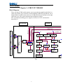
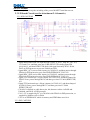
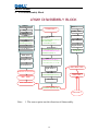
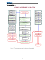
Service Manual
Service Manual
LCD Monitor P2210
-0-
1
Service Manual Versions and Revision
No.
Version
Release Date
Revision
1
1.0
2009-01-07
Initial Release
2009-03-01
Add minimum luminance spec (Chapter
5), ways to find the label Card (where
agency label and S/N is located-Chapter
6)
2
2.0
Copyright
Copyright 2007 InnoLux Display. Corp. Ltd
All Rights Reserved
This manual may not, in whole or in part, be copied, Photocopied, reproduced, translated, or converted to a
electronic or machine readable form without prior written permission of Foxconn Tech. Corp. Ltd.
Dell P2210 Service Manual
Service Manual
Table of Contents
CHAPTER 1- PRECAUTIONS & SAFETY NOTICES ............................................................................................................
1.
2.
3.
SAFETY PRECAUTIONS ...........................................................................................................................................
PRODUCT SAFETY NOTICE................................................................................................................................
SERVICE NOTES ........................................................................................................................................................
CHAPTER 2- SERVICE TOOLS & EQUIPMENT REQUIRED ............................................................................................
CHAPTER 3- CIRCUIT THEORY .............................................................................................................................................
1.
2.
3.
4.
5.
6.
7.
8.
BLOCK DIAGRAM ..........................................................................................................................................................
ELECTRONIC CIRCUIT THEORY ................................................................................................................................
FACTORY PRESET TIMING TABLE .........................................................................................................................
POWER ON/OFF SEQUENCY ...........................................................................................................................................
D-SUB CONNECTOR PIN ASSIGNMENT .........................................................................................................................
AC OUTLET PIN ASSIGNMENT ................................................................................................................................
INNER CONNECTOR PIN ASSIGNMENT ...........................................................................................................................
KEY PARTS PIN ASSIGNMENTS................................................................................................................................
CHAPTER 4- DISASSEMBLY & ASSEMBLY ..........................................................................................................................
1.
EXPLODED DIAGRAM ....................................................................................................................................................
2.
3.
P2210 DISASSEMBLY BLOCK ................................................................................................................................
ASSEMBLY BLOCK .........................................................................................................................................................
CHAPTER 5- TEST AND ADJUSTMENT ................................................................................................................................
1.
2.
3.
4.
5.
FUNCTION KEY DEFINITIONS .........................................................................................................................................
OSD CONTROL..............................................................................................................................................................
FACTORY MODE INTRODUCTION ................................................................................................................................
BURN-IN PATTERN .........................................................................................................................................................
AUTO COLOR BALANCE (AUTOMATICALLY CALIBRATE CHIP ADC PARAMETER BY USING CHIP
INTERNAL DAC.) .........................................................................................................................................................................
6.
UPLOAD FIRMWARE TO MCU VIA VGA CABLE .............................................................................................................
7.
AFTER REPAIR, TO ENSURE THE QUALITY YOU SHOULD DO THE FOLLOWING TEST AND
ADJUSTMENT. ...............................................................................................................................................................................
CHAPTER 6- TROUBLE SHOOTING ................................................................................................................................
1.
2.
3.
4.
5.
6.
COMMON ACKNOWLEDGE .............................................................................................................................................
NO POWER LED OFF .....................................................................................................................................................
POWER NORMAL LED AMBER ................................................................................................................................
BACKLIGHT CAN’T BE TURNED ON ................................................................................................................................
NO PICTURE BACKLIGHT ON ................................................................................................................................
AT 32-GRAY SCALE PATTERN, COLOR LOST IN SOME SCALE ............................................................................................
CHAPTER 7- RECOMMENDED PART LIST ..........................................................................................................................
ATTACHMENT 1- BILL OF MATERIAL ................................................................................................................................
2
Service Manual
Chapter 1- PRECAUTIONS & SAFETY NOTICES
SAFETY PRECAUTIONS
This monitor is manufactured and tested on a ground principle that a user’s
safety comes first. However, improper used or installation may cause
damage to the monitor as well as to the user.
WARNINGS:
l
This monitor should be operated only at the correct power sources
indicated on the rating label on the rear cover of the monitor. If you’re
unsure the power supply in your residence, consult your local dealer or
Power Company.
Use only the specified power cord that comes with this monitor.
Do not try to repair the monitor by yourself, as it contains no
user-serviceable parts. This monitor should only be repaired by a
qualified technician.
Do not remove the monitor cabinet. There is high-voltage parts inside
that may cause electric shock to human bodies.
Stop using the monitor if the cabinet is damaged. Have it checked by a
service technician.
Put your monitor only in a lean, cool, dry environment. If it gets wet,
unplug the power cable immediately and consult your closed dealer.
Always unplug the monitor before cleaning it. Clean the cabinet with a
clean, dry cloth. Apply non-ammonia based cleaner onto the cloth, not
directly onto the class screen.
Do not place heavy objects on the monitor or power cord.
l
l
l
l
l
l
l
PRODUCT SAFETY NOTICE
Many electrical and mechanical parts in this chassis have special safety
visual inspections and the protection afforded by them cannot necessarily be
obtained by using replacement components rated for higher voltage, wattage,
etc. Before replacing any of these components read the parts list in this
manual carefully. The use of substitute replacement parts, which do not have
the same safety characteristics as specified in the parts list, may create shock,
fire, or other hazards.
SERVICE NOTES
l
When replacing parts on circuit boards, clamp the solder wires around
terminals before soldering.
l
Keep wires away from high voltage, high temperature components and
sharp edges.
l
Keep wires in their original position so as to reduce interference.
l
Adjustment of this product please refers to the user’ manual.
l
Use Pb free solder wire for circuit board preparation.
3
Service Manual
Chapter 2- SERVICE TOOLS & EQUIPMENT REQUIRED
1.
2.
3.
4.
5.
6.
7.
8.
9.
SIGNAL GENERATOR
MULTIMETER
SCREW DRIVER
OSCILLOSCOPE
Soldering IRON
SOLDER (Lead free, RoHS compliance)
Color Analyzer
Realtek ISP_Programmer
Fox_VEDID_Programmer
4
Service Manual
Chapter 3- CIRCUIT THEORY
Block Diagram
There are 4pcs PCBA in this monitor, one is power& inverter& board which is a
single layer board, one is interface board including USB HUB 1up/4down, one is
keypad which is OSD control, and one is USB transfer board located on the right
side back cover. The system function block diagram as below
This is included switching power supplier, inverter for CCFL and interface
board.(fig.1)
INVERTER
POWER
DCR Control
Brightness Control
Inverter
Transformer
Panel
Lamp2
+16V
Snubber
&Schottky
Snubber
&Schottky
DC output
+5V
DC output
+12V
Snubber
&Schottky
Feedback
and OVP
Power
Transformer
MOSFET
2
DC output
+16V
1
ON/OFF Control
DCR Control
Brightness Control
To
Lamp2
ON/OFF Control
Regulator&
Filter
Circuit
Inverter IC
INL837
Rectifier&
Filter
Circuit
CCFL
Feedback
Control
AC Line Filter
AC Input
90V~264V
Fig.1
5
Power
MOSFET
Photocoupler
Power PWM
Control IC
LD7575
DC JACK
For Audio
Service Manual
Fig.12
6
Service Manual
Electronic Circuit Theory
2.1 Inverter PWM circuit
2.1.1)Inverter Control circuit:(fig.2)
+5V
R1
10R
DIM
3 DIM
R9
100K
+16V
C1
R11
R12
2.2uF/10V
3.3M
91K 1%
T1A
OLP1
PID_Input
R13
1M
OLP2
C13
10nF/25V
R15
U2
D10
1
1N4148
2
3
10K
4
C11/Open
C2
D1
G1
D1
S2
D2
G2
D2
C23
1nF/50V
8
R29
C24
33R
7
0.1uF/50V
6
C22
1nF/50V
5
R30
33R
U1
R2
0.1uF/25V
1
1nF
S1
100K
DRV1
DRV2
VDDA
GNDA
DIM
TIMER
P6006HVG
16
T1B
2
R28
5K/Open +5V
3
4
ISEN
R4
10K
5
C10
R5
47K
PID
6
CT
SSTCMP
RSTR
LCT
15
14
C5
2.2uF/16V
13
12
11
2.2uF/10V
R8
7
R6
100K
R7
330k
8
RT
OVPT
ENA
VSEN
10
C7
C8
C9
820K
10nF
47nF/16V
9
270pF/16V NPO
T1A
+16V
INL837
T1B
ZD3
R3 10K
3
R24
1
C33A
3
ON/OFF
2
R16
C3
100K
10nF/25V X7R
C14
1M
BAV70
C26
2200p
10nF/25V X7R
C35A
C35A
4.7K
R14
ISEN1
C25
2200p
R20
100K
DIM
ON/OFF
+5V
2
C36A
BAV70
C28
120p/Open
R26 0R
2
C27
R23 120p/Open
30K/Open
R22
30K/Open
ISEN2
3
1
C6
C33A
C34A
3
R10
OLP1
PID_Input
ZD4/Open
1
R17 10K/Open
R21
100K
ISEN1
ZD5/Open BAW56
C16
C18
27nF/Open 27nF/Open
200k/Open
10nF
1N4148
D9/Open
R18
0R
3.3V Lightest
DIM
CN1
D51
1
2
0V of lightest
C33
10
3
4
7
T1A
R31
470R 1%
CN3
C33A
3.3V ON
1
2
CN2
CCFL_ON/OFF
+16V
0V
OFF
4100-D02
1N4148/short
3pF/3KV NP0
C31
10pF/3KV NP0
T1
1
OLP1
1
2
NC
4100-D02
C40
470uF/35V
6
R32
T1B
C35
DIP EEL19 SPW-080
470R 1%
3pF/3KV NP0 ISEN1
D5
1N4148
CN4
1
2
NC
R19
680R
C35A
L858
D6
1N4148
CHK-053
PIN1
PIN2
PIN3
PIN4
PIN5
PIN6
PIN7
PIN8
PIN9
PIN10
PIN11
PIN12
PIN13
PIN14
PIN15
PIN16
PIN17
PIN18
PIN19
PIN20
1
2
3
4
5
6
7
8
9
10
11
12
13
14
15
16
17
18
19
20
C33A
+5VU
ON/OFF
DIM
R33
C46
OLP1
ISEN1
PID
1K 1%
4.7uF/16V
C35A
T1B
+16V
T1A
CN5
Title
Inverter DC to AC
Size
A4
Date:
Fig.2
7
Document Number
Wednesday , December 24, 2008
Sheet
4
of
Service Manual
+5VDC provides the power for U1; the control signals Brightness and
R15 makes up a divided voltage network ,DCR and ON/OFF come from I/F
board. ON/OFF signal connected to pin8 of U1 makes U1 enable. Brightness
signal connected to pin3 of U1 regulates the brightness of panel .PID connected
to pin5 of U1 control the monitor under the condition of DCR .TIMER makes
up a network of delaying time circuit and, C5 is used to control start-up timing.
The operation frequency is determined by the external Resistor R7 connected to
pin7 of U1 and R12 connected to pin13 of U1. C8 is used for soft start and
compensation.
The output drives, include DRV1, DRV2 (pins1,16 respectively) output
square pulses to drive MOSFET U2 and each of them is consist of a 2N channel
MOSFET.U2 works as push-pull structure, and it is high efficient, PWM
switching.
During start up, VSEN (pin9) senses the voltage at the transformer
secondary. When VSEN reaches 3.0V, the output voltage is regulated. If no
current is sensed for approximately 2 seconds U1 will shut off.
The current flowing through CCFL is sensed and regulated through sense
resistor R31. The feedback voltage connected to Pin4 (ISEN), then compared
with a reference voltage (1.2V) via a current amplifier, resulting that PWM
drive U1 to work and output square pulses .
2.1.2)Protection Circuit
Over-voltage and over-current protection are monitored by the voltage on
VSEN(pin9).During normal operation, if a CCFL is damaged or removed, the voltage
at VSEN exceeds the user-defined, preset voltage set by OVPT(pin10),the driver
output duty cycle is regulated and the shutdown delay timer is activated. OVPT sets
the overall protection threshold voltage that is lower than3V(VSEN threshold. Once
the voltage at TIMER pin reaches 3V,the IC will shut down and latch. OVPT voltage
setting is determined by a resistor divider (R9 and R13)connected to the OVPT.
The over-voltage protection feature is implemented by using an external
capacitor divider (C26 and C25) to sense the output voltage. The divide-down voltage
signal is sent to the IC Pin9(VSEN) ,thus regulate the output voltage.
If a CCFL is removed, fails or is damaged during normal operation, CCFL
current is no longer sensed and the voltage on ISEN pin drops. The voltage at the
SSTCMP(pin2)rises rapidly because there is no current feedback at ISEN(pin4).When
the voltage at SSTCMP reaches a threshold of approximately 2V and ISEN is less
than 1.2V,a current source charges the capacitor(C5) connected to
TIMER(pin14).Once the voltage level at the TIMER pin reaches a threshold of
approximately 3V,the drive outputs shut down and latch.To resume operation,toggle
the ENA signal or restart VDDA.
2.2 Power PWM circuit
2.2.1) Block diagram:(fig.4)
8
Service Manual
DCR Control
Brightness Control
ON/OFF Control
DC output
+16V
Snubber
&Schottky
Snubber
&Schottky
DC output
+5V
DC output
+12V
Snubber
&Schottky
Regulator&
Filter
Circuit
Feedback
and OVP
Power
Transformer
Power
MOSFET
DC output +12V
Rectifier&
Filter
Circuit
Photocoupler
Power PWM
Control IC
LD7575
AC Line Filter
AC Input
90V~264V
DC JACK
For
Audio
1
2.2.2) AC Input and EMI Filter:(fig.5)
+
BL4-06
2
3
D850
4
C852
0.47uF X2
R850
1
3
TVS
AC INPU
750K
RT850
C850
F850
222 Y2
8R5A
fig.5
CN850 is a connector for connecting AC Power. F850 is a fuse to protect all
the circuit AC. Input voltage is from 90V to 264V. R850/R851 are joined between
two inputting main circuit to prevent man from shock. L850 is used to filter low
frequency noise. C850 and C851 are used to discharge the noise that L850 produced.
9
AC 10A/250
222 Y2
VZ850
17mH CHK-090
4
C851
750K
3.15A 250V
1
2
3
-
R851
L850
Service Manual
High frequency waves are damped by C852;
2.2.3)High Voltage to Low Voltage Control Circuit:(fig.6)
10
Service Manual
R849
C846
3
I sense
NC
7
220R
HV
8
CN852
220pF/50V
D849
open/22V
U850
LD7575
1
Signal_GND
2
5
OUT
GND
4
3
R842
2
Vcc
4
20K
Isense
GND
FB
6
R847
5.1R/open
5
GND
1
COMP
RT
Signal_GND
Gate
6
C847
Open
R846
100K/ 1%
7
NC
R843
8
C849
VDD
C848
HV
20K
100nF/50V
CON8PIN
1nF/50V
Signal_GND
Signal_GND
R848
Signal_GND
20R
R841
10K
Signal_GND
Title
Size
A4
Date:
Power control BD LD7575
Document Number
<Doc>
Monday , February 16, 2009
fig.6
D850 is a rectifier in which there are 4 build-in diodes, inverting AC to DC.
C854 is used to smooth the wave from rectifier. U850 is a highly integrated
PWM controller. Typical start-up current for U850 is only 20 uA,
When current
flow through R842/R843 gets to Pin 8 of U850, with VDD hold-up capacitor C878,
U850 is enough for starting up.
When U850 begins to operate Pin5 of U850 will output square wave to drive
Q850, then the main current flow get to GND bypassing through T850, Q850.
Because of the change of current flow, wires in the other side of T850 will induct
current. In the same time, the current inducted by wires which connected T850 Pin 1
and Pin 3, with components of D852, R856and C878 ,will be supplied to U850 for
normal operating.
When the sense voltage across the sense resistor R869, reaches the threshold
voltage around 0.85v, the output GATE drive will be turned off. Every time when
the output of power supply is shorted or over loaded, the FB voltage will increase,
the build-in PWM output will then be turned off. Both of two will prevent the
power supply from being overheated under over loading condition. The PWM duty
cycle is determined by this current sense signal and COMP, the feedback voltage,
when the voltage on pin2 reaches V-(PWMcopm) =(Vcomp-2VF)/3, A switch cycle
will be terminated immediately, Vcomp is internally clamped to a variable voltage
around 0. 85 V for output power limit
When Q850 are turned off, the main current flow will be consumed through
11
Sheet
3
Service Manual
D851, C858, R854 and D853, This will prevent Q850 from being damaged under
large current impulse and voltage spike.
2.2.4) DC_16V ,12V and 5V Output Circuit and Feedback circuit: (fig.7)
C861
1000p/1kV
R862
10R 2W
D854
NC/SF50-04
L852
CHK-069
+16V
3
SF50-04
C880
1000p/1kV
R880
10 2W
D880
B
R887
R886
10K
12
.
Q851
2N4401
E
10K
Q852
F852
5A/125V
SB5200
R888
510R 2W
C
470u/35V
11
1
+12V
L854
CHK-111
AP9972
3
SB5200
C884
7
470u/25V
Q853
R871
+
2N3906
+16V
R875
10K
2
D881
1
1
1K 1/4
8
ZD882
+ C881
C882
GDZ18B 18V
+
470u/25V
D882
470u/25V
6
5
1N4148
.
.
9
10
20K 1%
R873
10K
R876
C889
3300p/250V
R870
47nF/50V X7R
I880
Audio_On/Of f
Q854
2N4401
C891
10K
C883
3300p/250V
T850-01
SPW-118
C885
10K
3
1
TL431
0.1/50V
R878
10K
2
R874
1M
R866
C866
3
39K
2
R872
R877
3
D855
T850
SPW-118NC
Z D880
GDZ18B 18V
+ C862
470u/35V
4
+ C865
12
.
1000p/1kV 10 2W
11
+5V
L851
1
1
2
3
C874
7
+5VU
CHK-069
D856
100V10A
+
1000u/25V
+
C864
C875
1000u/25V
+
470u/25V
C877
C876
0.1/50V
0.1/50V
8
6
5
.
.
9
10
R857
270
+5VU
R861
4.3K
I850
LTV817
4
1
3
2
R858
5K1 1%
ON/OFF
C863
DIM
Audio_detect
R859
0.1/50V
10K 1%
C859
Audio_On/Of f
10
11
PID
0.1/50V
3
12
+5V
I851
1
TL431
2
R890
6.34K
R892
10K
C890
D
10K
Q890
S
R860
2N7000
1nF/50V
G
R891
10K
C892
R893
39K
fig.7
D854&D855 are used to rectify the inducted current. C865 and C862 are used to
store energy when current is reversed. The parts including L852 are used to smooth
the current waves that are from D854&D855, and then 16V voltage is supplied.
D880&D881 are used to rectify the inducted current . C884 is used to store energy
when current is reversed. The parts Q852 is a switch and is controlled by Q853 ,and
then 12V voltage is supplied.
D856 is used to rectify the inducted current. C874,C864 are used to store energy
when current is reversed. The parts including L851,and C875 are used to smooth the
current waves that are from D856, and then 5V voltage is supplied.
5V supply voltage feed back to PWM controller U850 via R861, R860,and
I850,I851.R859,C859 and C863 are used to control response time.
LD7575 implements an OVP function on Vcc .Whenever the Vcc voltage is
higher than the OVP threshold voltage, the output gate drive circuit will be shutdown
12
1nF/50V
Service Manual
simultaneously thus to stop the switching of the power MOSFET until the next on.
2.3 I/F Board Circuit (see the Attachment 2- Schematic)
2.3.1 RGB CAPTURE
- Signal RED,GREEN,BLUE input through CN102 #1,#2,#3, Stop DC via C114,
C115 and C116, and then enter into U404 (RTD2375D) analog input PIN
#16,#14,#12, and then RTD2375D deals with signal internally. D103, D104,
D105 are ESD protector to prevent U404 from ESD.
- Signal DDC_SCL (series clock) inputs via CN102#15, and then passes through
ZD106 for ESD protection, goes into EDID EEPROM IC U103 #58
- Signal DDC_SDA (series data) inputs via CN102#12, and then passes through
ZD103 for ESD protection, goes into EDID EEPROM IC U103 #59.
- Signal TTL vertical sync. (Vsync) inputs via CN102 #14, and then clamped by
ZD105 Zener, passes through R134, and then goes into IC U404 (RTD2375D)
#21
- Signal TTL horizontal sync. (Hsync) inputs via CN102 #13, and then clamped
by ZD102 Zener, passes through R133, and then goes into IC U404
(RTD2375D) #22.
- CN102#5 is defined as cable detect pin, this detector realize via R450 and
U404#64, and D102 is ESD protector.
- U103 +5V is supplied by PC via CN102#9 with ZD102 for ESD protection, or
supplied by Monitor self via D106
- U103 is an EEPROM IC which is memory and EDID data saved in it.
2.3.2 DVI CAPTURE
13
Service Manual
CN201
DVI-D_CON
VCC5V
R203
R204
10
10
DVI_RX0DVI_RX0+
R205
R206
10
10
DVI_RXC+
DVI_RXC-
R207
R208
10
10
14
15
16
4
5
11
12
13
20
21
5
5
RX1RX1+
5
5
RX0RX0+
5
5
RXC+
RXC-
5
5
DVI5V
Note 1
R209
R210
1
DVI_RX1DVI_RX1+
RX2RX2+
2
10
10
D201
BAV70
C201
0.1/16V
3
R201
R202
DVI_SCL
DVI_SDA
R211 R212 R213
4K7
4K7 10K
R214
1K
100
100
DVI_DET
HPD_DVI
U201
AT24C02BN
8
7
6
5
VCC
WP
SCL
SDA
WP_EDID 3,5
DDC_SCL_DVI 5
DDC_SDA_DVI 5
DVI_DET 5
DVI_DET
HPD_DVI
A0
A1
A2
GND
1
2
3
4
GND
VCC_ESD
R217
10K
C204
0.1/16V
C206
0.1/16V
C208
0.1/16V
C210
0.1/16V
R218
100/NC
HPD_DVI
Q201
PMBT3904
2
D209
BAV99
1
DVI5V
DVI5V
3
C211
0.1/16V/NC
Note 2
6V2/NC
3
3
2
D210
BAV99
1
C213 0.1/16V
D207
BAV99
1
C209
0.1/16V
2
6V2
2
D208
BAV99
1
ZD202
C207
0.1/16V
2
6V2
D205
BAV99
1
3
3
2
D206
BAV99
1
ZD204
D203
BAV99
1
C205
0.1/16V
2
C212 0.1/16V/NC
2
D204
BAV99
1
ZD203
C203
0.1/16V
2
3
ZD201
D202
BAV99
1
3
2
3
3
DVI5V
6V2
5V
GND
HP
RX4RX4+
GND
RX3RX3+
RX5RX5+
6
7
8
DVI_RX2DVI_RX2+
3
SCL
SDA
VS
1
2
3
9
10
19
17
18
22
23
24
C202 0.1/16V
RX2RX2+
GND
RX1RX1+
GND
RX0RX0+
GND
RXC+
RXC-
1
R219
4K7
GND
GND
- Differential Signal input RX0+,RX0-,RX1+,RX1-,RX2+,RX2-,RXC+,RXCthrough CN201 #18,#17,#10,#9,#2,#1,#23,#24 via
R206,R205,R204,R203,R202,R201,R207,R208 enter into U404 (RTD2375D)
Digital input terminal #4,#5,#2,#3,#47,#48,#6,#7, and then RTD2375D deals
with signal internally. D206, D207, D204, D205, D202, D203, D208, D209
are ESD protector to prevent U404 from ESD
- Signal DDC_SCL (series clock) inputs via CN201#6, and then passes through
ZD204 Zener for ESD protection, via R209, goes into EDID EEPROM IC
U201 #6.
- Signal DDC_SDA (series data) inputs via CN201#7, and then passes through
ZD203 Zener for ESD protection, via R210, goes into EDID EEPROM IC
U201 #5.
- CN201#15 is defined as cable detect pin, this detector realize passes through
R449, go into U404#63, and D210 is ESD protector.
- U201 +5V- U201 is an EEPROM IC which is memory and DVI input EDID
data saved in it.
is supplied by PC via CN201#14 through D201, or supplied by Monitor self
via D201.
2.3.3 DP CAPTURE
14
HPD_CTRL 5
HDCP Function
Service Manual
- Main Link signal
LANE3N,LANE3P,LANE2N,LANE2P,LANE1N,LANE1P,LANE0N,LANE0
P through CN105 #1,#3,#4,#6,#7,#9,#10,#12 enter U404 RTD2375D
#10,#9,#8,#7,#6,#5,#4,#3, and then RTD2375D deals with signal internally,
D201, D202 are ESD protector to prevent U404 from ESD,
- CN105#16 is defined as cable detect pin, this detector go into U404#108, and
ZD283 is ESD protector.
- AUX Channel signal DAP,DAN through R291,R294,C424,C425 enter U404
RTD2375D #123,#124,through R292,R293 enter U404 RTD2375D
#53,#54,EP281,EP282 are ESD protector to prevent U404 from ESD damage.
2.3.4 Buttons Control
15
Service Manual
- CN402 #8 Button “Power” on front bezel through R420 and pull high R434
connects to U404 (RTD2375D) #67.
- CN402 #1 Button “+” on front bezel through R419 and pull high R439
connects to U404 (RTD2375D) #68.
- CN402 #2 Button “-” on front bezel through R457 and pull high R459
connects to U404 (RTD2375D) #48
- CN402 #4 Button “Menu” on front bezel through R412 and pull high R411
connects to U404 (RTD2375D) #66 .
- CN402 #3 Button “SELECT” on front bezel through R458 and pull high R460
connects to U404 (RTD2375D) #14 .
- LED Indicator on Front Bezel
a. When press button “power”, U404 (RTD2375D) #112 be send in low
Voltage, make Q401#3 sends out high Voltage , and then to CN401#5 on
keypad, LED blue on.
b. When in “Suspend” mode, U404 (RTD2375D) #113 sends out a low
Voltage, make Q402#3 sends out high Voltage and then to CN402 #7 on
keypad, LED Amber ON.
2.3.5 MATAR CHIP U404 (RTD2375D)
- U404 (RTD2375D) #86~#95 output 8 bit even and #74~#83 output 8 bit odd
LVDS digital data to panel control circuit through CN401.
- U404(RTD2375D) #71 output PPWR ”H” potential to make Q104 conducted,
and then make Q101 conducted, +5V flow to CN401#1~#3 as Panel Vdd .
- U404(RTD2375D) #101 output CCFL_ON/OFF ”L” potential to control
Inverter on/off.
- U404(RTD2375D) #102 outputs Brightness “PWM” signals to control CCFL
16
Service Manual
brightness.
- TCLK by Crystal 27MHz input to U404(RTD2375D) #127#128.
- U404(RTD2375D)#125 is RESET signals input pin
Please refer to U404 (RTD2375D) Pin Assignments table in page
2.3.5 Regulator Circuit
- +3.3V is generated from Regulator U101 which is supplied by+5V via R101
and through C102 filtering,
-+1.2V is generated from Regulator U102 which is supplied by+3.3V via R104
through C103 filtering,
3. FACTORY PRESET TIMING TABLE
6.1 Acceptable Signal Description
Horizontal Frequency
Vertical Frequency
Sync. Polarity
30KHz to 83KHz
56Hz to 75Hz
Independent Sync. Polarity
1680x1050@60Hz(For analog input)
1680x1050R@60Hz(For digital input)
6.2 Prime Mode
6.3 Preset Display Modes
1. VGA 640 x 480 @ 59.94Hz (31.469KHz)
2.VESA 640 x 480 @ 75Hz (37.5KHz)
3.VGA 720 x 400 @ 70.087Hz (31.469KHz)
4.VESA 800 x 600 @ 60.317Hz (37.879KHz)
5.VESA 800 x 600 @ 75 Hz (46.875KHz)
6.VESA 1024 x 768 @60.004 Hz (48.363KHz)
7.VESA 1024 x 768 @ 75.029Hz (60.023KHz)
8.VESA 1280 x 1024 @ 60.02Hz (64.00KHz)
9.VESA 1280 x 1024@ 75.02Hz (79.976KHz)
10.VESA 1152 x 864 @ 75Hz (67.5KHz)
11. CVT1680x1050@60Hz(55.935KHz,For analog input)
CVT-R 1680x1050@60Hz(55.496KHz,For digital input)
6.4 Abnormal Mode
640 x 400 @ 70Hz (31.5KHz)
Does not need to be a preset timing, but must display a picture. This is the Windows 98 start
up screen. Only centering is required, not fully scaled.
4. Power On/Off Sequency
Hardware power On/Off
When power cord plug into AC socket, Power provides 24V and DC_5V.
DC_5V is main voltage for panel and Regulator U101.
DC_3.3V is coming from Regulator U101, DC_3.3v is main voltage for U404.
When DC_3.3V input to U404 and U404 reset circuit active, U404 all registers
will be set to default, that means finish hardware power on.
DC_1.2V is coming from Regulator U102, DC_1.2v is main voltage for U404.
When pull out power cord from AC socket, the system shut down instantly for no
supply
Software power On/Off
17
Service Manual
- When press power key, U404 #67 receives low pulse, then U404(RTD2375D)
will be wake up and send control signals(at 101,71pin) to on CCFL and switch
5.0v to panel module, at the same time,U404 make the VGA/DVI/DP cable
input signal source display normal on panel if the VGA/DVI/DP cable input
signal is active
- If power ON, U404 #112 (LED_Blue) will send out low potential, and then LED
blue on.
- If power saveing, U404 #113 (LED_Amber) will send out low potential, and
then LED Amber on.
- If power ON or power saving, when press power key, U404 #67 receives low
pulse, then U404 will be sleeping and turn off backlight, at the same time, the
panel will lose +5V.
The Panel_Vcc, Backlight_En, CLK/DATA output to panel will follow the following
sequency.
18
Service Manual
Values
Parameter
Units
Min
Typ
Max
T1
0.5
-
10
ms
T2
0.01
-
50
ms
T3
500
-
-
ms
T4
200
-
-
ms
T5
0.01
-
50
ms
T7
1
-
-
s
5. D-SUB Connector Pin Assignment
Pin
1
2
3
4
5
Symbol
Red
Green
Blue
GND
Cable Detect
Pin
6
7
8
9
10
Symbol
Red_GND
Green_GND
Blue_GND
PC+5V
GND
Pin
11
12
13
14
15
Symbol
GND
DDC_SDA
Hsync
Vsync
DDC_SCL
2
6. AC Outlet Pin Assignment
1
3
CN850
Pin
1
2
3
Symbol
Line
GND
Neutral
7. Inner Connector Pin Assignment
7.1 CN103 (Connect M/B to Panel,)
Pin
Symbol
Description
1
Panel_Vcc
Panel power supply (typ.5.0V)
2
Panel_Vcc
Panel power supply (typ. 5.0V)
19
Service Manual
3
4
5
6
7
8
9
10
11
12
13
14
15
16
17
18
19
20
21
22
23
24
25
26
27
28
29
30
Panel_Vcc
NC
NC
NC
GND_LVDS
RXE3+
RXE3RXEC+
RXECRXE2+
RXE2GND_LVDS
RXE1+
RXE1GND_LVDS
RXE0+
RXE0RXO3+
RXO3RXOC+
RXOCGND_LVDS
RXO2+
RXO2RXO1+
RXO1RXO0+
RXO0-
Panel power supply (typ. 5.0V)
LVDS Ground
LVDS signal of even channel 3(-)
LVDS signal of even channel 3(+)
LVDS signal of even channel clock (+)
LVDS signal of even channel clock (-)
LVDS signal of even channel 2(+)
LVDS signal of even channel 2(-)
LVDS Ground
LVDS signal of even channel 1(+)
LVDS signal of even channel 1(-)
LVDS Ground
LVDS signal of odd channel 0(+)
LVDS signal of odd channel 0(-)
LVDS signal of odd channel 3(+)
LVDS signal of odd channel 3(-)
LVDS signal of even channel clock (+)
LVDS signal of even channel clock (-)
LVDS Ground
LVDS signal of even channel 2(+)
LVDS signal of even channel 2(-)
LVDS signal of even channel 1(+)
LVDS signal of even channel 1(-)
LVDS signal of odd channel 0(+)
LVDS signal of odd channel 0(-)
7.2 CN1, CN2, CN3, CN4 (Connect to Panel Backlight,)
Pin
Symbol
Description
1
HV
High voltage for lamp
2
LV
Low voltage for lamp
20
Service Manual
8. Key Parts Pin Assignments
U404(RTD2375D)
21
Service Manual
22
Service Manual
23
Service Manual
24
Service Manual
25
Service Manual
26
Service Manual
8.3 U850 (LD7575B, PWM Power Controller)
Pin
Symbol
I/O
Description
1
RT
I
This pin is to program the switching
frequency. By connecting a resistor to
ground to set the switching frequency.
2
COMP
I
Voltage feedback pin(same as the COMP pin
in UC384X).By connecting a photo-coupler
to close the control loop and achieve the
regulation.
3
CS
I
Current sense pin, connect to sense the
MOSFET current;
4
GND
Ground
5
OUT
O
Gate drive output to drive the external
MOSFET
6
VCC
I
Supply voltage pin
7
NC
Unconnected pin
8
HV
I
Connect this pin to positive terminal of bulk
capacitor the startup current for the
controller. When Vcc voltage trips the
UVLO(on),this HV loop will be off to save
the power loss on the startup circuit;
8.4 U1 (INL833, CCFL Inverter controller IC)
Pin
Symbol
I/O
Description
1
I
VSEN
Voltage sense Feedback
2
SSTCMP
Capacitor for soft-star and loop
I
compensation
3
CT
Timing resistor and capacitor for
I
operation and striking frequency
4
RT1
Timing resistor for striking frequency
5
GNDA
6
PDR2
7
GNDP
8
NDR2
O
Low side Driver output2
9
NDR1
O
Low side Driver output1
10
PDR1
O
High side Driver output1
11
VDDA
I
Input power Pin
12
TIMER
I
Timing capacitor for Delay Timer
13
PWM
I
External PWM Dimming Input
14
ISEN
I
Current sense feedback
I
Signal Ground
High side Driver output2
O
Power Ground
27
Service Manual
15
OVPT
Over-voltage protection threshold
I
voltage
16
ENA
IC Enable/Disable
I
28
29
Desi gnat i on
SHI ELD EMI
3- H
LP2207
CLI P, EMI GND( 3)
502120400300R
502040400600R
4
Bol t , #4- 40* 12. 5, Ni
Scr ew, P, Cr oss, T. T- 3* 4, Zn 509112304100R
3- f
3- g
2
SPRI NG, Φ 0. 5* D5* H17
3- e
Scr ew, P, Cr oss, M4* 10, Bl ack- NL
sl i de, LE22F4
3- d
504010000300R
f i x- pl at e- r i ght , LE19E6
3- c
PCBA, USB_BOARD
LVDS FFC
1
1
1
1
2
2
f i x- pl at e- l ef t , LE19E6
3- b
1
509146306202R
509212103500R
509016304200R
509016305200R
509116610510R
509000001000R
509016306200R
509446309100R
Scr ew, B, CROSS, W/ W- SPR, M3* 9, Zn
Scr ew, I , Cr oss, M3* 6, Zn- Cc
Scr ew, I , Cr oss, M3* 5, Zn- Cc
SCREW, F, CROSS, T. T- 2* 3, BLK
Scr ew, I , Cr oss, M3* 4, Zn- Cc
502040604700R
502040604800R
506380001730R
503020004500R
506250030100R
714011207500R
I dent i f i cat i on NO.
4
3
1
4
4
7
4
1
1
1
1
1
1
1
2
1
2
1
Q' t
S- 3
Scr ew, P, Cr oss, W/ WAS( 7. 8) , M3*6, Zn- Cc
PCBA, KEYPAD BOARD, LP2261
PCBA, I / F BOARD, W/ O SPK, LP2261
PCBA, P/ I BOARD, W/ O SPK, LP2261
PANEL
LABEL, CARD, LP2261
RUBBER, FOOT, 10* 3, f or cmo
TAPE, ACE, 85* 20mm, LE1913
SHI ELD LI GHT LP1703
701000016000R
502090317200R
502020306000R
502020306010R
502040500100R
SHI ELD, USB, LP1703 ROHS
Desi gnat i on
1
1
1
NO.
501020232400R
502210100400R
501030210502R
Remar k
1
1
1
1
1
1
Q' t
S- 1 S- 7 S- 6 S- 5
714030026300R
501010202300R
501030211500R
501120109500R
501110200400R
714050023800R
I dent i f i cat i on NO.
3- a
ASSY, CHASSI S, FOR LP2261
KENSI NGTON LOCK LE1963
r el ease- but t on, LE22F4
BACK, COVER , LP2261
ASSY, BACK, COVER, LP2261
LOGO Pl at e DELL UX383 LE1963
POWER BUTTON LENS, LP2236, DARK SMOKED
BUTTON, LP2236, BLACK
BEZEL, FRONT, LP2261
ASSY, BEZEL, FRONT, LP2261
CHASSI S, FOR LP2261
NO.
S- 2
AC- Socket t o chassi s / DP t o chassi s
f or LGD panel
f or CMO/ I nnol ux panel
Remar k
S- 1
St ar . hu
2008/ 11/ 21
S- 4
LP2261
Expl oded Dr awi ng ( BLACK)
Service Manual
Chapter 4- Disassembly & Assembly
1. Exploded Diagram
Service Manual
2. P2210 Disassembly Block
LP2261 DISASSEMBLY BLOCK
chassis* 1
slide* 1
button *1
CHASSIS ASSY * 1
spring* 2
fix-plate1* 1
(P,cross,T.T-3* 4,Zn)*1
fix-plate2* 1
(P,cross,T.T-3*4,Zn)*1
I/F board* 1
FFC-CABLE*1
(P,Cross,W/WAS,M3*6,Zn-Cc)*2
(BOLT,#4-40,NI)*4
( I , Cr oss, M3* 6, Zn- Cc) * 1
back cover*1
kensington lock*1
power board* 1
(P,Cross,W/WAS,M3*6,Zn-Cc)*4
(B,Cross,W/W-SPR,M3*9,Zn)*1
(I,Cross,M3*6,Zn-Cc)*2
l ogo- UX383* 1
(screw,f,cross,
T-2*3,BLK)*4
panel*1
TAPE ACE 85x20mm LE1913* 1
(I,Cross,M3* 4,Zn-Cc)*4 for CMO/INNOLUX
(I , Cr oss, M3* 5, Zn- Cc) * 4 f or LGD
vesa release button*1
light cover* 2
Rubber Foot * 2 10*3 For Cmo
front bezel * 1
keypad board*1
clip EMI gnd(3)LP1702*2
shield EMI LP2207*4
POWER, LENS* 1
usb board* 1
(P,Cross,W/WAS,M3*6,Zn-Cc)* 1
FRONT BEZEL ASSY * 1
STAND ASSY * 1
LABEL, CARD* 1
usb cover*1
BACK COVER ASSY*1
PANEL ASSY * 1
(P,Cross,M4*10,BLACK-NL)*4
FINALASSY*1
Note: 1. The arrows point out the direction of disassembly.
30
Service Manual
3. Assembly Block
LP2261 ASSEMBLY BLOCK
chassis* 1
slide* 1
button *1
CHASSIS ASSY * 1
spring* 2
front bezel * 1
fix-plate1* 1
(P,cross,T.T-3*4,Zn)*1
fix-plate2* 1
(P,cross,T.T-3*4,Zn)*1
I/F board* 1
FFC-CABLE*1
(P,Cross,W/WAS,M3*6,Zn-Cc)*3
(BOLT,#4-40,NI)*4
( I , Cr oss, M3* 6, Zn- Cc) *1
clip EMI gnd(3)LP1702*2
shield EMI LP2207*4
back cover*1
kensington lock*1
power board* 1
(P,Cross,W/WAS,M3*6,Zn-Cc)*4
(B,Cross,W/W-SPR,M3*9,Zn)*1
(I,Cross,M3*6,Zn-Cc)*2
keypad board*1
(screw,f,cross,
T-2*3,BLK)*4
TAPE ACE 85x20mm LE1913* 1
(I,Cross,M3*4,Zn-Cc)*4
light cover* 2
usb board* 1
(P,Cross,W/WAS,M3*6,Zn-Cc)* 1
LABEL, CARD* 1
l ogo- UX383* 1
panel*1
vesa release button*1
Rubber Foot * 2 10*3 For Cmo
POWER, LENS* 1
FRONT BEZEL ASSY * 1
STAND ASSY * 1
usb cover*1
BACK COVER ASSY*1
PANEL ASSY * 1
(P,Cross,M4*10,BLACK-NL)*4
FINALASSY*1
Note: 1. The arrows point out the direction of assembly
31
Service Manual
Chapter 5- TEST AND ADJUSTMENT
1. Function key Definitions
Hot Key Operation
Key1
To enter Preset modes menu
Key2
To enter brightness/contrast adjust menu
Key3
To enter OSD Main menu
To exit OSD Menu
Key4
Key function defining in Main Menu
Power Switch with power LED indicator
Panel Controls
Factory Modes Keys Function
Power: On/Off, includes power indicator and Power ICON
blue- Active On
Amber- DPMS
1. Key1: When “MENU OSD” displays, press this
key to change
the contents of an adjustment item, or change an
adjustment value(use as up key)
2. Key2: When “MENU OSD” displays, press this key to chang
the contents of an adjustment item, or change an
adjustment value(use as down key)
3. Key3: When “MENU OSD” displays, press this key to Enter
the OSD sub menu
When “MENU OSD” displays, press this key to select t
input source
4. Key4: When “MENU OSD” displays, press this key to back t
previous OSD menu
5. Power: Power on or off the monitor
Auto Color Balance
Purpose: Automatically calibrate chip ADC parameter by using chip internal
DAC.
Process: If we want to do “Auto Color Balance” again, please confirm the
following steps.
1) Connect the VGA cable with the standard video pattern generator and
display the pattern with blackest and whitest colors.
2) Press “Power Key”, to power off the monitor.
3) Press “Key1 ” and “Key2” simultaneously, and then press “Power Key
power on the monitor.
4) Press “Key1”, then entry “Factory mode”.
5) Set Burn In Mode item to ON, then execute Auto Color item
6) After the “Auto Color Balance” process finished, go back to
Main Menu, choose “Other settings” item and press “Key3
enter sub-Menu , then choose “factory reset” item and press
“Key3” again execute Reset all settings. .
32
Service Manual
OSD Control
First
Brightness
Second
Brightness
Contrast
Dynamic Contrast
Third
Default
75
75
off
Auto Adjust
Input Source
Auto Select
VGA
DVI-D
DisplayPort
Input Color Format
Mode Selection
Color Settings
Present Modes
RGB
YPbPr
Graphics
Video
Standard
Multimedia
Game
Warm
Cool
Custom(R,G,
B)
Hue
VGA
Yes(DCR off)
Yes
Yes
Yes
DVI
Yes
Yes
Yes
No
DP
Yes
Yes
Yes
No
Yes
Yes
Yes
Yes
Yes
Yes
Yes
Yes
Yes
Yes
Yes
Yes
Yes
Yes
Yes
Yes
Yes
Yes
No
No
Yes
No
No
Yes
No
No
Yes
No
No
Yes
Yes
Yes
Yes
Yes
Yes
Yes
Yes
Yes
Yes
Yes
Yes
Yes
Yes
Yes
Yes
Saturation
Reset Color Settings
Wide Mode
Display Settings
Fill
4:3
50
50
50
50
Horizontal Position
Vertical Position
Sharpness
Pixel Clock
Phase
Reset Display Settings
English
Espanol
Francais
Deutsch
Language
Other Settings
日本語
Russian
Brazilian
Portuguese
簡體中文
Menu Transparency
Menu Timer
Menu Lock
Menu Rotation
20
20
Unlock
Lock
Landscape
Portrait
33
Service Manual
On
Power Save Audio
DDC/CI
LCD Conditioning
Yes(When
connect sound
bar)
Yes
Yes
Yes
Yes
Yes
Off
Enable
Disable
Disable
Enable
Factory Reset
Yes(When
connect
sound bar)
Yes
Yes
Yes
Yes
Yes
Yes(When
connect
sound bar)
Yes
Yes
Yes
Yes
Yes
Hot Key Operation
HOT KEY OPERATION
FUNCTION
DESCRIPTION
Key1
Key2
FACTORY MODE
●
●
SERVICE
PATTERN
●
Key3
Key4
●
POWER
ON
Press [Key1]& [Key2] at the same time, and then
press [POWER] for DC power on. Press Key1 to enter
factory menu
ON
Press [Key1]& [Key4] at the same time when power
on to enter service pattern.
OSD Message
5.3.1 After disconnecting the cable, Self Test message should show as below:
“NO VGA Cable”
Present input status (1.stands for Auto Detect, 2 stands for VGA input, 3 stands
for DVI input, 4 stands for Display Port), and present input source should be
shown on the top of the message.
5.3.2 After disabling the sync output for VGA (DVI), DPMS message should show
as below for 3s:
Press the "-" or "+" key and the DPMS message should show as below:
."
34
Service Manual
Present input status (1.stands for Auto Detect, 2 stands for VGA input, 3
stands for DVI input,4 stands for DP input)
Upgrade Firmware to Serial via Flash Cable by ISP_Tool V4.100.exe
7.1 Connect the monitor and PC follow Fig 11
Fig 11
※ The detailed reprogramming procedures will be described in ISP User's Guide.
35
Service Manual
Burnedid.exe
BurnEdid Operation
Instructions
E: \ Tool f or
Real t ek\ I SP SOP\ Real t ek I SP SOP. doc
Relteck DebugTool_V6.3.exeDELL P2210 V11.7z
After repair, to ensure the quality you should do the following test
and adjustment.
36
Service Manual
Item
Test OSD
function
Content
Equipment
1.Signal is set as 1680×1050@60Hz under General-1
Chroma
2. LCM button are from left to right, checking whether each
Signal Generator
single function key and compound function key can be worked.
Contrast Check
1. Set input mode to 1680×1050@60Hz
2. Set to 32gray scale pattern
3. Set contrast to the maximum. At most 6 bars cannot be
distinguished.
1. Do “Auto color Balance” at 1680×1050@60Hz, 32gray
scale pattern
2. Measure color temperature, check if it complies with the
following temperature :
Warm x=0.328 +/- 0.03, y=0.344+/-0.03
Desktop x= 0.313 +/- 0.03, y=0.329+/-0.03
Cool x= 0.283 +/- 0.03, y=0.298+/-0.03
1. Use Chroma Pattern Generator to make sequence.
VESA (640x480 800x600 1024x768 1152x864 1280x1024
1680×1050@60Hz ), the detail supported modes (see table 1)
and power saving signal.
2. Confirm the above timing modes must be full screen and
the picture must be normal.
3. LED is amber at power saving mode.
Color
Temperature
Modes switching
check
VGA
detector
cable When select VGA model and VGA cable is not plugged out,
self-test OSD will be floated.
Minimum
1. LCD minimum luminance spec is 200 cd/m2 (0-15 months from
luminance
mfg. date)
measurement:
2. 0-15 months: > 80% of minimum luminance
OSD Lock Test
Soft Lock: When OSD is locked, this icon should appear for only
2 seconds with all buttons pressed, except for the “Menu” and
“Power” ones.
Hard Lock: Press “Menu” button for 15 seconds enables the
“locked” icon to be displayed, which will lock All buttons
expect for the “Power”. Press “Menu” button for another 15
seconds enables the “unlock” icon to be shown.
1. Mode:1680×1050@60Hz
2. Set Brightness& Contrast to default value (75%)
3. Do “Auto Adjustment”
4. Shut down PC to check whether there’s flicker on the center
of the picture.
1. Mode:1680×1050@60Hz
2. Pattern: full Black
3. Brightness: Max.
4. Contrast: Default
5. Check power consumption at each modes
State
Power Consumption
LED color
Normal(with full
blue
<52W
load)
Stand By
amber
<0.35W
Power Key Off
37
no
<0.35W
Panel Flicker
check
Power saving
Chroma
Signal Generator
Chroma Signal
Generator and color
analyzer
Chroma
Signal Generator
Visual check
Chroma Signal
Generator and Color
Analyzer
Visual Inspection
Equipment::
Chroma Signal
Generator & PC
Chroma signal
generator and
Power meter
AC input:230V/50Hz
Service Manual
Chapter 6- TROUBLE SHOOTING
Remark:
2209WA presents an unique feature that no labels can be found superficially. The
regular barcode label and rating label are fully inserted in USB compartment. See the
bellowing pic.
Back view
Back view with monitor stand
Section 5 : the information card which helps locating regulatory and barcode labels.
Pull out the label card to access the barcode serial number label and regulatory rating label.
Rear View with label card pulled out
38
Service Manual
Front View with label card pulled out
Common Acknowledge
l
l
l
l
l
l
l
l
l
If you change the M/B, be sure that the U402,U103 and U201 these three
components also changed to the new M/B because there was program inside.
If not, please re-write EDID or upload firmware into (U404) via VGA Cable.
How to do please refer to the Page 19.
If you adjust clock and phase, please do it at condition of Windows shut
down pattern.
Please confirm the R/G/B color under 32gray scale pattern.
This LCM is analog interface. So if the entire screen is an abnormal color
that means the problem happen in the analog circuit part, if only some scale
appears abnormal color that stand the problem happen in the digital circuit
part.
If you check the H/V position, please use the crosshatch pattern.
This LCM support 10 timing modes, if the input timing mode is out of
specification, “Cannot Display this Video Mode” will be displayed on the
screen.
If brightness uneven, repairs Inverter circuit or change a new panel.
If you find the vertical line or horizontal line lost on the screen, please
change panel.
If the self-test pattern is moving on the screen, please check whether VGA
Cable is plugged in the Monitor or PC if select analog model on OSD or
check whether DVI Cable is plugged in the Monitor or PC if select DVI
39
Service Manual
model on OSD . If the VGA or DVI and DP Cable is plugged in well, please
change another VGA or DVI and DP cable.
No Power and LED Off
Is there DC16V output
Is there DC5V at L851;
NO
Is the voltage at C854 in the
range of 127V~339V?
YES
NO
Check RT850, F850
Is the voltage at pin8 of U850 312V?
YES
NO
Check F850
Is the voltage at pin2 of U850 0.9V?
YES
NO
Check D852, D851
Is the voltage at pin5 of T850 120V?
YES
Check Q850
40
Service Manual
Power(include IF +5V and +3.3V) supply normal but LED off and no
display
Is the key function OK?
Yes
NO
Press power key to DC on the monitor,
if display ok the process is end, if no
display see the no backlight process
NO
Is the frequency 27MHz at #127,#128
of IF Board U404?
Yes
Change crystal Y401
NO
Is the high active reset signal at #125 of
IF Board U404 normal?
Change U404
Yes
Is the SI , SO and SCK date signal at #5,
#2,#6 of U402 normal when power AC
on?
NO
Change U402
Yes
Upgrade Firmware to U402 by VGA port
with ISP_ Tool V4.100.exe
END
Power(include IF +5V and +3.3V) supply and display normal only
LED off
NO
Is the keypad cable connective OK
Reassembly or changing
Yes
NO
Is LED at keypad work OK
Yes
Is R414 open?
yes
Change LED
Change R414
NO
Is Q401 work normal?
NO
Change Q401
Yes
Is the LED control signal at 112# of U404
high-low convertible when DC on/off
41
NO
Change U404
Service Manual
END
Power (include IF +5V and +3.3V) supply and display normal but
LED Amber
Is Power LED Amber?
YES
Do the Hsync. & Vsync. Signals exist
in CN102 #13& #14 separately when
select VGA mode by OSD?
NO
Insert VGA Cable correctly
YES
Do the Hsync. & Vsync. Signals exist
in R133 & R134?
NO
Check R133 & R134
YES
Do the Hsync. & Vsync. Signals exist
in U404#22& #21
NO
Change R135 & R136
YES
Is the Q402 work normal
NO
Change Q402
YES
Is the LED control signal at #113 of
U404 high-low convertible when DC
on/off
END
42
NO
Change U404
Service Manual
4. Power (include IF +5V and +3.3V) supply normal ,key function OK,
but backlight can’t be turned on
No backlight
Yes
No
No power supply to
inverter
LED lamp is OK
Yes
Check the cable that from I/F
BD to P/I BD is ok
Yes
No
Is there 16V Voltage on
Pin 1 & 6of T1
No
U2 fail
Check power supply
Yes
Replace U2
Yes
No
Is there PWM signal on
Pin3 of U1
Check I/F BD
Yes
No
Is there High level voltage
on Pin8 of U1
Check I/F BD
Yes
Yes
Lamp connector opened
Vsense voltage is 3.0V
No
No
Are there PWM signal on
pin1 &Pin16 of U1
U1 Failure
Yes
Pin4 of U1 Voltage
is Low Level
Yes
Feedback circuit failure
Yes
Check C6 ,D5,D6
NO
Pin14 of U1 voltage is high
level voltage
Yes
U1 protected
Yes
END
43
Yes
Check ZD3,R24
Service Manual
5. Backlight on, key function and LED accurate indication ok but no
picture
Backlight on, key function and LED
accurate indication ok but no picture
YES
YES
IS the display is white and cannot
display OSD when press key?
Check DC 5.0V on
CN103#1, #2, #3
NO
Is the panel enable
signal at 71# of U404
if yes, check Q10
Q101circuit
NO
Is display self-test picture at
VGA mode or DVI mode?
VGA
DVI
Is there DVI signal in U404
#12, #13,#14,#15,#16,#17,#18
#19
Is there RGB signal in
U404 #30, #27 #25?
NO
Change D10
D104 & D10
YES
Is the FFC cable
inserting ok,
reinsert else
change FFC cabl
Yes
YES
Are there data output on
U404#74~#83,#86~#
95
No
Change U404
Change D202, D203, D204,
D205, D206, D207, D208,
D209
END
44
Service Manual
6.At 32-gray scale pattern, color lost in some scale
Color lost in some scale at 32-gray scale pattern
Re-insert the FFC Cable
OK,
END
NO
Change FFC Cable
NO
Change U404
45
OK,
END
Service Manual
Chapter 7- RECOMMENDED PART LIST
Content
PI BD
IF BD
PN
Description
Supplier
412000453820R
IC LD7575PS SOP8(LEADTREND) RoHS
LEADTREND,
412000654630R
IC INL833GN SOP16(O2 MICRO)Rohs
O2,
426000091230R
XFMR SW DIP PQ3220 PC44 650uH SPW-123R RoHS
FOXCONN,FRONTIER,LISHIN,MEIKAI,
426000091160R
XFMR SW DIP EEL22 P4 4.16H SPW-116 ROHS
DARFON,FOXCONN,HUALON,LISHIN,
420271214585R
CAP SE 120UF/450V M,105℃ CF 18X45(BLA),
ELITE,SAMXON,SU'SCON,
410500059290R
XSTR AP2761I-A N-CH TO-220CFM ADVANCED P
APEC
410050103050R
XSTR FMA09N65GX N-CH TO-220F(FUJI) RoHS
FUJI
410050057280R
XSTR STP8NK80ZFP N-CH TO220FP (ST)
ST
491731400100R
PCB,P/I ,1/OSP /CEM1/16,LP2234 ROHS
HSIANGKUO,TATCHUN,
412000781140R
IC RTD2375D QFP128L(Realtek) RoHS
REALTEK,
412000728550R
IC AME8815BECS330Z TO252(AME)
AME
412000797800R
IC FSP2170BD33AD 3A/3.3V TO252B(Vivichip)
Vivichip
412000782330R
IC AP6260-12GJ SOT-223(ANSC)
ANSC
412000784990H
IC EC8811-12B7JG2 SOT23(E-CMOS)
E-CMOS
412000791800R
IC FSP2160B12AD-SOT-223(Vivichip)
Vivichip
412000435481R
IC AT24C02BN-SH-T 2K SOIC8(ATMEL)RoHS
412000480280R
IC M24C02-RMN6TP SO8(ST)RoHS
ST,
412000769830R
IC AS24C02ID-18/TR-LF
A1SEMI
412000480990R
IC CAT24C02WI-TE13 SOIC-8(CATALYST)RoHS
CATALYST,
412000721560R
IC W25X20AVNIG SOIC8(WINBOND) RoHS
WINBOND
412000661620R
IC MX25L2025MC-12G
MXIC,
ATMEL
SOP8(A1SEMI)
(MXIC)RoH
46
Service Manual
412000494310R
IC PM25LV020-100SCE SOIC8(PMC)RoHS
PMC,
412000224482R
IC AT24C16BN-SH-T 16K(ATMEL) SOIC 8 ROHS
ATMEL,
412000224280R
IC M24C16-WMN6TP SO8 16K (ST) ROHS
ST,
412000481990R
IC CAT24C16WI-TE13 SOIC-8(CATALYST)RoHS
CATALYST,
412000479990R
IC CAT24C04WI-TE13 SOIC-8(CATALYST)RoHS
CATALYST,
412000279280R
IC M24C04-WMN6TP4K SOP8(ST)RoHS
ST,
412000279480R
IC AT24C04N-10SU-2.7 SOP8 4K(ATMEL)
ATMEL,
47
Service Manual
48